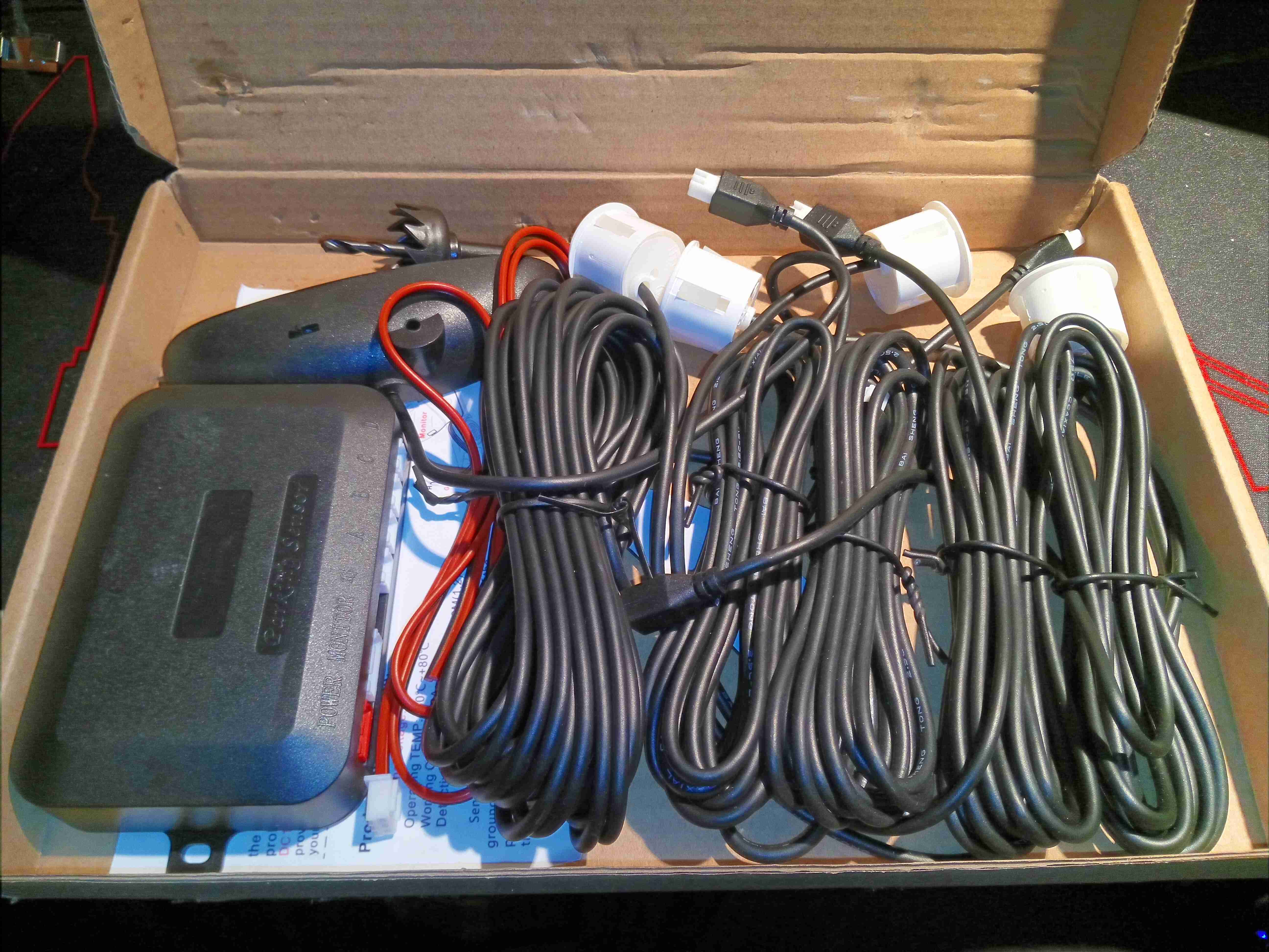
This is a cheap kit from eBay, to retrofit an older car with ultrasonic parking sensors. 4 sensors are included in the kit, along with a hole saw to fit them to the bumper. There’s a small controller module, and a display module that fits onto the dash of the car.
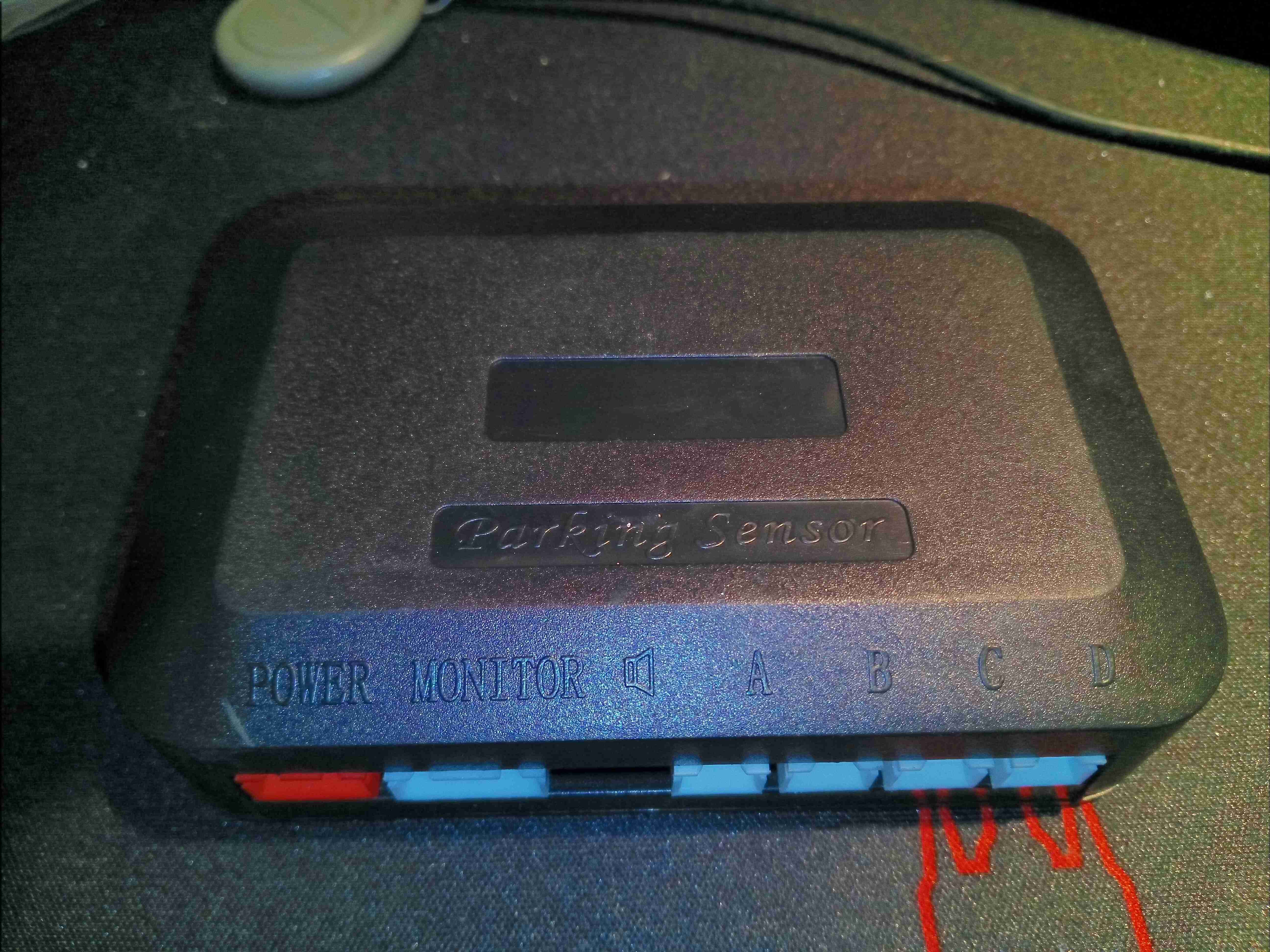
Controller Module
Here’s the controller module, with it’s row of connectors along the front. The unit gets it’s power from the reversing light circuit, via the red connector.
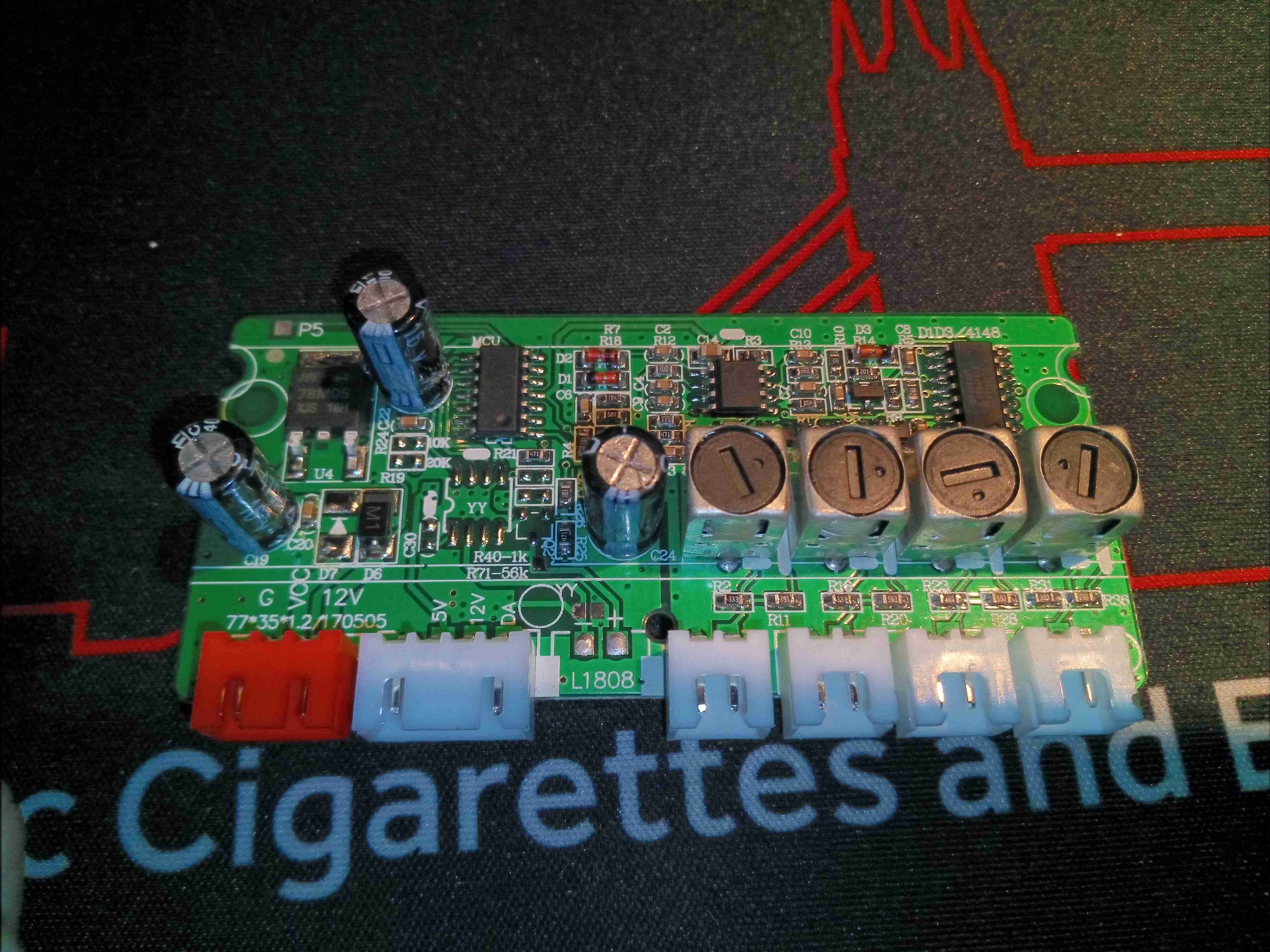
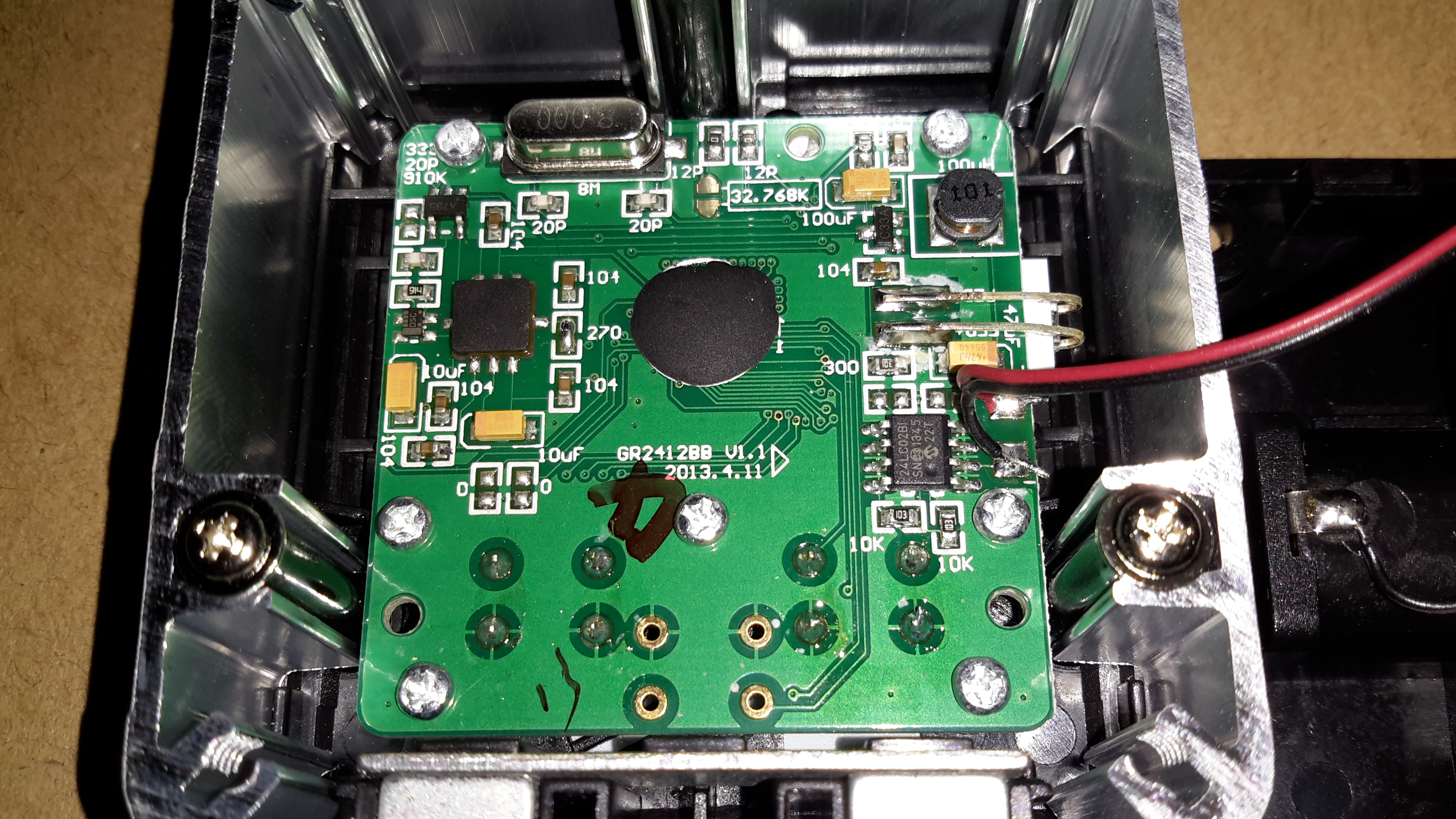
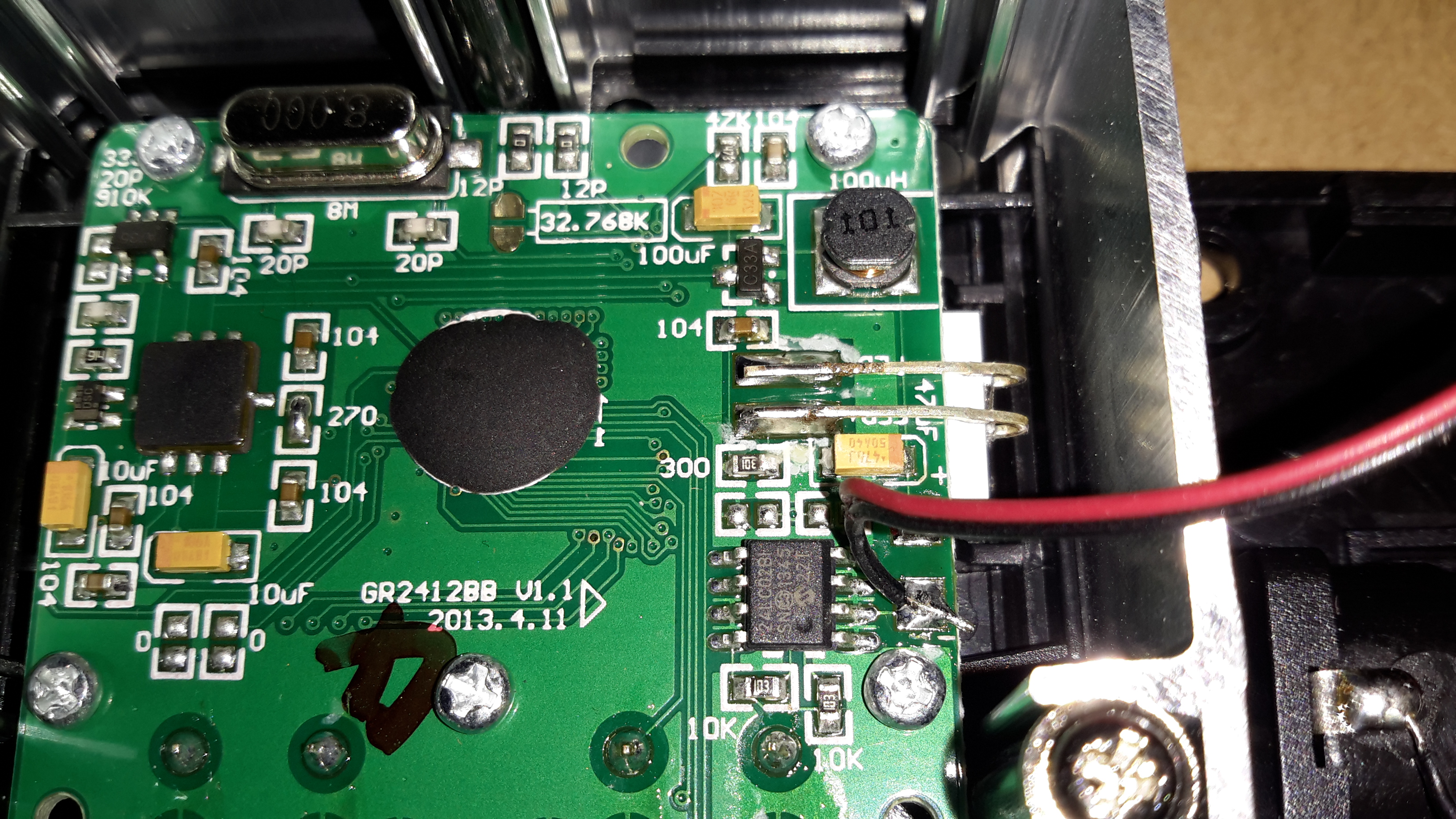
Main Controller PCB
Removing a couple of screws allows the PCB to be removed. There’s quite a bit on this board, including 4 tunable inductors for the ultrasonic transducers. There’s a linear voltage regulator on the left which supplies power to the electronics, and a completely unmarked microcontroller.
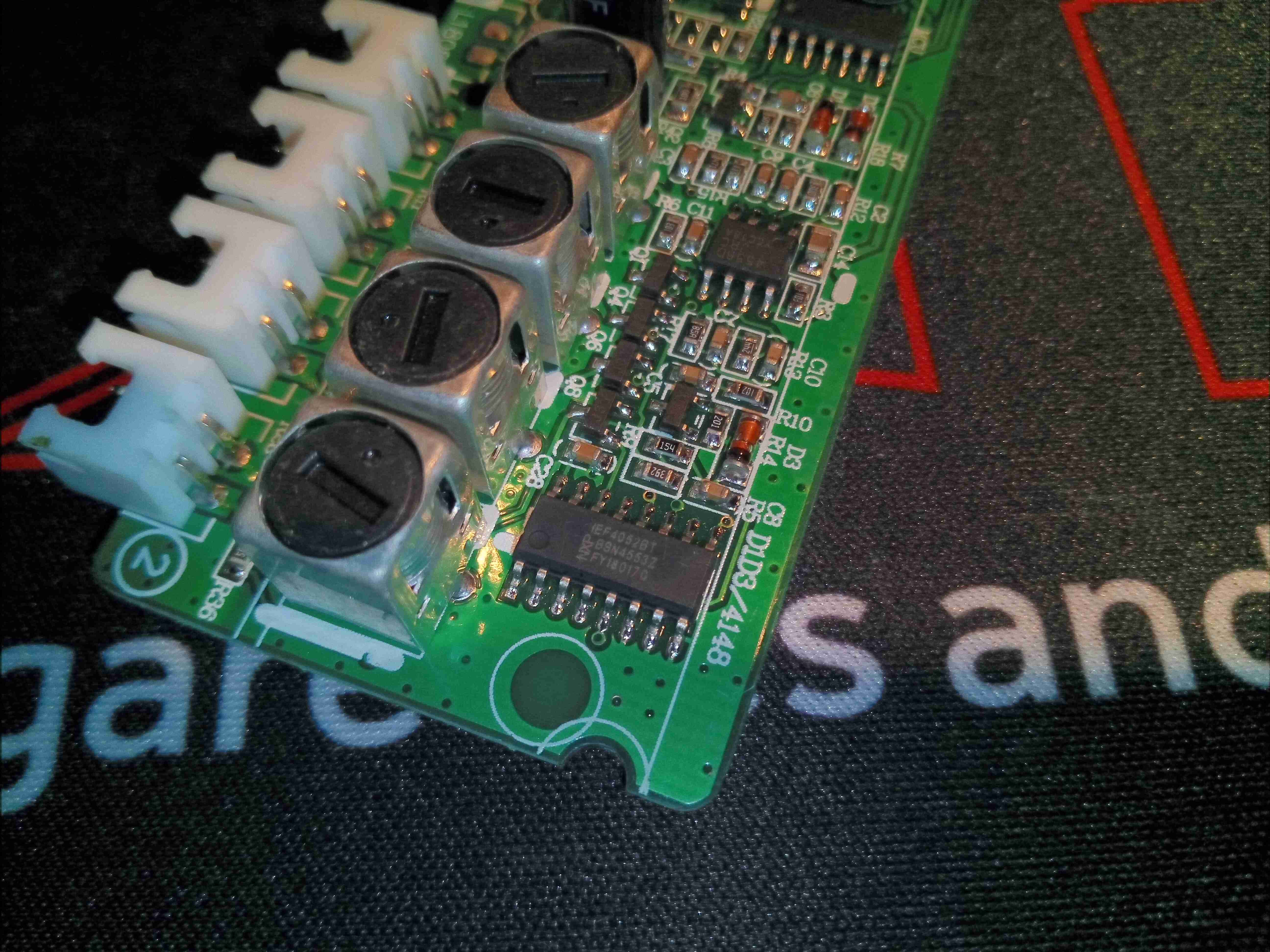
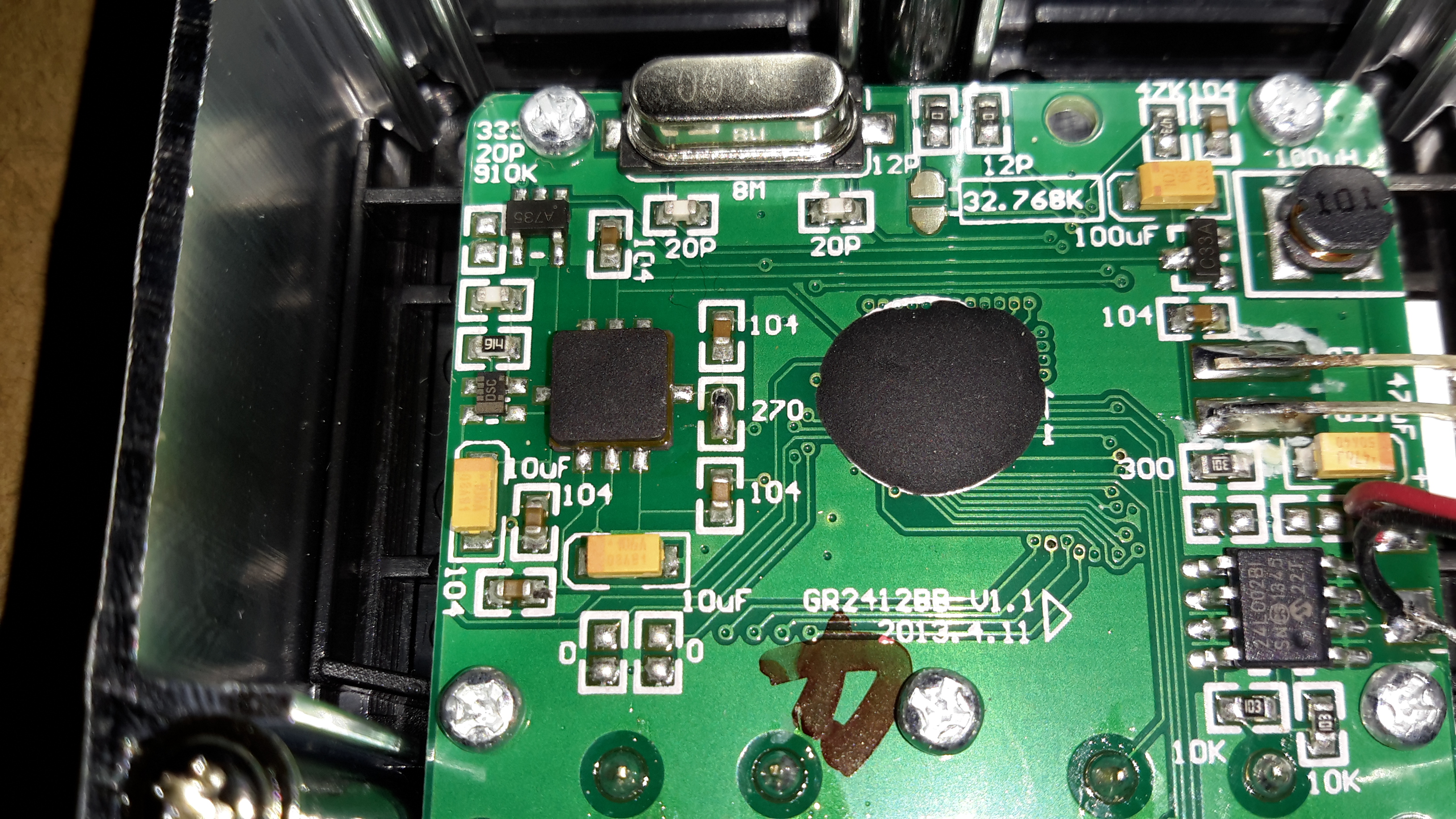
Electronics Closeup
A closer look at the analogue end of the board shows a JRC4558D dual Op-Amp, and an NXP HEF4052B analogue multiplexer. As the microcontroller is unmarked I have no data for that one.
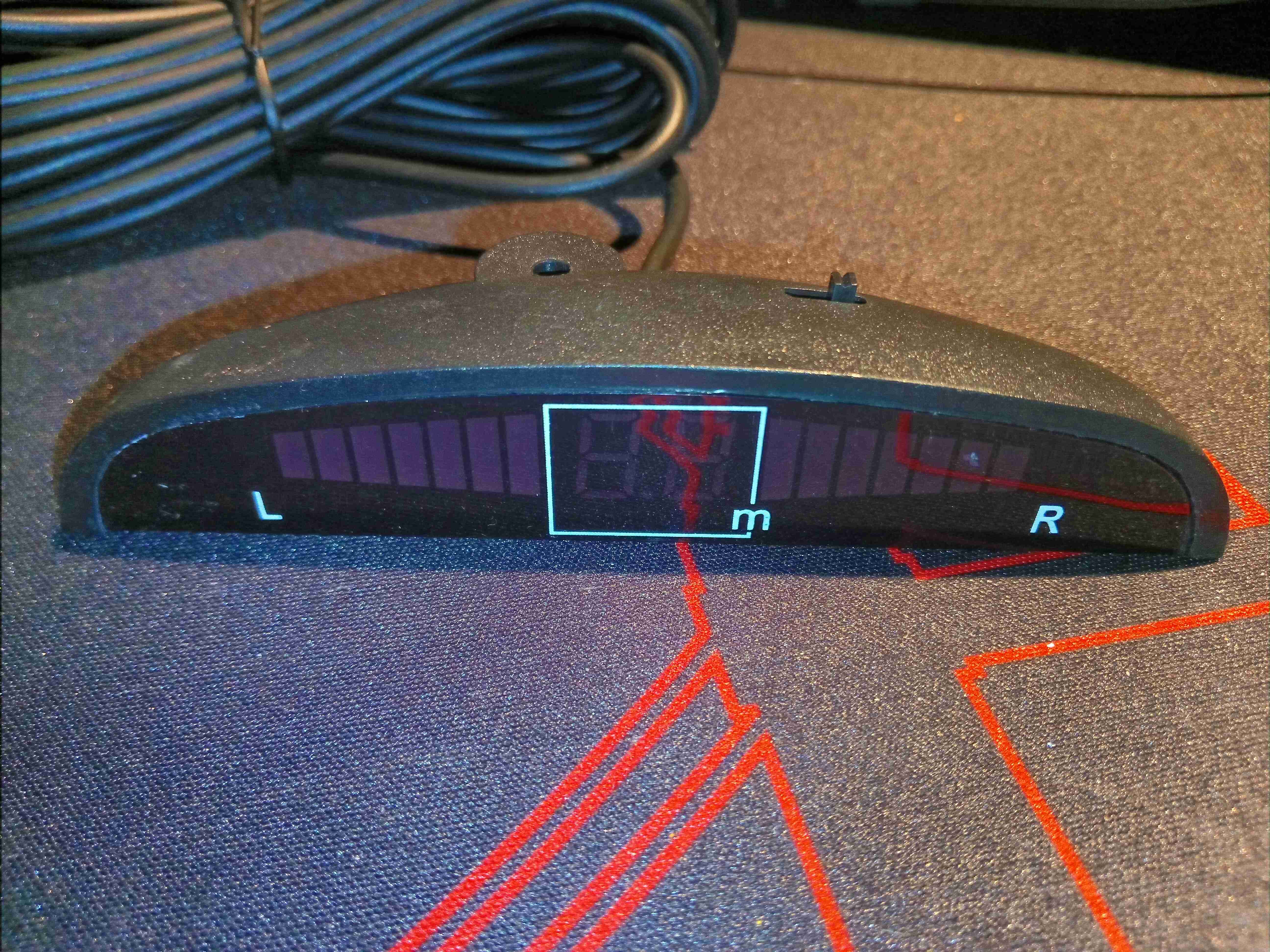
Dash Display
The dash display is housed in another small plastic box, with bargraphs for each side of the car & an overall distance meter.
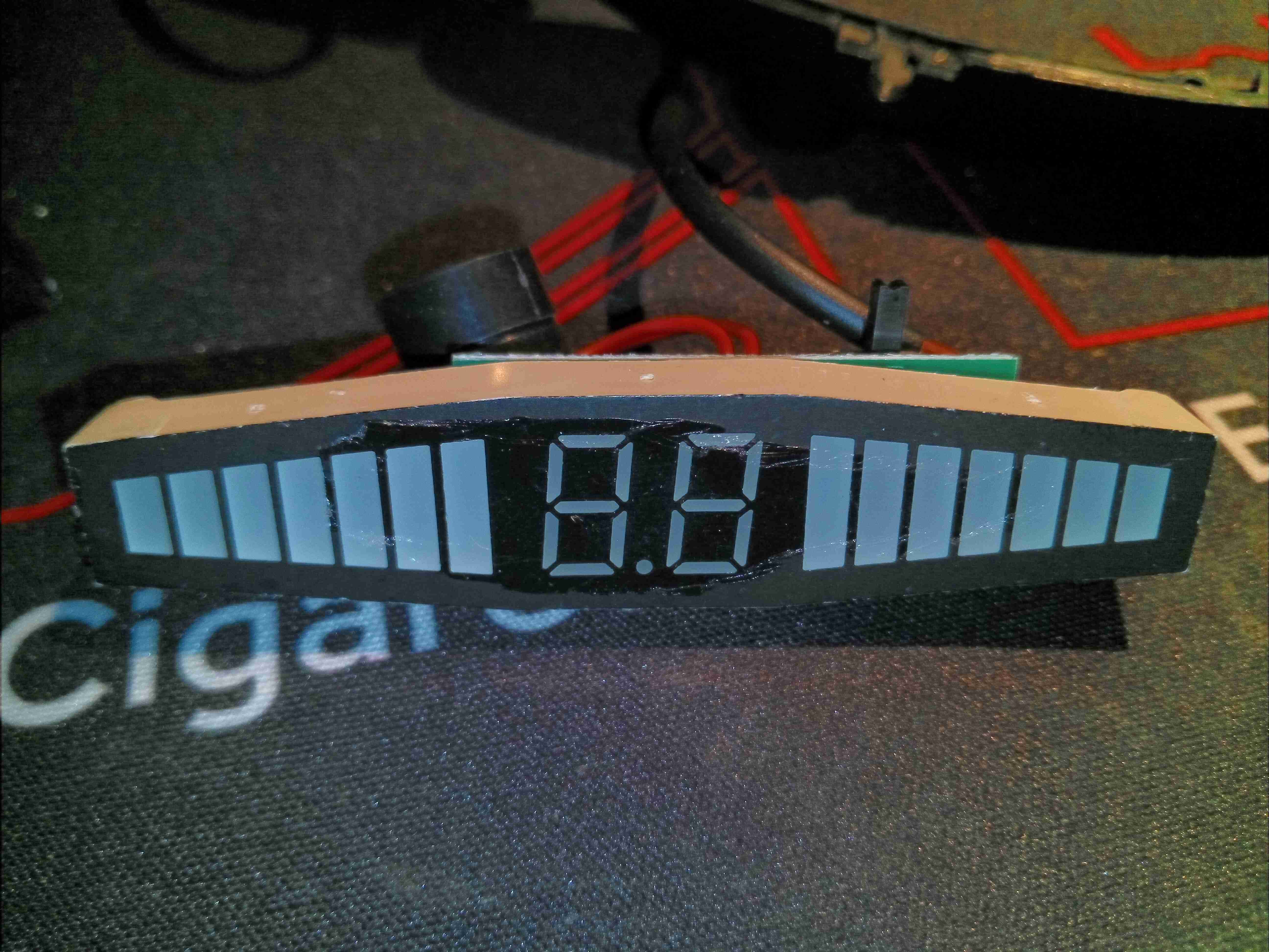
Display Module
Clearly this is a custom module, with the tapered bargraph LEDs on each side & the 7-segment display in the centre. There’s a beeper which works like every factory-fitted unit does, increasing in rate as the distance closes.
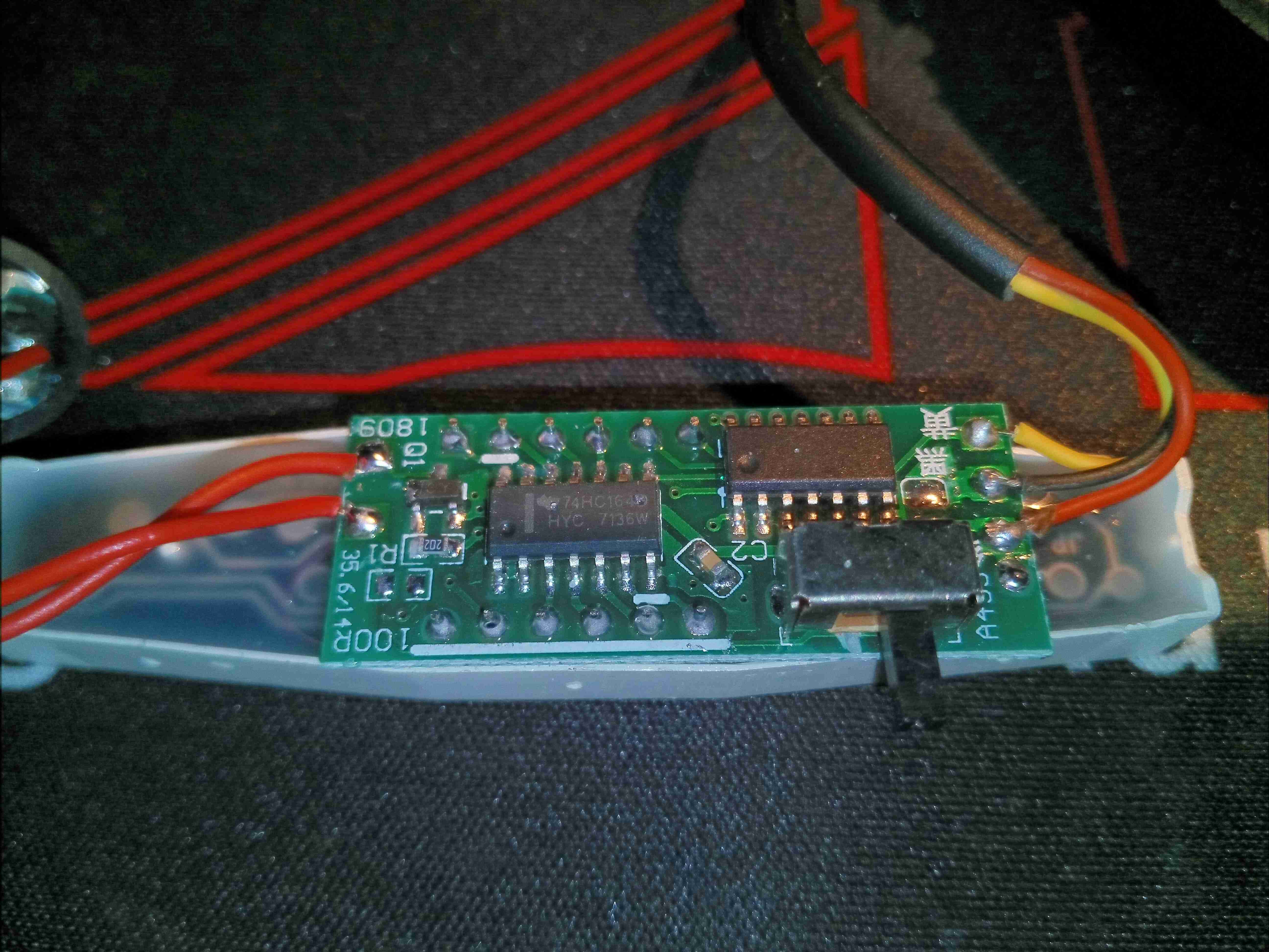
Display PCB
The back of the display module has the driver PCB, with yet another unmarked microcontroller, and a TI 74HC164 serial shift register as a display driver. There’s only 3 wires in the loom from the controller, so some sort of 1-wire protocol must be being used, while I²C is the most likely protocol to be talking to the display driver circuit. There’s also a small switch for muting the beeper.
Here’s another random bit of RF tech, I’m told this is a wireless energy management sensor, however I wasn’t able to find anything similar on the interwebs. It’s powered by a standard 9v PP3 battery.
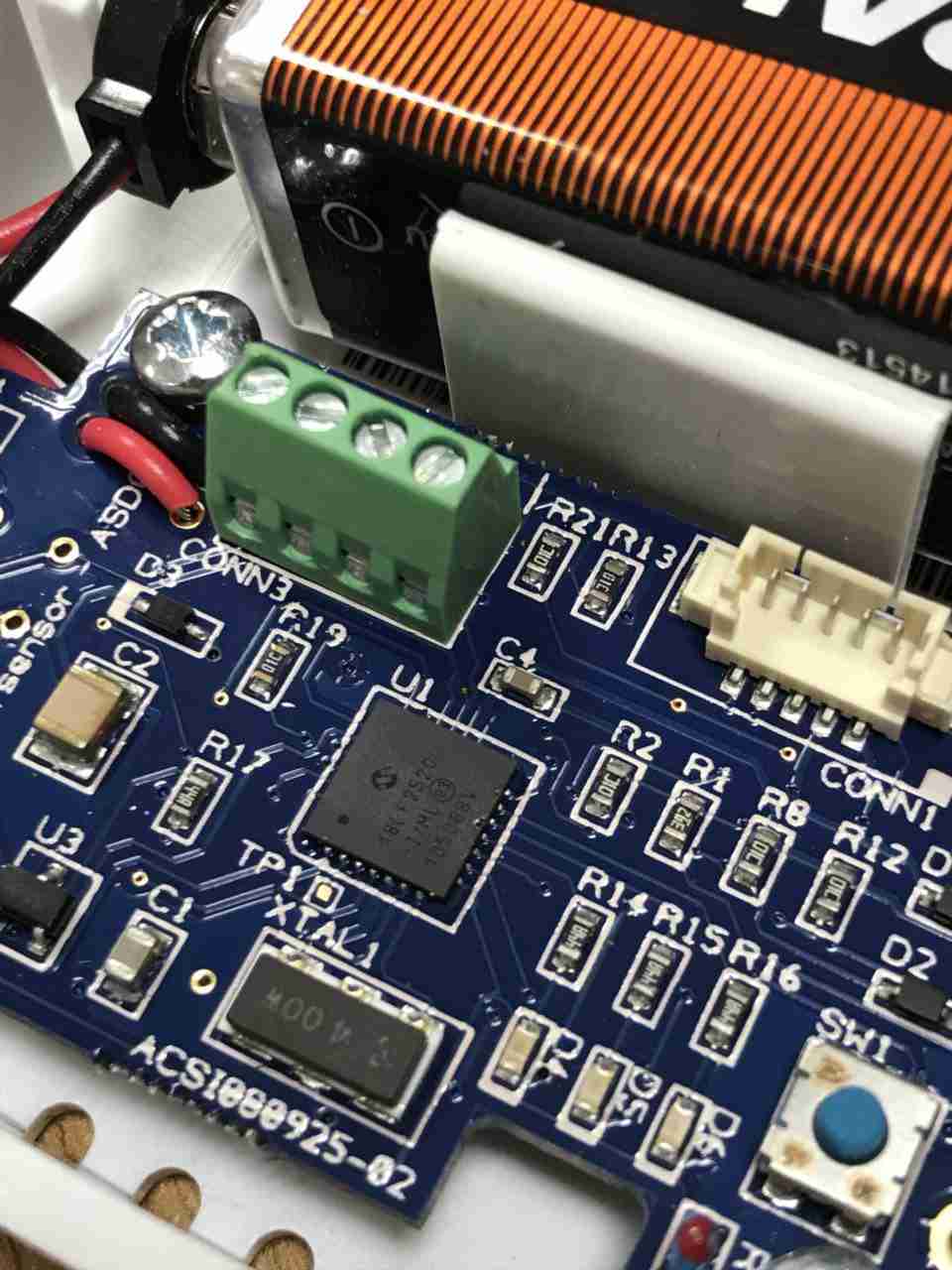
Microcontroller
System control is handled by this Microchip PIC18F2520 Enhanced Flash microcontroller, this has an onboard 10-bit ADC & nanoWatt technology according to their datasheet. There’s a 4MHz crystal providing the clock, with a small SOT-23 voltage regulator in the bottom corner. There’s a screw terminal header & a plug header, but I’ve no idea what these would be used for. Maybe connecting an external voltage/current sensor & a programming header? The tactile button I imagine is for pairing the unit with it’s controller.
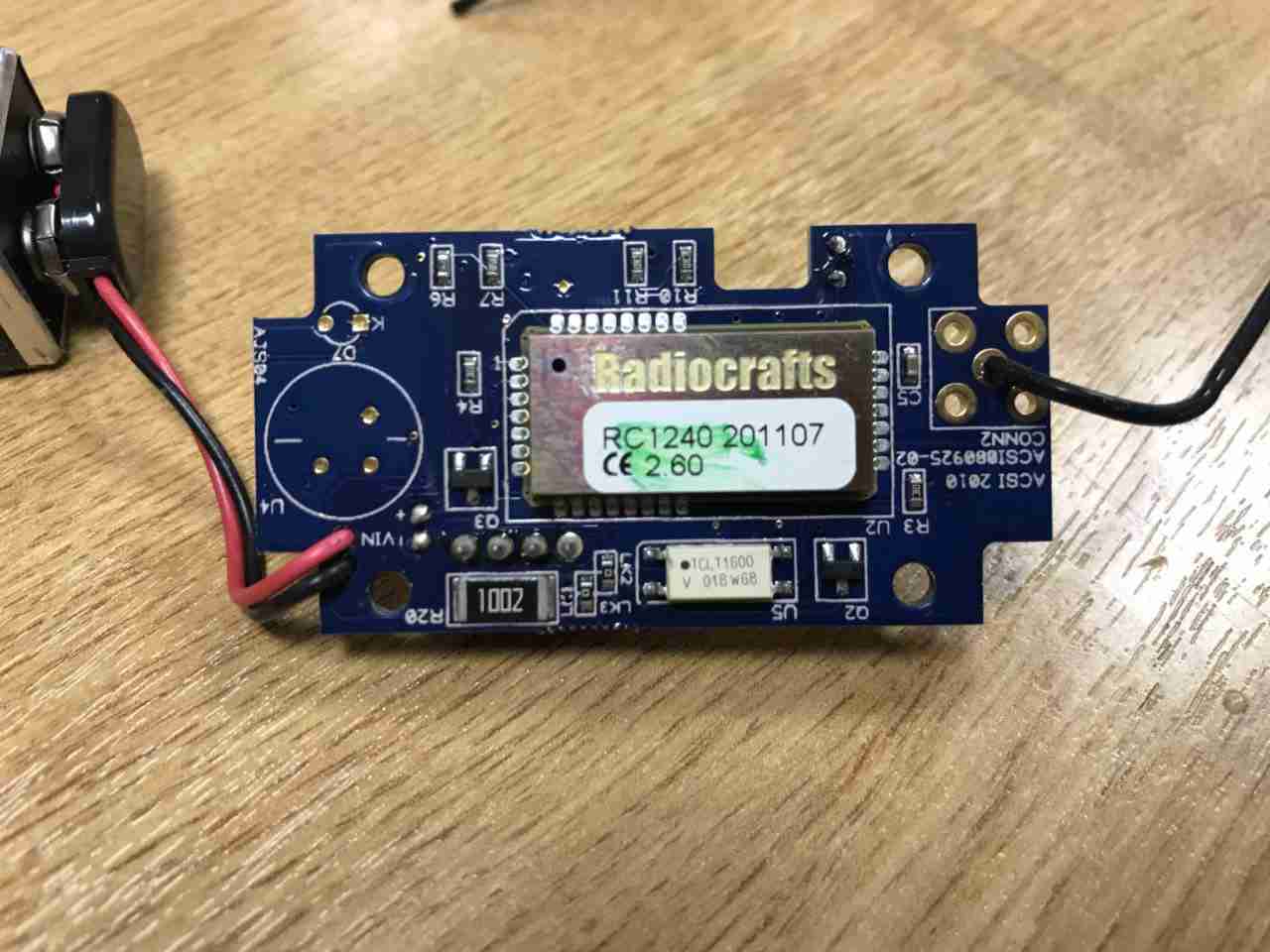
PCB Bottom
The bottom of the PCB is almost entirely taken up by a Radiocrafts RC1240 433MHz RF transceiver. Underneath there’s a large 10kΩ resistor, maybe a current transformer load resistor, and a TCLT1600 optocoupler. Just from the opto it’s clear this unit is intended to interface in some way to the mains grid. The antenna is connected at top right, in a footprint for a SMA connector, but this isn’t fitted.
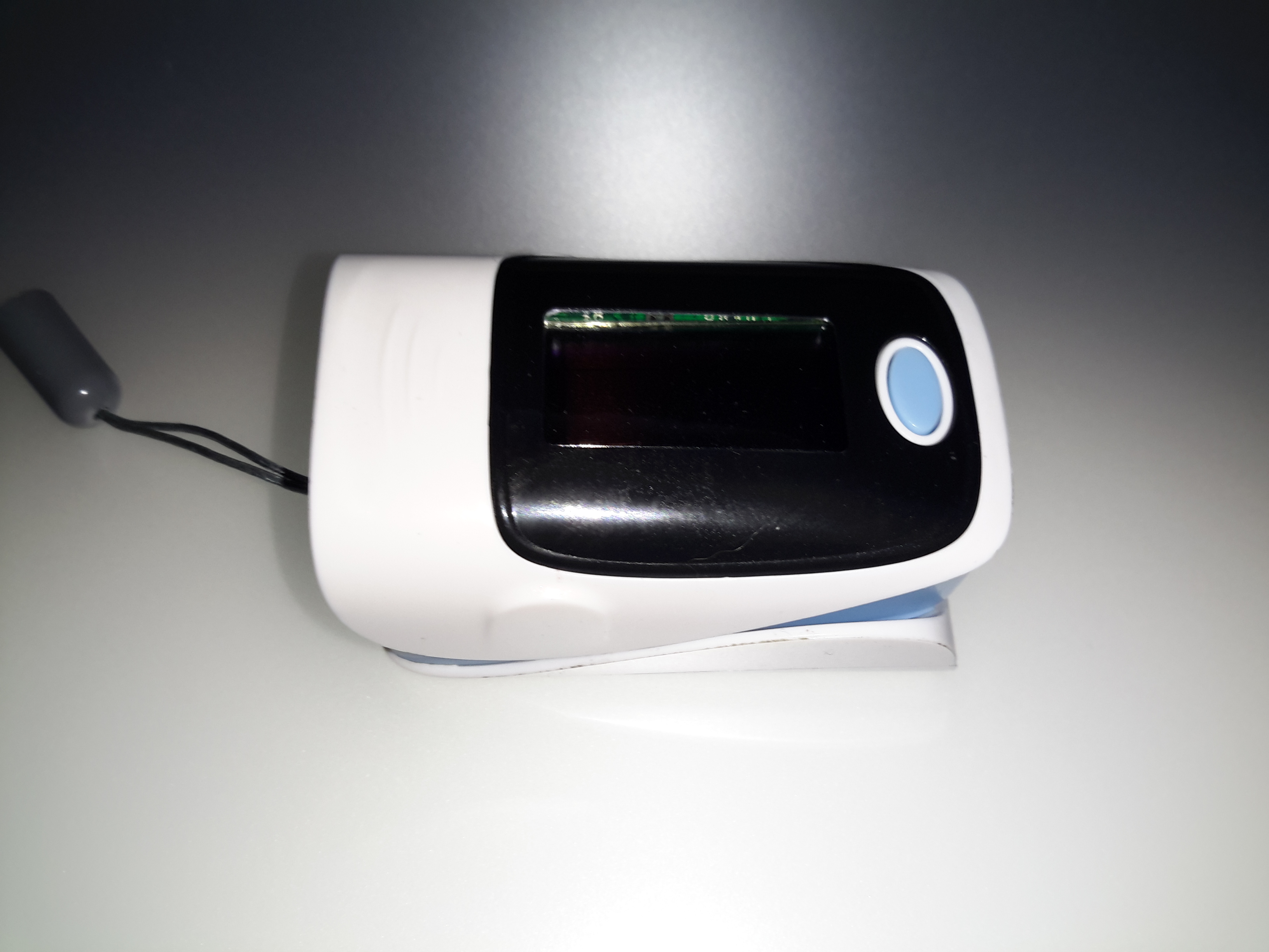
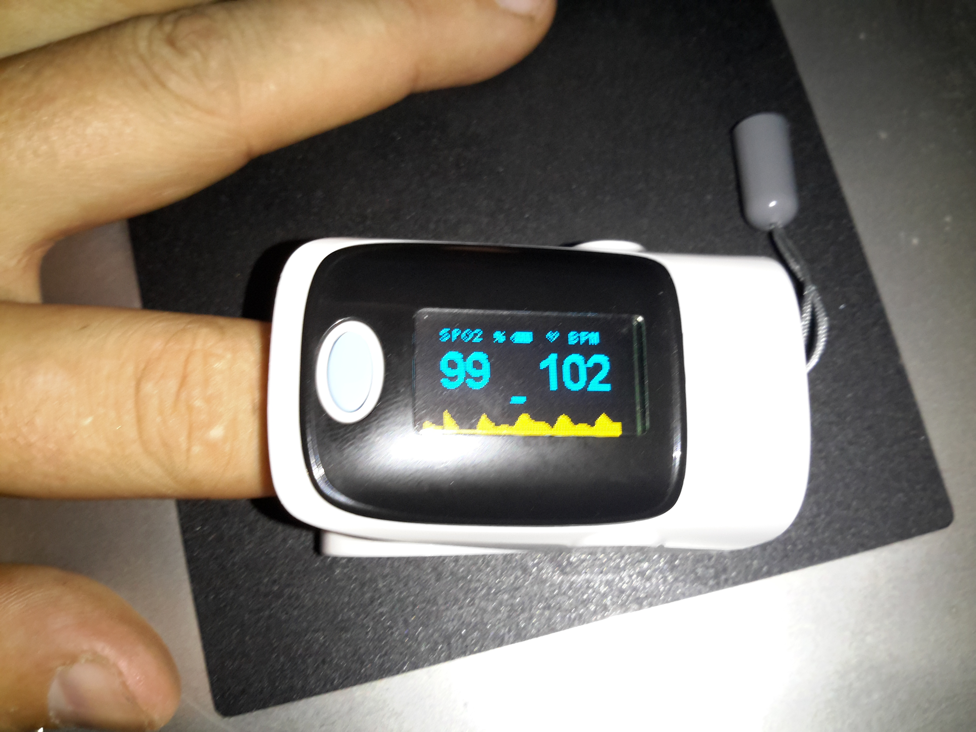
Here’s a piece of medical equipment that in recent years has become extremely cheap, – a Pulse Oximeter, used to determine the oxygen saturation in the blood. These can be had on eBay for less than £15.
Powered On
This one has a dual colour OLED display, a single button for powering on & adjusting a few settings. These cheap Oximeters do have a bit of a cheap plastic feel to them, but they do seem to work pretty well.
Pulse Oximeter
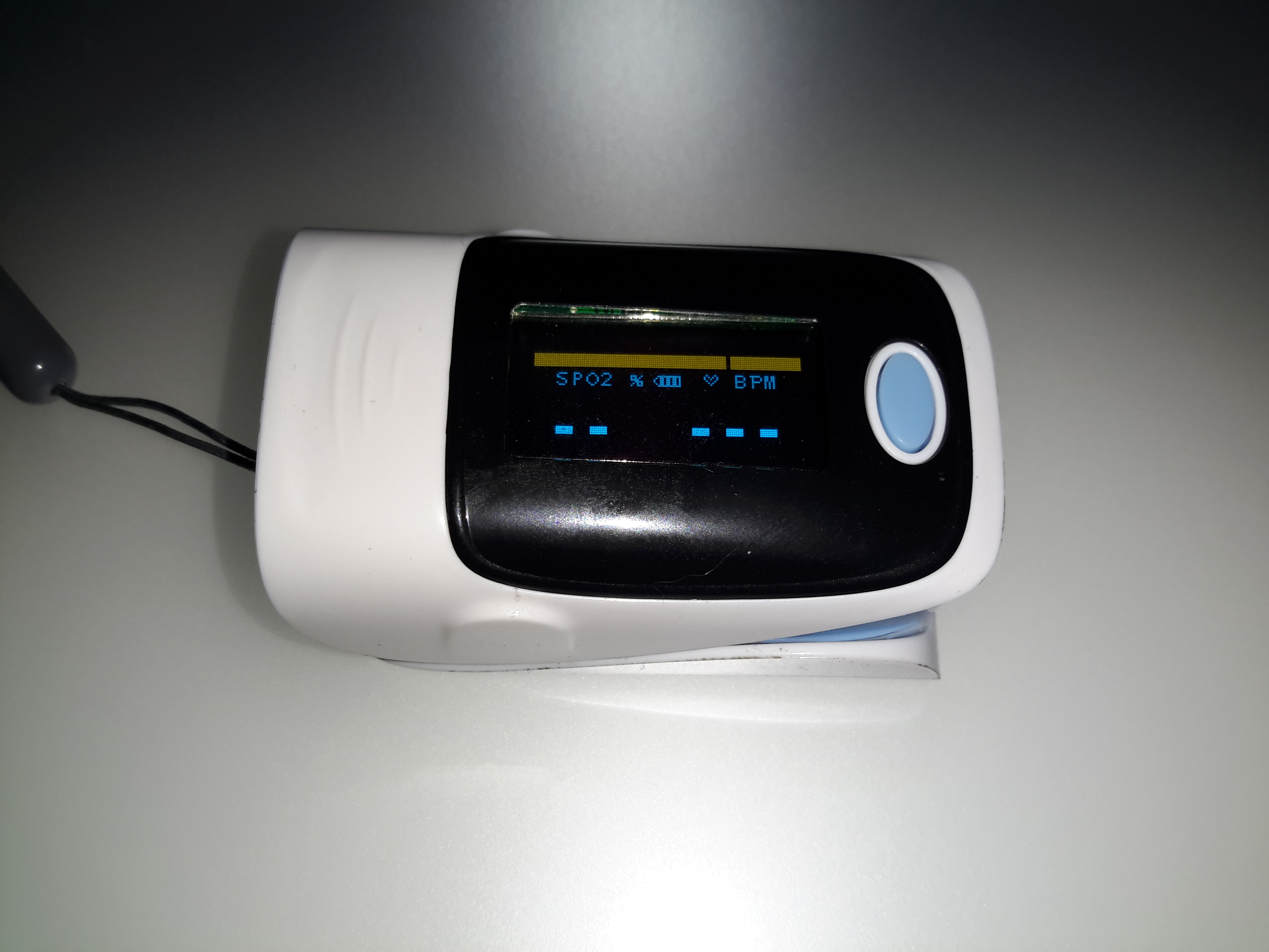
After a few seconds of being applied to a finger, the unit gives readings that apparently confirm that I’m alive at least. 😉 The device takes a few seconds to get a baseline reading & calibrate the sensor levels.
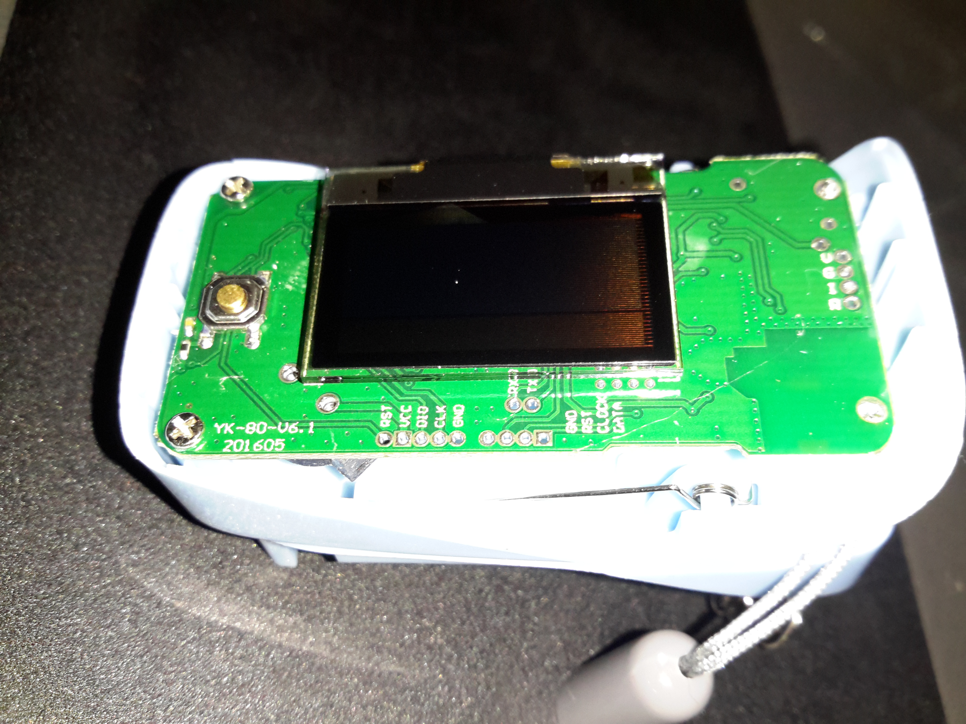
Main PCB Top
The plastic casing is held together with a few very small screws, but comes apart easily. here is the top of the main board with the OLED display panel. There appears to be a programming header & a serial port on the board as well. I’ll have to poke at these pads with a scope to see if any useful data is on the pins.
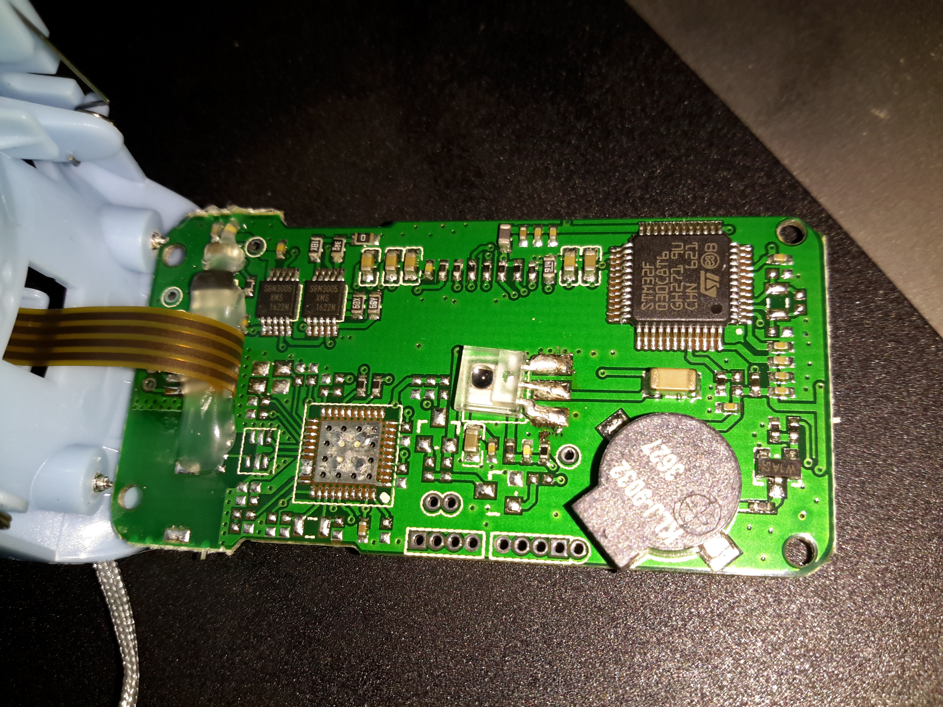
Main PCB Bottom
The bottom of the board has all the main components of the system. The microcontroller is a STM32F03C8T6, these are very common in Chinese gear these days. There’s a small piezo beeper & the main photodiode detector is in the centre.
There is an unpopulated IC space on the board with room for support components. I suspect this would be for a Bluetooth radio, as there’s a space at the bottom left of the PCB with no copper planes – this looks like an antenna mounting point. (The serial port on the pads is probably routed here, for remote monitoring).
At the top left are a pair of SGM3005 Dual SPDT analogue switches. These will be used to alternate the red & IR LEDs on the other side of the shell.
A 4-core FFC goes off to the other side of the shell, bringing power from the battery & supplying the sensing LEDs.
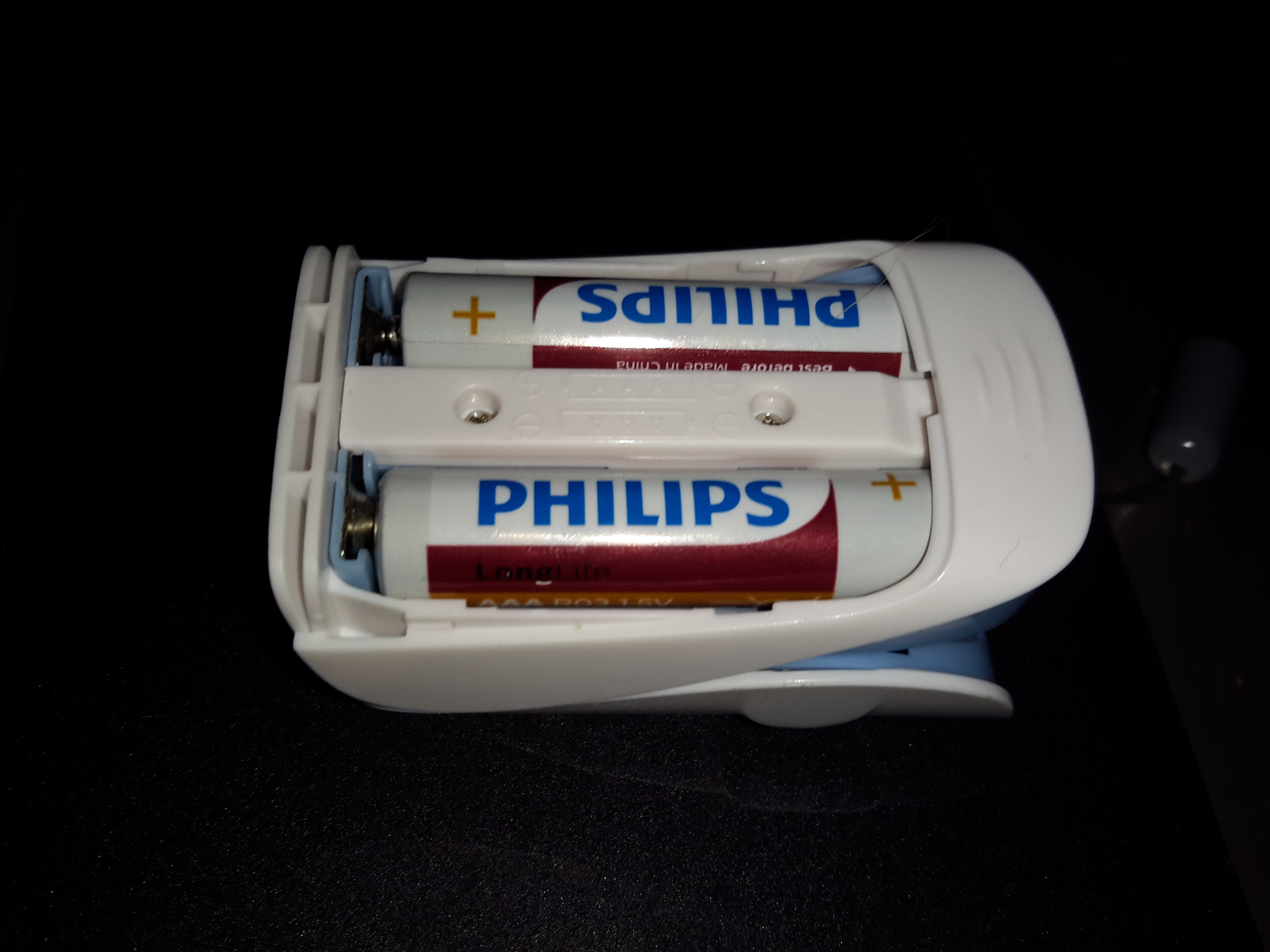
Battery Compartment
Power is supplied by a pair of AAA cells in the other shell.
Dual LED
The sensor LEDs are tucked in between the cells, this dual-diode package has a 660nm red LED & a 940nm IR LED.
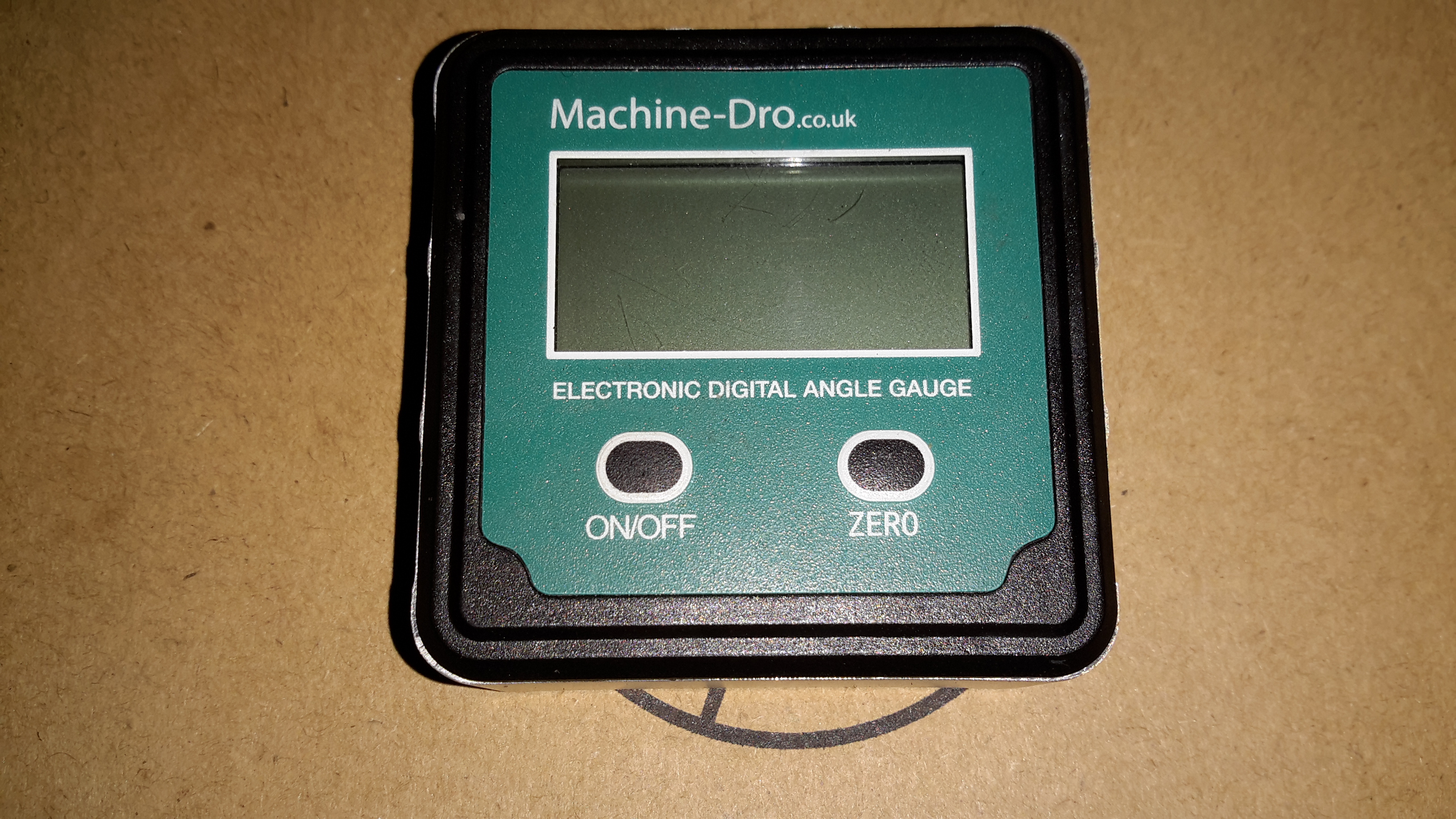
Here’s a useful tool for the kit, a digital angle gauge/protractor. These use a silicon sensor to show the number of degrees the unit is out of level.
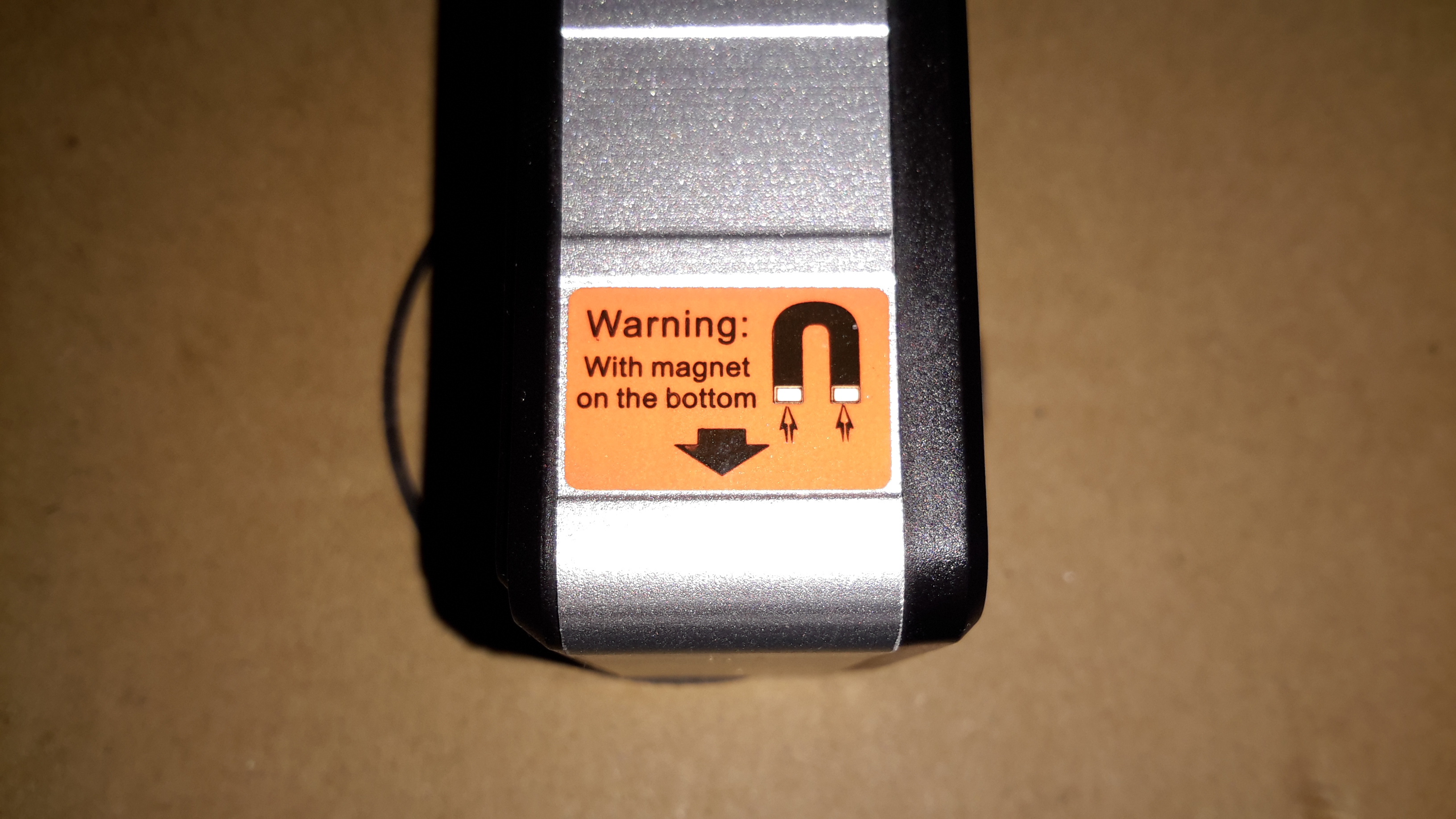
Magnets!
Magnets are provided in the base, so the tool can attach to any ferrous surface.
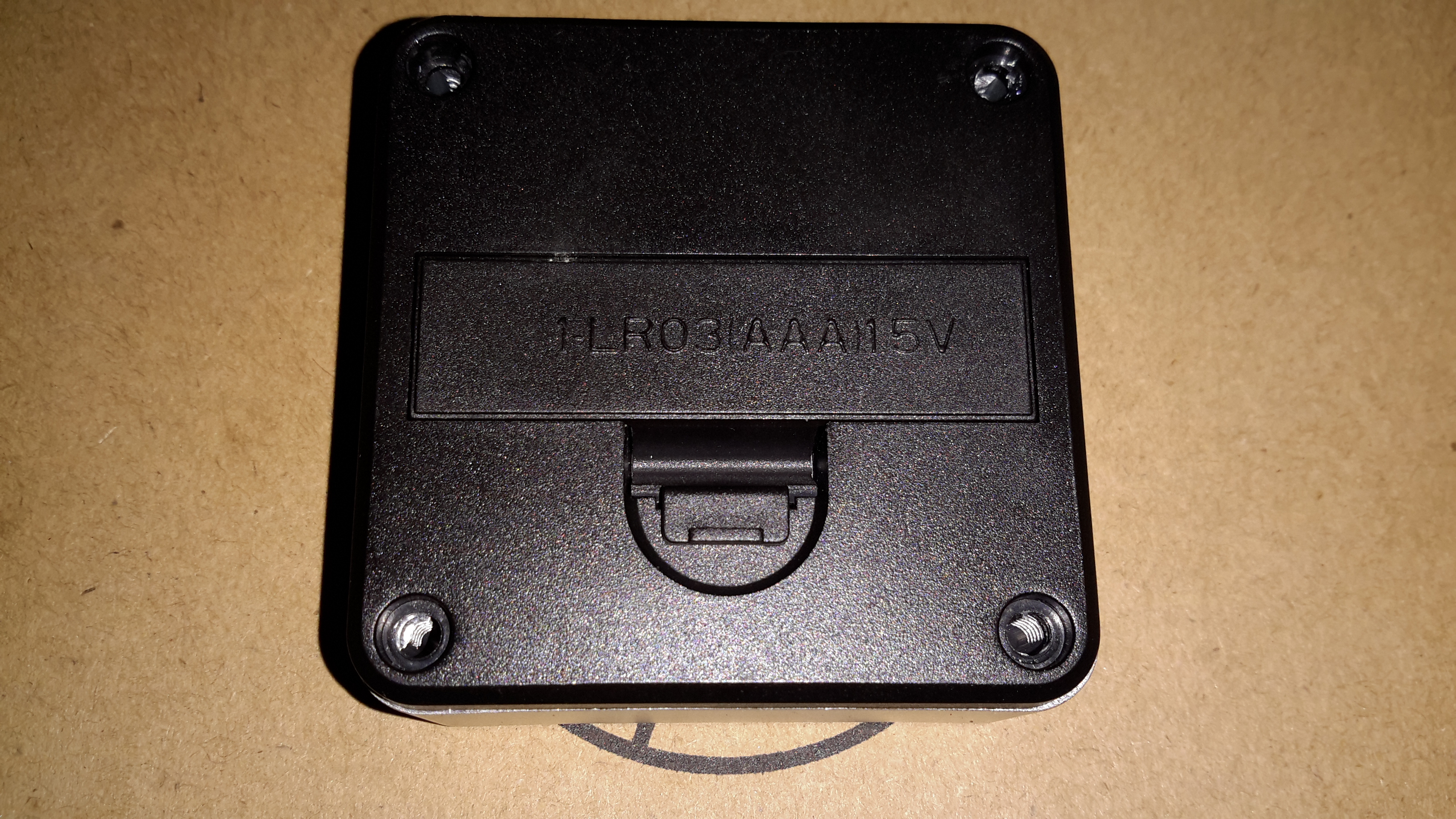
Battery Box
Power is provided by a single AAA cell.
Main PCB
Removing the rear cover reveals the brains of the unit, and there’s not much to it at all. The main microcontroller is a CoB-type device, so no part numbers available from that one.
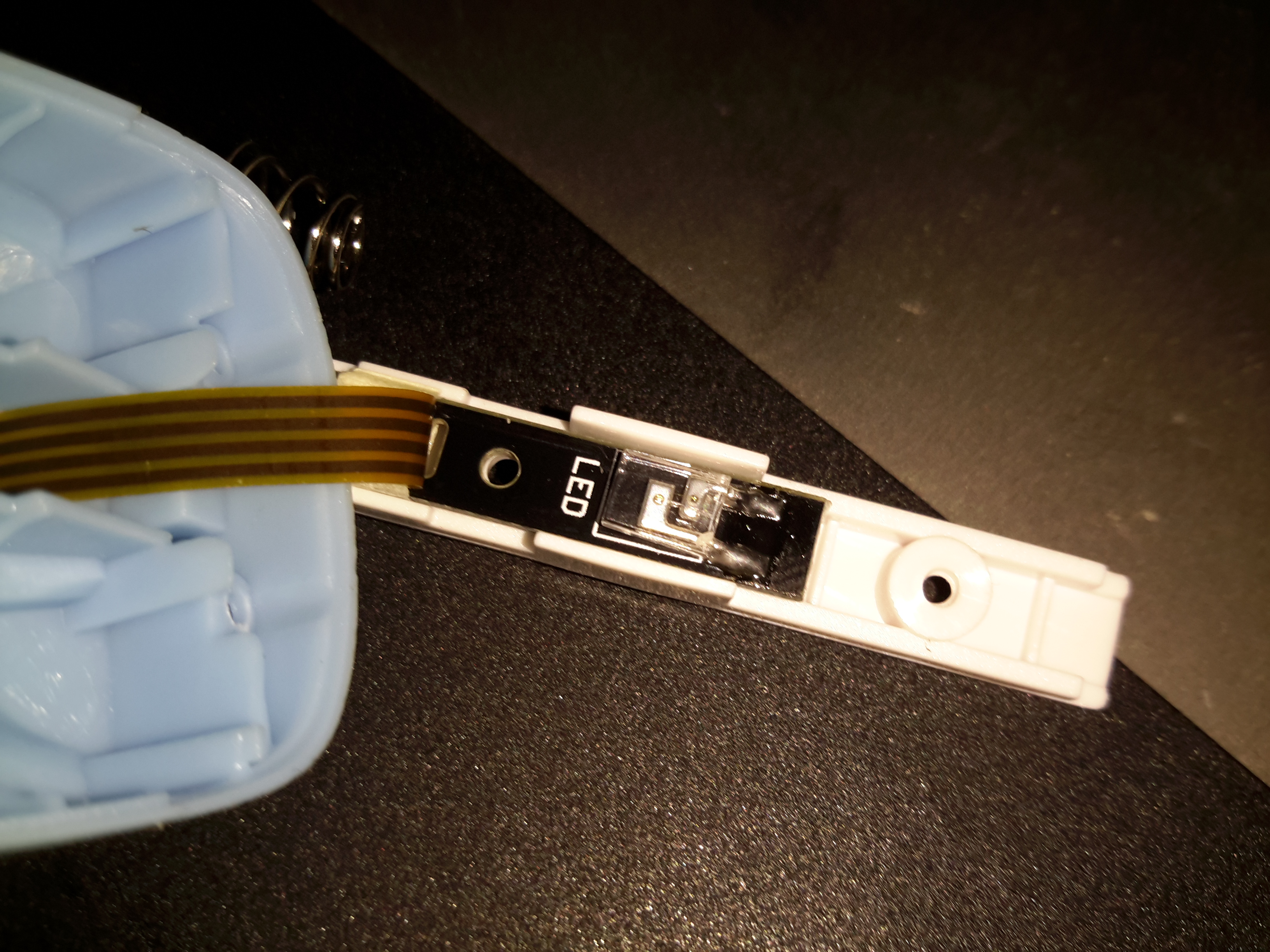
Sensing Element
The IC to the left of the main microcontroller is the sensing element. There’s no markings on this inclinometer IC so I’m not sure of the specs, but it will be a 3D-MEMS device of some sort.
Power Supply
The other side of the PCB has the power supply for the logic, and a serial EEPROM, probably storing calibration data.
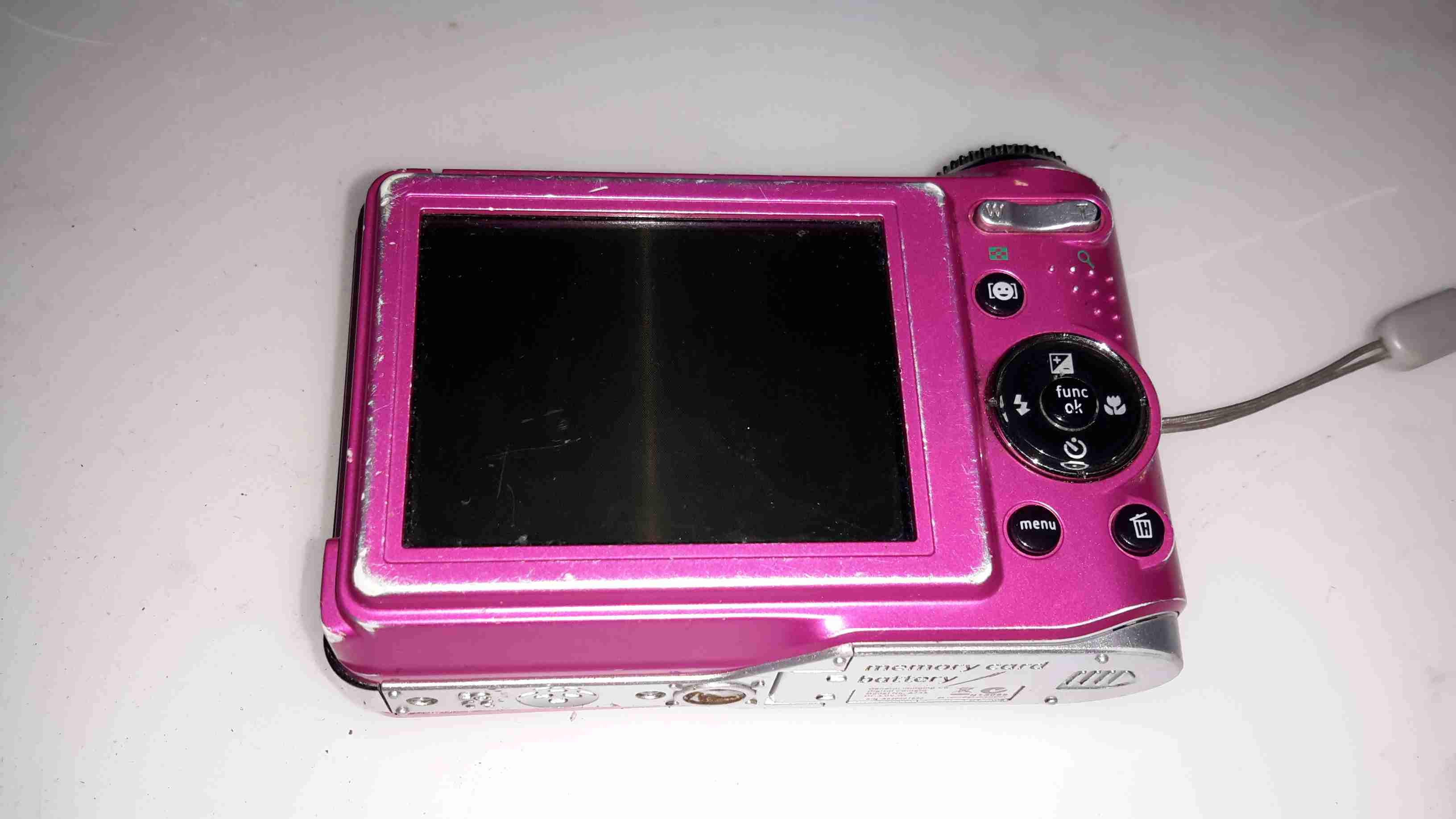
This camera has now been retired after many years of heavy use. Exposure to a 3-year old has caused severe damage to the lens mechanism, which no longer functions correctly.
Rear Panel
Pretty much standard interface for a digital camera, with a nice large LCD for it’s time.
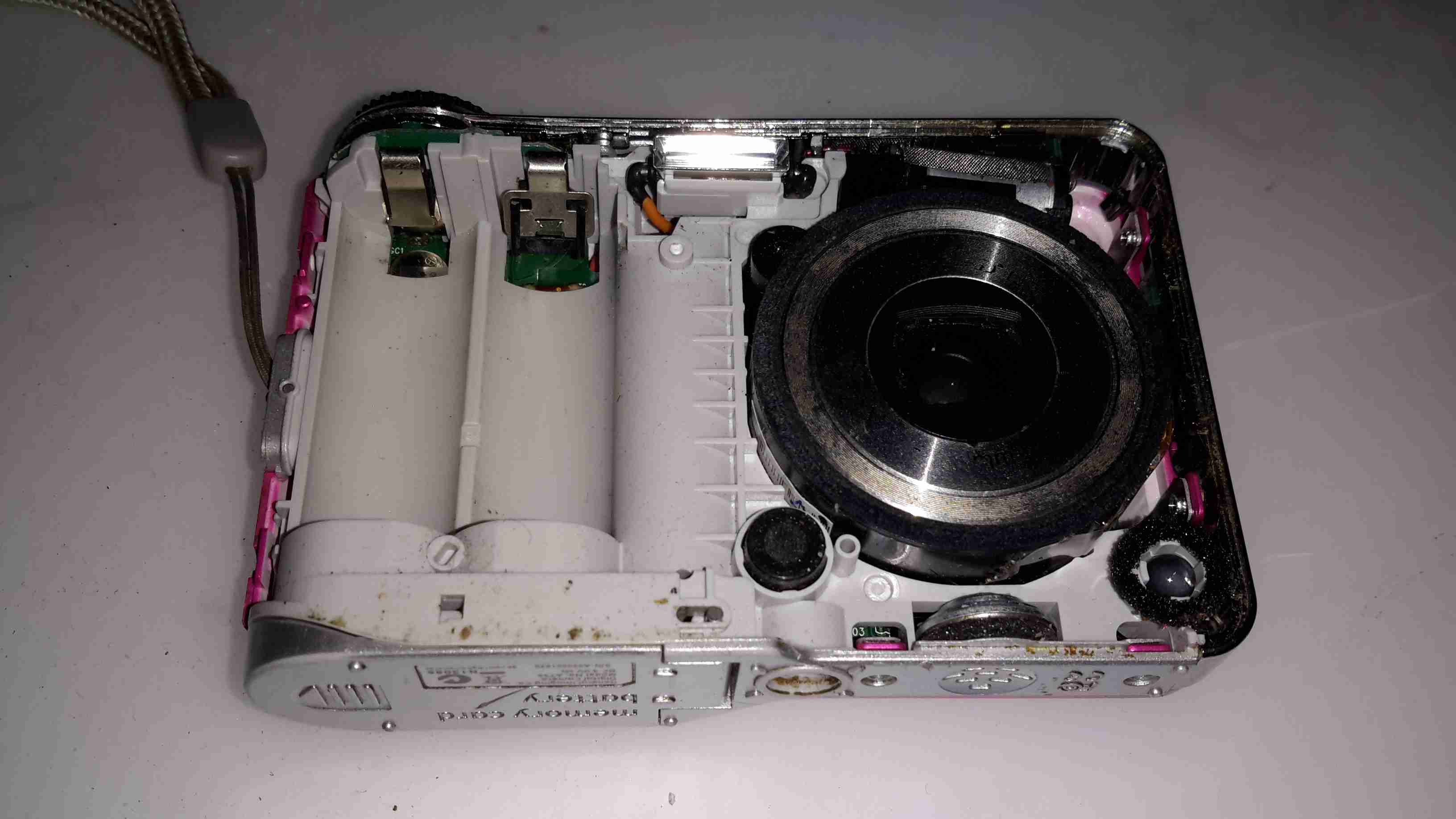
Front Cover Removed
With the front cover removed, the lens assembly & battery compartment is exposed.
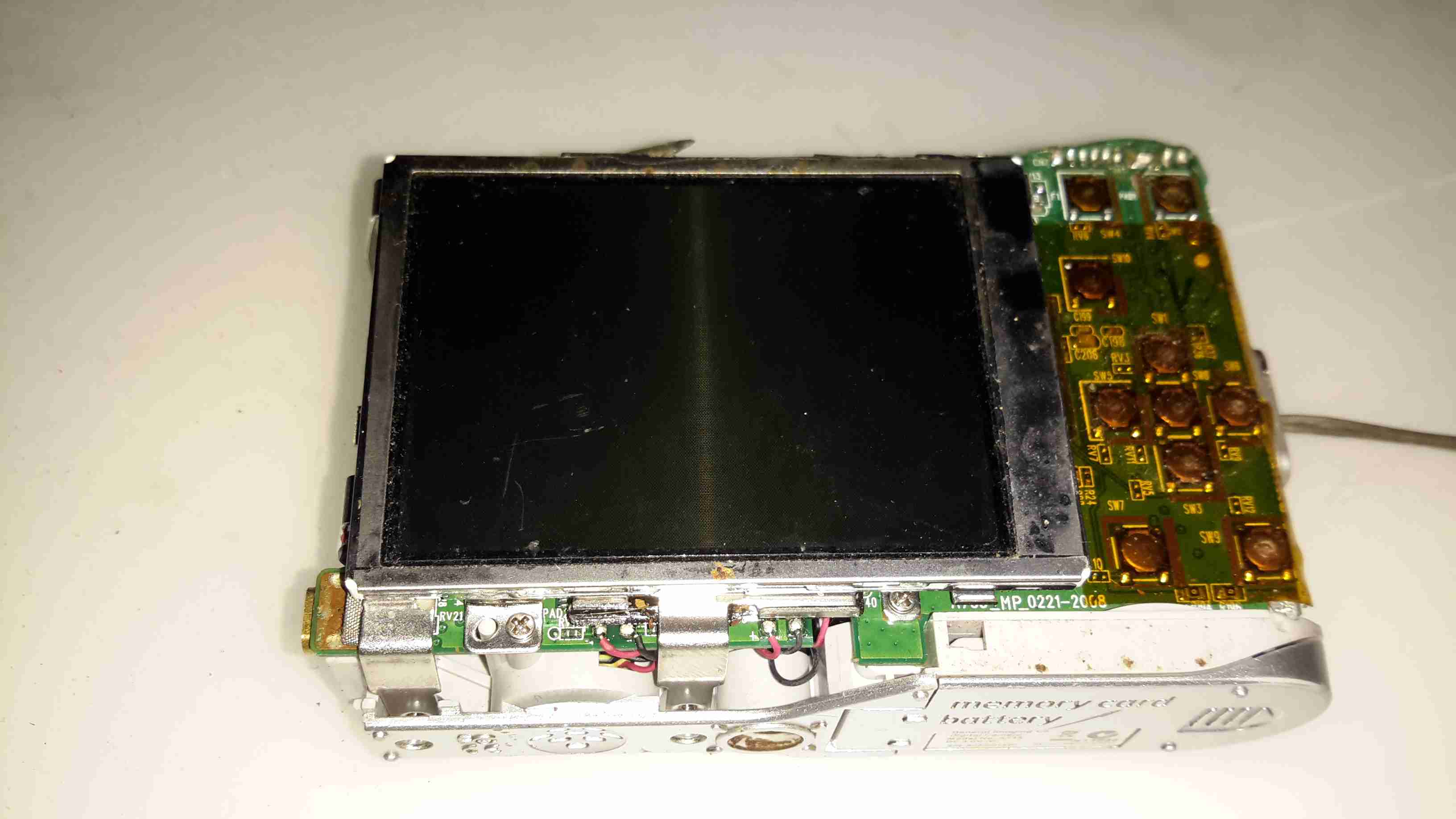
Rear Cover Removed
Removing the rear cover exposes the LCD module & the main PCB, the interface tactile switches are on the right under a protective layer of Kapton tape.
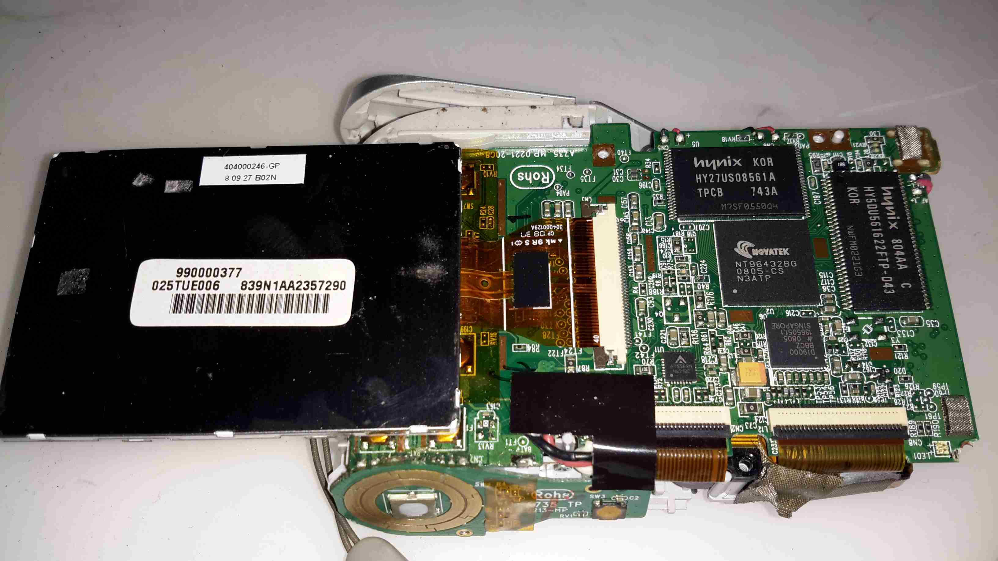
Main Chipset
Flipping the LCD out of it’s mounting bracket reveals the main camera chipset. The CPU is a NovaTek NT96432BG, no doubt a SoC of some kind, but I couldn’t find any information. Firmware & inbuilt storage is on a Hynix HY27US08561A 256MBit NAND Flash, with a Hynix HY5DU561622FTP-D43 256Mbit DRAM for system memory.
I couldn’t find any info on the other two chips on this side of the board, but one is probably a motor driver for the lens, while the other must be the front end for the CCD sensor input to the SoC.
Main PCB Reverse
The other side of the PCB handles the SD card slot & power management. All the required DC rails are provided for by a RT9917 7-Channel DC-DC converter from RichTek, an IC designed specifically for digital camera applications.
Top left above the SD card slot is the trigger circuitry for the Xenon flash tube & the RTC backup battery.
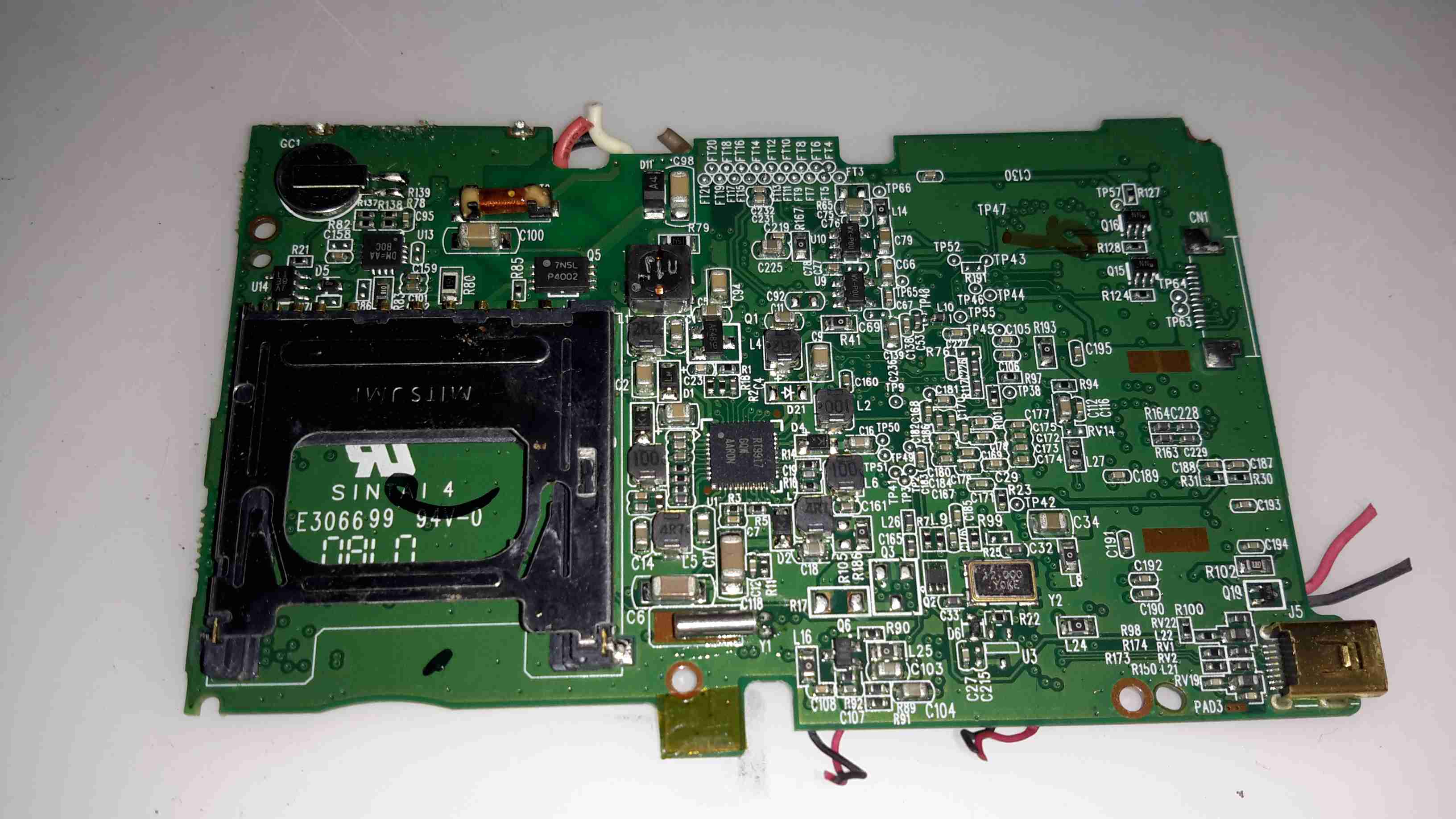
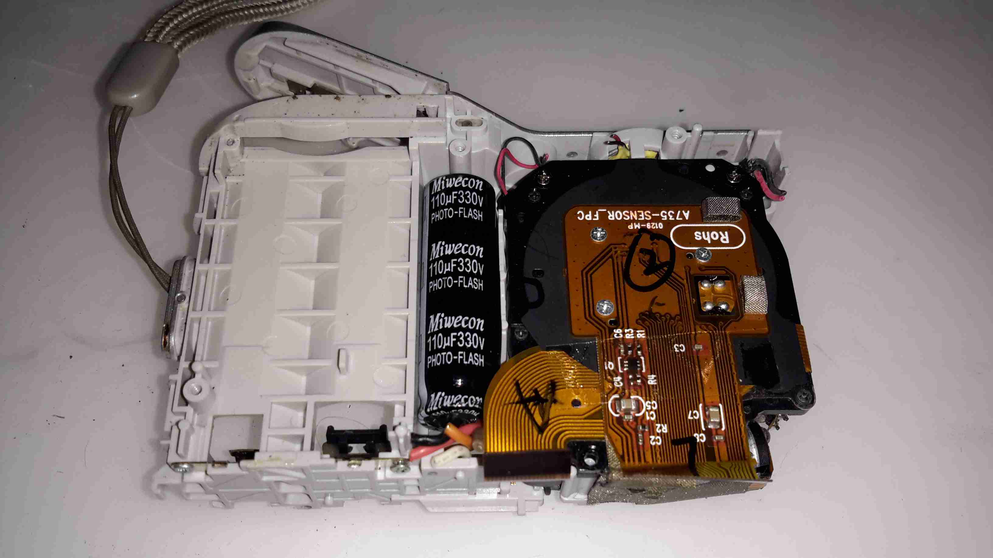
Main PCB Removed
Once the main PCB is out of the frame, the back of the lens module with the CCD is accessible. Just to the left is the high-voltage photoflash capacitor, 110µF 330v. These can give quite the kick when charged! Luckily this camera has been off long enough for the charge to bleed off.
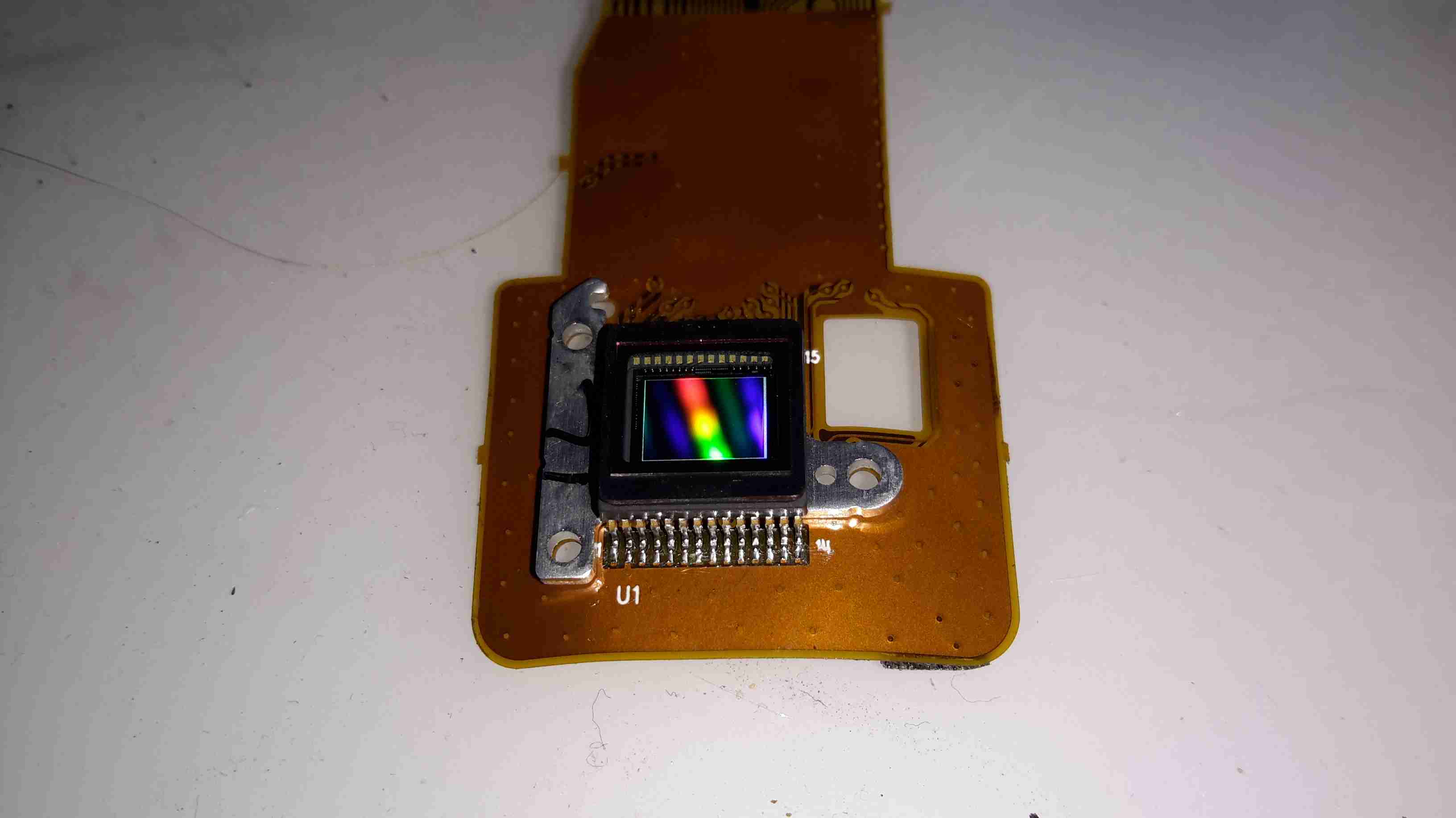
Sensor
Finally, here’s the 7-Megapixel CCD sensor removed from the lens assembly, with it’s built in IR cut filter over the top. I couldn’t find any make or model numbers on this part, as the Aluminium mounting bracket behind is bonded to the back of the sensor with epoxy, blocking access to any part information.
Die images of the chipset to come once I get round to decapping them!
As I’ve been posting some photos of decapped ICs lately, I thought I’d share the process I use personally for those that might want to give it a go 😉
The usual method for removing the epoxy package from the silicon is to use hot, concentrated Nitric Acid. Besides the obvious risks of having hot acids around, the decomposition products of the acid, namely NO² (Nitrogen Dioxide) & NO (Nitrogen Oxide), are toxic and corrosive. So until I can get the required fume hood together to make sure I’m not going to corrode the place away, I’ll leave this process to proper labs ;).
The method I use is heat based, using a Propane torch to destroy the epoxy package, without damaging the Silicon die too much.
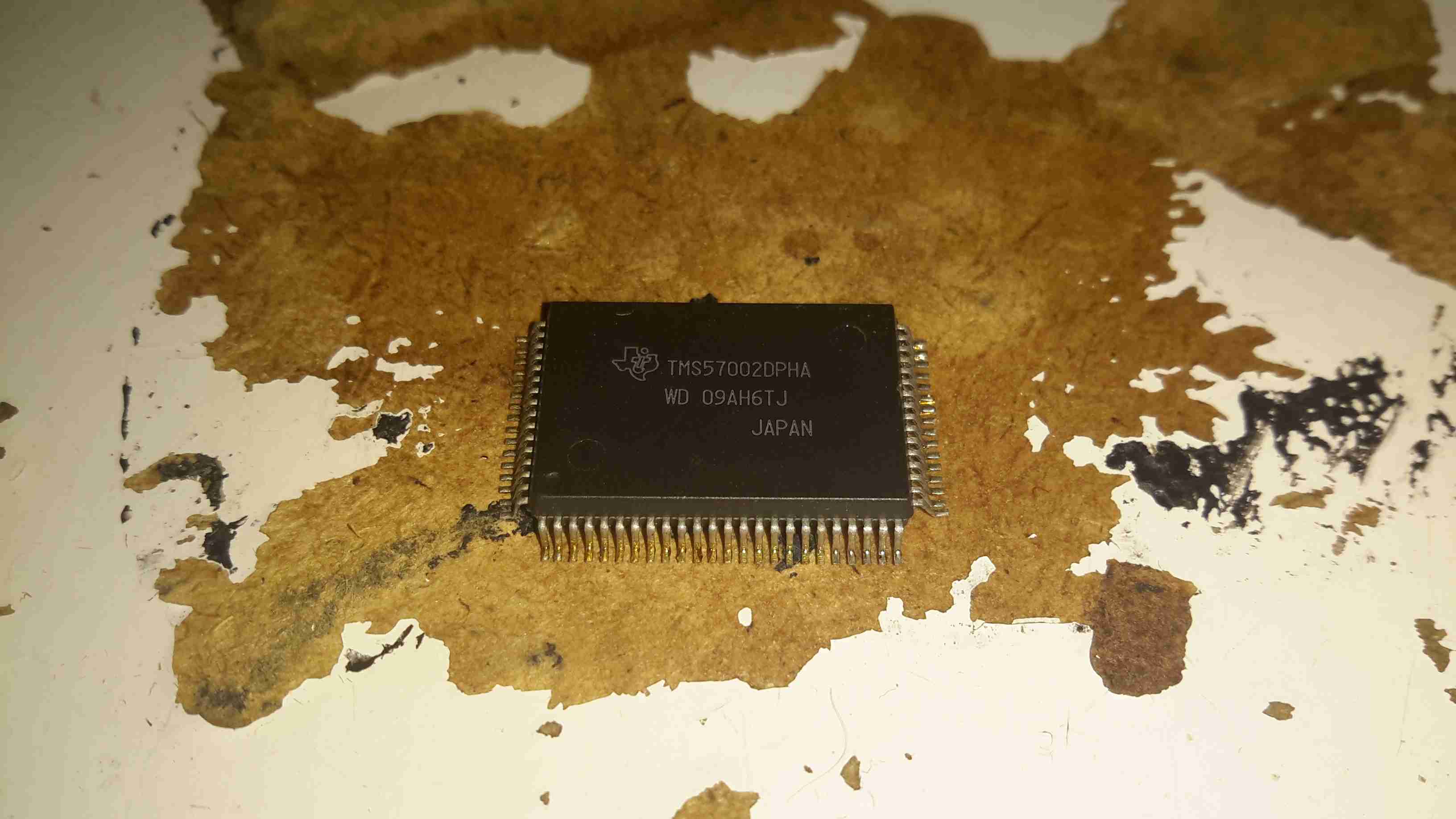
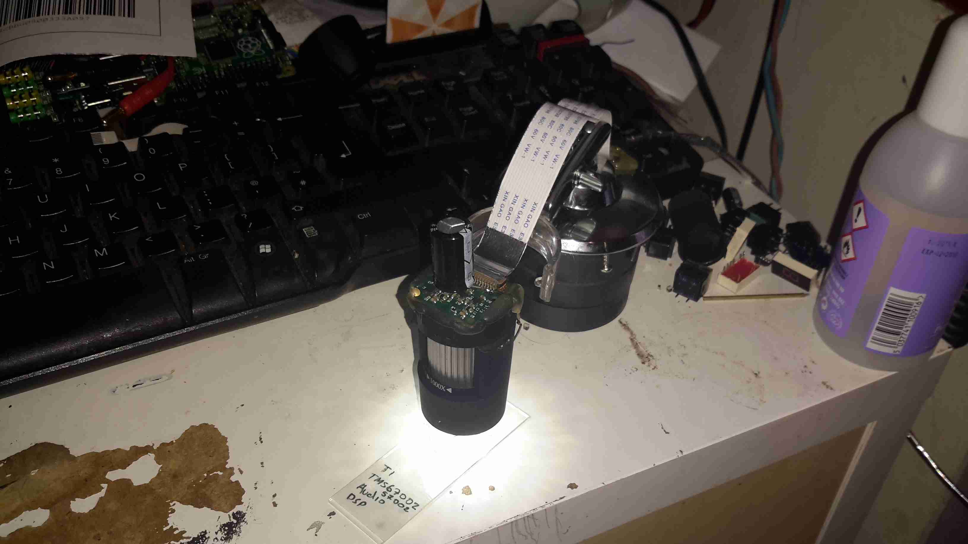
TMS57002 Audio DSP
I start off, obviously, with a desoldered IC, the one above an old audio DSP from TI. I usually desolder en-masse for this with a heat gun, stripping the entire board in one go.
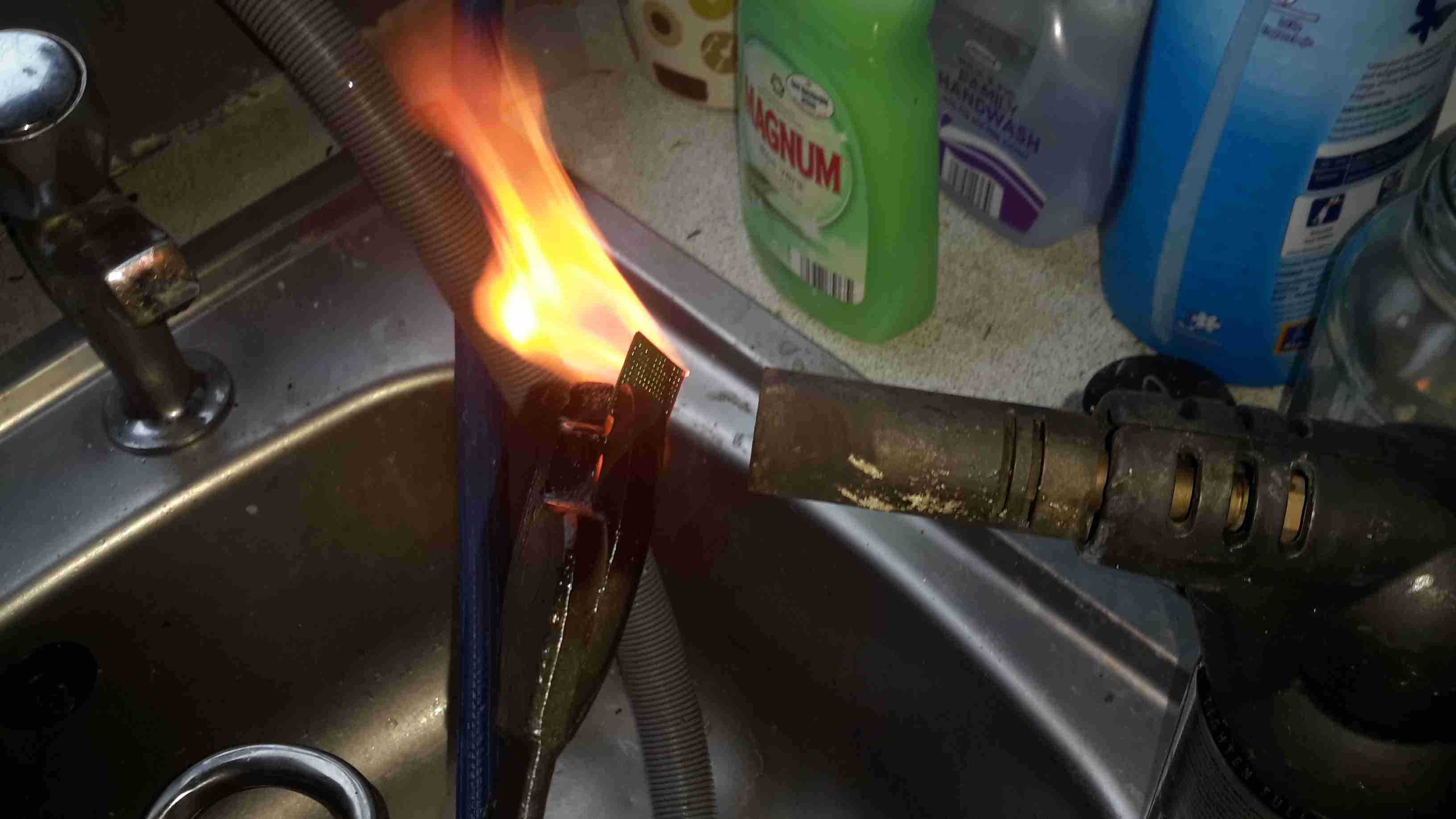
FLAMES!
Next is to apply the torch to the IC. A bit of practice is required here to get the heat level & time exactly right, overheating will cause the die to oxidize & blacken or residual epoxy to stick to the surface.
I usually apply the torch until the package just about stops emitting it’s own yellow flames, meaning the epoxy is almost completely burned away. I also keep the torch flame away from the centre of the IC, where the die is located.
Breathing the fumes from this process isn’t recommended, no doubt besides the obvious soot, the burning plastic will be emitting many compounds not brilliant for Human health!
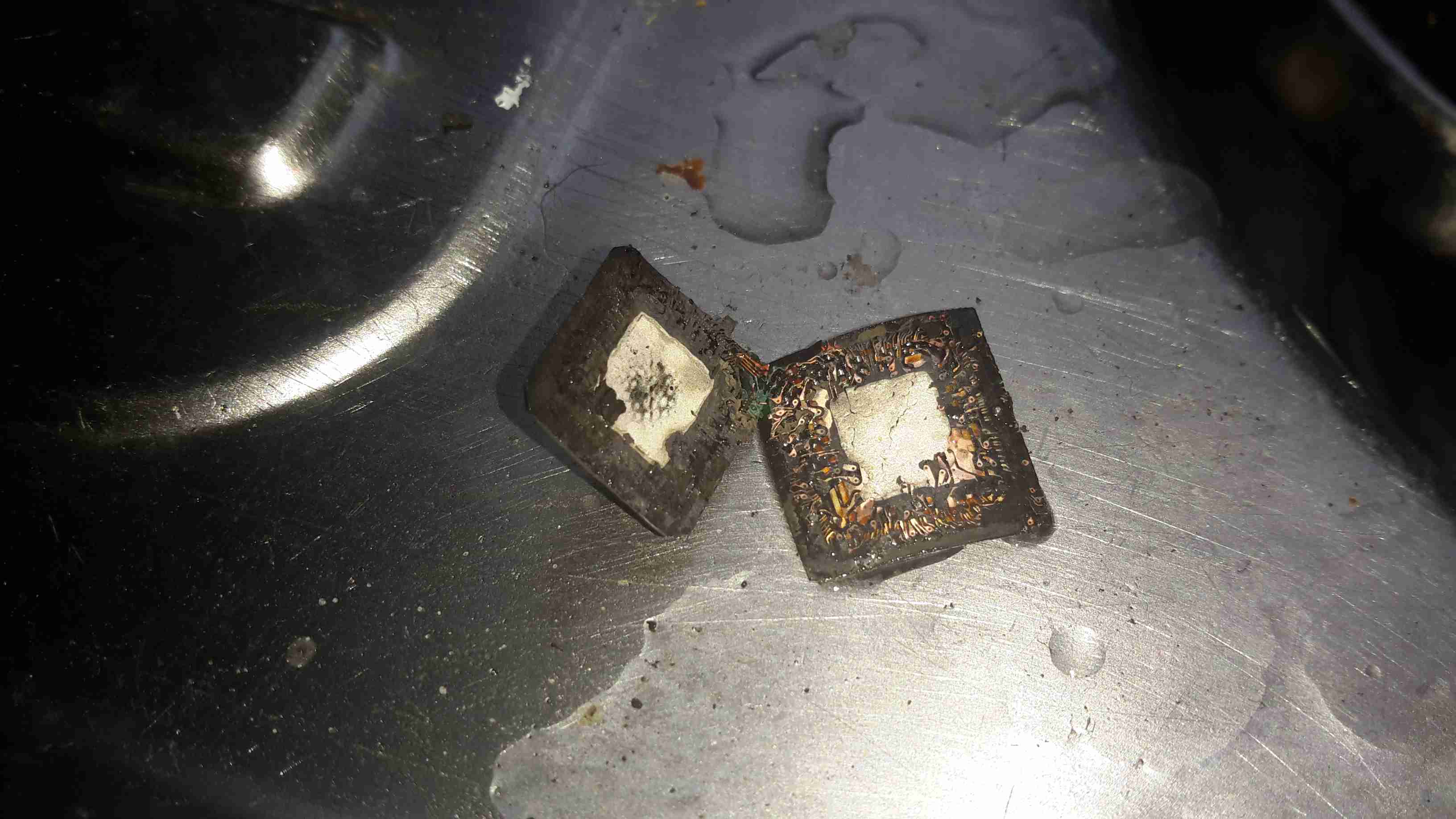
Once the IC is roasted to taste, it’s quenched in cold water for a few seconds. Sometimes this causes such a high thermal shock that the leadframe cracks off the epoxy around the die perfectly.
All Your Die Belong To Us
Now that the epoxy has been destroyed, it breaks apart easily, and is picked away until I uncover the die itself. (It’s the silver bit in the middle of the left half). The heat from the torch usually destroys the Silver epoxy holding the die to the leadframe, and can be removed easily from the remaining package.
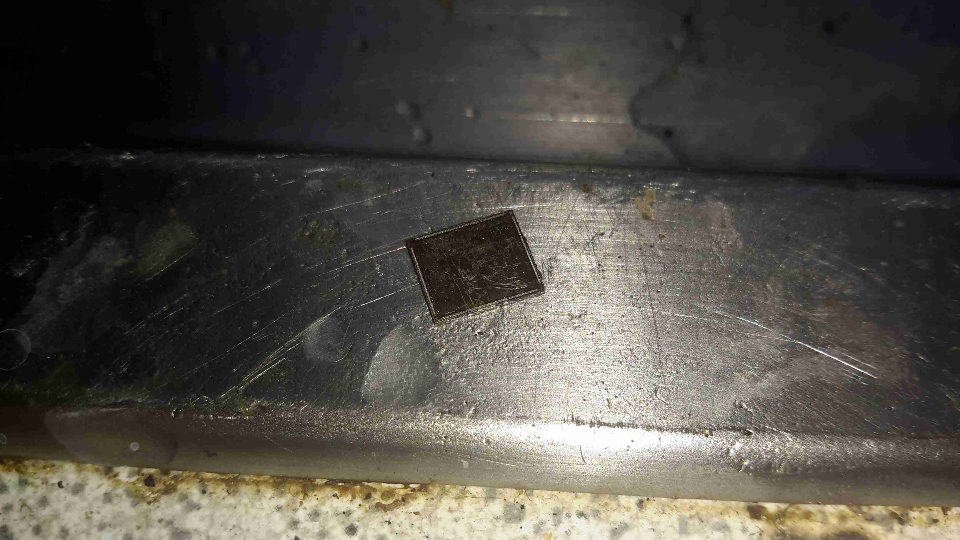
Decapped
BGA packages are usually the easiest to decap, flip-chip packages are a total pain due to the solder balls being on the front side of the die, I haven’t managed to get a good result here yet, I’ll probably need to chemically remove the first layer of the die to get at the interesting bits 😉
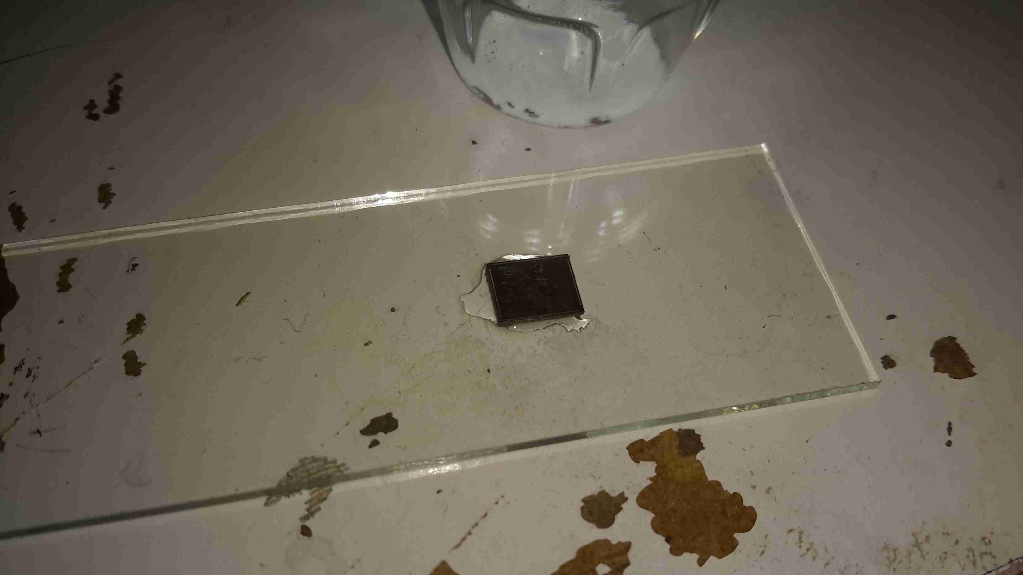
Slide
Once the die has been rinsed in clean water & inspected, it’s mounted on a glass microscope slide with a small spot of Cyanoacrylate glue to make handling easier.
Some dies require some cleaning after decapping, for this I use 99% Isopropanol & 99% Acetone, on the end of a cotton bud. Any residual epoxy flakes or oxide stuck to the die can be relatively easily removed with a fingernail – turns out fingernails are hard enough to remove the contamination, but not hard enough to damage the die features.
Once cleaning is complete, the slide is marked with the die identification, and the photographing can begin.
Microscope Mods
I had bought a cheap eBay USB microscope to get started, as I can’t currently afford a proper metallurgical microscope, but I found the resolution of 640×480 very poor. Some modification was required!
Modified Microscope
I’ve removed the original sensor board from the back of the optics assembly & attached a Raspberry Pi camera board. The ring that held the original sensor board has been cut down to a minimum, as the Pi camera PCB is slightly too big to fit inside.
The stock ring of LEDs is run direct from the 3.3v power rail on the camera, through a 4.7Ω resistor, for ~80mA. I also added a 1000µF capacitor across the 3.3v supply to compensate a bit for the long cable – when a frame is captured the power draw of the camera increases & causes a bit of voltage drop.
The stock lens was removed from the Pi camera module by careful use of a razor blade – being too rough here *WILL* damage the sensor die or the gold bond wires, which are very close to the edge of the lens housing, so be gentle!
Mounting Base
The existing mount for the microscope is pretty poor, so I’ve used a couple of surplus ceramic ring magnets as a better base, this also gives me the option of raising or lowering the base by adding or removing magnets.
To get more length between the Pi & the camera, I bought a 1-meter cable extension kit from Pi-Cables over at eBay, cables this long *definitely* require shielding in my space, which is a pretty aggressive RF environment, or interference appears on the display. Not surprising considering the high data rates the cable carries.
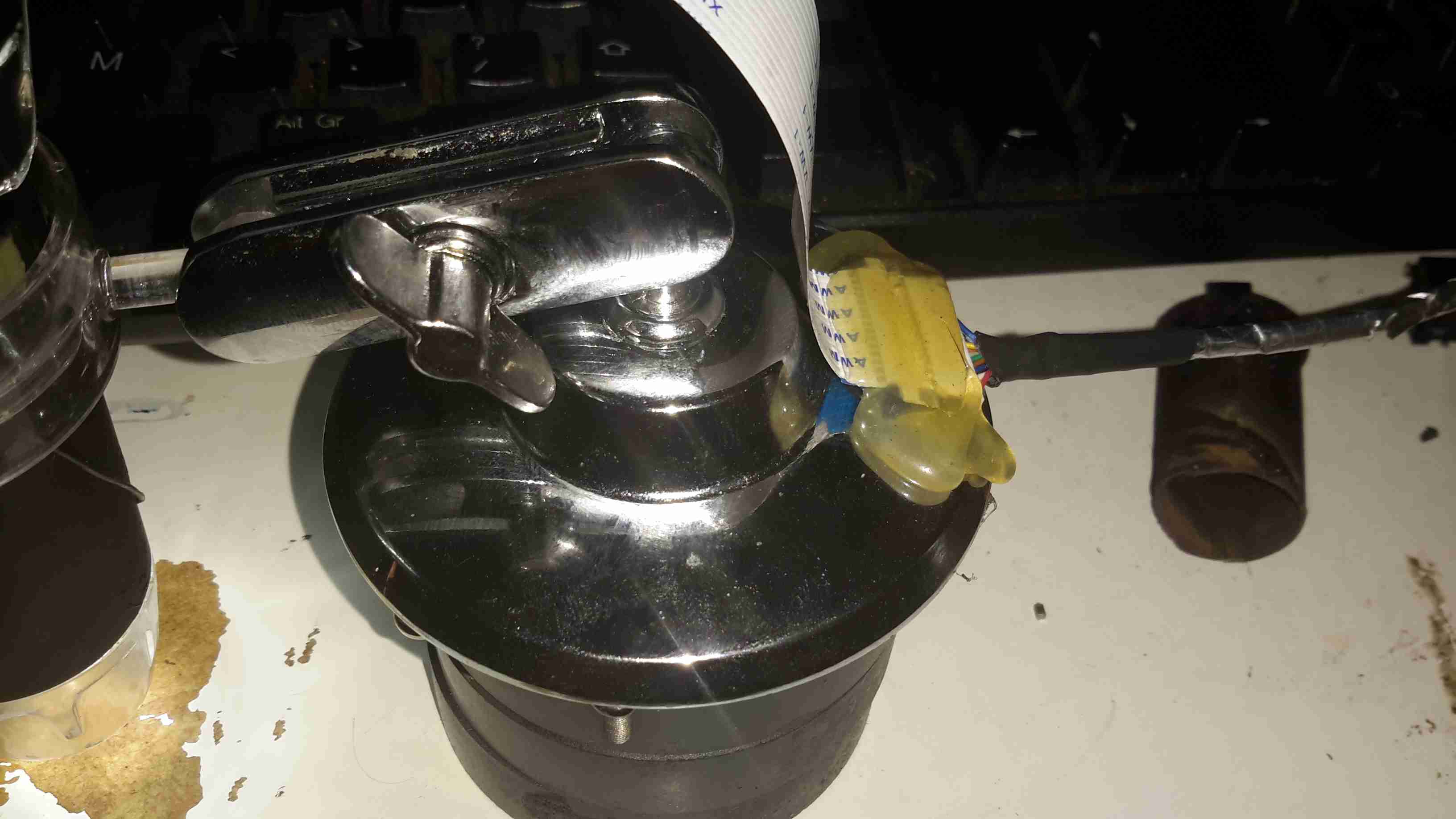
The FFC interface is hot-glued to the back of the microscope mount for stability, for handheld use the FFC is pretty flexible & doesn’t apply any force to the scope.
Die Photography
Since I modified the scope with a Raspberry Pi camera module, everything is done through the Pi itself, and the raspistill command.
Pi LCD
The command I’m currently using to capture the images is:
raspistill -ex auto -awb auto -mm matrix -br 62 -q 100 -vf -hf -f -t 0 -k -v -o CHIPNAME_%03d.jpg
This command waits between each frame for the ENTER key to be pressed, allowing me to position the scope between shots. Pi control & file transfer is done via SSH, while I use the 7″ touch LCD as a viewfinder.
The direct overhead illumination provided by the stock ring of LEDs isn’t ideal for some die shots, so I’m planning on fitting some off-centre LEDs to improve the resulting images.
Image Processing
Obviously I can’t get an ultra-high resolution image with a single shot, due to the focal length, so I have to take many shots (30-180 per die), and stitch them together into a single image.
For this I use Hugin, an open-source panorama photo stitching package.
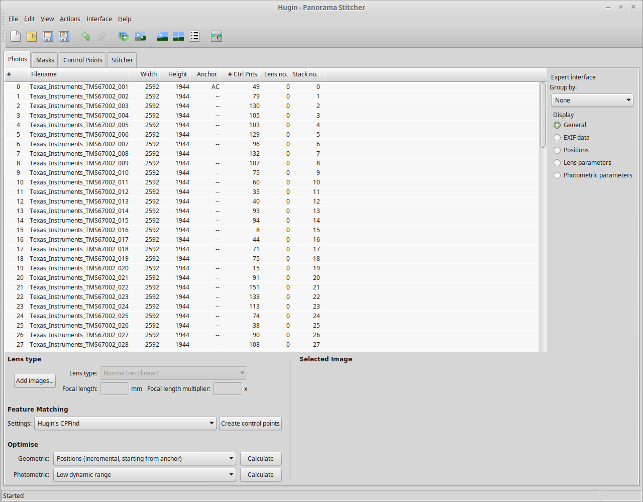
Hugin
Here’s Hugin with the photos loaded in from the Raspberry Pi. To start with I use Hugin’s built in CPFind to process the images for control points. The trick with getting good control points is making sure the images have a high level of overlap, between 50-80%, this way the software doesn’t get confused & stick the images together incorrectly.
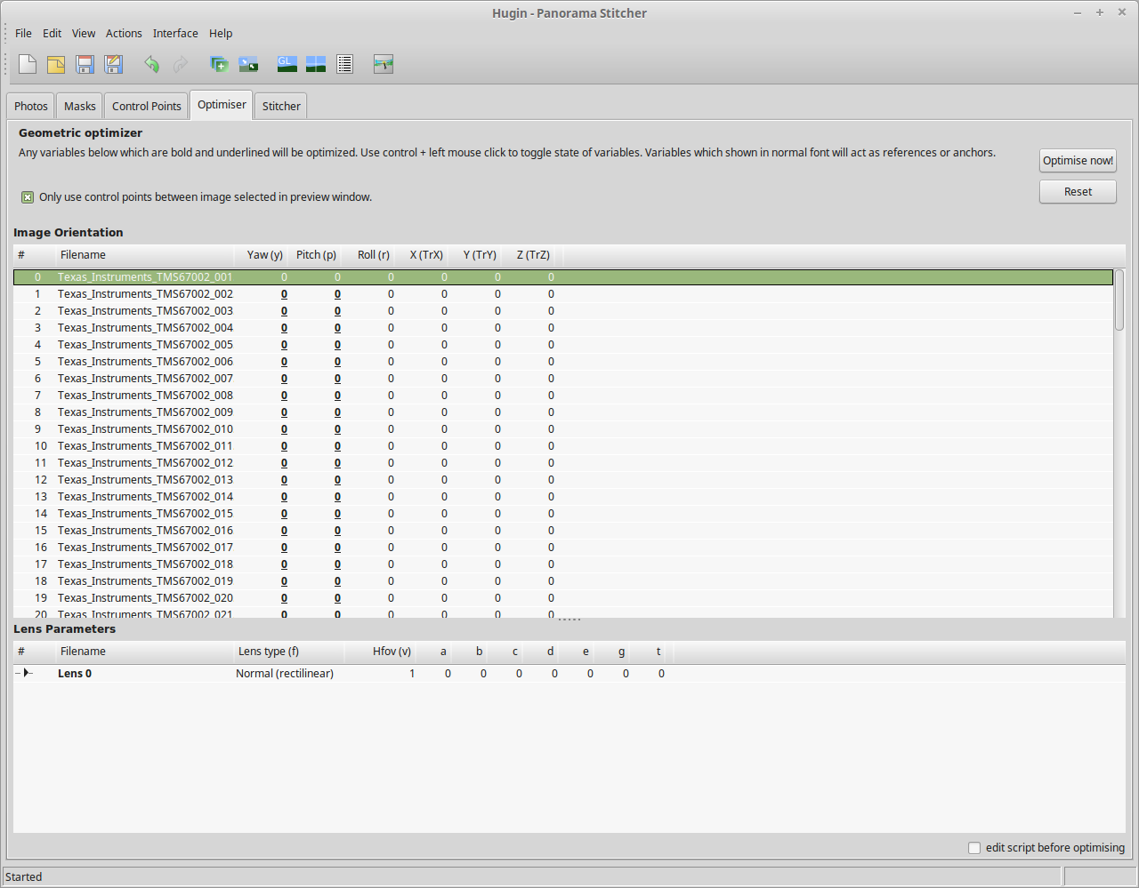
Optimiser
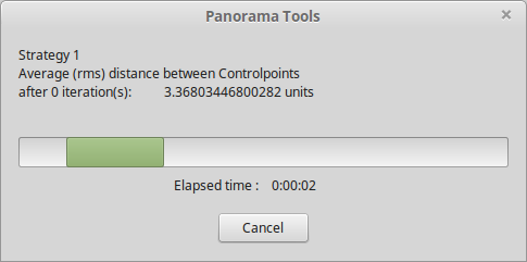
After the control points are generated, which for a large number of high resolution images can take some time, I run the optimiser with only Yaw & Pitch selected for all images.
Optimising
If all goes well, the resulting optimisation will get the distance between control points to less than 0.3 pixels.
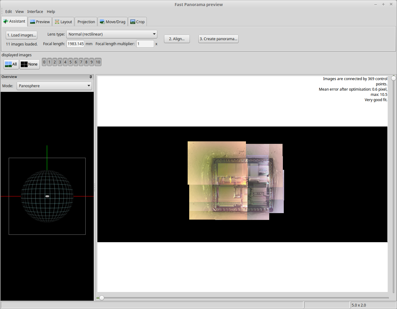
Panorama Preview
After the control points & optimisation is done, the resulting image can be previewed before generation.
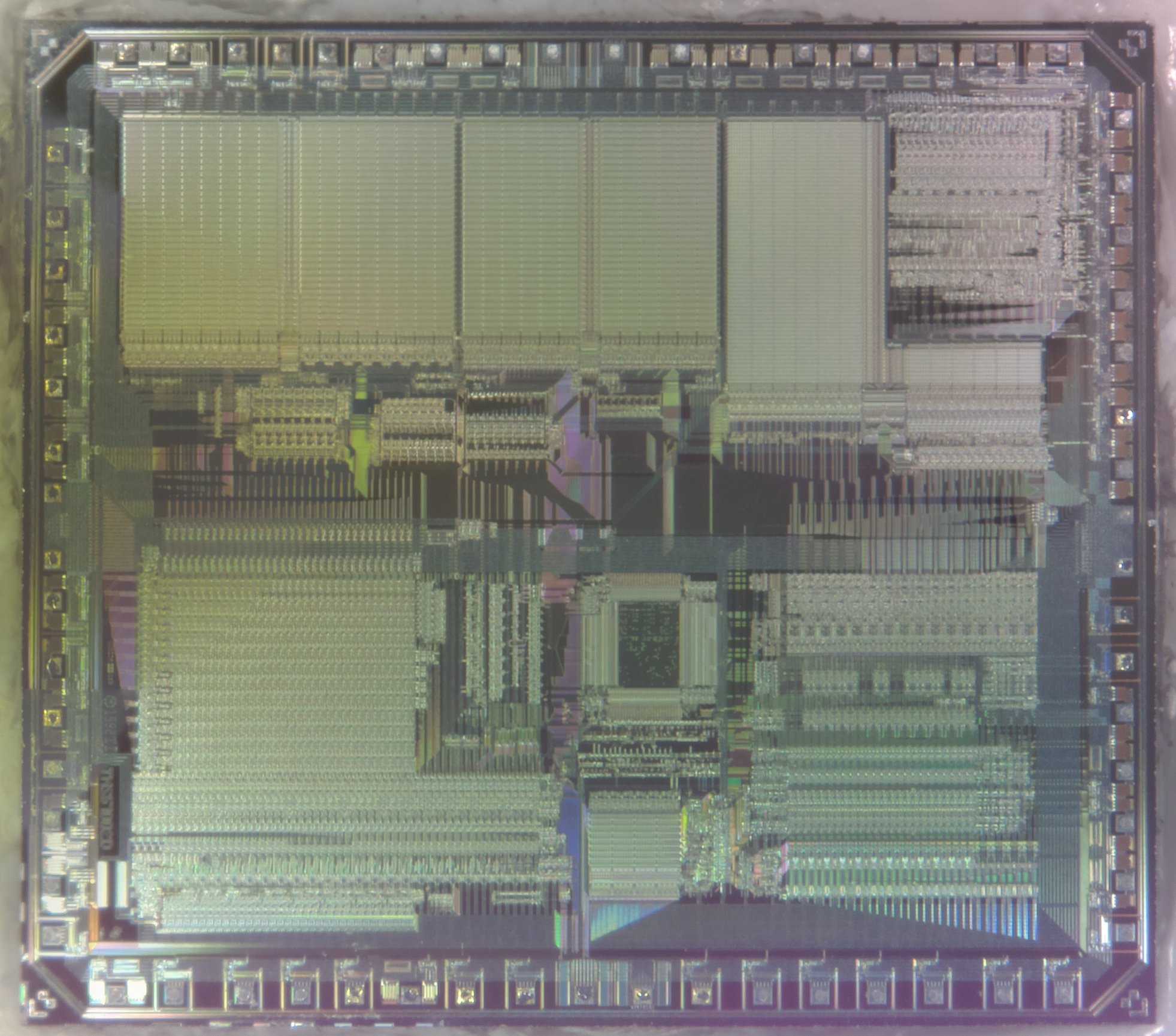
Texas Instruments TMS67002
After all the image processing, the resulting die image should look something like the above, with no noticeable gaps.
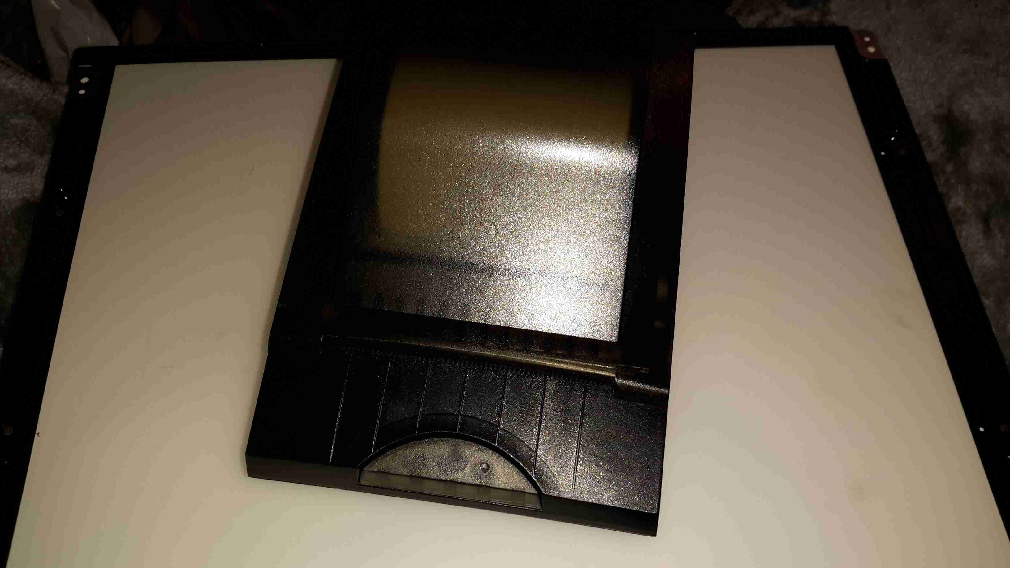
I have yet another receipt printer, this one appears to be brand new. It’s possibly the smallest thermal 80mm printer I have at the moment, and has both USB & Serial interfaces.
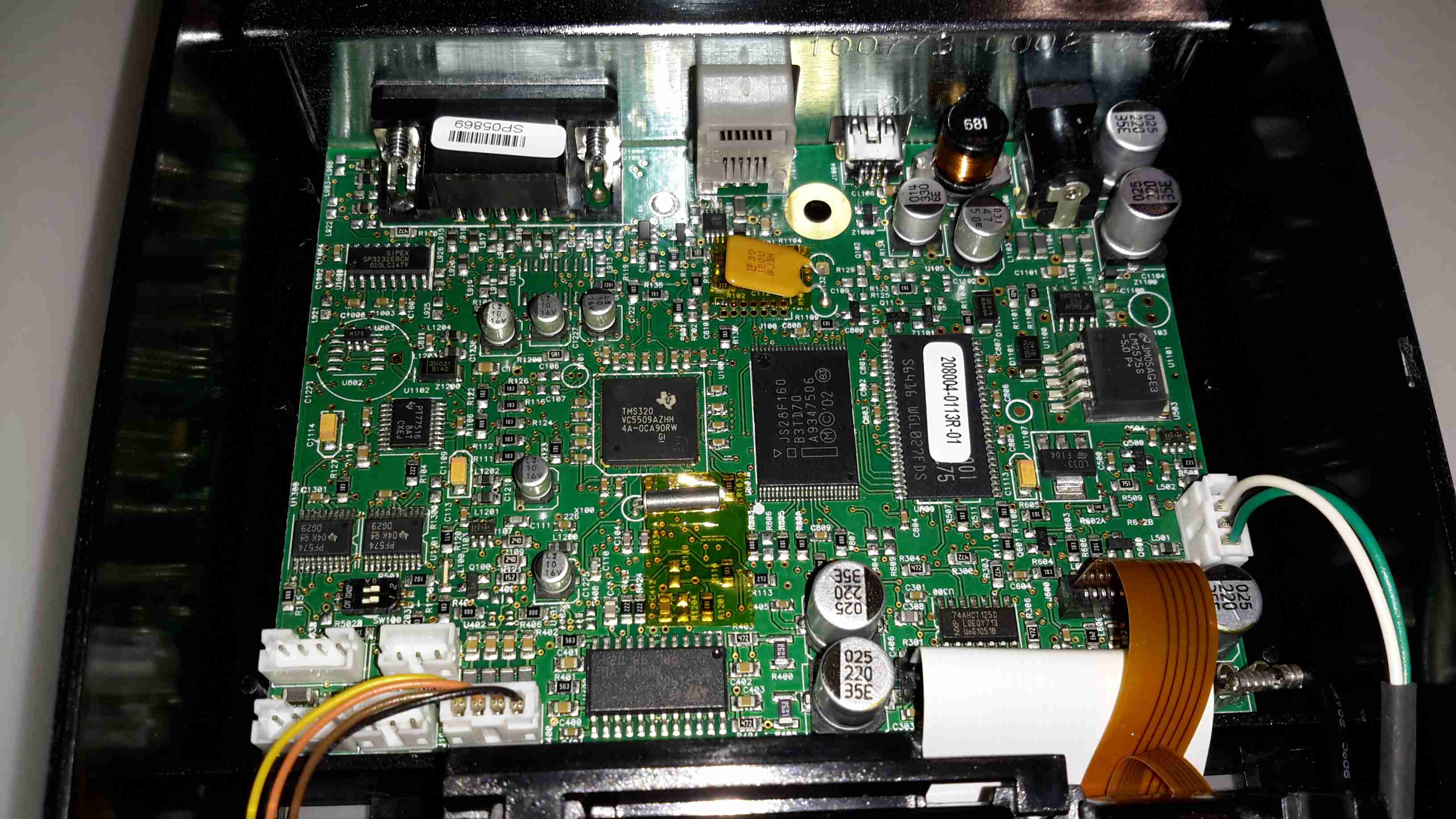
Controller PCB
There’s not much to these printers at all. Removing a single screw allows the case halves to separate, showing the guts. The controller is based around a Texas Instruments TMS320VC5509AFixed-Point DSP. It’s associated Flash ROM & RAM are to the right.
Power supply is dealt with in the top right of the PCB, with the interface ports further left.
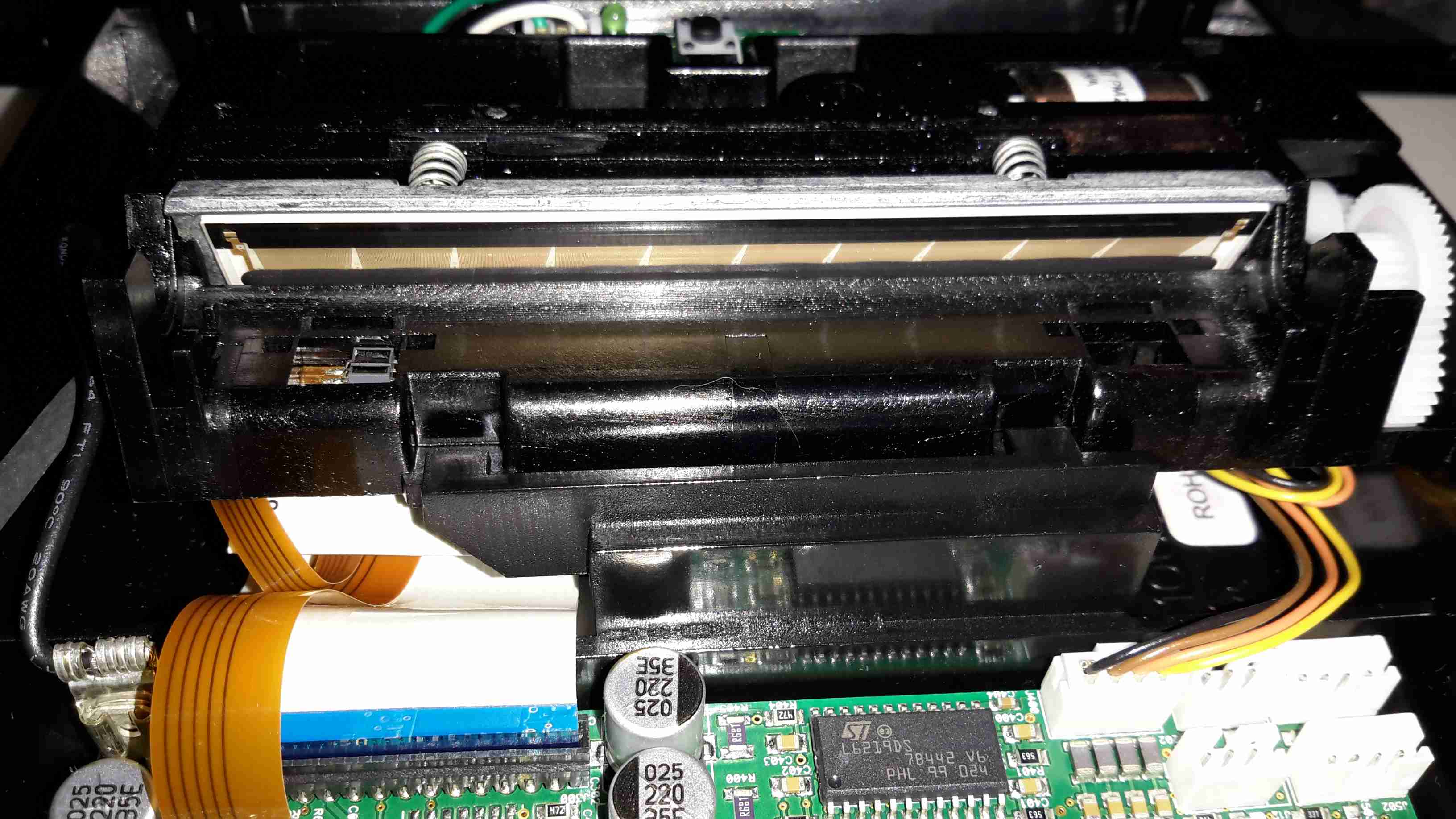
Print Head
Here’s the thermal mechanism itself, with the large print head. The stepper motor to drive the paper through the printer is just peeking out at top right. The paper present sensor is just under the left hand side of the print head.
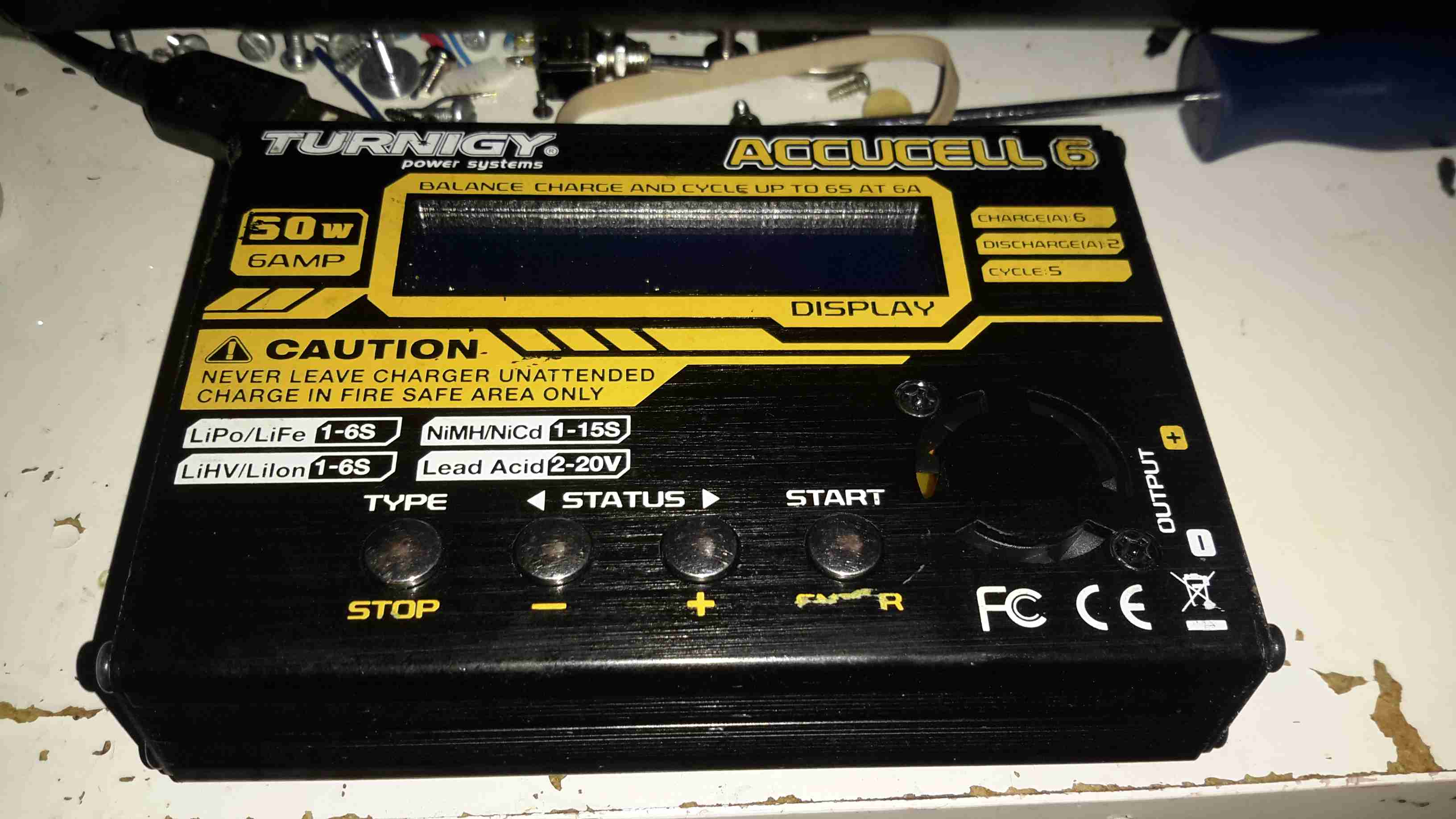
A lot of the electronics I use & projects I construct use batteries, mainly of the lithium variety. As charging this chemistry can be a little explosive if not done correctly, I decided a proper charger was required. This charger is capable of handling packs up to 6 cells for Lithium, and up to 20v for lead-acids.
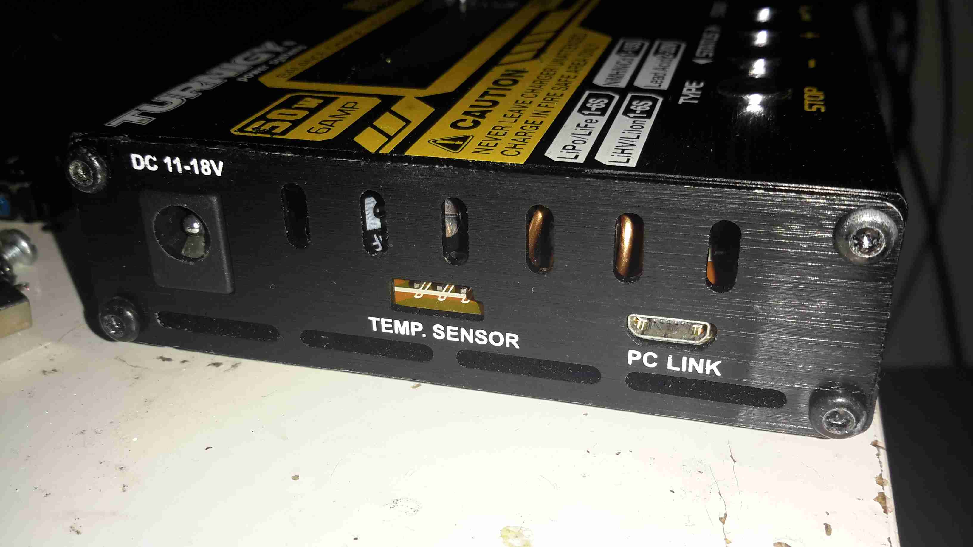
External Connections
The usual DC input barrel jack on the left, with an external temp sensor for fast charging NiCd/NiMH chemistry batteries. The µUSB port registers under Linux as USB HID, probably so drivers aren’t required. Unfortunately the software is Windows only, but it doesn’t provide anything handy like charging graphs or stats. Just a way to alter settings & control charging from a PC. On other versions of this charger there’s a setting to change the temp sensor port into a TTL serial output, which would be much handier.
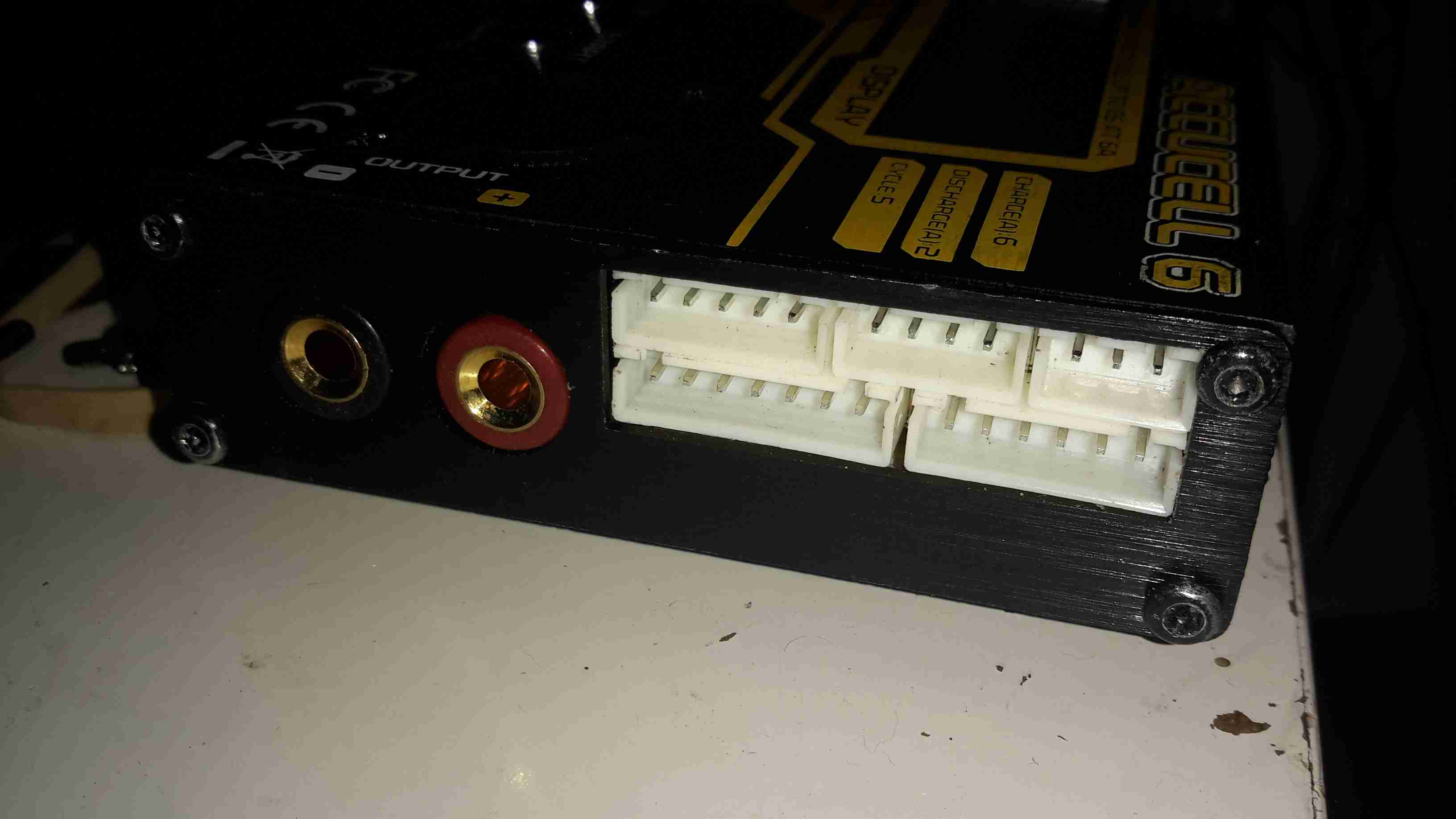
Output & Balance
The other side of the charger has the main DC output jacks & the pack balancing connections.
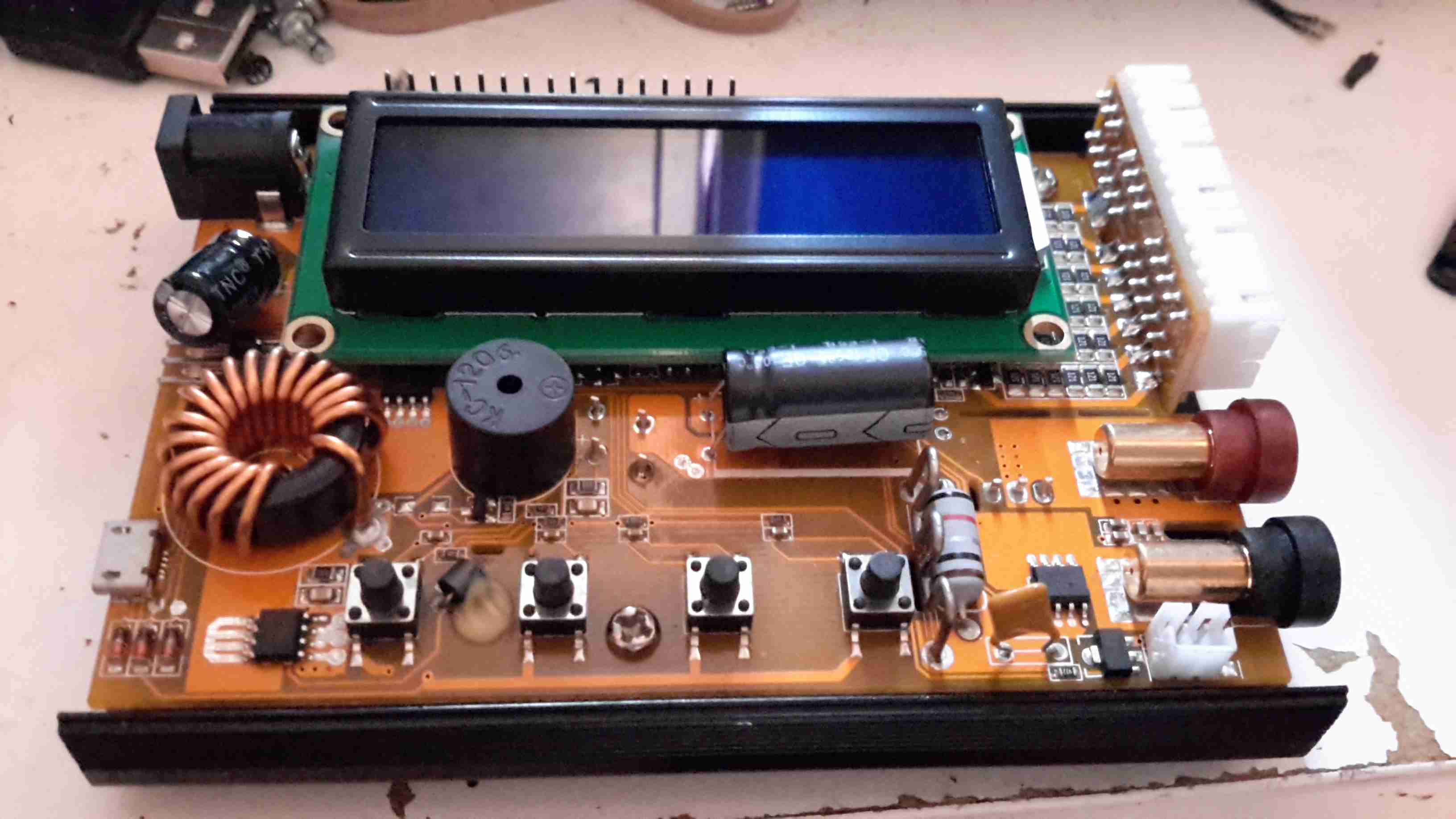
Cover Removed
Here’s the top cover removed from the charger, showing most of the internals. A standard HD44780 LCD provides the user interface, the CPU & it’s associated logic is hidden under there somewhere.
The PCB has nice heavy tracks to handle the 6A of current this charger is capable of.
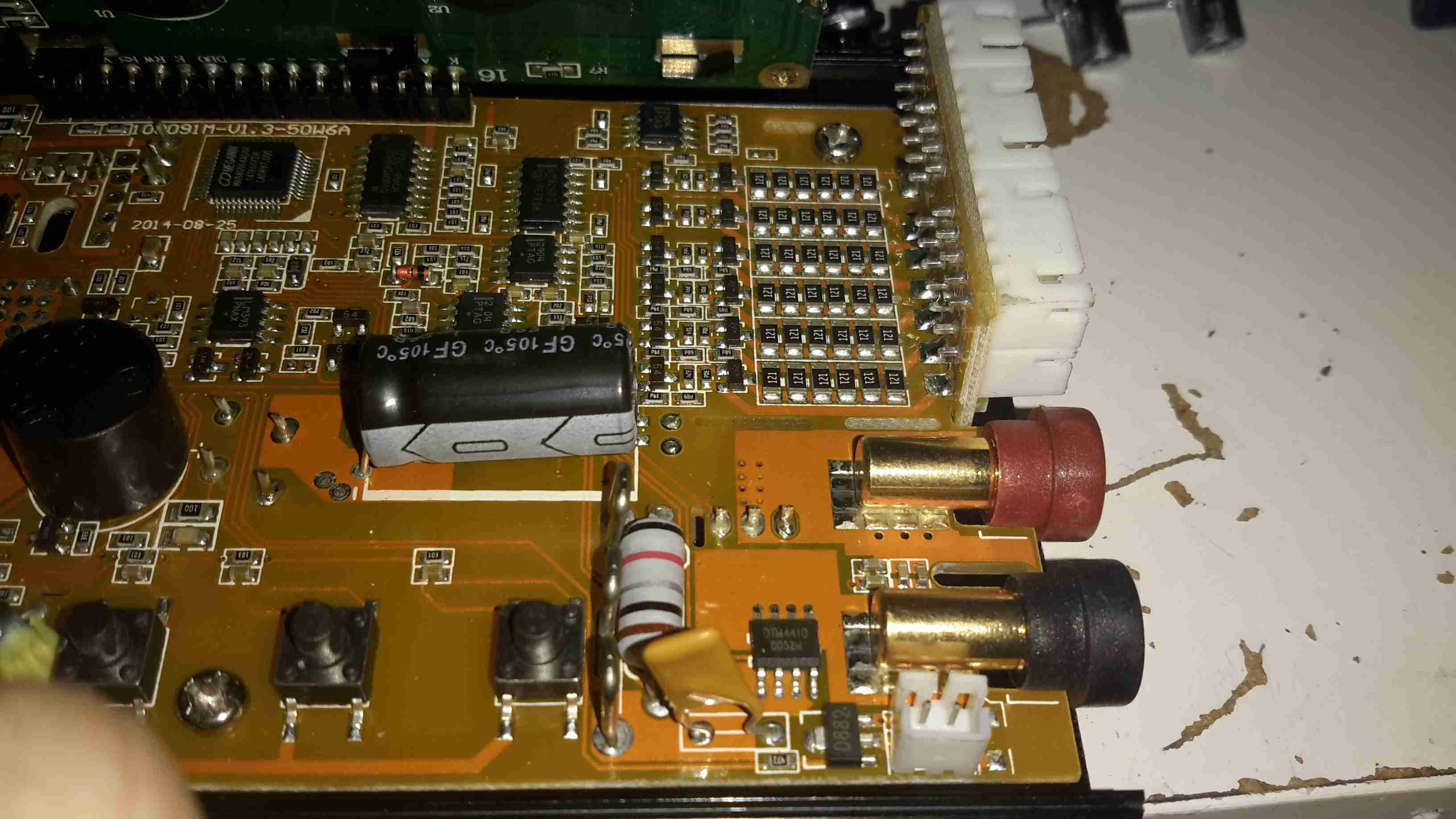
Balancing Network
The output side of the board. Here the resistive pack balancing network can be seen behind the vertical daughter board holding the connectors, along with the output current shunt between the DC output banana jacks & the last tactile button.
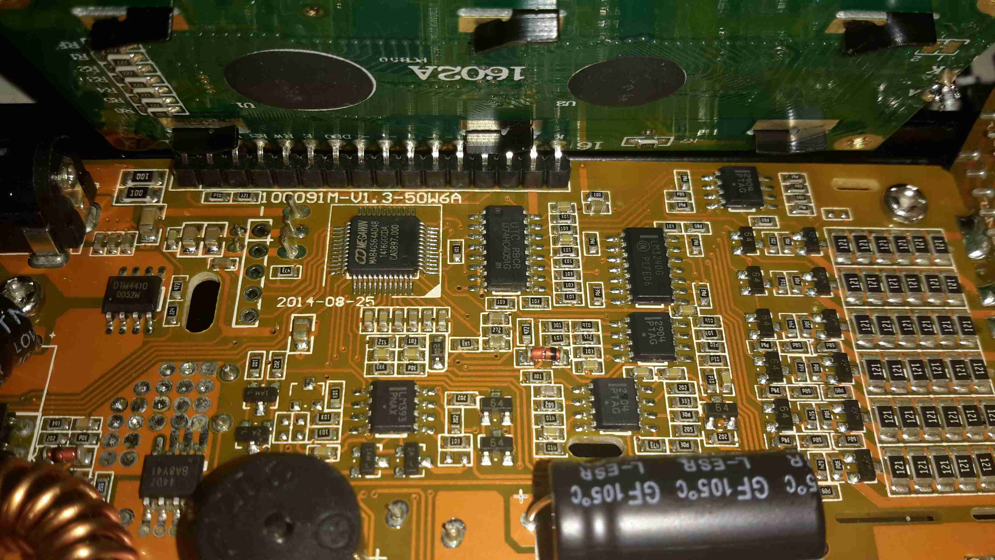
Main Logic
Unfortunately the LCD is soldered directly to the board, and my desoldering tool couldn’t quite get all the solder out, so time to get a bit violent. I’ve gently bent the header so I could see the brains of the charger. The main CPU is a Megwin MA84G564AD48, which is an Intel 8081 clone with USB support. Unfortunately I was unable to find a datasheet for this part, and the page on Megwin’s site is Chinese only.
I was hoping it was an ATMega328, as I have seen in other versions of this charger, as there are custom firmwares available to increase the feature set of the charger, but no dice on this one. I do think the µUSB port is unique to this version though, so avoiding models with that port probably would get a hackable version.
There’s some glue logic for controlling the resistor taps on the balancing network, and a few op-amps for voltage & current readings.
Power Switching Devices
All the power diodes & switching FETs for the DC-DC converter are mounted on the bottom of the PCB, and clamped against the aluminium casing when the PCB is screwed down. Not the best way to ensure great contact, but Chinese tech, so m’eh.
The power supplies I have recently built from surplus Cisco switch boards have started displaying a rather irritating problem – continual load of over 9A causes the supplies to shut down on overheat.
This was partially expected, as the original switches that these supplies came from are cooled by a monster of a centrifugal blower that could give a Dyson a run for it’s money. The problem with these fans is that they’re very loud, draw a lot of power (3-4A) and aren’t small enough to fit into the case I’ve used for the project.
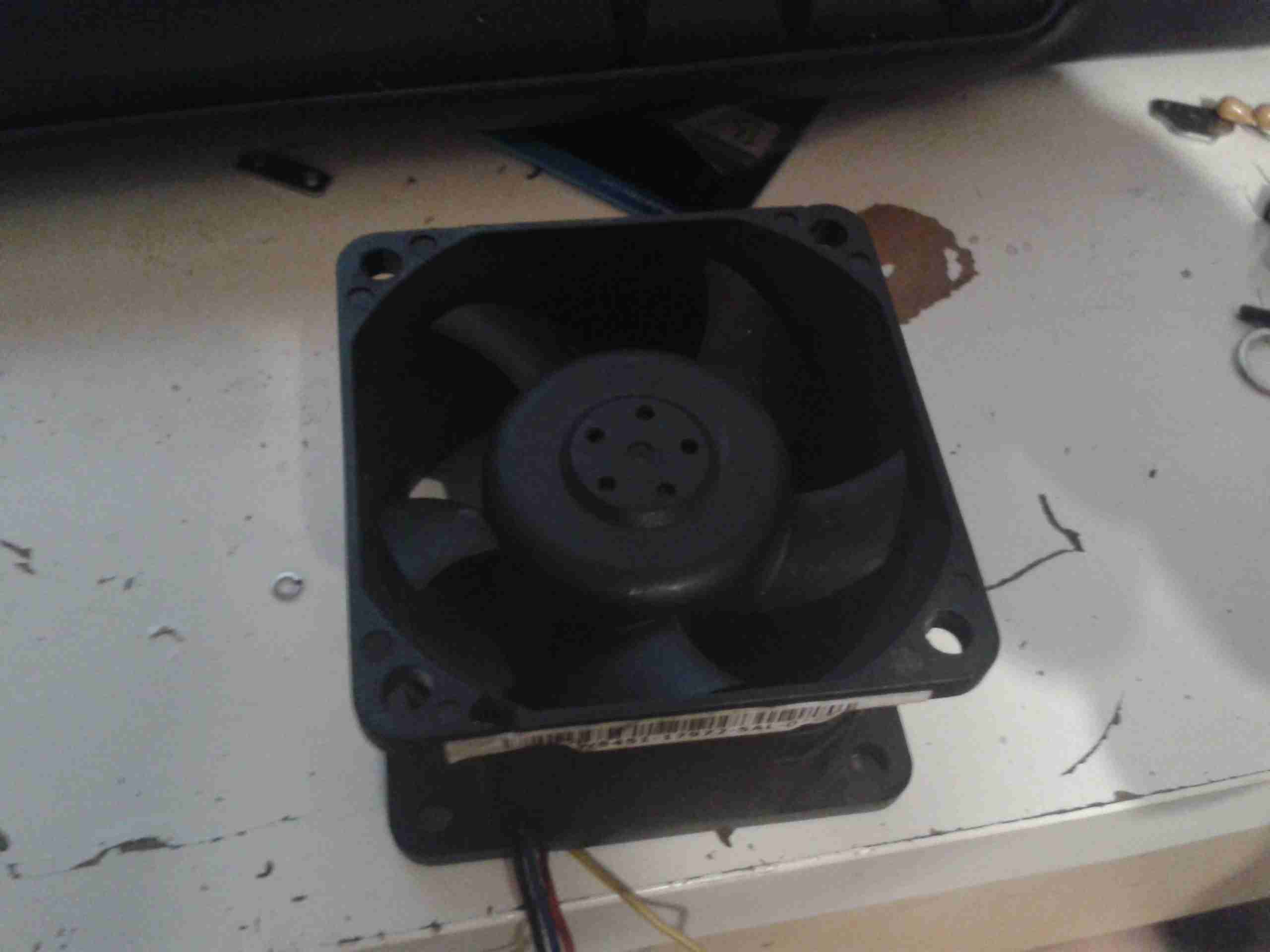
The solution of course, is a bigger fan – I’ve got some Delta AFB0612EHE server fans, these are very powerful axial units, shifting 60CFM at 11,000RPM, with a power draw of 1.12A.
They’re 60mm diameter, so only just fit into the back of the case – although they stick out of the back by 40mm.
Monster Fan
Here’s the fan, not the beefiest I have, but the beefiest that will fit into the available space.
These will easily take fingers off if they get too close at full speed, so guards will definitely be required.
To reduce the noise (they sound like jet engines at full pelt), I have ordered some PWM controllers that have a temperature sensor onboard, so I can have the fan run at a speed proportional to the PSU temperature. I will probably attach the sensor to the output rectifier heatsink, since that’s got the highest thermal load for it’s size.
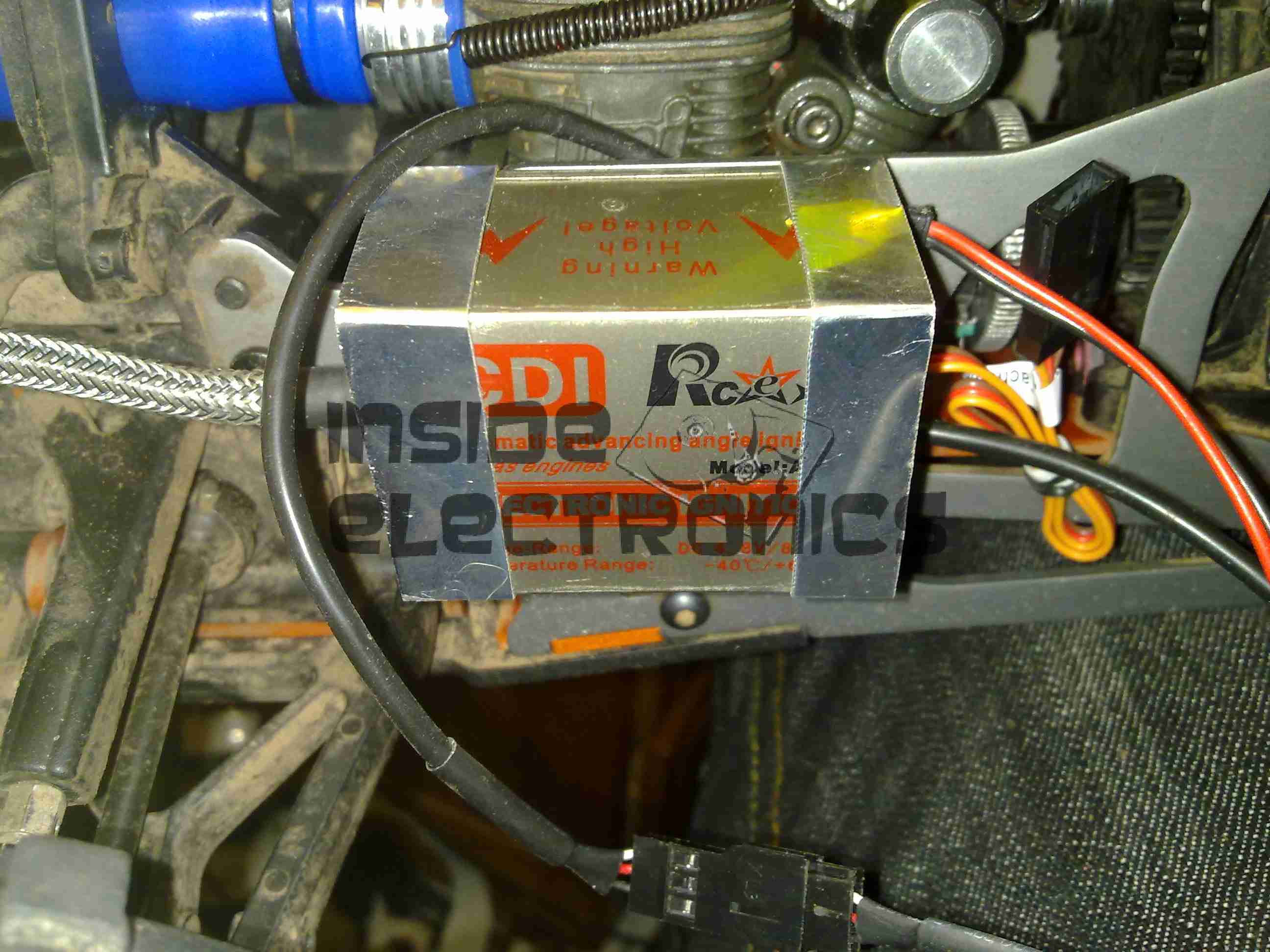
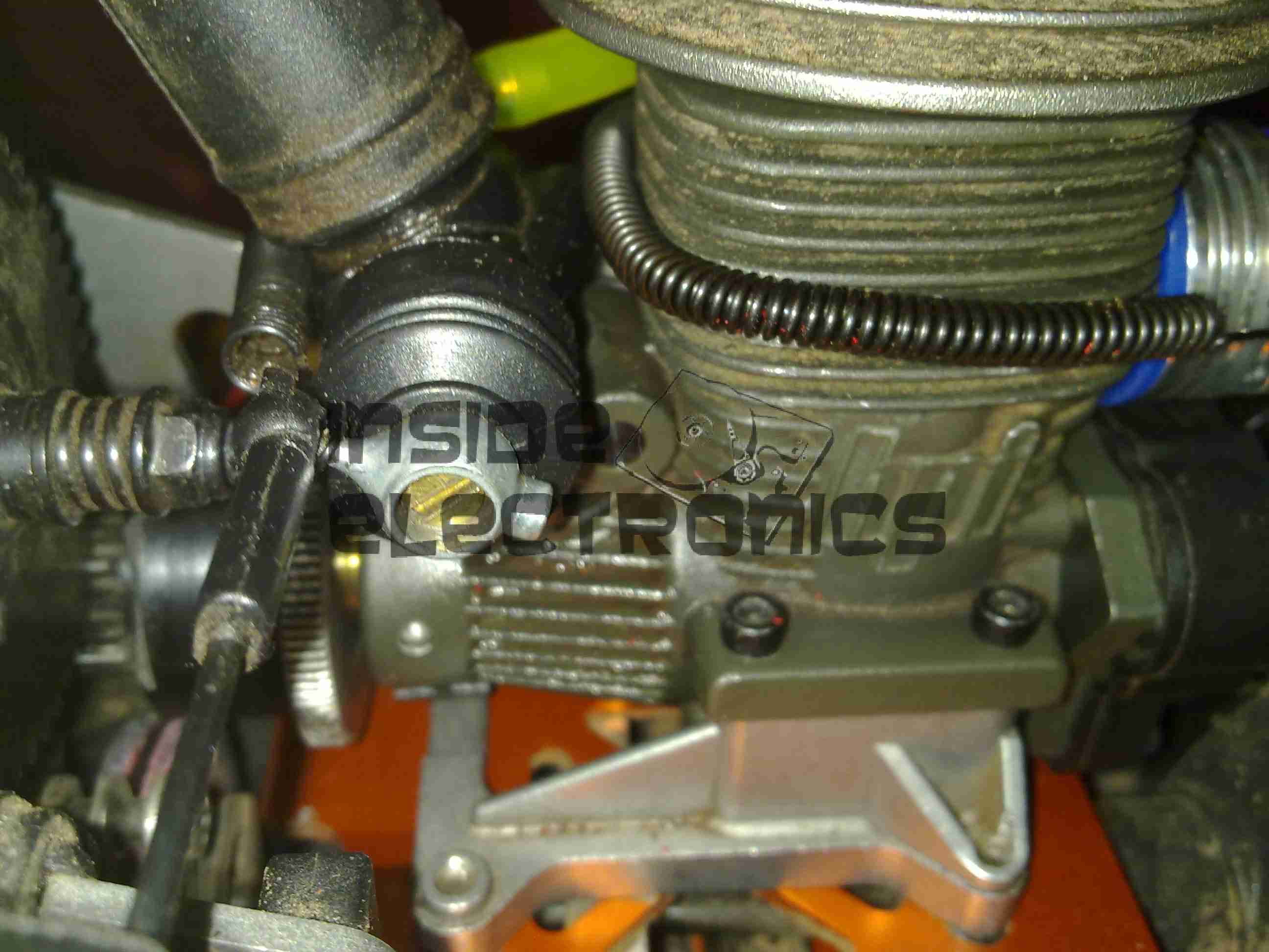
The engine now with it’s required ignition sensor, it is now mounted back on the chassis of the model. I have replaced the stock side exhaust with a rear silencer, so I could fit the ignition module in place next to the engine.
For the mounting, I fabricated a pair of brackets from 0.5mm aluminium, bent around the module & secured with the screws that attach the engine bed plate to the TVPs. The ignition HT lead can be routed up in front of the rear shock tower to clear all moving suspension parts, with the LT wiring tucked into the frame under the engine.
In this location the module is within the profile of the model chassis so it shouldn’t get hit by anything in service.
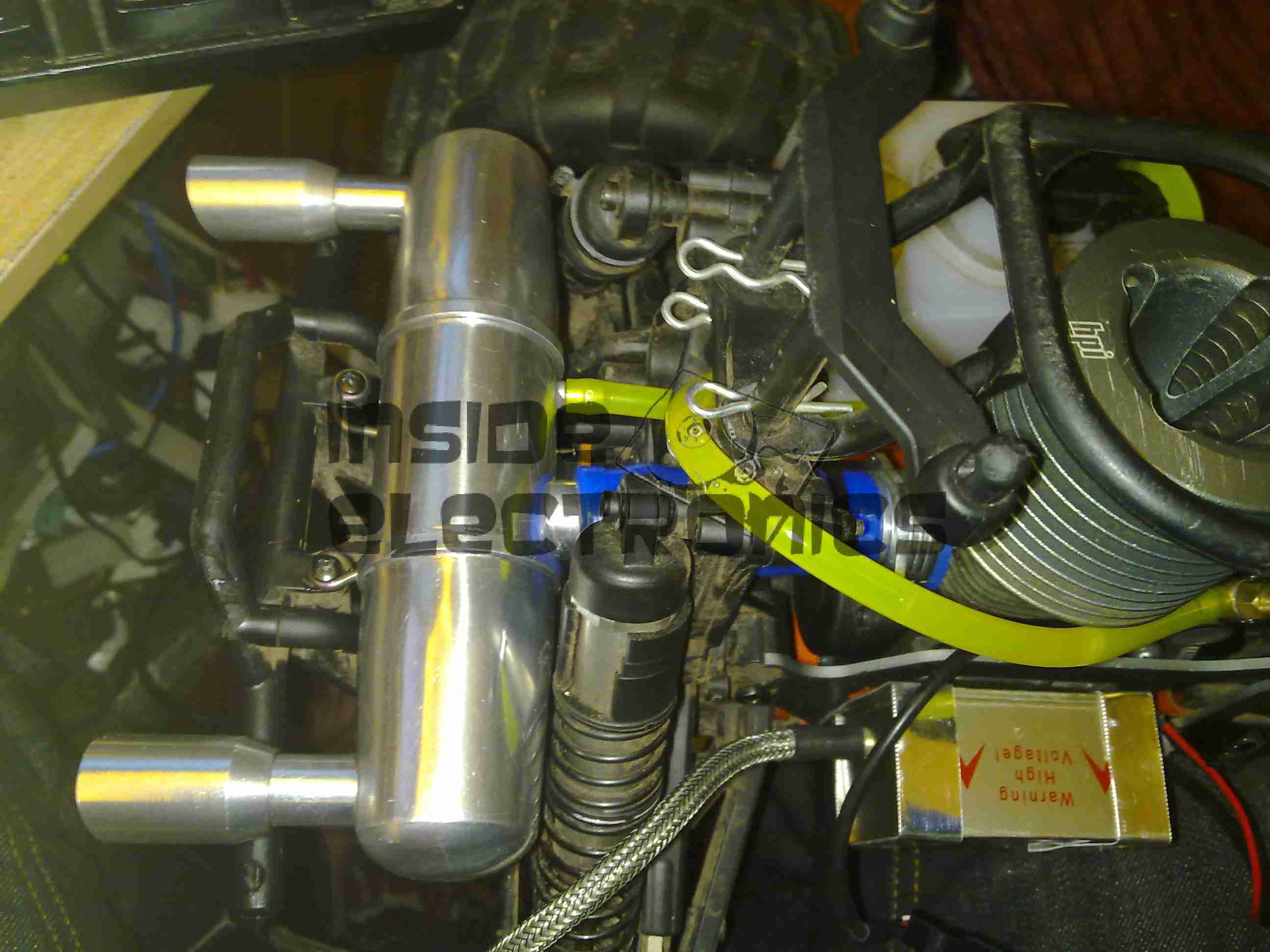
Rear Exhaust
New exhaust silencer fitted to the back of the model. This saves much space on the side of the model & allows the oily exhaust to be discharged away from the back wheel – no more mess to wipe up.
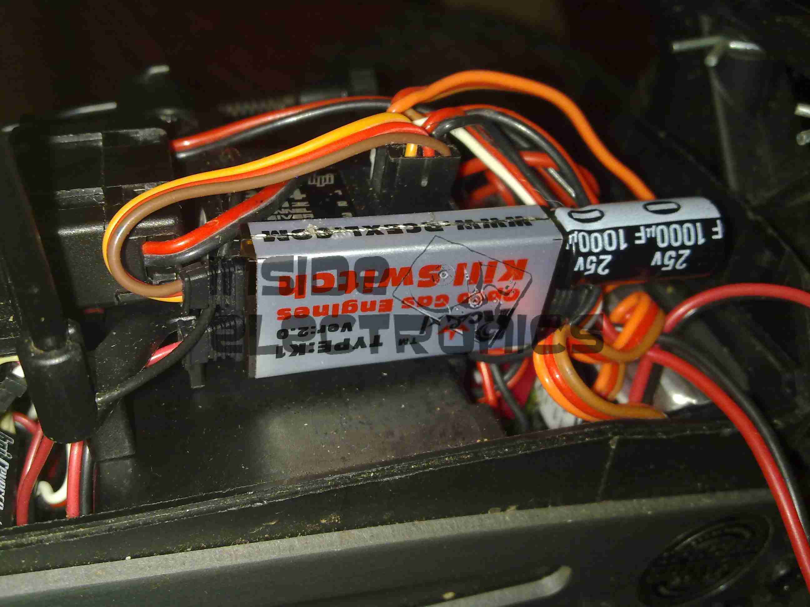
Kill Switch
The ignition switch fitted into the receiver box. This is wired into channel 3 of the TF-40 radio, allowing me to remotely kill the engine in case of emergency. I have fitted a 25v 1000µF capacitor to smooth out any power fluctuations from the ignition module.
The radio is running from a 11.1v 1Ah 3S LiPo pack connected to a voltage regulator to give a constant 6.5v for the electronics. I found this is much more reliable than the standard 5-cell Ni-MH hump packs.
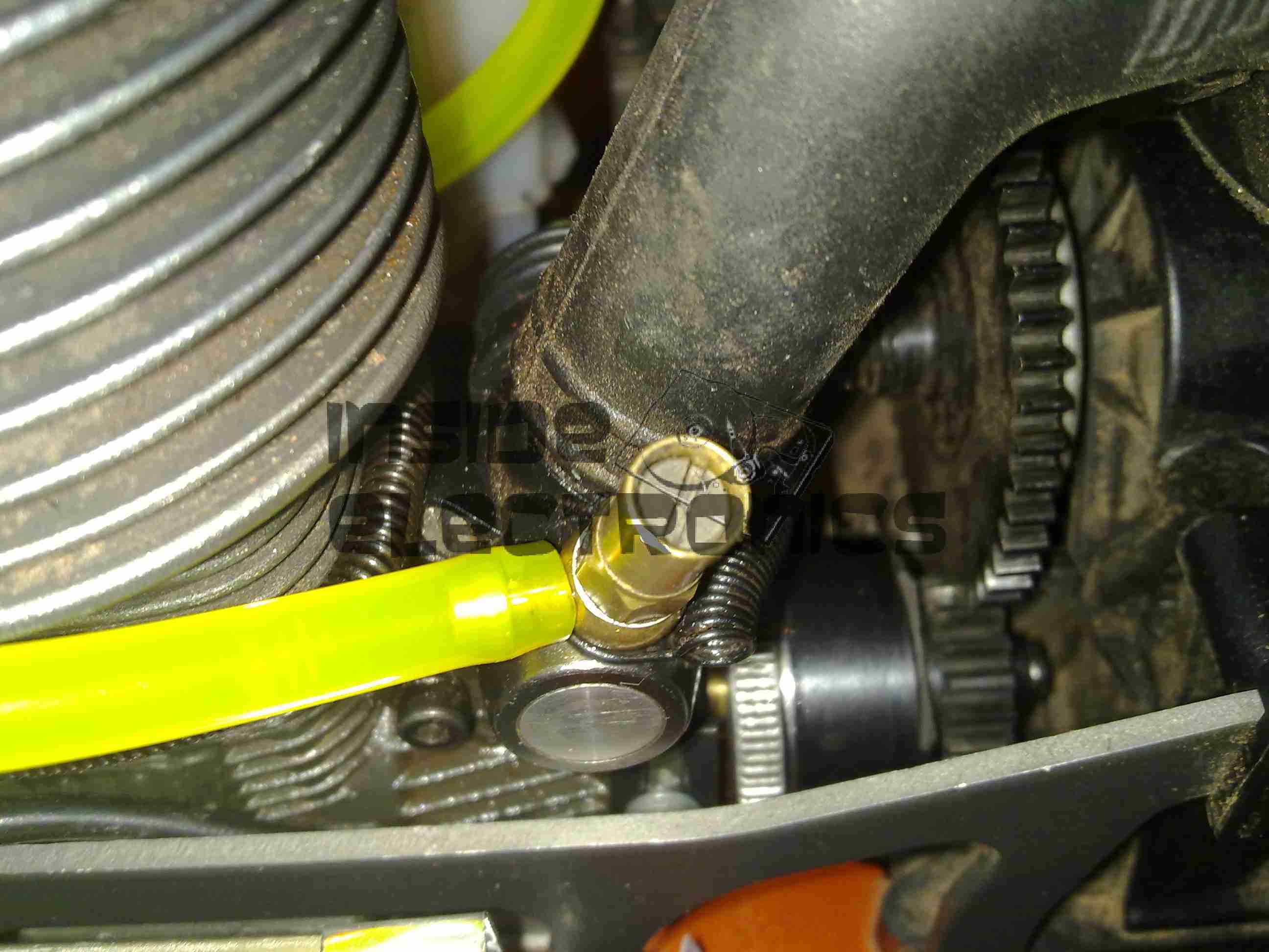
Fuel Tank
The stock silicone fuel tubing has been replaced with Tygon tubing to withstand the conversion to petrol.
High Speed Needle
High speed needle tweaked to provide a basic running setting on petrol. This is set to ~1.5mm below flush with the needle housing.
Low Speed Needle
Low speed needle tweaked to provide a basic running setting on petrol. This is set to ~1.73mm from flush with the needle housing.
As petrol is a much higher energy density fuel, it requires much more air than the methanol glow fuel – ergo much leaner settings.
The settings listed should allow an engine to run – if nowhere near perfectly as they are still rather rich. It’s a good starting point for eventual tuning.
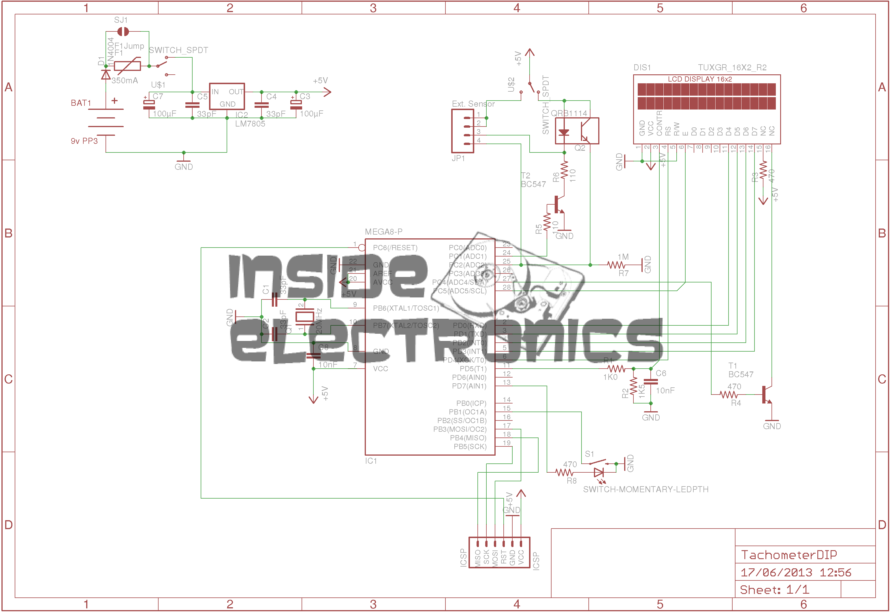
Here is an AVR powered optical tachometer design, that I adapted from the schematic found here.
I made a couple of changes to the circuit & designed a PCB & power supply module to be built in. The original design specified a surface mount IR LED/Photodiode pair, however my adjustment includes a larger IR reflectance sensor built onto the edge of the board, along with a Molex connector & a switch to select an externally mounted sensor instead of the onboard one.
There is also an onboard LM7805 based power supply, designed with a PCB mount PP3 battery box.
The power supply can also be protected by a 350mA polyfuse if desired. If this part isn’t fitted, then a pair of solder bridge pads are provided within the footprint for the fuse to short out the pads.
For more information on the basic design, please see the original post with the link at the top of the page.
Schematic
Here is an archive of the firmware & the Eagle CAD files for the PCB & schematic design.
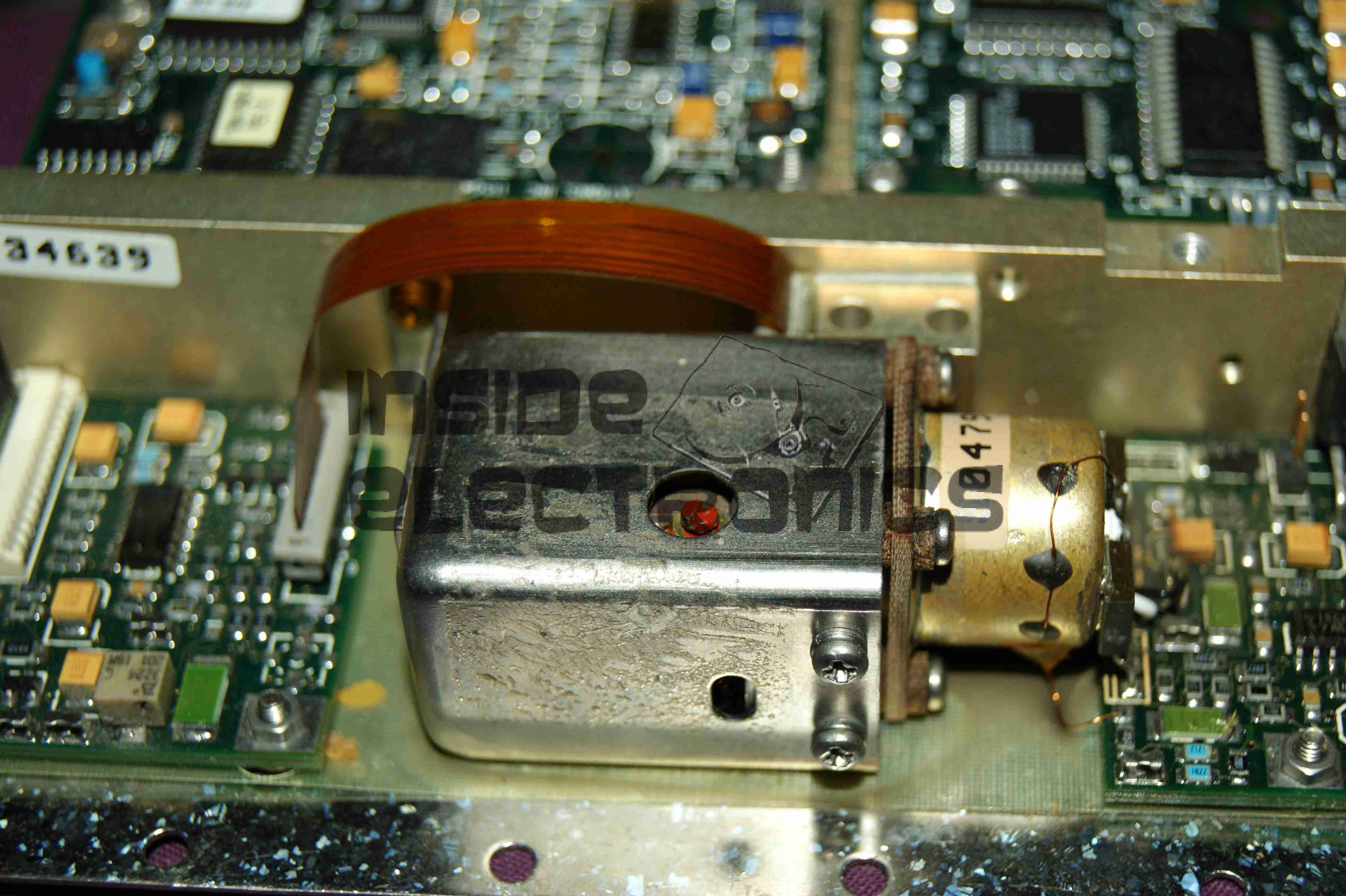
Here is a quick look inside the FE-5060A Rubidium Frequency Standard. Above you can see the entire physics package, with the rubidium lamp housing on the right hand side. The ribbon cable running into the resonator cavity has the power & signal traces for the internal heater, temperaturesensor & Helmholtz coil.
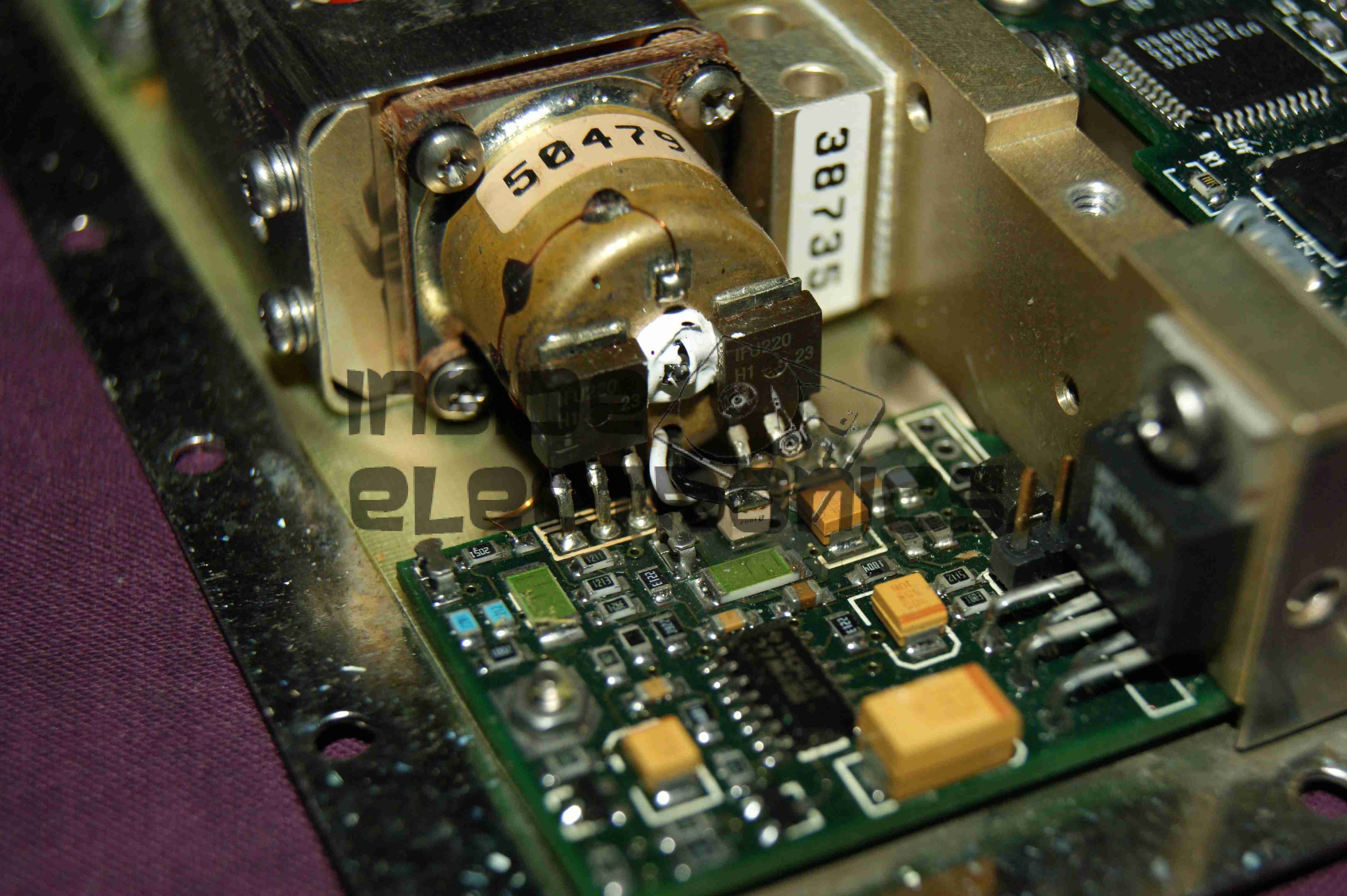
Lamp End
Here is the lamp end of the physics package, with the voltageregulator & RFdriver for the lamp. The FETs soldered to the back of the housing are being used as heaters to maintain a constant temperature on the lamp in operation.
The temperaturesensor can be seen between the two FETs, with a single copper wire running around the housing to connect to it.
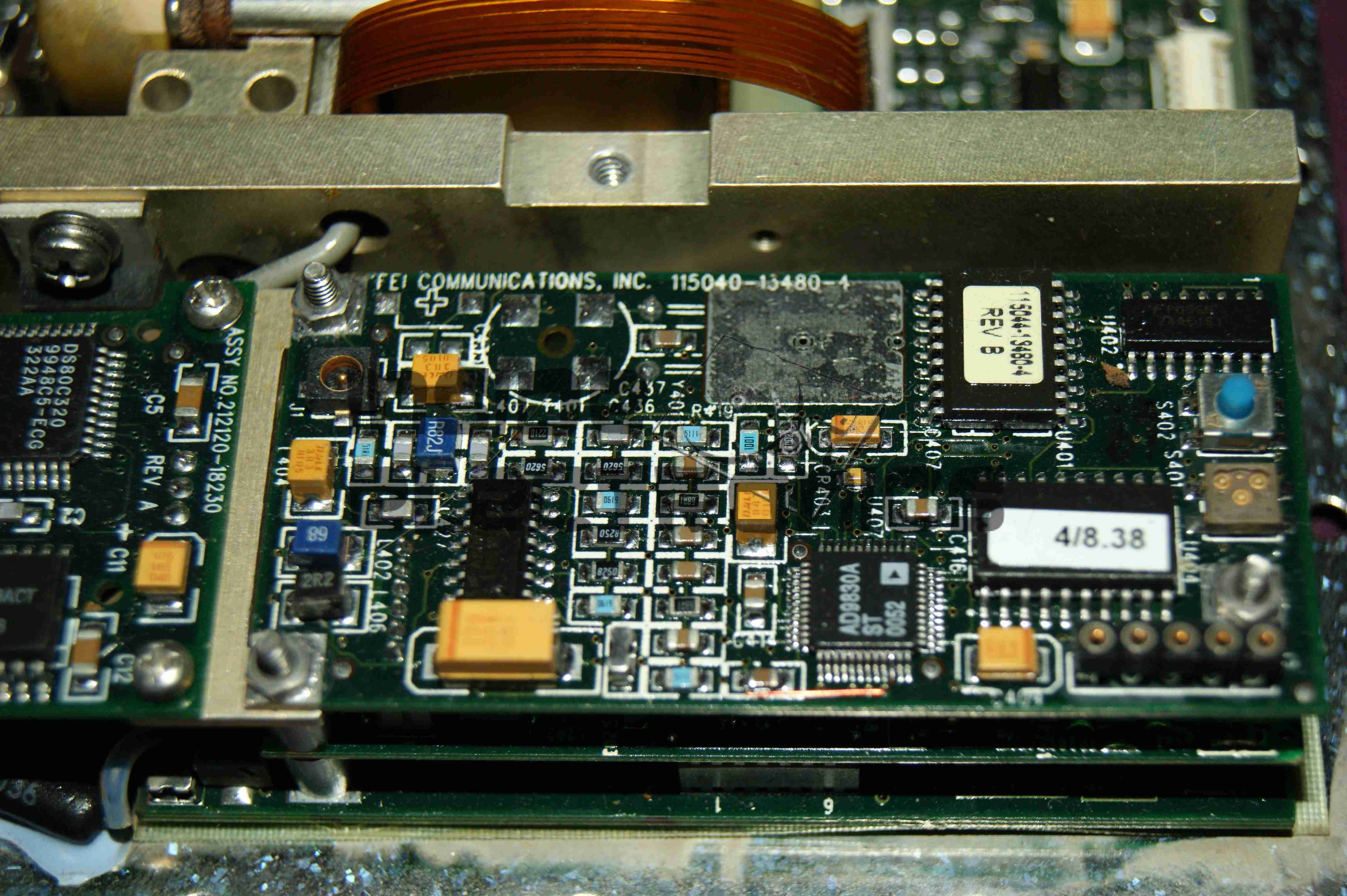
Main frequency synth board. This contains the RS-232 interface & the AD9830A from Analog Devices. This IC is a direct digital synthesizer & waveform generator.
Here is an old electrochemical type carbon monoxide detector cell, from Monox. Hole in the centre is the inlet for the gas under test. DO NOT TRY THIS AT HOME! Electrochemical cells contain a substantial amount of sulphuric acid, strong enough to cause burns.
This is a type of fuel cell that instead of being designed to produce power, is designed to produce a current that is precisely related to the amount of the target gas (in this case carbon monoxide) in the atmosphere. Measurement of the current gives a measure of the concentration of carbon monoxide in the atmosphere. Essentially the electrochemical cell consists of a container, 2 electrodes, connection wires and an electrolyte – typically sulfuric acid. Carbon monoxide is oxidized at one electrode to carbon dioxide while oxygen is consumed at the other electrode. For carbon monoxide detection, the electrochemical cell has advantages over other technologies in that it has a highly accurate and linear output to carbon monoxide concentration, requires minimal power as it is operated at room temperature, and has a long lifetime (typically commercial available cells now have lifetimes of 5 years or greater). Until recently, the cost of these cells and concerns about their long term reliability had limited uptake of this technology in the marketplace, although these concerns are now largely overcome. This technology is now the dominant technology in USA and Europe.
Rear
Rear of unit with connection pins. Hole here is to let oxygen into the cell which permits the redox reaction to take place in the cell when CO is detected, producing a voltage on the output pins.
Disassembled
Cell disassembled. The semi-permeable membrane on the back cover can be seen here, to allow gas into the cell, but not the liquid electrolyte out. Cell with the electrodes is on the right, immersed in sulphuric acid.
Platinum Electrode
Closeup of the electrode structure. Polymer base with a precious metal coating.
This is an old CO alarm, which was totally dead, having been connected to the wrong PSU.
Here is the front of the unit, with the Test button & indicator LEDs.
Overview
Front of the PCB, 3 1.5v cells powered the unit, Piezo sounder & sensor cell in the centre of the board.
Here is a Bosch 14.4v Professional cordless drill/driver, recovered from a skip!
It was thrown away due to a gearbox fault, which was easy to rectify.
Internals
Here is the drill with the side cover removed, showing it’s internal parts. The speed controller is below the motor & gearbox here. The unit at the top consists of a 12v DC motor, coupled to a 4-stage epicyclic gearbox unit, from which can be selected 2 different ratios, by way of the lever in the centre of the box. This disables one of the gear stages. There is a torque control clutch at the chuck end of the gearbox, this was faulty when found.
Motor
Here is the drive motor disconnected from the gearbox, having a bayonet fitting on the drive end.
Drive Gear
This is the primary drive gear of the motor, which connects with the gearbox.
Cooling Fan
The motor is cooled by this fan inside next to the commutator, drawing air over the windings.
Gearbox
This is the gearbox partially disassembled, showing the 1st & second stages of the geartrain. The second stage provides the 2 different drive ratios by having the annulus slide over the entire gearset, disabling it entirely, in high gear. The annulus gears are a potential weak point in this gearbox, as they are made from plastic, with all other gears being made of steel.
Charger
Here is the charging unit for the Ni-Cd battery packs supplied with the drill. The only indicator is the LED shown here on the front of the unit, which flashes while charging, & comes on solid when charging is complete. Charge termination is by way of temperature monitoring.
Transformer
Here the bottom of the charger has been removed, showing the internal parts. An 18v transformer supplies power to the charger PCB on the left.
Charger PCB
This is the charger PCB, with a ST Microelectronics controller IC marked 6HKB07501758. I cannot find any information about this chip.
Battery Pack Internals
Here is a battery pack with the top removed, showing the cells.
Temperature Sensor
This is the temperature sensor embedded inside the battery pack that is used by the charger to determine when charging is complete.
Another phone from the mid 90s. This is the nokia 7110.
Slider Open
Here the slider is open showing the keypad.
Battery Removed
Here the battery is removed, a Li-Ion unit.
Battery
The battery cell & protection circuit removed from the casing.
Rear Of PCB
This is the rear of the PCB removed from the housing. Data & charging ports on the right hand side f the board.
Front Of PCB
Front of the PCB with the RF sections at the left hand side & the keypad contacts on the right.
RF Sections
Closeup of the RF sections of the board, big silver rectangular cans are VCO units.
SIM Connector
Closeup of the top rear section of the PCB, with SIM cnnector, battery contacts, IR tranciever at the far left. Bottom centre is the external antenna connector.
CPU
The logic section of the board, Large chip is CPU, to right of that is the ROM storing the machine code. Other chips are unknown custom parts.
Mic & Speaker
The Mic & the loudspeaker removed from it’s housing.
LCD
LCD from the front of the unit, SPI interfaced. Flex PCB also contains the power button, loudspeaker contacts & a temperature sensor.
Scroll Wheel
The scroll wheel removed from the front housing.
Vibra-Motor
Tiny vibration motor removed from the rear housing, alerts the user to a text or phone call.
If you’ve found my content useful, please consider leaving a donation by clicking the Tip Jar below!
All collected funds go towards new content & the costs of keeping the server online.