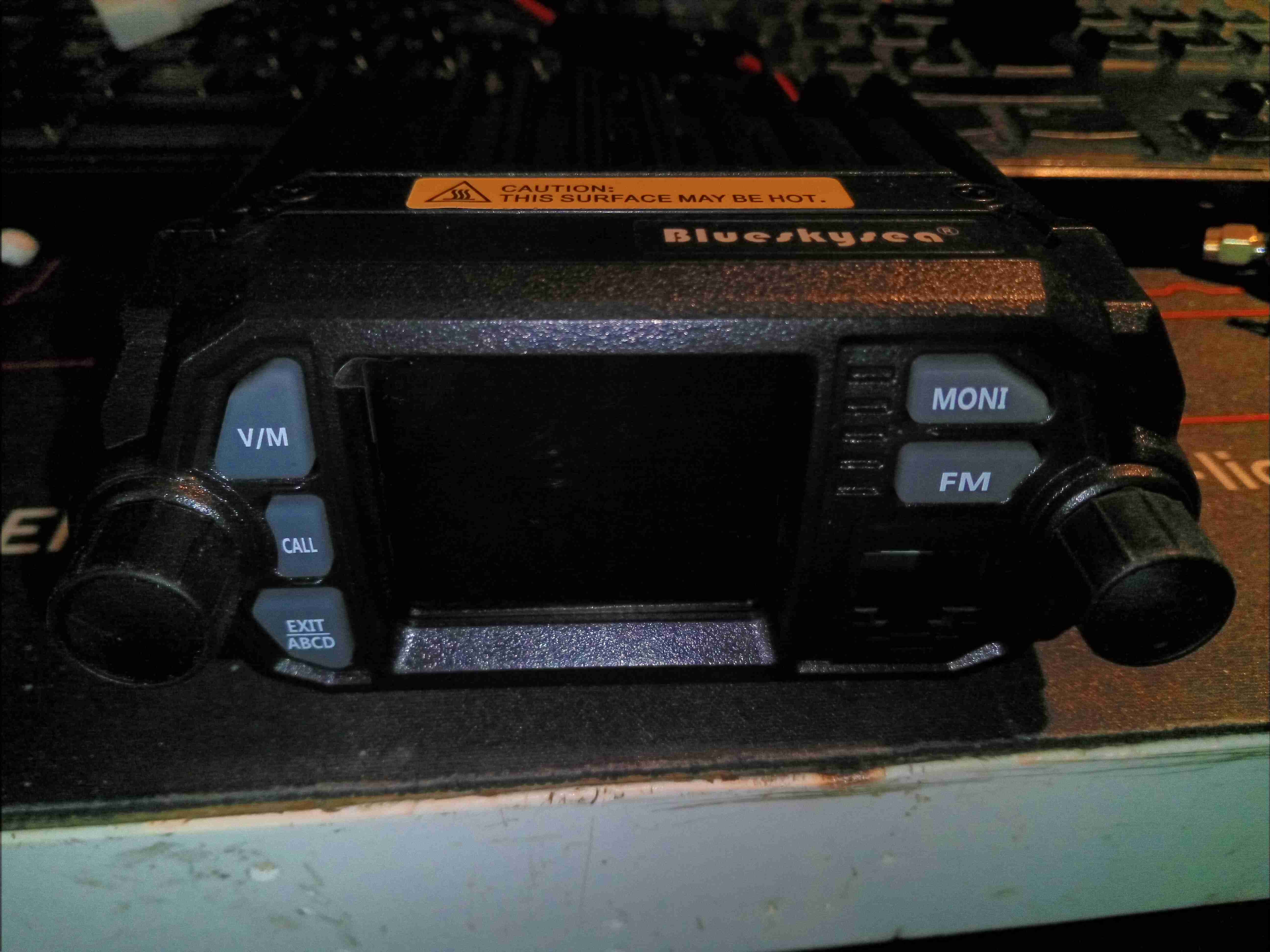
Here’s a miniature-sized mobile rig, which I purchased from eBay to fit in the car – my main Wouxun radio is far too big to fit under the dash! This unit is not much bigger than a UV-5R and cost less than £60! The front panel has a colour TFT LCD for the user interface, with a standard pot for volume, and rotary encoder for menu actions. Most of the controls are actually on the DTMF PTT mic, but some things are operable from the front panel.
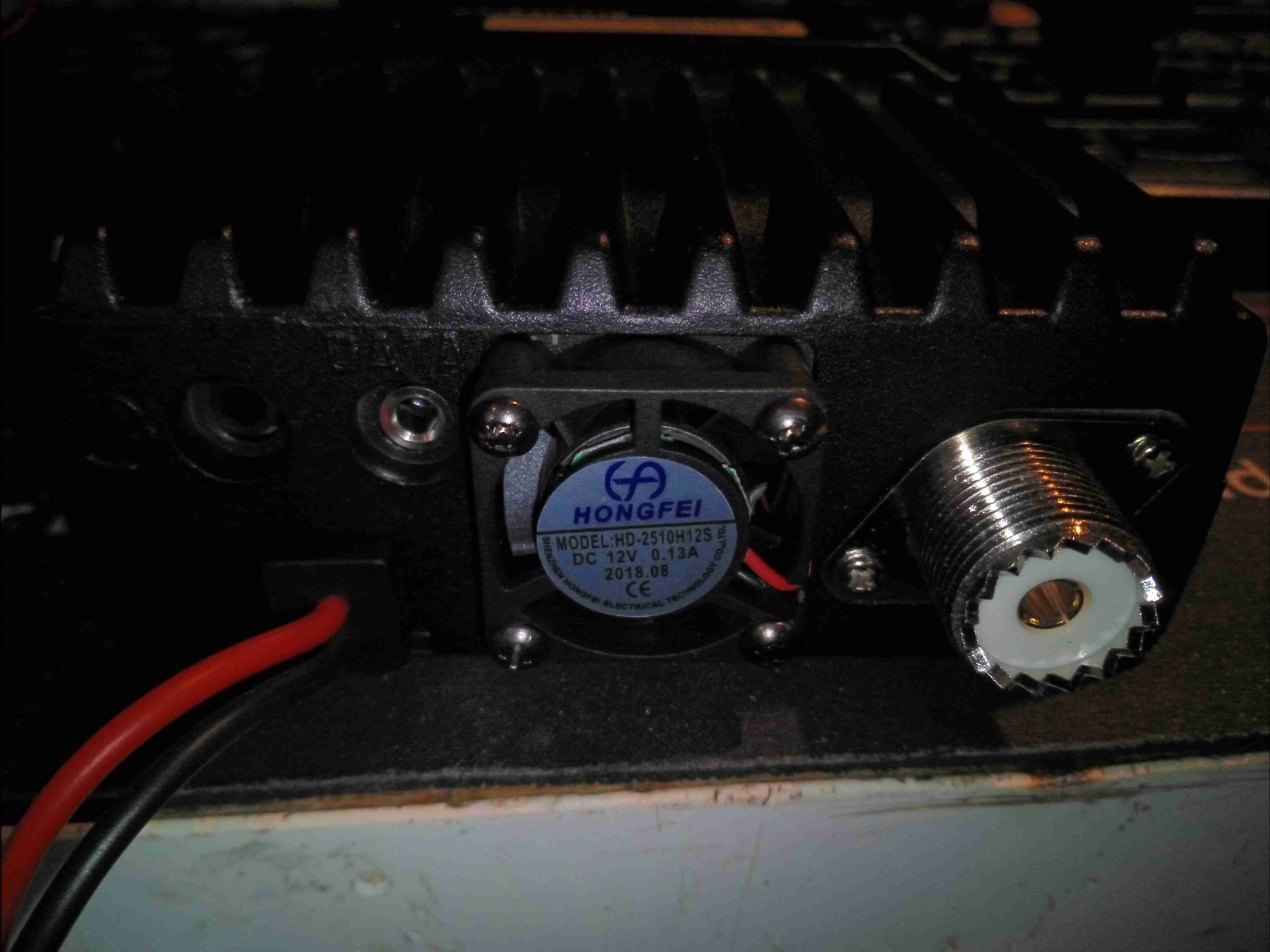
The rear panel has a small fan to cool the internal RF power amp, and a PL-259 connector for the antenna connection. This will be the first thing to be replaced, with an N-Type. There’s also a headset connector on the back, along with a 3.5mm TRS jack for serial data – very important on this radio for programming, as the interface is abysmal in this department ;).
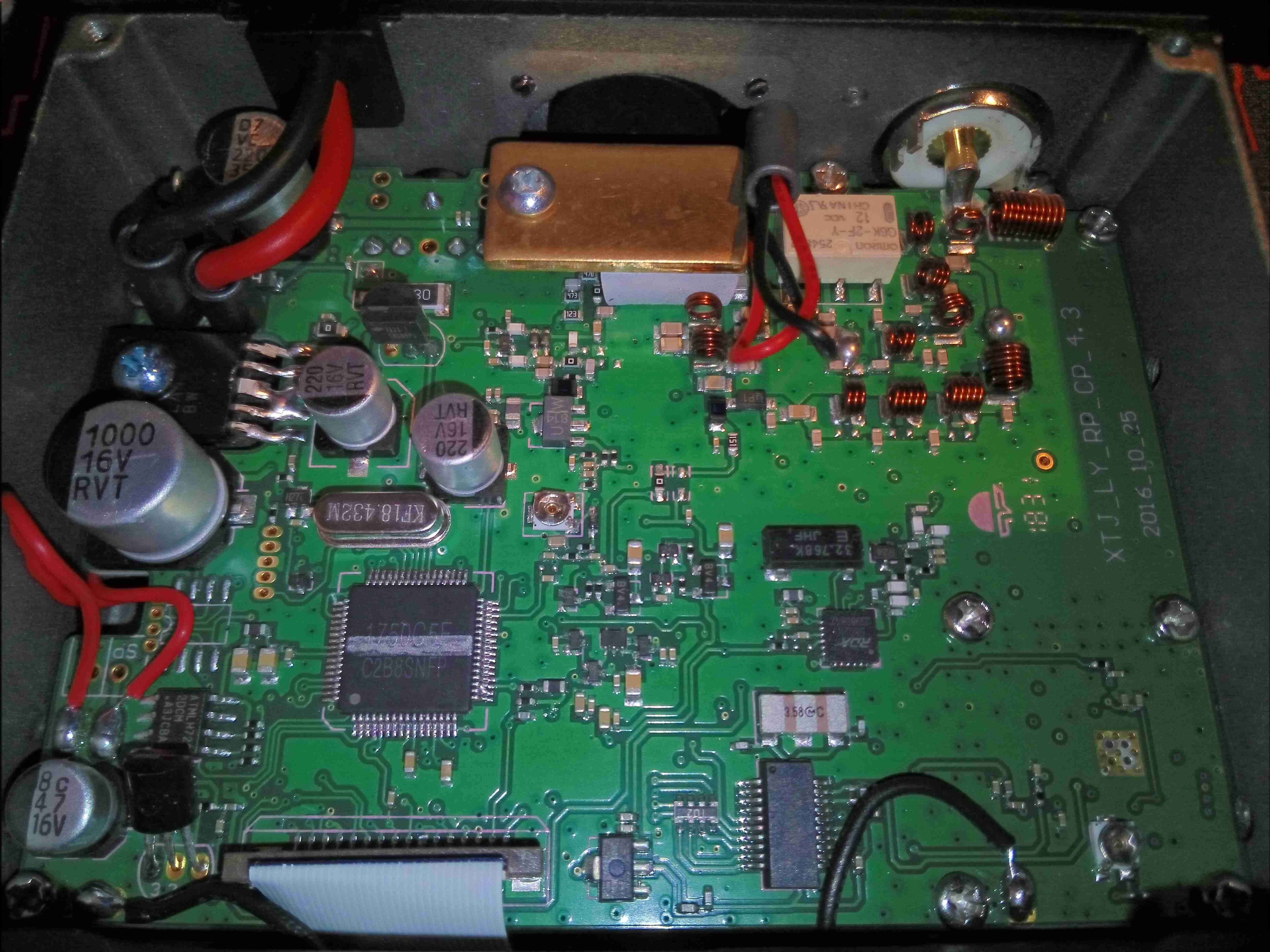
Popping the plastic bottom cover off allows access to the internals. There’s a single PCB in here with a double-sided load. Unfortunately the PCB is too difficult to remove from the casing without damaging anything, so only this side to be seen! On the top though is the main system microcontroller, the broadcast FM receiver, voltage regulation and the RF output stages.
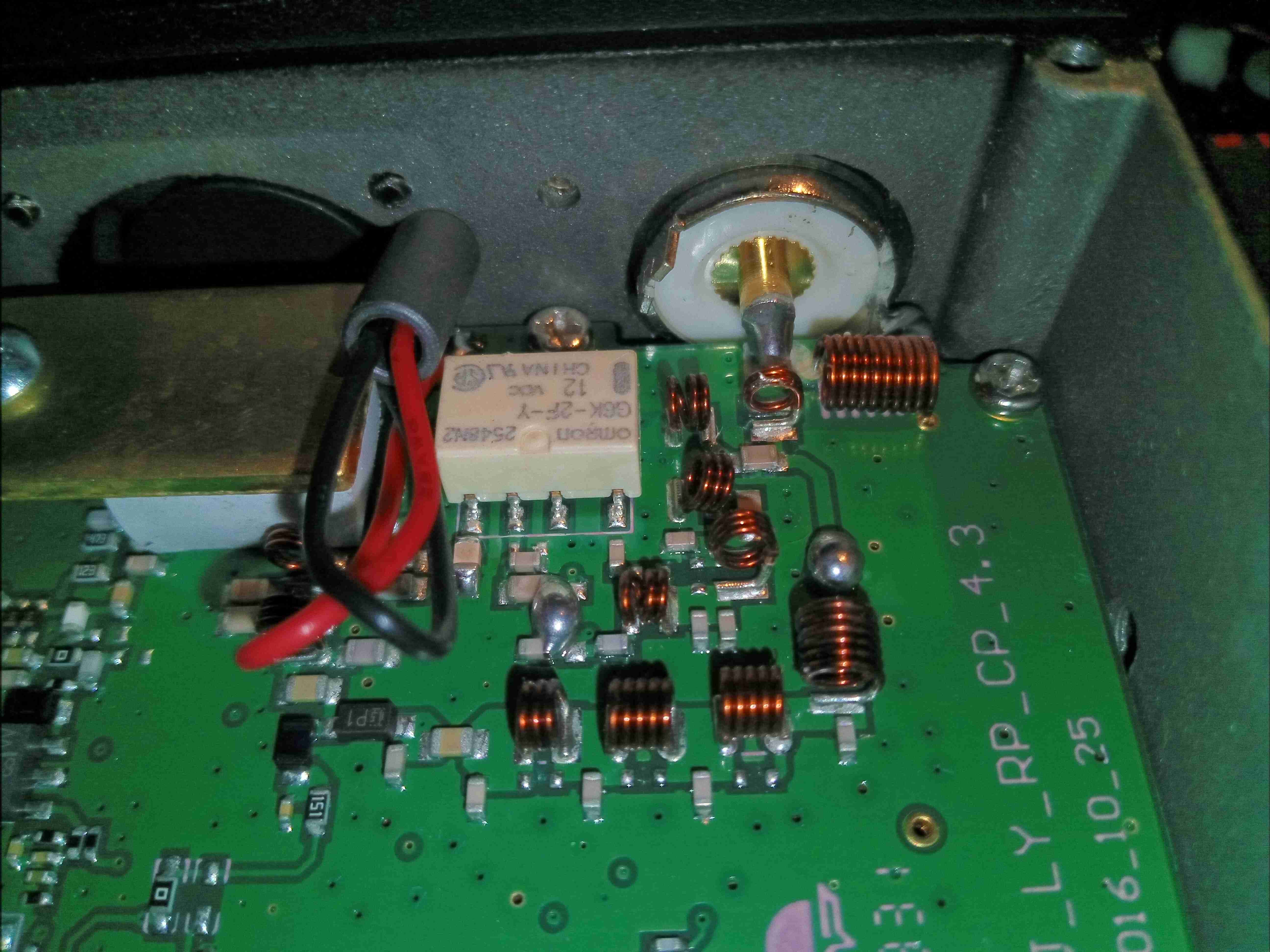
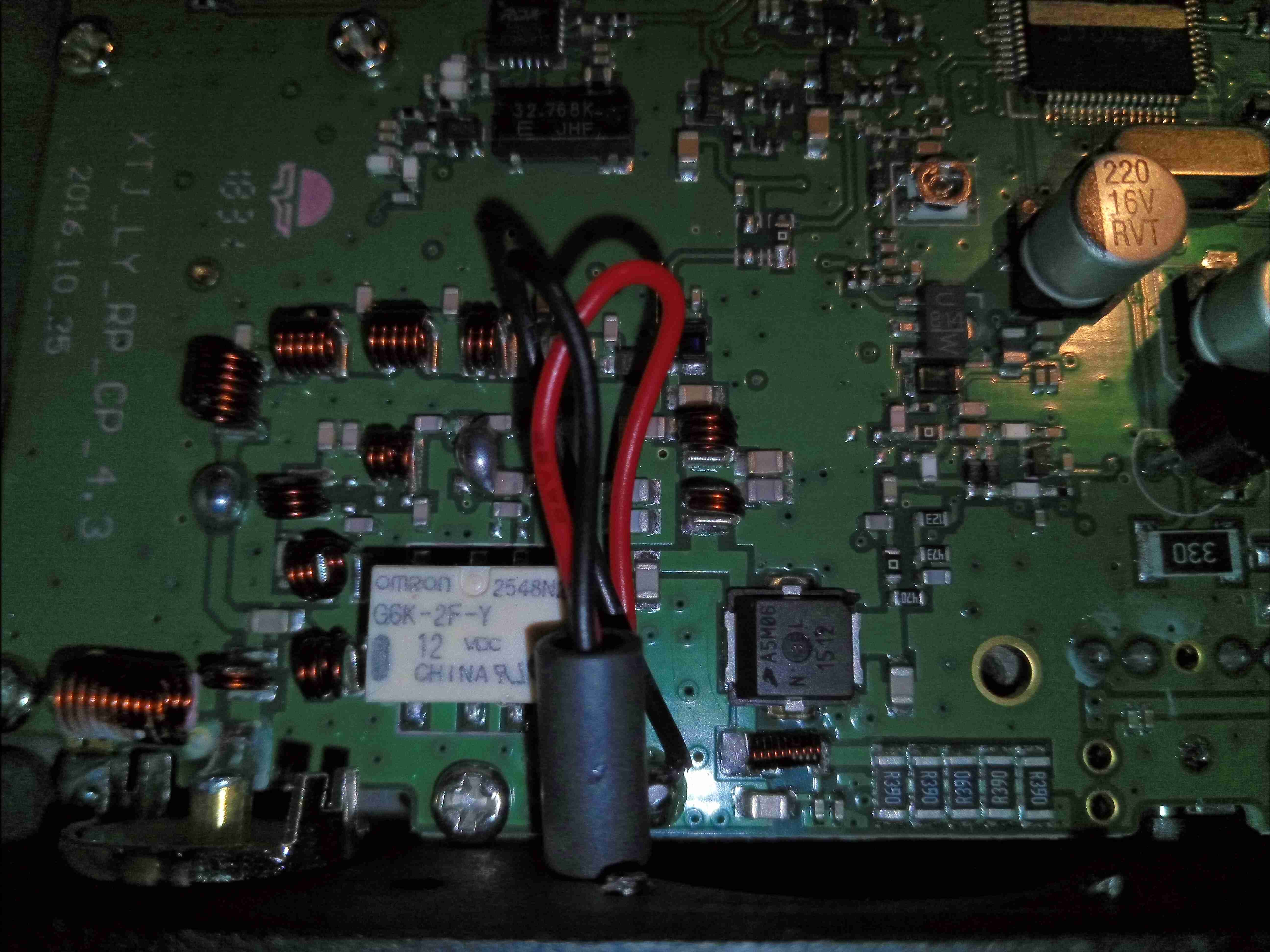
The RF output filters are tucked into a corner of the board near the antenna connector, with a small relay to switch between VHF & UHF. My concern with this relay is that it’s not intended for RF use, and is in fact a general purpose relay. This would have been designed into the unit as a price reduction measure. Under the brass plate & thick SIL pad is the main RF output transistor. The external fan leads also pass very close to the RF output stage, so they may end up radiating some RF from the back of the unit, despite the ferrite bead on the leads.
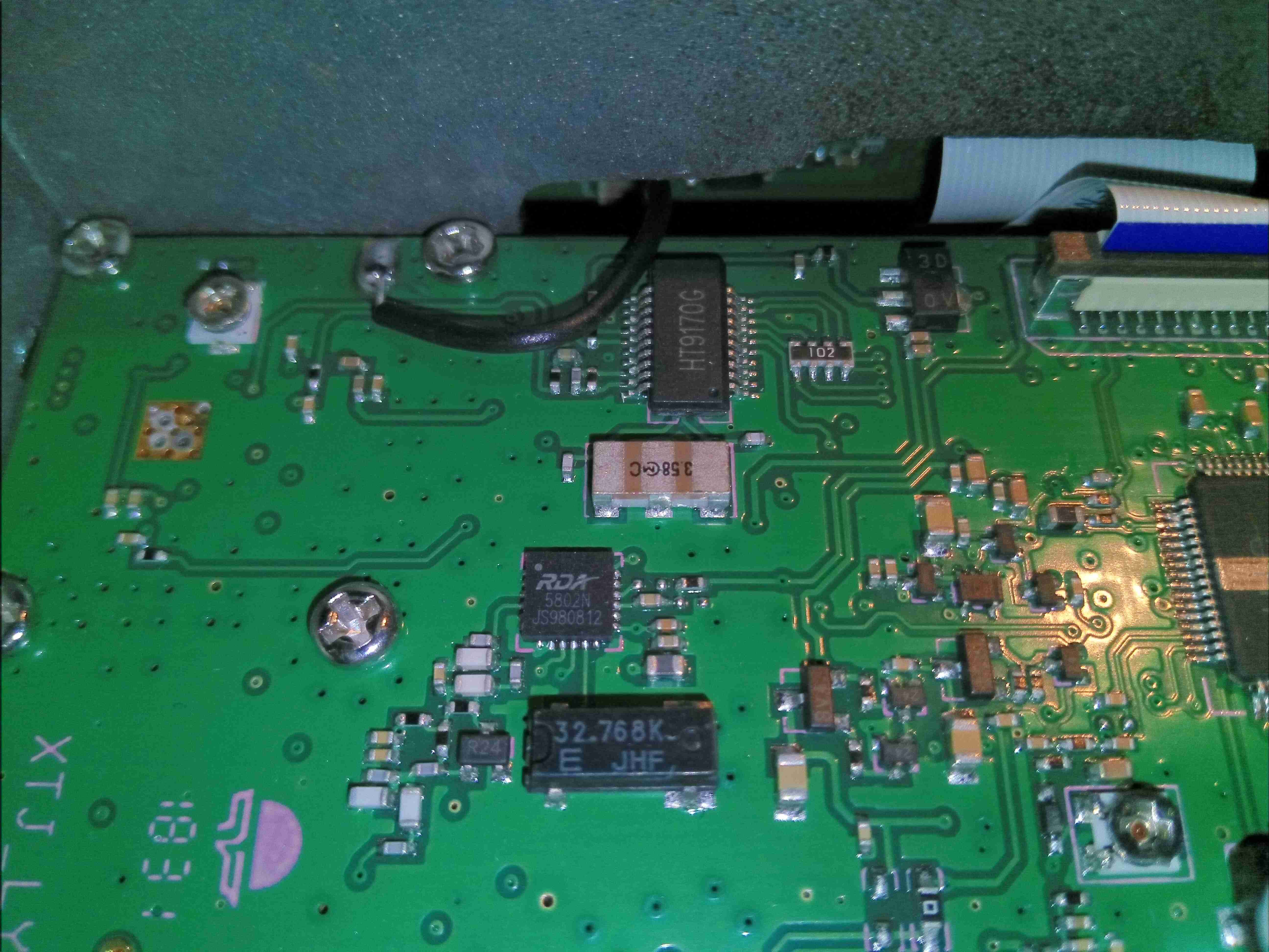
Just behind the front panel is the broadcast FM receiver, an RDA5802, with it’s 32.768kHz clock crystal. Just above that is the DTMF receiver & decoder, used in most Chinese radios, with it’s ceramic resonator. There’s a couple of unmarked pots on the board, but I am not certain what their function is.
Here’s the RF output stage, with the “heatsink” removed. I’m concerned on several fronts with this part – the heatsinking provided by a small brass plate and thick SIL pad is going to be poor at best, but looking at the datasheet for the main RF transistor, an AFT05MS006NT1 RF LDMOS N-Channel Lateral MOSFET from NXP shows some alarming numbers. Grab the full datasheet [download id=”7839″].
Remember that this radio is intended for mobile use in vehicles – the electrical systems of which can in a normal operational state rise to 14.8v.
This transistor is intended for handheld radio use, with an operational voltage of 7.5v, and absolute maximum ratings of 12.5v! Even when used on a regulated 13.8v PSU, the absolute maximum rating for the transistor is being exceeded.
At the very least, I would expect the life of the radio to be shortened due to this problem, and at worst the transistor may catastrophically fail in service, damaging the radio.
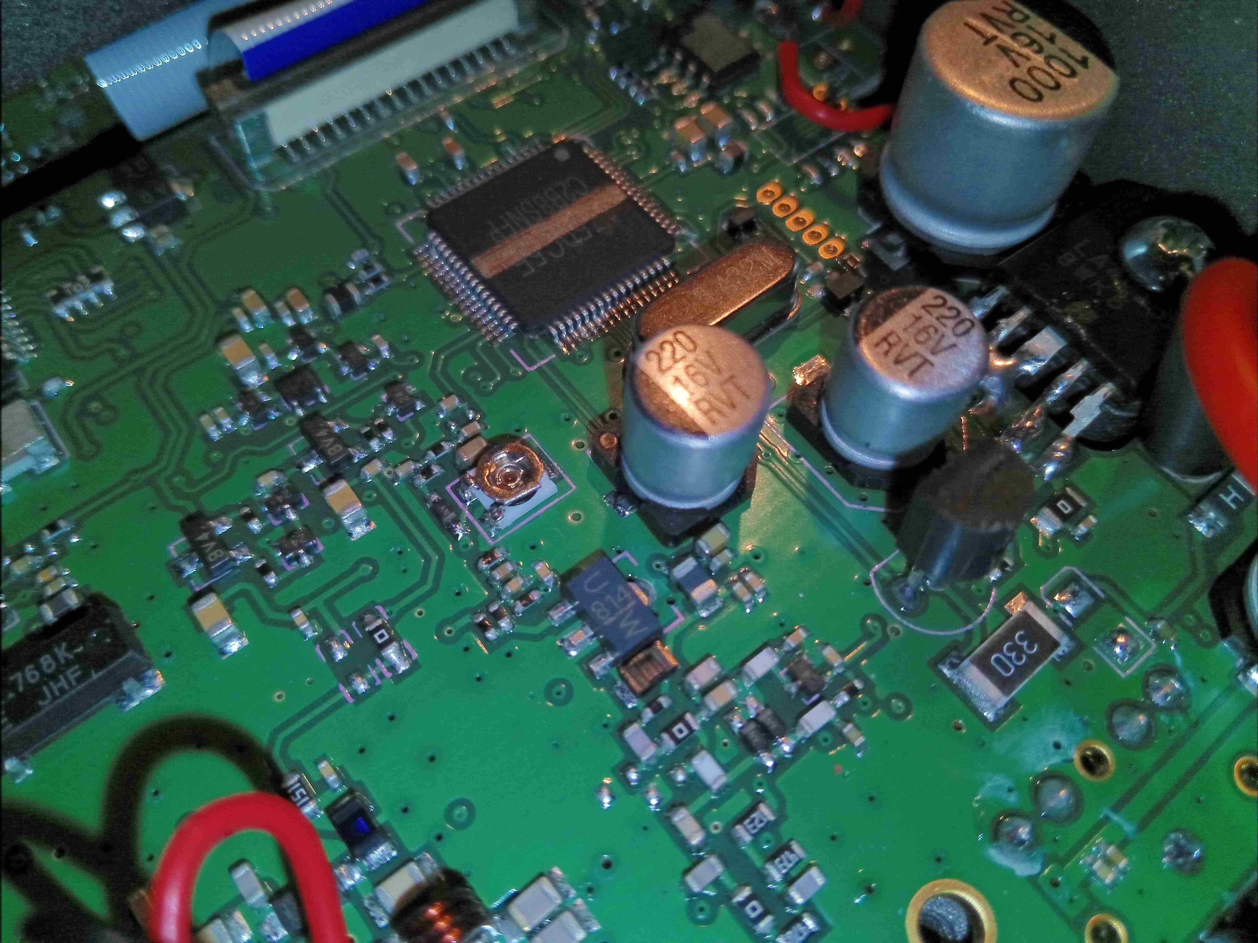
The main microcontroller is a Renesas R8C series device, with quite a few peripherals. It is accompanied by it’s clock crystal, and a programming header. An FFC cable vanishes off to the front panel PCB for driving the LCD & connecting up the user controls & mic connector. Just to the right is the main voltage regulation section for the electronics, minus the RF output stage, which is directly connected to the DC input bus.
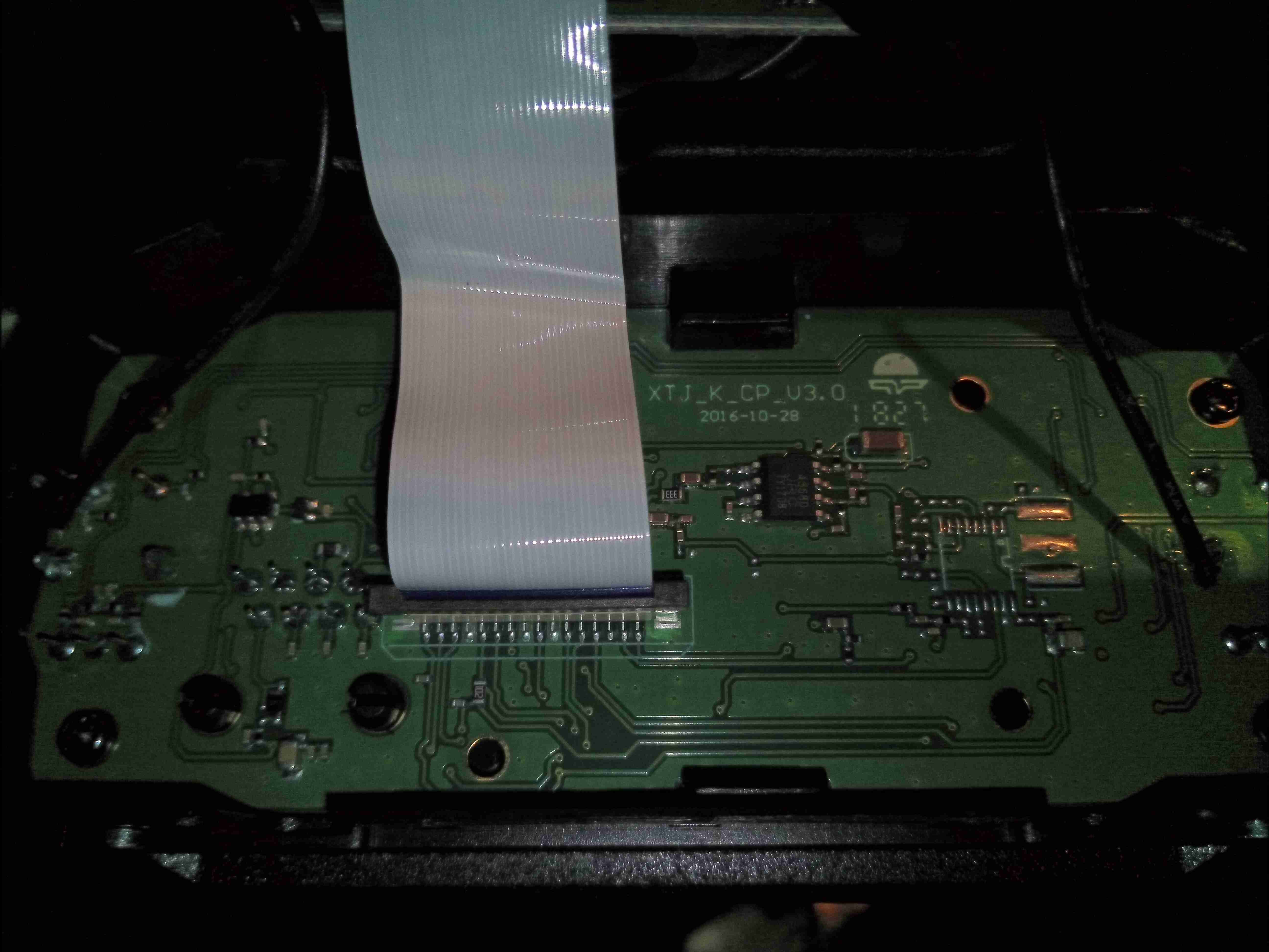
There’s not much on the front panel PCB, so I won’t bother taking it out of the frame, this is going to mainly be interconnects for the SPI/I²C driven LCD & analogue channels for the audio.
I’ll keep the blog posted with lifespan checks on this radio, as I’m definitely concerned about the power amplifier transistor, but other than that it seems to be an OK radio. The rotary encoder has zero debounce, so it doesn’t work properly, but this isn’t much of an issue when the radio is fully operable from the PTT mic.