Here’s a DMD Android-based projector from China. This has quite good resolution at 720p native, although the install of Android present is very outdated, and the internal battery has a very short life due to the power draw of the unit.
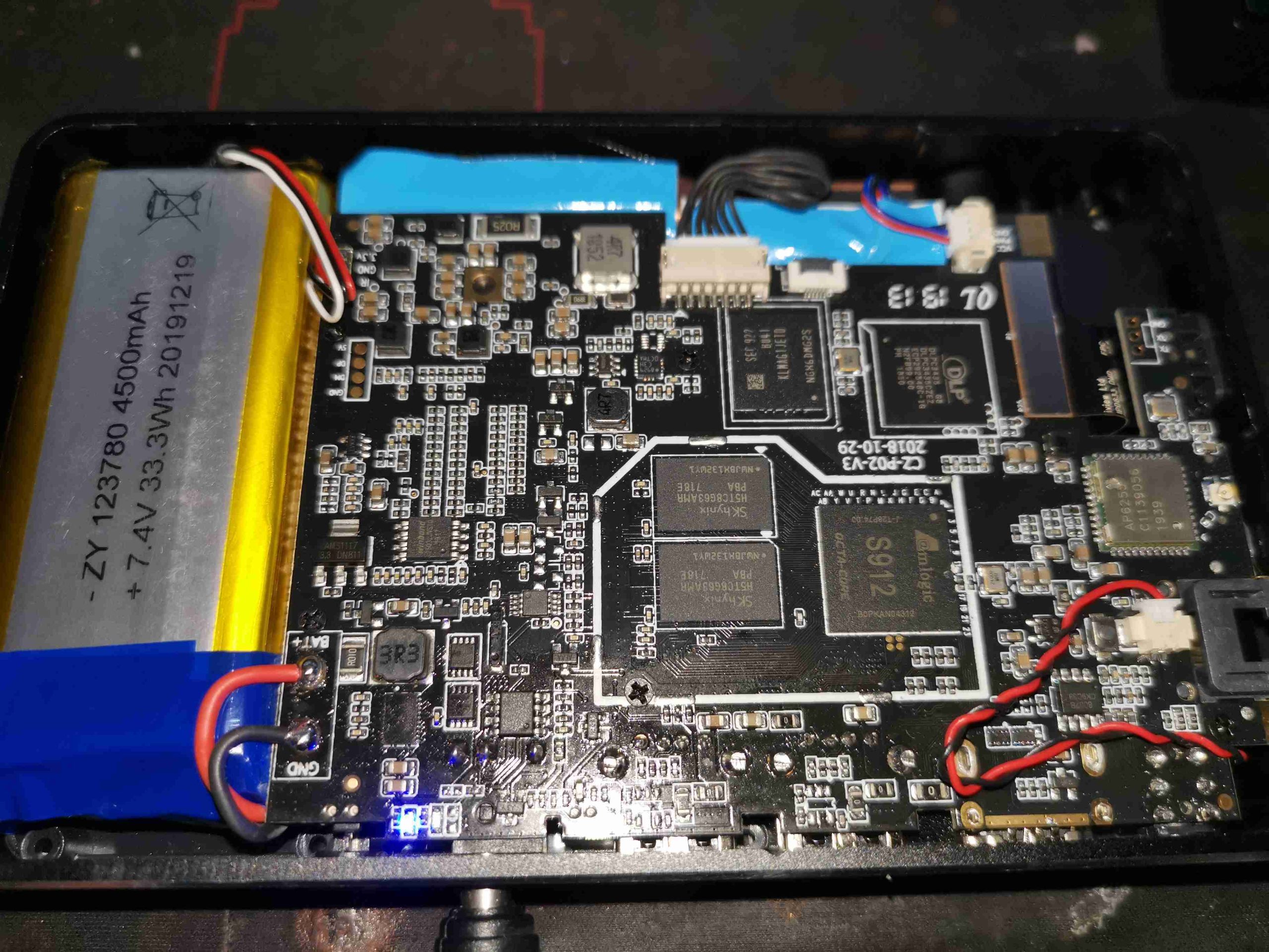
The top of the main PCB is above, and this has one half of the DMD chipset, and the SoC, Flash & RAM for the Android part of the projector.
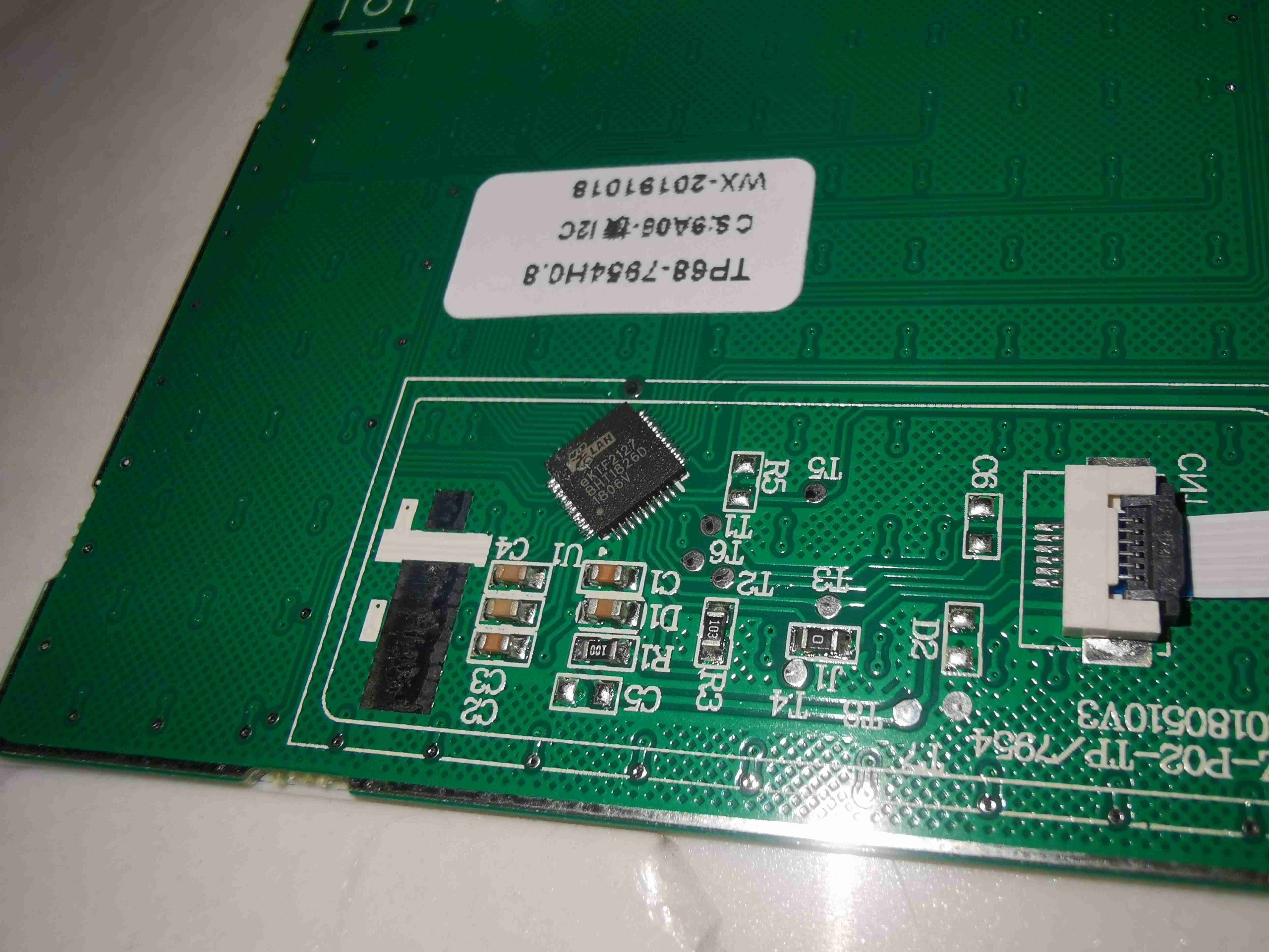
Touchpad
The top of the unit has touch buttons and mousepad for operation, in addition to an IR remote, the bottom of the lid moulding has the touch controller for those buttons and pad.
Mainboard
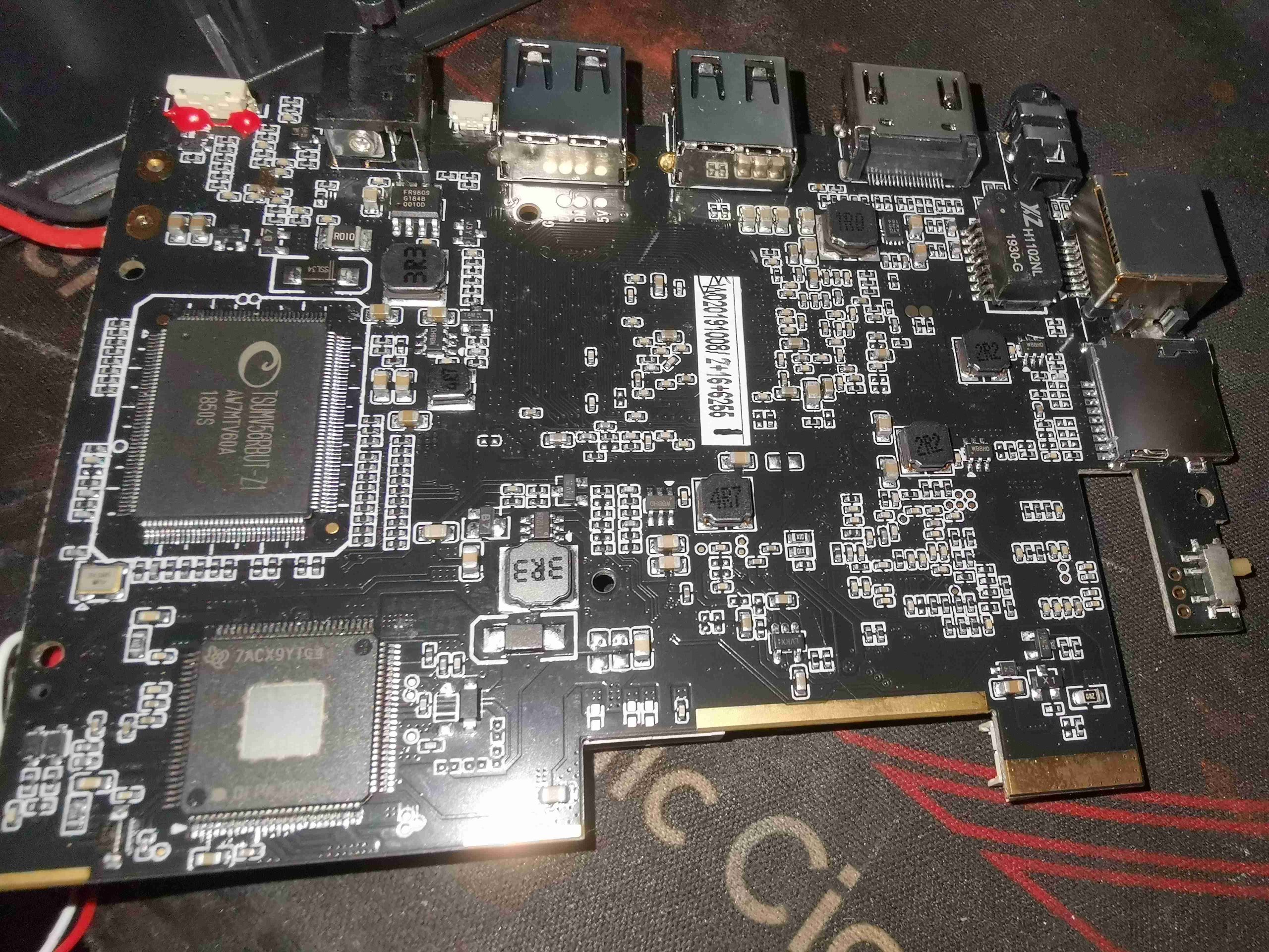
Removing the mainboard shows the rest of the chipset. The large IC at bottom left is one half of the DMD control chipset, and the large IC above that is a video switch to enable either the built in Android or external HDMI interfaces. The rest of the components here are power supply and general support.
Projector Module
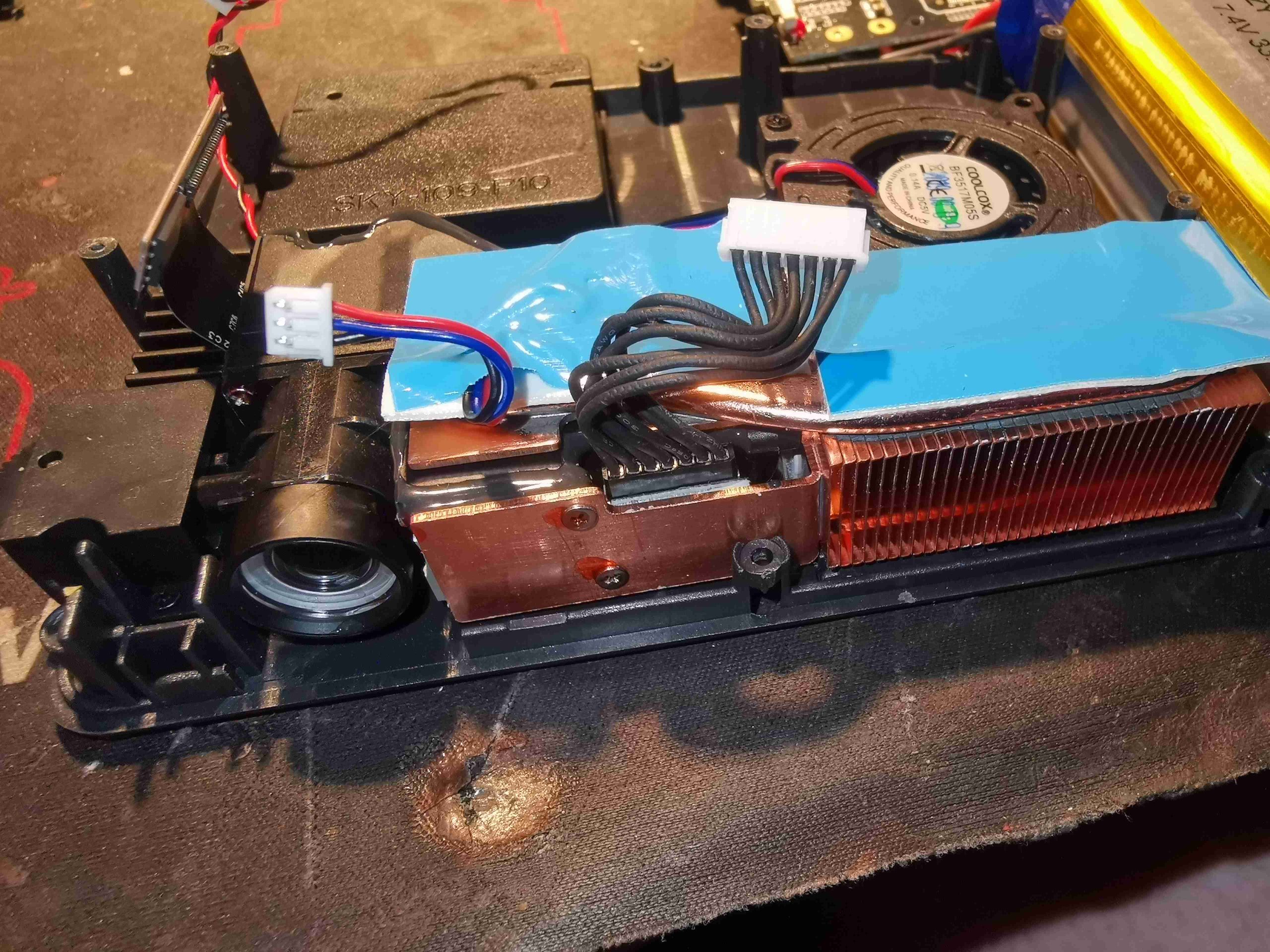
Under the mainboard is the projector module itself. Mostly heatsink just to cope with the high power LEDs, there’s a fan in the rear section that keeps everything cool.
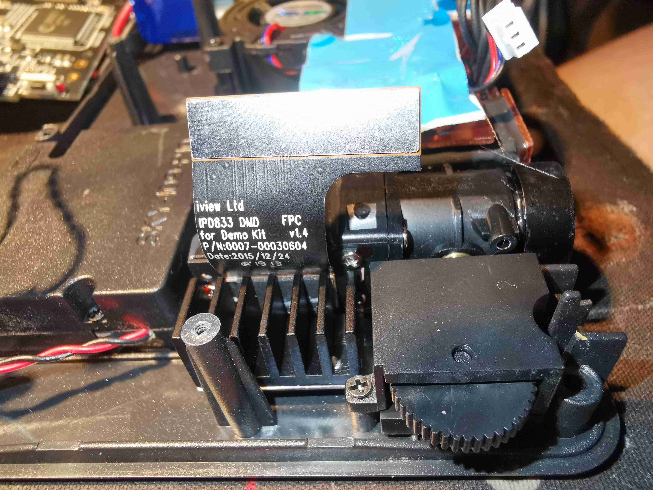
DMD Heatsink
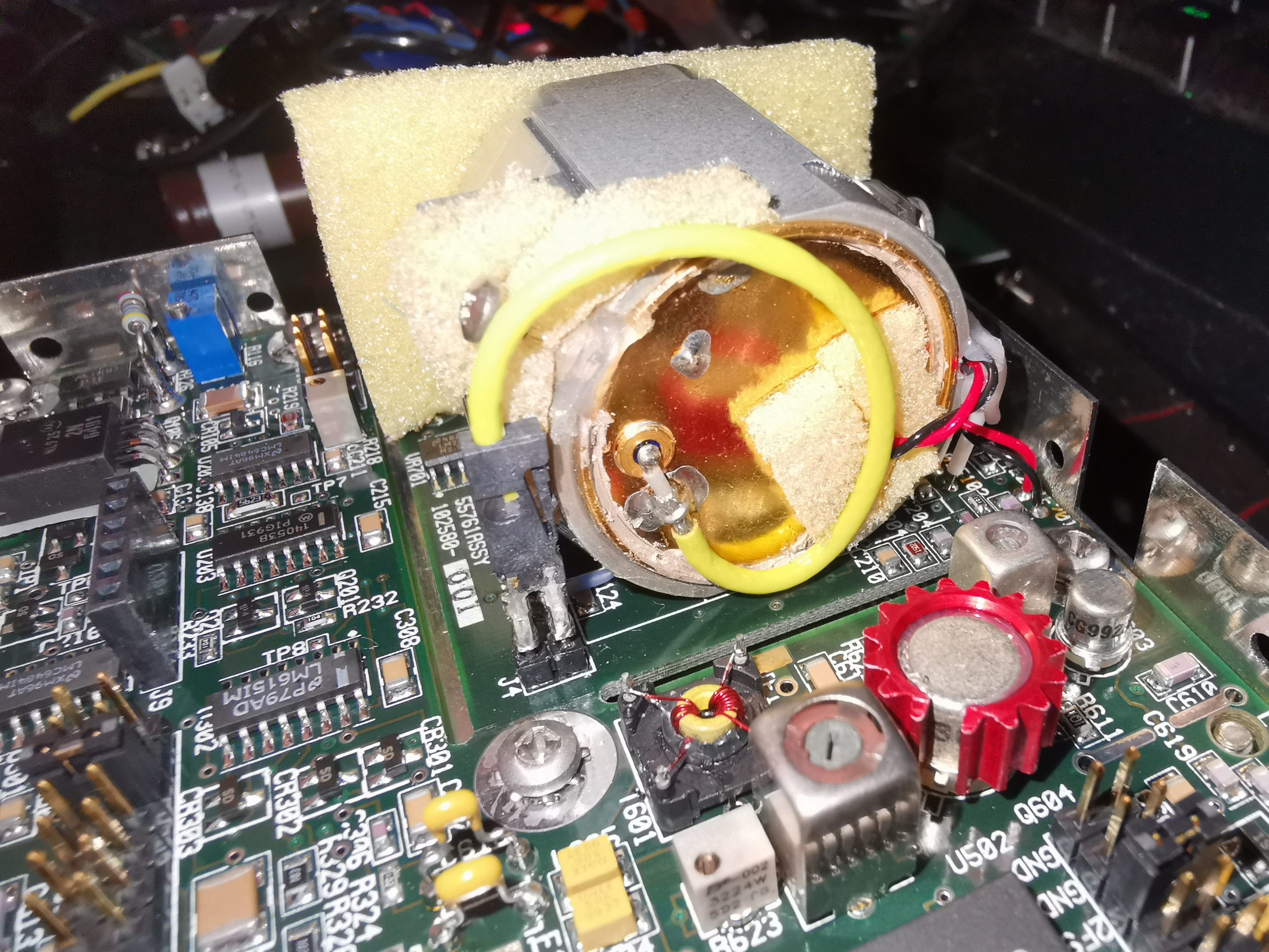
The DMD module is definitely from a development kit – it’s hidden behind this small heatsink. The wheel in the foreground is for main focus.
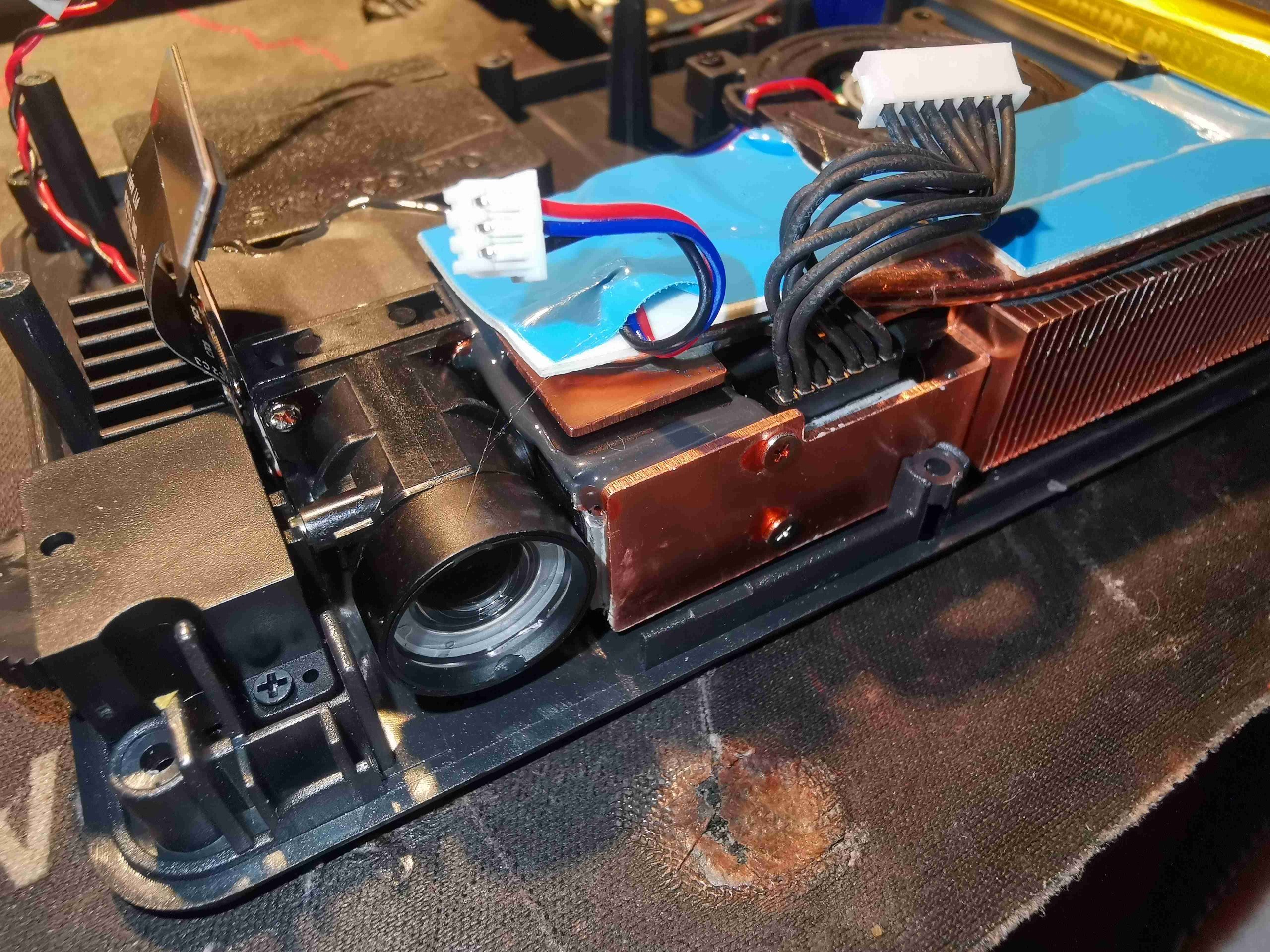
LED Module
On the front of the unit, behind the copper plate is the main RGB LED module, which is switched by the DMD chipset for full colour output from the main lens to the left.
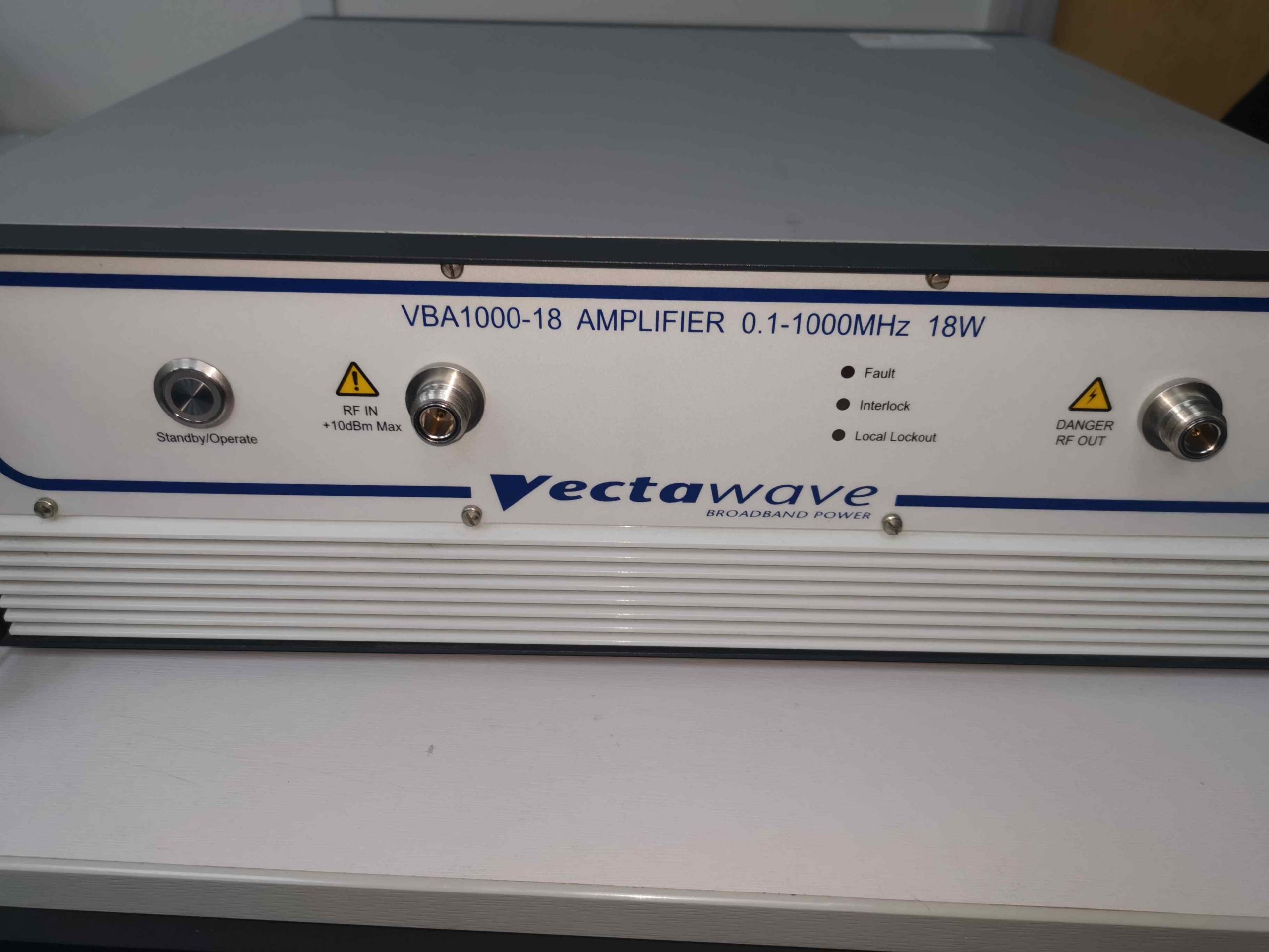
Here’s something that in my primary job as an EMC Test Engineer gets a lot of use – a laboratory grade amplifier for performing the Immunity testing phase of an EMC suite. I figured it was about time to crack them open & have a look at what makes them tick. I’ll start with the 100kHz-1GHz model in this post.
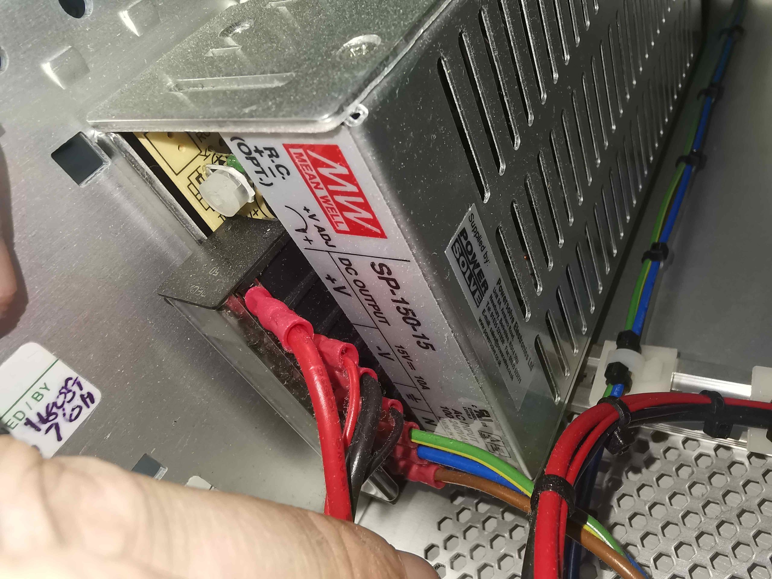
Main PSU
The main PSU providing power to the amplifier & control components is a 150W Meanwell unit in this example. While Meanwell have some fairly decent supplies, they are overall very hit & miss on reliability & especially in the compliance domain – the RSP-1000 & RSP2400 versions claim to be EMC Class B Conducted compliant, and definitely are not! They also claim Radiated Immunity to Industrial levels, but I’ve seen them fail this test, by reducing their output voltage by a factor of 10!
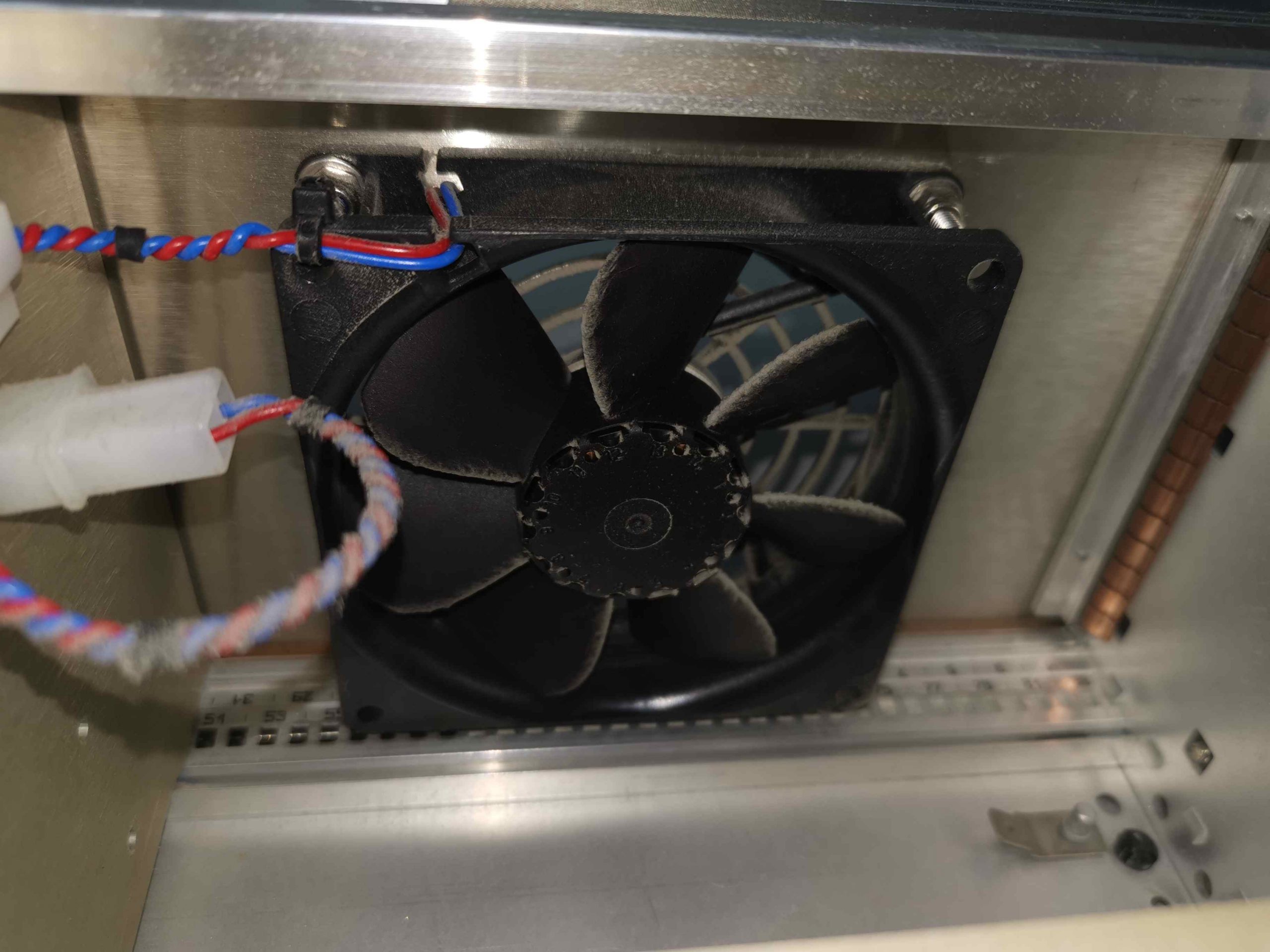
Cooling Fan
A 120mm 12V fan on the rear panel draws cooling air over the internal components. These amplifiers are Class A, so they do generate quite some heat due to the inefficiencies of this operational mode.
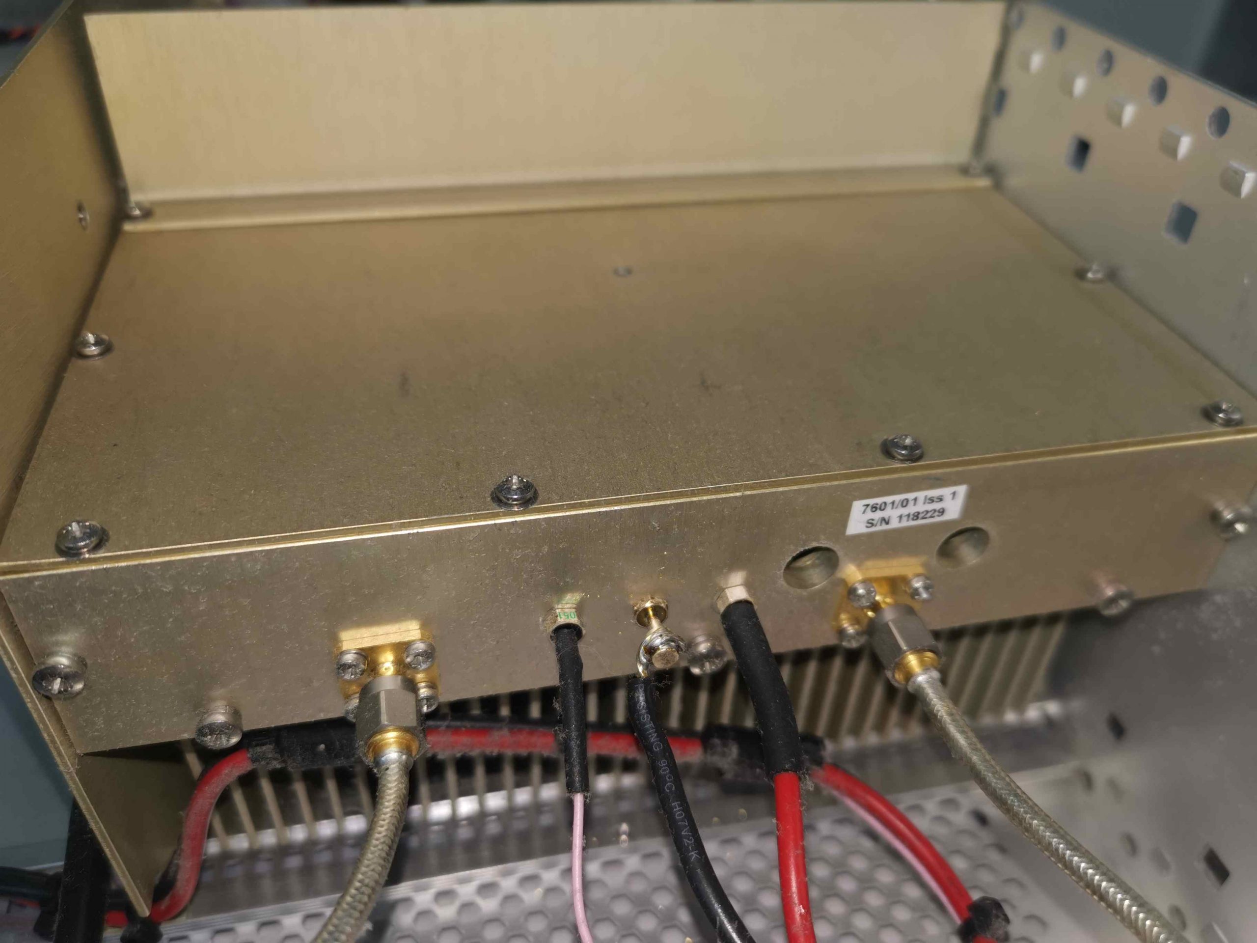
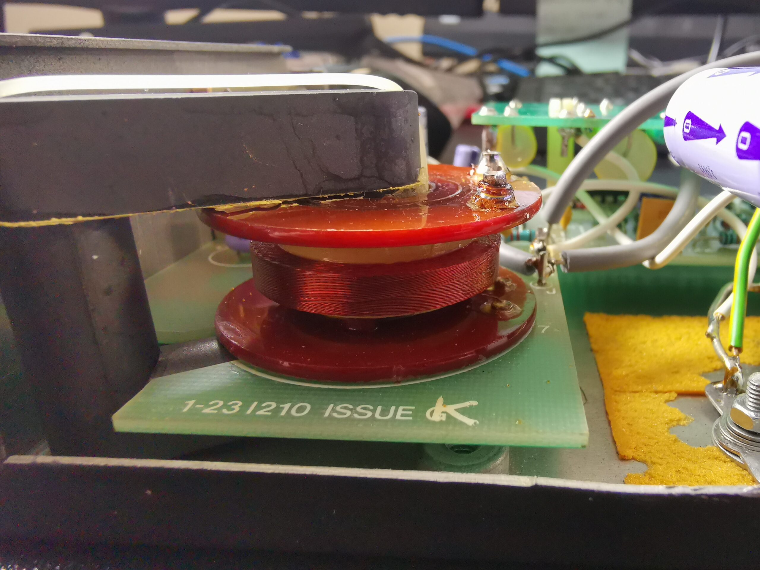
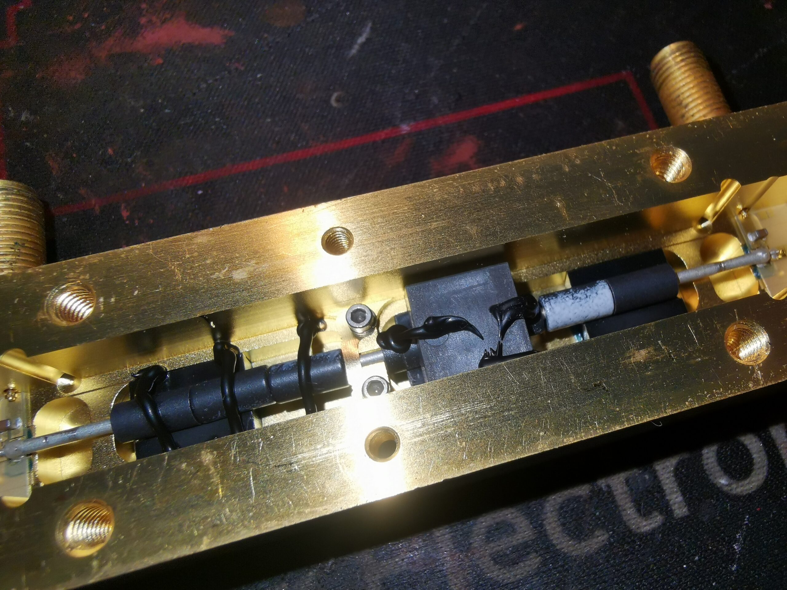
RF Amplifier Module
All the wideband RF magic is contained in this module. What’s unusual about these lab amps is the number of decades of operation – RF amplifiers are usually rather narrowband, and it’s very difficult to construct a wideband amplifier that has even close to a flat frequency response. There aren’t many connections; just the RF I/O connectors on SMAs, a ground, main power supply & finally an Enable input.
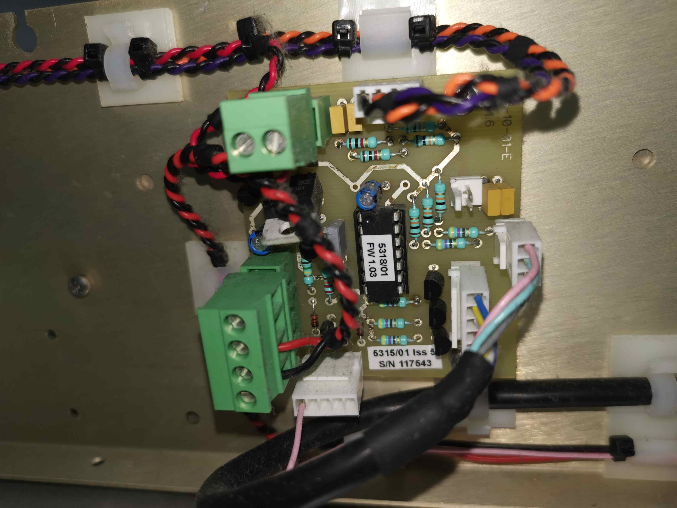
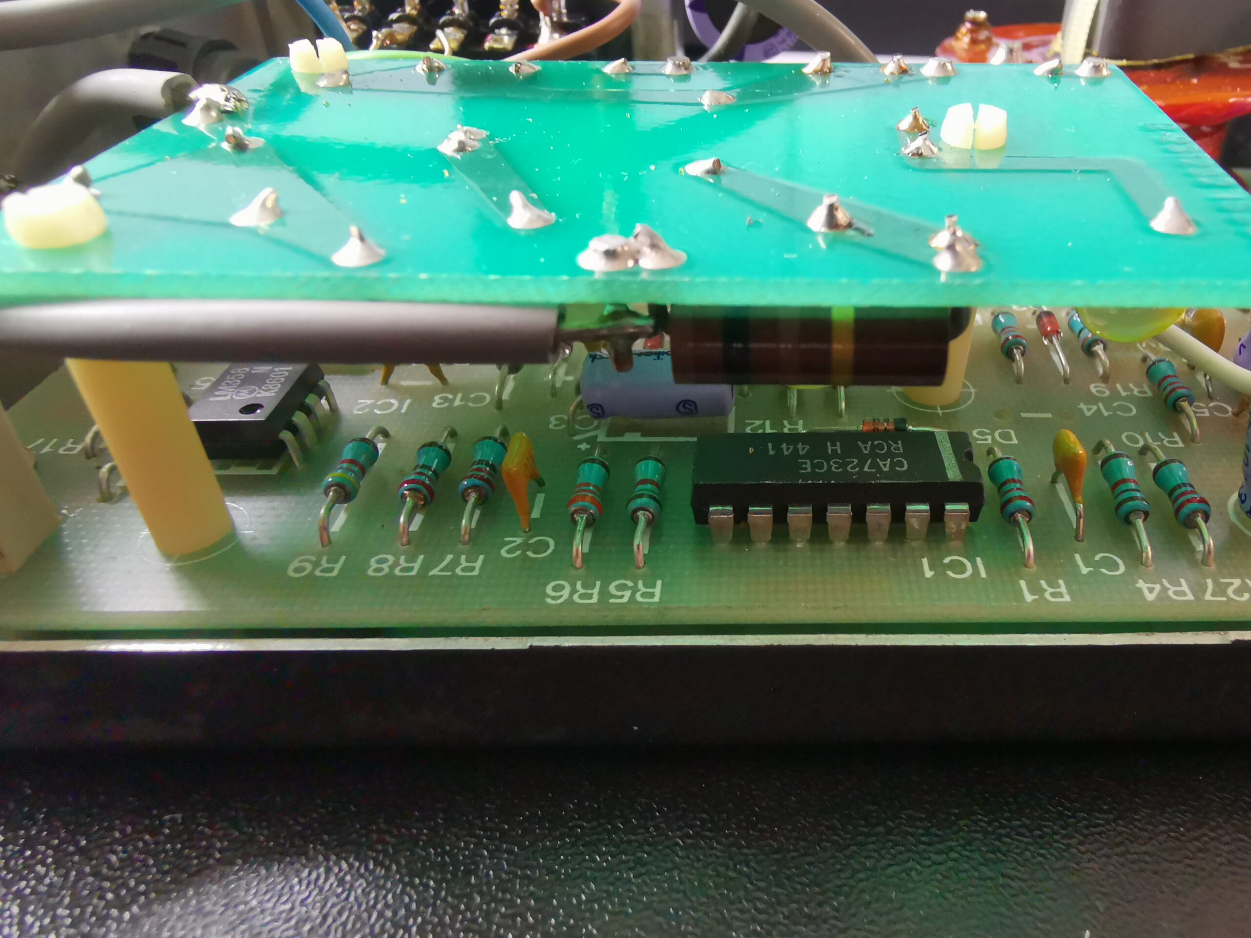
Control PCB
There’s a small PCB inside to do the safety interlocks, which are BNC connections on the back, as well as temperature monitoring & overtemperature shutdown. This just has a small PIC microcontroller & a few passives.
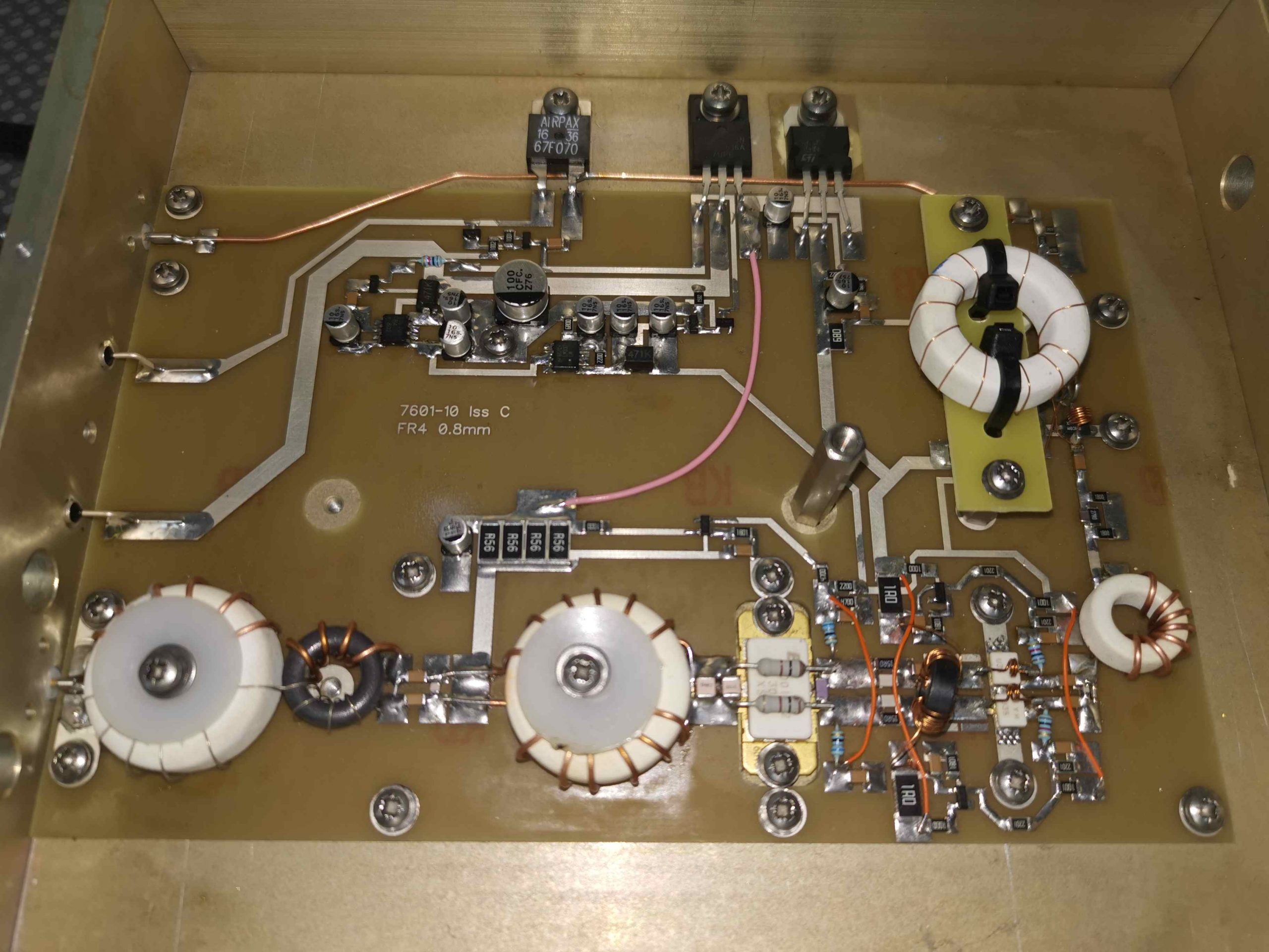
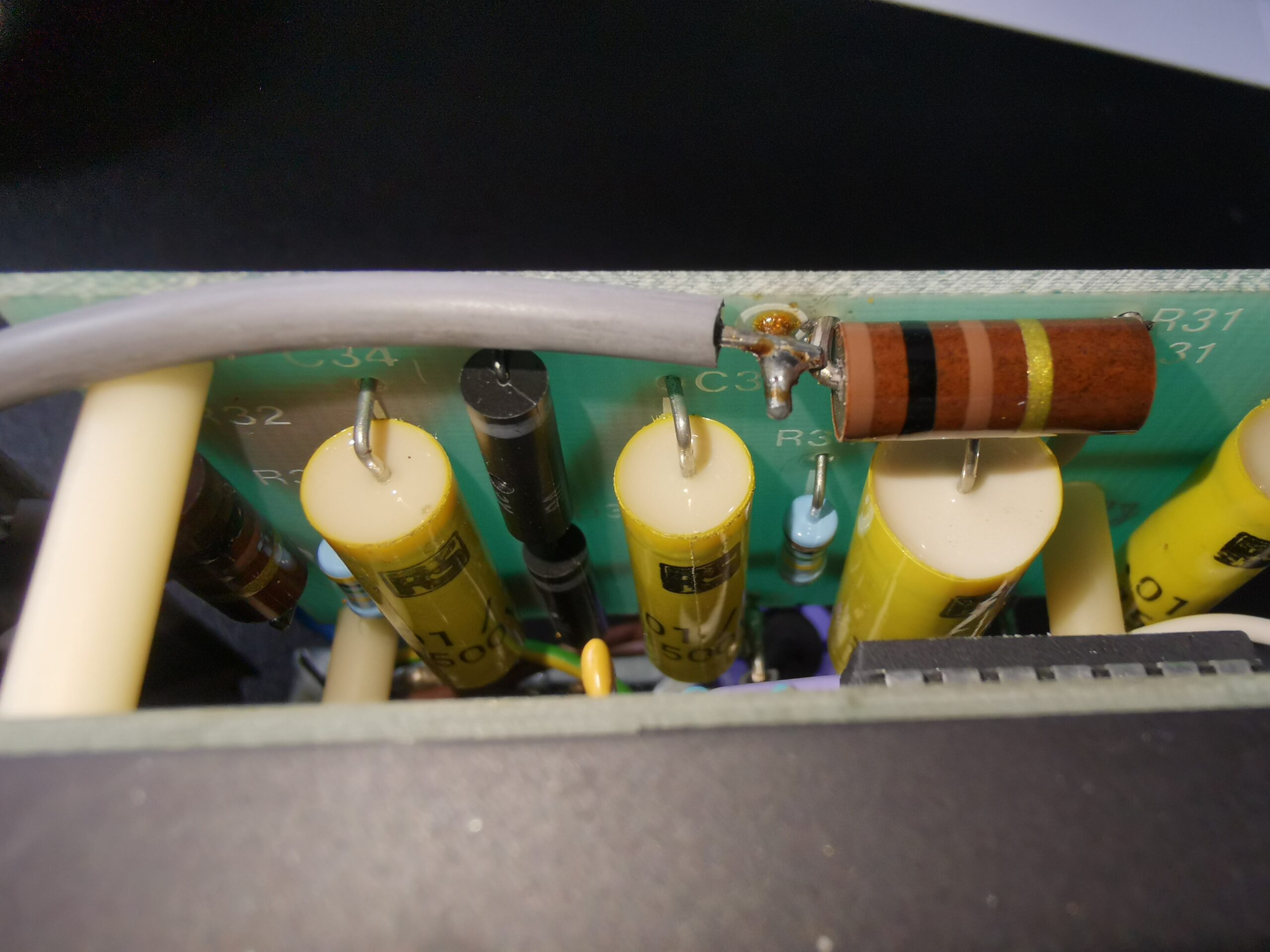
Main Amplifier PCB
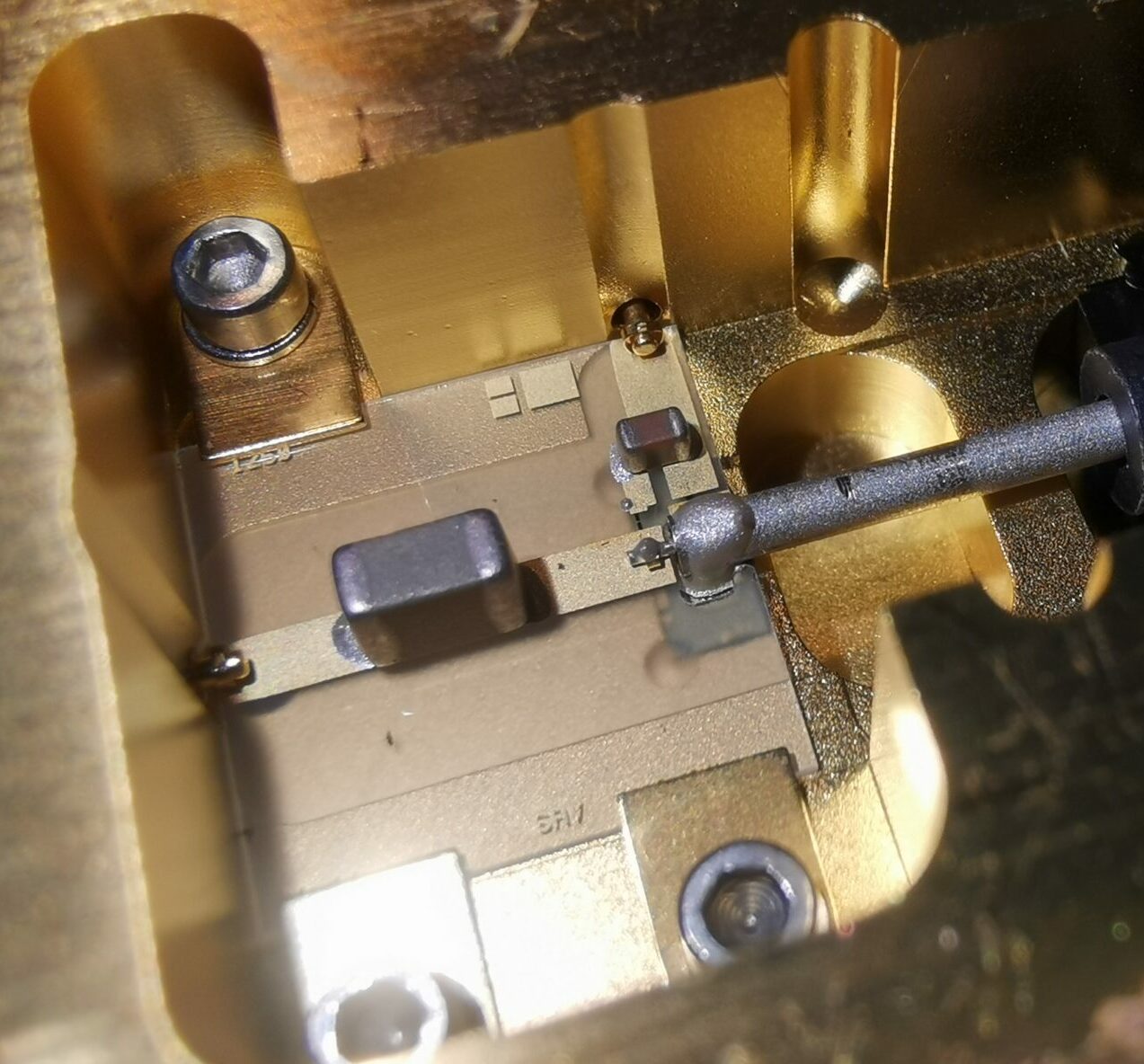
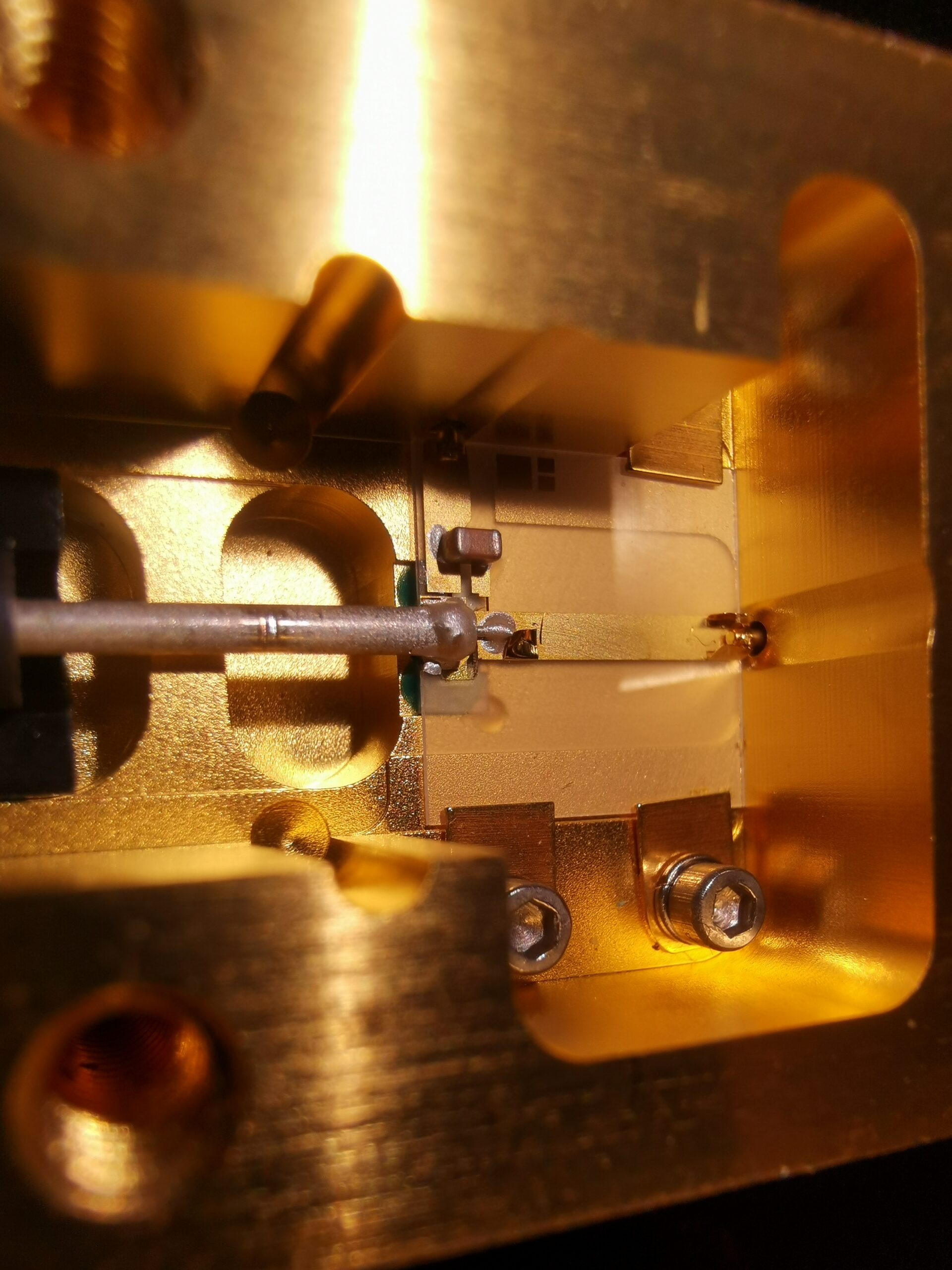
After taking the top off the amplifier module, a small PCB is all that’s in there, with single-sided construction. By the look the rear copper layer is all ground plane. Power supply & enable inputs are dealt with at the top of the board, with the pre-amp stage at bottom right, and finally the main PA stage bottom centre. This appears to be a push-pull design, with dual MOSFETs at all RF stages, and splitters/combiners at the I/O respectively.
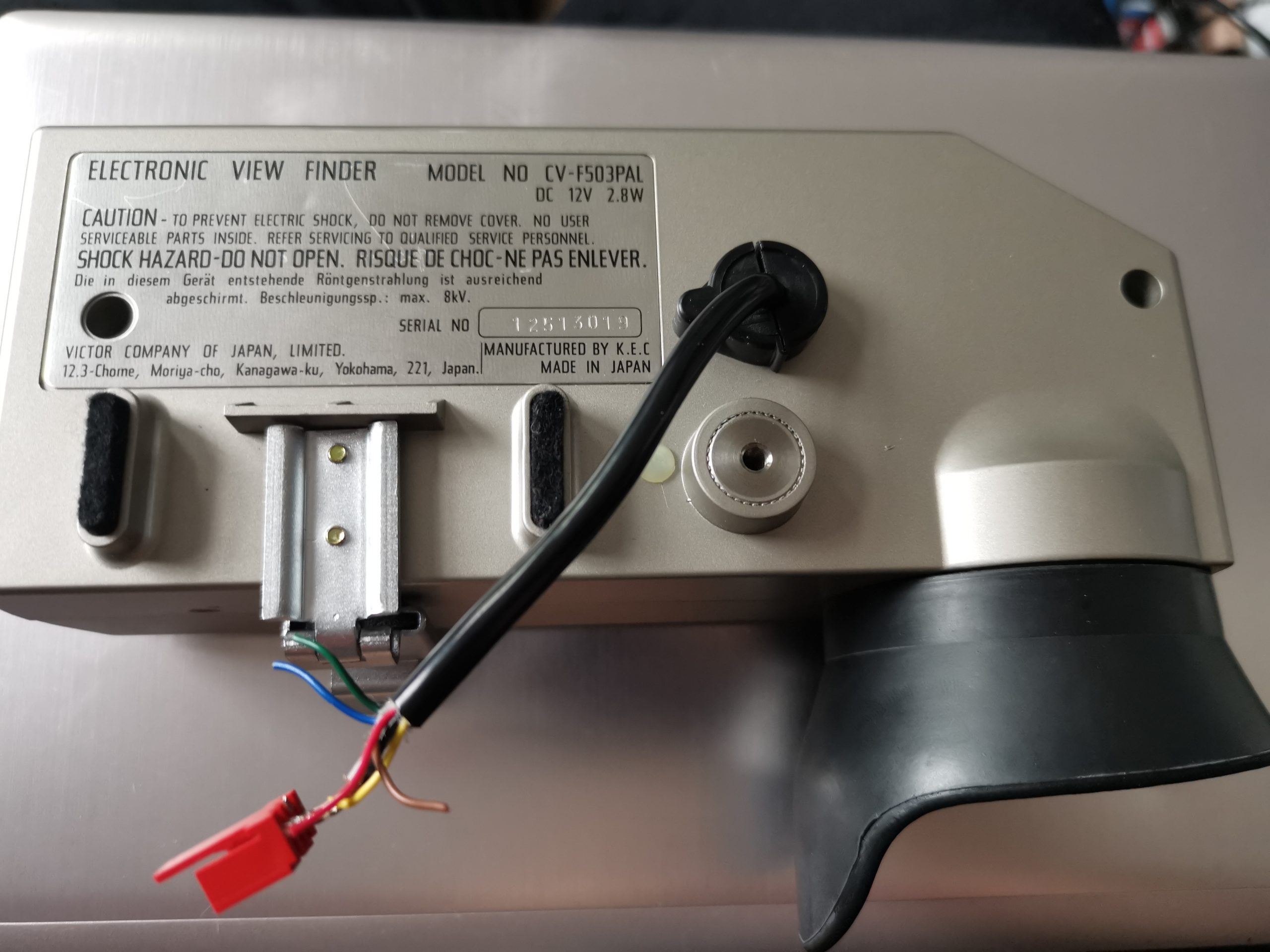
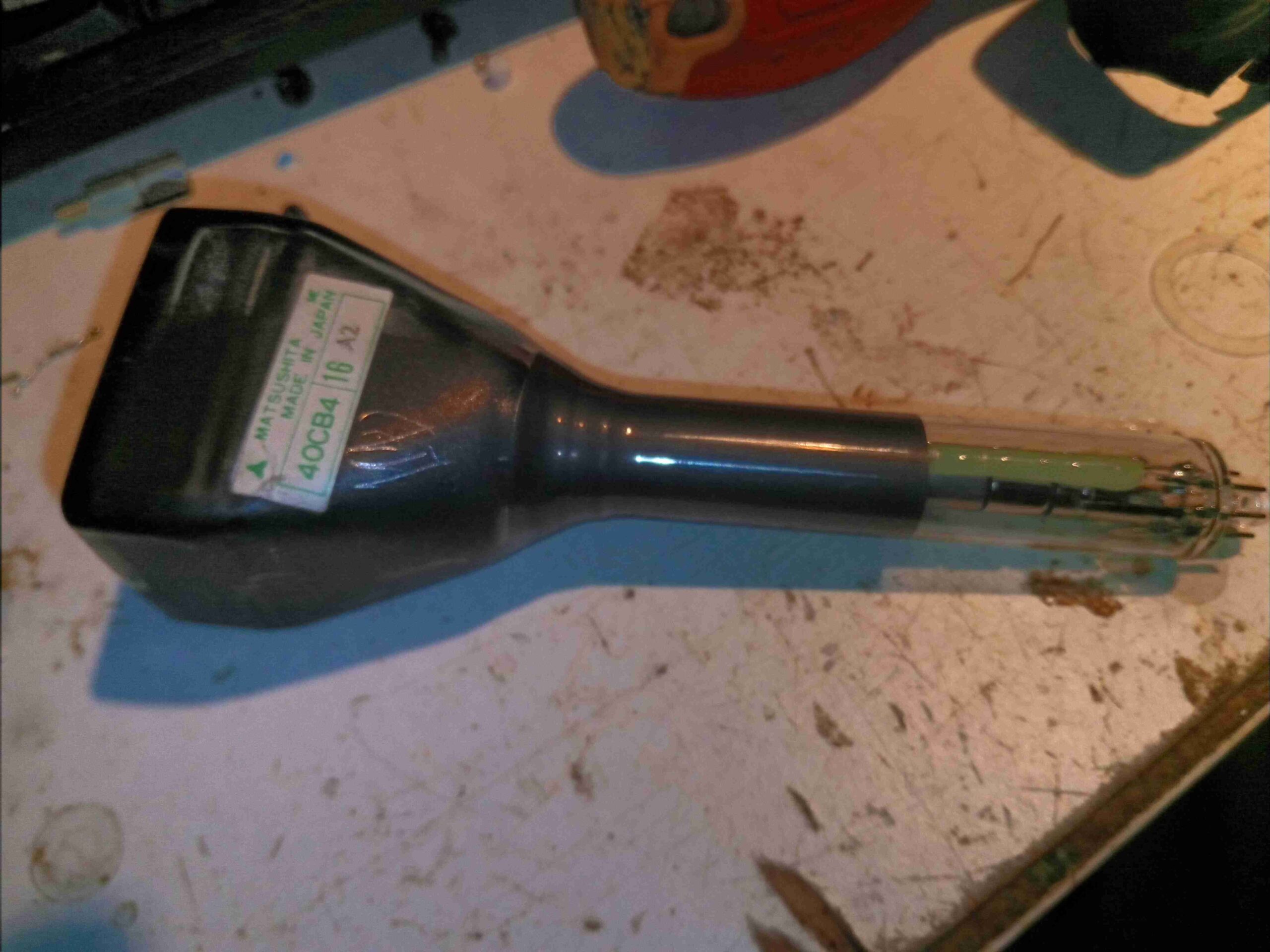
It’s time for another CRT-based post! This time it’s a Matsushita 40CB4-based viewfinder from 1980. These came from JVC colour tube cameras, and are physically massive! I’ve already worked out the pinout on the multicore cable here & attached a usable connector.
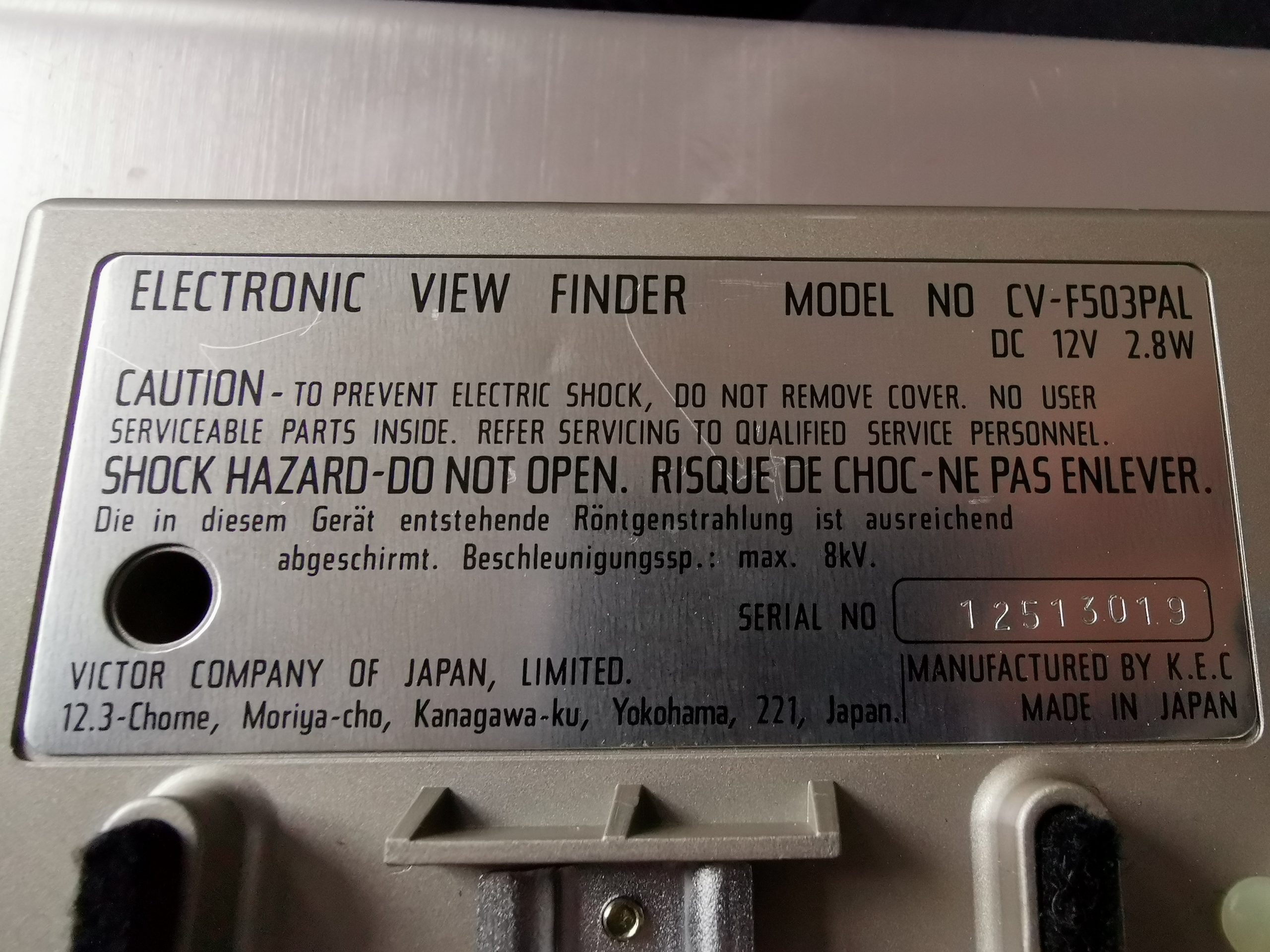
Information Label
There’s lots of information on the bottom label of this unit, including a notification in German that the X-Ray emission from the device is shielded, and the maximum CRT acceleration voltage is 8kV. This last point is a bit strange, since the 40CB4 datasheet states a maximum design voltage on the final anode of 6kV. I did measure the voltage at the anode cup, and it’s stable at 7.15kV!
Internal Overview
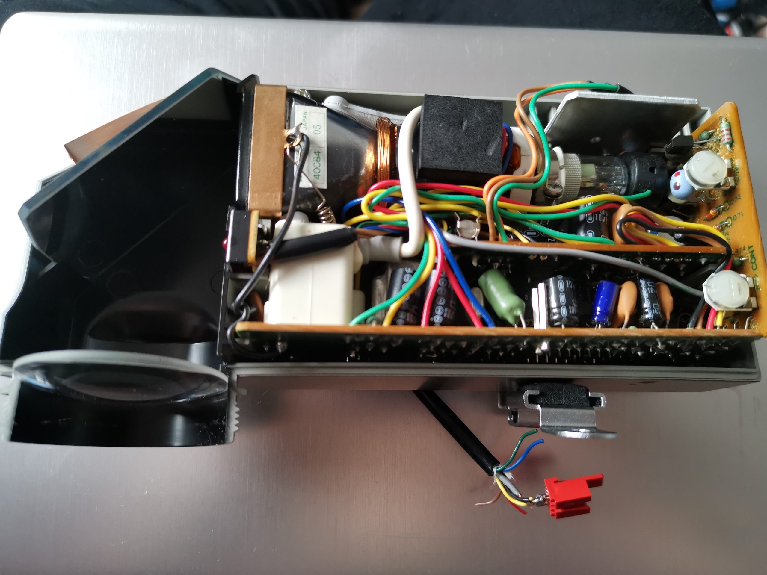
Popping a couple of screws out & removing the enormous eye cup allows the top cover to come off. This unit is very tightly packed inside, with 3 PCBs! The magnifying lens (~45mm diameter) & mirror on the left enlarge & turn the image so the camera operator can see it. The CRT’s at the top, with a copper grounding band around the face.
CRT Face
The CRT face is neatly slotted into the plastic housing, with the tally LEDs to the right of it. The legends on the LEDs are naturally printed in reverse, since they’re intended for viewing through the mirror. The optical section is entirely spray painted black for better contrast & stray light control.
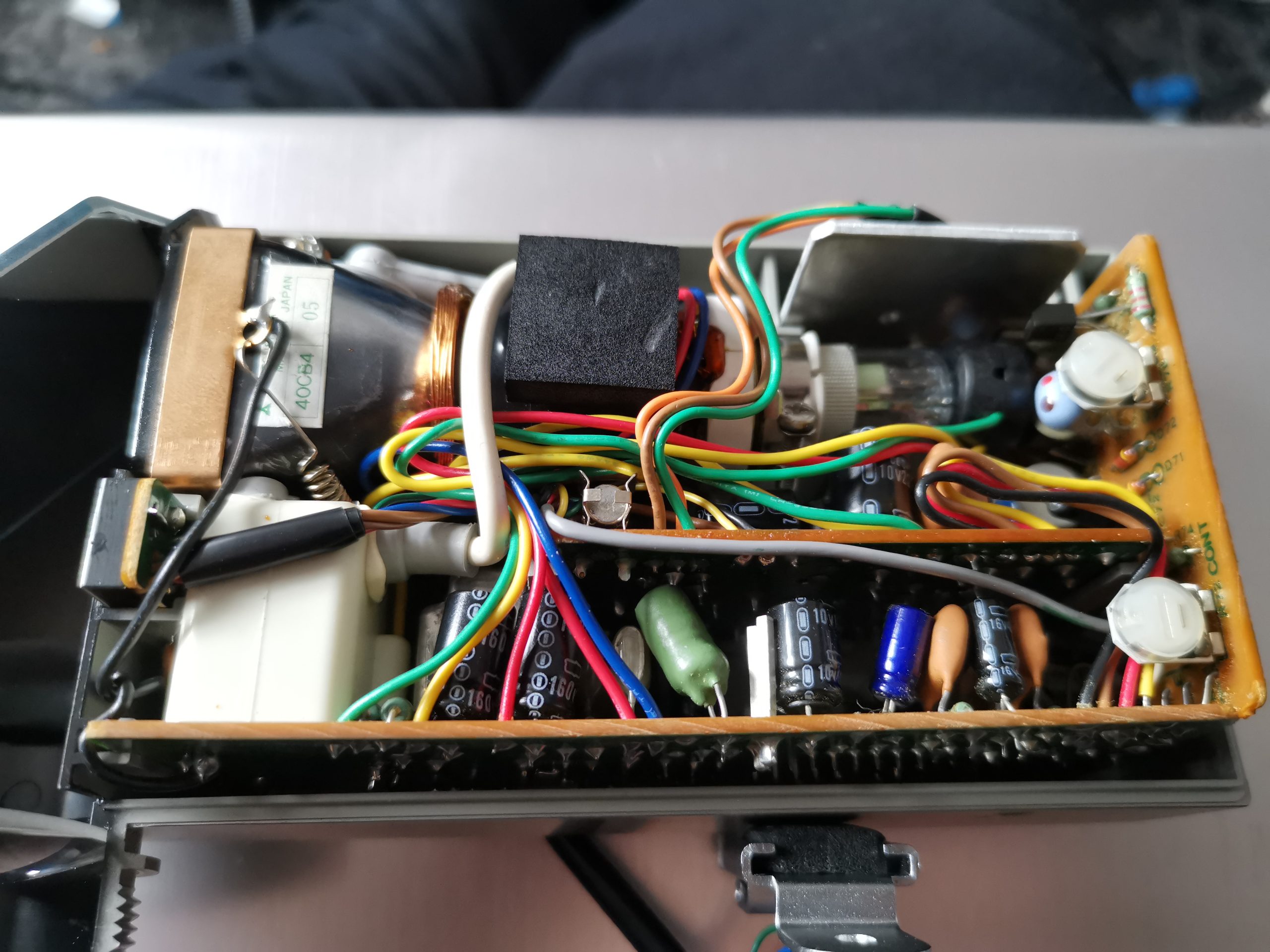
Electronics Area
The other 5″ of the casing is packed with electronics to support the CRT. The bottom PCB even “wraps around” to the right, with copper staples connecting the boards together. The CRT tube itself is hiding inside the deflection yoke and under a foam pad at the top of the unit. It’s secured in place with a copper grounding strap wrapped around the face of the tube, and a spring. A single screw secures the strap to the case. This also provides a local earth for the outer Aquadag coating on the tube, which is the negative plate of the final anode smoothing capacitor. The other plate is formed by the coating on the inside of the CRT glass, and the dielectric is of course the glass itself.
The main anode wire snakes off from the flyback at bottom left to the anode cup at the top of the CRT, insulating the 7kV from everything else.
There aren’t many reasons to jack up the final anode voltage on a CRT, past the design voltage of the tube as JVC have done here. The only plausible one I could think of is to increase brightness of the image, but the Sony 4CB4-based units I have only run at around 3kV, and those are plenty bright enough! The downside here of course, is that with higher energy electrons and a brighter image, the phosphor of the CRT will wear out faster.
Increasing voltage also increases X-Ray emission, but even at the 8kV maximum, such X-Rays would be so weak as to not make it through the CRT faceplate glass, which is loaded with lead anyway.
There’s not much sense in yanking the tube out of this unit, it’s identical to the Sony one’s I’ve done in the past:
Bare 40CB4 CRTVoltage Regulator Pass Transistor
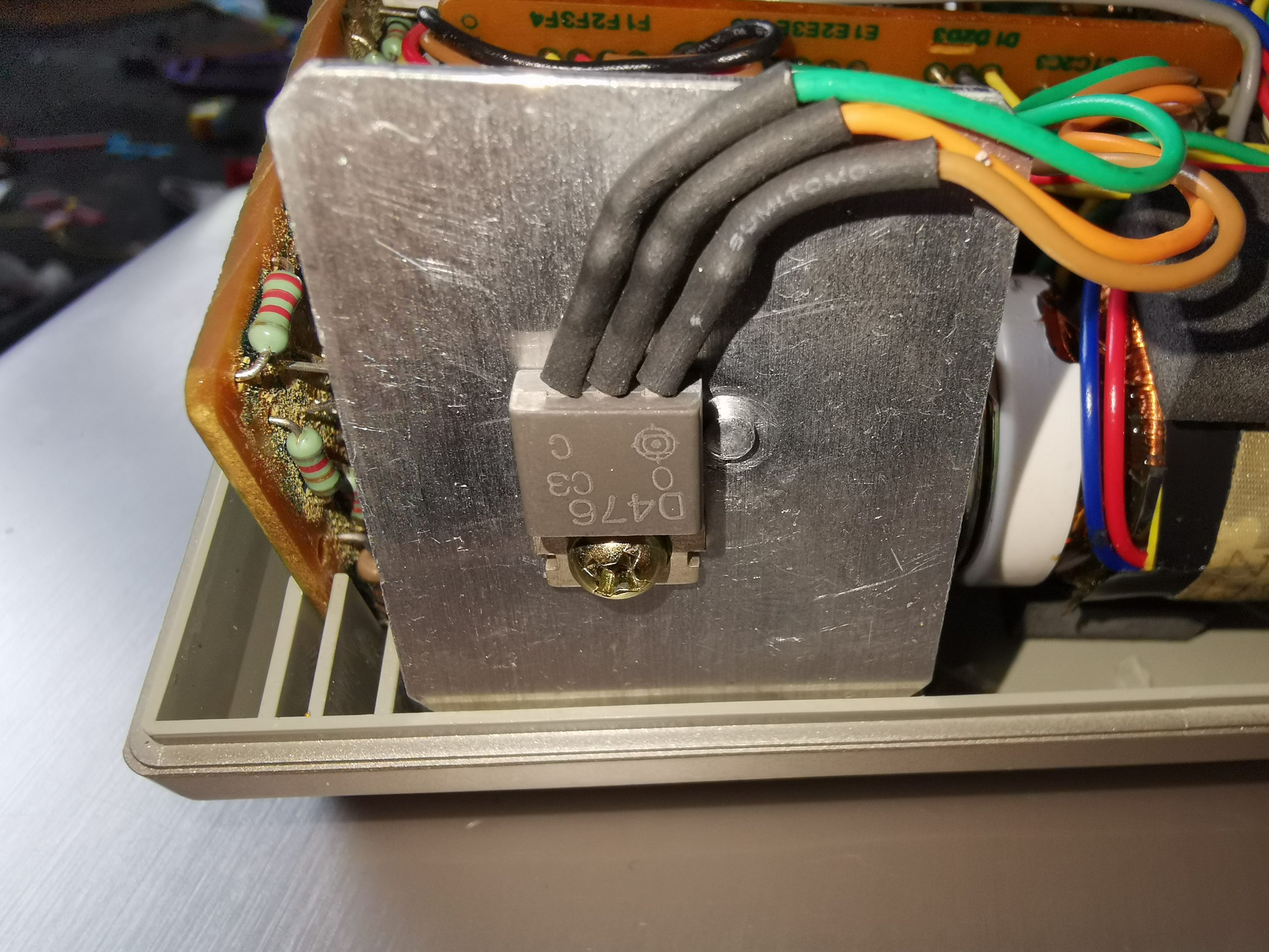
Slotted into a gap above the CRT is a large TO-220 2SD476 NPN transistor, this is part of the power circuit; it’s the series pass element regulating the input 12v down to 9v for all the remaining circuits. The aluminium sheet on the back provides some heatsinking as this part gets warm! Current draw of this unit with no video input is about 260mA.
CRT Removed & Vertical Board
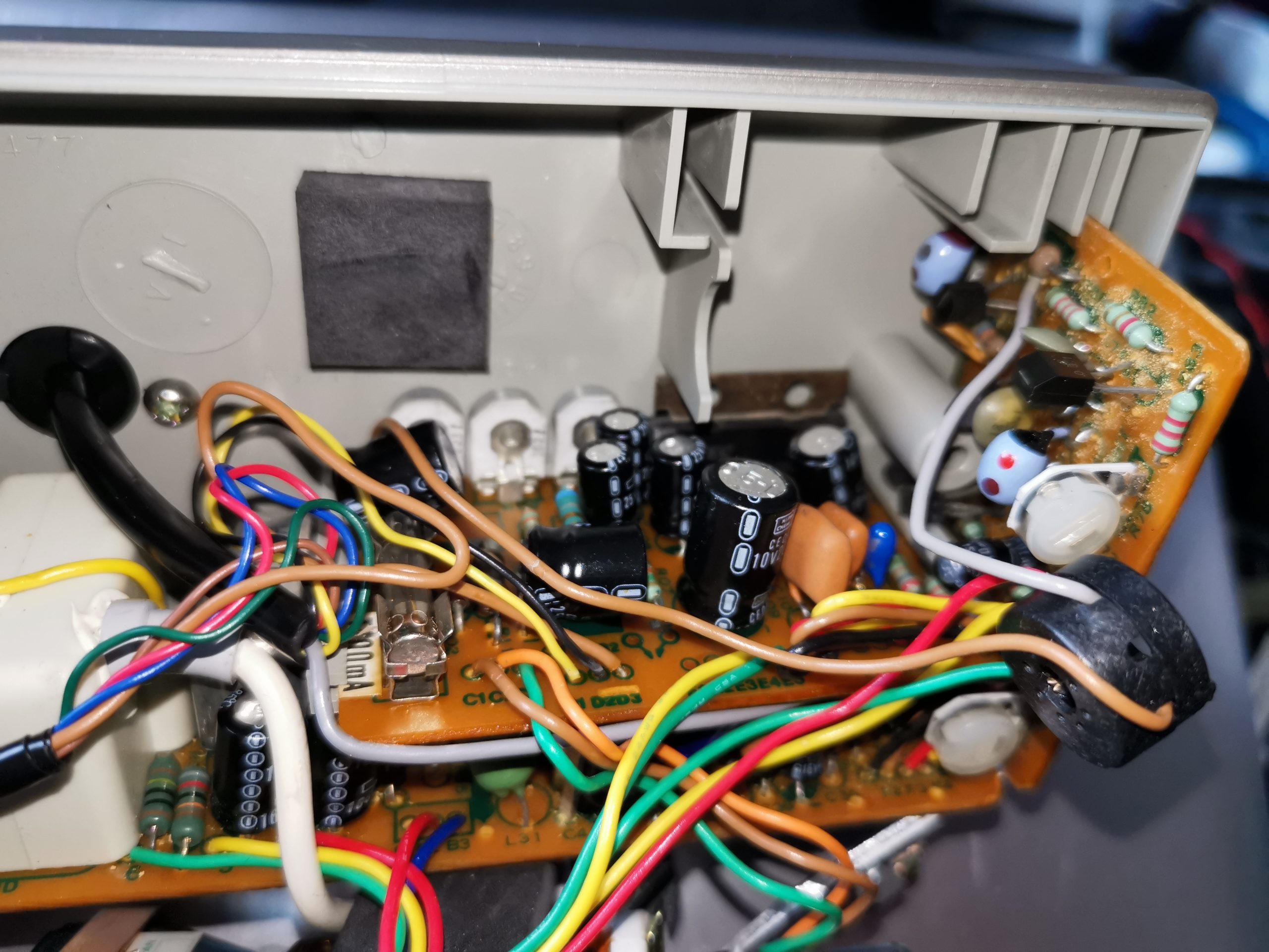
Popping the CRT out allows a view of the Vertical & Power Board. This hosts the input linear voltage regulator, and the vertical output control circuitry. Hiding at the back on the right is a NEC µPC1031H2 Vertical Deflection Controller.
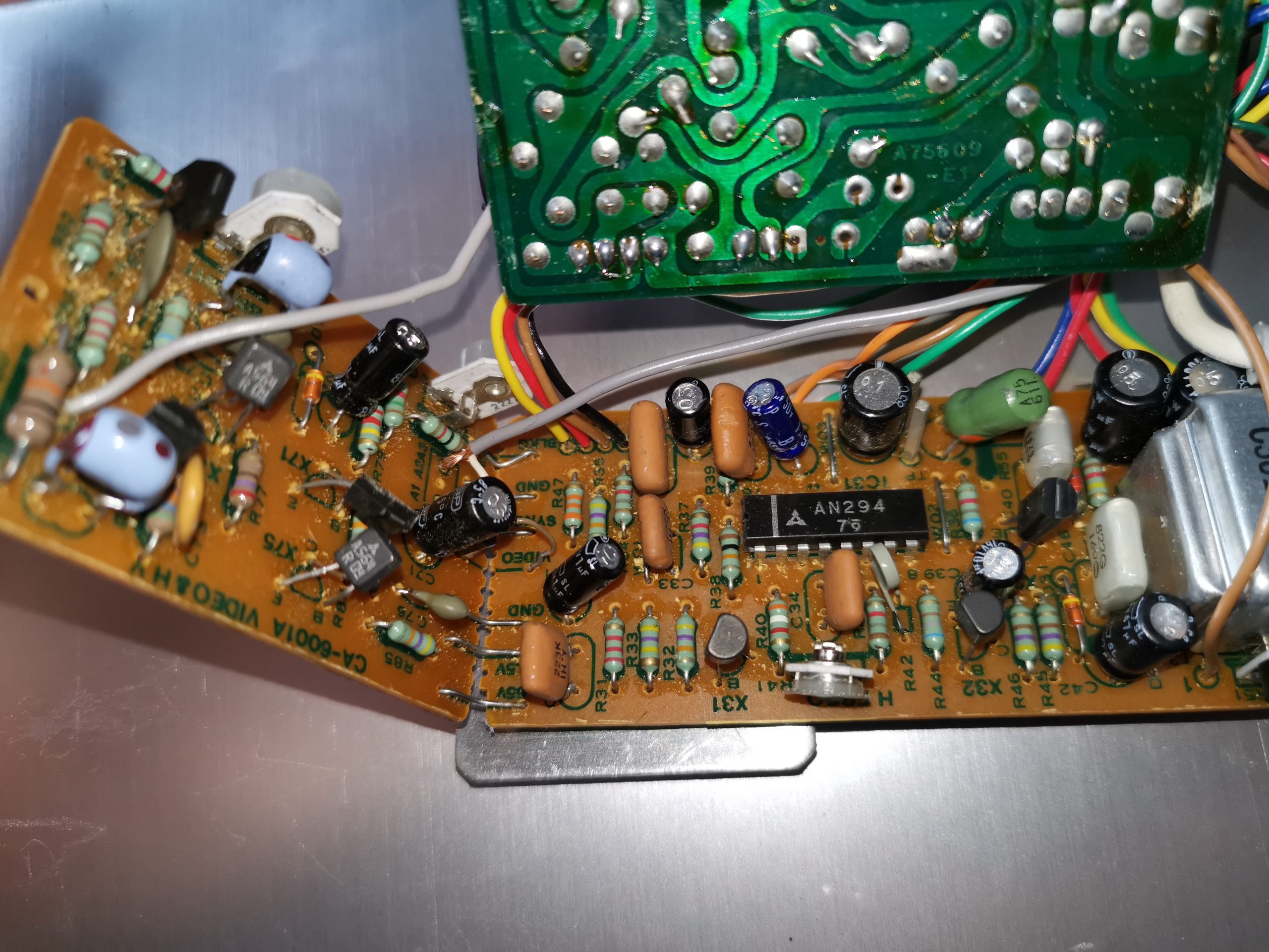
Horizontal & Video Boards
Separating the boards reveals the other two PCBs, the Video & Horizontal/HV boards. The bottom board takes care of the Horizontal output, and the lefthand board the video input, sync separation & amplification.
Horizontal Control IC
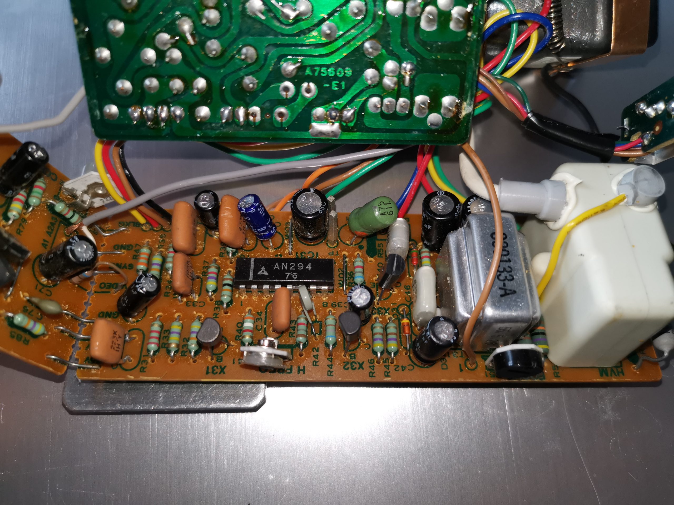
The Horizontal section is controlled by a Matsushita AN294 device. Unfortunately I haven’t been able to locate a datasheet for this one. The flyback transformer (Horizontal Output) is on the right, with another smaller transformer I don’t quite know the purpose of. Oddly, there’s no large switching transistor for the horizontal output stage – as the PCB notes the flyback as being a “HVM” this may in fact be more tightly integrated with some of the drive circuitry in the potting. There aren’t anywhere near as many pins on it as a usual CRT flyback has either.
This section also generates the other voltages required by the CRT – 2.8v for the filament, and ~80v & ~400v for the grids.
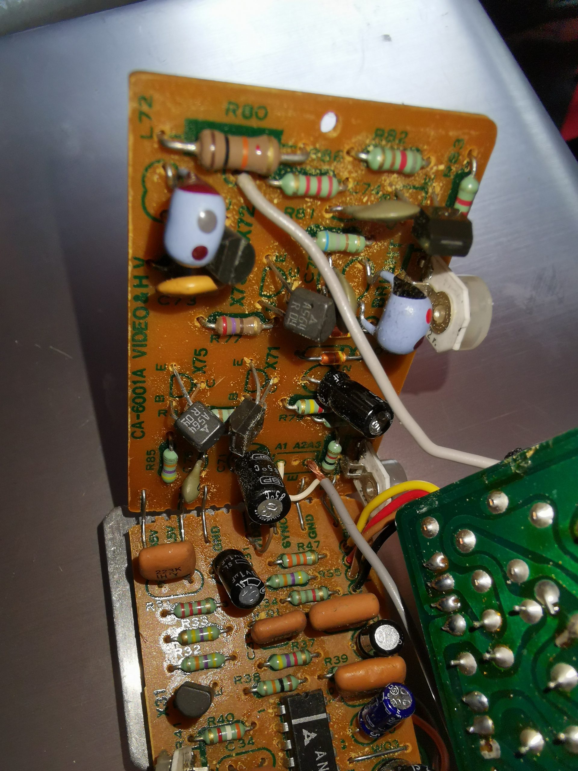
Video Board
A closeup of the video board shows the relative simplicity. Only 4 transistors are doing all the video actions. There is relatively high voltage on here though – an 85v feed from the power supply which is the rail voltage for the video amplifier to the CRT cathode/G1.
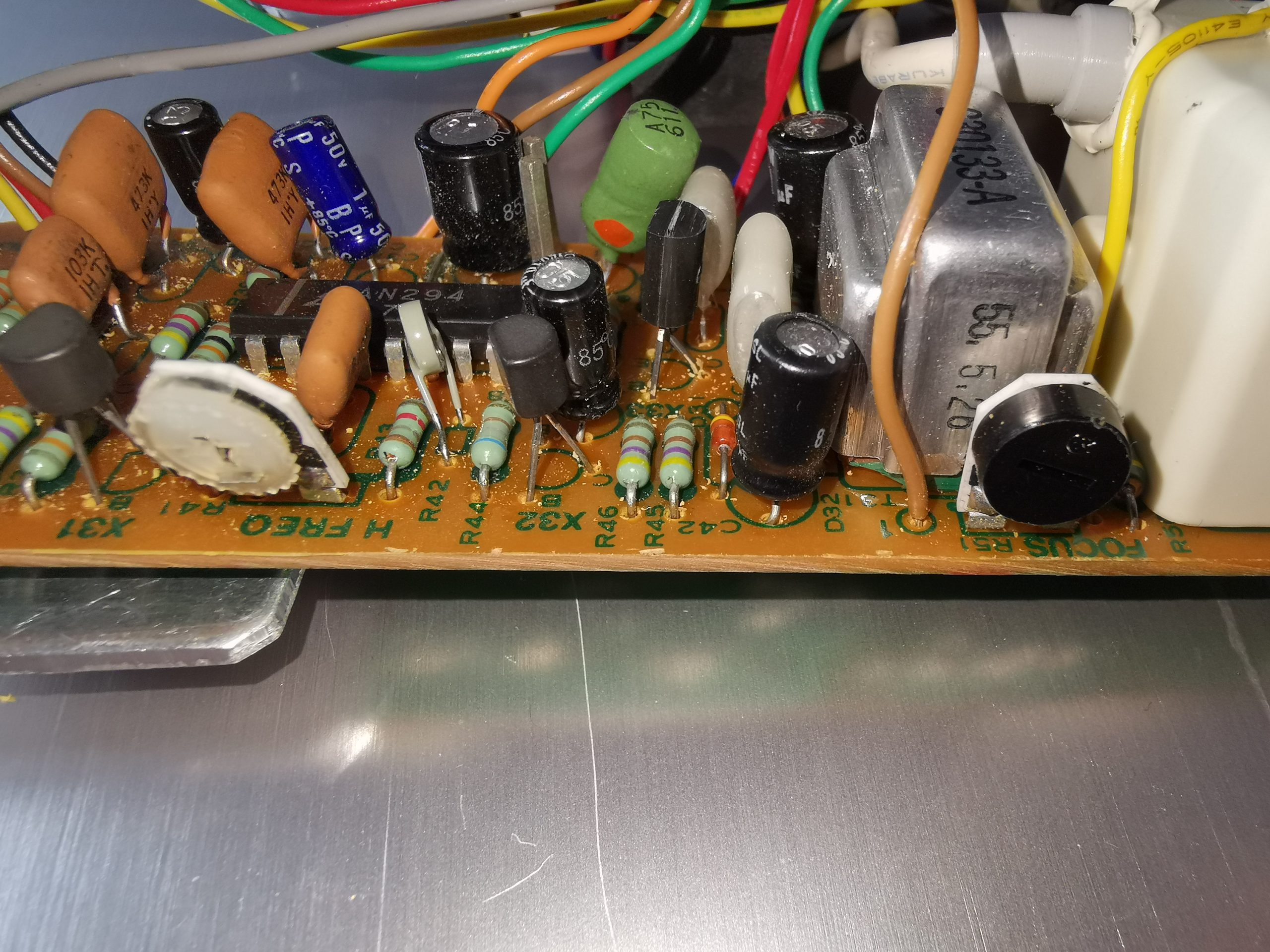
Focus & Horizontal Hold Adjustments
There’s a few adjustments available on this unit, here are the Focus & Horizontal Frequency (Hold) pots. Amazingly, even though this unit is about 43 years old at the time of writing, the unit fired straight up when I applied power & a composite video signal, with no adjustments required at all!
Unfortunately there’s no service manual or schematics that I could find on the web for this or the camera it came from, but connections to make this unit work are very simple:
Wire Colour
Signal Name
YELLOW
+12V DC
BLACK
GND
Coax - Core
Composite Video 1v p-p
Coax - Shield
Composite Video GND
There’s another blogger who’s done this particular viewfinder, but they didn’t dig into the unit anywhere near as far as I usually do:
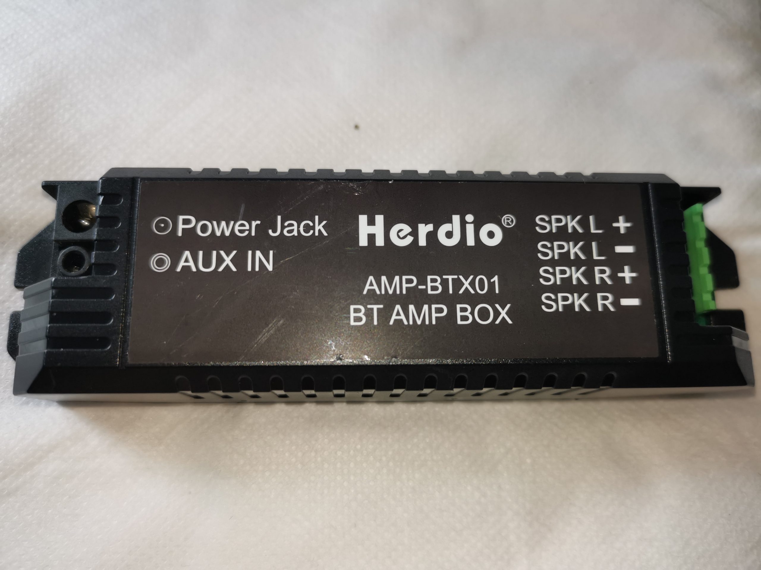
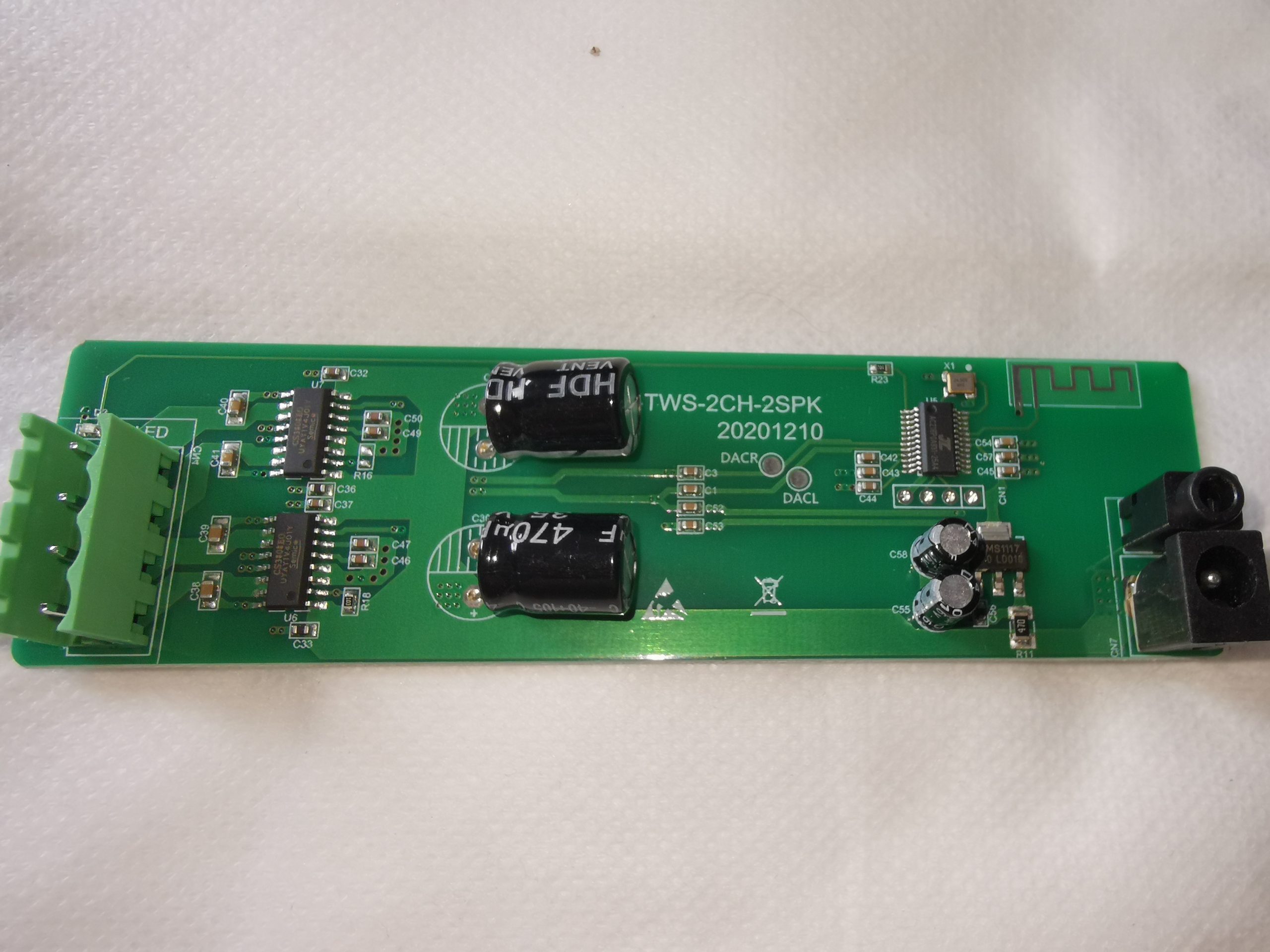
Here’s a very cheap audio amplifier, from the usual suspects in Shenzhen. This is a Herdio AMP-BTX01 Bluetooth Audio Amplifier. This is a stereo unit, but the quality is going to be piss poor!
Main PCB
Cracking the casing, which is just clipped together reveals the sparsely populated PCB. There’s a 12v power input on the right, along with a line-level input. The speaker outputs are on the left. Between the two are only a few components to do the audio signal processing.
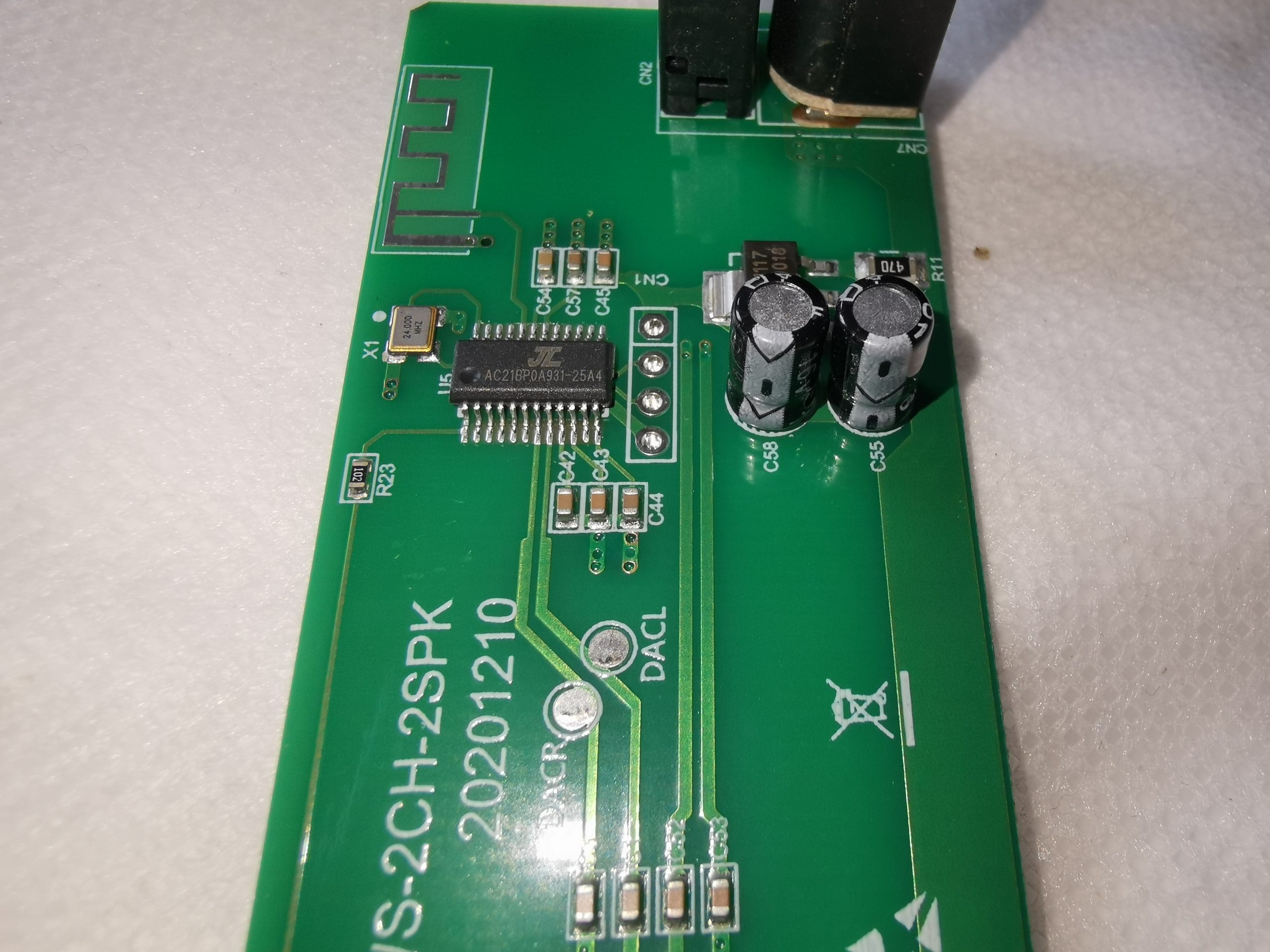
Bluetooth Radio
There’s just the Bluetooth radio IC, an AC21BP0A931. Not much is available on this IC, I certainly can’t find a datasheet, but it has all the low-level audio stuff, a microcontroller & a 2.4GHz Bluetooth radio integrated into a single IC. There’s a 5v linear regulator hiding behind the electrolytic caps to provide a power rail for this. The only other components here are a ruck of SMD ceramic coupling capacitors in the audio lines to the amplifier ICs.
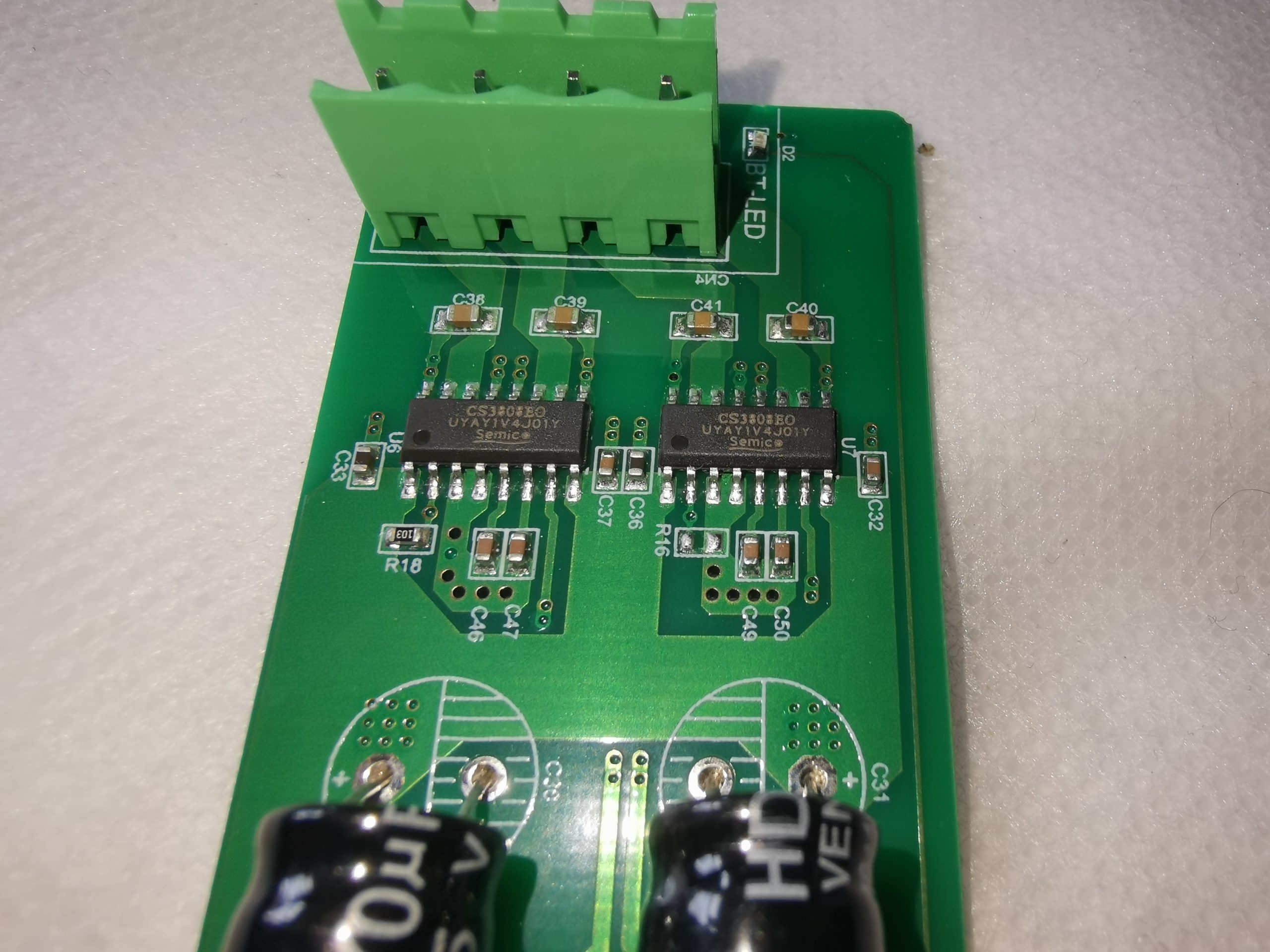
Amplifier ICs
The final components are these Chinese FET audio amplifier ICs, rated at 15W per channel, and driving a speak each in Bridge mode – these are stereo amps.
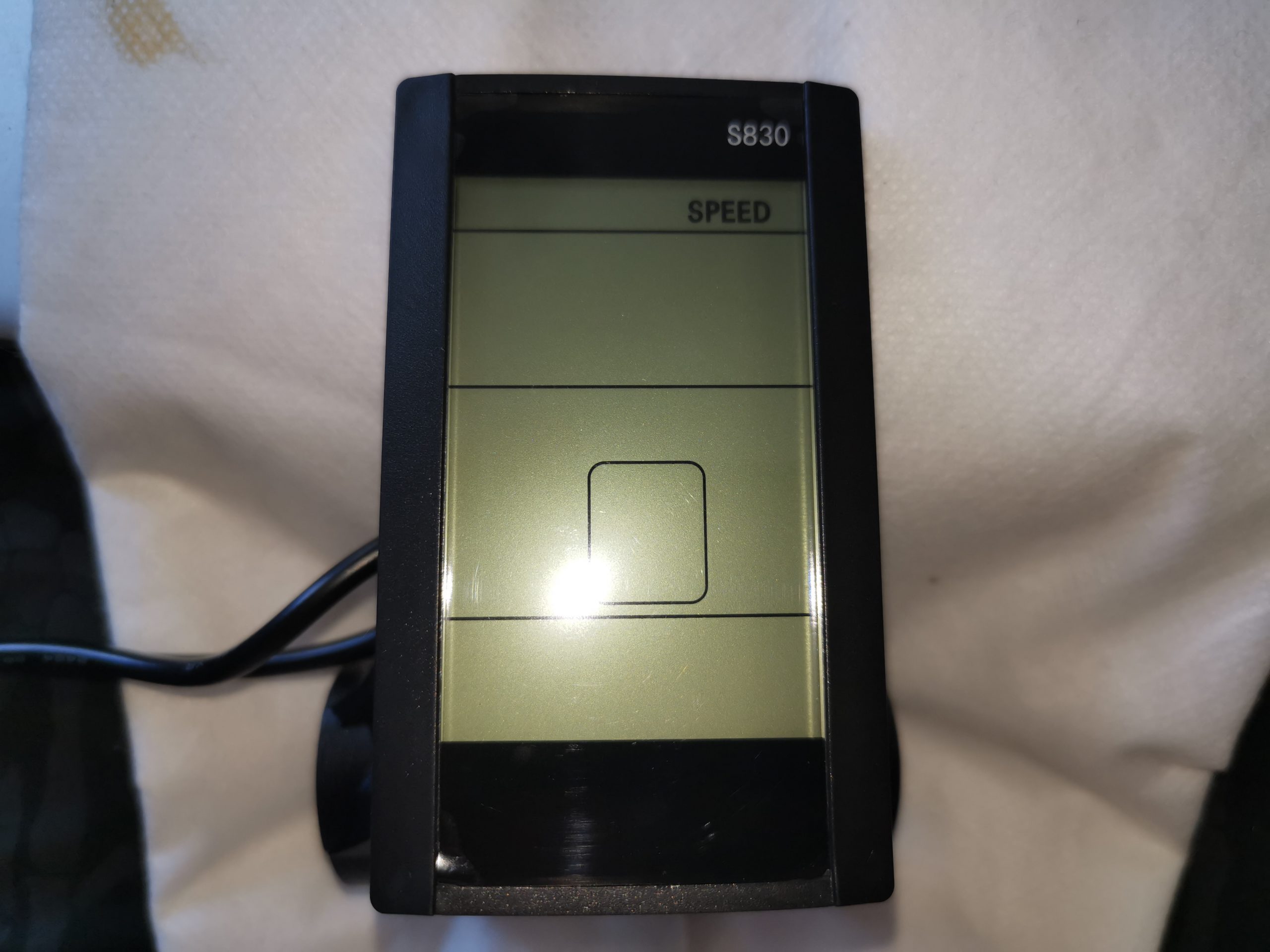
I’ve been doing quite a bit with eBikes of late, given the current fuel costs in the UK, so the bike I managed to get from work needed a couple of upgrades. Above is one of the best controllers I’ve found, an S830 model. This is very full featured, with Speedometer, Odometer, Trip counter, programmable assist power levels & battery monitoring.
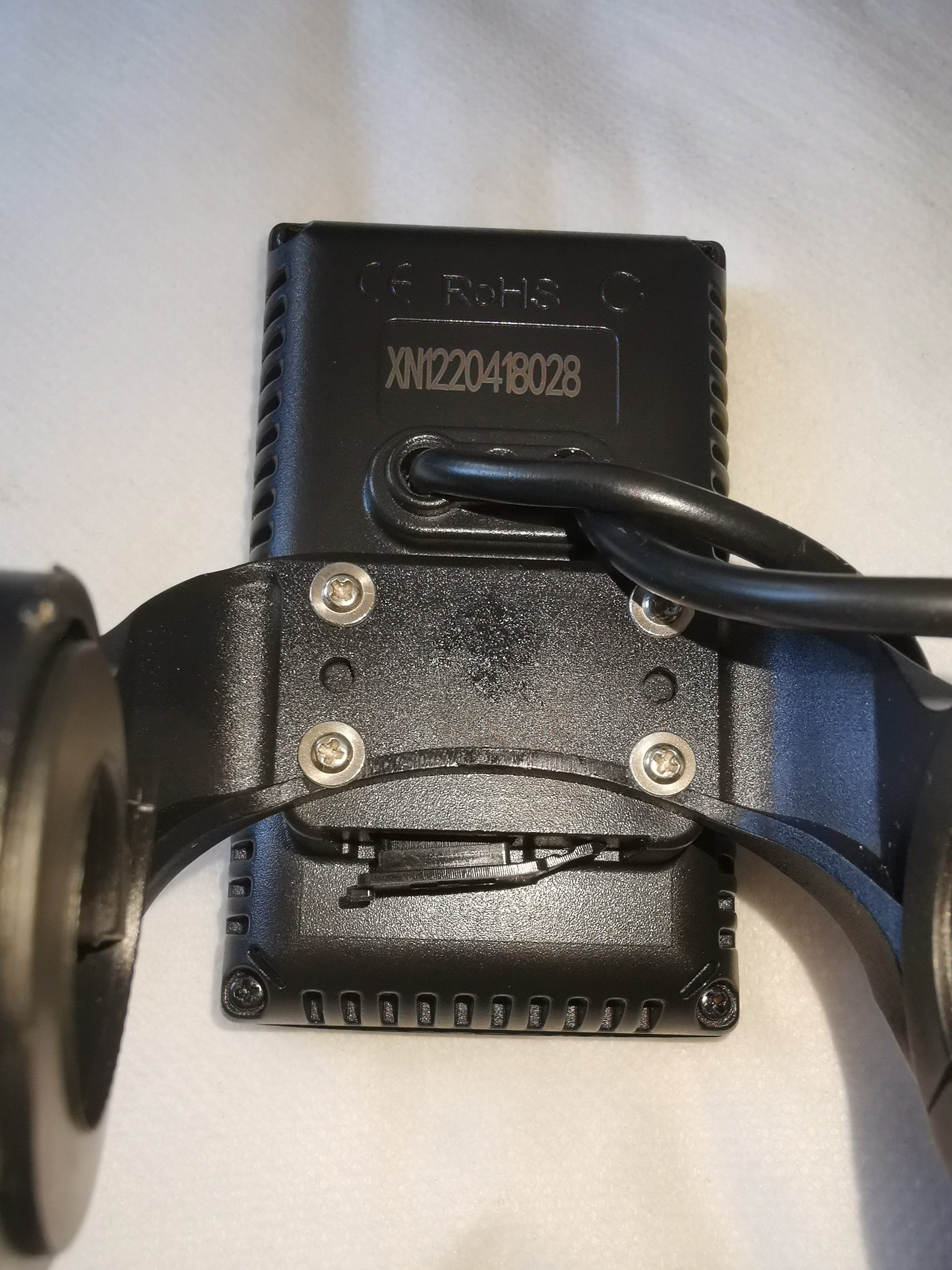
Rear
There’s not much on the rear panel of the device, I’m not even sure who actually manufactures these! There’s a USB port on the bottom for charging a mobile phone etc while riding. The cables are potted into the back of the casing for water protection.
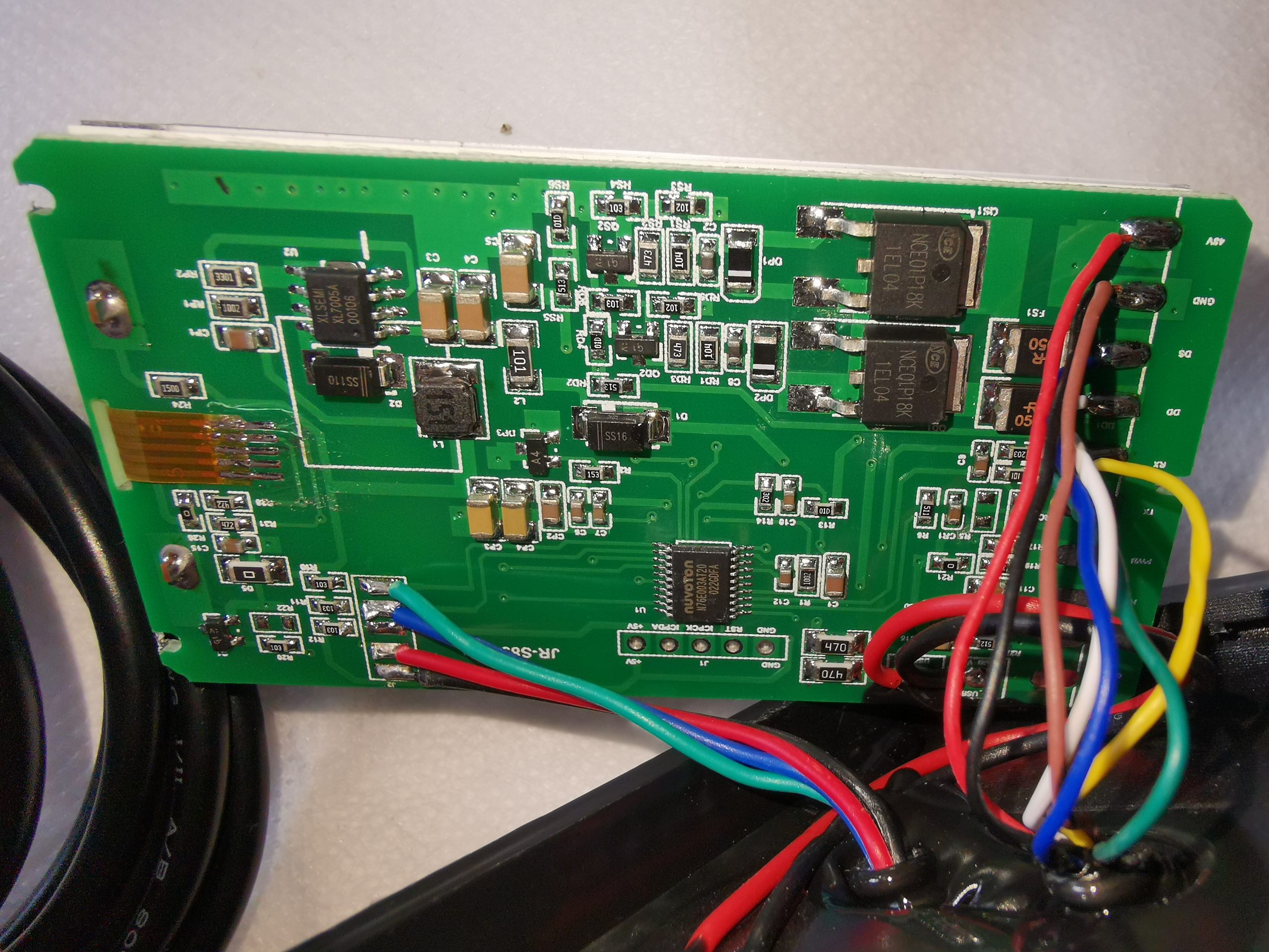
Main PCB
Removing the 4 screws from around the perimeter of the rear panel allows the front to come off with some peeling – there’s silicone & a gasket to keep water out! The module is driven by a Nuvoton N76E003AT20 8051-based Flash microcontroller. Most of the PCB is actually taken up by the DC-DC voltage regulation to be able to handle a very wide input voltage of from around 24V – 84V depending on what battery pack the eBike has, since these are run direct from the battery. The LCD only has a few connections, so it’s probably SPI or I²C controlled.
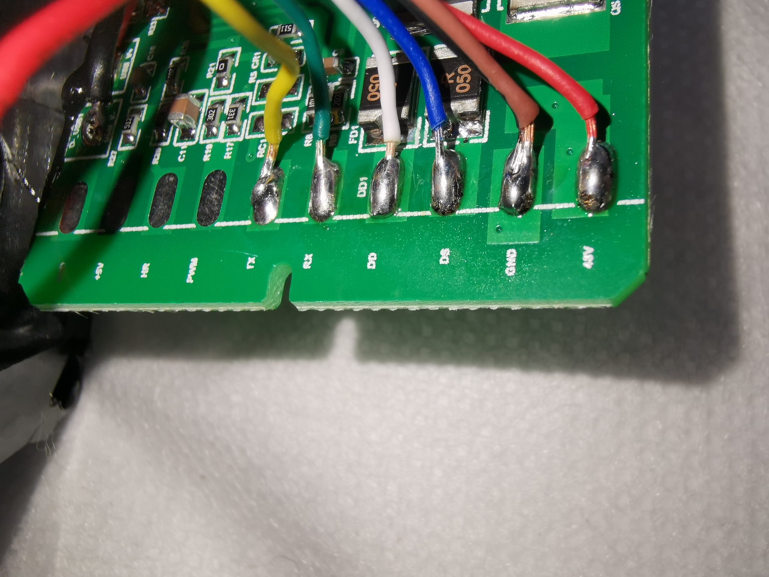
Harness Connections
All the connections into the harness are marked on the board, which might be handy should the cable need replacing. There are also a few that aren’t used at all, but all the components to support them are populated on the PCB.
Rear Panel
The rear panel has the sealed-in cables, and the USB port module, which is also completely potted. It’s likely there’s another DC-DC under that potting, given there’s clearly a PCB there.
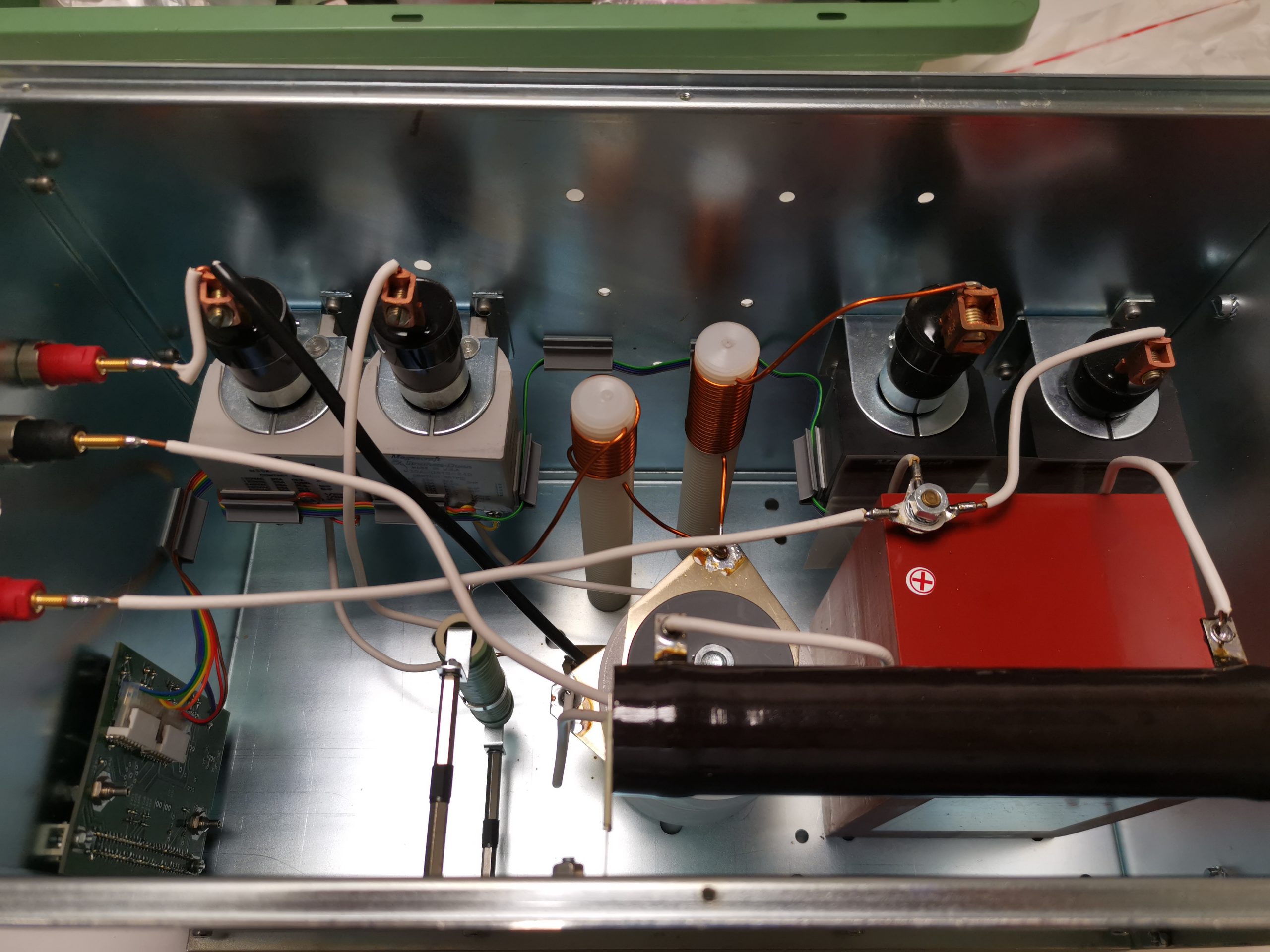
Here’s another module from the decommissioned impulse testing rig – the pulse forming network for the Surge generator section. Lots of high-energy high-voltage parts should be hiding in here.
Resistor Side
Pulling the cover off shows there’s not a lot to the network, but it’s a collection of rather exotic parts. The row of 4 devices on the back panel are Mercury Displacement Relays – these don’t have solid contacts as such, but a pool of metallic Mercury that gets pushed up by a magnetic plunger into contact with both terminals. I’ll do a separate post on these not very common parts. A couple of small chokes wound on large nylon studding are in the centre, along with an adjustable wirewound resistor. On the right is the main energy storage capacitor, rated at 10kV – this thing is enormous, and about half the size of a house brick. The large vitreous wirewound resistor next to it is the safety discharge resistor, switched by the normally closed Mercury relay on the far right. Charging & impulse discharging are handled by the other three relays.
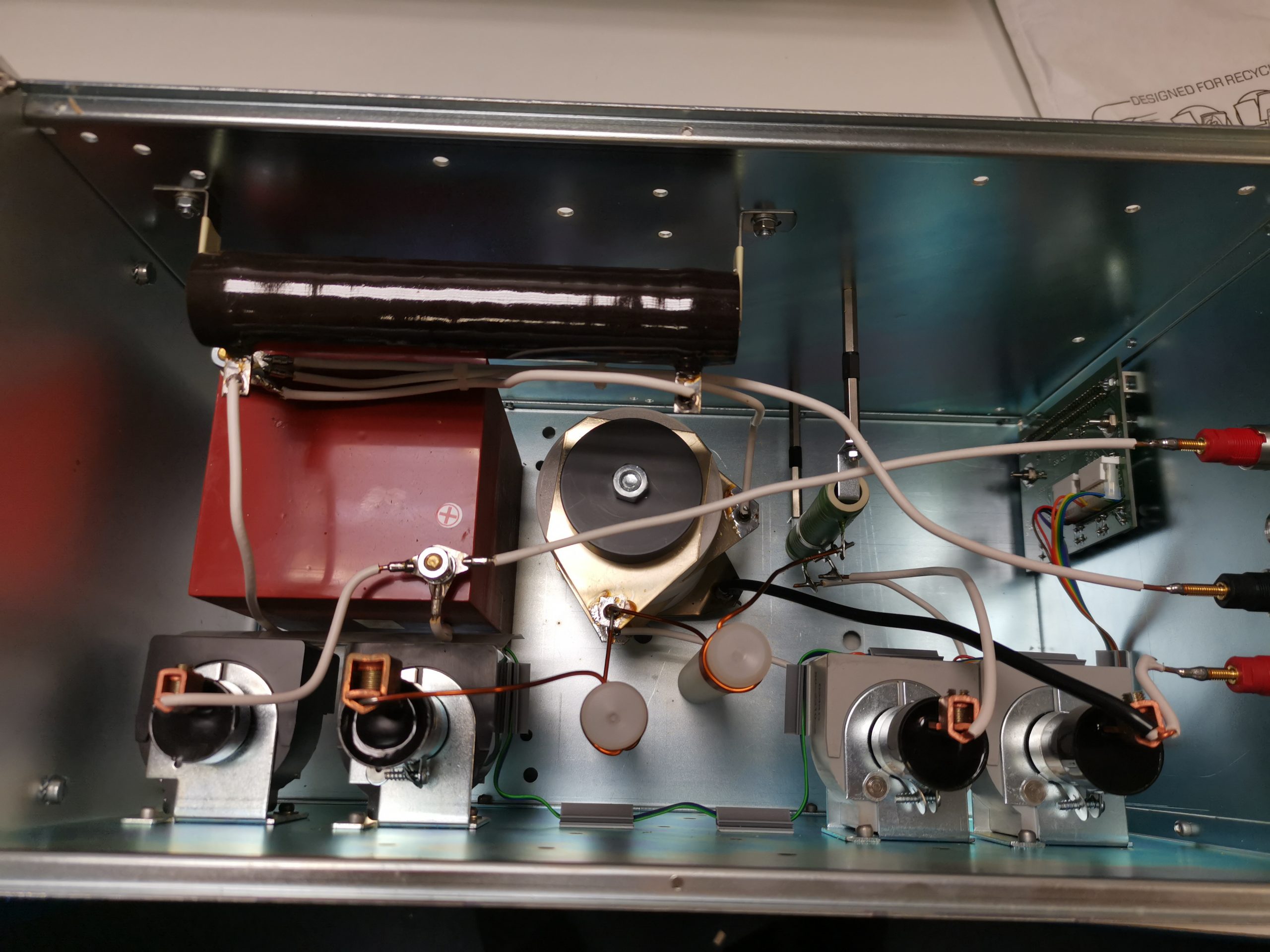
Relay Side
Another view shows a very large stack of high voltage pulse rated resistor pucks, there are three in this stack, held together by a large bolt down the centre.
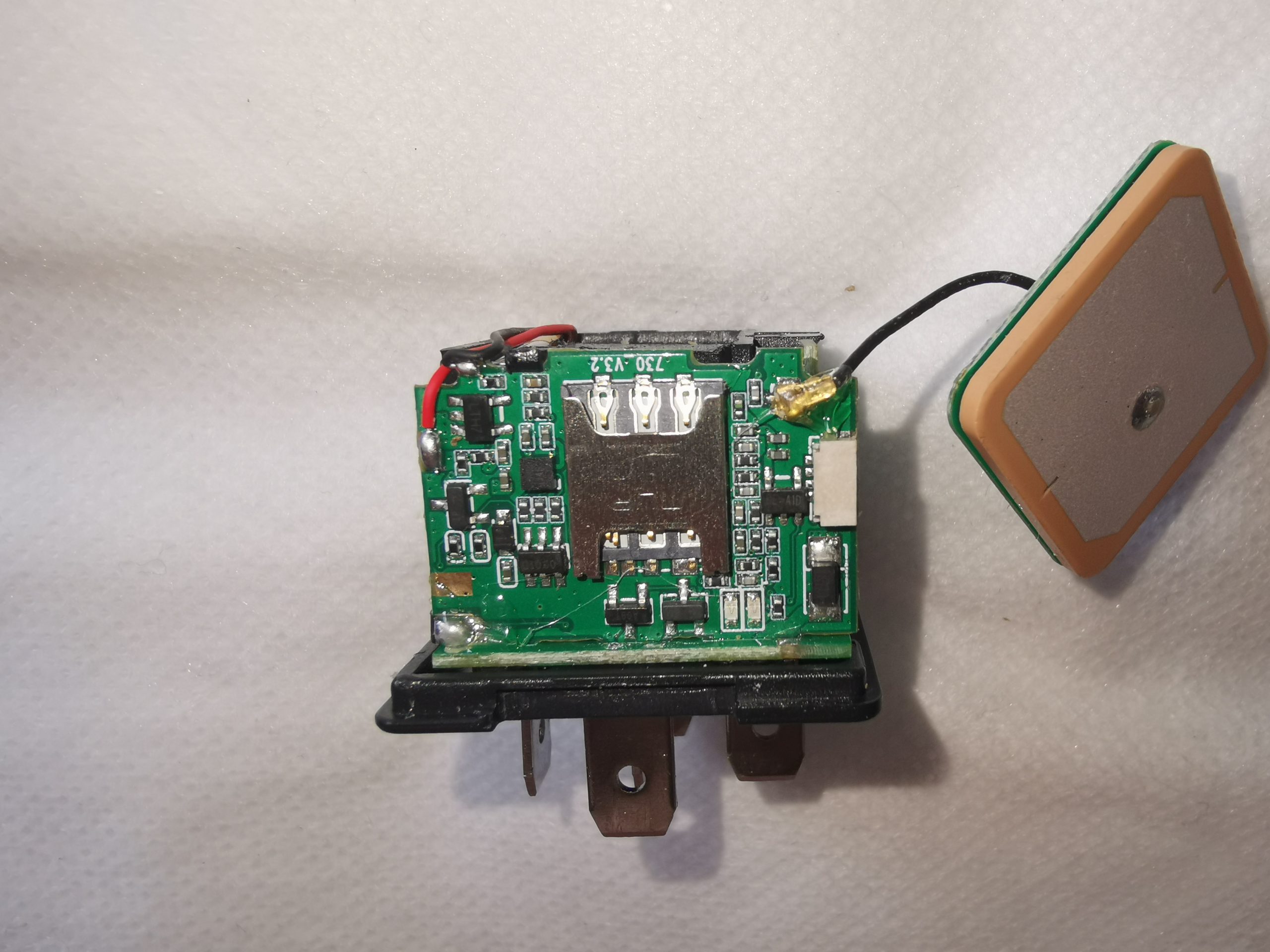
Time for another Chinese gadget! This time it’s a tiny GPS tracker, designed to look like a standard vehicle relay, the MV730.
Only a partial teardown on this one, since I need the thing to work afterwards, and the unit is very tightly integrated. Not only does this unit look like a relay, it’s exactly the same size. Some serious compaction of the electronics has been done here to get things into such a small package.
GSM Module
On one side is the PCB with the GSM module (it’s on the other side of the board), and the SIM socket. There are also a pair of LEDs to show both GPS & GSM status. The module on this has both GPS & GSM functions, so the active antenna is connected directly to the PCB here.
There is a very small-pitch 4 pin connector just under the antenna connection, I would assume this is for a TTL serial connection to the radio module.
GPS Antenna
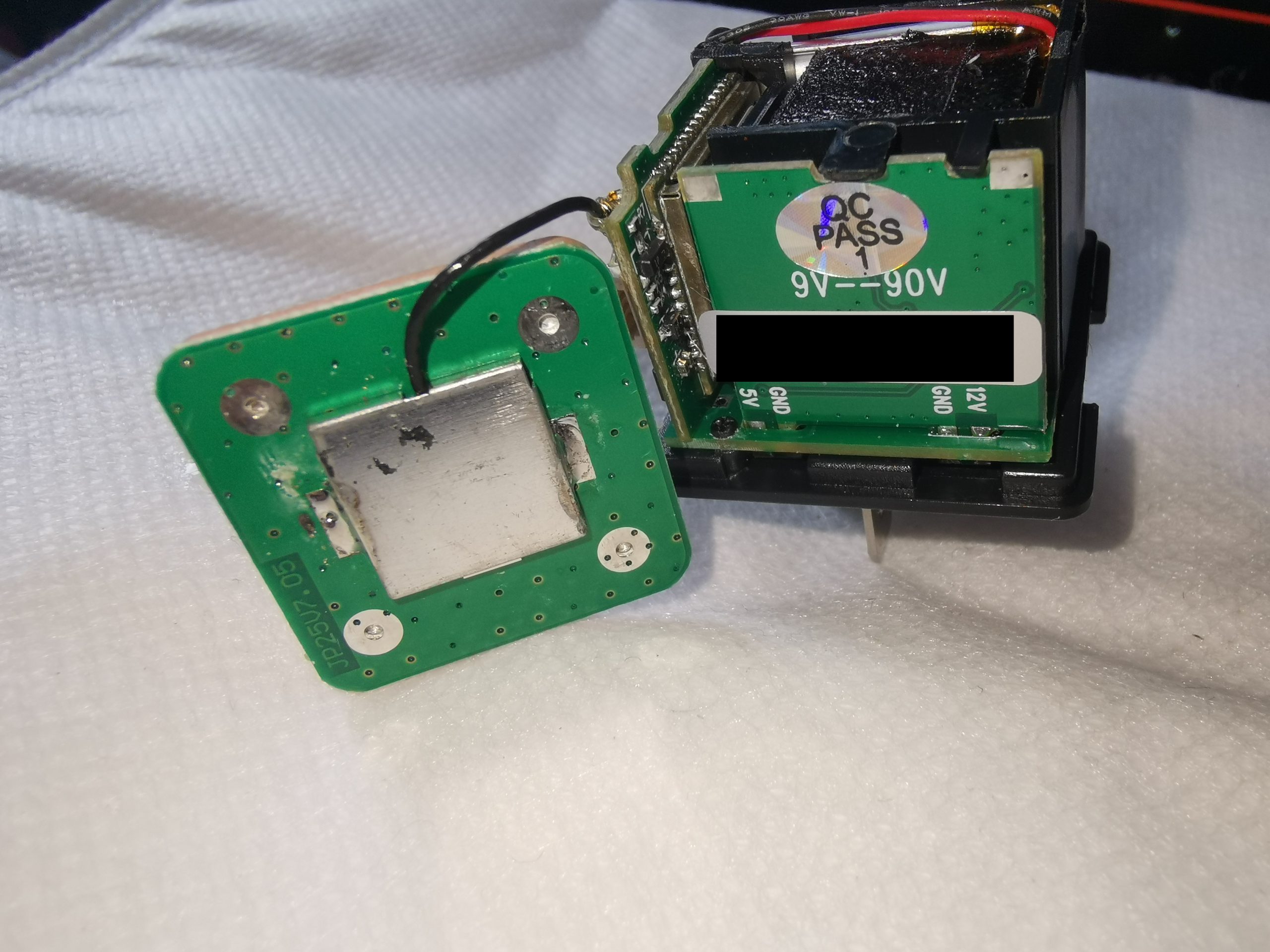
The GPS antenna is attached to the top of the assembly by a sticky pad, which has here been peeled off. The other vertical PCB is visible here also, which contains the power supply for the tracker. As this unit can handle anything from 9-90V (allegedly), there’s going to be some DC-DC action on that board. The serial number is also on this PCB, redacted for privacy 😉
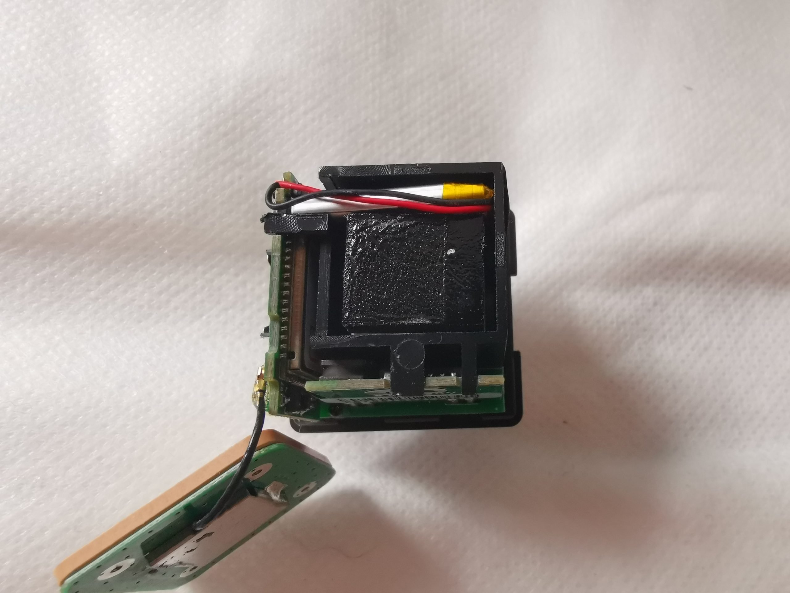
Module Top
even the centre of the unit is packed with parts. There’s a plastic frame for general support, and this also has the foil GSM antenna stuck to it. There’s also an 80mAh backup Lithium Ion cell, and an actual relay hiding in the middle which is for the “Fuel Cut” feature of this tracker.
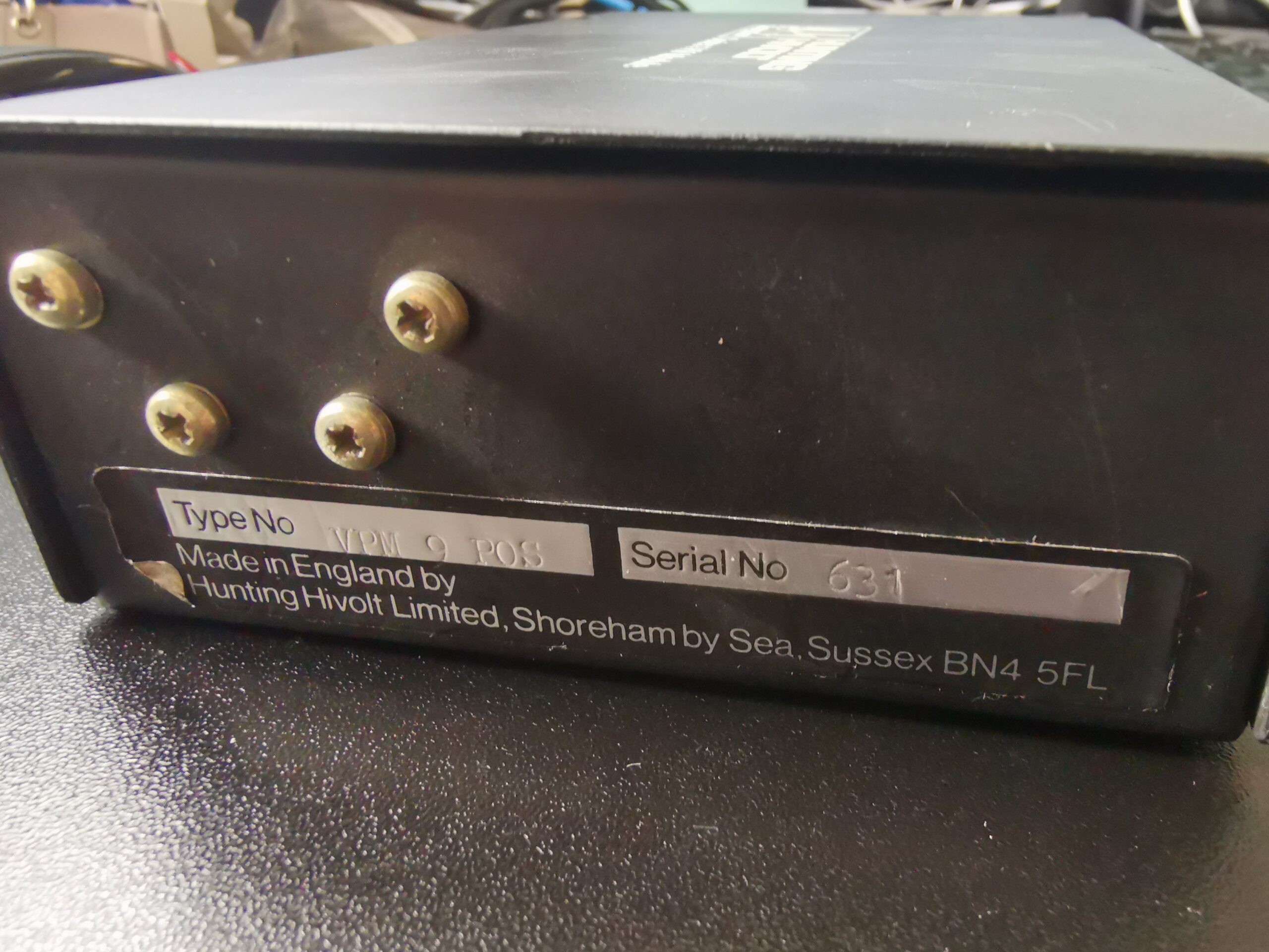
Another quick teardown post! This is a high voltage supply module from Hunting HiVolt – a company that hasn’t been around in some time. This is adjustable, and takes a standard 230v AC mains input to output a +1kV rail & a -250V rail.
Label End
There is a rating plate with some identifying marks, but I’ve not been able to find any information on these units anywhere.
HV Outputs
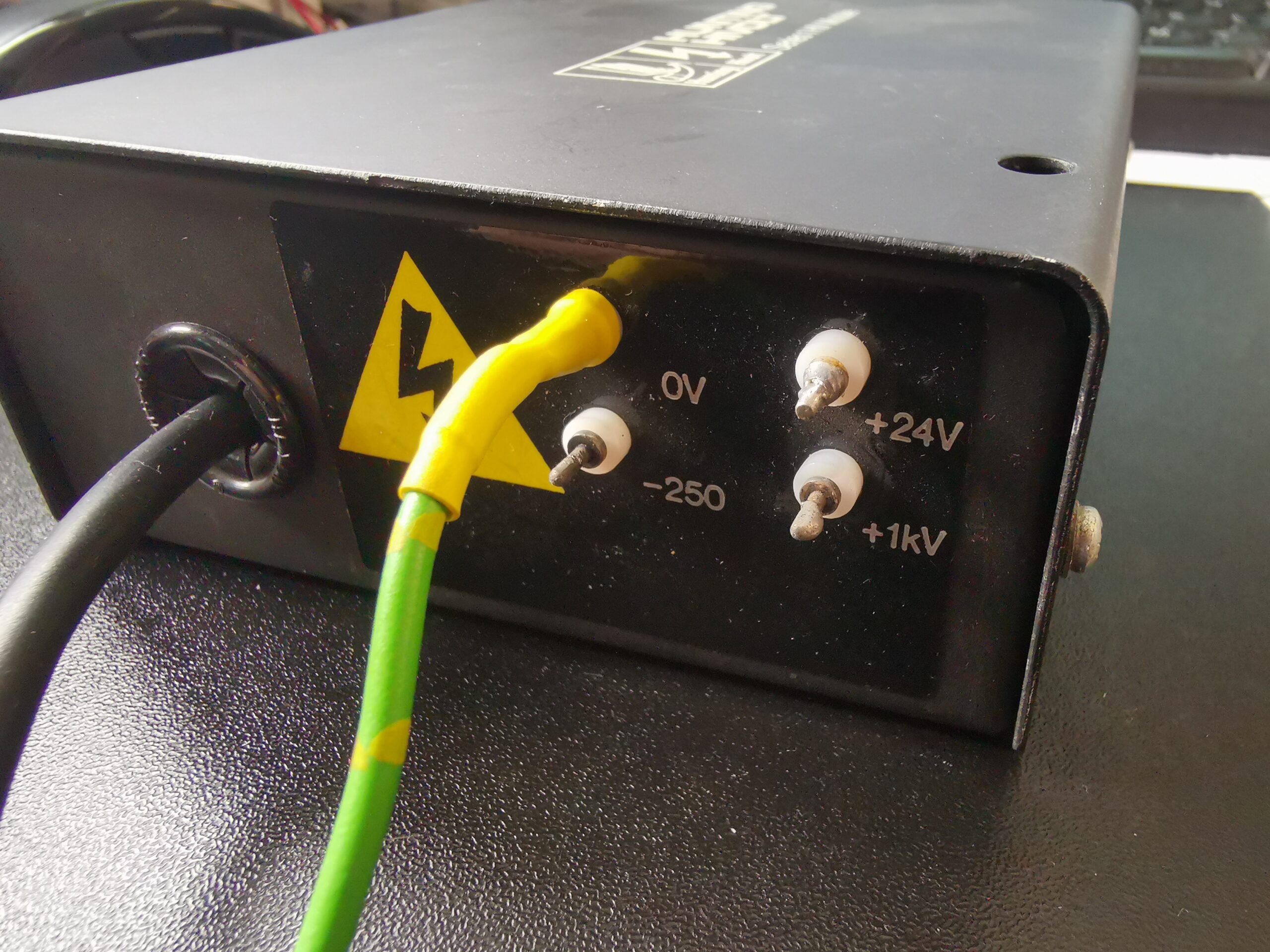
The other end of the unit has the mains input, and the HV outputs on binding posts, along with an Earth connection.
Cover Removed
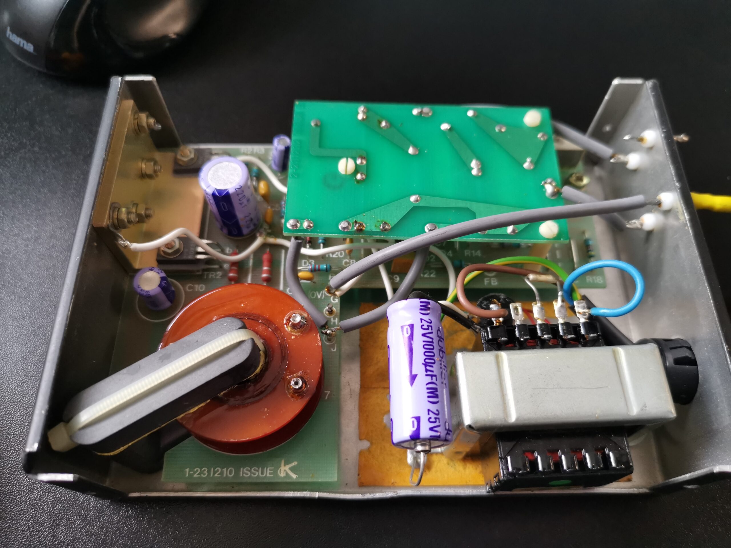
A couple of screws allows the cover to come off, revealing the electronics inside. The mains is led straight to a transformer, that outputs 24V to run the DC-DC converter.
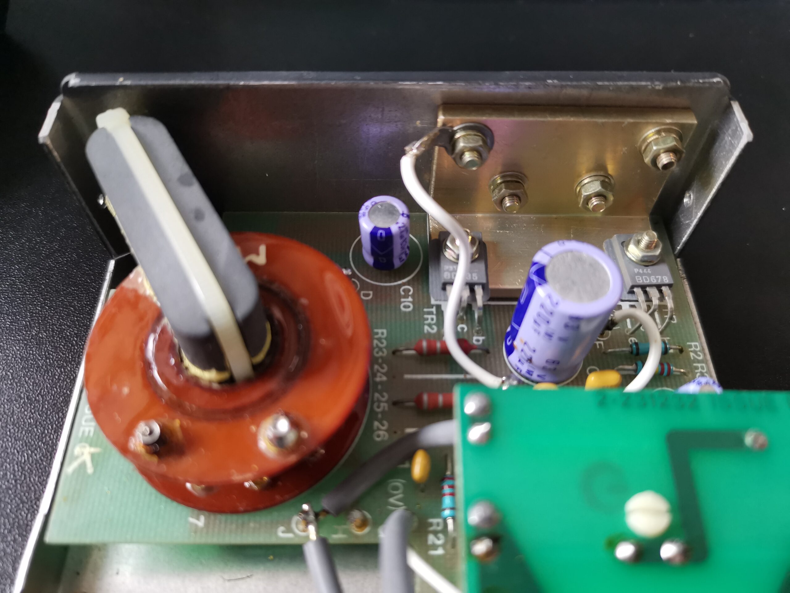
High Voltage Transformer
The main HV transformer is on the left, and the switching transistors on the right, attached to a heatsink.
Transformer Windings
These transformer windings are always pretty, no doubt done by machine & varnished for mechanical support & extra insulation.
Control IC
Control is done at the other side of the PCB, underneath the output PCB. Just a standard PWM controller.
Voltage Multiplier Section
The output voltage from the transformer is rectified & smoothed with capacitors, and there is also a voltage doubler hiding under here – this helps reduce the amount of insulation required on the transformer windings, since they only need to handle half the output voltage.
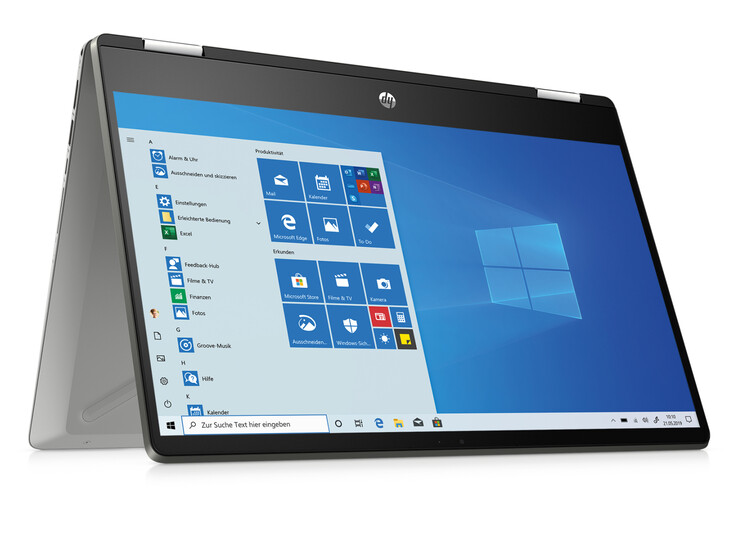
Recently I figured it was about time I treated myself to a brand-new laptop, and as I was also in the market for a tablet at the same time, I figured I’d go with one of the “convertible” types that are about these days.
The HP x360 series are locally available to me for fairly reasonable prices, so I decided to go with one of these. With a Core i7-1165G7 11th Gen CPU, and factory with 16GB of RAM (upgradeable), and 512GB of NVMe SSD for storage as standard, I figured that this would be a snappy little laptop just for my general day to day use. Unfortunately my local supplier (Curry’s PC World), don’t actually give the model number, but it’s their stock code 676743.
As every machine does, they come with Windows pre-loaded, which is rather a pain. I’ve not used Windows in a production environment for over a decade, and I don’t plan on starting again now, so the first thingto do is image the NVMe SSD (having a backup of the original image is handy), and firing up a Linux Mint bootable USB. I did need to enter the BIOS to disable Secure Boot for this to work correctly.
There were some issues with the standard version of Mint 20.3 – namely no touch screen and no mousepad. It’s certainly not uncommon for really new hardware to have support issues in minstream builds of Linux, and as Mint 20.3 by default runs on Kernel version 5.4, this needed to be upgraded. (For reference Mint Edge Edition does come with a later version of the kernel as standard, but I didn’t have an image to hand).
The touchscreen controller and mousepad are both Elan products – an ELAN0749 04F3:31A5 for the mouse, and an ELAN2514 04F3:2CF3 for the touchscreen. Both are operated over I²C.
Once the kernel was updated to version 5.13, there were no more issues with the mousepad, and the touchscreen works es you expect a touchscreen to work. The only bug I’ve found so far is with the included smart pen – once the pen is detected finger touch stops working, and the only way to get it back is a full reboot, which is most annoying. This isn’t a massive issue for me, but hopefully driver support for the ELAN touchscreen controllers will improve with time.
Another upgrade I did straight away since I had the parts hanging around was to upgrade the RAM to a full 32GB. This is a very simple swapover – the bottom of the laptop does need to be removed, the screws for which are underneath the rubber feet on the bottom panel, which can be peeled back gently with fine tweezers for access. There are 5 screws in total.
Before the RAM upgrade, the system was quick under Linux – with a full 32GB there is much more capability. The NVMe drive is also replaceable, so this will probably get upgraded with time to at least 1TB.
Overall, I’m very happy with this HP laptop, I will post an update after I’ve had some time to get to know it better.
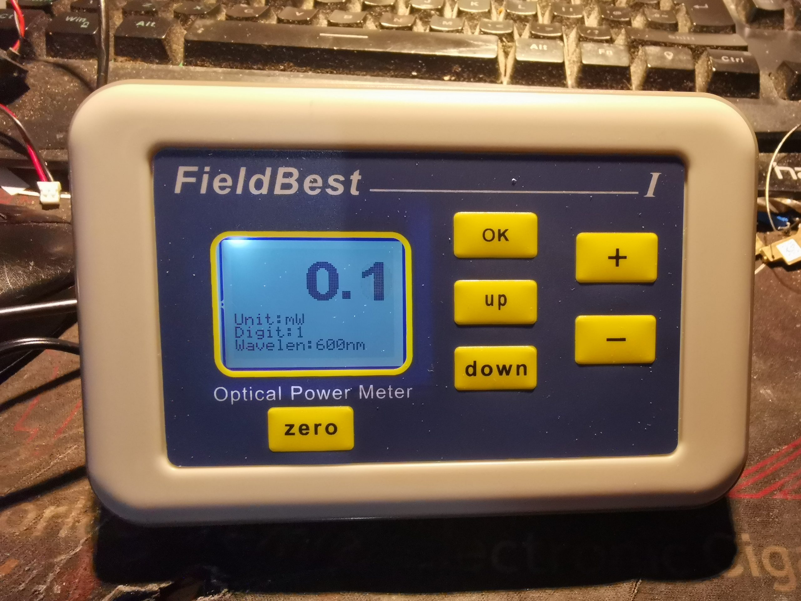
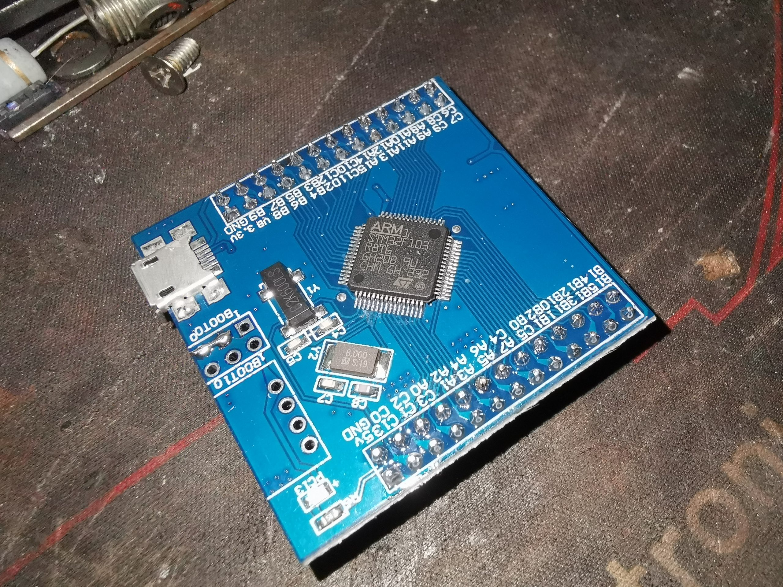
Since I’m building optical power meters at the moment, I figured it was time to see what the Chinese have to offer in this department, and these meters were on offer over on AliExpress, at over 50% off. This is the Fieldbest I meter, and I got two versions – the 1mW-2W & 10mW-50W model, with thermopile sensors. A graphical LCD provides the user interface, and there is also USB serial present for logging to a PC with software. These units appear to be made by a company called “Fastlaser Tech”, but I can’t seem to find much about them.
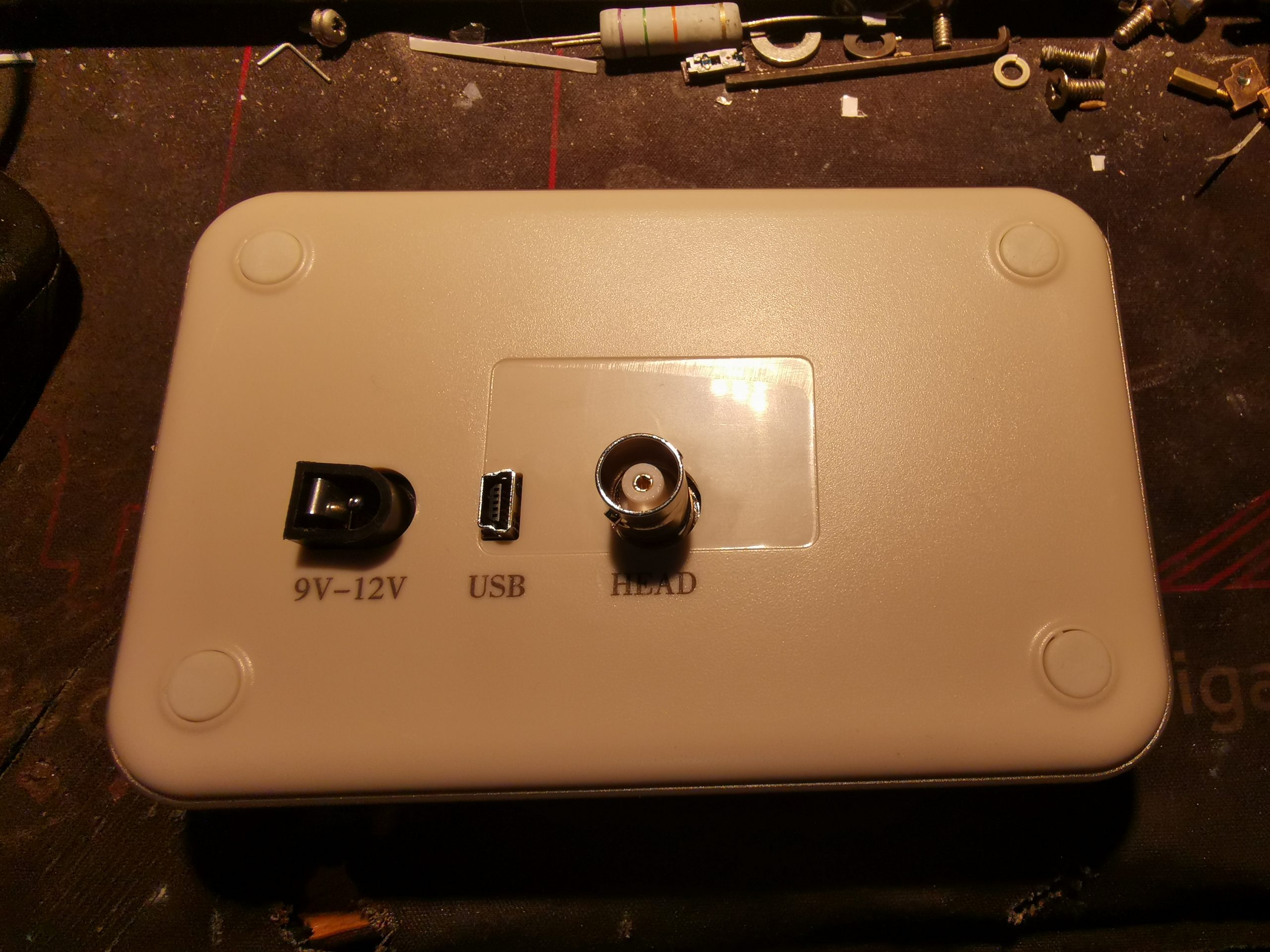
Rear Panel
The rear panel has the power input, USB & the signal connection on BNC from the sensor head.
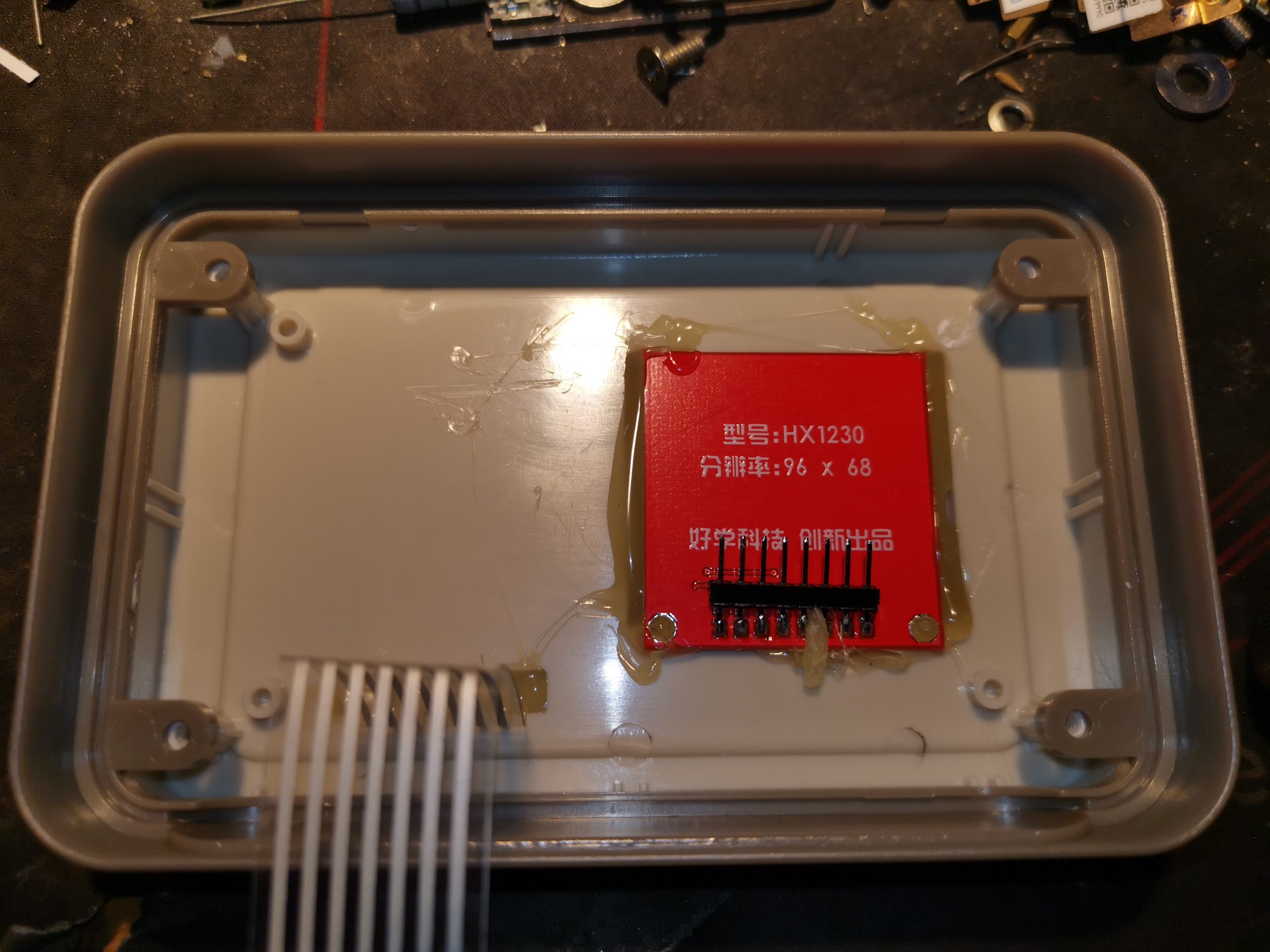
Front Cover
Inside the front cover there is a standard HX1230 LCD, and the flex to the front panel buttons. The LCD itself is rather roughly hot-glued in place.
Boards Assembled
The PCB stack normally sits inside the rear cover, ans holds all the electronics required to run the meter. The main microcontroller is on a separate daughterboard, and looks a lot like a dev board! The input stages from the sensor head are on the left hand side of the PCB.
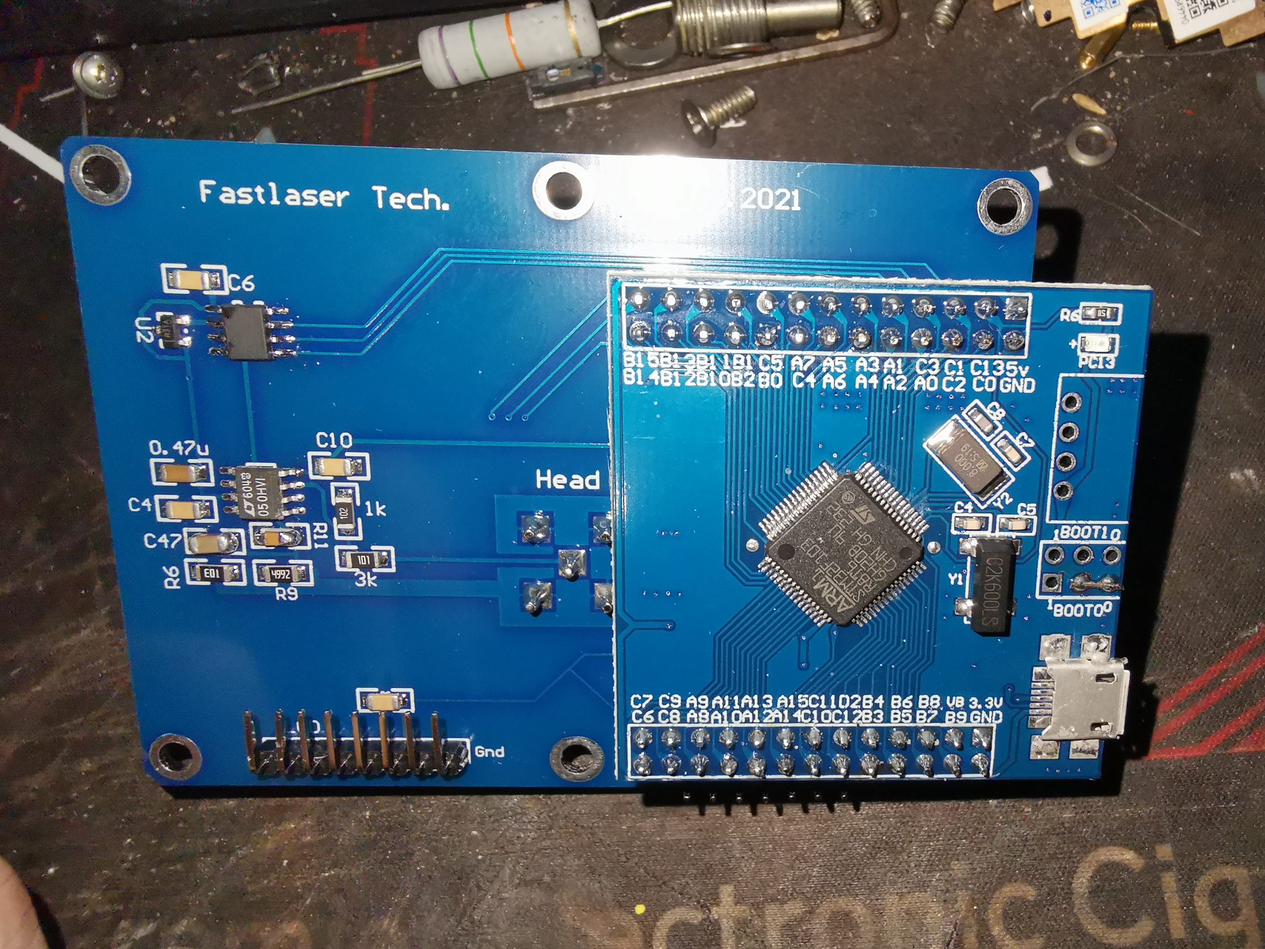
MCU Board
Here’s the MCU daughterboard, hosting the support components for the STM32F107 microcontroller. There’s a USB port on this board too, not sure what that one does yet.
MCU Board Rear
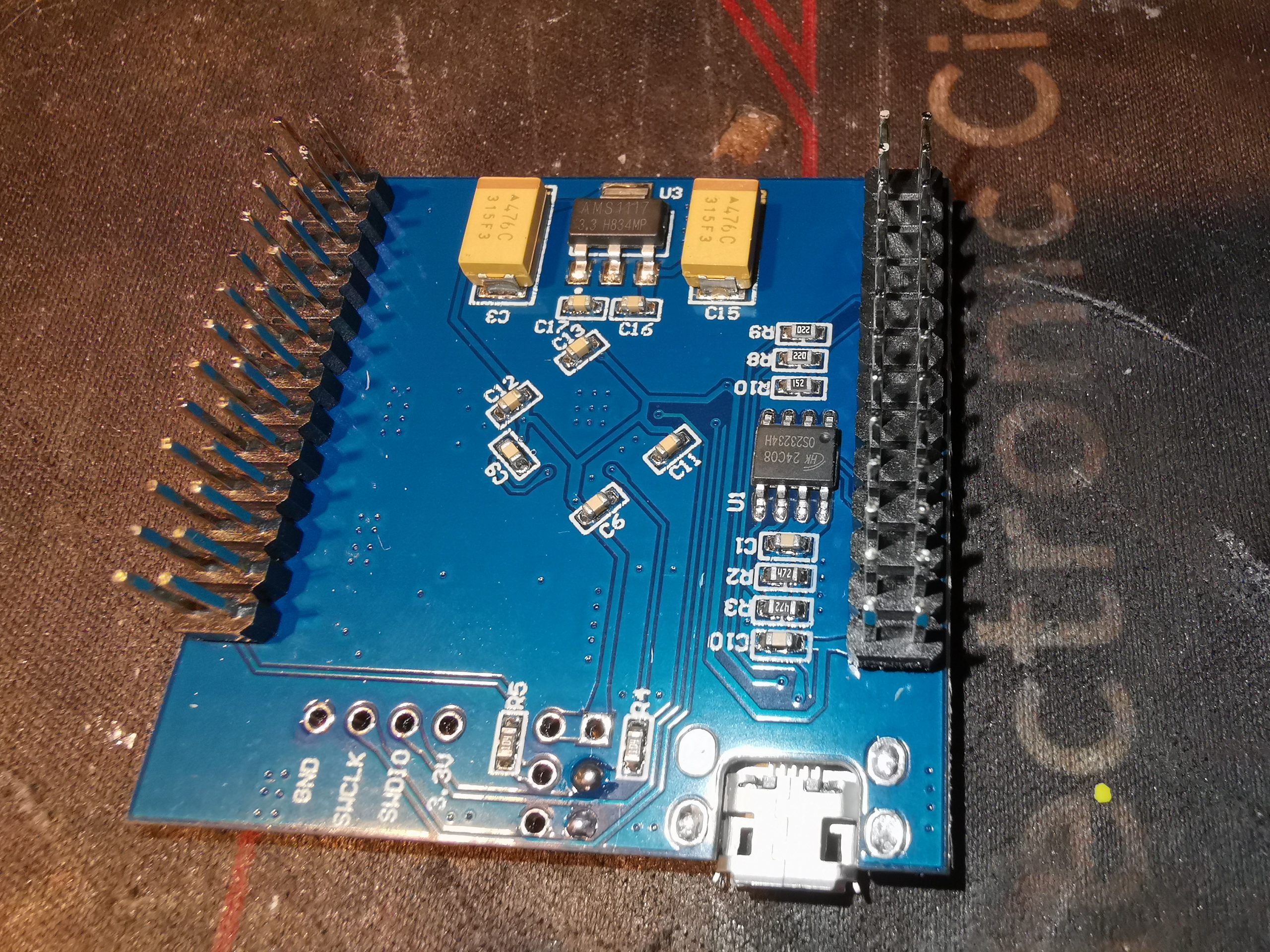
Here’s the other side of the PCB, with a small EEPROM, and voltage regulator. The programming pins are on the bottom left.
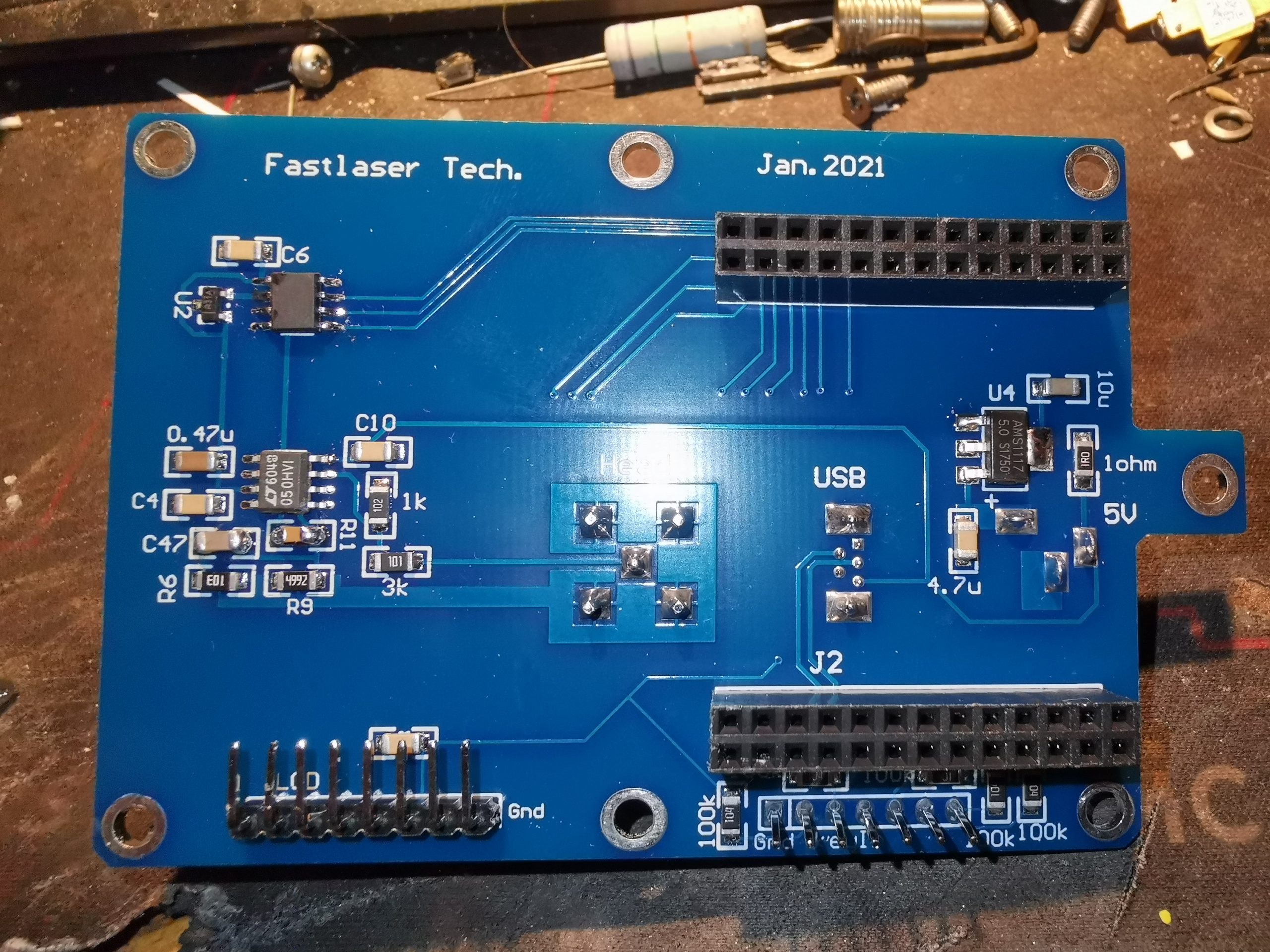
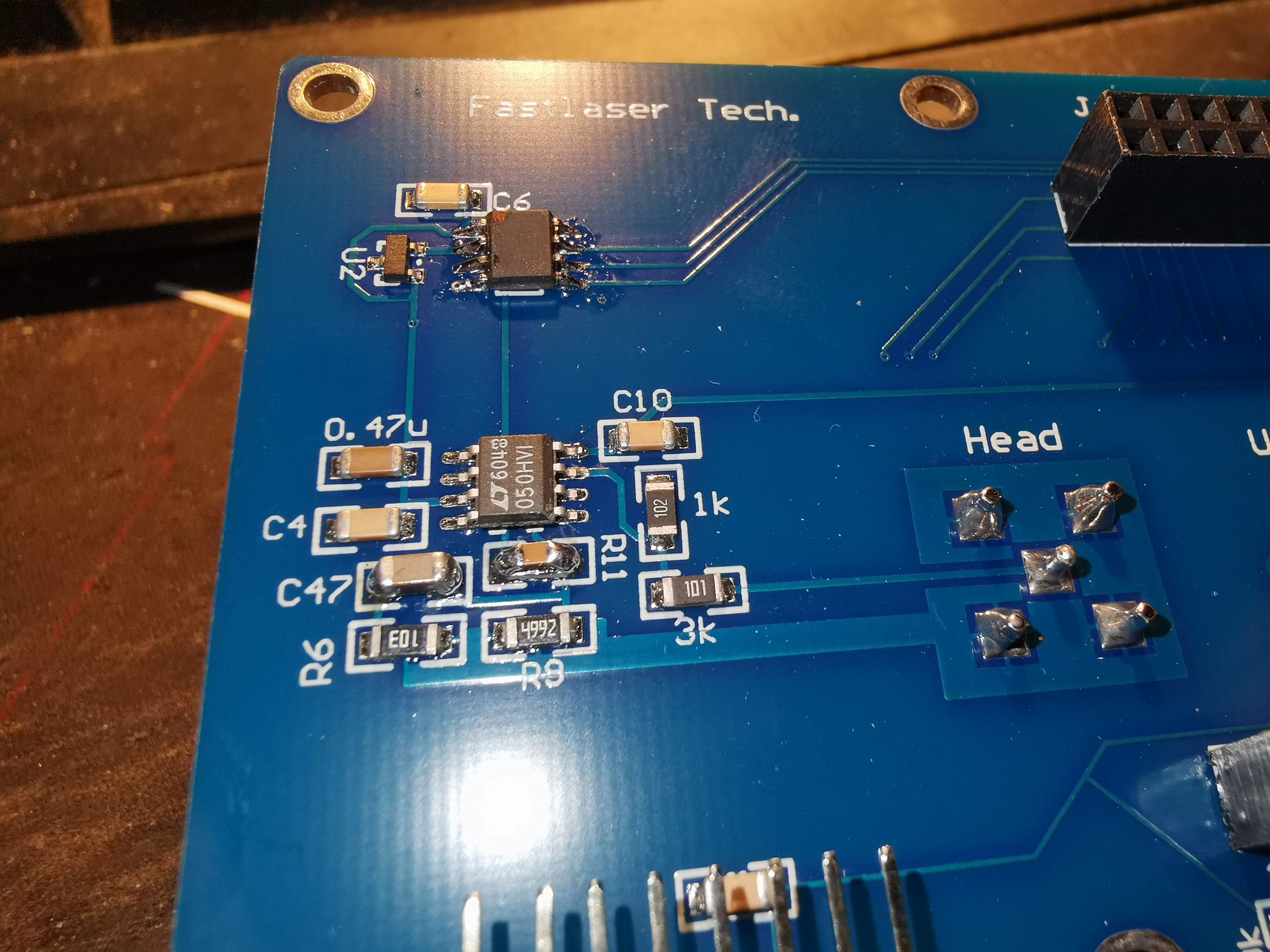
Mainboard
Here’s the mainboard without the MCU daughterboard. Not much on these boards, very sparsely populated indeed!
Voltage Regulator
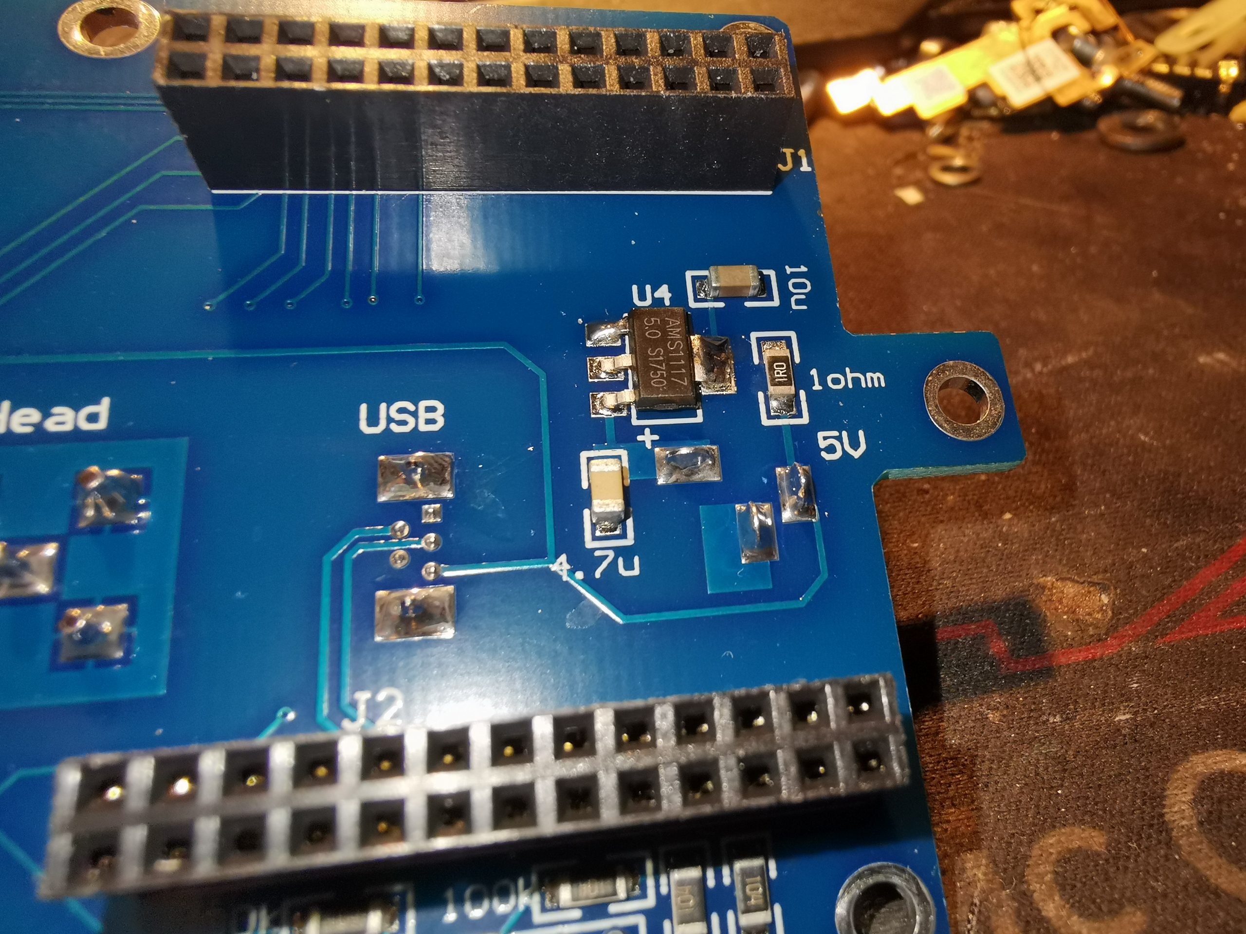
There’s a AMS1117-5.0 regulator on the right, which takes the 9-12v input from the external PSU down to a 5v rail, very simple.
Sensor Head Input Circuitry
The input stage & A/D converter are on the left side of the board, consisting of an LT6004 dual Op-Amp, likely configured as a transimpedance amplifier, and a small A/D converter, which has had the number scrubbed off. It’s been said many times before that this is pointless, as it’s not too difficult to work out what parts have been used. In this case, everything matches to the LTC1286 12-Bit successive approximation sampling converter from Linear Tech, and it’s being controlled via SPI from the main microcontroller. A TL431 in a SOT23-3 package handles the need for a local stable voltage reference.
I posted a couple of weeks back that I was soon to be the recipient of a new gigabit symmetric link to the intertubes – and there was a bit of a caveat of their use of CG-NAT due to the exhaustion of the IPv4 address space.
To compensate I’ve routed everything over a VPN link in prep for this new connection, which does work fantastically well.
After a chat with their support guys – and I did actually manage to speak to someone in their Networks team, not just a customer support droid(!), they will soon be introducing a service where I can add a public IPv4 to my account, so I’ll be able to run at full gigabit speeds without the 100Mbit restriction of this VPN connection!
I’m told that this will be within the next couple of months, which is around the same lead time as the connection itself, so hopefully this will be live just in time for my new fibre.
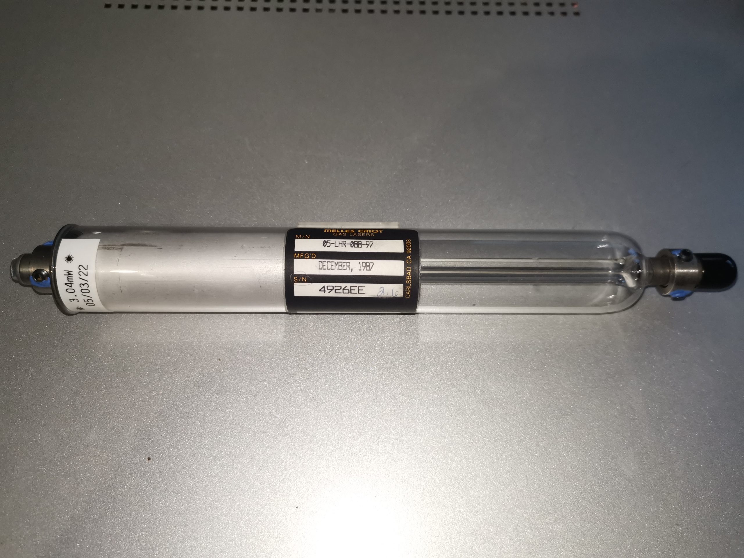
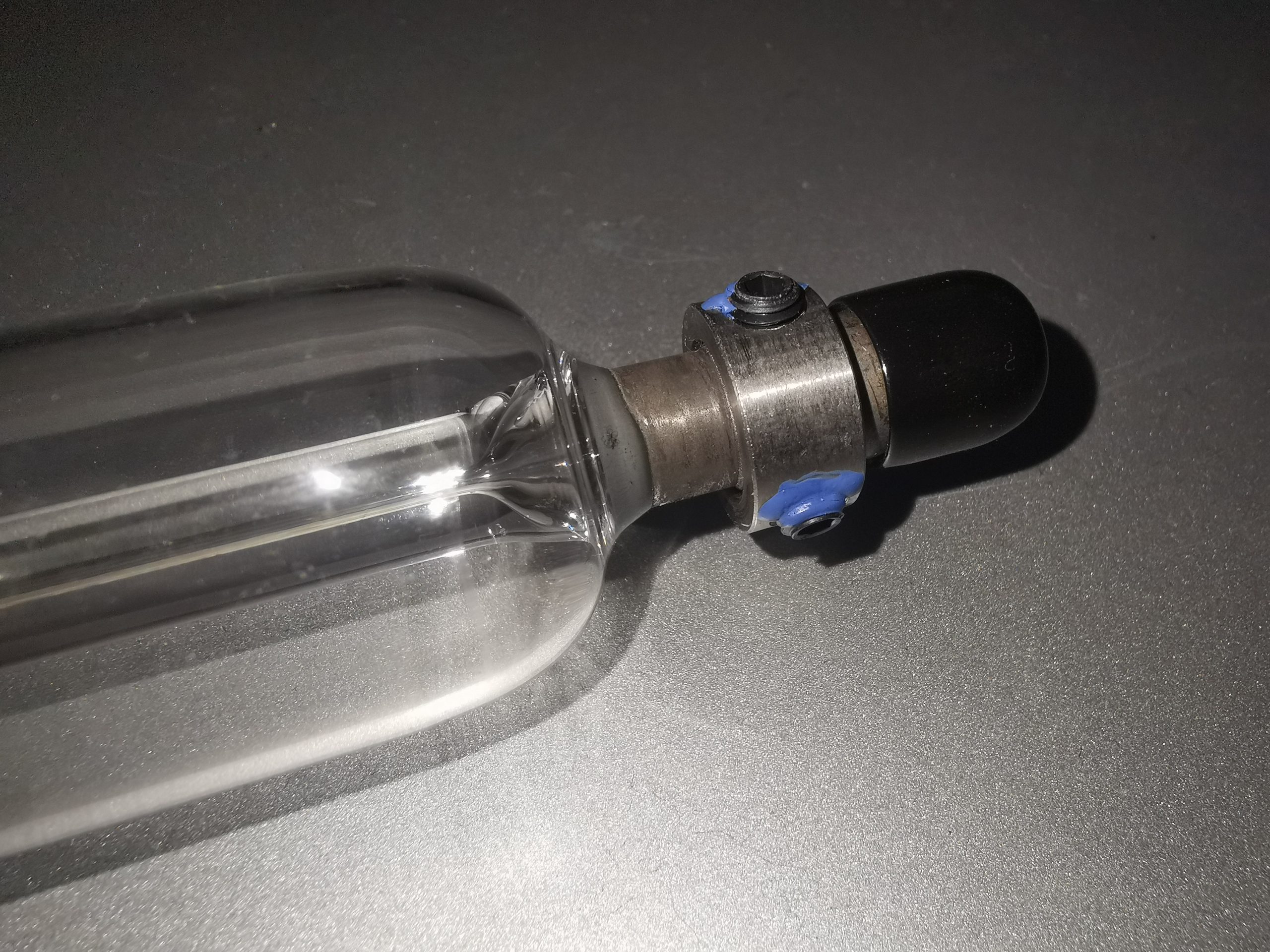
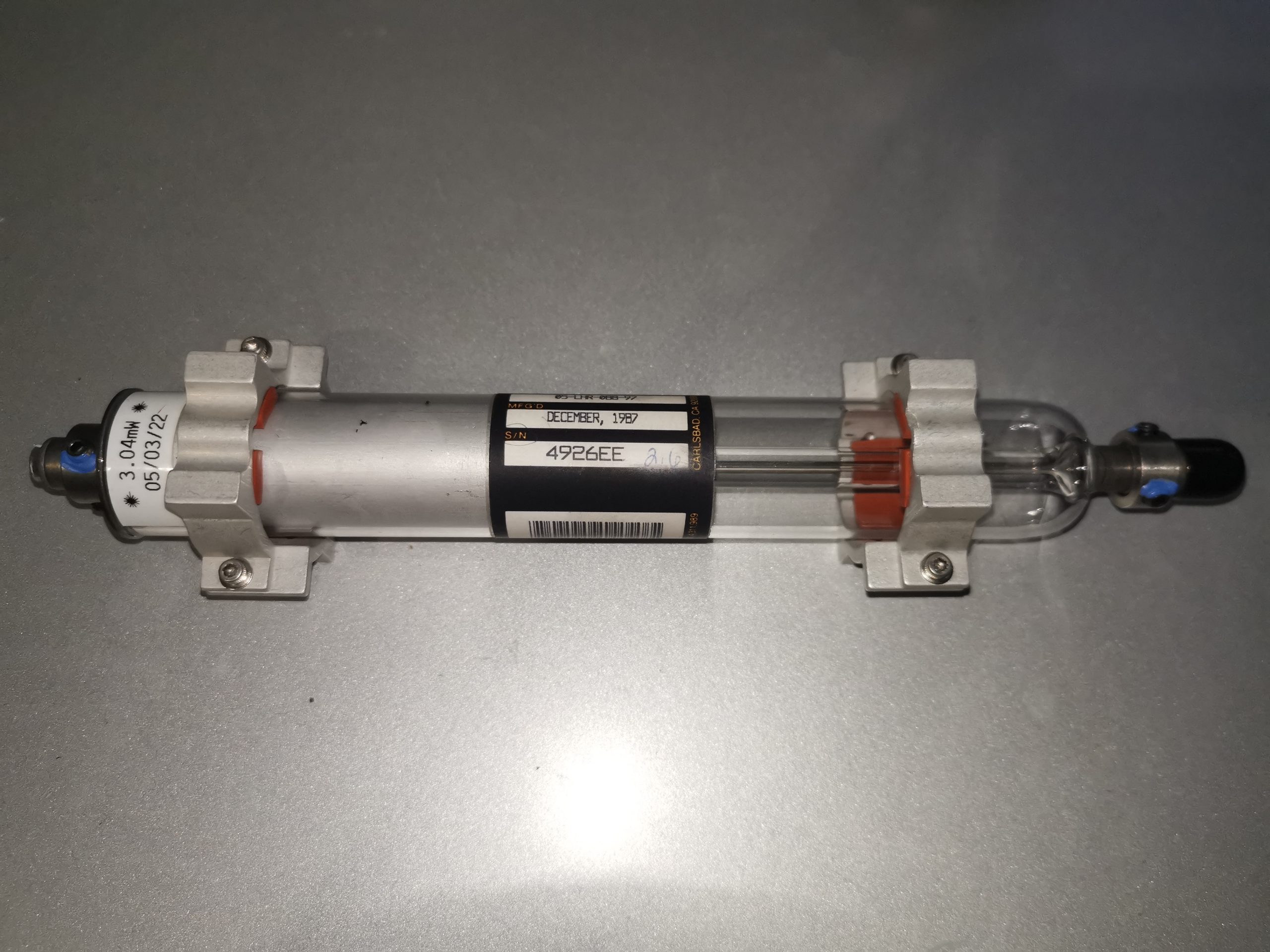
Here’s another Helium-Neon to add to the electric glassware collection, a 2mW Melles-Griot 05-LHR-088 which I pulled from the optical assembly from an ancient Spectra-Physics SP910 laser level. This tube is a standard Red 632.8nm with Random beam polarisation. The specifications are in the table below:
Minimum Optical Power
e/2 Beam Diameter
Divergence
c/2L Mode Spacing
Supply Opr/Start Volts
Nominal Current
Diameter/Length
2mW
0.63mm
1.4mR
641MHz
1.82/10kV
4.5mA
29/241mm
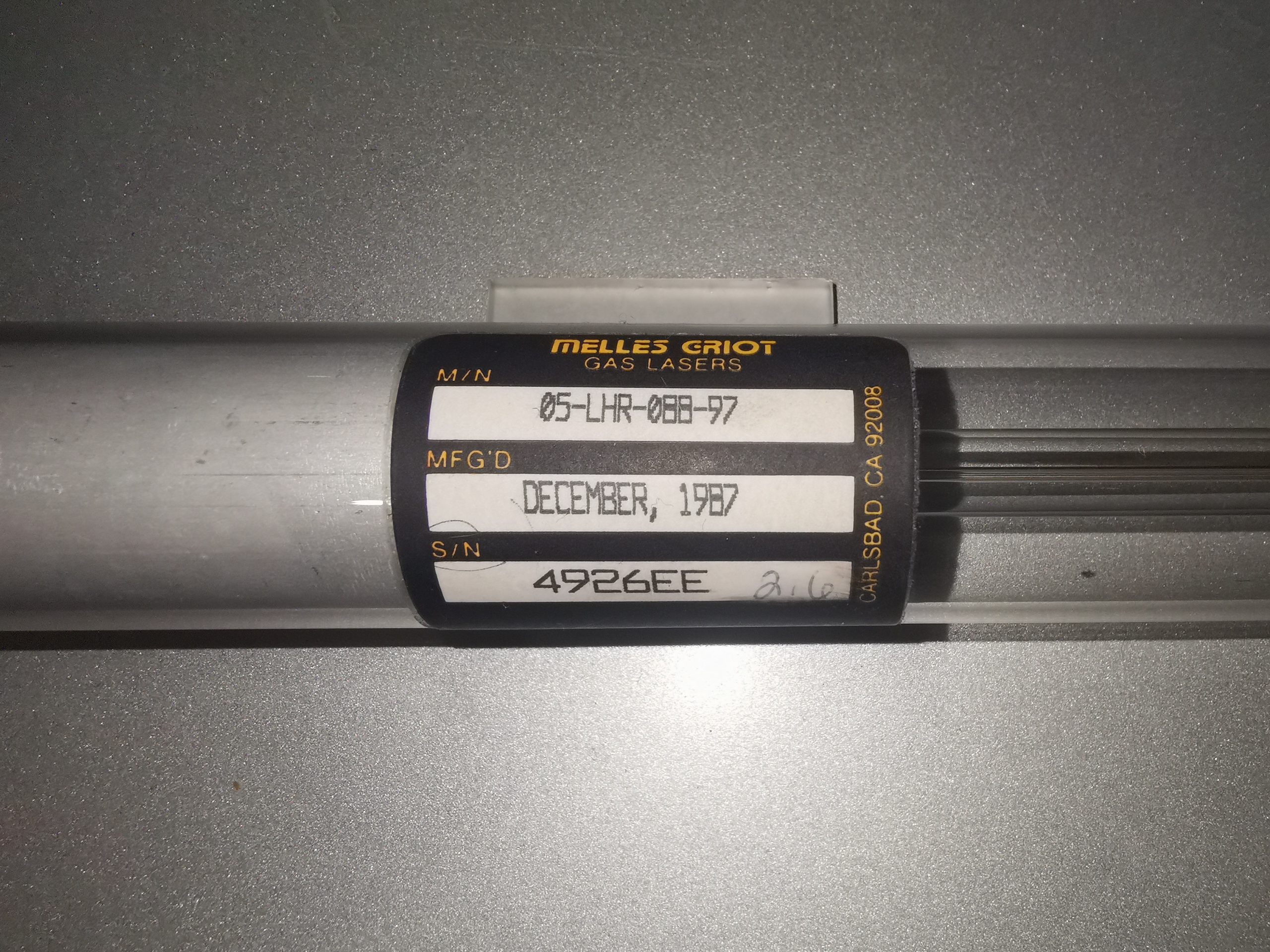
Tube Label
The label shows that this tube was manufactured back in 1987. 34 years at the time of writing! There is a slight amount of brown deposit in the main bore, indicating the tube has seen some use, however it’s nowhere near as bad as the Barcode scanner tube I have, which must have spent many years operating. I am assuming the “2.6” hand-written onto the label next to the serial number was the power measured at the factory.
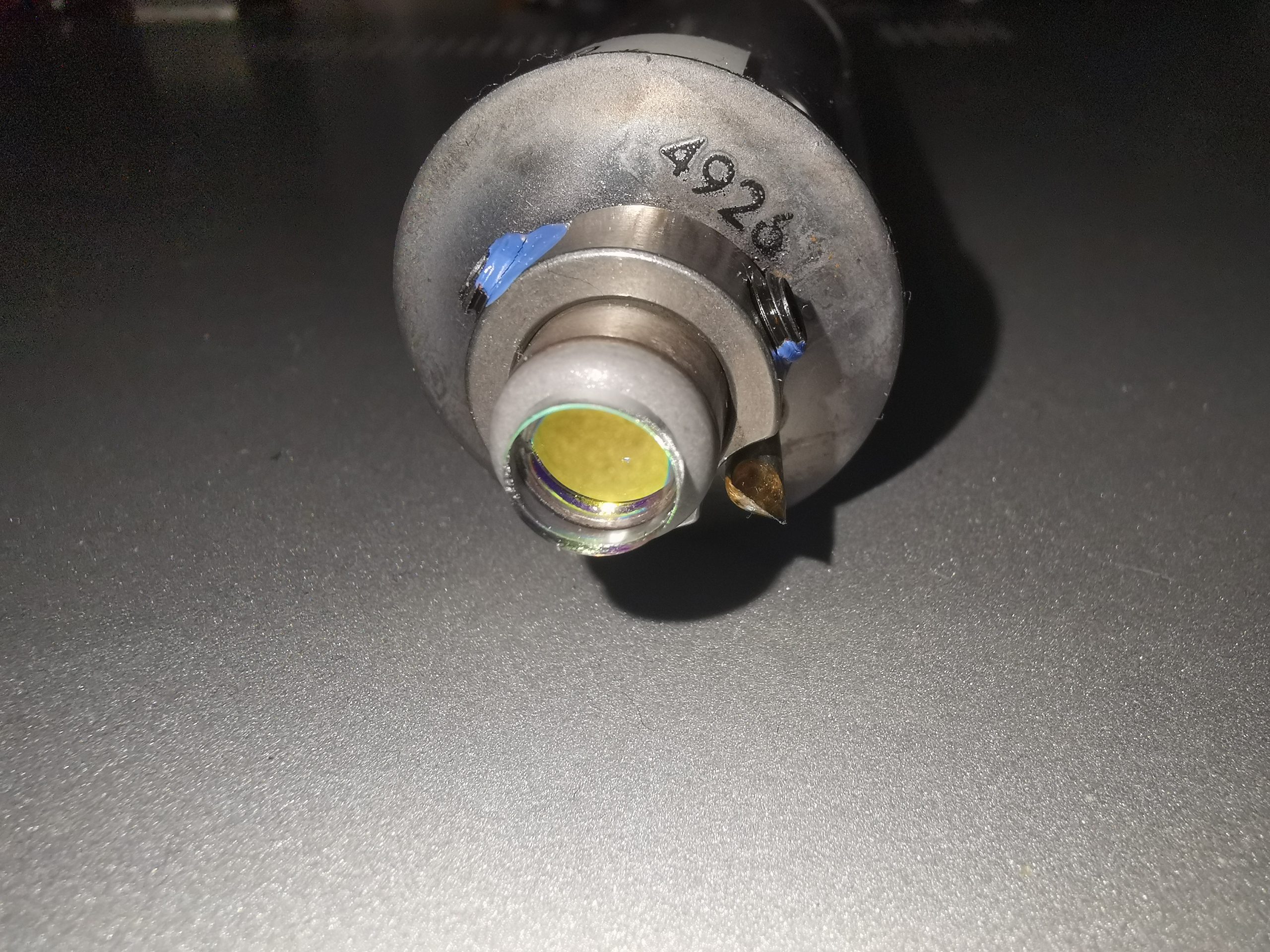
Anode End
This tube is old enough to have 3-screw locking/adjustment collars on the mirror mounts. This one is at the anode end of the tube, with a cap over the HR mirror for protection.
OC Mirror
The OC (Cathode) end of the tube has the same locking collar.
Tube Mounts
The original tube mounts are reattached here, made from Aluminium with silicone rubber pads.
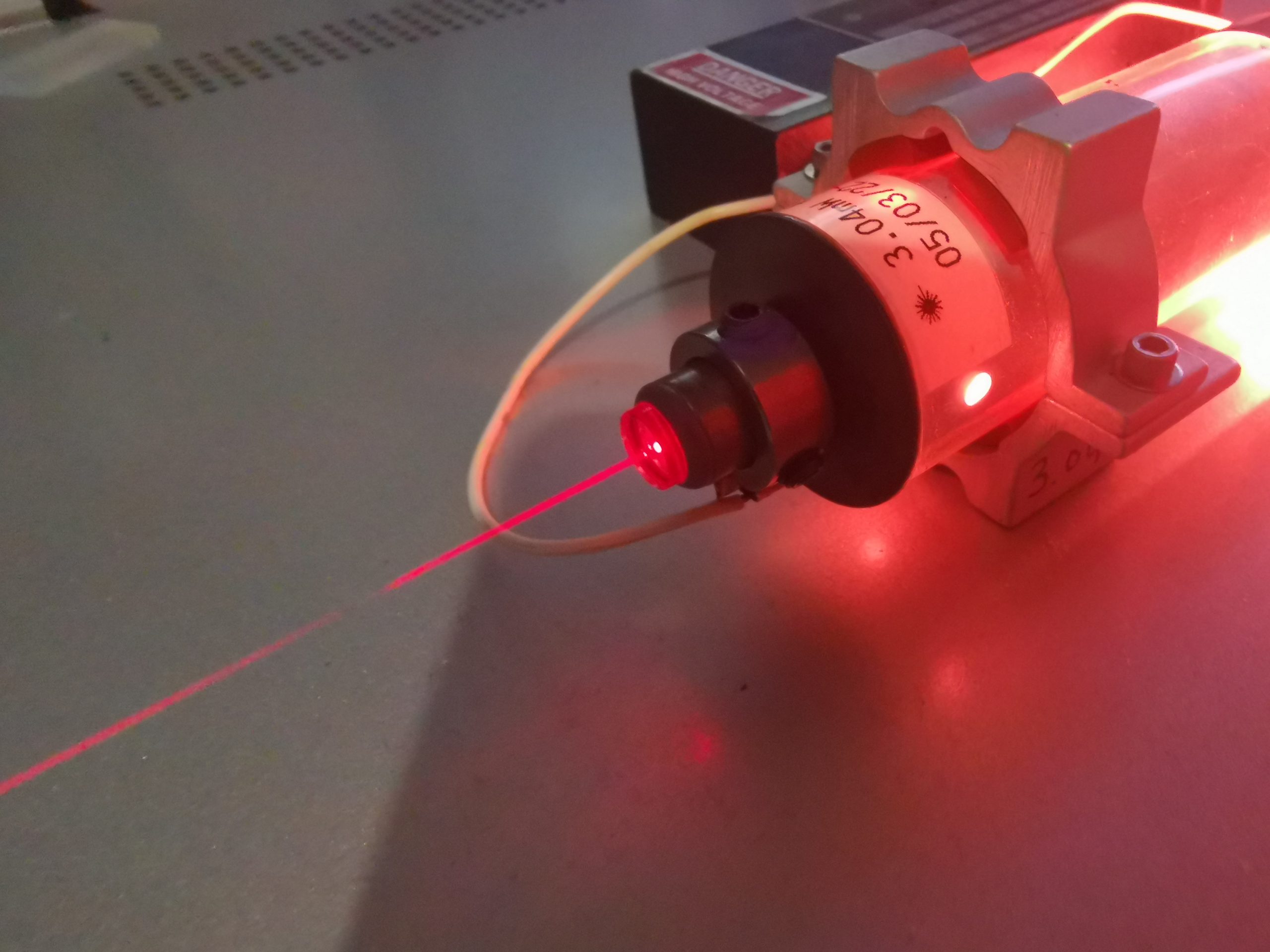
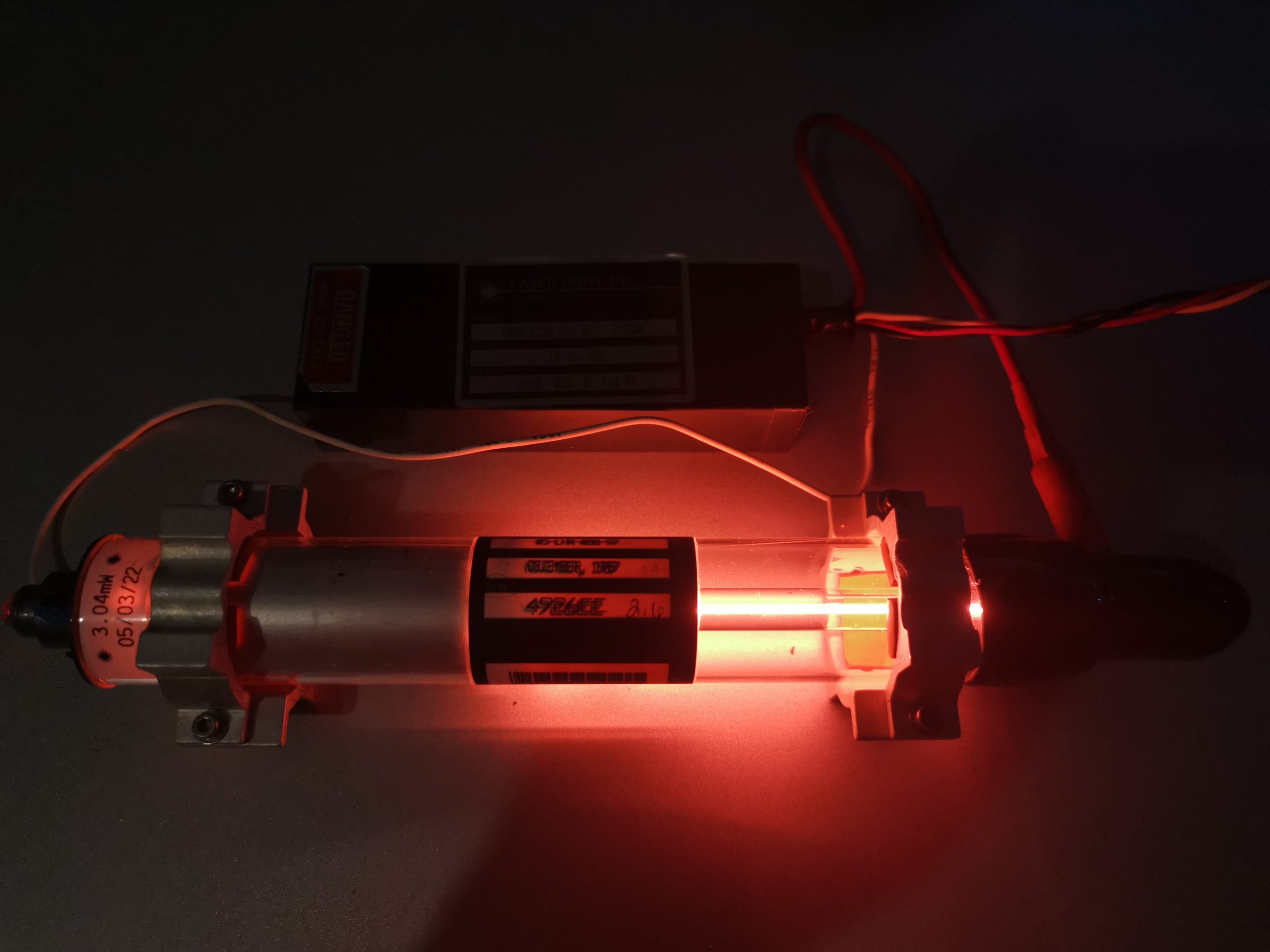
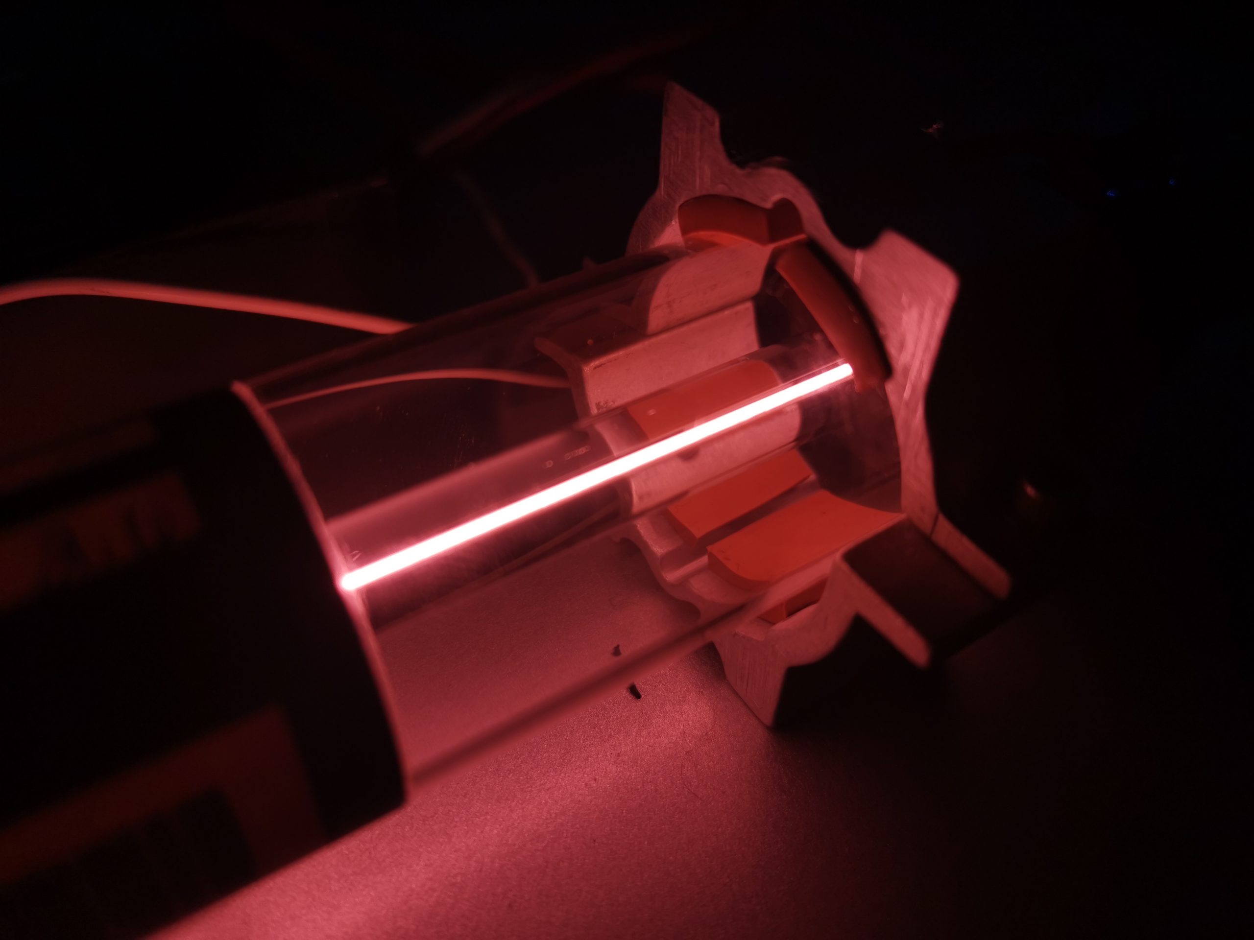
Tube Running
Here’s the tube running on a LaserDrive 4.5mA PSU. The camera doesn’t quite pick up the colour of the discharge, it’s more salmon-pink.
Bore Closeup
A closeup of the bore more accurately shows the colour of the glow discharge in the tube.
Finally, the output beam from the tube. This one actually measured at 3.04mW on a Coherent LaserCheck, a bit higher than the assumed factory measurement of 2.6mW!
Everyone who reads this website will know about the cost of living crisis – this is a global problem brought about by the combination of the Covid-19 pandemic, and the unfortunate situation in Ukraine at the present time.
For us in the UK, the costs of energy have skyrocketed in recent months, with our government permitting the energy companies to charge us all an extra £600 per year in electricity alone. Given I run servers, this isn’t particularly good news.
The cost of running the network infrastructure behind this blog is not insignificant – just the server alone runs me around £30-£40 per month just in power, and add onto that the £45 in connectivity costs. I don’t meter the power taken by the router, switch etc, so the total cost will be marginally higher.
Given the increases that have hit, I expect to see a 3x increase in power costs to run this blog on the current hardware – an unsustainable jump.
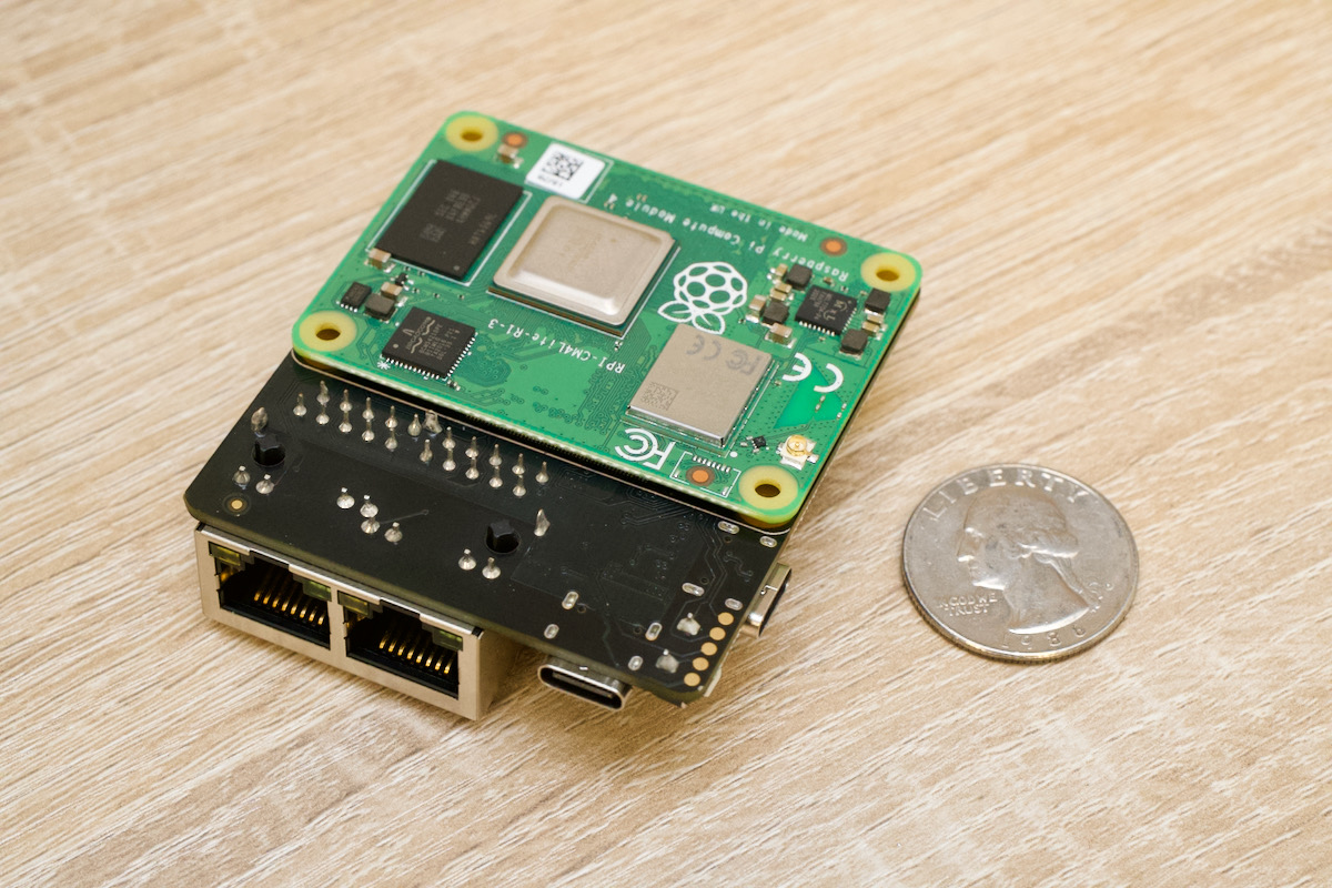
I’ve got a couple of Raspberry Pi’s floating around, at the moment uncommitted to any tasks, so I thought I’d use one of these. A Pi CM4 module in a support PCB with dual network links should so just fine. I ogirinally got this to build a Pi based router (what it was designed for) – nevermind!
I’m using the new 64-Bit version of Raspberry Pi OS, and a 128GB MicroSD card for storage, since this board doesn’t have an open PCIe lane for a NVMe drive.
A quick setup with Nginx, php-fpm & MariaDB & I’m in business! The site is now running on a Raspberry Pi! As a plus, everything does seem to be quicker than the old Apache setup too. I have for now dropped a few features of the site, just until I get a feel of how quick this new setup is going to be, but they should be back soon!
For 90% of the time I’ve run this website, it’s been run from a server in my house, over a domestic-grade ADSL connection. The problem has always been the very asymmetric download/upload bandwidth provided by domestic ISPs. Normally it’s about a 10:1 ratio these days (the current connection is 350MBit DL / 20MBit UL, which is even worse). Going back a few years, this wasn’t much of an issue – 99.9% of general ISP customers didn’t need a high upload rate, as they were only requesting web addresses, etc. Nowadays especially with the rise of online video services & social media, upload rates are more important than ever, since a good proportion of the population is uploading their own content daily.
Despite these changes in how the networks are utilised by the end users, the upload rates haven’t really improved much, which I’ve always found baffling.
Considering the bandwidth limitations imposed by such a connection on upload rates, the site’s done pretty well over the years, even though it can be a touch slow at times. I’ve been looking at changing this situation for a long time, watching to see if any of the direct fibre ISPs in the UK were going to get around to serving my area, such as Gigafibre, CityFibre or HyperOptic, but they unfortunately haven’t yet appeared anywhere near my locale.
Cue the entry of a new ISP: Brsk. These guys are building an entirely new fibre network, and just so happen to be doing the network build in my direct area at the moment. For only £5 more a month than I’m paying for the service I have now, I can now obtain full gigabit symmetric connectivity!
There’s one small caveat to the service, which wouldn’t bother the average member of the public, is a serious block to how I use my internet connectivity – they don’t hand out globally addressable IPv4 addresses. This is ostensibly due to the global IPv4 address shortage. Instead, they use CGNAT to address their endpoints, which renders me unable to route anything out to the global internet from my connection. Luckily there are ways around this issue.
I do have access to some public IPv4 addresses that are currently unallocated, in another networking installation, which also runs a VPN into my home network. So it’s just a matter of hooking up my primary server to that VPN, and routing one of the spare IPv4s over the private link from the router at the other site. This will limit thing somewhat, as the other site link is a 100MBit symmetric leased-line, however that’s still an 80MBit improvement in upload rate overall.
This latter solution of routing a public IP over VPN to a private endpoint is something I’ve already done in preparation – and it works great. The firewall on the site router provides extra protection for the server, and even with the VPN overhead it’s just as quick as it was before.
Since they’re still building out the network, I’ve only been able to place a preorder, and the connection will be installed (allegedly) sometime in July. Once the new link is in, I can get rid of my existing provider.
Once the link’s installed I’ll provide some updates!
I’ve been looking for ways to build a DIY Laser Power meter for some time now, but I had no way to calibrate anything. I have been aware of DIY thermopile sensors with TECs – but no way to verify any results until now. Since I have my Gentec meter to calibrate against, I can finally get on with the project.
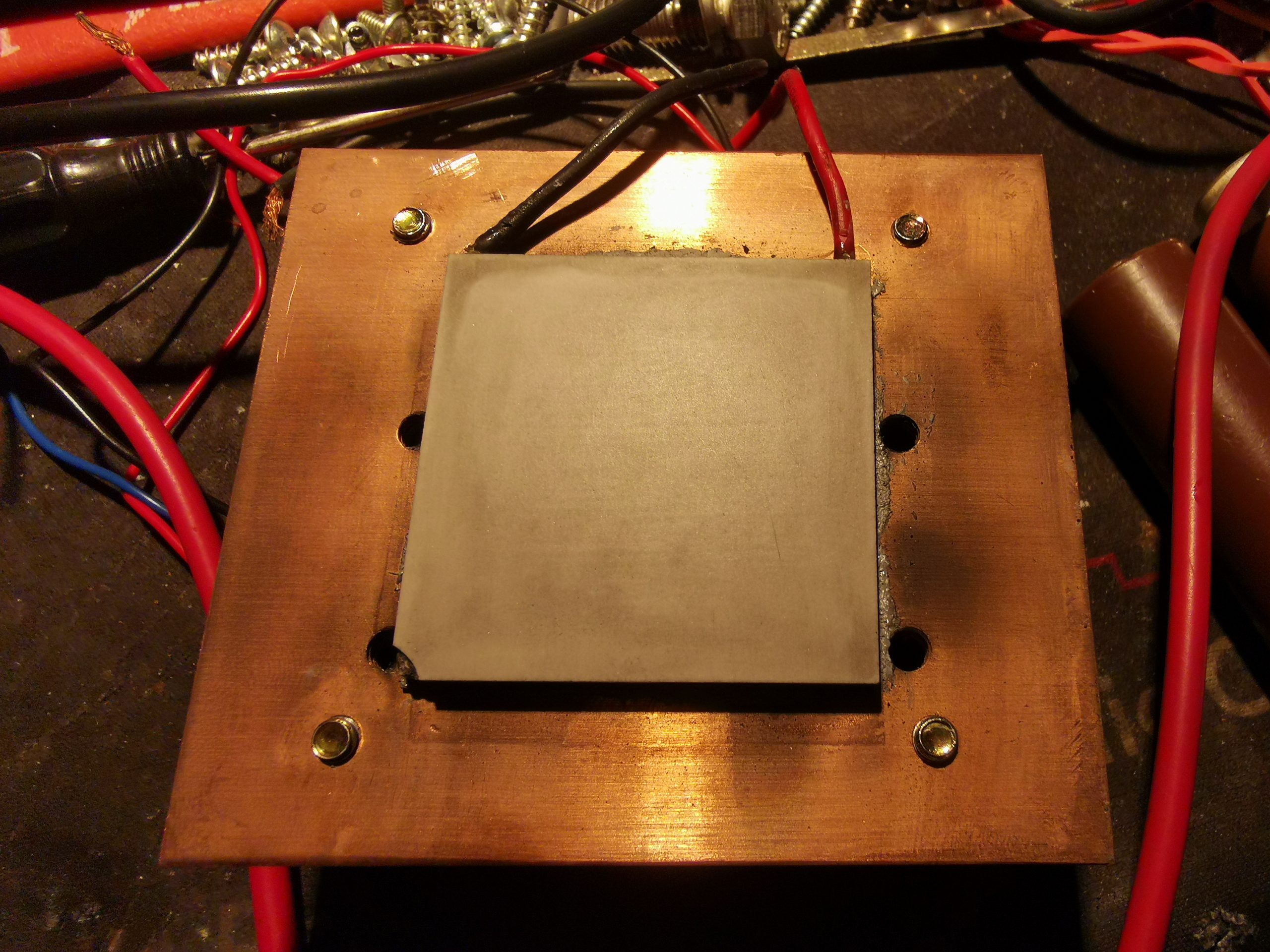
In the photo above, is the Peltier/TEC module mounted to the heatsink with thermal compound. In this case it’s a TEC1-12706, pulled from a cheapo dehumidifier. The cold face (with the part number printing) is against the heatsink, and the hot face will serve as the beam target. This was cleaned with solvent, and roughed up a bit with silicon carbide abrasive paper – the abrasive needs to be harder than the Alumina ceramic the module is constructed from.
Optical Coating
To be any good as an optical power sensor, the front face of the module needs to be coated with something to absorb as much energy from the laser beam as possible. In this case, black paint was used, as it’s completely matte when dried. Lampblack also works, and this can be coated onto a sensor face with just a wax candle, but this is far too fragile to be any practical use (being just carbon, it’s much more resistant to thermal damage from the laser beams though!).
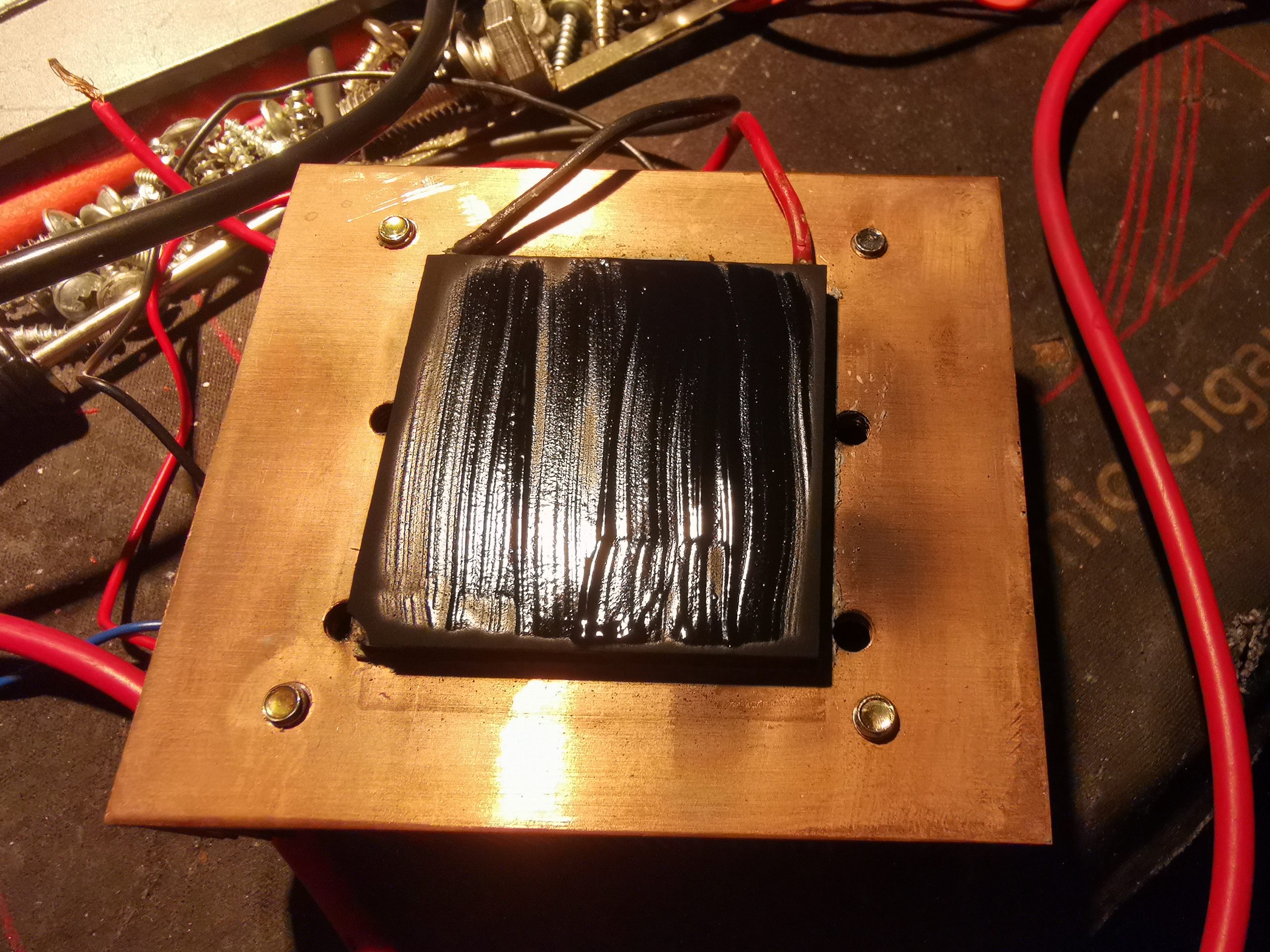
Coated Sensor
After two coats of the paint are applied to the front face of the module, the sensor head is complete. Try to get this as smooth as possible for best results. I designed & 3D printed a retention bracket for the module, and matches up with the screws that hold the fan on the finned side. This also has a block on the bottom which I threaded 1/4-20 to fit a standard tripod thread.
Like all commercial laser power sensors, the beam should be expanded as much as possible to fill the full face of the sensor. A focused high-power beam will quickly destroy the coating!
After completion, the sensor needs to be characterised. For this I set a diode module to be as close to 1W as possible, according to my calibrated meter, and applied the beam to the constructed sensor. A load impedance of 68Ω was placed across the output leads as a load. For this unit, I obtained a reading of 83.5mV/W of applied power. Even for low power levels, the fan does need to be running on the back of the heatsink, as the cold side of the sensor heating up will skew the reading.
After calibration at 1W optical power, I then ran some more tests at higher powers – 2W gave exactly double the output voltage, and throughout the power range I am able to test, the sensor seems to be entirely linear in operation.
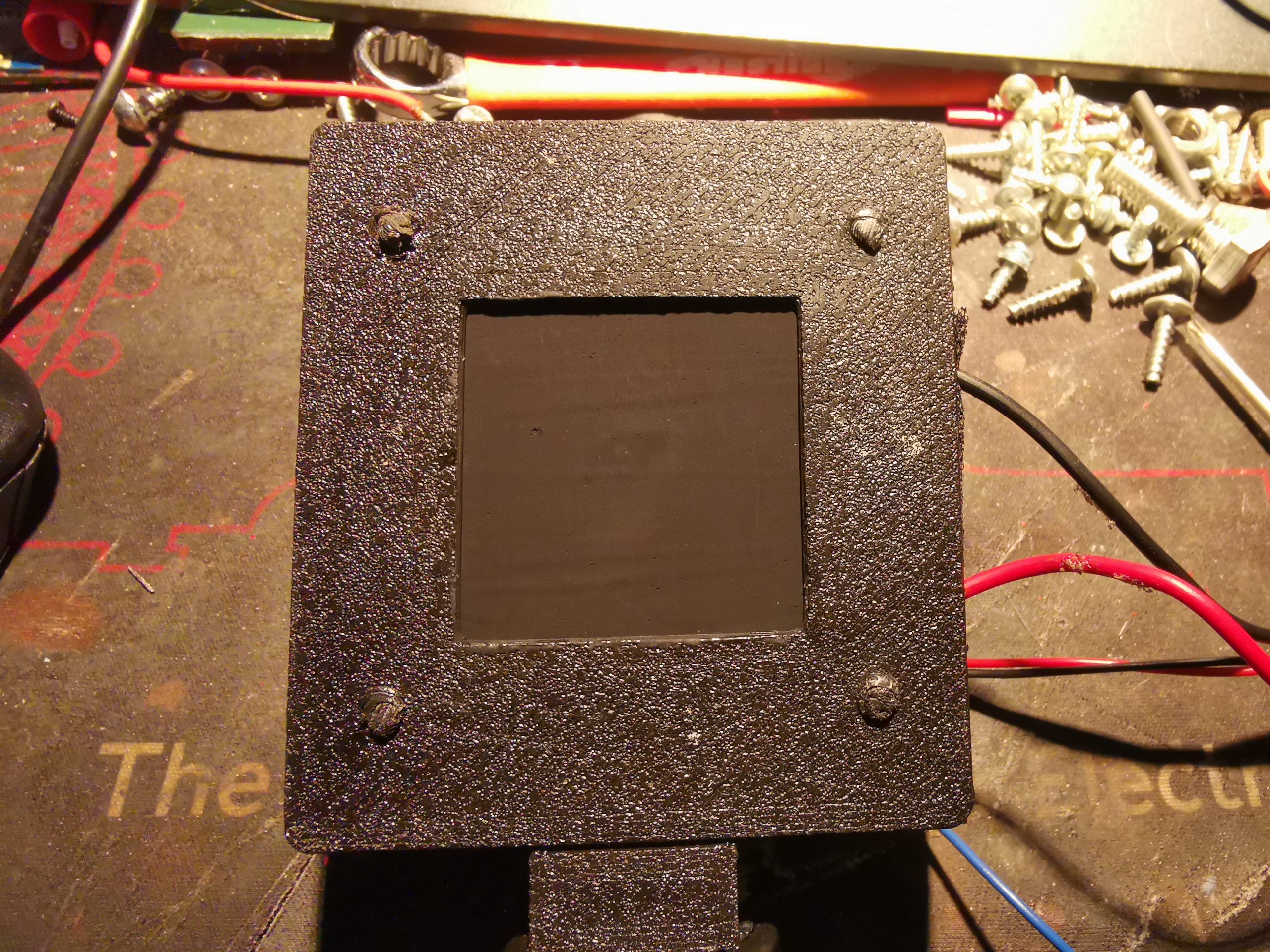
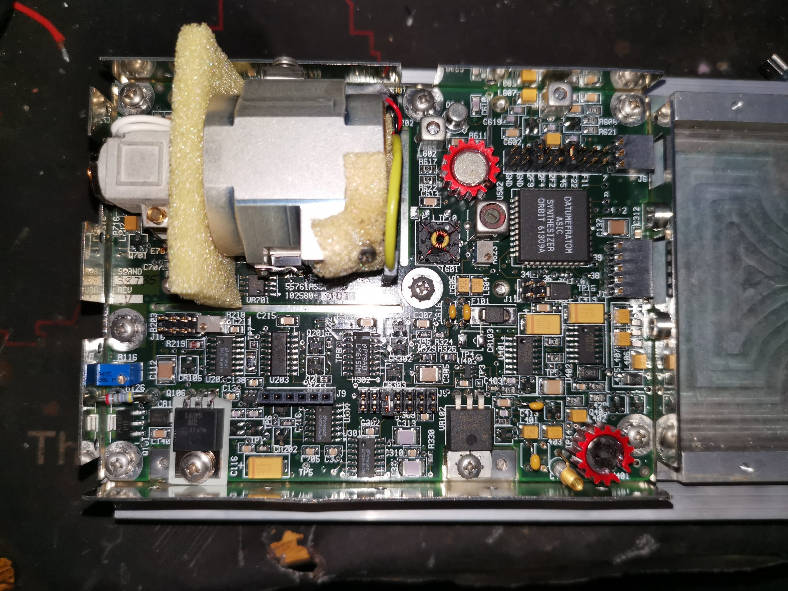
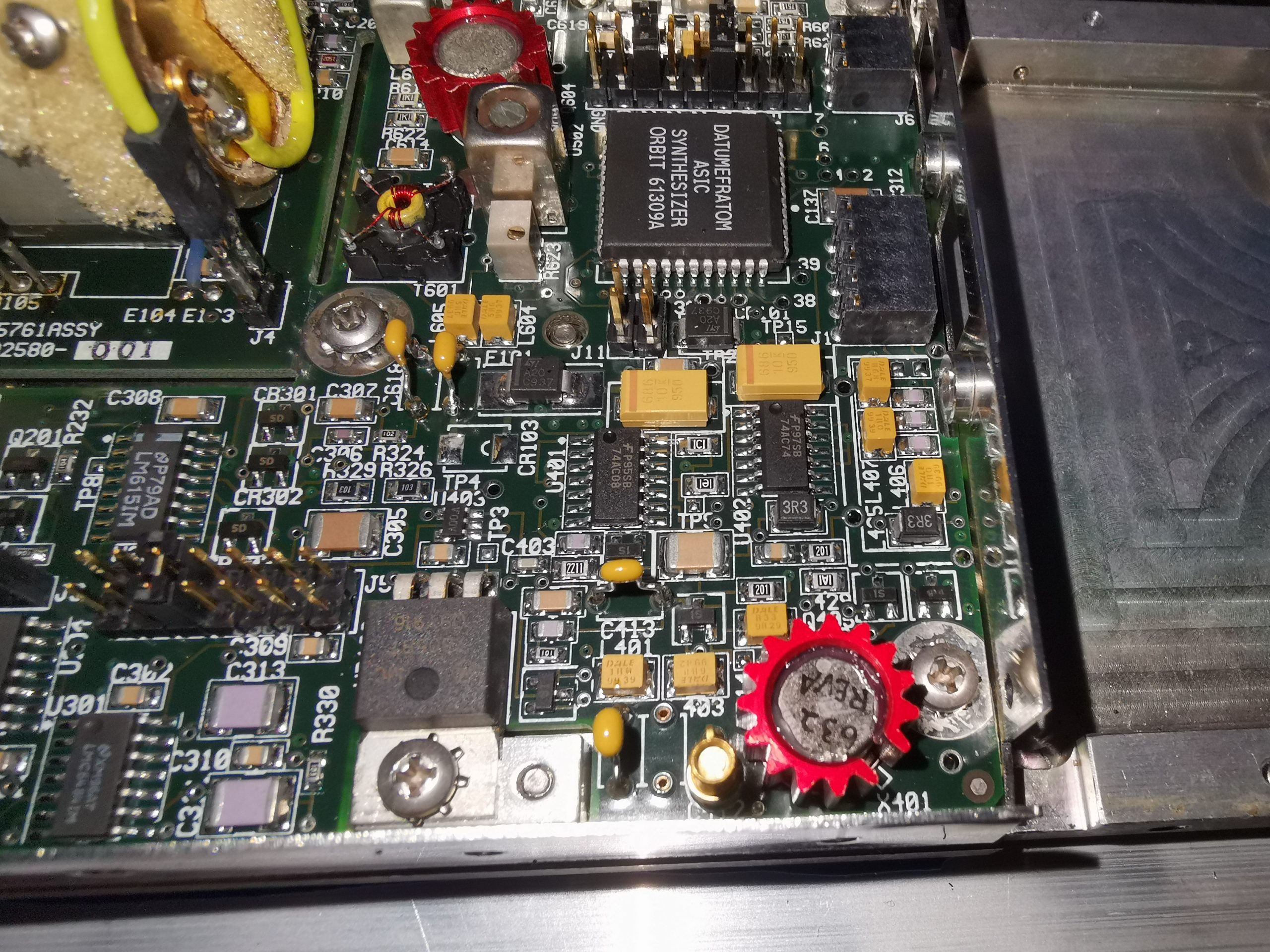
Time for another Rubidium Standard Teardown! This one was supposed to happen a year ago, however I completely forgot about this unit. This is an Efratom / Datum LPRO-101 Rb standard, which does differ somewhat internally from the previous unit I tore down. Above is the unit with the Mu-Metal top cover unclipped. The PCB is very tightly packed with components, and this unit dates to approx 1999. The way all of these units operate is with a standard Quartz oscillator, and locking that to a Rubidium physics package to gain the stability of an atomic reference.
Servo Section
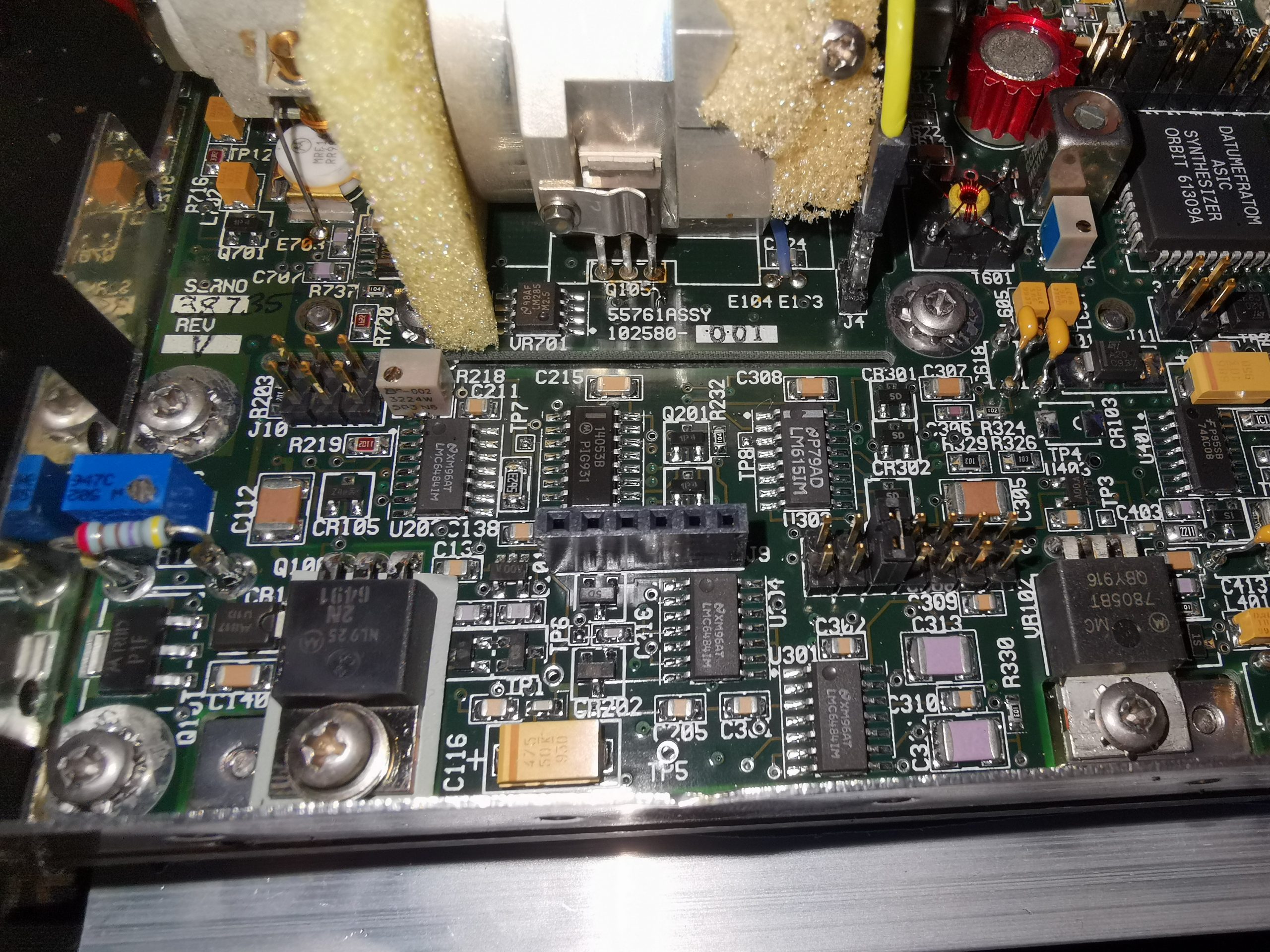
The bottom left corner of the board has the C-Field control & servo section, with the C-Field (Frequency Adjust) pot on the left, with the selectable tuning resistor. There’s a mountain of 74 series glue logic in this unit, and will be visible in every shot. The adjustment pot can be accessed through a tube in the top cover with an adjustment tool.
VCXO Section
Bottom right is the 20MHz VCXO section, with the main crystal in the TO-3 can wrapped in a heatsink at the bottom right. Again there’s more space for selectable components here, with a blank spot for another ceramic cap – most likely to further tune the operating frequency. One of the main regulators is here as well, an LM7805 in the TO-220 package.
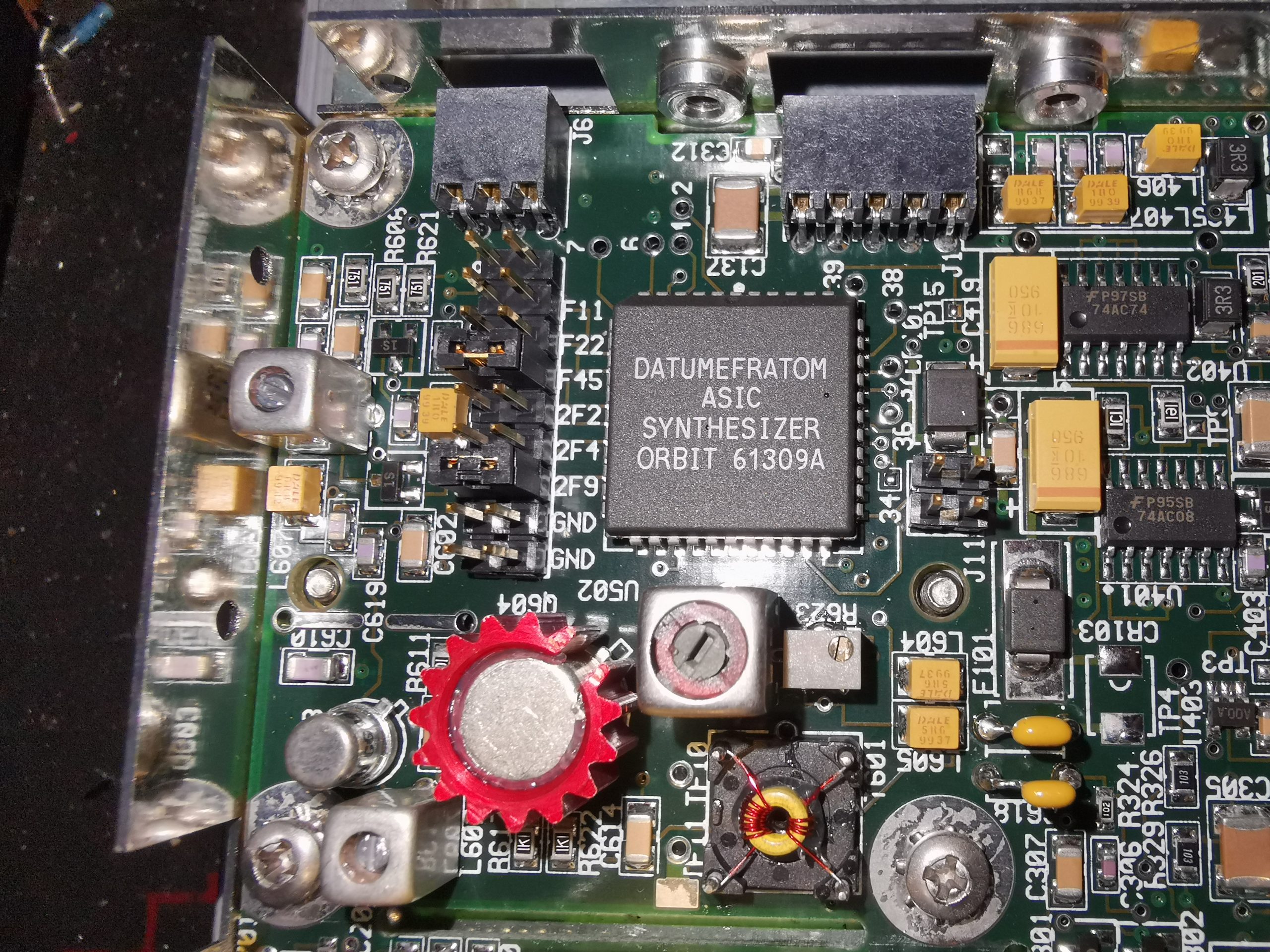
Synthesizer Section
Here’s the RF synthesizer, used to indirectly generate the 6.8GHz hyperfine transistion frequency of Rubidium. The synth here frequency multiplies the 20MHz main clock to 60MHz, and feeds this through a coaxial cable into a Step Recovery Diode, mounted inside the microwave cavity with the Rb cell. This section also sweeps the frequency to be able to obtain physics lock when powered up.
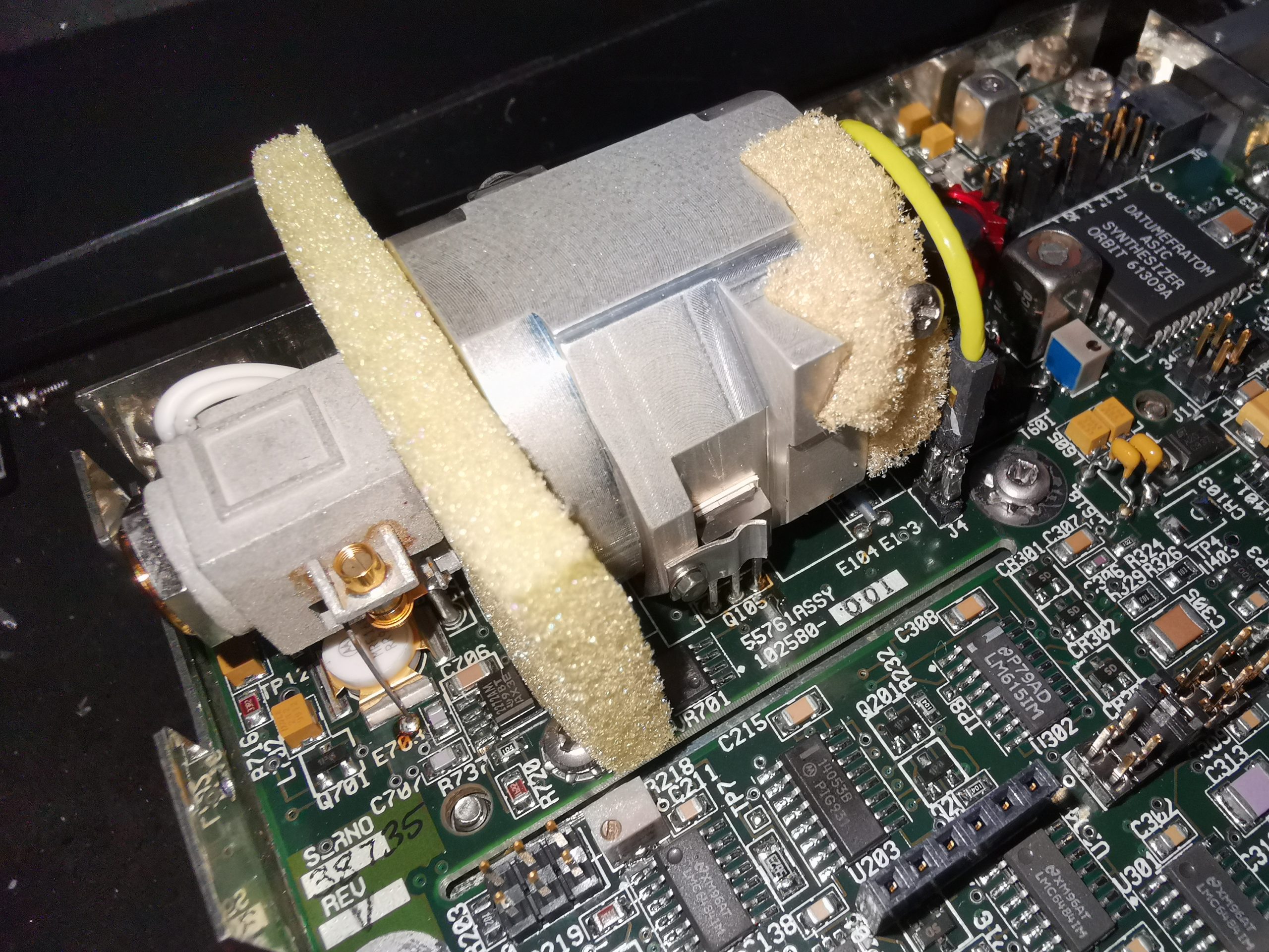
Physics Package
This is the very important section of the oscillator – the Rubidium Physics package. This section is heated to high temperature – 100°C for the lamp (the small section on the left), and 70°C for the vapour cell & microwave cavity (the larger section on the right).
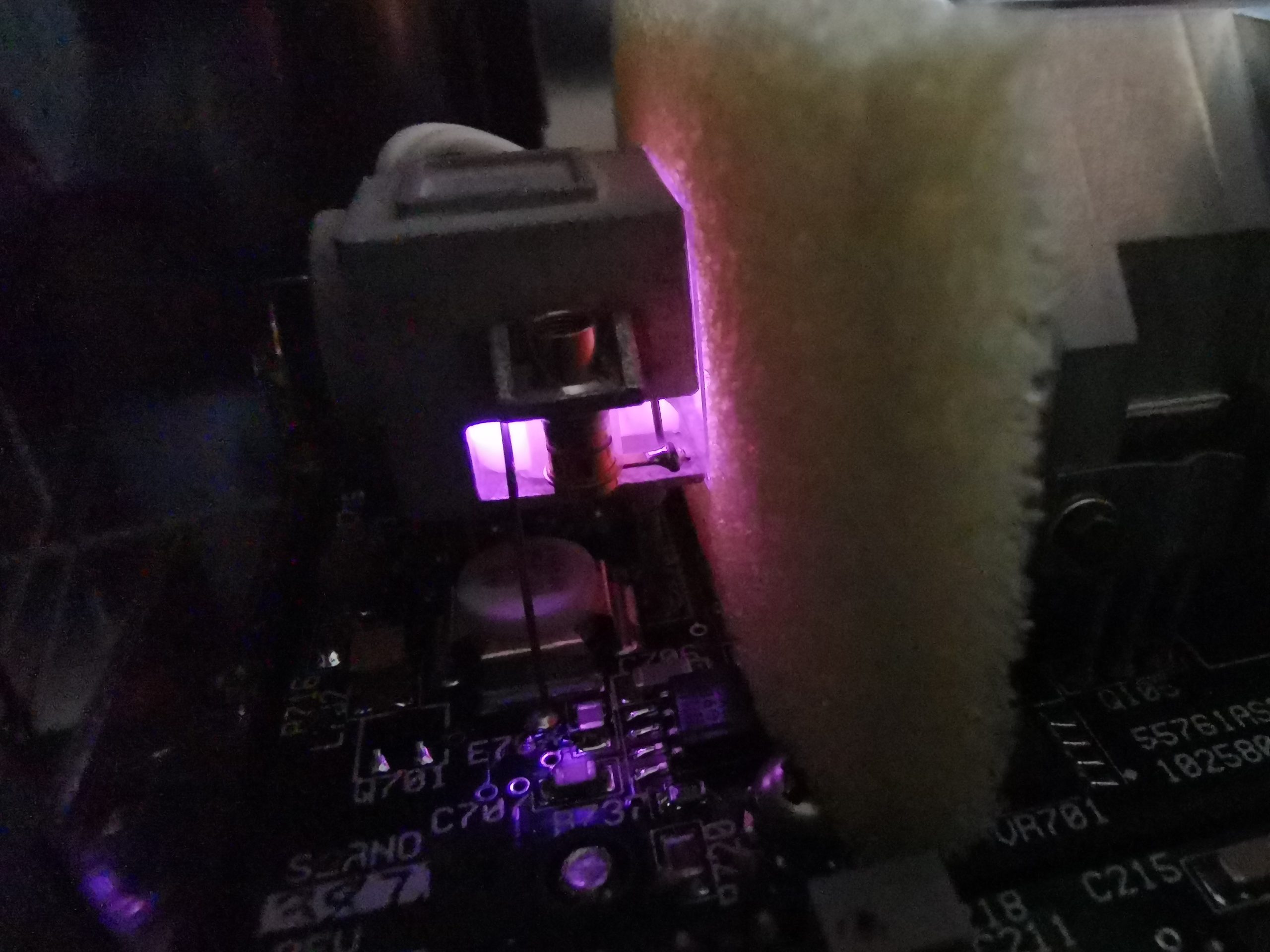
Rubidium Lamphouse
The Rb spectral source is hiding inside this small casting, with a barrel tuning capacitor on the side. In these units, the lamps are driven with RF, through a coil of wire wrapped around the glass bulb of the lamp itself. In my case, I managed to pick up a 156MHz signal in this area with a spectrum analyser, so I can only assume this is the drive frequency for the lamp. The main RF drive MOSFET, an MRF160 sits underneath the lamp housing. The driver is a Colpitts oscillator, and drives the lamp with about 4W of RF power. The lamp is heated with a MOSFET thermally bonded to the other side of the housing, which can’t be seen here.
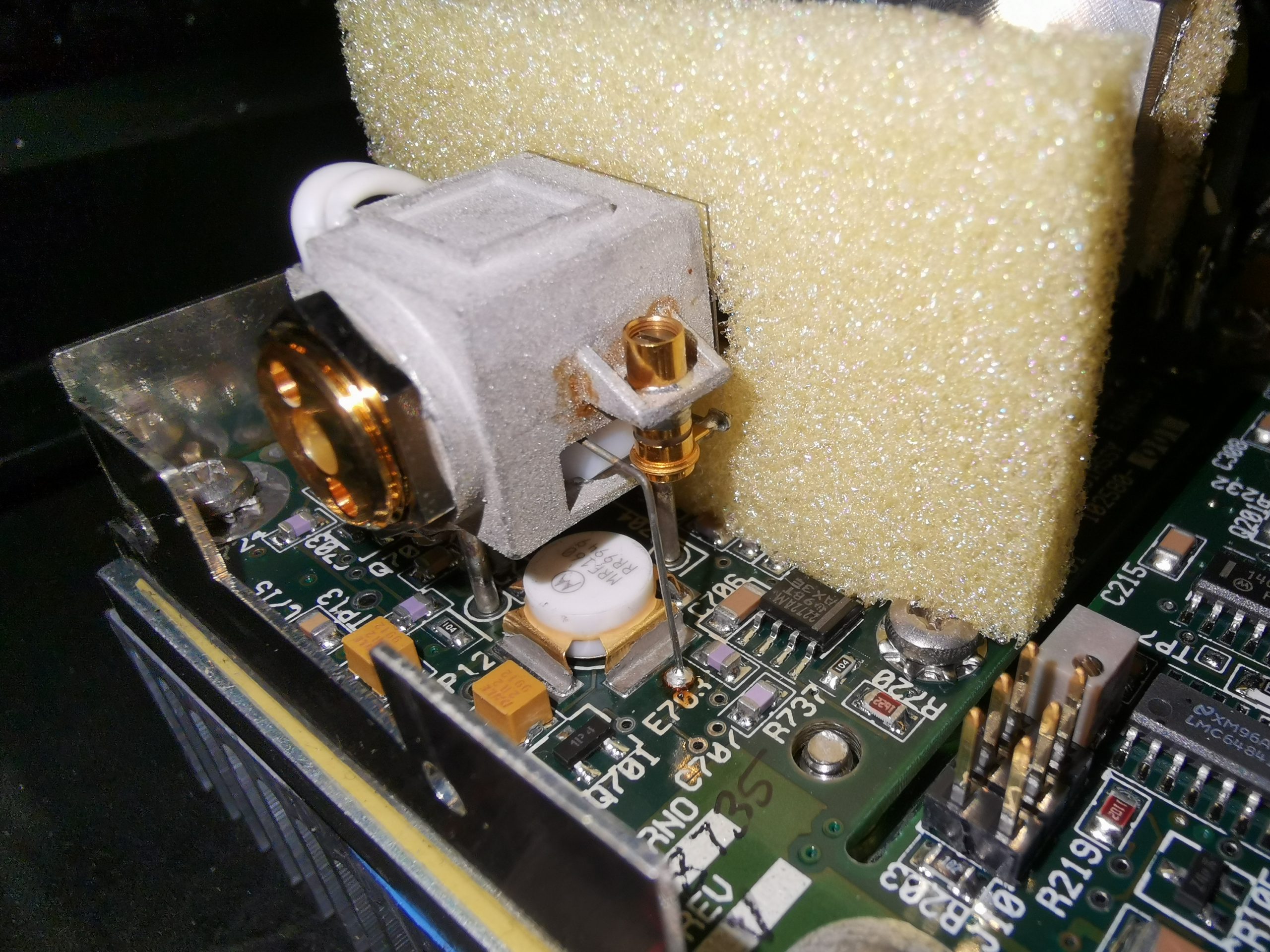
Microwave Cavity
The other end of the physics package has the Rubidium Vapour cell, photodetector & step recovery diode housed in a microwave cavity. The coax cable feeding the 60MHz signal from the synthesizer can be seen going through a passthrough in the brass plate. Inside is the SRD & photodetector. This section is heated by further thermally bonded MOSFETs on the sides of the cavity housing.
Rubidium Lamp Bulb
Loosening the locknut on the lamp housing, and gently unscrewing the gold-plated holder allows removal of the bulb. The tiny bead of Rubidium metal can be just seen in the pinch of the bulb, with a couple of spots on the outer part of the bulb. The lamp voltage on this unit was around 6.21v, however after removing the lamp & giving it a clean, and warming it to get the Rubidium to re-condense in the pinch got the voltage up to 7v – this is plenty healthy for one of these.
There’s definitely some wear though – there’s a slightly yellow tinge to the glass, and from what I have read in a couple of scientific papers on the subject of Rb Lamp Failure Modes, this is probably Rubidium Oxide, caused by an interaction between the metal & the glass.
rubidiumRubidium GlowA final photo shows the very pretty colour of these lamps – it’s a pastel purple colour, and surprisingly the camera picks this up very well.
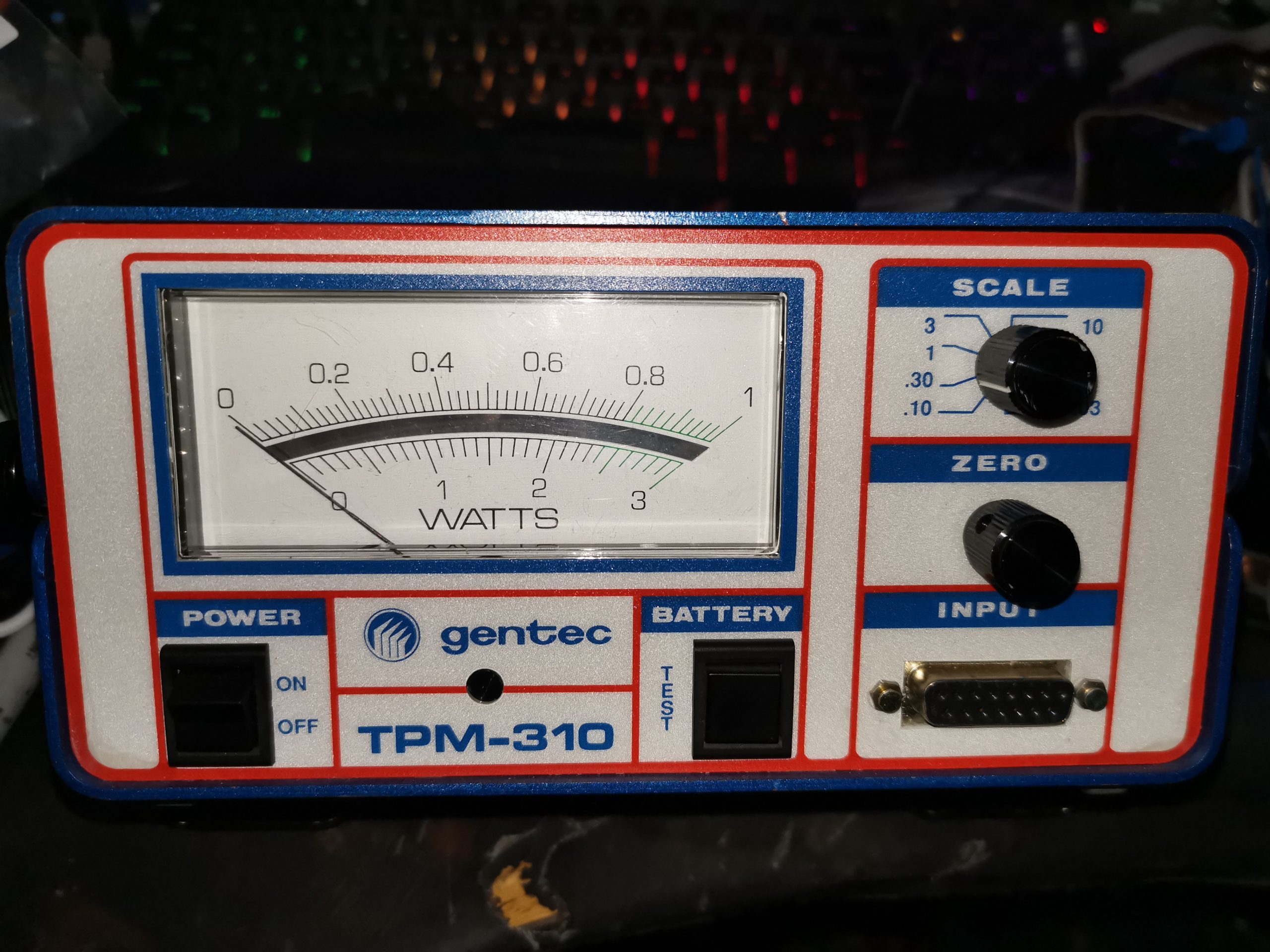
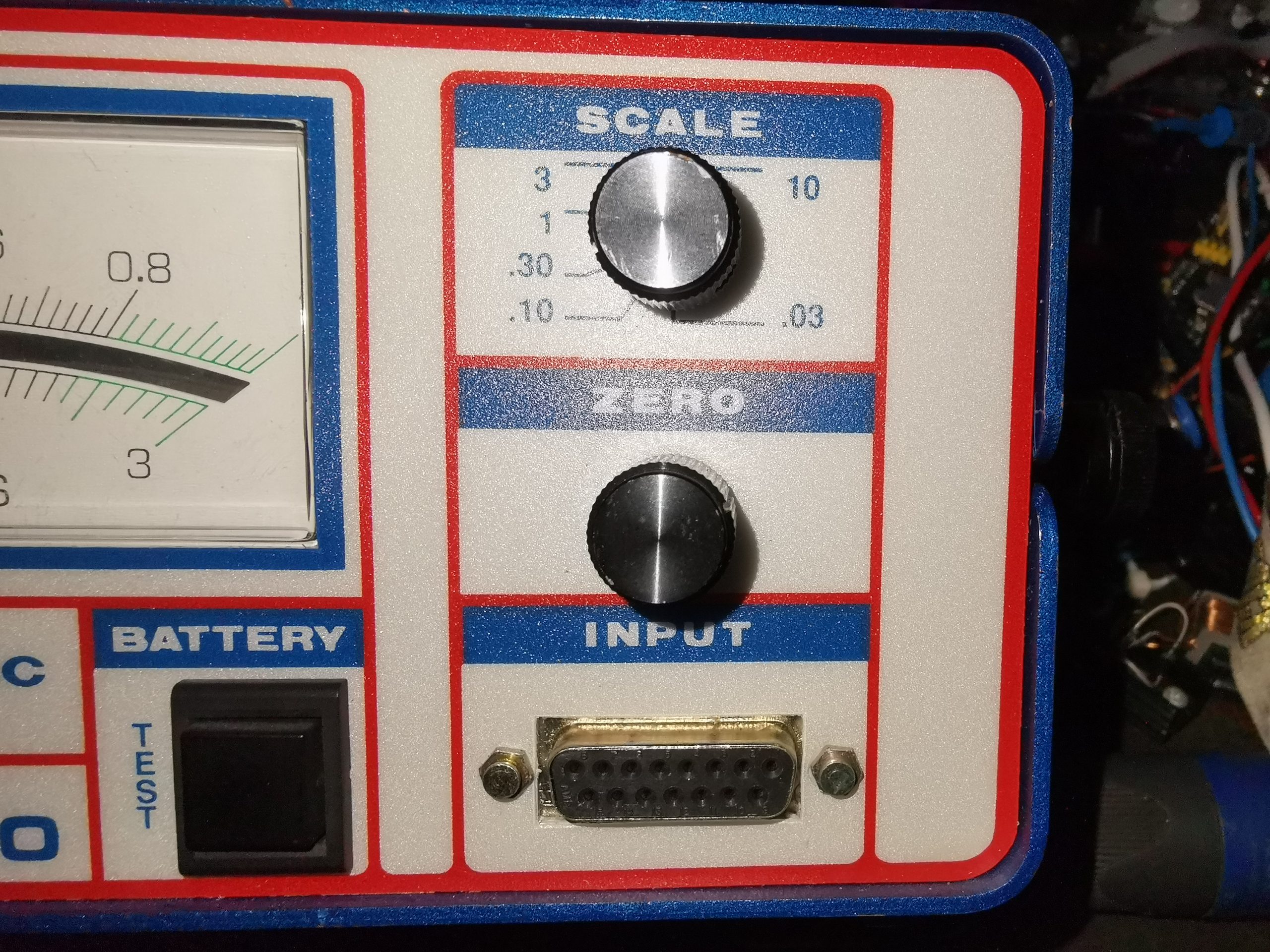
Here we have an optical power meter, vintage 1991! This is a Gentec unit, with scaling to to handle up to 10W with a suitable powerhead. Powered either with 4 PP3 9v batteries, or from a 24v DC jack on the rear, this unit is quite versatile. I managed to get this for very little money on eBay – similar units cost over £1,500 new – without a powerhead.
Meter Movement
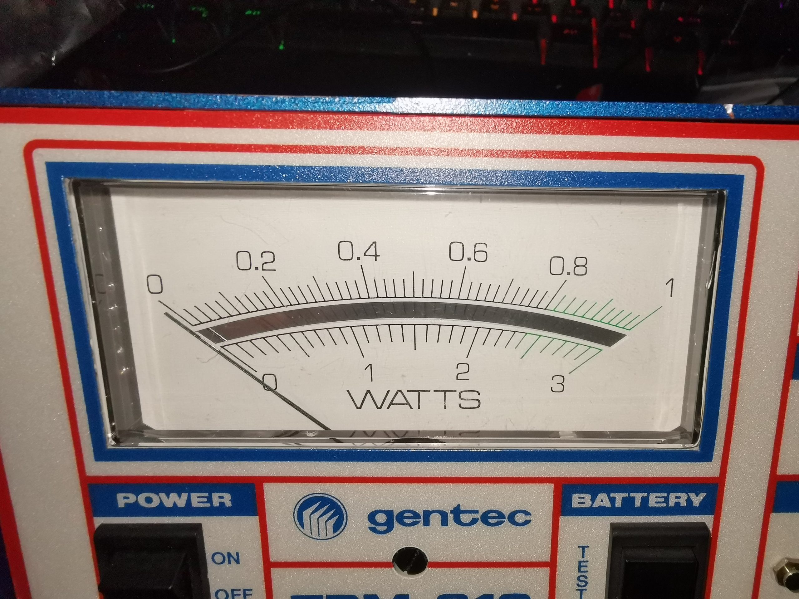
The unit is completely analogue, with no digital circuitry at all. The meter movement has a mirror on the scale for parallax correction. Under the movement are the main power switch & battery test switch, which uses the meter itself to show battery level.
User Controls
The right hand side of the unit has the Zero adjustment, the range switch, and the DB15 powerhead input connector.
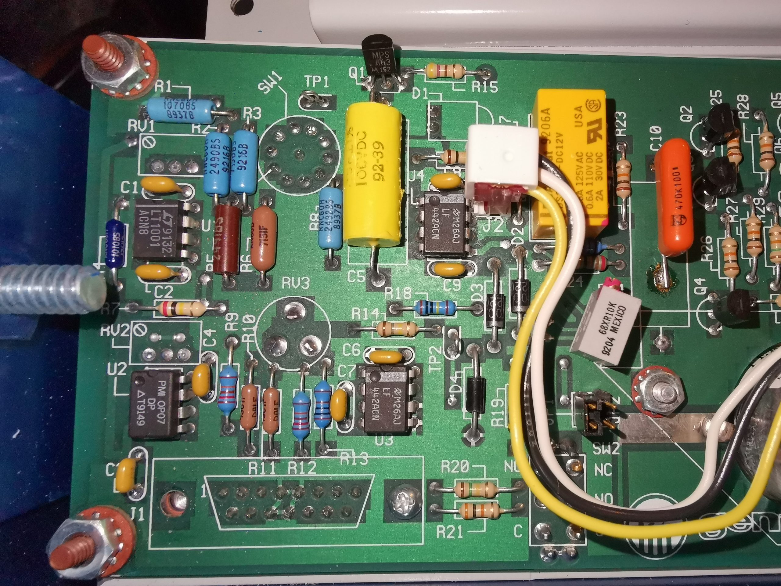
Board Left
Taking the unit apart, with just 4 allen screws on the case reveals the mainboard. There’s very little back here! The active components are just Op-Amps – An OP07 ultralow offset in the bottom left corner is most likely the front-end amplifier, along with a few LF442ACN precision JFET input devices in the same area. The other amplifiers are LT1001 precision devices, with a 10mA output current capability. Most of the passives in this area are also high-stability & high precision parts.
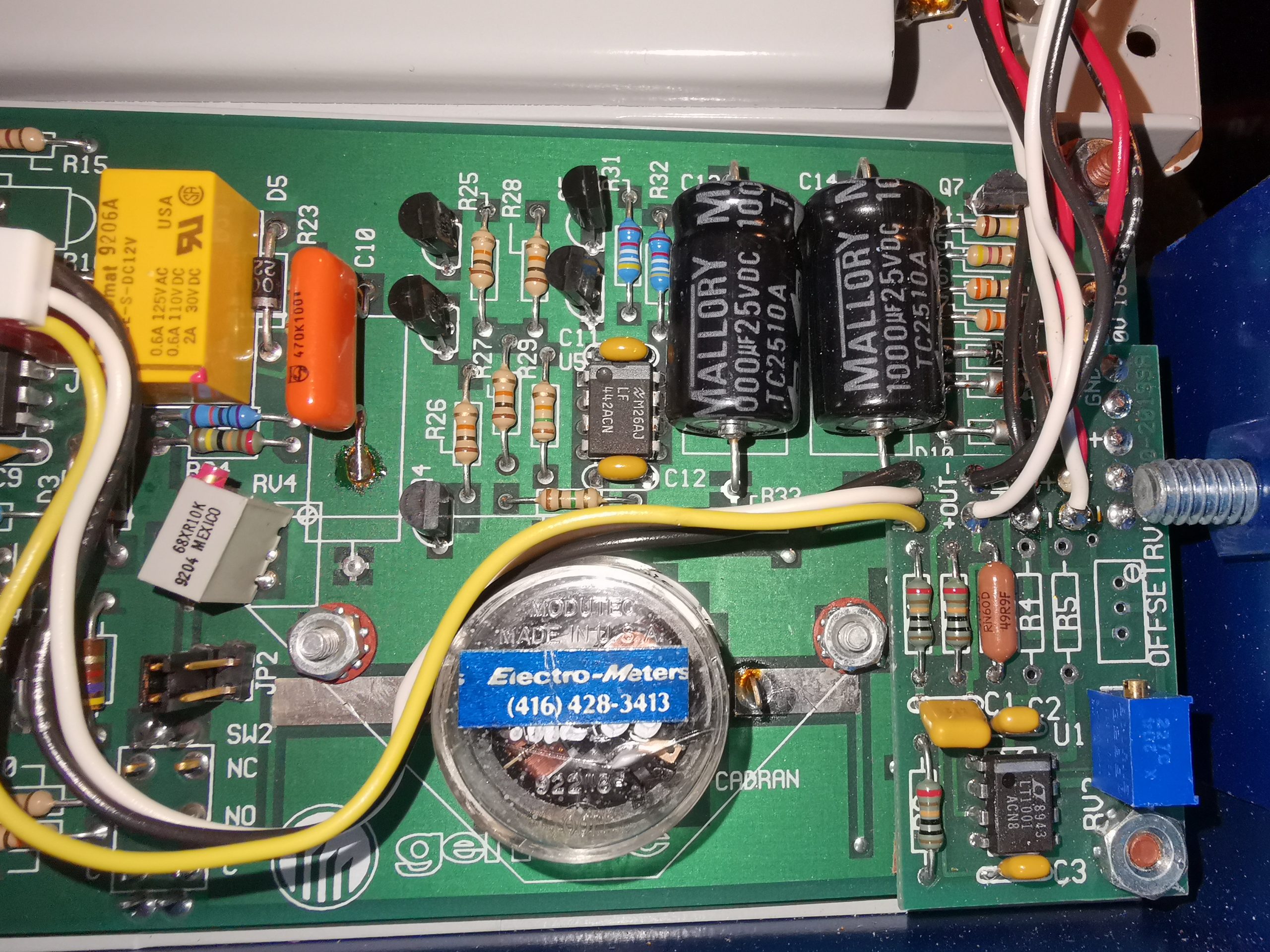
Board Right
The other side of the board handles the meter movement, and the power input section. There is a small daughterboard with another LT1001 Op-Amp on board, along with some passives, and the battery inputs go into here, however I’m not exactly sure what this is doing – there is another connection to the rear panel 1v analogue output BNC jack, so it may be the driver for that section. The 24v input is a single DC rail, however the 4 PP3 battery holders are wired as parallel pairs of batteries back to back, so a split +9v/-9v supply is generated.
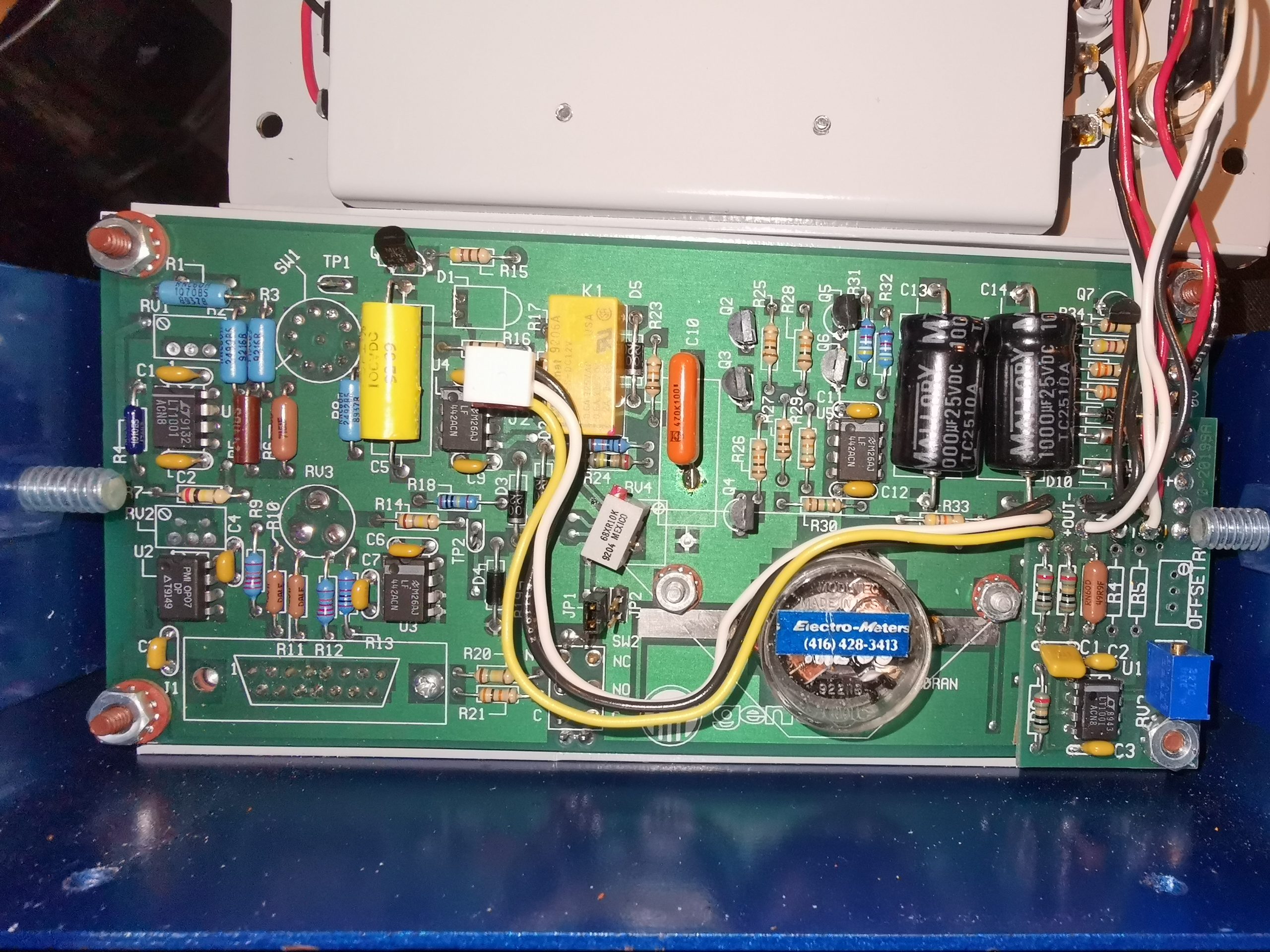
Main PCB
An overall view of the board shows the wiring back to the battery holder, 1v analogue output jack & DC input connector.
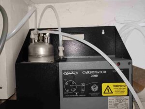
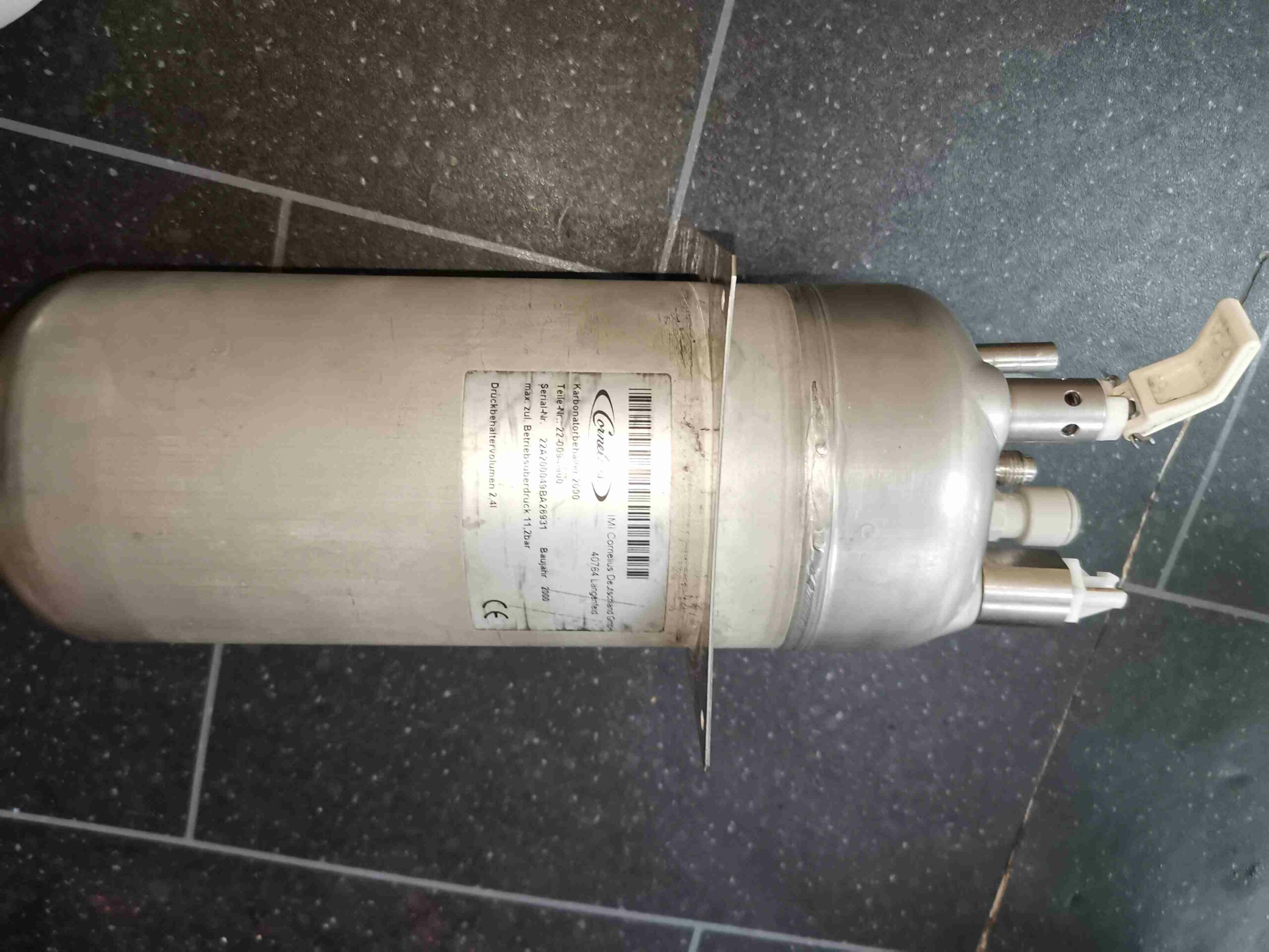
To run my postmix rig, I needed a carbonator, to turn tap water into soda water. These units are very common in pubs in the UK, and are very simple in construction. The unit is fed water at about 3 bar from the water main & food-grade CO² at about 5 bar from a regulator, and soda water appears at the outlet.
Pump Motor
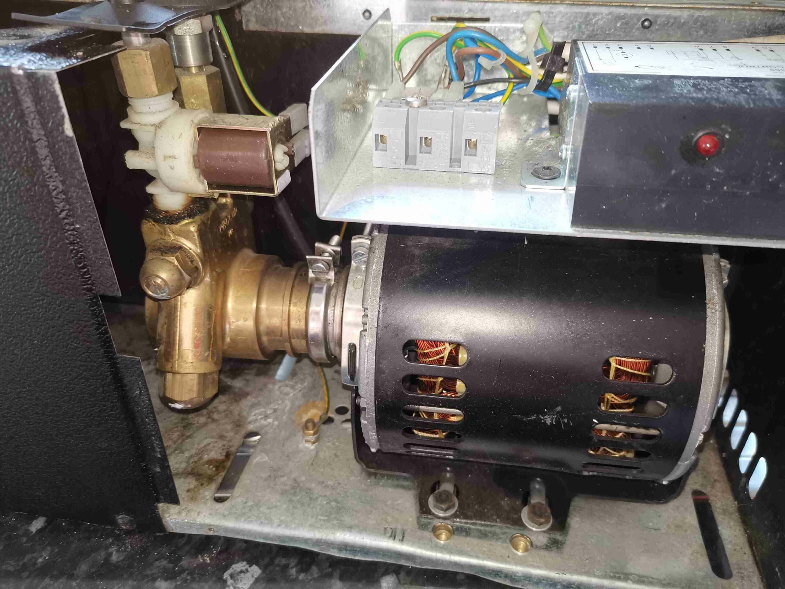
To raise the incoming water pressure above the pressure in the carbonator tank, the unit contains this rather large vane pump, with a 230v induction motor for mechanical power. There’s a solenoid valve on the inlet to prevent water flow when the pump is off, and the motor is automatically controlled.
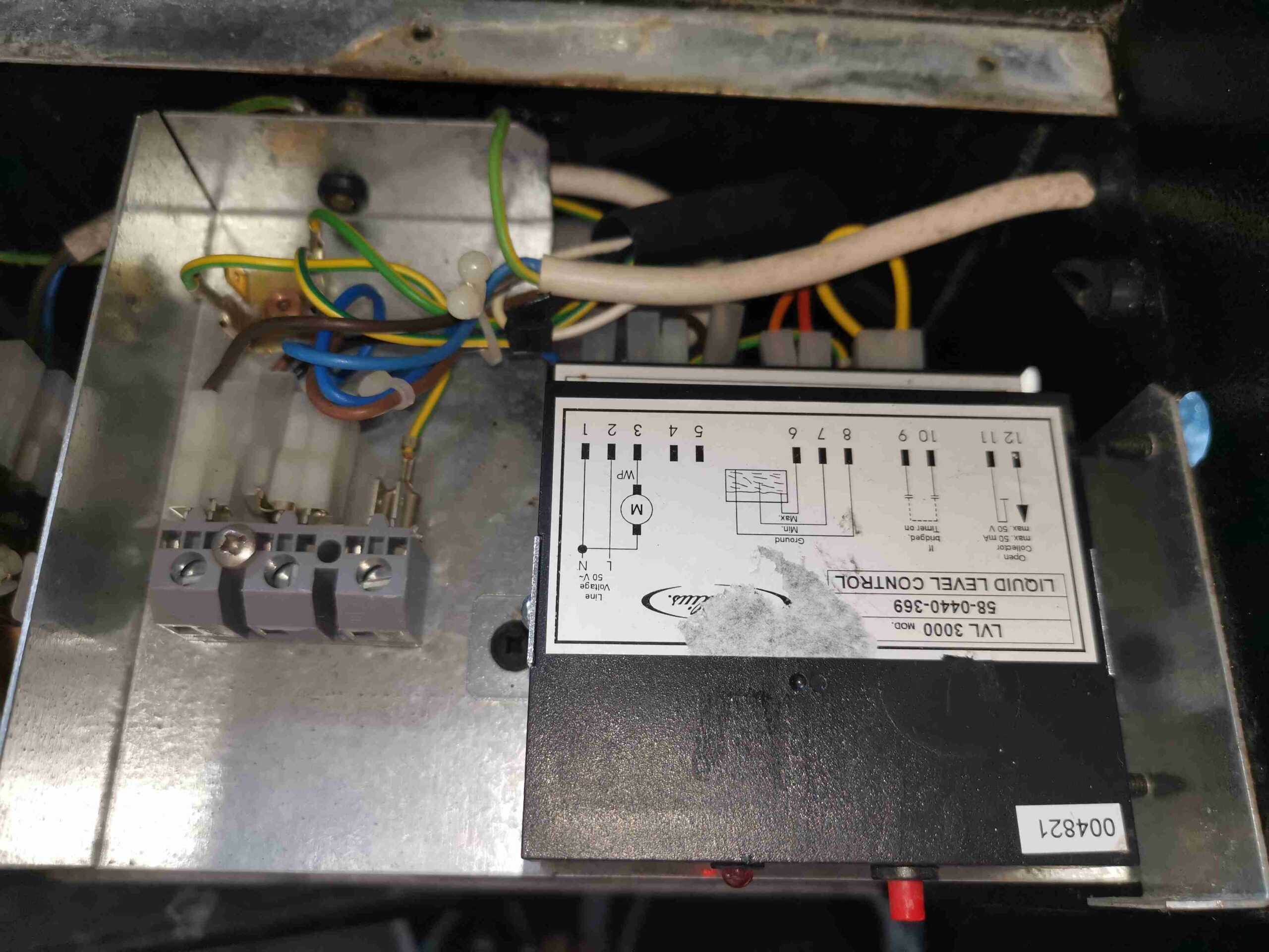
Electrical
Above the pump is the electrical wiring & control. This is a simple level control, and reads a conductance probe inserted into top of the carbonator tank, activating the pump when the level in the tank drops below a minimum level, and shutting it down when a max level is reached. There’s also a timeout function, which shuts everything down on lockout if the pump runs longer than a preset time interval as protection in case of such issues as a leak in the system, or dry running without a water feed.
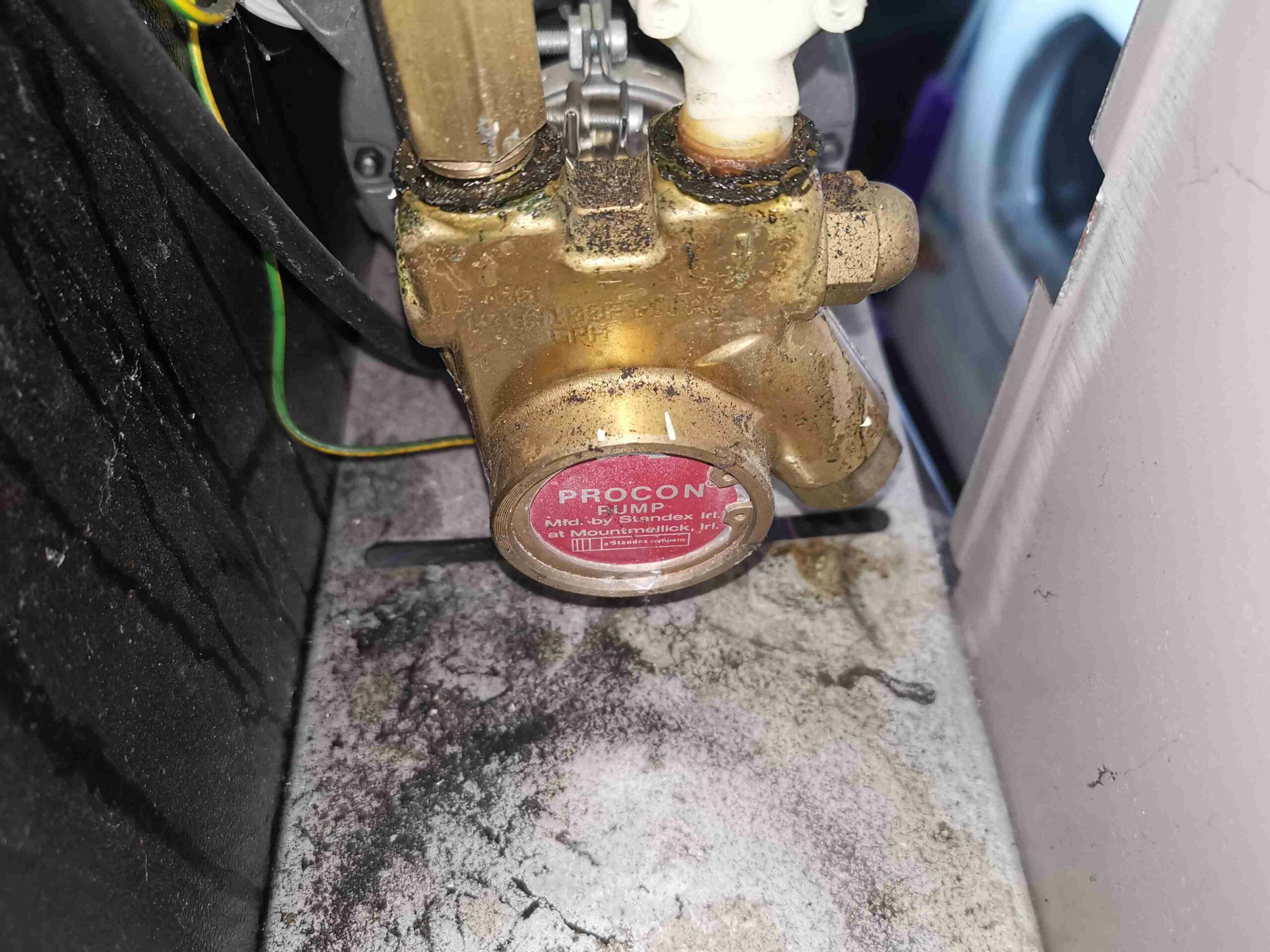
Carbon Vane Pump
Coupled to the front of the motor is a carbon vane pump. This type is very commonly seen in food-grade equipment, such as these units, and commercial coffee machines. The unit has a suction strainer, and a built-in pressure relief valve to stop the pipework exploding or the motor from burning out if there’s a blockage in the outlet line.
Carbonator Tank
The final & main part of the unit is this 115mm diameter stainless steel tank, with fittings at the top. This is pressurised with CO², and water is sprayed into it through an orifice. This spray increases the surface area of the incoming water, making it absorb as much of the gas as possible. There’s a pressure relief valve at the top, just in case the internal pressure reaches dangerous levels.
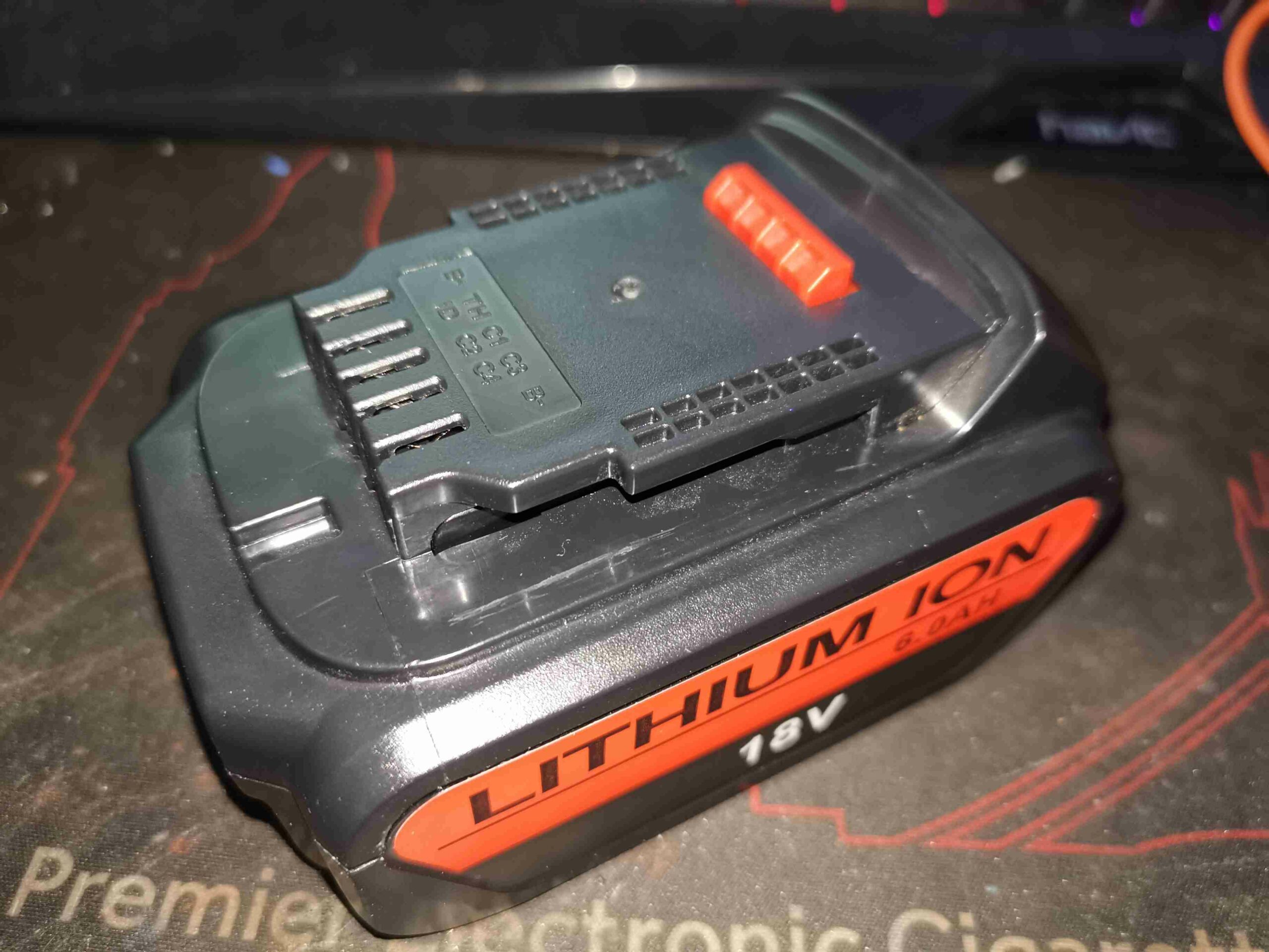
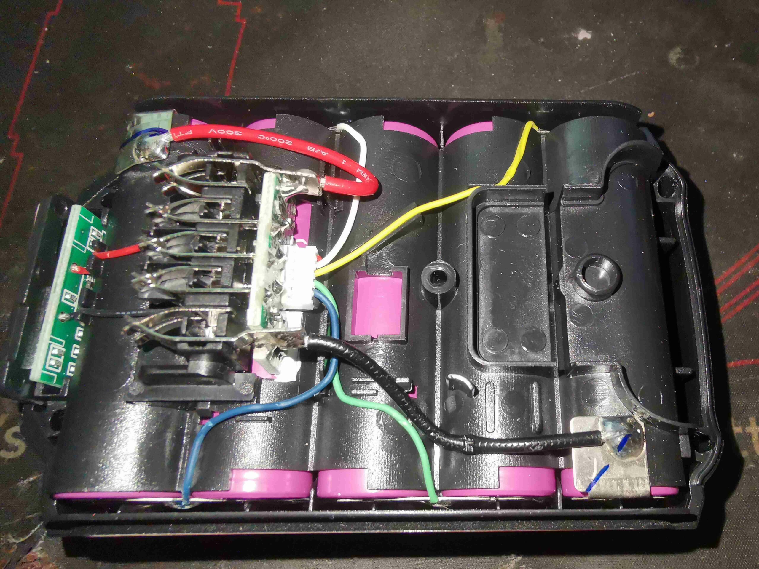
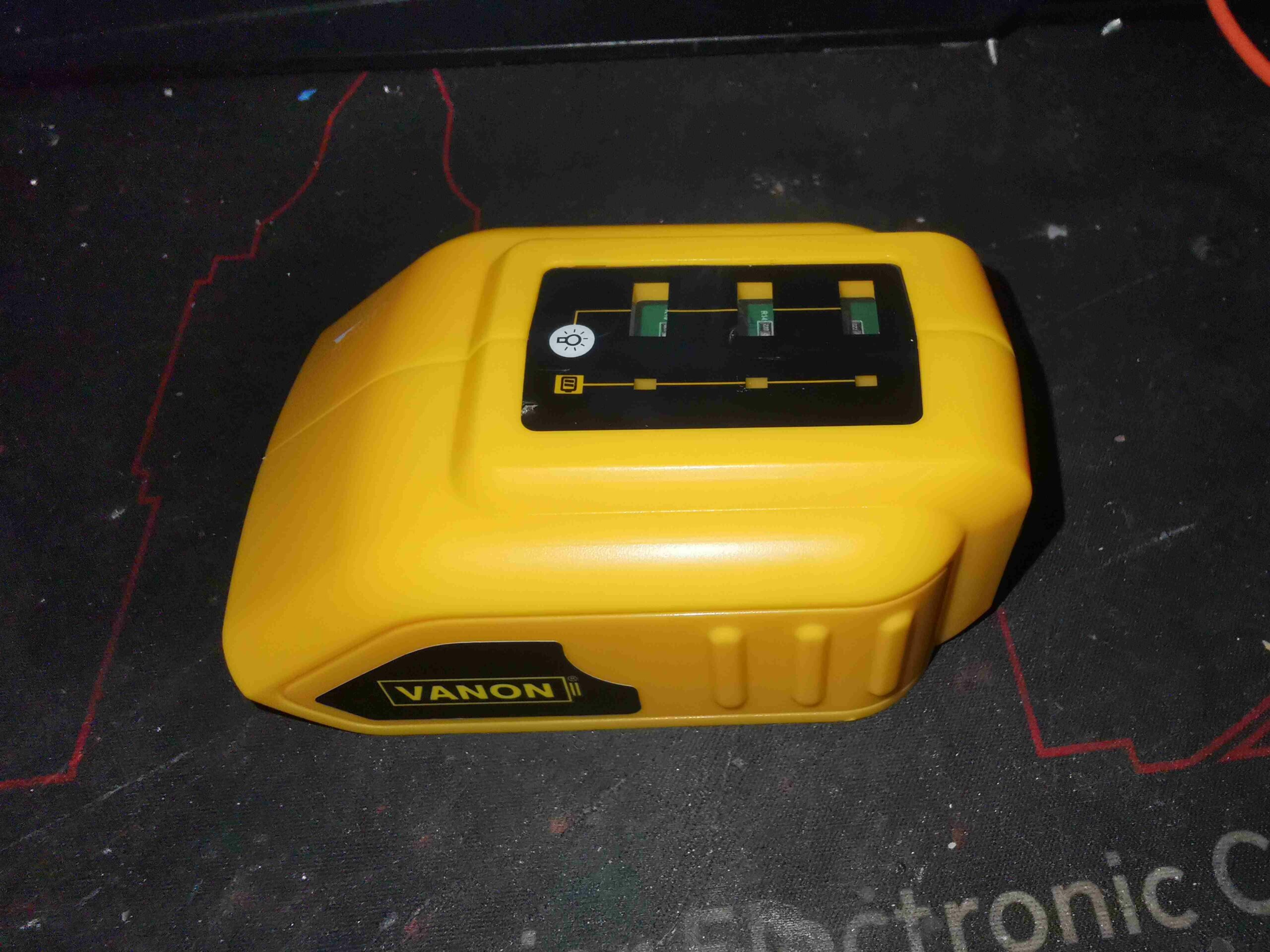
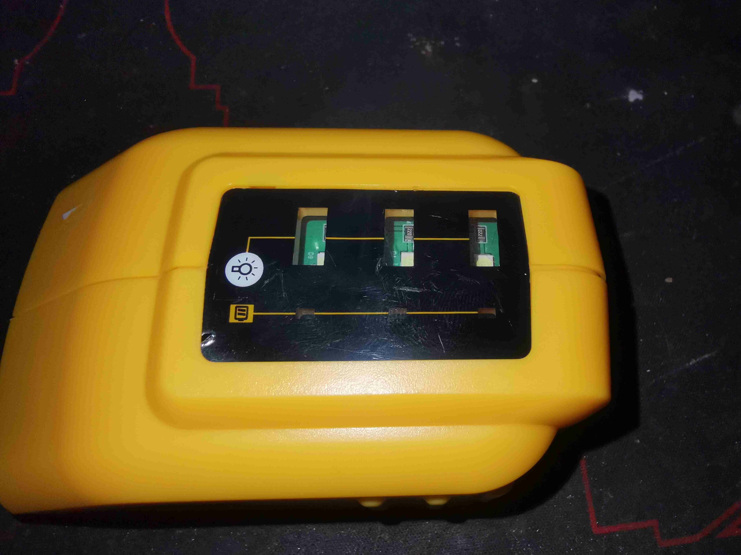
I bought two of these packs for my new DeWalt combi drill, as the branded packs are very expensive and there’s unlikely to be much of a difference in cells used. I was a little mistaken on this, as you’ll see!
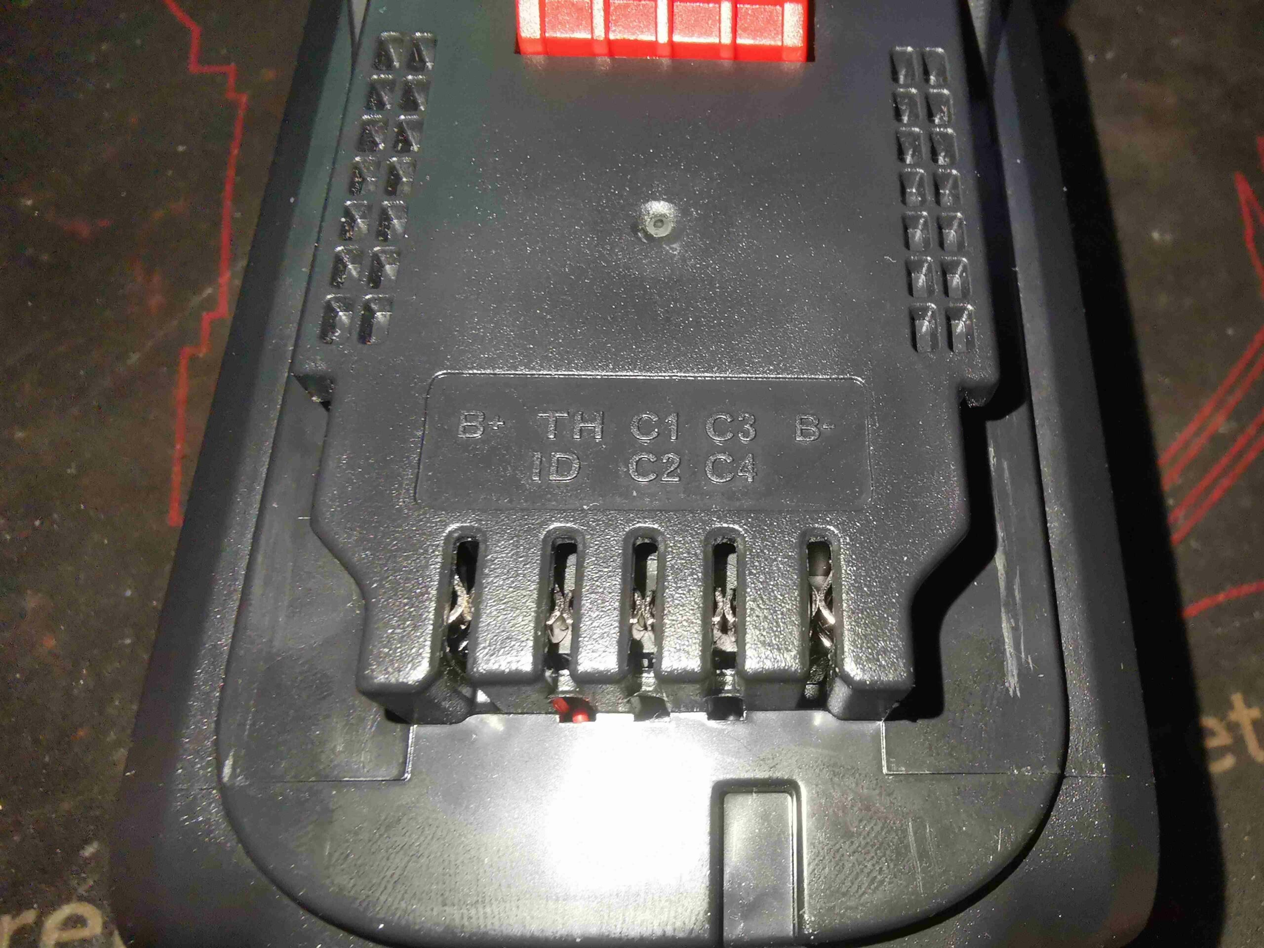
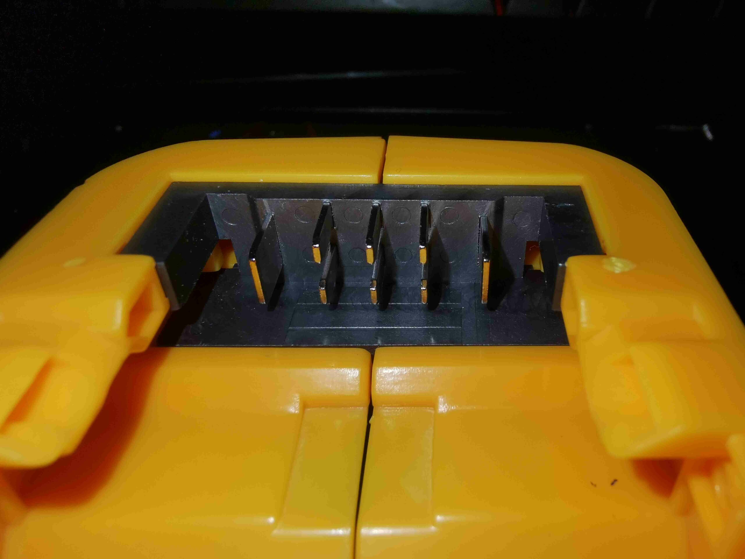
Battery Terminals
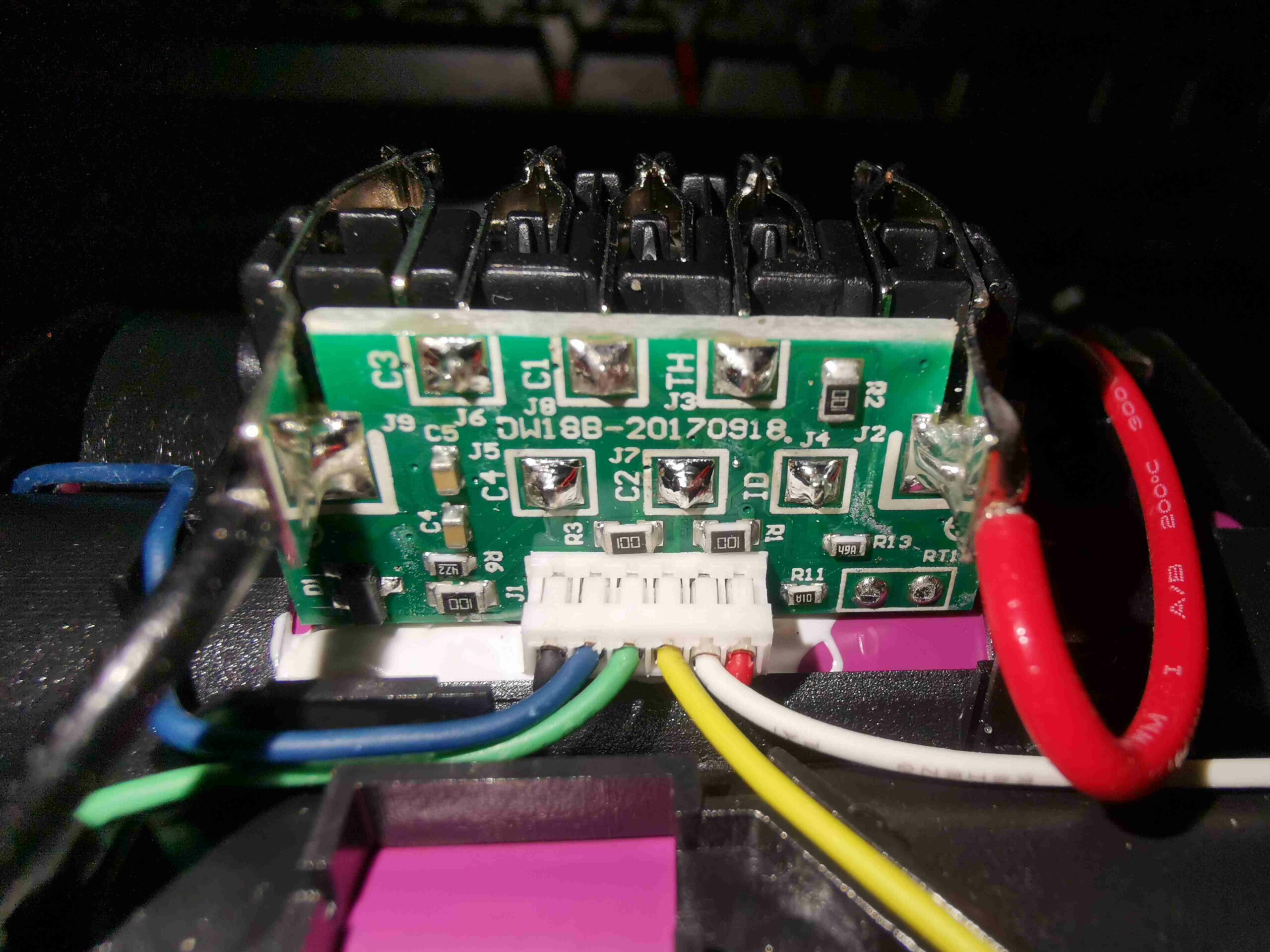
The top of the unit has the battery connections, with all the cell balance lines, along with an ID pin, and a TH pin. The TH pin connects a 10K NTC thermistor up to B+.
Battery Label
The bottom of the unit has the rating & warning label. This claims to be a 6Ah pack, but it’s nowhere even close!
Top Cover Removed
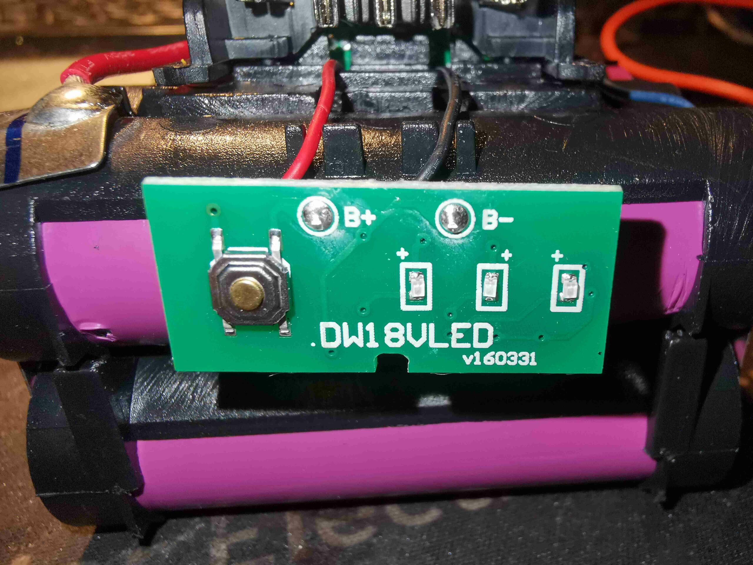
Removing 4 Torx screws gives access to the internals. The cells are all fitted into a plastic holder. There’s a small PCB holding the connector pins, and all the cells connect up to this for the balance outputs. There’s a small PCB on the side of the pack that holds the components for the battery meter.
Connector PCB
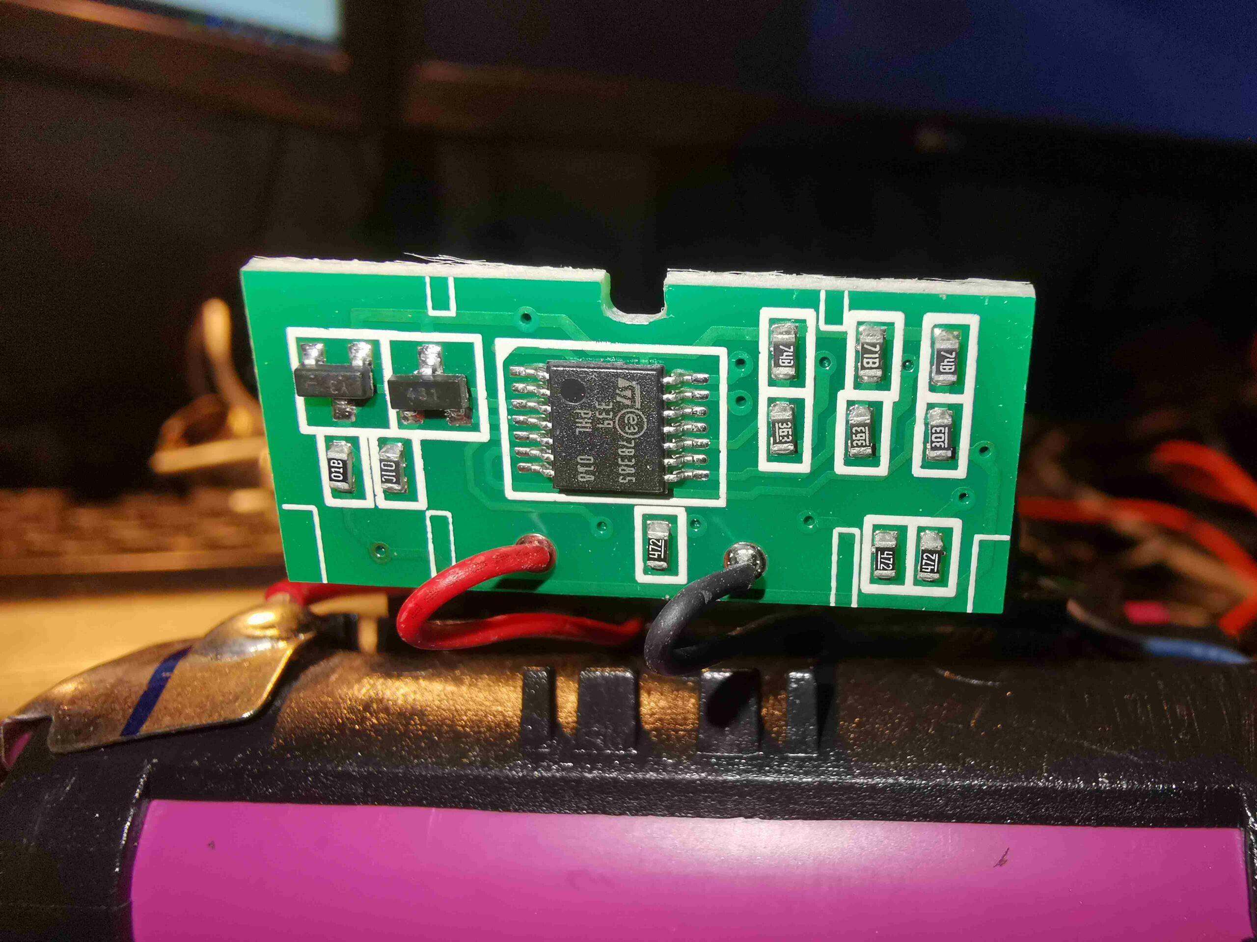
The back of the connector PCB has some passive components, but not much else. There’s the connections for the NTC at the bottom right of the board. There is an IC on this board, on the other side, but without desoldering all the pins, it’s not possible to see properly as it’s mainly hidden by the connector frame.
Battery Indicator LEDs
Not much on the front of the battery meter board, apart from the 3 bright green LEDs and the tactile switch.
Battery Indicator Components
The other side has a small ST microcontroller, a TL431 shunt reference, and some other passives.
Cell Links
All the cells are linked together with hefty interconnects, as expected for a high current pack. This is laid out as a 5S2P configuration, giving 21V max, 15V flat. Unfortunately I can’t see any markings on the cells – they may be off brand, or pulls from other products.
I figured as I always do with Chinese battery packs that the stated capacity of 6Ah was too good to be true, so I ran my usual cycle tests to see what the real capacity was, and was met with the following results:
Cycle Number
Pack A
Pack B
1
3969mAh
3917mAh
2
3963mAh
3947mAh
3
3961mAh
3956mAh
4
3953mAh
3959mAh
As can be seen from the table, these packs are 4Ah, not 6Ah. 2Ah cells sort of make sense for a pack like this, as the high-current capacity cells tend to be a lower capacity.
Since I got my new DeWalt combi drill, I needed a way to charge the batteries without having to resort to sticking blade terminals into the pack connectors – I didn’t purchase the branded charger, mainly due to cost. I also have a very capable multi-chemistry charger that handles multi-cell lithium packs with no issues, so I saw no need to replicate things. This little gadget was ordered just for it’s main pack connector; I can then use this to make up a charger adaptor cable. What this normally does is allow the use of DeWalt XR battery packs to charge mobile devices via 5v USB outputs, so there’s going to be some kind of DC-DC converter in here. There’s also a “charge level indicator” built in, which doesn’t actually do anything sensible – even on a flat battery pack, showing a single LED on it’s charge indicator shows the full 3 LEDs on this unit.
The remaining feature is a trio of white LEDs to function as a torch, but it’s less than stellar in the brightness department. Given that there’s not much in the way of control inside the battery packs themselves, I reckon this unit could actually overdischarge a pack, causing damage.
Torch LED & Charge Indicator
The top of the unit has a large label with windows in for the various LEDs, and a pad covering the tactile switch to operate the torch function.
Label
The label on the side indicates the unit will operate down to 10.8v, good for the 3S packs, as well as the 18/20V packs.
Pack Connector
Here’s what I was after – the battery pack connector. This has the full compliment of pins for all the balance taps too.
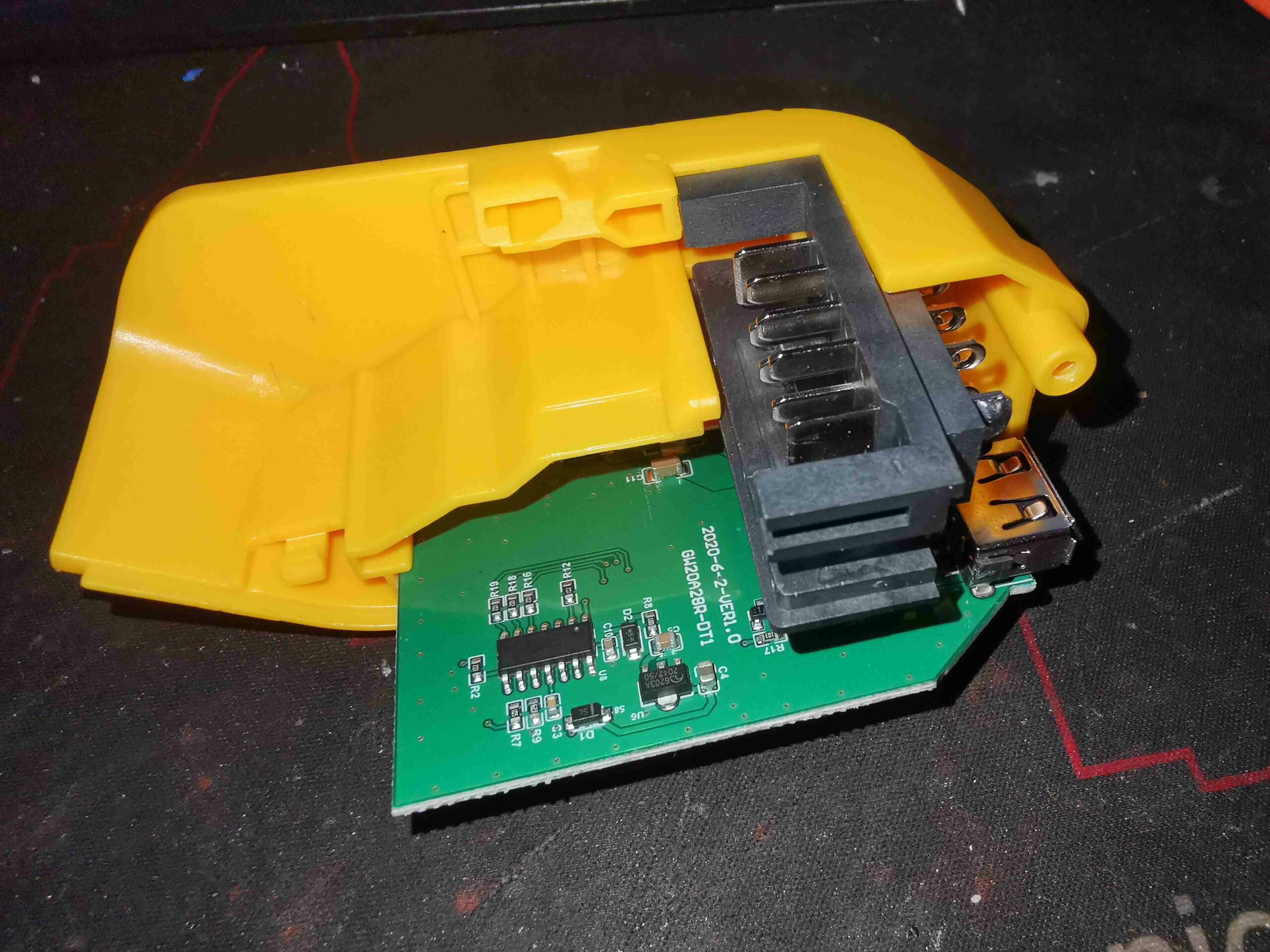
Casing Opened
Removing a label, and a single screw gives access to the internals. There’s not much in here apart from a large PCB, with a few components.
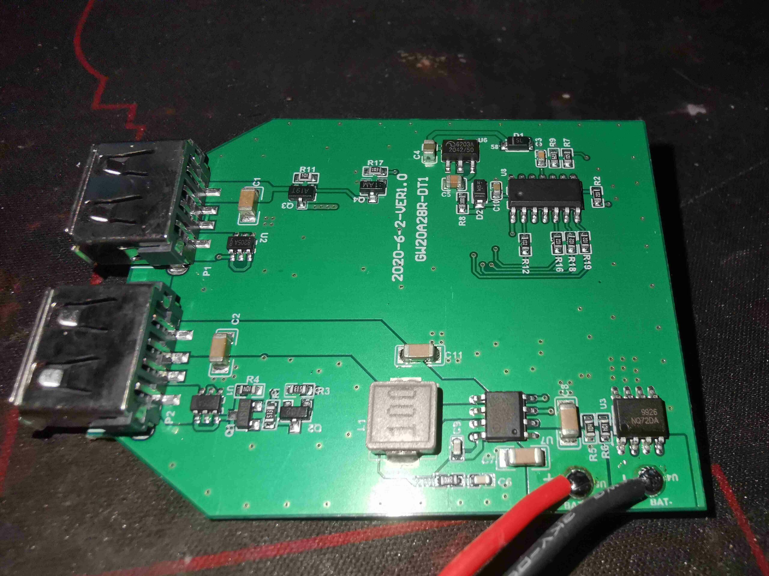
Main PCB
The PCB is pretty sparse. There’s a microcontroller in the top right corner that does the torch LED switching, and the “battery indicator LEDs”. This is completely unmarked, which is very common now for Chinese microcontrollers. The only way I’m identifying this one is via a decap operation on the IC!
The USB ports have MOSFETs in their negative pin paths, probably to switch off the ports if they’re overloaded. The data pins are bridged together on one port, and connected to the DC-DC converter on the other port.
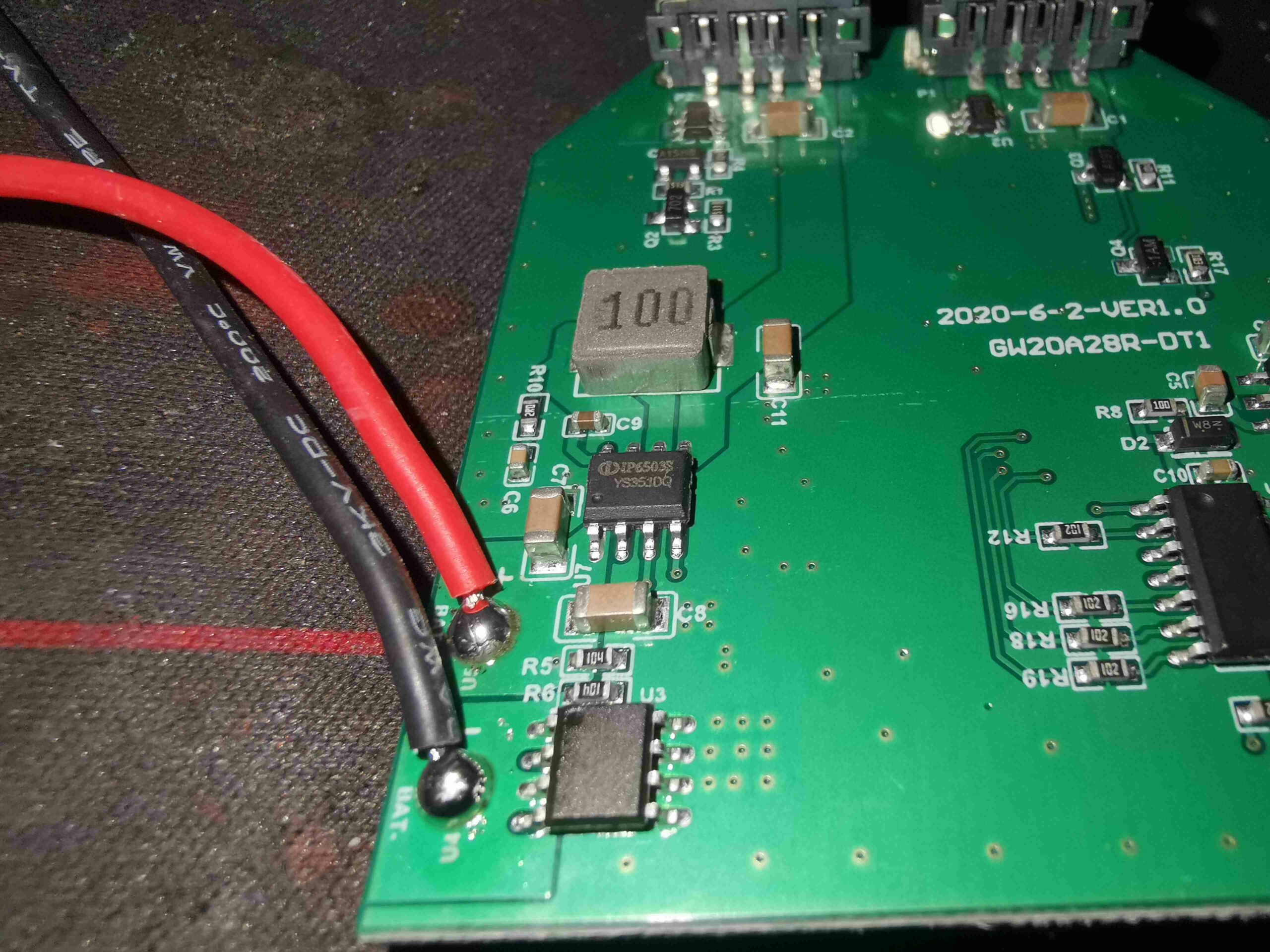
DC-DC Converter
The main DC-DC converter IC is in the bottom right corner of the board, next to the input pins. This is an IP6503S multi-protocol USB charging converter, with a 24W power limit. This explains why the data pins of one of the USB ports is connected back here – it’s doing some communications with the connected device for fast charging. Chinese datasheet below.
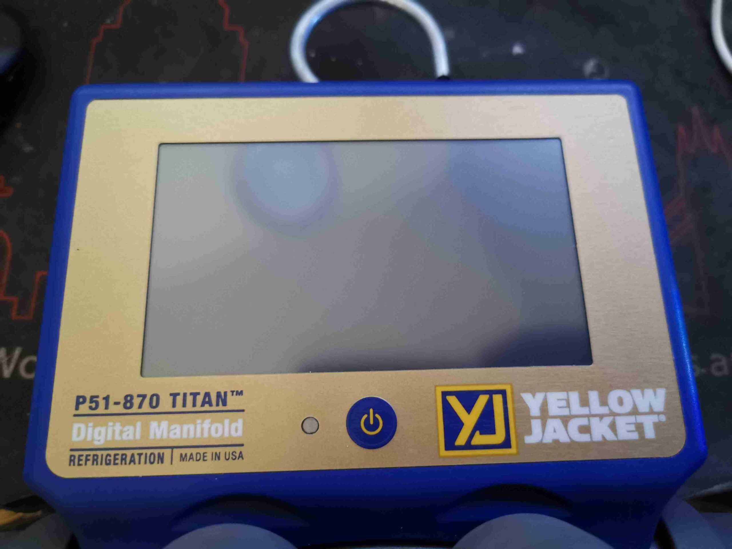
New tool time! I figured now I’m a fully ticketed member of the F-Gas community, I’d treat myself to passing the course by buying a decent set of refrigeration gauges. This is the Yellow Jacket P51-870 Titan manifold, a fully digital unit with all the useful functions built in. Basically an electronic module attached on the top of the standard Titan manifold, this unit performs all the regular functions I’d normally need either a calculator for, or other tools. The front of the unit has just a power button, LED & a large resistive touch TFT panel for display.
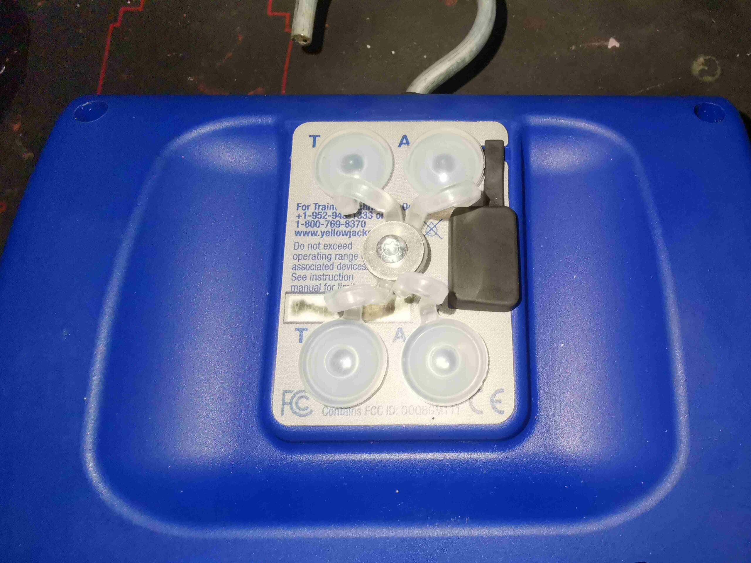
Rear Panel
The rear panel has the ports for charging the internal battery, which is micro USB – this is also used to download log data to a PC from a system processing run. There are 4 3.5mm jacks for the external temperature probes, and vacuum sensor.
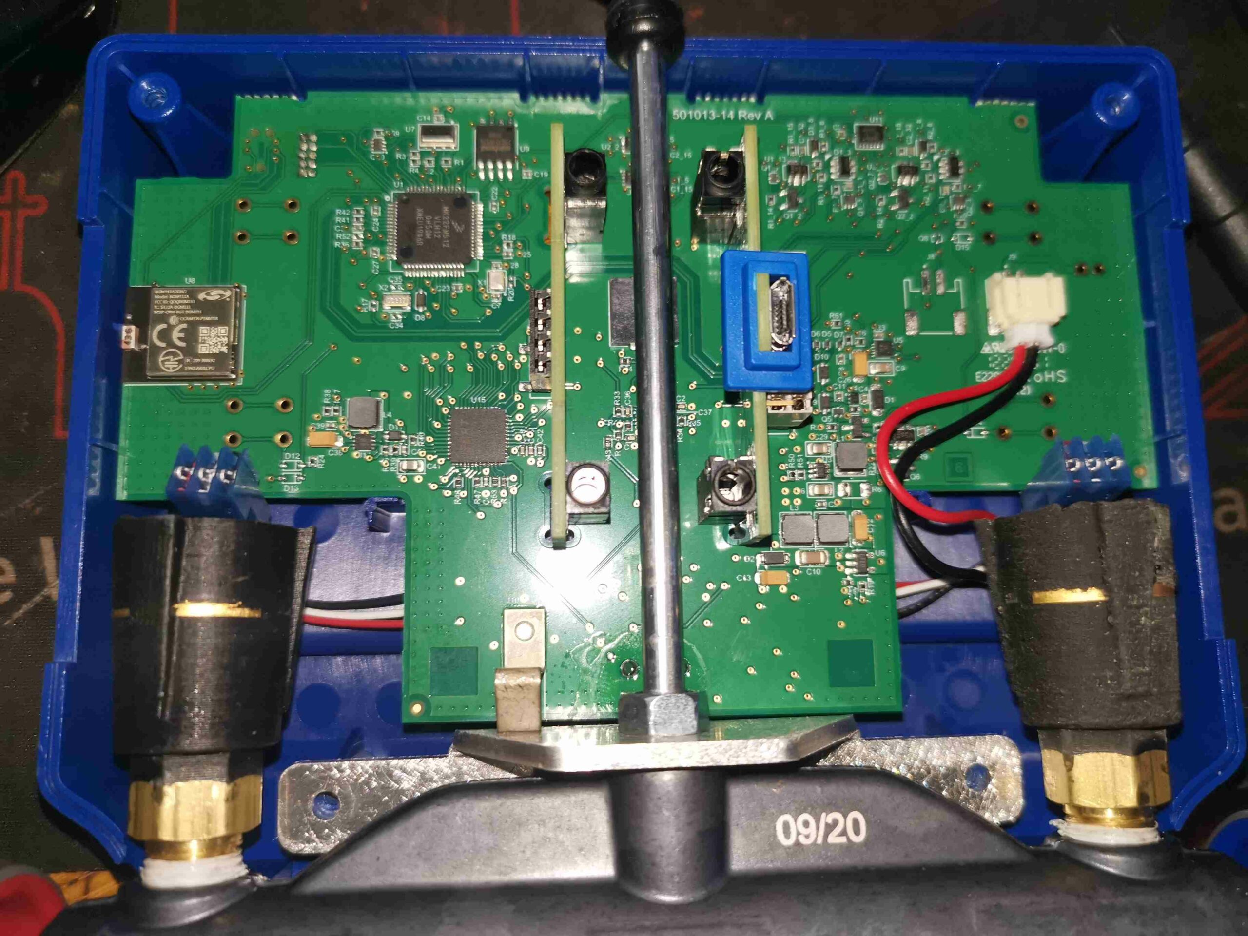
Rear Cover Removed
Removing 4 Torx screws in the back panel allows the clamshell case to come apart, showing the mainboard, and the pressure transducers screwed into the manifold. The aux jacks & the USB charging & data port are supported on small vertical PCBs plugged into the mainboard via 0.1″ headers.
Main PCB Overview
With the pressure transducers unplugged from their looms to the mainboard, the module is free from the manifold section.
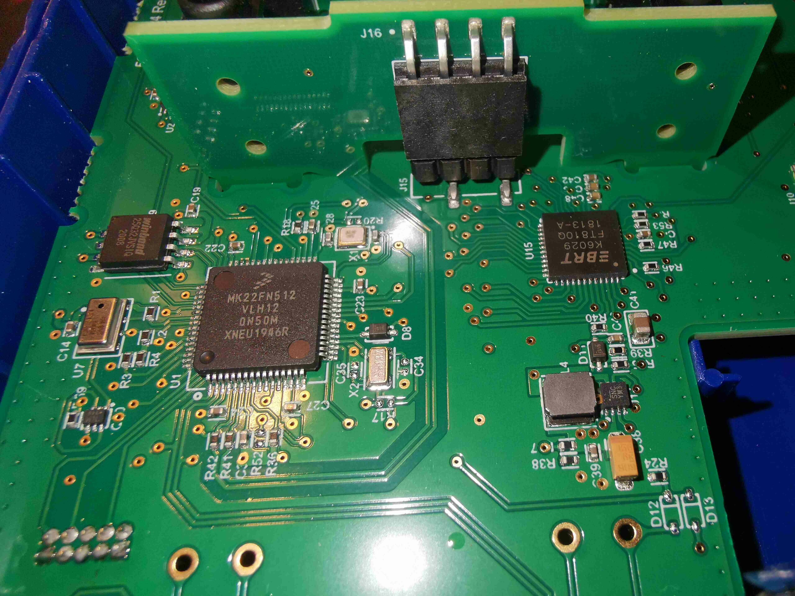
Main Microcontroller
The muscle of the operation here is a Freescale (now NXP) Kinetis K2 Series MK22FN512VLH12 ARM microcontroller. With a Cortex-M4 core at 120MHz, there’s a bit of beef here. The LCD & touch overlay is controlled by a Bridgetek FT810Q Embedded Video Engine. The video controller communicates with the microcontroller via SPI, and the LCD via parallel RGB. There’s some SPI Flash memory up on the left, for log data storage, a Winbond W25Q32JV 32Mbit part. Just under that is a pressure sensor, which I’ve been so far unable to pull a part number off. This is required to assist in calibration of the main pressure transducers.
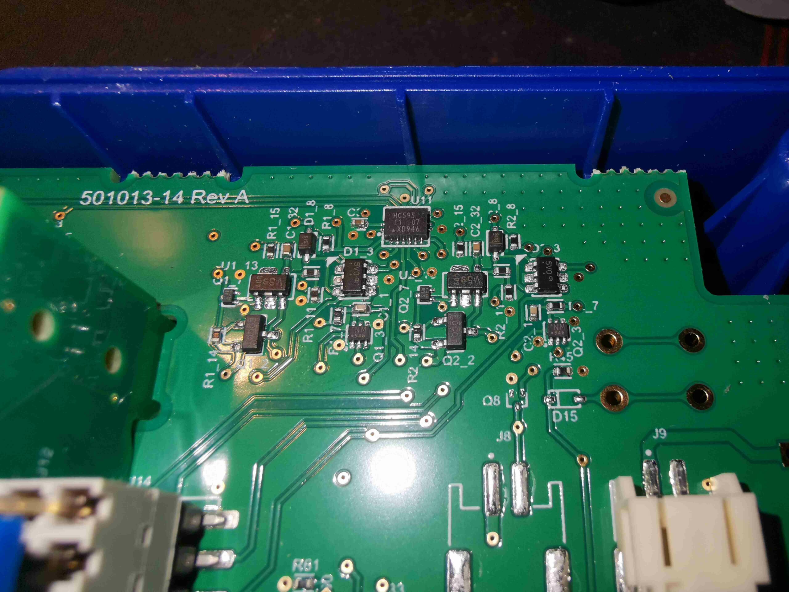
In the top right corner of the board is a 74HC595 shift register, with quite a few discrete transistors & diodes hanging around it. I suspect this is used to switch between two vacuum sensors when both are plugged in – from looking at the waveforms present on the sensor interface, the power does appear to be switched ON/OFF on a single sensor at about 1Hz.
My guess at the moment is that the sensor communications are over I²C, by the 4-wire connection, and the very obvious clock & data line on the connector, but I haven’t yet looked deeply into this.
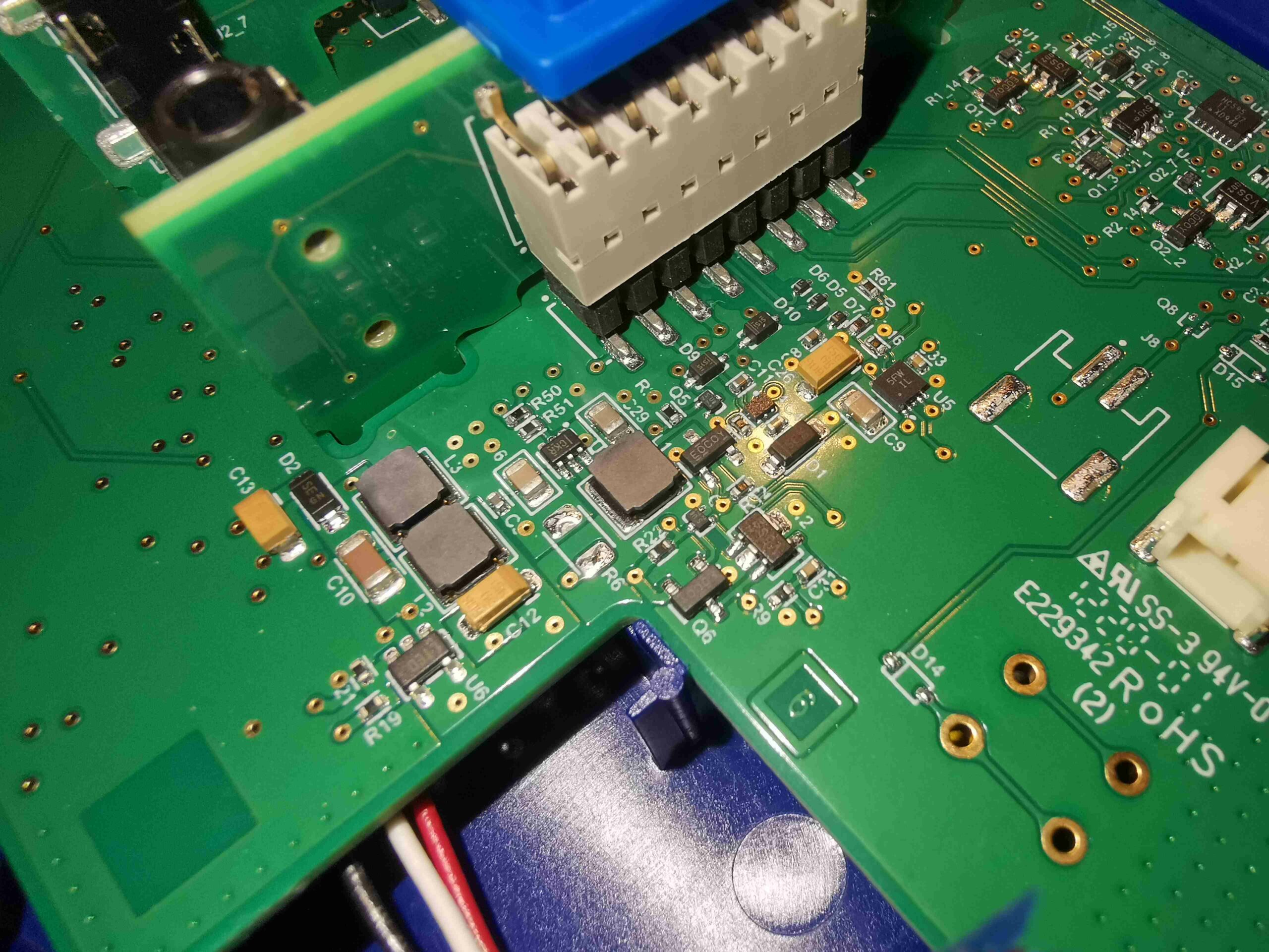
Main Power Supplies
Next to the battery connector (the battery itself is a single LiPo pouch cell, double-sided taped to the front shell, behind the display), are a selection of DC-DC converters, providing all the required voltage rails. No doubt there’s lithium charging control going on here too.
Bluetooth Module
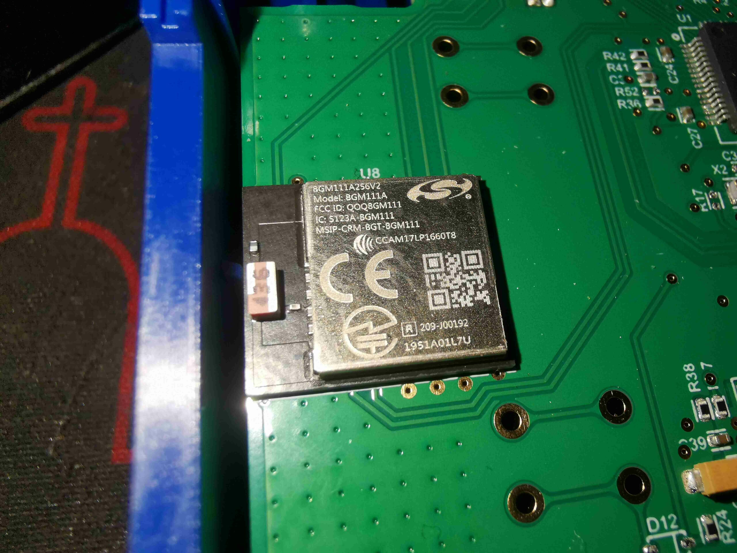
Wireless connectivity is provided for by a Silicon Labs Blue Gecko BGM111A256V2 Bluetooth 4.2 SoC module. These are also fairly powerful parts, with a full ARM Cortex M4 microcontroller hiding inside, clocked at 40MHz. There are as a result two programming headers on this board, in the top left corner, for both this part & the main microcontroller.
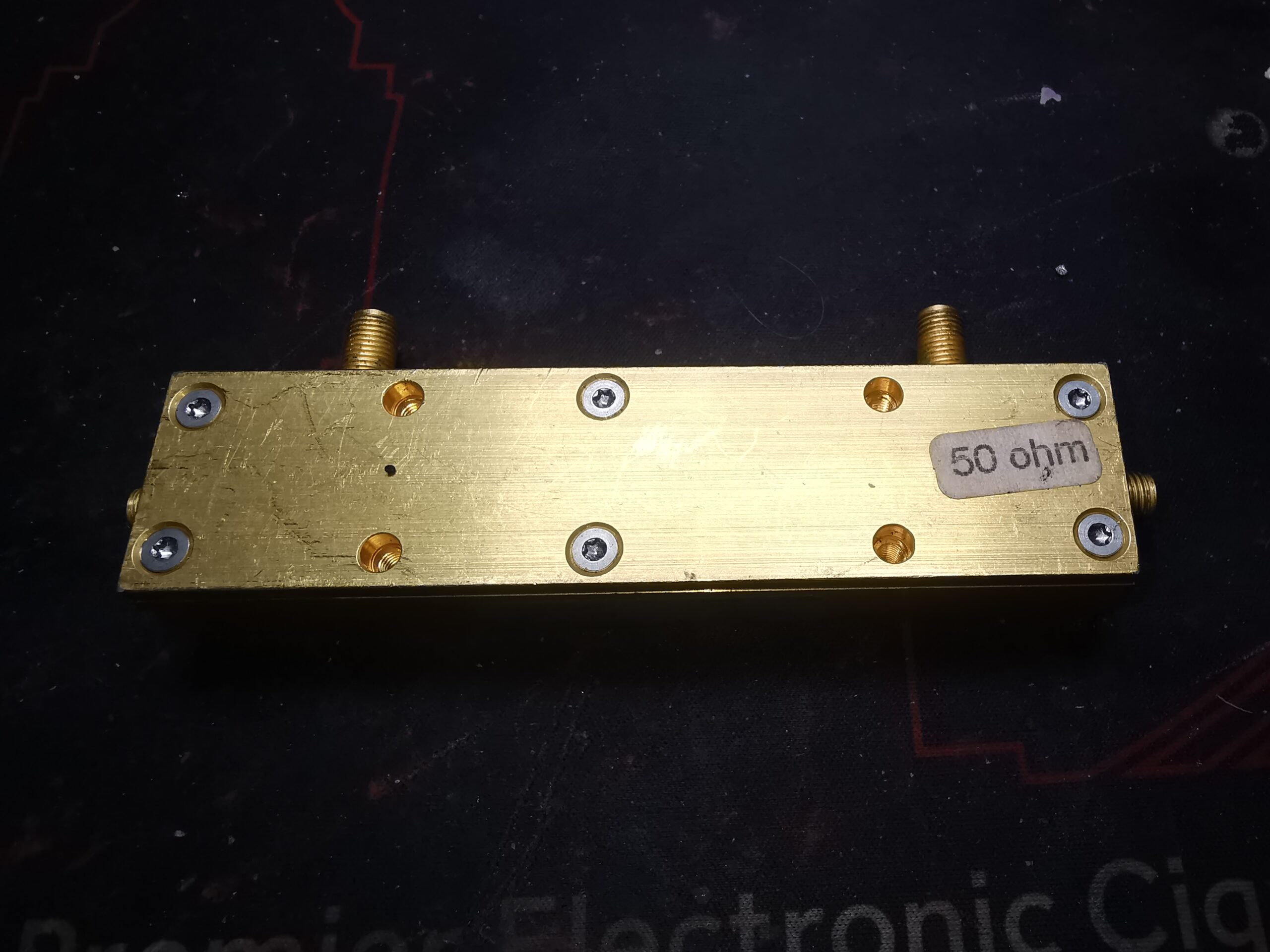
Time for some more RF component teardowns, here’s a very high quality Directional Coupler from HP, I believe this was part of a Vector Network Analyser at some stage. The main body appears to be made of Brass, but the entire unit looks like it’s Gold plated – the shine is far too good to be just Brass! Connections are via SMA connectors.
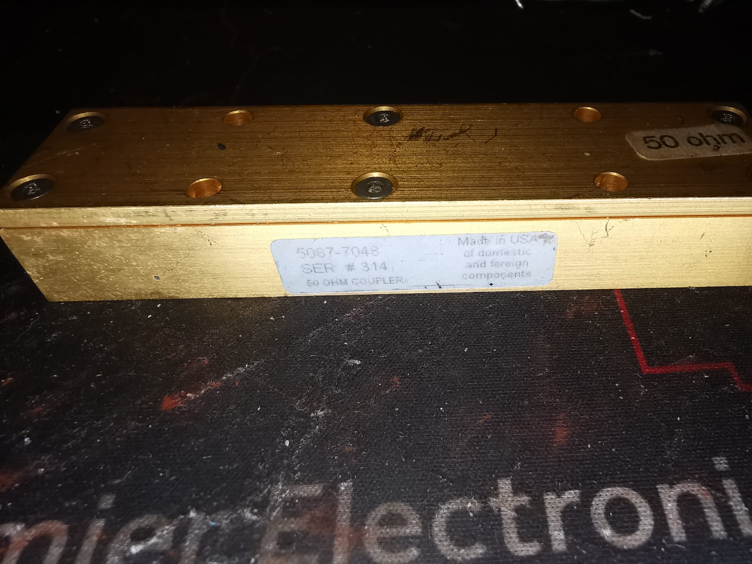
Label
There isn’t much on the label to explain what the specifications are unfortunately. Nothing that can’t be found out with a quick look on a VNA though.
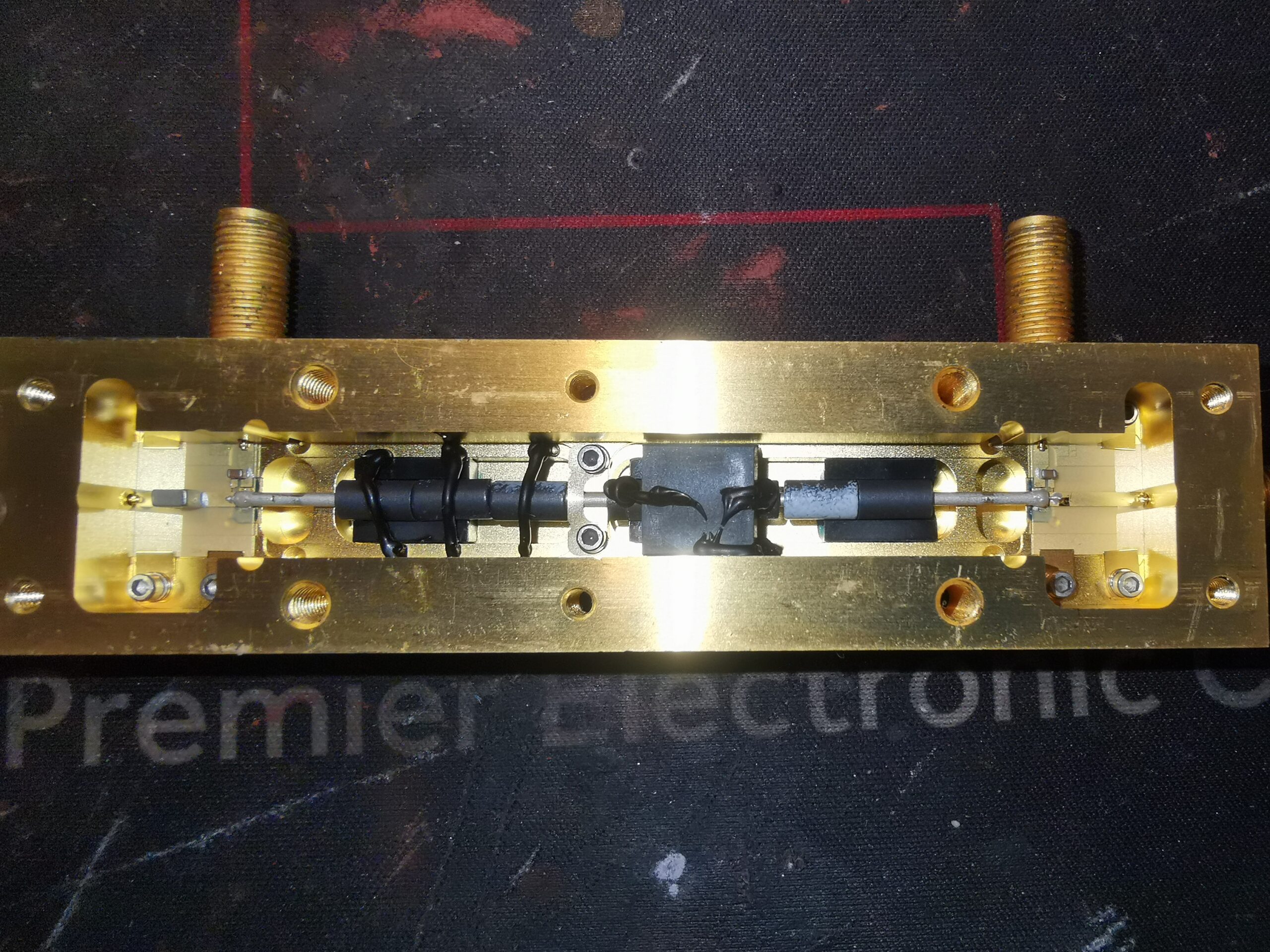
Cover Removed
After removing the 6 Torx screws securing the top cap of the coupler, the internal components are revealed. There is no RF gasket or seal on the top cover, and relies on flat machining for an RF seal.
Internal Components
The internal construction of this unit is a little different from what I’ve seen before in directional couplers. The arrangement is usually parallel copper tracks on a suitable RF substrate, but in this case, HP have used a very small diameter Coaxial cable, covered with ferrite sleeves on the outer shield. The large square block in the middle is rubber, and may just be to stabilise the assembly. It may also be loaded with ferrite powder to give some RF properties too.
The ferrite cores are secured in place with beads of black silicone, again probably to prevent movement under vibration.
Input End
The input of this coupler is AC coupled via a capacitor, and then fed into the centre core of the Coax. The forward power output pin, visible at the top of the track, is coupled to the centre core of the coax by a tiny carbon track making up a resistor, via another ceramic capacitor. The track is more directly coupled via another carbon trace to the outer shield of the Coax. I believe this coupler is damaged, as the carbon trace that goes via the capacitor has a break in the centre, but the coupler does seemingly still work.
Output End
The other end of the coupler is very similar, although with no main line coupling capacitor, it’s direct fed to the SMA here. The reverse power output is connected the same way as the other, with a network. The carbon trace here though doesn’t have a break.
The time has come yet again, to reduce my rack footprint. For the last 5 years or so, this blog has been hosted on a small HP MicroServer Gen8, as at the time I needed a new host machine, and for some reason they were going by their thousands for rock-bottom cash. That machine has faithfully worked 24/7, without many gripes, but it’s time to concentrate things down to requiring less physical hardware.
What’s enabled me to sort this out, is performing a hardware rebuild on my main file server, which has for years been a Heath-Robinson affair.
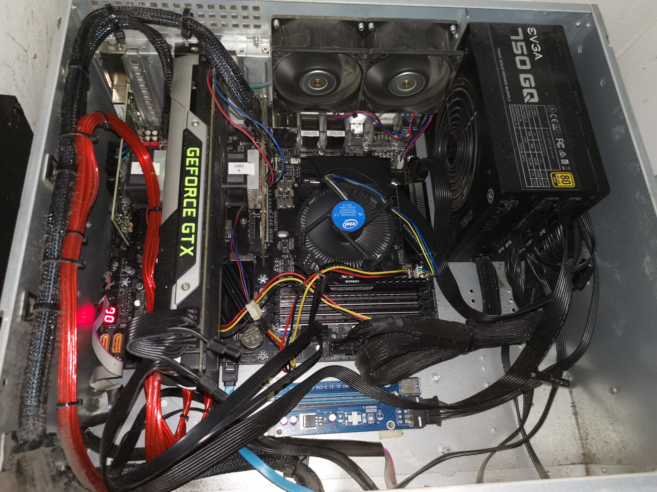
GPU & RAID Cards
Well, the file server got ANOTHER upgrade, quite quickly. The motherboard was replaced again, this time with a new board, new Corsair RAM & a new Intel i7-9700F 8-Core CPU. As this server also runs video transcoding services, the tiny GPU got pulled & replaced with a spare nVidia GTX980 I had just for that task. My LSI RAID cards are still used as HBAs, just as JBOD, since Linux is running the main disk array via mdadm.
Server Internals
Once this upgrade was completed, with space for resource expansion – the motherboard supports up to 128GB RAM, at the moment there’s 32GB in there due to the eye-watering cost of RAM at the present time – there was scope for running some Virtualisation for other services.
Still running OpenMediaVault, based around Debian 10, I installed the Kernel KVM modules & QEMU, along with Cockpit for control. Going this route was dictated by VirtualBox not being directly supported in Debian 10, for reasons I don’t know.
Once all this was installed, and a network bridge set up for the VMs through a spare network interface, I brought up a pair of Debian 10 servers – one for PiHole which had up until this point been running on a spare Raspberry Pi for the last 6 or so years (I think the SD card is totally shot at this point!), and one for my web App server.
At the moment, all the VMs are running from the main RAID6 spinning rust array, which is a little slow, but the next planned upgrade is to move the VM subsystem to it’s own RAID10 array of disks, hopefully speeding things up – there are just enough SATA ports left on the motherboard to accommodate 6 more drives, and with both 5.25″ disk bays being available for caddies, this should be a simple fix.
As a result, I’m down to a single server powering my entire online domain, and a reduction in power usage!
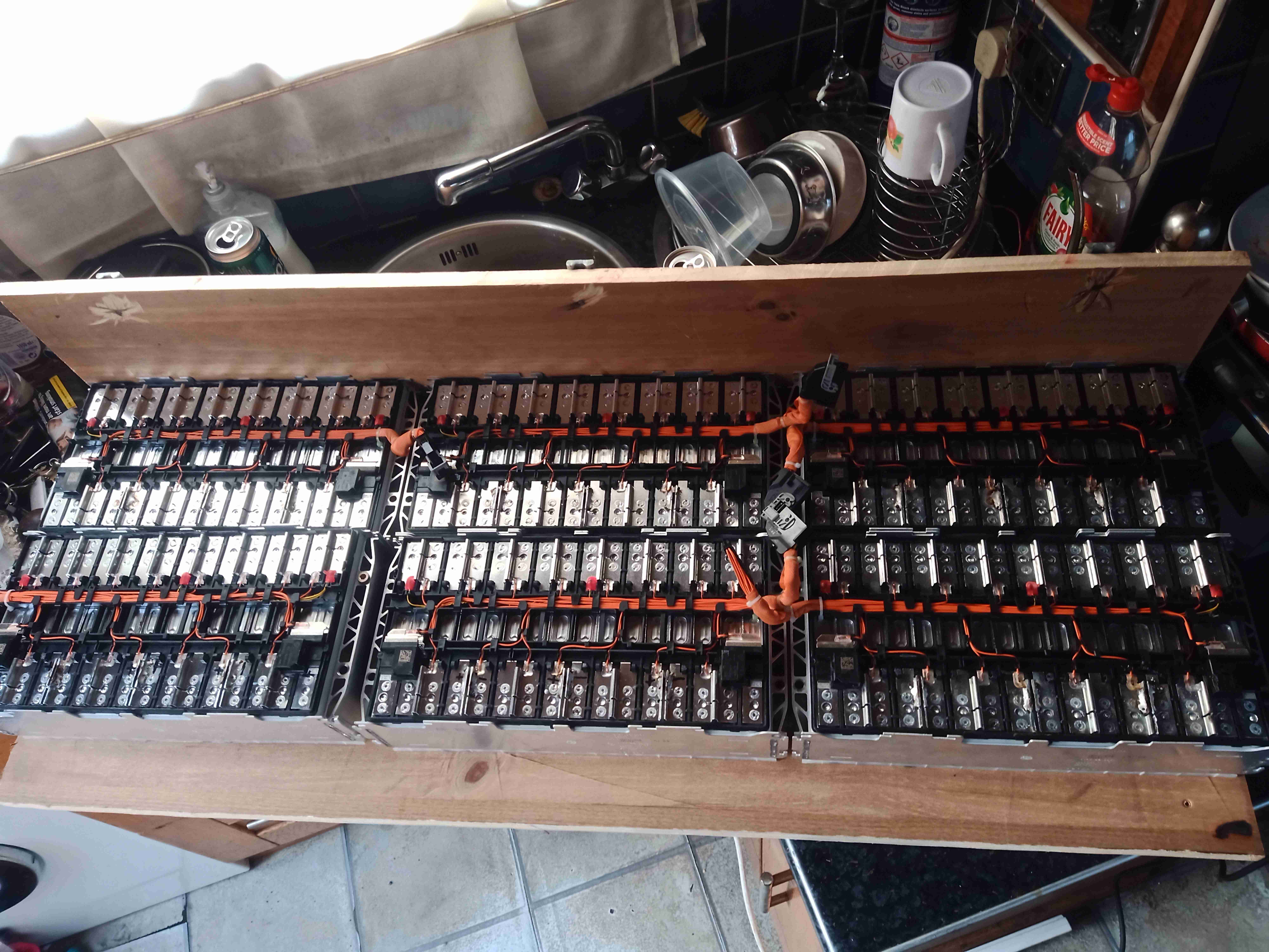
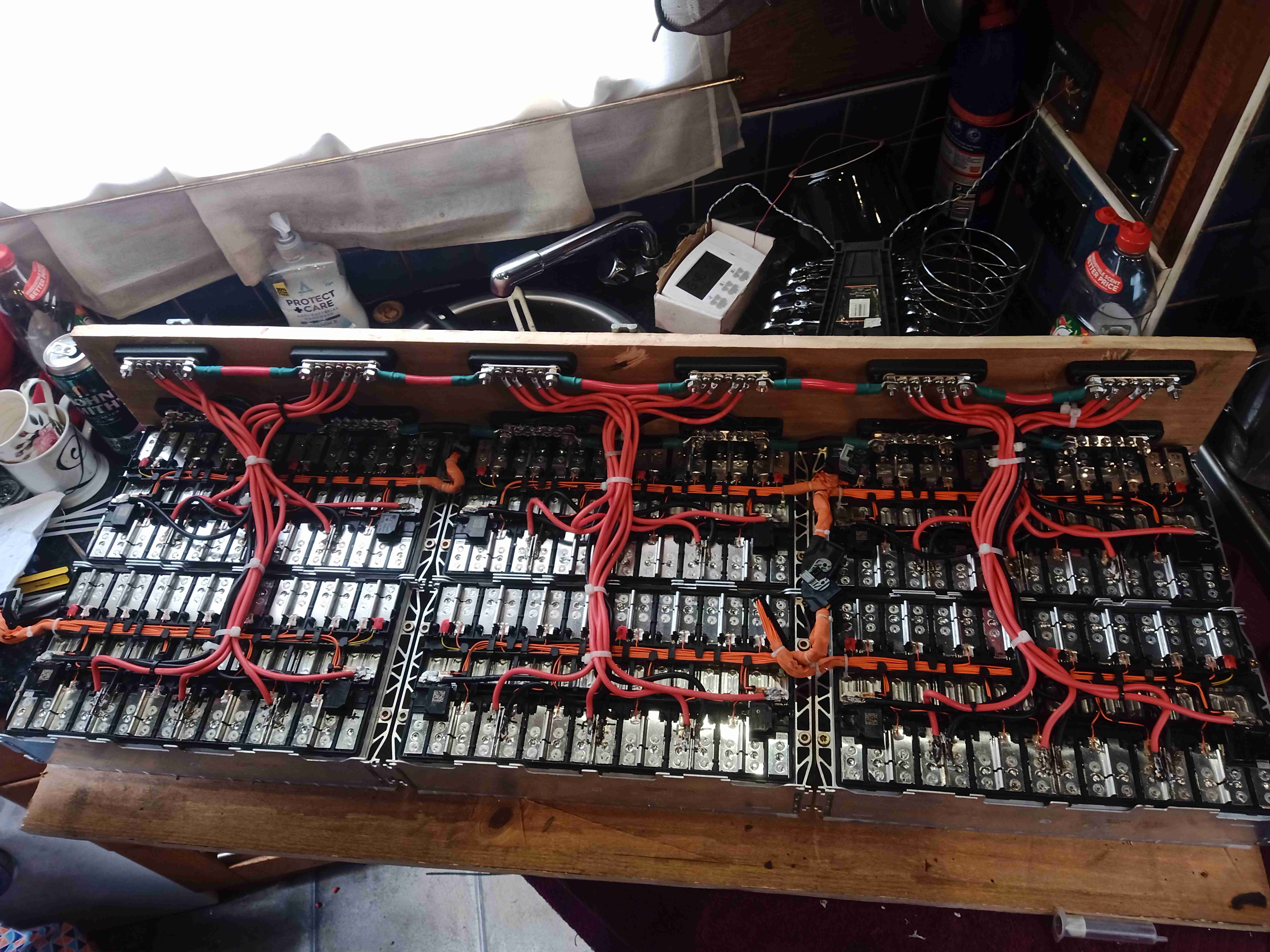
Now the cell modules have been removed from their original home, it’s time to get them repurposed! A custom mounting board has been constructed from timber, and the modules mounted on them. To say this assembly is heavy would be an understatement – it’s barely a two-man lift!
As assembled in the car, the pack as 96S1P, with every cell in series. As we need a low voltage bus, the modules have been reconfigured for 4S4P, in total this makes 4S24P with all 6 modules bussed together. As the cell interconnects are laser welded, some ingenuity was required here.
It turned out the best method (and the safest, to avoid any swarf shorting out cells!), was to use a grinder to cut off the top of the loop on the aluminium interconnects, separating them.
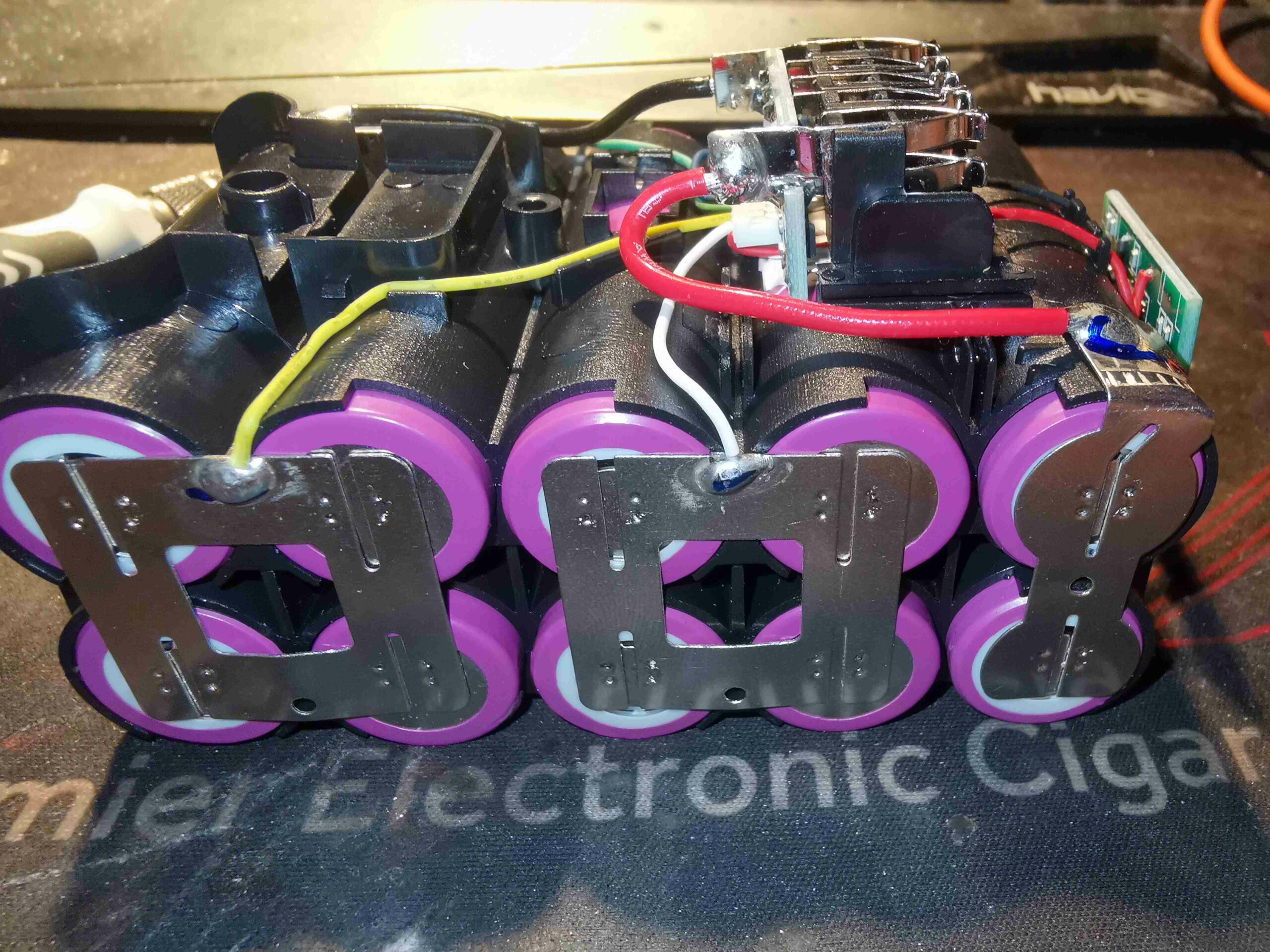
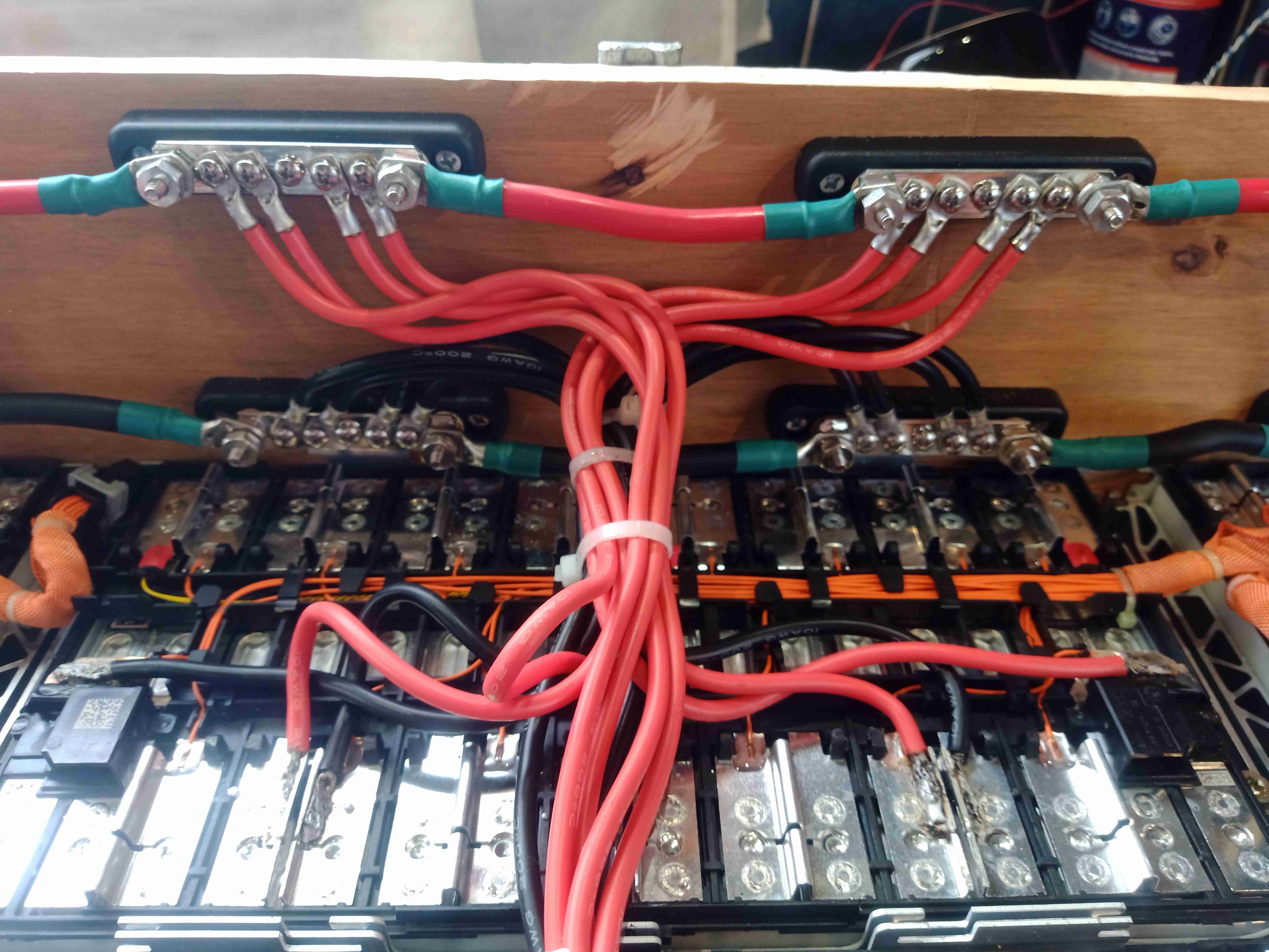
Battery Bus Links
12 5-way bus bars have been installed on the board, and 25mm² cable links them together. To get the angry pixies from the cell modules, 8mm² flexible silicone cable has been used, 4 links to a bus bar. This setup should provide more than enough current capacity.
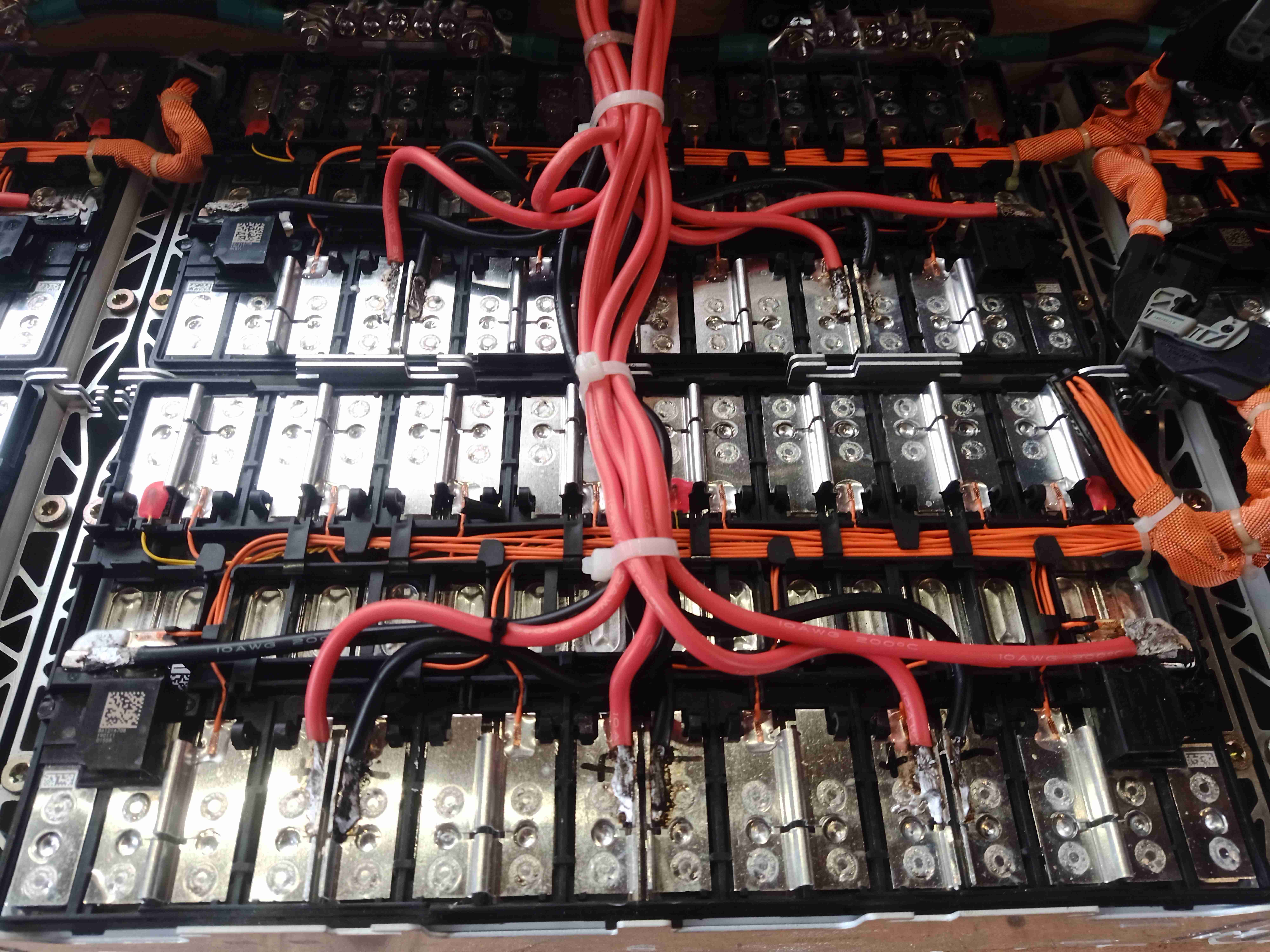
Cell Connections
Here can be seen the cell interconnects – and the grinder cuts to separate them where required to break the module up into 4S strings. As the interconnects are Aluminium, special solder was required to get the copper cables soldered down, in my case I used Alusol 45D solder, which contains a very active flux capable of stripping the oxide from the Aluminium.
Batteries Wired
Finally, here is the new pack, all connected together. All that needs to be done now is the balance wiring loom, which will allow the BMS to sense each cell voltage individually, and connection of the BMS, Coloumeter & fuses, this will all be covered in a future post!
Well, while working on the boat’s engine, I was surprised by this little sod, who’d managed to crawl into the air intake skin fitting on the transom, and got very irritated at the engine being fired up! How the little dude avoided getting sucked into one of the cylinders, I have no idea! The wee mouse was recovered from the air intake & released on the towpath.
Tip Jar
If you’ve found my content useful, please consider leaving a donation by clicking the Tip Jar below!
All collected funds go towards new content & the costs of keeping the server online.