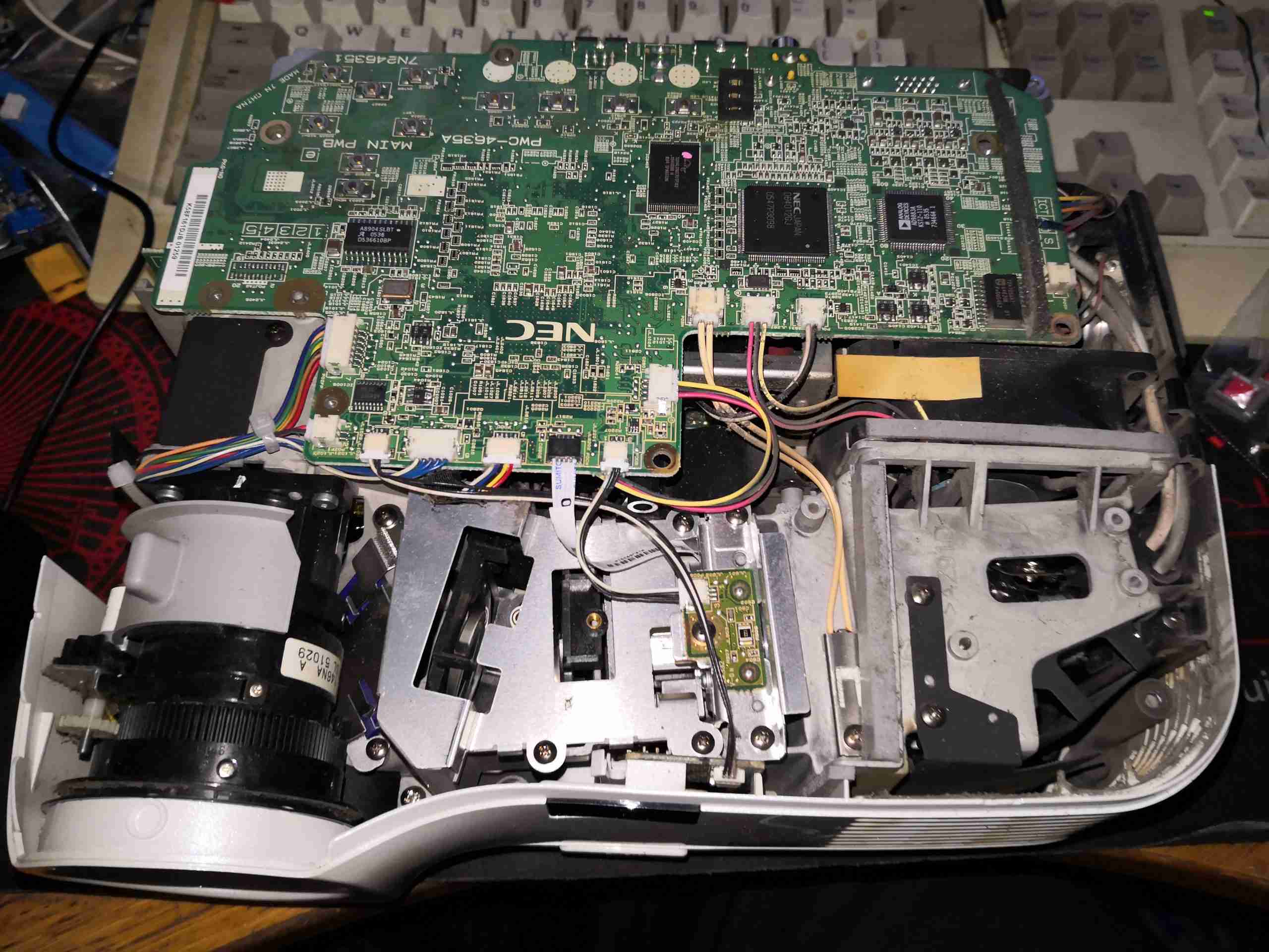
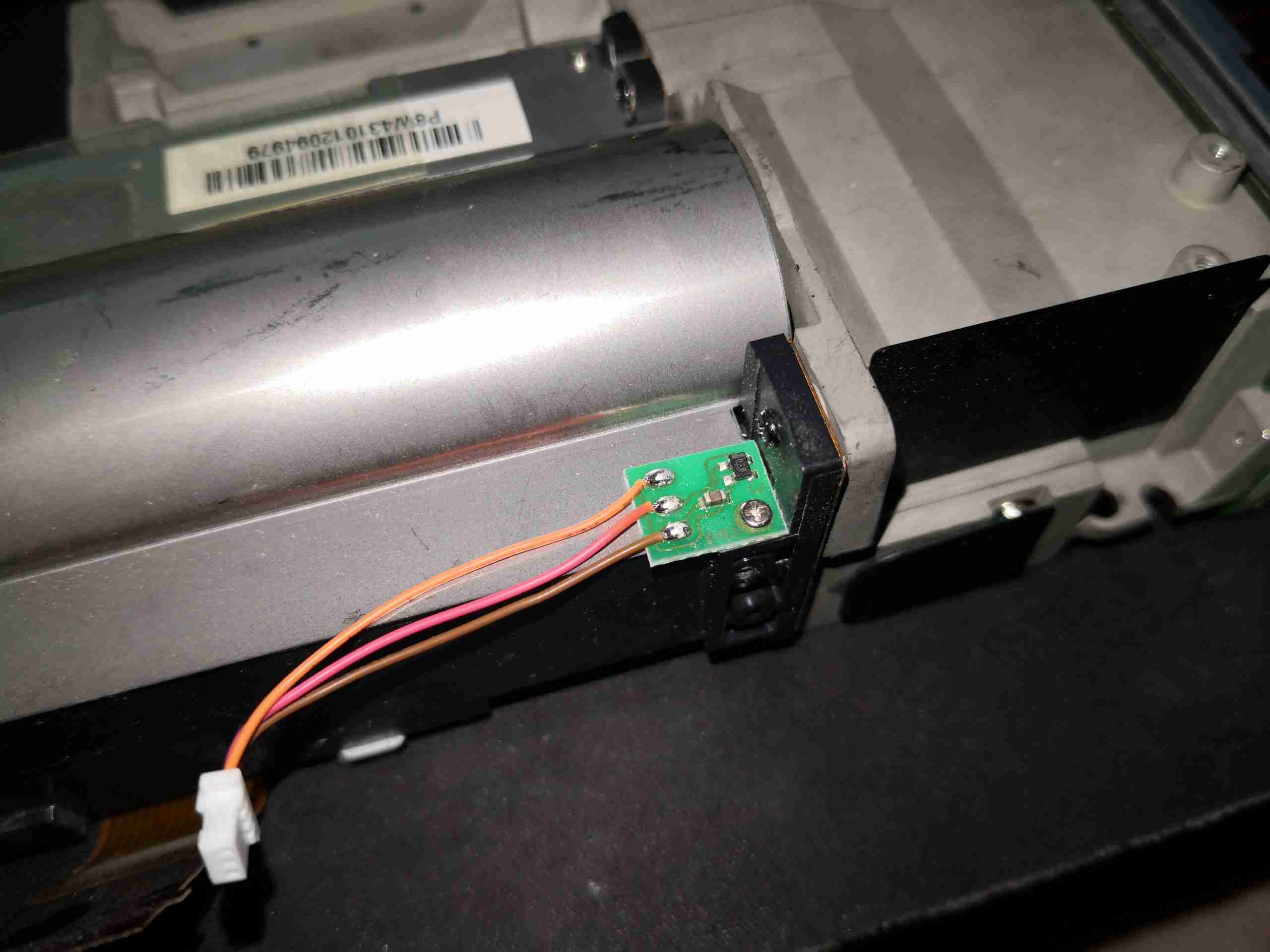
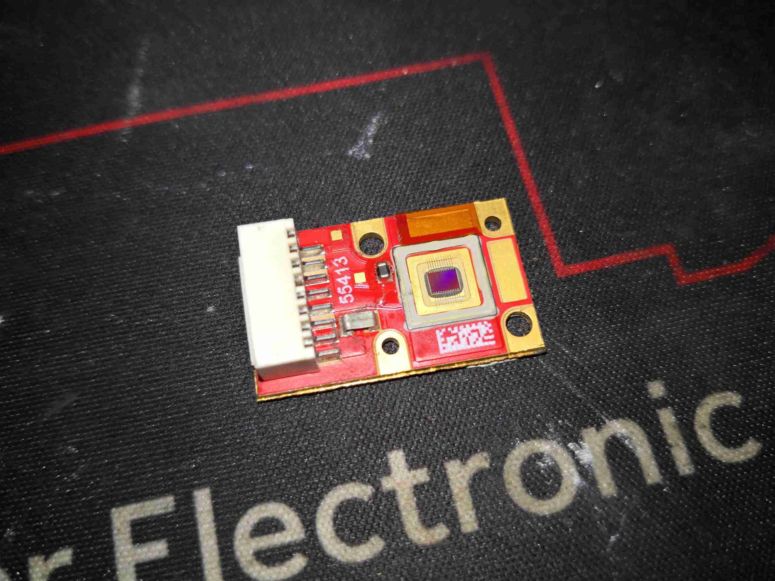
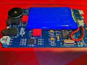
Here’s a DMD Android-based projector from China. This has quite good resolution at 720p native, although the install of Android present is very outdated, and the internal battery has a very short life due to the power draw of the unit.
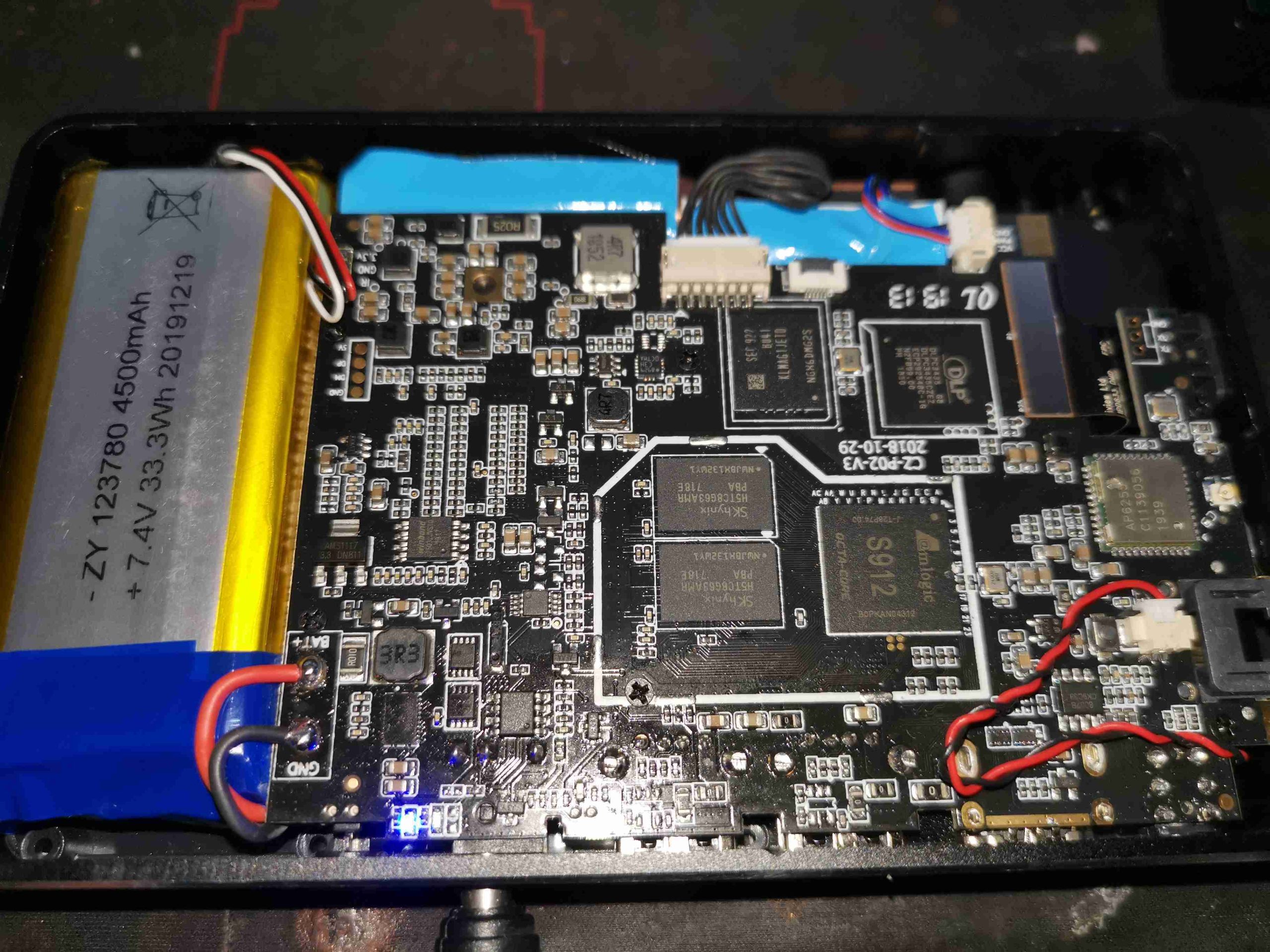
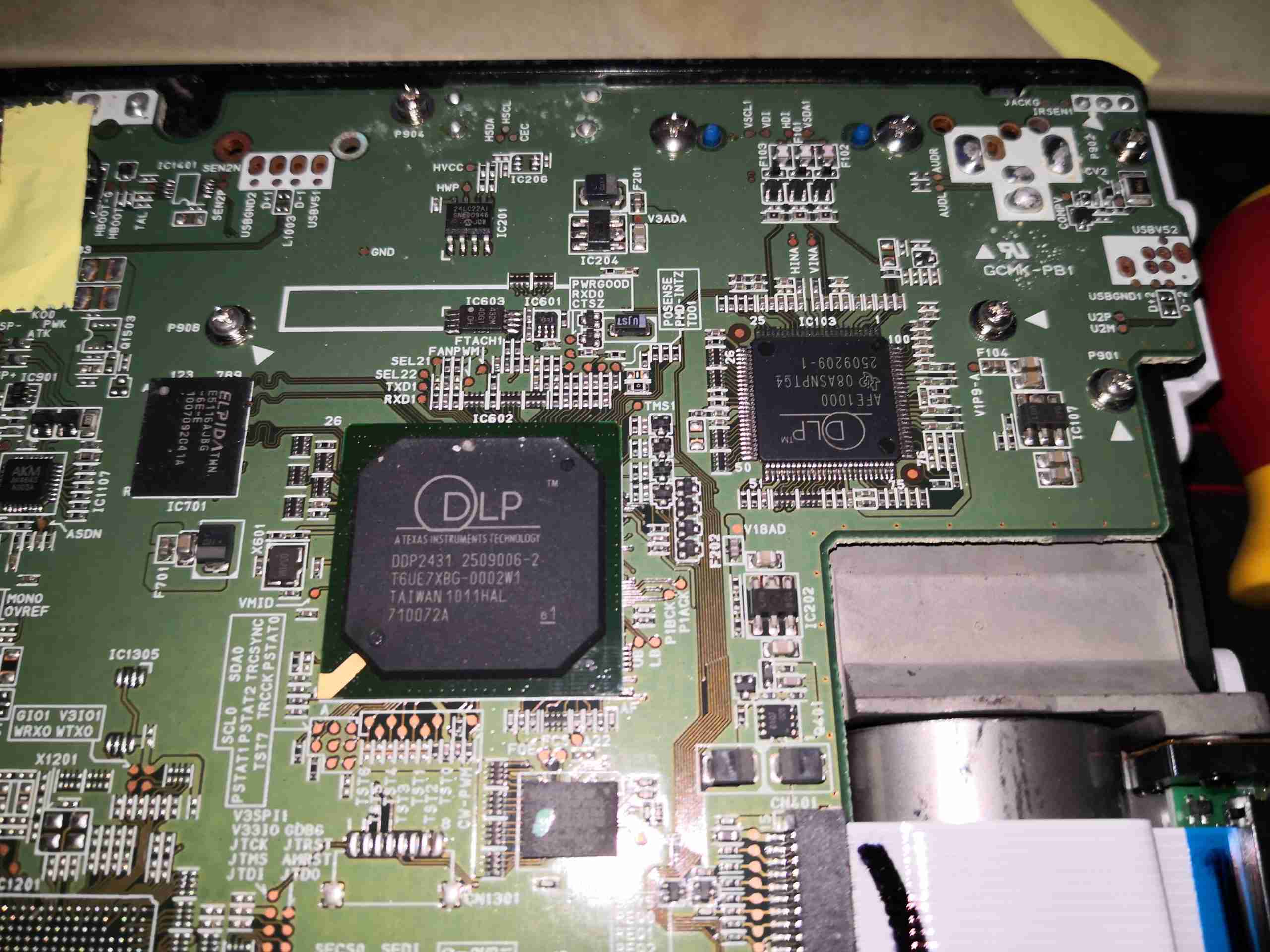
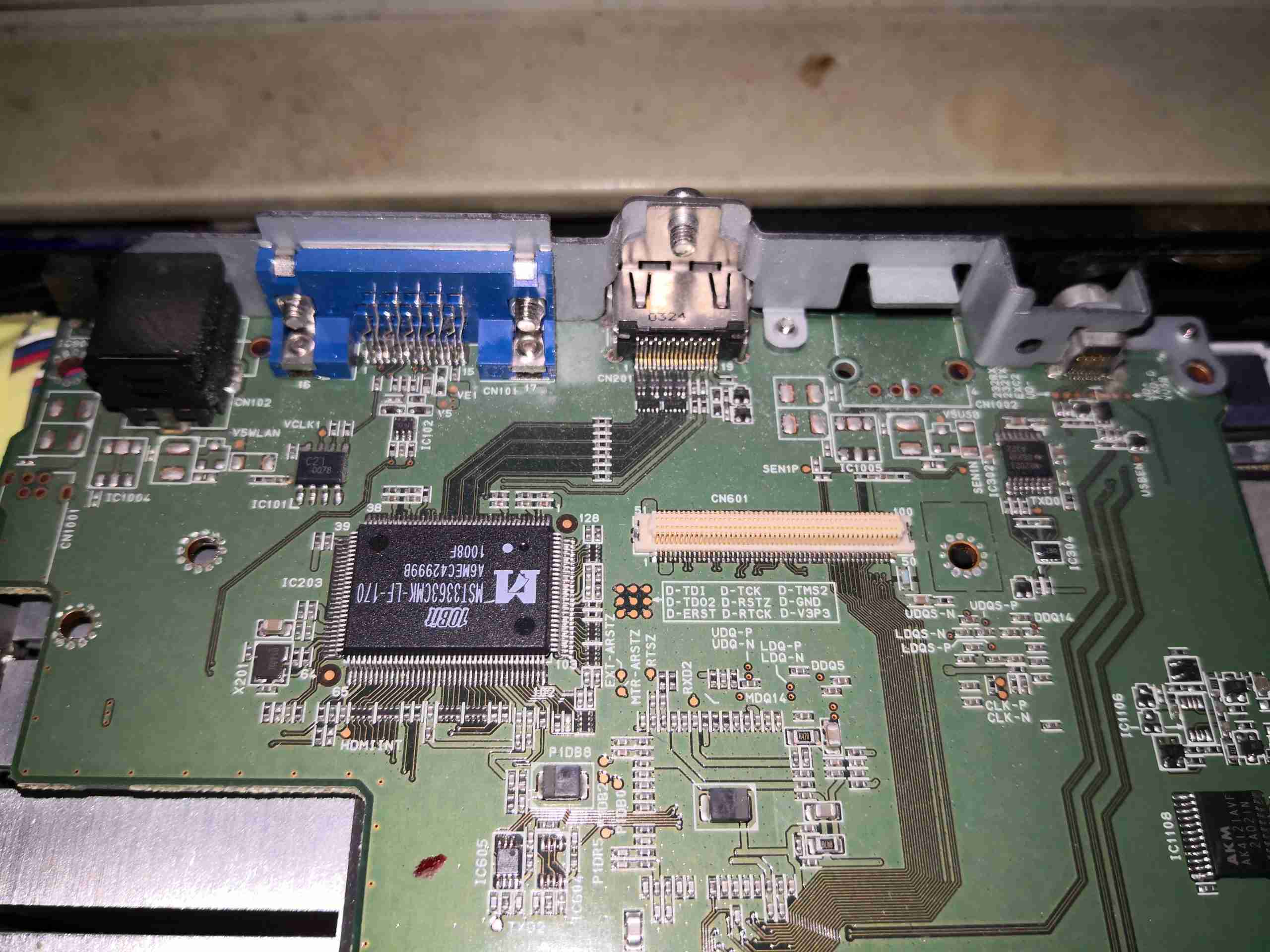
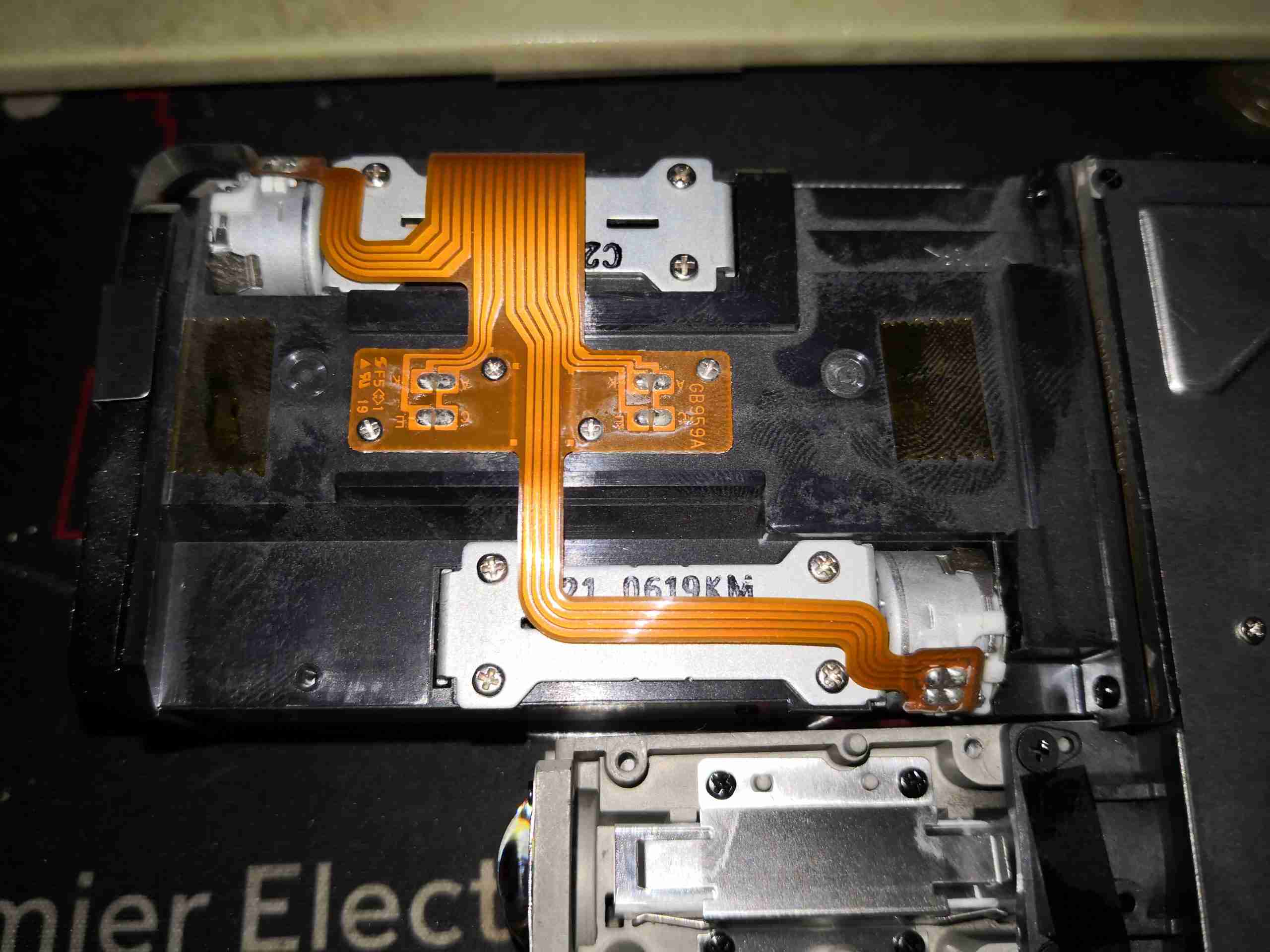
The top of the main PCB is above, and this has one half of the DMD chipset, and the SoC, Flash & RAM for the Android part of the projector.
Touchpad
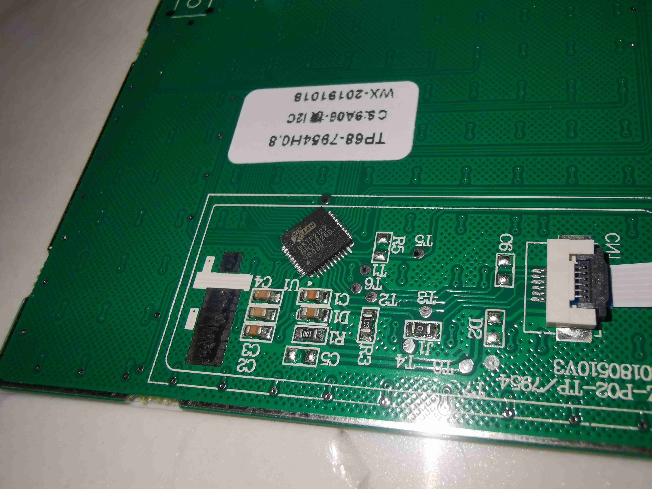
The top of the unit has touch buttons and mousepad for operation, in addition to an IR remote, the bottom of the lid moulding has the touch controller for those buttons and pad.
Mainboard
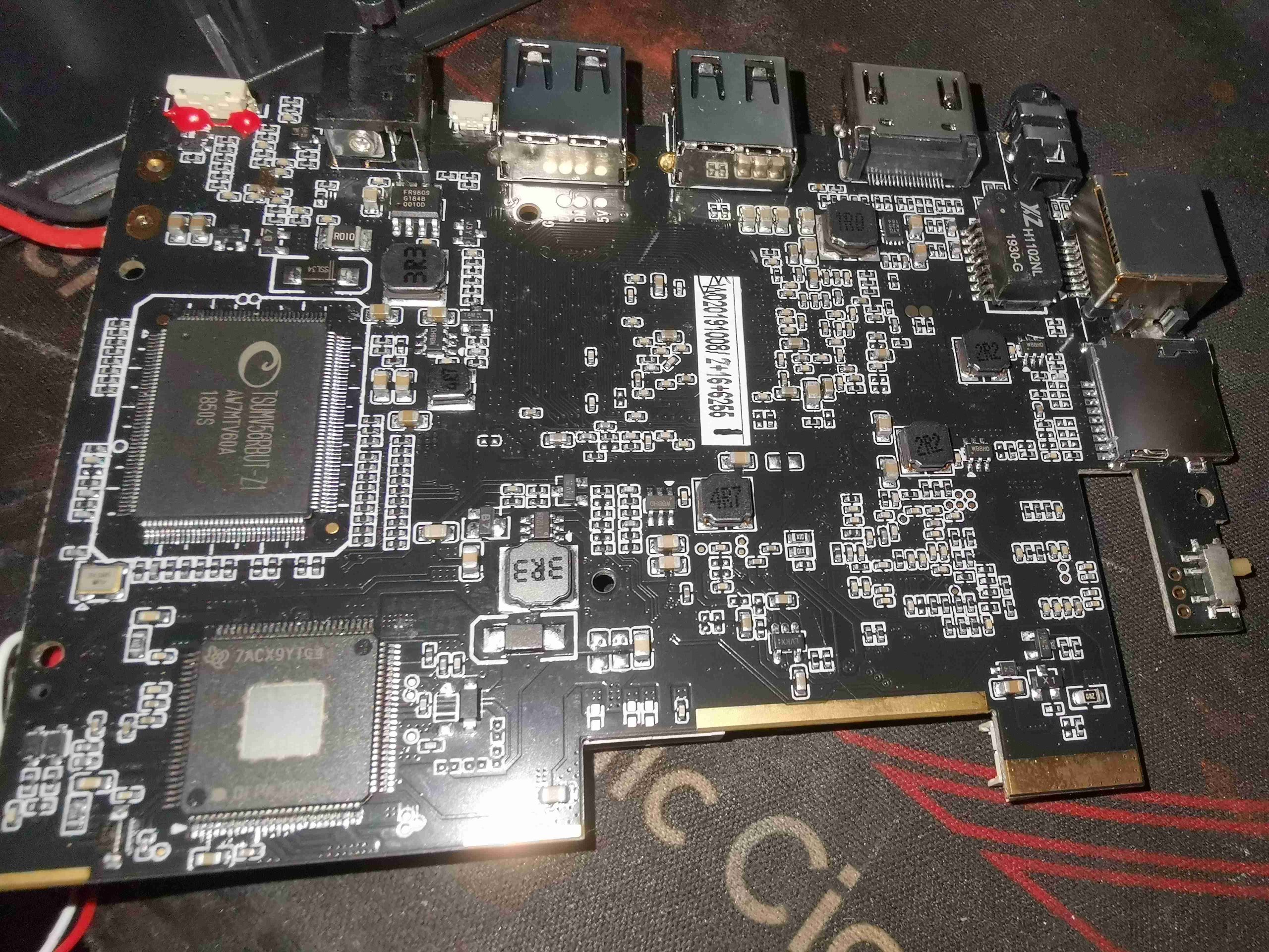
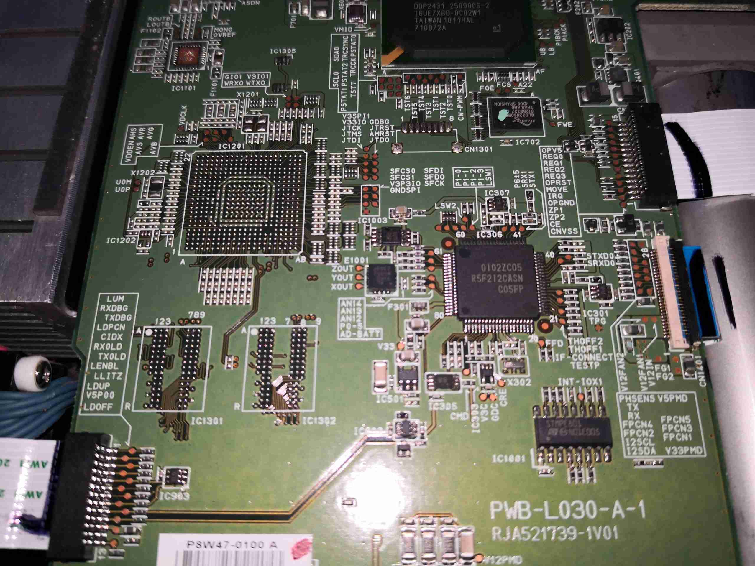
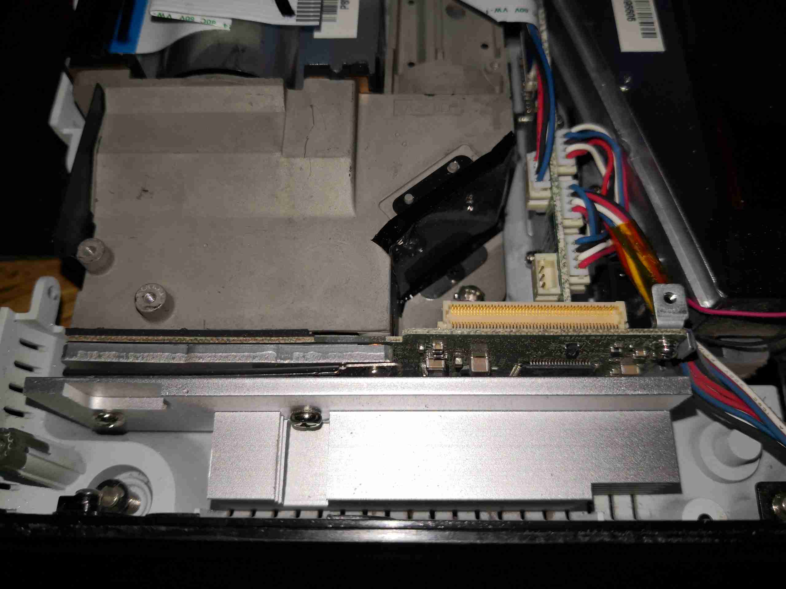
Removing the mainboard shows the rest of the chipset. The large IC at bottom left is one half of the DMD control chipset, and the large IC above that is a video switch to enable either the built in Android or external HDMI interfaces. The rest of the components here are power supply and general support.
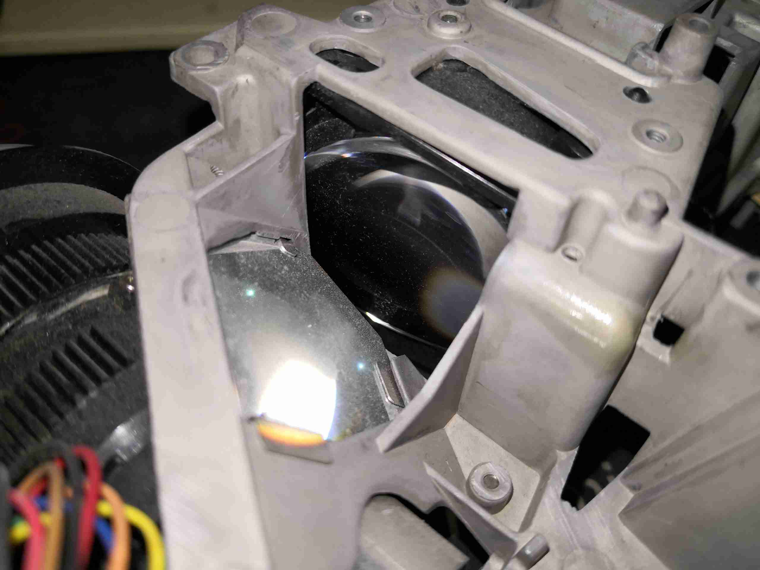
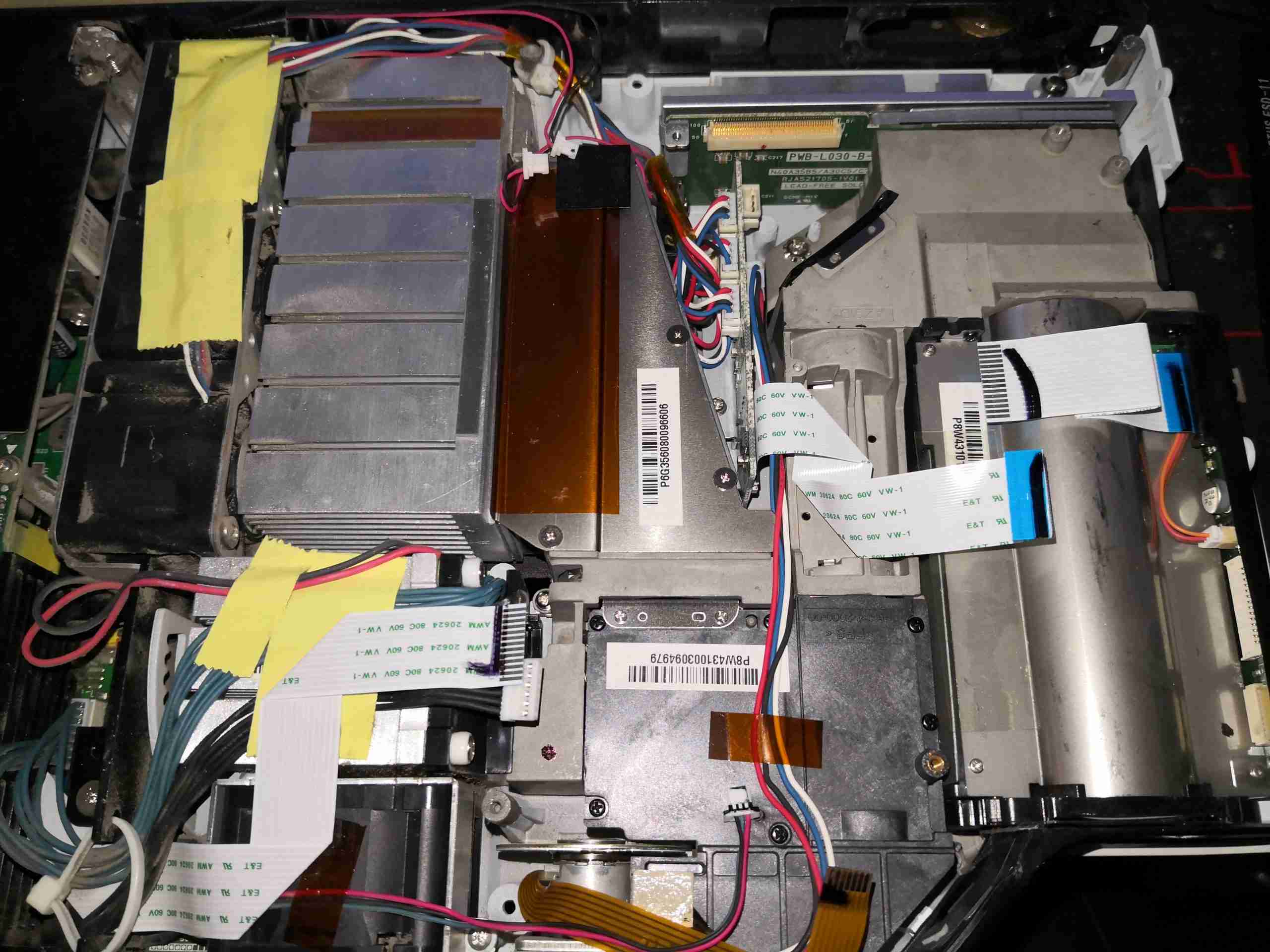
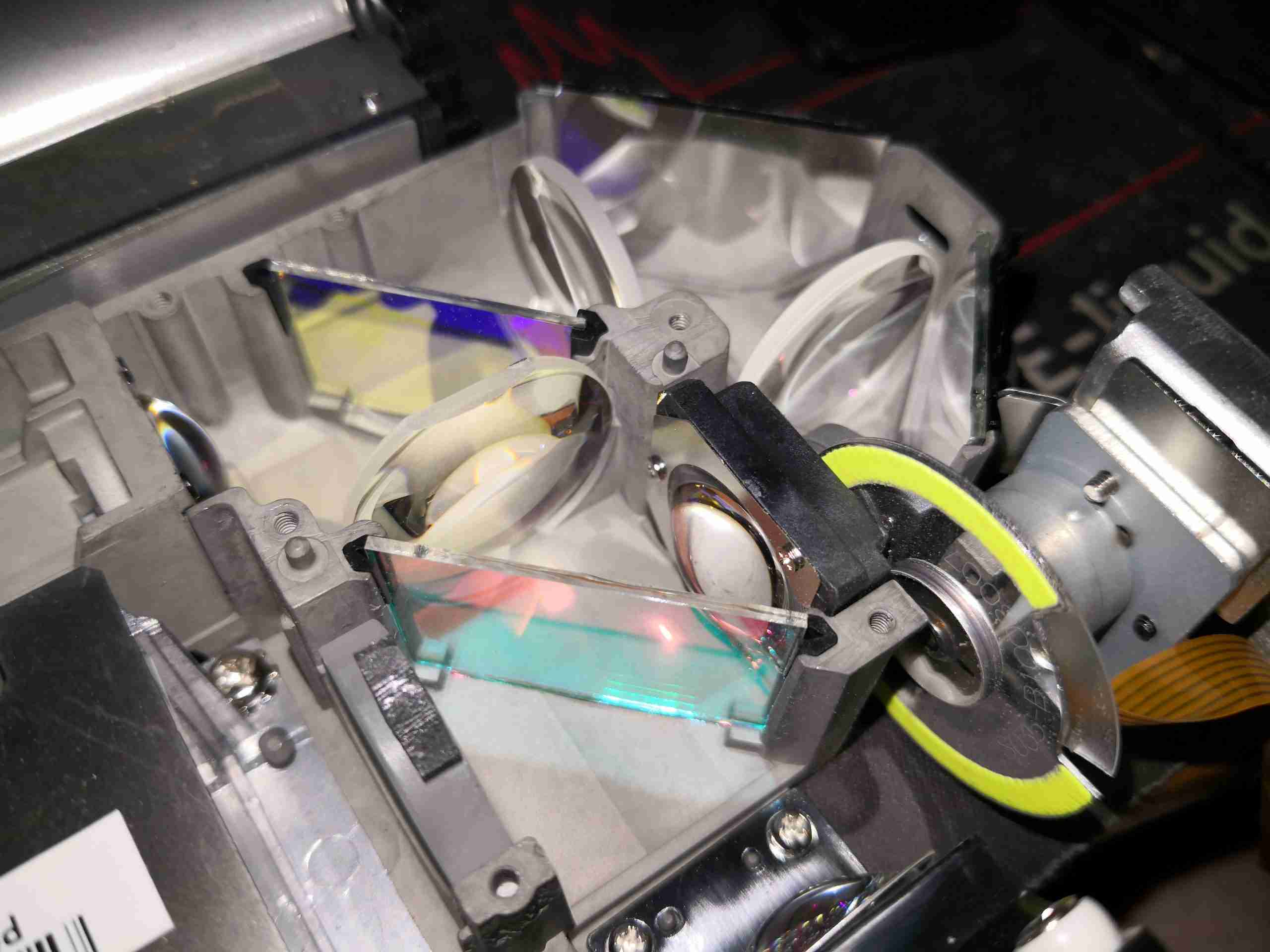
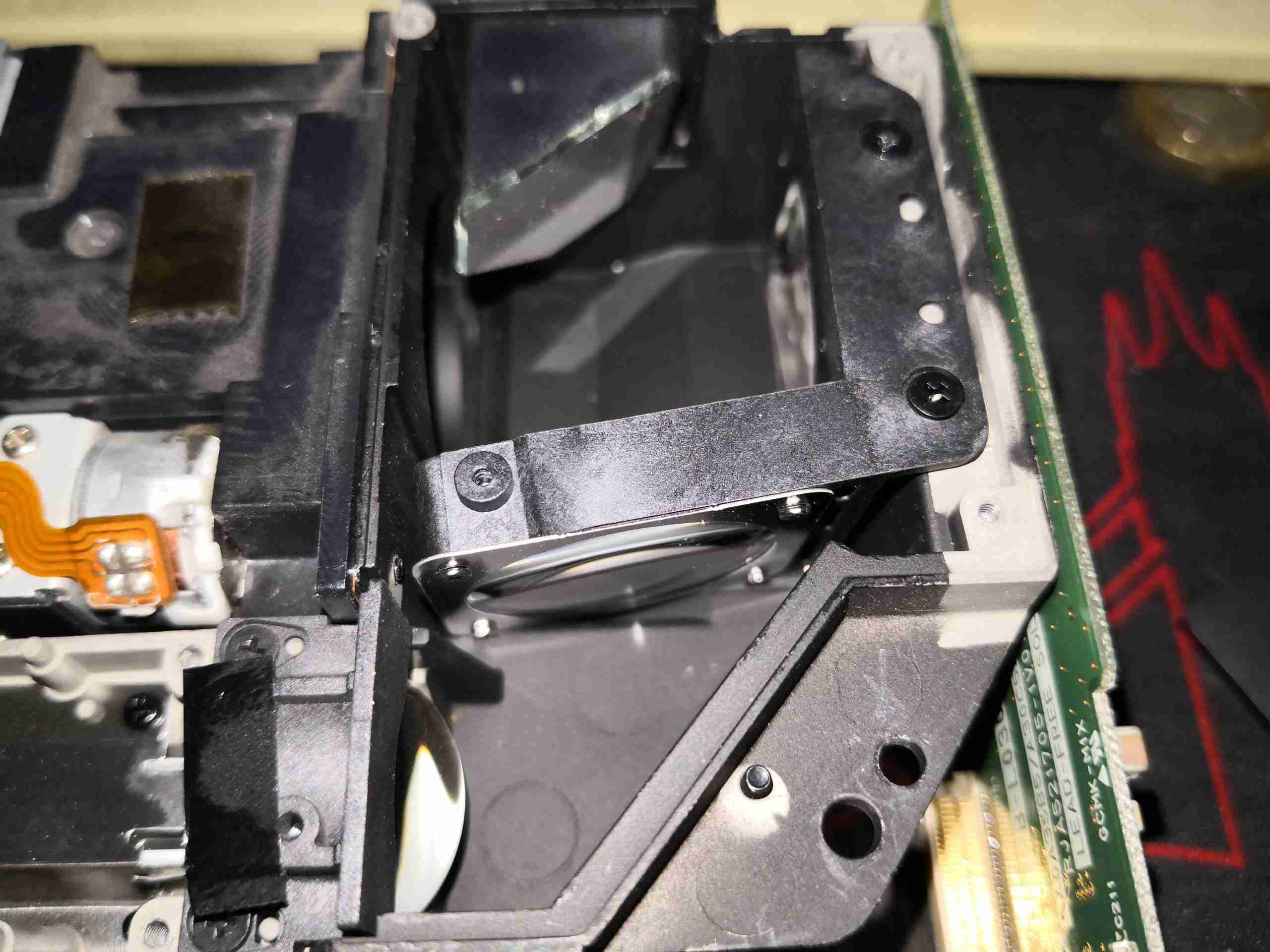
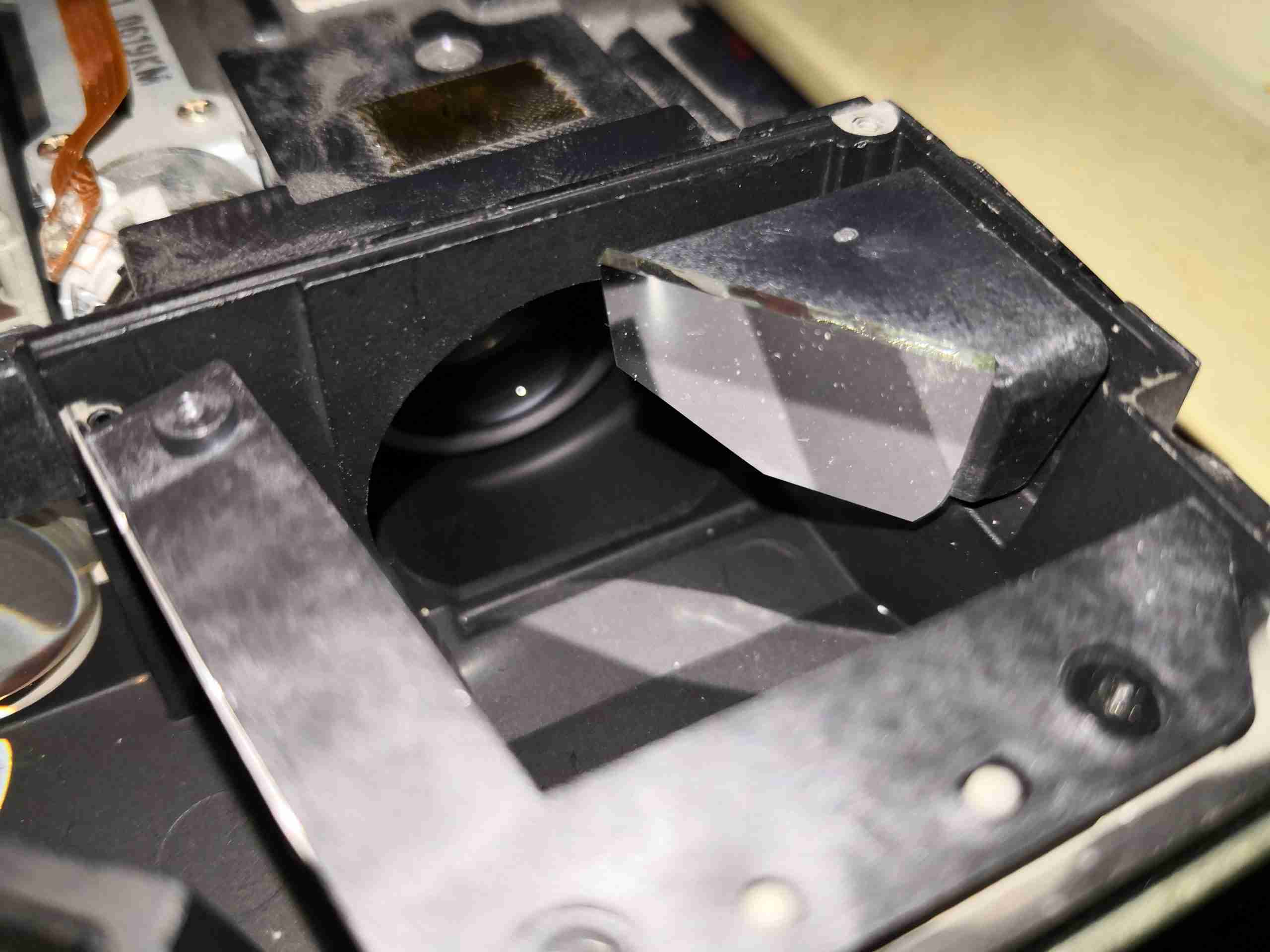
Projector Module
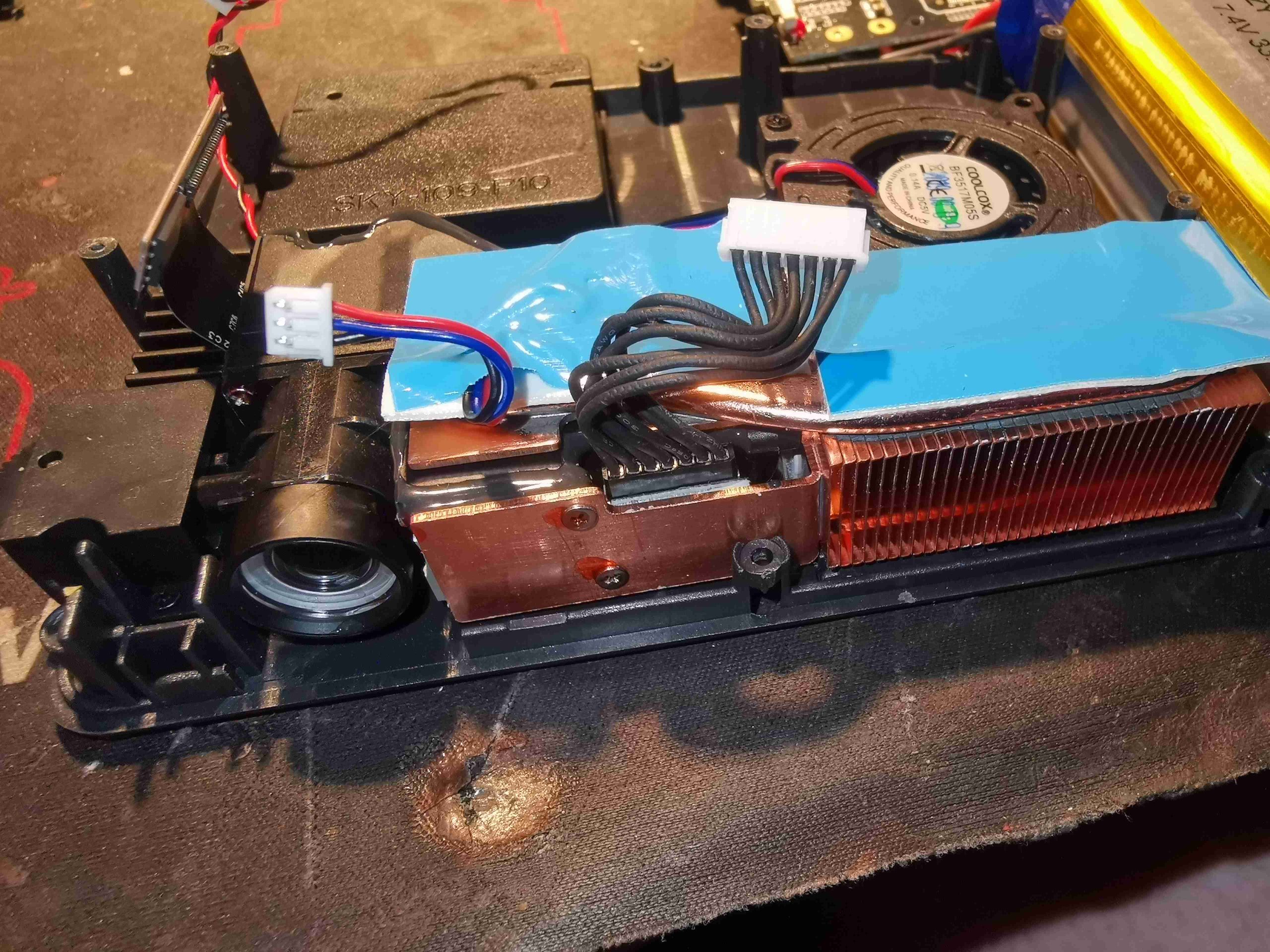
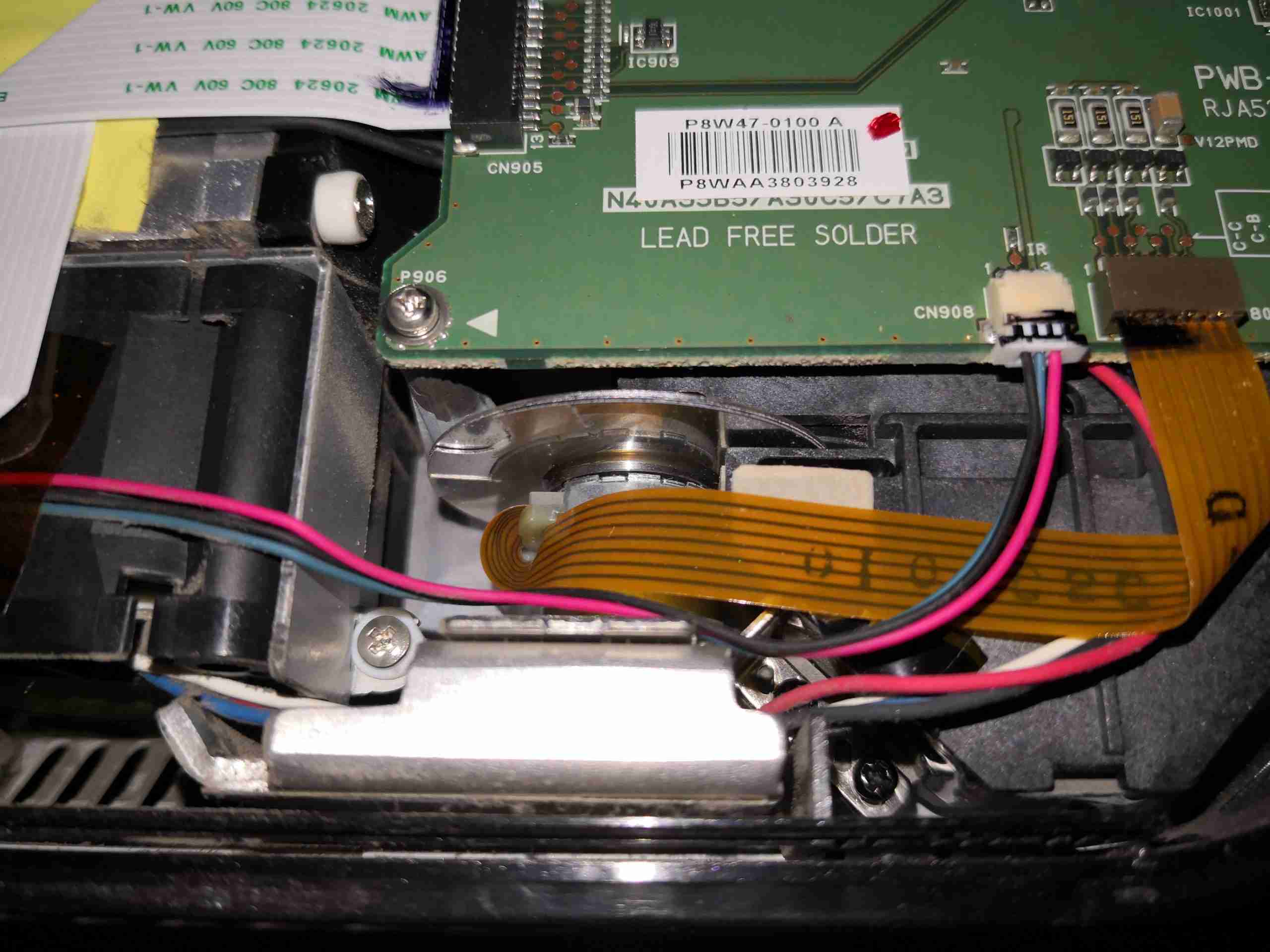
Under the mainboard is the projector module itself. Mostly heatsink just to cope with the high power LEDs, there’s a fan in the rear section that keeps everything cool.
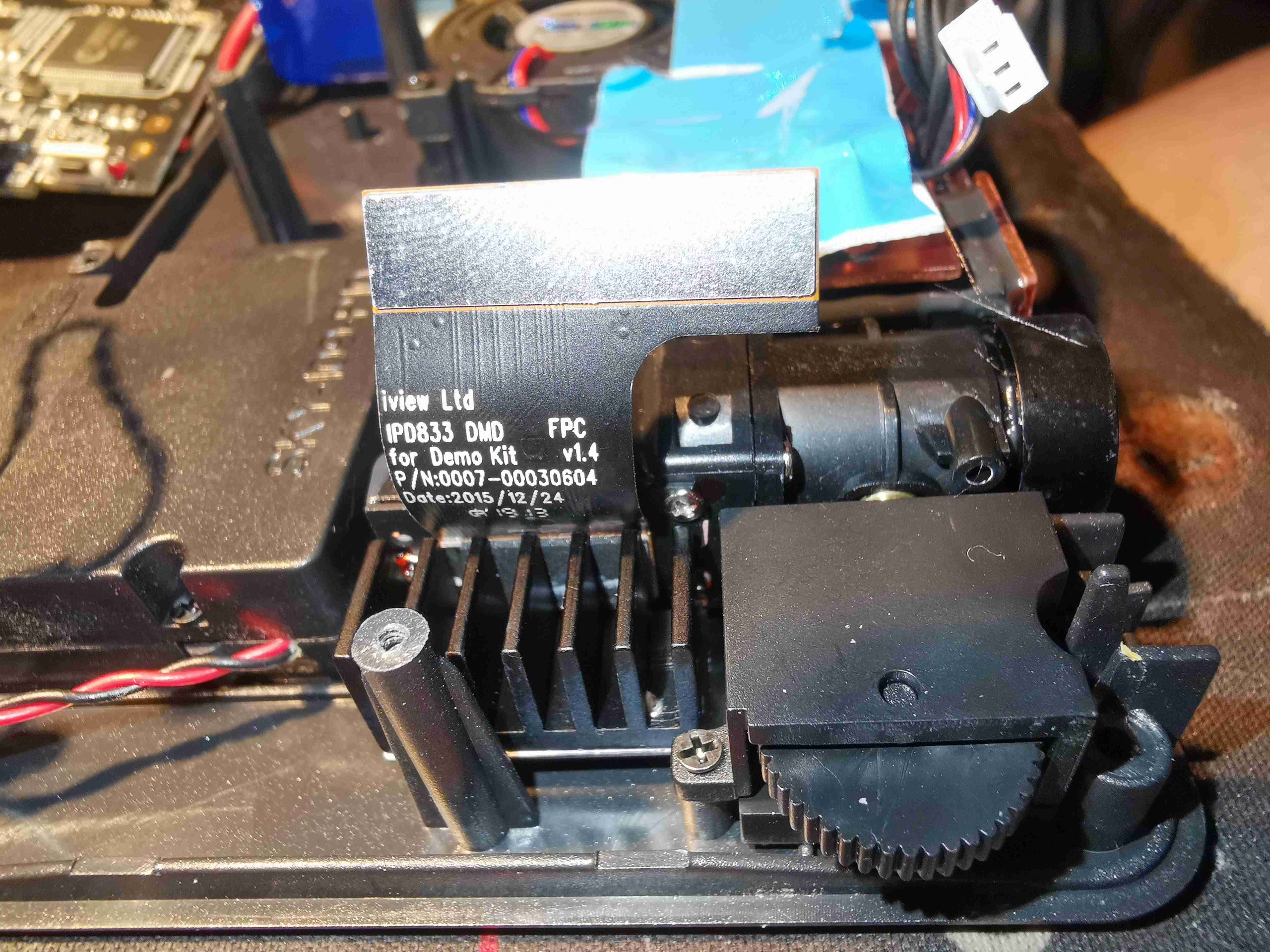
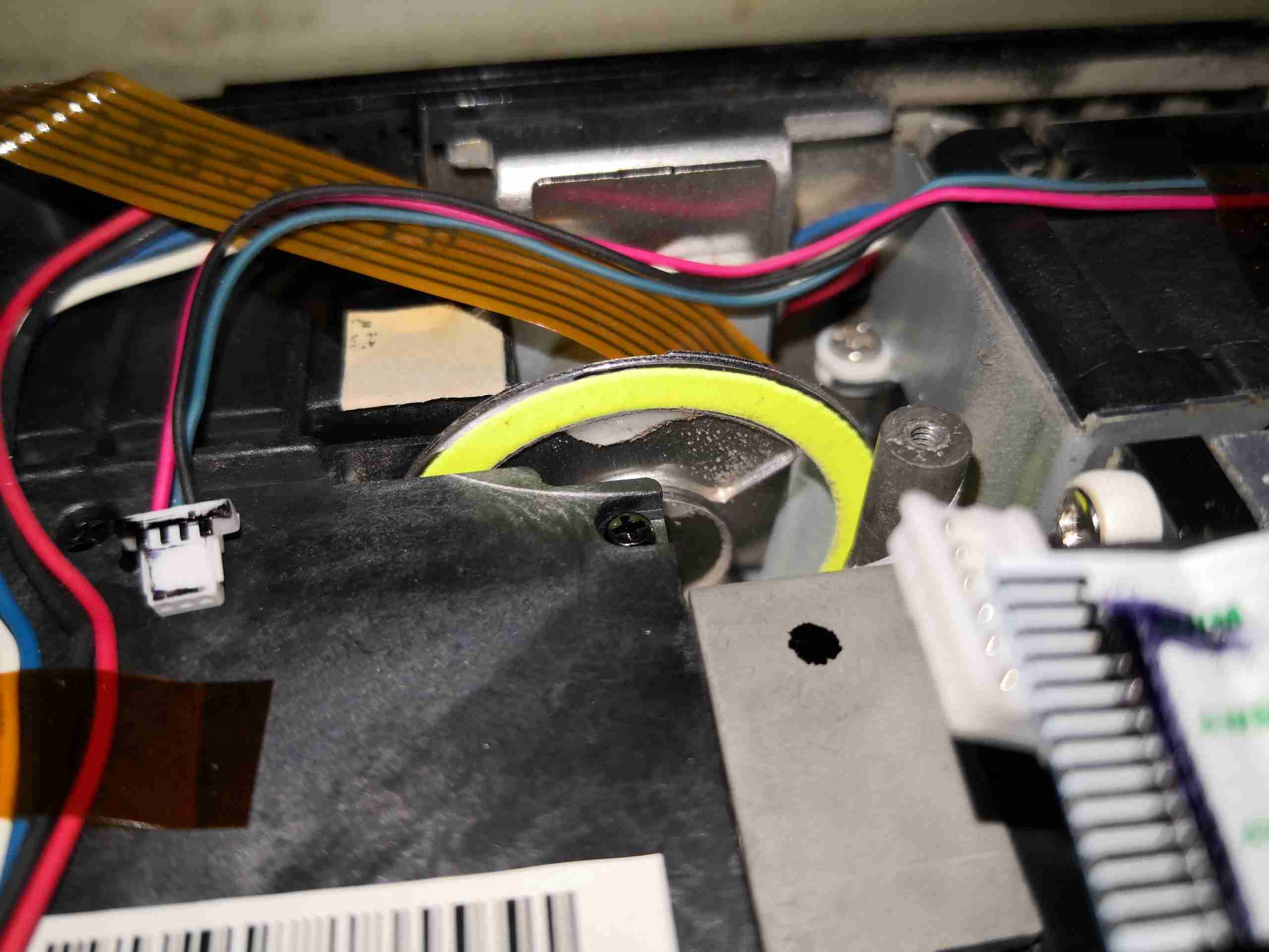
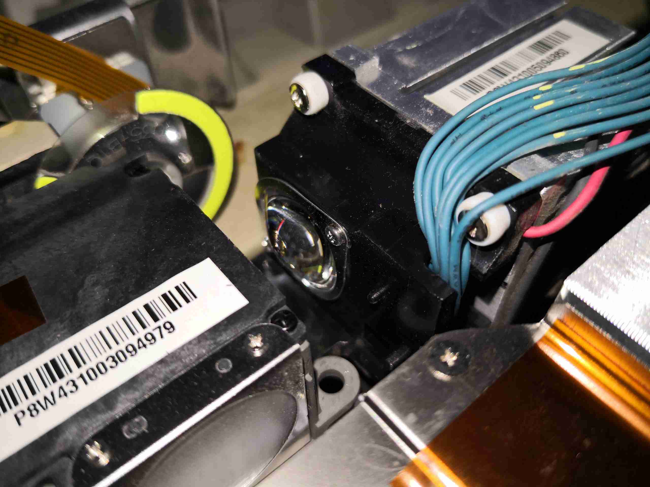
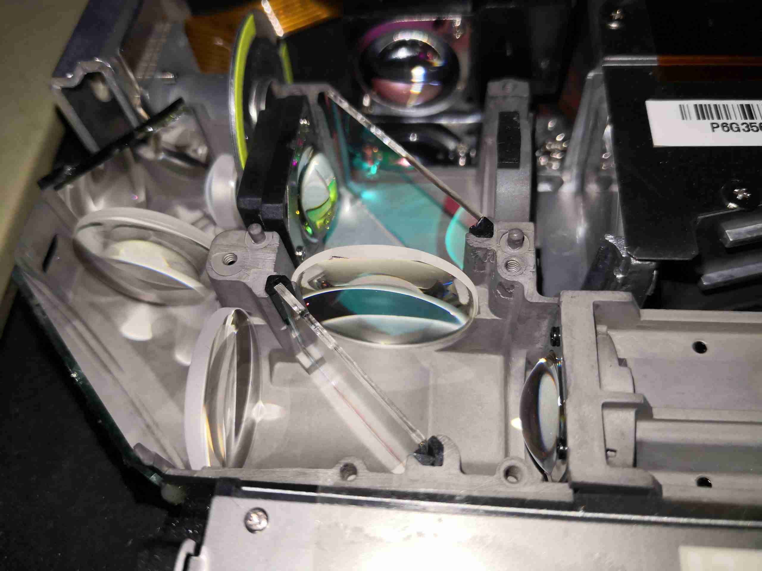
DMD Heatsink
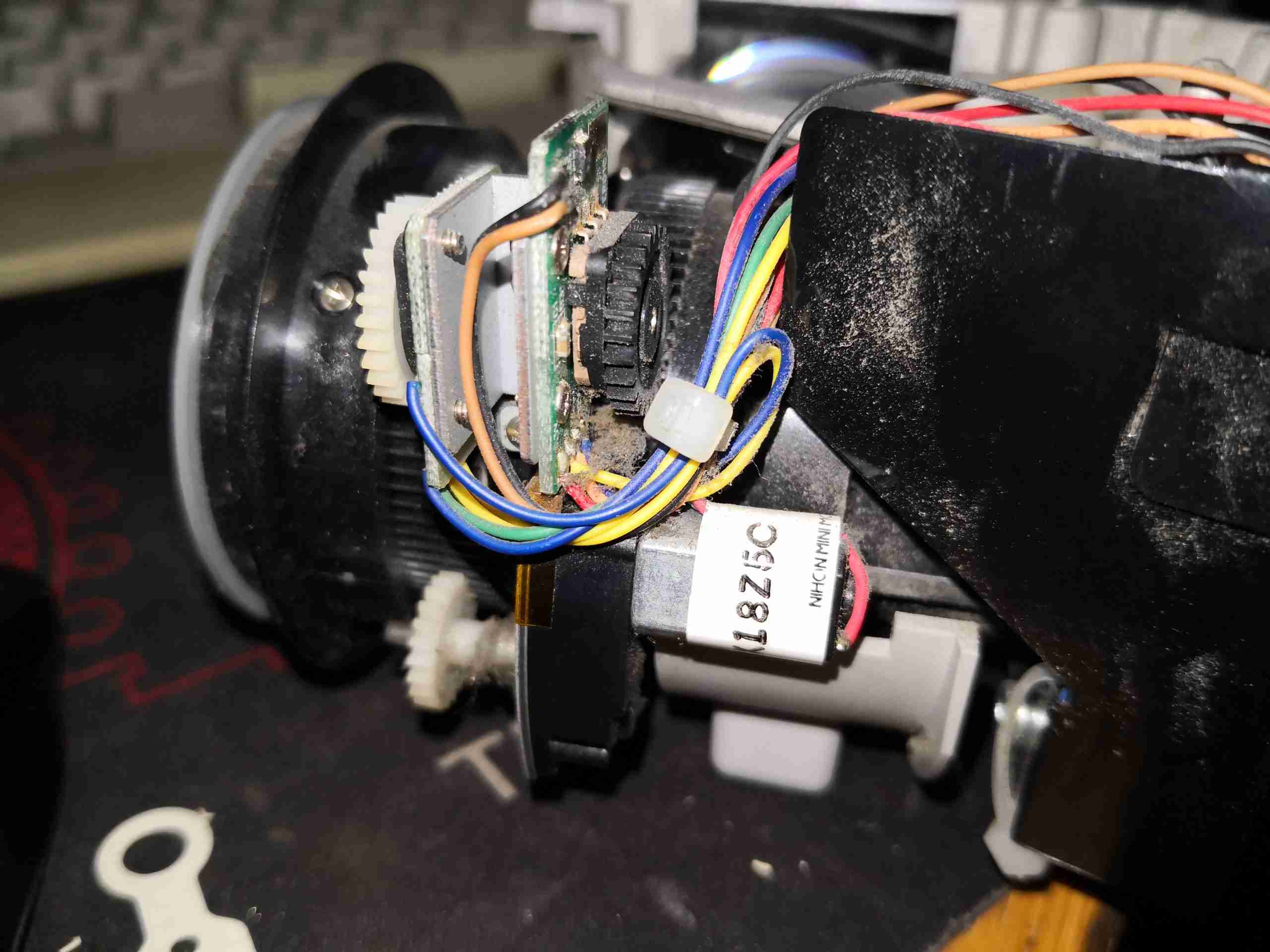
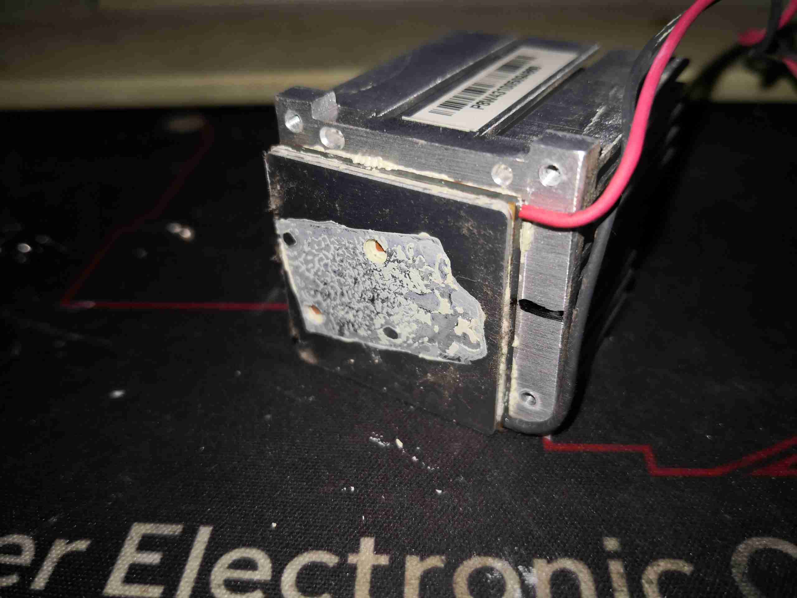
The DMD module is definitely from a development kit – it’s hidden behind this small heatsink. The wheel in the foreground is for main focus.
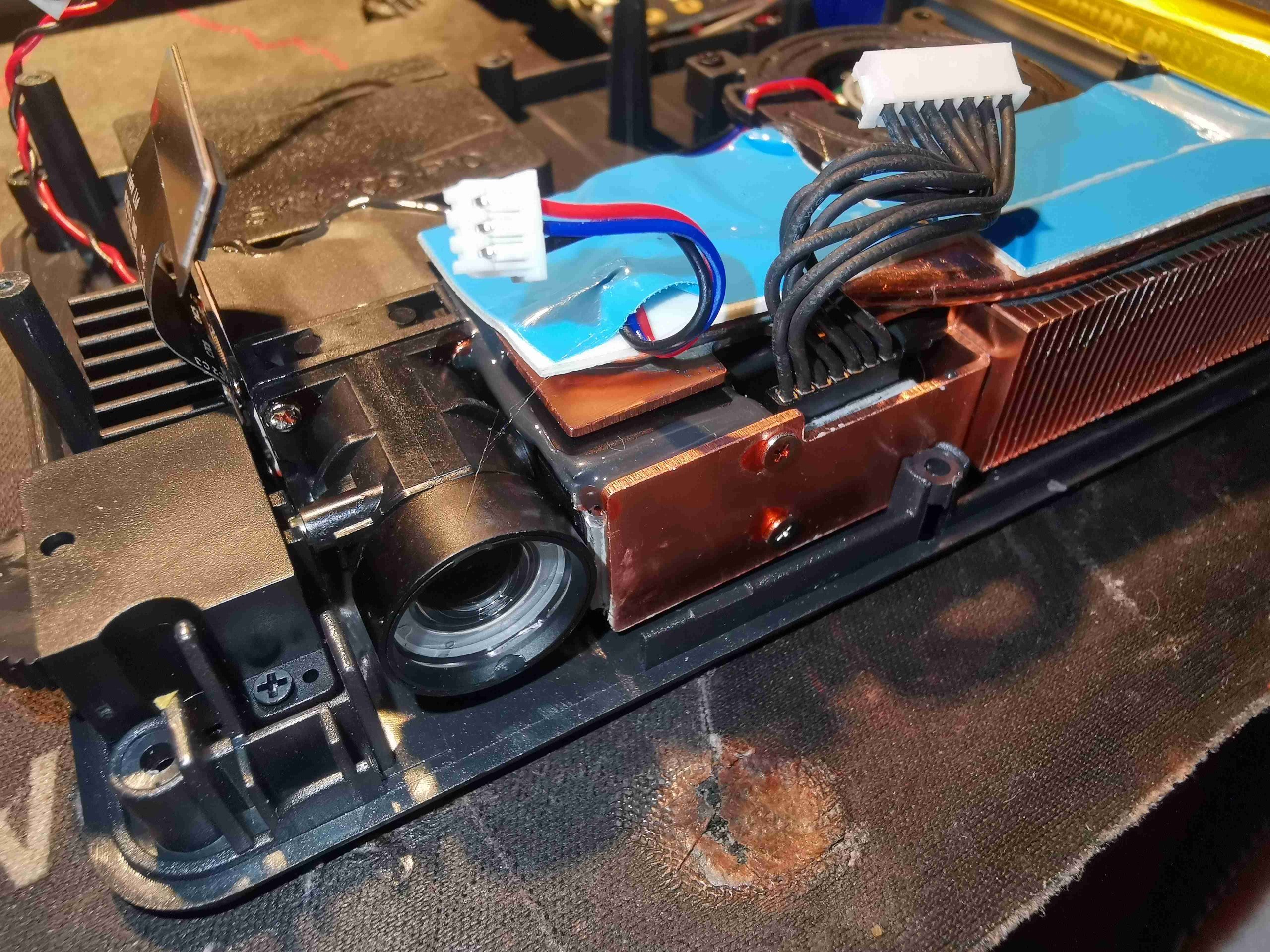
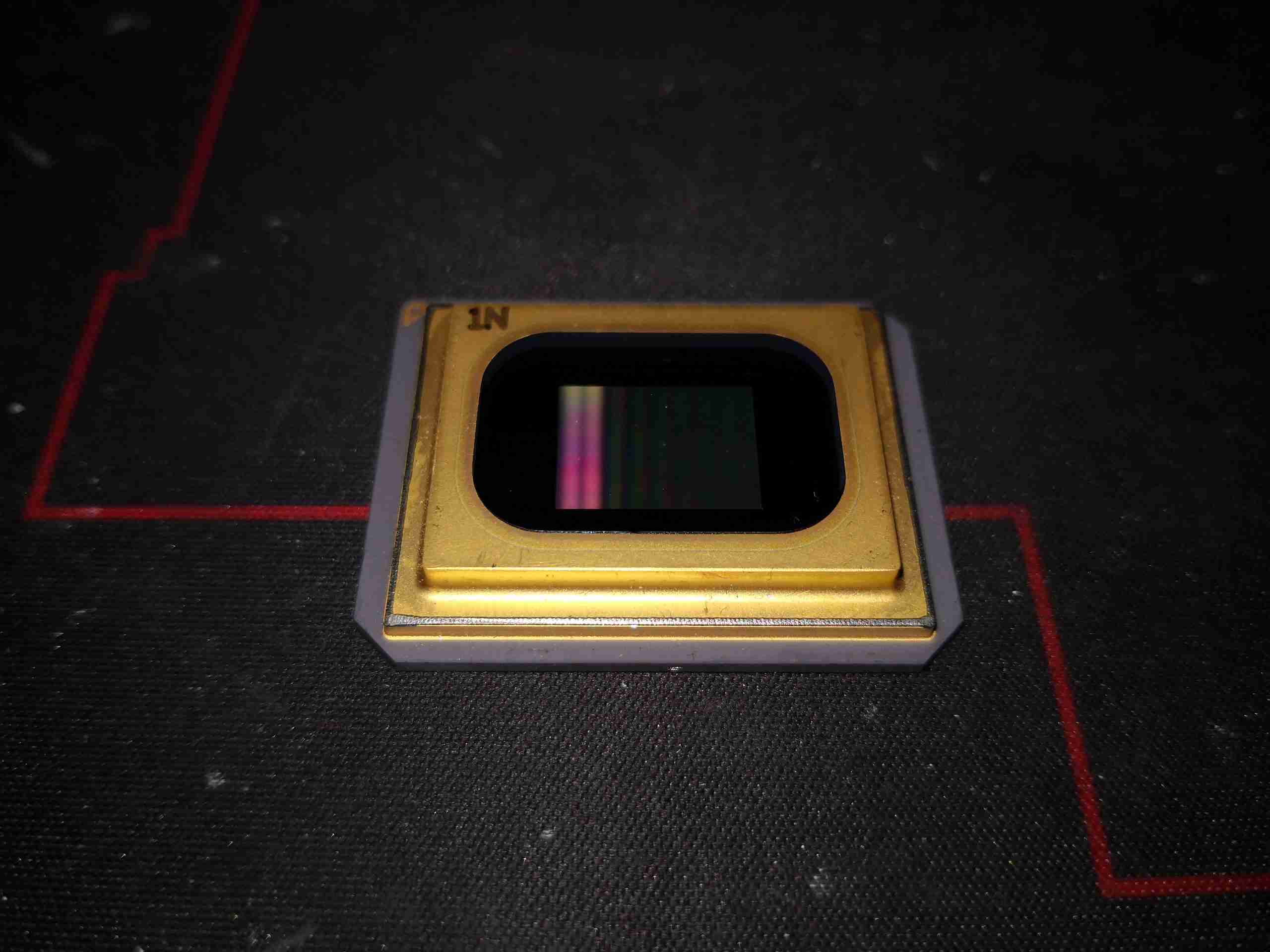
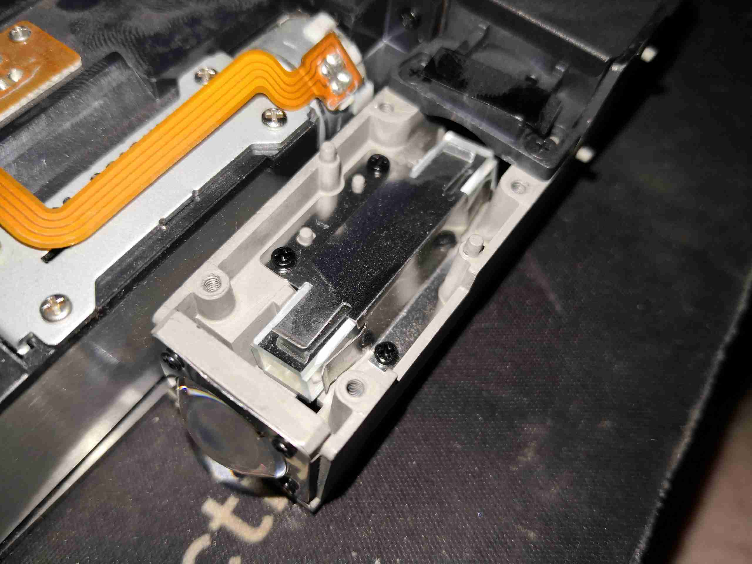
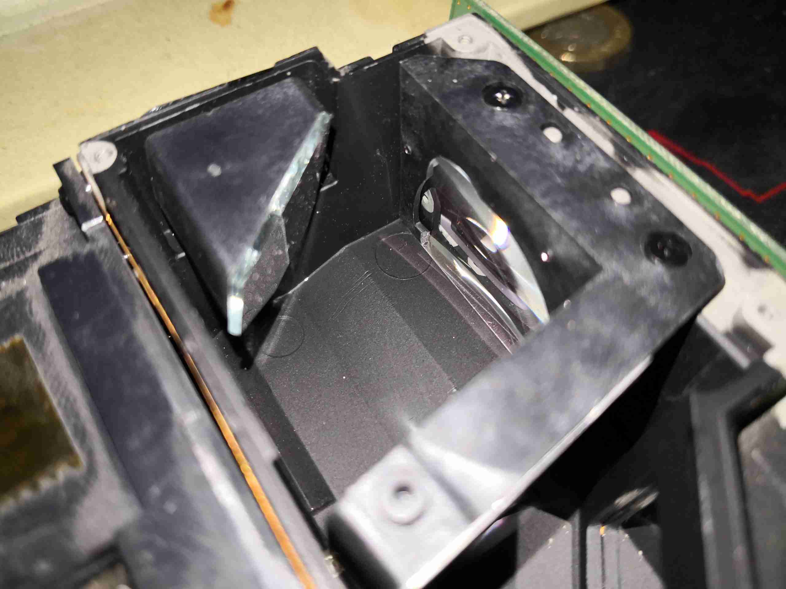
LED Module
On the front of the unit, behind the copper plate is the main RGB LED module, which is switched by the DMD chipset for full colour output from the main lens to the left.
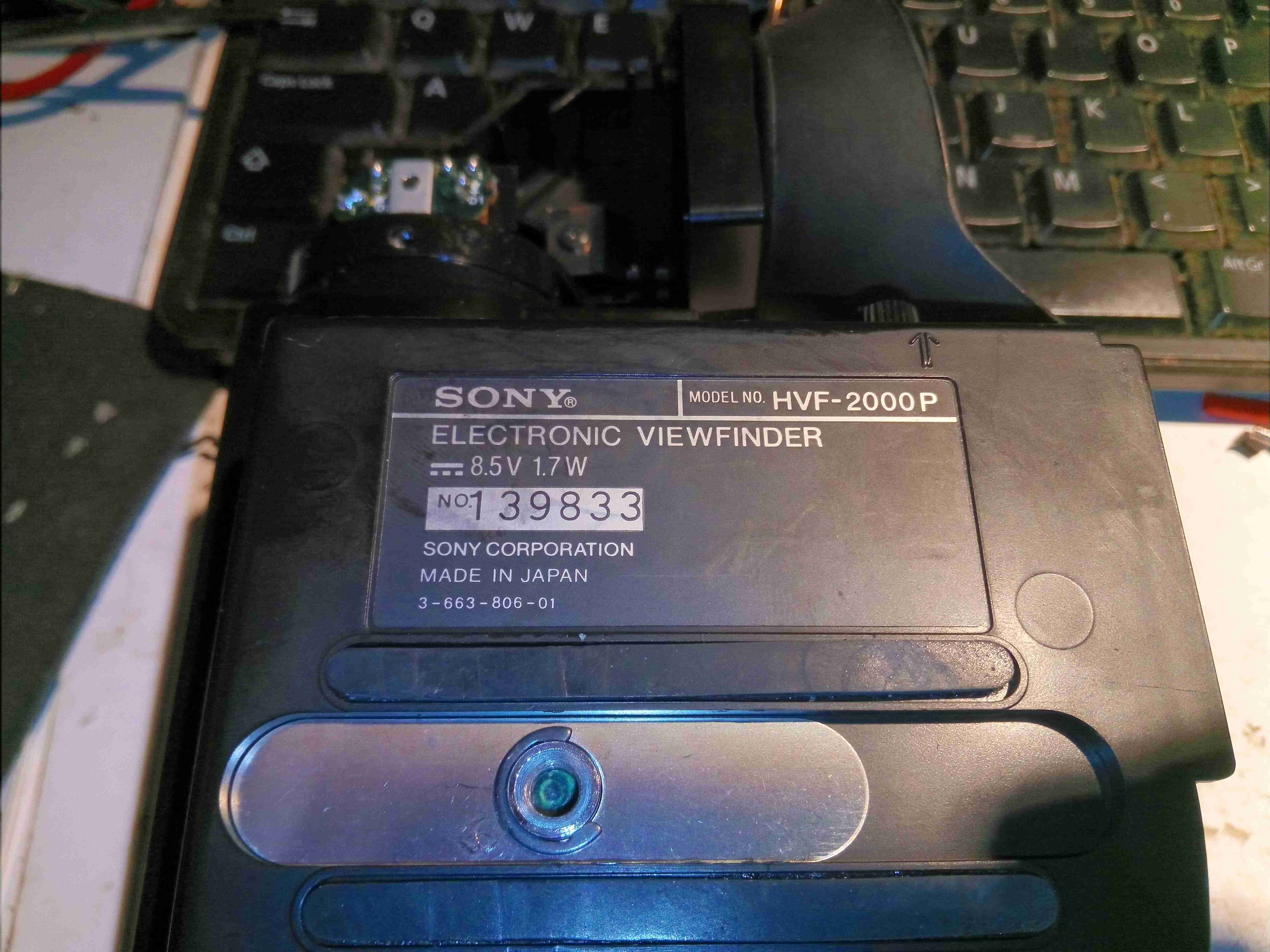
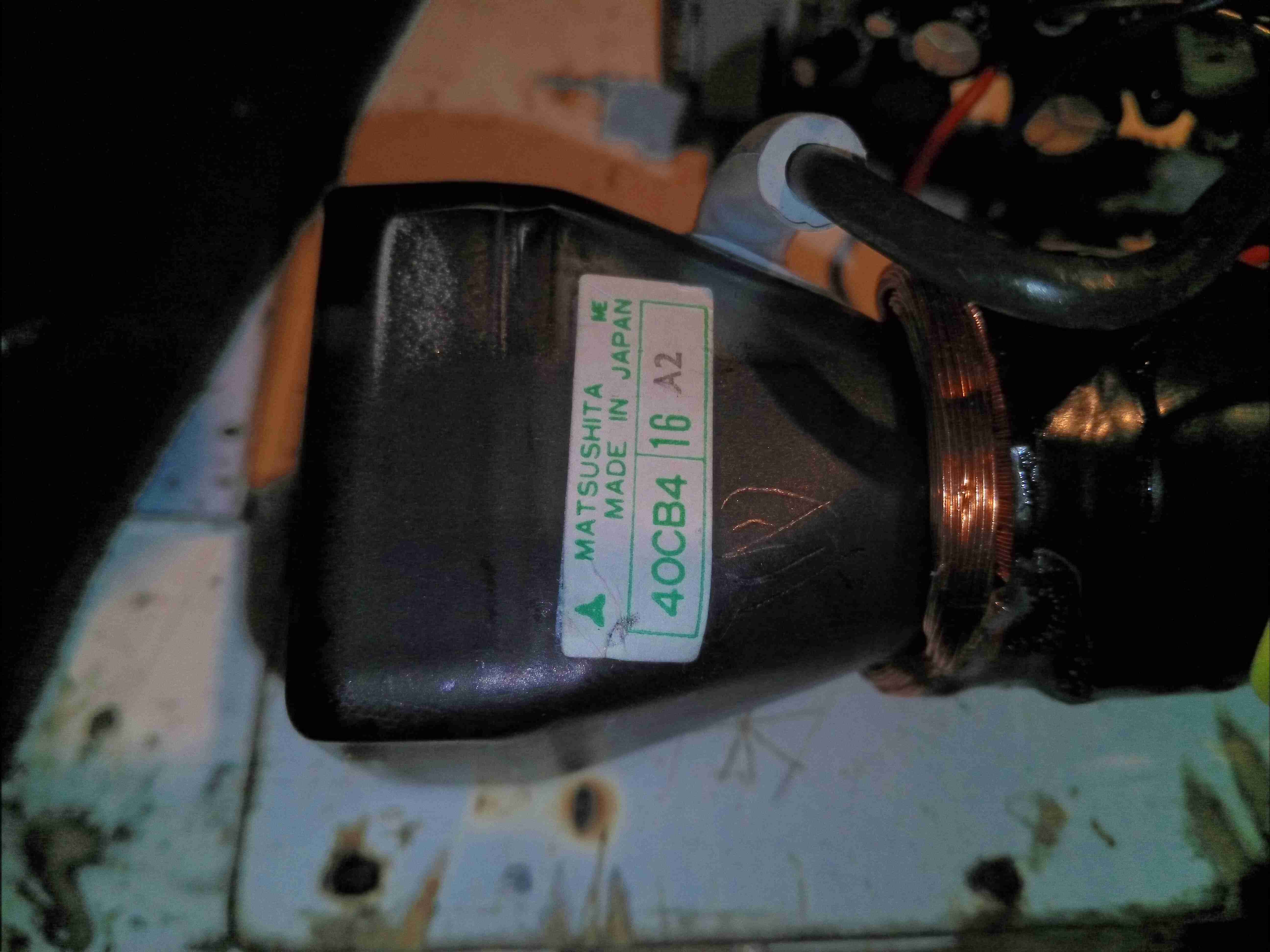
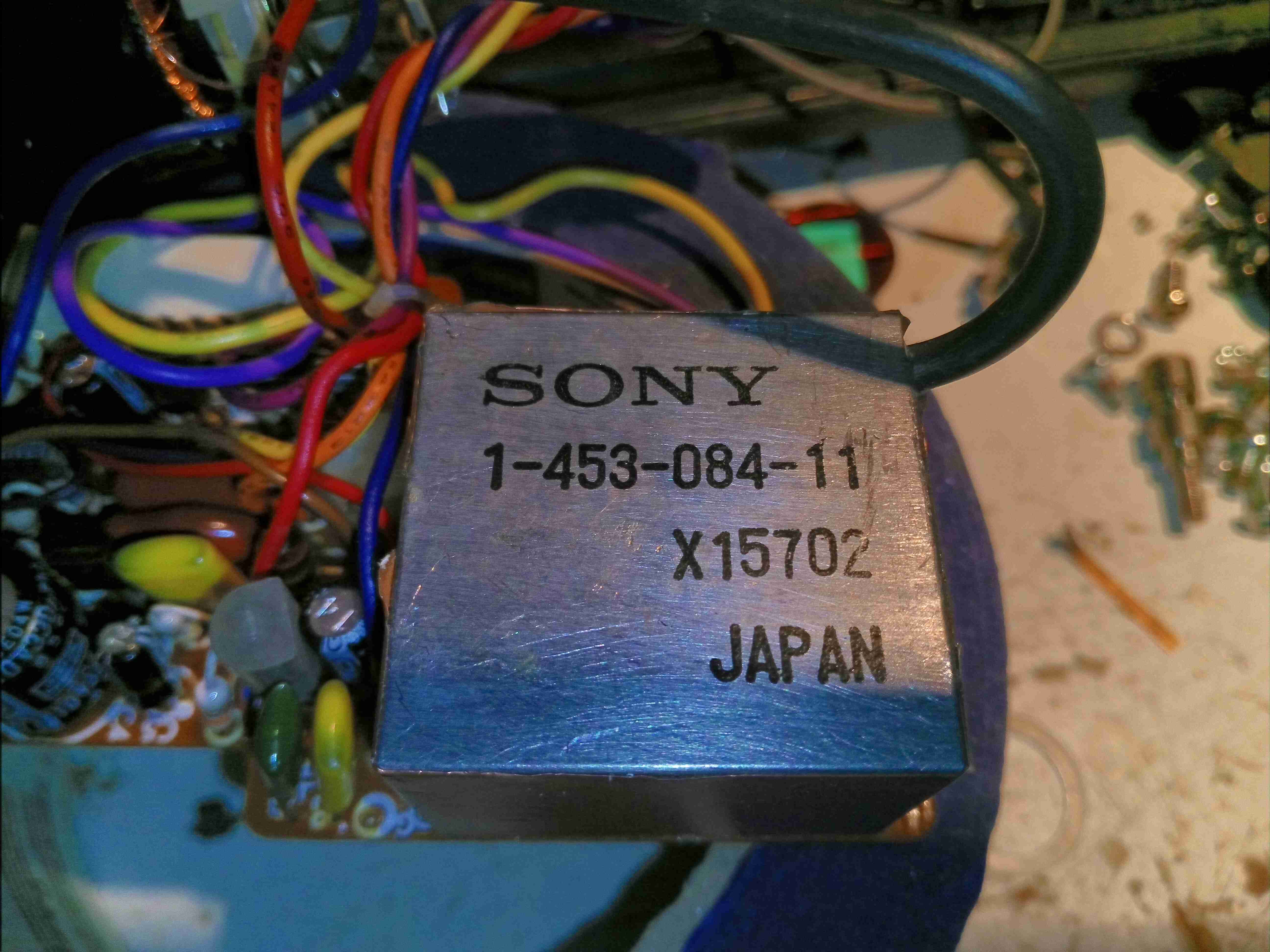
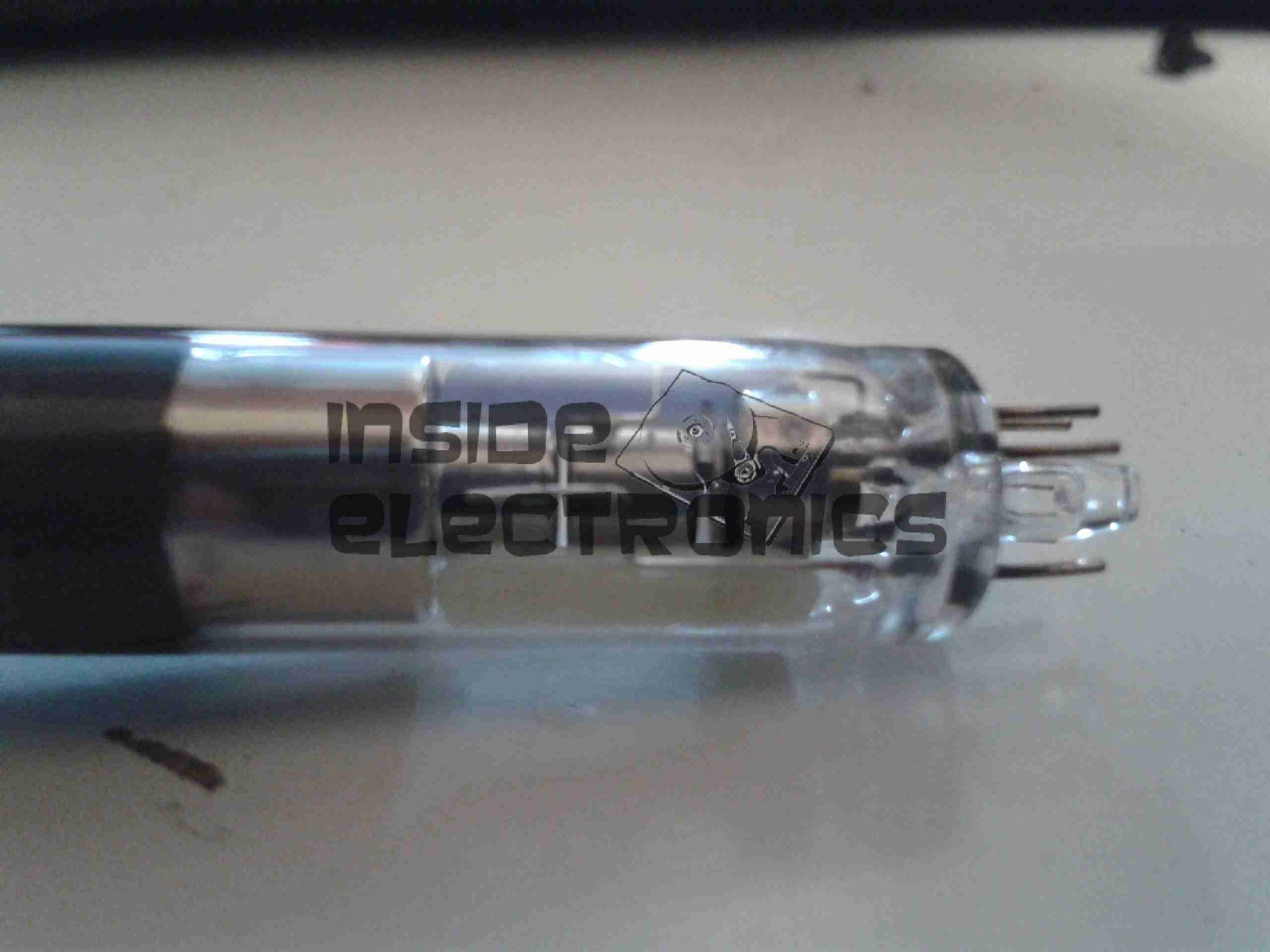
It’s time for another CRT-based post! This time it’s a Matsushita 40CB4-based viewfinder from 1980. These came from JVC colour tube cameras, and are physically massive! I’ve already worked out the pinout on the multicore cable here & attached a usable connector.
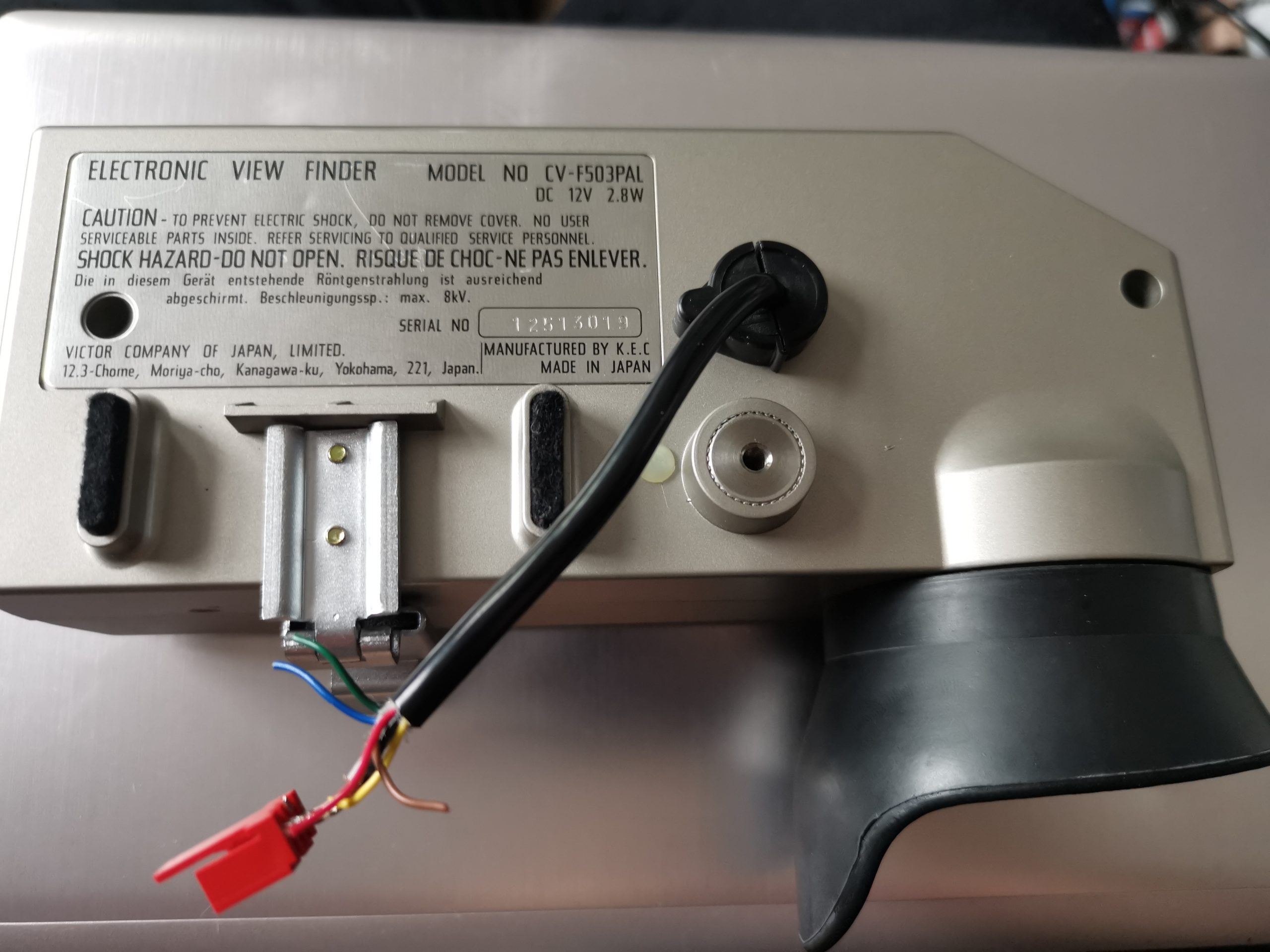
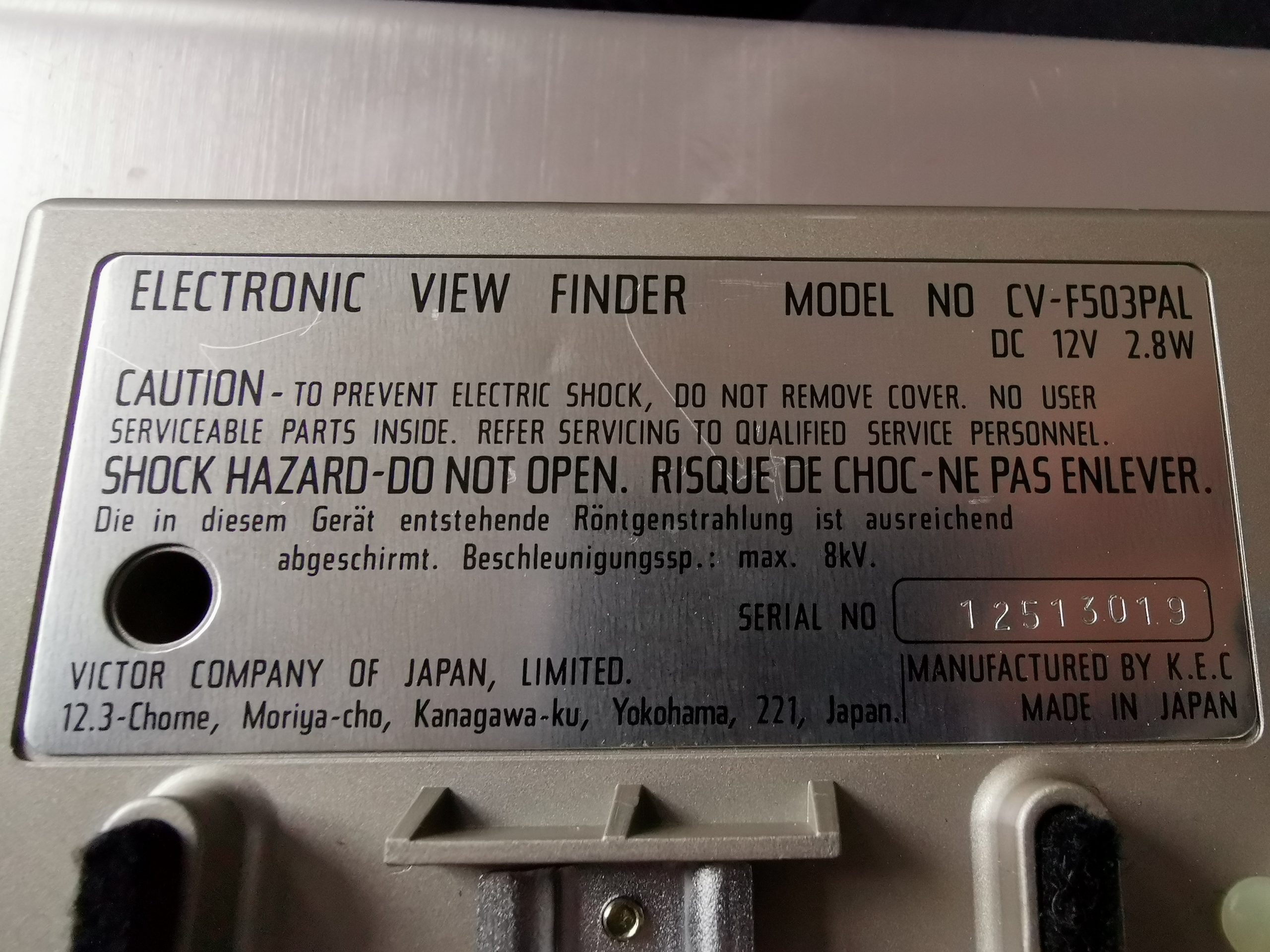
Information Label
There’s lots of information on the bottom label of this unit, including a notification in German that the X-Ray emission from the device is shielded, and the maximum CRT acceleration voltage is 8kV. This last point is a bit strange, since the 40CB4 datasheet states a maximum design voltage on the final anode of 6kV. I did measure the voltage at the anode cup, and it’s stable at 7.15kV!
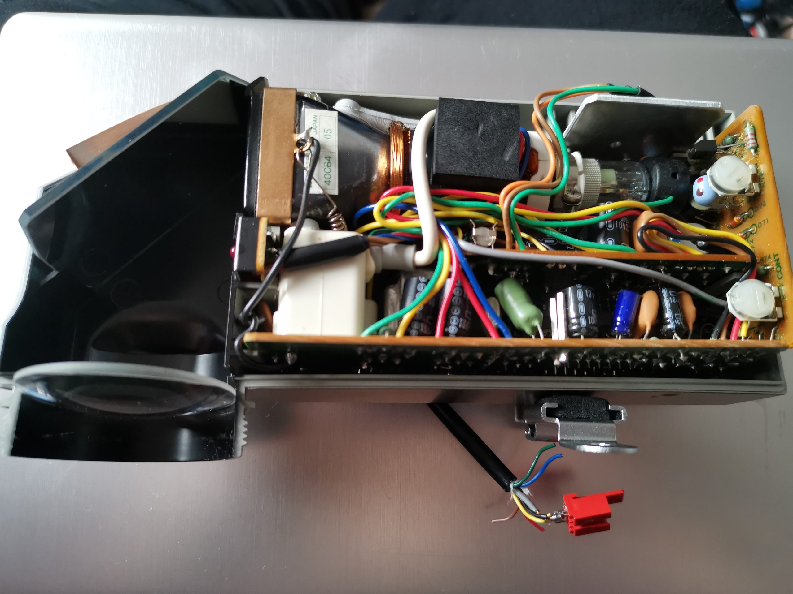
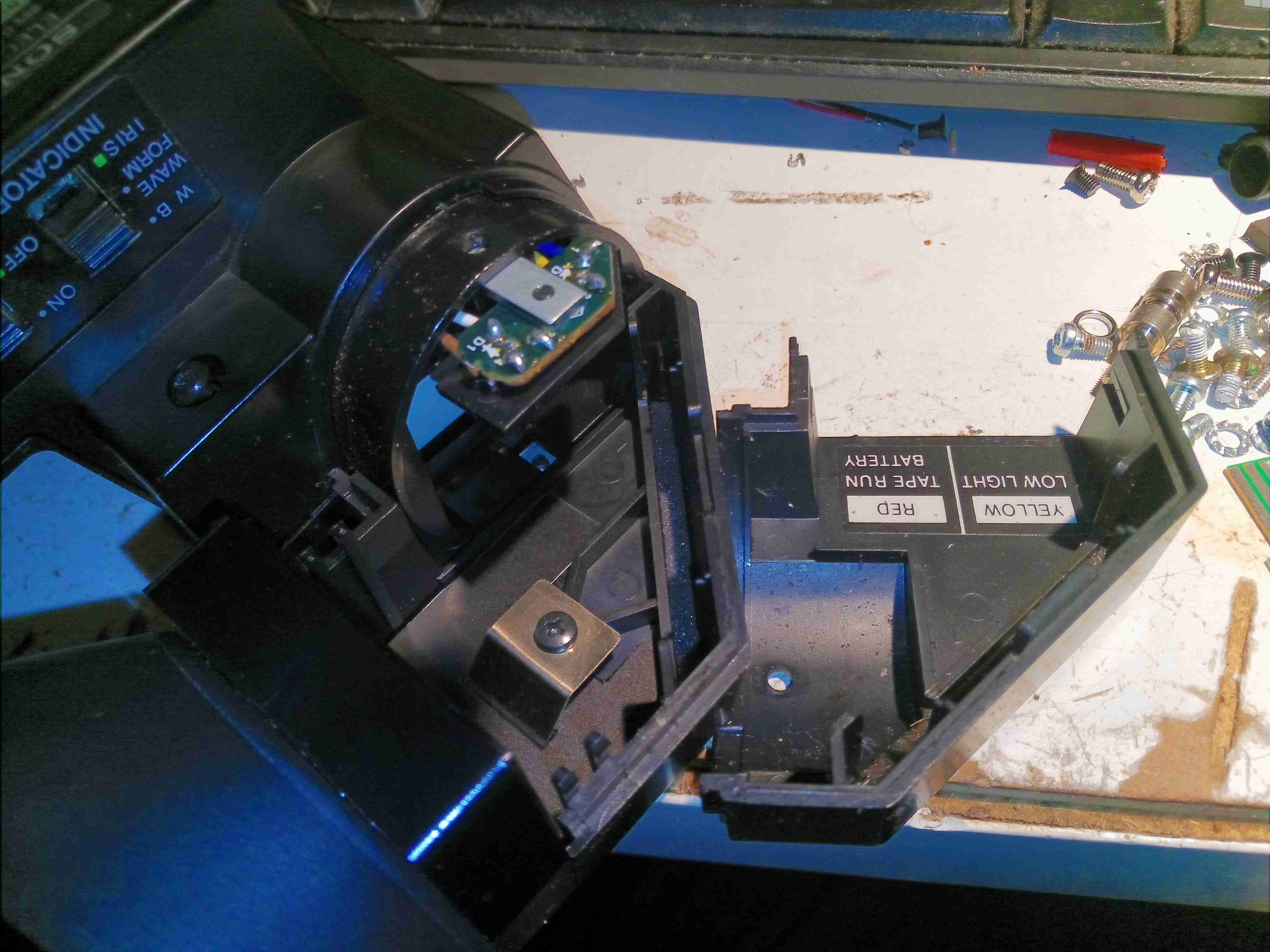
Internal Overview
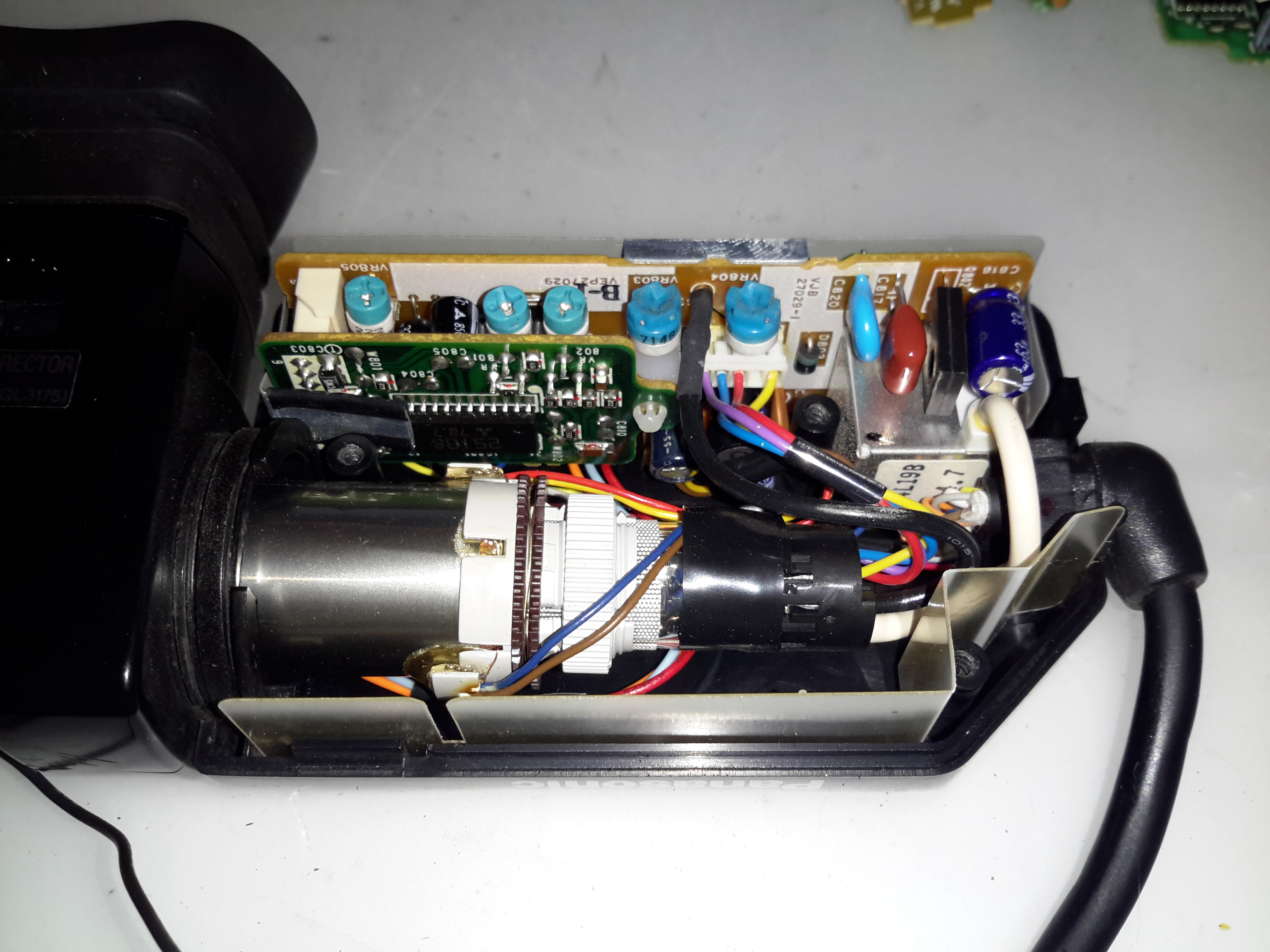
Popping a couple of screws out & removing the enormous eye cup allows the top cover to come off. This unit is very tightly packed inside, with 3 PCBs! The magnifying lens (~45mm diameter) & mirror on the left enlarge & turn the image so the camera operator can see it. The CRT’s at the top, with a copper grounding band around the face.
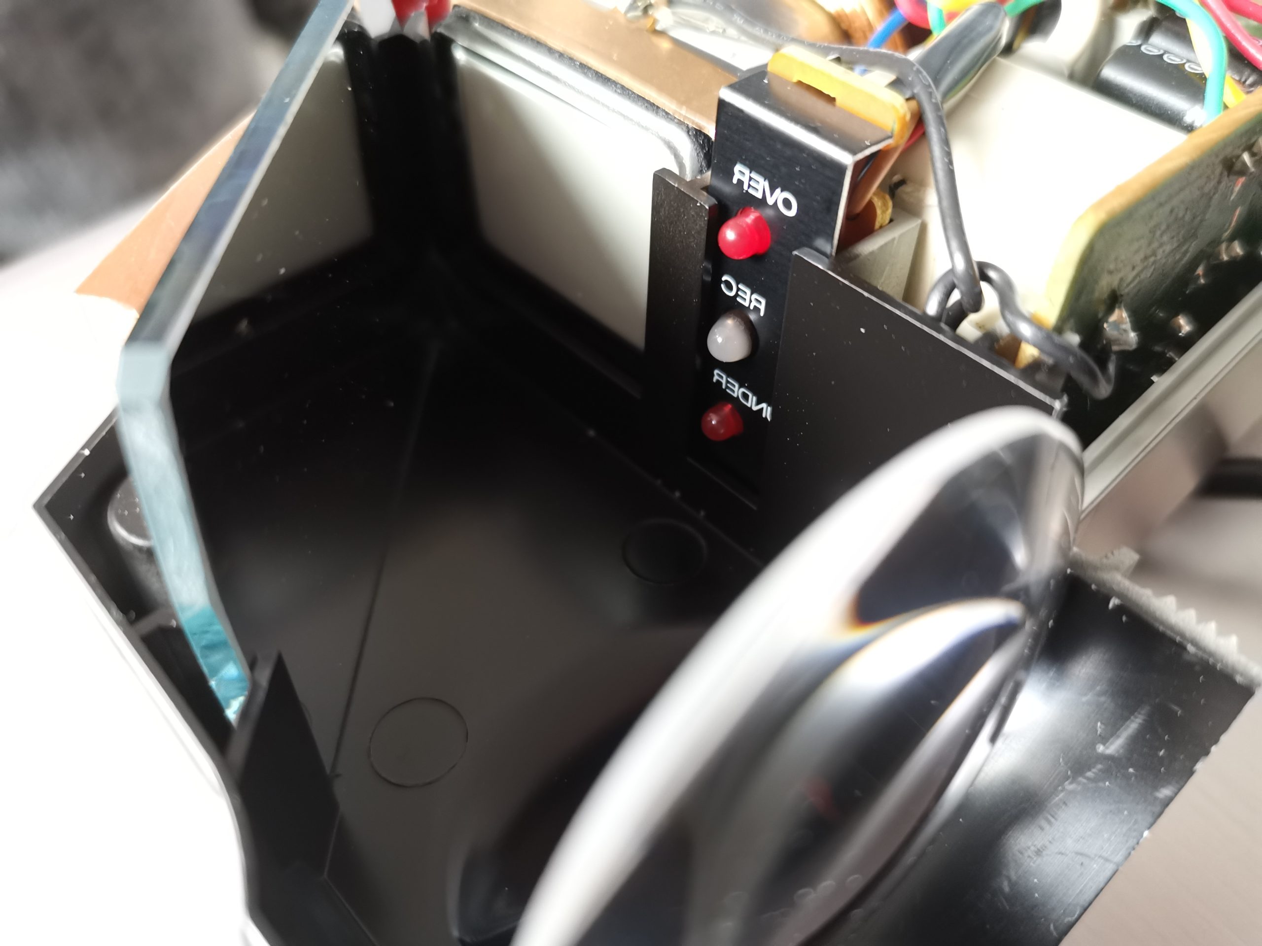
CRT Face
The CRT face is neatly slotted into the plastic housing, with the tally LEDs to the right of it. The legends on the LEDs are naturally printed in reverse, since they’re intended for viewing through the mirror. The optical section is entirely spray painted black for better contrast & stray light control.
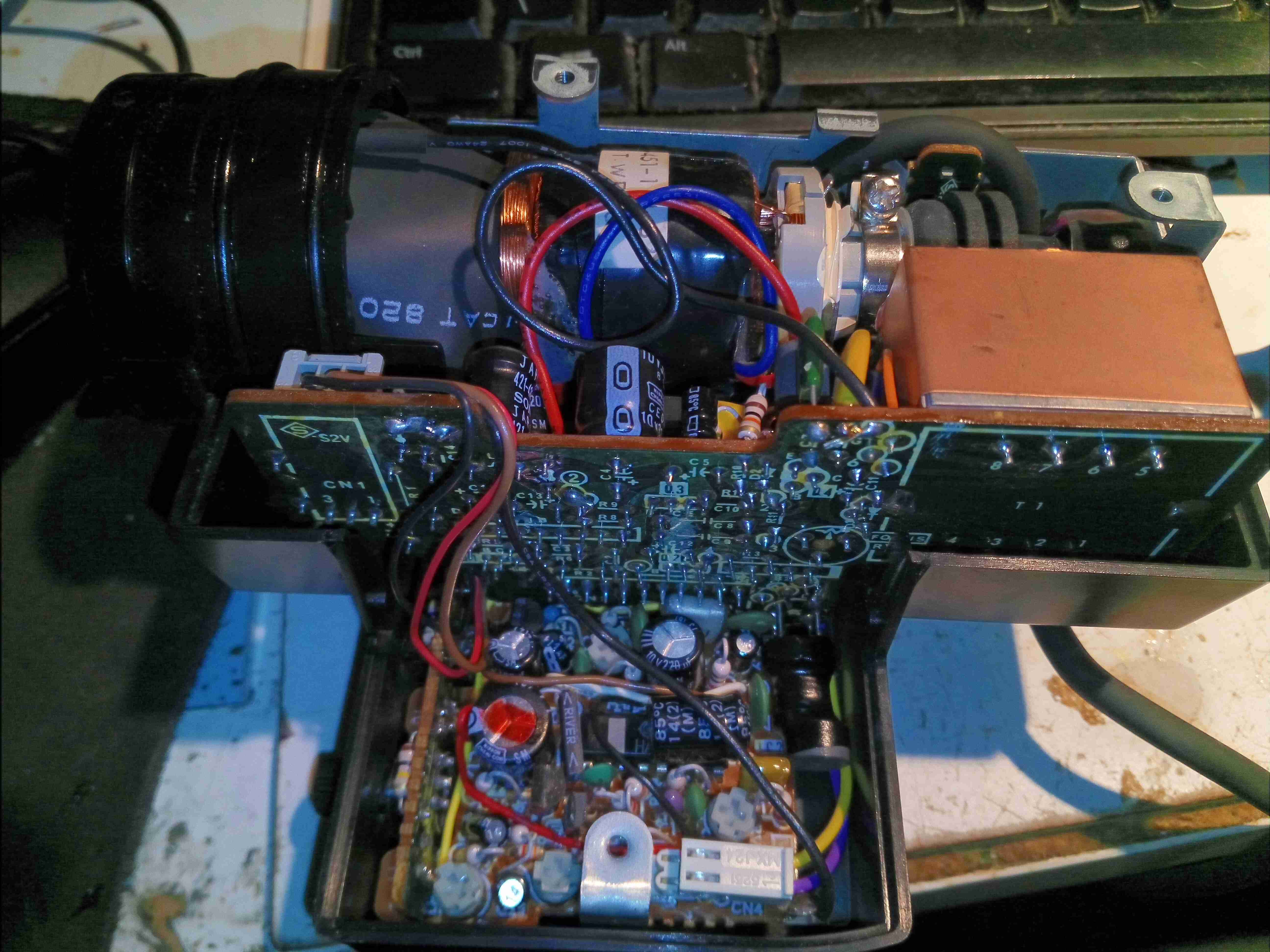
Electronics Area
The other 5″ of the casing is packed with electronics to support the CRT. The bottom PCB even “wraps around” to the right, with copper staples connecting the boards together. The CRT tube itself is hiding inside the deflection yoke and under a foam pad at the top of the unit. It’s secured in place with a copper grounding strap wrapped around the face of the tube, and a spring. A single screw secures the strap to the case. This also provides a local earth for the outer Aquadag coating on the tube, which is the negative plate of the final anode smoothing capacitor. The other plate is formed by the coating on the inside of the CRT glass, and the dielectric is of course the glass itself.
The main anode wire snakes off from the flyback at bottom left to the anode cup at the top of the CRT, insulating the 7kV from everything else.
There aren’t many reasons to jack up the final anode voltage on a CRT, past the design voltage of the tube as JVC have done here. The only plausible one I could think of is to increase brightness of the image, but the Sony 4CB4-based units I have only run at around 3kV, and those are plenty bright enough! The downside here of course, is that with higher energy electrons and a brighter image, the phosphor of the CRT will wear out faster.
Increasing voltage also increases X-Ray emission, but even at the 8kV maximum, such X-Rays would be so weak as to not make it through the CRT faceplate glass, which is loaded with lead anyway.
There’s not much sense in yanking the tube out of this unit, it’s identical to the Sony one’s I’ve done in the past:
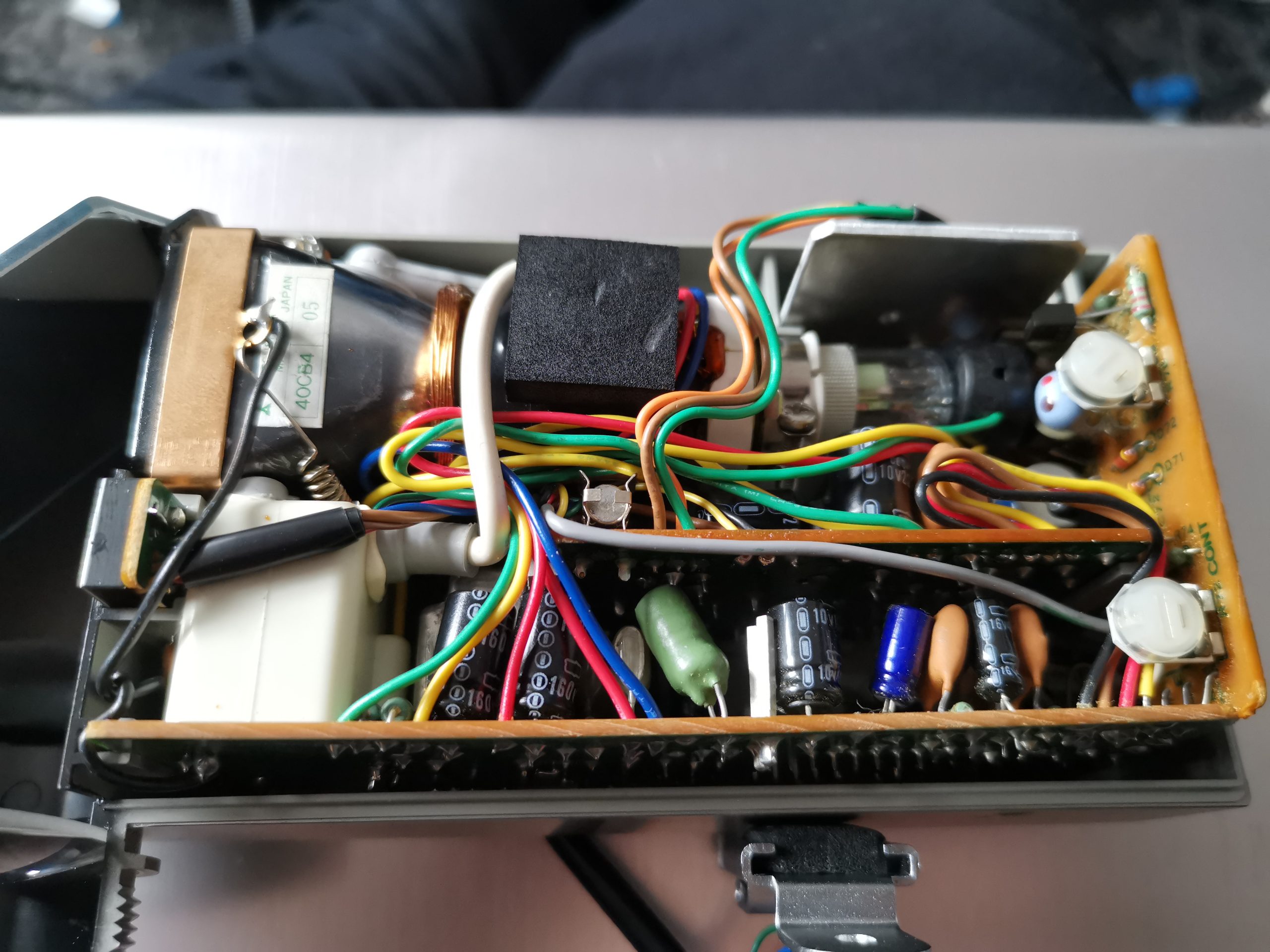
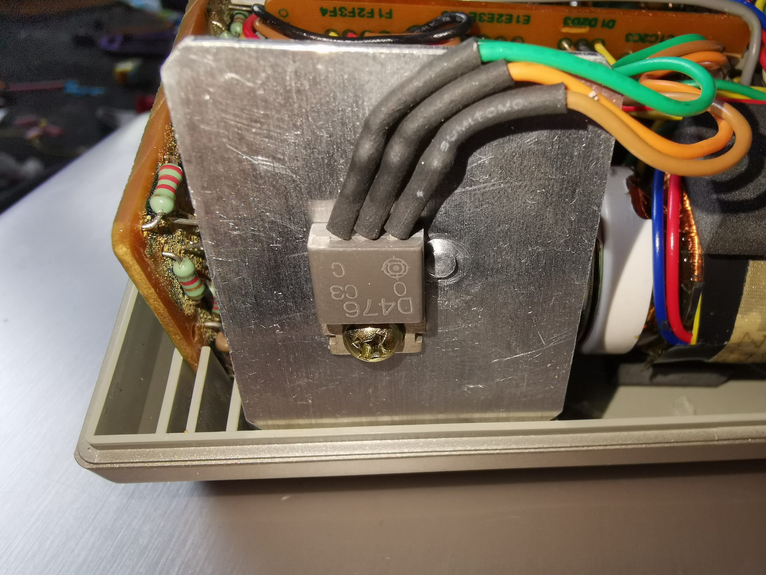
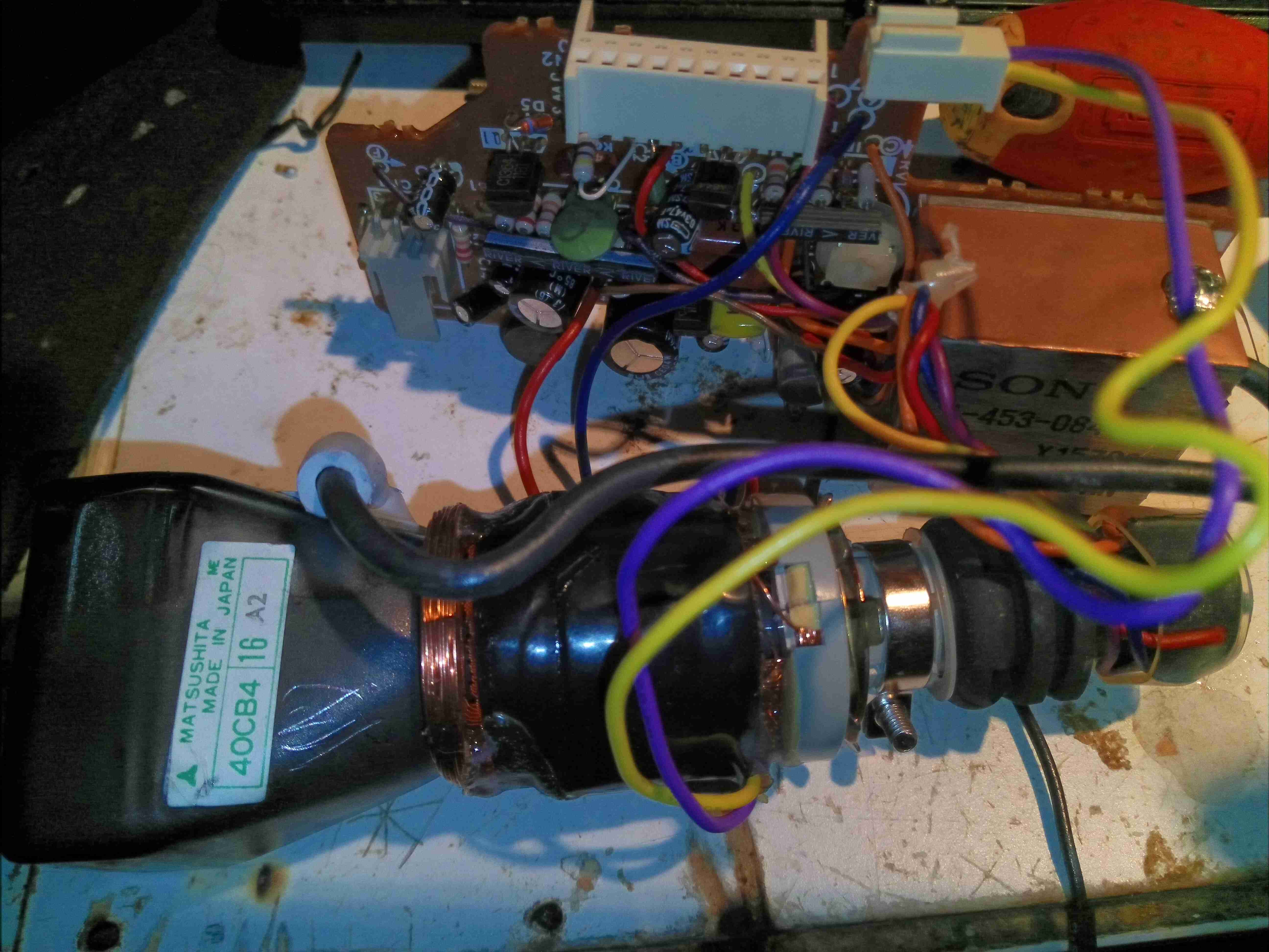
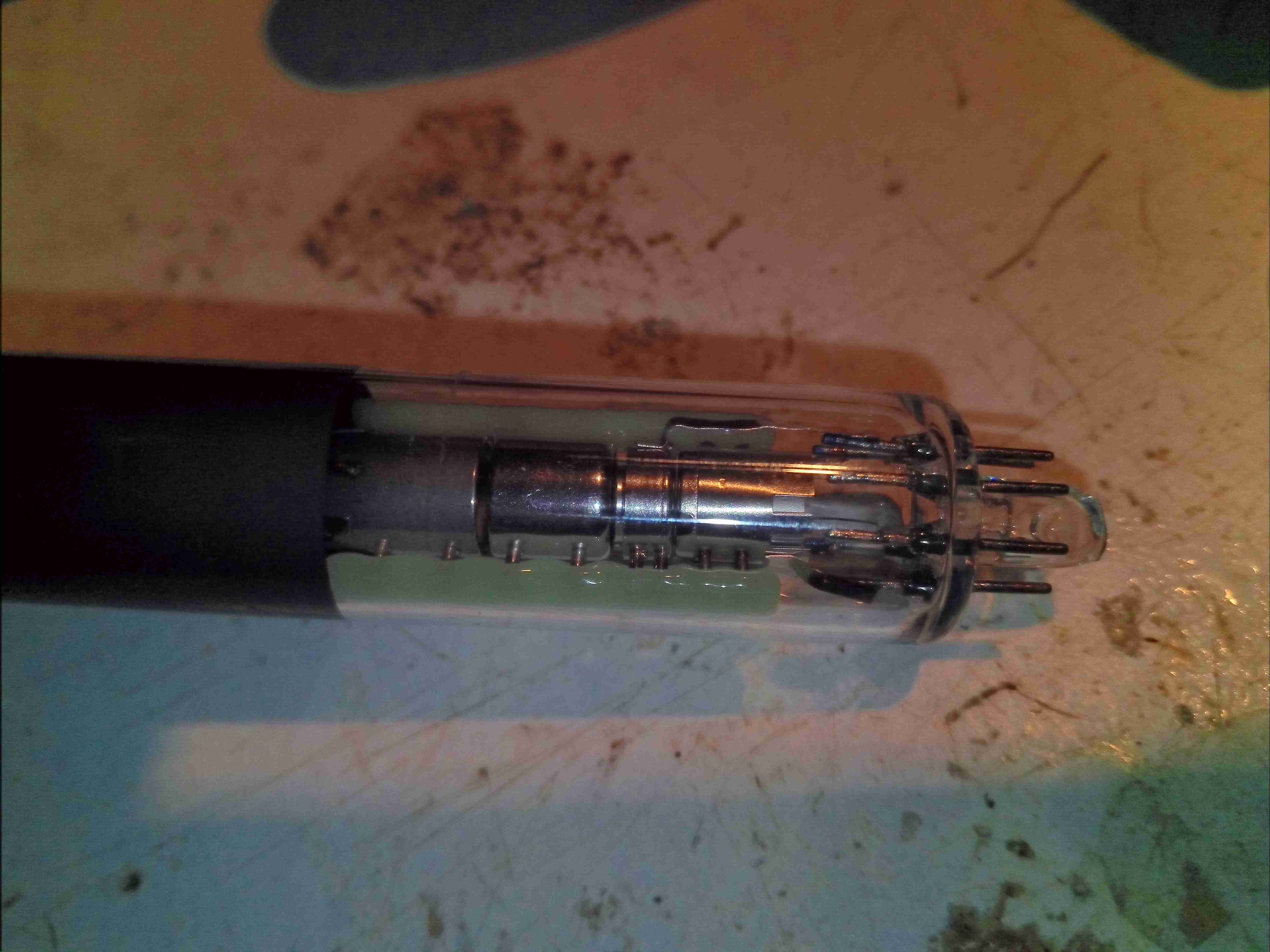
Bare 40CB4 CRTVoltage Regulator Pass Transistor
Slotted into a gap above the CRT is a large TO-220 2SD476 NPN transistor, this is part of the power circuit; it’s the series pass element regulating the input 12v down to 9v for all the remaining circuits. The aluminium sheet on the back provides some heatsinking as this part gets warm! Current draw of this unit with no video input is about 260mA.
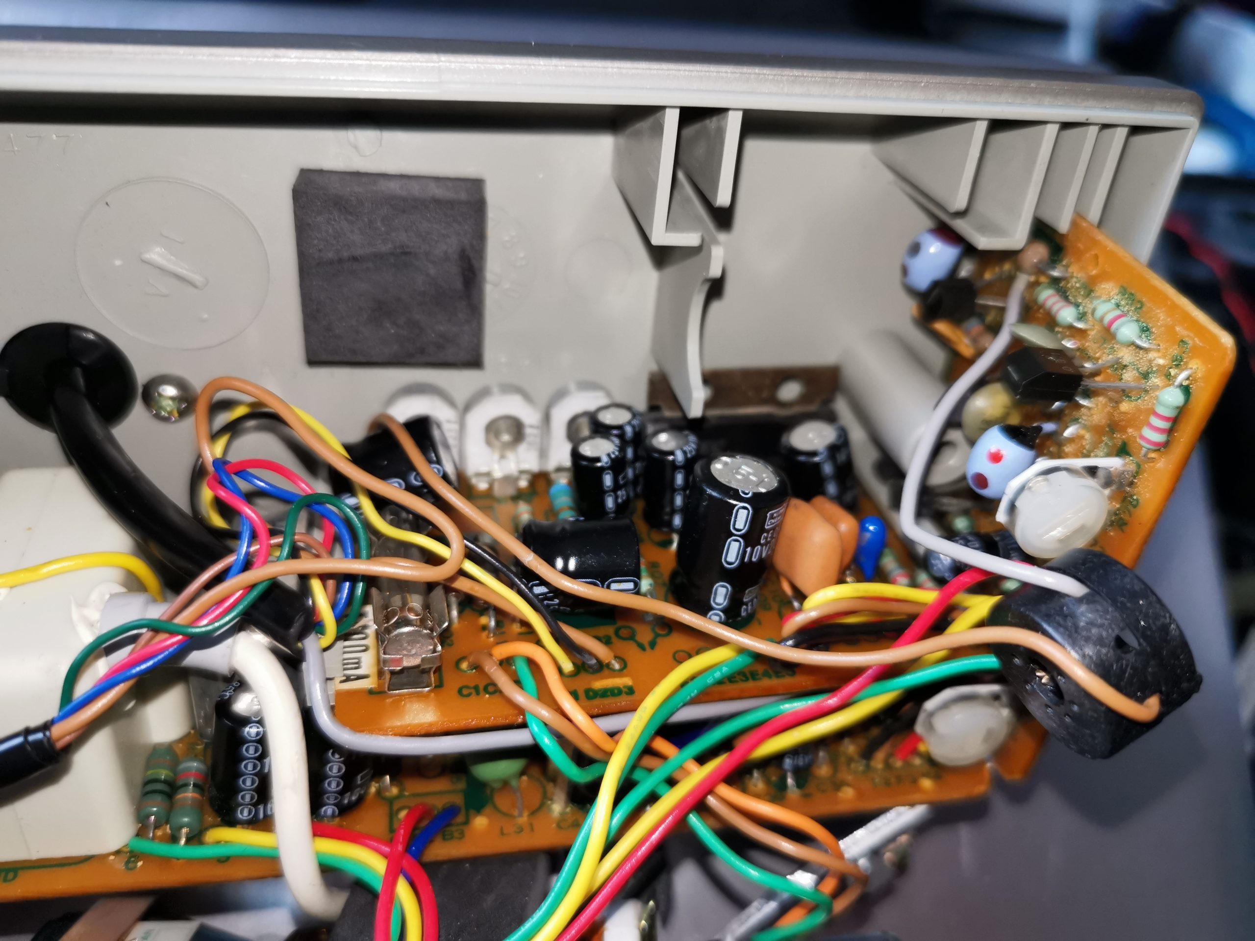
CRT Removed & Vertical Board
Popping the CRT out allows a view of the Vertical & Power Board. This hosts the input linear voltage regulator, and the vertical output control circuitry. Hiding at the back on the right is a NEC µPC1031H2 Vertical Deflection Controller.
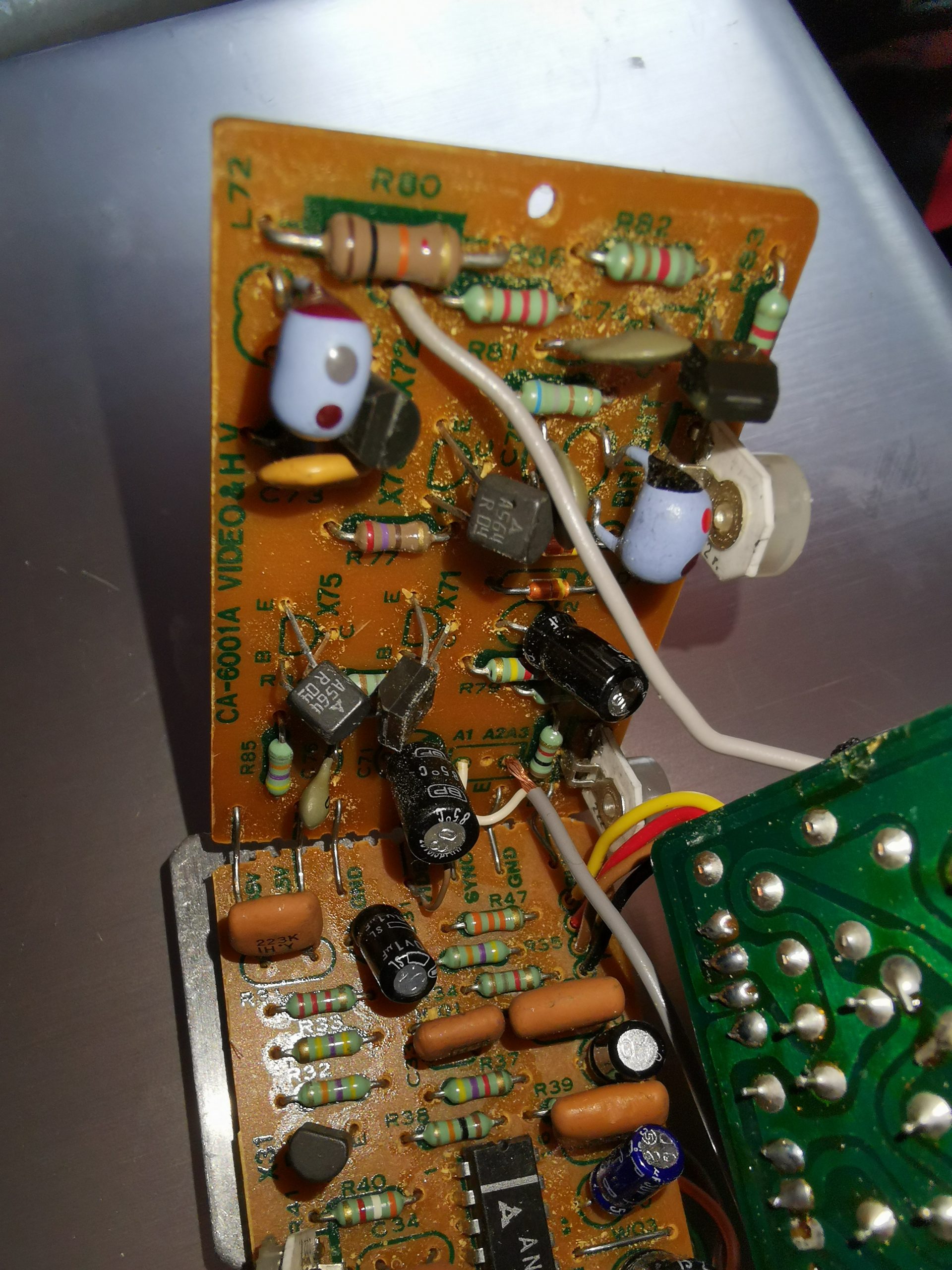
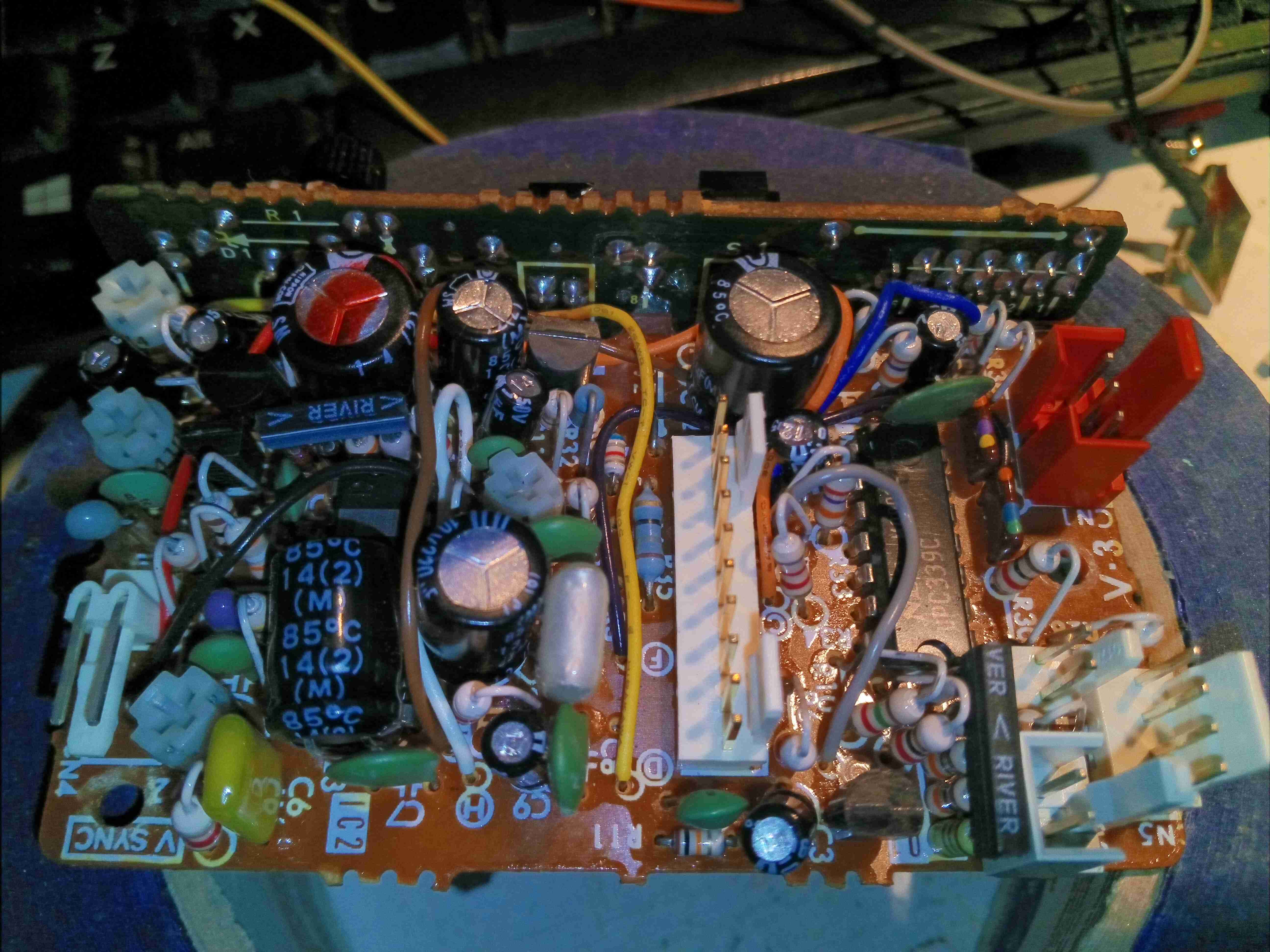
Horizontal & Video Boards
Separating the boards reveals the other two PCBs, the Video & Horizontal/HV boards. The bottom board takes care of the Horizontal output, and the lefthand board the video input, sync separation & amplification.
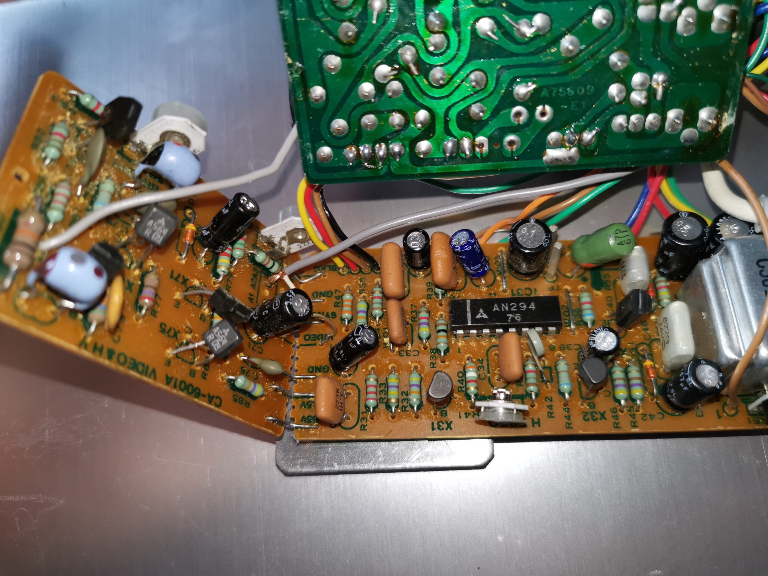
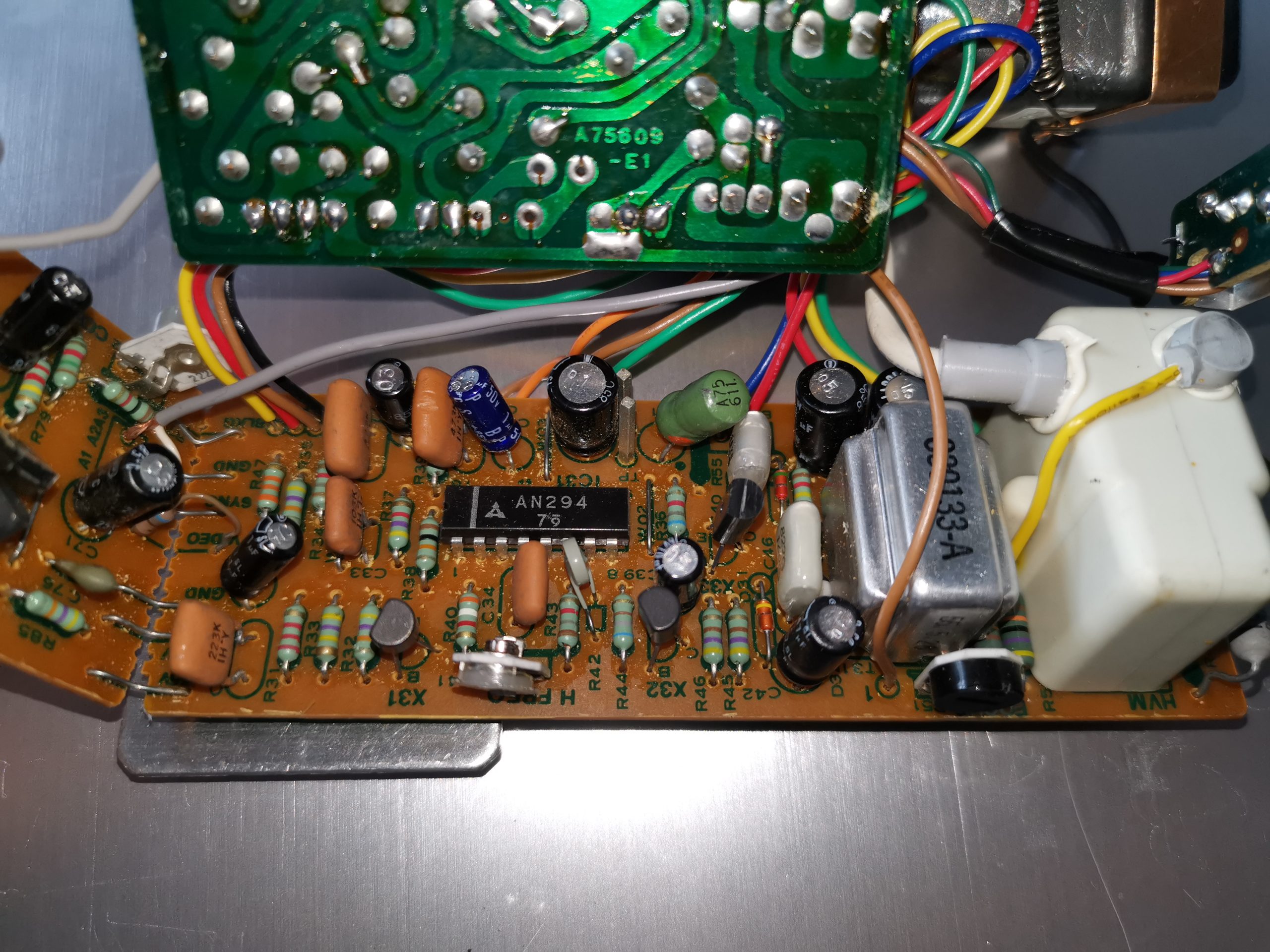
Horizontal Control IC
The Horizontal section is controlled by a Matsushita AN294 device. Unfortunately I haven’t been able to locate a datasheet for this one. The flyback transformer (Horizontal Output) is on the right, with another smaller transformer I don’t quite know the purpose of. Oddly, there’s no large switching transistor for the horizontal output stage – as the PCB notes the flyback as being a “HVM” this may in fact be more tightly integrated with some of the drive circuitry in the potting. There aren’t anywhere near as many pins on it as a usual CRT flyback has either.
This section also generates the other voltages required by the CRT – 2.8v for the filament, and ~80v & ~400v for the grids.
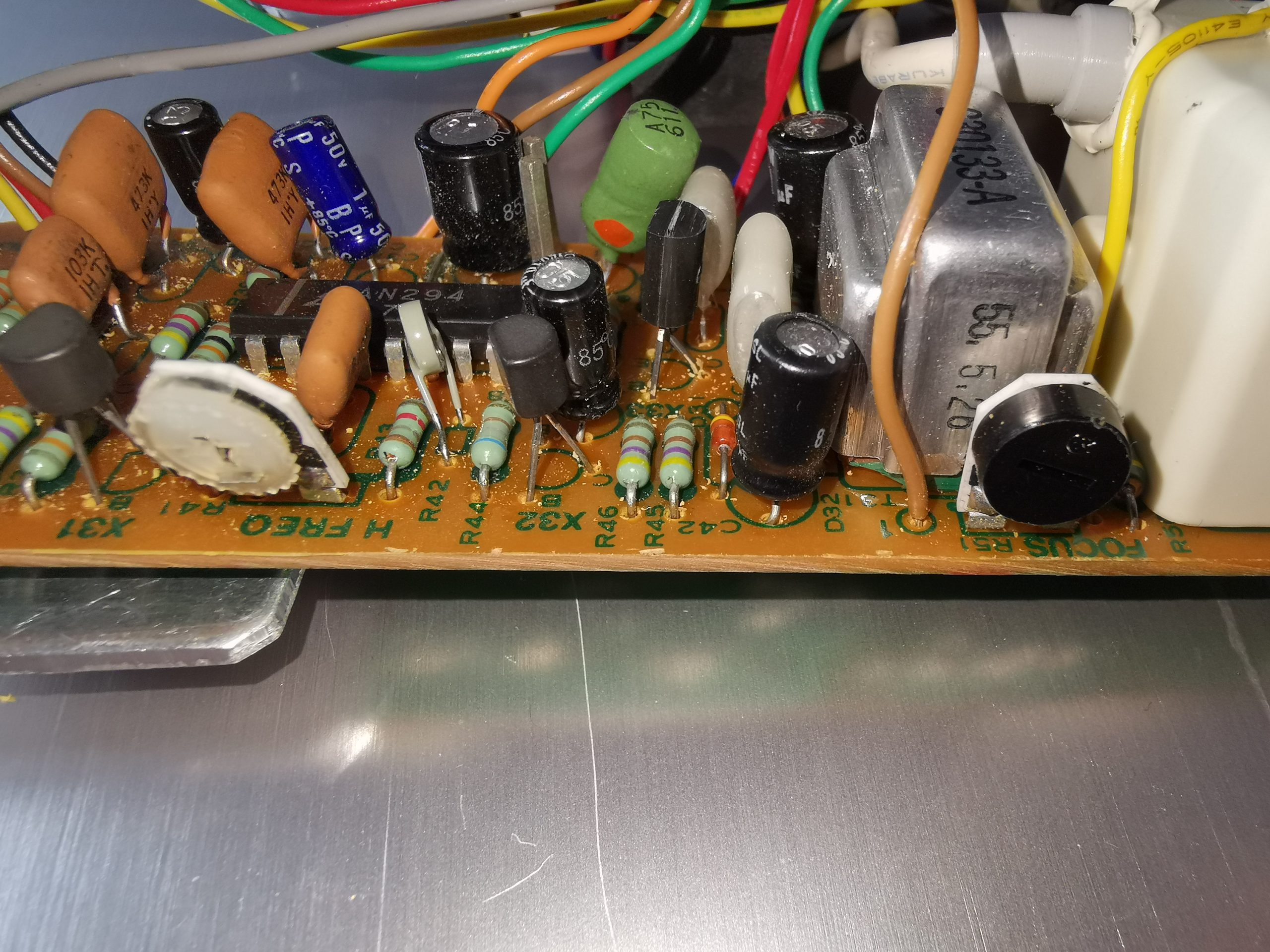
Video Board
A closeup of the video board shows the relative simplicity. Only 4 transistors are doing all the video actions. There is relatively high voltage on here though – an 85v feed from the power supply which is the rail voltage for the video amplifier to the CRT cathode/G1.
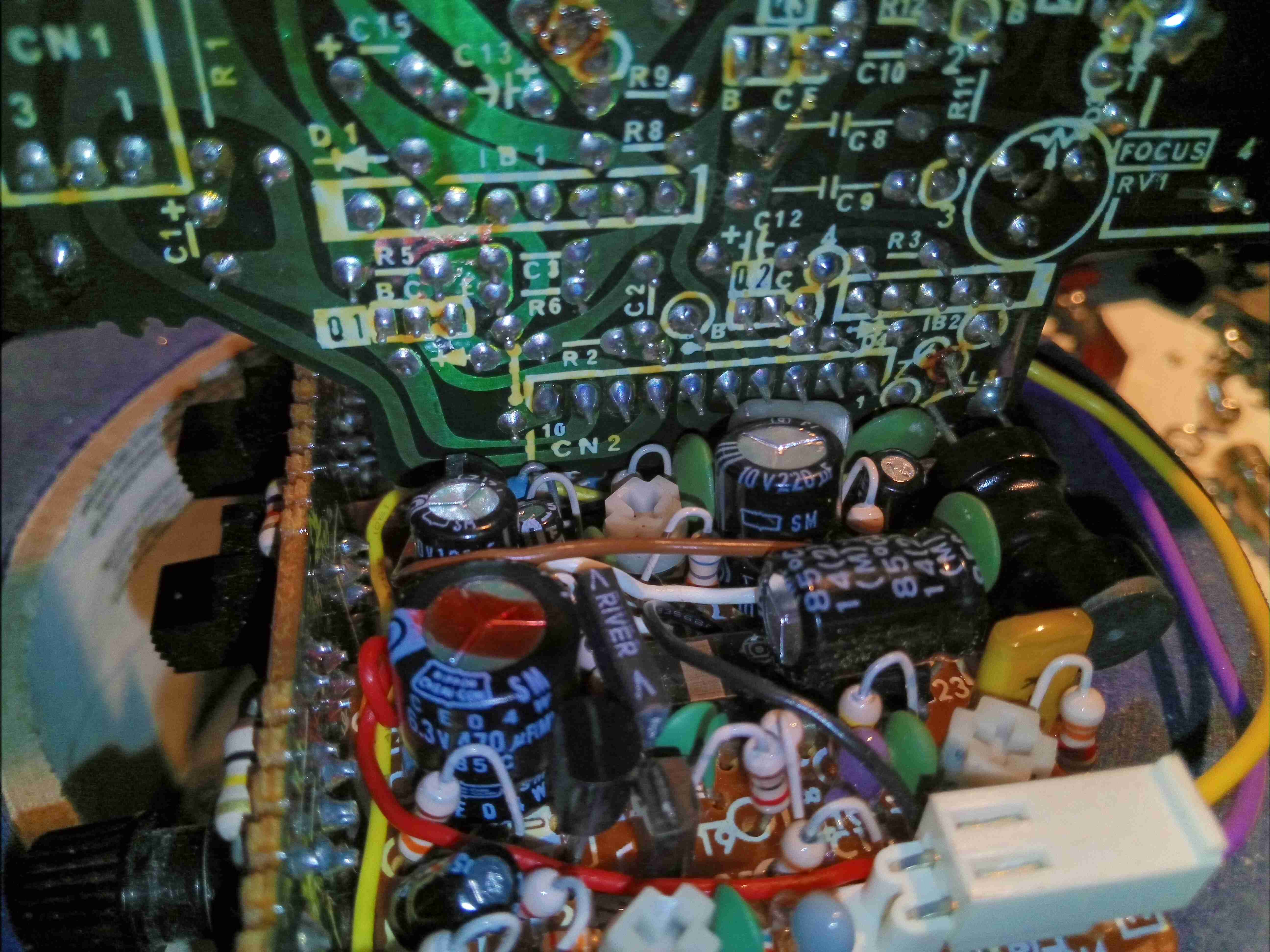
Focus & Horizontal Hold Adjustments
There’s a few adjustments available on this unit, here are the Focus & Horizontal Frequency (Hold) pots. Amazingly, even though this unit is about 43 years old at the time of writing, the unit fired straight up when I applied power & a composite video signal, with no adjustments required at all!
Unfortunately there’s no service manual or schematics that I could find on the web for this or the camera it came from, but connections to make this unit work are very simple:
Wire Colour
Signal Name
YELLOW
+12V DC
BLACK
GND
Coax - Core
Composite Video 1v p-p
Coax - Shield
Composite Video GND
There’s another blogger who’s done this particular viewfinder, but they didn’t dig into the unit anywhere near as far as I usually do:
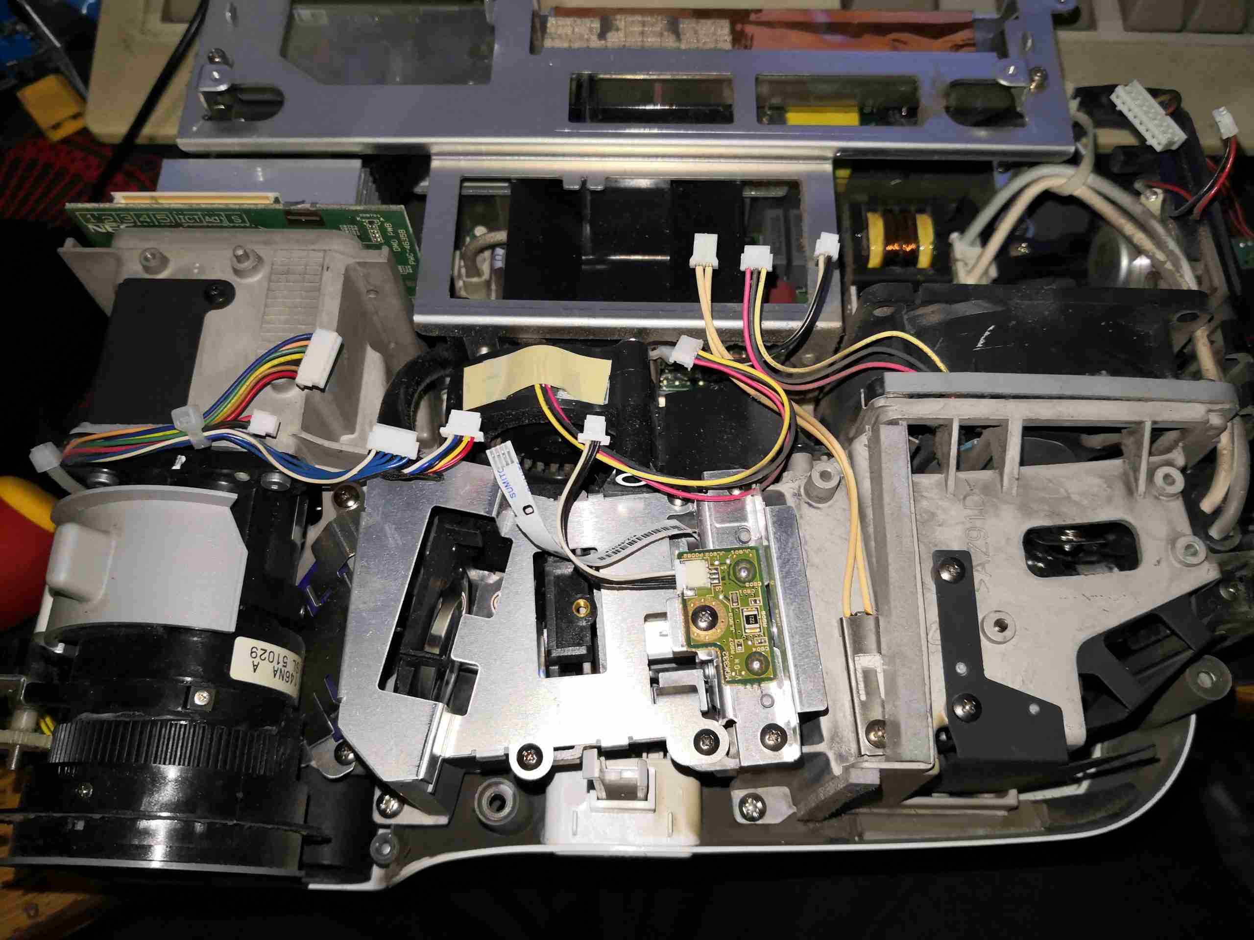
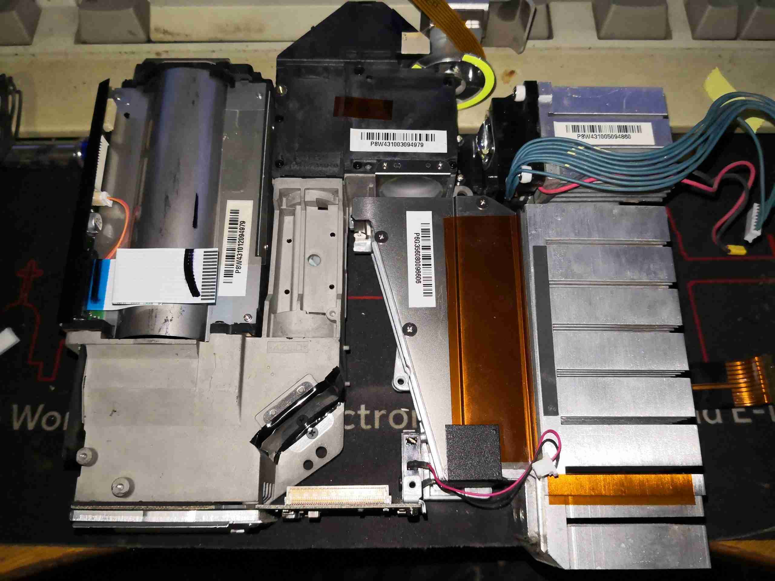
Time for another projector! This one was brought to me with a fault, described as a shadow in the middle of the image, shortly after the lamp was replaced after exploding. This is an older DLP projector, with a UHP mercury lamp. I’ve already removed the top cover of the projector here, showing the internals. The light engine is along the front of the unit, with the lamp on the right. The main control board on top contains all the image processing logic & control functions.
Mainboard
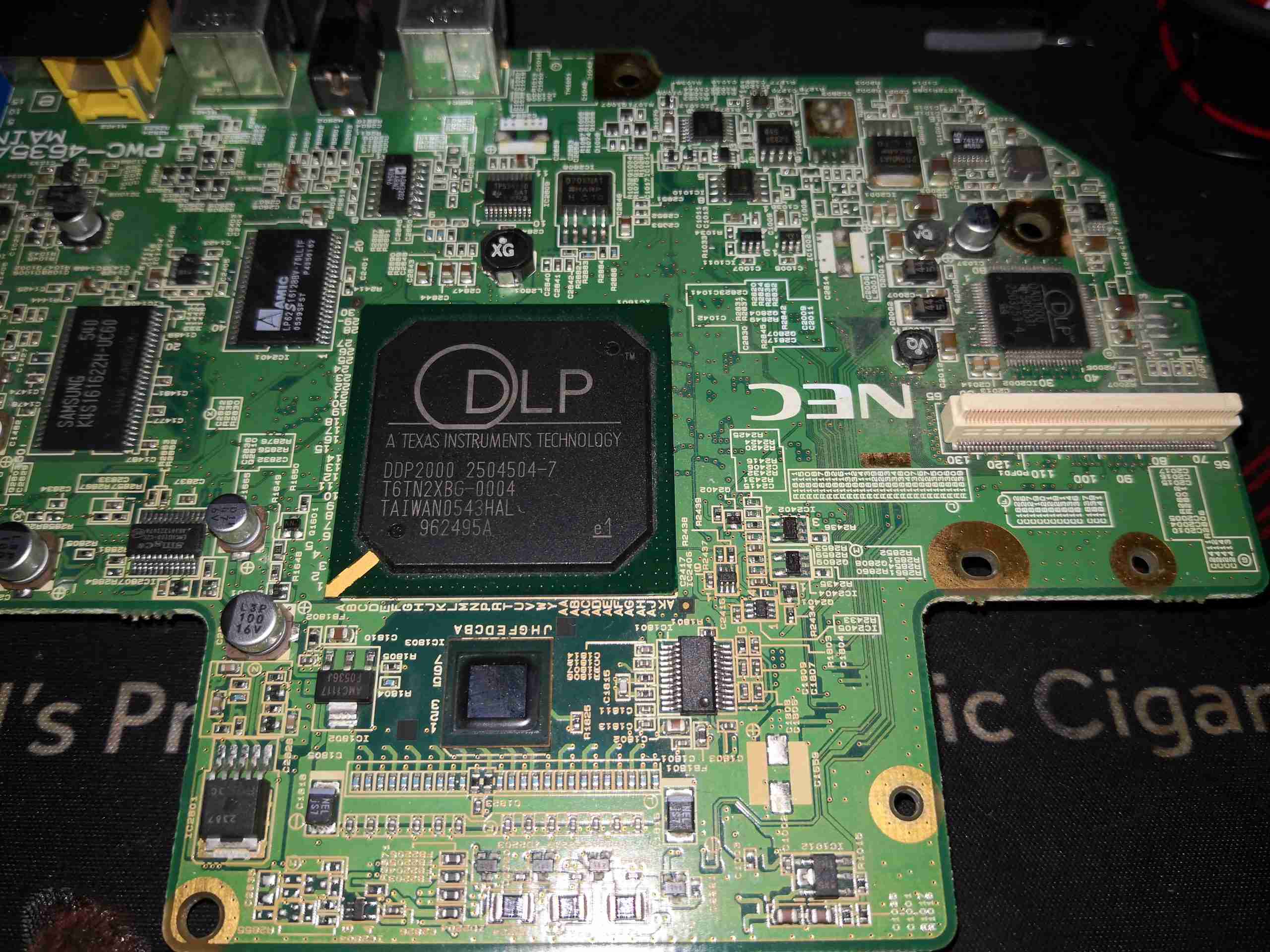
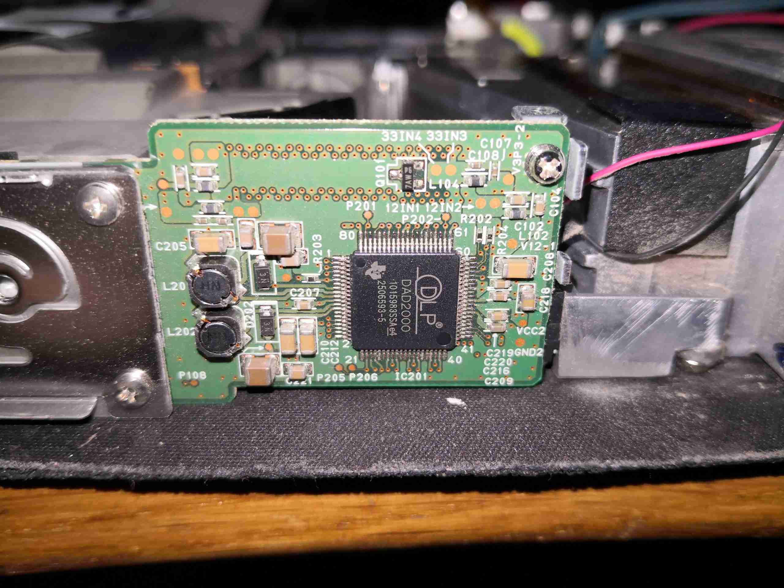
The other side of the mainboard holds the processing chipset. This is probably one of the biggest flip-chip BGA packages I’ve ever seen, the DDP2000. Along with the DAD1000 on the right, these format & send the image data to the DLP chip, via the large white header.
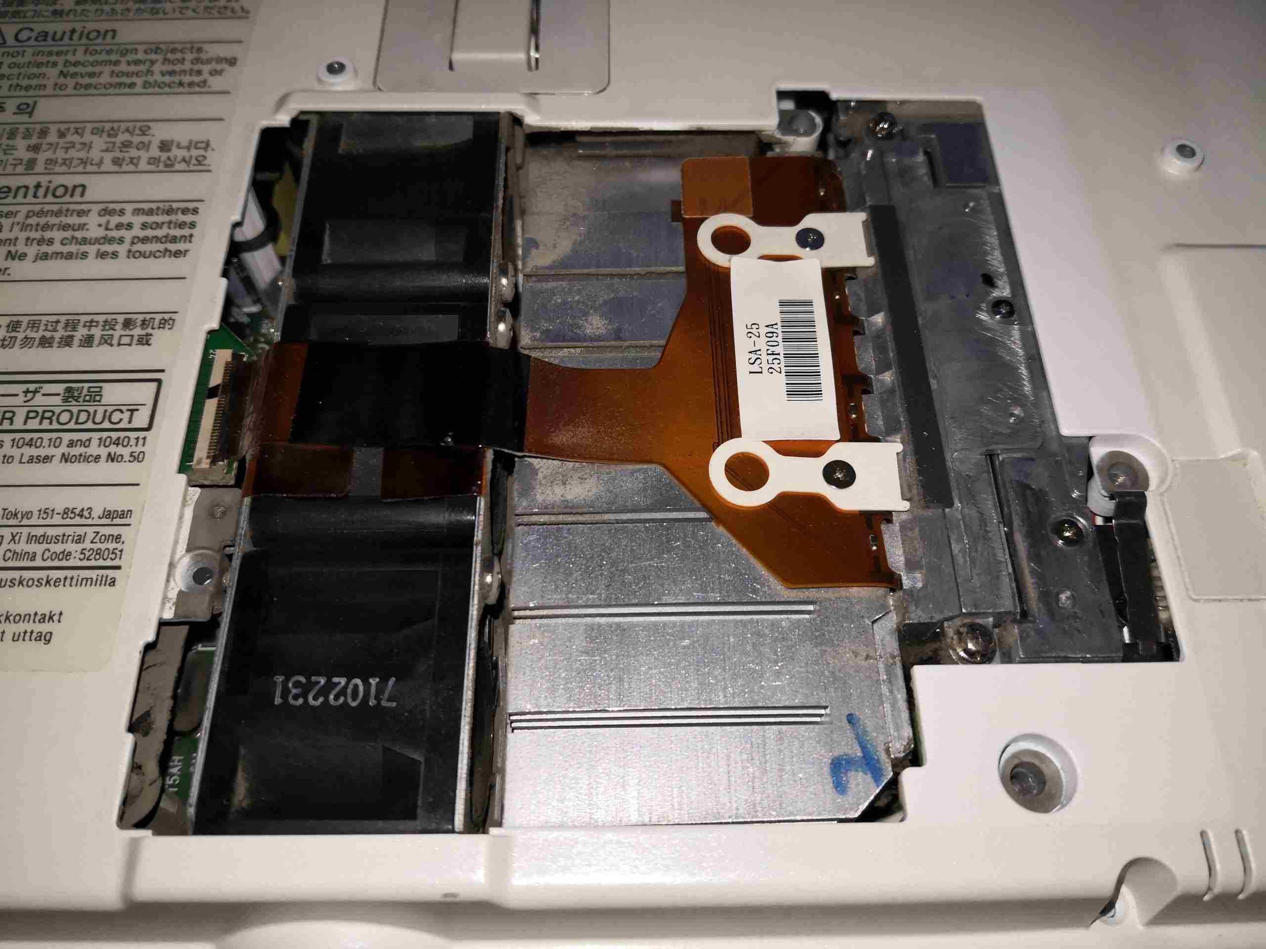
Main PCB Removed
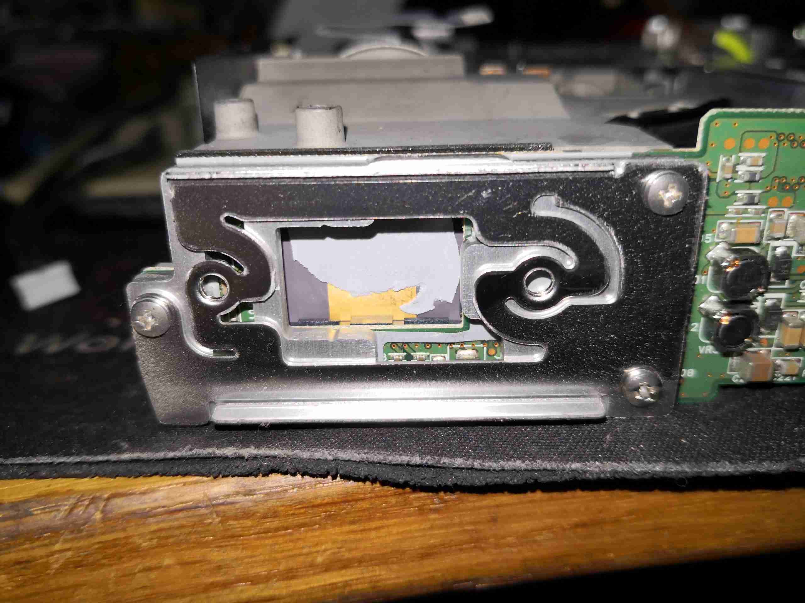
After the mains PCB is removed from the chassis, the rest of the light engine is visible. The DLP is hidden on the left, behind the large heatsink & interface PCB. The light engine is spread out a lot more on this projector, across the entire front of the unit.
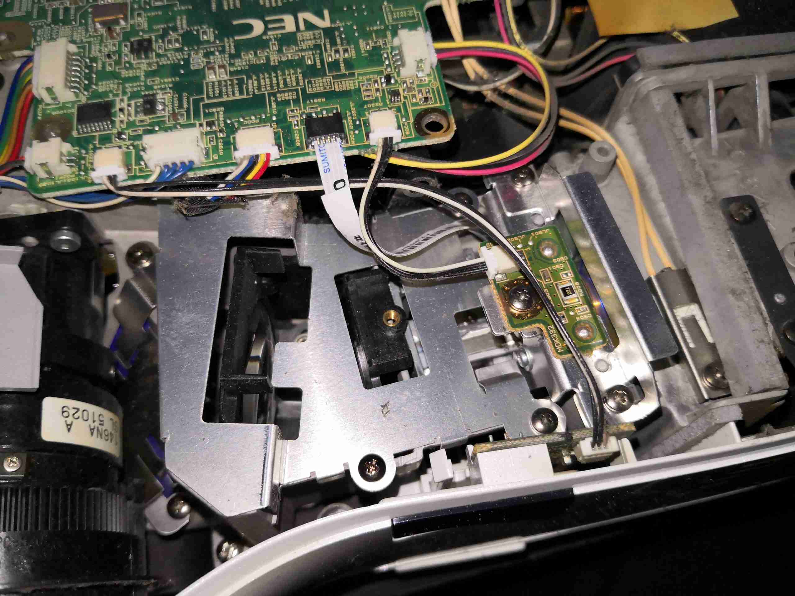
Light Engine
A closeup of the light engine shows the back of the phase sensor for the colourwheel, and the mounting brackets for the optics.
Colourwheel
The dichroic colourwheel is tucked into the gap between the lamphouse & the first optic.
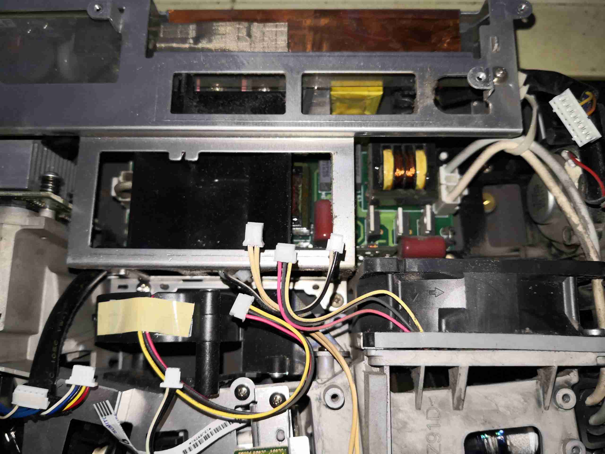
PSU Section
Hiding at the back of the projector is the alloy frame holding the power supplies & cooling ducts.
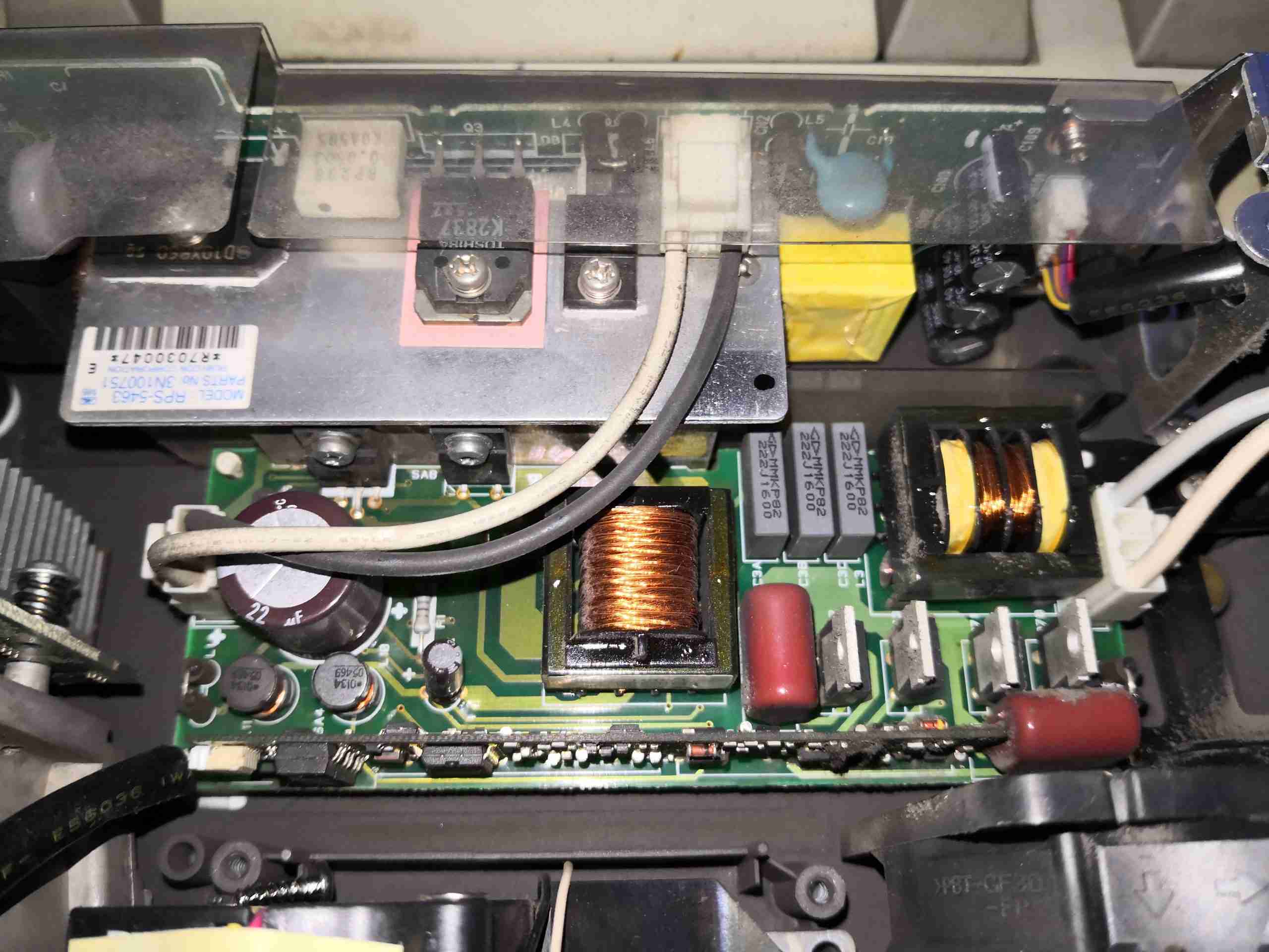
DC PSU & Lamp Ballast
After removing the brackets, the DC power supply & the lamp ballast are visible. Since this projector uses a UHP arc lamp, the DC power supply which has the usual low voltage outputs for the logic board, has an auxiliary output from the +340v rail after the PFC circuit that supplies power to the lamp ballast.
Lamp Ballast Control PCB
The lamp ballast is a pretty standard design, using an Osram control board.
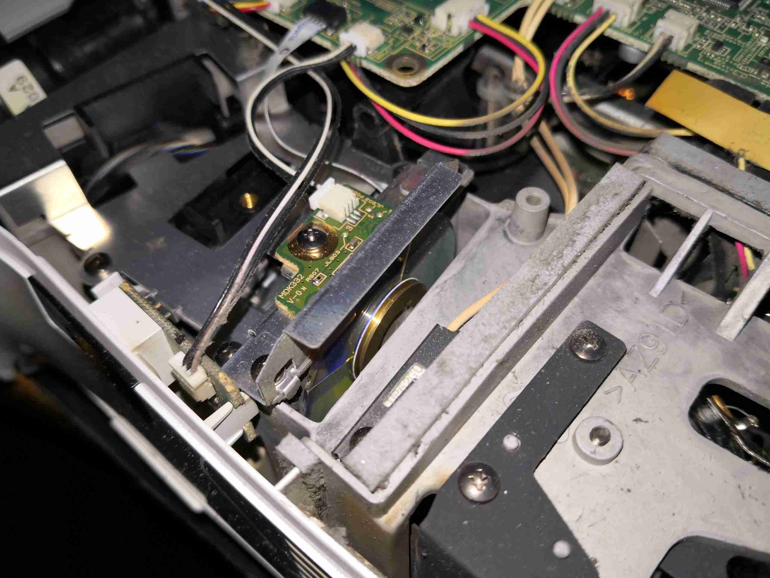
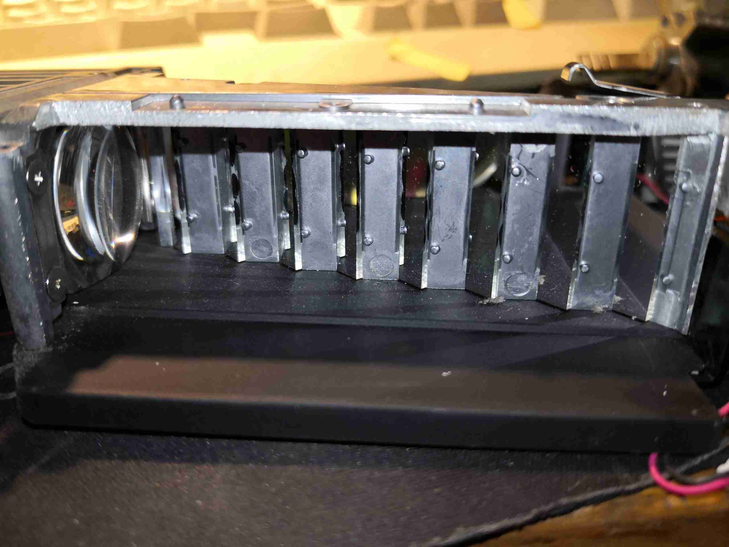
Homogeniser & Lenses
After removing the top cover with the colourwheel, the main optic chain is visible. The usual mirror tunnel homogenizer at the start, with a convex & aspheric lens on the left.
Lamphouse Thermal Cutout
The lamphouse has a last-resort thermal cutout to shut the ballast down if the cooling fans fail. These lamps output some serious heat, and likely wouldn’t last longer than a couple of minutes without cooling.
DLP Optics
The final turning optics before the DLP chip are hidden in the Mg casting of the light engine.
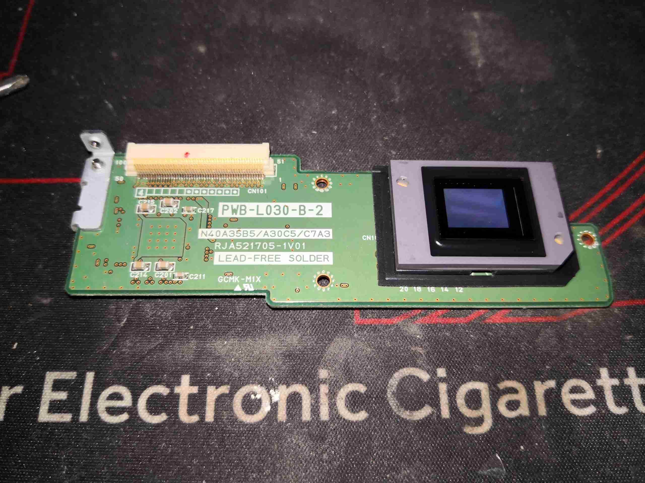
DLP
The DLP is the older type, with the large ceramic LGA package.
Projection Lens
After the DLP, the light is routed through the objective lens, to the screen. This is the back of the lens inside the light engine.
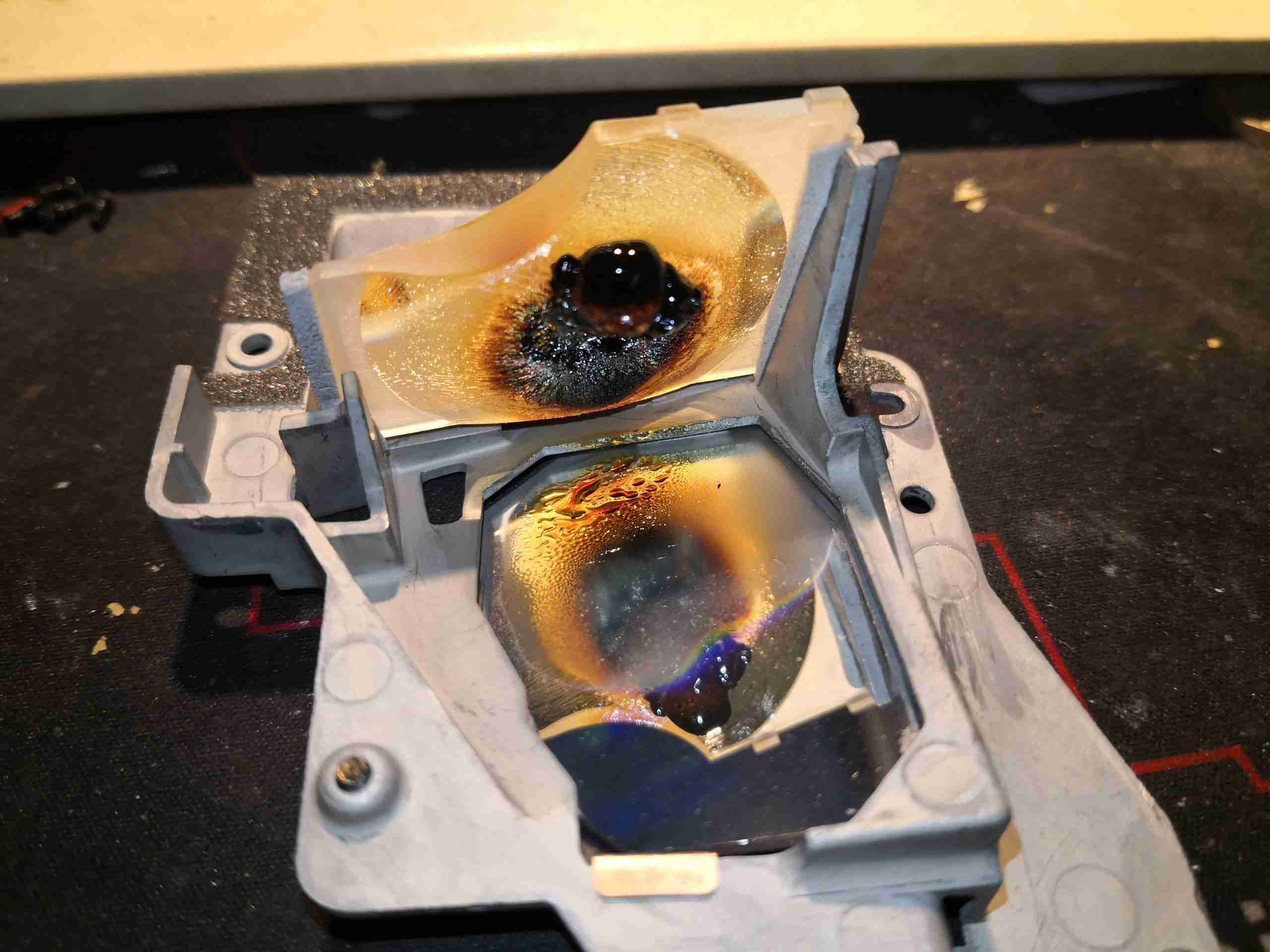
Failed Optic
And here is the main problem with the projector – the last lens in the optical chain before the DLP chip has been roasted by the intense light flux from the lamp. Unfortunately NEC cheaped out on this one – it’s the only optic in the machine that isn’t made of glass. This was likely caused by some contamination on the lens, which starts the process of absorbing light on the surface. The resulting heat then causes discolouring of the lens, which absorbs more heat. A chain reaction ensues, ending in the lens completely destroying itself.
Autofocus
The projection lens has a couple of sensors, for the focus & zoom, along with a focus motor. This is driven by feedback from a distance sensor in the base so no manual focusing is required.
These projectors were very popular when they first appeared on the market with the laser hobbyist community, and for very good reason – they contain a massive array of 445nm Royal Blue laser diodes in their optics engine. Originally very expensive, these units can now be had for under £50 on eBay, usually with damaged DLP chips.
Laser Module Door
Under the door on the bottom of the projector is the 445nm Laser diode array module, itself secured in place with security screws to the beam combiner. The rack of 3 high speed fans to the left draws air over the substantial heatsink.
Top Cover Removed
After removing the shell securing screws, the top cover comes off with the button panel. This gives a view of the internals, mostly PCBs at this stage.
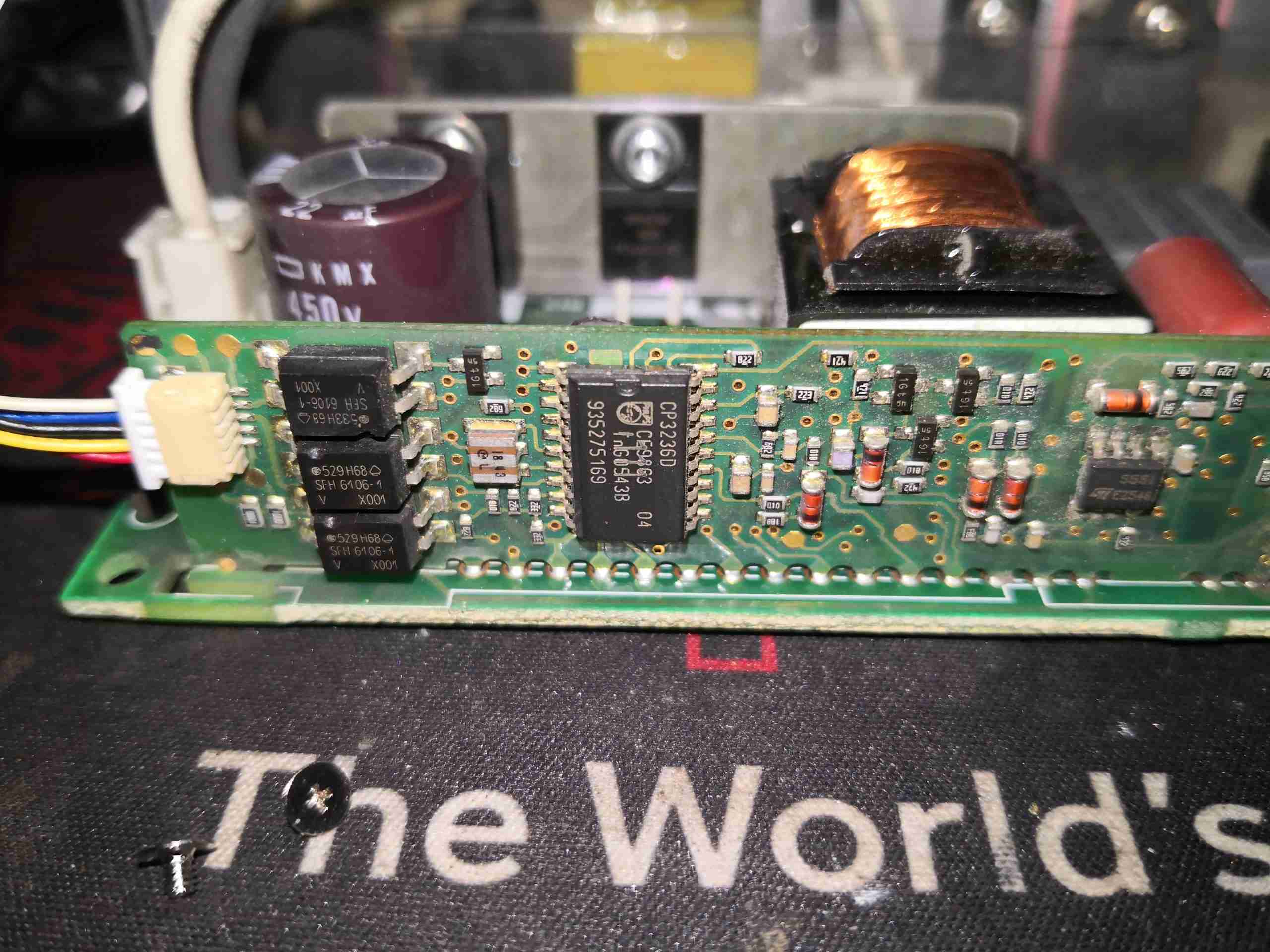
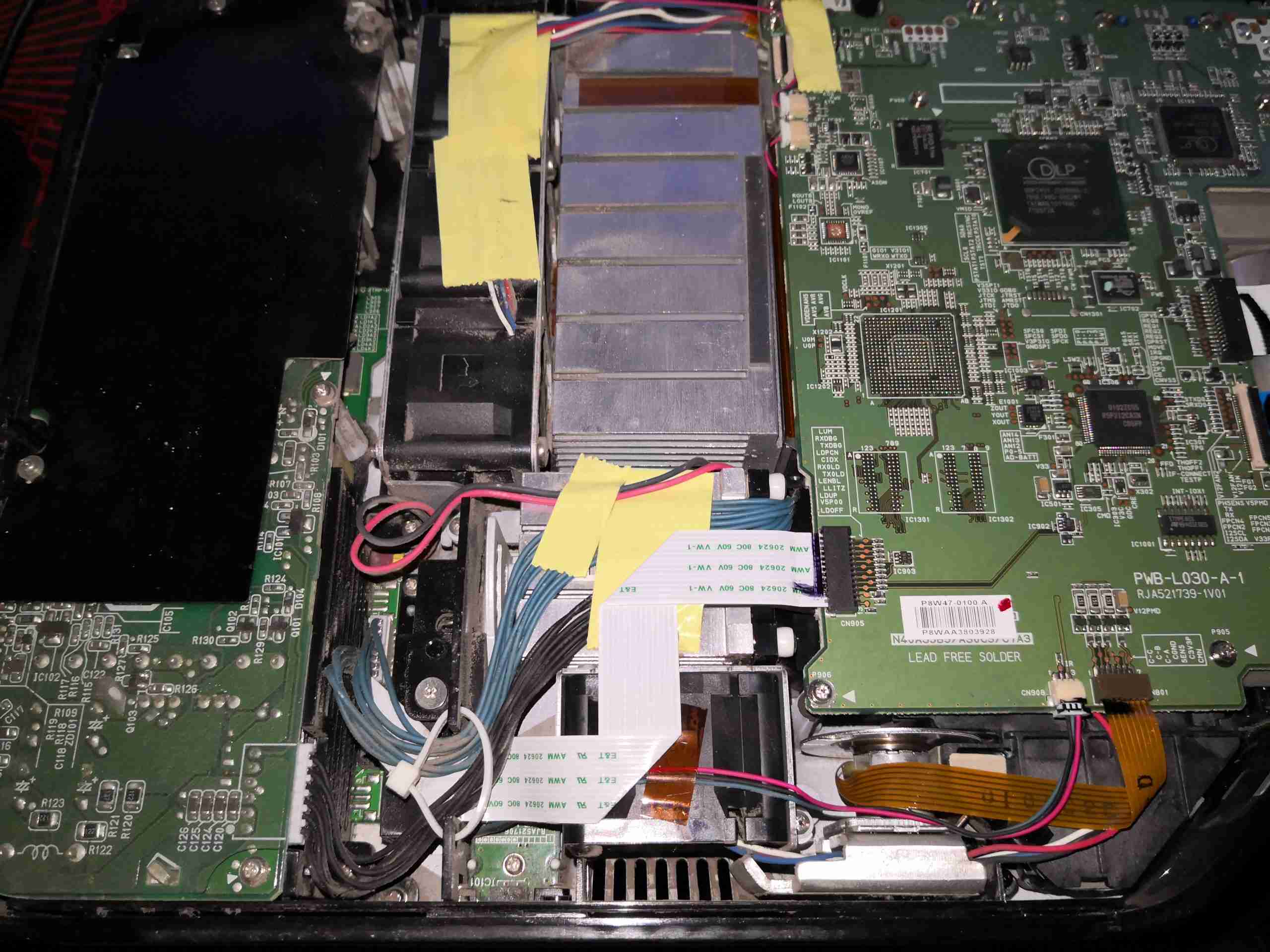
Main Control Board
On the left side of the projector is the main control PCB, with the video handling circuitry.
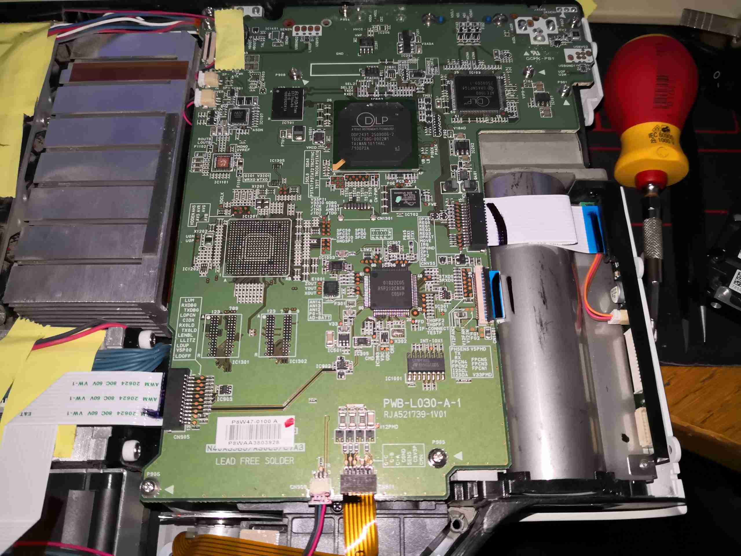
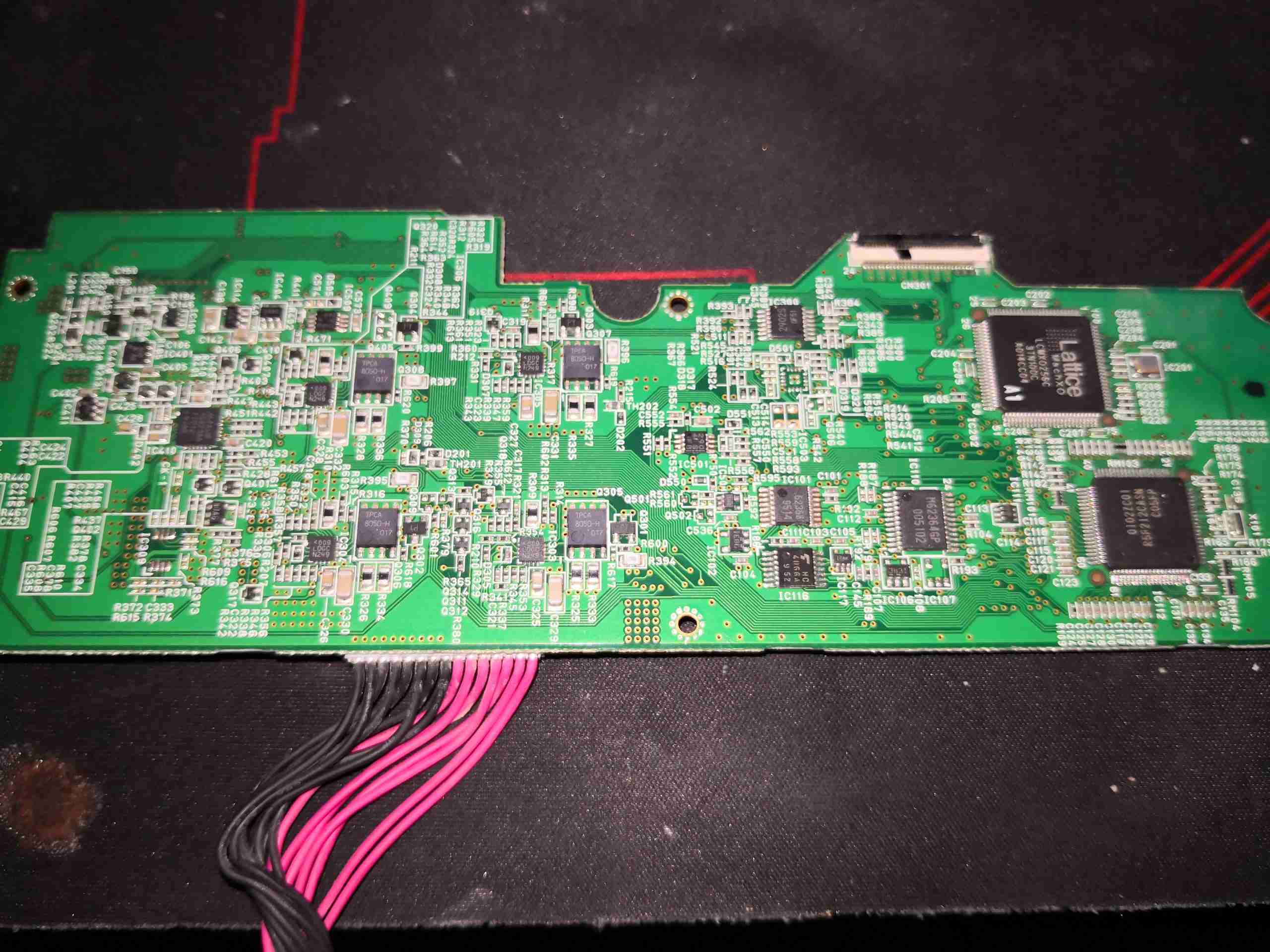
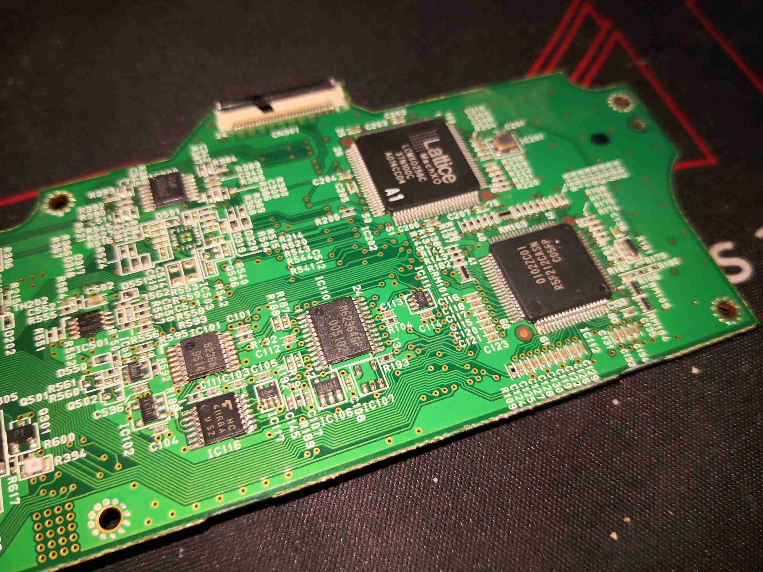
DLP Chipset
At the top of the board is the main DLP image processing chipset, these two components are actually custom parts, so no datasheets are available. The main DLP IC has some DRAM & a Spansion serial flash for firmware storage. There’s also a small audio amplifier on the left to drive the onboard 2W speaker.
System Microcontroller
Further down the board sees an unpopulated BGA footprint, with more space for DRAM. The main system microcontroller is on the right, a Renesas part.
Phosphor Wheel Motor
Right at the bottom edge is the connector running off to the phosphor wheel drive motor.
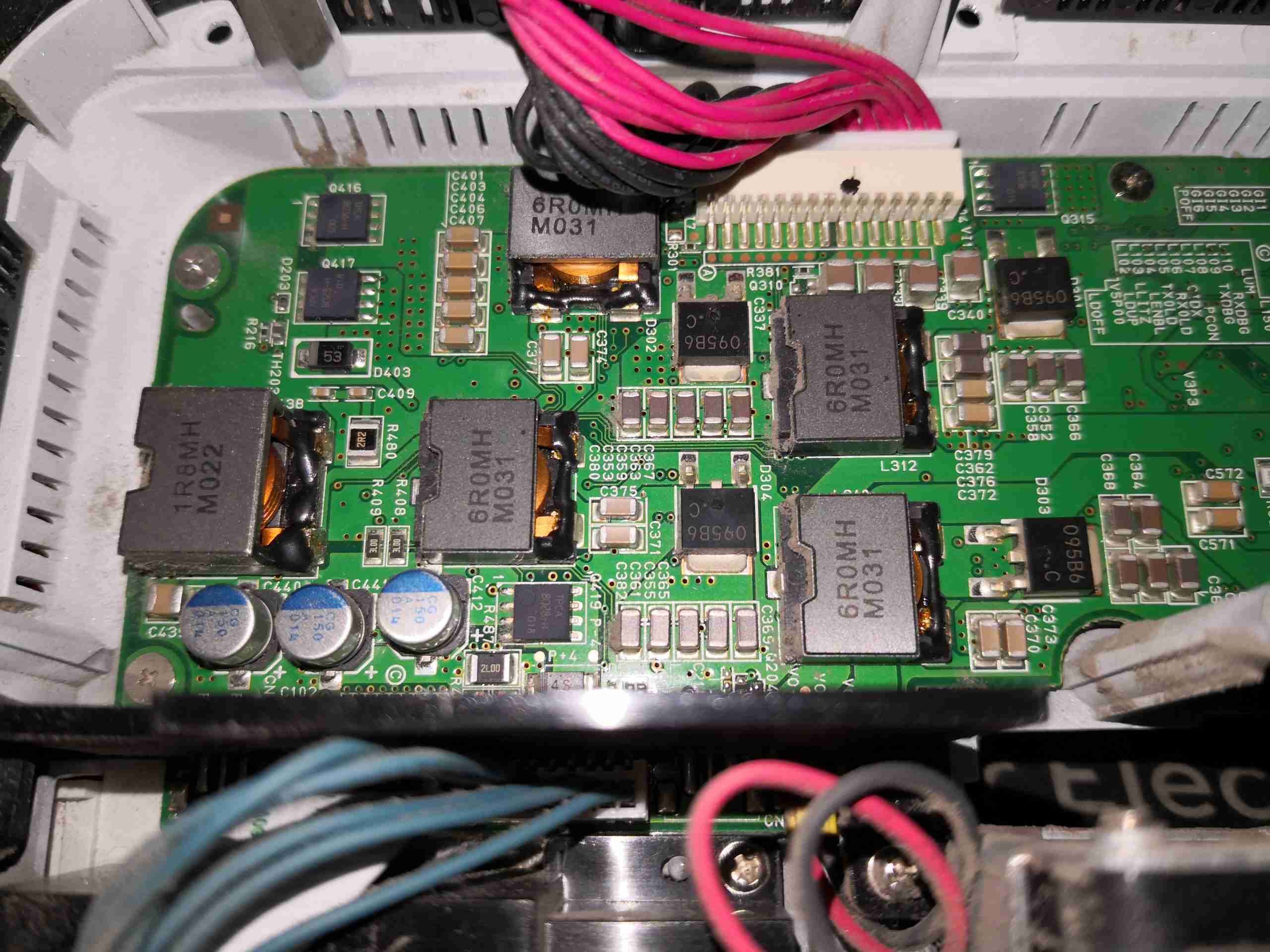
DC-DC Power Management
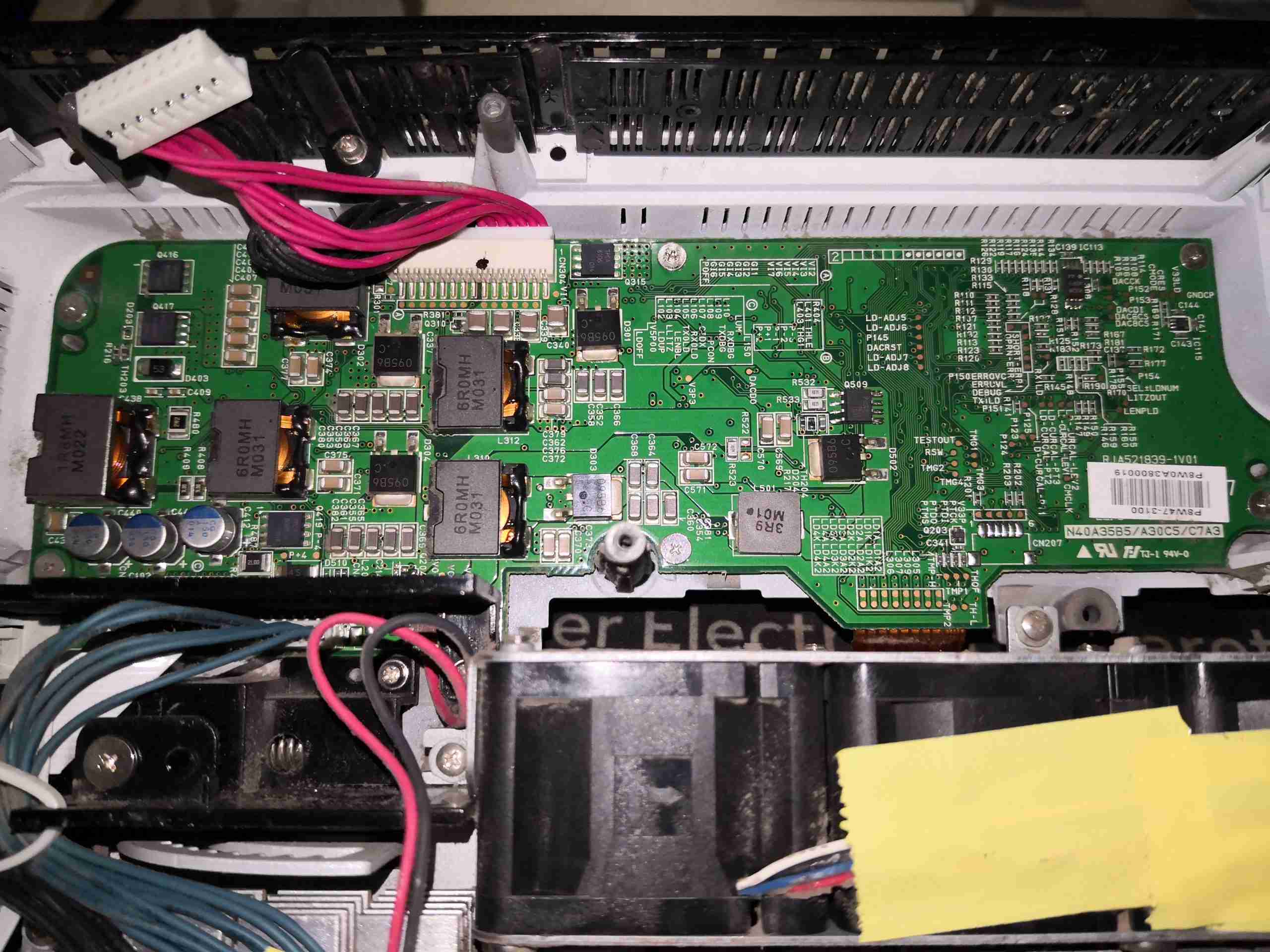
The reverse side of the board is pretty sparse, there’s quite a few passives & power control. Down towards the bottom surrounded by inductors is the system power management IC, the DLPA100. This takes the incoming DC 12v rail from the connector on the right side of the board & produces several supply rails for the internal logic: 1.1v 1.8v, 2.5v, 3.3, 5v & also contains the 3-phase brushless driver for the phosphor wheel motor. The main control board input power connector also has a +5v from the mains supply, for standby power. The main board signals the PSU to switch on the main +12v rail through a pin on this connector.
HDMI Interface Chipset
The other end of the board just has the connectors, a bit of glue logic & the HDMI interface chipset.
Main Board Removed
After unplugging all the connectors, the massive cast frame of the light engine is visible.
Phosphor Stripe
Here’s a closeup of the phosphor stripe around the edge of the wheel. This takes the 445nm light from the laser module, and converts it into green. There’s also a frosted glass section of the wheel to pass some blue for the image. The reason for the phosphor being in a large stripe on the wheel is load spreading – there’s several watts of optical power focused down to a very small spot on this phosphor, and would overheat quickly if it wasn’t moving.
DLP Frame
At the back of the light engine is the DLP module, with it’s substantial heatsink.
Light Source PSU Board
Hiding under the mains PSU, is the light source control PCB. This contains several DC-DC converters, which run the 4 strings of laser diodes, the large Phlatlight Red LED & it’s associated TEC cooler. This board takes the incoming +12v from the mains PSU through the multi-way loom at top centre. There are multiple cores on this connector to spread the load – at normal brightness, in Eco mode, I measured the power consumption at about 8.5A at 12v input for the entire projector.
DC-DC Converters
The left side of the board is dedicated to the high power section of the controller. There’s a power inductor for every channel.
Light Source Drive Board
The other side of the board is very heavily populated with components.
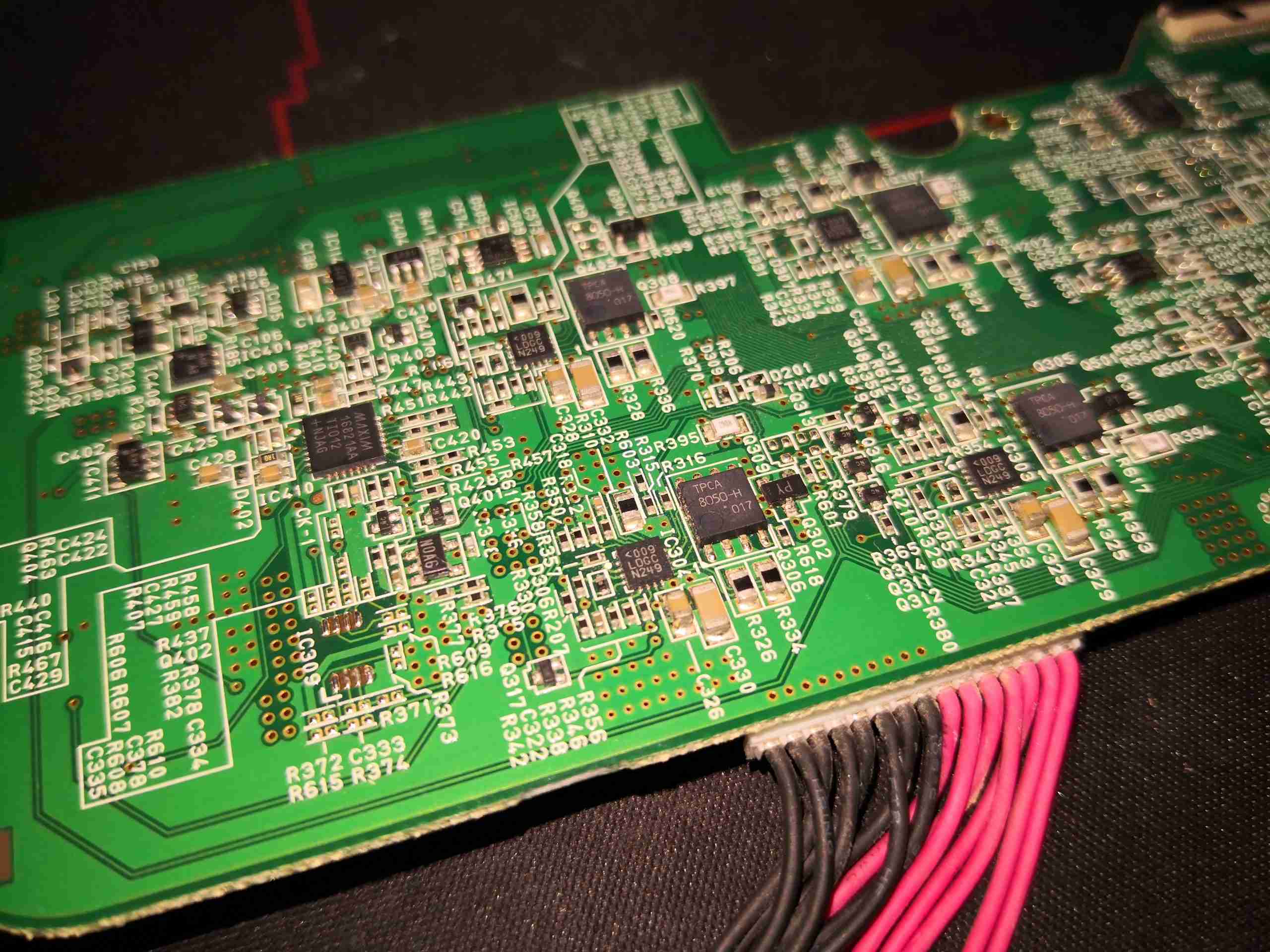
Control Logic
The right hand side has the control logic, a Lattice CPLD, and another Renesas Microcontroller. There’s also some glue logic here & a dedicated DA converter.
Power Drivers
The other end of the board has the power drive control logic. There’s a MAX16821AA LED buck driver for the Red LED, and 4 drive ICs for the laser diodes, which are marked <009 LDGC N249. I haven’t been able to find anything about these, so they may be custom.
DLP Light Engine
Removing some screws allows the entire optical assembly to be removed from the lower shell. This may be mostly manufactured from a magnesium alloy from the rather low weight.
DLP Board
On the back of the DLP module is the DLPA200 Micromirror Driver IC. This generates the high voltage bias supplies for the DMD chip (+/-28v) from the 12v rail, generates all the timing waveforms required for the DLP chip. There’s a couple of power inductors for the onboard regulators. Video data is sent from the main image processing chipset to the DMD chip via 2 channels of LVDS.
DLP Mount
Now the heatsink has been removed, the rear of the DLP chip can be seen, with the remains of the thermal pad. The mount for the heatsink is sprung, to accommodate thermal expansion.
Red PhlatLight
The Red light required to create a colour image is generated by a giant LED, more on this one later.
DLP Removed
Here’s the DLP board removed from the projector with the micromirror surface visible. This DLP has many dead pixels, hence the decommission at ~4500 hours of operation.
Laser Beam Combiner
The 24 laser diodes have their beams combined by this knife-edge mirror assembly, turning the beam through 90° to the lens on the left, which focuses the 24 beams down to the optics engine.
445nm Laser Array
Removing the beam combiner from the array allows the 24 diodes to be seen, mounted under their collimating lenses. This is one beast of a laser unit!
Dichroic Optics
Taking the cover off the optics assembly allows the main optical path to be seen. The blue laser comes in a bottom left, through the lens, the red LED comes in bottom right. The pair of dichroic mirrors manage the light path for the red & green light, while passing the blue straight through.
Optical Path
Here’s another view of the optical path, with both light sources visible.
Light Homogenizer
After the light source, is the homogeniser – this tunnel of 4 mirrors facing each other evens out the light beam & removes all coherence from the laser light. This is important to not have any speckle in the image.
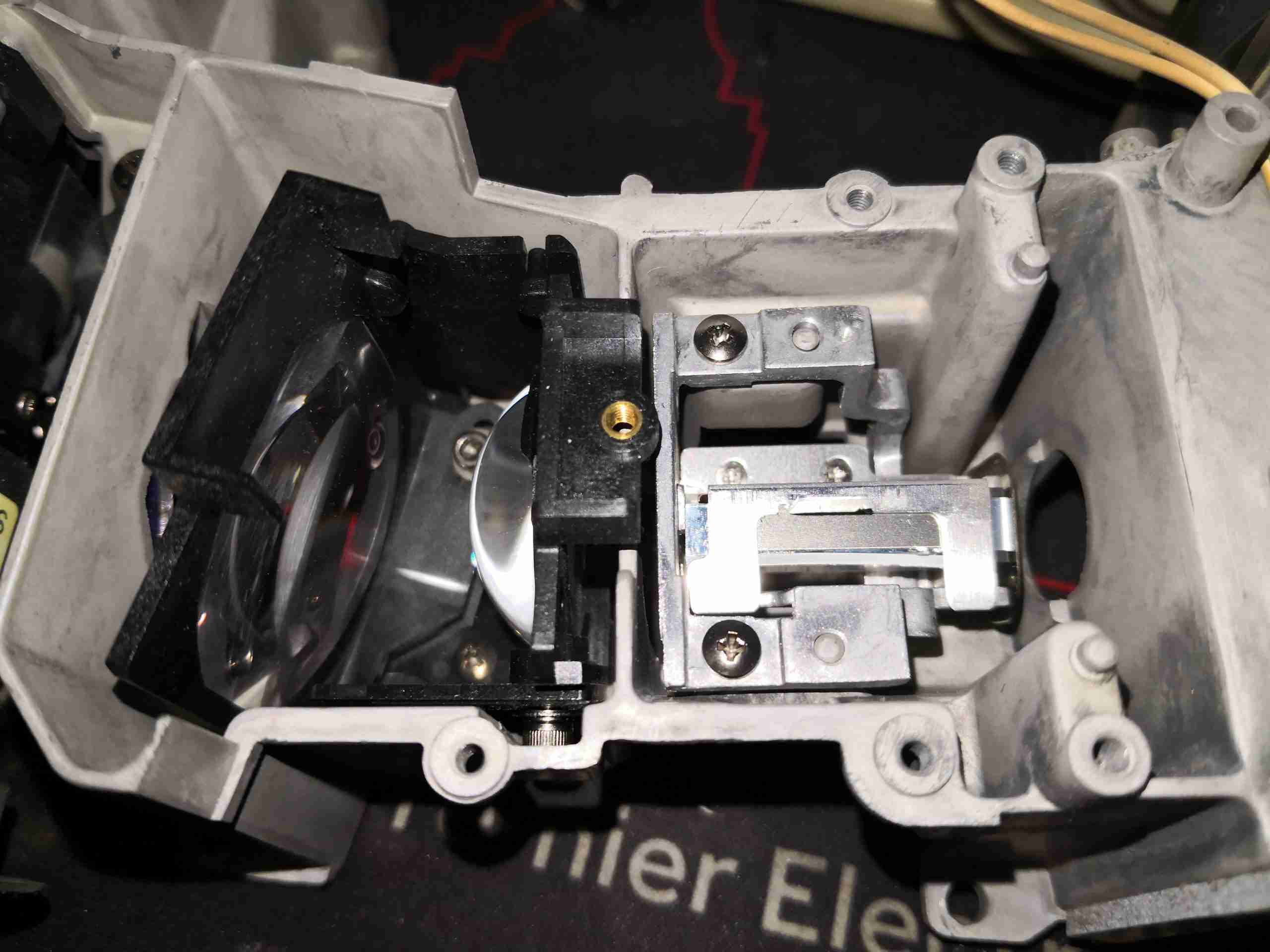
Focus & Zoom Motors
Underneath the objective lens are the pair of stepper motors that drive the focus & zoom mechanisms, along with their position sensors.
Turning Mirror
Just after the homogeniser, is the final optical path to the DLP. Here the light comes in a bottom left, and hits the turning mirror, after which it is focused onto the DLP chip by the mirror top centre. The objective lens is through the hole in the centre of the optical block, while the DLP is on the right side.
DLP Final Optics
Here’s where the DLP will be mounted in normal operation, with it’s lens in place.
Objective Lens
Finally, the created image is passed out through the objective lens to the projection screen.
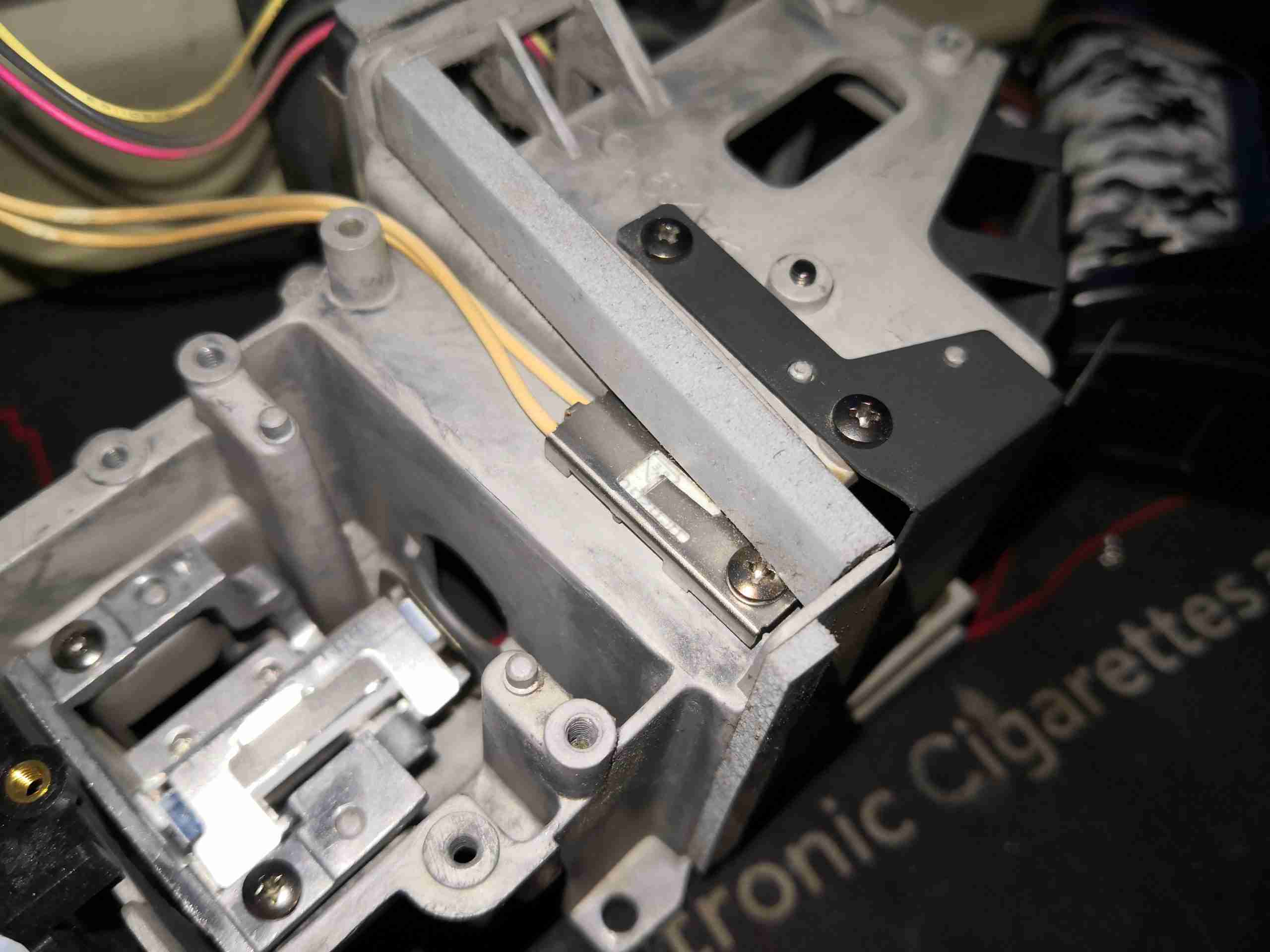
Hall Effect Sensor
There’s a sensor mounted on the side of the lens barrel, that I think is a Hall effect device, but I’m unsure what this would be used for, as there is no magnet anywhere near this to sense. It could also be a temperature sensor though, for the DLP & lens assembly.
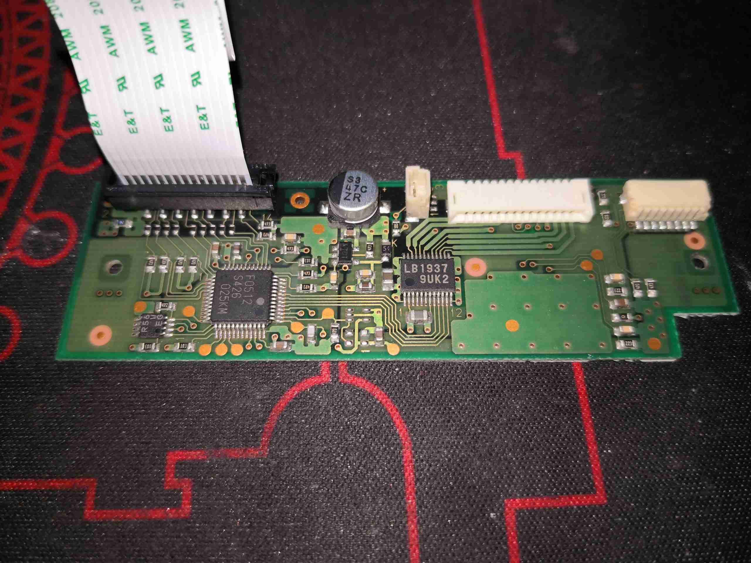
Stepper Motor Drive
The small PCB on the side of the lens unit holds the stepper motor drive IC, an LB1937 from Sanyo. There is another IC here, which looks to be a microcontroller.
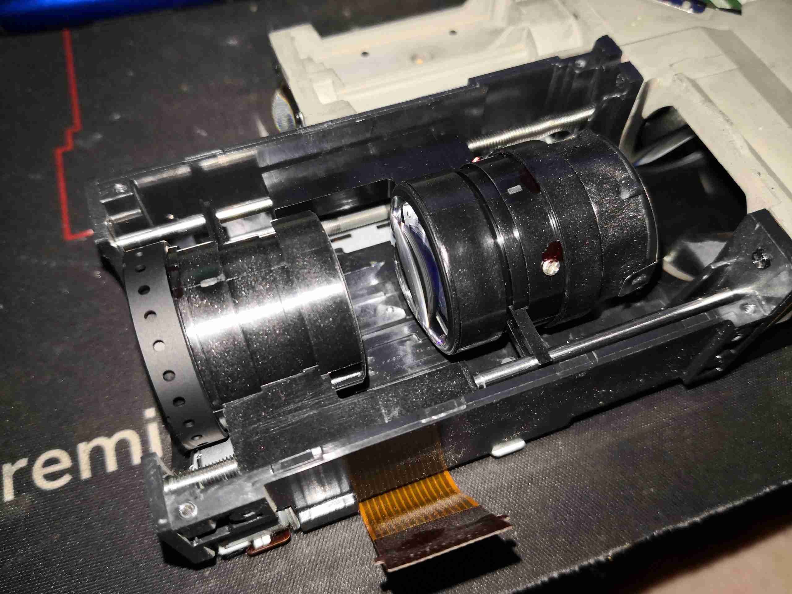
Lens Assembly
Removing the top cover allows the moving lens assemblies to be seen. These move independently of each other to implement focus & zoom, via lead screw drives on the stepper motors.
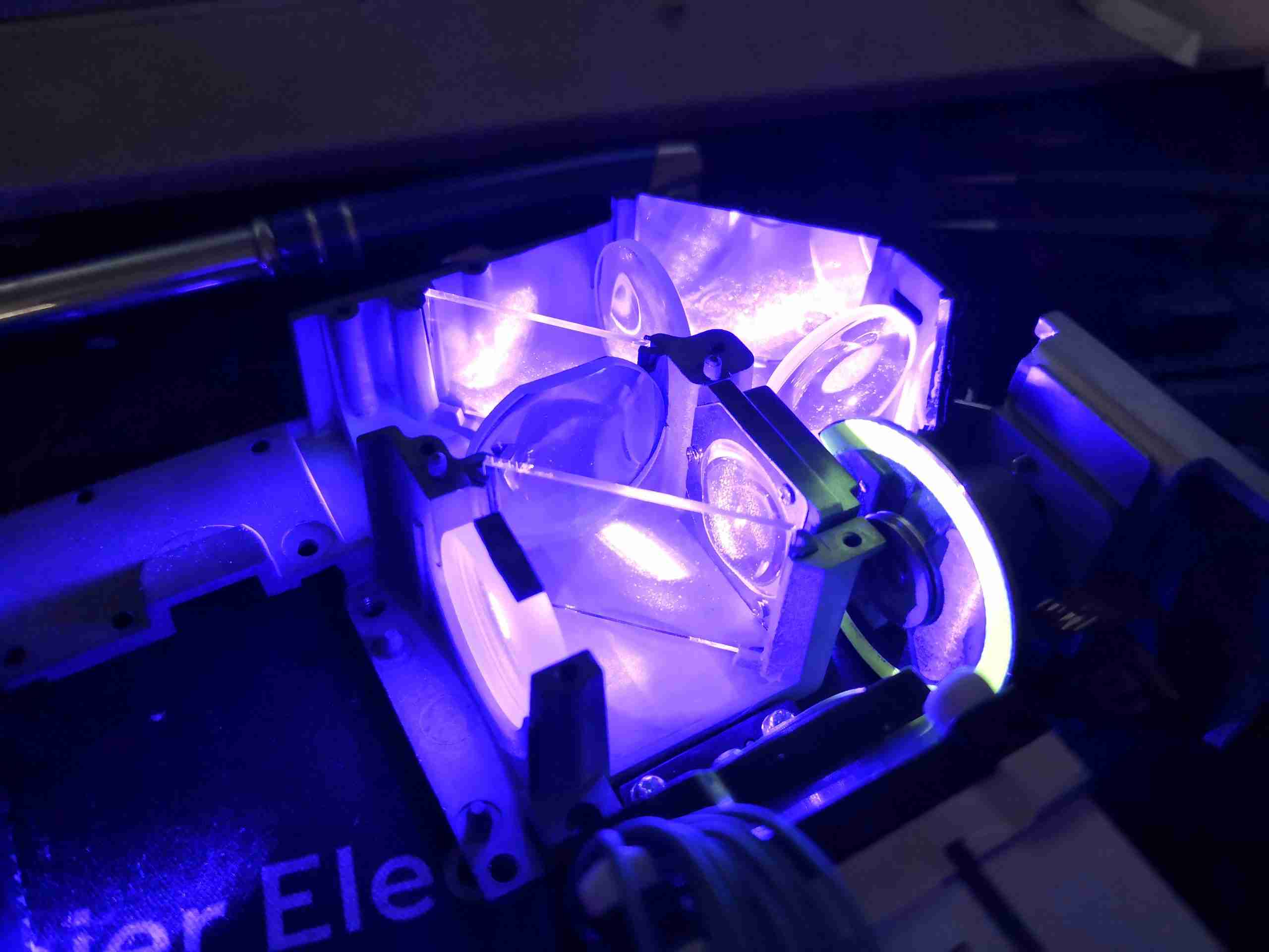
Blue Light Path
Here I’m shining a separate 445nm diode laser into the optical assembly, through the blue optical path. The phosphor wheel is turned to the clear section, which allows the 445nm light to pass straight through, being turned 180° by the mirrors & directed out towards where the DLP assembly would be.
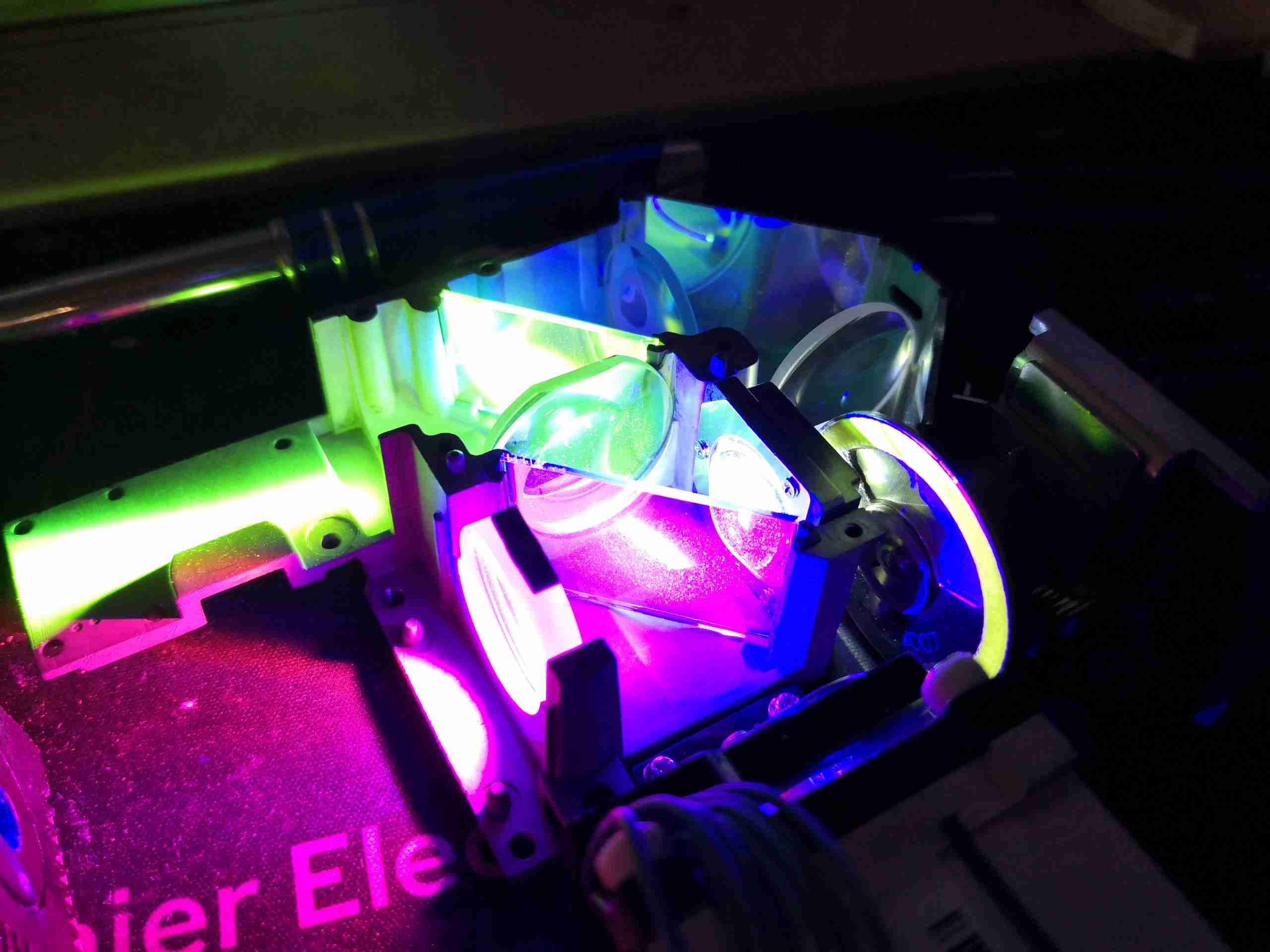
Green Light Path
Turning the phosphor into the light path causes a very bright green light to be generated, and passed back towards the 445nm laser entry point. The dichroic mirror in the way reflects this light to the left, through a lens & then to the other dichroic mirror to be turned another 90° to the DLP assembly. I’m not sure where the magenta light is coming from – the phosphor probably generates light on more wavelengths than just pur green, giving some red to mix with the blue.
PhlatLight LED
Here’s the Red LED removed from it’s cooling & collimation assembly – this has an enormous silicon emitter area, and apparently these LEDs are designed to be uniform in light emission, specially made for projection use. There’s a thermistor onboard for temperature sensing – sensible when the datasheet gives CW currents of 8A, and pulsed currents of 13.5A!
LED TEC Cooler
Not surprisingly, cooling this beast of an LED requires more than just a heatsink, so it’s mounted on a TEC module, possibly around 40W thermal capacity.
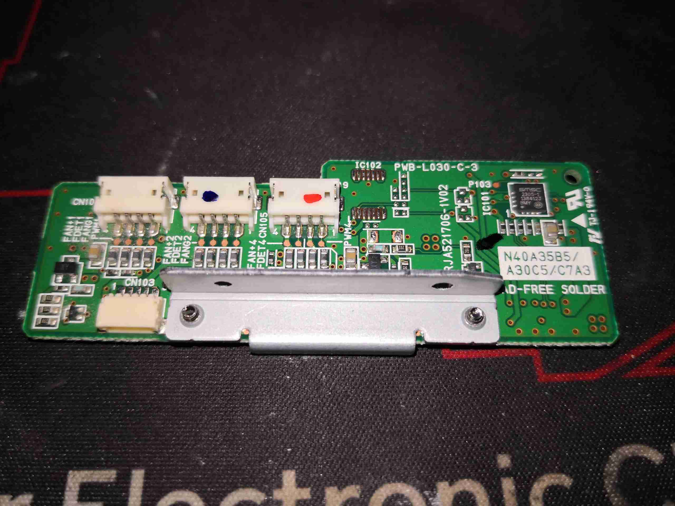
Fan Control Board
Fan control is handled by this little PCB, squeezed in between the optics engine & 445nm Laser array. There’s a SMSC EMC2305 I²C 5-channel PWM fan controller on here, communicating back to the main system microcontroller. Besides some passives, and 4 transistors to make sure the fans don’t start at full power when the projector is powered on, there’s not much else.
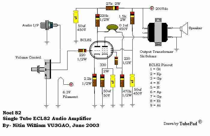
I figured it was about time I built another valve amplifier, and since I already had most of the required parts in stock, here it is! Above is the lid of a cake tin sourced from a local shop as a case, marked out & drilled for the valve sockets, output transformers & speaker terminals.
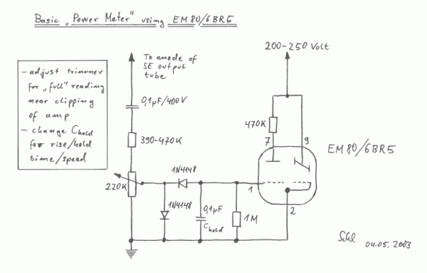
The ECL82 valve is a Triode & Audio Output Pentode in a single envelope, requiring only a single valve per audio channel. There are a pair of extra holes drilled here for a couple of EM80 magic-eye valves wired as VU meters to give a bit of a lightshow.
Amplifier Schematic
Here’s the base schematic for the Class-A ECL82 amplifier sections, obtained from the interweb. It’s pretty basic, and doesn’t mention a value for the volume potentiometer, so I used a 100K audio taper for that. Power will be supplied from low-voltage DC, running through a high voltage DC-DC converter for the anode supply of 200v, and a 5A buck converter for the 6.3v filament supply.
EM80 Schematic
The EM80 side is as the schematic above, the signal input being taken directly from the Pentode anode of the ECL82. I have removed the second 1N4148 diode down to ground, leaving only a single diode.
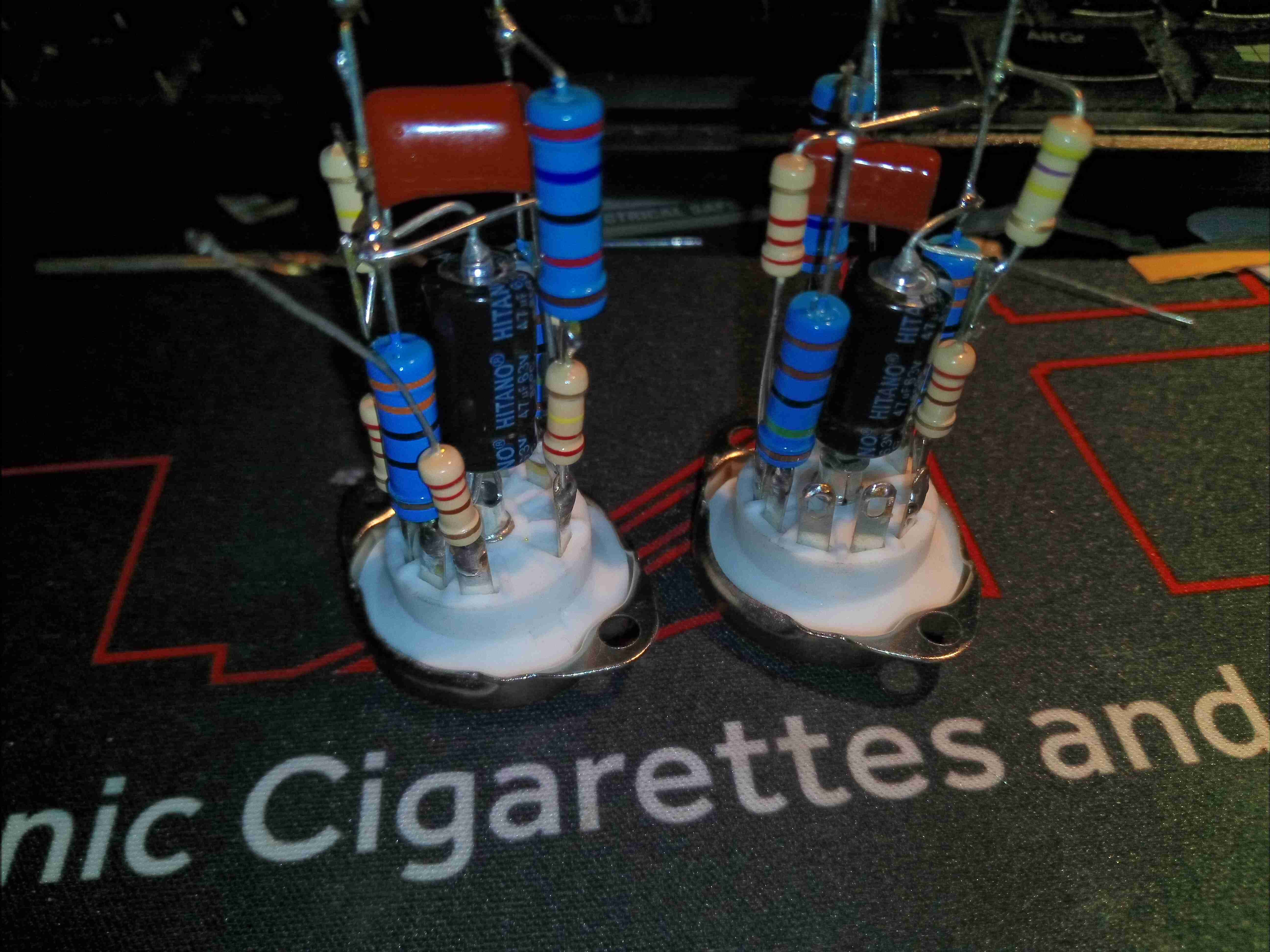
Valve Base
Most of the parts comprising the ECL82 amplifier stages are mounted directly on the back of the valve sockets, requiring only a 6.3v filament supply, 200v anode supply & audio I/O connections. Axial electrolytics have been used for ease of assembly, even though they’re getting a little expensive nowadays!
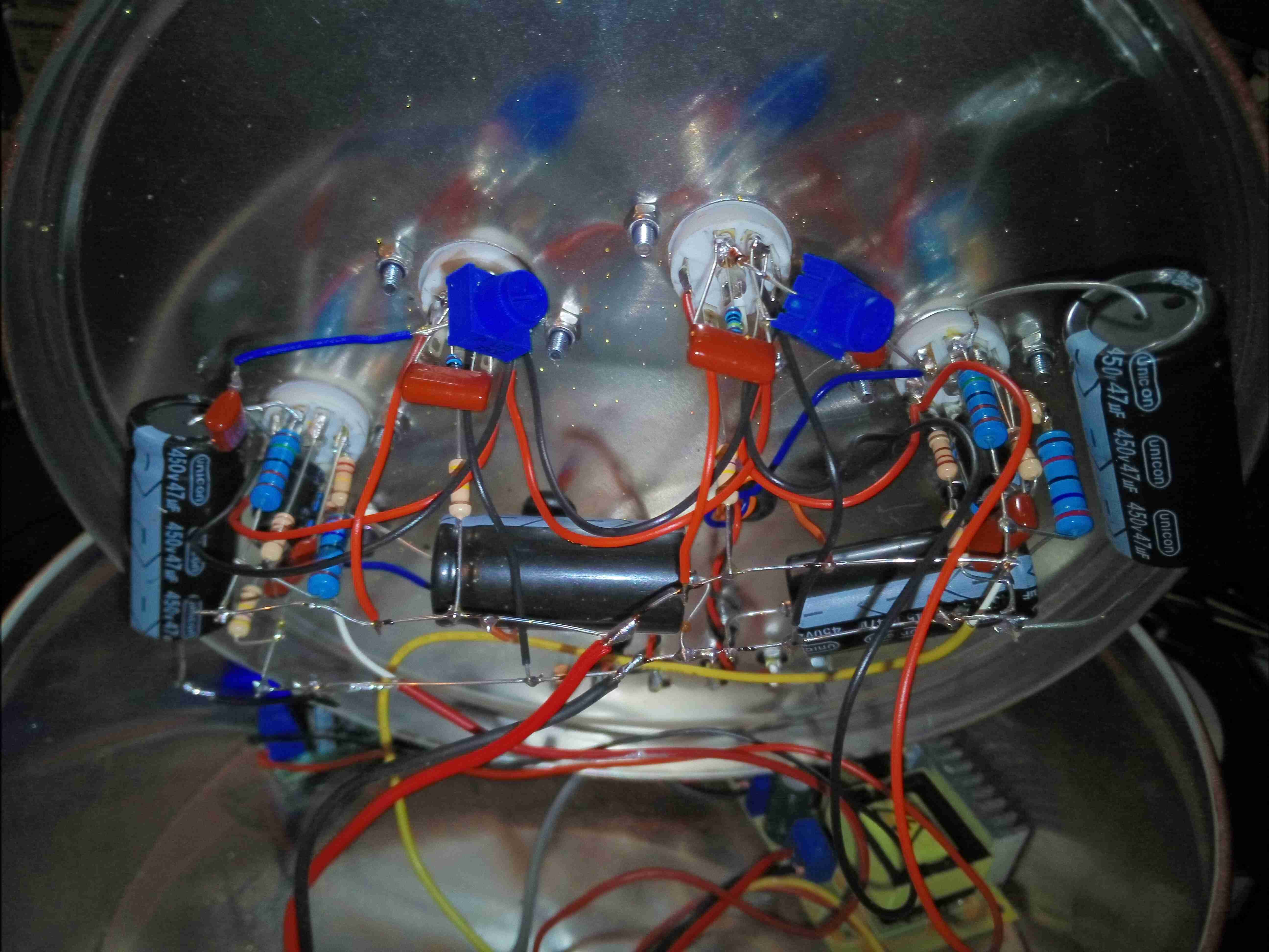
Point To Point Wiring
After fitting the components to the top lid, point-to-point wiring is used to connect up the valve socket assemblies. Some large electrolytics provide B+ smoothing, and all the filaments are daisy-chained in parallel. Audio is brought in on micro-coax from the I/O, and straight out to the output transformers on twisted pairs, keeping the audio wiring away from the B+ voltage.
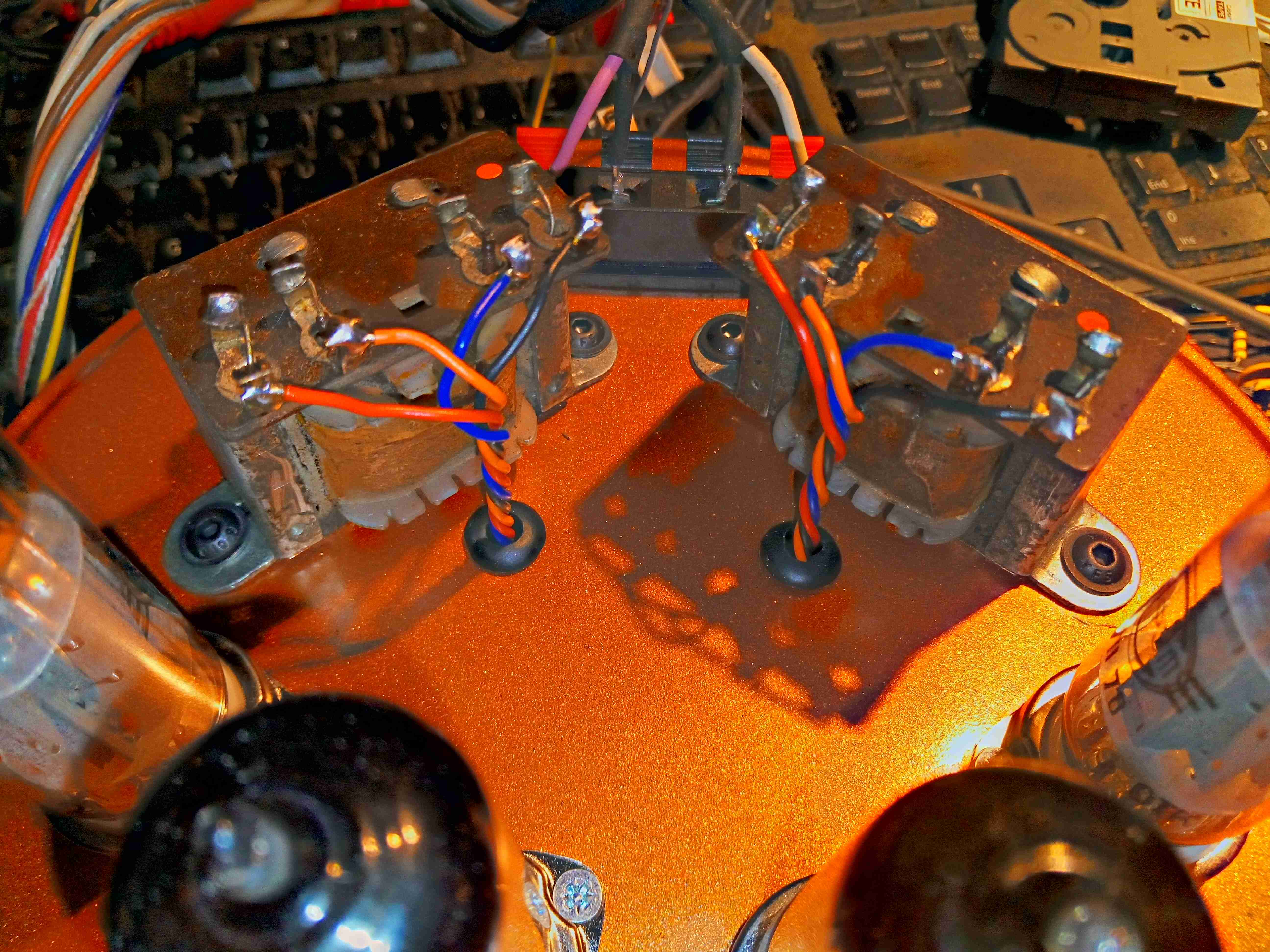
Output Transformers
The audio transformers, from a 1960’s Philips Radiogram, are mounted behind the valves, with the wiring emerging through holes in the case. I’ve already done the paint job here, in metallic copper.
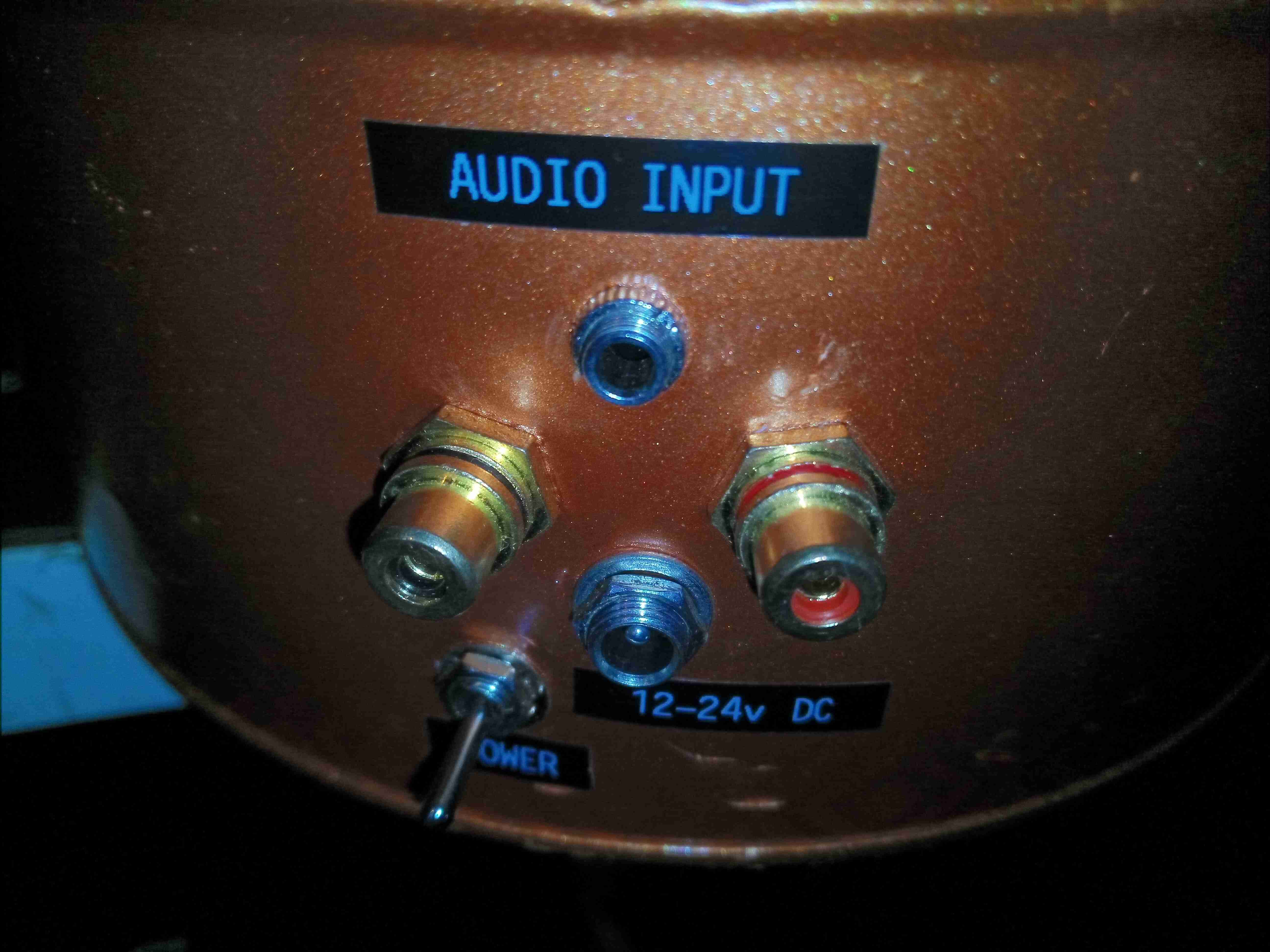
I/O
Audio & power sockets are on the back of the tin, with both 3.5mm Stereo inputs & phono inputs. A DC barrel jack takes care of the power, accepting 12-24v.
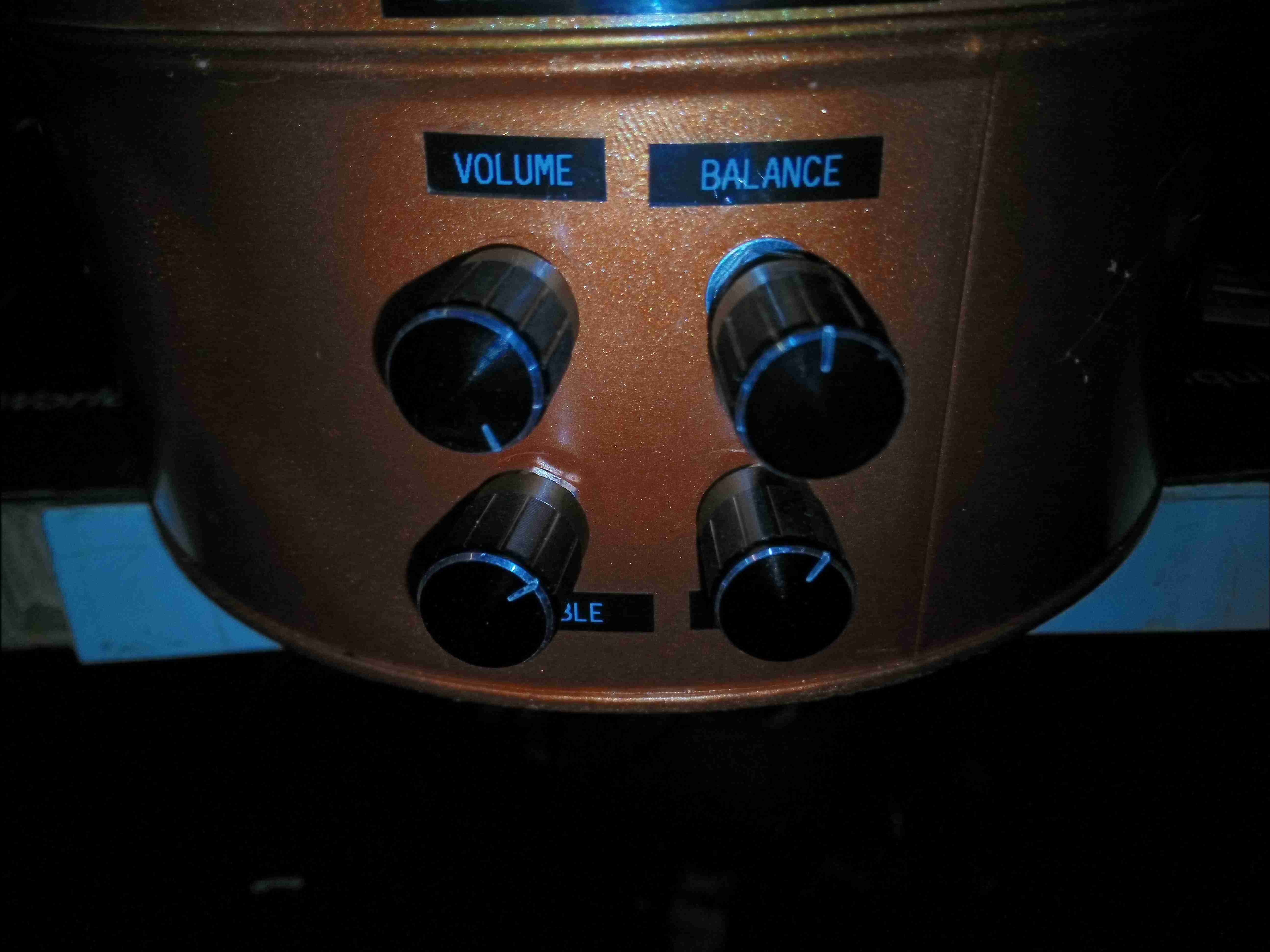
Controls
Controls on the front provide volume, balance, bass & treble adjustments.
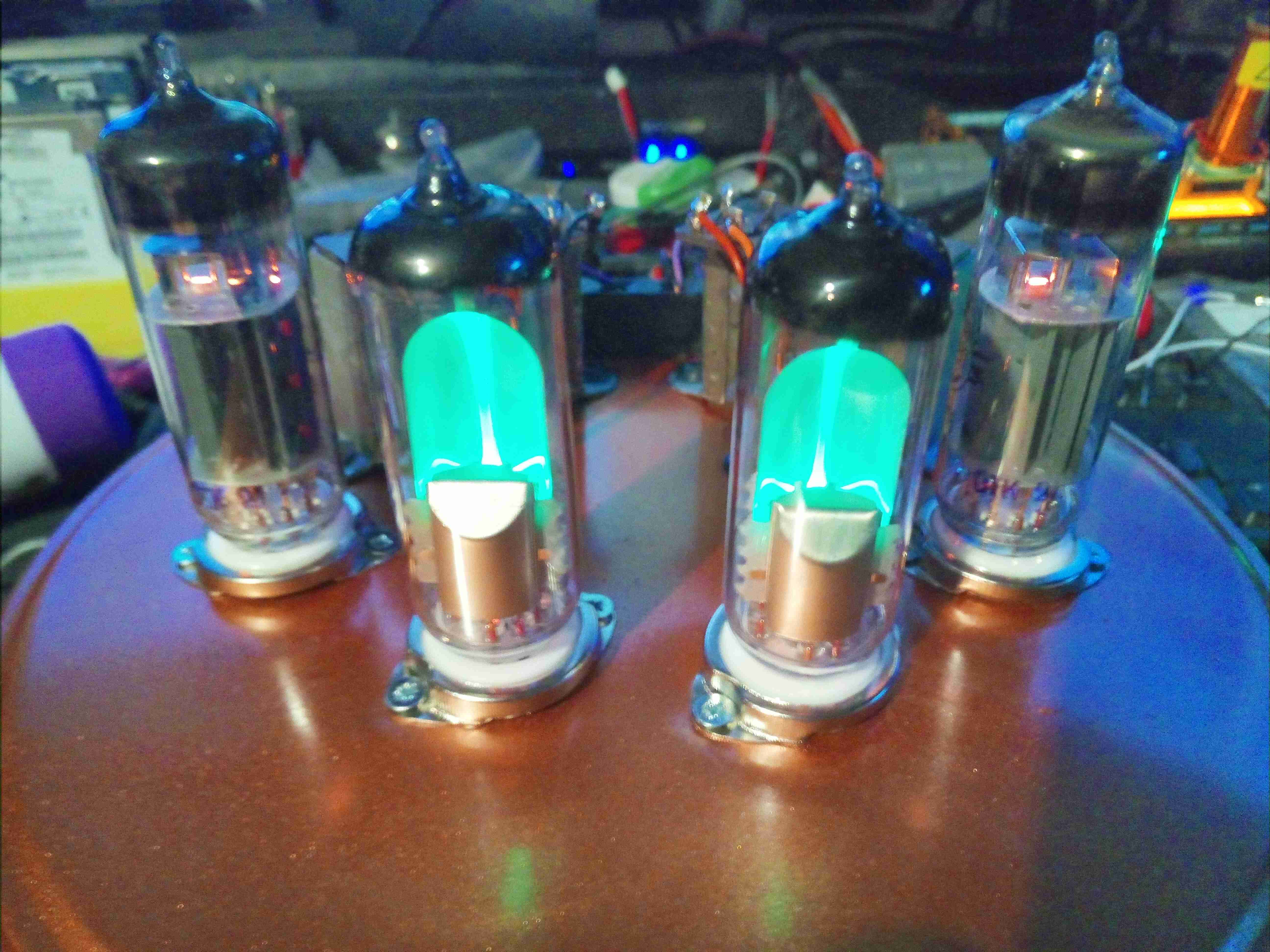
Amplifier Operational
Here’s the amplifier with it’s valves glowing nicely. Total power consumption is roughly 30W, using NOS Svetlana ECL82s & EM80s. In operation there is no hum or noise in the background, with no audio input the connected speakers are entirely silent.
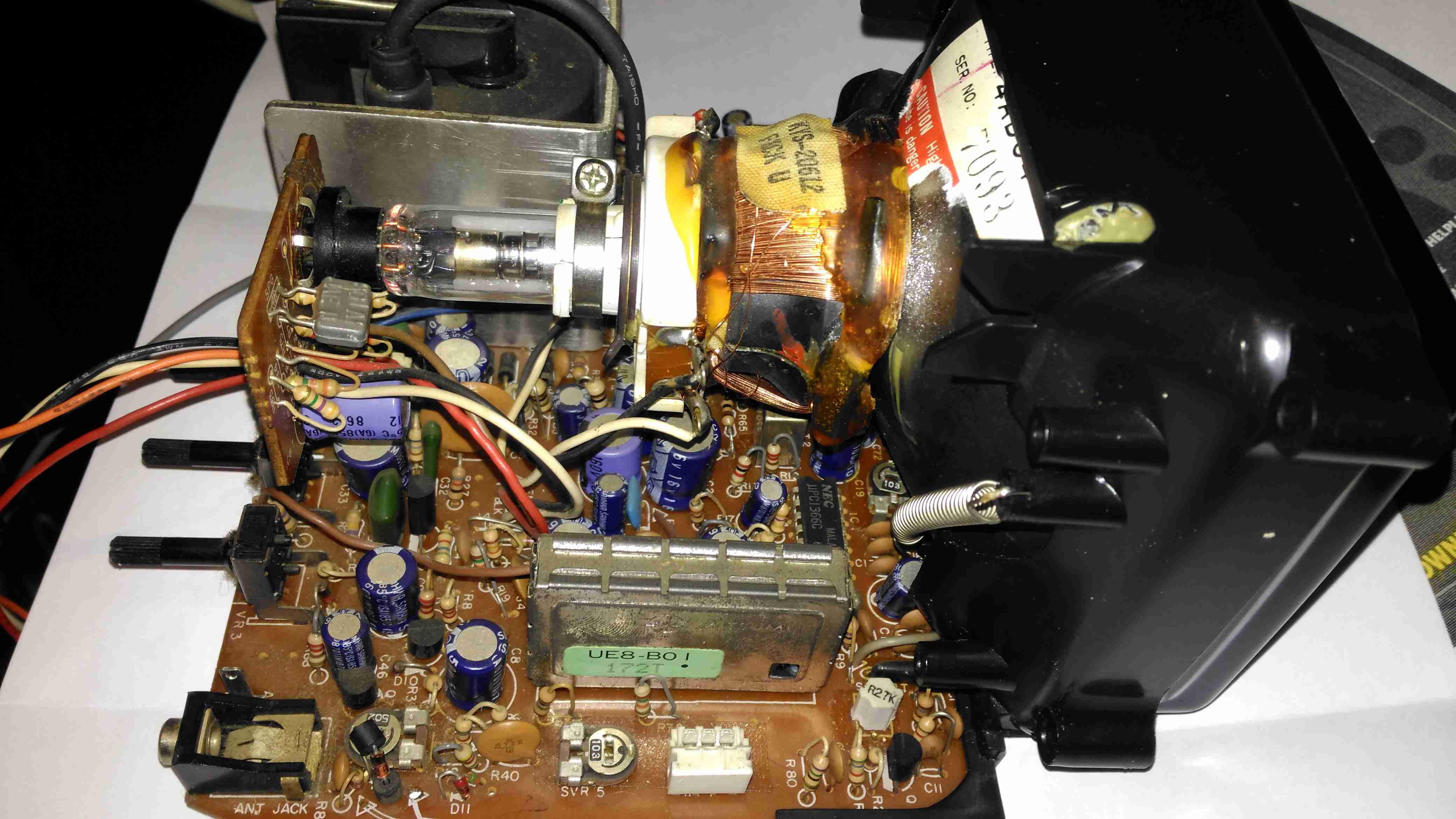
Well, it’s time for another viewfinder hack! I’ve been after one of these for a while, this is from an early 1980’s era Sony Trinicon camera, and instead of the tiny ½” round CRT display, these have a 1.5″ square CRT – a Matsushita 40CB4. Luckily I managed to score a pair of these from eBay for very little money. Update: The second camera’s viewfinder module turned out to have a dead flyback transformer, but at least I have a good spare CRT & the rest of the support components. More to come later on the teardown of the camera itself.
Mirror & Eyecup Assembly
The eyecup assembly with the magnifying lens & turning mirror is easy to remove, with clips & a single screw holding it onto the CRT holder sticking out of the side of the main casing.
Top Cover Removed
Removing some screws around the case allows the top cover to be removed, revealing the electronics. There’s certainly more in here than the later camera viewfinders, in this unit there are two boards slotted together with a board-to-board interconnect at the bottom. The CRT is at the top of the photo, hiding inside the plastic housing & deflection yoke assembly.
Bare PCBs & CRT
Here’s the CRT & one of the control boards removed from the case, having been stripped of the heatshrink tube that held the final anode lead in place. Just like on larger CRTs, this viewfinder has the final anode on a cavity connector fused into the bell, instead of being led out to a pin on the base. This is probably due to the much higher anode voltage of 5kV, a big jump from the 2kV on the ½” round tubes.
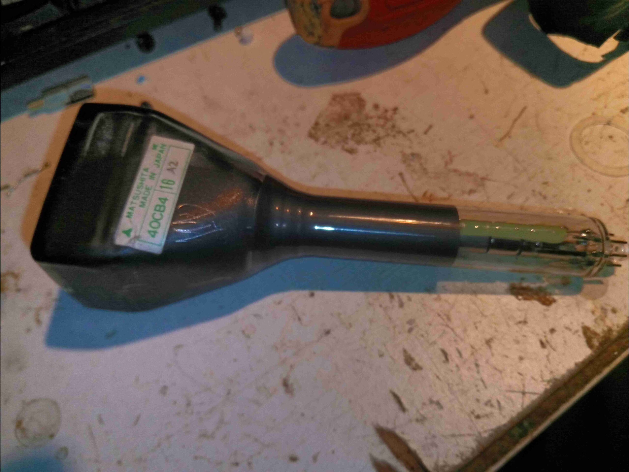
40CB4 CRT Label
Yup, it’s definitely the elusive 40CB4. Apparently these CRTs are still manufactured to this day for professional camera viewfinders, as the resolution of this small vacuum tube is still better than similarly sized modern tech such as LCDs or OLEDs. The phosphor used is type P4 – ZnS:Ag+(Zn,Cd)S:Ag, with an aluminized overcoat.
Bare 40CB4 CRT
After the base connector & deflection yoke are removed from the tube, the very long neck can be seen, this long glass neck apparently giving better focus & resolution than the stubbier tubes.
Electron Gun
The electron gun is the usual single unit as usually found in monochrome tubes.
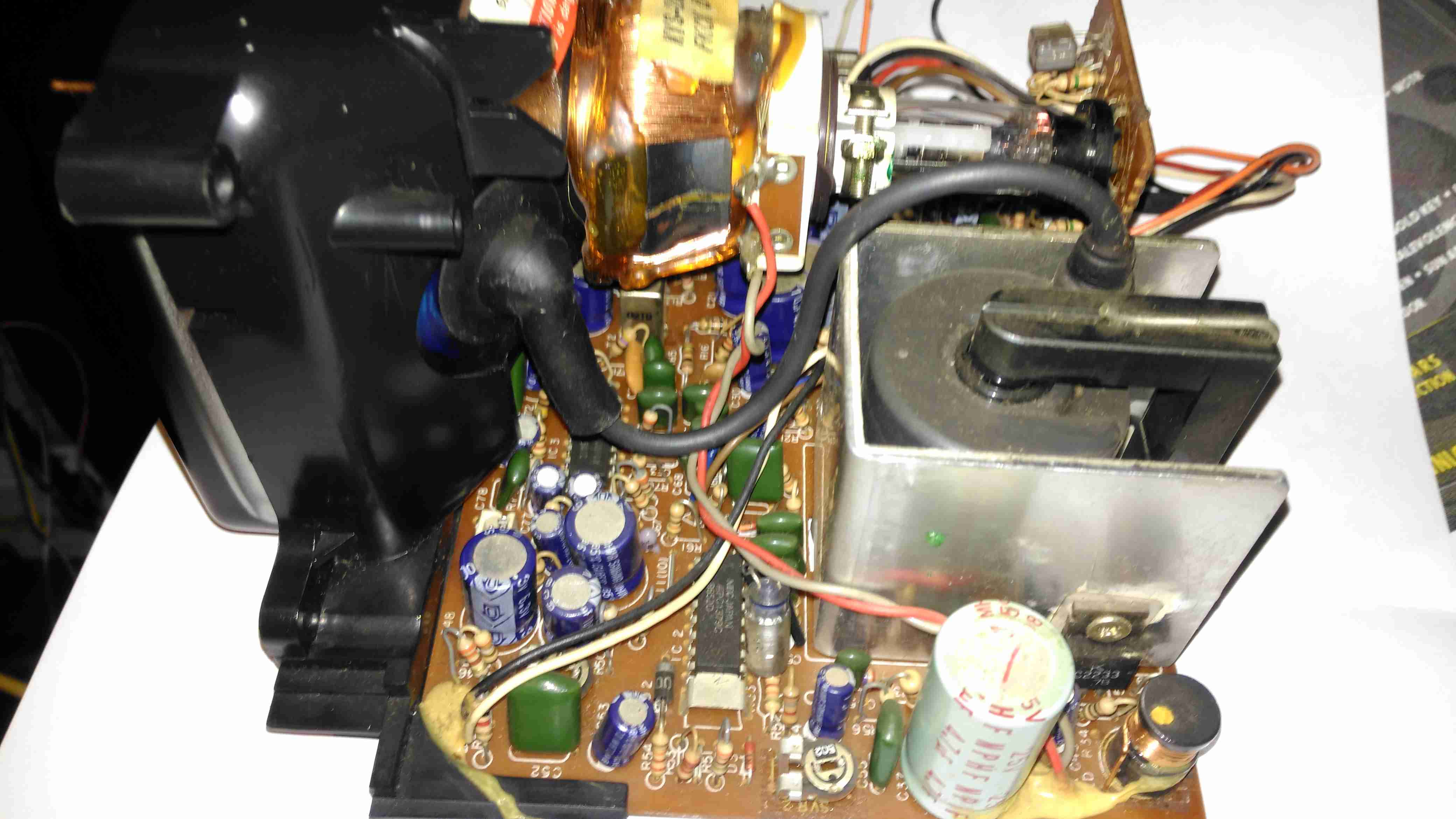
Deflection Board
The bottom board in the assembly has all the control circuitry for the CRT, including the HA11244 deflection IC, composite sync separator & vertical deflection drive circuit. There are also circuits here to display a video waveform on the CRT, along with iris & white balance markers.
Horizontal Board
The other board has the horizontal drive circuitry, along with the video input amplifier. Despite the attempt to miniaturize the entire assembly, these are still well packed boards. Some of the resistors & diodes are bussed together in custom SIL hybrid modules to save PCB space. Like all the other CRT viewfinders, these units are meant for viewing via a mirror – the horizontal deflection coil connections need to be reversed to show a correct image without the mirror. The Red & Blue wires to the yoke need to be swapped here.
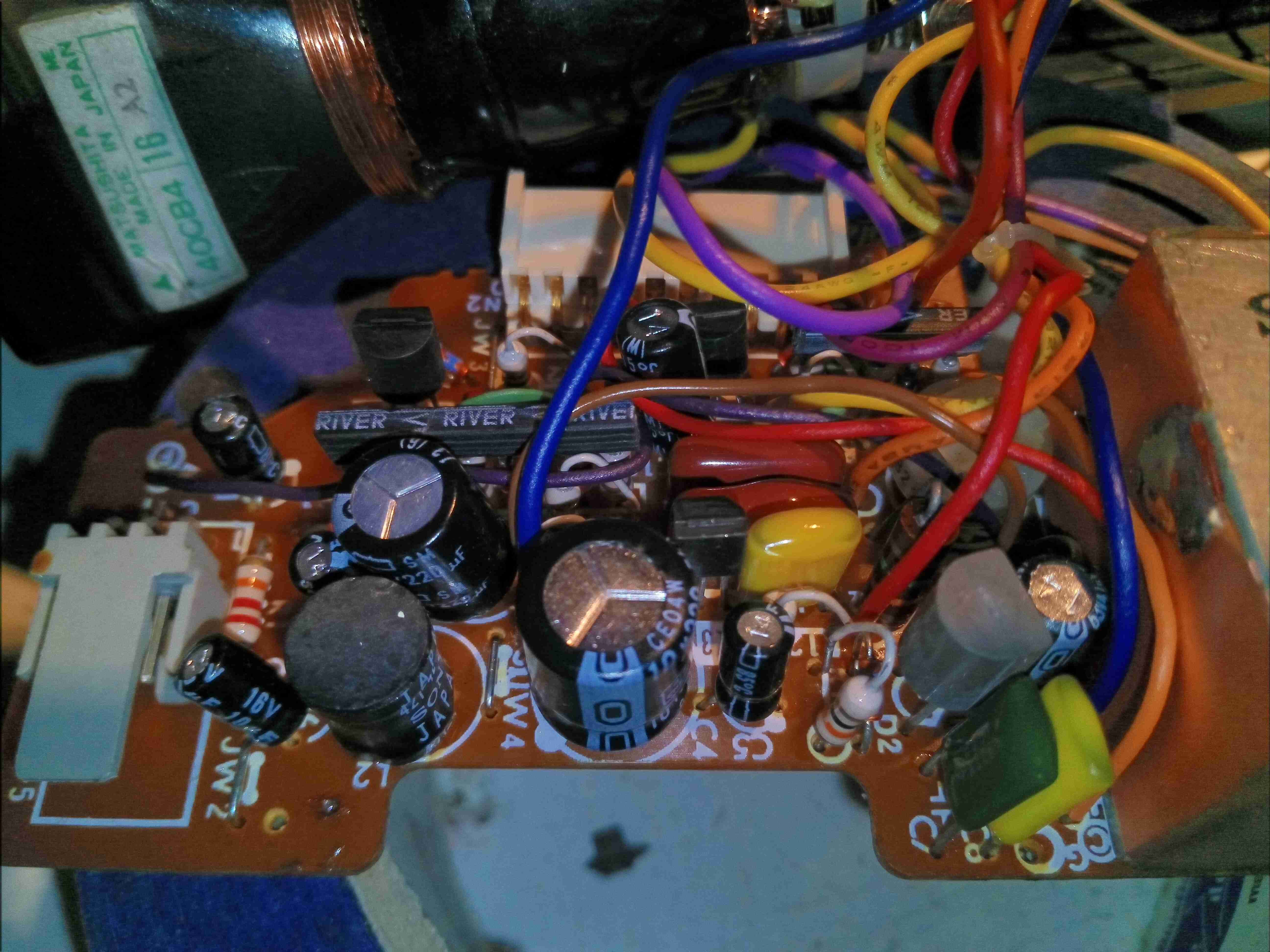
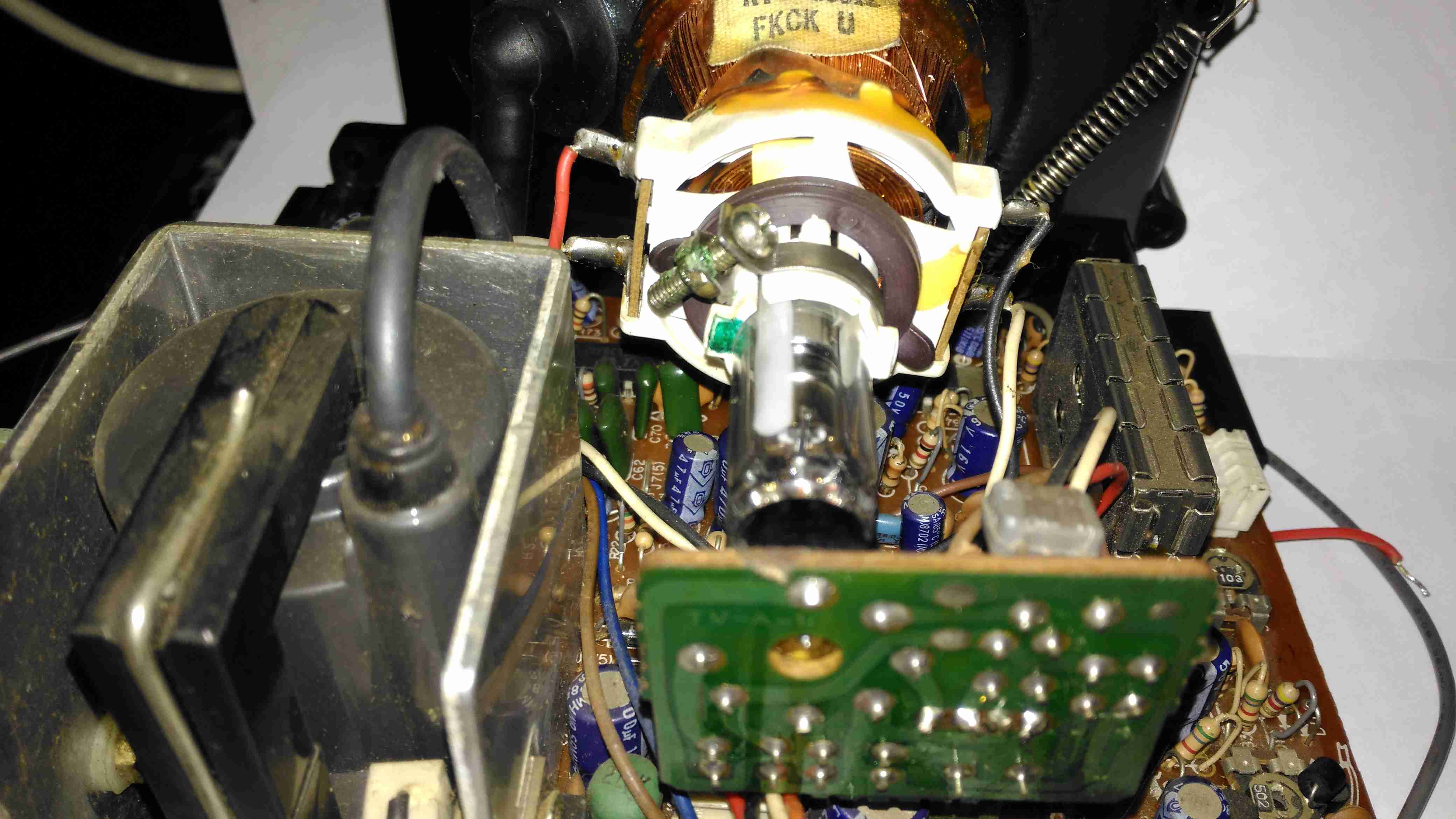
Flyback Transformer
The horizontal board on this unit also supports the flyback transformer, which is massive compared to the other viewfinder circuits. Biasing, focus & filament supplies for the CRT are also derived from this transformer, via auxiliary windings.
Boards Connected
The boards slot together in the centre to form the fully operational circuit.
Video Input
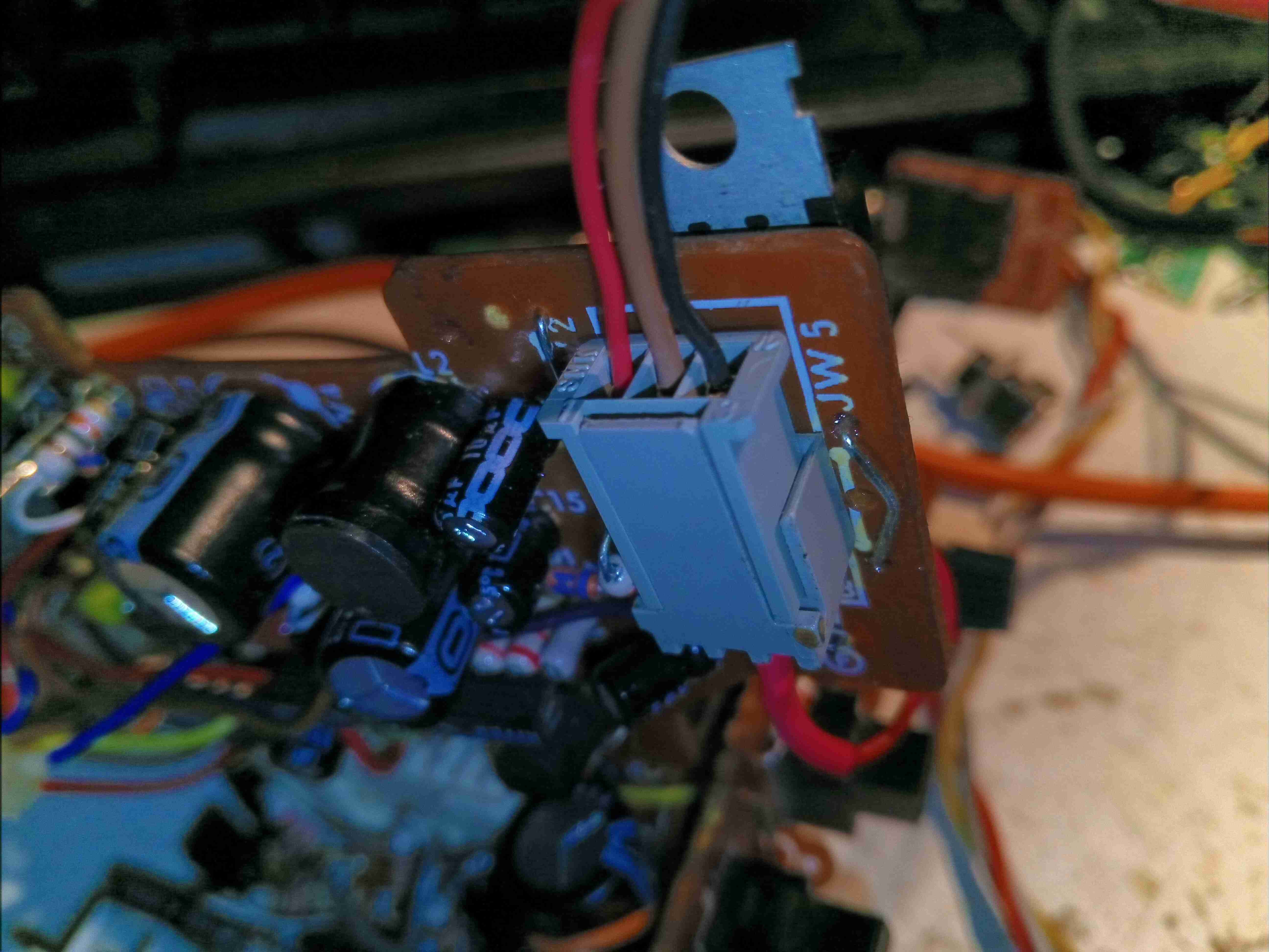
Out of the 3 plugs emerging from the cable feeding the viiewfinder, only this one is important, on the horizontal drive board. Black is ground, Brown +8.5v & red is composite video input. There’s also a resistor tied into the positive rail to the video input pin, which pulls it high to 8.5v – this is R1 right next to this connector. Desolder this 22K resistor to help protect anything feeding a signal into the unit, like a RPi, it’s not needed for normal operation.
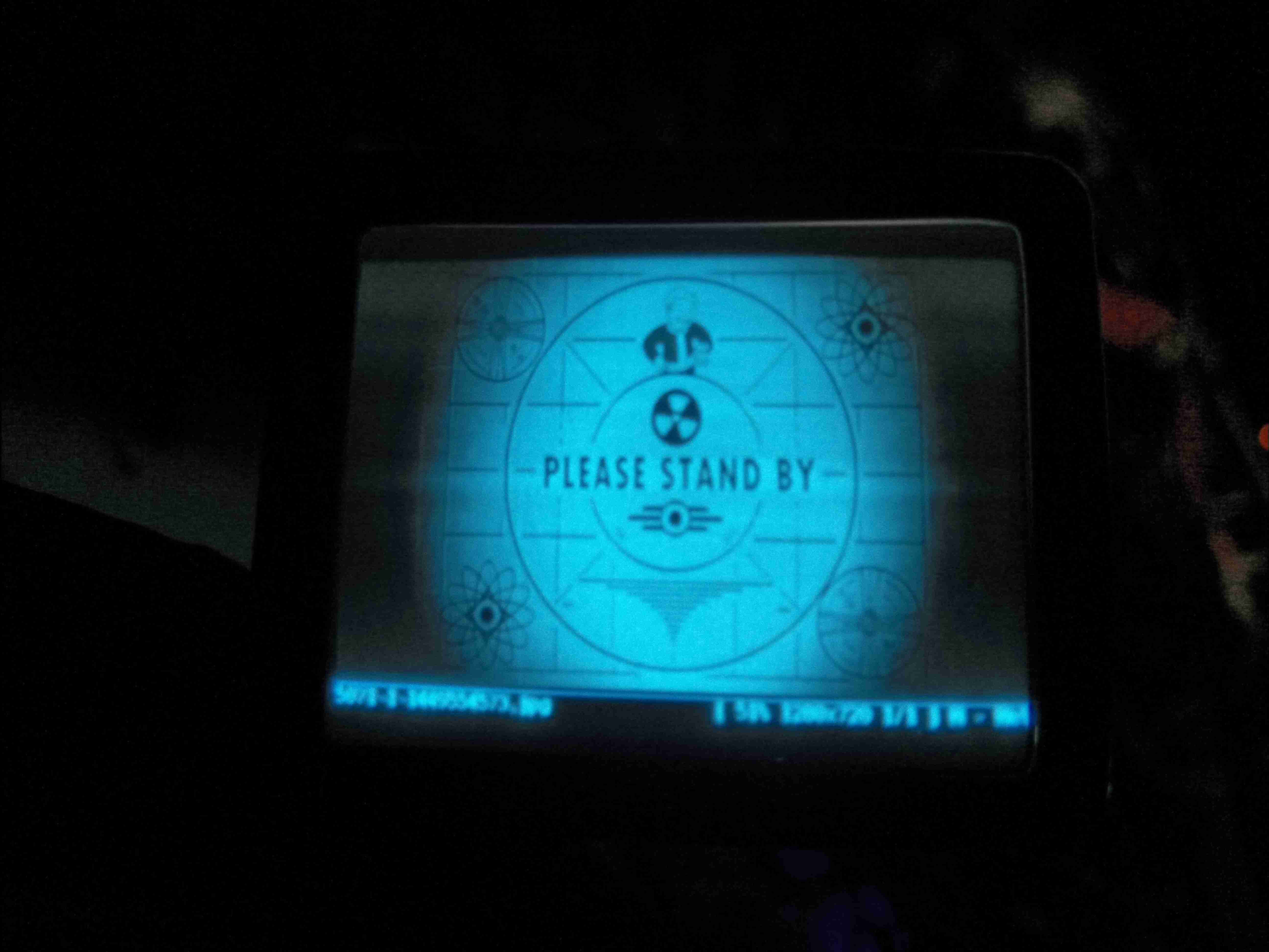
Fallout!
As usual for a CRT post, the Fallout loading screen on the display. The picture quality isn’t as good as it should be, probably due to the noisy buck-converter I have rigged up for testing. If it doesn’t get better with a linear regulator, I’ll start replacing the 39 year old electrolytic capacitors. Current draw is 130mA at 7.5v. Schematics for this unit & the CRT datasheet are available below:
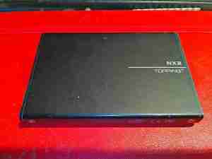
Time for another headphone amplifier! This is the Topping NX2, the upgrade from the NX1 I previously posted about. This one has a built in Burr Brown Audio DAC, along with the analogue audio input.
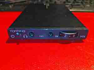
Audio I/O
The front of the unit has the audio connections, power switch & volume control wheel. Standard 3.5mm TRS jacks are used.
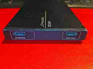
USB I/O
The other end holds a pair of USB Micro B connectors – one for charging the internal lithium cell, and the other providing a data interface for the internal DAC. A charge indicator LED is provided next to the charging port.
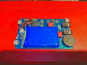
Main PCB
The PCB slides out of the casing, revealing a nice compact layout. The biggest item here is the lithium cell, providing all power to the unit.
Chipset
Audio amplification is handled by a Texas Instruments TP9260 Current-Feedback Class AB amplifier IC, with the USB Audio DAC being a Burr-Brown PCM2704. Nice Wima film capacitors are used on the input stage, although this amplifier suffers from a total lack of bass response – all low frequencies seem to get cut.
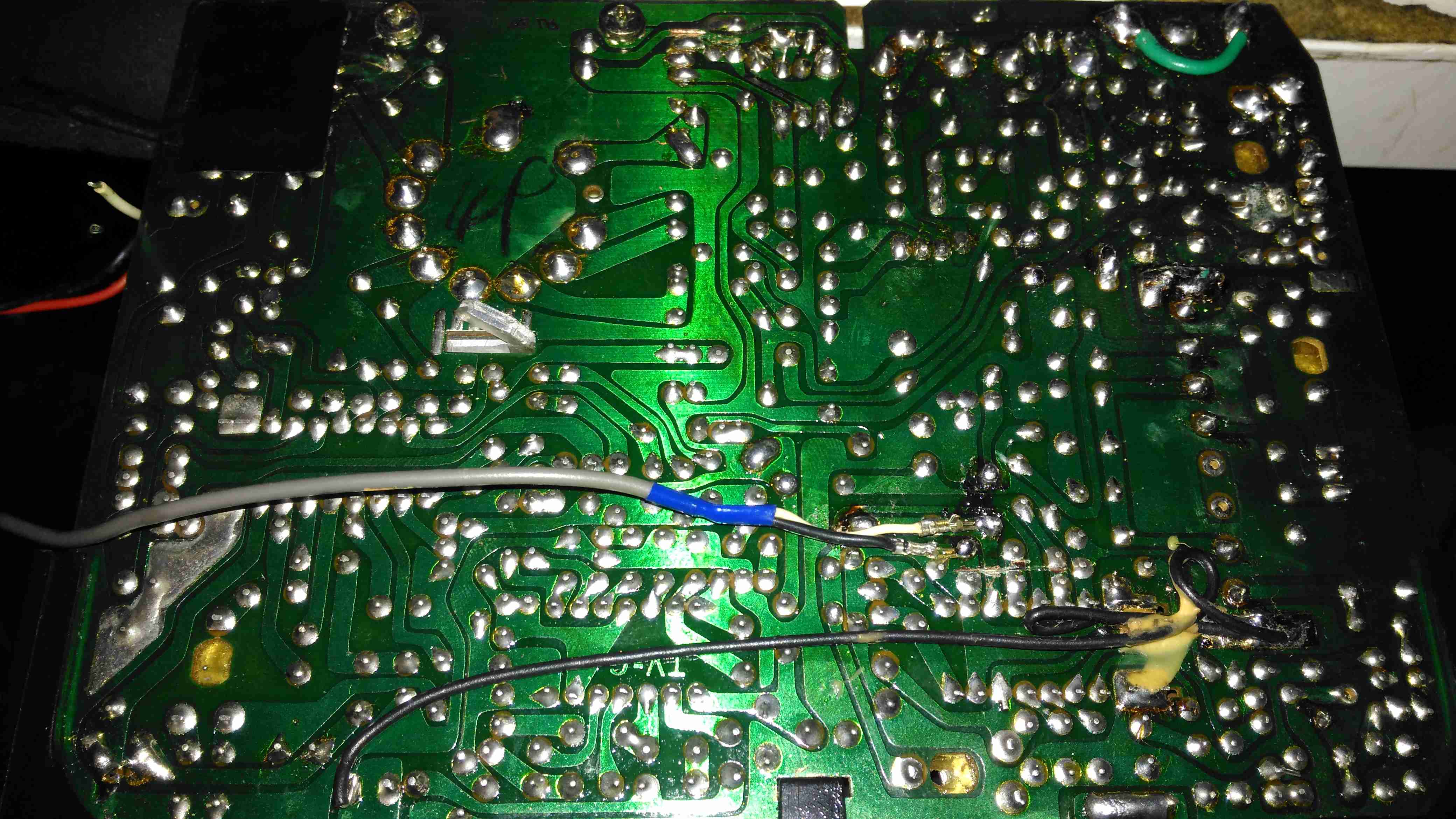
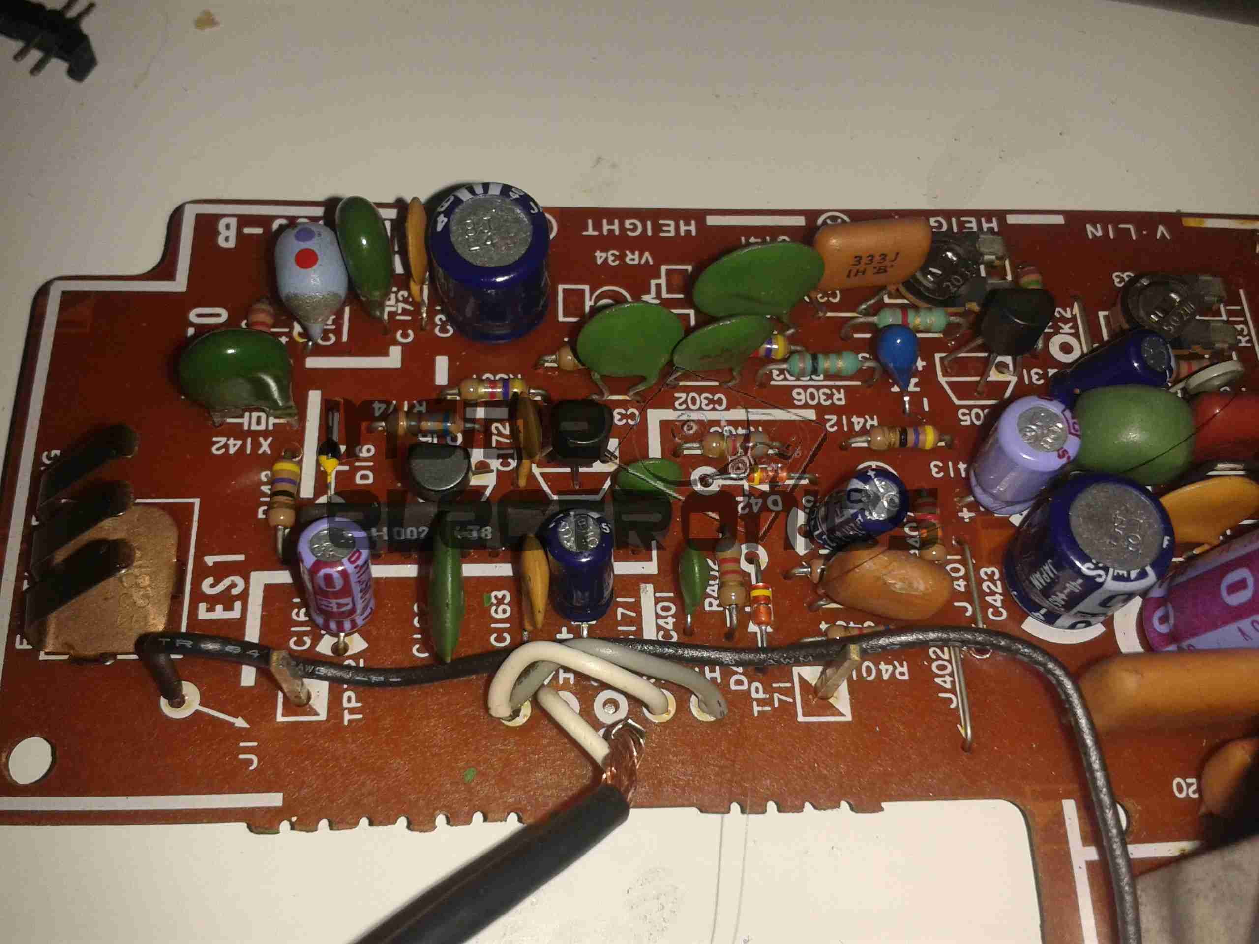
Here’s the CRT & it’s drive board removed from the main chassis. Nicely modular this unit, all the individual modules (radio, tape, TV), are separate. This is effectively a TV itself, all the tuner & IF section are onboard, unlike in other vintage units I’ve modified, where the tuner & IF has been on a separate board. There’s a 3-pin header bottom centre for the tuning potentiometer, and external antenna input jack. The internal coax for the built in antenna has been desoldered from the board here. here a the usual controls on the back for adjusting brightness, contrast & V Hold, all the other adjustments are trimmers on the PCB.
Unfortunately after 30+ years of storage, this didn’t work on first power up, neither of the oscillators for vertical or horizontal deflection would lock onto the incoming signal, but a couple of hours running seemed to improve things greatly. The numerous electrolytic capacitors in this unit were probably in need of some reforming after all this time, although out of all of them, only 21 are anything to do with the CRT itself.
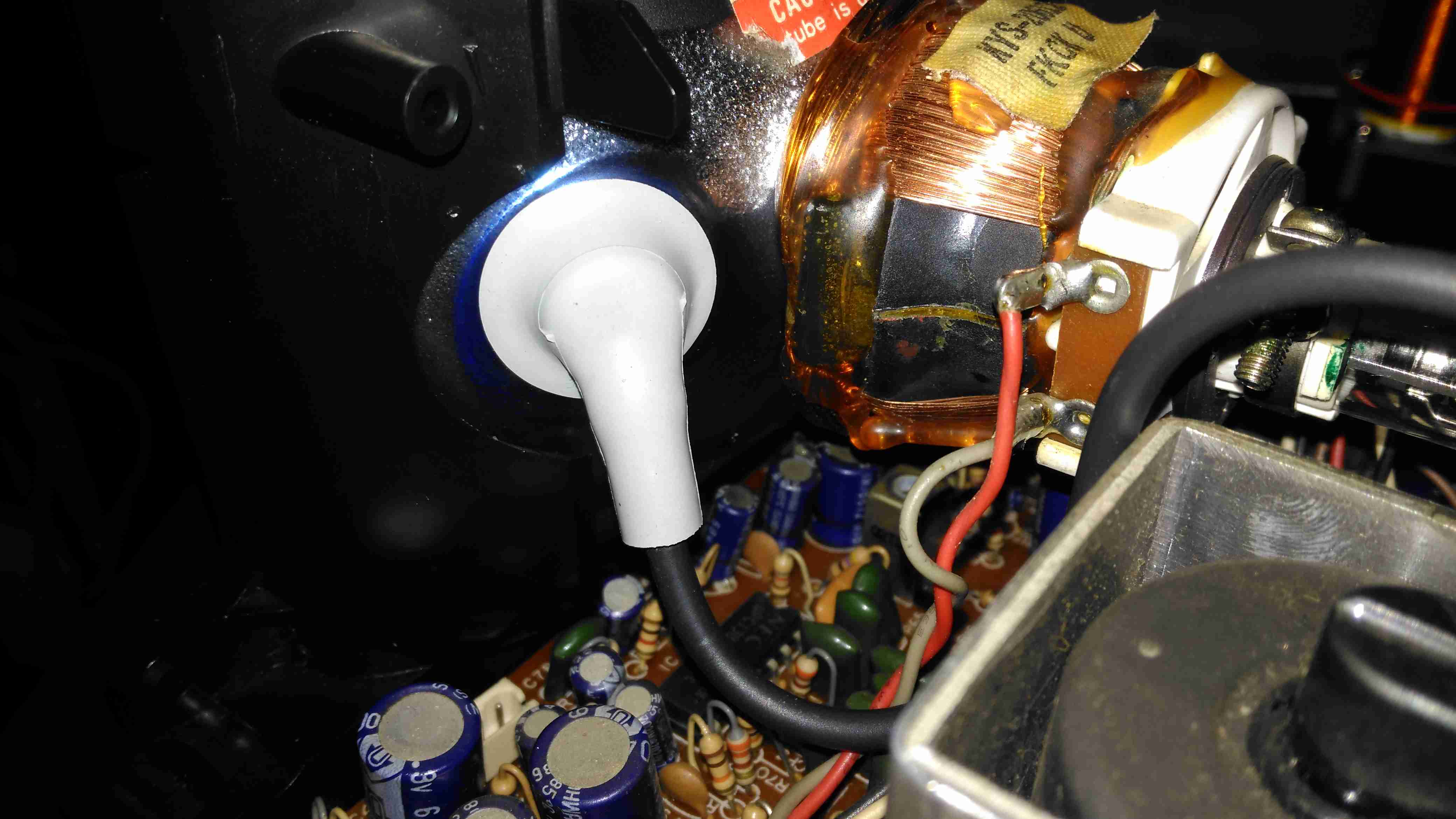
Anode Cap
Here’s the anode side of the unit, with the small flyback transformer. The rubber anode cap has become very hard with age, so I’ll replace this with a decent silicone one from another dead TV. The Horizontal Output Transistor (a 2SC2233 NPN type) & linearity coil are visible at the bottom right corner of the board. Unfortunately, the disgusting yellow glue has been used to secure some of the wiring & large electrolytics, this stuff tends to turn brown with age & become conductive, so it has to be removed. Doing this is a bit of a pain though. It’s still a little bit flexible in places, and rock hard in others. Soaking in acetone softens it up a little & makes it easier to detach from the components.
Neck PCB
There’s little on the neck board apart from a few resistors, forming the limiting components for the video signal, and the focus divider of 1MΩ & 470KΩ feeding G3. No adjustable focus on this unit. There’s also a spark gap between the cathode line & ground, to limit the filament to cathode voltage. The flyback transformer is nestled into the heatsink used by the horizontal output transistor & a voltage regulator transistor.
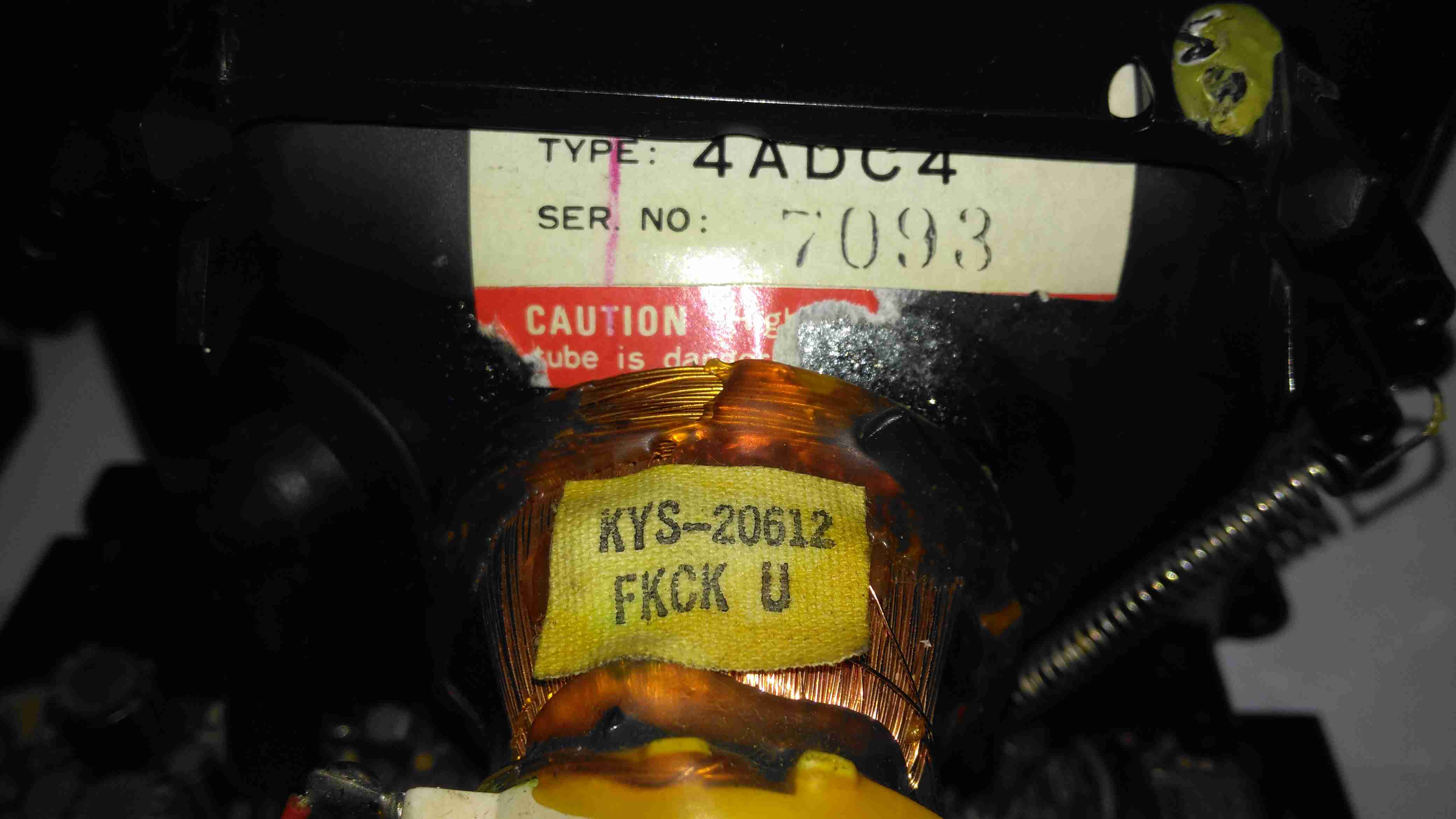
Tube Details
The CRT is a Samsung Electron Devices 4ADC4, with a really wide deflection angle. It’s a fair bit shorter than the Chinese CRT I have which is just a little larger, with a neck tube very thin indeed for the overall tube size.
Unusually, while the filament voltage is derived from the flyback transformer as usual, it’s rectified into DC in this unit, passing through a 1Ω resistor before the filament connection. I measured 5.3v here. The glow from the filament is barely visible even in the dark.
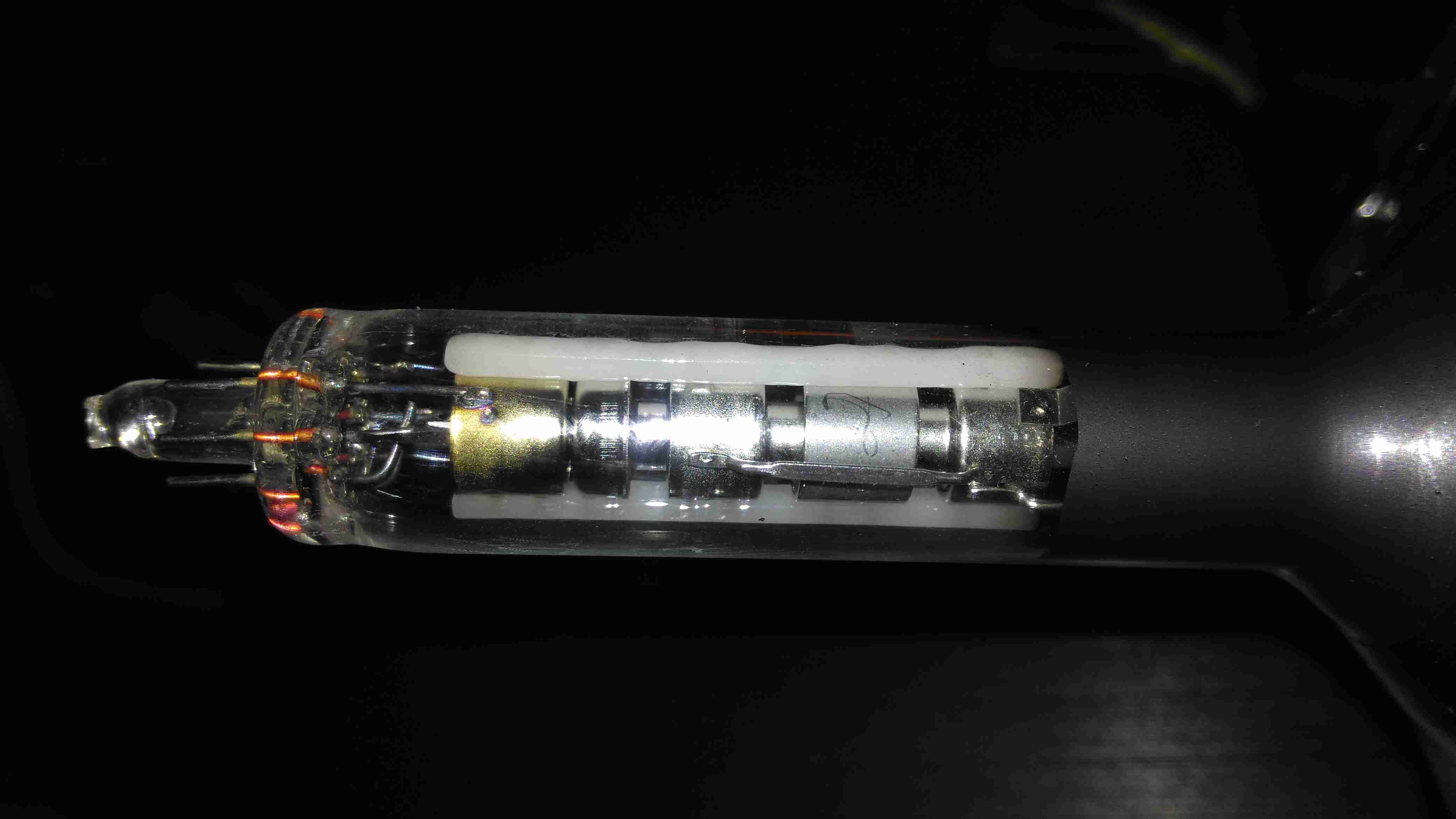
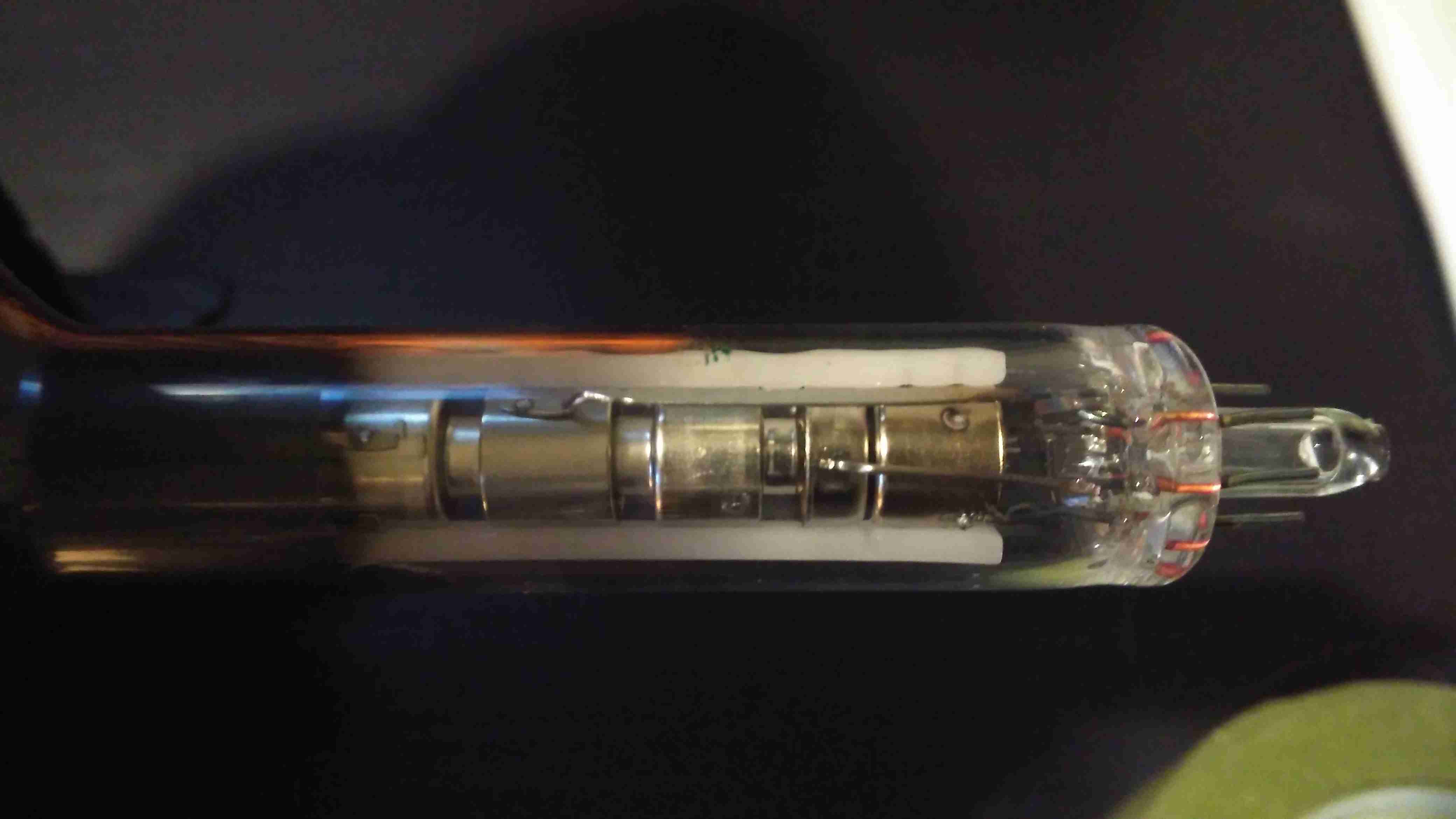
Electron Gun 1
The electron gun is the usual for a monochrome tube, with 7 pins on the seal end.
Electron Gun 2
The electrodes here from left are Final Anode, G3 (Focus Grid), Accelerating Anode, G2 (Screen Grid), G1 (Control Grid). The cathode & filament are hidden inside G1. In operation there’s about 250v on G2, and about 80v on G3.
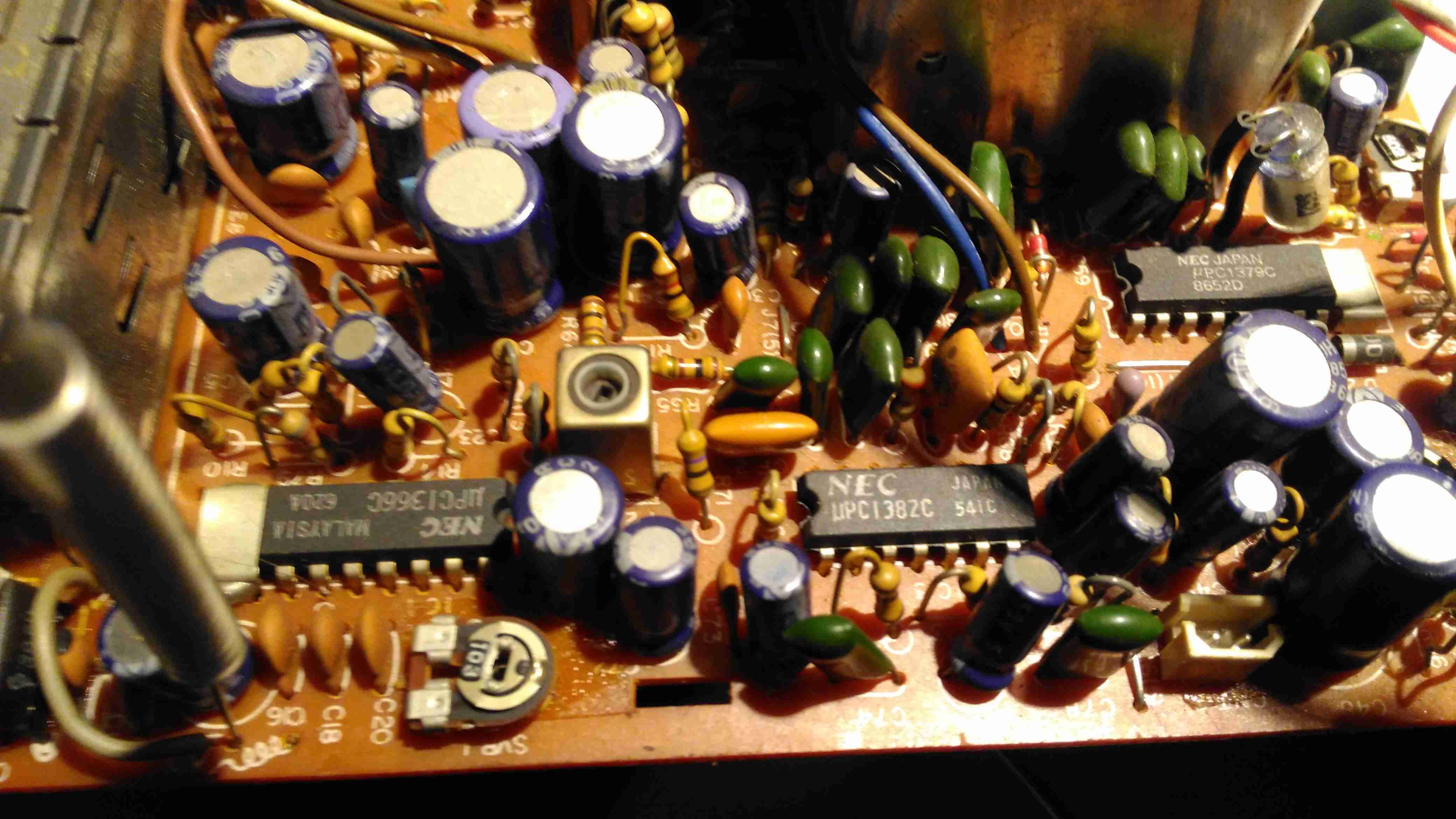
Chipset
The chipset used here is all NEC, starting with a µPC1366C Video IF Processor, which receives the IF signal from the tuner module to the left. This IC outputs the standard composite signal, and a modulated sound signal.
This then splits off to a µPC1382C Sound IF Processor & Attenuator IC, which feeds the resulting sound through the two pin header at the right bottom edge of the board to the audio amplifier in the chassis.
The composite video signal is fed through a discrete video amplifier with a single 2SC2229 transistor before going to the CRT cathode.
The remaining IC is a µPC1379C Sync Signal Processor, containing the sync separator, this is generating the required waveforms to drive the CRT deflection systems from another tap off the composite video line.
From this chip I can assume the unit was built around 1986, since this is the only date code on any of the semiconductors. Besides these 3 ICs, the rest of the circuit is all discrete components, which are well-crammed into the small board space.
There are 5 trimmer potentiometers on the board here, I’ve managed to work out the functions of nearly all of them:
SVR1: IF Gain Adjust
SVR2: H. Hold
SVR3: V. Size
SVR4: B+ Voltage Adjust
SVR5: Tuner Frequency Alignment? It’s in series with the tuning potentiometer in the chassis.
PCB Bottom
The PCB bottom shows the curved track layout typical of a hand taped out board. The soldermask is starting to flake off in places due to age, and there a couple of bodge wires completing a few ground traces. Respinning a board in those days was an expensive deal! Surprisingly, after all this time I’ve found no significant drift in the fixed resistors, but the carbon track potentiometers are drifiting significantly – 10KΩ pots are measuring as low as 8KΩ out of circuit. These will have to be replaced with modern versions, since there are a couple in timing-sensitive places, like the vertical & horizontal oscillator circuits.
Anode Cap Replaced
Here the anode cap has been replaced with a better silicone one from another TV. This should help keep the 6kV on the CRT from making an escape. This was an easy fix – pulling the contact fork out of the cap with it’s HT lead, desoldering the fork & refitting with the new cap in place.
Here I’ve replaced the important trimmers with new ones. Should help stabilize things a little.
Composite Injection Mod
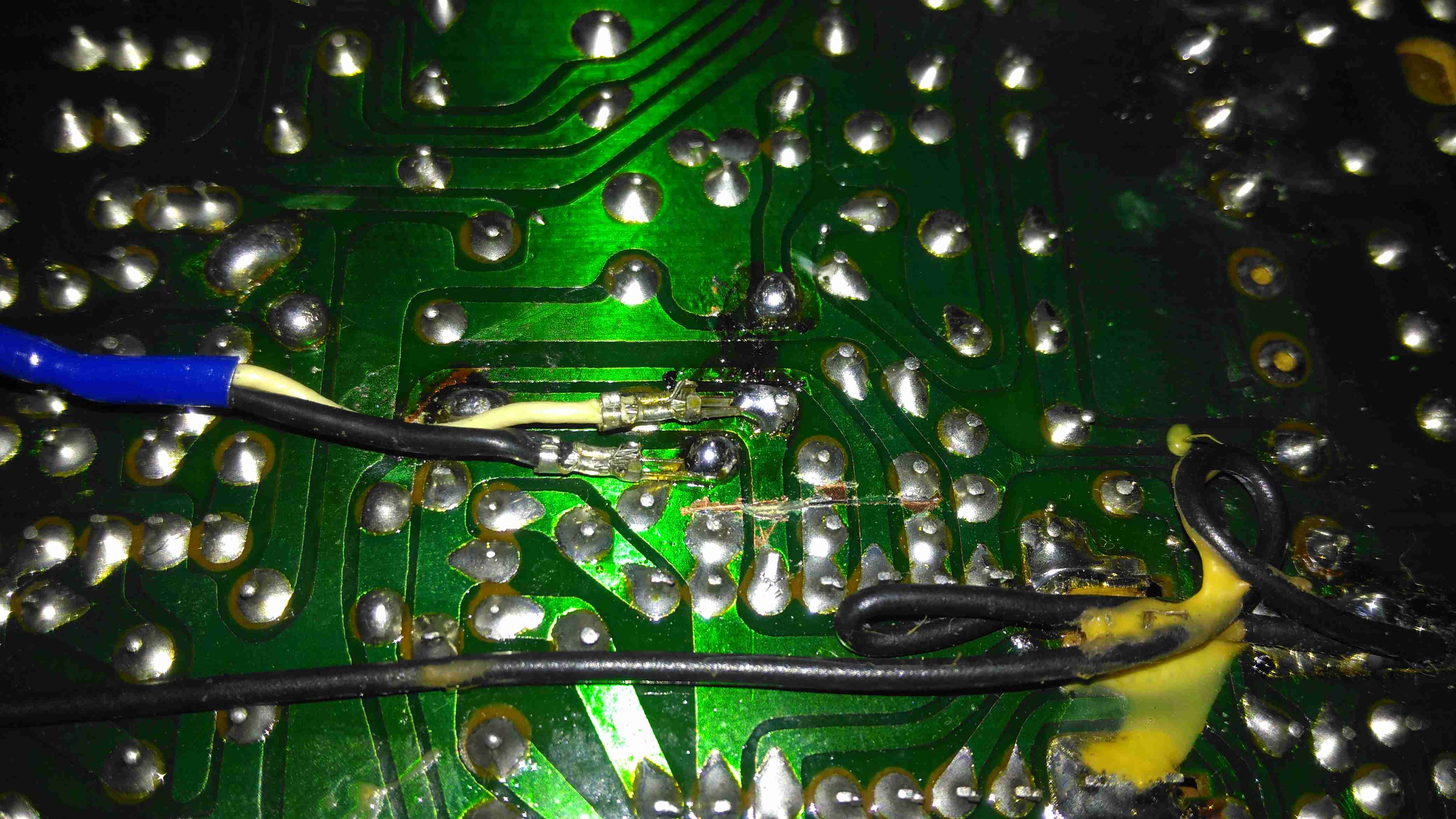
Injecting a video signal is as easy as the other units. Pin 3 of the µPC1366C Video IF Processor is it’s output, so the track to Pin 3 is cut and a coax is soldered into place to feed in an external signal.
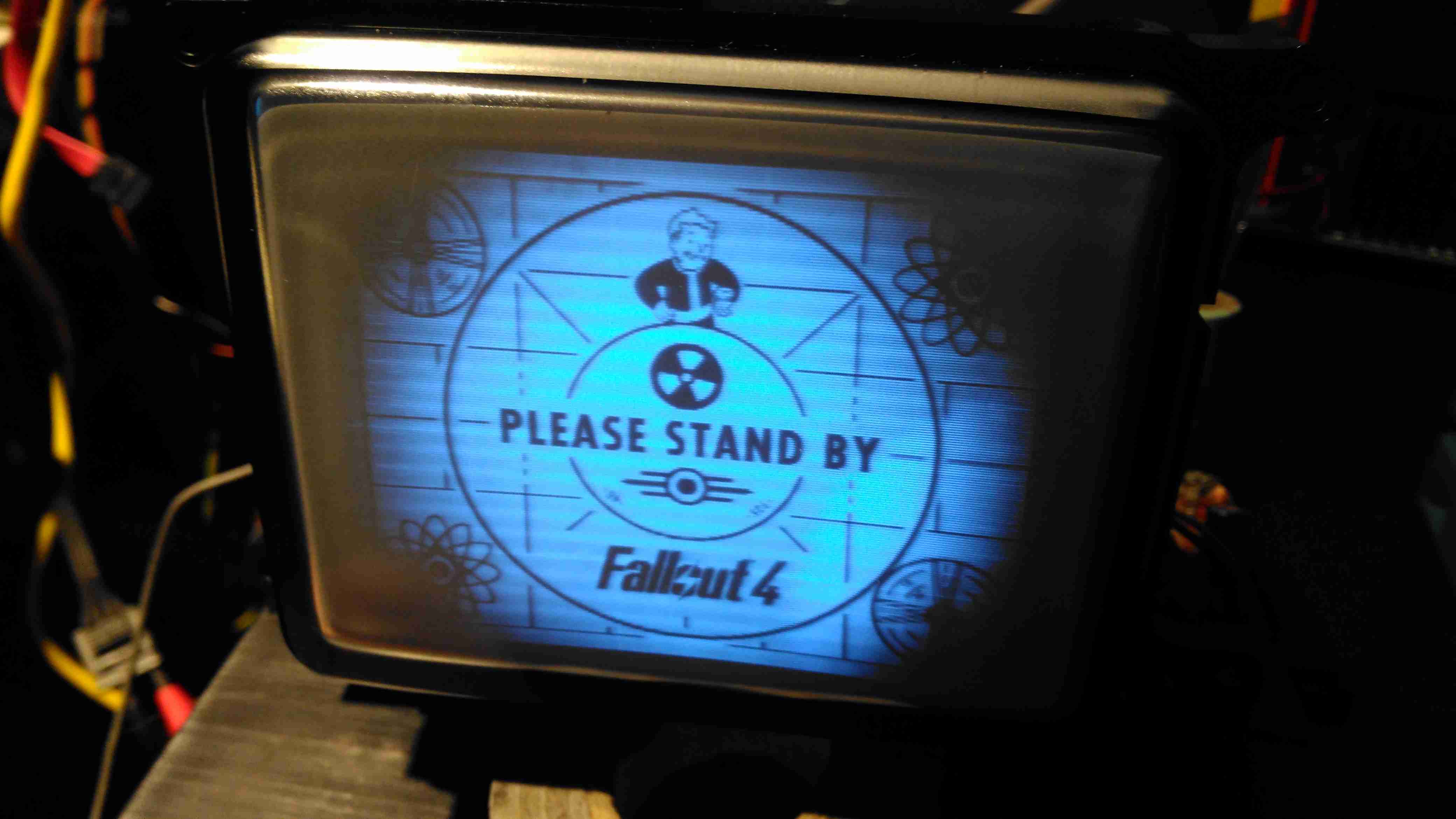
CRT In Operation
After hooking up a Raspberry Pi, we have display! Not bad after having stood idle for 30+ years.
Datasheets for the important ICs are available below:
[download id=”5690″]
[download id=”5693″]
[download id=”5696″]
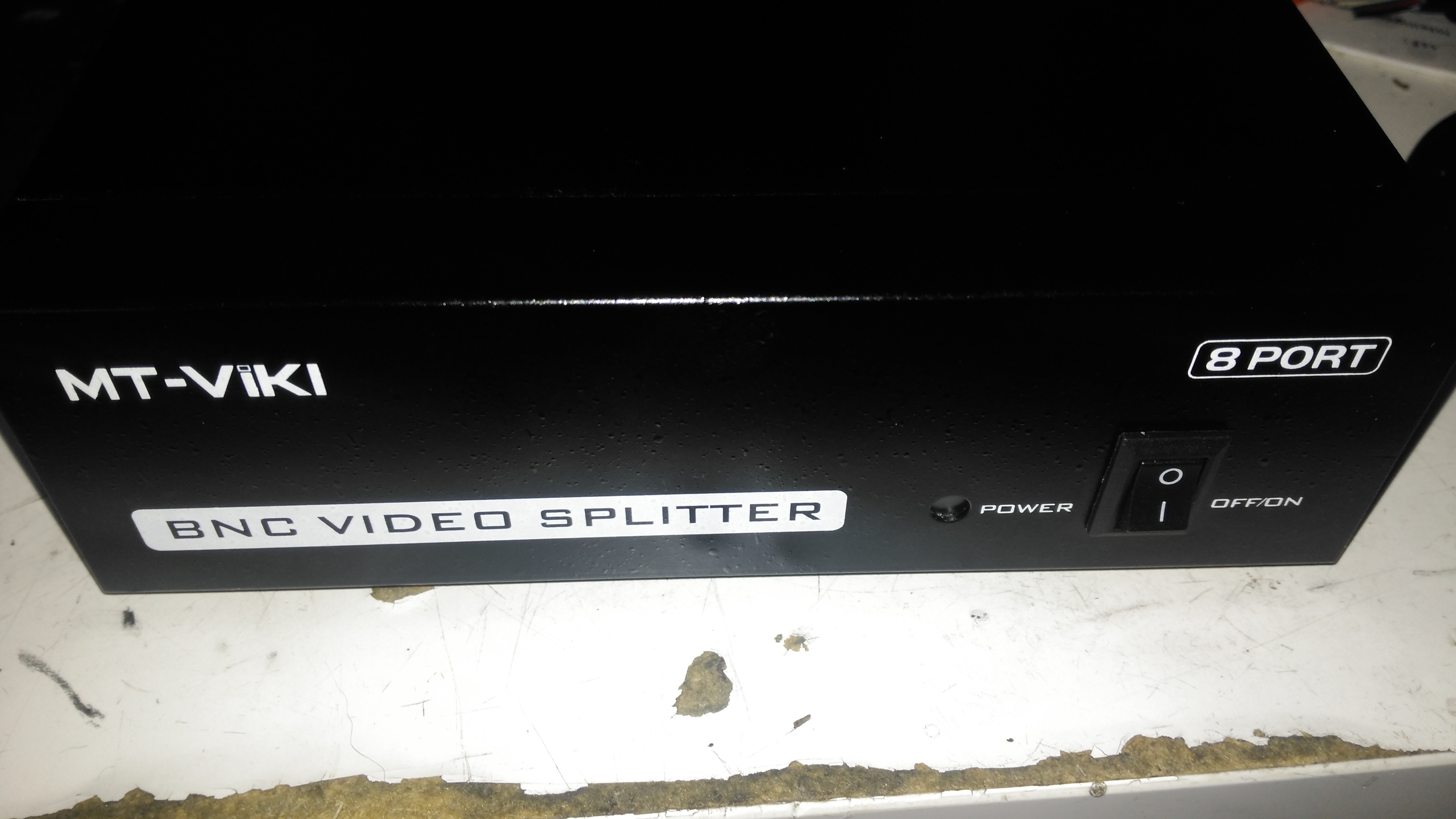
Time for another eBay special: this time it’s an 8-port video distribution amplifier, with BNC connections designed for commercial/industrial equipment. Not much on the front panel above, apart from the power switch & LED.
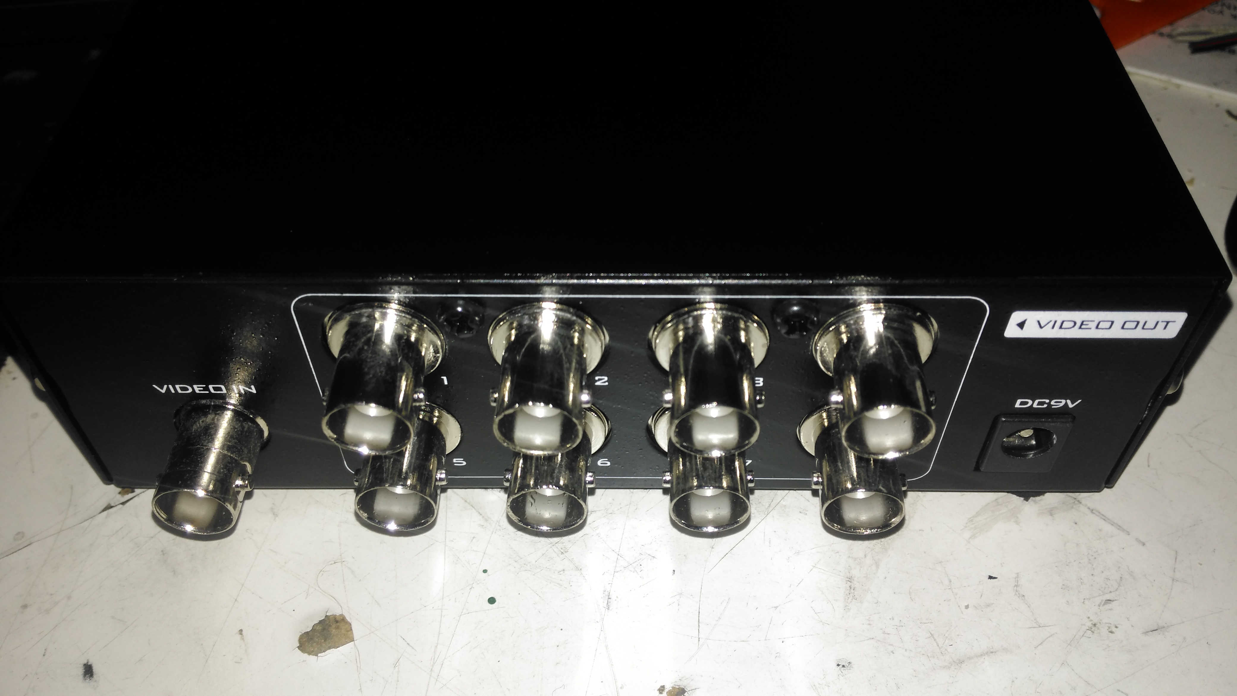
Rear Panel
The rear panel has all the connectors, input is on the left, while the outputs are in the centre. Power is supplied through the barrel jack on the right, 9v DC in this case.
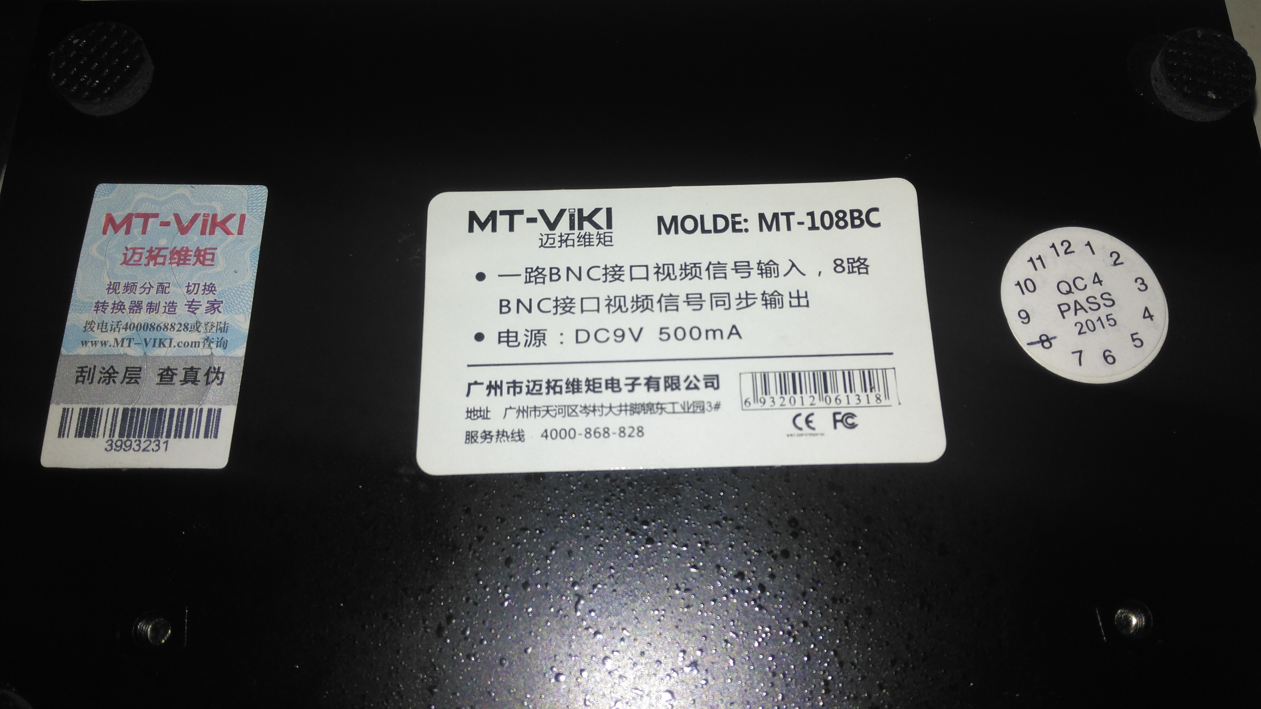
Data Label
Not much in English on the data labels, there’s also an authenticity label on the left to make sure you don’t get a fake.
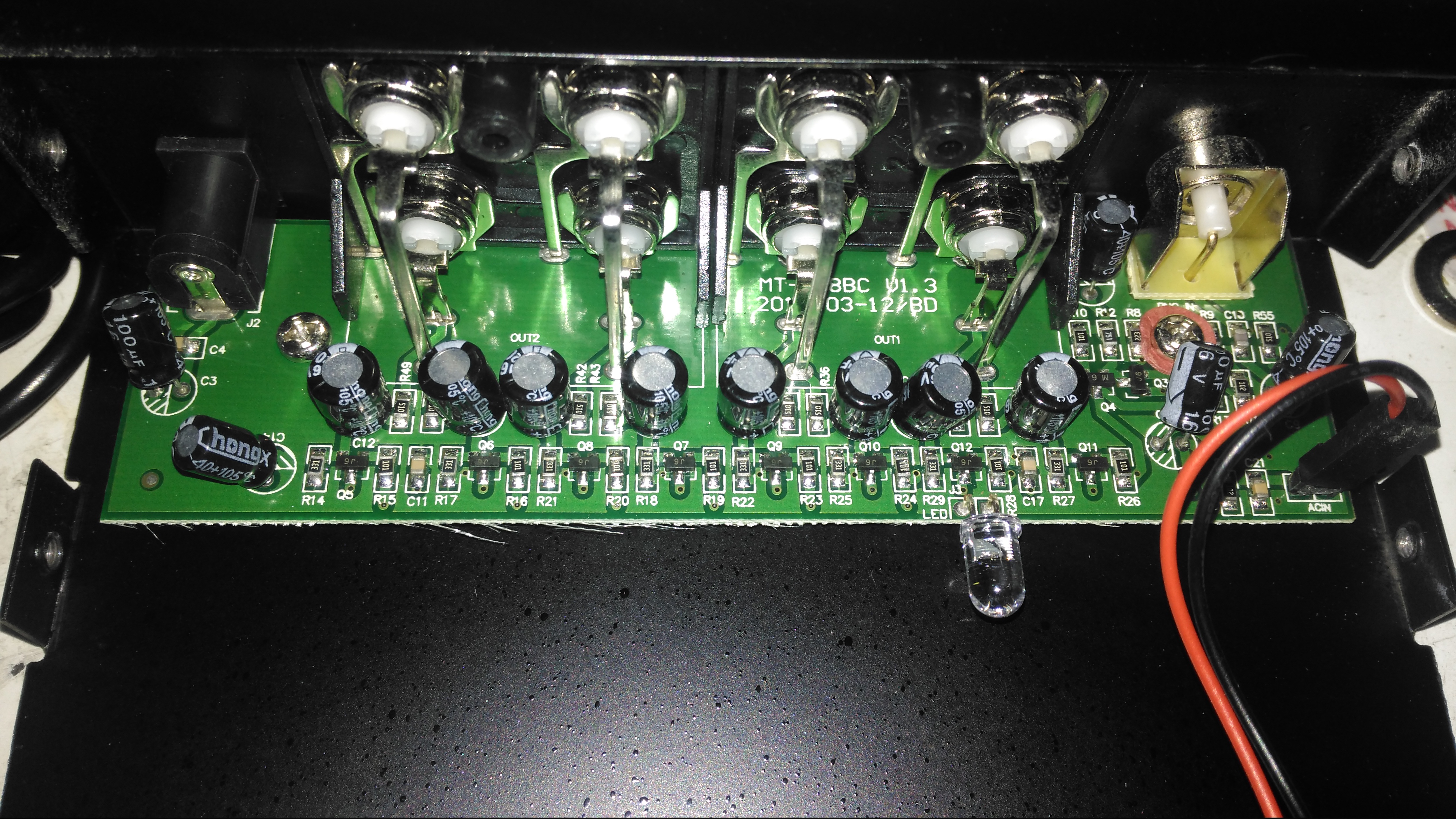
Amplifier Board
Taking the lid off reveals a very small PCB, taking up less than a third of the aluminium case! The input stage is on the right, composed of a pair of SOT-23 transistors to buffer the incoming signal. There’s an KST812M6 PNP & an S9014 NPN Epitaxial. The signal is then fed to the output stages, all individual S9014 NPN transistors to the output ports.
The power LED is just poking in the general direction of the hole in the front panel, so this isn’t likely to work very well – it’s going to illuminate the inside of the case more!
The old Panasonic NV-M5 has the standard for the time CRT based viewfinder assembly, which will happily take a composite video signal from an external source.
This viewfinder has many more connections than I would have expected, as it has an input for the iris signal, which places a movable marker on the edge of the display. This unit also has a pair of outputs for the vertical & horizontal deflection signals, I imagine for sync, but I’ve never seen these signals as an output on a viewfinder before.
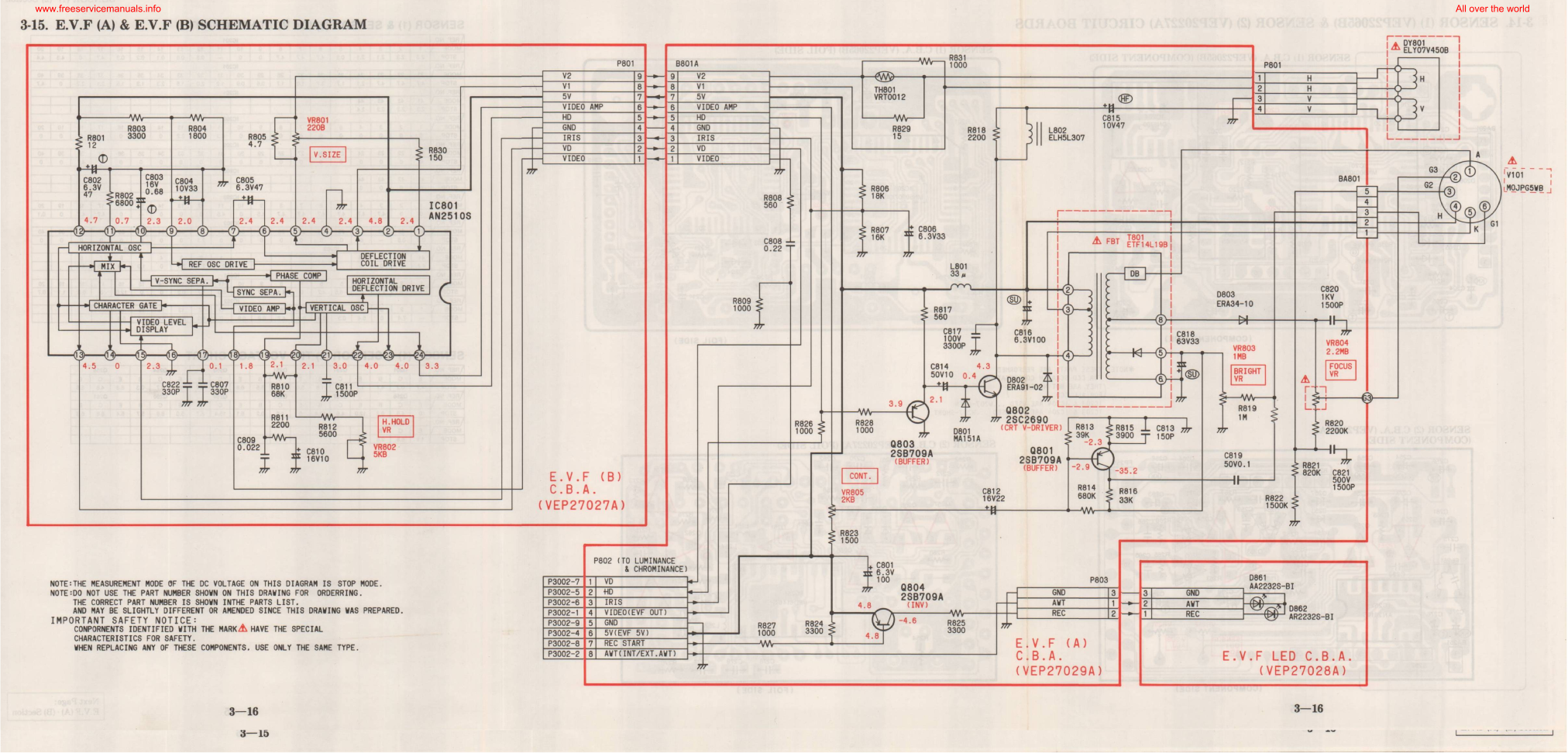
EVF Schematic
Luckily I managed to get a service manual for the camera with a full schematic.
This unit takes a 5v input, as opposed to the 8-12v inputs on previous cameras, so watch out for this! There’s also no reverse polarity protection either.
Pins
Making the iris marker vanish from the screen is easy, just put a solder bridge between pins 15 & 16 of the drive IC. The important pins on the interface connector are as follows:
Pin 3: GND
Pin 4: Video Input
Pin 5: Video GND
Pins 6: +5v Supply
I was recently given this unit, along with another Behringer sound processor to repair, as the units were both displaying booting problems. This first one is a rather swish Mastering Processor, which has many features I’ll leave to Behringer to explain 😉
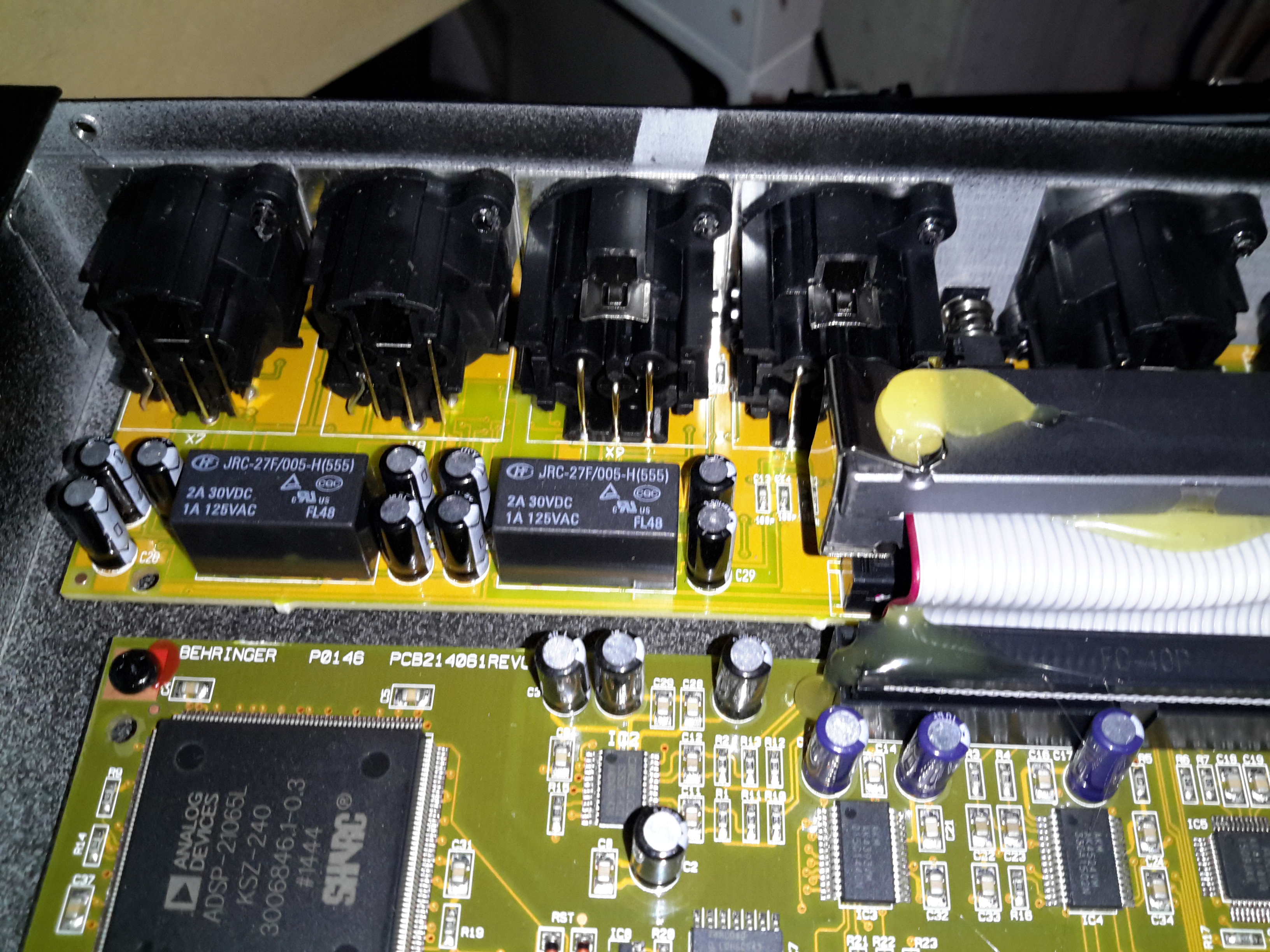
Input Board & Relays
All the inputs are on the back of this 19″ rackmount bit of kit, nothing much on this PCB other than the connectors & a couple of switching relays.
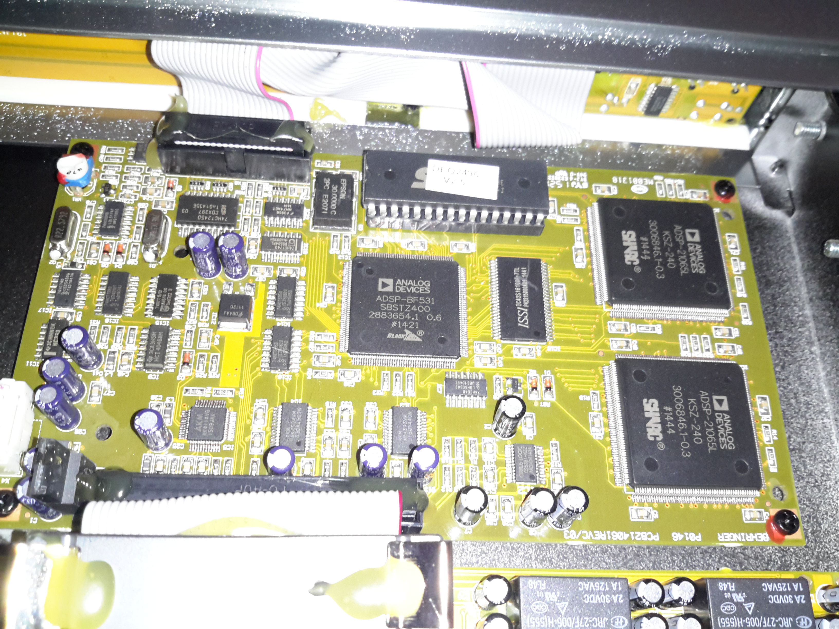
Main Processor PCB
All the magic is done on the main processor PCB, which is host to 3 Analog Devices DSP processors:
ADSP-BF531 BlackFin DSP. This one is probably handling most of the audio processing, as it’s the most powerful DSP onboard at 600Mhz. There’s a ROM on board above this for the firmware & a single RAM chip. On the right are a pair of ADSP-21065 DSP processors at a lower clock rate of 66MHz. To the left is some glue logic to interface the user controls & dot-matrix LCD.
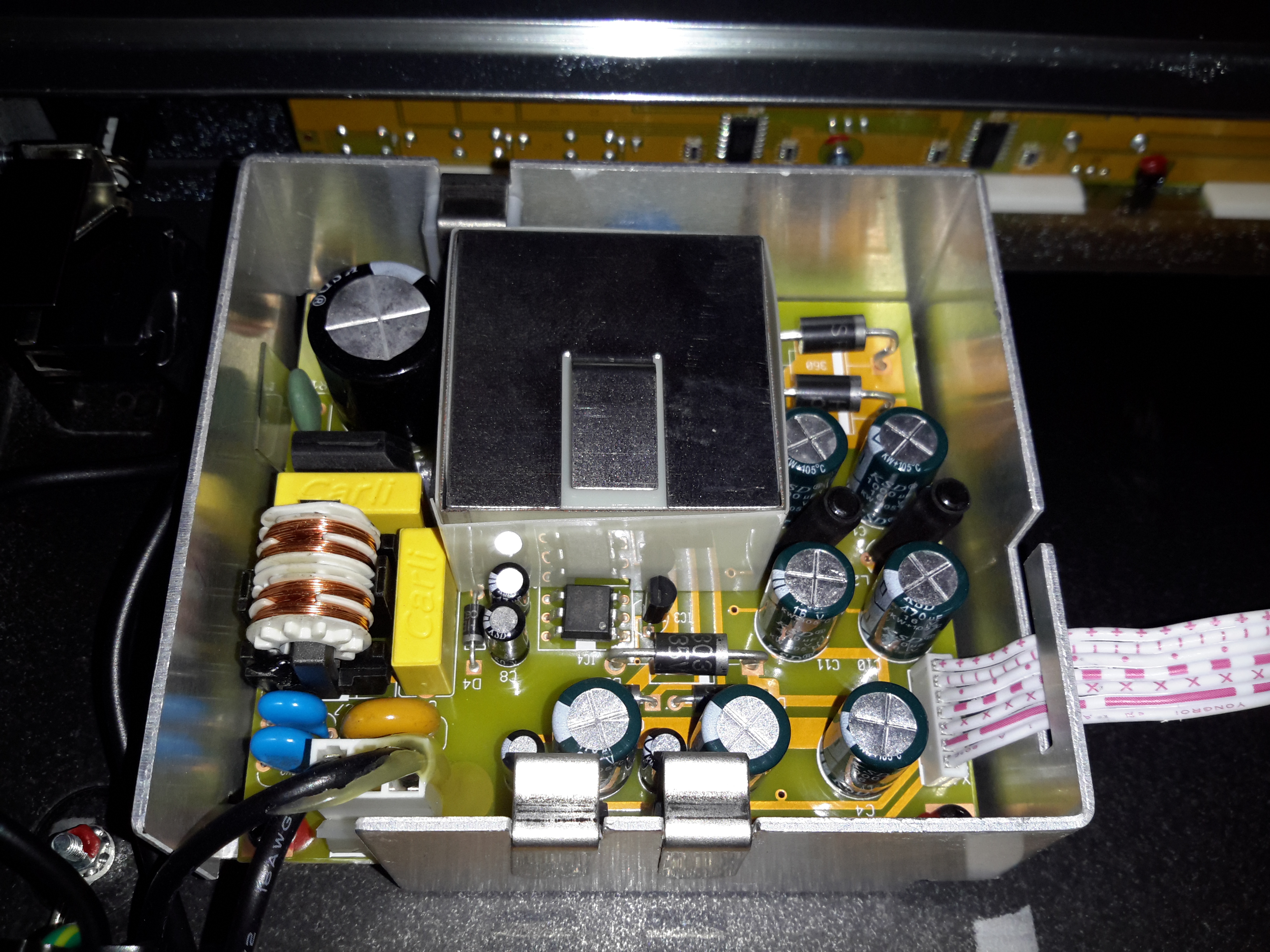
PSU Module
The PSU in this unit is a pretty standard looking SMPS, with some extra noise filtering & shielding. The main transformer is underneath the mu-metal shield in the centre of the board.
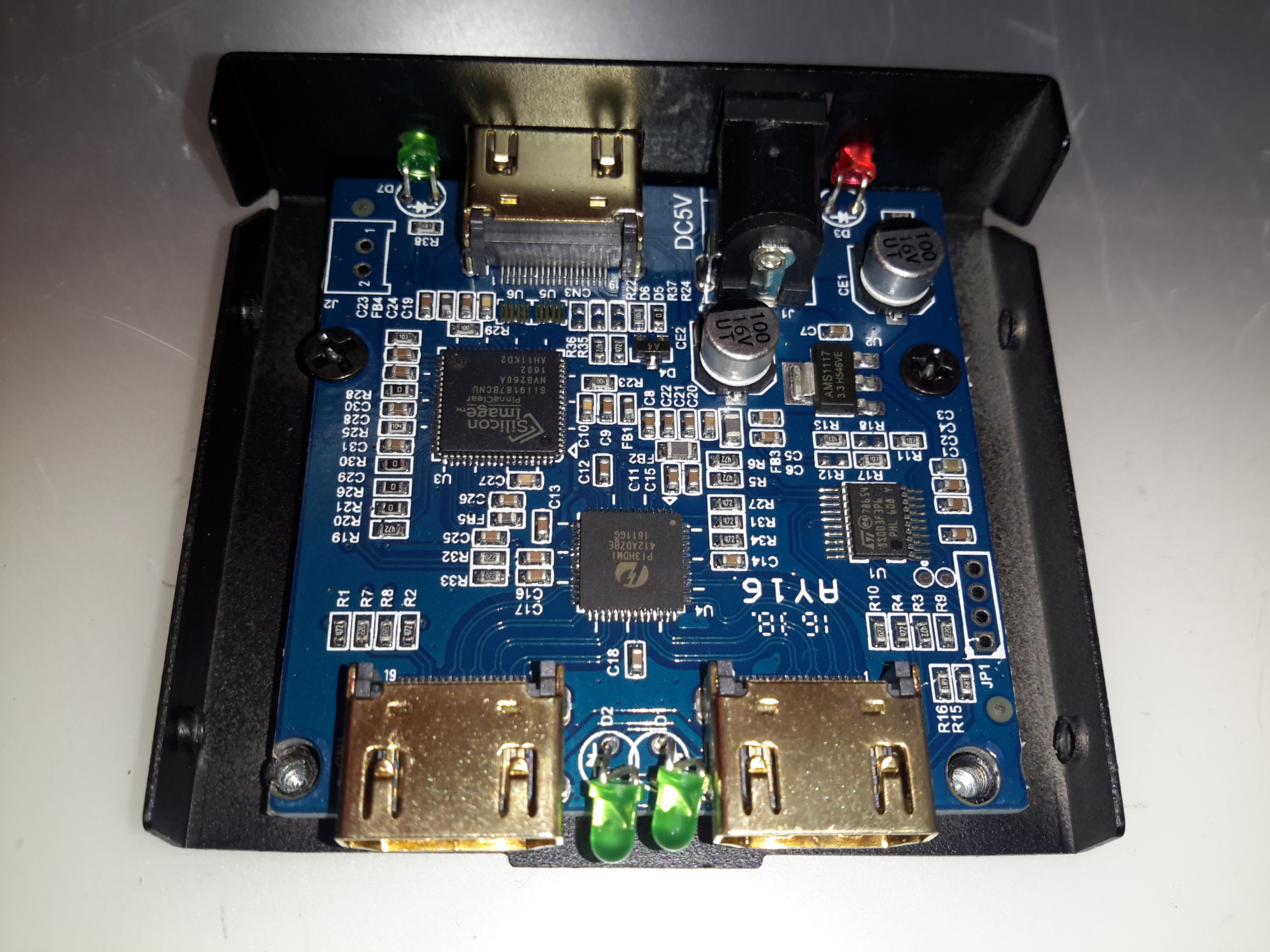
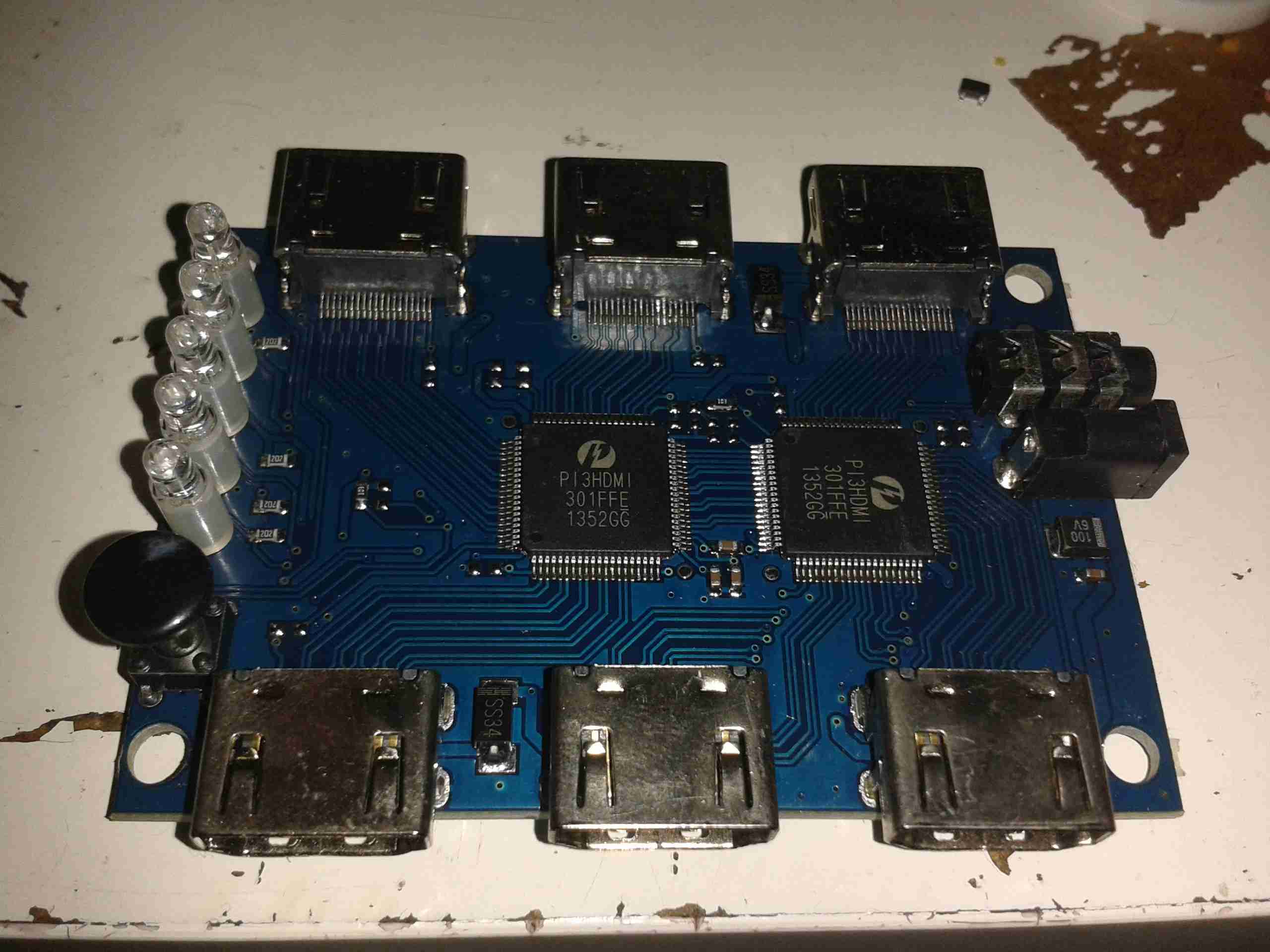
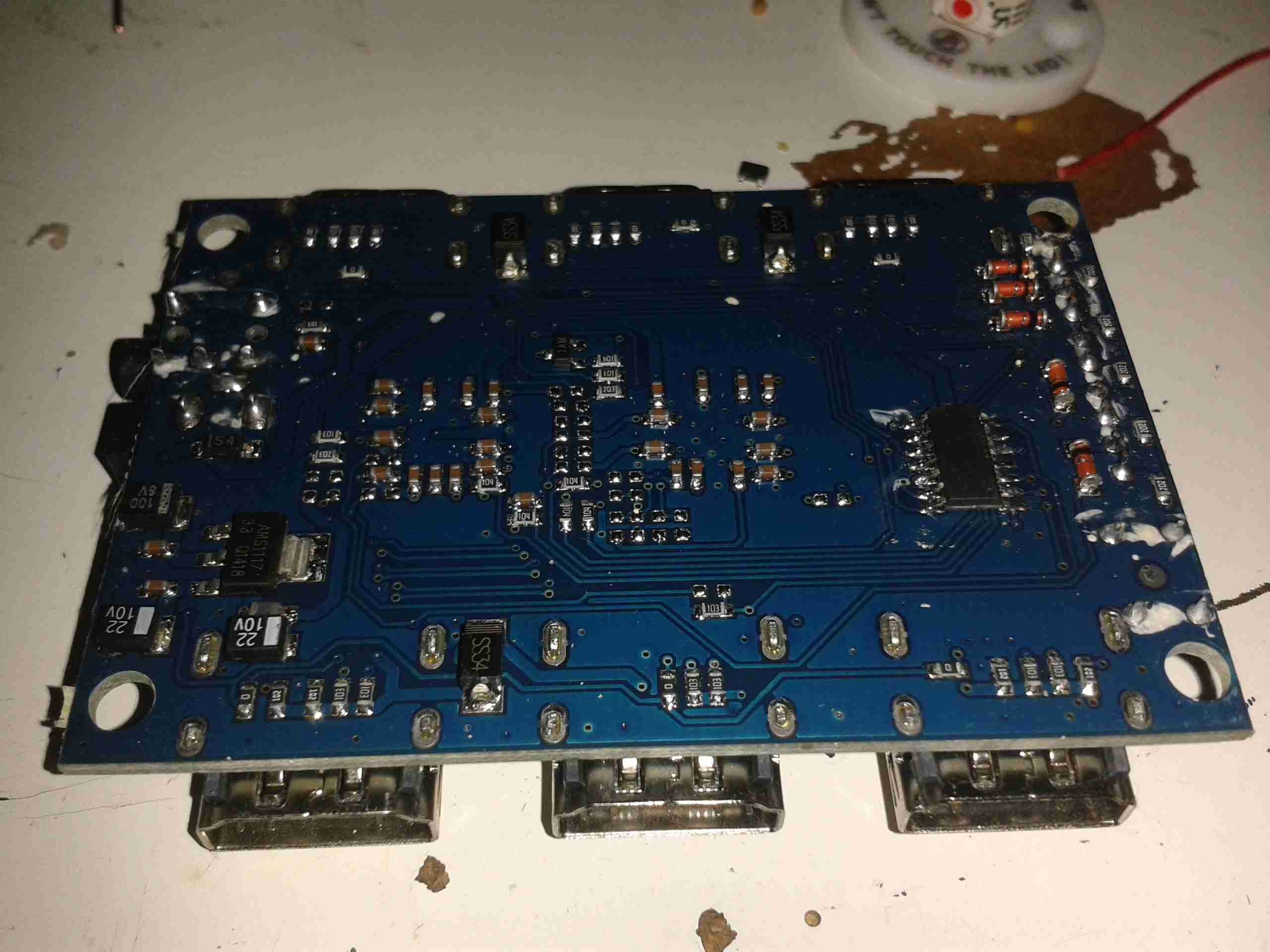
Time for another random teardown, a signal splitter for HDMI. These units are available very cheap these days on eBay. This one splits the incoming signal into two to drive more than one display from the same signal source.
Main PCB
The stamped alloy casing comes apart easily with the removal of a few screws. The PCB inside is rather densely packed with components.
Chipset
The main IC on the incoming signal is a Silicon Image Sil9187B HDMI Port Processor, with a single input & 4 outputs. In this case the chip is used as a repeater to amplify the incoming signal. the signal path then gets fed into a Pericom PI3HDMI412 HDMI Demux, which then splits the signal into two for the output ports.
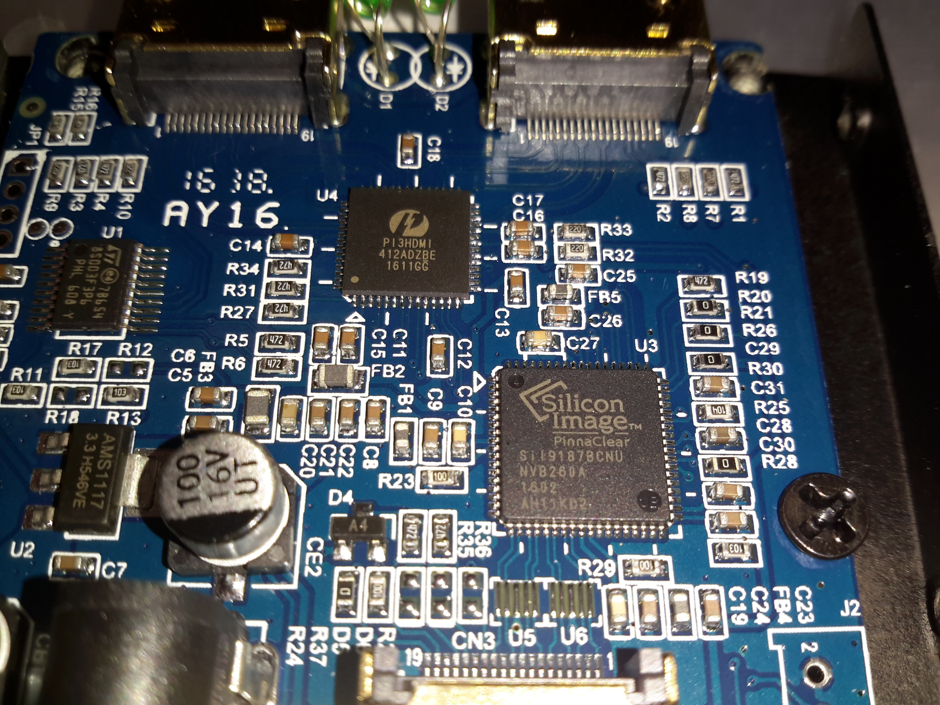
Microcontroller
The main pair of ICs processing the video signals are controlled over I²C, with this STM32 microcontroller. The 4 pads to the lower left are for the STLink programmer. The main 3.3v power rail is provided by the LM1117 linear regulator on the right.
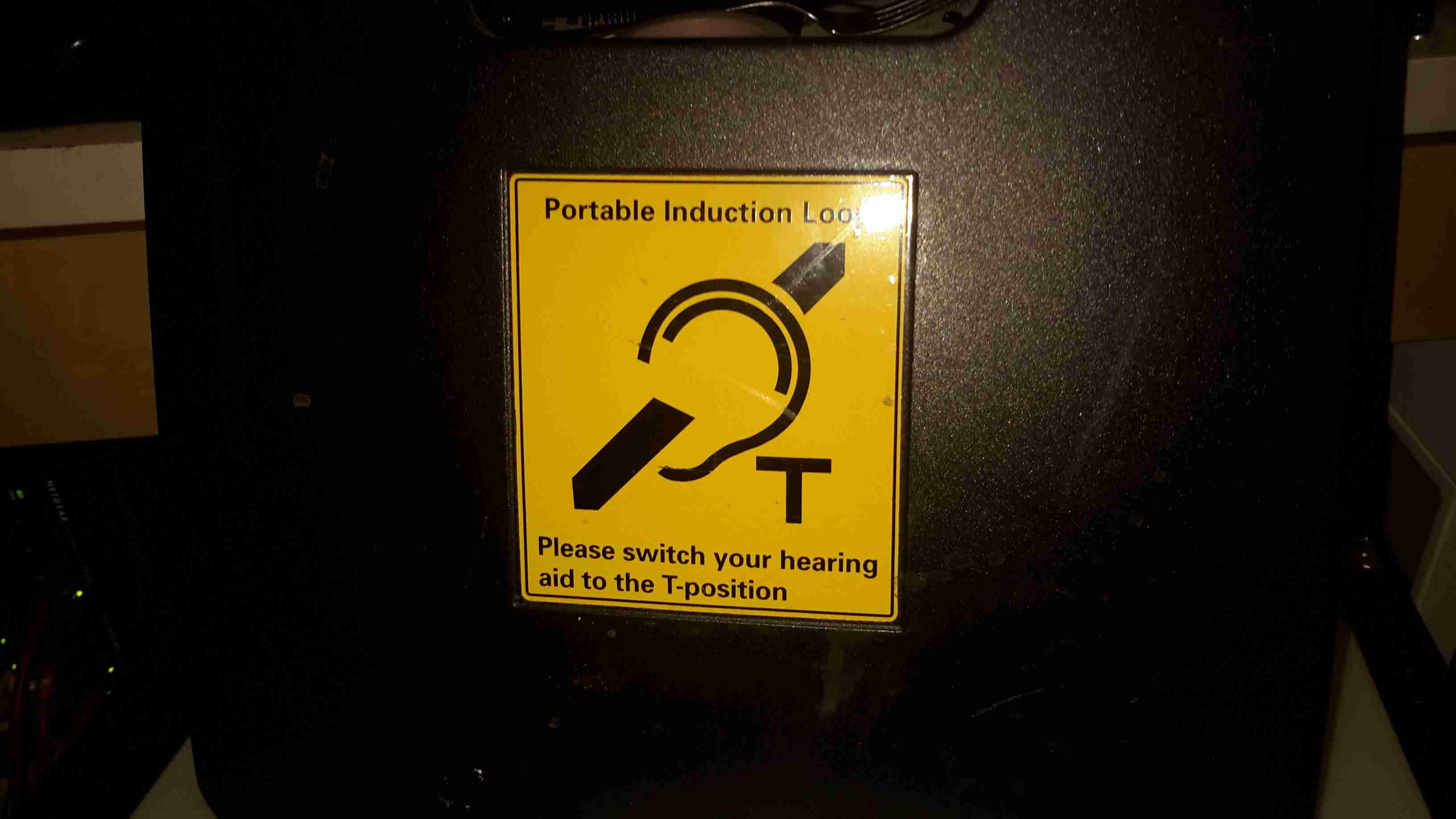
These units are used to broadcast local audio, such as from a public address system or local microphone. They accomplish this by producing a modulated magnetic field that a hearing aid is capable of picking up.
Back Panel
Not many controls on this bit of equipment. A bi-colour LED for status indications, a microphone, external audio input, charging input & a power switch.
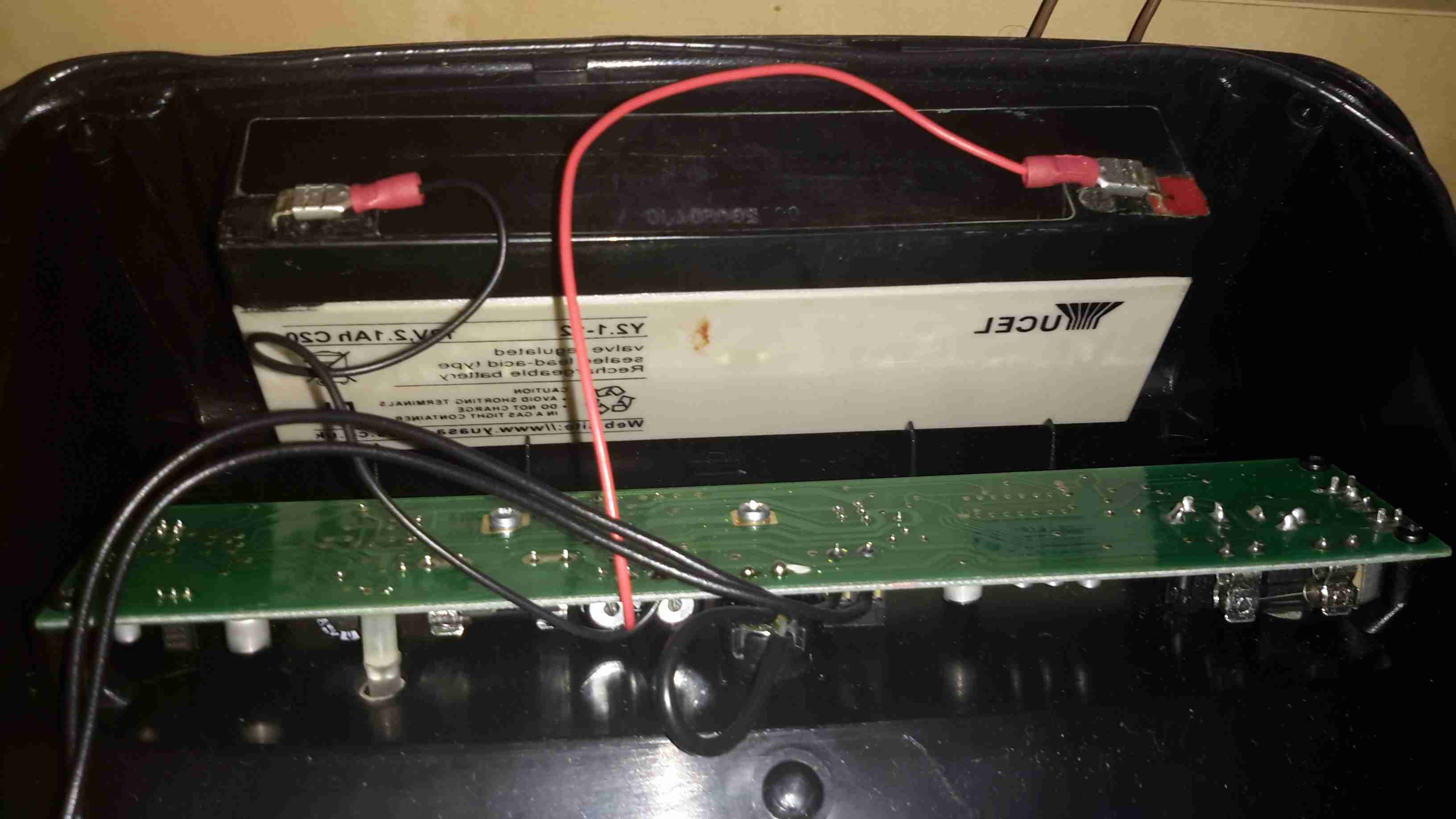
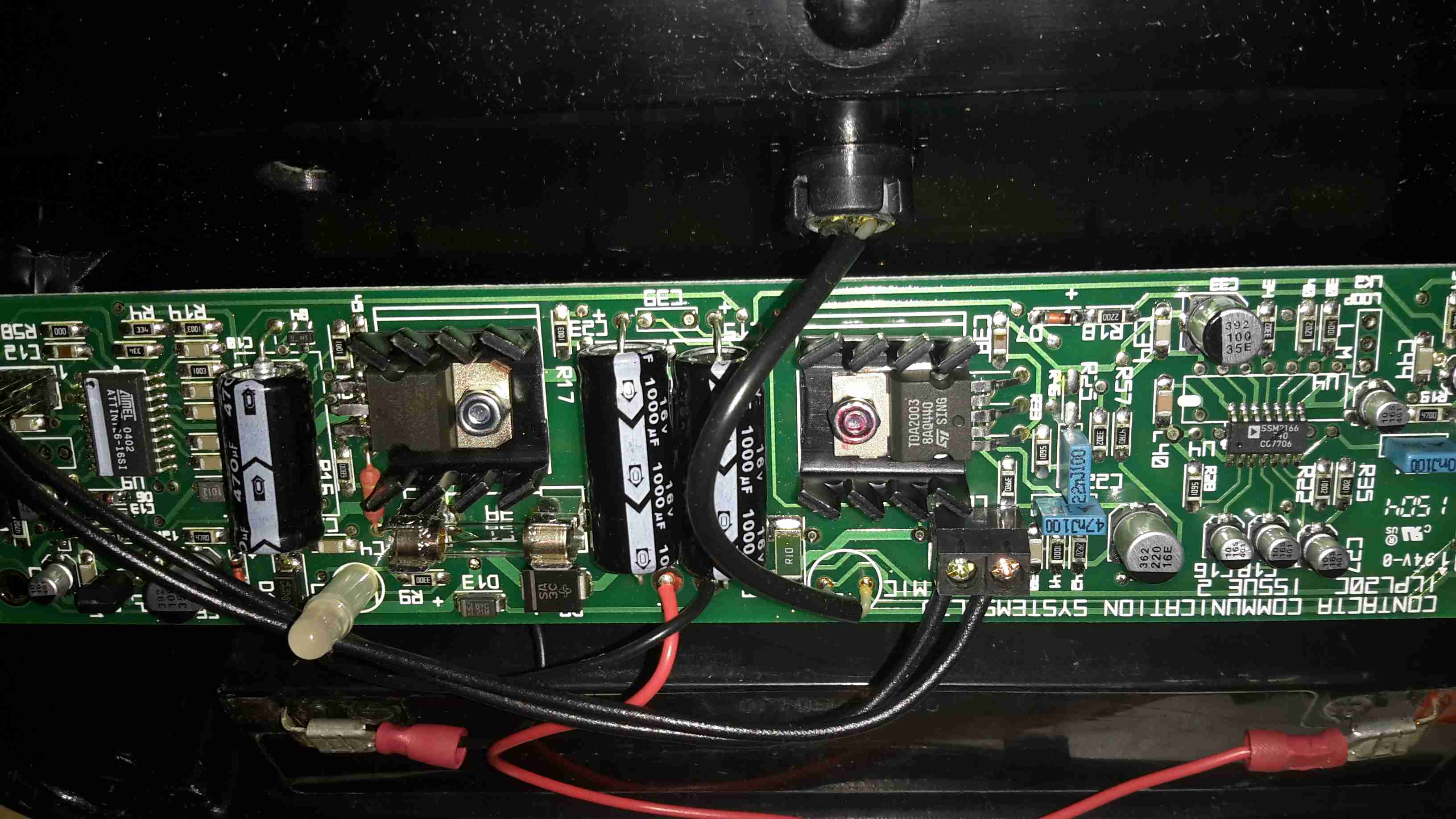
Internals
Popping the cover off reveals a small lead-acid battery, 2.1Ah at 12v. This is used when the loop is unplugged.
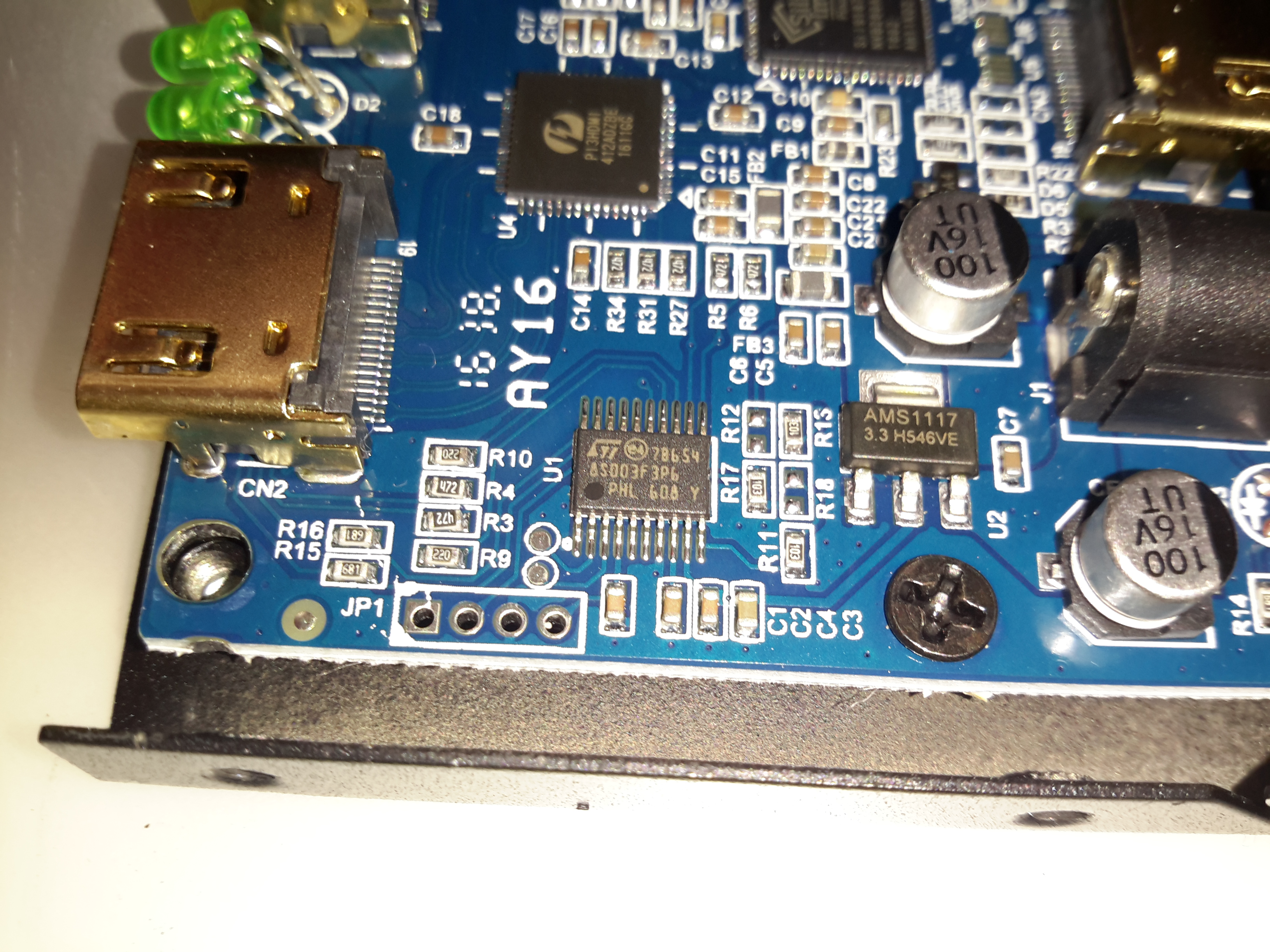
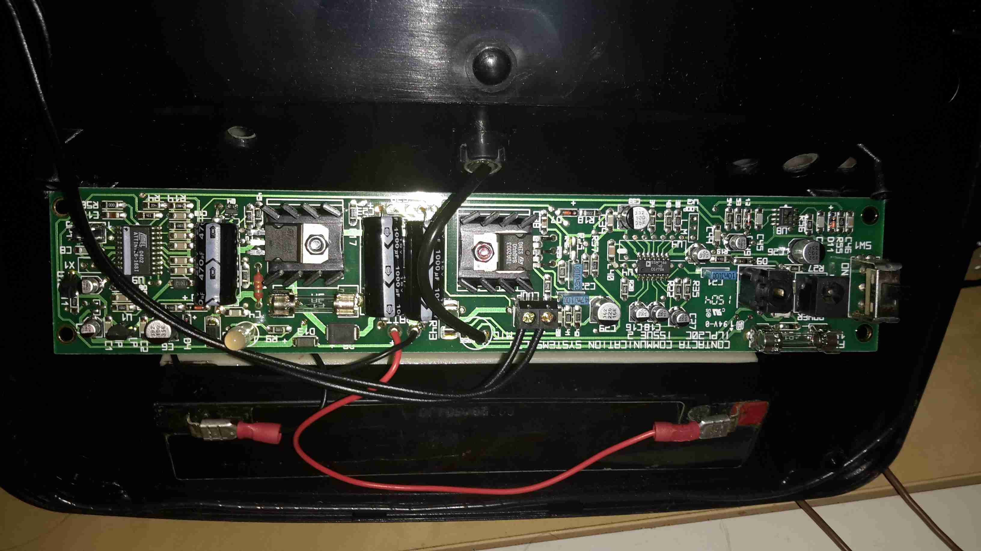
Main PCB
Here’s the main PCB, which takes care of the audio & battery charging. The inductive loop itself is just visible as the tape-covered wire bundle around the edge of the casing.
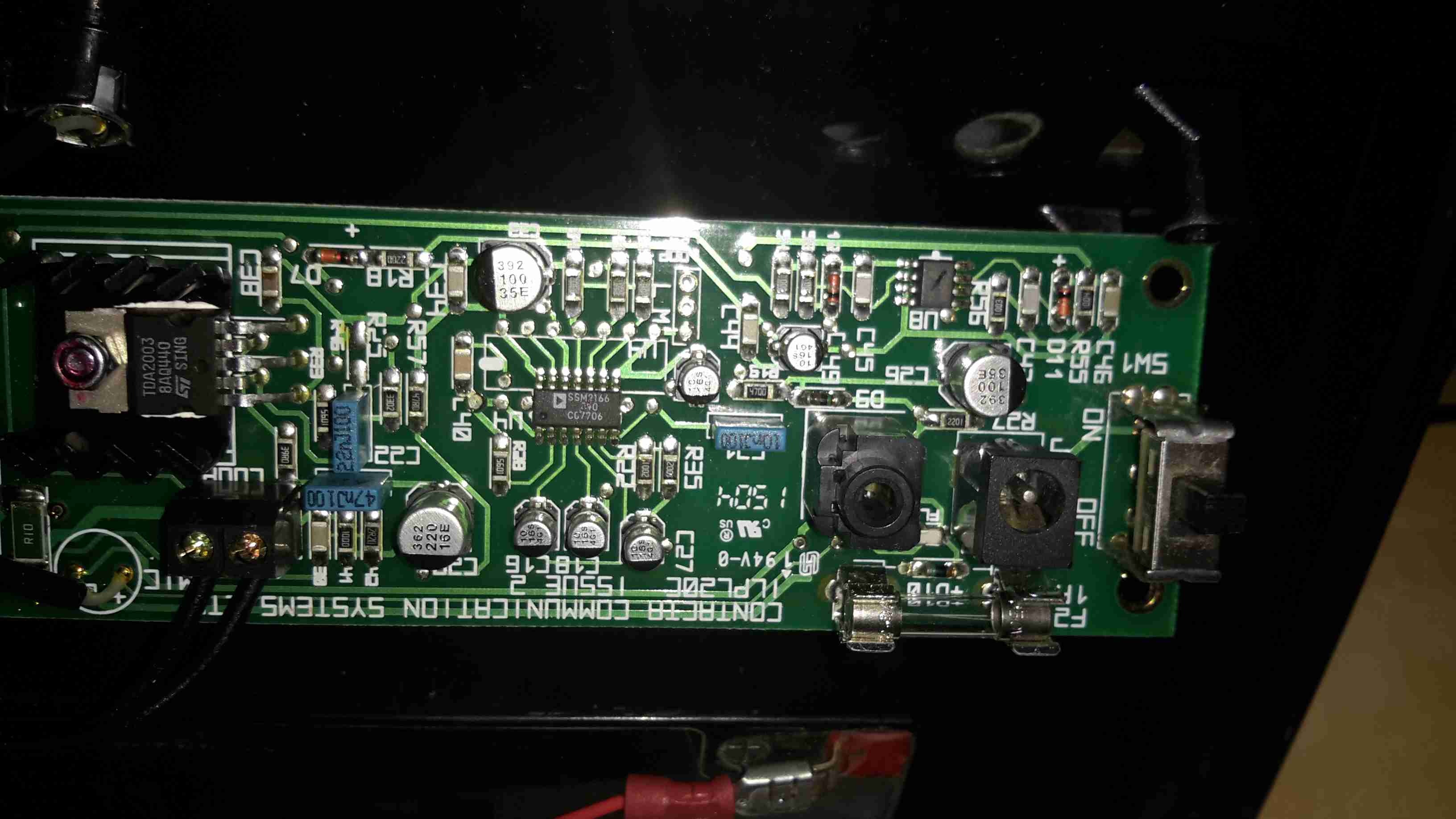
Audio & Power Input
Here’s the input section of the main PCB. The microphone input is handled by a SSM2166 front-end preamplifier from Analog Devices.
Power Amplifier
This audio is then fed into a TDA2003 10W Mono Power Amplifier IC, which directly drives the induction coil as if it were a speaker. Any suitable receiving coil & amplifier can then receive the signal & change it back into audio.
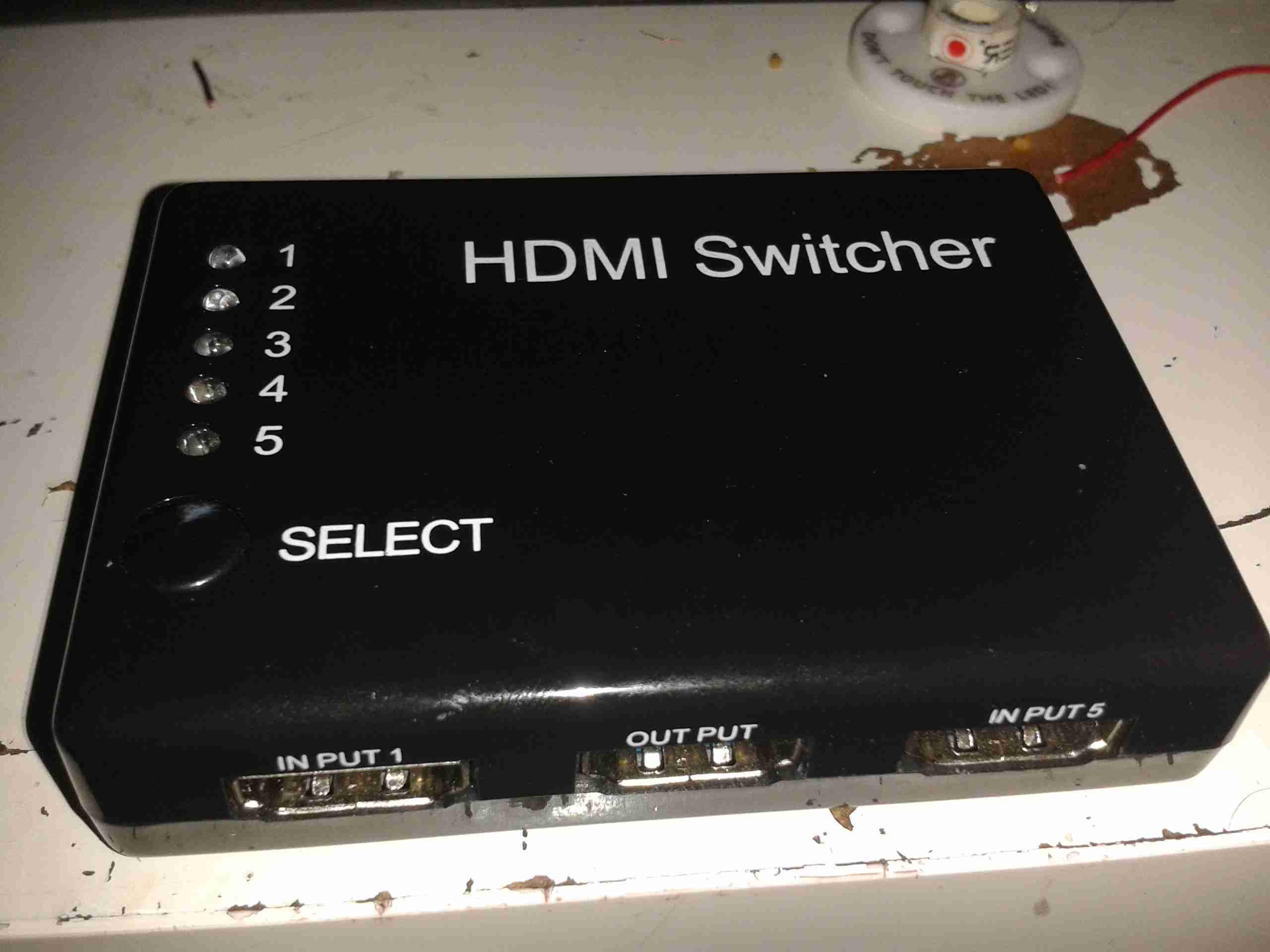
Here’s another quick teardown, a cheap 5-port HDMI switch box. This is used to allow a single input on a monitor to be used by 5 different external HDMI devices, without having to mess about plugging things in.
Power & Remote
Here’s the DC barrel jack & 3.5mm TRS jack for power & remote control. There’s a little IR decoder & remote that go with this for hands free switching.
PCB Top
Here’s the PCB out of it’s plastic housing. The main logic is a pair of PI3HDMI303 3:1 HDMI switches from Pericom Semiconductor. These are cascaded for the 5-ports, the first 3 input HDMI ports are switched through both ICs to reach the output.
These HDMI switch ICs are operated with TTL input pins, the combination of these pins held either high or low determines the input port that appears on the output.
There’s a button on the left for switching between inputs, with a row of 5 LED indicators.
PCB Bottom
Not much on the bottom side, a lot of passives & bypass capacitors. There’s a 3.3v LDO regulator on the left for supplying the main rail to the active switch ICs. The IC on the right doesn’t have any numbering at all, but I’m presuming it’s a microcontroller, dealing with the IR remote input & pushbutton inputs to switch the inputs.
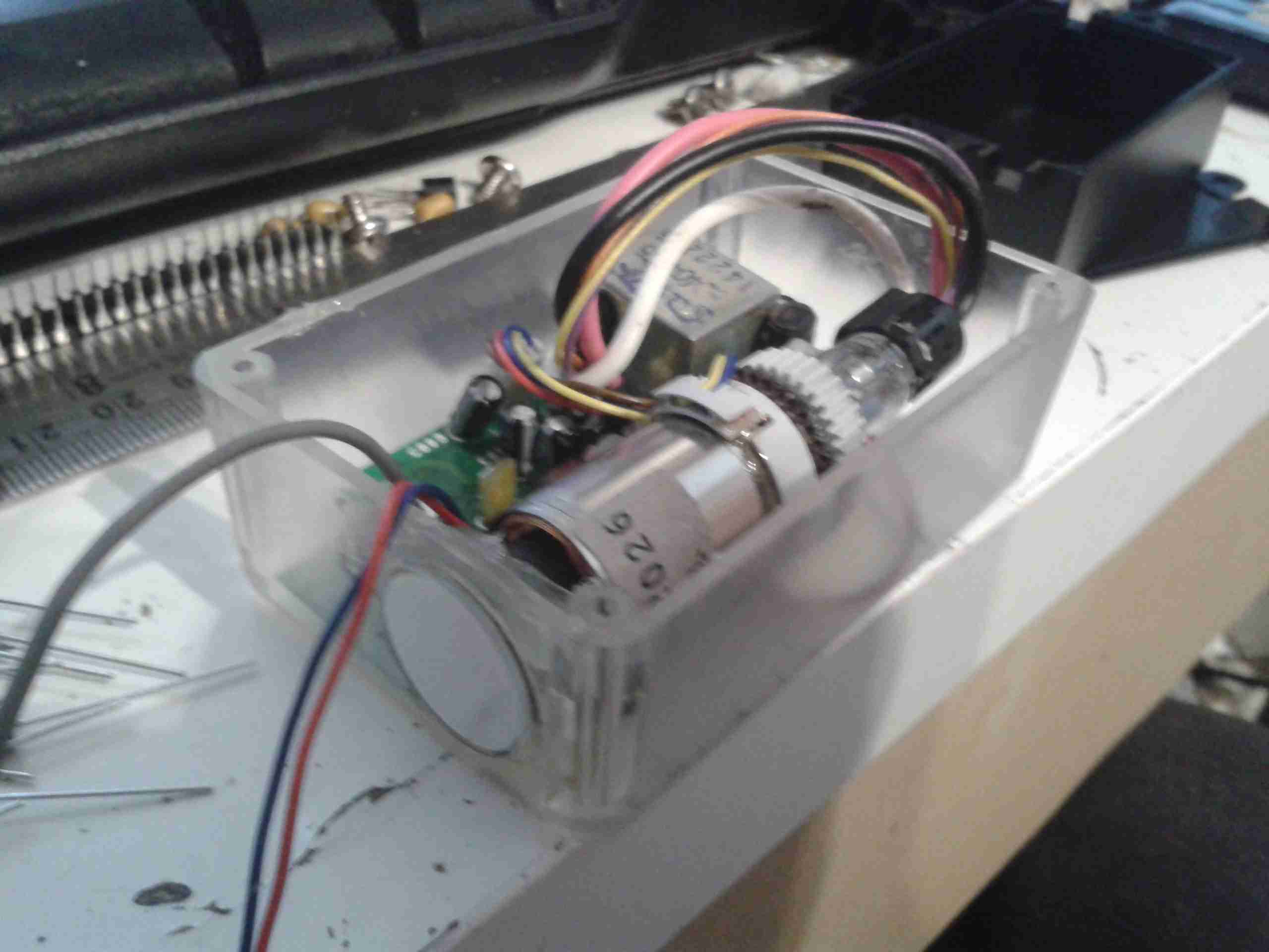
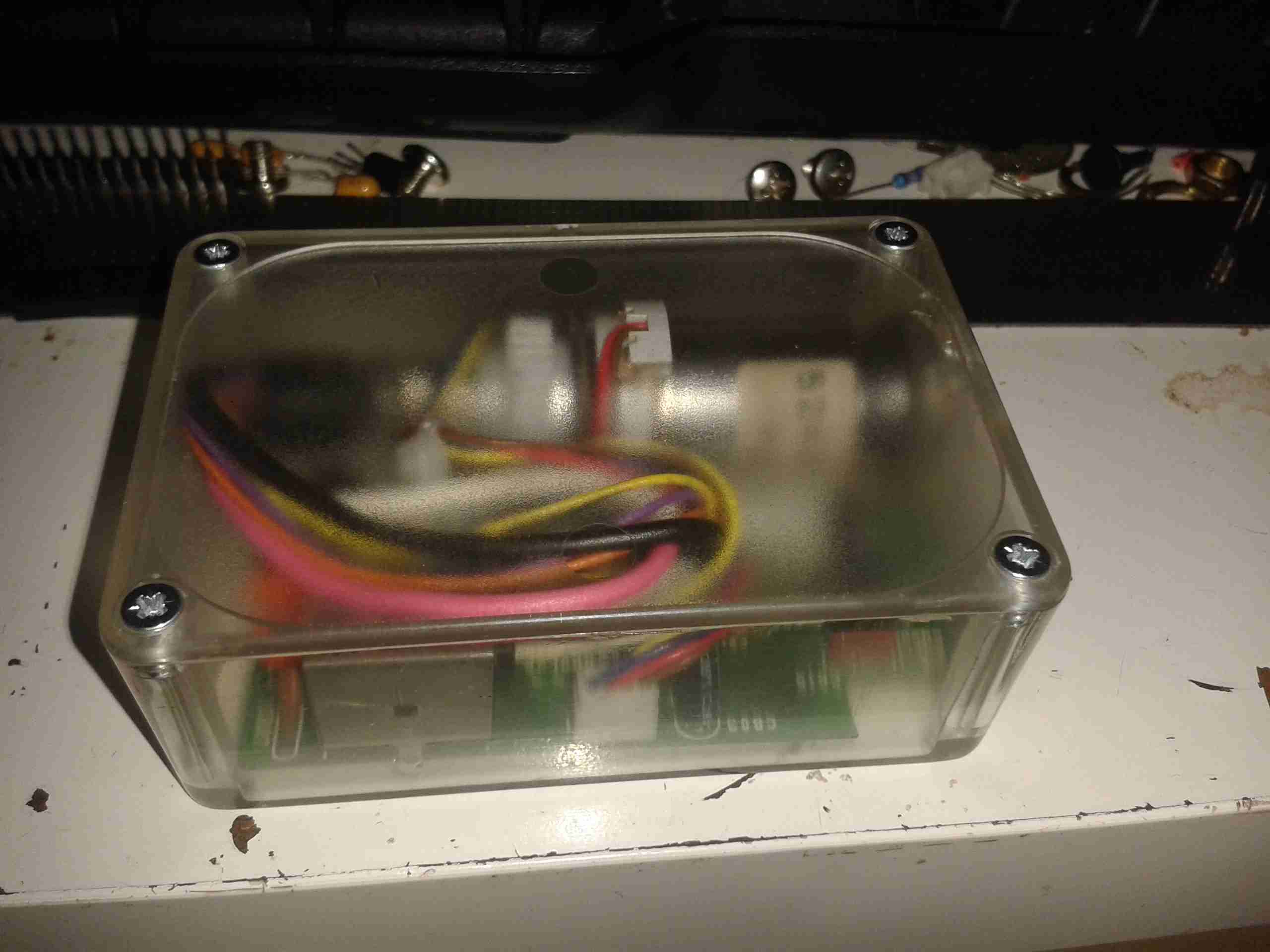
I’ve had a couple of viewfinder CRT modules for a while, & haven’t done much with them, so I decided to make a very small B&W monitor.
CRT
I ordered a small transparent ABS box when I made a large order with Farnell, that turned out to be just about the perfect size for the project! The CRT & PCB barely fit into the space. The face of the CRT itself is about 17mm across.
Module Installed
Here’s the main PCB & tube fully installed into the case. Barely enough room for a regulator left over!
Power is provided by a simple LM7809 IC to take a standard 12v input.
Module Rear
Rear of the case, showing the fit of the control board.
Connections
Here’s the back of the monitor, with the DC input jack & a 3.5mm 4-pole jack for audio & video. This allows simple connection to many devices, including the one I’ll use the most – the Raspberry Pi.
Completed
Completed monitor. Audio is handled by a very small 20mm speaker, currently mounted just below the CRT face.
Current draw from a 13.8v supply is 117mA.
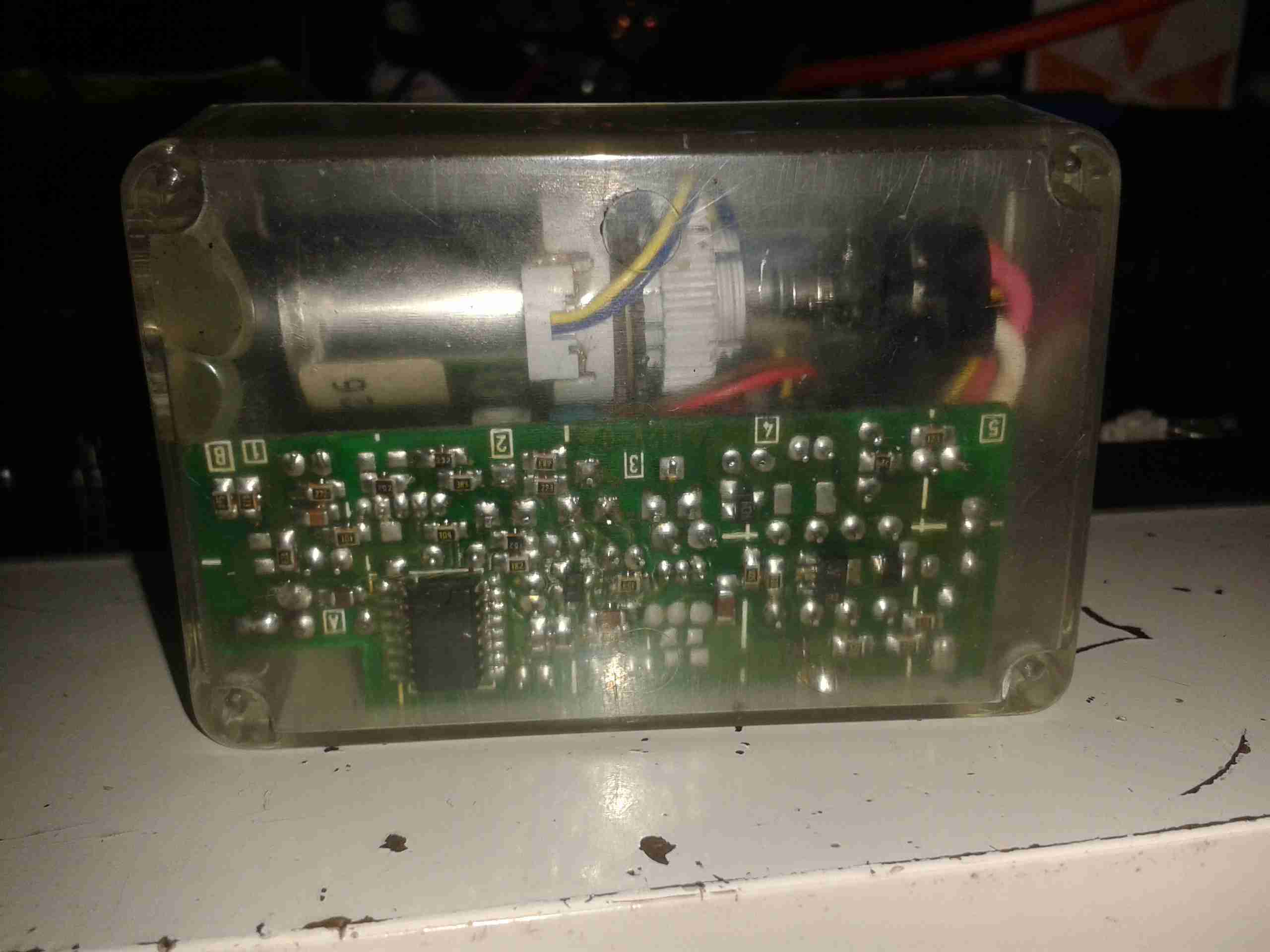
Here’s another viewfinder CRT, removed from a 1980’s vintage VHS camera I managed to get cheap from eBay.
This unit is very similar to the last one I posted about, although there are a few small differences in the control circuitry.
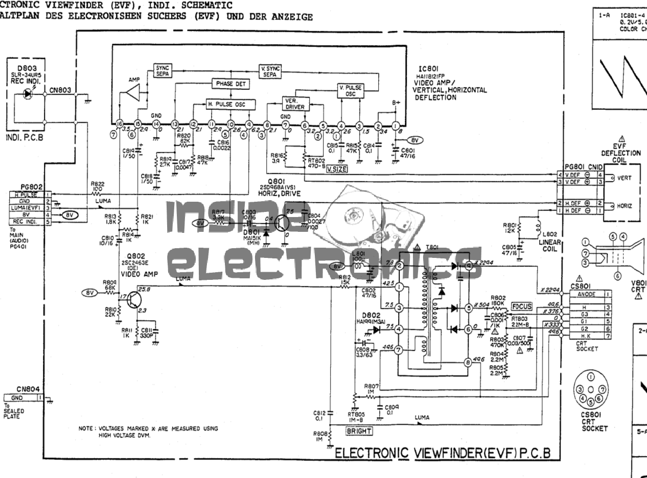
Viewfinder Schematic – Click to Embiggen
Here’s the schematic, showing all the functional blocks of the viewfinder circuitry. An integrated viewfinder IC is used, which generates all the required scan waveforms for the CRT.
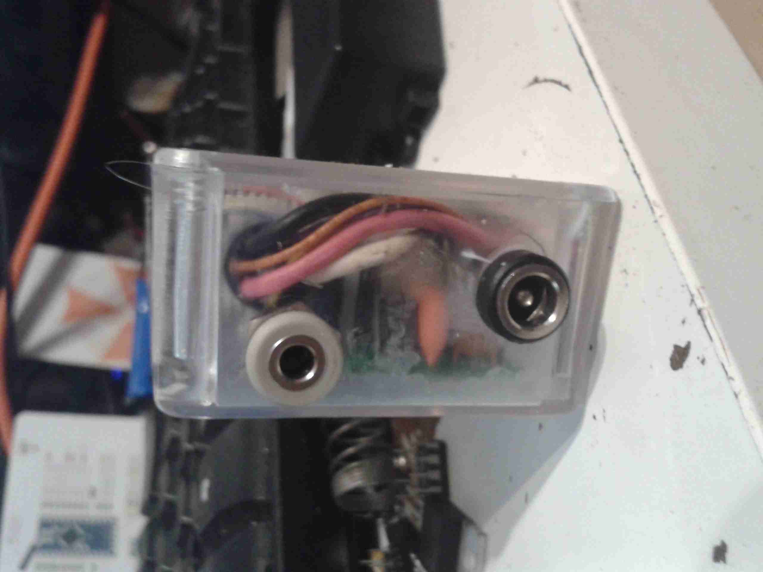
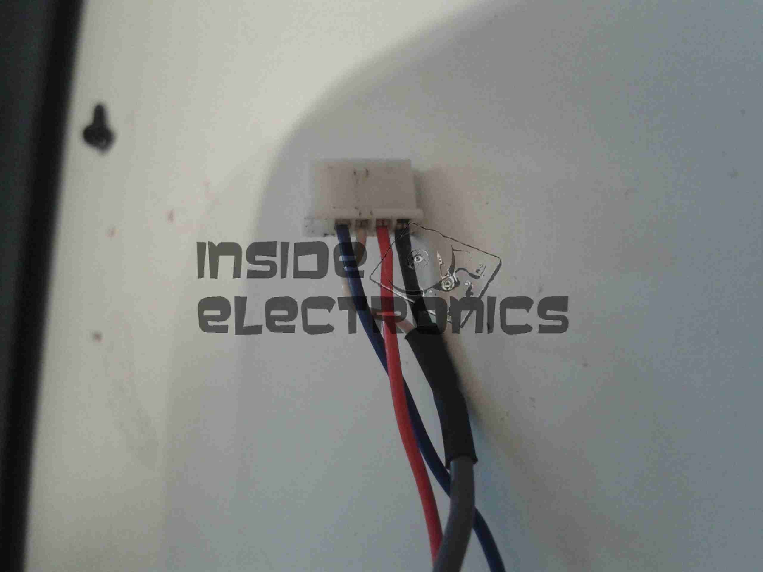
On the left is the input connector, with the power & video signals. Only pins 2 (GND), 3 (Composite video), & 4 (+8v) are needed here. Pin 1 outputs a horizontal sync signal for use elsewhere in the camera, while pin 5 fed the recording indicator LED.
To make connection easier, I have rearranged the wires in the input connector to a more understandable colour scheme:
Input Connector
Red & Blue for power input, & a coax for the video. For the video GND connection, I have repurposed the Rec. LED input pin, putting a shorting link across where the LED would go to create a link to signal ground. Keeping this separate from the power GND connection reduces noise on the CRT.
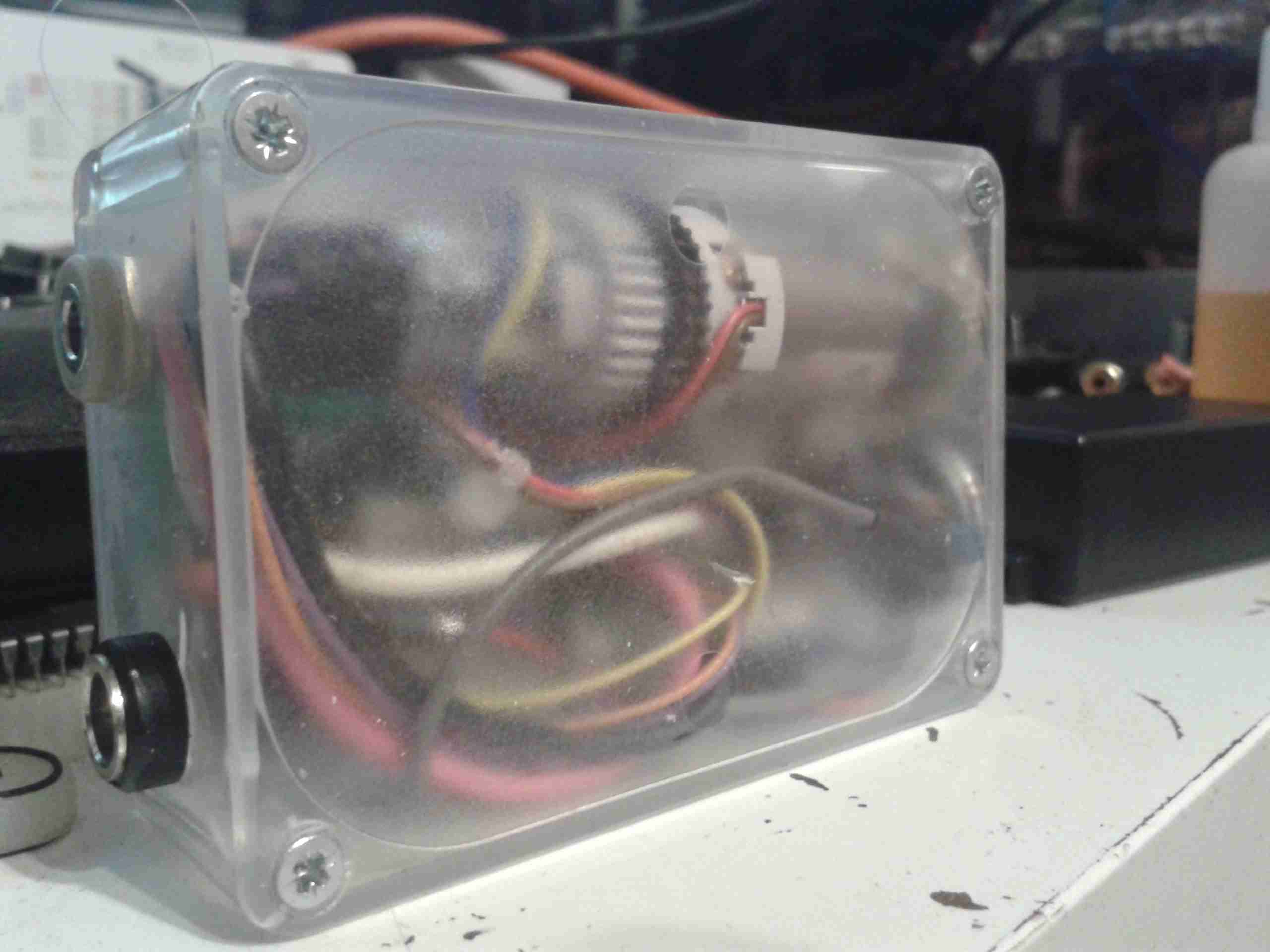
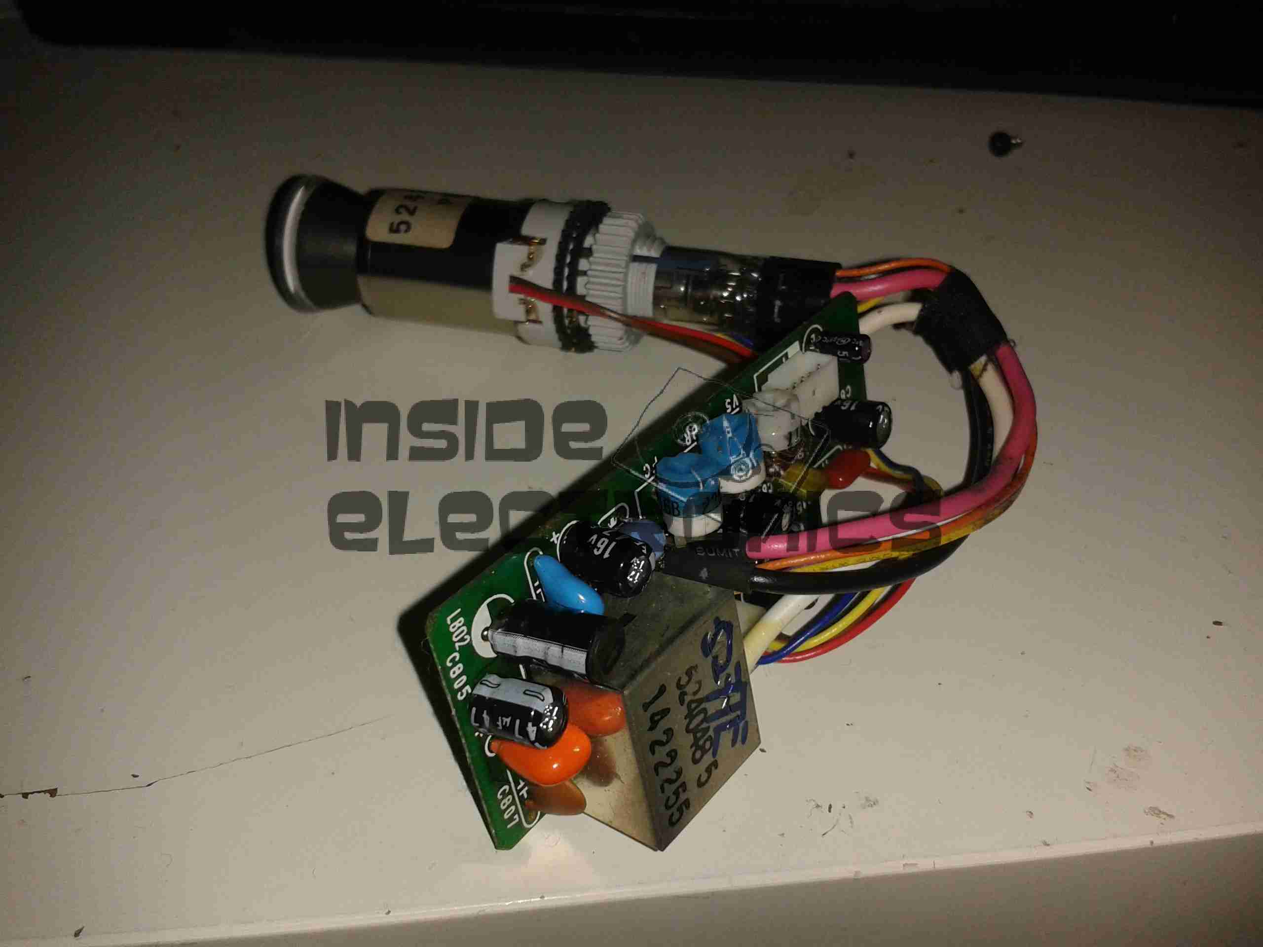
Viewfinder CRT Assembly
Here’s the complete assembly liberated from it’s plastic enclosure.
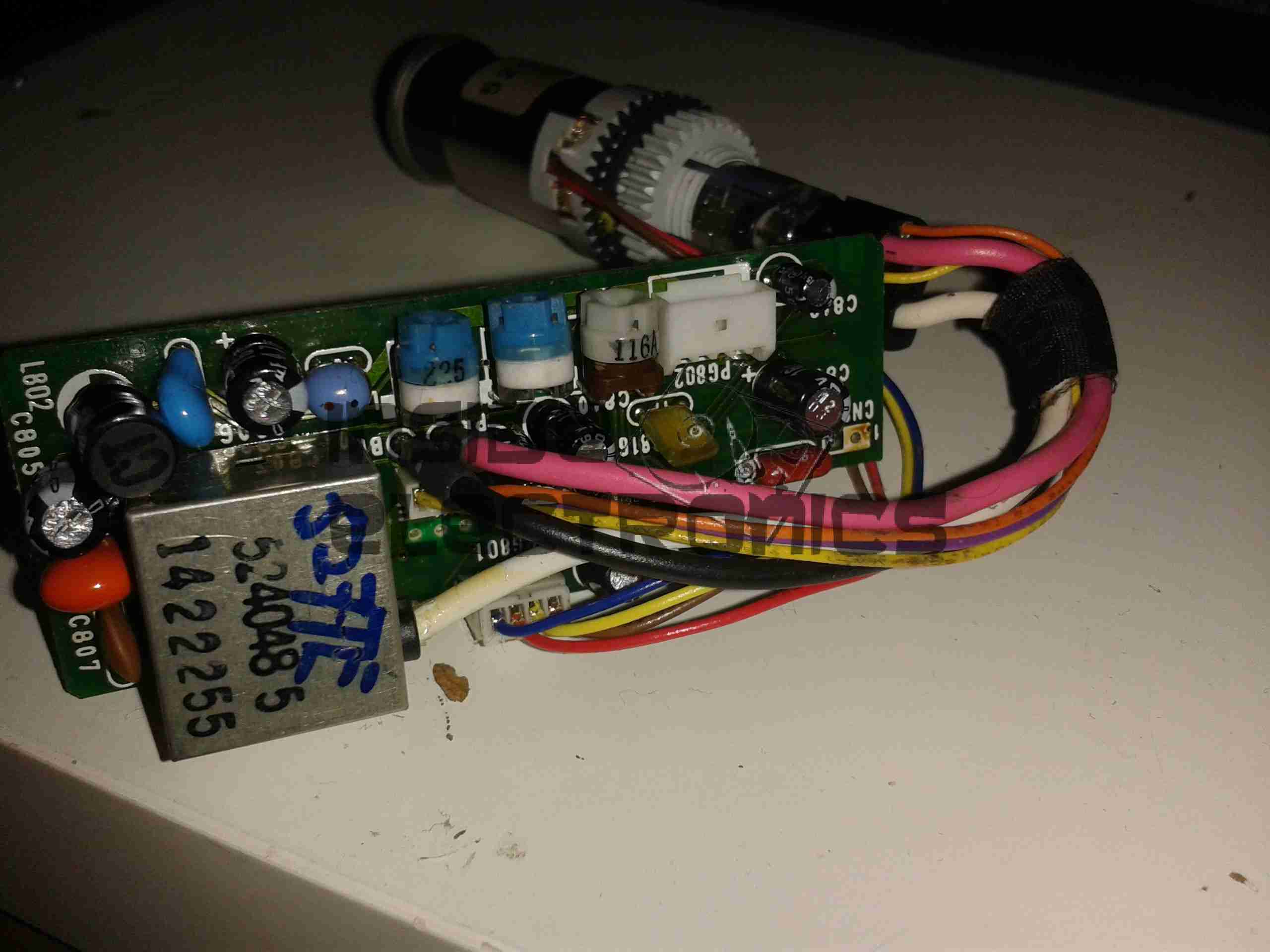
PCB Closeup
Closeup of the control PCB. The 3 potentiometers control the CRT brightness, focus & vertical size.
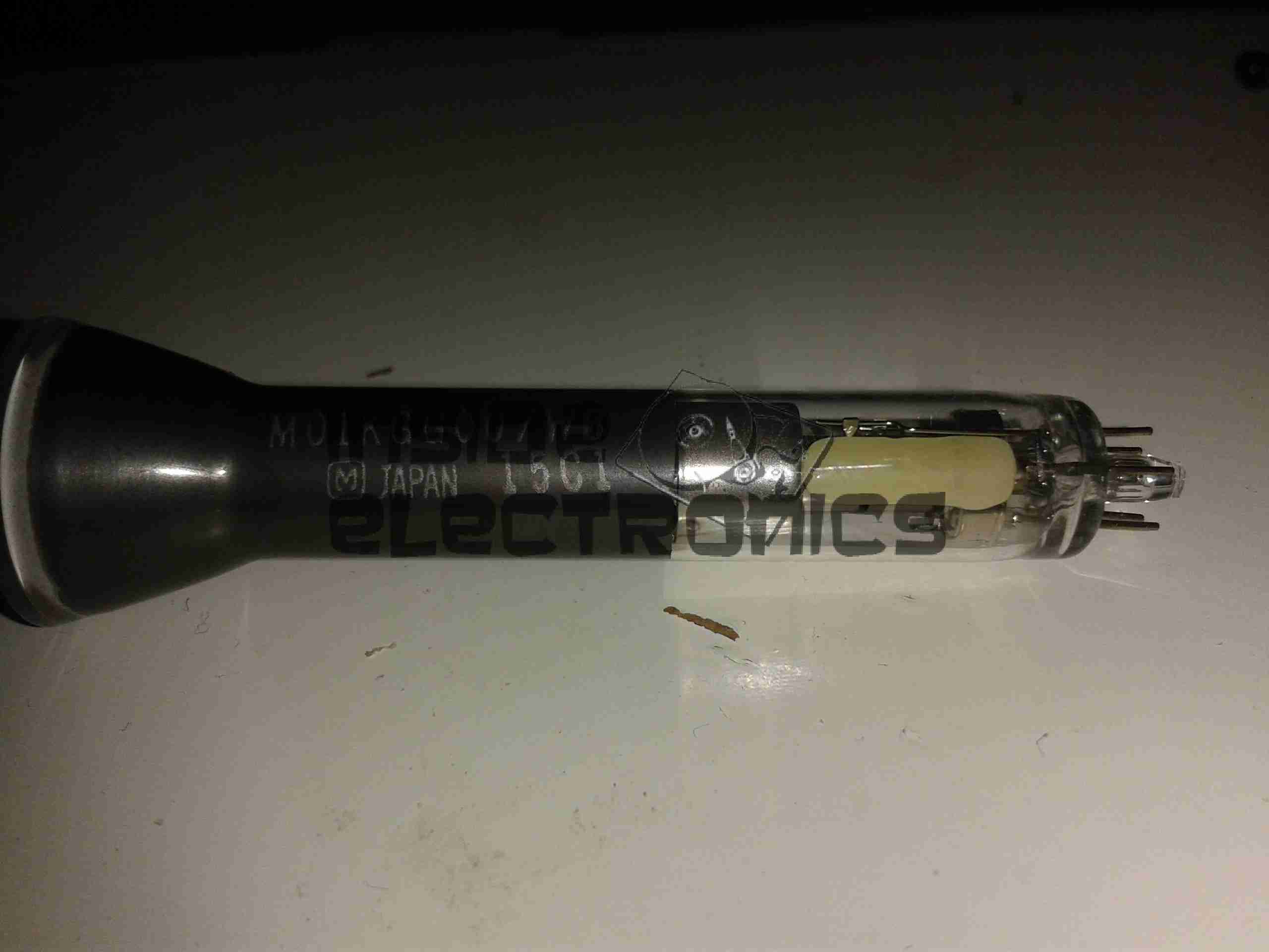
M01KGG007WB CRT
The tiny CRT. Only ~60mm in length, with an 18mm screen size. This tube runs on +2294v final anode voltage. Much higher than I expected.
Electron Gun Closeup
The electron gun assembly, with the cathode, focus & final anode cups.
Phosphor Screen
This screen is just a little bigger than a UK 5p piece! A marvel of precision engineering.
I recently managed to score a 3″ B&W portable TV on eBay, a Panasonic TR-3000G. As these old units are now useless, thanks to the switch off of analogue TV signalling, I figured I could find a composite signal internally & drive the CRT with an external source.
Panasonic TR-3000G
Here’s the TV in it’s native state. Running from 9v DC, or 6 D size cells. I’m guessing from somewhere around the 1970’s. Here is the CRT & associated drive circuitry, removed from the casing:
CRT Module
After dissecting the loom wiring between the CRT board & the RF/tuner board, I figured out I had to short out Pins 1,2 & 5 on the H header to get the CRT to operate straight from the power switch. This board also generates the required voltages & signals to drive the RF tuner section. I have removed the loom from this, as the PCB operates fine without. It doesn’t seem to be fussy about power input either: it’s specified at 9v, but seems to operate fine between 7.5v & 14.5v DC without issue.
Video Connections
Tracing the wiring from the tuner PCB revealed a length of coax snaking off to the section marked Video/Sync. I successfully found the composite input!
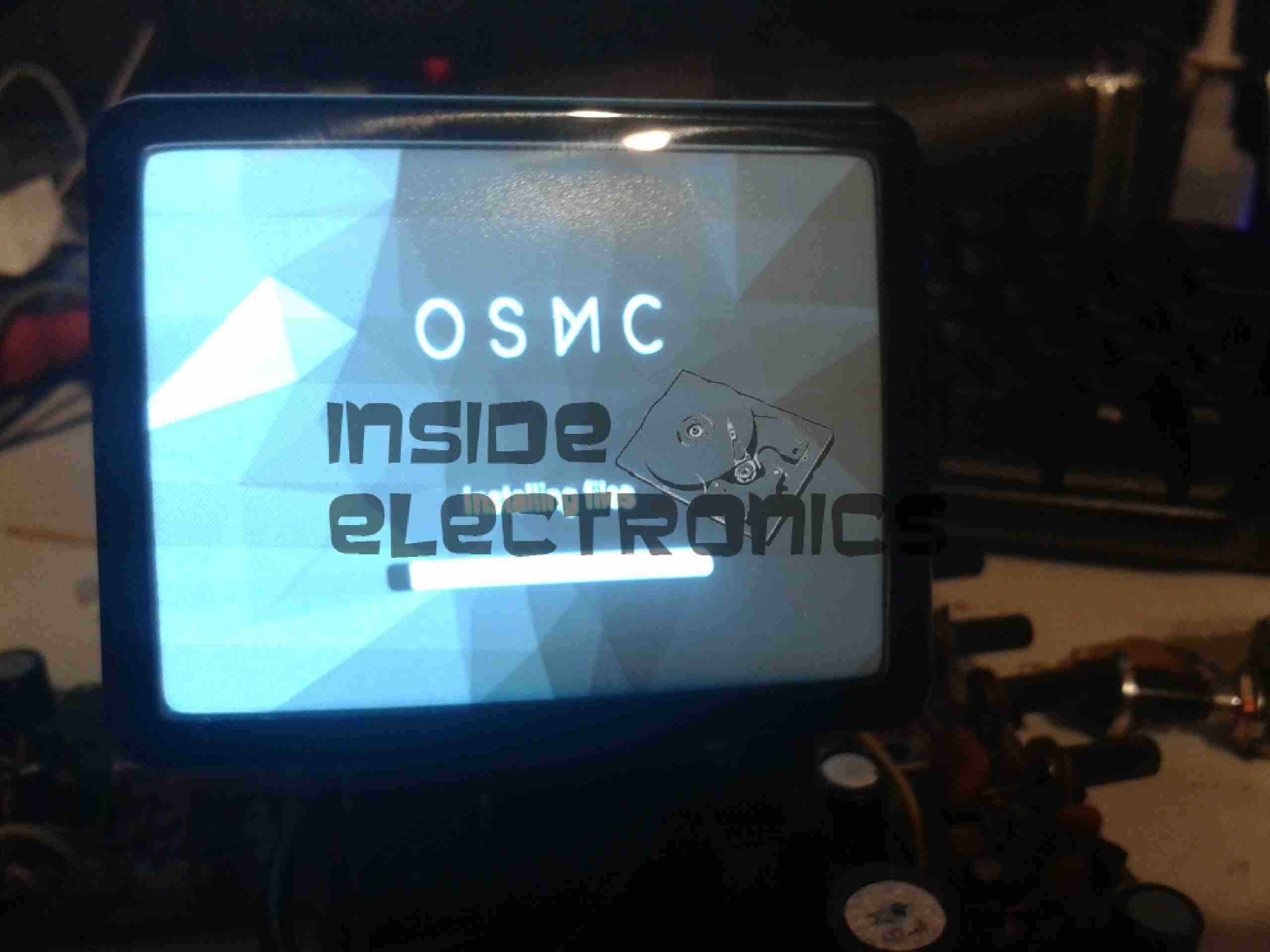
Running OSMC
A quick bit of wiring to a Raspberry Pi, & we have stable video! For such an old unit, the picture quality is brilliant, very sharp focus.
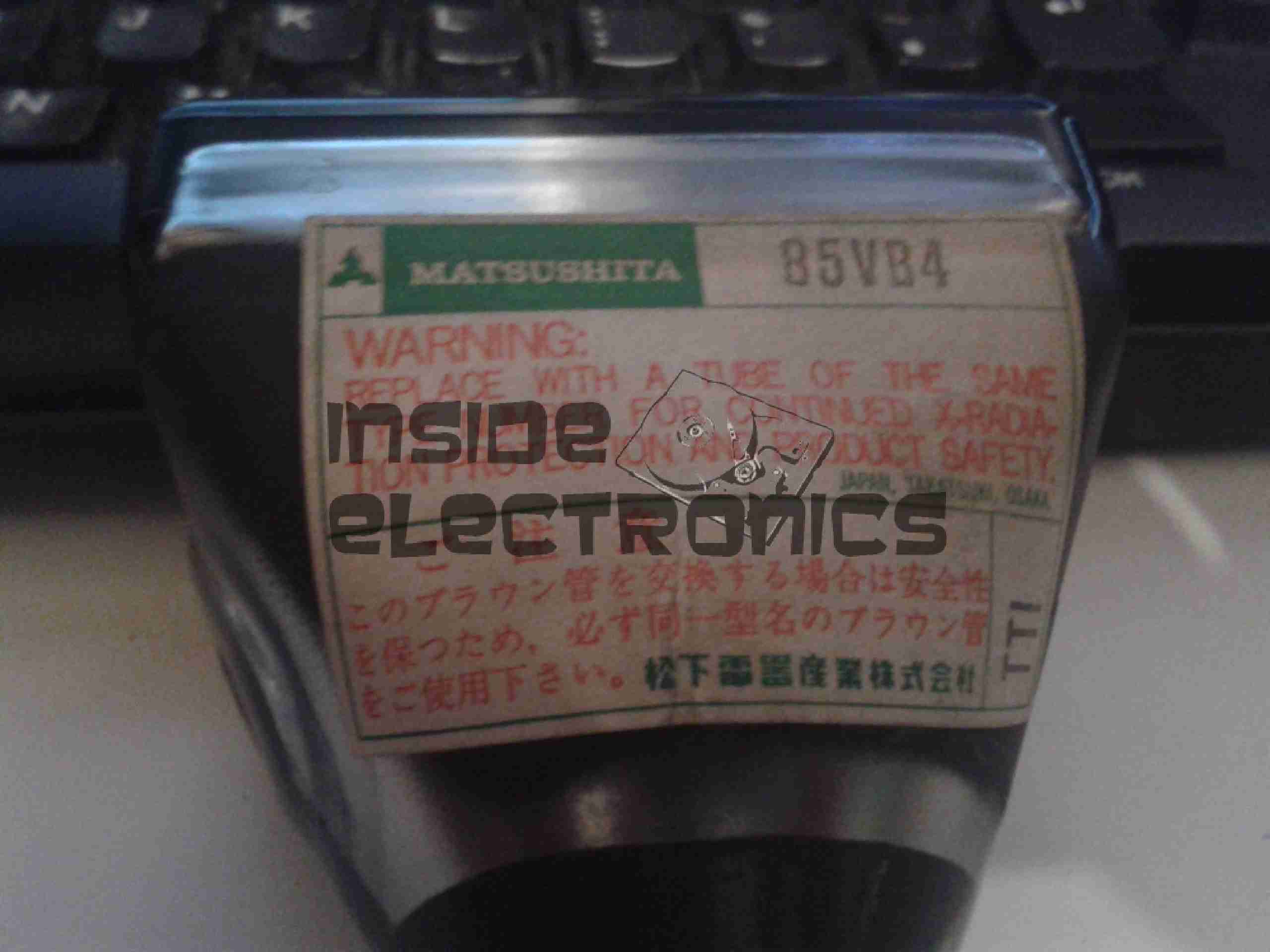
Matsushita 85VB4 CRT
Closeup of the CRT itself. I haven’t been able to find much data on this unit, but I’m guessing it’s similar to many commercial viewfinder CRTs.
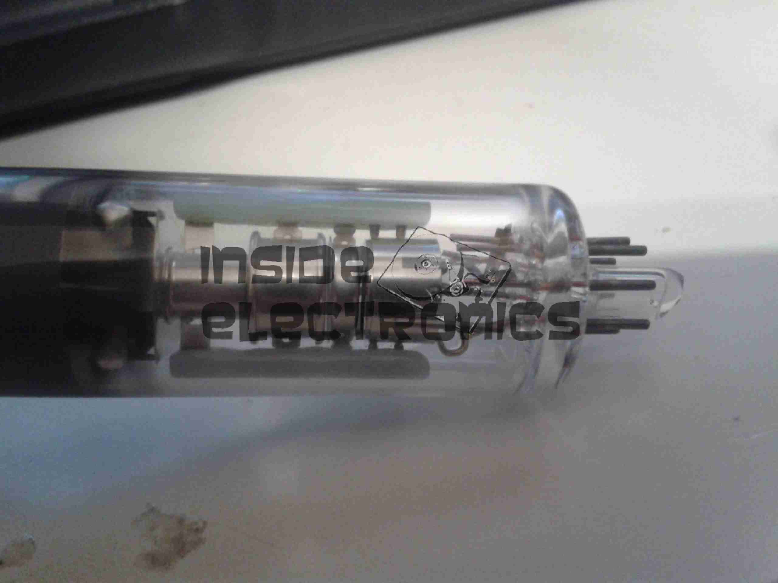
Electron Gun Closeup
Amazingly, there isn’t a single IC in the video circuitry, it’s all discrete components. This probably accounts for the large overall size of the control PCB. Viewfinder CRTs from a few years later on are usually driven with a single IC & a few passives that provide all the same functions.
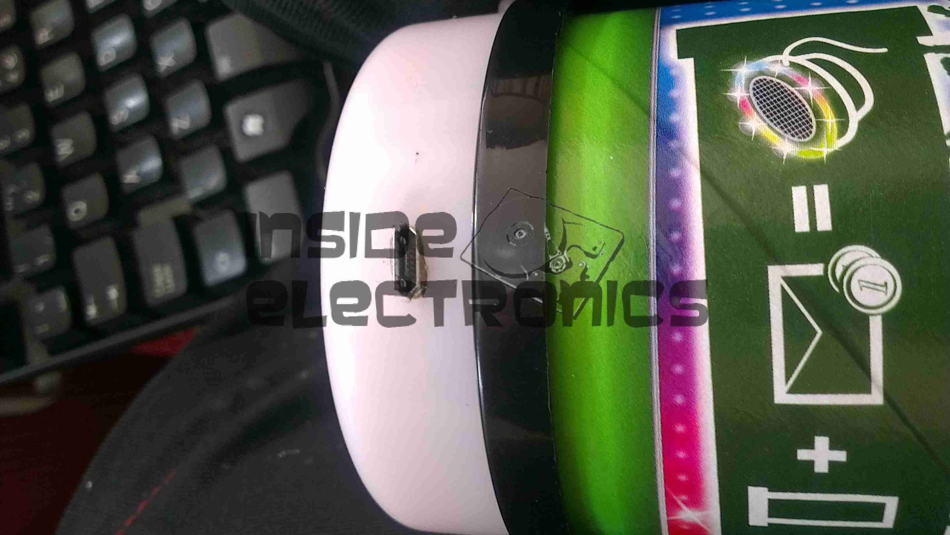
These speakers are available free from Pringles, with two packs bought. Normally running on 3x AAA cells, I have made modifications to include a high capacity Li-Ion battery & USB charging.
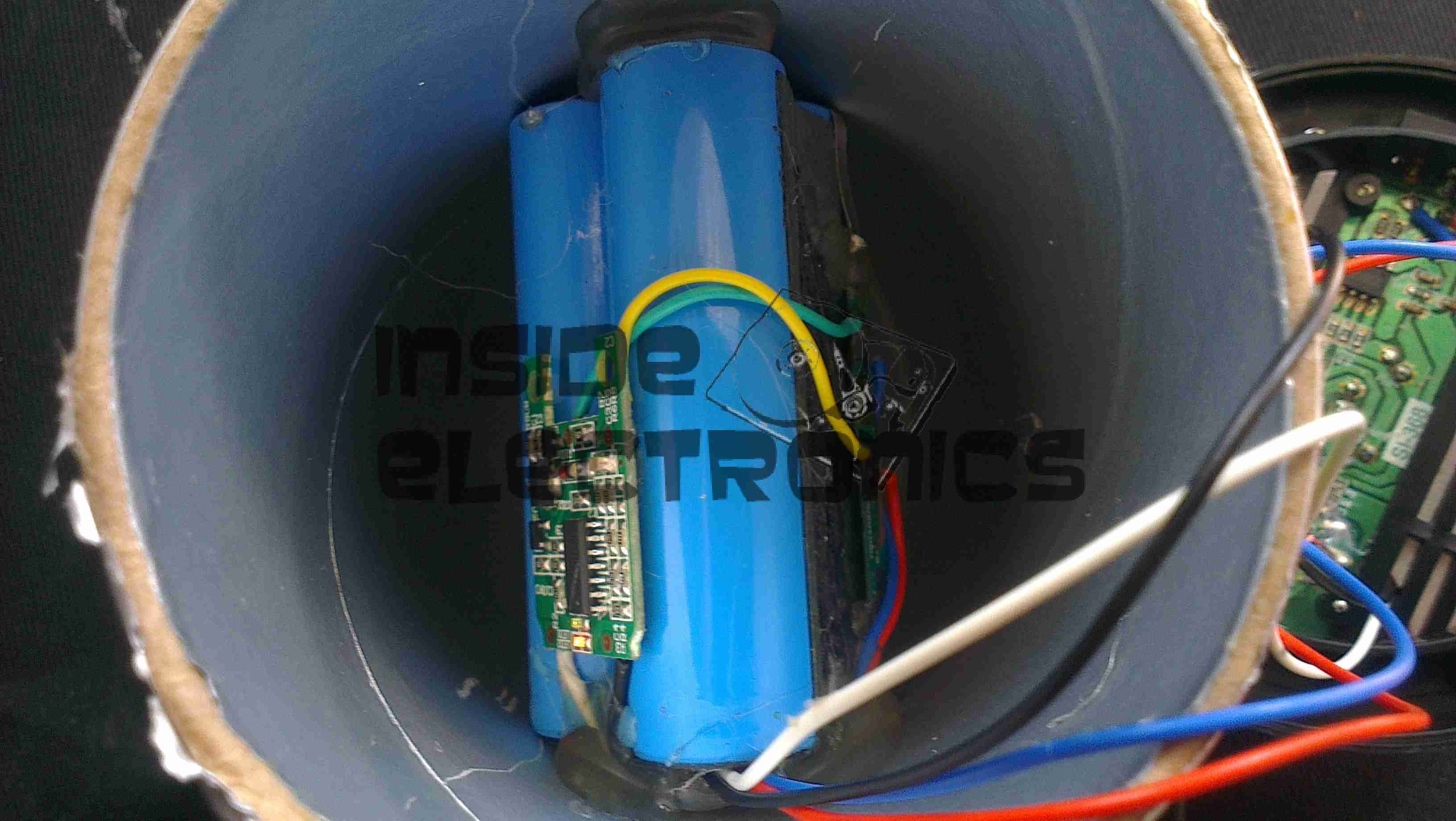
18650 Battery
New battery is 3x 18650 Li-Ion cells in parallel, providing ~6600mAh of capacity. These are hot glued inside the top of the tube under the speaker, with the charging & cell protection logic.
The battery charging logic is salvaged from an old USB eCig charger, these are single cell lithium chargers in a small form factor ideal for other uses. Charging current is ~450mA.
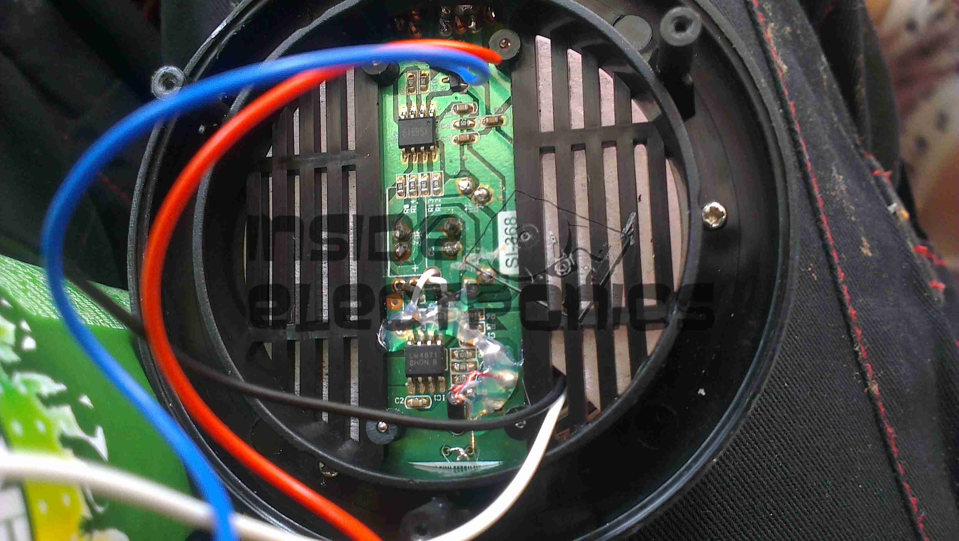
Amplifier Board
The cells are connected to the same points as the original AAA cells, with the other pair of wires going into the top of the device to connect to the MicroUSB charging port.
The amplifier in this is a LM4871 3W Mono amplifier IC, connected to a 6Ω 1W speaker.
The other IC on the board is unidentifiable, but provides the flashing LED function to the beat of the music.
This is a little script to make OMXPlayer on the Raspberry Pi cycle through every file in a specified folder, useful for playing sequential movies or series of episodes.
#!/bin/bash
if [ x"$1" = x"help" -o x"$1" = x"--help" -o x"$1" = x"-help" ];then
echo "Usage: omxseries [folder path]"
echo "Audio Mode can be either 'hdmi' or 'local'."
echo "Folder Path is the full path to the video files on your system."
echo "This script will attempt to play every file in the target folder, with any file extension,"
echo "so ensure that only valid video files are present in the target folder to avoid errors."
exit
fi
for file in $2/*
do
 omxplayer -o $1 $file
done
Example:
[root@raspbian ~]# omxseries hdmi /media/stuff/videos
would play everything in /media/stuff/videos and send the audio over the HDMI port.
Here’s the teardown of the projector itself! On the right is the info label from the projector, which covers the flex ribbon to the VGA/composite input board below.
This unit is held together with Allen screws, but is easy to get apart.
PicoP Display Engine
Here’s the insides of the projector, with just the top cover removed. The main board can be seen under the shielding can, the Micro HDMI connector is on the left & the MicroUSB connection is on the right. The USB connection is solely for charging the battery & provides no data interface to the unit.
On top of the main board is the shield can covering the PicoP Display Engine driver board, this shield was soldered on so no peek inside unfortunately!
Laser Module
The laser module itself is in the front of the unit, the laser assemblies are closest to the camera, on the left is the Direct Doubled Green module, in the centre is the blue diode, and the red diode on the right. Inside the module itself is an arrangement of mirrors & beamsplitters, used to combine the RGB beams from the lasers into a single beam to create any colour in the spectrum.
Module Innards
Here is the module innards revealed, the laser mounts are at the top of the screen, the green module is still mounted on the base casting.
The three dichroic mirrors in the frame do the beam combining, which is then bounced onto the mirror on the far left of the frame, down below the MEMs. From there a final mirror directs the light onto the MEMs scanning mirror before it leaves through the output window.
A trio of photodiodes caters for beam brightness control & colour control, these are located behind the last dichroic turning mirror in the centre of the picture.
Green Module Cavity
This is inside the green laser module, showing the complexity of the device. This laser module is about the size of a UK 5p coin!
Green Module Labeled
And here on the left is the module components labelled.
Main PCB Top
Here is the main PCB, with the unit’s main ARM CPU on the right, manufactured by ST.
User buttons are along the sides.
Main PCB Bottom
Other side of the main board, with ICs that handle video input from the HDMI connector, battery charging via the USB port & various other management.
Above is the image projected from the Pi, on the default login screen. Distance from the projector is approx 10 feet.
Projector
State of the art projector mount, fashioned from several cable ties. HDMI cable is plugged into the right hand side of the projector.
Unfortunately the projector cannot handle audio on the HDMI connector, the 3.5mm headphone jack on the projector is for splitting audio out of the iDevice connection only, and does not make the HDMI audio stream available.
Pi
The Raspberry Pi, hosting a USB keyboard, & USB powered speakers. Running the standard Debian release, on a 16GB card, with omxplayer installed for media functions.
As I’m building a portable “media center” with my first Pi, I was looking for a suitable screen. I remembered the existence of these:
ShowWX+ HDMI Pico Projector
A laser pico projector combined with a Pi, in a small enough package would make a fantastic
little portable media player. So £220 was shelled out 🙂
Along with the case for my Pi coming from Mod My Pi, I am aiming for a device as small as possible. At some point I will fit the Pi into the same package as the projector, if it can be cannibalised in such a way 🙂
Check back for an update with running images of the projector, powered from the Pi’s HDMI output.
I will also be doing the standard teardown of the projector when time allows 🙂
Bootnote:
Micro HDMI Connections: These are CRAP. They don’t stand up to any form of day-to-day use, and the projector began displaying a blue screen with “INVALID VIDEO MODE” as soon as anything was plugged into the Micro HDMI port. A quick attack with a jeweller’s screwdriver fixed the port, as it had become loose.
Here are the viewfinder electronics from a 1984 Hitachi VHS Movie VM-1200E Camcorder. These small CRT based displays accept composite video as input, plus 5-12v DC for power.
Screen
Here is the front face of the CRT, diameter is 0.5″.
Power Board
Closeup view of the PCB, there are several adjustments & a pair of connectors. Socket in the upper left corner is the power/video input. Pinout is as follows:
Brown – GND
Red – Video Input
Orange – +12v DC
Yellow – Record LED
The potentiometers on the PCB from left:
H. ADJ
V. ADJ
BRIGHT
FOCUS
PCB Part Number reads: EM6-PCB
This unit utilises the BA7125L deflection IC.
Solderside
Reverse side of the PCB, very few SMT components on this board.
Tube Assembly
Here is an overall view of the CRT assembly with scan coils. Tube model is NEC C1M52P45.
Electron Gun
Closeup view of the CRT neck, showing the electron gun assembly.
CCTV Camera
The old CCTV camera used to feed a composite signal to the CRT board. Sanyo VCC-ZM300P.
CCTV Camera Connections
Connections at the back of the camera. Red & Black pair of wires lead to 12v power supply, Green & Black pair lead to the CRT board’s power pins. Seperate green wire is pushed into the BNC video connector for the video feed. video ground is provided by the PSU’s ground connection.
Connections
Finally the connections at the CRT drive board, left to right, +12v, Video, GND.
This is a small audio mixer, marketed for camcorder audio dubbing.
Rear Panel
I/O Panel on the rear of the unit. Contains a small preamp, but will not drive speakers directly. Power is a 9v battery or plugpack.
PCB Front
Front of the PCB removed from the case. Mic preamp bottom right corner. Each channel has it’s own Preamp IC between the faders.
PCB Rear
Rear of the PCB.
Tip Jar
If you’ve found my content useful, please consider leaving a donation by clicking the Tip Jar below!
All collected funds go towards new content & the costs of keeping the server online.