Posted on 1 Comment

Brother PT-E300 Industrial Label Machine Teardown

Tape Installed
Tape Installed

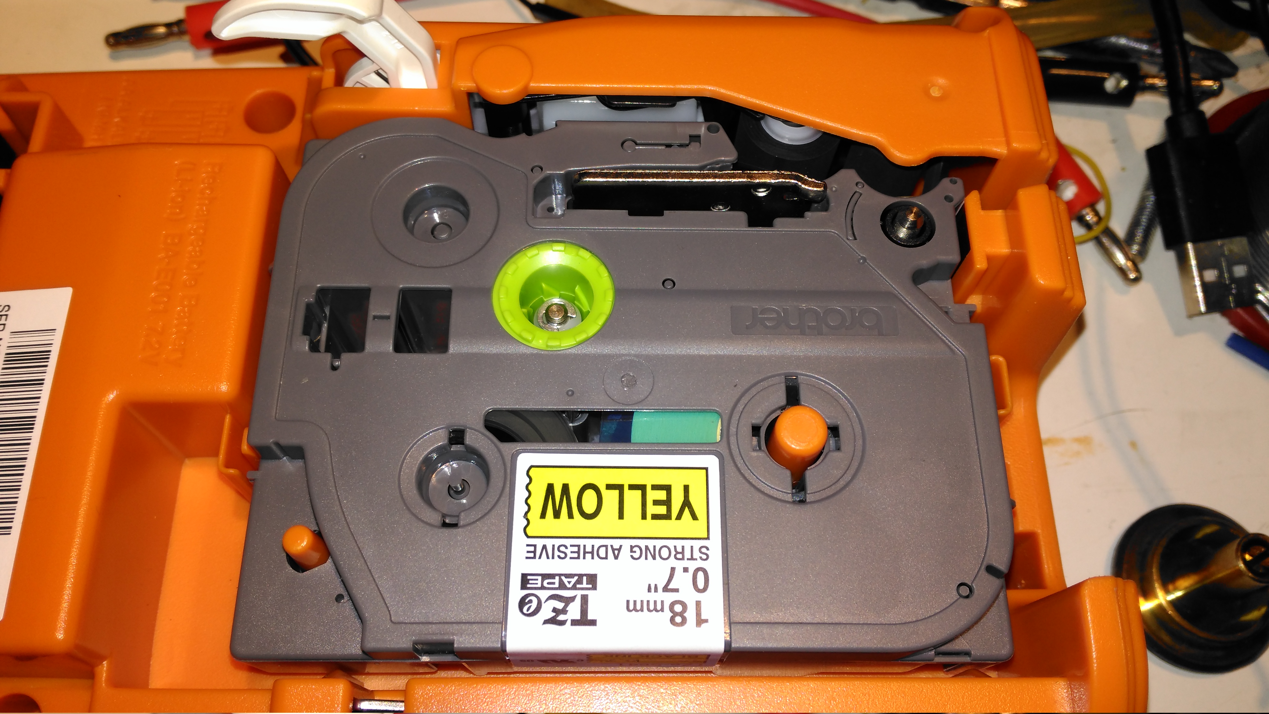
Here a tape is installed in the printer. This unit can handle tape widths up to 18mm. The pinch rollers are operated by the white lever at the top of the image, which engages with the back cover.

Li-Ion Battery
Li-Ion Battery

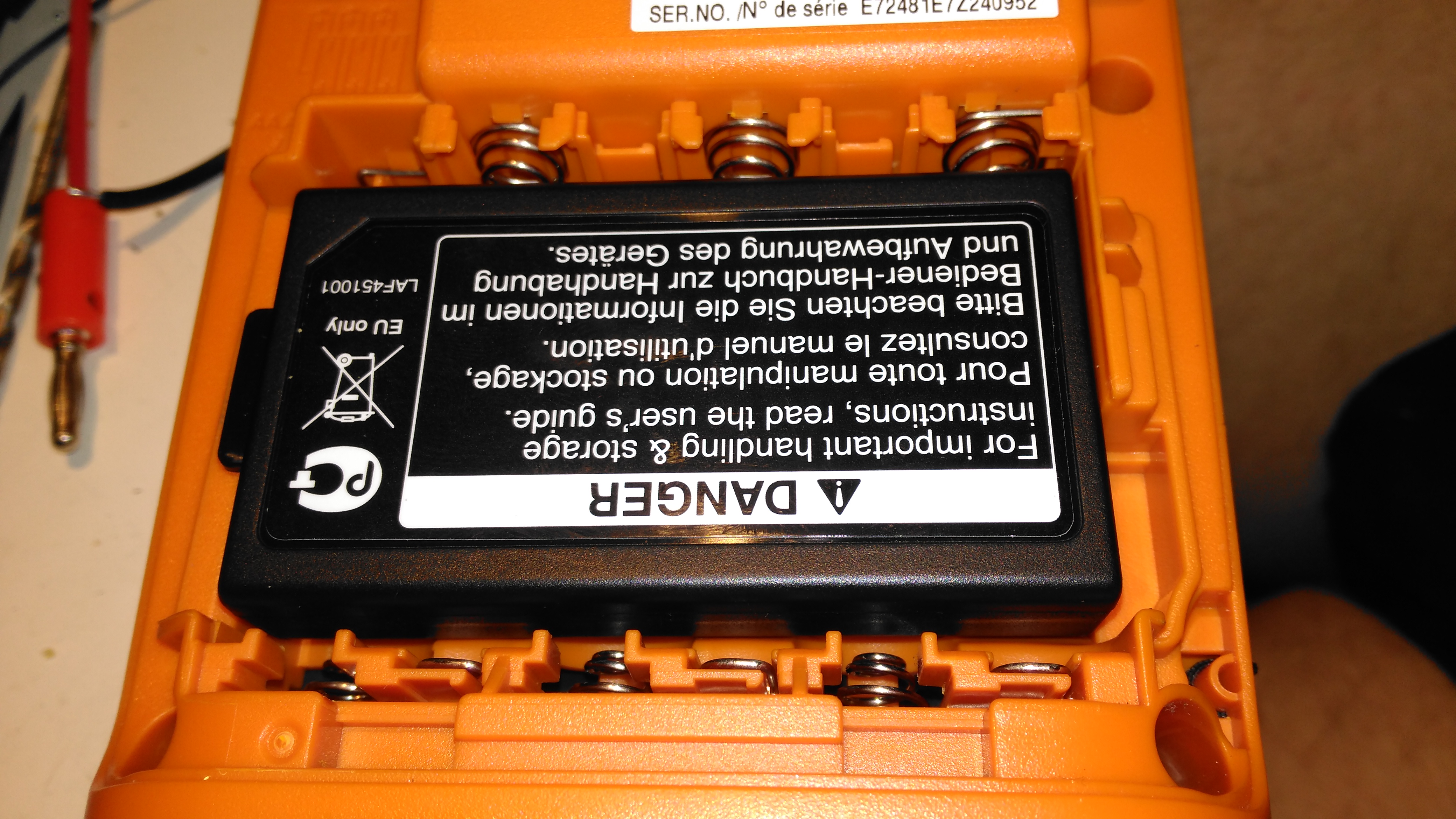
This printer is supplied with a rechargeable battery pack, but AA cells can be used as well. Some of the AA battery terminals can be seen above the battery.

Battery Specs
Battery Specs

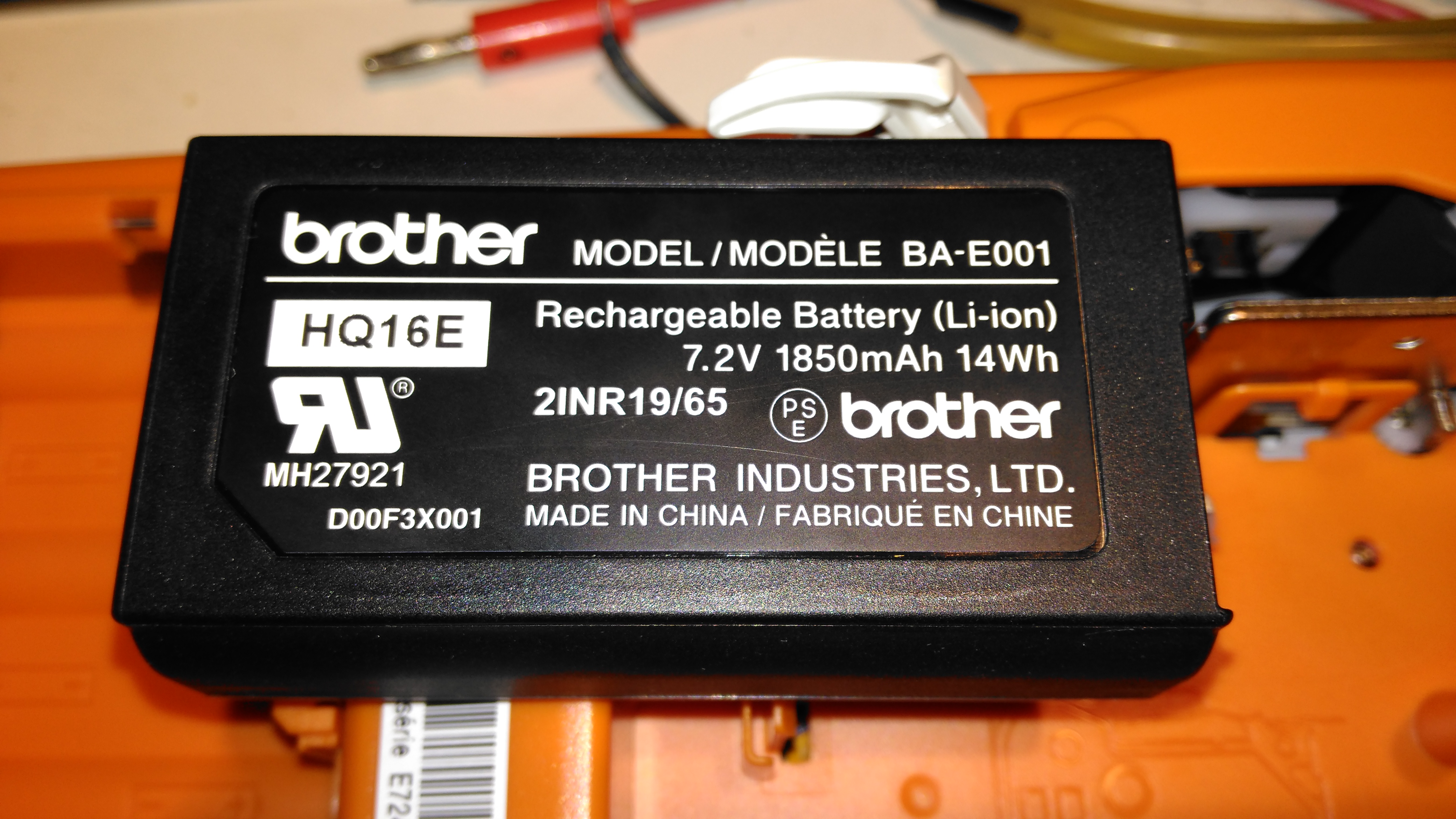
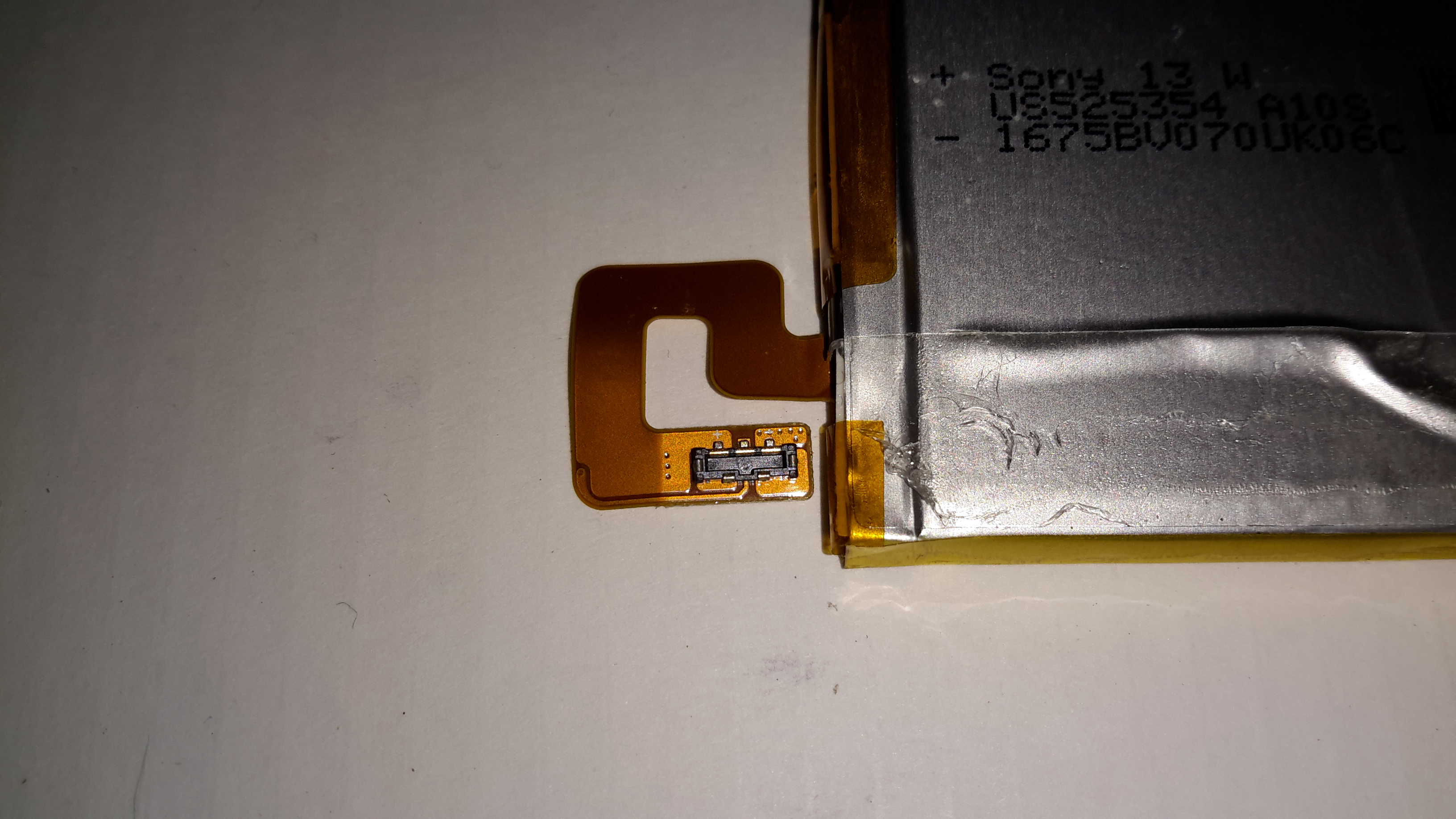
Pretty standard fare for a 2-cell lithium pack. The charging circuitry doesn’t appear to charge it to full voltage though, most likely to get the most life from the pack.

Cartridge Slot
Cartridge Slot

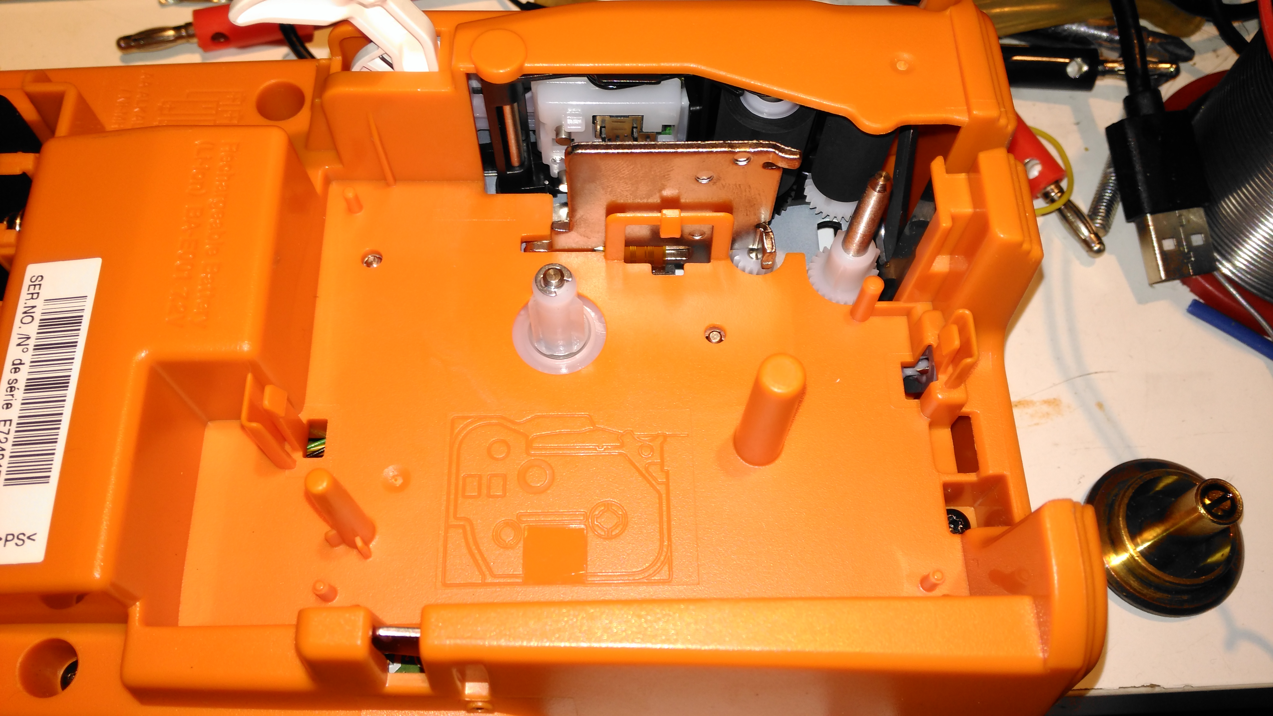
With the cartridge removed, the printer components can be seen. As these cartridges have in effect two rolls, one fro the ribbon & one for the actual label, there are two drive points.

Pinch Rollers & Print Head

The thermal print head is hidden on the other side of the steel heatsink, while the pinch rollers are on the top right. The plastic piece above the print head heatsink has a matrix of switches that engage with holes in the top of the label cartridge, this is how the machine knows what size of ribbon is fitted.

Mainboard
Mainboard

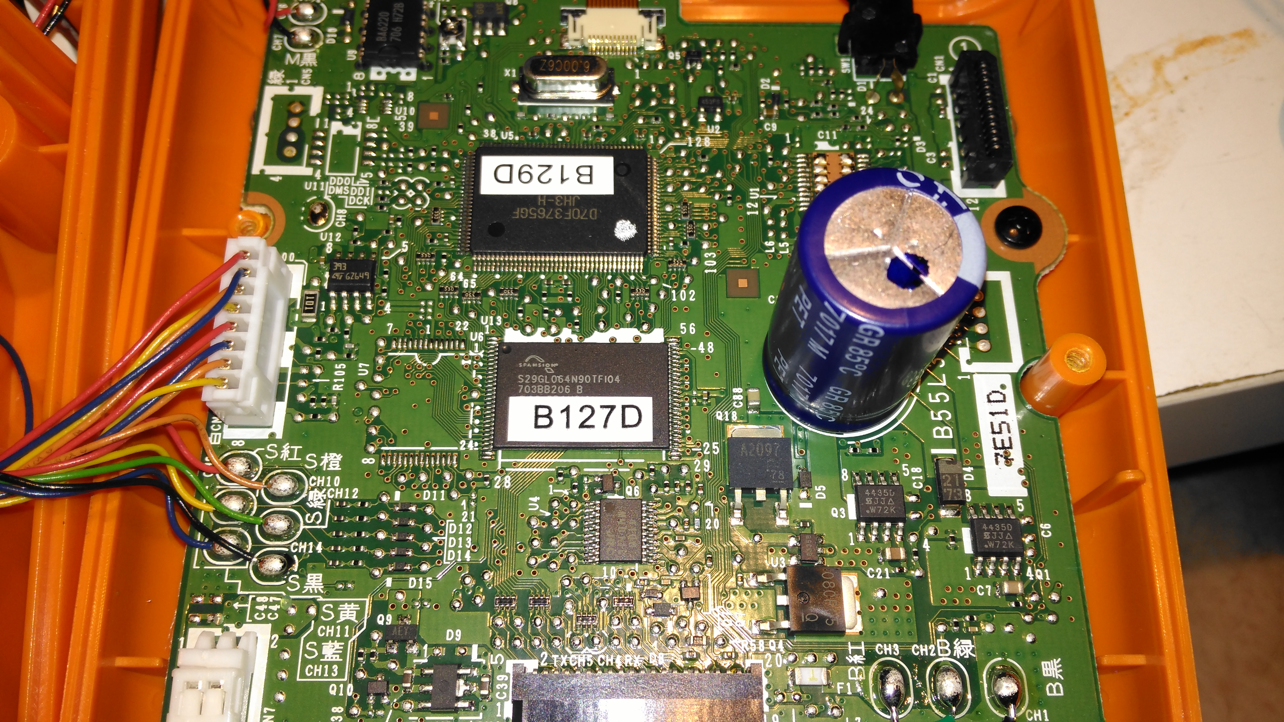
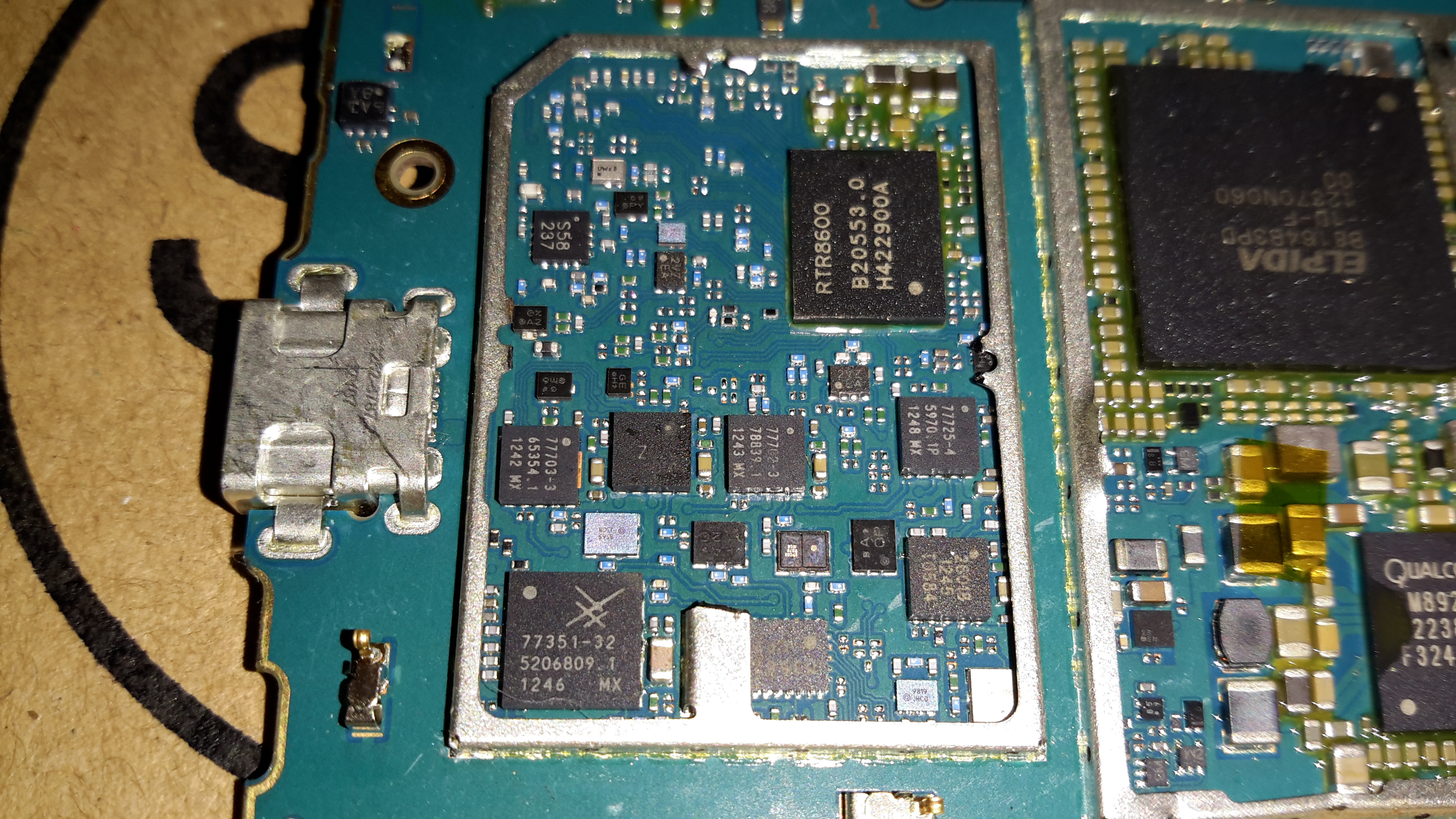
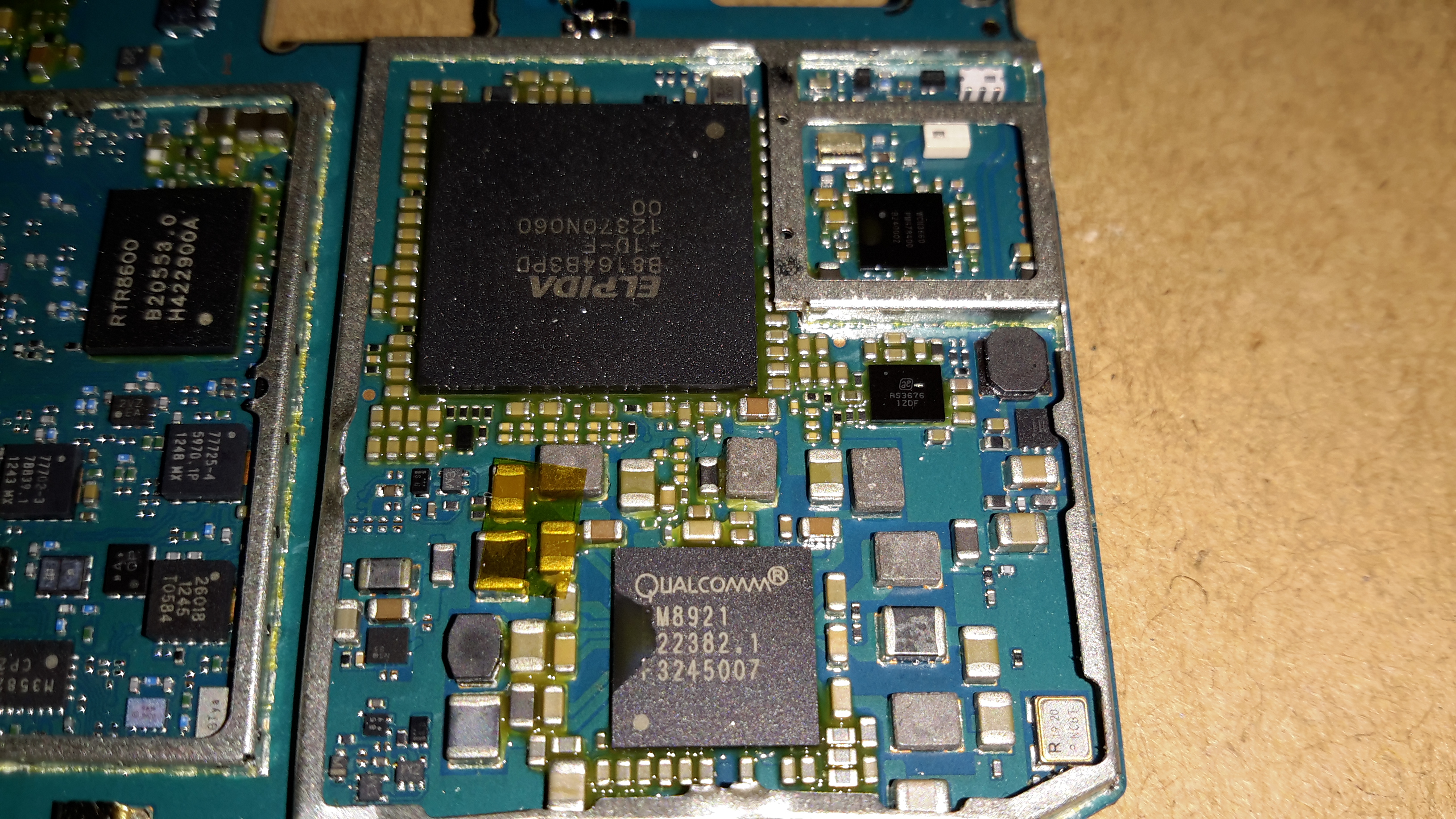
Most of the internal space is taken up by the main board, with the microprocessor & it’s program flash ROM top & centre.

Charger Input
Charger Input

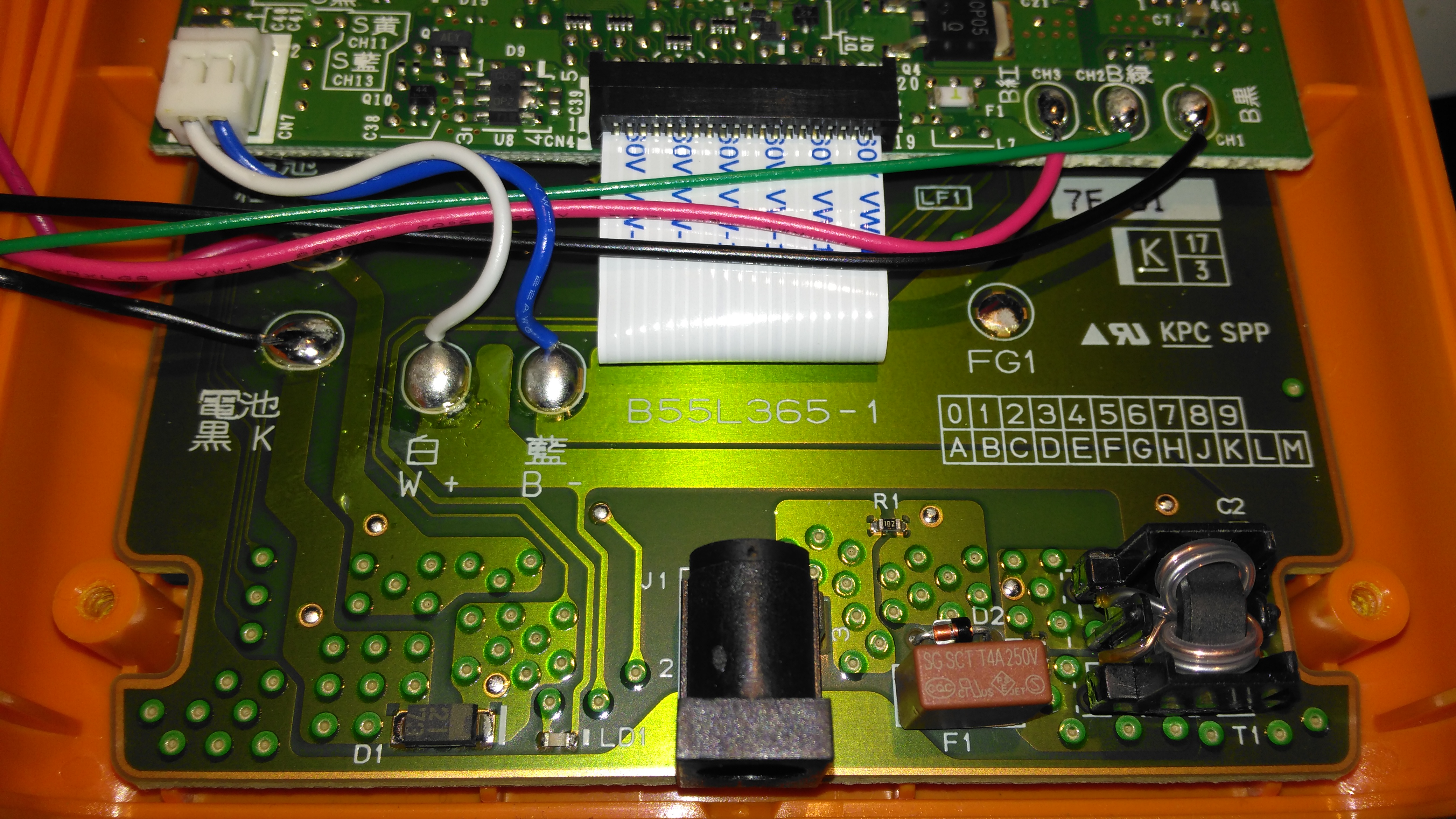
The charger input is located on the keyboard PCB just under the mainboard, which is centre negative, as opposed to 99% of other devices using centre positive, the bastards.

LCD Module
LCD Module

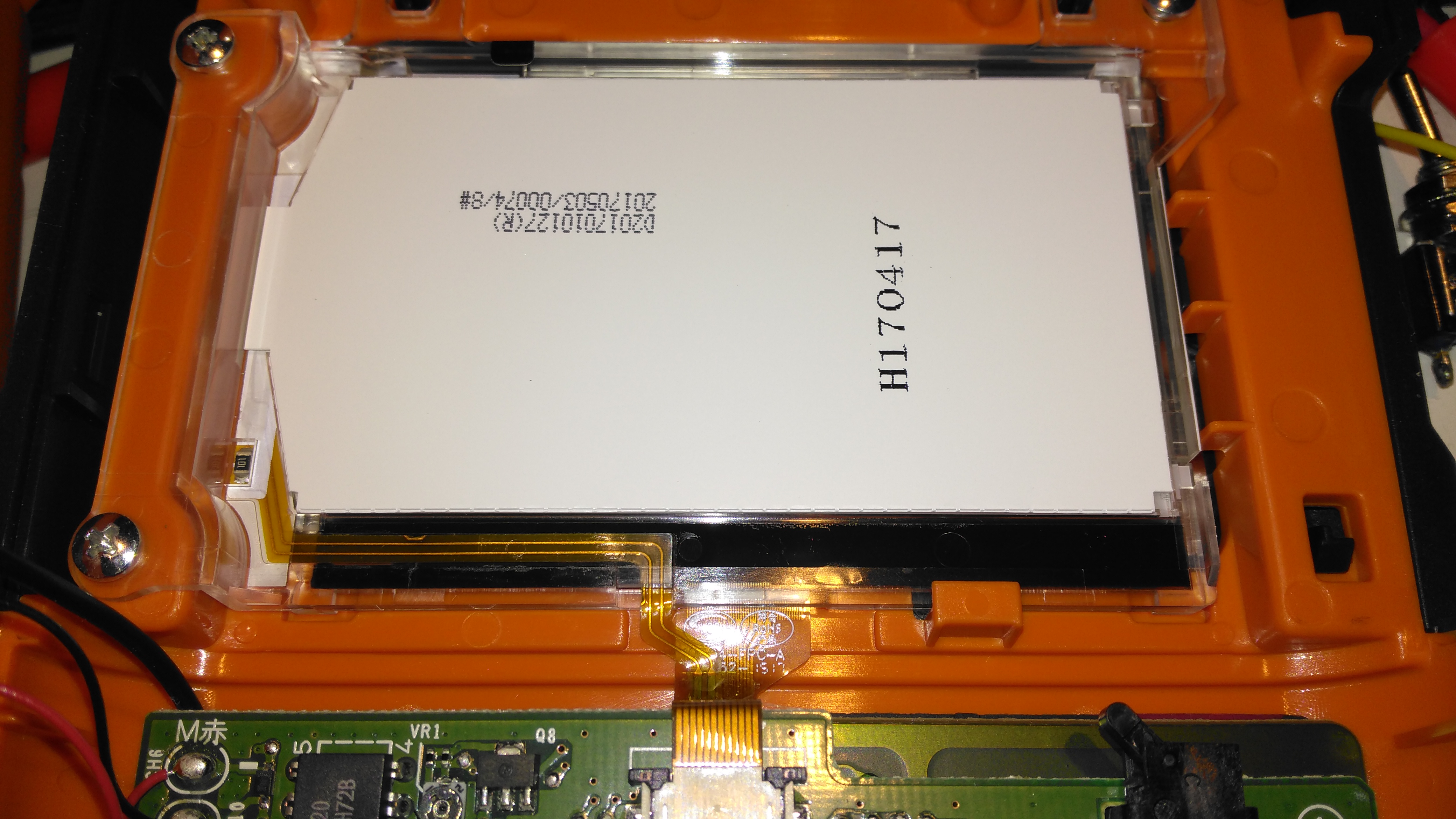
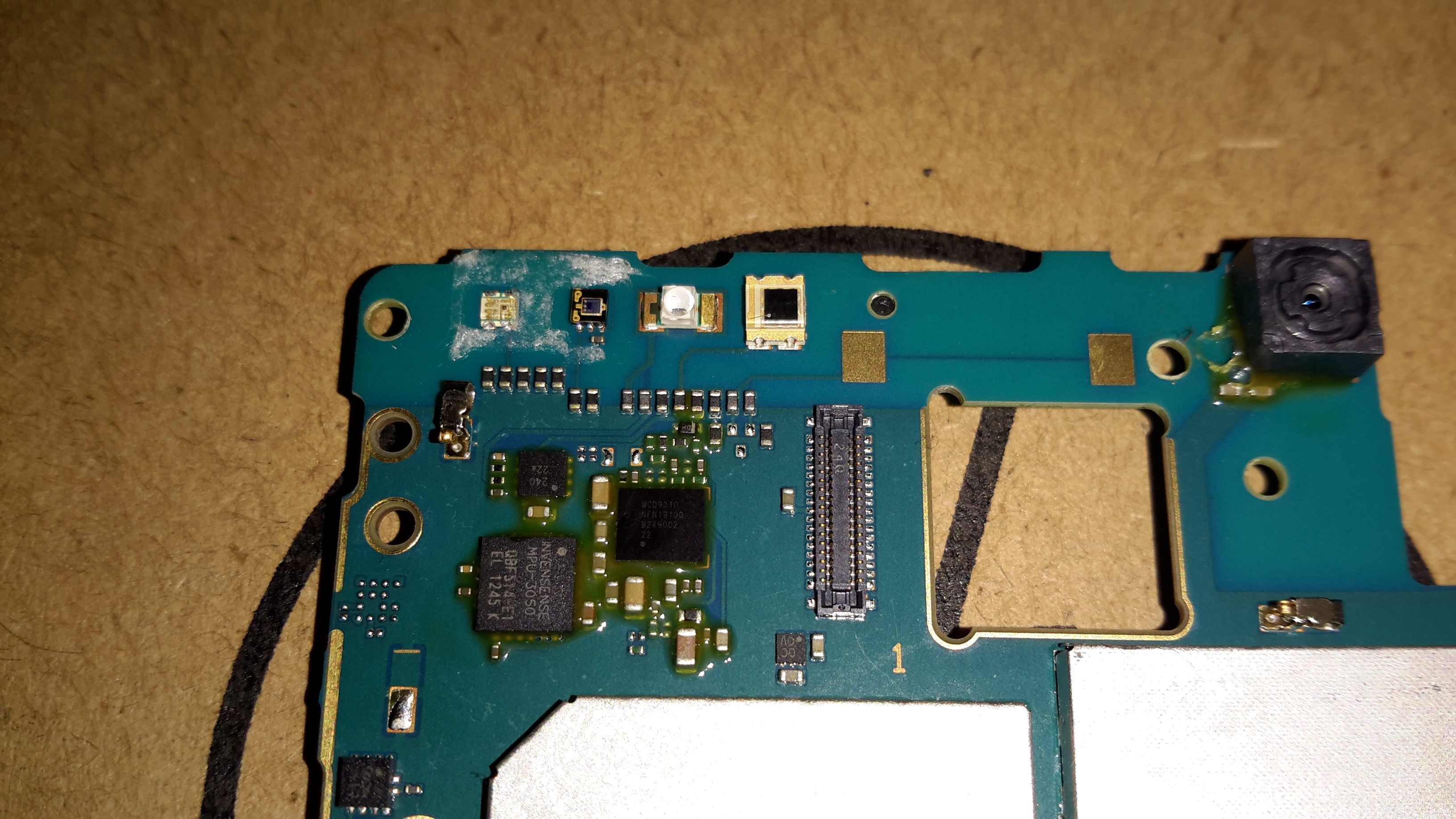
The dot-matrix LCD is attached to the mainboard with a short flex cable, and from the few connections, this is probably SPI or I²C.

Print Mech Drive
Print Mech Drive

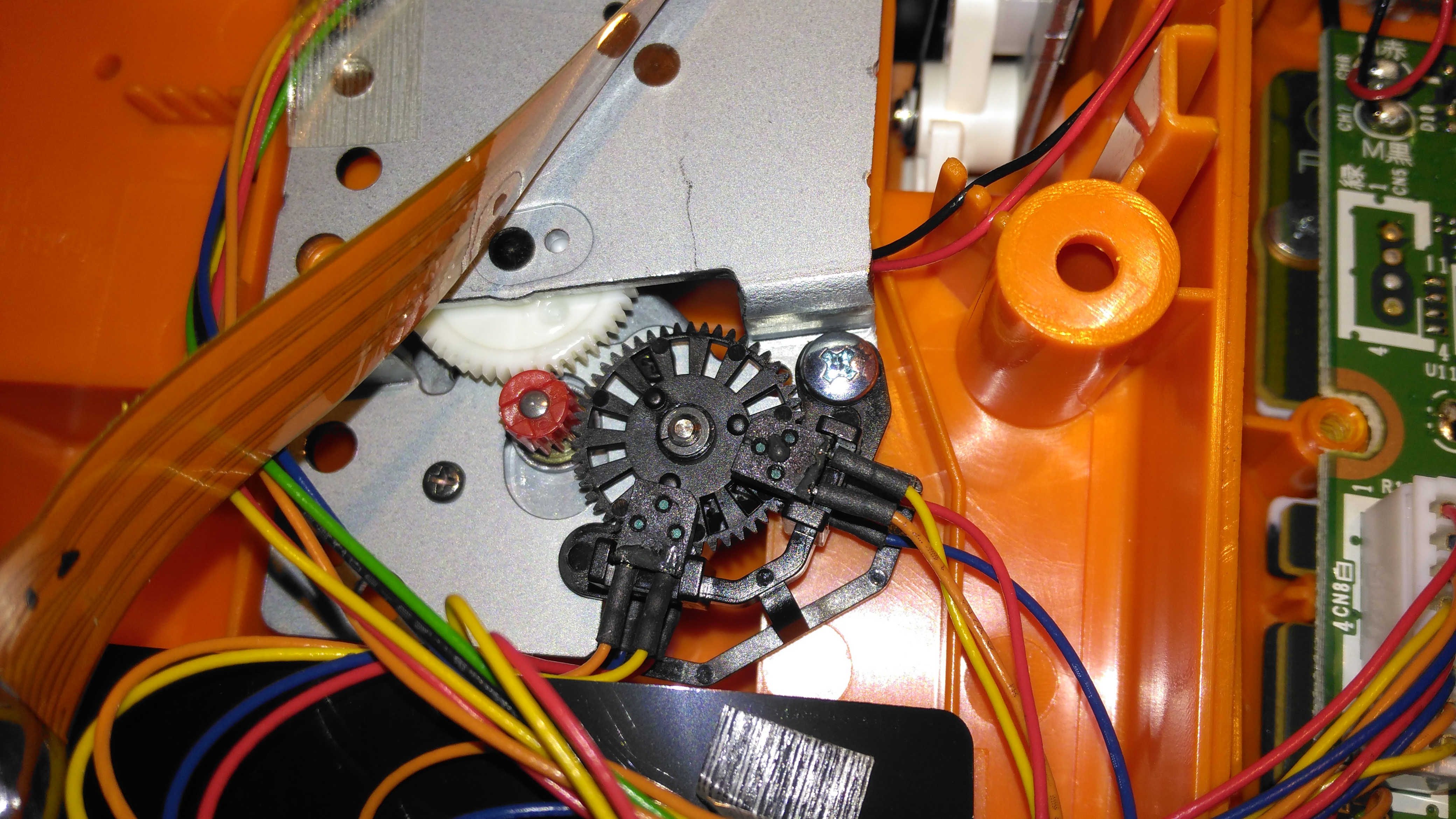
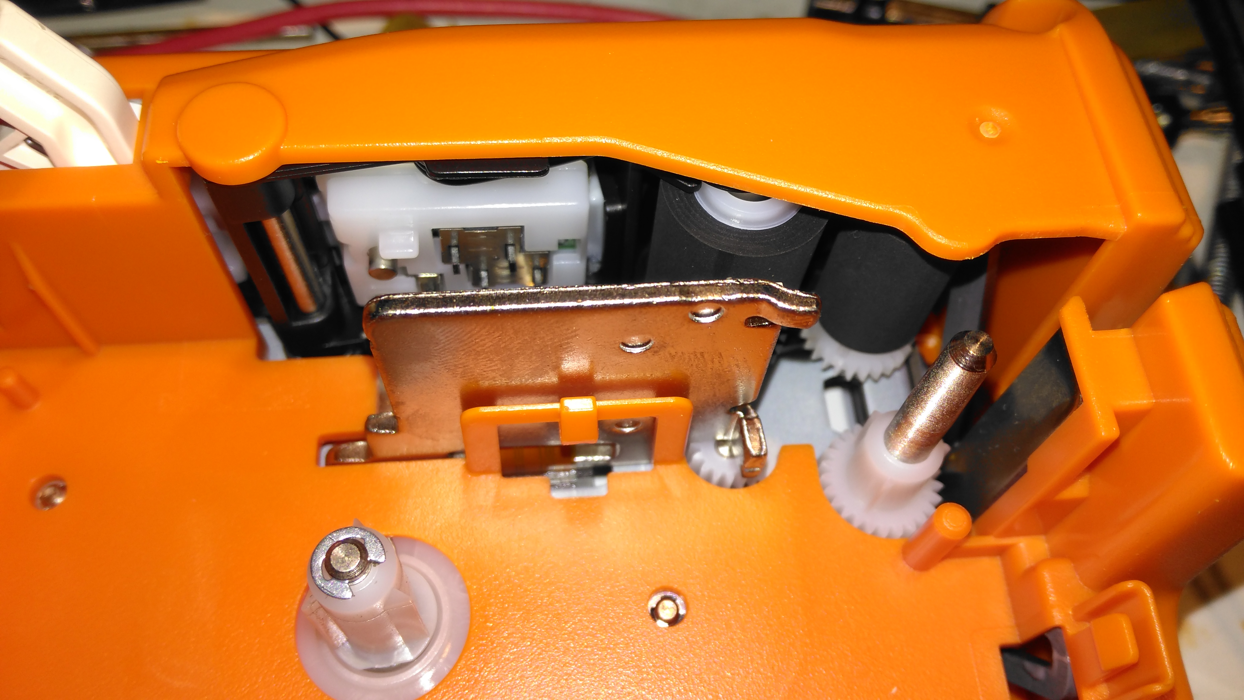
The printer itself is driven by a simple DC motor, speed is regulated by a pair of photo-interrupters forming an encoder on the second gear in the train.

Battery Holder Connections

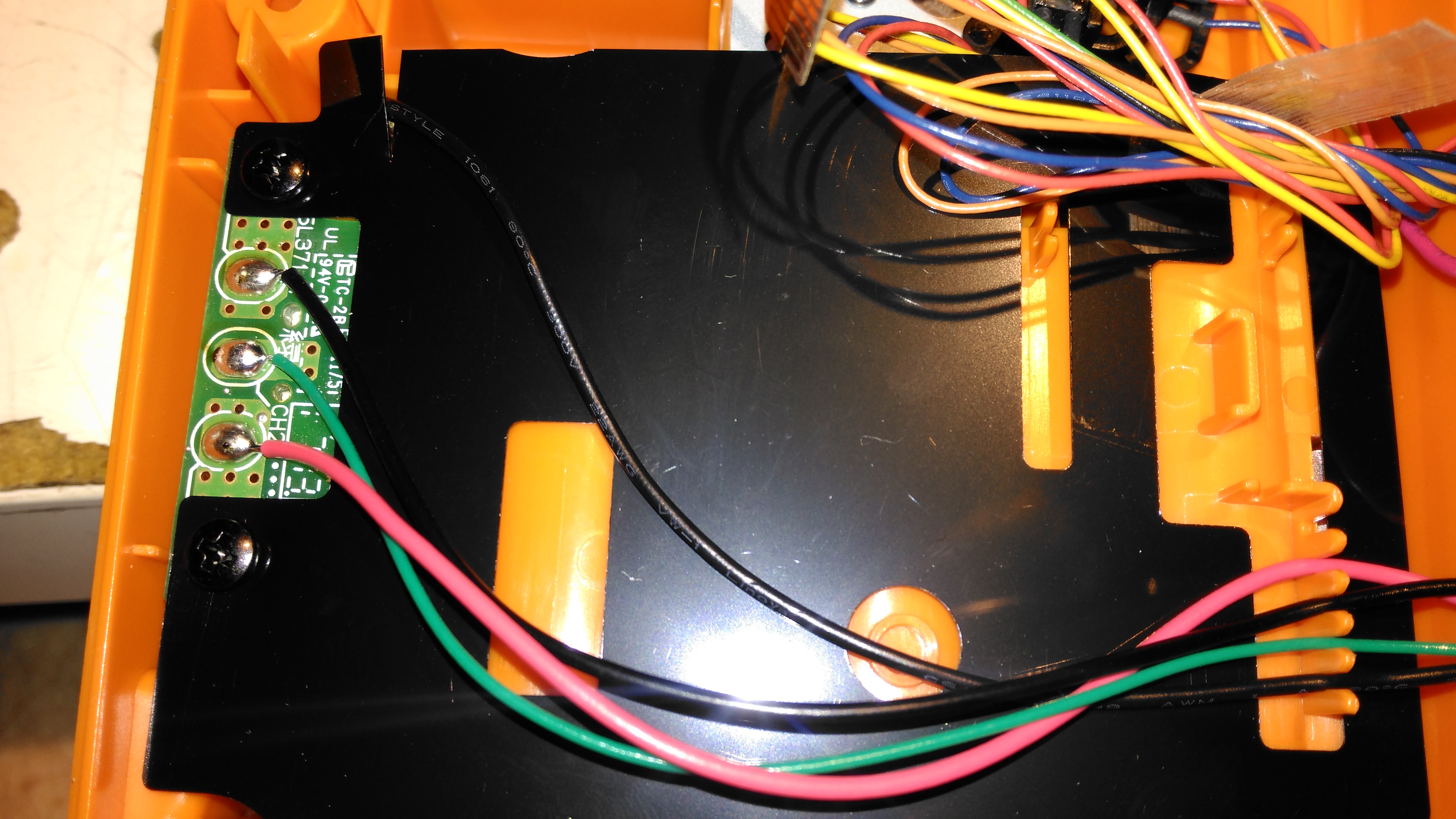
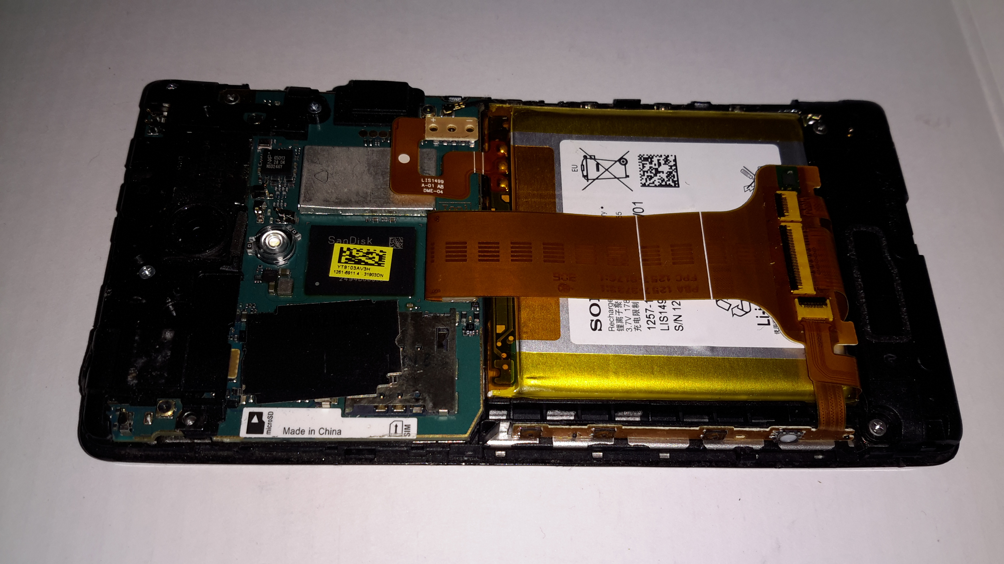
The back case has the battery connections for both the lithium pack & the AA cells, the lithium pack has a 3rd connection, probably for temperature sensing.

Posted on Leave a comment

MingHe D3806 Buck-Boost DC-DC Converter

DC-DC Converter
DC-DC Converter

Here’s a useful buck-boost DC-DC converter from eBay, this one will do 36v DC at 6A maximum output current. Voltage & current are selected on the push buttons, when the output is enabled either the output voltage or the output current can be displayed in real time.

Display PCB
Display PCB

Here’s the display PCB, which also has the STM32 microcontroller that does all the magic. There appears to be a serial link on the left side, I’ve not yet managed to get round to hooking it into a serial adaptor to see if there’s anything useful on it.

Display Drive & Microcontroller

The bottom of the board holds the micro & the display multiplexing glue logic.

Main PCB
Main PCB

Not much on the mainboard apart from the large switching inductors & power devices. There’s also a SMPS PWM controller, probably being controlled from the micro.

Posted on Leave a comment

Sony Xperia T Teardown

Back Cover Removed
Back Cover Removed

Since this phone has been in my drawer for some time, I figured it was time for a teardown. (It’s never going to see any more use).
The back cover on these phones is easily removed, as it’s just clipped on.

Motherboard
Motherboard

Once the back cover is removed, the Li-Polymer cell is exposed, along with the logic board. Pretty much all of the PCB is under RF shields.

Motherboard Removed
Motherboard Removed
Battery Management
Battery Management

Under the small RF can on the back of the board is the battery management circuitry & the charger. There’s an extra connection to the cell for temperature monitoring. Just under that circuitry is the eMMC flash storage.
Just to the left of the battery circuit is the NFC transceiver IC, from NXP.

Battery Flex
Battery Flex

The cell is connected to the main board with a FFC, with a very small SMT connector, although not as small as the more modern Xperia series phones.

RF Section
RF Section

The other side of the mainboard holds the large RF transceiver section, with a Qualcomm RTR8600 multiband transceiver IC. In the bottom corner is a Skyworks SKY77351-32 Quad-band power amplifier IC, along with 3 other power amplifier ICs, also from Skyworks.

Gyro & Audio Codec
Gyro & Audio Codec

The top corner of the board holds the various sensors, including an Invensense MPU-3050 3-axis gyro. To the right of that is the Audio Codec, a WCD9310 from Qualcomm.

Logic & CPU Section
Logic & CPU Section

Everything is controlled from the last section on the board, with the main CPU & RAM in a PoP (Package-On-Package) configuration. Under the main CPU is the main power management IC, also from Qualcomm. No datasheet for this one unfortunately, but it gives it’s purpose away by being surrounded by large inductors & capacitors.

Posted on Leave a comment

Rigol DS1054Z 12v Power Supply Noise Filtering

Since I fitted my scope with a SMPS based 12v input supply, there has been a noise problem on very low volts/div settings, this noise isn’t present on the mains supply, so I can only think it’s coming from the switching frequencies of the various DC-DC modules I’ve used.

Scope Ripple
Scope Ripple

Because of this I’ve designed a linear post-regulation stage for the supply, to remove the RFI from the DC rails.
This board takes the outputs from the DC-DC converters, removes all the noise & outputs clean DC onto the mainboard of the scope.

As the scope internally uses regulation to get the voltages lower, I’ve found that I don’t have to match the outputs of the mains supply exactly, for the +/-17.5v rails, 12v is perfectly fine instead.

Scope Linear PSU
Scope Linear PSU

Here’s the PCB layout, with the 6  common mode filters on the input (left), linear regulator ICs in the centre & the output filters on the right.

Scope Linear PSU
Scope Linear PSU

Here’s the schematic layout, as usual the Eagle Project files are in the link below, I’ll update when I have built the board & tested!

[download id=”5589″]

73s for now 🙂

Posted on Leave a comment

iPod

Front
Front

Old iPod with damaged screen. Here is the front with the Click Wheel.

Cover Removed
Cover Removed

Cover removed from the back, here the HDD is the biggest visible part.

Mainboard
Mainboard

Back cover removed from the unit, here is the back of the screen & the main PCB.

Back Cover
Back Cover

Back cover with the battery & headphone jack PCB.

Battery
Battery

Closeup of the Li-Ion battery.

Front Removed
Front Removed

Front removed from the unit, the touch sensitive Click Wheel PCB is folded away from the mainboard here.

Buttons
Buttons

Tactile switches underneath the Click Wheel.

HDD
HDD

1.8″ hard drive. Toshiba MK3008GAL.

Posted on Leave a comment

PSP Slim

Front
Front

Here is a PSP Slim that recently died.

Label
Label

For those that are interested, here is the ID label, this is a PSP-2003.

Front Removed
Front Removed

Here the front of the unit has been removed, showing the first internal components.

Screen Removed
Screen Removed

Here is the unit with the LCD removed, here the mainboard is partially visible.

Left Pad
Left Pad

Left pad unit removed from the PSP, with the left speaker & the memory stick slot cover.

Left Pad Rear
Left Pad Rear

Rear of the left pad assembly, showing the speaker.

Joypad
Joypad

Joypad removed from the casing. Resistive unit.

Output Jack
Output Jack

Headphone/data board removed from the casing. This also has TV-Out on the PSP-200x series.

Mainboard
Mainboard

Mainboard removed. Main CPU is at the top. Sockets around the bottom connect to the UMD drive & UMD Drive.

CPU & GPU
CPU & GPU

Closeup of the main chipset. CPU is the top IC.

Mainboard Rear
Mainboard Rear

Rear of the mainboard, Memory Stick socket on the right.

WiFi Chipset
WiFi Chipset

Closeup of the WiFi chipset & the charging power socket on the right.

Charging Chipset
Charging Chipset

Closeup of the bettery connector & the charge controller IC.

UMD Drive
UMD Drive

UMD Drive removed from the rear of the casing. This is a miniature DVD style drive, using a 635nm visible red laser.

UMD Drive Back
UMD Drive Back

Rear of the UMD drive, showing the laser sled & drive motors. Both the spindle motor & the sled motor are 3-phase brushless type. The laser diode/photodiode array is at the top of the laser sled.

Posted on 2 Comments

Current Cost ‘Envi’ CC128 Power Meter

Display Unit
Display Unit

This is the Current Cost CC128 Real Time Power Meter. Shown here is the display unit, British Gas issued these free to some customers.
This unit measures current power draw in Watts, cost of power currently being used (requires unit price to be set), overall kWh usage over the past 1, 7 or 30 days & power trends during the day, night & evening. Also displays current time & current room temperature.

Display PCB
Display PCB

Here the front panel of the display has been un-clipped. At the bottom are the RJ-45 serial port & power connections.
This unit uses a PIC micro-controller as it’s CPU (PIC18F85J90) Just above & left of the CPU is the 433MHz SPD radio receiver module. The chips on the right of the CPU are a 25LC128 SPI serial EEPROM for data storage & a 74HC4060 14 stage binary counter, to which is connected the 32kHz clock crystal. The red wire around the top of the display is the antenna for the radio receiver.

For more info on the CC128 in general, the serial port & software for computer data logging, see this link
See this link for Current Cost’s list of software

Processor & Radio
Processor & Radio

Closeup of the ICs on the mainboard.

Transmitter Unit
Transmitter Unit

Here we have the transmitter unit, with Current Transformer (CT). The red clamp fits around one of the electric meter tails & read the current going to the various circuits. This unit is powered by 2x D cells, rated at a life of 7 years.

Transmitter PCB
Transmitter PCB

The PCB inside the transmitter. Again very minimal design, unknown controller IC, 433MHz radio transmitter on right hand side with wire antenna. Two barrel connectors on left hand side of board allow connection of up to two more CT clamps for measurement of 3-phase power. Centre of board is unmarked header. (ICSP?)

Current Transformer
Current Transformer

CT unit. Inside is a coil of wire & an iron core which surrounds the cable to be measured.