This is a chip aimed at the automotive market – this is a low power voltage regulator for supplying power to microcontrollers, for instance in a CD player.
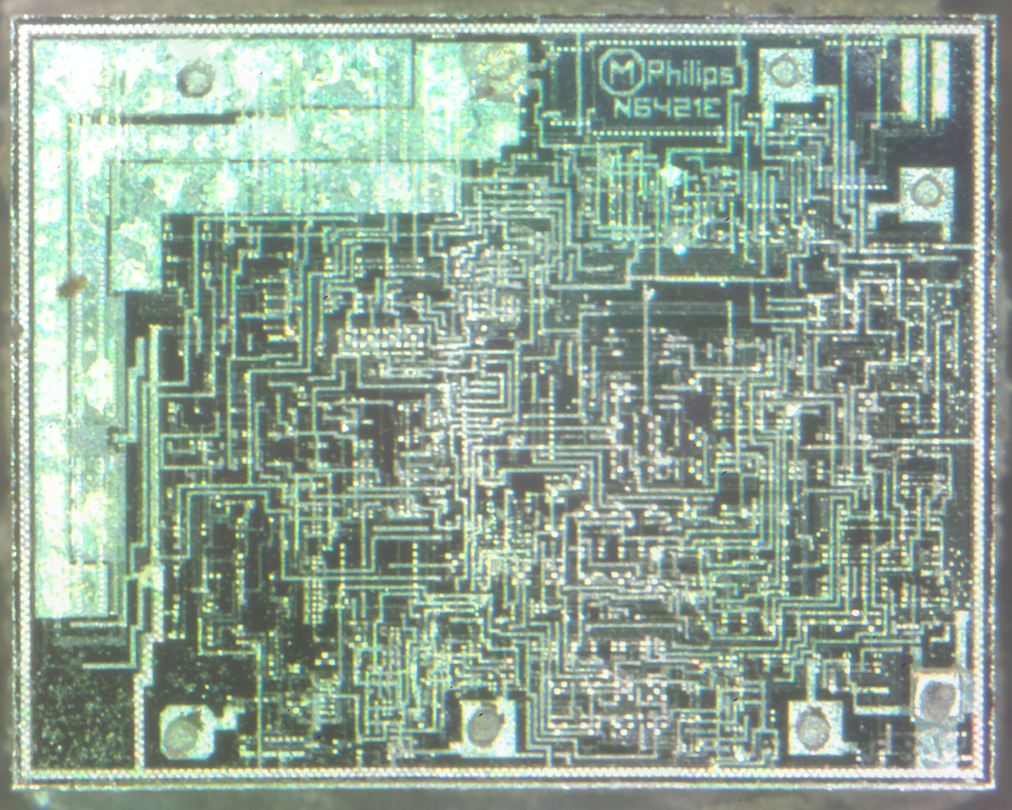
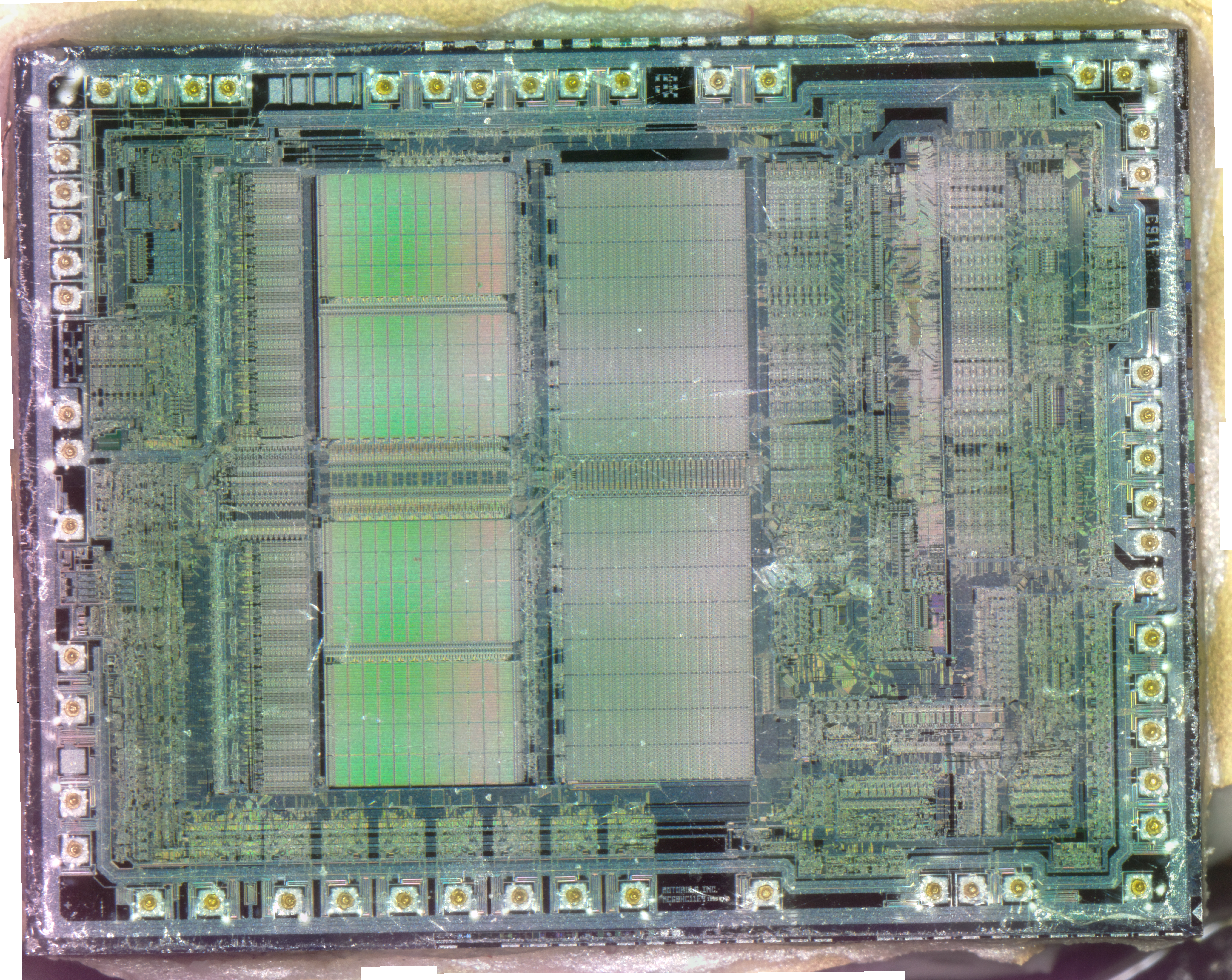
TDA3606 Die
The TDA3606 is a voltage regulator intended to supply a microprocessor (e.g. in car radio applications). Because of low voltage operation of the application, a low-voltage drop regulator is used in the TDA3606. This regulator will switch on when the supply voltage exceeds 7.5 V for the first time and will switch off again when the output voltage of the regulator drops below 2.4 V. When the regulator is switched on, the RES1 and RES2 outputs (RES2 can only be HIGH when RES1 is HIGH) will go HIGH after a fixed delay time (fixed by an external delay capacitor) to generate a reset to the microprocessor. RES1 will go HIGH by an internal pull-up resistor of 4.7 kΩ, and is used to initialize the microprocessor. RES2 is used to indicate that the regulator output voltage is within its voltage range. This start-up feature is built-in to secure a smooth start-up of the microprocessor at first connection, without uncontrolled switching of the regulator during the start-up sequence. All output pins are fully protected. The regulator is protected against load dump and short-circuit (foldback
current protection). Interfacing with the microprocessor can be accomplished by means of a battery Schmitt-trigger and output buffer (simple full/semi on/off logic applications). The battery output will go HIGH when the battery input voltage exceeds the HIGH threshold level.
I recently got the latest upgrade from Virgin Media, 200Mbit DL / 20Mbit UL, and to get this I was informed I’d have to buy their latest hardware, since my existing CPE wouldn’t be able to handle the extra 5Mbit/s upload speed. (My bullshit detector went off pretty hard at that point, as the SuperHub 2 hardware is definitely capable of working fine with 20Mbit/s upload rates). Instead of having to return the old router, I was asked to simply recycle it, so of course the recycling gets done in my pretty unique way!
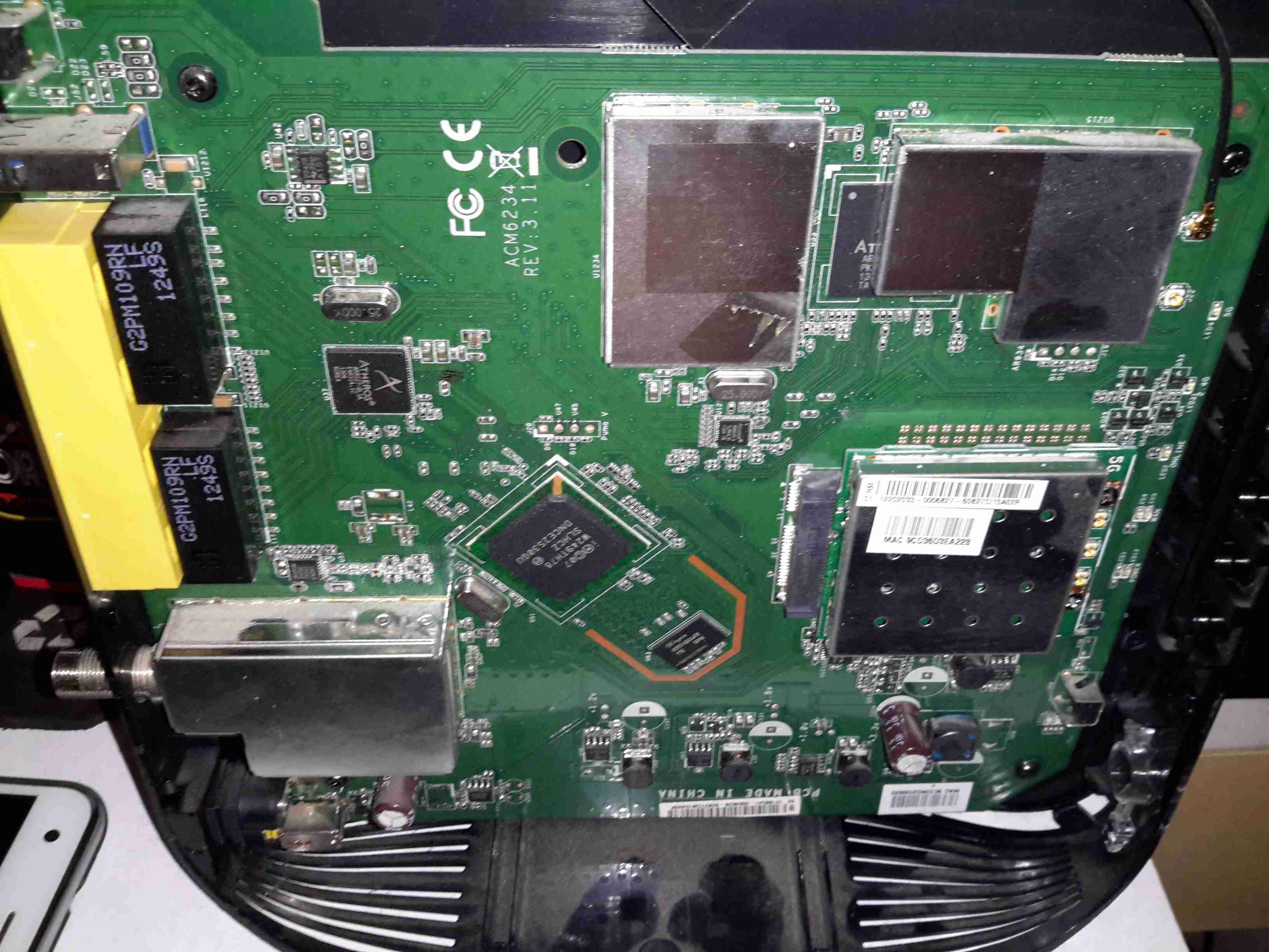
Mainboard
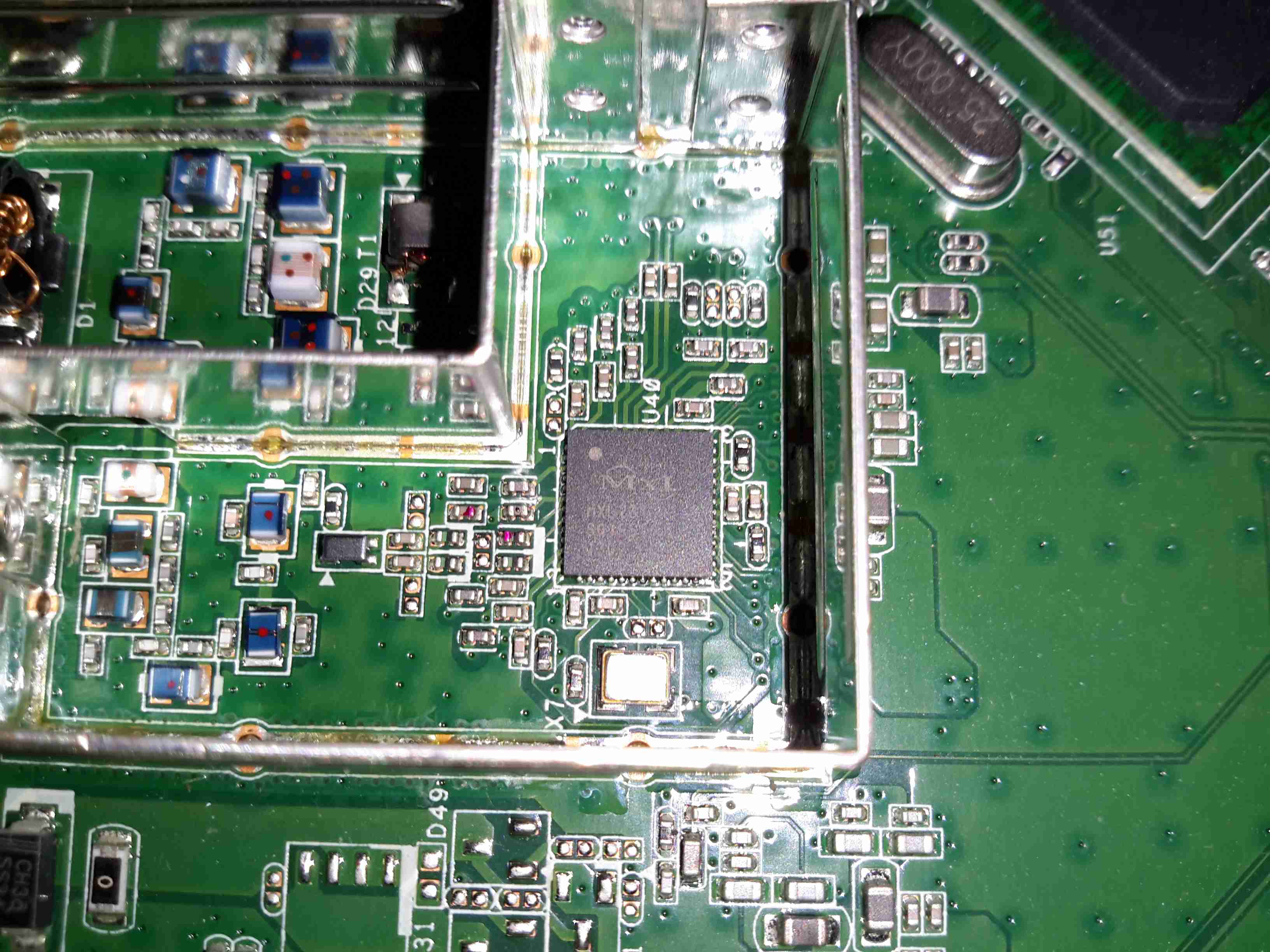
The casing of these units is held together by a single screw & a metric fuckton of plastic clips, disassembly is somewhat hindered by the radio antennas being positioned all over both sides of the casing. Once the side is off, the mainboard is visible. The DOCSIS frontend is lower left, centre is the Intel PUMA 5 Cable Modem SoC with it’s RAM just to the lower right. The right side of the board is taken up by both of the WiFi radio frontends, the 5GHz band being covered by a Mini PCIe card.
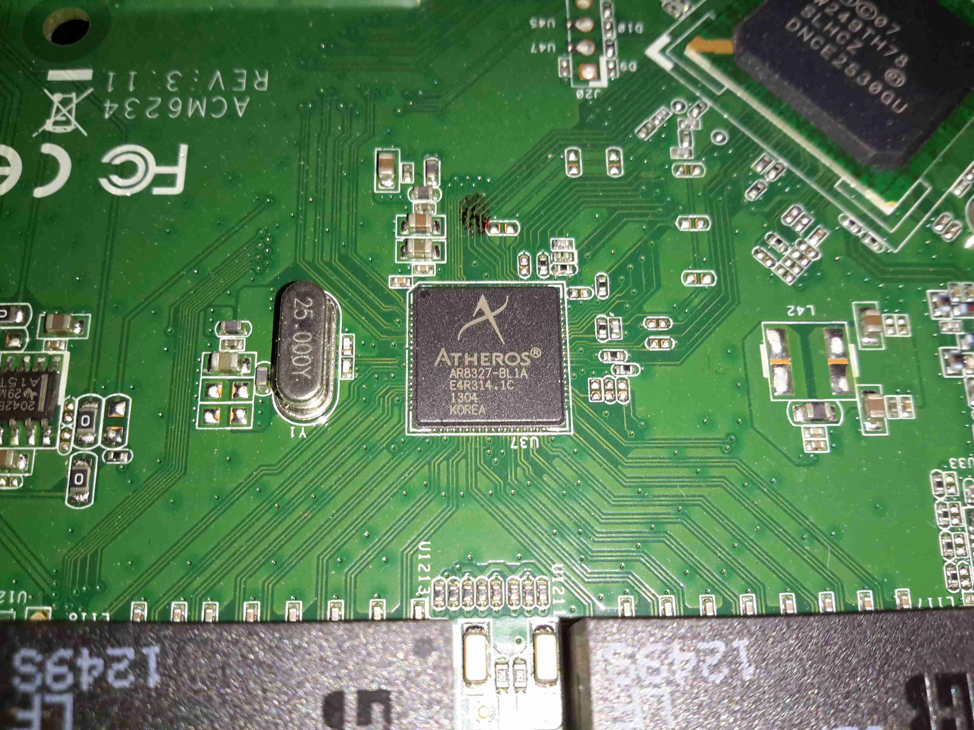
Atheros Gigabit Switch
The 4 gigabit Ethernet ports on the back are serviced by an Atheros AR8327 Managed Layer 3 switch IC, which seems to be a pretty powerful device:
The AR8327 is the latest in high performance small network switching. It is ultra low power, has extensive routing and data management functions and includes hardware NAT functionality (AR8327N). The AR8327/AR8327N is a highly integrated seven-port Gigabit Ethernet switch with a fully non-blocking switch fabric, a high-performance lookup unit supporting 2048 MAC addresses, and a four-traffic class Quality of Service (QoS) engine. The AR8327 has the flexibility to support various networking applications. The AR8327/AR8327N is designed for cost-sensitive switch applications in wireless AP routers, home gateways, and xDSL/cable modem platforms.
Unfortunately most of the features of this router are locked out by VM’s extremely restrictive firmware. With any of their devices, sticking the VM supplied unit into modem mode & using a proper router after is definitely advised!
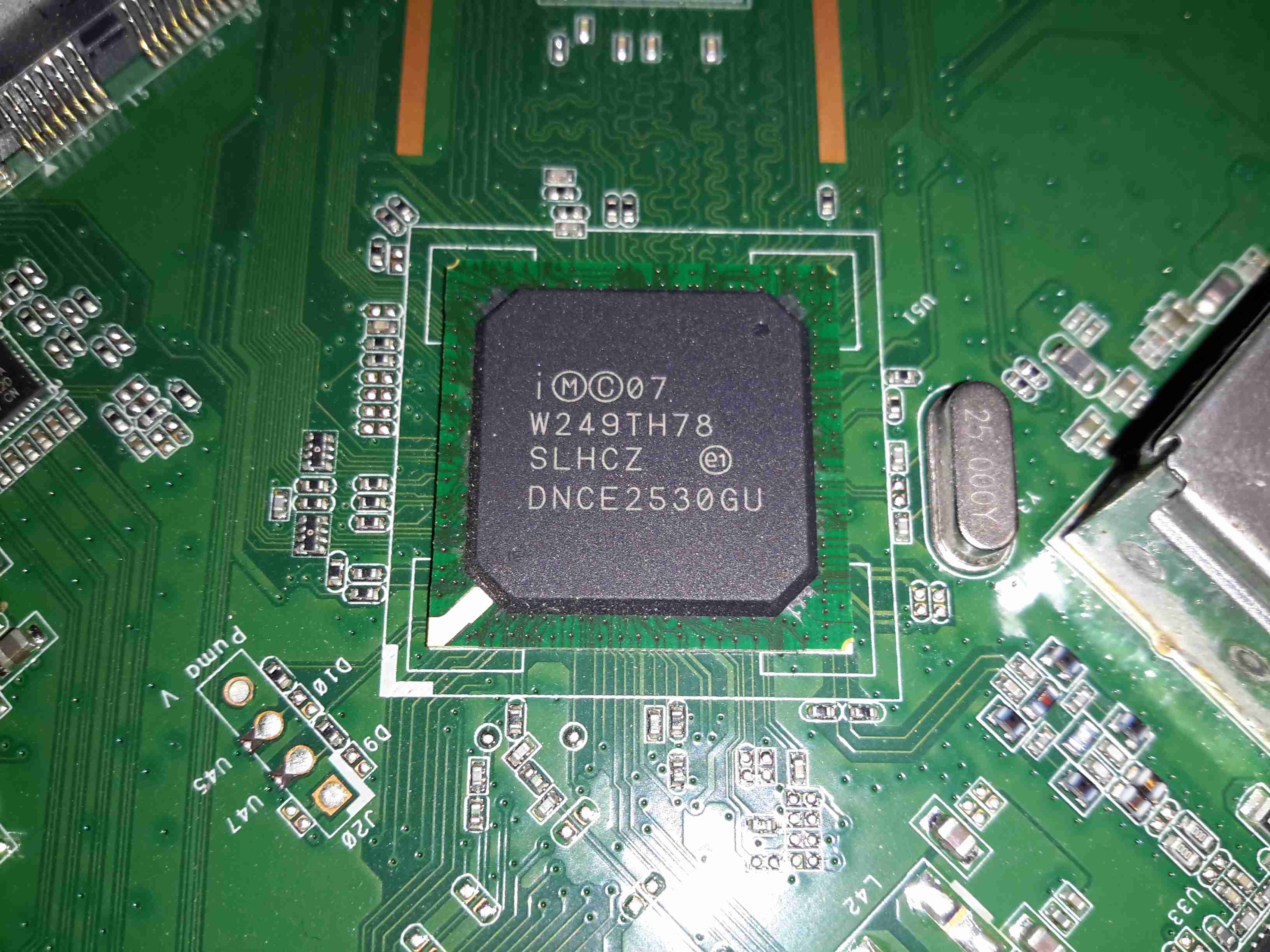
Intel Puma 5 CM CPU
The cable modem side of things is taken care of by the Intel PUMA 5 DNCE2530GU SoC. This appears to communicate with the rest of the system via the Ethernet switch & PCI Express for the 5GHz radio.
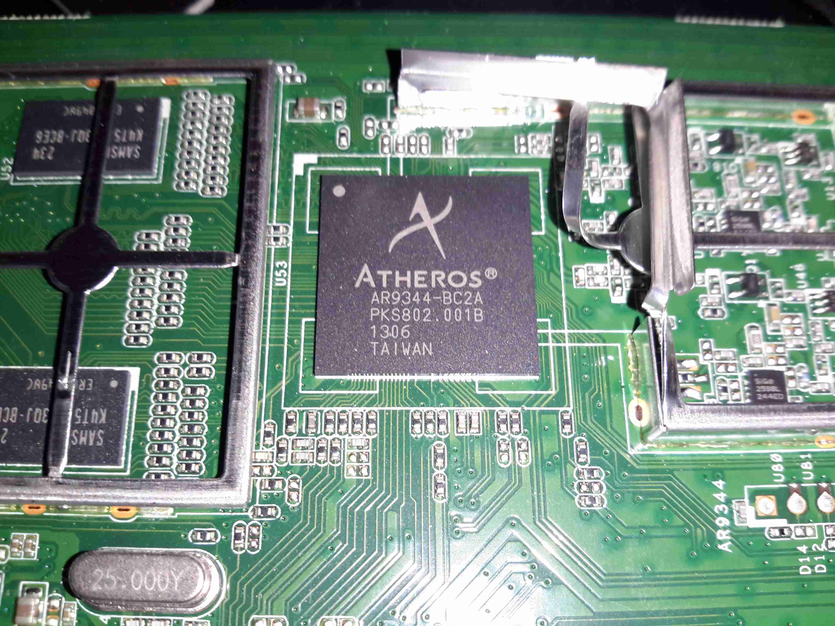
Atheros WiFi SoC
The 2.4GHz radio functionality is supplied by an Atheros AR9344 SoC, it’s RAM is to the left. This is probably handling all the router functions of this unit, but I can’t be certain.
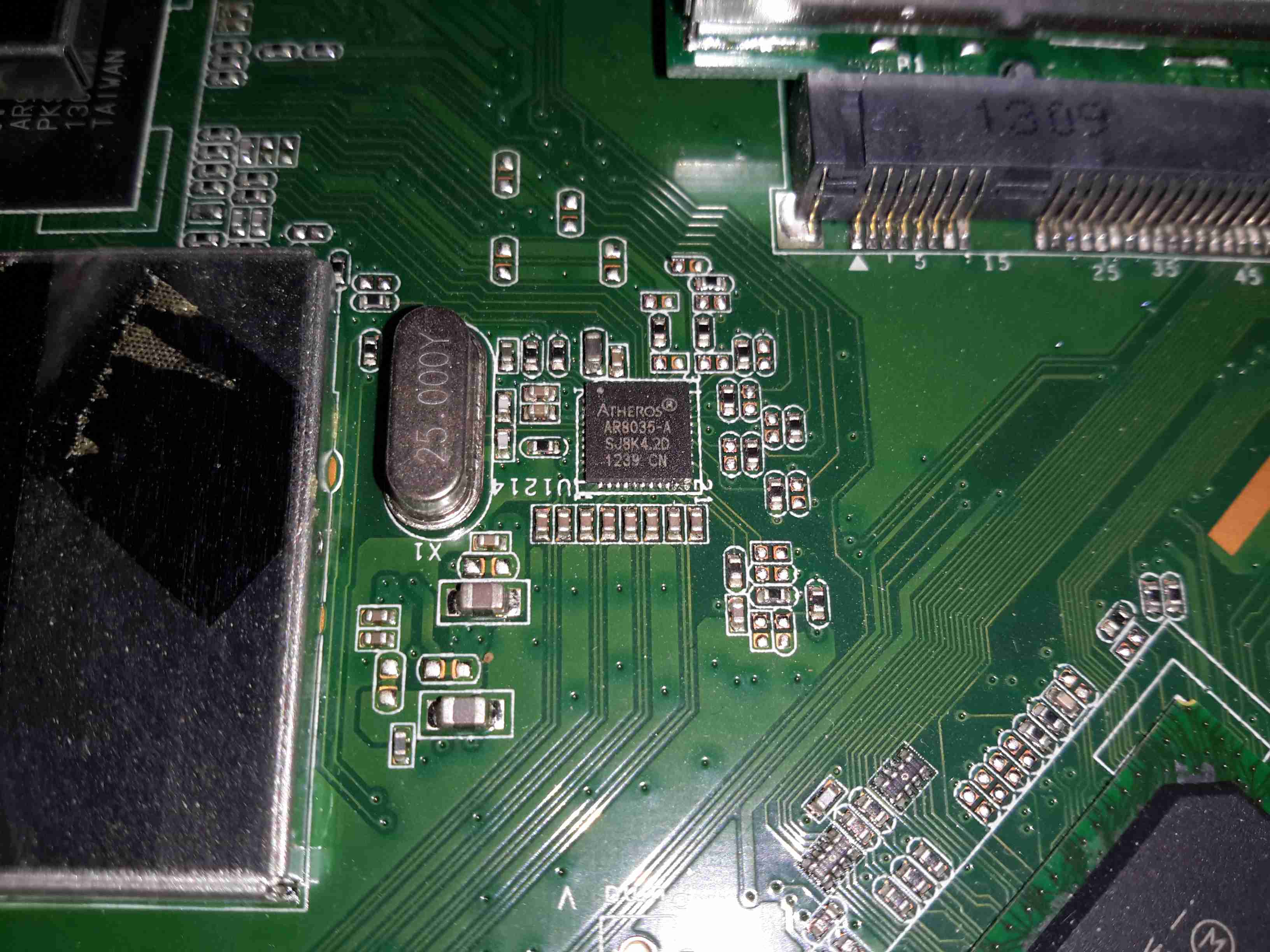
Atheros LAN PHY
A separate Ethernet PHY is located between the SoC & the switch IC.
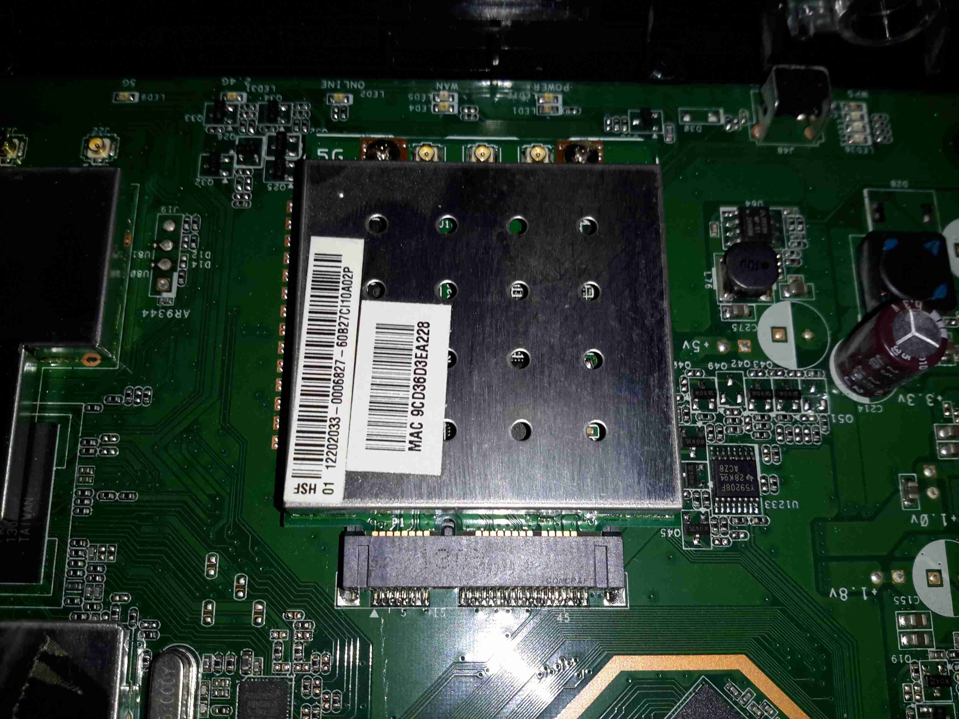
5GHz Radio Card
The 5GHz band is served by a totally separate radio module, in Mini PCIe format, although it’s a bit wider than standard. This module will probably be kept for reuse in another application.
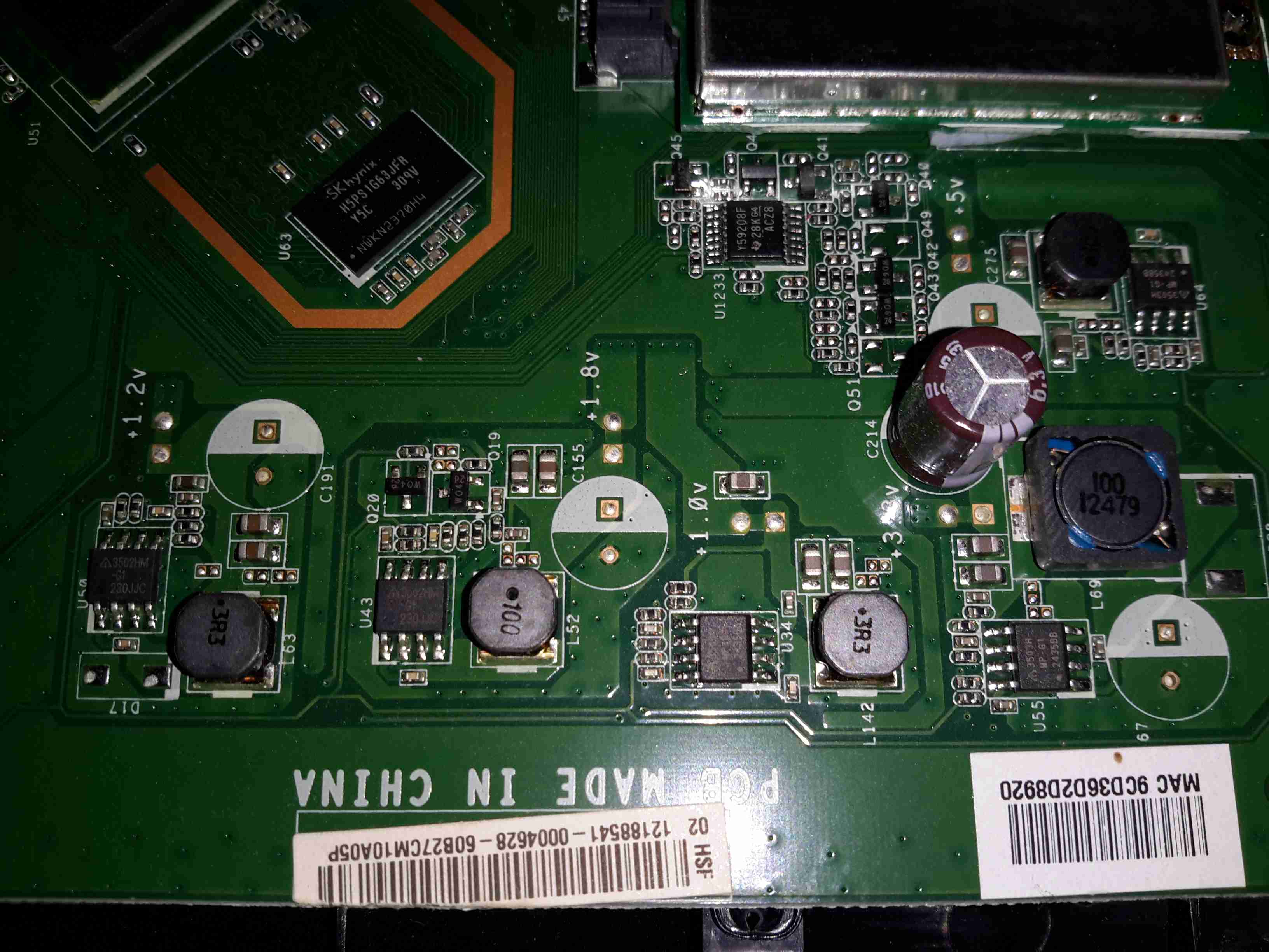
Power Supplies
All down the edge of the board are the multiple DC-DC converters to generate the required voltage rails.
MaxLinear MXL261 Frontend
The DOCSIS frontend is handled by a MaxLinar MXL261 Tuner/Demodulator. More on this IC in my decapping post 🙂
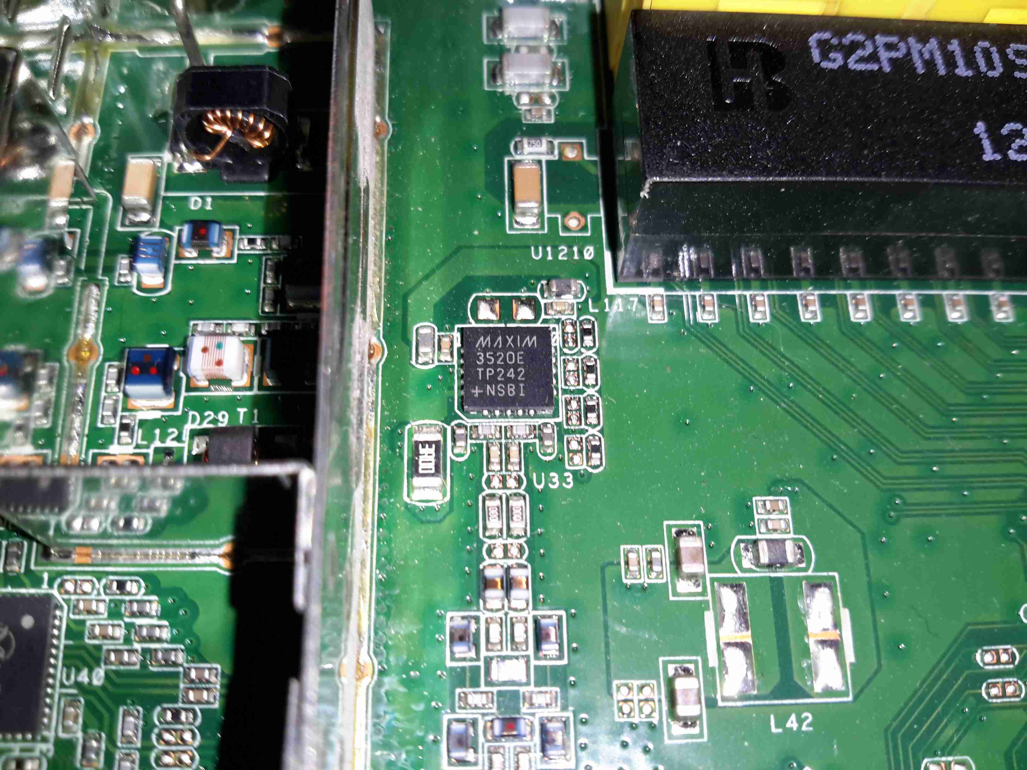
The Unknown One
I’ve honestly no idea what on earth this Maxim component is doing. It’s clearly connected via an impedance matched pair, and that track above the IC looks like an antenna, but nothing I search for brings up a workable part number.
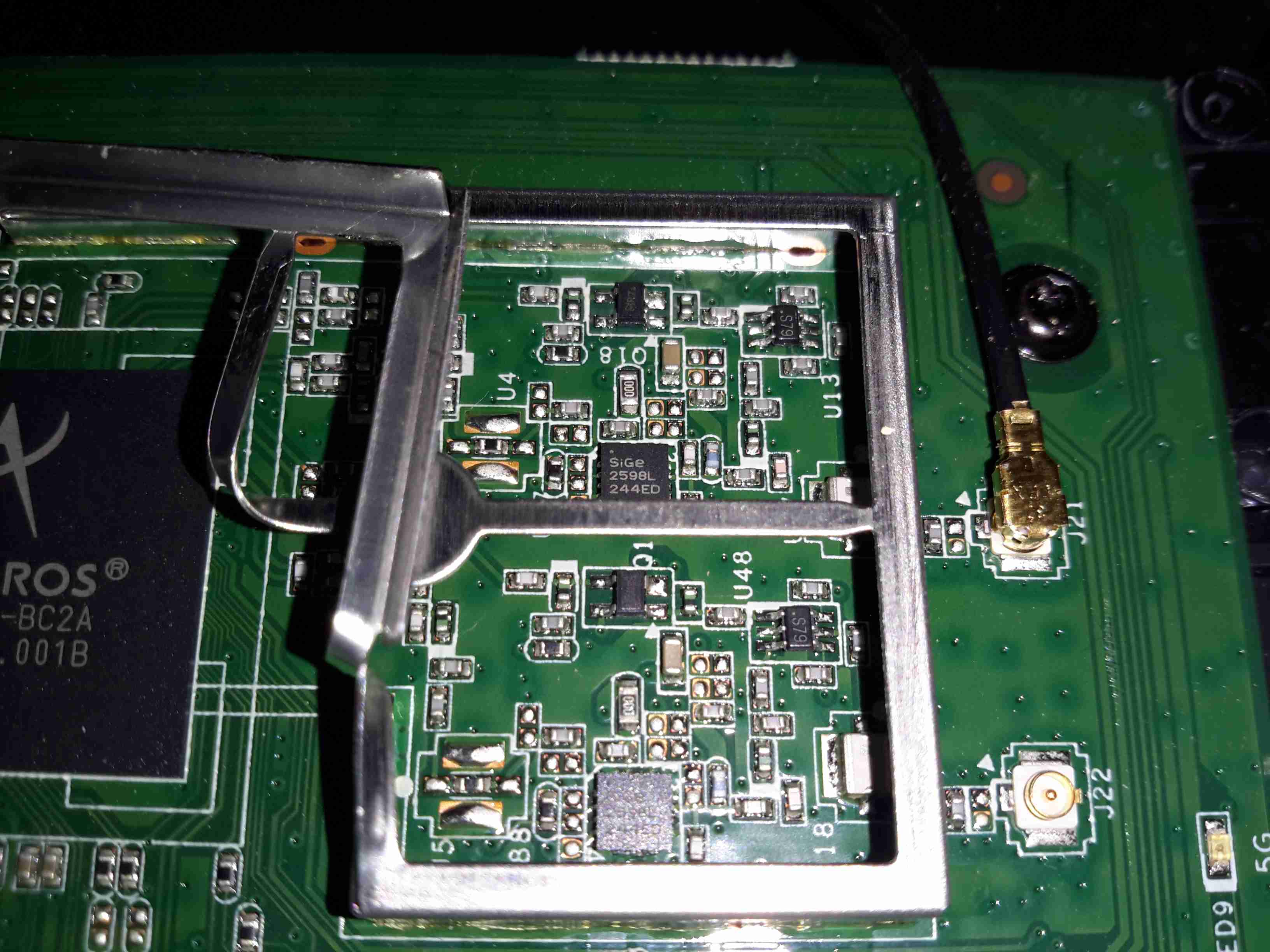
2.4GHz Frontend
The RF switching & TX amplifiers are under a shield, these PA chips are SiGe parts.
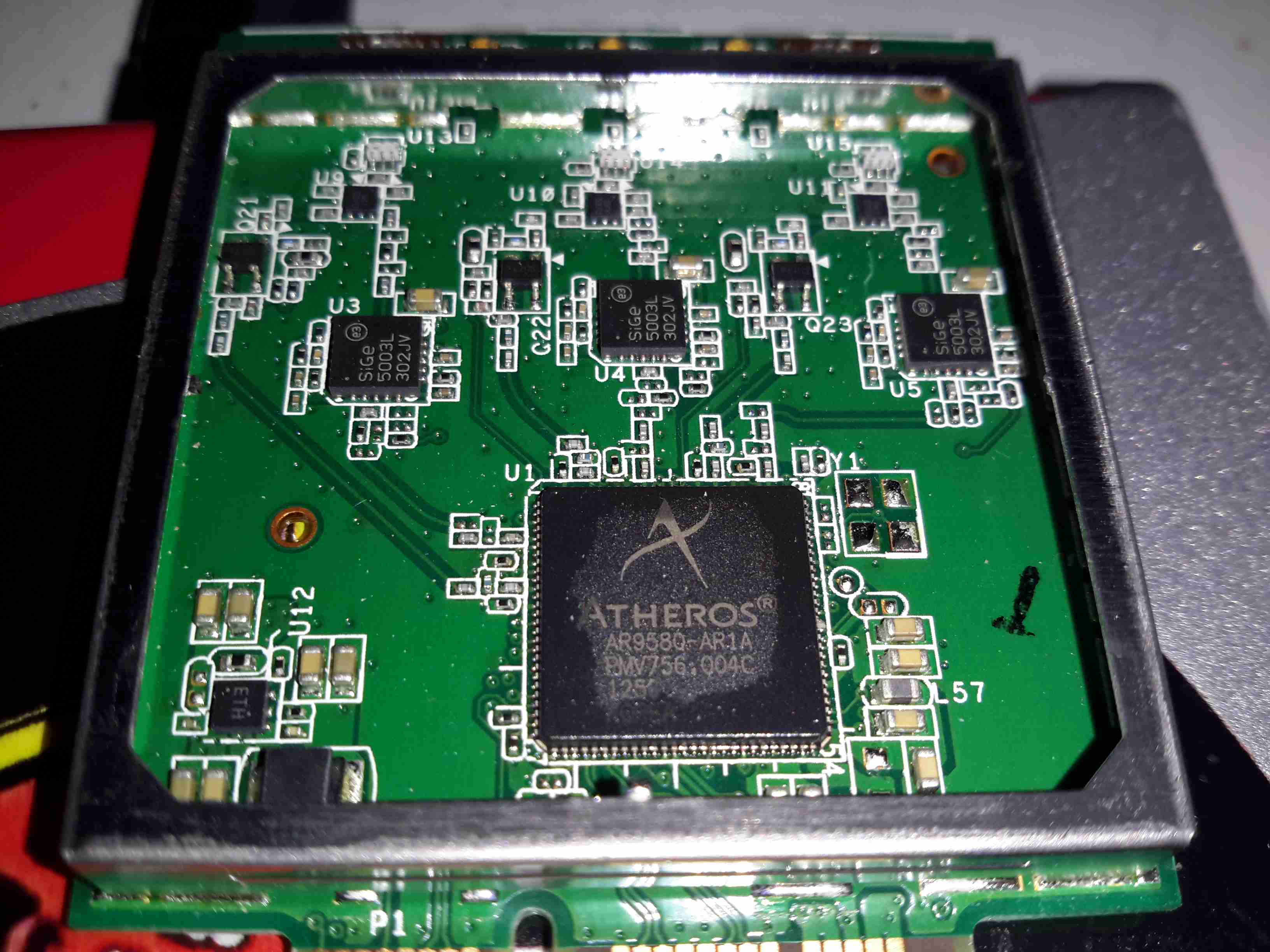
Atheros 5GHz Radio
Pretty much the same for the 5GHz radio, but with 3 radio channels.
Power for a He-Ne laser is provided by a special high voltage power supply and consists of two parts (these maximum values depend on tube size – a typical 1 to 10 mW tube is assumed):
Operating voltage of 1,000 to 3,000v DC at 3 to 8mA.Like most low current discharge tubes, the He-Ne laser is a negative resistance device. As the current *increases* through the tube, the voltage across the tube *decreases*. The incremental magnitude of the negative resistance also increases with decreasing current.
Starting voltage of 5 to 12 kV at almost no current.In the case of a He-Ne tube, the initial breakdown voltage is much greater than the sustaining voltage. The starting voltage may be provided by a separate circuit or be part of the main supply.Often, you may find a wire or conductive strip running from the anode or ballast resistor down to a loop around the tube in the vicinity of the cathode. (Or there may be a recommendation for this in a tube spec sheet.) This external wire loop is supposed to aid in starting (probably where a pulse type starter is involved). There may even be some statistical evidence suggesting a reduction in starting times. I wouldn’t expect there to be much, if any, benefit when using a modern power supply but it might help in marginal cases. But, running the high voltage along the body of the tube requires additional insulation and provides more opportunity for bad things to happen (like short circuits) and may represent an additional electric shock hazard. And, since the strip has some capacitance, operating stability may be impaired. I would probably just leave well enough alone if a starting strip is present and the laser operates without problems but wouldn’t install one when constructing a laser head from components.
With every laser I’ve seen using one of these strips, it has either had virtually or totally no effect on starting OR has caused problems with leakage to the grounded cylinder after awhile. Cutting away the strip in the vicinity of the anode has cured erratic starting problems in the latter case and never resulted in a detectable increase in starting time.
With a constant voltage power supply, a series ballast resistor is essential to limit tube current to the proper value. A ballast resistor will still be required with a constant current or current limited supply to stabilize operation. The ballast resistor may be included as part of a laser head but will be external for most bare tubes. (The exceptions are larger Spectra-Physics He-Ne lasers where the ballast resistors are also inside a glass tube extension, electrically connected but sealed off from the main tube.In order for the discharge to be stable, the total of the effective power supply resistance, ballast resistance, and tube (negative) resistance must be greater than 0 ohms at the operating point. If this is not the case, the result will be a relaxation oscillator – a flashing or cycling laser!
Power supply polarity is important for He-Ne tubes. Electrical behaviour may be quite different if powered with incorrect polarity and tube damage (and very short life) will likely be the result from prolonged operation.
The positive output of the power supply is connected to a series ballast resistor and then to the anode (small) electrode of the He-Ne tube. This electrode may actually be part of the mirror assembly at that end of the tube or totally separate from it. The distance from the resistors to the electrode should be minimized – no more than 2 or 3 inches.
The negative output of the power supply is connected to the cathode (large can) electrode of the He-Ne tube. This electrode may be electrically connected to the mirror mount at that end of the tube but is a separate aluminium cylinder that extends for several inches down the tube. CAUTION: Some He-Ne tubes use a separate terminal for the cathode and sometimes the anode as well, not the mirror mount(s). Powering one of these via the mirror mounts may result in lasing but will also result in tube damage.
Note: He-Ne tube starting voltage is lower and operating voltage is higher when powered with reverse polarity. With some power supply designs, the tube may appear to work equally well or even better (since starting the discharge is easier) when hooked up incorrectly. However, this is damaging to the anode electrode of the tube (and may result in more stress on the power supply as well due to the higher operating voltage) and must be avoided (except possibly for a very short duration during testing).
Every He-Ne tube will have a nominal current rating. In addition to excessive heating and damage to the electrodes, current beyond this value does not increase laser beam intensity. In fact, optical output actually decreases (probably because too high a percentage of the helium/neon atoms are in the excited state). You can easily and safely demonstrate this behaviour if your power supply has a current adjustment or you run an unregulated supply using a Variac. While the brightness of the discharge inside the tube will increase with increasing current, the actual intensity of the laser beam will max out and then eventually decrease with increasing current. (This is also an easy way of determining optimal tube current if you have not data on the tube – adjust the ballast resistor or power supply for maximum optical output and set it so that the current is at the lower end of the range over which the beam intensity is approximately constant.) Optical noise in the output will also increase with excessive current.
The efficiency of the typical He-Ne laser is pretty pathetic. For example, a 2 mW HeNe tube powered by 1,400 V at 6mA has an efficiency of less than 0.025%. More than 99.975% of the power is wasted in the form of heat and incoherent light (from the discharge)! This doesn’t even include the losses of the power supply and ballast resistor.
A few He-Ne lasers – usually larger or research types – have used a radio frequency (RF) generator – essentially a radio transmitter to excite the discharge. This was the case with the original He-Ne laser but is quite rare today given the design of internal mirror He-Ne tubes and the relative simplicity of the required DC power supply.
This particular IC came out of a very old VHF band radio, from the early 90’s. The die was encased in a custom ceramic package, like every other IC in the radio, with a custom part number. I managed to identify it from the markings on the silicon.
Motorola MC68HC11L6
This was a pretty powerful MCU for it’s time, with 16K of onboard ROM, 512 bytes of both RAM & EEPROM, a 16-bit timer, 8-bit ADC, SPI & a MC68HC11 CPU core.
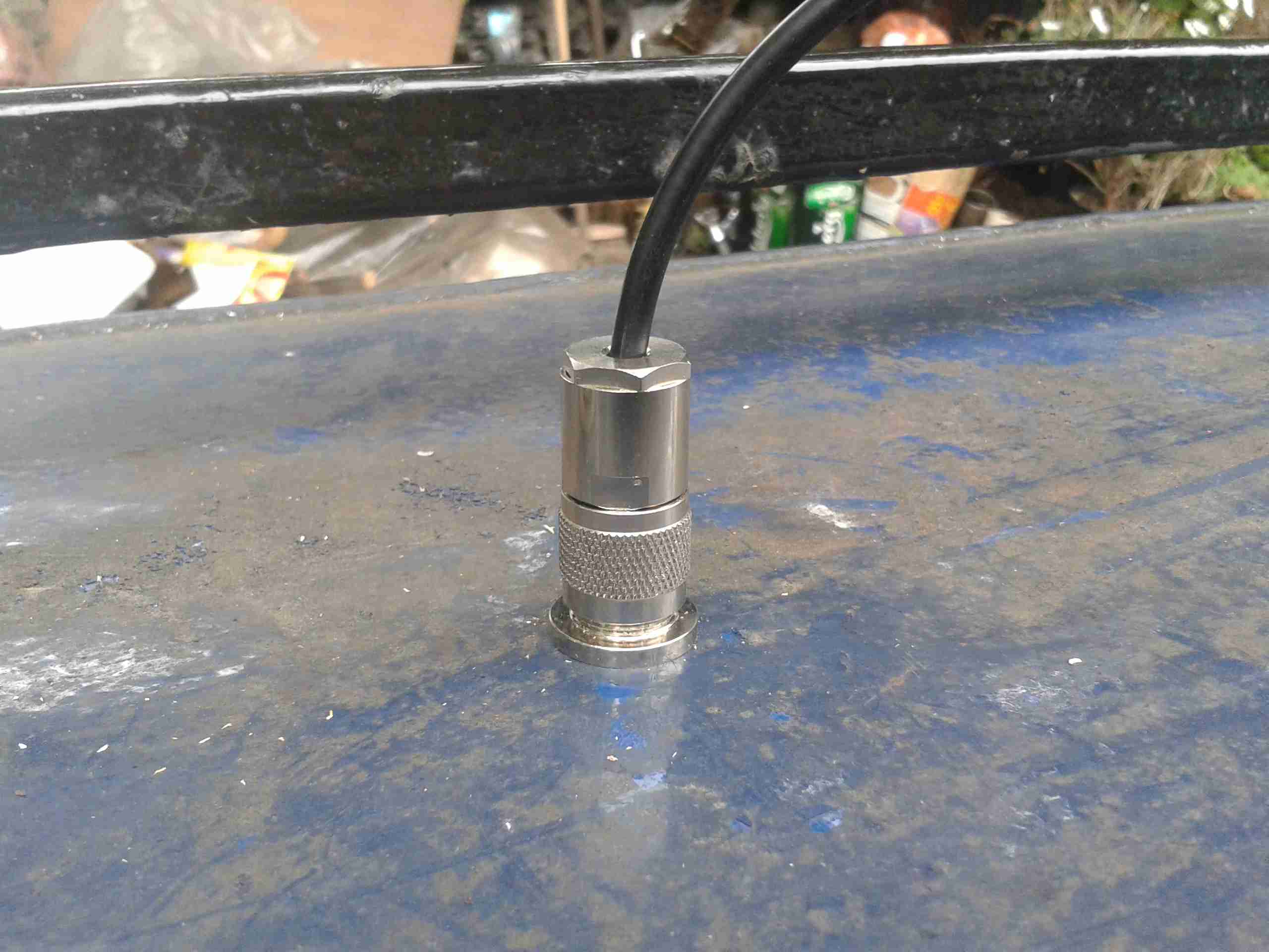
As supplied, the RTL type tuner dongles are a little fragile, especially when they’ve got a rather heavy coax feeder attached for Ham Radio use.
The MCX antenna connectors on the tuner can’t stand up to much abuse, and even the USB plug rips itself from it’s mounts after a while with a heavy weight on the end. Since this dongle sits in my radio go bag, it definitely needed some protection & support.
PCB
The PCB itself is removed from it’s flimsy plastic casing, the USB plug is desoldered from the board.
To the exposed pads, a USB cable is soldered, giving much more flexibility in where the tuner is placed.
Instead of using the MCX antenna connector on the PCB, the coax is stripped & soldered direct to the PCB itself, as this connector has become unreliable.
N-Connector
To get the RF into the device, the case is fitted with an N connector, as is everything else in my shack.
Boxed
The box used is a surplus one which previously housed an electronic lighting transformer. This would be very easy to waterproof as well, for more protection against outdoor use.
Since the boat was still running it’s internal network on 10/100M speeds, an upgrade was decided on, the internal WiFi signal strength was also pretty poor further than a few feet from the NOC.
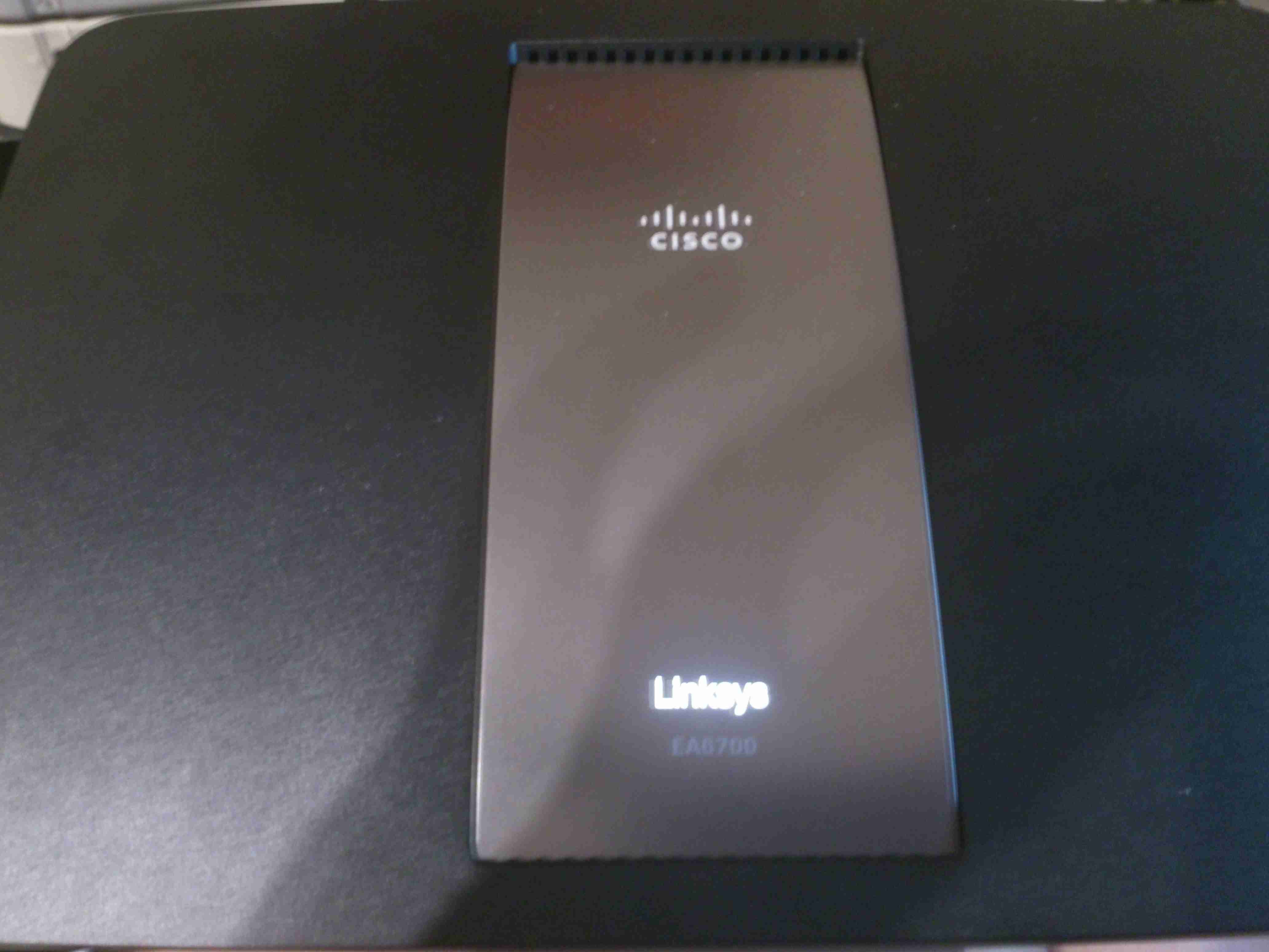
The new router is a Cisco/Linksys AC1750 model, with gigabit networking, and full 802.11ac 2.4/5GHz Wireless. This router also has a built in media server, print server, USB3 & USB2.
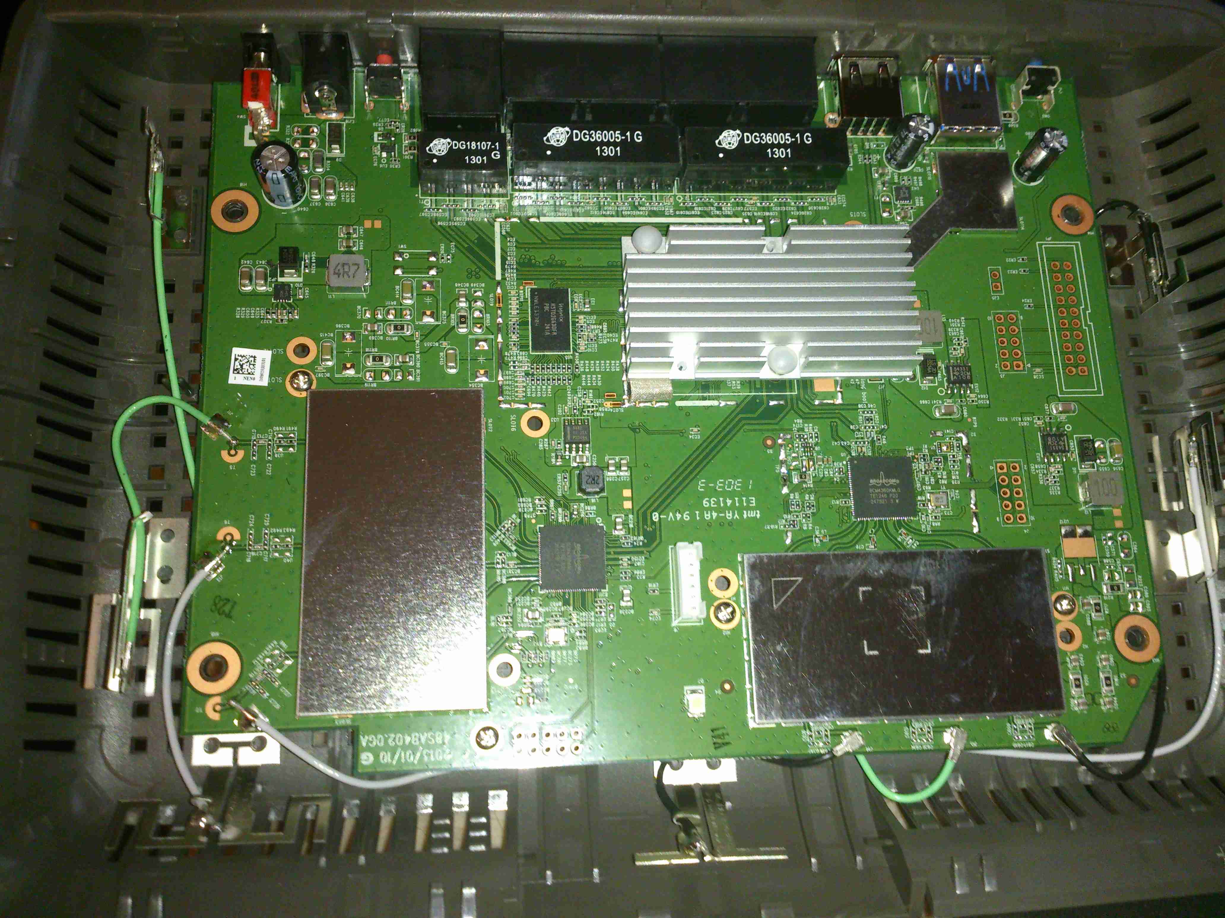
PCB Overview
Teardown time! Here’s the router with the cover removed. Most of the fun stuff is hidden under the shields, but these aren’t fully soldered down & the covers are removable. The 6 antennas can be seen spaced around the edge of the housing, the main CPU is under the large heatsink upper centre. The radio power amplifier stages are underneath the shields, while the main RF transceivers are just outside the shields.
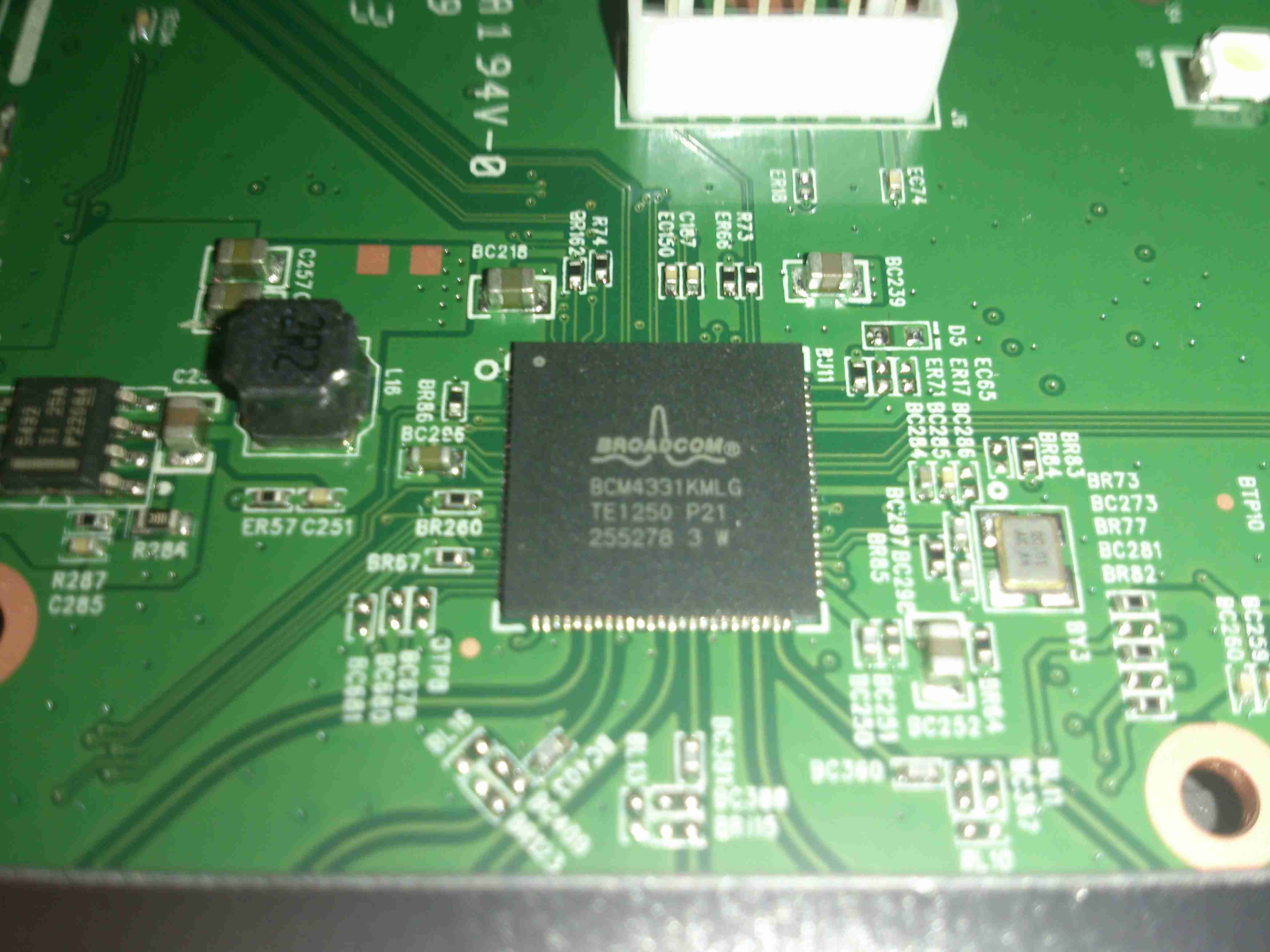
2.4GHz Transceiver
Wireless N is provided by a Broadcom BCM4331, this provides full dual-band 3×3 802.11n support. Being 3×3 it is actually 3 separate transceivers in a single package, to get much higher throughput rates of 600Mbit/s.
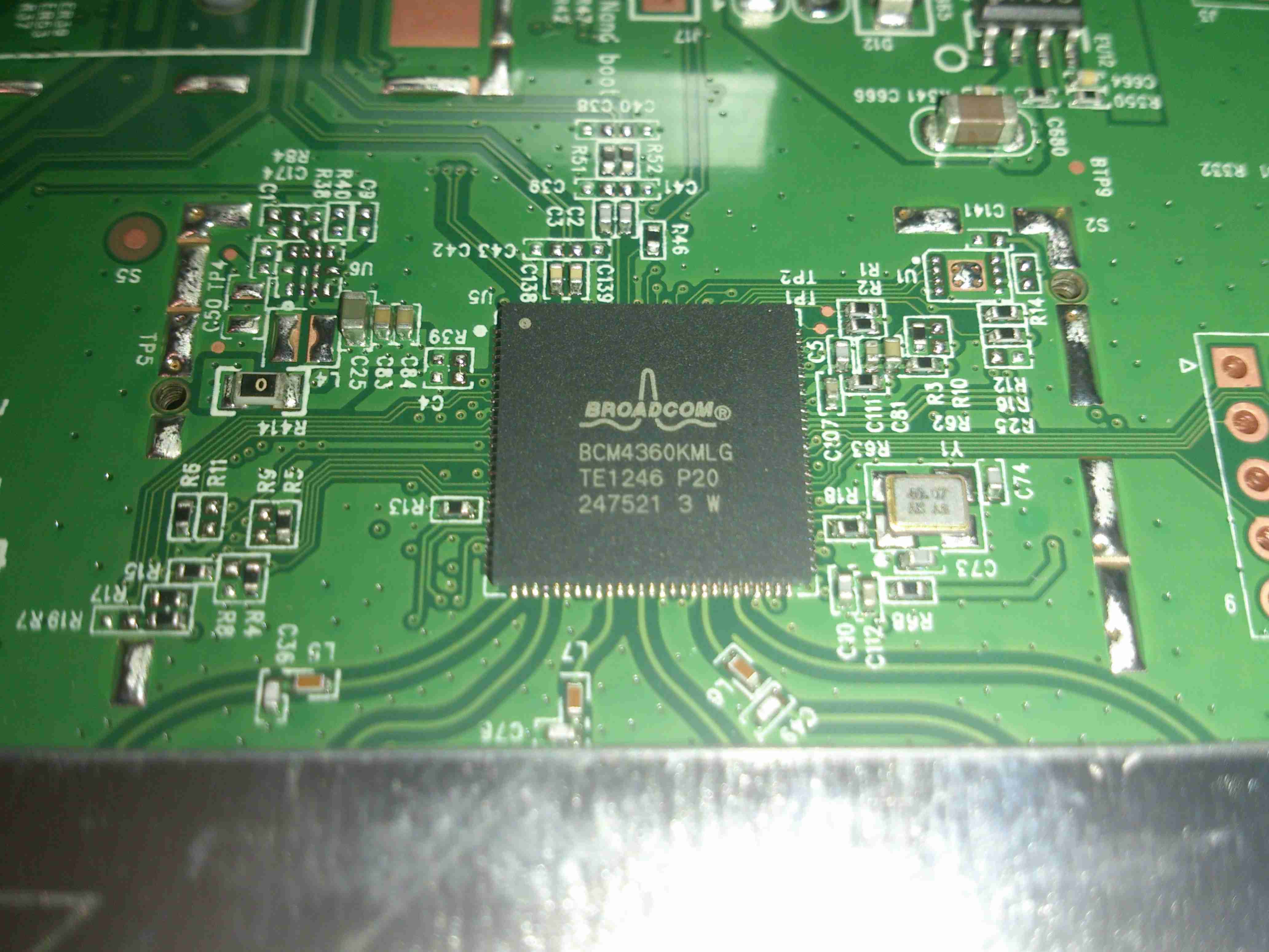
5GHz Transceiver
Wireless AC is provided by it’s sister IC, the BCM4360, with throughput speeds of 1.3Gbit/s. Both of these transceiver ICs connect back to the main CPU via PCI Express.
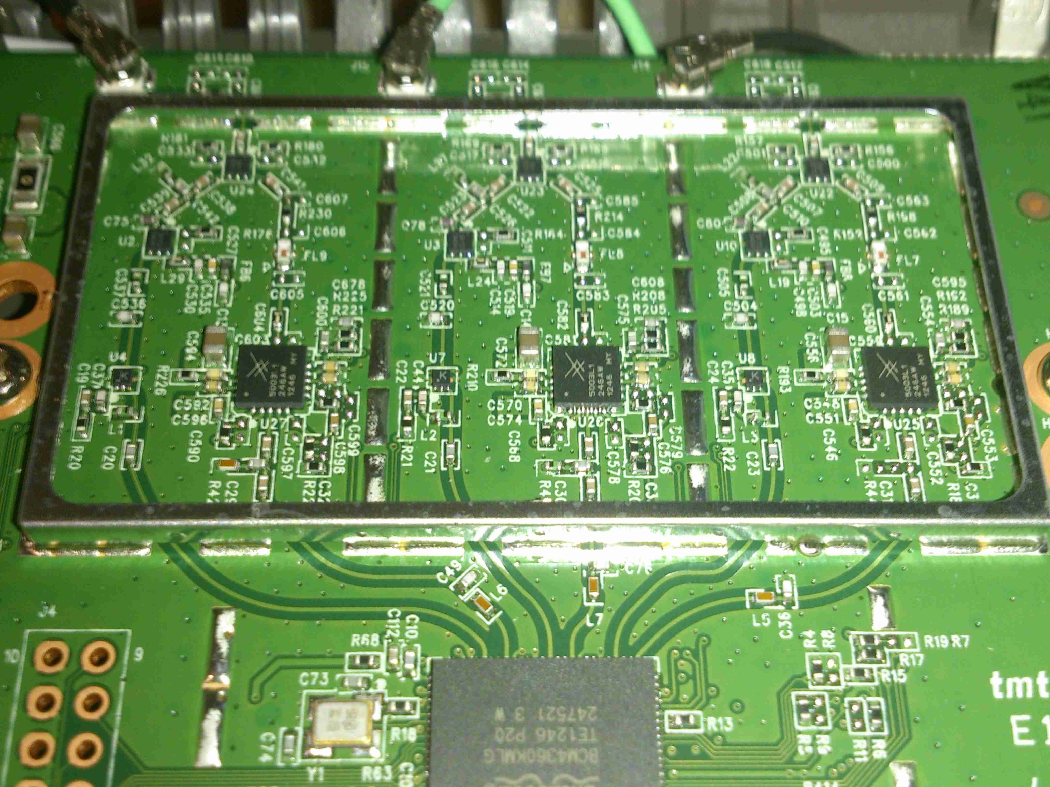
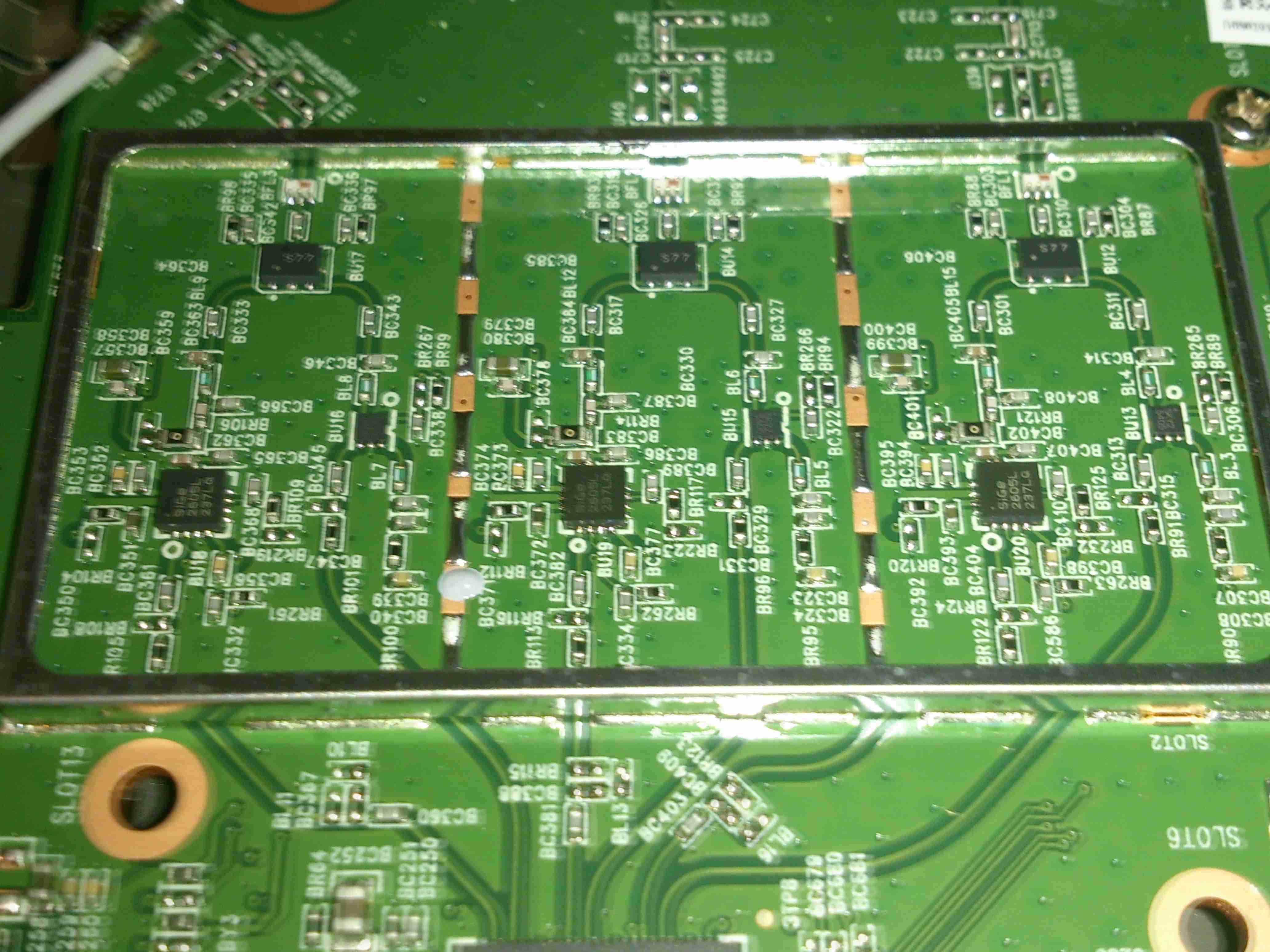
5GHz Power Amplifiers
To get increased range, there are a trio of Skyworks SE5003L +23dBm 5GHz power amplifier ICs under the shield, along with the TX/RX switching & antenna matching networks. Heatsinking for these is provided by a sink screwed to the bottom side of the PCB. The outputs to the antennas can be seen at the top of the image.
2.4GHz Power Amplifiers
The 2.4GHz section is fitted with a trio of Skyworks SE2605L +23dBm 2.4GHz power amplifiers, with a similar heatsink arrangement under the board. Unlike the 5GHz section, the 2.4GHz antenna feeds are soldered to the PCB here instead of using connectors.
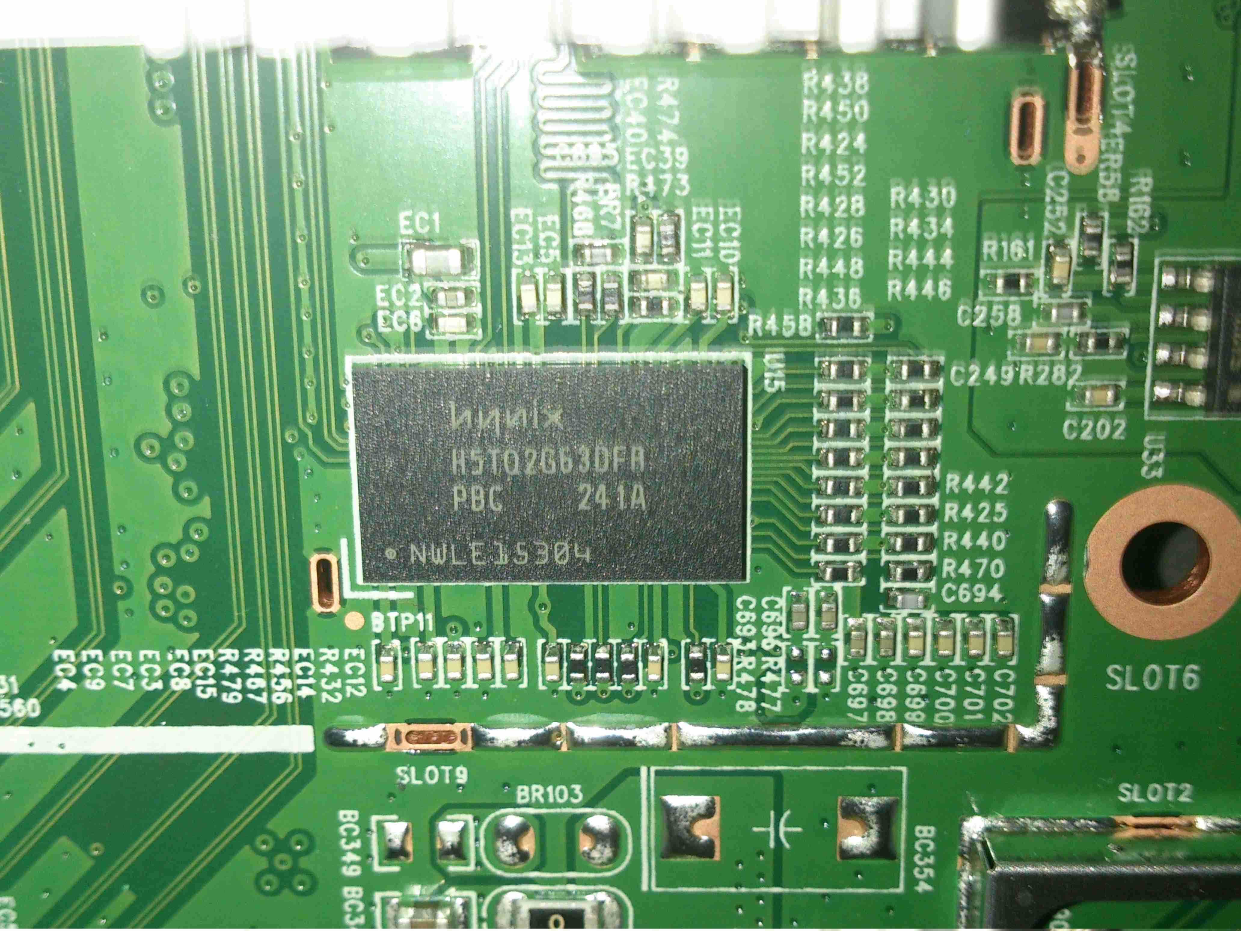
Main CPU
The main CPU is a BCM4708 Communications Processor from Broadcom, as for the other Broadcom chips in this router, very little information is available unless under NDA, but I do know it’s a dual core ARM Cortex A9 running at 1GHz, with built in 5-port gigabit ethernet switch.
CPU RAM
Working RAM for the processor is a Hynix H5TQ2G63DFA 256MB part.
More to come on the installation of the new networking, with it’s associated 4G mobile gateway connection system.
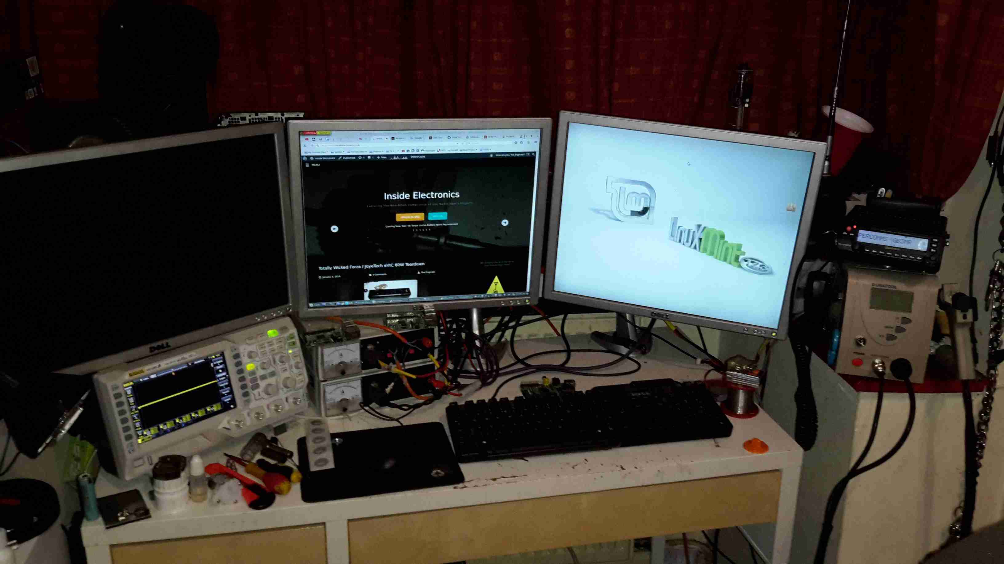
Main radio of course is housed on the left, it’s partially hidden under my currently over-populated breadboard.
All 3 monitors are linked to the same PC, using a pair of video cards. This is a very flexible system with so much screen real estate.
Main system power is provided by the pair of power supplies next to the radio – these are homebrew units using surplus switched mode PSU boards. Check my previous posts for more details.
Power Supplies
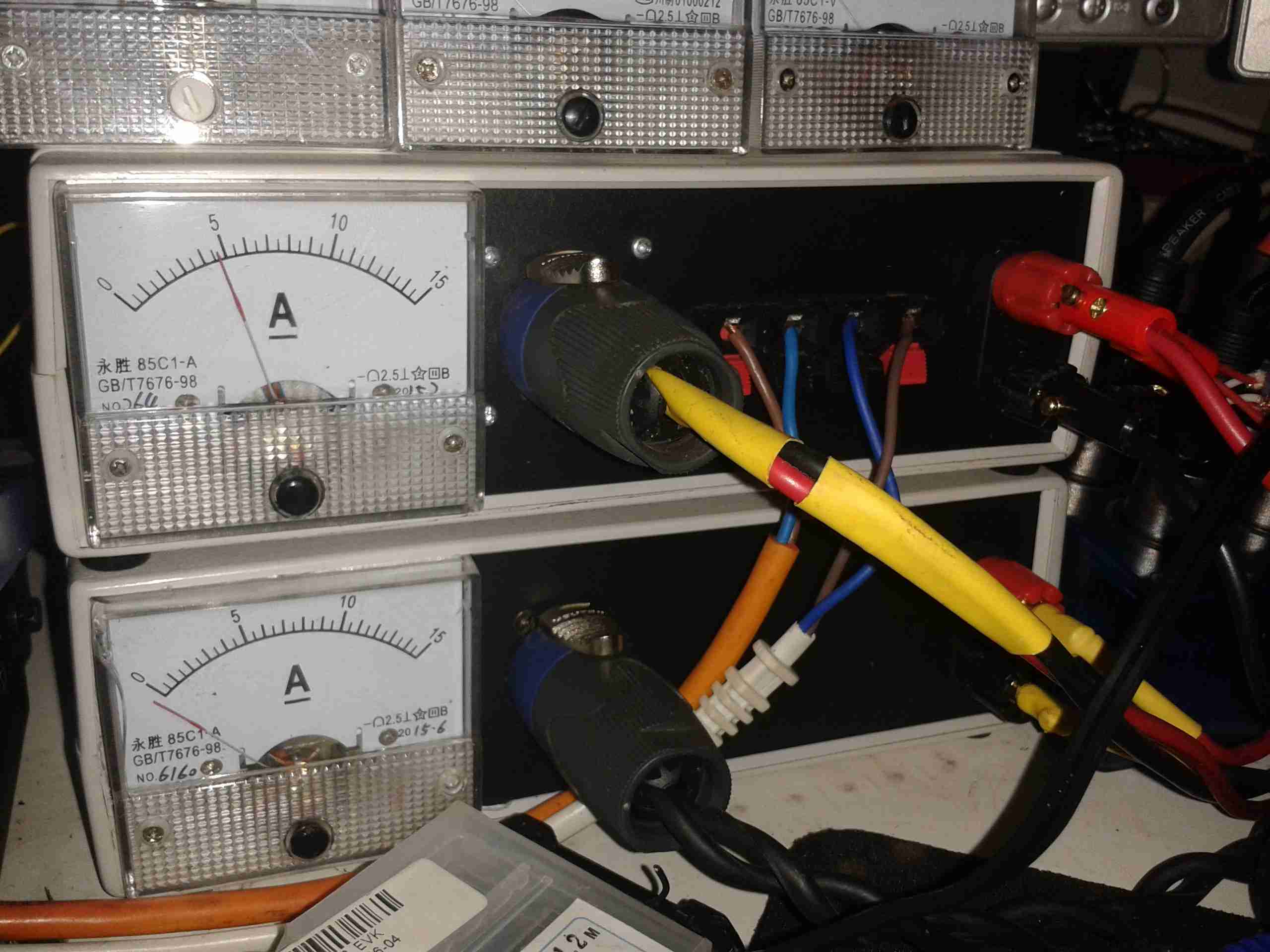
The mainpowersupply system. These two supplies are cross connected, giving a total DC amperage of 30A at 13.8v. There is also a link to a large 220Ah lead-acid battery bank (orange cable), to keep me on the air during power outages. This cable is getting upgraded to something more beefy shortly. The white cable is currently supplying power to my onlineradiation monitor.
The main high-currentDC outputs are the Speakon connectors next to the meters. The top one is powering the radio directly, the bottom is linked through to my 12v distribution box for lower current loads, such as the oscilloscope, audio amplifiers, tools, etc.
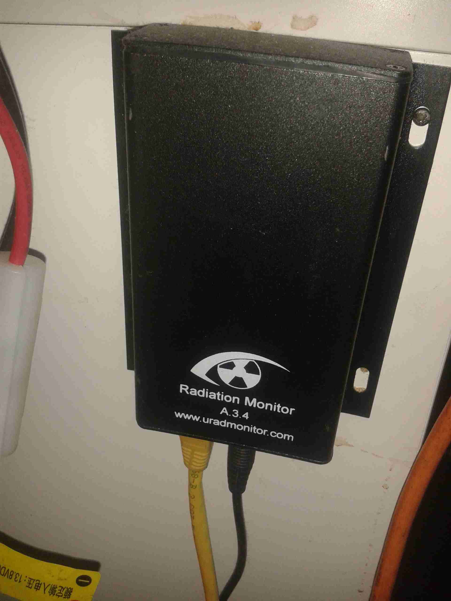
Radiation Monitor
Attached to the side of the desk is the radiation monitor itself.
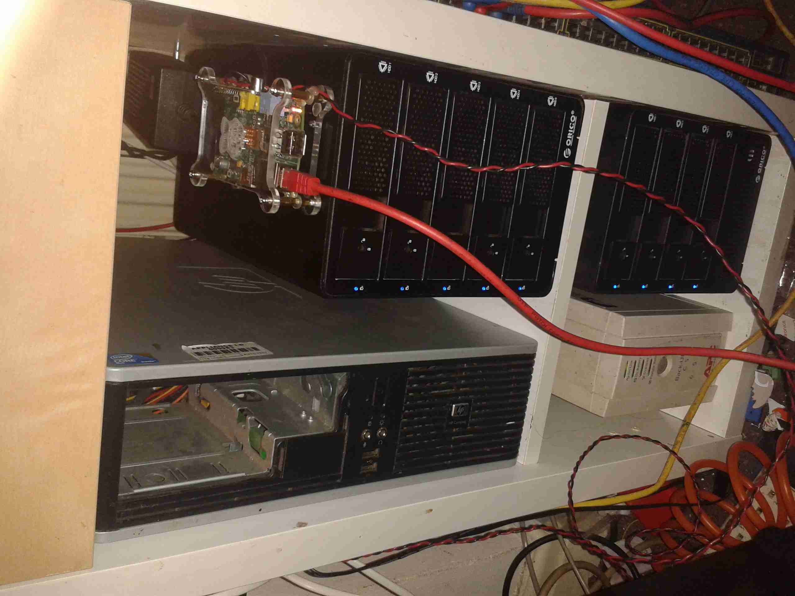
Core NAS
Under the radio is the core NAS of the network. It’s an array of 9 4TB disks, in RAID6, giving a total capacity after parity of 28TB. This provides storage & services to every other machine in the shack, the Raspberry Pi on top of the disk array is doing general network housekeeping & monitoring, also generating the graphs for the Radiation Monitor page. A Cisco 48-portswitch is partially out of frame on the right, providing 100MB Ethernet to the devices that don’t require gigabit.
Here’s the final bit of the radio install now the required parts have arrived!
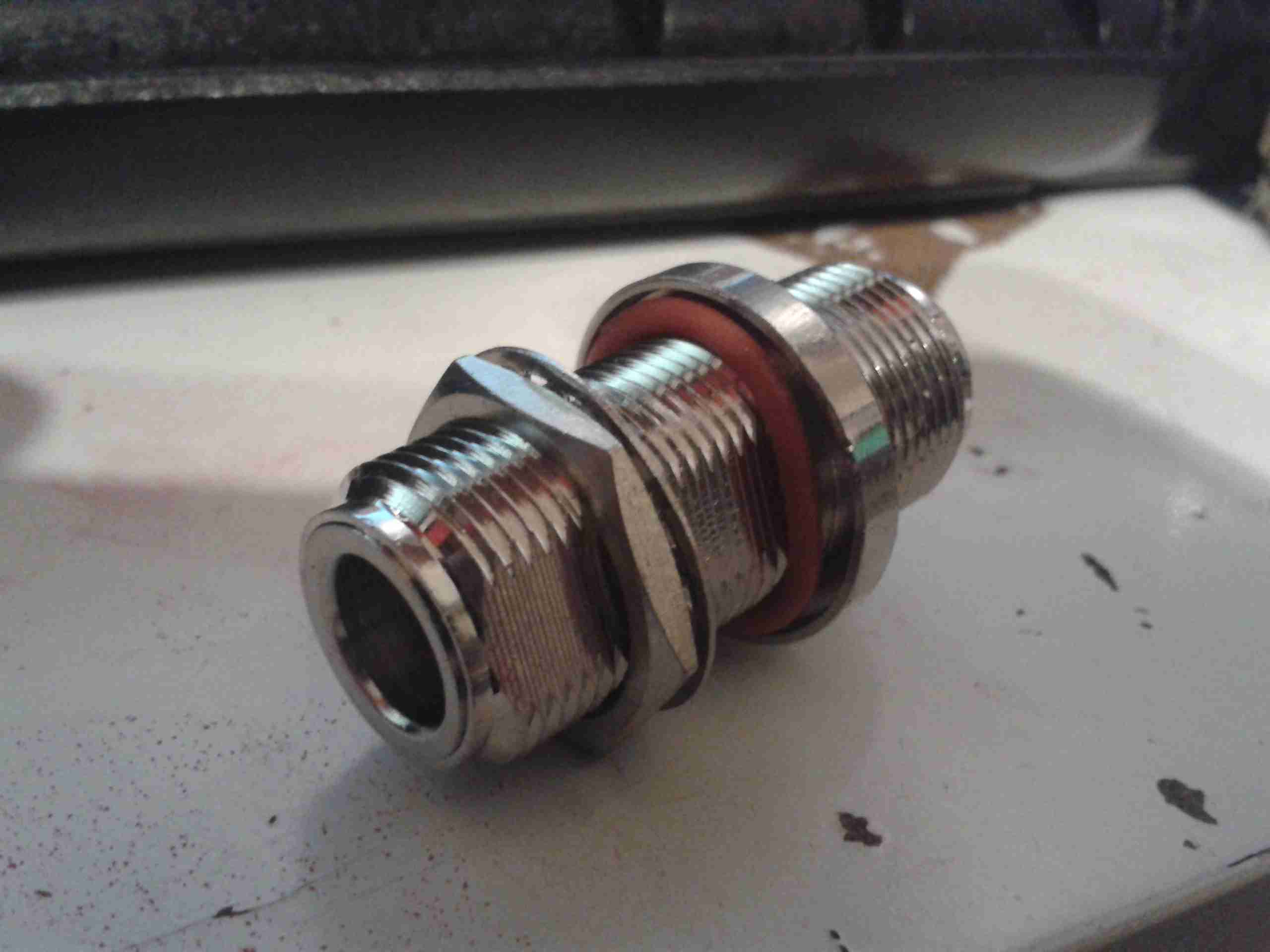
The radio being inside, we needed a reliable way to route the antenna coax through the hull to the external antenna, I managed to find some N-type bulkhead connectors, that are perfect for this job:
Bulkhead Fitting
This fitting will allow for simple disconnection of the antenna for service, and N-type connectors are water resistant.
Hole
A hole was drilled in a suitable location with a cone drill. The steel here is pretty heavy, at 5mm. A spot between the handrail & the sliding roof was picked since there’s less chance of the fitting being knocked by any flying ropes, windlasses or crew members 😉
Bulkhead Connector
Here’s the connector fitted into it’s hole. The O-ring under the flange seals against the steel hull to prevent water getting through to the radio equipment on the other side.
Completed
Completed connection to the antenna. The short run to the radio underneath (~18″) is RG213, but I’ve used RG-58 on the antenna itself since it’s more flexible. The antenna is only a metre or so away so losses shouldn’t be much of an issue.
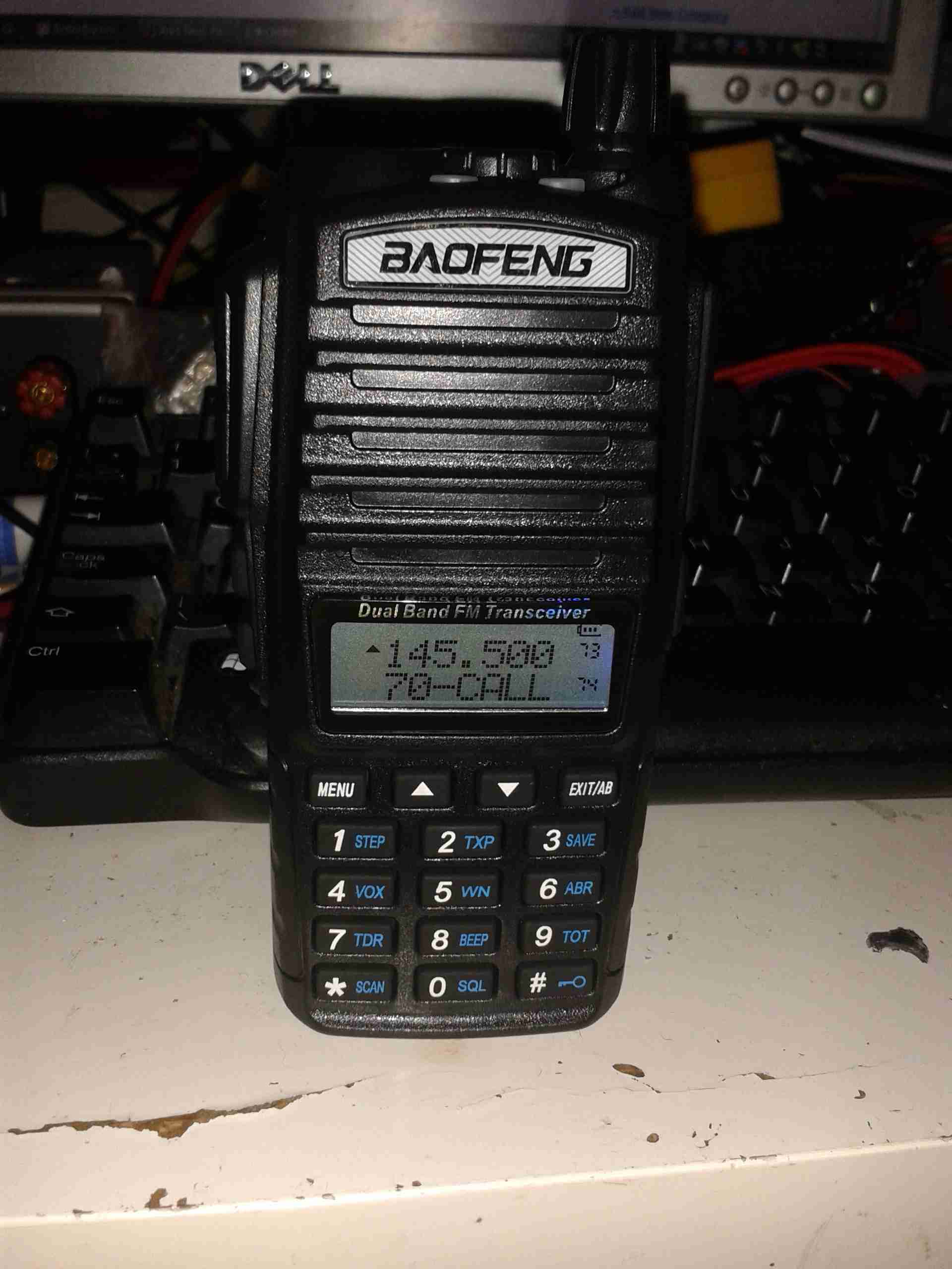
Thanks to Lewis over at Distant Signal Radio, the bad influence he is on my bank balance ;), I’m the proud new owner of a new Baofeng. This time it’s the UV-82.
This radio is a little different from the other Baofengs I have. Here are the main differences:
Dual PTT – This one is going to take some getting used to 😉
Higher capacity battery pack
A more rugged, commercial feel
This radio has a different method of selecting the VFO mode – holding the menu key while the unit is powered on. This is a little awkward, but since I only usually use my local repeaters when I’m mobile, it’s not much of an issue.
UV-82
Here’s the radio itself, it has a much more commercial feel to it than the UV-5Rs, and it’s slightly bigger. Mainly due to the use of a larger standard battery & larger loudspeaker.
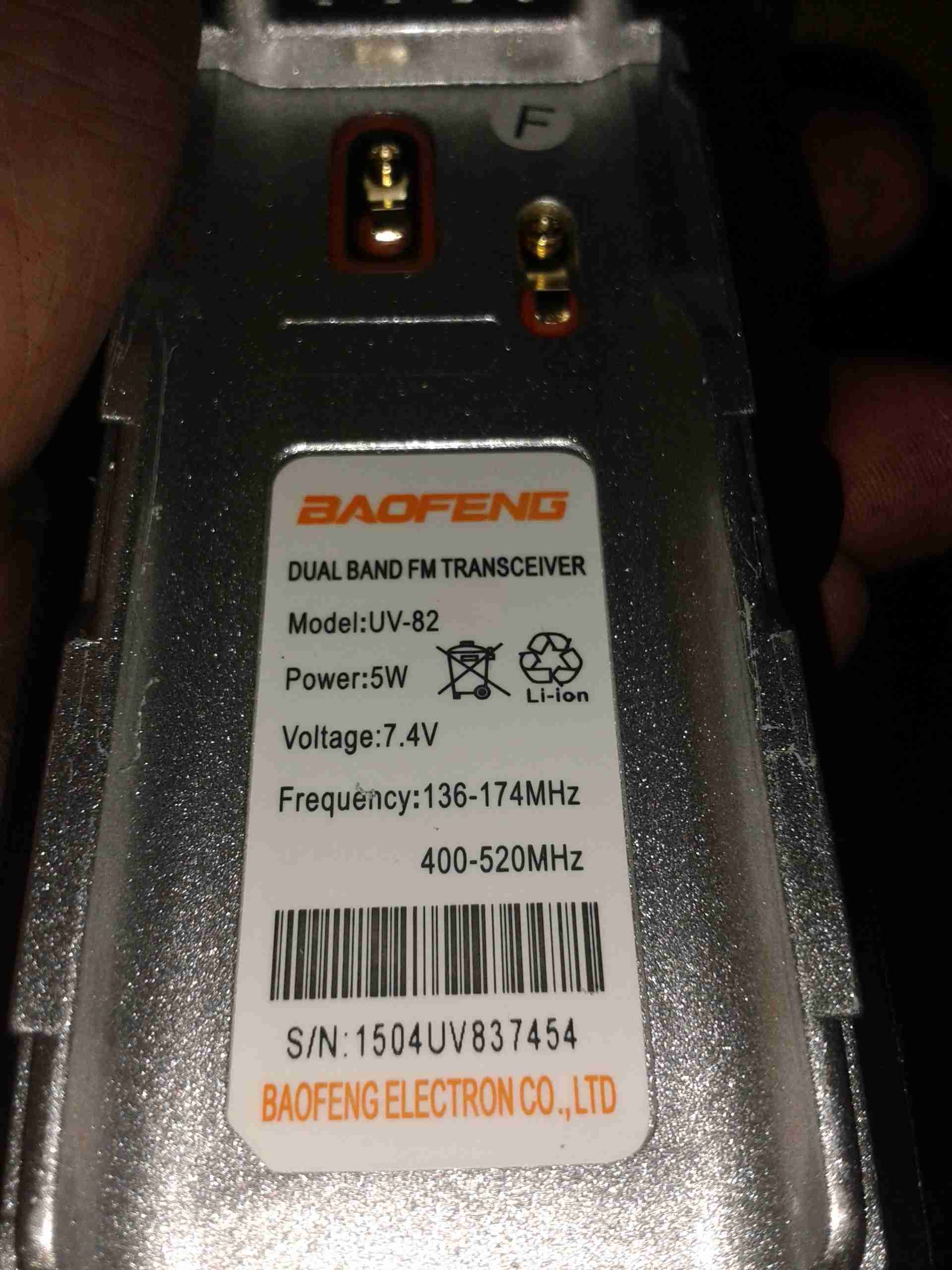
Spec Label
Back of the unit with the spec label. As per usual Baofeng are a bit conservative with the power ratings, more to come on that below.
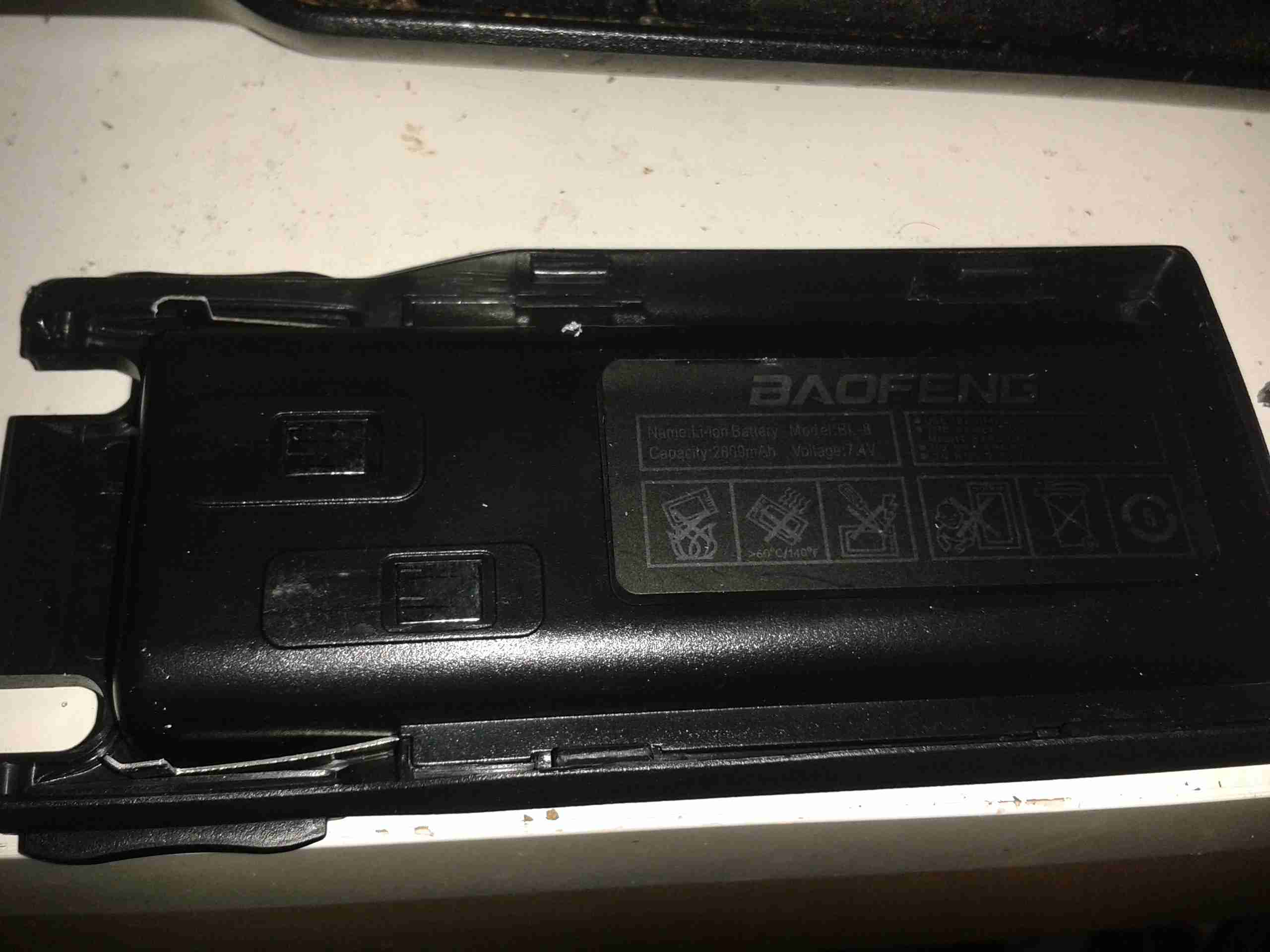
Battery Pack
Here’s the battery pack, a 2-cell lithium-polymer unit. This has a bigger capacity than the standard UV-5R battery, at 2800mAh.
Here are the power settings as measured by my GY-561. Frequencies used are 145.500 & 433.500
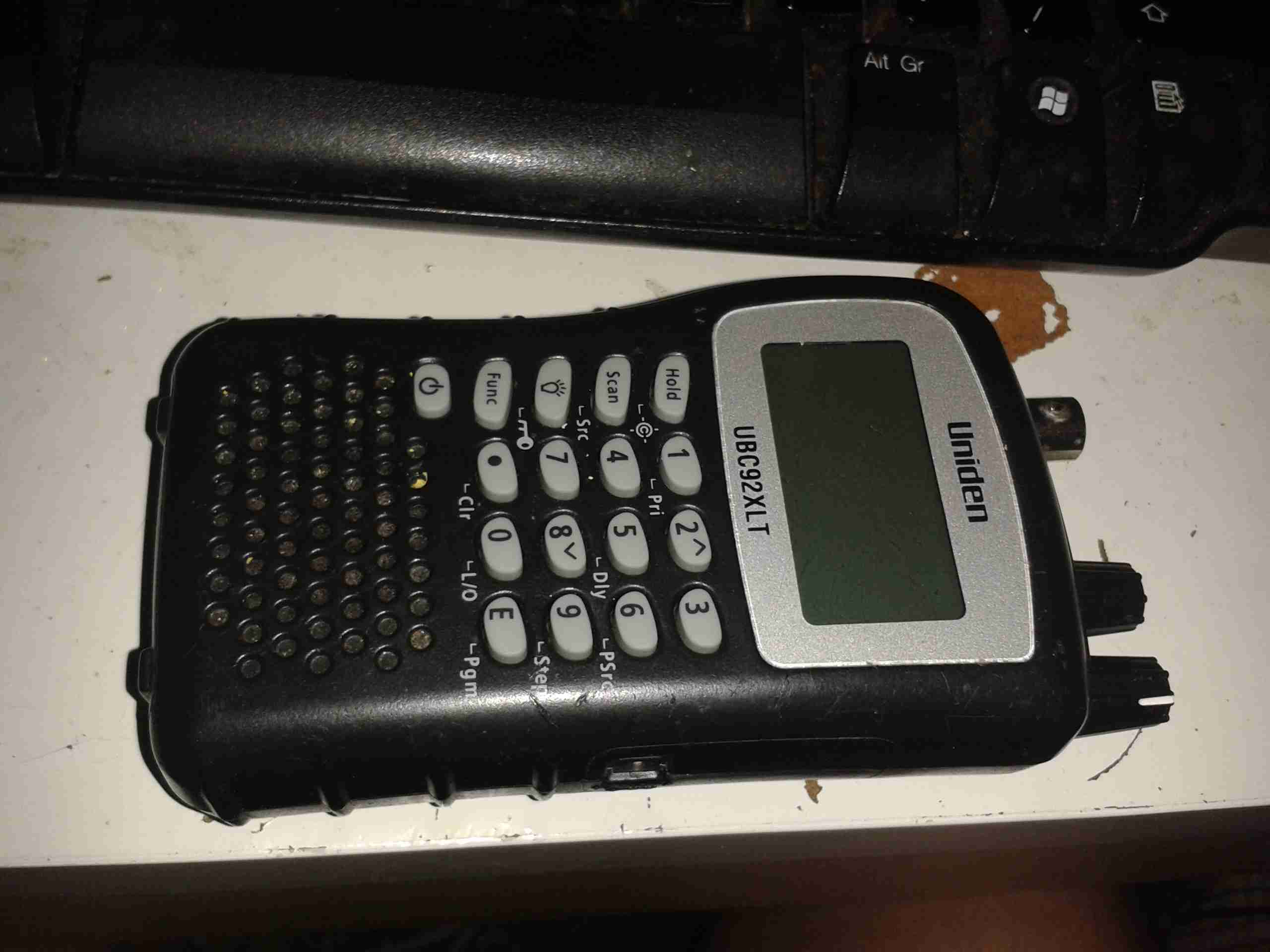
One bit of my equipment that I’ve never looked into is my scanner, a handheld Uniden unit. I got this when Maplin Electronics had them on special offer a few years ago.
Uniden Scanner
Here’s the scanner itself, roughly the same size as a usual HT.
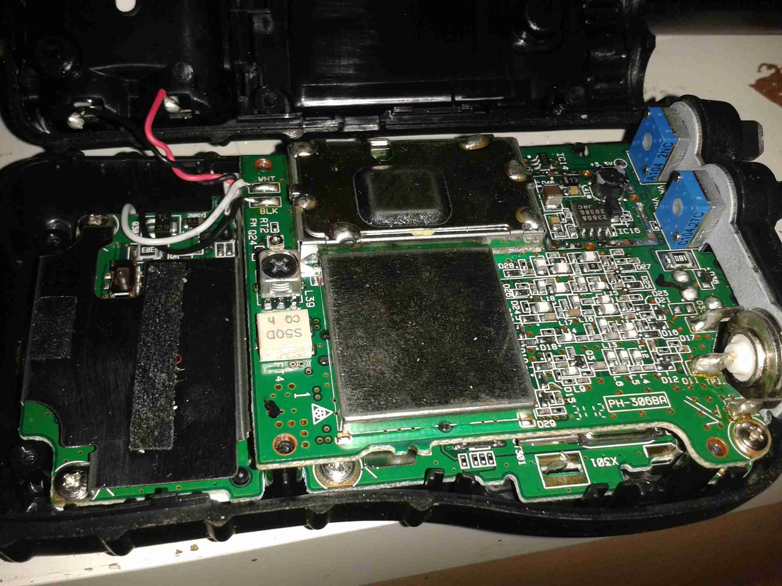
Back Cover Removed
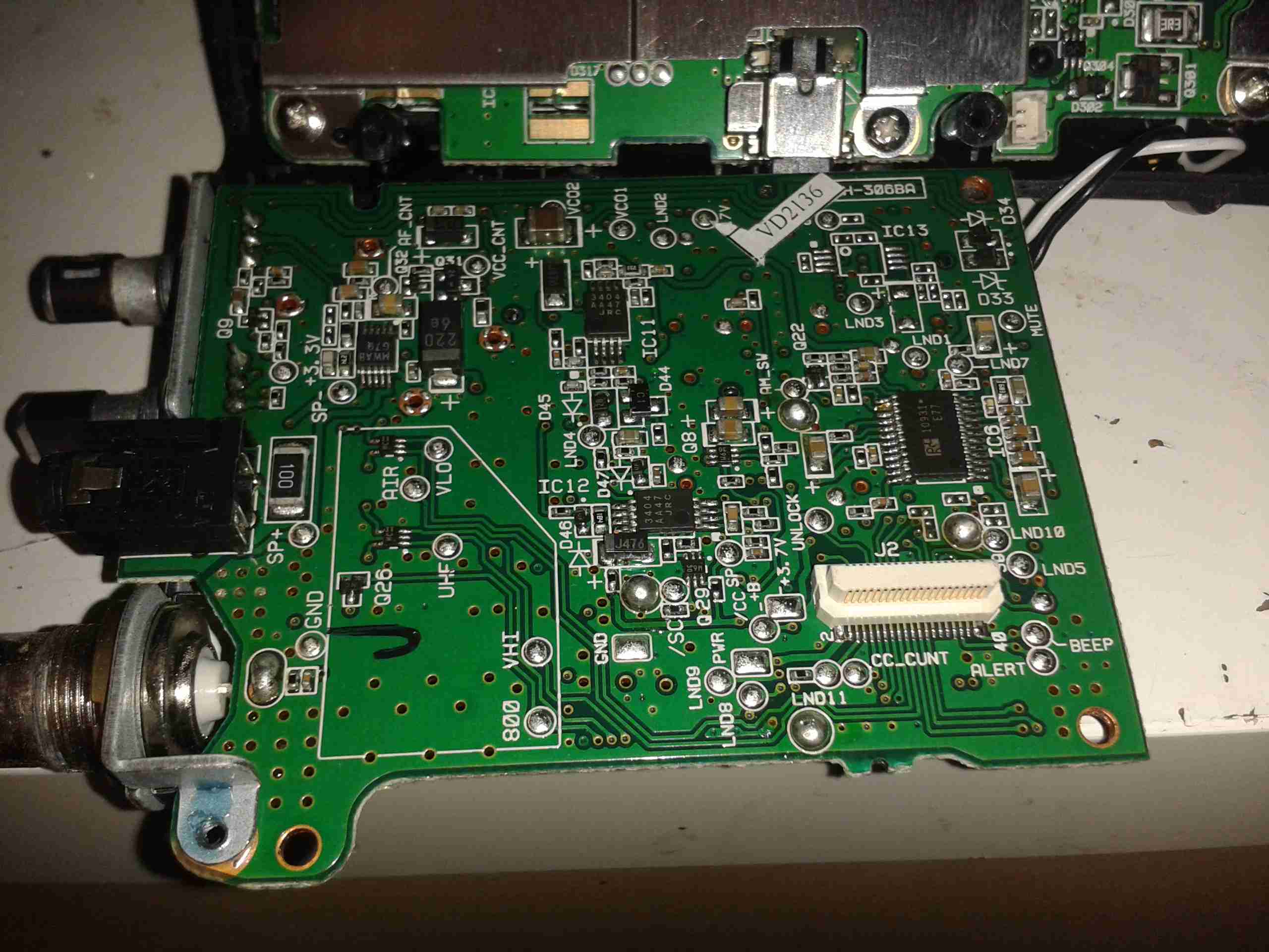
Here the back cover has been removed, and the main RF board is visible at the top of the stack. Unfortunately the shielding cans are soldered on this unit, so no looking under there 🙁
On the right hand side of the board next to the antenna input is the main RF filter network, and it’s associated switching. The RF front end is under the shield closest to the front edge.
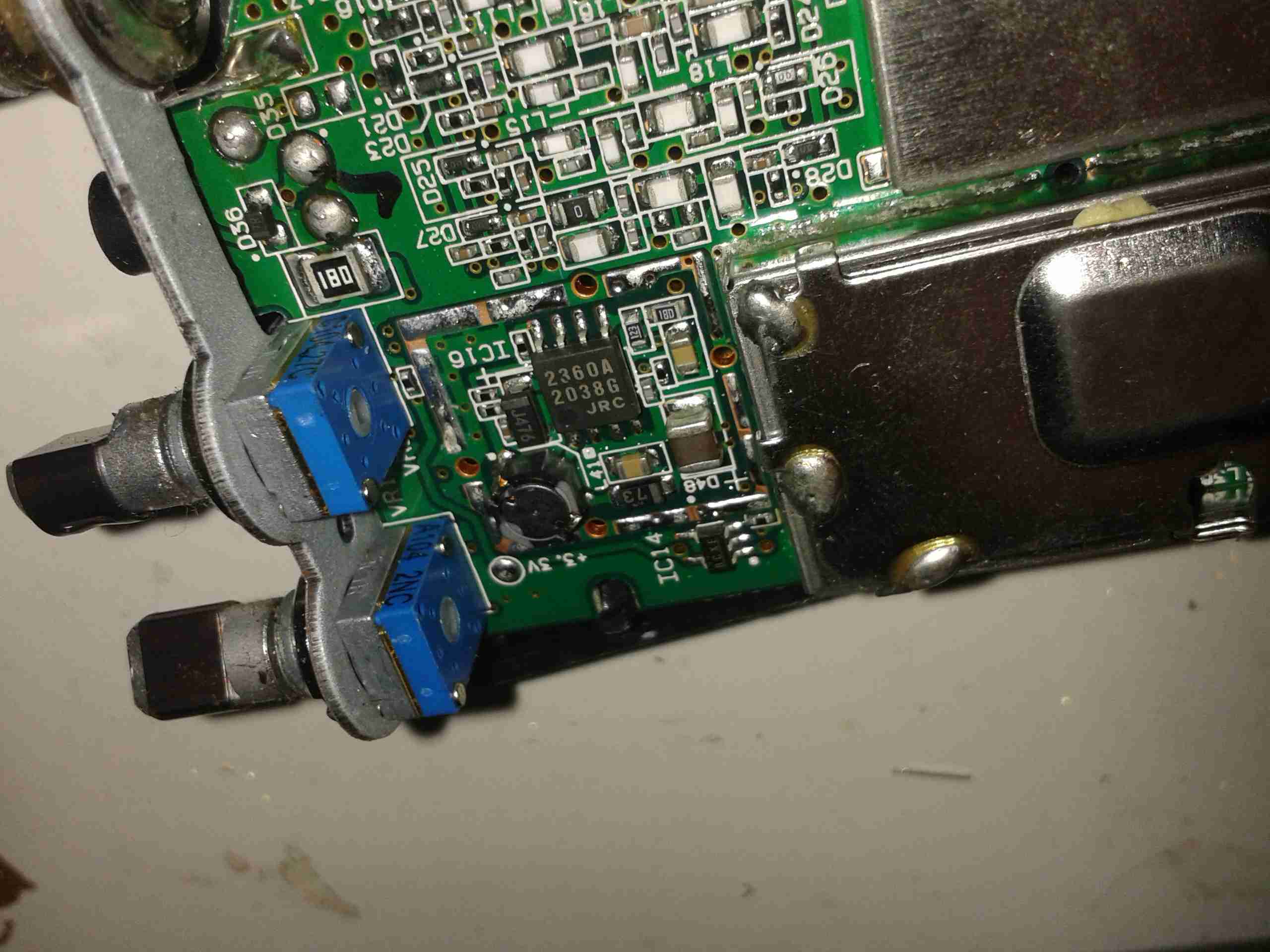
Controls & 3.3v Regulator
On the other side of the PCB is the Volume & Squelch potentiometers, along with a dedicated 3.3v switching supply. An NJM2360A High Precision DC/DC converter IC controls this one. A 3.3v test point is visible next to the regulator.
RF Board Reverse
Here’s the backside of the RF board, some more interesting parts here. There’s a pair of NJM3404A Single Supply Dual Op-Amp ICs, and a TK10931V Dual AM/FM IF Discriminator IC. This is the one that does all the back-end radio functionality. The audio amplifier for the internal speaker & external headphone jack is also on this PCB, top left. A board-to-board interconnect links this radio board with the main control board underneath.
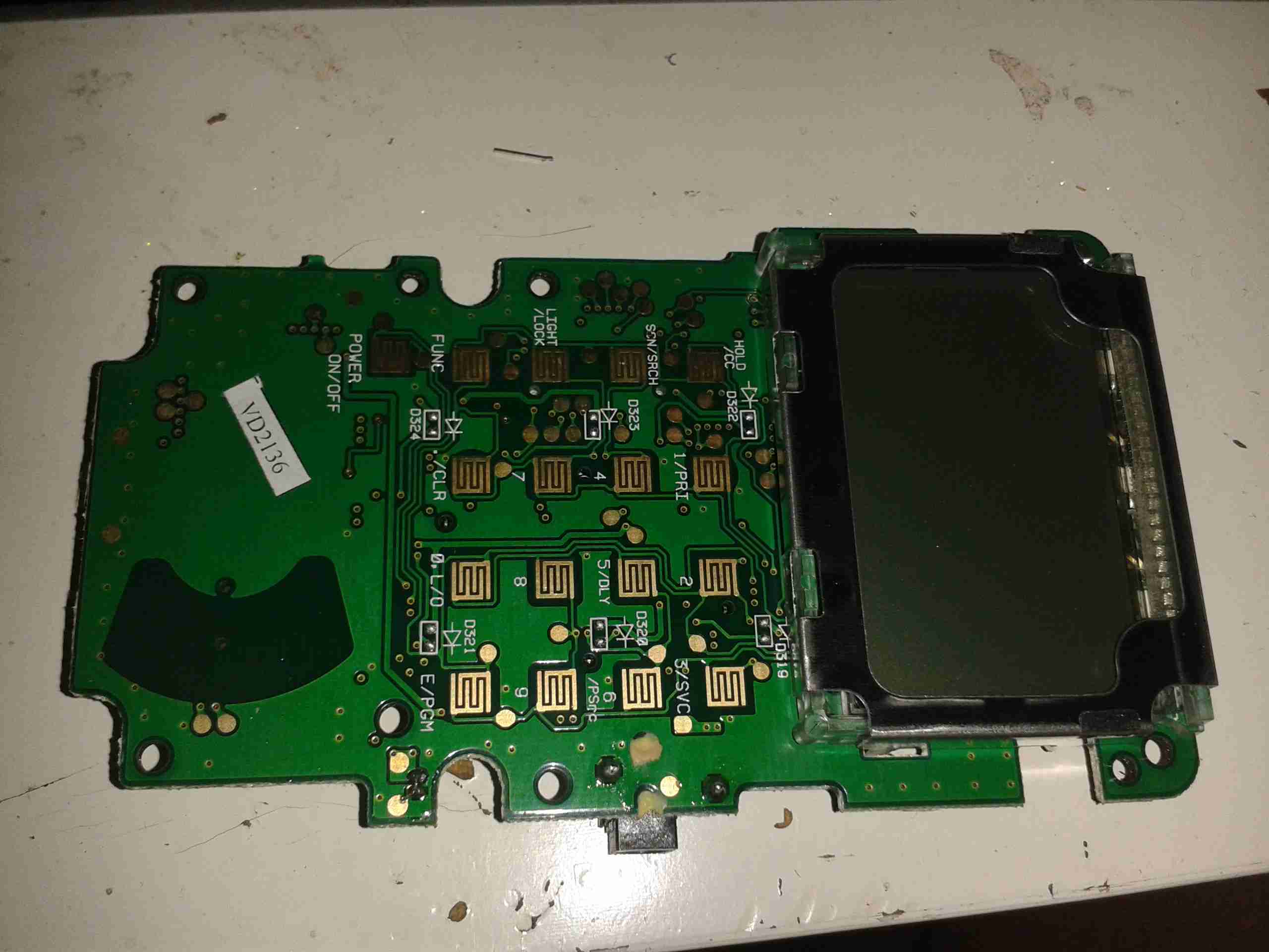
Control PCB Front
Here’s the front of the control PCB, nothing much to see here, just the LCD & membrane keypad contacts.
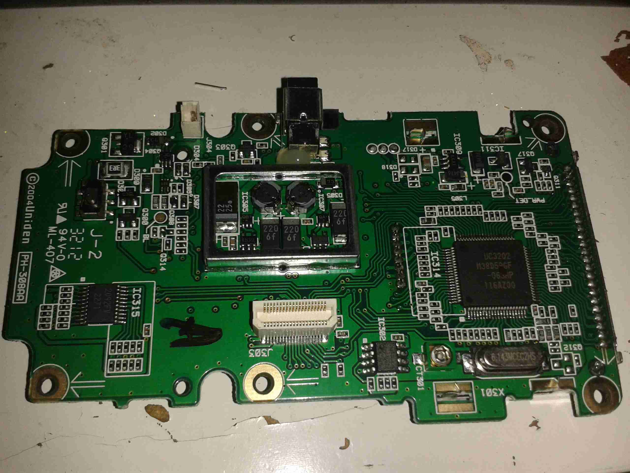
Control PCB Reverse
And here’s the reverse side of the control board. All the interesting bits are here. The main microcontroller is on the right, a Renesas M38D59GF, a fairly powerful MCU, with onboard LCD drive, A/D converter, serial interface, 60K of ROM & 2K of RAM. It’s 6.143MHz clock crystal is just below it.
The mating connector for the RF board is in the centre here.
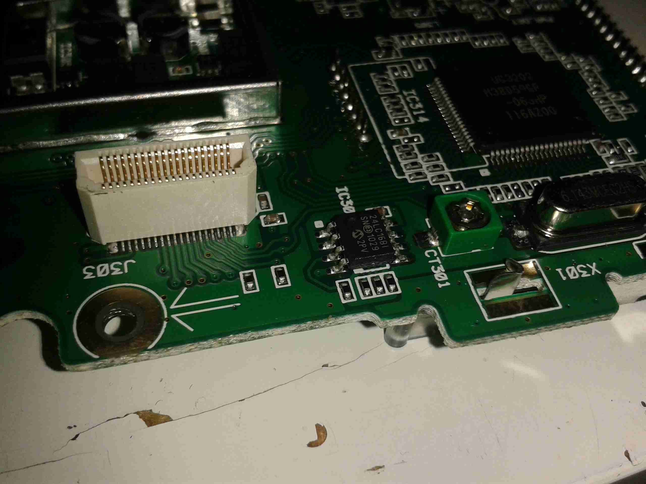
There is also a Microchip 24LC168 16KB I²C EEPROM next to the main microcontroller. This is probably for storing user settings, frequencies, etc.
EEPROM
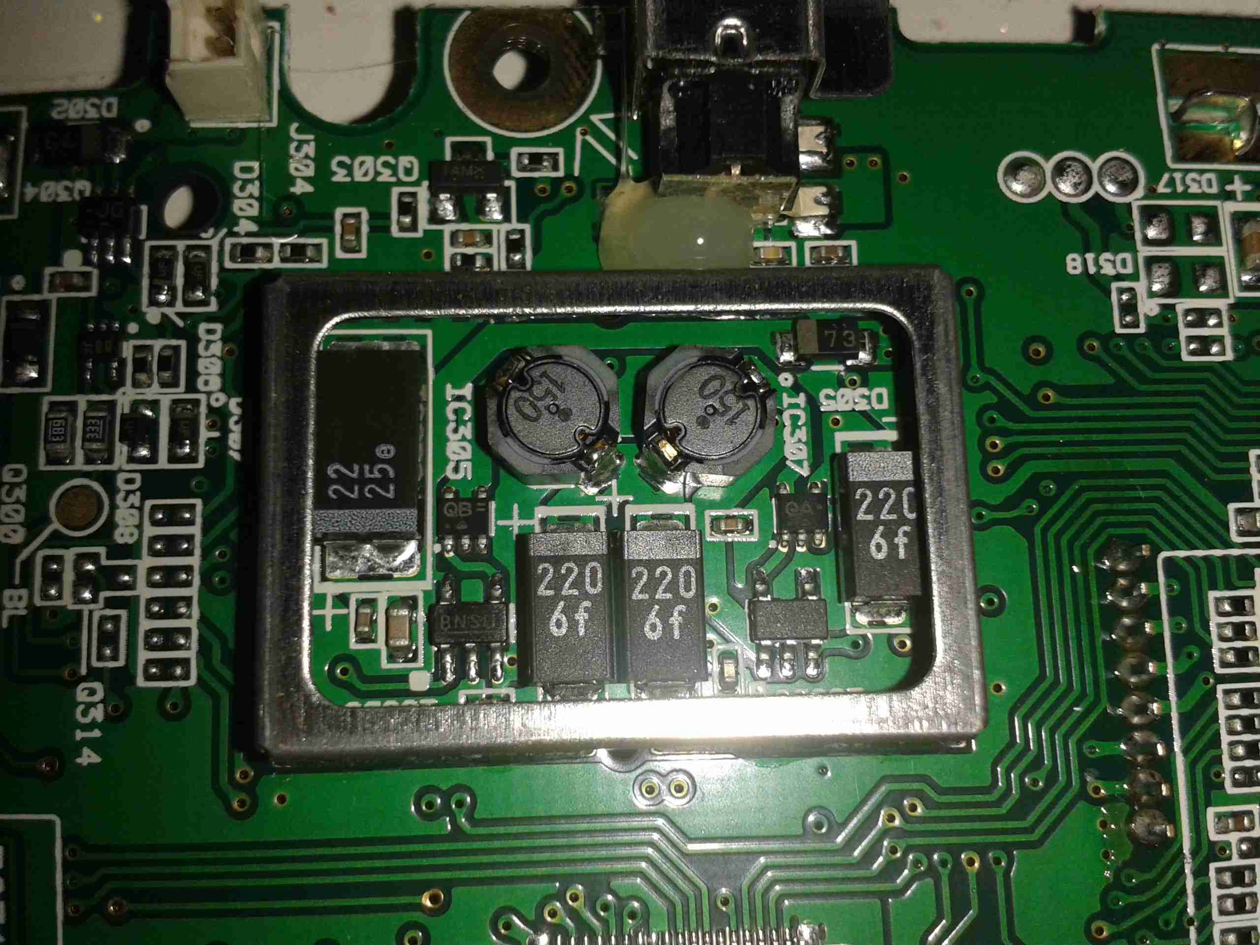
The rest of this board is dedicated to battery charging and power supply, in the centre is a dual switching controller, I can’t figure out the numbers on the tiny SOT23 components in here, but this is dealing with the DC 6v input & to the left of that is the circuitry for charging the NiMH cells included with the scanner.
PSU
The last bit of this PCB is a BU2092FV Serial In / Parallel Out 4 channel driver. Not sure what this one is doing, it might be doing some signal multiplexing for the RF board interface. Unfortunately the tracks from this IC are routed on the inner layers of the board so they can’t be traced out.
A while ago I blogged about modifying the output voltage of some surplus Cisco switch power supplies to operate at 13.8v.
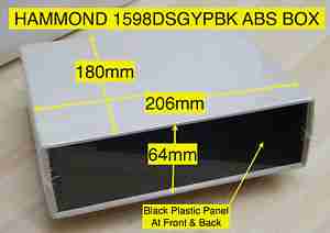
Since I was able to score a nice Hammond 1598DSGYPBK ABS project box on eBay, I’ve built one of the supplies into a nice bench unit.
Hammond ABS CaseSupply Unit
Above is the supply mounted into the box, I had to slightly trim one edge of the PCB to make everything fit, as it was just a couple of mm too wide. Luckily on the mains side of the board is some space without any copper tracks.
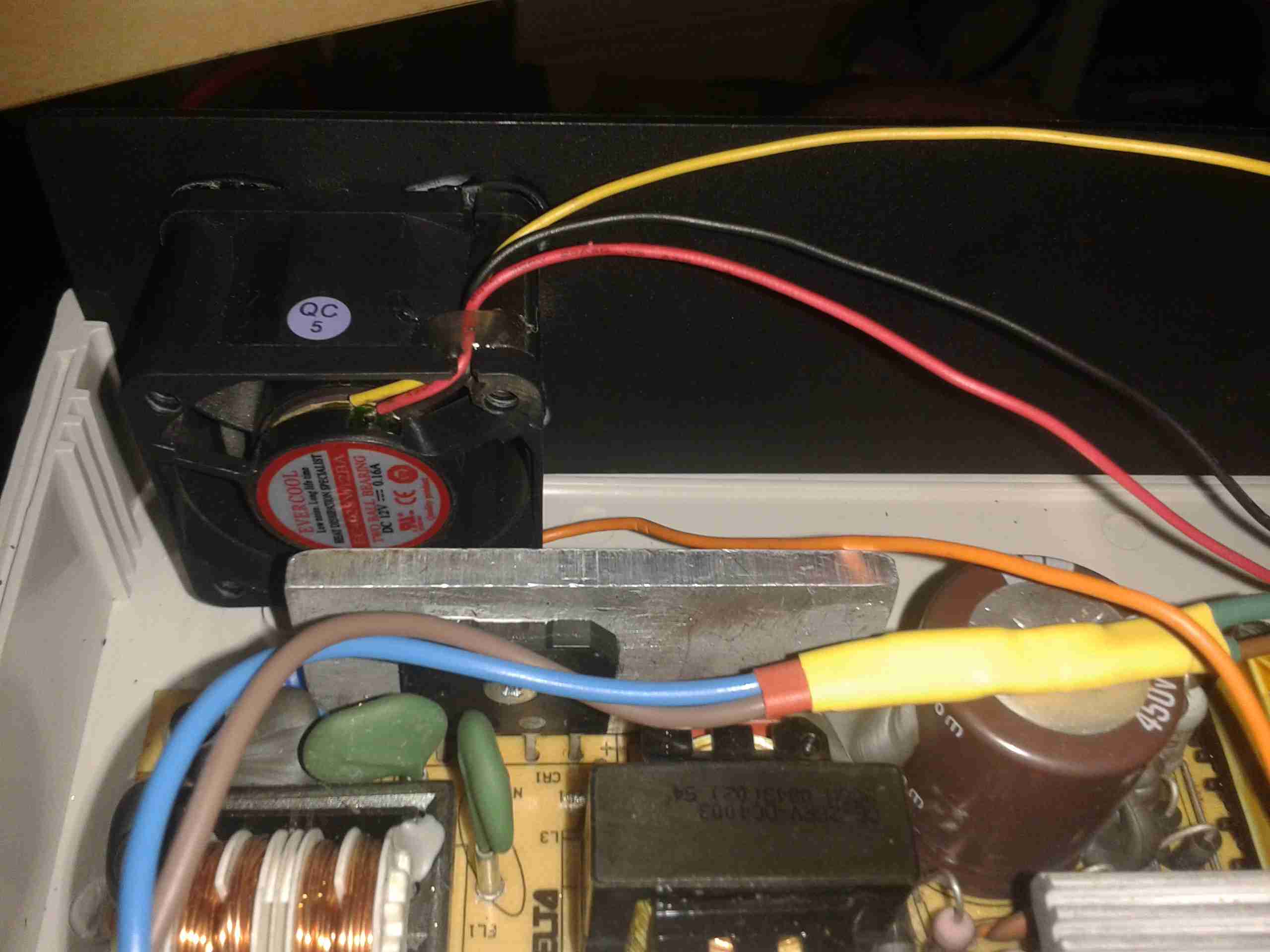
PSU Fan
These supplies are very high quality & very efficient, however they came from equipment that was force-air cooled. Running the PSU in this box with no cooling resulted in overheating. Because of this I have added a small 12v fan to move some air through the case. The unit runs much cooler now. To allow the air to flow straight through the case, I drilled a row of holes under the front edge as vents.
Output Side
Here is the output side of the supply, it uses standard banana jacks for the terminals. I have used crimp terminals here, but they are soldered on instead of crimped to allow for higher current draw. The negative return side of the output is mains earth referenced.
I have tried to measure output ripple on this supply, but with my 10X scope probe, and the scope set to 5mV/Div, the trace barely moves. The output is a very nice & stable DC.
This supply is now running my main radio in the shack, and is small enough to be easily portable when I move my station.
Recently I’ve noticed my usual mobile rig, the Baofeng UV-5R, has had very poor receive, and non-existent transmit.
I did a power test on the radio, and confirmed it was still outputting it’s rated RF power. Trying another antenna proved that the radio was fine.
Time to tear down the antenna & see if it can be fixed!
Stock Antenna
Here’s the antenna, just the factory rubber duckie. As with all these antennas, they’re a compromise between size & their efficiency.
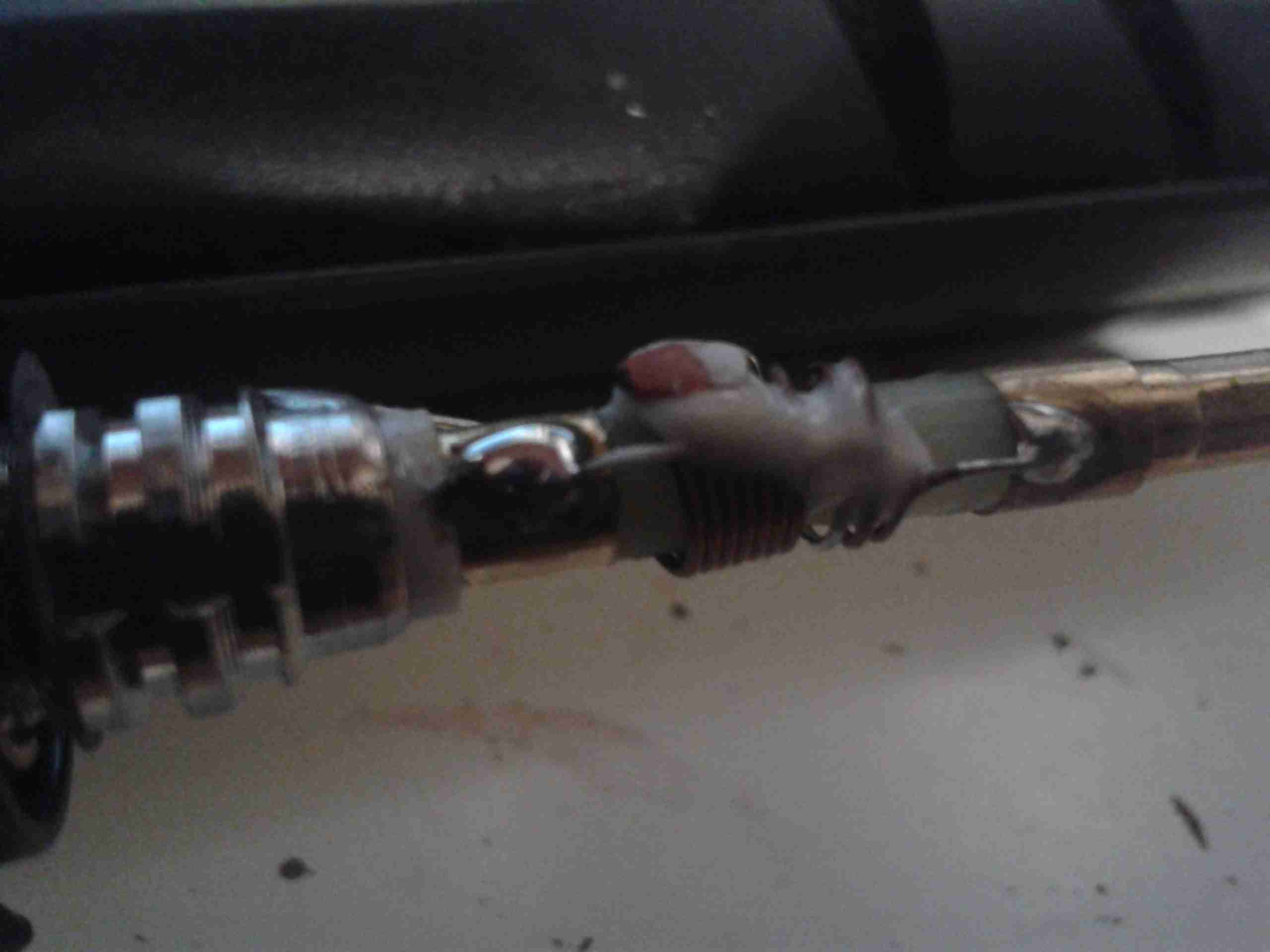
Naked Antenna!
Giving a gentle pull to the antenna sheath while it’s attached to the radio allows it to come apart. The quality actually doesn’t look to bad. It’s very similar in construction to my Diamond X-30, just on a much smaller scale.
At the bottom of the antenna is the matching network, an inductor & ceramic disc capacitor. Here lies the problem with this antenna.
Dry Joint
Here where the capacitor joins onto the feedpoint from the SMA connector, the solder joint has come away. This was a very poor joint to start with, and the solder hadn’t wetted the capacitor lead at all
After cleaning the joint, and applying some flux, a new joint was easily made with some Real Solder.
Repaired Joint
Here’s the joint freshly repaired, the antenna is now back to full working order. It even seems to work better than the others I have 🙂
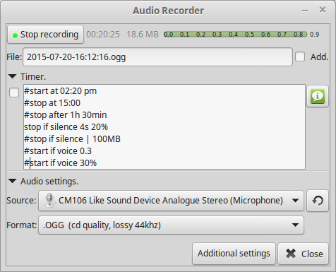
Since my new Wouxun has audio output jacks, I figured it would be useful to have the ability to record what my rig hears, if anything interesting comes on the air.
Under Linux, I use an application called, (creatively enough), Audio Recorder.
Recorder Screenshot
Using a simple connection to the mic input on a USB soundcard, I can capture everything the radio hears. Unfortunately this doesn’t work for outgoing audio, so it’s not much good at capture of my personal QSOs. For this I will have to set up another radio to act as the main receiver.
At some point in the future I will implement this with a Raspberry Pi as the audio capture server.
After a few years of running with the same look, I’ve decided on some changes.
New theme!
The site now looks much better, and has better support for more eye candy 😉
Addition of my QRZ link
New QSO logging system
Accessible from a button in the header, this is my new preferred system for logging my radio contacts. (I was originally using CQRLOG under Linux). If I’ve spoken to you on the radio your callsign will most likely appear immediately. 🙂
If not, I’m probably working mobile. In that case, drop me a comment or an E-Mail 🙂
Finally there have been some behind the scenes changes to implement some better security on site.
Getting the number of hits I do per day, this site gets attacked by the Internet’s Great Unwashed on a regular basis. No attack has ever been successful but more security never hurts!
I’ve noticed that the RF power output from the Chinese radios can be quite variable from model to model, and even from individual radios of the same model & batch.
I’ve bought an RF Power meter (GY561) to do some tests on the HTs I have at present.
All tests were performed with the radio fully charged & still on the charging base, to make sure the supply voltage remained constant at 8.4v throughout the tests.
Frequencies used were 145.500 & 433.500 for VHF & UHF respectively.
The power meter was connected with ~8″ of RG174 Coax.
This possibly has the potential to damage the radio, if you transmit on a frequency it’s not designed for. Not to mention the legal issues with transmitting on frequencies that aren’t permitted! Use at your own risk!
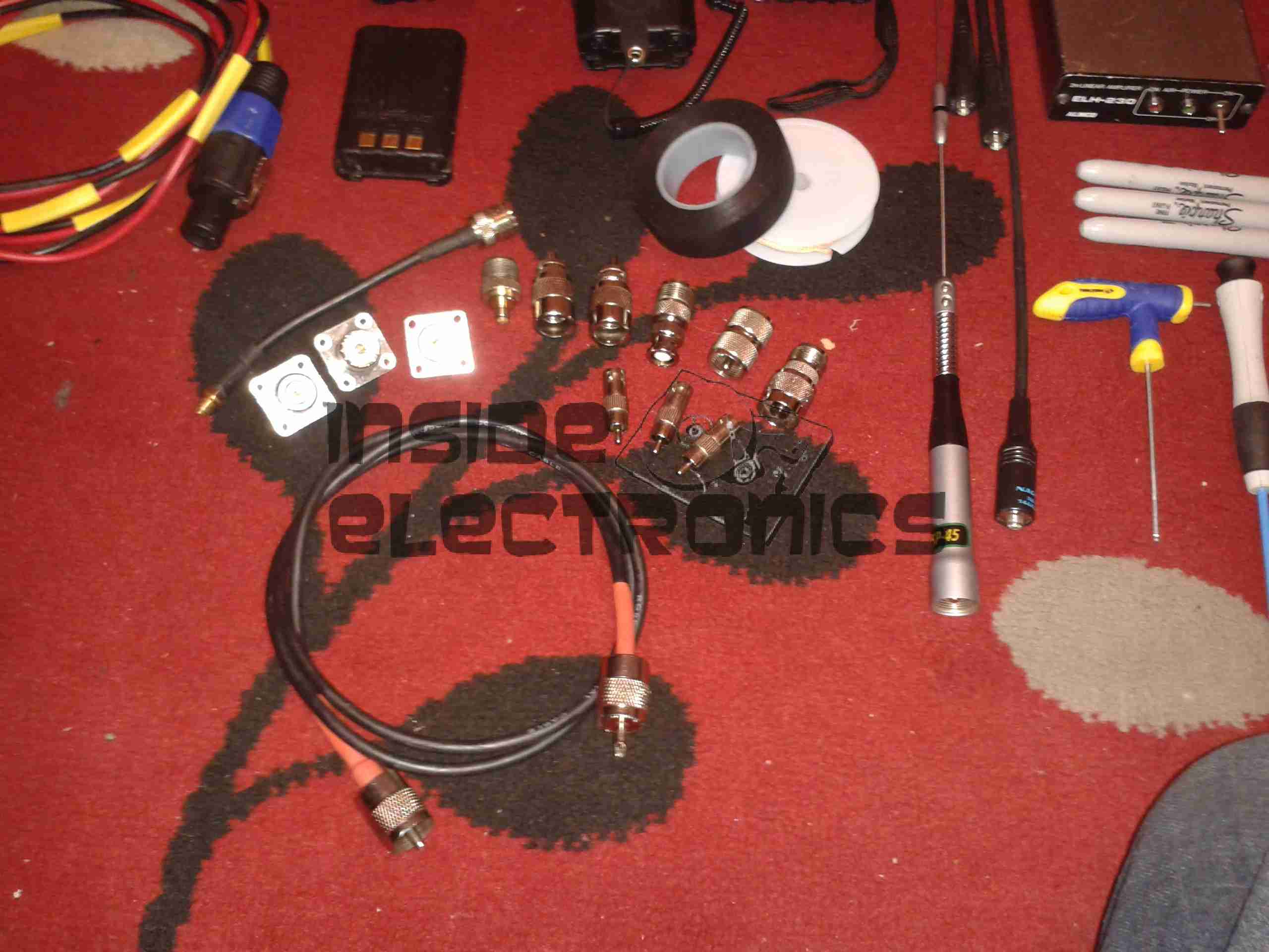
There are times when I am frequently away from home base, usually either on the canal system or at a festival. During these times it’s very handy to be able to just grab a bag, without having to be concerned about sorting everything out.
This post will only detail the portable shack bag. The power supply kit that goes along with it with be detailed in another post.
The bag I use is an VHS Camcorder bag from the early 80’s. It’s very well built, & copes easily with the weight of all the radio gear.
Total weight for this system is 13.4lbs (6kg).
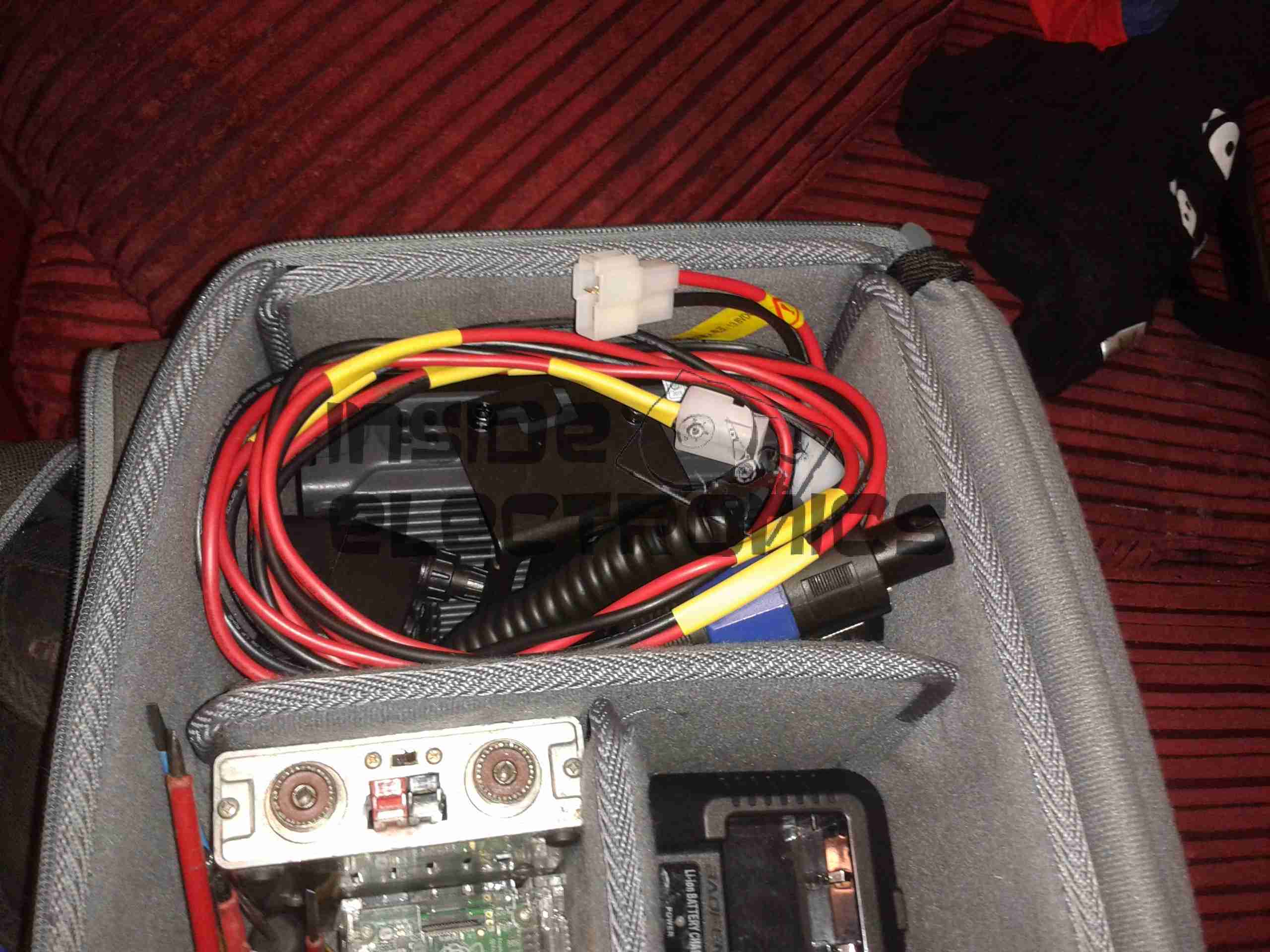
Mobile Radio Bag
Above is the bag packed. Obligatory International Ameteur Radio Symbol patch front & centre. Being an old camera bag, this easily slings over the shoulder, with it’s padded strap.
Current Equipment
Here is all the current equipment laid out. All the equipment to enable me to set up a station anywhere.
In the following photos I will go into the details.
Main Radio
First off, my main radio. This is the same Wouxun KG-UV950P mobile rig I have posted about previously. I have heatshrunk the power cable to keep it together & attached my standard power connector to the end. More on these later on.
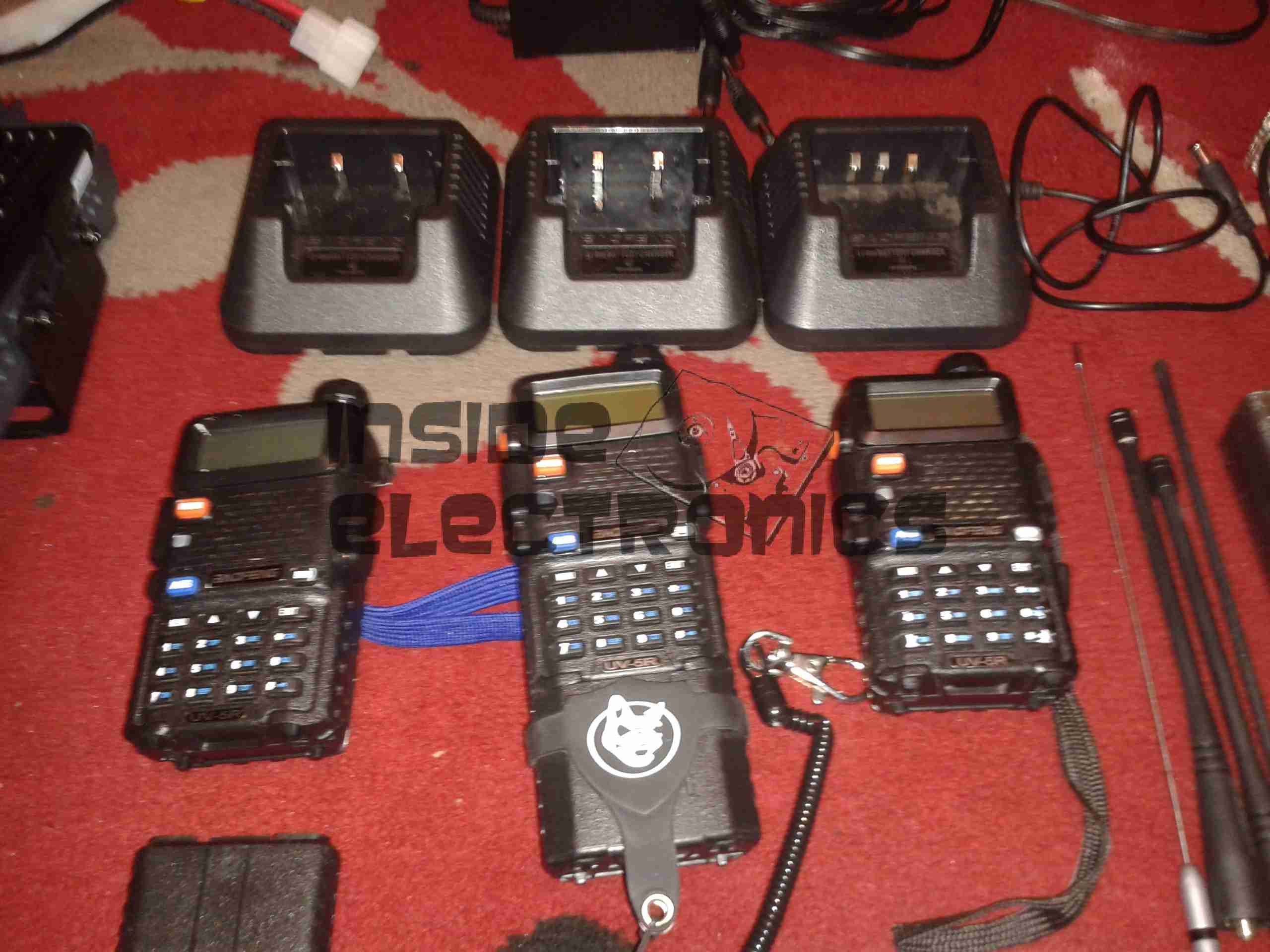
HTs
In the bag I also carry three Baofeng UV-5R handhelds. Extremely useful for short range site communications, along with their charger bases. The charging base on the right has been slightly modified to support charging of my main LED torch as well, which uses similar Li-Ion based packs as the Baofengs.
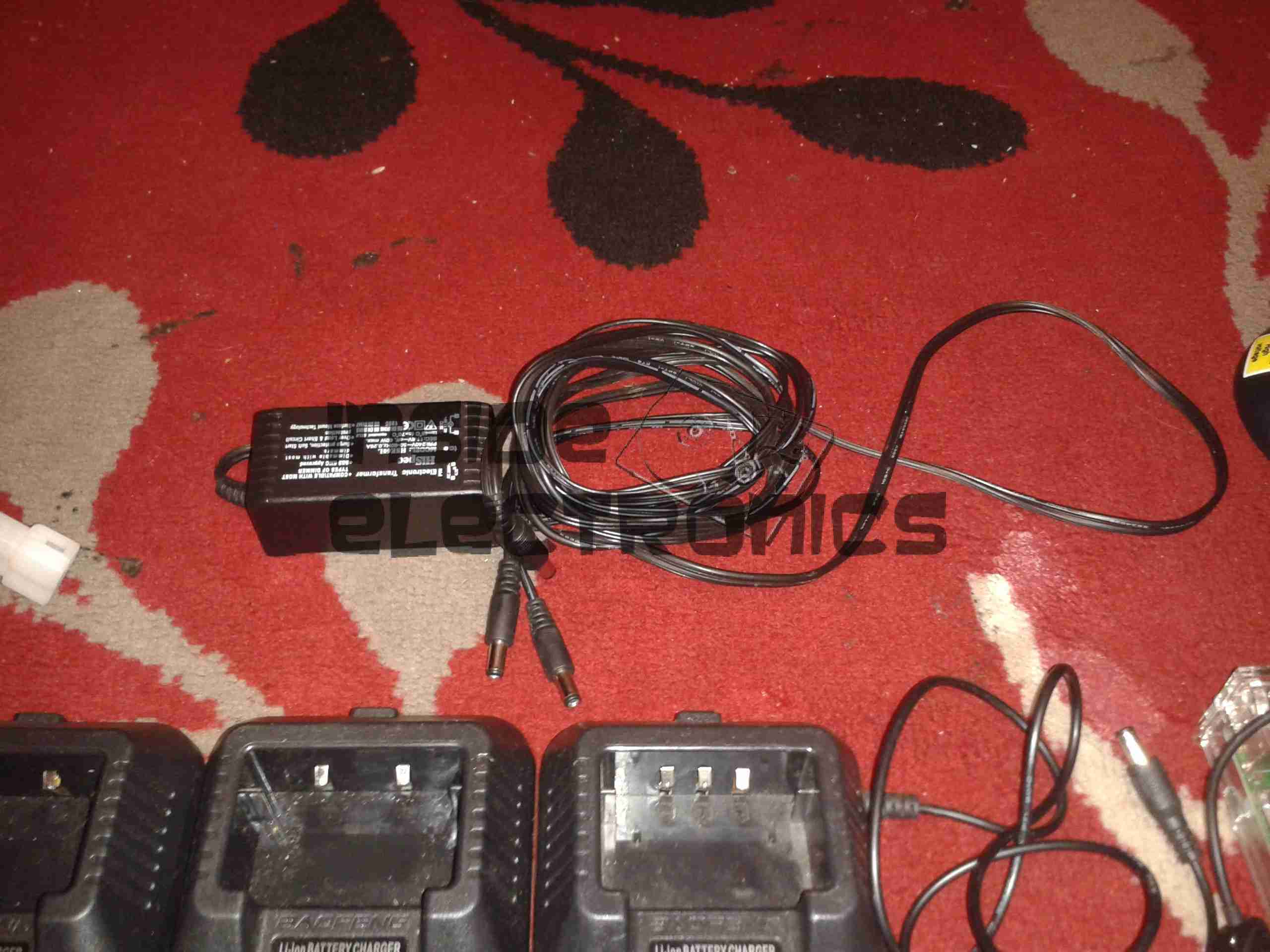
Baofeng 12v Charger
As the charger bases for the Baofeng HTs take a supply of 10v DC, I have constructed a 12v adaptor system for them. (Which utter prat of an engineer at Baofeng picked 10v?)
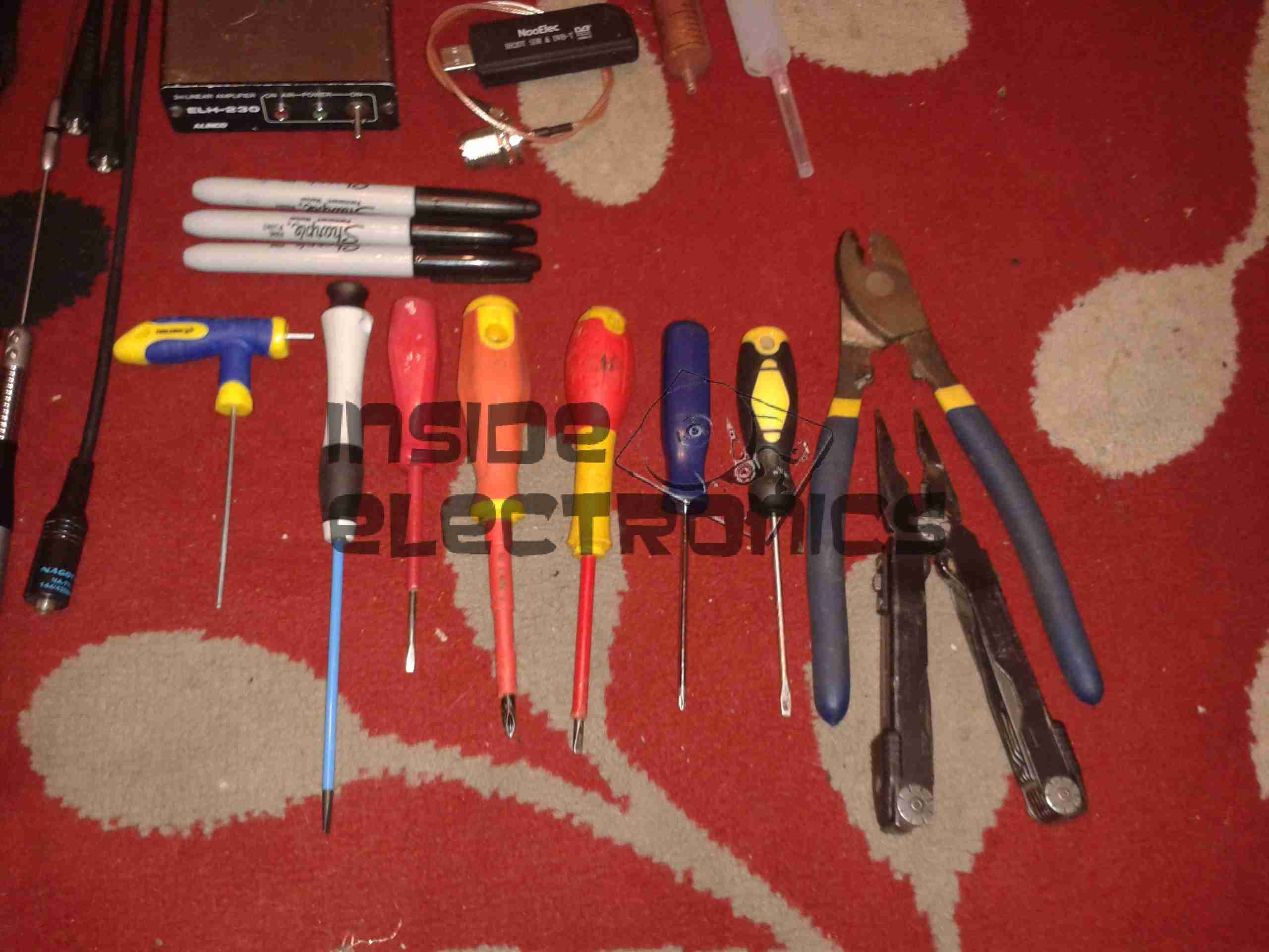
Linear Amplifier & SWR Meter
Also included is a small Alinco ELH-2320 35W 2m linear amplifier. This was given to me from the local HackSpace in Manchester. (They don’t have any ham members, besides myself). Also here is my small SWR & Power meter, SDR kit & a pair of syringes. These are filled respectively with Copaslip copper loaded grease, (very good for stopping fasteners exposed to the weather from seizing up), and dielectric silicone grease. (I use this stuff for filling connectors that are exposed to the weather – keeps the water out).
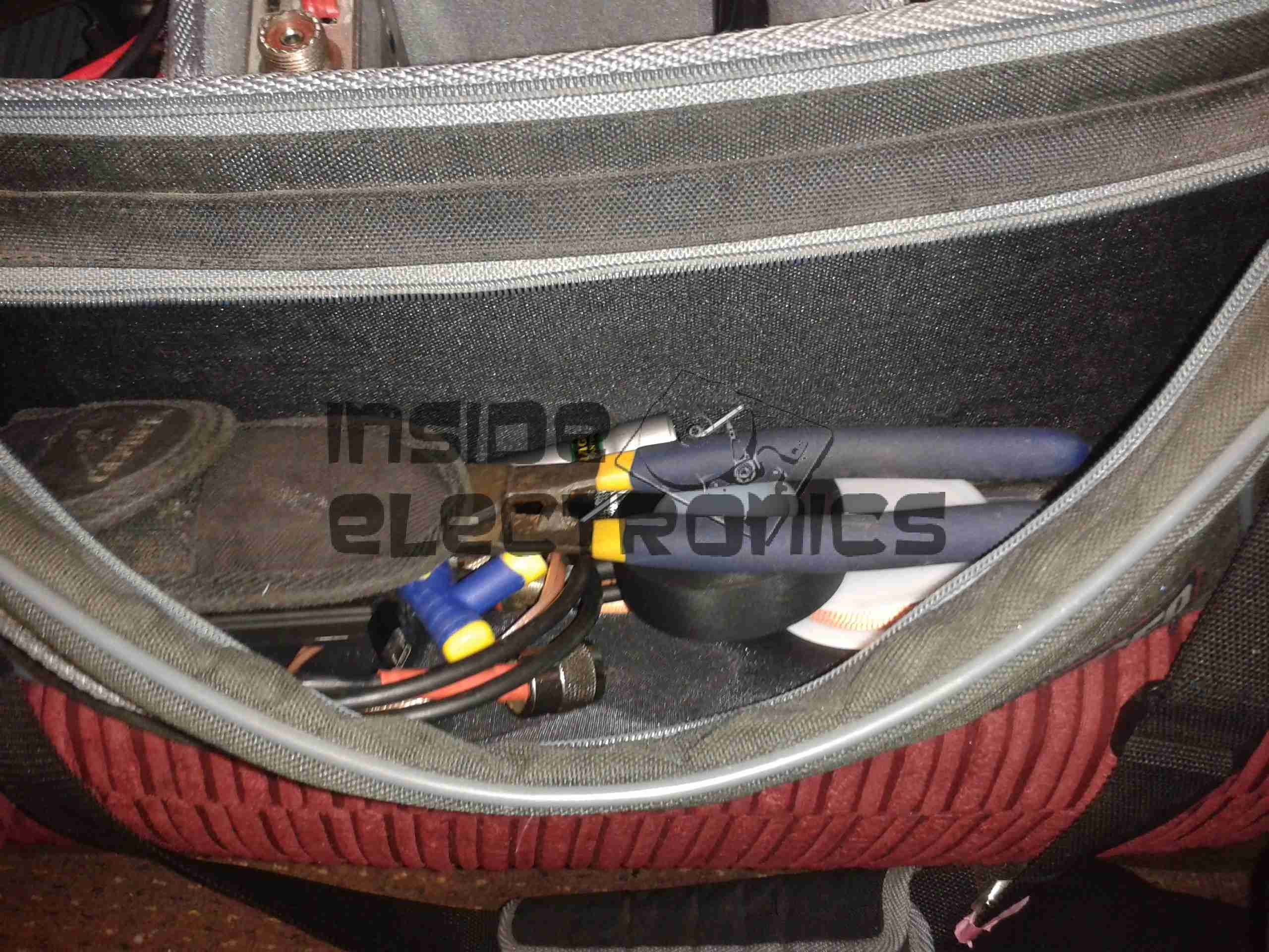
Tools
I always keep essential tools in the bag, here is the small selection of screwdrivers which fit pretty much any screw fastener around, my heavy-duty cable shears (these buggers can cut through starter cable in one go!) and my trusty Gerber Diesel multitool.
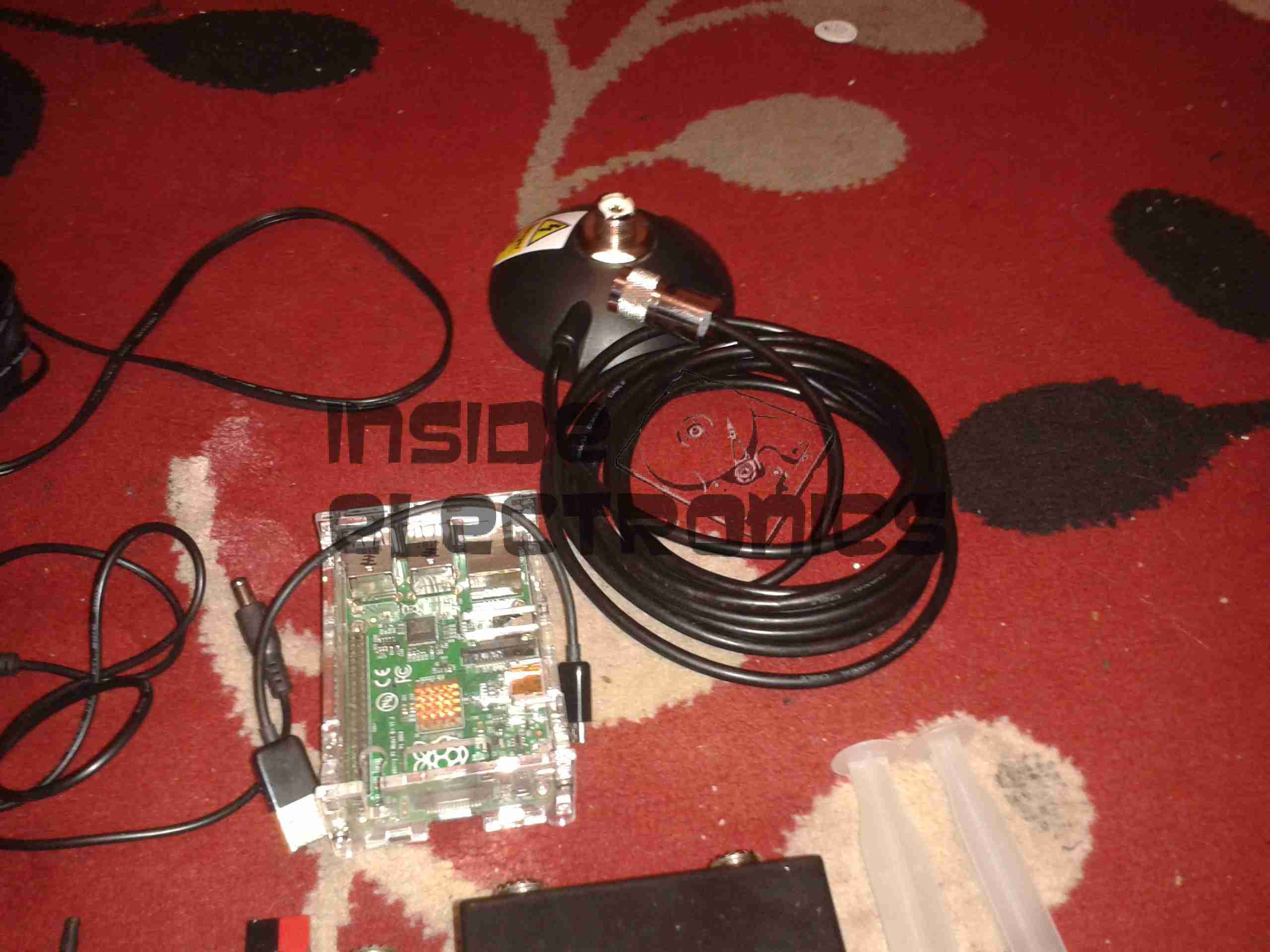
Magmount & Pi
Main antenna magmount & a spare Raspberry Pi.
Antenna, Patch Leads, Etc.
Finally, the antennas for the HTs, main dual-band antenna (Nagoya SP-45) for the magmount, a small selection of spare plugs, sockets & adaptors. Also here is a roll of self-amalgamating tape, very handy for waterproofing wiring connections (especially when used in conjunction with the silicone grease), & a roll of solder wick.
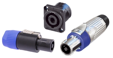
Now, the main power connectors of choice for my equipment are Neutrik SpeakOn type connectors:
Neutrik SpeakOn
These connectors have many advantages:
They are positive locking connectors. No more loose connections.
They have a high continuous current rating of 30A RMS.
Relatively weather resistant.
Also, they have two pairs of pins – and as some of my bigger non-radio related equipment is 24v, this allows me to use a single set of plugs for everything. Without having to worry about plugging a 12v device into a 24v socket, and letting out the magic blue genie.
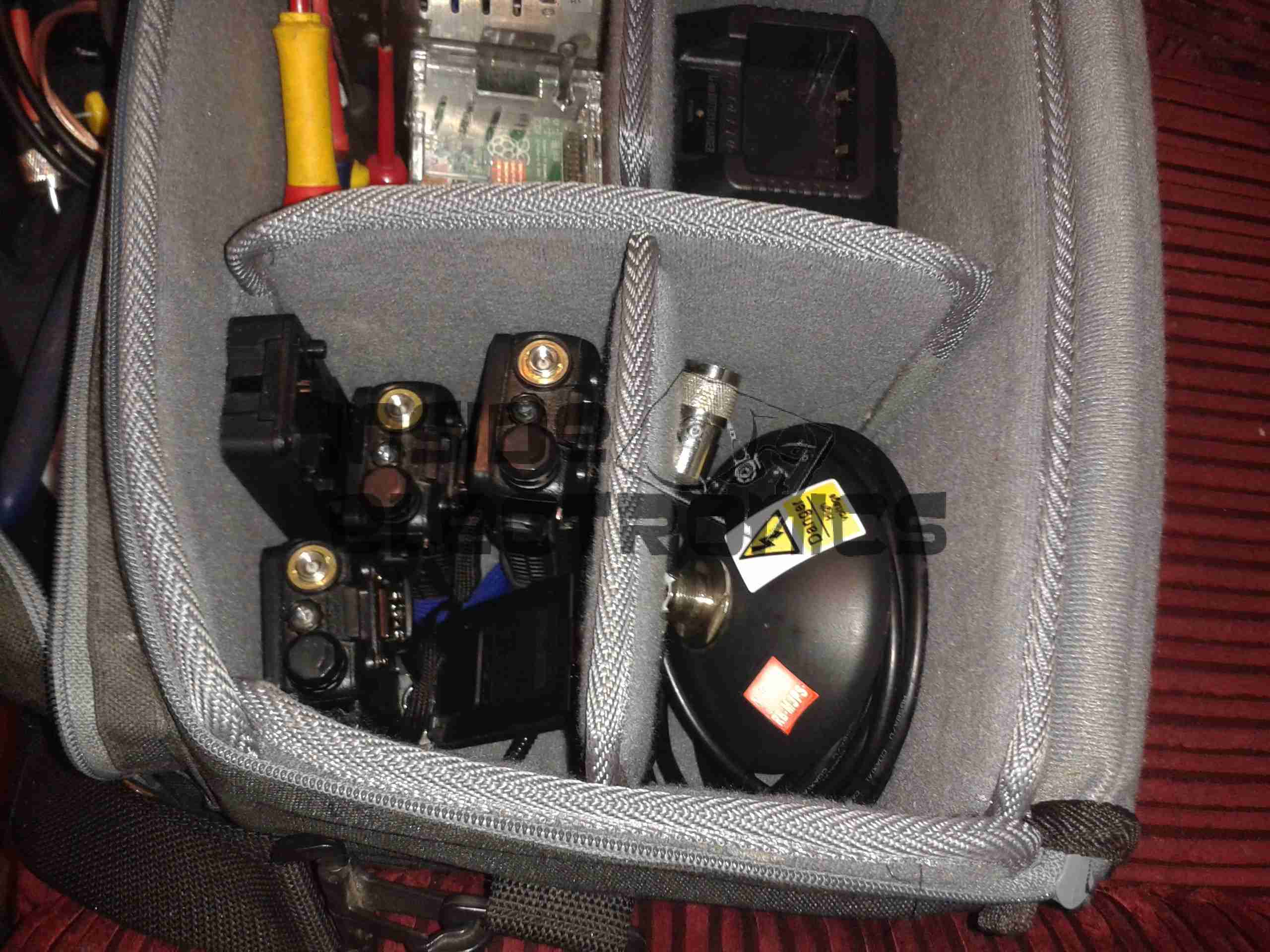
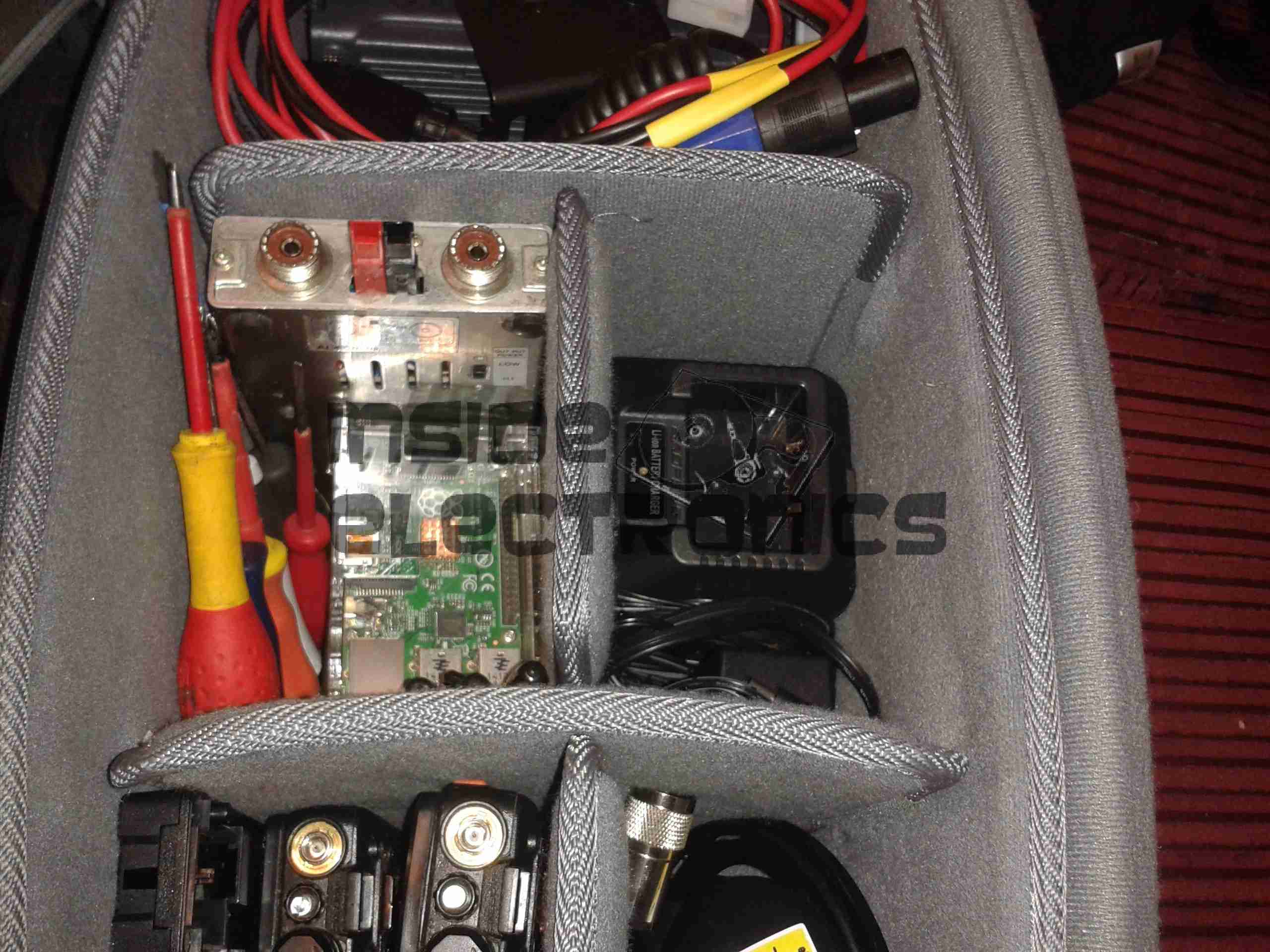
Once everything is packed up, here’s the bag:
Packed
Everything has a neat little pocket for easy access. Some closeups below.
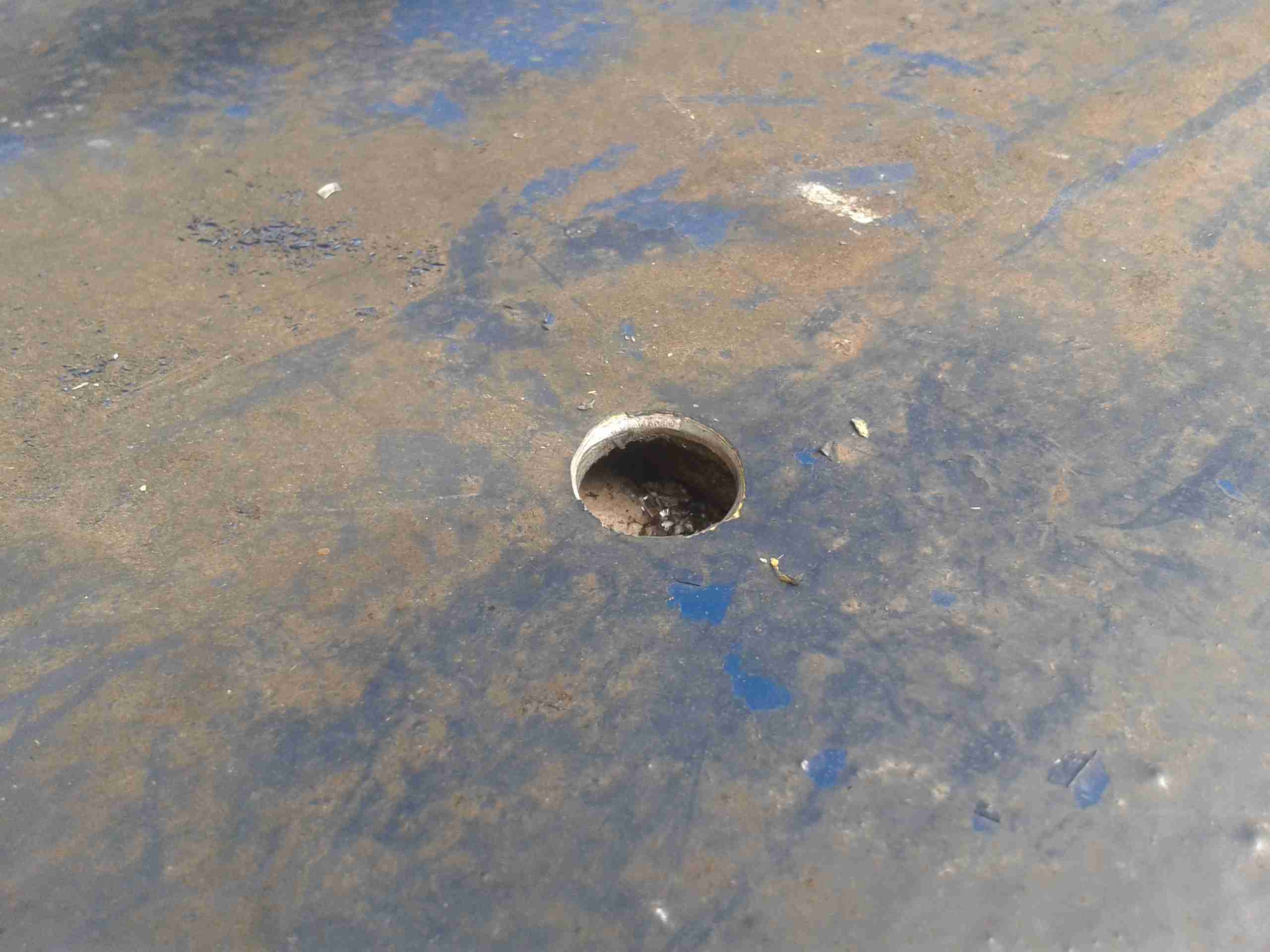
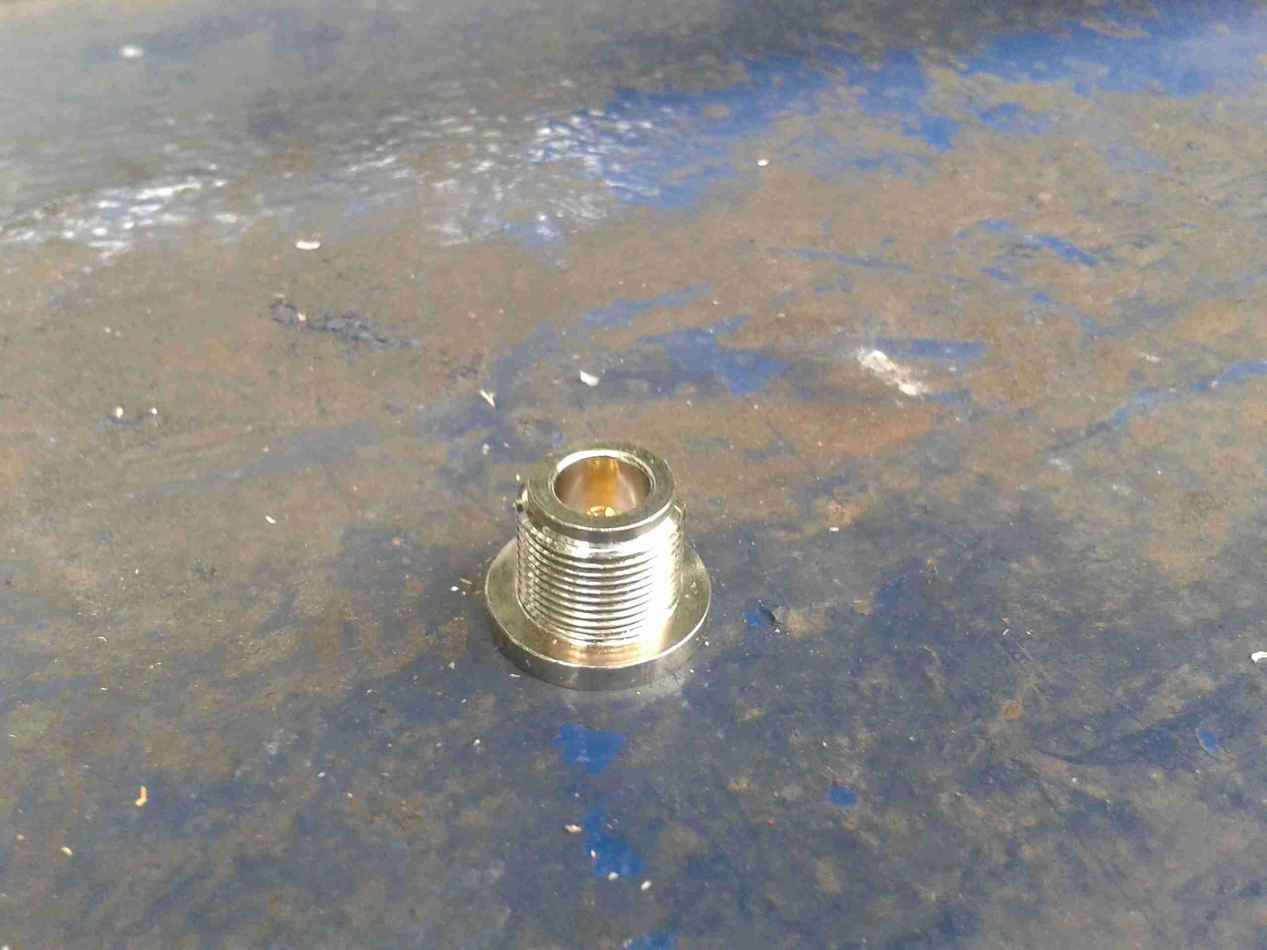
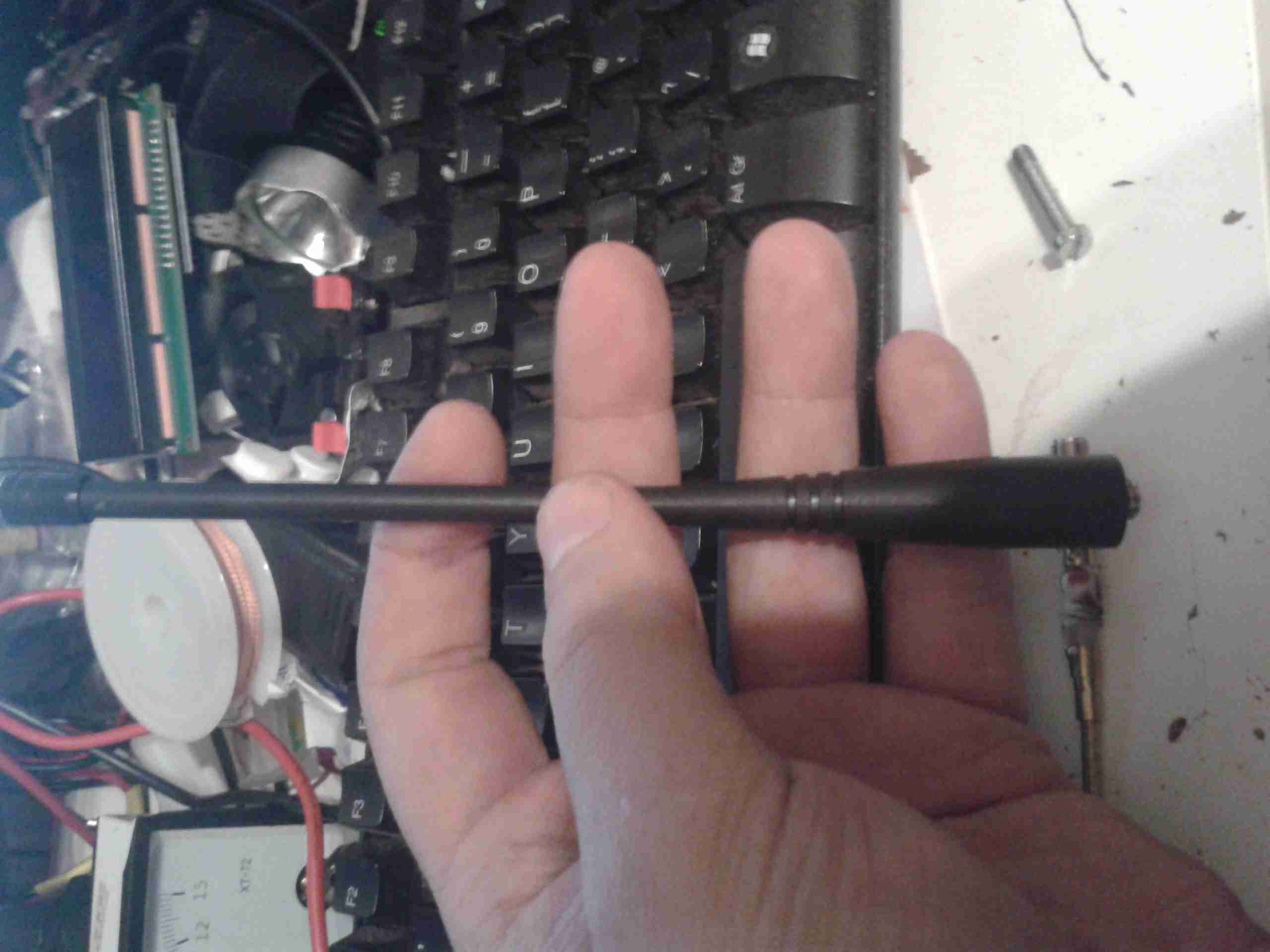
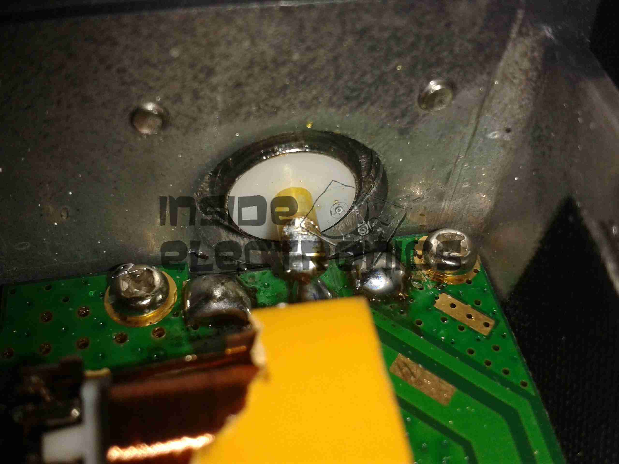
In my original review, I noted that this radio was supplied with a SO-259 socket for the antenna connection.
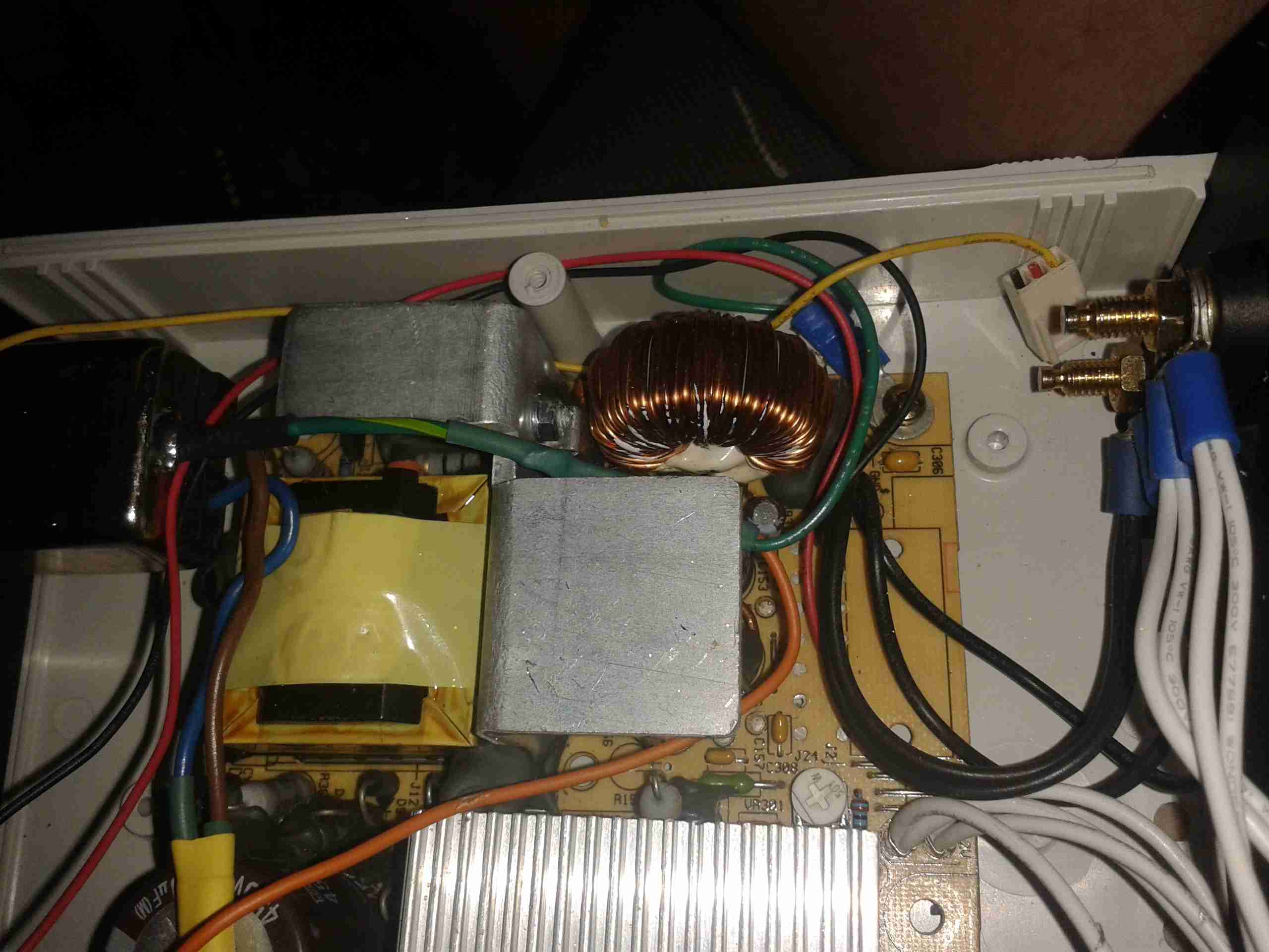
However I’m less than fond of these, due to their non-constant impedance, which can cause signal loss issues at VHF/UHF. Because of this, I’ve replaced it with a high quality N-type connector. These connectors are much better, as they are a constant 50Ω impedance, they’re weather resistant, and being rated to 11GHz, are more than sufficient for a radio that will only do up to 70cm.
RF Output Jack
Here can be seen the point where the connection is made to the PCB.
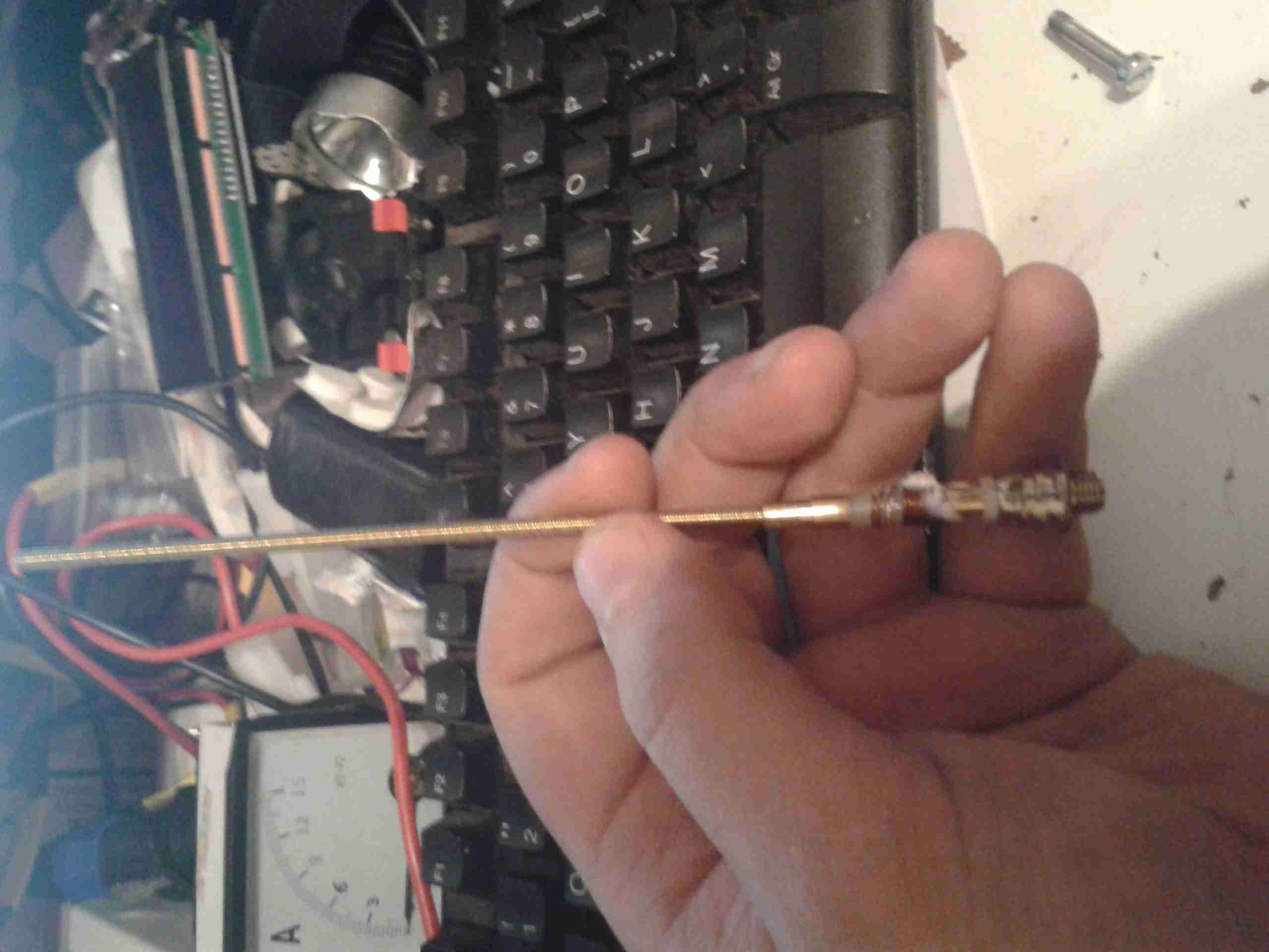
I’ve already replaced the socket in this photo. The pair of solder pads either side of the central RF point were soldered to wings on the back of the original SO-259. As there are a pair of screws, also connected to the ground plane, there have been no signal issues with just using the frame of the radio as the ground point. Shown below is the original socket, with the ground wings.
Original SO-259
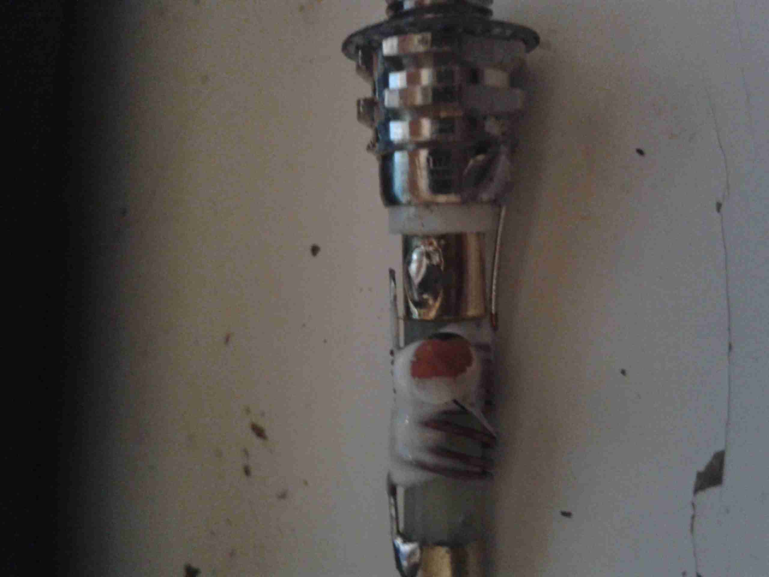
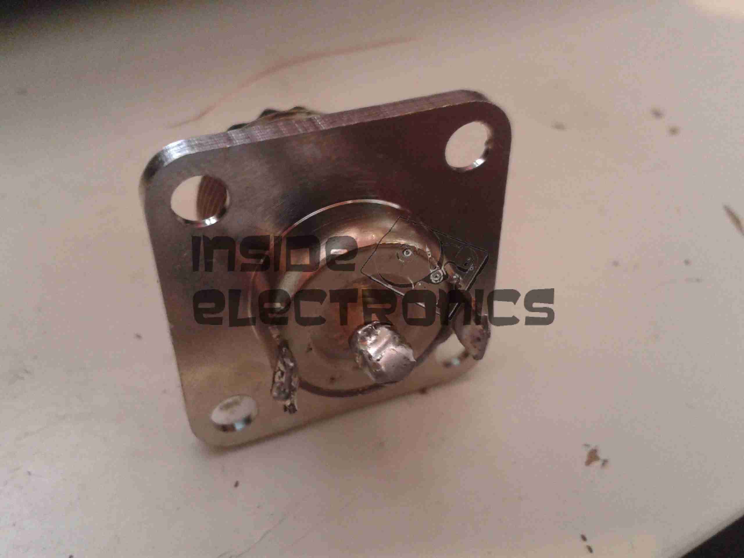
Finally, here is the back of the radio with it’s shiny new N connector.
New Connection
Chassis mount connectors are pretty standard, so this new connector fits perfectly into the same recess of the original. Looks like factory fitted!
I am now standardising on N connectors for everything in my radio shack, next on the project list for conversion is the SWR meter I recently acquired.
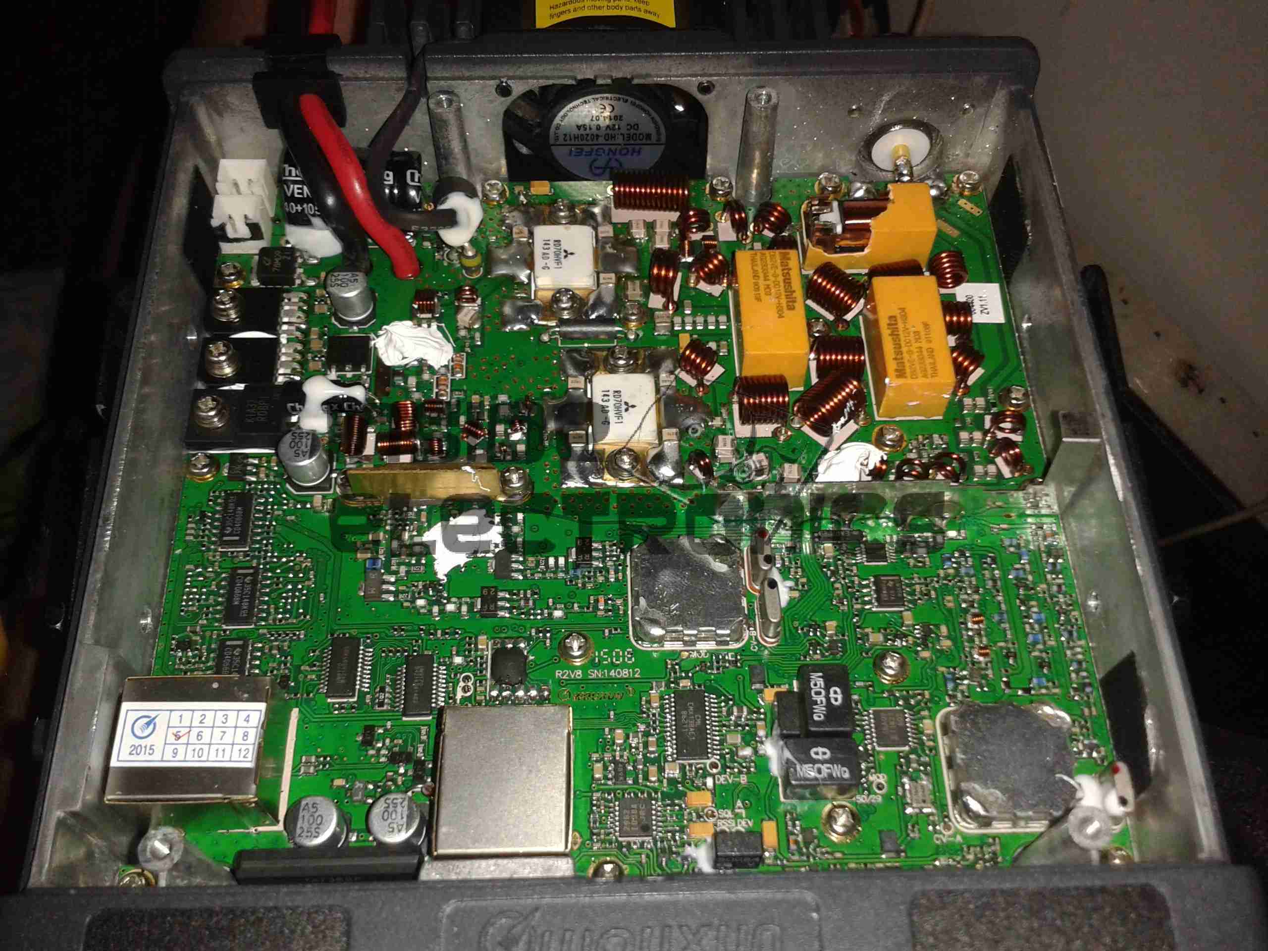
Following on from my review, here are some internal views & detail on the components used in this radio. Below is an overview of the main PCB with the top plate removed from the radio.
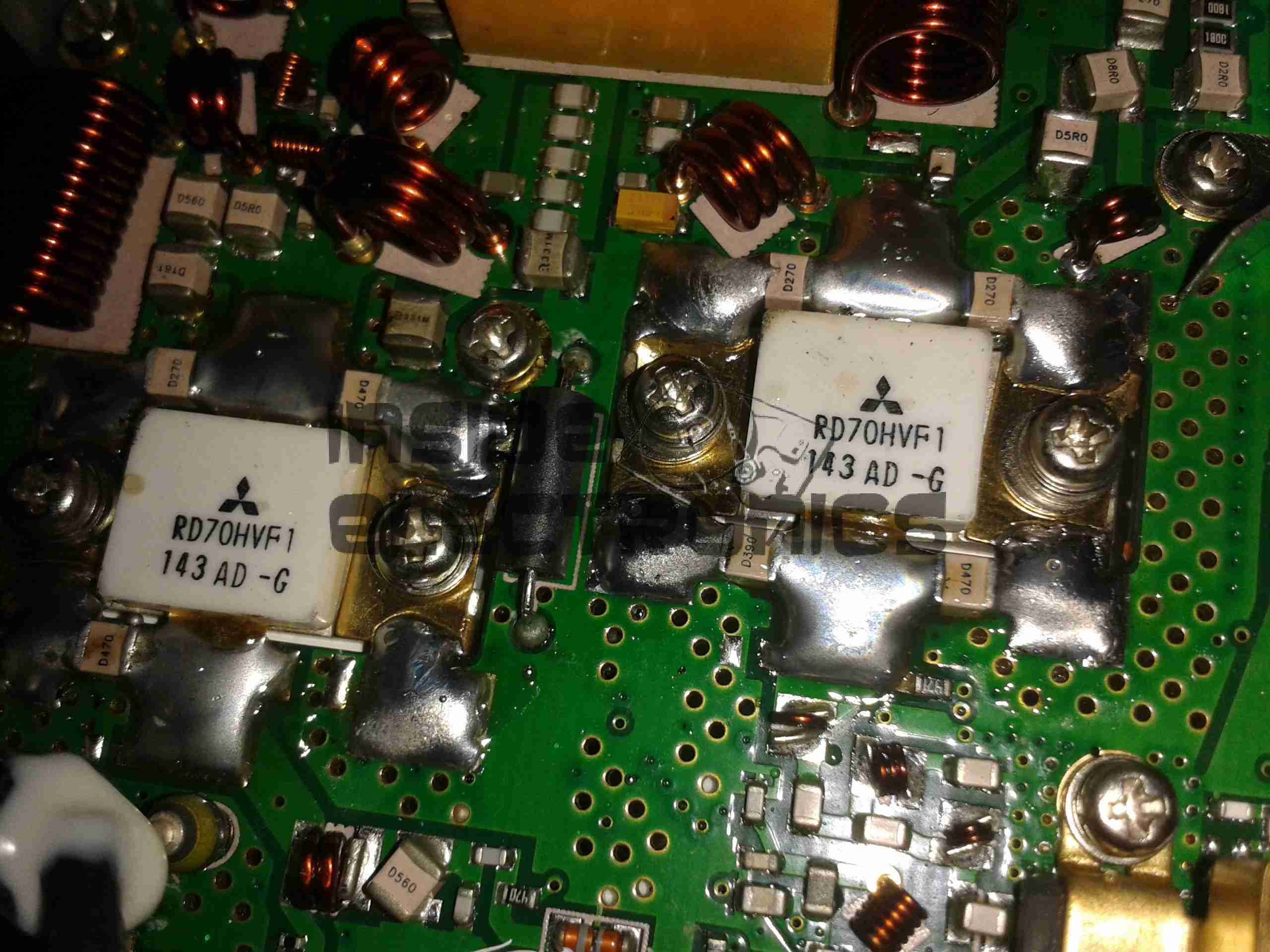
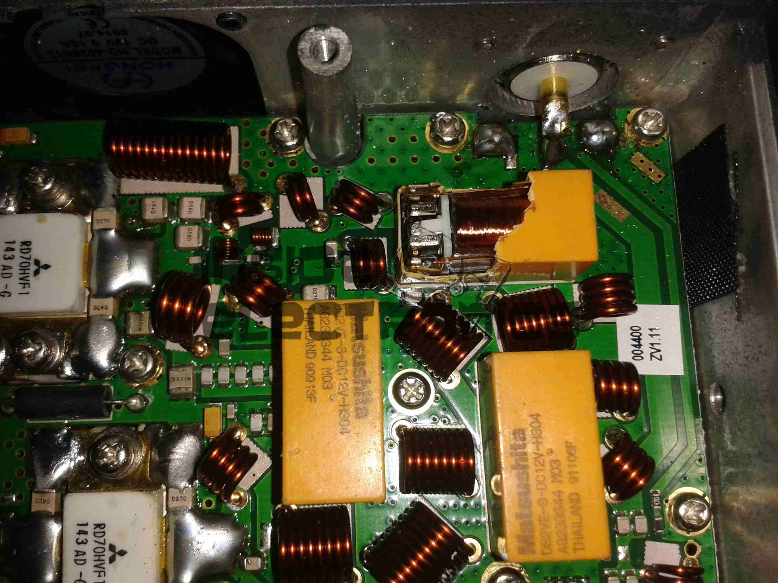
Cover RemovedRF Final Amplifier Stage
Most visible are these MOSFETs, which are Mitsubishi RD70HVF1 VHF/UHF power devices. Rated for a maximum of 75W output power at 12.5v (absolute maximum of 150W, these are used well within their power ratings. They are joined to the PCB with heavy soldering, with bypass caps tacked right on to the leads.
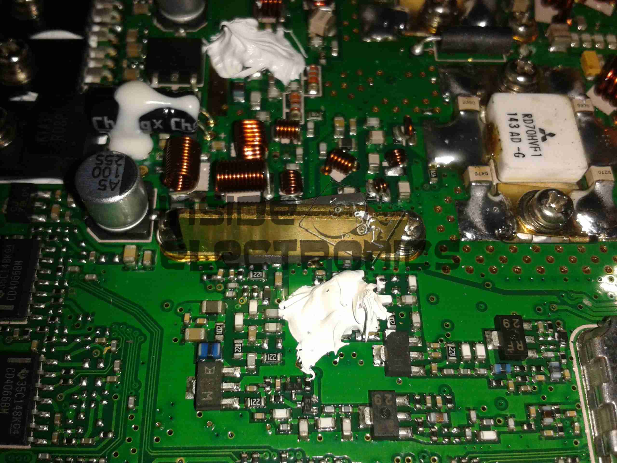
RF Pre Drivers
Here is the RF pre-driver stage, with intermediate transistors hidden under the small brass heatspreader.
Power Section
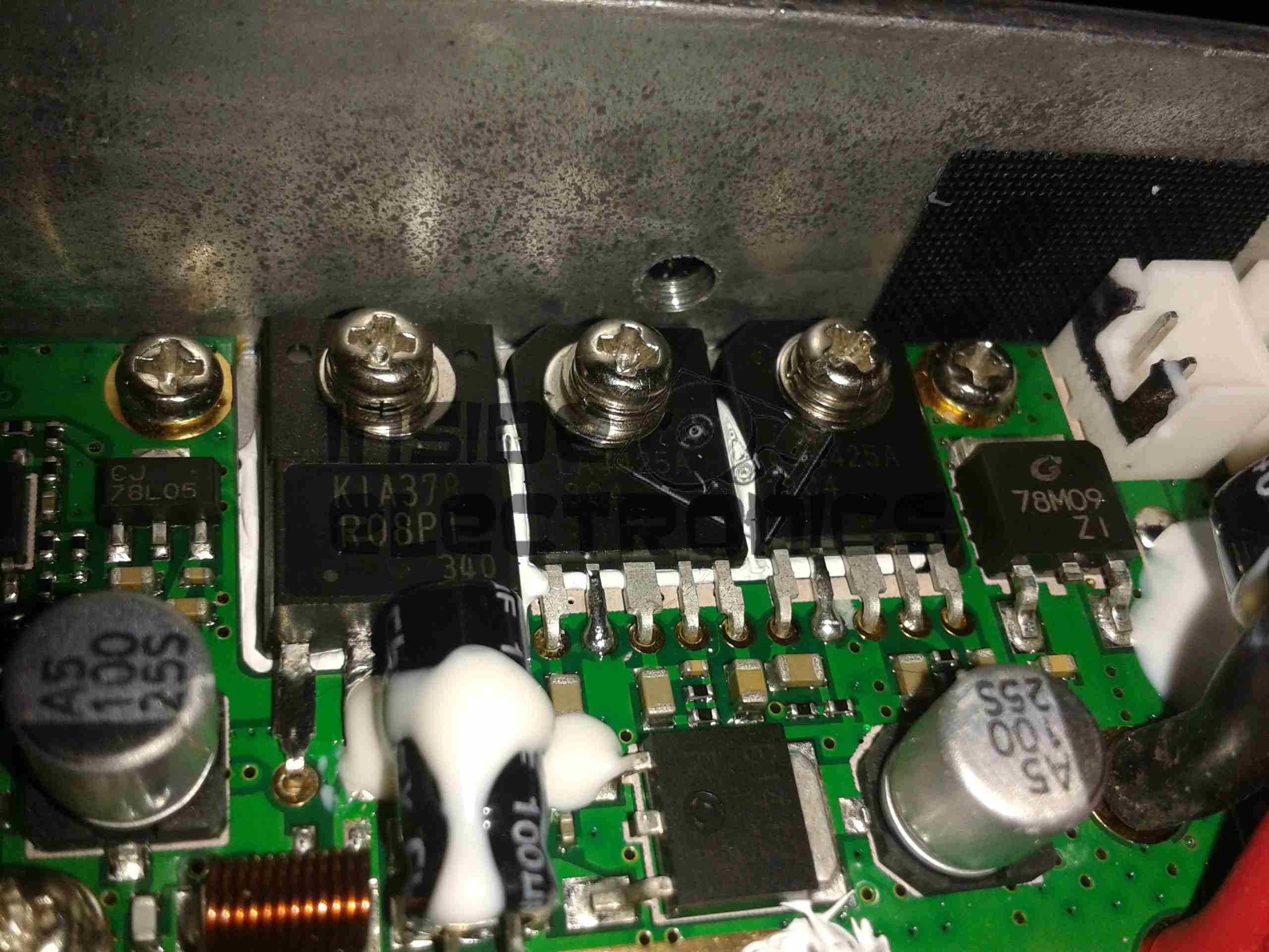
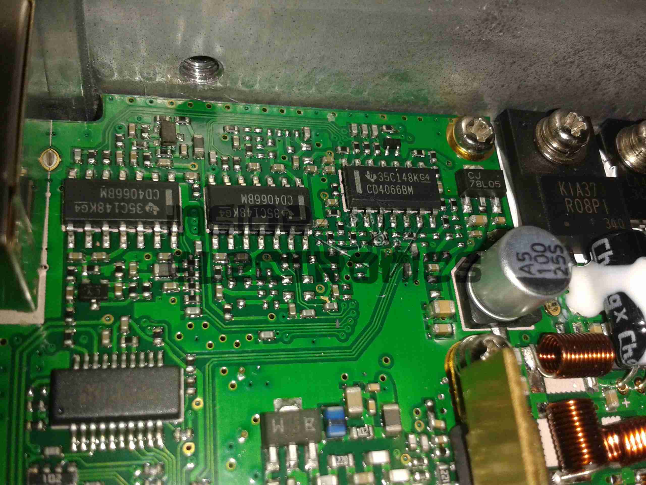
In the top left corner of the radio, near the power input leads, is the power supply & audio amplifier section. Clearly visible are the pair of LA4425A 5W audio power amplifier ICs, these drive the speakers on the top of the radio. Either side of these parts are a 7809 & a 7805 – both linear regulators providing +9v & +5v logic supplies respectively. The large TO220 package device is a KIA378R08PI 3A LDO regulator with ON/OFF control, this one outputs +8v. Just visible in the top right corner are the sockets for the speaker connections.
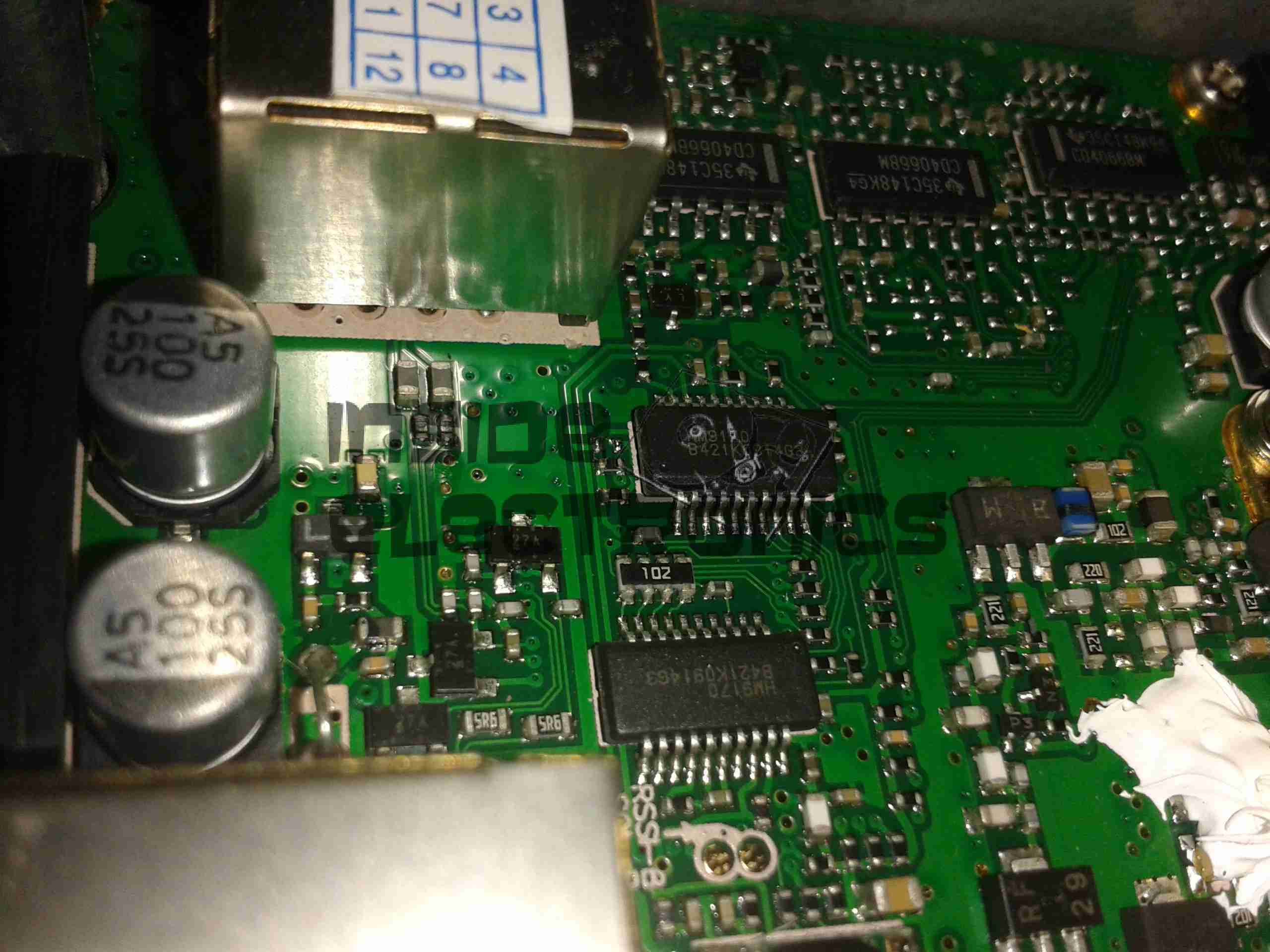
DTMF Circuits
Here are the two ICs for dealing with DTMF tones, they are HM9170 receivers.
Glue Logic
In the corner next to the interface jack, there are some CD4066B Quad Bilateral switches. These make sense since the interface jack has more than a single purpose, these will switch signals depending on what is connected.
RF Section
Here are visible the RF cans for the oscillators, the crystals visible next to the can at the top. The shields are soldered on, so no opening these unfortunately.
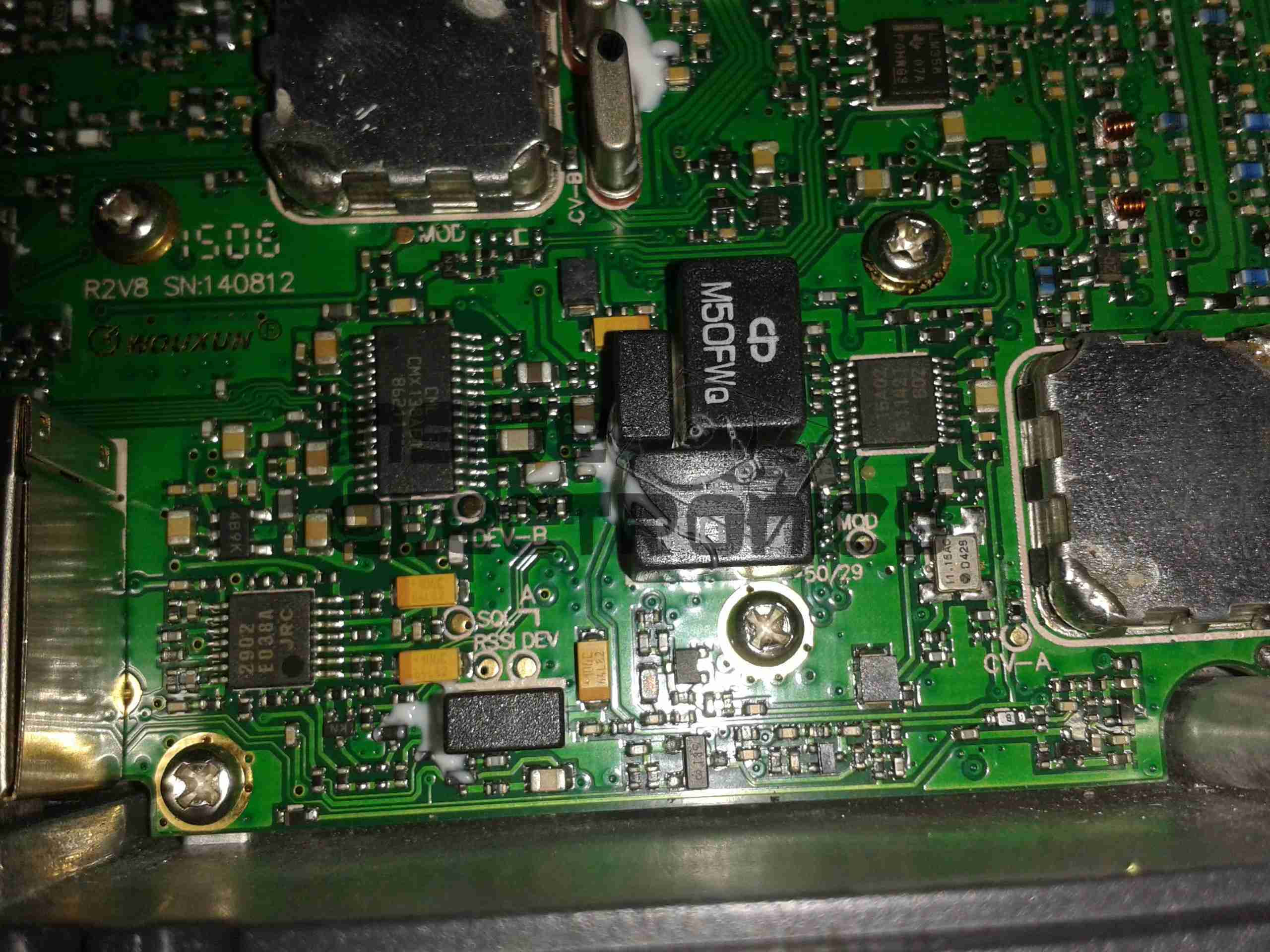
Also visible in this image is a CMX138A Audio Scrambler & Sub-Audio Signalling processor. This IC deals with the Voice Inversion Scrambling feature of the radio, & processes the incoming audio before being sent to the modulator.
Output Filter Network
Shown here is the RF output filter network, this radio uses relays for switching instead of PIN diodes, I imagine for cost reasons. The relay closest to the RF output socket has had a slight accident 🙂 This is slated to be replaced soon.
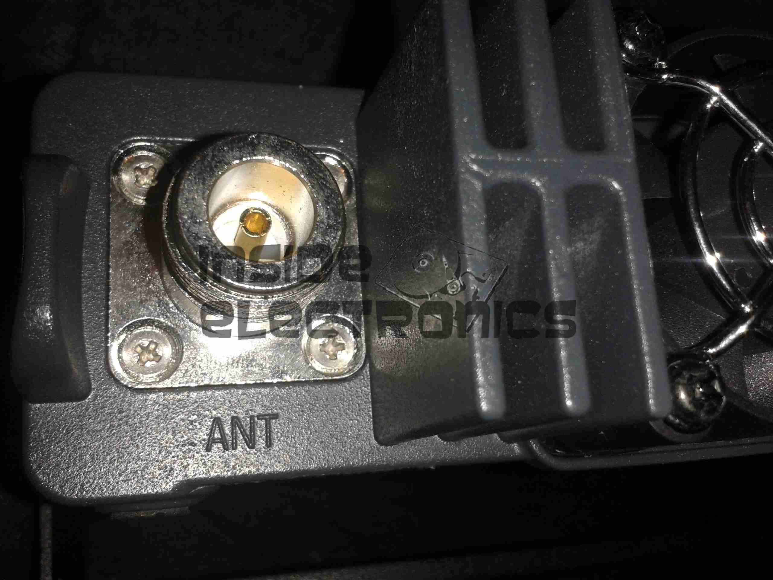
RF Output Jack
Finally, the RF output jack.
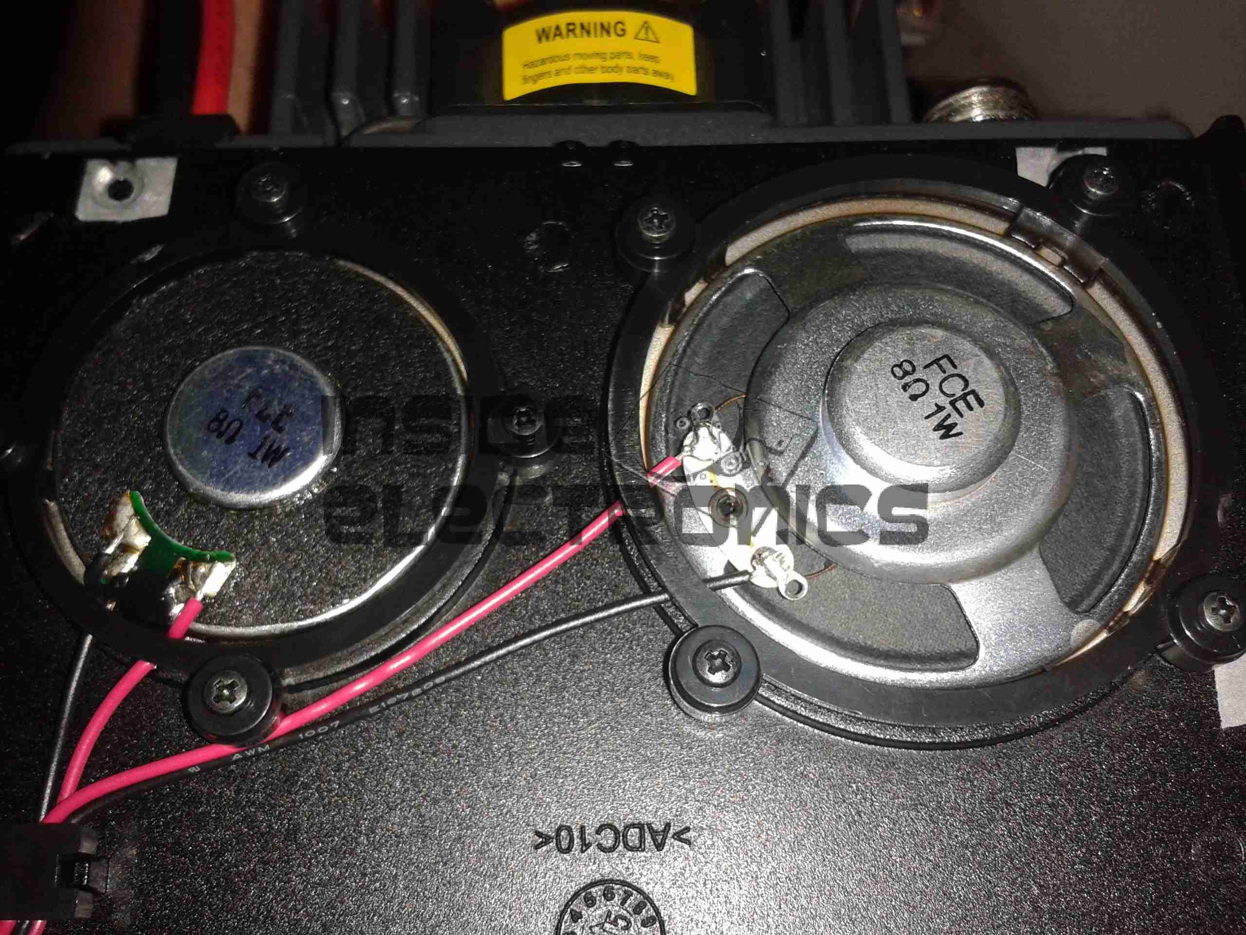
Audio Speakers
Here the speakers are shown, attached to the bottom of the top plate. They are both rated 8Ω 1W.
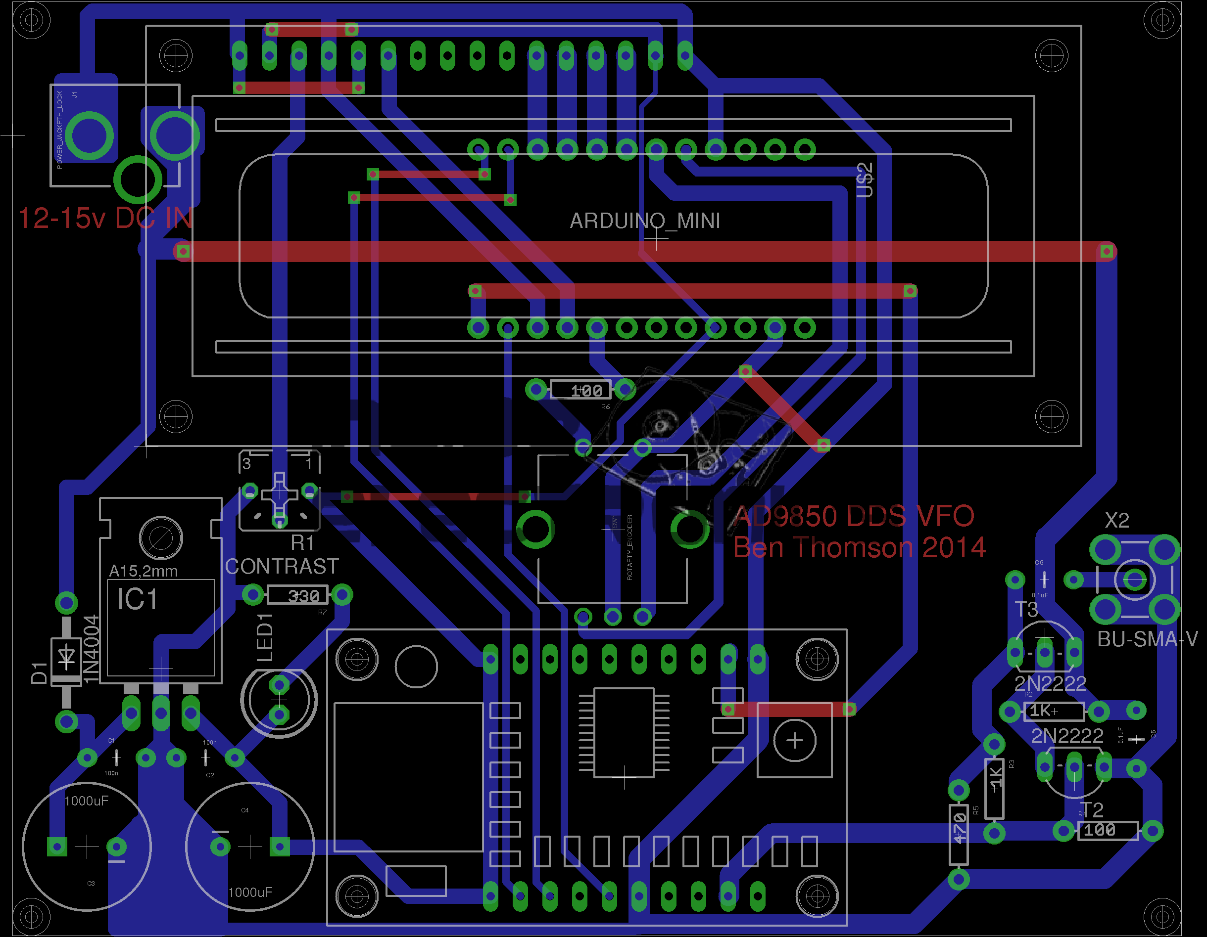
I recently came across a design for an Arduino controlled AD9850 DDS module, created by AD7C, so I figured I would release my Eagle CAD design for the PCB here.
It is a mainly single-sided layout, only a few links on the top side are needed so this is easy to etch with the toner transfer method.
My version uses an Arduino Pro Mini, as the modular format is much easier to work with than a bare ATMega 328.
RF output is via a SMA connector & has a built in amplifier to compensate for the low level generated by the DDS Module.
DDS VFO
Version 2 Update: Added reverse polarity protection, added power indicator LED, beefed up tracks around the DC Jack.
[download id=”5571″]
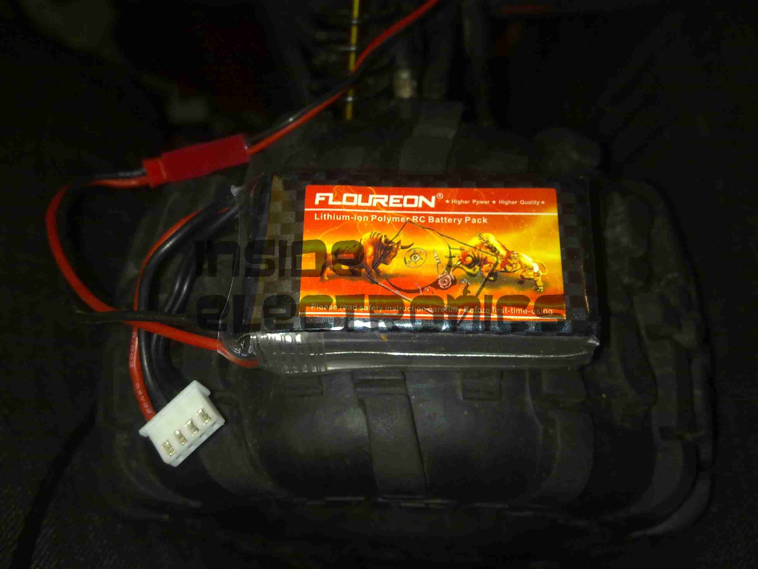
To provide more run time with the conversion to petrol & spark ignition, I have also upgraded the on-board electronics supply to compensate for the extra ~650mA draw of the ignition module.
This modification is centred around a 3S Lithium-Polymer battery pack, providing a nominal 11.1v to a voltage regulator, which steps down this higher voltage to the ~6v required by the receiver & servo electronics.
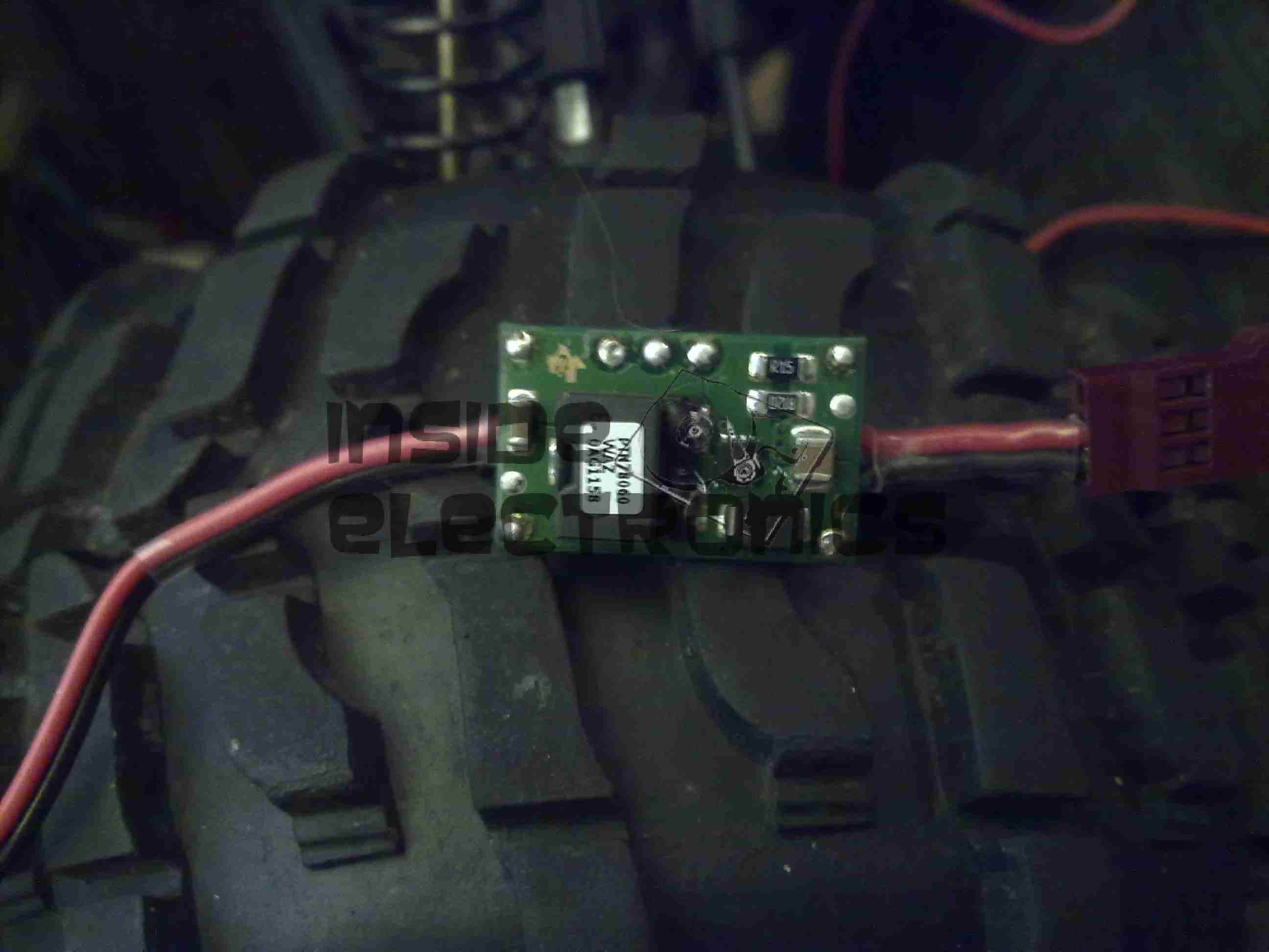
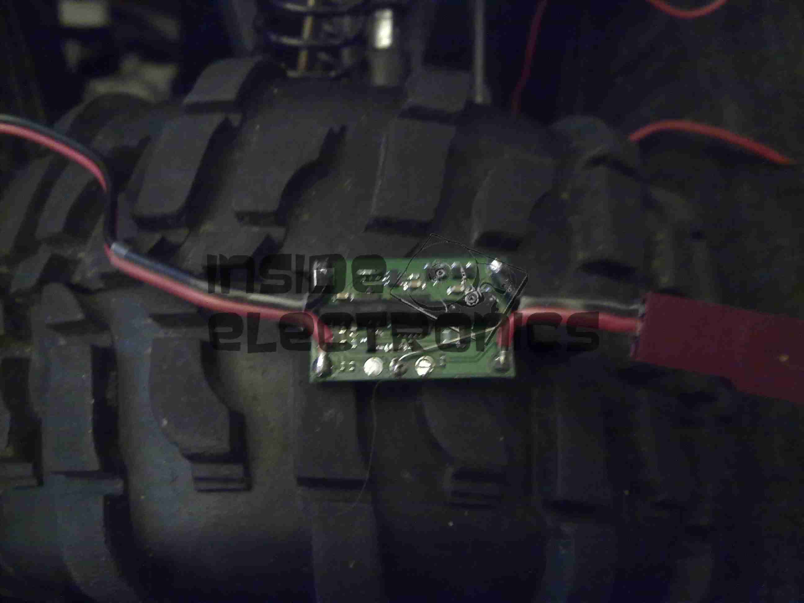
Power RegulatorPower Regulator
The regulator, shown above, is a Texas Instruments PTN78060WAZ wide-input voltage adjustable regulator. This module has an exceptionally high efficiency of ~96% at it’s full output current of 3A. The output voltage is set by a precision resistor, soldered to the back of the module, in this case 6.5v. Standard RC connectors are used on the regulator to allow connection between the power switch & the radio receiver.
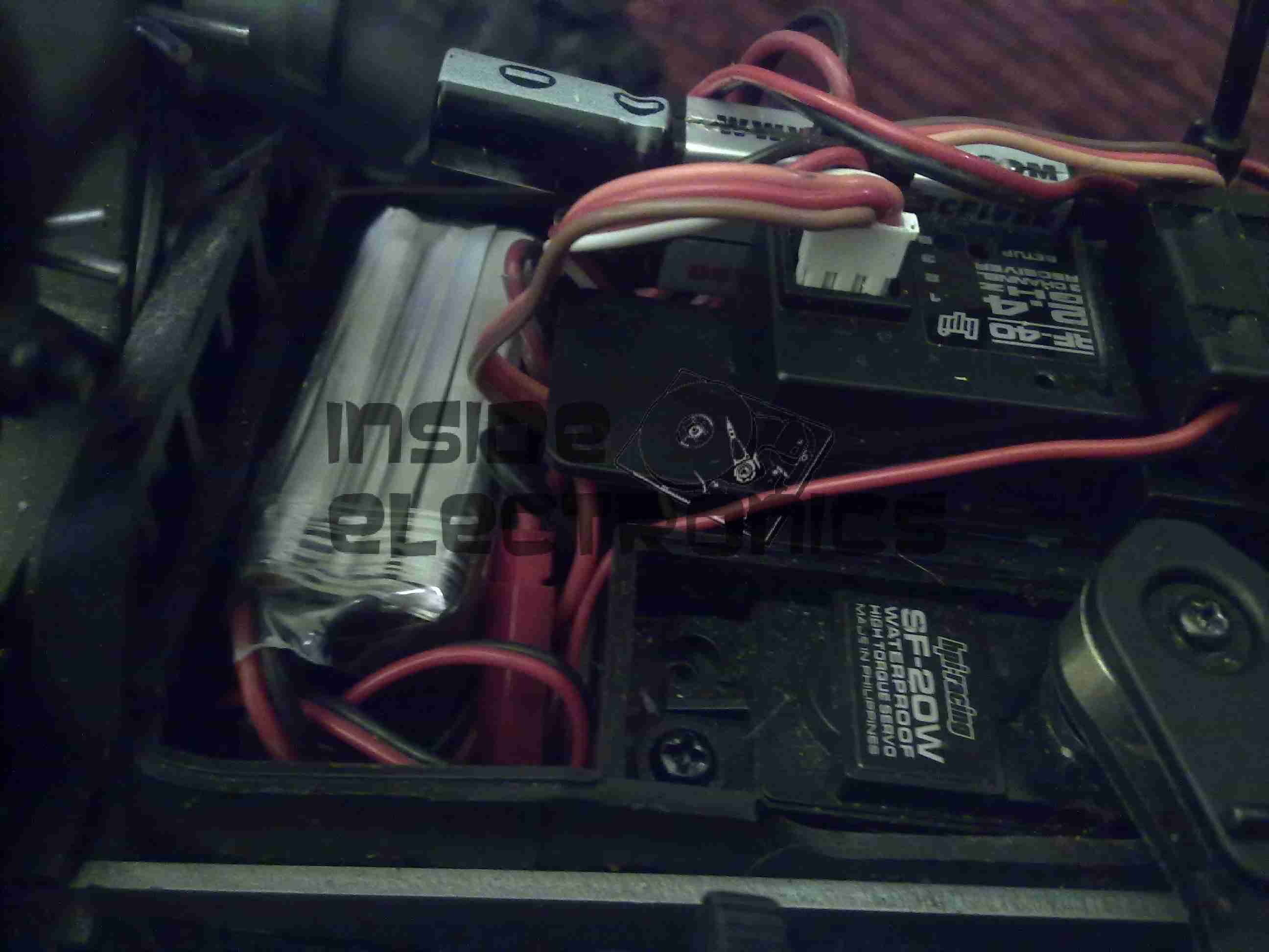
Receiver Box
Everything tucked away into place inside the receiver box. The 3S 1000mAh LiPo fits perfectly in the space where the original Ni-Mh hump pack was located.
The completely stable output voltage of the regulator over the discharge curve of the new battery gives a much more stable supply to the radio & ignition, so I should experience fewer dropouts. Plus the fact that the engine now relies on power from the receiver pack to run, it’s a built in fail safe – if the power dies to the receiver, the engine also cuts out.
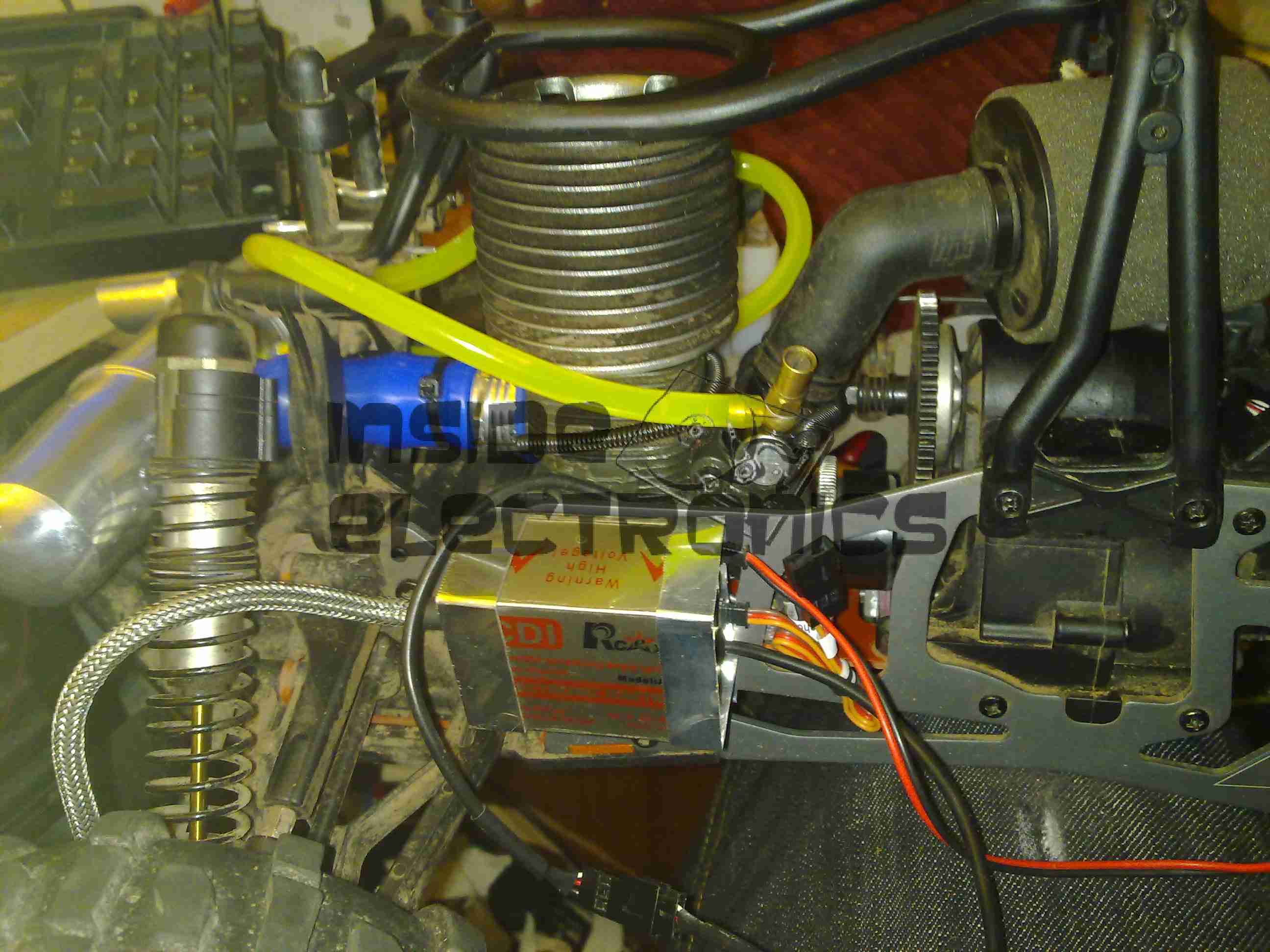
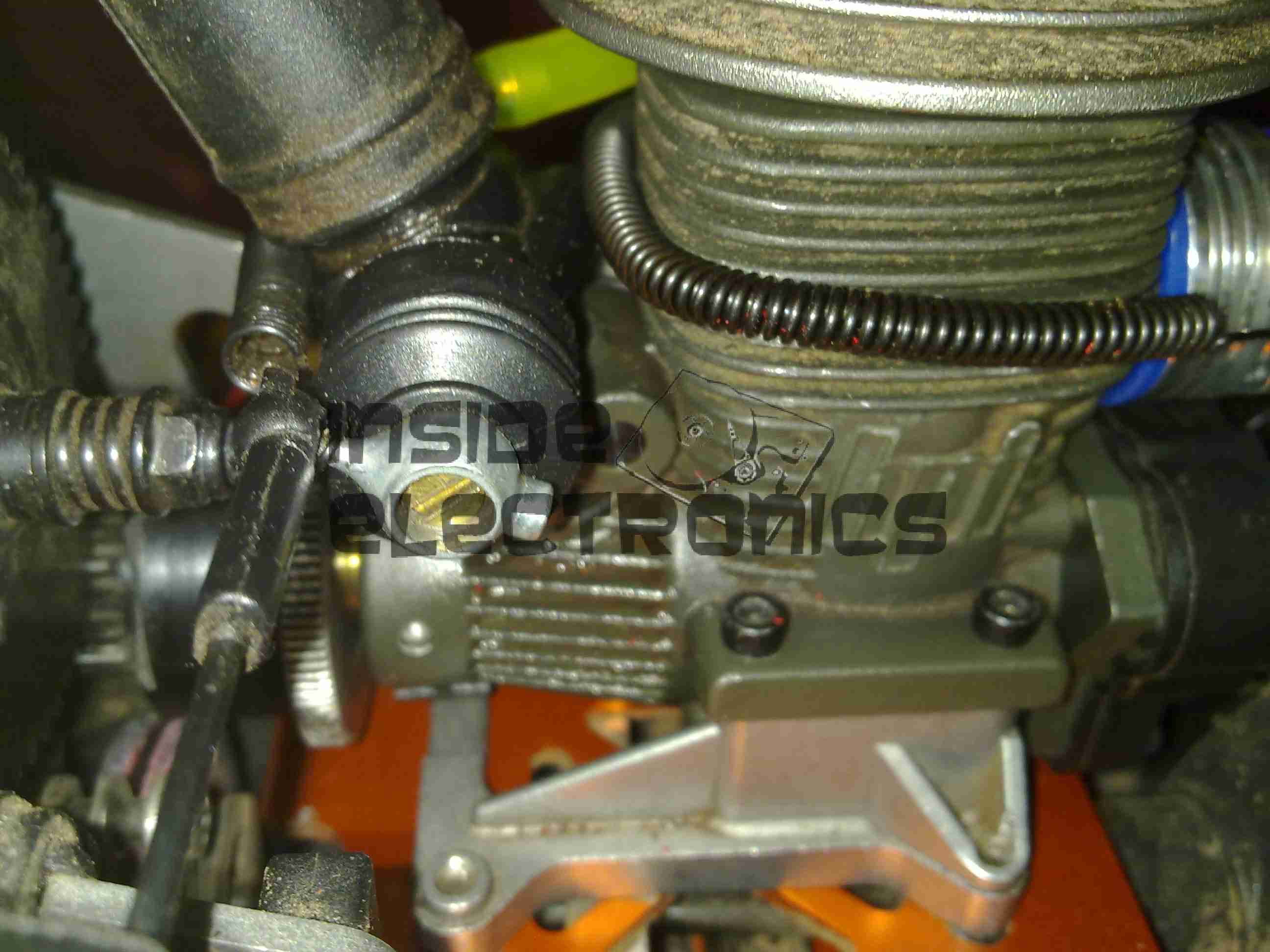
The engine now with it’s required ignition sensor, it is now mounted back on the chassis of the model. I have replaced the stock side exhaust with a rear silencer, so I could fit the ignition module in place next to the engine.
For the mounting, I fabricated a pair of brackets from 0.5mm aluminium, bent around the module & secured with the screws that attach the engine bed plate to the TVPs. The ignition HT lead can be routed up in front of the rear shock tower to clear all moving suspension parts, with the LT wiring tucked into the frame under the engine.
In this location the module is within the profile of the model chassis so it shouldn’t get hit by anything in service.
Rear Exhaust
New exhaust silencer fitted to the back of the model. This saves much space on the side of the model & allows the oily exhaust to be discharged away from the back wheel – no more mess to wipe up.
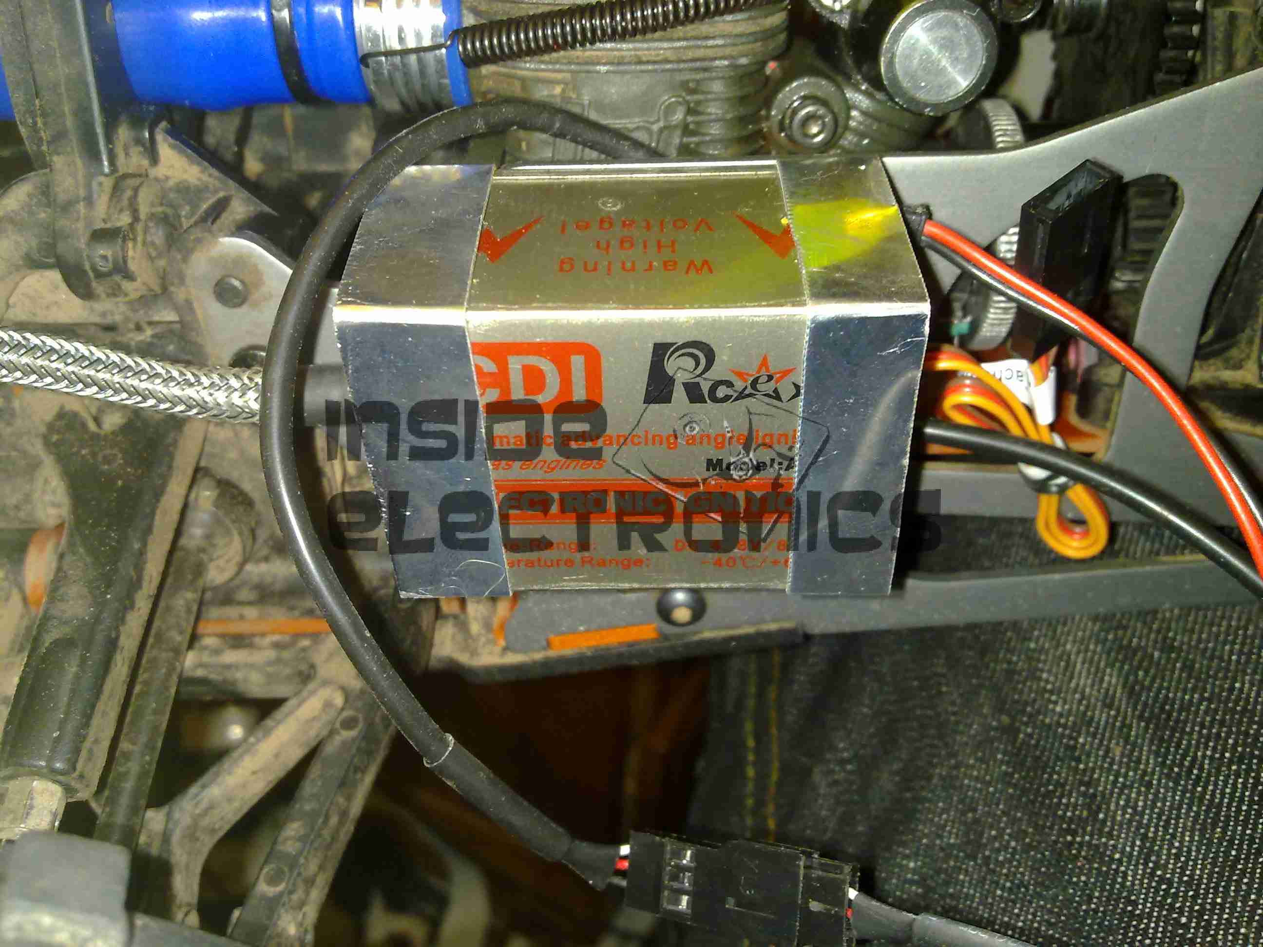
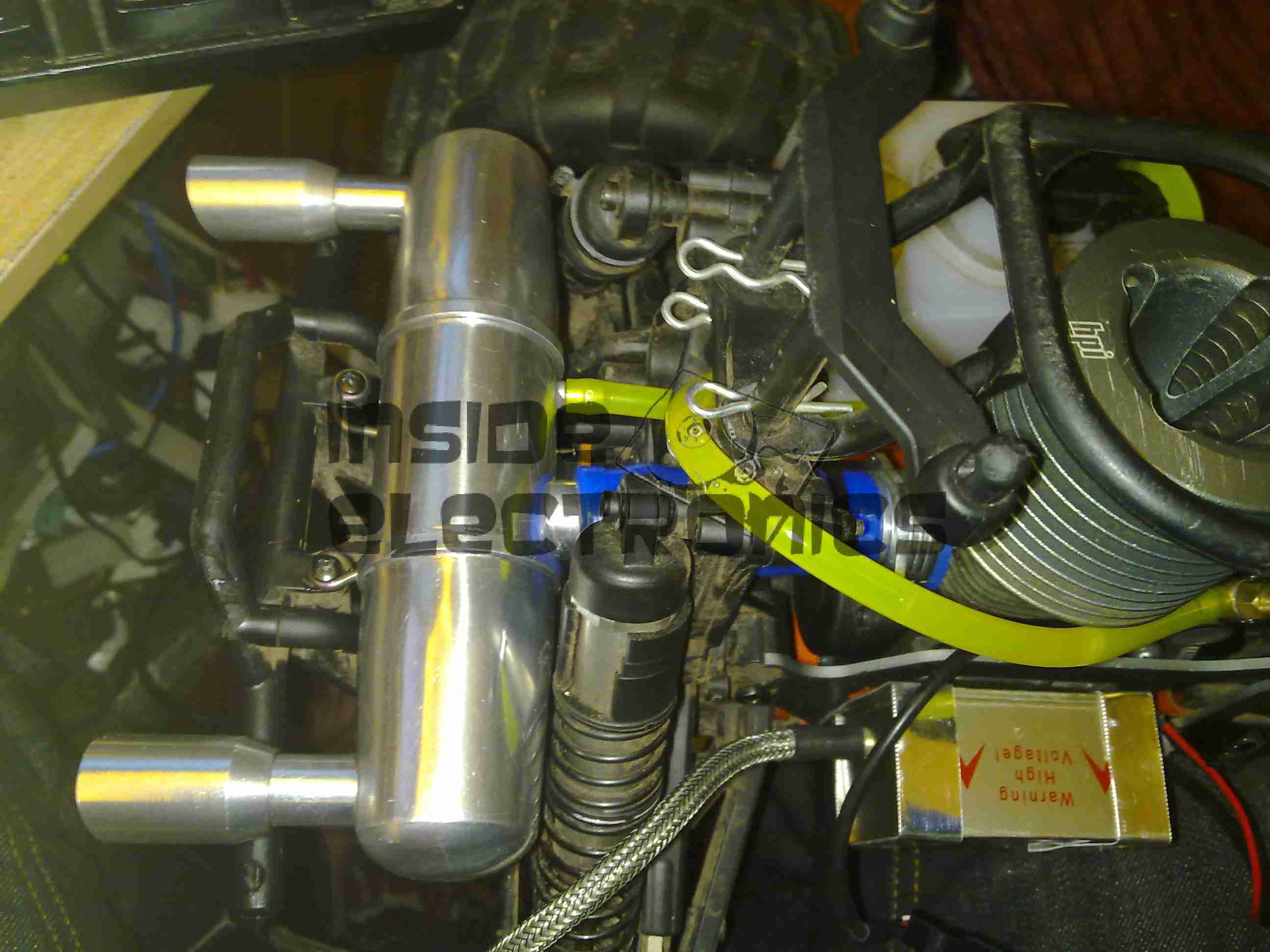
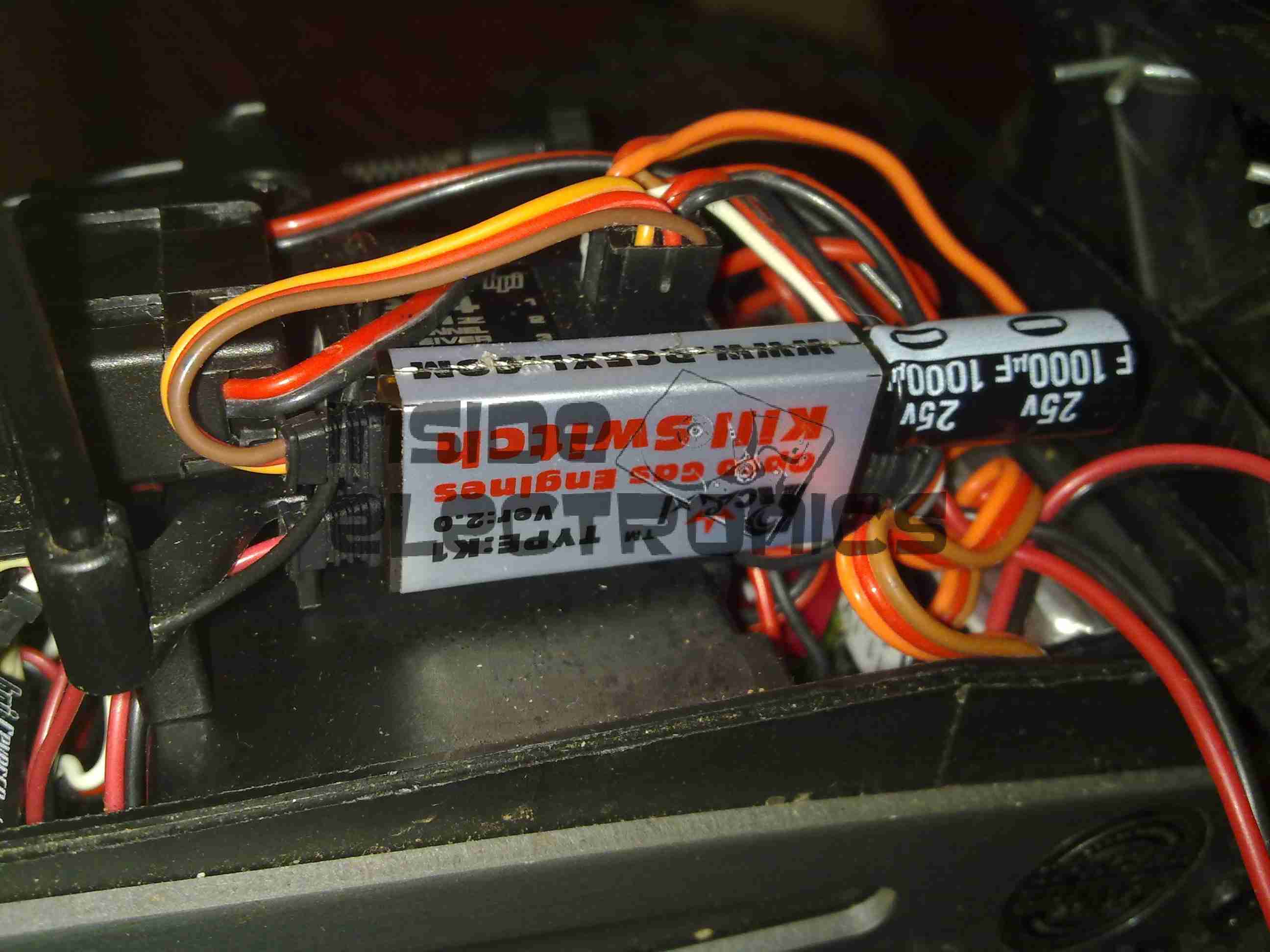
Kill Switch
The ignition switch fitted into the receiver box. This is wired into channel 3 of the TF-40 radio, allowing me to remotely kill the engine in case of emergency. I have fitted a 25v 1000µF capacitor to smooth out any power fluctuations from the ignition module.
The radio is running from a 11.1v 1Ah 3S LiPo pack connected to a voltage regulator to give a constant 6.5v for the electronics. I found this is much more reliable than the standard 5-cell Ni-MH hump packs.
Fuel Tank
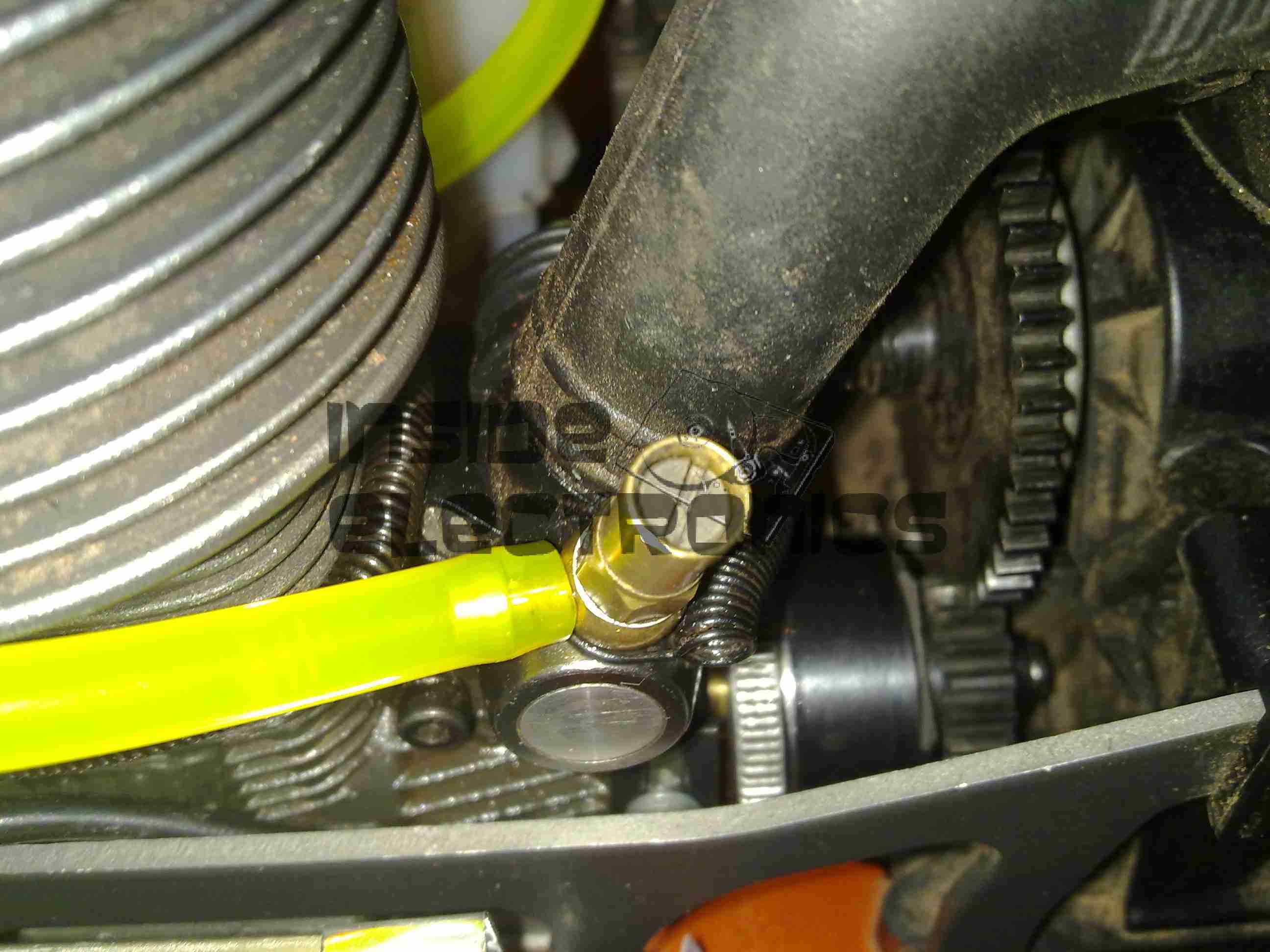
The stock silicone fuel tubing has been replaced with Tygon tubing to withstand the conversion to petrol.
High Speed Needle
High speed needle tweaked to provide a basic running setting on petrol. This is set to ~1.5mm below flush with the needle housing.
Low Speed Needle
Low speed needle tweaked to provide a basic running setting on petrol. This is set to ~1.73mm from flush with the needle housing.
As petrol is a much higher energy density fuel, it requires much more air than the methanol glow fuel – ergo much leaner settings.
The settings listed should allow an engine to run – if nowhere near perfectly as they are still rather rich. It’s a good starting point for eventual tuning.
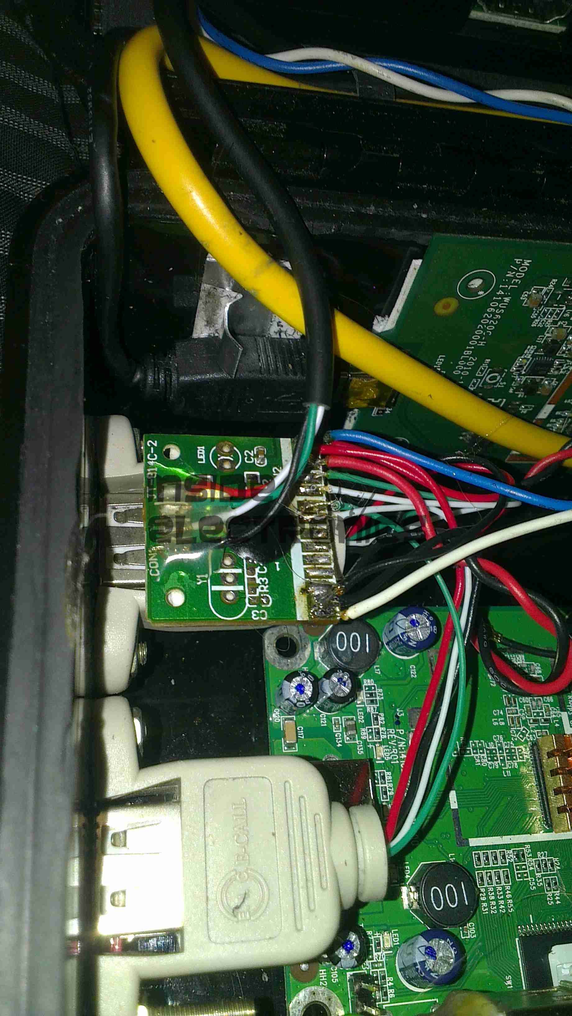
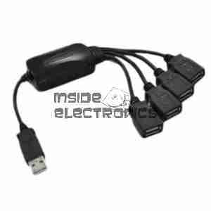
As the first USB hub I was using was certainly not stable – it would not enumerate between boots & to get it working again would require waiting around 12 hours before applying power, it has been replaced. This is a cheapie eBay USB hub, of the type shown below.
These hubs are fantastic for hobbyists, as the connections for power & data are broken out on the internal PCB into a very convenient row of pads, perfect for integration into many projects.
Breakout Hub
I now have two internal spare USB ports, for the inbuilt keyboard/mouse receiver & the GPS receiver I plan to integrate into the build.
These hubs are also made in 7-port versions, however I am not sure if these have the same kind of breakout board internally. As they have the same cable layout, I would assume so.
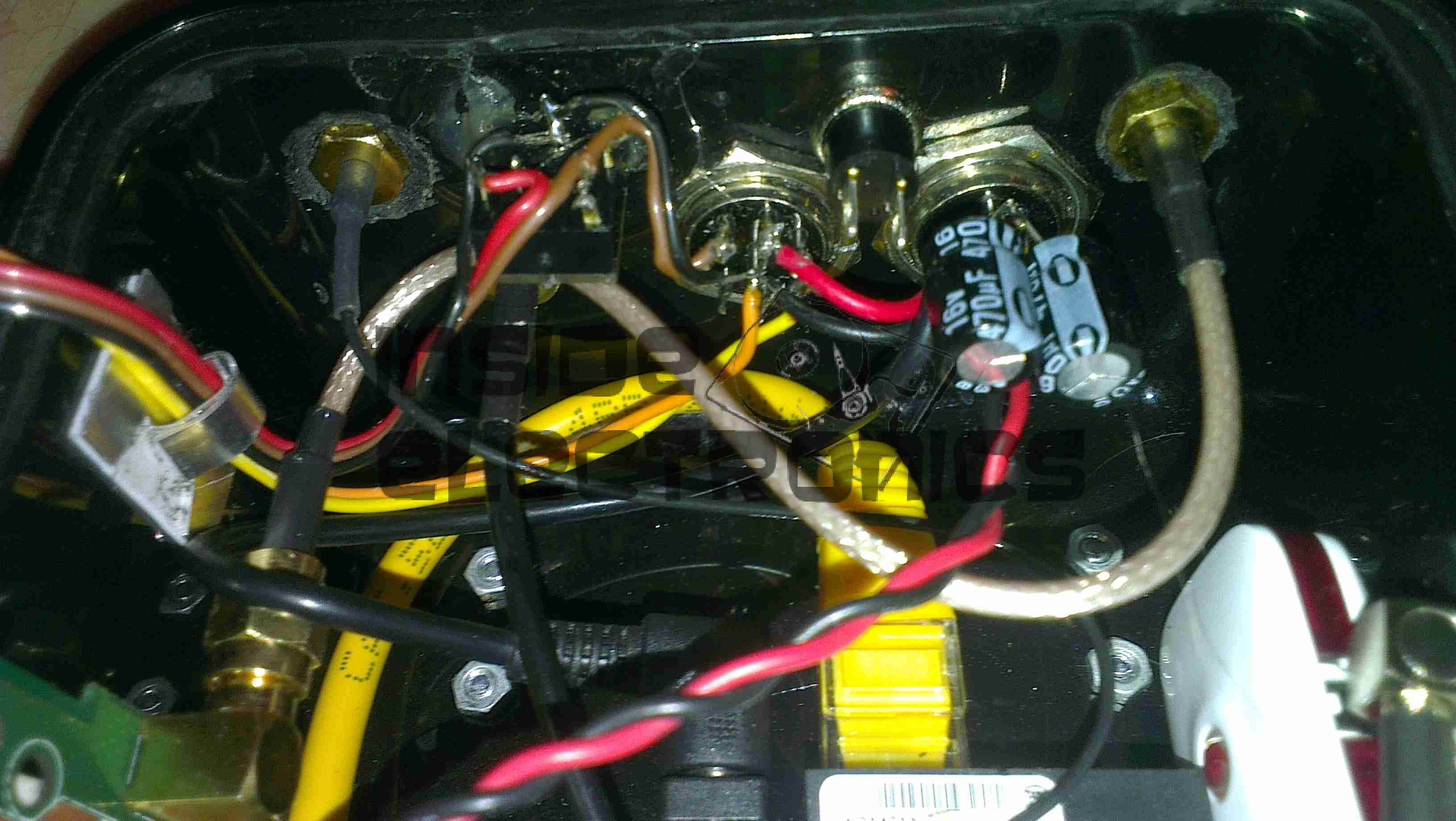
Connector Panel
Here is a closeup of the back of the connectors, showing a couple of additions.
I have added a pair of 470µF capacitors across the power rails, to further smooth out the ripple in the switching power supply, as I was having noise issues on the display.
Also, there is a new reset button added between the main interface connectors, which will be wired into the pair of pads that the Raspberry Pi has to reset the CPU.
This can be used as a power switch in the event the Pi is powered down when not in use & also to reset the unit if it becomes unresponsive.
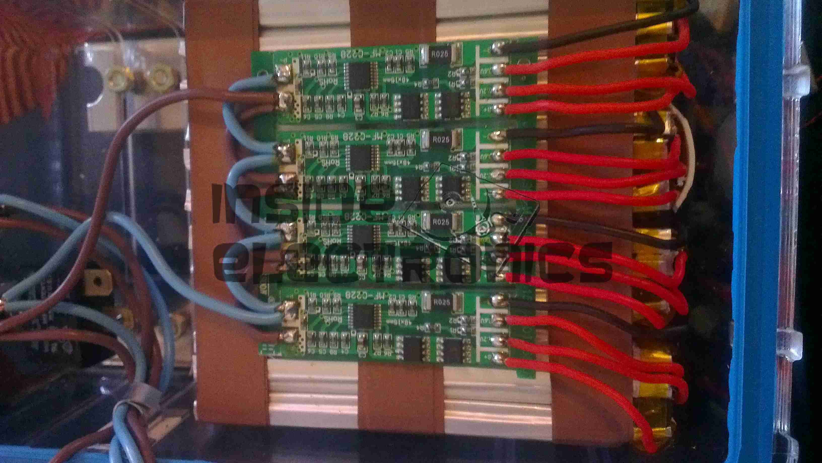
The final part for the battery pack has finally arrived, the PCM boards. These modules protect the cells by cutting off the power at overcharge, undercharge & overcurrent. Each cell is connected individually on the right, 12v power appears on the left connections. These modules also ensure that all the cells in the pack are balanced.
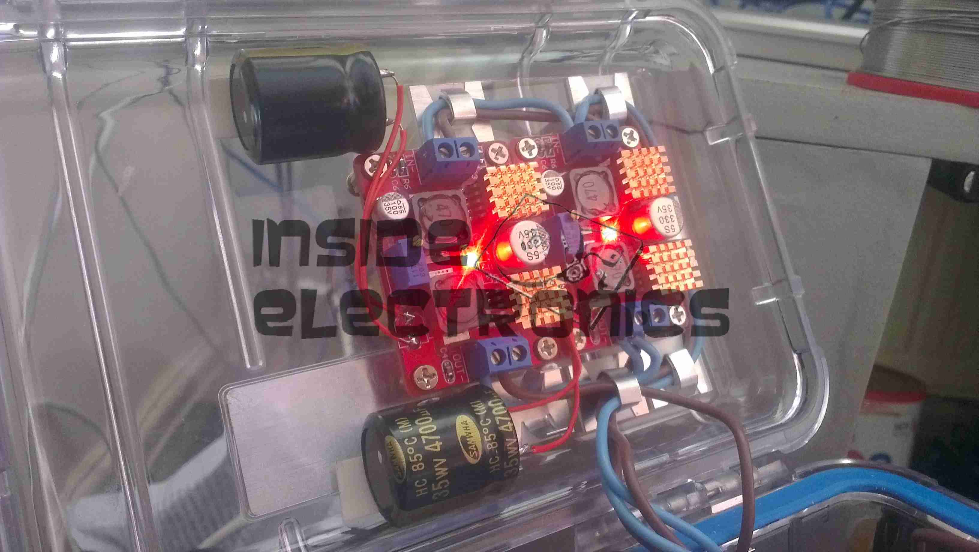
A few modifications were required to the SMPS modules to make the power rails stable enough to run the Pi & it’s monitor. Without these the rails were so noisy that instability was being caused.
I have replaced the 100µF output capacitors & replaced them with 35v 4700µF caps. This provides a much lower output ripple.
There are also heatsinks attached to the converter ICs to help spread the heat.
Tip Jar
If you’ve found my content useful, please consider leaving a donation by clicking the Tip Jar below!
All collected funds go towards new content & the costs of keeping the server online.