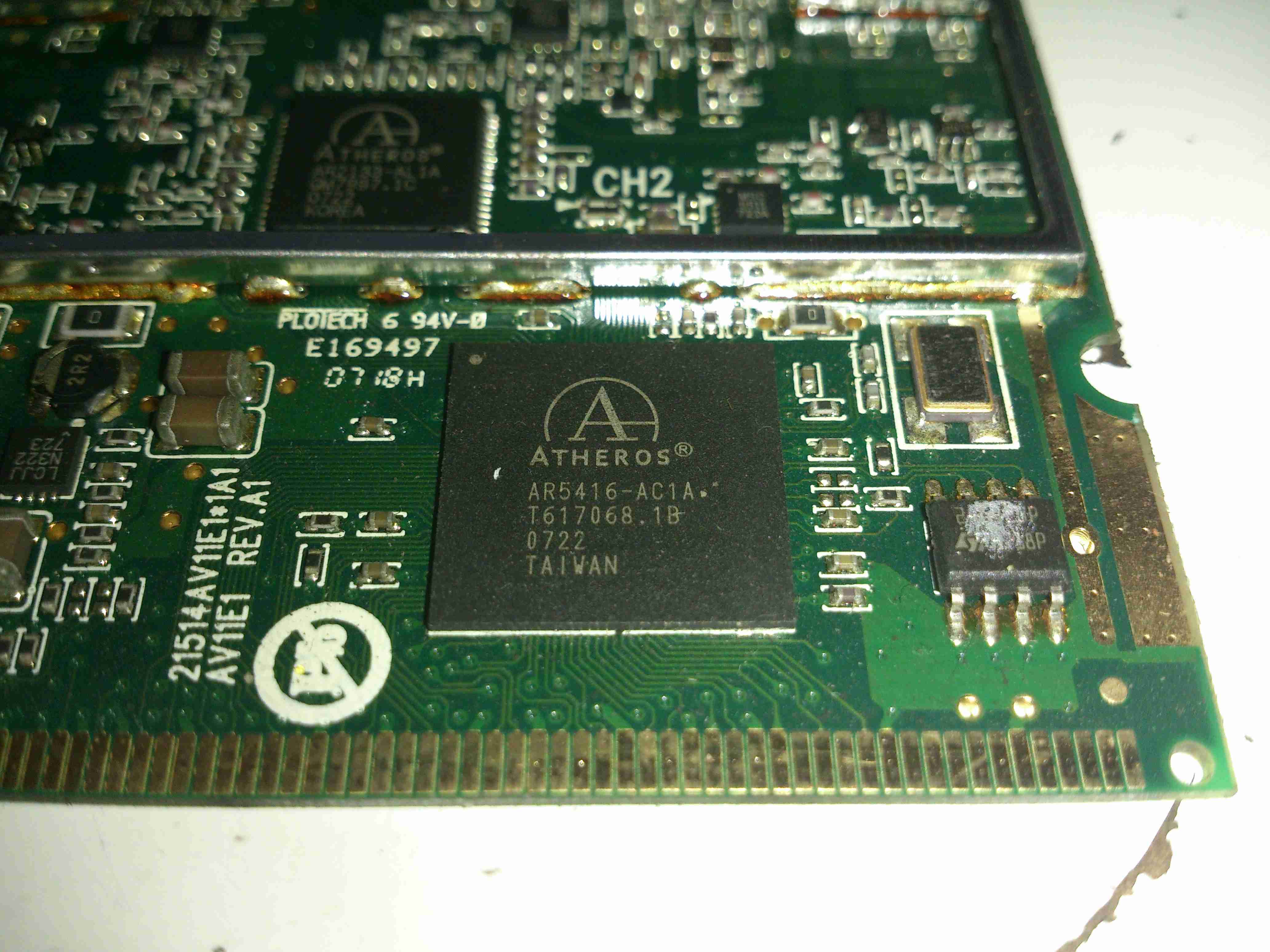
Here’s a quick look at one of the now surplus cards from my old networking system, a MiniPCI Wireless interface card.
Card Overview
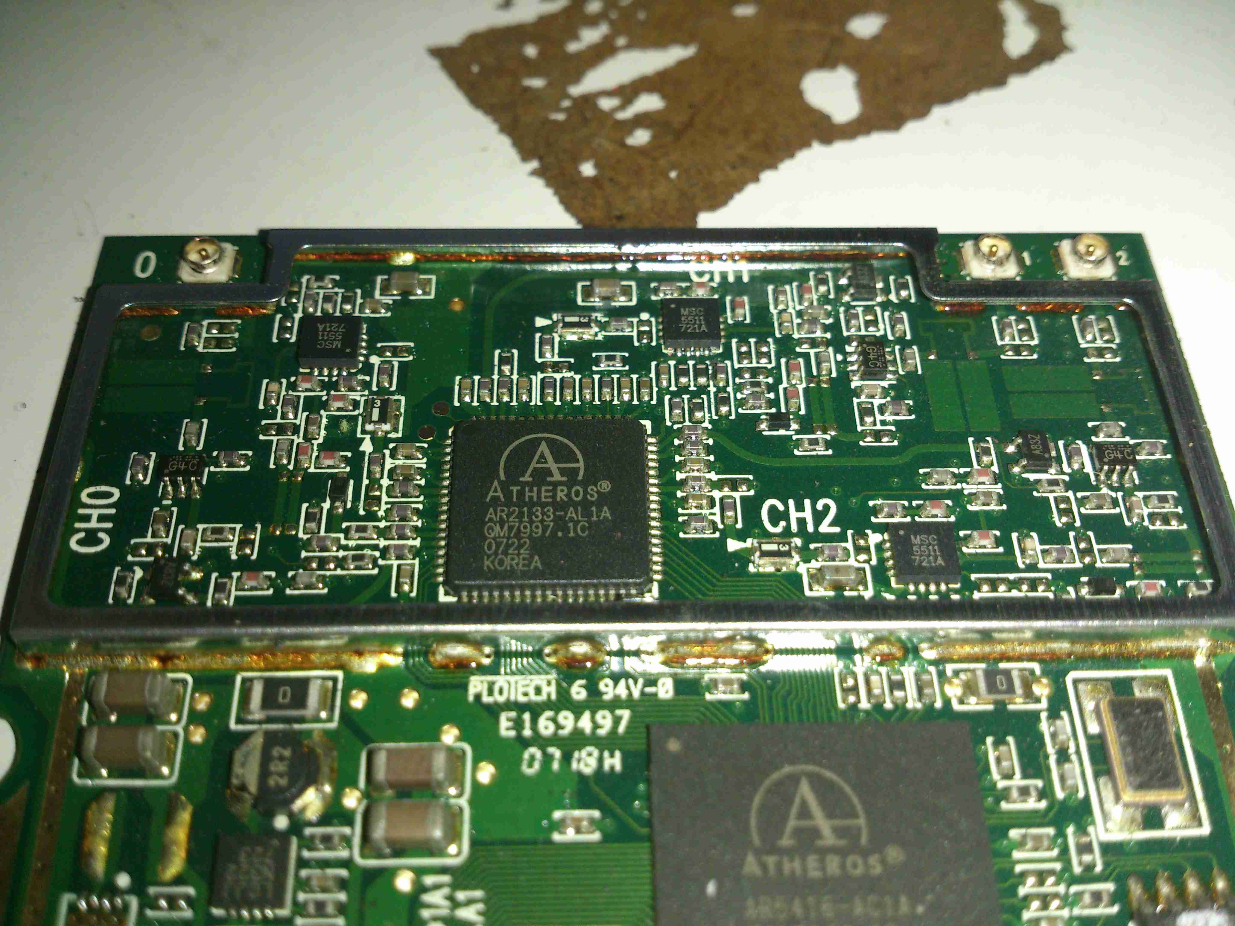
This is an older generation card, one of the first with Wireless N support on 2.4GHz.
PCI Chipset
Network PHY & firmware EEPROM. Power supply stuff is over to the left.
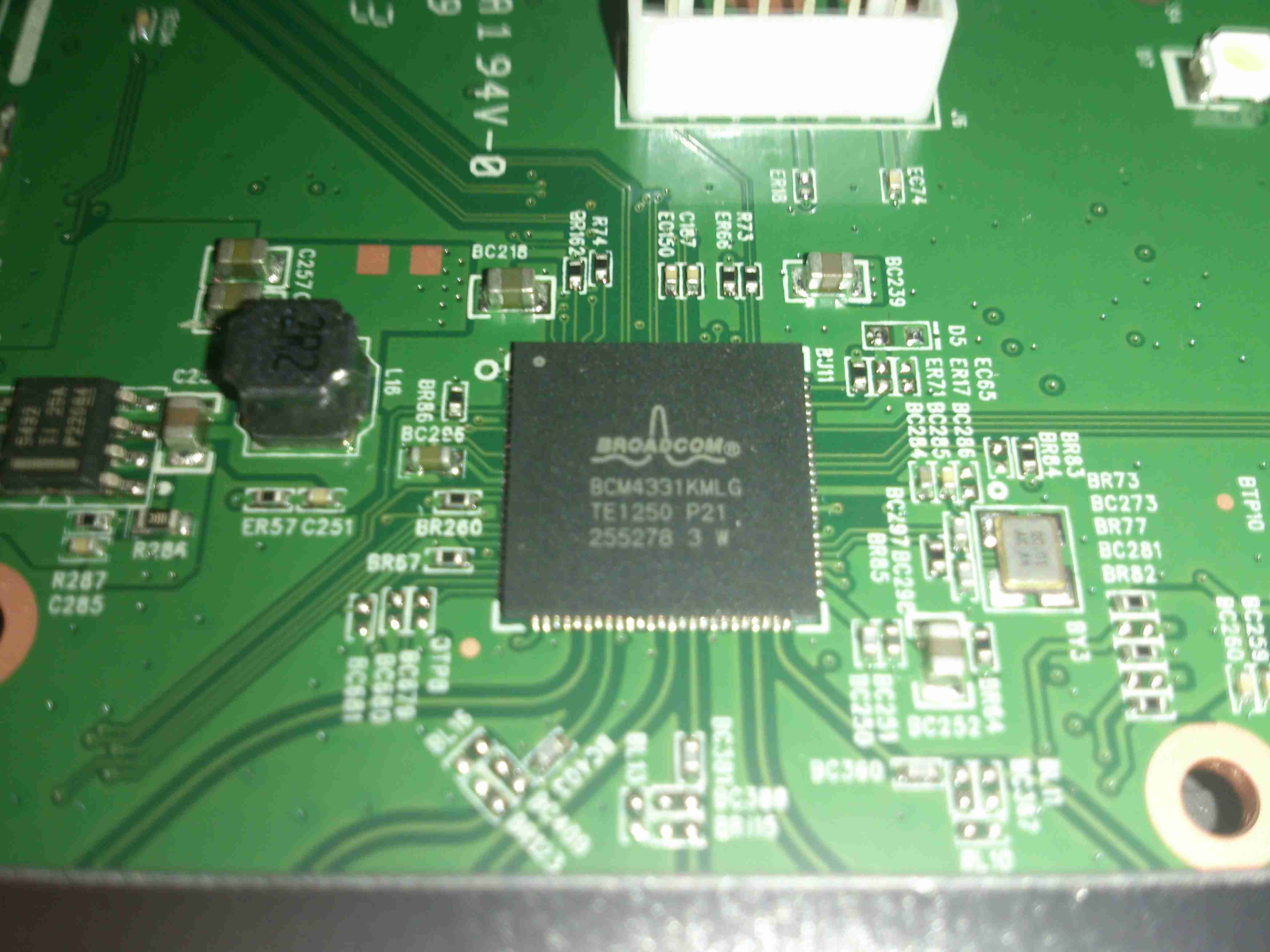
RF Transceiver
Inside the shield is the RF Transceiver IC & it’s associated RF power amplifier ICs for each antenna. These power amplifiers are LX5511 types from Microsemi, with a maximum power output of +26dBm.
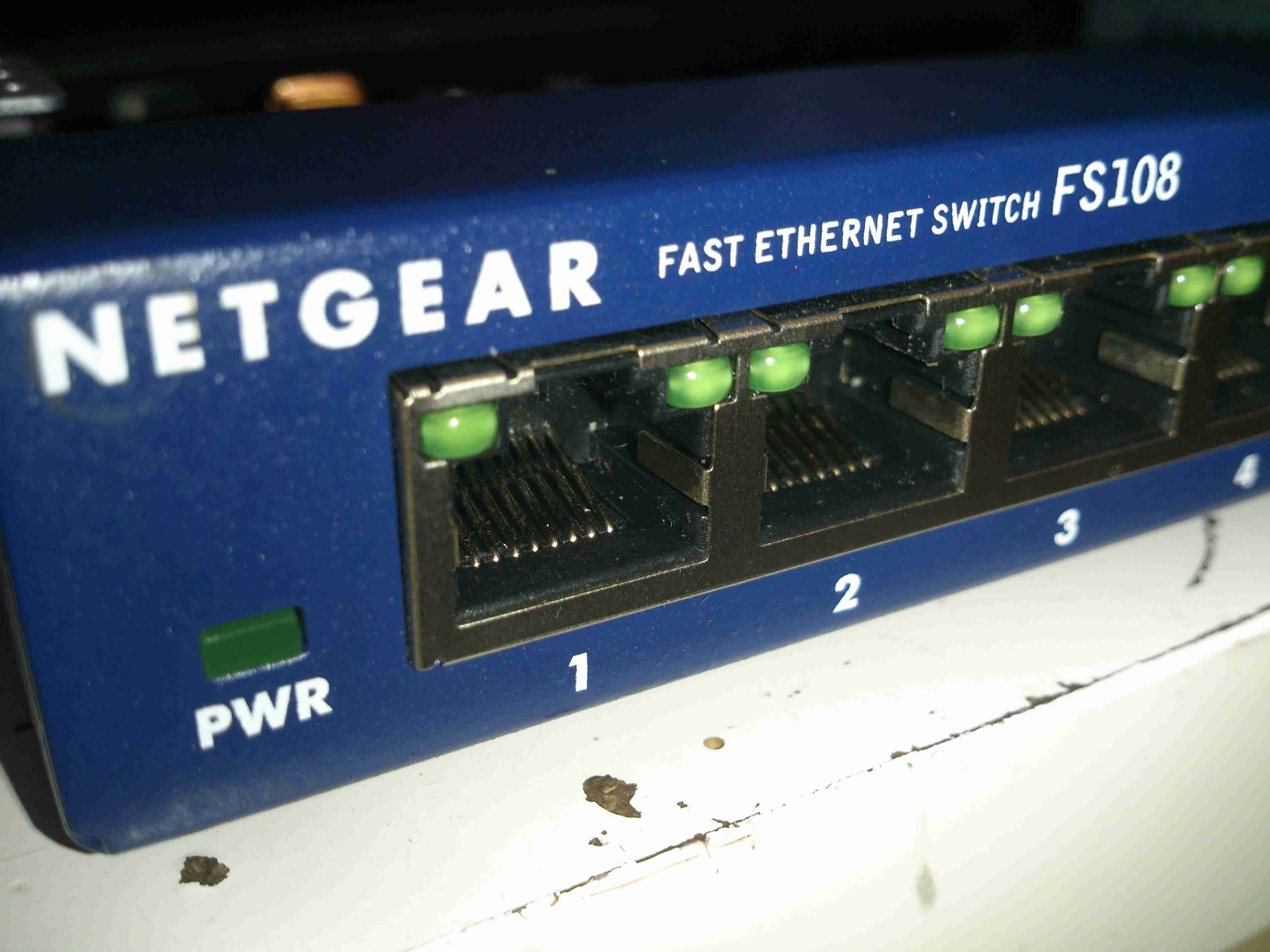
During the replacement of the networking onboard nb Tanya Louise with gigabit, the main 8-port distribution switch was also changed. Here’s a quick teardown of the old one.
Netgear FS108
This has been quite a reliable switch for the internal networking on board, but the time has come to switch over to something a little faster. This switch will be getting repurposed for the slower devices on my network, such as the radiation monitor & the raspberry Pi systems.
Cover Removed
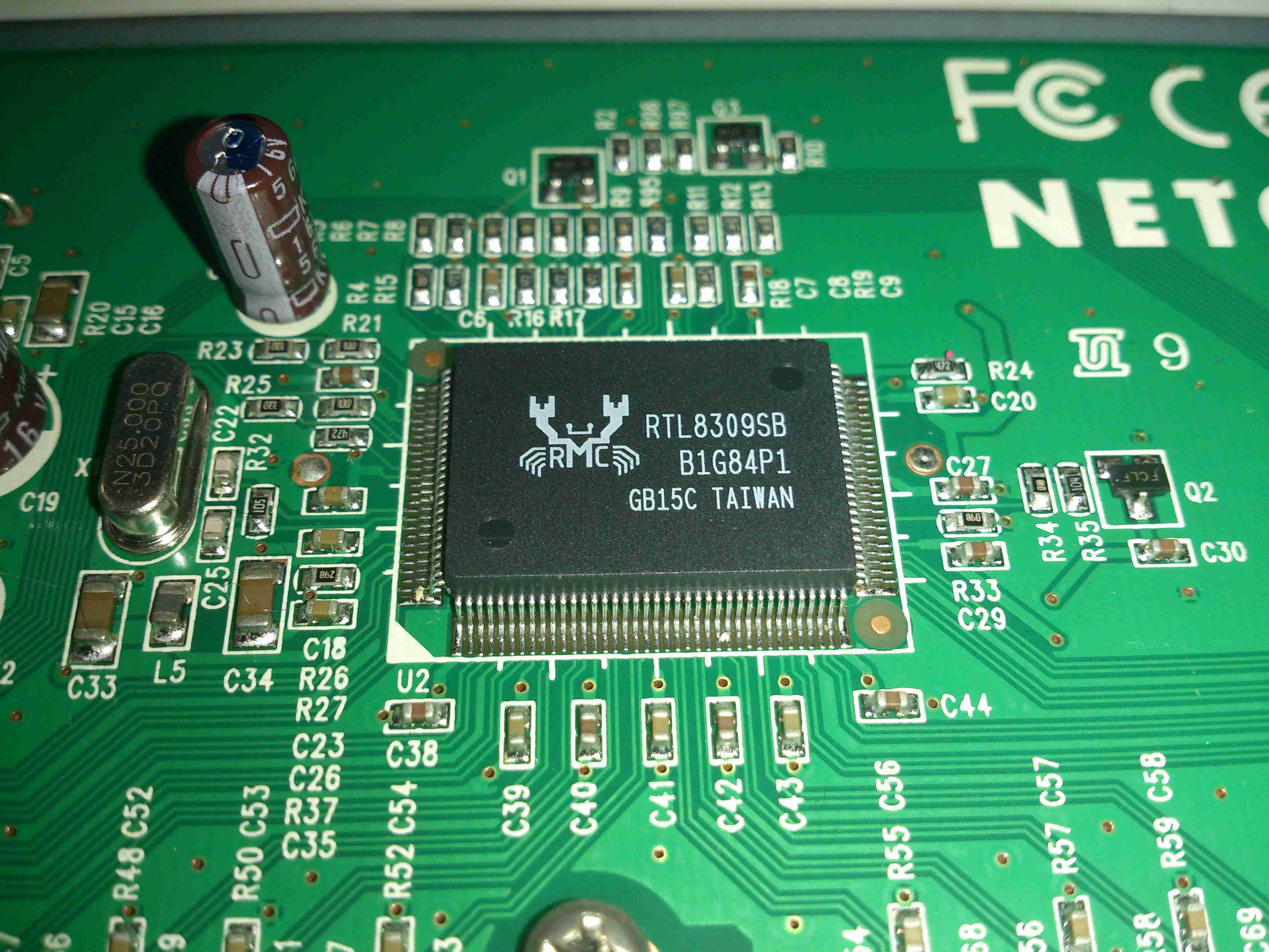
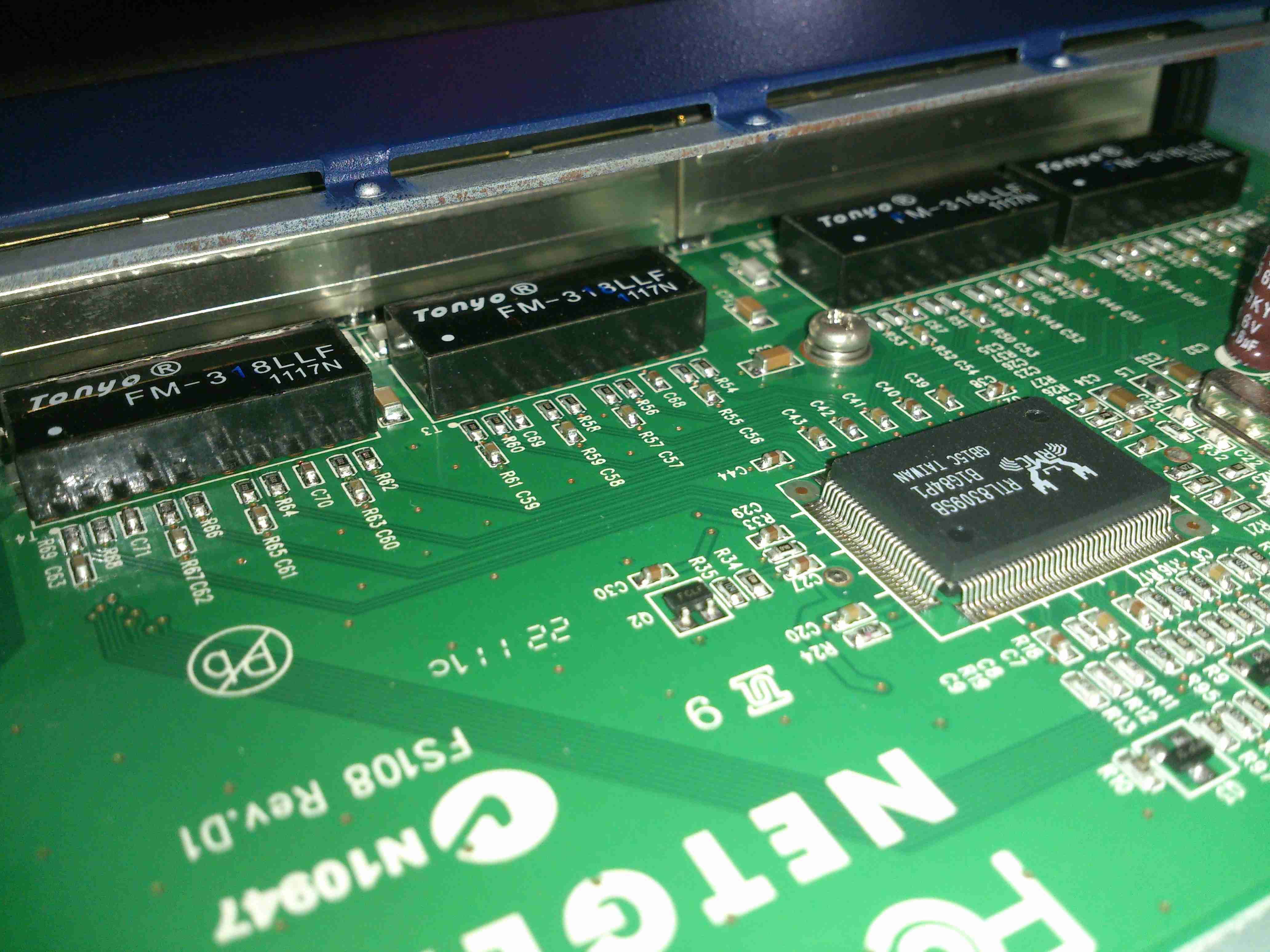
Here’s the top removed from the switch. It’s a very simple construction, with a small power supply section & the main switch IC in the centre.
Main Switch IC
All the magic happens in this main IC, a Realtek RTL8309SB Fast Ethernet switch. This is a feature-packed IC, with support for VLAN tagging, but being in a small unmanaged switch the extra features aren’t used.
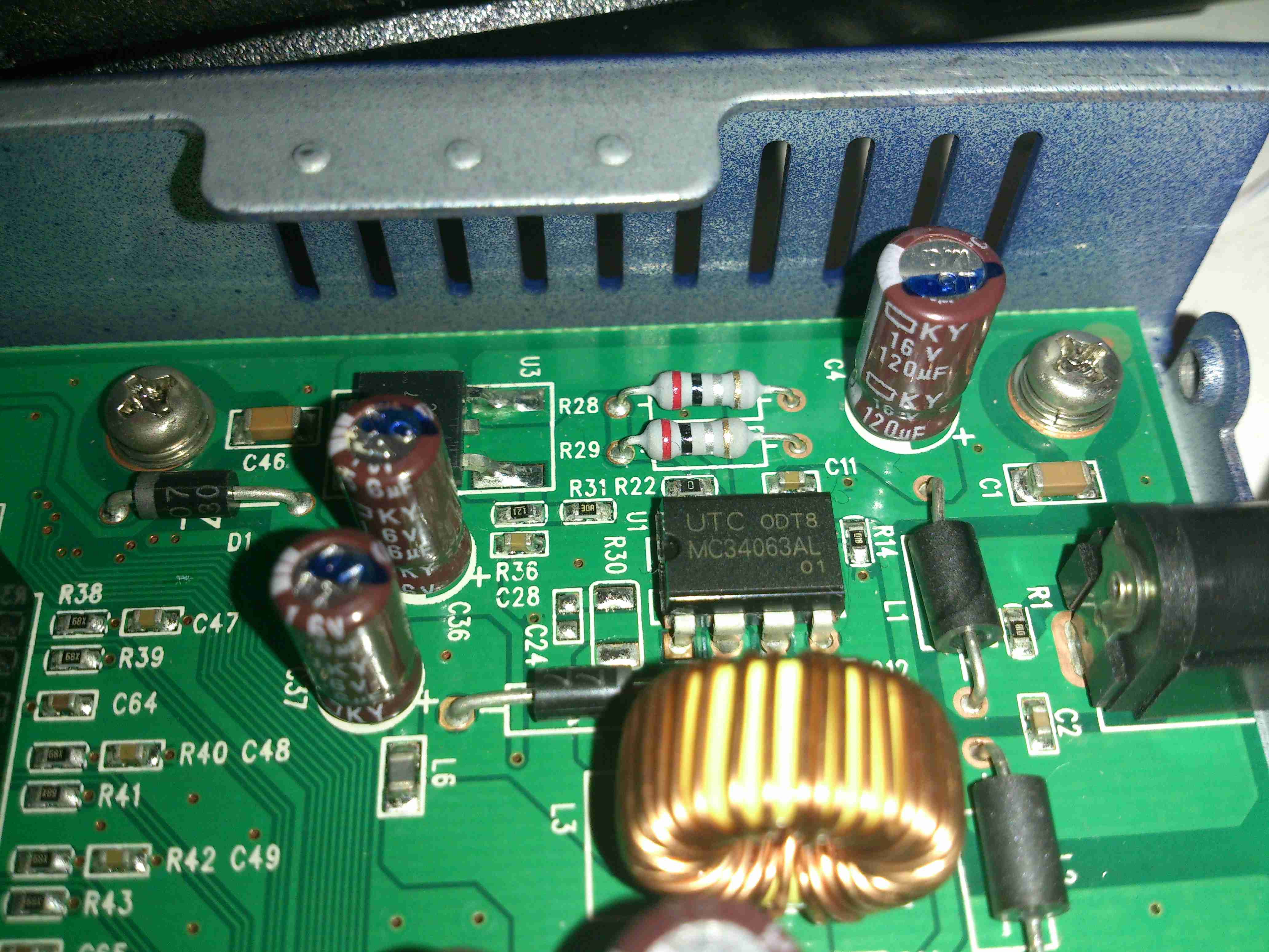
Power Supply
Main power supply is provided by a jelly bean MC34063 DC-DC converter, and an adjustable LM1117 linear regulator. Nothing much special here.
Ethernet Magnetics
The only other parts are the magnetics for the ethernet interfaces, behind the ports themselves.
Since the boat was still running it’s internal network on 10/100M speeds, an upgrade was decided on, the internal WiFi signal strength was also pretty poor further than a few feet from the NOC.
The new router is a Cisco/Linksys AC1750 model, with gigabit networking, and full 802.11ac 2.4/5GHz Wireless. This router also has a built in media server, print server, USB3 & USB2.
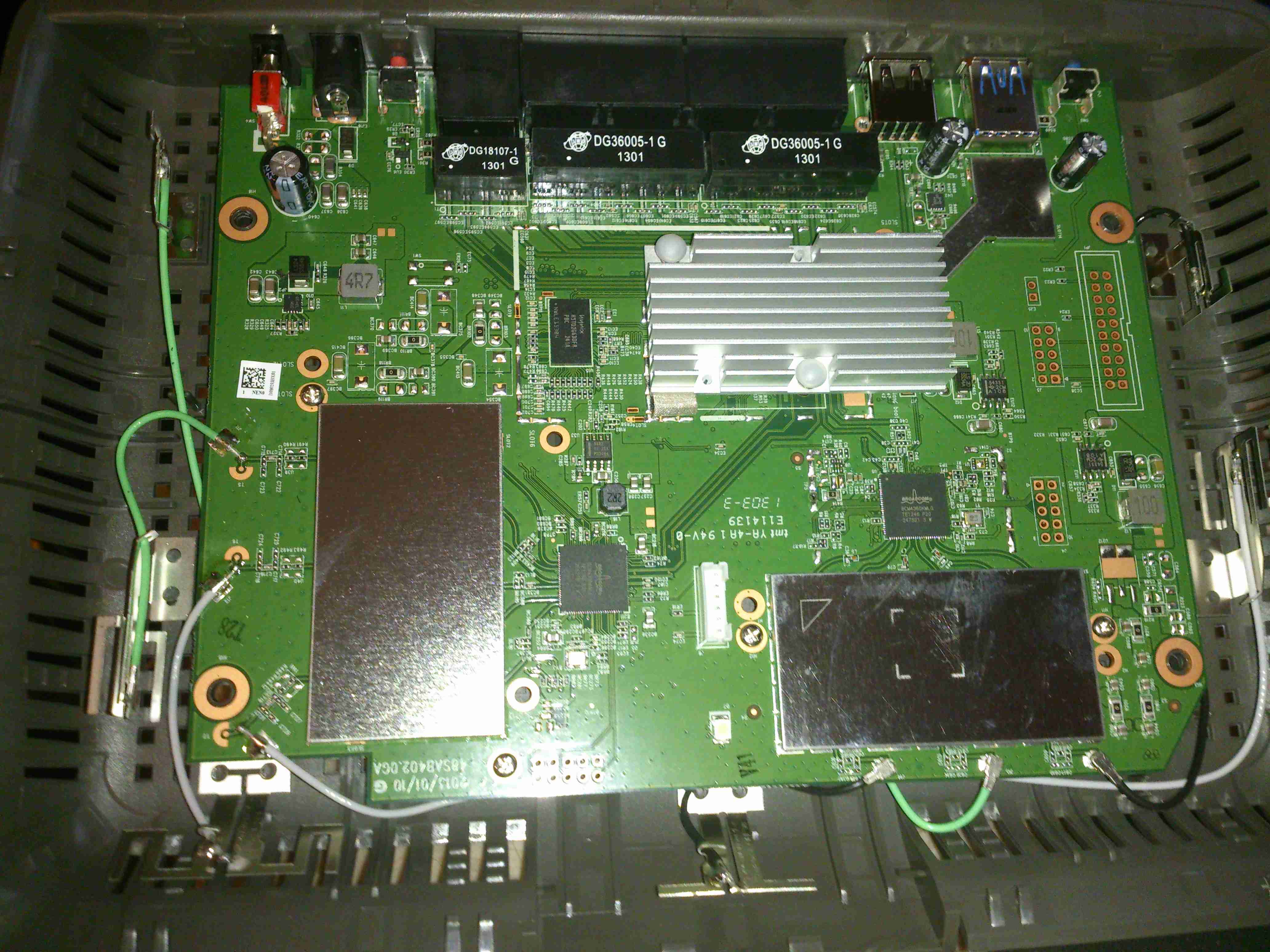
PCB Overview
Teardown time! Here’s the router with the cover removed. Most of the fun stuff is hidden under the shields, but these aren’t fully soldered down & the covers are removable. The 6 antennas can be seen spaced around the edge of the housing, the main CPU is under the large heatsink upper centre. The radio power amplifier stages are underneath the shields, while the main RF transceivers are just outside the shields.
2.4GHz Transceiver
Wireless N is provided by a Broadcom BCM4331, this provides full dual-band 3×3 802.11n support. Being 3×3 it is actually 3 separate transceivers in a single package, to get much higher throughput rates of 600Mbit/s.
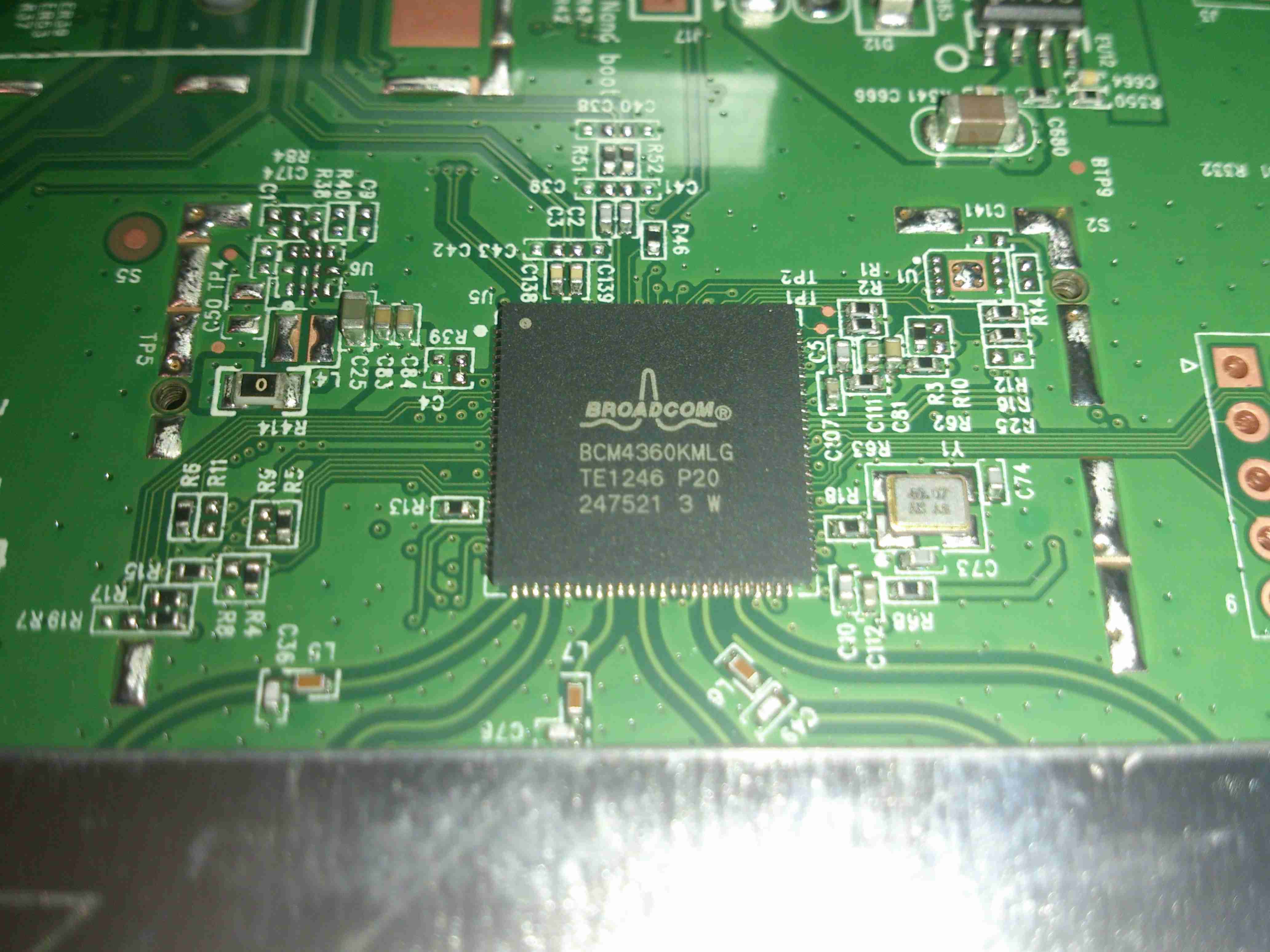
5GHz Transceiver
Wireless AC is provided by it’s sister IC, the BCM4360, with throughput speeds of 1.3Gbit/s. Both of these transceiver ICs connect back to the main CPU via PCI Express.
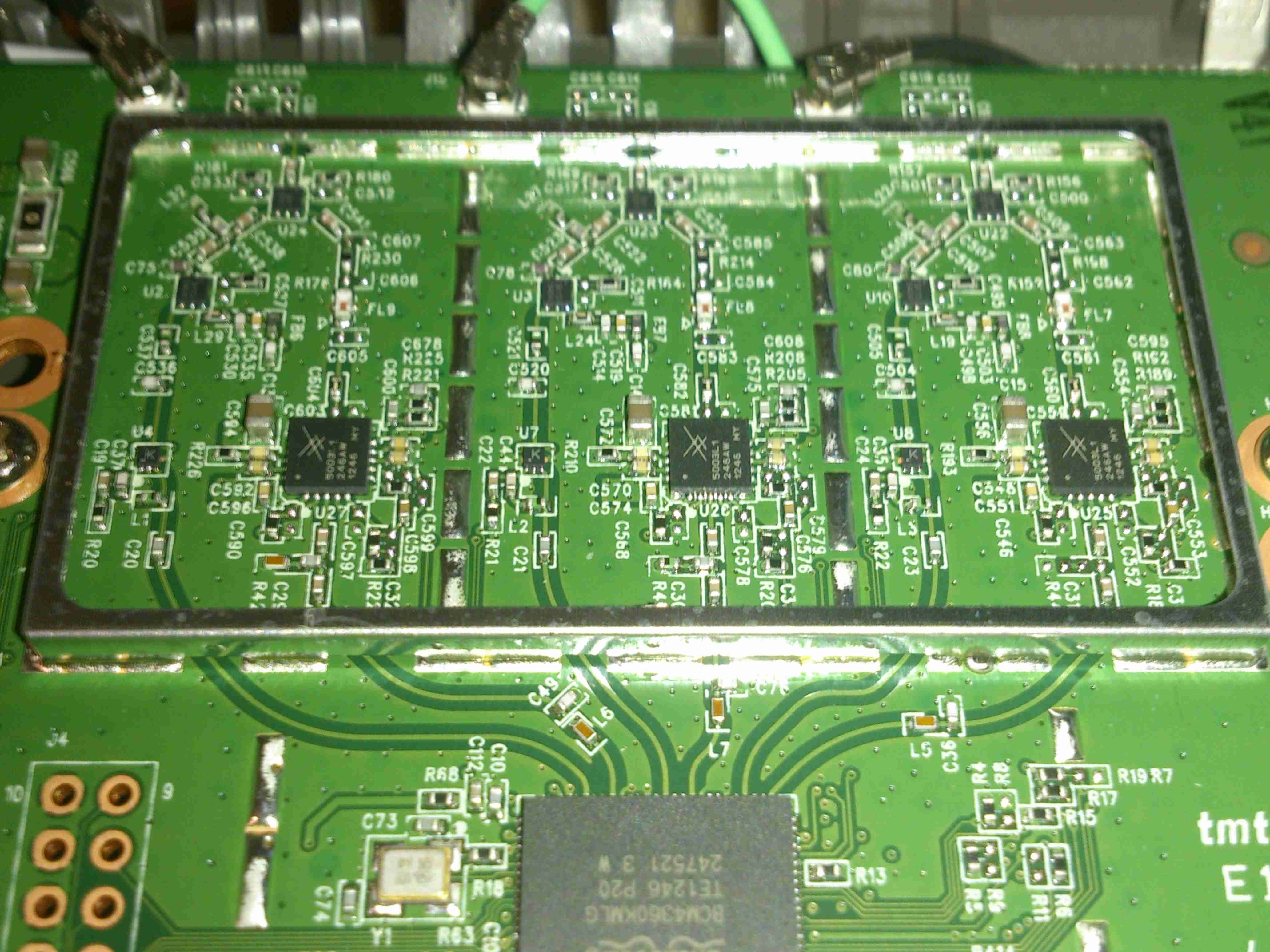
5GHz Power Amplifiers
To get increased range, there are a trio of Skyworks SE5003L +23dBm 5GHz power amplifier ICs under the shield, along with the TX/RX switching & antenna matching networks. Heatsinking for these is provided by a sink screwed to the bottom side of the PCB. The outputs to the antennas can be seen at the top of the image.
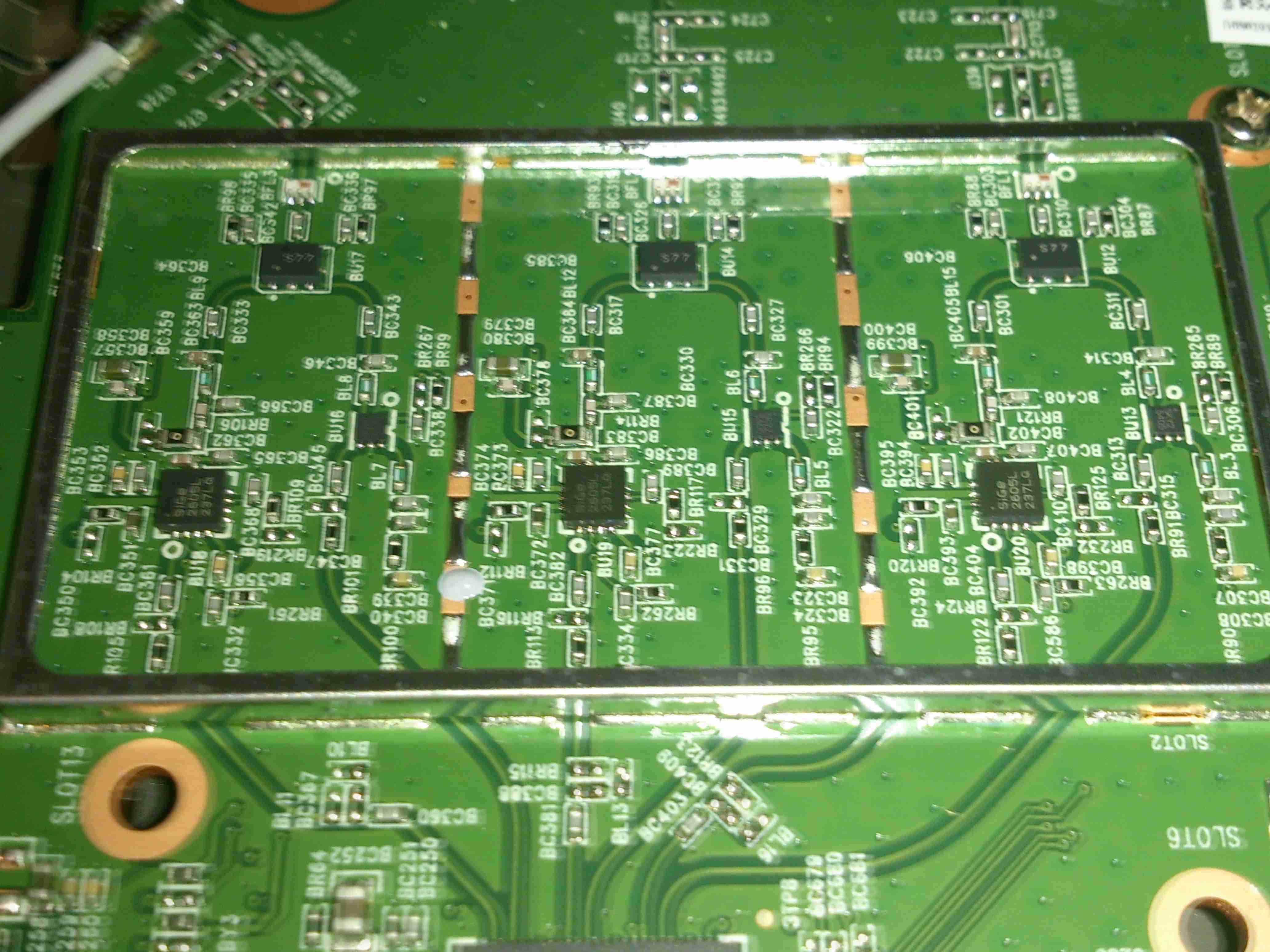
2.4GHz Power Amplifiers
The 2.4GHz section is fitted with a trio of Skyworks SE2605L +23dBm 2.4GHz power amplifiers, with a similar heatsink arrangement under the board. Unlike the 5GHz section, the 2.4GHz antenna feeds are soldered to the PCB here instead of using connectors.
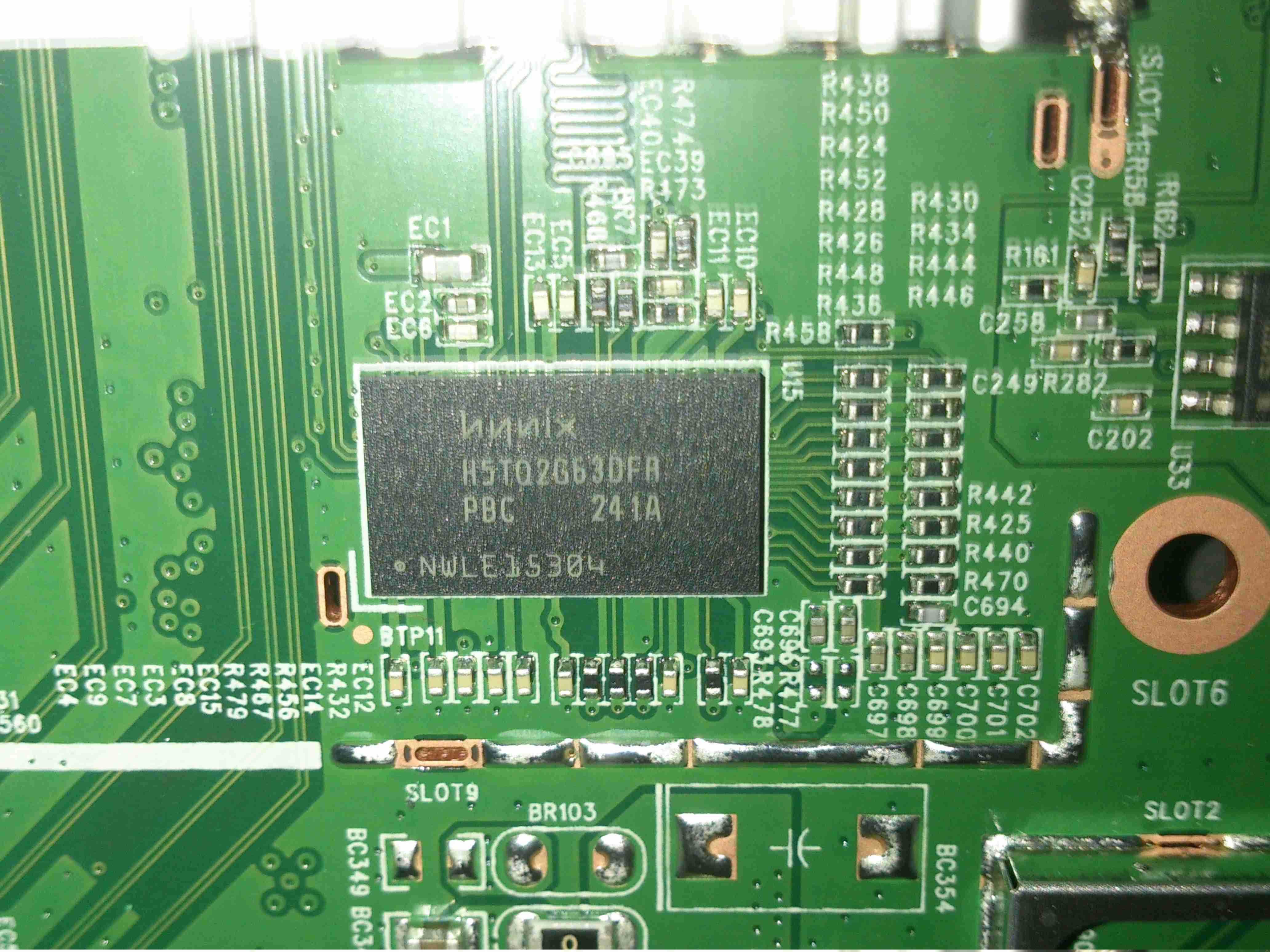
Main CPU
The main CPU is a BCM4708 Communications Processor from Broadcom, as for the other Broadcom chips in this router, very little information is available unless under NDA, but I do know it’s a dual core ARM Cortex A9 running at 1GHz, with built in 5-port gigabit ethernet switch.
CPU RAM
Working RAM for the processor is a Hynix H5TQ2G63DFA 256MB part.
More to come on the installation of the new networking, with it’s associated 4G mobile gateway connection system.
It’s official. I’m now part of the uRadMonitor network, & assisting in some of the current issues with networking some people (including myself) have been having.
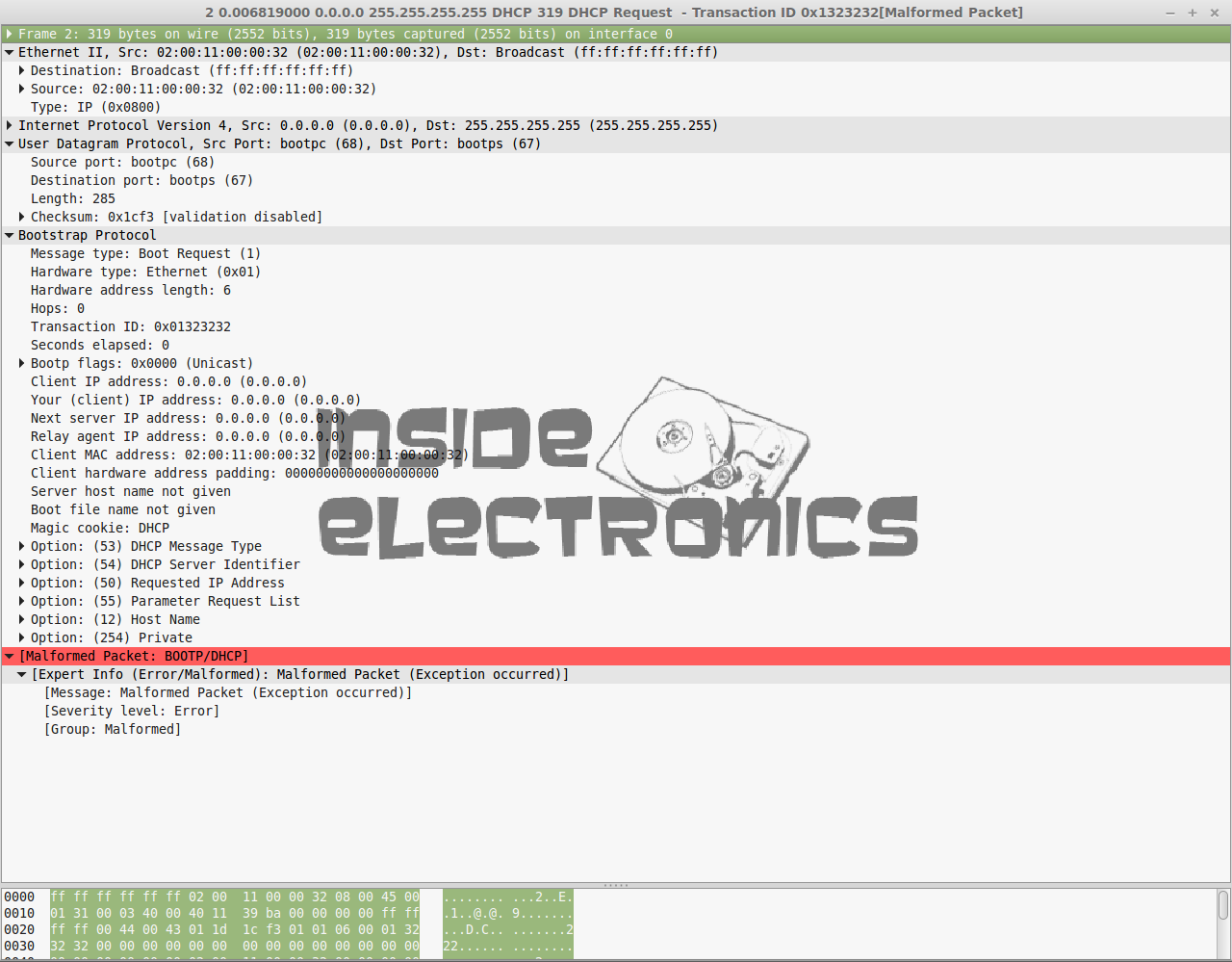
It seems that the uRadMonitor isn’t sending out technically-valid DHCP requests, here is what Wireshark thinks of the DHCP on my production network hardware setup:
WireShark Screencap
As can be seen, the monitor unit is sending a DHCP request of 319 bytes, where a standard length DHCP Request packet should be ~324 bytes, as can be seen on the below screen capture.
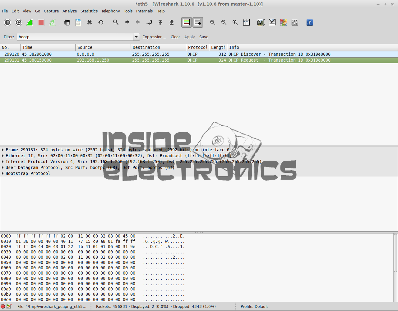
Valid DHCP
This valid one was generated from the same SPI Ethernet module as the monitor, (Microchip ENC28J60) connected to an Arduino. Standard example code from the EtherCard library was used to set up the DHCP. The MAC address of the monitor was also cloned to this setup to rule out the possibility of that being the root cause.
My deductive reasoning in this case points to the firmware on the monitor being at fault, rather than the SPI ethernet hardware, or my network hardware. Radu over at uRadMonitor is looking into the firmware being at fault.
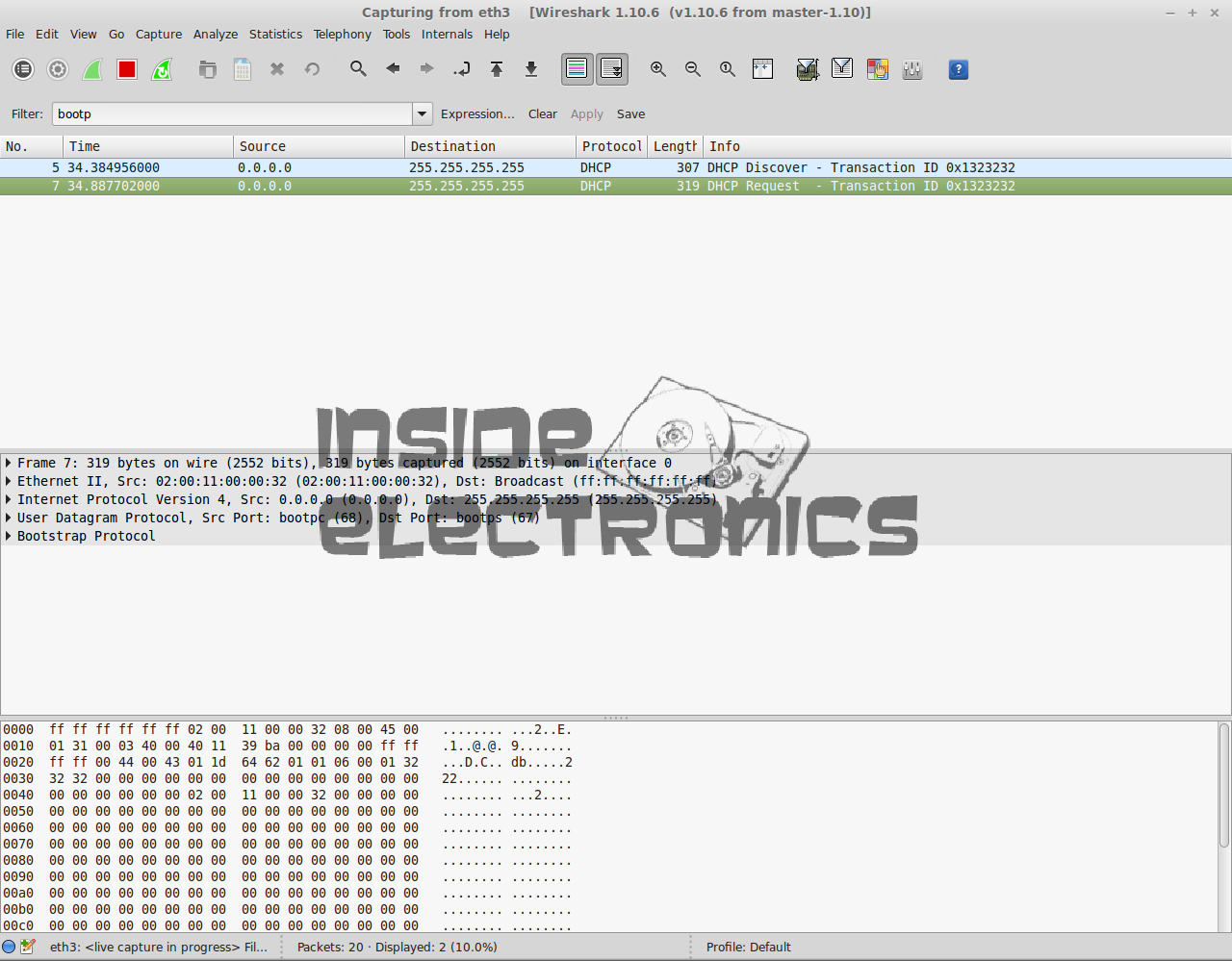
Strangely, most routers don’t seem to have an issue with the monitor, as connecting another router on a separate subnet works fine, and Wireshark doesn’t even complain about an invalid DHCP packet, although it’s exactly the same.
Working DHCP
As the firmware for the devices isn’t currently available for me to pick apart & see if I can find the fault, it’s up to Radu to get this fixed at the moment.
Now, for a µTeardown:
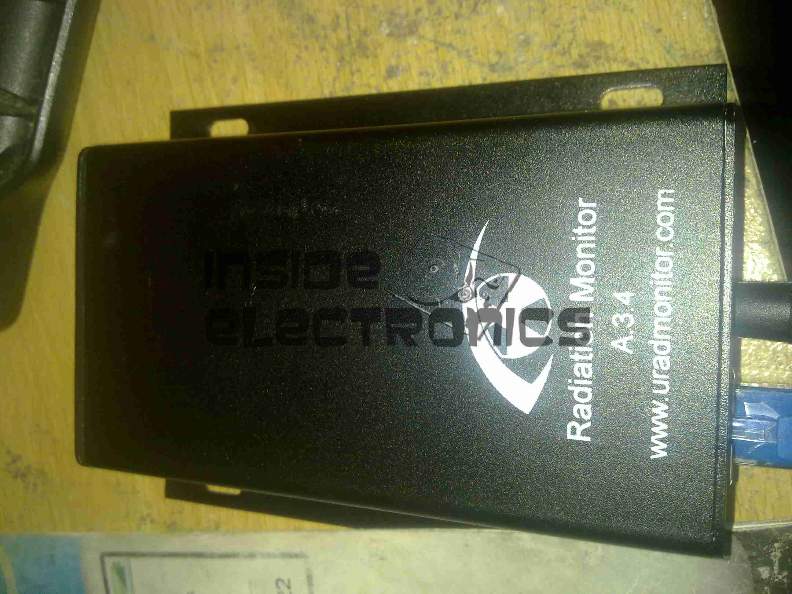
uRadMonitor
Here is the monitor, a small aluminium box, with power & network.
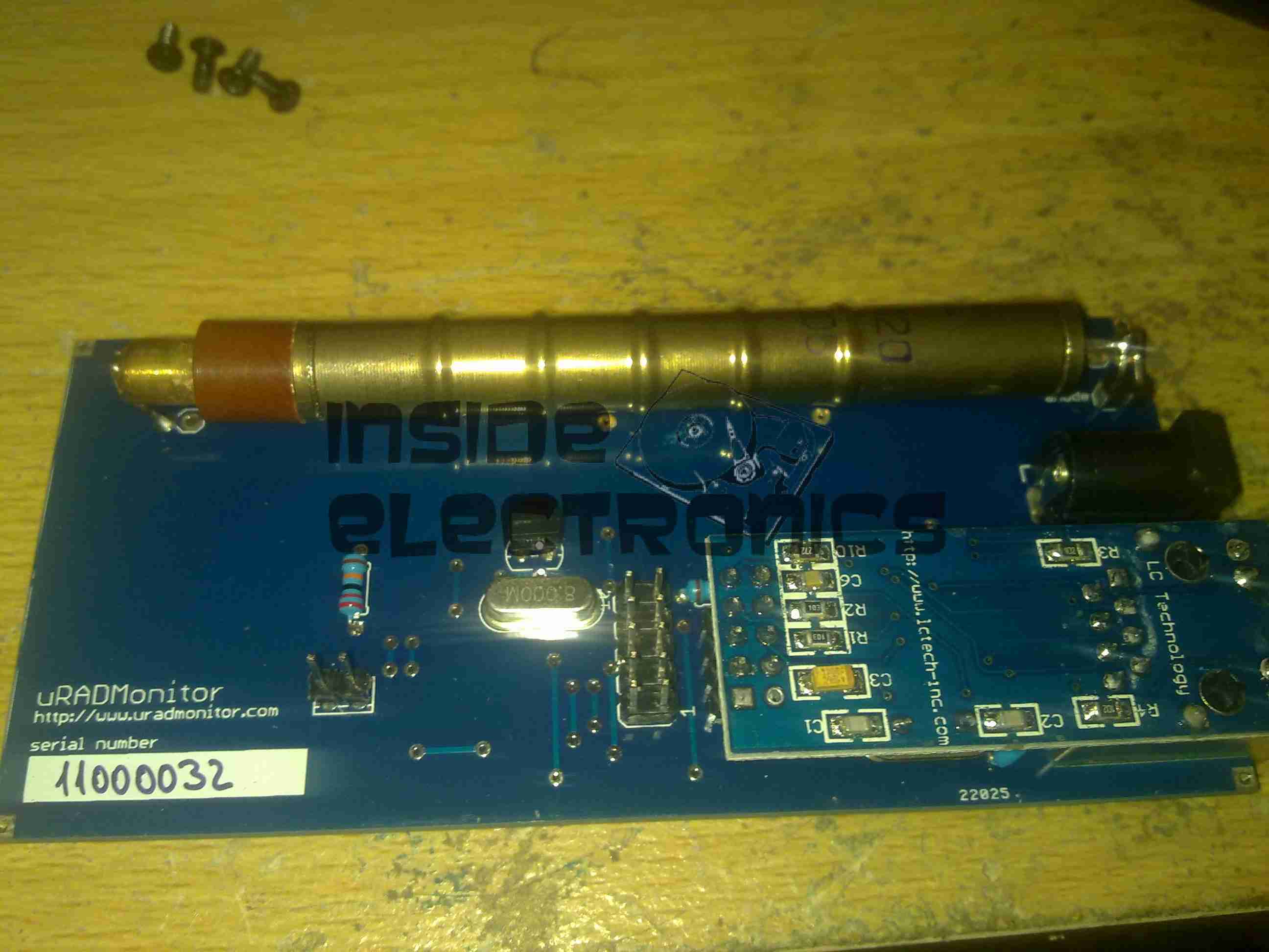
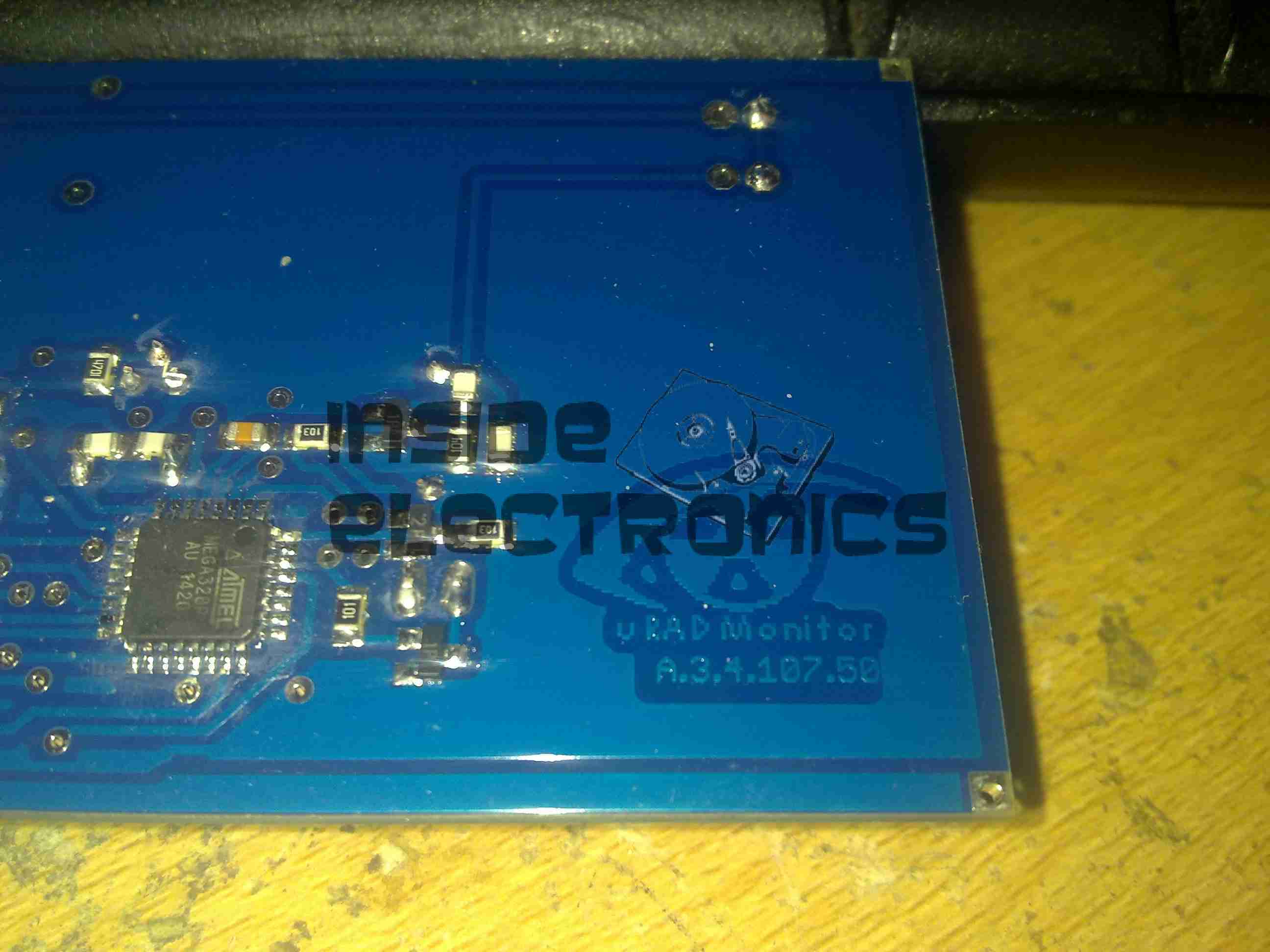
PCB
Removing 4 screws in the end plate reveals the PCB, with the Geiger-Mueller tube along the top edge. My personal serial number is also on the PCB.
The ethernet module is on the right, with the DC barrel jack.
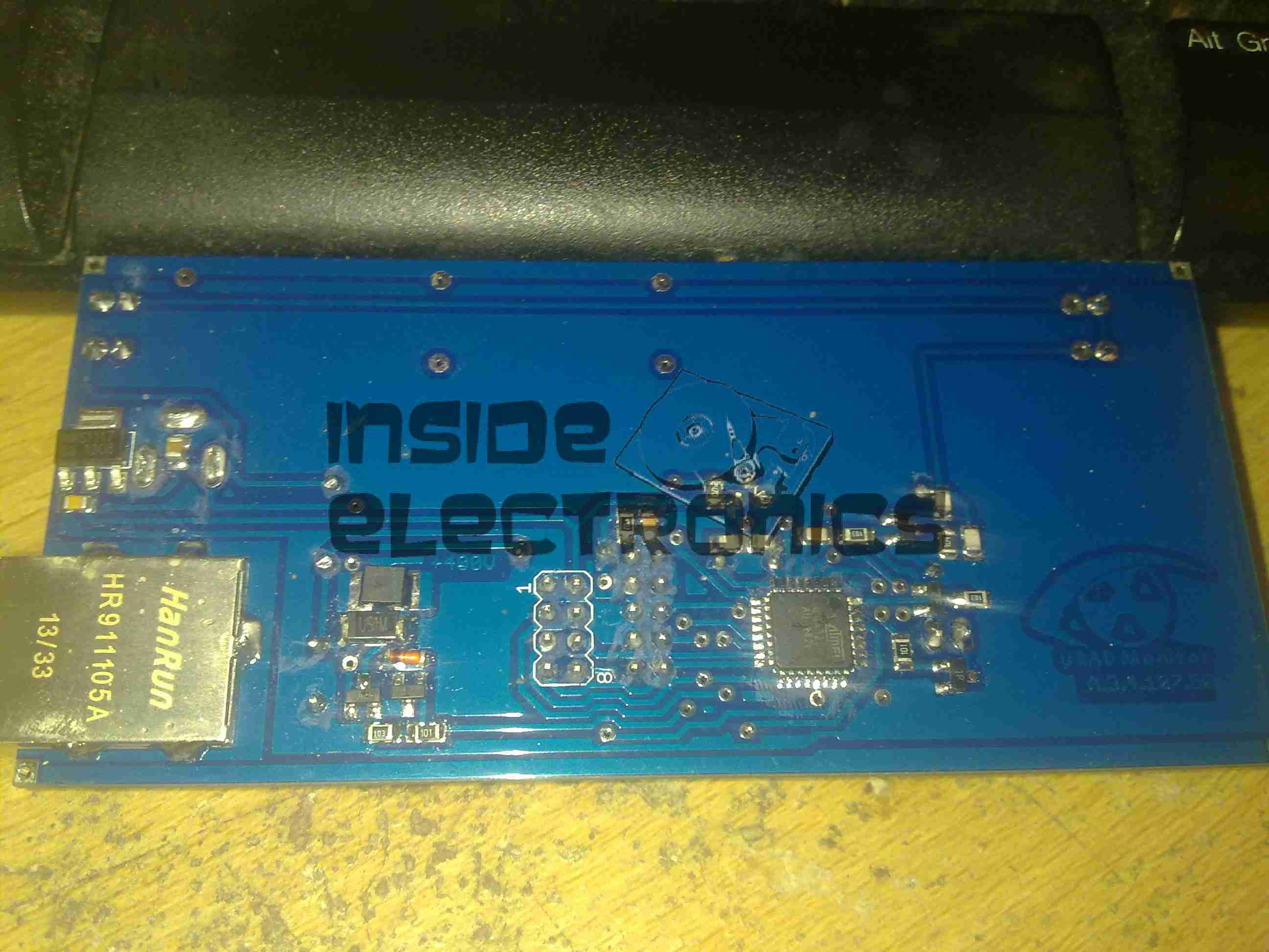
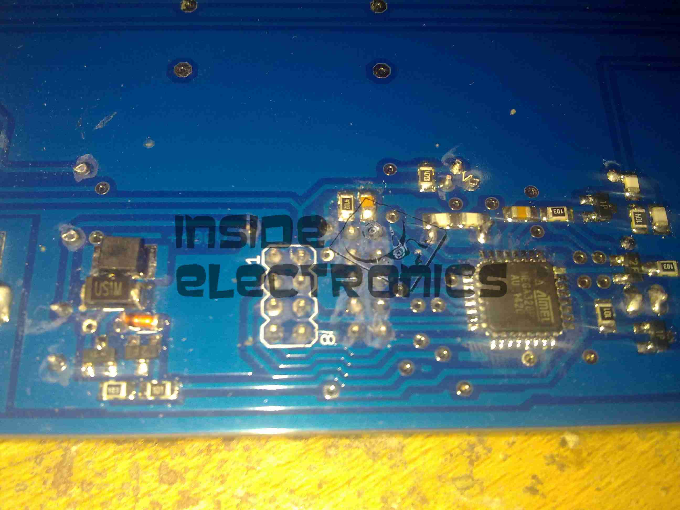
PCB Bottom
Here is the bottom of the PCB, with the control MCU & the tiny high voltage inverter for the Geiger tube.
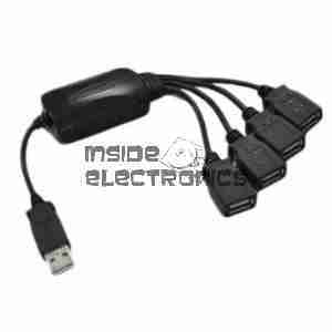
As the first USB hub I was using was certainly not stable – it would not enumerate between boots & to get it working again would require waiting around 12 hours before applying power, it has been replaced. This is a cheapie eBay USB hub, of the type shown below.
These hubs are fantastic for hobbyists, as the connections for power & data are broken out on the internal PCB into a very convenient row of pads, perfect for integration into many projects.
Breakout Hub
I now have two internal spare USB ports, for the inbuilt keyboard/mouse receiver & the GPS receiver I plan to integrate into the build.
These hubs are also made in 7-port versions, however I am not sure if these have the same kind of breakout board internally. As they have the same cable layout, I would assume so.
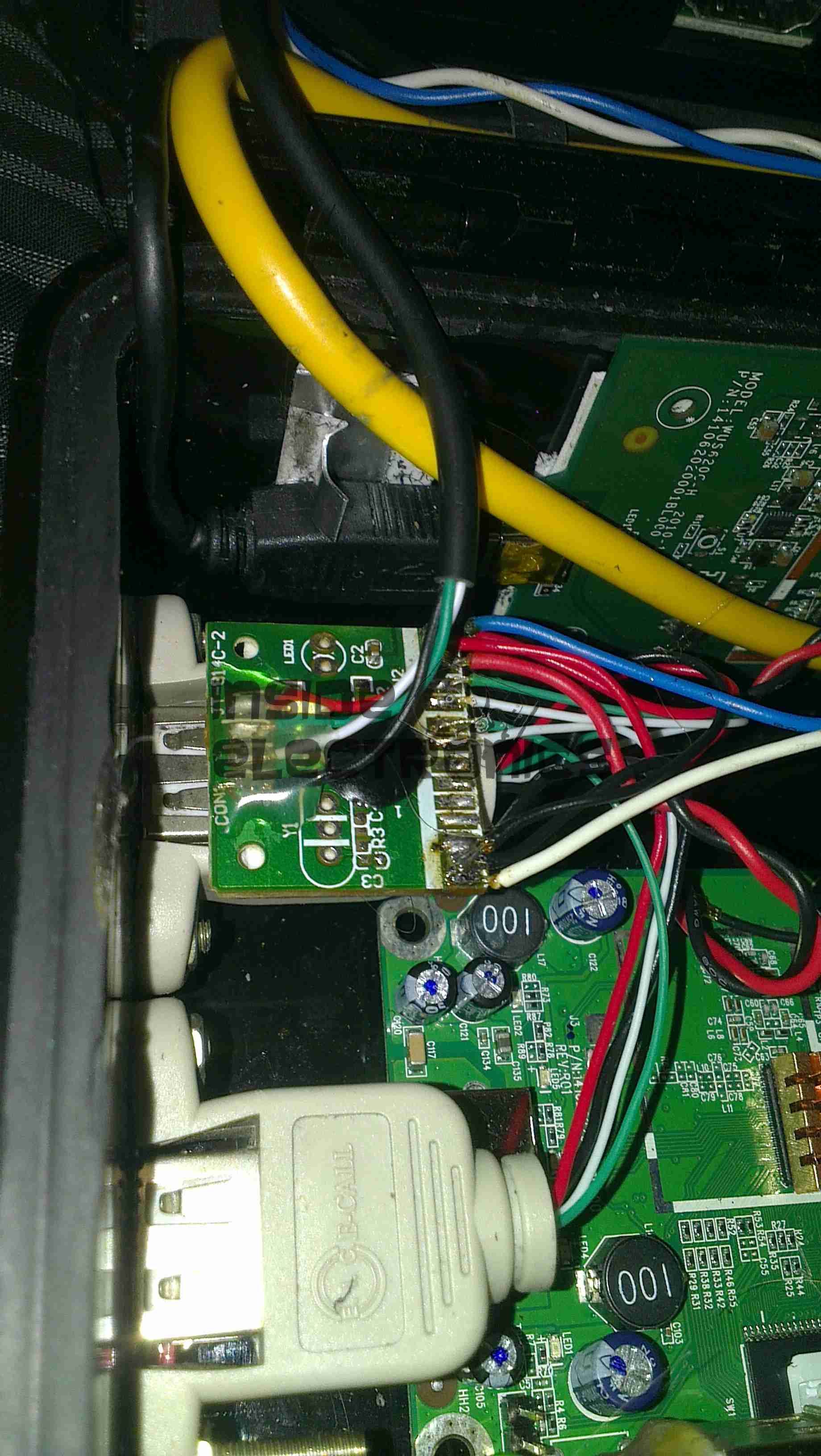
Connector Panel
Here is a closeup of the back of the connectors, showing a couple of additions.
I have added a pair of 470µF capacitors across the power rails, to further smooth out the ripple in the switching power supply, as I was having noise issues on the display.
Also, there is a new reset button added between the main interface connectors, which will be wired into the pair of pads that the Raspberry Pi has to reset the CPU.
This can be used as a power switch in the event the Pi is powered down when not in use & also to reset the unit if it becomes unresponsive.
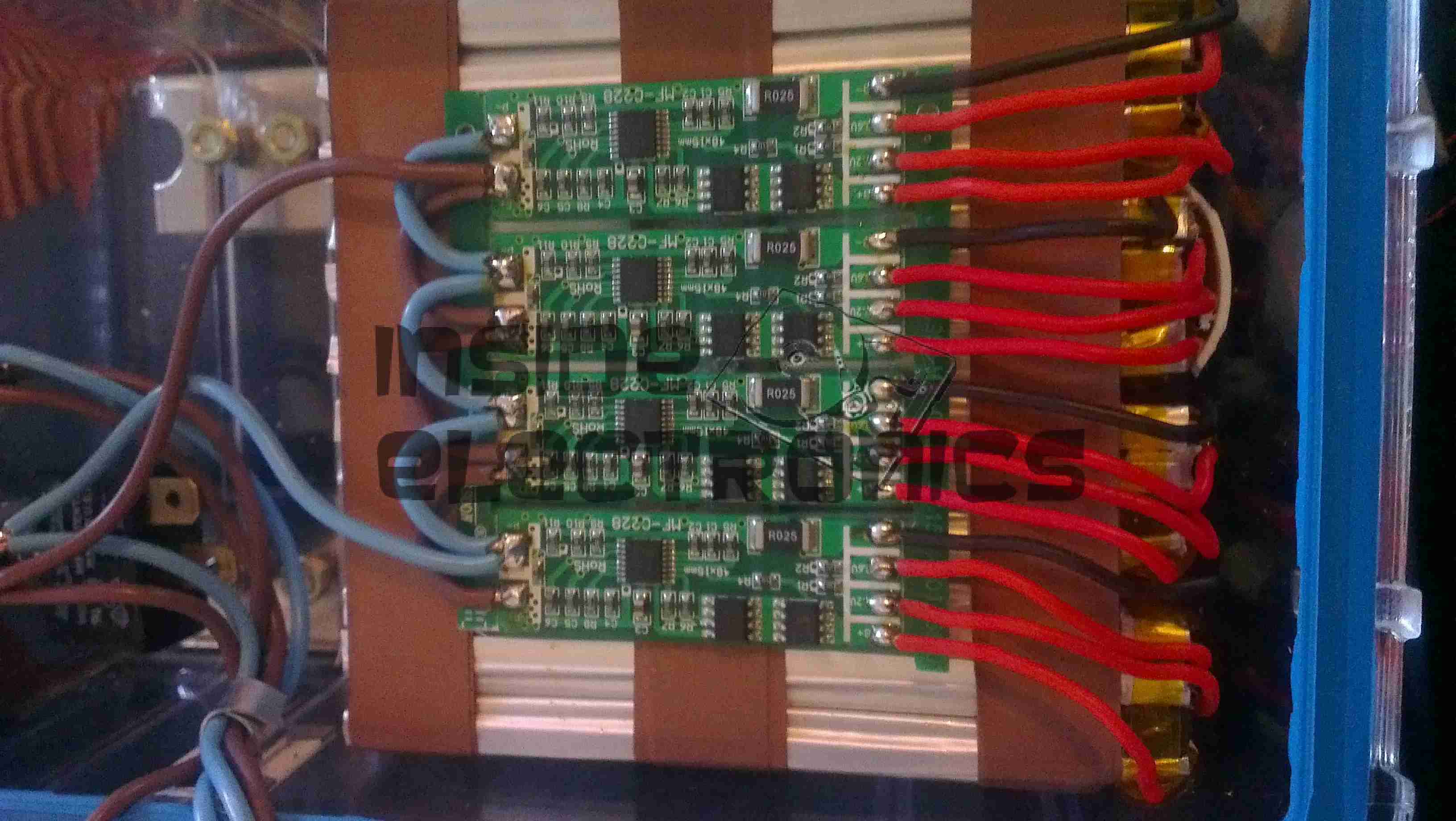
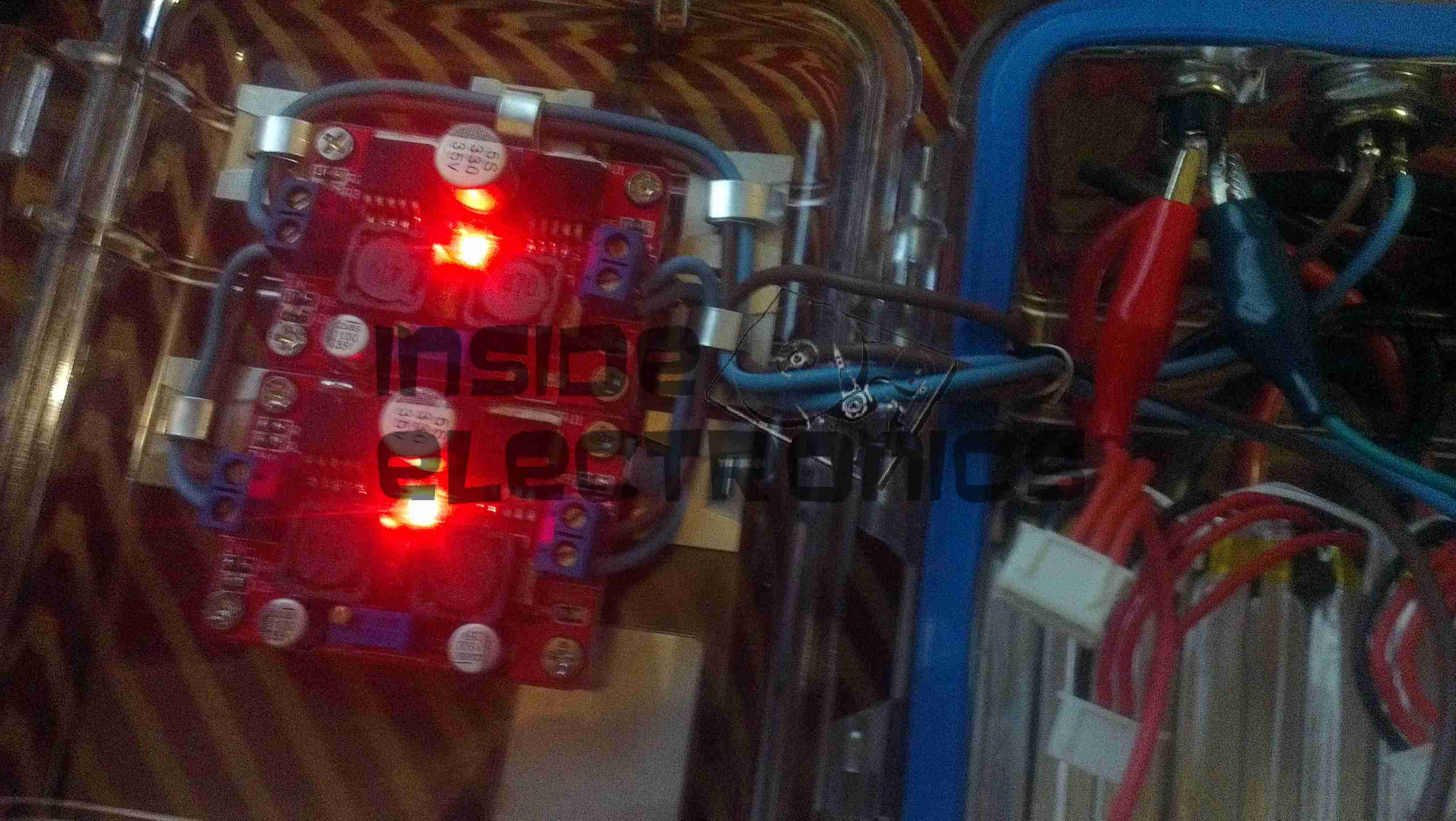
The final part for the battery pack has finally arrived, the PCM boards. These modules protect the cells by cutting off the power at overcharge, undercharge & overcurrent. Each cell is connected individually on the right, 12v power appears on the left connections. These modules also ensure that all the cells in the pack are balanced.
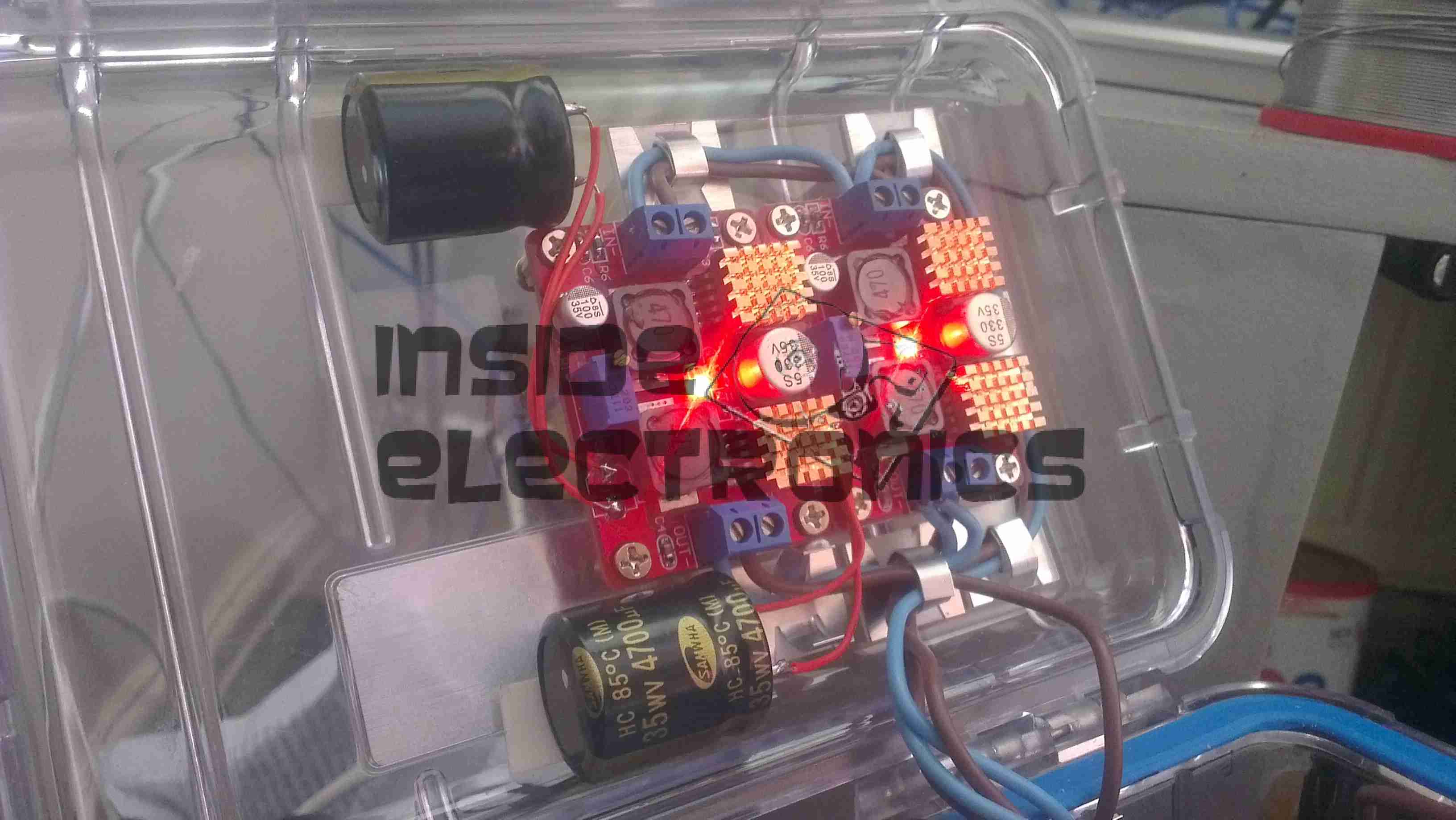
A few modifications were required to the SMPS modules to make the power rails stable enough to run the Pi & it’s monitor. Without these the rails were so noisy that instability was being caused.
I have replaced the 100µF output capacitors & replaced them with 35v 4700µF caps. This provides a much lower output ripple.
There are also heatsinks attached to the converter ICs to help spread the heat.
Progress is finally starting on the power supply unit for the Pi, fitted into the same case style as the Pi itself, this is an 8Ah Li-Poly battery pack with built in voltage regulation.
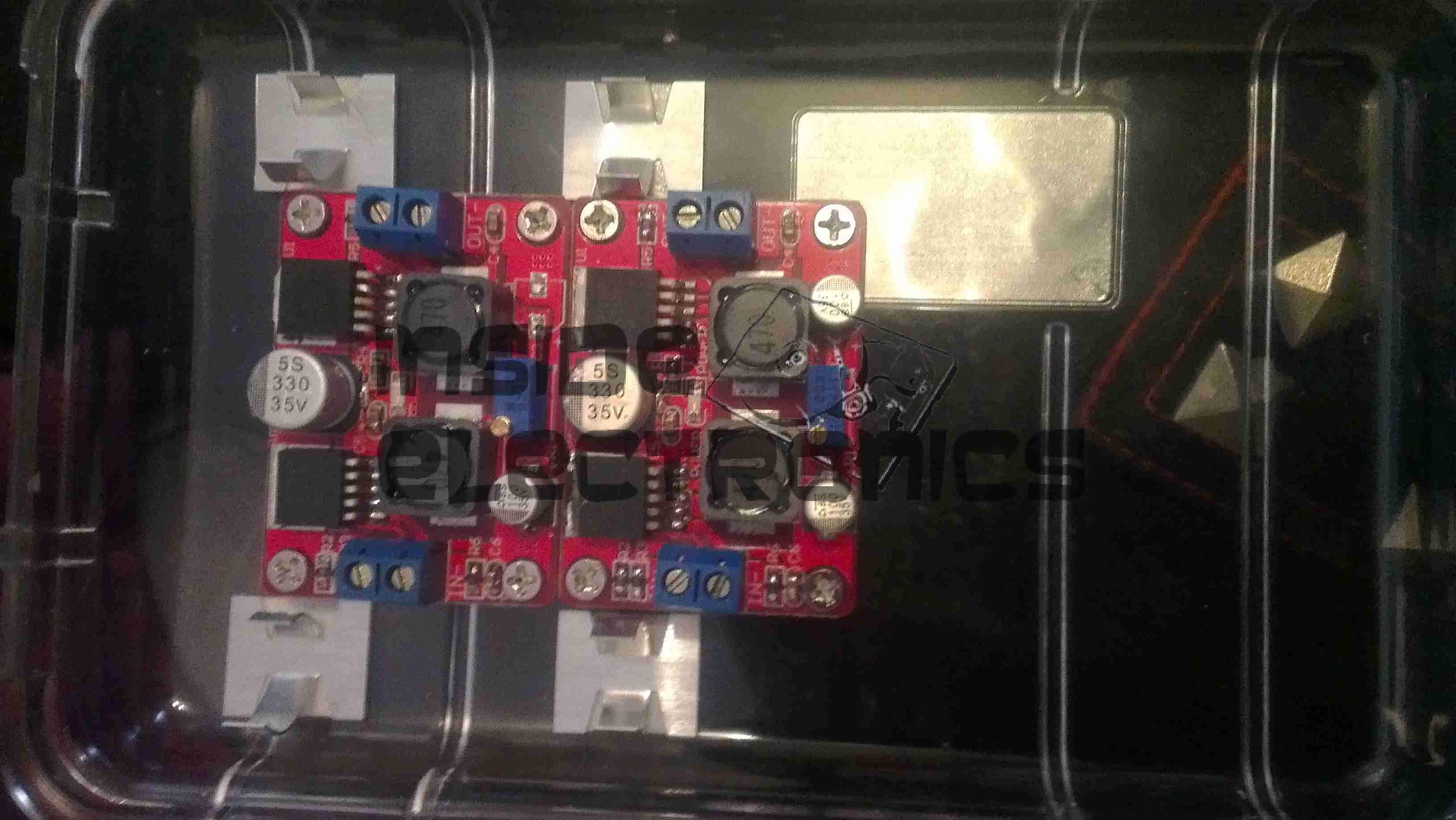
Regulator Boards
Here are the regulators, fixed to the top of the enclosure. These provide the 12v & 5v power rails for the Pi unit, at a max 3A per rail.
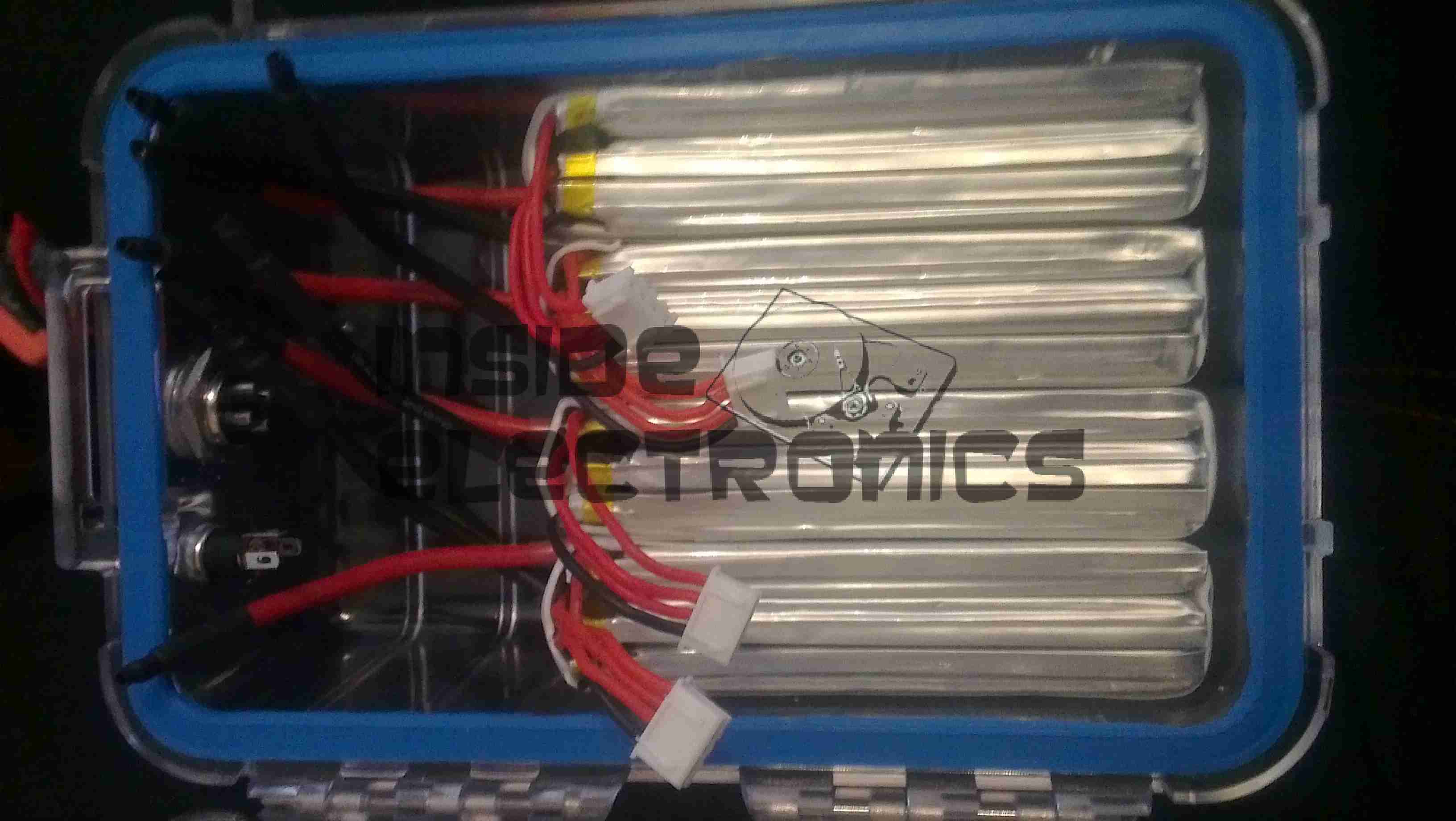
Battery Pack
In the main body of the case the battery pack is fitted. This is made up of 4 3-cell Li-Poly RC battery packs, rated at 2Ah each. All wired in parallel this will provide a total of 8Ah at 12.6v when fully charged.
Powered Up
Here the regulators are powered up from a 13v supply for testing. I have discovered at full load these modules have very bad ripple, so I will be adding extra smoothing capacitors to the power rails to compensate for this.
I/O
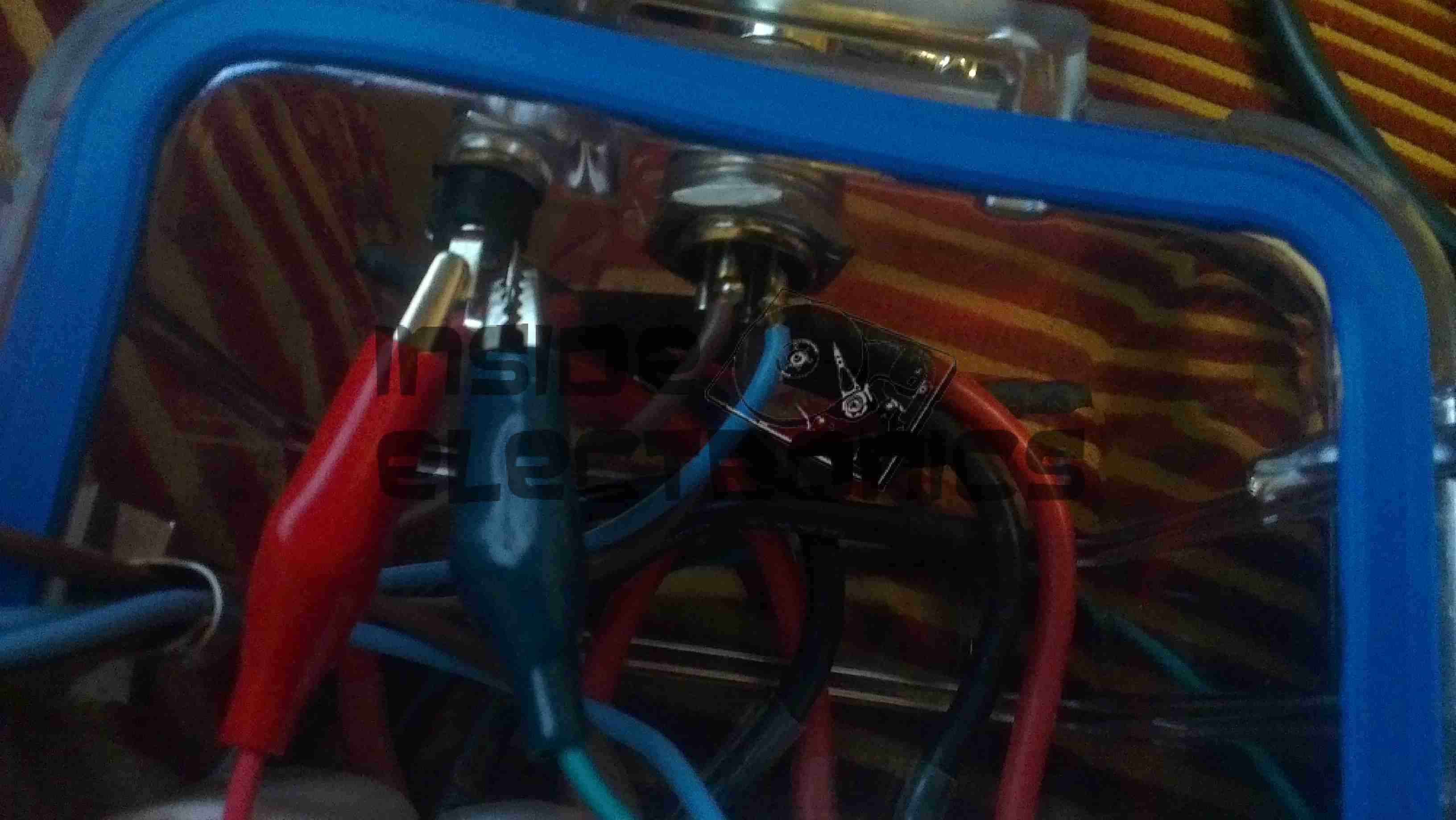
Here are the connectors on the top of the unit, outputting the two power rails to the Pi & the DC barrel jack that will be used to charge the pack.
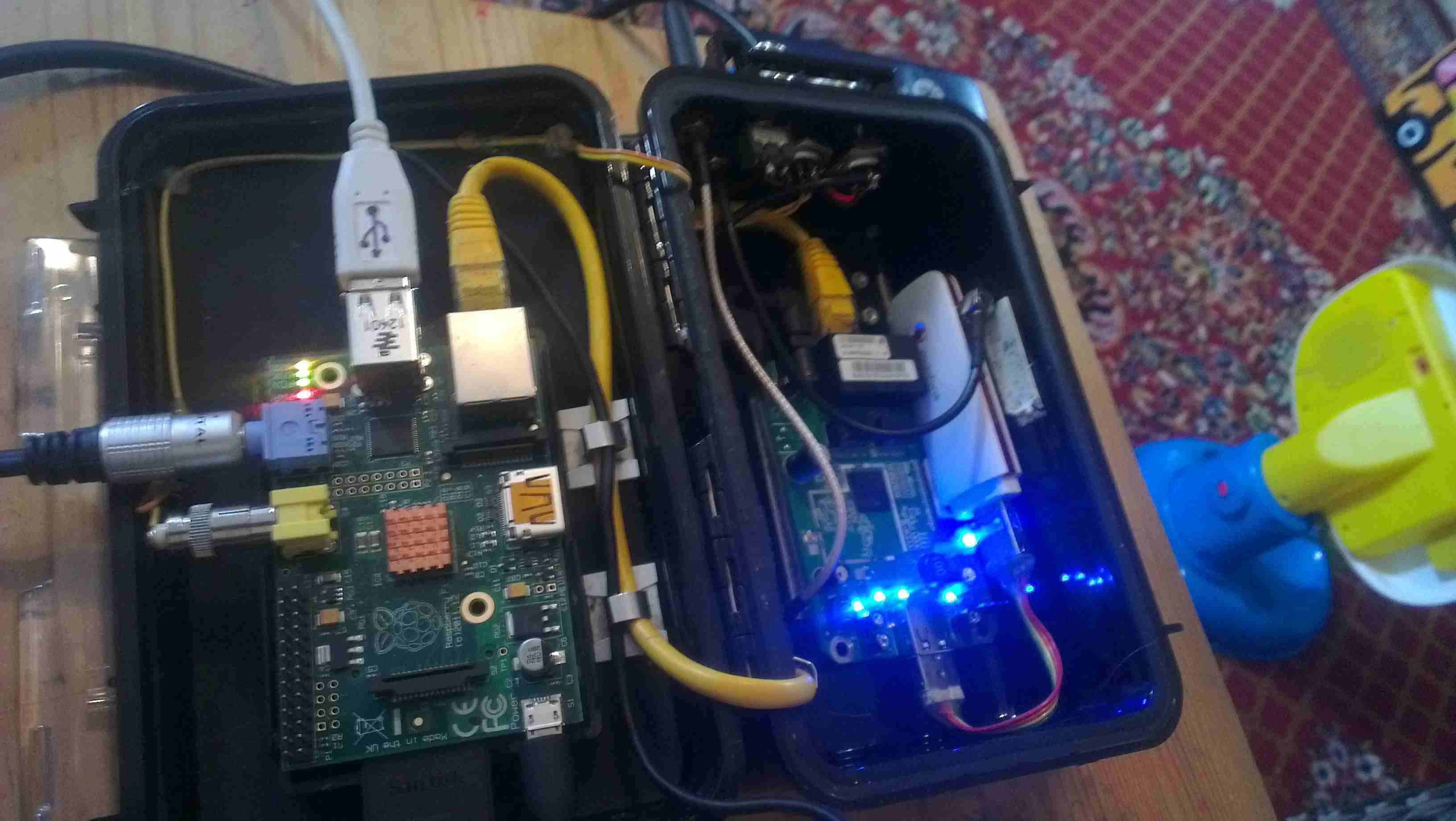
Here is the project I’m currently working on. A completely wearable computing platform based on the Raspberry Pi & the WiFi Pineapple.
Above can be seen the general overview of the current unit.
On the left:
Alfa AWUS036NHA USB High Power WiFi Network Interface
512MB Model B Raspberry Pi, 16GB SD card, running Raspbian & LXDE Desktop. Overclocked to 1GHz.
On the right:
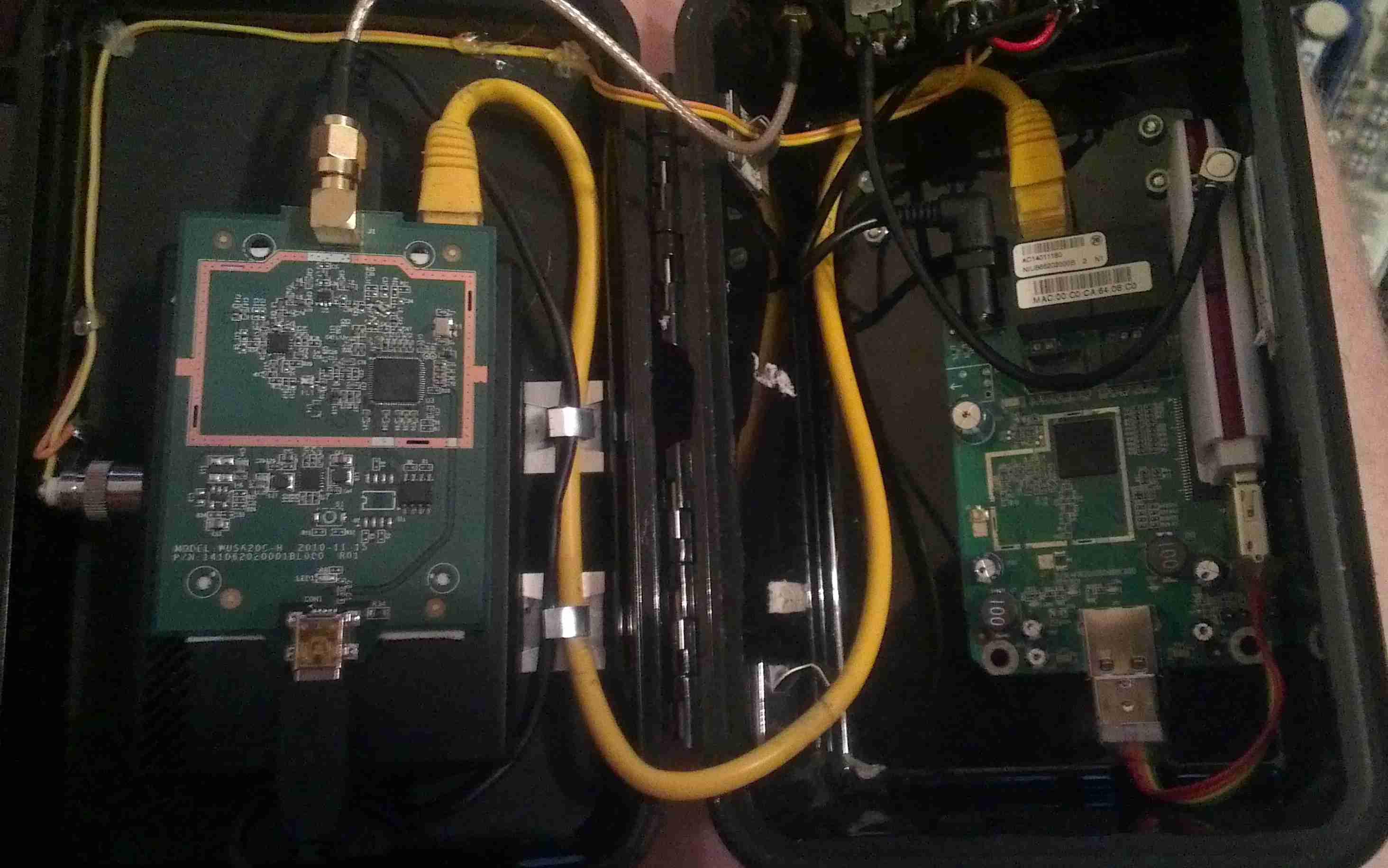
WiFi Pineapple router board
USB 3G card.
The WiFi, Pineapple & 3G all have external antenna connections for a better signal & the whole unit locks onto the belt with a pair of clips.
The Raspberry Pi is using the composite video output to the 7″ LCD I am using, running at a resolution of 640×480. This gives a decent amount of desktop space while retaining readability of the display.
The case itself is a Pelican 1050 hard case, with it’s rubber lining removed. The belt clips are also a custom addition.
Connections
Here are the connections to the main unit, on the left is the main power connector, supplying +5v & +12v DC. The plug on the right is an 8-pin connection that carries two channels of video, mono audio & +12v power to the display.
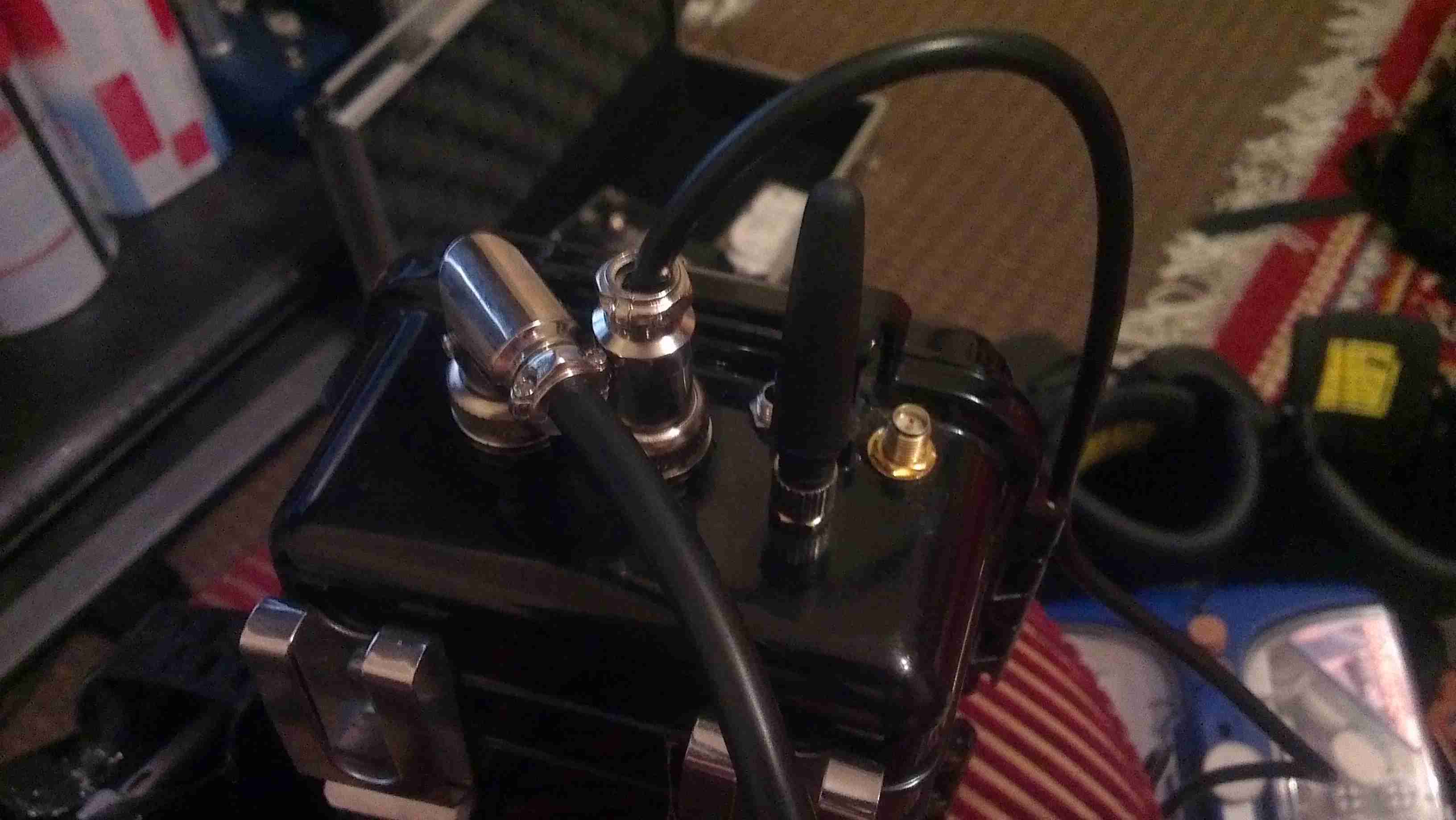
Currently the only antenna fitted is the 3G.
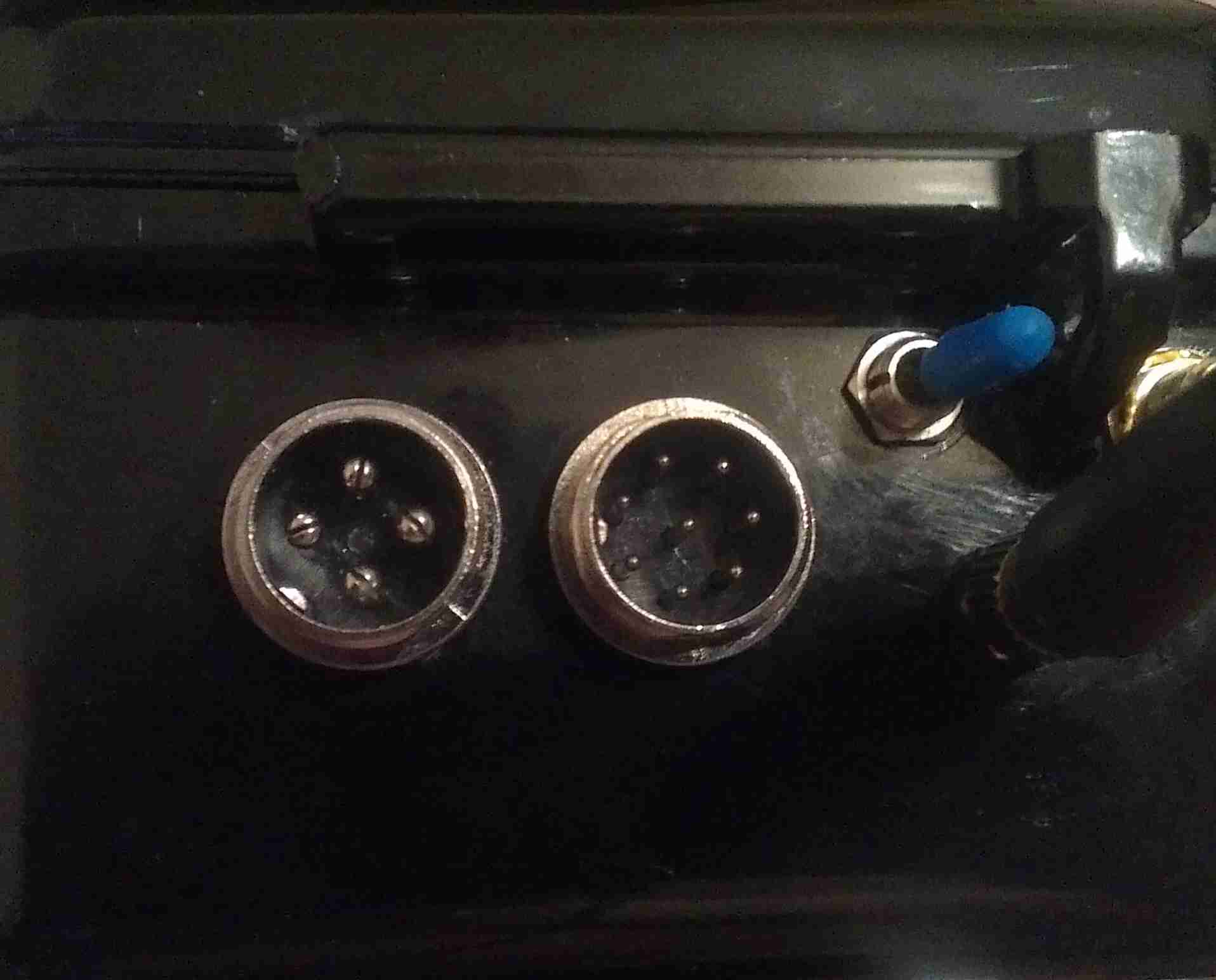
Connectors
Closeup of the connections for power, audio & video. The toggle switch is redundant & will soon be replaced with a 3.5mm stereo jack for headphones, as an alternative to the mono audio built into the display.
Test Run
Current state of test. Here the unit is running, provided with an internet connection through the Pineapple’s 3G radio, funneled into the Pi via it’s ethernet connection.
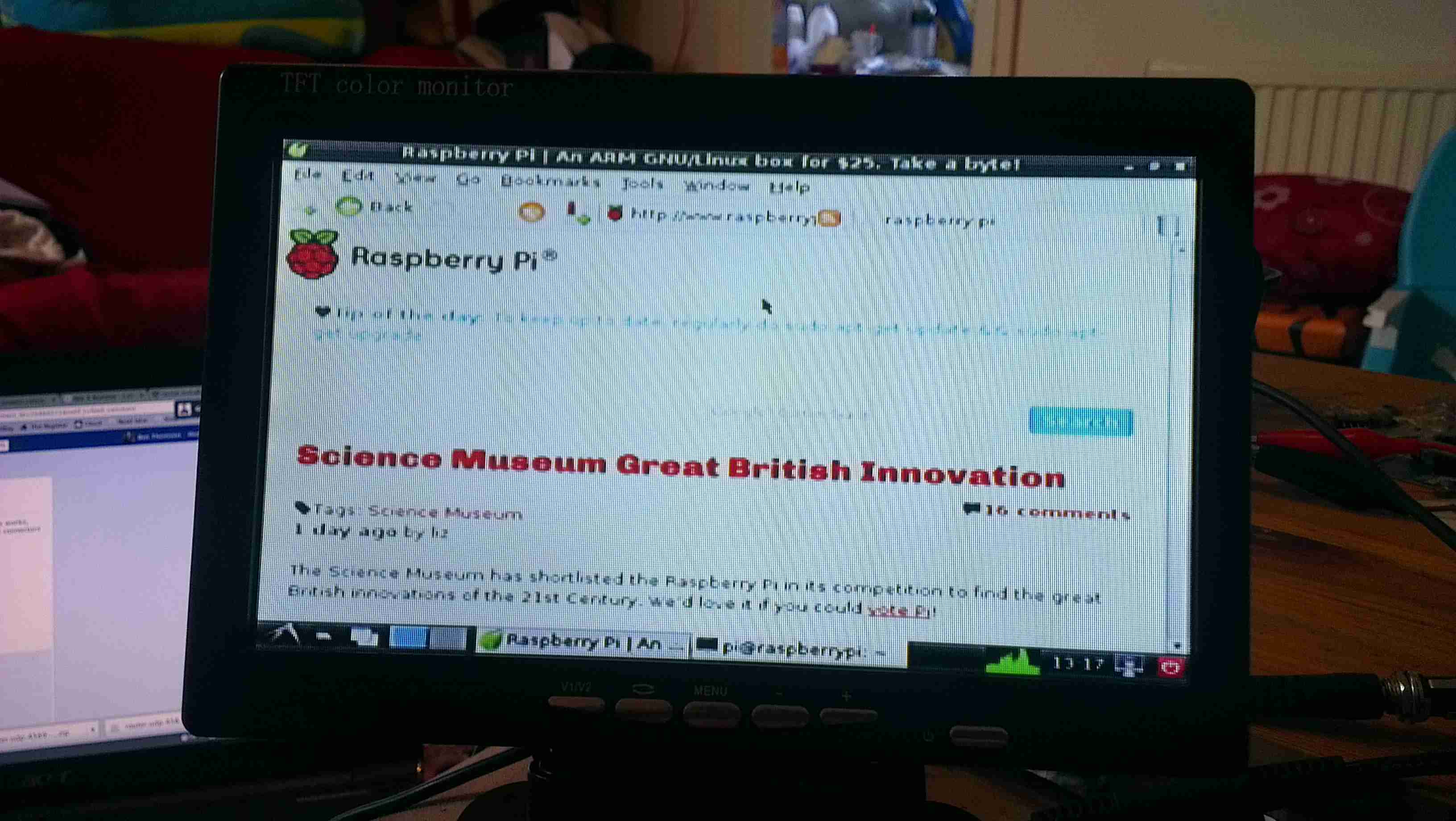
Pi Goodness!
Running on a car reversing camera monitor at 640×480 resolution. This works fairly well for the size of the monitor & the text is still large enough to be readable.
Stay tuned for Part 2 where I will build the power supply unit.
Tip Jar
If you’ve found my content useful, please consider leaving a donation by clicking the Tip Jar below!
All collected funds go towards new content & the costs of keeping the server online.