A while back I found myself in the need of an adjustable RF attenuator capable of high-GHz operation. As luck would have it I had an old Spectrum analyser on the shelf at work, which we had retired quite some time ago.
Spectrum analysers being quite capable test instruments, I knew that the input attenuation would be done with a standalone module that we could recover for reuse without too much trouble.
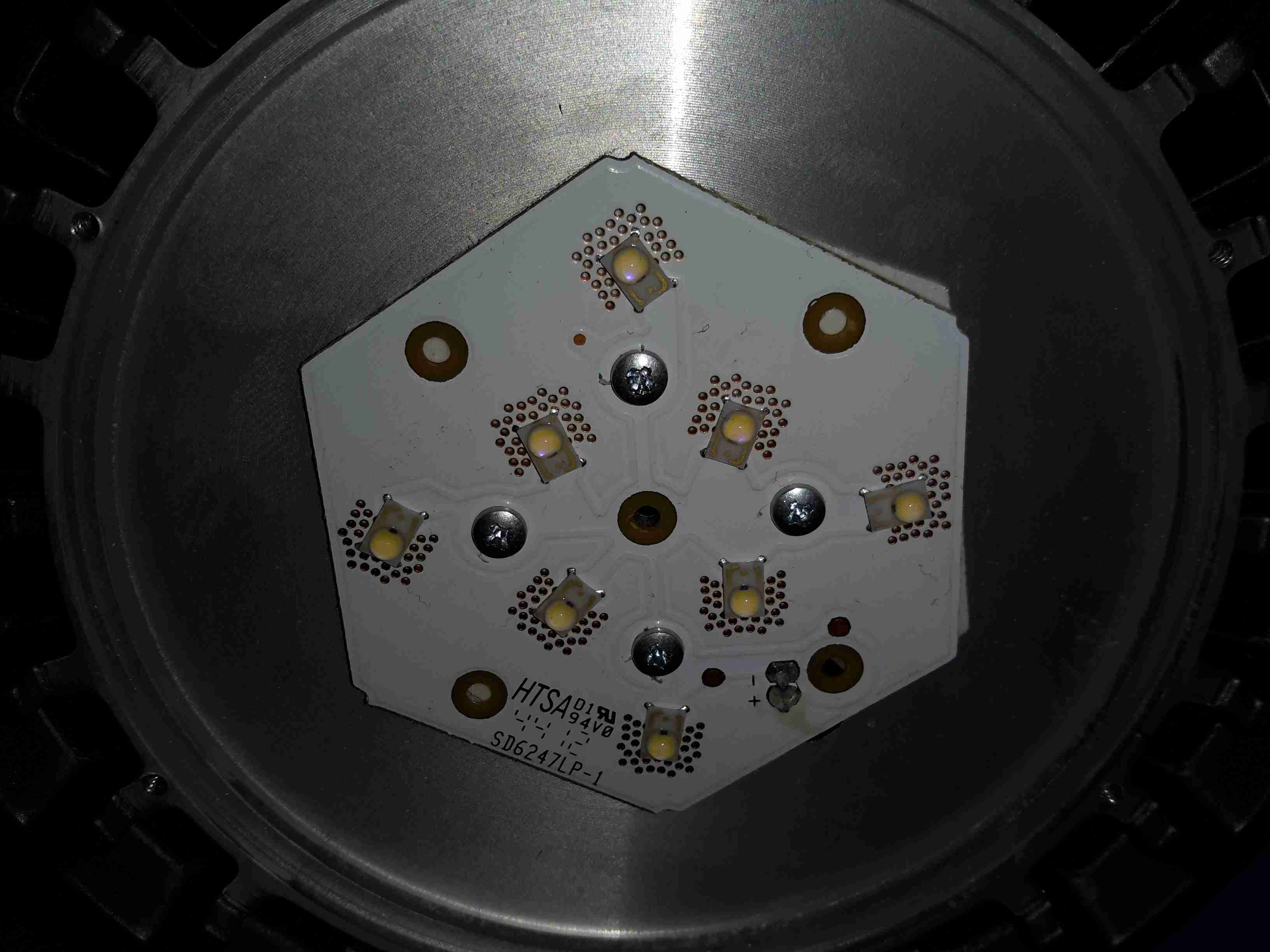
The attenuator module
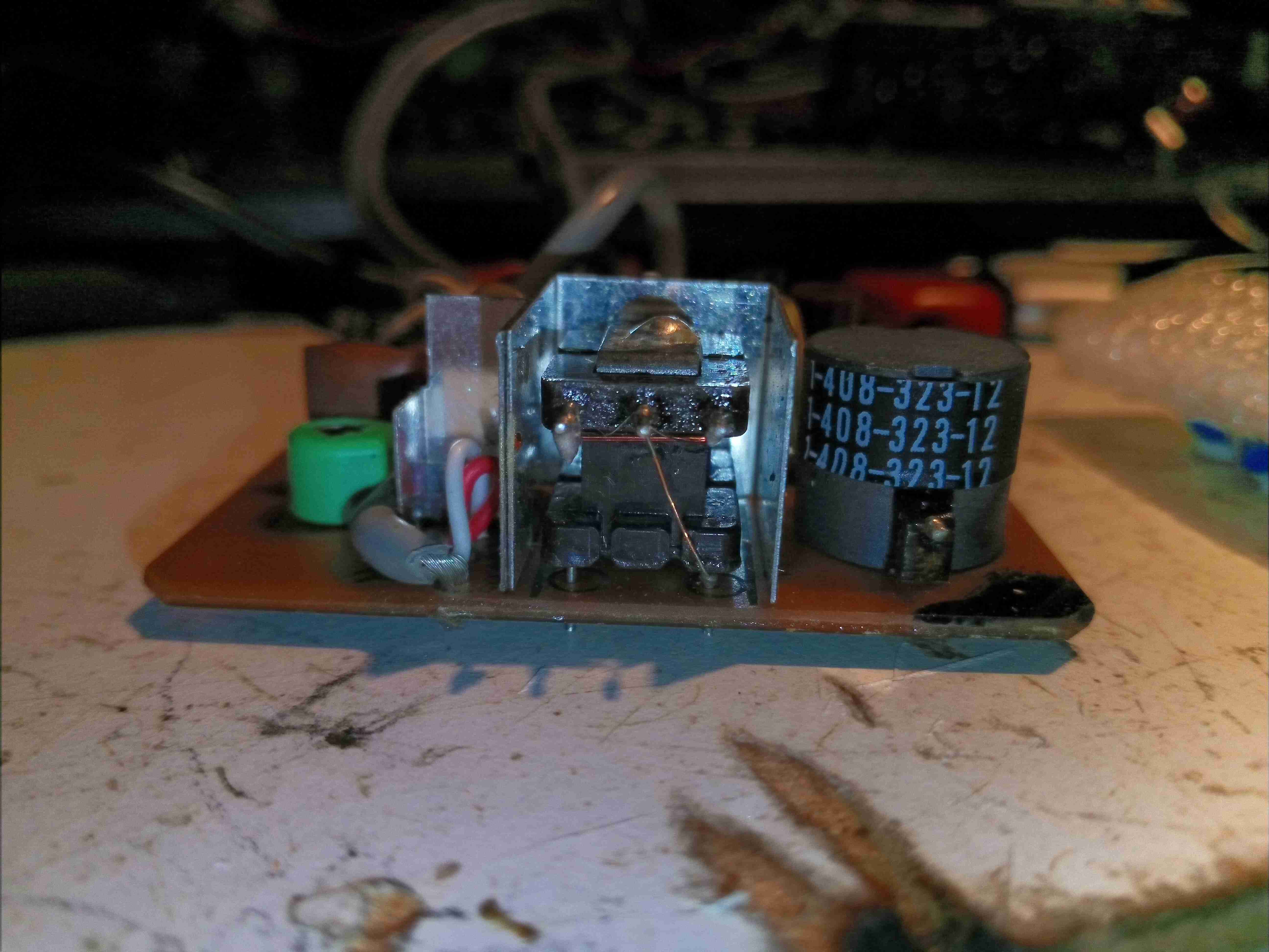
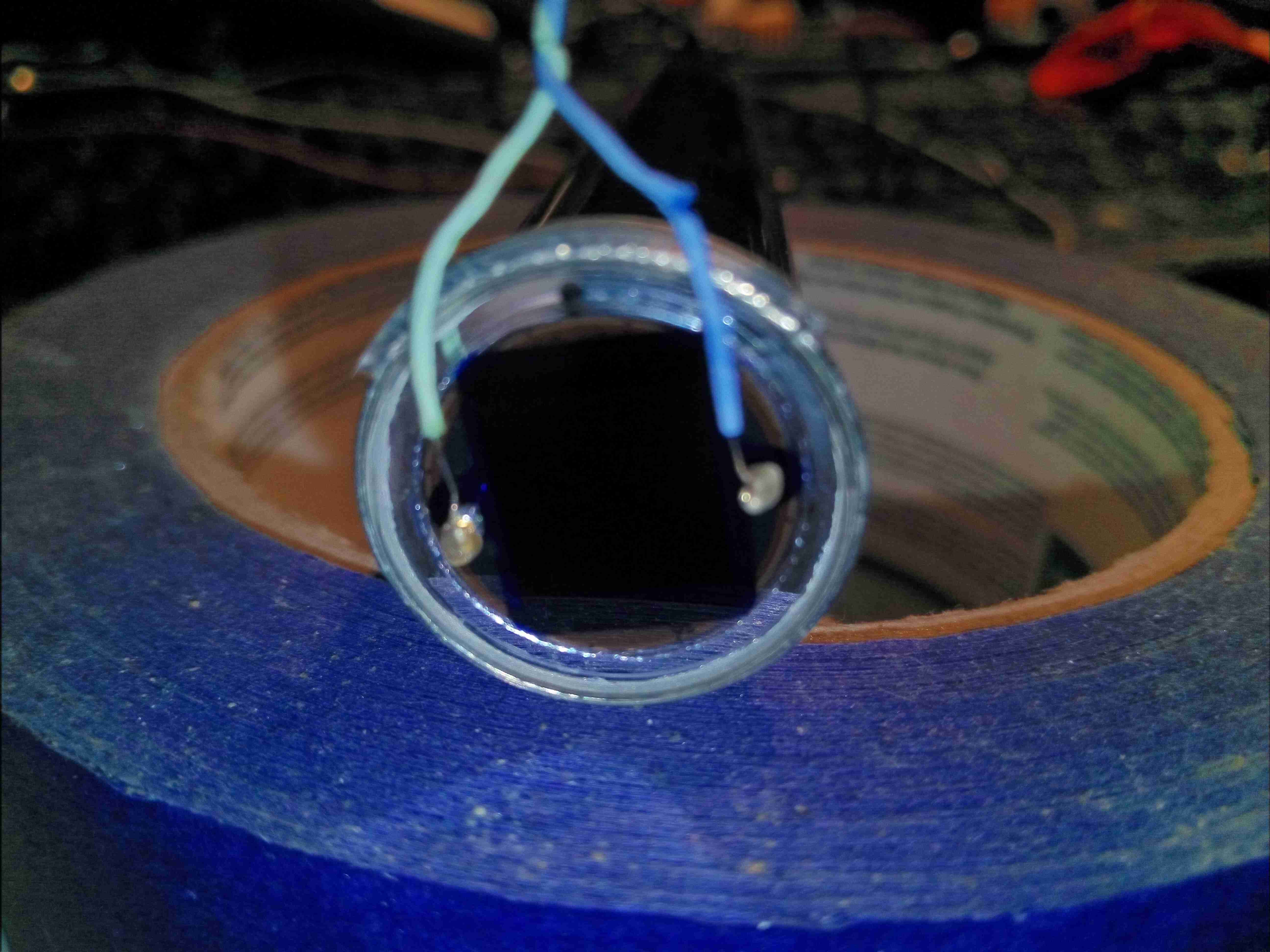
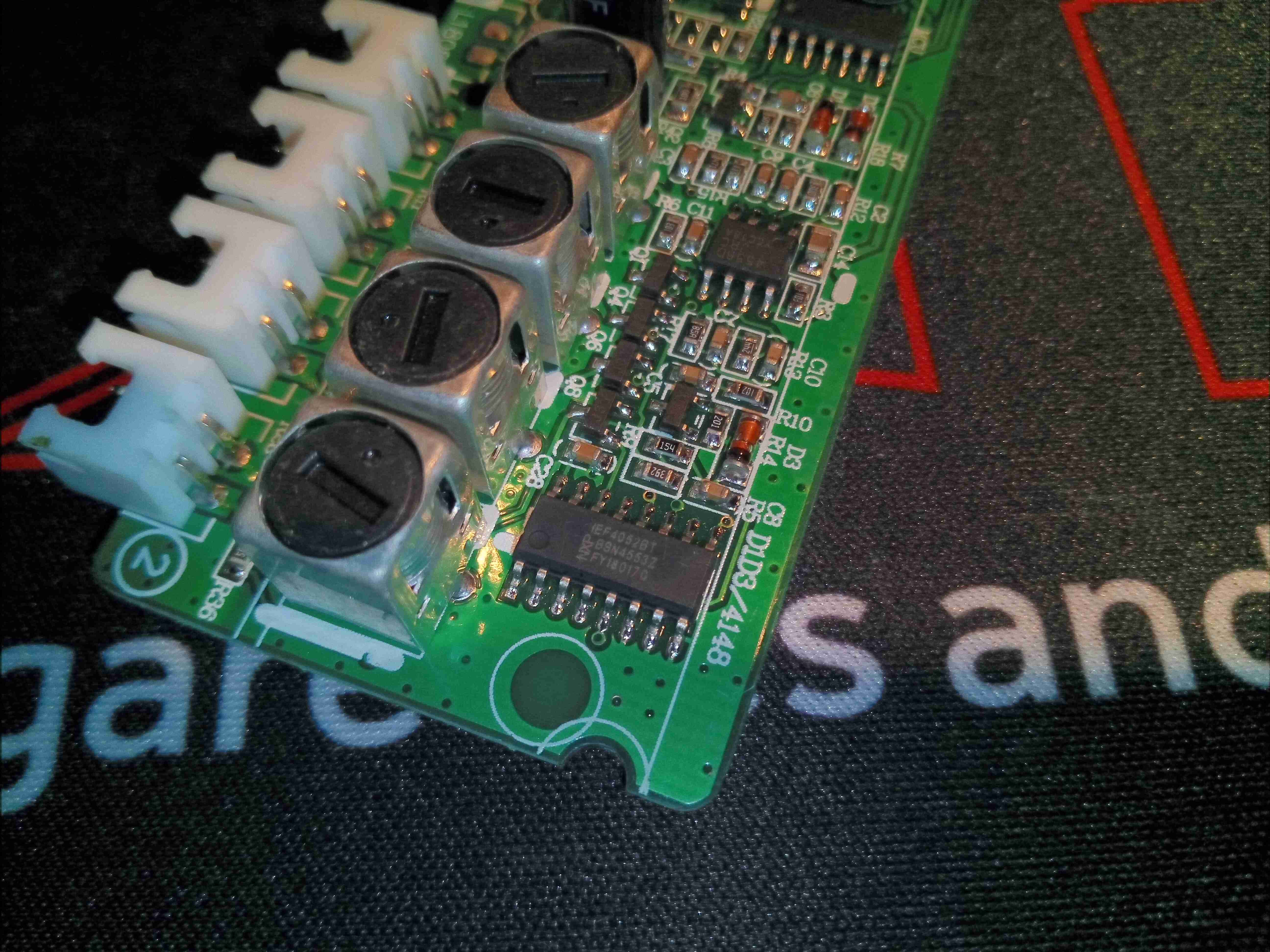
Here’s the module itself, with the factory drive PCB removed from the bottom, showing the solenoids that operate the RF switches. There are test wires attached to them here to work out which solenoid switches which attenuation stage. In the case of this module, there are switches for the following:
Input select switch
AC/DC coupling
-5dB
-10dB
-20dB
-40dB
For me this means I have up to -75dB attenuation in 5dB steps, with optional switchable A-B input & either AC or DC coupling.
Drive is easy, requiring a pulse on the solenoid coil to switch over, the polarity depending on which way the switch is going.
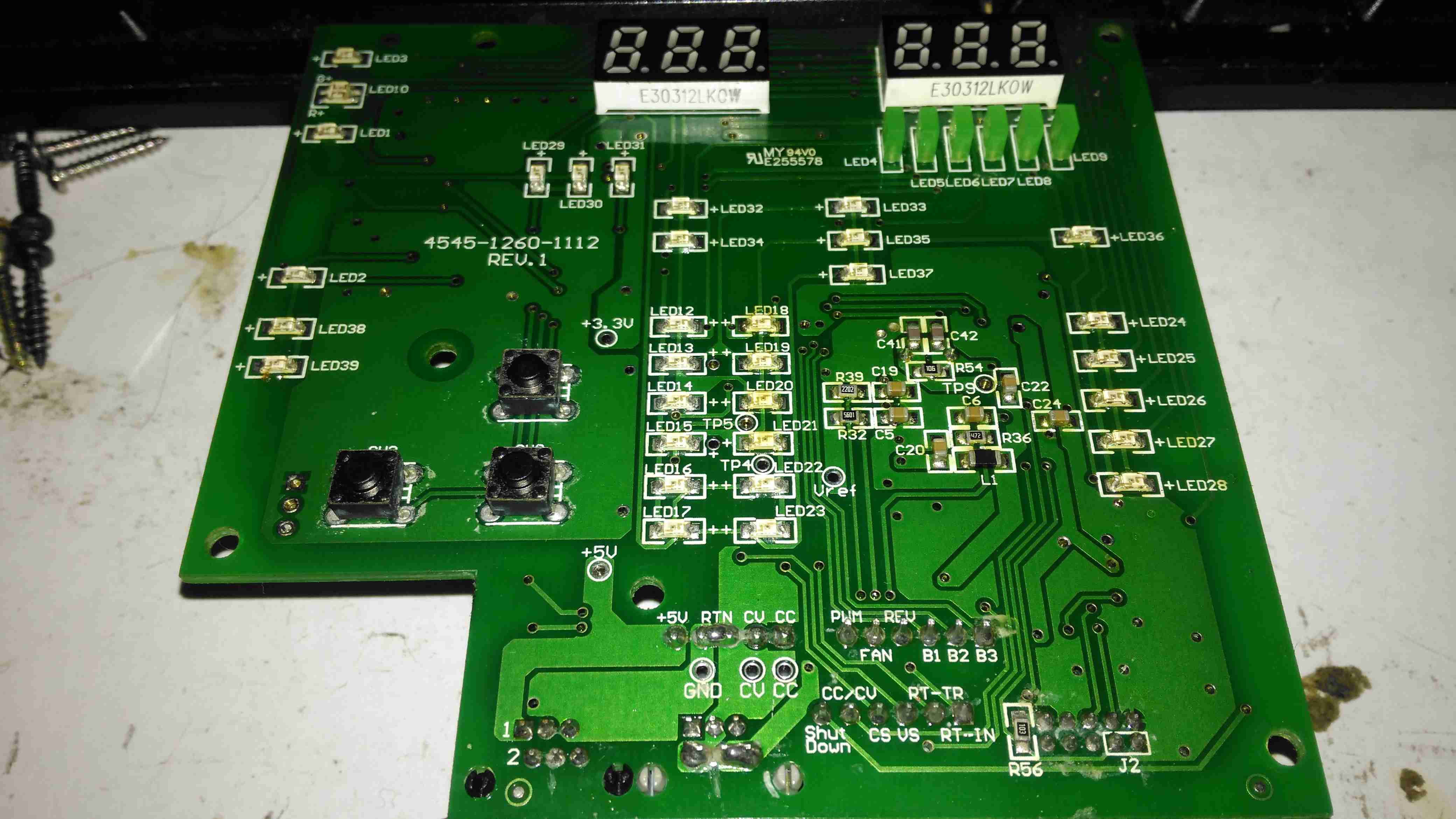
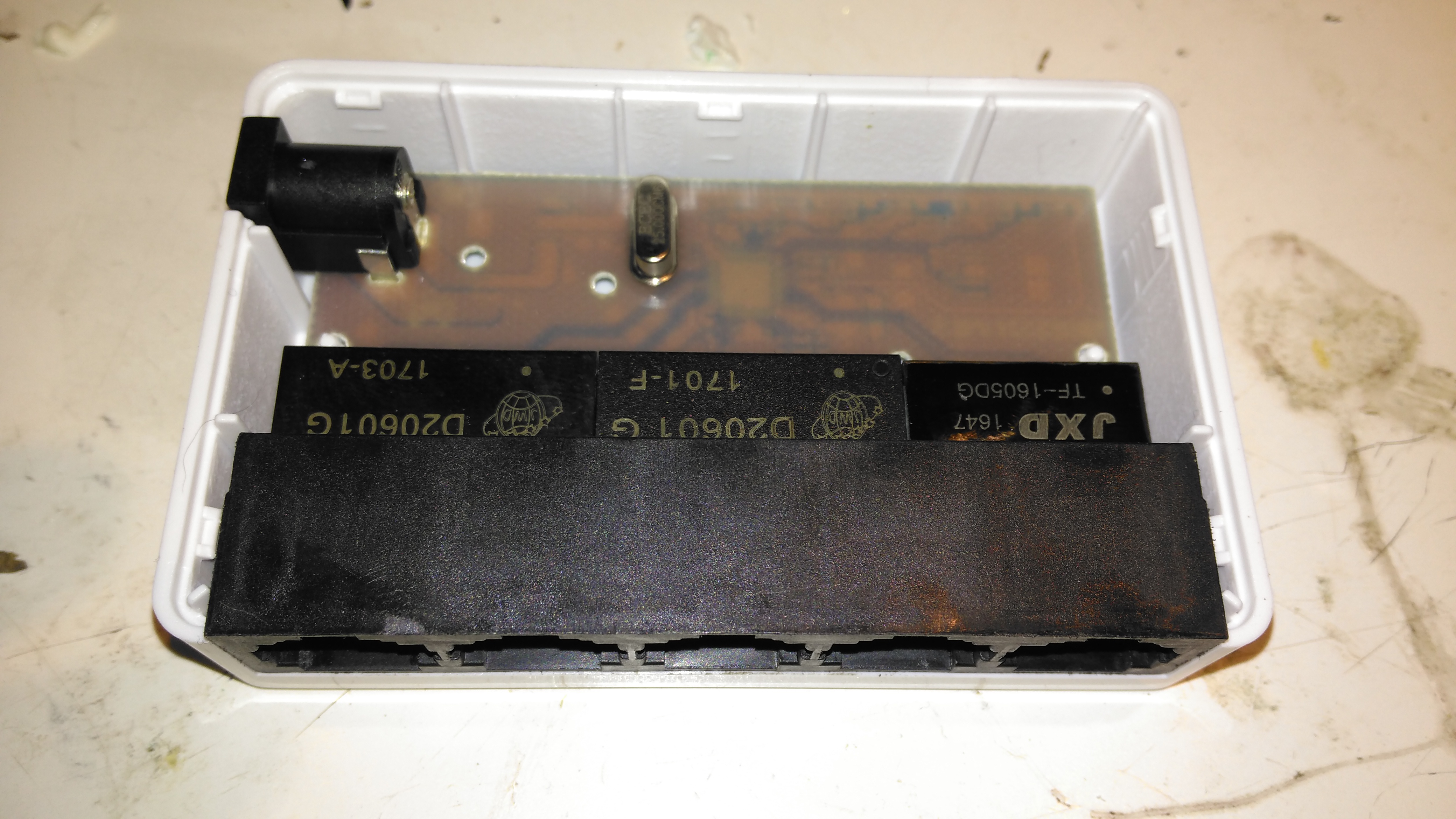
Building a Control Board
Now I’ve identified that the module was reusable, it was time to spin up a board to integrate all the features we needed:
Onboard battery power
Pushbutton operation
Indication of current attenuation level
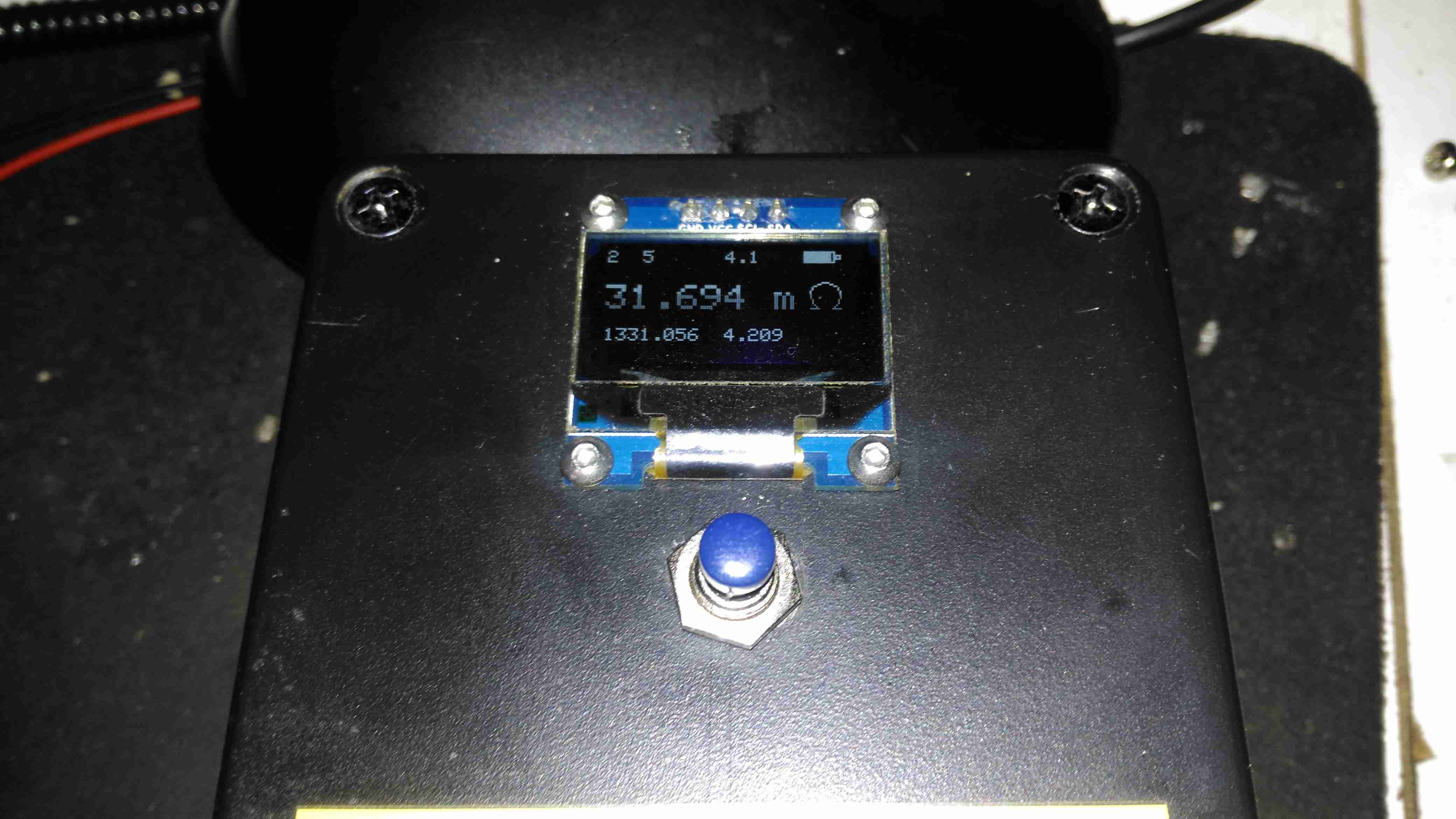
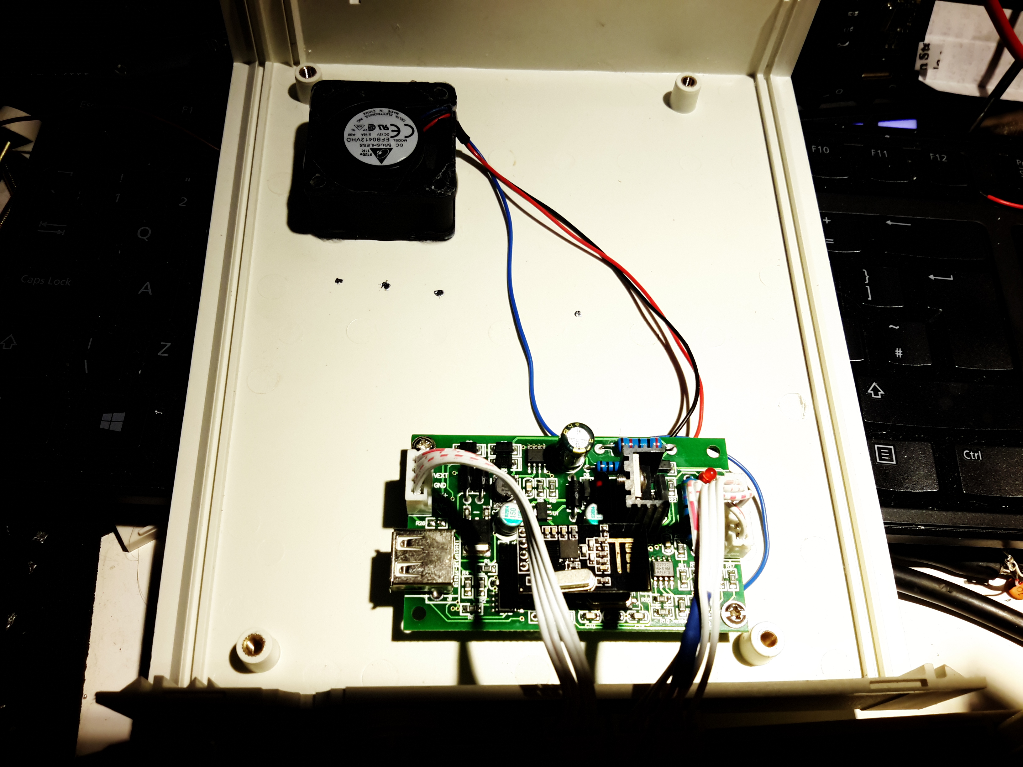
The partially populated board is shown at right, with an Arduino microcontroller for main control, 18650 battery socket on the right, and control buttons in the centre. The OLED display module for showing the current attenuation level & battery voltage level is missing at the moment, but it’s clear where this goes.
As there weren’t enough GPIO pins for everything on the Arduino, a Microchip MC23017 16-Bit I/O expander, which is controlled via an I²C bus. This is convenient since I’m already using I²C for the onboard display.
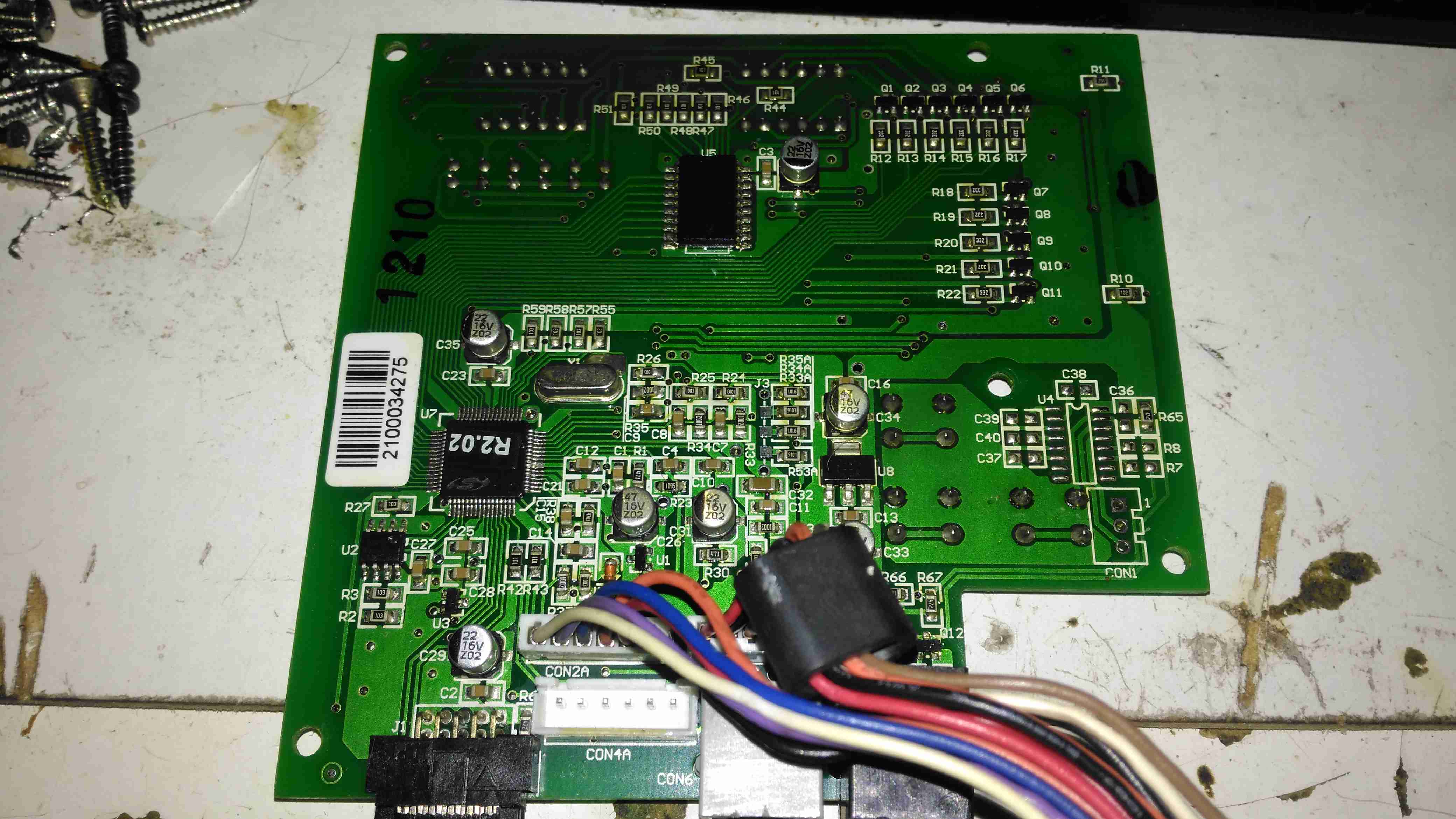
Driving the Solenoids
A closer view of the board shows the trip of dual H-Bridge drivers on the board, which will soon be hidden underneath the attenuator block. These are LB1836M parts from ON Semiconductor. Each chip drives a pair of solenoids.
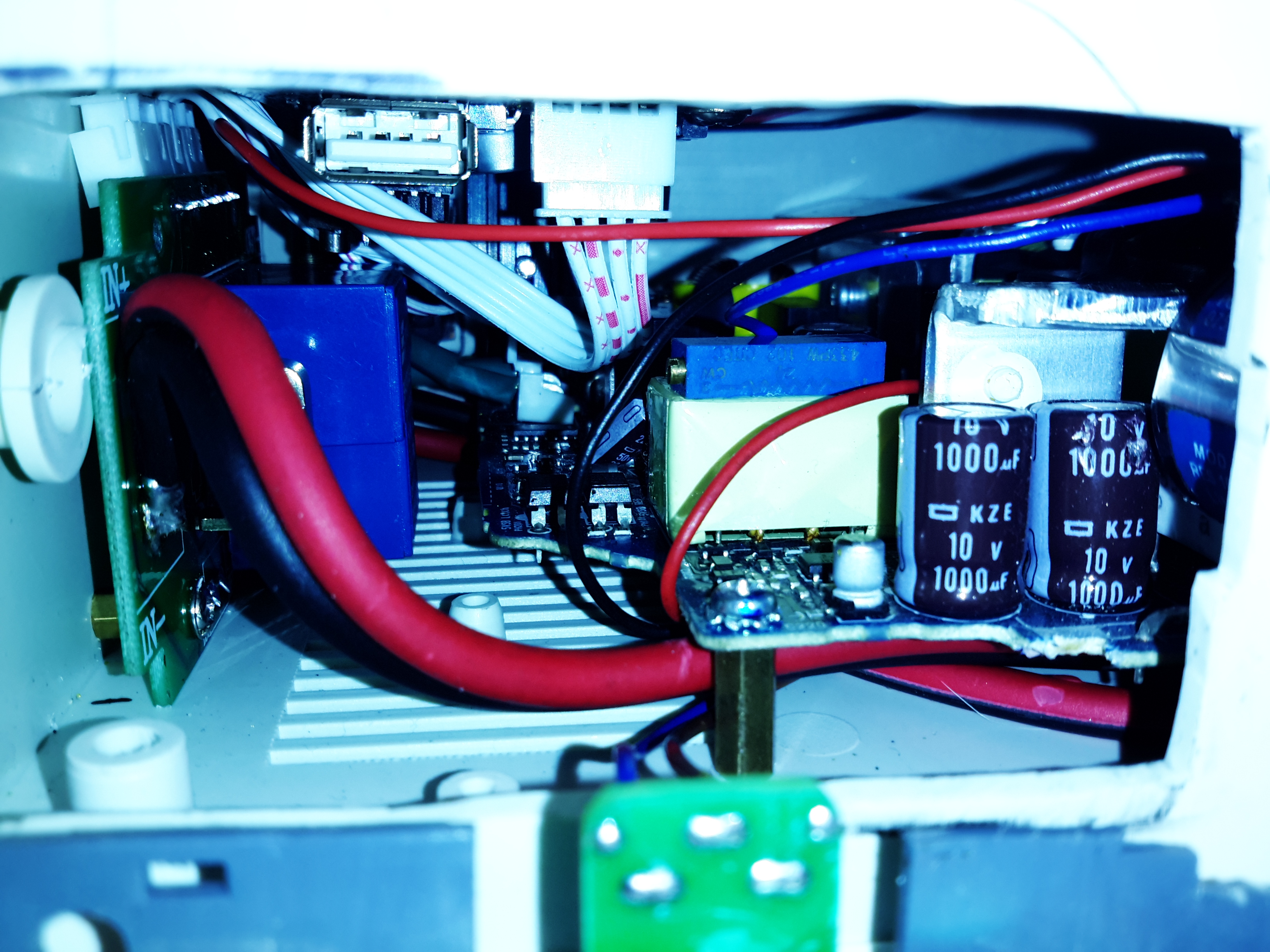
Power Supplies
The bottom of the board has all the power control circuitry, which are modularised for ease of production. There’s a Lithium charge & protection module for the 18650 onboard cell, along with a boost converter to give the ~9v rail required to operate the attenuator solenoids. While they would switch at 5v, the results were not reliable.
Finishing off
A bit more time later, some suitable firmware has been written for the Arduino, and the attenuator block is fitted onto the PCB. The onboard OLED nicely shows the current attenuation level, battery level & which input is selected.
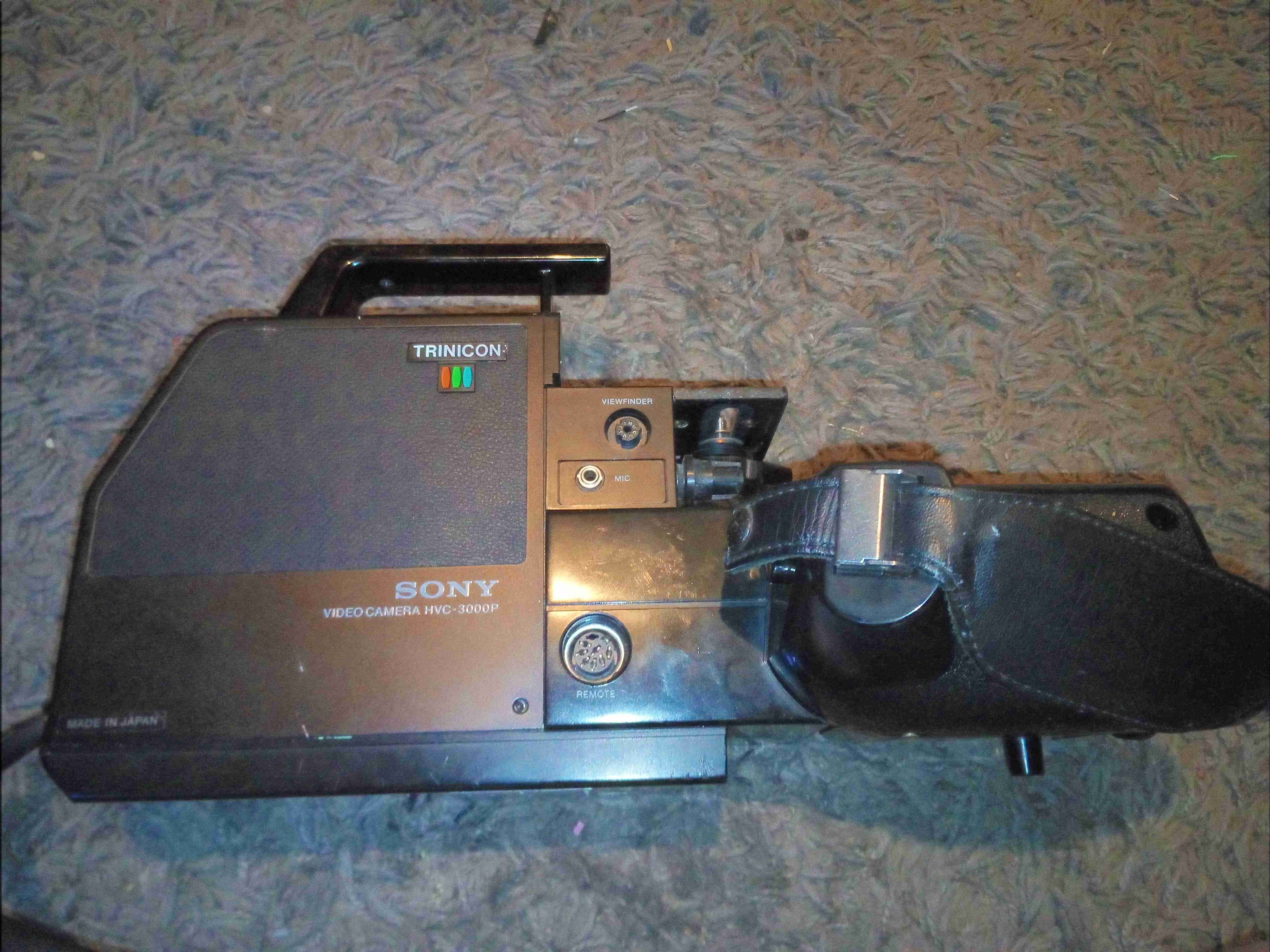
Following on from the viewfinder teardown, here’s the rest of the camera. This unit dates back to 1980, and is made almost exclusively of cast aluminium. Very little plastic has been used here & only for the bits that the user comes into contact with. This camera is based around the Sony Trinicon camera tube system, technology dating back before CCDs. There aren’t many controls on this side of the camera, only the record button, which is hidden behind the camera handgrip.
Camera Right
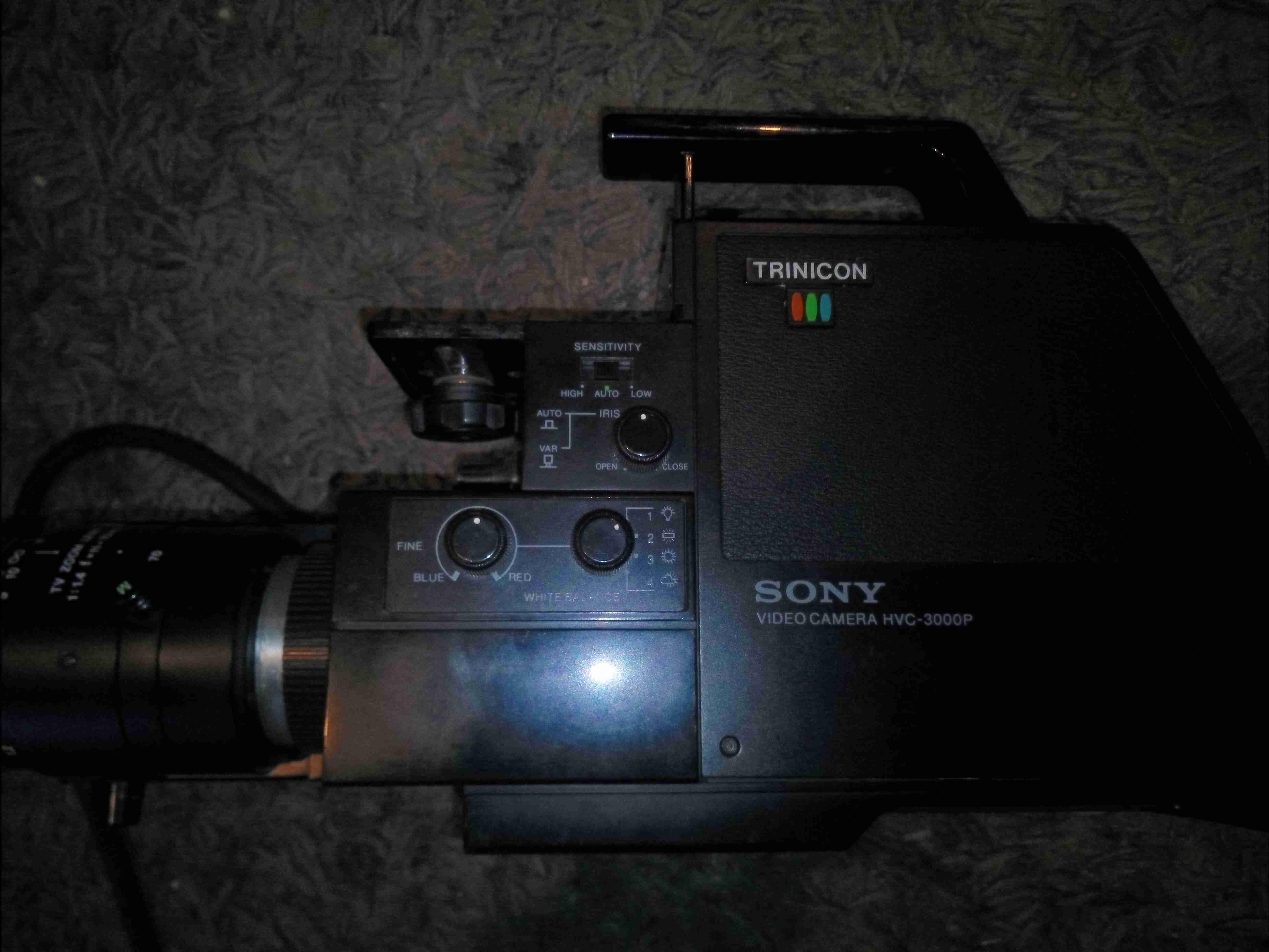
The other side of the camera has most of the controls for the picture.
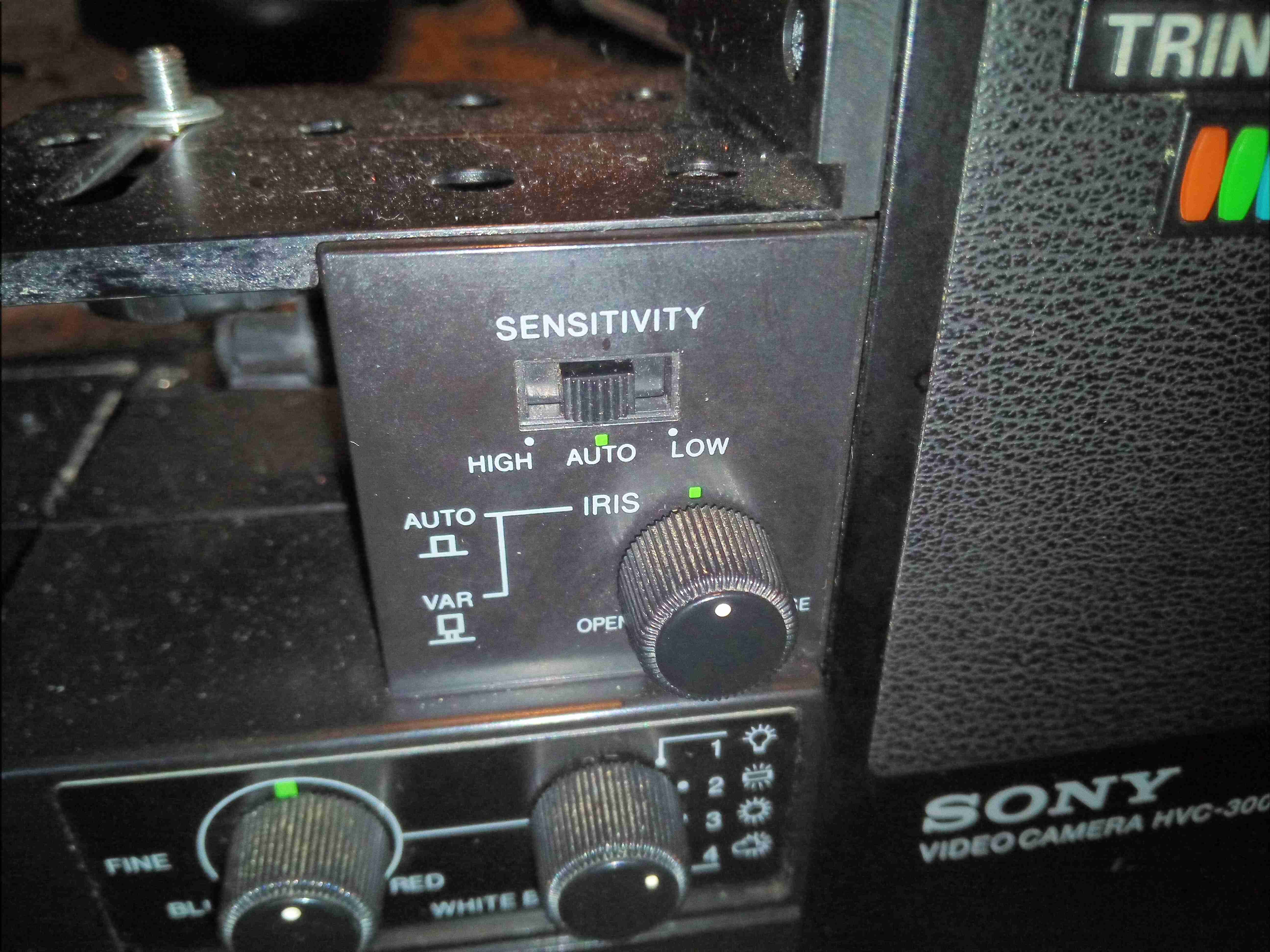
Image Controls
The image controls inclue auto / manual iris, white balance & colour balance.
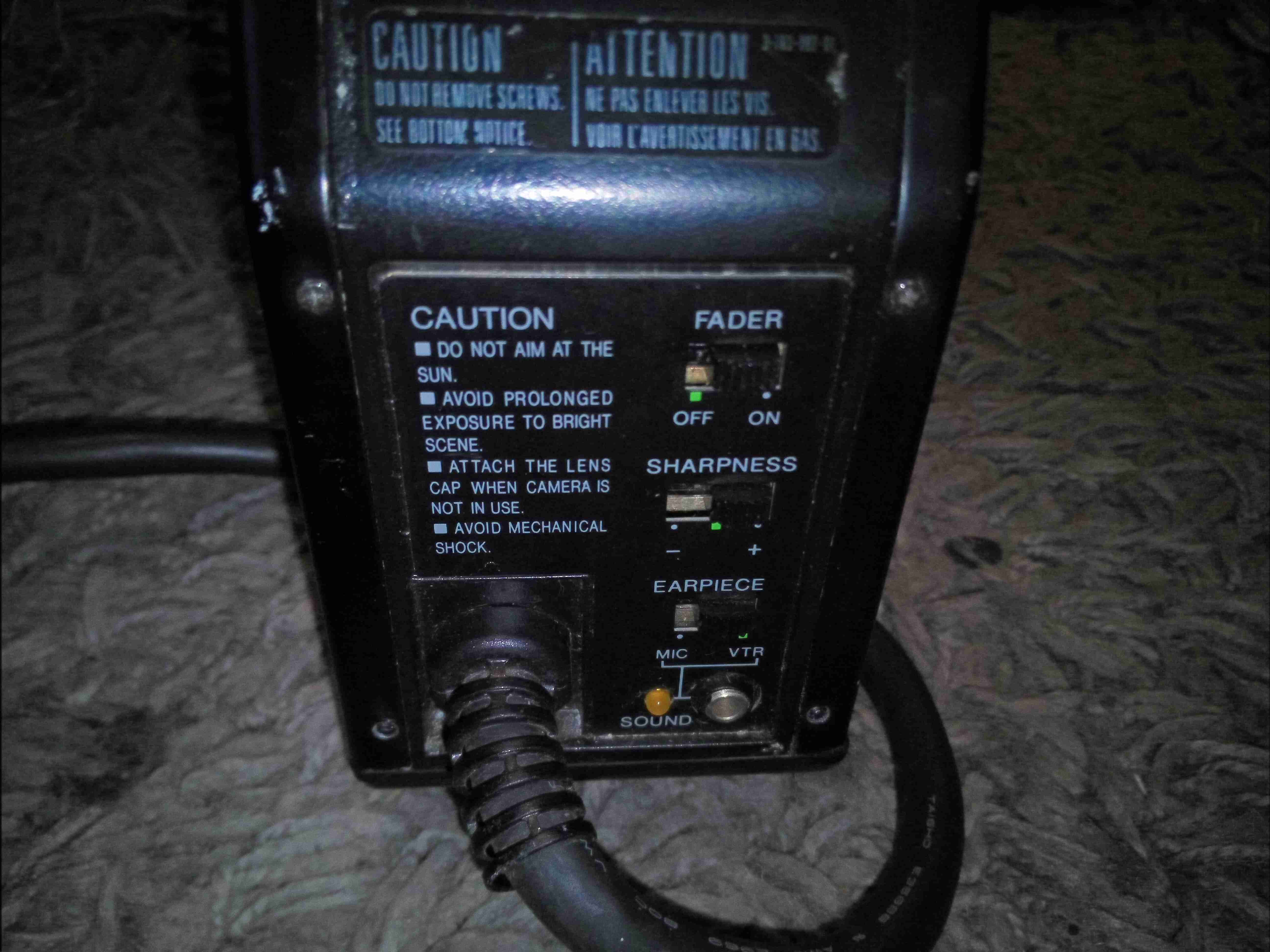
Rear Panel
Sharpness & fader controls are on the back of the camera, along with the umbilical cable which would have connected to a Betamax recorder.
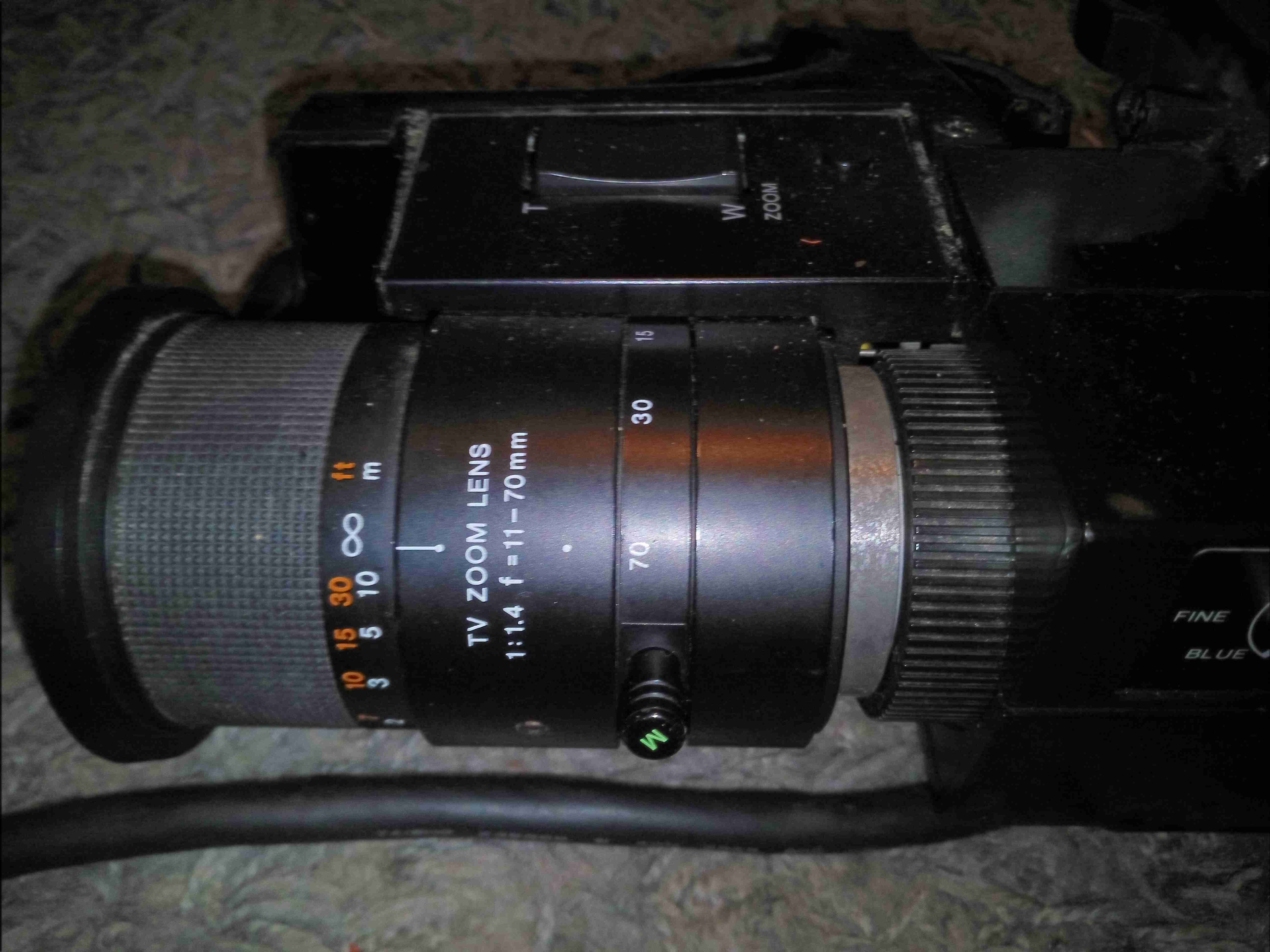
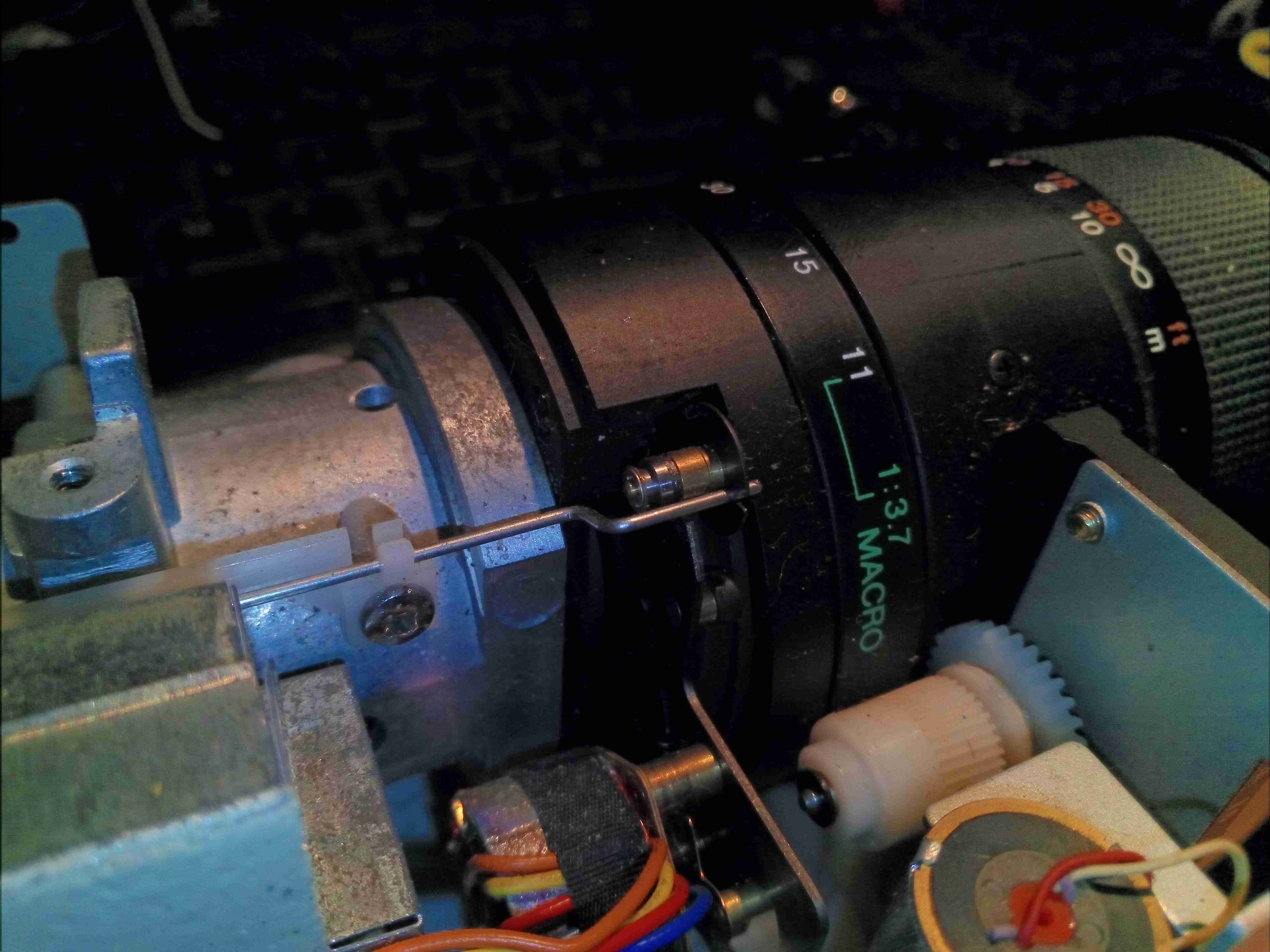
Main Lens
The lens on this camera is massive, at least a kilo of optical glass. Focus control is manual, with both auto & manual zoom control.
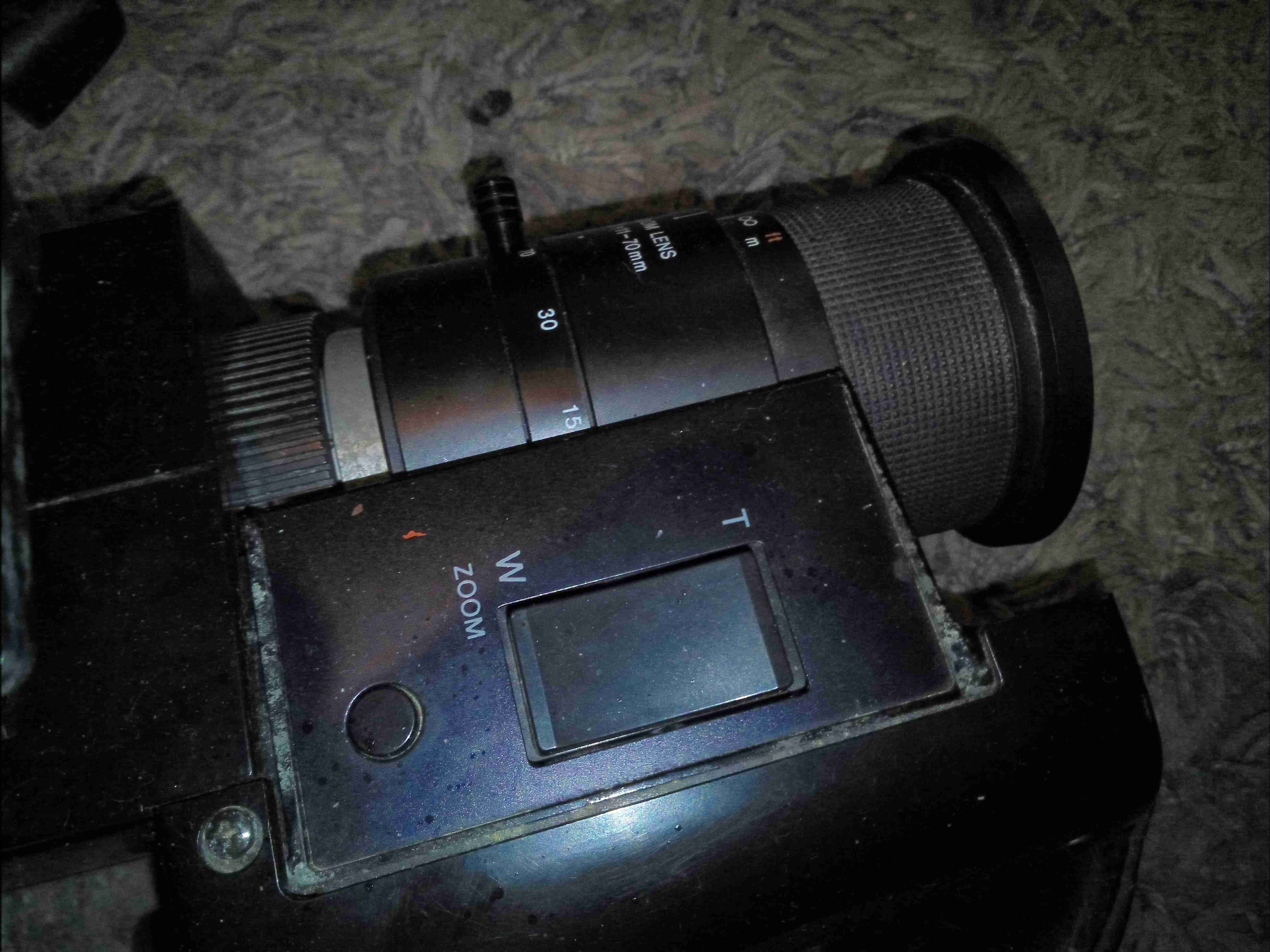
Lens Zoom Control
The Zoom controls are on top of the grip, with a button to the rear of the control which I have no idea about. The internal belts are a bit rotted with age so the zoom function doesn’t work great.
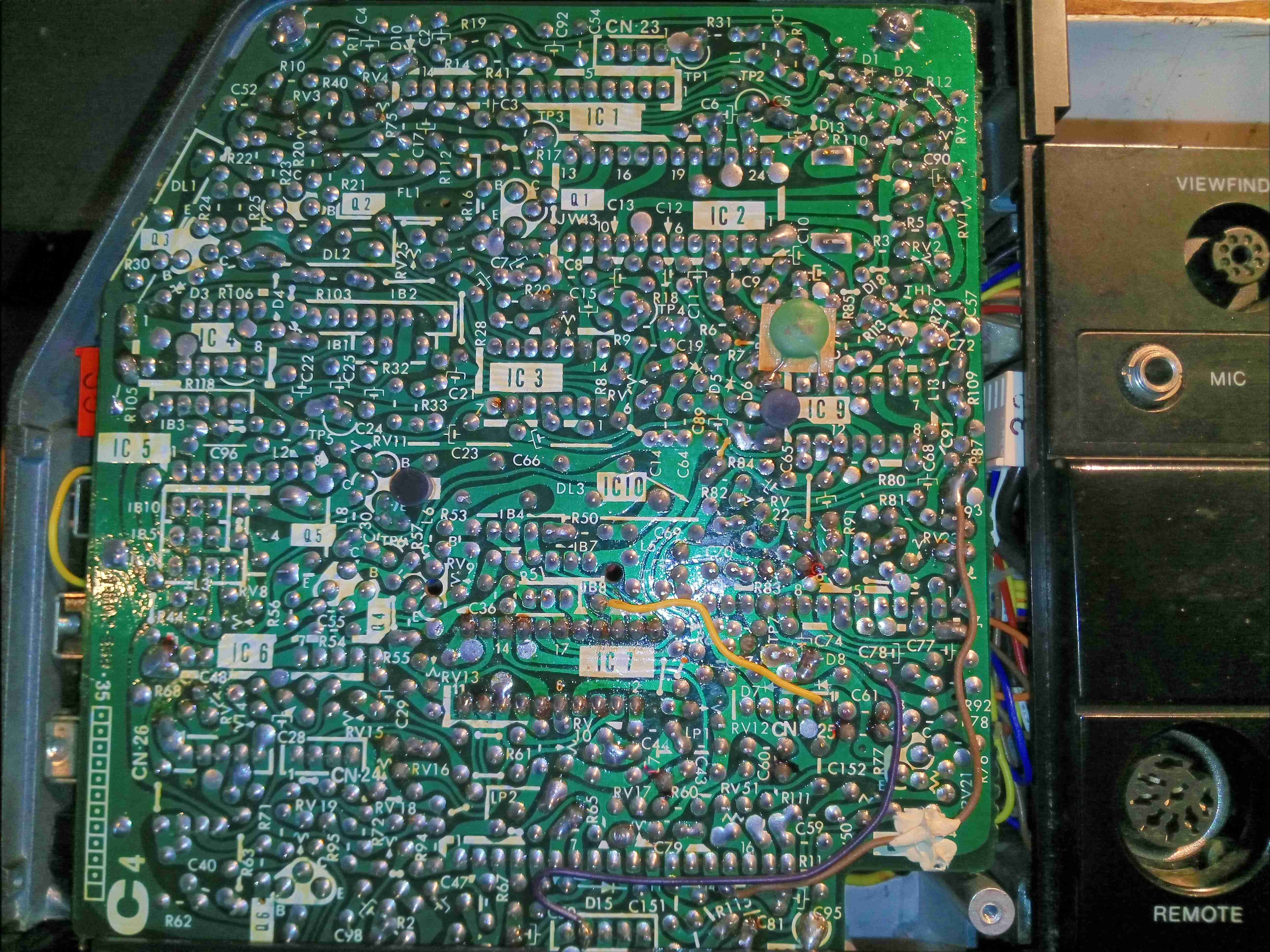
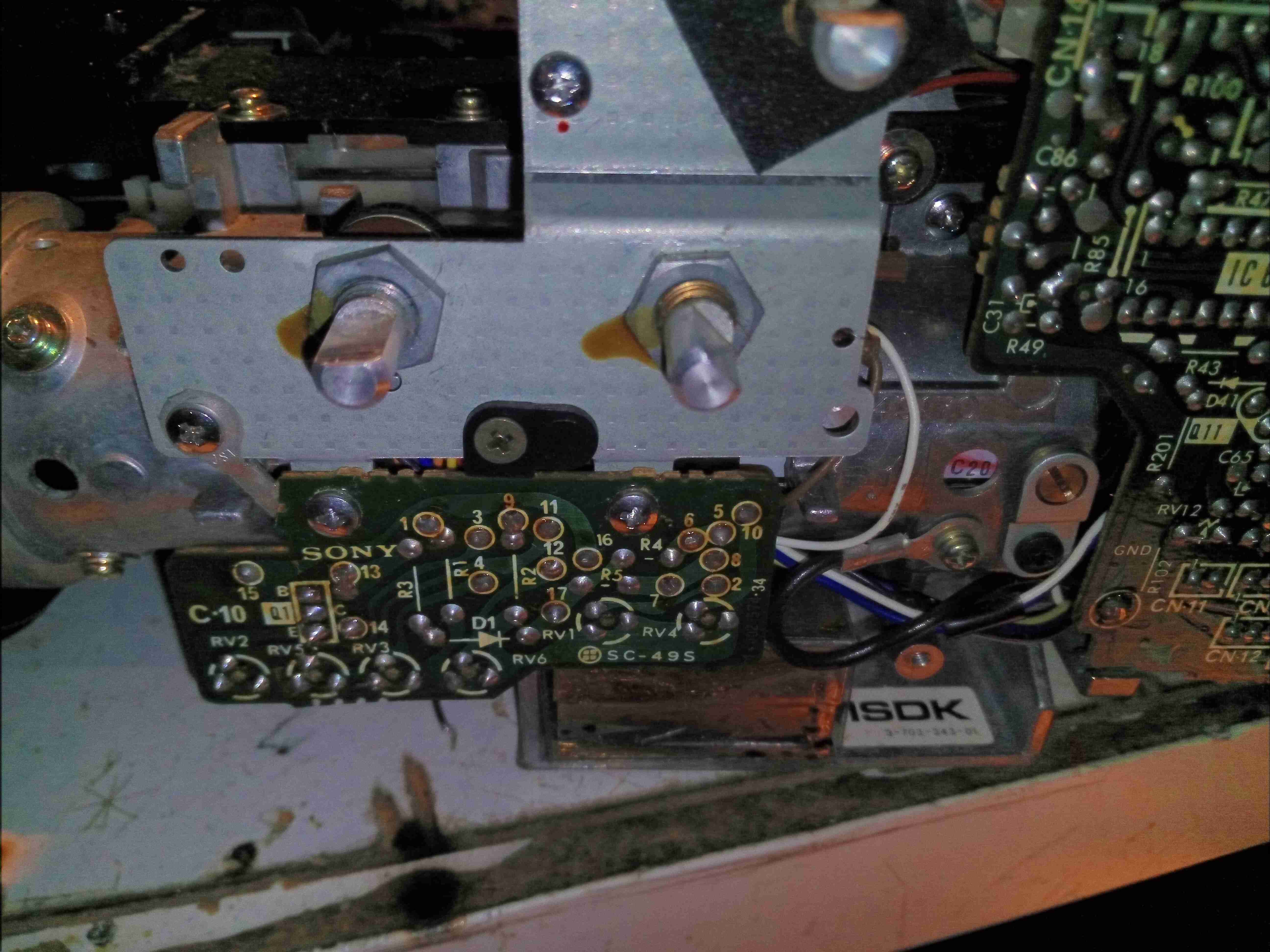
Trinicon Control Board
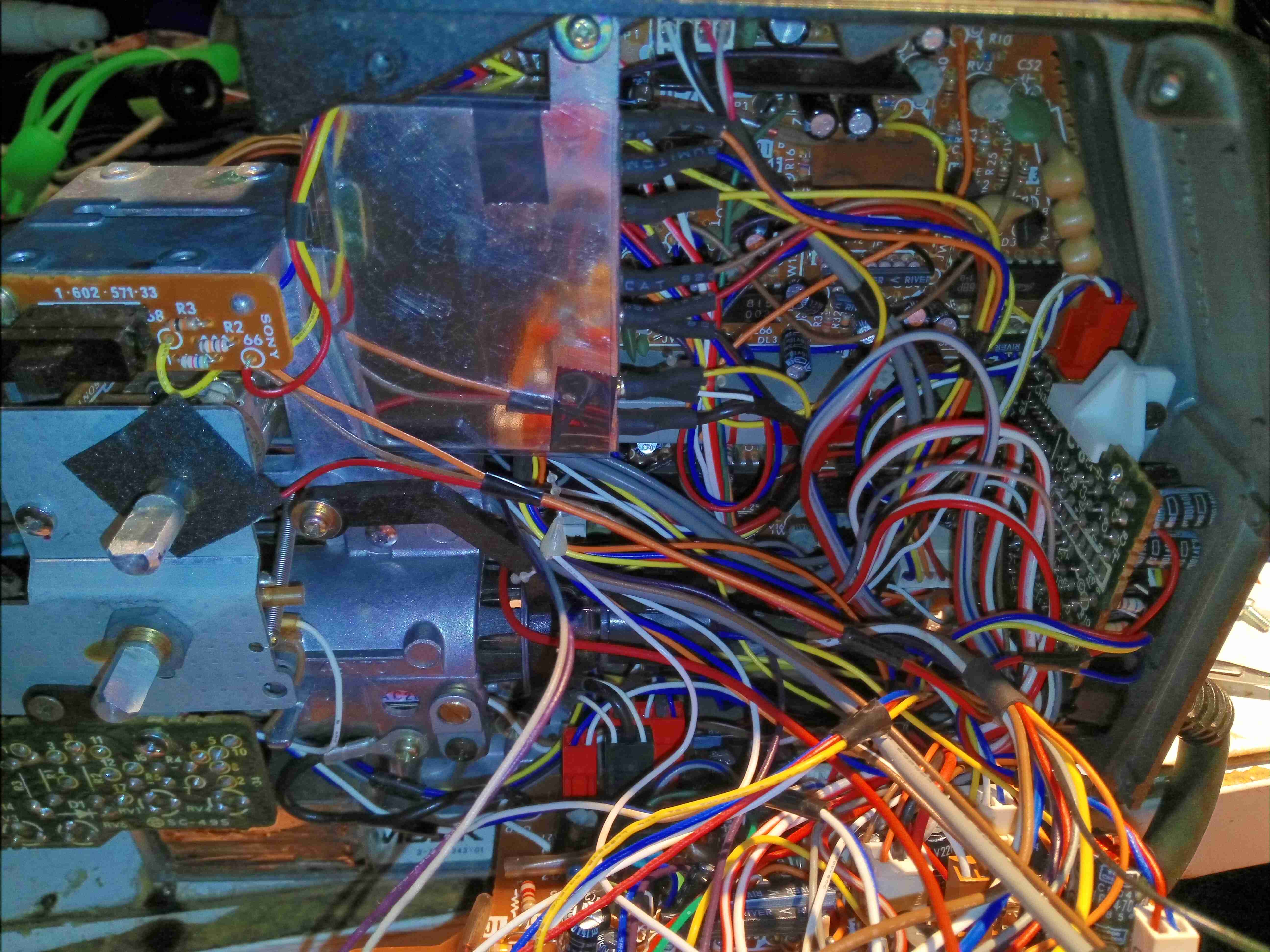
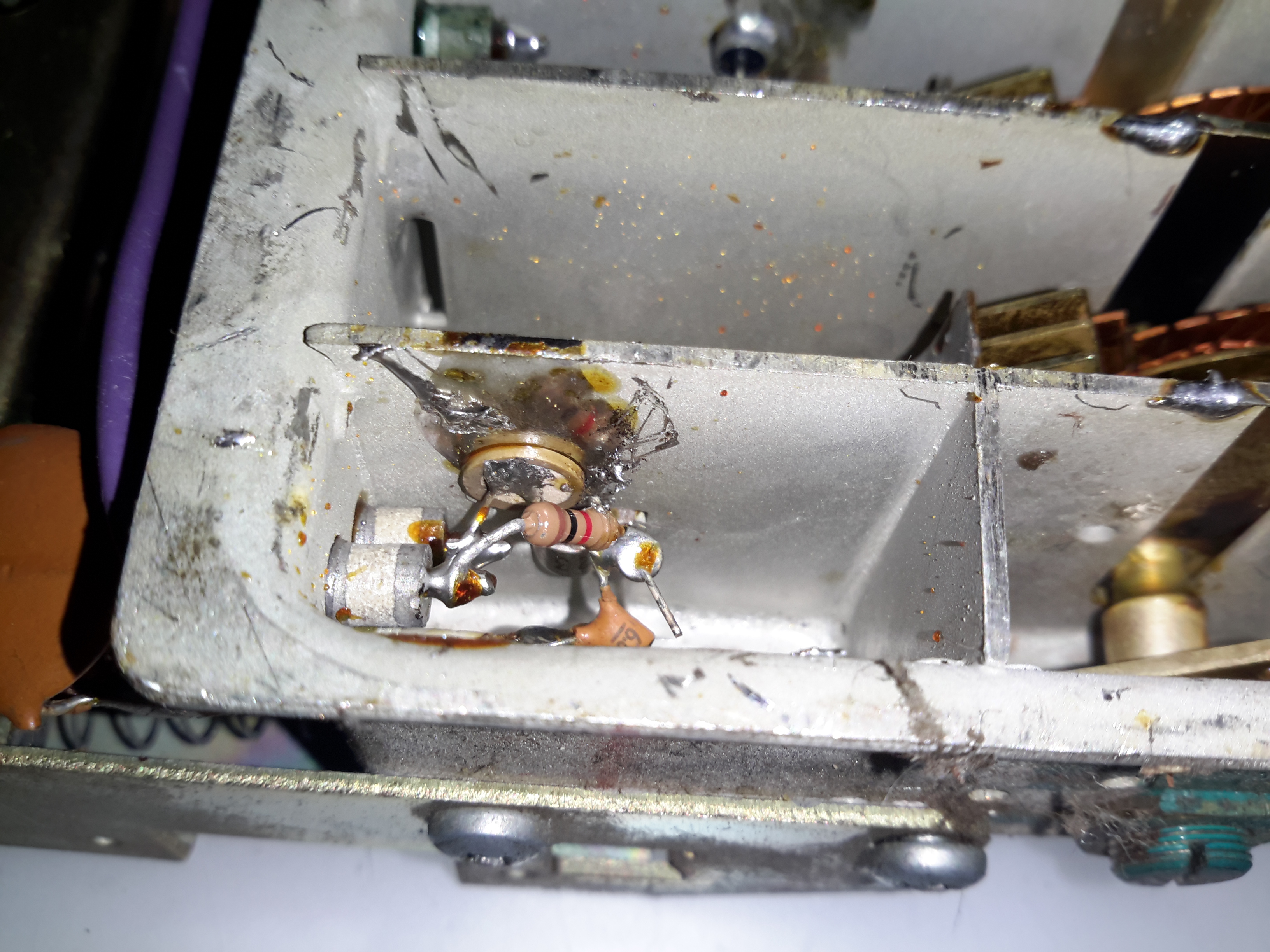
After removing the side covers, the two large PCBs become visible. These units are absolutely packed with electronics. On this side is the Trinicon tube control board, generating all the high voltages for electron beam acceleration, focus & electrostatic deflection of the beam. There’s around 500 volts knocking around on this board, with some rather specialised hybrid modules doing all the high voltage magic.
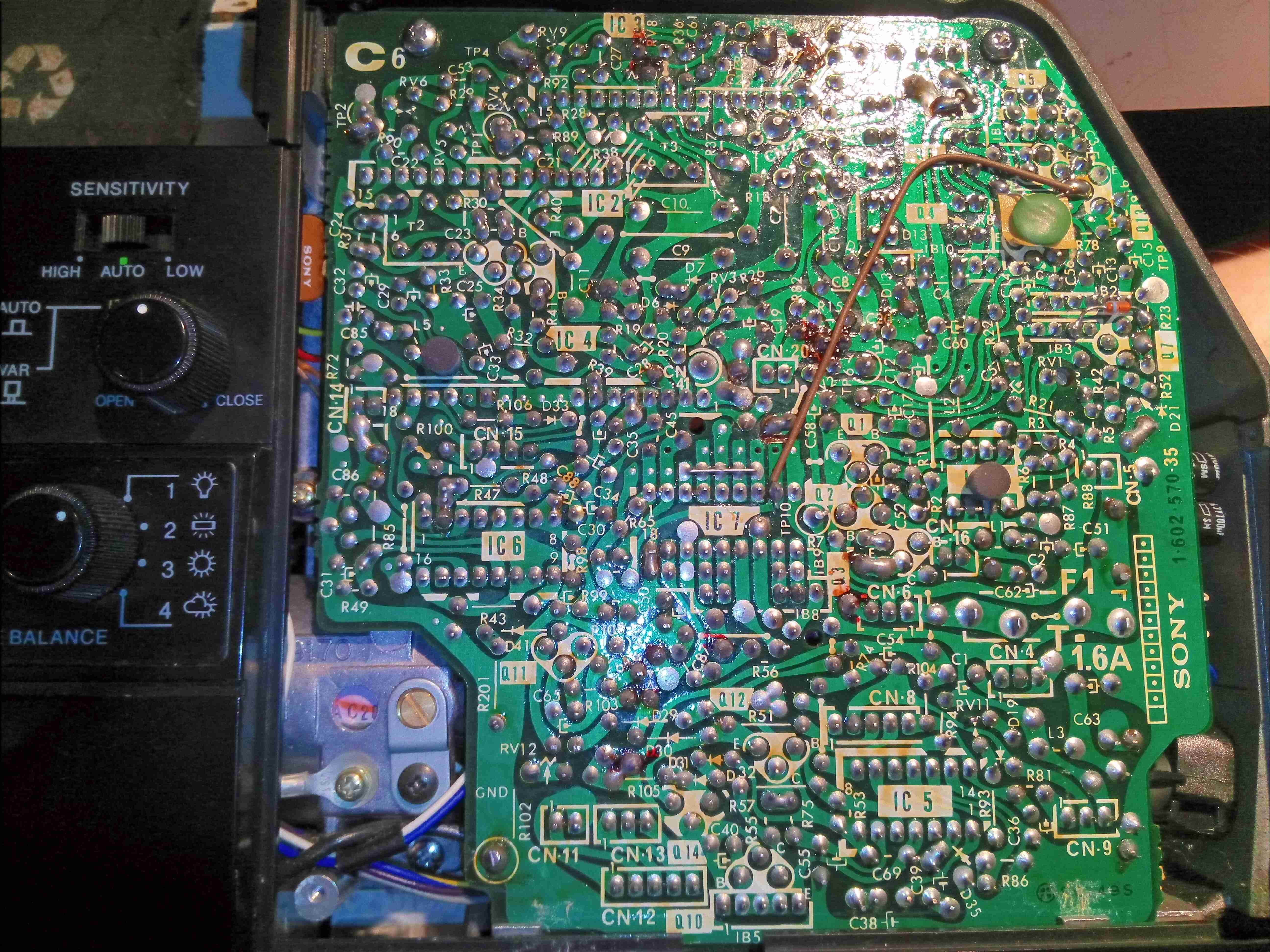
Video Process Board
The other side of the camera has the video process board, which performs all the colour separation of the video signal from the tube, processes the resulting signals into a composite video signal, and finally sends it down the umbilical.
Bare Controls
Removing some of the remaining covers exposes the bare video controls, and a small PCB just underneath covered in trimpots to set factory levels.
White Balance Filter Arm
The white balance is partially electronic & partially mechanical. This lever actuates a filter inside the lens assrembly.
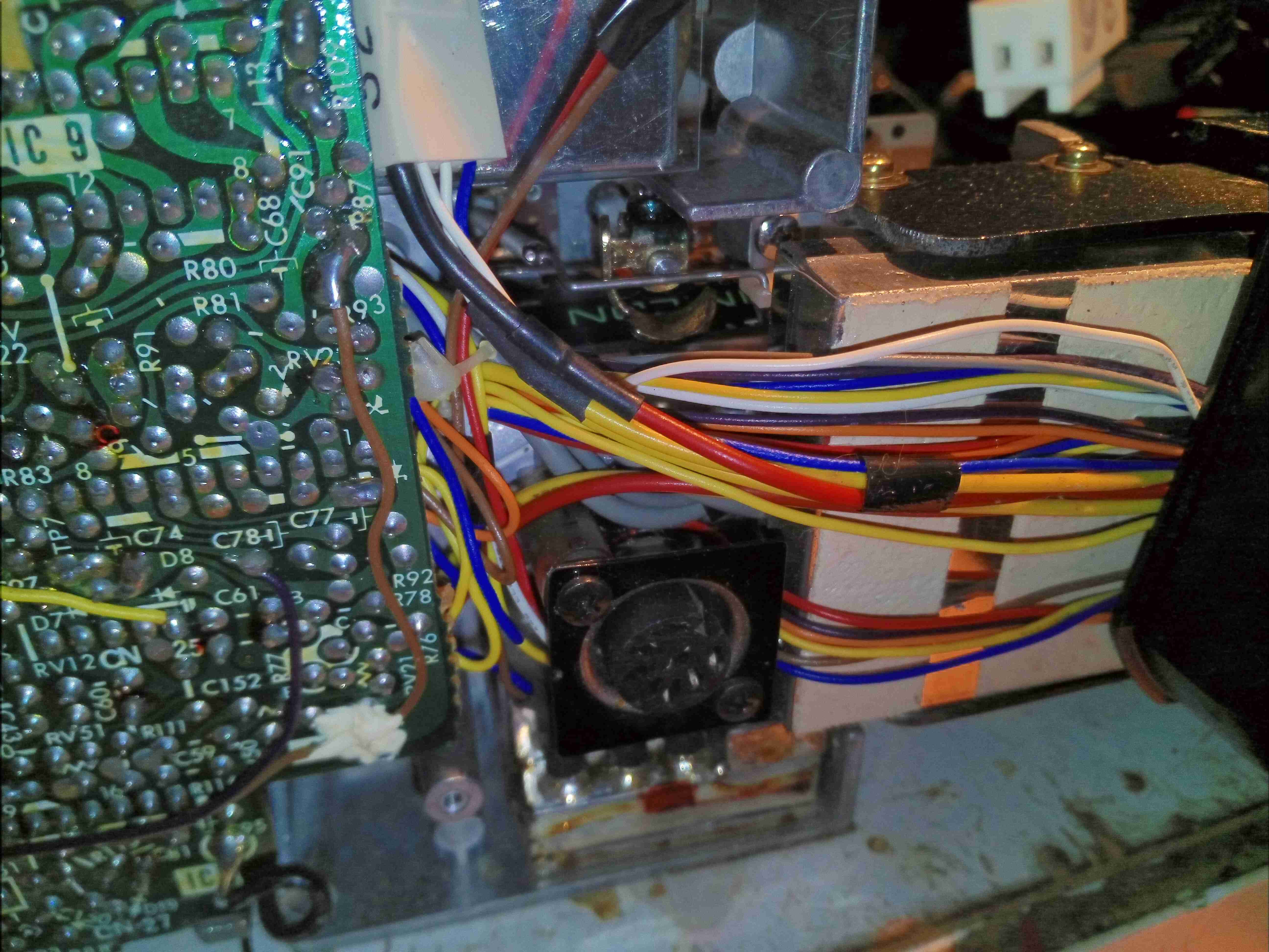
Remote Connector
A DIN connector offers remote control ability. The large loom of wires disappearing off to the right is dealing with the zoom mechanism & the onboard microphone amplifier. Just under the DIN connector hides the system power supply, inside a soldered can. The can under the white tape is the head end amplifier for the Trinicon video tube.
Trinicon Mount
Hiding in the centre of the camera inside the casting is the Trinicon tube assembly itself. The label can just be seen here.
Camera Internals 1
As is typical of 1980’s electronic design, the main boards swing down & are designed to slot into the base casting folded out for repairs. Internally the unit is a rat’s nest of wiring loom. There’s also another shielding can in here nestled between the boards – this is the video sync generator circuit.
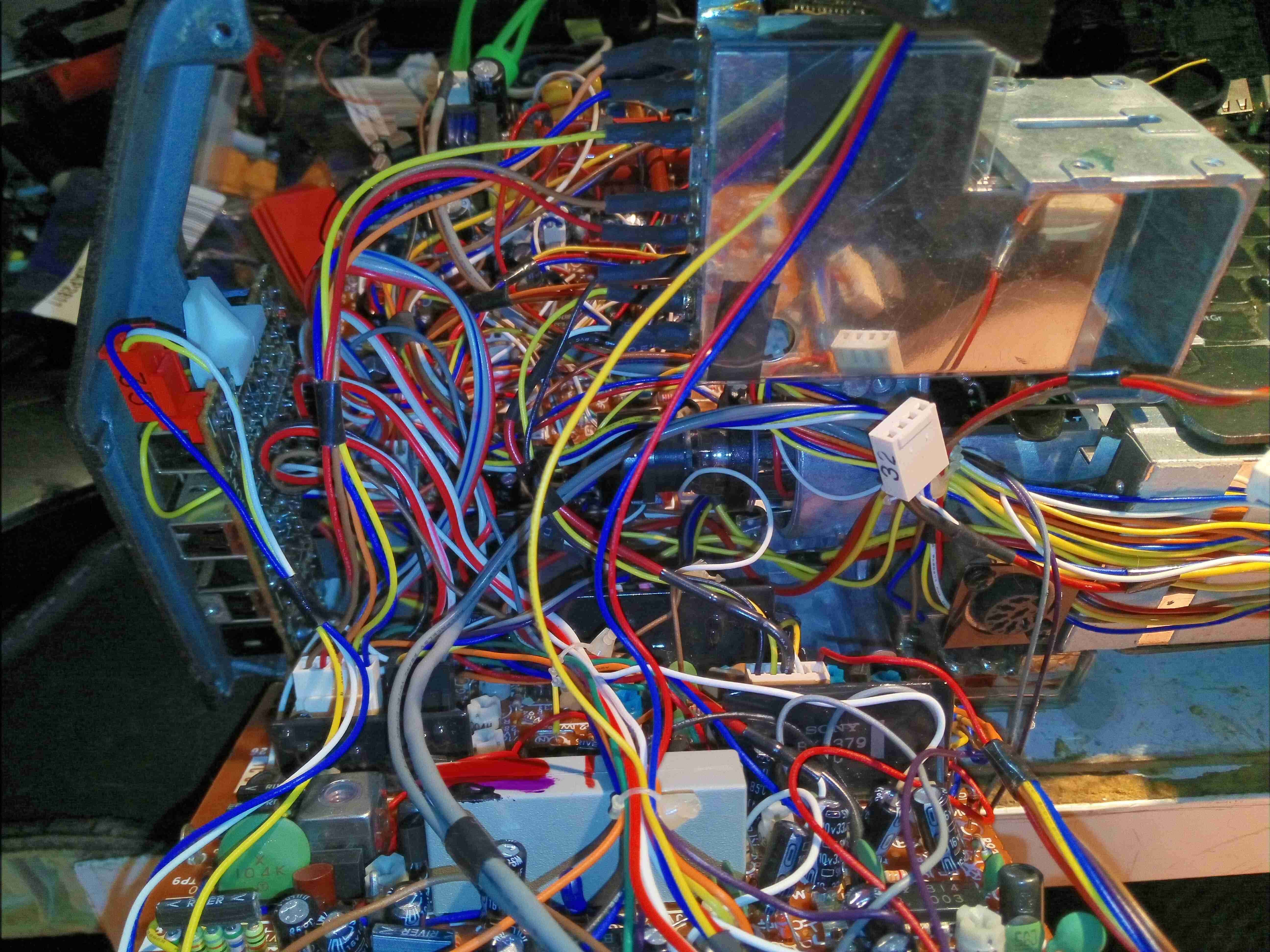
Camera Internals 2
The other side gives a better view of the video sync generator can. I’ll dive into the individual modules later on.
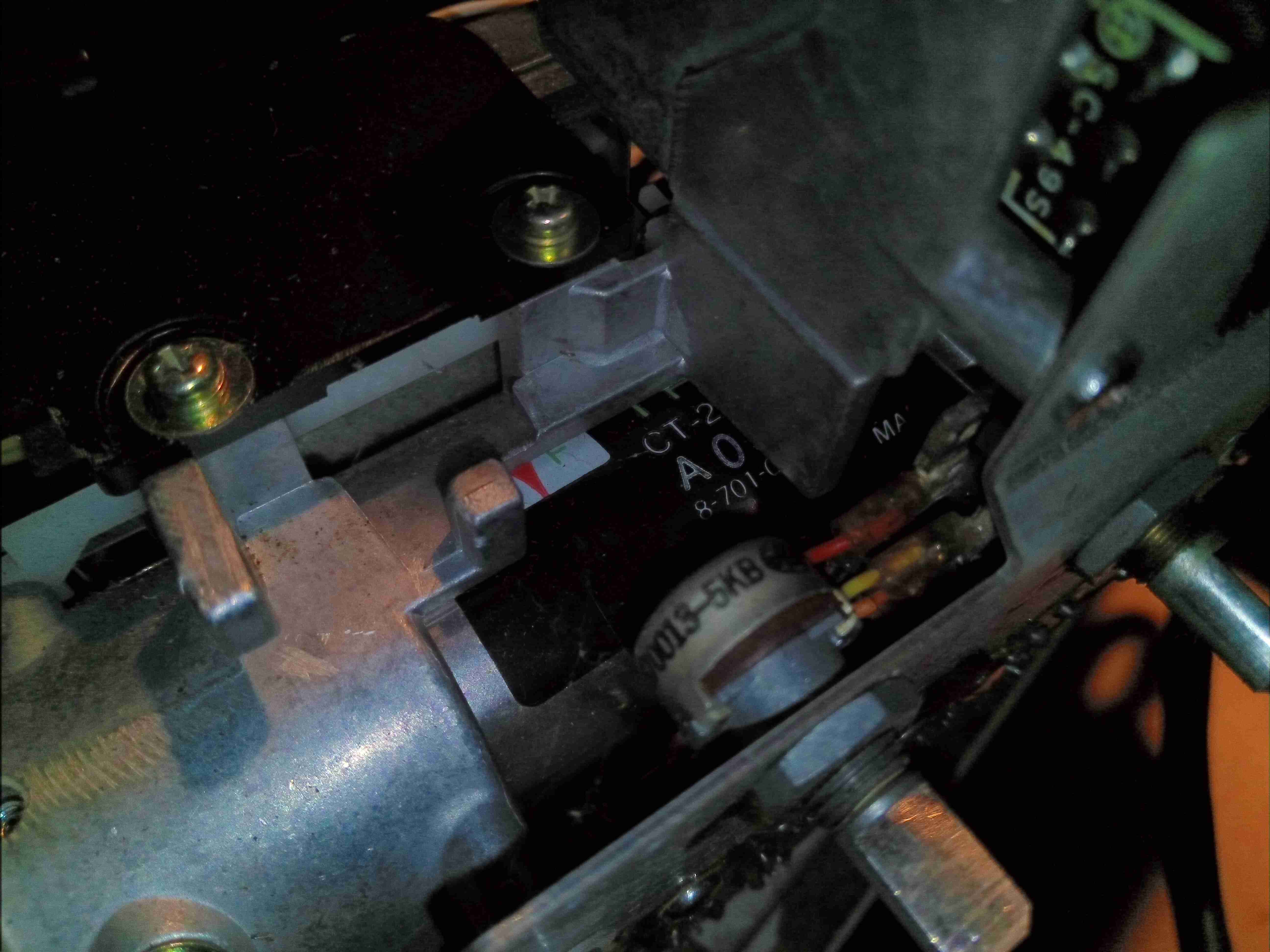
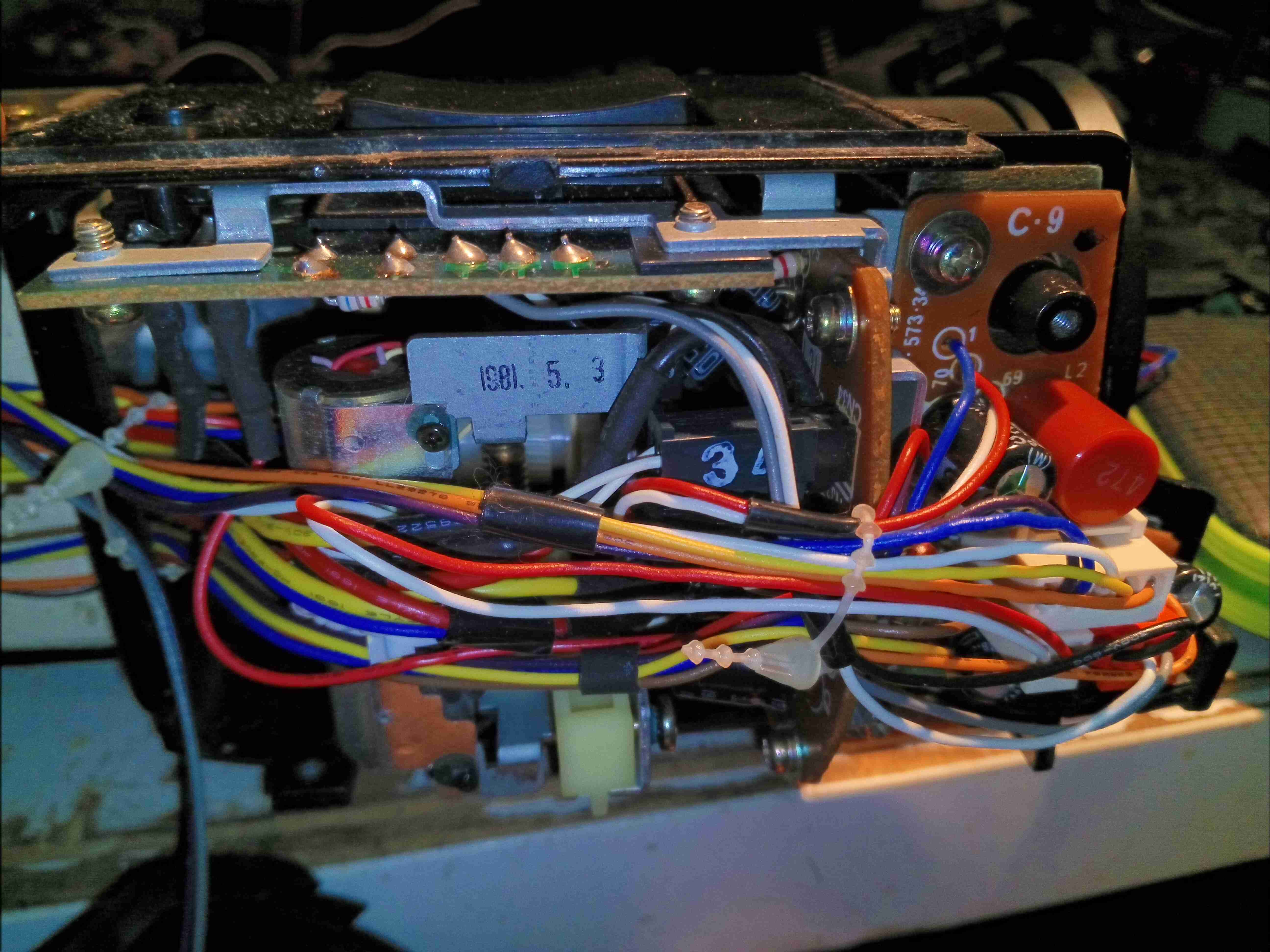
Lens Zoom Assembly
Under the remaining side cover is the zoom assembly & microphone amplifier board. More massive wiring loom hides within.
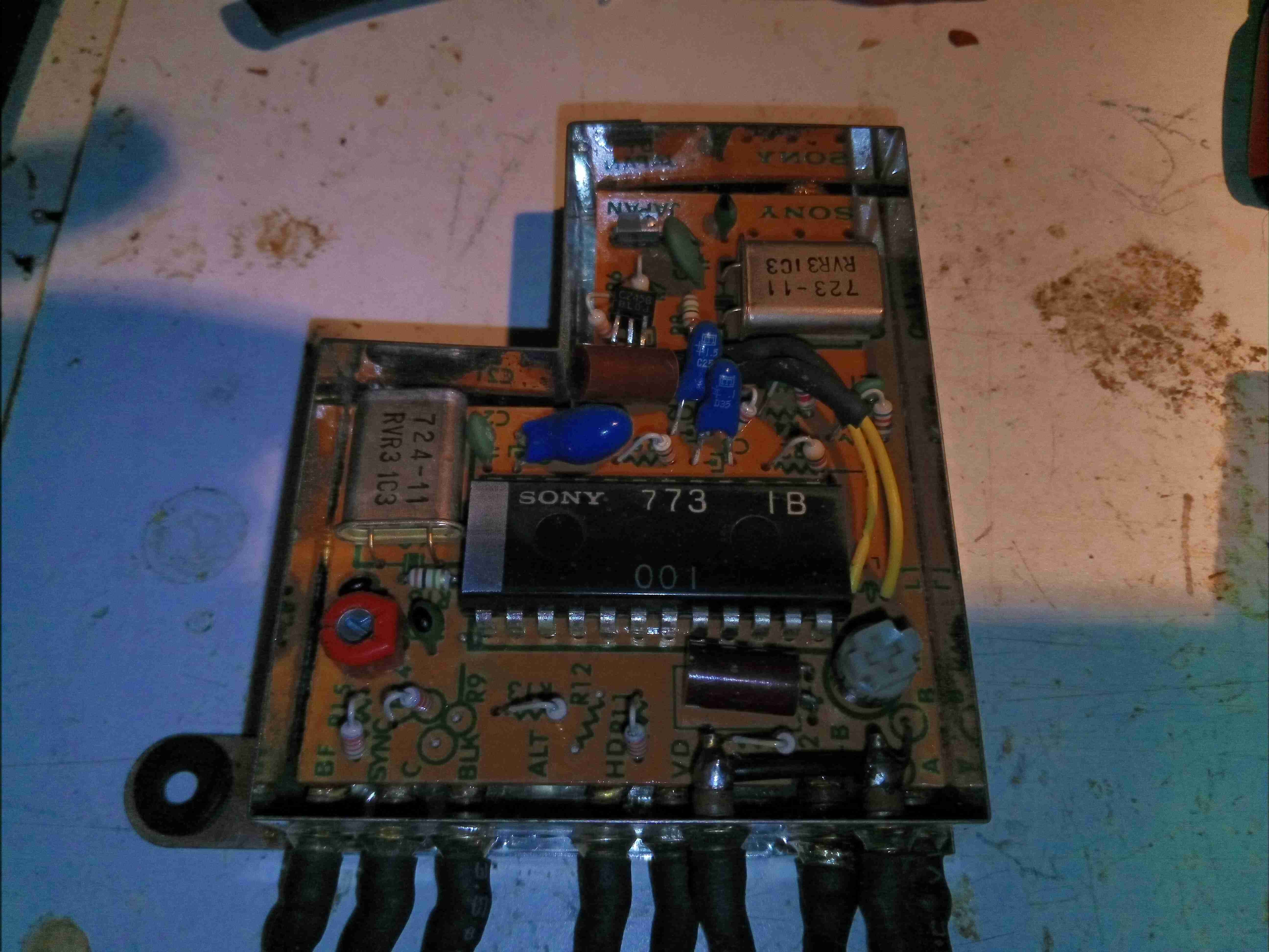
Video Sync Generator
The video sync generator is pretty sparse inside, just a large Sony CX773 Sync Generator IC, with a pair of crystals. There are a couple of adjustments in here for video sync frequencies.
Head End Amplifier
Removed from it’s shielding can, here is the head end amplifier for the Trinicon tube. This very sensitive JFET input amplifier feeds into the main video process board.
Input Transformer
The Trinicon tube target connects to this input transformer on the front of the amplifier board.
Internal Video Adjustments
The internal white balance controls are on this small PCB, mounted under the user-accessible controls.
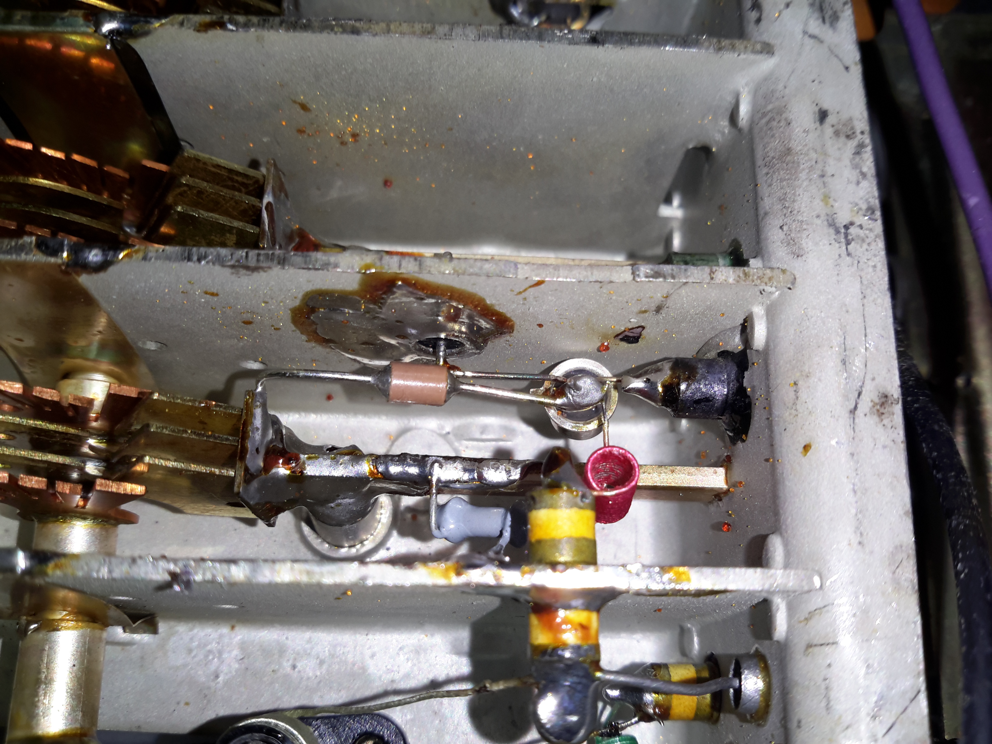
Vidicon Control Board
Here’s the main control board responsible for the Trinicon tube & exposure control. Down near the front is the auto-iris circuit, nearer the centre is timing control & at the top is the high voltage power supply & deflection generator ICs.
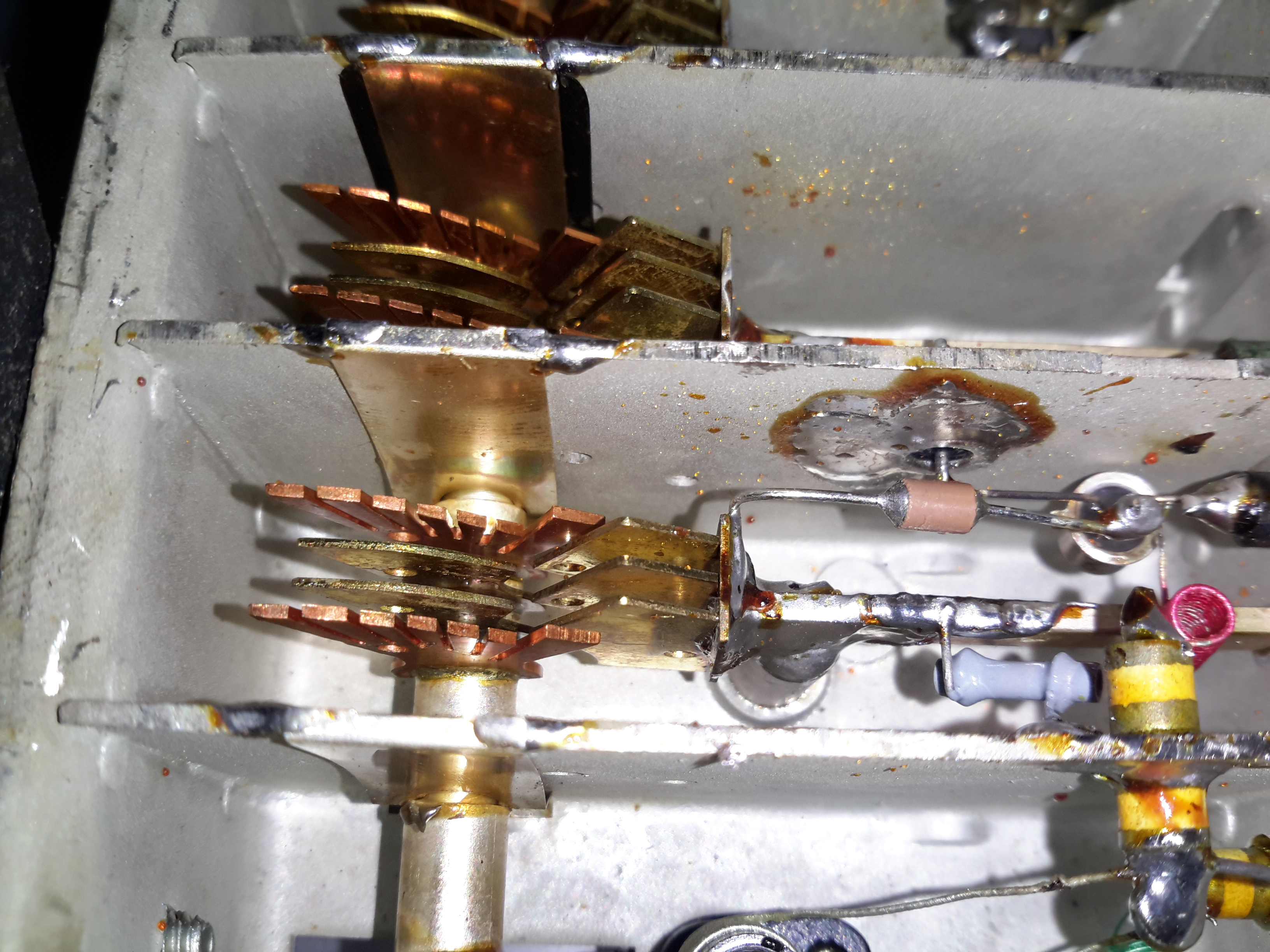
High Voltage Section
Here’s the high voltage section, the main transformer at right generating the voltages required to drive the video tube. The large orange hybrids here are a pair of BX369 high-voltage sawtooth generators that create the deflection waveforms for the tube. The other large hybrid is a BX382 Fader Control.
Video Process Board
The other large board contains all the video process circuitry, all analogue of course. There are a lot of manual adjustment pots on this board.
Lens Barrel
After removing the lens assembly, the tube assembly is visible inside the barrel casting. Not much to see yet, just the IR filter assembly.
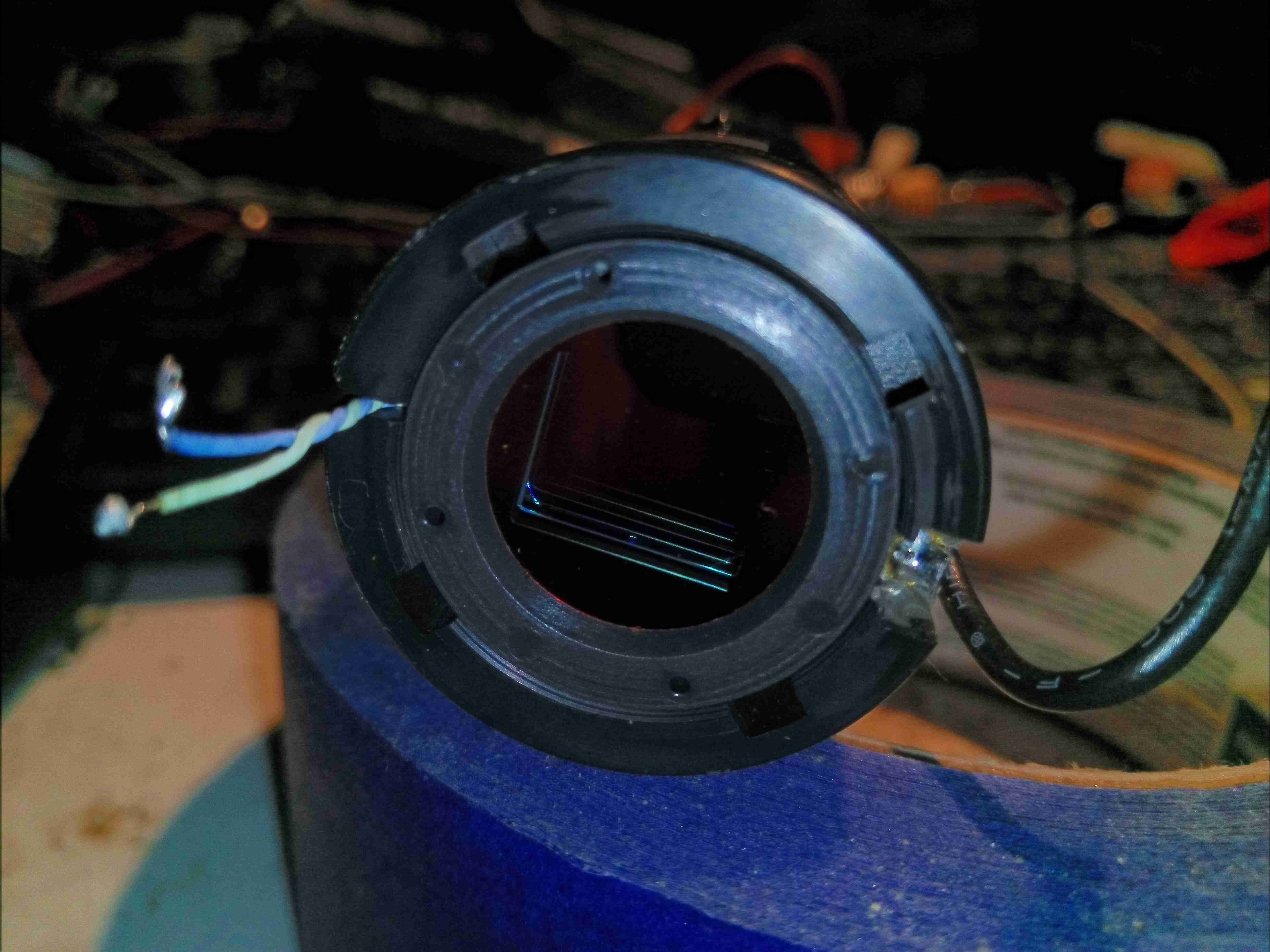
Trinicon Tube Assembly
Here’s the unit removed from the camera. Unfortunately this tube is dead – it shows a lot of target burn on the resulting image, and very bad ghosting on what poor image there is. The Trinicon tube itself is encased in the focus coil assembly, the windings of which are hidden under the shielding.
IR Filter
The IR filter is locked into the front of the tube, on a bayonet fitting. The twin target wires are running off to the left, where they would connect to the head end amplifier.
Bare Tube
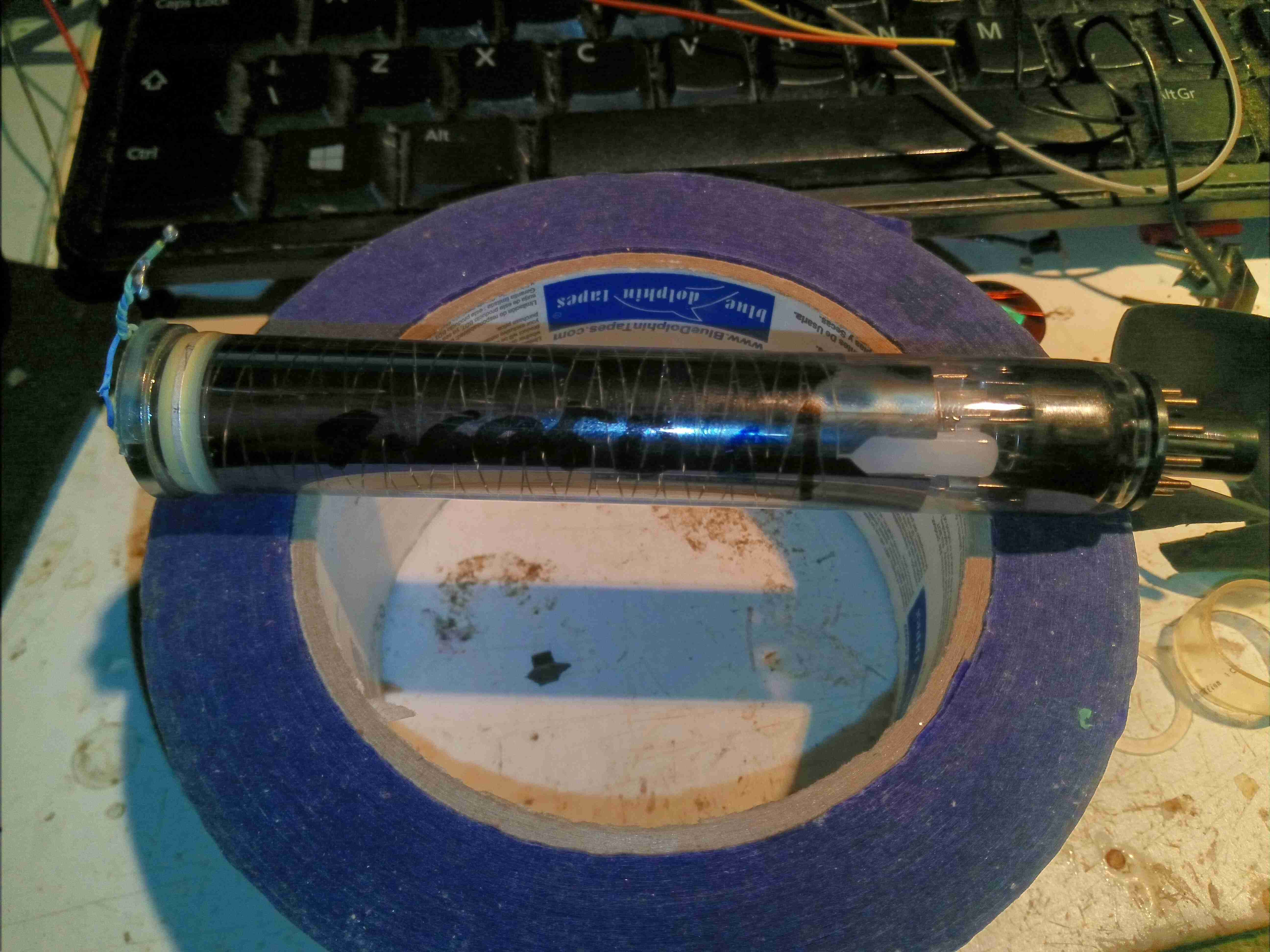
After removing the IR filter glass, the Trinicon tube itself is removed from the focus coil assembly. There’s an electron gun at the rear of the tube, like all CRTs, although this one works in reverse – sensing an image projected on the front instead of generating one.
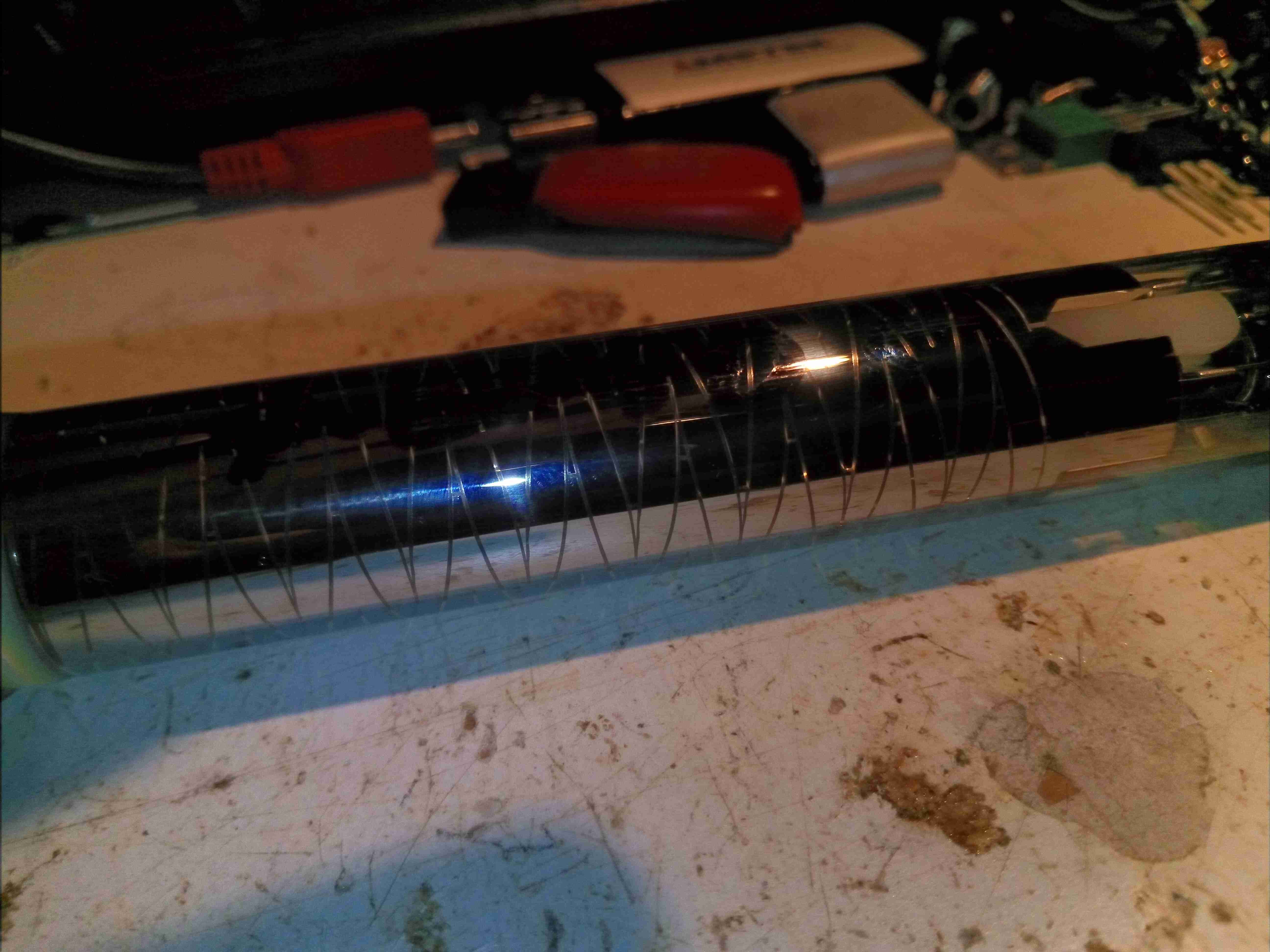
Deflection Plates
It’s a little difficult to see, but the electrostatic deflection electrodes in this tube are created from the aluminium flashing on the inside of the glass, in a zig-zag pattern. The interleaving electrodes are connected to base pins by spring contacts at the electron gun end of the tube.
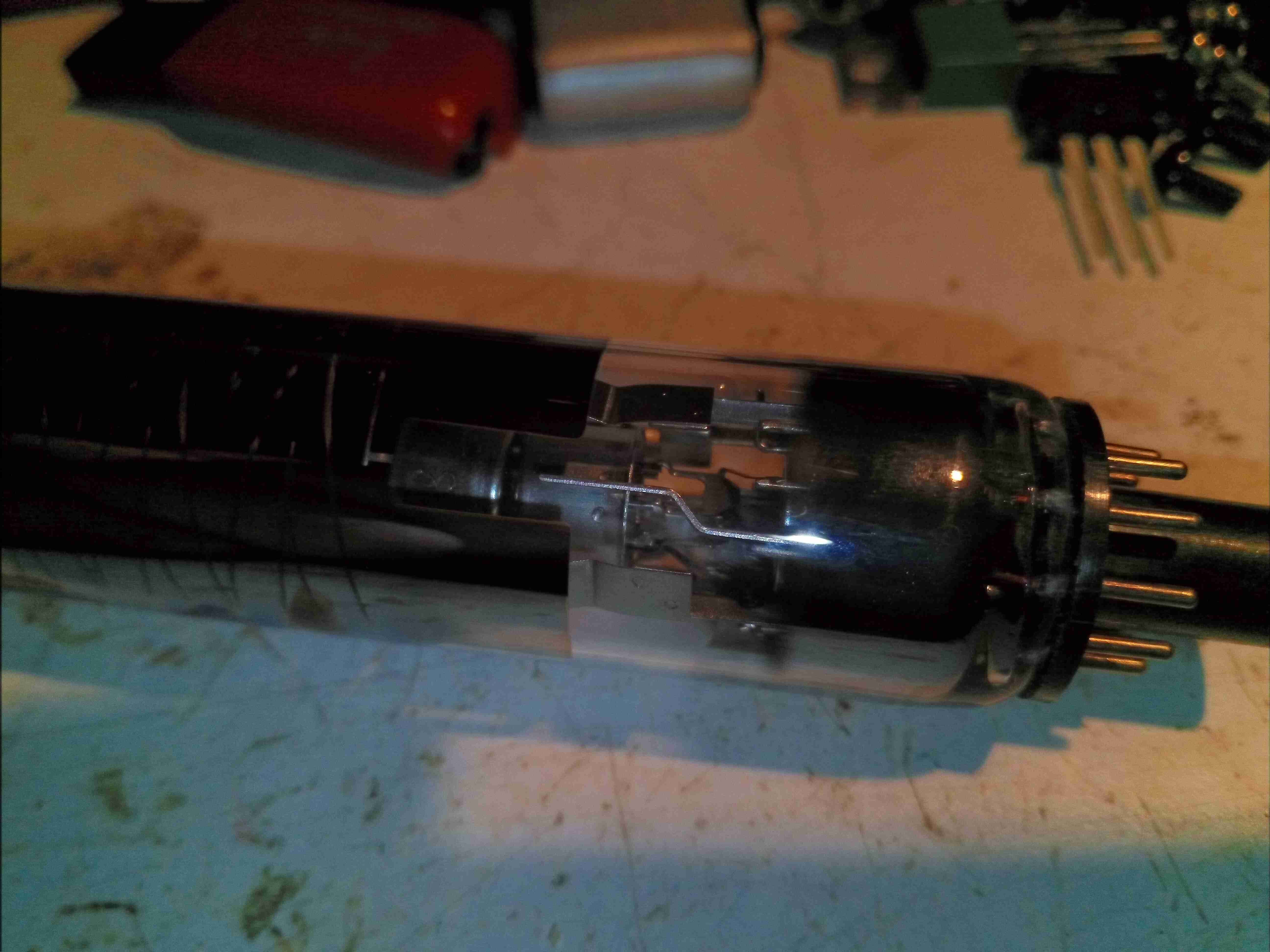
Electron Gun
The electron gun is mostly hidden by the getter flash & the deflection electrodes, but the cathode can is visible through the glass, along with the spring contacts that make a connection to the deflection electrodes. This is also a very short gun – it doesn’t extend more than about 5mm into the deflection zone. The rest of the tube up to the target is empty space.
Target
Finally, here’s the target end of the tube. I’m not sure how the wires are attached to the terminals – it certainly isn’t solder, maybe conductive adhesive?
It uses a vertically striped RGB colour filter over the faceplate of an otherwise standard Vidicon imaging tube to segment the scan into corresponding red, green and blue segments. It is used mostly in low-end consumer cameras, though Sony also used it in some moderate cost professional cameras in the 1980s.
Although the idea of using colour stripe filters over the target was not new, the Trinicon was the only tube to use the primary RGB colours. This necessitated an additional electrode buried in the target to detect where the scanning electron beam was relative to the stripe filter. Previous colour stripe systems had used colours where the colour circuitry was able to separate the colours purely from the relative amplitudes of the signals. As a result, the Trinicon featured a larger dynamic range of operation.
I have the service manuals below for the HVP-2000P & the HVP-4000P, which are very similar cameras, so these may be useful to anyone who has one of these!
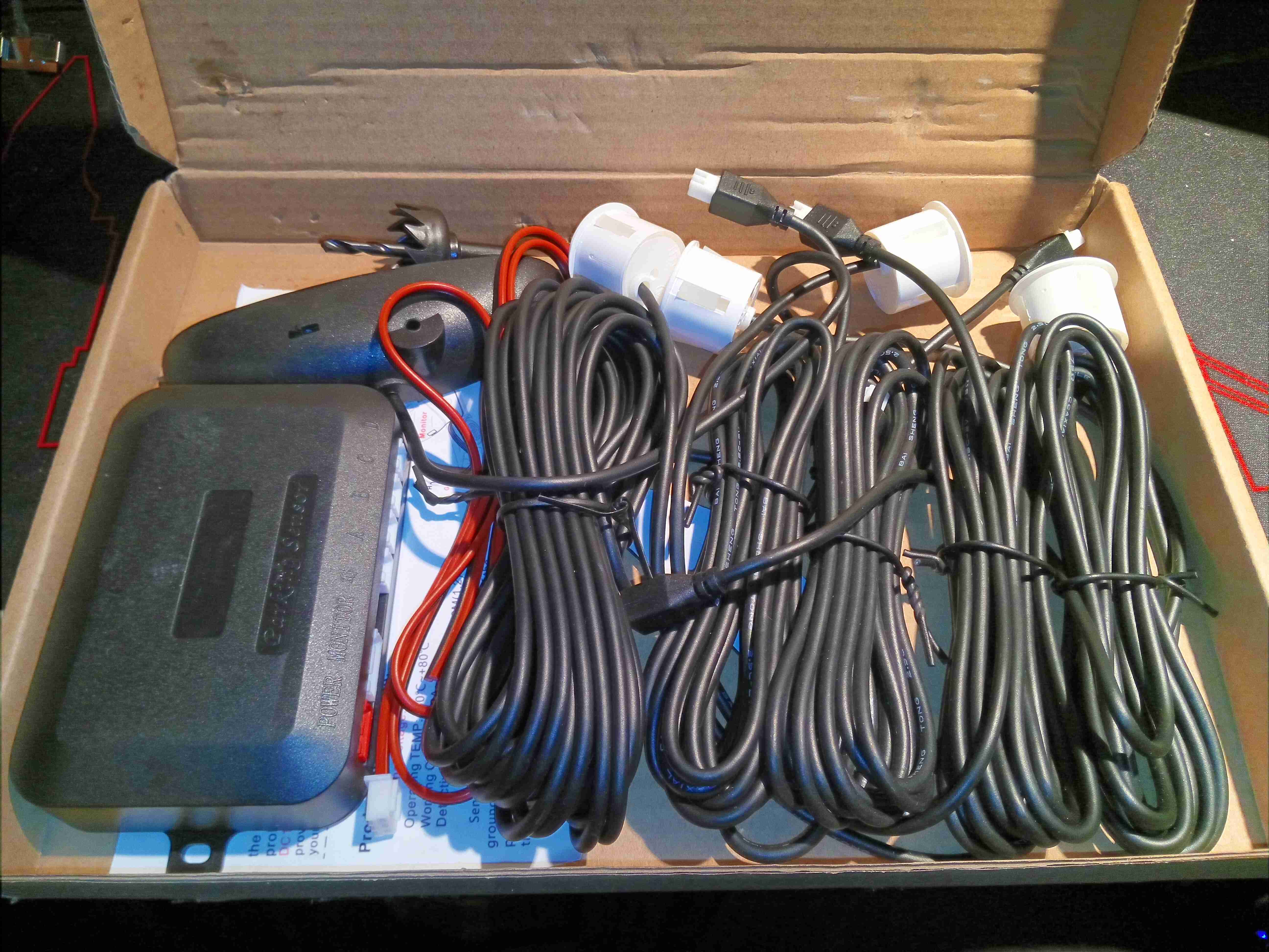
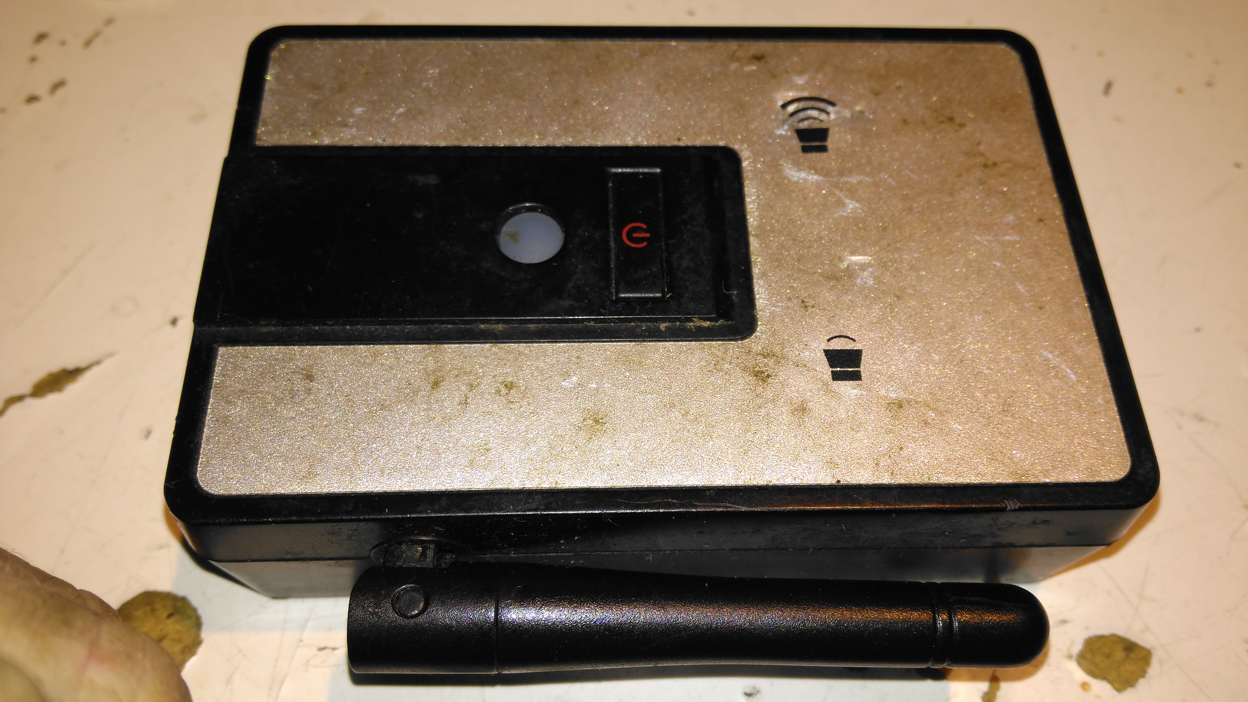
This is a cheap kit from eBay, to retrofit an older car with ultrasonic parking sensors. 4 sensors are included in the kit, along with a hole saw to fit them to the bumper. There’s a small controller module, and a display module that fits onto the dash of the car.
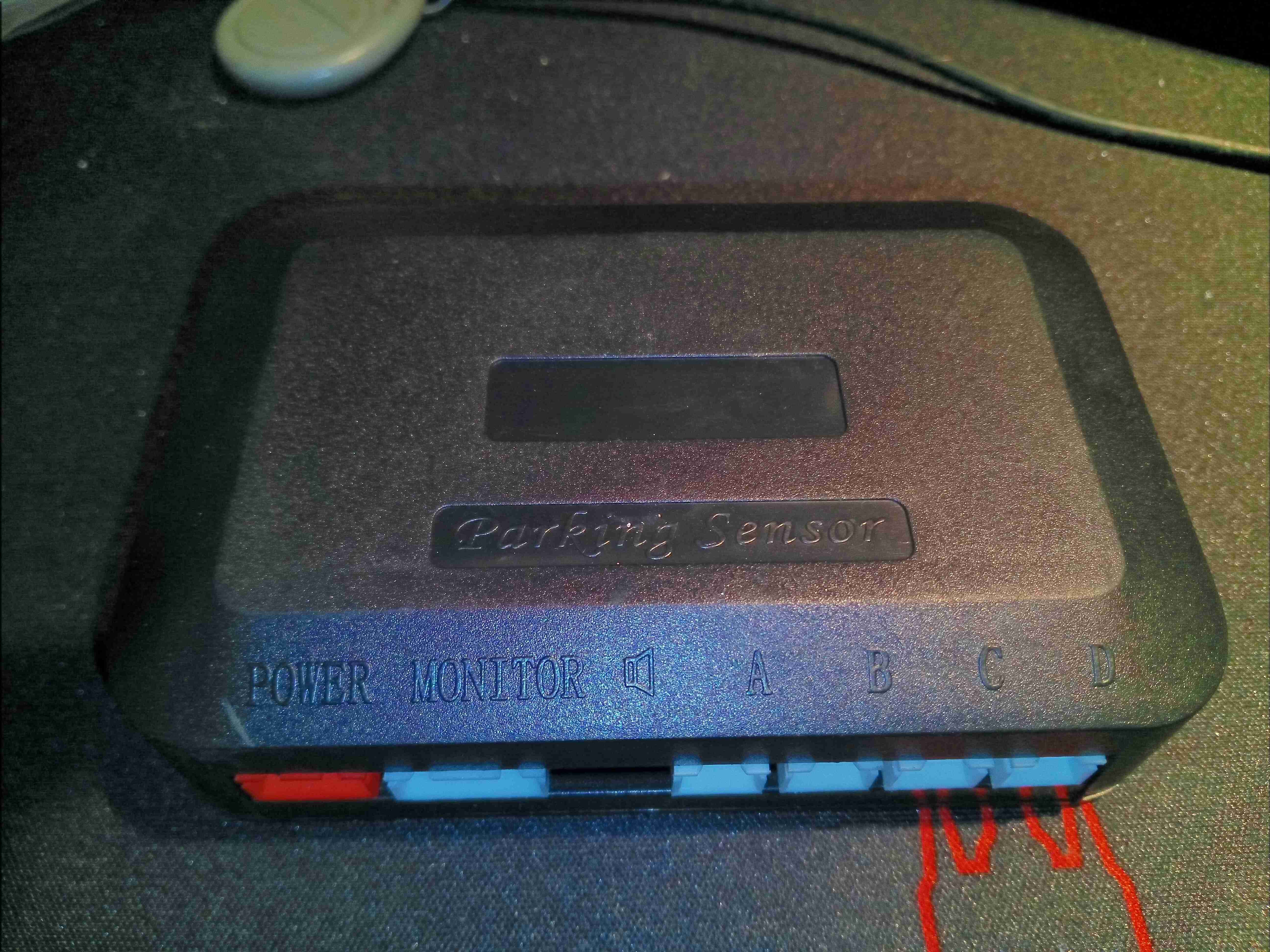
Controller Module
Here’s the controller module, with it’s row of connectors along the front. The unit gets it’s power from the reversing light circuit, via the red connector.
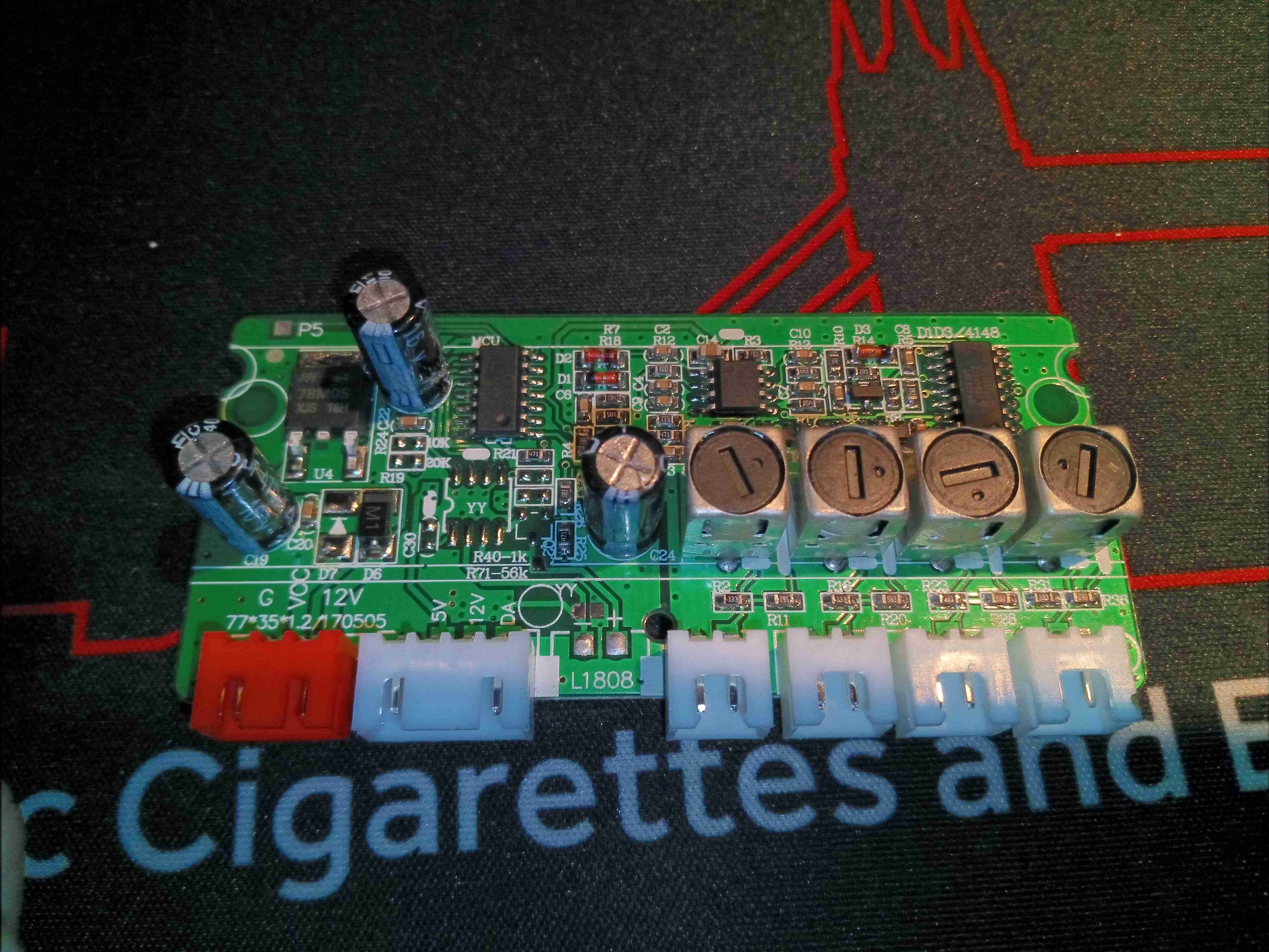
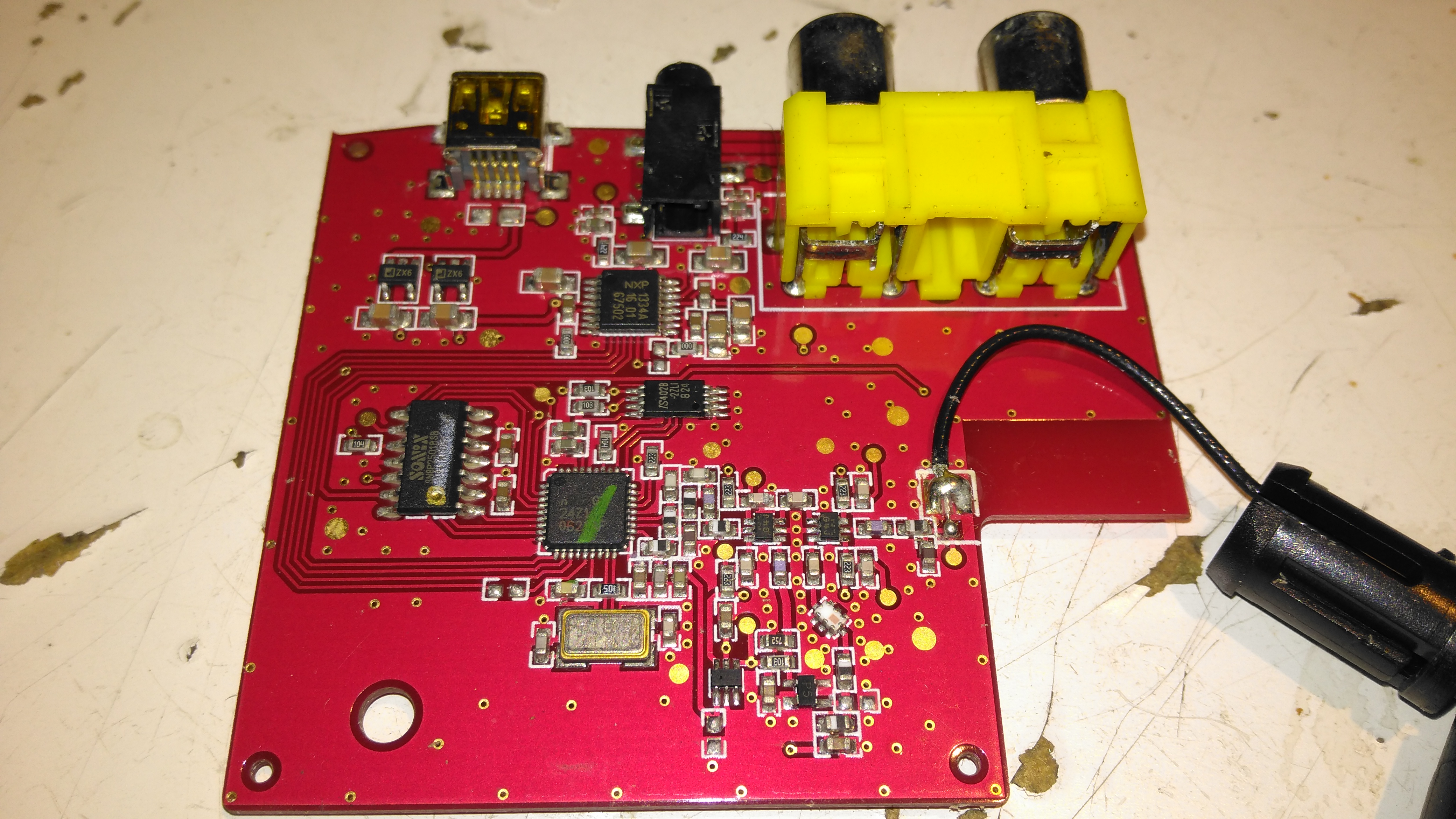
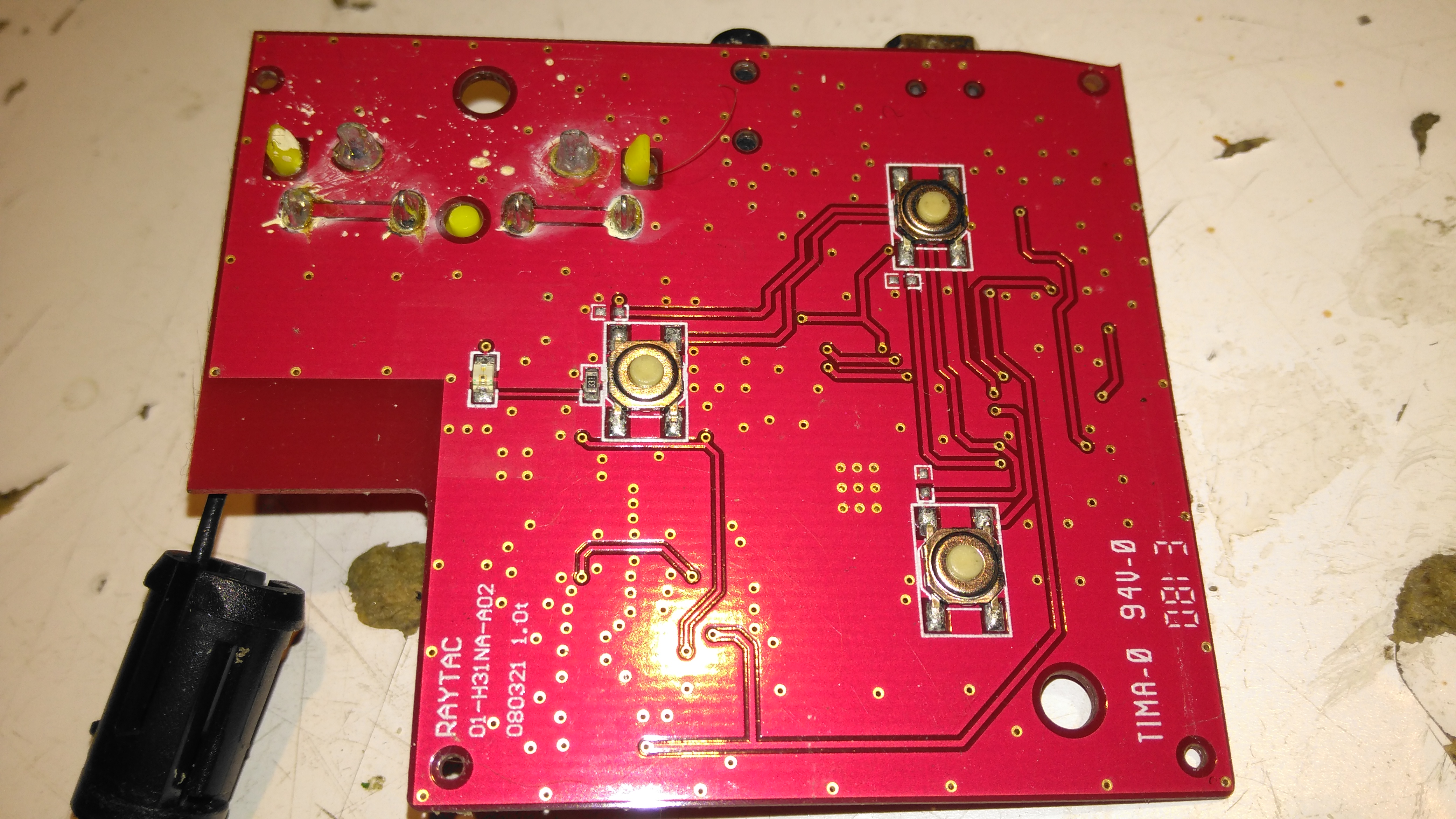
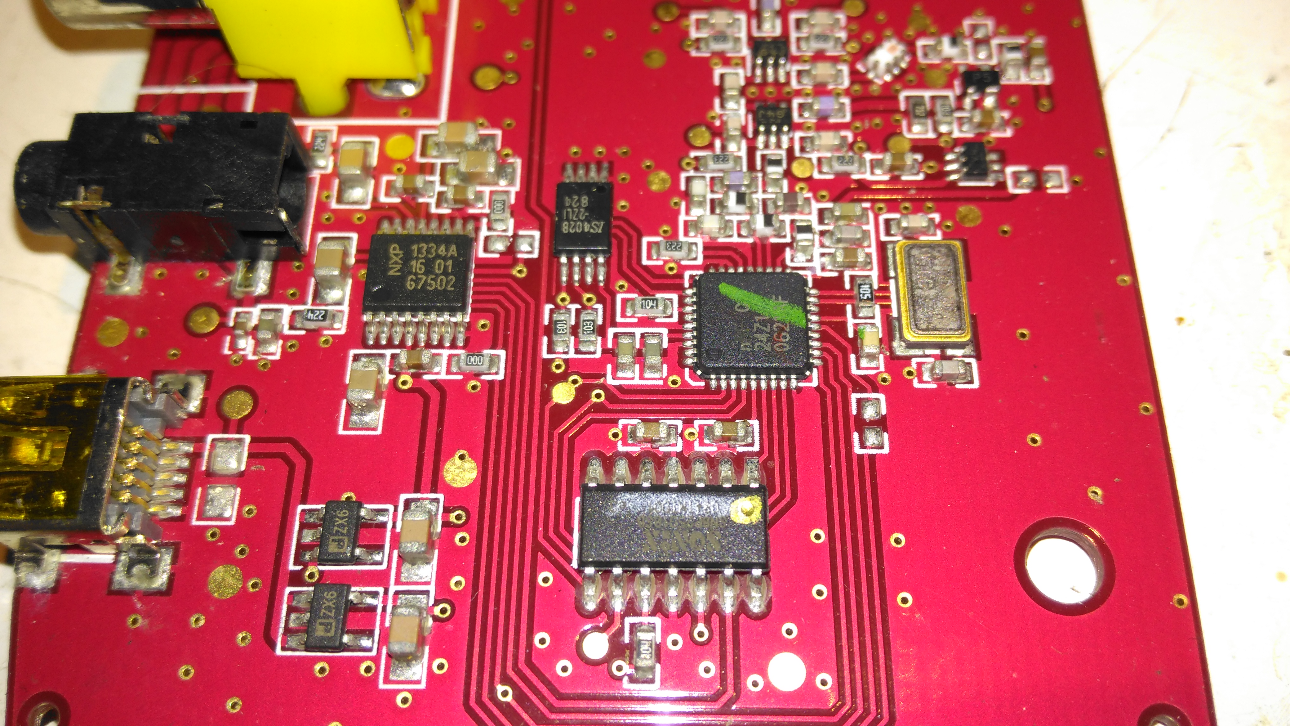
Main Controller PCB
Removing a couple of screws allows the PCB to be removed. There’s quite a bit on this board, including 4 tunable inductors for the ultrasonic transducers. There’s a linear voltage regulator on the left which supplies power to the electronics, and a completely unmarked microcontroller.
Electronics Closeup
A closer look at the analogue end of the board shows a JRC4558D dual Op-Amp, and an NXP HEF4052B analogue multiplexer. As the microcontroller is unmarked I have no data for that one.
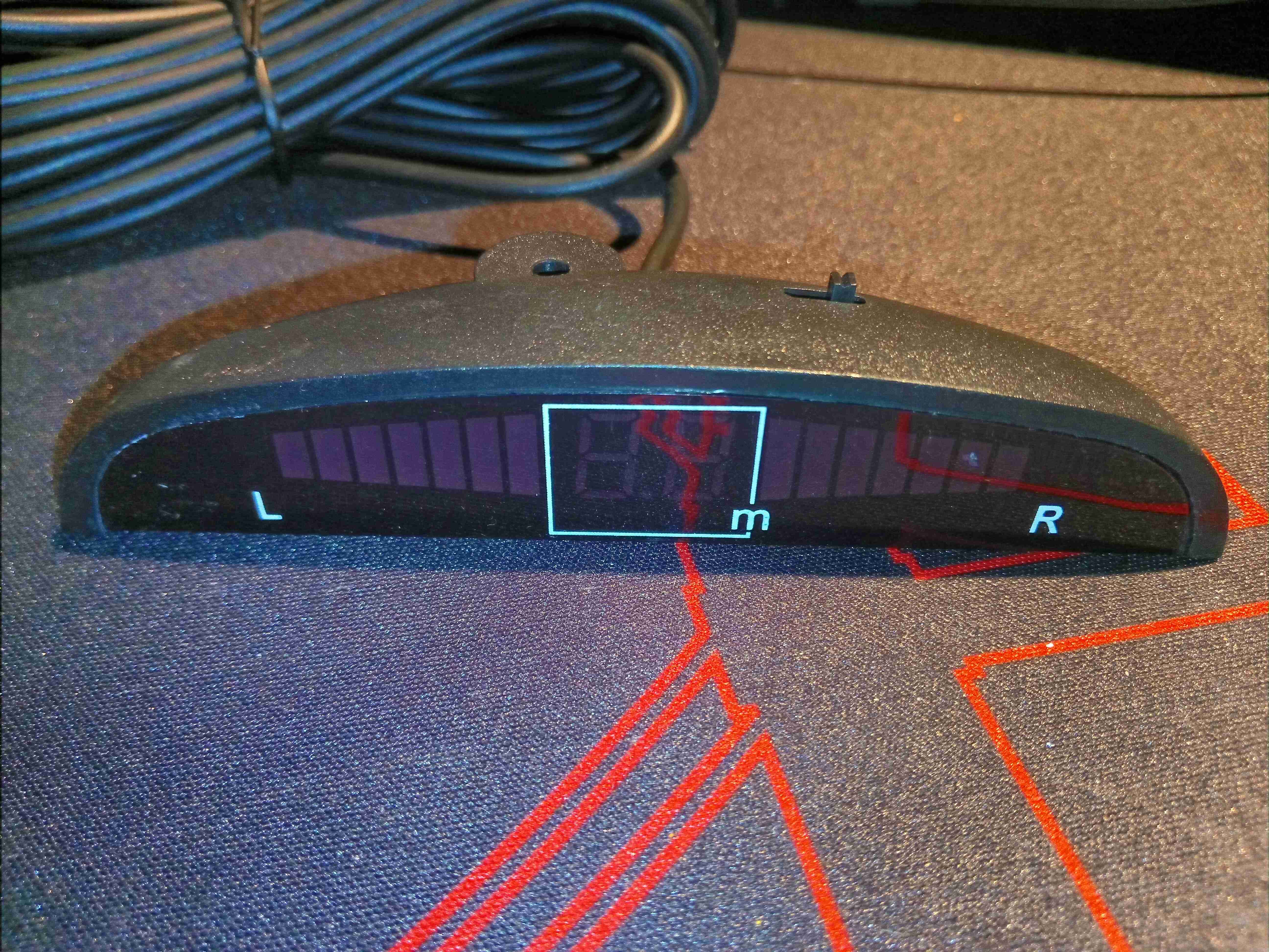
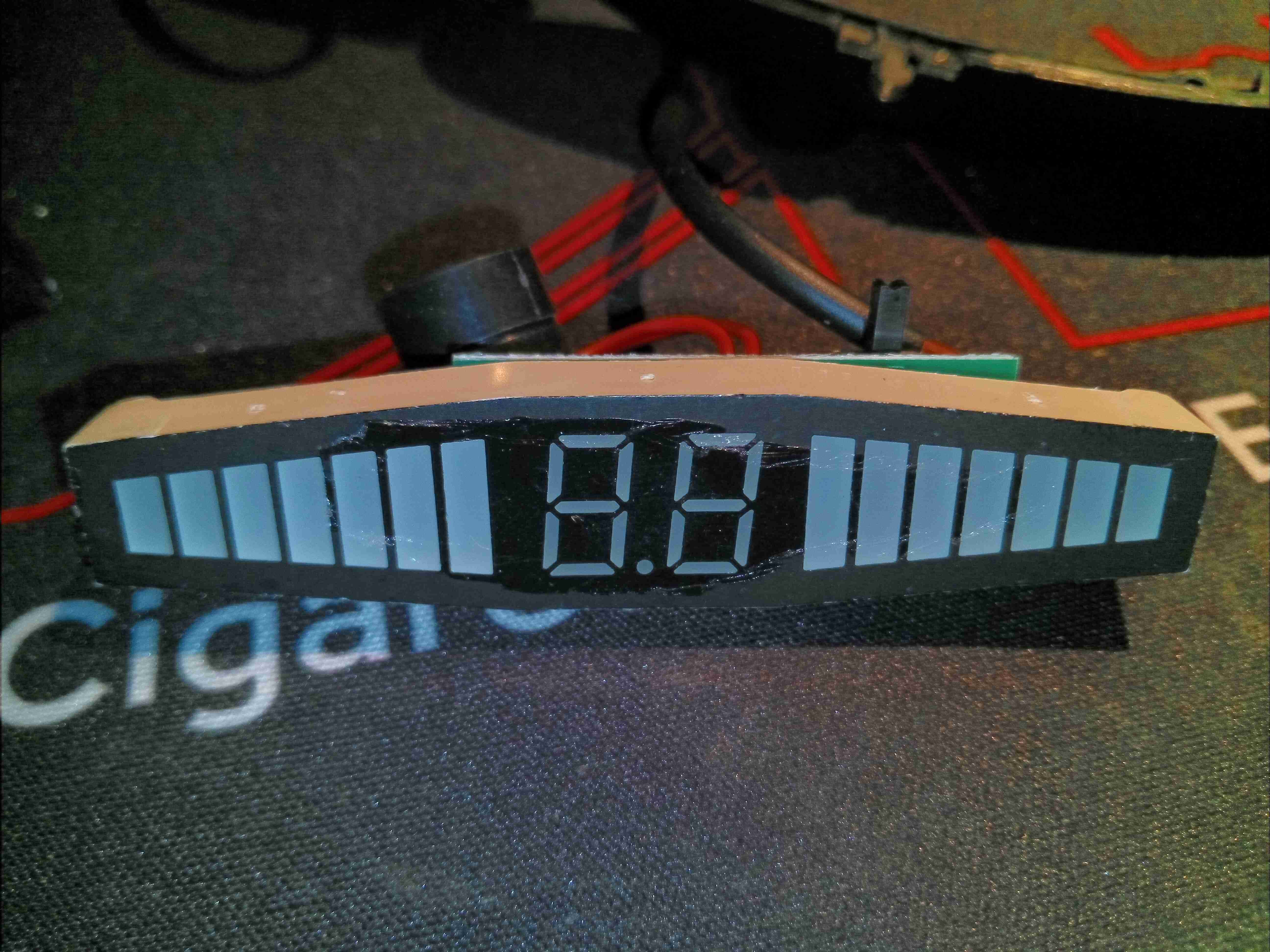
Dash Display
The dash display is housed in another small plastic box, with bargraphs for each side of the car & an overall distance meter.
Display Module
Clearly this is a custom module, with the tapered bargraph LEDs on each side & the 7-segment display in the centre. There’s a beeper which works like every factory-fitted unit does, increasing in rate as the distance closes.
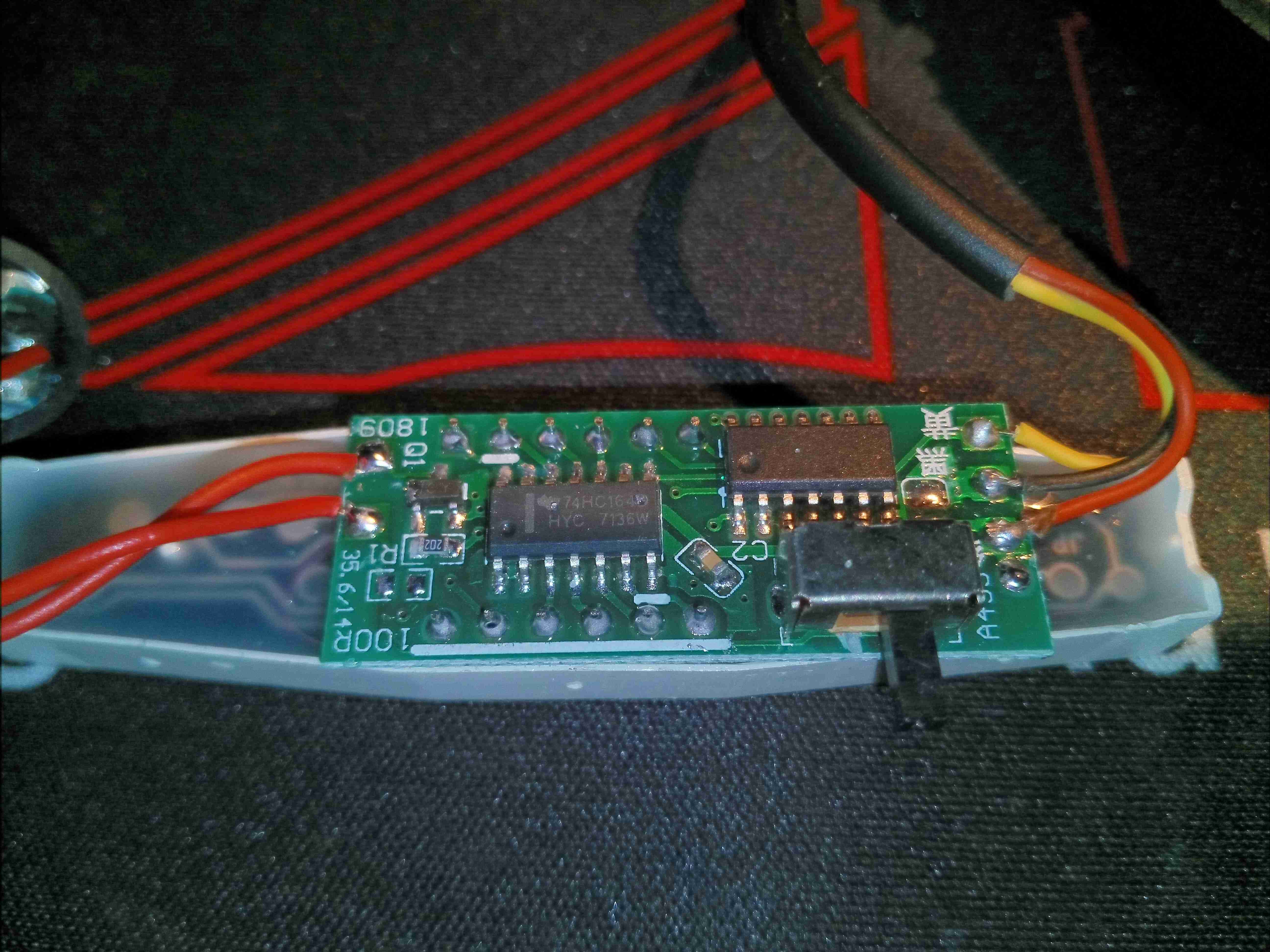
Display PCB
The back of the display module has the driver PCB, with yet another unmarked microcontroller, and a TI 74HC164 serial shift register as a display driver. There’s only 3 wires in the loom from the controller, so some sort of 1-wire protocol must be being used, while I²C is the most likely protocol to be talking to the display driver circuit. There’s also a small switch for muting the beeper.
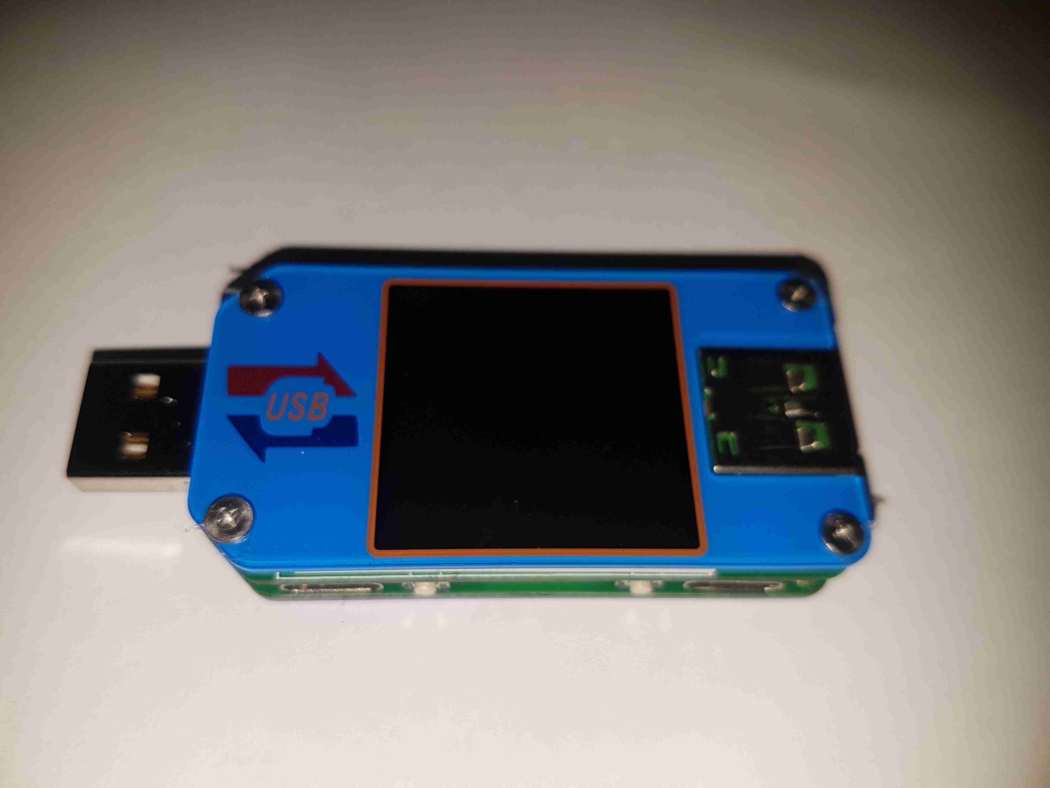
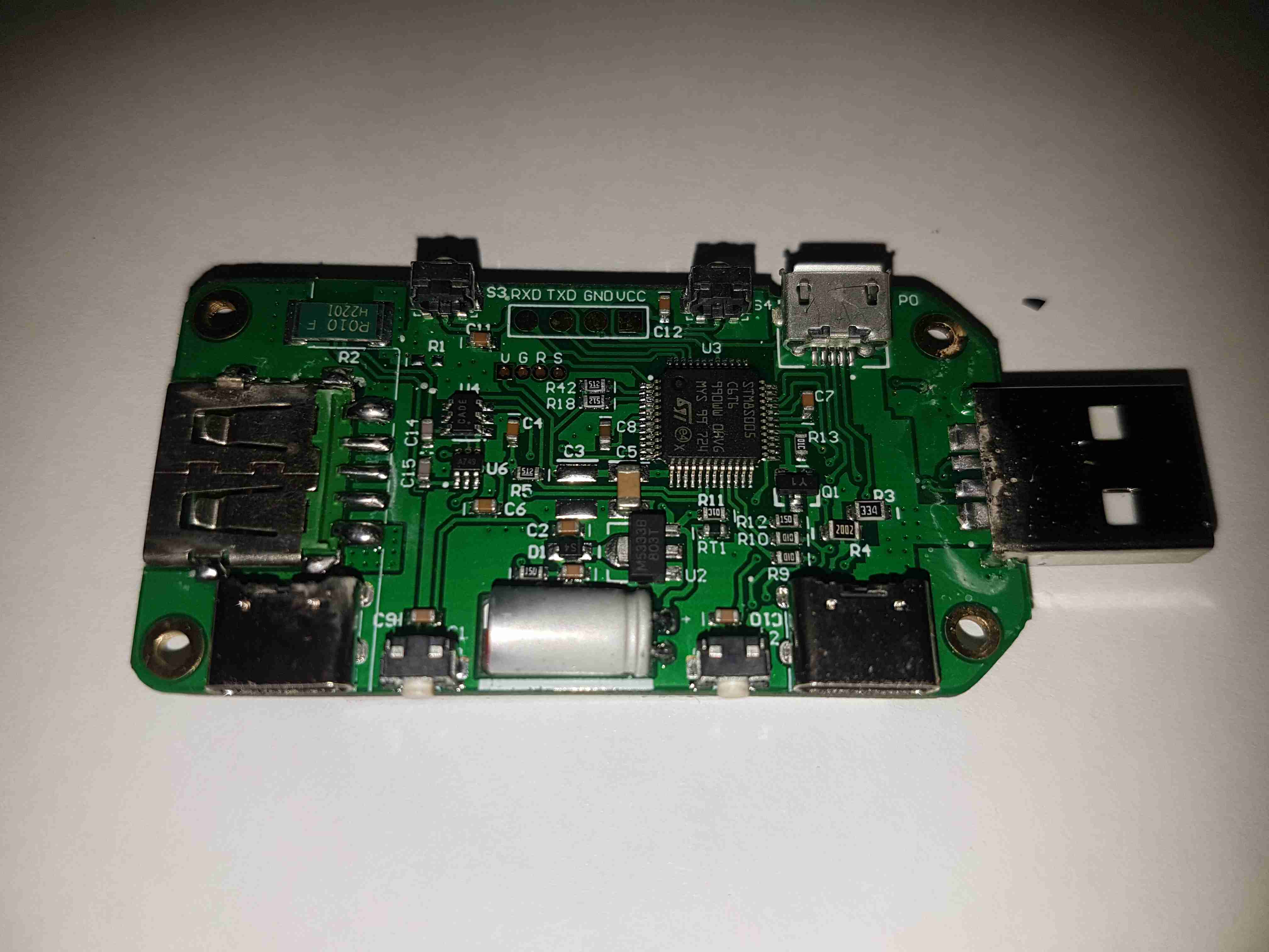
Here’s a nice little feature-packed USB power meter, the UM25C. This unit has USB-C along with the usual USB type A connectors, along with a bluetooth radio for remote monitoring of stats via a Windows or Android app. Construction is nice, it’s a stack of two PCBs, and polycarbonate cover plates, secured together with brass posts & screws.
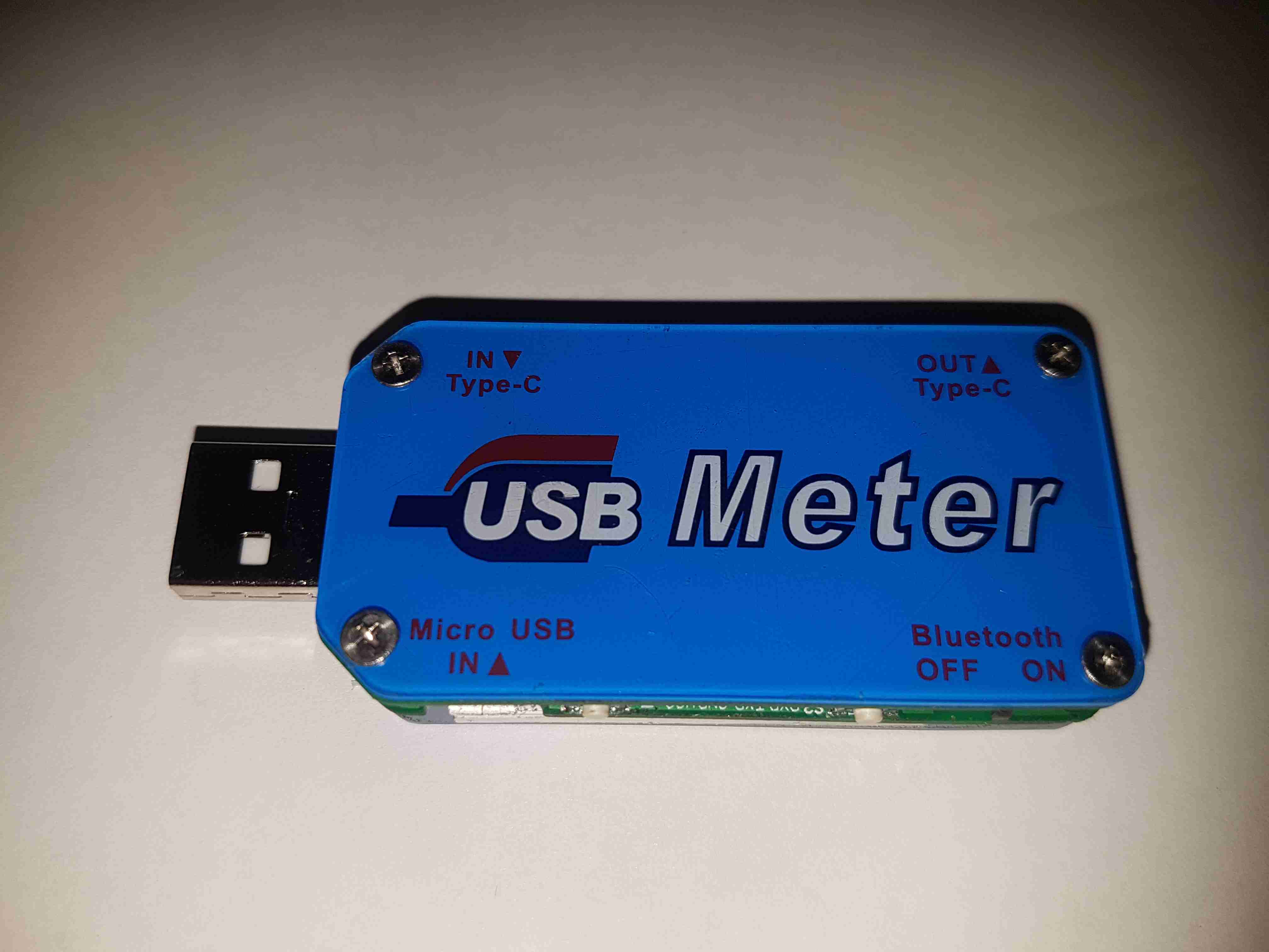
Back Cover
The back cover has the legend for all the side connectors, along with the logo.
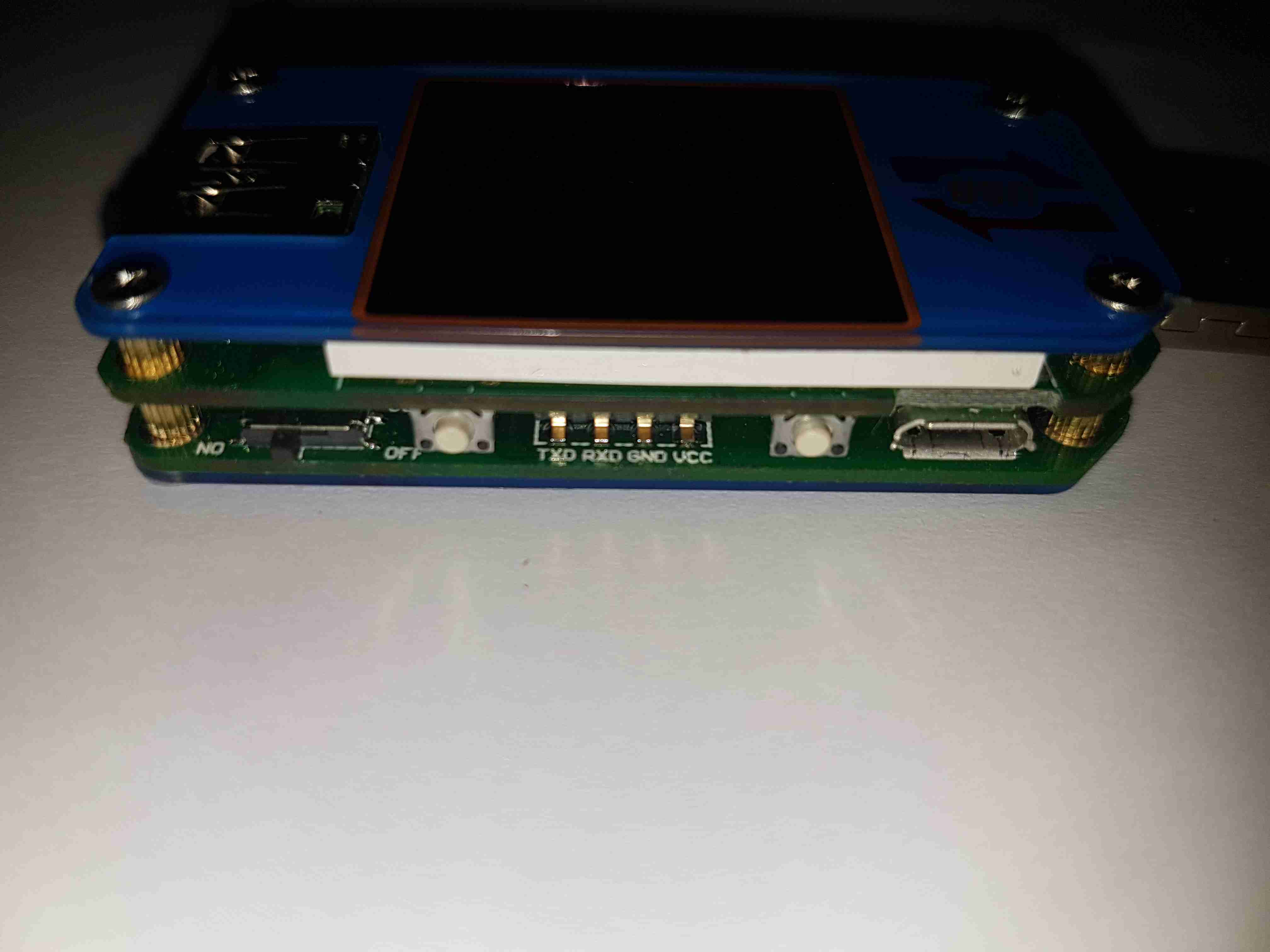
USB Micro Input
Down the sides are the user interface buttons, and here the Micro-B input connector. The 4-pin header is visible here that takes serial data down to the bluetooth section.
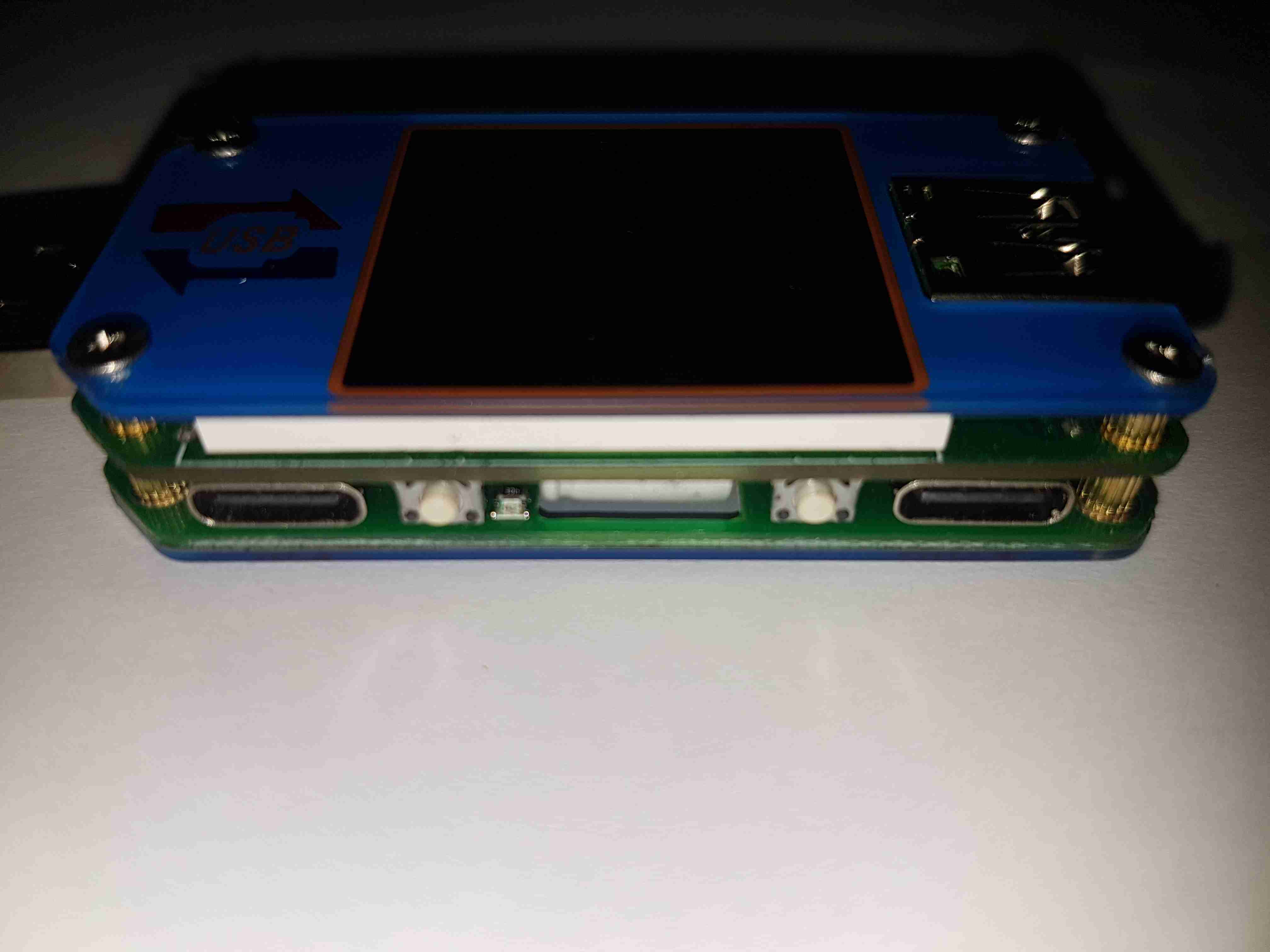
USB-C Connectors
The other side has the remaining pair of buttons, and the USB-C I/O. I don’t yet own anything USB-C based, but this is good future proofing.
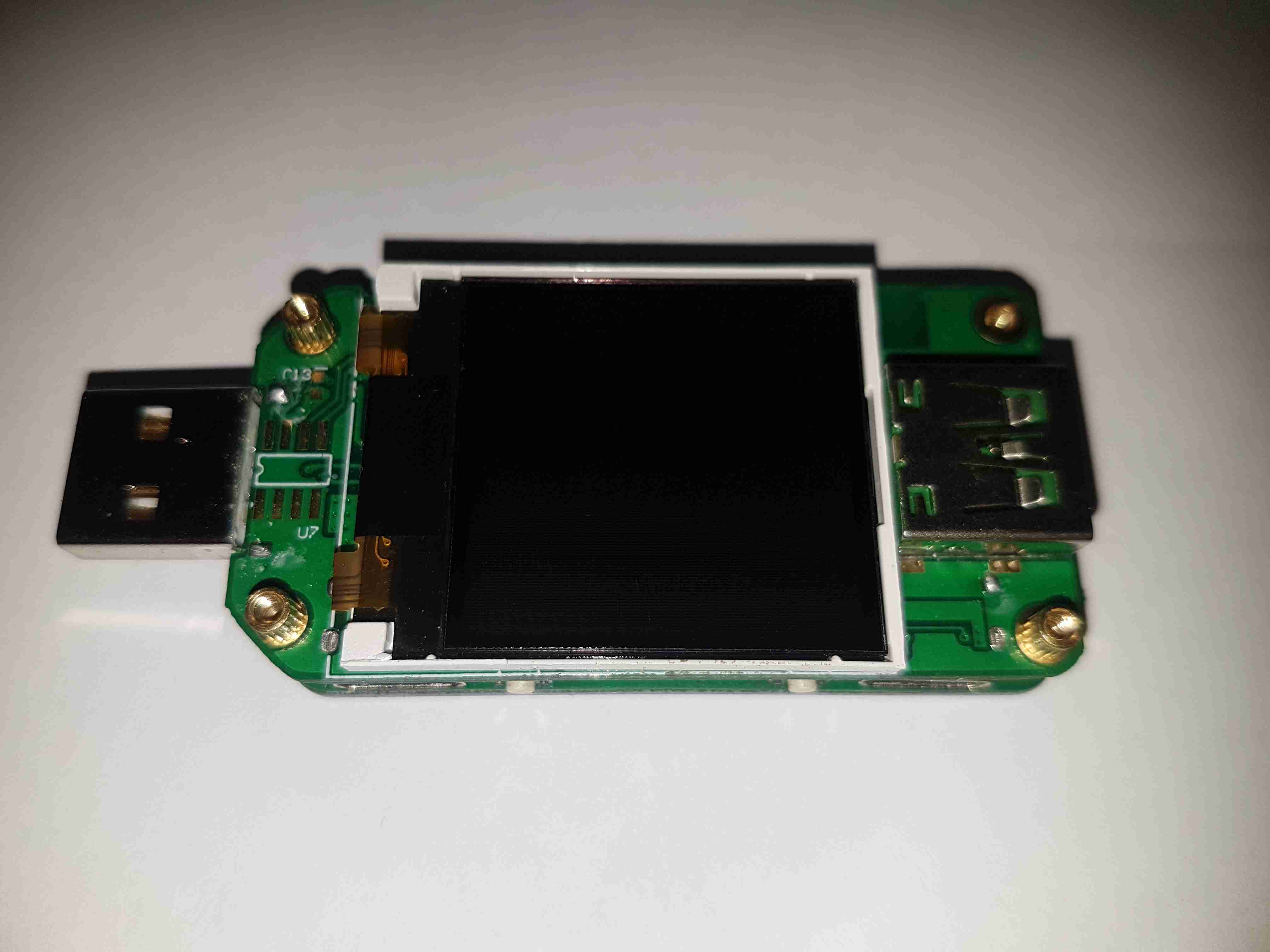
LCD Display
Removing the top plastic cover plate reveals the small 1″ TFT LCD module. This will be hot-bar soldered underneath the screen. There’s an unused footprint next to the USB input connector, judging by the pin layout it’s probably for a I²C EEPROM.
Main Board Components
The underside of the top PCB has all the main components. The brains of the operation is a ST STM8S005C6T6 microcontroller. It’s at the basic end of the STM range, with a 16MHz clock, 32K flash, EEPROM, 10-bit ADC, SPI, UART & I²C. The main 0.010Ω current shunt is placed at the top left of the board in the negative rail. A couple of SOT-23 components in the centre of the board, I haven’t been able to identify properly, but I think they may be MOSFETs. The large electrolytic filter capacitor has a slot routed into the PCB to allow it to be laid flat. Providing the main power rail is a SOT-89 M5333B 3.3v LDO regulator.
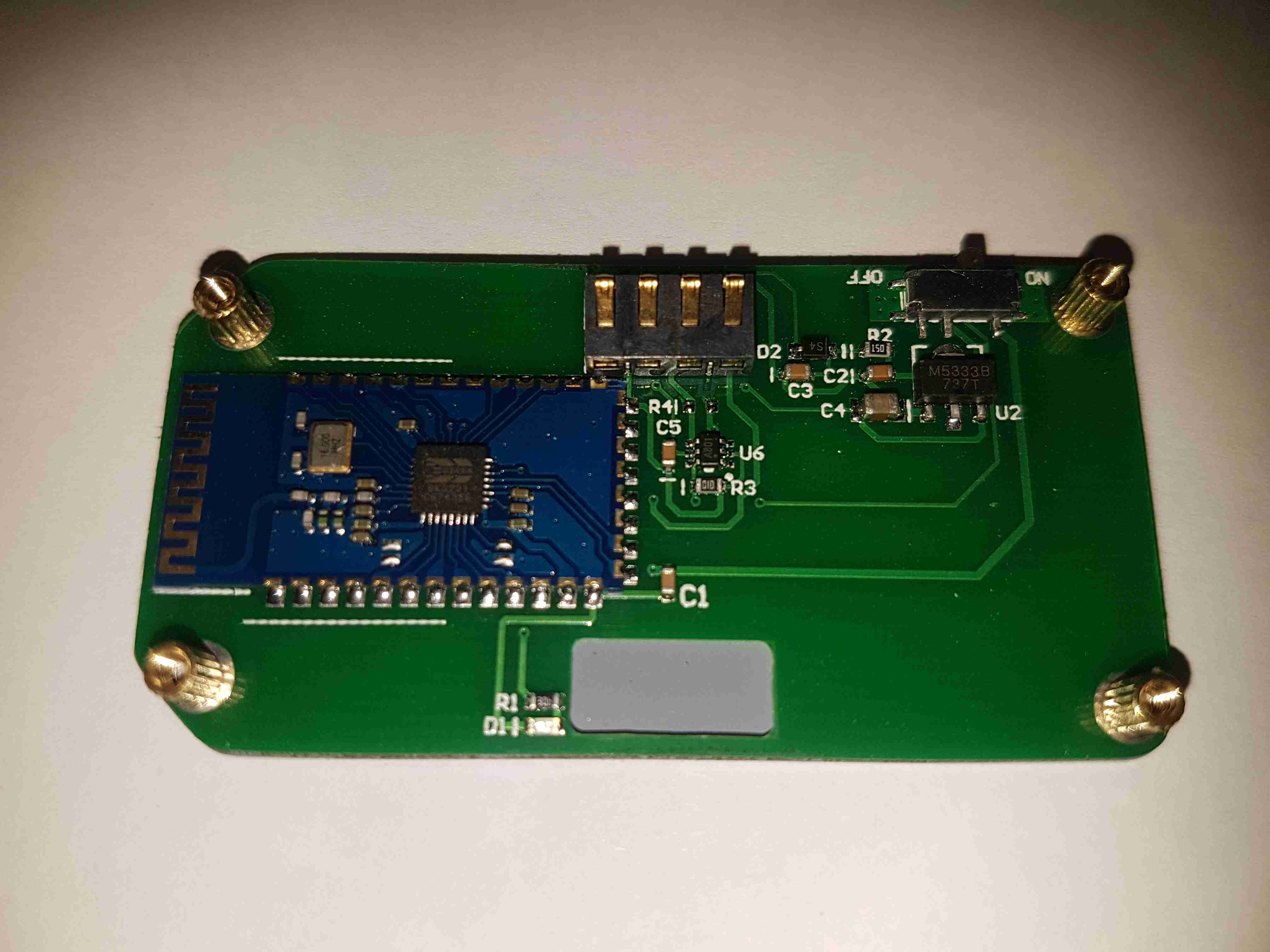
Bluetooth Radio
The bottom board contains the bluetooth radio module, this is a BK3231 Bluetooth HID SoC. The only profile advertised by this unit is a serial port. There’s a local 3.3v LDO regulator & support components, along with an indicator LED.
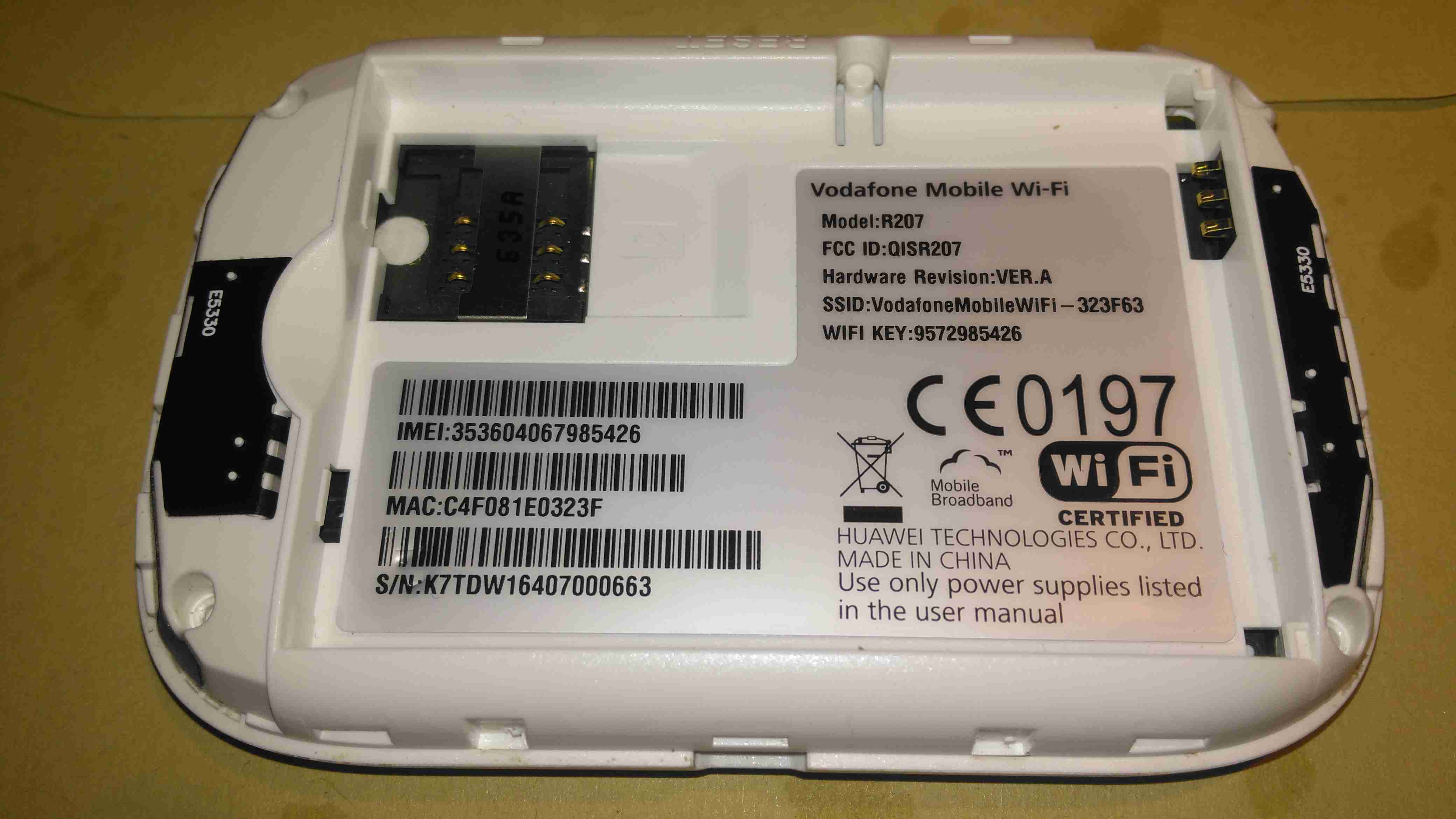
Here’s one of the old modems from my spares bin, a Vodafone Mobile WiFi R207. This is just a rebranded Huawei E5330. This unit includes a 3G modem, and a WiFi chipset, running firmware that makes this a mini-router, with NAT.
Specs
The back has the batter compartment & the SIM slot, with a large label showing all the important details.
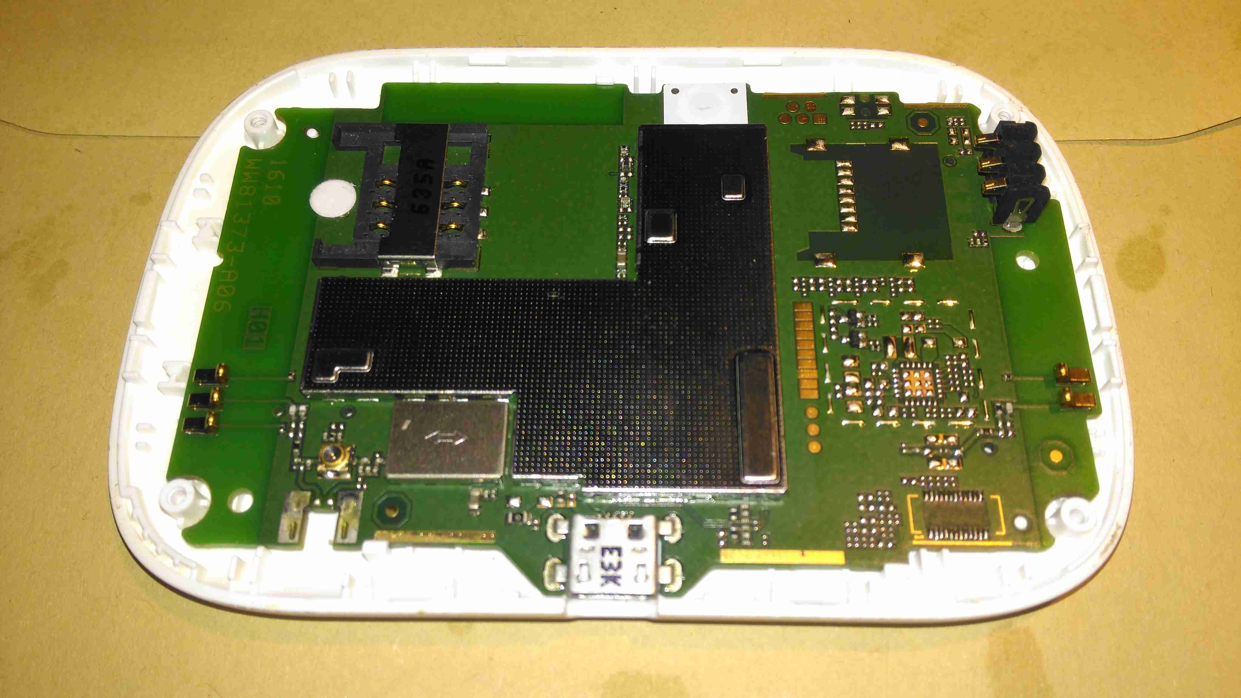
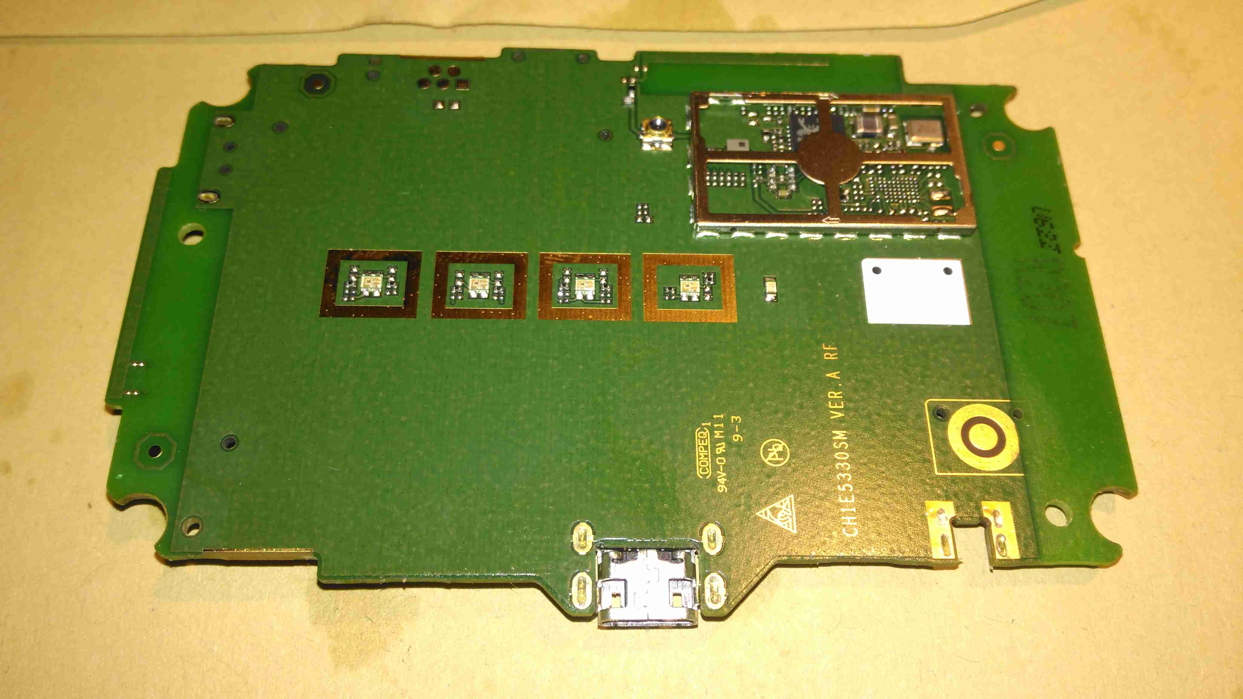
Cover Removed
A couple of small Torx screws later & the shell splits in half. All the electronics are covered by shields here, but luckily they are the clip-on type, and aren’t soldered direct to the PCB.
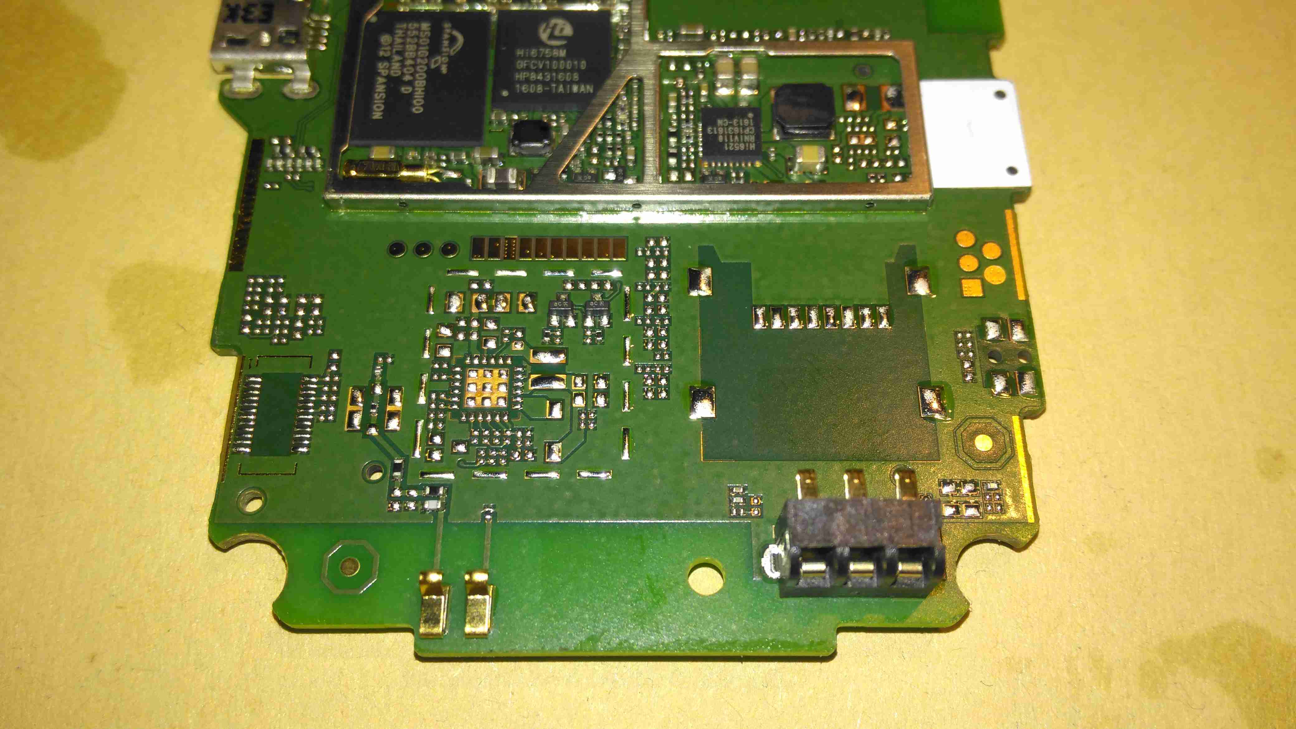
Chipset
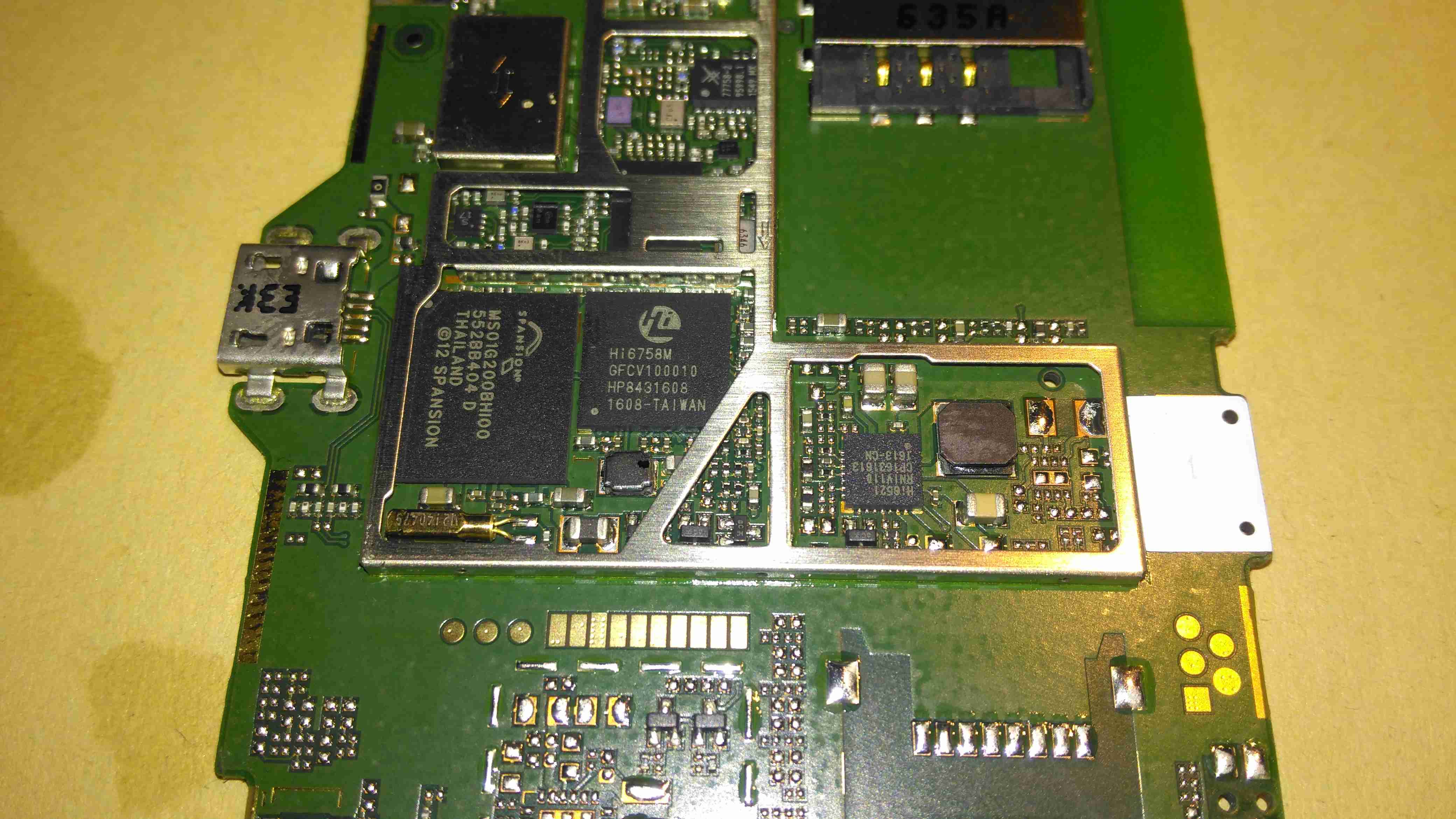
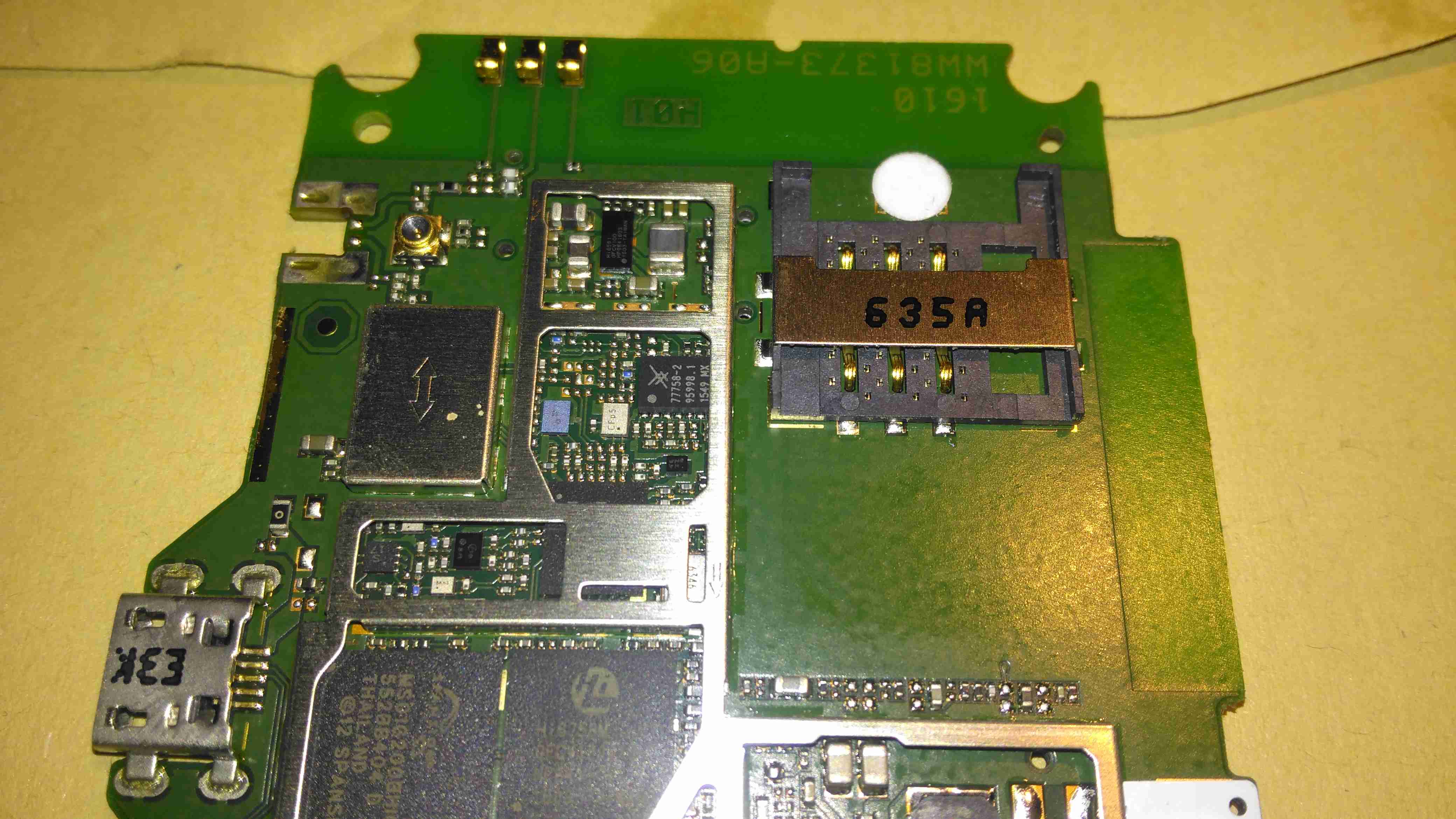
Once the shield has been removed, the main chipset is visible underneath. There’s a large Spansion MS01G200BHI00 1GBit flash, which is holding the firmware. Next to that is the Hi6758M baseband processor. This has all the hardware required to implement a 3G modem. Just to the right is a Hi6521 power management IC, which is dealing with all the power supplies needed by the CPU.
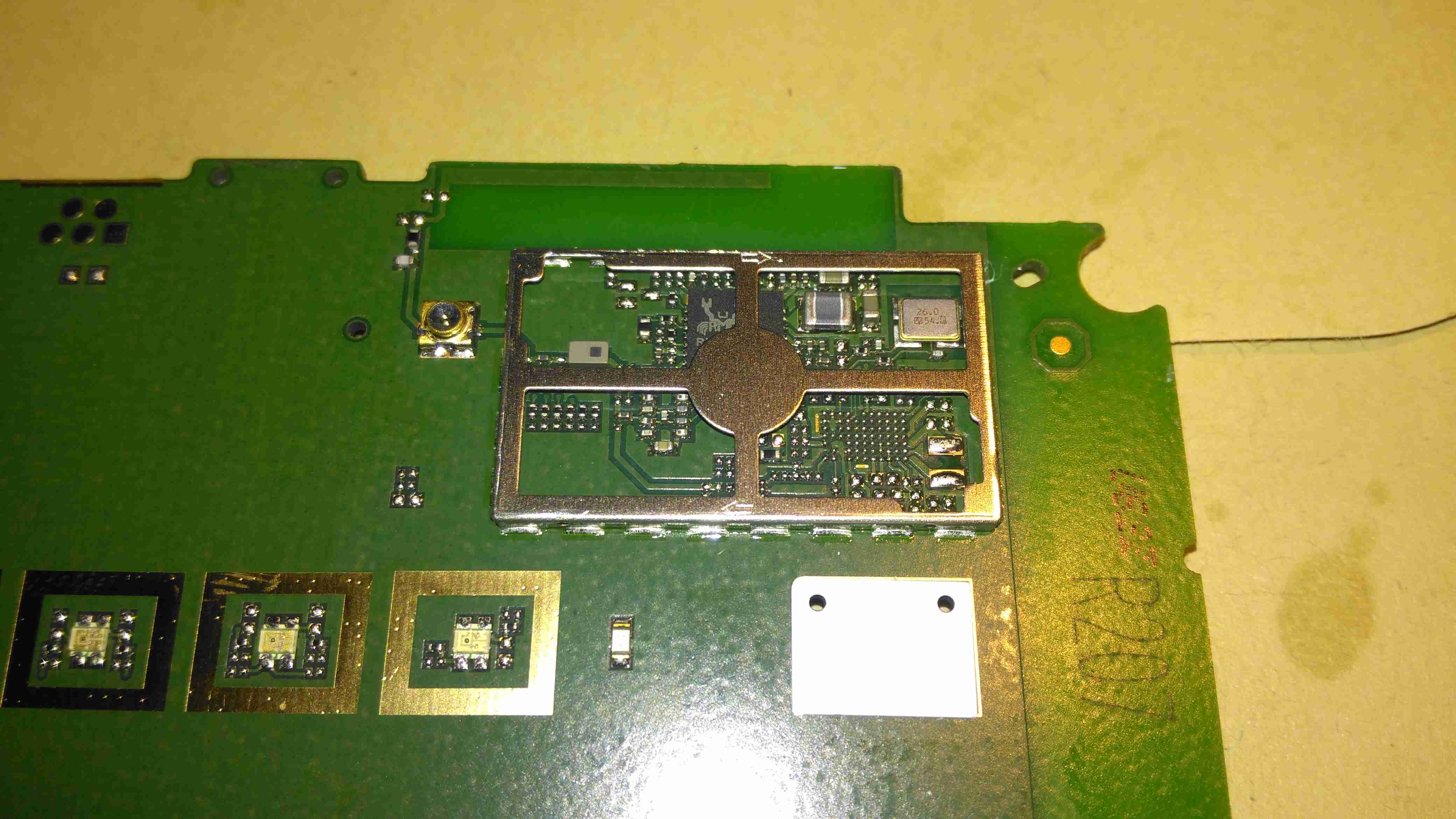
The RF section is above the baseband processor, some of which is hiding under the bits of the shield that aren’t removable.
SIM Socket
There’s a socket onboard for a standard Mini-SIM, just to the left of that is a Hi6561 4-phase buck converter. I would imagine this is providing the power supplies for the RF section & amplifier.
Unpopulated Parts
Not sure what this section is for, all the parts are unpopulated. Maybe a bluetooth option?
PCB Reverse
The other side of the PCB is pretty sparse, holding just the indicator LEDS, button & the WiFi Chipset.
Realtek WiFi Chipset
The chipset here is a Realtek part, but it’s number is hidden by some of the shield. The antenna connection is routed to the edge of the board, where a spring terminal on the plastic case mounted antenna makes contact.
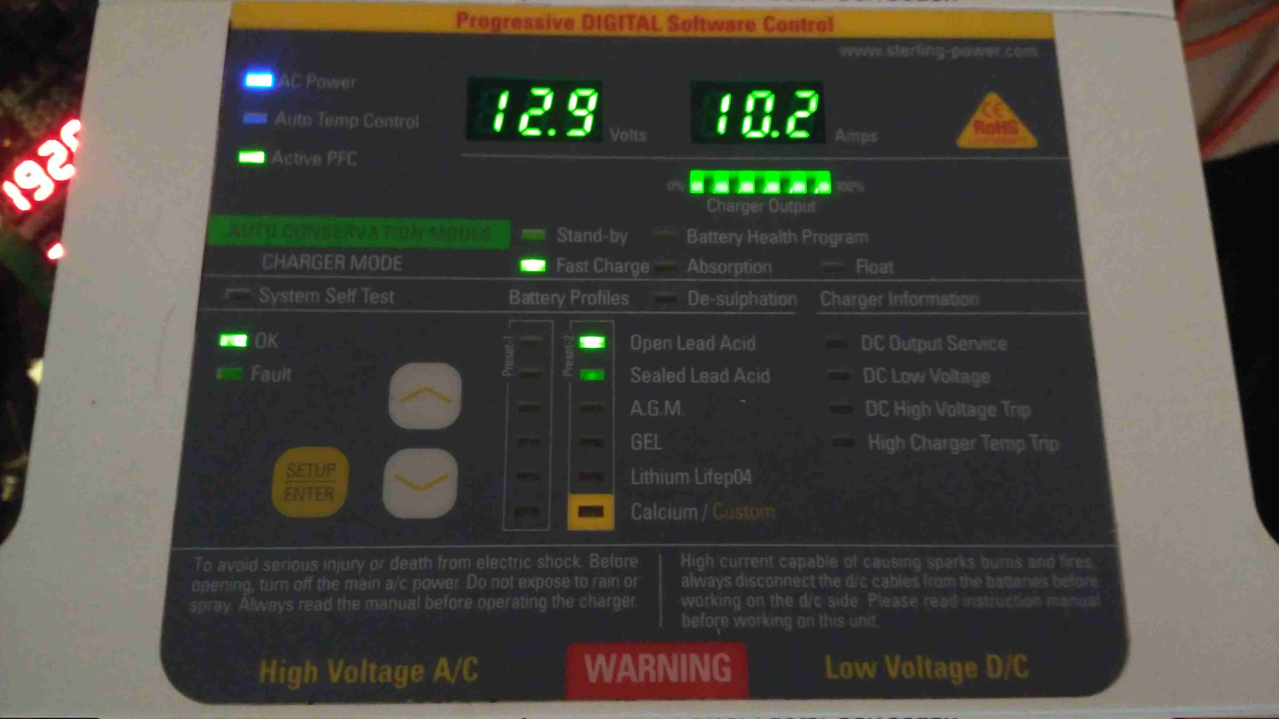
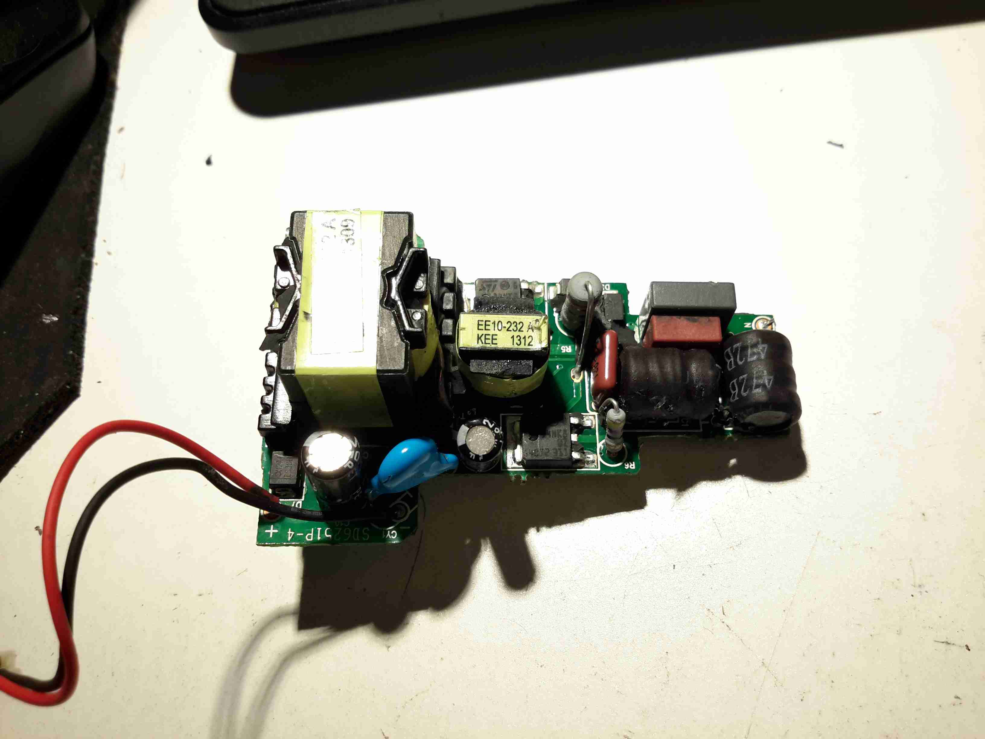
The Sterling charger we’ve had on board nb Tanya Louise since Feb 2014 has bitten the dust, with 31220 hours on it’s internal clock. Since we’re a liveaboard boat, this charger has had a lot of use while we’re on the mooring during winter, when the solar bank isn’t outputting it’s full rate. First, a bit of a teardown to explore the unit, then onto the repair:
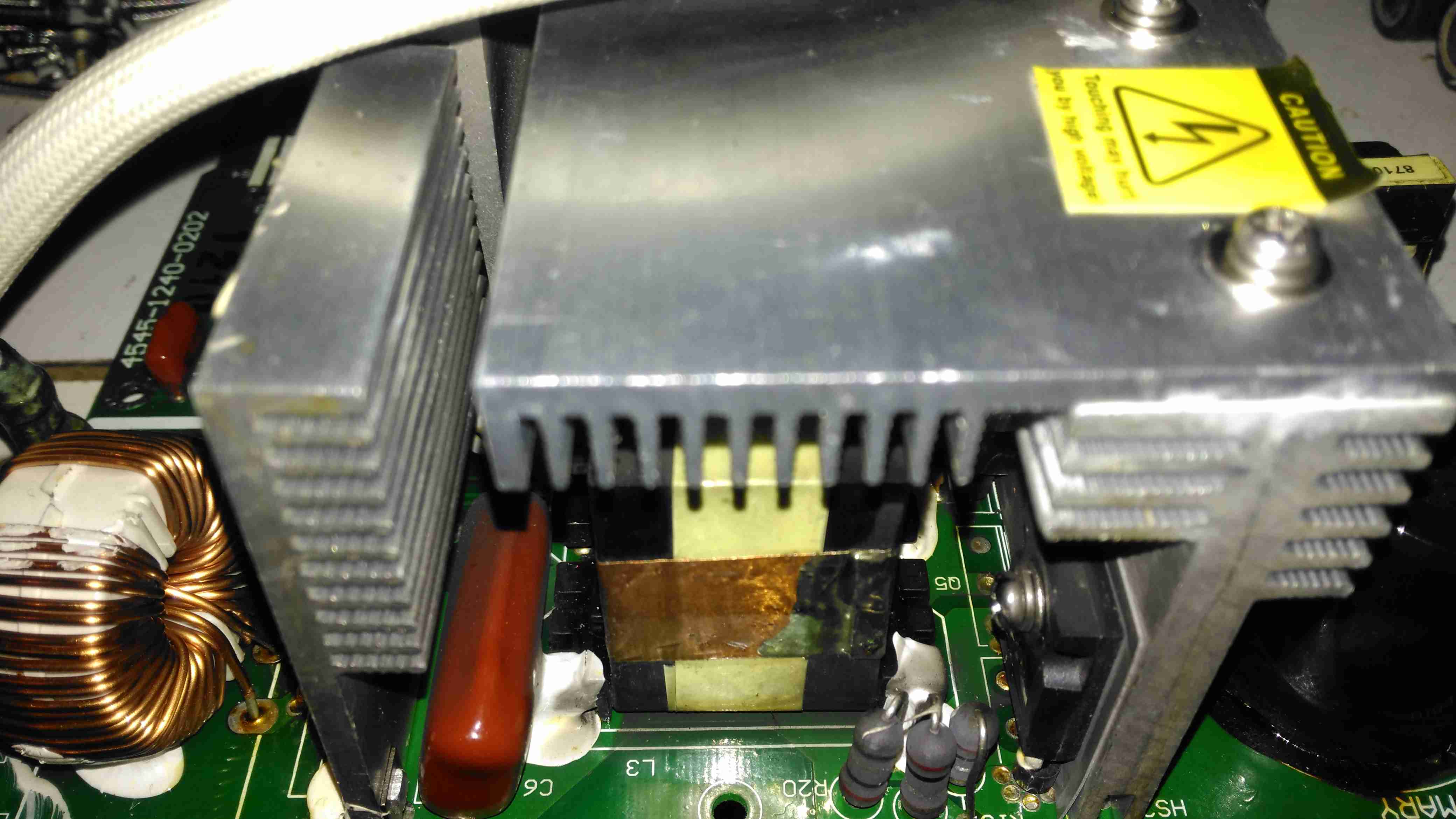
Active PFC Section
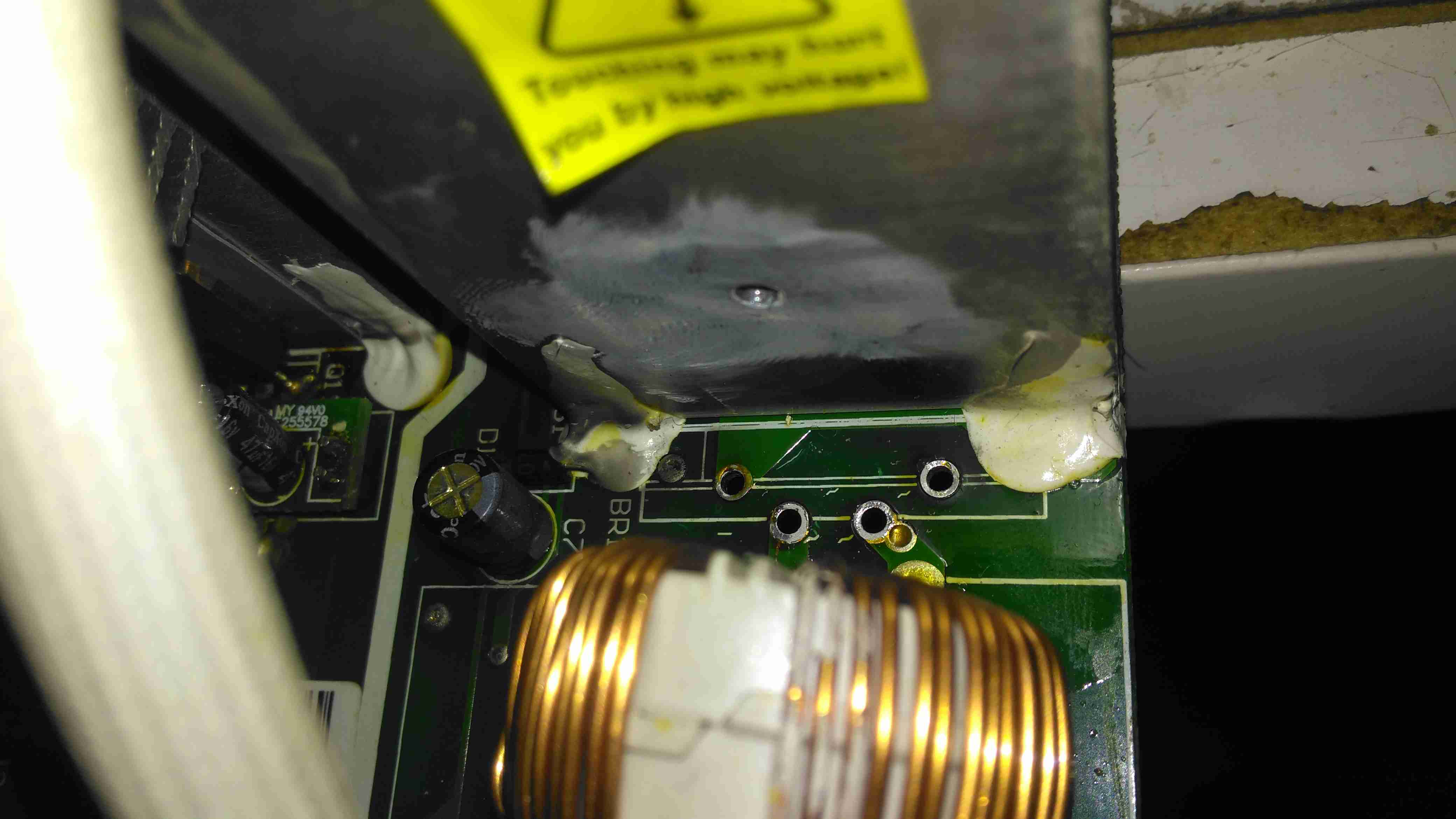
There’s the usual mains input filtering on the left, with the bridge rectifier on it’s heatsink.
Underneath the centre massive heatsinks is the main transformer (not visible here) & active PFC circuit. The device peeking out from underneath is the huge inductor needed for PFC. It’s associated switching MOSFET is to the right.
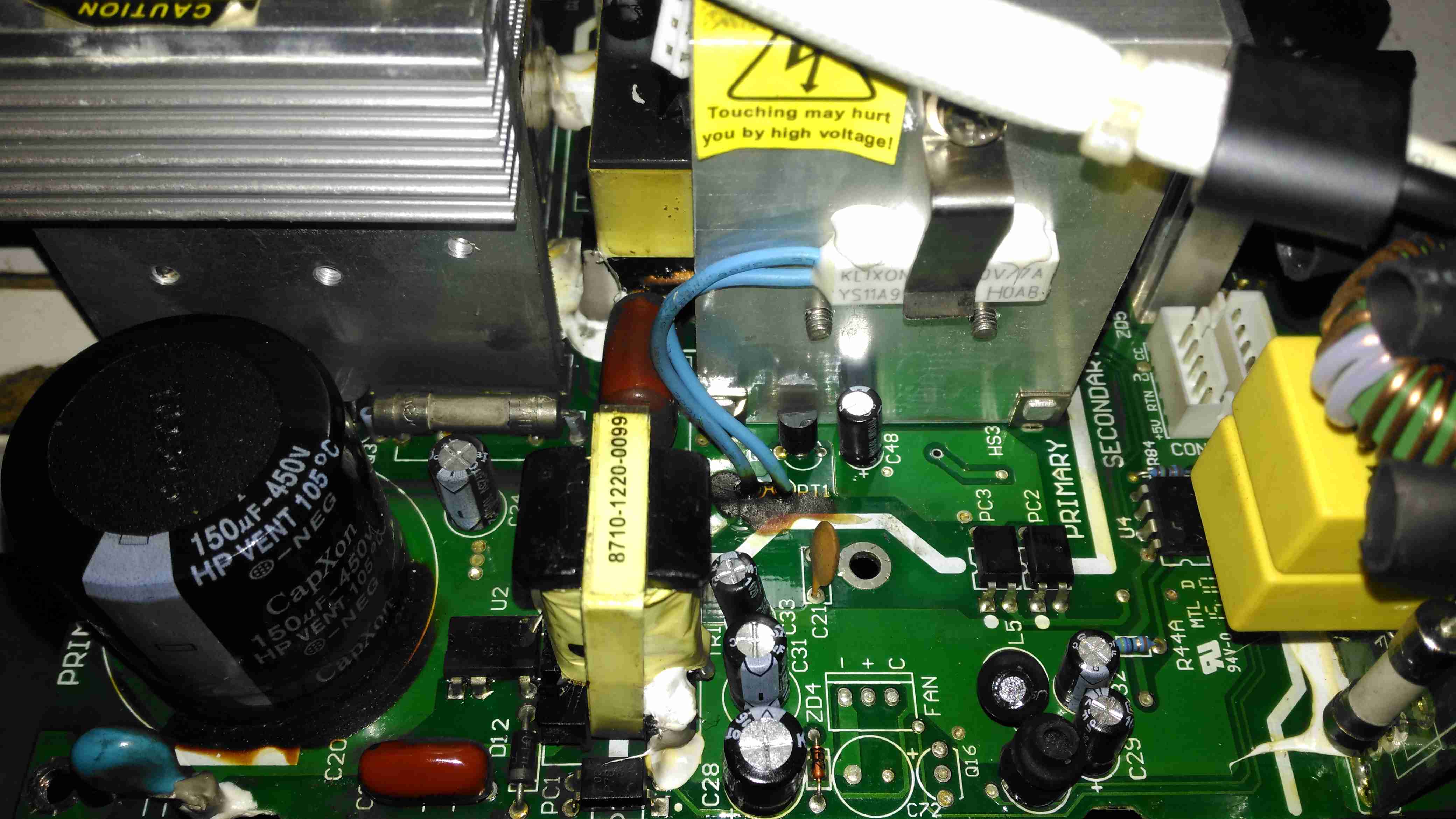
Logic PSU Section
On the other side of the PFC section is the main DC rail filter electrolytic, a 450v 150µF part. Here some evidence of long-term heating can be seen in the adhesive around the base, it’s nearly completely turned black! It’s not a decent brand either, a Chinese CapXon.
The PCB fuse just behind it is in the DC feed to the main switching supply, so the input fuse only protects the filter & Active PFC circuitry. Luckily this fuse didn’t blow during the failure, telling me the fault was earlier in the power chain.
The logic circuits are powered by an independent switching supply in the centre, providing a +5v rail to the microcontroller. The fan header & control components are not populated in this 10A model, but I may end up retrofitting a fan anyway as this unit has always run a little too warm. The entire board is heavily conformal coated on both sides, to help with water resistance associated with being in a marine environment. This has worked well, as there isn’t a single trace of moisture anywhere, only dust from years of use.
There is some thermal protection for the main SMPS switching MOSFETS with the Klixon thermal fuse clipped to the heatsink.
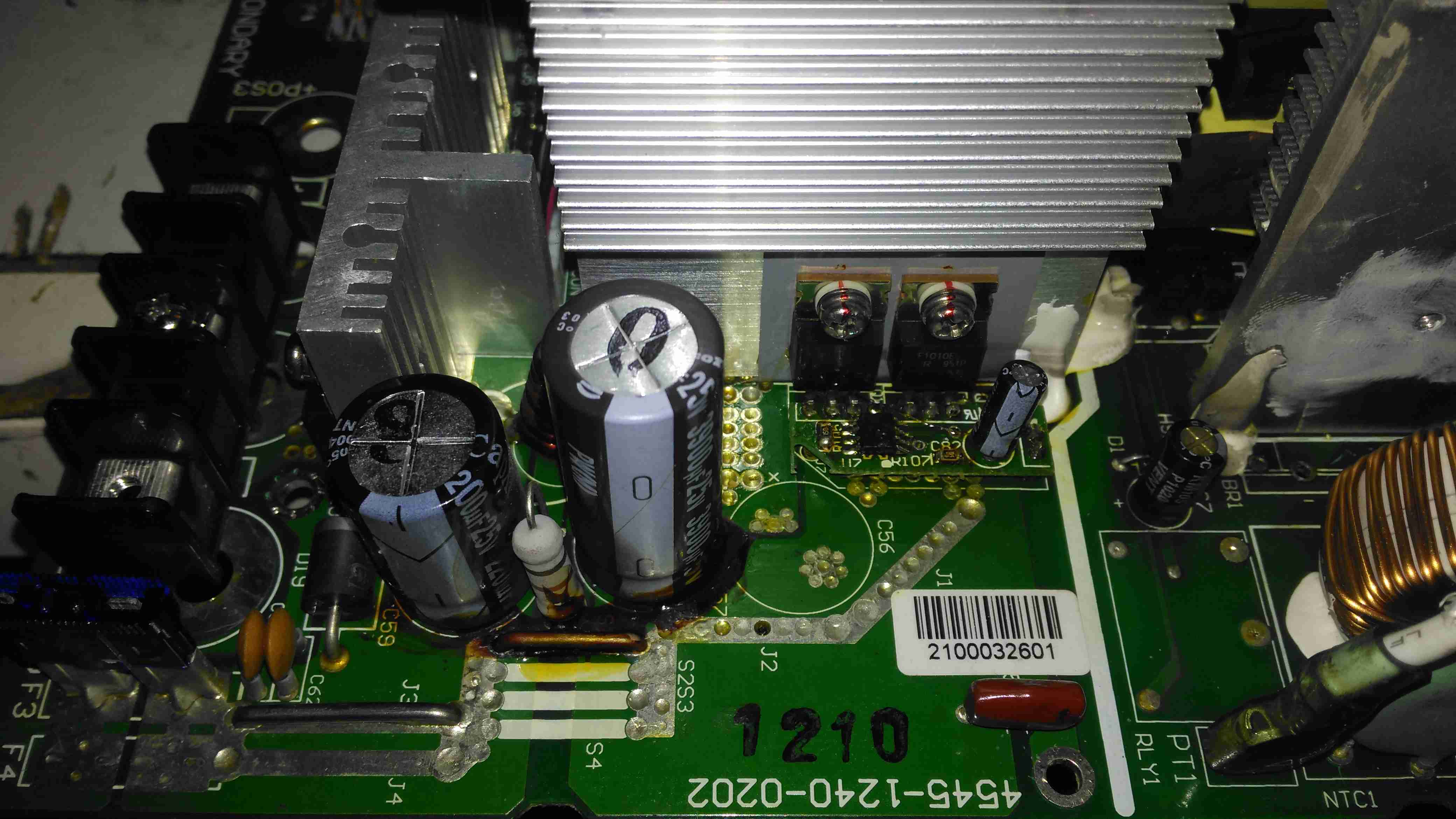
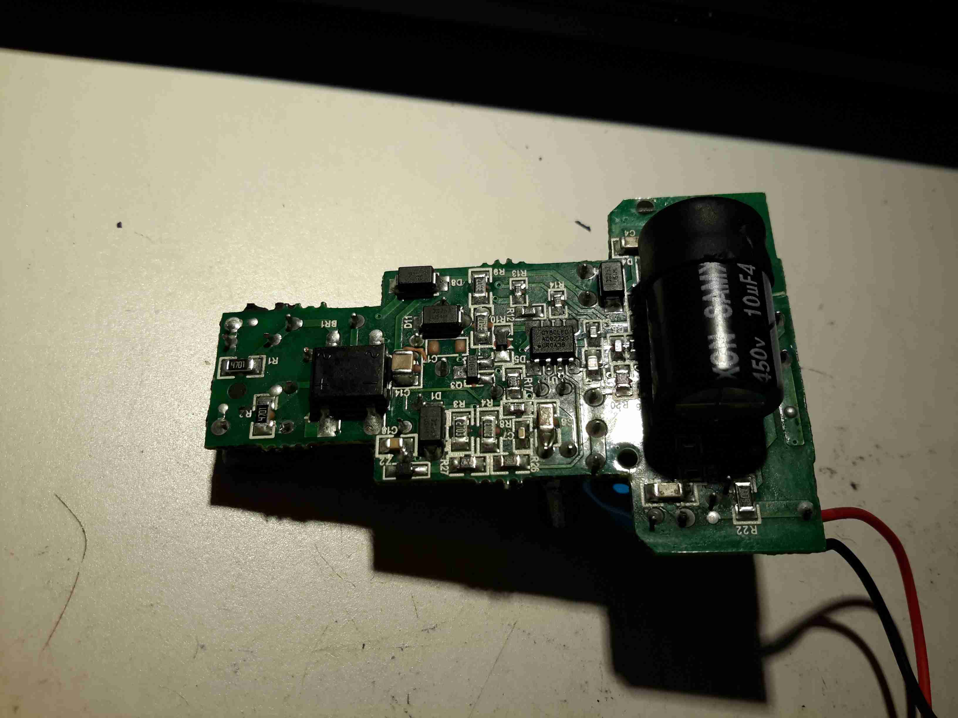
DC Output Section
The DC output rectifiers are on the large heatsink in the centre, with a small bodge board fitted. Due to the heavy conformal coating on the board I can’t get the ID from this small 8-pin IC, but from the fact that the output rectifiers are in fact IRF1010E MOSFETS, rated at 84A a piece, this is an synchronous rectifier controller.
Oddly, the output filter electrolytics are a mix of Nichicon (nice), and CapXon (shite). A bit of penny pinching here, which if a little naff since these chargers are anything but cheap. (£244.80 at the time of writing).
Hiding just behind the electrolytics is a large choke, and a reverse-polarity protection diode, which is wired crowbar-style. Reversing the polarity here will blow the 15A DC bus fuse instantly, and may destroy this diode if it doesn’t blow quick enough.
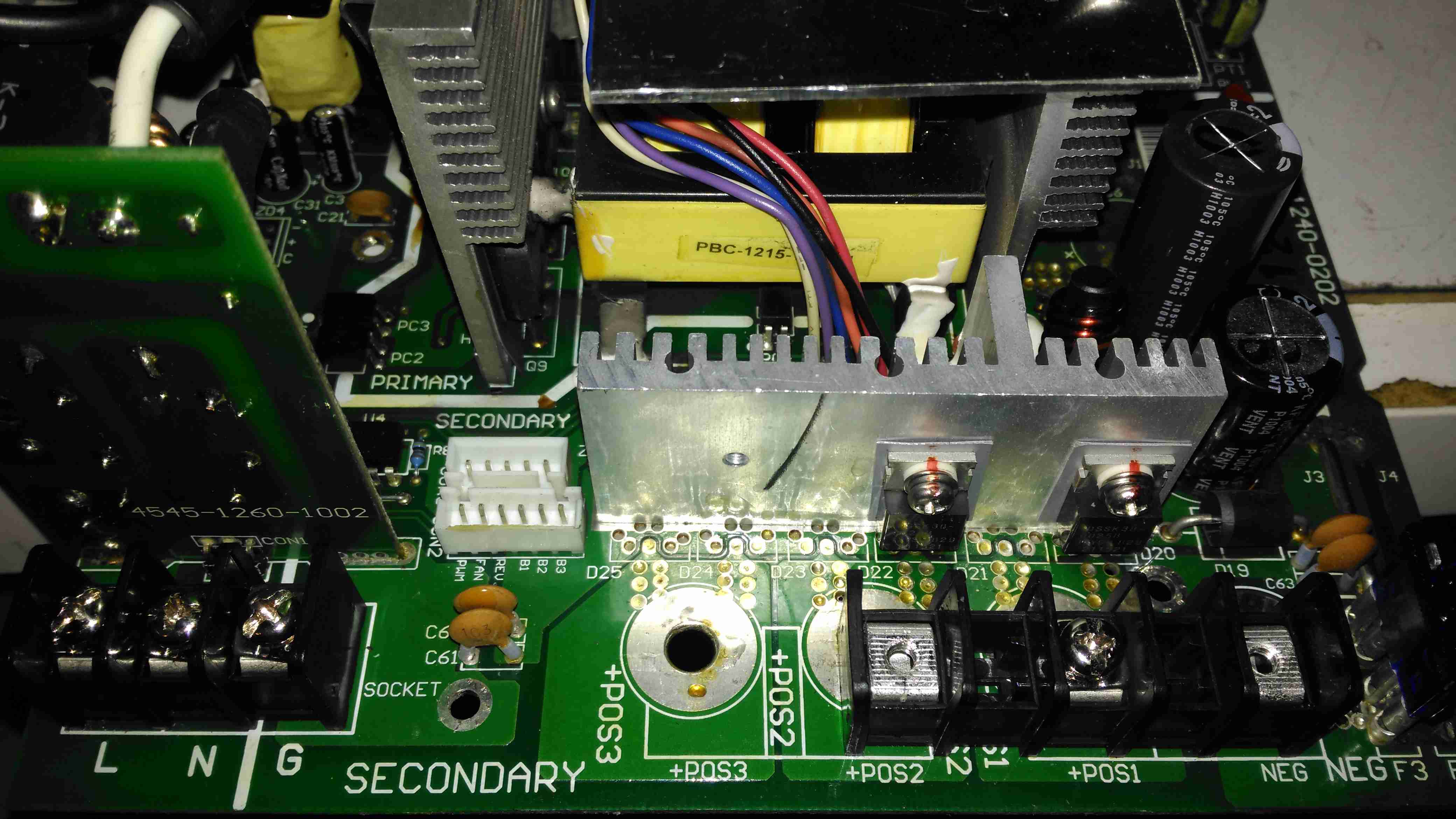
DC Outputs
Right on the output end are a pair of large Ixys DSSK38 TO220 Dual 20A dual Schottky diodes, isolating the two outputs from each other, a nice margin on these for a 10A charger, since the diodes are paralleled each channel is capable of 40A. This prevents one bank discharging into another & allows the charger logic to monitor the voltages individually. The only issue here is the 400mV drop of these diodes introduce a little bit of inefficiency. To increase current capacity of the PCB, the aluminium heatsink is being used as the main positive busbar. From the sizing of the power components here, I would think that the same PCB & component load is used for all the chargers up to 40A, since both the PFC inductor & main power transformer are massive for a 10A output. There are unpopulated output components on this low-end model, to reduce the cost since they aren’t needed.
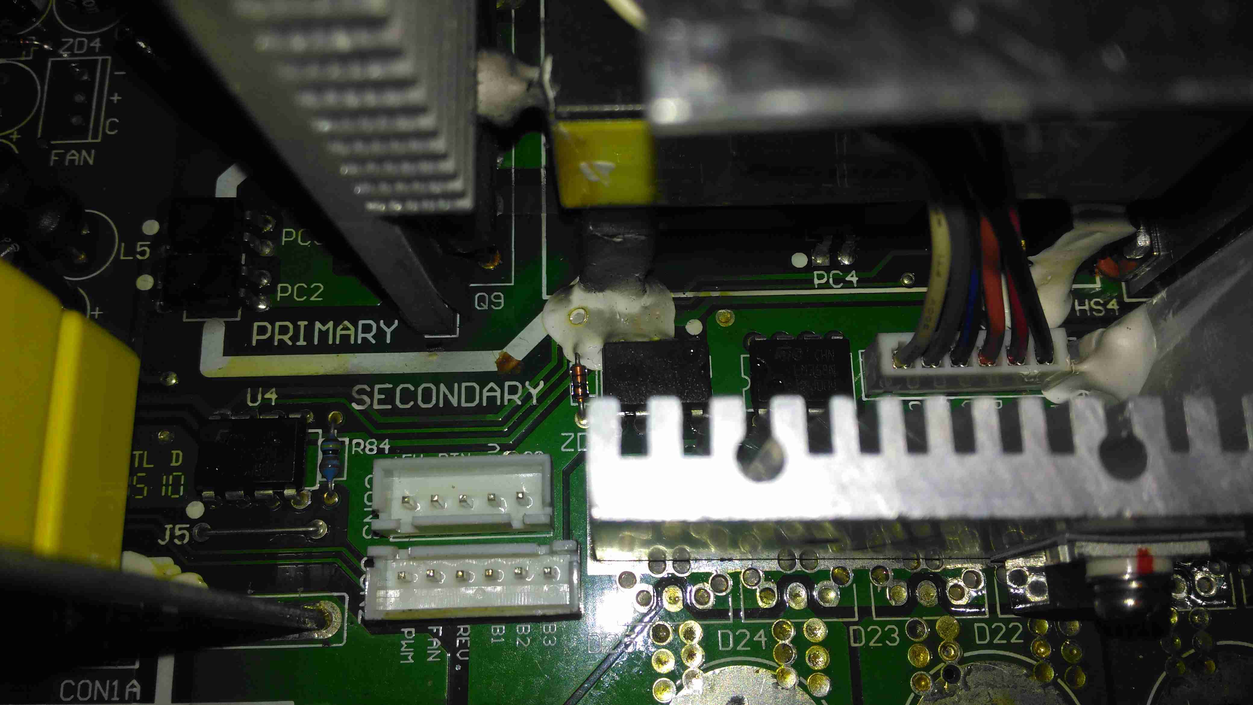
Front Panel Control Connections
A trio of headers connect all the control & sense signals to the front panel PCB, which contains all the control logic. This unit is sensing all output voltages, output current & PSU rail voltages.
Front Panel LEDs
The front panel is stuffed with LEDs & 7-segment displays to show the current mode, charging voltage & current. There’s 2 tactile switches for adjustments.
Front Panel Reverse
The reverse of the board has the main microcontroller – again identifying this is impossible due to the heavy conformal coat. The LEDs are being driven through a 74HC245D CMOS Octal Bus Transceiver.
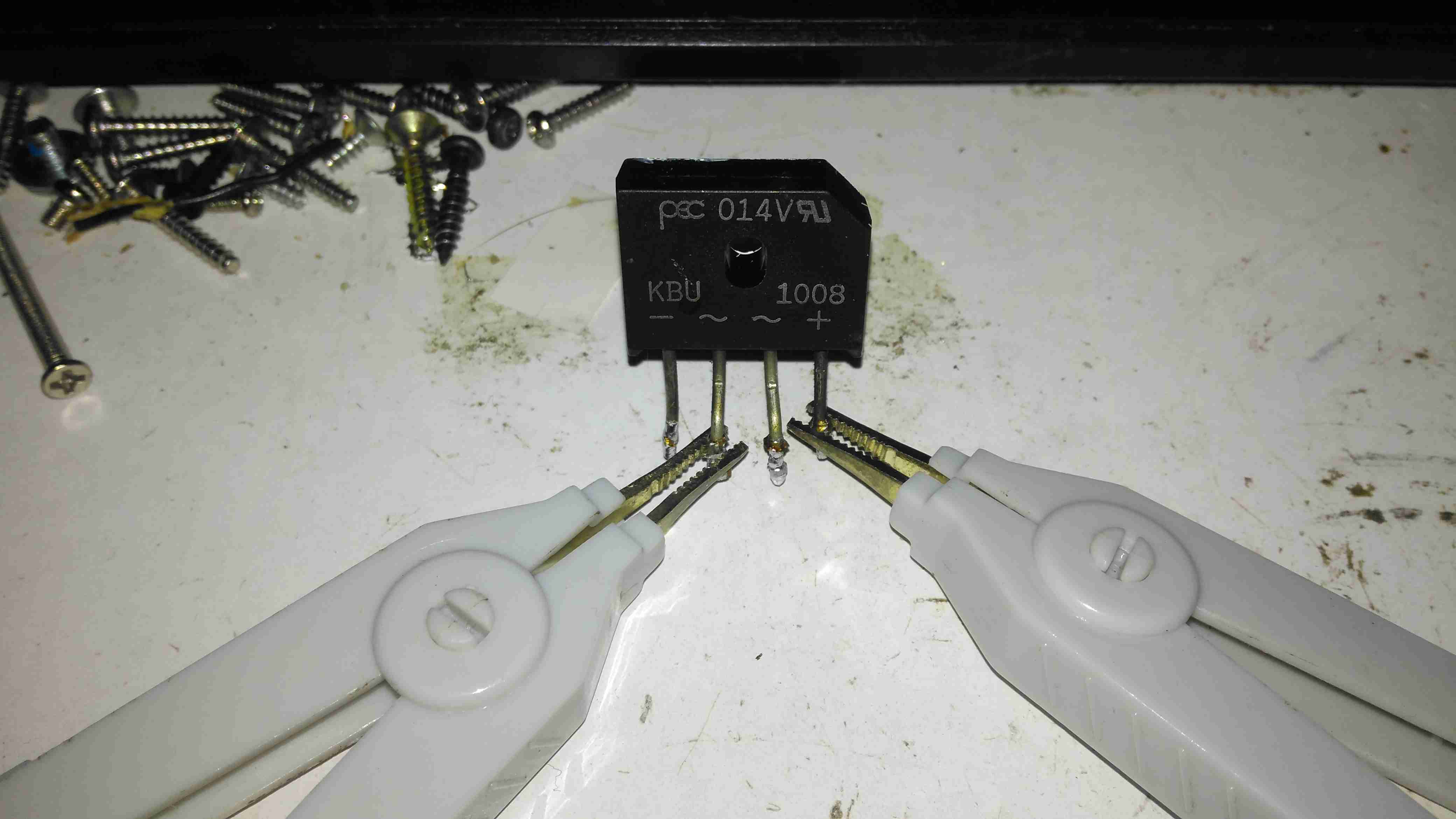
Now on to the repair! I’m not particularly impressed with only getting 4 years from this unit, they are very expensive as already mentioned, so I would expect a longer lifespan. The input fuse had blown in this case, leaving me with a totally dead charger. A quick multimeter test on the input stage of the unit showed a dead short – the main AC input bridge rectifier has gone short circuit.
Bridge Rectifier Removed
Here the defective bridge has been desoldered from the board. It’s a KBU1008 10A 800v part. Once this was removed I confirmed there was no longer an input short, on either the AC side or the DC output side to the PFC circuit.
Testing The Rectifier
Time to stick the desoldered bridge on the milliohm meter & see how badly it has failed.
Yep, Definitely Shorted
I’d say 31mΩ would qualify as a short. It’s no wonder the 4A input fuse blew instantly. There is no sign of excessive heat around the rectifier, so I’m not sure why this would have failed, it’s certainly over-rated for the 10A charger.
Testing Without Rectifier
Now the defective diode bridge has been removed from the circuit, it’s time to apply some controlled power to see if anything else has failed. For this I used a module from one of my previous teardowns – the inverter from a portable TV.
Test Inverter
This neat little unit outputs 330v DC at a few dozen watts, plenty enough to power up the charger with a small load for testing purposes. The charger does pull the voltage of this converter down significantly, to about 100v, but it still provides just enough to get things going.
It’s Alive!
After applying some direct DC power to the input, it’s ALIVE! Certainly makes a change from the usual SMPS failures I come across, where a single component causes a chain reaction that writes off everything.
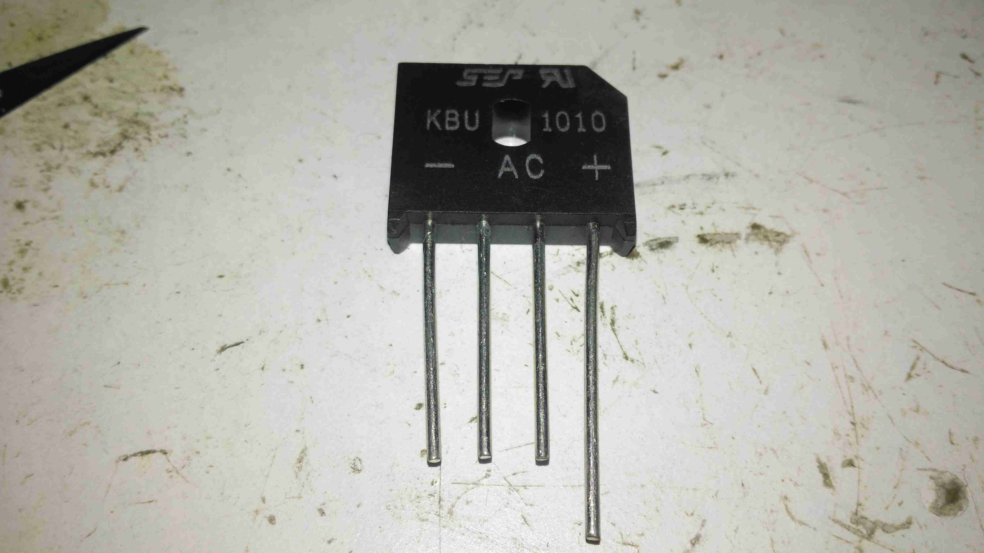
Replacement Rectifier
Unfortunately I couldn’t find the exact same rectifier to replace the shorted one, so I had to go for the KBU1010, which is rated for 1000v instead of 800v, but the Vf rating (Forward Voltage), is the same, so it won’t dissipate any more power.
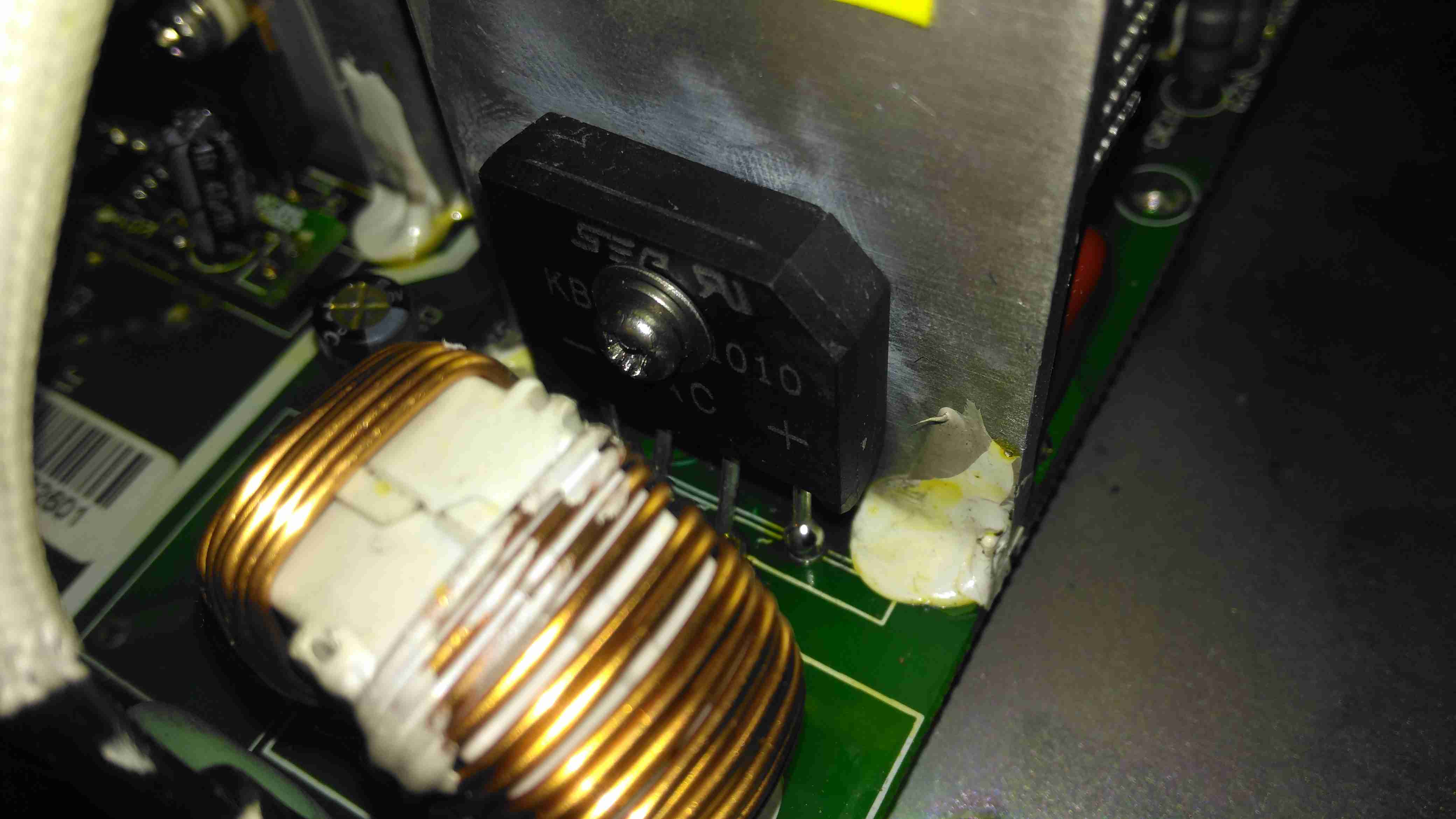
Soldered In
Here’s the new rectifier soldered into place on the PCB & bolted to it’s heatsink, with some decent thermal compound in between.
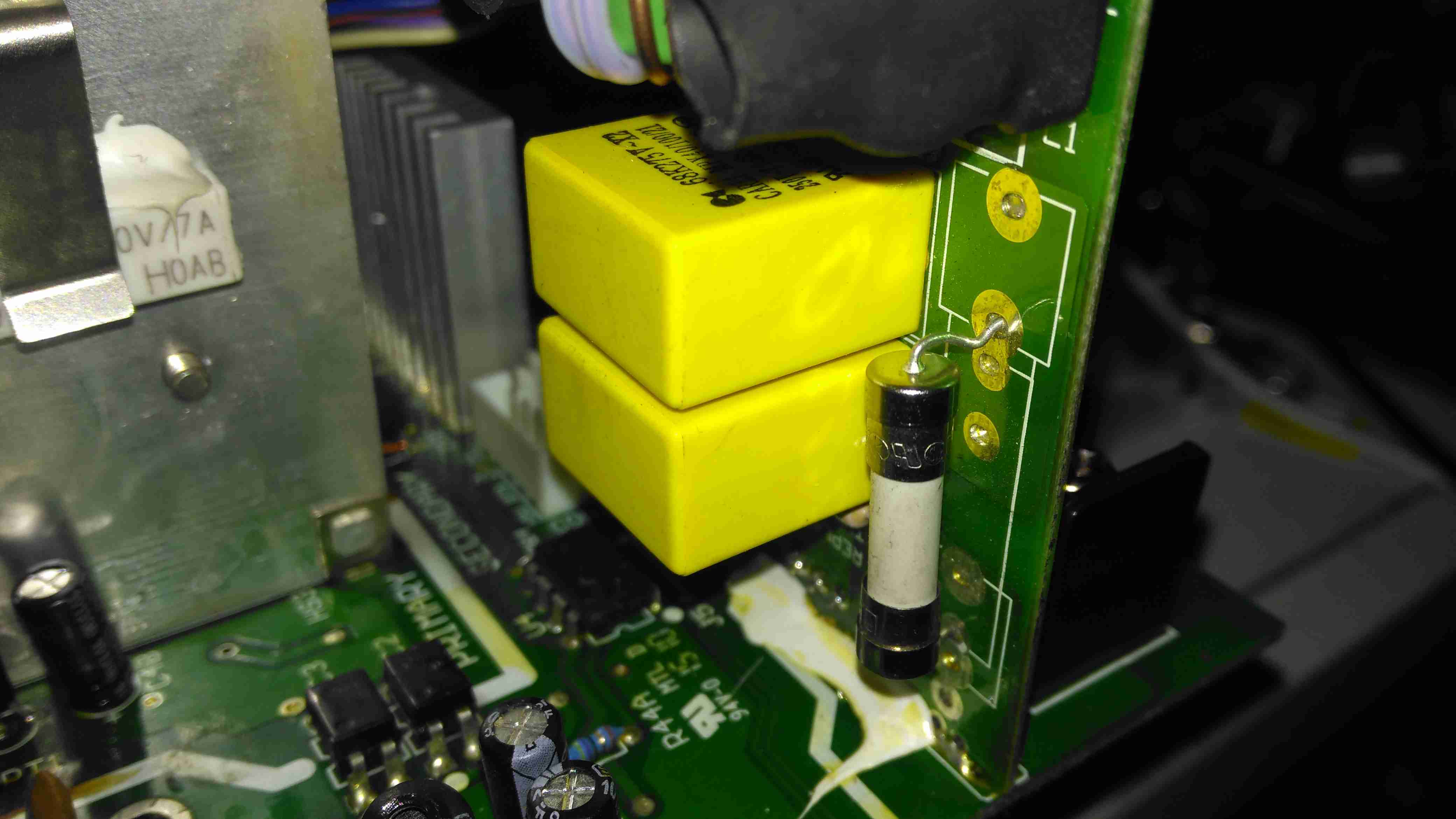
Input Board
Here is the factory fuse, a soldered in device. I’ll be replacing this with standard clips for 20x5mm fuses to make replacement in the future easier, the required hole pattern in the PCB is already present. Most of the mains input filtering is also on this little daughterboard.
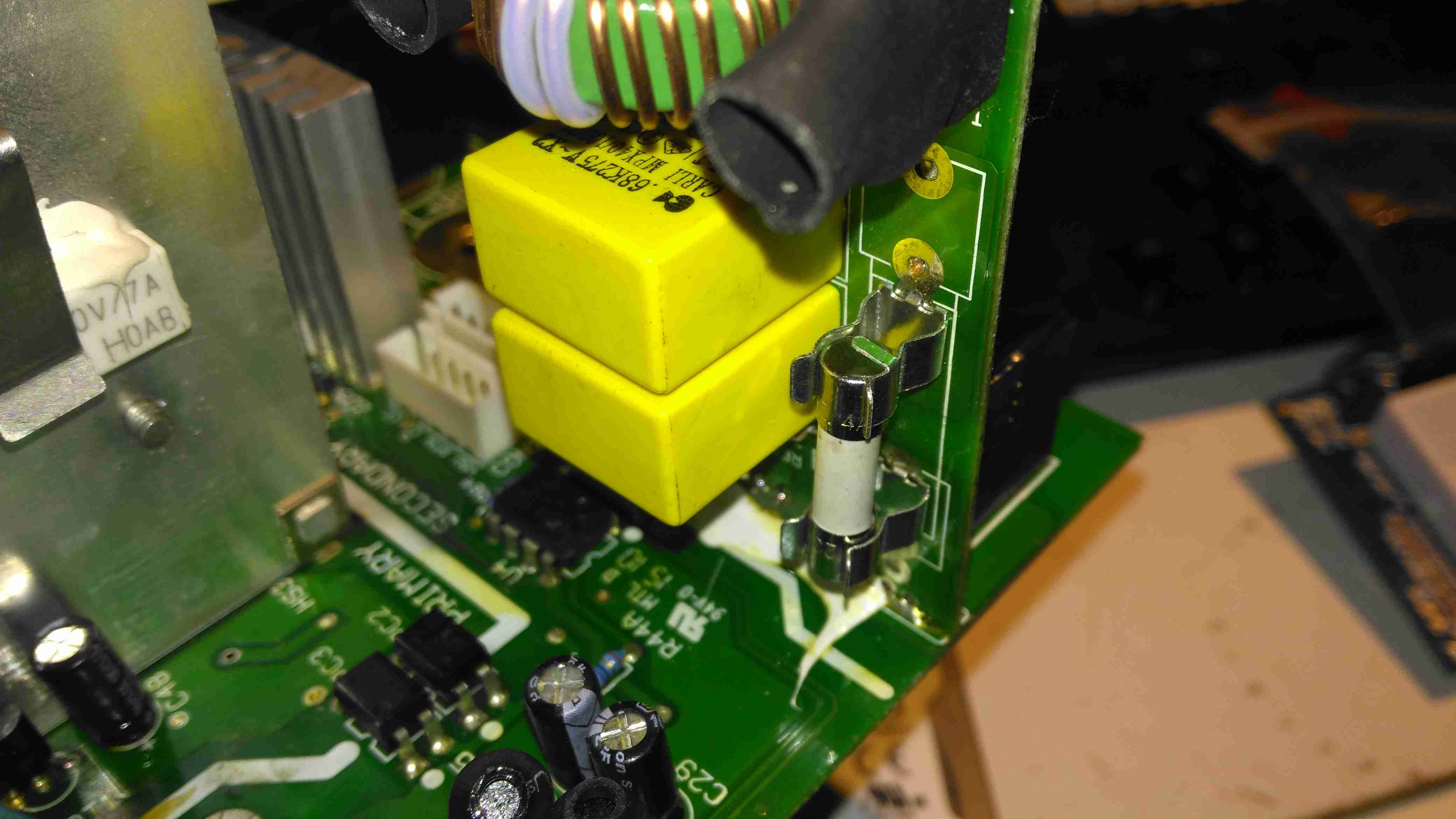
Fuse Replaced
Now the fuse has been replaced with a standard one, which is much more easily replaceable. This fuse shouldn’t blow however, unless another fault develops.
Full Load Test
Now everything is back together, a full load test charging a 200Ah 12v battery for a few hours will tell me if the fix is good. This charger won’t be going back into service onboard the boat, it’s being replaced anyway with a new 50A charger, to better suit the larger loads we have now. It won’t be a Sterling though, as they are far too expensive. I’ll report back if anything fails!
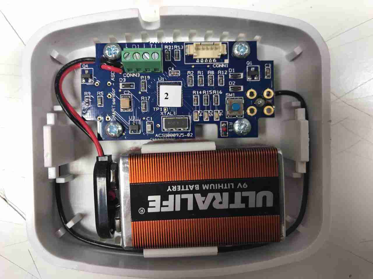
Here’s another random bit of RF tech, I’m told this is a wireless energy management sensor, however I wasn’t able to find anything similar on the interwebs. It’s powered by a standard 9v PP3 battery.
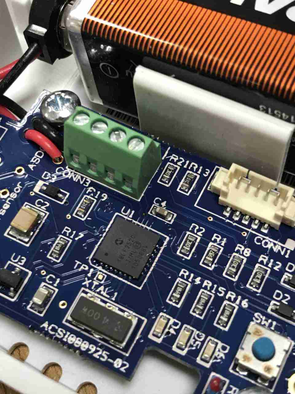
Microcontroller
System control is handled by this Microchip PIC18F2520 Enhanced Flash microcontroller, this has an onboard 10-bit ADC & nanoWatt technology according to their datasheet. There’s a 4MHz crystal providing the clock, with a small SOT-23 voltage regulator in the bottom corner. There’s a screw terminal header & a plug header, but I’ve no idea what these would be used for. Maybe connecting an external voltage/current sensor & a programming header? The tactile button I imagine is for pairing the unit with it’s controller.
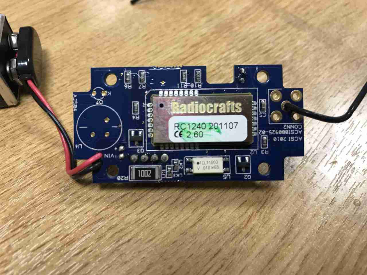
PCB Bottom
The bottom of the PCB is almost entirely taken up by a Radiocrafts RC1240 433MHz RF transceiver. Underneath there’s a large 10kΩ resistor, maybe a current transformer load resistor, and a TCLT1600 optocoupler. Just from the opto it’s clear this unit is intended to interface in some way to the mains grid. The antenna is connected at top right, in a footprint for a SMA connector, but this isn’t fitted.
These photos were sent over to me by a friend, an interesting piece of tech that’s used in the retail industry. This is a BluVision BLE Beacon, which as far as I can tell is used to provide some automated customer assistance. From their website it seems they can also be used for high-price asset protection & tracking. These units don’t appear to be serviceable, being completely sealed & only having a primary cell. I’m not sure what they cost but it seems to be an expensive way to contact clients with adverts etc.
Component Side
There’s not much populated on this PCB, the main component here is the CC2640 SimpleLink ultra-low-power wireless microcontroller for Bluetooth Low Energy. It’s a fairly powerful CPU, with an ARM Cortex M3 core, 129KB of flash & up to 48MHz clock speed. There’s a couple of crystals, one of which is most likely a 32,768kHz low-power sleep watch crystal, while the other will be the full clock frequency used while it’s operating. Unfortunately I can’t make the markings out from the photos. There doesn’t appear to be any significant power supply components, so this must be running direct from the battery underneath.
2.2Ah 3.6v Lithium Cell
The other side of the PCB has a single primary lithium cell, rated at 3.6v, 2.2Ah. The factory spec sheet specifies a 2.2 year life at 0dBm TX Power, Running 24/7, 100ms advertisement rate.
Yesterday, the Raspberry Pi community got a nice surprise – a new Pi! This one has some improved features over the previous RPi 3 Model B:
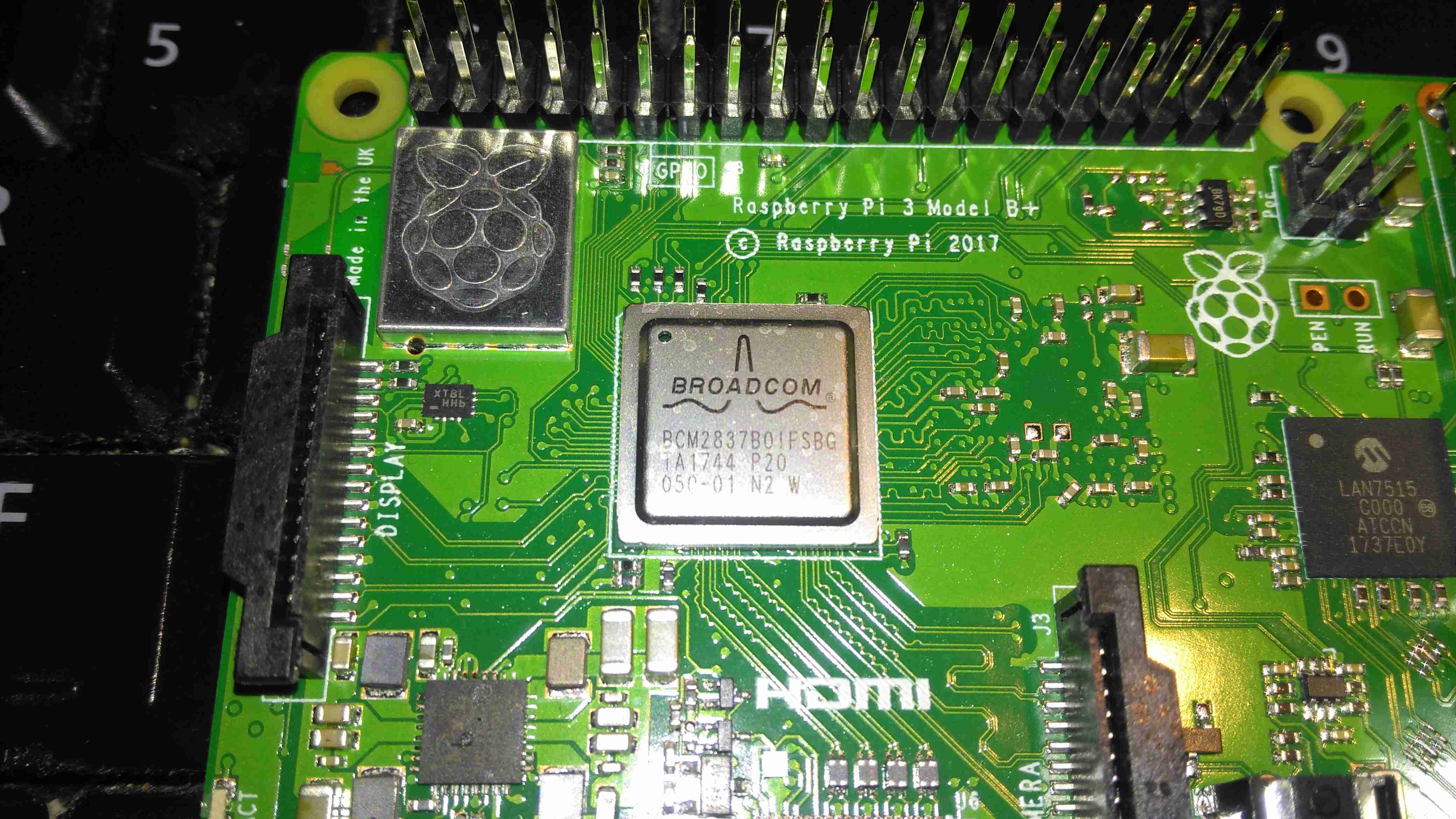
Improved CPU – 64-Bit 1.4GHz Quad-Core BCM2837B0
Improved WiFi – Dual Band 802.11b/g/n/ac. This is now under a shield on the top of the board.
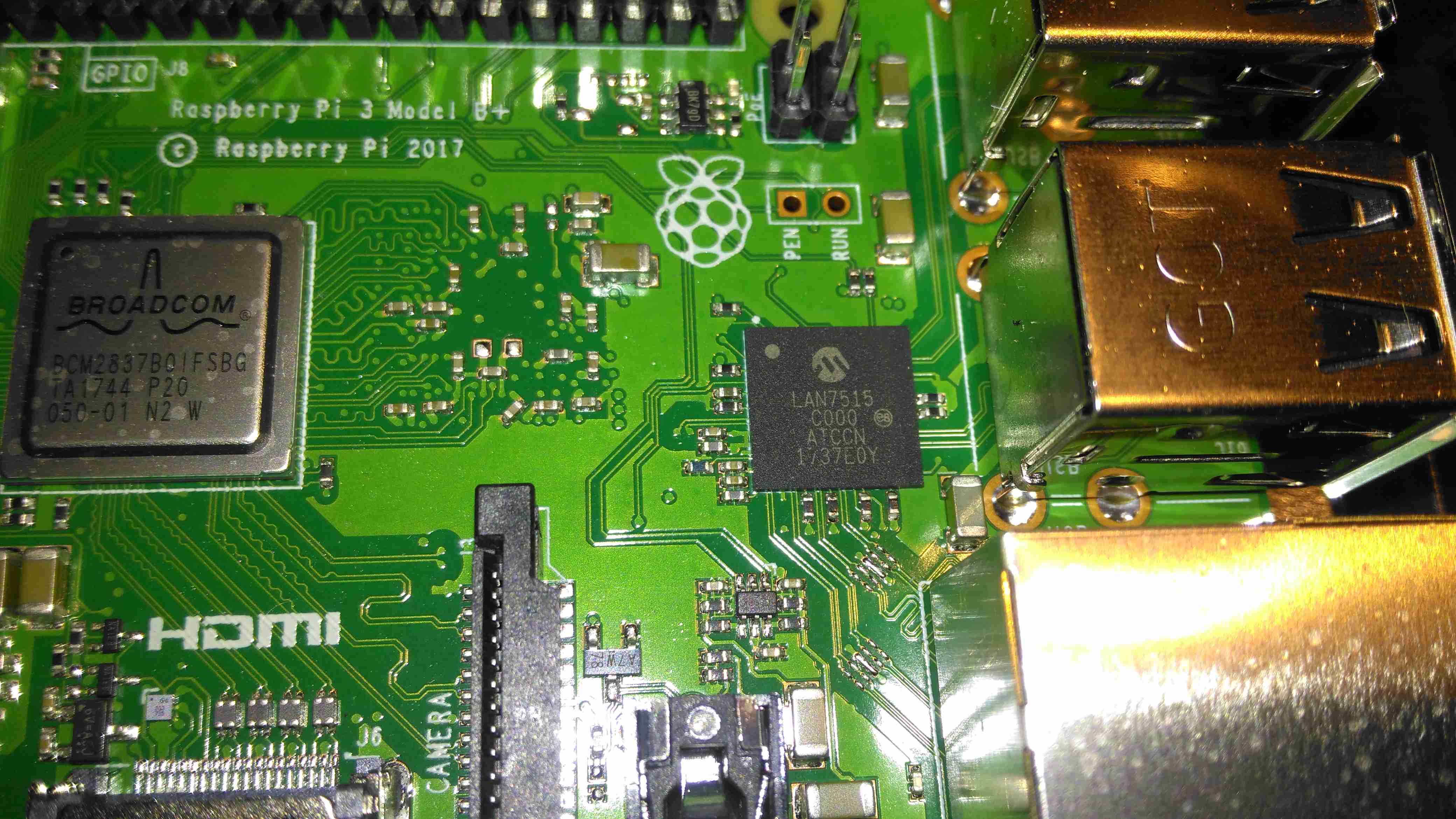
Improved Ethernet – The USB/Ethernet IC has been replaced with a LAN7515, supporting gigabit ethernet. The backhaul is still over USB2 though, so this would max out at about 300Mbit/s
PoE Support – There’s a new 4-pin header, and a matching HAT for power over ethernet support.
Chipset
The USB/LAN Controller is now a BGA package, supporting gigabit ethernet. The USB connections are still USB2 though, limiting total bandwidth. This shouldn’t be much of an issue though, since anything over the 100Mbit connection we’ve had previously is an improvement.
CPU & Radio
The CPU now has a metal heatspreader on top of the die, no doubt to help with cooling under heavy loads. As far as I know, it’s still the same silicon under the hood though. The WiFi radio is under the shielding can to the top left, with the PCB trace antenna down the left edge of the board.
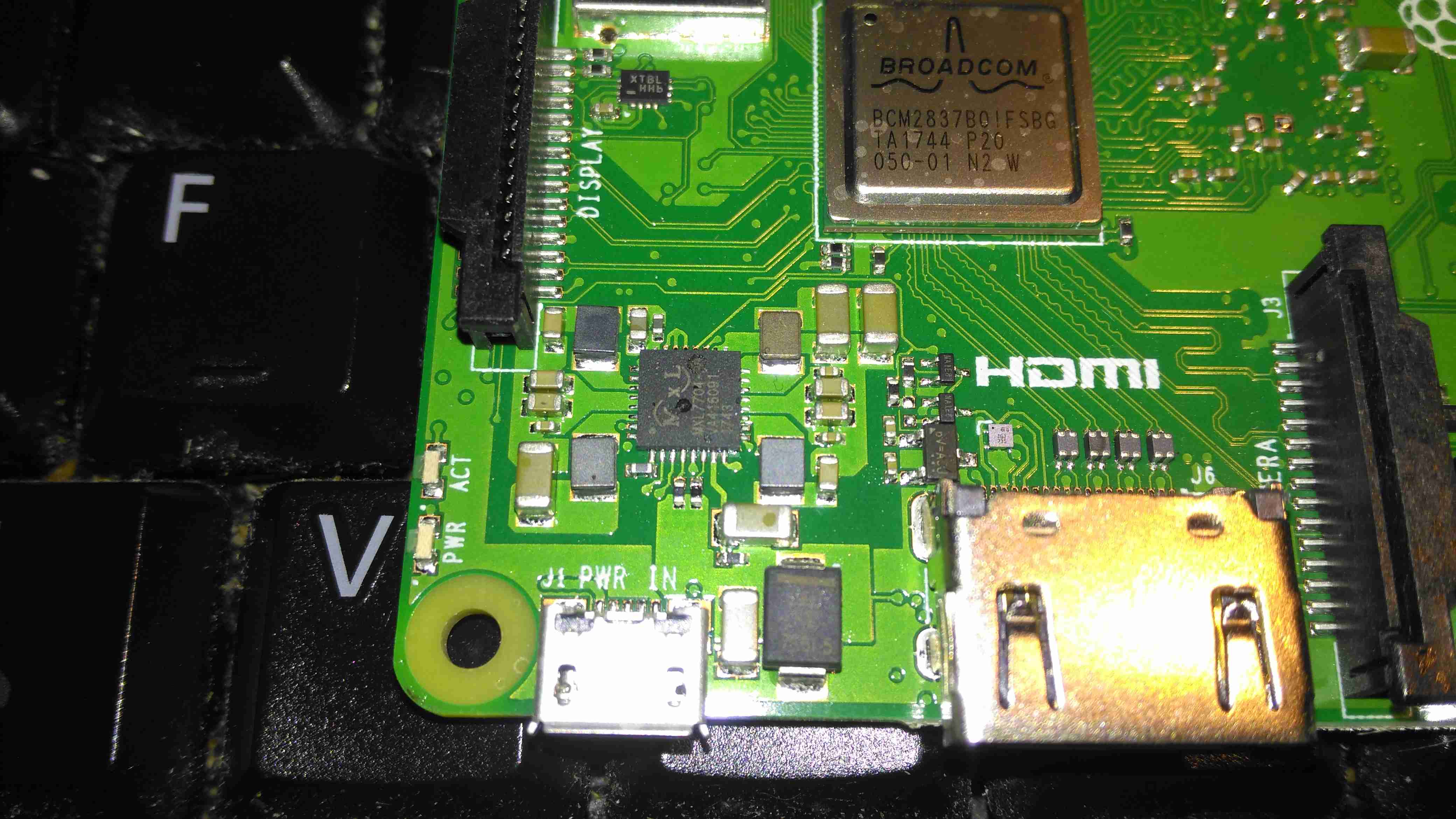
Power Controller
The power supplies are handled on this new Pi by the MaxLinear MxL7704, from what I can tell from MaxLinear’s page, it seems to be somewhat of a collaborative effort to find something that would do the best job, since they apparently worked with the Foundation to get this one right. This IC apparently includes four synchronous step-down buck regulators that provide system, memory, I/O and core power from 1.5A to 4A. An on-board 100mA LDO provides clean 1.5V to 3.6V power for analog sub-systems. This PMIC utilizes a conditional sequencing state machine that is flexible enough to meet the requirements of virtually any processor.
PCB Bottom
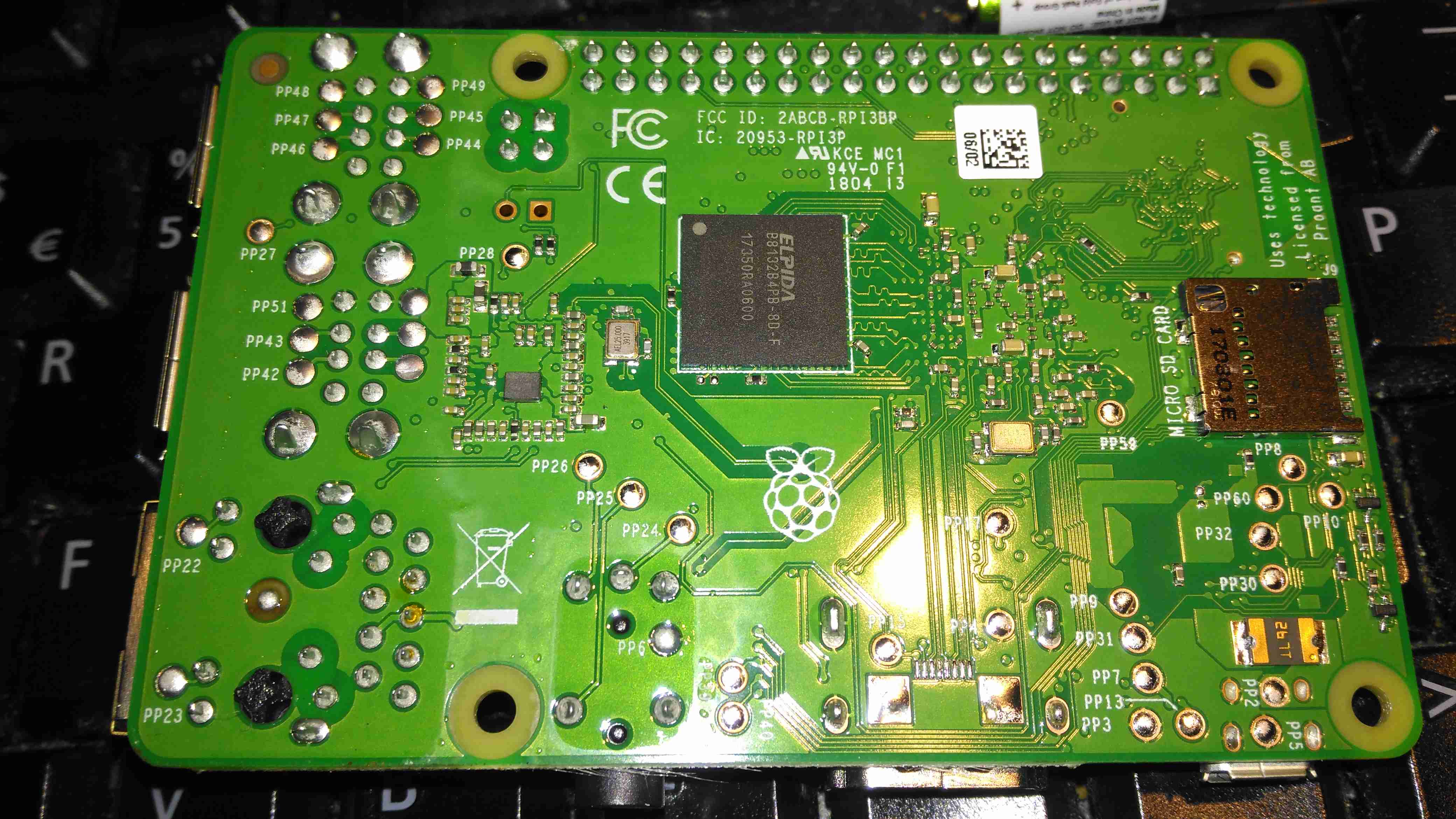
The bottom of the PCB has the Elpida 1GB RAM package, which is LPDDR2, along with the MicroSD slot.
A quick benchmark running Raspbian Lite & a SanDisk Ultra 32GB Class 10 SD card gives some nice results:
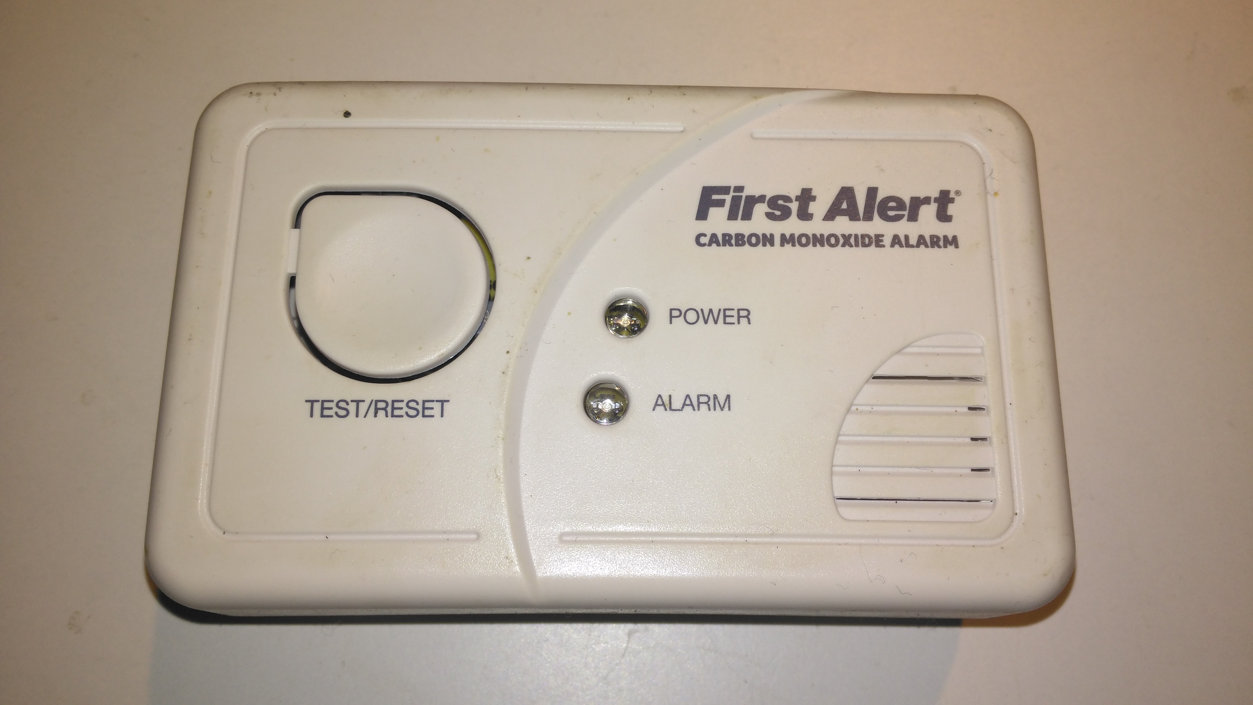
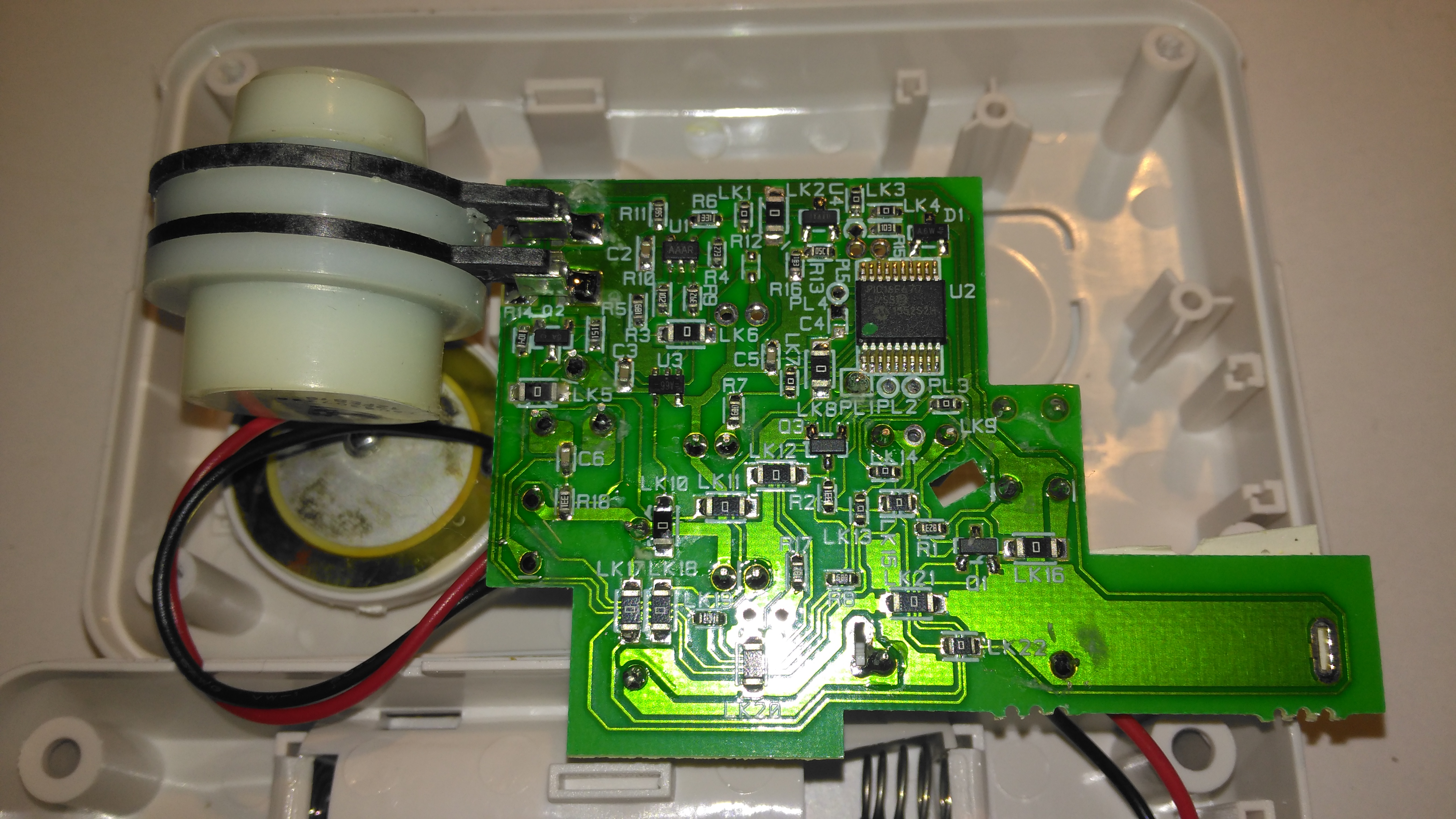
Here’s another domestic CO Alarm, this one a cheaper build than the FireAngel ones usually use, these don’t have a display with the current CO PPM reading, just a couple of LEDs for status & Alarm.
Rear
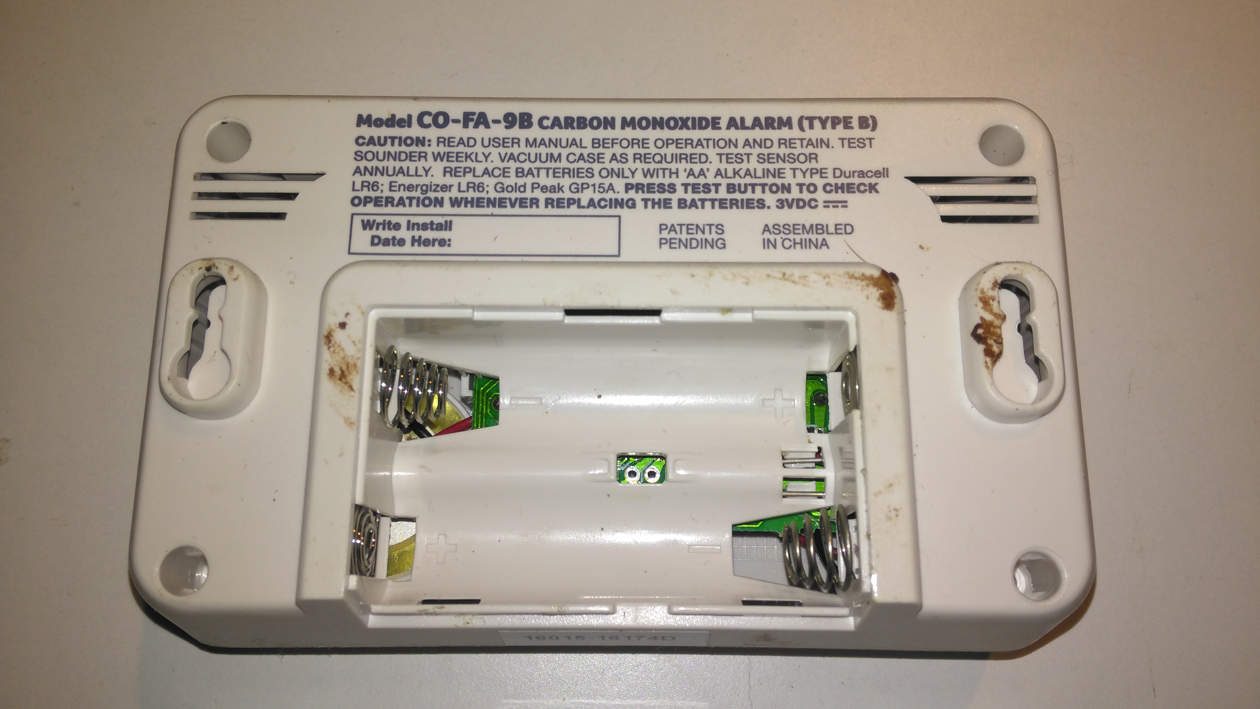
This alarm also doesn’t have the 10-year lithium cell for power, taking AA cells instead. The alarm does have the usual low battery alert bleeps common with smoke alarms though, so you’ll get a fair reminder to replace them.
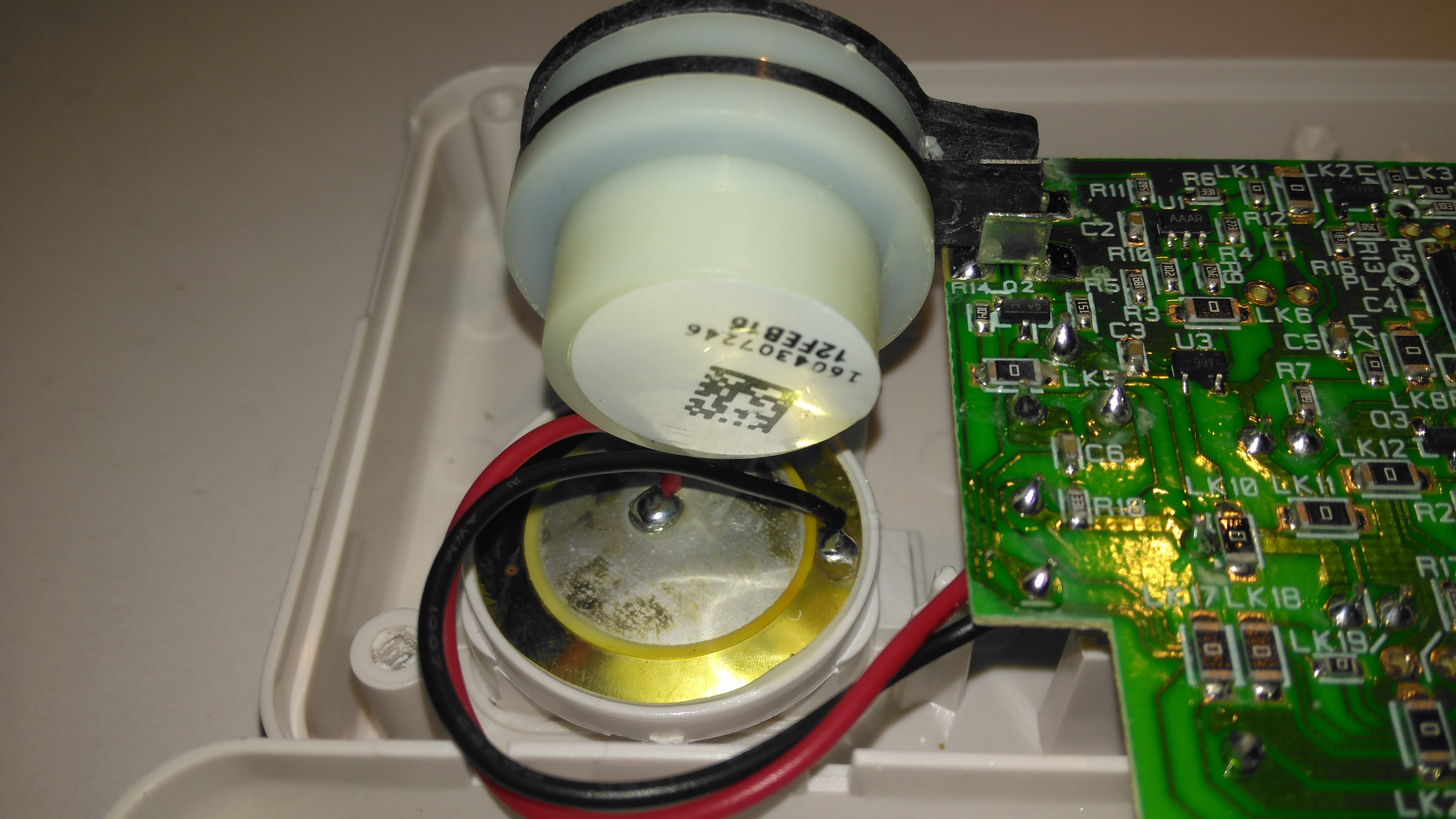
Internals
Not much at all on the inside. The CO sensor cell is the same one as used in the FireAngel alarms, I have never managed to find who manufactures these sensors, or a datasheet for them unfortunately.
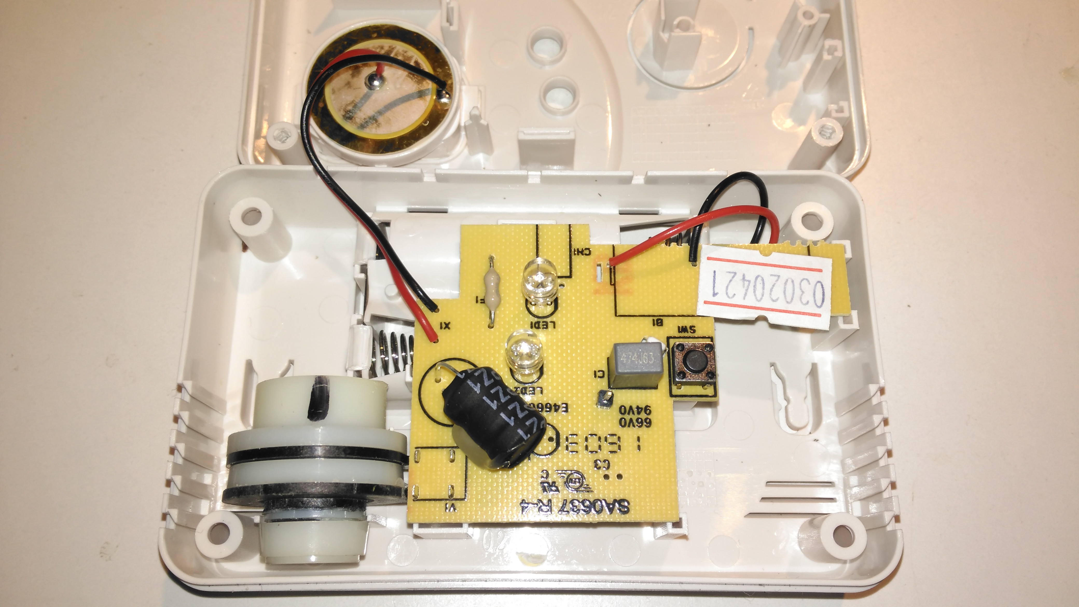
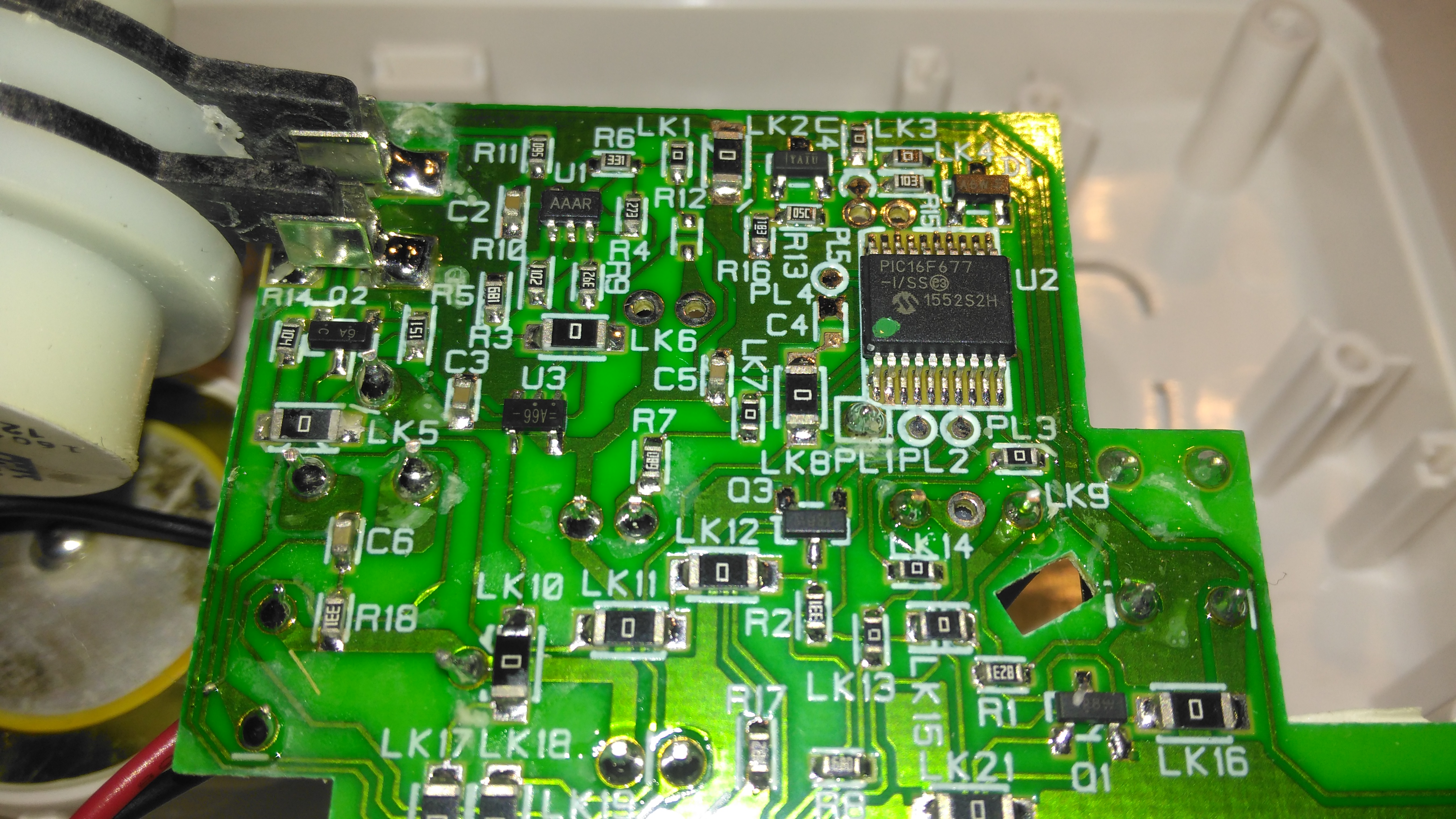
PCB Top
The top of the single sided PCB has the transformer for driving the Piezo sounder, the LEDs & the test button.
PCB Bottom
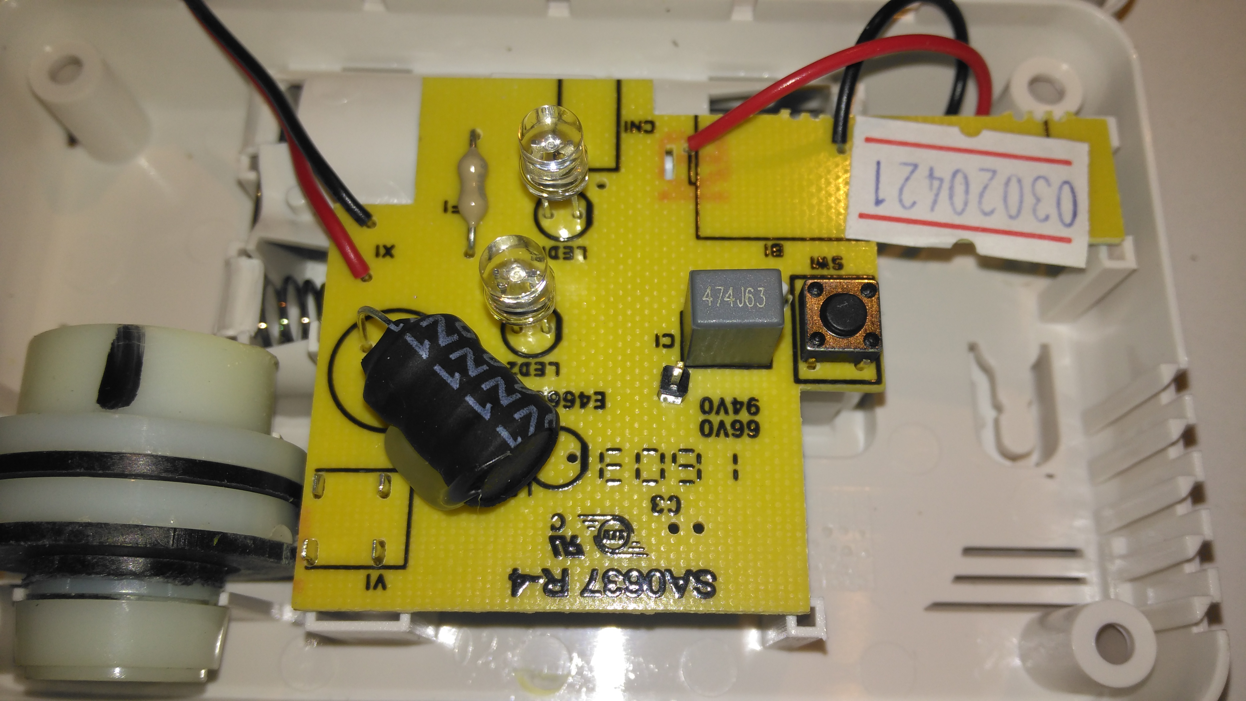
All the magic happens on the bottom of the PCB. The controlling microcontroller is on the top right, with the sensor front end on the top left.
Circuitry Closeup
The microcontroller used here is a Microchip PIC16F677. I’ve not managed to find datasheets for the front end components, but these will just be a low-noise op-amp & it’s ancillaries. There will also be a reference voltage regulator. The terminals on these sensors are made of conductive plastic, probably loaded with carbon.
Sensor Cell & Piezo Disc
The expiry date is handily on a label on the back of the sensor, the Piezo sounder is just underneath in it’s sound chamber.
This is a pair of modules that Maplin was selling some time back, to send stereo audio over a 2.4GHz radio link. The transmitter identifies as a USB sound card, I’ve personally used these units to transmit audio about 60ft. The transmitter, above, has a single button for pairing with the receiver below.
Receiver
The receiver unit has a large external antenna, a link status LED & volume buttons, these directly control the volume level on the host PC via the sound card drivers.
Receiver PCB Top
Popping the case open on the receiver reveals a large PCB, holding the chipset, along with the audio output jacks & Mini-USB power input. The antenna Coax is soldered to the PCB.
Receiver PCB Bottom
The top of the board has the control buttons, and the status LED.
Receiver Chipset
The chipset used here is a Nordic Semiconductor nRF20Z01 2.4GHz Stereo Audio Streamer, there’s a small microcontroller which does all the register magic on the RF transceiver. The RF chain is at the top of the photo, audio outputs on the top left, and the micro USB power input & voltage regulators at bottom left.
Transmitter PCB Top
The transmitter PCB has a Sonix USB Audio Codec, to interface with the host PC. This is then fed into another Nordic Semi part on the opposite side of the board:
Transmitter PCB Bottom
The bottom of the transmitter has the RF section, and another small control microcontroller.
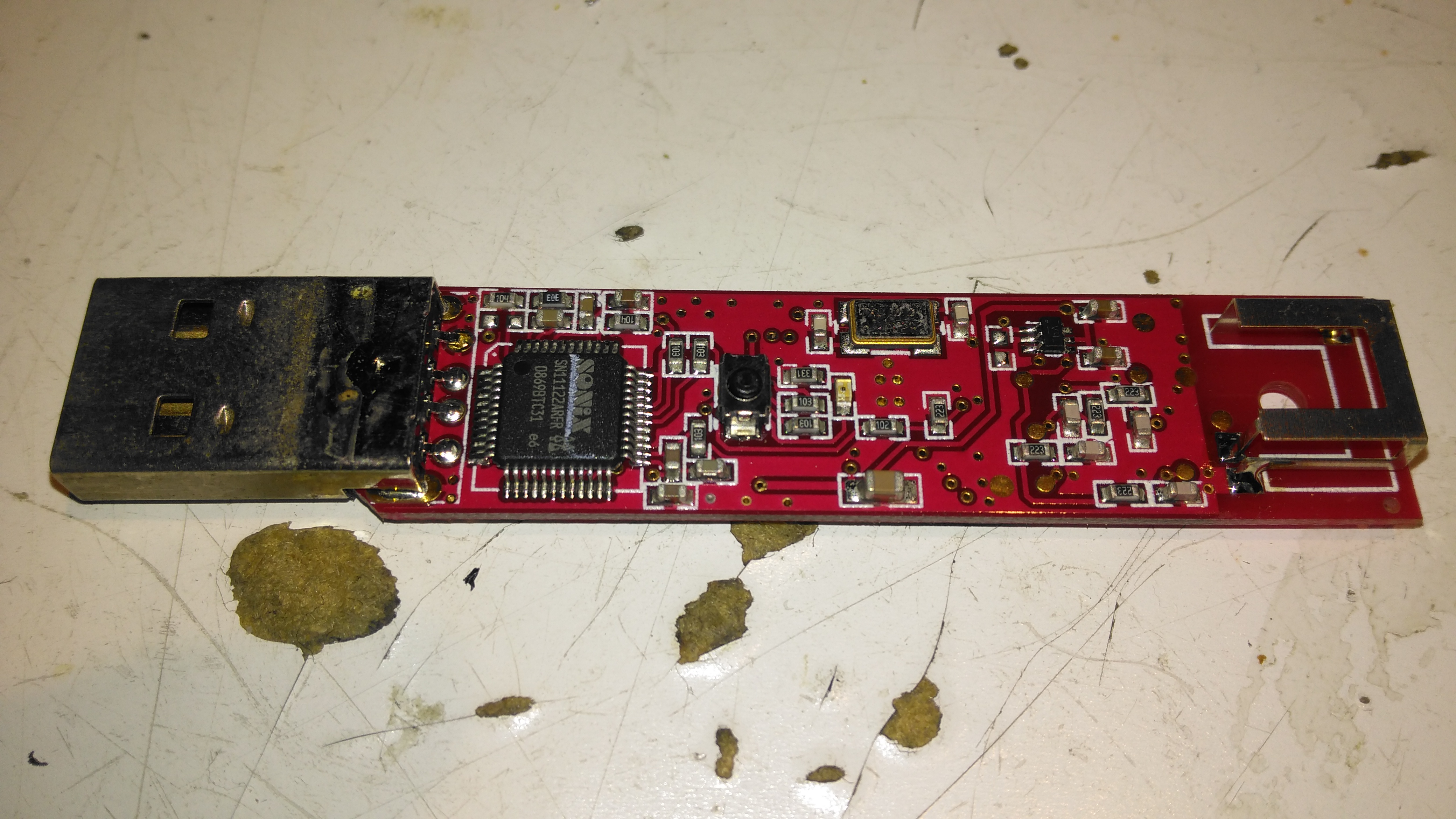
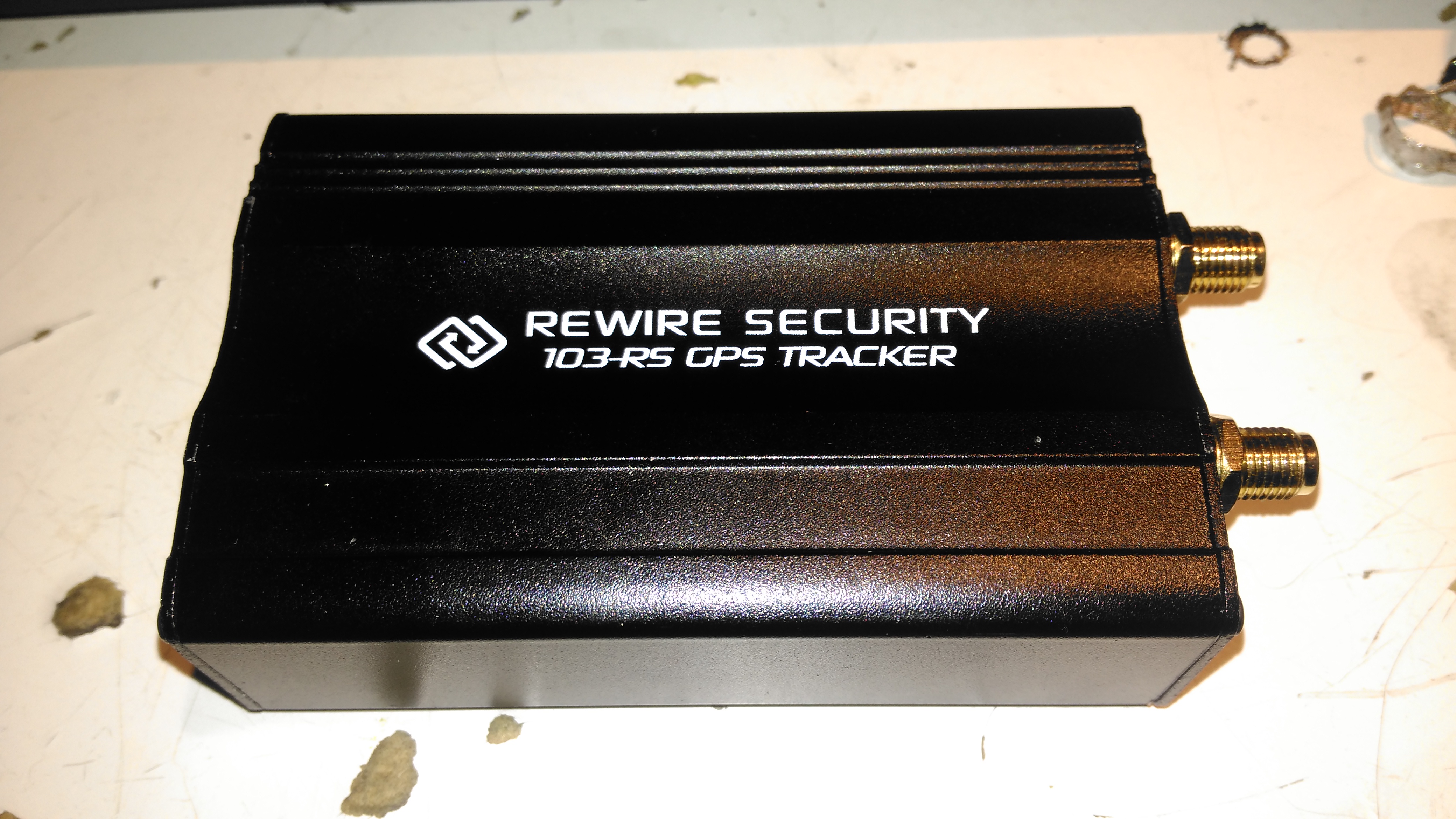
I thought it was time to add a bit of security to the gear I take camping, so this GPS tracker unit was sourced from eBay. This is a Rewire Security 103RS, a slightly customised version of the common Chinese TK103 GPS tracker.
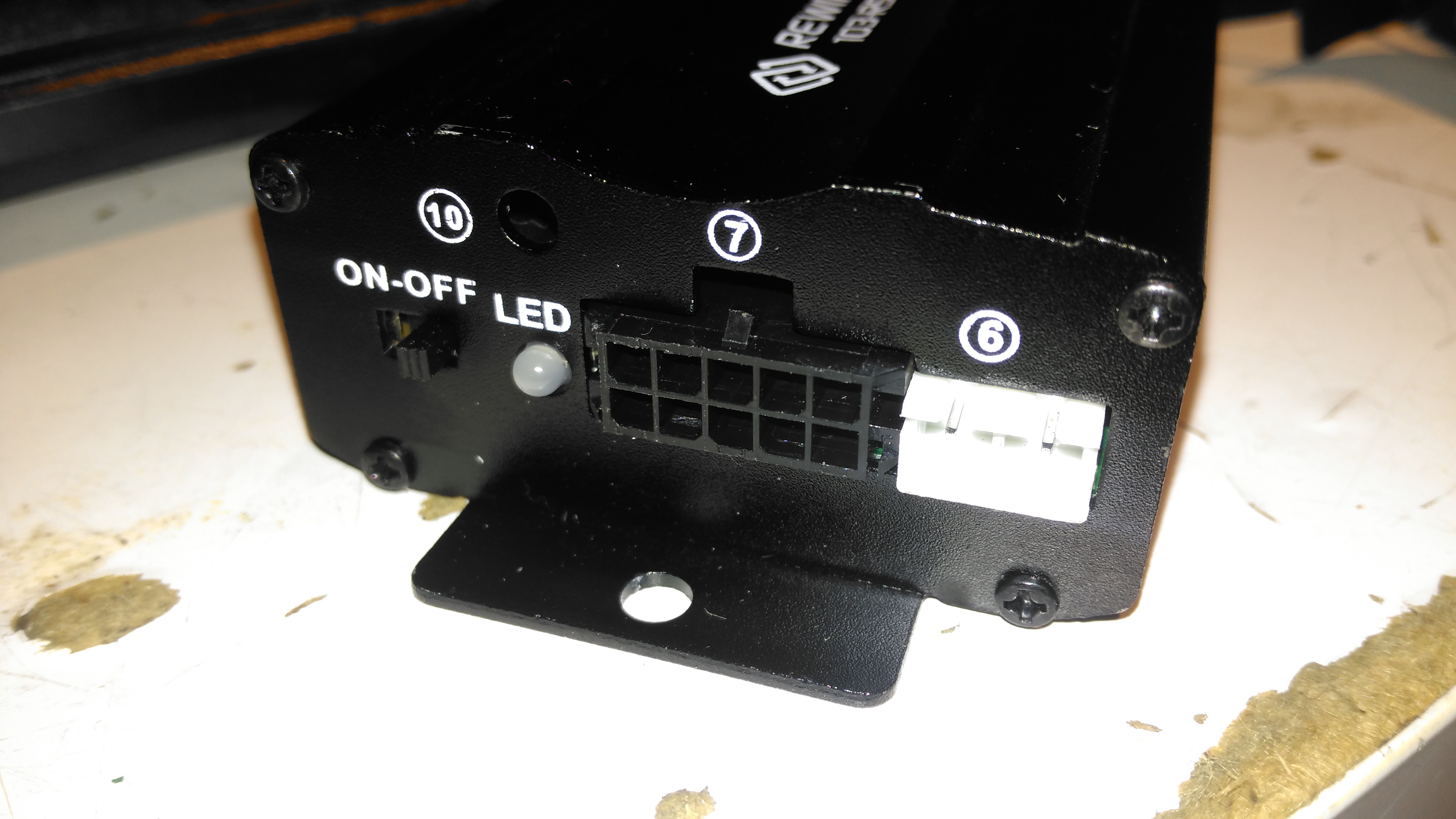
Input Connections
The small module has all it’s power connections on one end of the unit, on a Molex multi-way block. The white connector is for a piezo-shock sensor – this interfaces with the alarm functionality of the unit. There’s an indicator LED for both the GPS & GSM status, and a switch for the backup battery.
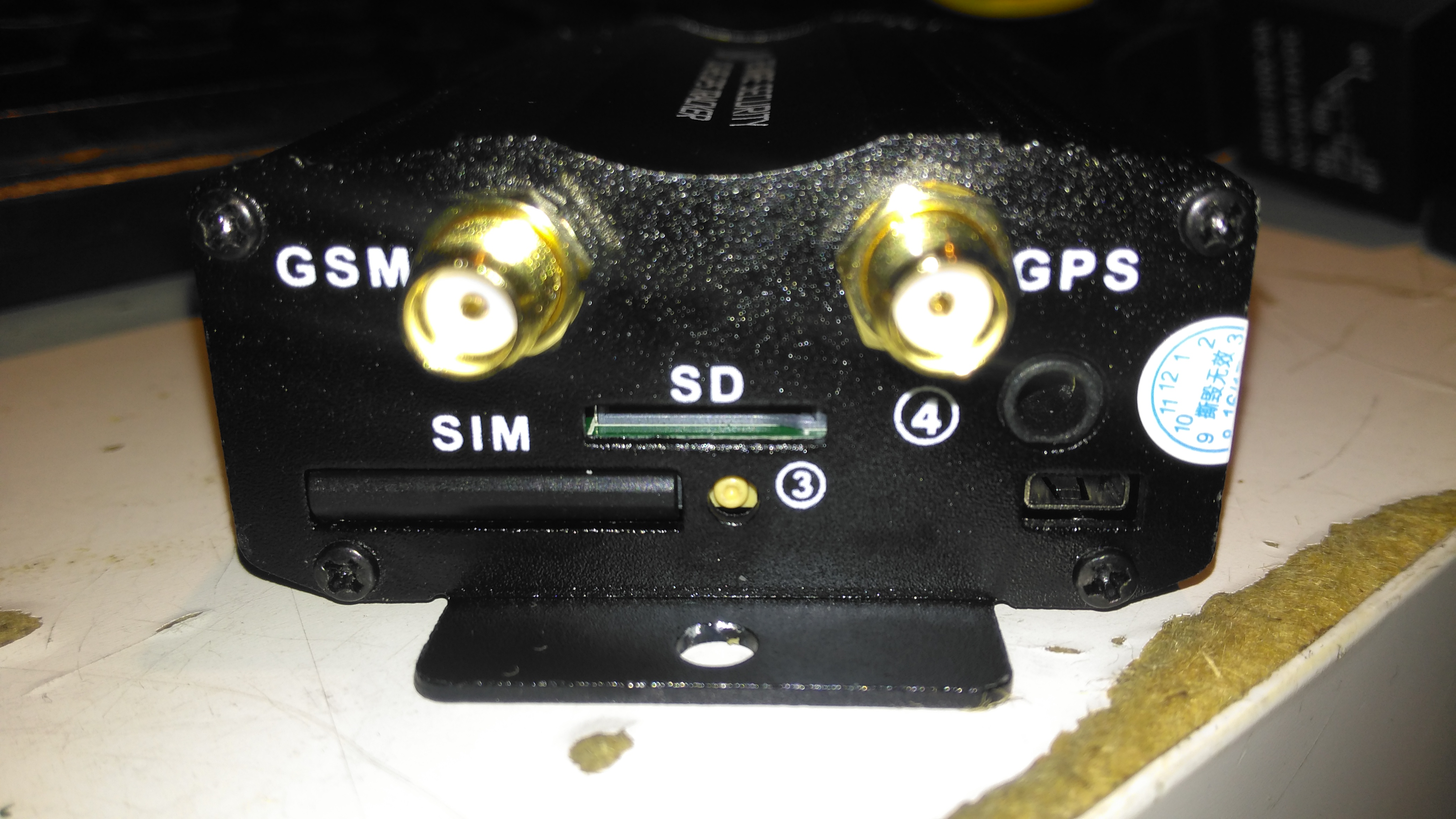
Antenna Connections
The other end has the antenna connections, microphone connection for the monitor function, along with the SIM & SD card slots.
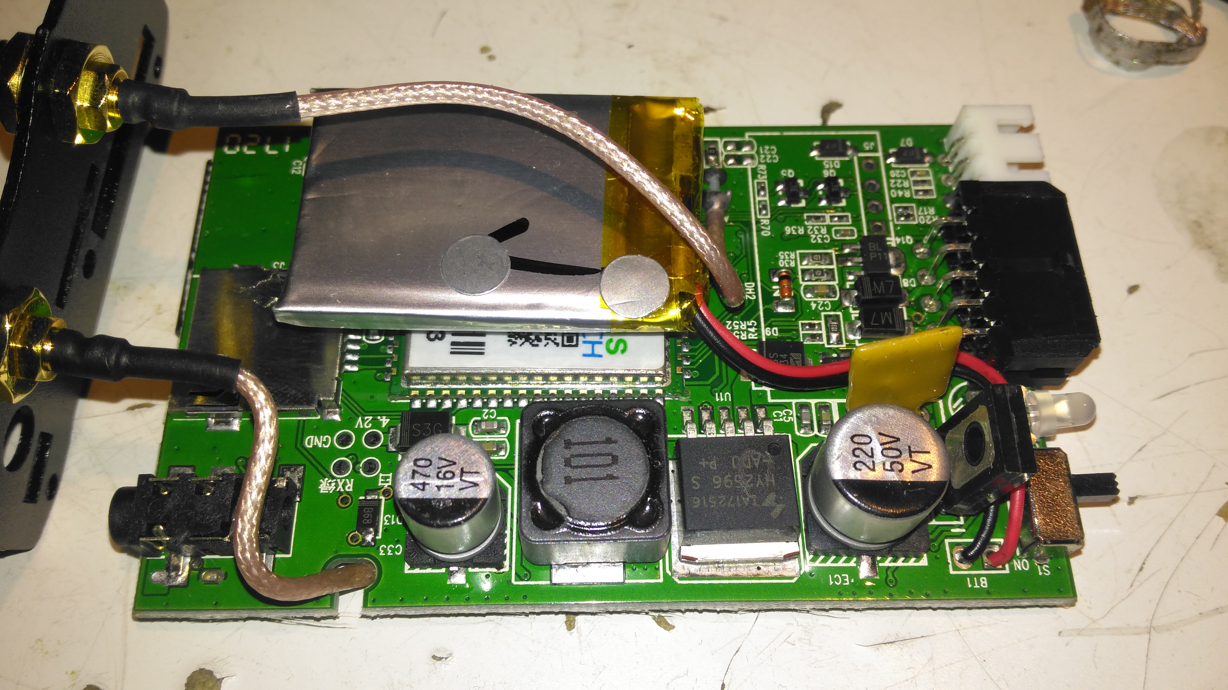
PCB Top
Once the end panel is removed, the PCB just slides out of the aluminium extruded casing. It’s pretty heavily packed with components in here. A switching regulator deals with the 12v input from the vehicle battery, and is protected by a polyfuse on the right. The GSM module is hiding under the Li-Po backup cell, unfortunately the sticky pad used to secure this wouldn’t come off without damaging something. The pigtails for both the GPS & GSM antennas are permanently soldered to the board here.
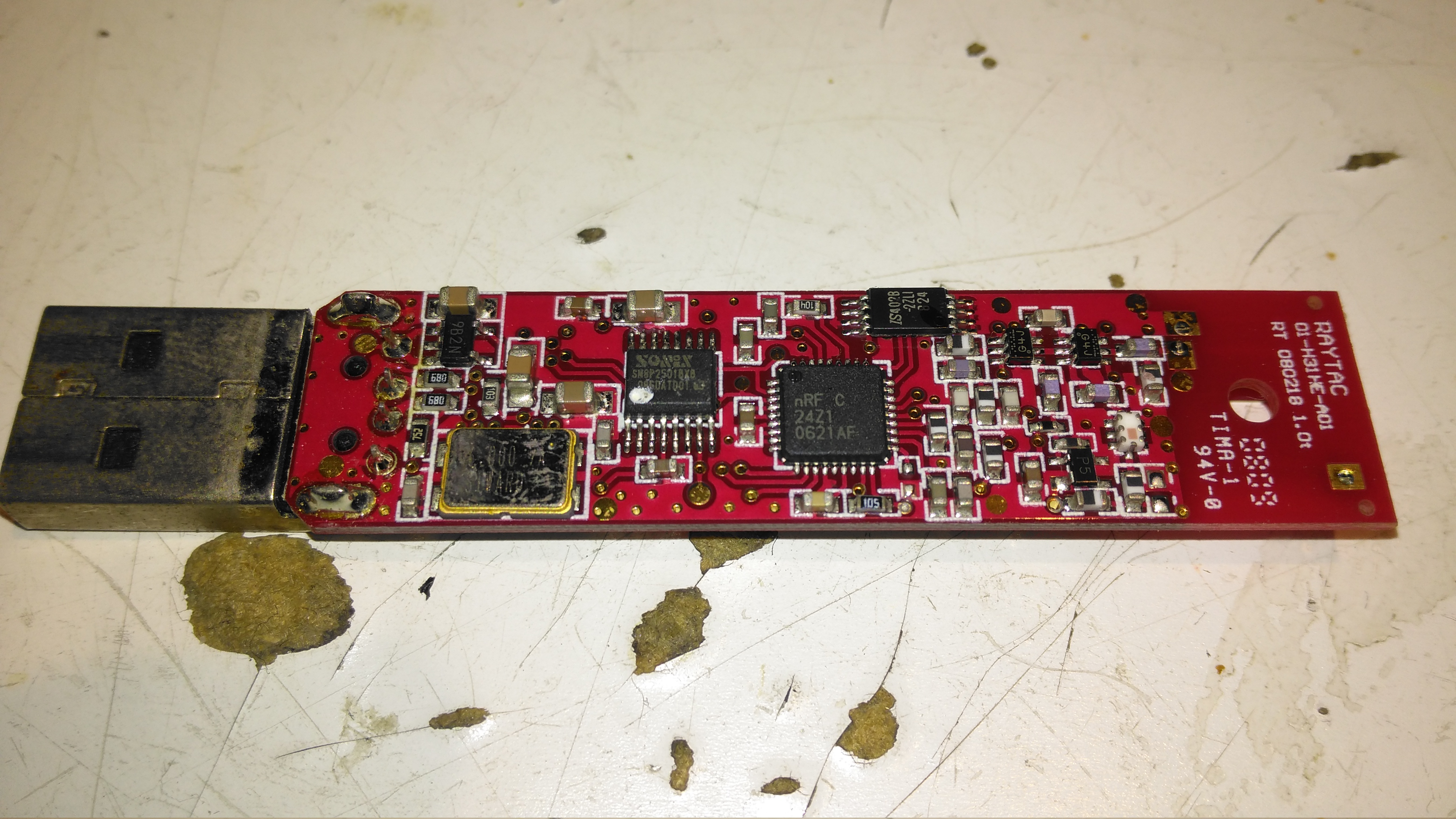
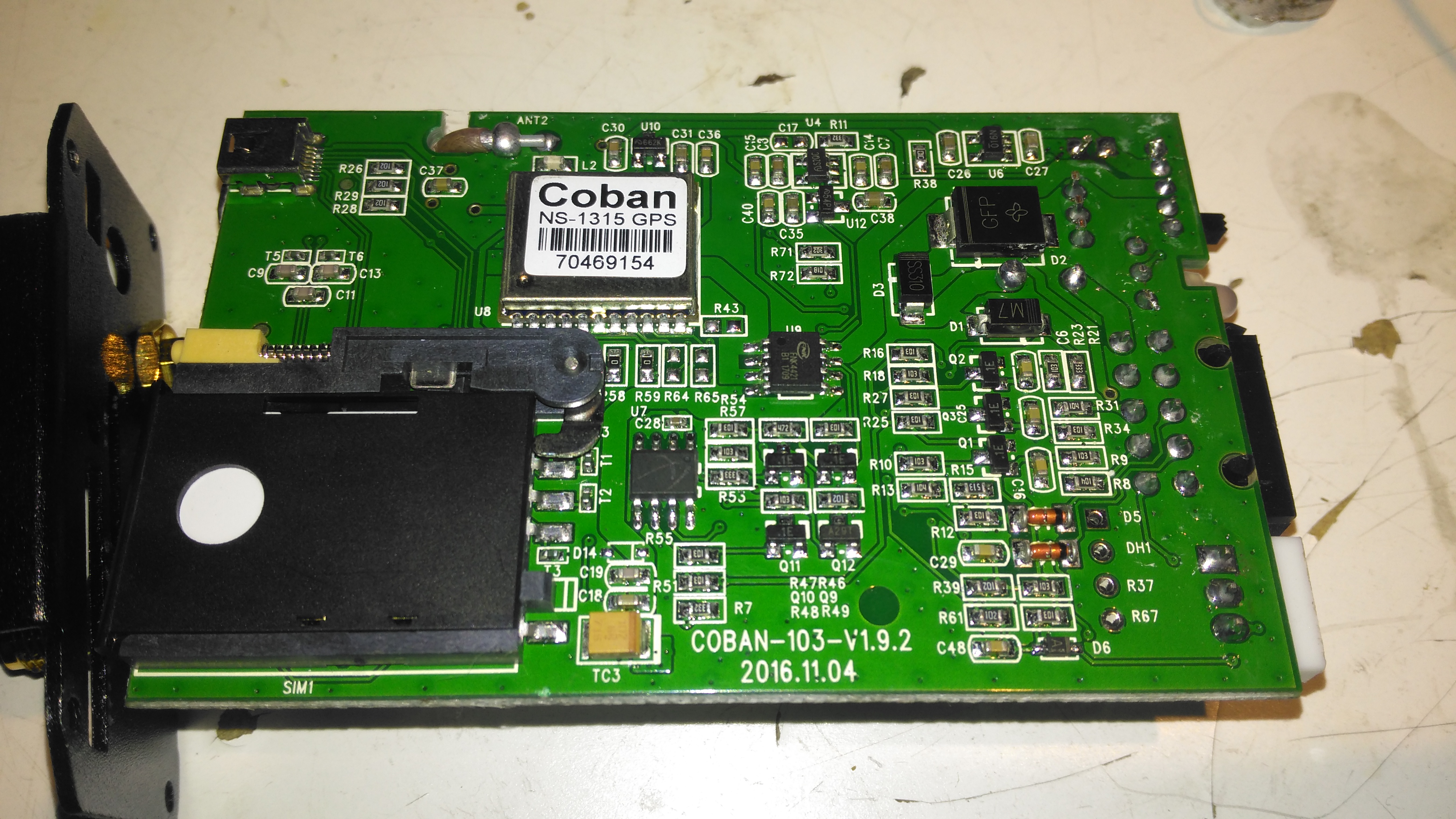
PCB Bottom
The bottom of the PCB has the GPS module, and mainly input protection & bypassing components. There is a FNK4421 Dual P-Channel MOSFET here as well, probably used for switching the external relay or alarm siren. The SIM socket for the GSM modem is located here in the corner.
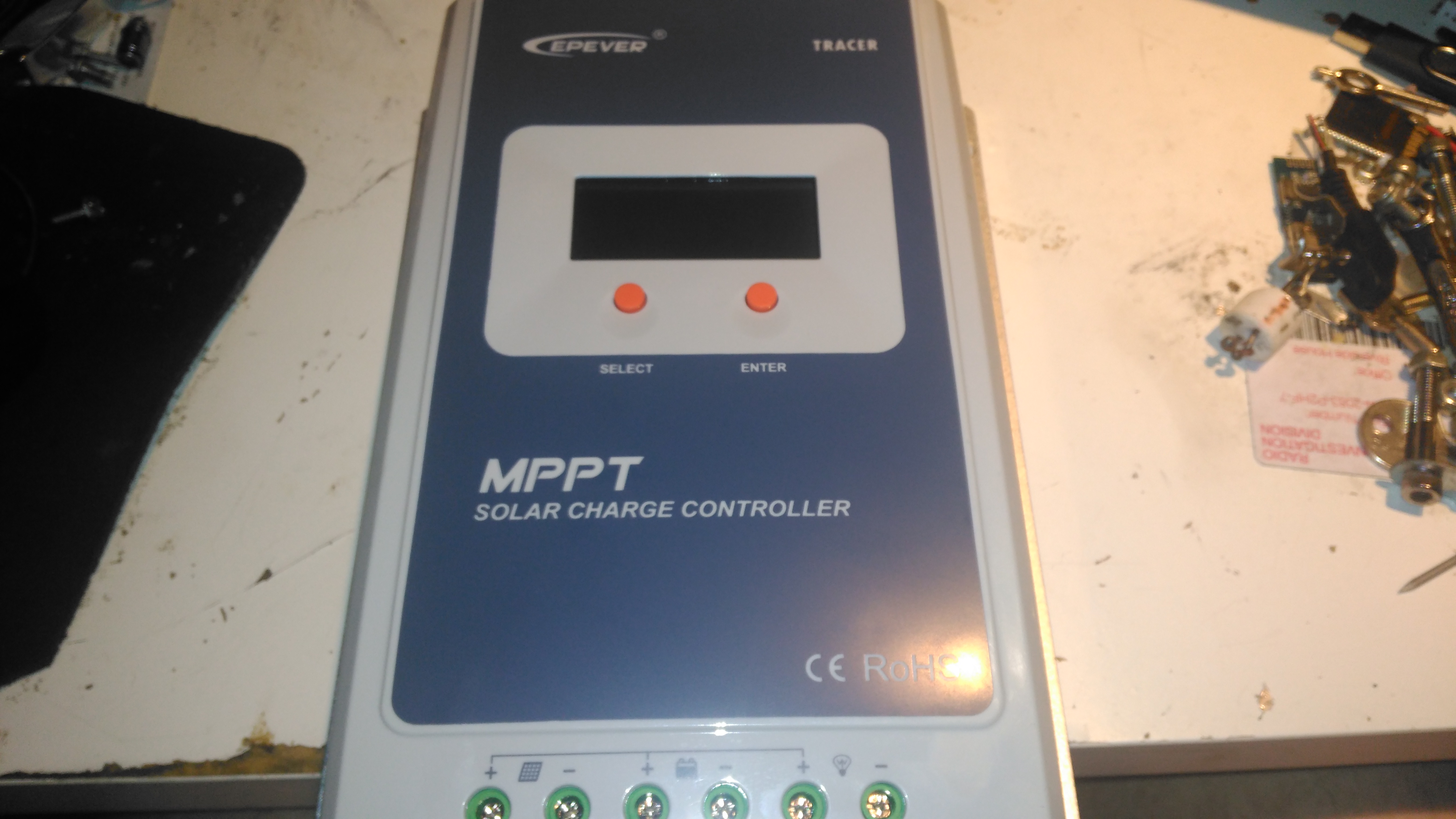
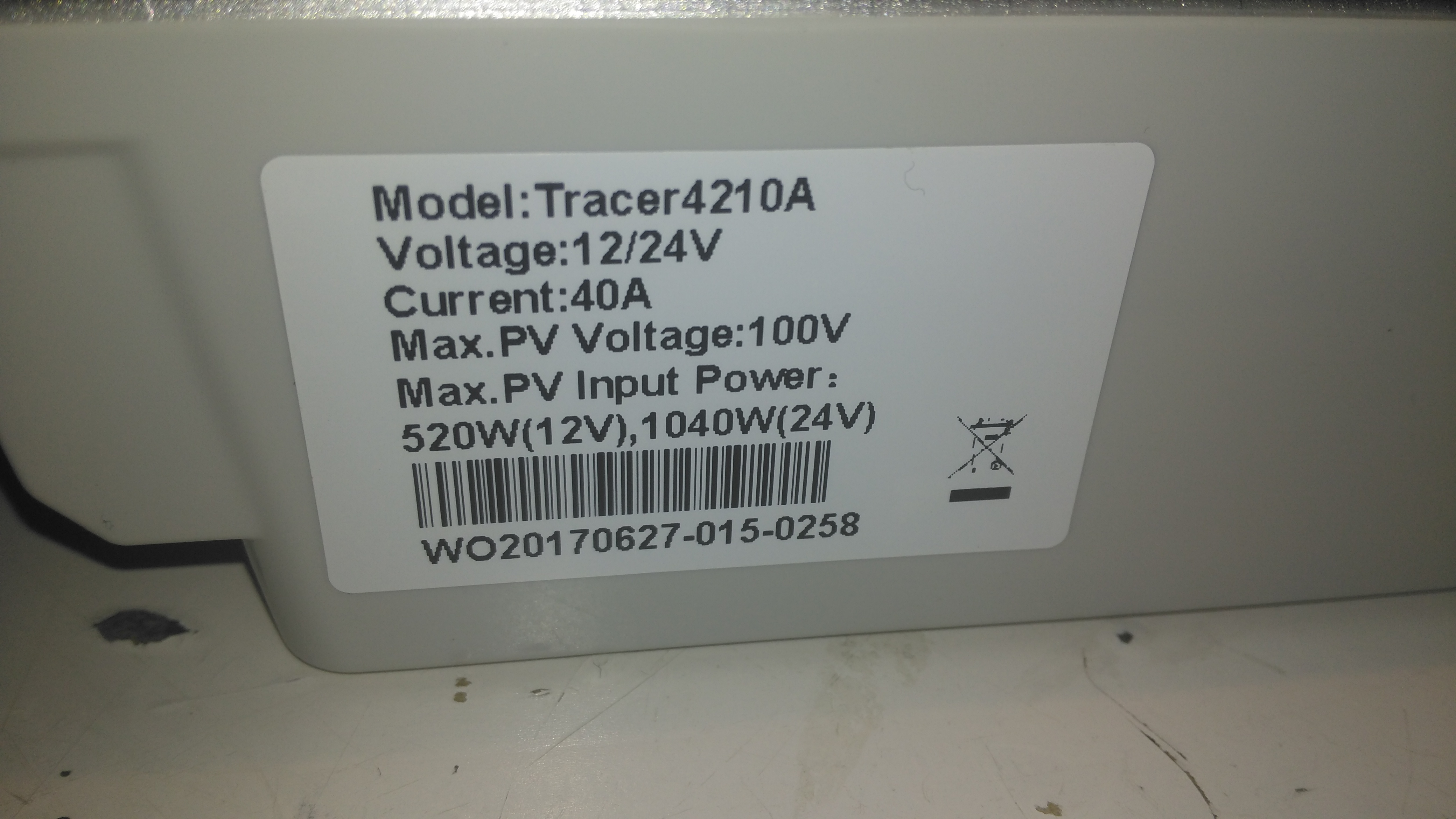
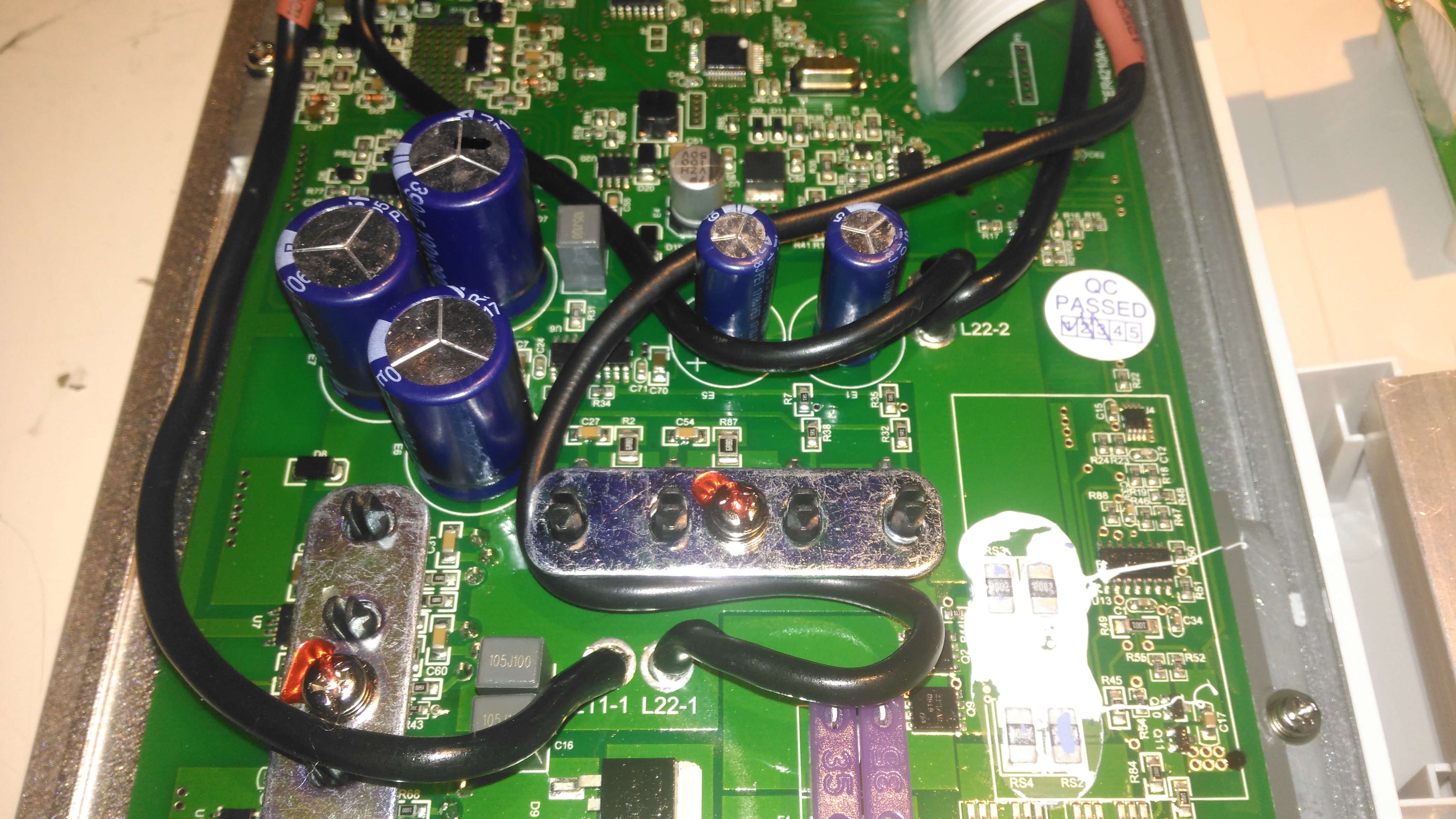
Here’s the solar charge controller to go with the MT50 from the last post. This is the 40A version of the EpEver Tracer A series, the 4210A. This unit is large, and very heavy. Most of this weight comes from the enormous heatsink which doubles as the mounting plate for all the other components, and the large inductors that are going to be required for the DC-DC conversion that MPPT requires.
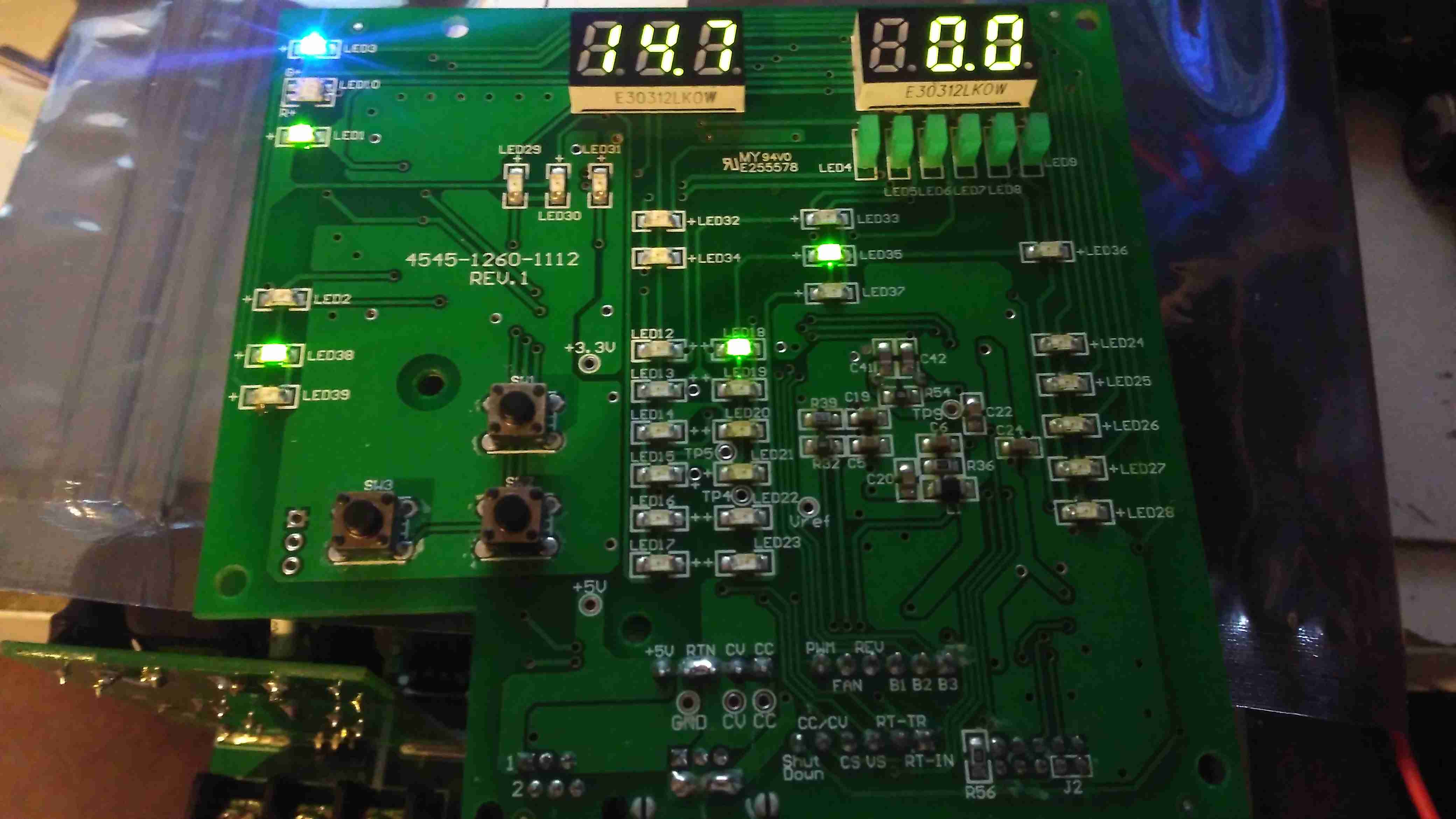
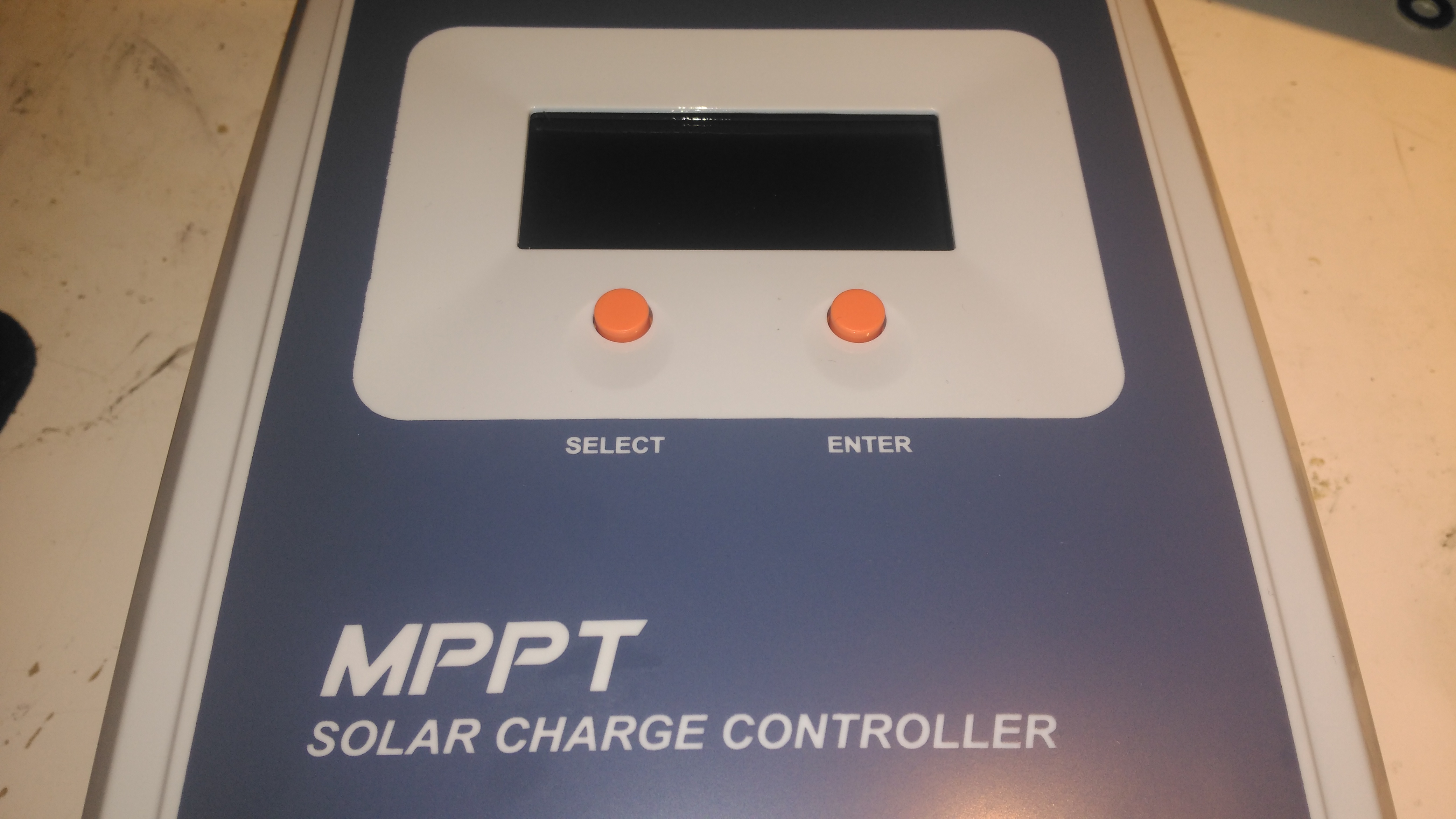
Front Panel
The front panel has a basic LCD, which shows various stats, such as PV Volts & Amps, and battery bank Volts & Amps. The pair of buttons are used to navigate the basic menu to configure some options, along with switching the load terminals ON/OFF.
Specifications
There’s a specs label on the top, with a slight difference here vs the manual, which states the max. PV volts as 92v.
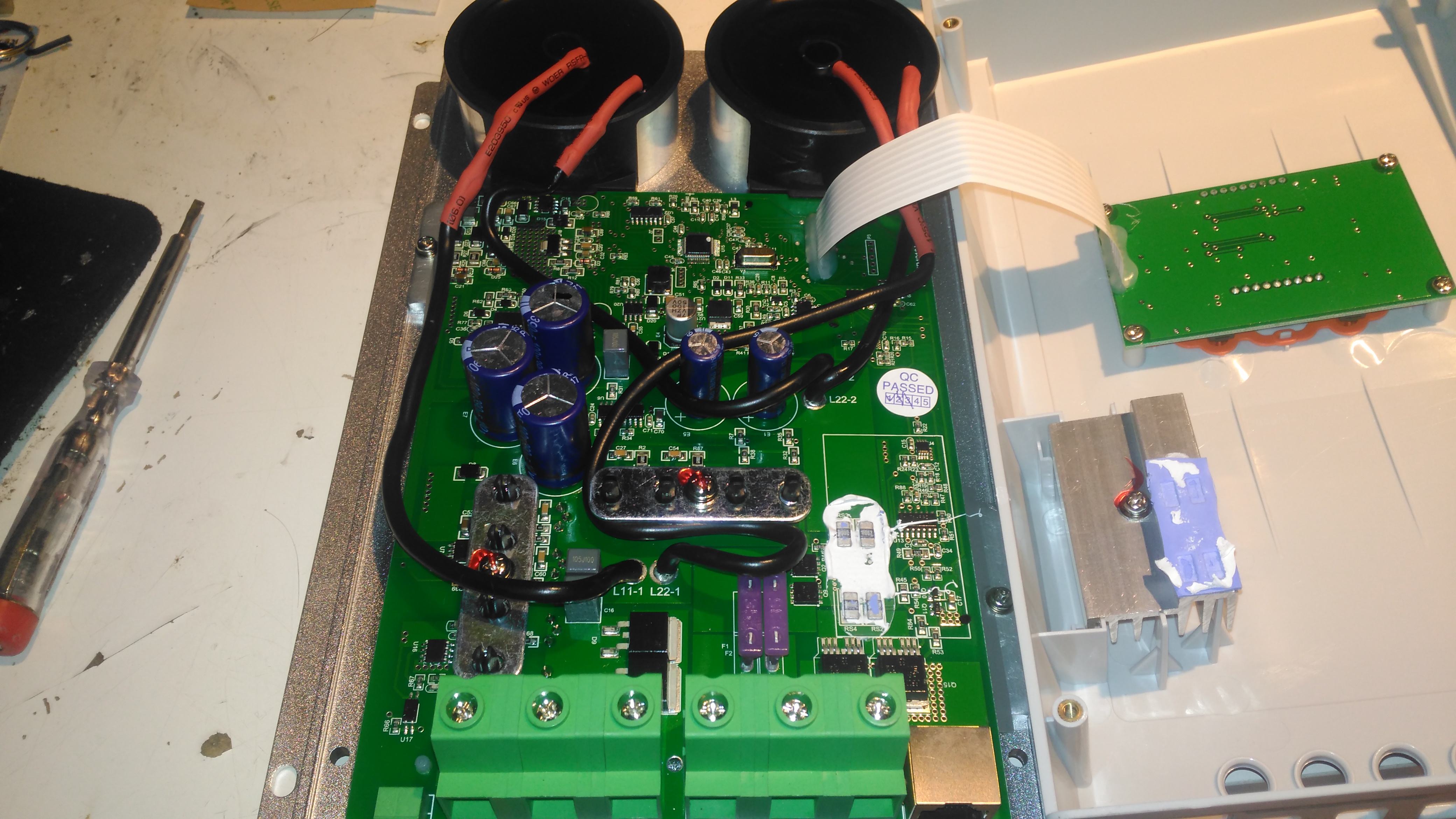
Main PCB Overview
Removing 4 machine screws from the bottom of the unit allows the top to come off. Like the MT50 remote panel, this unit also has moulded-in brass thread inserts in the plastic parts. The PCB in here is heavily comformal coated, which stops me from reading the laser-etched numbers on the semiconductor devices, so there will be few details there.
Main PCB Lower
Here’s the bottom section of the main PCB, with the enormous screw terminals, which will easily take cables up to about 16mm². The RJ-45 jack which hosts the unit’s RS-485 bus is to the right, and a smaller 2-pin connector on the left sorts out the battery temperature sensor.
The DC output MOSFET switches are hiding just behind the right-hand terminals, there’s a pair of them in this unit to handle the output current. Some beefy diodes polarity-protect both the battery & PV inputs.
Board Centre
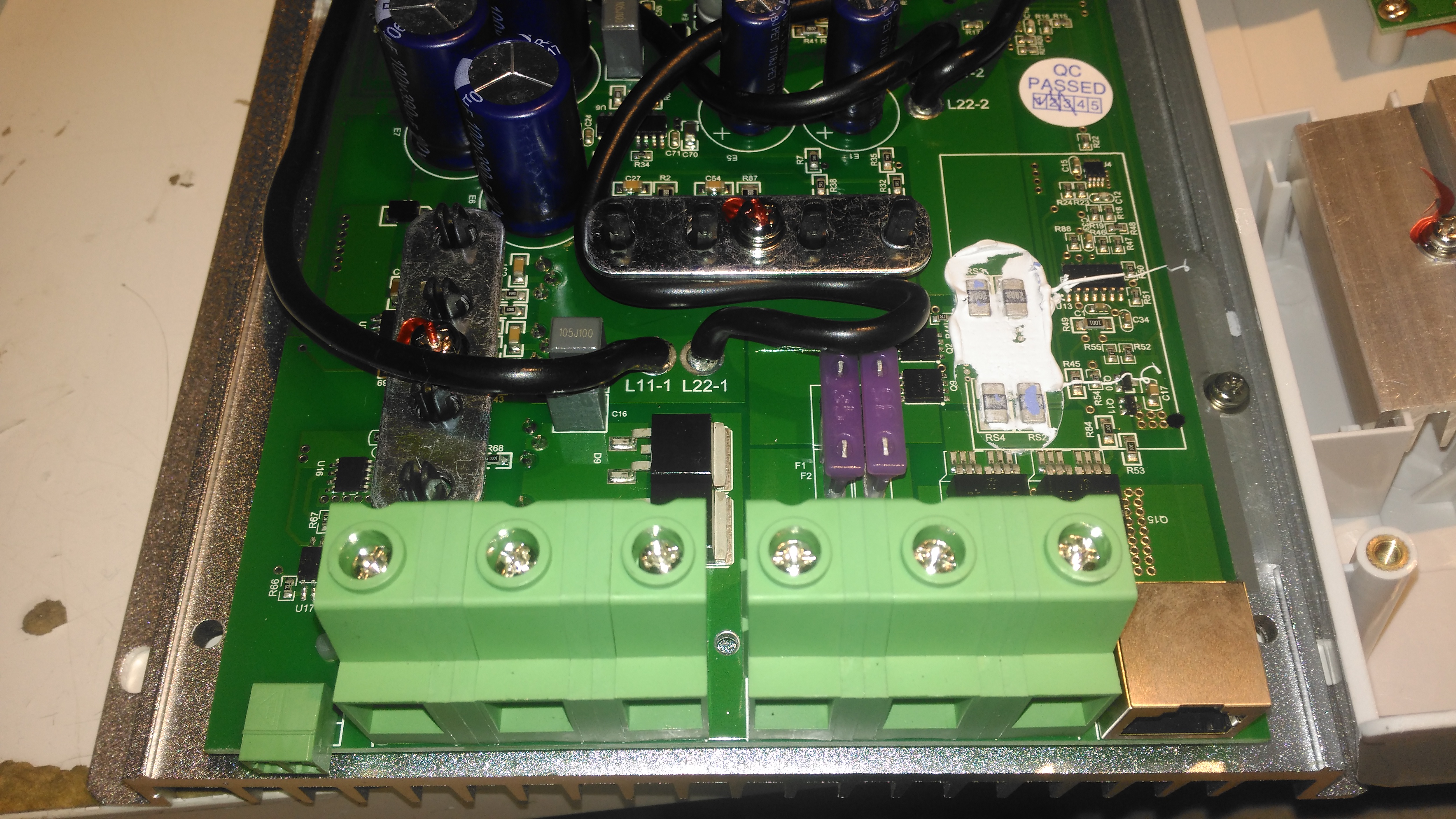
Moving up the board shows two 35A automotive blade fuses soldered into the board – these would be a real pain to replace if they ever blew, however with the electronic load current protection built into this unit, it’s an unlikely situation, unless something went hideously wrong. The main switching devices for the DC-DC converter are hidden – they’re clamped to the heatsink with the bars at right angles in the photo, I’m not going to dig any deeper into this just for those though – they’re just TO220 devices.
Under a load of thermal gunk on the right are 4 current shunt resistors, and the amplifiers for reading their values. These 1206-size SMD resistors looked a bit small for the power rating to me, but they’re heatsinked in operation to a small heatsink mounted in the top cover.
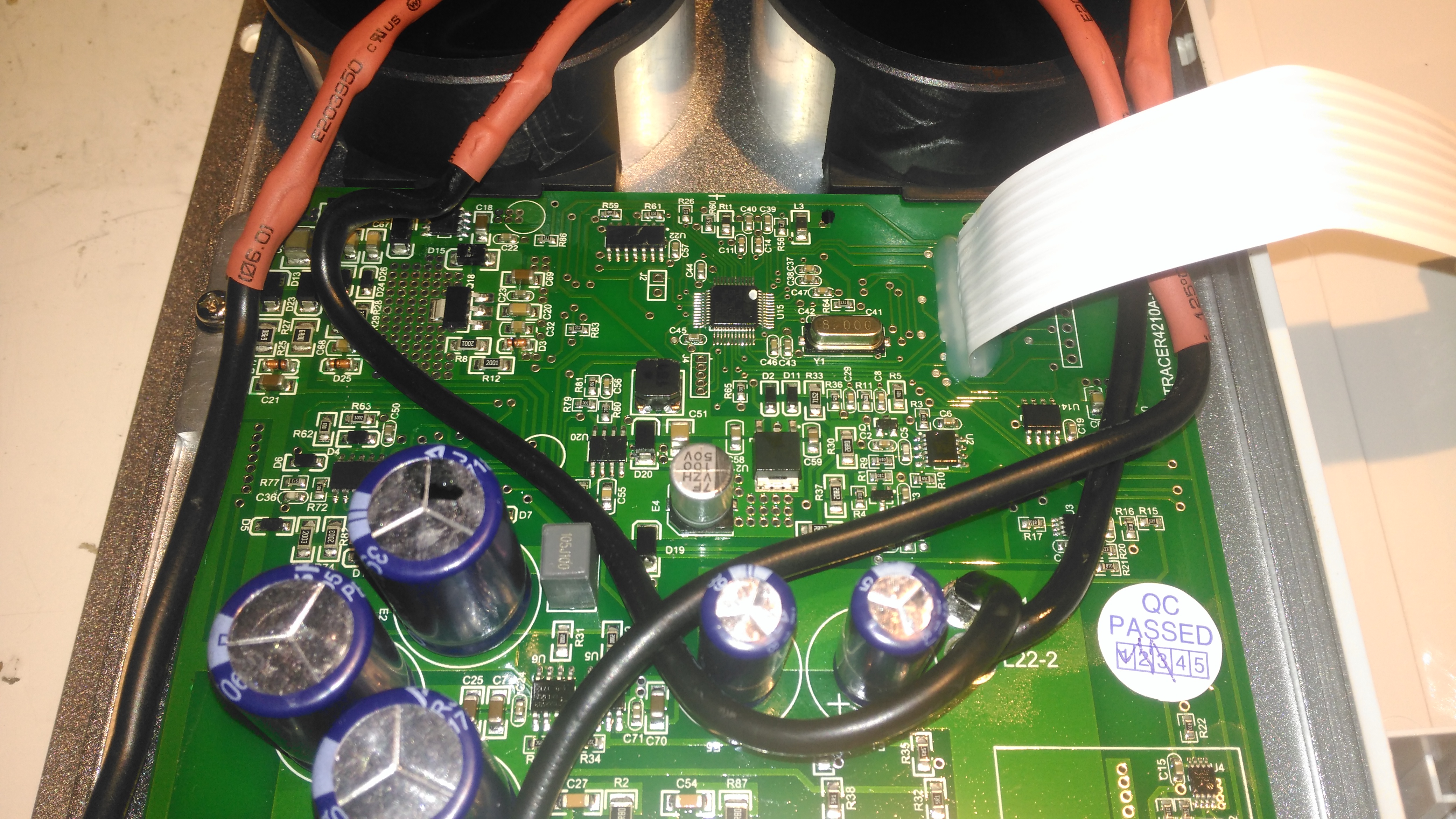
Board Upper
The upper section of the PCB hosts the main microcontroller, and the connections over to the front panel LCD & buttons. Couldn’t really get much info from these chips, due to the conformal coating.
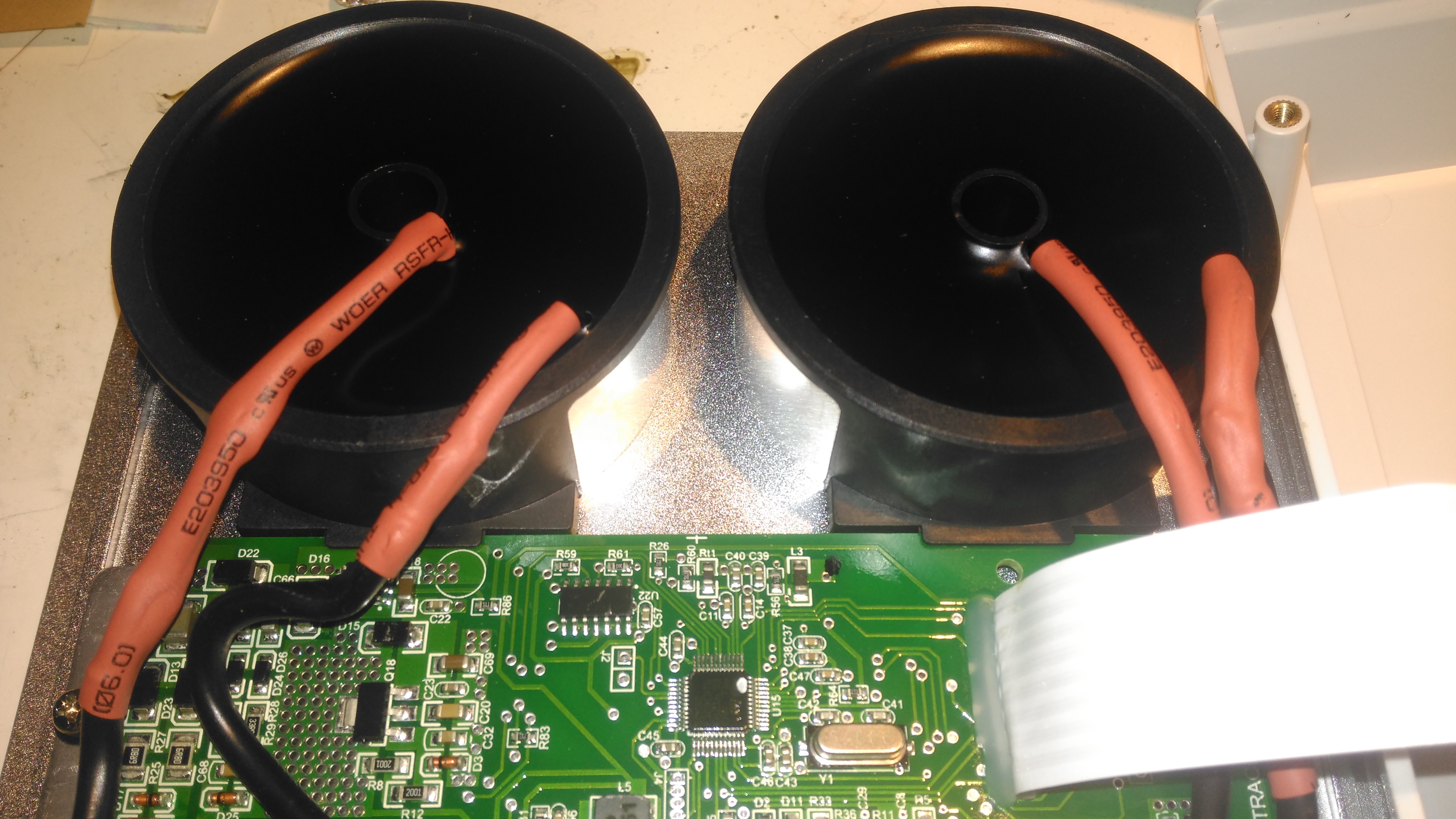
Toroidal Inductors
Right at the top of the unit are these toroidal inductors, potted into aluminium housings. The copper windings of these is very heavy – at least 2.5mm². They’re electrically in parallel, the 20A version would only have a single inductor.
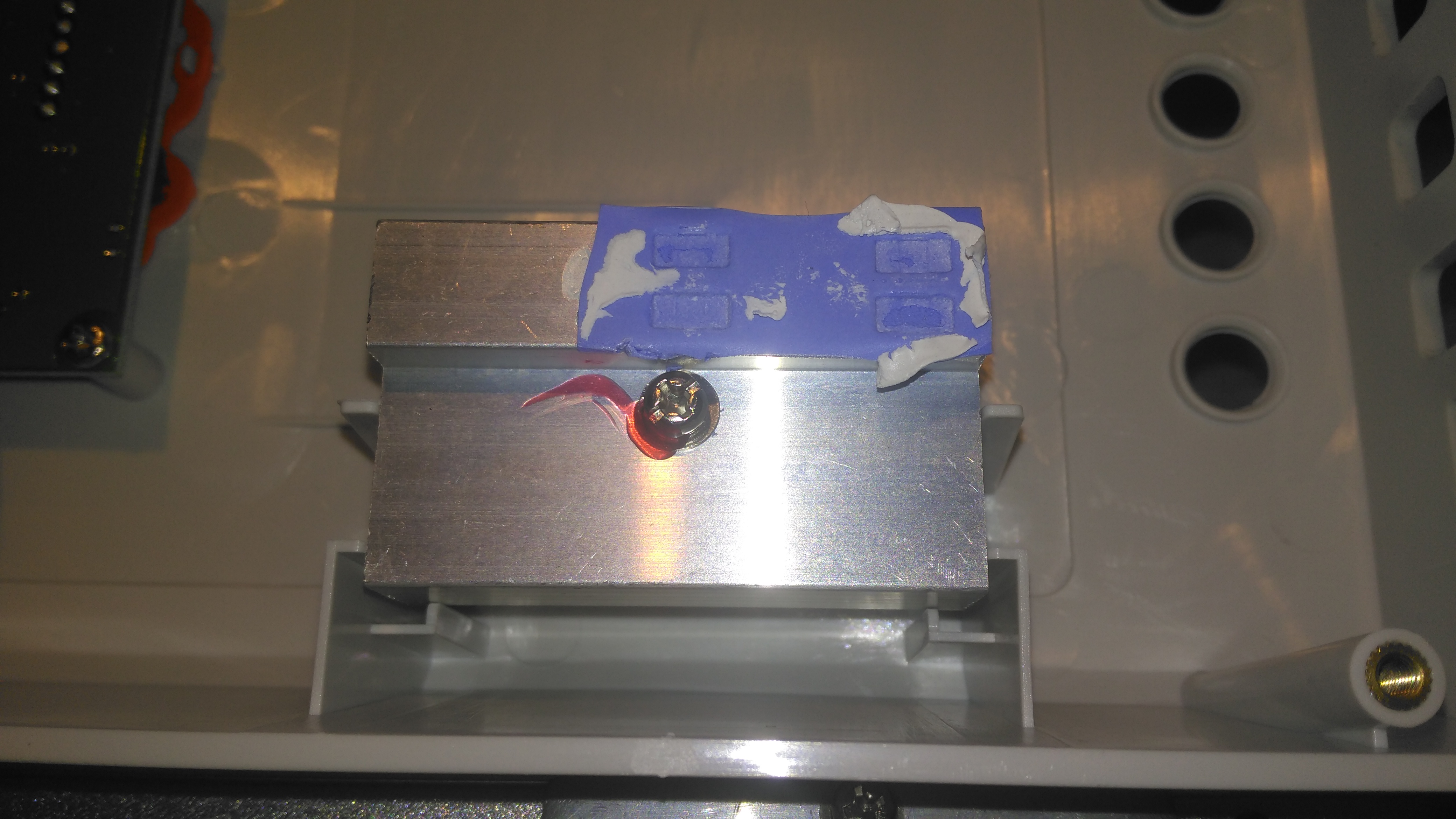
Current Shunt Heatsink
This small heatsink sits inside the top cover, and provides some cooling to the current shunts.
Display Board
Not much to say for the display board, there’s going to be nothing here apart from an I²C LCD driver & the pair of front panel buttons, so I won’t bother removing this from the case.
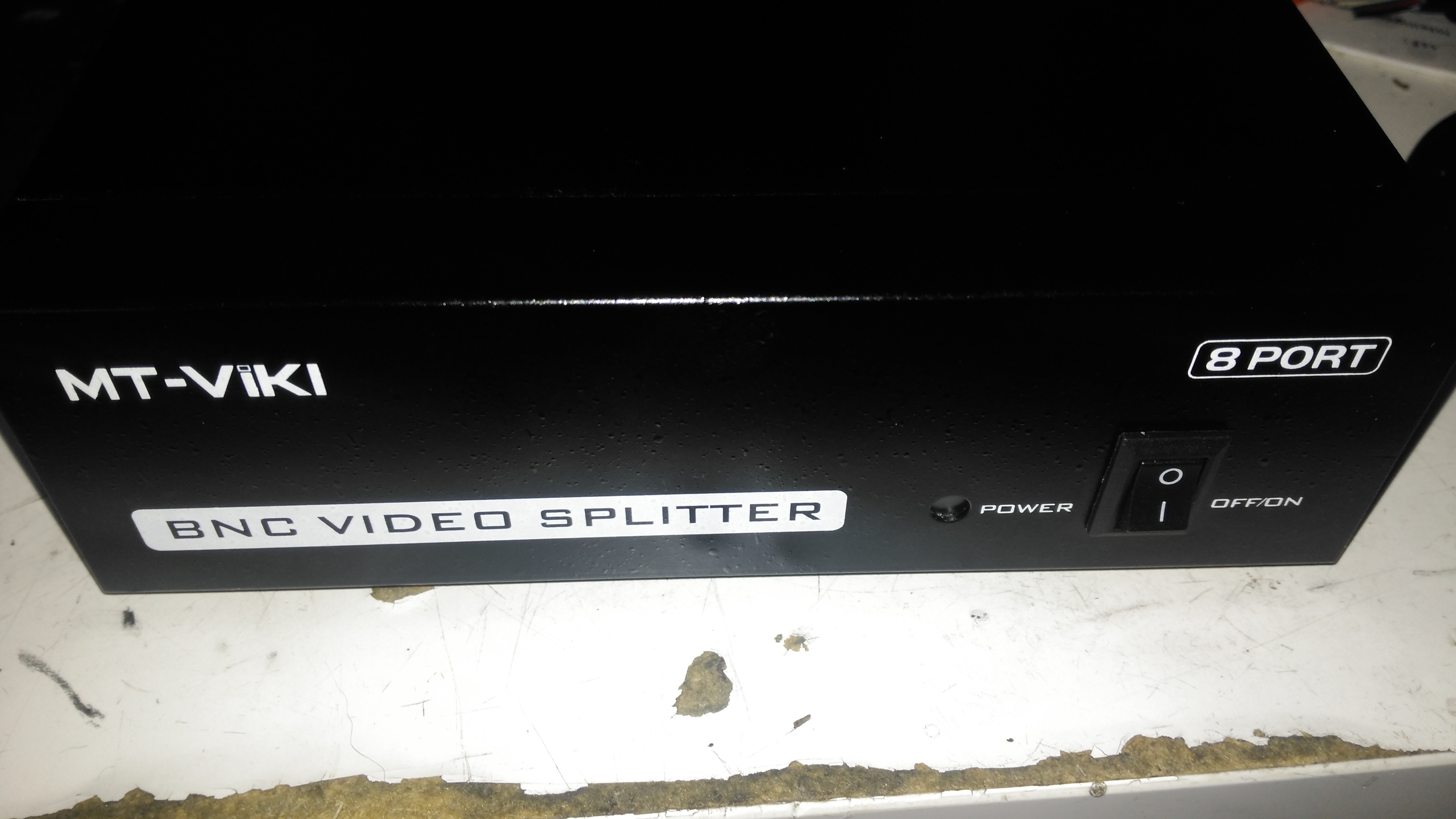
Time for another eBay special: this time it’s an 8-port video distribution amplifier, with BNC connections designed for commercial/industrial equipment. Not much on the front panel above, apart from the power switch & LED.
Rear Panel
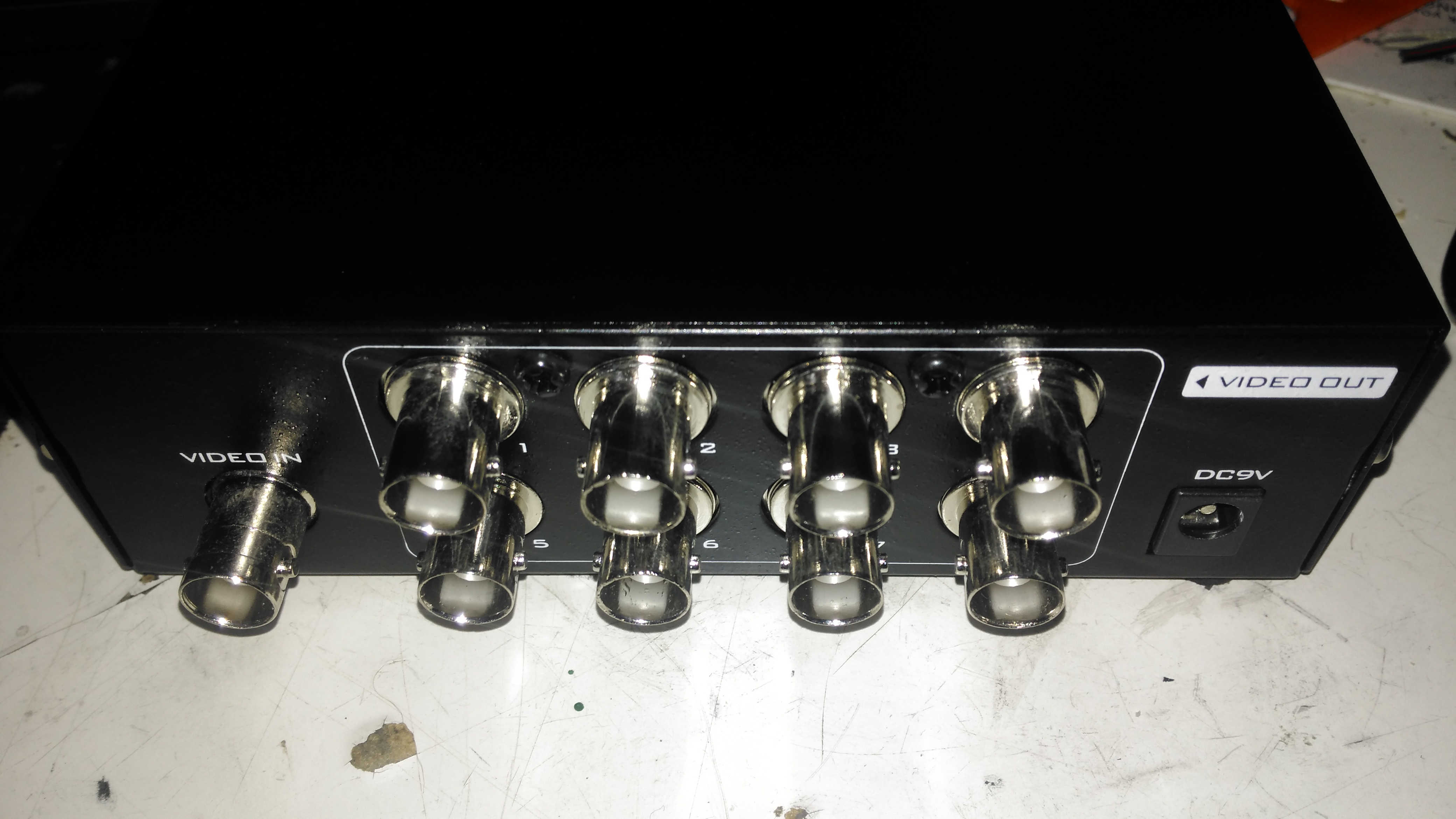
The rear panel has all the connectors, input is on the left, while the outputs are in the centre. Power is supplied through the barrel jack on the right, 9v DC in this case.
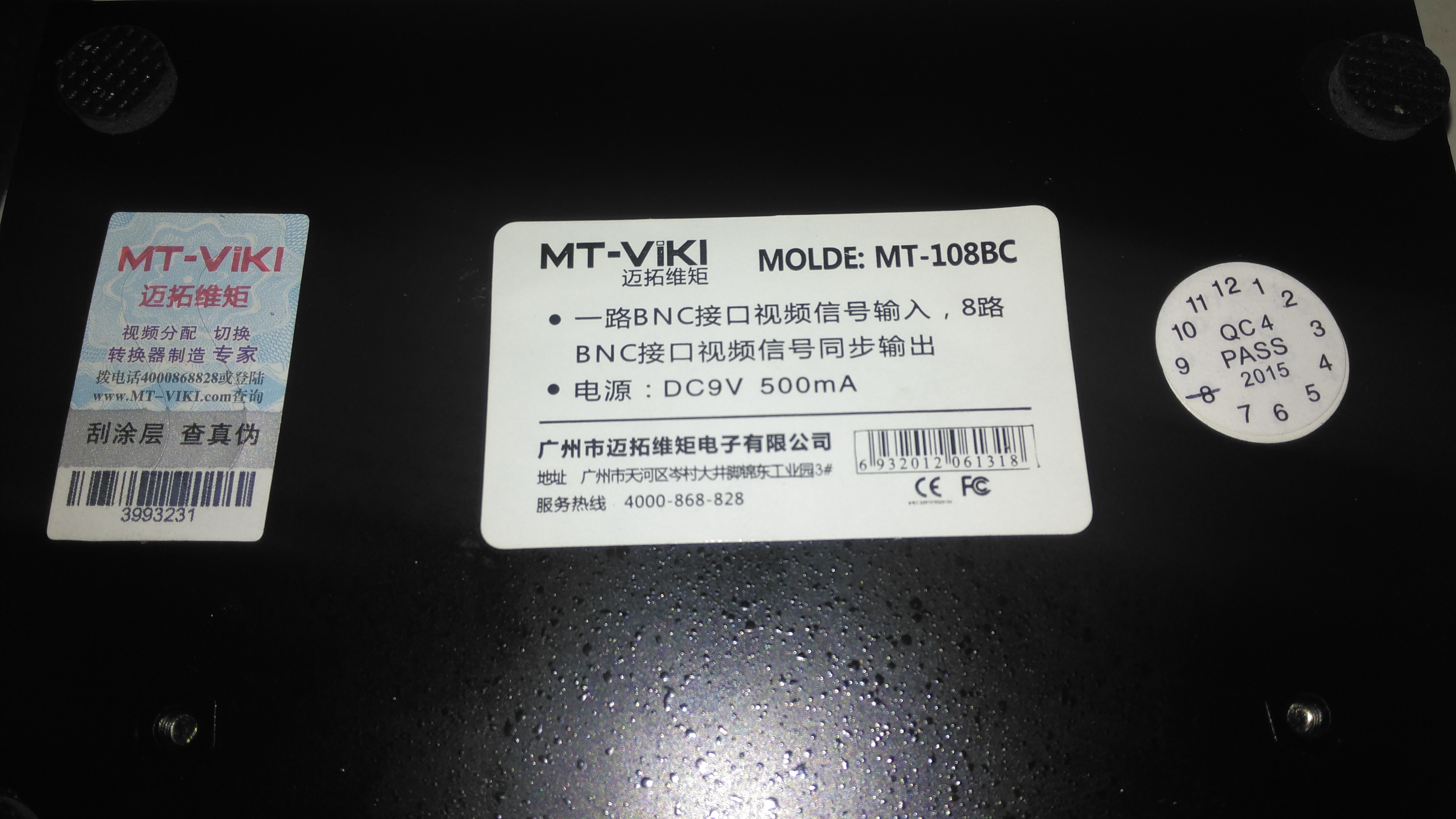
Data Label
Not much in English on the data labels, there’s also an authenticity label on the left to make sure you don’t get a fake.
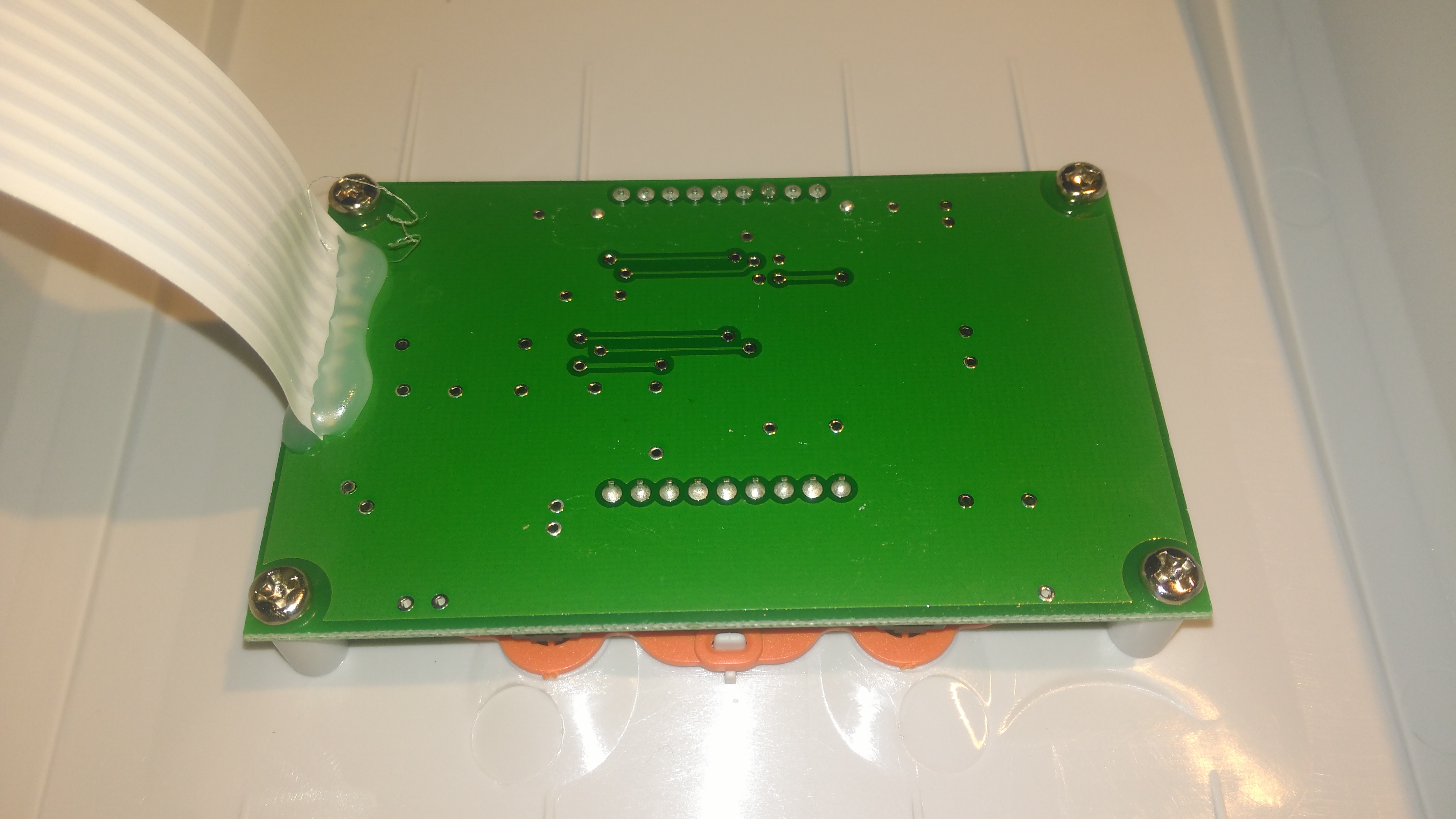
Amplifier Board
Taking the lid off reveals a very small PCB, taking up less than a third of the aluminium case! The input stage is on the right, composed of a pair of SOT-23 transistors to buffer the incoming signal. There’s an KST812M6 PNP & an S9014 NPN Epitaxial. The signal is then fed to the output stages, all individual S9014 NPN transistors to the output ports.
The power LED is just poking in the general direction of the hole in the front panel, so this isn’t likely to work very well – it’s going to illuminate the inside of the case more!
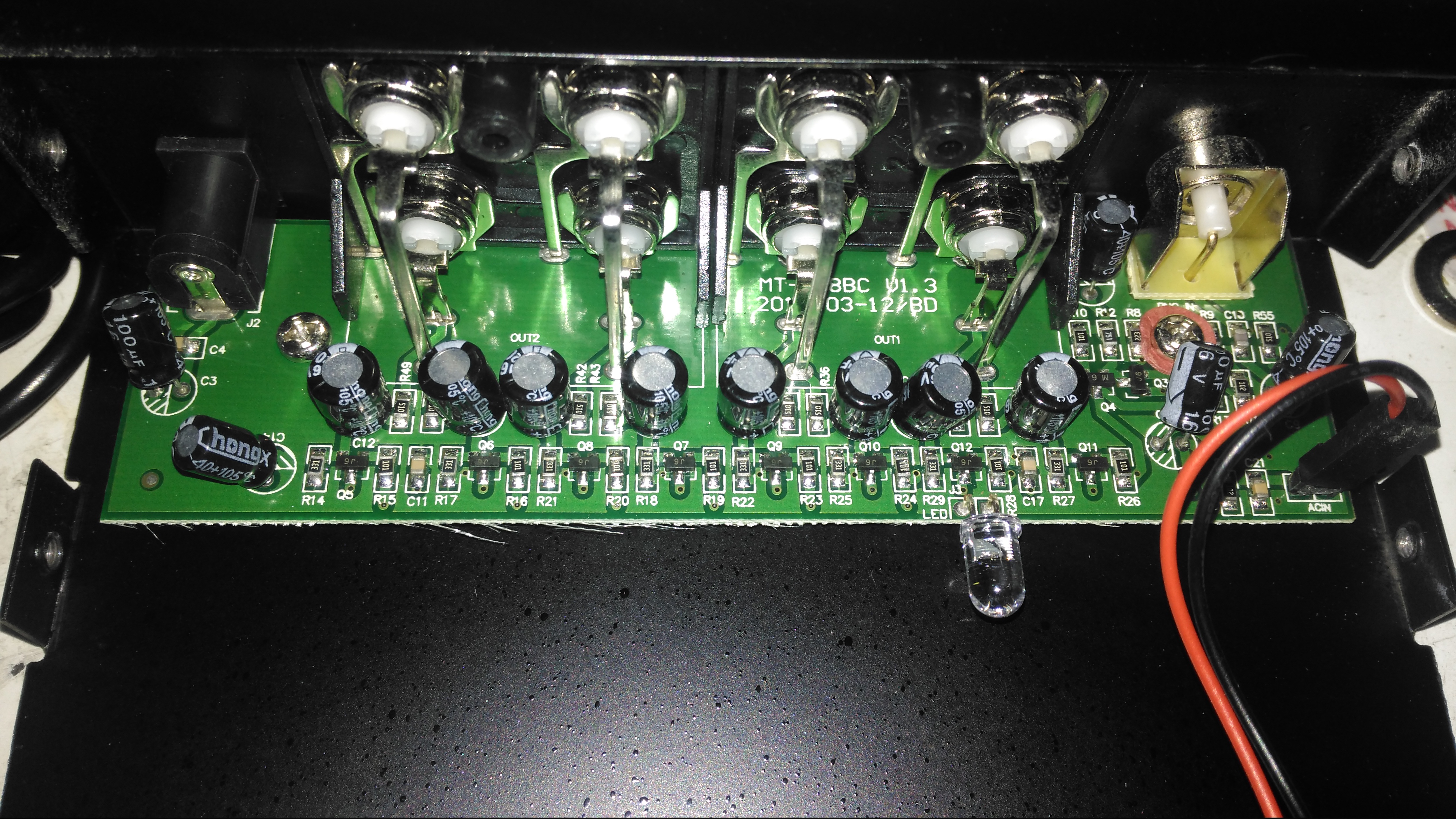
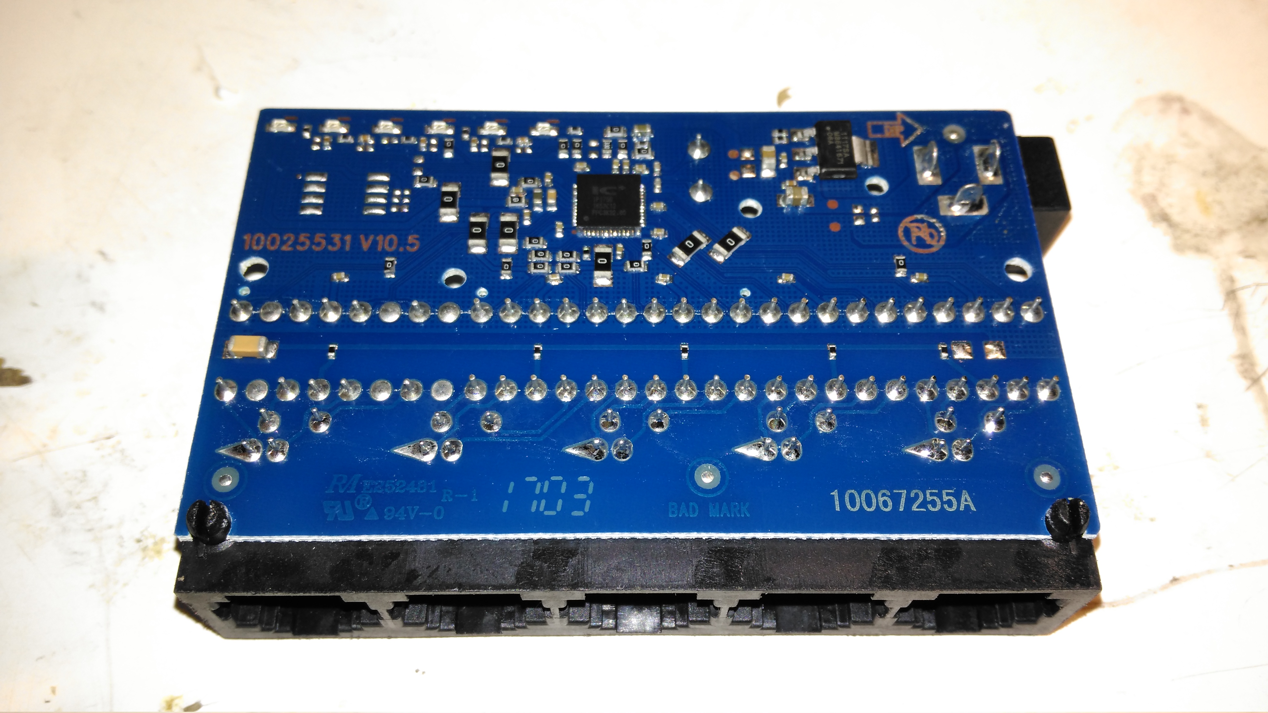
Here’s a tiny ethernet switch from the great fle market that is eBay – the Tenda S105. This unit has 5 ports, but only supports 10/100M. Still, for something so small it’s not bad.
Bottom
Not much on the bottom, there’s a pair of screw hooks for mounting this to a surface.
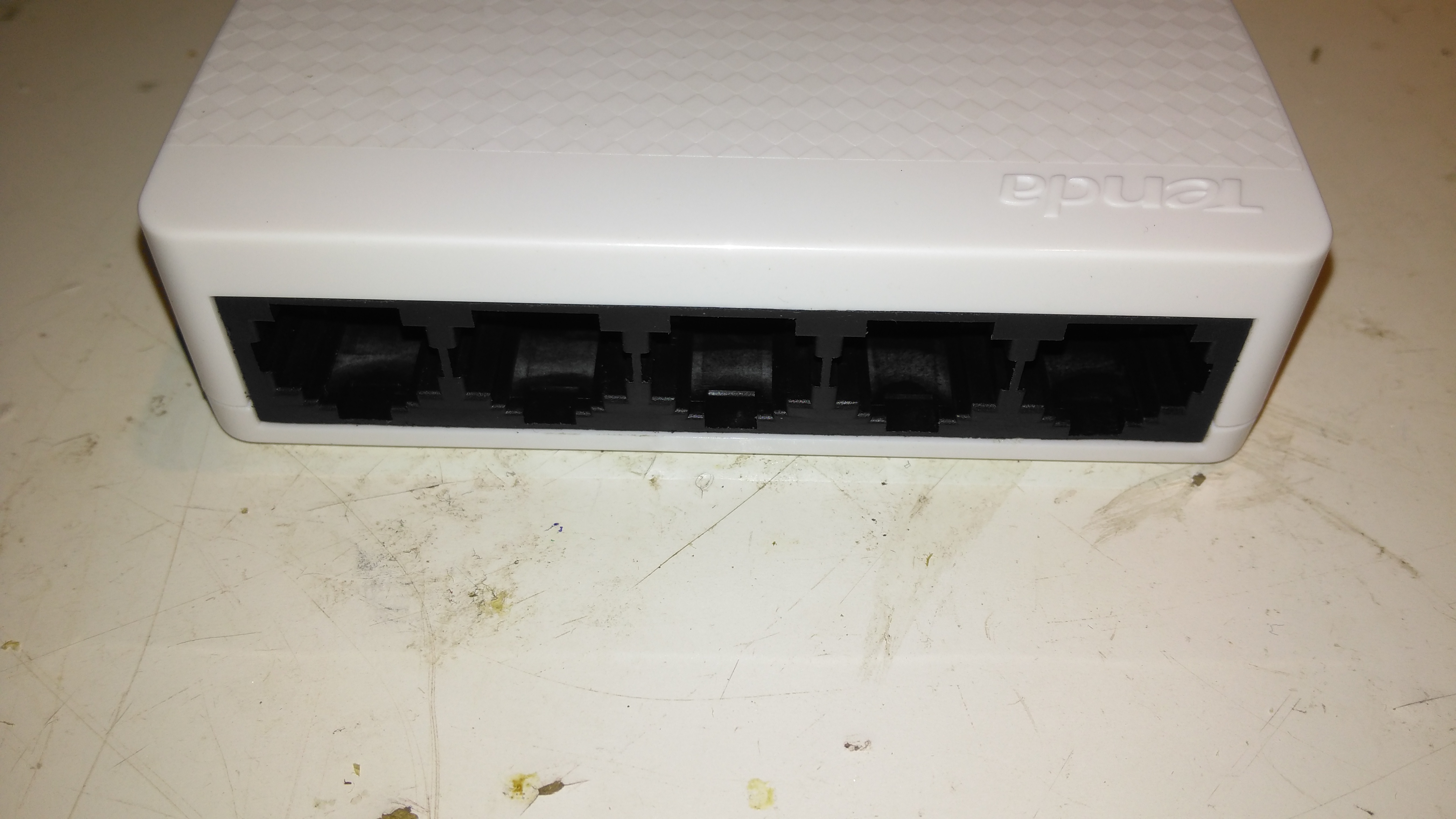
Ports
The 5 ports on the front actually have the pins for the unused pairs of the ethernet cables removed – saving every penny here.
PCB Top
The casing just unclips, revealing the small PCB. Nothing much on the top, just the connectors, isolating transformers & the crystal for the switch IC.
PCB Bottom
The bottom of the PCB is a little more busy, mainly with decoupling components. There’s a 3.3v linear regulator to step down the 5v input for the switch IC.
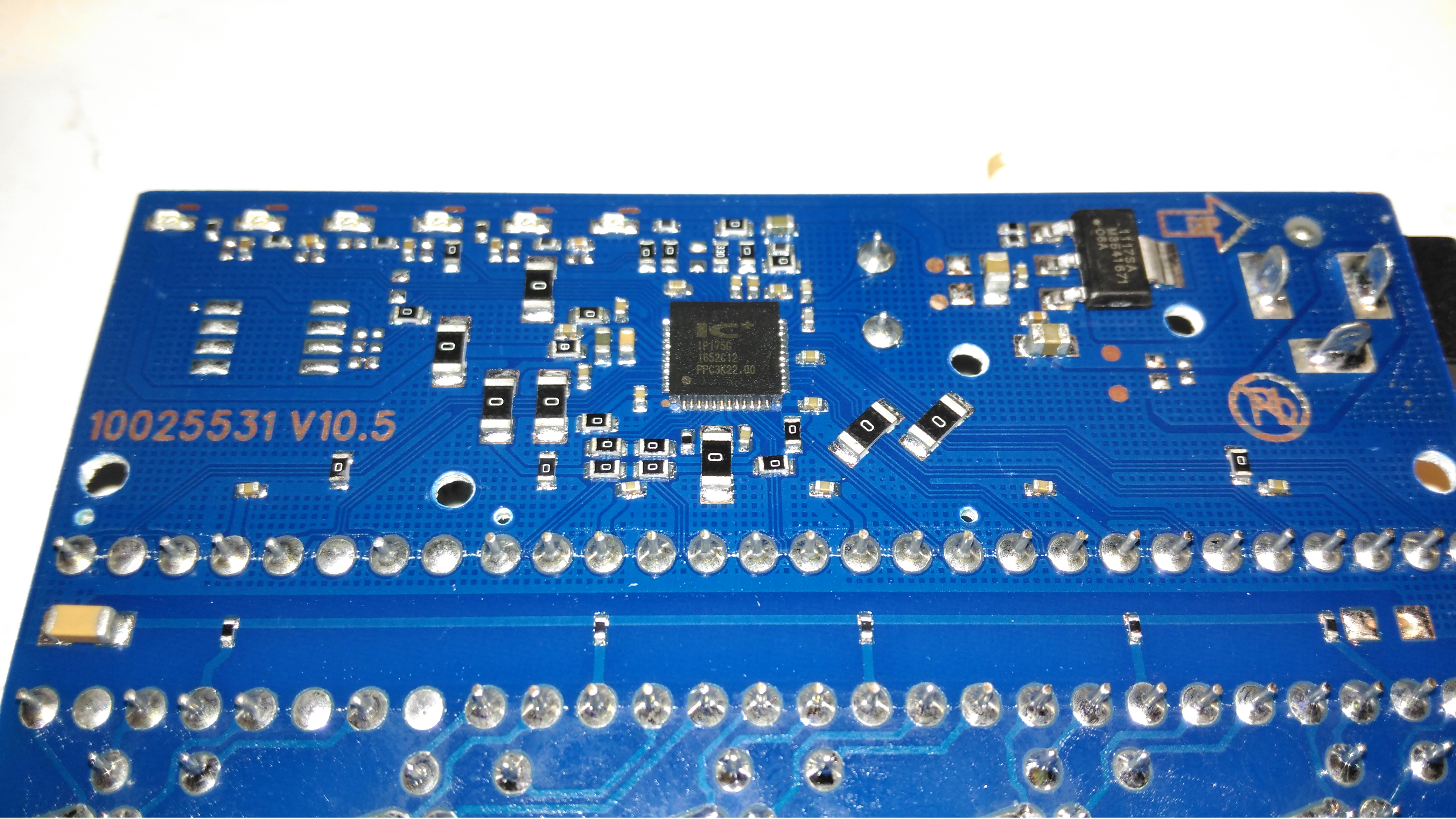
Switch IC
The IC doing all the data switching is an IP175G 5-Port 10/100 Switch from IC+ Corp. No datasheet available for this, but it’s going to be a bog-standard switch.
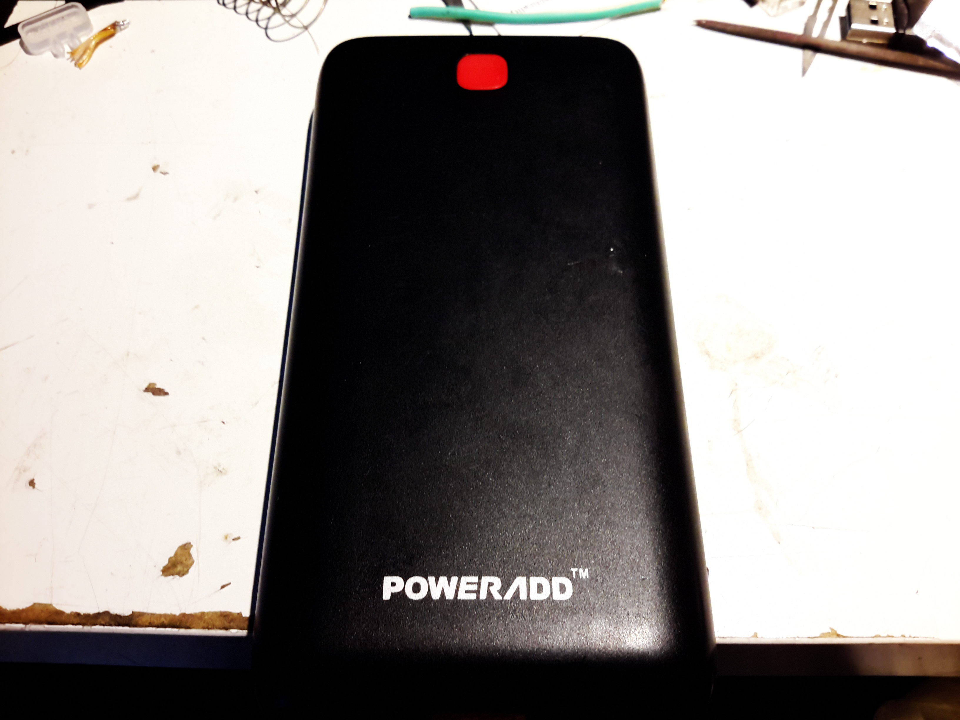
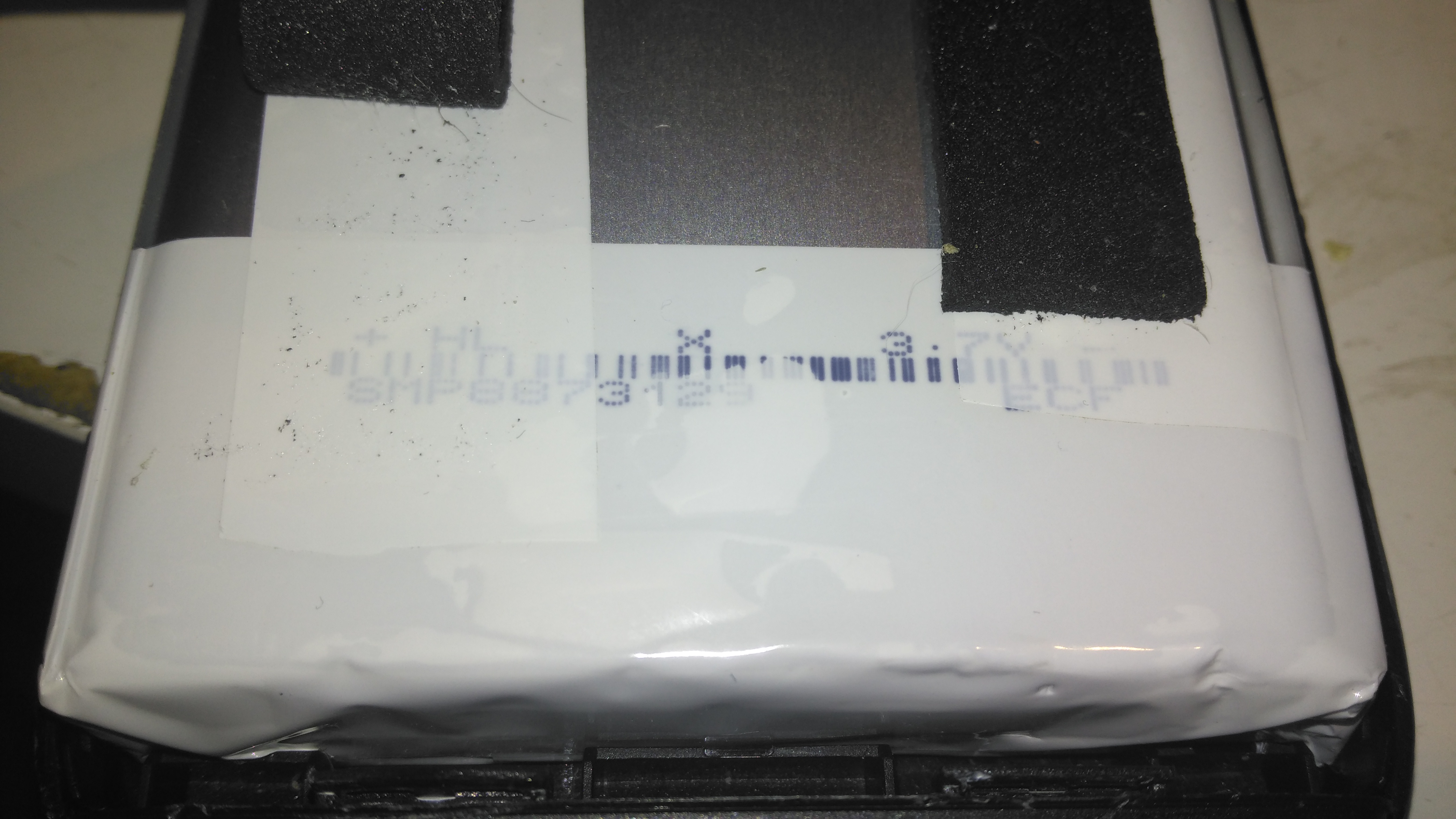
Here’s the biggest portable USB powerbank I’ve seen yet – the PowerAdd Pilot X7, this comes with a 20Ah (20,000mAh) capacity. This pack is pretty heavy, but this isn’t surprising considering the capacity.
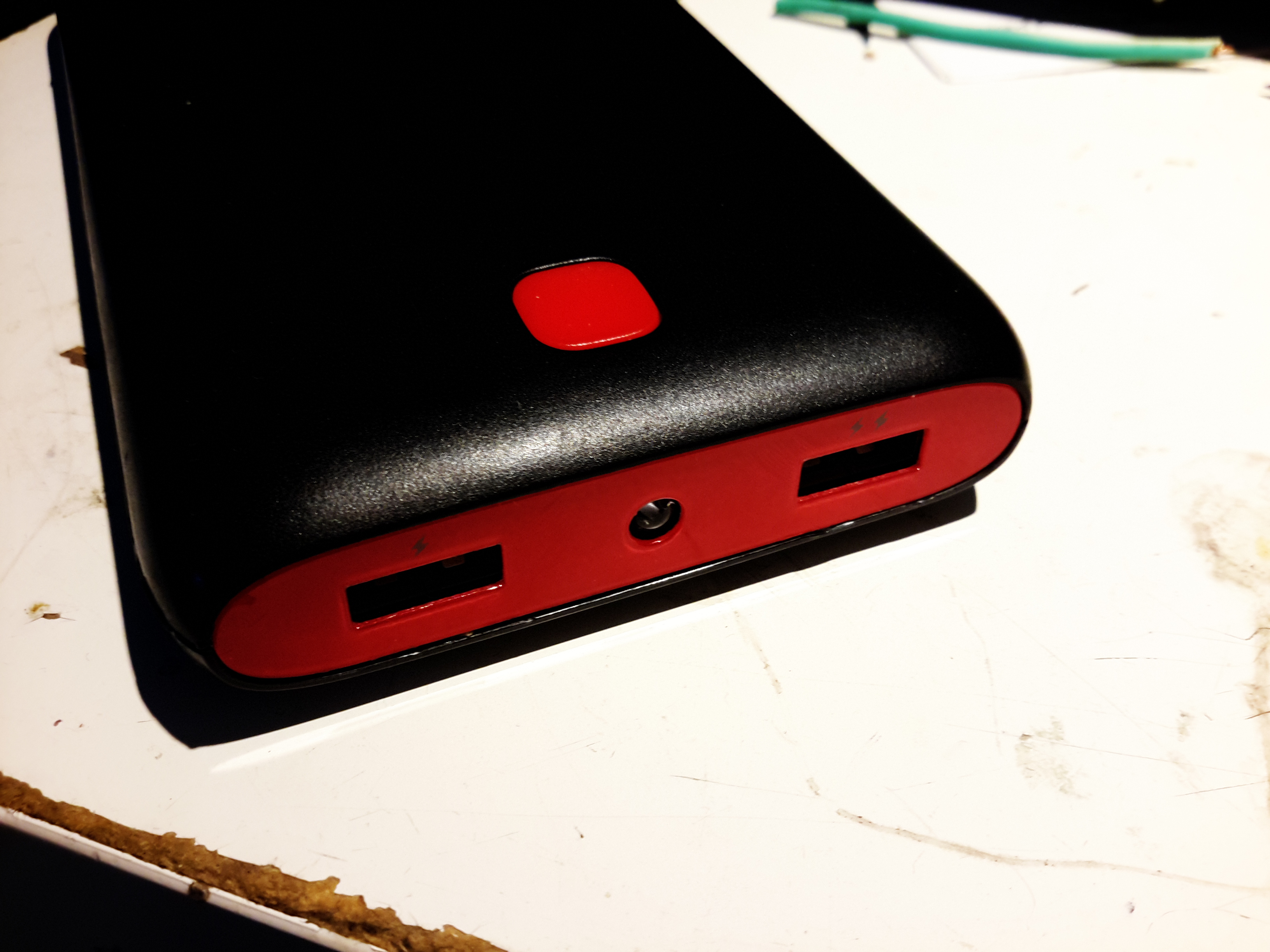
USB Ports & LED
The front of the pack houses the usual USB ports, in this case rated at 3.4A total between the ports. There’s a white LED in the centre as a small torch, activated by double-clicking the button. A single click of the button lights up the 4 blue LEDs under the housing that indicate remaining battery capacity. Factory charging is via a standard µUSB connector in the side, at a maximum of 2A.
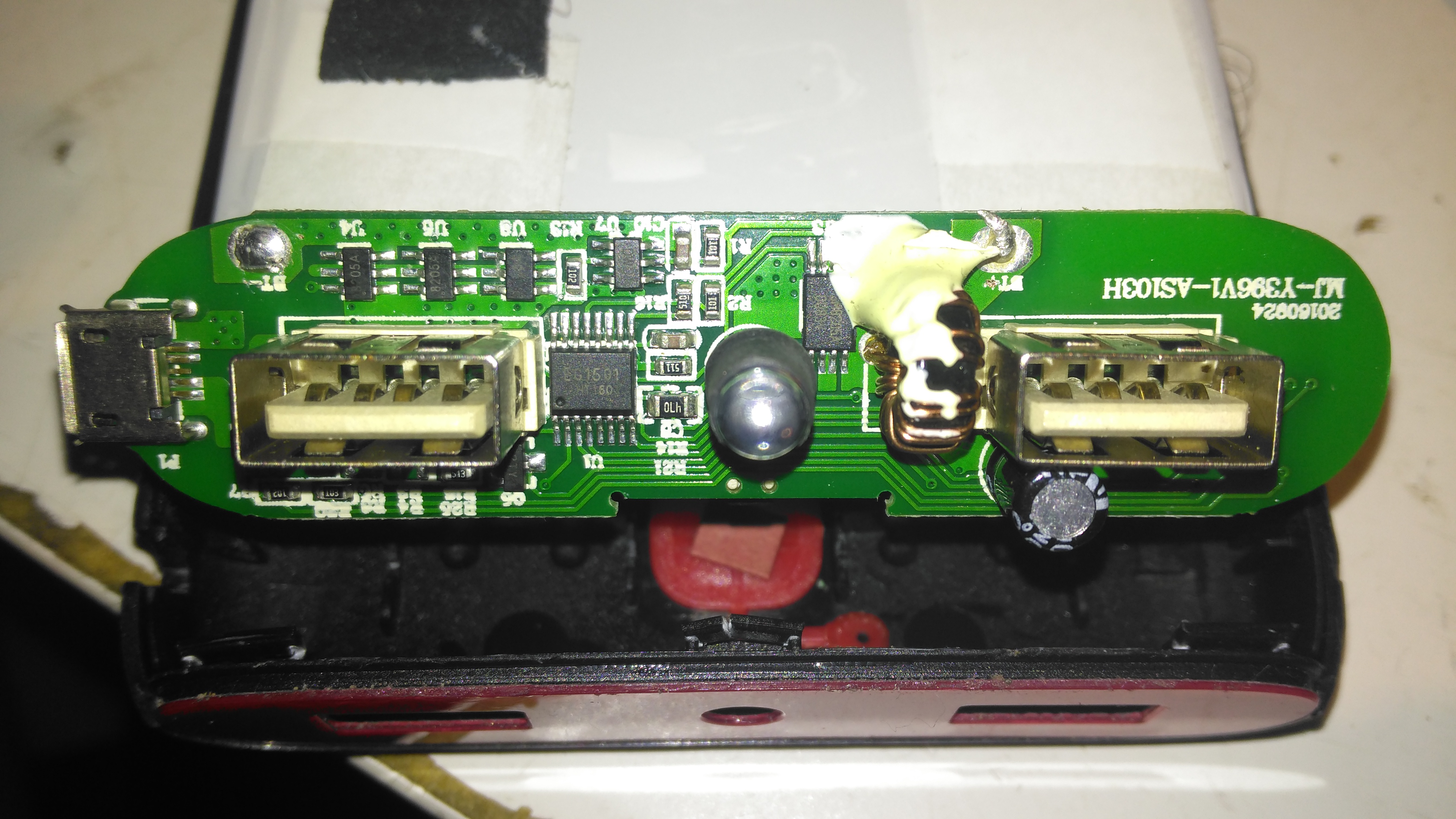
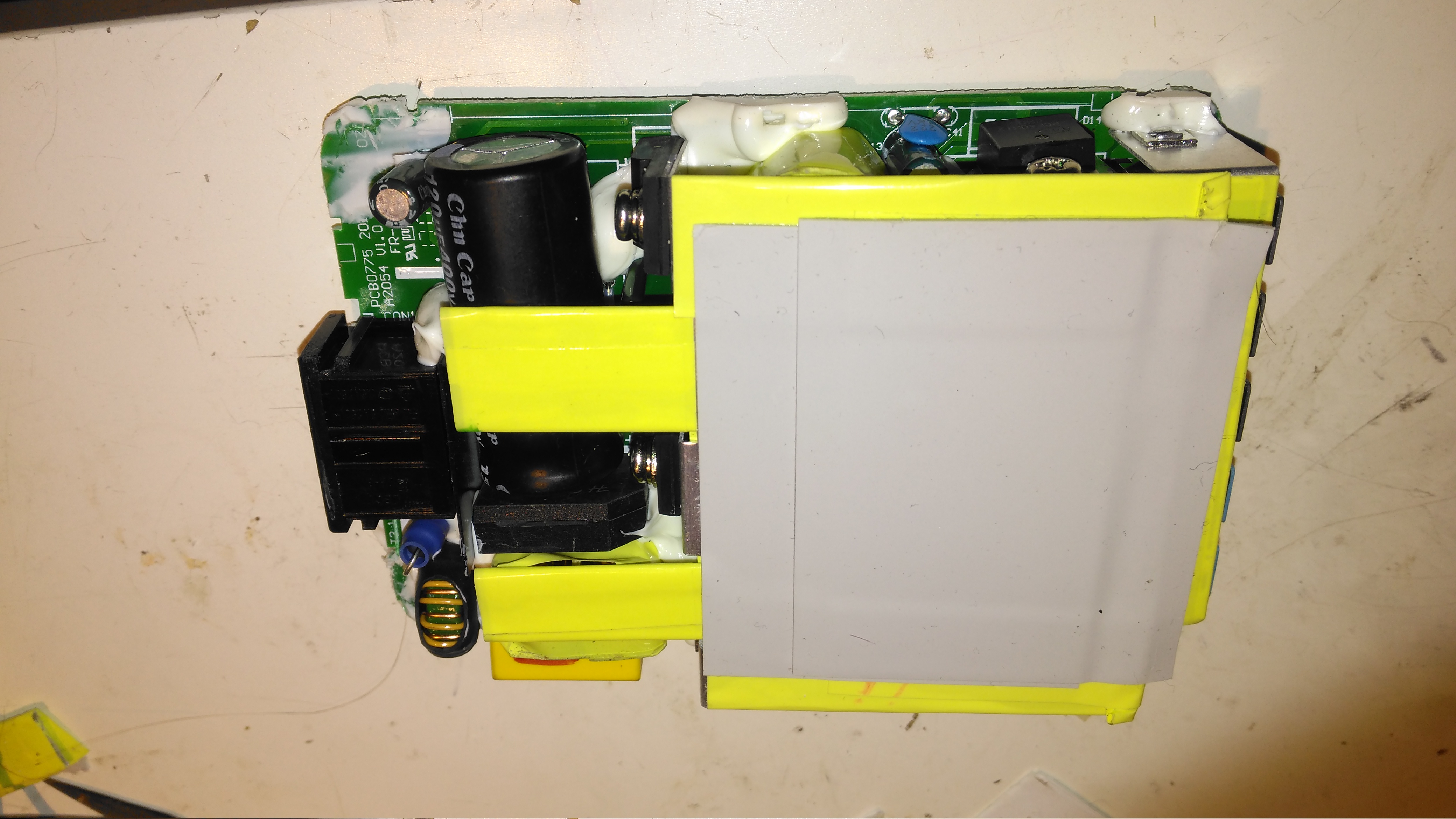
PCB Front
The front of the PCB holds the USB ports, along with most of the main control circuitry. At top left is a string of FS8025A dual-MOSFETs all in parallel for a current carrying capacity of 15A total, to the right of these is the ubiquitous DW01 Lithium-Ion protection IC. These 4 components make up the battery protection – stopping both an overcharge & overdischarge. The larger IC below is an EG1501 multi-purpose power controller.
This chip is doing all of the heavy lifting in this power pack, dealing with all the DC-DC conversion for the USB ports, charge control of the battery pack, controlling the battery level indicator LEDs & controlling the torch LED in the centre.
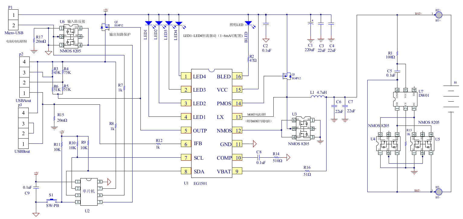
EG1501 Example
The datasheet is in Chinese, but it does have an example application circuit, which is very similar to the circuitry used in this powerbank. A toroidal inductor is nestled next to the right-hand USB port for the DC-DC converter, and the remaining IC next to it is a CW3004 Dual-Channel USB Charging Controller, which automatically sets the data pins on the USB ports to the correct levels to ensure high-current charging of the devices plugged in. This IC replaces the resistors R3-R6 in the schematic above.
The DC-DC converter section of the power chain is designed with high efficiency in mind, not using any diodes, but synchronous rectification instead.
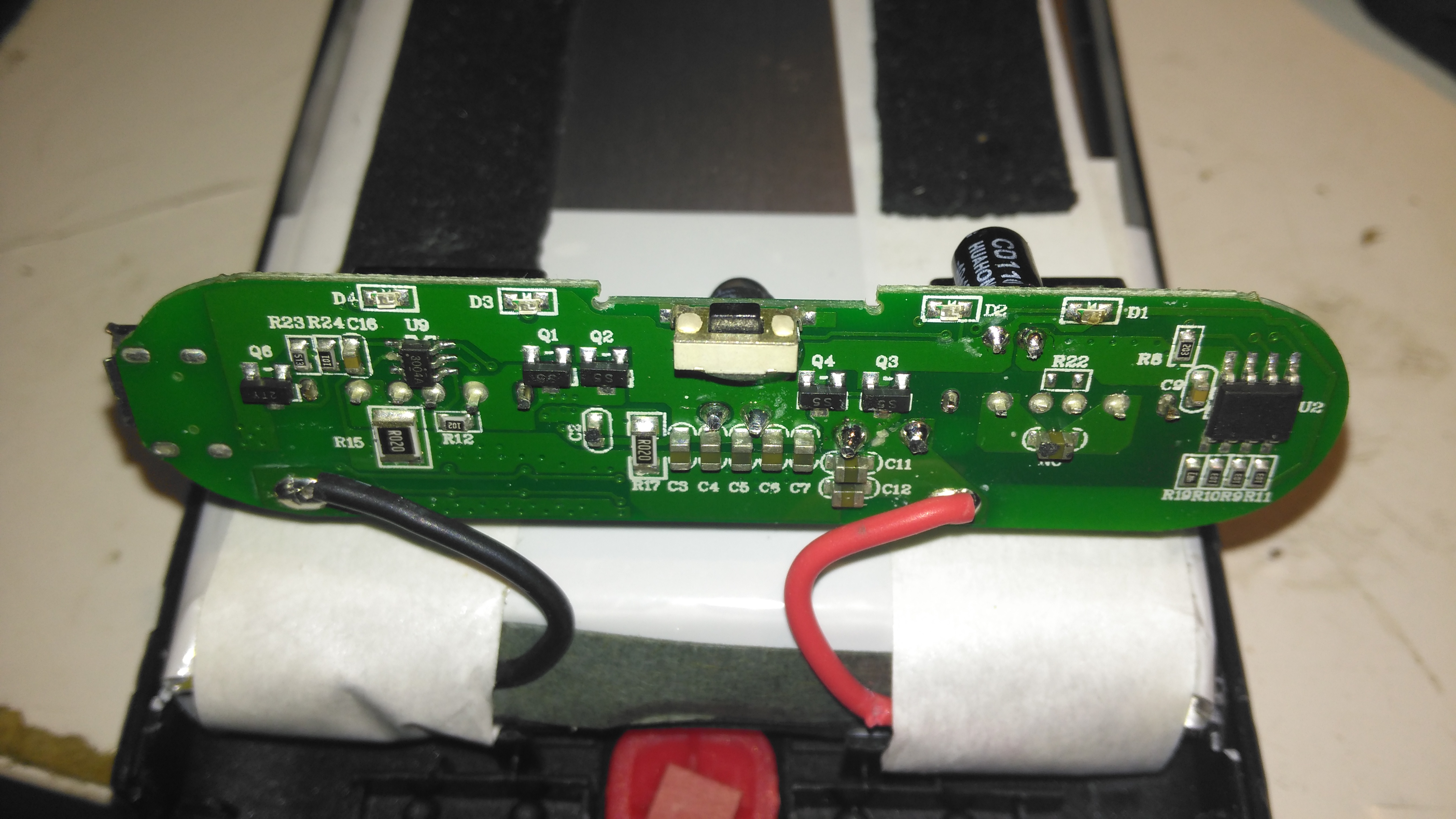
PCB Back
The back of the PCB just has a few discrete transistors, the user interface button, and a small SO8 IC with no markings at all. I’m going to assume this is a generic microcontroller, (U2 in the schematic) & is just there to interface the user button to the power controller via I²C.
Cells
Not many markings on the cells indicating their capacity, but a full discharge test at 4A gave me a resulting capacity of 21Ah – slightly above the nameplate rating. There are two cells in here in parallel, ~10Ah capacity each.
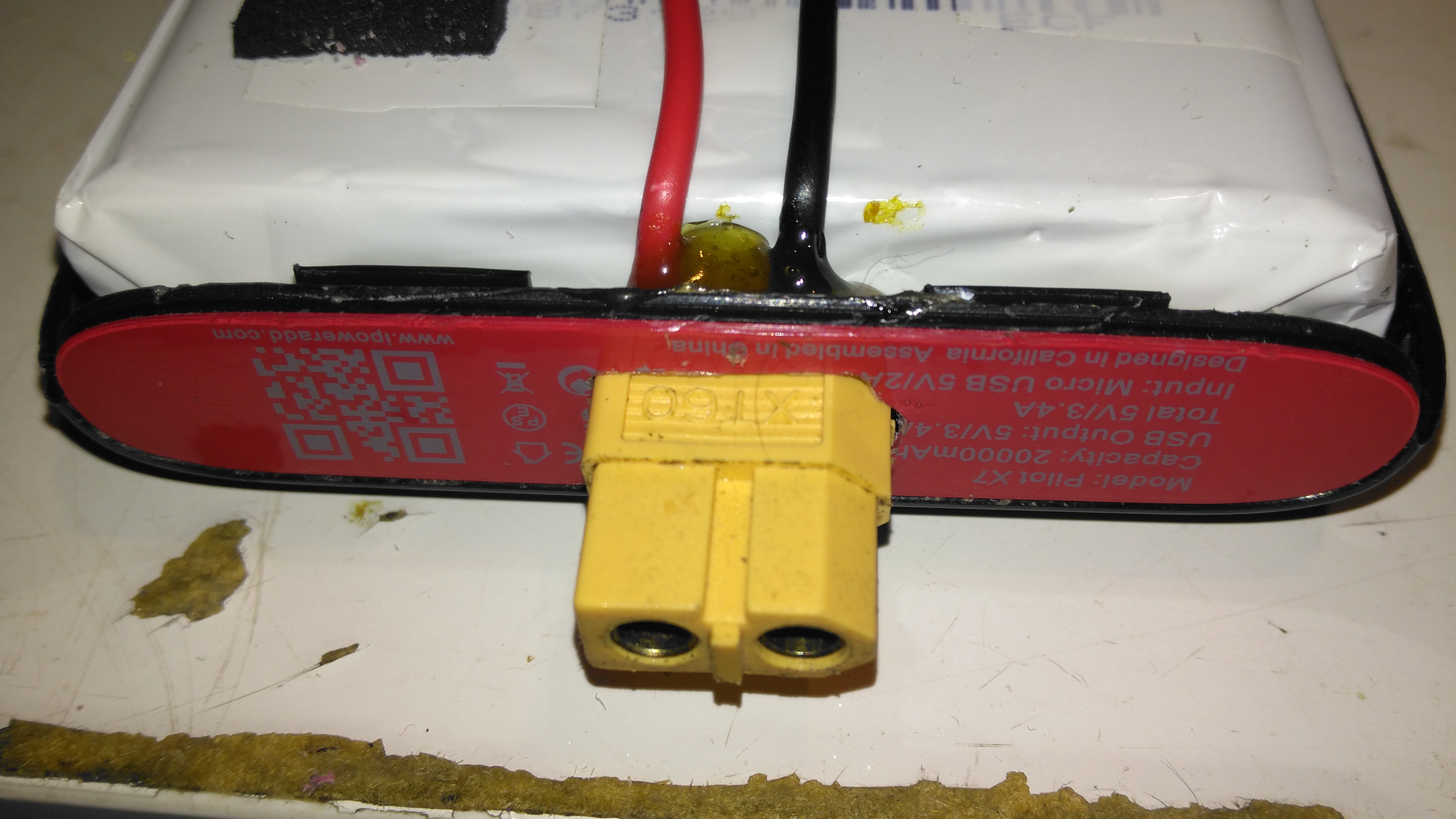
XT60 Battery Connector
The only issue with powerbanks this large is the amount of time they require to recharge themselves – at this unit’s maximum of 2A through the µUSB port, it’s about 22 hours! Here I’ve fitted an XT60 connector, to interface to my Turnigy Accucell 6 charger, increasing the charging current capacity to 6A, and reducing the full-charge time to 7 hours. This splits to 3A charge per cell, and after some testing the cells don’t seem to mind this higher charging current.
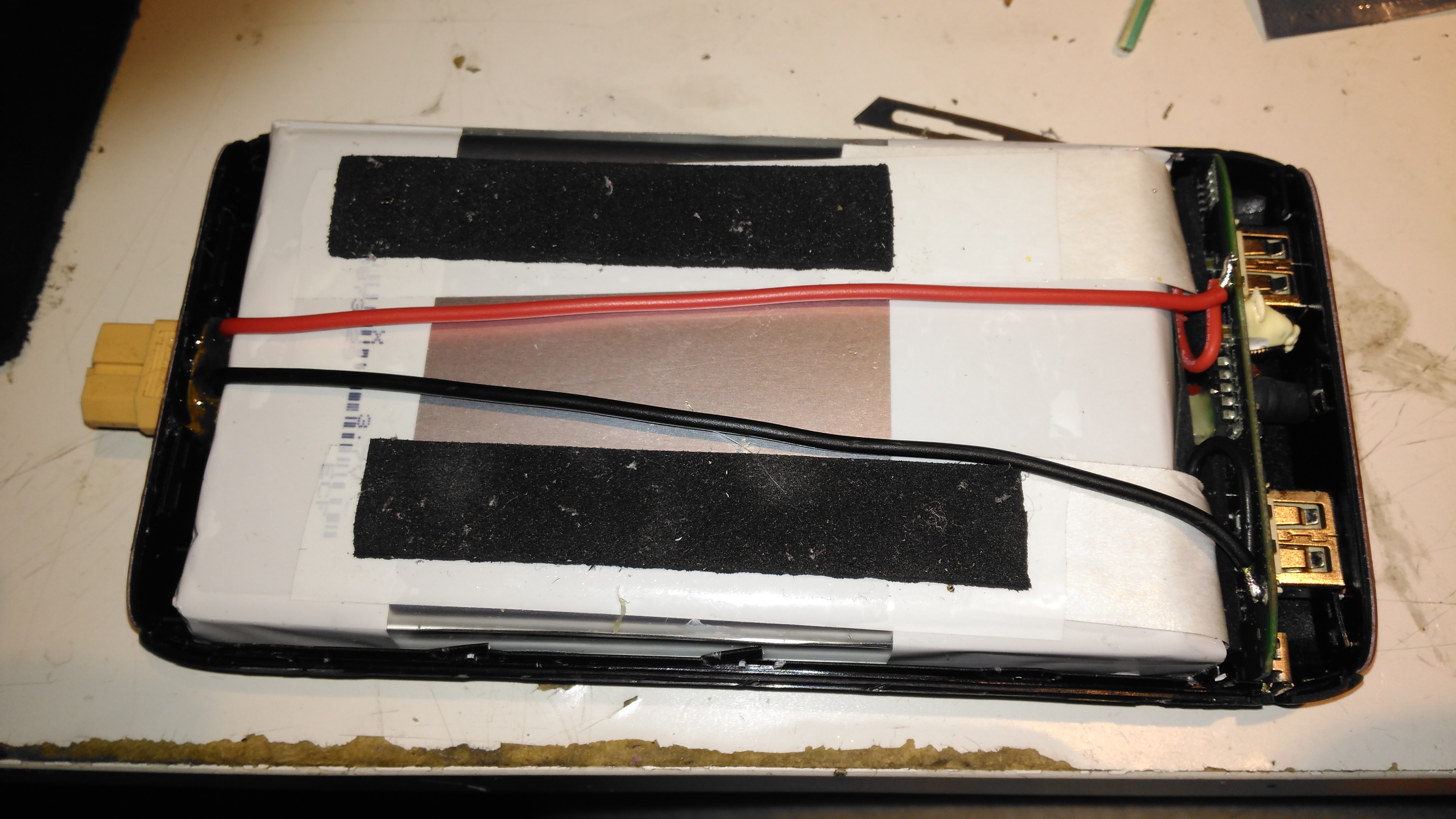
Battery Connector Wiring
The new charging connector is directly connected to the battery at the control PCB, there’s just enough room to get a pair of wires down the casing over the cells.
A few months ago I did a teardown on this Anker PowerPort Speed 5 USB charger, but I didn’t get round to detailing the conversion to 12v I had to do, so I’ll get to that now I’ve got a couple more to convert over.
Power Module
Here’s the internals of the Anker charger once I’ve removed the casing – which like many things these days, is glued together. (Joints can be cracked with a screwdriver handle without damaging the case). There’s lots of heatsinking in here to cool the primary side switching devices & the pot core transformers, so this is the first thing to get removed.
Heatsink Removed
Once the heatsink has been removed, the pot core transformers are visible, wrapped in yellow tape. There’s some more heatsink pads & thermal grease here, to conduct heat better. The transformers, primary side switching components & input filter capacitor have to go.
Primary Side Components Removed
Here’s the PCB once all the now redundant mains conversion components have been deleted. I’ve left the input filtering & bridge rectifier in place, as this solves the issue of the figure-8 cable on the input being reversible, polarity of the input doesn’t matter with the bridge. I’ve removed the main filter capacitor to make enough room for the DC-DC converters to be fitted.
Tails Installed
Installing the tails to connect everything together is the next step, this charger requires two power supplies – the QC3 circuits need 14.4v to supply the multi-voltage modules, the remaining 3 standard ports require 5v. The DC input tails are soldered into place where the main filter capacitor was, while the outputs are fitted to the spot the transformer secondary windings ended up. I’ve left the factory Schottky rectifiers in place on the secondary side to make things a little more simple, the output voltages of both the DC-DC converters does need to be increased slightly to compensate for the diode drops though. I’ve also bypassed the mains input fuse, as at 12v the input current is going to be substantially higher than when used on mains voltage.
DC-DC Converters Installed
With a squeeze both the boost converter & the buck converter fit into place on the PCB.
Since I’ve discovered some nice high power PSUs in the form of Playstation 3 PSUs, it’s time to get a new Bench PSU Build underway!
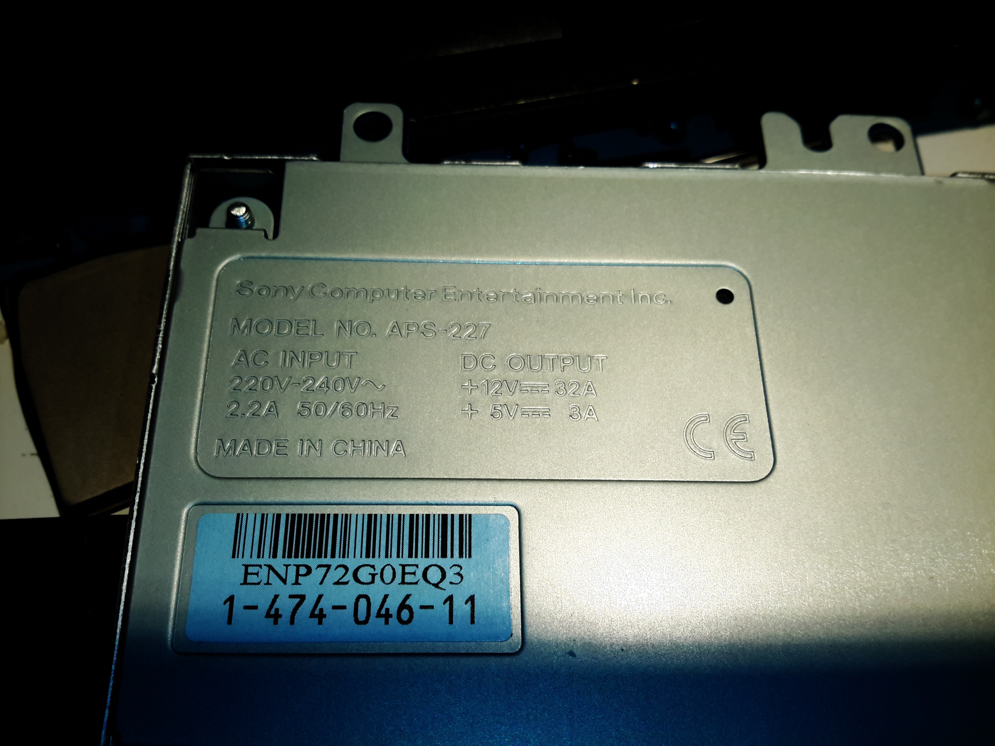
Specifications
I’ve gone for the APS-227 version as it’s got the 32A rail. This makes things slightly beefier overall, as the loading will never be anywhere close to 100% for long, more headroom on the specs is the result.
Desktop Instrument Case
The case I’ve chosen for this is an ABS desktop instrument case from eBay, the TE554 200x175x70mm. The ABS is easy to cut the holes for all the through-panel gear, along with being sturdy enough. Aluminium front & back panels would be a nice addition for a better look.
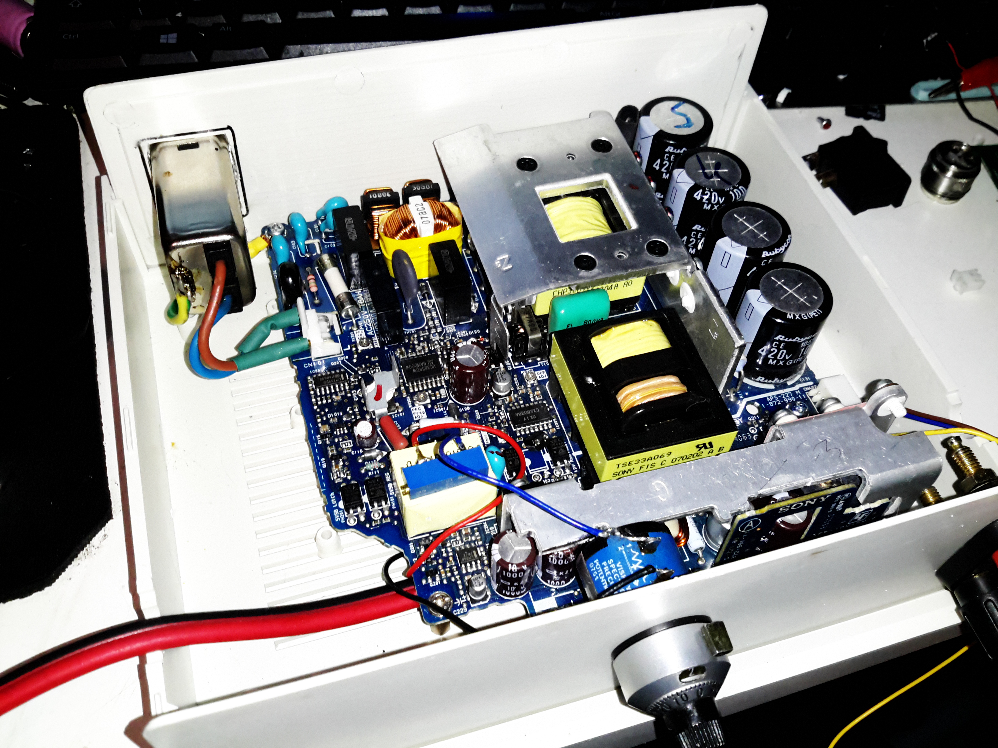
PSU Mounted
The PSU board is removed from it’s factory casing & installed on the bottom shell half, unfortunately the moulded-in posts didn’t match the screw hole locations so I had to mount some brass standoffs separately. The AC input is also fitted here, I’ve used a common-mode filter to test things (this won’t be staying, as it fouls one of the case screw holes). The 40A rated DC output cable is soldered directly to the PCB traces, as there’s no room under the board to fit the factory DC power connector. (This is the biggest case I could find on eBay, and things are still a little tight). Some minor modifications were required to get the PCB to fit correctly.
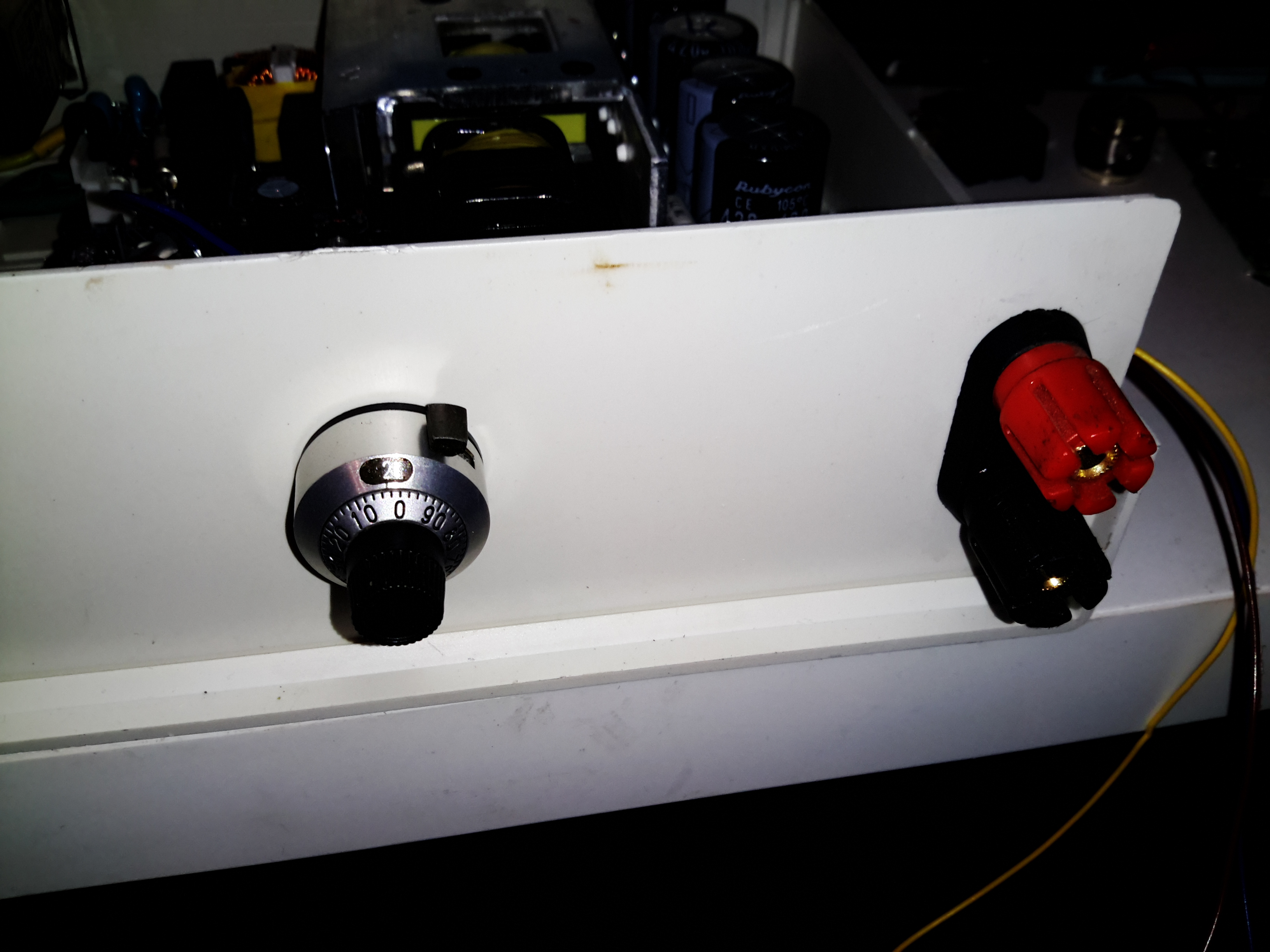
Output Terminals & Adjuster
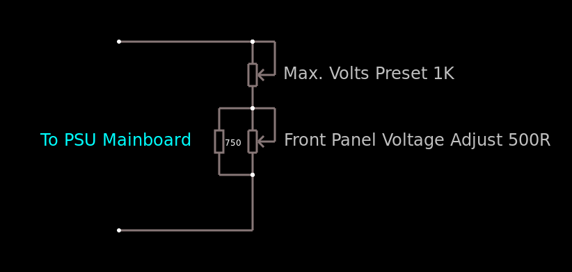
I decided to add some limited voltage adjustment capability to the front panel, I had a 100Ω Vishay Spectrol Precision 10-turn potentiometer in my parts bin, from a project long since gone that just about fits between the panel & the output rectifier heatsink. The trimpot I added when I first posted about these PSUs is now used to set the upper voltage limit of 15 volts. (The output electrolytics are 16v rated, and are in an awkward place to get at to change for higher voltage parts). The binding posts are rated to 30A, and were also left over from a previous project.
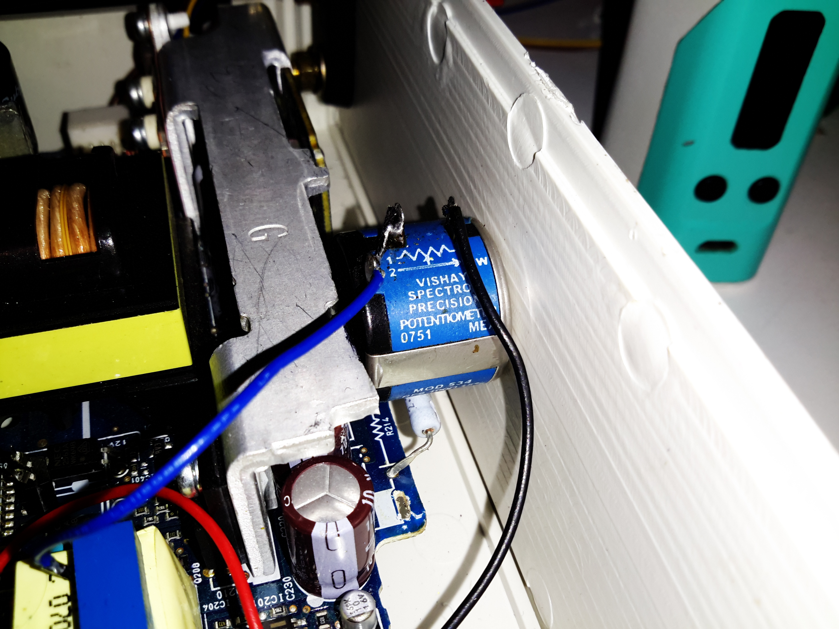
Vishay Spectrol 10-Turn
Addon Regulator Components
This front panel potentiometer is electrically in series with the trimpot glued to the top of the auxiliary transformer, see above for a simple schematic of the added components. In this PSU, reducing the total resistance in the regulator circuit increases the voltage, so make sure the potentiometer is wired correctly for this!
After some experimentation, a 500Ω 10-turn potentiometer would be a better match, with a 750Ω resistor in parallel to give a total resistance range on the front panel pot of 300Ω. This will give a lower minimum voltage limit of about 12.00v to make lead-acid battery charging easier.
I’ve had to make a minor modification to the output rectifier heatsink to get this pot to fit in the available space, but nothing big enough to stop the heatsink working correctly.
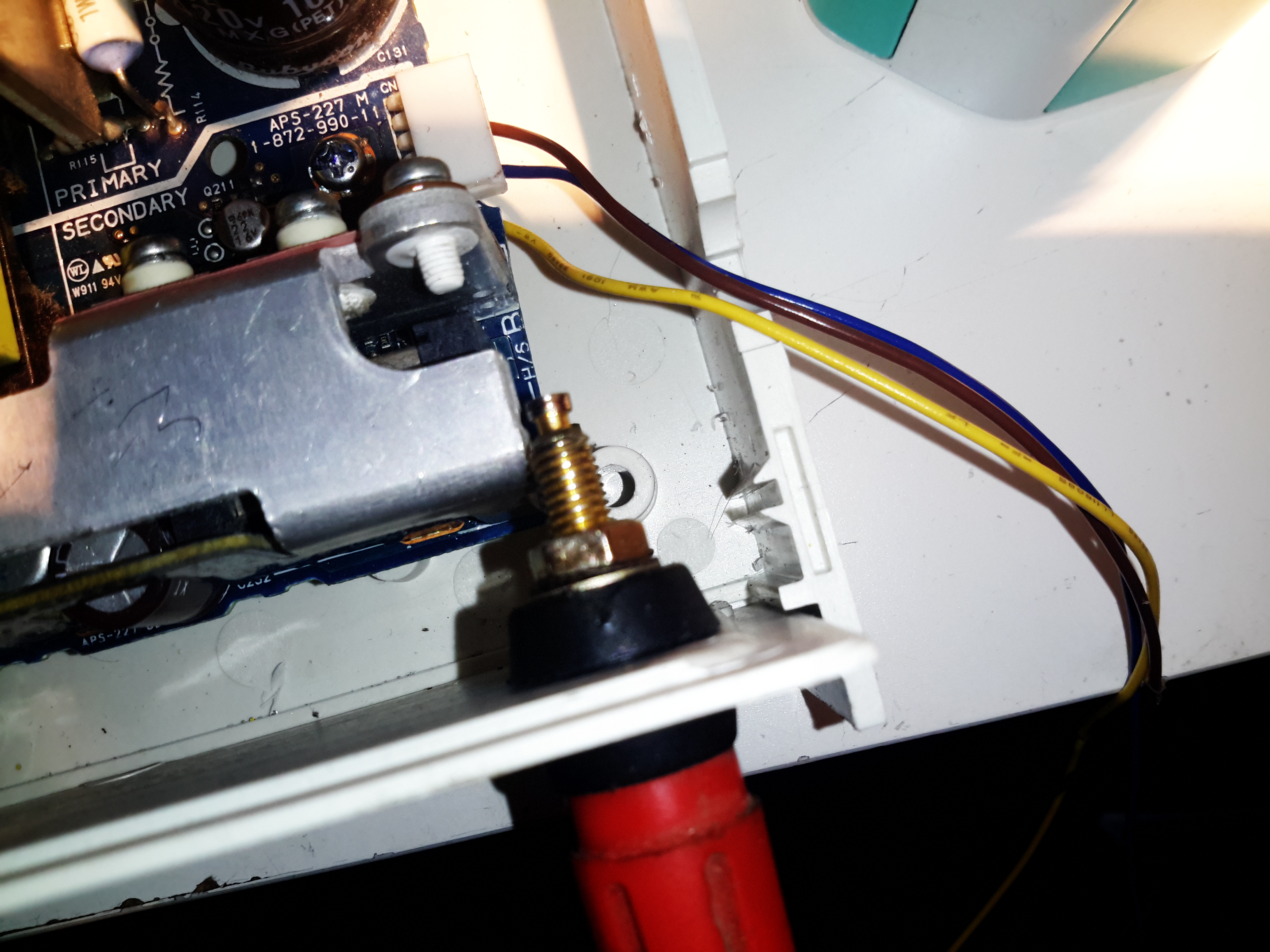
Terminal Posts
Here I’ve got the binding posts mounted, however the studs are a little too long. Once the wiring is installed these will be trimmed back to clear both the case screw path & the heatsink. (The heatsink isn’t a part of the power path anyway, so it’s isolated).
Power Meter Control Board & Fan
To keep the output rectifier MOSFETs cool, there’s a fan mounted in the upper shell just above their location, this case has vents in the bottom already moulded in for the air to exit. The fan is operated with the DC output contactor, only running when the main DC is switched on. This keeps the noise to a minimum when the supply doesn’t require cooling. The panel meter control board is also mounted up here, in the only empty space available. The panel meter module itself is a VAC-1030A from MingHe.
Meter Power Board
The measurement shunt & main power contactor for the DC output is on another board, here mounted on the left side of the case. The measurement shunt is a low-cost one in this module, I doubt it’s made of the usual materials of Manganin or Constantan, this is confirmed by my meansurements as when the shunt heats up from high-power use, the readings drift by about 100mA. The original terminal blocks this module arrived with have been removed & the DC cables soldered directly to the PCB, to keep the number of high-current junctions to a minimum. This should ensure the lowest possible losses from resistive heating.
Meter Panel Module
The panel meter module iself is powered from the 5v standby rail of the Sony PSU, instead of the 12v rail. This allows me to keep the meter on while the main 12v output is switched off.
PSU Internals
here’s the supply with everything fitted to the lower shell – it’s a tight fit! A standard IEC connector has been fitted into the back panel for the mains input, giving much more clearance for the AC side of things.
Inside View
With the top shell in place, a look through the panel cutout for the meter LCD shows the rather tight fit of all the meter components. There’s about 25mm of clearance above the top of the PSU board, giving plenty of room for the 40mm cooling fan to circulate air around.
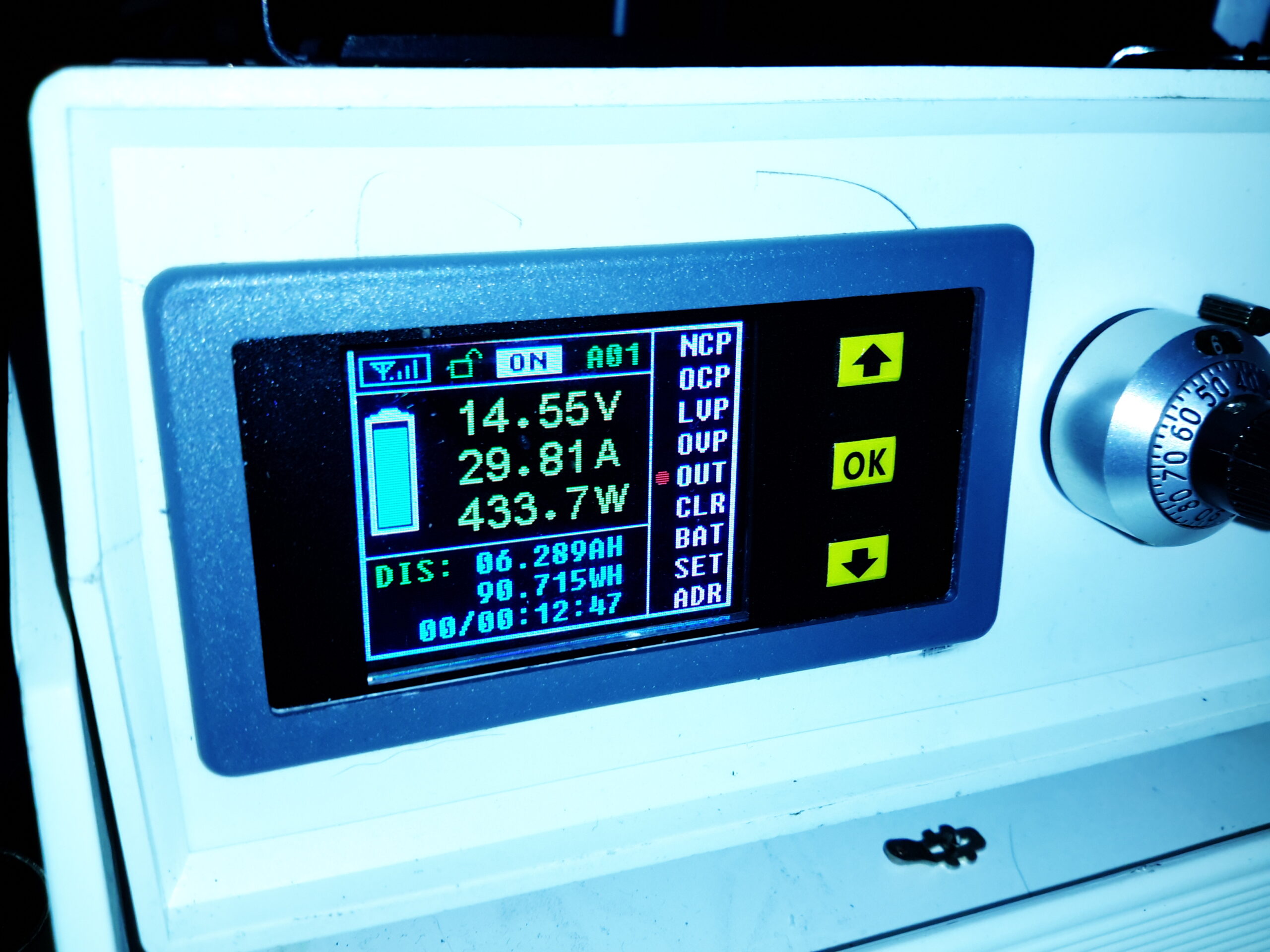
Load Test
Here’s the finished supply under a full load test – it’s charging a 200Ah deep cycle battery. The meter offers many protection modes, so I’ve set the current limit at 30A – preventing Sony’s built in over current protection on the PSU tripping with this function is a bonus, as the supply takes a good 90 seconds to recover afterwards. I’ll go into the many modes & features of this meter in another post.
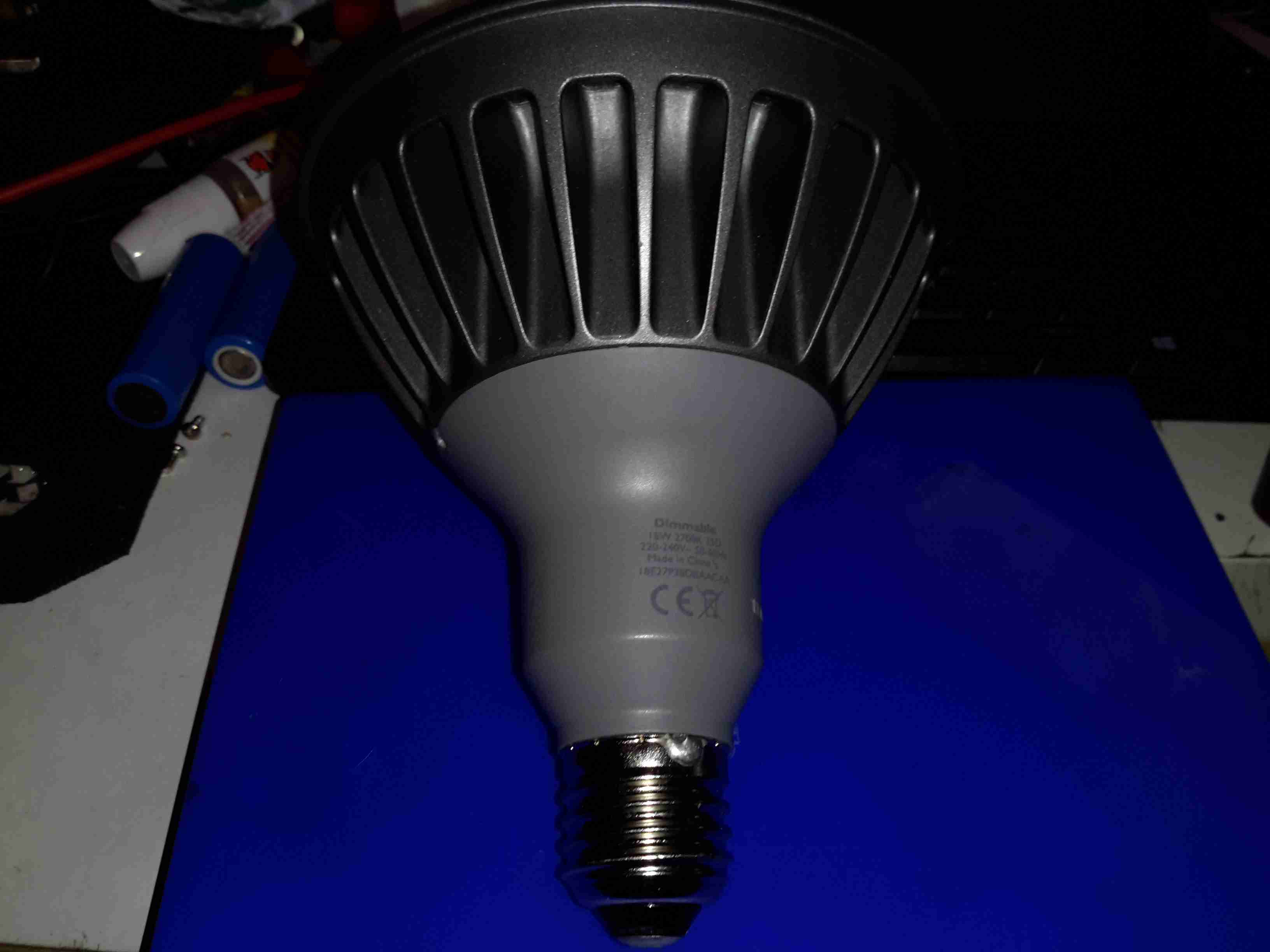
These large LED Philips PAR38 lamps were recently on clearance sale in my local T.N. Robinsons electrical contractors for about £3, so I decided to grab one in the hopes I might be able to hack it into a low-voltage LED lamp. These are full-size PAR38 format, with most of the bulk being the large aluminium heatsink on the front. The back section with the power supply module is secured with silicone, so some unreasonable force was required to liberate the two pieces.
Specification
These lamps are rated at 18W in operation, and are surprisingly bright for this power level.
Lens
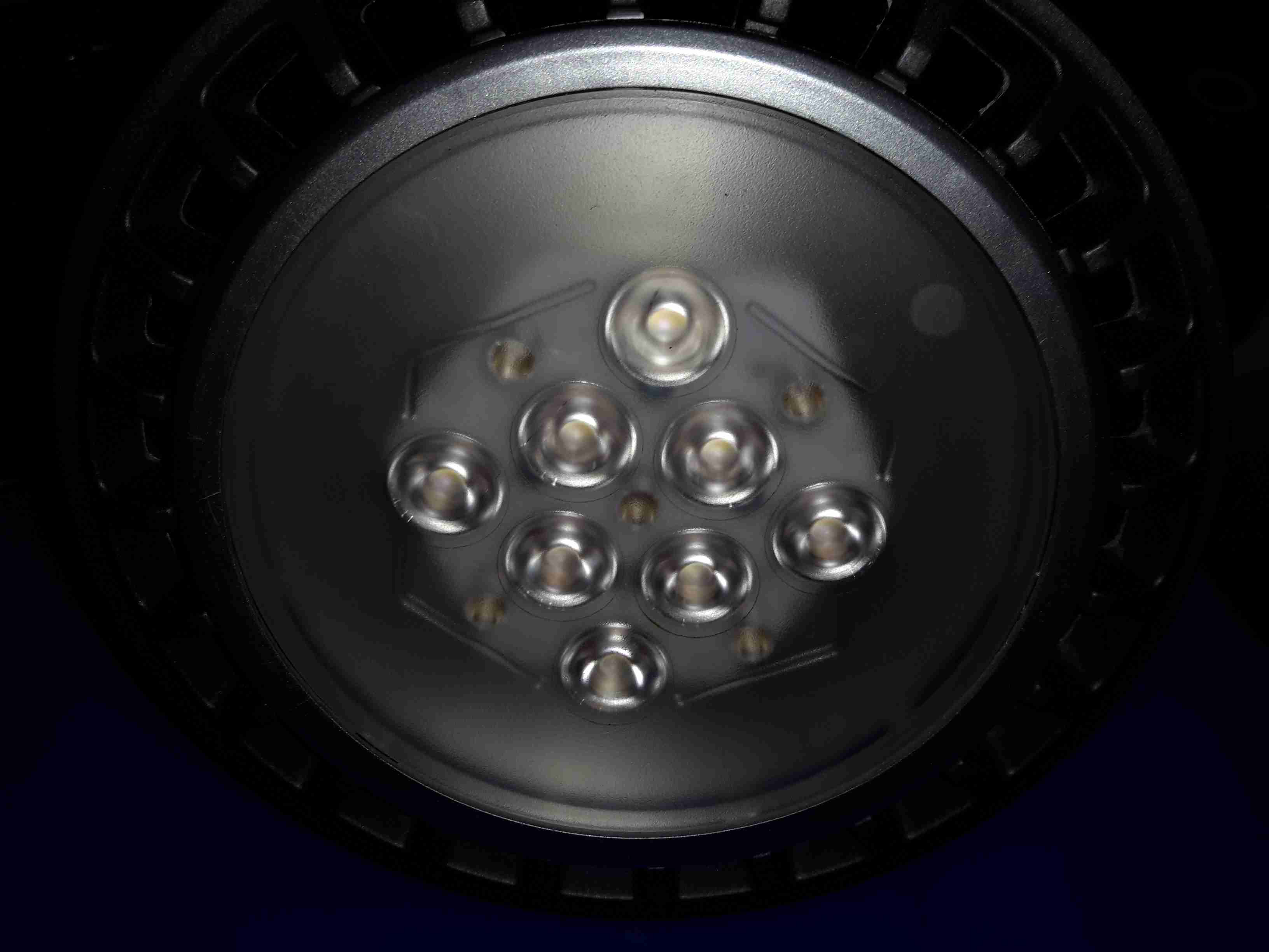
The front has the moulded multi-lens over the LEDs, to spread the light a bit further than the bare dies.
LED Array
The LED array is two series strings of 4 LEDs, for ~24v forward voltage. Unusual for a high power LED array, this PCB isn’t aluminium cored, but 0.8mm FR4. Heat is transferred to the copper plane on the backside by the dozens of vias around the Luxeon Rebel LEDs. There is a thermal pad under the PCB for improved heat transfer to the machined surface of the heatsink.
Control PCB Top
The power supply & control PCB is pretty well made, it’s an isolated converter, so no nasty mains on the LED connections.
This is a little bit of kit I got to talk to the Webasto TT-V I salvaged from a scrap Jaguar S-Type, and converts USB-RS232 to the standard car diagnostic ODB connector. (These are a much cheaper option at £4 than the official Webasto diagnostic adaptor & loom which is over £90.
PCB Top
There’s really not much to this adaptor, the only signals that are routed to the ODB connector seem to be the +12v on pin 16, K-Line on Pin 7 & L-Line on pin 15. The main IC here is a CH340 USB-Serial interface, with some glue logic in the form of an LM339 quad comparator.
PCB Reverse
The reverse side of the PCB only has the power indicator LED.
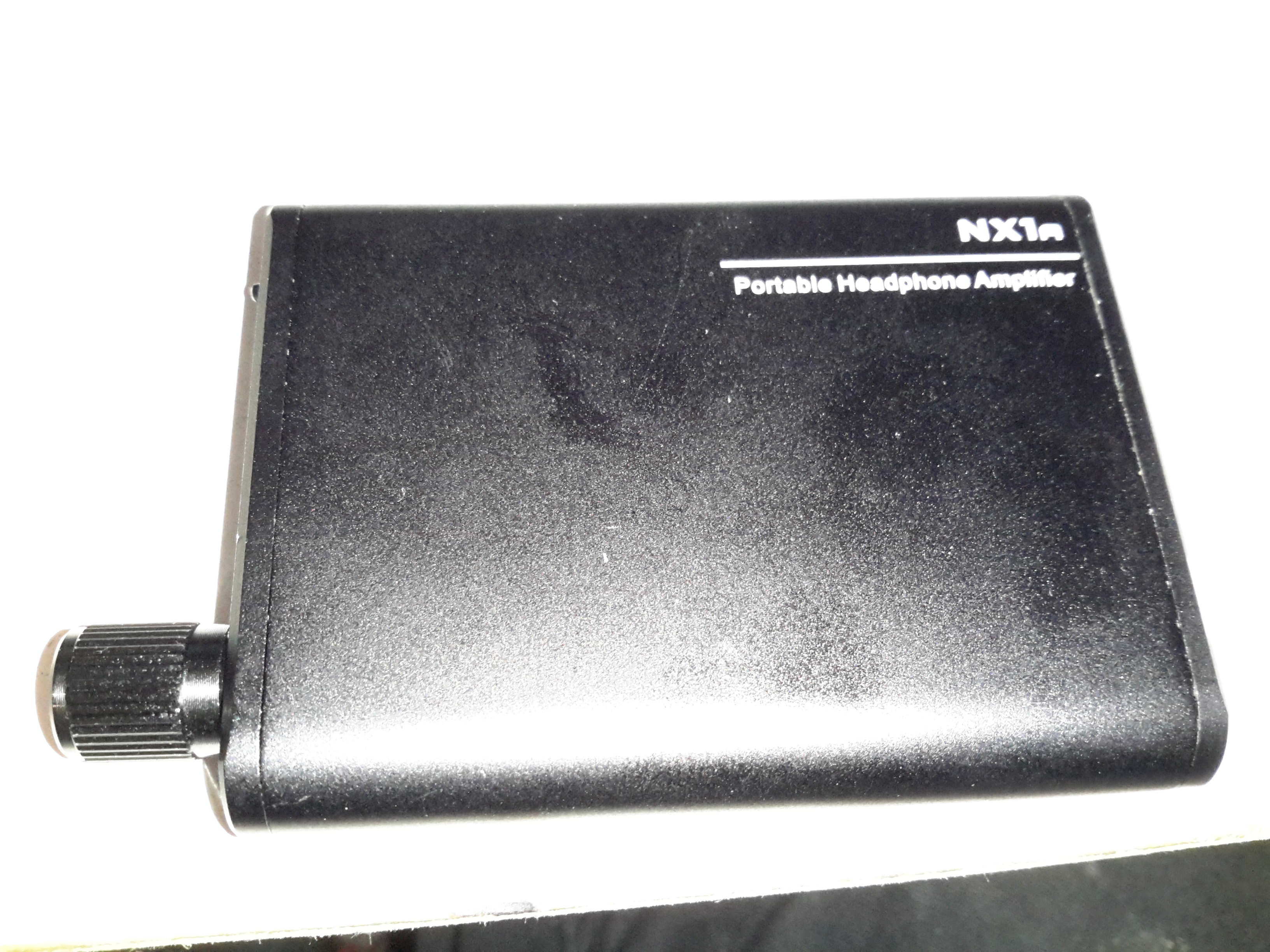
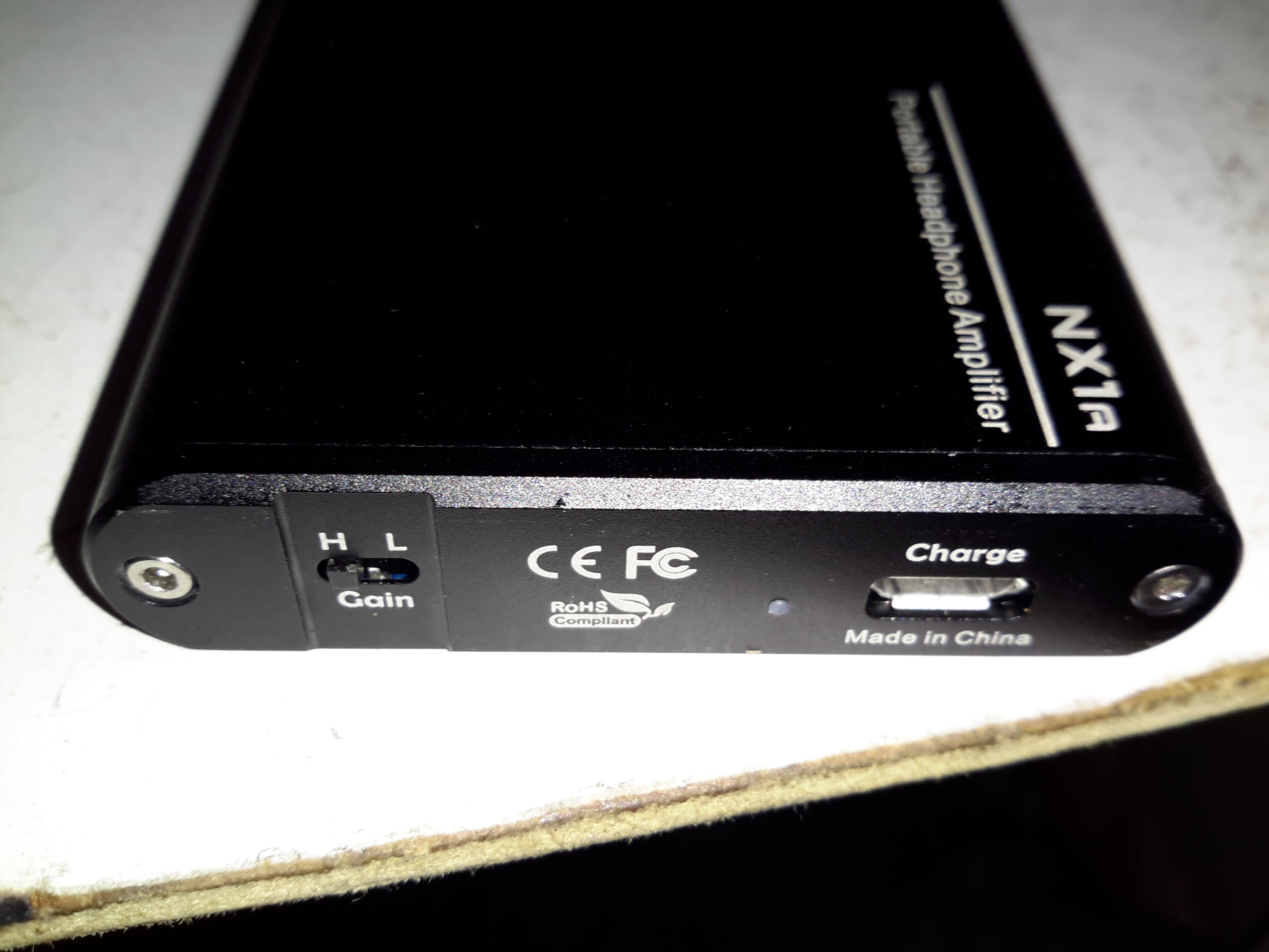
Time for another teardown! Here’s a pocket-sized headphone amplifier for use with mobile devices. This unit is powered by a built-in lithium cell, and can give some pretty impressive volume levels given it’s small size.
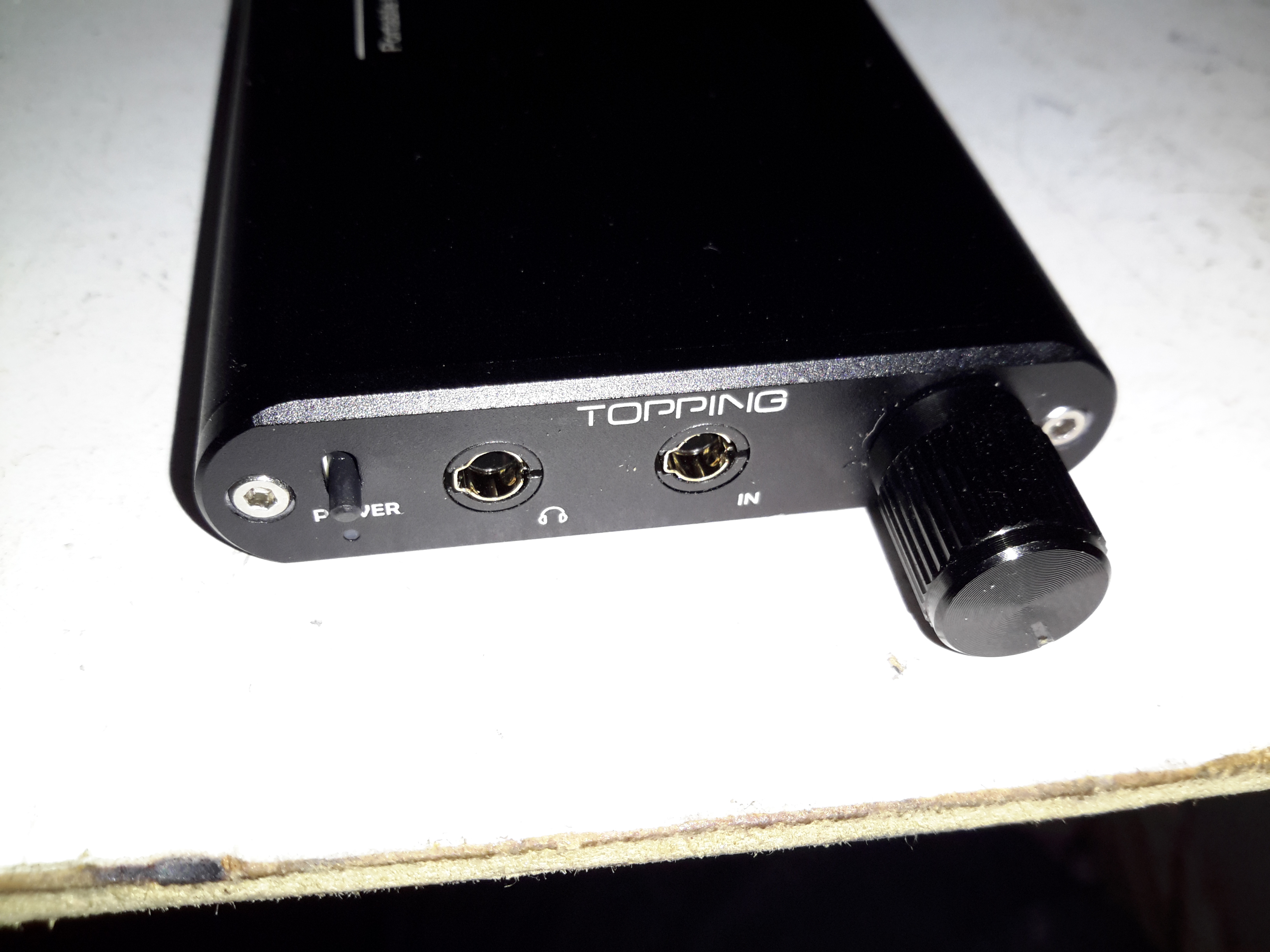
Audio Connections
The 3.5mm audio input & output jacks are on the front of the unit, along with the relatively enormous volume knob & power switch. There’s a little blue LED under the switch that lets the user know when the power is on, but this is a very sedate LED, using very little power.
Gain & Charging
On the back is the High-Low gain switch, and the µUSB charging port. There’s another indicator LED to show that the internal cell is charging, in this case a red one.
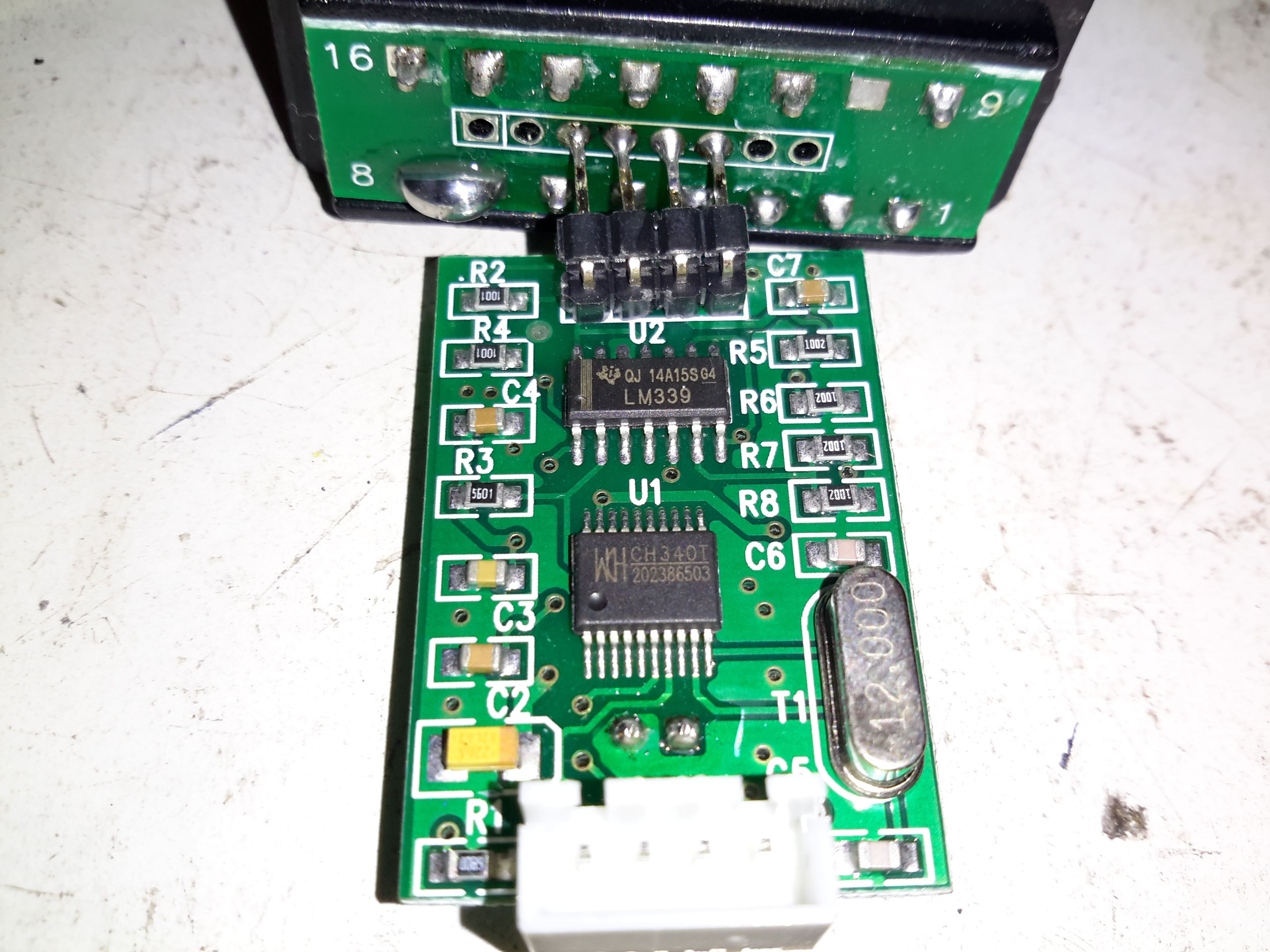
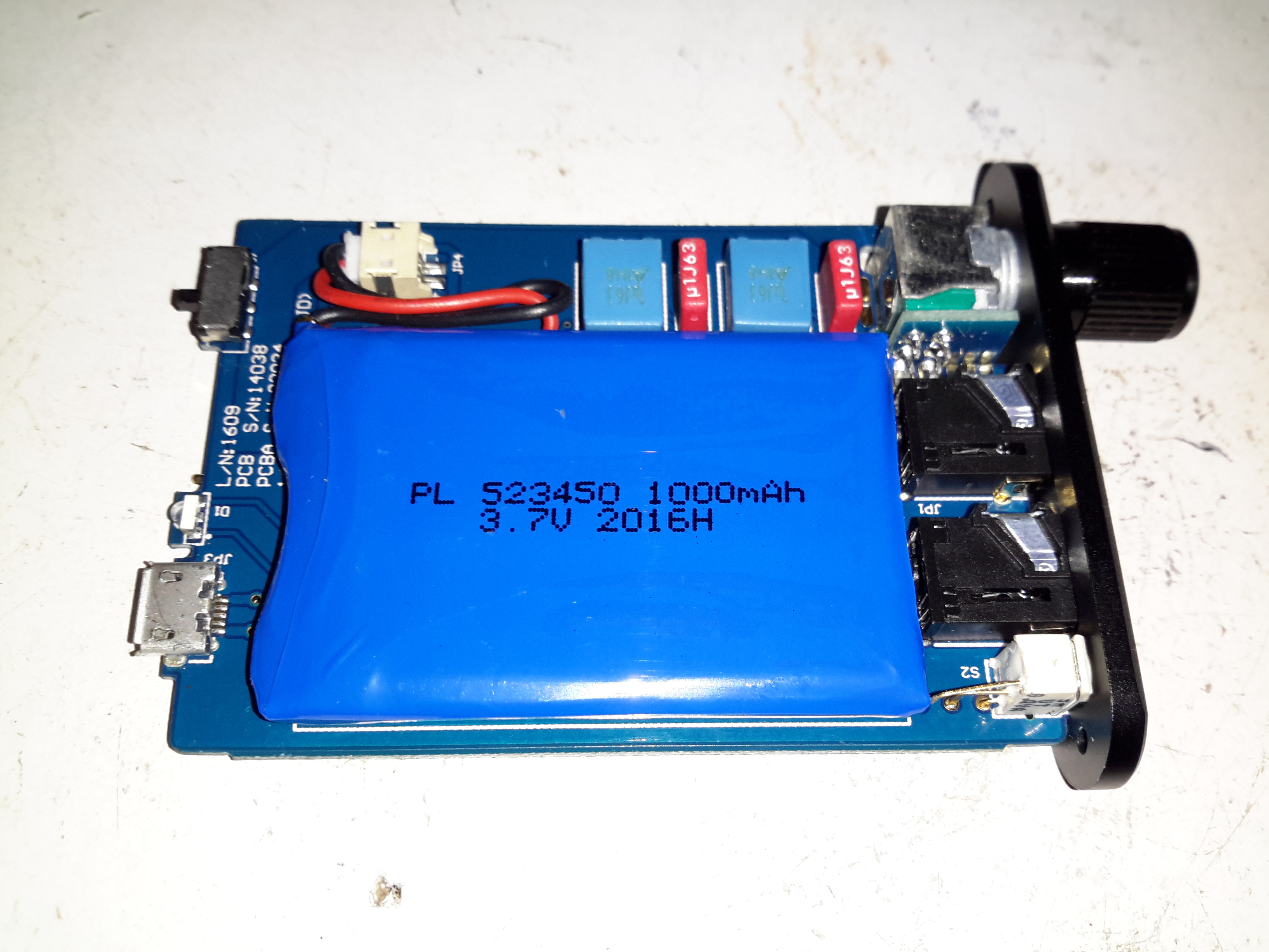
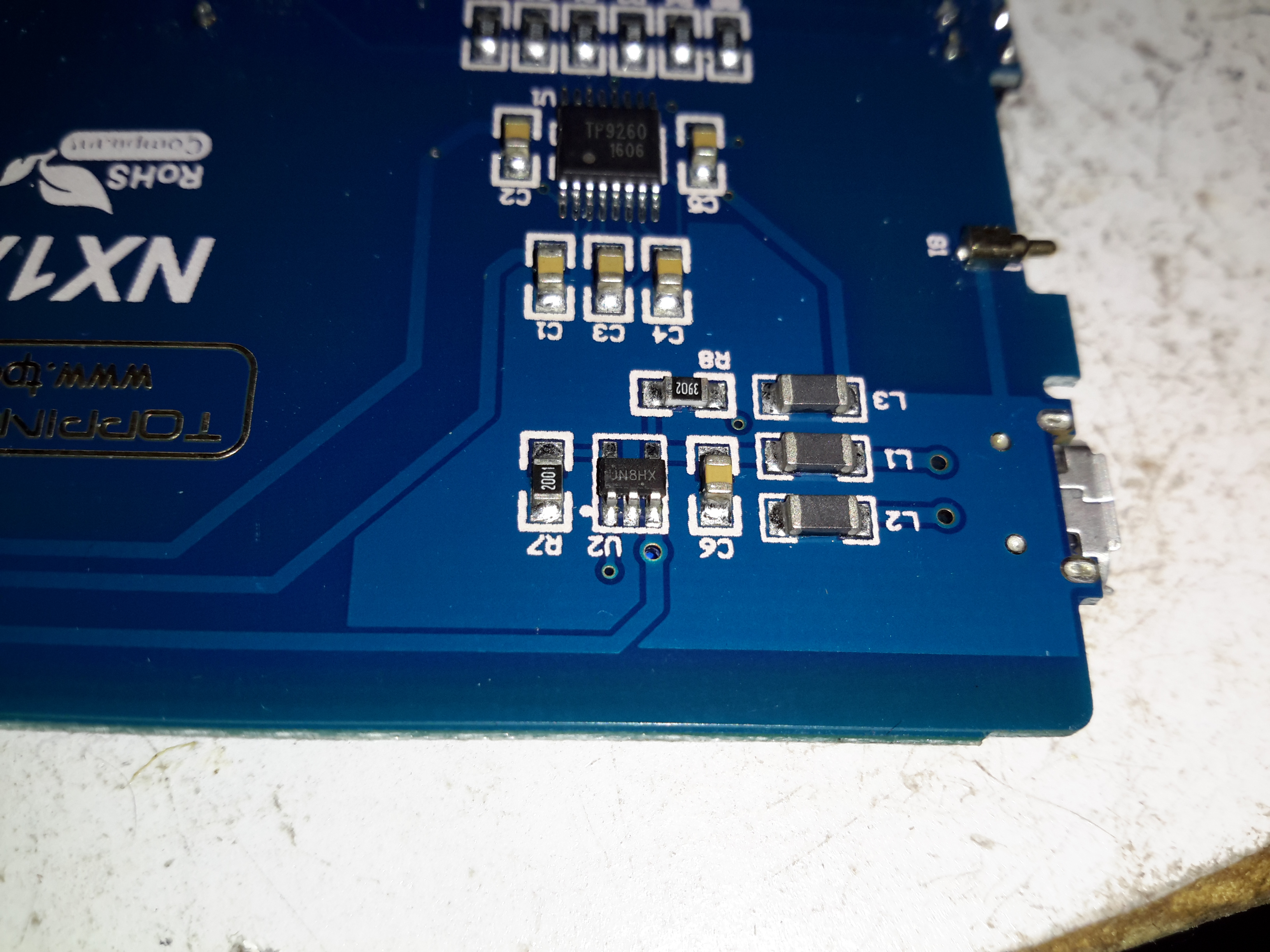
PCB Top
Removing a couple of cap screws allows the internals to slide out of the extruded aluminium casing. Most of the internal space is taken up by the 1Ah lithium cell, here on the top of the PCB secured by some double-sided tape. The volume potentiometer is mounted on a small daughterboard at right angles to get it to fit into the small vertical space in the case.
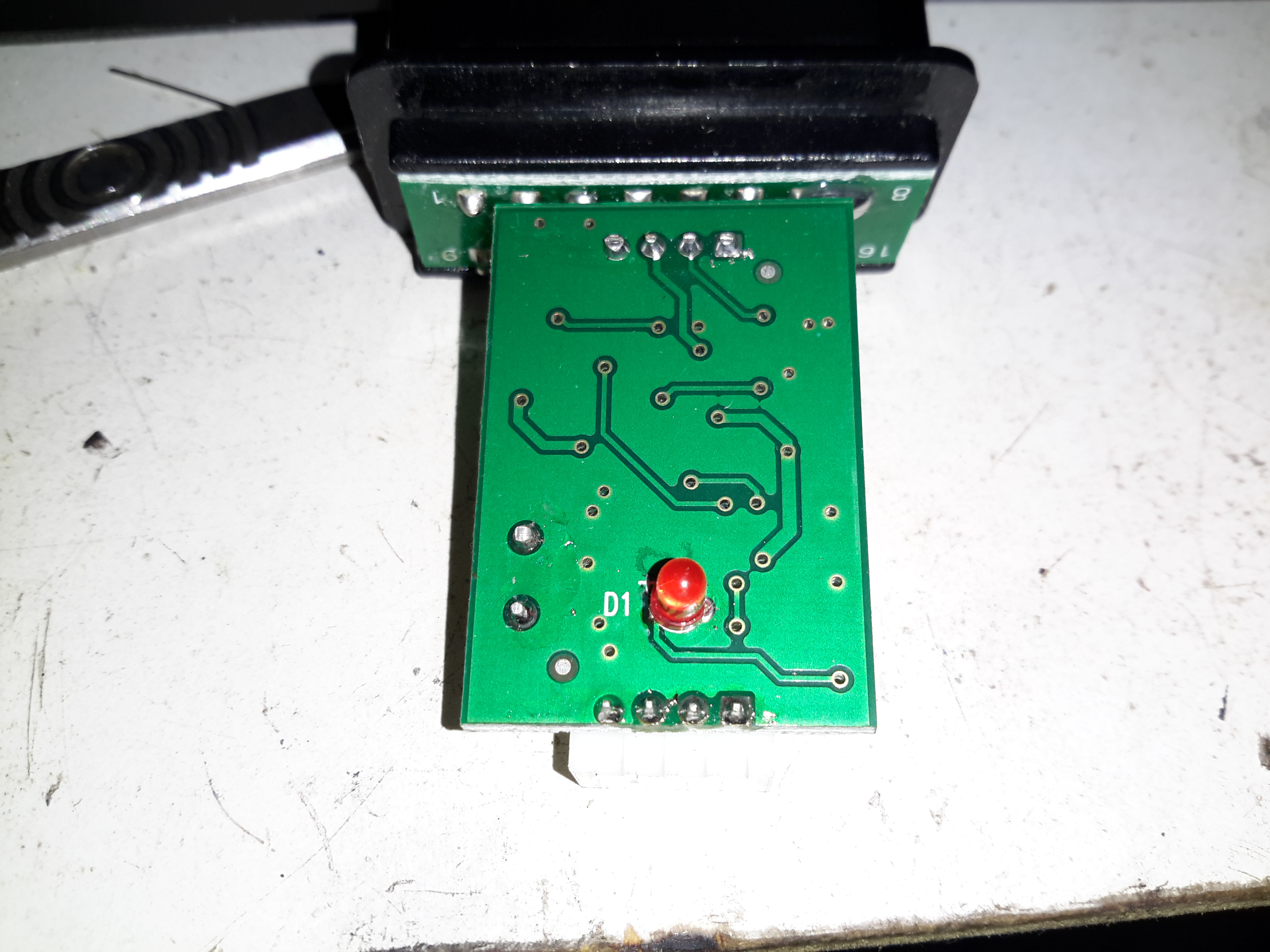
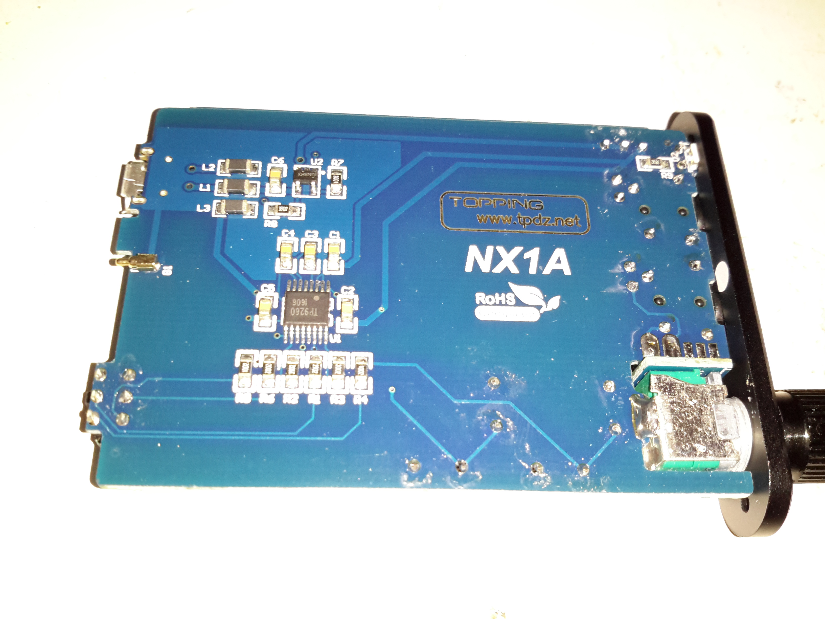
PCB Rear
The bottom of the PCB is equally as sparse – the only ICs being the main audio amp in the centre & the battery charger IC at the top.
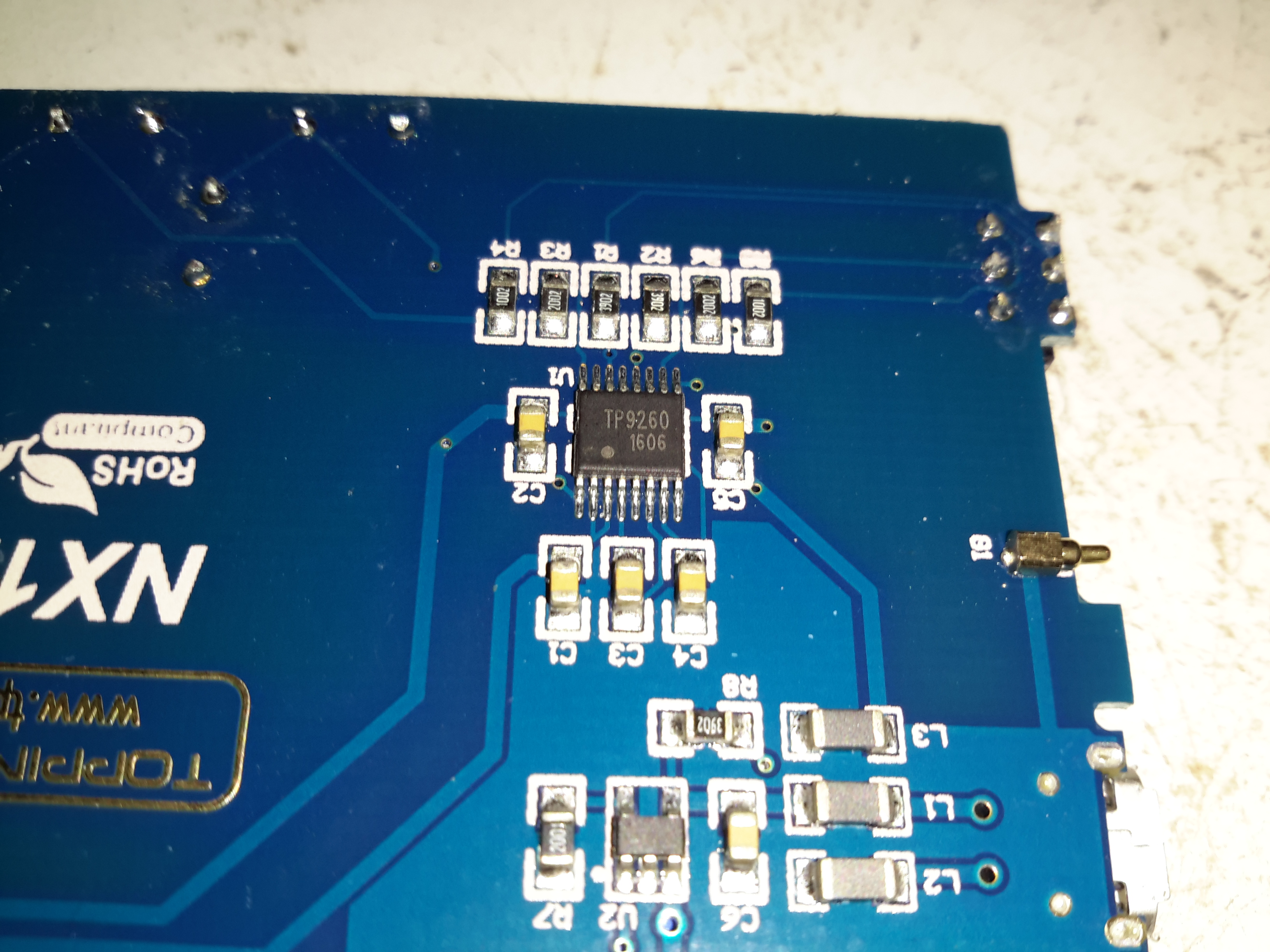
Amplifier IC
The main audio amplifier is a TP9260, I couldn’t find a datasheet on this, so I’m unsure of what the specs are. The row of resistors above the IC are for the gain divider circuit. There’s also a pogo pin on the right that makes contact with the back panel of the case for grounding.
Battery Charger
Battery charging is taken care of by a UN8HX 500mA linear charging IC, not much special here.
This little amplifier seems to be pretty well made, considering the price point. The only issue I’ve had so far is the audio cables act like antennas, and when in close proximity to a phone some signal gets picked up & blasted into the headphones as interference.
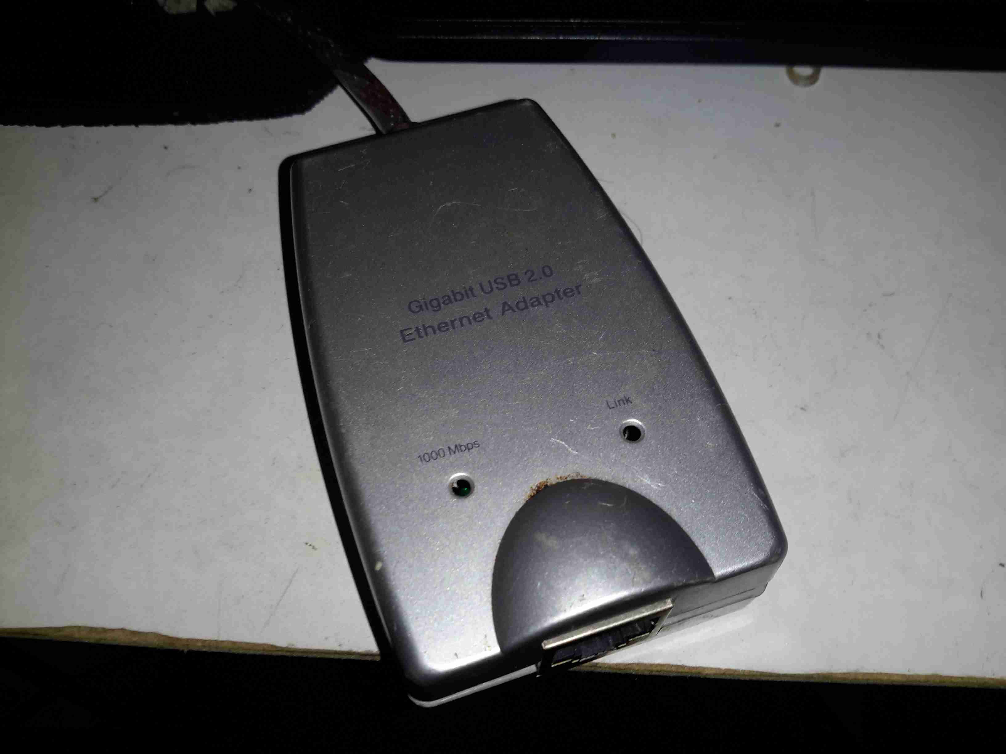
Here’s a chap eBay USB-To-Ethernet dongle I obtained for use with the Raspberry Pi Zero. This one is getting torn down permanently, as it’s rather unreliable. It seems to like having random fits where it’ll not enumerate on the USB bus. The silicon in the ICs will eventually make it here once I manage to get a new microscope 😉
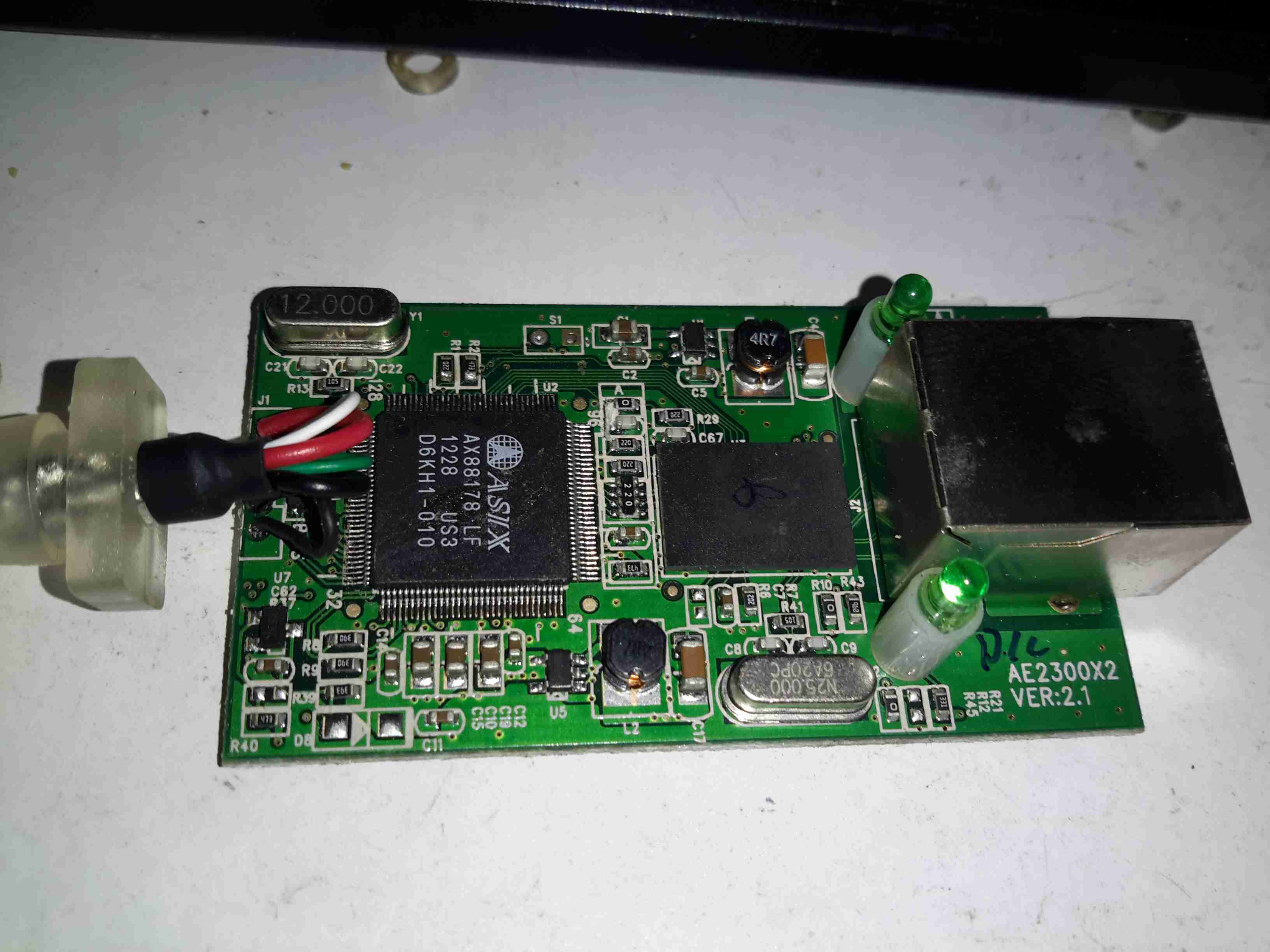
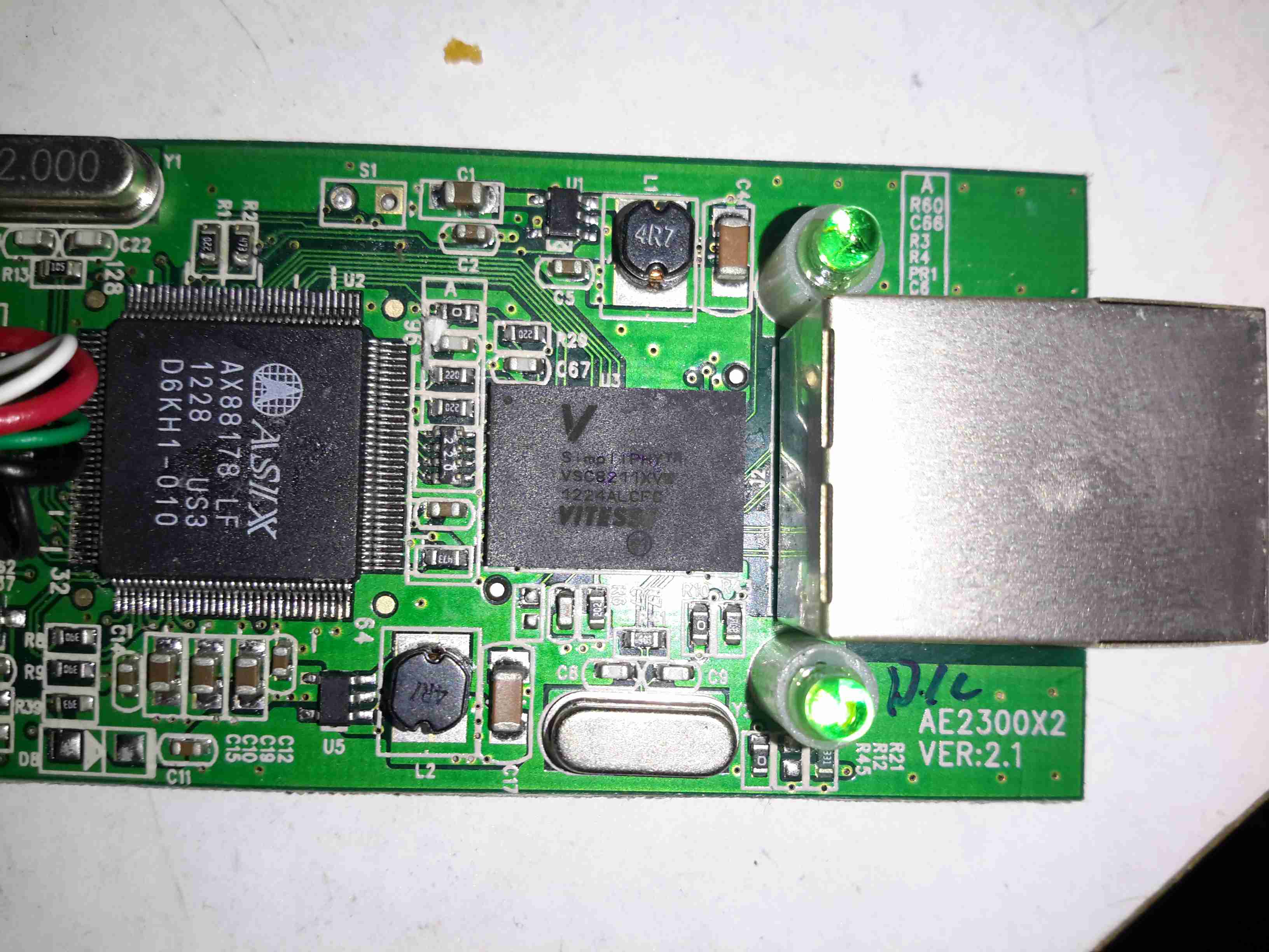
Main Chipset
This is quite a heavily packed PCB, with the main Asix AX88178 on the left. This IC contains all of the logic for implementing the Ethernet link over USB, except the PHY. It’s clock crystal is in the top left corner.
Reverse Side
Not much on the reverse side, there’s a 3.3v linear regulator at top left, the SOIC is an Atmel AT93C66A 4KB EEPROM for configuration data.
Vitesse PHY
The final IC in the chain is the Vitesse VSC8211 Gigabit PHY, with it’s clock crystal below. This interfaces the Ethernet MAC in the Asix IC to the magjack on the right.
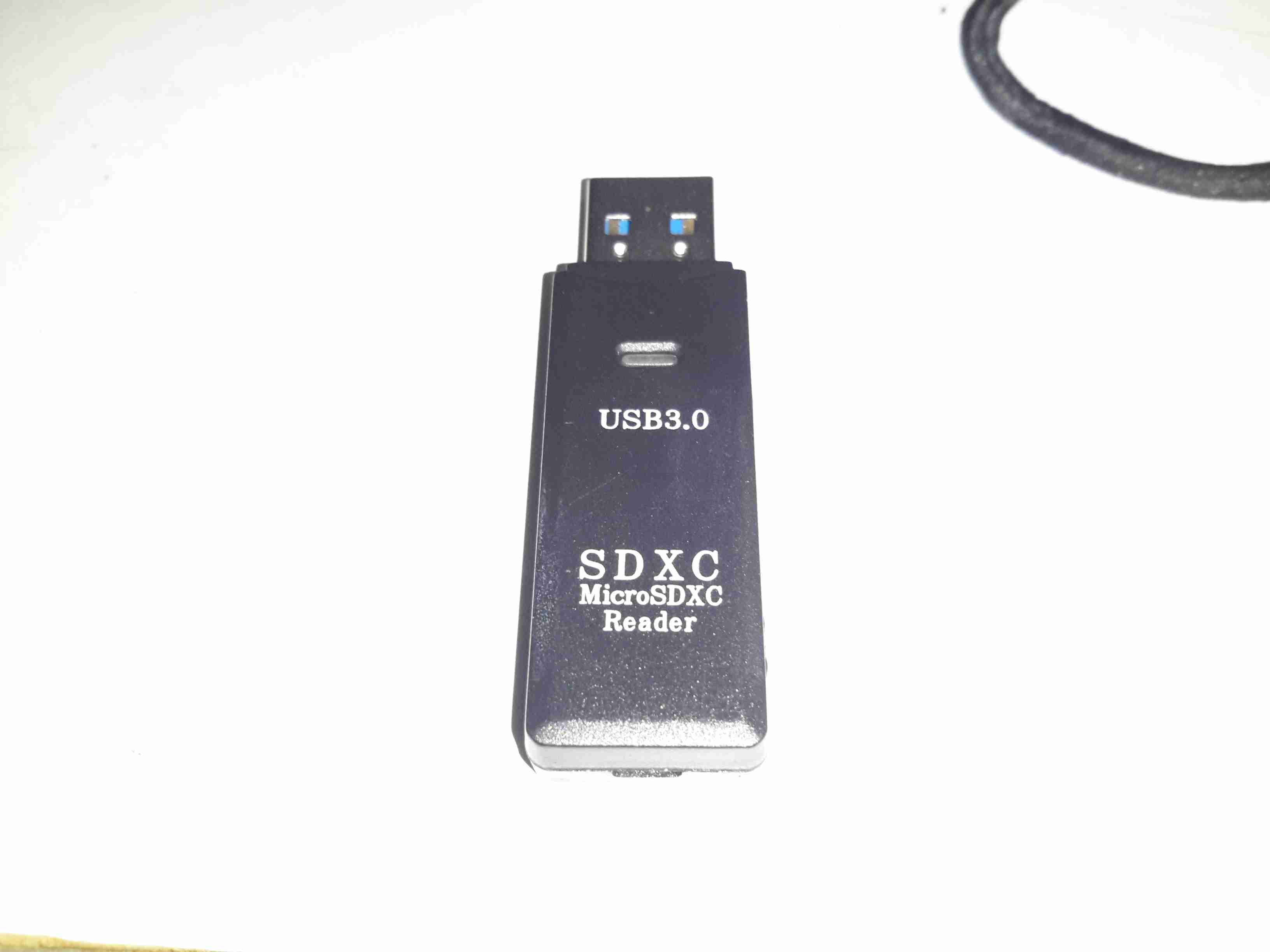
This is a cheap little eBay reader to replace my ~10 year old multi-reader that very recently died. My original was an 8-in-1 version, but as I never read anything else other than SD cards these days, a little USB dongle version was more convenient.
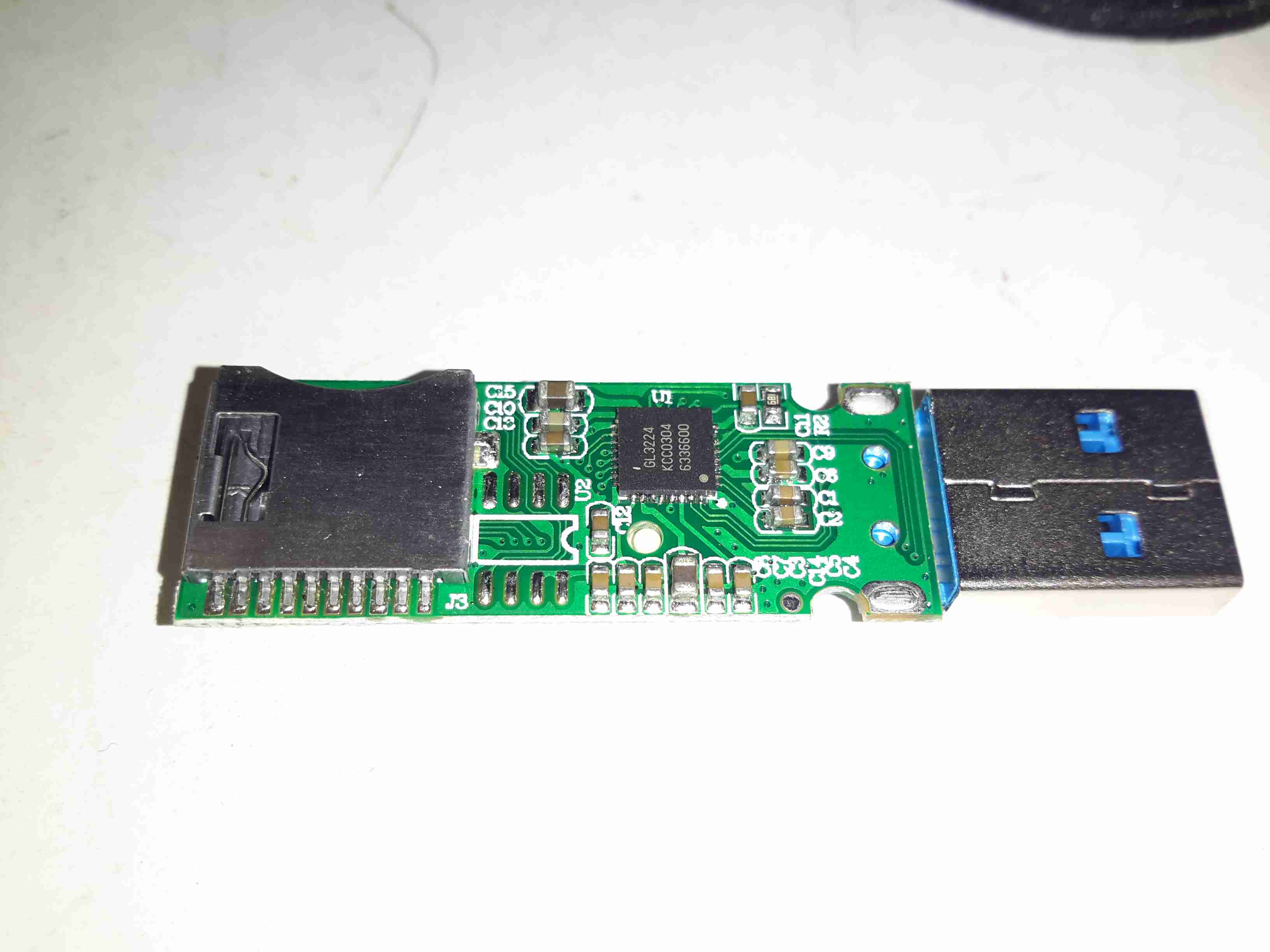
Controller Chipset
The layout is very minimal, just the µSD socket, bypass passives & the main controller chip on this side, which is a GL3224 Dual LUN Memory Card Controller from Genesys Logic. This is fully USB3 capable according to the datasheet, but I’m not certain of the advantage of this for something that reads relatively slow devices like SD cards.
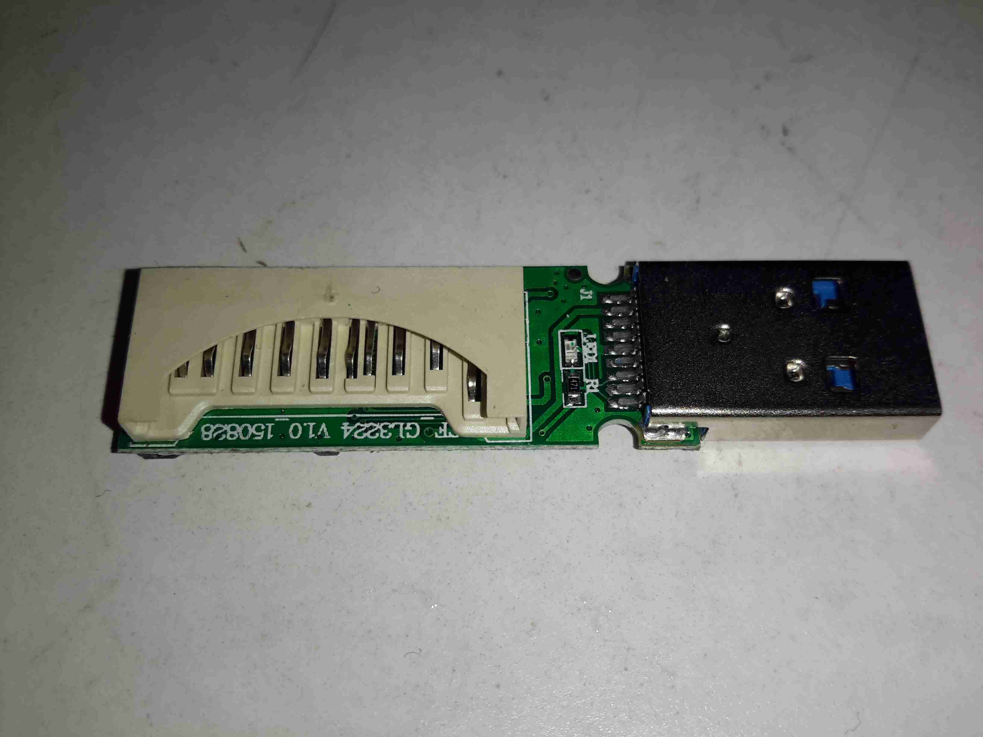
SD Socket
The other side of the PCB holds the full size SD socket, along with the activity LED & USB connector.
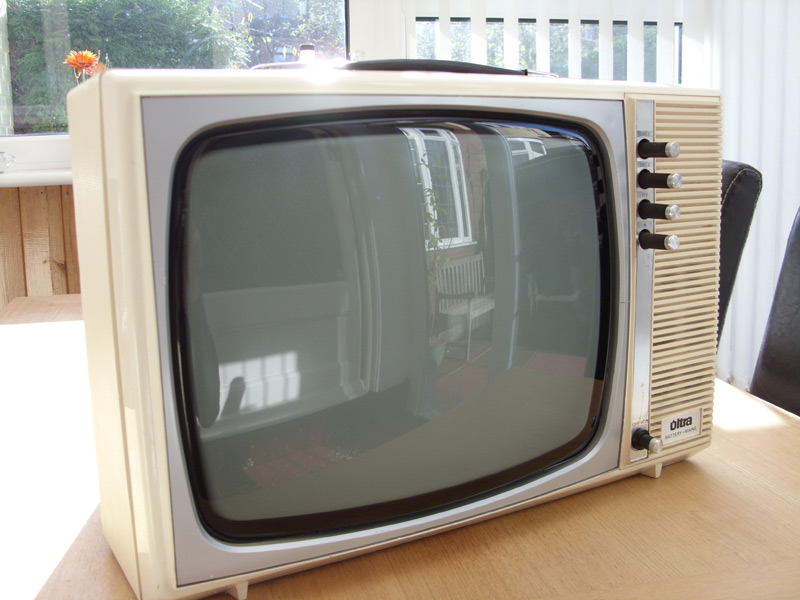
The other day at the local canal-side waterpoint, this TV was dumped for recycling, along with another later model Colour TV. This is a 1970’s Black & White mains/battery portable made by Thorn. It’s based on a common British Radio Corporation 1590 chassis. Having received a soaking from rain, I didn’t expect this one to work very well.
Tuner
Being so old, there is no electronic control of the tuner in this TV, and only has the capability to mechanically store 4 different channels. The tuner itself is a cast box with a plastic cover.
Tuning Lever
The mechanical buttons on the front of the TV push on this steel bar, by different amounts depending on the channel setting. This bar is connected to the tuning capacitor inside the tuner.
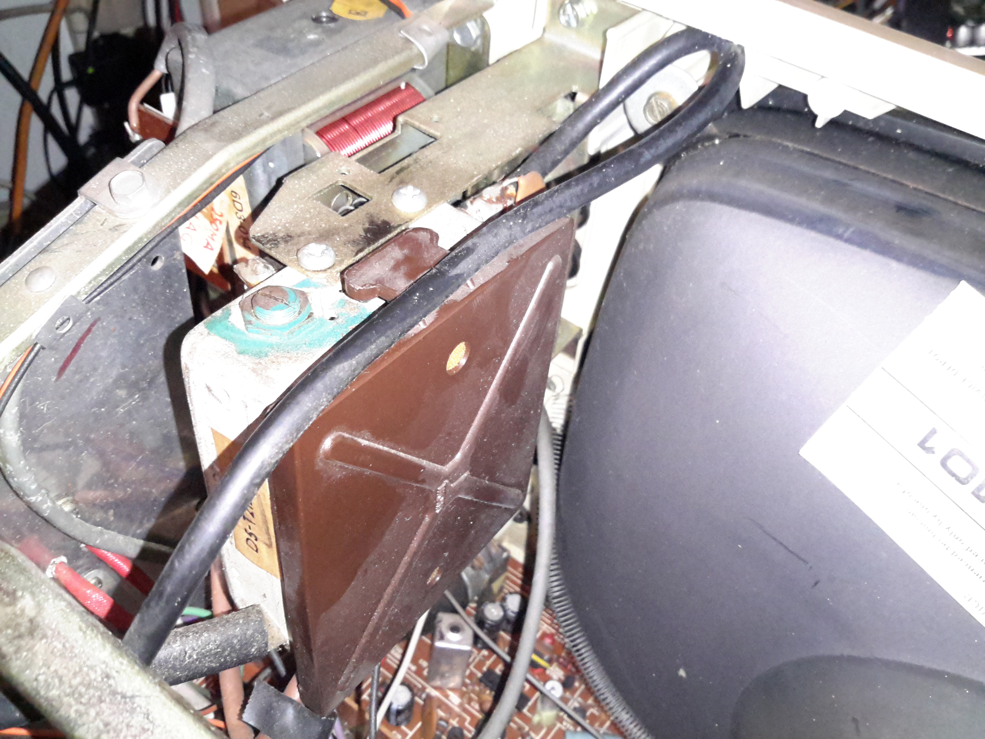
Tuner Compartments
Unclipping the plastic cover, with it’s lining of aluminium foil for shielding reveals the innards of the tuner module.
Tuner Input Stage
Here’s the tuner front end RF transistor, which has it’s can soldered into the frame, this is an AF239 germanium UHF transistor, rated at up to 900MHz.
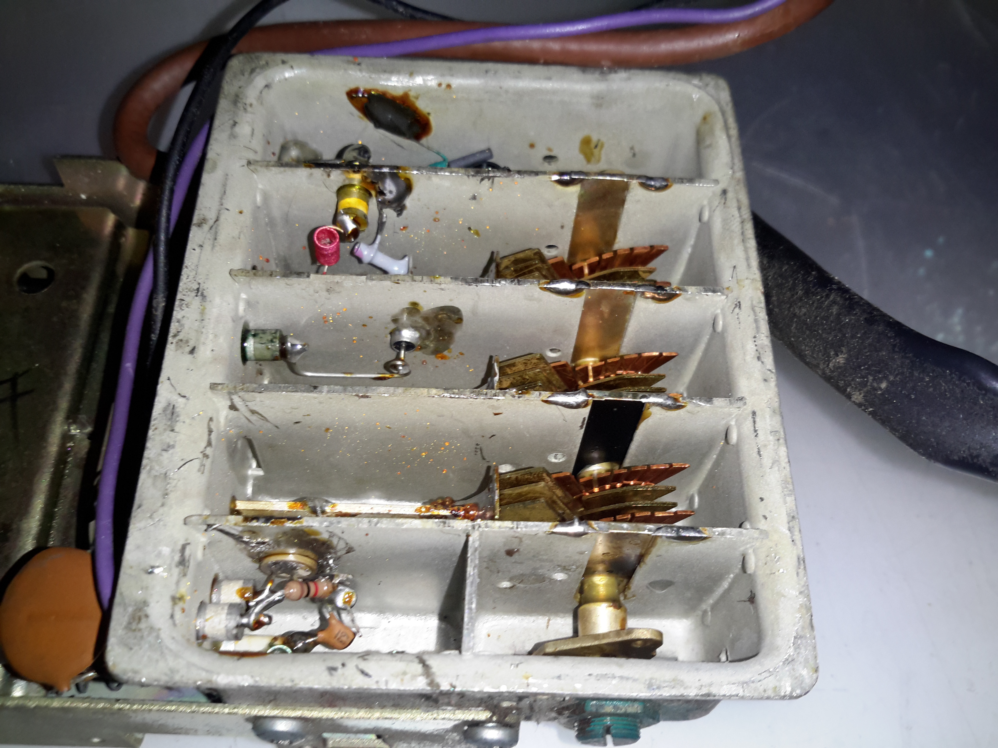
Tuner IF Mixer Stage
As the signal propagates through the compartments of the tuner, another transistor does the oscillator / IF mixing, an AF139 germanium, rated to 860MHz.
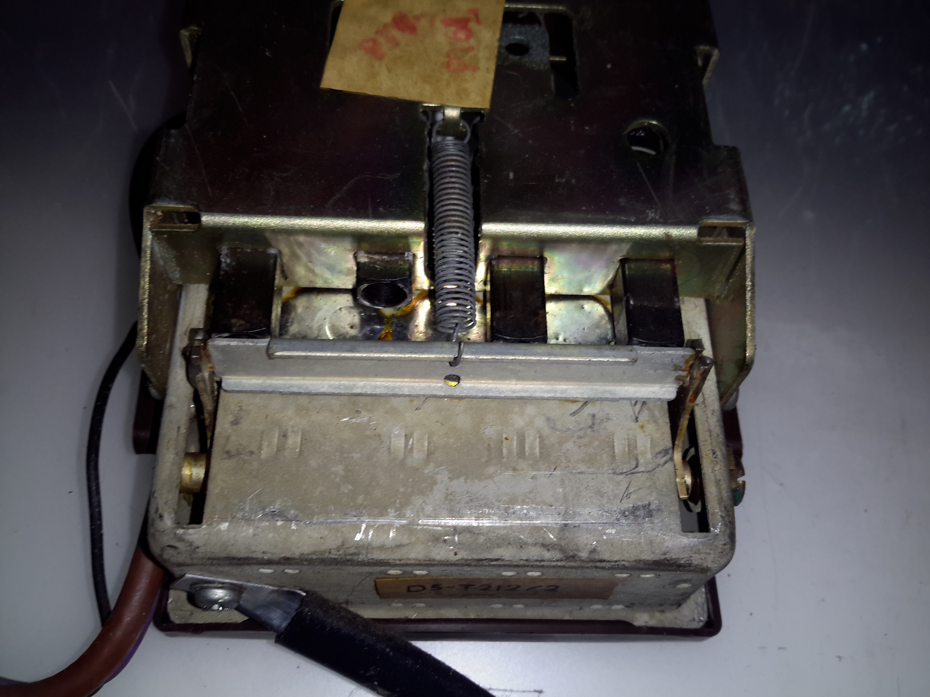
Tuning Capacitor
As the buttons on the front of the set are pushed, moving the lever on the outside, the tuning capacitor plates intermesh, changing the frequency that is filtered through the tuner. The outer blades of the moving plates are slotted to allow for fine tuning of the capacitance, and therefore transmitted frequency by bending them slightly.
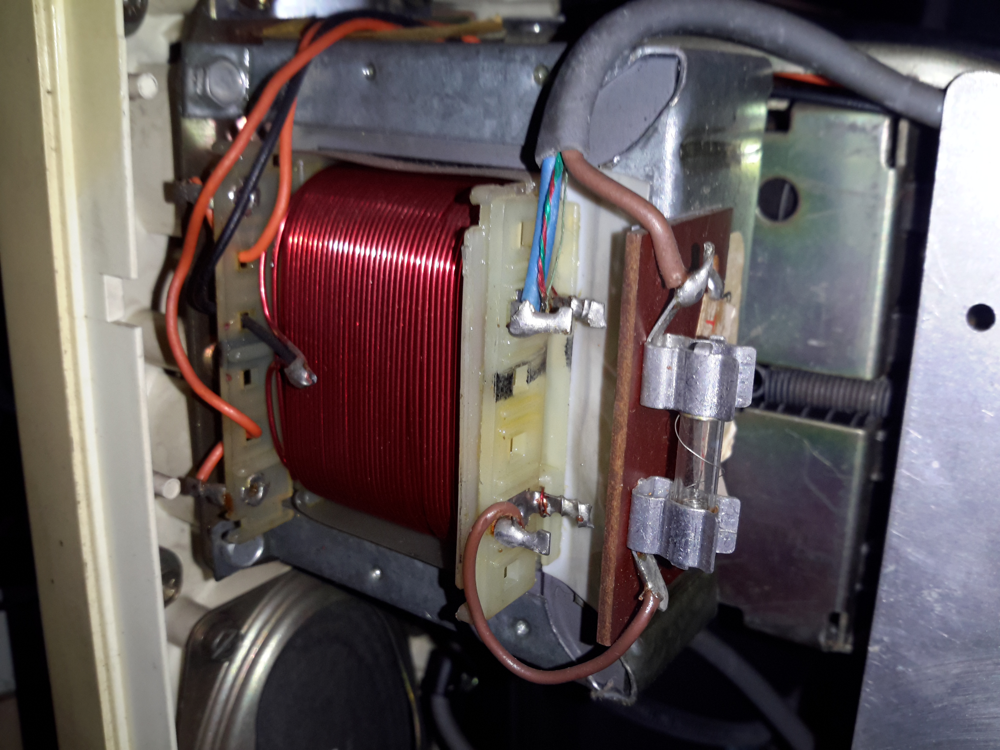
Mains Transformer
Being a dual supply TV that can operate on either 12v battery power or mains, this one has a large centre tapped mains transformer that generates the low voltage when on AC power. Full wave rectification is on the main PCB. The fuse of this transformer has clearly been blown in the past, as it’s been wound with a fine fuse wire around the outside to repair, instead of just replacing the fuse itself.
Chassis Rear
The back of the set has all the picture controls on the bottom edge, with the power input & antenna connections on the left just out of shot. The CRT in this model is an A31-120W 12″ tube, with a really wide deflection angle of 110°, which allows the TV to be smaller.
Main PCB
The bottom of the mainboard has all the silkscreen markings for the components above which certainly makes servicing easier 😉 This board’s copper tracks would have been laid out with tape, obviously before the era of PCB design software.
Components
The components on this board are laid out everywhere, not just in square grids. The resistors used are the carbon composition type, and at ~46 years old, they’re starting to drift a bit. After measuring a 10K resistor at 10.7K, all of these would need replacing I have no doubt. Incedentally, this TV could be converted to take a video input without the tuner, by lifting the ferrite beaded end of L9 & injecting a signal there.
Flyback Primary Windings
The flyback (Line Output Transformer) is of the old AC type, with the rectifier stack on top in the blue tube, as opposed to more modern versions that have everything potted into the same casing. The primary windings are on the other leg of the ferrite core, making these transformers much more easily repairable. This transformer generates the 12kV required for the CRT final anode, along with a few other voltages used in the TV, for focussing, etc.
Rectifier Stack
The main EHT rectifier stack looks like a huge fuse, inside the ceramic tube will be a stack of silicon diodes in series, to withstand the high voltage present.
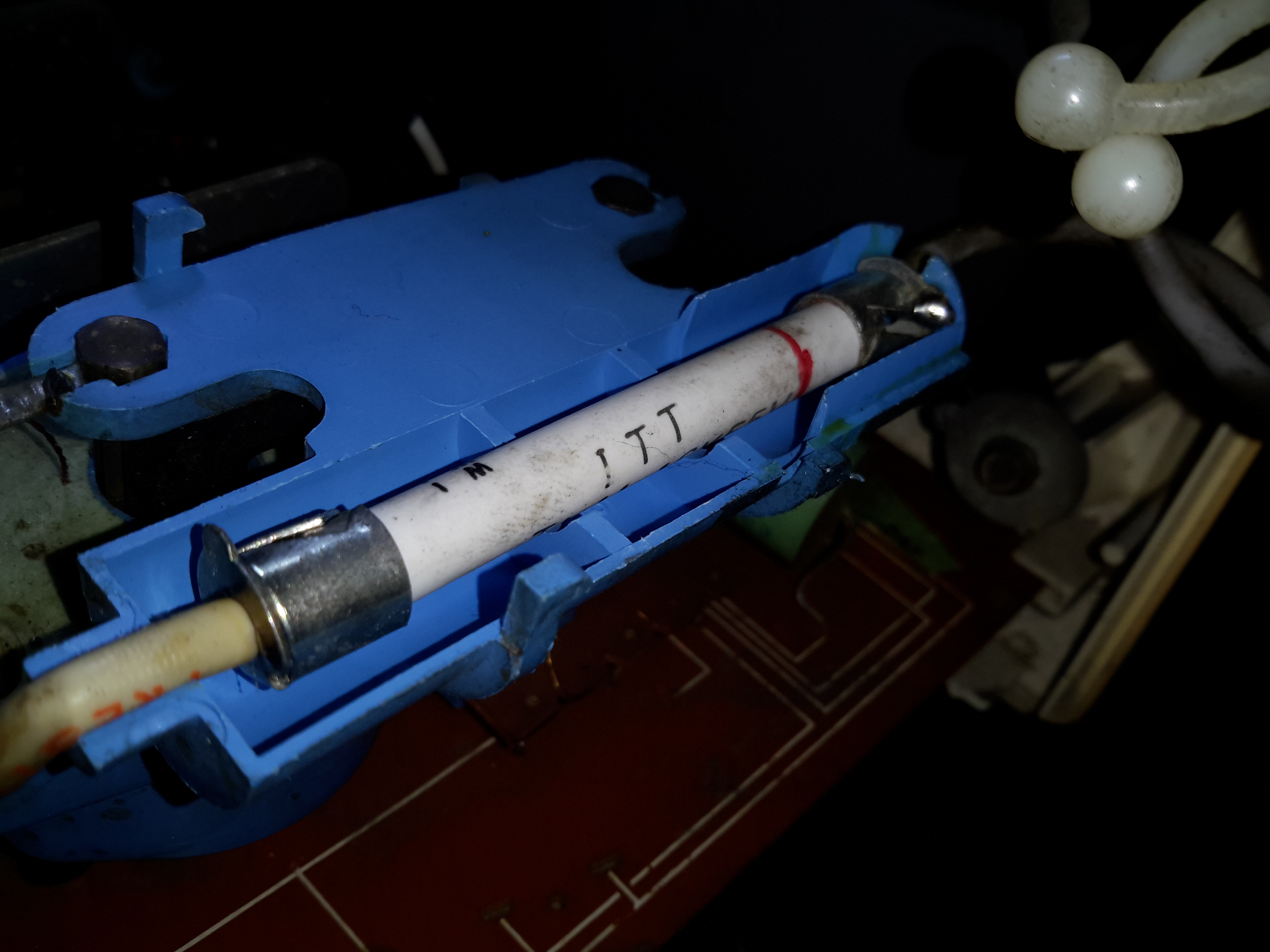
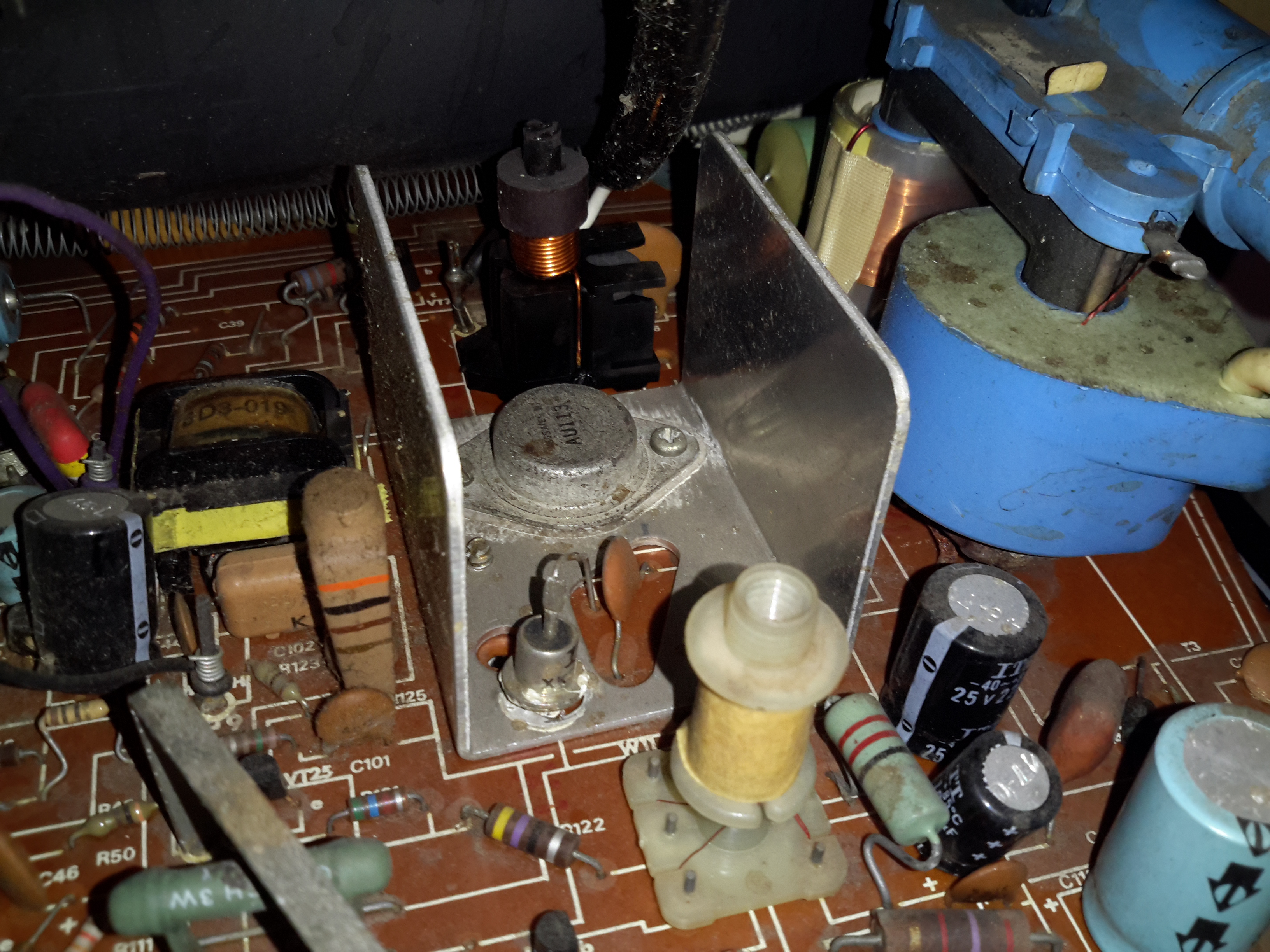
Horizontal Output Transistor
This is the main switching transistor that drives the flyback, the HOT. This is an AU113, another germanium type, rated at 250v 4A. The large diode next to the transistor is the damper.
I’ve managed to find all the service information for this set online, link below!
[download id=”5616″]
More to come if I manage to get this TV working!
I was recently given this unit, along with another Behringer sound processor to repair, as the units were both displaying booting problems. This first one is a rather swish Mastering Processor, which has many features I’ll leave to Behringer to explain 😉
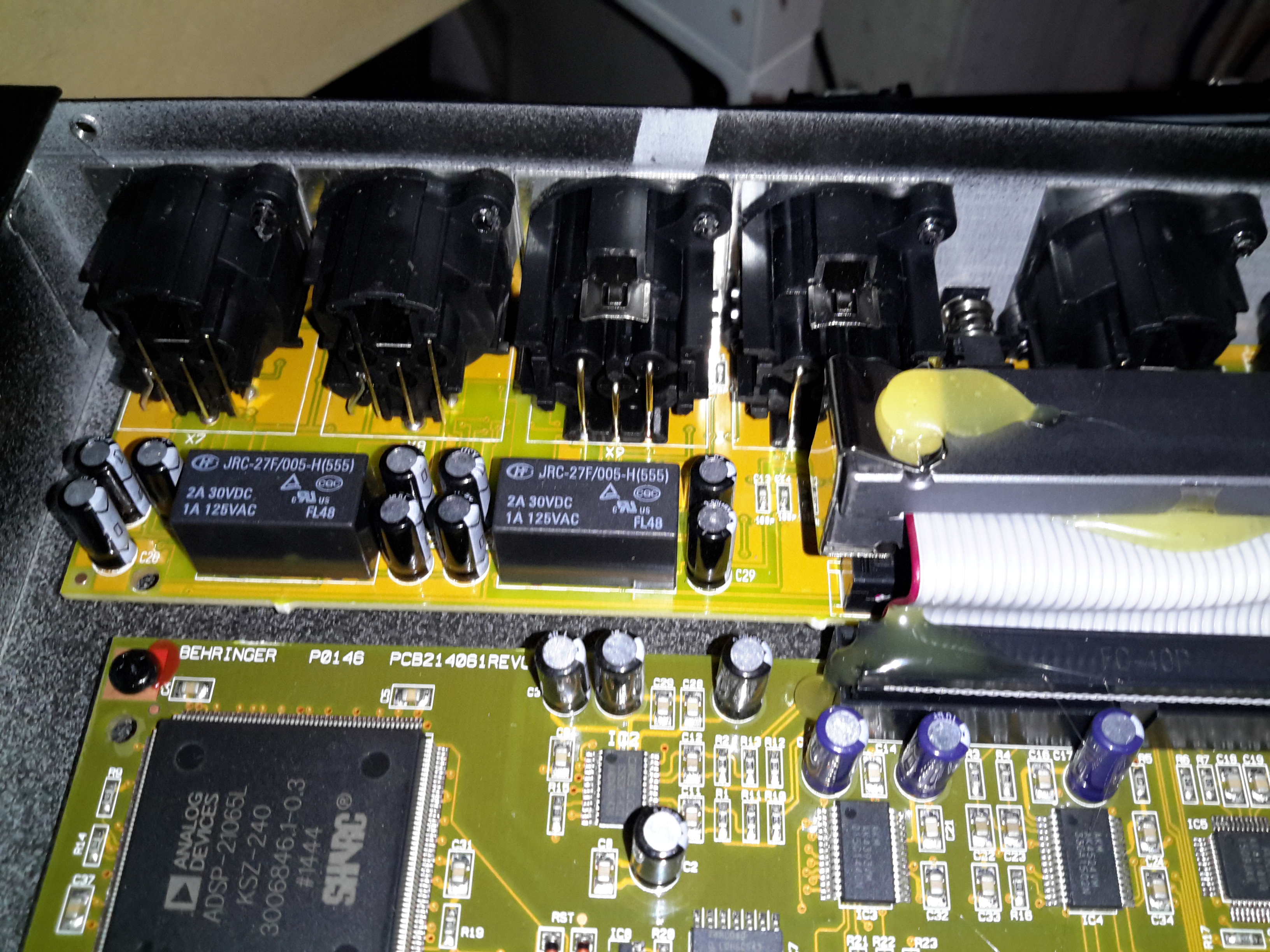
Input Board & Relays
All the inputs are on the back of this 19″ rackmount bit of kit, nothing much on this PCB other than the connectors & a couple of switching relays.
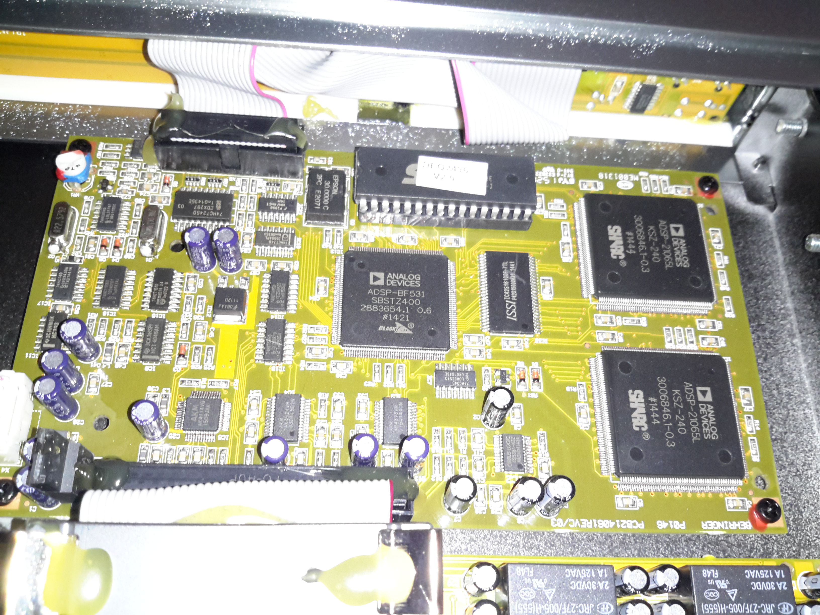
Main Processor PCB
All the magic is done on the main processor PCB, which is host to 3 Analog Devices DSP processors:
ADSP-BF531 BlackFin DSP. This one is probably handling most of the audio processing, as it’s the most powerful DSP onboard at 600Mhz. There’s a ROM on board above this for the firmware & a single RAM chip. On the right are a pair of ADSP-21065 DSP processors at a lower clock rate of 66MHz. To the left is some glue logic to interface the user controls & dot-matrix LCD.
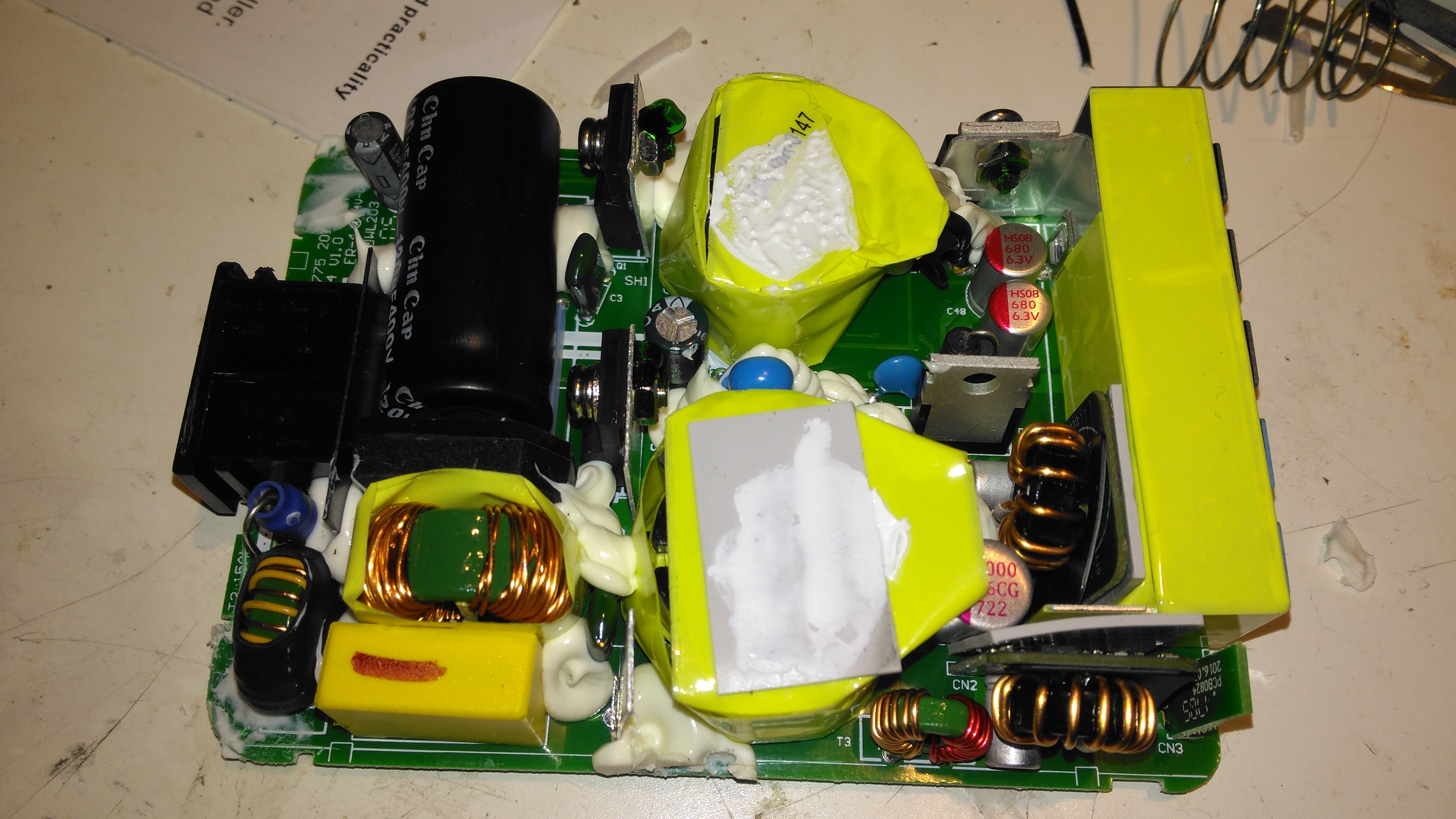
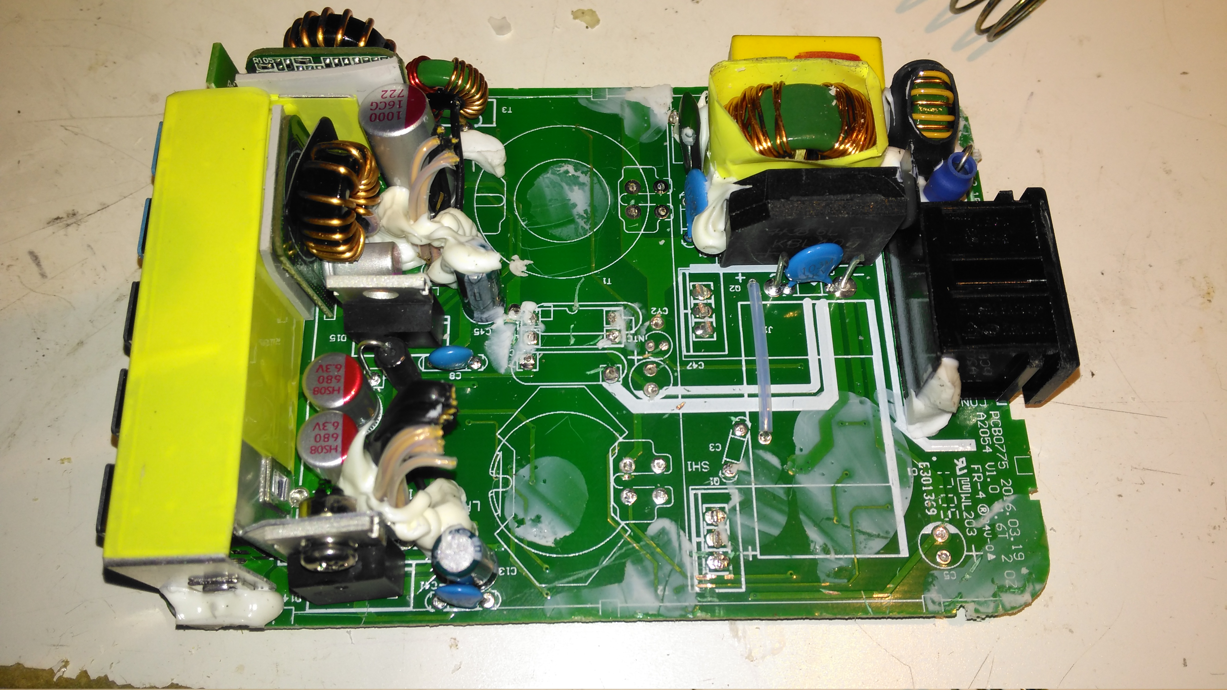
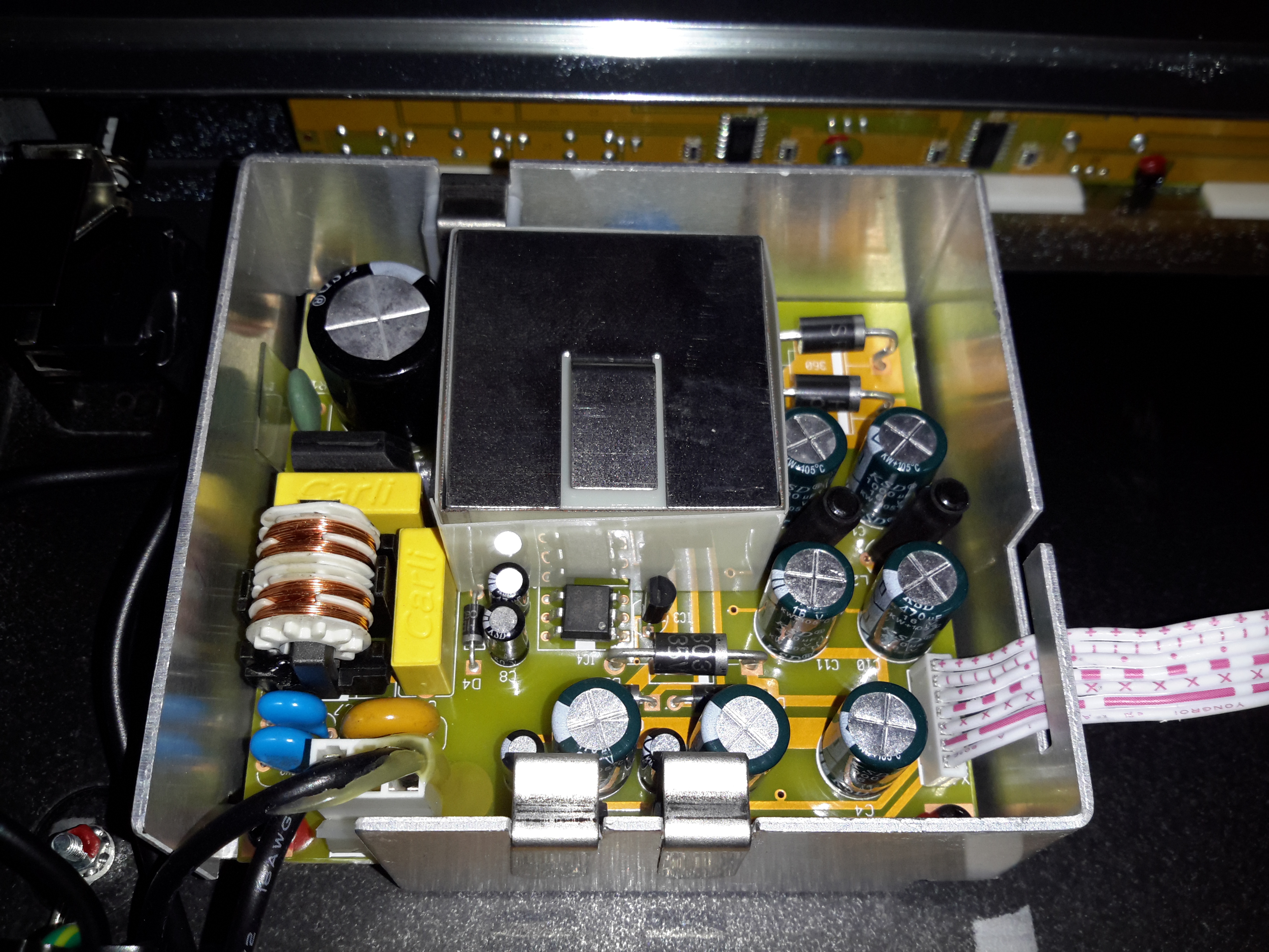
PSU Module
The PSU in this unit is a pretty standard looking SMPS, with some extra noise filtering & shielding. The main transformer is underneath the mu-metal shield in the centre of the board.
Tip Jar
If you’ve found my content useful, please consider leaving a donation by clicking the Tip Jar below!
All collected funds go towards new content & the costs of keeping the server online.