Posted on Leave a comment

Thorn Ultra 6816 B&W CRT TV Teardown

Thorn Ultra 6816
Thorn Ultra 6816 (Stock Photo)

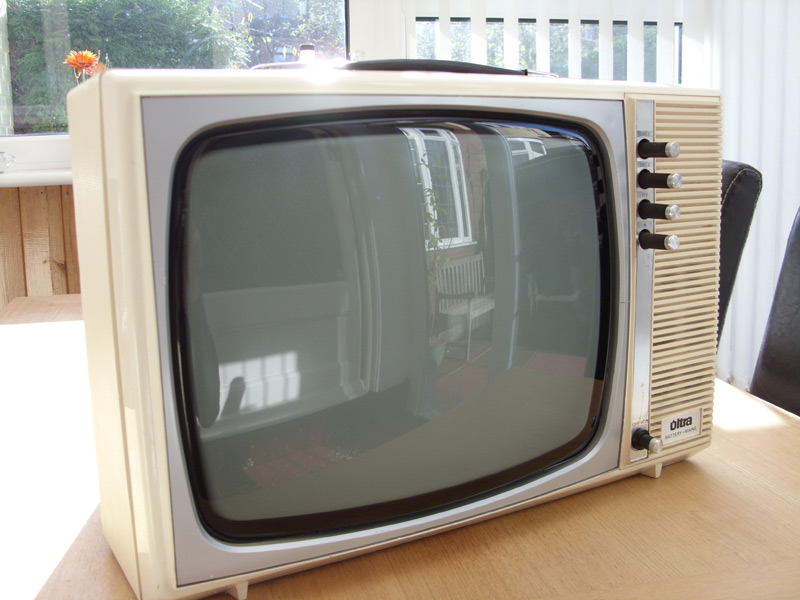
The other day at the local canal-side waterpoint, this TV was dumped for recycling, along with another later model Colour TV. This is a 1970’s Black & White mains/battery portable made by Thorn. It’s based on a common British Radio Corporation 1590 chassis. Having received a soaking from rain, I didn’t expect this one to work very well.

Tuner
Tuner

Being so old, there is no electronic control of the tuner in this TV, and only has the capability to mechanically store 4 different channels. The tuner itself is a cast box with a plastic cover.

Tuning Lever
Tuning Lever

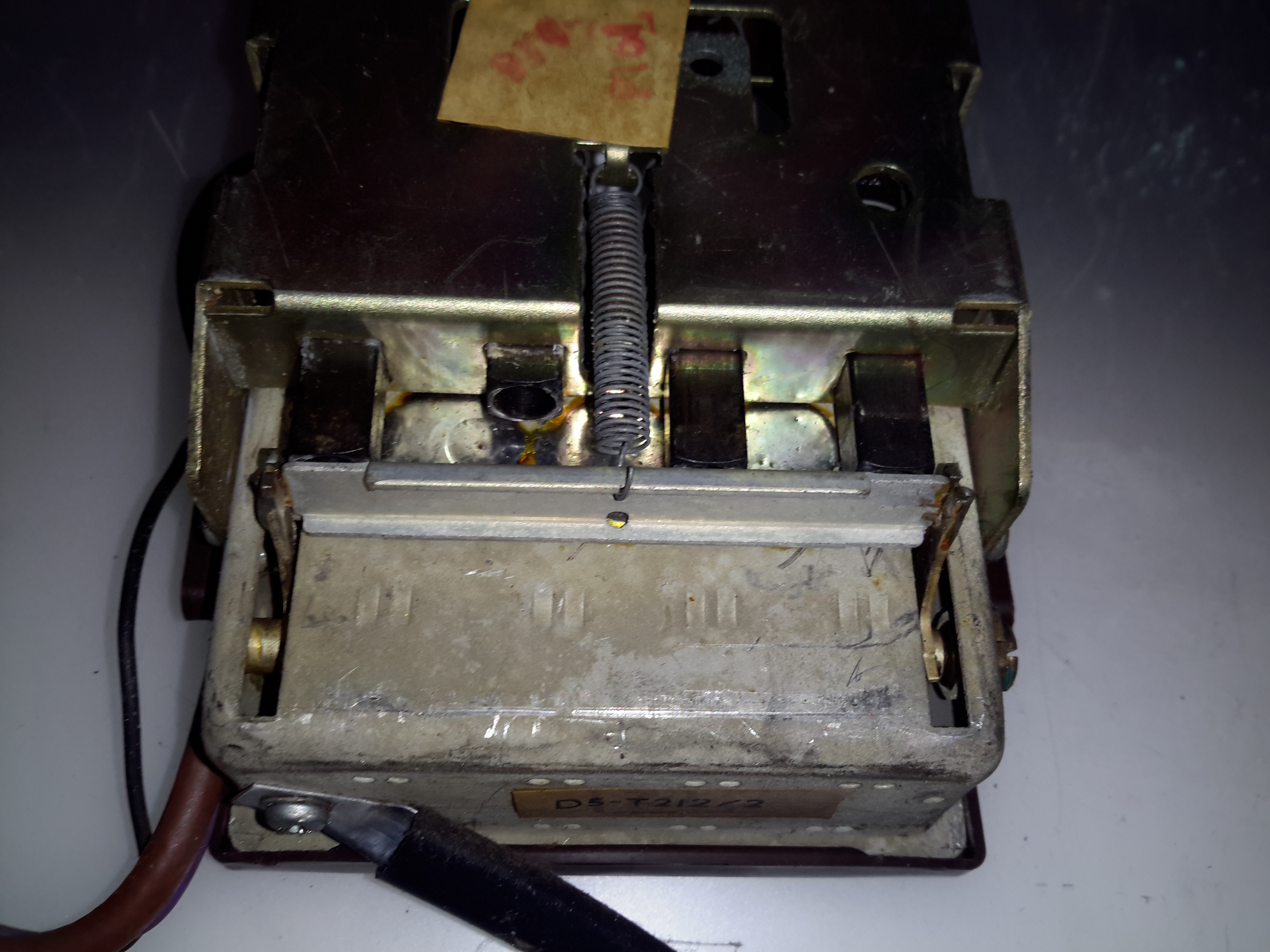
The mechanical buttons on the front of the TV push on this steel bar, by different amounts depending on the channel setting. This bar is connected to the tuning capacitor inside the tuner.

Tuner Compartments
Tuner Compartments

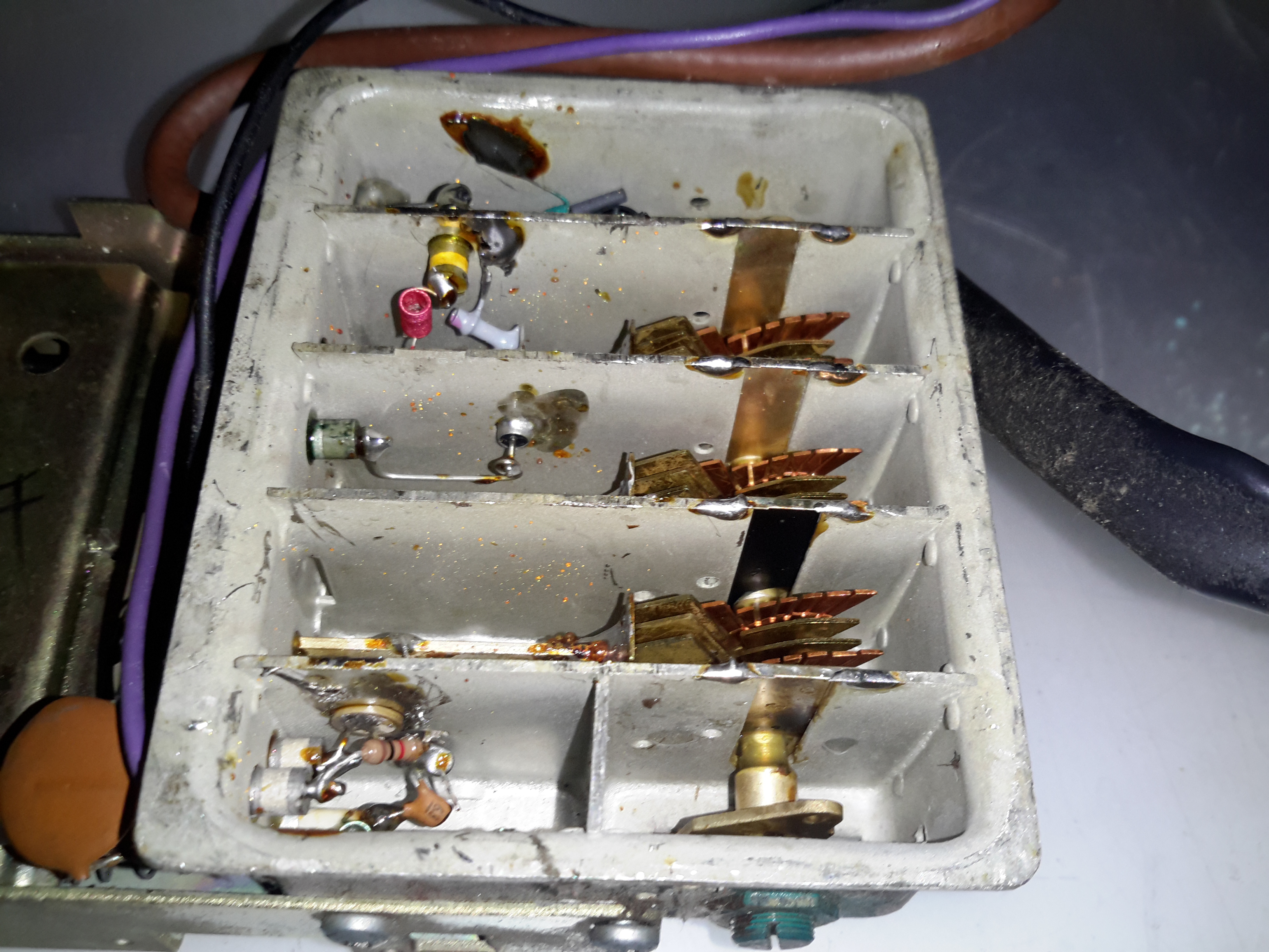
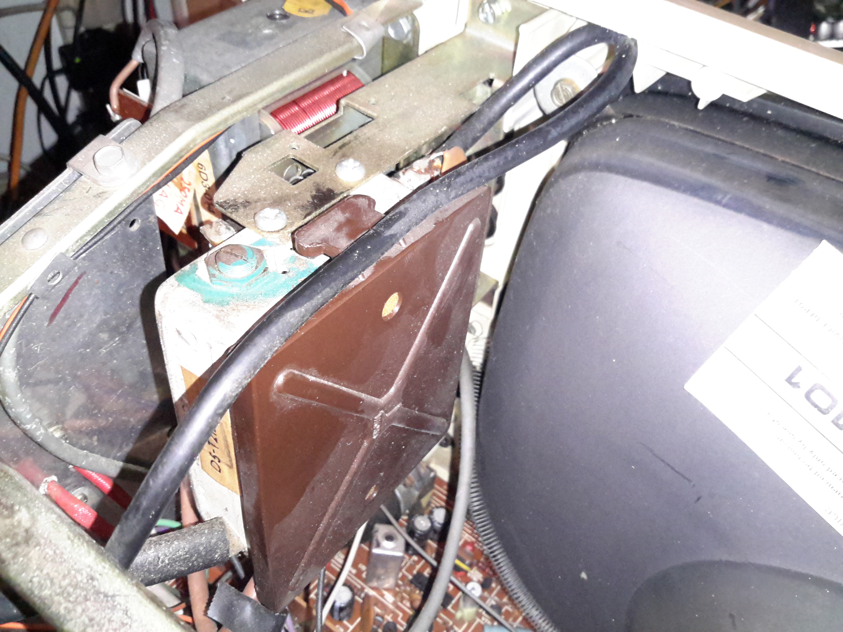
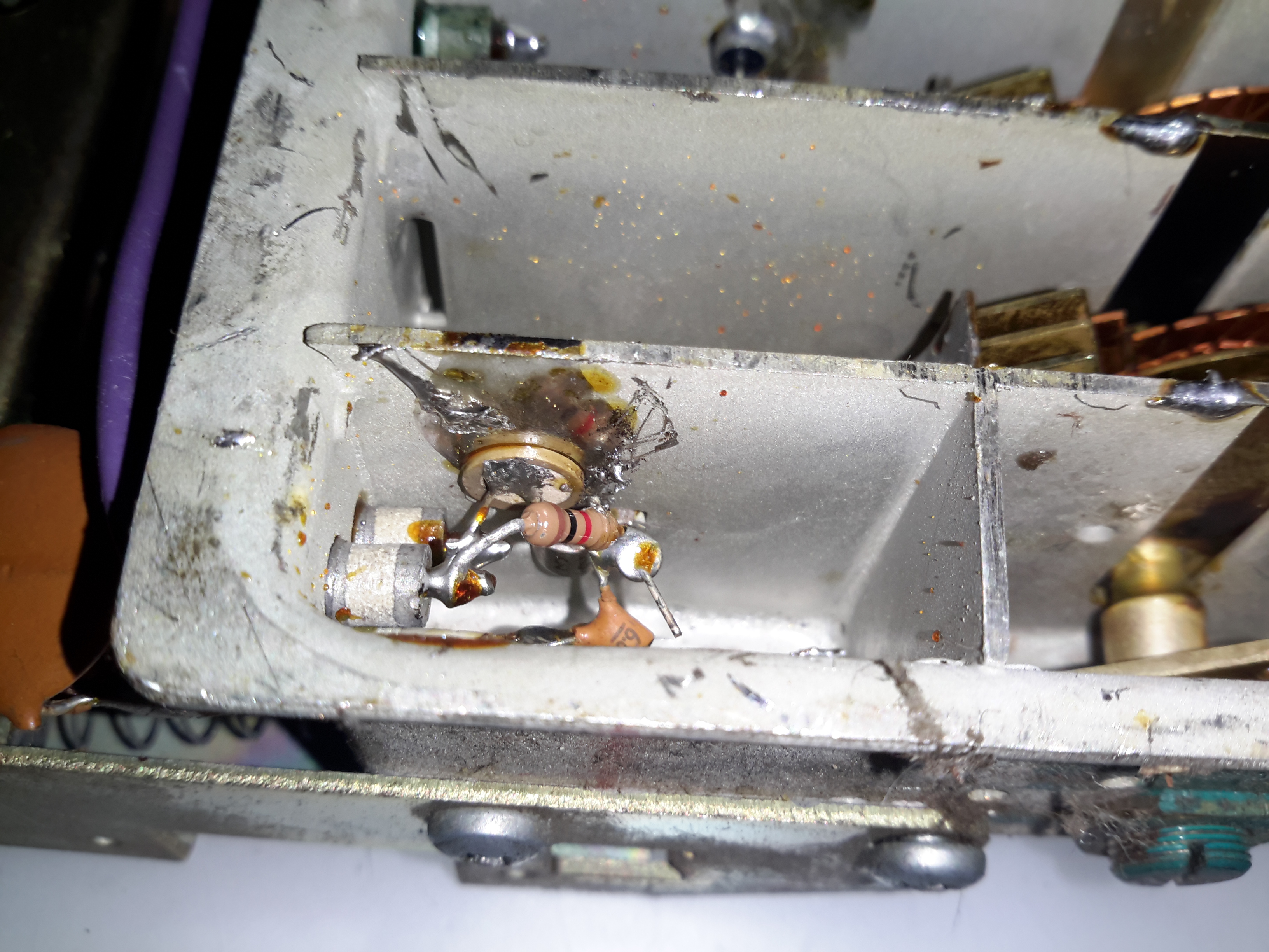
Unclipping the plastic cover, with it’s lining of aluminium foil for shielding reveals the innards of the tuner module.

Tuner Input Stage
Tuner Input Stage

Here’s the tuner front end RF transistor, which has it’s can soldered into the frame, this is an AF239 germanium UHF transistor, rated at up to 900MHz.

Tuner IF Mixer Stage

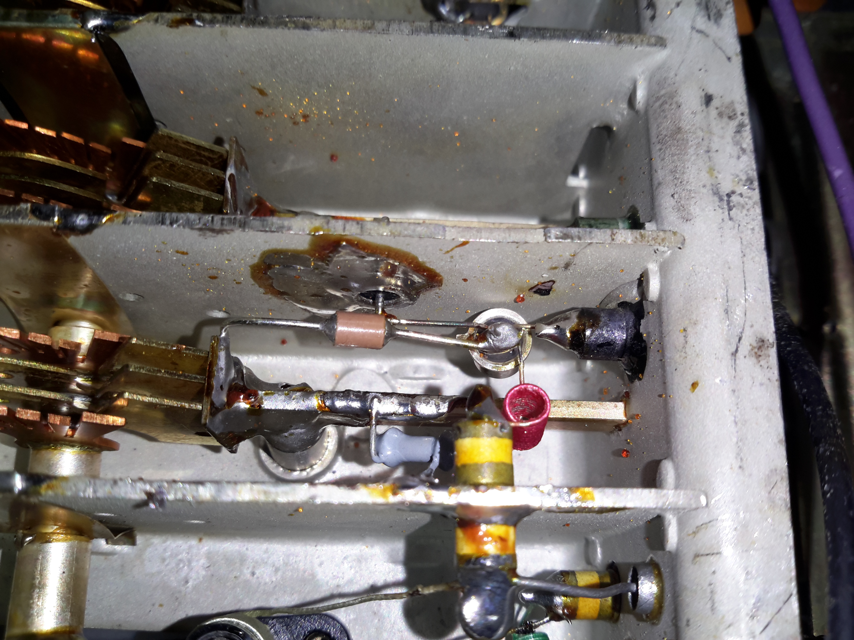
As the signal propagates through the compartments of the tuner, another transistor does the oscillator / IF mixing, an AF139 germanium, rated to 860MHz.

Tuning Capacitor
Tuning Capacitor

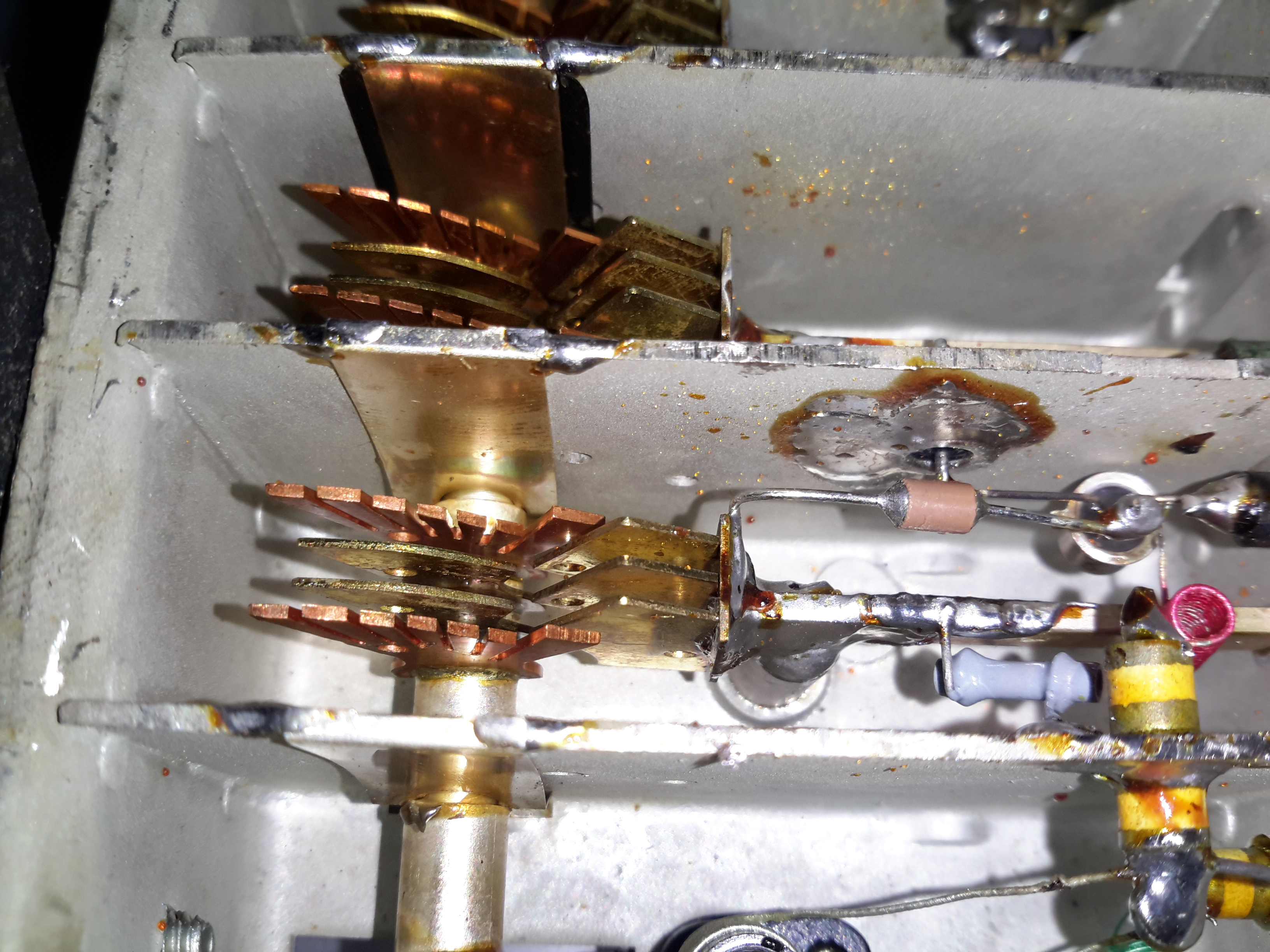
As the buttons on the front of the set are pushed, moving the lever on the outside, the tuning capacitor plates intermesh, changing the frequency that is filtered through the tuner. The outer blades of the moving plates are slotted to allow for fine tuning of the capacitance, and therefore transmitted frequency by bending them slightly.

Mains Transformer
Mains Transformer

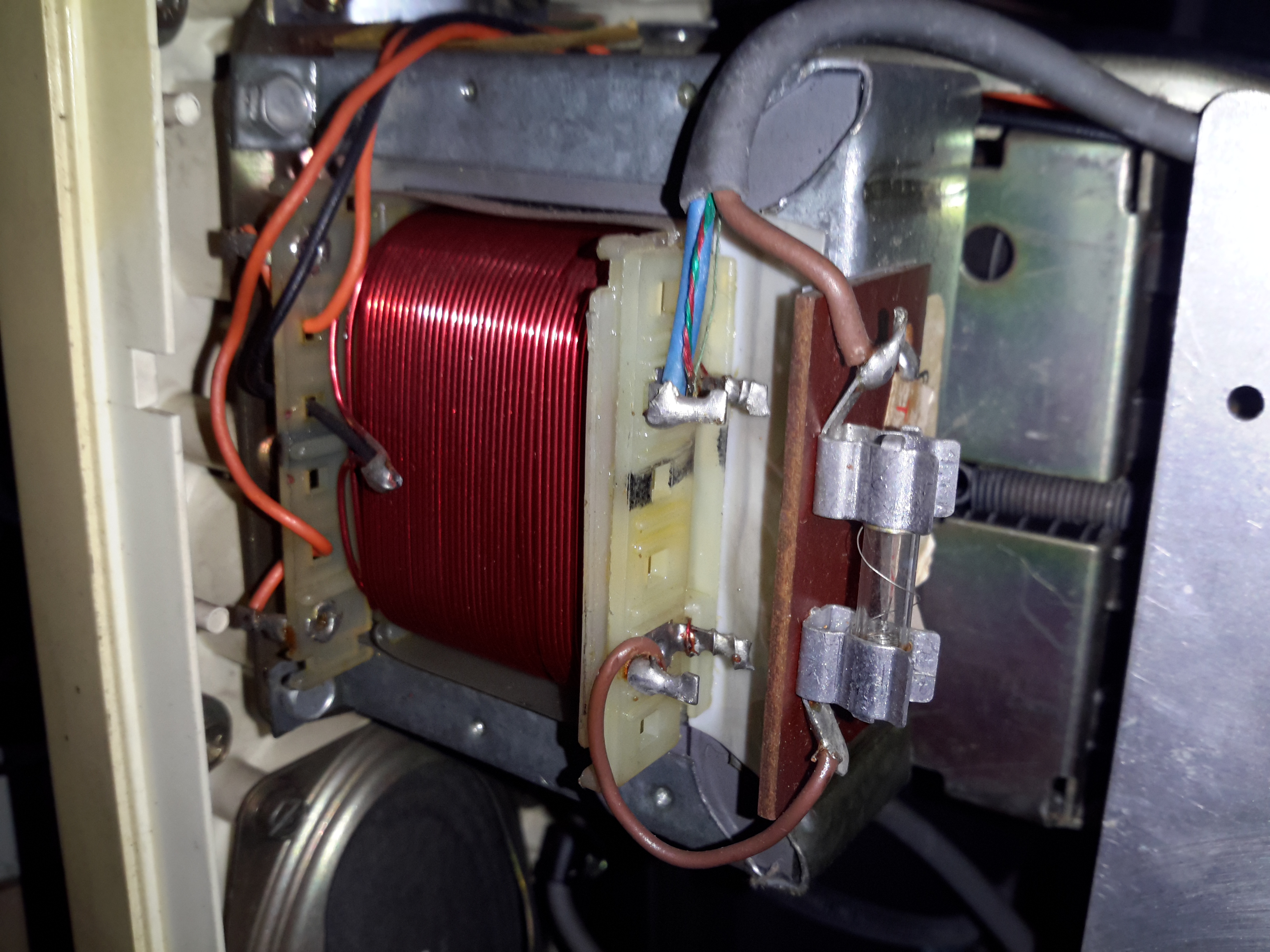
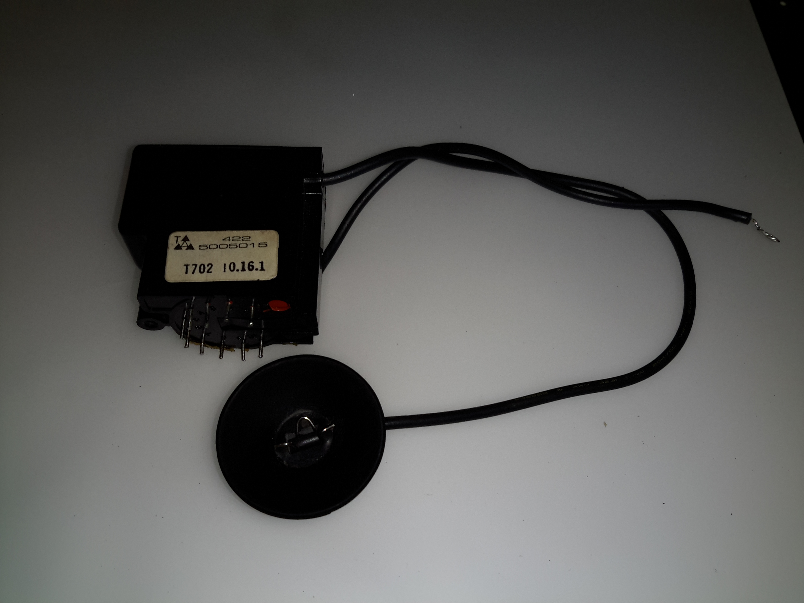
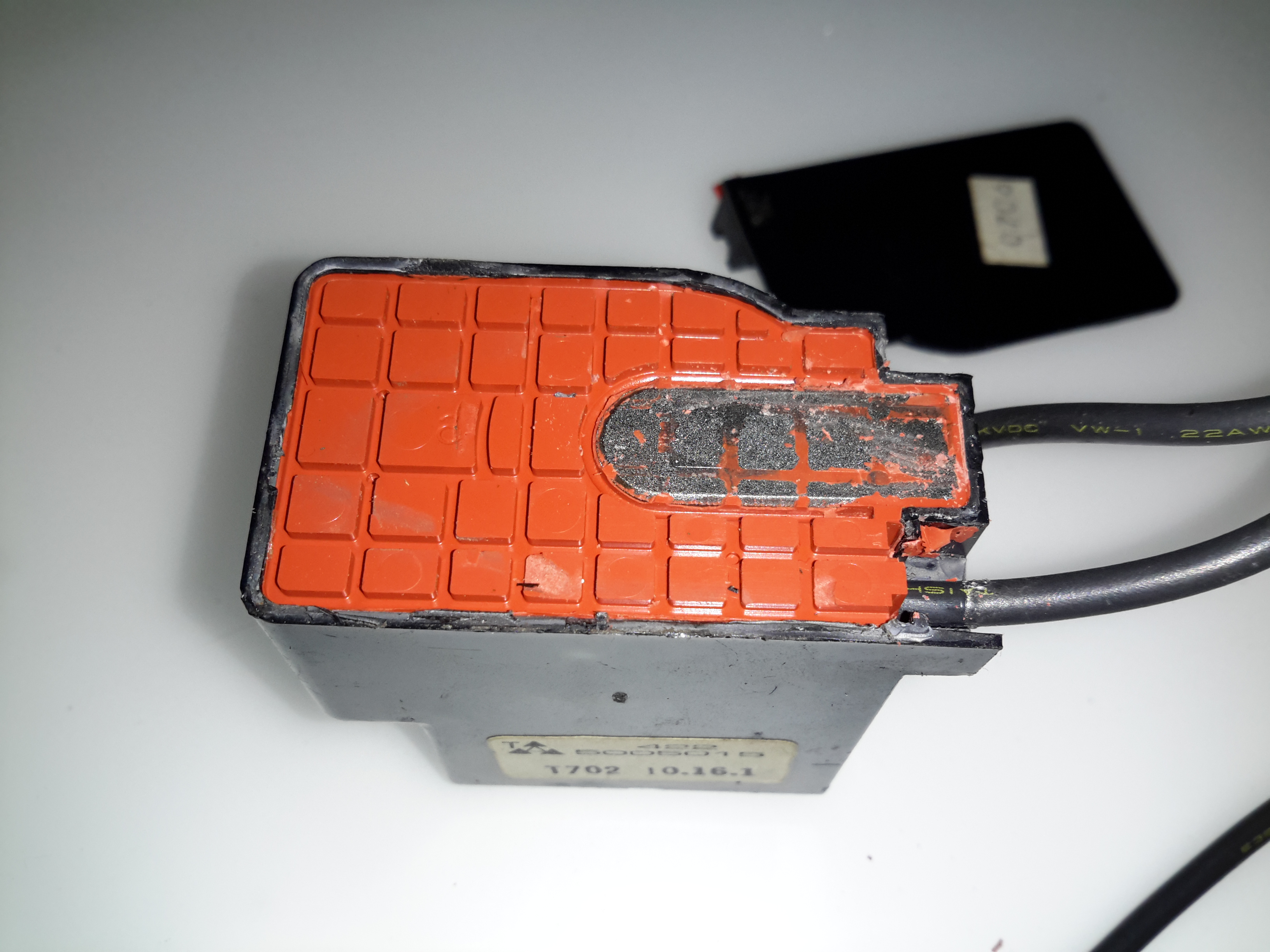
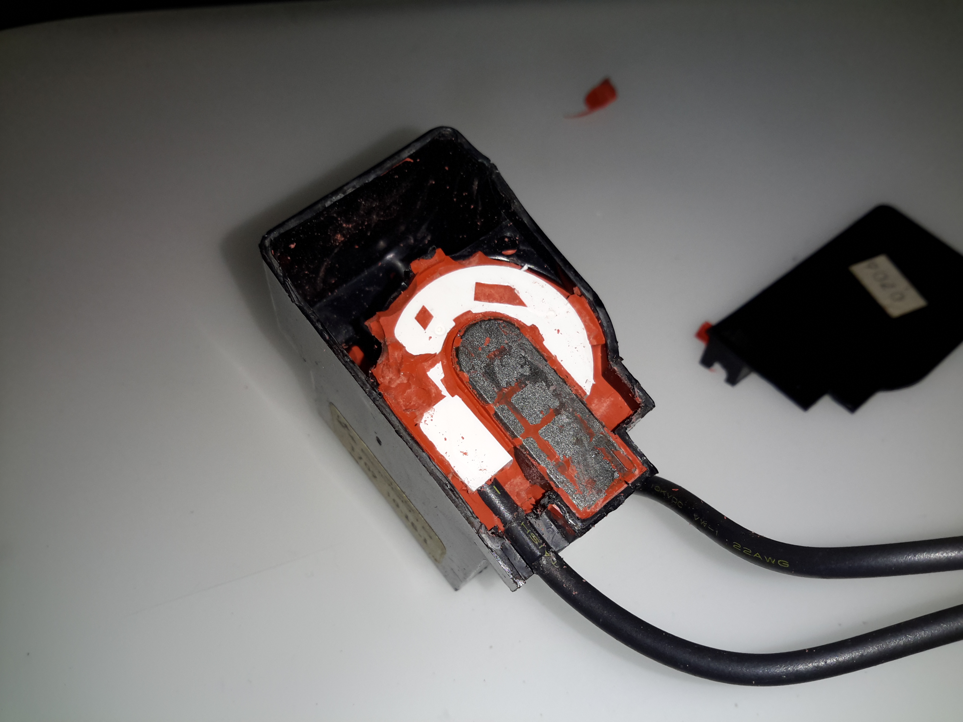
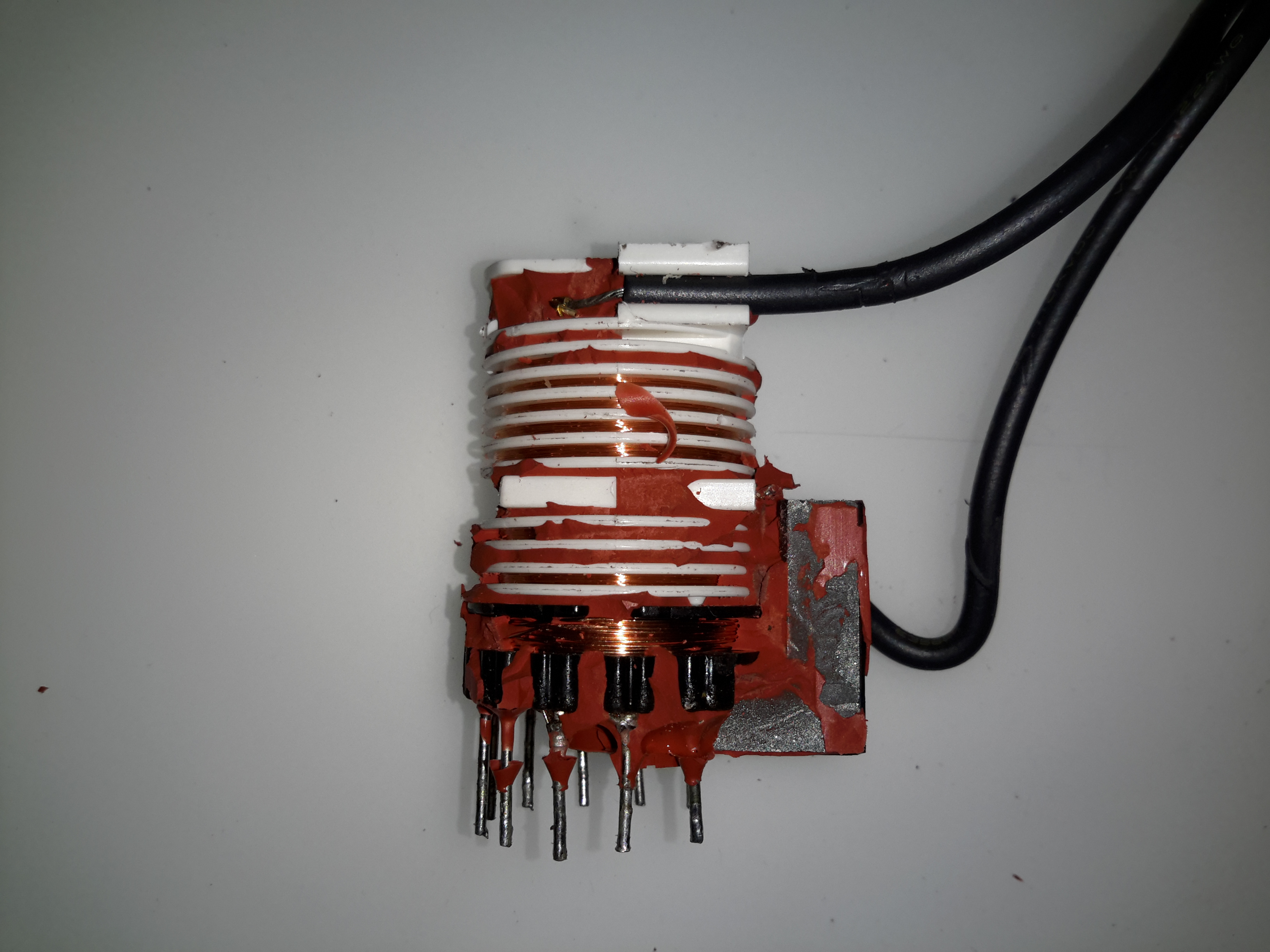
Being a dual supply TV that can operate on either 12v battery power or mains, this one has a large centre tapped mains transformer that generates the low voltage when on AC power. Full wave rectification is on the main PCB. The fuse of this transformer has clearly been blown in the past, as it’s been wound with a fine fuse wire around the outside to repair, instead of just replacing the fuse itself.

Chassis Rear
Chassis Rear

The back of the set has all the picture controls on the bottom edge, with the power input & antenna connections on the left just out of shot. The CRT in this model is an A31-120W 12″ tube, with a really wide deflection angle of 110°, which allows the TV to be smaller.

Main PCB
Main PCB

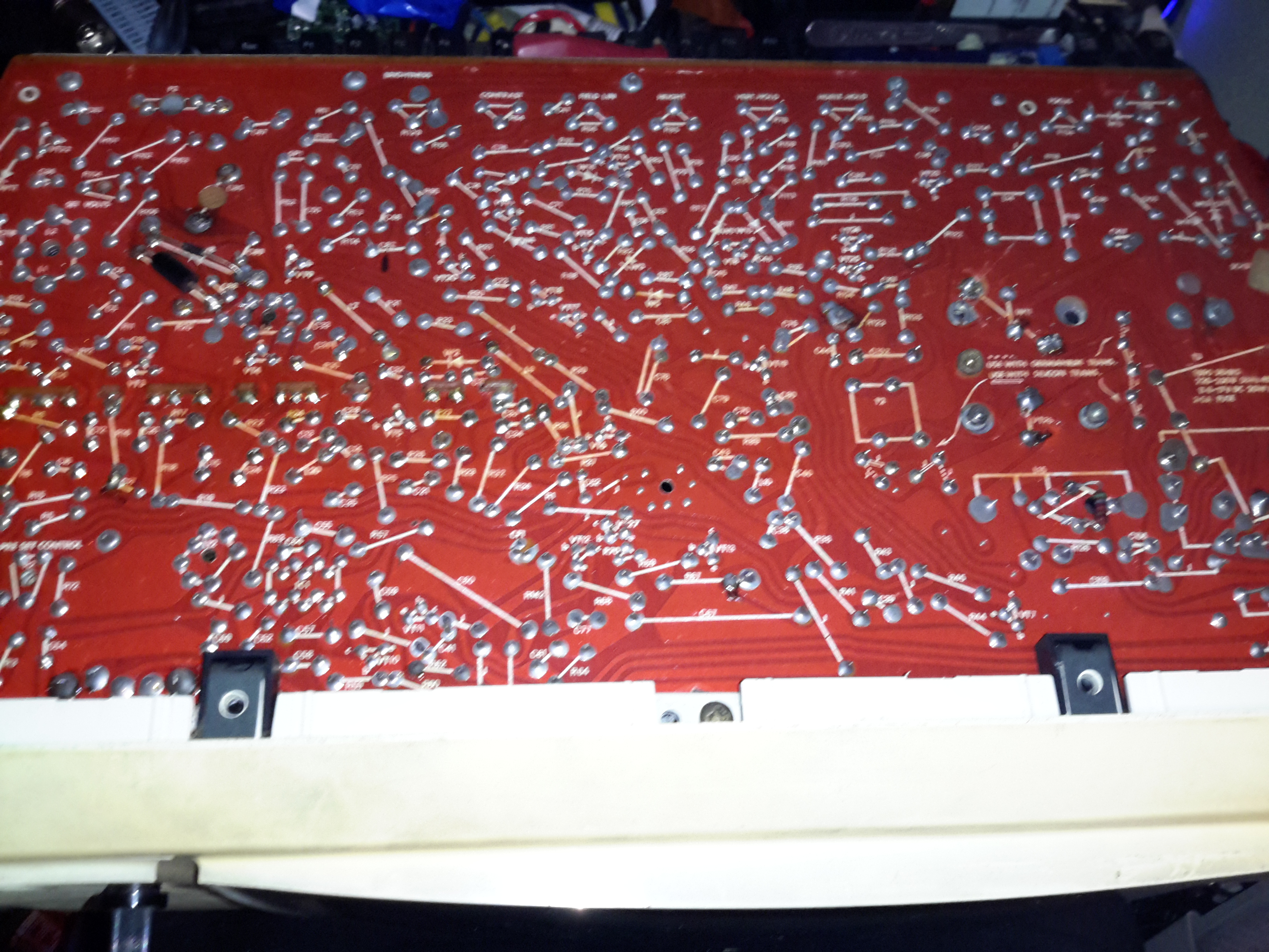
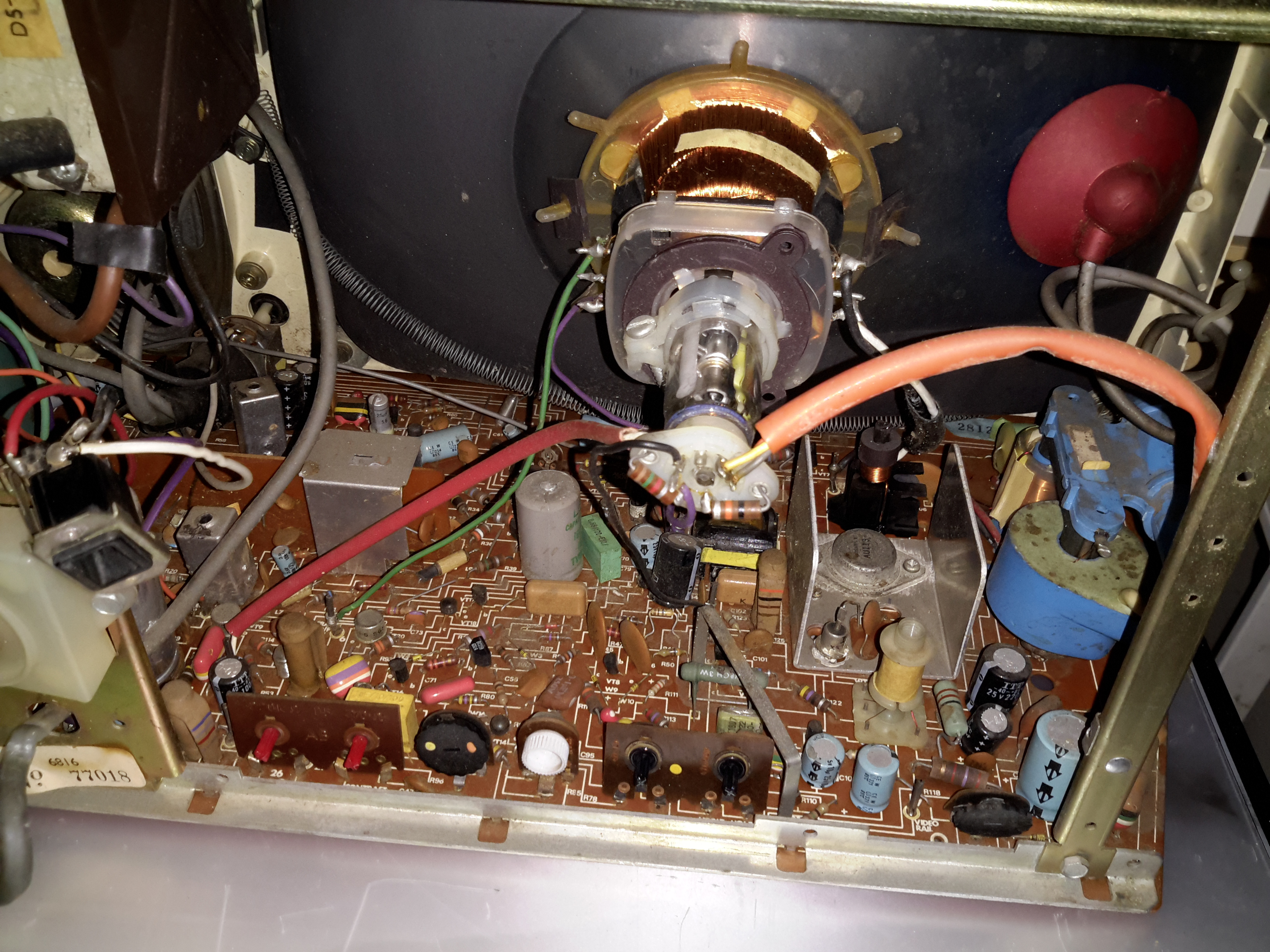
The bottom of the mainboard has all the silkscreen markings for the components above which certainly makes servicing easier 😉 This board’s copper tracks would have been laid out with tape, obviously before the era of PCB design software.

Components
Components

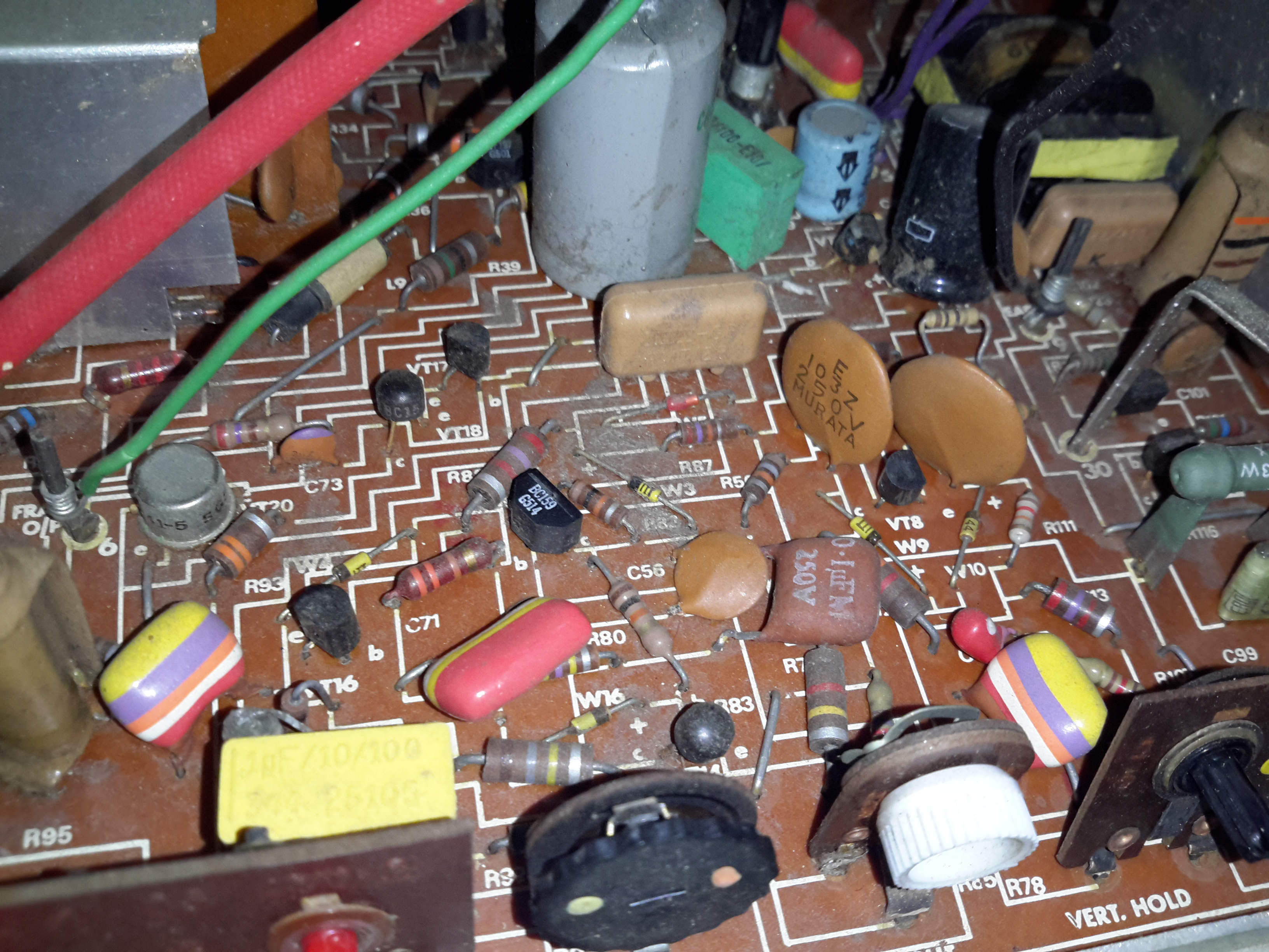
The components on this board are laid out everywhere, not just in square grids. The resistors used are the carbon composition type, and at ~46 years old, they’re starting to drift a bit. After measuring a 10K resistor at 10.7K, all of these would need replacing I have no doubt. Incedentally, this TV could be converted to take a video input without the tuner, by lifting the ferrite beaded end of L9 & injecting a signal there.

Flyback Primary Windings

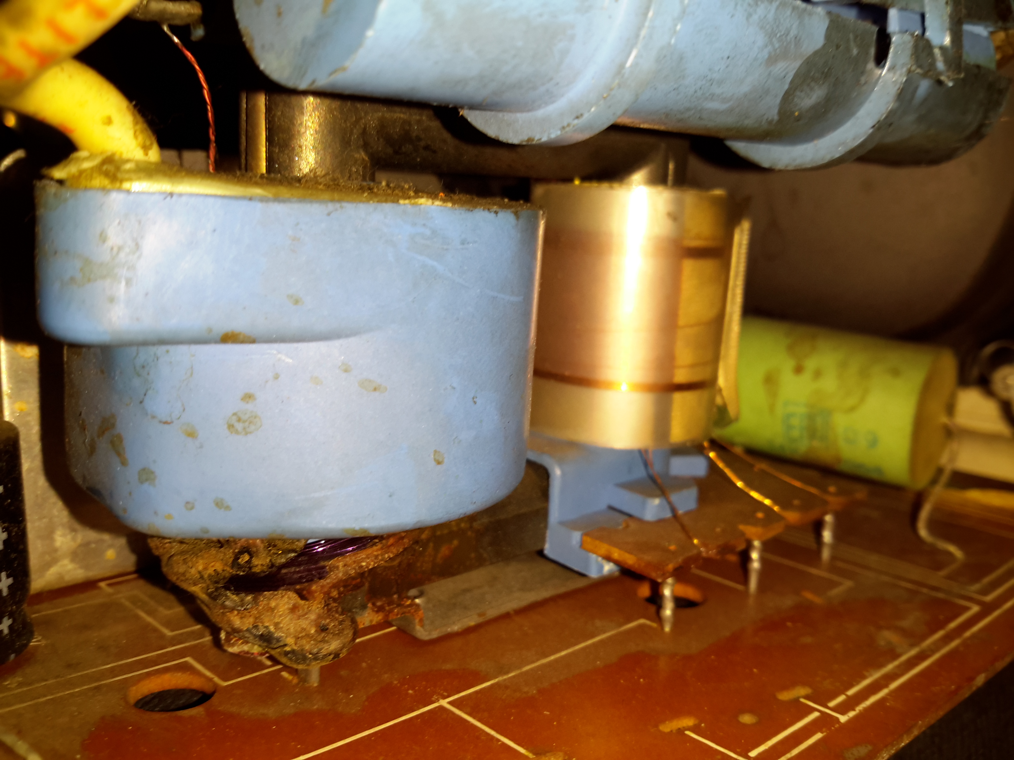
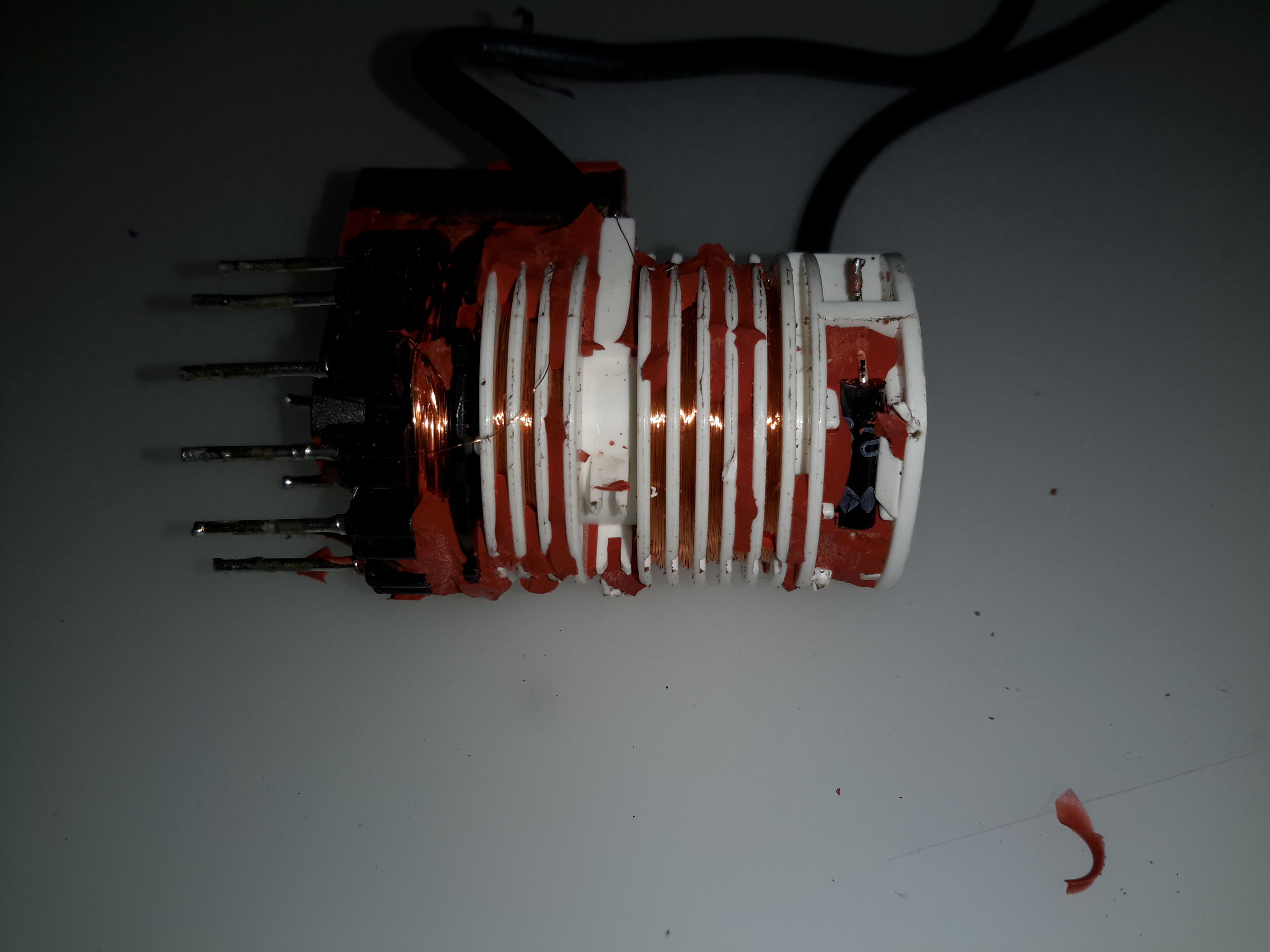
The flyback (Line Output Transformer) is of the old AC type, with the rectifier stack on top in the blue tube, as opposed to more modern versions that have everything potted into the same casing. The primary windings are on the other leg of the ferrite core, making these transformers much more easily repairable. This transformer generates the 12kV required for the CRT final anode, along with a few other voltages used in the TV, for focussing, etc.

Rectifier Stack
Rectifier Stack

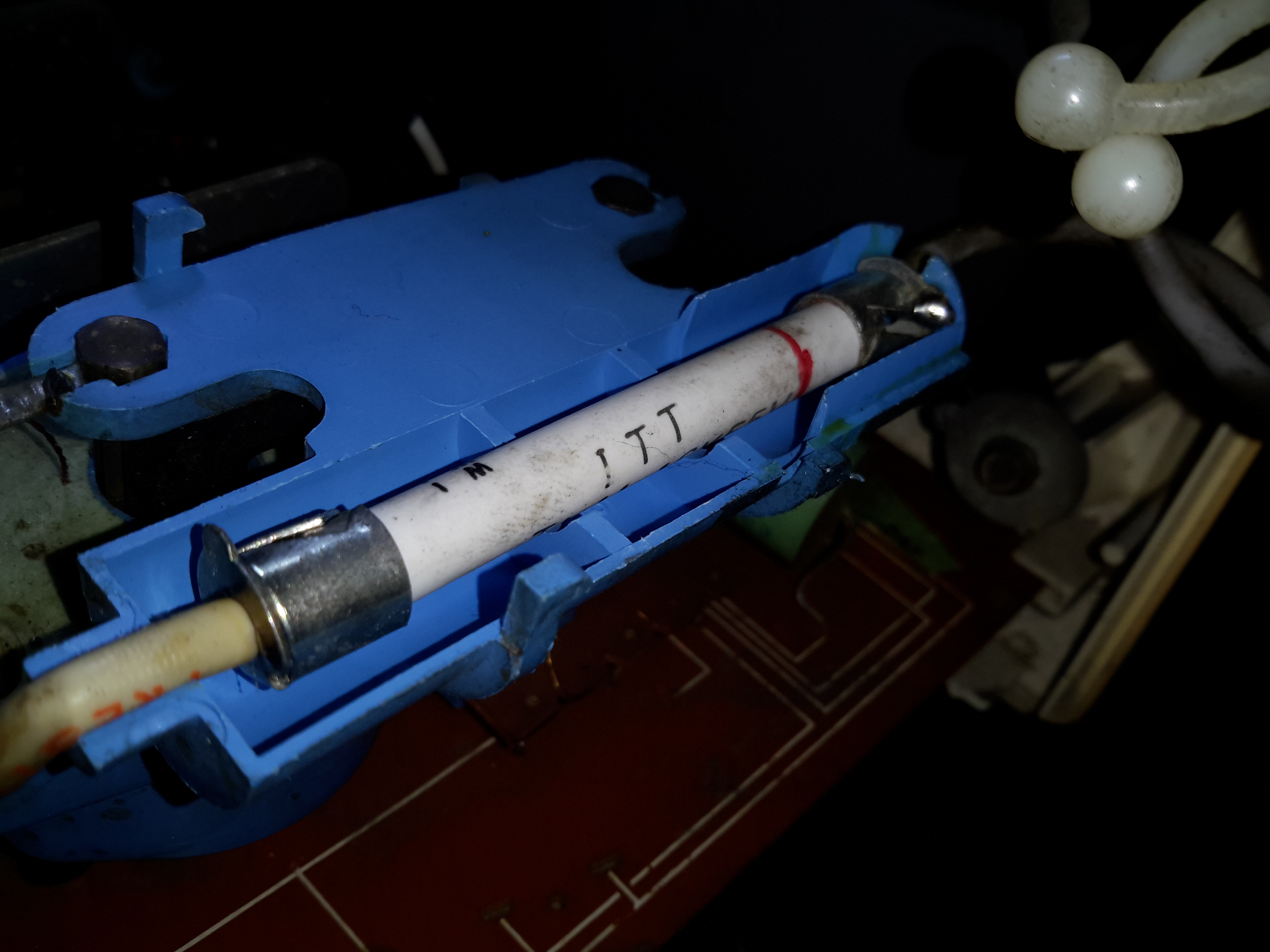
The main EHT rectifier stack looks like a huge fuse, inside the ceramic tube will be a stack of silicon diodes in series, to withstand the high voltage present.

Horizontal Output Transistor

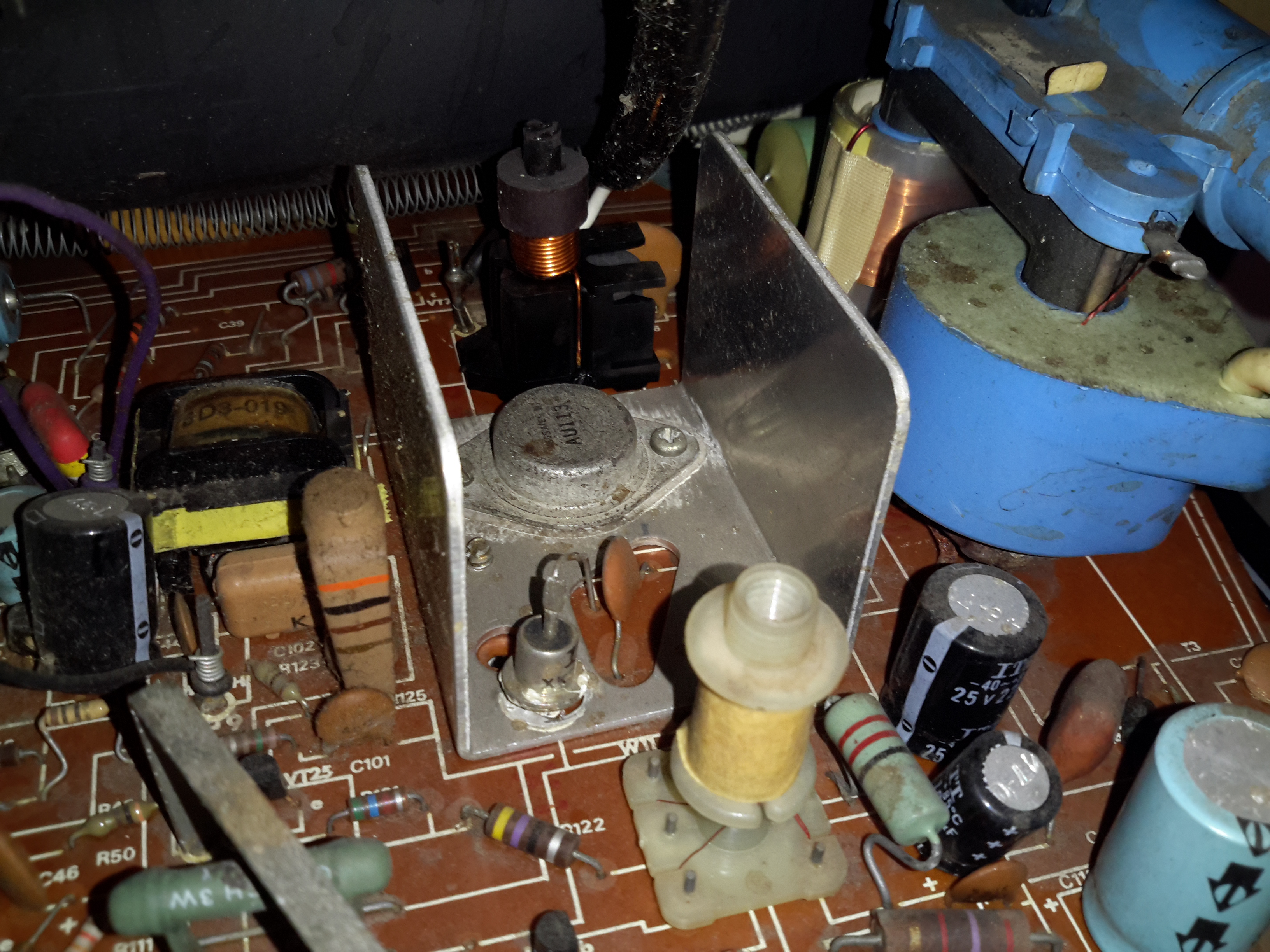
This is the main switching transistor that drives the flyback, the HOT. This is an AU113, another germanium type, rated at 250v 4A. The large diode next to the transistor is the damper.

I’ve managed to find all the service information for this set online, link below!
[download id=”5616″]
More to come if I manage to get this TV working!

Posted on 2 Comments

CRT Flyback / Line Output Transformer Destructive Teardown

Small Flyback Transformer

Here’s a small flyback / Line Output Transformer from a portable colour TV set. Usually these transformers are vacuum potted in hard epoxy resin & are impossible to disassemble without anything short of explosives. (There are chemical means of digesting cured epoxies, but none of them are pleasant). This one however, was potted in silicone, so with some digging, the structure of the transformer can be revealed.

Cap Removed
Cap Removed

The cap was glued on to the casing, but this popped off easily. The top of the core is visible in the silicone potting material.

The Digging Starts
The Digging Starts

A small screwdriver was used to remove the potting material, while trying not to damage the winding bobbin & core too badly. The bulge in the casing that I originally thought might house a voltage multiplier turns out to be totally empty. The white plastic bobbin is becoming visible around the core.

Bobbin
Bobbin

After some more digging & a lot of mess later, the entire transformer is revealed. The primary & auxiliary secondaries are visible at the bottom of the transformer, next to the pins. These transformers have multiple windings, as they’re used not only for supplying the final anode voltage of several Kilovolts to the CRT, but many of the other associated voltages, for the heater, grids, focus electrodes, etc. These lower voltage windings are on the same part of the core as the primary.
Above those is the main high voltage secondary winding, which looks to be wound with #38-#40AWG wire (about the thinnest available, at 0.07mm diameter. This is wound in many sections of of a few hundred turns each to increase the insulation resistance to the high voltage. The main anode wire emerges from the top of the bobbin.

Output Rectifier
Output Rectifier

Hidden in a recess at the top is the main HV rectifier, which on this small transformer is a single device (it’s probably not internally, most likely a series stack of diodes to get the PIV rating required).

Posted on Leave a comment

555 Flyback Driver

Flyback Secondary Waveform
Board Layout
Board Layout

Here is a simple 555 timer based flyback transformer driver, with the PCB designed by myself for some HV experiments. Above is the Eagle CAD board layout.

The 555 timer is in astable mode, generating a frequency from about 22kHz to 55kHz, depending on the position of the potentiometer. The variable frequency is to allow the circuit to be tuned to the resonant frequency of the flyback transformer in use.

This is switched through a pair of buffer transistors into a large STW45NM60 MOSFET, rated at 650v 45A.

Input power is 15-30v DC, as the oscillator circuit is fed from an independent LM7812 linear supply.

Provision is also made on the PCB for attaching a 12v fan to cool the MOSFET & linear regulator.

Initial Board
Initial Board

Board initially built, with the heatsink on the linear regulator fitted. I used a panel mount potentiometer in this case as I had no multiturn 47K pots in stock.

PCB Traces
PCB Traces

Bottom of the PCB. The main current carrying traces have been bulked up with copper wire to help carry the potentially high currents on the MOSFET while driving a large transformer.
This board was etched using the no-peel toner transfer method, using parchement paper as the transfer medium.

MOSFET Heatsinked
MOSFET Heatsinked

Main MOSFET now fitted with a surplus heatsink from an old switchmode power supply. A Fan could be fitted to the top of this sink to cope with higher power levels.

Gate Drive Waveform
Gate Drive Waveform

This is the gate drive waveform while a transformer is connected, the primary is causing some ringing on the oscillator. The waveform without an attached load is a much cleaner square wave.

Flyback Secondary Waveform

I obtained a waveform of the flyback secondary output by capacitively coupling the oscilloscope probe through the insulation of the HT wire. The pulses of HV can be seen with the decaying ringing of the transformer between cycles.

Corona Discharge
Corona Discharge
Arc Discharge
Arc Discharge

Corona & arc discharges at 12v input voltage.

Download the Eagle schematic files here: [download id=”5561″]