Posted on 2 Comments

PowerAdd Pilot X7 20,000mAh Powerbank & Fast Charging Mod

PowerAdd Pilot X7
PowerAdd Pilot X7

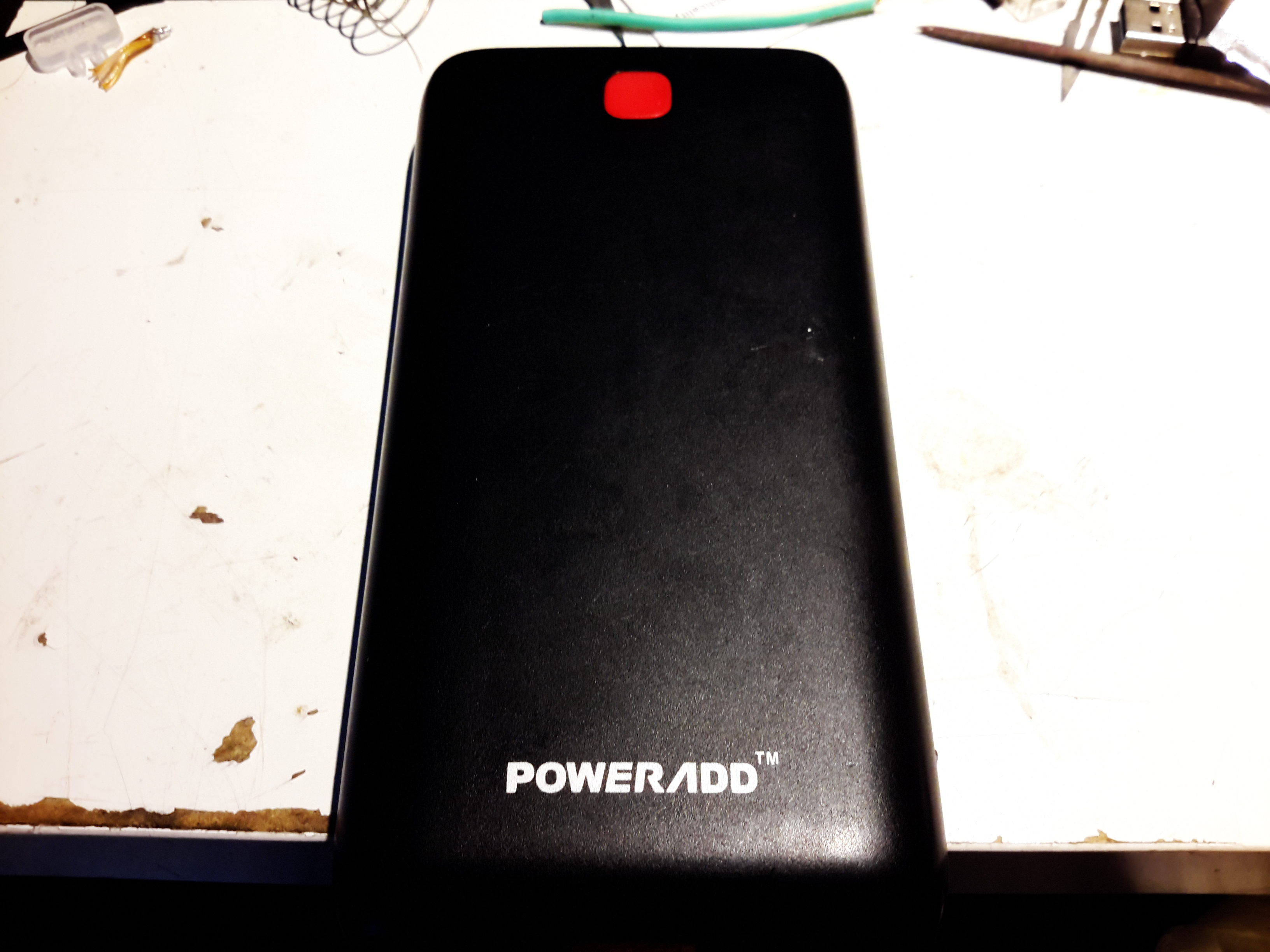
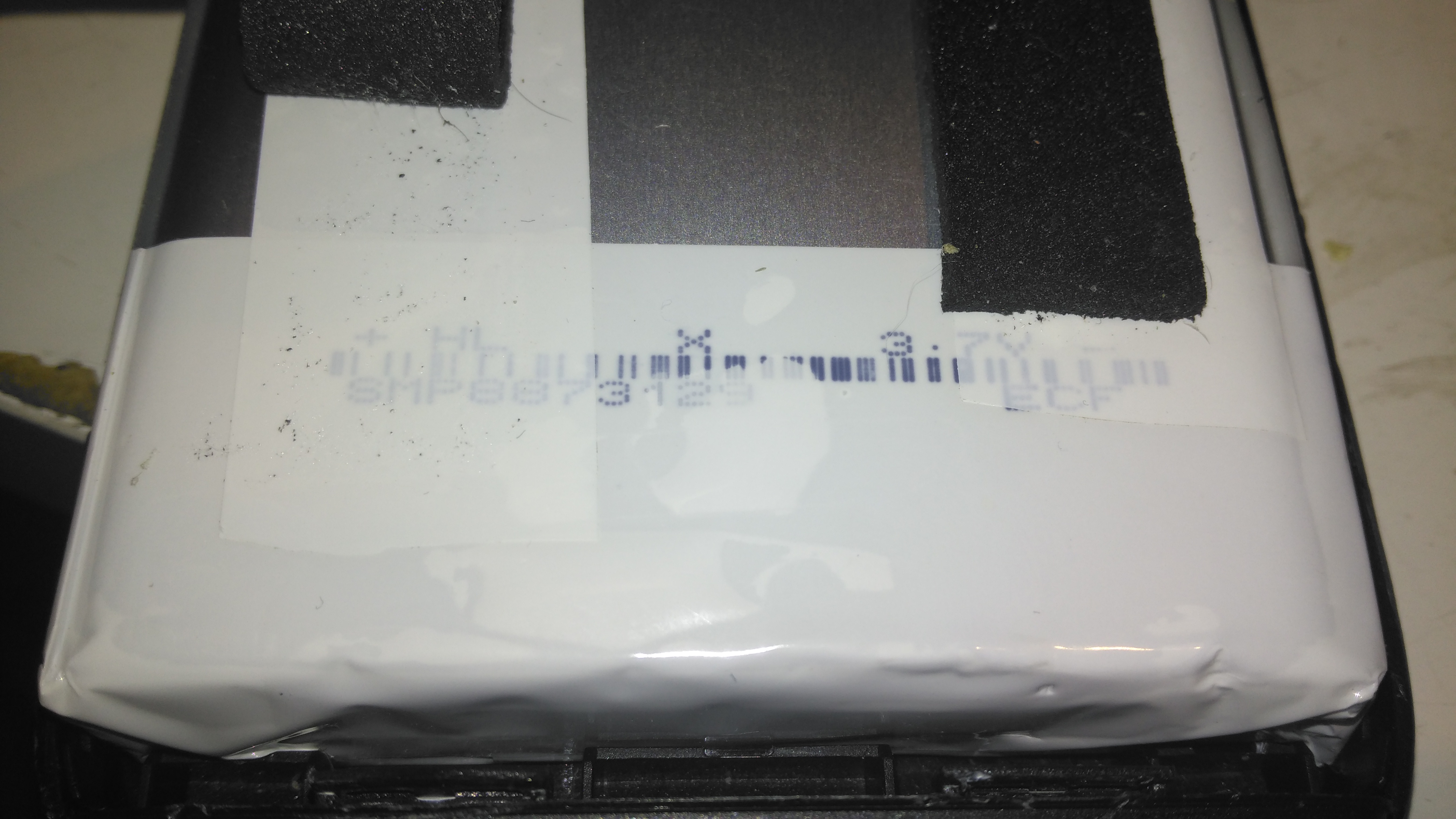
Here’s the biggest portable USB powerbank I’ve seen yet – the PowerAdd Pilot X7, this comes with a 20Ah (20,000mAh) capacity. This pack is pretty heavy, but this isn’t surprising considering the capacity.

USB Ports & LED
USB Ports & LED

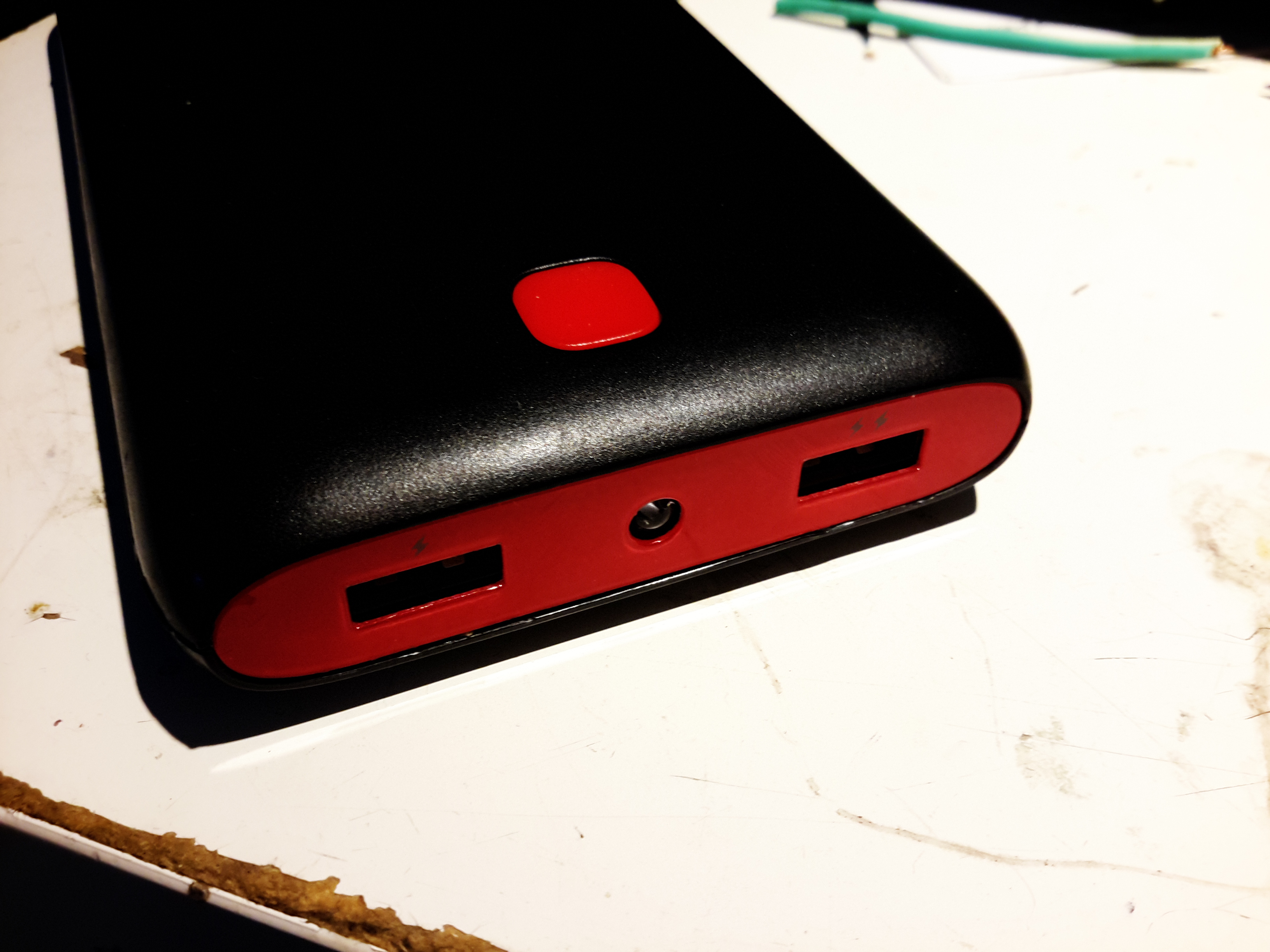
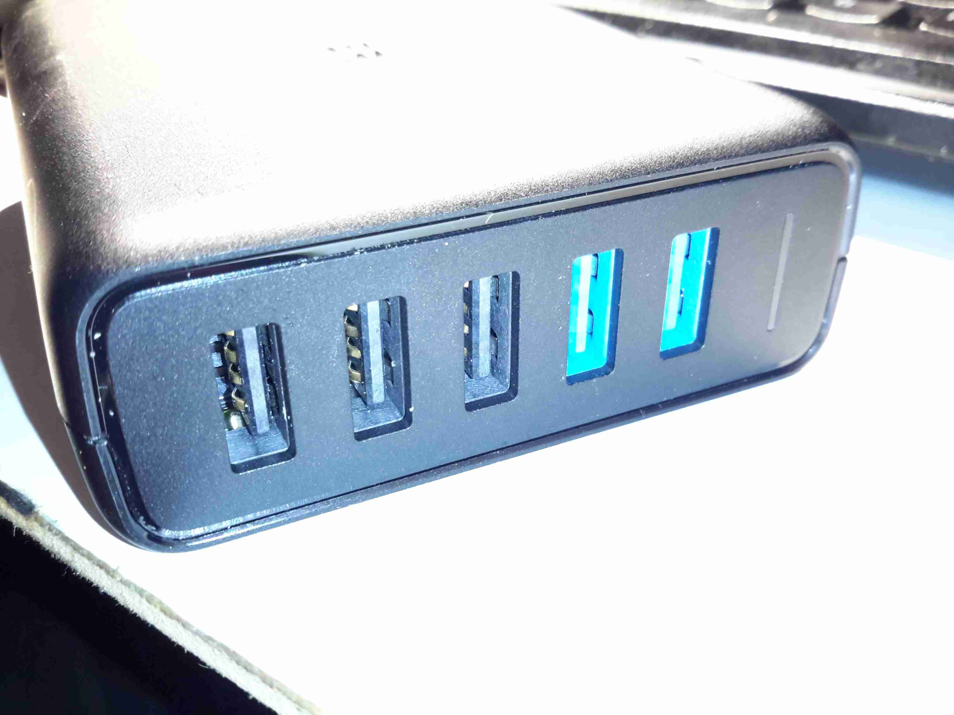
The front of the pack houses the usual USB ports, in this case rated at 3.4A total between the ports. There’s a white LED in the centre as a small torch, activated by double-clicking the button. A single click of the button lights up the 4 blue LEDs under the housing that indicate remaining battery capacity. Factory charging is via a standard µUSB connector in the side, at a maximum of 2A.

PCB Front
PCB Front

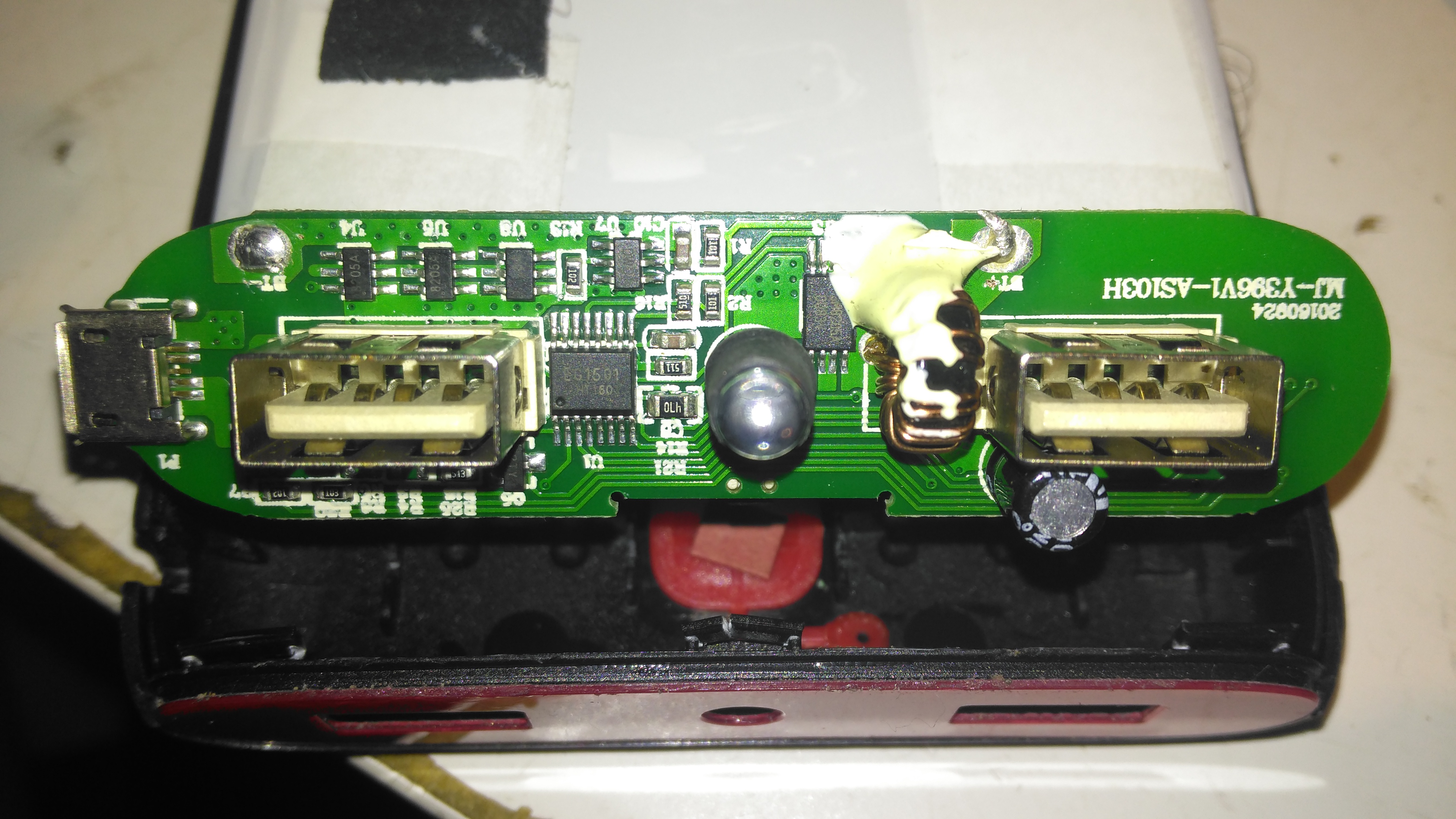
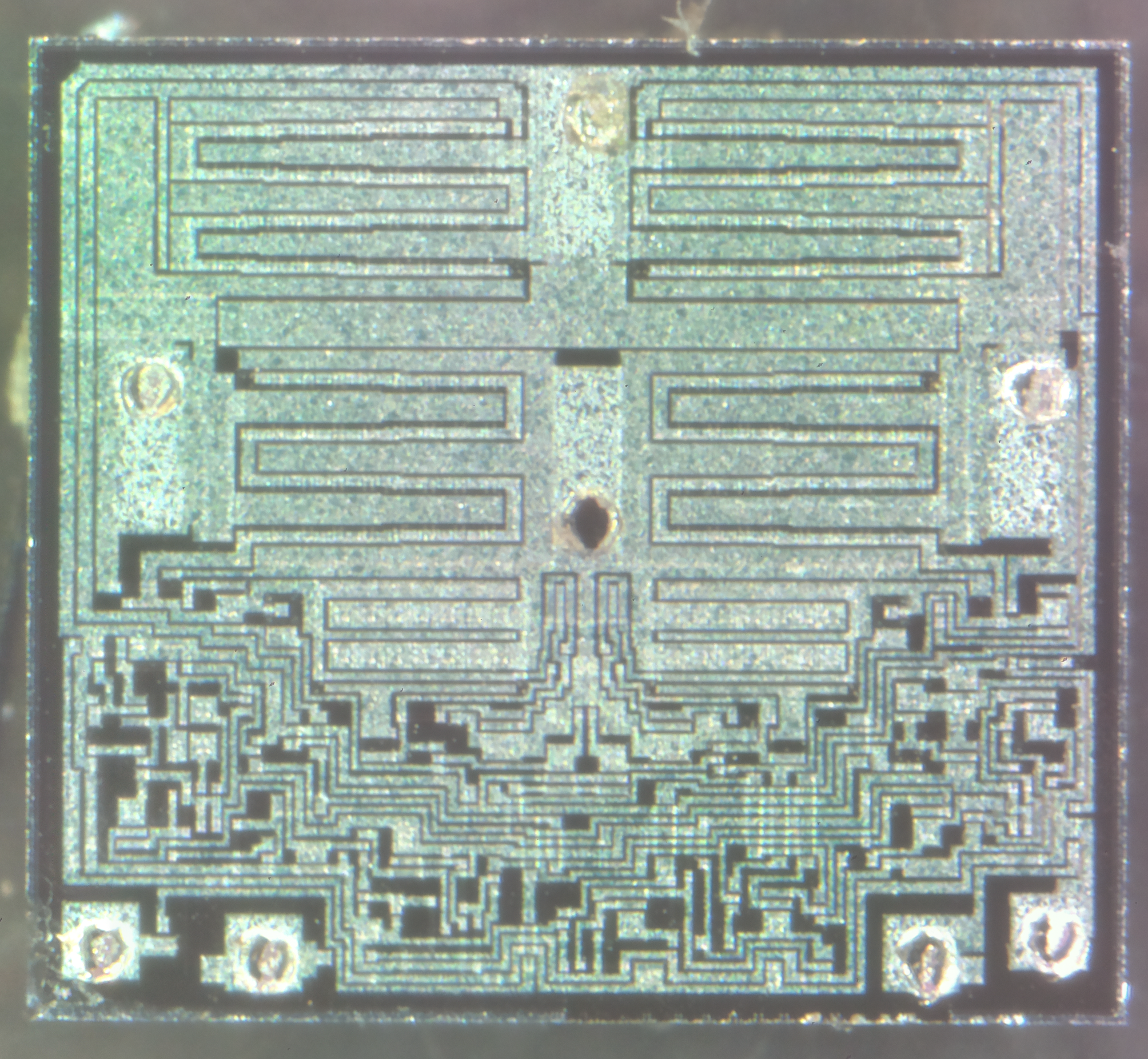
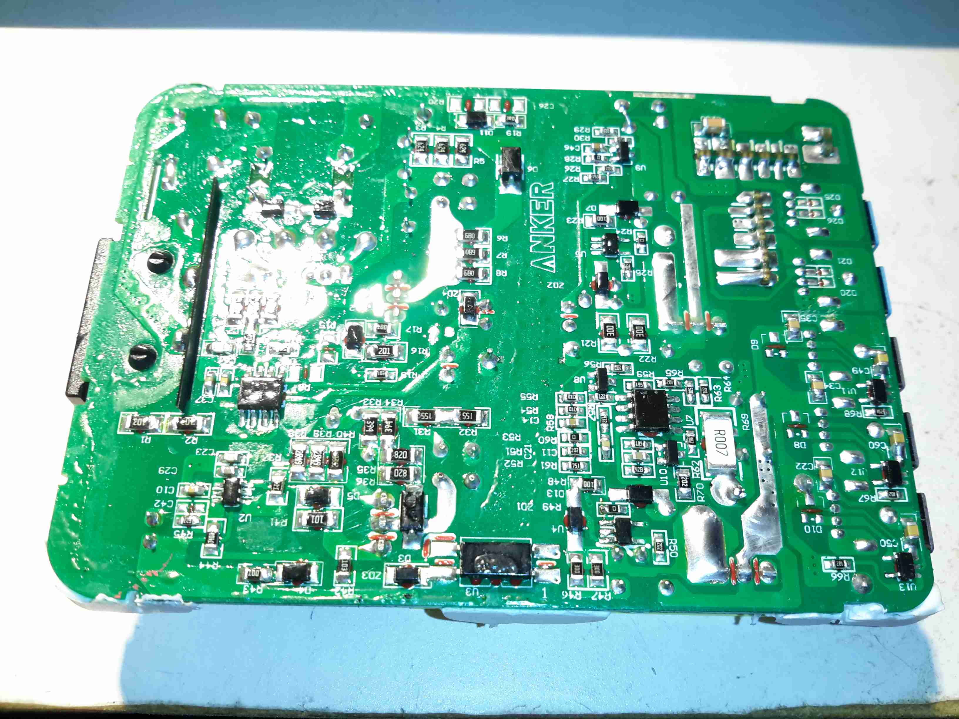
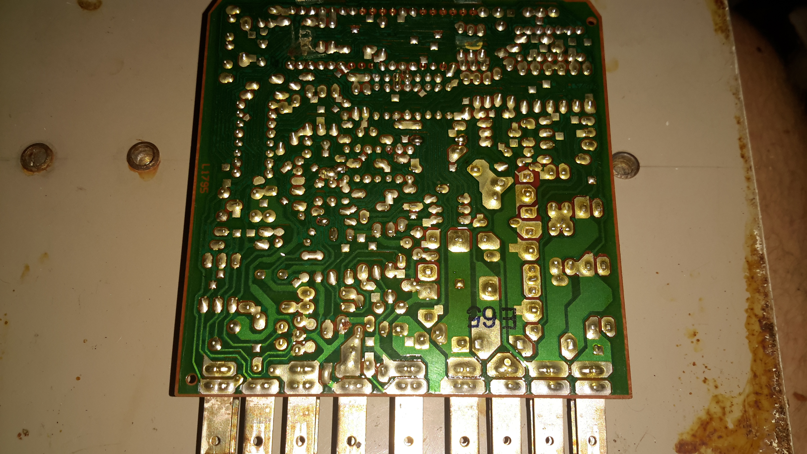
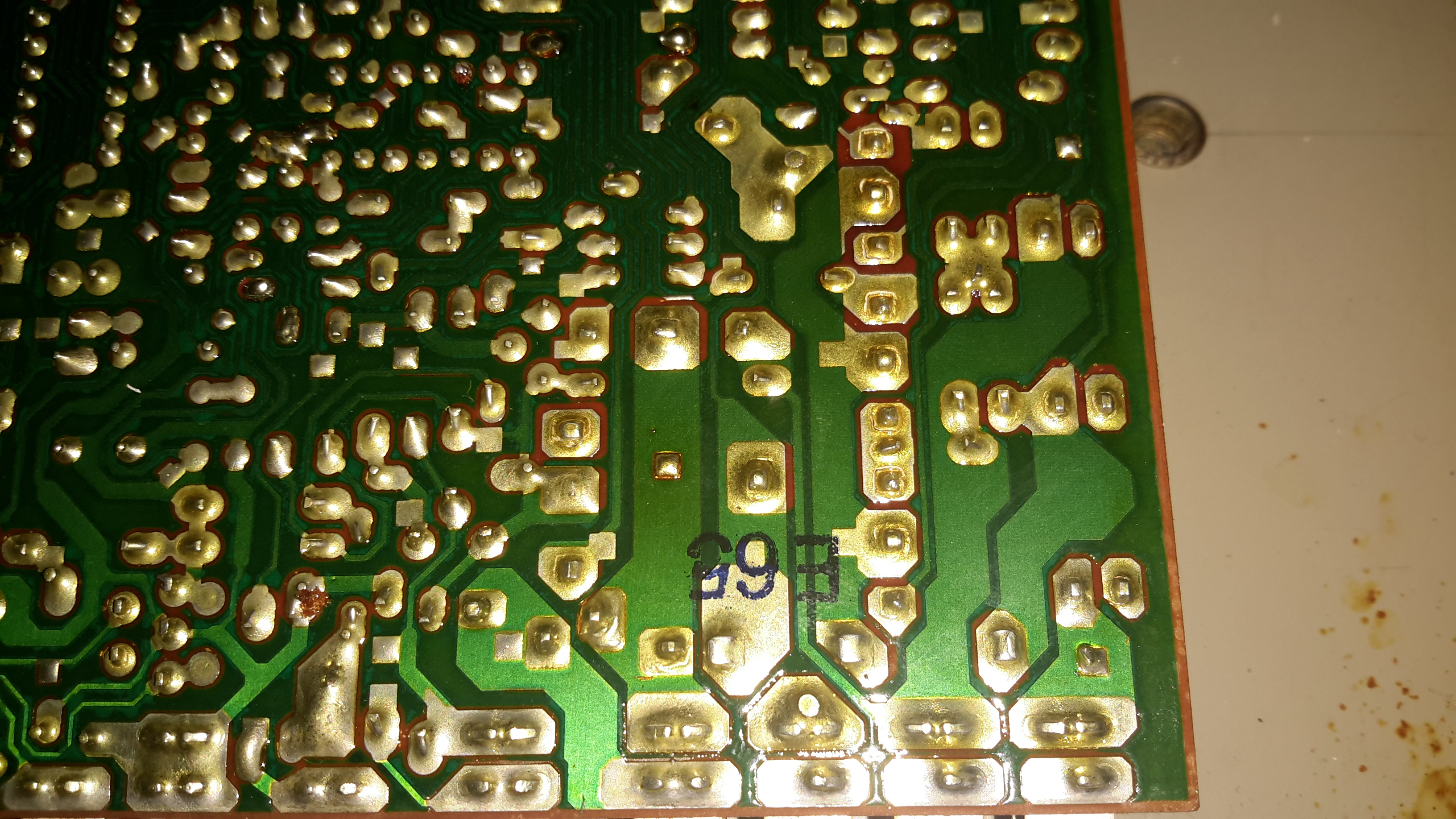
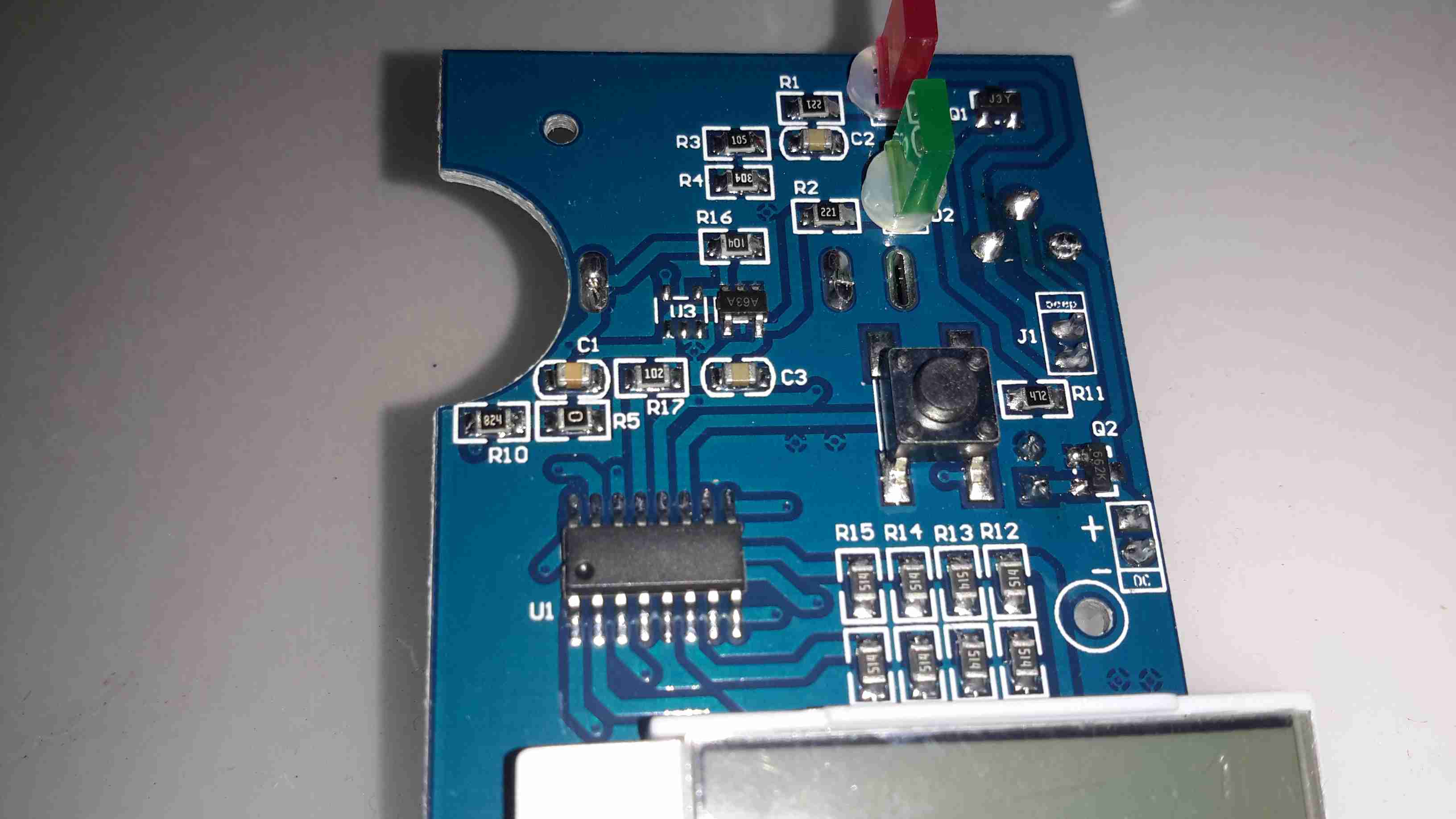
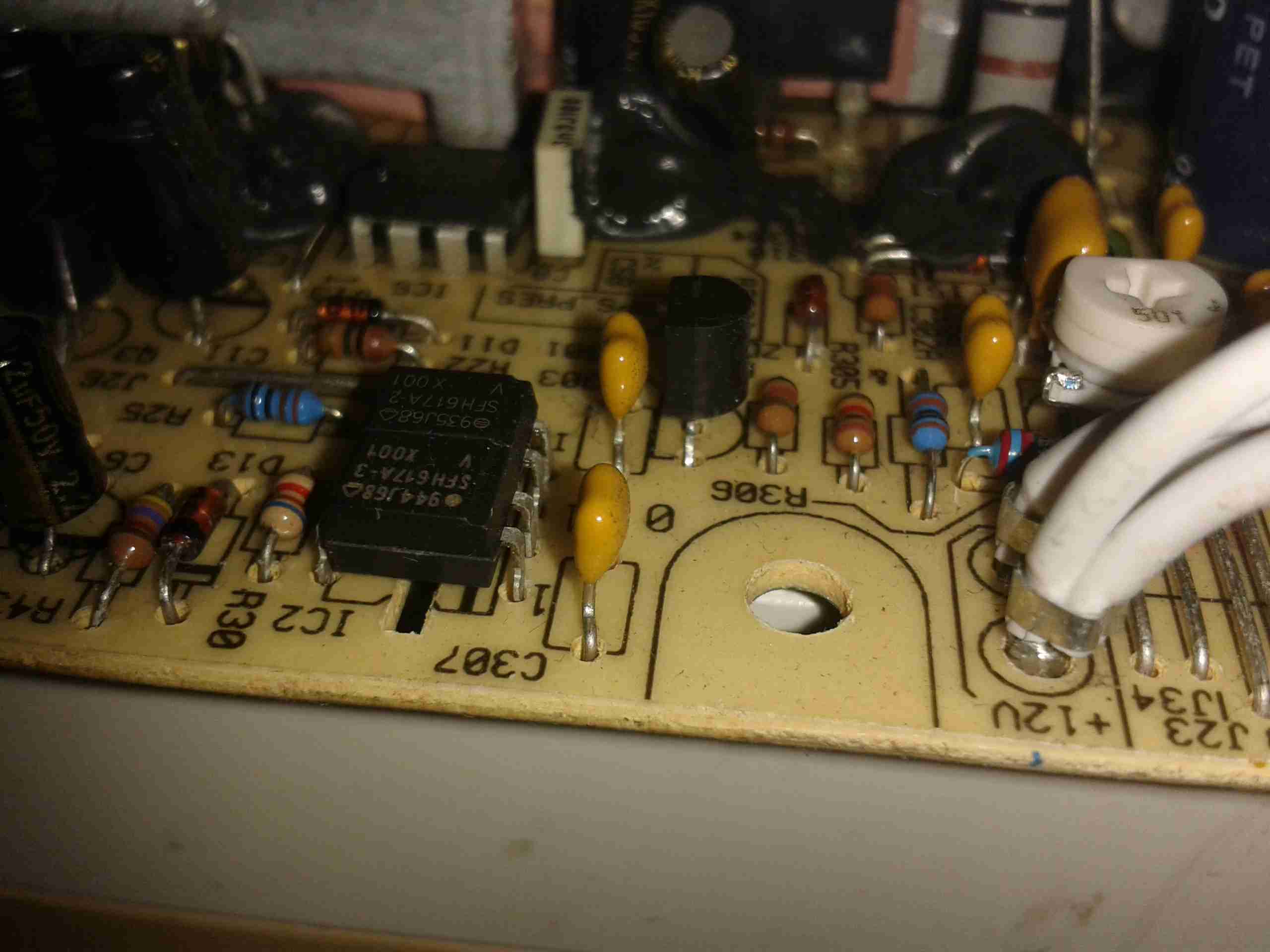
The front of the PCB holds the USB ports, along with most of the main control circuitry. At top left is a string of FS8025A dual-MOSFETs all in parallel for a current carrying capacity of 15A total, to the right of these is the ubiquitous DW01 Lithium-Ion protection IC. These 4 components make up the battery protection – stopping both an overcharge & overdischarge. The larger IC below is an EG1501 multi-purpose power controller.

This chip is doing all of the heavy lifting in this power pack, dealing with all the DC-DC conversion for the USB ports, charge control of the battery pack, controlling the battery level indicator LEDs & controlling the torch LED in the centre.

EG1501 Example
EG1501 Example

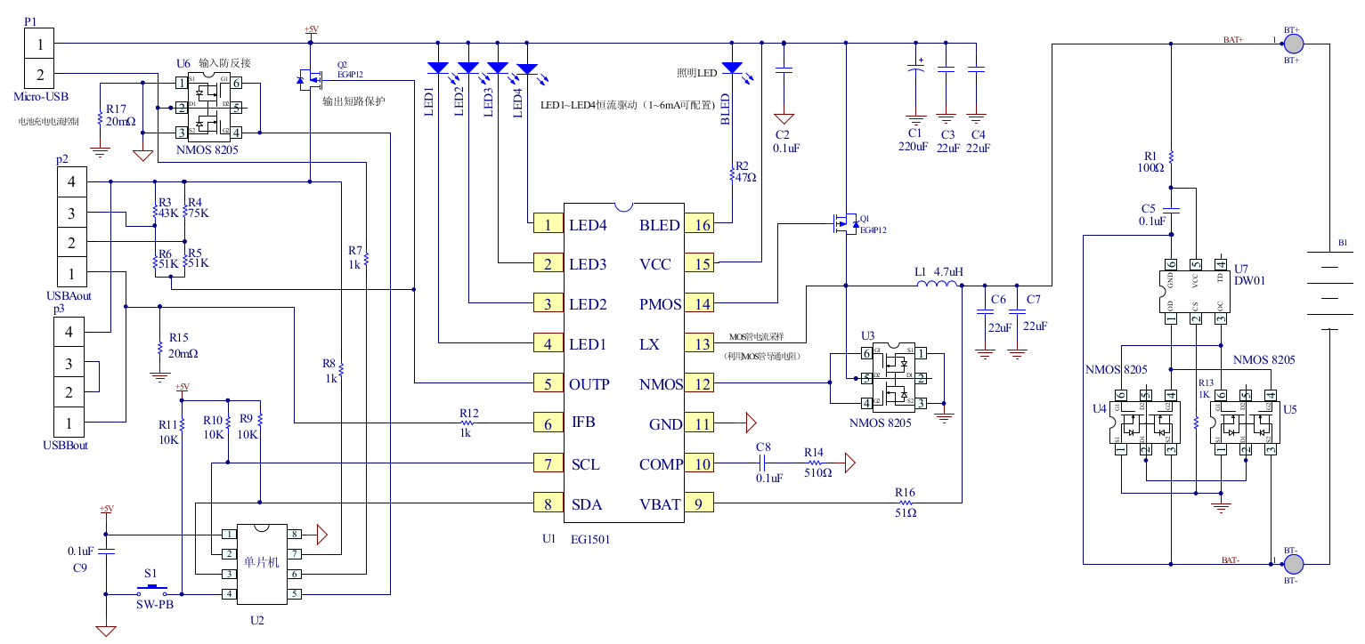
The datasheet is in Chinese, but it does have an example application circuit, which is very similar to the circuitry used in this powerbank. A toroidal inductor is nestled next to the right-hand USB port for the DC-DC converter, and the remaining IC next to it is a CW3004 Dual-Channel USB Charging Controller, which automatically sets the data pins on the USB ports to the correct levels to ensure high-current charging of the devices plugged in. This IC replaces the resistors R3-R6 in the schematic above.
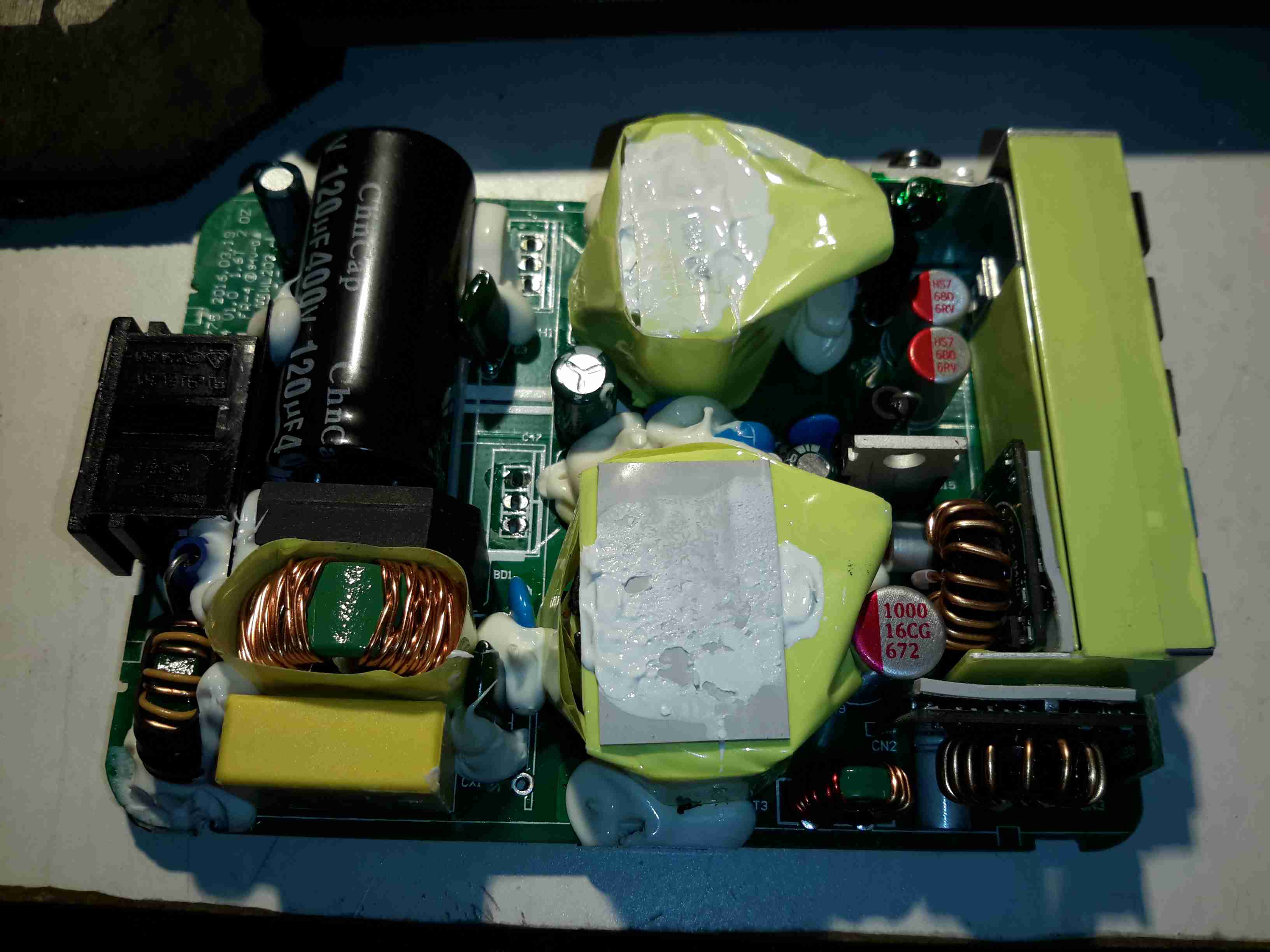
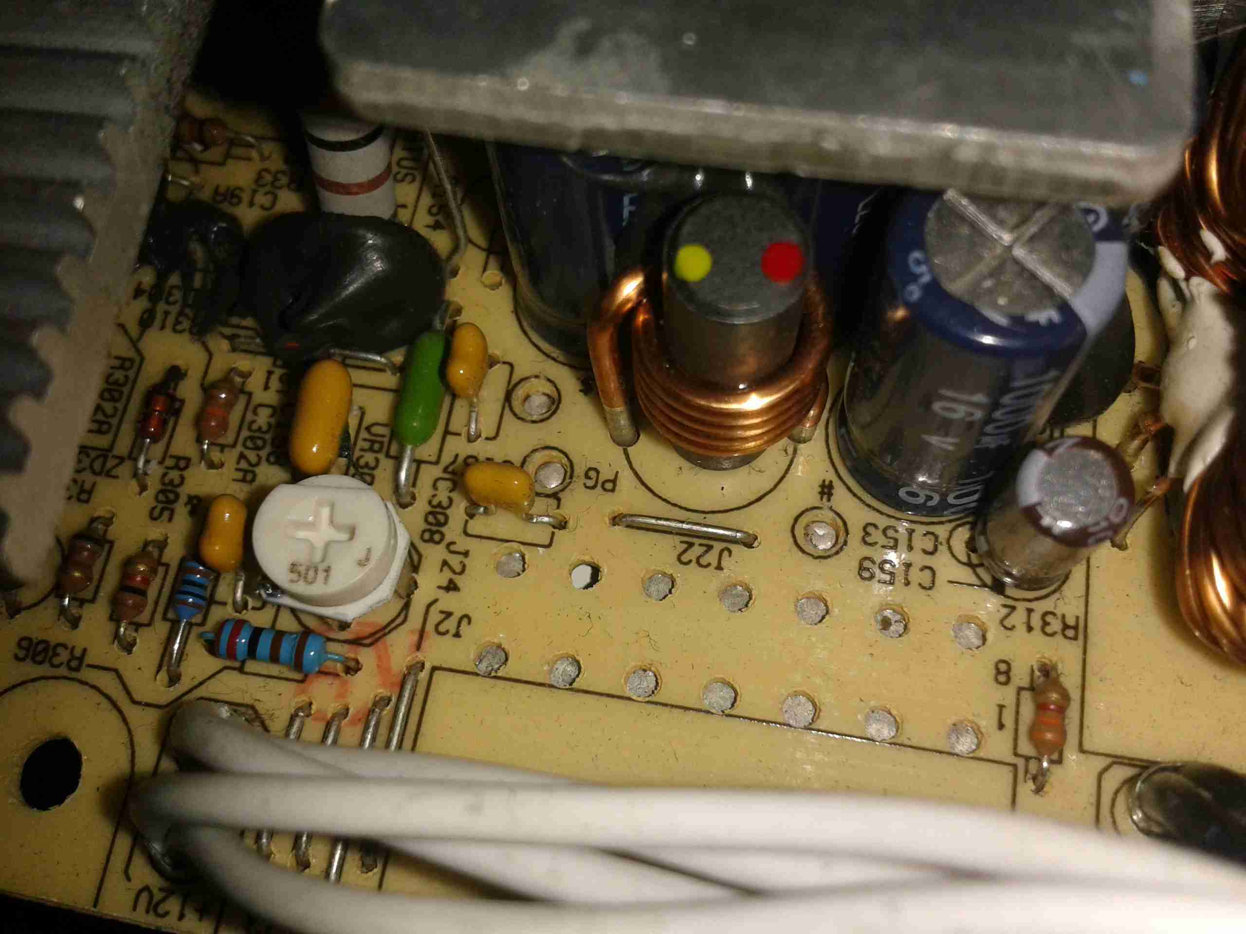
The DC-DC converter section of the power chain is designed with high efficiency in mind, not using any diodes, but synchronous rectification instead.

PCB Back
PCB Back

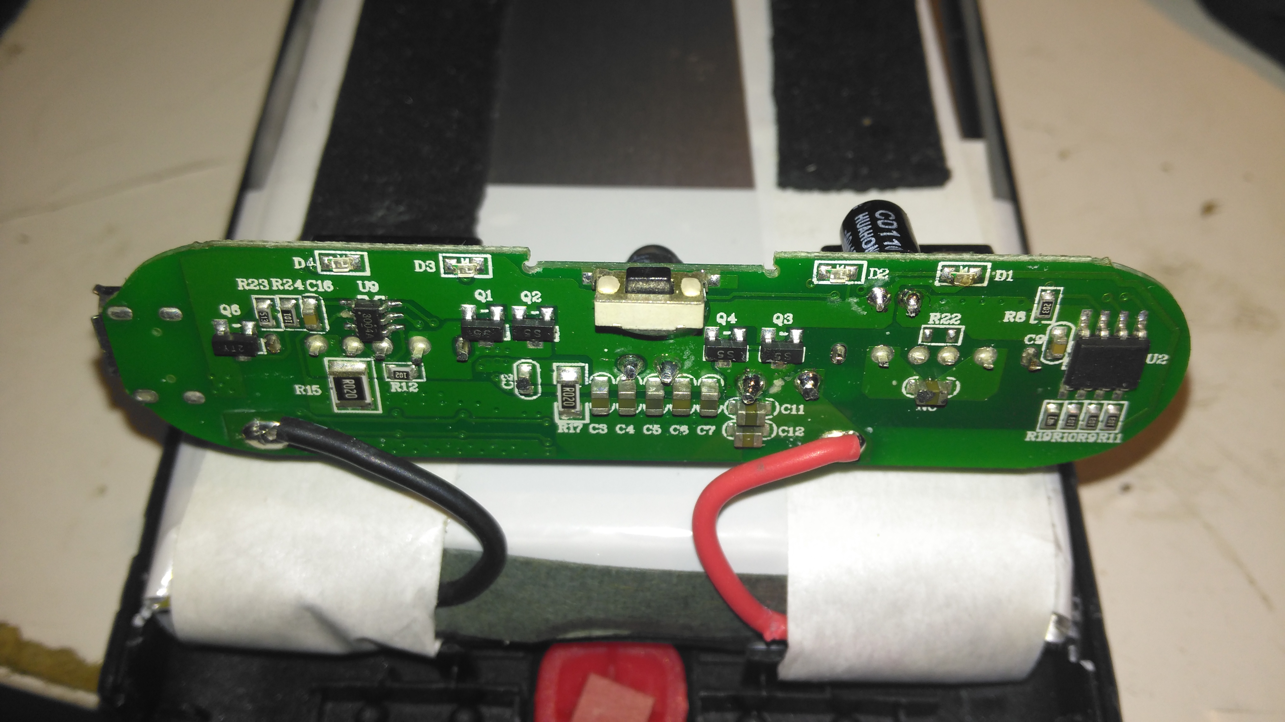
The back of the PCB just has a few discrete transistors, the user interface button, and a small SO8 IC with no markings at all. I’m going to assume this is a generic microcontroller, (U2 in the schematic) & is just there to interface the user button to the power controller via I²C.

Cells
Cells

Not many markings on the cells indicating their capacity, but a full discharge test at 4A gave me a resulting capacity of 21Ah – slightly above the nameplate rating. There are two cells in here in parallel, ~10Ah capacity each.

XT60 Battery Connector

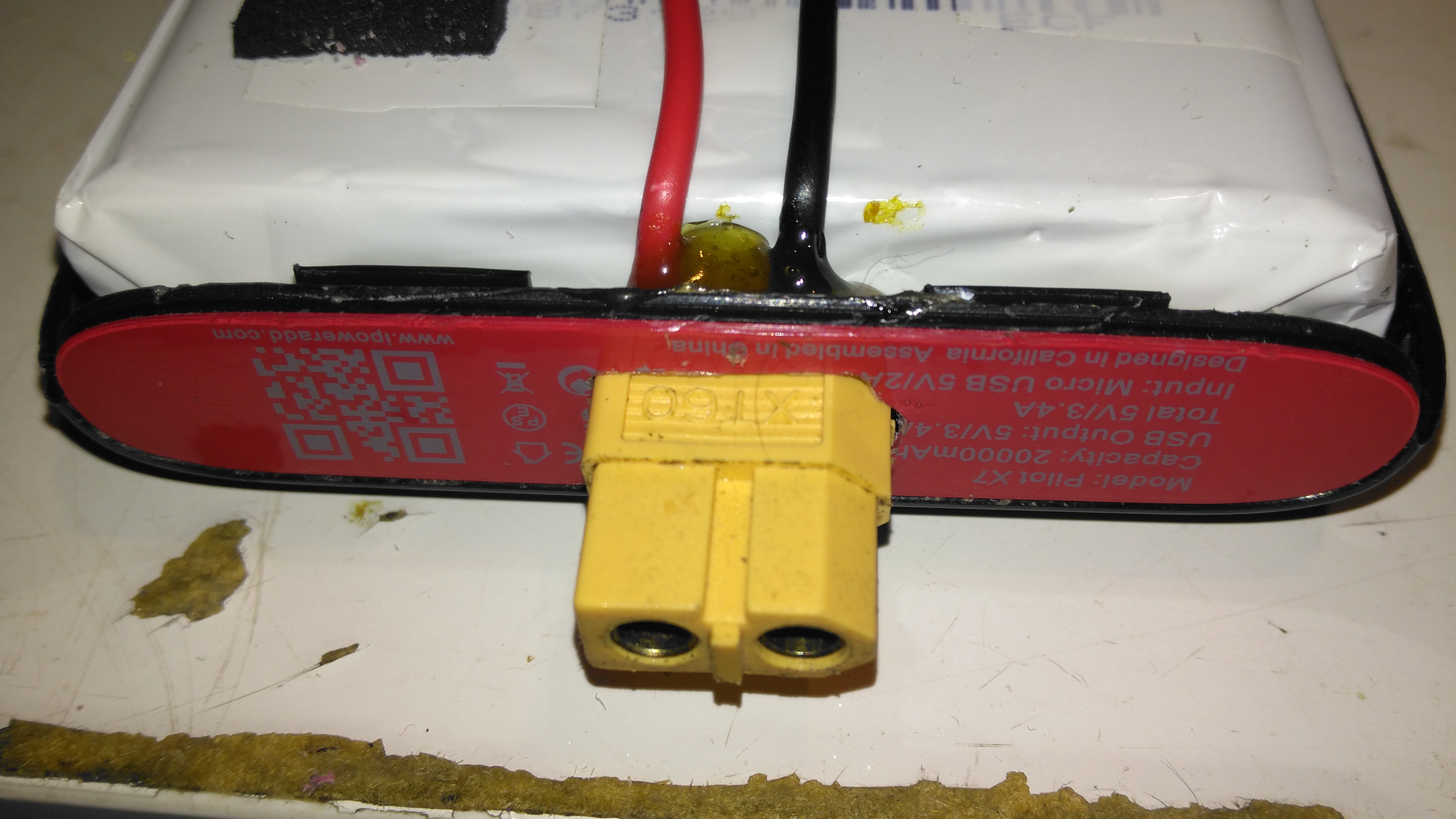
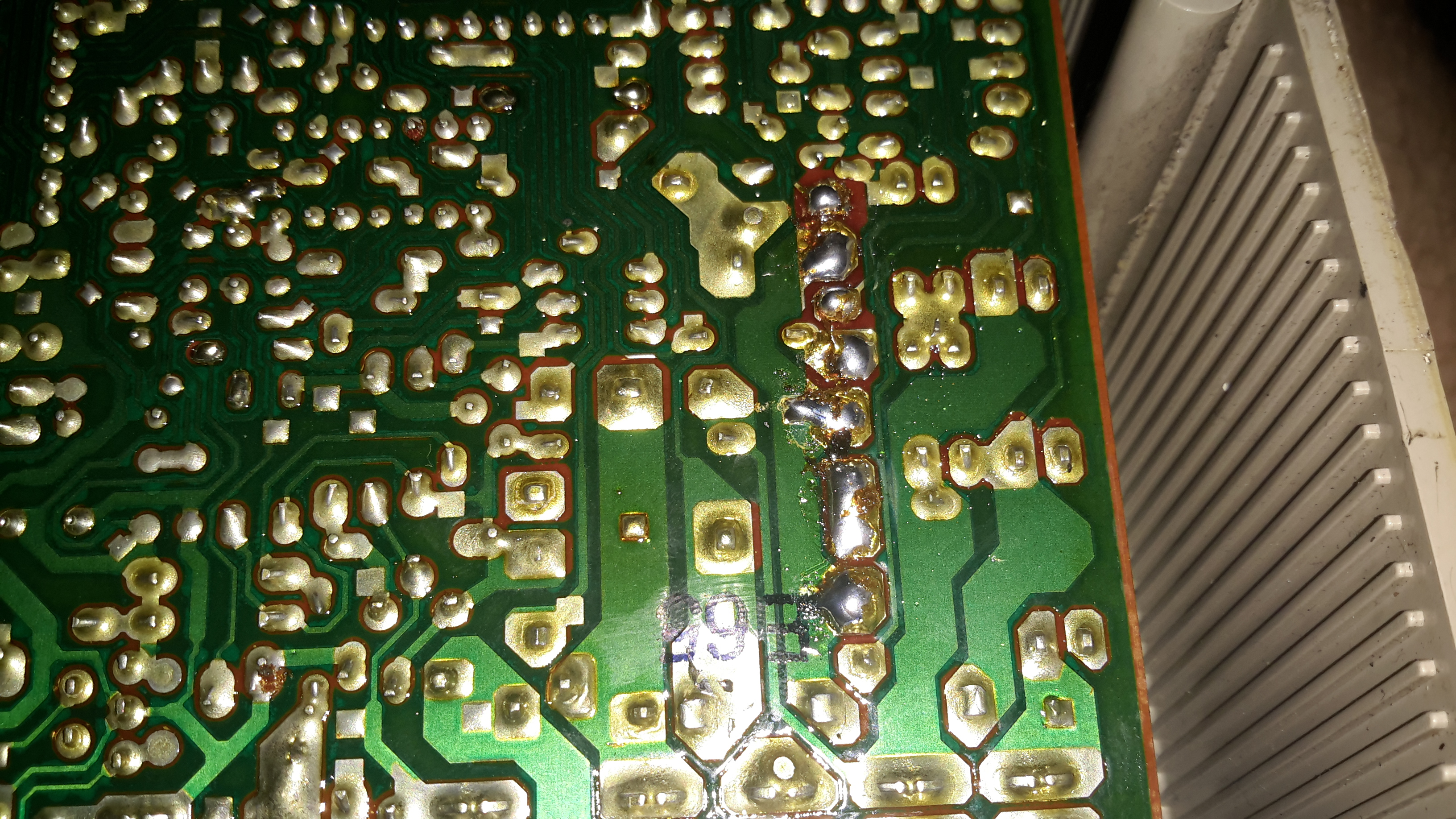
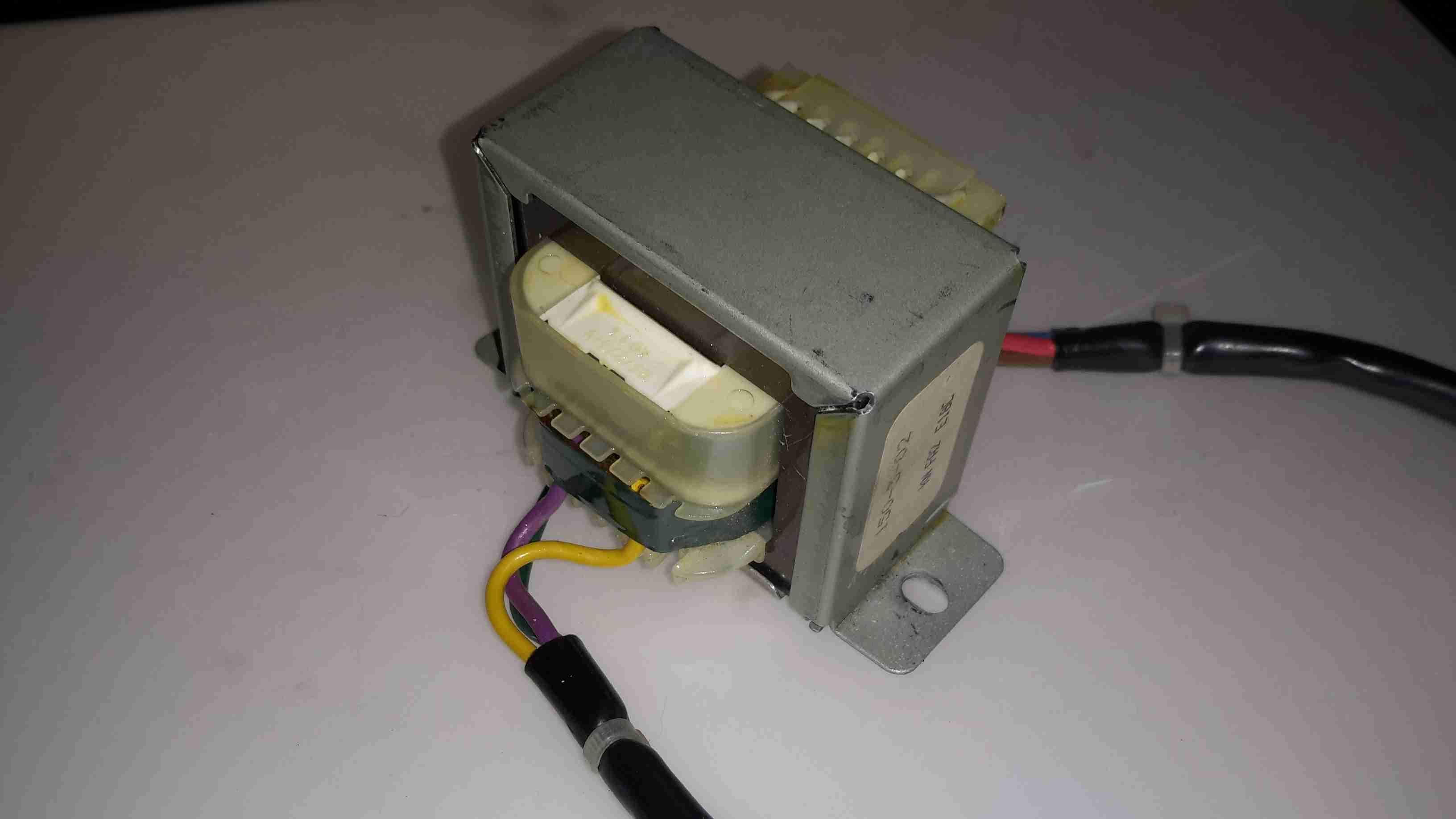
The only issue with powerbanks this large is the amount of time they require to recharge themselves – at this unit’s maximum of 2A through the µUSB port, it’s about 22 hours! Here I’ve fitted an XT60 connector, to interface to my Turnigy Accucell 6 charger, increasing the charging current capacity to 6A, and reducing the full-charge time to 7 hours. This splits to 3A charge per cell, and after some testing the cells don’t seem to mind this higher charging current.

Battery Connector Wiring

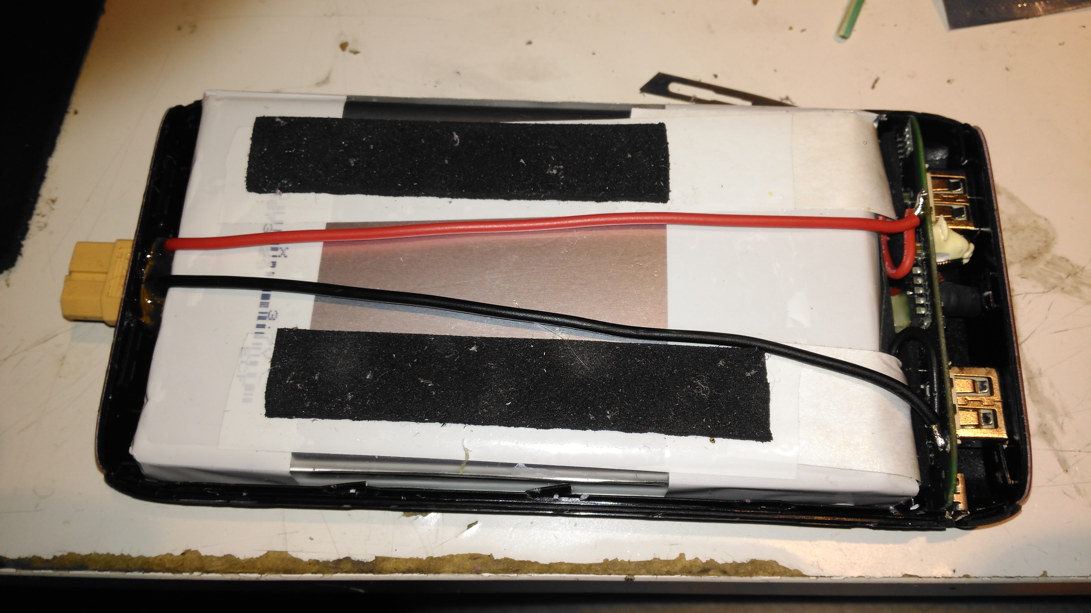
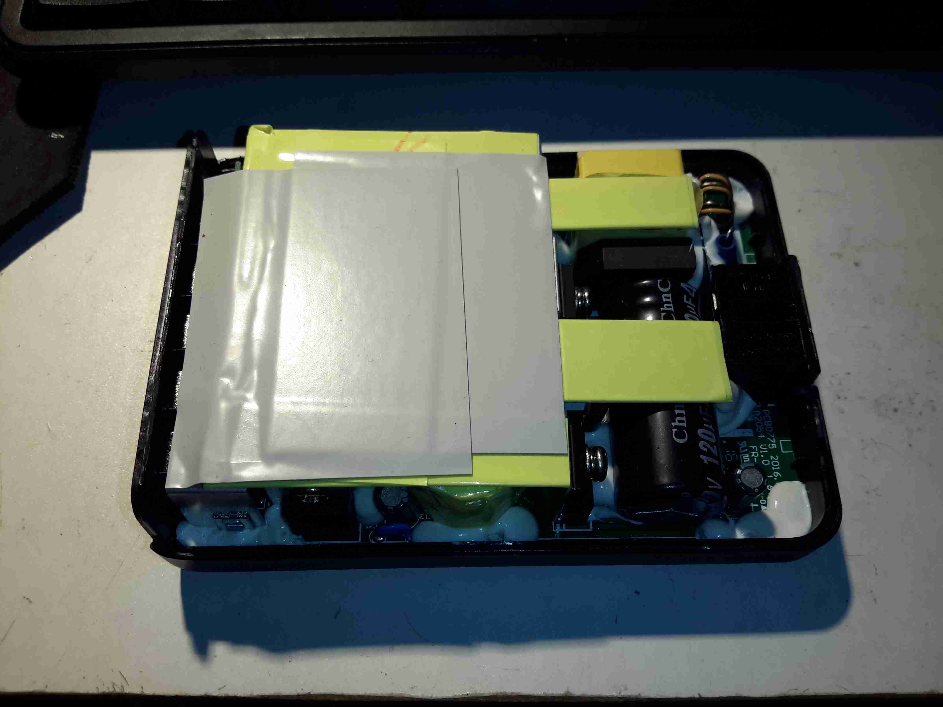
The new charging connector is directly connected to the battery at the control PCB, there’s just enough room to get a pair of wires down the casing over the cells.

Posted on Leave a comment

IC Decap – TA7291 H-Bridge DC Motor Driver

Here’s a jellybean chip – a DC motor driver. This device has all the logic to drive a small motor, such as that used to drive the tray of a CD drive in both directions. The control logic is at the bottom of the die, while the main power transistors are at the top, in H-Bridge formation.

TA7291 Die
TA7291 Die
Posted on 3 Comments

Anker PowerPort Speed 5 USB Rapid Charger Teardown

Front
Front

Here’s a piece of tech that is growing all the more important in recent times, with devices with huge battery capacities, a quick charger. This unit supports Qualcomm’s Quick Charge 3 standard, where the device being charged can negotiate with the charger for a higher-power link, by increasing the bus voltage past the usual 5v.

Rear
Rear

The casing feels rather nice on this unit, sturdy & well designed. All the legends on the case are laser marked, apart from the front side logo which is part of the injection moulding.

Specifications
Specifications

The power capacity of this charger is pretty impressive, with outputs for QC3 from 3.6-6.5v at 3A, up to 12v 1.5A. Standard USB charging is limited at 4.8A for the other 3 ports.

Ports
Ports

The two of the 5 USB ports are colour coded blue on the QC3 ports. The other 3 are standard 5v ports, the only thing that doesn’t make sense in the ratings is the overall current rating of the 5v supply (4.8A), and the rated current of each of the ports (2.4A) – this is 7.2A total rather than 4.8A.

Top Removed
Top Removed

The casing is glued together at the seam, but it gave in to some percussive attack with a screwdriver handle. The inside of this supply is mostly hidden by the large heatspreader on the top.

Main PCB Bottom
Main PCB Bottom

This is a nicely designed board, the creepage distances are at least 8mm between the primary & secondary sides, the bottom also has a conformal coating, with extra silicone around the primary-side switching transistor pins, presumably to decrease the chances of the board flashing over between the close pins.
On the lower 3 USB ports can be seen the 3 SOT-23 USB charge control ICs. These are probably similar to the Texas Instruments TPS2514 controllers, which I’ve experimented with before, however I can’t read the numbers due to the conformal coating. The other semiconductors on this side of the board are part of the voltage feedback circuits for the SMPS. The 5v supply optocoupler is in the centre bottom of the board.

Heatsink Removed
Heatsink Removed

Desoldering the pair of primary side transistors allowed me to easily remove the heatspreader from the supply. There’s thermal pads & grease over everything to get rid of the heat. Here can be seen there are two transformers, forming completely separate supplies for the standard USB side of things & the QC3 side. Measuring the voltages on the main filter capacitors showed me the difference – the QC3 supply is held at 14.2v, and is managed through other circuits further on in the power chain. There’s plenty of mains filtering on the input, as well as common-mode chokes on the DC outputs before they reach the USB ports.

Quick Charge 3 DC-DC Converters

Here’s where the QC3 magic happens, a small DC-DC buck converter for each of the two ports. The data lines are also connected to these modules, so all the control logic is located on these too. The TO-220 device to the left is the main rectifier.

Posted on Leave a comment

Mercury 30A Ham Radio SMPS

Mercury 30A SMPS
Mercury 30A SMPS

After having a couple of the cheap Chinese PSUs fail on me in a rather spectacular fashion, I decided to splash on a more expensive name-brand PSU, since constantly replacing PSUs at £15 a piece is going to get old pretty fast. This is the 30A model from Mercury, which seems to be pretty well built. It’s also significantly more expensive at £80. Power output is via the beefy binding posts on the front panel. There isn’t any metering on board, this is something I’ll probably change once I’ve ascertained it’s reliability. This is also a fixed voltage supply, at 13.8v.

Rear Panel
Rear Panel

Not much on the rear panel, just the fuse & cooling fan. This isn’t temperature controlled, but it’s not loud. No IEC power socket here, the mains cable is hard wired.

Main Board
Main Board

Removing some spanner-type security screws reveals the power supply board itself. Everything on here is enormous to handle the 30A output current at 13.8v. The main primary side switching transistors are on the large silver heatsink in the centre of the board, feeding the huge ferrite transformer on the right.

Transformer
Transformer

The transformer’s low voltage output tap comes straight out instead of being on pins, due to the size of the winding cores. Four massive diodes are mounted on the black heatsinks for output rectification.


SMPS Controller
SMPS Controller

The supply is controlled via the jelly bean TL494 PWM controller IC. The multi-turn potentiometer doesn’t adjust the output voltage, more likely it adjusts the current limit.

Standby Supply
Standby Supply

Power to initially start the supply is provided by a small SMPS circuit, with a VIPer22A Low Power Primary Switcher & small transformer on the lower right. The transformer upper left is the base drive transformer for the main high power supply.

Posted on Leave a comment

IR Remote Control Repeater

IR Remote Repeater
IR Remote Repeater

Here’s another random gadget for teardown, this time an IR remote control repeater module. These would be used where you need to operate a DVD player, set top box, etc in another room from the TV that you happen to be watching. An IR receiver sends it’s signal down to the repeater box, which then drives IR LEDs to repeat the signal.

Repeater Module
Repeater Module

Not much to day about the exterior of this module, the IR input is on the left, up to 3 receivers can be connected. The outputs are on the right, up to 6 repeater LEDs can be plugged in. Connections are done through standard 3.5mm jacks.

Repeater PCB
Repeater PCB

Not much inside this one at all, there are 6 transistors which each drive an LED output. This “dumb” configuration keeps things very simple, no signal processing has to be done. Power is either provided by a 12v input, which is fed into a 7805 linear regulator, or direct from USB.

Posted on 2 Comments

Eberspacher D5W ECU Constant Overheat Error

Eberspacher ECU 25 1599 50 00 00

Here’s another Eberspacher control unit, this time from an ancient D5W 5kW water heater. The system in this case is just flaky – sometimes the heater will start without fault & run perfectly, then suddenly will stop working entirely.
The error codes are read on these very old units via an indicator lamp connected to a test terminal. In this case the code was the one for Overheat Shutdown.

Considering this fault occurs when the heater is stone cold, I figured it was either a fault with the sensor itself or the ECU.

Temperature Sensor
Temperature Sensor

The temperature sensor is located on the heat exchanger, right next to the hot water outlet fitting. I’m not sure what the spec is, but it reads exactly 1KΩ at room temperature.

ECU PCB
ECU PCB

The PCB is held into the aluminium can by means of crimps around the edge that lock into the plastic terminal cover. Inserting a screwdriver & expanding the crimps allows the PCB to be slid out.

Casing Crimps
Casing Crimps

The factory date stamp on the microcontroller dates this unit to March 1989 – considerably older than I expected!
Unlike the newer versions that use transistors, this ECU has a bunch of PCB relays to do the high current switching of the water pump motor, fan motor & glowplug.
Overall the board looks to be solidly constructed, with silicone around all the larger components.

ECU PCB Solder Side
ECU PCB Solder Side

Here’s the solder side of the PCB, which has a generous coating of sealant to keep moisture out.

Bad Joint Closeup
Bad Joint Closeup

Looking at the solder joints for the row of relays on the top side of the PCB, it looks like that there’s some dry joints here.
I suspect that years of vibration has taken it’s toll, as the relays are otherwise unsupported. It wouldn’t be possible to use silicone to secure these devices as they are completely open – any sealant would likely stop them from operating.

Resoldered Joints
Resoldered Joints

Using a very hot soldering iron I managed to get the joints to reflow properly, using lots of flux to make sure the conformal coating didn’t interfere with the reflow.

Posted on Leave a comment

No-Brand eBay Carbon Monoxide Detector

Chinese CO Alarm
Chinese CO Alarm

I was looking around eBay for decent deals on a branded CO alarm, and came across these for next to no money, so I thought I’d grab one just to see how bad they could be.

Alarm Opened
Alarm Opened

Popping the casing open shows the very small circuit board inside, with the CO sensor cell on the right. I can’t find any manufacturer information on this cell, nor can I find a photo of anything similar on the intertubes, so no specifications there. The other parts are pretty standard, a Piezo sounder & it’s associated step-up transformer to increase the loudness.

Sensor Closeup
Sensor Closeup

The sensor cell has the usual opening in the end to allow entry of gas.

Main PCB
Main PCB

The other side of the board doesn’t reveal much, just an LCD, a couple of LEDs, a pair of transistors, Op-Amp for the sensor & a main microcontroller.

MCU
MCU

The microcontroller isn’t marked unfortunately. It’s not had the number scrubbed off, it’s just never been laser marked with a part number. Above the micro is a SOT-23 LM321 low-power Op-Amp which does the signal conditioning for the CO sensor.


I tried to make this alarm trigger with the exhaust from the Eberspacher heater, which on a well-made branded alarm registered a reading of 154ppm after a few minutes. In the case of this alarm though, I couldn’t make it trigger at all, no matter how long I exposed it to hydrocarbon exhaust gases. I won’t be trusting this one then!

Nothing quite like a piece of safety equipment that doesn’t work correctly from new!

Posted on Leave a comment

De La Rue Coin Counting Machine Followup – PSU Oddness

I did a little more digging into the PSU circuitry of the small coin counting machine, and it’s even more strange than I thought!
The part I originally thought was a transformer on the PSU board is in fact a DC-DC converter module!

DC-DC Converter
DC-DC Converter

Here’s the device after desoldering it from the PCB. It turns out that instead of a transformer, it’s an inductor.

Hiding Control Electronics

Underneath is the controller electronics, with an COB controller & the switching transistors are under a protective covering of silicone.

Mains Transformer
Mains Transformer

Driving this whole lot of PSU randomness is the mains transformer, with a secondary voltage of 35v.

The only reason I can think of that the manufacturer went to this much expense with the power supply is stability – a coin counting machine that miscounts due to power supply surges, sags & spikes wouldn’t be very much use. It’s not likely I’ll see anything similar again, unless I manage to get hold of something like medical grade equipment.

Posted on 1 Comment

Cisco PSU Hack & Switched Mode PSU Background

Recently I decommissioned some networking equipment, and discovered the power supplies in some switches were single rail 12v types, with a rather high power rating. I figured these would be very good for powering my Ham radio gear.

They’re high quality Delta Electronics DPSN-150BP units, rated at a maximum power output of 156W.

Label
Label

These supplies have an adjustment pot for the output voltage regulation, but unfortunately it just didn’t have quite enough range to get from 12.0v to 13.8v. The highest they would go was ~13.04v.

After taking a look at the regulator circuit, I discovered  I could further adjust the output voltage by changing a single resistor to a slightly lower value.

Firstly though, a little background on how switched mode power supplies operate & regulate their output voltage.

SMPS
SMPS

Here’s the supply. It’s mostly heatsink, to cool the large power switching transistors.

The first thing a SMPS does, is to rectify the incoming mains AC with a bridge rectifier. This is then smoothed by a large electrolytic capacitor, to provide a main DC rail of +340v DC (when on a 240v AC supply).

Mains Input
Mains Input

Above is the mains input section of the PSU, with a large common-mode choke on the left, bridge rectifier in the centre, and the large filter capacitor on the right. These can store a lot of energy when disconnected from the mains, and while they should have a discharge resistor fitted to safely drain the stored energy, they aren’t to be relied on for safety!

Once the supply has it’s main high voltage DC rail, this is switched into the main transformer by a pair of very large transistors – these are hidden from view on the large silver heatsinks at the bottom of the image. These transistors are themselves driven with a control IC, in the case of this supply, it’s a UC3844B. This IC is hidden under the large heatsink, but is just visible in the below photo. (IC5).

Control IC
Control IC
Main Switching Transformer

Here’s the main switching transformer, these can be much smaller than a conventional transformer due to the high frequencies used. This supply operates at 500kHz.
After the main transformer, the output is rectified by a pair of Schottky diodes, which are attached to the smaller heatsink visible below the transformer, before being fed through a large toroidal inductor & the output filter capacitors.
All this filtering on both the input & the output is required to stop these supplies from radiating their operating frequency as RF – a lot of cheap Chinese switching supplies forego this filtering & as a result are extremely noisy.

After all this filtering the DC appears at the output as usable power.

Getting back to regulation, these supplies read the voltage with a resistor divider & feed it back to the mains side control IC, through an opto-isolator. (Below).

Feedback Loop
Feedback Loop

The opto isolators are the black devices at the front with 4 pins.

Regulator Adjustment

For a more in-depth look at the inner workings of SMPS units, there’s a good article over on Hardware Secrets.

My modification is simple. Replacing R306 (just below the white potentiometer in the photo), with a slightly smaller resistor value, of 2.2KΩ down from 2.37KΩ, allows the voltage to be pulled lower on the regulator. This fools the unit into applying more drive to the main transformer, and the output voltage rises.

It’s important to note that making too drastic a change to these supplies is likely to result in the output filter capacitors turning into grenades due to overvoltage. The very small change in value only allows the voltage to rise to 13.95v max on the adjuster. This is well within the rating of 16v on the output caps.

Now the voltage has been sucessfully modified, a new case is on the way to shield fingers from the mains. With the addition of a couple of panel meters & output terminals, these supplies will make great additions to my shack.

More to come on the final build soon!

Posted on Leave a comment

4″ 7-Segment Display Driver

I was recently given some 4″ 7-Segment displays, Kingbright SC40-19EWA & of course, I needed to find a use for them.

I only have three, so a clock isn’t possible…

4" 7-Segment Display
4″ 7-Segment Display

As these displays are common cathode, & have a ~9v forward voltage on the main segments, some driver circuity is required to run multiplexed from an Arduino.

Driver Transistors
Driver Transistors

Driver circuit built on Veroboard, PNP segment transistors on the left, cathode NPN transistors in the centre, level-shifting NPN array on the right.

Base Bias Resistor Network

Base bias resistors on the back of the board to bias the bases of the segment drive transistors correctly.

Display Rear
Display Rear

Board soldered into the pins of the displays, which have been multiplexed.

Schematic to come along with some Arduino code to run a room thermometer, with an LM35 sensor

Posted on Leave a comment

555 Flyback Driver

Flyback Secondary Waveform
Board Layout
Board Layout

Here is a simple 555 timer based flyback transformer driver, with the PCB designed by myself for some HV experiments. Above is the Eagle CAD board layout.

The 555 timer is in astable mode, generating a frequency from about 22kHz to 55kHz, depending on the position of the potentiometer. The variable frequency is to allow the circuit to be tuned to the resonant frequency of the flyback transformer in use.

This is switched through a pair of buffer transistors into a large STW45NM60 MOSFET, rated at 650v 45A.

Input power is 15-30v DC, as the oscillator circuit is fed from an independent LM7812 linear supply.

Provision is also made on the PCB for attaching a 12v fan to cool the MOSFET & linear regulator.

Initial Board
Initial Board

Board initially built, with the heatsink on the linear regulator fitted. I used a panel mount potentiometer in this case as I had no multiturn 47K pots in stock.

PCB Traces
PCB Traces

Bottom of the PCB. The main current carrying traces have been bulked up with copper wire to help carry the potentially high currents on the MOSFET while driving a large transformer.
This board was etched using the no-peel toner transfer method, using parchement paper as the transfer medium.

MOSFET Heatsinked
MOSFET Heatsinked

Main MOSFET now fitted with a surplus heatsink from an old switchmode power supply. A Fan could be fitted to the top of this sink to cope with higher power levels.

Gate Drive Waveform
Gate Drive Waveform

This is the gate drive waveform while a transformer is connected, the primary is causing some ringing on the oscillator. The waveform without an attached load is a much cleaner square wave.

Flyback Secondary Waveform

I obtained a waveform of the flyback secondary output by capacitively coupling the oscilloscope probe through the insulation of the HT wire. The pulses of HV can be seen with the decaying ringing of the transformer between cycles.

Corona Discharge
Corona Discharge
Arc Discharge
Arc Discharge

Corona & arc discharges at 12v input voltage.

Download the Eagle schematic files here: [download id=”5561″]

Posted on Leave a comment

Chicom “500W” ATX PSU

Cover Removed
Cover Removed

Here is a cheapo 500W rated ATX PSU that has totally borked itself, probably due to the unit NOT actually being capable of 500W. All 3 of the switching transistors were shorted, causing the ensuing carnage:

AC Input
AC Input

Here is the AC input to the PCB. Note the vapourised element inside the input fuse on the left. There is no PFC/filtering built into this supply, being as cheap as it is links have been installed in place of the RFI chokes.

Input Side
Input Side

Main filter capacitors & bridge rectifier diodes. PCB shows signs of excessive heating.

Filter Caps Removed
Filter Caps Removed

Filter capacitors have been removed from the PCB here, showing some cooked components. Resistor & diode next to the heatsink are the in the biasing network for the main switching transistors.

Heatsinks Removed
Heatsinks Removed

Heatsink has been removed, note the remaining pin from one of the switching transistors still attached to the PCB & not the transistor 🙂

Transformers
Transformers

Output side of the PSU, with heatsink removed. Main transformer on  the right, transformers centre & left are the 5vSB  transformer & feedback transformer.

Output Side
Output Side

Output side of the unit, filter capacitors, choke & rectifier diodes are visible here attached to their heatsink.

Comparator
Comparator

Comparator IC that deals with regulation of the outputs & overvoltage protection.