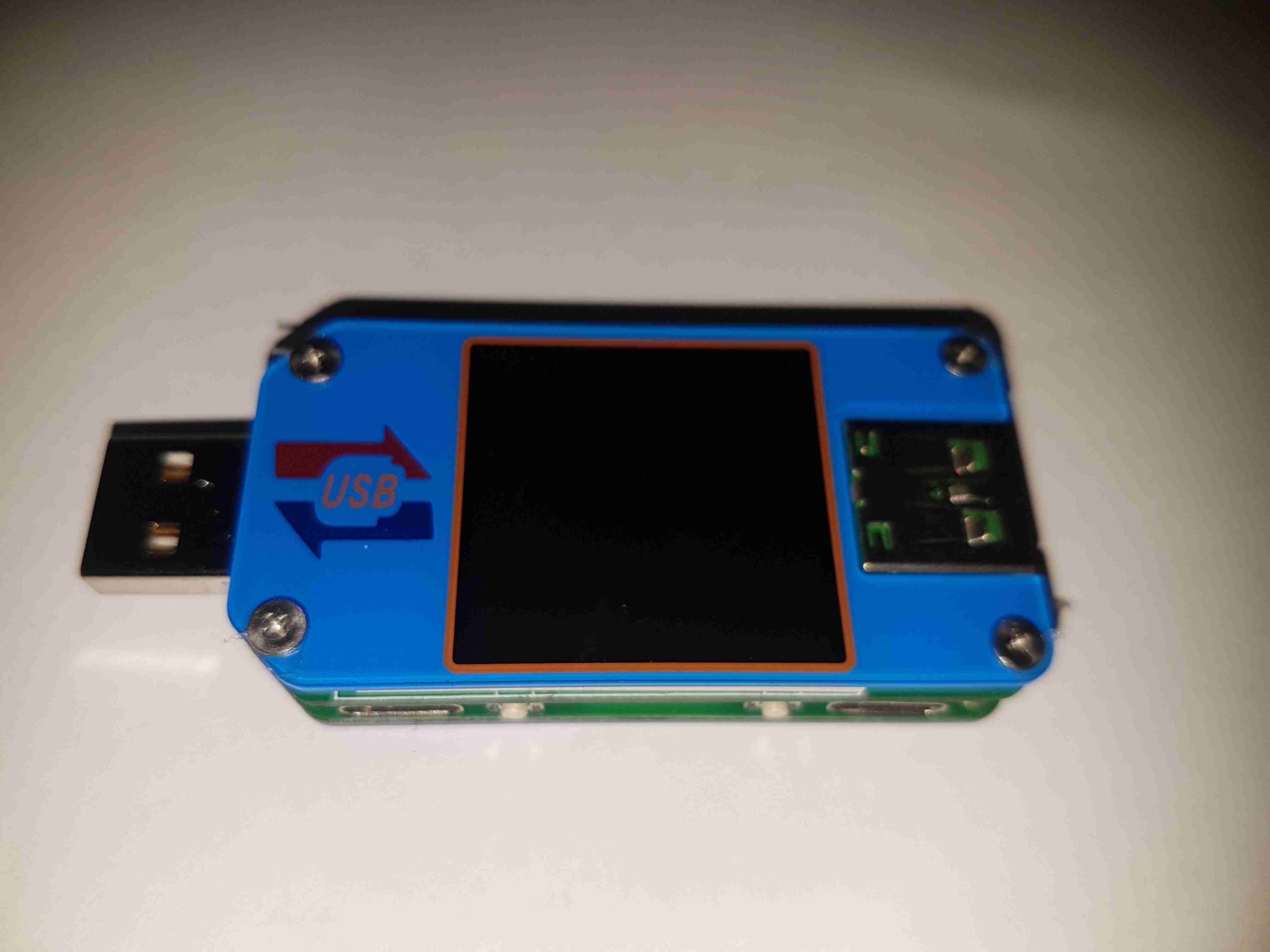
Here’s a nice little feature-packed USB power meter, the UM25C. This unit has USB-C along with the usual USB type A connectors, along with a bluetooth radio for remote monitoring of stats via a Windows or Android app. Construction is nice, it’s a stack of two PCBs, and polycarbonate cover plates, secured together with brass posts & screws.
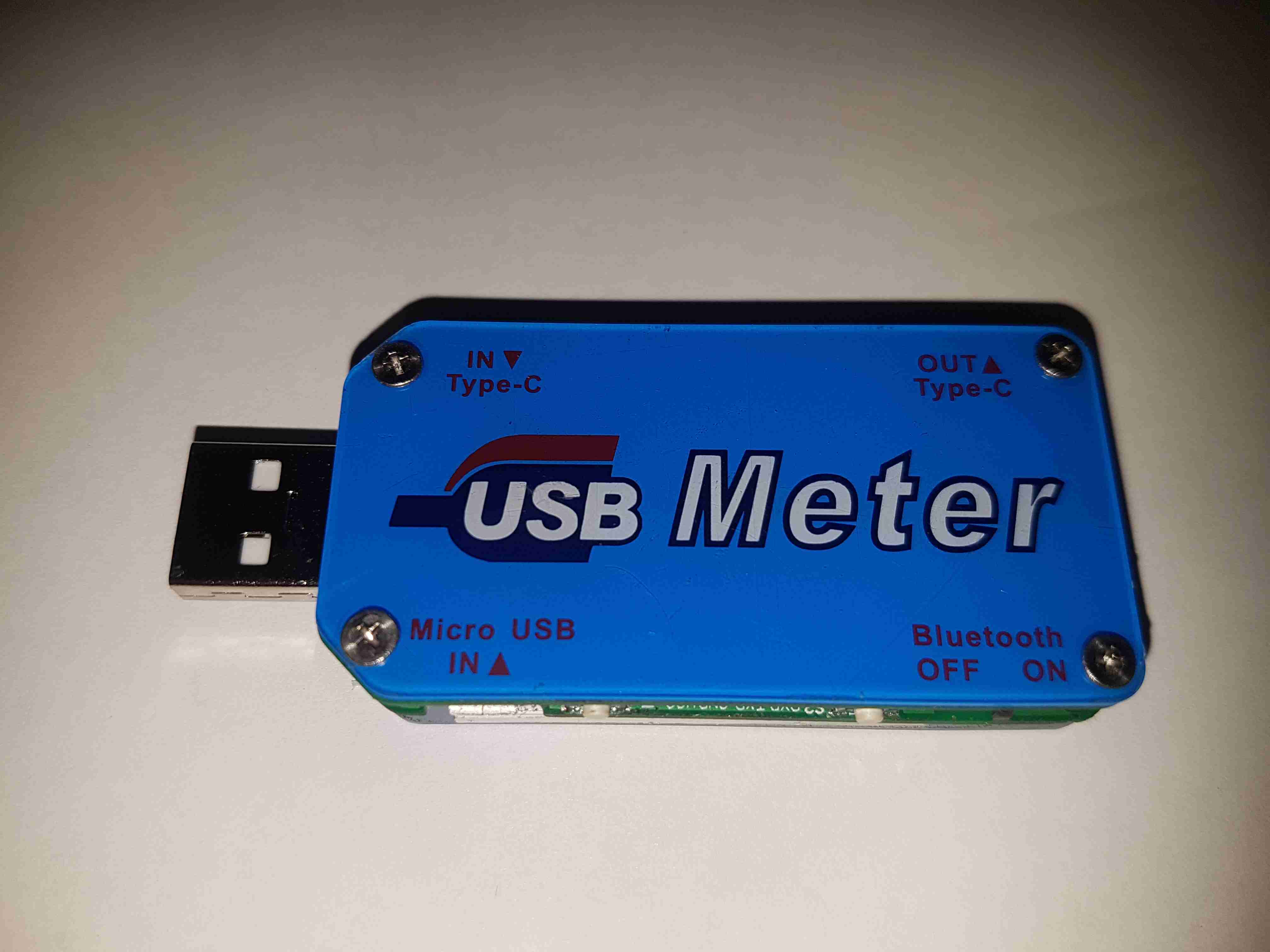
Back Cover
The back cover has the legend for all the side connectors, along with the logo.
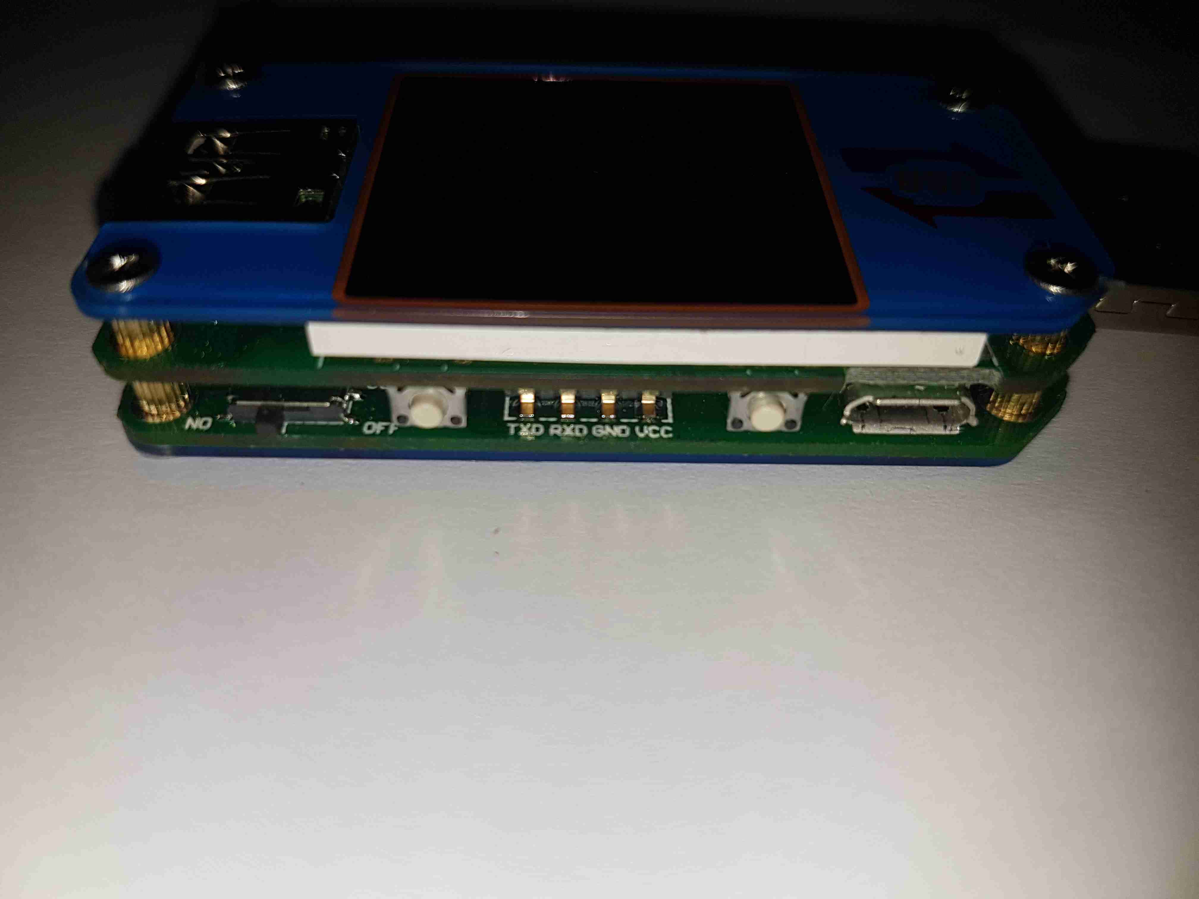
USB Micro Input
Down the sides are the user interface buttons, and here the Micro-B input connector. The 4-pin header is visible here that takes serial data down to the bluetooth section.
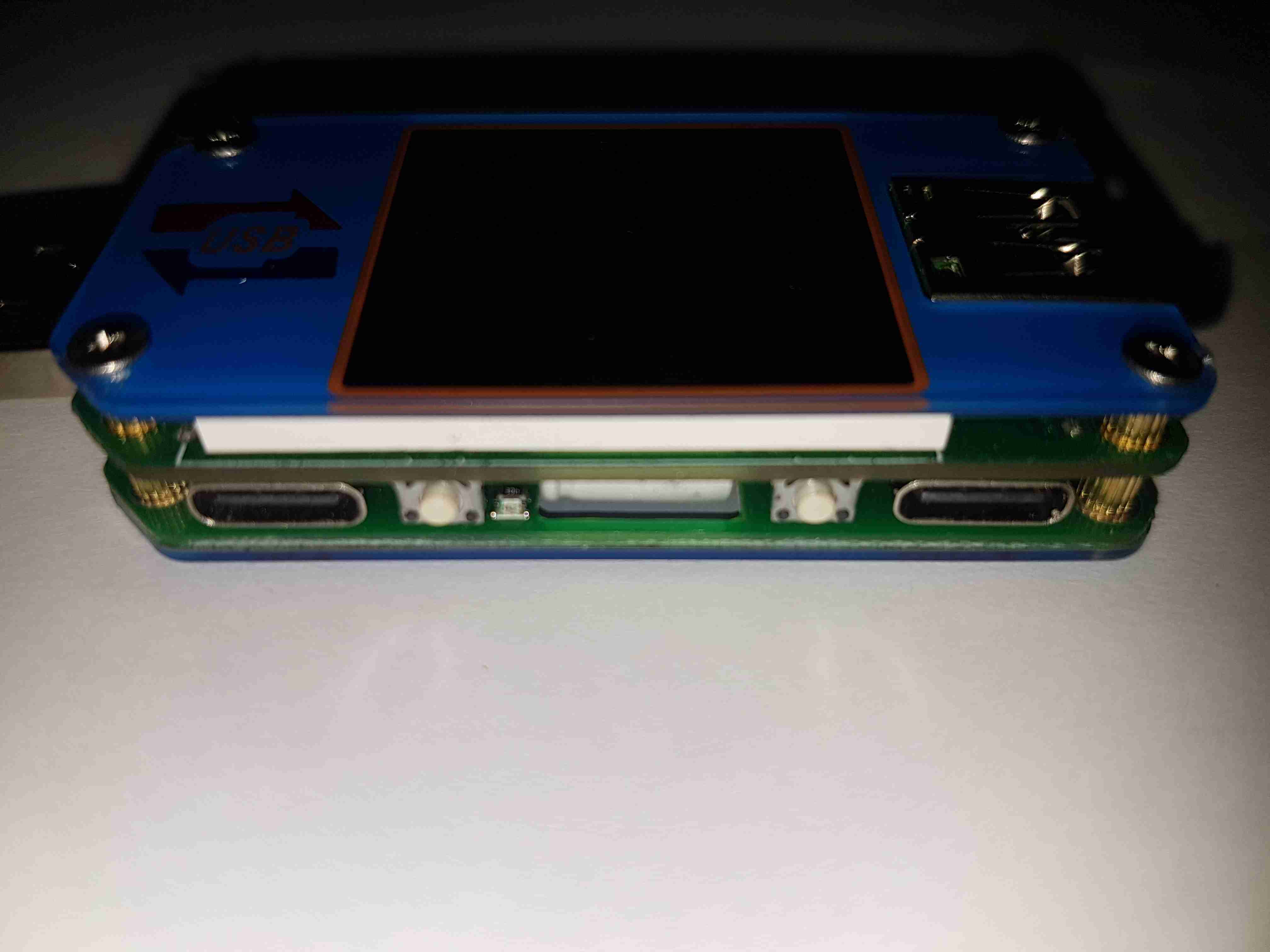
USB-C Connectors
The other side has the remaining pair of buttons, and the USB-C I/O. I don’t yet own anything USB-C based, but this is good future proofing.
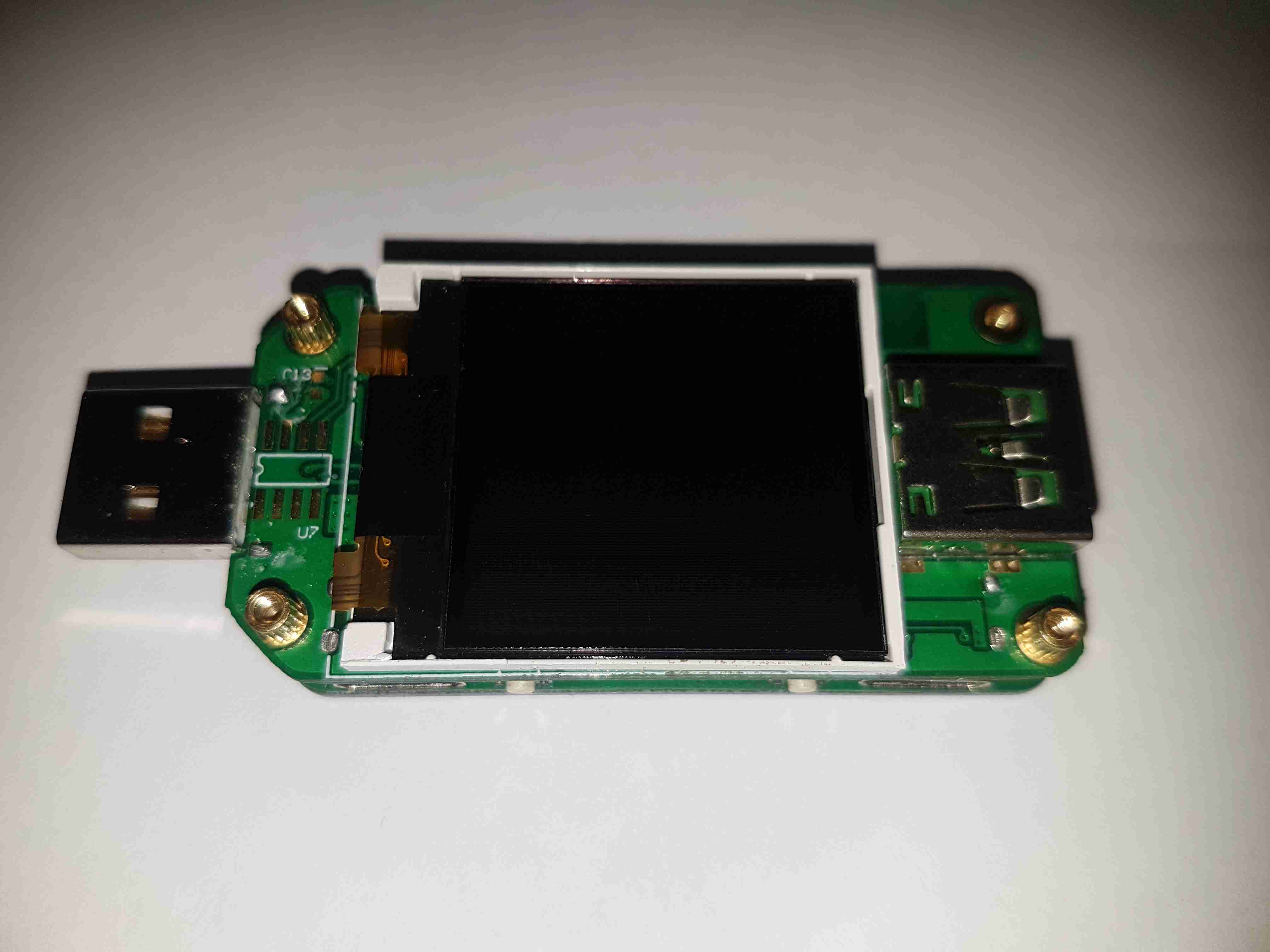
LCD Display
Removing the top plastic cover plate reveals the small 1″ TFT LCD module. This will be hot-bar soldered underneath the screen. There’s an unused footprint next to the USB input connector, judging by the pin layout it’s probably for a I²C EEPROM.
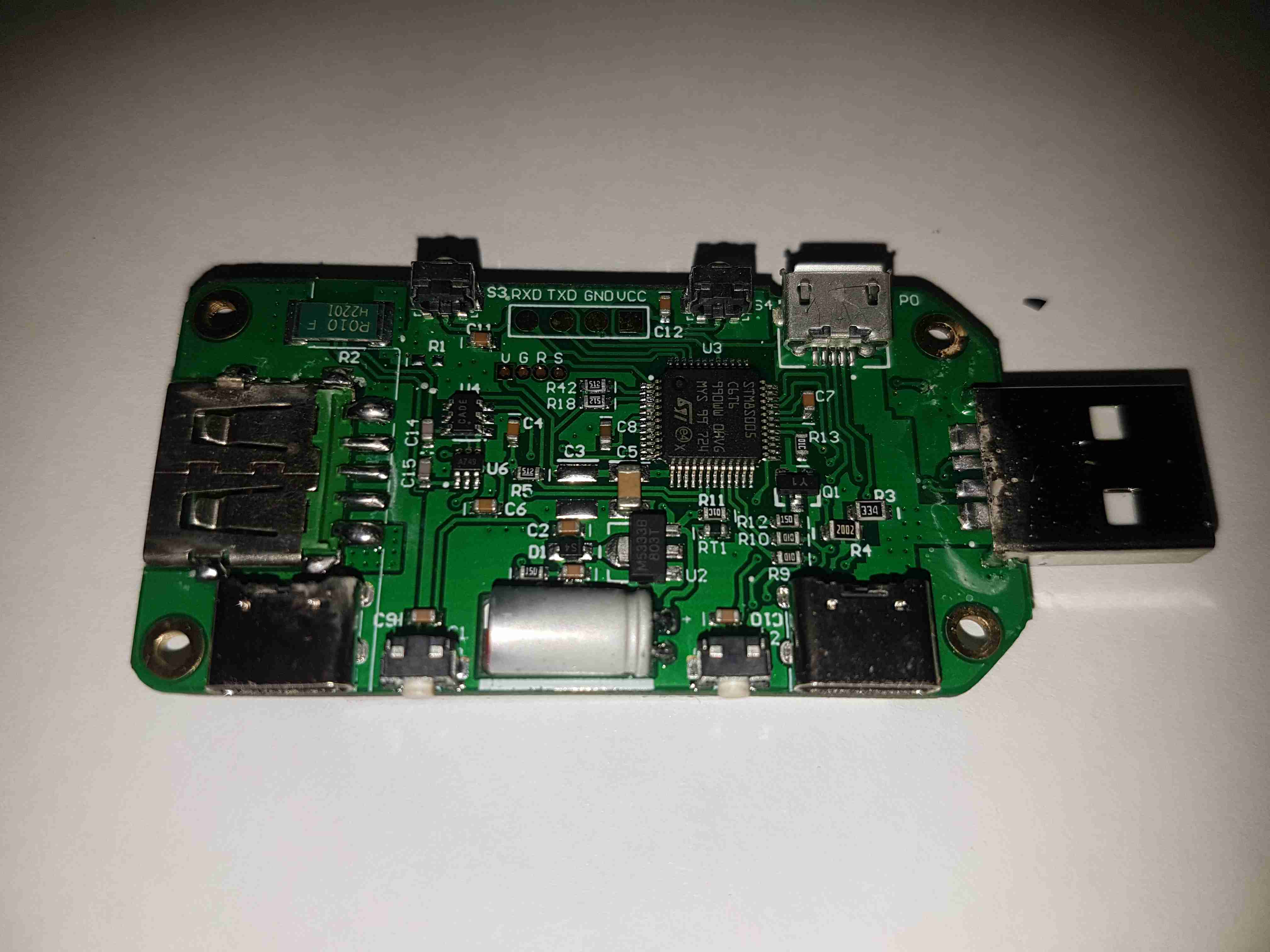
Main Board Components
The underside of the top PCB has all the main components. The brains of the operation is a ST STM8S005C6T6 microcontroller. It’s at the basic end of the STM range, with a 16MHz clock, 32K flash, EEPROM, 10-bit ADC, SPI, UART & I²C. The main 0.010Ω current shunt is placed at the top left of the board in the negative rail. A couple of SOT-23 components in the centre of the board, I haven’t been able to identify properly, but I think they may be MOSFETs. The large electrolytic filter capacitor has a slot routed into the PCB to allow it to be laid flat. Providing the main power rail is a SOT-89 M5333B 3.3v LDO regulator.
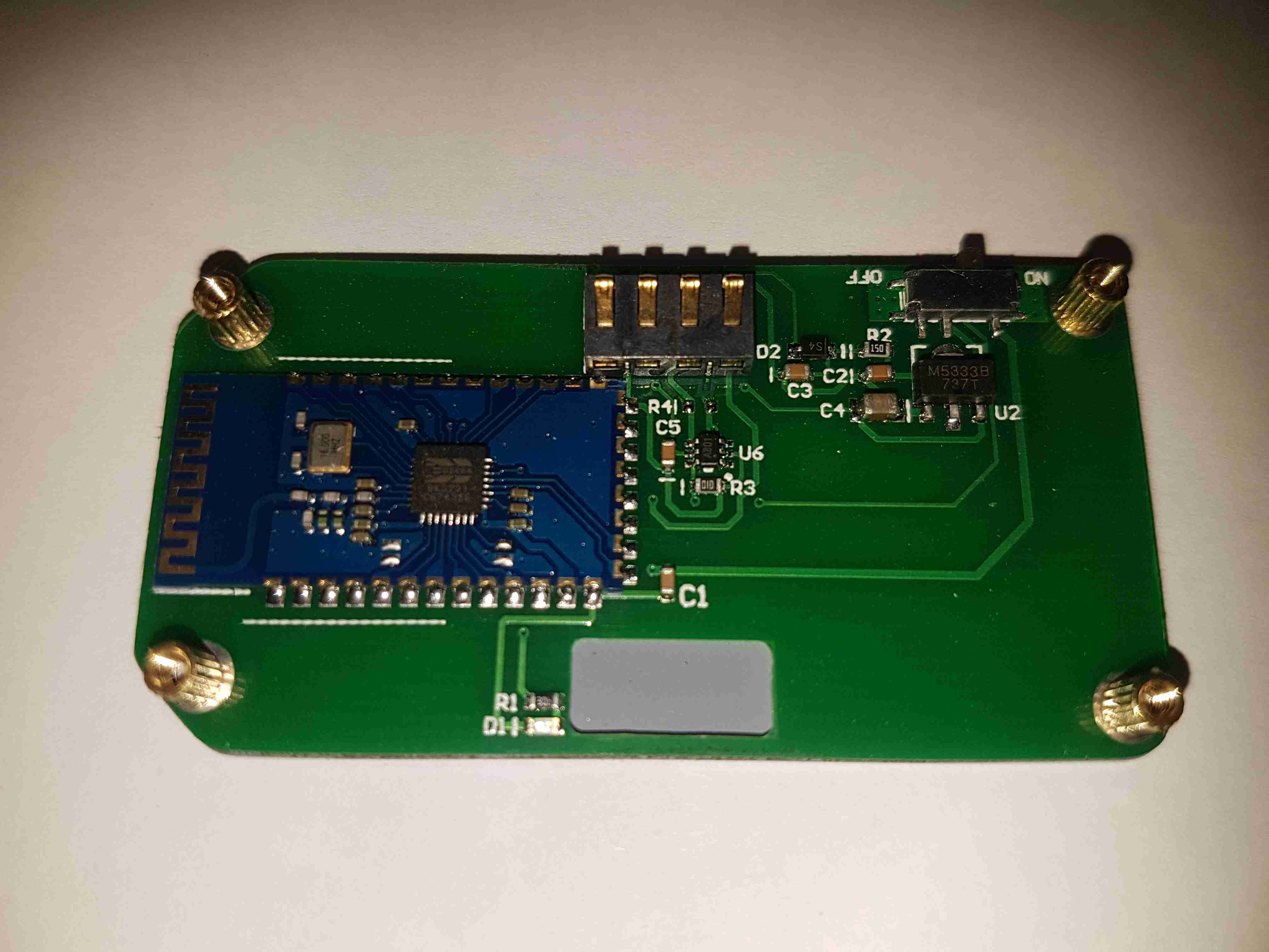
Bluetooth Radio
The bottom board contains the bluetooth radio module, this is a BK3231 Bluetooth HID SoC. The only profile advertised by this unit is a serial port. There’s a local 3.3v LDO regulator & support components, along with an indicator LED.
A few months ago I did a teardown on this Anker PowerPort Speed 5 USB charger, but I didn’t get round to detailing the conversion to 12v I had to do, so I’ll get to that now I’ve got a couple more to convert over.
Power Module
Here’s the internals of the Anker charger once I’ve removed the casing – which like many things these days, is glued together. (Joints can be cracked with a screwdriver handle without damaging the case). There’s lots of heatsinking in here to cool the primary side switching devices & the pot core transformers, so this is the first thing to get removed.
Heatsink Removed
Once the heatsink has been removed, the pot core transformers are visible, wrapped in yellow tape. There’s some more heatsink pads & thermal grease here, to conduct heat better. The transformers, primary side switching components & input filter capacitor have to go.
Primary Side Components Removed
Here’s the PCB once all the now redundant mains conversion components have been deleted. I’ve left the input filtering & bridge rectifier in place, as this solves the issue of the figure-8 cable on the input being reversible, polarity of the input doesn’t matter with the bridge. I’ve removed the main filter capacitor to make enough room for the DC-DC converters to be fitted.
Tails Installed
Installing the tails to connect everything together is the next step, this charger requires two power supplies – the QC3 circuits need 14.4v to supply the multi-voltage modules, the remaining 3 standard ports require 5v. The DC input tails are soldered into place where the main filter capacitor was, while the outputs are fitted to the spot the transformer secondary windings ended up. I’ve left the factory Schottky rectifiers in place on the secondary side to make things a little more simple, the output voltages of both the DC-DC converters does need to be increased slightly to compensate for the diode drops though. I’ve also bypassed the mains input fuse, as at 12v the input current is going to be substantially higher than when used on mains voltage.
DC-DC Converters Installed
With a squeeze both the boost converter & the buck converter fit into place on the PCB.
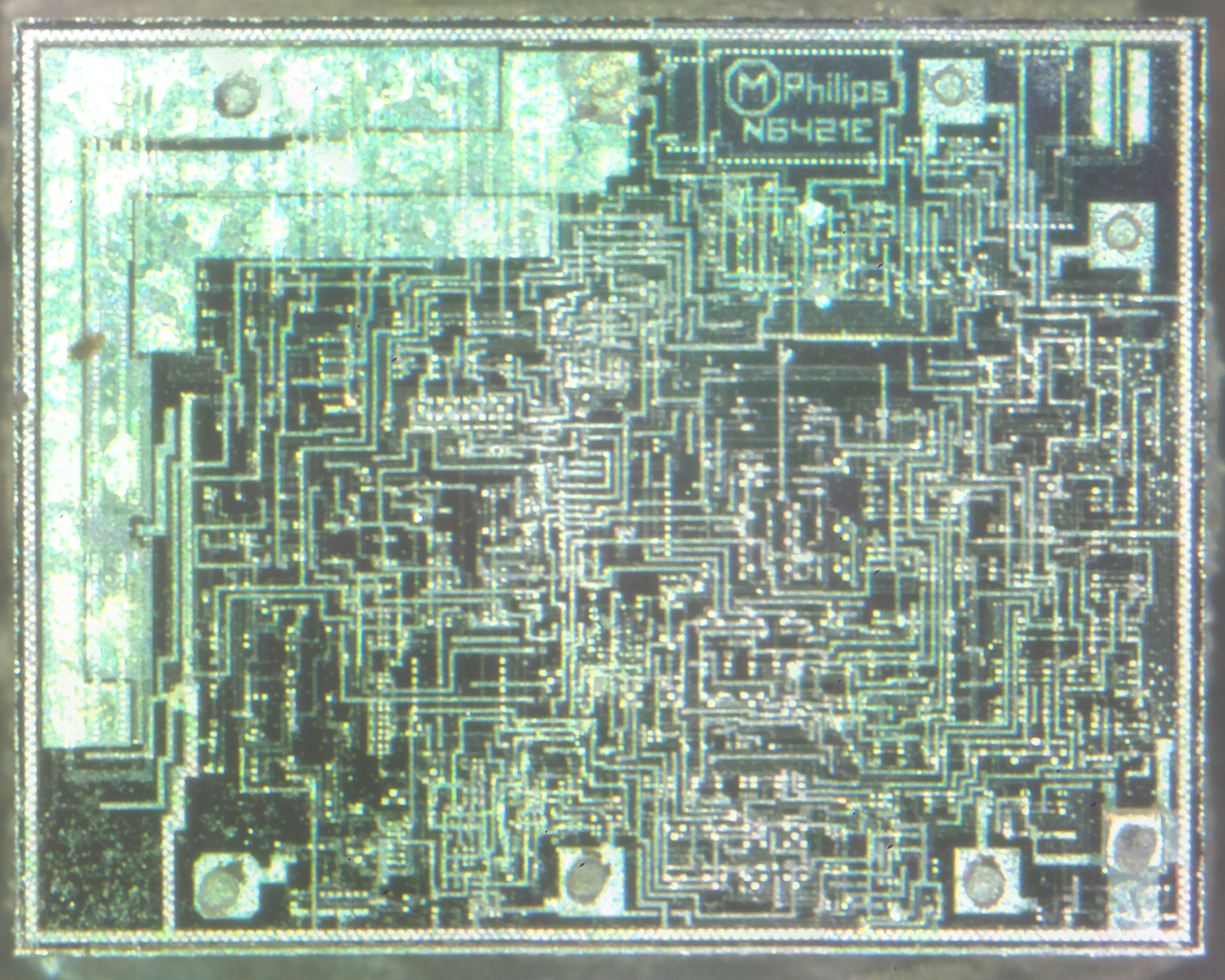
This is a chip aimed at the automotive market – this is a low power voltage regulator for supplying power to microcontrollers, for instance in a CD player.
TDA3606 Die
The TDA3606 is a voltage regulator intended to supply a microprocessor (e.g. in car radio applications). Because of low voltage operation of the application, a low-voltage drop regulator is used in the TDA3606. This regulator will switch on when the supply voltage exceeds 7.5 V for the first time and will switch off again when the output voltage of the regulator drops below 2.4 V. When the regulator is switched on, the RES1 and RES2 outputs (RES2 can only be HIGH when RES1 is HIGH) will go HIGH after a fixed delay time (fixed by an external delay capacitor) to generate a reset to the microprocessor. RES1 will go HIGH by an internal pull-up resistor of 4.7 kΩ, and is used to initialize the microprocessor. RES2 is used to indicate that the regulator output voltage is within its voltage range. This start-up feature is built-in to secure a smooth start-up of the microprocessor at first connection, without uncontrolled switching of the regulator during the start-up sequence. All output pins are fully protected. The regulator is protected against load dump and short-circuit (foldback
current protection). Interfacing with the microprocessor can be accomplished by means of a battery Schmitt-trigger and output buffer (simple full/semi on/off logic applications). The battery output will go HIGH when the battery input voltage exceeds the HIGH threshold level.
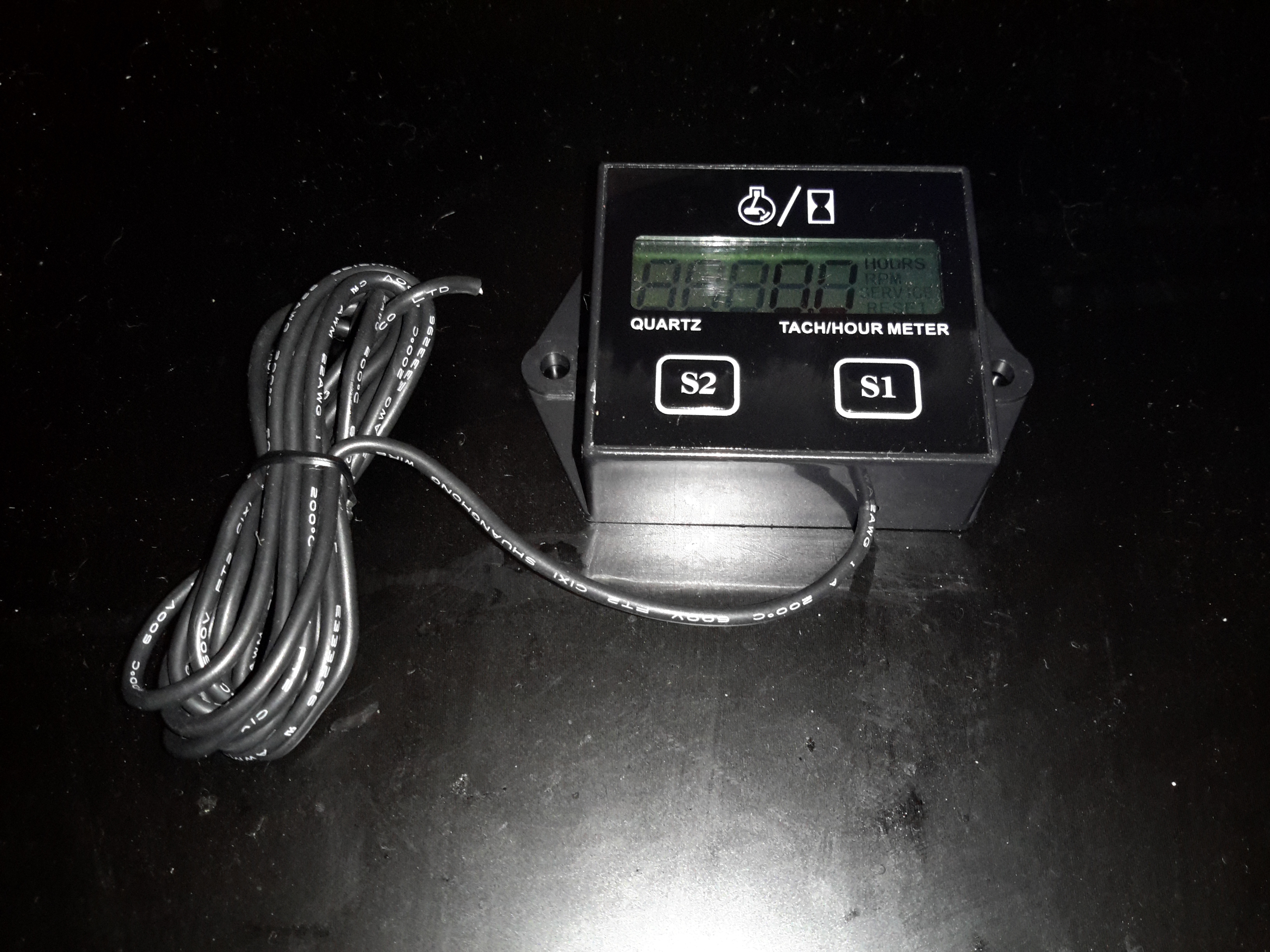
As one of my current projects involves a small petrol engine – a Honda GX35 clone, I figured an hour counter would be very handy to keep an eye on service intervals. (More to come on the engine itself later on). I found a device that would suit my needs on good old eBay.
Inductive Engine Monitor
These engine monitors are pretty cheap, at about £4. The sensing is done by a single heat-resistant silicone wire, that wraps around the HT lead to the spark plug. The unit can be set for different firing intervals via the buttons. In the case of most single-cylinder 4-stroke engines, the spark plug fires on every revolution – wasted-spark ignition. This simplifies the ignition system greatly, by not requiring the timing signal be driven from 1/2 crankshaft speed. The second “wasted” spark fires into the exhaust stroke, so has no effect.
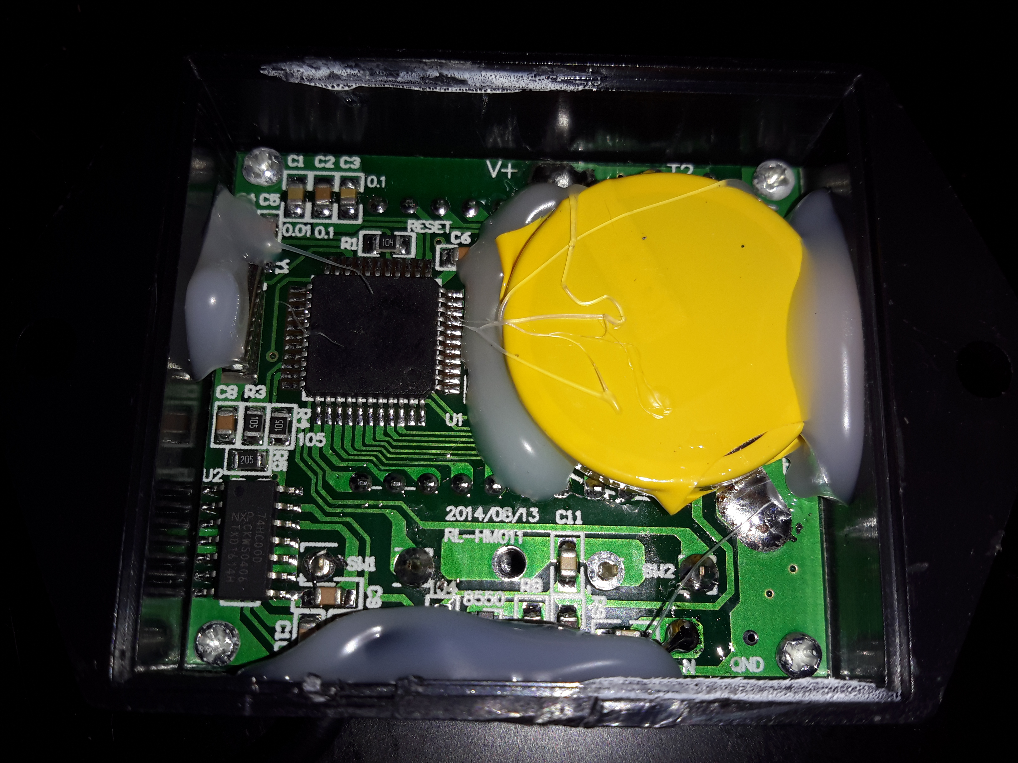
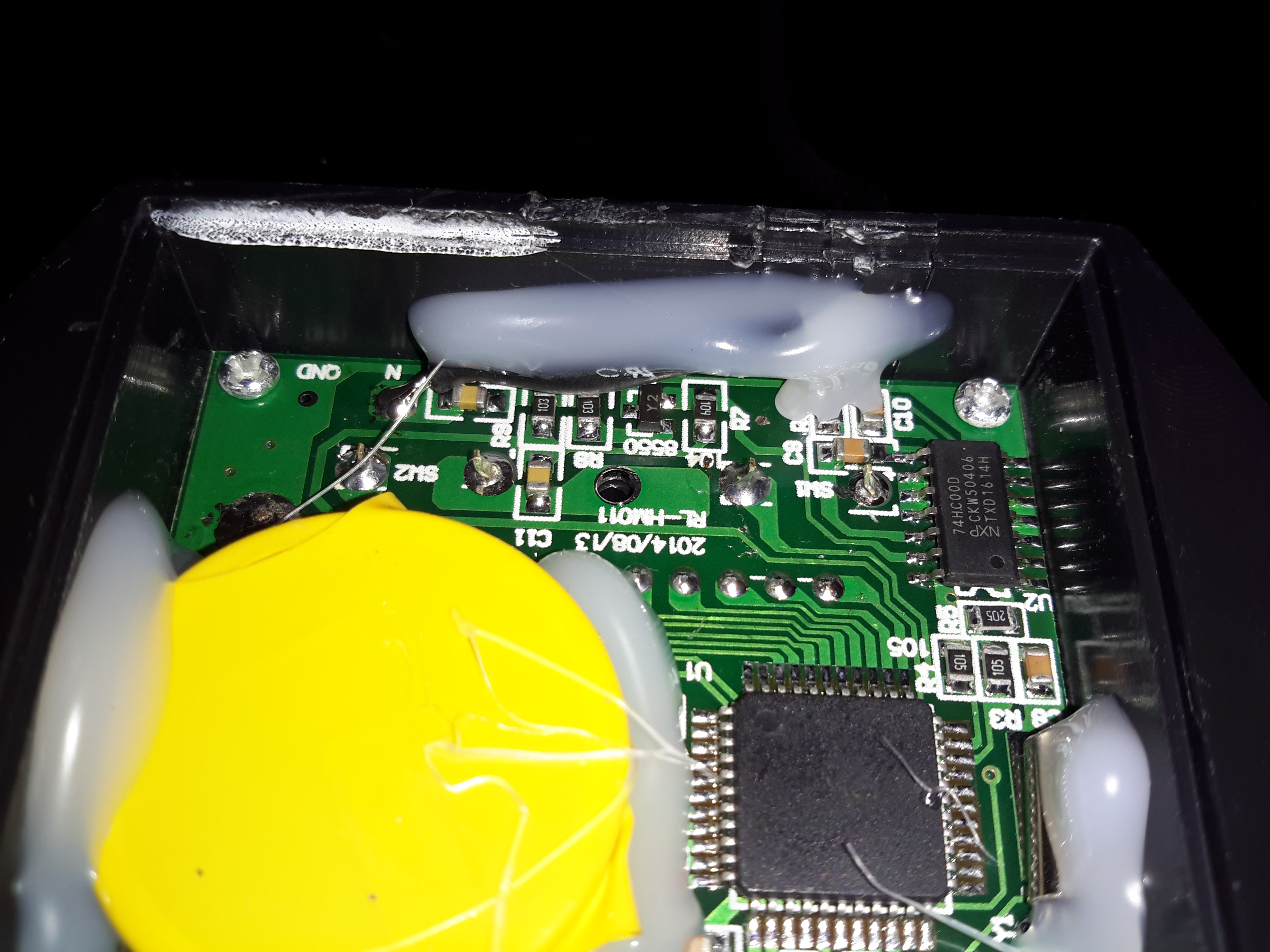
Internals
The back cover is lightly glued into place with a drop of cyanoacrylate in opposite corners, but easily pops off. The power is supplied by a soldered-in 3v Lithium cell. The main microcontroller has no number laser etched on to it at all – it appears it skipped the marking machine.
Input Filtering
The input from the sensing wire comes in through a coupling capacitor & is amplified by a transistor. It’s then fed into a 74HC00D Quad 2-Input NAND gate, before being fed into the microcontroller.
Pickup
The pickup wire is simply wound around the spark plug lead. I’ve held it in position here with some heatshrink tubing. Heat in this area shouldn’t be an issue as it’s directly in the airflow from the flywheel fan.
Here’s a quick teardown of an ignition transformer, used on gas fired ovens & hobs. This unit takes mains 240v AC & uses a transformer to step the voltage to several kV, at a low current to ignite the burners.
Bottom
The transformer section is completely potted in Epoxy resin for insulation, but the driver circuitry is exposed, with a pair of leads from the primary winding exposed
Driver PCB
The drive is very simple. The incoming AC flows through a series resistor through a half-wave rectifier to charge up a 2.2µF film capacitor. Once the voltage on the capacitor reaches a certain level, a DIAC in series with the transformer primary fires, discharging the capacitor through the primary.
The current spike induces a very high voltage on the secondary winding, this then arcs across a gap in the gas flow to start ignition.
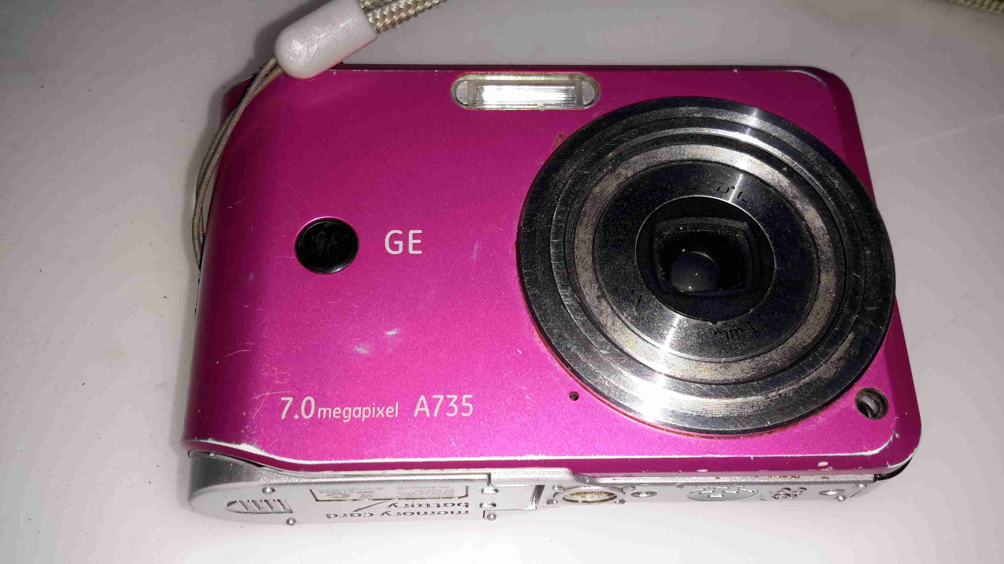
This camera has now been retired after many years of heavy use. Exposure to a 3-year old has caused severe damage to the lens mechanism, which no longer functions correctly.
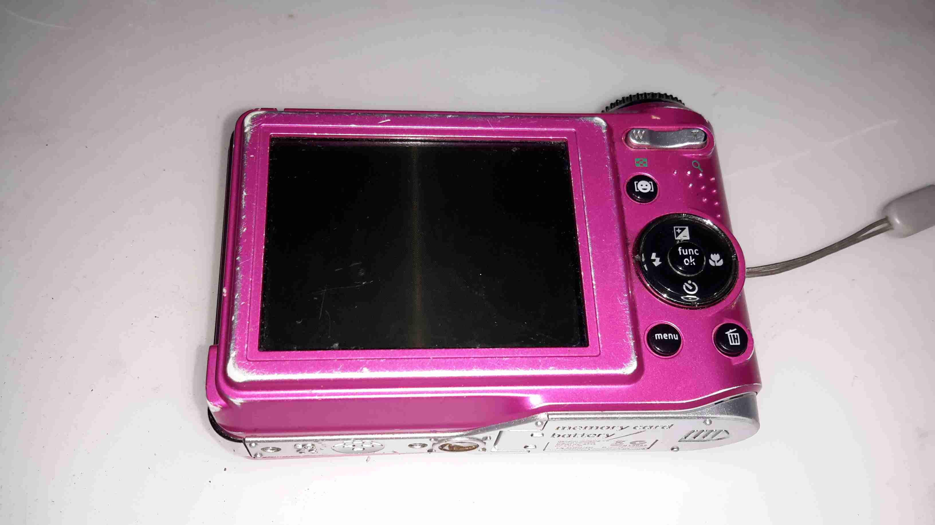
Rear Panel
Pretty much standard interface for a digital camera, with a nice large LCD for it’s time.
Front Cover Removed
With the front cover removed, the lens assembly & battery compartment is exposed.
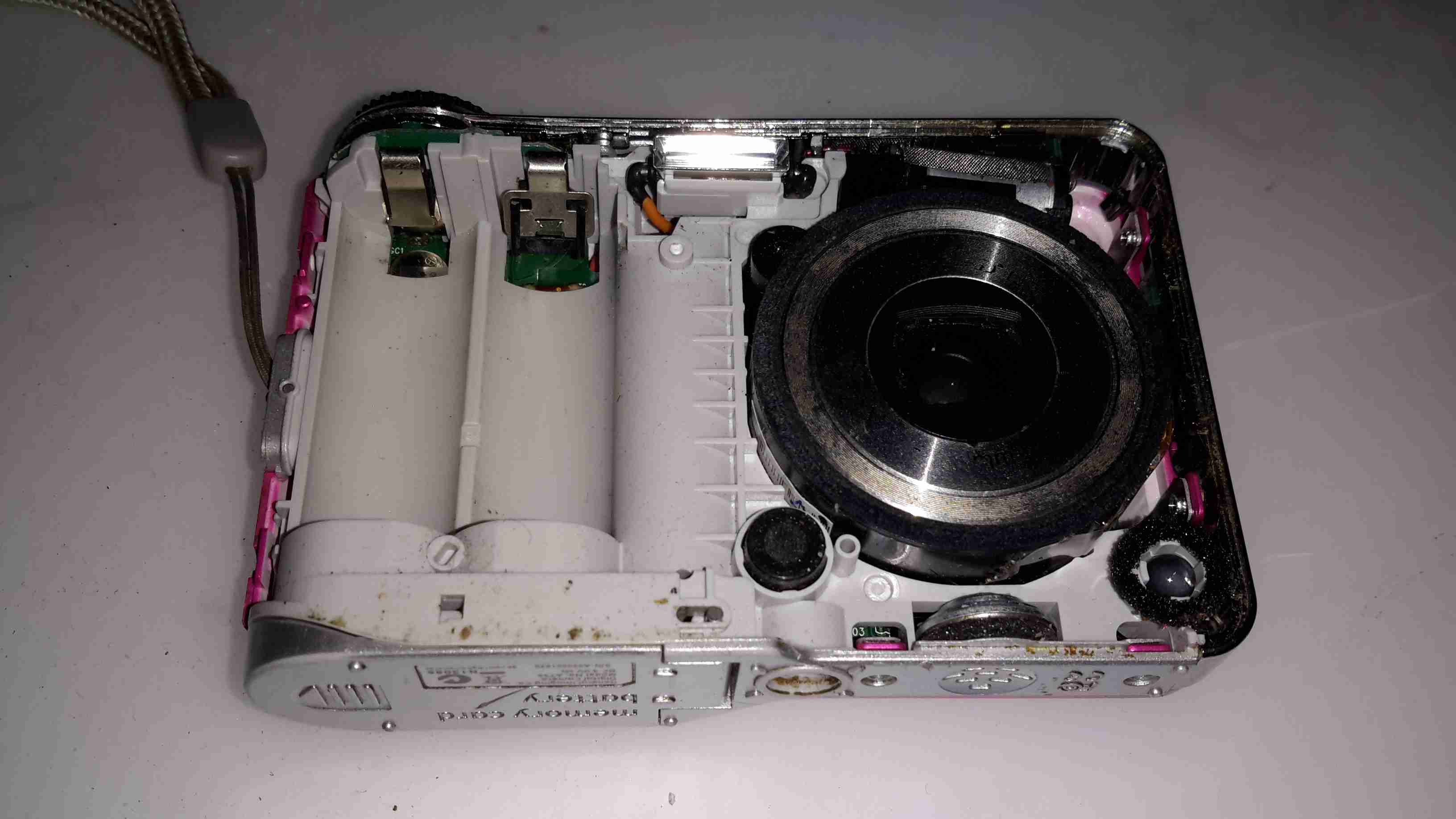
Rear Cover Removed
Removing the rear cover exposes the LCD module & the main PCB, the interface tactile switches are on the right under a protective layer of Kapton tape.
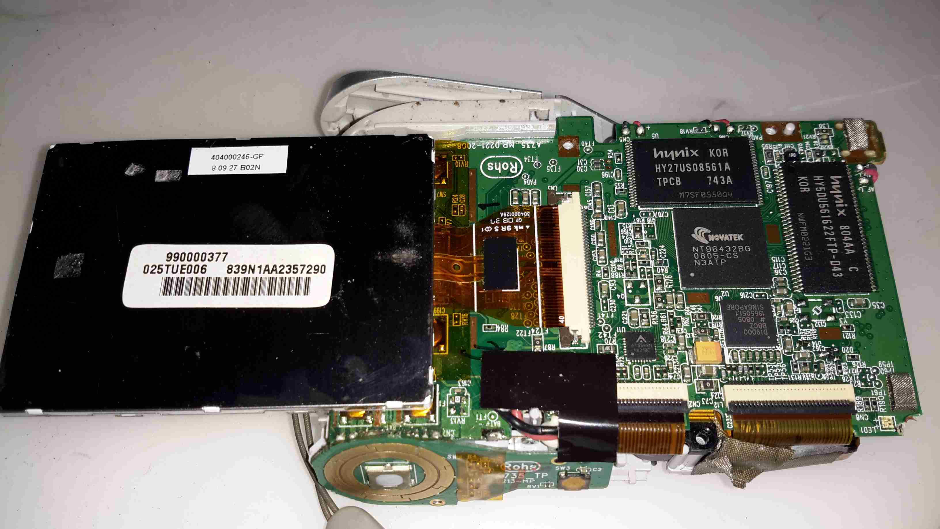
Main Chipset
Flipping the LCD out of it’s mounting bracket reveals the main camera chipset. The CPU is a NovaTek NT96432BG, no doubt a SoC of some kind, but I couldn’t find any information. Firmware & inbuilt storage is on a Hynix HY27US08561A 256MBit NAND Flash, with a Hynix HY5DU561622FTP-D43 256Mbit DRAM for system memory.
I couldn’t find any info on the other two chips on this side of the board, but one is probably a motor driver for the lens, while the other must be the front end for the CCD sensor input to the SoC.
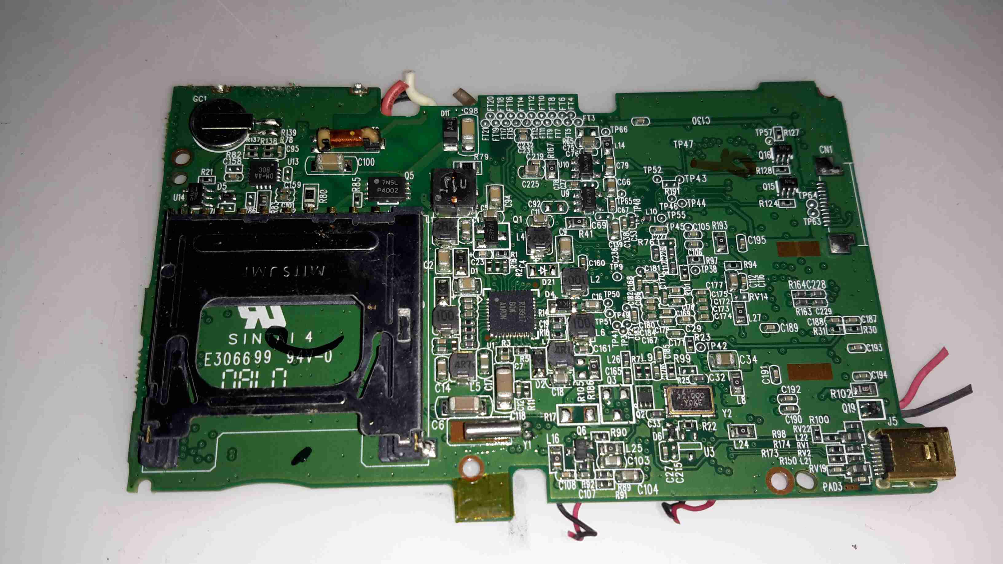
Main PCB Reverse
The other side of the PCB handles the SD card slot & power management. All the required DC rails are provided for by a RT9917 7-Channel DC-DC converter from RichTek, an IC designed specifically for digital camera applications.
Top left above the SD card slot is the trigger circuitry for the Xenon flash tube & the RTC backup battery.
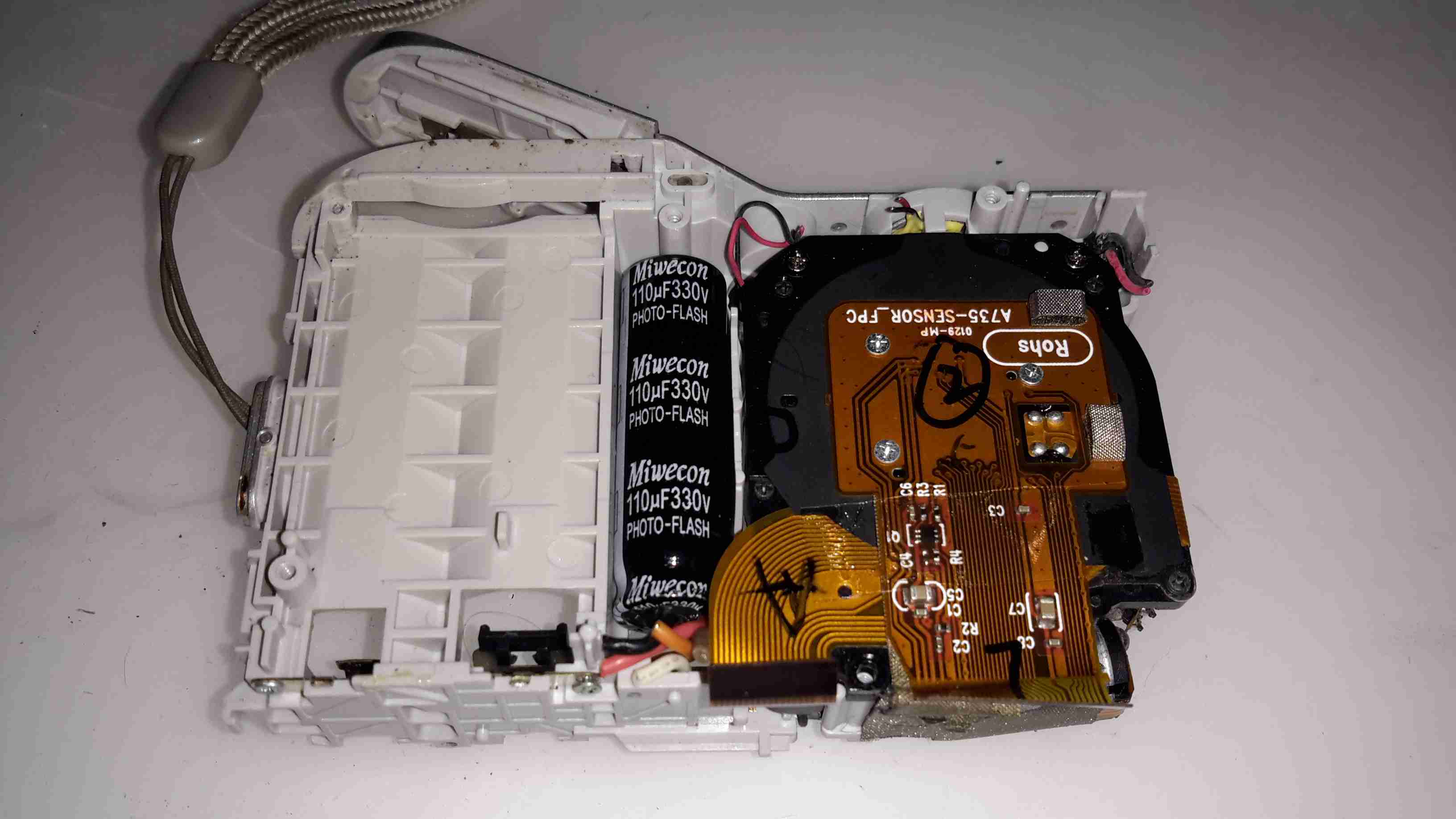
Main PCB Removed
Once the main PCB is out of the frame, the back of the lens module with the CCD is accessible. Just to the left is the high-voltage photoflash capacitor, 110µF 330v. These can give quite the kick when charged! Luckily this camera has been off long enough for the charge to bleed off.
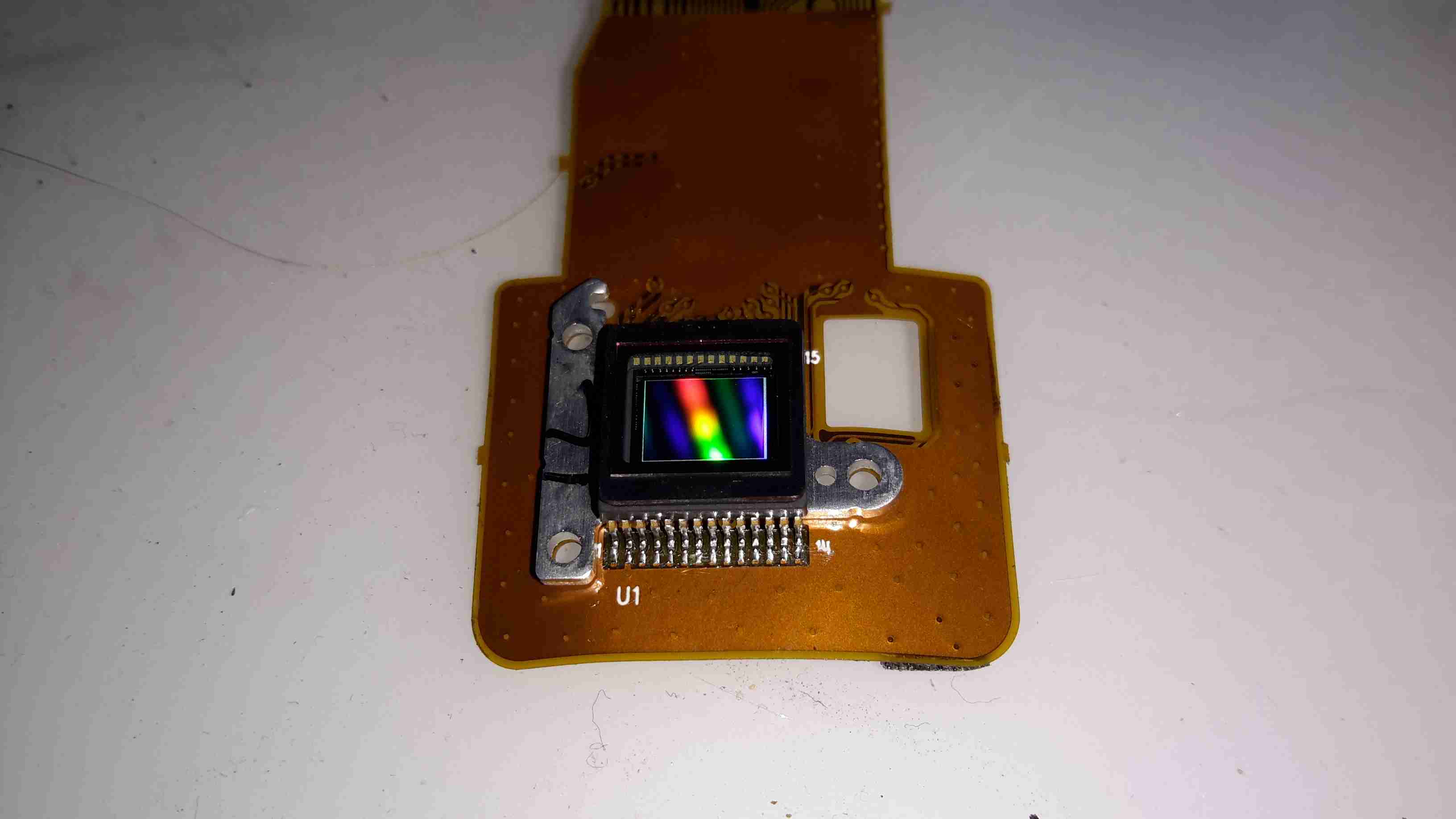
Sensor
Finally, here’s the 7-Megapixel CCD sensor removed from the lens assembly, with it’s built in IR cut filter over the top. I couldn’t find any make or model numbers on this part, as the Aluminium mounting bracket behind is bonded to the back of the sensor with epoxy, blocking access to any part information.
Die images of the chipset to come once I get round to decapping them!
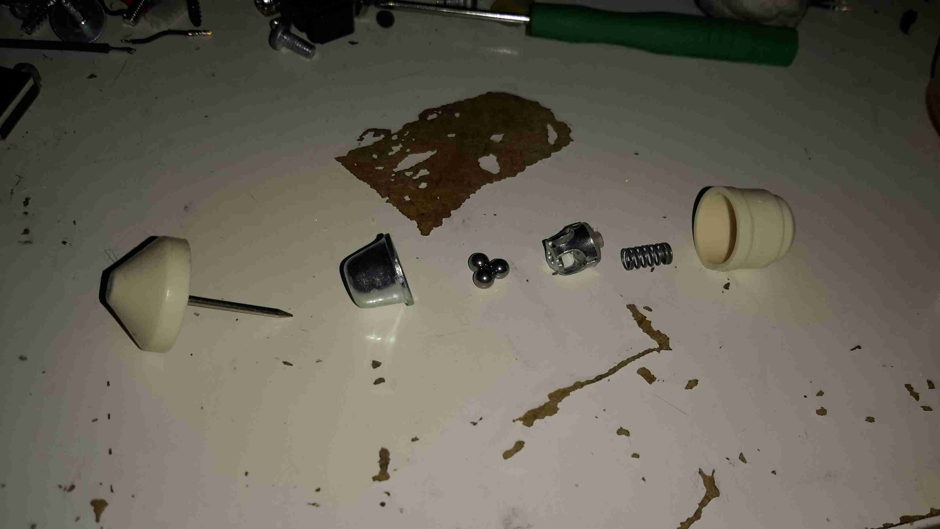
Everyone at some stage must have seen these EAS security tags in shops, usually attached to clothing with a steel pin. As some of this year’s presents had been left with the tags attached, I had to forcibly remove them before wrapping could commence.
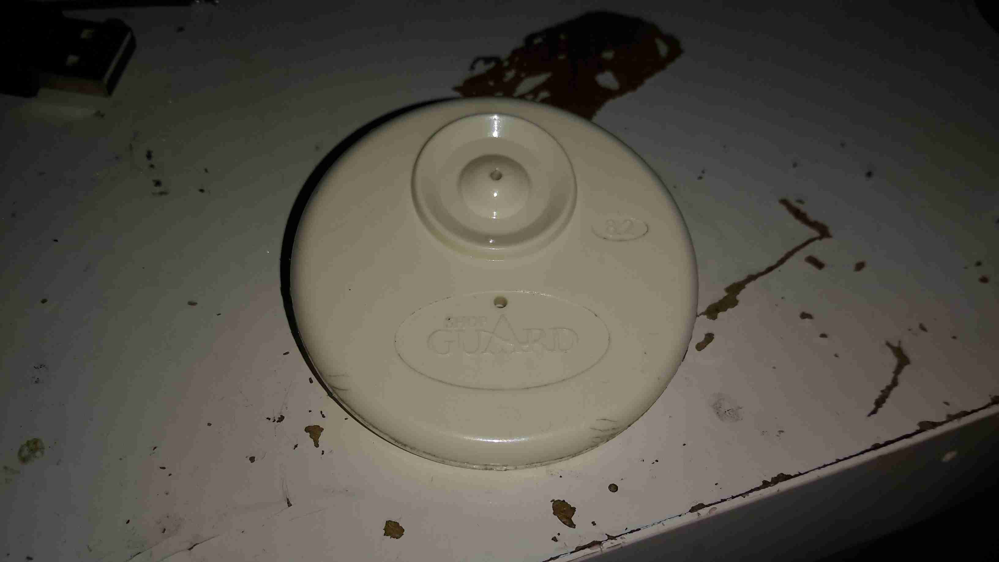
Reverse Side
These are just a plastic disc about 50mm in diameter, with an internal locking mechanism & RF tag inside.
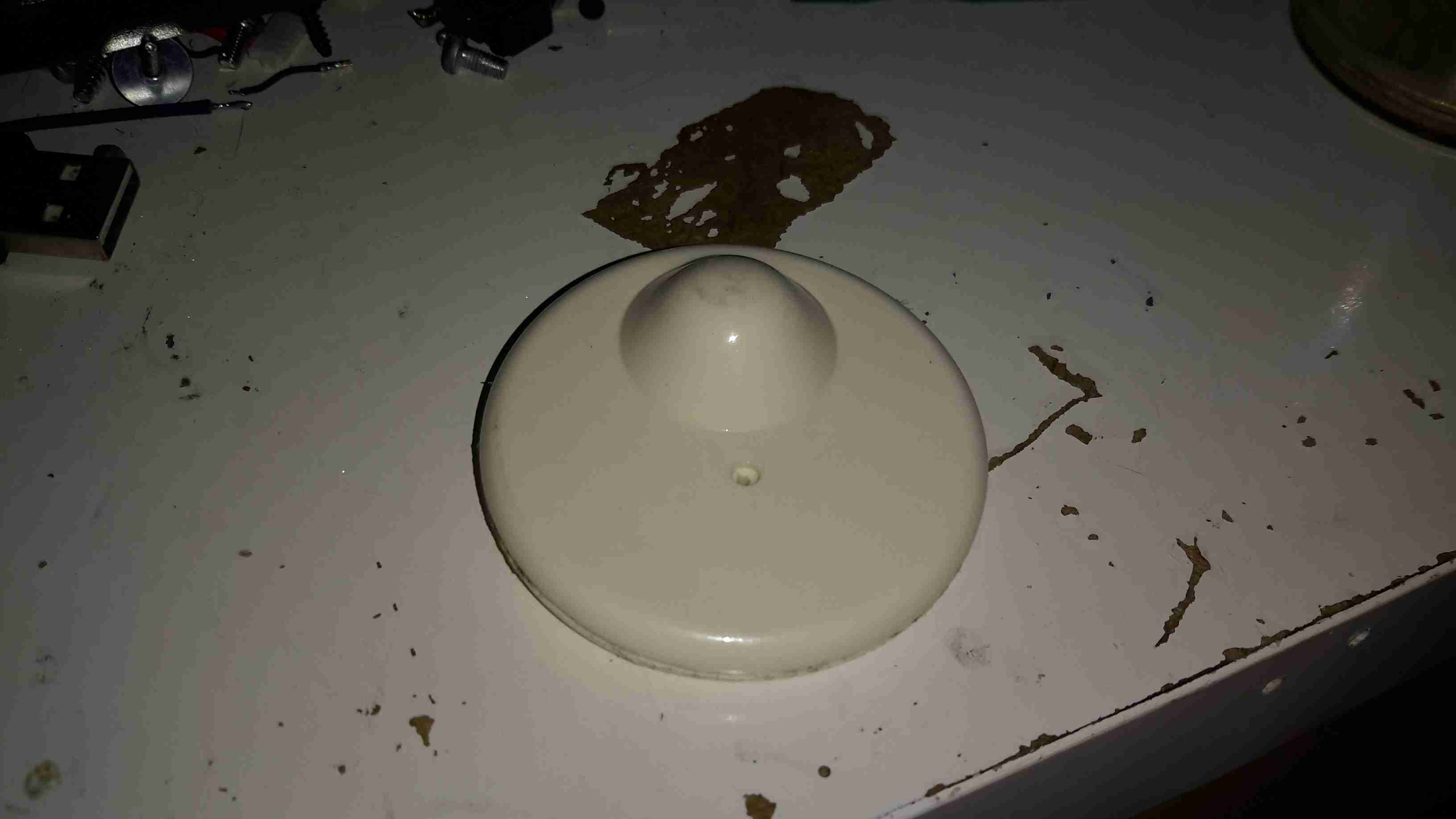
RF Coil
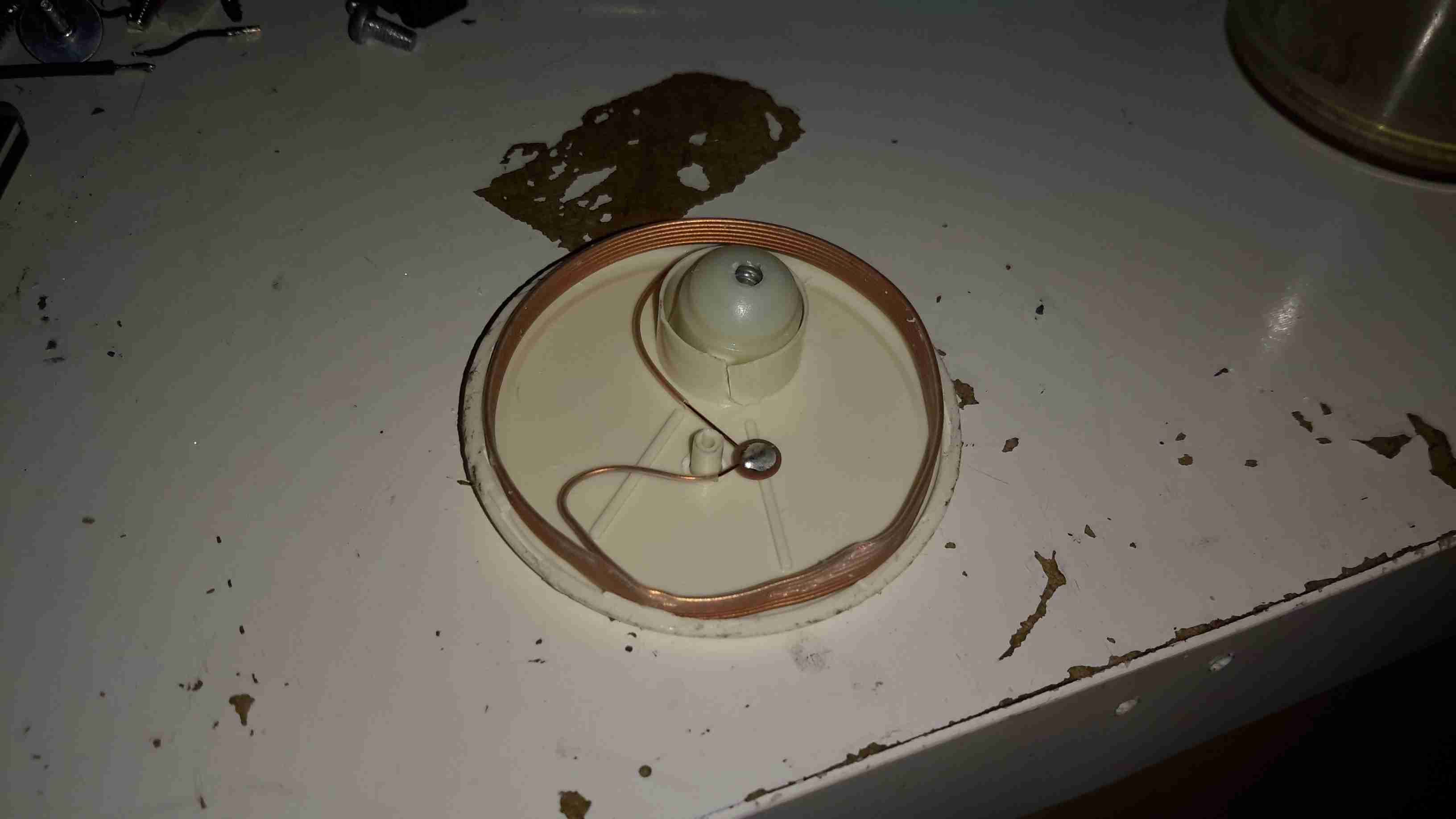
After some careful attack with a saw around the glue seam, the tag comes apart into it’s halves. The RF coil & it’s ceramic capacitor can be seen wrapped around the outside of the tag. The capacitor in this case isn’t even epoxy dipped to save that extra 0.0001p on the manufacturing price. In the top centre is the pin locking mechanism, enclosed in a small plastic pill.
Lock Pill
Popping off the back cap of the lock shows it’s internals.
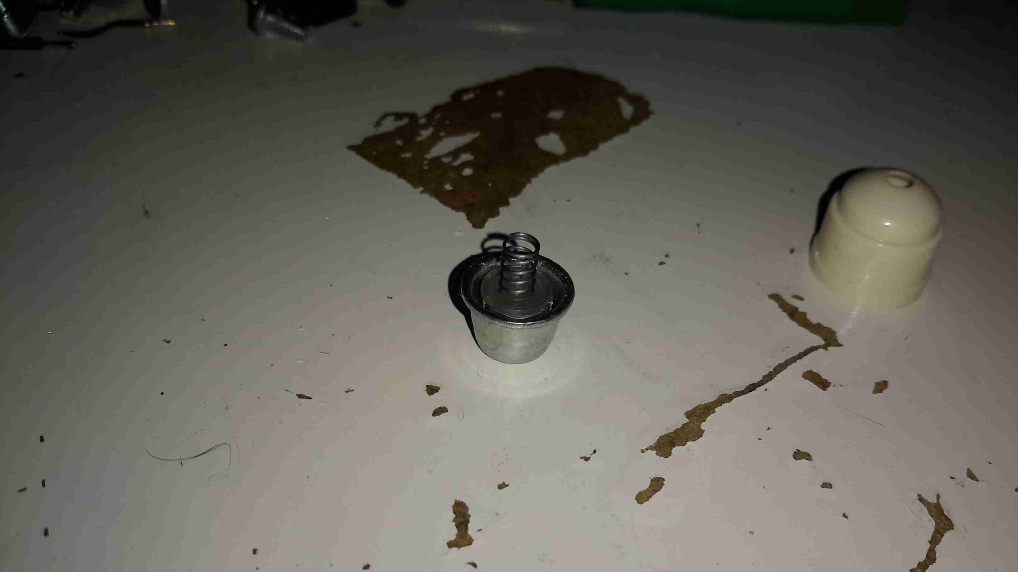
Ball Bearing Lock Assembly
The lock itself is very simple. The centre section, held in place by a spring, carries 3 small ball bearings. The outer metal frame of the lock is conical in shape.
When the pin is pushed into the tag, the conical shape of the lock chamber causes the ball bearings to grab onto it, helped by the action of the spring that pushes the ball bearing carrier further into the cone.
This also means that any attempt to force the mechanism causes it to lock tighter onto the pin.
In normal operation, removal is achieved by a strong magnet that pulls the ball bearing carrier back slightly against it’s spring, allowing the pin to disengage & be pulled out.
This design is incredibly simple & cheap to make, and gains it’s locking strength from friction alone.
I would consider the RF coil being around the outer edge of the device a bit of a security risk – a quick chop with a sharp pair of wire cutters would disable the tag’s alarm functionality instantly. Making the coil slightly smaller & keeping it out of reach of the edge of the tag would help in this regard.
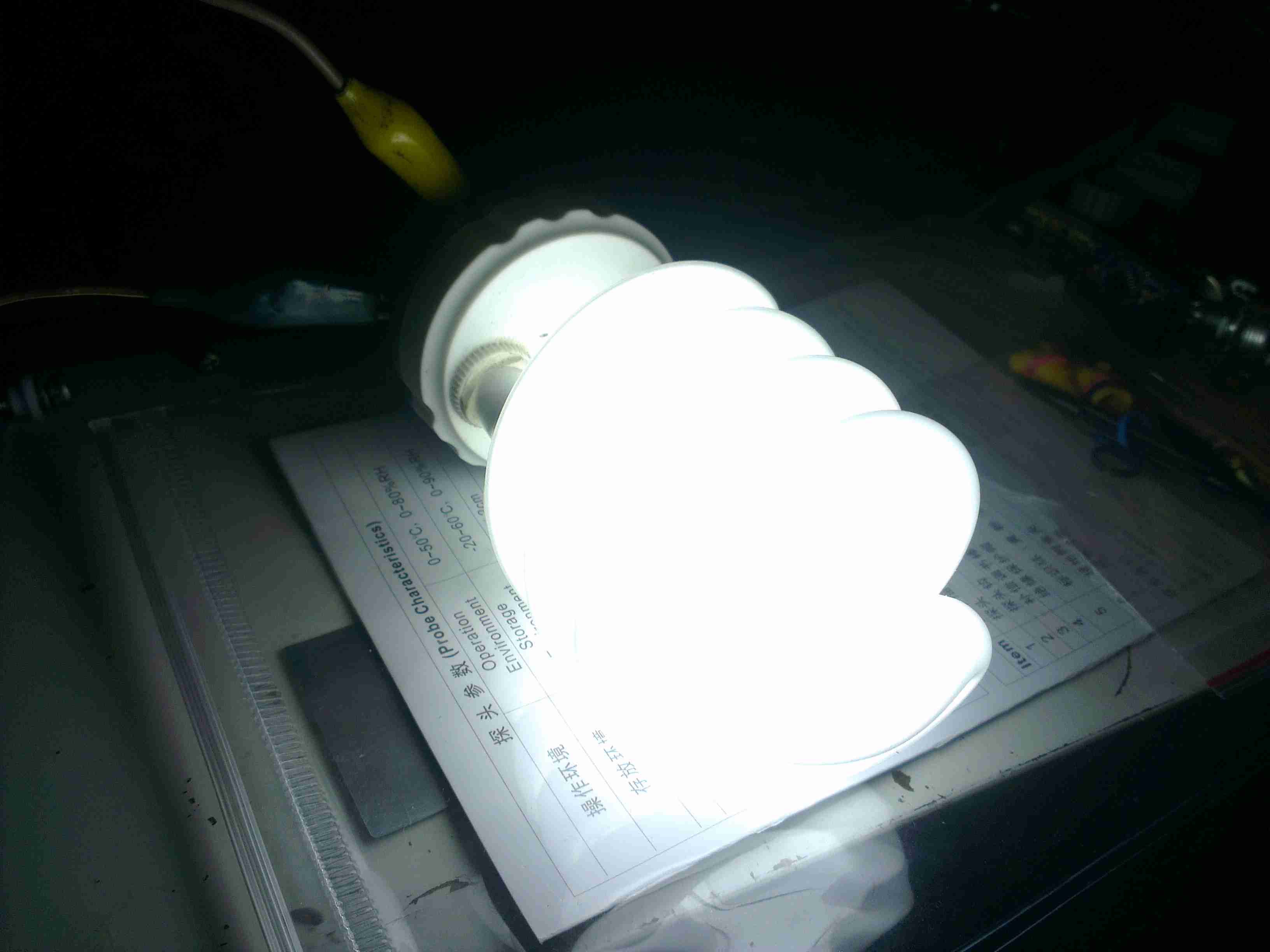
On the boat I have installed custom LED lighting almost everywhere, but we still use CFL bulbs in a standing lamp since they have a wide light angle, and brightness for the size.
I bought a couple of 12v CFLs from China, and the first of these has been running for over a year pretty much constantly without issue. However, recently it stopped working altogether.
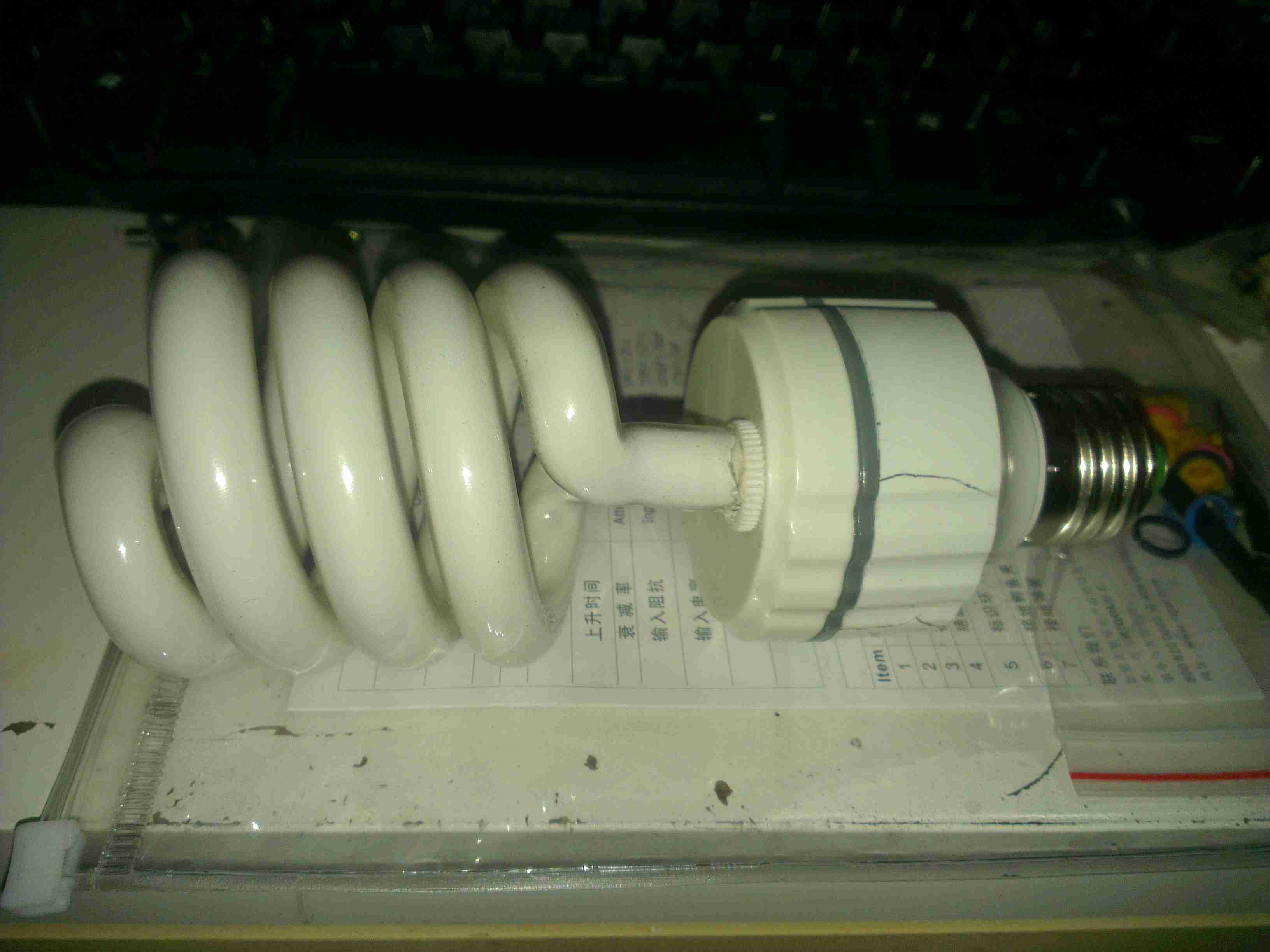
12v CFL
Here’s the lamp, exactly the same as the 240v mains versions, except for the design of the electronic ballast in the base. As can be seen here, the heat from the ballast has degraded the plastic of the base & it’s cracked. The tube itself is still perfectly fine, there are no dark spots around the ends caused by the electrodes sputtering over time.
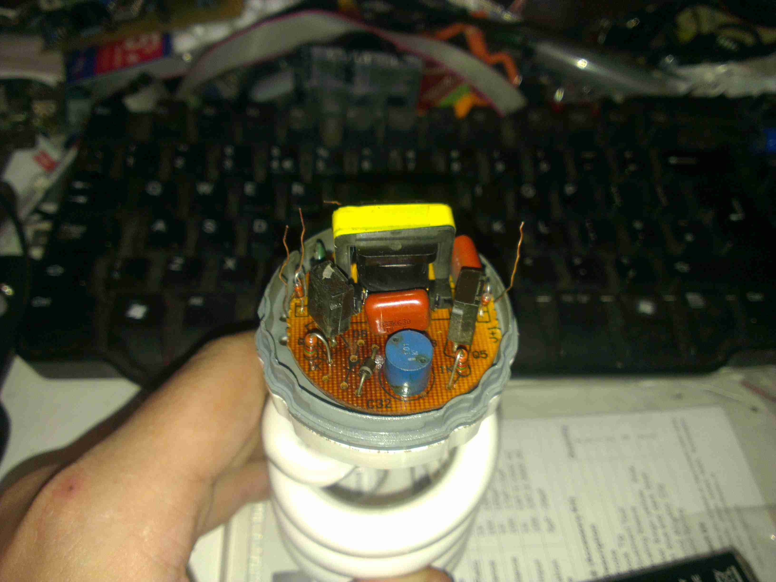
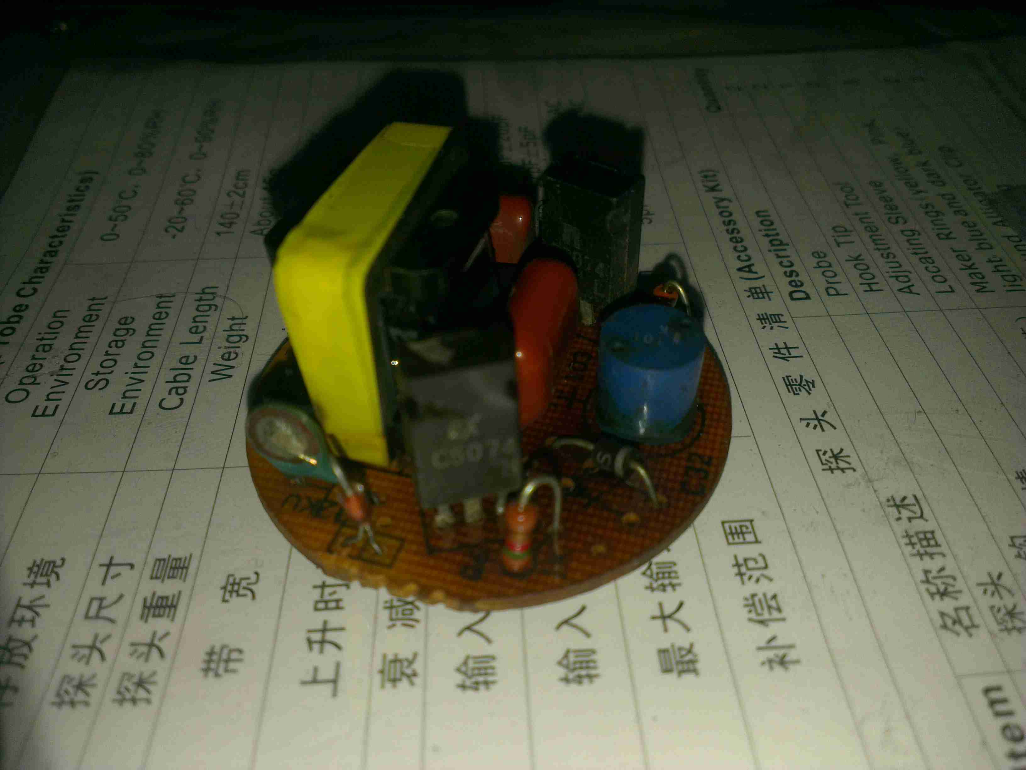
Ballast
Here’s the ballast inside the bottom of the lamp, a simple 2-transistor oscillator & transformer. The board has obviously got a bit warm, it’s very discoloured!
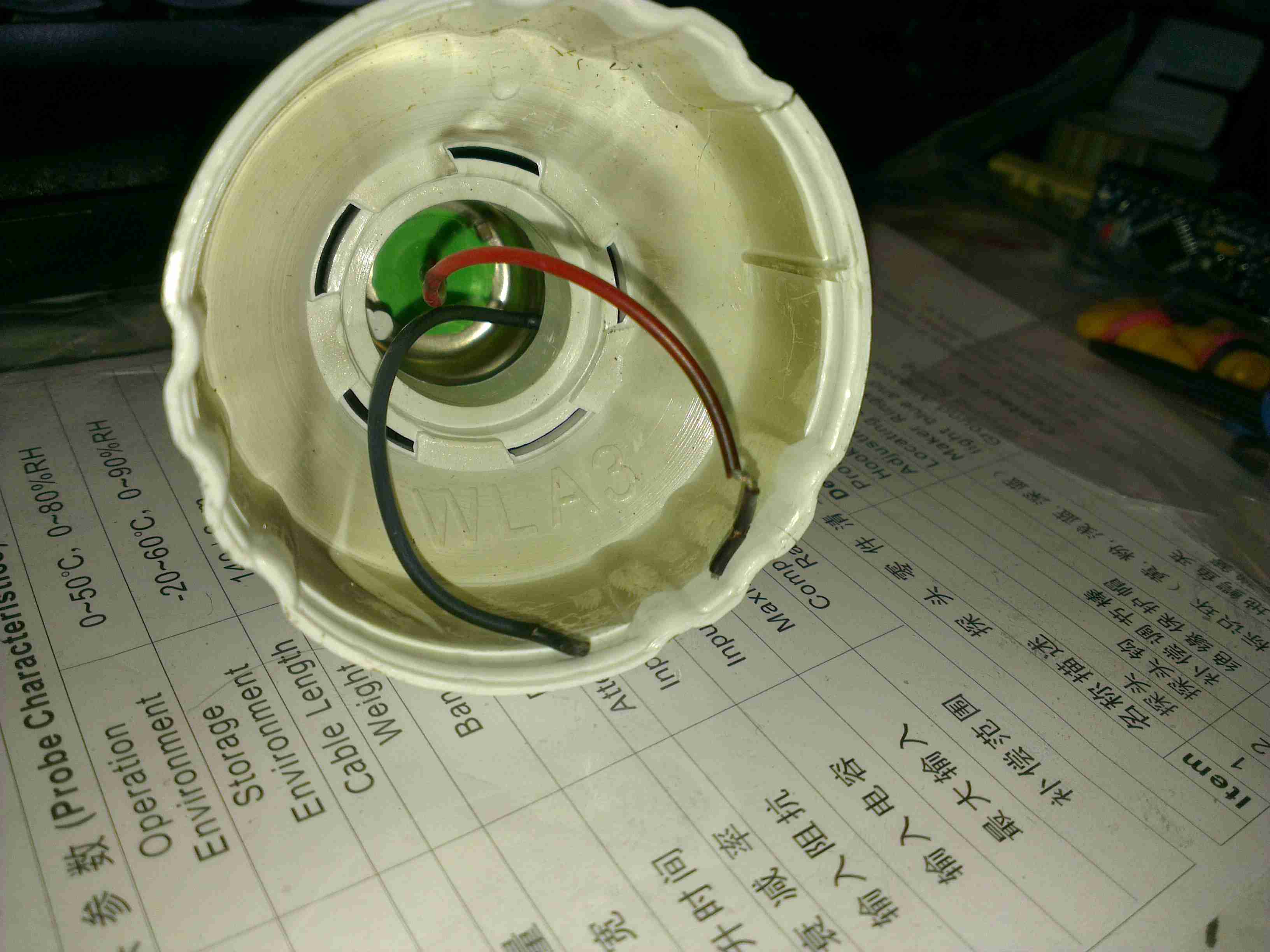
Failed Wiring
The failure mode in this case was cooked wiring to the screw base. The insulation is completely crispy!
Direct Supply
On connection direct to a 12v supply, the lamp pops into life again! Current draw at 13.8v is 1.5A, giving a power consumption of 20.7W. Most of this energy is obviously being dissipated as heat in the ballast & the tube itself.
Ballast PCB
Here’s the ballast PCB removed from the case. It’s been getting very warm indeed, and the series capacitor on the left has actually cracked! It’s supposed to be 2.2nF, but it reads a bit high at 3nF. It’s a good thing there are no electrolytics in this unit, as they would have exploded long ago. There’s a choke on the DC input, probably to stop RFI, but it doesn’t have much effect.
Supply Waveform
Here’s the waveform coming from the supply, a pretty crusty sinewave at 71.4kHz. The voltage at the tube is much higher than I expected while running, at 428v.
RFI
Holding the scope probe a good 12″ away from the running bulb produces this trace, which is being emitted as RFI. There’s virtually no filtering or shielding in this bulb so this is inevitable.
I recently ordered a PSU to run one of the TVs I converted to 12v operation, and being an older TV, it’s a fairly heavy load at 6.5A. eBay to the rescue again, with a cheap 10A rated supply.
Power Brick
Like all similar supplies these days, it’s a SMPS unit, and feels suspiciously light for it’s power rating.
Cover Removed
Luckily this one is easy to get into, no ultrasonic welding on the case, just clips. Here’s the top cover removed, big alloy plate between the heatsinks.
PCB
The top heatsink plate was glued to the top of the transformer with silicone, some gentle prying released it. From the top, things don’t look too bad. There’s some filtering on the mains input & it’s even fused!
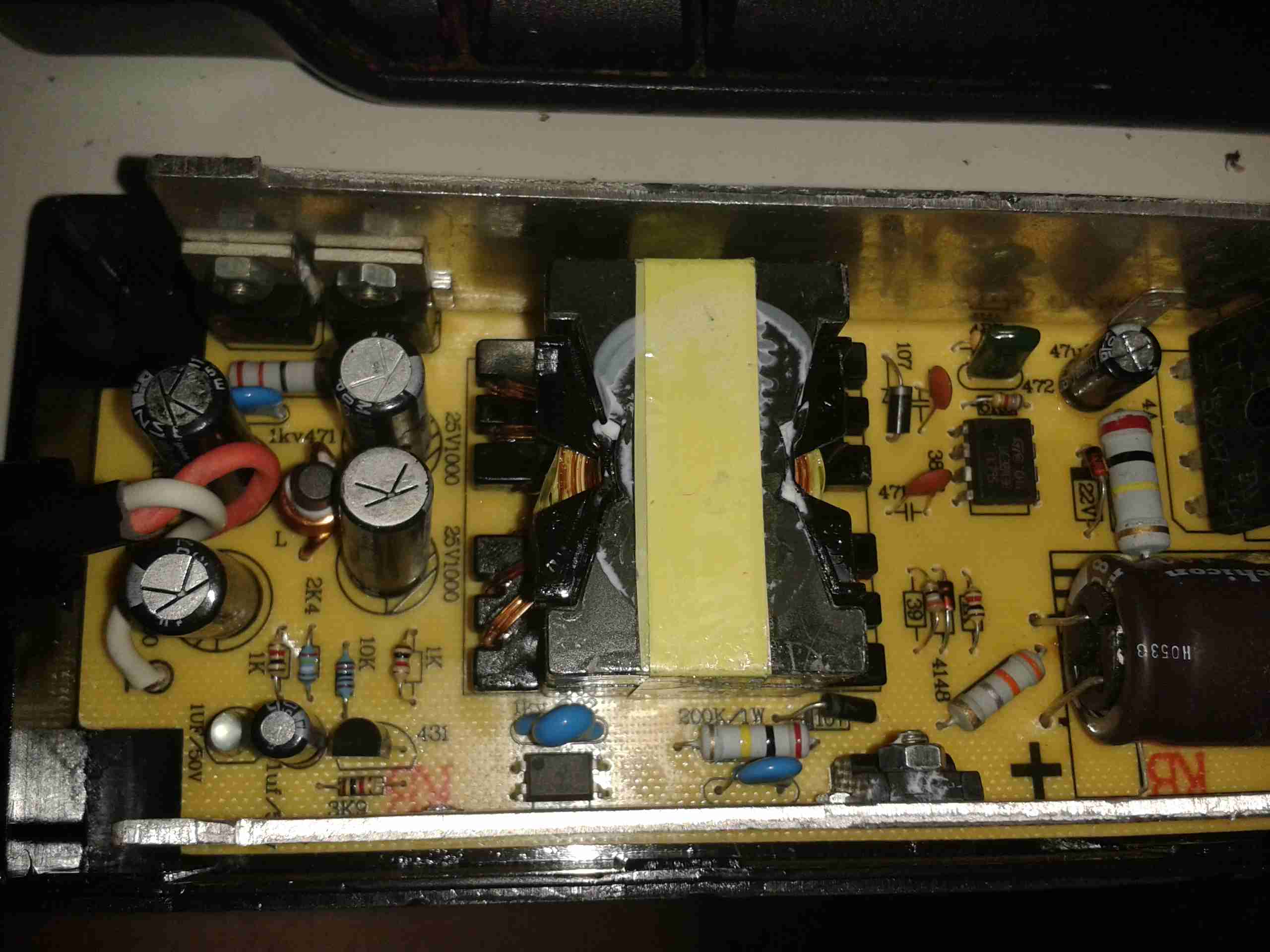
Primary Side
Here’s a closeup of the primary side of the PSU, the main DC bus capacitor is a Nichicon one, but it’s clearly been recovered from another device, look at the different glue on the end!
it’s also flapping about in the breeze, the squirt of silicone they’ve put on does nothing to stop movement.
Also here is the mains input fuse, filter capacitor & common mode choke. At least there is some filtering!
The main control IC is a UC3843B High Performance Current Mode PWM Controller, operating at a switching frequency of 250kHz.
The main switching transistor is visible at the bottom left corner, attached to the heatsink.
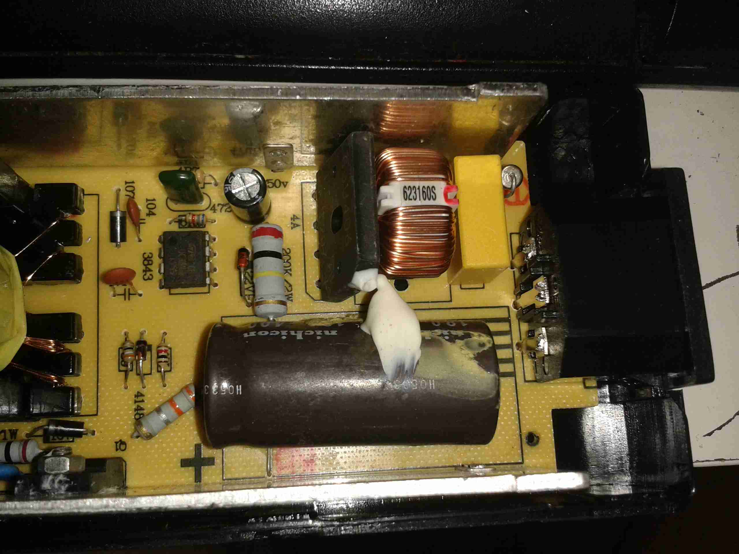
Secondary Side
Here’s the secondary side of the supply. The transformer itself is OK, nice heavy windings on the output to suit the high current.
It’s using proper opto-isolated feedback for voltage regulation, with a TL431 reference IC.
The output diodes are attached to the heatsink at the top of the photo, I couldn’t read any numbers on those parts.
The output filter capacitors are low quality, only time will tell if they survive. I’ll put the supply under full load & see what the temperature rise is inside the casing.
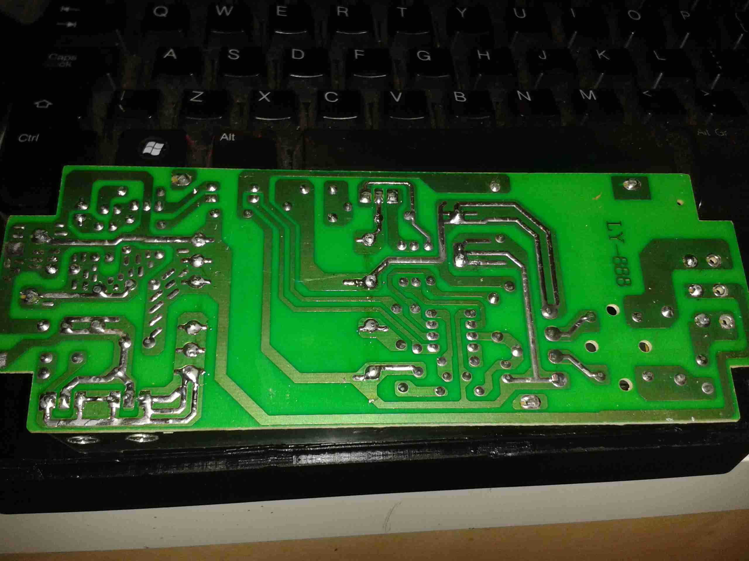
PCB Bottom
On the bottom of the PCB things get a little more dire. There isn’t really much of an isolation gap between the primary & secondary sides, and there’s a track joining the output negative with mains earth, which gets to within 2mm of the live mains input!
As with all these cheapo supplies, there’s good points & bad points, I will update when I’ve had a chance to put the supply under full load for a while & see if it explodes!
Recently I’ve noticed my usual mobile rig, the Baofeng UV-5R, has had very poor receive, and non-existent transmit.
I did a power test on the radio, and confirmed it was still outputting it’s rated RF power. Trying another antenna proved that the radio was fine.
Time to tear down the antenna & see if it can be fixed!
Stock Antenna
Here’s the antenna, just the factory rubber duckie. As with all these antennas, they’re a compromise between size & their efficiency.
Naked Antenna!
Giving a gentle pull to the antenna sheath while it’s attached to the radio allows it to come apart. The quality actually doesn’t look to bad. It’s very similar in construction to my Diamond X-30, just on a much smaller scale.
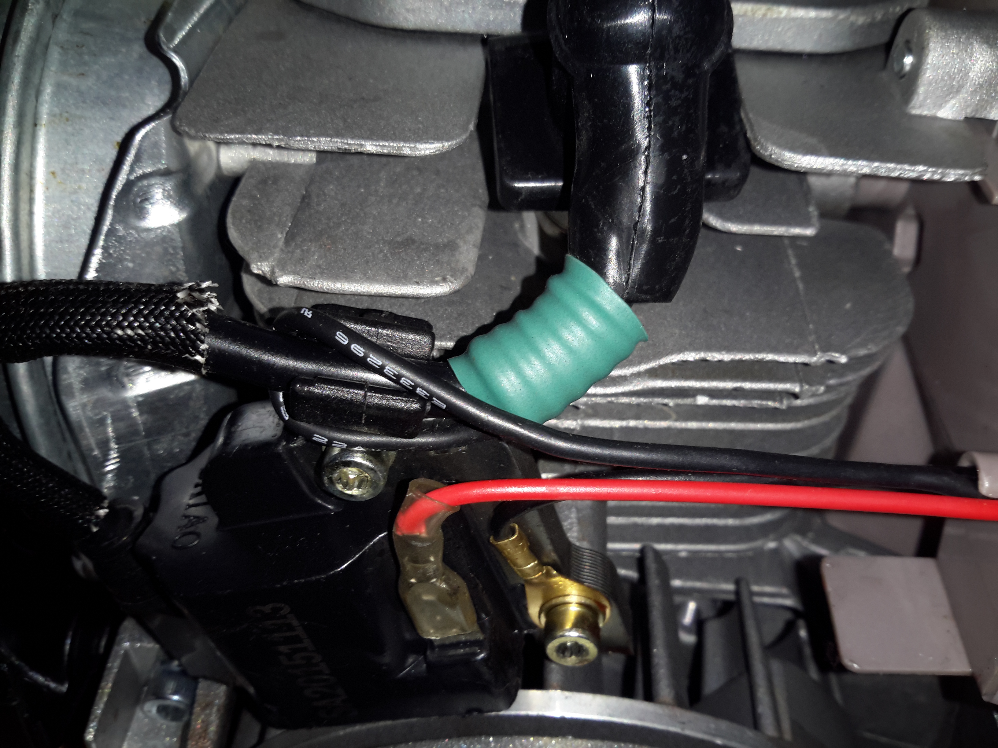
At the bottom of the antenna is the matching network, an inductor & ceramic disc capacitor. Here lies the problem with this antenna.
Dry Joint
Here where the capacitor joins onto the feedpoint from the SMA connector, the solder joint has come away. This was a very poor joint to start with, and the solder hadn’t wetted the capacitor lead at all
After cleaning the joint, and applying some flux, a new joint was easily made with some Real Solder.
Repaired Joint
Here’s the joint freshly repaired, the antenna is now back to full working order. It even seems to work better than the others I have 🙂
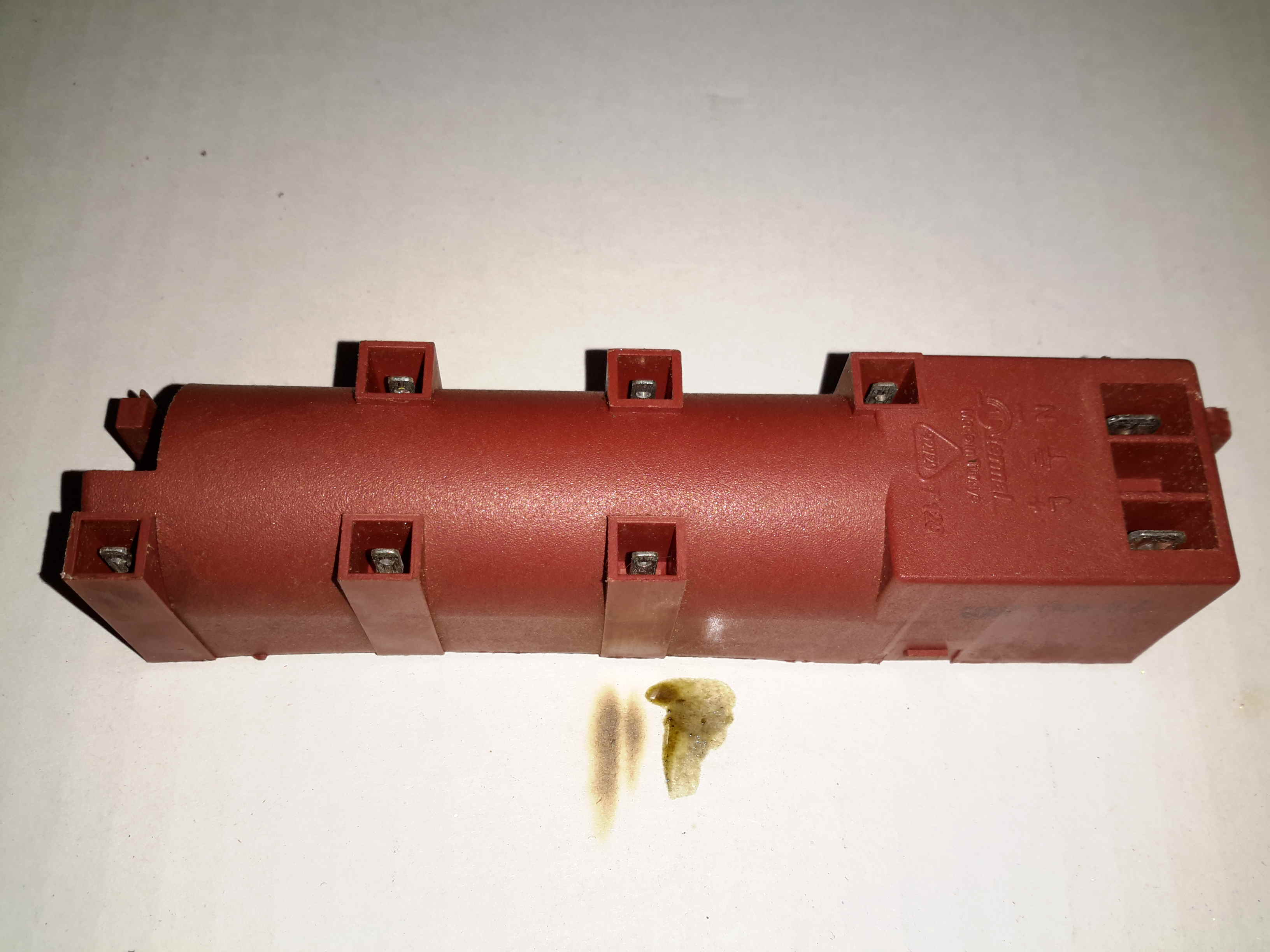
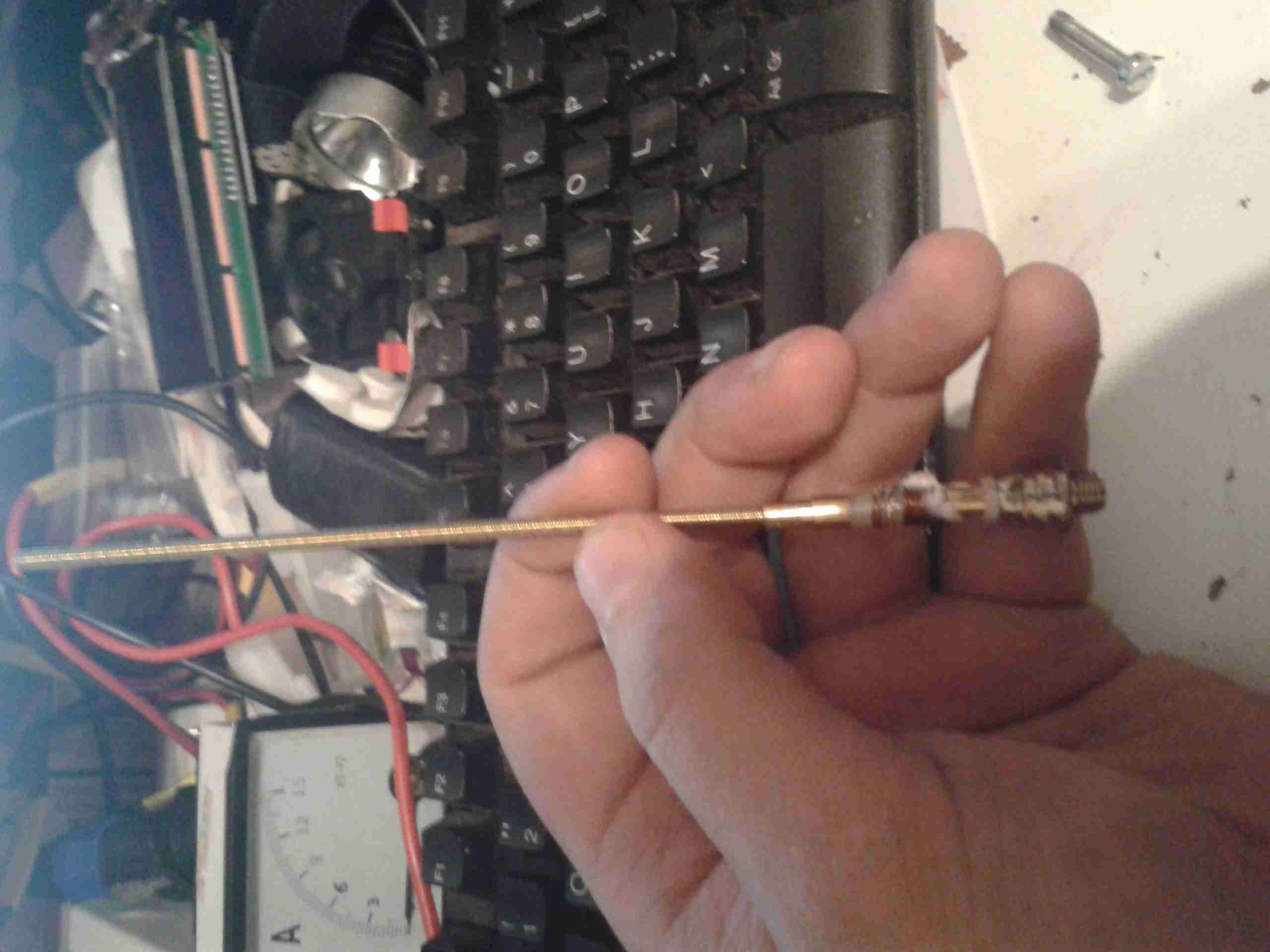
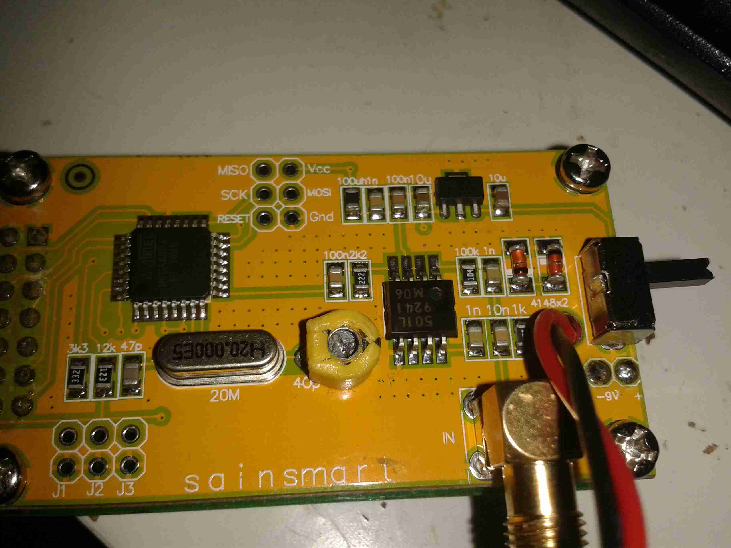
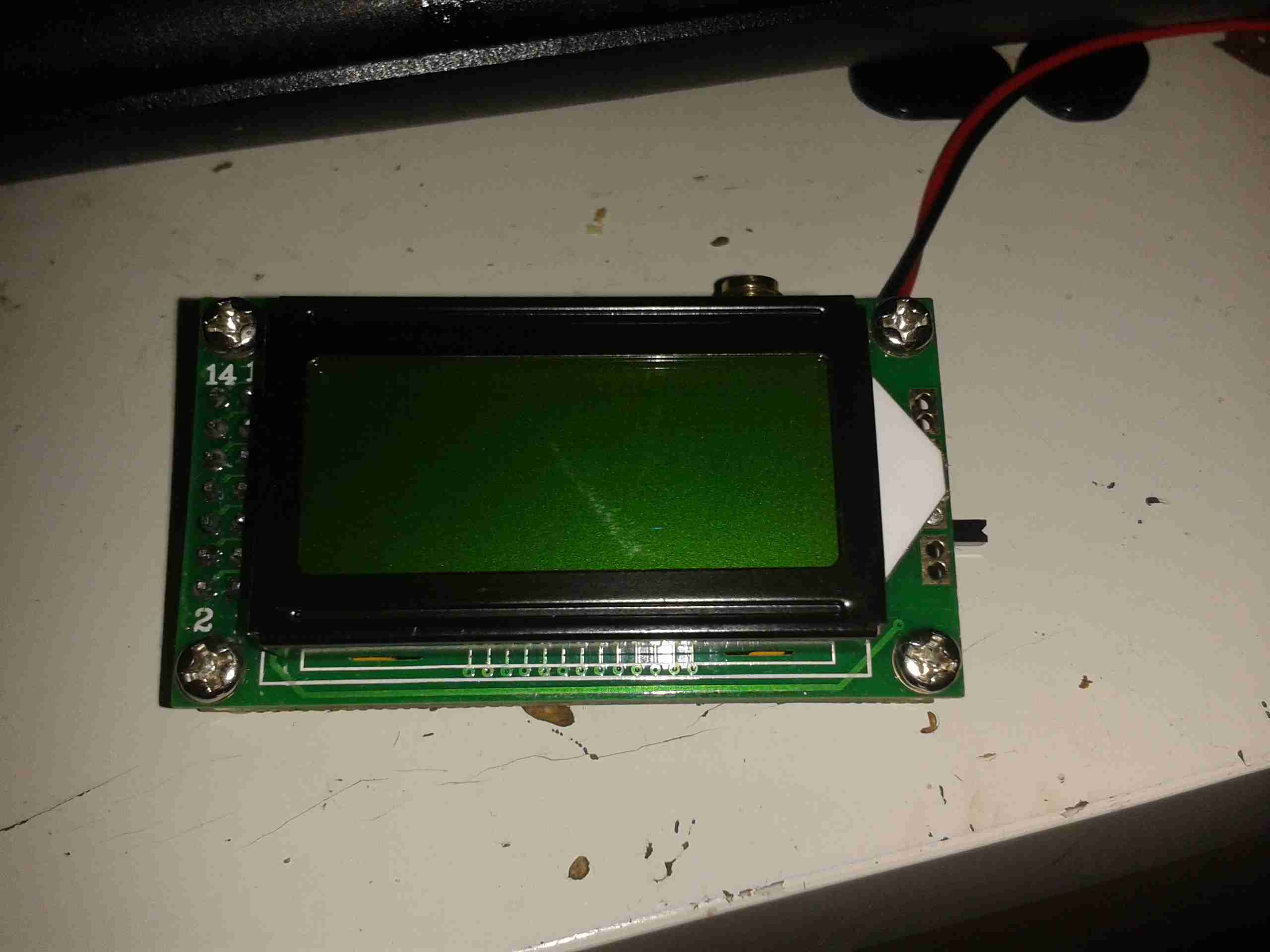
Here’s a quick look at a Sainsmart frequency counter module. These are useful little gadgets, showing the locked frequency on a small LCD display.
It’s built around an ATMega328 microcontroller (µC), and an MB501L Prescaler IC. The circuit for this is very simple, and is easily traced out from the board.
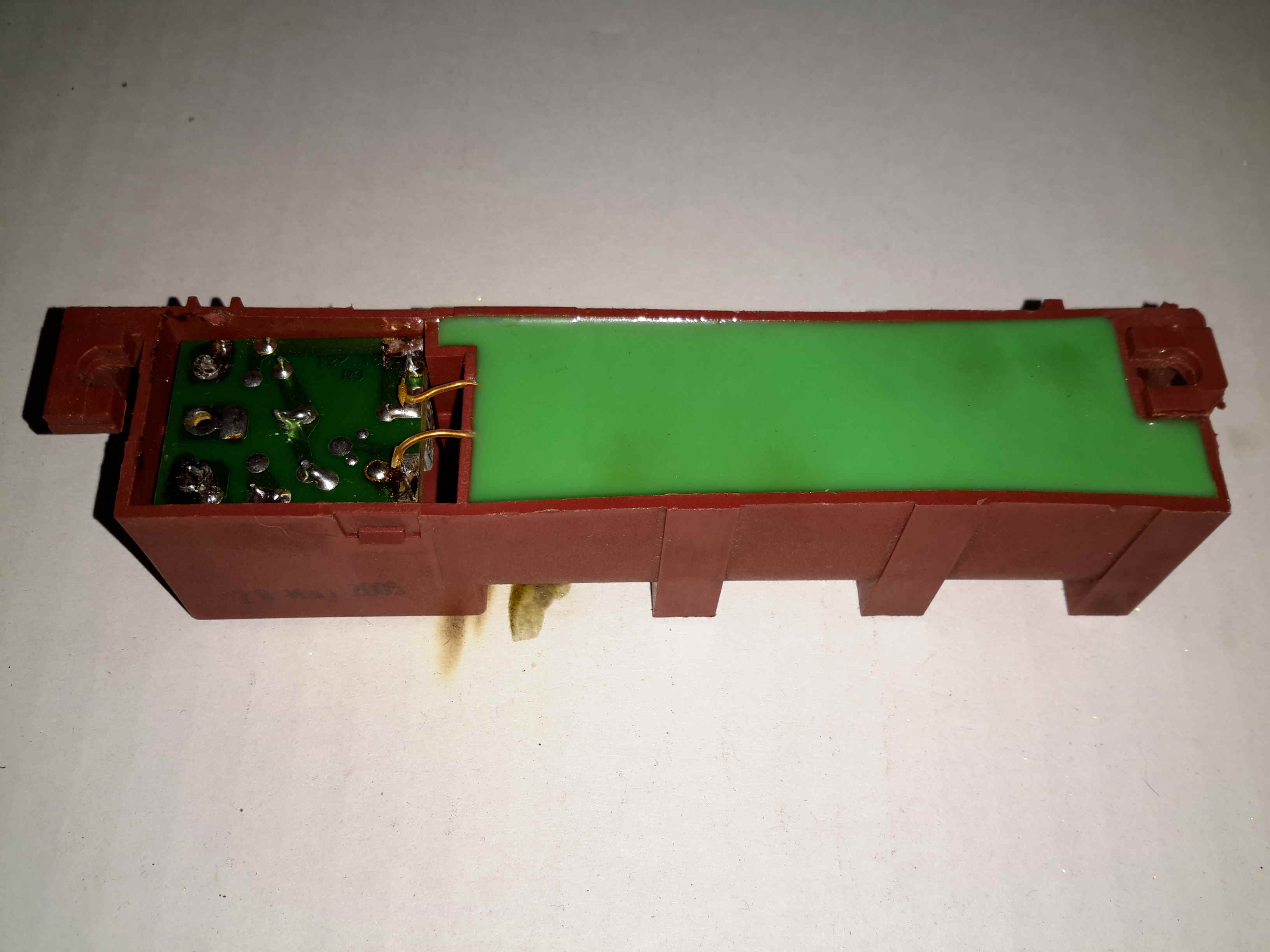
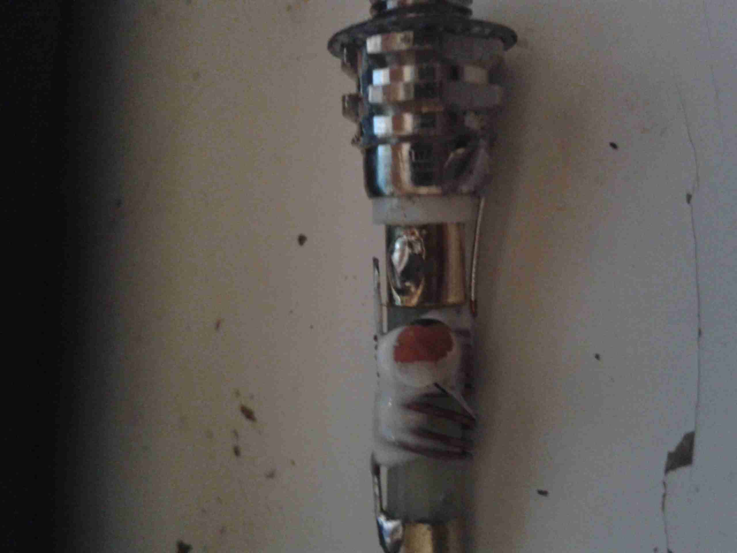
Frequency Counter
Here’s the back of the board, with the µC on the left & the prescaler IC on the right. This uses a rather novel method for calibration, which is the trimmer capacitor next to the crystal. This trimmer varies the frequency of the µC’s oscillator, affecting the calibration.
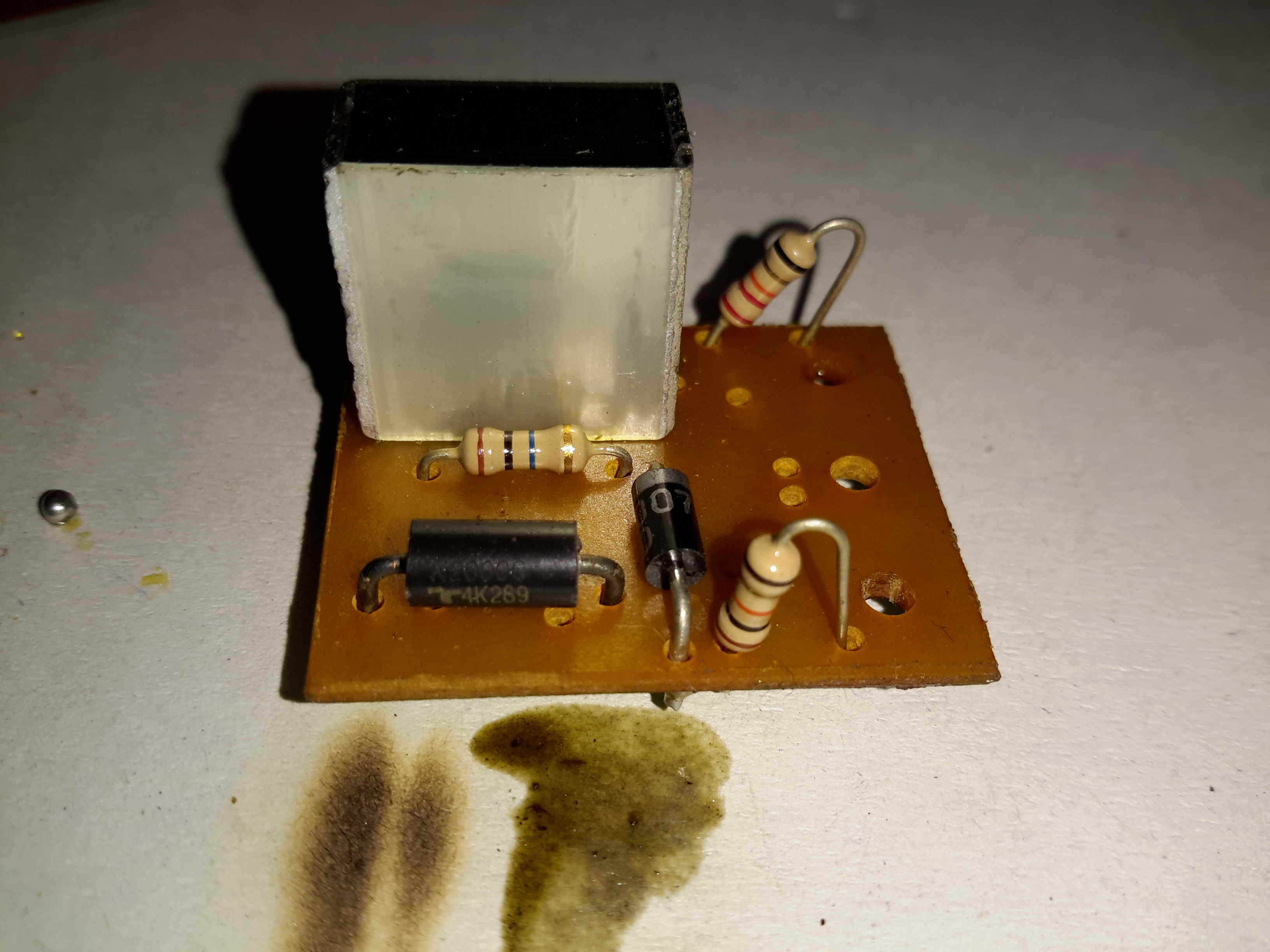
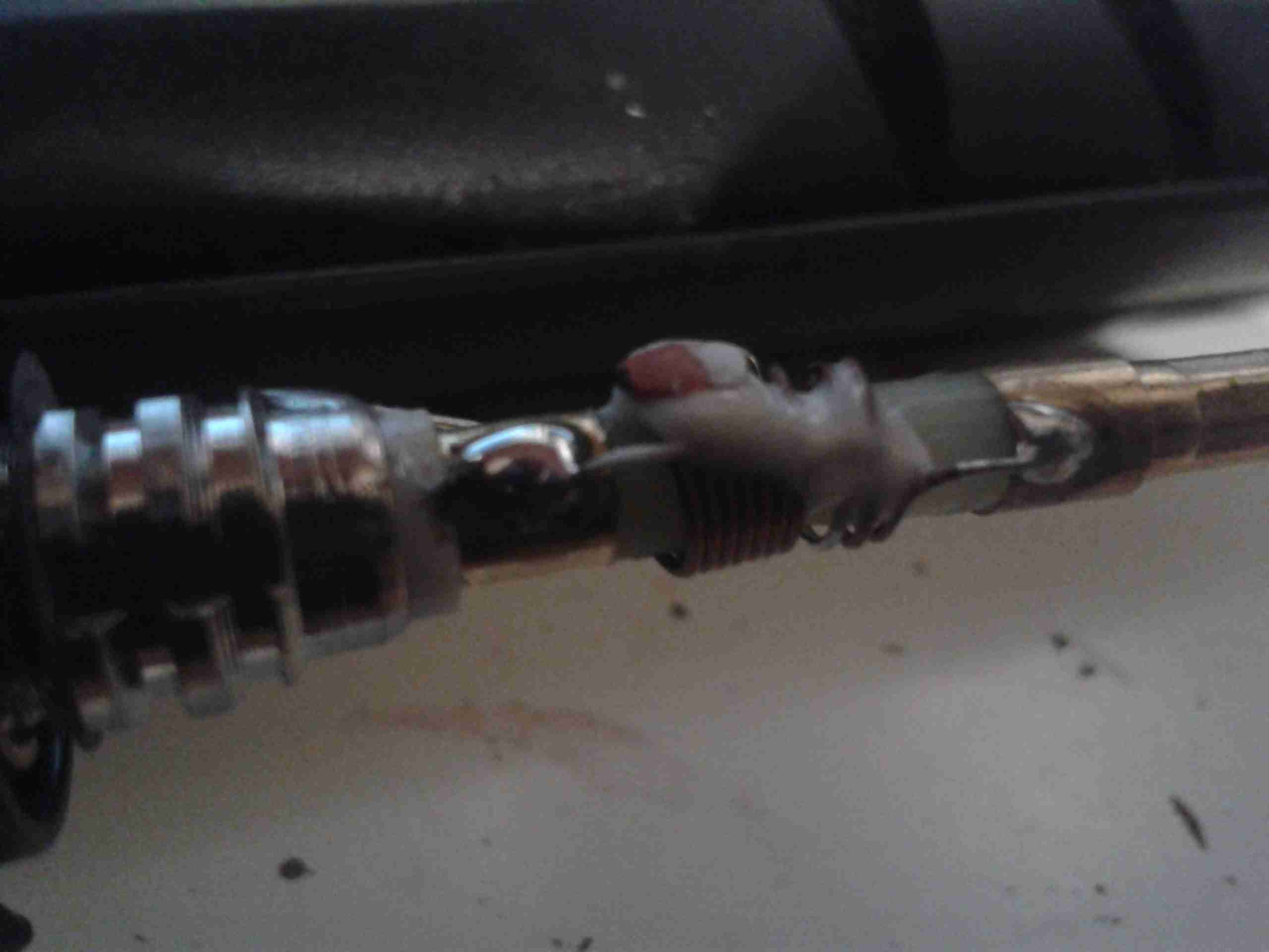
Input protection is provided by a pair of 1N4148 diodes in inverse parallel. These will clamp the input to +/-1v.
The prescaler IC is set to 1/64 divide ratio. This means that for an input frequency of 433MHz, it will output a frequency of 6.765625MHz to the µC.
The software in the µC will then calculate the input frequency from this intermediate frequency. This is done because the ATMega controllers aren’t very cabable of measuring such high frequencies.
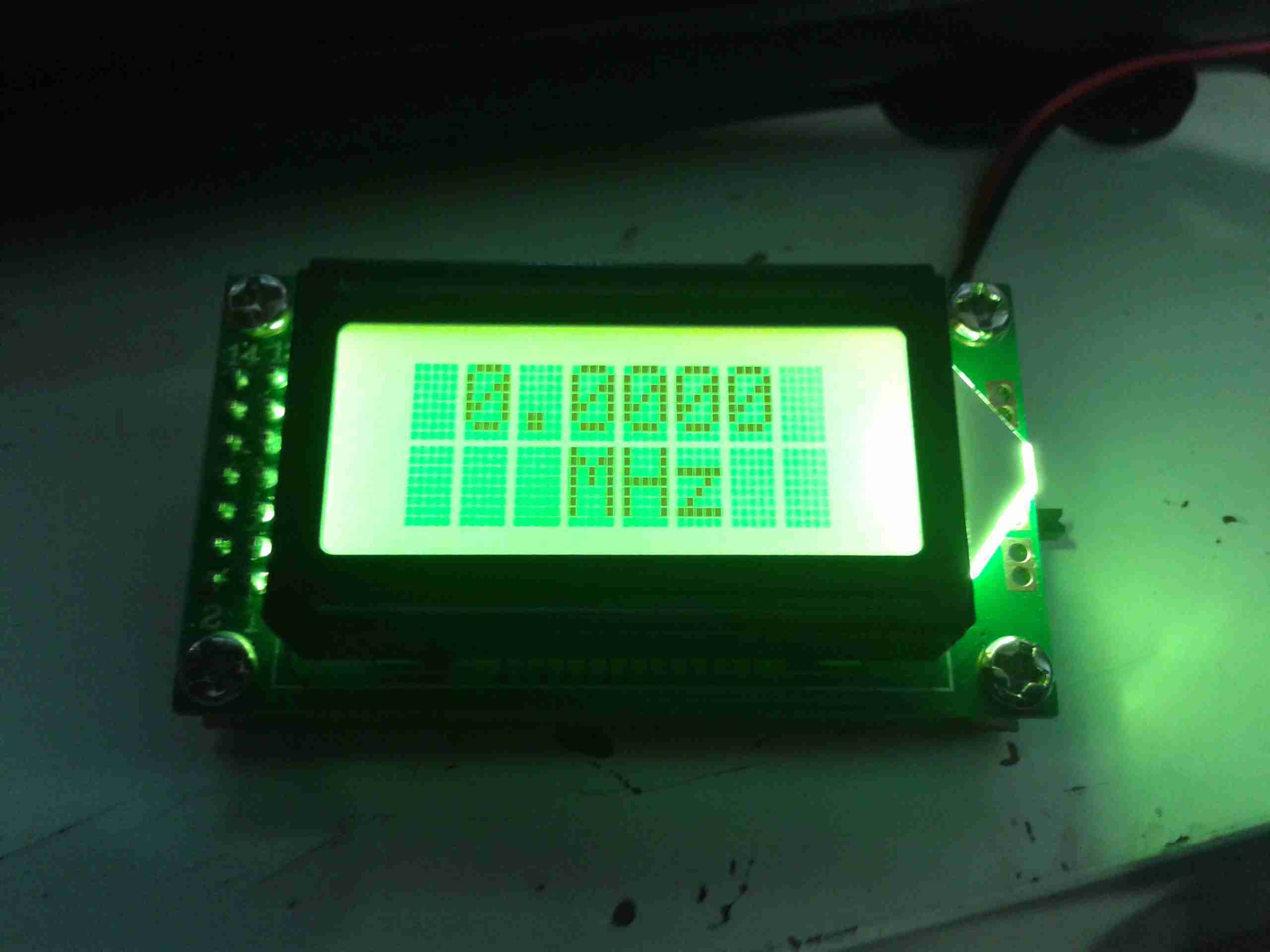
The calculated frequency is then displayed on the LCD. This is a standard HD44780 display module.
LCD
Power is provided by a 9v PP3 battery, which is then regulated down by a standard LM7805 linear regulator.
Readout
I’ve found it’s not very accurate at all at the lower frequencies, when I fed it 40MHz from a signal generator it displayed a frequency of around 74MHz. This is probably due to the prescaler & the software not being configured for such a low input. In the case for 40MHz input the scaled frequency would have been 625kHz.
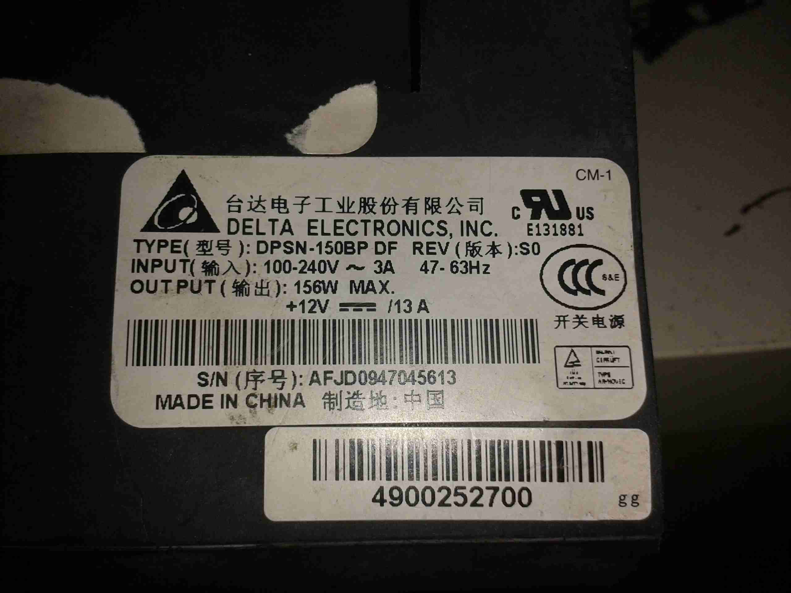
Recently I decommissioned some networking equipment, and discovered the power supplies in some switches were single rail 12v types, with a rather high power rating. I figured these would be very good for powering my Ham radio gear.
They’re high quality Delta Electronics DPSN-150BP units, rated at a maximum power output of 156W.
Label
These supplies have an adjustment pot for the output voltage regulation, but unfortunately it just didn’t have quite enough range to get from 12.0v to 13.8v. The highest they would go was ~13.04v.
After taking a look at the regulator circuit, I discovered I could further adjust the output voltage by changing a single resistor to a slightly lower value.
Firstly though, a little background on how switched mode power supplies operate & regulate their output voltage.
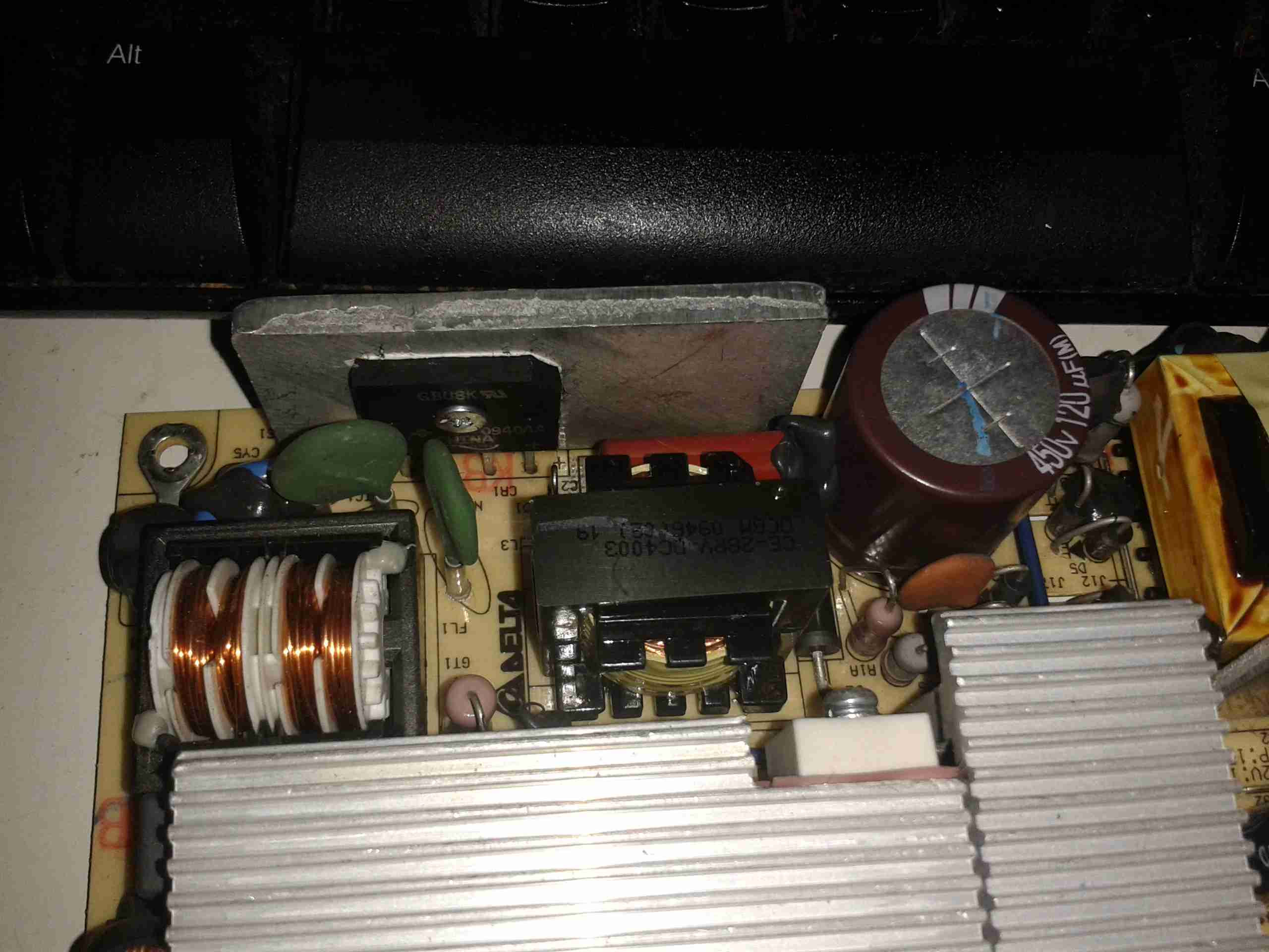
SMPS
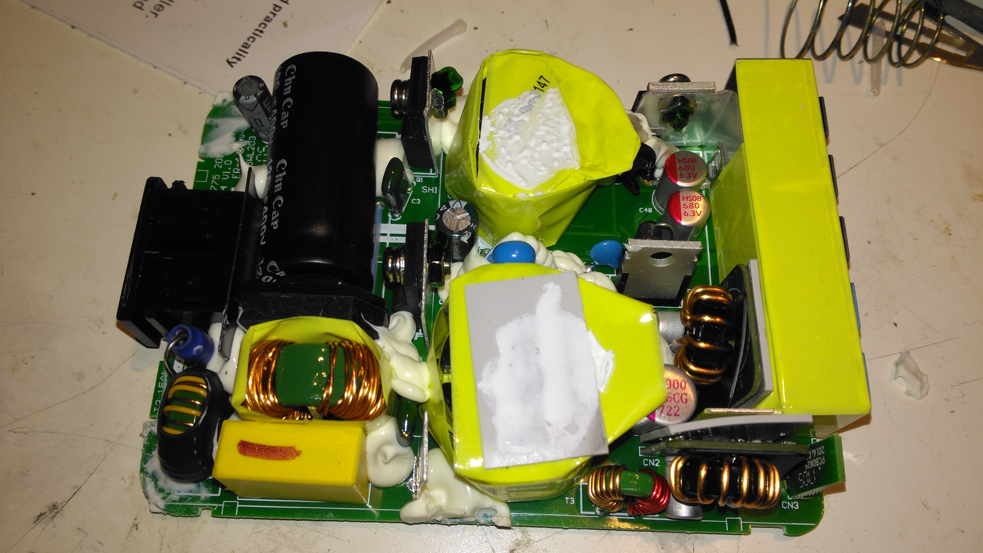
Here’s the supply. It’s mostly heatsink, to cool the large power switching transistors.
The first thing a SMPS does, is to rectify the incoming mains AC with a bridge rectifier. This is then smoothed by a large electrolytic capacitor, to provide a main DC rail of +340v DC (when on a 240v AC supply).
Mains Input
Above is the mains input section of the PSU, with a large common-mode choke on the left, bridge rectifier in the centre, and the large filter capacitor on the right. These can store a lot of energy when disconnected from the mains, and while they should have a discharge resistor fitted to safely drain the stored energy, they aren’t to be relied on for safety!
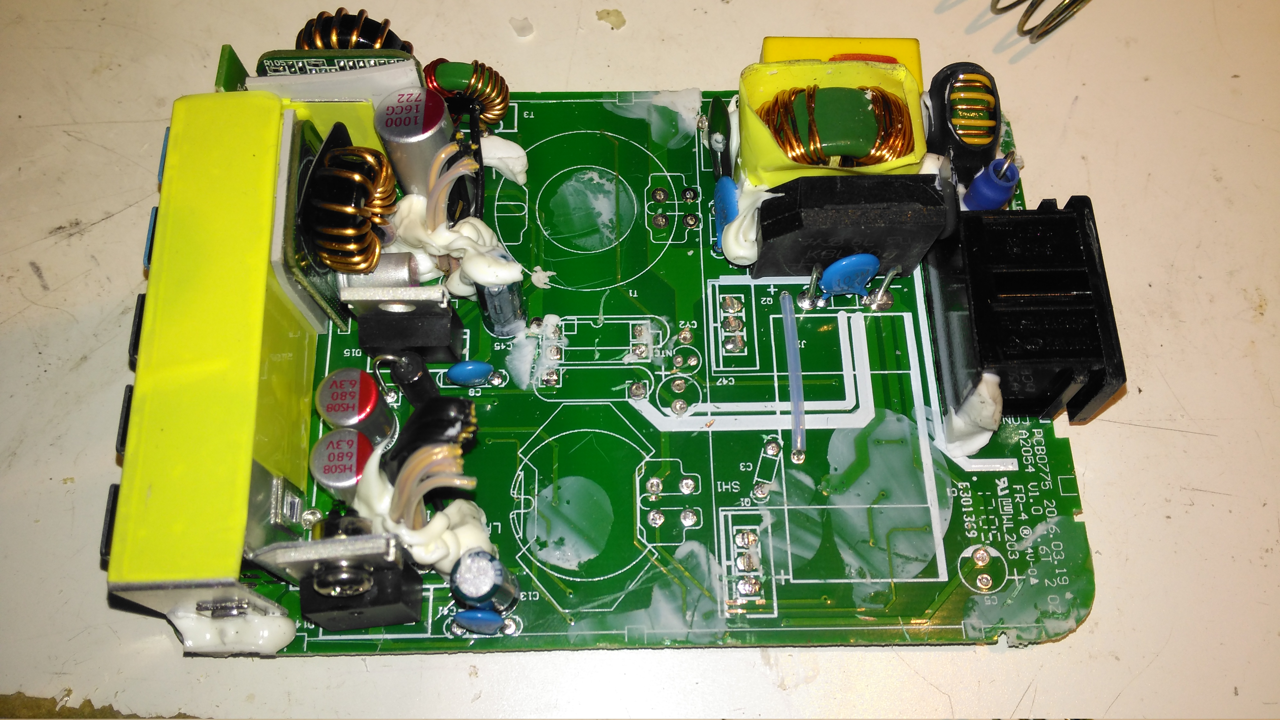
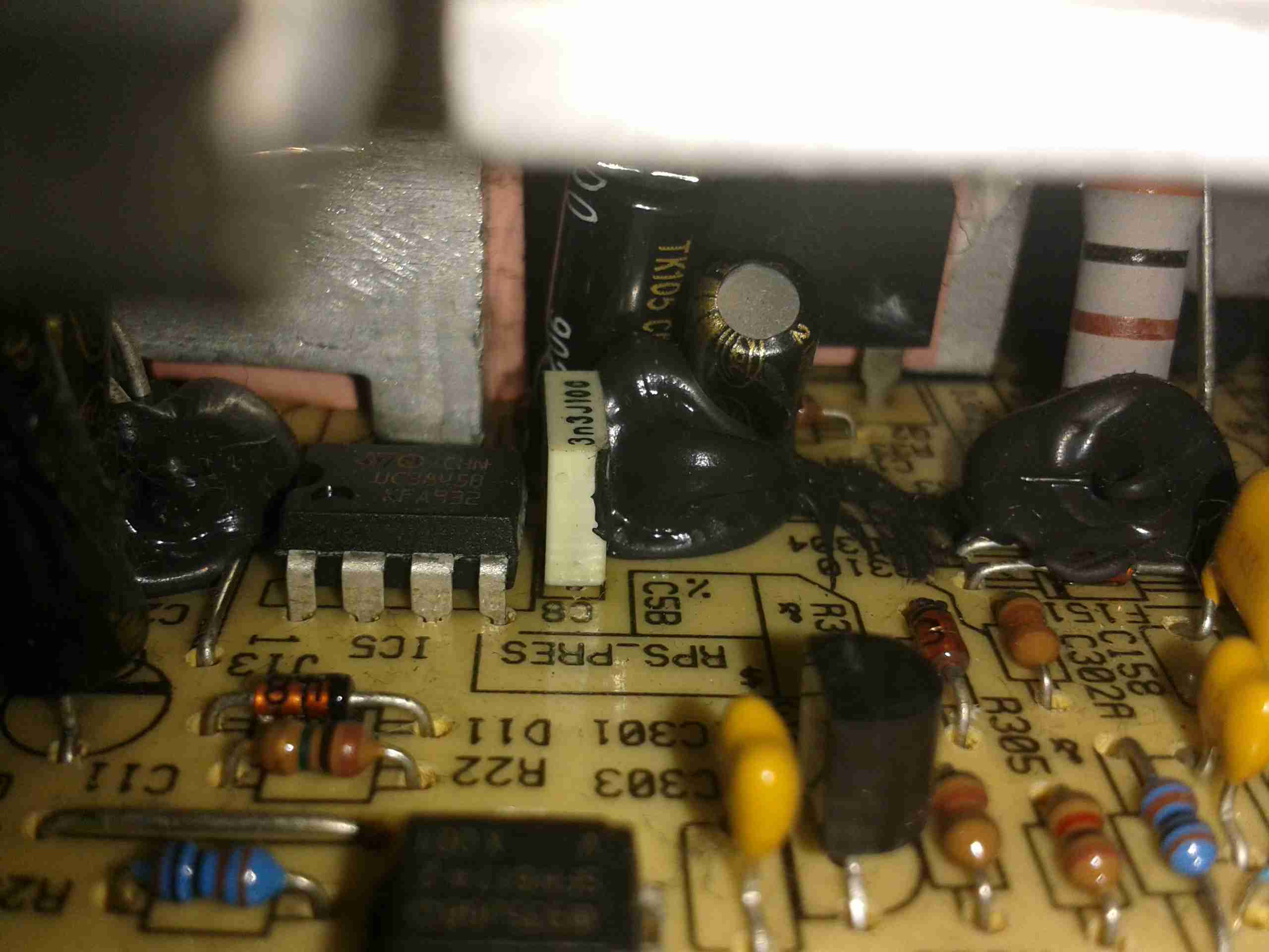
Once the supply has it’s main high voltage DC rail, this is switched into the main transformer by a pair of very large transistors – these are hidden from view on the large silver heatsinks at the bottom of the image. These transistors are themselves driven with a control IC, in the case of this supply, it’s a UC3844B. This IC is hidden under the large heatsink, but is just visible in the below photo. (IC5).
Control ICMain Switching Transformer
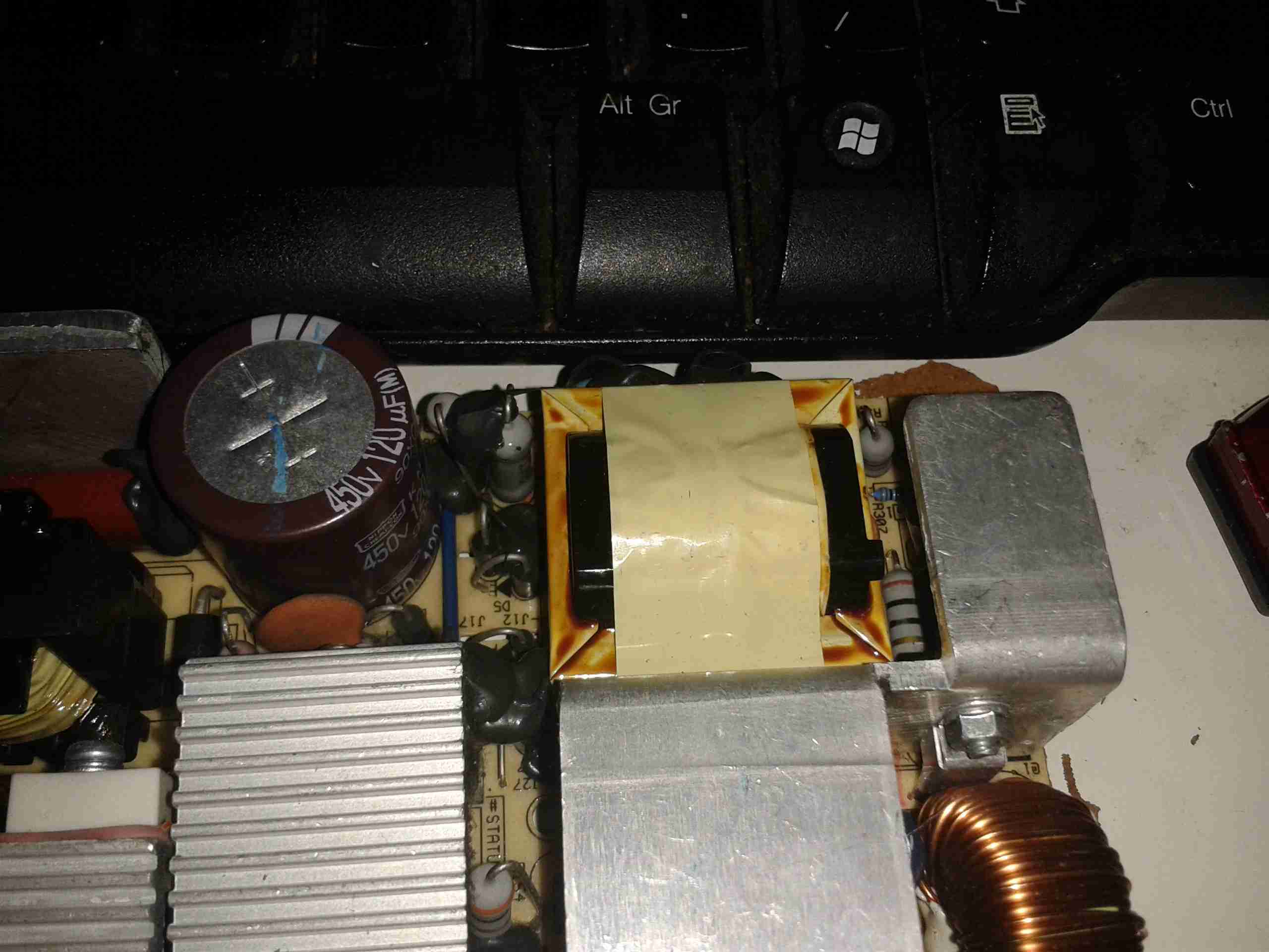
Here’s the main switching transformer, these can be much smaller than a conventional transformer due to the high frequencies used. This supply operates at 500kHz.
After the main transformer, the output is rectified by a pair of Schottky diodes, which are attached to the smaller heatsink visible below the transformer, before being fed through a large toroidal inductor & the output filter capacitors.
All this filtering on both the input & the output is required to stop these supplies from radiating their operating frequency as RF – a lot of cheap Chinese switching supplies forego this filtering & as a result are extremely noisy.
After all this filtering the DC appears at the output as usable power.
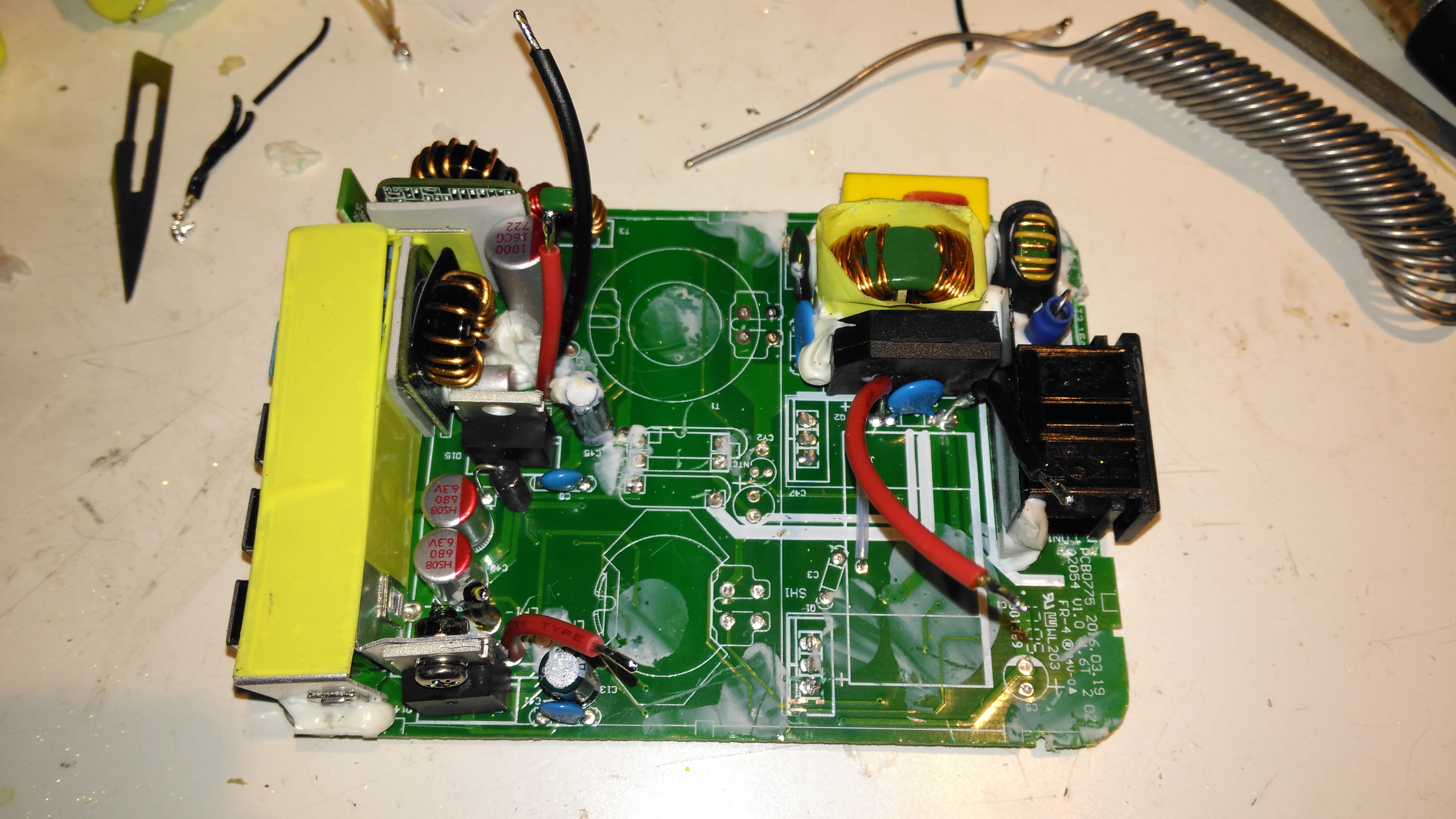
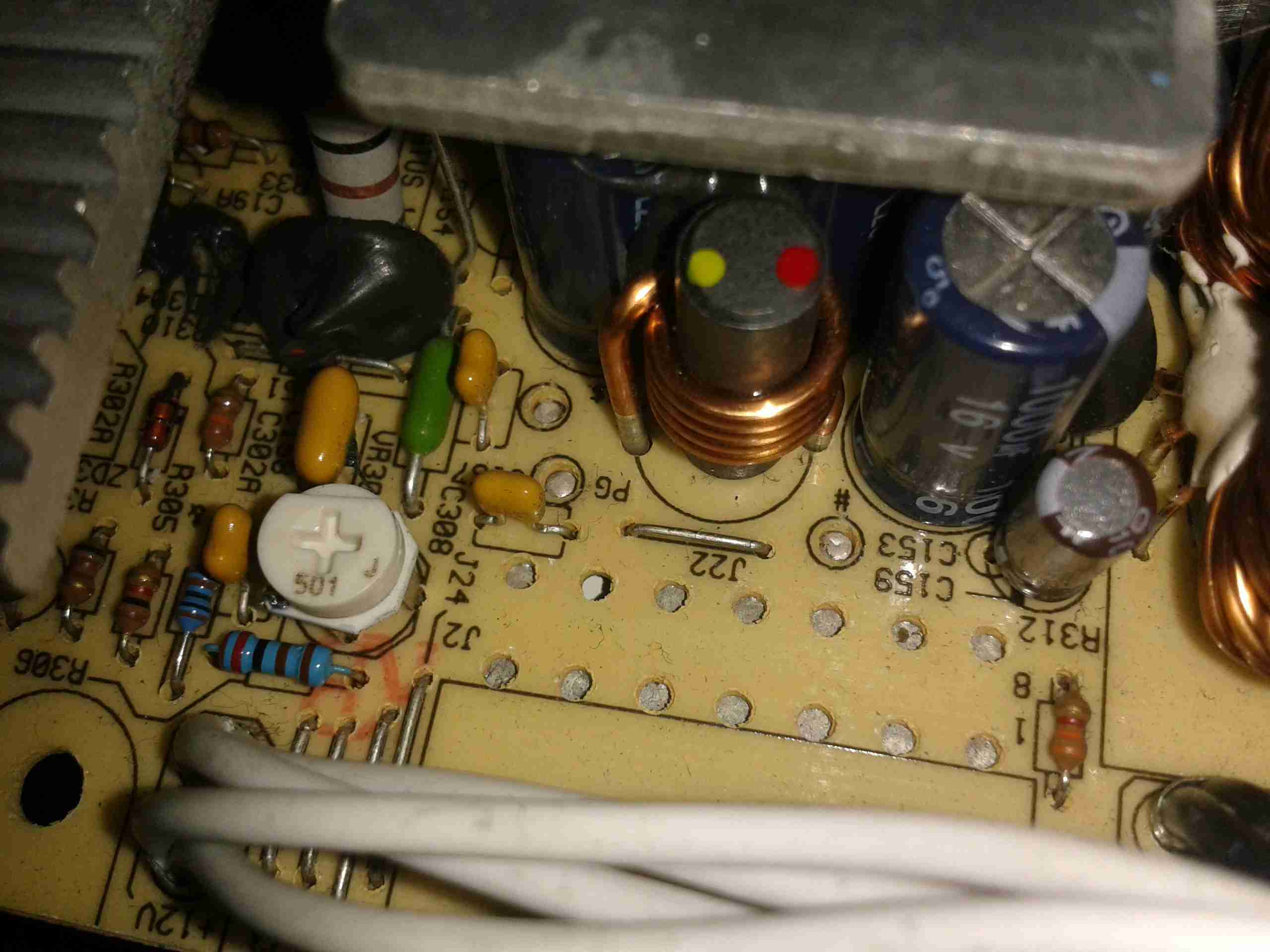
Getting back to regulation, these supplies read the voltage with a resistor divider & feed it back to the mains side control IC, through an opto-isolator. (Below).
Feedback Loop
The opto isolators are the black devices at the front with 4 pins.
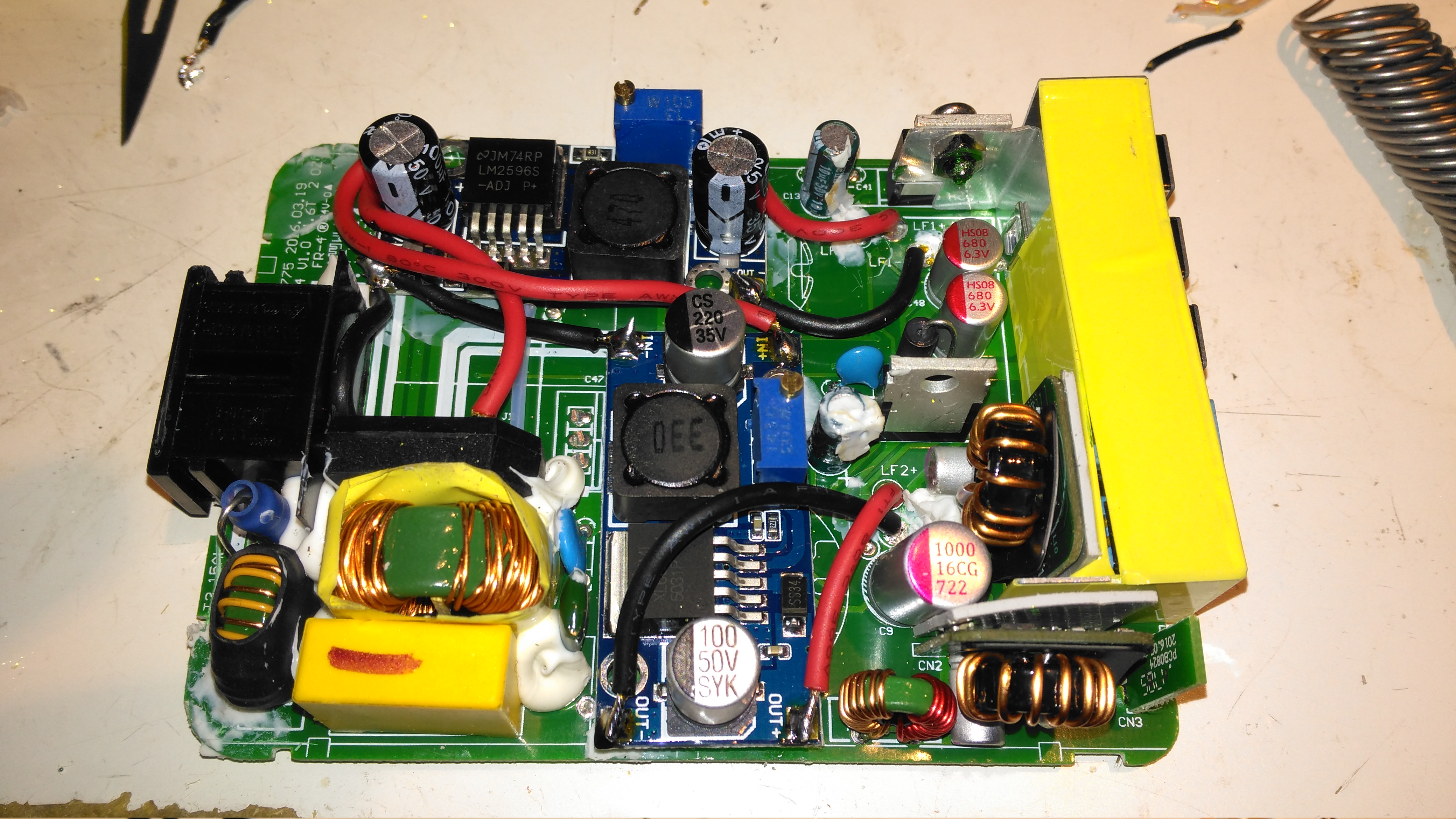
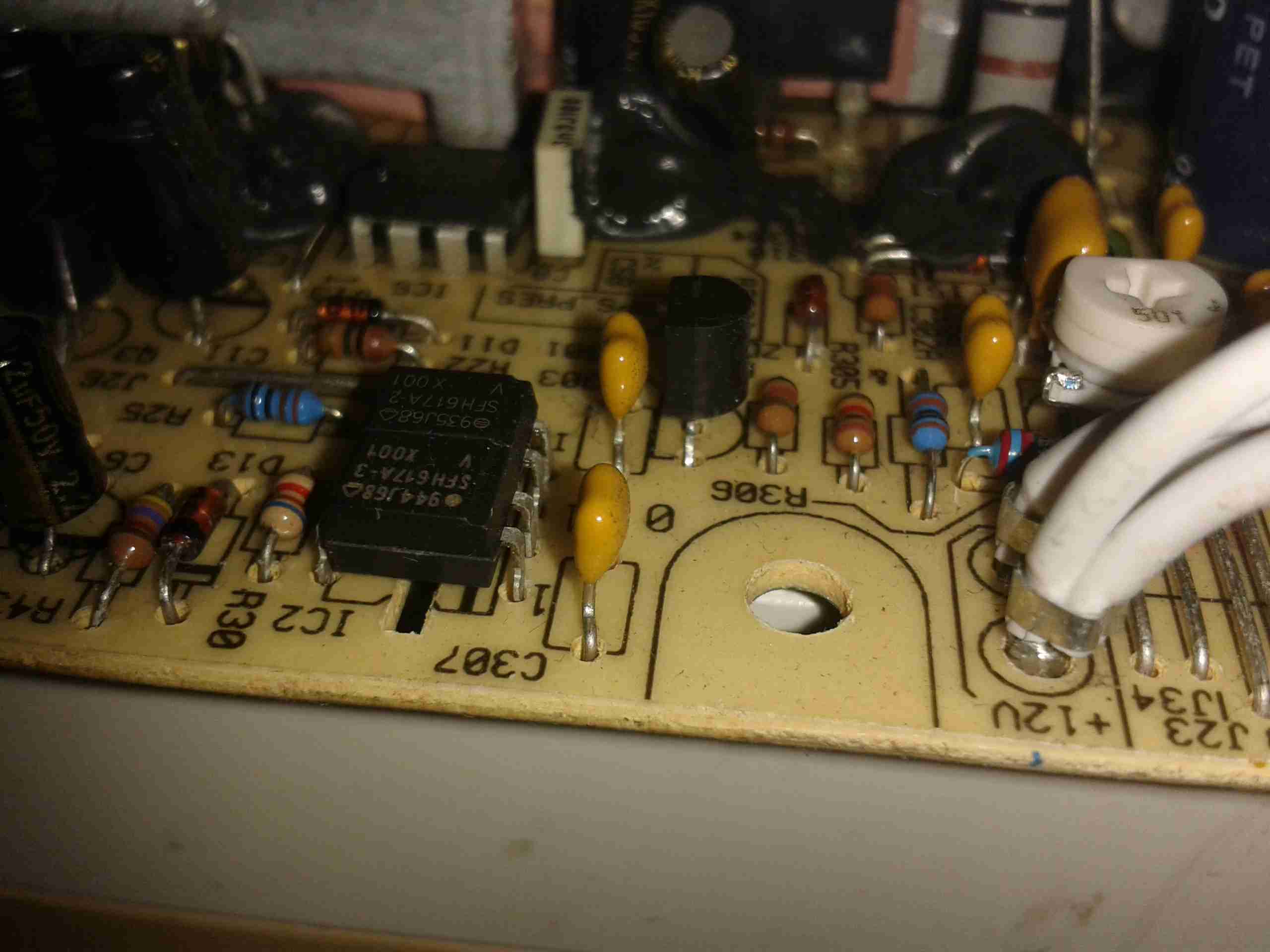
Regulator Adjustment
For a more in-depth look at the inner workings of SMPS units, there’s a good article over on Hardware Secrets.
My modification is simple. Replacing R306 (just below the white potentiometer in the photo), with a slightly smaller resistor value, of 2.2KΩ down from 2.37KΩ, allows the voltage to be pulled lower on the regulator. This fools the unit into applying more drive to the main transformer, and the output voltage rises.
It’s important to note that making too drastic a change to these supplies is likely to result in the output filter capacitors turning into grenades due to overvoltage. The very small change in value only allows the voltage to rise to 13.95v max on the adjuster. This is well within the rating of 16v on the output caps.
Now the voltage has been sucessfully modified, a new case is on the way to shield fingers from the mains. With the addition of a couple of panel meters & output terminals, these supplies will make great additions to my shack.
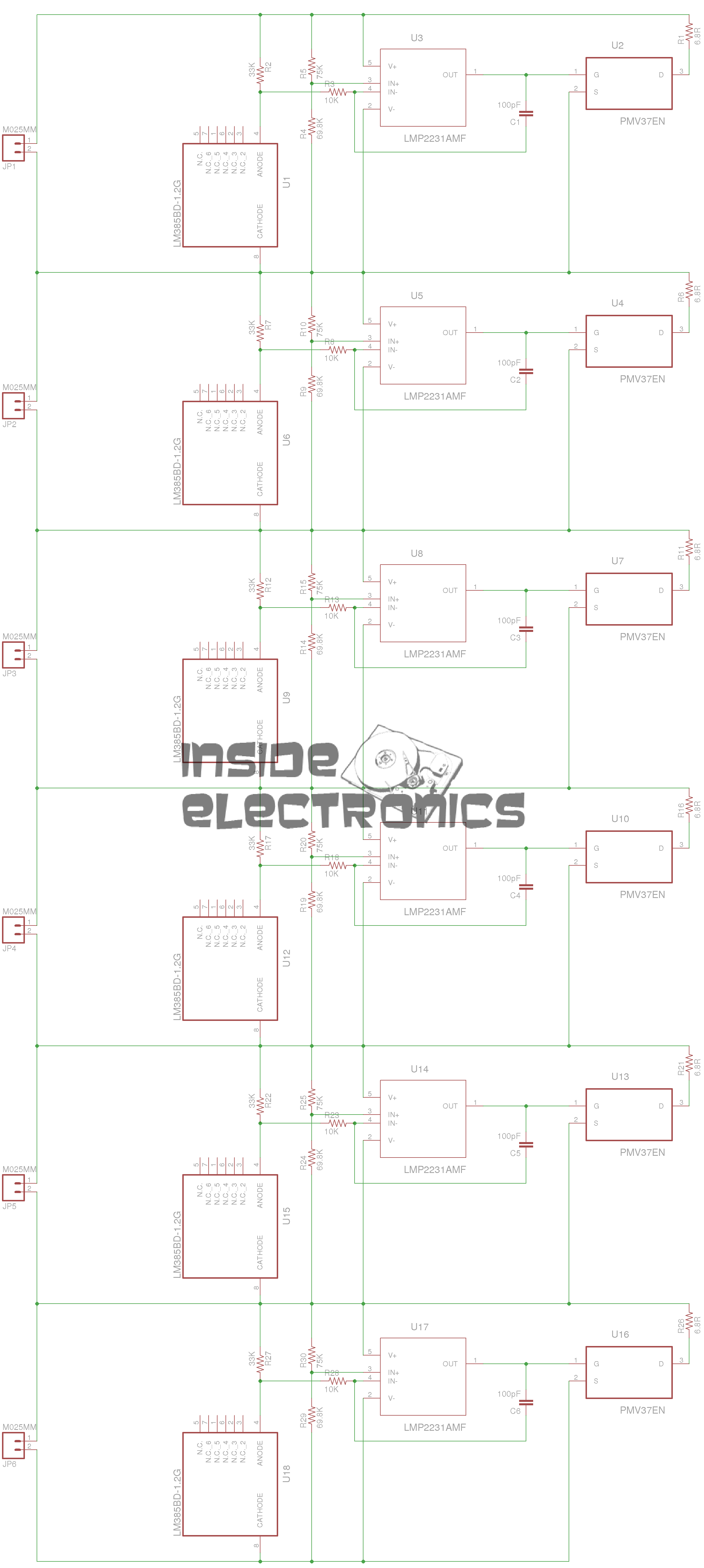
Here’s another active balancing circuit for large ultracapacitor banks, this one is designed for a series string of 6, at 2.5v per capacitor.
Based on the design here, I have transcribed the circuit into Eagle & designed a PCB layout.
Ultracap Balancer Circuit – Click to Embiggen
As can be seen from the circuit diagram above, this is just 6 copies of the circuit from the above link, with screw terminals to attach to the capacitor string.
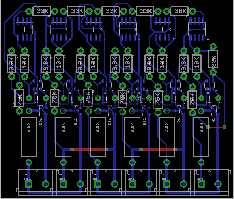
Ultracap Balancer PCB
And here’s the PCB. the MOSFETs & OpAmps are very small SMT parts, so require a steady hand in soldering. This board can easily be etched by hand as there’s only 3 links on the top side. No need for a double sided PCB.
As always, the Eagle project files & my Eagle library collection are available below:
I have finally got round to designing the balancing circuitry for my ultracapacitor banks, which have a total voltage of 15v when fully charged. The 2600F capacitors have a max working voltage of 2.5v each, so to ensure reliable operation, balancing is required to make sure that each capacitor is charged fully.
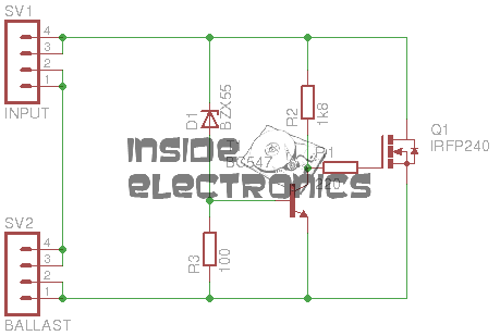
The circuit above is a simple shunt regulator, which uses a 2.2v zener diode to regulate the voltage across the capacitor.
A 10W 1Ω resistor is connected to the BALLAST header, while the capacitor is connected across the INPUT. Once the voltage on the capacitor reaches 2.6v, the MOSFET begins to conduct, the 1Ω resistor limiting current to ~2.6A.
Each capacitor in the series string requires one of these connected across it.
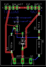
PCB
Below is a link to the Eagle project archive for this. Includes schematic, board & gerber files.
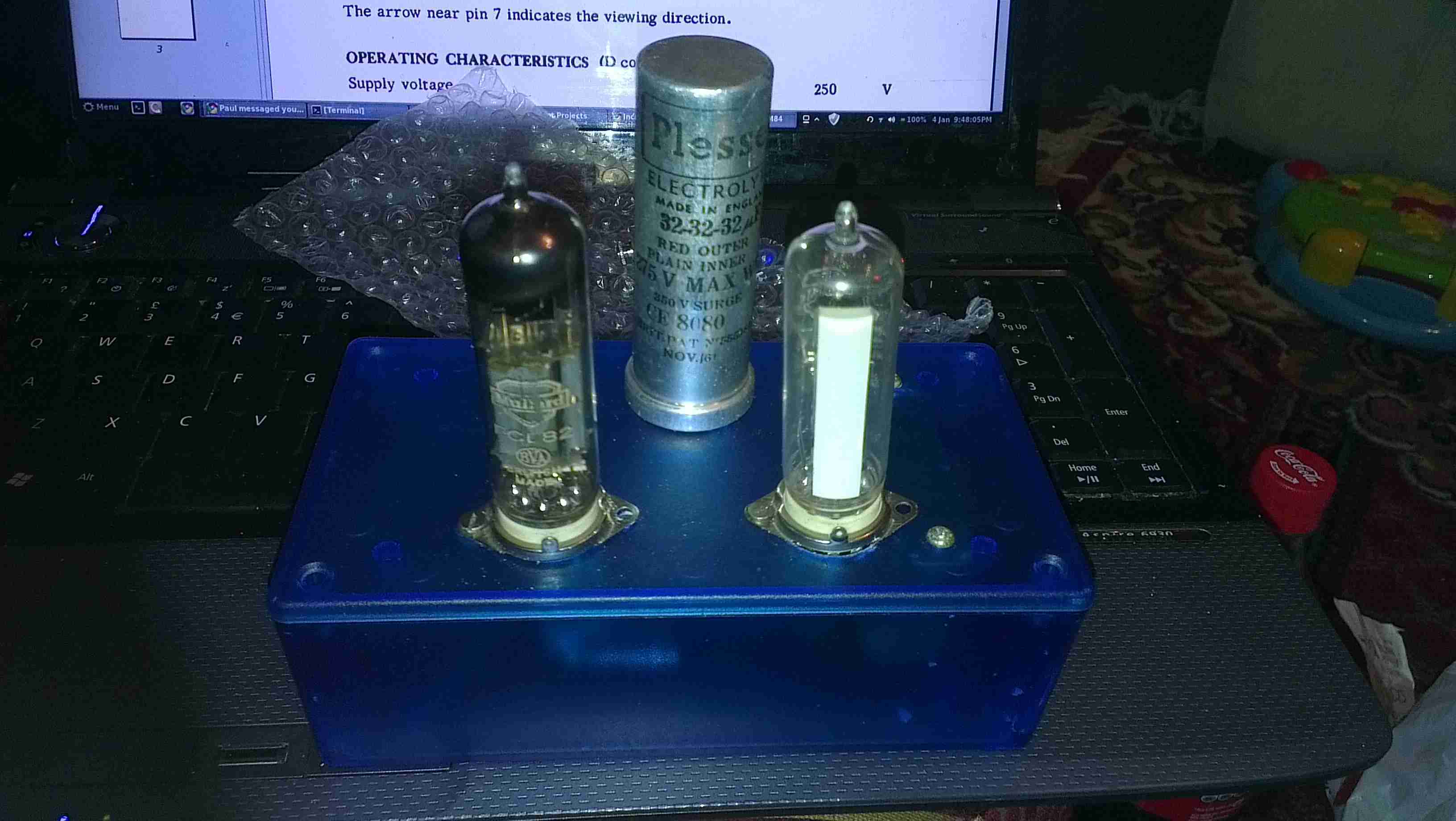
Here are a few details of a valve amplifier I am building, using the valve related parts from a 1960’s reel to reel tape recorder.
This amplifier is based on an a Mullard ECL82 triode/pentode valve, with an EM84 magic eye tube for level indication.
Beginnings Of The Amplifier
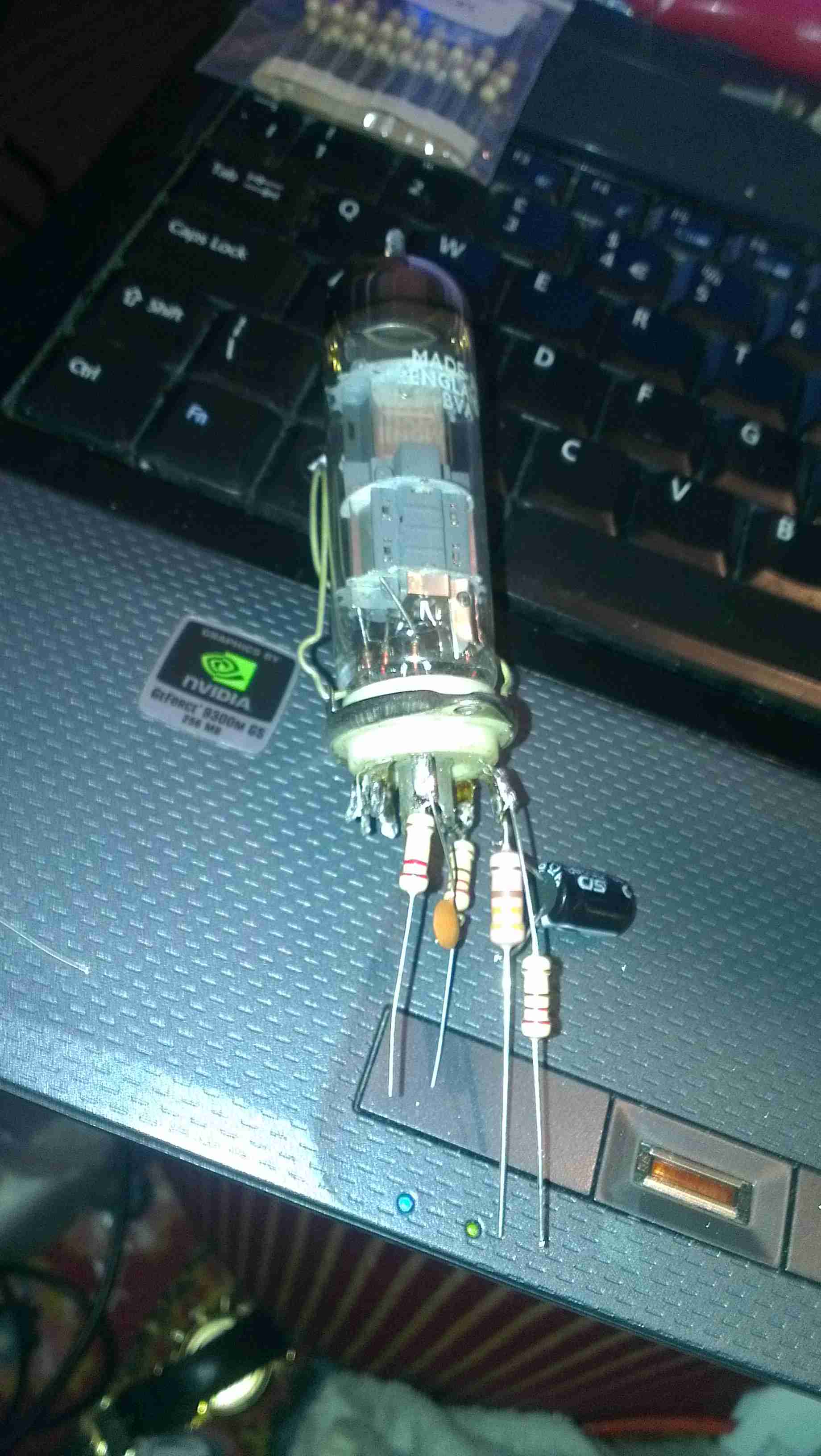
Here the first components are being soldered to the tags on the valve holder, there are so few components that a PCB is not required, everything can be rats-nested onto the valve holders.
Progress
Progressing with the amplifier section componentry, all resistors are either 1/2W or 2W.
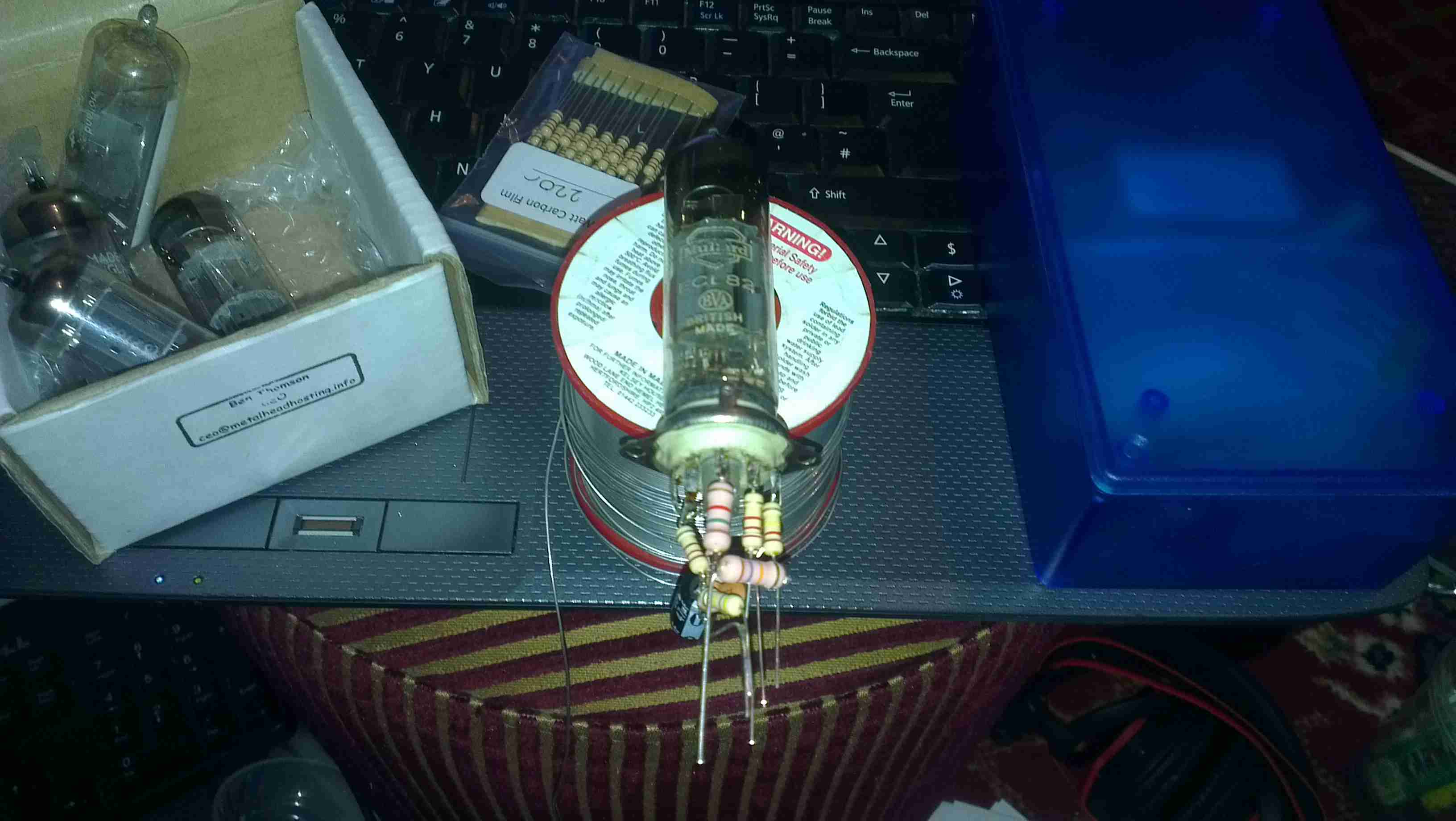
Valve Sockets Fitted
Here the valve holders have been fitted, along with the output transformer, DC smoothing capacitor & the filament wiring, into the top of the plastic housing. At this point all the components that complete the amplifier section are soldered to the bottom of the right hand valve holder.
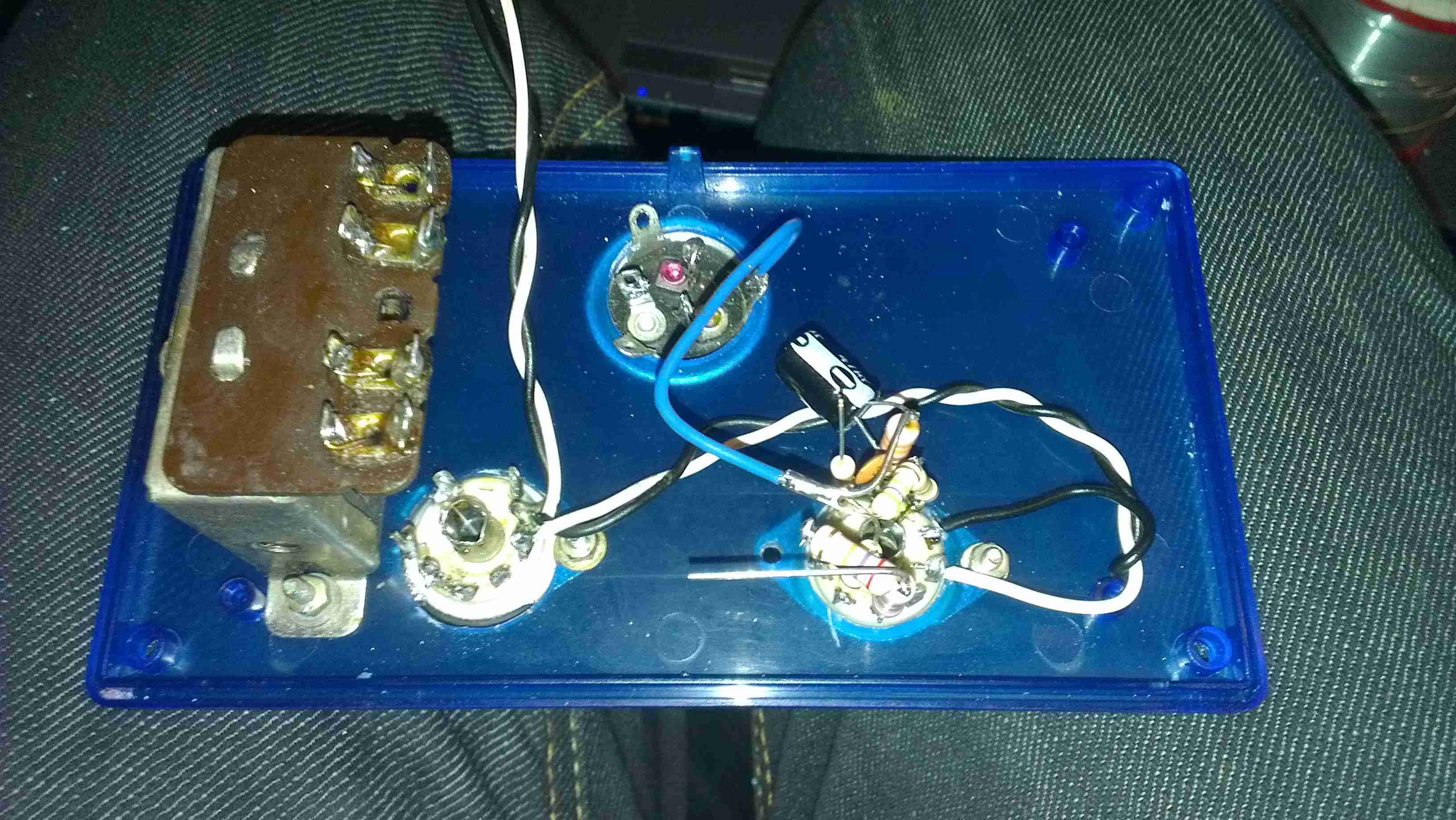
Wiring
Starting the wiring between the valves & the power supply components. The volume control pot is fitted between the valve holders.
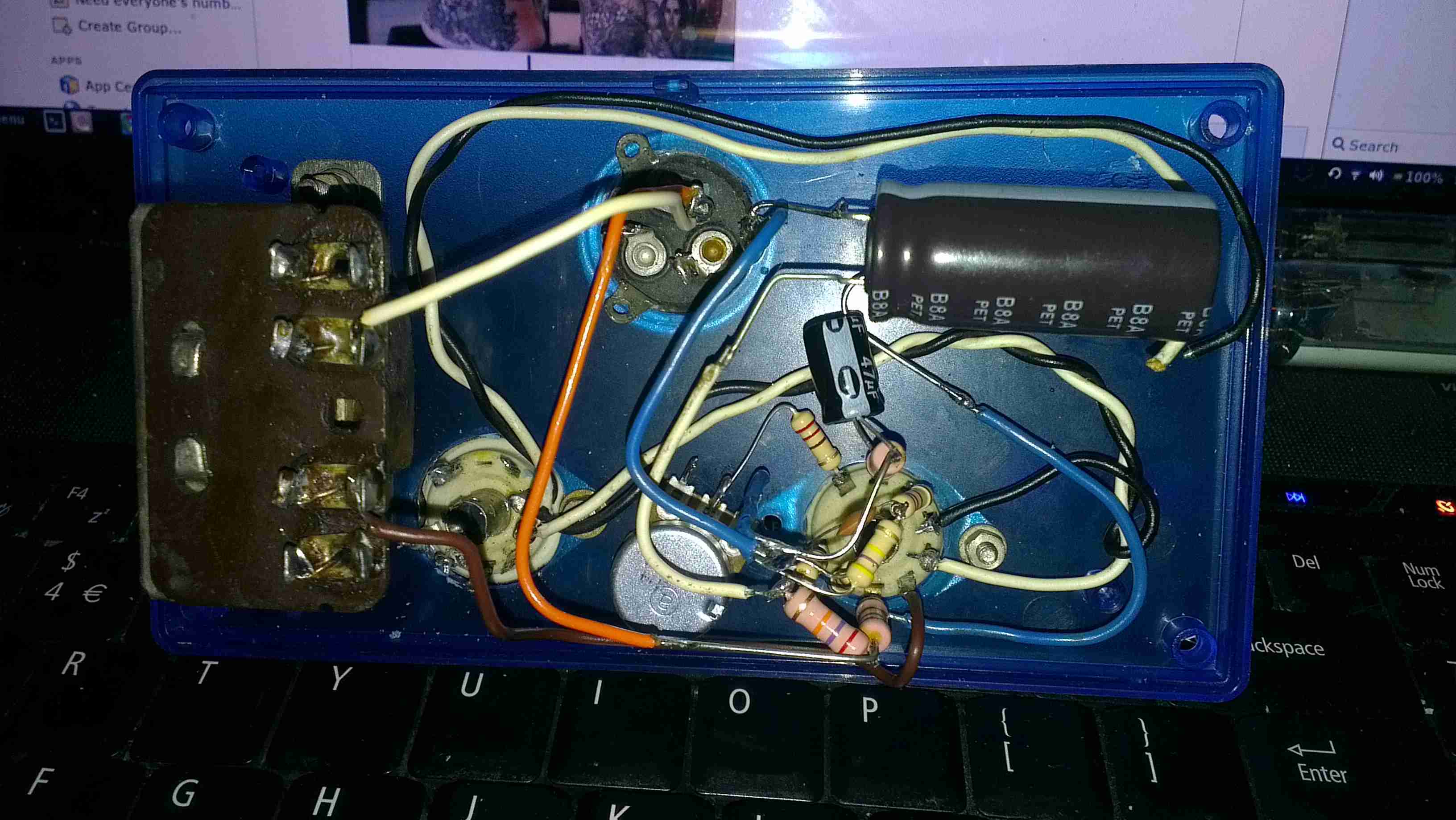
Valves Test Fit
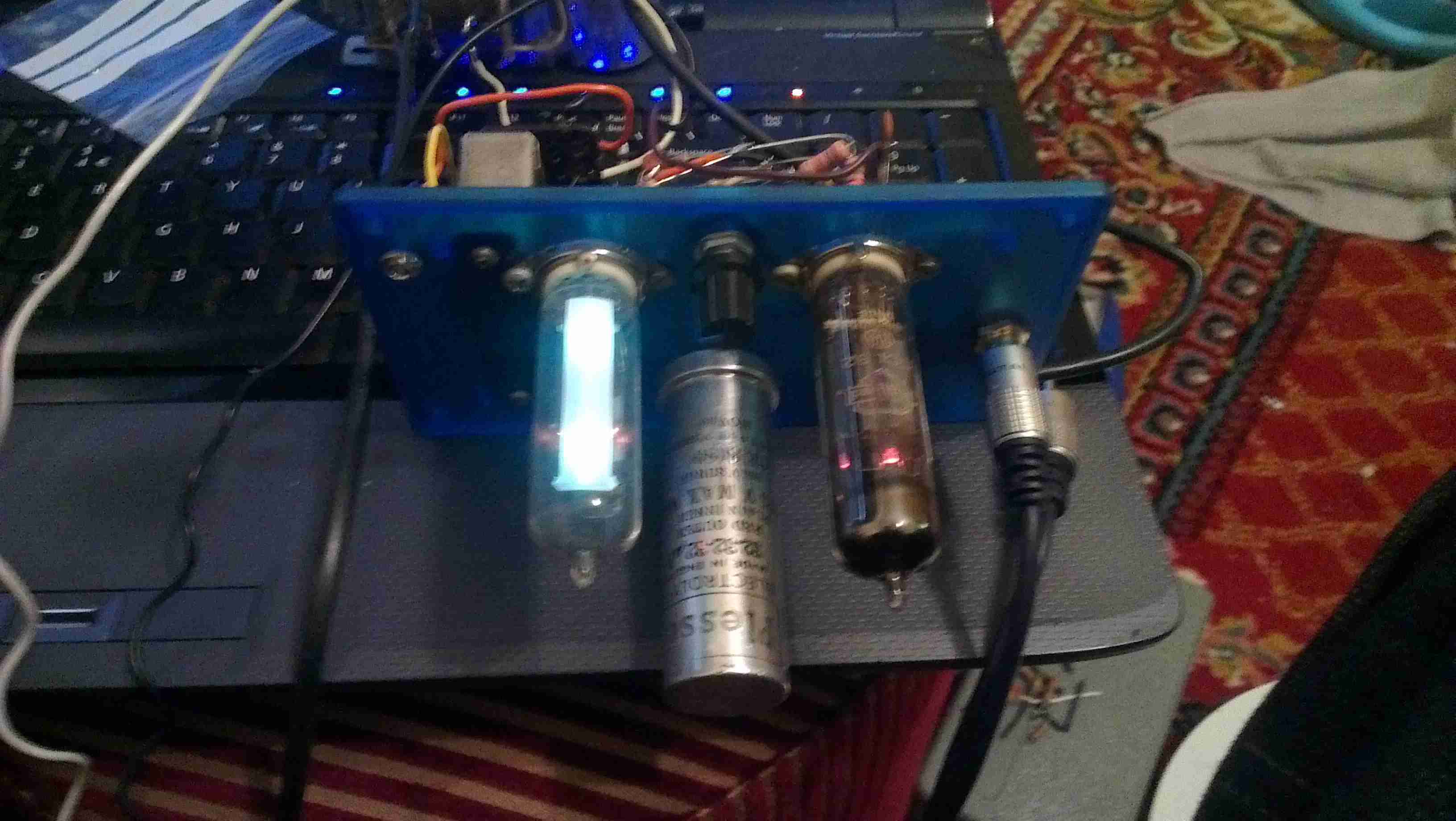
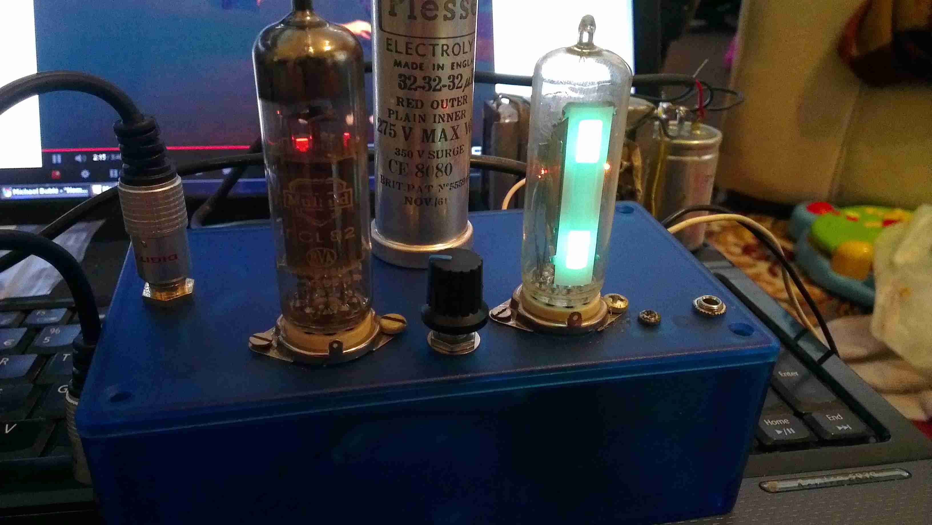
The valves here are test fitted into their sockets, the aluminium can at the back is a triple 32uF 250v electrolytic capacitor for smoothing the B+ rail.
Amplifier Section First Test
First test of the amplifier, with the speaker from the 1960’s tape recorder from which the valves came from. the 200v DC B+ supply & the 6.3v AC filament supply is derived from the mains transformer in the background.
Magic Eye Tube Added
Here the magic eye tube has been fitted & is getting it’s initial tuning to the amplifier section. This requires selecting combinations of anode & grid resistors to set the gap between the bars while at no signal & picking a coupling RC network to give the desired response curve.
Final Test
Here both valves are fitted & the unit is sitting on it’s case for final audio testing. the cathodes of the ECL82 can be clearly seen glowing dull red here.
In the final section, I will build a SMPS power supply into the unit to allow it to be powered from a single 12v DC power supply.
A 5 megapixel digital camera from Vivitar. Visible here is the lens, viewfinder & flash.
Back
Rear of the unit showing the LCD & user control buttons.
Cover Removed
Front frame removed showing some of the internals. Shutter assembly & lens in centre, battery compartment at left.
Rear Cover Removed
Rear frame removede, showing the LCD module & tactile switches.
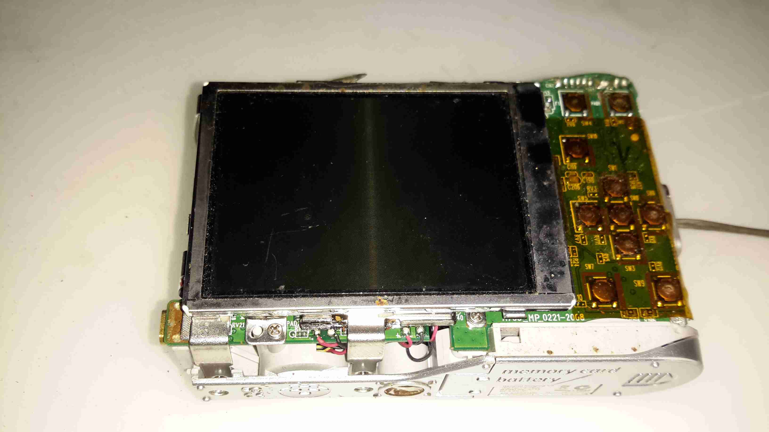
LCD
LCD module removed from the PCB
Flash PCB
Flash PCB removed. Transformer is fed with the 4.5v from the 3 AA cells & steps it up to ~300v DC for the flash capacitor. A pulse transformer energizes an electrode next to the Xenon flash tube with ~5kV to ionize the gas.
Main PCB
Main PCB removed. Internal flash ROM & RAM IC visible above the SD card socket. USB connector is at the top right, next to the piezo buzzer.
CPU
Main processor on reverse side of the PCB.
Image Sensor
Closeup of the CMOS image sensor with the lens assembly removed.
Here are the internals of a cheap Microwave/Convection Oven combo. Electronics bay is pretty much the same as a standard microwave, with the magnetron, transformer & diode/capacitor voltage doubler, with the addition of an extra fan & a pair of nichrome elements to provide the convection oven function.
Convection Fan
Convection blower which keeps the cooking vapours & smoke away from the elements, & circulates the hot air around the cooking chamber. This is a 12v DC centrifugal type blower.
Convection Element
The elements are inside this steel shield, air duct extends from the centre.
Thermal Cutouts
This oven has a pair of thermal switches on the magnetron.
Capacitor & Diode
The usual capacitor/diode voltage doubler in the magnetron power supply. The transformer is visible to the left.
Controller
Electronic controller PCB. This has a pair of relays that switch the elements & the magnetron transformer.
Here is a cheap no frills microwave oven, which died after a few weeks of normal use.
Electronics Bay
Cover removed, showing the internals. Front of the microwave is on the left.
Timer
Closeup of the timer unit. Cheap & nasty.
Magnetron
Magnetron removed from the oven. Antenna is on the top, cooling fins visible in the center. White conector at the bottom is the filament terminals.
Magnetron Chokes
Chokes on the magnetron’s filament connections. These prevent microwave energy from feeding back into the electronics bay through the connections.
Magnetron Assembly
Magnetron cooling fins, tube & magnets removed from the frame.
Magnetron Tube
Bare magnetron tube.
Power Input Board
This PCB does some rudimentary power conditioning, power resistors are in series with the live feed to the power trasformer, to prevent huge power up surge. When the transformer energizes the relay, which is in parallel with the resistors, switches them out a fraction of a second after, providing full power to the transformer.
Standard RFI choke & capacitor at the top of the board, with the input resistor.
Transformer
Power transformer to supply the magnetron with high voltage.
Power output is ~2kV at ~0.5A. Pair of spade terminals are the low voltage filament winding.
Capacitor
HV Capacitor. This along with the diode form a voltage doubler, to provide the magnetron with ~4kV DC.
Diode
HV diode stack.
Fuse Element
Internals of the HV fuse. Rated for ~0.75A at 5kV. The fuse element is barely visible attached to the end of the spring. Connects between the transformer & the capacitor.
Cooling Fan
Cooling fan for the magnetron. Drive is cheap shaded pole motor.
A quick post documenting a DPSS laser module i salvaged from a disco scanner. Estimated output ~80mW
Diode Connection
Connection to the 808nm pump diode on the back of the module. There is a protection diode soldered across the diode pins. (Not visible). Note heatsinking of the module.
Driver PCB
Driver PCB. This module was originally 240v AC powered, with a transformer mounted on the PCB with a built in rectifier & filter capacitor. I converted it to 5v operation. Emission LED on PCB.
This is an old cordless landline phone, with dead handset batteries.
Handset Radio Board
Here’s the handset with the back removed. Shown is the radio TX/RX board, underneath is the keyboard PCB with the speaker & mic. All the FM radio tuning coils are visible & a LT450GW electromechanical filter.
Handset Radio Board Bottom
Radio PCB removed from the housing showing the main CPU controlling the unit, a Motorola MC13109FB.
Keypad Board
The keypad PCB, with also holds the microphone & speaker.
Handset Keypad Board Bottom
Bottom of the keypad board, which holds a LSC526534DW 8-Bit µC & a AT93C46R serial EEPROM for phone number storage.
Base Main Board
Here’s the base unit with it’s top cover removed. Black square object on far right of image is the microphone for intercom use, power supply section is top left, phone interface bottom left, FM radio is centre. Battery snap for power backup is bottom right.
Power Supply Section
PSU section of the board on the left here, 9v AC input socket at the bottom, with bridge rectifier diodes & main filter capacitor above. Two green transformers on the right are for audio impedance matching. Another LT450GW filter is visible at the top, part of the base unit FM transceiver.
ICs
Another 8-bit µC, this time a LSC526535P, paired with another AT93C46 EEPROM. Blue blob is 3.58MHz crystal resonator for the MCU clock. The SEC IC is a KS58015 4-bit binary to DTMF dialer IC. This is controlled by the µC.
Base Main Board Bottom
Underside of the base unit Main PCB, showing the matching MC13109FB IC for the radio functions.
This is a 1500W hairdryer, death caused by thermal switch failure.
Switch
This is the switch unit. Attached are two suppression capacitors & a blocking diode. Cold switch is on right.
Heating Element
Heating element unit removed from housing. Coils of Nichrome wire heat the air passing through the dryer. Fan unit is on right.
Thermal Switch
Other side of the heating element unit, here can be seen the thermal switch behind the element winding. (Black square object).
Fan Motor
The fan motor in this dryer is a low voltage DC unit, powered through a resistor formed by part of the heating element to drop the voltage to around 12-24v. Mounted on the back of the motor here is a rectifier assembly. Guide vanes are visible around the motor, to straighten the airflow from the fan blades.
Fan
5-blade fan forces air through the element at high speed. Designed to rotate at around 13,000RPM.
Tip Jar
If you’ve found my content useful, please consider leaving a donation by clicking the Tip Jar below!
All collected funds go towards new content & the costs of keeping the server online.