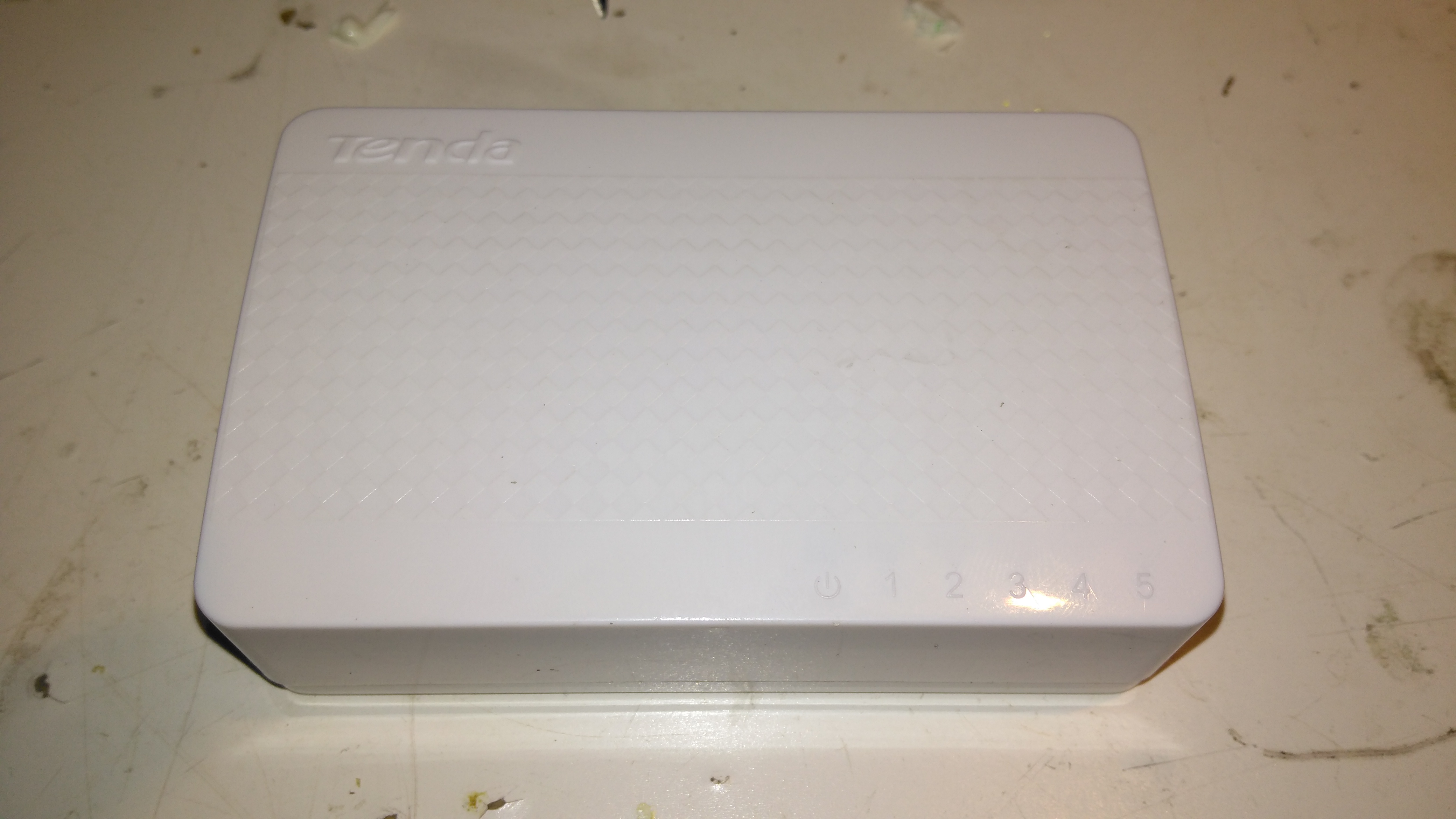
Here’s a tiny ethernet switch from the great fle market that is eBay – the Tenda S105. This unit has 5 ports, but only supports 10/100M. Still, for something so small it’s not bad.
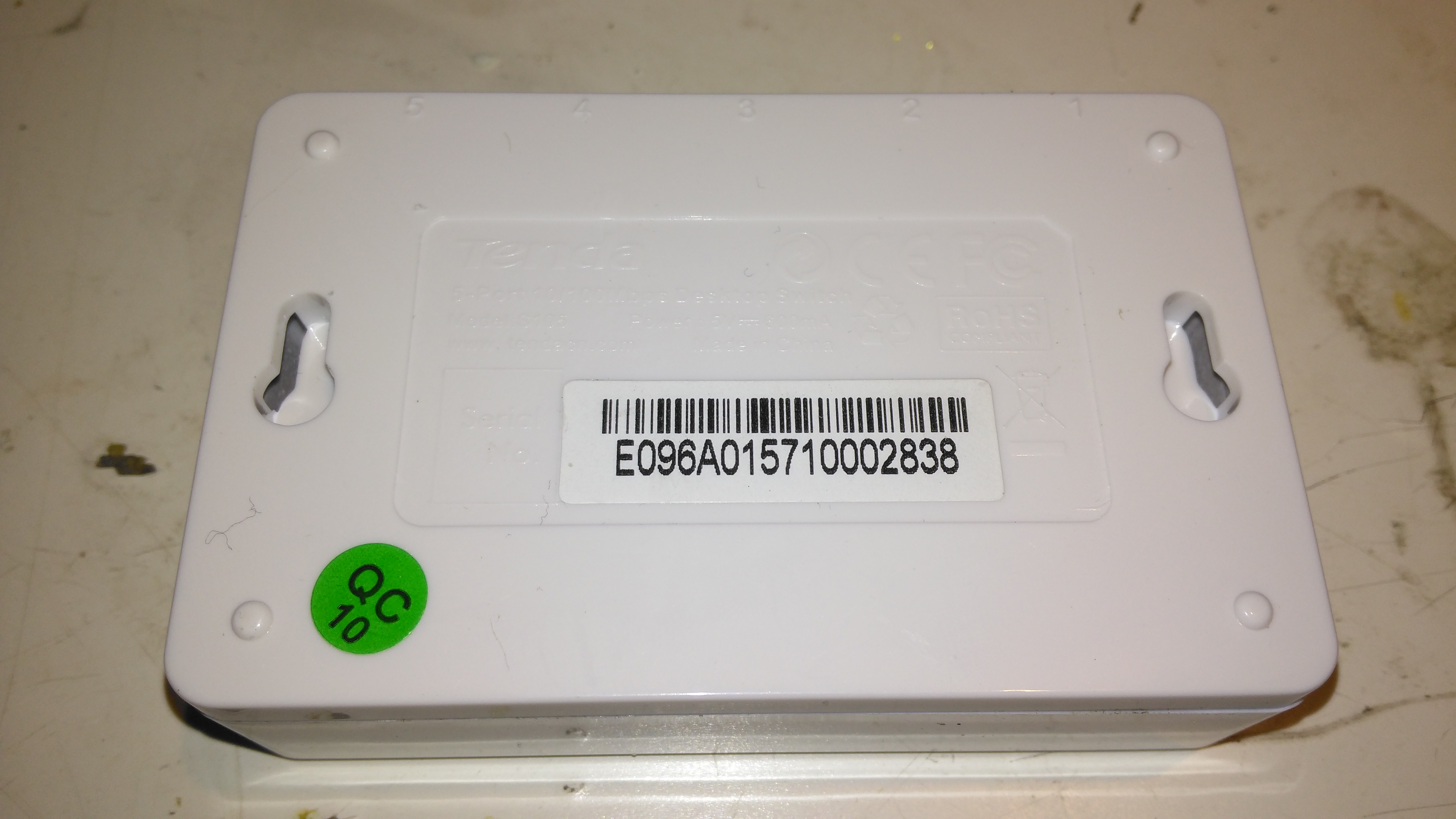
Bottom
Not much on the bottom, there’s a pair of screw hooks for mounting this to a surface.
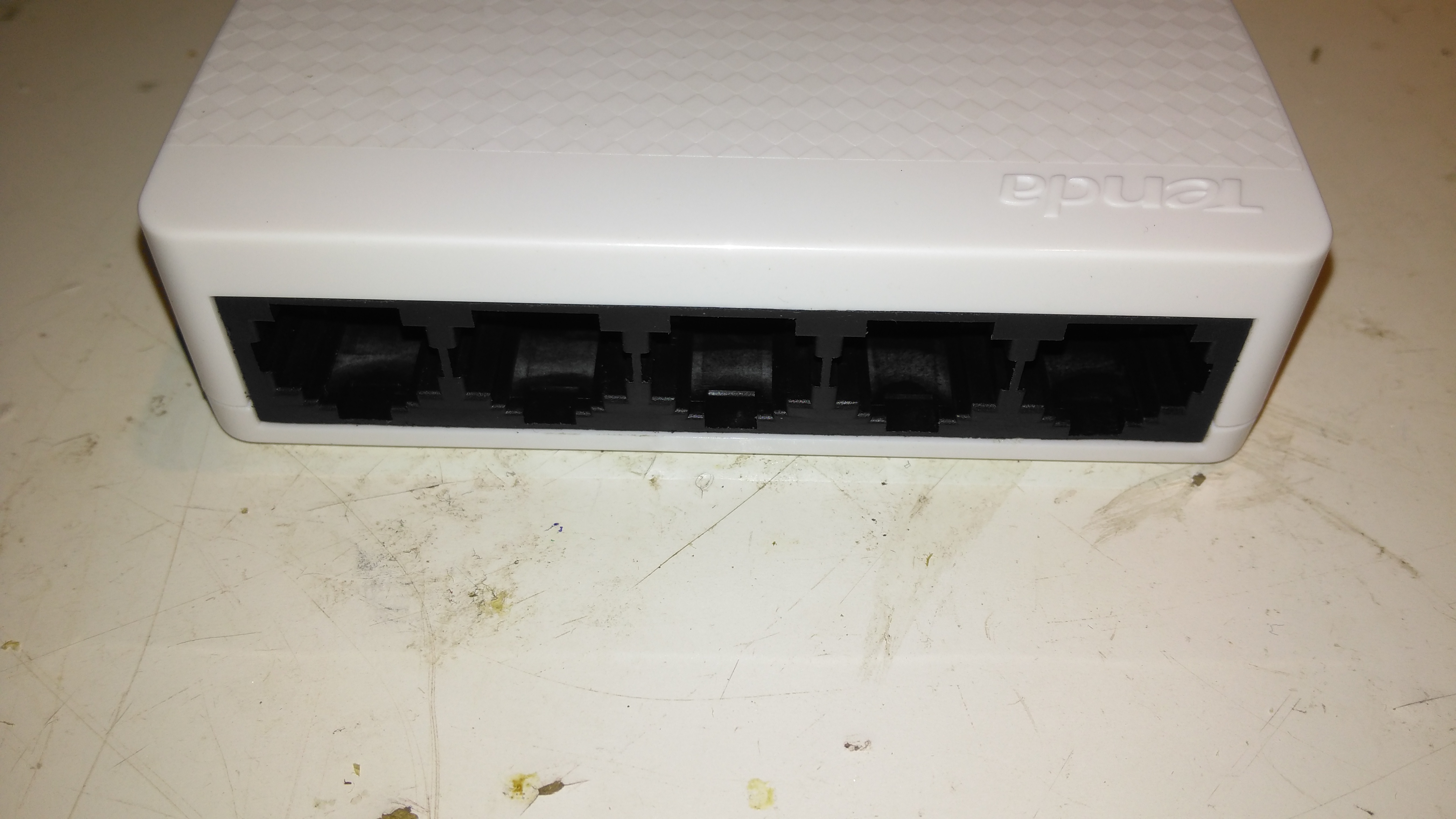
Ports
The 5 ports on the front actually have the pins for the unused pairs of the ethernet cables removed – saving every penny here.
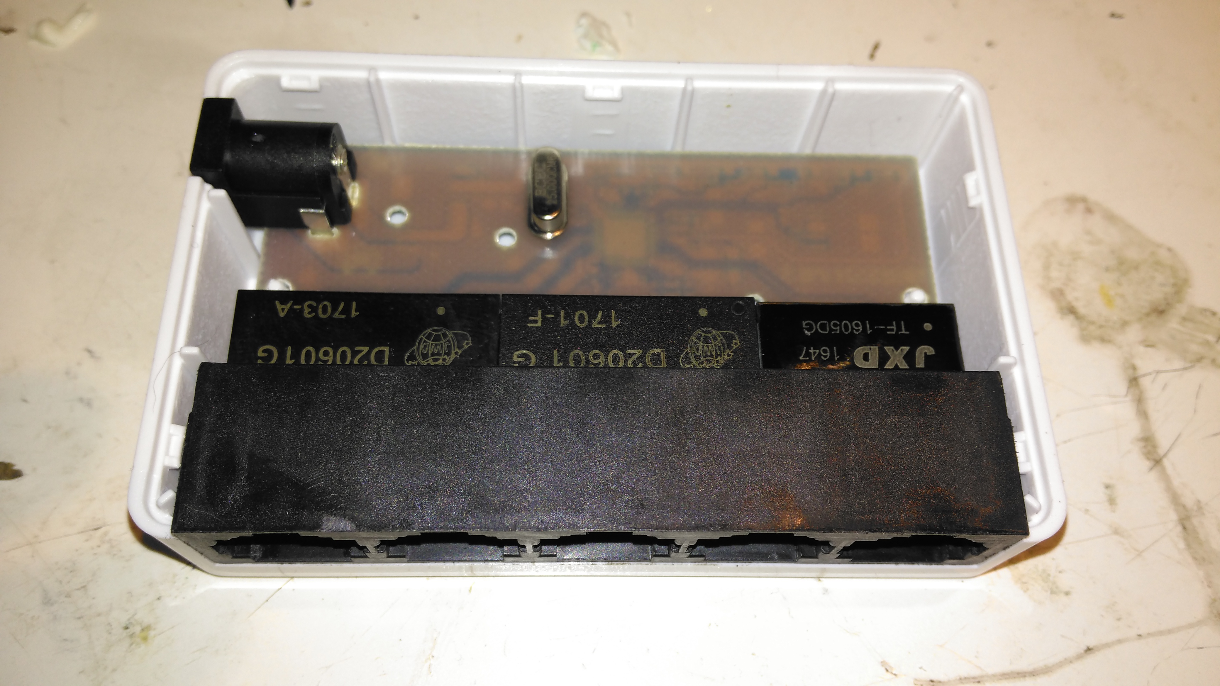
PCB Top
The casing just unclips, revealing the small PCB. Nothing much on the top, just the connectors, isolating transformers & the crystal for the switch IC.
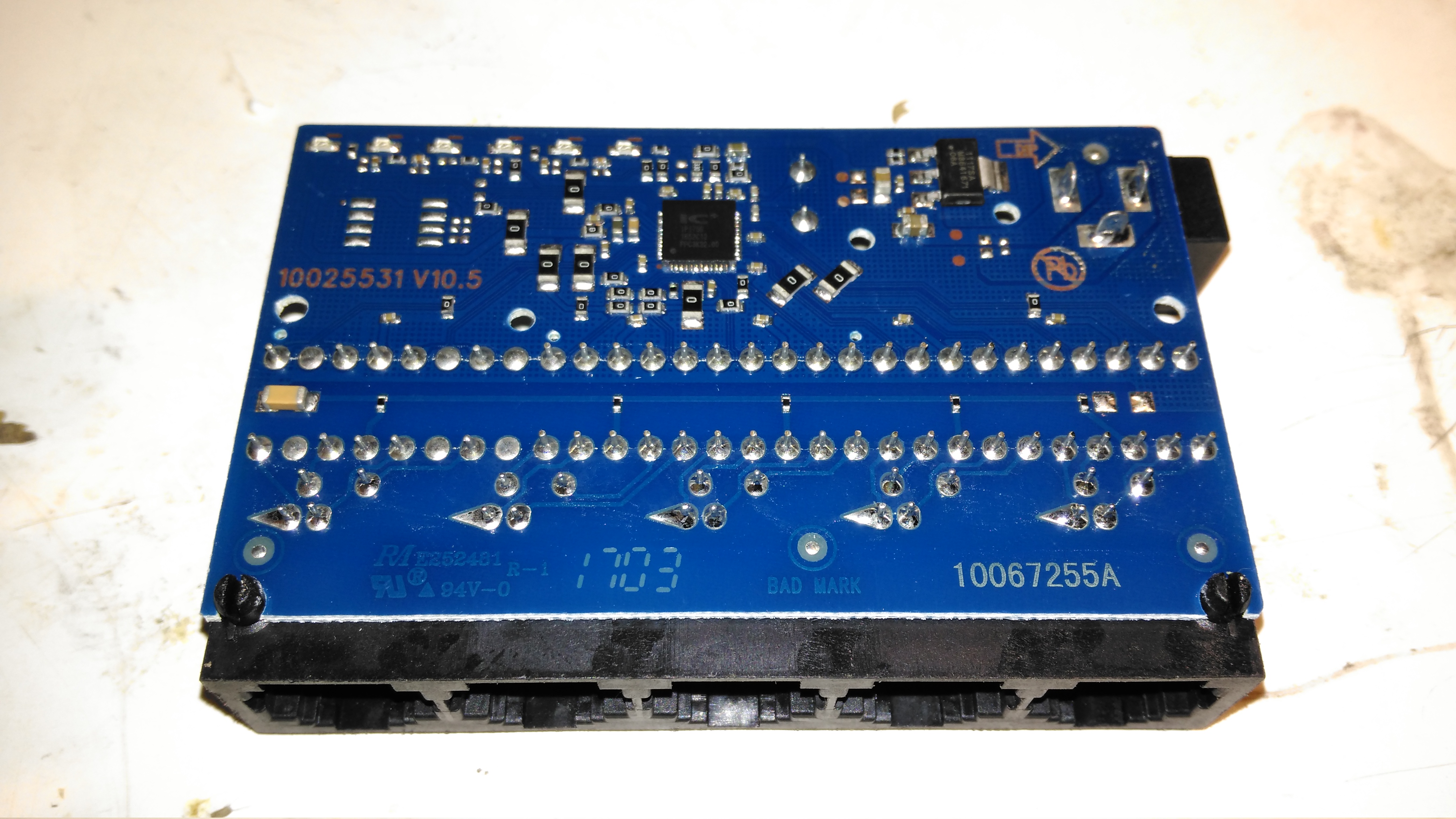
PCB Bottom
The bottom of the PCB is a little more busy, mainly with decoupling components. There’s a 3.3v linear regulator to step down the 5v input for the switch IC.
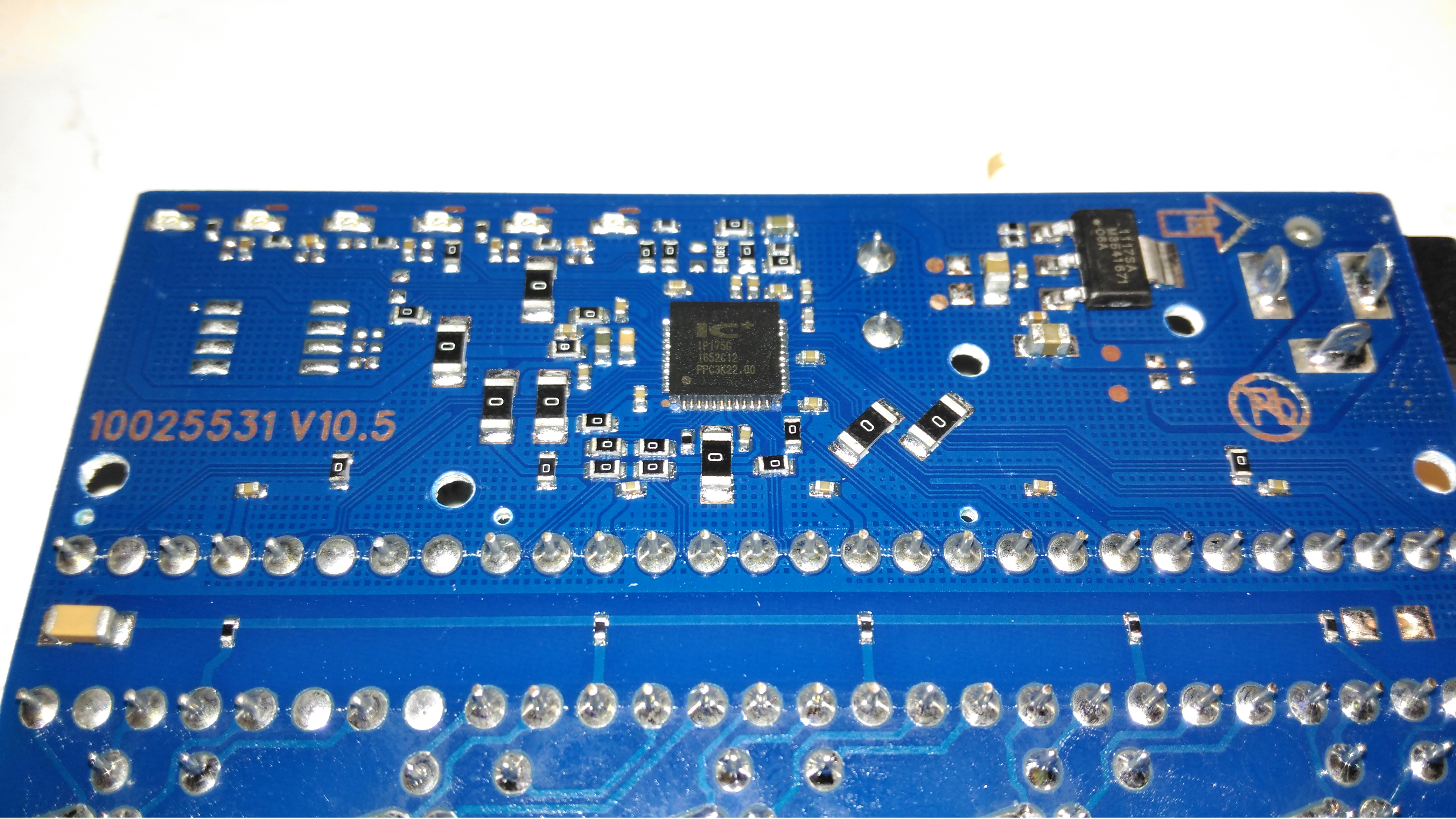
Switch IC
The IC doing all the data switching is an IP175G 5-Port 10/100 Switch from IC+ Corp. No datasheet available for this, but it’s going to be a bog-standard switch.
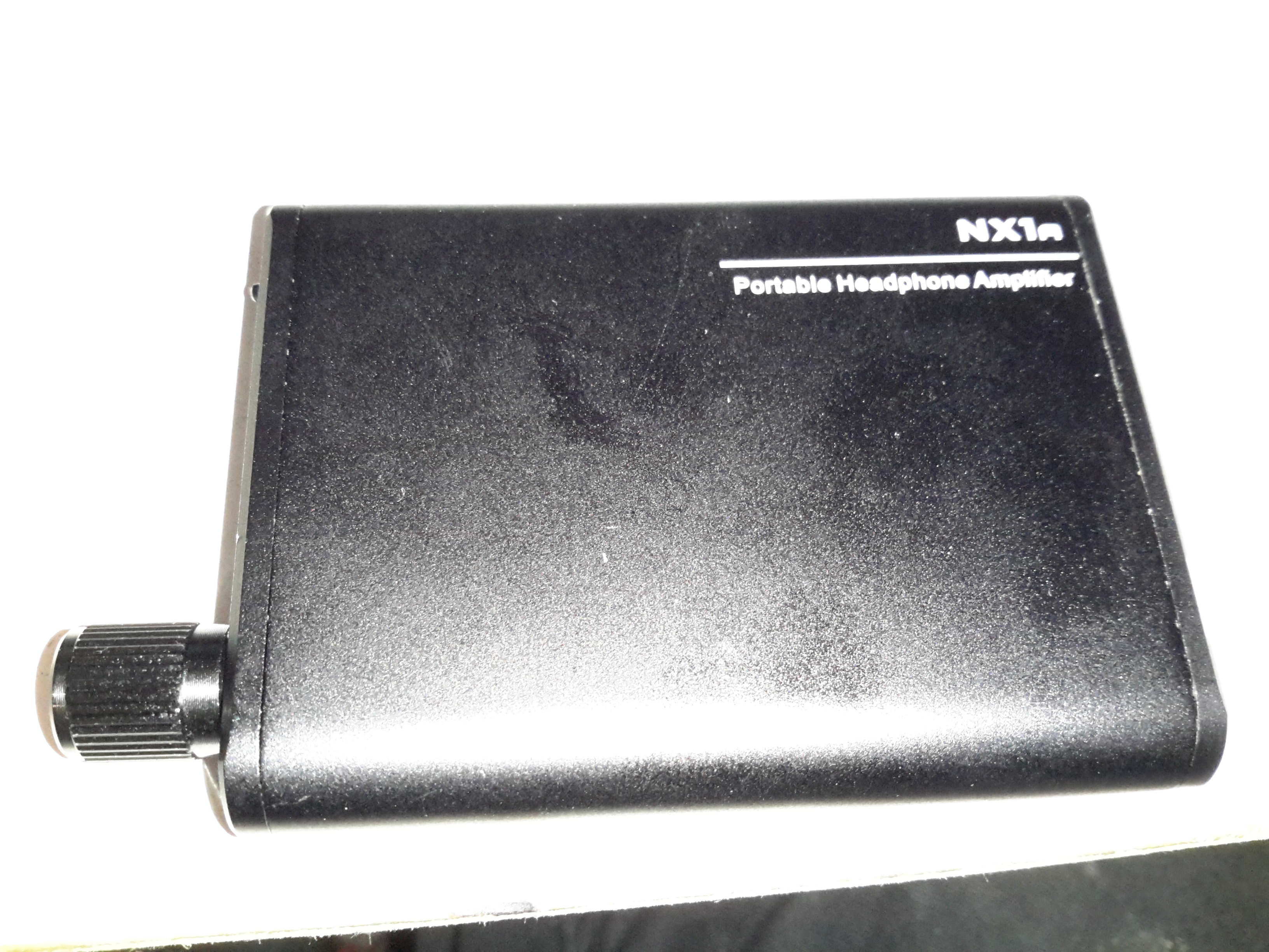
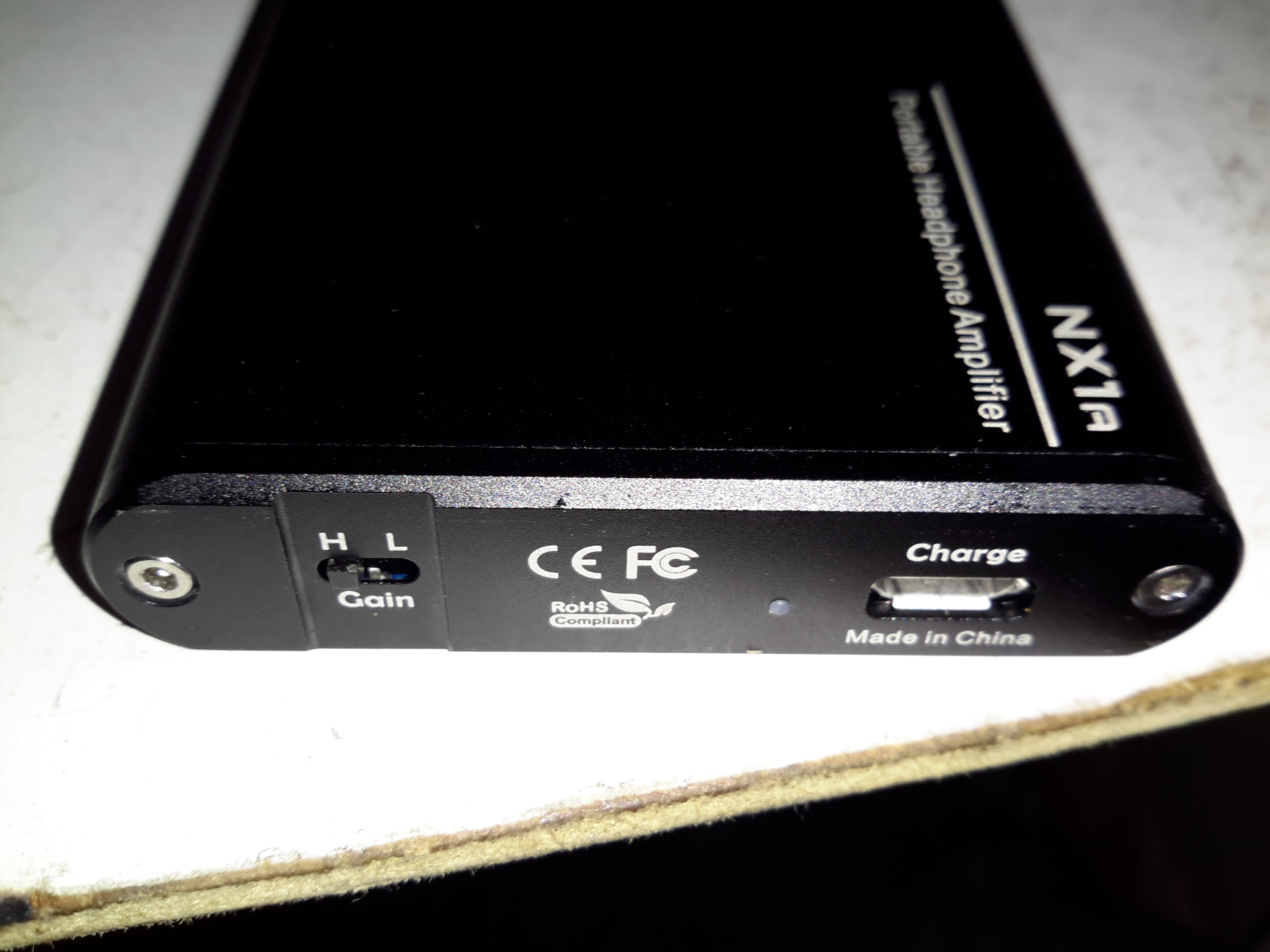
Time for another teardown! Here’s a pocket-sized headphone amplifier for use with mobile devices. This unit is powered by a built-in lithium cell, and can give some pretty impressive volume levels given it’s small size.
Audio Connections
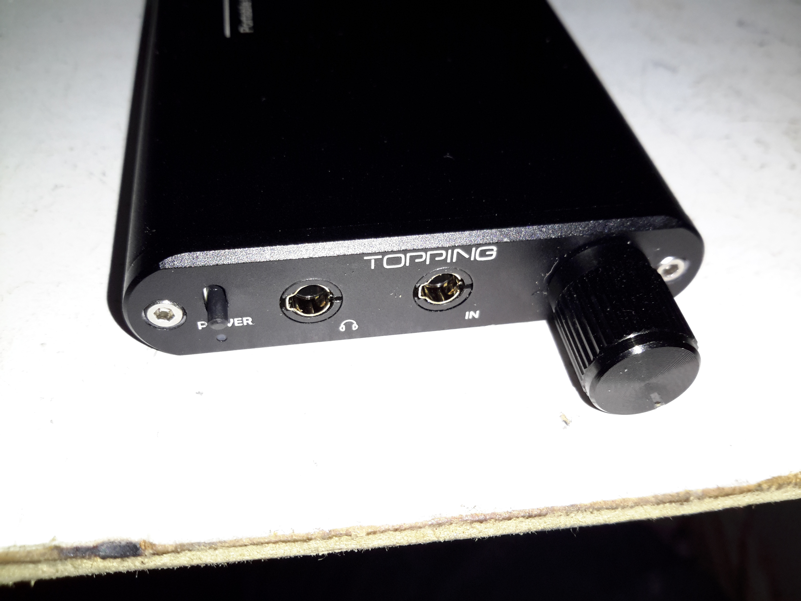
The 3.5mm audio input & output jacks are on the front of the unit, along with the relatively enormous volume knob & power switch. There’s a little blue LED under the switch that lets the user know when the power is on, but this is a very sedate LED, using very little power.
Gain & Charging
On the back is the High-Low gain switch, and the µUSB charging port. There’s another indicator LED to show that the internal cell is charging, in this case a red one.
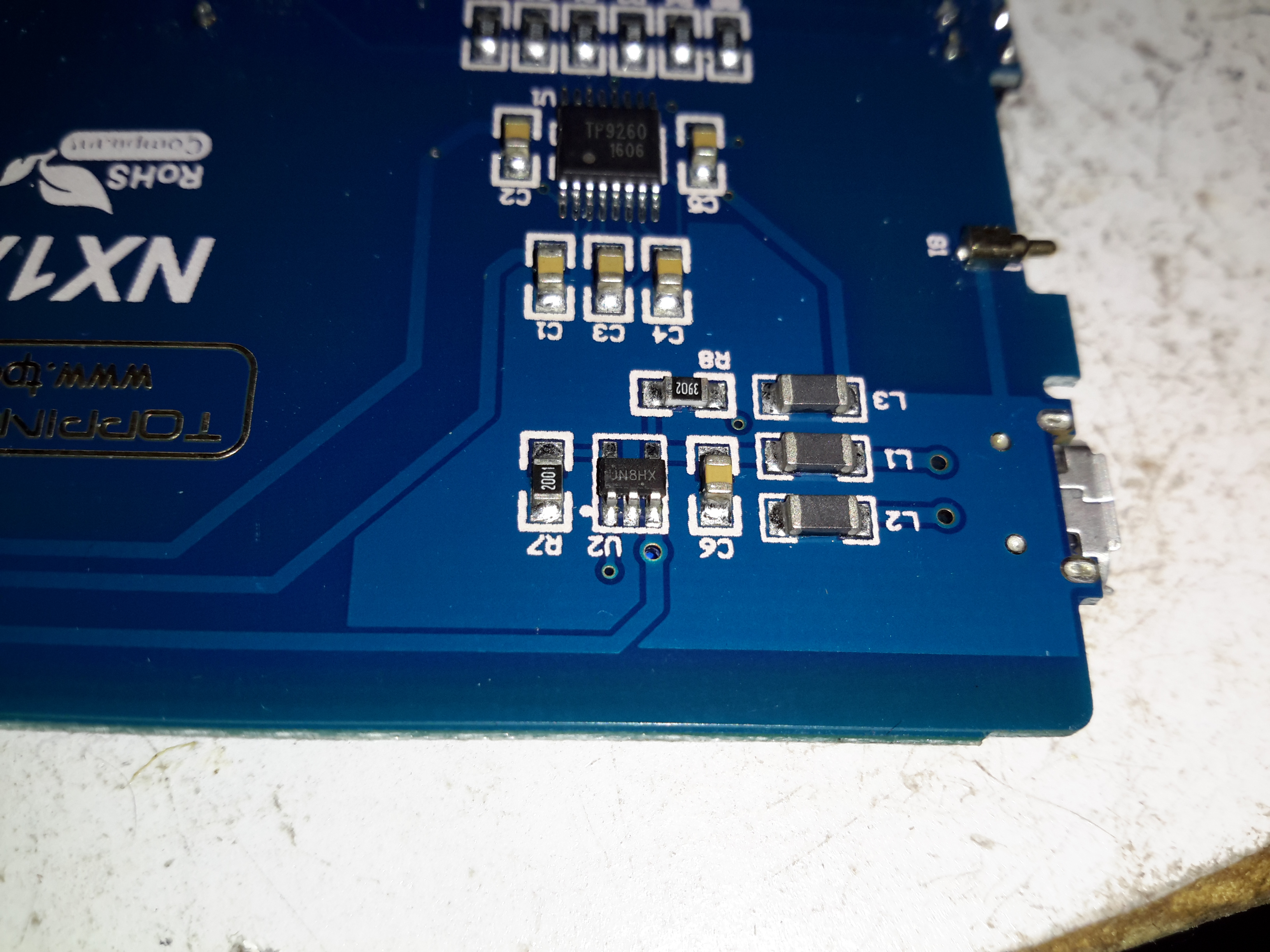
PCB Top
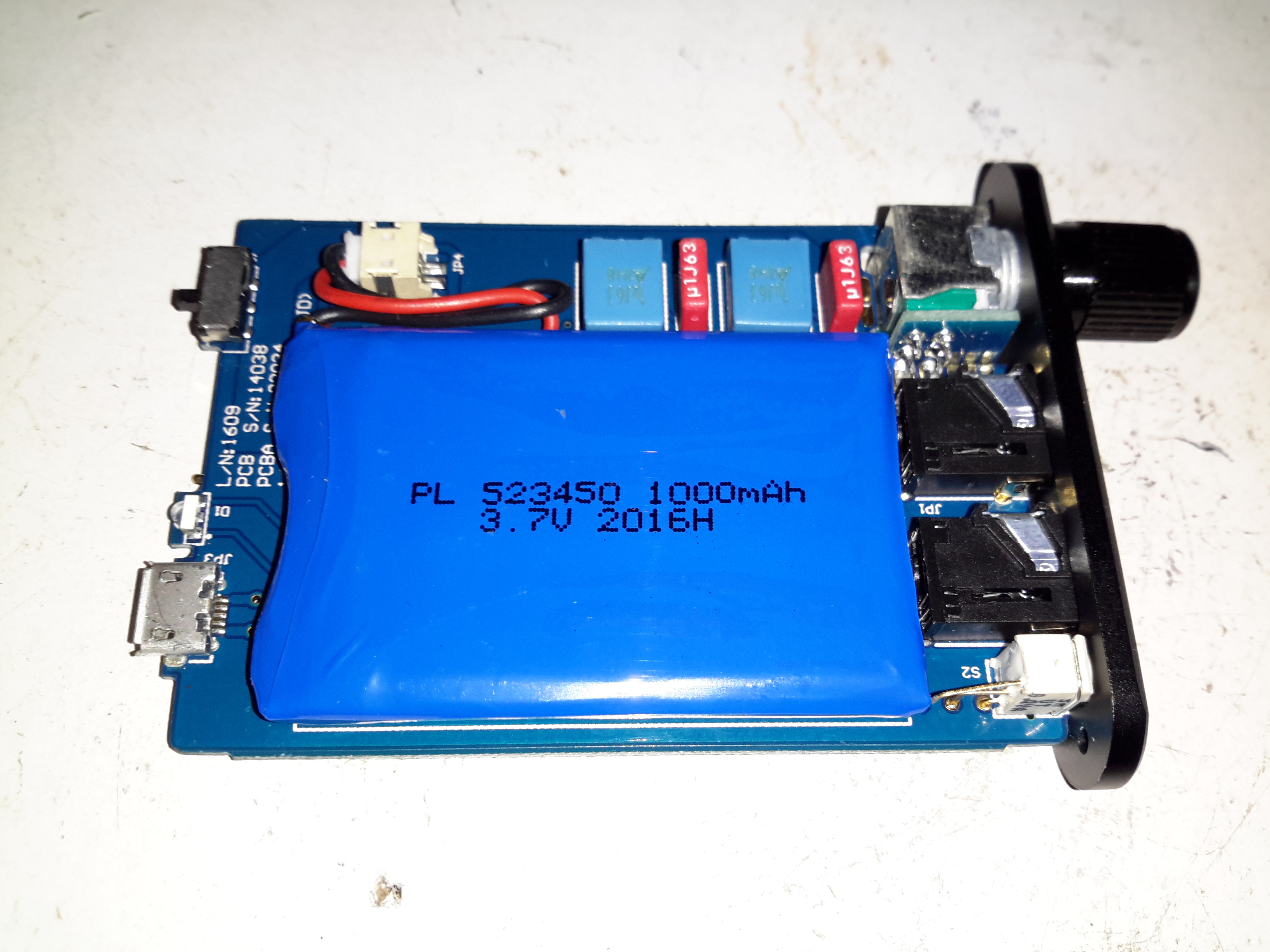
Removing a couple of cap screws allows the internals to slide out of the extruded aluminium casing. Most of the internal space is taken up by the 1Ah lithium cell, here on the top of the PCB secured by some double-sided tape. The volume potentiometer is mounted on a small daughterboard at right angles to get it to fit into the small vertical space in the case.
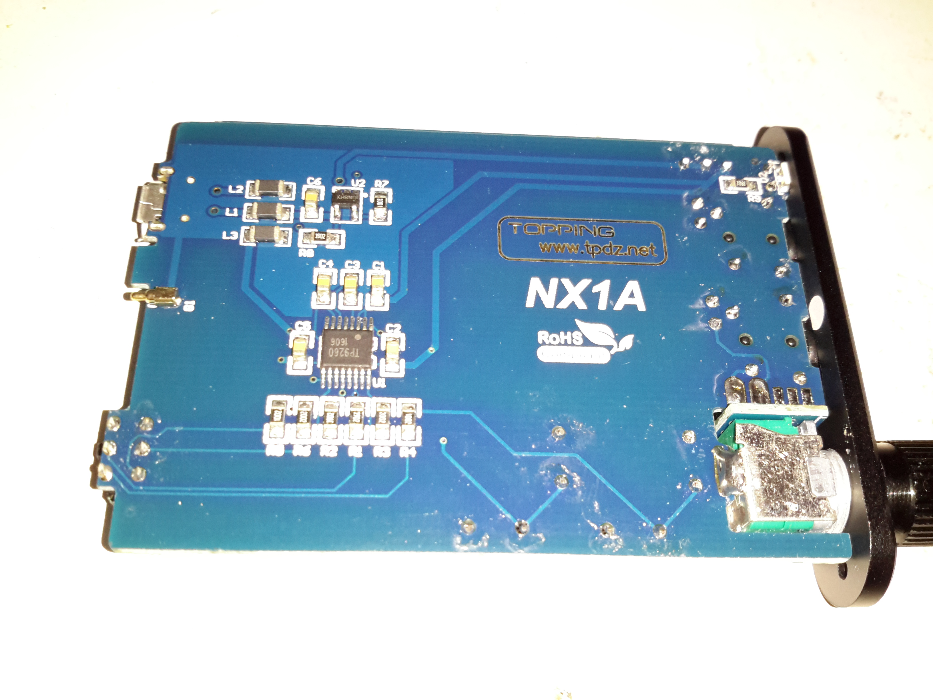
PCB Rear
The bottom of the PCB is equally as sparse – the only ICs being the main audio amp in the centre & the battery charger IC at the top.
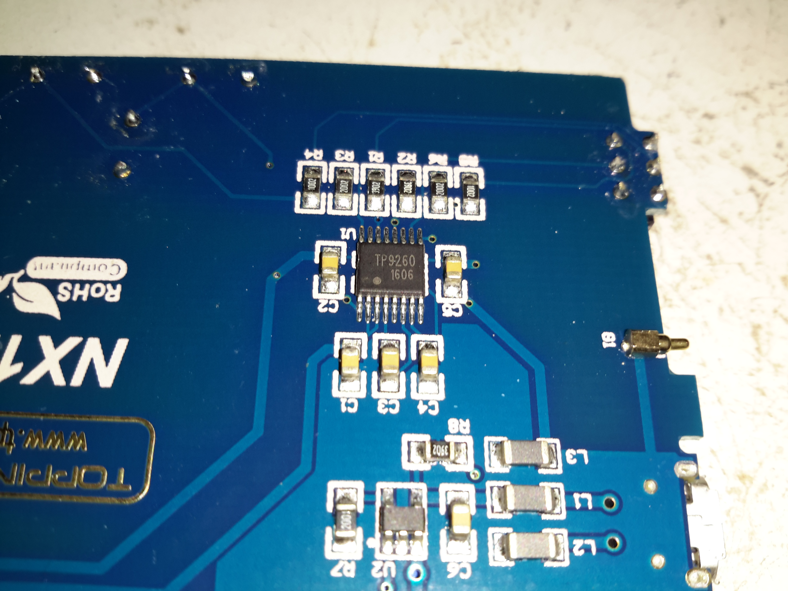
Amplifier IC
The main audio amplifier is a TP9260, I couldn’t find a datasheet on this, so I’m unsure of what the specs are. The row of resistors above the IC are for the gain divider circuit. There’s also a pogo pin on the right that makes contact with the back panel of the case for grounding.
Battery Charger
Battery charging is taken care of by a UN8HX 500mA linear charging IC, not much special here.
This little amplifier seems to be pretty well made, considering the price point. The only issue I’ve had so far is the audio cables act like antennas, and when in close proximity to a phone some signal gets picked up & blasted into the headphones as interference.
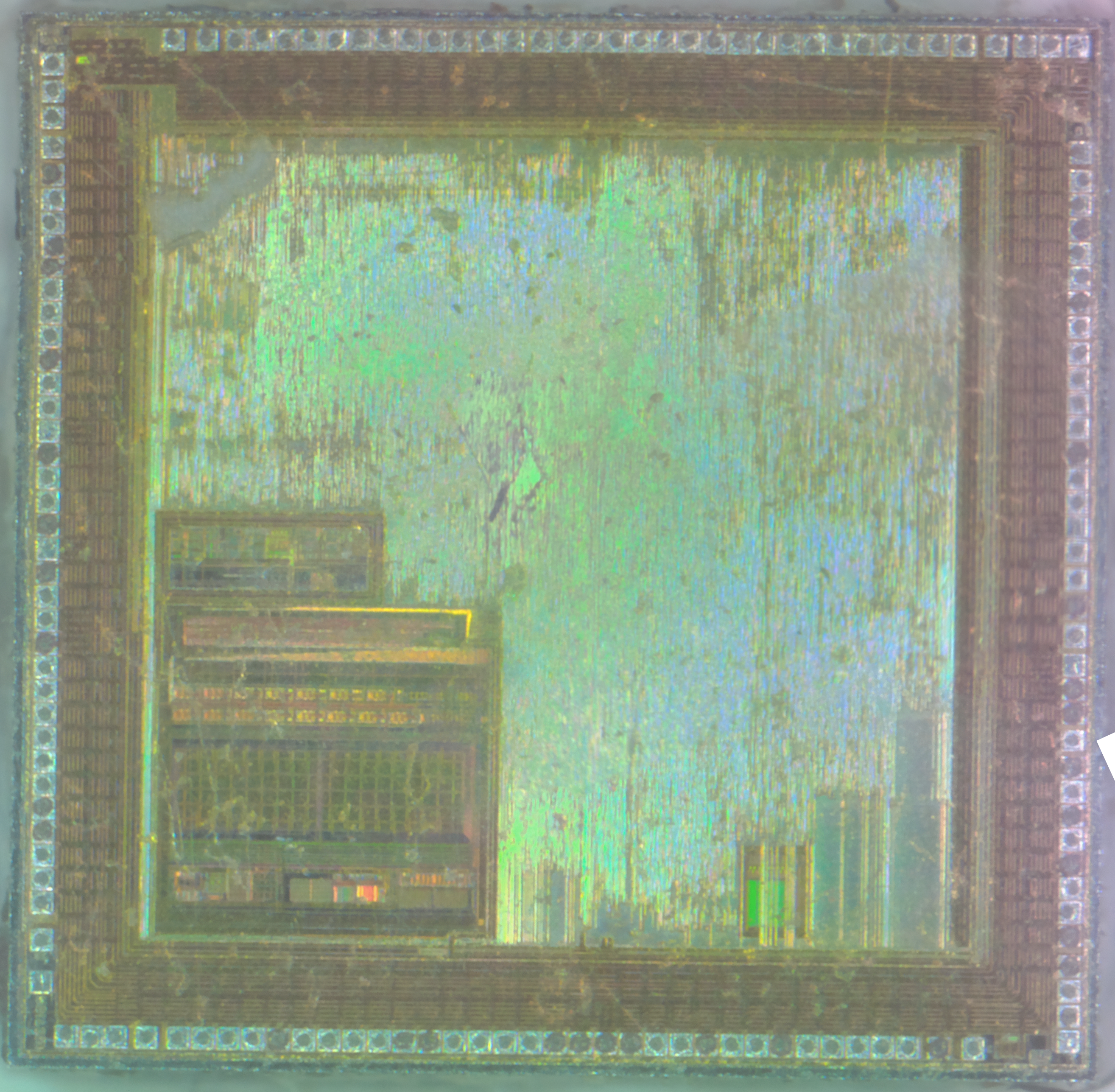
Here’s a very common chip used in older LCD monitors. This converts the incoming VGA signal into LVDS for the panel itself.
gmZAN3 Die
The gmZAN3 is a graphics processing IC for Liquid Crystal Display (LCD) monitors at XGA resolution. It provides all key IC functions required for the highest quality LCD monitors. On-chip functions include
a high-speed triple-ADC and PLL, a high quality zoom and shrink scaling engine, an on-screen display (OSD) controller and digital color controls.
I recently got the latest upgrade from Virgin Media, 200Mbit DL / 20Mbit UL, and to get this I was informed I’d have to buy their latest hardware, since my existing CPE wouldn’t be able to handle the extra 5Mbit/s upload speed. (My bullshit detector went off pretty hard at that point, as the SuperHub 2 hardware is definitely capable of working fine with 20Mbit/s upload rates). Instead of having to return the old router, I was asked to simply recycle it, so of course the recycling gets done in my pretty unique way!
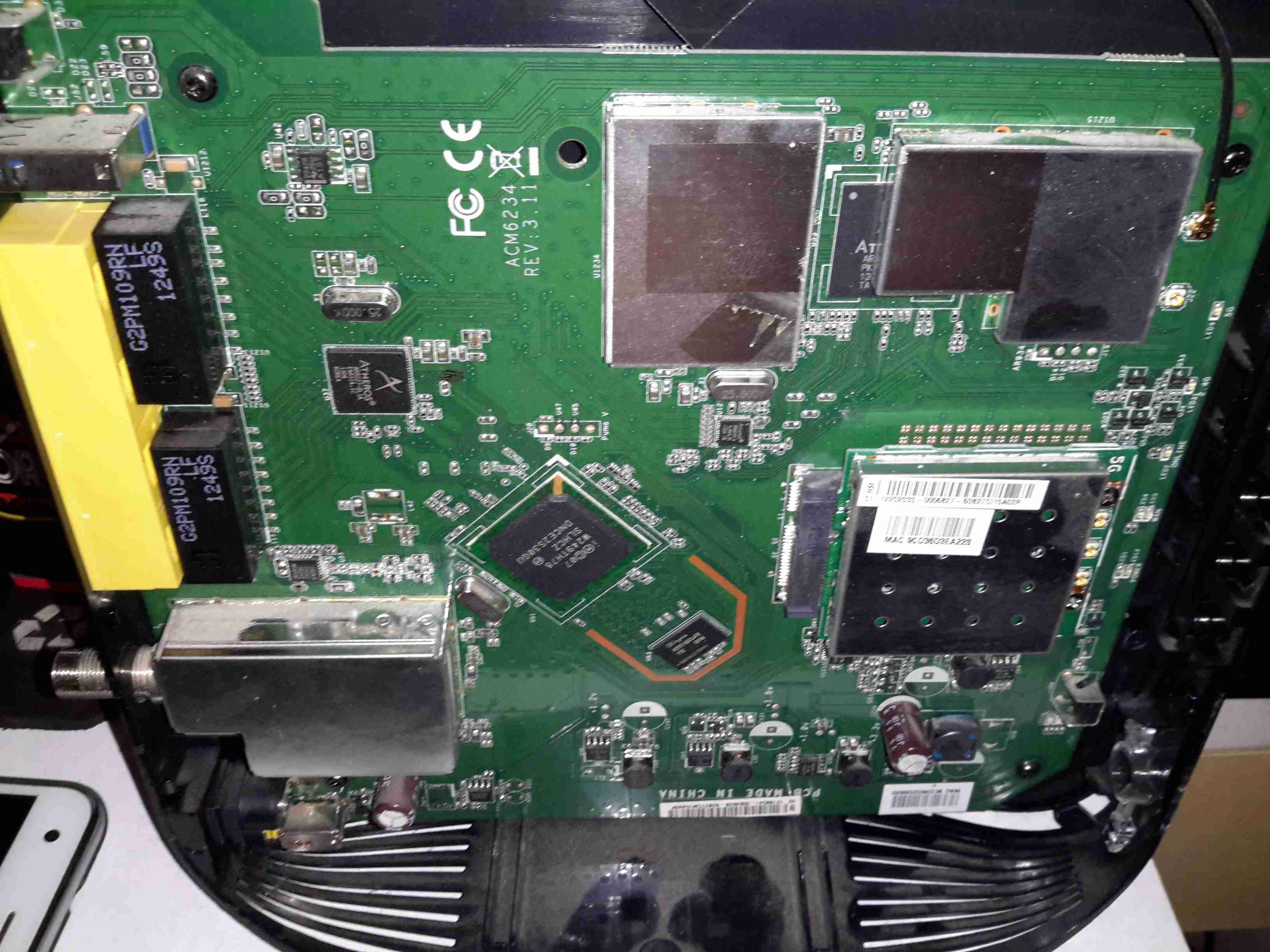
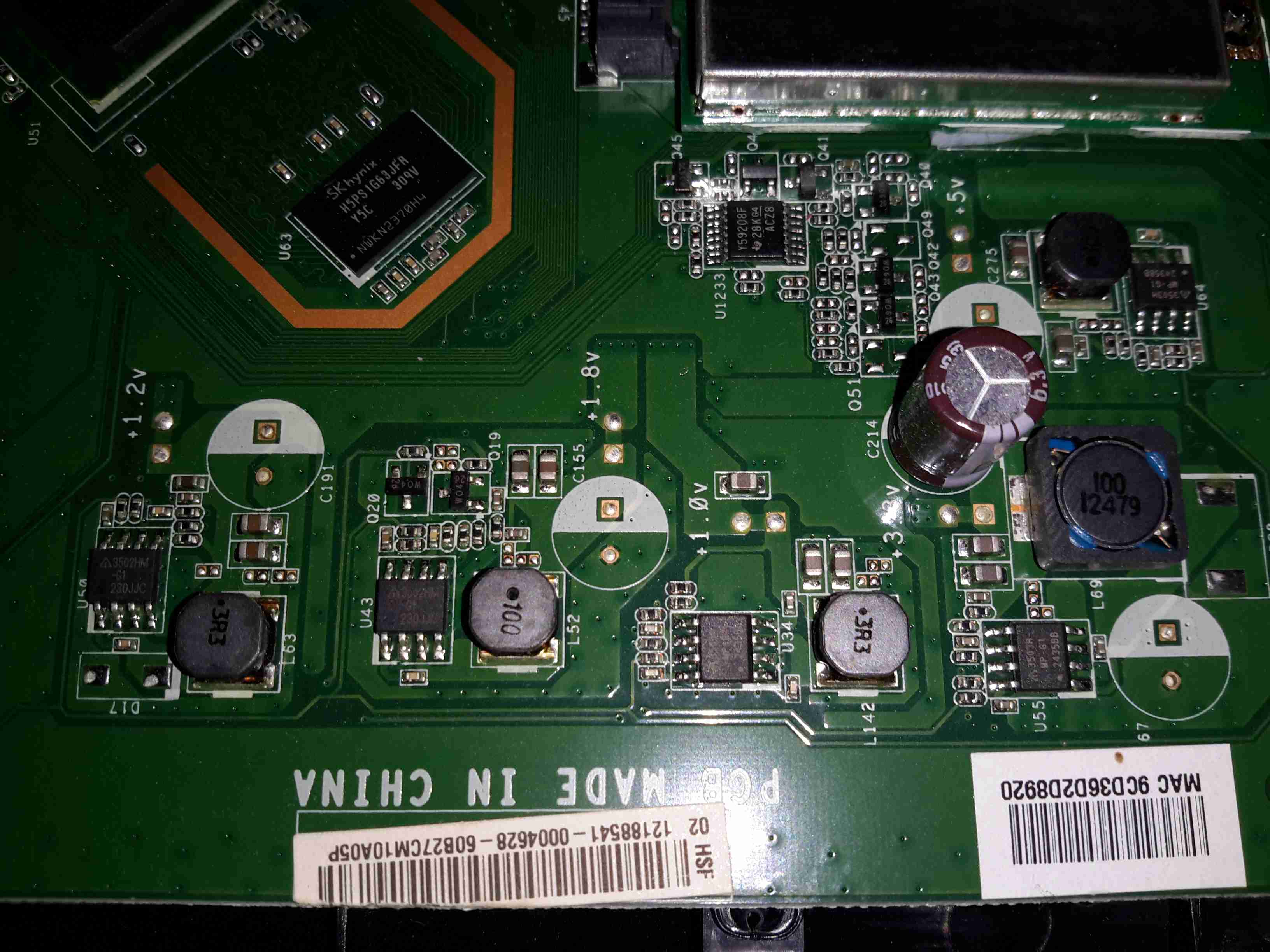
Mainboard
The casing of these units is held together by a single screw & a metric fuckton of plastic clips, disassembly is somewhat hindered by the radio antennas being positioned all over both sides of the casing. Once the side is off, the mainboard is visible. The DOCSIS frontend is lower left, centre is the Intel PUMA 5 Cable Modem SoC with it’s RAM just to the lower right. The right side of the board is taken up by both of the WiFi radio frontends, the 5GHz band being covered by a Mini PCIe card.
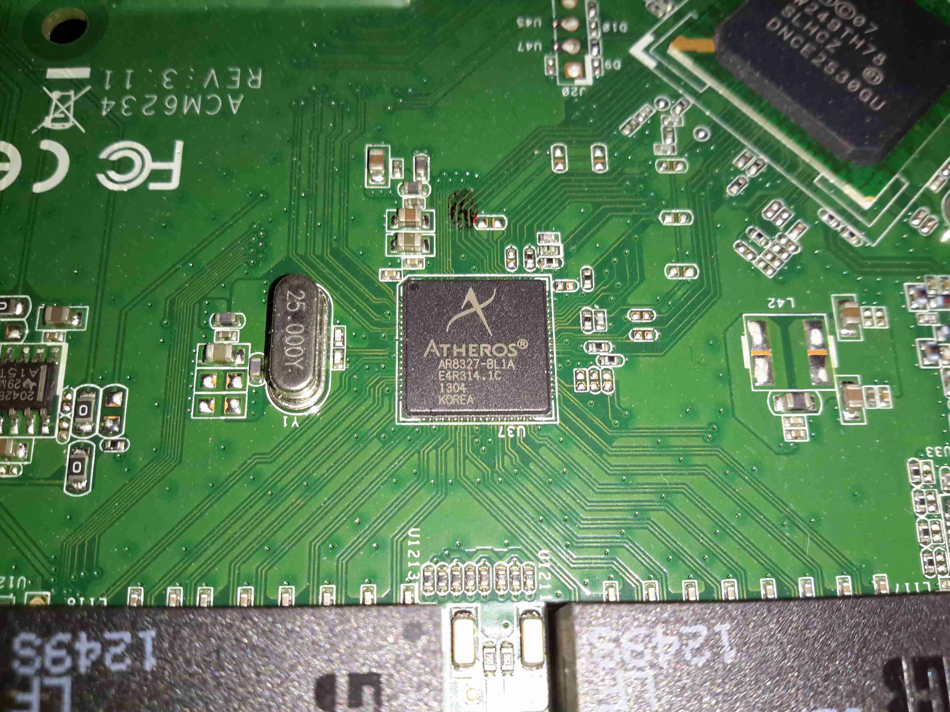
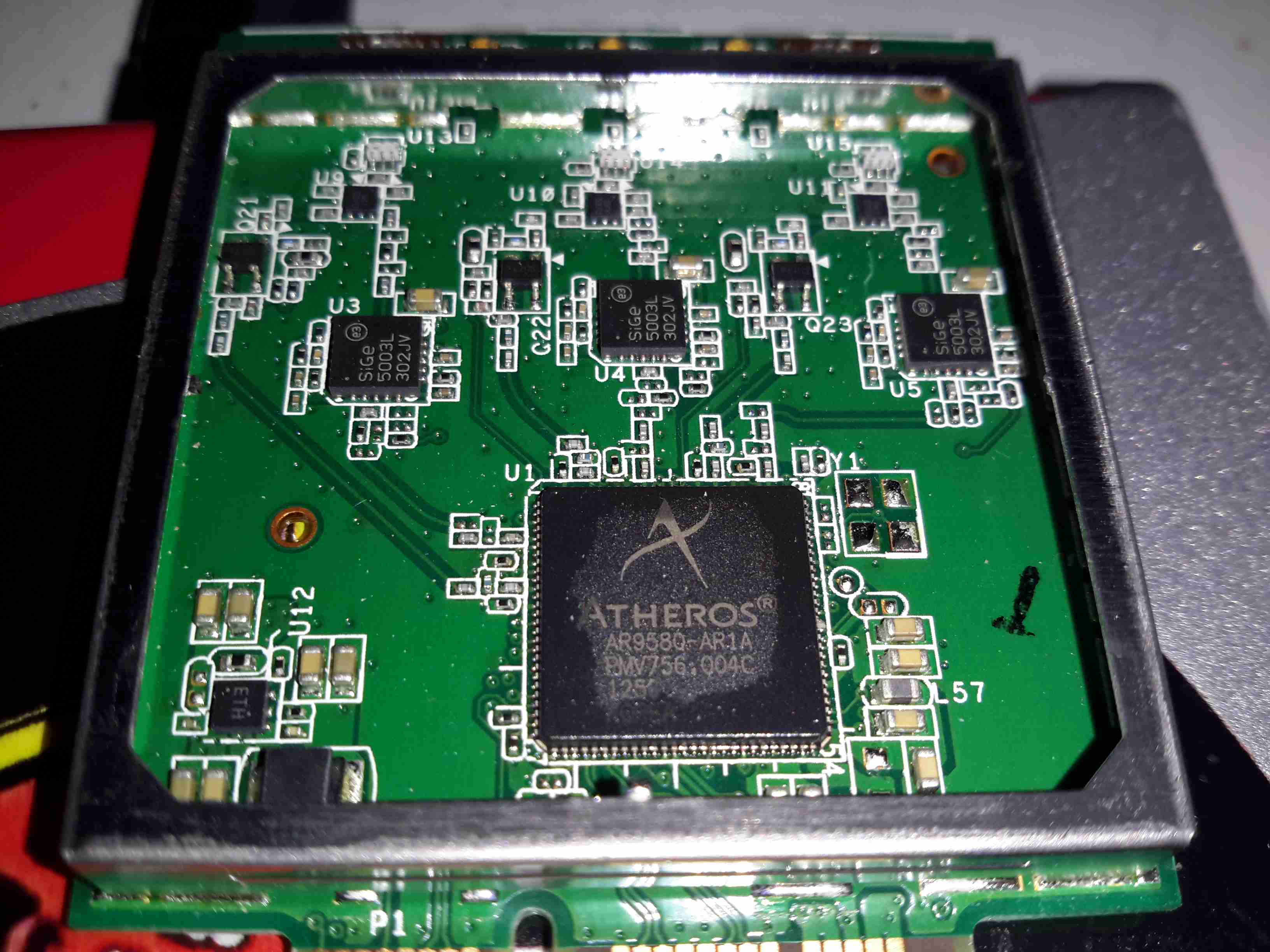
Atheros Gigabit Switch
The 4 gigabit Ethernet ports on the back are serviced by an Atheros AR8327 Managed Layer 3 switch IC, which seems to be a pretty powerful device:
The AR8327 is the latest in high performance small network switching. It is ultra low power, has extensive routing and data management functions and includes hardware NAT functionality (AR8327N). The AR8327/AR8327N is a highly integrated seven-port Gigabit Ethernet switch with a fully non-blocking switch fabric, a high-performance lookup unit supporting 2048 MAC addresses, and a four-traffic class Quality of Service (QoS) engine. The AR8327 has the flexibility to support various networking applications. The AR8327/AR8327N is designed for cost-sensitive switch applications in wireless AP routers, home gateways, and xDSL/cable modem platforms.
Unfortunately most of the features of this router are locked out by VM’s extremely restrictive firmware. With any of their devices, sticking the VM supplied unit into modem mode & using a proper router after is definitely advised!
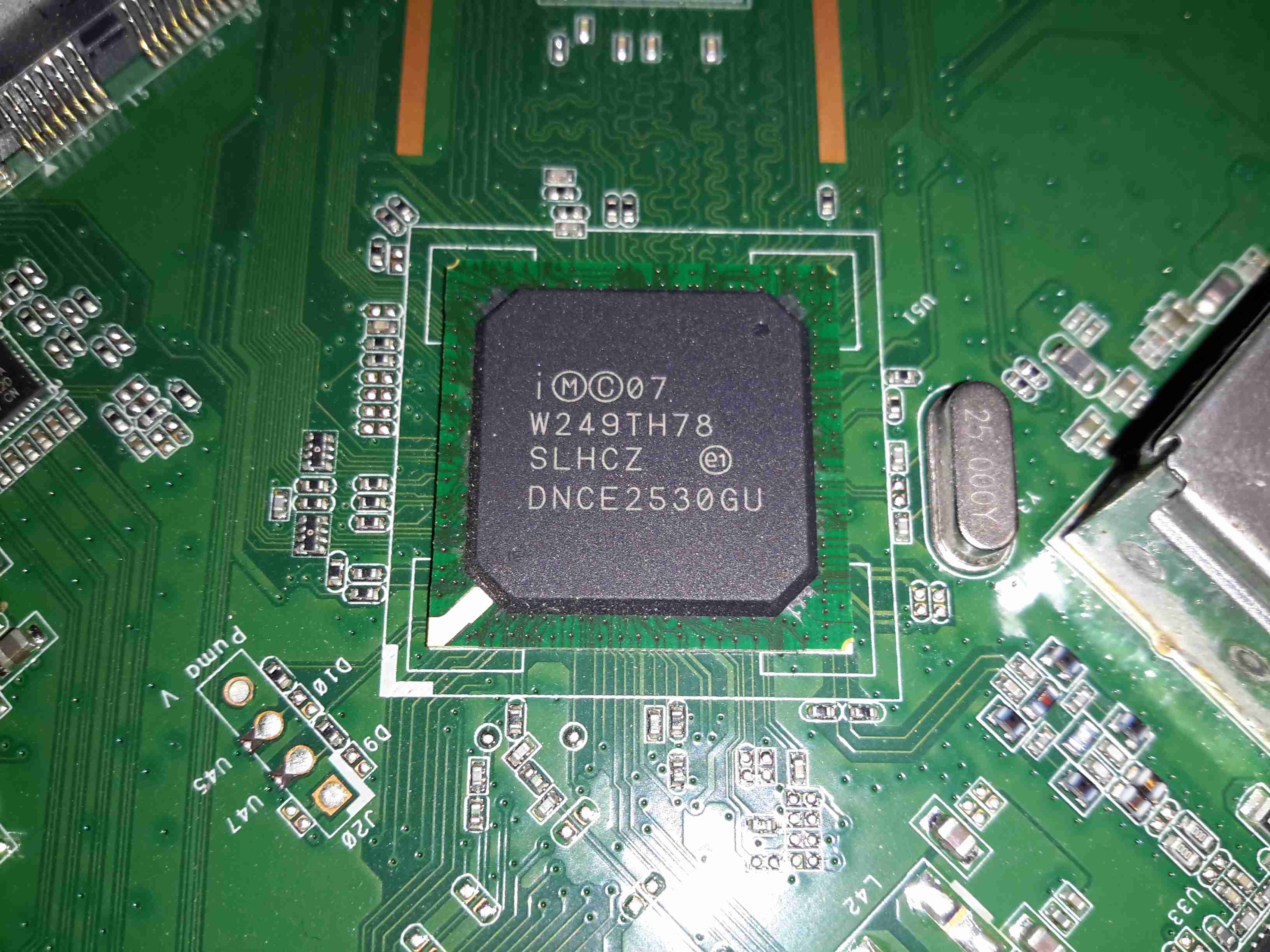
Intel Puma 5 CM CPU
The cable modem side of things is taken care of by the Intel PUMA 5 DNCE2530GU SoC. This appears to communicate with the rest of the system via the Ethernet switch & PCI Express for the 5GHz radio.
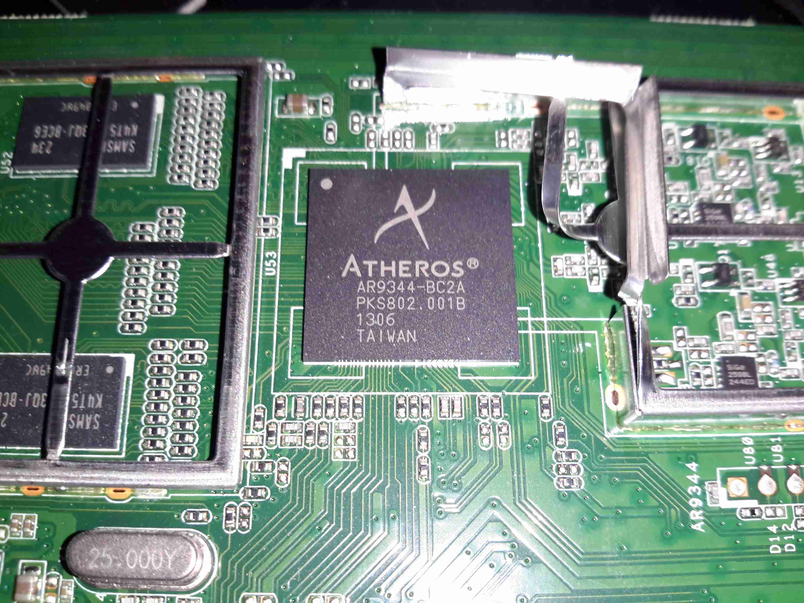
Atheros WiFi SoC
The 2.4GHz radio functionality is supplied by an Atheros AR9344 SoC, it’s RAM is to the left. This is probably handling all the router functions of this unit, but I can’t be certain.
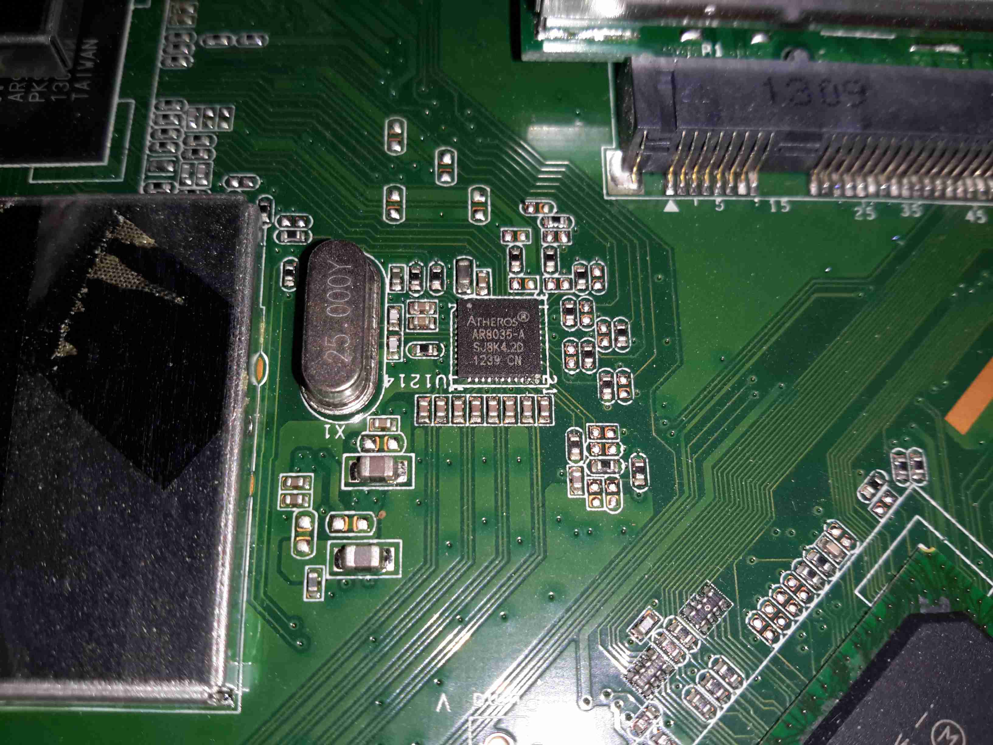
Atheros LAN PHY
A separate Ethernet PHY is located between the SoC & the switch IC.
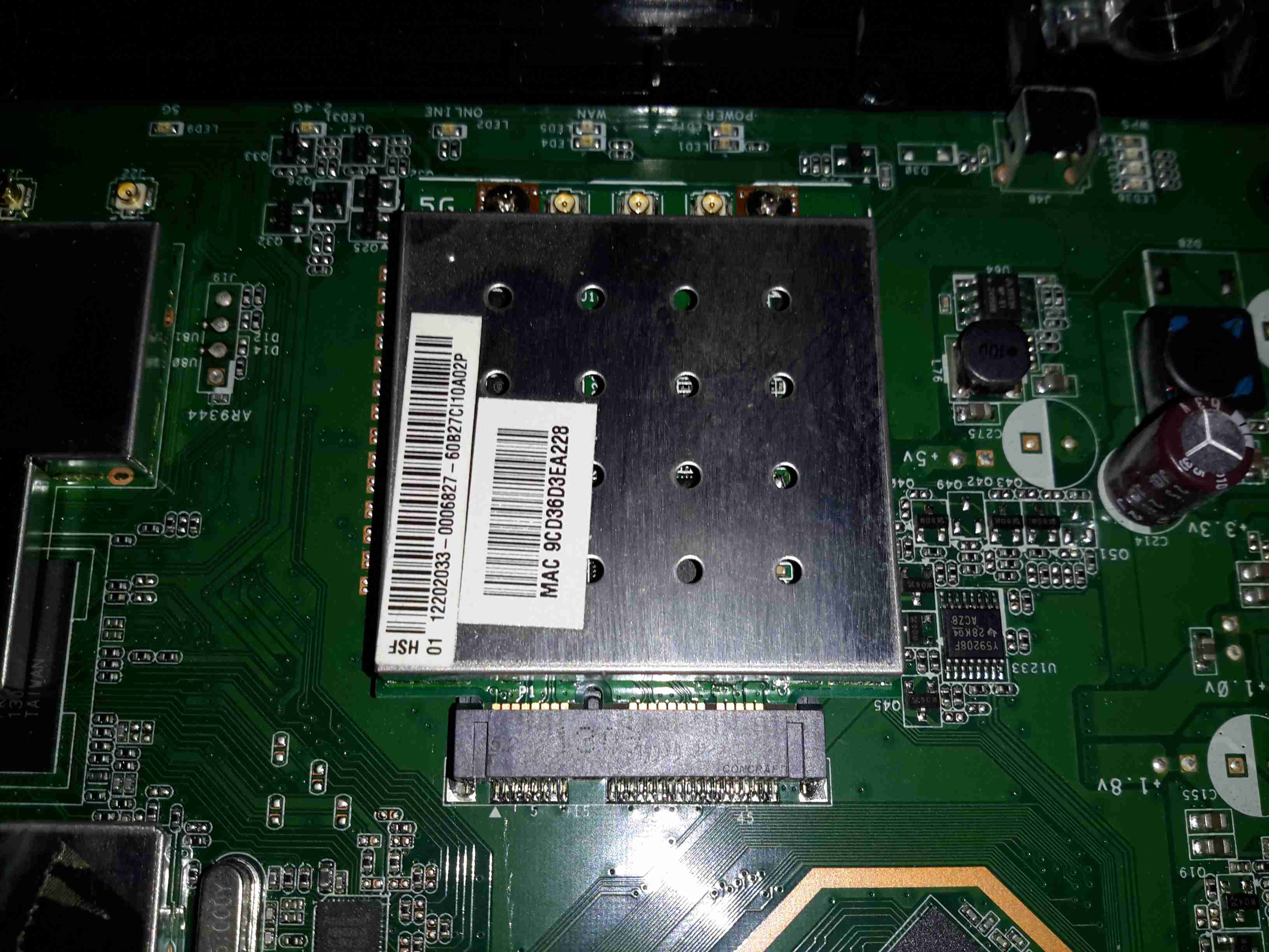
5GHz Radio Card
The 5GHz band is served by a totally separate radio module, in Mini PCIe format, although it’s a bit wider than standard. This module will probably be kept for reuse in another application.
Power Supplies
All down the edge of the board are the multiple DC-DC converters to generate the required voltage rails.
MaxLinear MXL261 Frontend
The DOCSIS frontend is handled by a MaxLinar MXL261 Tuner/Demodulator. More on this IC in my decapping post 🙂
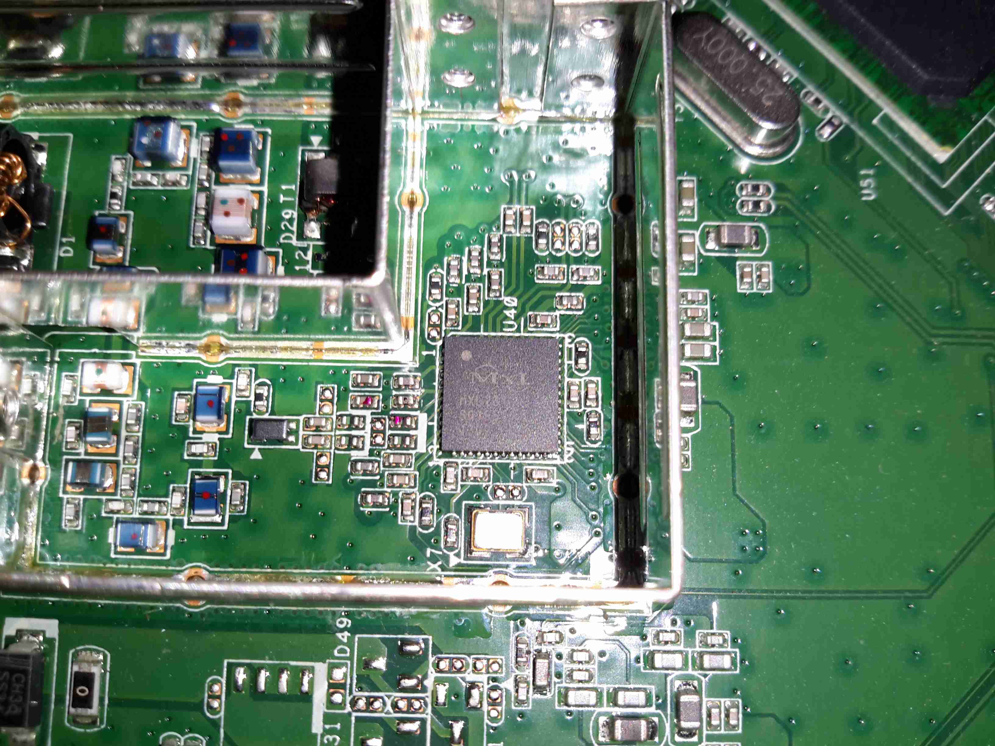
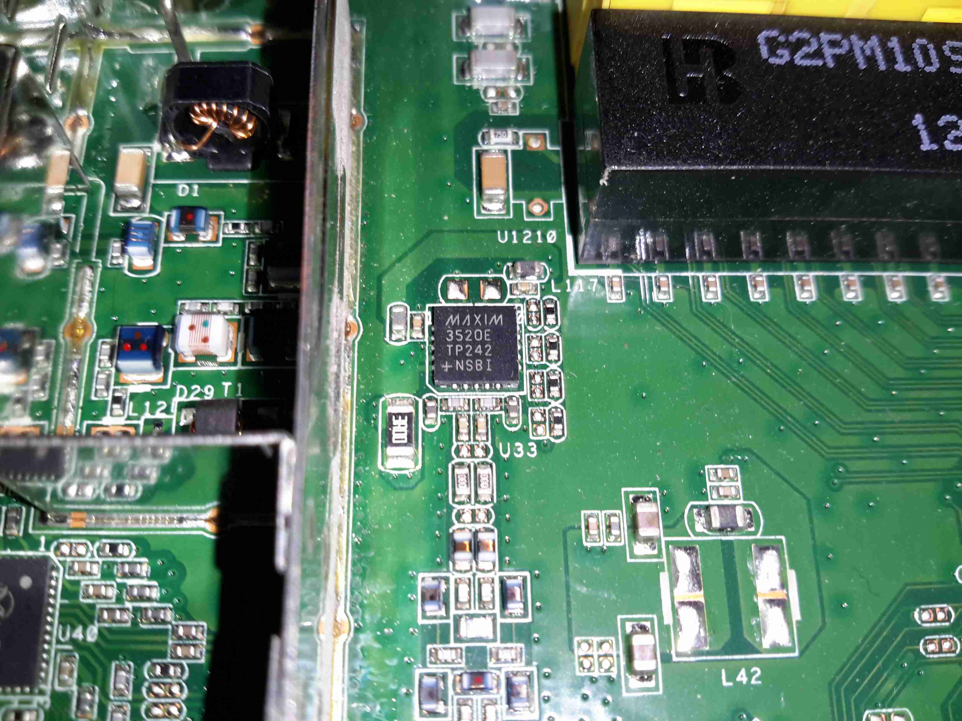
The Unknown One
I’ve honestly no idea what on earth this Maxim component is doing. It’s clearly connected via an impedance matched pair, and that track above the IC looks like an antenna, but nothing I search for brings up a workable part number.
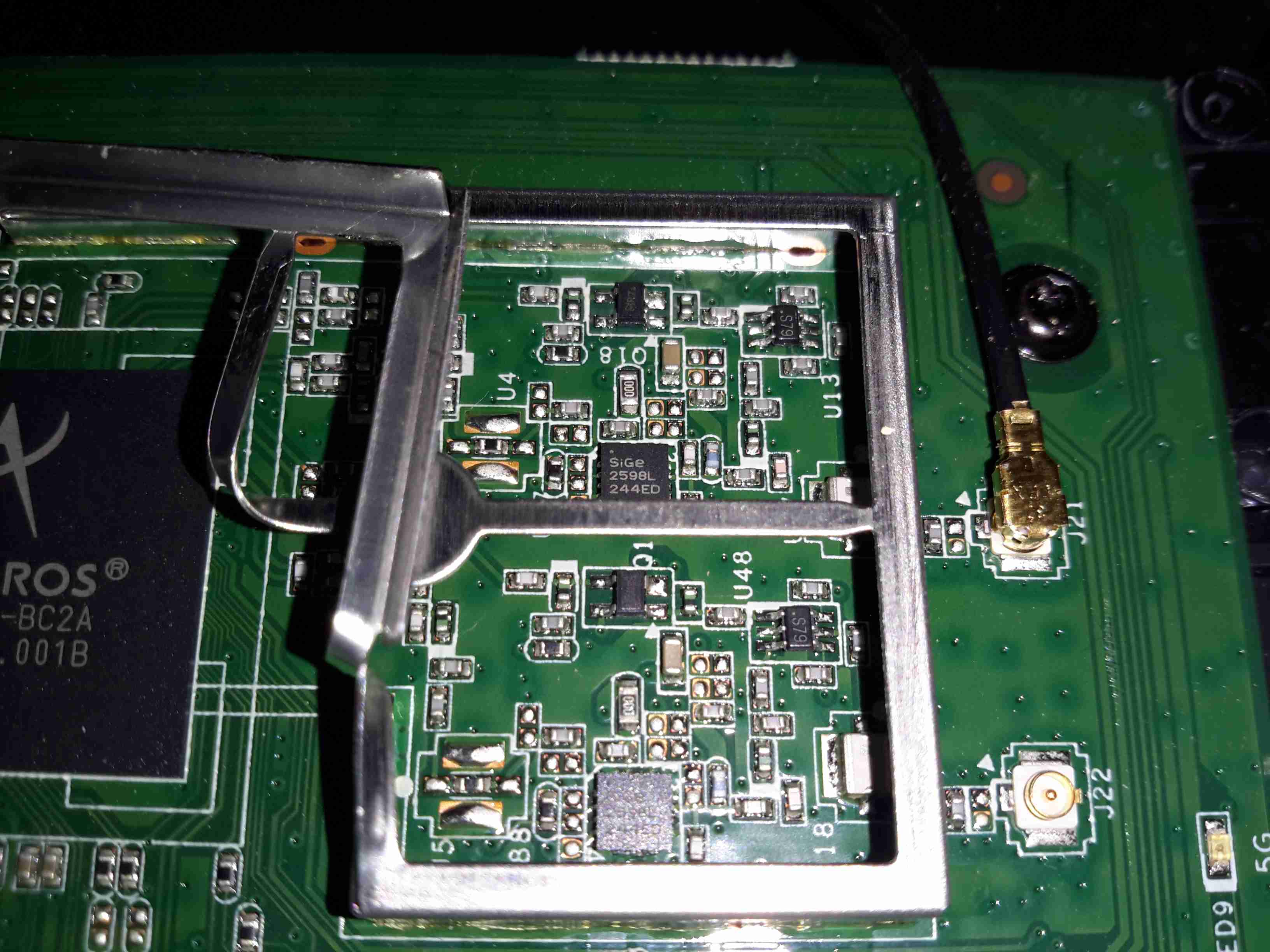
2.4GHz Frontend
The RF switching & TX amplifiers are under a shield, these PA chips are SiGe parts.
Atheros 5GHz Radio
Pretty much the same for the 5GHz radio, but with 3 radio channels.
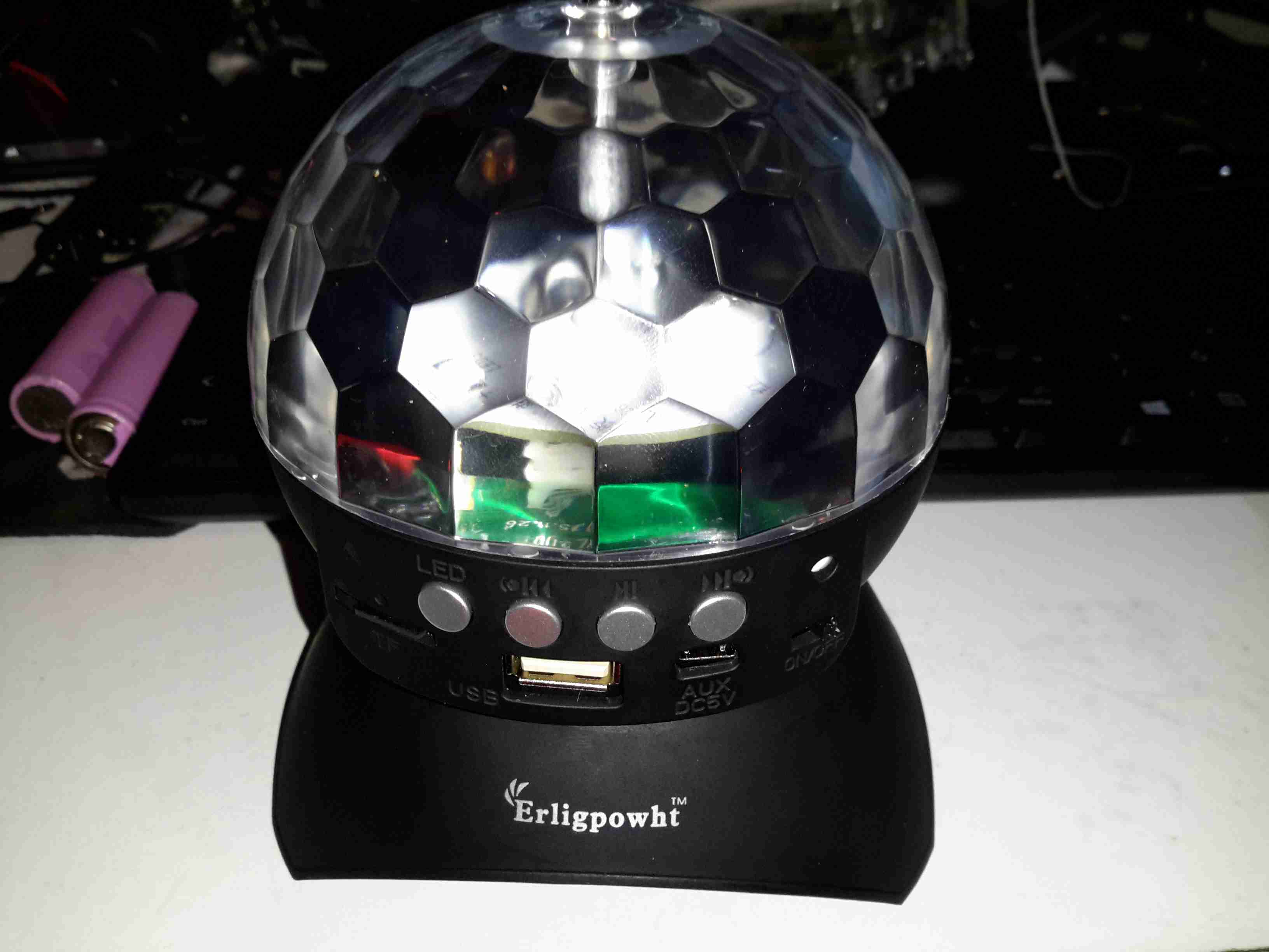
Here’s an eBay oddity – it’s got the same light & lens mechanism as the cheap “disco light” style bulbs on eBay, but this one is battery powered & has a built in MP3 player.
MP3 Disco Light
This device simply oozes cheapness. The large 4″ plastic dome lens sits on the top above the cheap plastic moulding as a base, which also contains the MP3 player speaker.
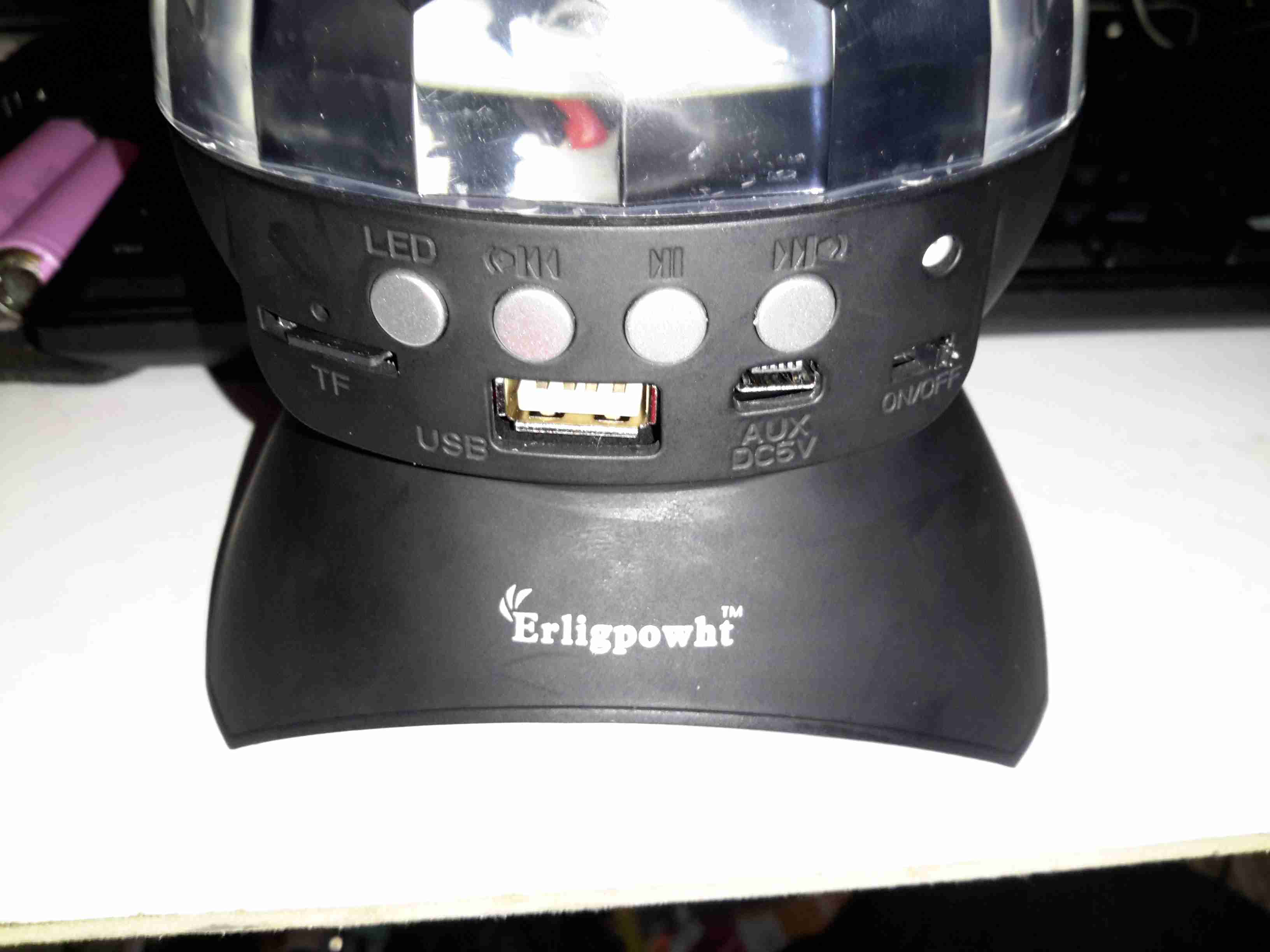
Controls
There are few controls on this player, the volume buttons are combined with the skip track buttons, a long press operates the volume control, while a short press skips the tracks. Several options for getting this thing to play music are provided:
Bluetooth – Allows connection from any device for bluetooth audio
USB – Plugging in a USB flash drive with MP3 files
SD Card – Very similar to the USB flash drive option, just a FAT32 formatted card with MP3 files
Aux – There’s no 3.5mm jack on this unit for an audio input, instead a “special” USB cable is supplied that is both used to charge the built in battery & feed an audio signal. This is possible since the data lines on the port aren’t used. But it’s certainly out of the ordinary.
Top Removed
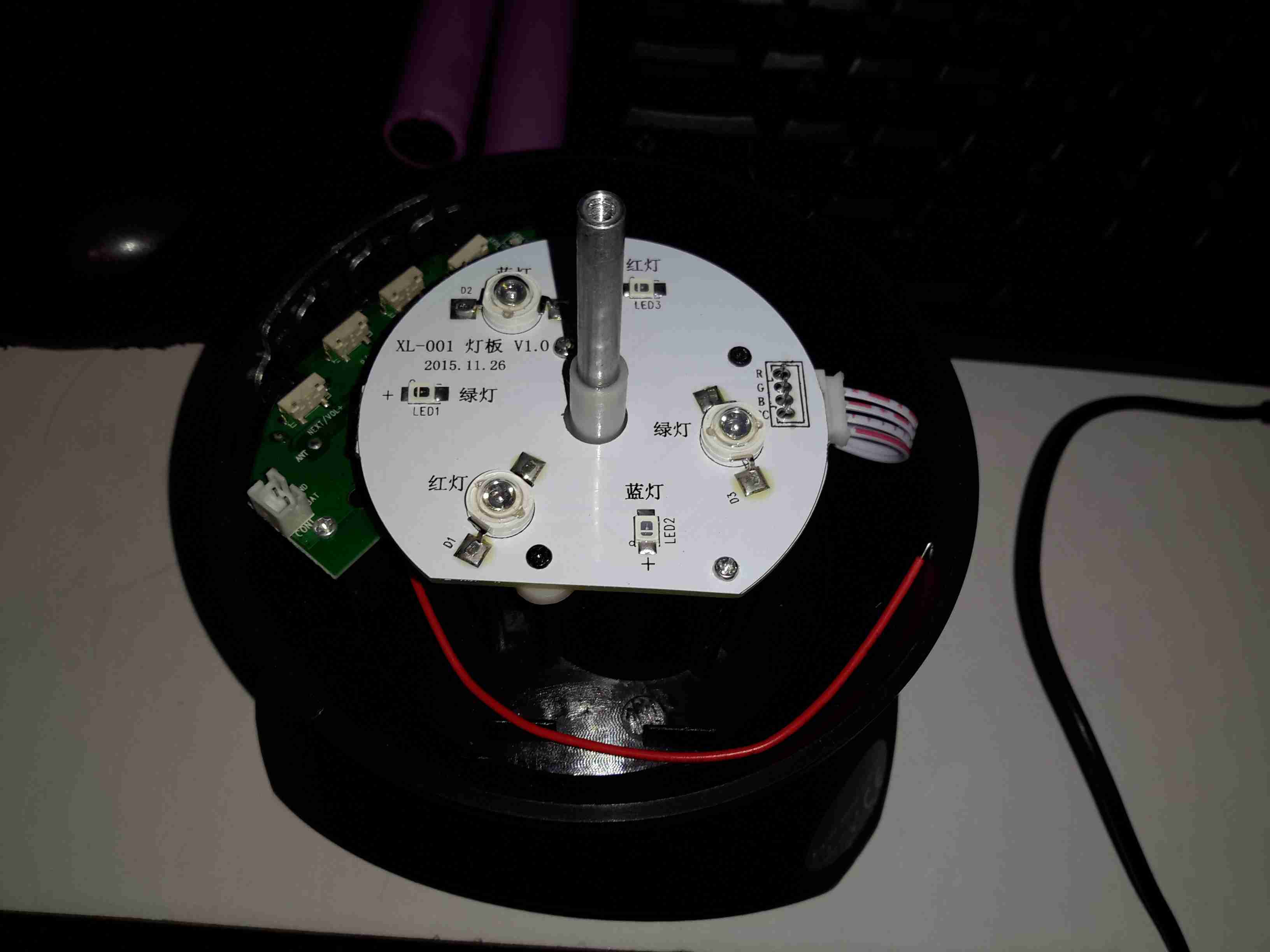
The top comes off with the removal of a single screw in the centre of the lens. The shaft in the centre that holds the lens is attached to a small gear motor under the LED PCB. There’s 6 LEDs on the board, to form an RGB array. Surprisingly for a very small battery powered unit these are bright to the point of being utterly offensive.
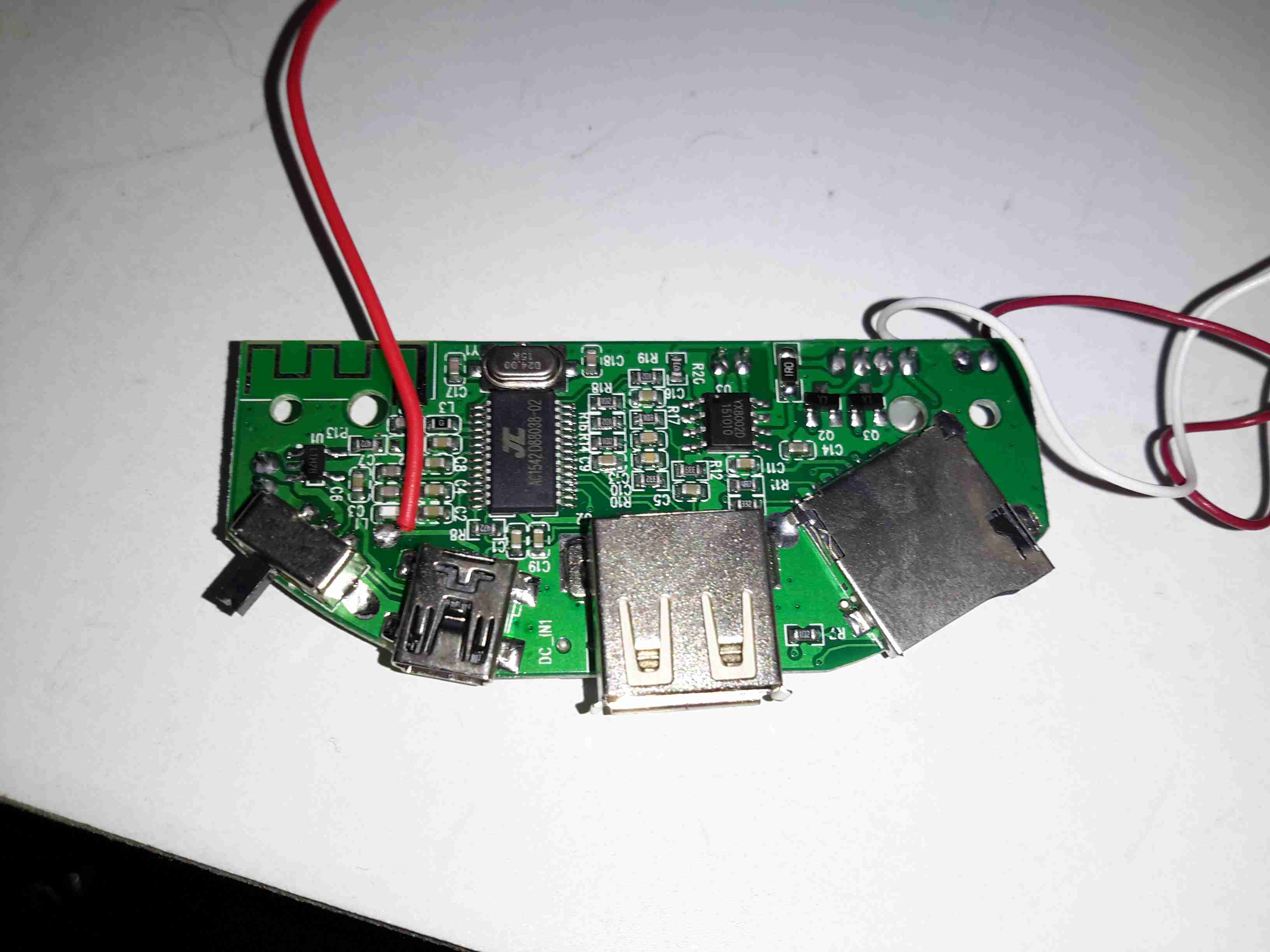
Mainboard
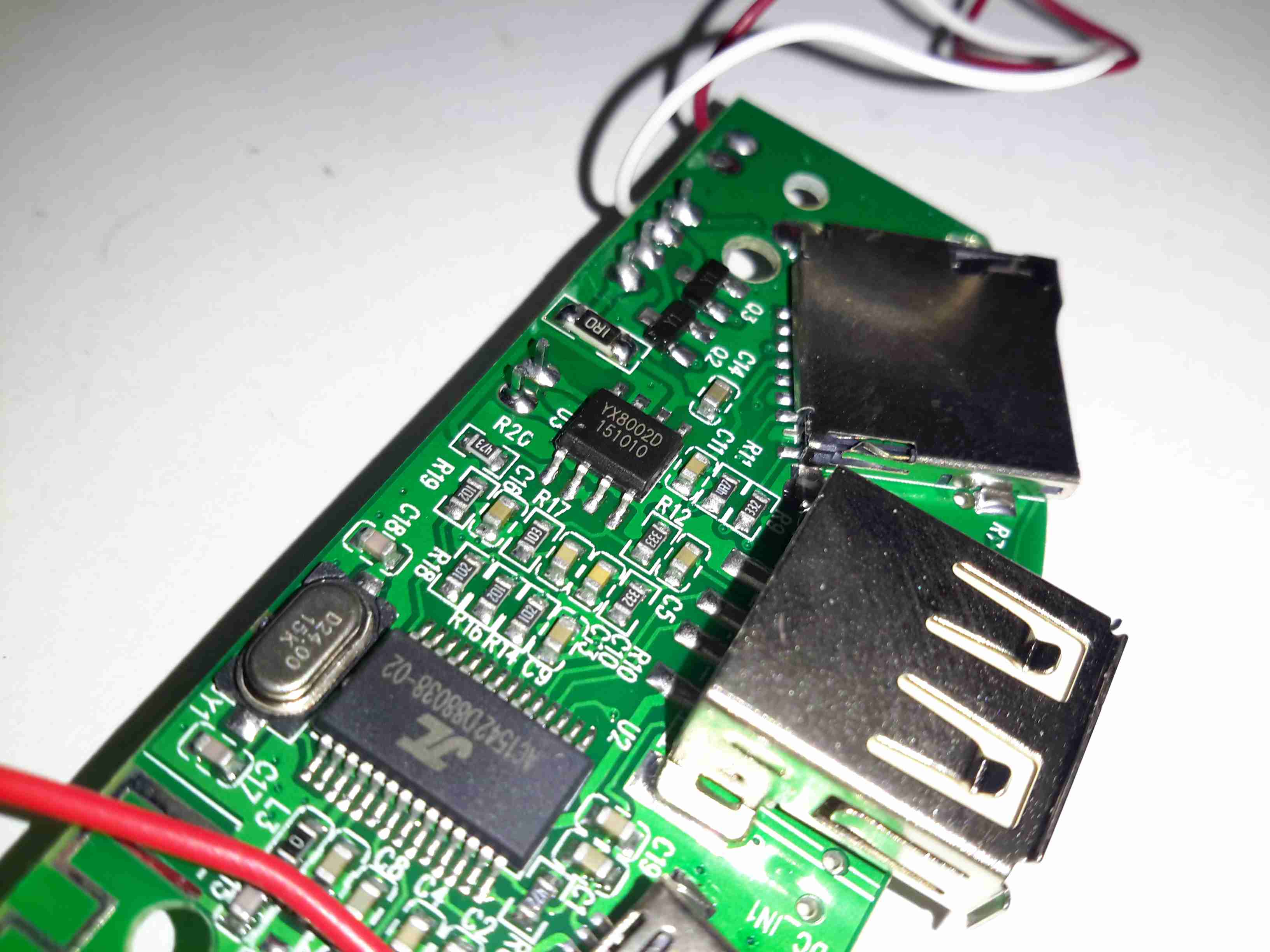
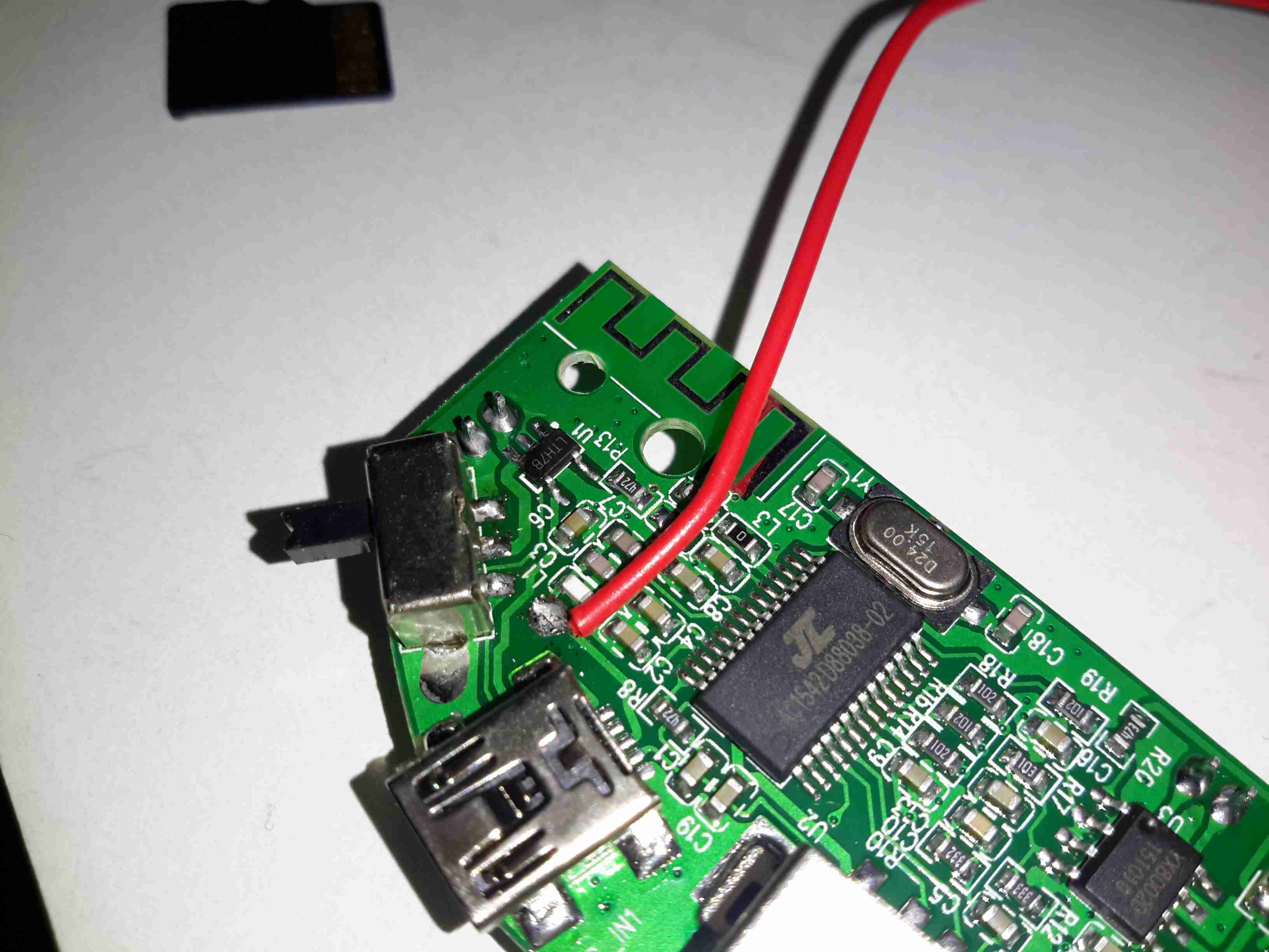
Here’s the mainboard removed from the plastic base. There’s not much to this device, even with all the options it has. The power switch is on the left, followed by the Mini-B USB charging port & aux audio input. The USB A port for a flash drive is next, finishing with the µSD slot. I’m not sure what the red wire is for on the left, it connects to one of the pins on the USB port & then goes nowhere.
Audio Amplifier
The audio amplifier is a YX8002D, I couldn’t find a datasheet for this, but it’s probably Class D.
Main Chipset
Finally there’s the main IC, which is an AC1542D88038. I’ve not been able to find any data on this part either, it’s either a dedicated MP3 player with Bluetooth radio built in, or an MCU of some kind.The RF antenna for the Bluetooth mode is at the top of the board.
Just behind the power switch is a SOT23-6 component, which should be the charger for the built in Lithium Ion cell.
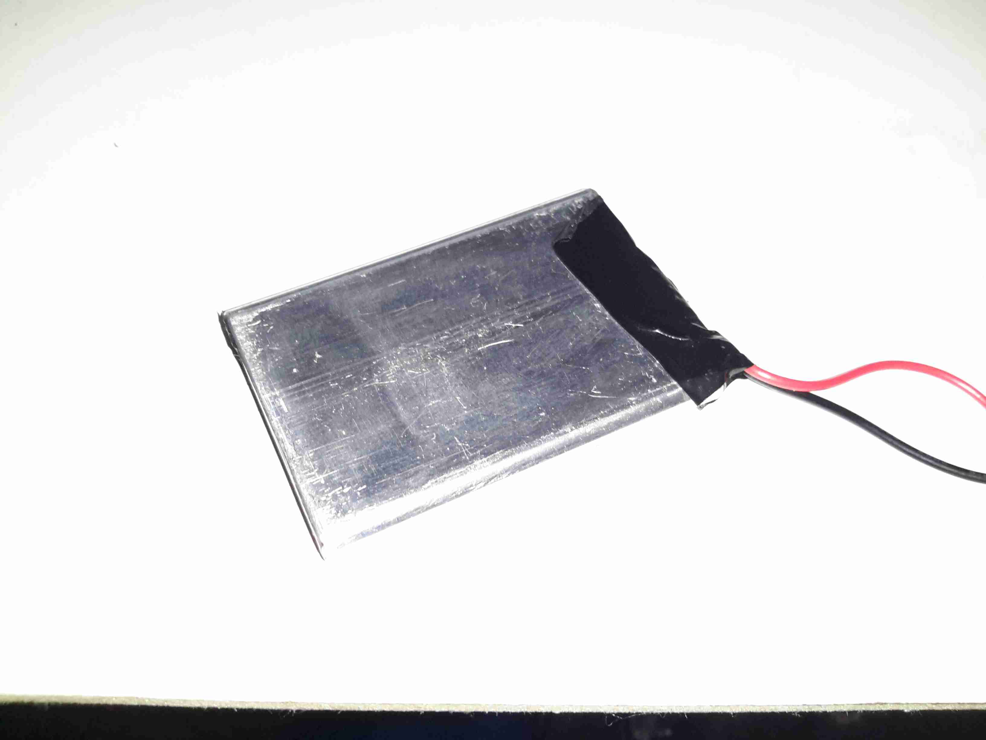
Lithium Ion Cell
The cell itself is a prismatic type rated in the instructions at 600mAh, however my 1C discharge test gave a reading of 820mAh, which is unusual for anything Li-Ion based that comes from eBay 😉
There is cell protection provided, it’s under the black tape on the end, nothing special here.
The main issue so far with this little player is the utterly abysmal battery life – at full volume playing MP3s from a SD card, the unit’s current draw is 600mA, with the seizure & blindness-inducing LEDs added on top, the draw goes up to about 1200mA. The built in charger is also not able to keep up with running the player while charging. This in all only gives a battery life of about 20 minutes, which really limits the usability of the player.
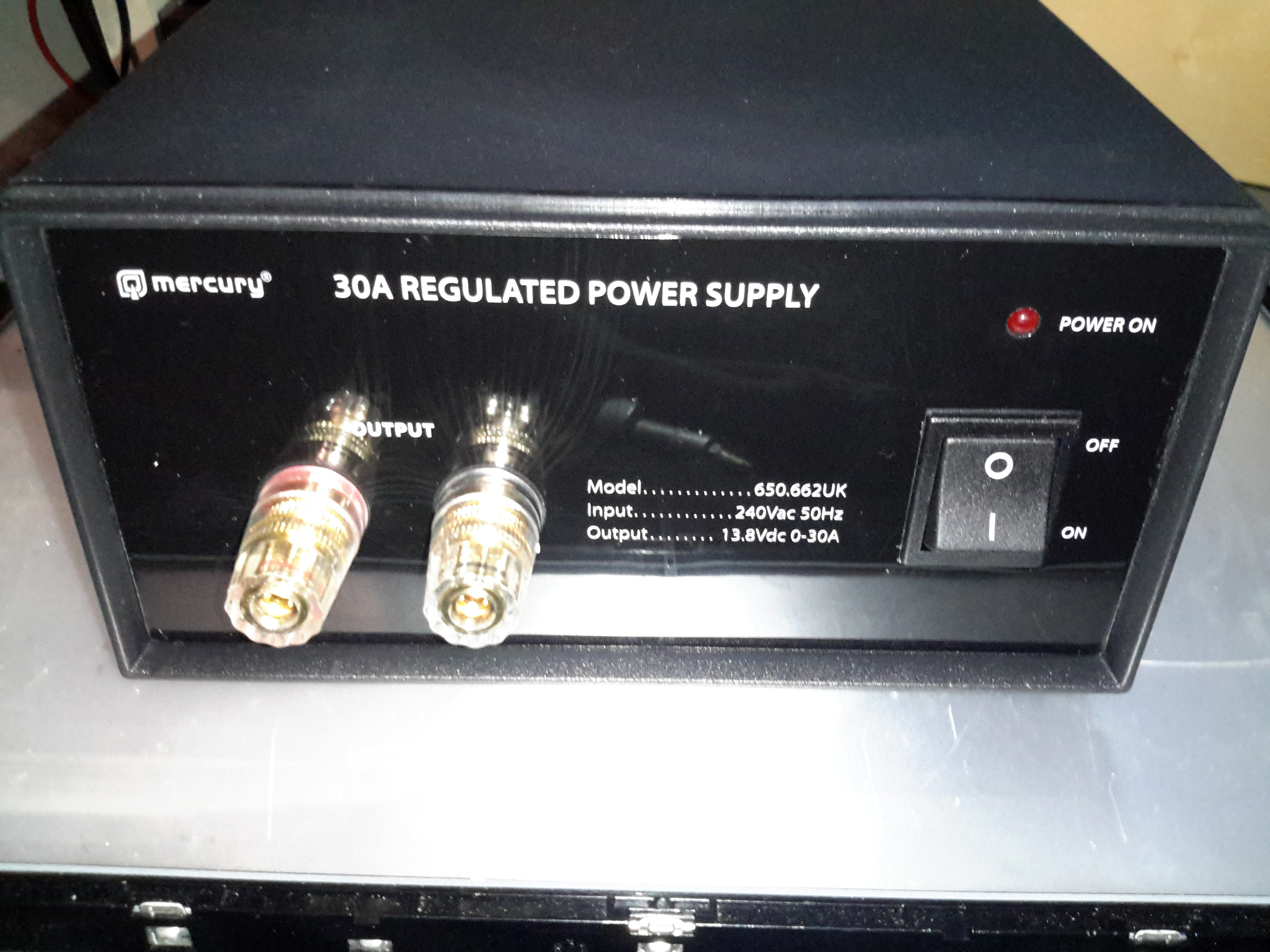
After having a couple of the cheap Chinese PSUs fail on me in a rather spectacular fashion, I decided to splash on a more expensive name-brand PSU, since constantly replacing PSUs at £15 a piece is going to get old pretty fast. This is the 30A model from Mercury, which seems to be pretty well built. It’s also significantly more expensive at £80. Power output is via the beefy binding posts on the front panel. There isn’t any metering on board, this is something I’ll probably change once I’ve ascertained it’s reliability. This is also a fixed voltage supply, at 13.8v.
Rear Panel
Not much on the rear panel, just the fuse & cooling fan. This isn’t temperature controlled, but it’s not loud. No IEC power socket here, the mains cable is hard wired.
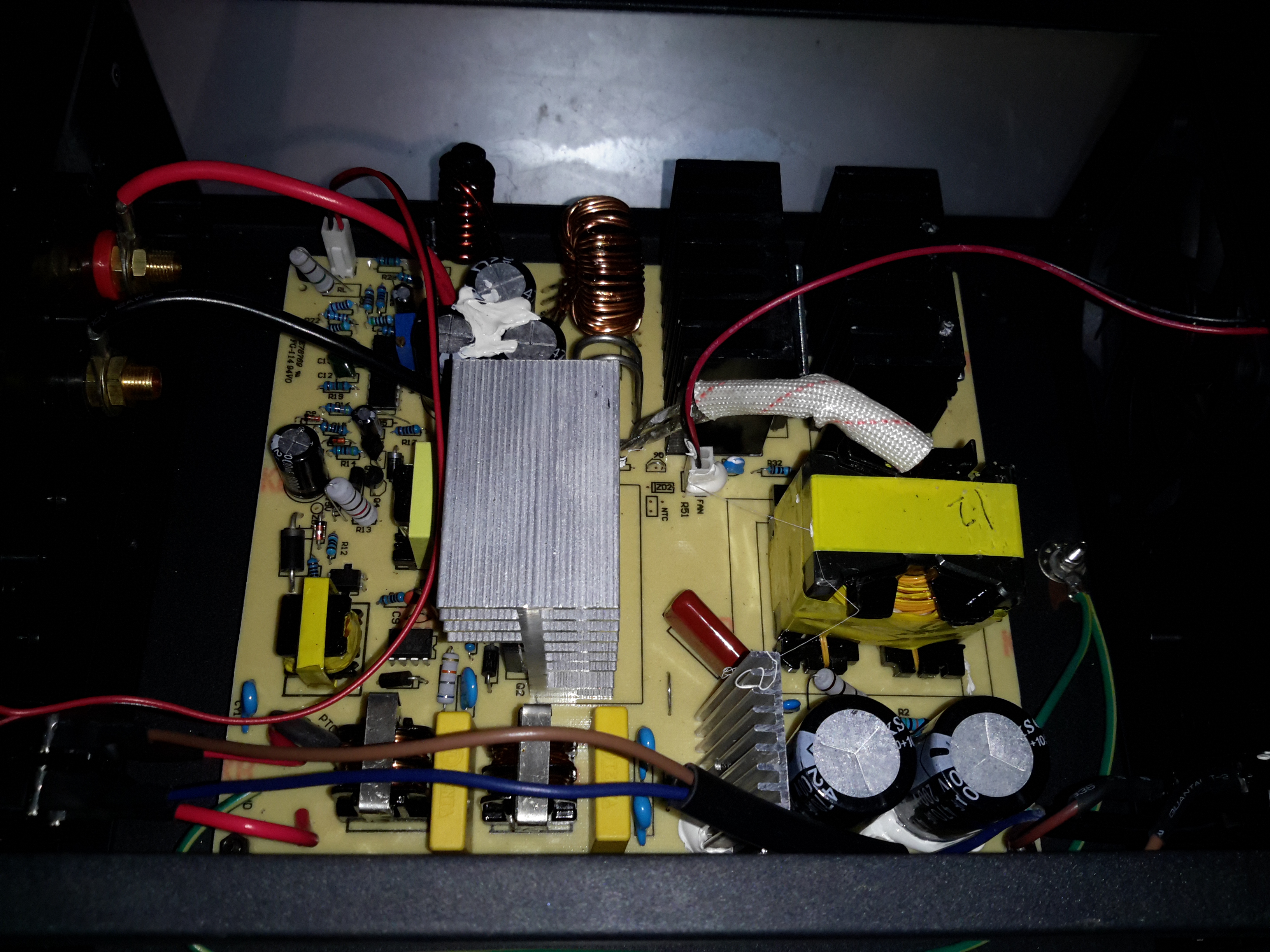
Main Board
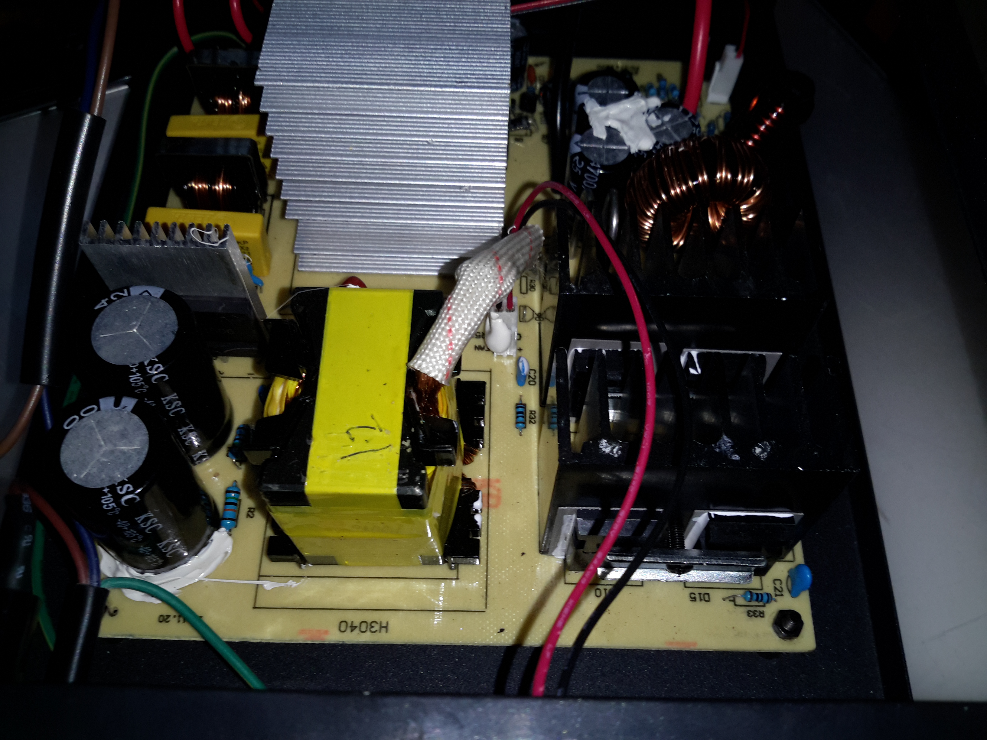
Removing some spanner-type security screws reveals the power supply board itself. Everything on here is enormous to handle the 30A output current at 13.8v. The main primary side switching transistors are on the large silver heatsink in the centre of the board, feeding the huge ferrite transformer on the right.
Transformer
The transformer’s low voltage output tap comes straight out instead of being on pins, due to the size of the winding cores. Four massive diodes are mounted on the black heatsinks for output rectification.
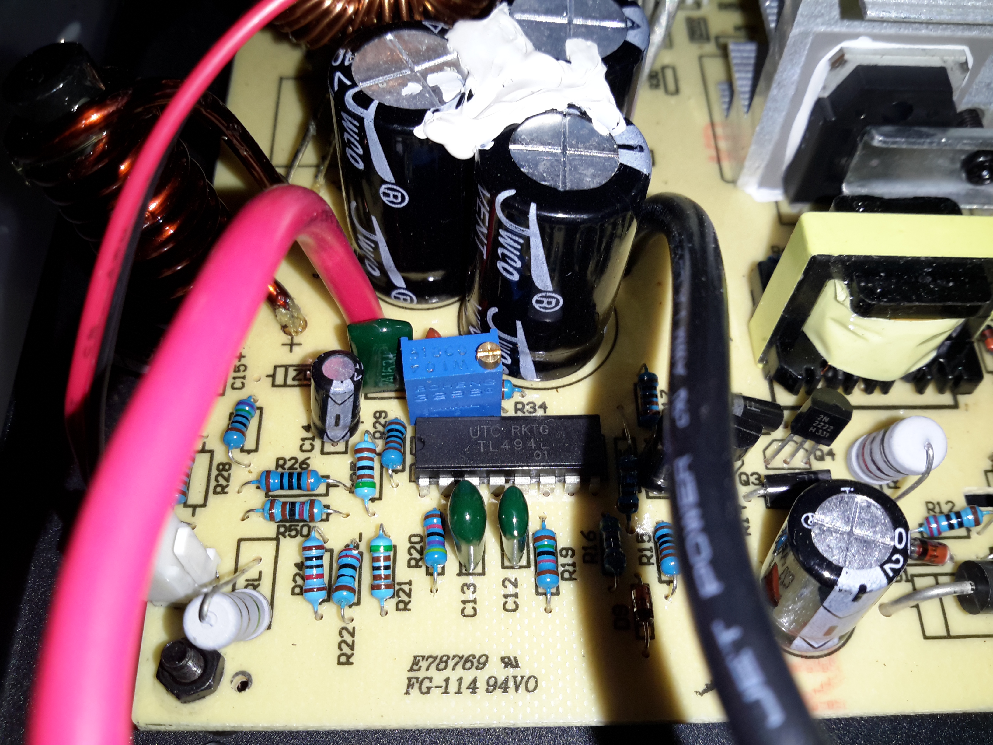
SMPS Controller
The supply is controlled via the jelly bean TL494 PWM controller IC. The multi-turn potentiometer doesn’t adjust the output voltage, more likely it adjusts the current limit.
Standby Supply
Power to initially start the supply is provided by a small SMPS circuit, with a VIPer22A Low Power Primary Switcher & small transformer on the lower right. The transformer upper left is the base drive transformer for the main high power supply.
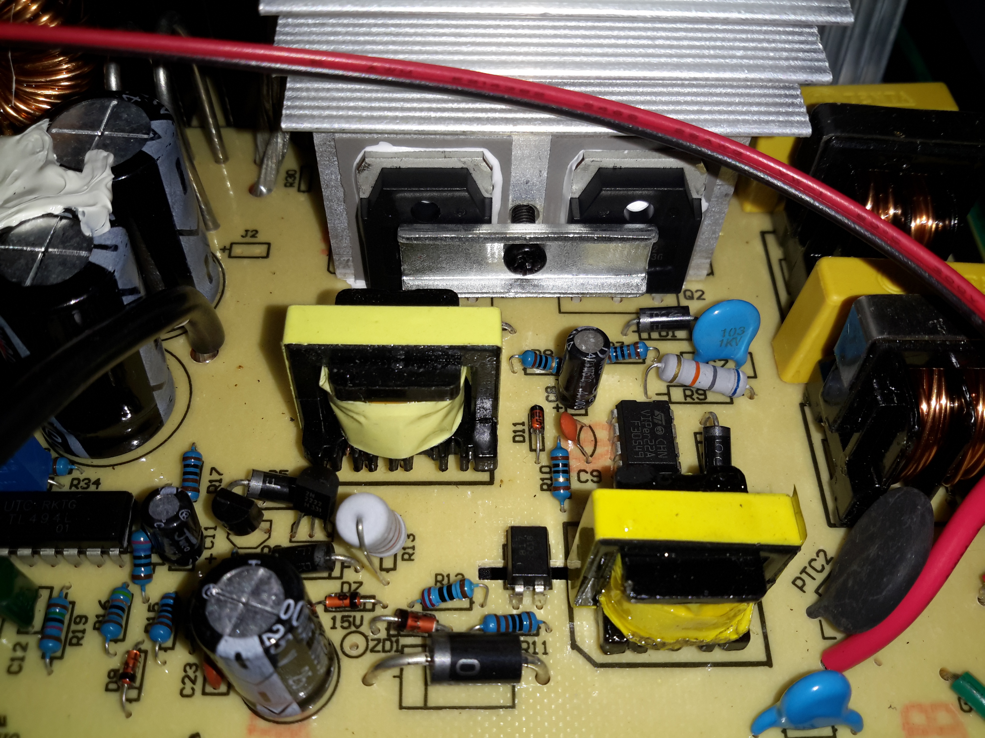
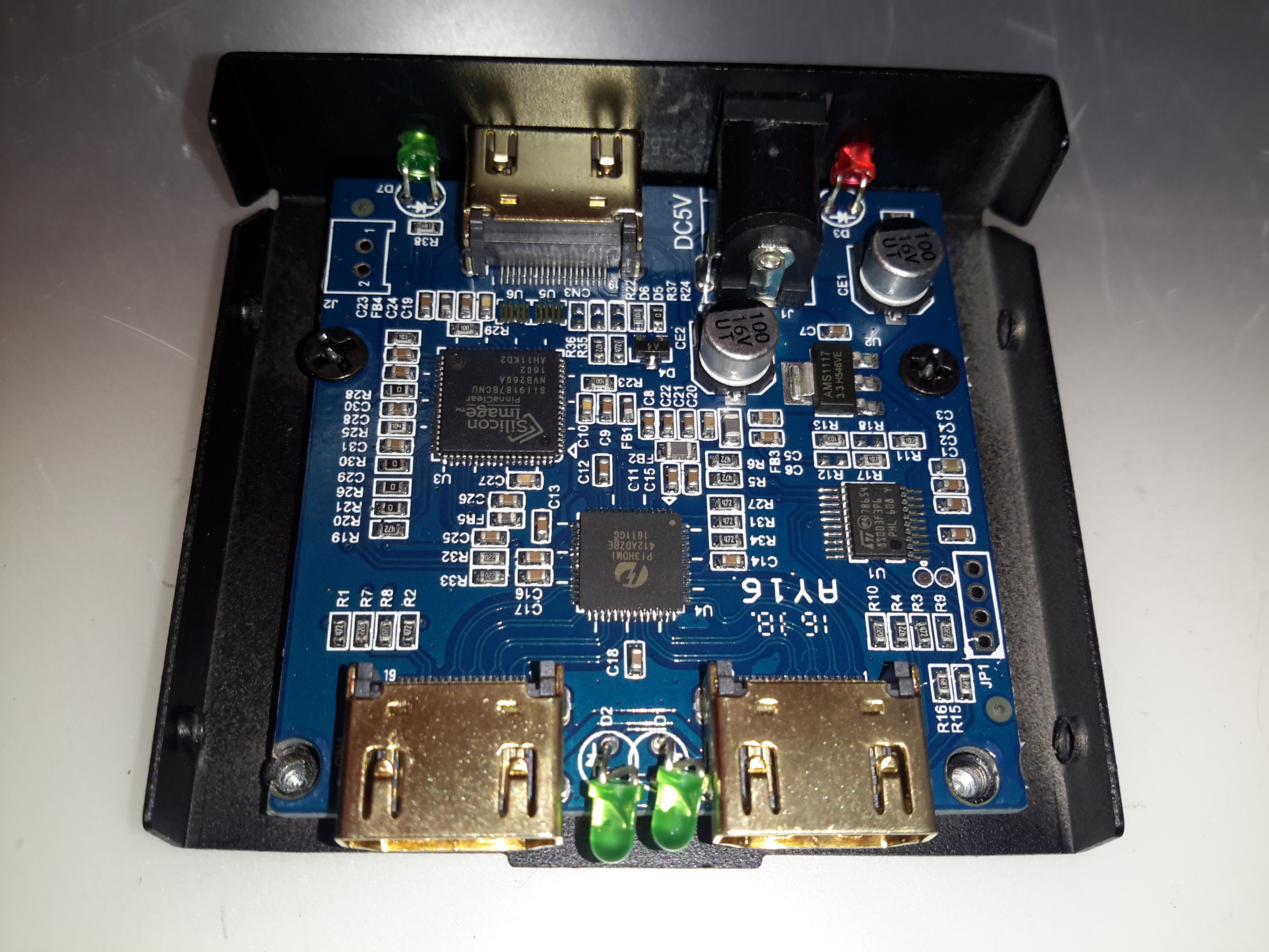
Time for another random teardown, a signal splitter for HDMI. These units are available very cheap these days on eBay. This one splits the incoming signal into two to drive more than one display from the same signal source.
Main PCB
The stamped alloy casing comes apart easily with the removal of a few screws. The PCB inside is rather densely packed with components.
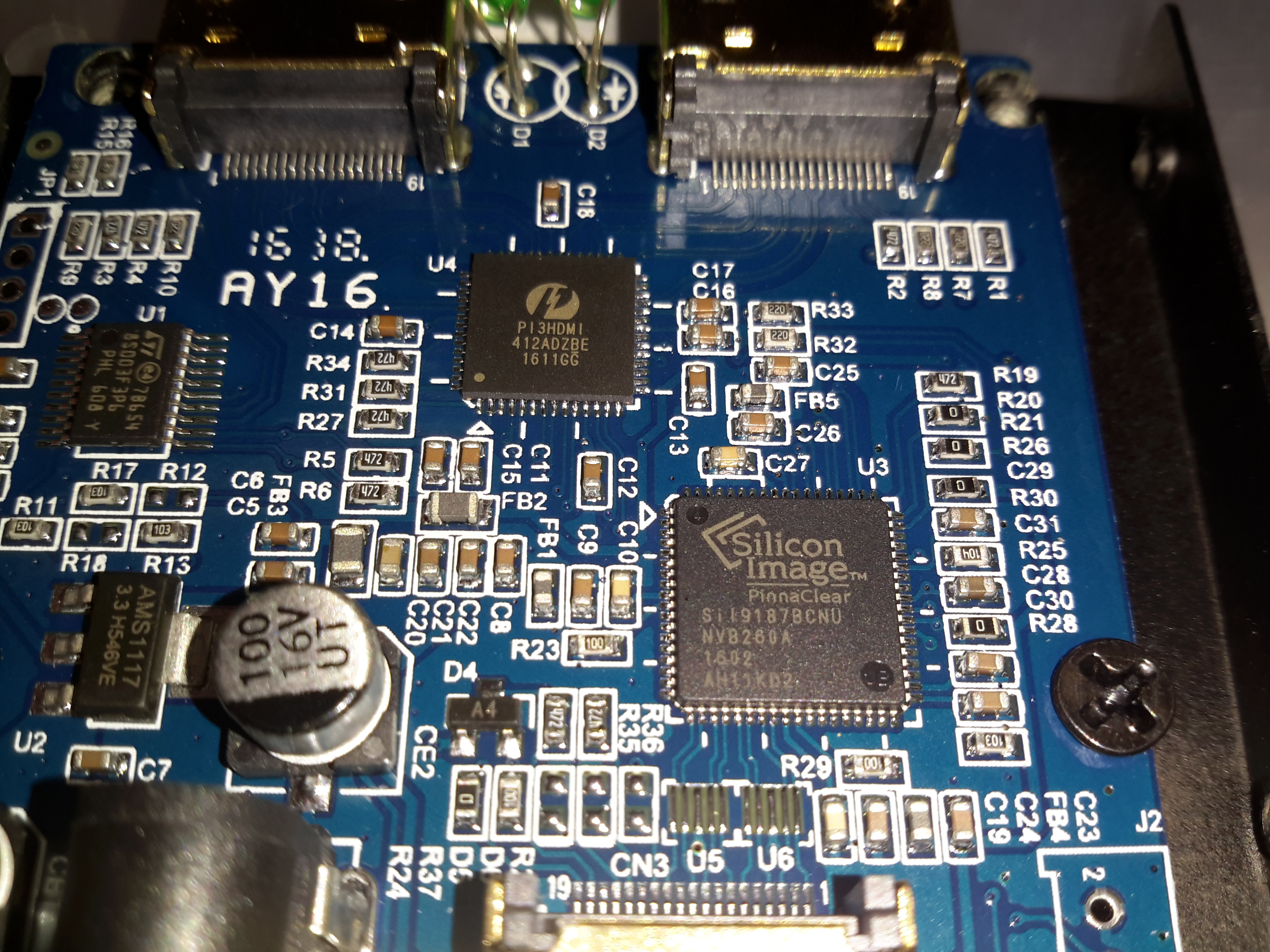
Chipset
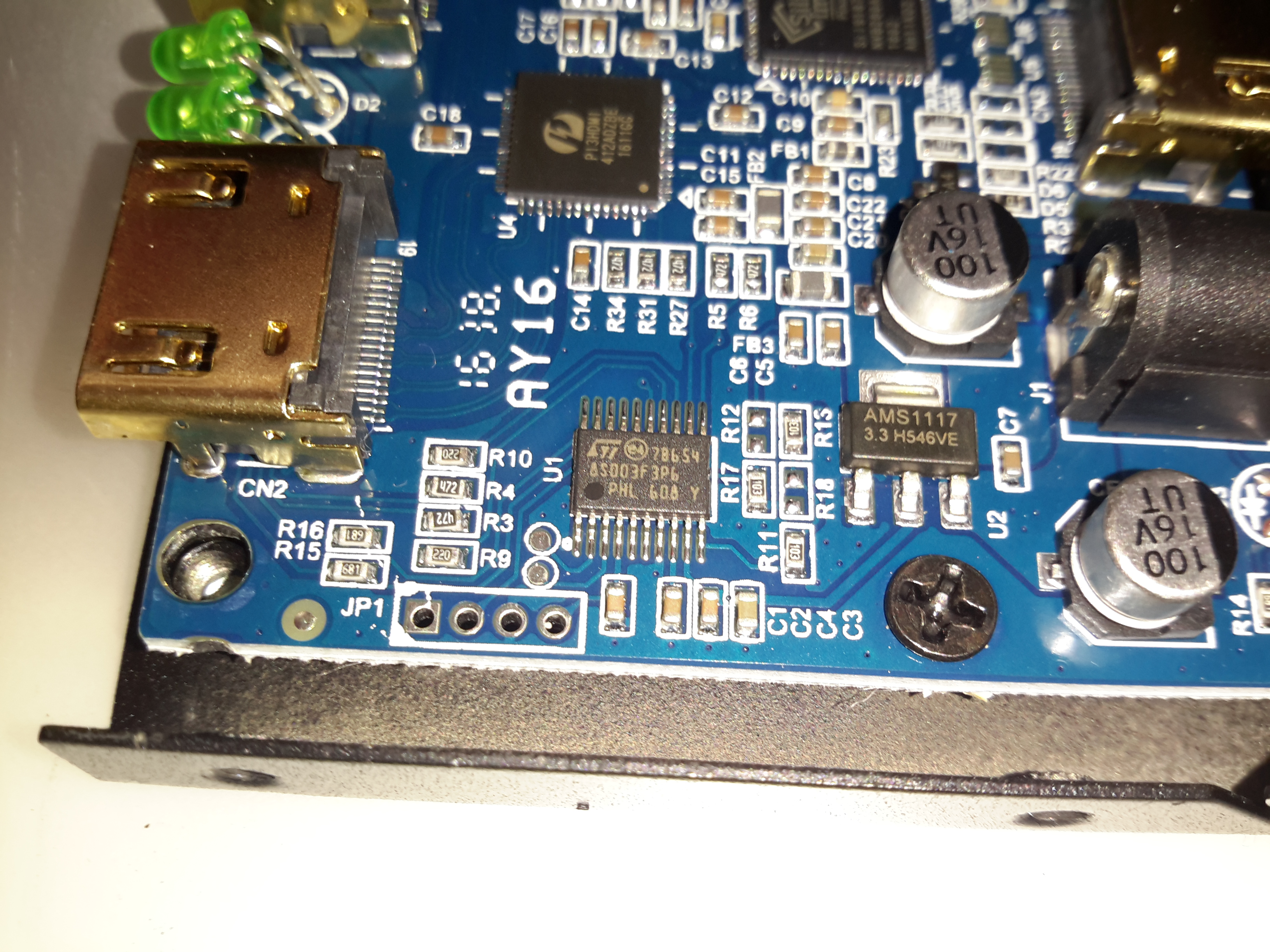
The main IC on the incoming signal is a Silicon Image Sil9187B HDMI Port Processor, with a single input & 4 outputs. In this case the chip is used as a repeater to amplify the incoming signal. the signal path then gets fed into a Pericom PI3HDMI412 HDMI Demux, which then splits the signal into two for the output ports.
Microcontroller
The main pair of ICs processing the video signals are controlled over I²C, with this STM32 microcontroller. The 4 pads to the lower left are for the STLink programmer. The main 3.3v power rail is provided by the LM1117 linear regulator on the right.
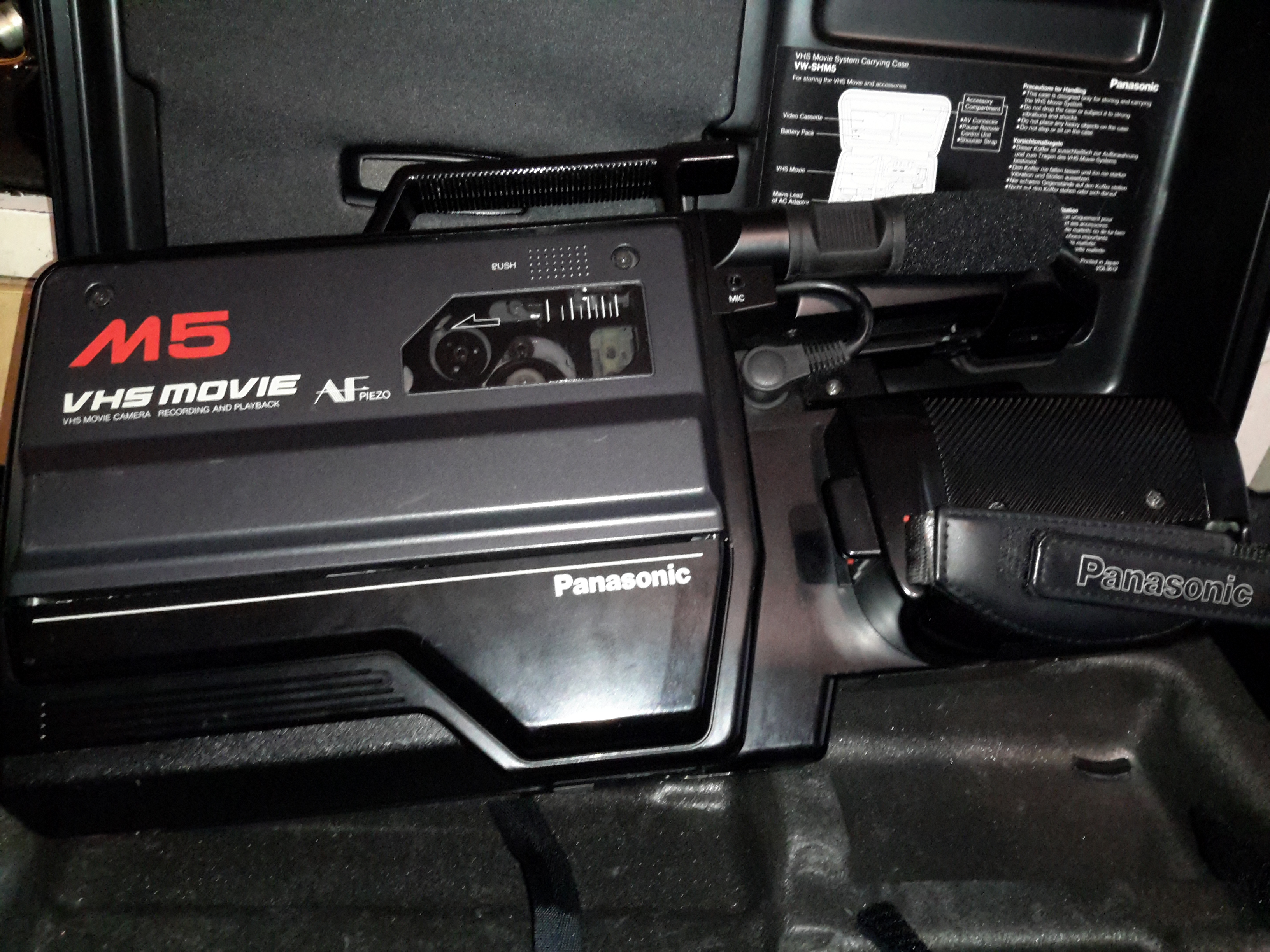
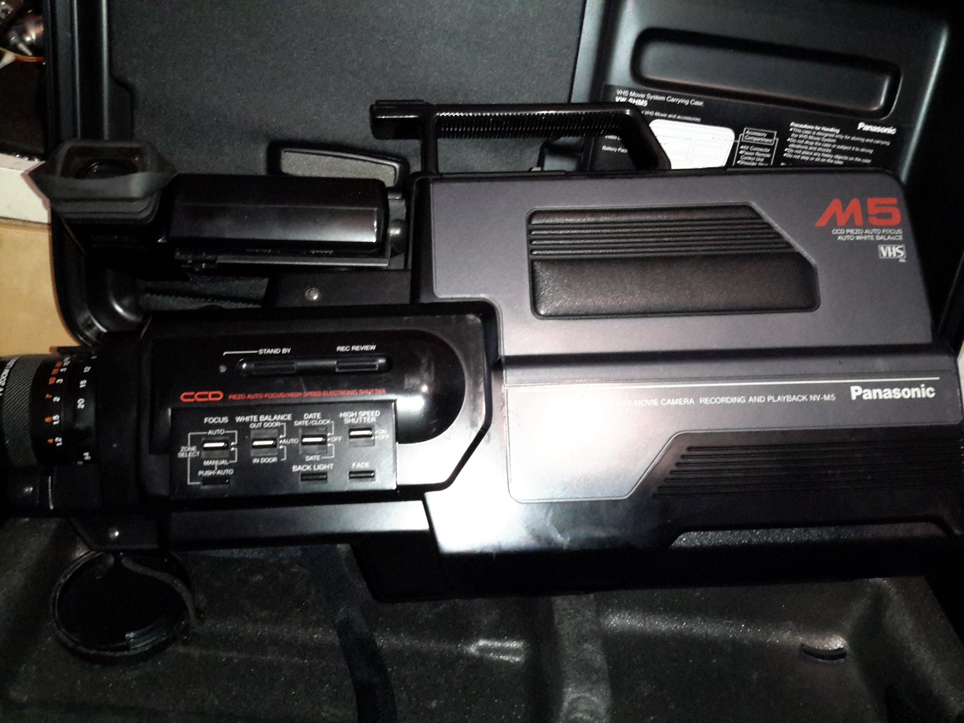
Time foe some more retro tech! This is a 1980’s vintage CCD-based VHS camcorder from Panasonic, the NV-M5. There are a lot of parts to one of these (unlike modern cameras), so I’ll split this post into several sections to make things easier to read (and easier to keep track of what I’m talking about :)).
Left Side
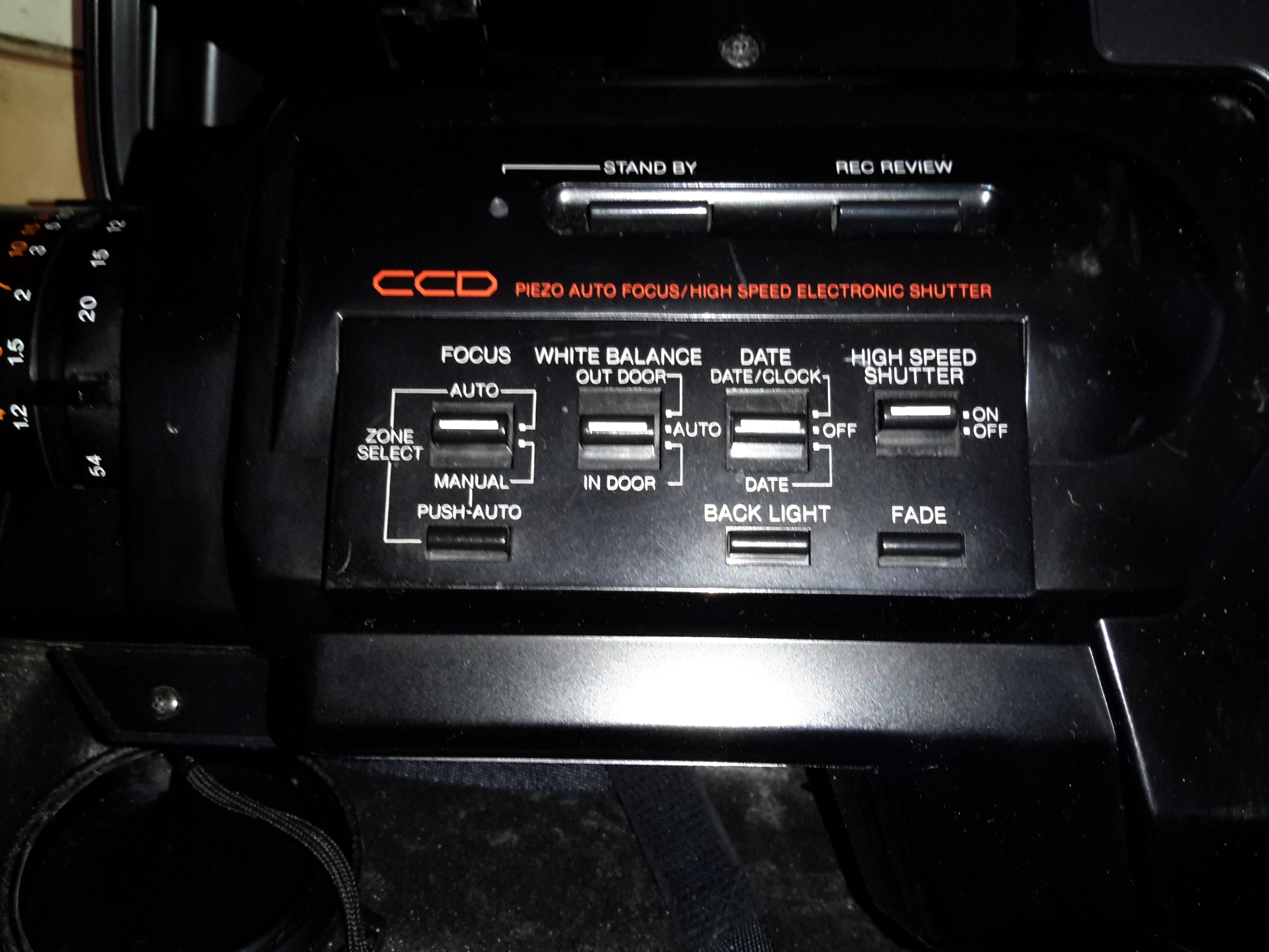
The left side of the camera holds the autofocus, white balance, shutter speed & date controls.
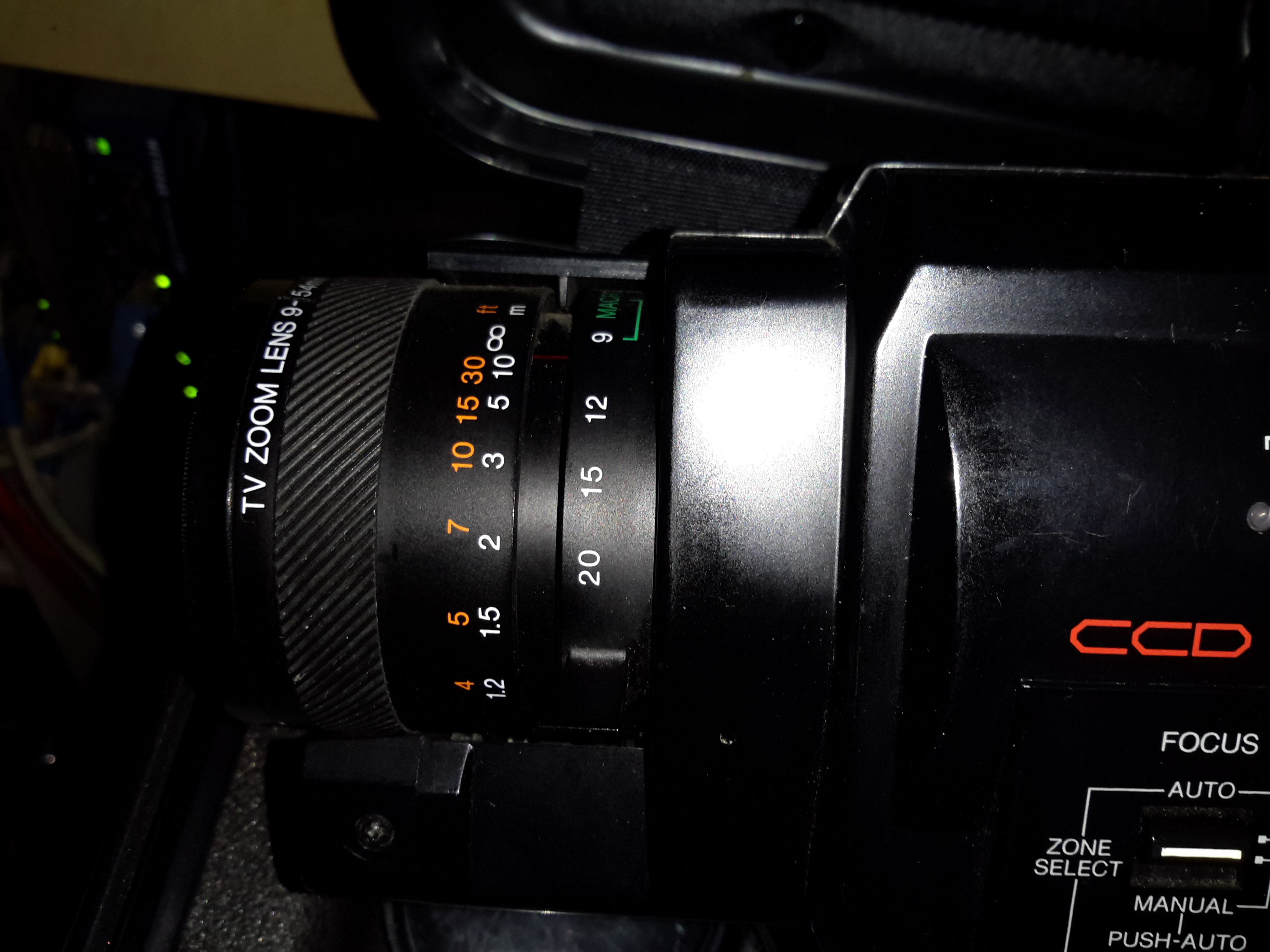
Left Side ControlsLens Adjustments
The lens is fully adjustable, with either manual or motorized automatic control.
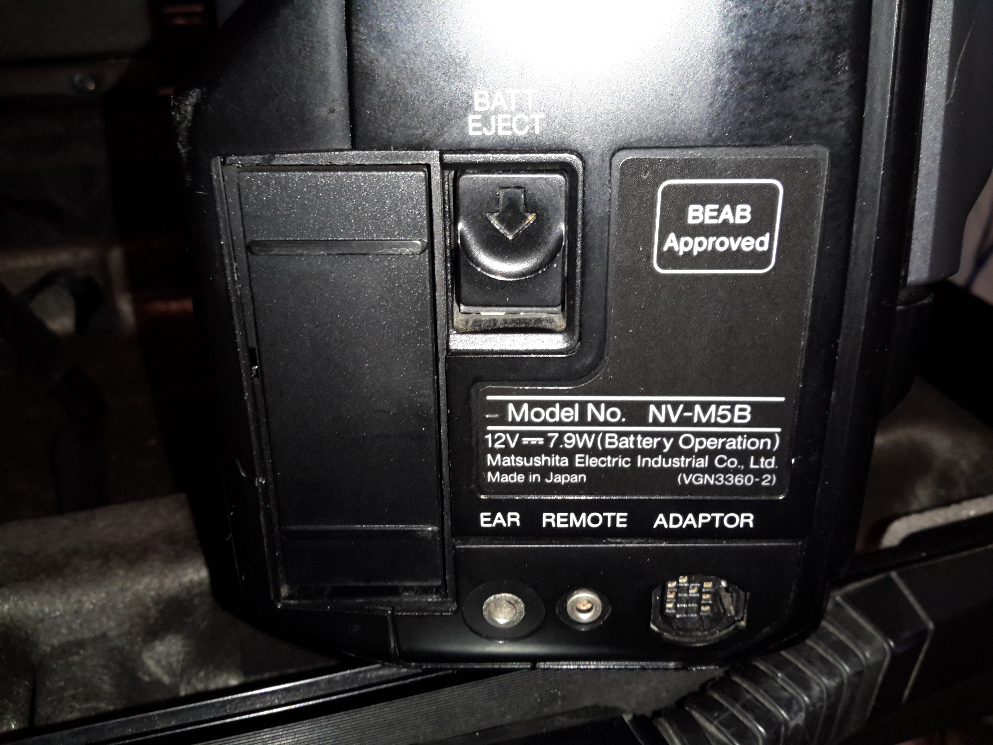
Rear Panel
The back panel has the battery slot, a very strange looking DC input connector, remote control connector & the earphone jack.
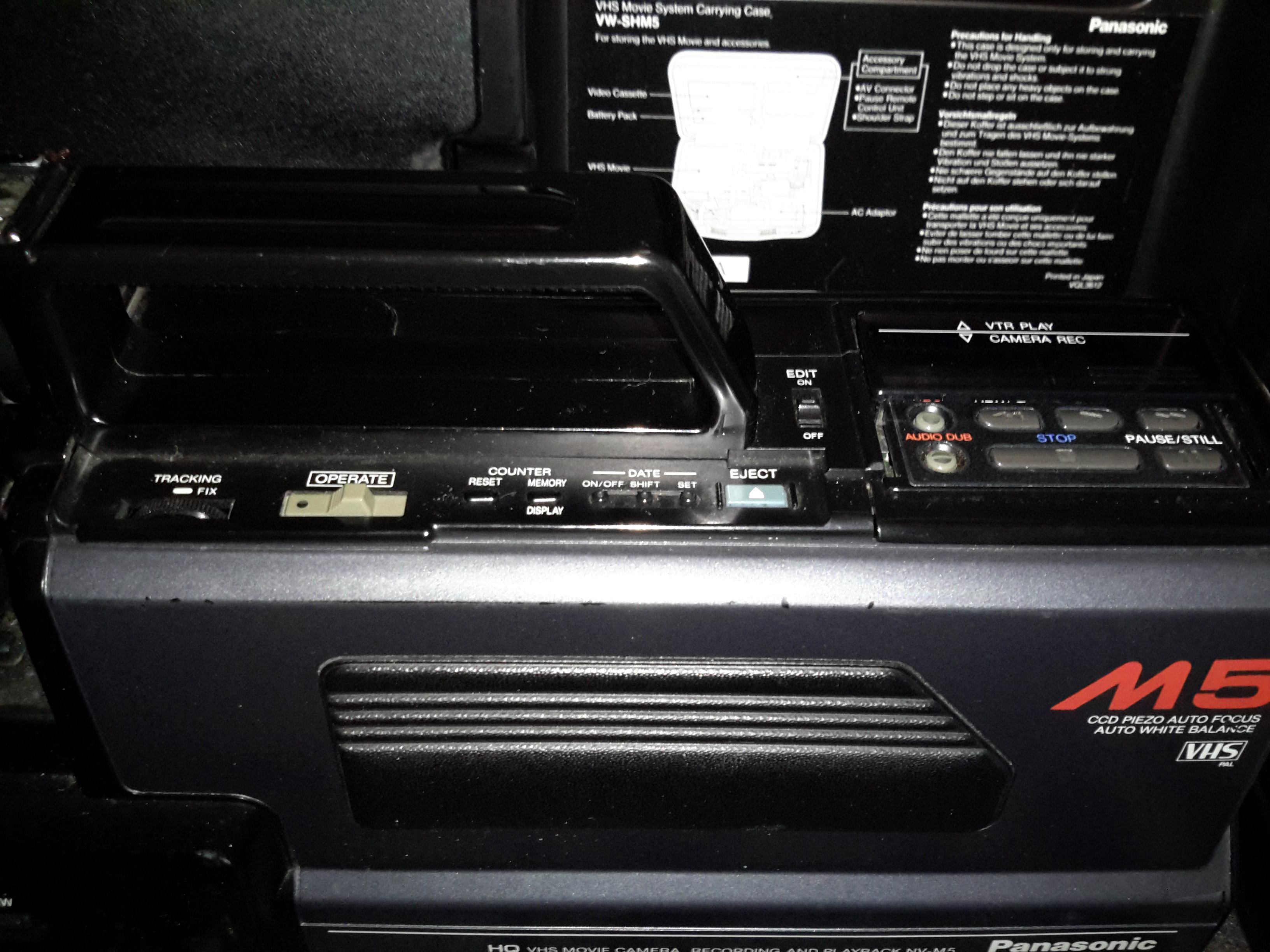
Top Controls
The top panel of the camera holds the main power controls, manual tape tracking & the tape transport control panel.
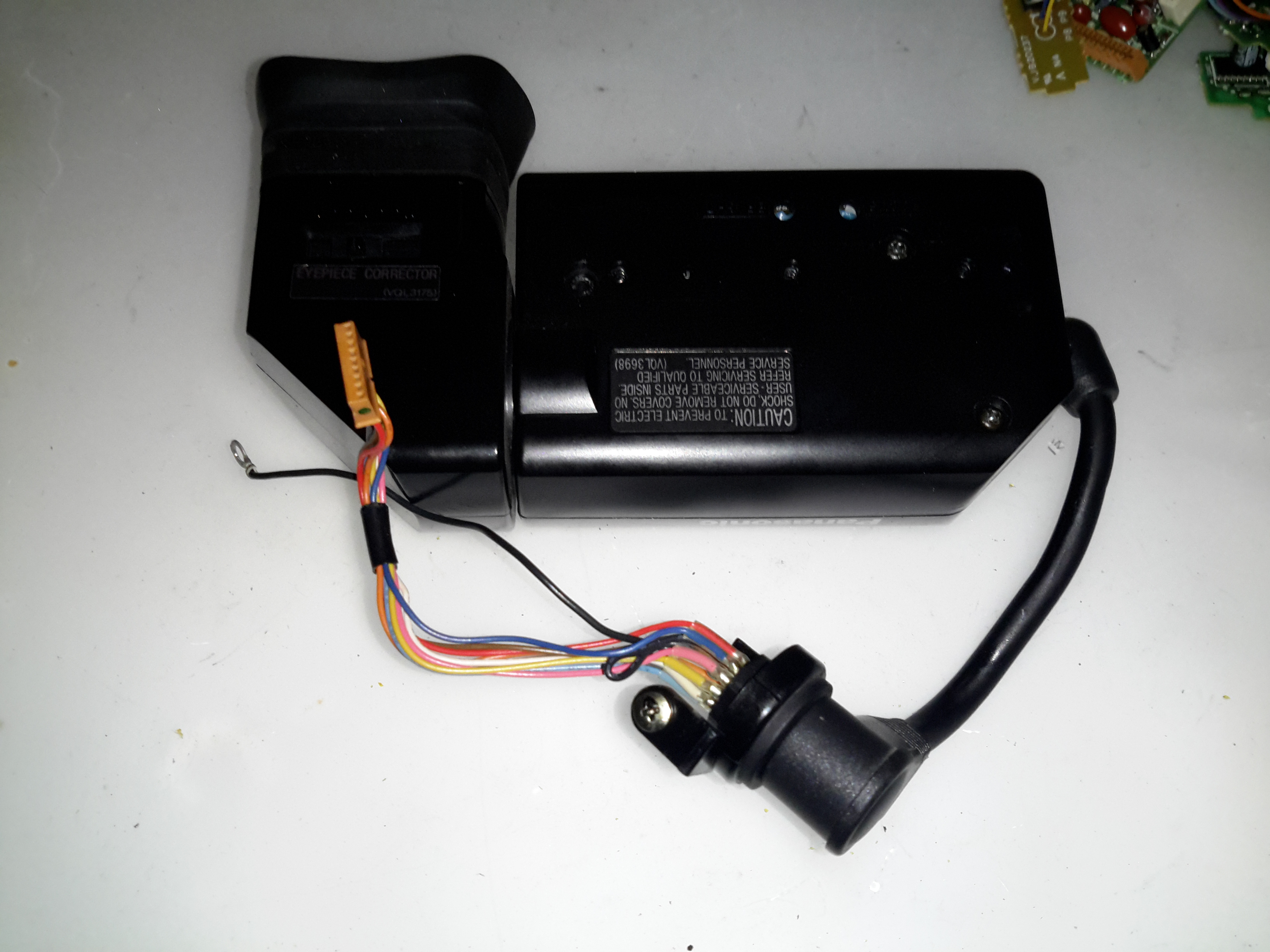
Viewfinder
The viewfinder is mounted on a swivel mount. There’s a CRT based composite monitor in here. Hack ahoy!
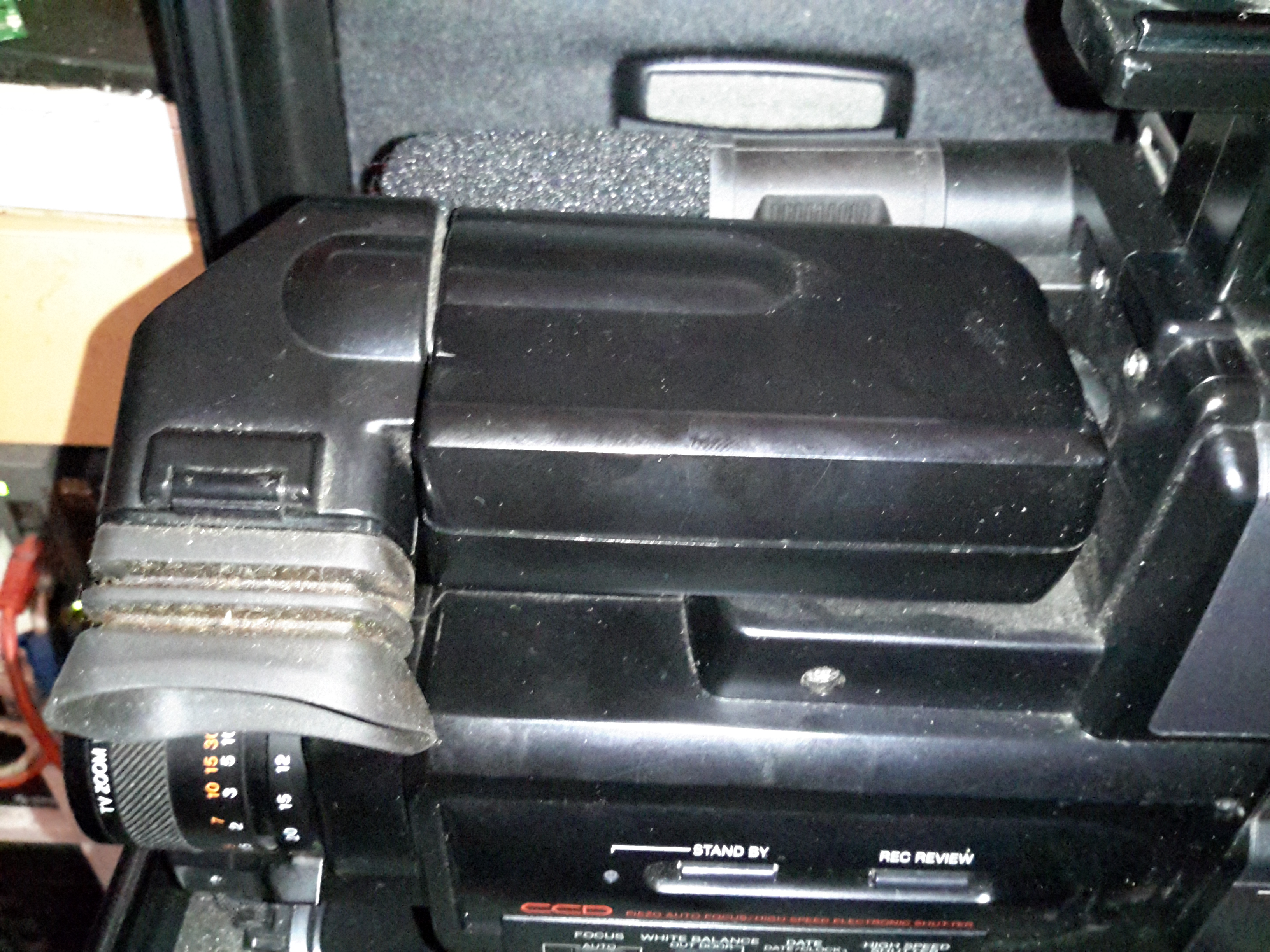
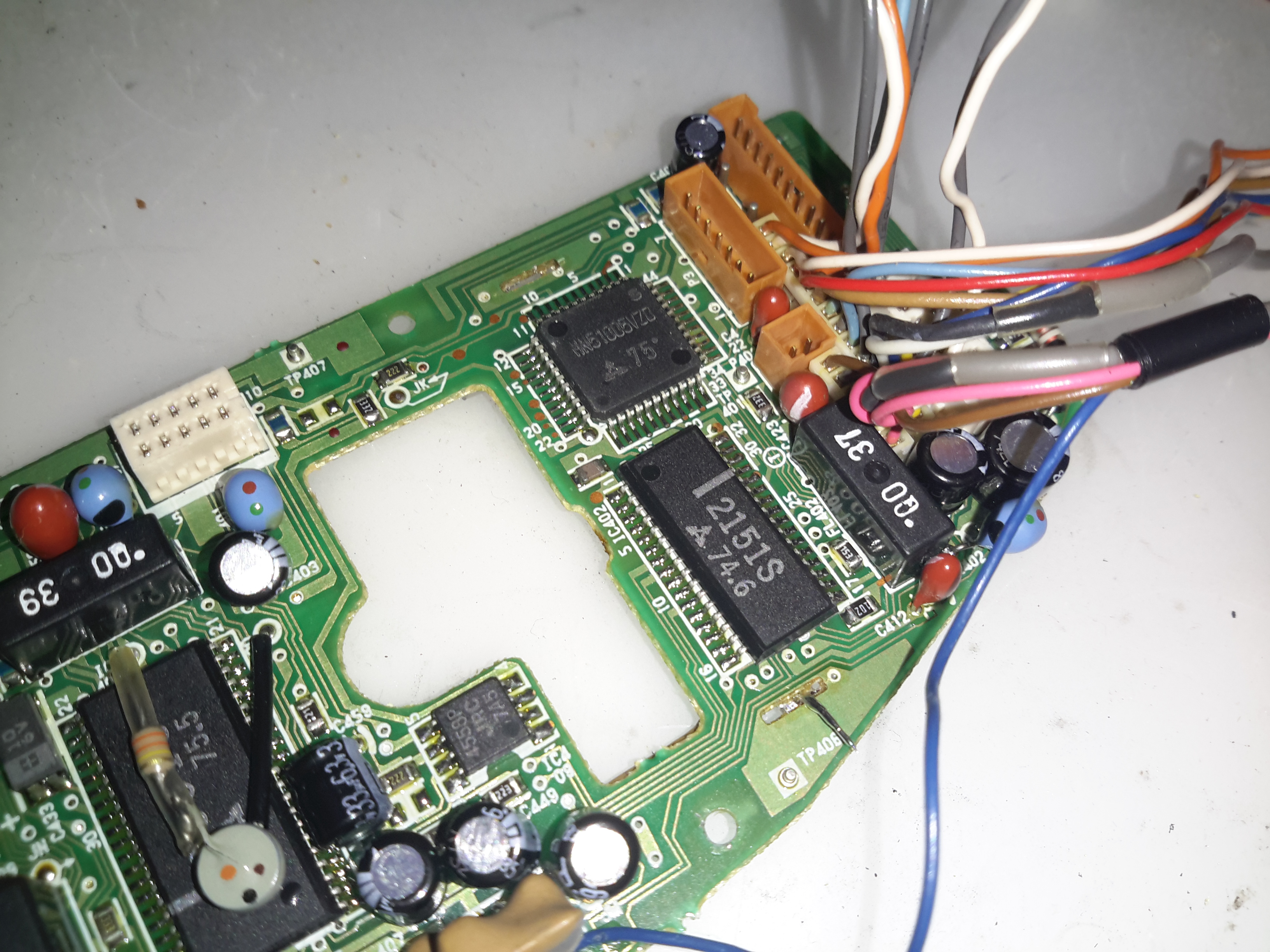
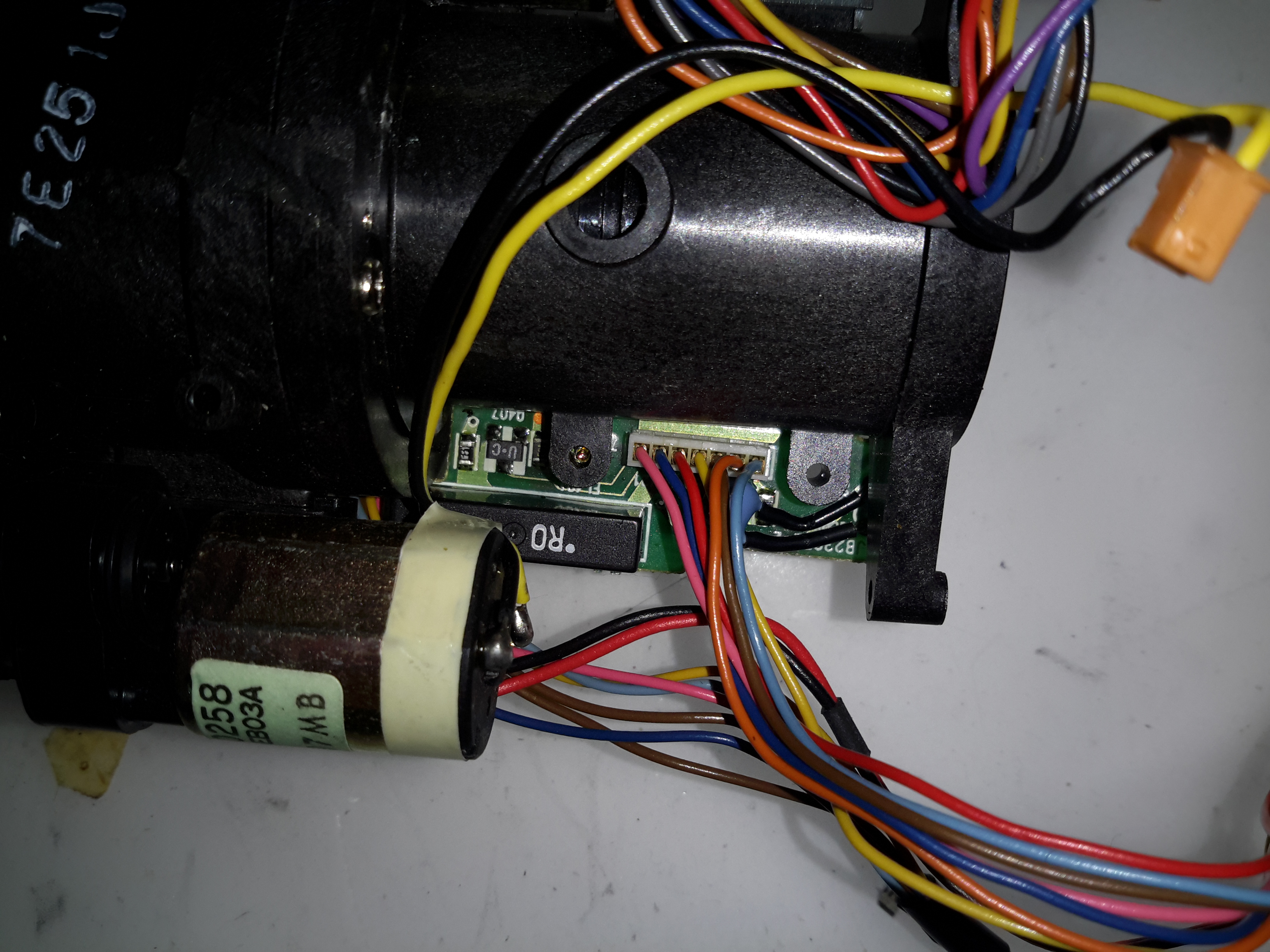
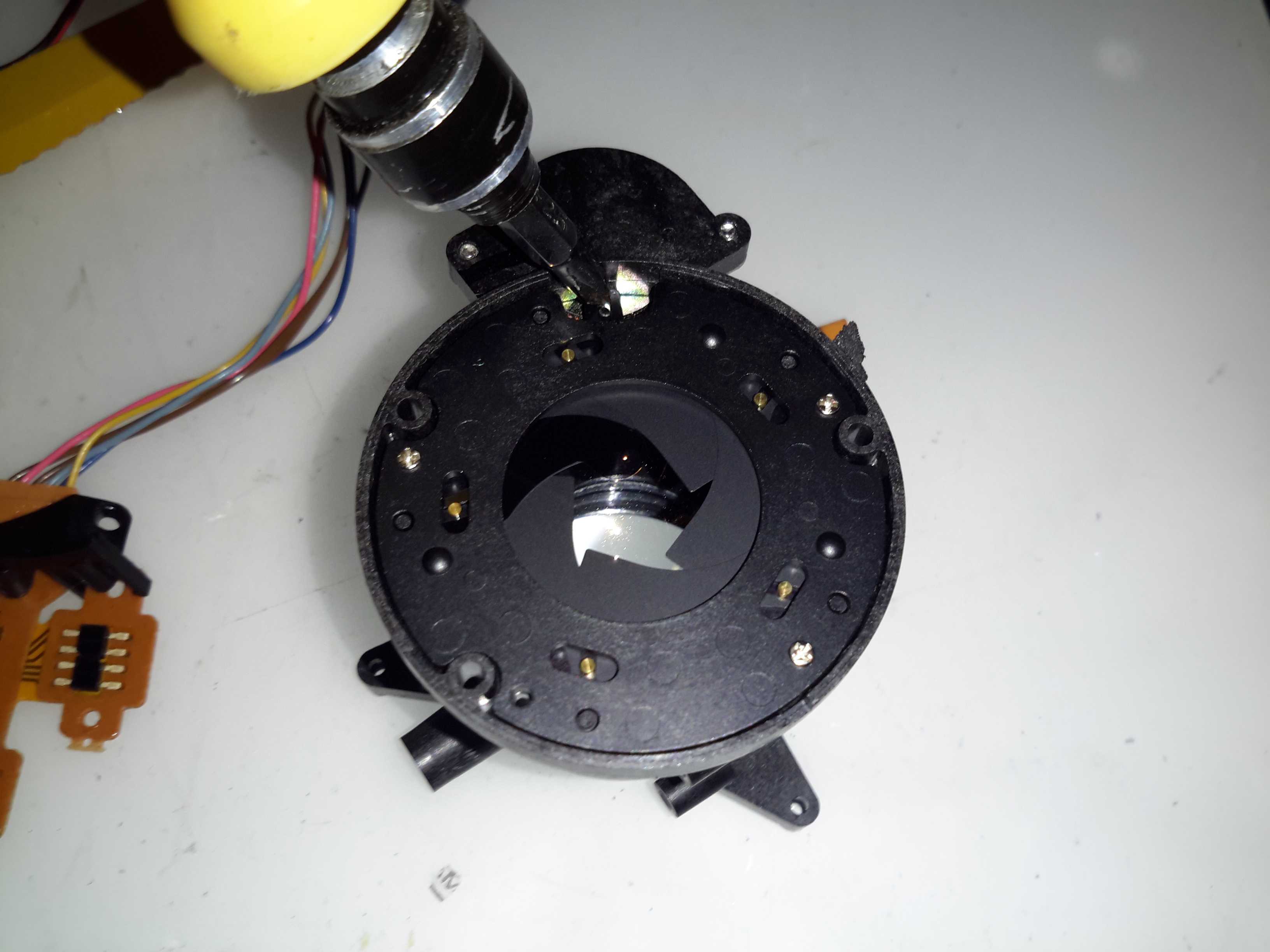
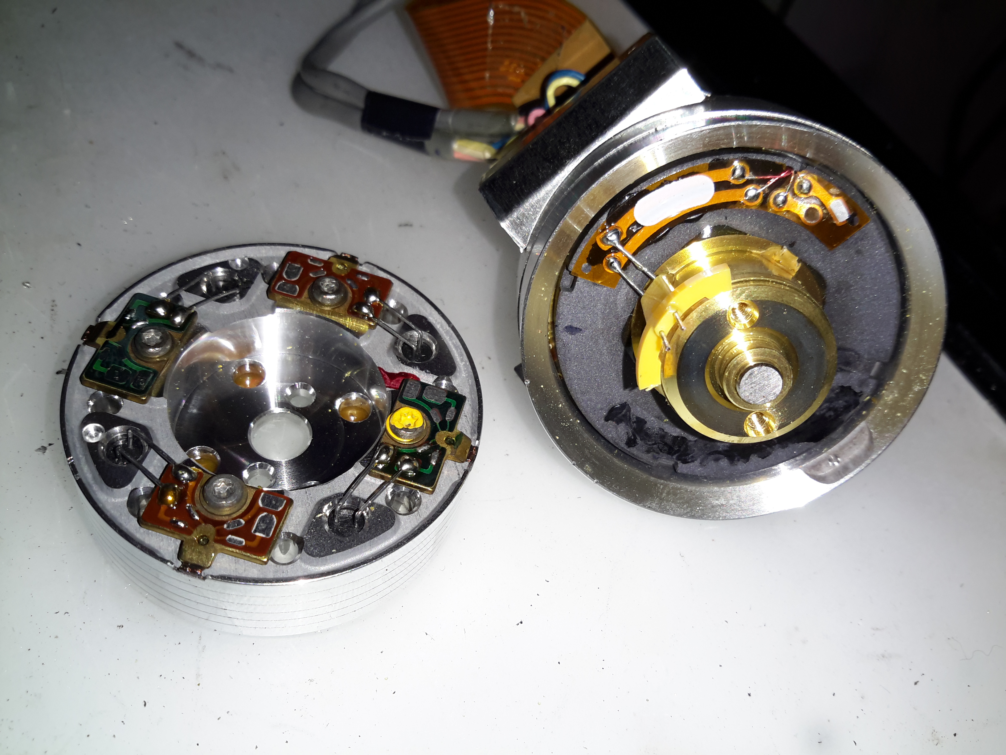
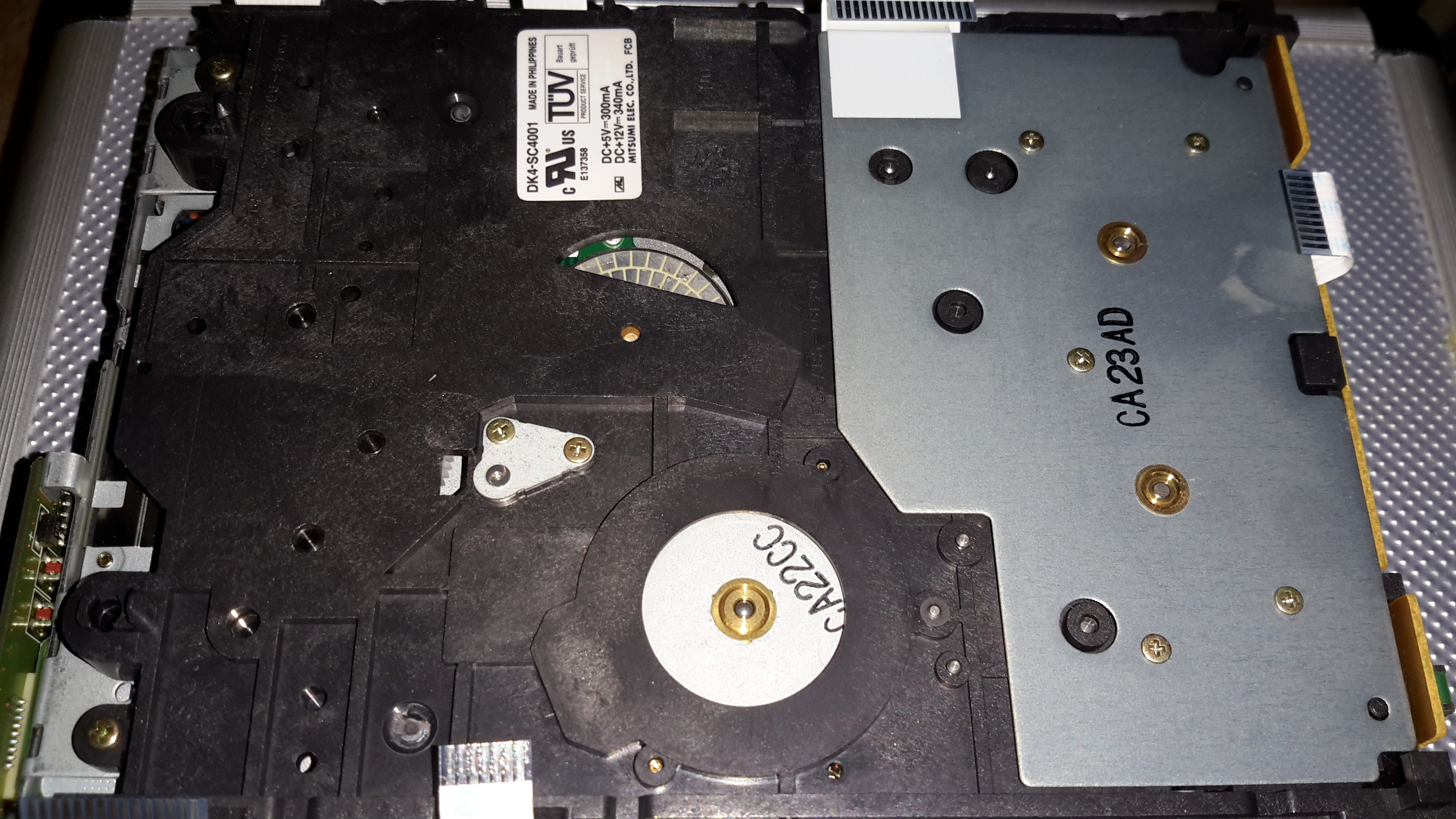
Camera Section
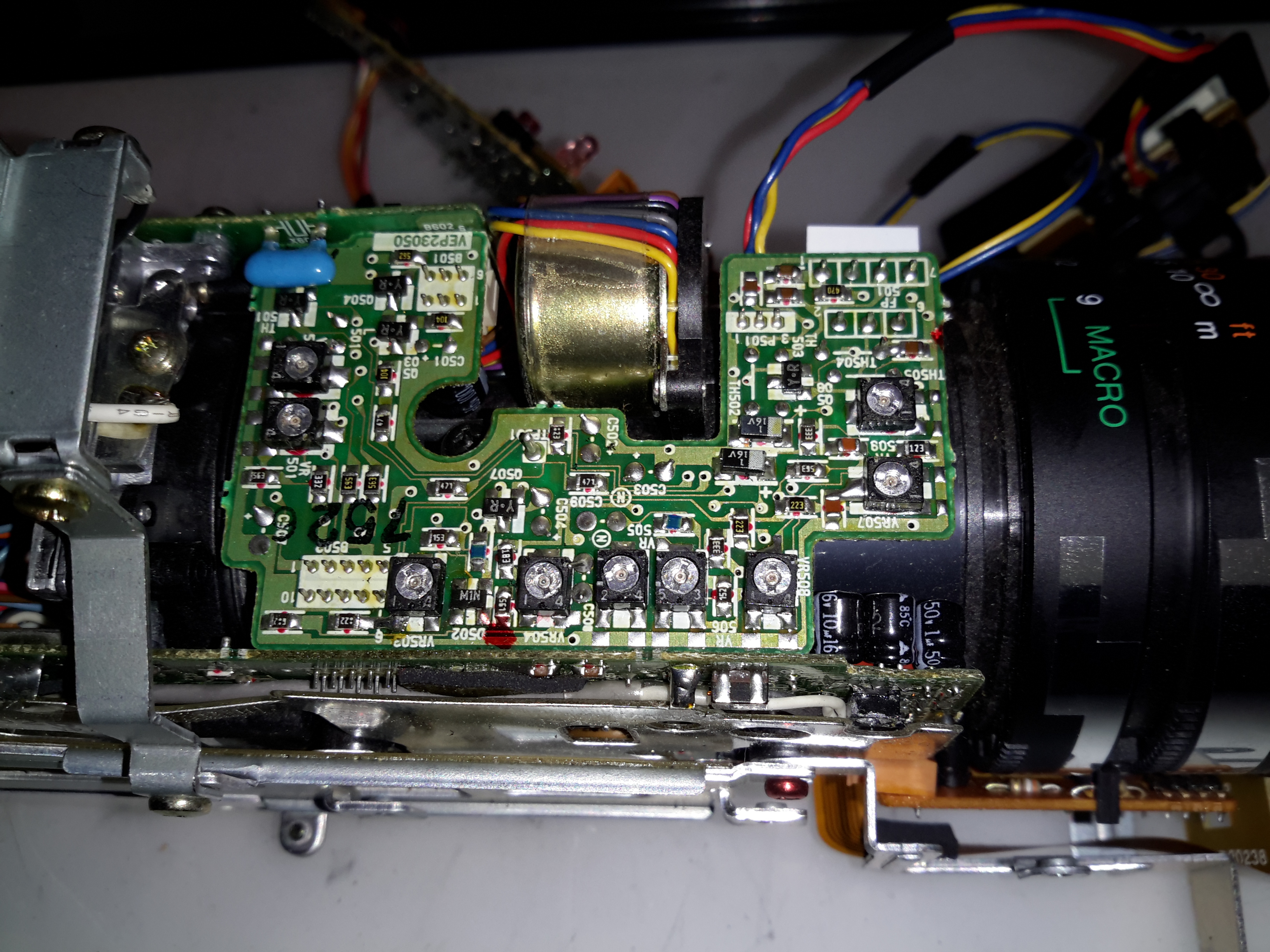
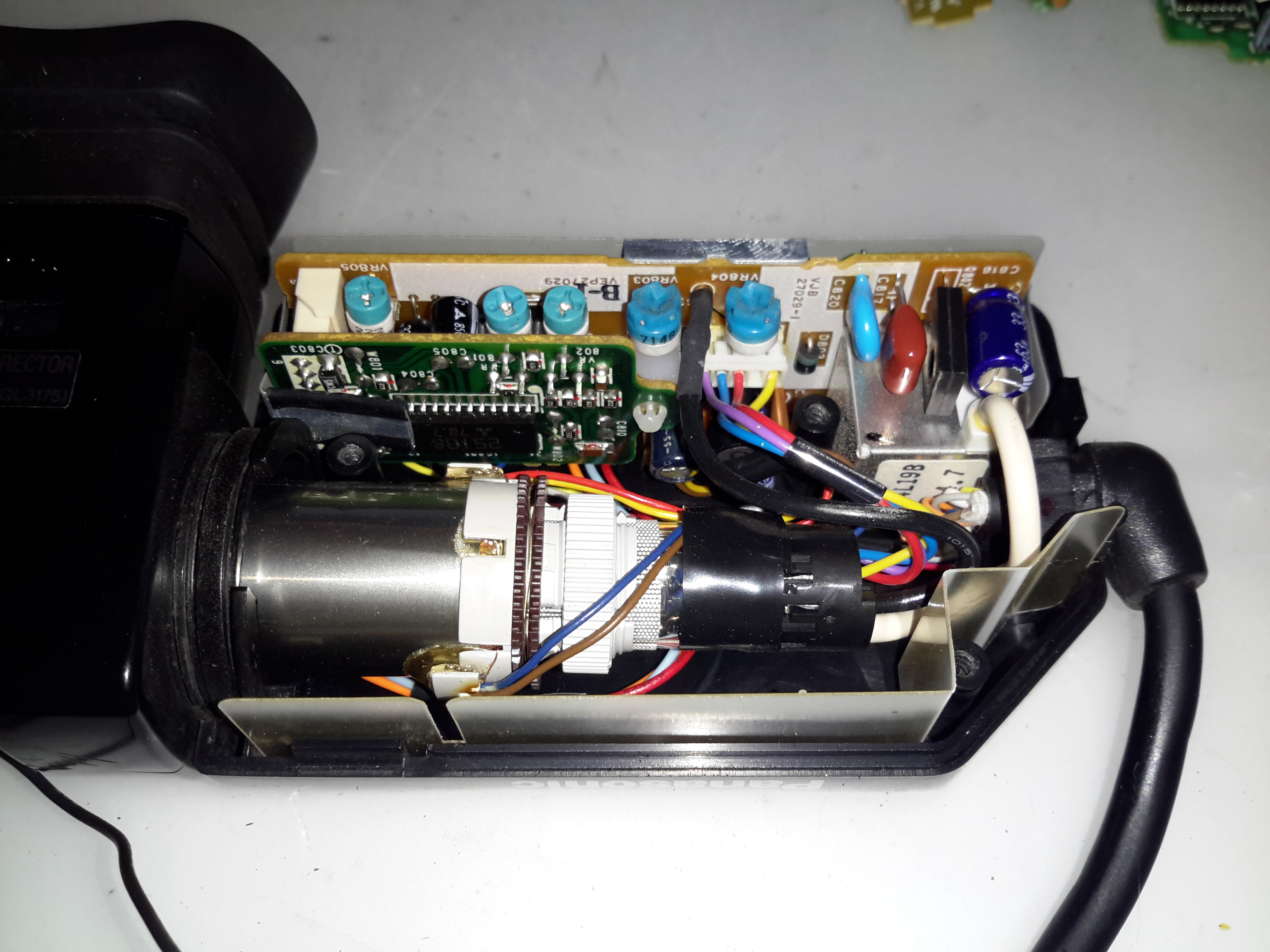
Process Board Assembly
Here’s the camera section of the camcorder, and is totally packed with electronics! There’s at least half a dozen separate boards in here, all fitted together around the optics tube assembly.
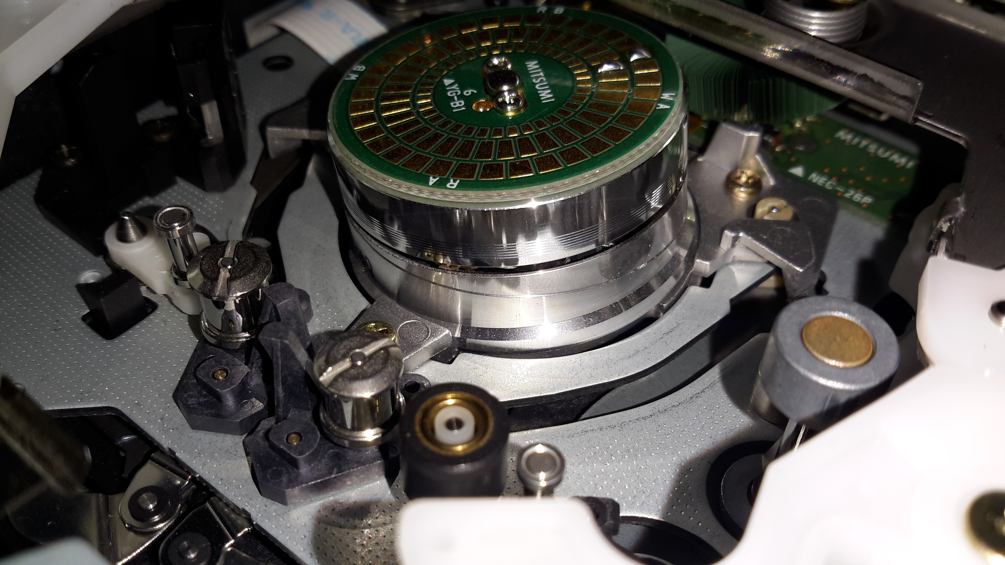
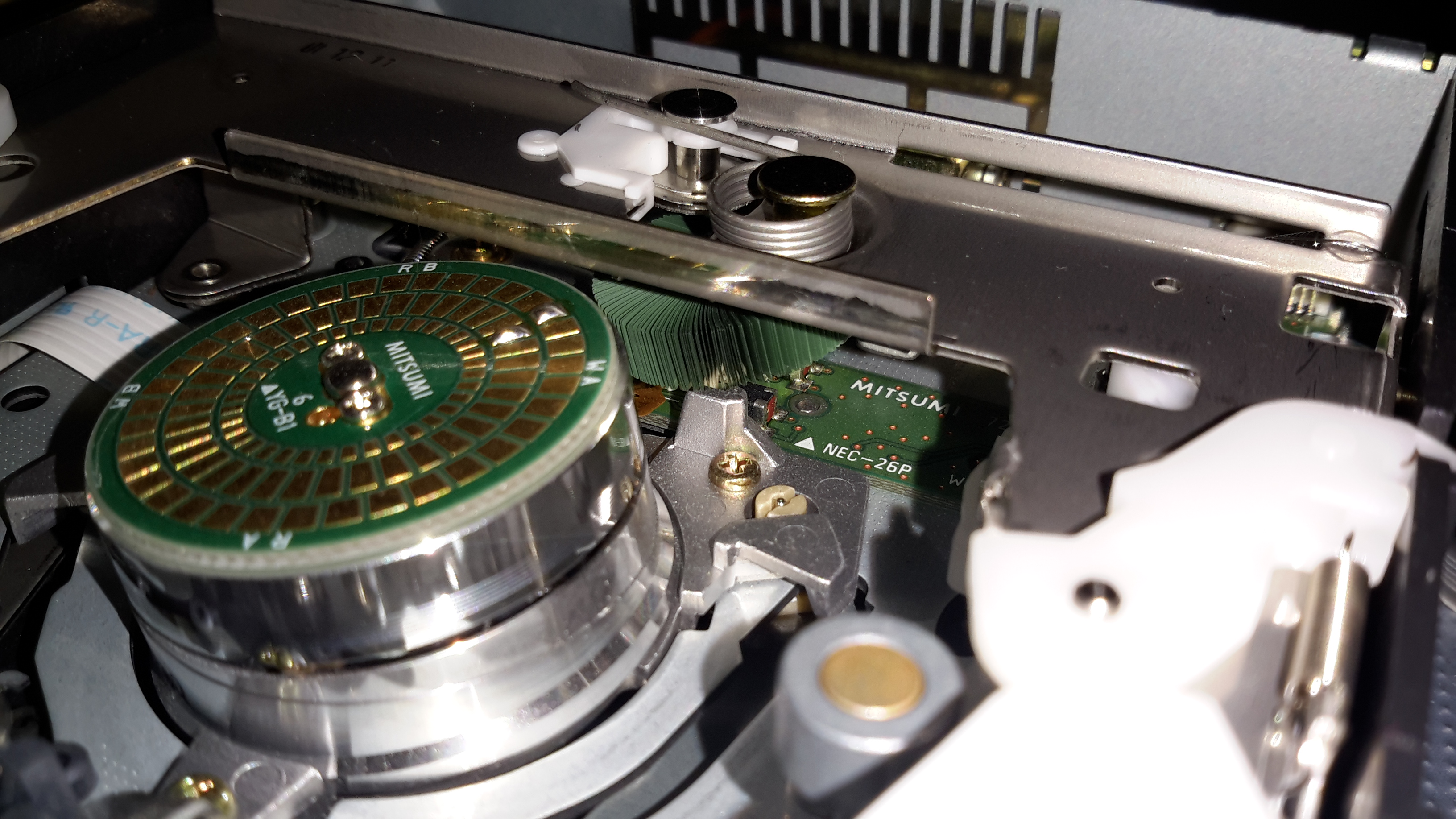
AWB PCB
On the top of the assembly is the Automatic White Balance PCB. Many adjustments here to get everything set right. Not much on the other side of this board other than a bunch of Op-Amps. The iris stepper motor is fitted in a milled opening in the PCB, this connects to one of the other PCBs in the camera module.
AWB Sensor
Here’s the AWB sensor, mounted next to the lens. I’m not all to certain how this works, but the service manual has the pinout, and there are outputs for all the colour channels, RGB. So it’s probably a trio of photodiodes with filters.
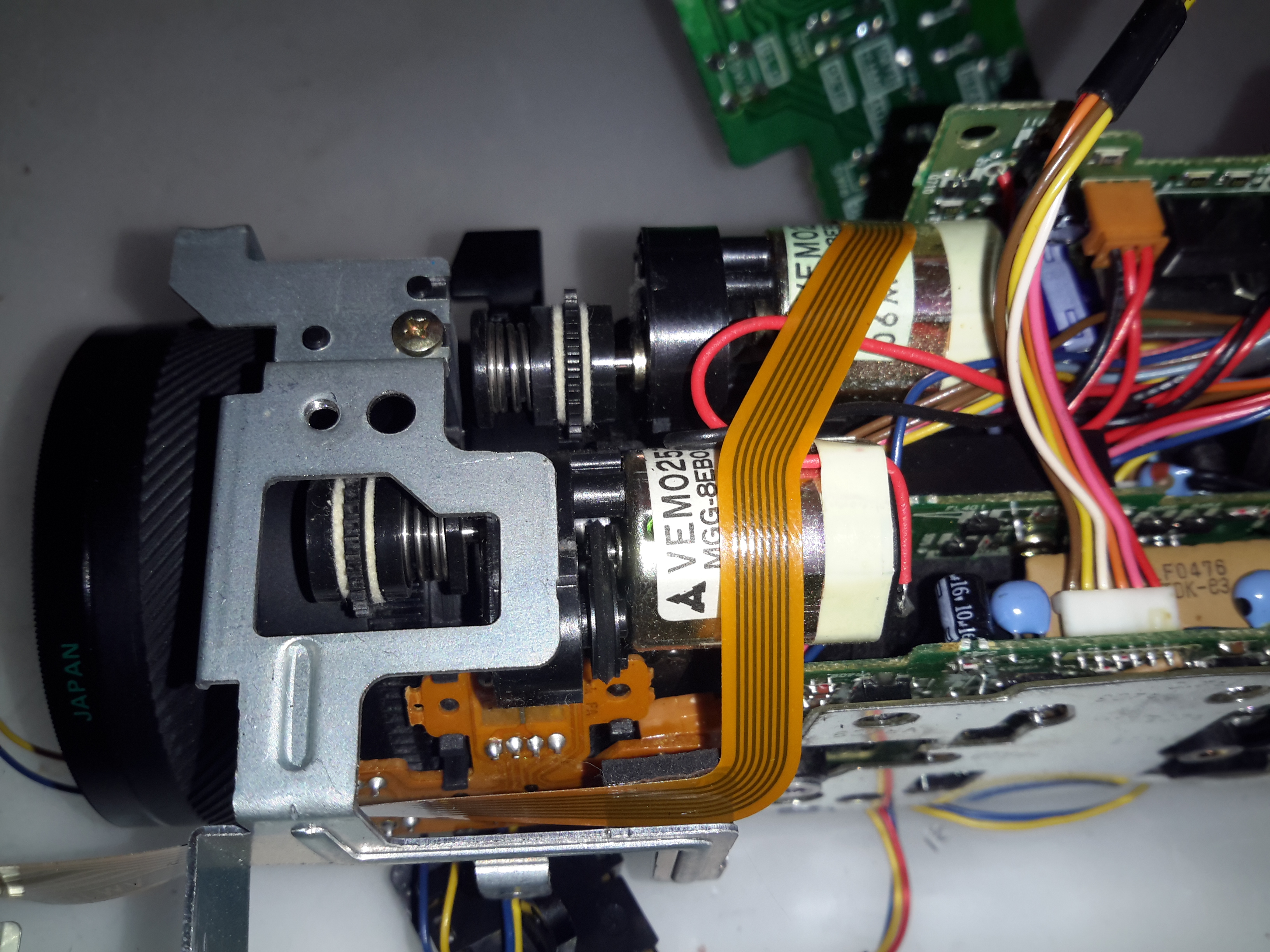
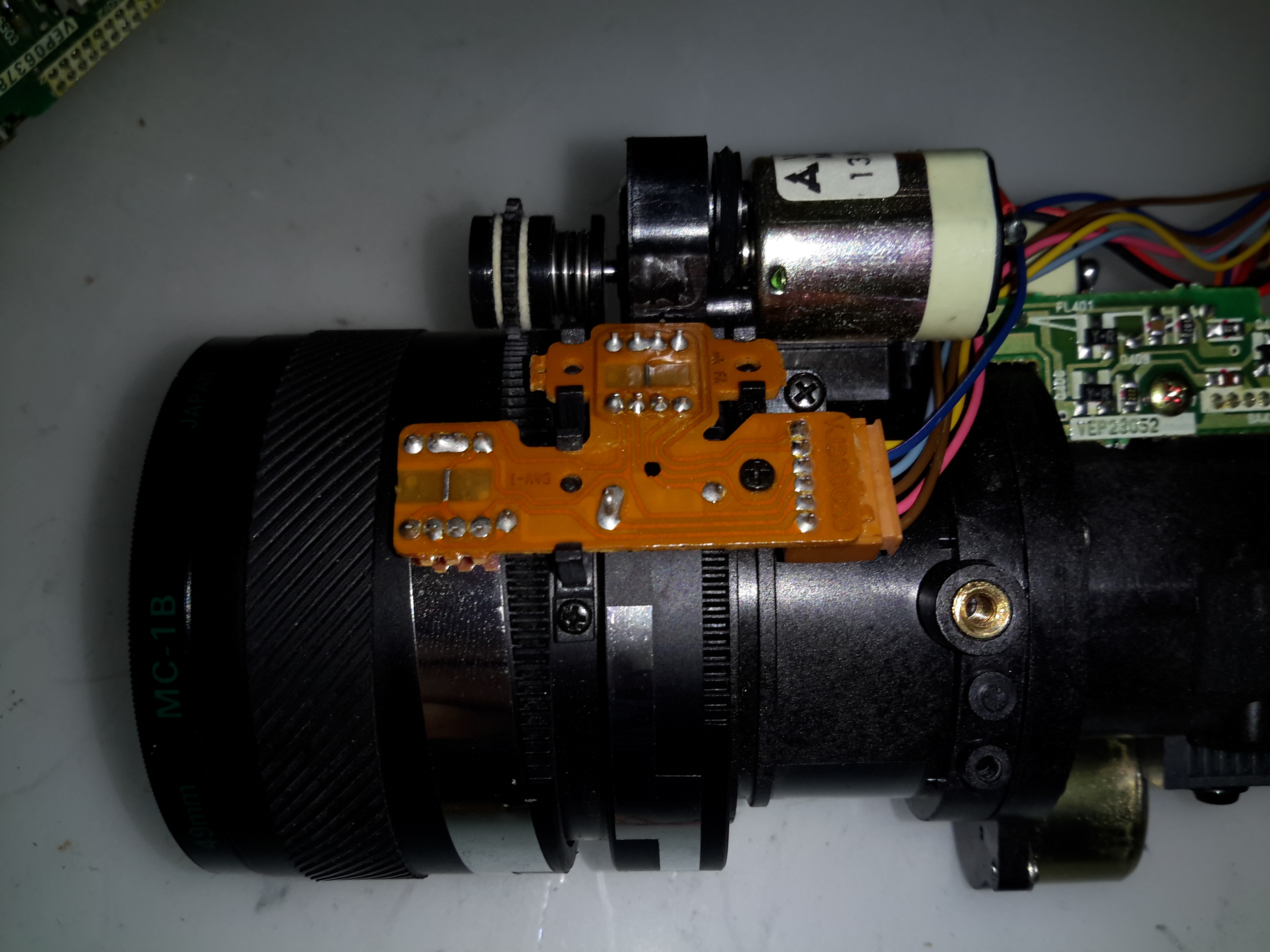
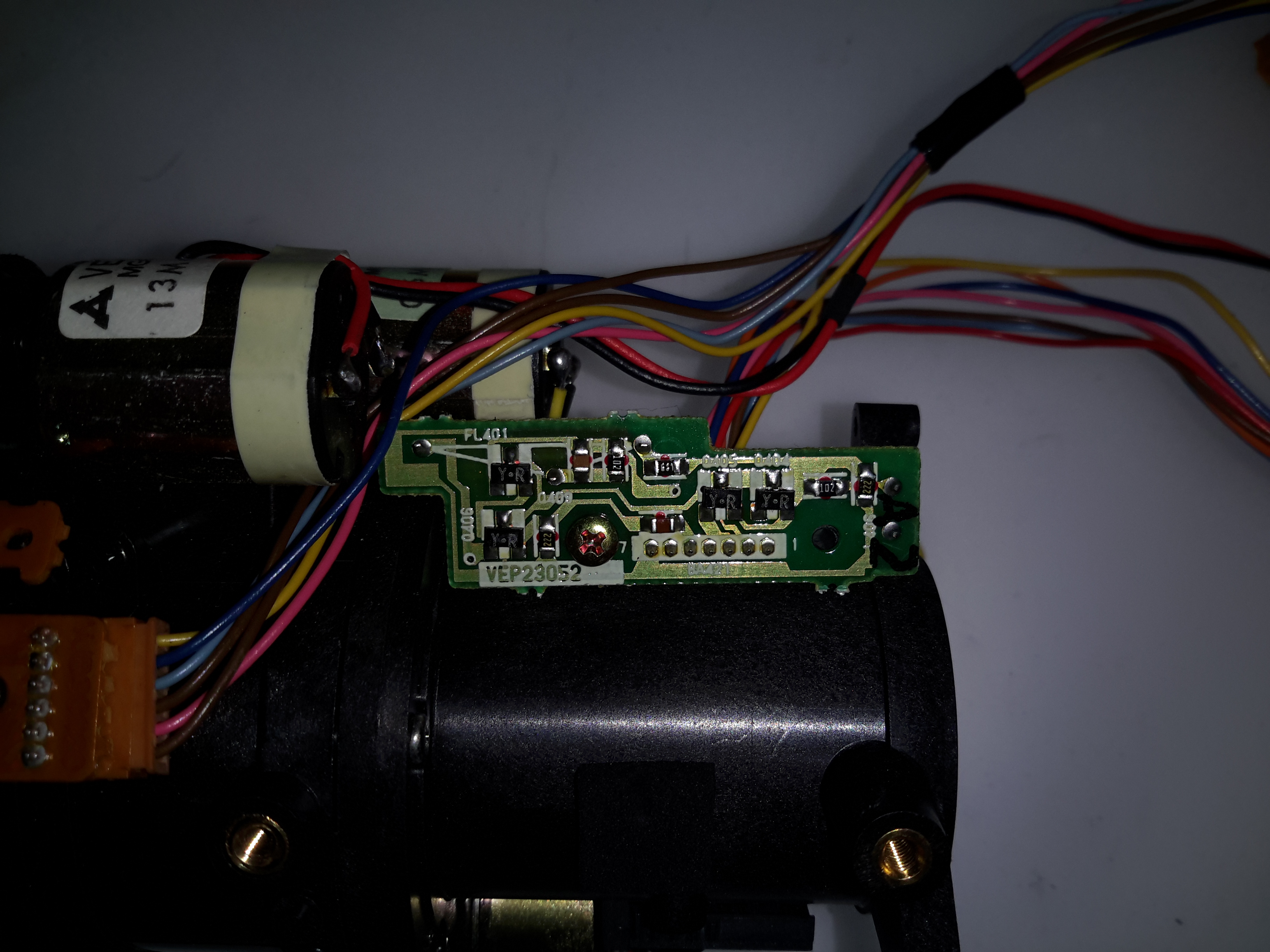
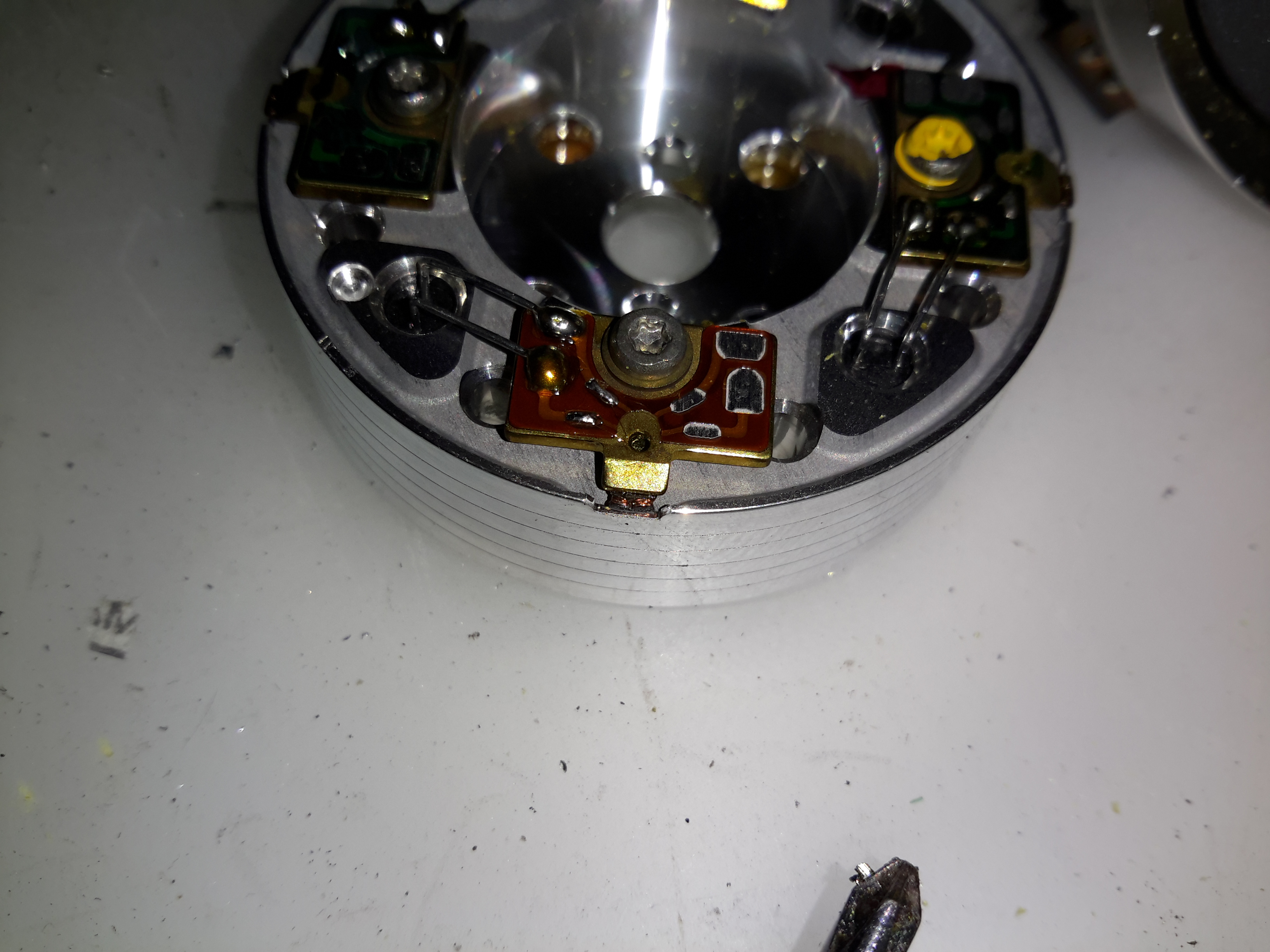
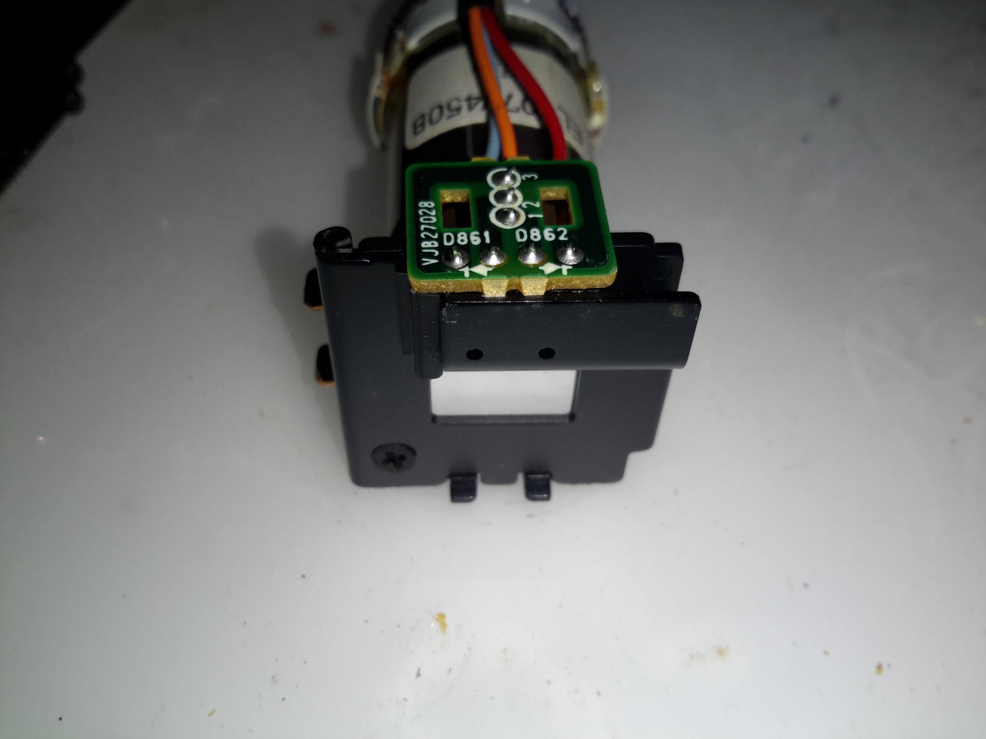
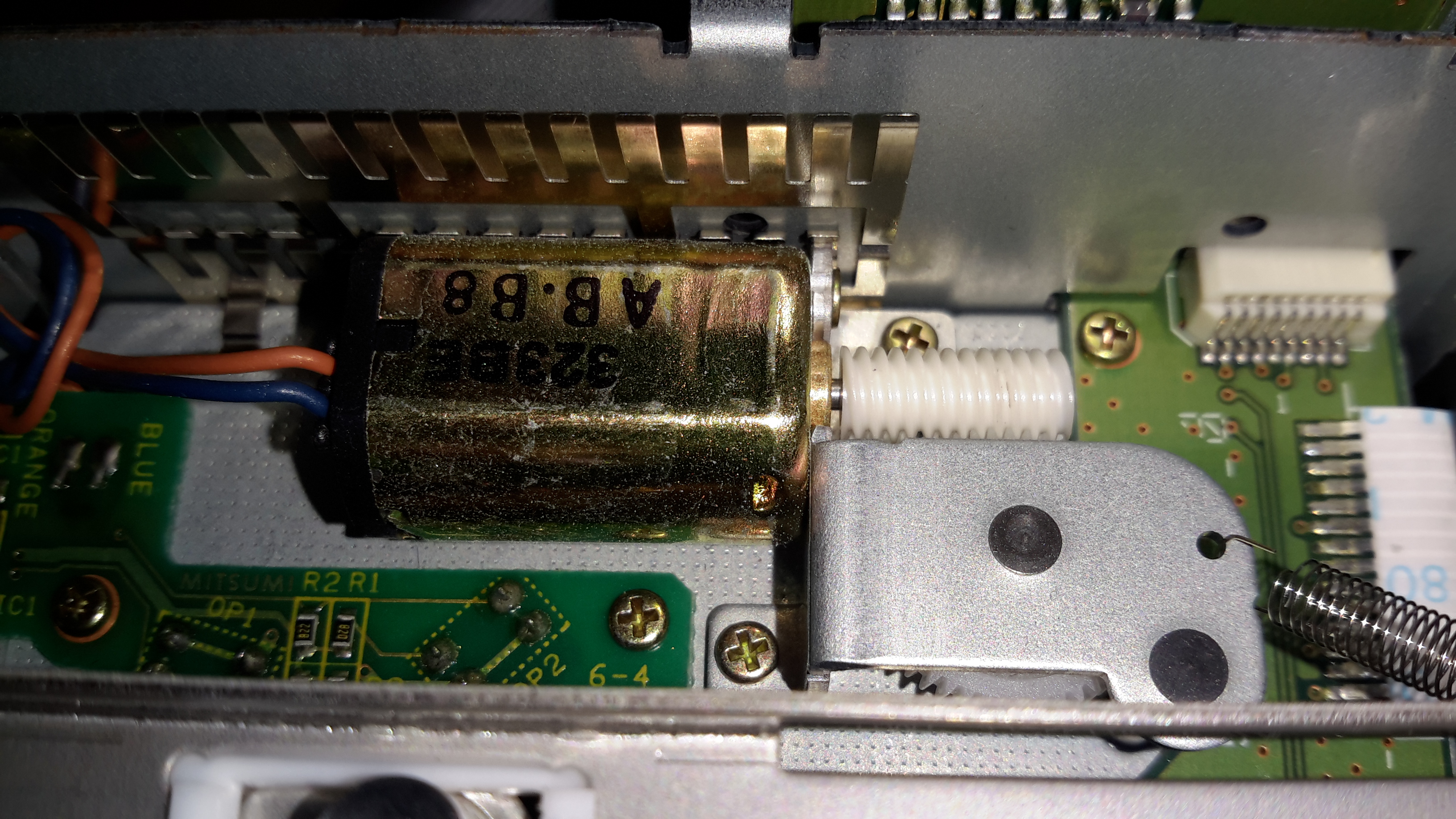
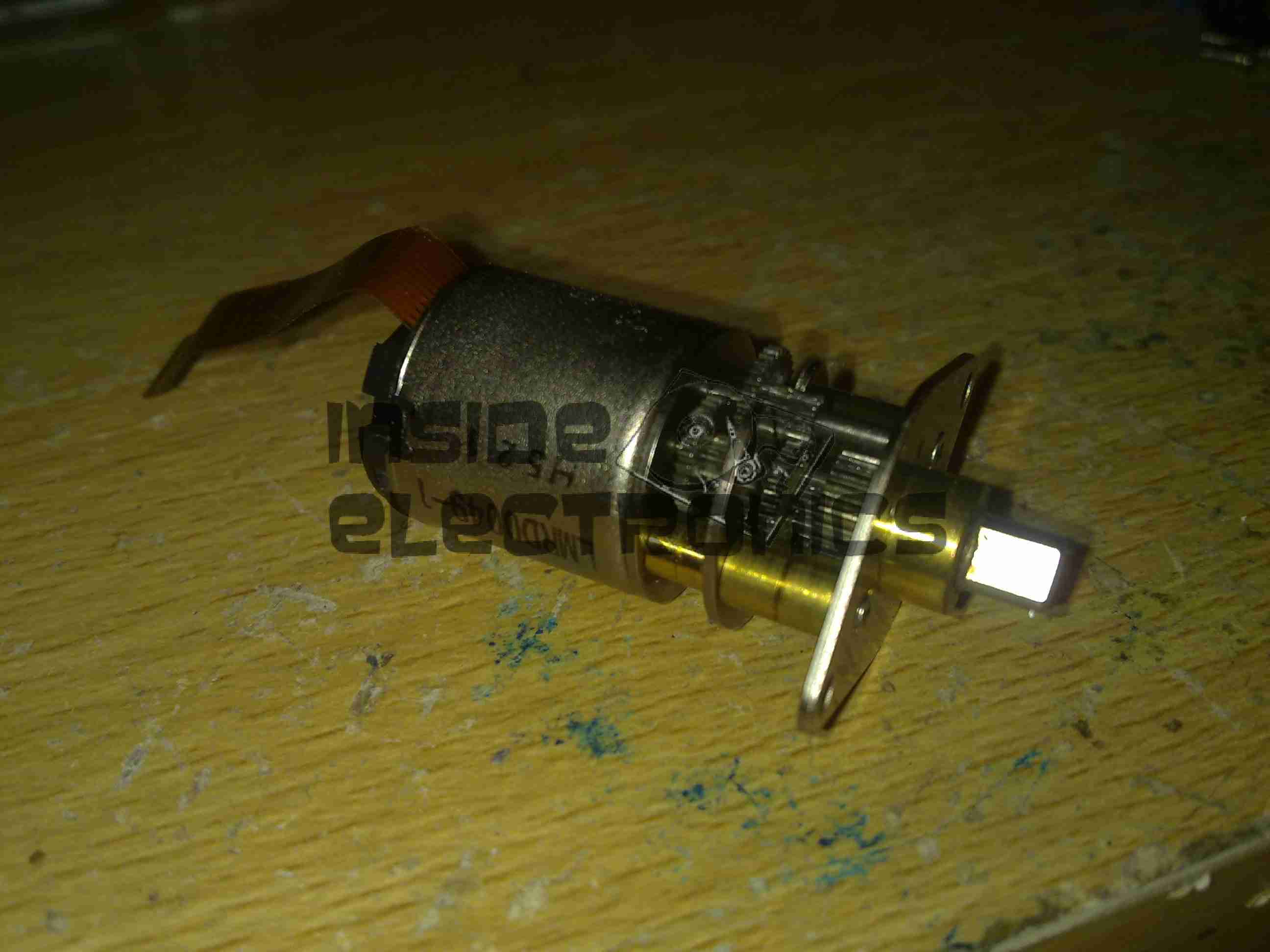
Focus & Zoom Motors
Focus & Zoom are controlled with a pair of DC gear motors. The manual operation is feasible through the use of slip clutches in the final drive pinion onto the lens barrel.
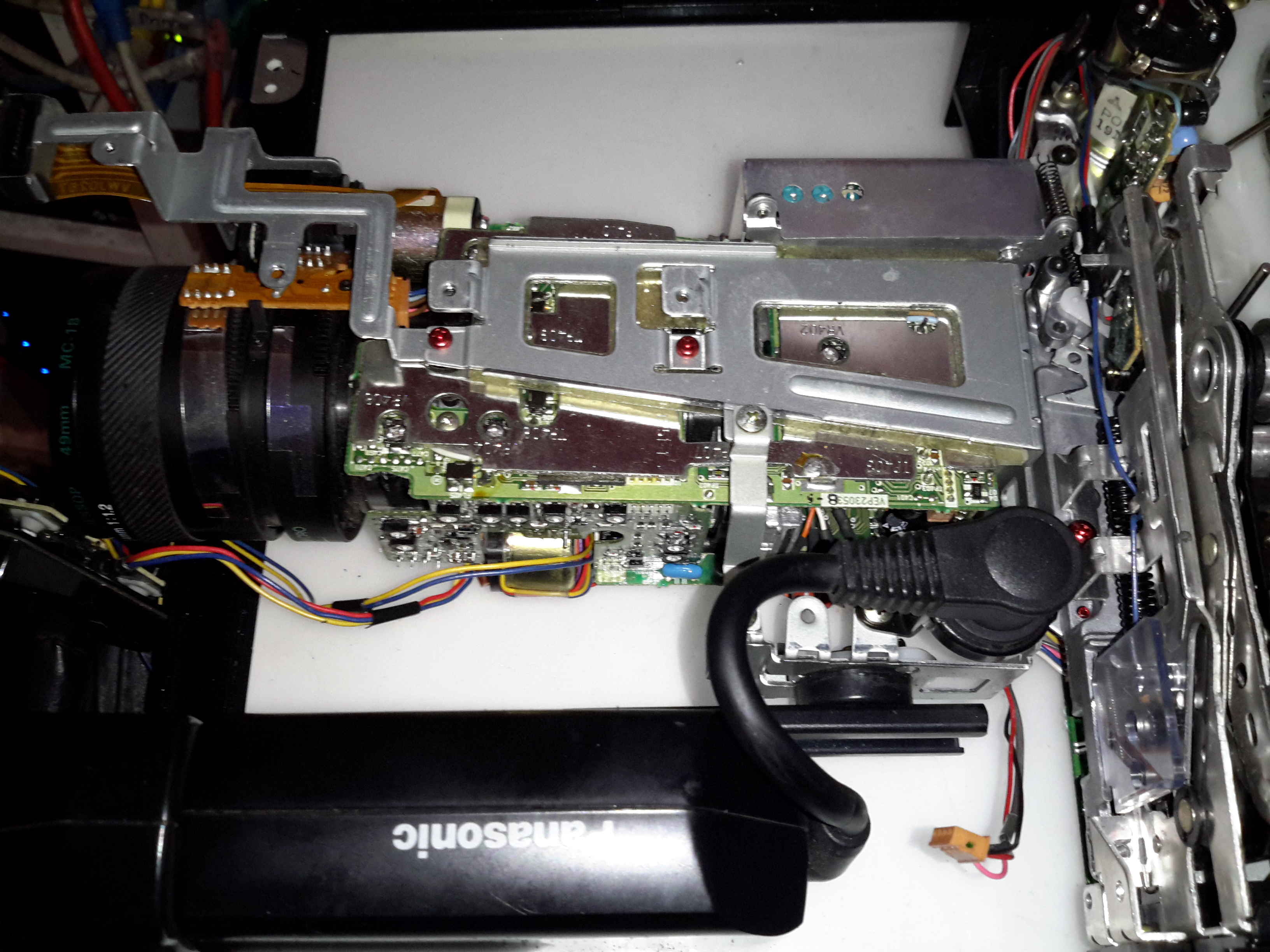
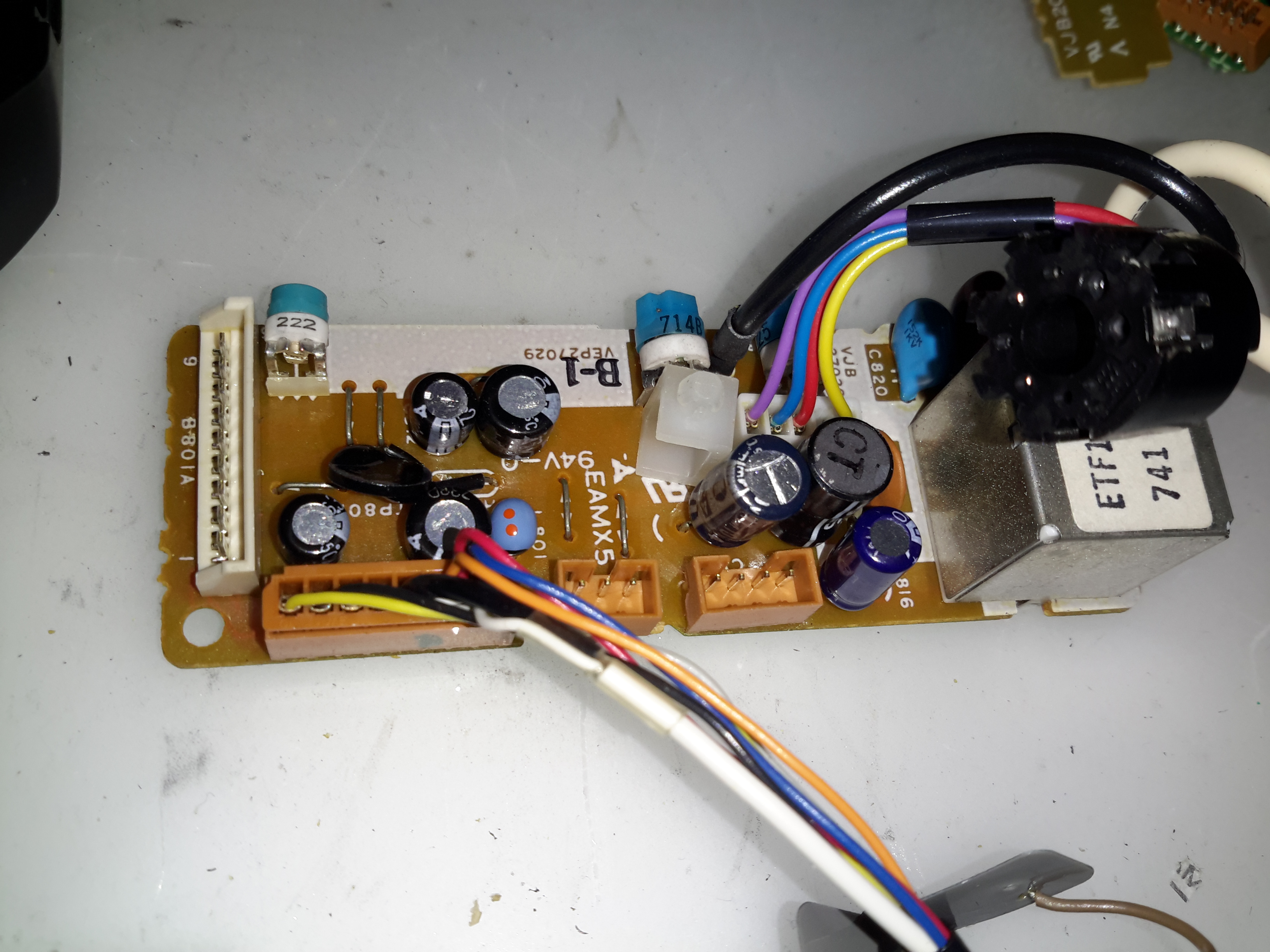
Process Board
The main camera section process board is above. This board does all the signal processing for the CCD, has the bias voltage supplies and houses the control sections for the motorized parts of the optics assembly. There are quite a few dipped Tantalum capacitors on pigtails, instead of being directly board mounted. This was probably done due to space requirements on the PCB itself.
Under the steel shield on this board is some of the main signal processing for the CCD.
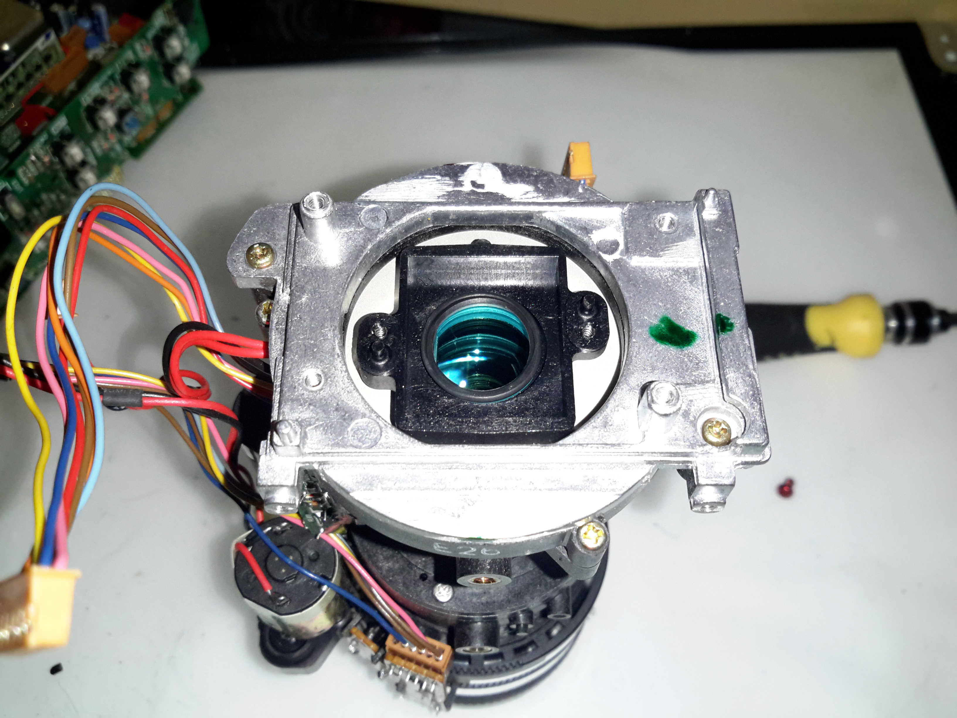
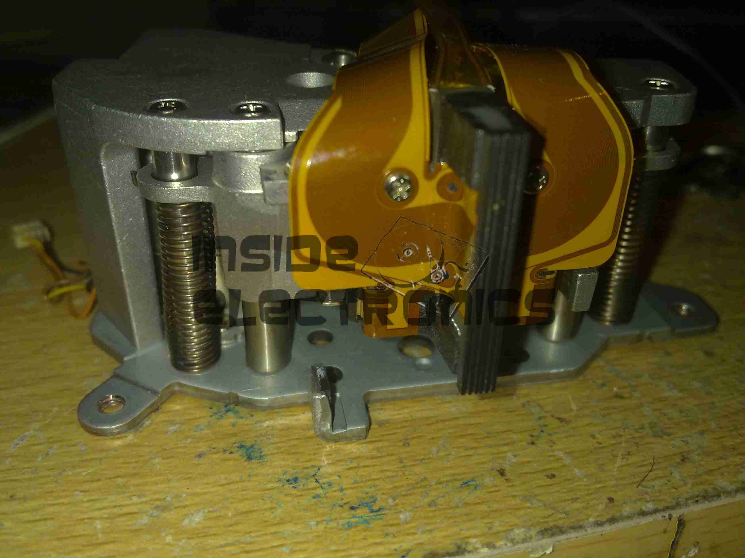
Optics Assembly
The back of the optics tube is a heavy casting, to supress vibration. This will be more clear later on.
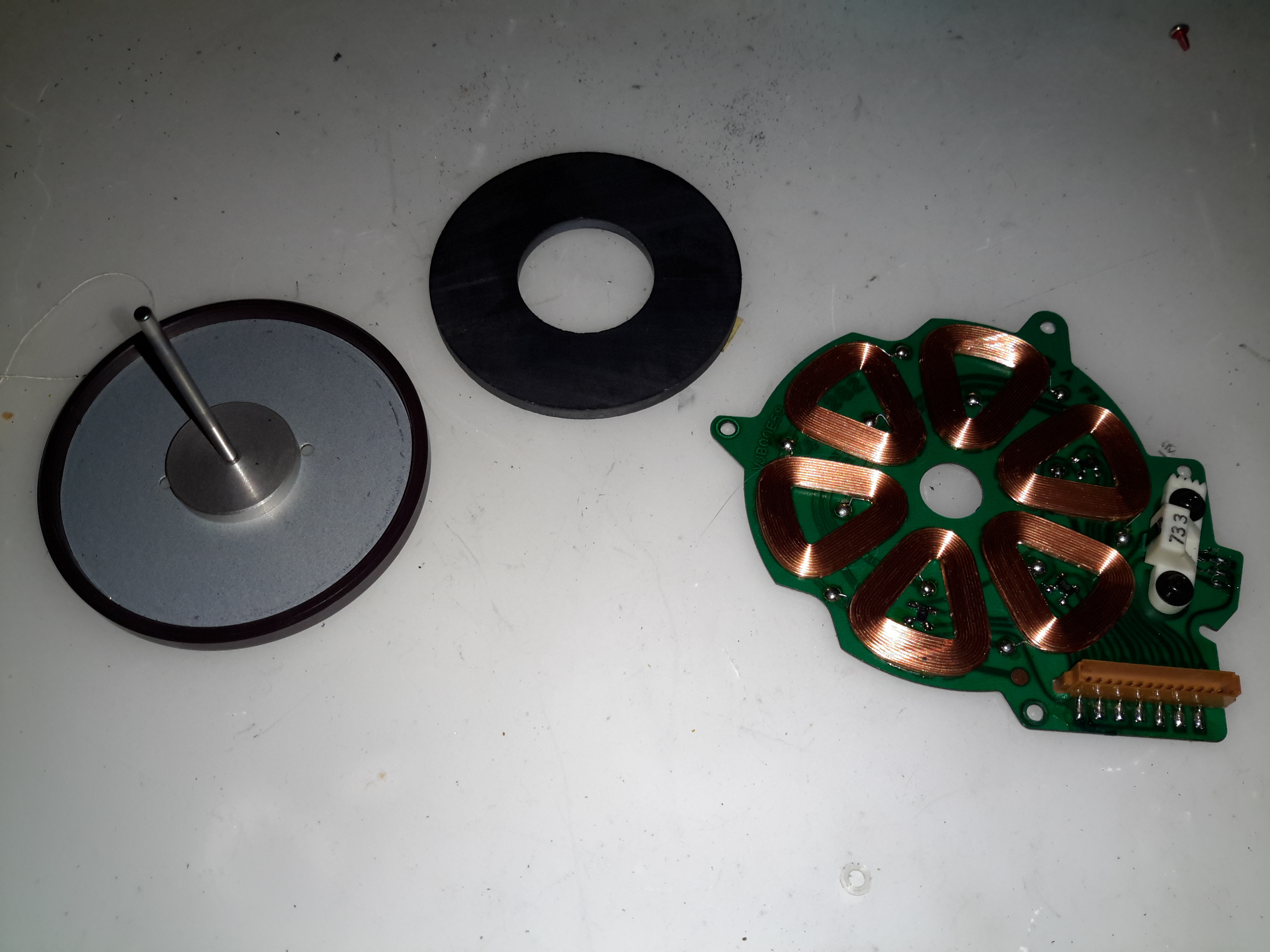
Position Sensor Flex
The position of the lens elements is determined by reflective strips on the barrel & sensors on this flex PCB.
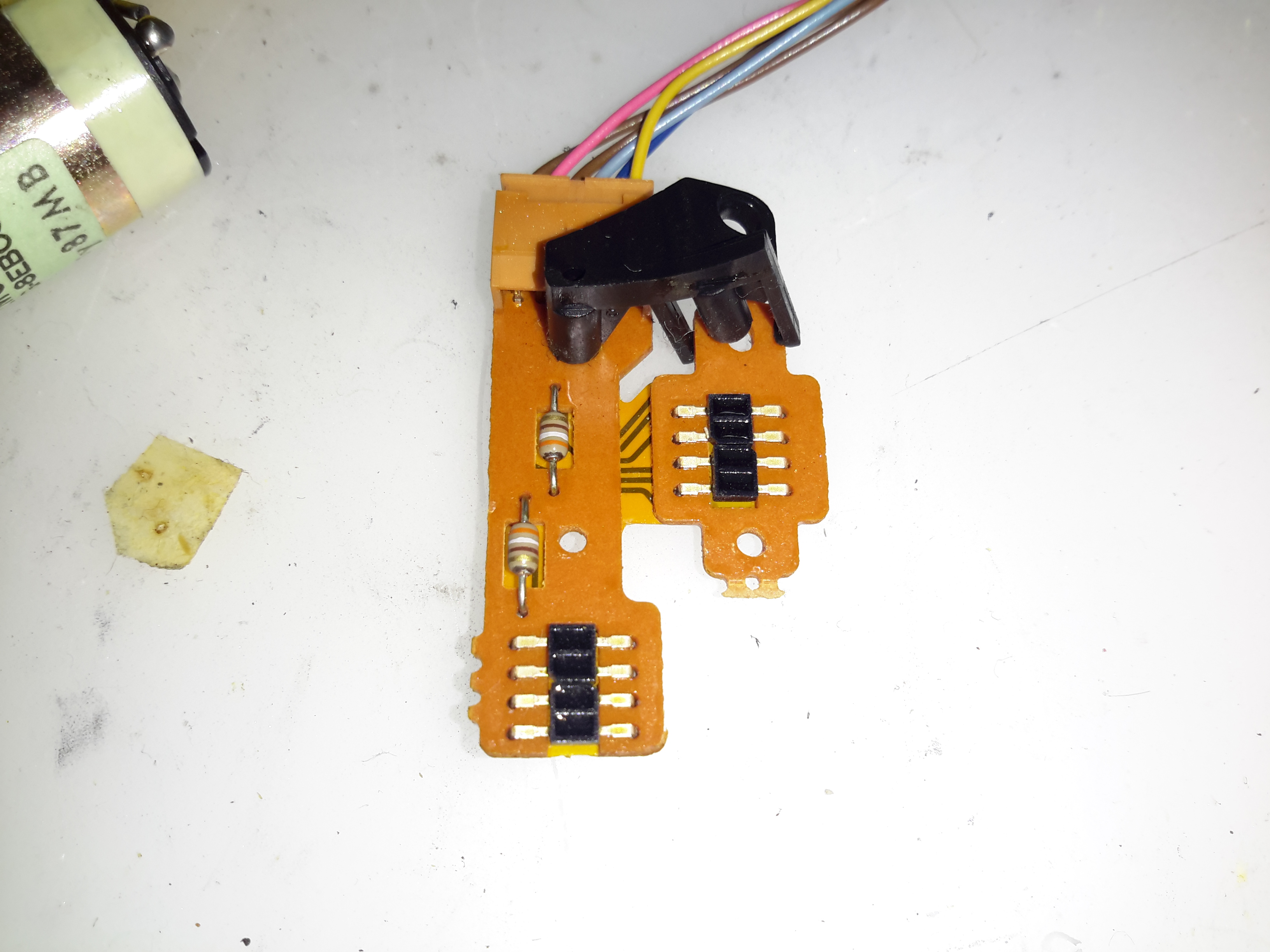
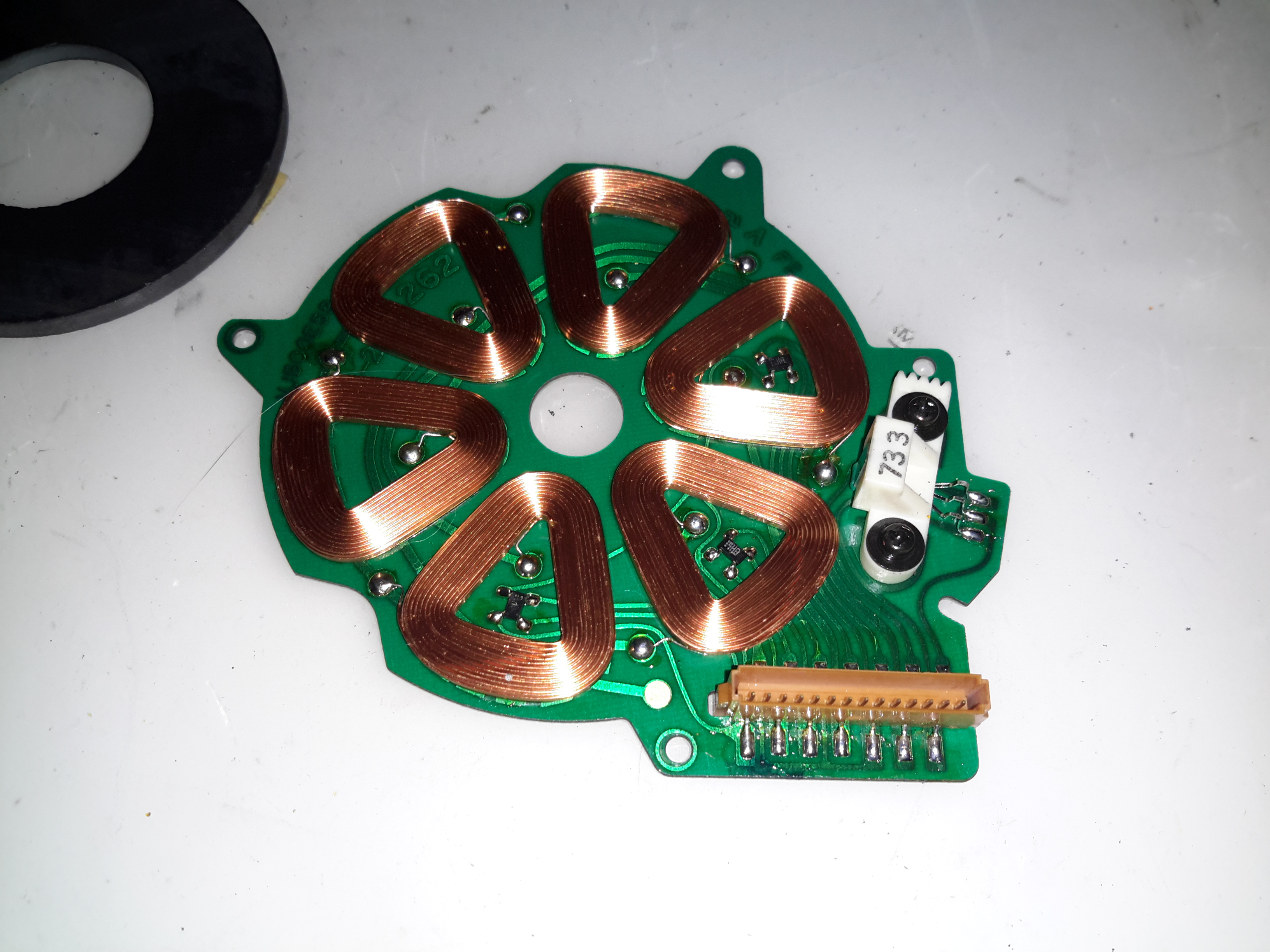
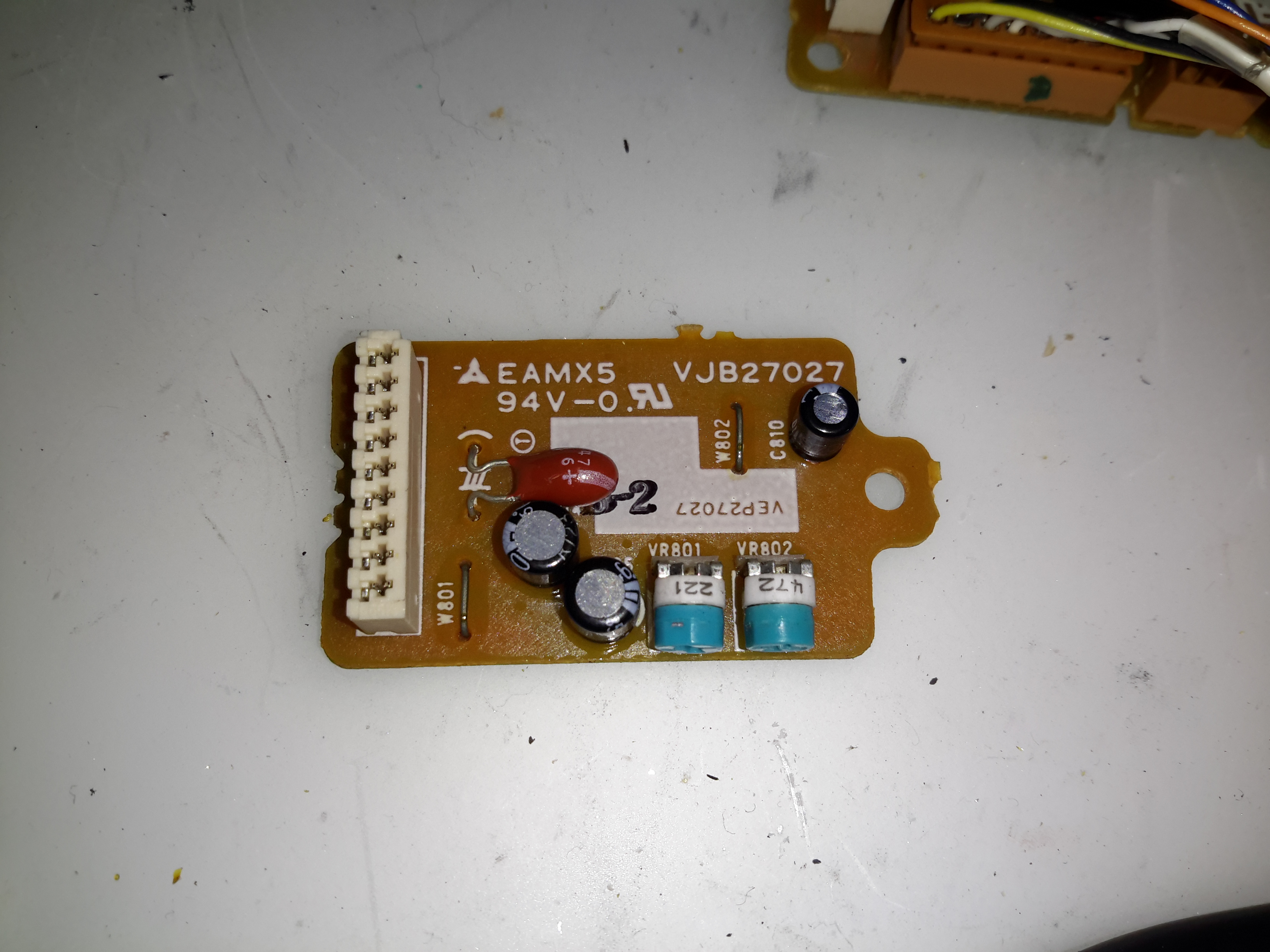
Sub Process Board
There’s another small board tucked into the side of the tube, this hooks into the process PCB.
Process Delay Line
According to the schematic, there’s nothing much on this board, just a delay line & a few transistors.
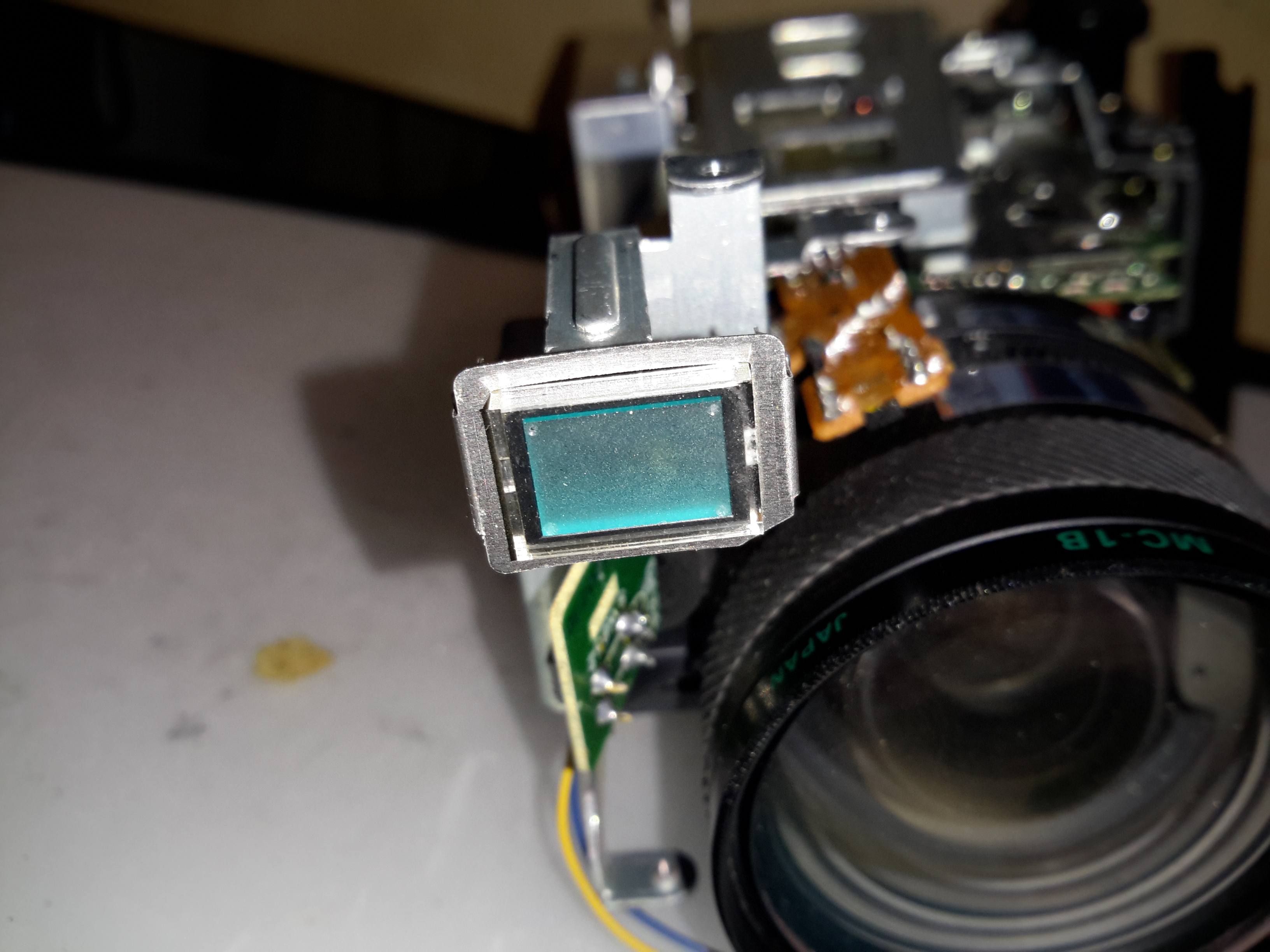
Piezo Focus Disc
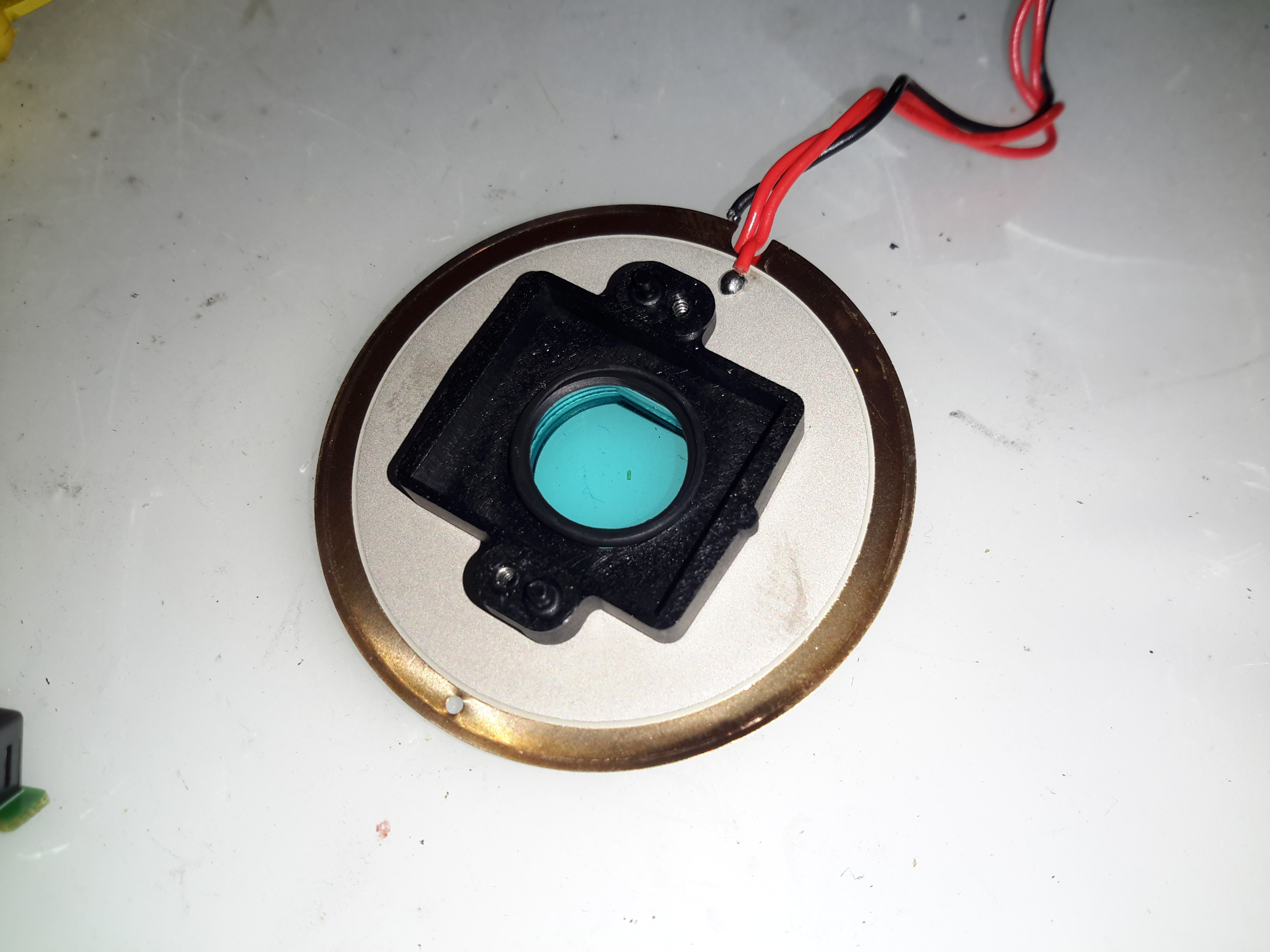
Here’s the reason for the heavy alloy casing at the CCD mounting end of the optics: the fine focus adjustment is done with a piezoelectric disc, the entire CCD assembly is mounted to this board. Applying voltage to the electrodes moves the assembly slightly to alter the position of the CCD. The blue glass in the centre of the unit is the IR filter.
IR Relective Sensors
The barrel position sensors are these IR-reflective type.
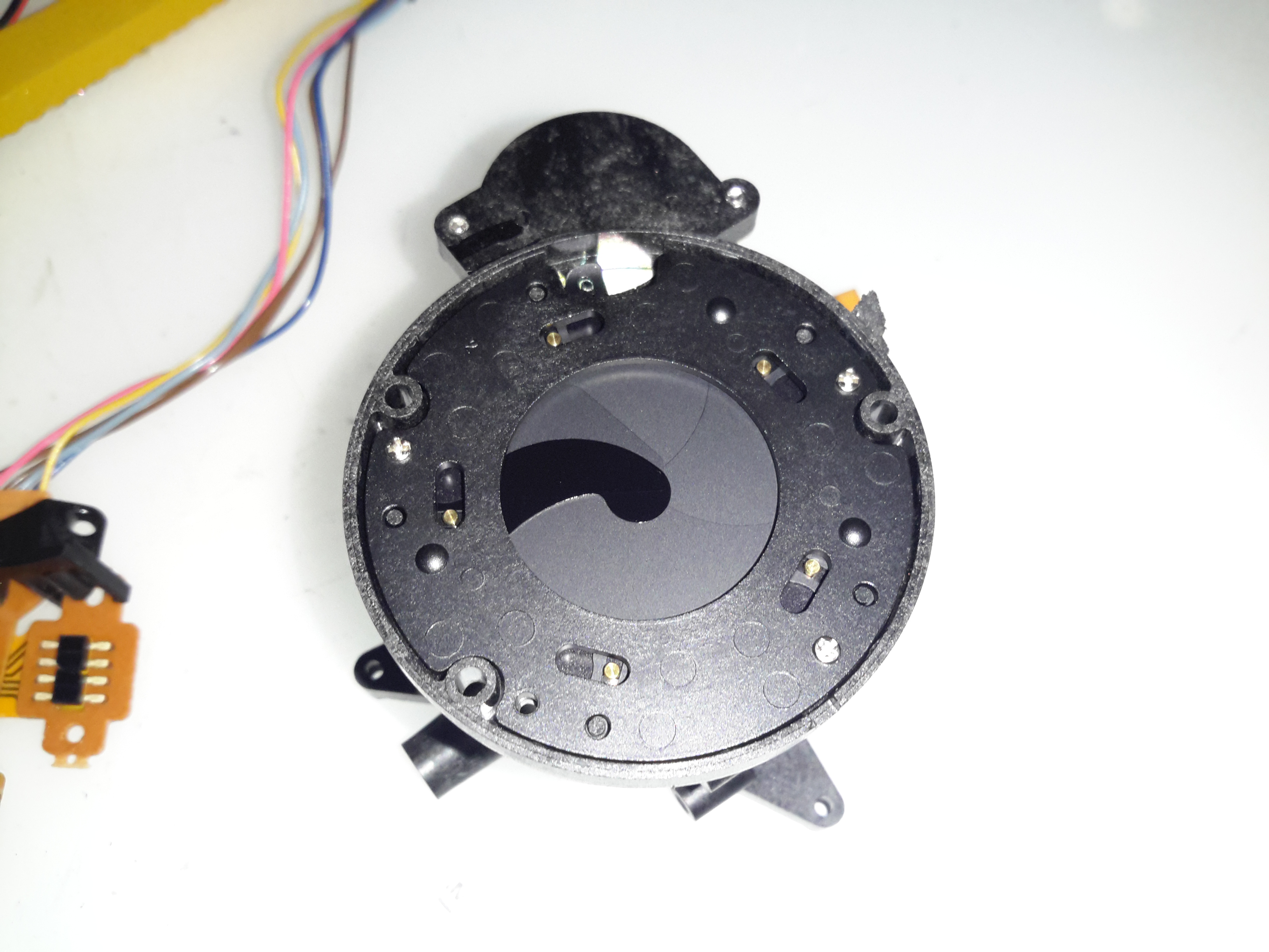
Iris Assembly
The iris is mounted just before the CCD, this is controlled with a galvanometer-type device with position sensors incorporated.
Iris Opening
Pushing on the operating lever with the end of my screwdriver opens the leaves of the iris against the return spring.
Tape Transport & Main Control
Main Control Board
Tucked into the side of the main body of the unit is the main system control board. This PCB houses all the vital functions of the camera: Power Supply, Servo Control, Colour Control,Video Amplifiers, etc.
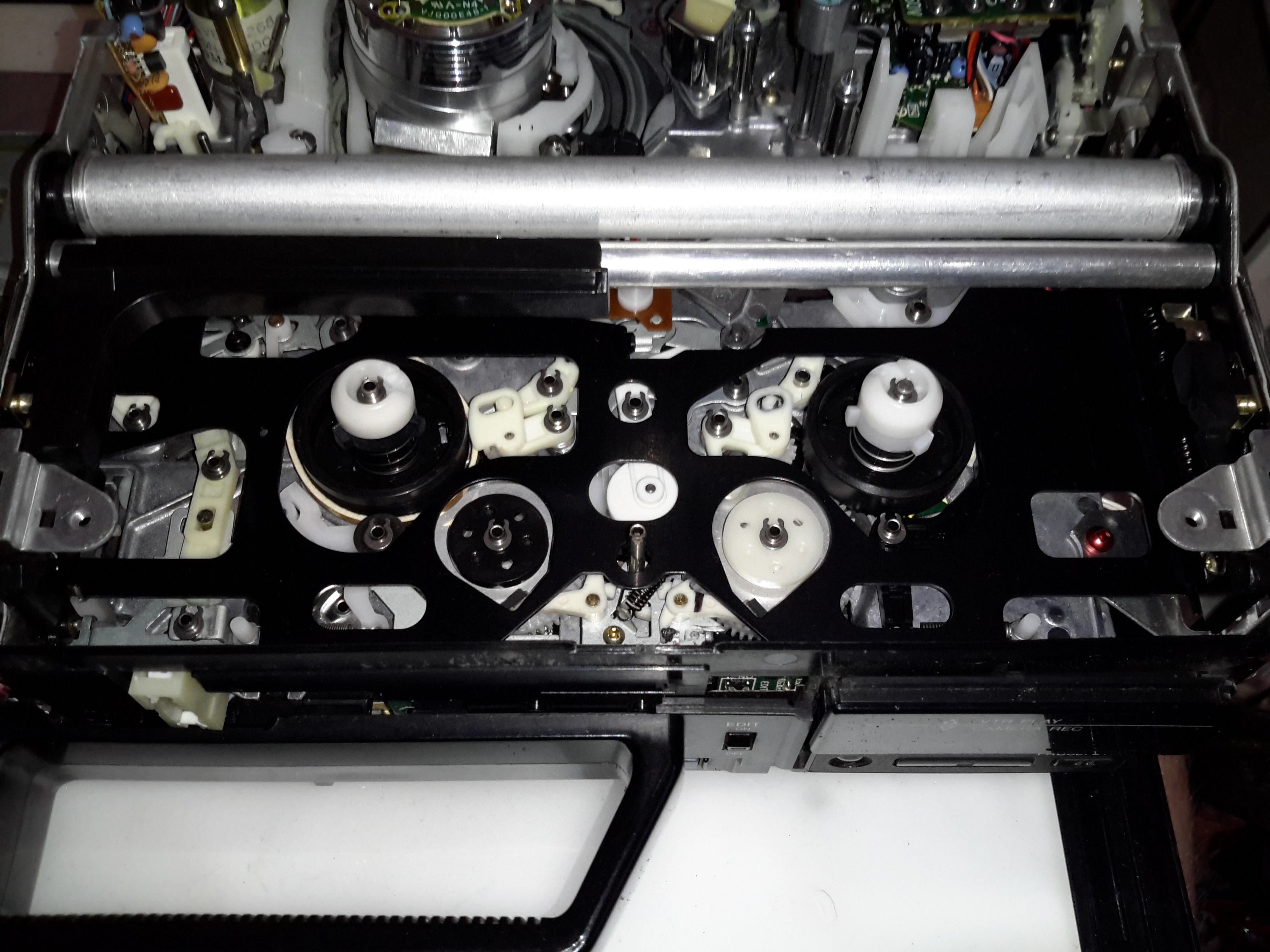
Tape Drum
Here’s the main tape transport mechanism, this is made of steel & aluminium stampings for structural support. The drum used in this transport is noticeably smaller than a standard VHS drum, the tape is wrapped around more of the drum surface to compensate.
Tape Transport
The VHS tape sits in this carriage & the spools drive the supply & take up reels in the cartridge.
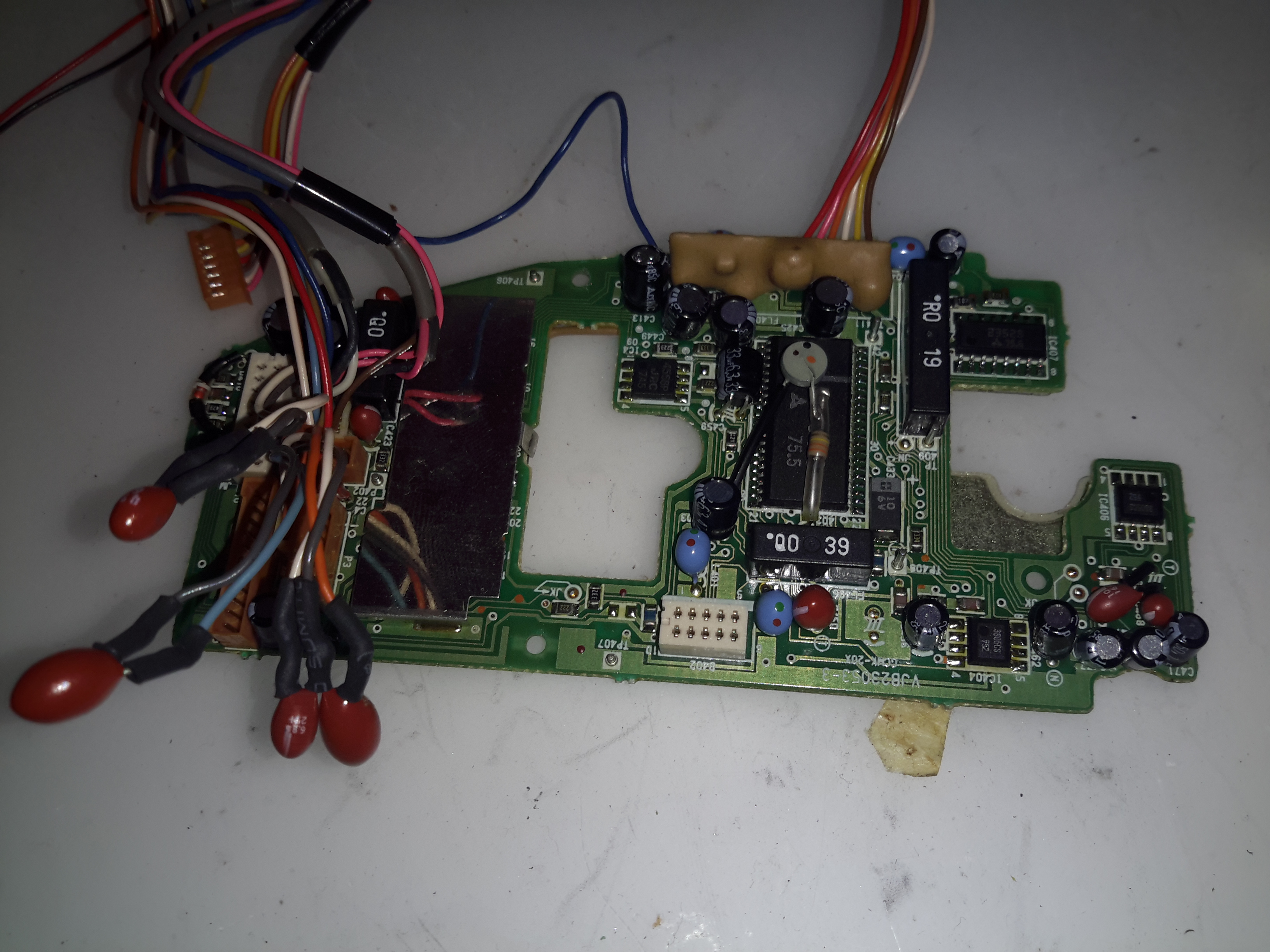
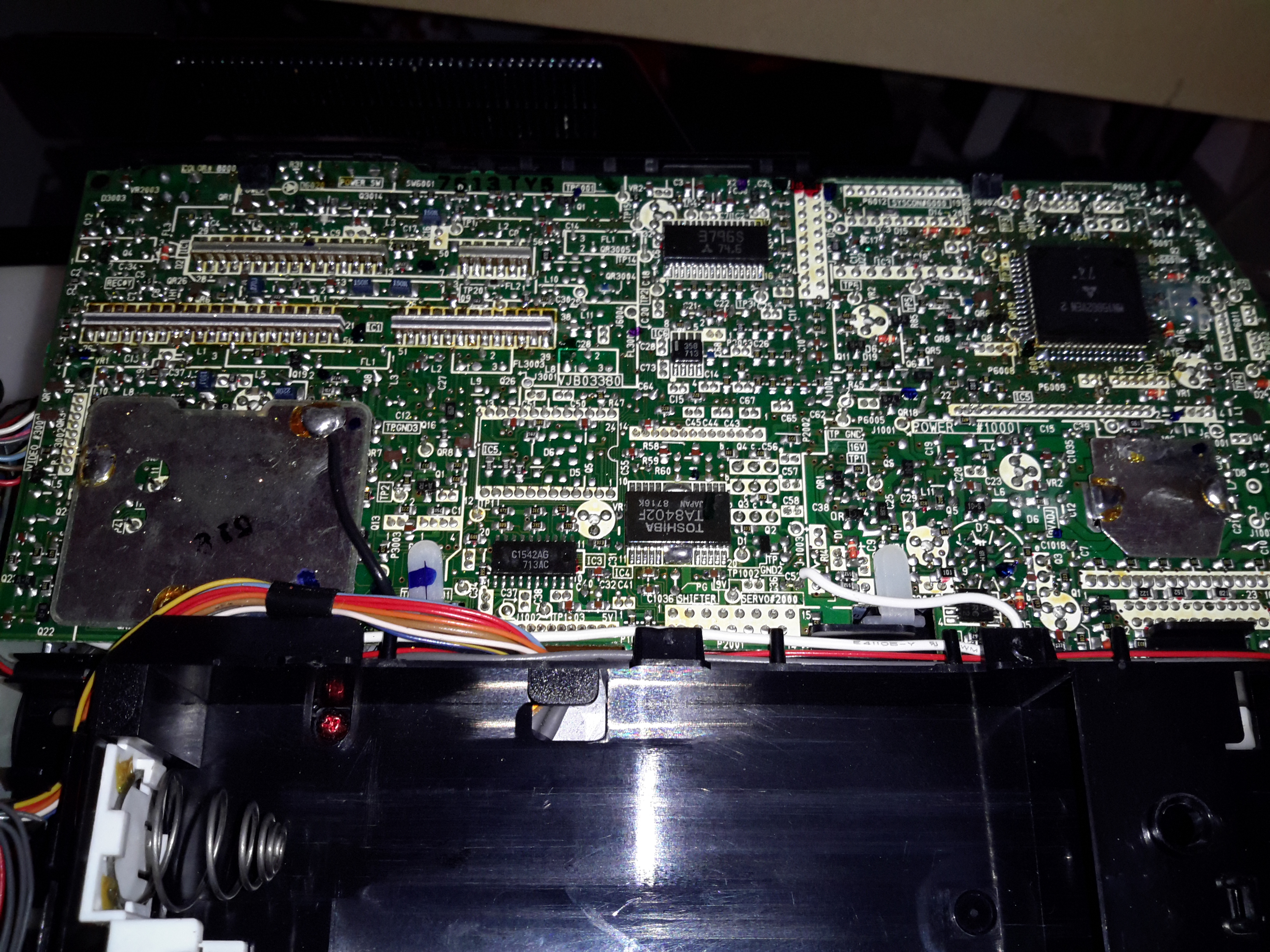
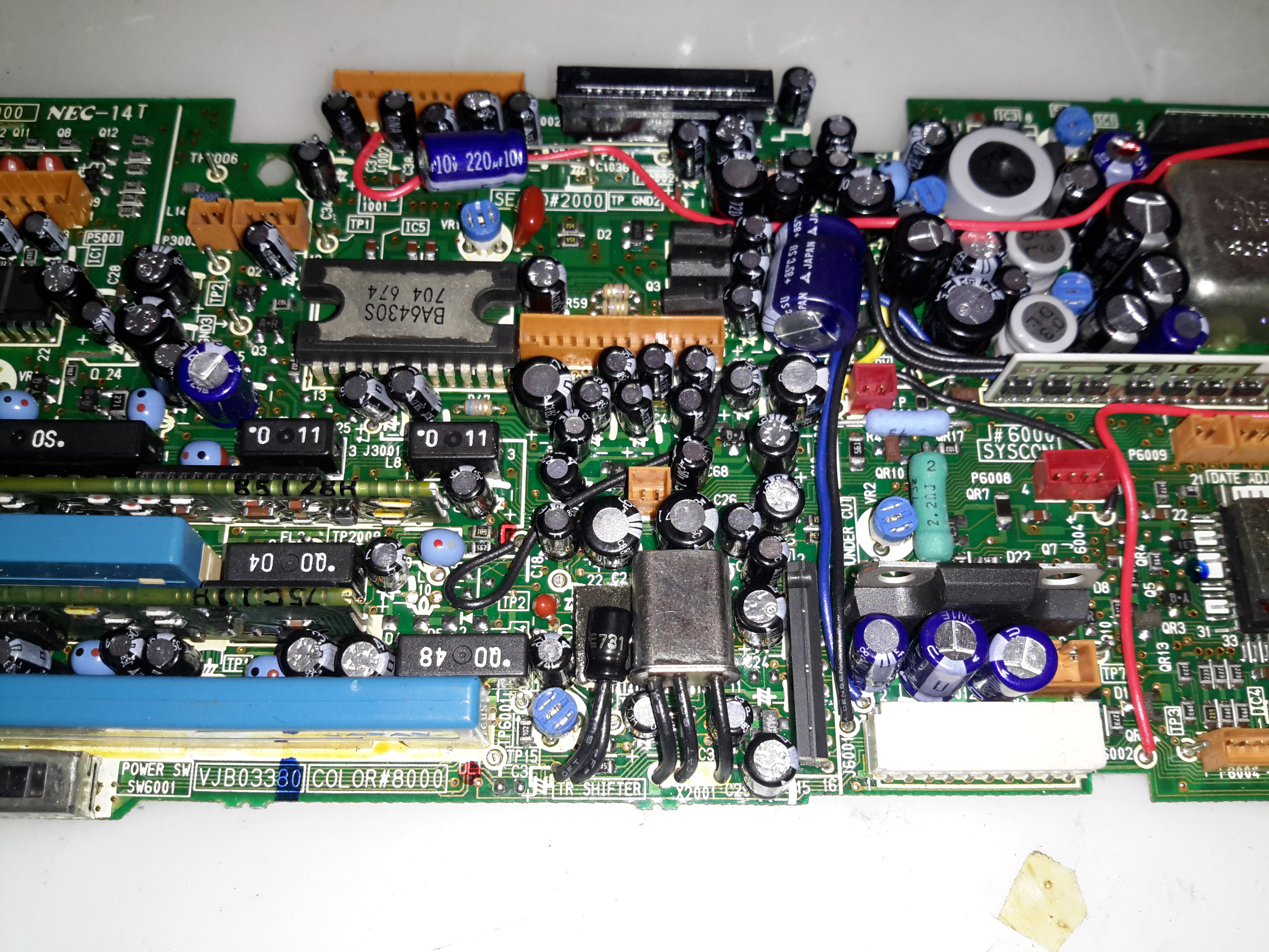
Main Control PCB
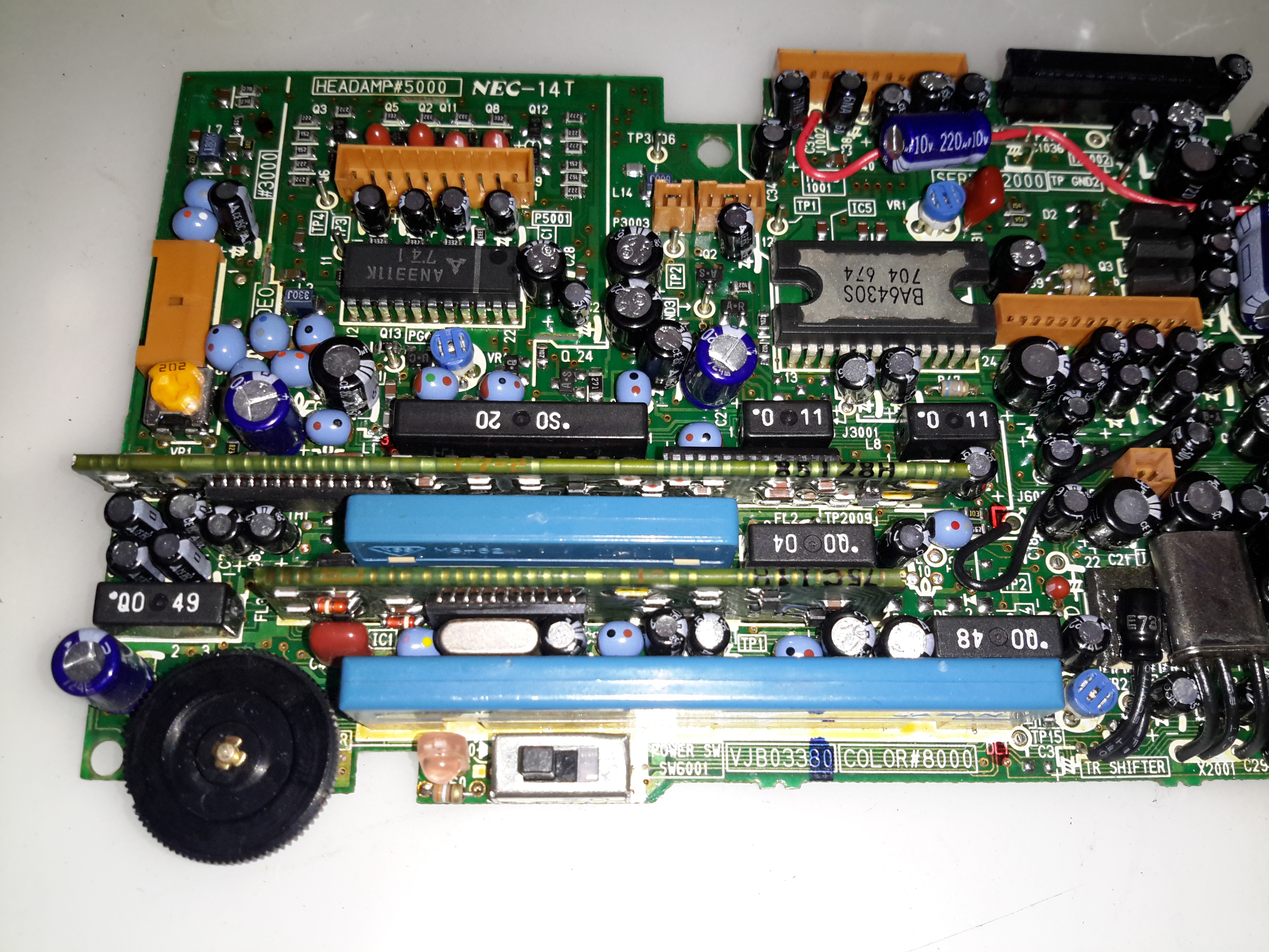
Here’s the component side of the main control PCB. This one is very densely packed with parts, I wouldn’t like to try & troubleshoot something like this!
Main PCB Left
The left side has the video head amp at the top, a Panasonic AN3311K 4-head video amp. Below that is video processing, the blue components are the analogue delay lines. There are a couple of hybrid flat-flex PCBs tucked in between with a couple of ICs & many passives. These hybrids handle the luma & chroma signals.
Top left is the capstan motor driver a Rohm BA6430S. The transport motors are all 3-phase brushless, with exception of the loading motor, which is a brushed DC type.
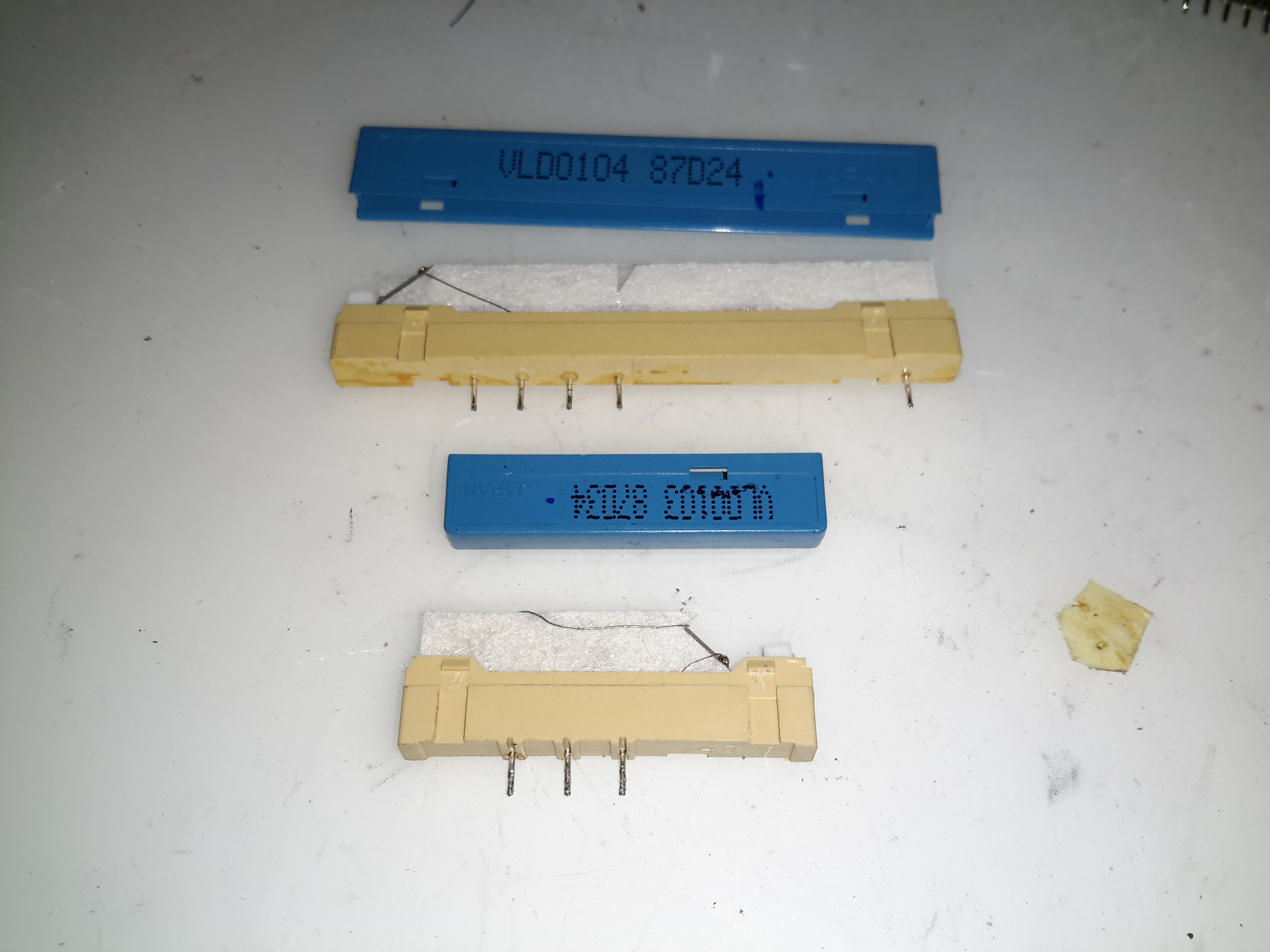
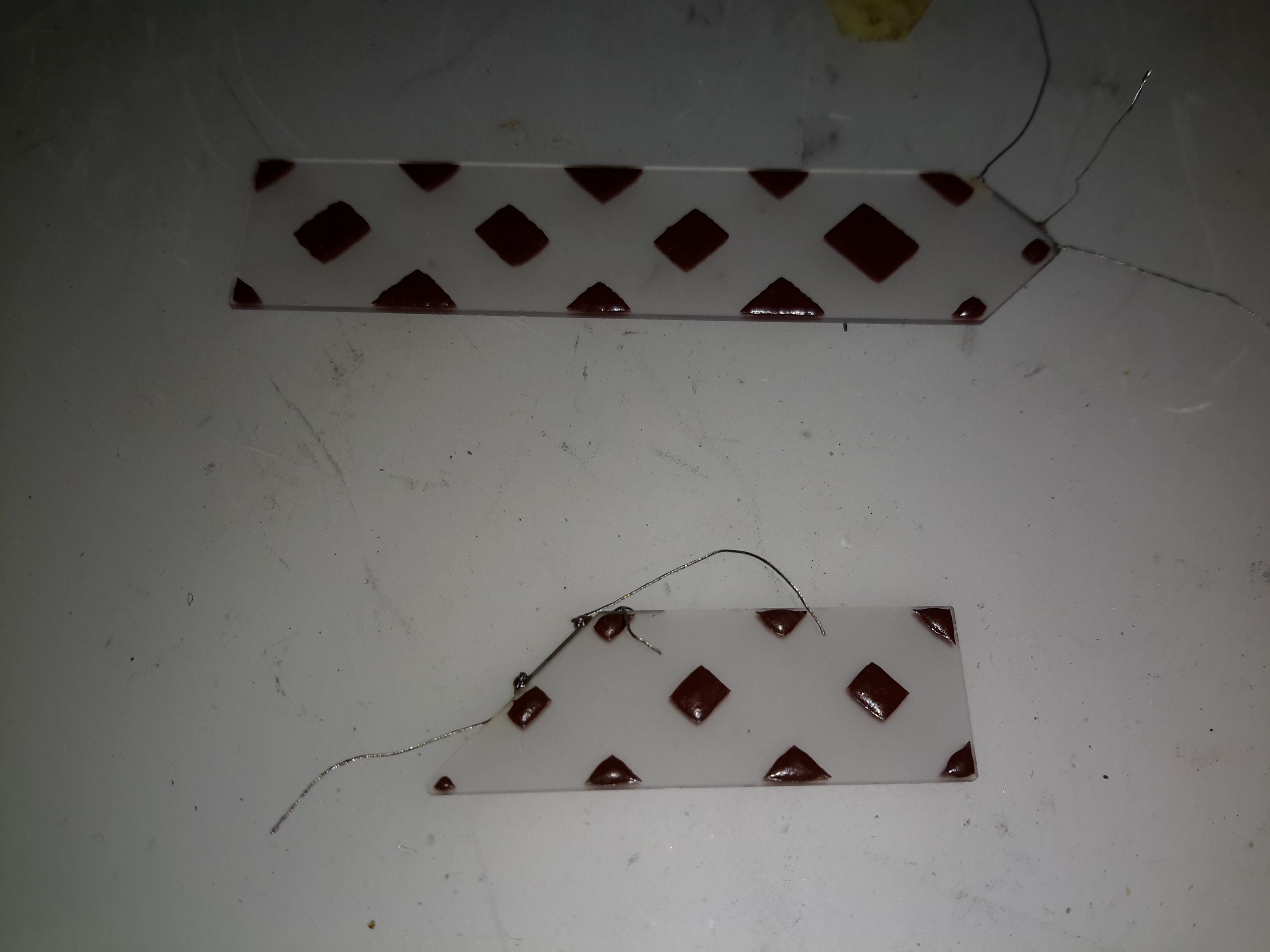
Delay Line
Here’s what is inside the delay lines for the analogue video circuits. The plastic casing holds a felt liner, inside which is the delay line itself.
Internal Glass
The delay is created by sending an acoustic signal through the quartz crystal inside the device by a piezoelectric transducer, bouncing it off the walls of the crystal before returning it to a similar transducer.
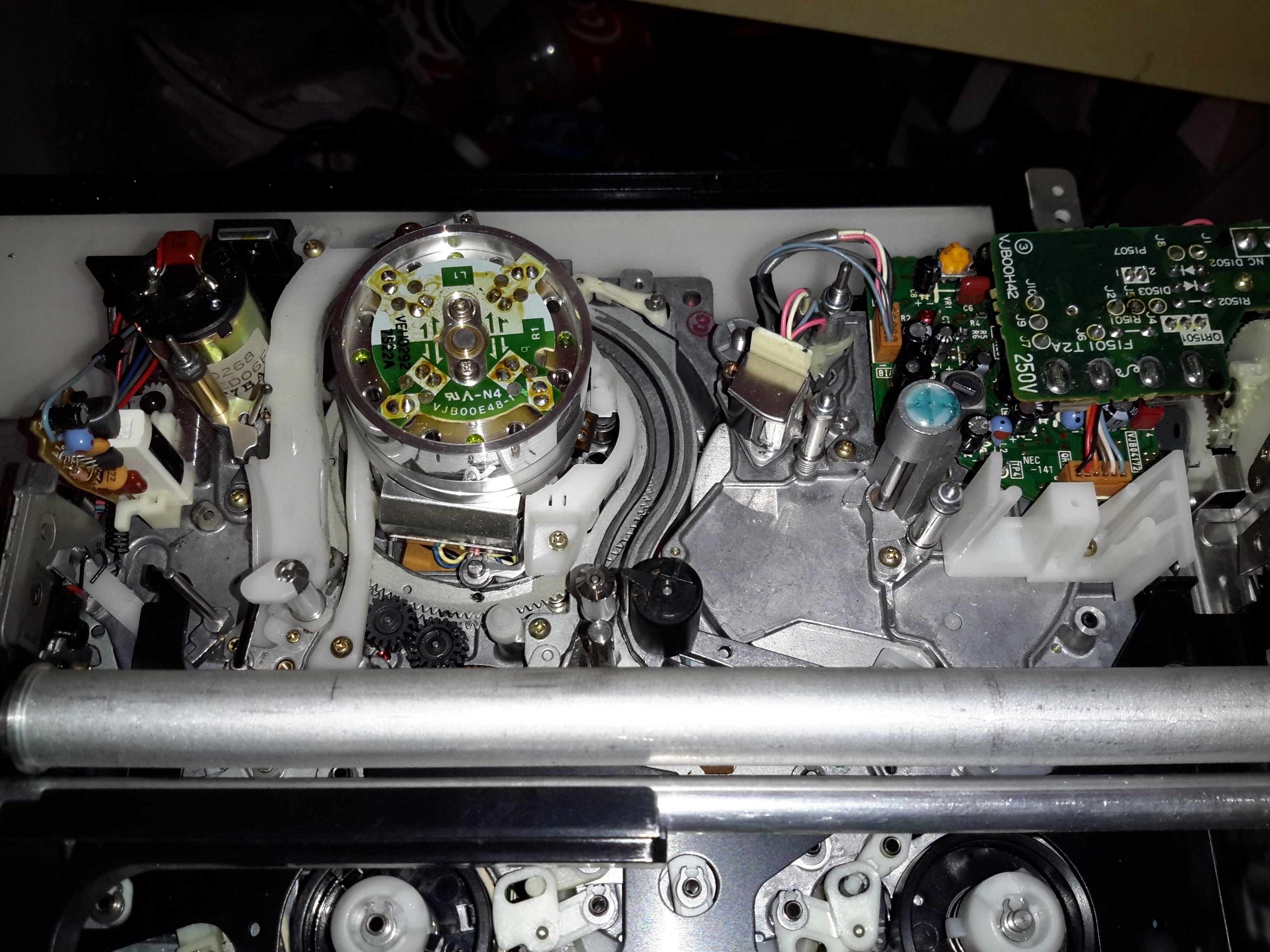
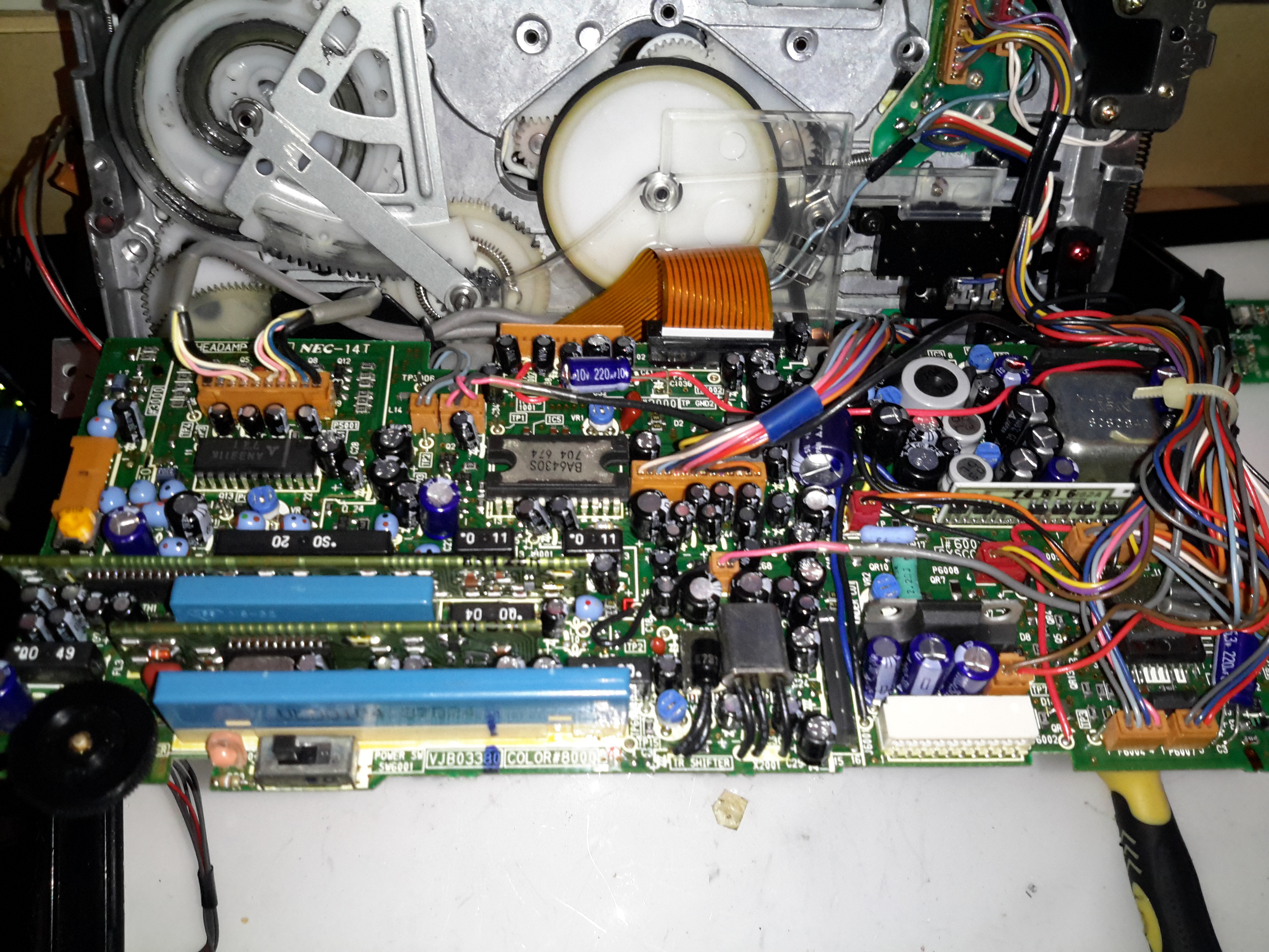
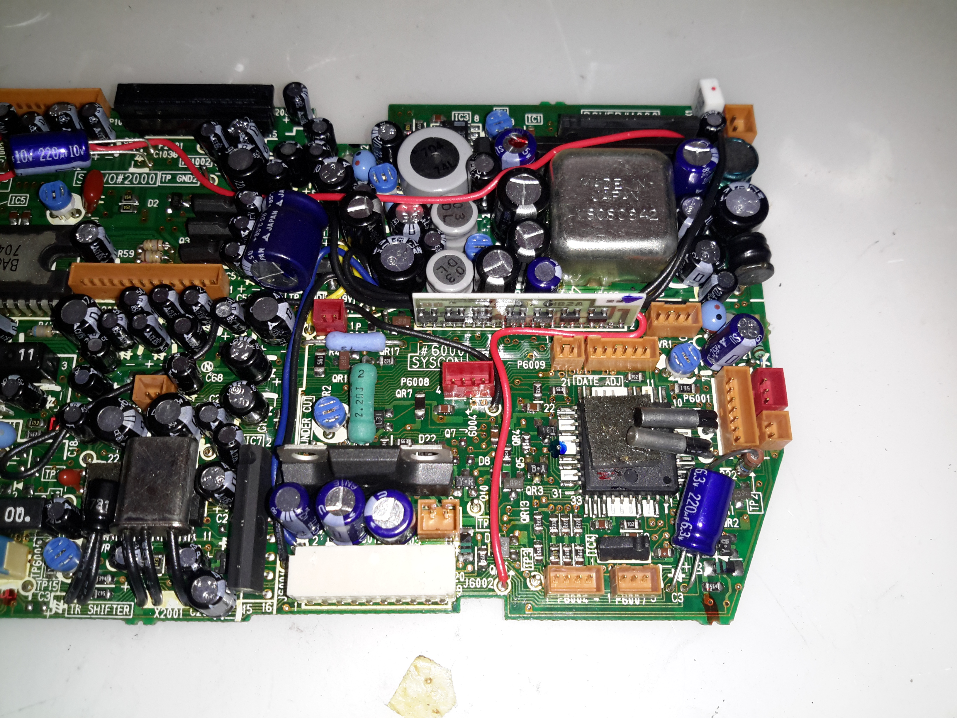
Main PCB Centre
Here’s the centre of the board, the strange crystal at bottom centre is the clock crystal for the head drum servo. Why it has 3 pins I’m not sure, only the two pins to the crystal inside are shown connected on the schematic. Maybe grounding the case?
The main servo controls for the head drum & the capstan motor are top centre, these get a control signal from the tape to lock the speed of the relative components.
Main PCB Right
Here’s the right hand side. The main power supply circuitry is at top right, with a large can containing 4 switching inductors & a ferrite pot core transformer. All these converters are controlled by a single BA6149 6-channel DC-DC converter controller IC via a ULN2003 transistor array.
The ceramic hybrid board next to the PSU has 7 switch transistors for driving various indicator LEDs.
The large tabbed IC bottom centre is the loading motor drive, an IC from Mitsubishi, the M54543. This has bidirectional DC control of the motor & built in braking functions. The large quad flat pack IC on the right is the MN1237A on-screen character generator, with the two clock crystals for the main microcontroller.
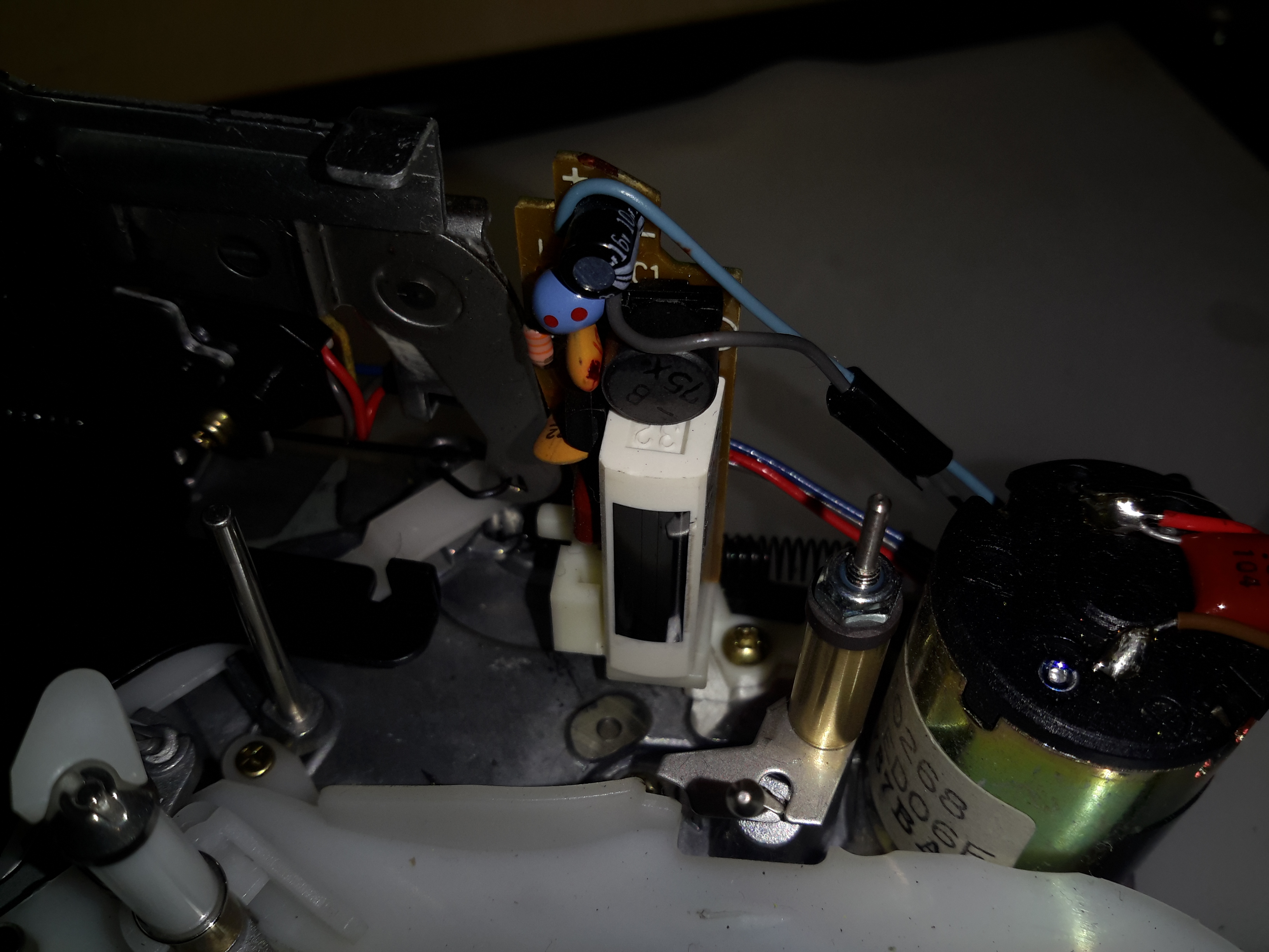
Erase Head
The full erase head has it’s power supply & oscillator on board, applying 9v to this board results in an AC signal to the head, which erases the old recording from the tape before the new recording is laid down by the flying heads on the drum.
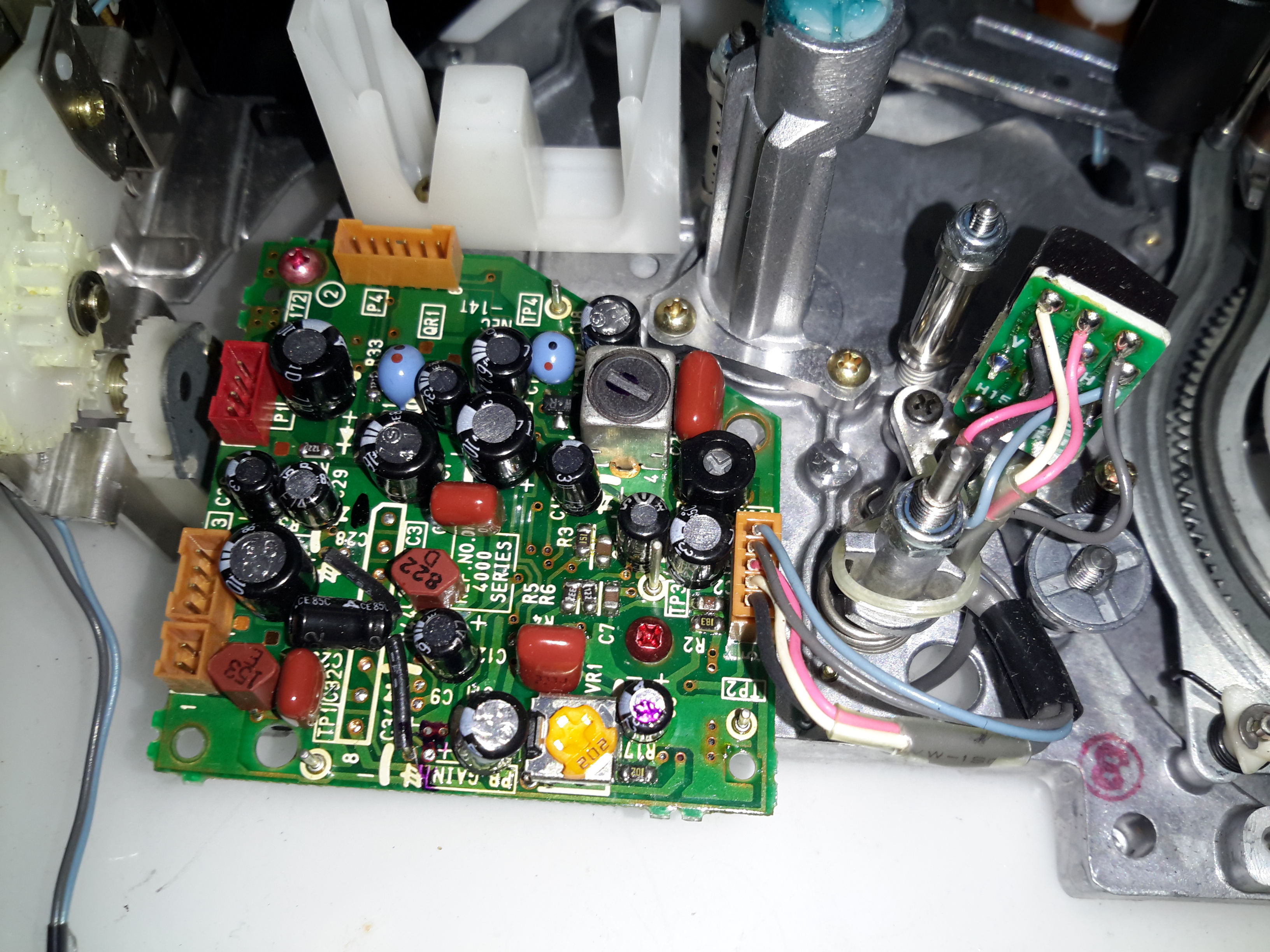
Audio Control PCB
The Audio & Control head is connected to this PCB, which handles both reading back audio from the tape & recording new audio tracks. The audio bias oscillator is on this board, & the onboard microphone feeds it’s signal here. The control head is fed directly through to the servo section of the main board.
Drum Motor
The motor that drives the head drum is another DC brushless 3-phase type.
Hall Sensors
These 3 Hall sensors are used by the motor drive to determine the rotor position & time commutation accordingly.
Stator
The stator on this motor is of interesting construction, with no laminated core, the coils are moulded into the plastic holder. The tach sensor is on the side of the stator core. This senses a small magnet on the outside of the rotor to determine rotational speed. For PAL recordings, the drum rotates at 1500 RPM.
Motor Removed
Not much under the stator other than the bearing housing & the feedthrough to the rotary transformer.
Head Disc
The heads are mounted onto the top disc of the drum, 4 heads in this recorder. The signals are transmitted to the rotating section through the ferrite rotary transformer on the bottom section.
Head Chip
The tiny winding of the ferrite video head can just about be seen on the end of the brass mounting.
Capstan Motor Components
The capstan motor is similar to the drum motor, only this one is flat. The rotor has a ferrite magnet, in this case it wasn’t glued in place, just held by it’s magnetic field.
Capstan Motor Stator
The PCB on this motor has a steel backing to complete the magnetic circuit, the coils for the 3 motor phases are simply glued in place. The Hall sensors on this motor are placed in the middle of the windings though.
Again there is a tach sensor on the edge of the board that communicates the speed back to the controller. This allows the servo to remain locked at constant speed.
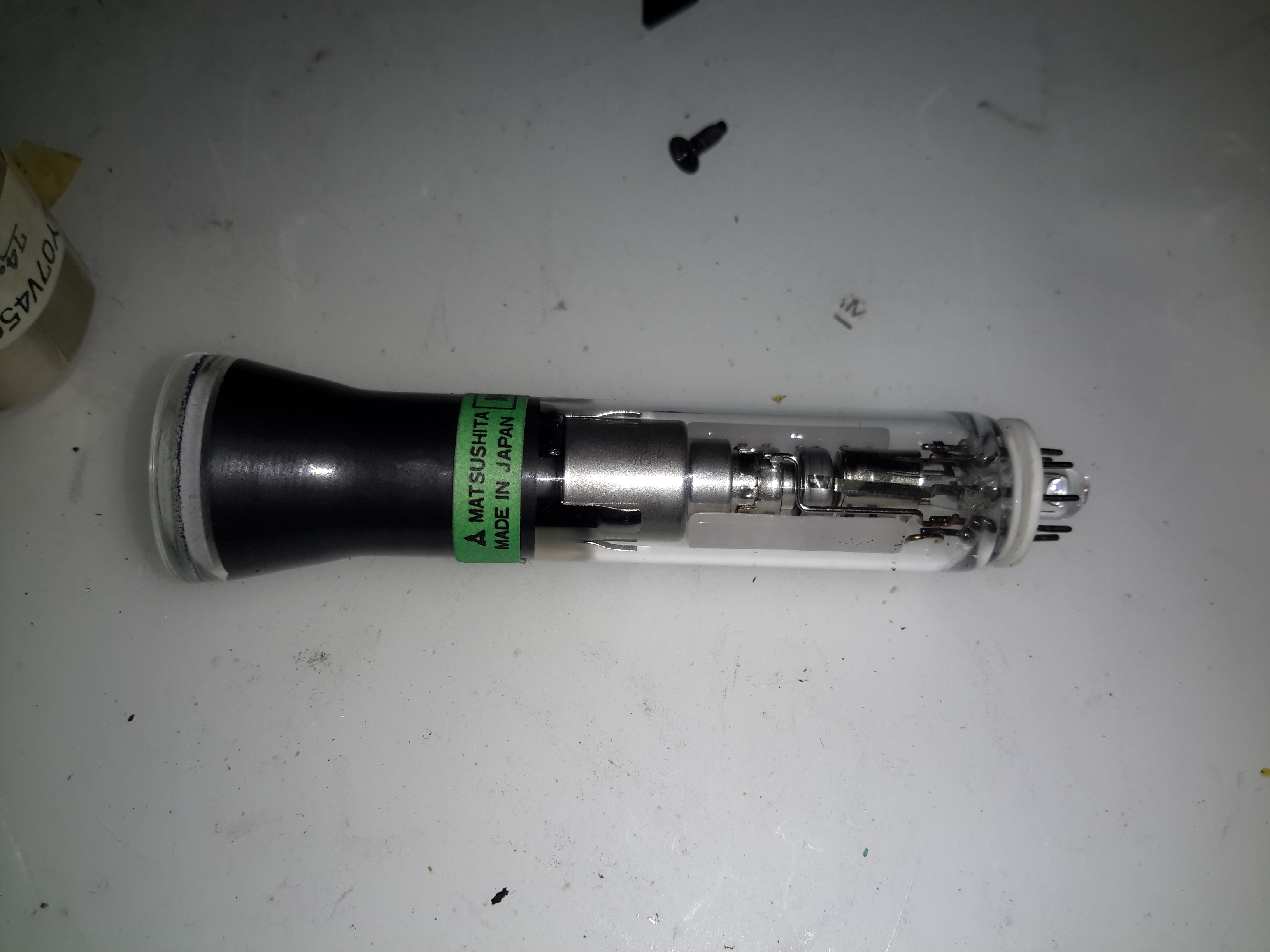
Viewfinder
Viewfinder Assembly
As usual with these cameras, this section is the CRT based viewfinder. These units take the composite signal from the camera to display the scene. This one has many more pins than the usual viewfinder. I’ll hack a manual input into this, but I’ll leave that for another post.
Viewfinder Circuits
Being an older camera than the ones I’ve had before, this one is on a pair of PCBs, which are both single-sided.
Main Viewfinder Board
The main board has all the power components for driving the CRT & some of the adjustments. The main HV flyback transformer is on the right. This part creates both the final anode voltage for the tube & the focus/grid voltages.
Viewfinder Control PCB Top
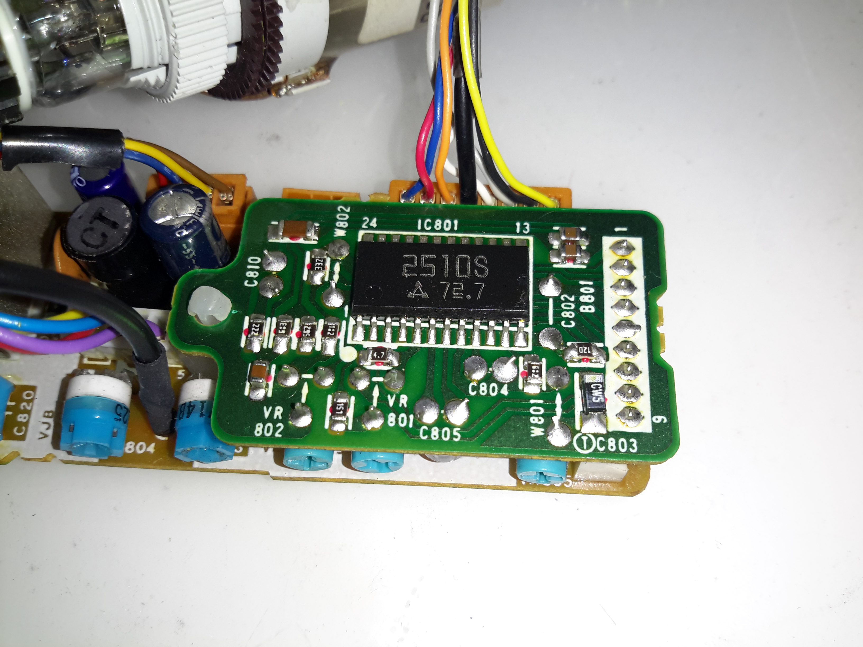
The viewfinder control IC is on a separate daughter board in this camera, with two more controls.
Control IC
The control IC is a Matsushita AN2510S, this has all the logic required to separate the sync pulses from the composite signal & generate an image on the CRT.
Viewfinder CRT Frame
The recording indicator LEDs are mounted in the frame of the CRT & appear above the image in the viewfinder.
Viewfinder CRT With Yoke
Here the CRT has been separated from the rest of the circuitry with just the deflection yoke still attached.
M01JPG5WB CRT
The electron gun in this viewfinder CRT is massive in comparison to the others that I have seen, and the neck of the tube is also much wider. These old tubes were very well manufactured.
Viewfinder Optics
A simple mirror & magnifying lens completes the viewfinder unit.
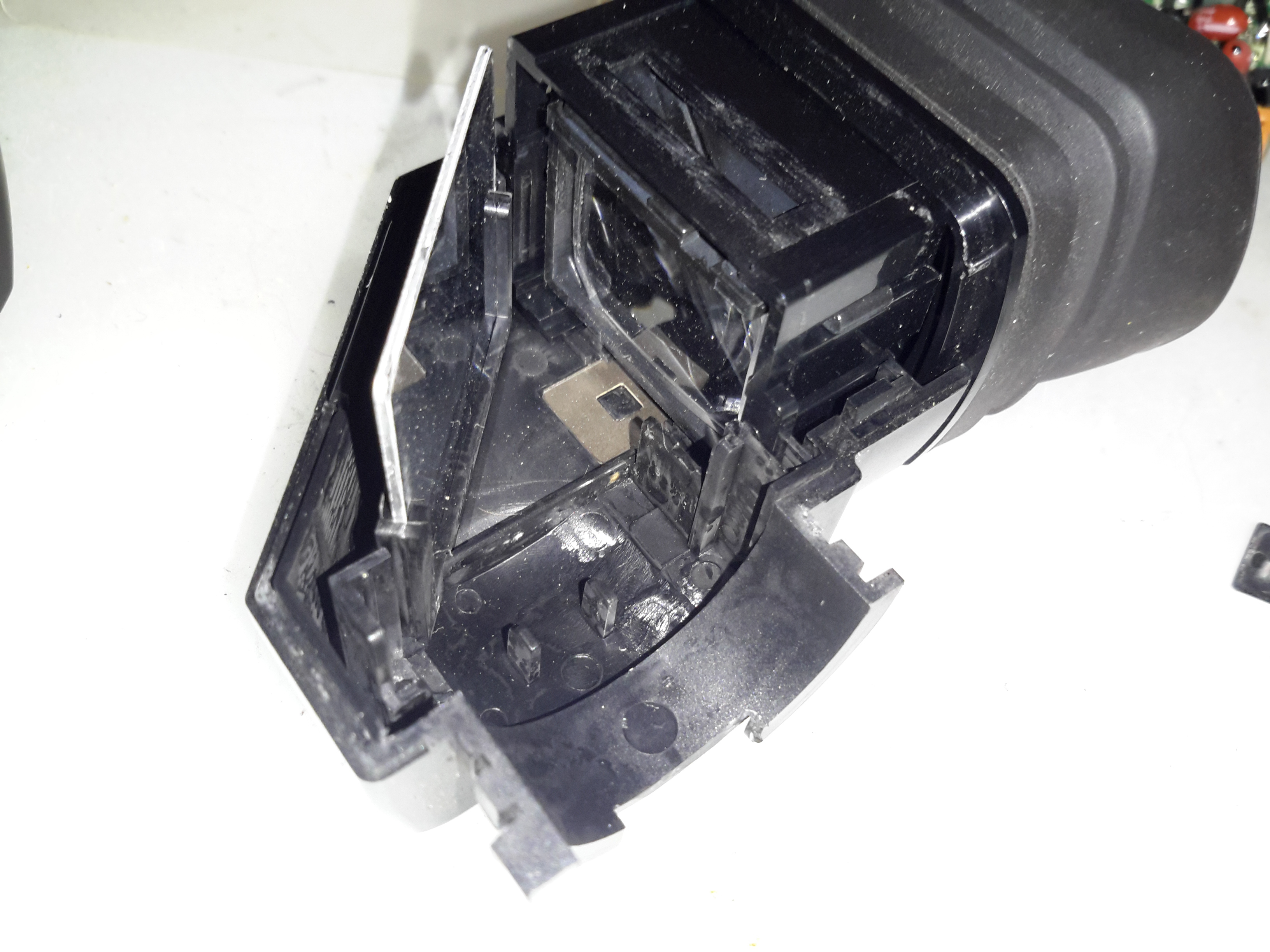
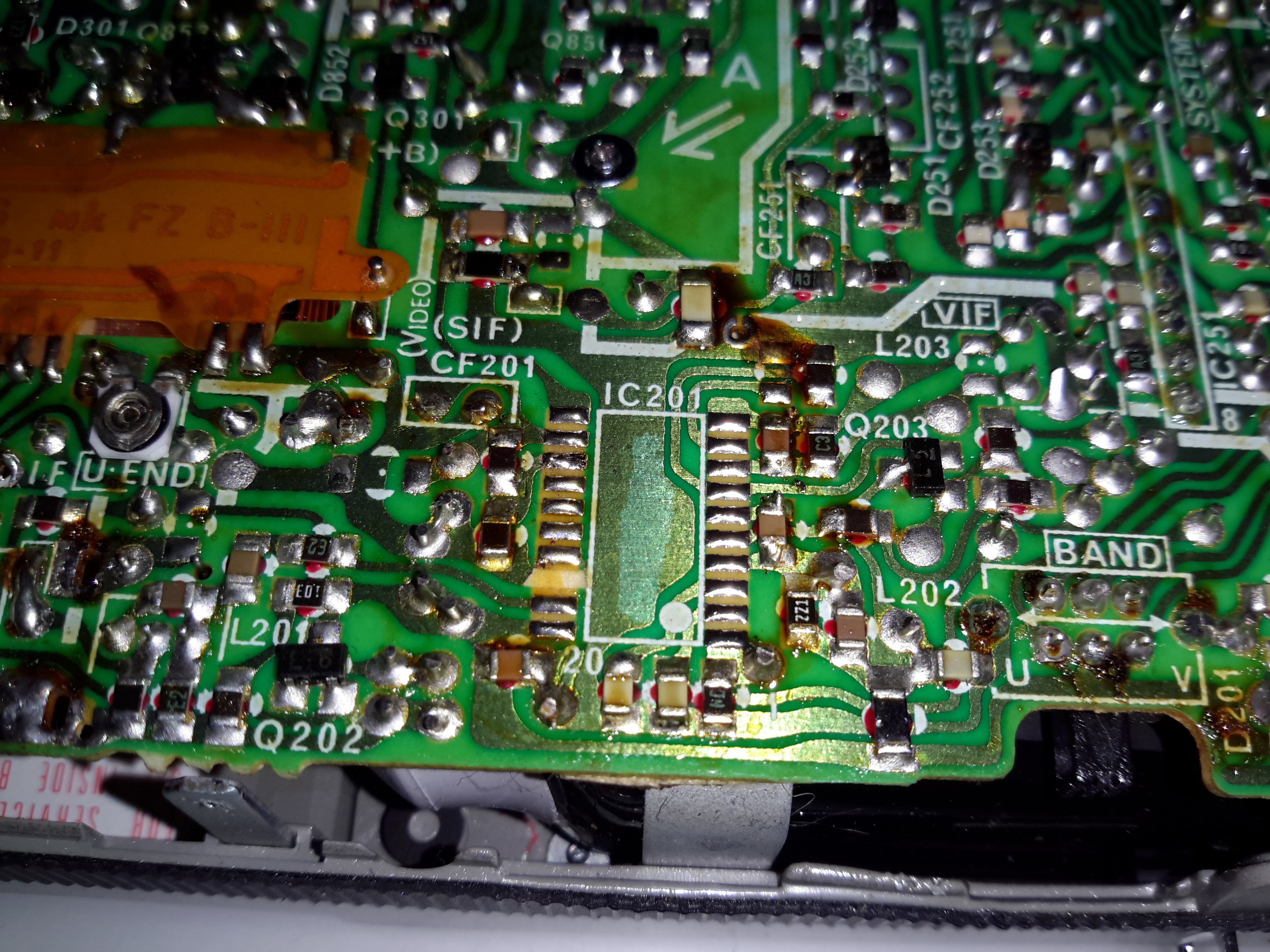
Hacking the Sony FD-20 to accept a composite input is easy – the tuner receives the RF transmission, produces an IF, this is then fed into IC201, a Mitsubishi M51364P Video IF Processor. The VIF IC then separates out the composite video signal, which is output on Pin 13 (in photo above, left side, 3rd pin from the top). The audio is separated out & sent via Pin 11 to the Audio IF processor.
In the above photo, the VIF IC has been removed from the board with hot air, as it was interfering with the signal if left in place. The RF tuner was also desoldered & removed. Unfortunately I managed to mangle a pad, which is the ground pin for the VIF IC. This isn’t much of an issue though, as an identical signal ground is available, just to the left of the IC.
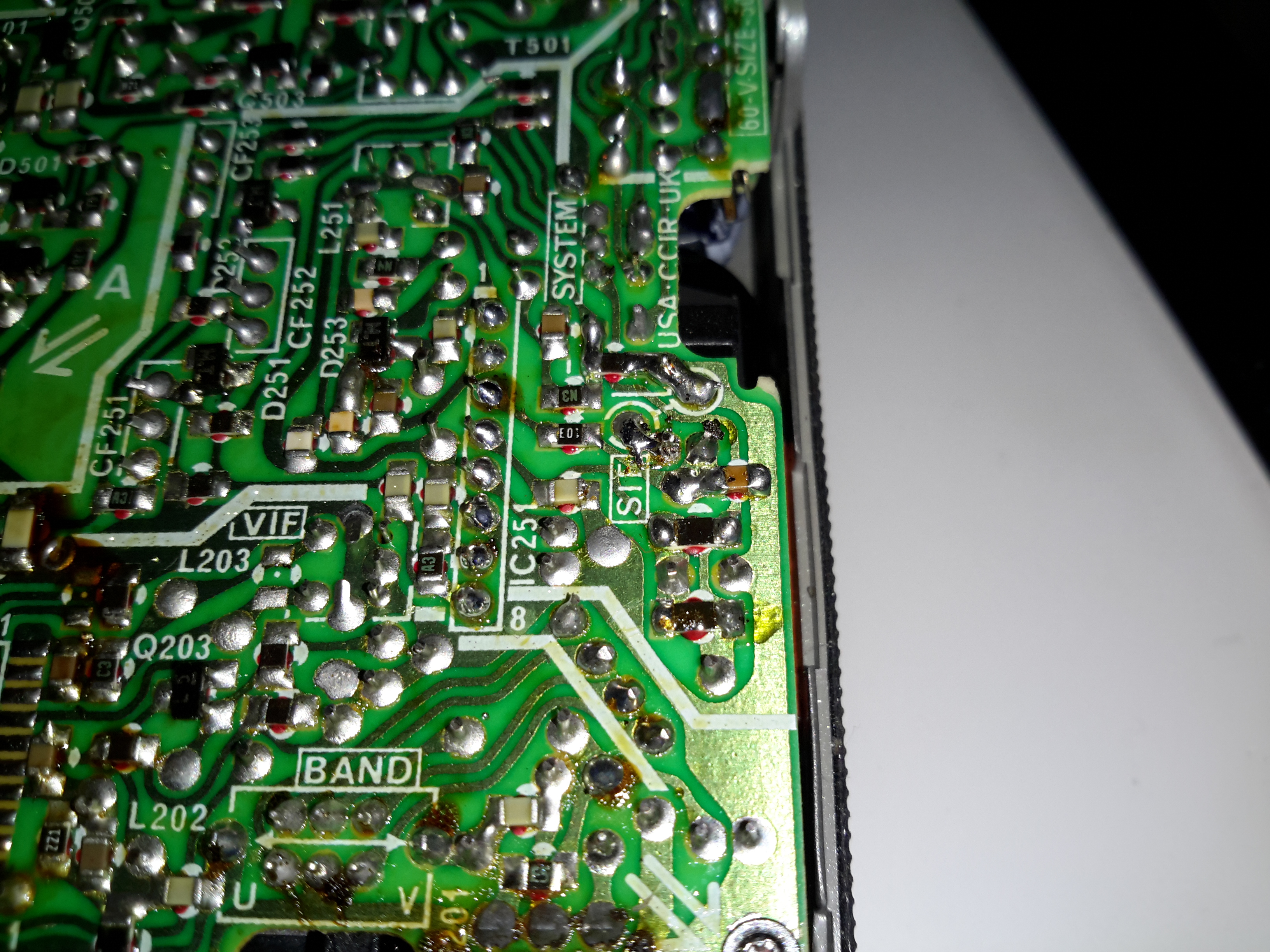
Audio Input
The audio can be tapped into in a similar way, the circled pad in the centre of the photo marked SIF is the place, this is the output of the Audio IF processor to the audio amplifier. The Audio IF processor didn’t interfere with the injected signal, so it was left in place.
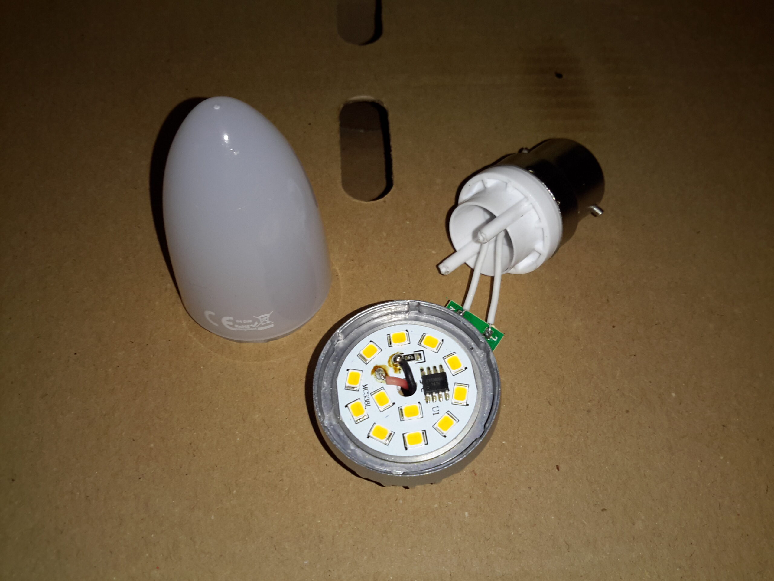
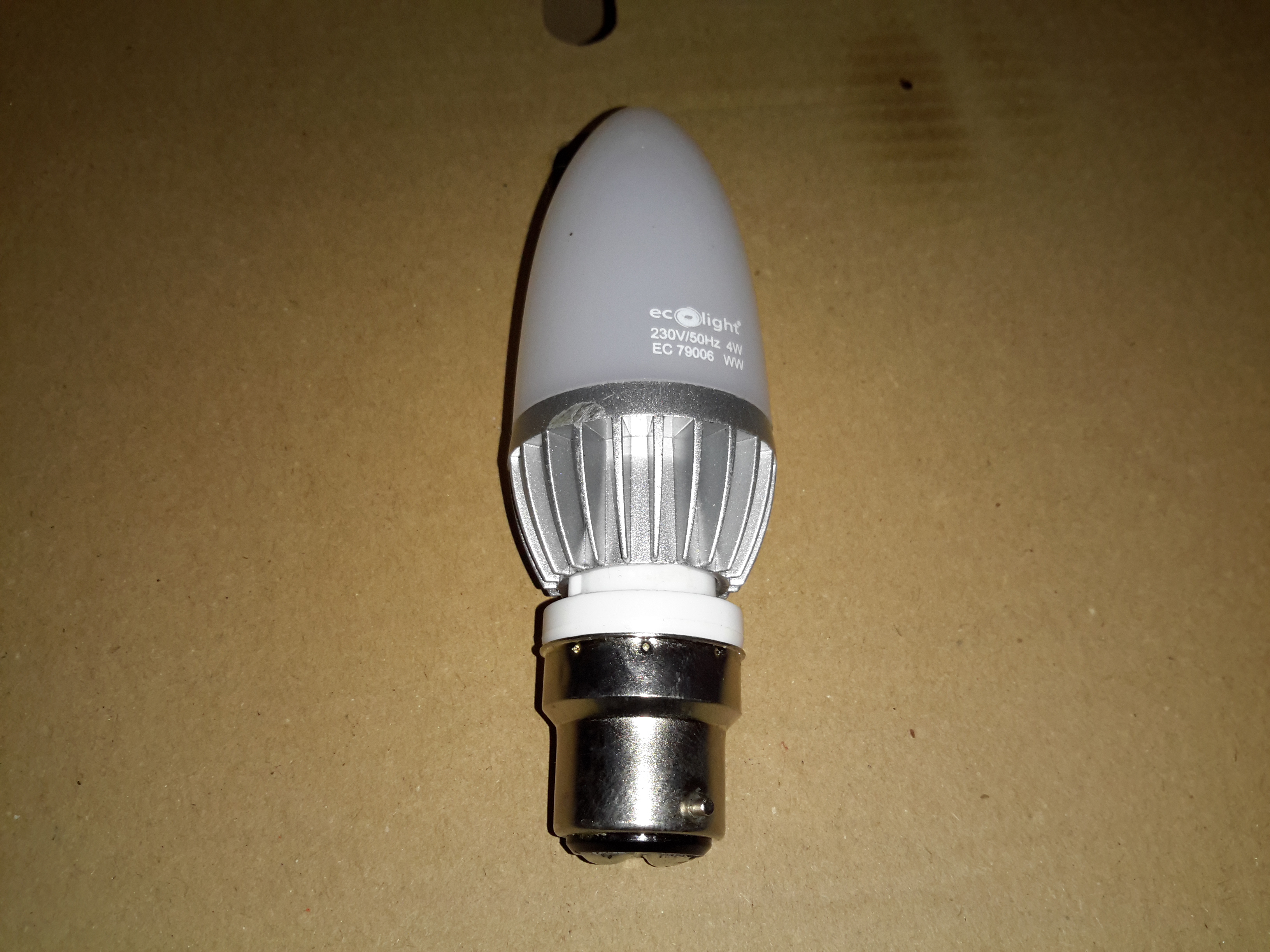
Here’s a modern LED bulb, that unfortunately decided to disassemble itself within a few minutes of being installed in a light fitting! The base plastic snapped off the main aluminium body at the screw posts!
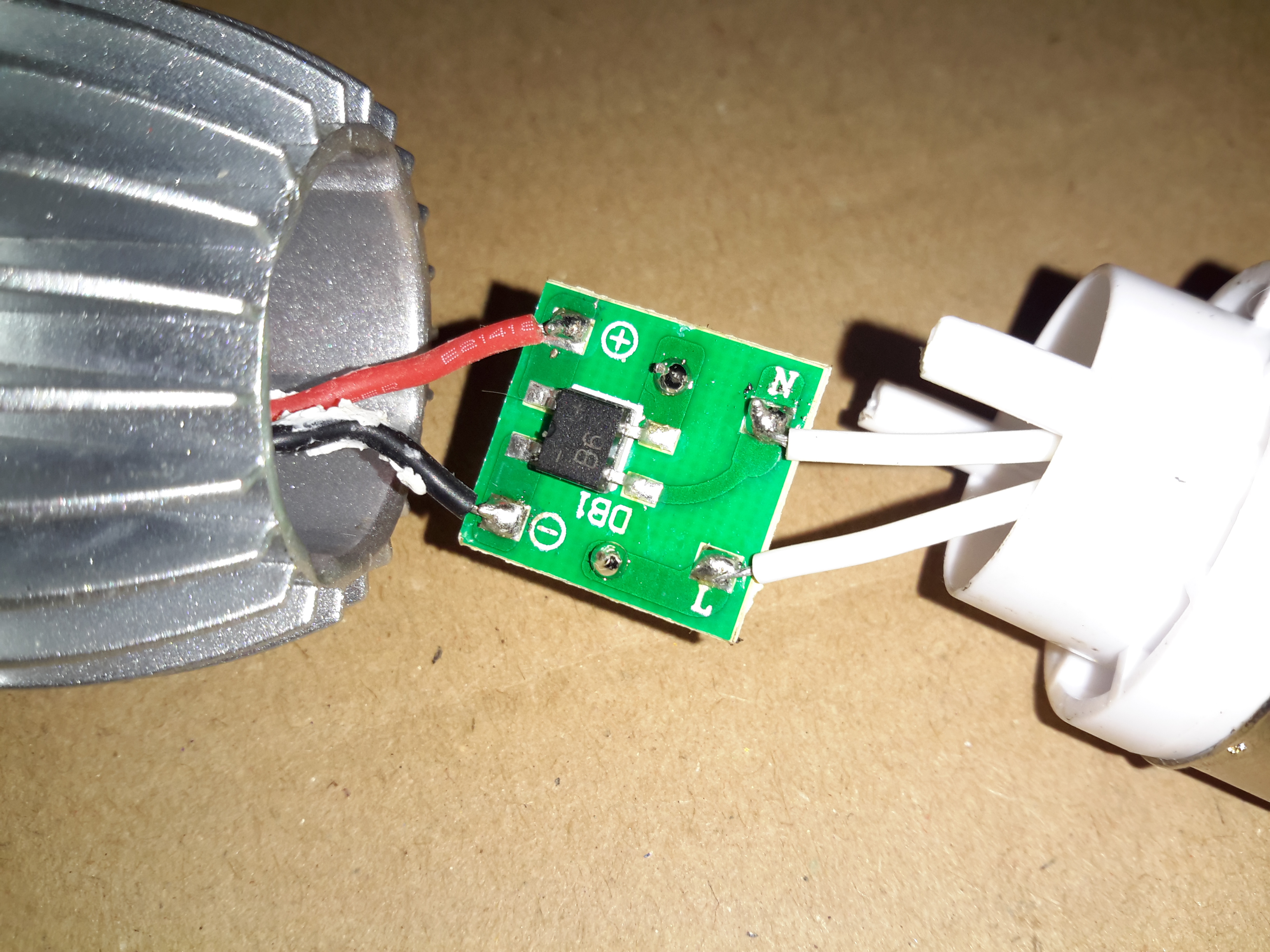
Input Rectifier
The PCB in the base holds nothing but the input components. Above is the bridge rectifier.
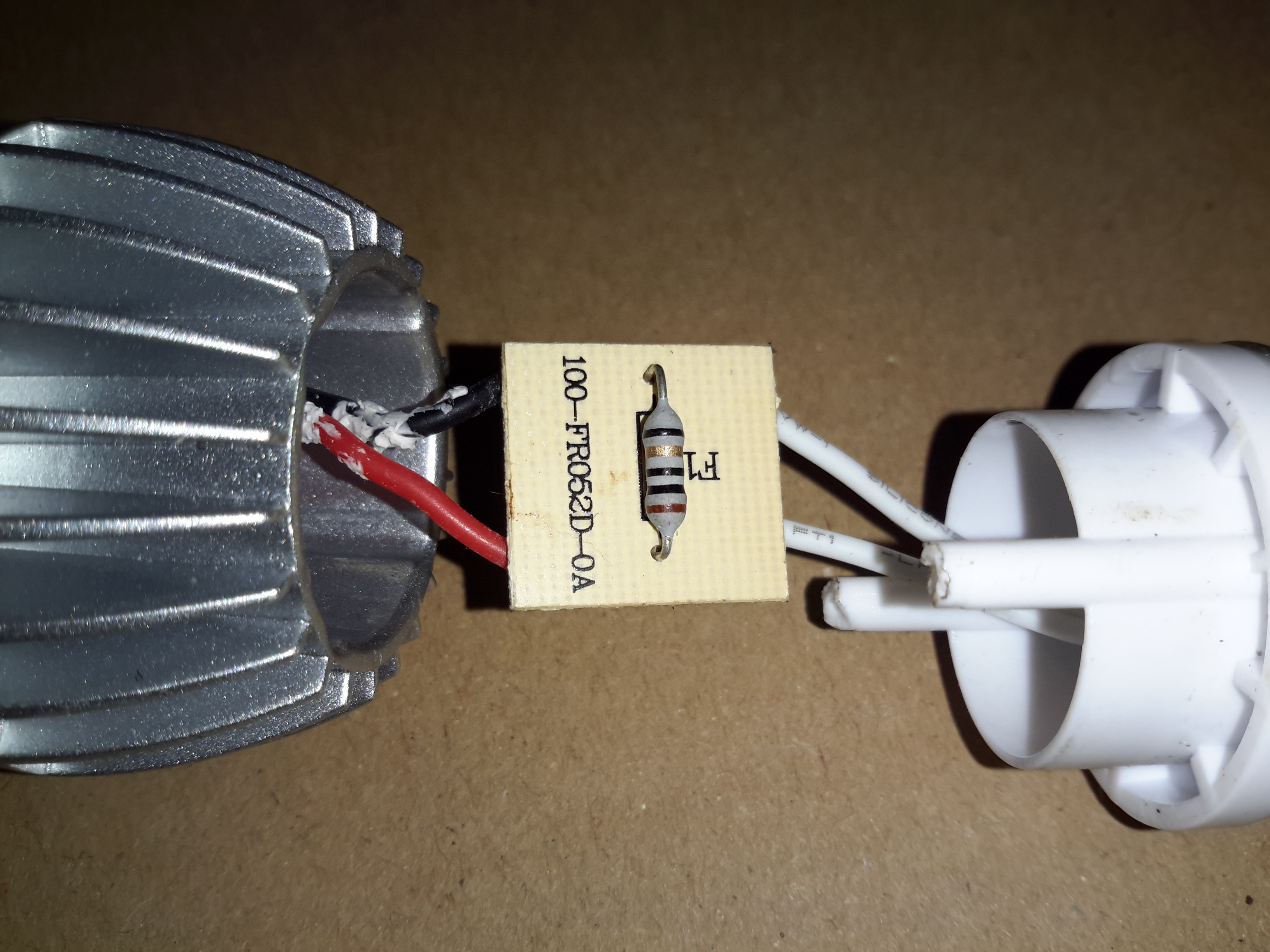
Fusible Resistor
The other side of the PCB has a 10Ω fusible resistor, for protection.
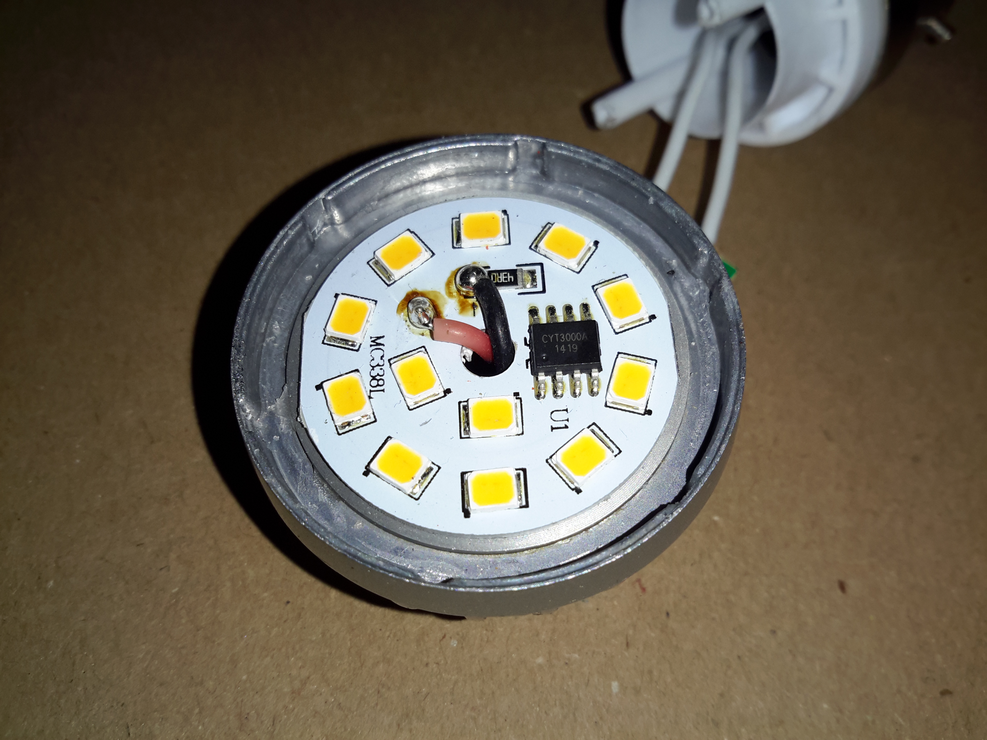
LED PCB
The LED PCB itself has the driver IC, which is a CYT3000A linear constant current IC, that runs direct from full-wave rectified mains. The single resistor sets the LED current, but there aren’t any smoothing capacitors on the DC rail, so this bulb would flicker a lot.
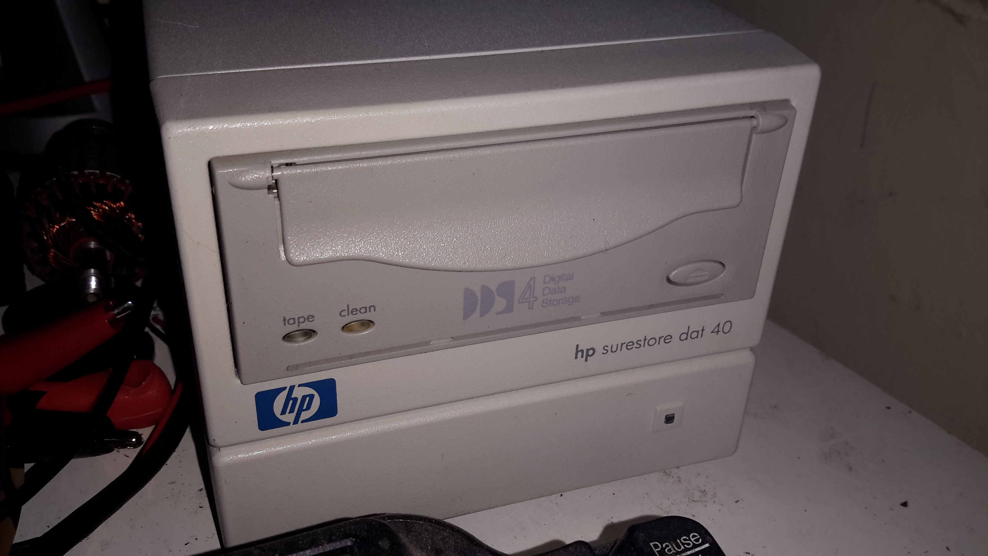
Magnetic tape is the medium of choice for my offline backups & archives, as it’s got an amazing level of durability when in storage. (LTO Has a 30 year archival rating).
For the smaller stuff, like backing up the web server this very site runs on, another format seemed to suit better. Above is a HP DDS4 tape drive, which will store up to 40GB on a cassette compressed.
I picked this format since I already had some tapes, so it made sense.
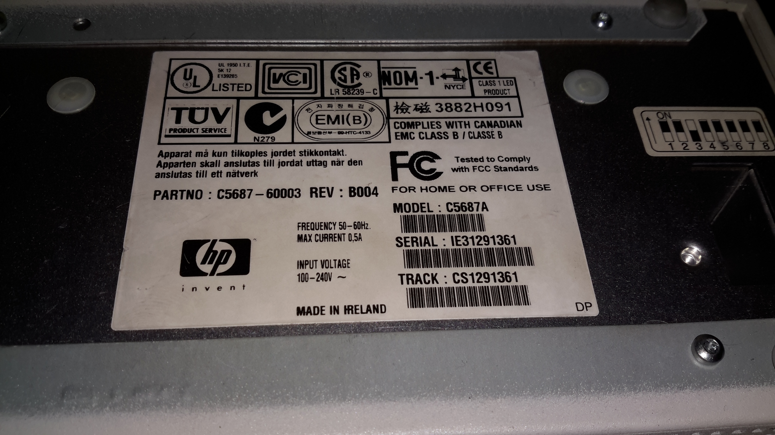
Data Plate
Here’s the info for those who want to know. It’s an older generation drive, mainly since the current generation of tape backup drives are hideously expensive, while the older ones are cheap & plentiful. Unfortunately the older generation of drives are all parallel SCSI, which can be a expensive & awkward to set up. Luckily I already have other parallel SCSI devices, so the support infrastructure for this drive was already in place.
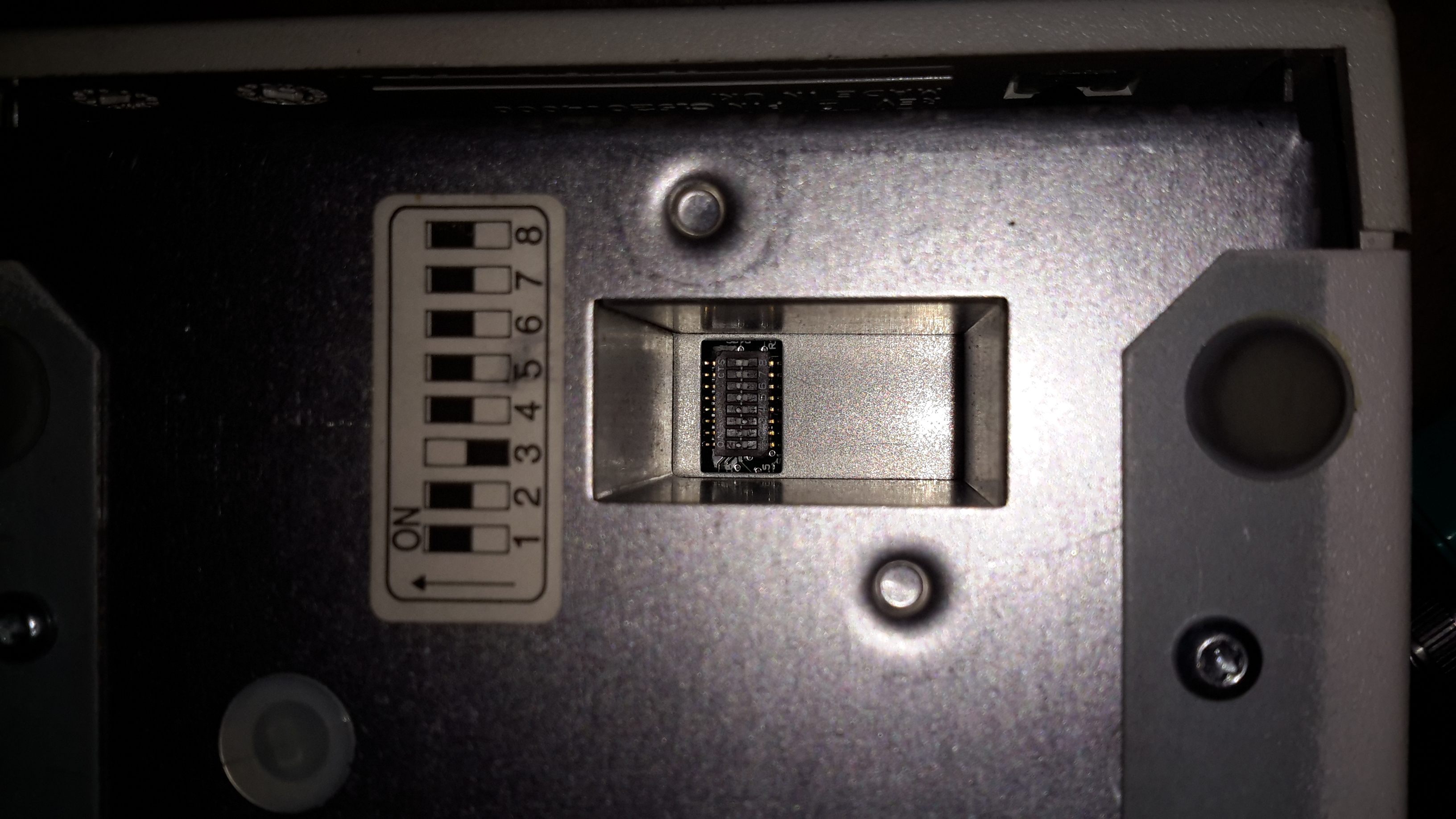
Option Switches
On the bottom of the drive is a bank of DIP switches, according to the manual these are for setting the drive for various flavours of UNIX operating systems. However it doesn’t go into what they actually change.
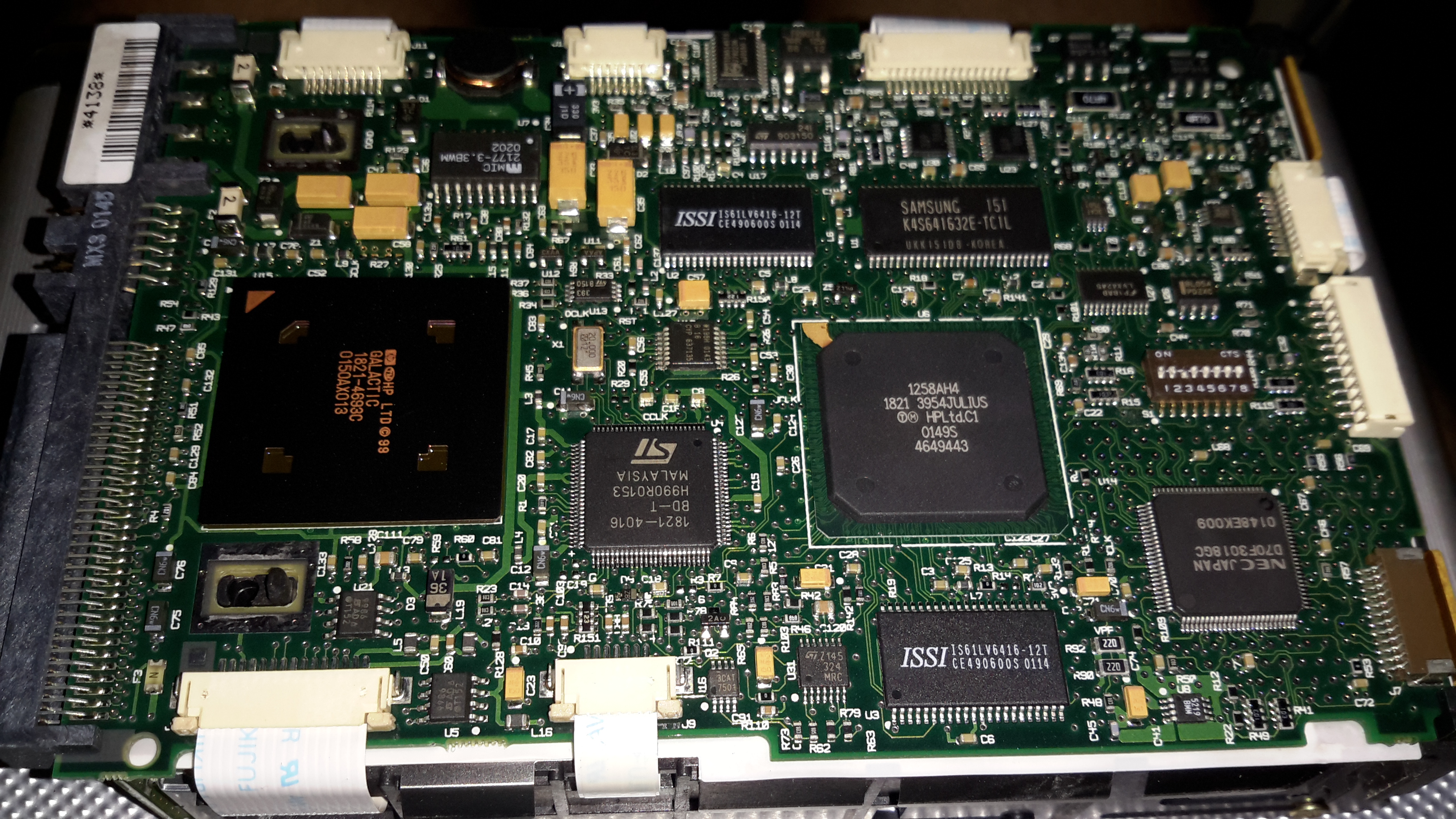
Controller PCB
The bottom of the drive has the control PCB. The large IC on the left is the SCSI interface, I’ve seen this exact same chip on other SCSI tape drives. Centre is a SoC, like so many of these, not much information available.
Drive Frame
Removing the board doesn’t reveal much else, just the bottom of the frame with the tape spool motors on the right, capstan motor bottom centre. The bottom of the head drum motor is just peeping through the plastic top centre.
Head Drum
Here’s the head drum itself. These drives use a helical-scan flying head system, like old VHS tape decks. The top of the capstan motor is on the bottom right.
Cleaning Brush
Hidden just under the tape transport frame is the head cleaning brush. I’m not sure exactly what this is made of, but it seems to be plastic.
Loading Motor
A single small DC motor with a worm drive handles all tape loading tasks. The PCB to the bottom left of the motor holds several break-beam sensors that tell the drive what position the transport is in.
Tape Transport Mech
Here’s the overall tape transport. The PCB on top of the head drum is a novel idea: it’s sole purpose in life is to act as a substrate for solder blobs, used for balancing. As this drum spins at 11,400RPM when a DDS4 tape is in the drive, any slight imbalance would cause destructive vibration.
Tape Transport
Here’s the drive active & writing a tape. (A daily backup of this web server actually). The green head cleaning brush can be better seen here. The drive constantly reads back what it writes to the tape, and if it detects an error, applies this brush momentarily to the drum to clean any shed oxide off the heads. The tape itself is threaded over all the guides, around the drum, then through the capstan & pinch roller.
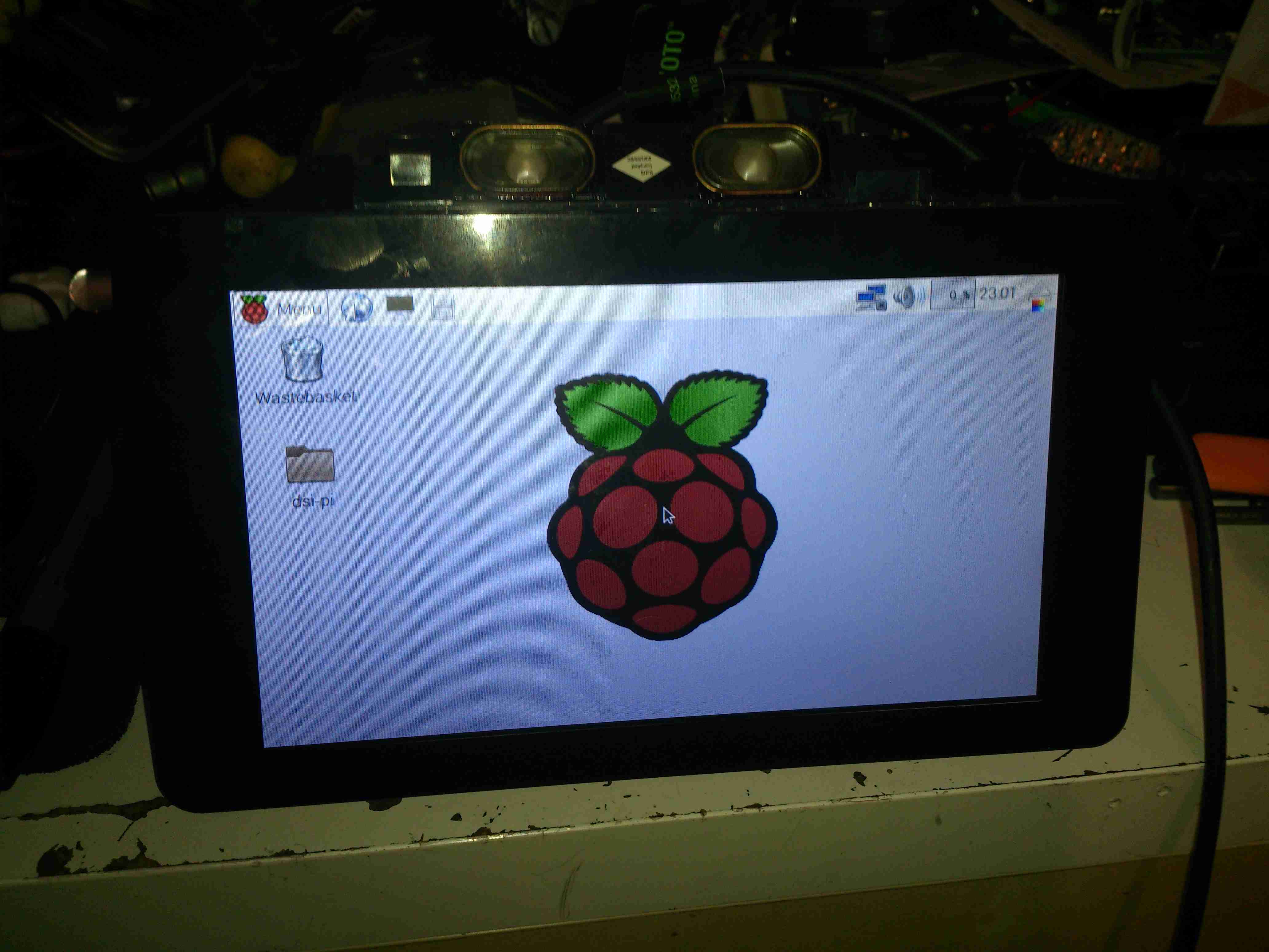
Finally the Raspberry Pi Foundation have released an official LCD for the DSI connector on the Pi. When these were announced, I placed an order straight away, but due to demand it’s taken quite a while for it to arrive in the post.
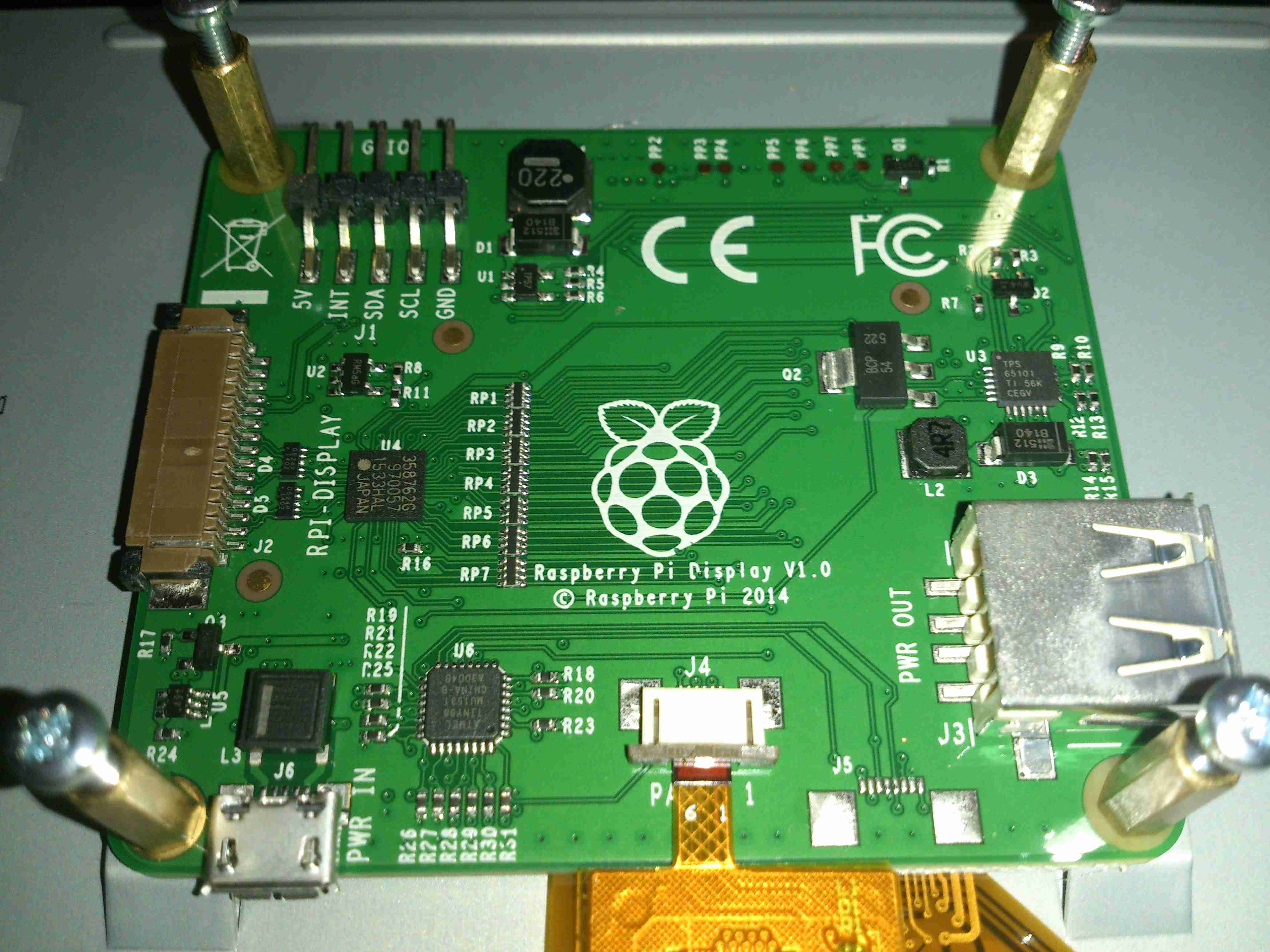
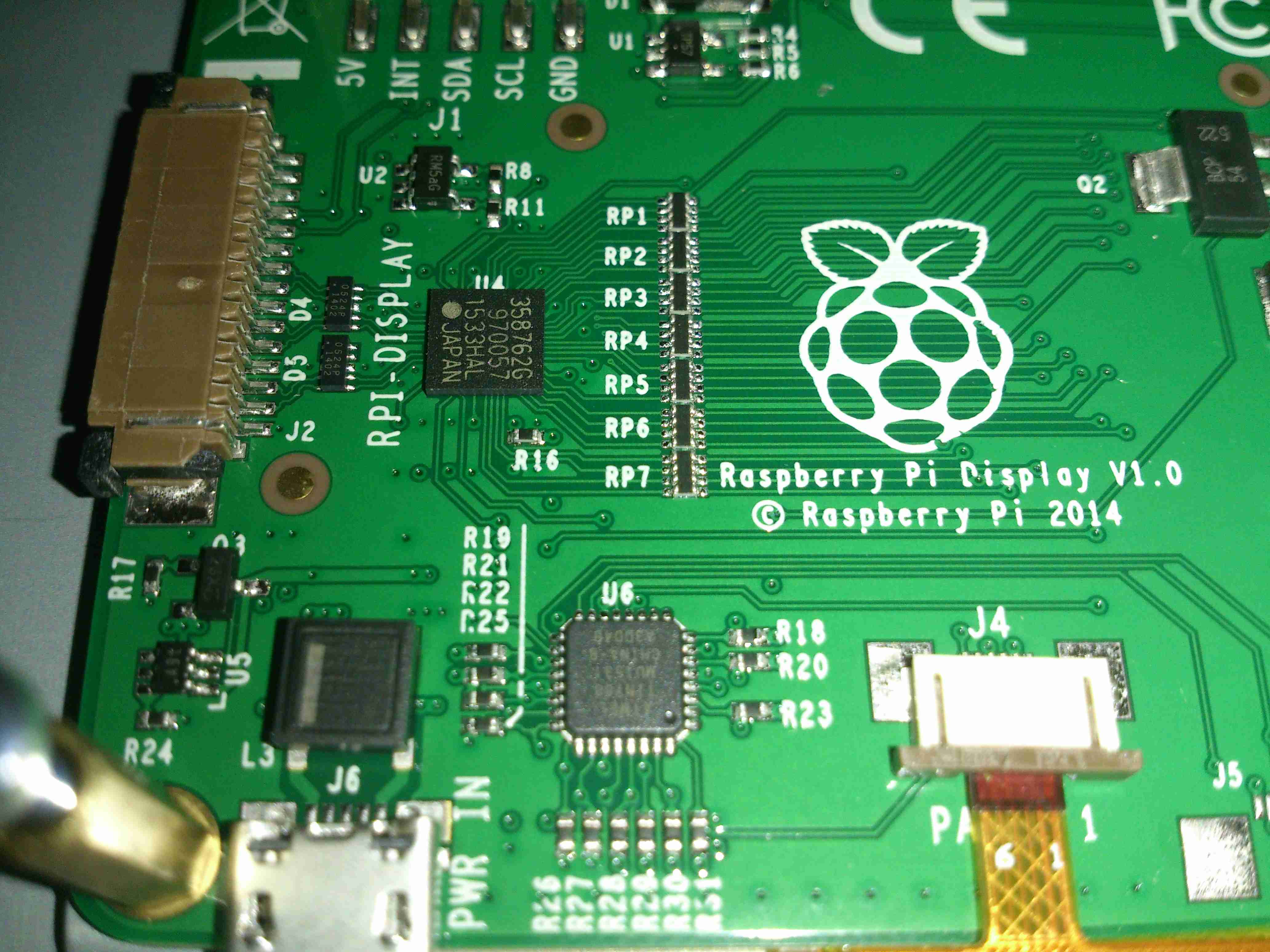
Interface PCB
The LCD itself is an RGB panel, to interface the Pi via the MIPI DSI port, some signal conversion is required. A small PCB is mounted on the back of the LCD to do this conversion. It also handles the power supply rails required by the LCD itself & interfacing the touch screen.
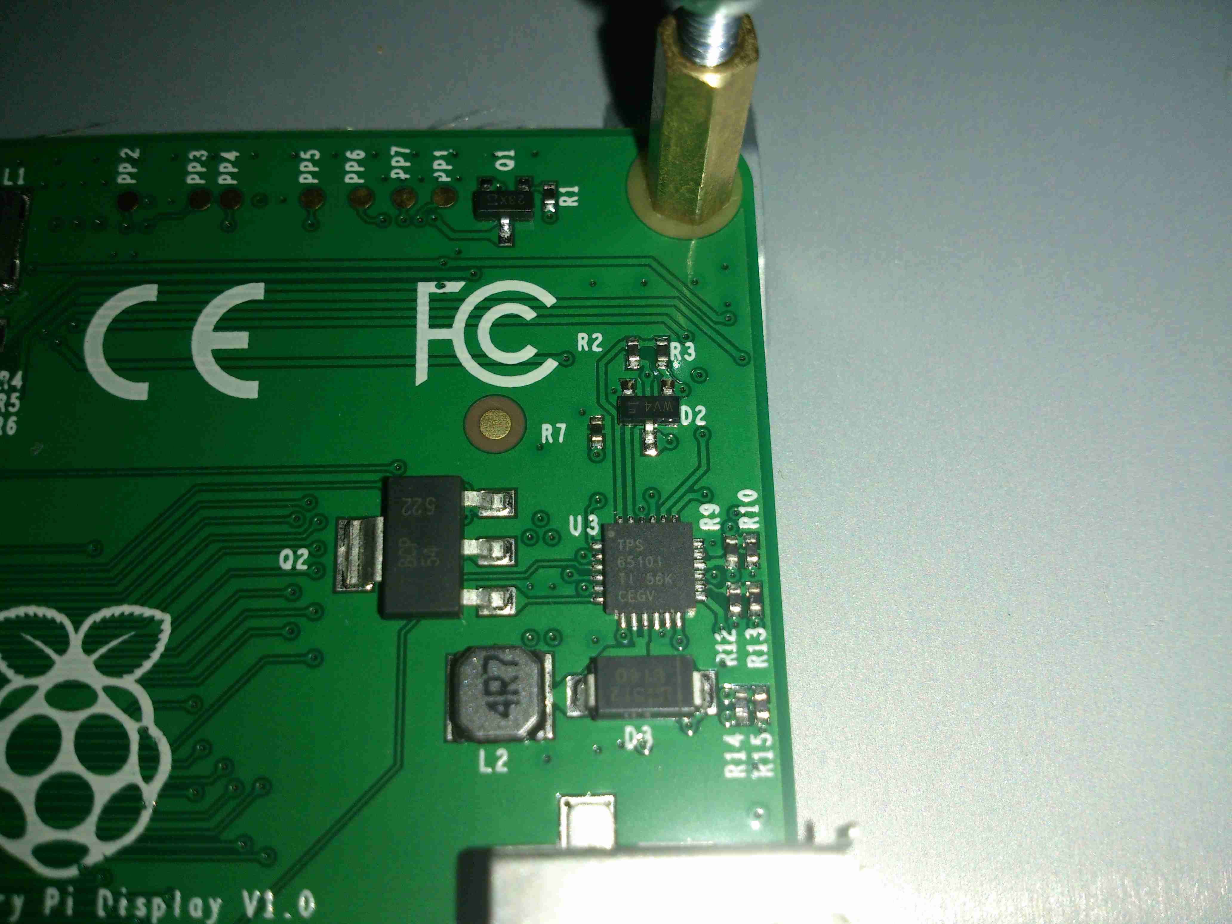
LCD Power Supply
Taking care of the power supply is a Texas Instruments TPS65101 triple output LCD power supply IC. This also has a built in linear regulator to supply 3.3v for the rest of the circuitry on board. The large transistor to the left of the IC is the pass transistor for this regulator.
Main Controller
The video signal comes in on the FFC connector on the left, into the BGA IC. I’ve not managed to identify this component, but it’s doing the conversion from serial video from the Pi to parallel RGB for the LCD.
There’s also an Atmel ATtiny88 on the board below the main video conversion IC, not sure what this is doing.
The touch controller itself is mounted on the flex of the LCD, in this case it’s a FT5406.
Raspberry Pi LCD
Here’s the LCD in operation. It’s not the highest resolution out there, but it leaves the GPIO & HDMI ports free for other uses.
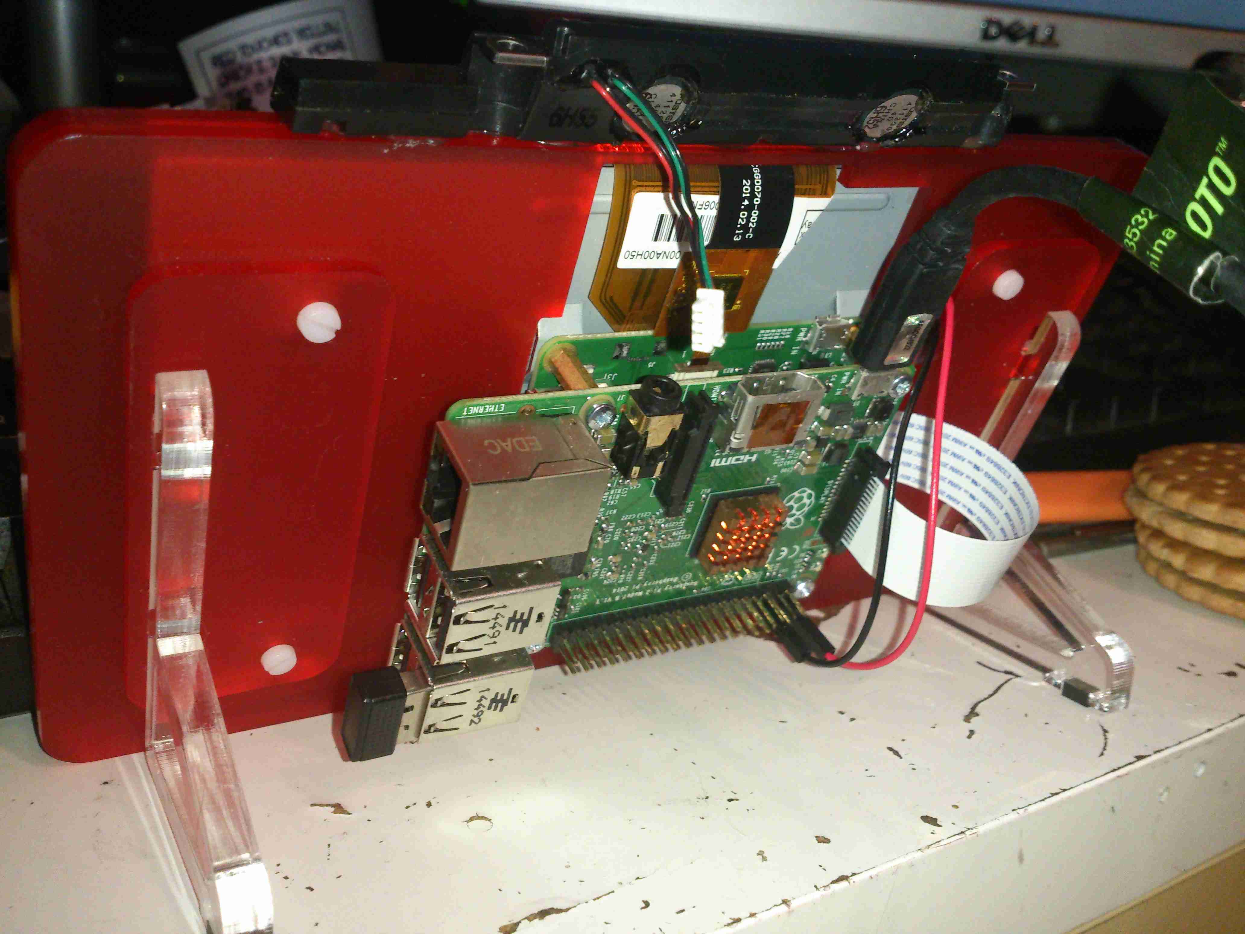
Pi Mounted
The Pi screws to the back of the LCD & is connected with a flat flex cable & a pair of power jumpers. I’ve added a couple of small speakers to the top edge of the LCD to provide sound. (More to come on this bit).
Since the boat was still running it’s internal network on 10/100M speeds, an upgrade was decided on, the internal WiFi signal strength was also pretty poor further than a few feet from the NOC.
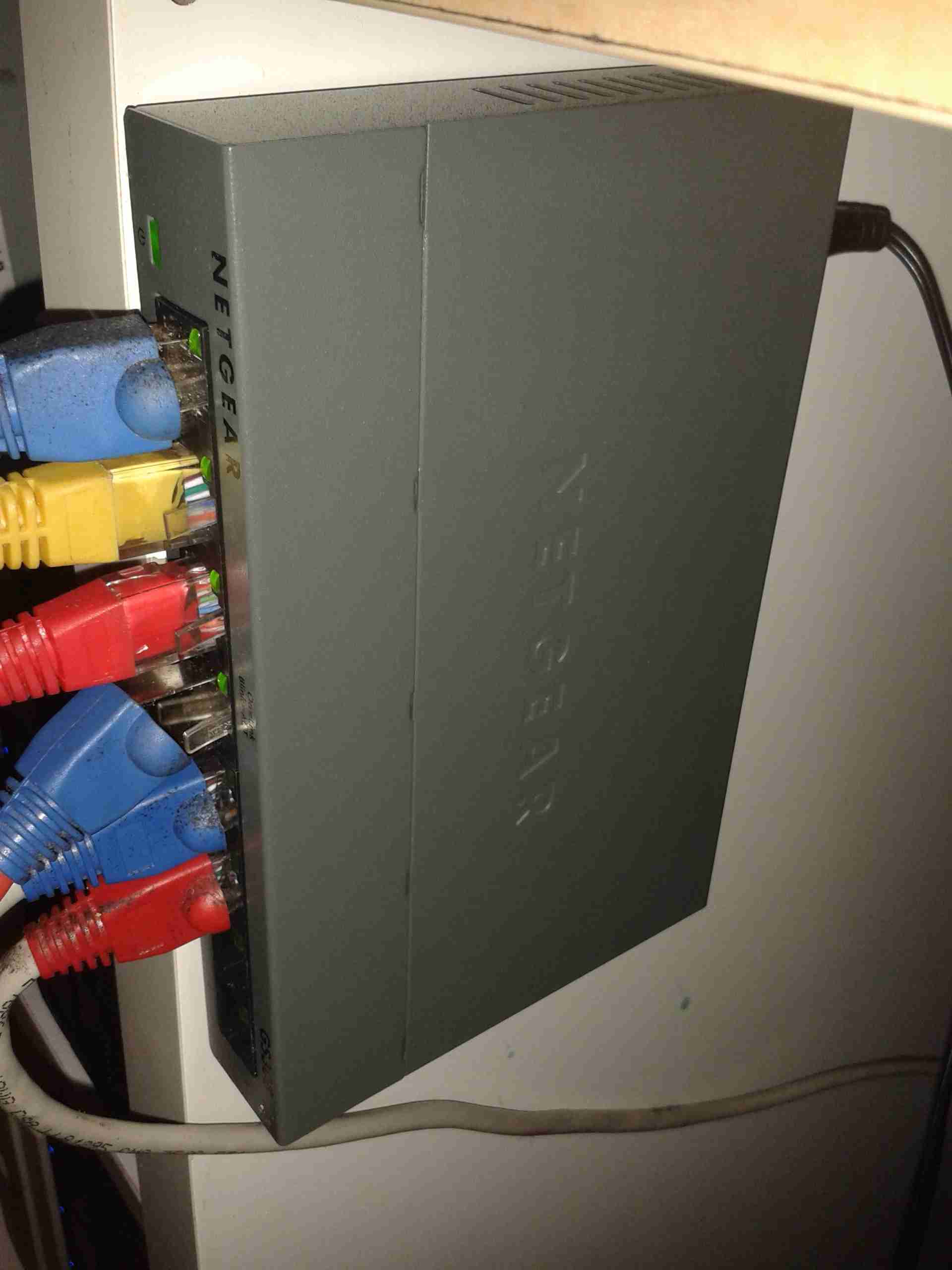
The new router is a Cisco/Linksys AC1750 model, with gigabit networking, and full 802.11ac 2.4/5GHz Wireless. This router also has a built in media server, print server, USB3 & USB2.
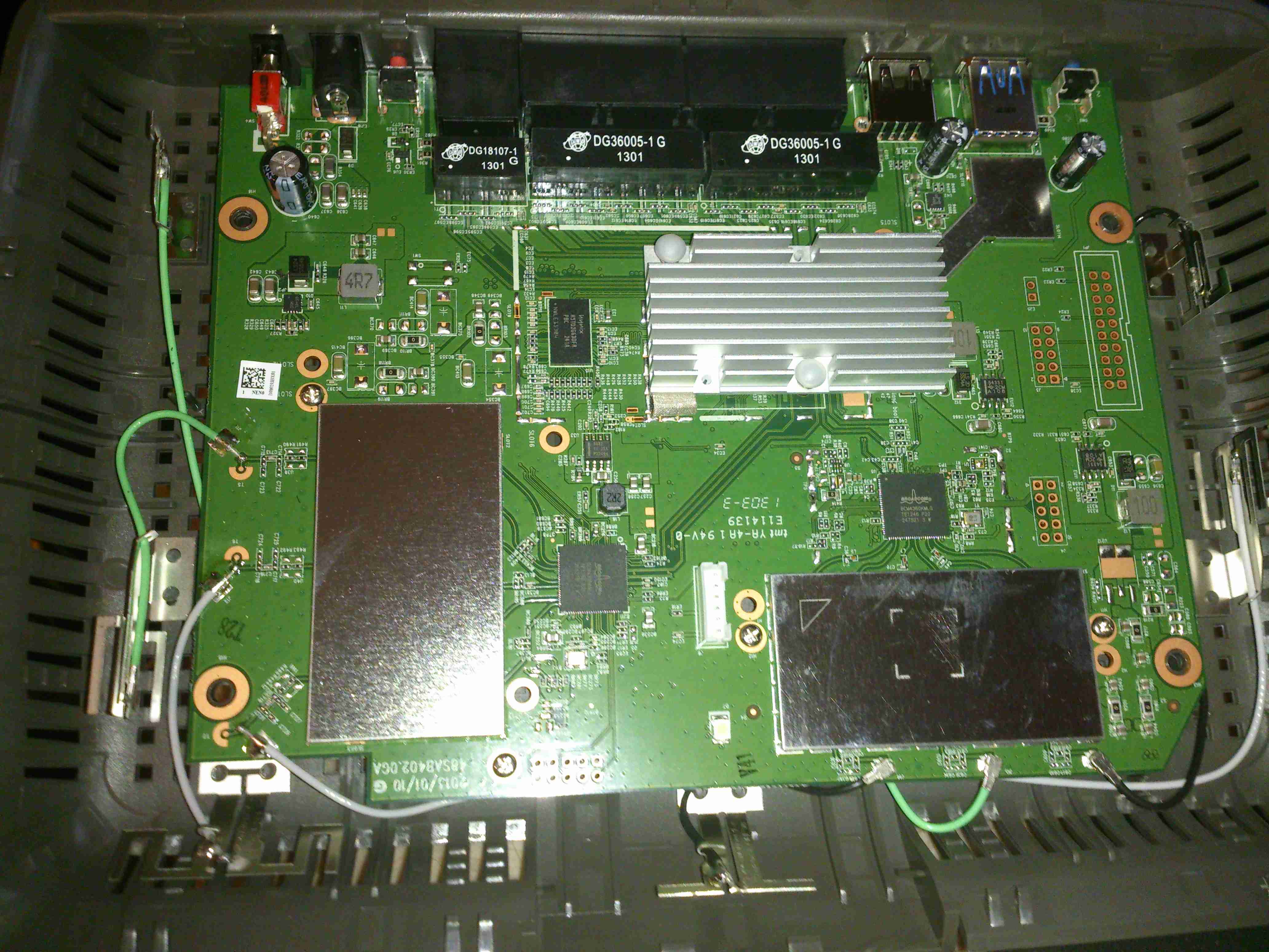
PCB Overview
Teardown time! Here’s the router with the cover removed. Most of the fun stuff is hidden under the shields, but these aren’t fully soldered down & the covers are removable. The 6 antennas can be seen spaced around the edge of the housing, the main CPU is under the large heatsink upper centre. The radio power amplifier stages are underneath the shields, while the main RF transceivers are just outside the shields.
2.4GHz Transceiver
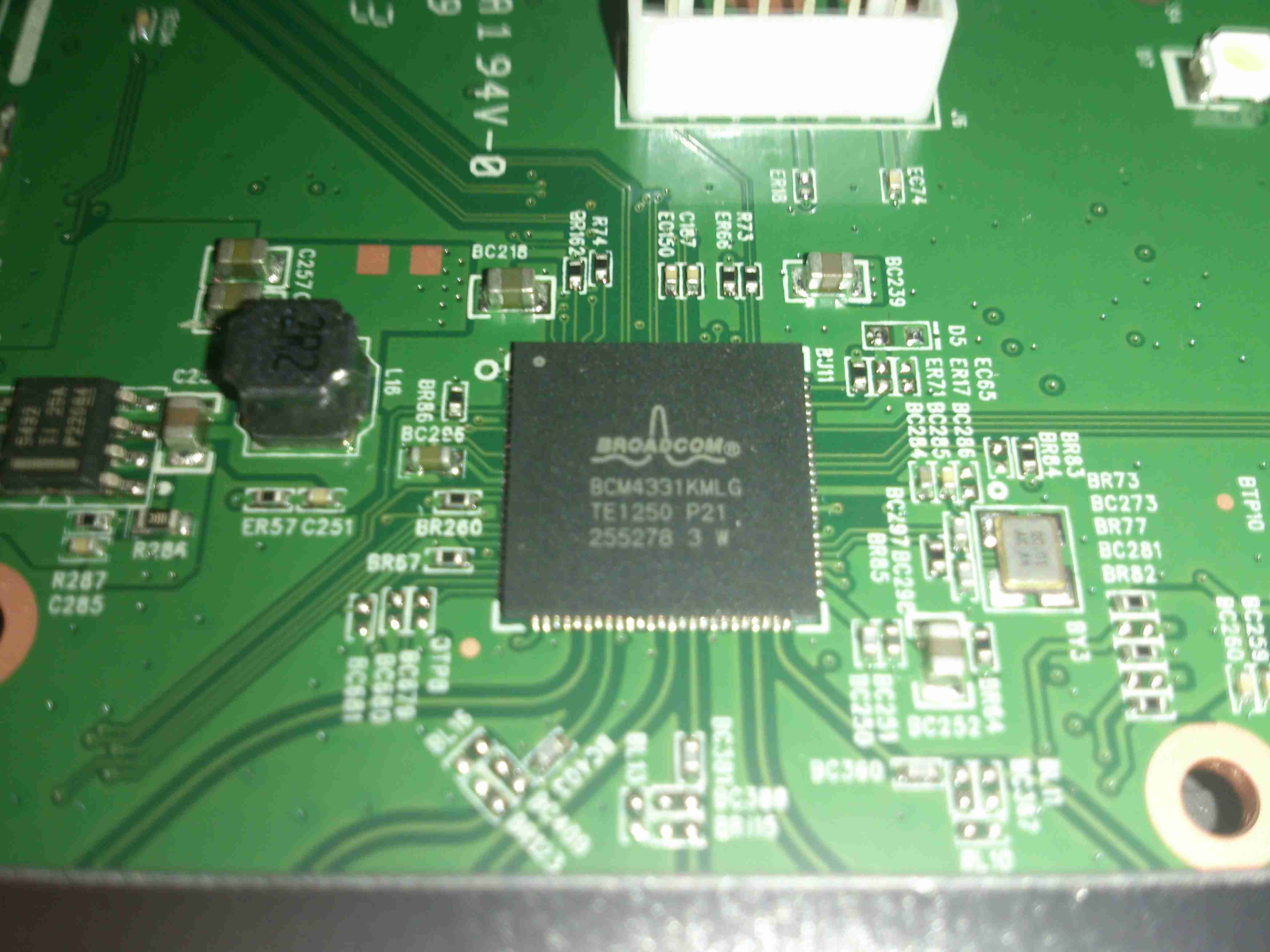
Wireless N is provided by a Broadcom BCM4331, this provides full dual-band 3×3 802.11n support. Being 3×3 it is actually 3 separate transceivers in a single package, to get much higher throughput rates of 600Mbit/s.
5GHz Transceiver
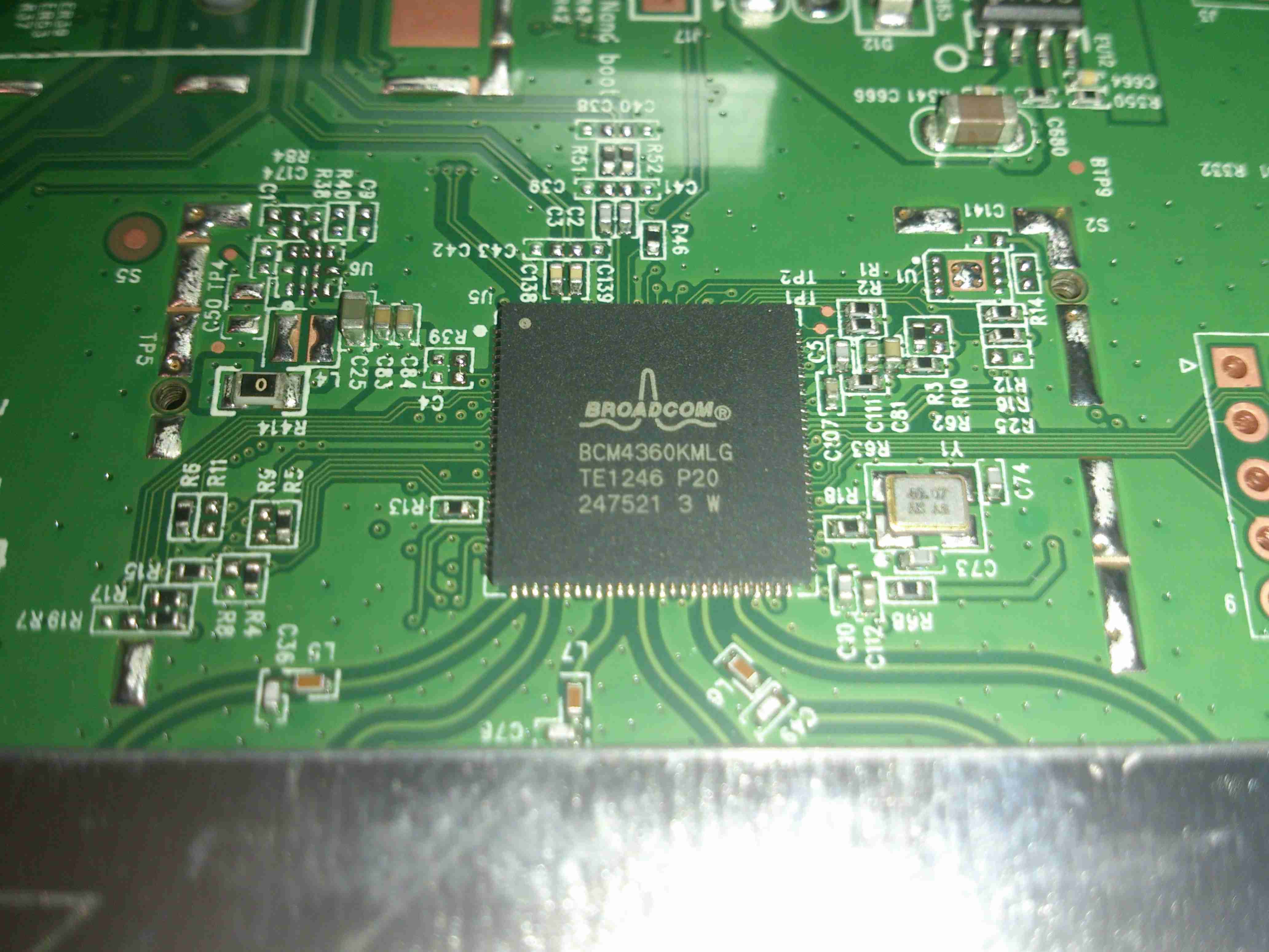
Wireless AC is provided by it’s sister IC, the BCM4360, with throughput speeds of 1.3Gbit/s. Both of these transceiver ICs connect back to the main CPU via PCI Express.
5GHz Power Amplifiers
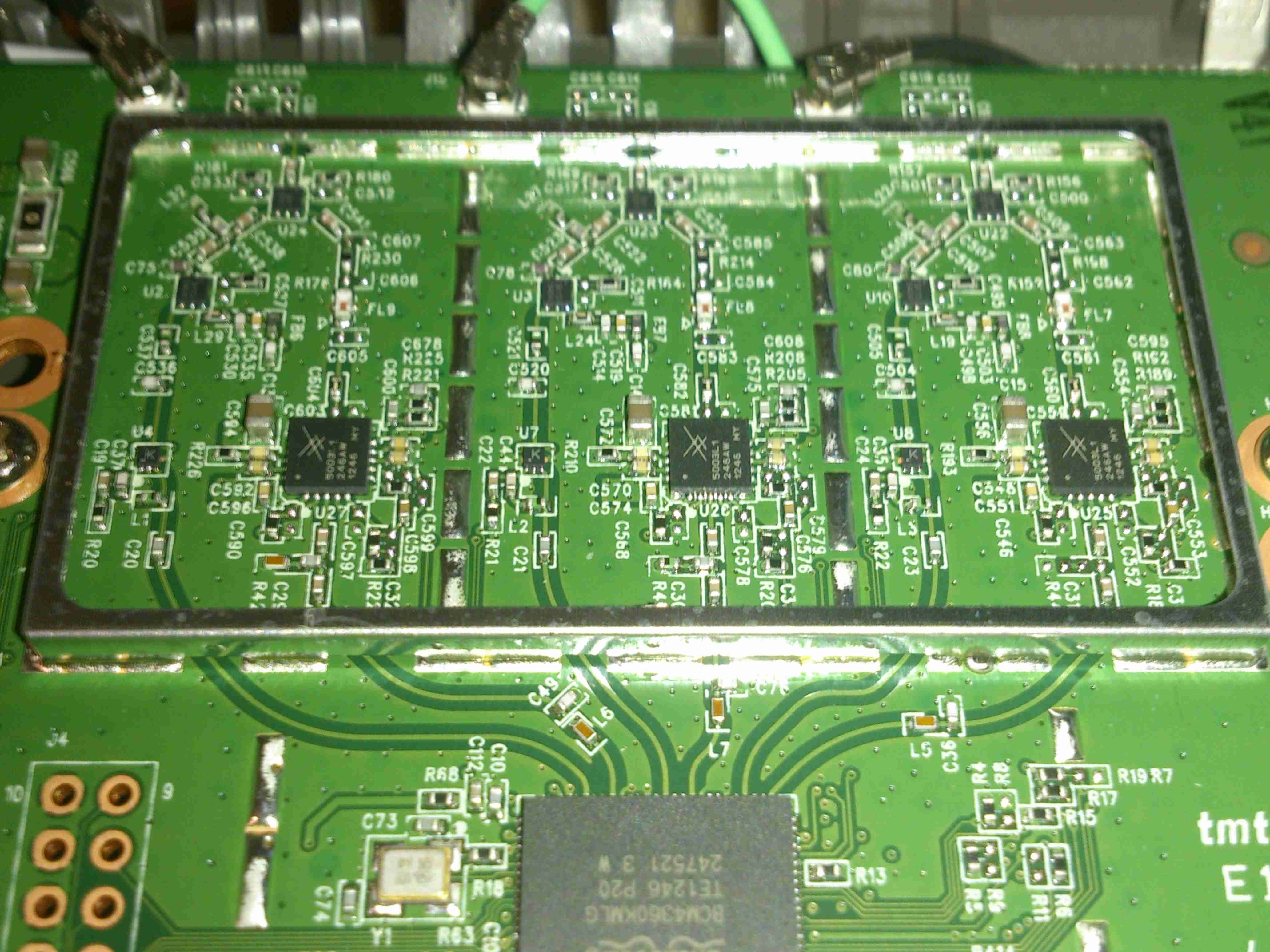
To get increased range, there are a trio of Skyworks SE5003L +23dBm 5GHz power amplifier ICs under the shield, along with the TX/RX switching & antenna matching networks. Heatsinking for these is provided by a sink screwed to the bottom side of the PCB. The outputs to the antennas can be seen at the top of the image.
2.4GHz Power Amplifiers
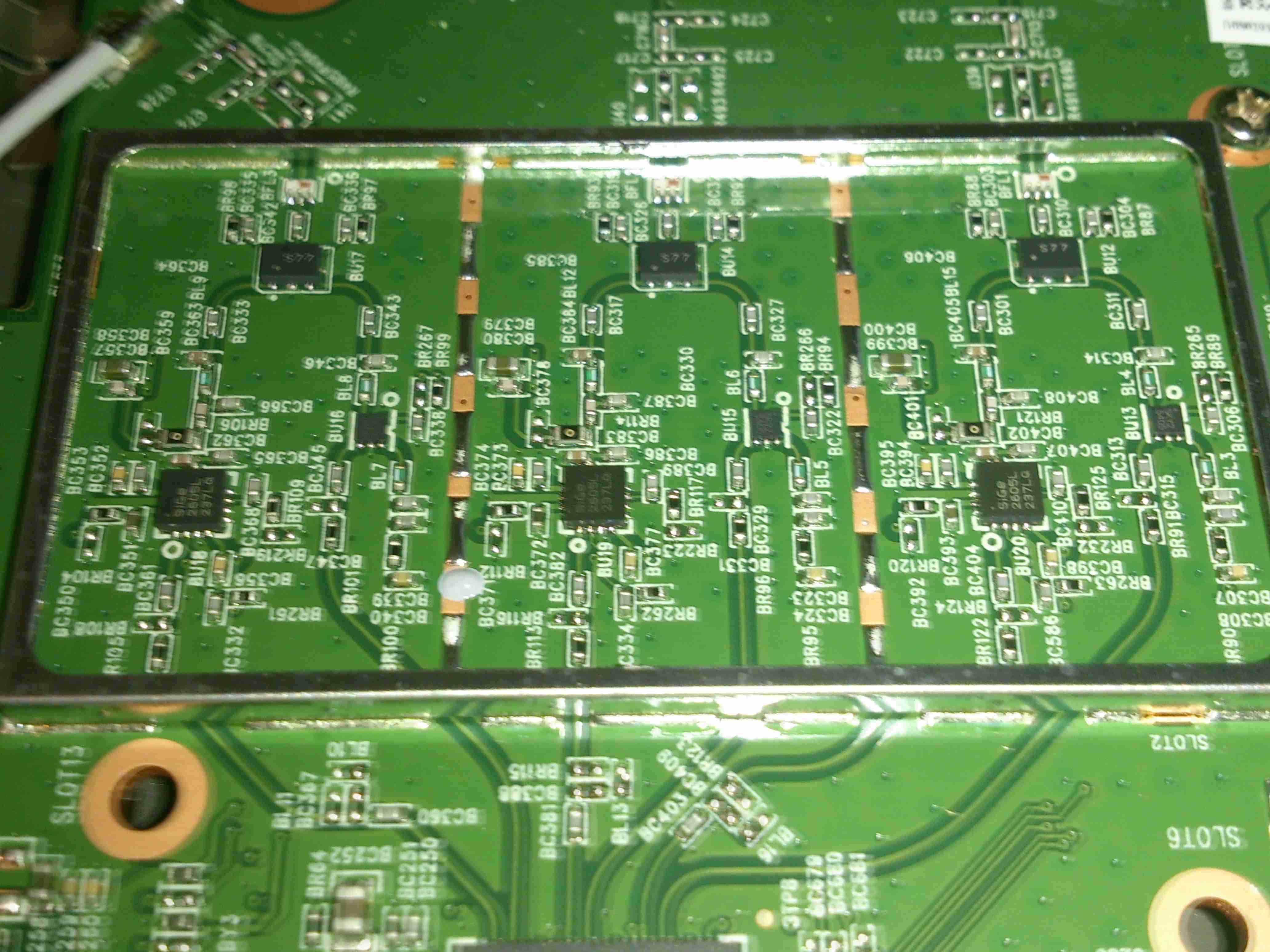
The 2.4GHz section is fitted with a trio of Skyworks SE2605L +23dBm 2.4GHz power amplifiers, with a similar heatsink arrangement under the board. Unlike the 5GHz section, the 2.4GHz antenna feeds are soldered to the PCB here instead of using connectors.
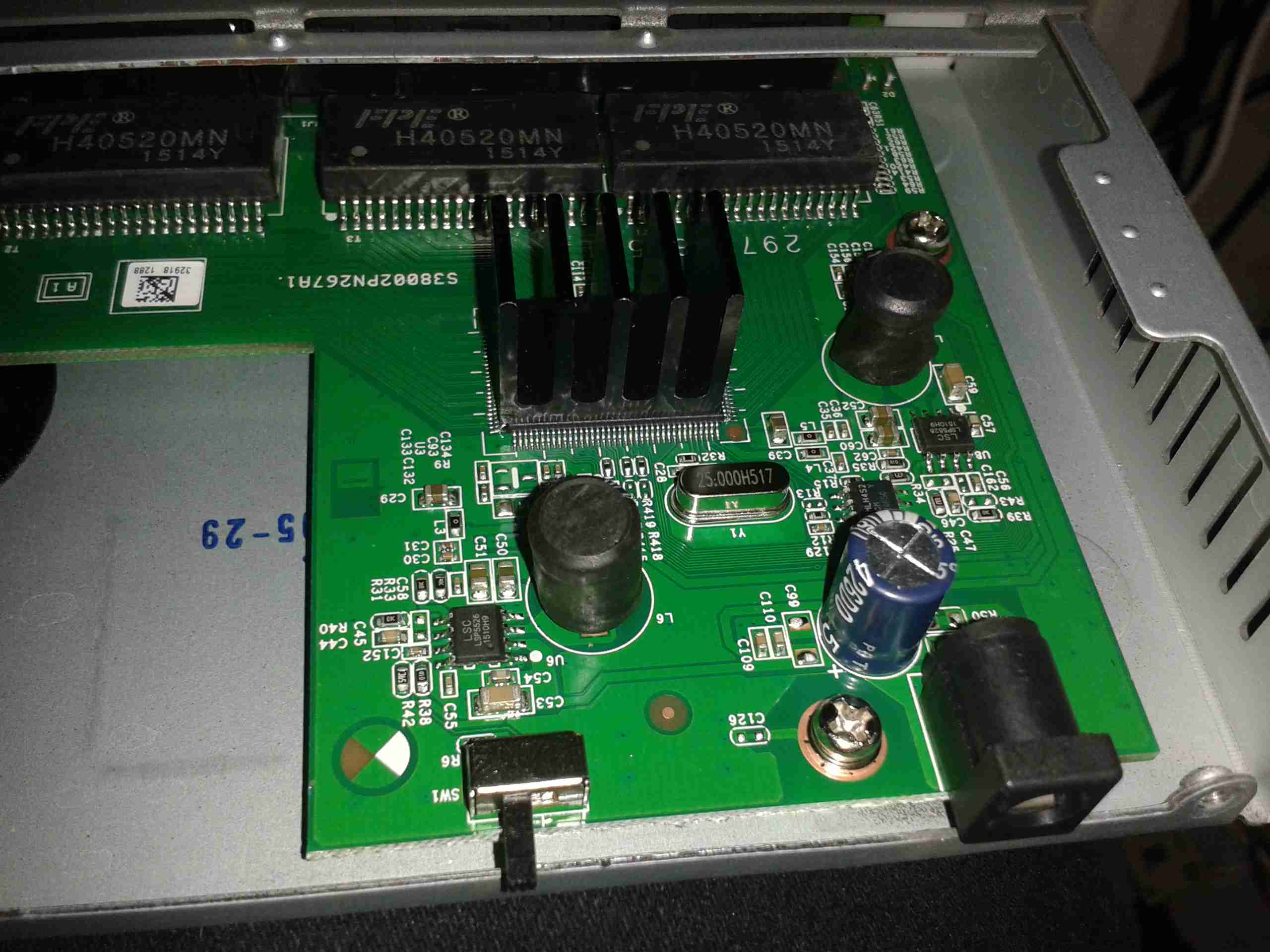
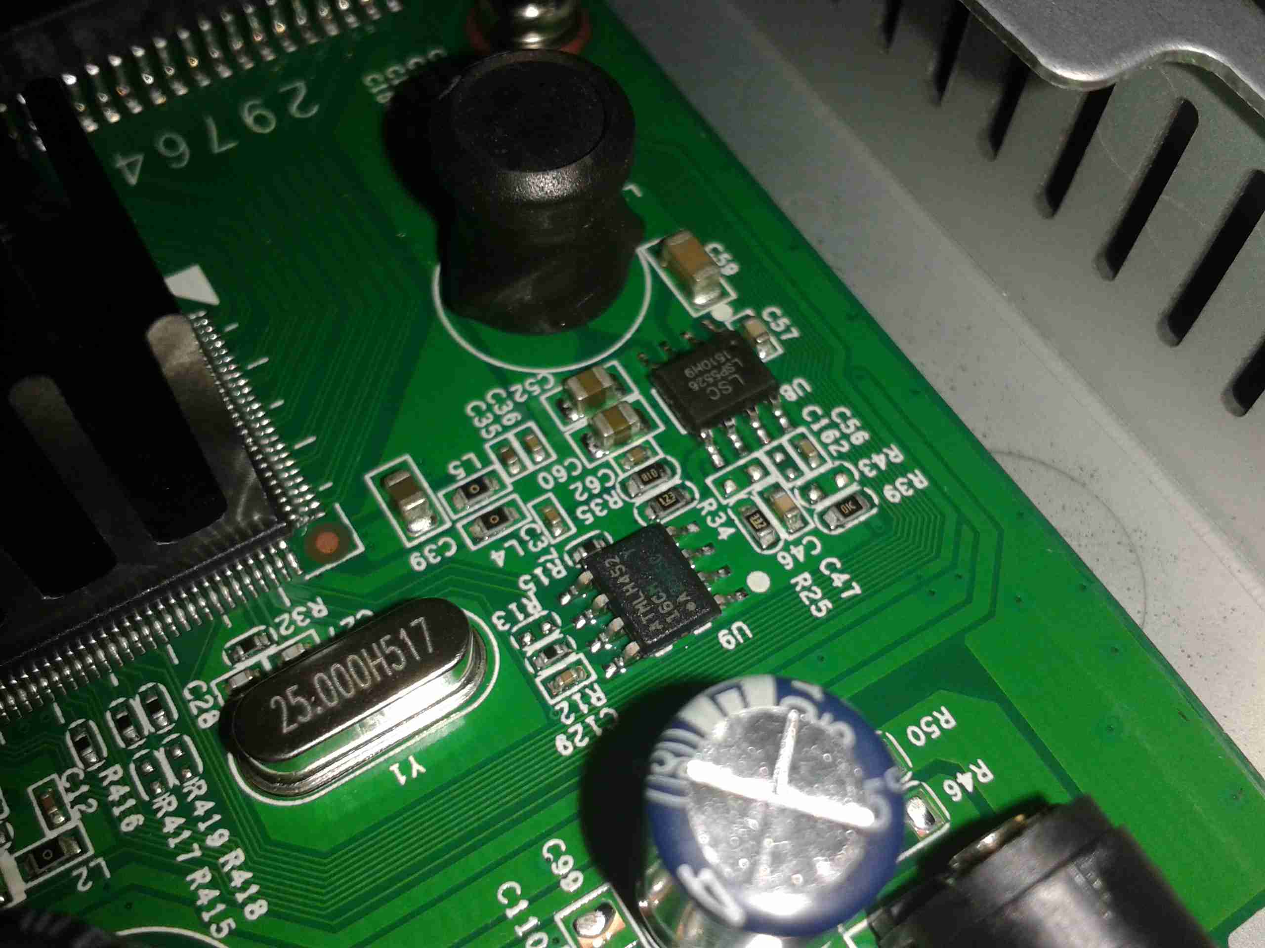
Main CPU
The main CPU is a BCM4708 Communications Processor from Broadcom, as for the other Broadcom chips in this router, very little information is available unless under NDA, but I do know it’s a dual core ARM Cortex A9 running at 1GHz, with built in 5-port gigabit ethernet switch.
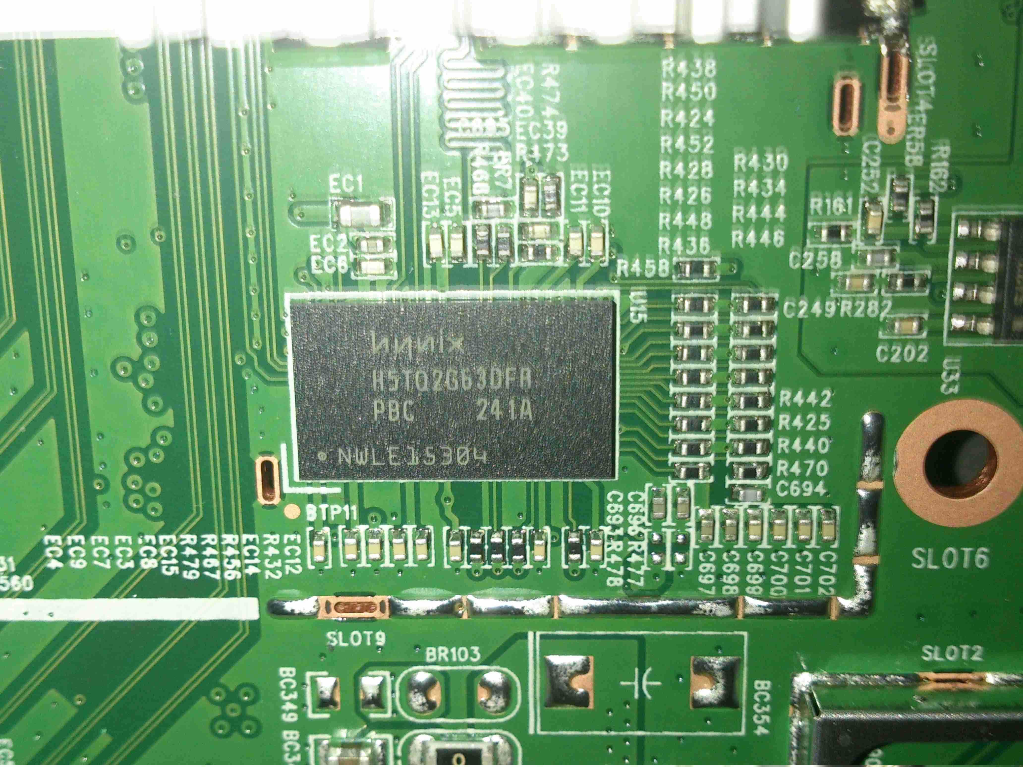
CPU RAM
Working RAM for the processor is a Hynix H5TQ2G63DFA 256MB part.
More to come on the installation of the new networking, with it’s associated 4G mobile gateway connection system.
Here’s a new addition to the network, mainly to replace the ancient Cisco Catalyst 3500 XL 100MB switch I’ve been using for many years, until I can find a decently priced second hand commercial gigabit switch.
Operational
Here’s the switch with some network connections on test. So far it’s very stable & draws minimum power. I’ve not yet attempted to run my core links (NAS) through yet, as I’ve not yet seen a consumer grade switch that can stand up to constant full load without crashing.
Internals
Here’s the switch with it’s lid popped. The magnetics can be seen at the back, next to the RJ-45 ports, the large IC in the centre is the main switching IC, with a heatsink bonded to the top. Very minimal design, with only a couple of switching regulators for power supply & not much else.
Power & EEPROM
Here’s a closeup of some of the support components. There’s a 25MHz crystal providing a clock signal for the switch IC, just to the right of that is an EEPROM. I imagine this is storing the switch configuration & MAC address. Further right is one of the switching DC-DC converter ICs for power.
As a quick test, here’s 500GB of data being shifted through the switch, at quite an impressive rate. I’m clearly maxing out the bandwidth of the link here. Soon I will upgrade to a 10G Ethernet link between the NAS & main PC to get some more performance.
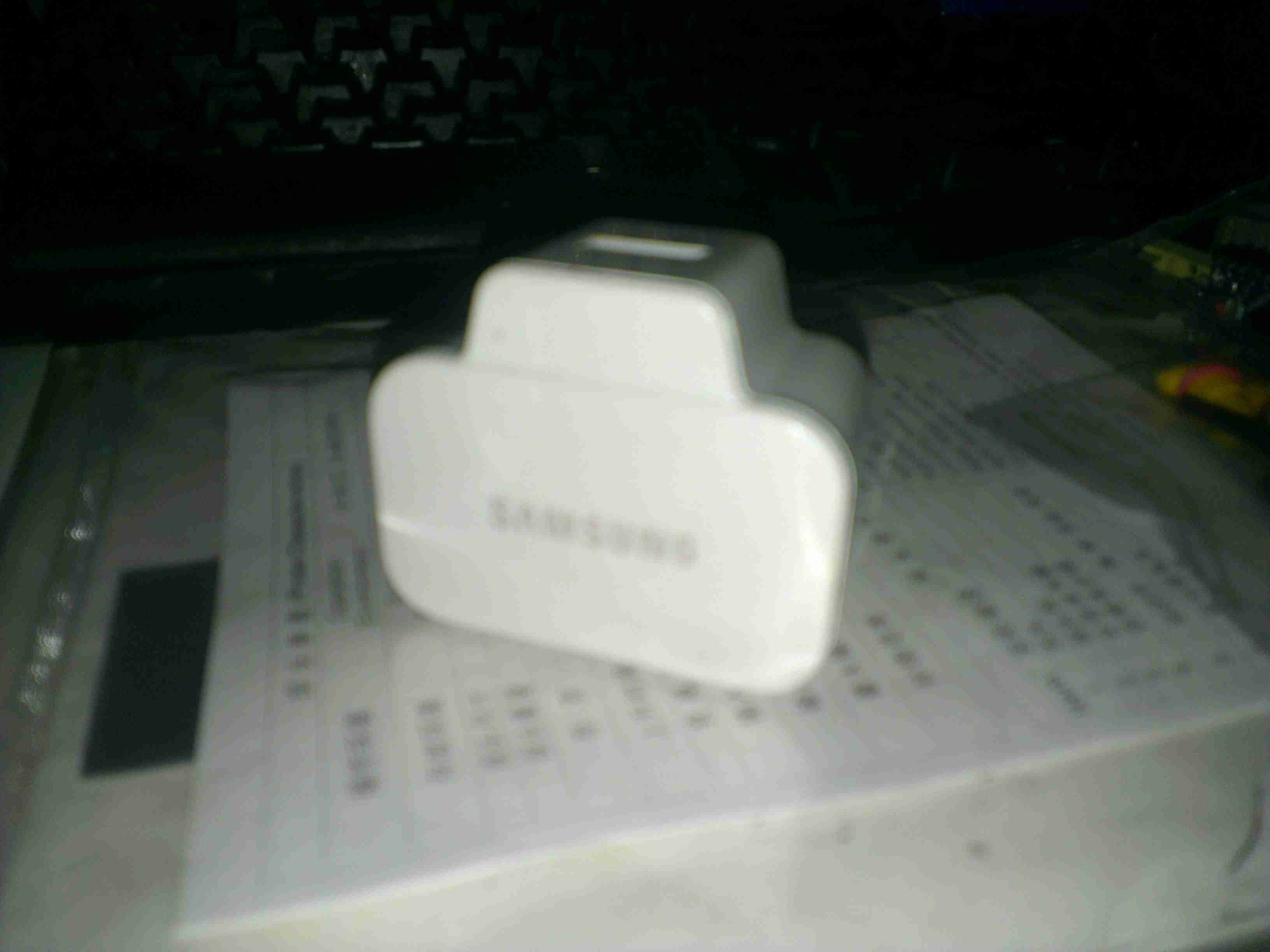
Here’s an odd & sudden failure, the power adaptor for a Samsung device. It’s been working for months & on being plugged into the mains today the magic blue smoke escaped.
Samsung Charger
It’s one of their 2A models, for charging bigger devices like tablets.
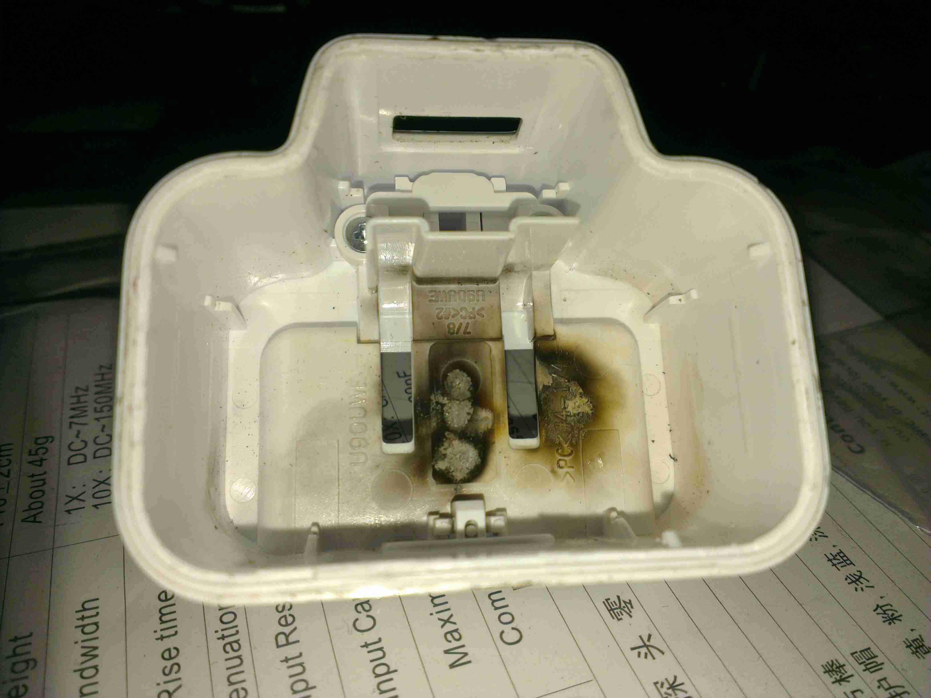
Flash Burn
Strangely for one of these chargers, no glue is used to hold it together – just clips. This made disassembly for inspection much easier. Evidence of a rather violent component failure is visible inside the back casing.
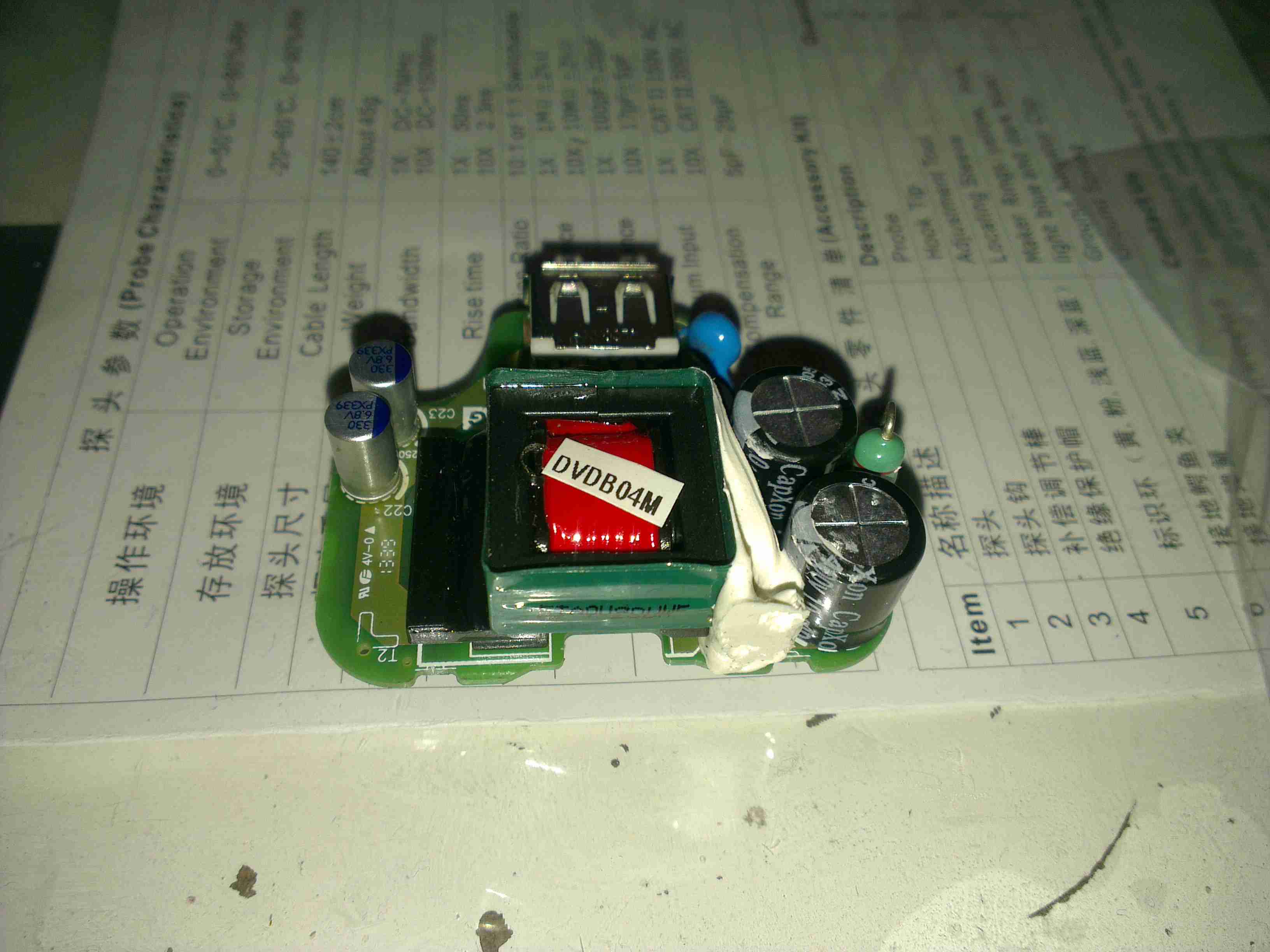
PCB
Here’s the charger PCB removed from the casing. As to be expected from Samsung, it’s a high quality unit, with all the features of a well designed SMPS.
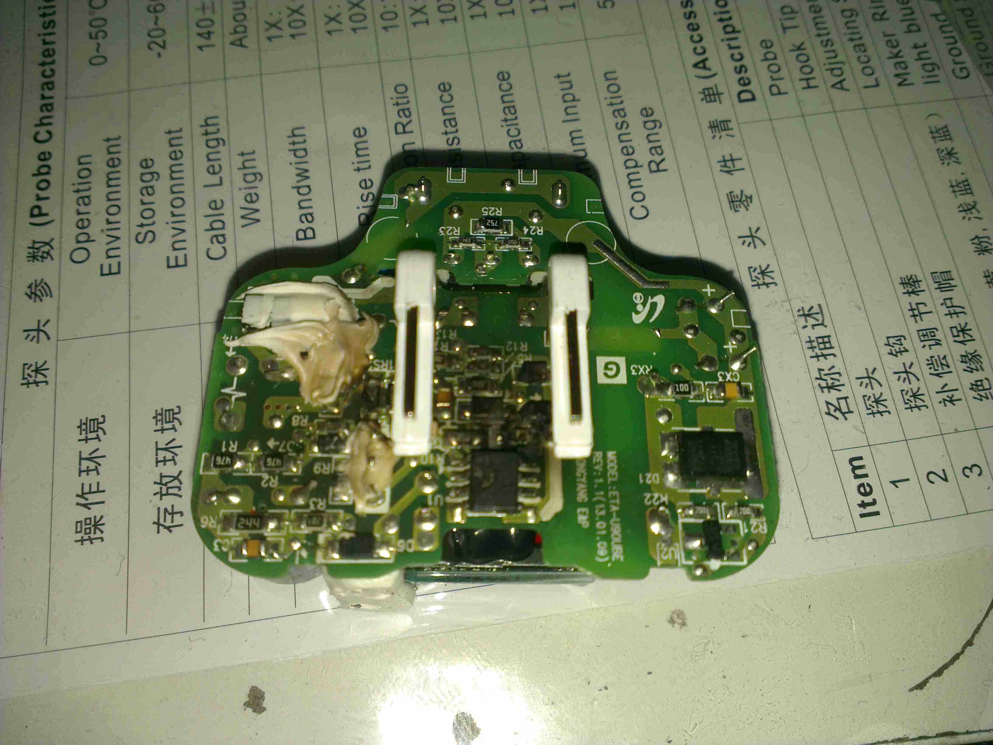
PCB Reverse
However, on turning the board over, the blown component is easily visible. It’s the main SMPS controller IC, with a massive hole blown in the top. The on board fuse has also blown open, but it obviously didn’t operate fast enough to save the circuit from further damage!
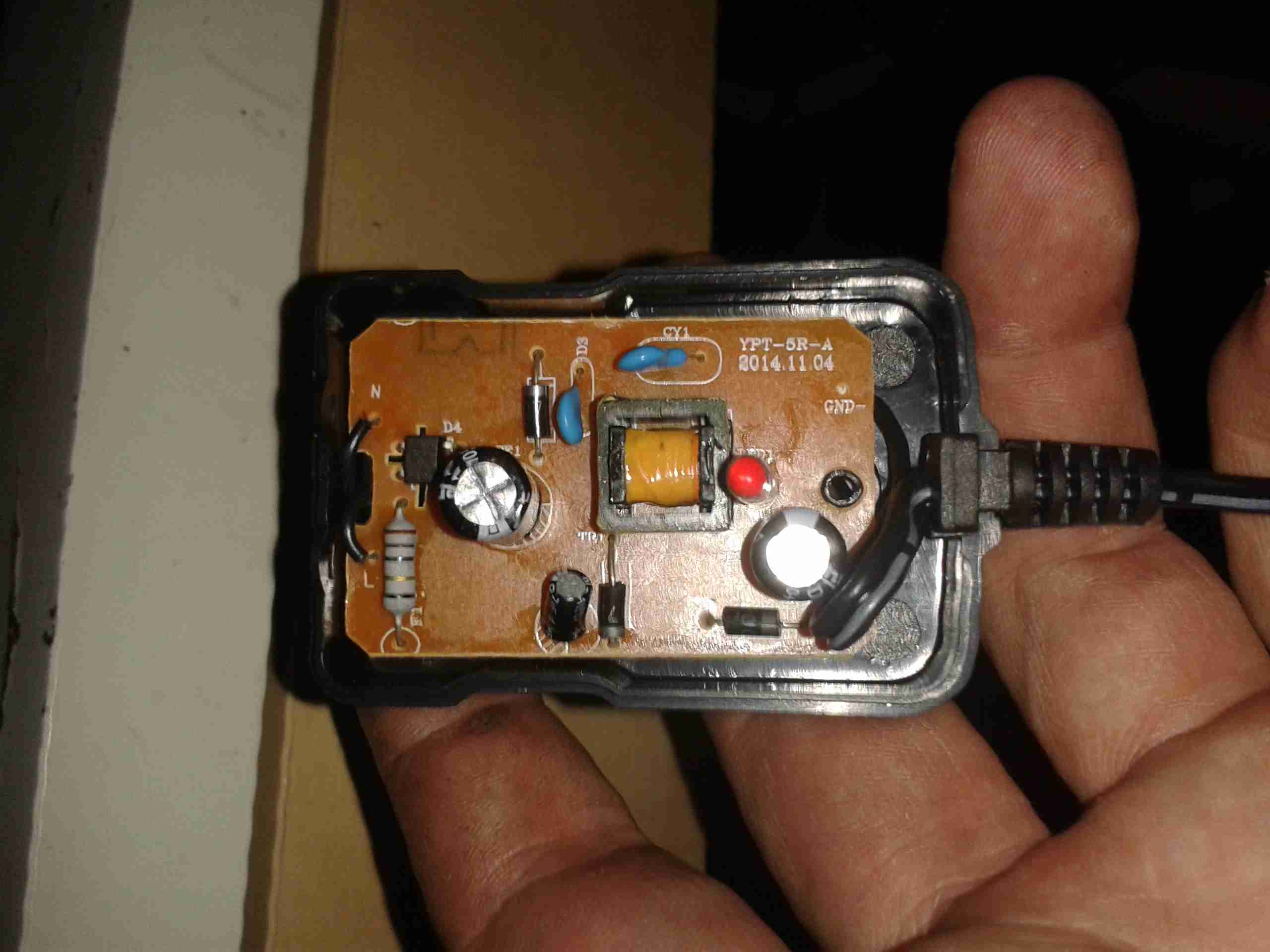
With every piece of Chinese electronics I obtain, mainly Baofeng radios, they come with a Europlug-type power adaptor, and a universal plug adaptor for the mains.
The charger units aren’t too bad, there’s a fair amount of isolation between the primary & secondary, and even though they’re very simple & cheap, I can’t see any immediate safety problems with them.
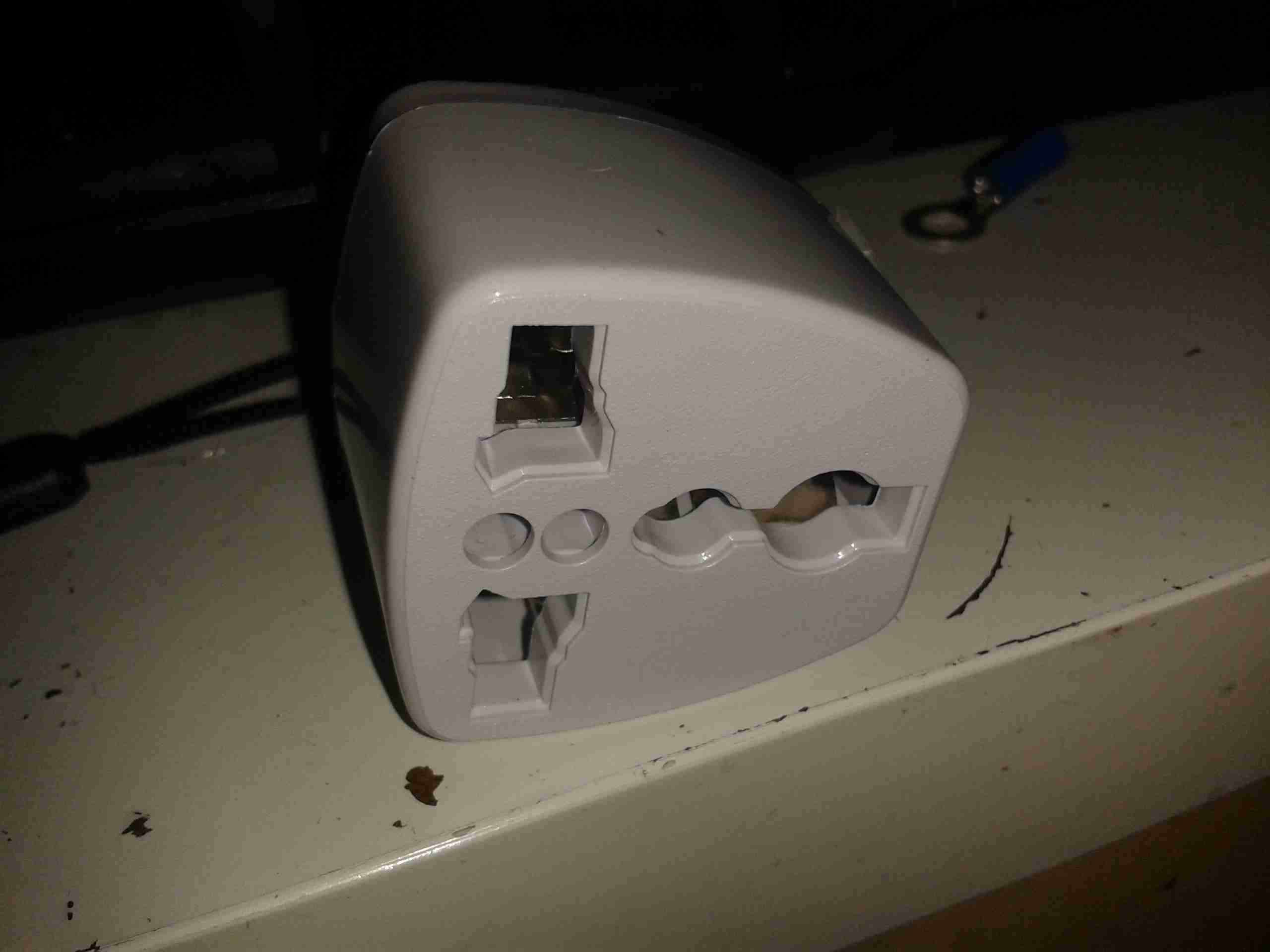
The plug adaptors, however, are a different matter. These things are utterly lethal!
Baofeng PSU
Here’s the inside of the PSU. It’s just a very simple SMPS, giving an output of 10v 500mA. The fuse is actually a fusible resistor.
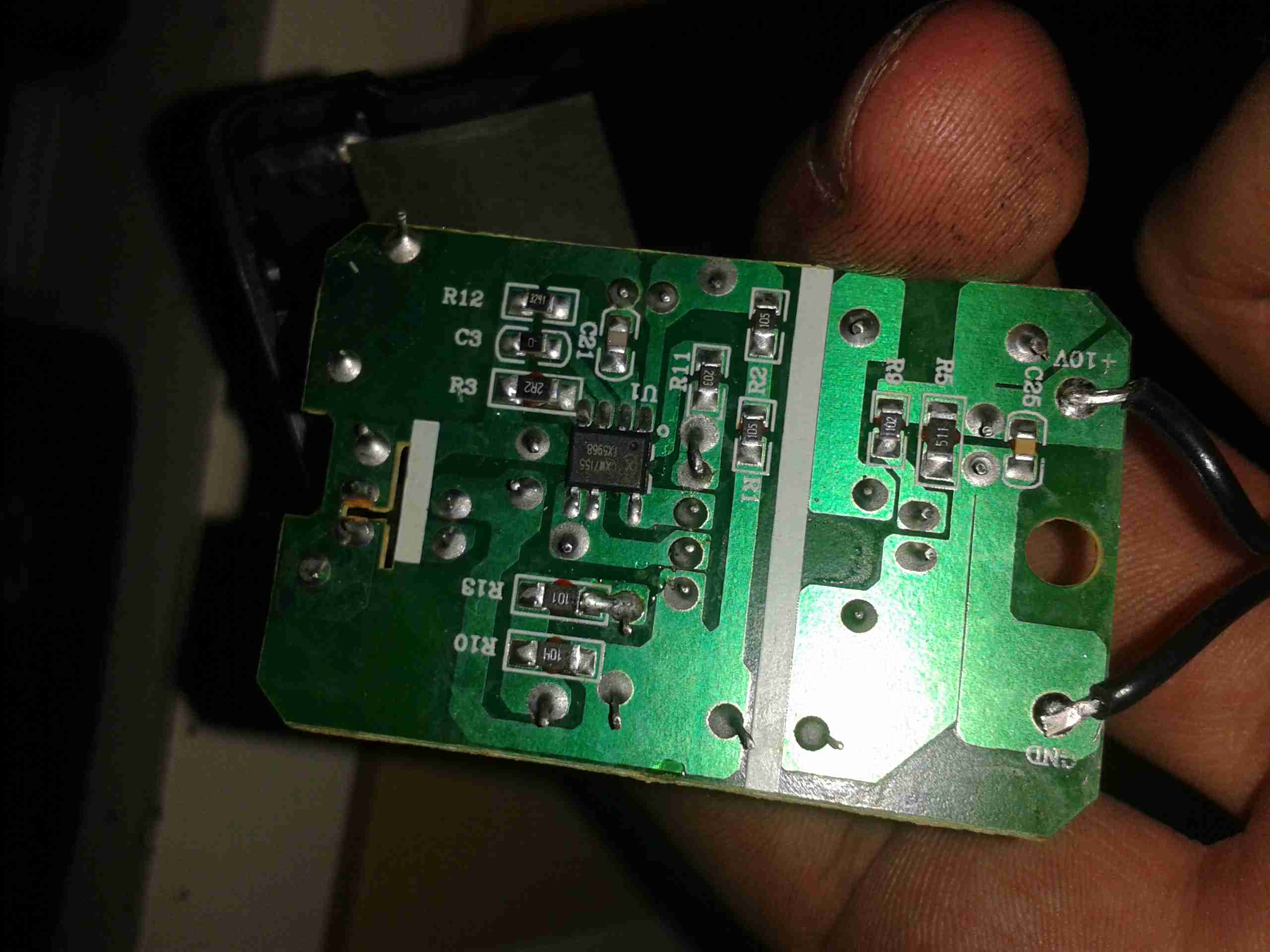
PCB Reverse
Here’s the back of the PCB with the SMPS control IC. I can’t find any English datasheets for this part unfortunately.
Universal Travel Adaptor
Here’s the dangerous adaptor. There’s no safety shield, so the live parts are exposed.
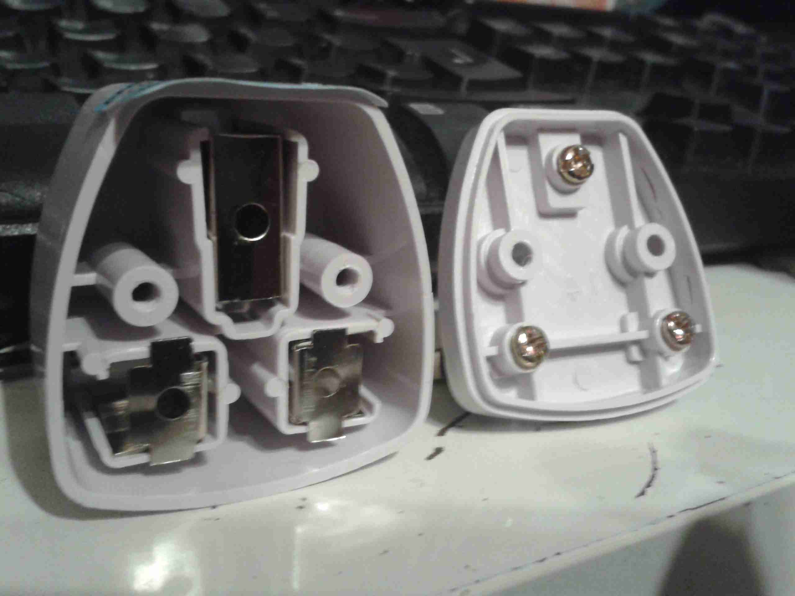
Internals
Here’s the adaptor split apart. The output contacts are on the left, and rely just on pressure to make contact with the brass screws on the mains input pins to provide power.
This is a very poor way to get a connection, a dirty or worn contact here would create a lot of heat if any significant power is pulled through, and could quite possibly result in a fire.
Not surprisingly, I bin these things as soon as I open the box, and charge all my radios with a 12v charging system.
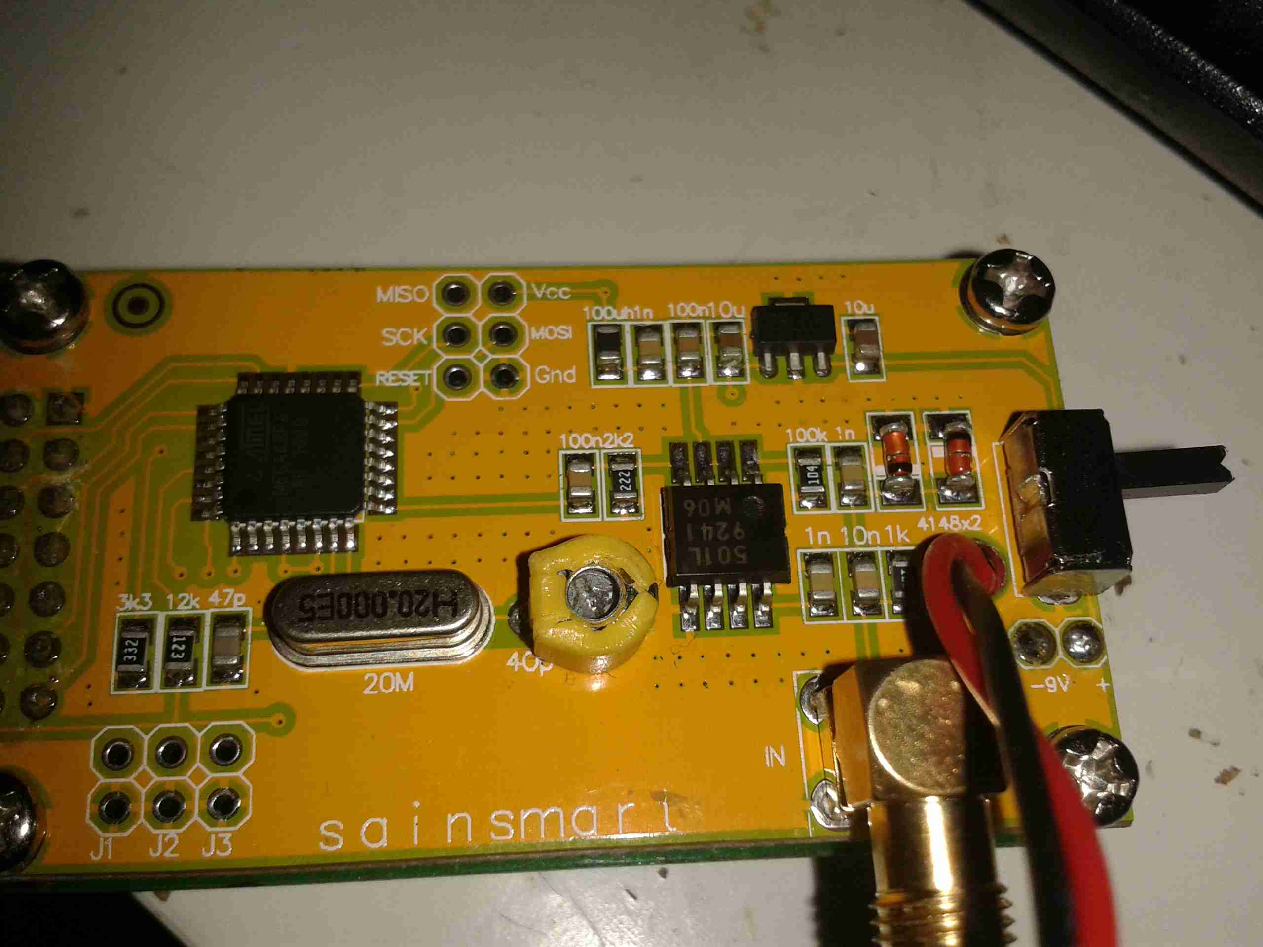
Here’s a quick look at a Sainsmart frequency counter module. These are useful little gadgets, showing the locked frequency on a small LCD display.
It’s built around an ATMega328 microcontroller (µC), and an MB501L Prescaler IC. The circuit for this is very simple, and is easily traced out from the board.
Frequency Counter
Here’s the back of the board, with the µC on the left & the prescaler IC on the right. This uses a rather novel method for calibration, which is the trimmer capacitor next to the crystal. This trimmer varies the frequency of the µC’s oscillator, affecting the calibration.
Input protection is provided by a pair of 1N4148 diodes in inverse parallel. These will clamp the input to +/-1v.
The prescaler IC is set to 1/64 divide ratio. This means that for an input frequency of 433MHz, it will output a frequency of 6.765625MHz to the µC.
The software in the µC will then calculate the input frequency from this intermediate frequency. This is done because the ATMega controllers aren’t very cabable of measuring such high frequencies.
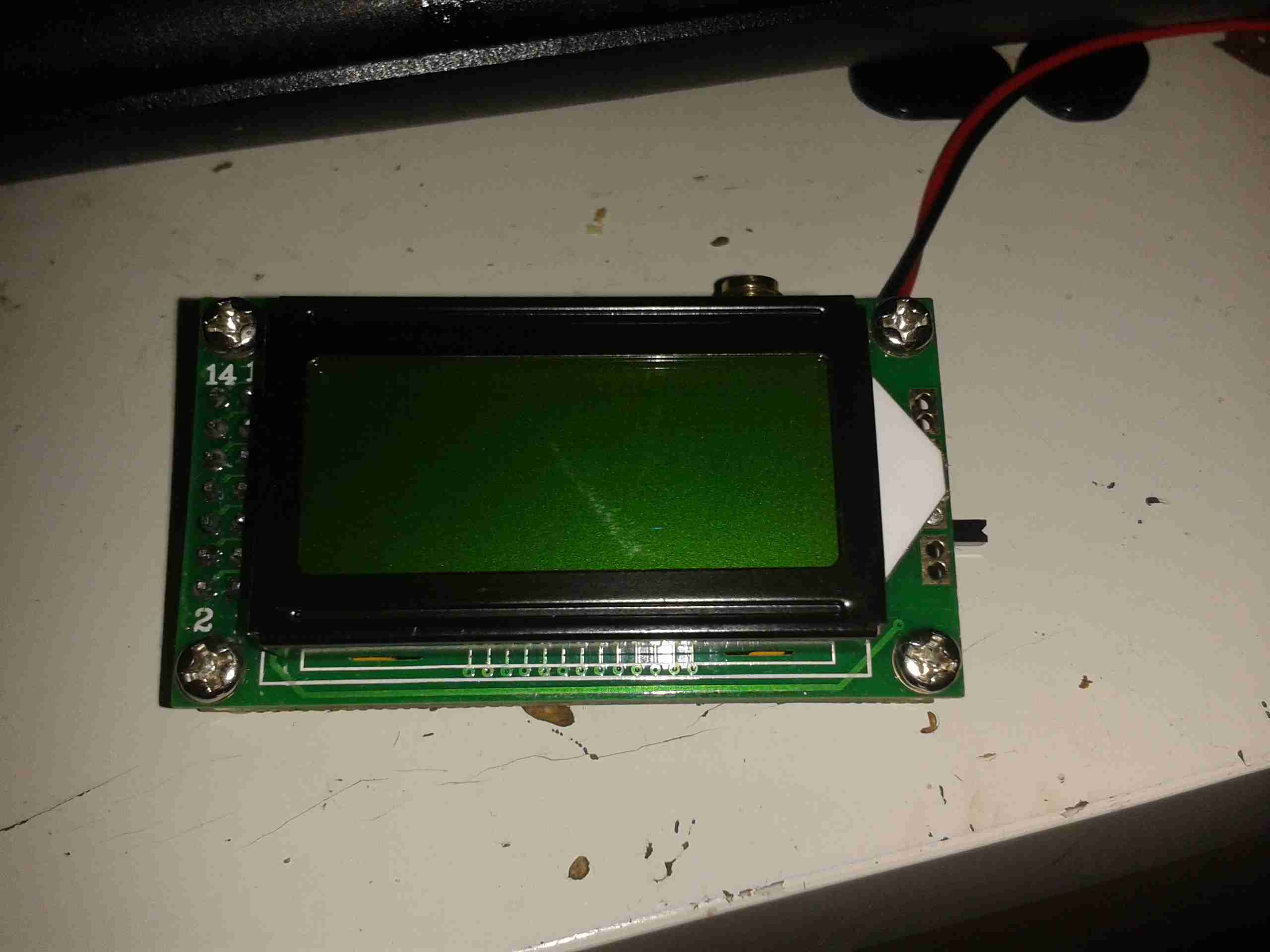
The calculated frequency is then displayed on the LCD. This is a standard HD44780 display module.
LCD
Power is provided by a 9v PP3 battery, which is then regulated down by a standard LM7805 linear regulator.
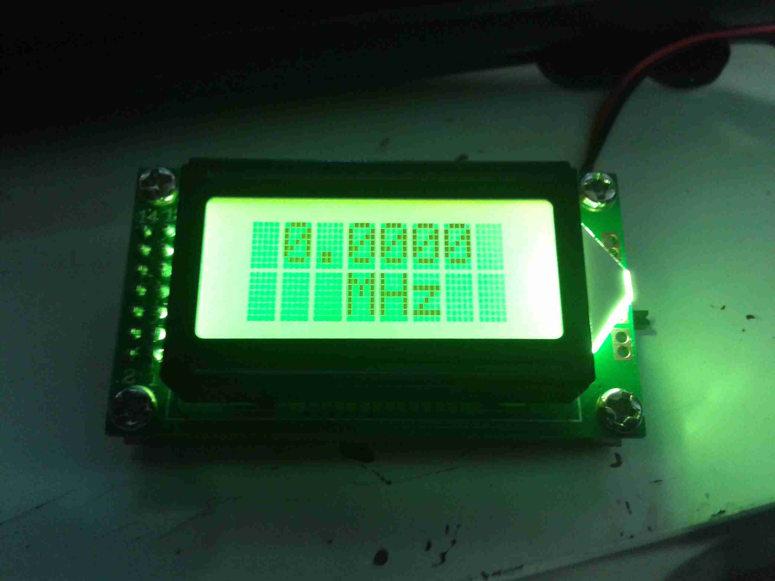
Readout
I’ve found it’s not very accurate at all at the lower frequencies, when I fed it 40MHz from a signal generator it displayed a frequency of around 74MHz. This is probably due to the prescaler & the software not being configured for such a low input. In the case for 40MHz input the scaled frequency would have been 625kHz.
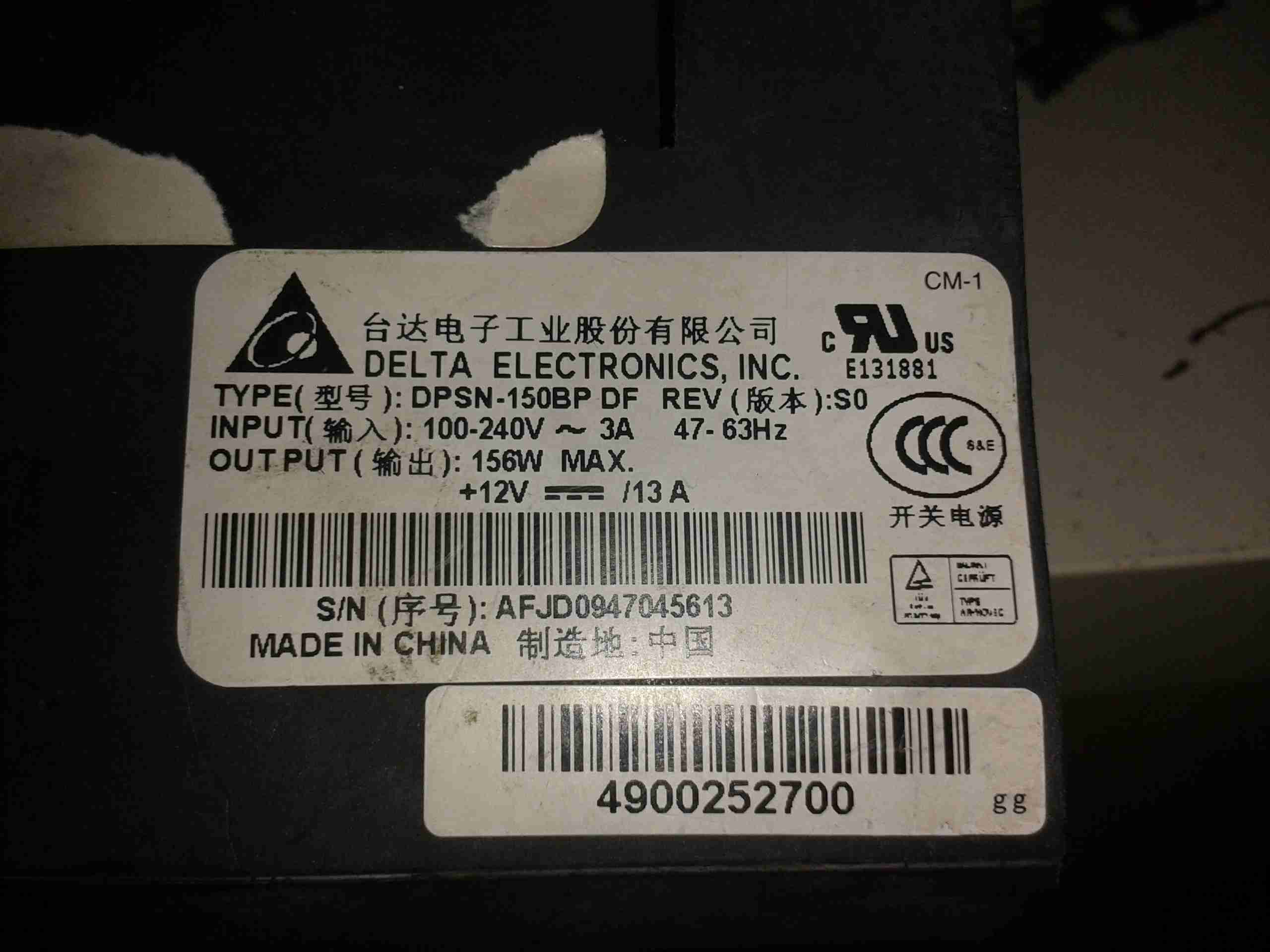
Recently I decommissioned some networking equipment, and discovered the power supplies in some switches were single rail 12v types, with a rather high power rating. I figured these would be very good for powering my Ham radio gear.
They’re high quality Delta Electronics DPSN-150BP units, rated at a maximum power output of 156W.
Label
These supplies have an adjustment pot for the output voltage regulation, but unfortunately it just didn’t have quite enough range to get from 12.0v to 13.8v. The highest they would go was ~13.04v.
After taking a look at the regulator circuit, I discovered I could further adjust the output voltage by changing a single resistor to a slightly lower value.
Firstly though, a little background on how switched mode power supplies operate & regulate their output voltage.
SMPS
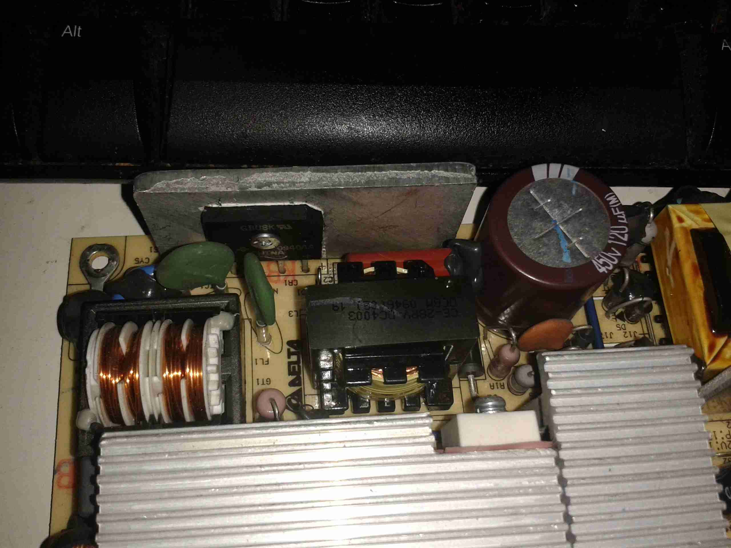
Here’s the supply. It’s mostly heatsink, to cool the large power switching transistors.
The first thing a SMPS does, is to rectify the incoming mains AC with a bridge rectifier. This is then smoothed by a large electrolytic capacitor, to provide a main DC rail of +340v DC (when on a 240v AC supply).
Mains Input
Above is the mains input section of the PSU, with a large common-mode choke on the left, bridge rectifier in the centre, and the large filter capacitor on the right. These can store a lot of energy when disconnected from the mains, and while they should have a discharge resistor fitted to safely drain the stored energy, they aren’t to be relied on for safety!
Once the supply has it’s main high voltage DC rail, this is switched into the main transformer by a pair of very large transistors – these are hidden from view on the large silver heatsinks at the bottom of the image. These transistors are themselves driven with a control IC, in the case of this supply, it’s a UC3844B. This IC is hidden under the large heatsink, but is just visible in the below photo. (IC5).
Control ICMain Switching Transformer
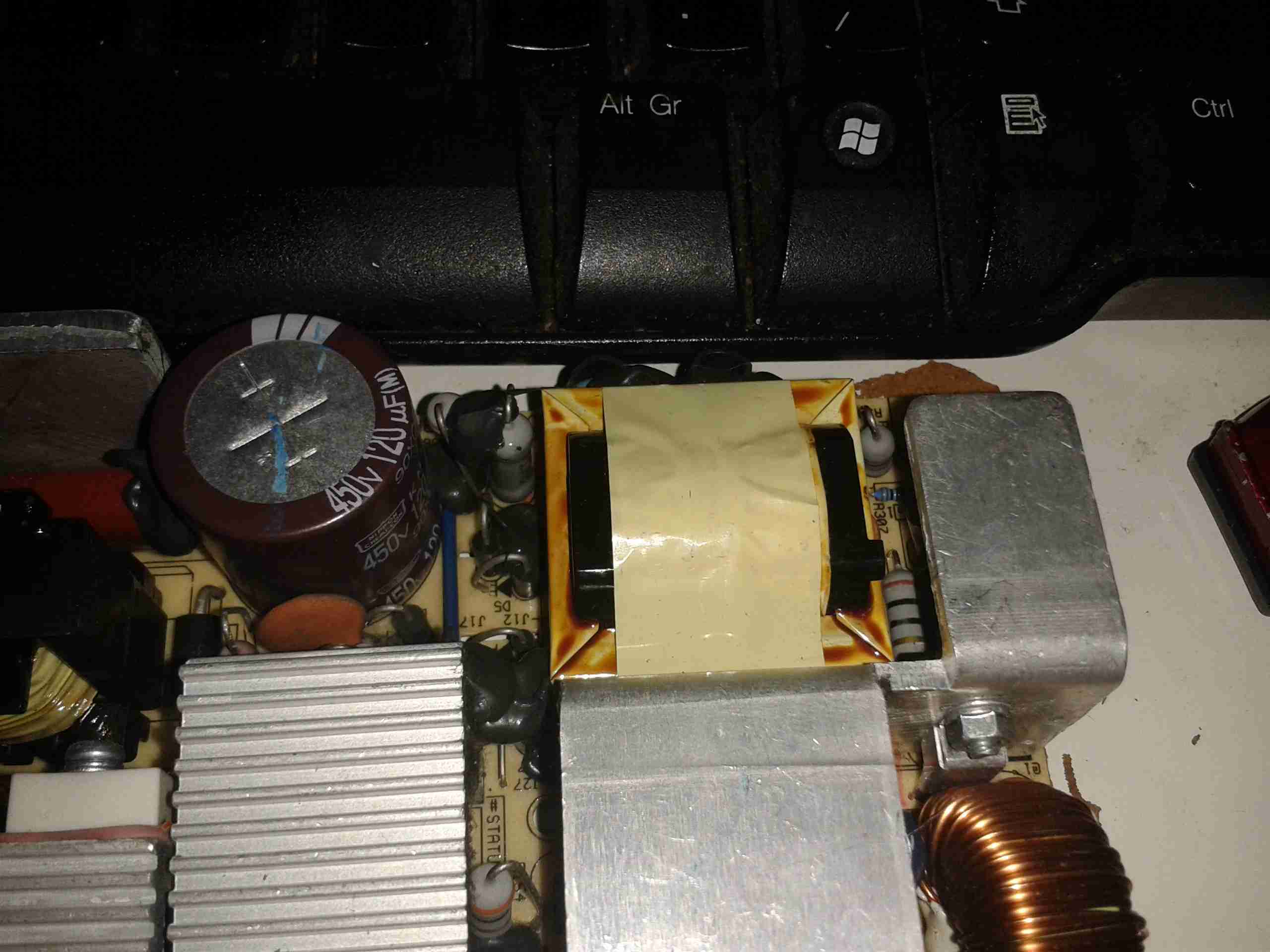
Here’s the main switching transformer, these can be much smaller than a conventional transformer due to the high frequencies used. This supply operates at 500kHz.
After the main transformer, the output is rectified by a pair of Schottky diodes, which are attached to the smaller heatsink visible below the transformer, before being fed through a large toroidal inductor & the output filter capacitors.
All this filtering on both the input & the output is required to stop these supplies from radiating their operating frequency as RF – a lot of cheap Chinese switching supplies forego this filtering & as a result are extremely noisy.
After all this filtering the DC appears at the output as usable power.
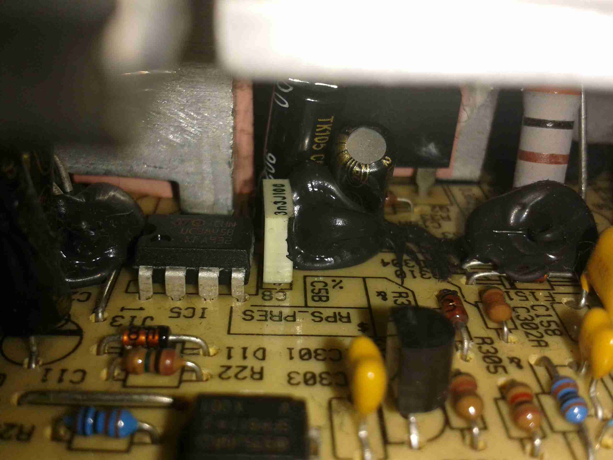
Getting back to regulation, these supplies read the voltage with a resistor divider & feed it back to the mains side control IC, through an opto-isolator. (Below).
Feedback Loop
The opto isolators are the black devices at the front with 4 pins.
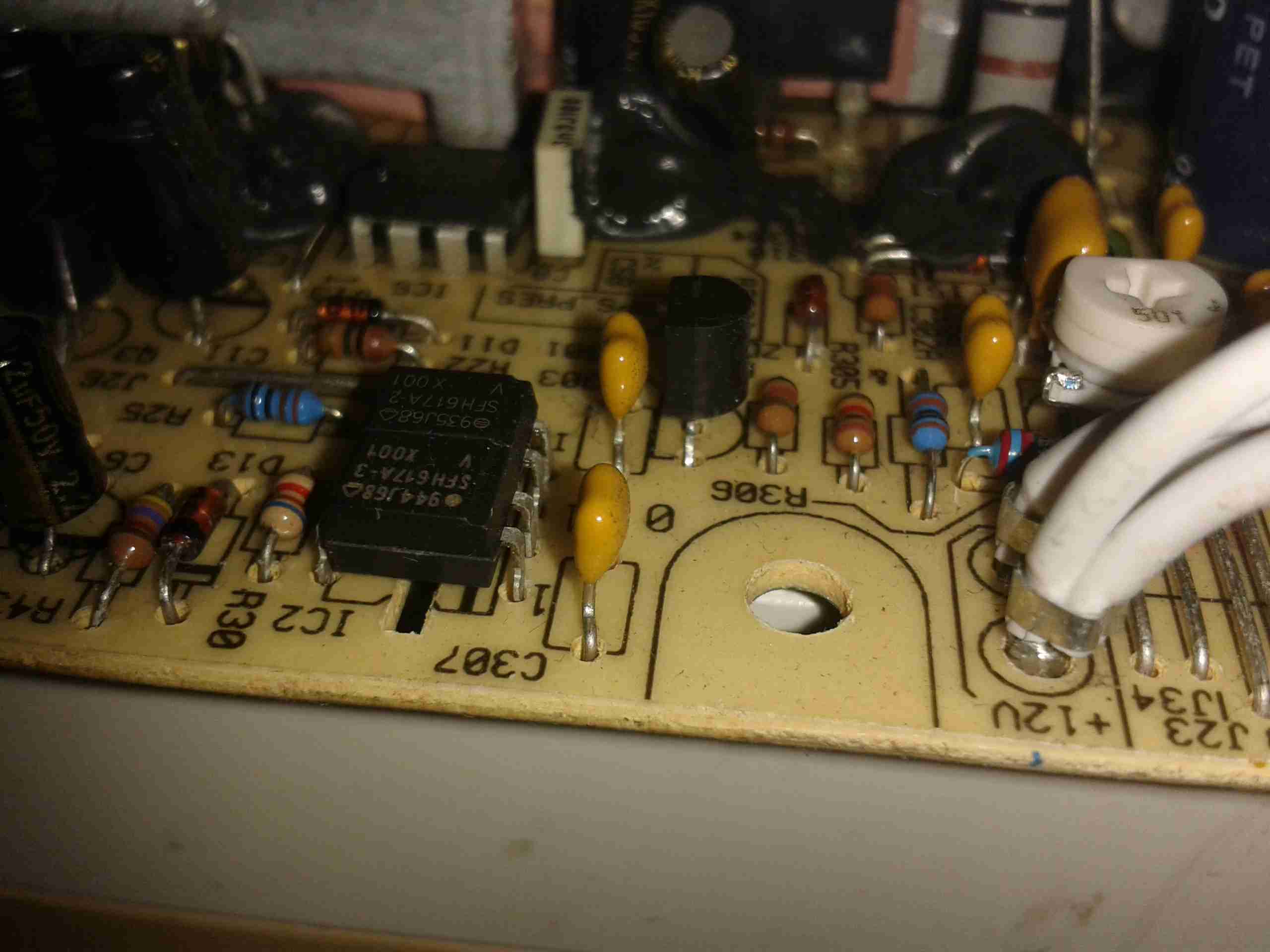
Regulator Adjustment
For a more in-depth look at the inner workings of SMPS units, there’s a good article over on Hardware Secrets.
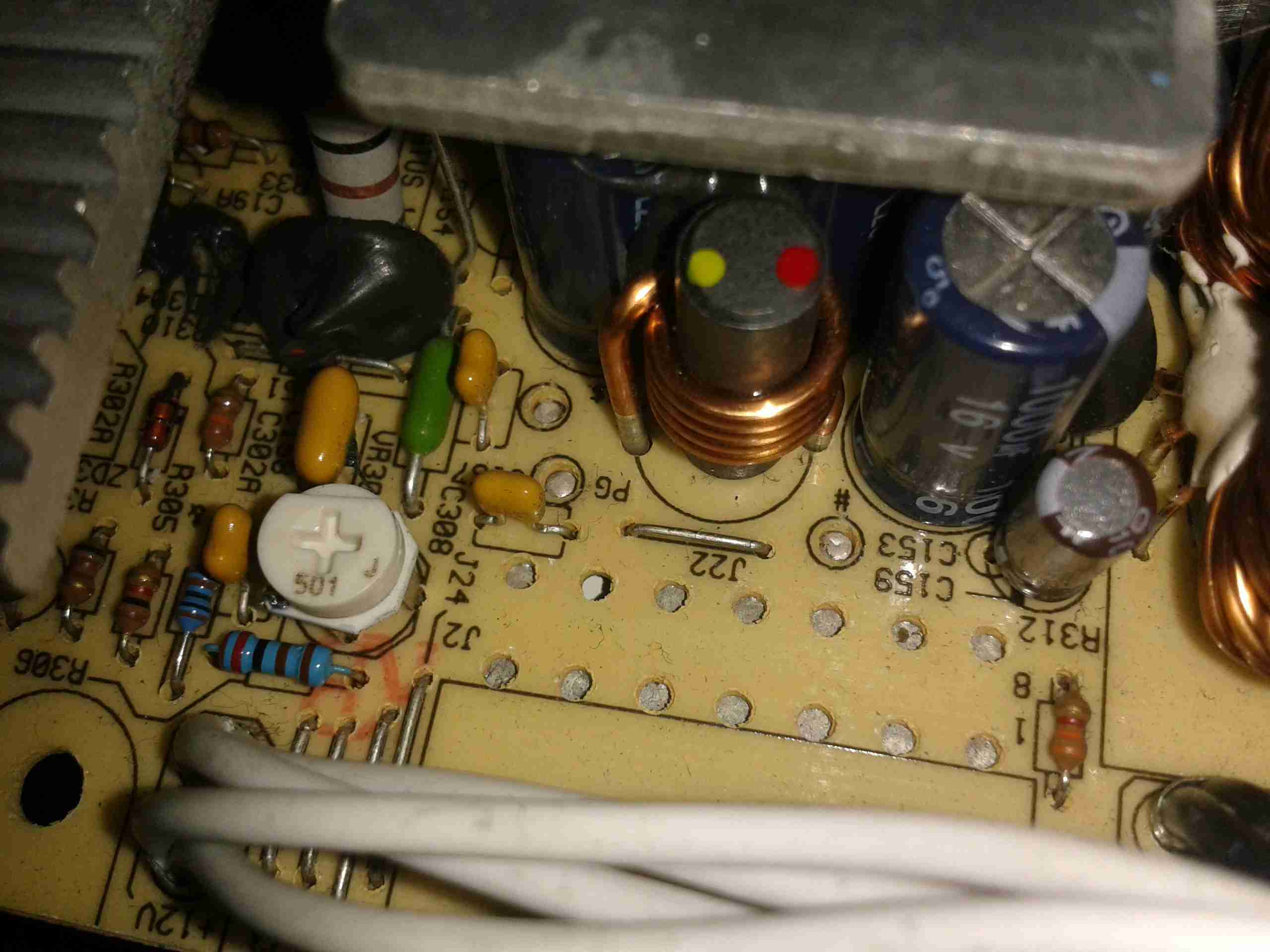
My modification is simple. Replacing R306 (just below the white potentiometer in the photo), with a slightly smaller resistor value, of 2.2KΩ down from 2.37KΩ, allows the voltage to be pulled lower on the regulator. This fools the unit into applying more drive to the main transformer, and the output voltage rises.
It’s important to note that making too drastic a change to these supplies is likely to result in the output filter capacitors turning into grenades due to overvoltage. The very small change in value only allows the voltage to rise to 13.95v max on the adjuster. This is well within the rating of 16v on the output caps.
Now the voltage has been sucessfully modified, a new case is on the way to shield fingers from the mains. With the addition of a couple of panel meters & output terminals, these supplies will make great additions to my shack.
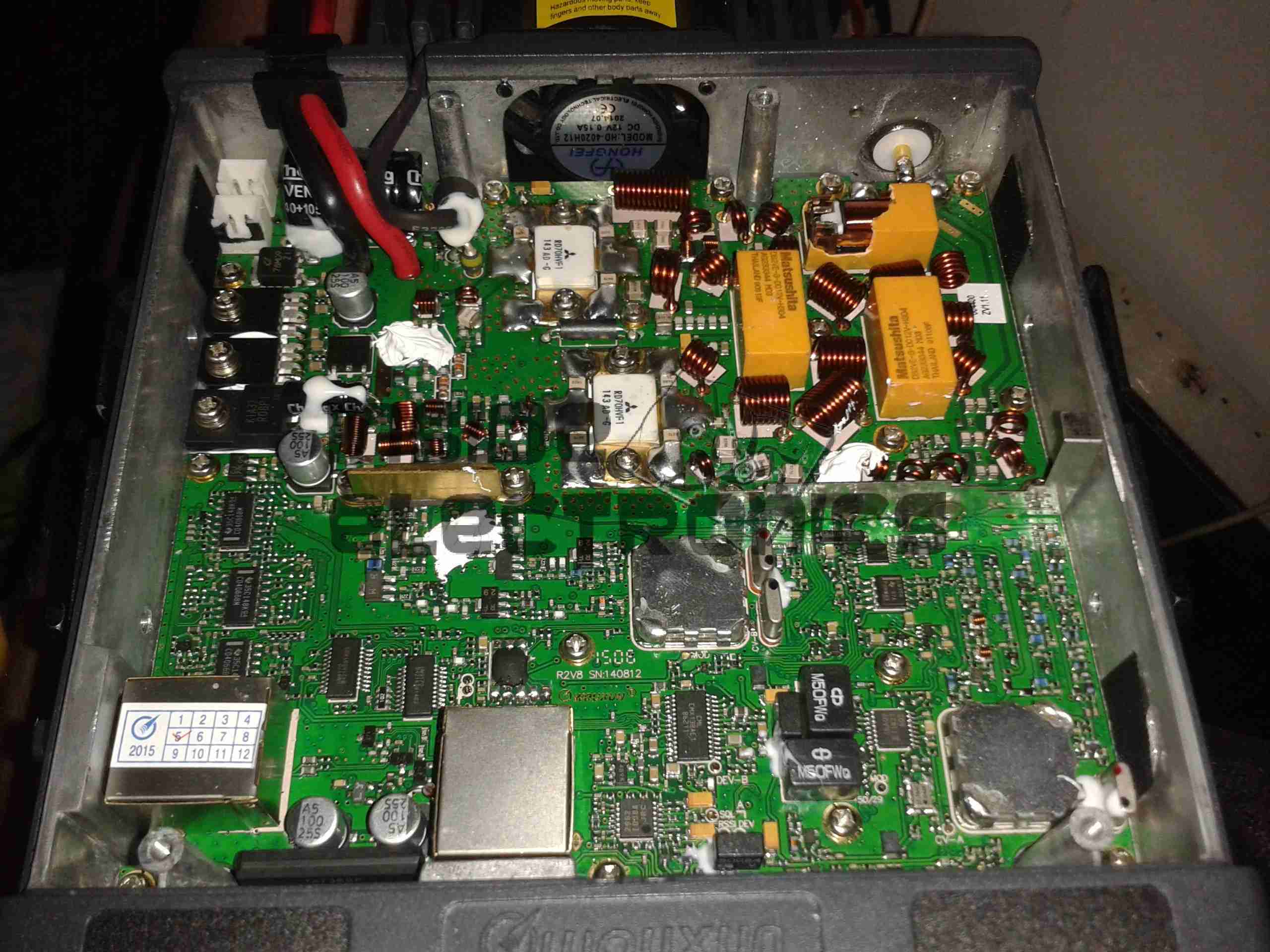
Following on from my review, here are some internal views & detail on the components used in this radio. Below is an overview of the main PCB with the top plate removed from the radio.
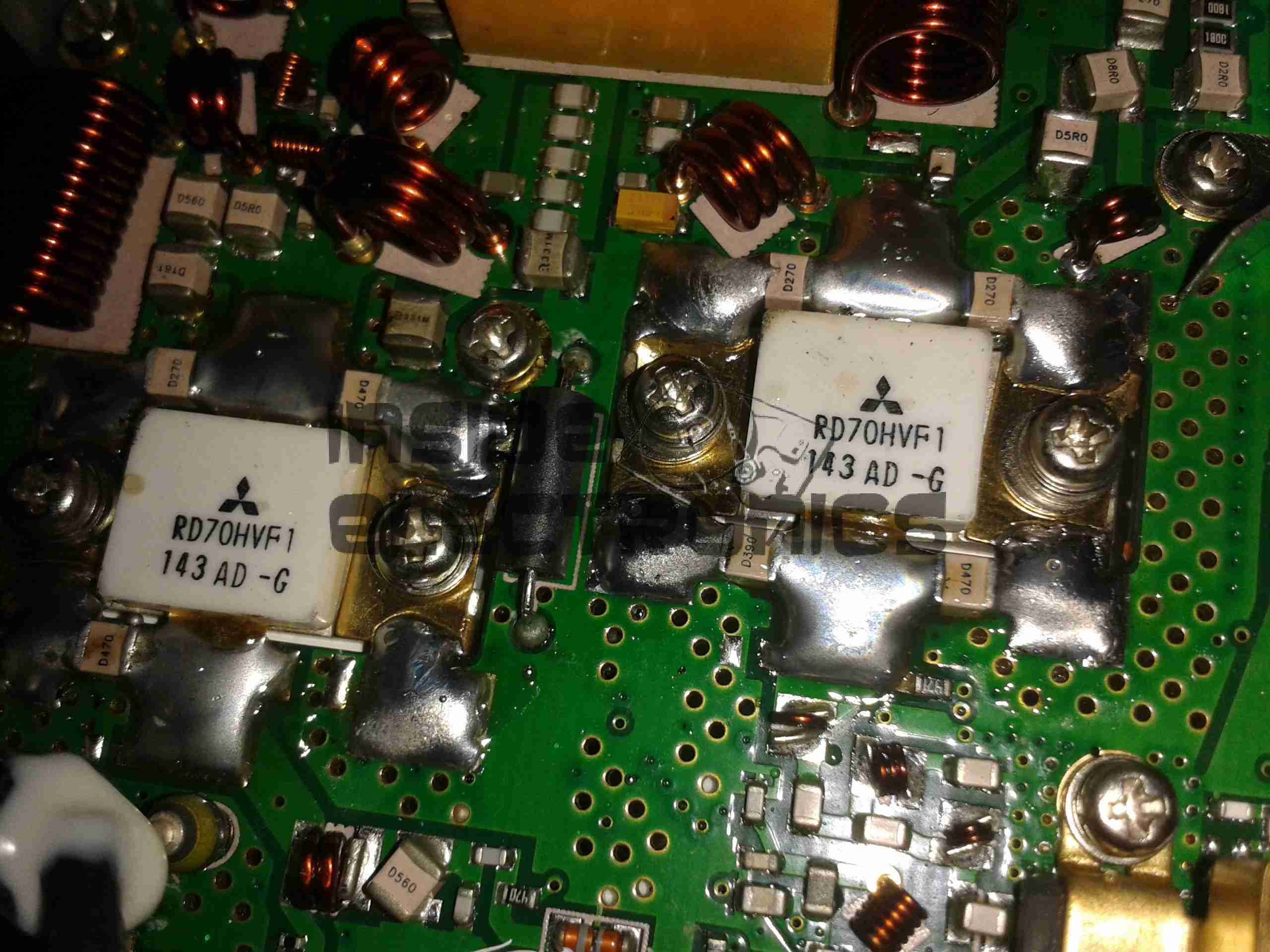
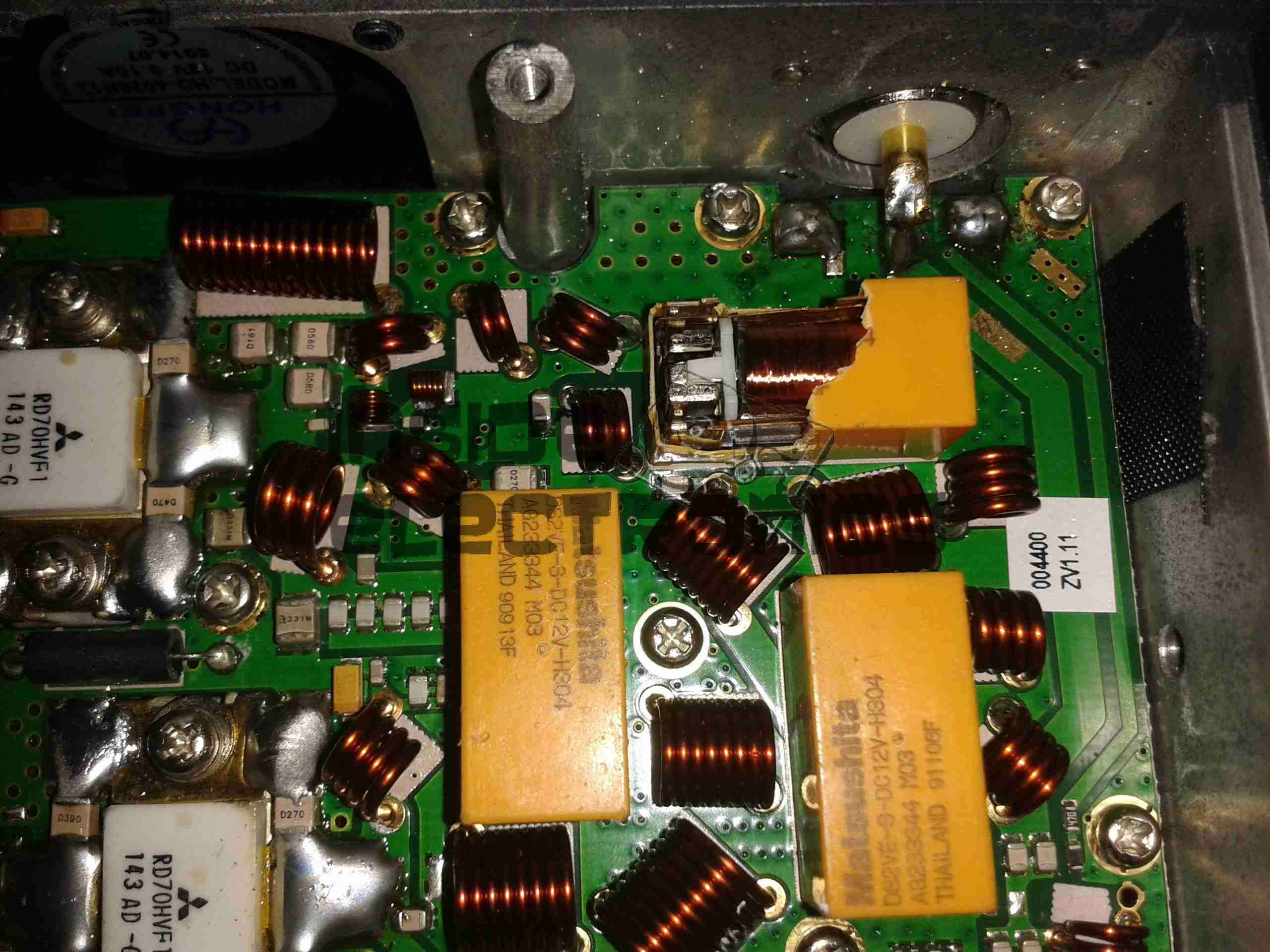
Cover RemovedRF Final Amplifier Stage
Most visible are these MOSFETs, which are Mitsubishi RD70HVF1 VHF/UHF power devices. Rated for a maximum of 75W output power at 12.5v (absolute maximum of 150W, these are used well within their power ratings. They are joined to the PCB with heavy soldering, with bypass caps tacked right on to the leads.
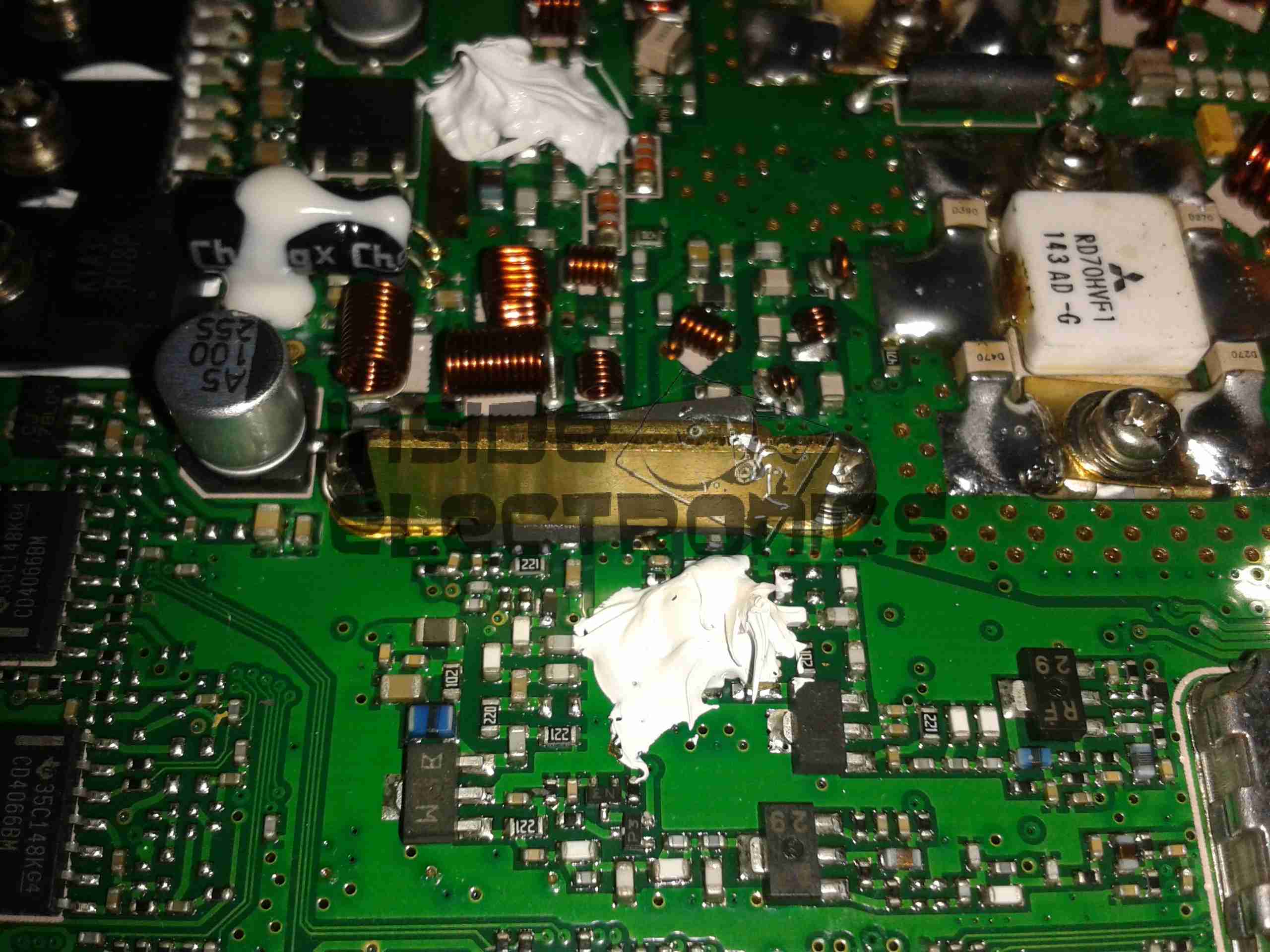
RF Pre Drivers
Here is the RF pre-driver stage, with intermediate transistors hidden under the small brass heatspreader.
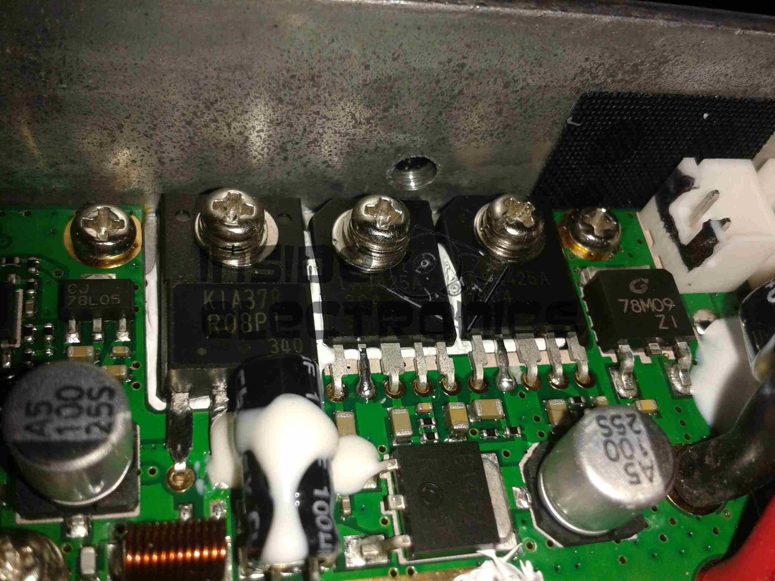
Power Section
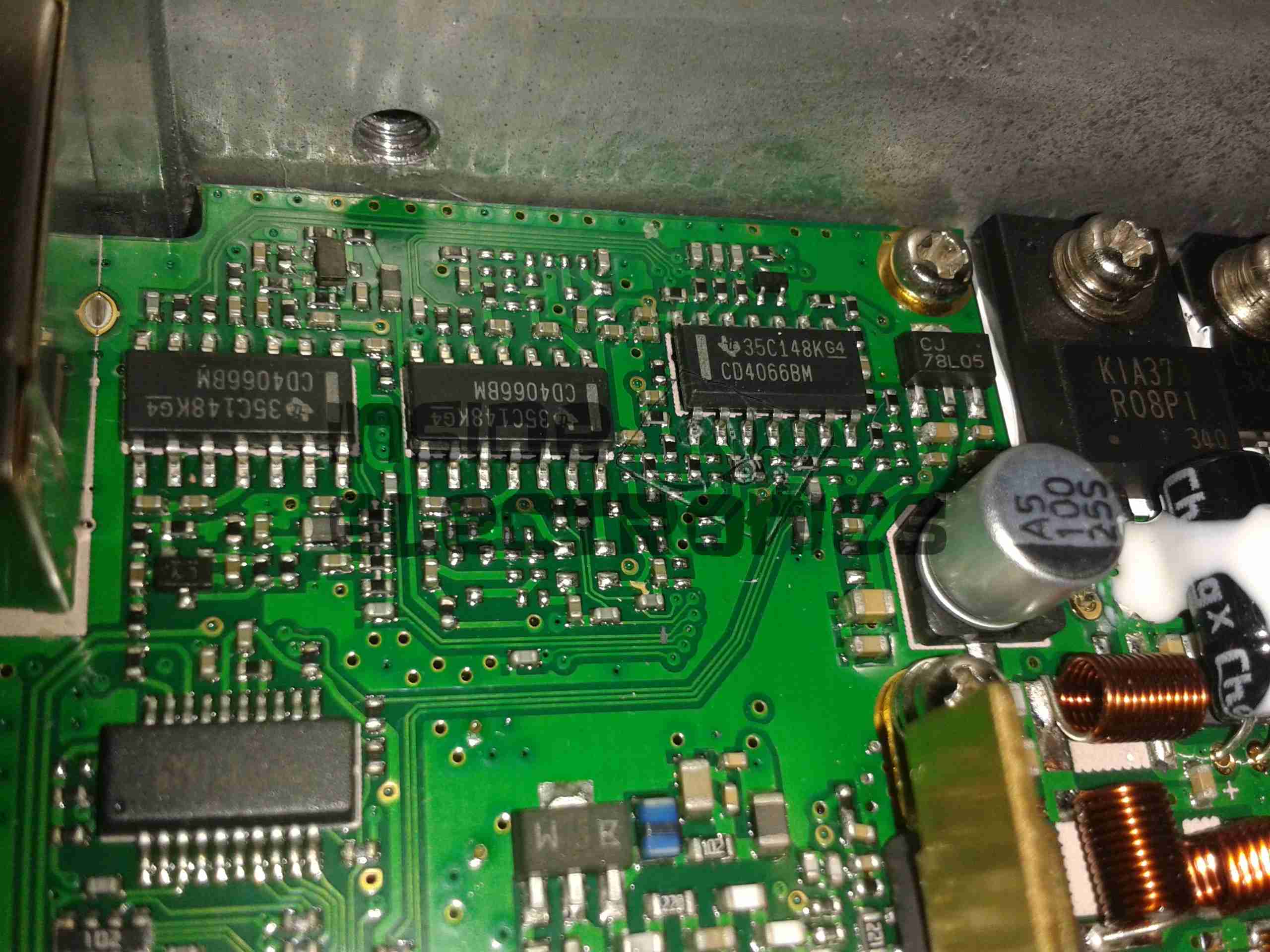
In the top left corner of the radio, near the power input leads, is the power supply & audio amplifier section. Clearly visible are the pair of LA4425A 5W audio power amplifier ICs, these drive the speakers on the top of the radio. Either side of these parts are a 7809 & a 7805 – both linear regulators providing +9v & +5v logic supplies respectively. The large TO220 package device is a KIA378R08PI 3A LDO regulator with ON/OFF control, this one outputs +8v. Just visible in the top right corner are the sockets for the speaker connections.
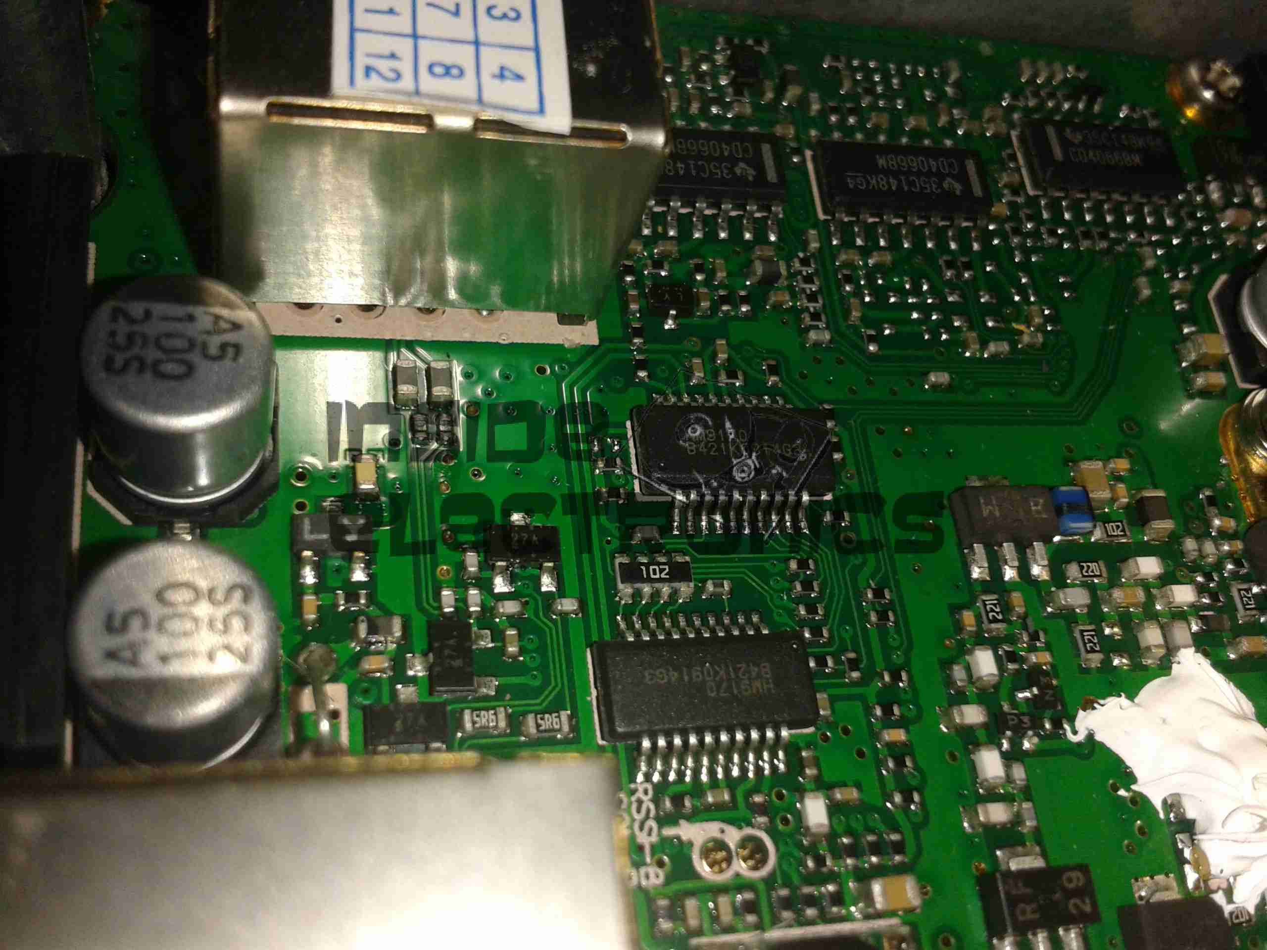
DTMF Circuits
Here are the two ICs for dealing with DTMF tones, they are HM9170 receivers.
Glue Logic
In the corner next to the interface jack, there are some CD4066B Quad Bilateral switches. These make sense since the interface jack has more than a single purpose, these will switch signals depending on what is connected.
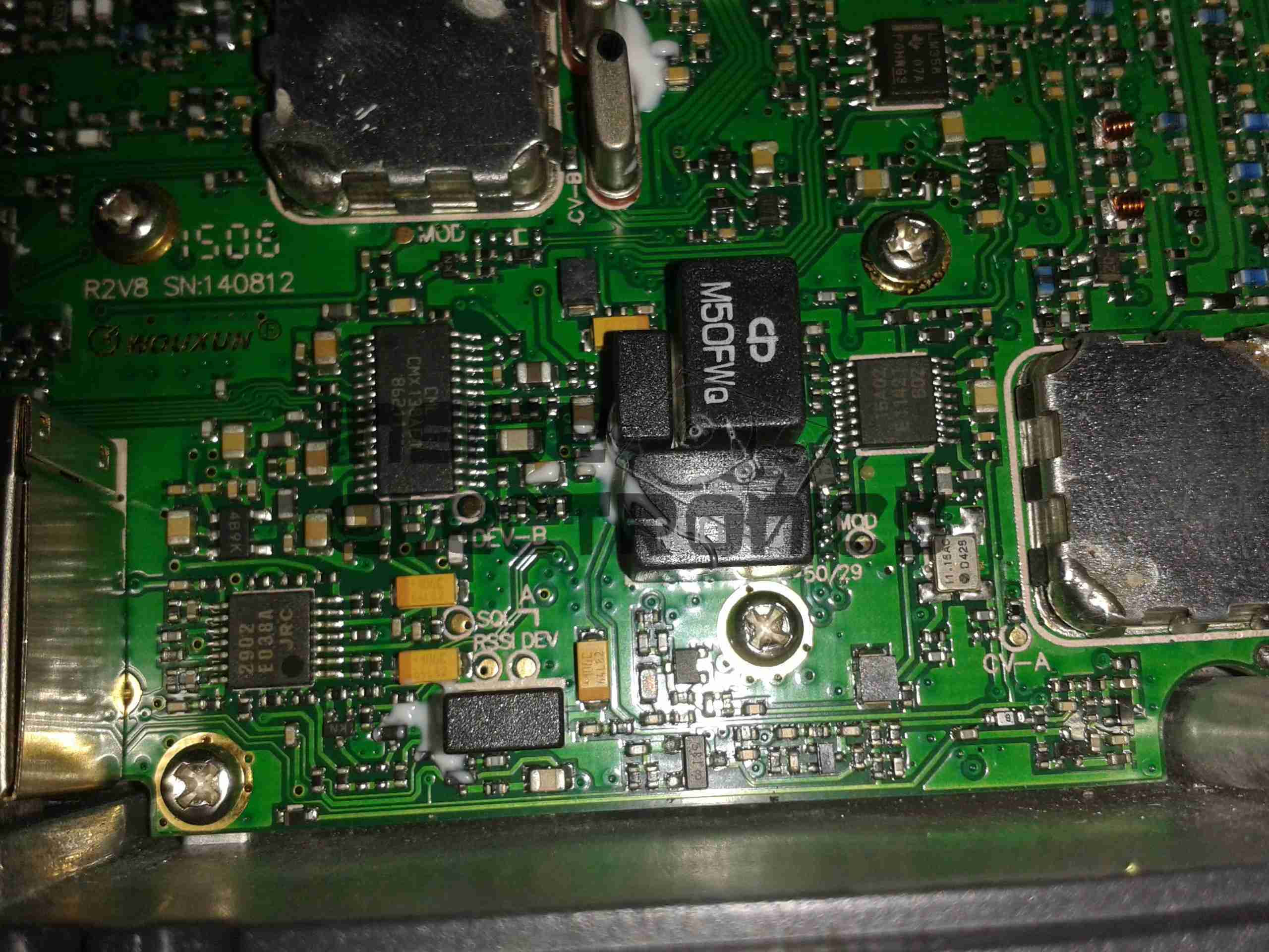
RF Section
Here are visible the RF cans for the oscillators, the crystals visible next to the can at the top. The shields are soldered on, so no opening these unfortunately.
Also visible in this image is a CMX138A Audio Scrambler & Sub-Audio Signalling processor. This IC deals with the Voice Inversion Scrambling feature of the radio, & processes the incoming audio before being sent to the modulator.
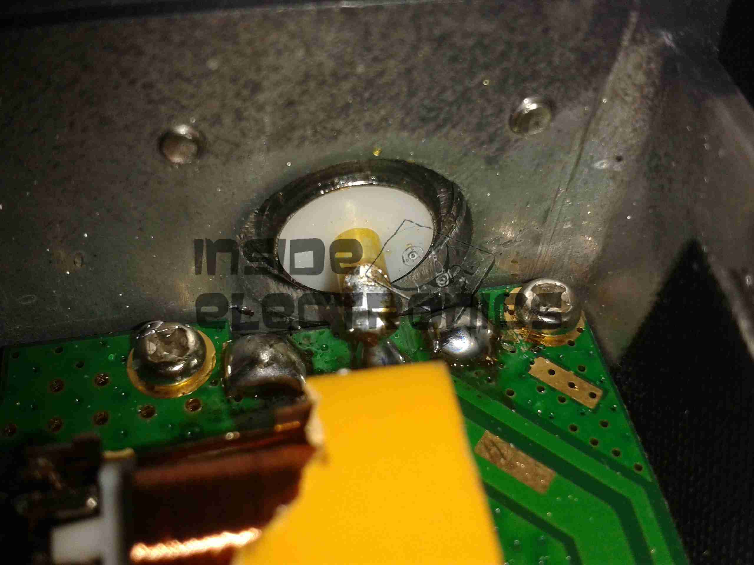
Output Filter Network
Shown here is the RF output filter network, this radio uses relays for switching instead of PIN diodes, I imagine for cost reasons. The relay closest to the RF output socket has had a slight accident 🙂 This is slated to be replaced soon.
RF Output Jack
Finally, the RF output jack.
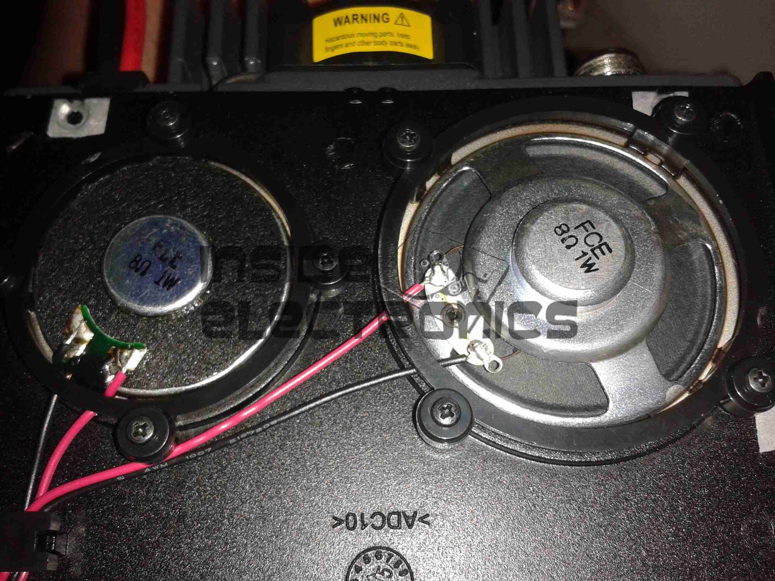
Audio Speakers
Here the speakers are shown, attached to the bottom of the top plate. They are both rated 8Ω 1W.
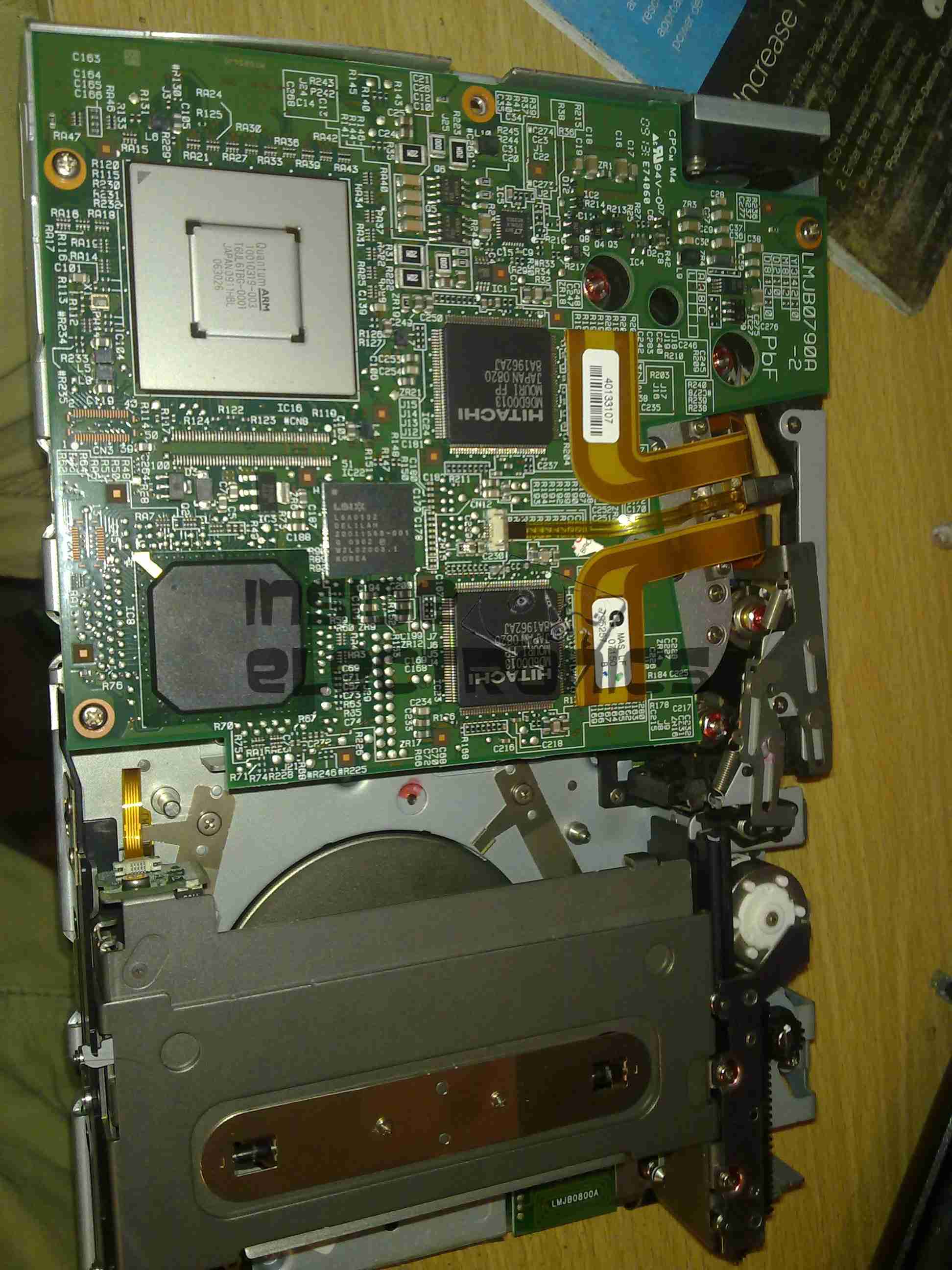
I have recently begun to create an archive of all my personal data, and since LTO2 tape drives offer significant capacity (200GB/400GB) per tape, longevity is very high (up to 30 years in archive), & relatively low cost, this is the technology I’ve chosen to use for my long term archiving needs.
Unfortunately, this drive was DOA, due to being dropped in shipping. This drop broke the SCSI LVD connector on the back of the unit, & bent the frame, as can be seen below.
Broken SCSI
As this drive is unusable, it made for a good teardown candidate.
Cover Removed
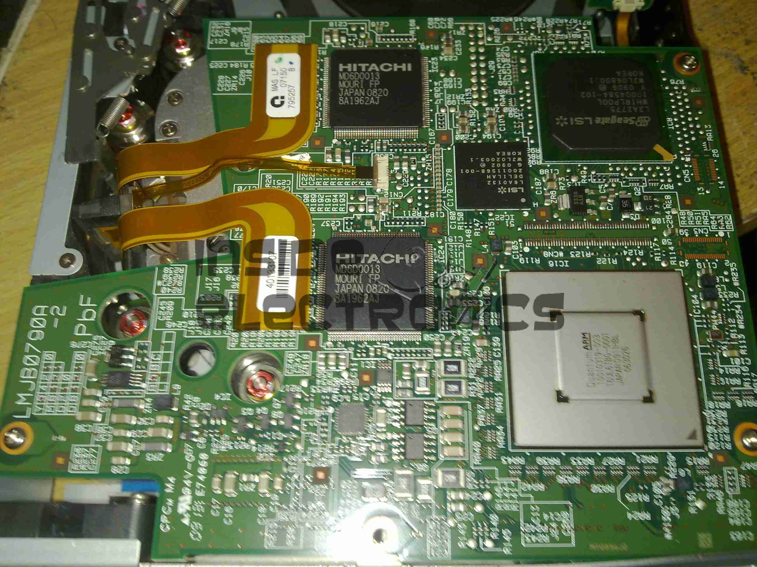
Here the top cover of the drive has been removed, showing the top of the main logic PCB. The large silver IC in the top corner is the main CPU for the drive. It’s a custom part, but it does have an ARM core.
The two Hitachi ICs are the R/W head interface chipset, while the smaller LSI IC is the SCSI controller.
The tape transport & loading mech can be seen in the lower half of the picture.
Main Logic
Close up of the main logic.
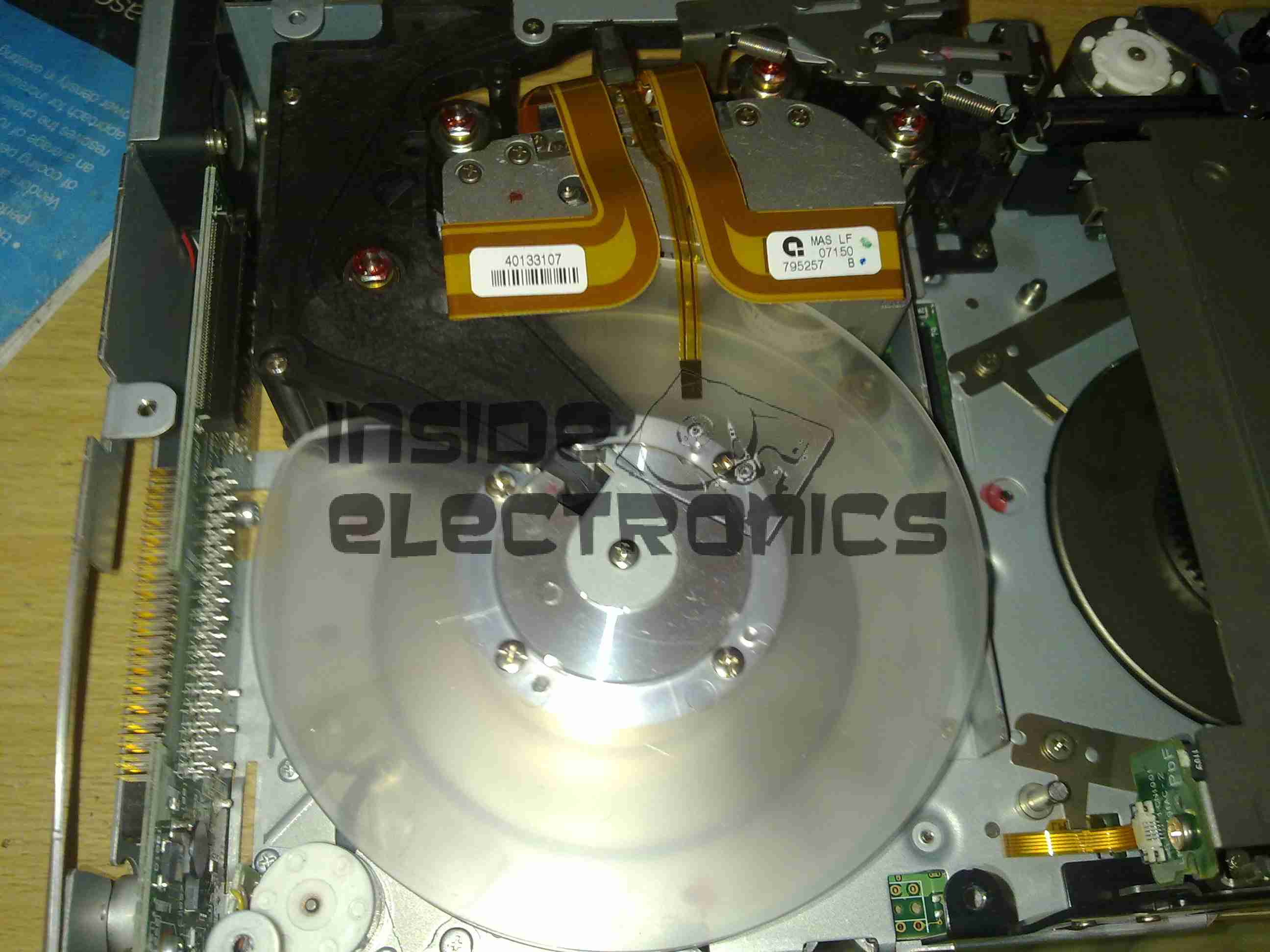
Tape Spool
Here the main logic PCB has been removed, showing the tape take up spool. The data cartridges have only one spool to make the size smaller. When the tape is loaded, the drive grabs onto the leader pin at the end of the tape & feeds it onto this spool.
The head assembly is just above the spool.
Bottom Plate Removed
Bottom of the drive with the cover plate removed. Here the spindle drive motors are visible, both brushless 3-Phase units. Both of these motors are driven by a single controller IC on the other side of the lower logic PCB.
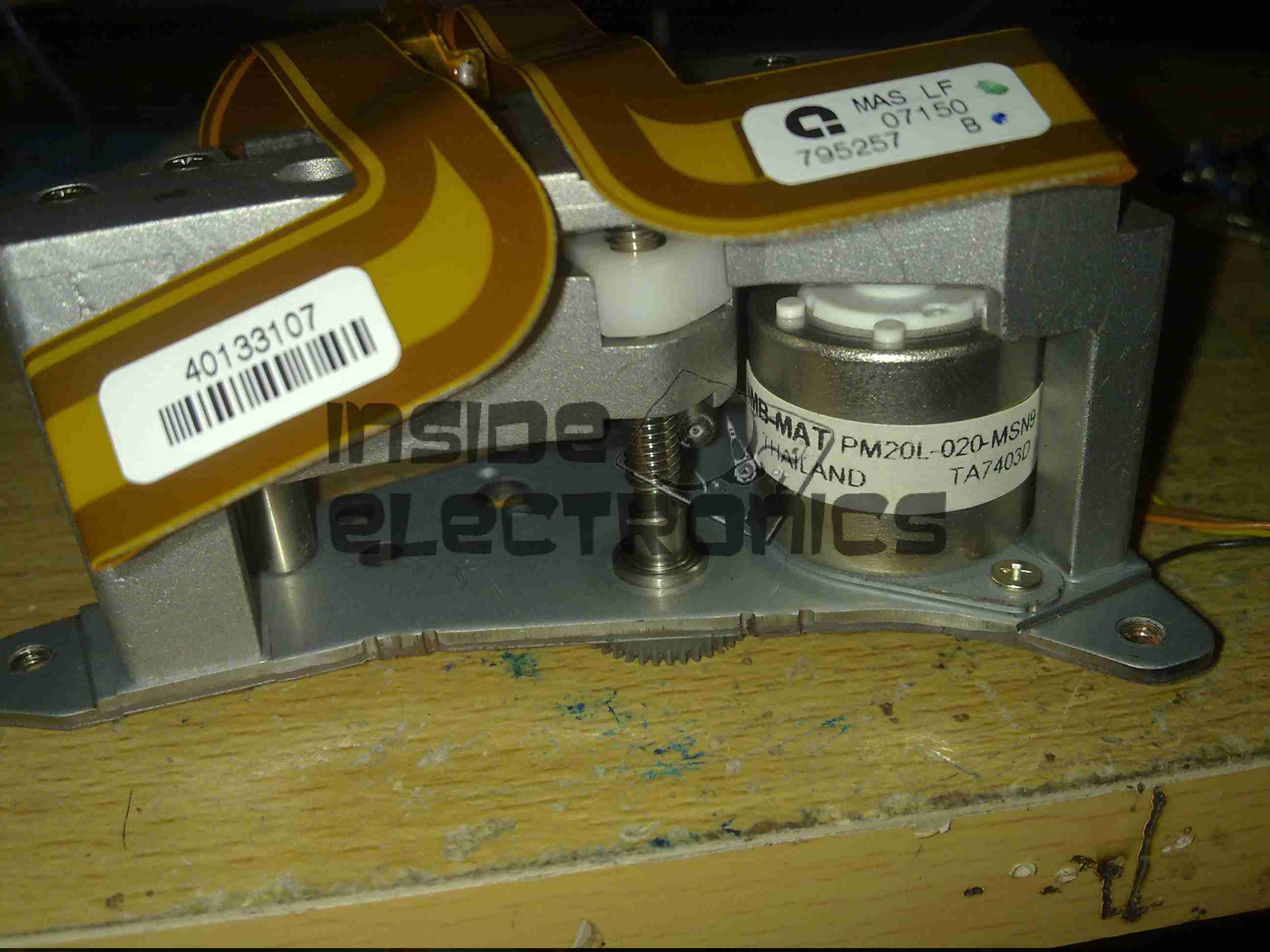
Head Drive Motor
The head is moved up & down the face of the tape by this stepper motor for coarse control, while fine control is provided by a voice coil assembly buried inside the head mount.
Tape Head Assembly
The face of the tape R/W head. This unit contains 2 sets of 8 heads, one of which writes to the tape, the other then reads the written data back right after to verify integrity.
Cartridge Load Motor
The tape cartridge loading motor. I originally thought that this was a standard brushed motor, but it has a ribbon cable emerging, this must be some sort of brushless arrangement.
A replacement drive is on the way, I shall be documenting some more of my archiving efforts & system setup once that unit arrives.
This is the control unit for a Routemaster system, that downloads traffic information for the area local to the vehicle.
Unit Overview
Here is an overview of the unit, in it’s aluminium box.
Here is the unit with the top cover removed, showing the pair of PCBs. The bottom PCB is the main control PCB, the top one holds an IC similar to a SIM card & part of the radio.
Cover Removed
Main PCB Top
Here is the main PCB removed from the casing, contains the program ROM & microcontroller. for the system
Daughtercard view. This holds another programmed CPLD, the custom SIM-like IC & the RTC battery, along with some power conversion circuitry.
Daughterboard Top
Radio Receiver
This is the radio receiver, looks to be AM, the large loop antenna can be seen at the bottom of the box.
Here are the first set of mods & improvements to the RasPi Experiment board. Instead of the solder-point experiment space, I have added a standard mini-breadboard, even though it’s a little too long to fit on the board properly.
In the DIP breakout, is a MAX232 TTL-RS232 interface IC, useful for interfacing directly to the Pi’s UART, made available on the GPIO breakout. I will be hardwiring the MAX232 IC into the GPIO port, & fitting headers to the relevant pins on the IC breakout to make interfacing to the Pi easier.
All the MAX232 requires to operate are a 5v supply & 4 1µF capacitors.
The new TO220 device next to the breadboard is a TIP121 darlington power transistor.This is rated at 80v 5A continuous. Useful for driving large loads from a GPIO output.
This is the Velleman MK179 Proximity Card Reader, which is supplied in kit form. In the image above you can see the completed kit, the read coil is etched onto the black PCB on the left. Bringing a recognised card close to the coil operates the relay on the main PCB for a programmable amount of time.
Main PCB
Closeup of the main PCB, 12v DC input at top right. Left IC is an LM358 dual Op-Amp, the IC on the right is a PIC12F629 with Velleman’s custom firmware.
Logic power is supplied to the ICs & the oscillator from the LM7805 regulator at the top of the PCB. The relay is a standard 15A SPDT 12v coil relay, with the switch contacts broken out onto the screw terminals on the left.
Schematic Diagram
As it is not provided with the kit, unlike other Velleman kits, here is the schematic for this.
Here are the viewfinder electronics from a 1984 Hitachi VHS Movie VM-1200E Camcorder. These small CRT based displays accept composite video as input, plus 5-12v DC for power.
Screen
Here is the front face of the CRT, diameter is 0.5″.
Power Board
Closeup view of the PCB, there are several adjustments & a pair of connectors. Socket in the upper left corner is the power/video input. Pinout is as follows:
Brown – GND
Red – Video Input
Orange – +12v DC
Yellow – Record LED
The potentiometers on the PCB from left:
H. ADJ
V. ADJ
BRIGHT
FOCUS
PCB Part Number reads: EM6-PCB
This unit utilises the BA7125L deflection IC.
Solderside
Reverse side of the PCB, very few SMT components on this board.
Tube Assembly
Here is an overall view of the CRT assembly with scan coils. Tube model is NEC C1M52P45.
Electron Gun
Closeup view of the CRT neck, showing the electron gun assembly.
CCTV Camera
The old CCTV camera used to feed a composite signal to the CRT board. Sanyo VCC-ZM300P.
CCTV Camera Connections
Connections at the back of the camera. Red & Black pair of wires lead to 12v power supply, Green & Black pair lead to the CRT board’s power pins. Seperate green wire is pushed into the BNC video connector for the video feed. video ground is provided by the PSU’s ground connection.
Connections
Finally the connections at the CRT drive board, left to right, +12v, Video, GND.
Screen Operation
Display taking video signal from the CCTV camera.
Tip Jar
If you’ve found my content useful, please consider leaving a donation by clicking the Tip Jar below!
All collected funds go towards new content & the costs of keeping the server online.