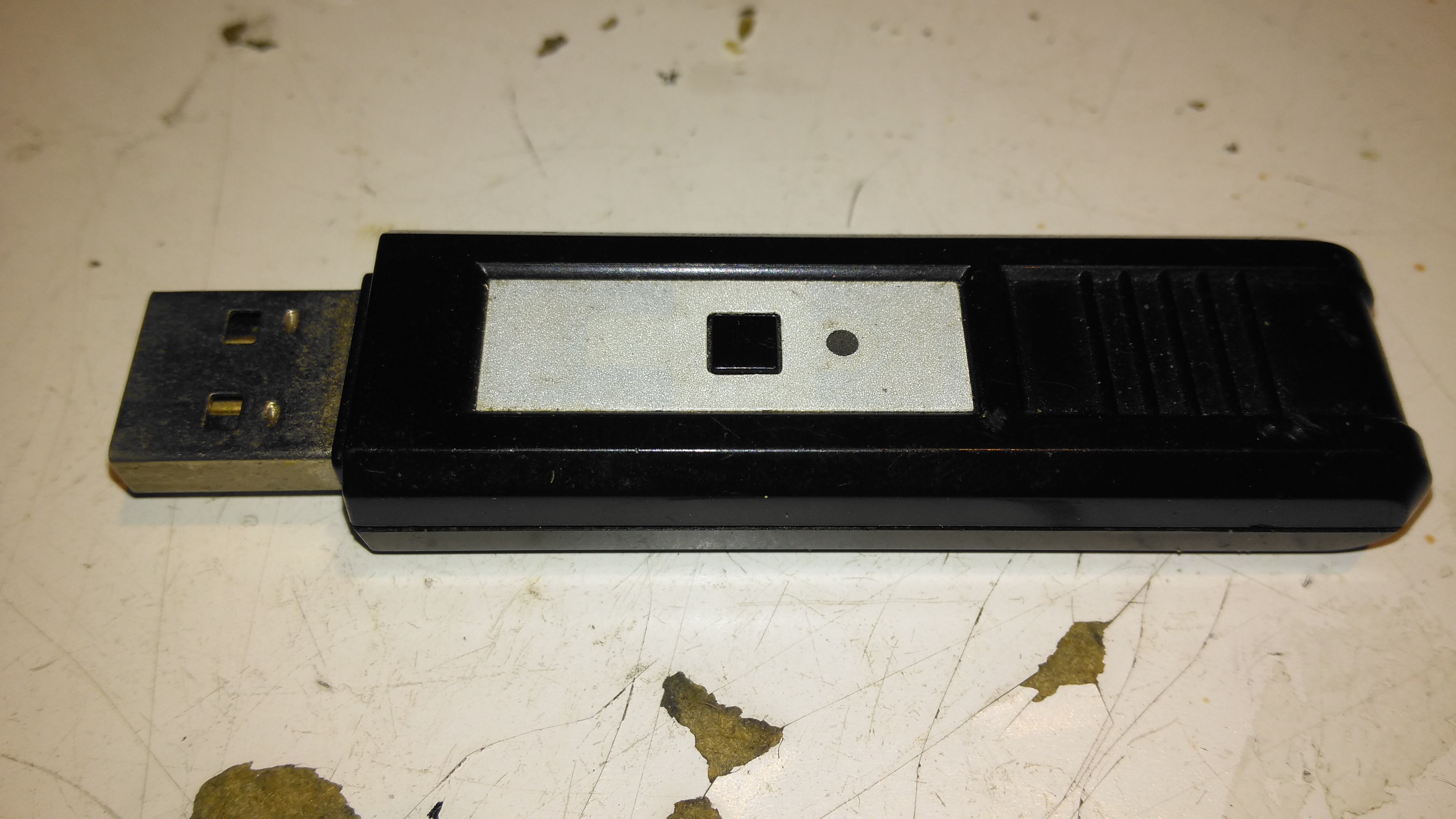
This is a pair of modules that Maplin was selling some time back, to send stereo audio over a 2.4GHz radio link. The transmitter identifies as a USB sound card, I’ve personally used these units to transmit audio about 60ft. The transmitter, above, has a single button for pairing with the receiver below.
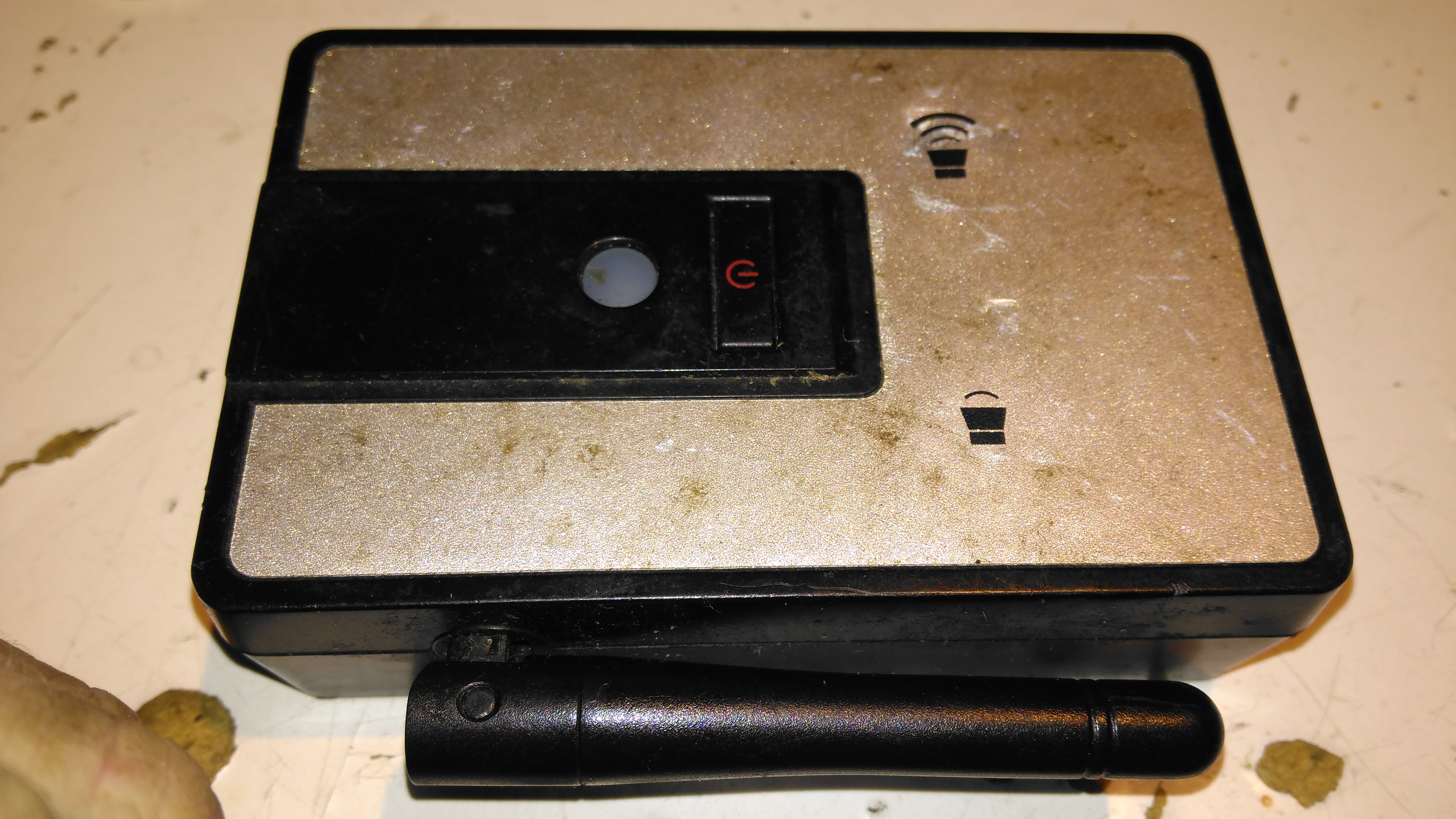
Receiver
The receiver unit has a large external antenna, a link status LED & volume buttons, these directly control the volume level on the host PC via the sound card drivers.
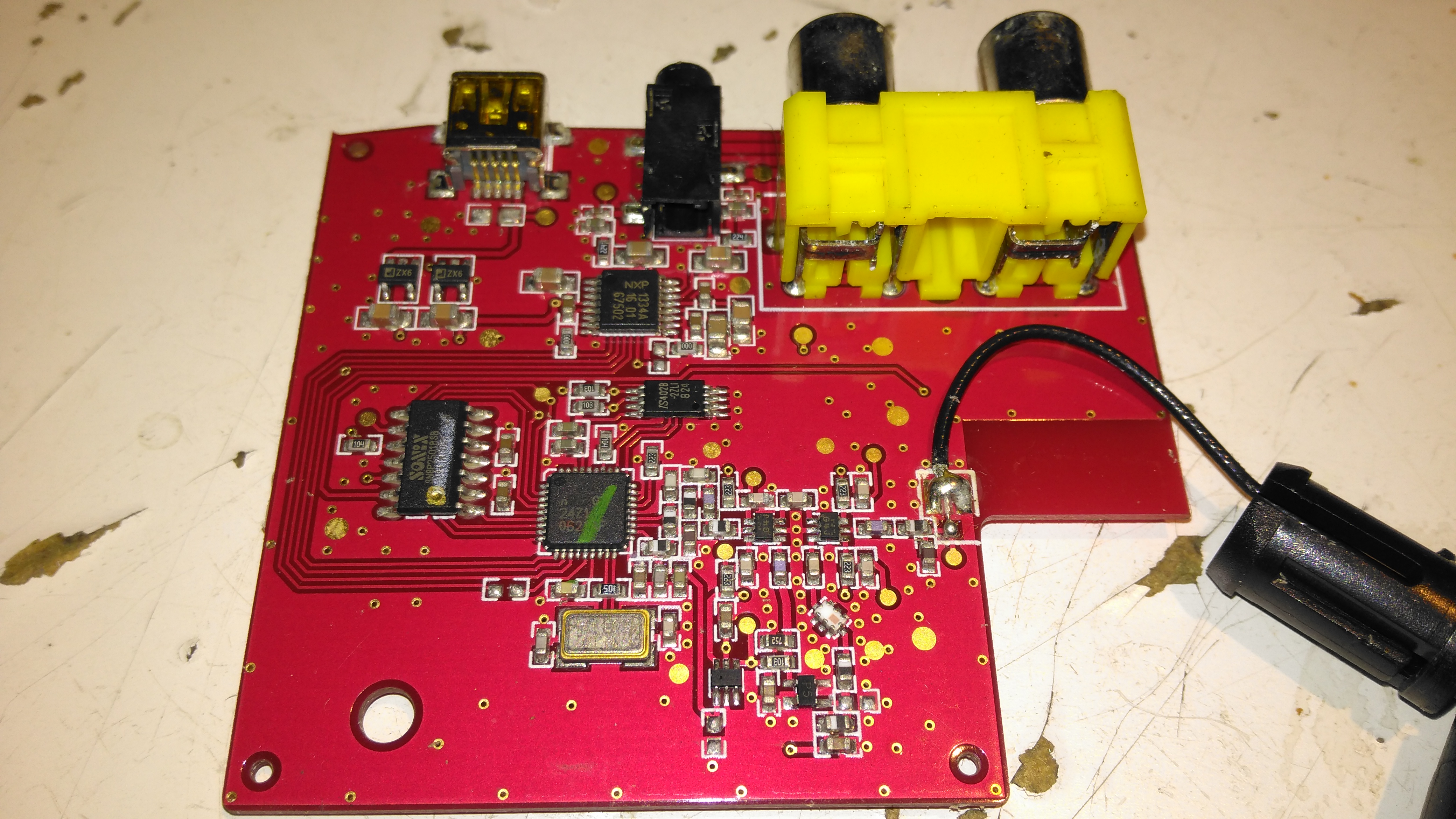
Receiver PCB Top
Popping the case open on the receiver reveals a large PCB, holding the chipset, along with the audio output jacks & Mini-USB power input. The antenna Coax is soldered to the PCB.
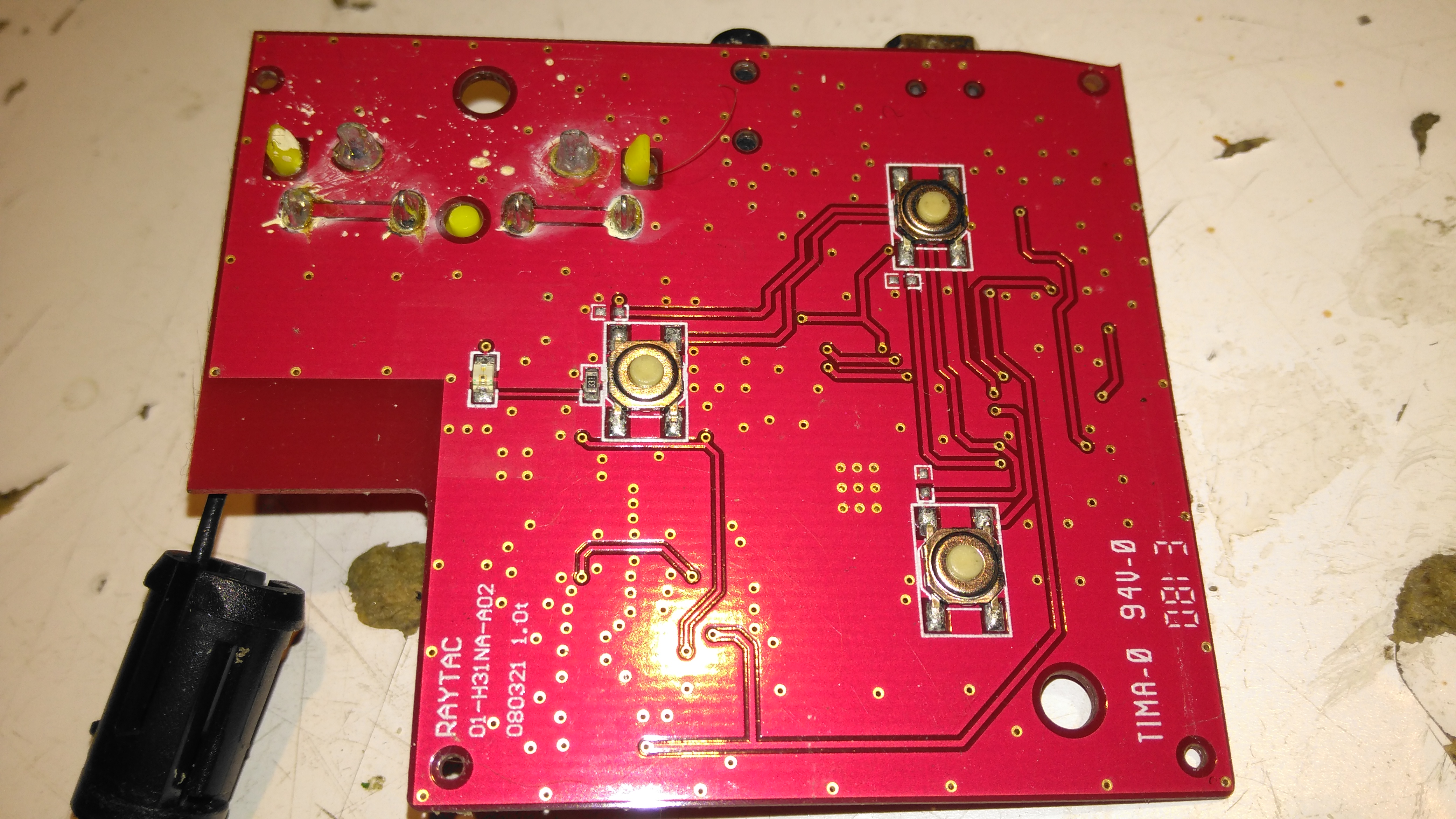
Receiver PCB Bottom
The top of the board has the control buttons, and the status LED.
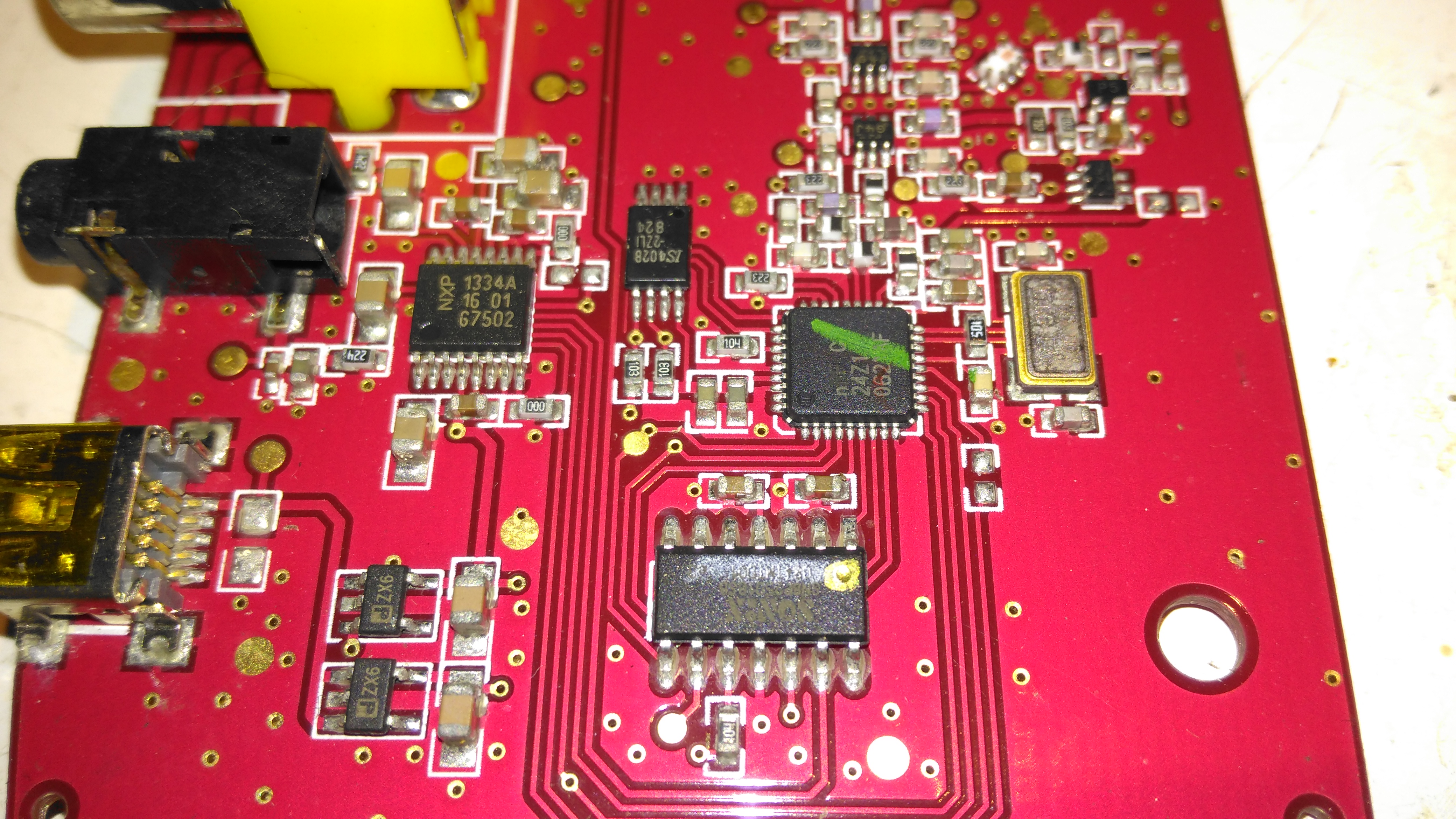
Receiver Chipset
The chipset used here is a Nordic Semiconductor nRF20Z01 2.4GHz Stereo Audio Streamer, there’s a small microcontroller which does all the register magic on the RF transceiver. The RF chain is at the top of the photo, audio outputs on the top left, and the micro USB power input & voltage regulators at bottom left.
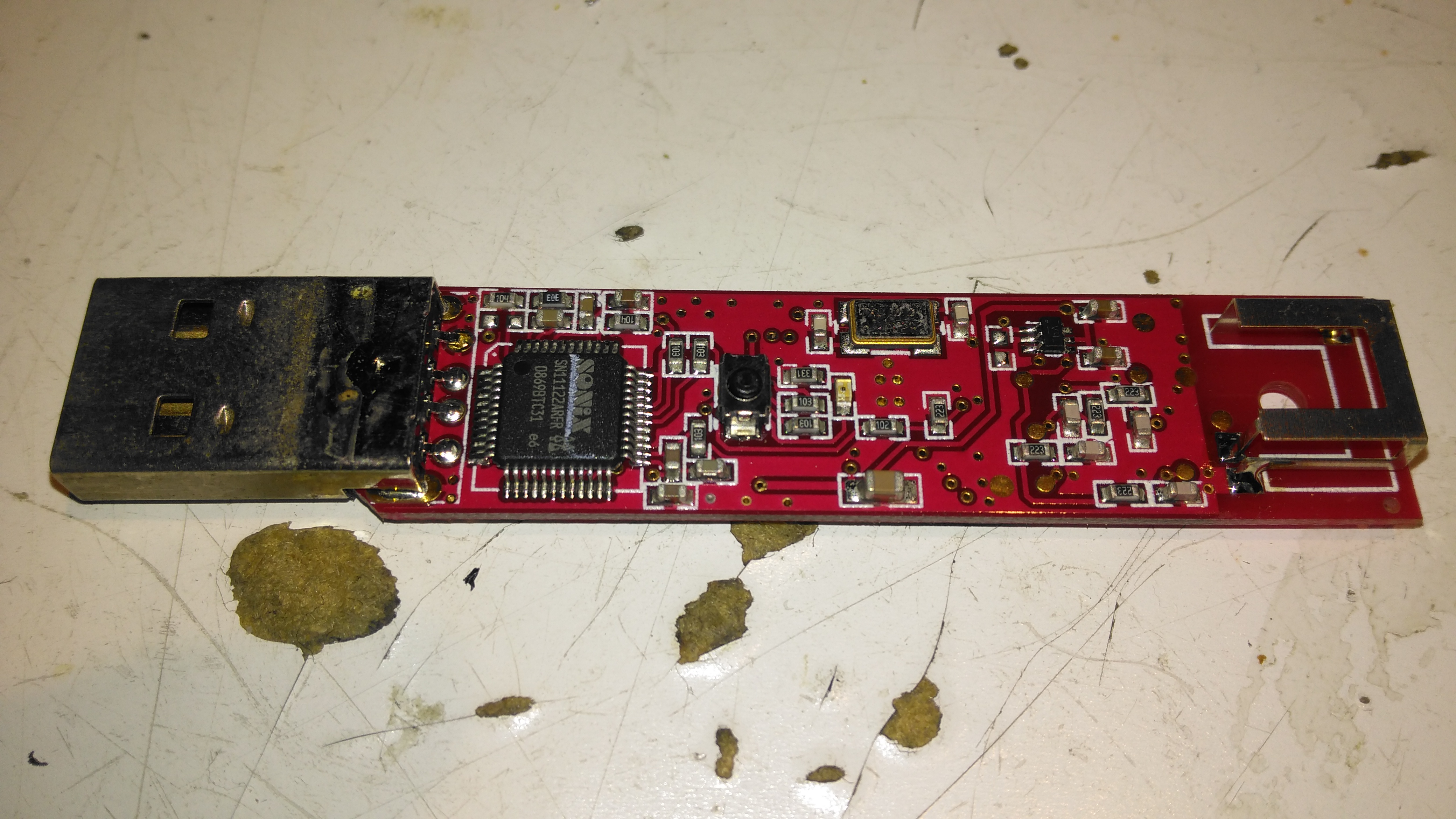
Transmitter PCB Top
The transmitter PCB has a Sonix USB Audio Codec, to interface with the host PC. This is then fed into another Nordic Semi part on the opposite side of the board:
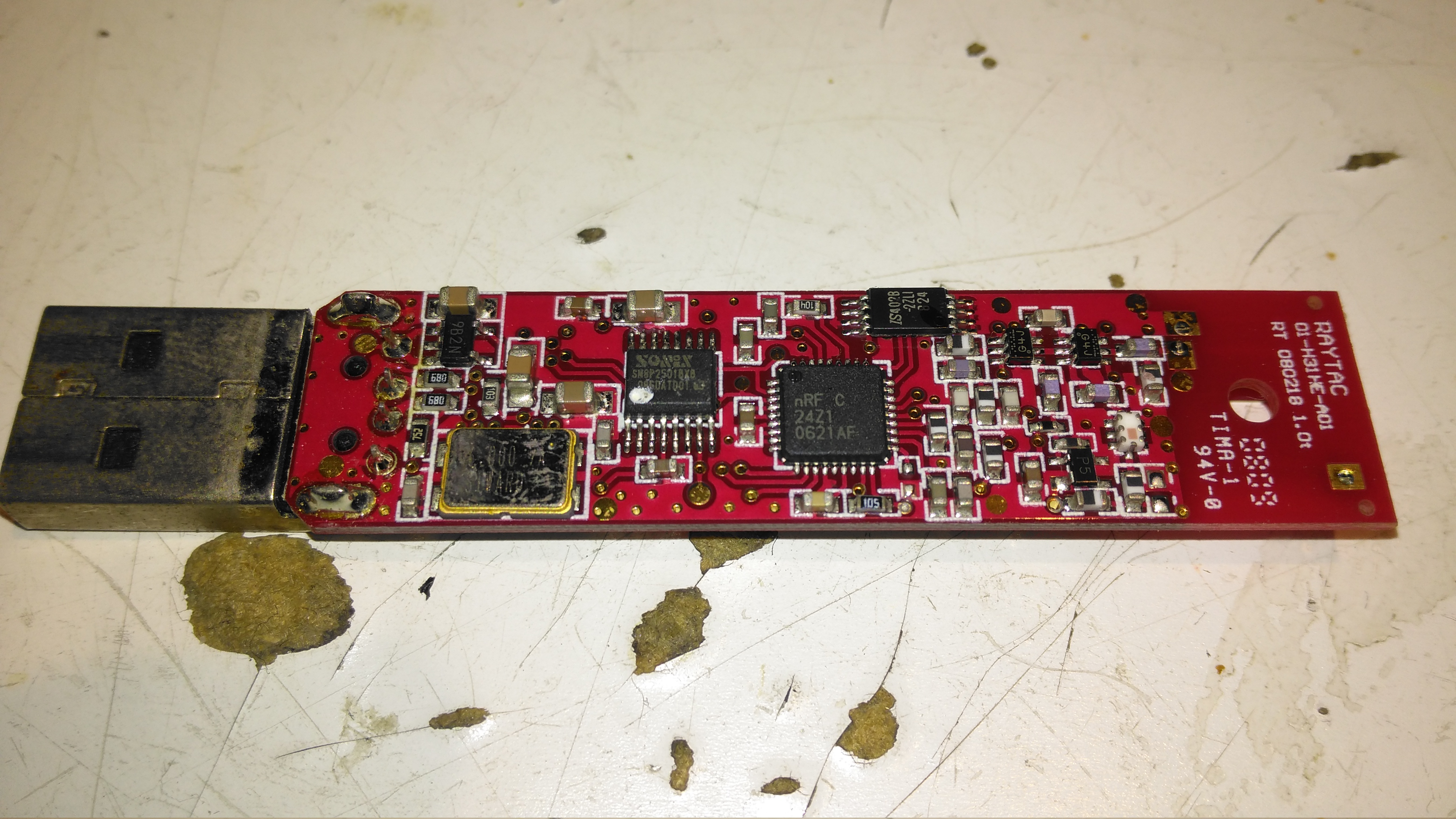
Transmitter PCB Bottom
The bottom of the transmitter has the RF section, and another small control microcontroller.
My new DMM I posted about a while back came with PC software & drivers for the RS-232 interface, on a CD. I haven’t used CDs for some time, so I had to dig out my USB drive.
The Tenma website doesn’t list the software for all their models, so to help others I’m posting an archive of all the supplied drivers here. The archive contains software & drivers for the following Tenma models:
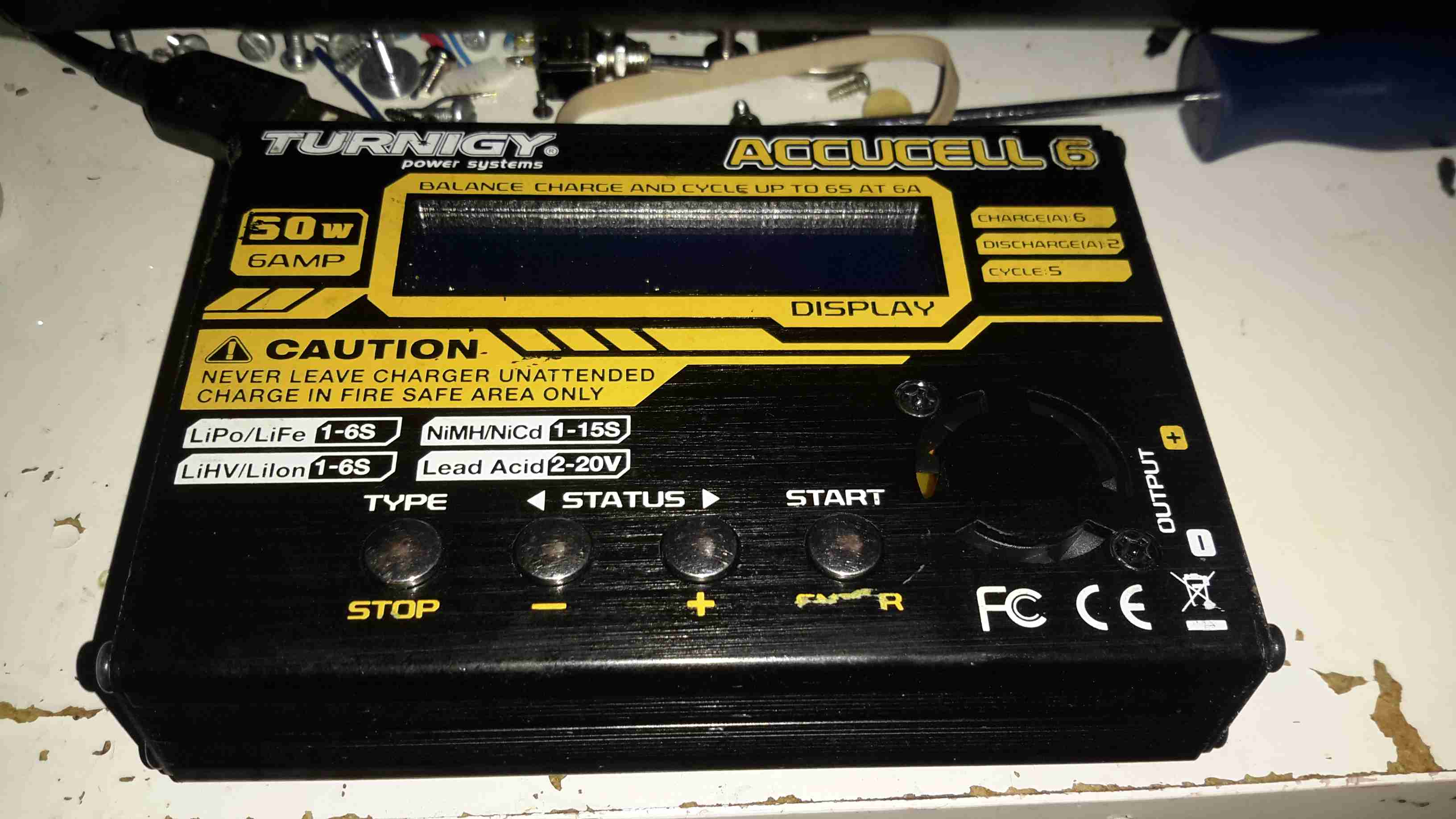
A lot of the electronics I use & projects I construct use batteries, mainly of the lithium variety. As charging this chemistry can be a little explosive if not done correctly, I decided a proper charger was required. This charger is capable of handling packs up to 6 cells for Lithium, and up to 20v for lead-acids.
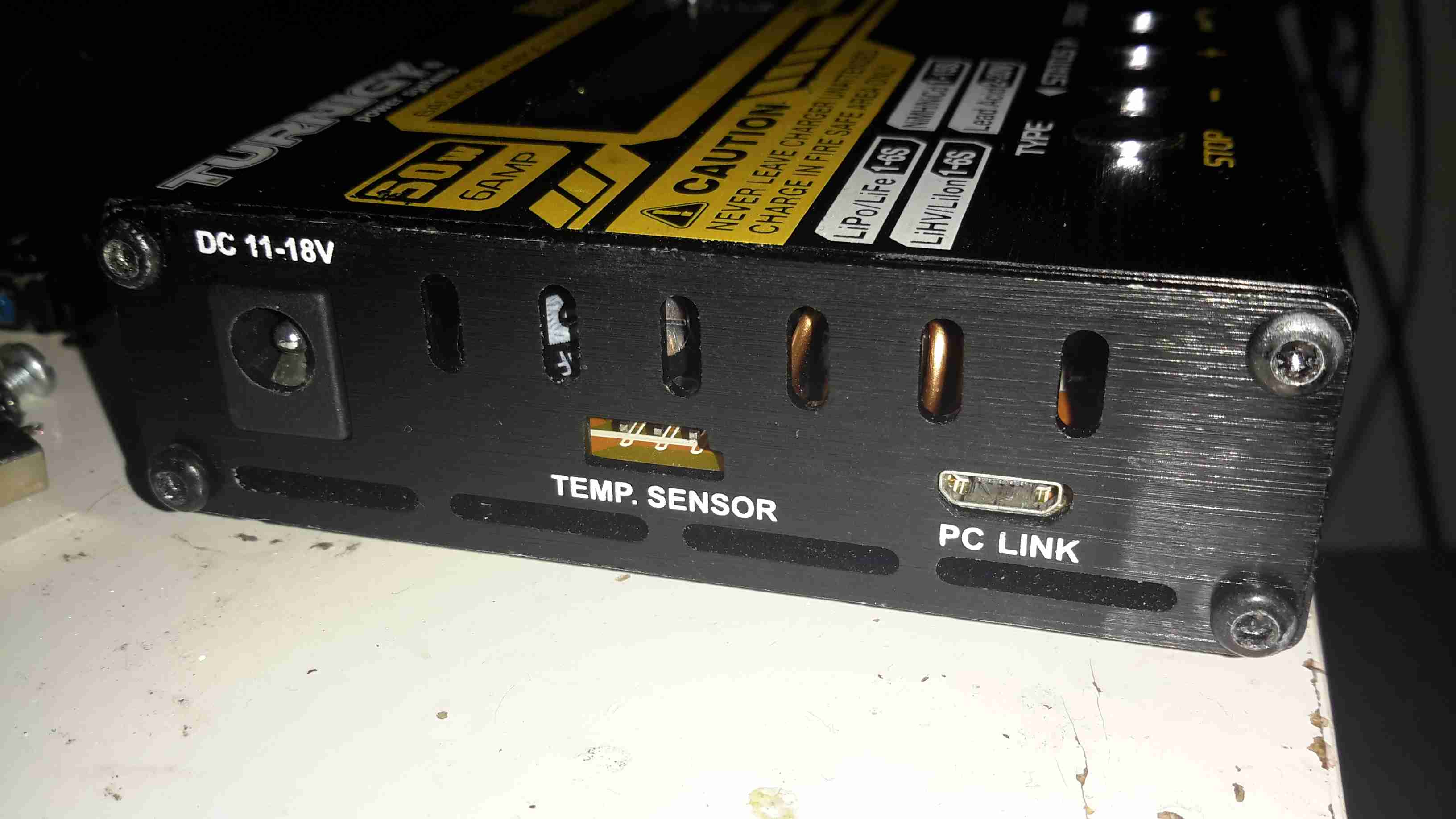
External Connections
The usual DC input barrel jack on the left, with an external temp sensor for fast charging NiCd/NiMH chemistry batteries. The µUSB port registers under Linux as USB HID, probably so drivers aren’t required. Unfortunately the software is Windows only, but it doesn’t provide anything handy like charging graphs or stats. Just a way to alter settings & control charging from a PC. On other versions of this charger there’s a setting to change the temp sensor port into a TTL serial output, which would be much handier.
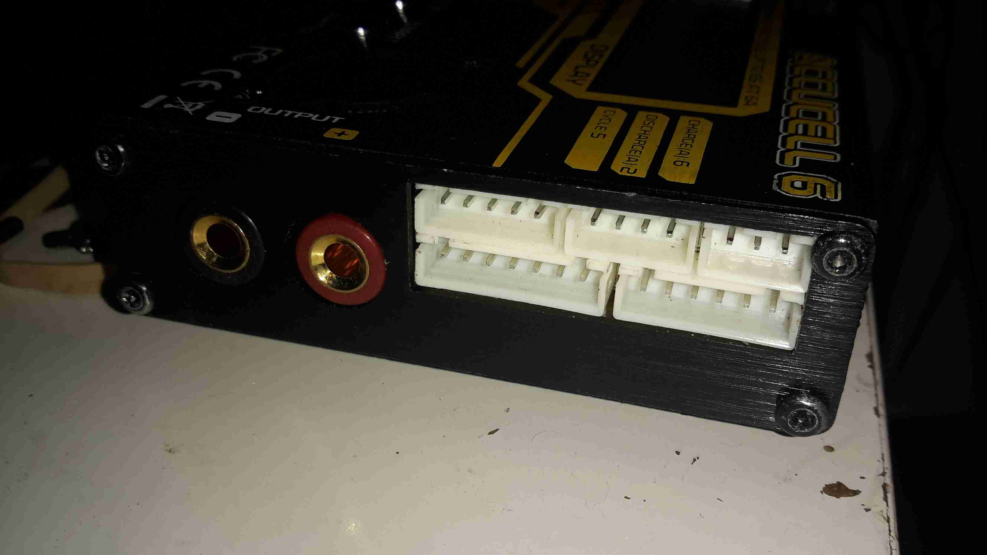
Output & Balance
The other side of the charger has the main DC output jacks & the pack balancing connections.
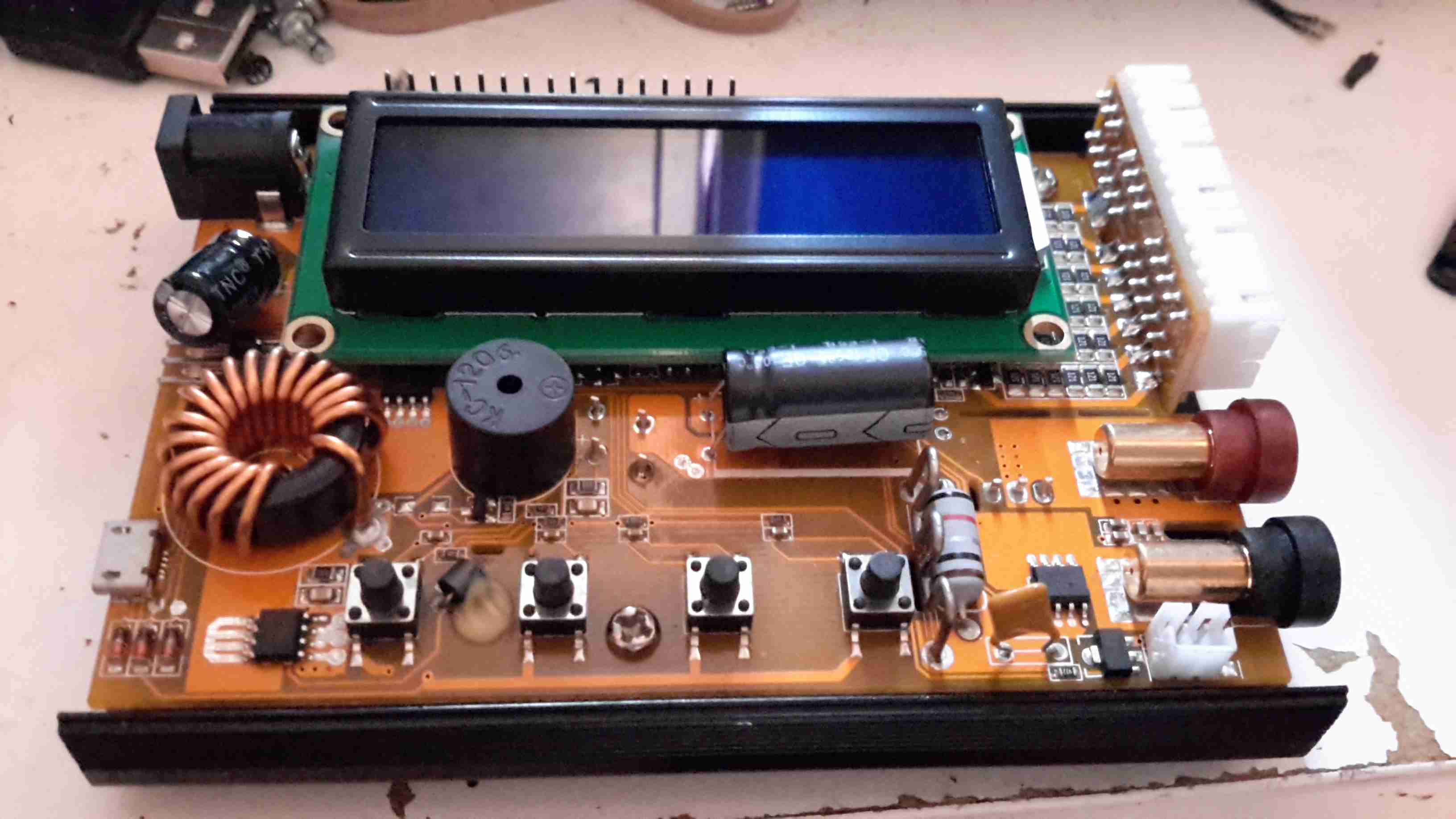
Cover Removed
Here’s the top cover removed from the charger, showing most of the internals. A standard HD44780 LCD provides the user interface, the CPU & it’s associated logic is hidden under there somewhere.
The PCB has nice heavy tracks to handle the 6A of current this charger is capable of.
Balancing Network
The output side of the board. Here the resistive pack balancing network can be seen behind the vertical daughter board holding the connectors, along with the output current shunt between the DC output banana jacks & the last tactile button.
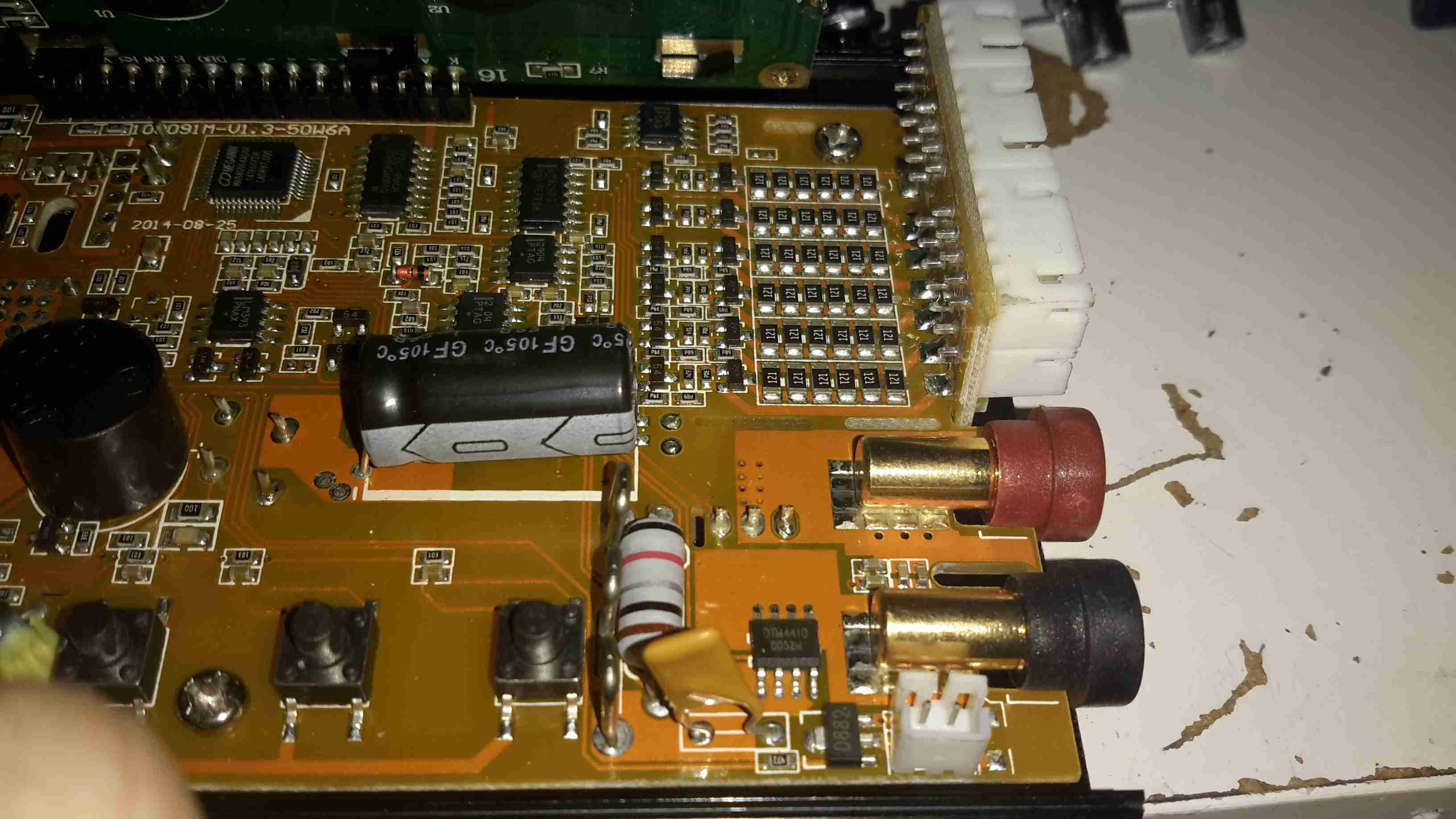
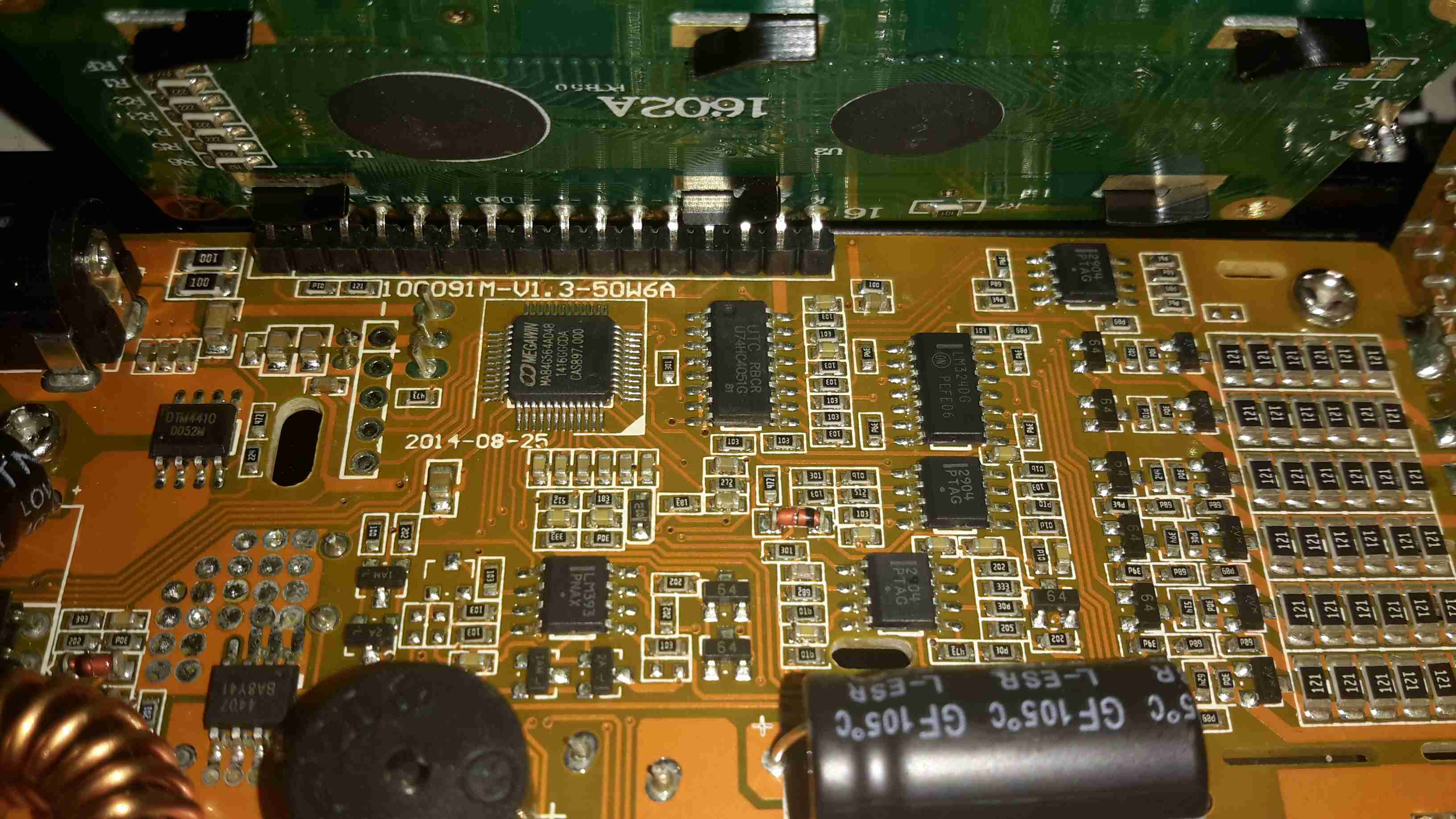
Main Logic
Unfortunately the LCD is soldered directly to the board, and my desoldering tool couldn’t quite get all the solder out, so time to get a bit violent. I’ve gently bent the header so I could see the brains of the charger. The main CPU is a Megwin MA84G564AD48, which is an Intel 8081 clone with USB support. Unfortunately I was unable to find a datasheet for this part, and the page on Megwin’s site is Chinese only.
I was hoping it was an ATMega328, as I have seen in other versions of this charger, as there are custom firmwares available to increase the feature set of the charger, but no dice on this one. I do think the µUSB port is unique to this version though, so avoiding models with that port probably would get a hackable version.
There’s some glue logic for controlling the resistor taps on the balancing network, and a few op-amps for voltage & current readings.
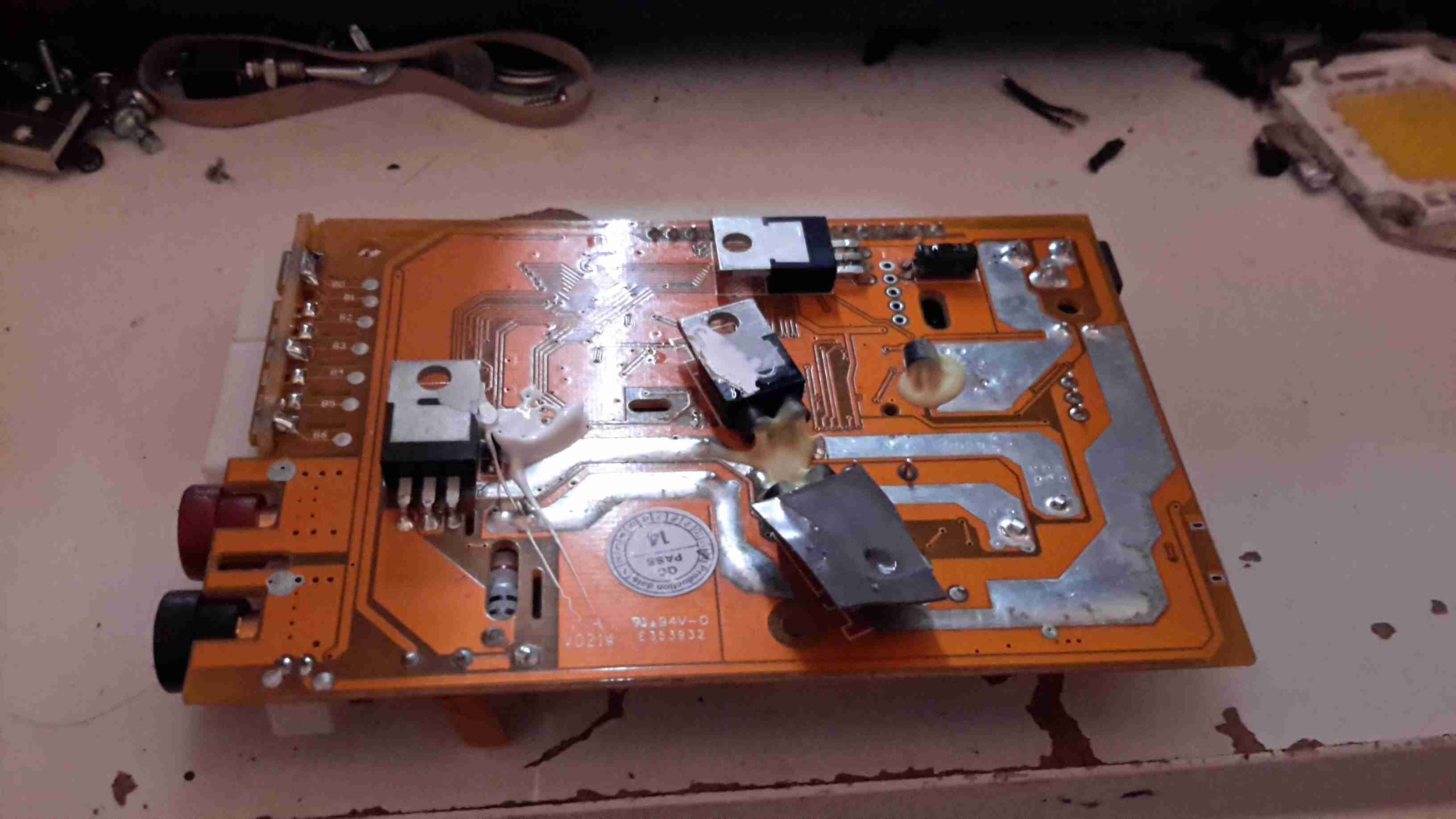
Power Switching Devices
All the power diodes & switching FETs for the DC-DC converter are mounted on the bottom of the PCB, and clamped against the aluminium casing when the PCB is screwed down. Not the best way to ensure great contact, but Chinese tech, so m’eh.
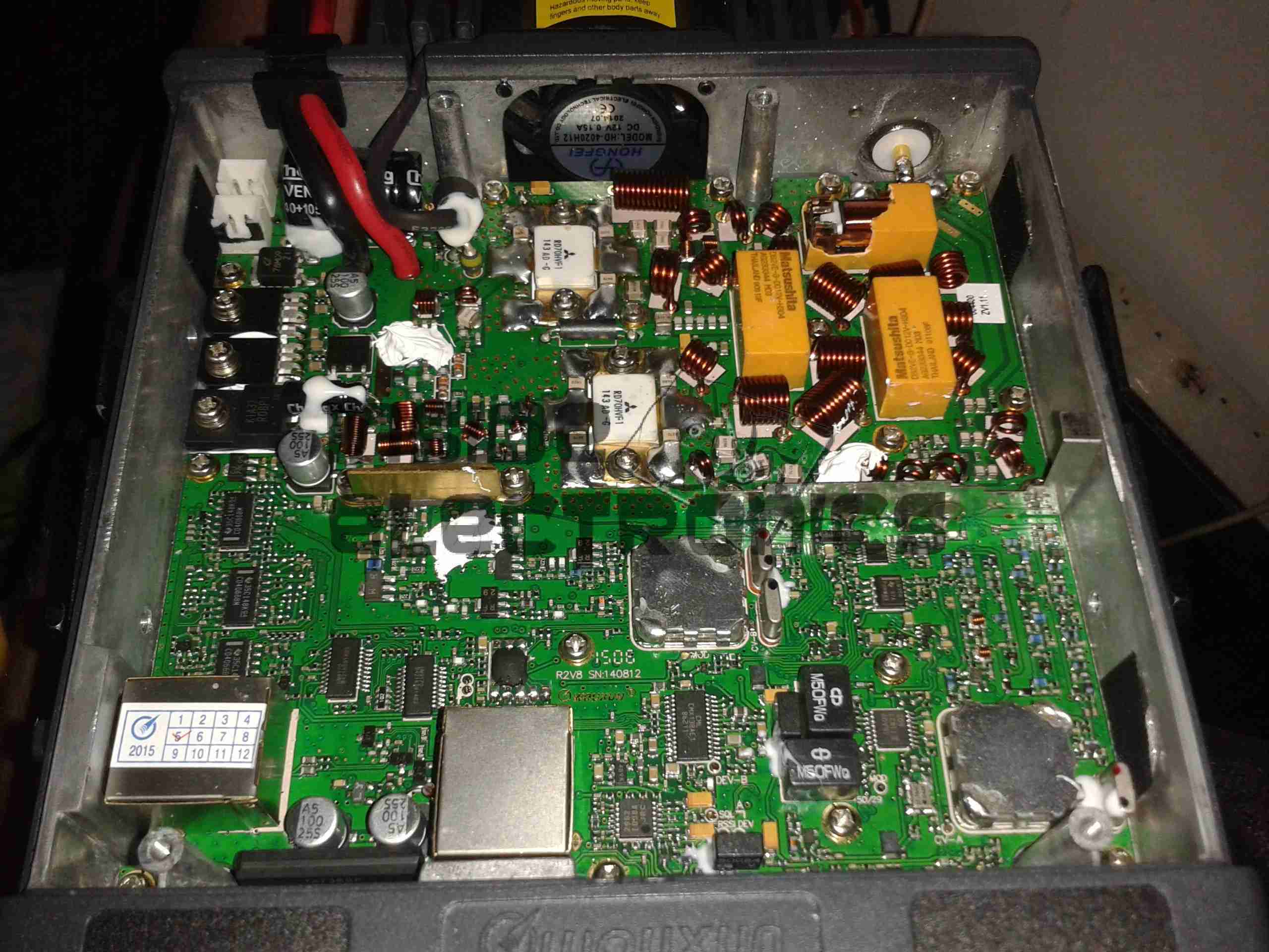
Following on from my review, here are some internal views & detail on the components used in this radio. Below is an overview of the main PCB with the top plate removed from the radio.
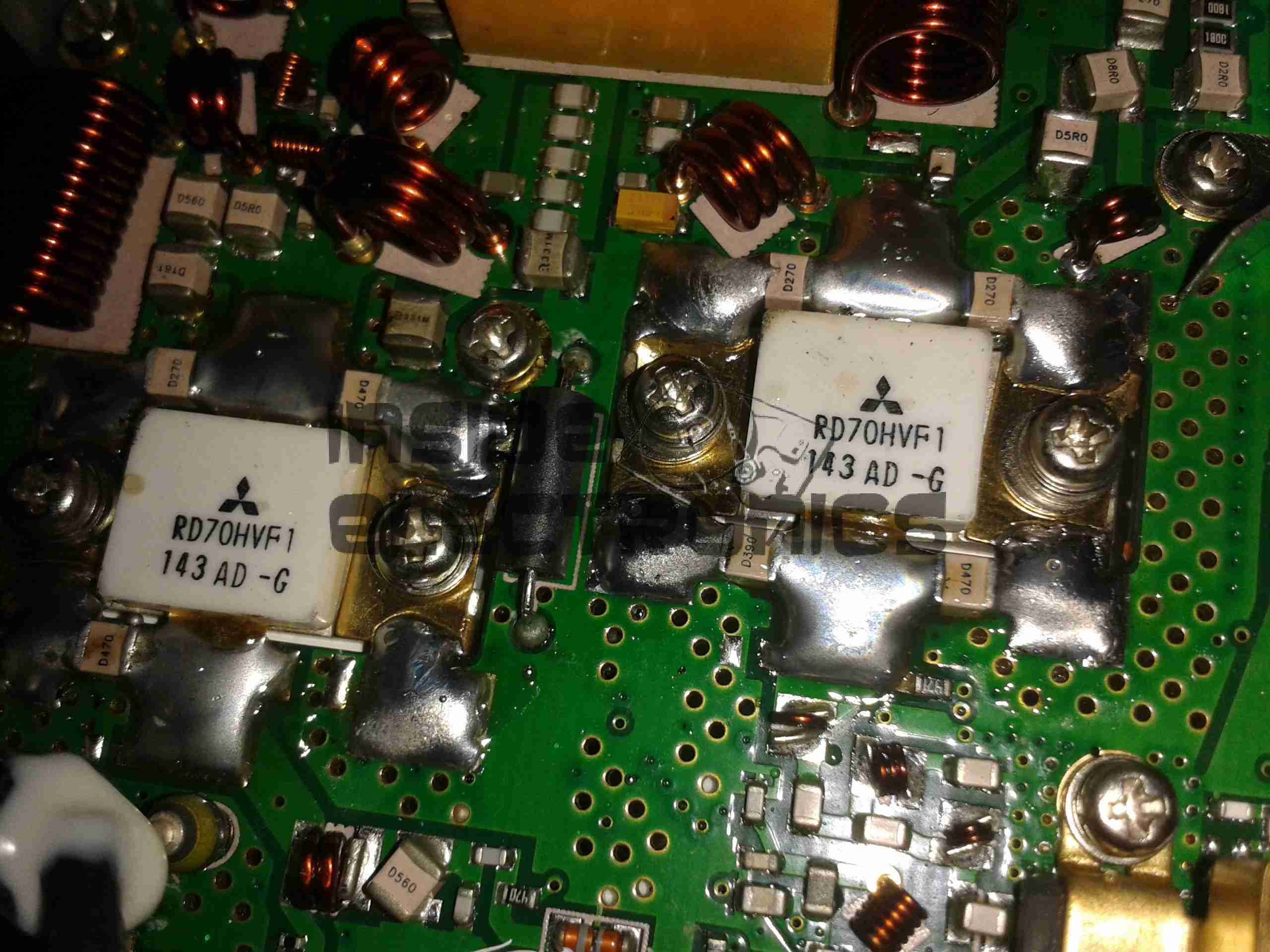
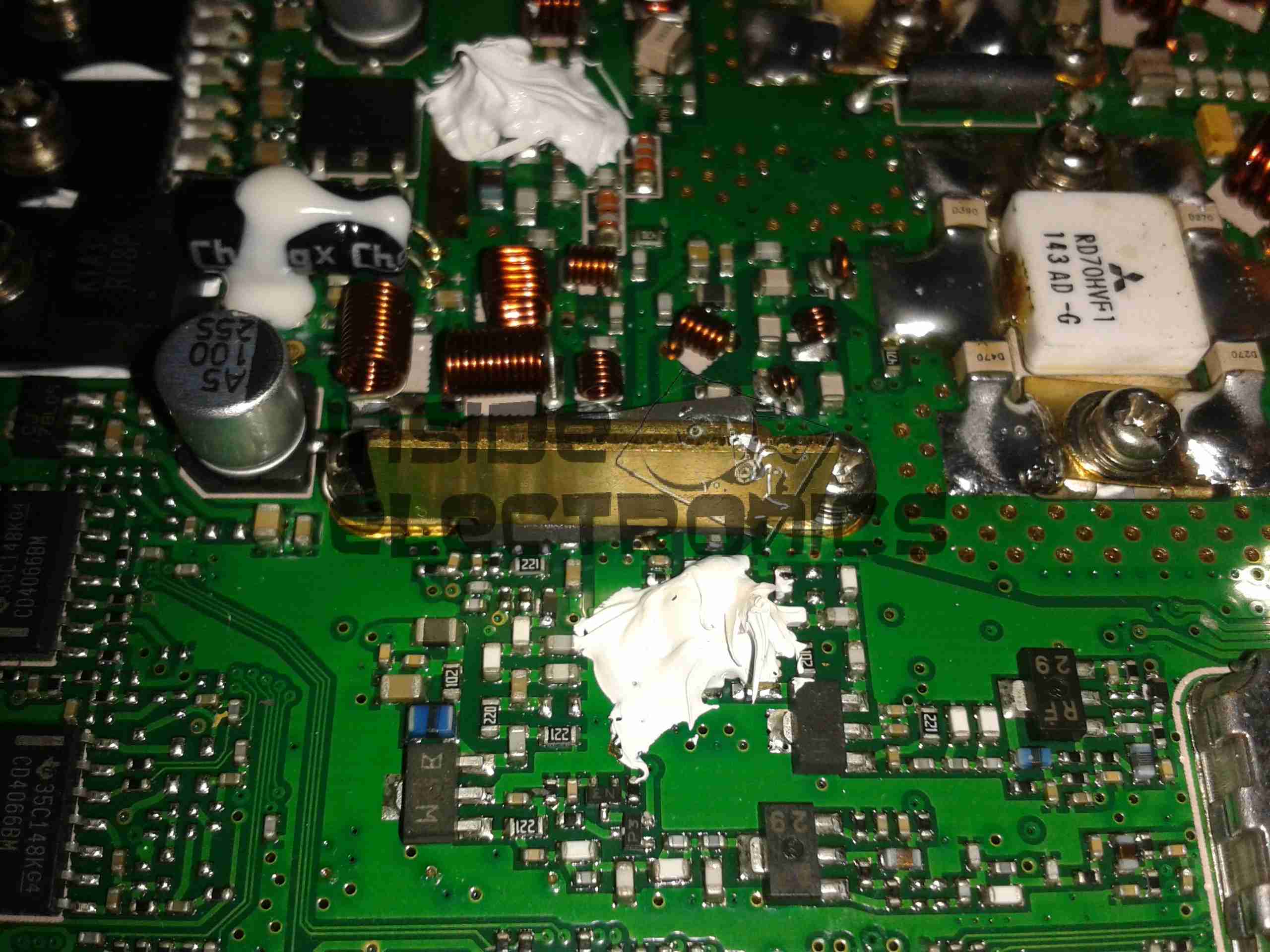
Cover RemovedRF Final Amplifier Stage
Most visible are these MOSFETs, which are Mitsubishi RD70HVF1 VHF/UHF power devices. Rated for a maximum of 75W output power at 12.5v (absolute maximum of 150W, these are used well within their power ratings. They are joined to the PCB with heavy soldering, with bypass caps tacked right on to the leads.
RF Pre Drivers
Here is the RF pre-driver stage, with intermediate transistors hidden under the small brass heatspreader.
Power Section
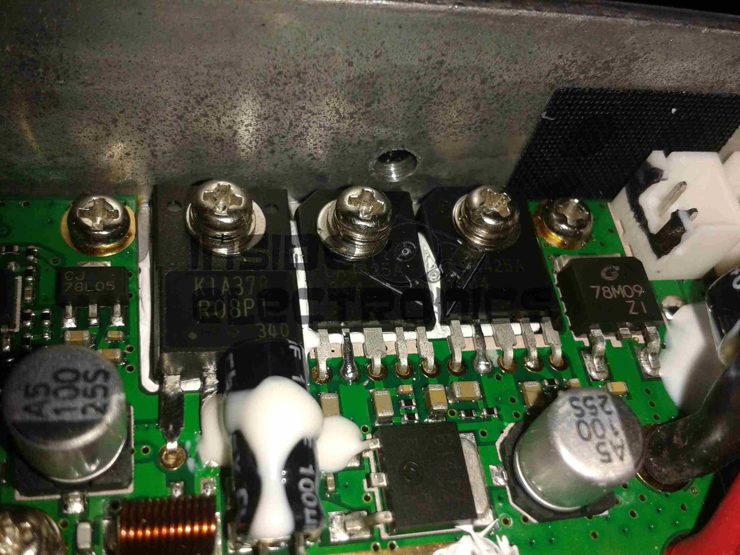
In the top left corner of the radio, near the power input leads, is the power supply & audio amplifier section. Clearly visible are the pair of LA4425A 5W audio power amplifier ICs, these drive the speakers on the top of the radio. Either side of these parts are a 7809 & a 7805 – both linear regulators providing +9v & +5v logic supplies respectively. The large TO220 package device is a KIA378R08PI 3A LDO regulator with ON/OFF control, this one outputs +8v. Just visible in the top right corner are the sockets for the speaker connections.
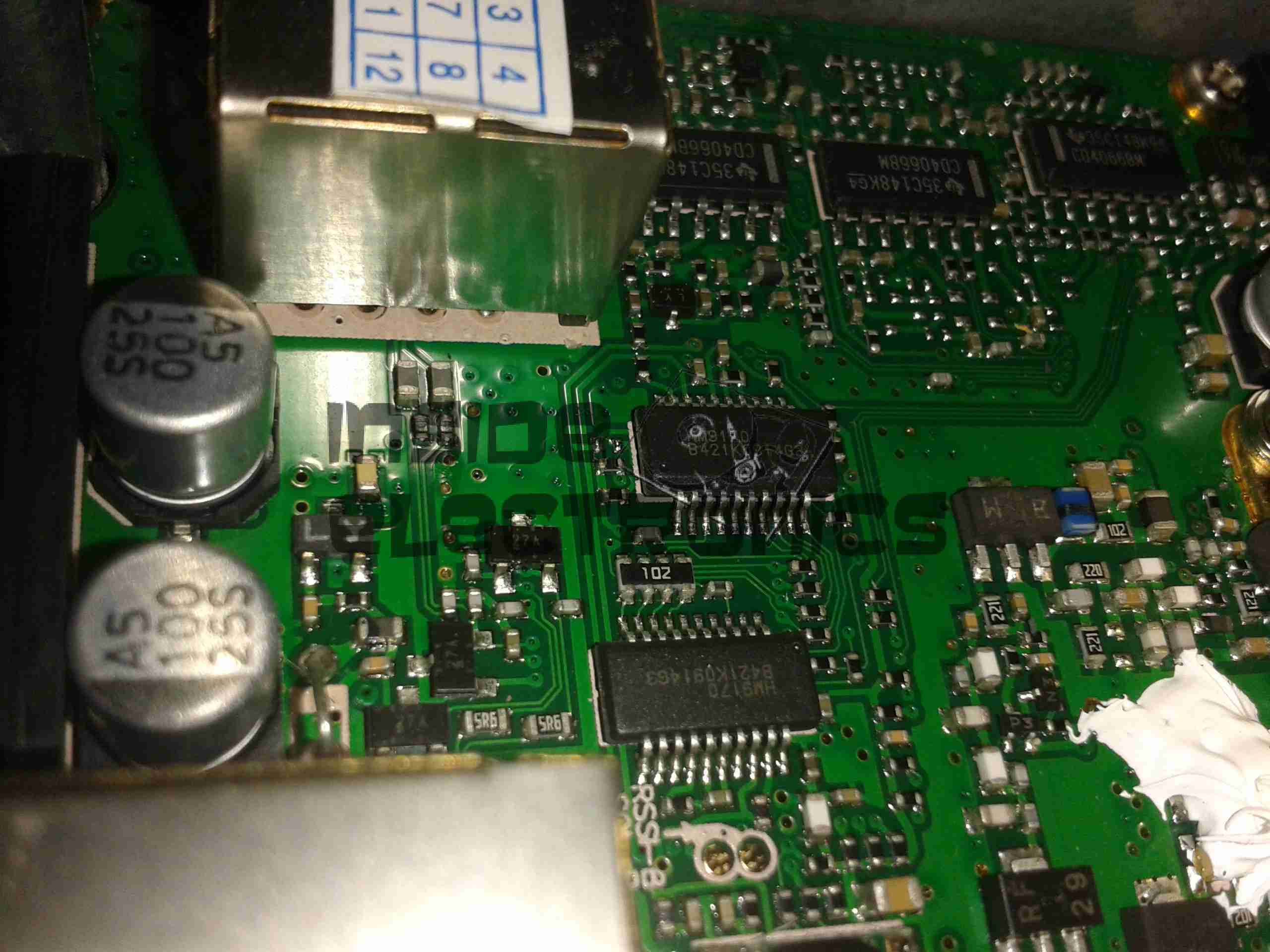
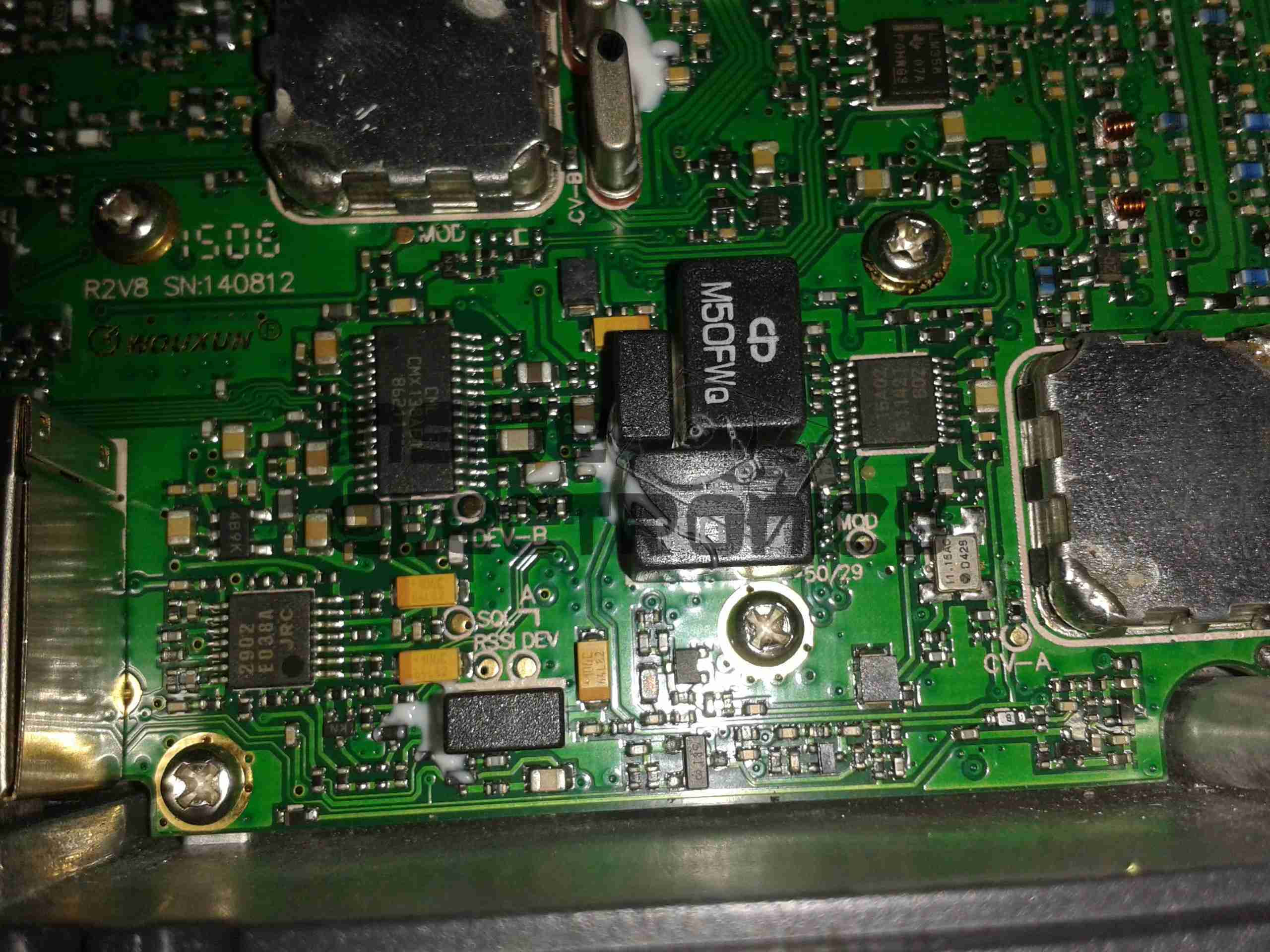
DTMF Circuits
Here are the two ICs for dealing with DTMF tones, they are HM9170 receivers.
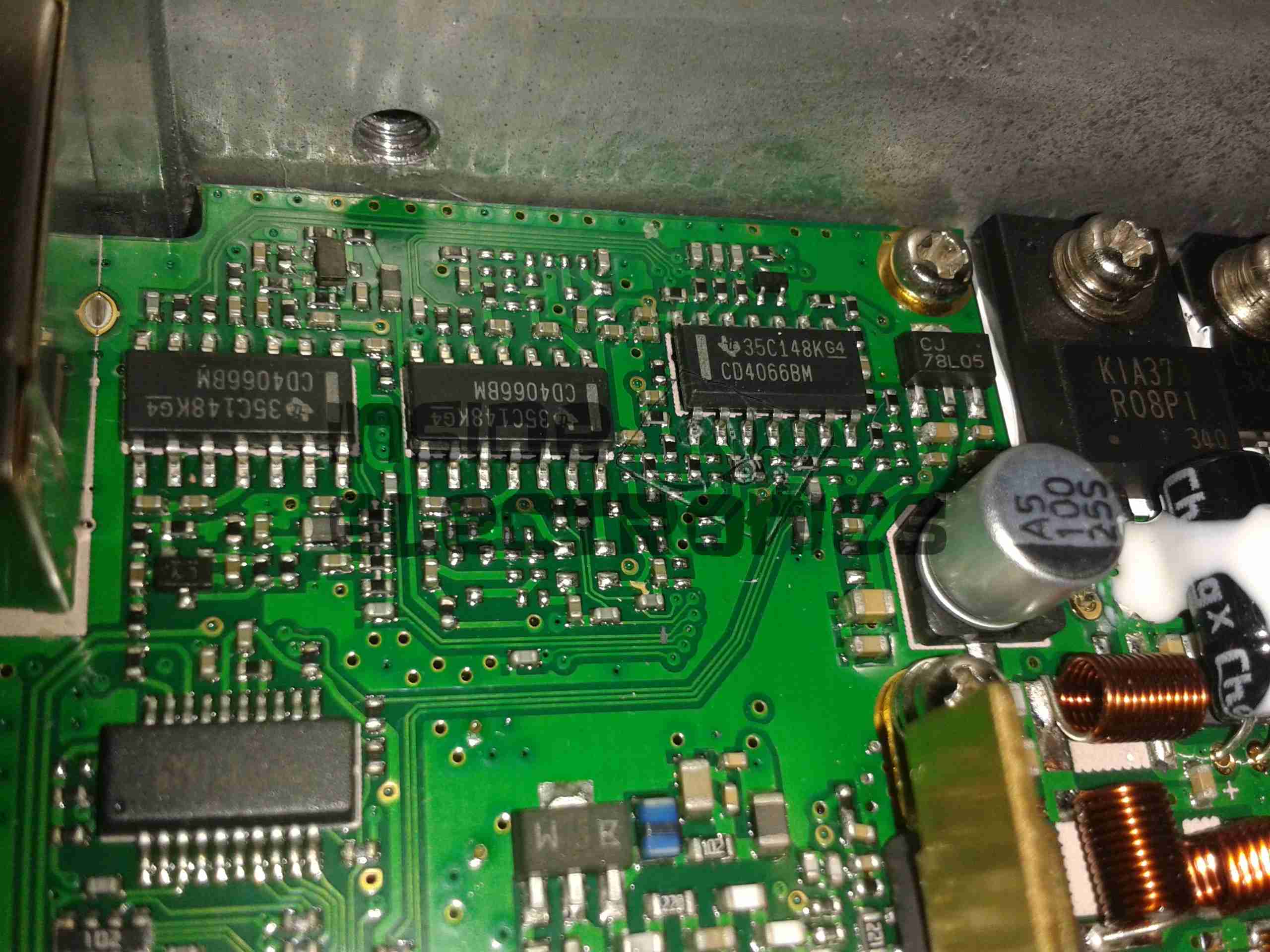
Glue Logic
In the corner next to the interface jack, there are some CD4066B Quad Bilateral switches. These make sense since the interface jack has more than a single purpose, these will switch signals depending on what is connected.
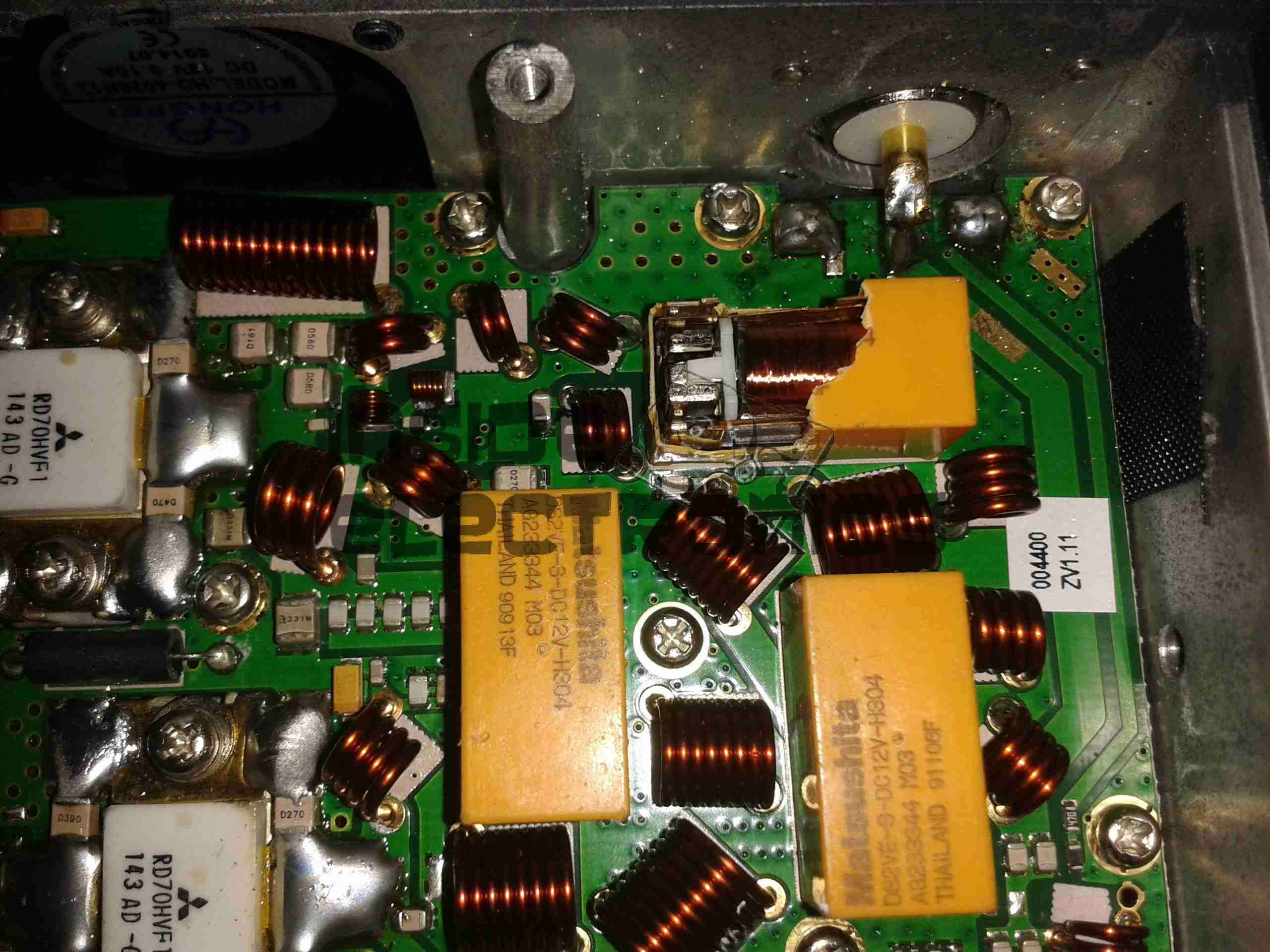
RF Section
Here are visible the RF cans for the oscillators, the crystals visible next to the can at the top. The shields are soldered on, so no opening these unfortunately.
Also visible in this image is a CMX138A Audio Scrambler & Sub-Audio Signalling processor. This IC deals with the Voice Inversion Scrambling feature of the radio, & processes the incoming audio before being sent to the modulator.
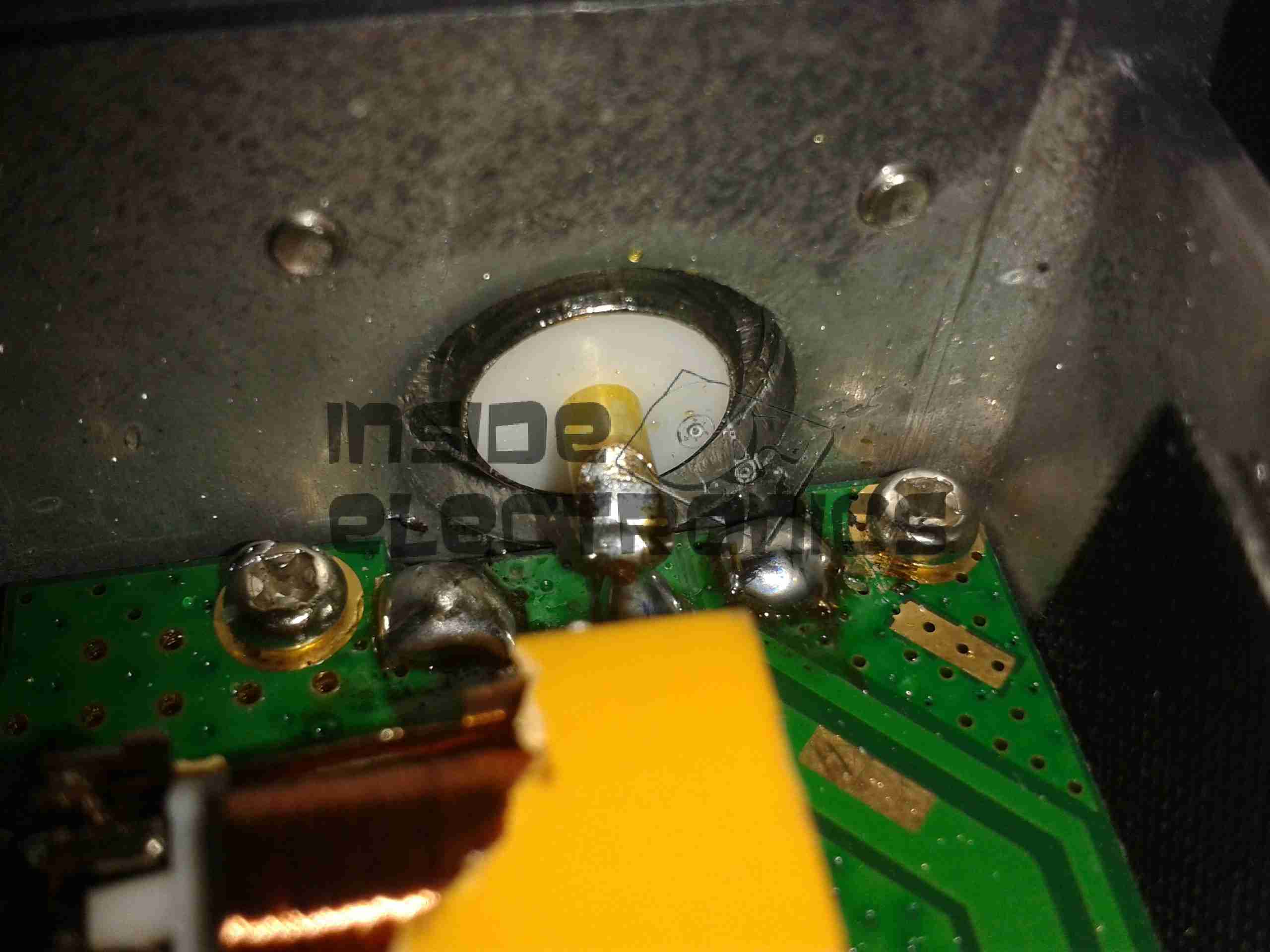
Output Filter Network
Shown here is the RF output filter network, this radio uses relays for switching instead of PIN diodes, I imagine for cost reasons. The relay closest to the RF output socket has had a slight accident 🙂 This is slated to be replaced soon.
RF Output Jack
Finally, the RF output jack.
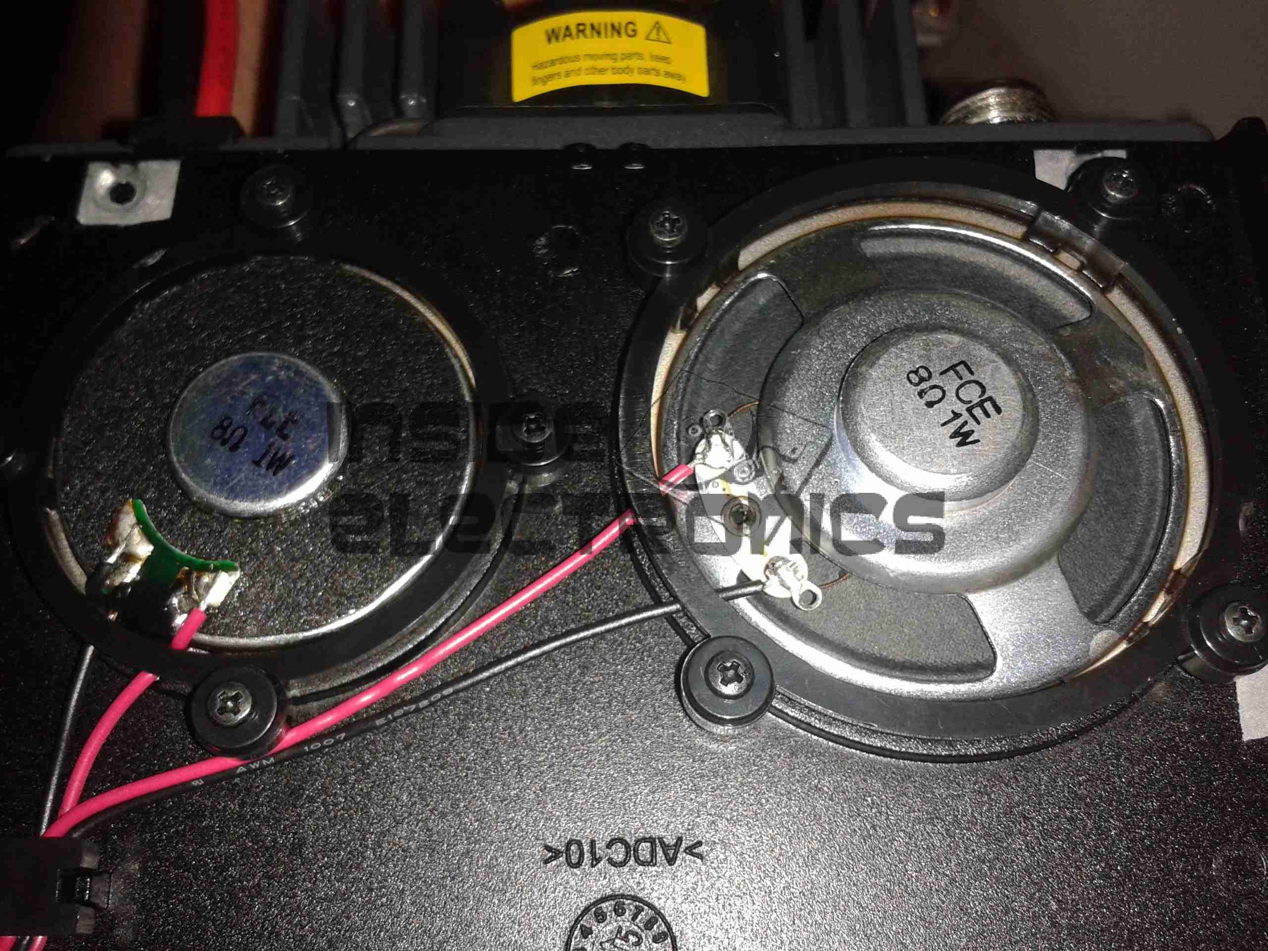
Audio Speakers
Here the speakers are shown, attached to the bottom of the top plate. They are both rated 8Ω 1W.
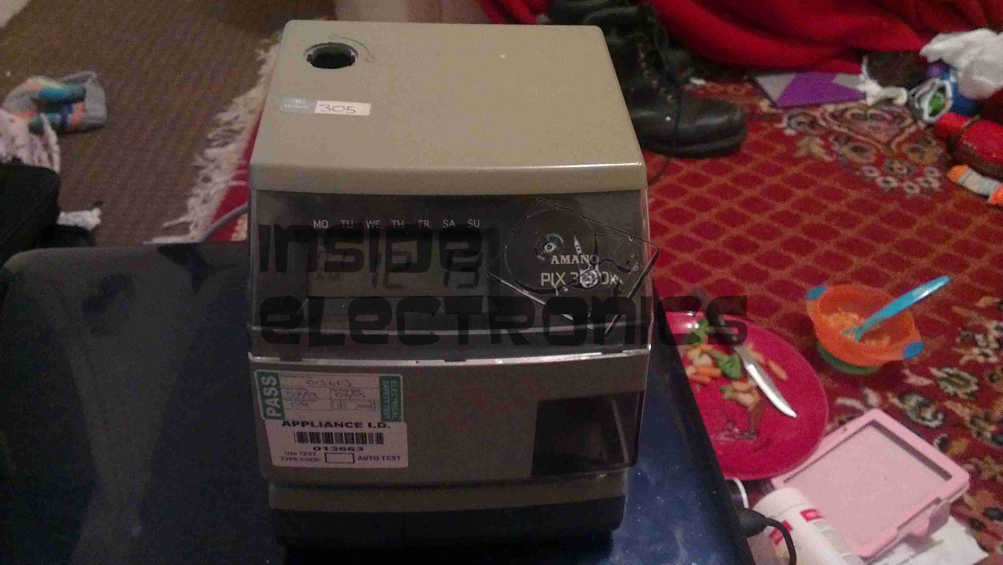
This is a late 90’s business timeclock, used for maintaining records of staff working times, by printing the time when used on a sheet of card.
Front Internal
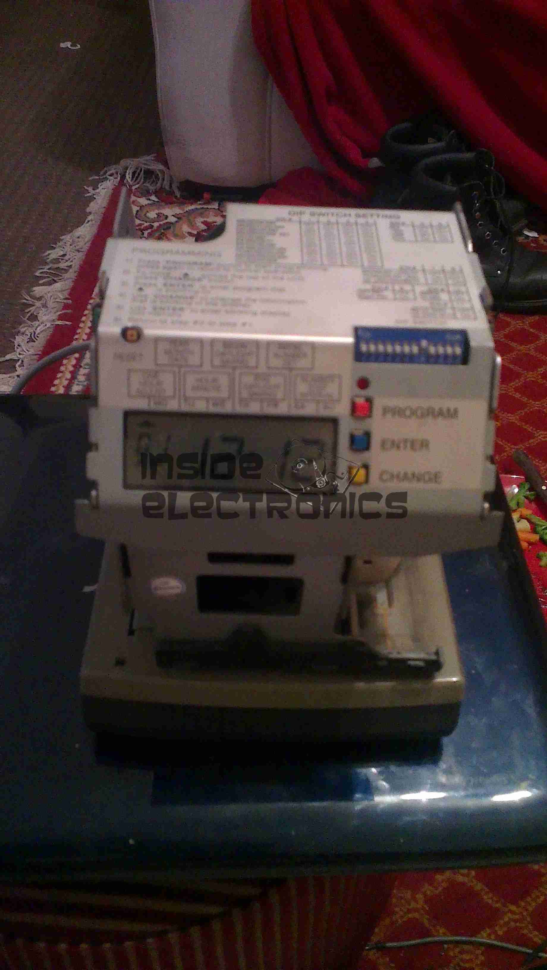
Here is the top cover removed, which is normally locked in place to stop tampering. The unit is programmed with the 3 buttons & the row of DIP switches along the top edge.
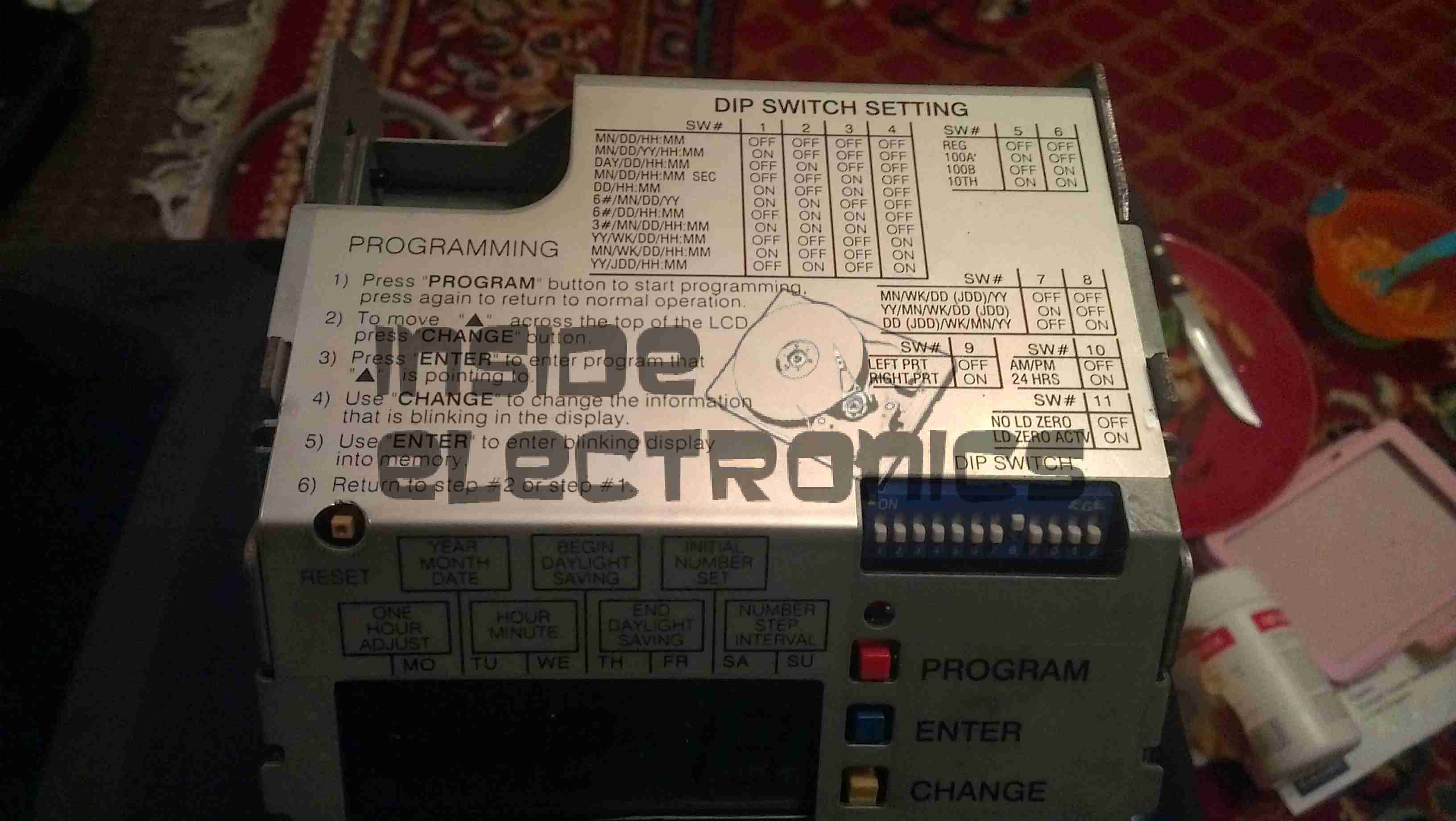
Instructions
Closeup of the settings panel, with all the various DIP switch options.
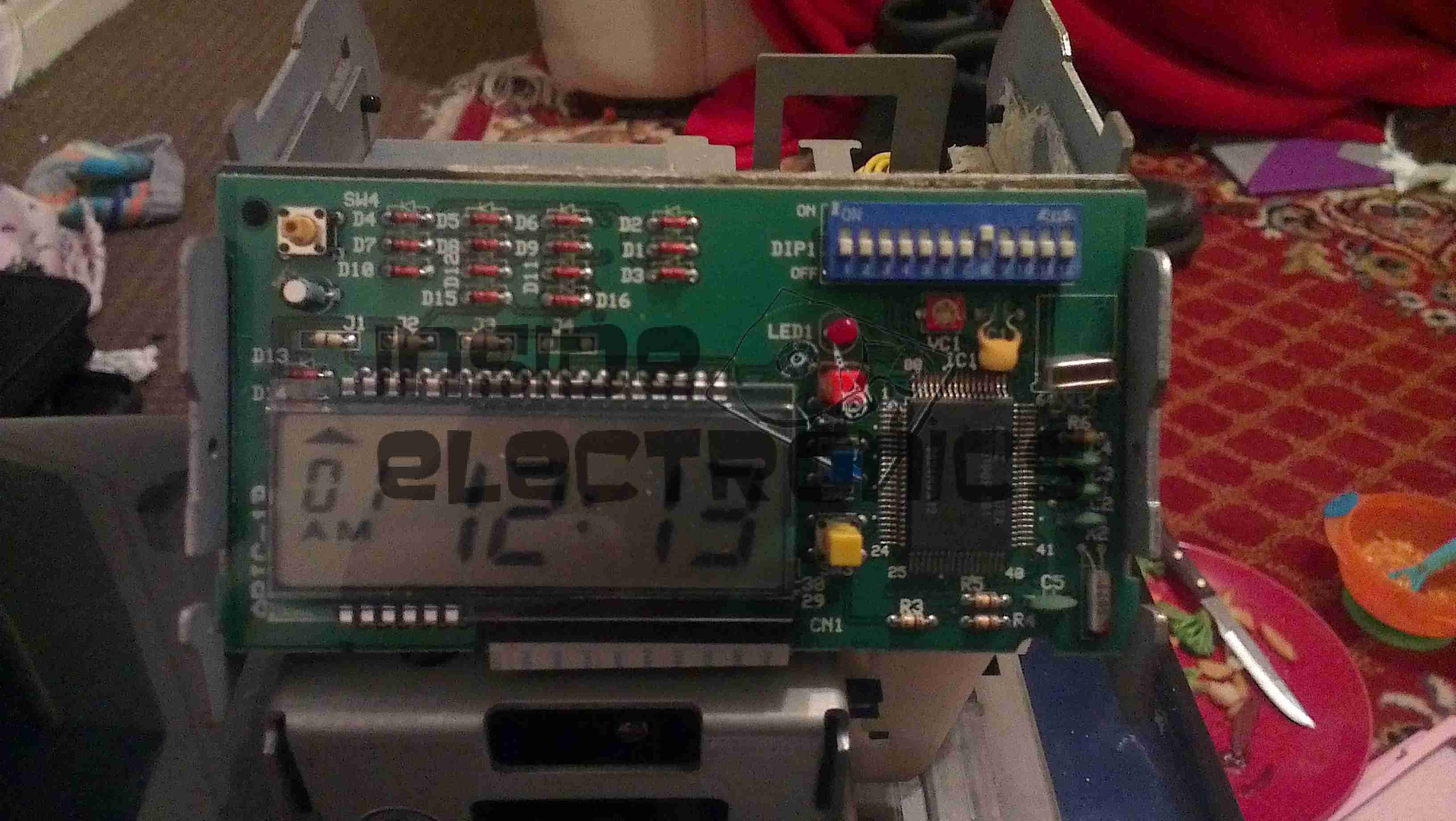
CPU & Display
Cover plate removed from the top, showing the LCD & CPU board, the backup battery normally fits behind this. The CPU is a 4-bit microcontroller from NEC, with built in LCD driver.
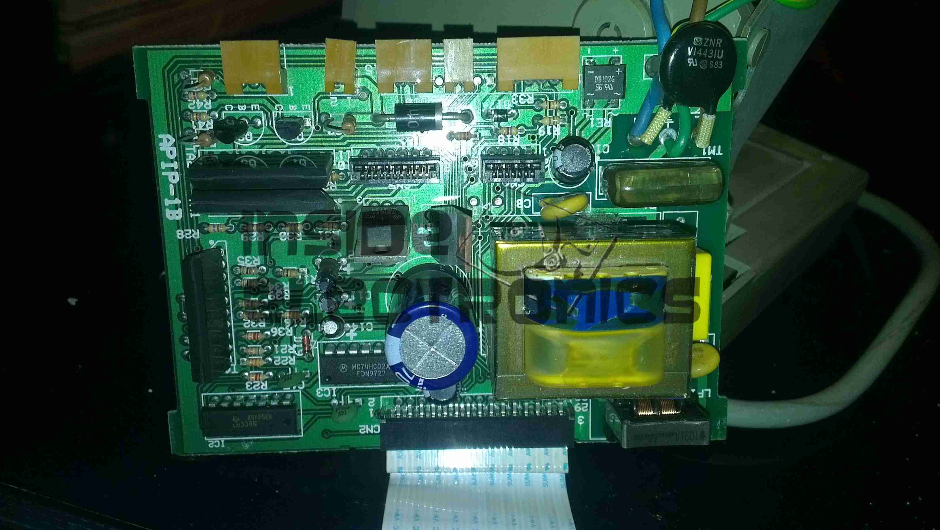
PSU & Drivers
Power Supply & prinhead drivers. This board is fitted with several NPN Darlington transistor arrays for driving the dox matrix printhead.
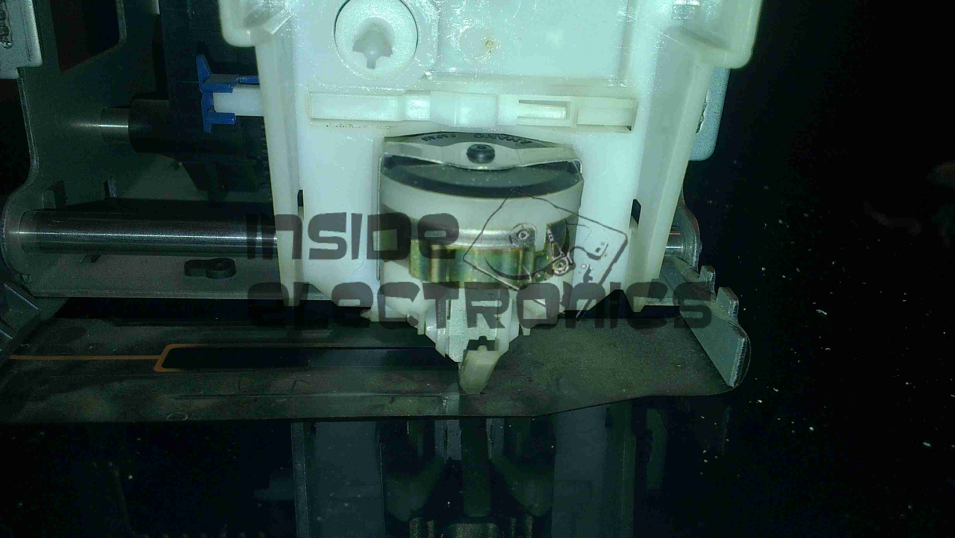
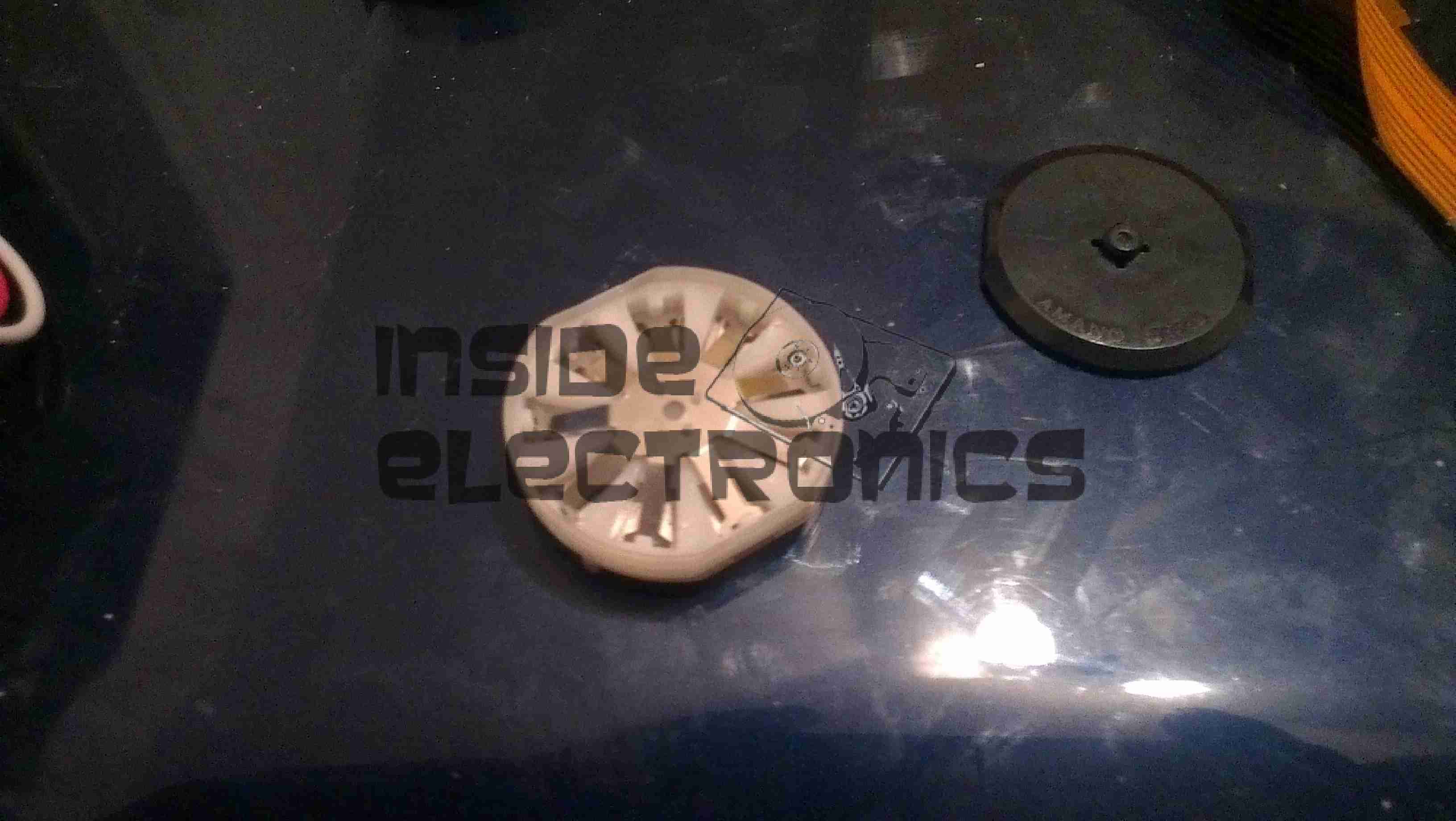
Printhead
Printhead assembly itself. The print ribbon fits over the top of the head & over the pins at the bottom. The drive hammers & solenoids are housed in the circular top of the unit.
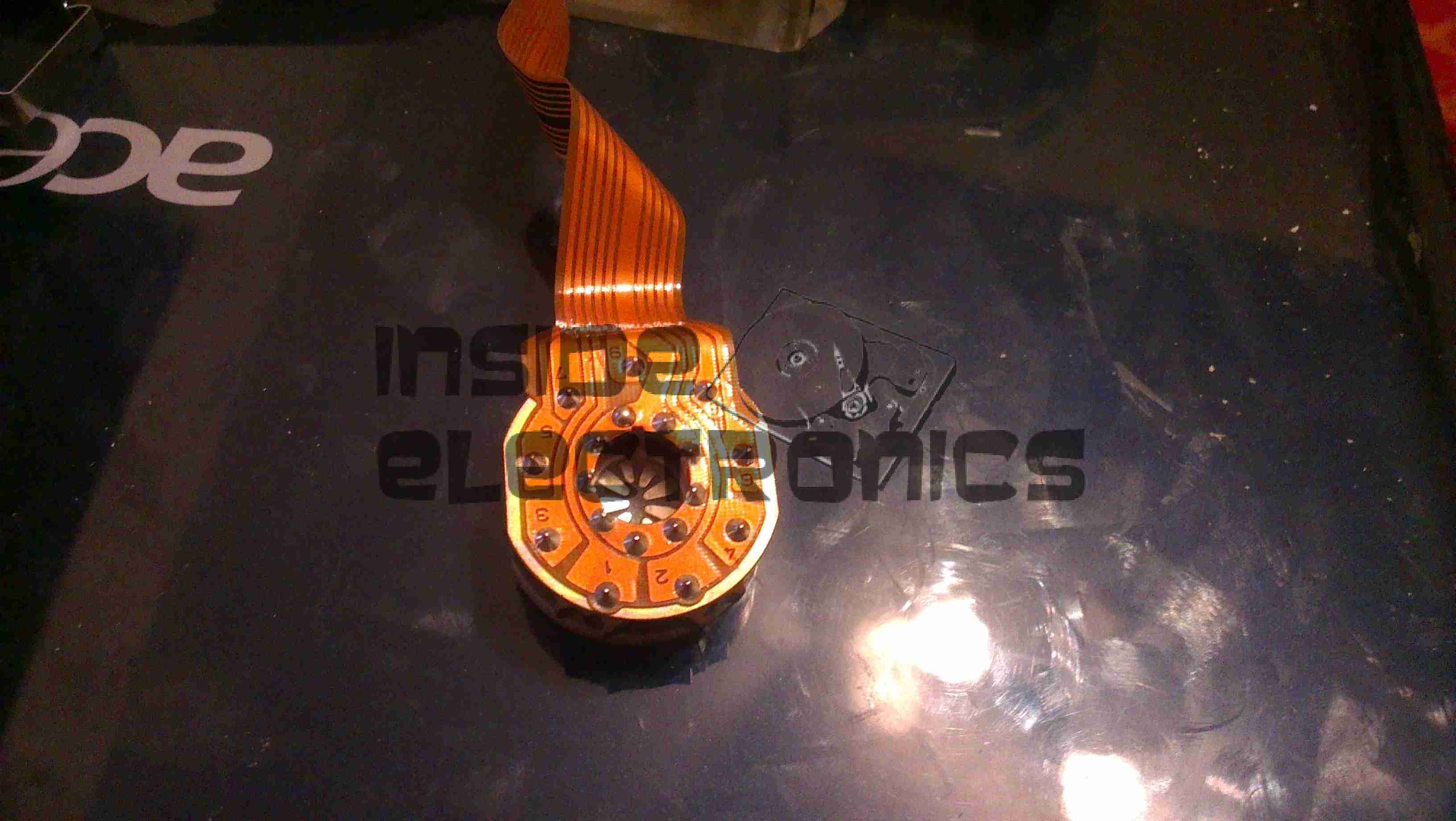
Printhead Bottom
Bottom of the print head showing the row of impact pins used to create the printout.
Bottom of the solenoid assembly with the ribbon cable for power. There are 9 solenoids, to operate the 9 pins in the head.
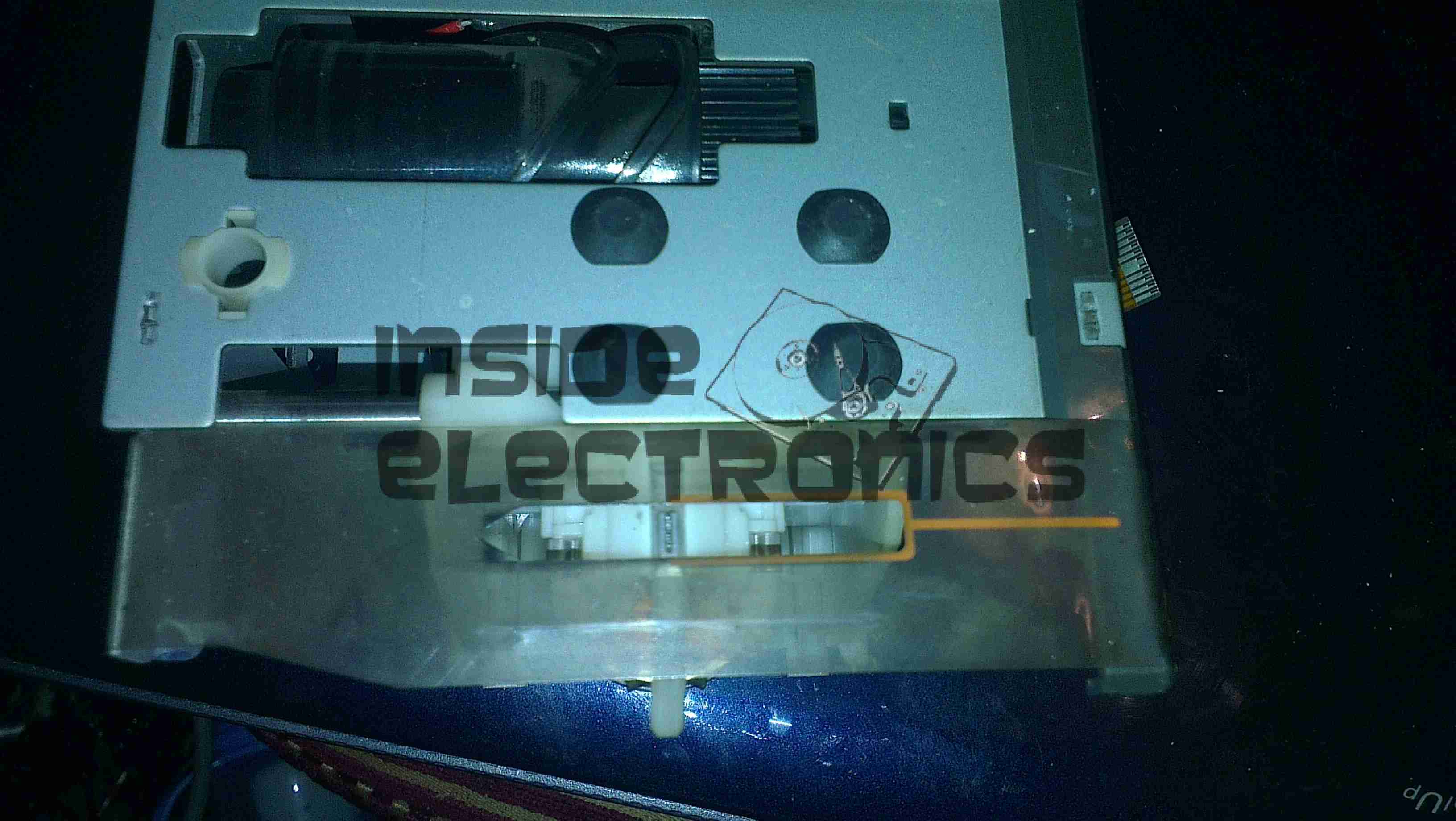
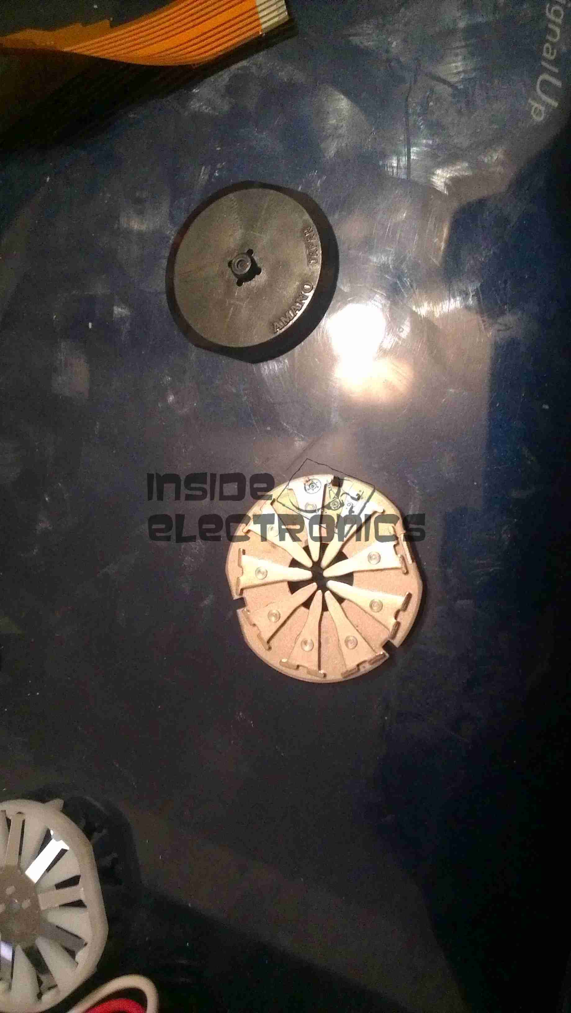
Return Spring
Top layer of the printhead assembly, showing the leaf spring used to hold the hammers in the correct positions.
Hammers
Hammer assembly. The fingers on the ends of the arms push on the pins to strike through the ribbon onto the card.
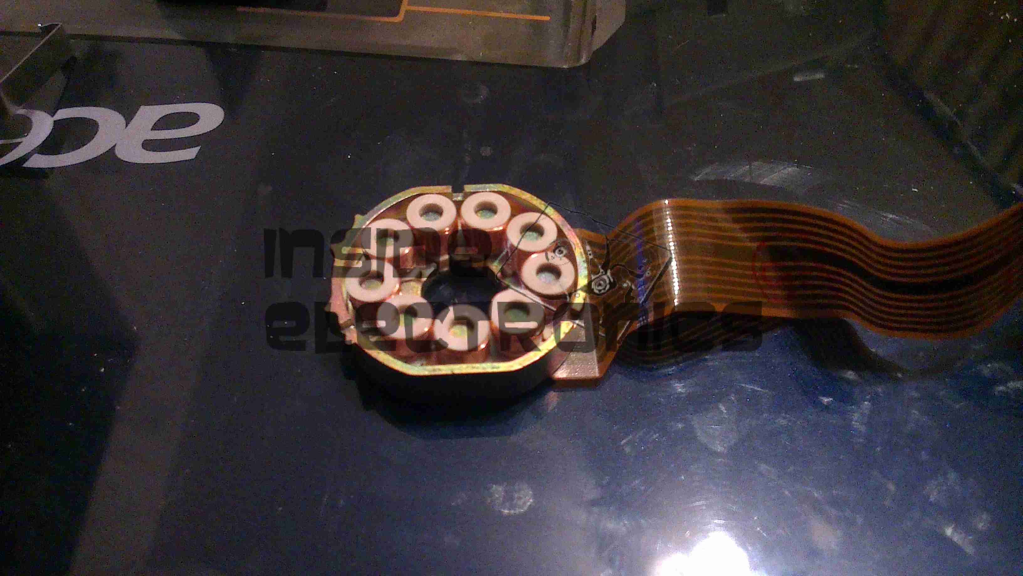
Solenoids
The ring of solenoids at the centre of the assembly. These are driven with 3A darlington power arrays on the PSU board.
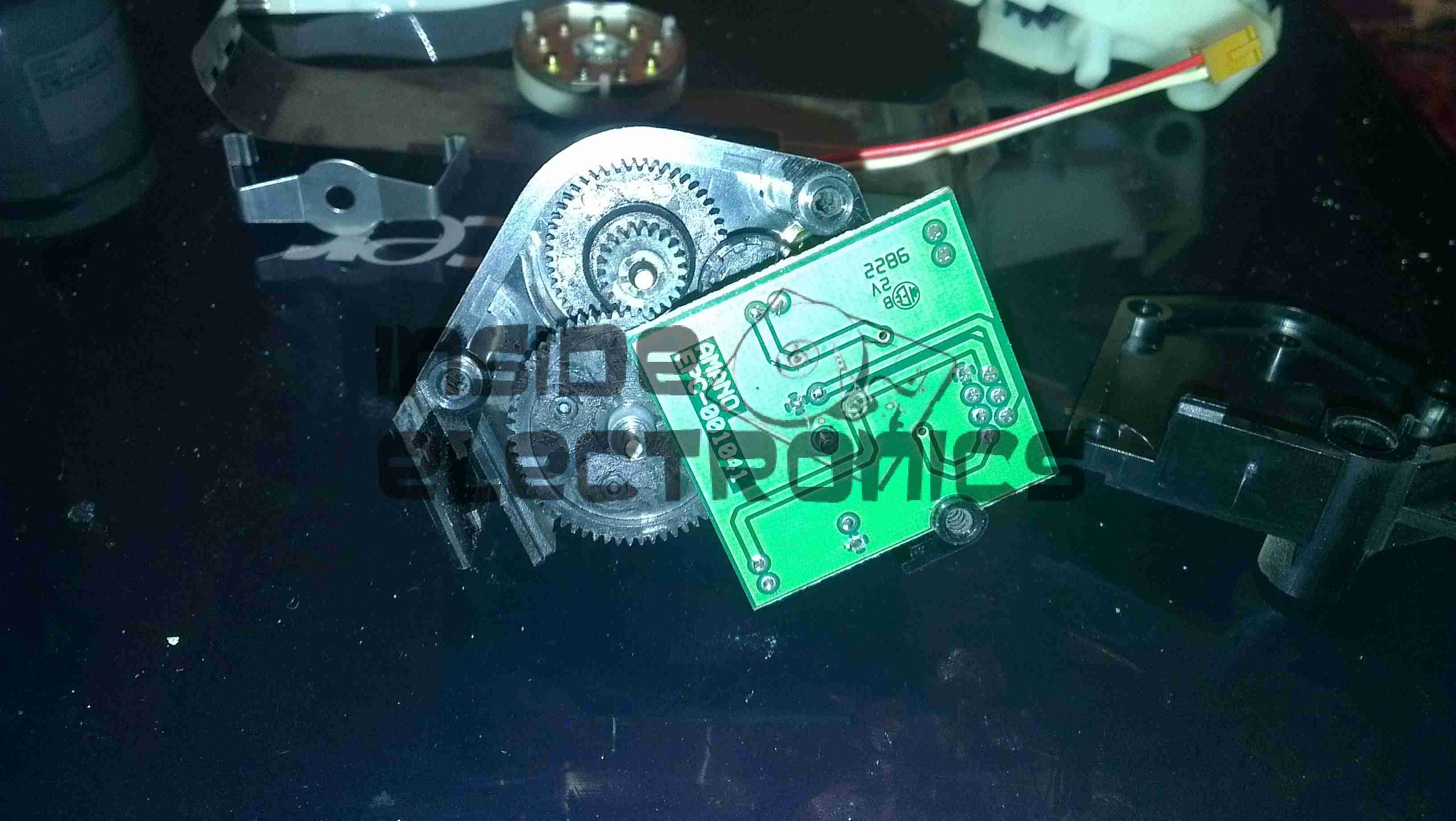
Gearbox Internals
There is only a single drive motor in the entire unit, that both clamps the card for printing & moves the printhead laterally across the card. Through a rack & pinion this also advances the ribbon with each print.
Tip Jar
If you’ve found my content useful, please consider leaving a donation by clicking the Tip Jar below!
All collected funds go towards new content & the costs of keeping the server online.