Posted on 2 Comments

Goodmans Quadro 902 Composite Video Mod

CRT Module
CRT Module

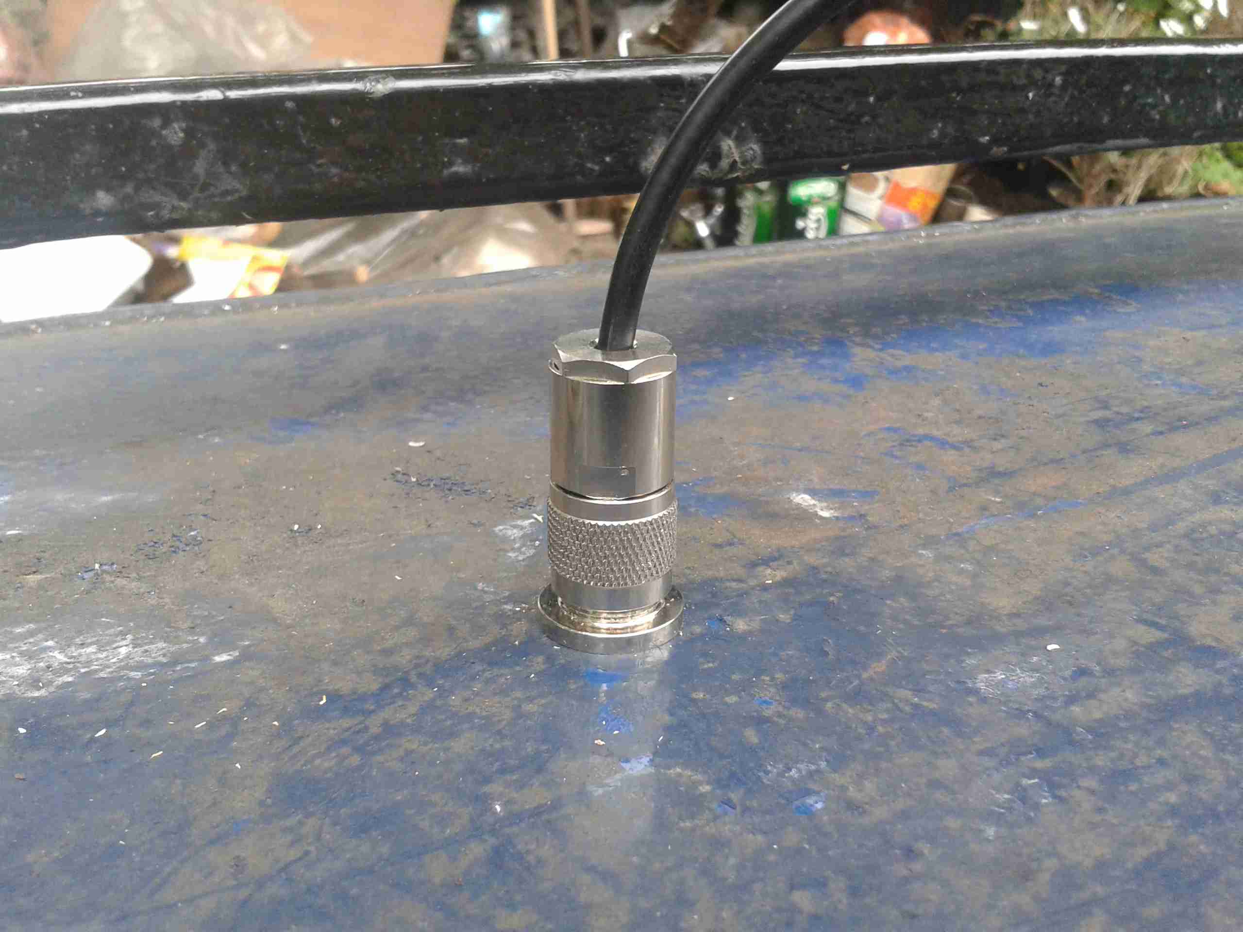
Here’s the CRT & it’s drive board removed from the main chassis. Nicely modular this unit, all the individual modules (radio, tape, TV), are separate. This is effectively a TV itself, all the tuner & IF section are onboard, unlike in other vintage units I’ve modified, where the tuner & IF has been on a separate board. There’s a 3-pin header bottom centre for the tuning potentiometer, and external antenna input jack. The internal coax for the built in antenna has been desoldered from the board here. here a the usual controls on the back for adjusting brightness, contrast & V Hold, all the other adjustments are trimmers on the PCB.
Unfortunately after 30+ years of storage, this didn’t work on first power up, neither of the oscillators for vertical or horizontal deflection would lock onto the incoming signal, but a couple of hours running seemed to improve things greatly. The numerous electrolytic capacitors in this unit were probably in need of some reforming after all this time, although out of all of them, only 21 are anything to do with the CRT itself.

Anode Cap
Anode Cap

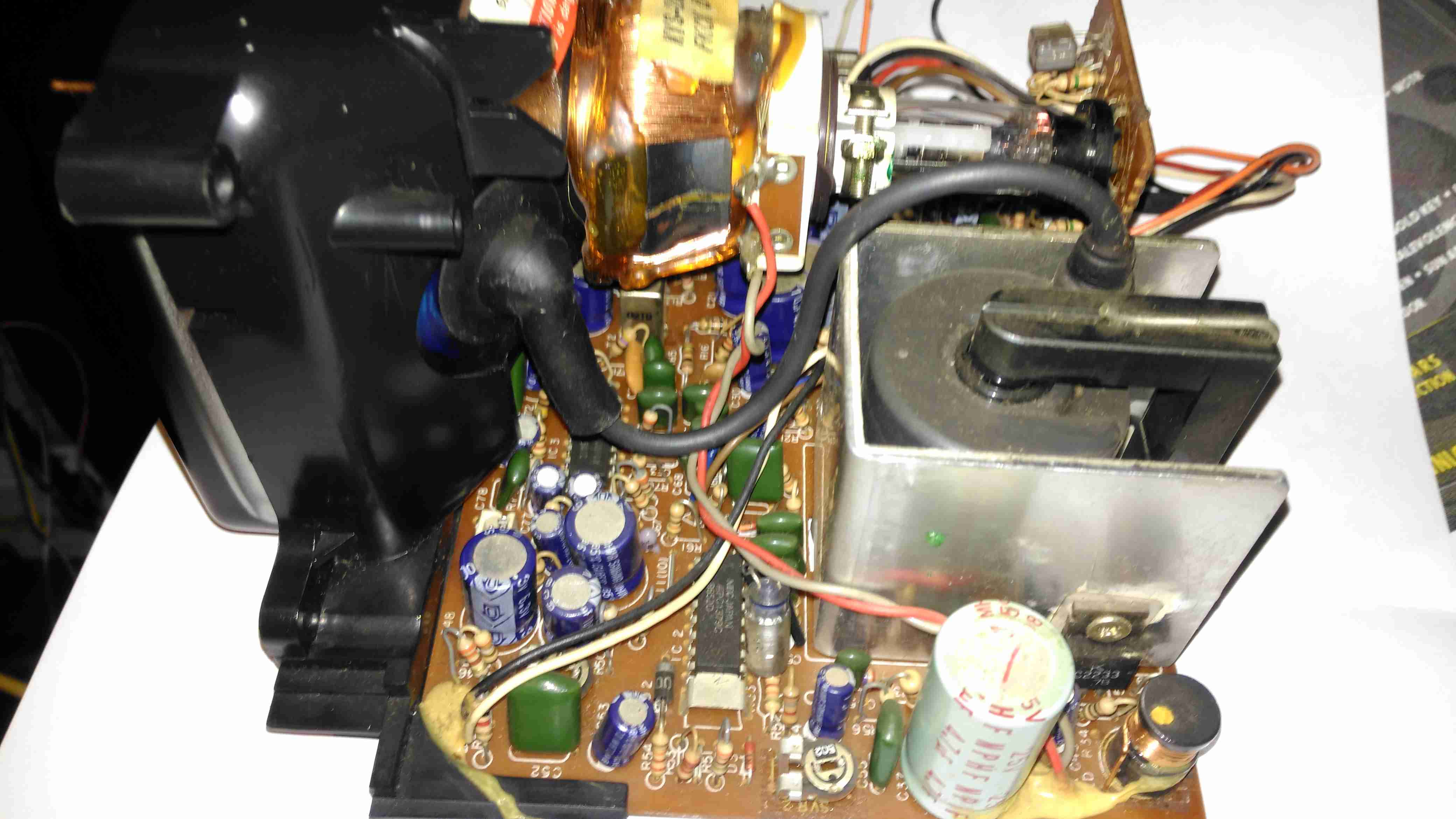
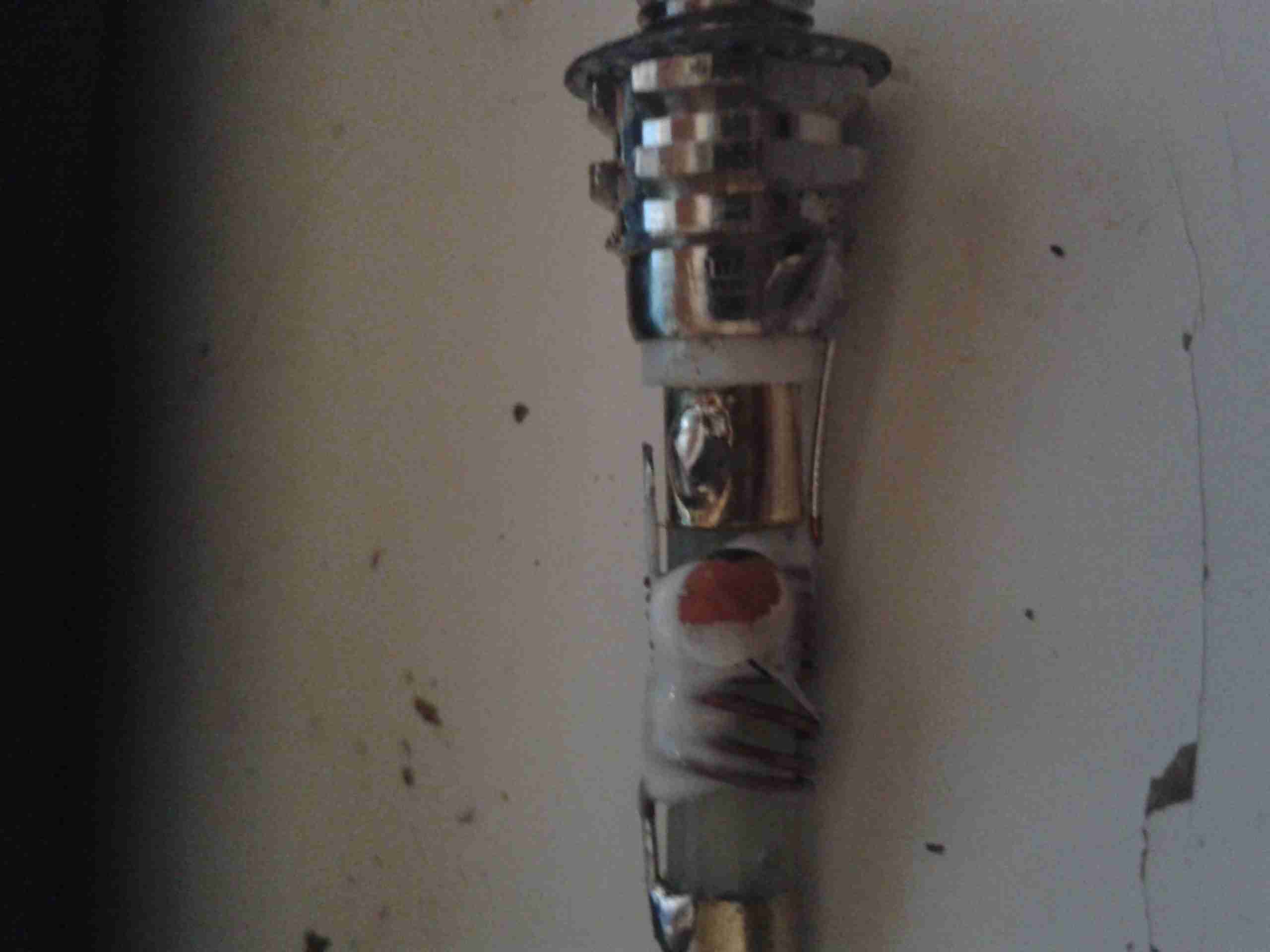
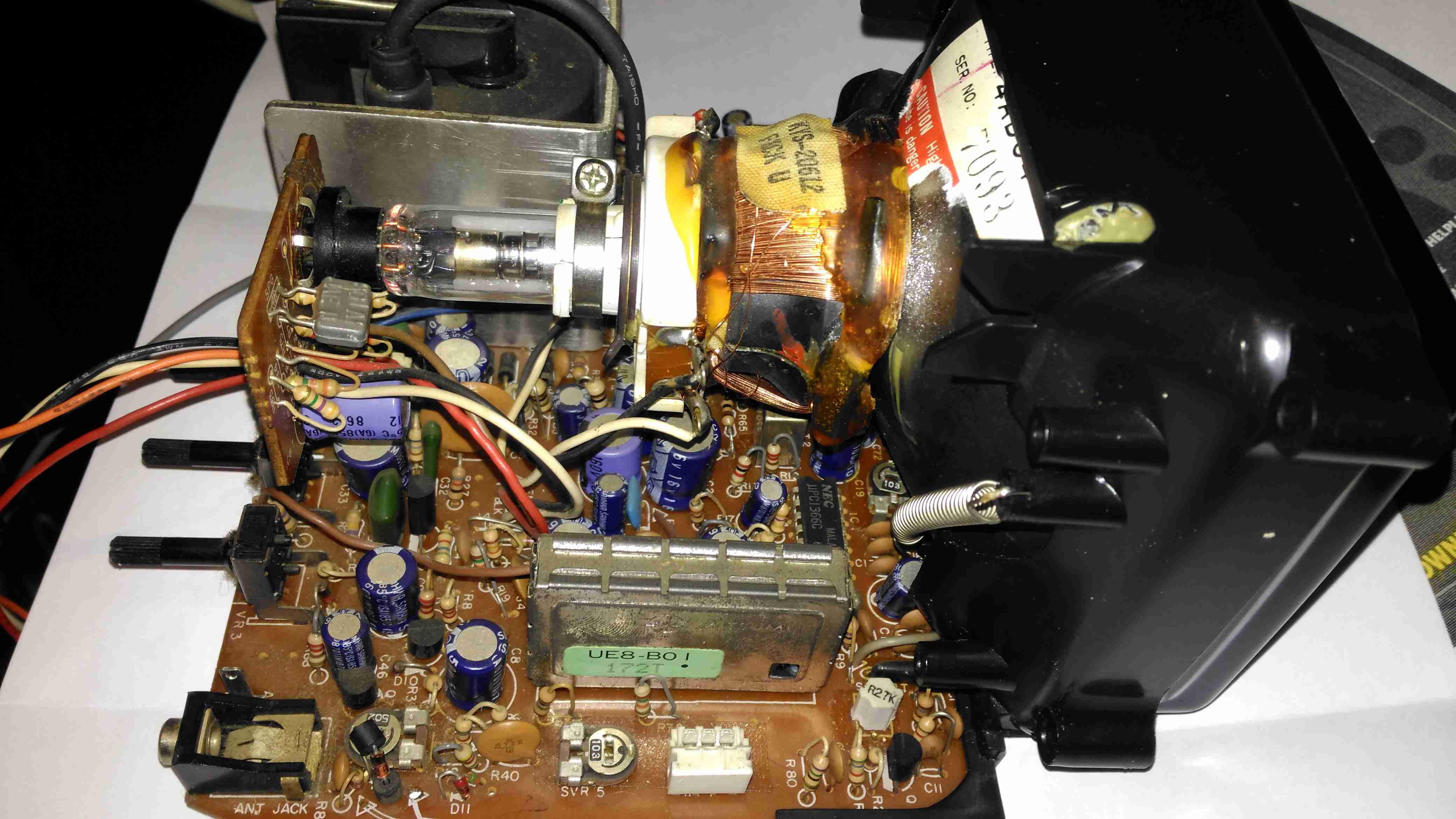
Here’s the anode side of the unit, with the small flyback transformer. The rubber anode cap has become very hard with age, so I’ll replace this with a decent silicone one from another dead TV. The Horizontal Output Transistor (a 2SC2233 NPN type) & linearity coil are visible at the bottom right corner of the board. Unfortunately, the disgusting yellow glue has been used to secure some of the wiring & large electrolytics, this stuff tends to turn brown with age & become conductive, so it has to be removed. Doing this is a bit of a pain though. It’s still a little bit flexible in places, and rock hard in others. Soaking in acetone softens it up a little & makes it easier to detach from the components.

Neck PCB
Neck PCB

There’s little on the neck board apart from a few resistors, forming the limiting components for the video signal, and the focus divider of 1MΩ & 470KΩ feeding G3. No adjustable focus on this unit. There’s also a spark gap between the cathode line & ground, to limit the filament to cathode voltage. The flyback transformer is nestled into the heatsink used by the horizontal output transistor & a voltage regulator transistor.

Tube Details
Tube Details

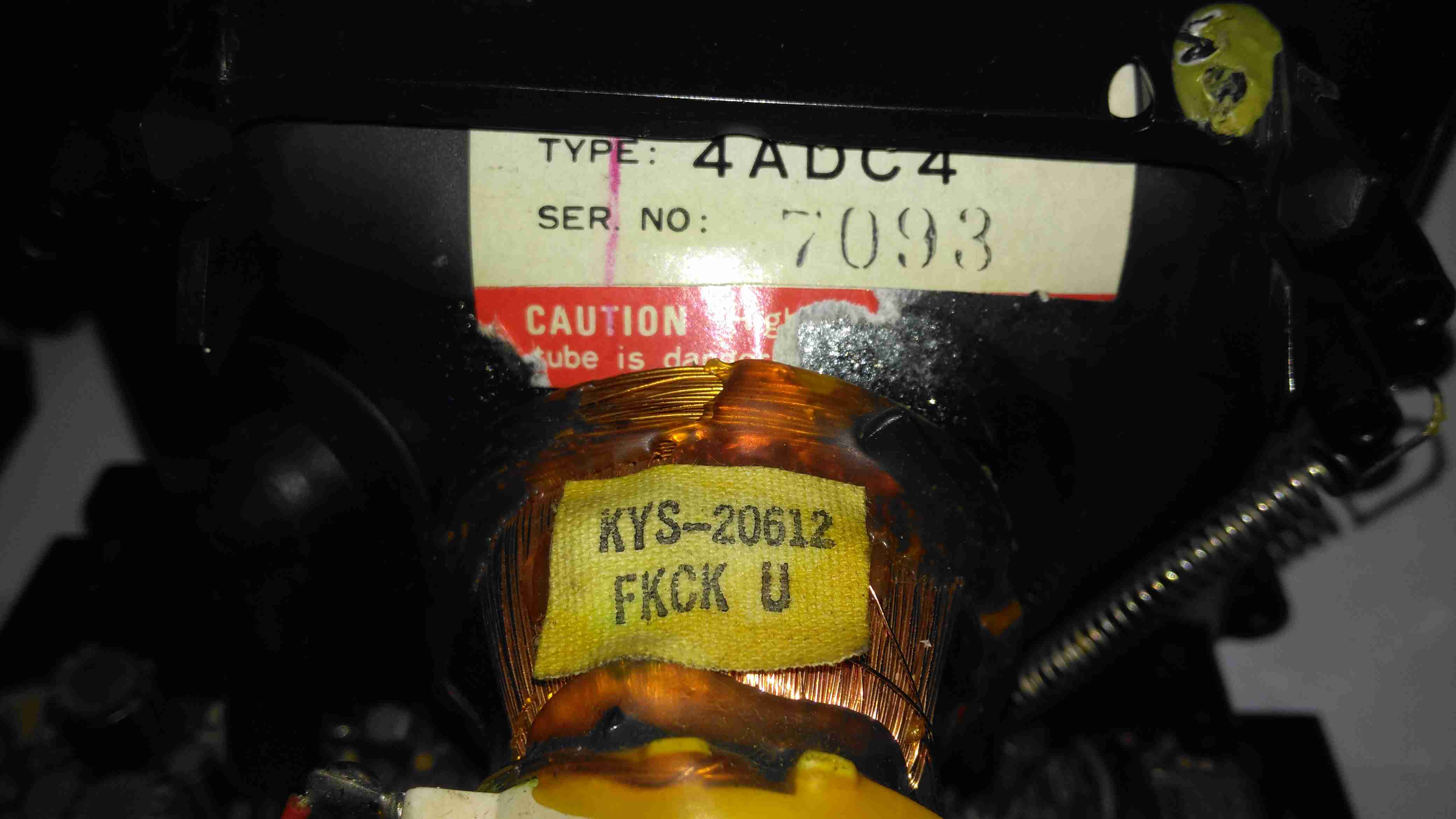
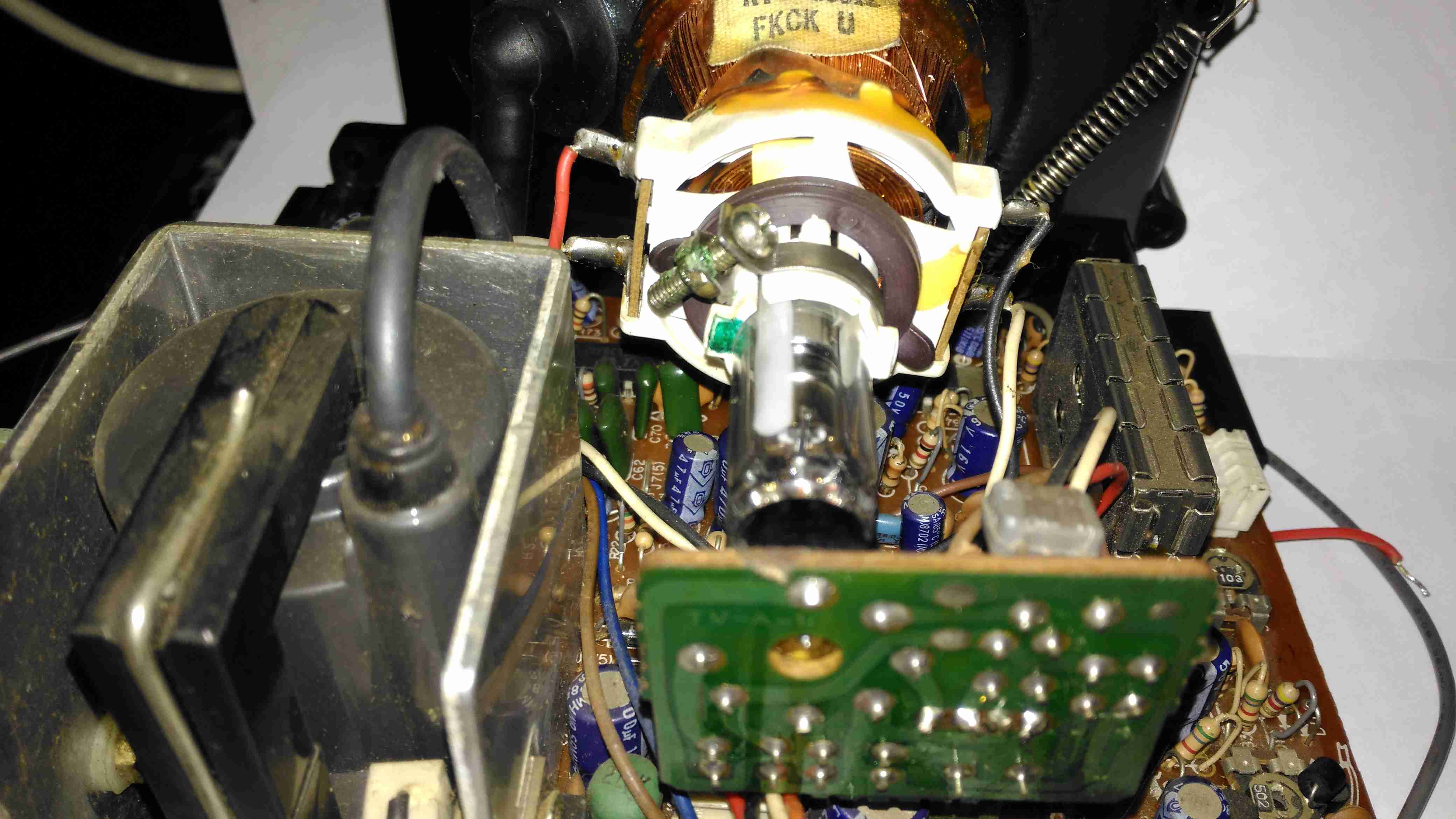
The CRT is a Samsung Electron Devices 4ADC4, with a really wide deflection angle. It’s a fair bit shorter than the Chinese CRT I have which is just a little larger, with a neck tube very thin indeed for the overall tube size.
Unusually, while the filament voltage is derived from the flyback transformer as usual, it’s rectified into DC in this unit, passing through a 1Ω resistor before the filament connection. I measured 5.3v here. The glow from the filament is barely visible even in the dark.

Electron Gun 1
Electron Gun 1

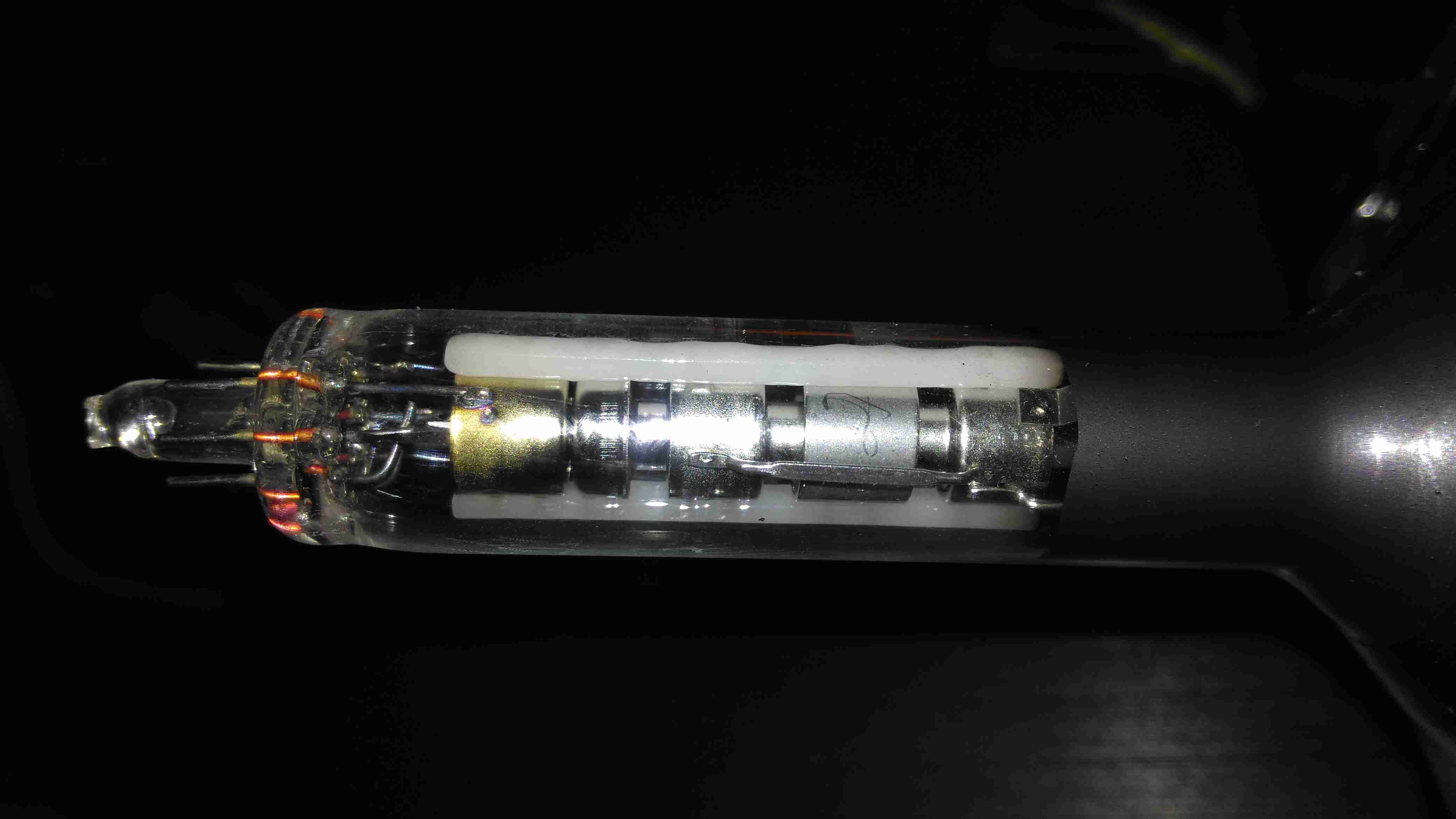
The electron gun is the usual for a monochrome tube, with 7 pins on the seal end.

Electron Gun 2
Electron Gun 2

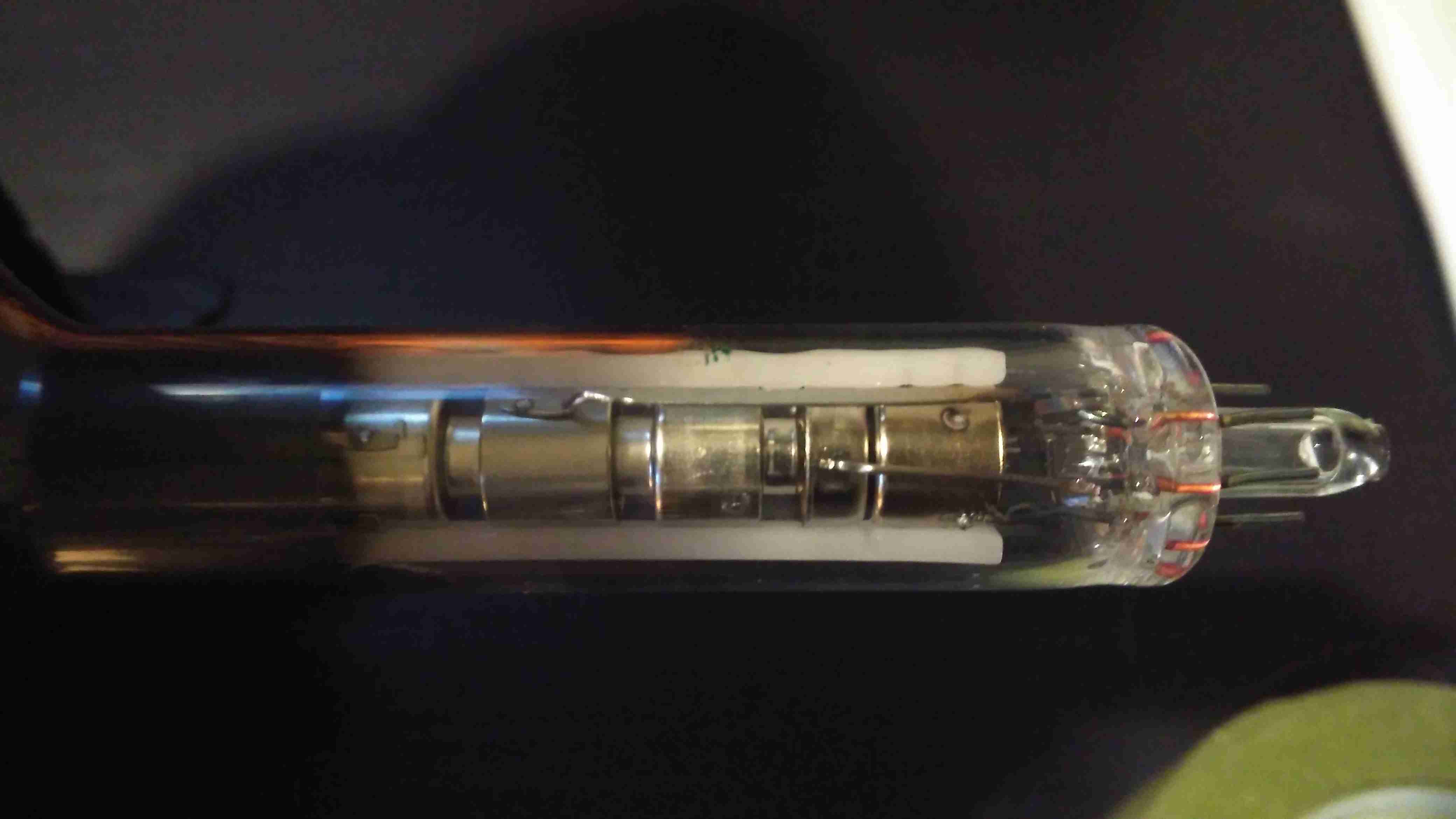
The electrodes here from left are Final Anode, G3 (Focus Grid), Accelerating Anode, G2 (Screen Grid), G1 (Control Grid). The cathode & filament are hidden inside G1. In operation there’s about 250v on G2, and about 80v on G3.

Chipset
Chipset

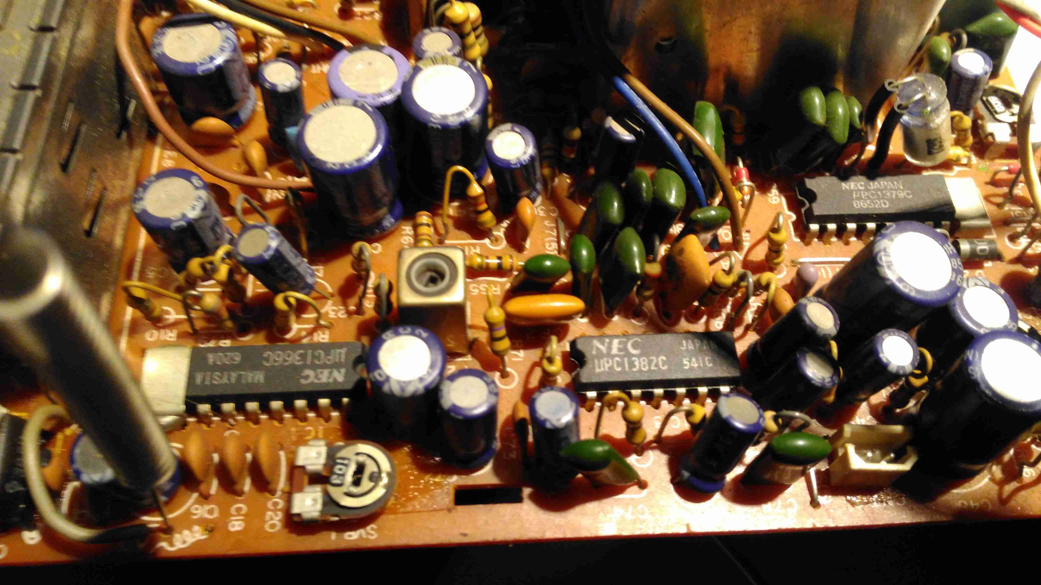
The chipset used here is all NEC, starting with a µPC1366C Video IF Processor, which receives the IF signal from the tuner module to the left. This IC outputs the standard composite signal, and a modulated sound signal.
This then splits off to a µPC1382C Sound IF Processor & Attenuator IC, which feeds the resulting sound through the two pin header at the right bottom edge of the board to the audio amplifier in the chassis.
The composite video signal is fed through a discrete video amplifier with a single 2SC2229 transistor before going to the CRT cathode.
The remaining IC is a µPC1379C Sync Signal Processor, containing the sync separator, this is generating the required waveforms to drive the CRT deflection systems from another tap off the composite video line.
From this chip I can assume the unit was built around 1986, since this is the only date code on any of the semiconductors. Besides these 3 ICs, the rest of the circuit is all discrete components, which are well-crammed into the small board space.
There are 5 trimmer potentiometers on the board here, I’ve managed to work out the functions of nearly all of them:

  • SVR1: IF Gain Adjust
  • SVR2: H. Hold
  • SVR3: V. Size
  • SVR4: B+ Voltage Adjust
  • SVR5: Tuner Frequency Alignment? It’s in series with the tuning potentiometer in the chassis.
PCB Bottom
PCB Bottom

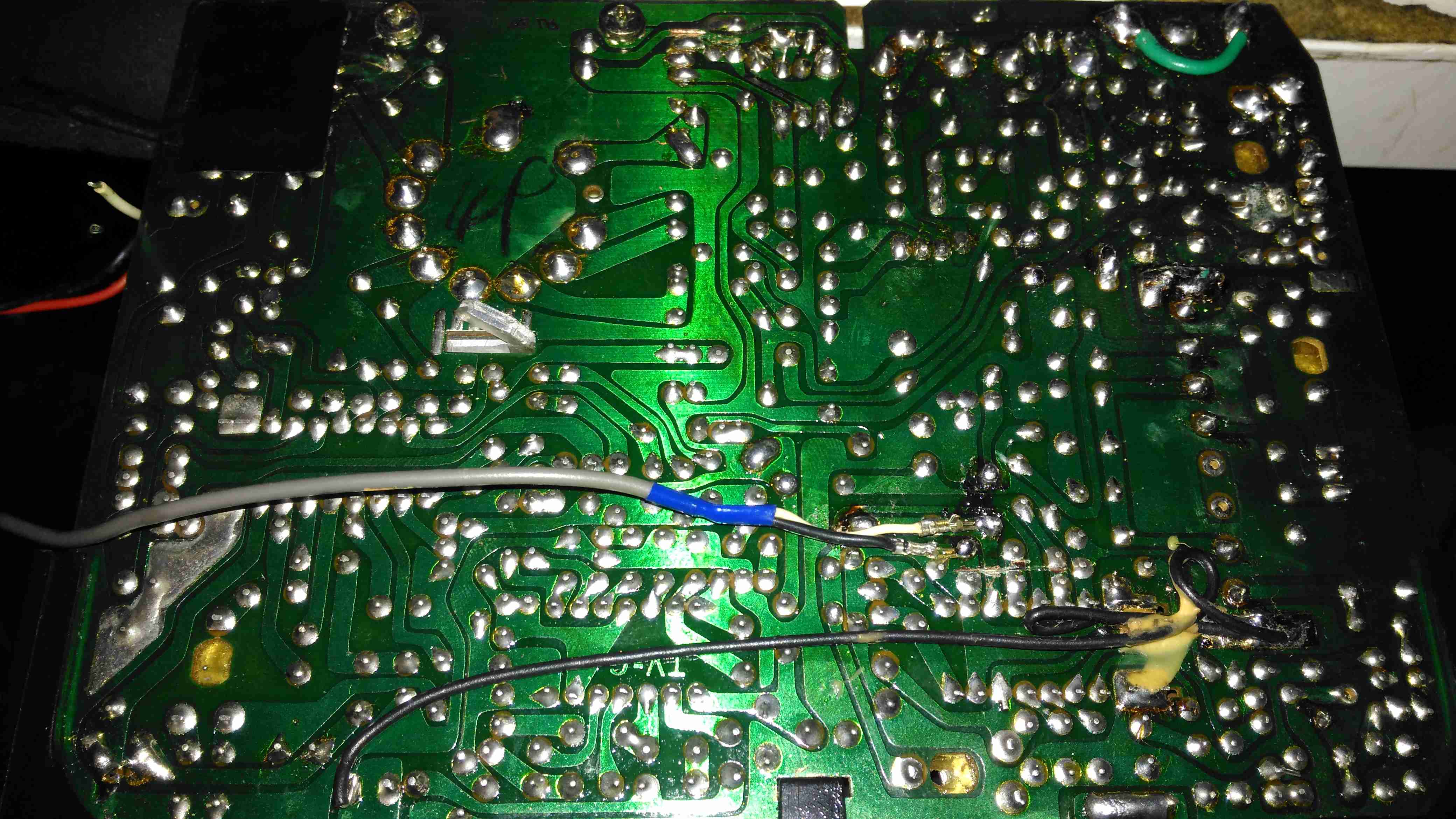
The PCB bottom shows the curved track layout typical of a hand taped out board. The soldermask is starting to flake off in places due to age, and there a couple of bodge wires completing a few ground traces. Respinning a board in those days was an expensive deal! Surprisingly, after all this time I’ve found no significant drift in the fixed resistors, but the carbon track potentiometers are drifiting significantly – 10KΩ pots are measuring as low as 8KΩ out of circuit. These will have to be replaced with modern versions, since there are a couple in timing-sensitive places, like the vertical & horizontal oscillator circuits.

Anode Cap Replaced
Anode Cap Replaced

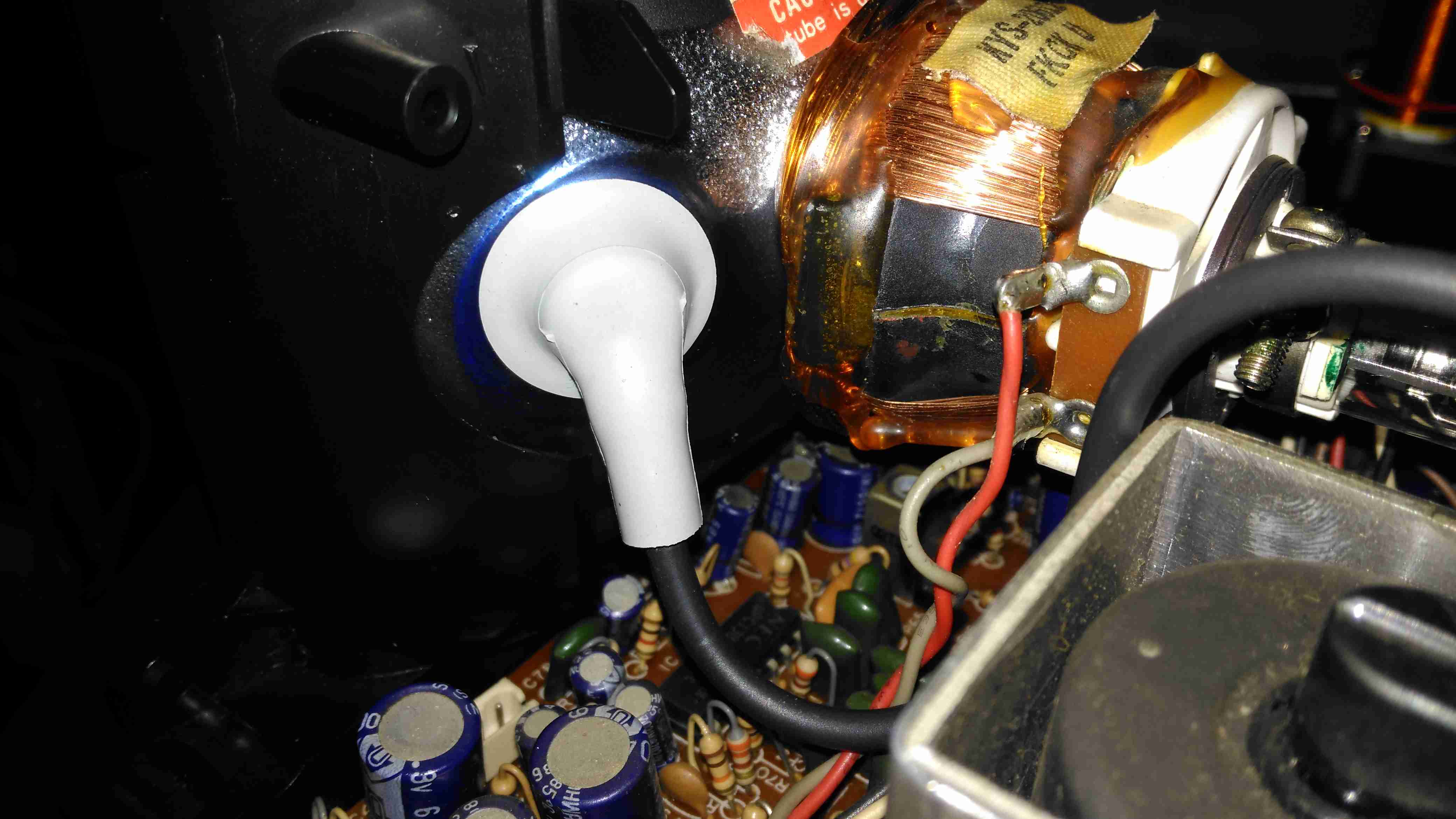
Here the anode cap has been replaced with a better silicone one from another TV. This should help keep the 6kV on the CRT from making an escape. This was an easy fix – pulling the contact fork out of the cap with it’s HT lead, desoldering the fork & refitting with the new cap in place.

Here I’ve replaced the important trimmers with new ones. Should help stabilize things a little.

Composite Injection Mod

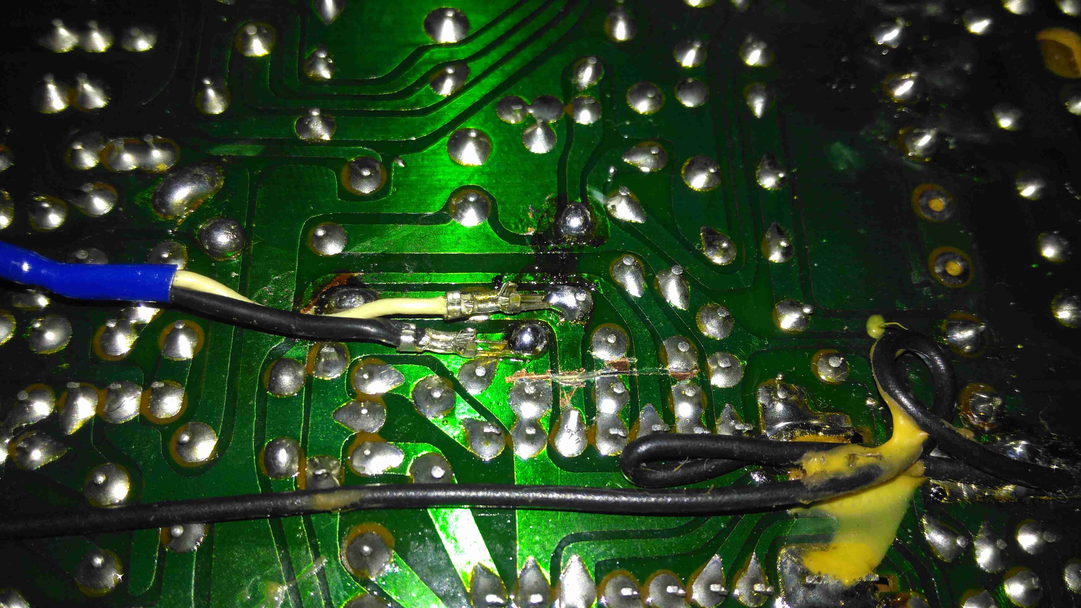
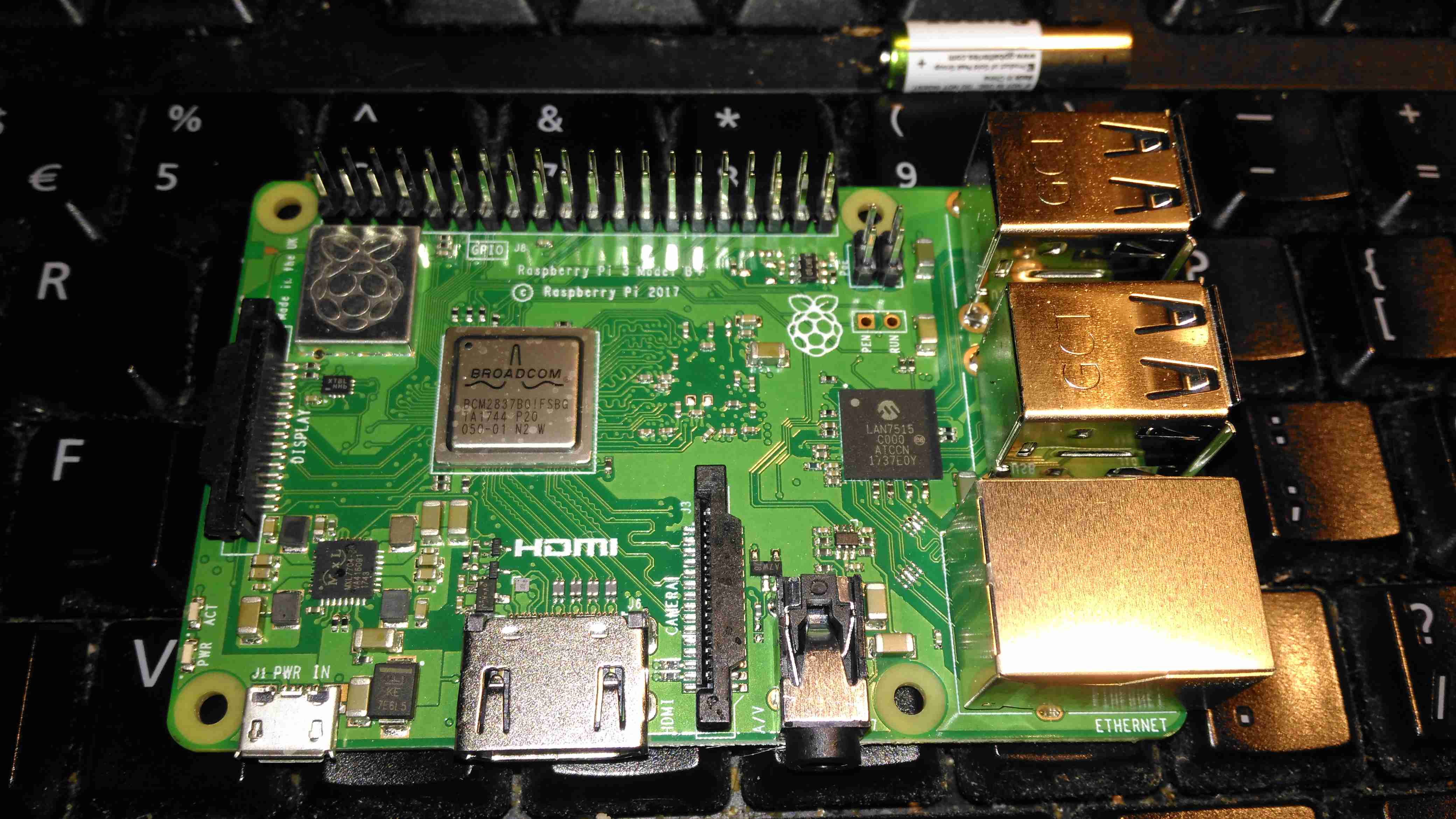
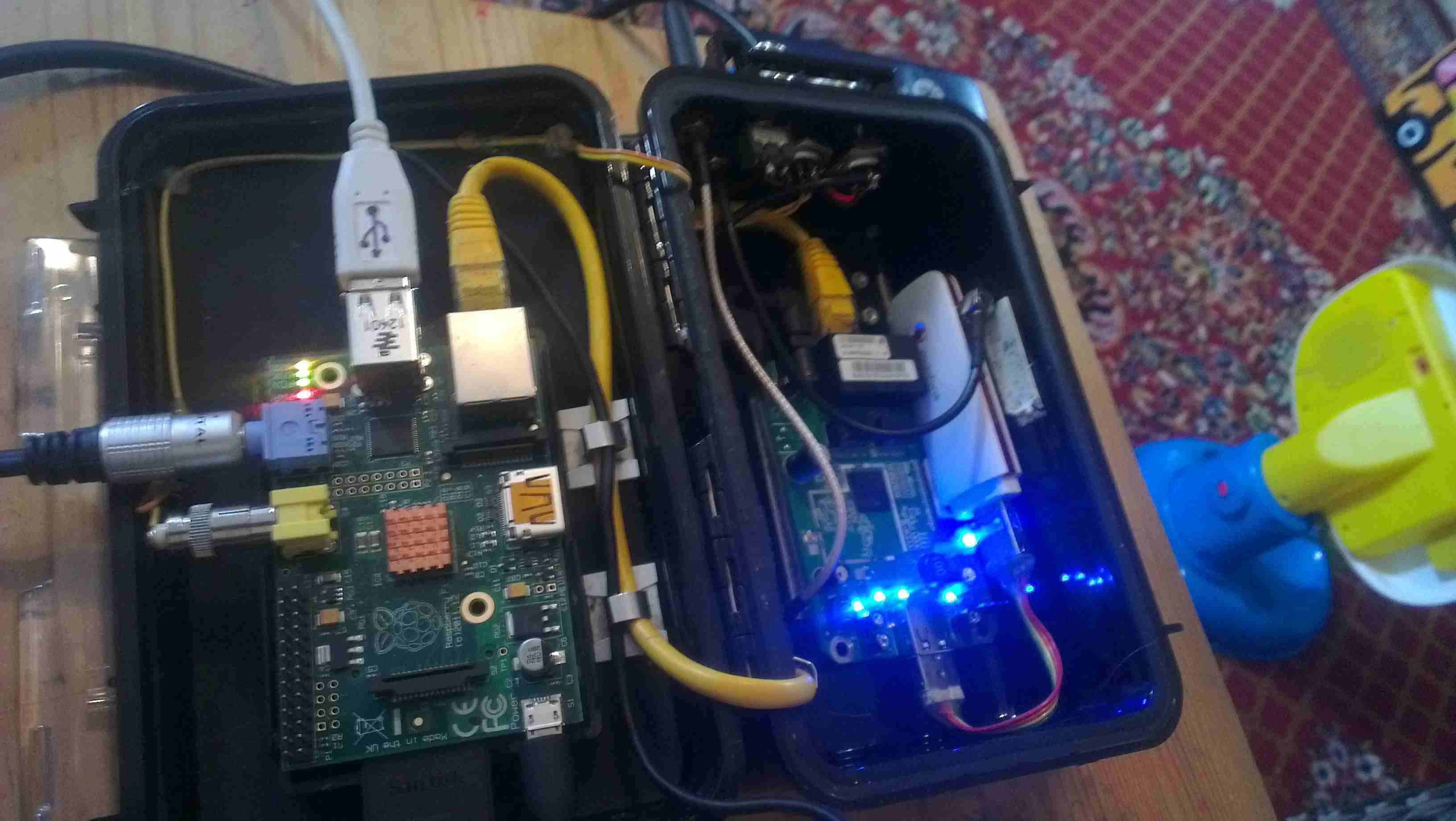
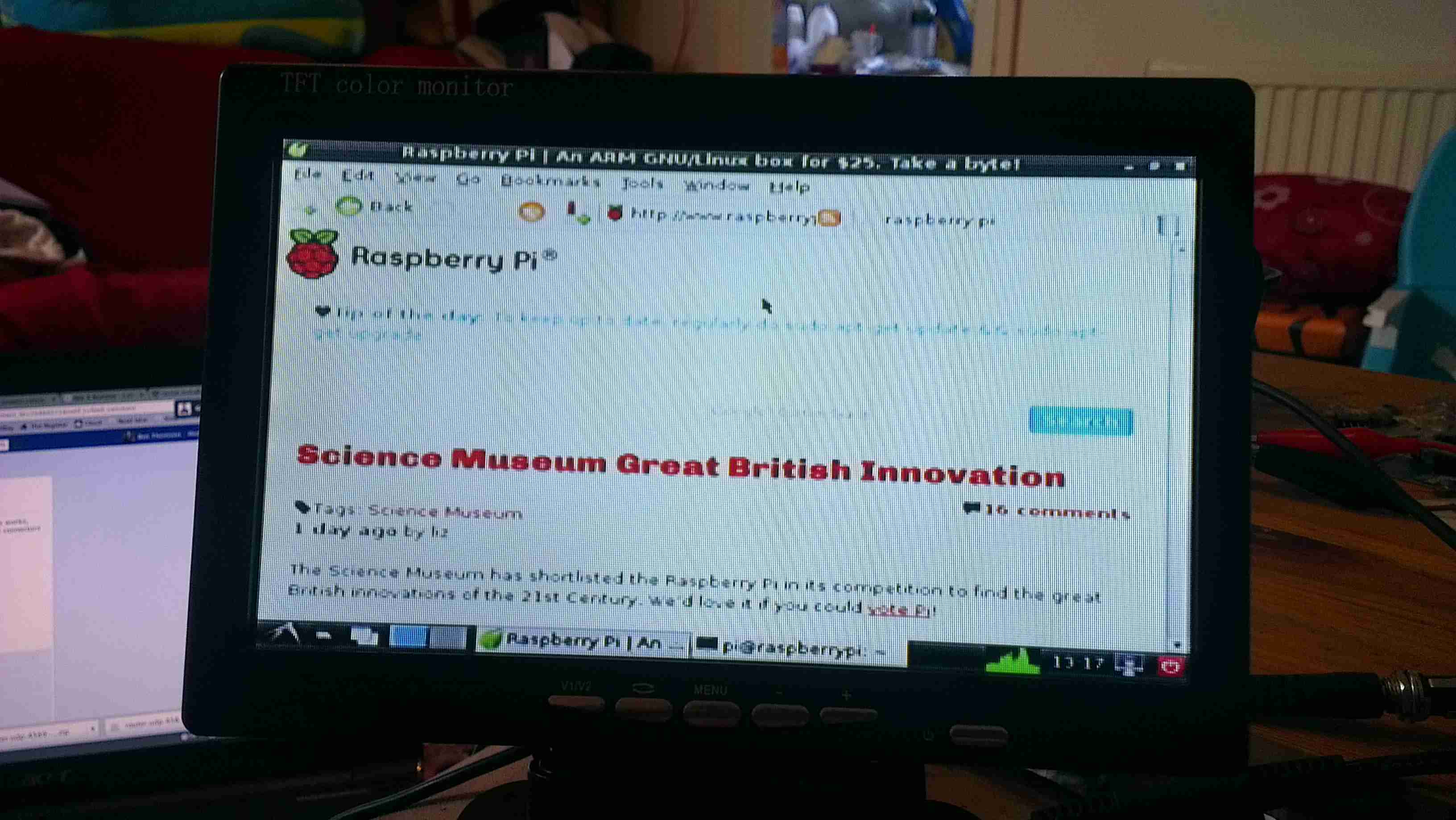
Injecting a video signal is as easy as the other units. Pin 3 of the µPC1366C Video IF Processor is it’s output, so the track to Pin 3 is cut and a coax is soldered into place to feed in an external signal.

CRT In Operation
CRT In Operation

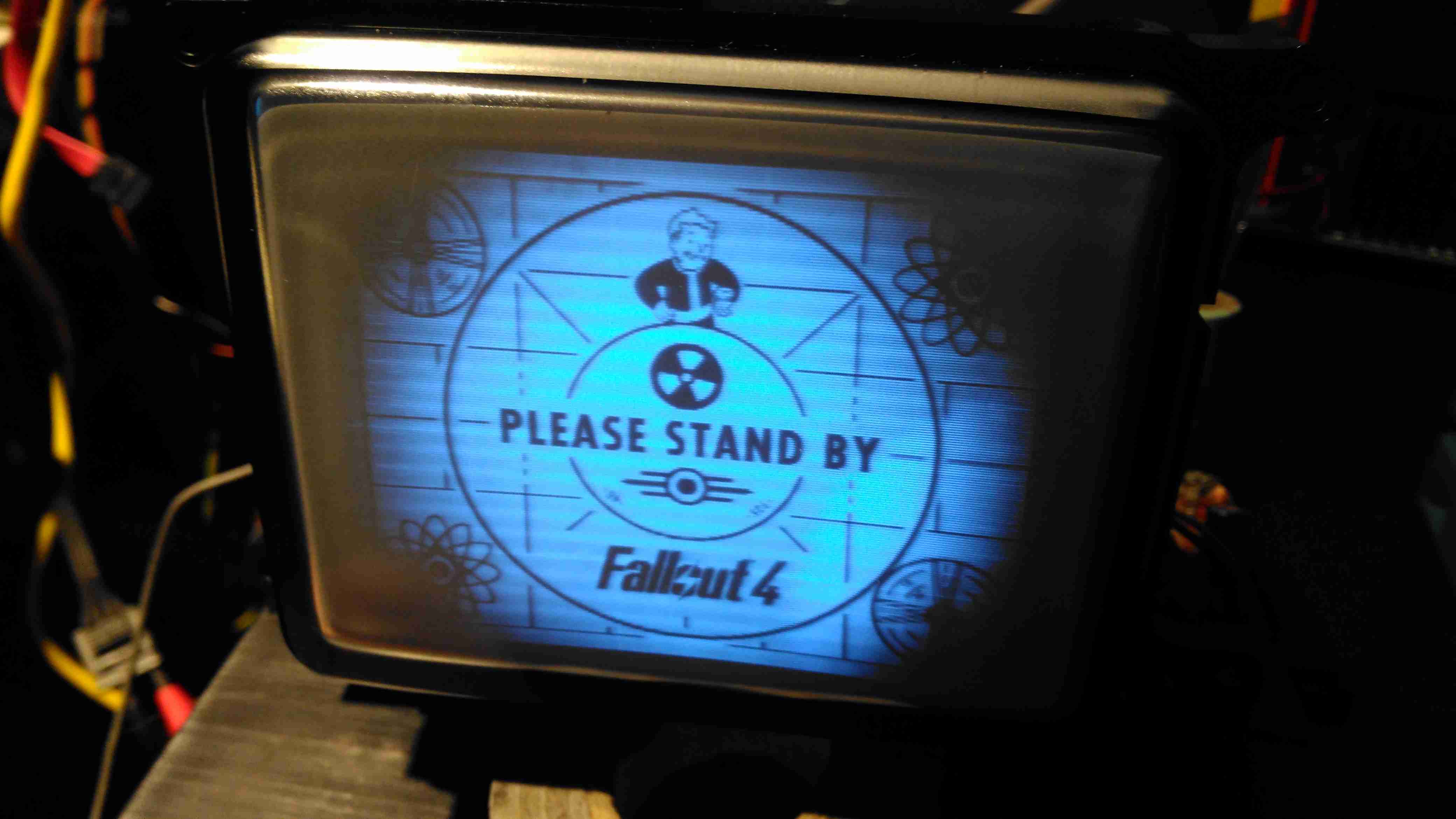
After hooking up a Raspberry Pi, we have display! Not bad after having stood idle for 30+ years.

Datasheets for the important ICs are available below:
[download id=”5690″]
[download id=”5693″]
[download id=”5696″]

Posted on 5 Comments

Vodafone Mobile WiFi R207 Teardown

Vodafone Mobile WiFi R207

Here’s one of the old modems from my spares bin, a Vodafone Mobile WiFi R207. This is just a rebranded Huawei E5330. This unit includes a 3G modem, and a WiFi chipset, running firmware that makes this a mini-router, with NAT.

Specs
Specs

The back has the batter compartment & the SIM slot, with a large label showing all the important details.

Cover Removed
Cover Removed

A couple of small Torx screws later & the shell splits in half. All the electronics are covered by shields here, but luckily they are the clip-on type, and aren’t soldered direct to the PCB.

Chipset
Chipset

Once the shield has been removed, the main chipset is visible underneath. There’s a large Spansion MS01G200BHI00 1GBit flash, which is holding the firmware. Next to that is the Hi6758M baseband processor. This has all the hardware required to implement a 3G modem. Just to the right is a Hi6521 power management IC, which is dealing with all the power supplies needed by the CPU.
The RF section is above the baseband processor, some of which is hiding under the bits of the shield that aren’t removable.

SIM Socket
SIM Socket

There’s a socket onboard for a standard Mini-SIM, just to the left of that is a Hi6561 4-phase buck converter. I would imagine this is providing the power supplies for the RF section & amplifier.

Unpopulated Parts
Unpopulated Parts

Not sure what this section is for, all the parts are unpopulated. Maybe a bluetooth option?

PCB Reverse
PCB Reverse

The other side of the PCB is pretty sparse, holding just the indicator LEDS, button & the WiFi Chipset.

Realtek WiFi Chipset

The chipset here is a Realtek part, but it’s number is hidden by some of the shield. The antenna connection is routed to the edge of the board, where a spring terminal on the plastic case mounted antenna makes contact.

Posted on Leave a comment

Wireless Energy Management SmartSensor

Cover Removed
Cover Removed

Here’s another random bit of RF tech, I’m told this is a wireless energy management sensor, however I wasn’t able to find anything similar on the interwebs. It’s powered by a standard 9v PP3 battery.

Microcontroller
Microcontroller

System control is handled by this Microchip PIC18F2520 Enhanced Flash microcontroller, this has an onboard 10-bit ADC & nanoWatt technology according to their datasheet. There’s a 4MHz crystal providing the clock, with a small SOT-23 voltage regulator in the bottom corner. There’s a screw terminal header & a plug header, but I’ve no idea what these would be used for. Maybe connecting an external voltage/current sensor & a programming header? The tactile button I imagine is for pairing the unit with it’s controller.

PCB Bottom
PCB Bottom

The bottom of the PCB is almost entirely taken up by a Radiocrafts RC1240 433MHz RF transceiver. Underneath there’s a large 10kΩ resistor, maybe a current transformer load resistor, and a TCLT1600 optocoupler. Just from the opto it’s clear this unit is intended to interface in some way to the mains grid. The antenna is connected at top right, in a footprint for a SMA connector, but this isn’t fitted.

Posted on Leave a comment

Raspberry Pi 3 Model B+ Initial Tests & Benchmarks

Raspberry Pi 3 Model B+

Yesterday, the Raspberry Pi community got a nice surprise – a new Pi! This one has some improved features over the previous RPi 3 Model B:

  • Improved CPU – 64-Bit 1.4GHz Quad-Core BCM2837B0
  • Improved WiFi – Dual Band 802.11b/g/n/ac. This is now under a shield on the top of the board.
  • Improved Ethernet – The USB/Ethernet IC has been replaced with a LAN7515, supporting gigabit ethernet. The backhaul is still over USB2 though, so this would max out at about 300Mbit/s
  • PoE Support – There’s a new 4-pin header, and a matching HAT for power over ethernet support.
Chipset
Chipset

The USB/LAN Controller is now a BGA package, supporting gigabit ethernet. The USB connections are still USB2 though, limiting total bandwidth. This shouldn’t be much of an issue though, since anything over the 100Mbit connection we’ve had previously is an improvement.

CPU & Radio
CPU & Radio

The CPU now has a metal heatspreader on top of the die, no doubt to help with cooling under heavy loads. As far as I know, it’s still the same silicon under the hood though. The WiFi radio is under the shielding can to the top left, with the PCB trace antenna down the left edge of the board.

Power Controller
Power Controller

The power supplies are handled on this new Pi by the MaxLinear MxL7704, from what I can tell from MaxLinear’s page, it seems to be somewhat of a collaborative effort to find something that would do the best job, since they apparently worked with the Foundation to get this one right. This IC apparently includes four synchronous step-down buck regulators that provide system, memory, I/O and core power from 1.5A to 4A. An on-board 100mA LDO provides clean 1.5V to 3.6V power for analog sub-systems. This PMIC utilizes a conditional sequencing state machine that is flexible enough to meet the requirements of virtually any processor.

PCB Bottom
PCB Bottom

The bottom of the PCB has the Elpida 1GB RAM package, which is LPDDR2, along with the MicroSD slot.

A quick benchmark running Raspbian Lite & a SanDisk Ultra 32GB Class 10 SD card gives some nice results:

Posted on 2 Comments

Maplin A24GU Wireless Audio Module Teardown

Transmitter
Transmitter

This is a pair of modules that Maplin was selling some time back, to send stereo audio over a 2.4GHz radio link. The transmitter identifies as a USB sound card, I’ve personally used these units to transmit audio about 60ft. The transmitter, above, has a single button for pairing with the receiver below.

Receiver
Receiver

The receiver unit has a large external antenna, a link status LED & volume buttons, these directly control the volume level on the host PC via the sound card drivers.

Receiver PCB Top
Receiver PCB Top

Popping the case open on the receiver reveals a large PCB, holding the chipset, along with the audio output jacks & Mini-USB power input. The antenna Coax is soldered to the PCB.

Receiver PCB Bottom
Receiver PCB Bottom

The top of the board has the control buttons, and the status LED.

Receiver Chipset
Receiver Chipset

The chipset used here is a Nordic Semiconductor nRF20Z01 2.4GHz Stereo Audio Streamer, there’s a small microcontroller which does all the register magic on the RF transceiver. The RF chain is at the top of the photo, audio outputs on the top left, and the micro USB power input & voltage regulators at bottom left.

Transmitter PCB Top
Transmitter PCB Top

The transmitter PCB has a Sonix USB Audio Codec, to interface with the host PC. This is then fed into another Nordic Semi part on the opposite side of the board:

Transmitter PCB Bottom

The bottom of the transmitter has the RF section, and another small control microcontroller.

Posted on 8 Comments

Virgin Media Superhub 2 Teardown

I recently got the latest upgrade from Virgin Media, 200Mbit DL / 20Mbit UL, and to get this I was informed I’d have to buy their latest hardware, since my existing CPE wouldn’t be able to handle the extra 5Mbit/s upload speed. (My bullshit detector went off pretty hard at that point, as the SuperHub 2 hardware is definitely capable of working fine with 20Mbit/s upload rates). Instead of having to return the old router, I was asked to simply recycle it, so of course the recycling gets done in my pretty unique way!

Mainboard
Mainboard

The casing of these units is held together by a single screw & a metric fuckton of plastic clips, disassembly is somewhat hindered by the radio antennas being positioned all over both sides of the casing. Once the side is off, the mainboard is visible. The DOCSIS frontend is lower left, centre is the Intel PUMA 5 Cable Modem SoC with it’s RAM just to the lower right. The right side of the board is taken up by both of the WiFi radio frontends, the 5GHz band being covered by a Mini PCIe card.

Atheros Gigabit Switch

The 4 gigabit Ethernet ports on the back are serviced by an Atheros AR8327 Managed Layer 3 switch IC, which seems to be a pretty powerful device:

The AR8327 is the latest in high performance small network switching. It is ultra low power, has extensive routing and data management functions and includes hardware NAT functionality (AR8327N). The AR8327/AR8327N is a highly integrated seven-port Gigabit Ethernet switch with a fully non-blocking switch fabric, a high-performance lookup unit supporting 2048 MAC addresses, and a four-traffic  class Quality of Service (QoS) engine. The AR8327 has the flexibility to support various networking applications. The AR8327/AR8327N is designed for cost-sensitive switch applications in wireless AP routers, home gateways, and xDSL/cable modem platforms.

Unfortunately most of the features of this router are locked out by VM’s extremely restrictive firmware. With any of their devices, sticking the VM supplied unit into modem mode & using a proper router after is definitely advised!

Intel Puma 5 CM CPU
Intel Puma 5 CM CPU

The cable modem side of things is taken care of by the Intel PUMA 5 DNCE2530GU SoC. This appears to communicate with the rest of the system via the Ethernet switch & PCI Express for the 5GHz radio.

Atheros WiFi SoC
Atheros WiFi SoC

The 2.4GHz radio functionality is supplied by an Atheros AR9344 SoC, it’s RAM is to the left. This is probably handling all the router functions of this unit, but I can’t be certain.

Atheros LAN PHY
Atheros LAN PHY

A separate Ethernet PHY is located between the SoC & the switch IC.


5GHz Radio Card
5GHz Radio Card

The 5GHz band is served by a totally separate radio module, in Mini PCIe format, although it’s a bit wider than standard. This module will probably be kept for reuse in another application.

Power Supplies
Power Supplies

All down the edge of the board are the multiple DC-DC converters to generate the required voltage rails.

MaxLinear MXL261 Frontend

The DOCSIS frontend is handled by a MaxLinar MXL261 Tuner/Demodulator. More on this IC in my decapping post 🙂

The Unknown One
The Unknown One

I’ve honestly no idea what on earth this Maxim component is doing. It’s clearly connected via an impedance matched pair, and that track above the IC looks like an antenna, but nothing I search for brings up a workable part number.

2.4GHz Frontend
2.4GHz Frontend

The RF switching & TX amplifiers are under a shield, these PA chips are SiGe parts.

Atheros 5GHz Radio
Atheros 5GHz Radio

Pretty much the same for the 5GHz radio, but with 3 radio channels.

Posted on Leave a comment

Mercedes Benz Temic Central Locking / Immobilizer Module Teardown

Mercedes Benz Temic Module

The other day I was given a random pile of car electronic parts from the scrap bin at the local garage, so I decided to do a few teardowns. This first one is a Temic Central Locking / Immobiliser module from a Mercedes van. Judging by the 125kHz stamped on the label, this also has RFID capability.

PCB
PCB

The casing just unclips, revealing the PCB. Surprisingly for an automotive module, there is no conformal coating on this (they’re usually heavily coated in protective lacquer to prevent moisture ingress).

Microcontroller
Microcontroller

The large IC from Motorola I’m assuming to be a microcontroller, but I didn’t manage to find anything from the markings. There’s not much else in here apart from some glue logic, and what I think is the 125Khz toroidal antenna in the top left corner.

Posted on Leave a comment

OLED Pulse Oximeter Teardown

OLED Pulse Oximeter
OLED Pulse Oximeter

Here’s a piece of medical equipment that in recent years has become extremely cheap, – a Pulse Oximeter, used to determine the oxygen saturation in the blood. These can be had on eBay for less than £15.

Powered On
Powered On

This one has a dual colour OLED display, a single button for powering on & adjusting a few settings. These cheap Oximeters do have a bit of a cheap plastic feel to them, but they do seem to work pretty well.

Pulse Oximeter
Pulse Oximeter

After a few seconds of being applied to a finger, the unit gives readings that apparently confirm that I’m alive at least. 😉 The device takes a few seconds to get a baseline reading & calibrate the sensor levels.

Main PCB Top
Main PCB Top

The plastic casing is held together with a few very small screws, but comes apart easily. here is the top of the main board with the OLED display panel. There appears to be a programming header & a serial port on the board as well. I’ll have to poke at these pads with a scope to see if any useful data is on the pins.

Main PCB Bottom
Main PCB Bottom

The bottom of the board has all the main components of the system. The microcontroller is a STM32F03C8T6, these are very common in Chinese gear these days. There’s a small piezo beeper & the main photodiode detector is in the centre.
There is an unpopulated IC space on the board with room for support components. I suspect this would be for a Bluetooth radio, as there’s a space at the bottom left of the PCB with no copper planes – this looks like an antenna mounting point. (The serial port on the pads is probably routed here, for remote monitoring).
At the top left are a pair of SGM3005 Dual SPDT analogue switches. These will be used to alternate the red & IR LEDs on the other side of the shell.
A 4-core FFC goes off to the other side of the shell, bringing power from the battery & supplying the sensing LEDs.

Battery Compartment
Battery Compartment

Power is supplied by a pair of AAA cells in the other shell.

Dual LED
Dual LED

The sensor LEDs are tucked in between the cells, this dual-diode package has a 660nm red LED & a 940nm IR LED.

Posted on Leave a comment

Huawei E160E USB HSDPA Modem

E160E Modem
Huawei E160E Modem

Here’s an old HDSPA 3G USB modem stick that I got with a mobile phone contact many years ago. As it’s now very old tech, and I have a faster modem, not to mention that I’m no longer with Orange (Robbing <expletive>), here’s a teardown of the device!

Cover Removed
Cover Removed

The top shell is just clipped into place, while a pair of very small screws hold down the orange piece at left to hold the PCB stack in the casing. Not much to see here, but it’s clear that there’s a lot crammed into a very small space.

PCB Assembly
PCB Assembly

Here’s the PCB stack removed from the outer casing. The main antenna is on the right, attached with another small screw. Every IC on the boards is covered with an RF can. No problems there, pliers to the rescue!

SD Card Slot
SD Card Slot

Here’s the top PCB, all the shields have been removed. On the left is a Qualcomm PM6658 Power Management IC with integrated USB transceiver. This is surrounded by many of the power management circuits.
The integrated SD Card slot is on the right side. with what looks to be a local switching regulator for supply voltage. This might also provide the SIM card with it’s power supply.

PSU & SIM Contacts
PSU & SIM Contacts

The other side of the top board reveals more power management, with another switching regulator, and a truly massive capacitor at the top edge. I’m guessing this is a solid Tantalum.

Main Chipset PCB
Main Chipset PCB

The other PCB holds the main chipset & RF circuits. On the left here is a Samsung MCP K5D1G13ACH IC. This one is a multiple chip package, having 1Gbit of NAND Flash & 512Mbit of mobile SDRAM.
To it’s right is a Qualcomm RTR6285 RF Transceiver. This IC supports multiband GSM/EDGE/UMTS frequencies & also has a GPS receive amplifier included.
At bottom right is an Avago ACPM7371 Wide-Band 4×4 CDMA Power Amplifier. The external antenna connector is top right.

Main Chipset PCB Reverse

On the other side of the main PCB is a Qualcomm MSM6246 Baseband processor. Not sure about this one as I can’t find anything resembling a datasheet. Another micro-coax connector is in the centre, probably for factory test purposes, as it’s not accessible from the outside.
Just above the coax connector is a Qorvo RF1450 SP4T (single-pole 4-throw) High Power (34.5dBm) GSM RF Switch.
Upper right is an Avago FEM-7780 UMTS2100 4×7 Front End Module.
Under that is an RFMD RF3163 Quad-Band RF Power Amplifier Module.

Posted on 4 Comments

Eberspacher Controller & Remote

7-Day Programmer
7-Day Programmer

The Eberspacher heaters can be controlled with a single switch, but it’s more convenient to have some temperature control & the option of a timer. Above is an ex-BT 701 series controller, with built in 7-day programmer. Being an ex-BT van version though, it’ll only switch the heater on for 1 hour at a time.
To get around this slight niggle, I fitted a bypass toggle switch.

Remote Control
Remote Control

For a bit of extra convenience, I got an RF remote controlled relay module from eBay (£5).
This allows me to switch things on remotely, so I can return to a nice toasty tent while camping.
There is an official RF remote for Eberspacher heaters, but I’ve no doubt they’re hideously expensive.

RF Receiver
RF Receiver

Here’s the receiver PCB, there’s an EEPROM & a microcontroller onboard for handling the codes the remotes send, but as the number has been scrubbed off the micro, no data there. This uses a standard RF receiver module.

RF Remote
RF Remote

Here’s the remote itself, this uses a 12v battery instead of a 3v lithium cell. A little of a pain since these batteries can be a bit pricey.
As this RF system operates on 315MHz, it’s technically illegal in the UK, but I was unable to find a 433MHz version with the features required. Nevermind ;).

Controller Internals

Here’s the module installed in the controller casing. I have since run the antenna wire around the edge of the case to try & get the furthest range on receive. The relay contacts are just paralleled across the bypass switch, so when the relay energizes the heater fires up.
Luckily the thermostatic control portion of the 701 programmer is operational even when heating mode is not active.

Posted on Leave a comment

Alpha Networks WMP-N06SA MiniPCI Wireless N Card

Here’s a quick look at one of the now surplus cards from my old networking system, a MiniPCI Wireless interface card.

Card Overview
Card Overview

This is an older generation card, one of the first with Wireless N support on 2.4GHz.

PCI Chipset
PCI Chipset

Network PHY & firmware EEPROM. Power supply stuff is over to the left.

RF Transceiver
RF Transceiver

Inside the shield is the RF Transceiver IC & it’s associated RF power amplifier ICs for each antenna. These power amplifiers are LX5511 types from Microsemi, with a maximum power output of +26dBm.

Posted on Leave a comment

nb Tanya Louise Antenna Feeder Install

Here’s the final bit of the radio install now the required parts have arrived!

The radio being inside, we needed a reliable way to route the antenna coax through the hull to the external antenna, I managed to find some N-type bulkhead connectors, that are perfect for this job:

Bulkhead Fitting
Bulkhead Fitting

This fitting will allow for simple disconnection of the antenna for service, and N-type connectors are water resistant.

Hole
Hole

A hole was drilled in a suitable location with a cone drill. The steel here is pretty heavy, at 5mm. A spot between the handrail & the sliding roof was picked since there’s less chance of the fitting being knocked by any flying ropes, windlasses or crew members 😉

Bulkhead Connector
Bulkhead Connector

Here’s the connector fitted into it’s hole. The O-ring under the flange seals against the steel hull to prevent water getting through to the radio equipment on the other side.

Completed
Completed

Completed connection to the antenna. The short run to the radio underneath (~18″) is RG213, but I’ve used RG-58 on the antenna itself since it’s more flexible. The antenna is only a metre or so away so losses shouldn’t be much of an issue.

Posted on Leave a comment

Stock Baofeng Antenna Problems

Recently I’ve noticed my usual mobile rig, the Baofeng UV-5R, has had very poor receive, and non-existent transmit.

I did a power test on the radio, and confirmed it was still outputting it’s rated RF power. Trying another antenna proved that the radio was fine.

Time to tear down the antenna & see if it can be fixed!

Stock Antenna
Stock Antenna

Here’s the antenna, just the factory rubber duckie. As with all these antennas, they’re a compromise between size & their efficiency.

Naked Antenna!
Naked Antenna!

Giving a gentle pull to the antenna sheath while it’s attached to the radio allows it to come apart. The quality actually doesn’t look to bad. It’s very similar in construction to my Diamond X-30, just on a much smaller scale.

At the bottom of the antenna is the matching network, an inductor & ceramic disc capacitor. Here lies the problem with this antenna.

Dry Joint
Dry Joint

Here where the capacitor joins onto the feedpoint from the SMA connector, the solder joint has come away. This was a very poor joint to start with, and the solder hadn’t wetted the capacitor lead at all

After cleaning the joint, and applying some flux, a new joint was easily made with some Real Solder.

Repaired Joint
Repaired Joint

Here’s the joint freshly repaired, the antenna is now back to full working order. It even seems to work better than the others I have 🙂

Posted on Leave a comment

Labgear PSM114E/S 12v Conversion

Onboard the boat we have a small issue with a weak TV signal, and this coupled with a 60′ long run of coax is an issue. Due to the loss in the coax, we’ve lost most of the already weak signal.
To try & solve this issue, I’m fitting a masthead amplifier unit.

These amplifiers are fed power down the same coax that’s carrying the RF signal, and a special power supply is supplied with the amplifier for this. However it’s only 240v AC, no 12v version available.

Here’s the power supply unit, which fits into the coax between the TV & the antenna.

Amplifier Supply
Amplifier Supply

Luckily the 240v supply is easily removable & here has been replaced with a 12v regulator.

New Supply
New Supply

There’s not very much inside the shielding can, just a few filter capacitors & an RF choke on the DC feed, to keep the RF out of the power supply system.

The original cable is used, so the supply doesn’t even look like it’s been modified from the outside.

More to come on this when I get the amplifier installed along with the new coax run 🙂

73s

Posted on 22 Comments

GY561 Frequency & Power Meter

The latest addition to my radio shack is the GY561 frequency & power meter, which has already come in useful for measuring the output power of all my radios.

GY561
GY561

It’s a small device, roughly the same size & weight as a stock UV-5R. Power is provided by 3 AAA cells.

Display
Display

The display is a standard HD44780 8×2 module. The display on this unit isn’t backlit, so no operating in the dark.

Cover Removed
Cover Removed

The cover pops off easily to allow access to the internals, without having to remove any screws!
The 4 screws on the back of the unit hold the heatsink plate for the 50W 50Ω dummy load resistor.
Removing the cover reveals a couple of adjustments, for frequency & RF power calibration.

There are also 3 tactile switches that aren’t on the front panel. According to the manual (which in itself is a masterpiece of Chinglish), they are used to software calibrate the unit if an accurate RF power source is available. I will attempt to do a reasonable translation when time allows.

Disassembly further than this involves some desoldering in awkward places, so a search of the internet revealed an image of the rest of the internal components. In the case of my meter, all the part numbers have been scrubbed off the ICs in an attempt to hide their purpose. While it’s possible to cross-reference IC databooks & find the part numbers manually, this process is a time consuming one. Luckily the image I managed to locate doesn’t have the numbers scrubbed.

Total Disassembly
Total Disassembly

Under the LCD is some 74HC series logic, and a prescaler IC as seen in the previous frequency counter post. However in this unit the prescaler is a MB506 microwave band version to handle the higher frequencies specified.
In this case however the main microcontroller is an ATMEGA8L.
This is complemented by a SN54HC393 4-bit binary counter for the frequency side of things. This seems to make it much more usable down to lower frequencies, although the manual is very generous in this regard, stating that it’s capable of reading down to 1kHz. In practice I’ve found the lowest it reliably reads the frequency input is 10MHz, using my AD9850 DDS VFO Module as a signal source.
It did however read slightly high on all readings with the DDS, but this could have been due to the low power output of the frequency source.
Just like the other frequency counter module, this also uses a trimmer capacitor to adjust the microcontroller’s clock frequency to adjust the calibration.

The power supply circuitry is in the bottom left corner of the board, in this case a small switching supply. The switching regulator is needed to boost the +4.5v of the batteries to +5v for the logic.
Also, as the batteries discharge & their terminal voltage drops, the switching regulator will allow the circuit to carry on functioning. At present I am unsure of the lower battery voltage limit on the meter, but AAA cells are usually considered dead at 0.8v terminal voltage. (2.4v total for the 3 cells).
When turned on this meter draws 52mA from the battery, and assuming 1200mAh capacity for a decent brand-name AAA cell, this should give a battery life of 23 hours continuous use.

On the back of the main PCB is a 5v relay, which seems to be switching an input attenuator for higher power levels, although I only managed to trigger it on the 2m band.

Finally, right at the back attached to an aluminium plate, is the 50Ω dummy load resistor. This component will make up most of the cost of building these, at roughly £15.

On my DVM, this termination reads at about 46Ω, because of the other components on the board are skewing the reading. There are a pair of SMT resistors, at 200Ω & 390Ω in series, and these are connected across the 50Ω RF resistor, giving a total resistance of 46.094Ω.
This isn’t ideal, and the impedance mismatch will probably affect the calibration of the unit somewhat.

The heatsinking provided by the aluminium plate is minimal, and the unit gets noticeably warm within a couple of minutes measuring higher power levels.
High power readings should definitely be limited to very short periods, to prevent overheating.
The RF is sampled from the dummy load with a short piece of Teflon coax.

There’s a rubber duck antenna included, but this is pretty useless unless it’s almost in contact with the transmitting antenna, as there’s no input amplification. It might be handy for detecting RF emissions from power supplies, etc.

For the total cost involved I’m not expecting miracles as far as accuracy is concerned, (the manual states +/-10% on power readings).
The frequency readout does seem to be pretty much spot on though, and the ability to calibrate against a known source is handy if I need some more accuracy in the future.

I’ve also done an SWR test on the dummy load, and the results aren’t good.

At 145.500 MHz, the SWR is 3:1, while at 433.500 it’s closer to 4:1. This is probably due to the lower than 50Ω I measured at the meter’s connector.
These SWR readings also wander around somewhat as the load resistor warms up under power.

I’ll probably also replace the AAA cells with a LiPo cell & associated charge/protection circuitry, to make the unit chargeable via USB. Avoiding disposable batteries is the goal.

Posted on Leave a comment

Wouxun KG-UV950P RF Connector Replacement

In my original review, I noted that this radio was supplied with a SO-259 socket for the antenna connection.
However I’m less than fond of these, due to their non-constant impedance, which can cause signal loss issues at VHF/UHF. Because of this, I’ve replaced it with a high quality N-type connector. These connectors are much better, as they are a constant 50Ω impedance, they’re weather resistant, and being rated to 11GHz, are more than sufficient for a radio that will only do up to 70cm.

RF Output Jack
RF Output Jack

Here can be seen the point where the connection is made to the PCB.
I’ve already replaced the socket in this photo. The pair of solder pads either side of the central RF point were soldered to wings on the back of the original SO-259. As there are a pair of screws, also connected to the ground plane, there have been no signal issues with just using the frame of the radio as the ground point. Shown below is the original socket, with the ground wings.

Original SO-259
Original SO-259

Finally, here is the back of the radio with it’s shiny new N connector.

New Connection
New Connection

Chassis mount connectors are pretty standard, so this new connector fits perfectly into the same recess of the original. Looks like factory fitted!

I am now standardising on N connectors for everything in my radio shack, next on the project list for conversion is the SWR meter I recently acquired.

Stay tuned for more!

Posted on Leave a comment

Wearable Raspberry Pi Part 1.5

USB Ports
USB Ports

For convenience, a pair of USB ports have been fitted to the wearable Pi, which open on the bottom of the unit. These will be hardwired into a 4-port USB hub which will also support the wireless adaptor for the mini-keyboard that is to be used with the device.

USBs
USBs

The two USB ports on the bottom of the casing.

External Connections

The external connectors are also complete. The audio jack & second WiFi antenna port are fitted.

The audio is normally routed to the LCD display speaker, until a jack is plugged into the 3.5mm socket.


Posted on 3 Comments

Wearable Raspberry Pi Part 1

Overview
Overview

Here is the project I’m currently working on. A completely wearable computing platform based on the Raspberry Pi & the WiFi Pineapple.

Above can be seen the general overview of the current unit.

On the left:

  • Alfa AWUS036NHA USB High Power WiFi Network Interface
  • 512MB Model B Raspberry Pi, 16GB SD card, running Raspbian & LXDE Desktop. Overclocked to 1GHz.

On the right:

  • WiFi Pineapple router board
  • USB 3G card.

The WiFi, Pineapple & 3G all have external antenna connections for a better signal & the whole unit locks onto the belt with a pair of clips.
The Raspberry Pi is using the composite video output to the 7″ LCD I am using, running at a resolution of 640×480. This gives a decent amount of desktop space while retaining readability of the display.

The case itself is a Pelican 1050 hard case, with it’s rubber lining removed. The belt clips are also a custom addition.

Connections
Connections

Here are the connections to the main unit, on the left is the main power connector, supplying +5v & +12v DC. The plug on the right is an 8-pin connection that carries two channels of video, mono audio & +12v power to the display.
Currently the only antenna fitted is the 3G.

Connectors
Connectors

Closeup of the connections for power, audio & video. The toggle switch is redundant & will soon be replaced with a 3.5mm stereo jack for headphones, as an alternative to the mono audio built into the display.

Test Run
Test Run

Current state of test. Here the unit is running, provided with an internet connection through the Pineapple’s 3G radio, funneled into the Pi via it’s ethernet connection.

Pi Goodness!
Pi Goodness!

Running on a car reversing camera monitor at 640×480 resolution. This works fairly well for the size of the monitor & the text is still large enough to be readable.


Stay tuned for Part 2 where I will build the power supply unit.


Posted on Leave a comment

Routemaster Control Unit

This is the control unit for a Routemaster system, that downloads traffic information for the area local to the vehicle.

Unit Overview
Unit Overview

Here is an overview of the unit, in it’s aluminium box.


Here is the unit with the top cover removed, showing the pair of PCBs. The bottom PCB is the main control PCB, the top one holds an IC similar to a SIM card & part of the radio.

Cover Removed
Cover Removed


Main PCB Top
Main PCB Top

Here is the main PCB removed from the casing, contains the program ROM & microcontroller. for the system


Daughtercard view. This holds another programmed CPLD, the custom SIM-like IC & the RTC battery, along with some power conversion circuitry.

Daughterboard Top
Daughterboard Top


Radio Receiver
Radio Receiver

This is the radio receiver, looks to be AM, the large loop antenna can be seen at the bottom of the box.

Posted on Leave a comment

Garmin eTrex

Front
Front

Pocket sized GPS navigator. Here is shown the greyscale dot matrix LCD.

Interface
Interface

Serial interface on the back of the unit. Pinout from left is +3v, Rx, Tx, GND.

PCB Back
PCB Back

PCB Removed from the casing. RTC backup battery in the centre of board, CPU & flash ROM on the left. GPS chipset is under the shield on the right.

PCB Front
PCB Front

Front of the PCB, GPS antenna on the right, LCD panel left.

LCD Removed
LCD Removed

LCD folded back from the PCB. Driver IC can be seen attached to the ribbon.

Electroluminescent Panel

LCD Panel backlight. Requires 200v AC at 20kHz to glow green.

GPS Reciever
GPS Reciever

GPS chipset with the shield removed.

Posted on 1 Comment

Hauppauge WinTV USB

Front
Front

Here is one of the first USB tuners that was available from Hauppauge Computer Works. Totally analog tuner of course, this model required 2 cables – a USB interface & a sound cable for the audio output of the tuner.

I/O
I/O

A/V connections.

Label
Label

For those who are interested. Here is the label with the model details.

Antenna Connection
Antenna Connection

Connection to an external antenna.

PCB Bottom
PCB Bottom

Bottom of the PCB.

PCB Top
PCB Top

Top of the PCB showing the USB interface IC (top left), cache memory (top right) & the main tuner assembly.

Posted on Leave a comment

Logitech Cordless Ball Mouse

Top
Top

This is an old legacy wireless mouse from Logitech. This uses a ball rather than optical technology.

Bottom
Bottom

Bottom of the mouse, showing the battery cover & the mouse ball.

PCB Bottom
PCB Bottom

Top removed from the mouse, showing the PCB inside. The smaller PCB on the left supports the microswitches for the buttons & mouse wheel.

Switches
Switches

Closeup of small PCB showing the microswitches & the IR LED & phototransistor pair for the mouse wheel encoder.

Main PCB
Main PCB

View of main PCB, with interface IC lower right. Pair of quartz crystals provide clocking for the transmitter & internal µC.
Battery contacts are on lower left of the PCB. At the top are the IR pairs for the X & Y axis of the mouse ball.

Encoder Pairs
Encoder Pairs

Closeup of the pairs of IR LEDs & phototransistors that make up the encoders for X/Y movement of the mouse, together with the slotted wheels in the mouse base that rotate with the ball. Steel wire around the smaller PCB is the antenna.

Posted on Leave a comment

Marmitek Gigavideo 30

Antenna
Antenna

Here is a Marmitek Gigavideo 30 2.4GHz wireless video transmitter, has a receiver paired which will be uploaded shortly. Here is a view of the antennae, the large flat one being the 2.4GHz directional, the whip antenna possibly performing IR relay functions for the remote control.

Bottom Label
Bottom Label

For all those interested, here’s the bottom label.

PCB Top
PCB Top

The top cover removed reveals the main PCB. Big metal can is the RF transmitter circuitry. was encapsulated circuitry below that looks like an FM modulator for the whip antenna. Big TO220 package on heatsink is a LM7805 5-Volt regulator for the transmitter module.

These units work fantastically well when the antennas are aligned properly, at a decent range, however, they do have a nasty habit of doubling as a very effective WiFi LAN jammer.

Posted on Leave a comment

Belkin PCMCIA Wi-Fi Card

Top label
Top label

Here is an old Belkin Wireless G network card. This is a PCMCIA version.

Bottom Label
Bottom Label

Here is the bottom of the device, with all the details.

Antenna
Antenna

Plastic antenna cover removed, showing the pair of 2.4GHz etched antennae. There is a pair of LEDs on the upper left of the PCB showing activity & link status.

PCB
PCB

Overall view of the PCB, antennae on the left, RF chipset in centre, WiFi controller IC on right, and PCMCIA socket on far right. Can below wireless controller is a quartz crystal for the clock.

Chipset
Chipset

Closeup of the chipset, a Ralink RT2560F wireless controller on the right & a RT2525L transceiver on the left.

Posted on Leave a comment

Motorola V360v

Front
Front

Here is a more modern phone, the Motorola V360v. Features include Dual screens, 640×480 VGA camera, full col

our TFT Main LCD, SD-Micro slot.
Here on the back the grey scale LCD can be seen, with the camera lens to the right of the Motorola logo

Keypad
Keypad

Here the phone is opened showing the keypad & the full colour TFT LCD display.

Battery Compartment
Battery Compartment

Here the battery is removed from the unit, showing the SIM connector. The antenna cover is still on at the bottom.

Antenna
Antenna

The antenna cover has been removed in this shot, the antenna is the white section at the bottom, With the loudspeaker & the external antenna connector hidden at the right.

PCB
PCB

Here is the main PCB. Parts from left are the Bluetooth module at the top, supplied by Broadcom, the SD Card socket at the bottom. Main CPU next to that is the Freescale SC29343VKP. Above right of the CPU is the Freescale SC13890P23A Charger, Power & Audio IC. Below is the SIM card socket. Under the main CPU is the Intel Flash memory IC. ICs inside the shields are the RF sections for transmit & receive.

Cover Removed
Cover Removed

Rear of the display unit showing the monochrome LCD. The camera module on the bottom left. Ear speaker on the far right of the unit.

Main LCD
Main LCD

Main colour TFT LCD.

Camera
Camera

Camera module removed from the LCD unit.

Vibra-Motor
Vibra-Motor

The vibration motor attached to one of the LCD looms.