Posted on 8 Comments

Sterling ProCharge Ultra PCU1210 Teardown & Repair

The Sterling charger we’ve had on board nb Tanya Louise since Feb 2014 has bitten the dust, with 31220 hours on it’s internal clock. Since we’re a liveaboard boat, this charger has had a lot of use while we’re on the mooring during winter, when the solar bank isn’t outputting it’s full rate. First, a bit of a teardown to explore the unit, then onto the repair:


Active PFC Section
Active PFC Section

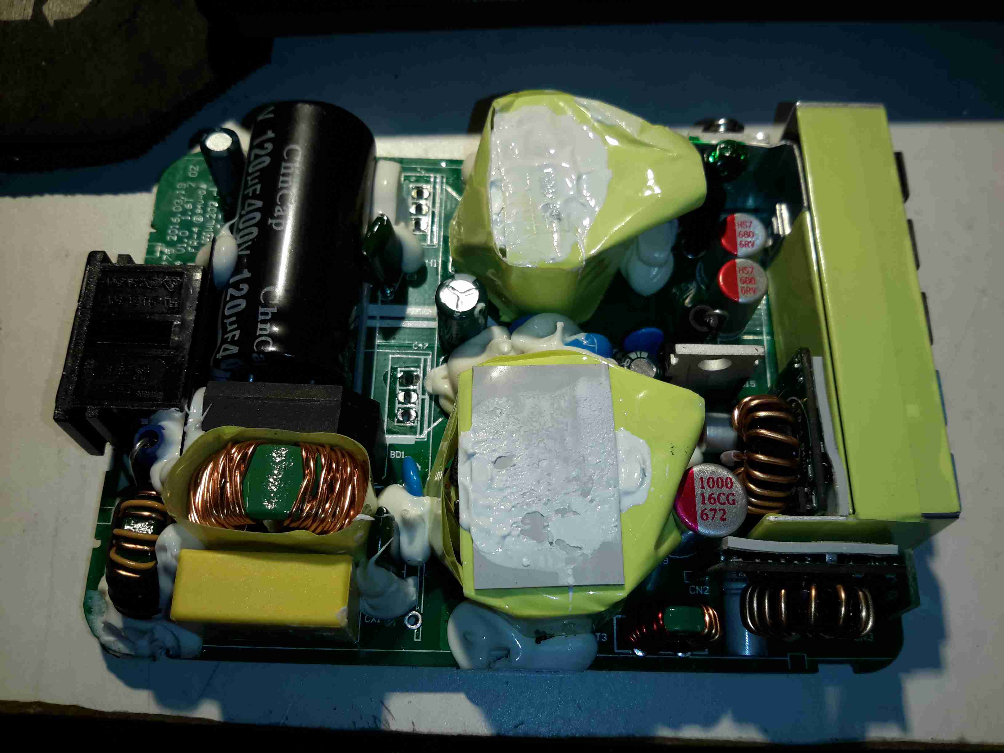
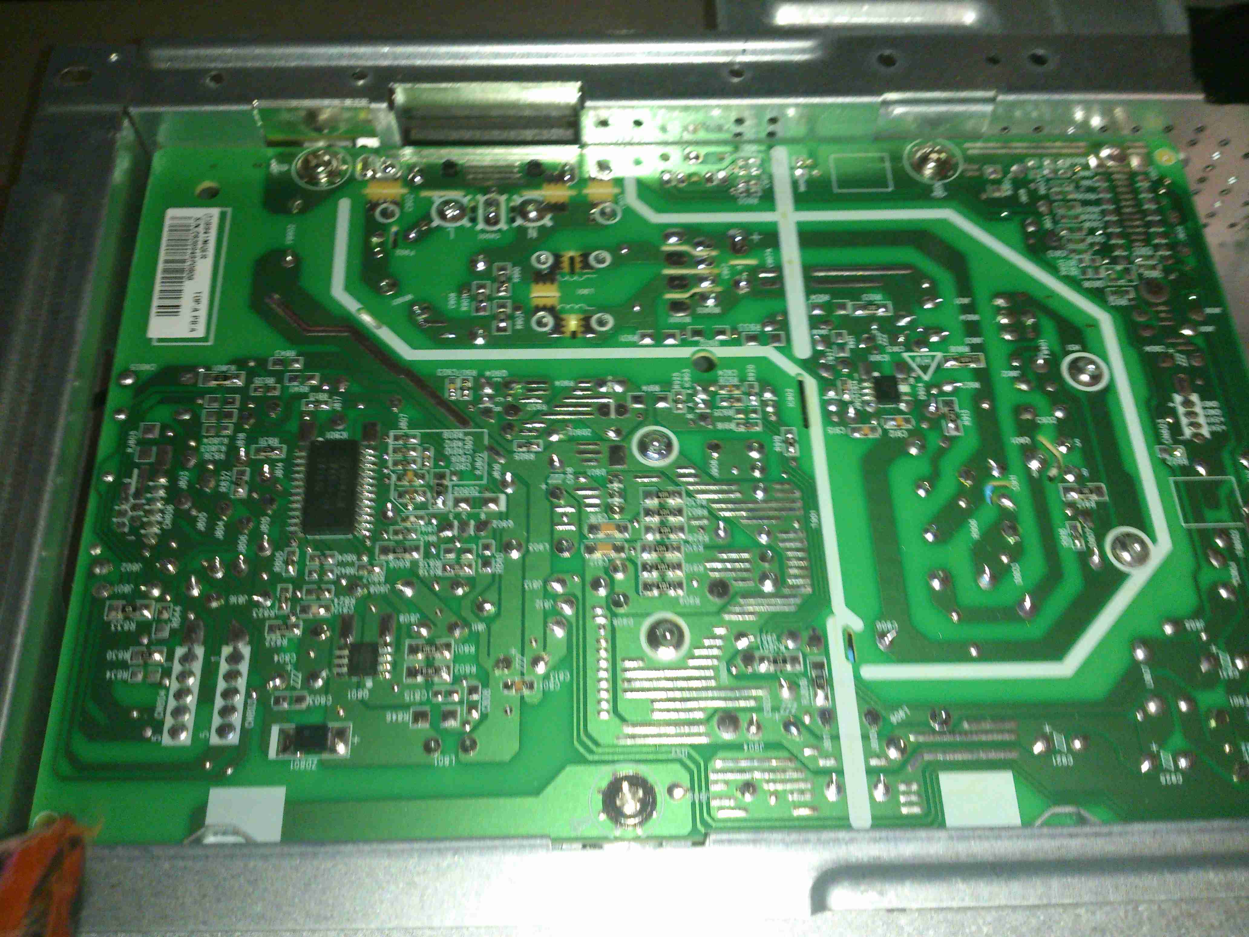
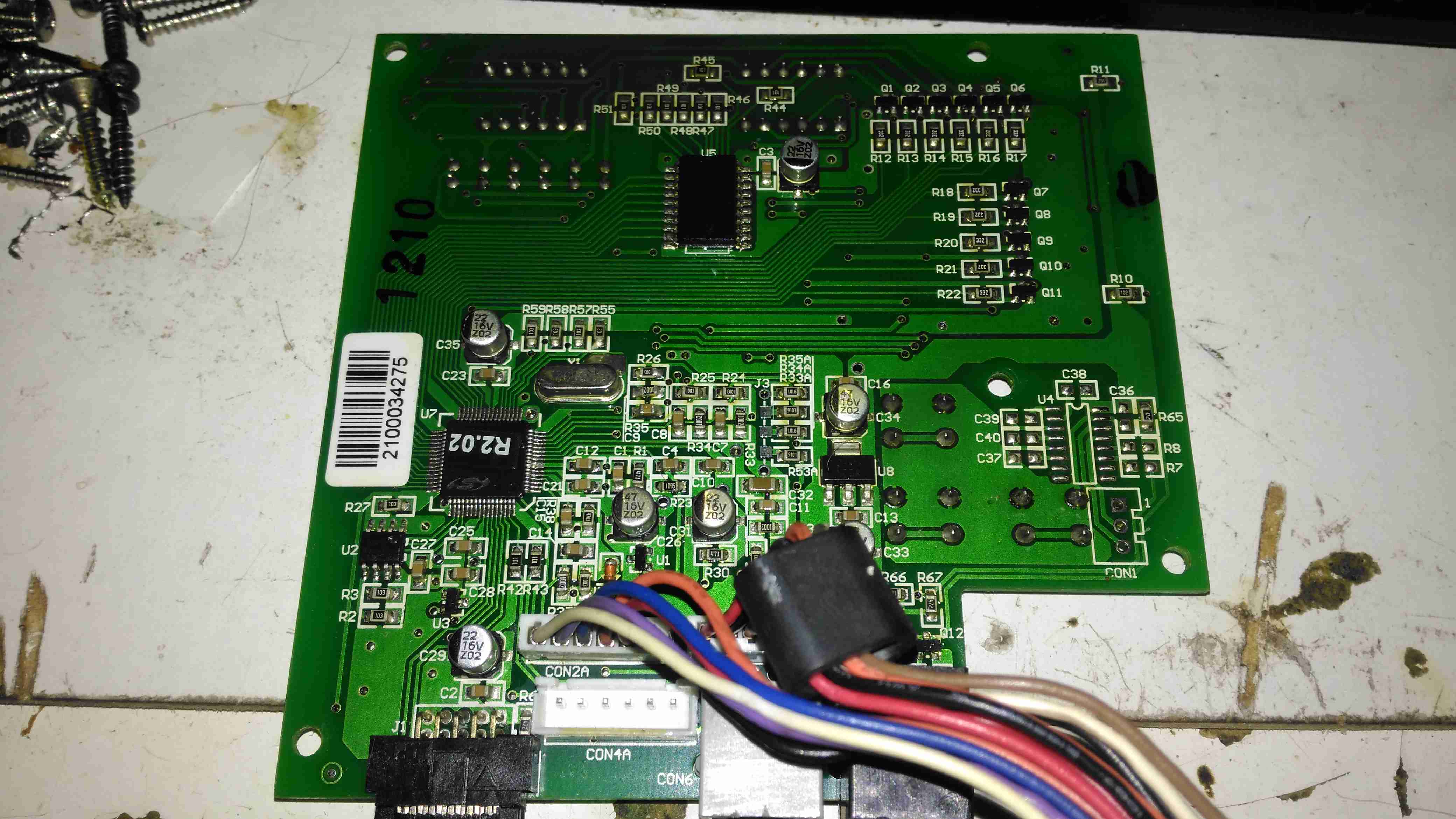
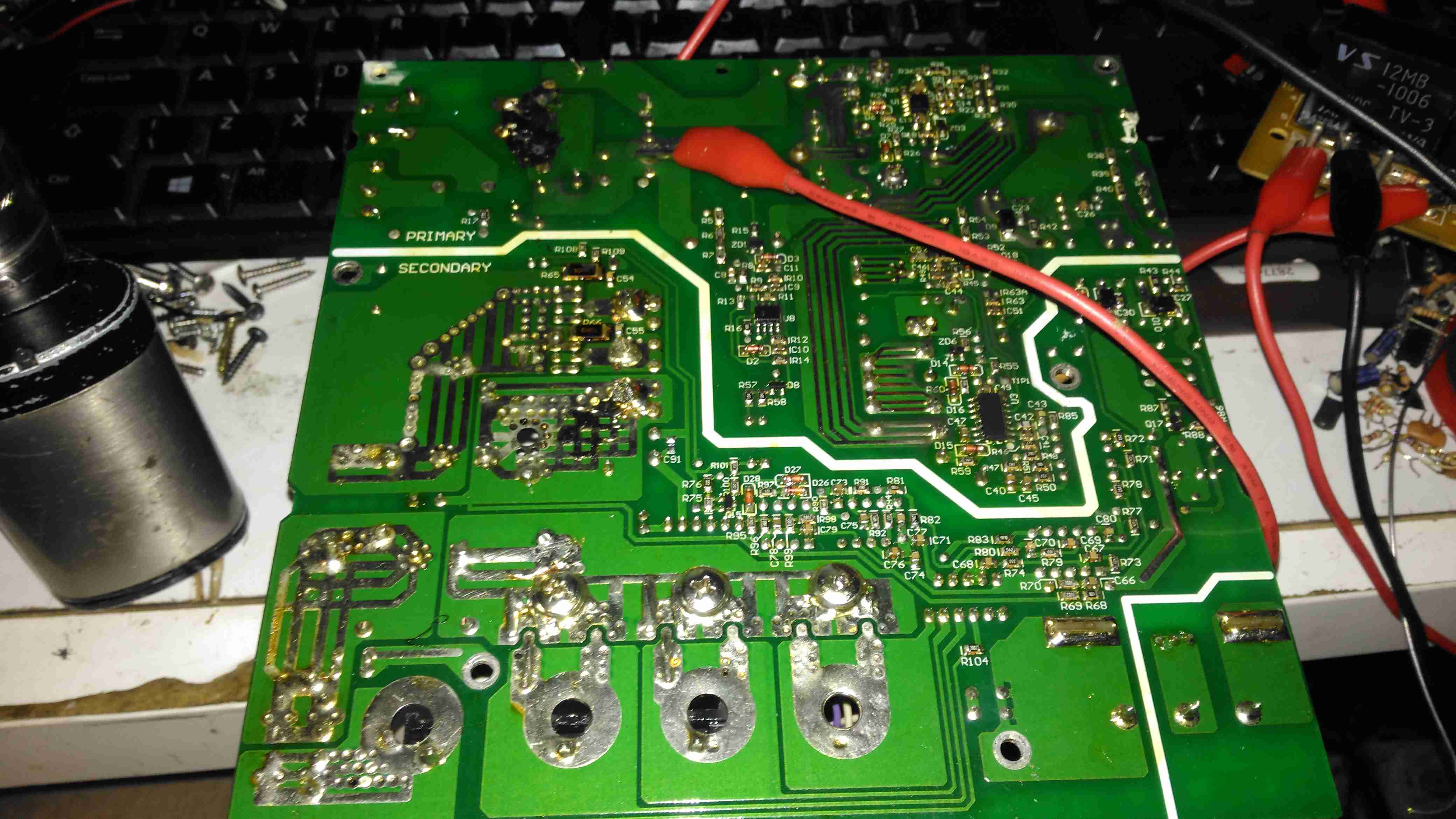
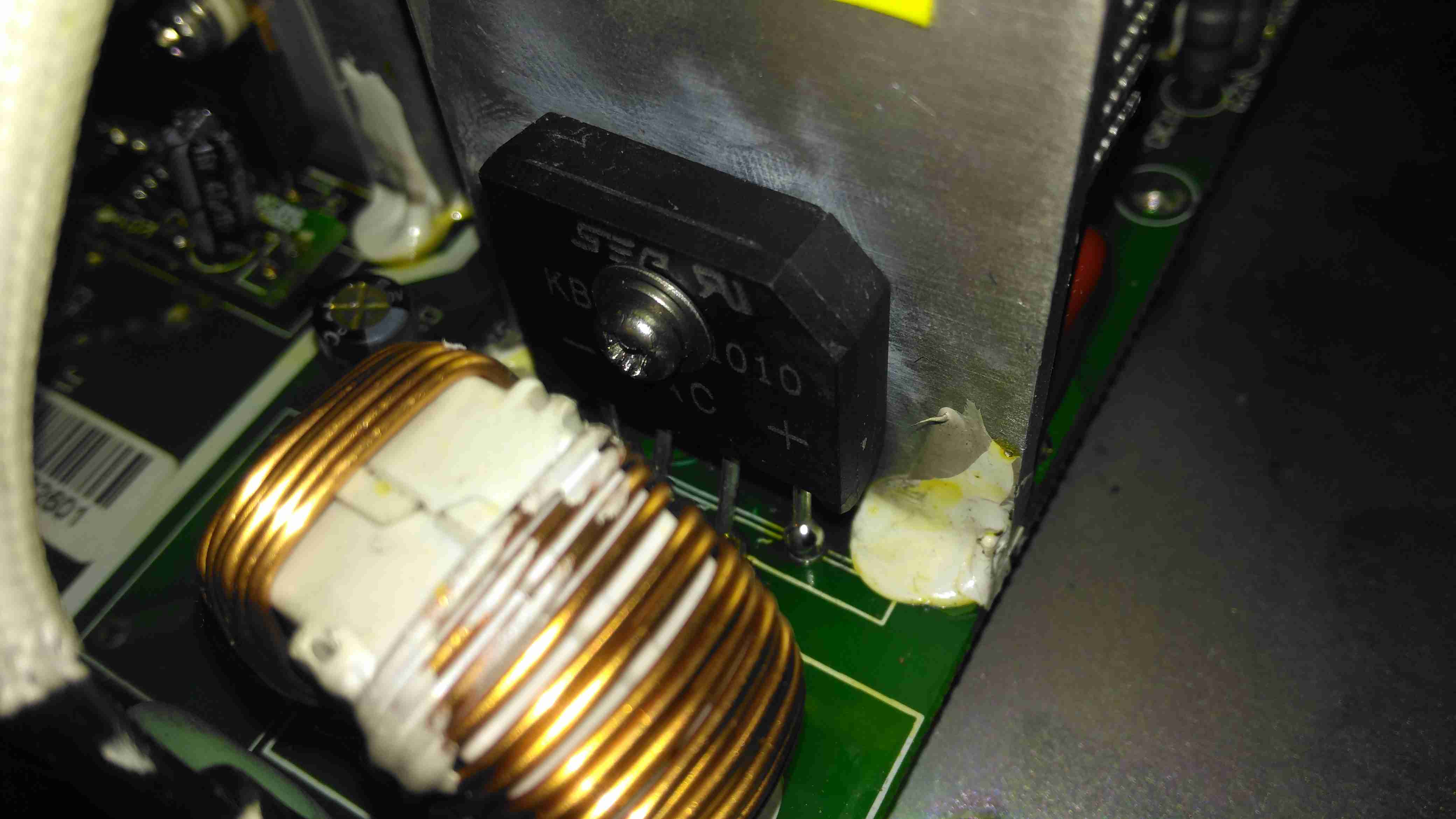
There’s the usual mains input filtering on the left, with the bridge rectifier on it’s heatsink.
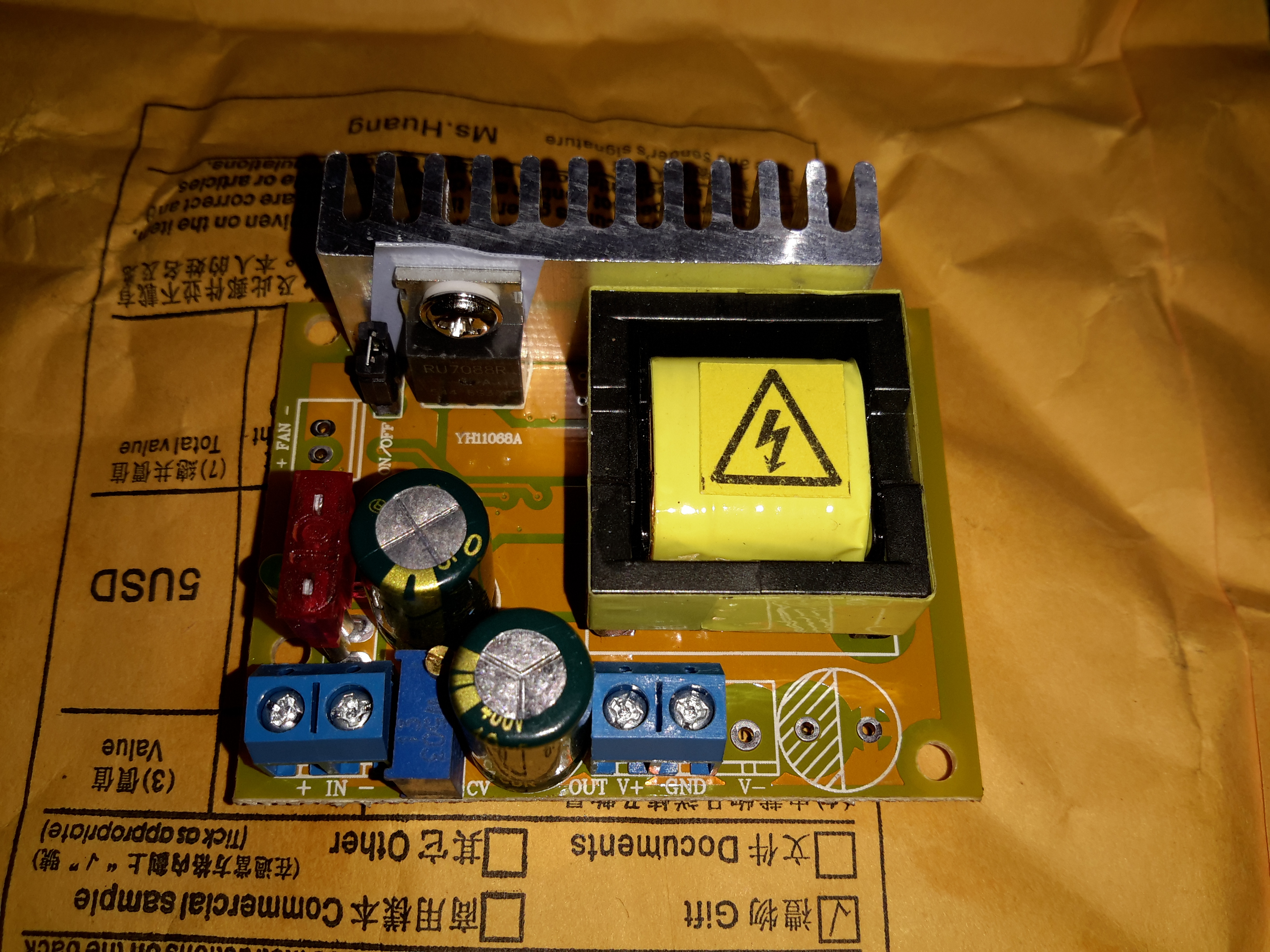
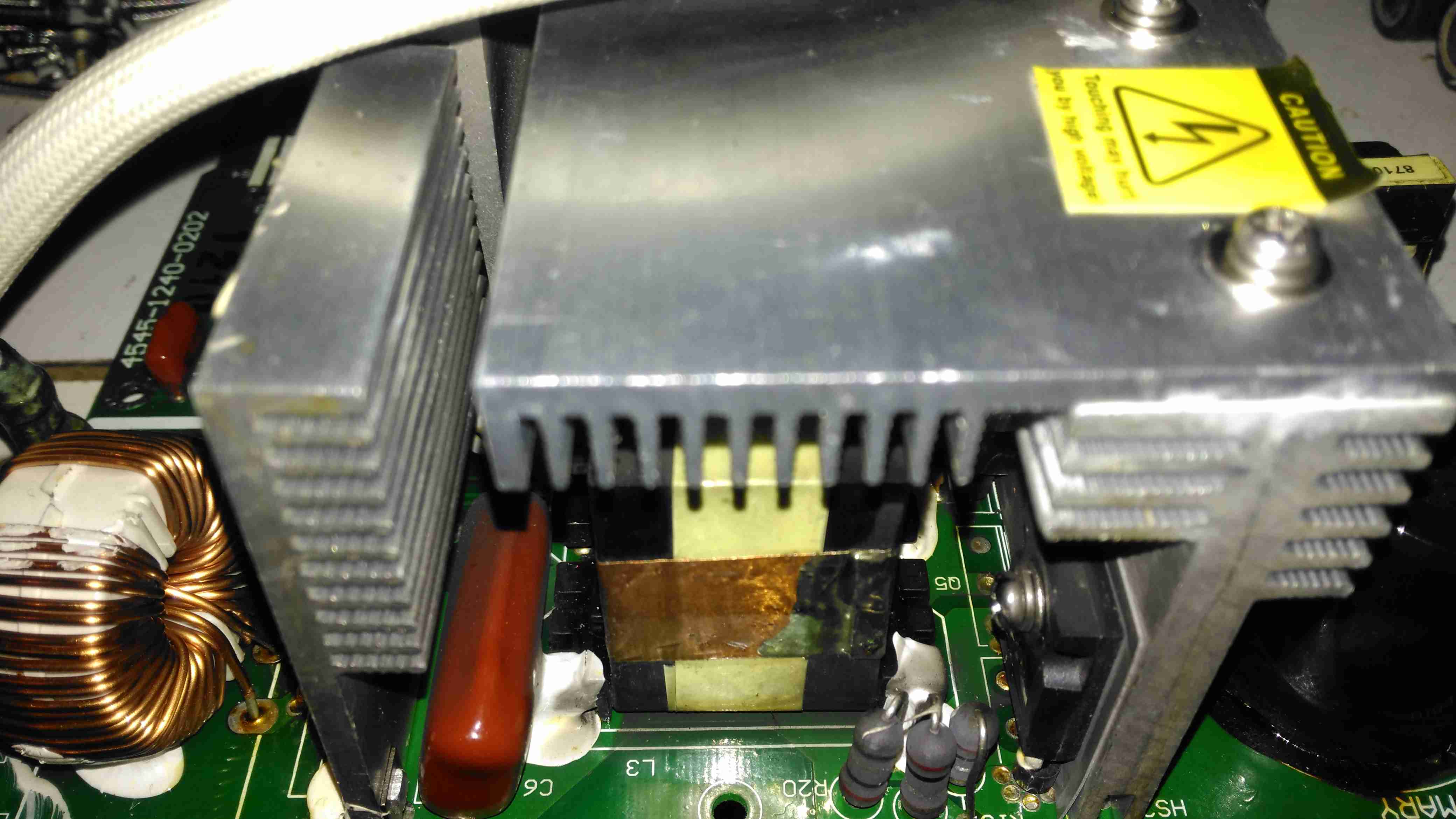
Underneath the centre massive heatsinks is the main transformer (not visible here) & active PFC circuit. The device peeking out from underneath is the huge inductor needed for PFC. It’s associated switching MOSFET is to the right.

Logic PSU Section
Logic PSU Section

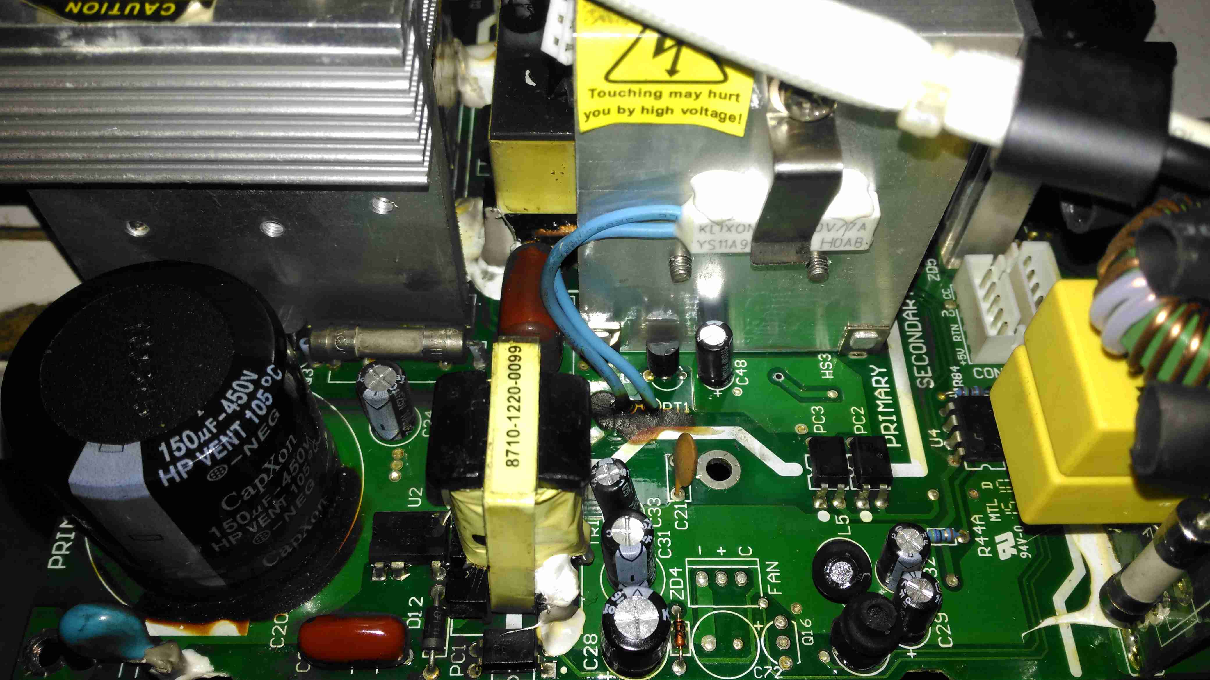
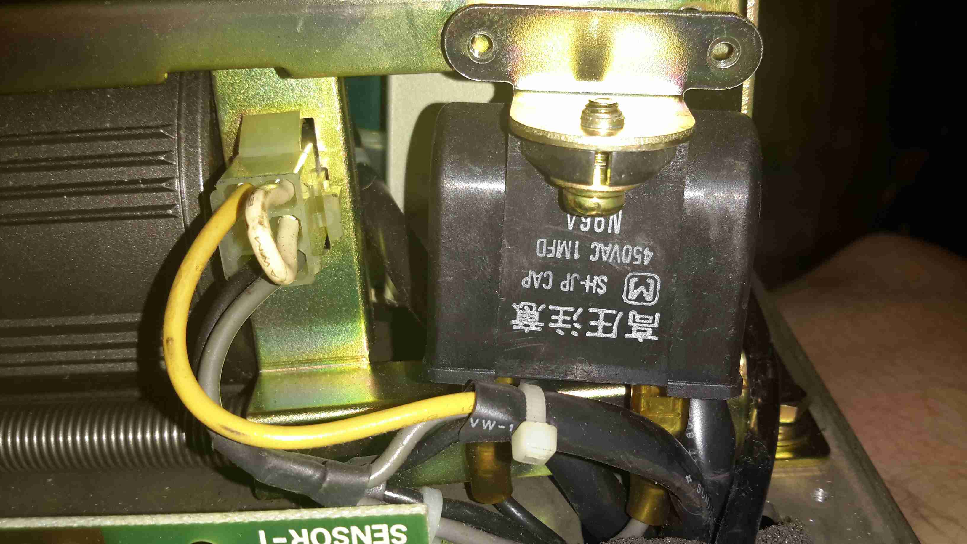
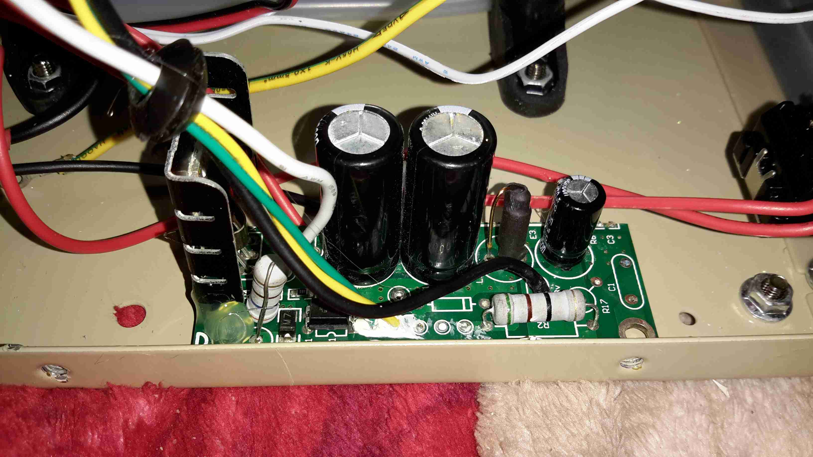
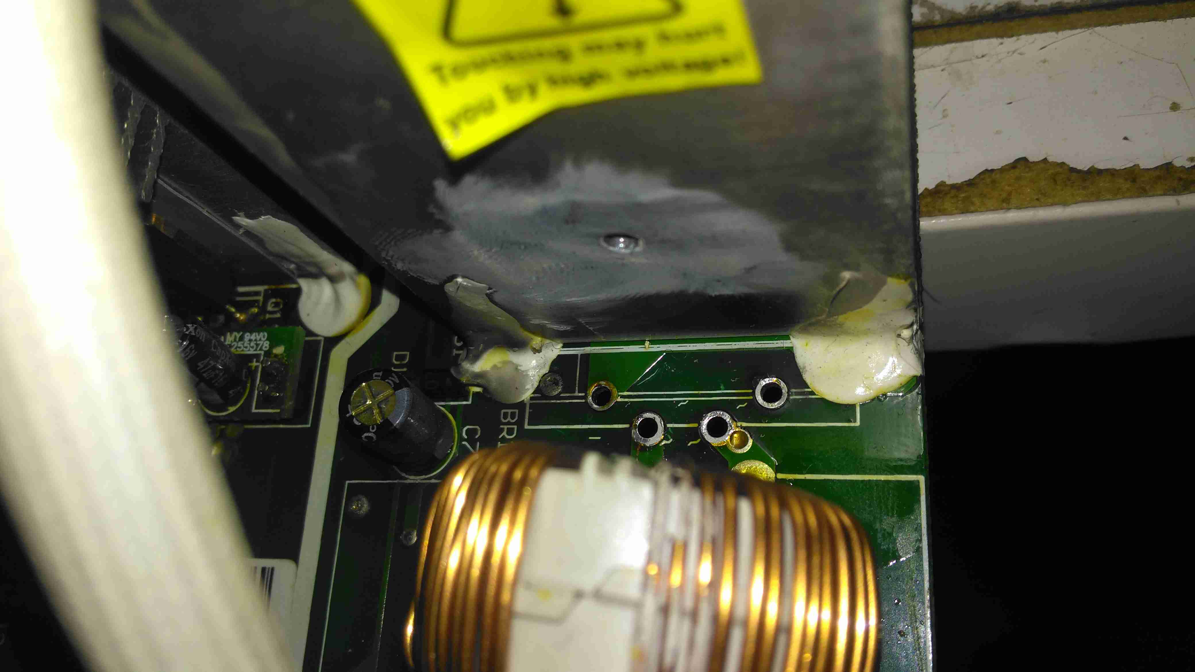
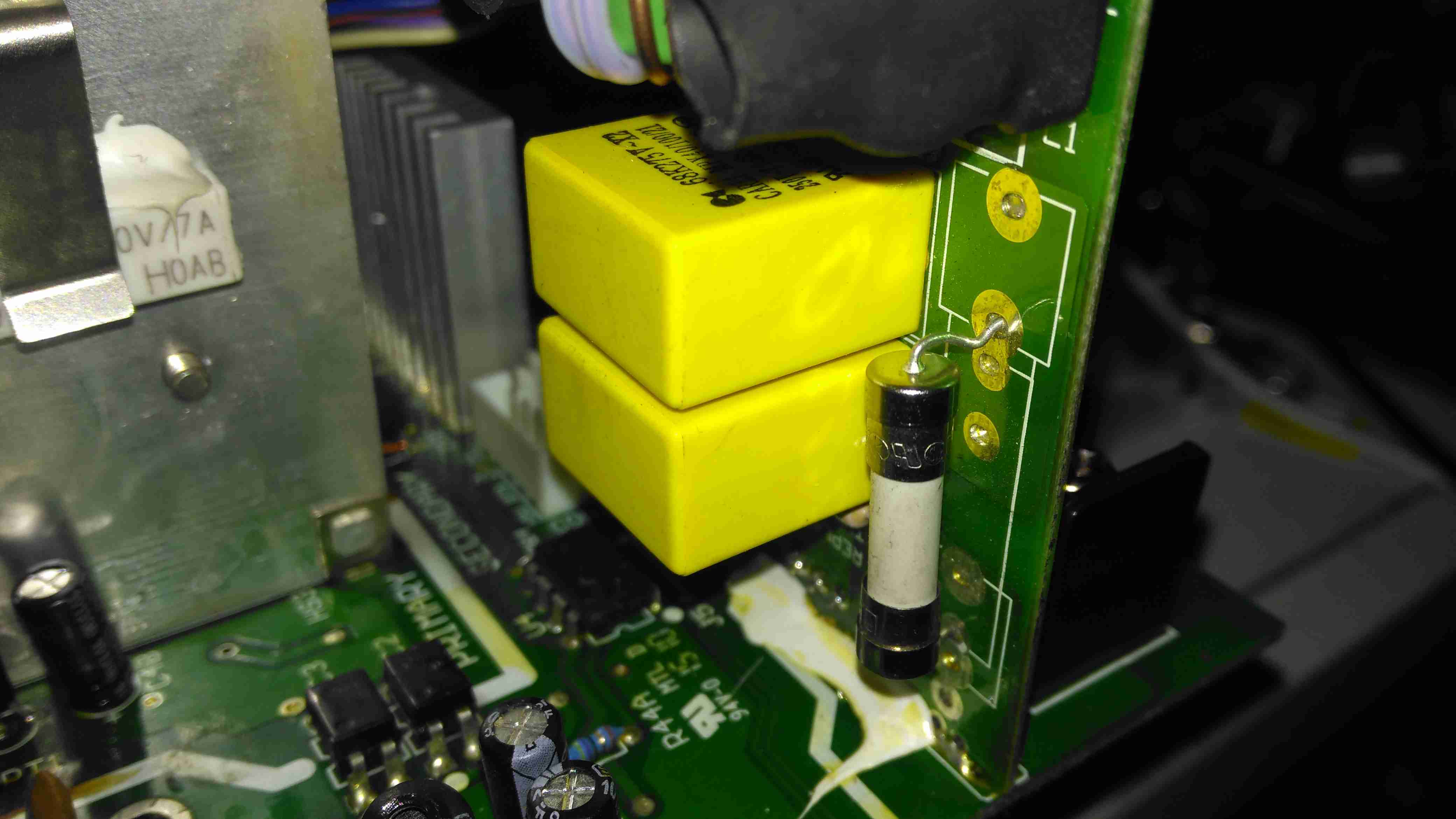
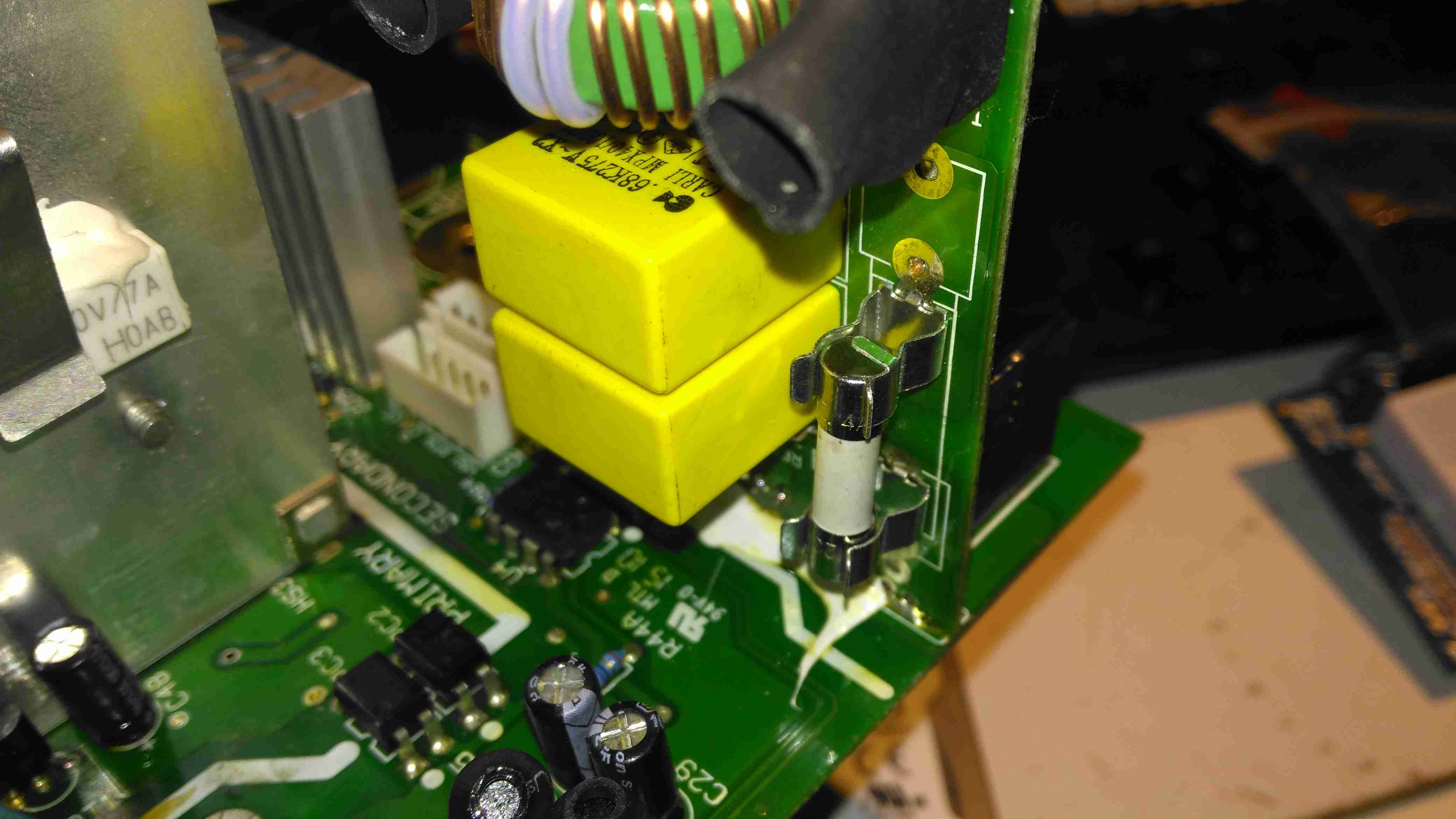
On the other side of the PFC section is the main DC rail filter electrolytic, a 450v 150µF part. Here some evidence of long-term heating can be seen in the adhesive around the base, it’s nearly completely turned black! It’s not a decent brand either, a Chinese CapXon.
The PCB fuse just behind it is in the DC feed to the main switching supply, so the input fuse only protects the filter & Active PFC circuitry. Luckily this fuse didn’t blow during the failure, telling me the fault was earlier in the power chain.
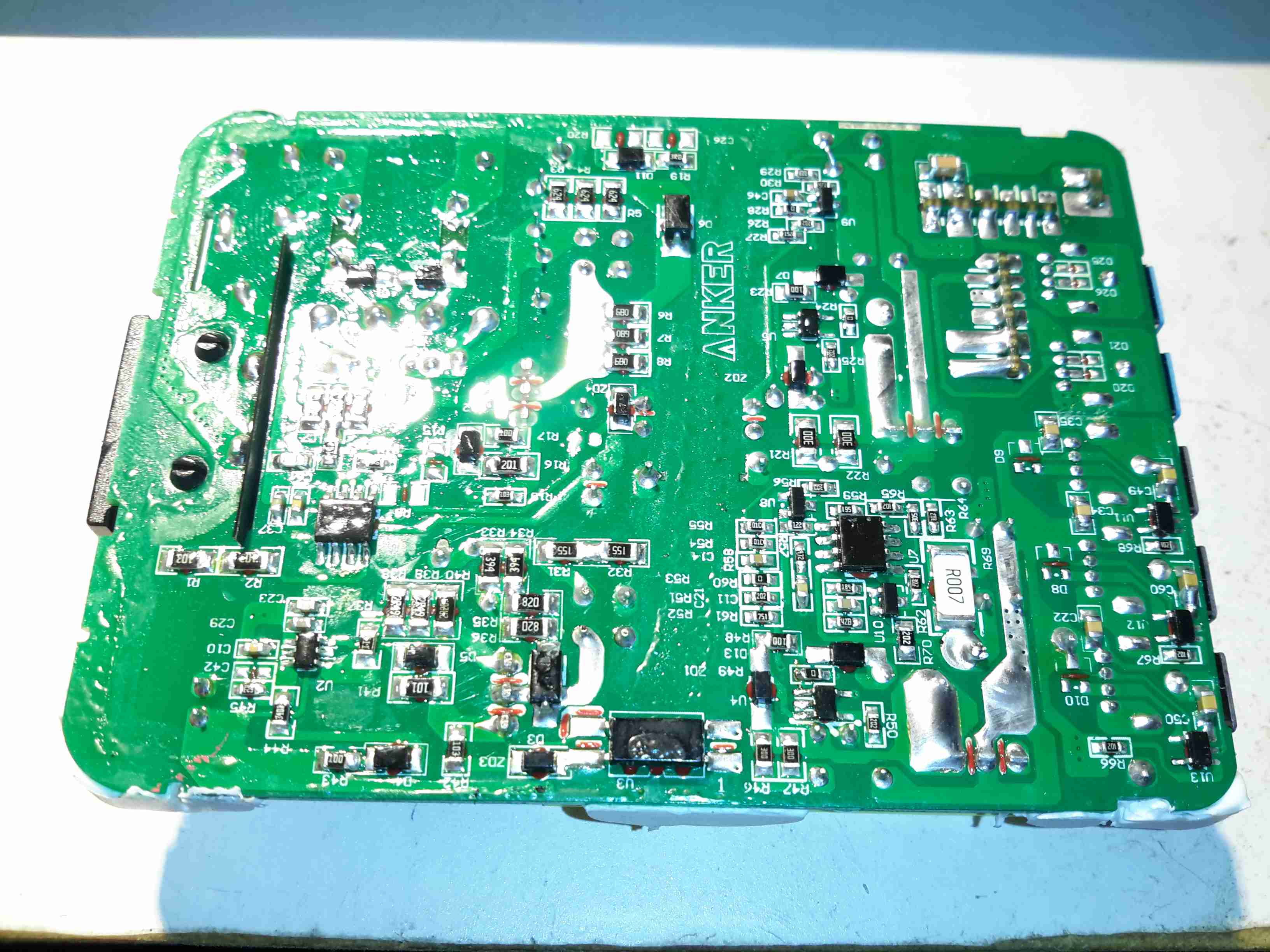
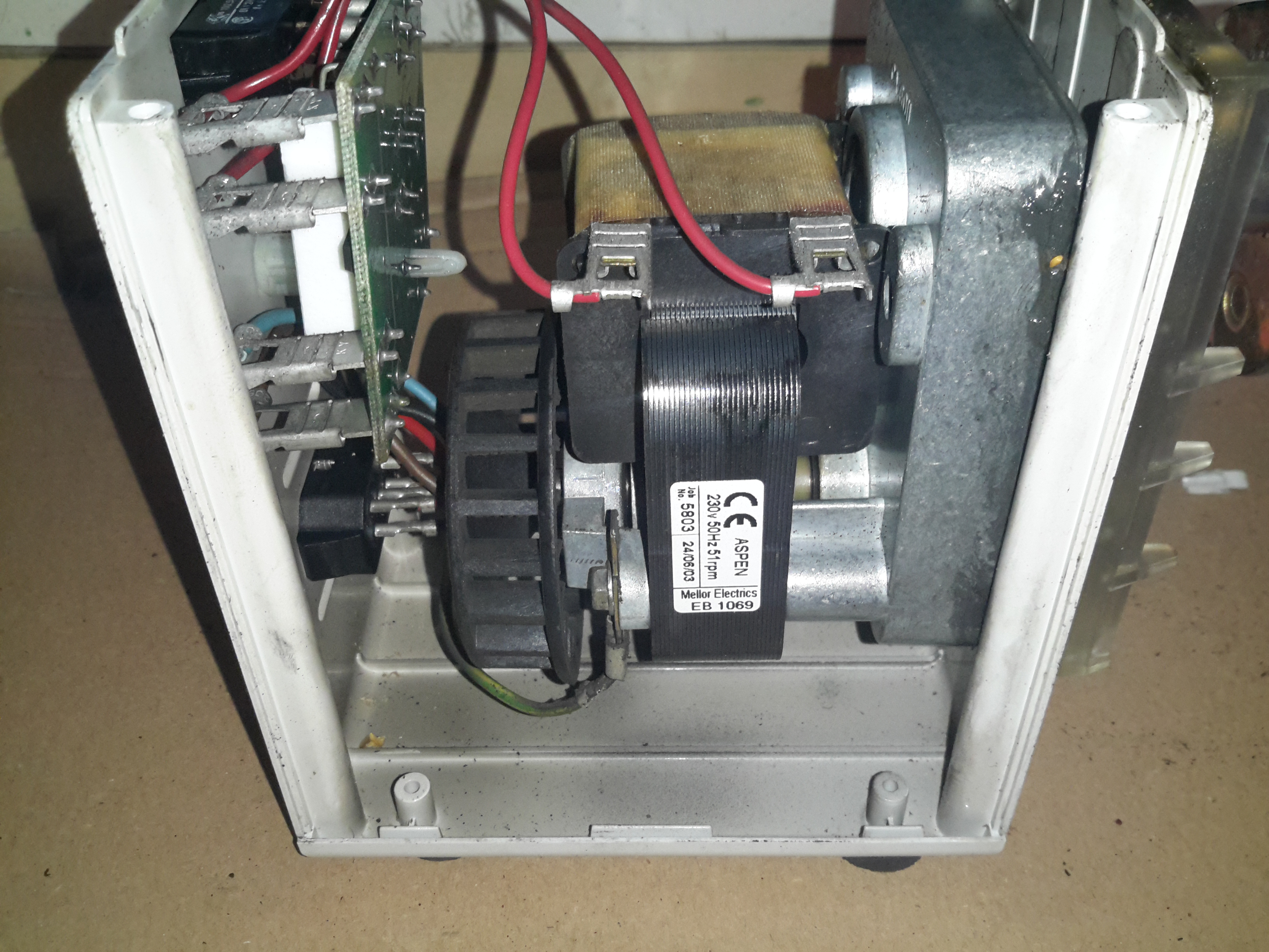
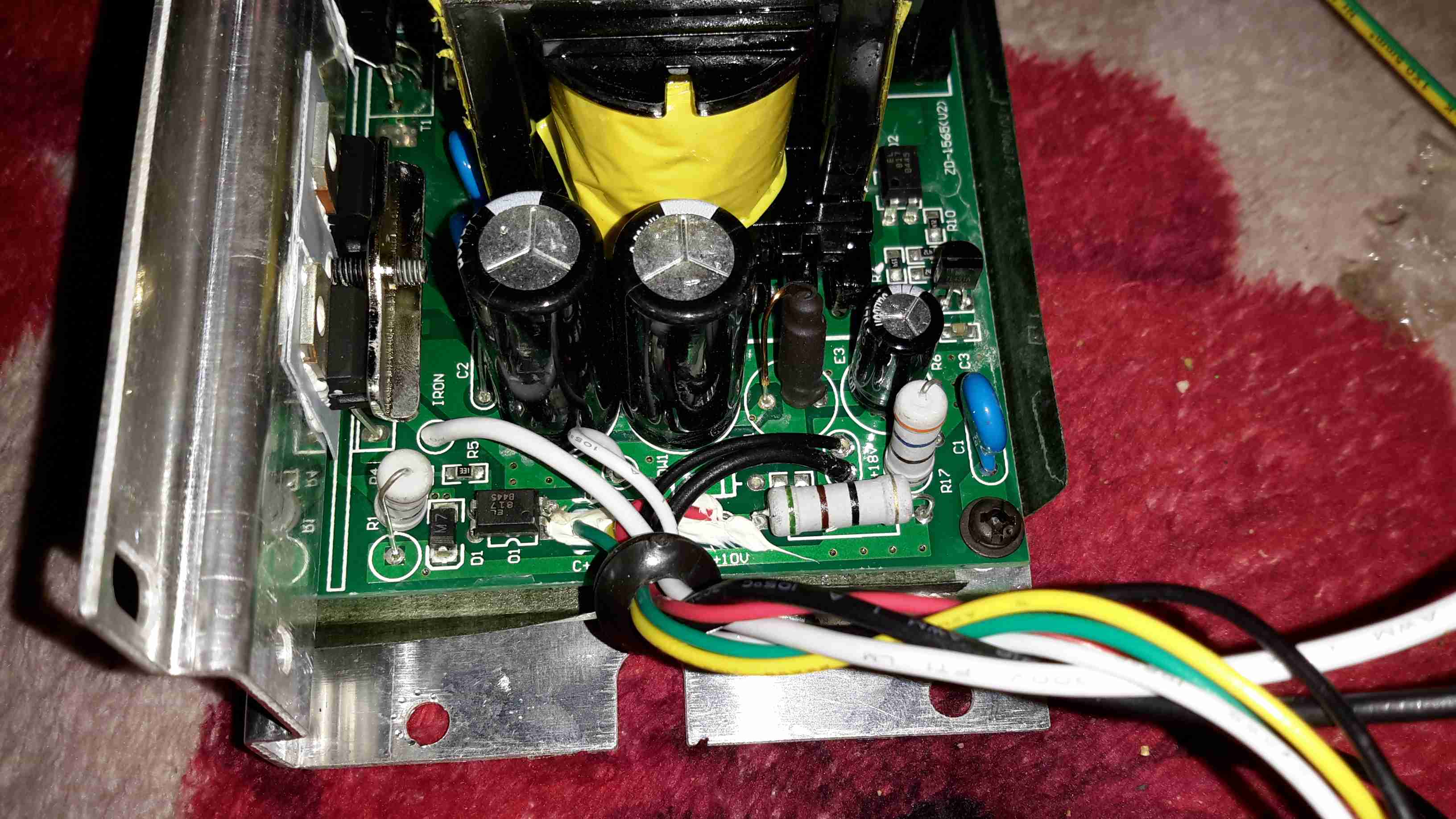
The logic circuits are powered by an independent switching supply in the centre, providing a +5v rail to the microcontroller. The fan header & control components are not populated in this 10A model, but I may end up retrofitting a fan anyway as this unit has always run a little too warm. The entire board is heavily conformal coated on both sides, to help with water resistance associated with being in a marine environment. This has worked well, as there isn’t a single trace of moisture anywhere, only dust from years of use.
There is some thermal protection for the main SMPS switching MOSFETS with the Klixon thermal fuse clipped to the heatsink.

DC Output Section
DC Output Section

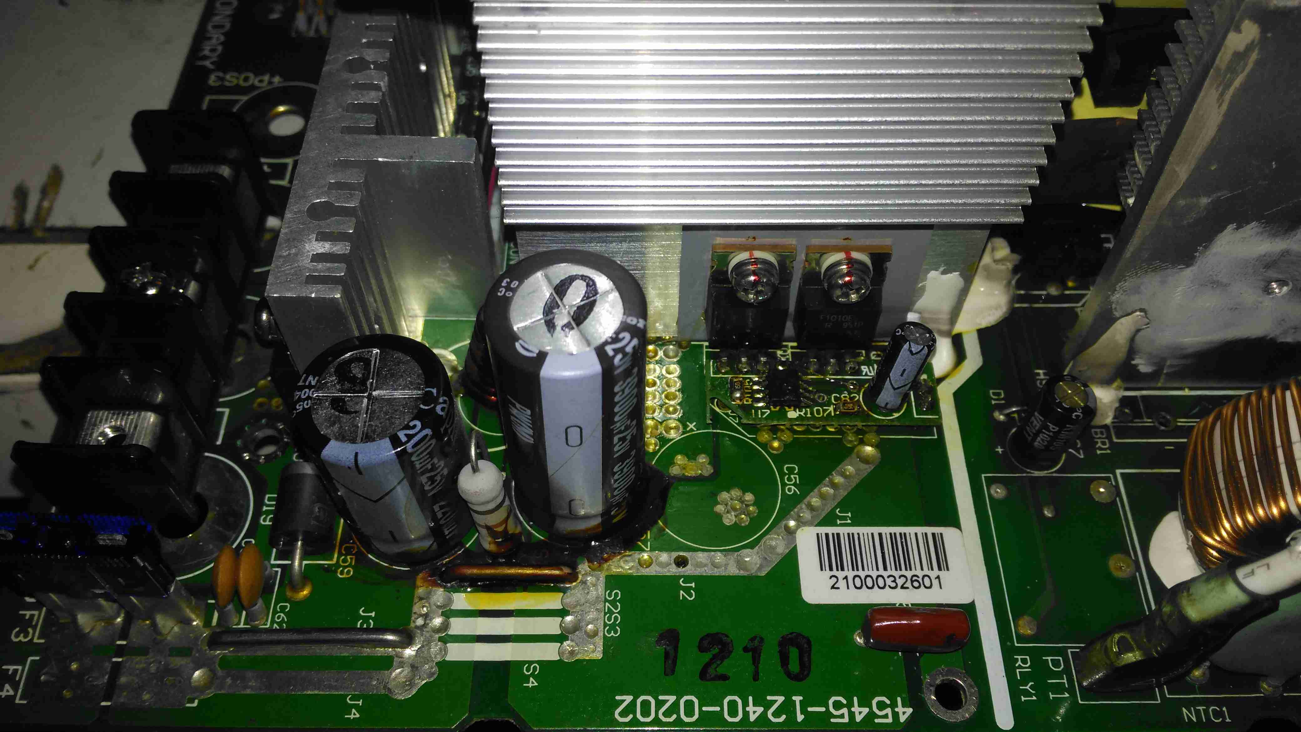
The DC output rectifiers are on the large heatsink in the centre, with a small bodge board fitted. Due to the heavy conformal coating on the board I can’t get the ID from this small 8-pin IC, but from the fact that the output rectifiers are in fact IRF1010E MOSFETS, rated at 84A a piece, this is an synchronous rectifier controller.
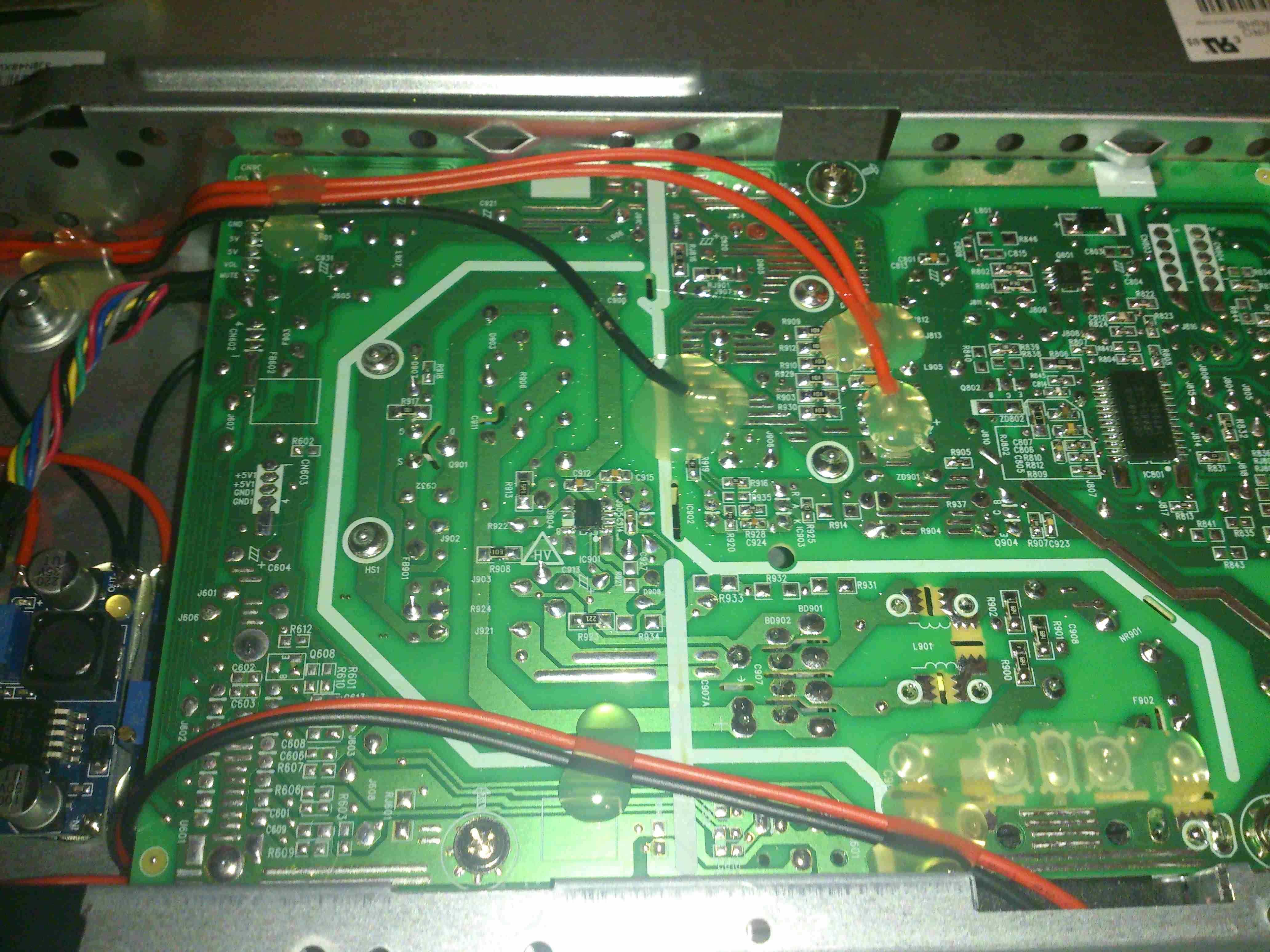
Oddly, the output filter electrolytics are a mix of Nichicon (nice), and CapXon (shite). A bit of penny pinching here, which if a little naff since these chargers are anything but cheap. (£244.80 at the time of writing).
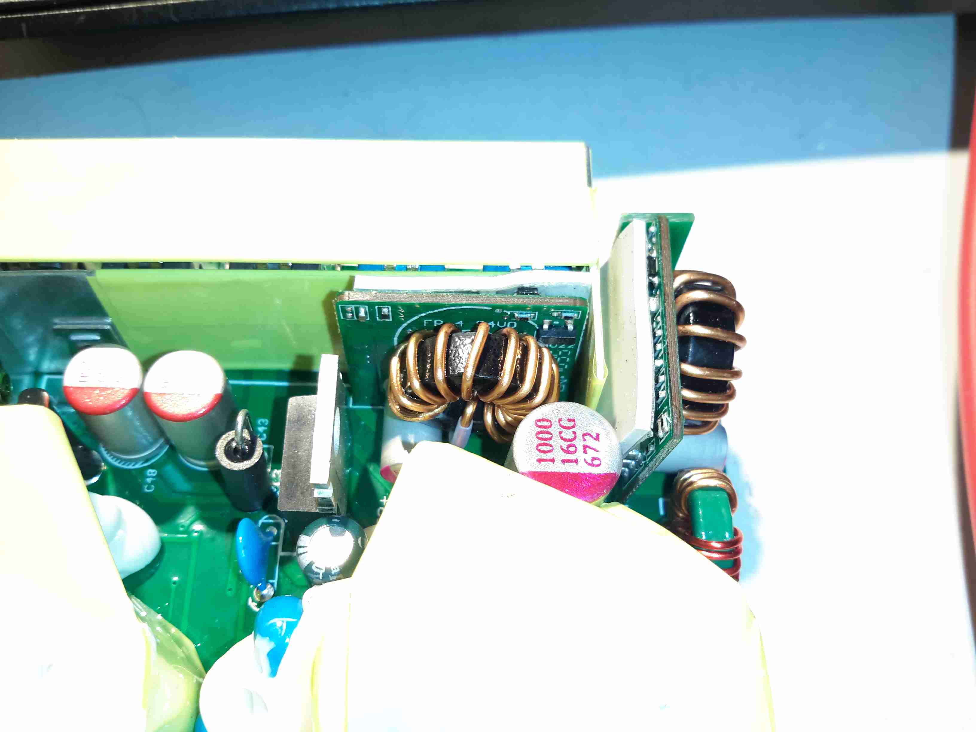
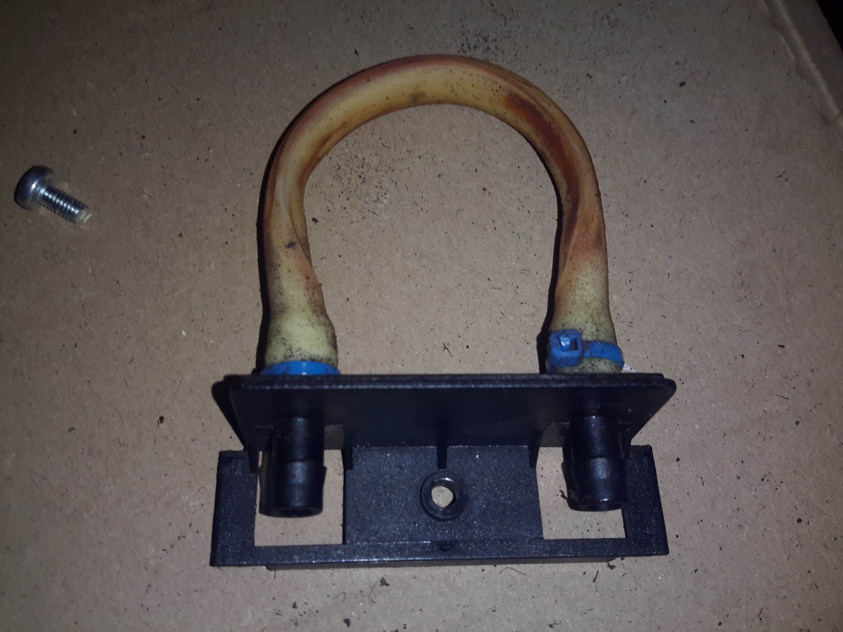
Hiding just behind the electrolytics is a large choke, and a reverse-polarity protection diode, which is wired crowbar-style. Reversing the polarity here will blow the 15A DC bus fuse instantly, and may destroy this diode if it doesn’t blow quick enough.

DC Outputs
DC Outputs

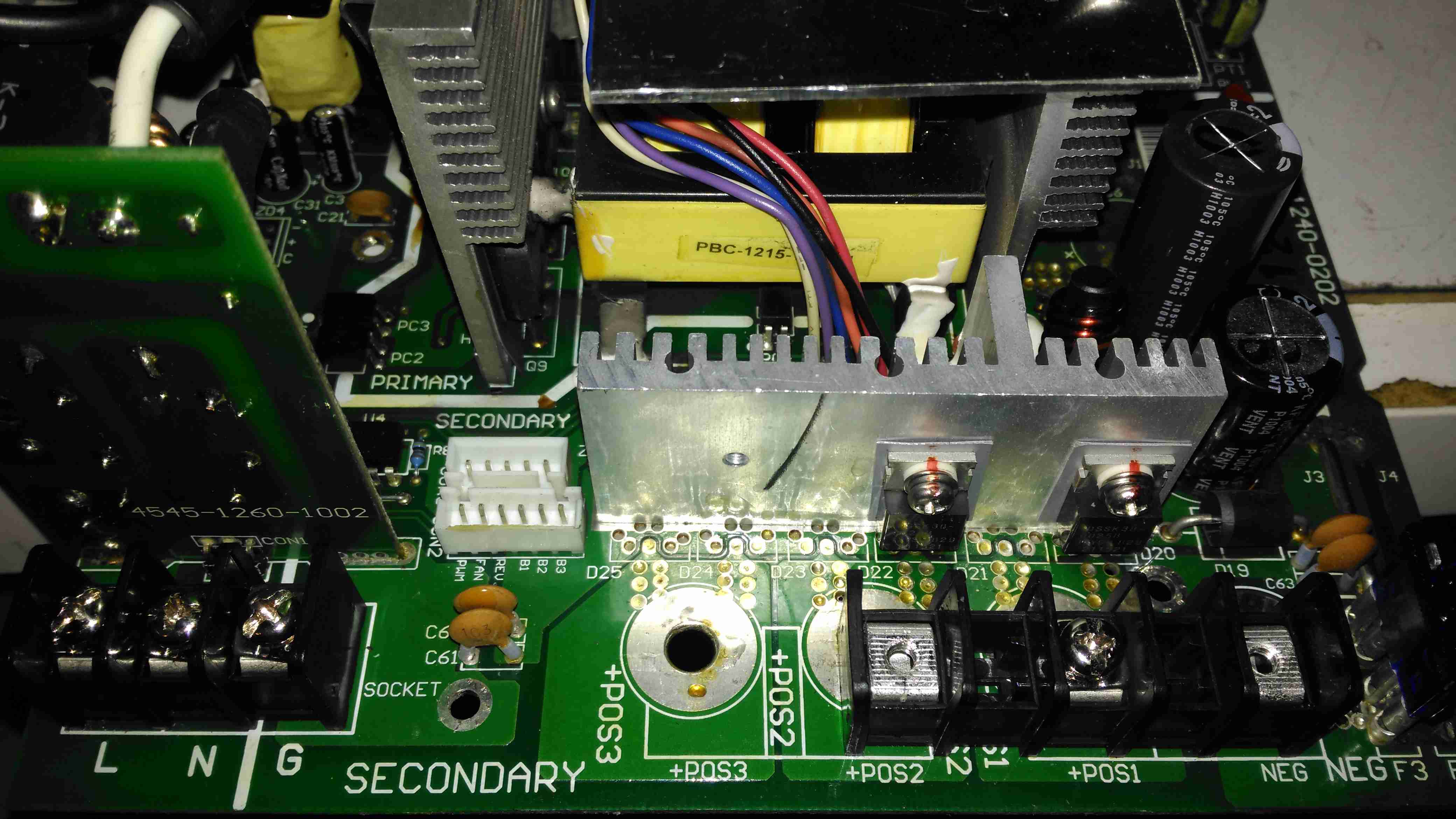
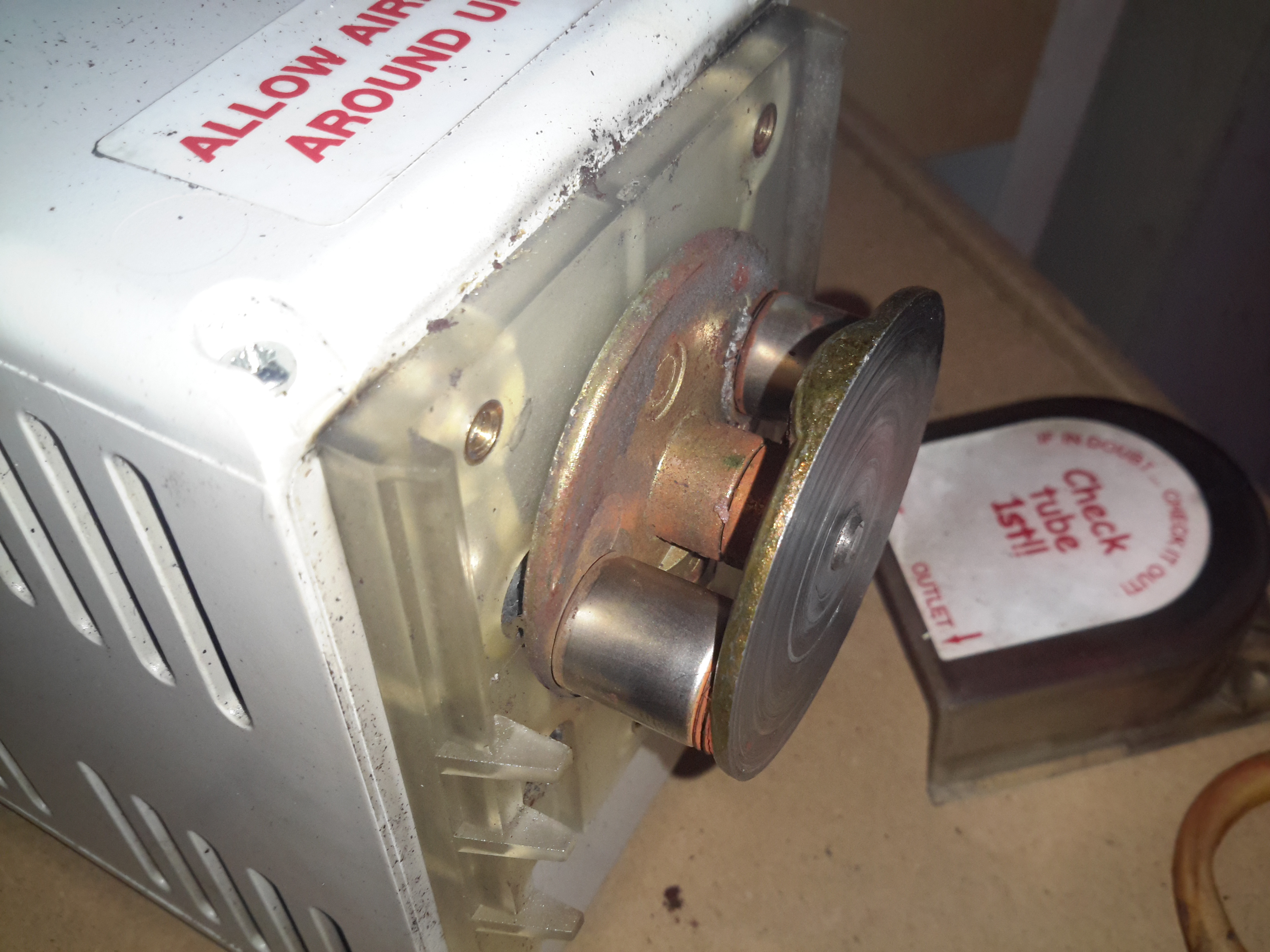
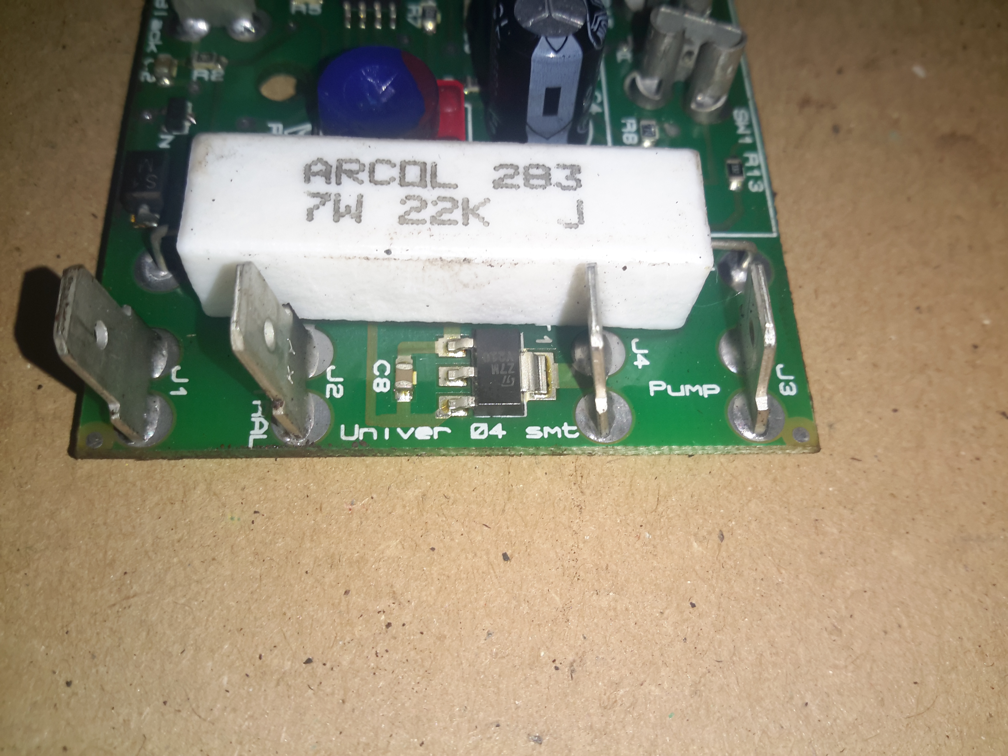
Right on the output end are a pair of large Ixys DSSK38 TO220 Dual 20A dual Schottky diodes, isolating the two outputs from each other, a nice margin on these for a 10A charger, since the diodes are paralleled each channel is capable of 40A. This prevents one bank discharging into another & allows the charger logic to monitor the voltages individually. The only issue here is the 400mV drop of these diodes introduce a little bit of inefficiency. To increase current capacity of the PCB, the aluminium heatsink is being used as the main positive busbar. From the sizing of the power components here, I would think that the same PCB & component load is used for all the chargers up to 40A, since both the PFC inductor & main power transformer are massive for a 10A output. There are unpopulated output components on this low-end model, to reduce the cost since they aren’t needed.

Front Panel Control Connections

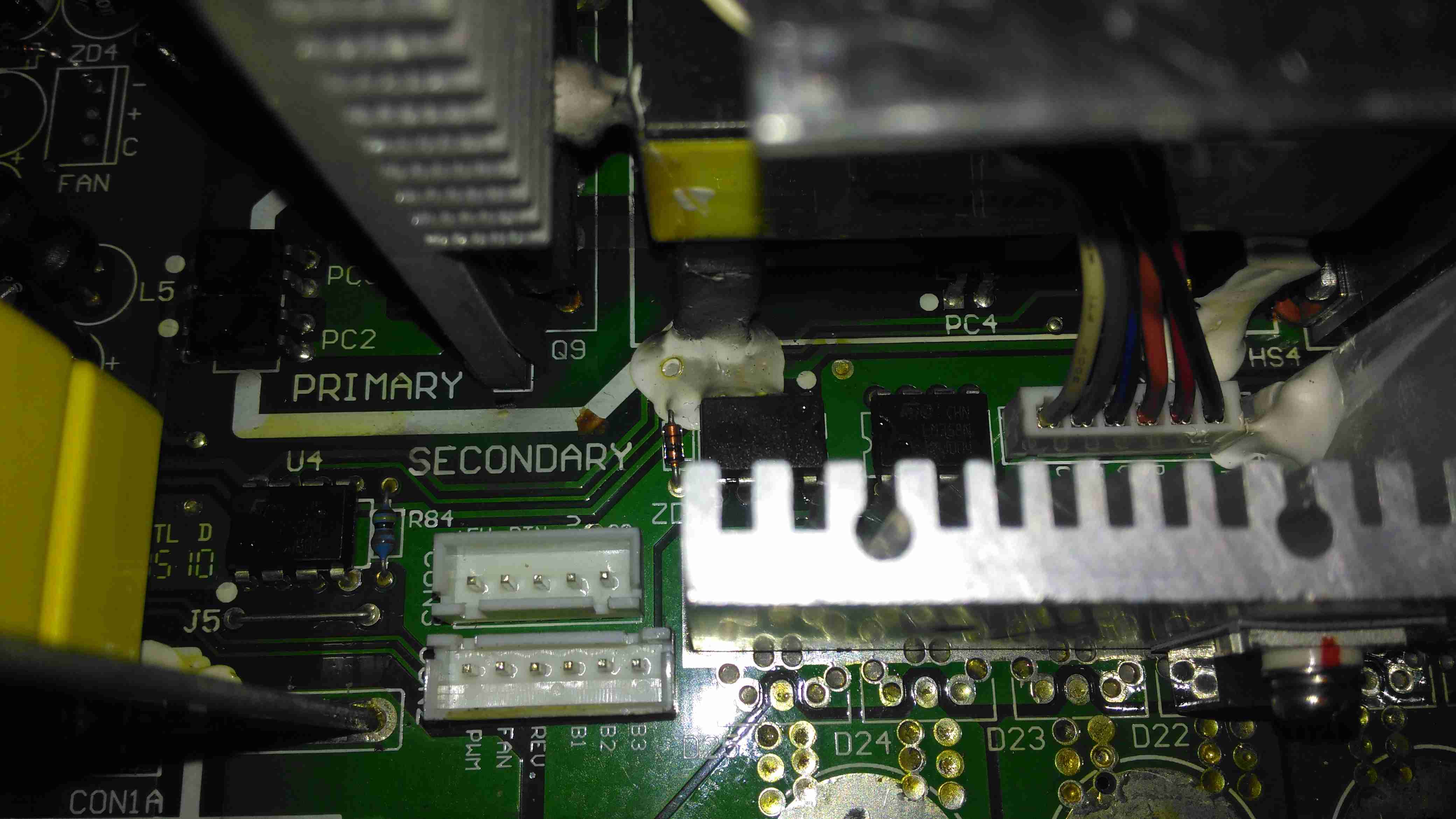
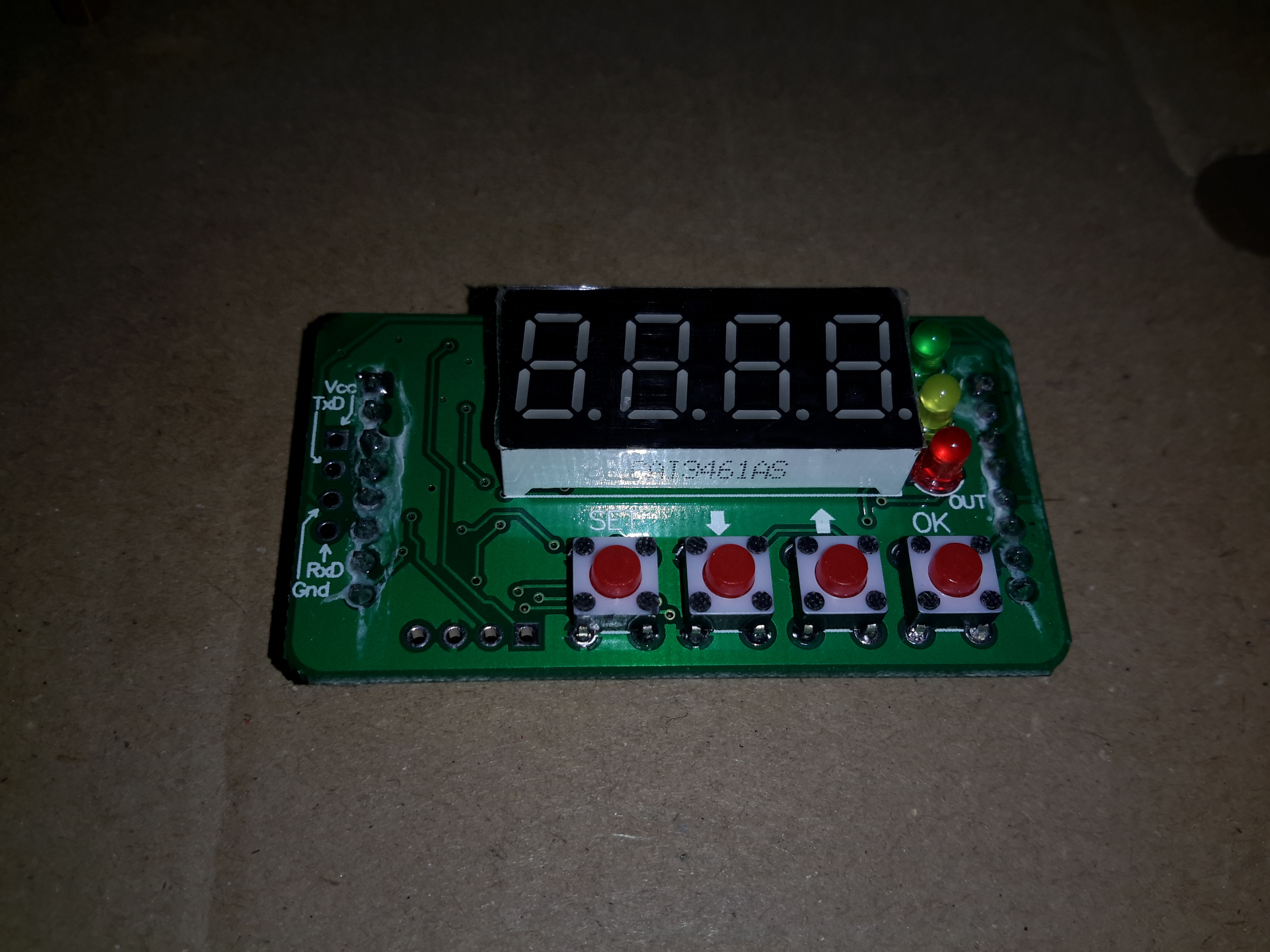
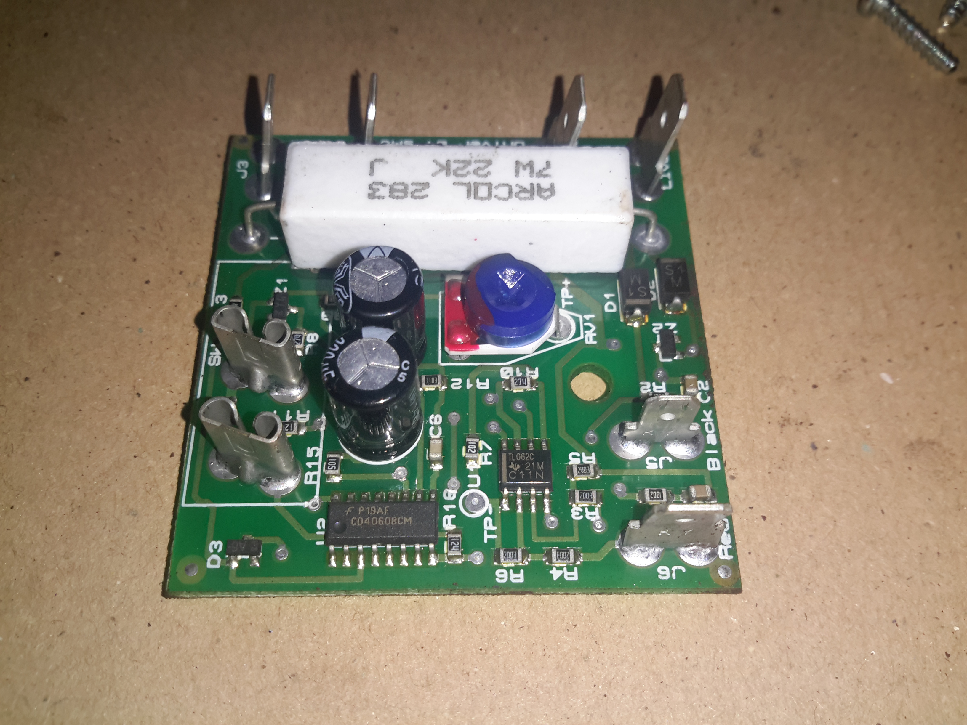
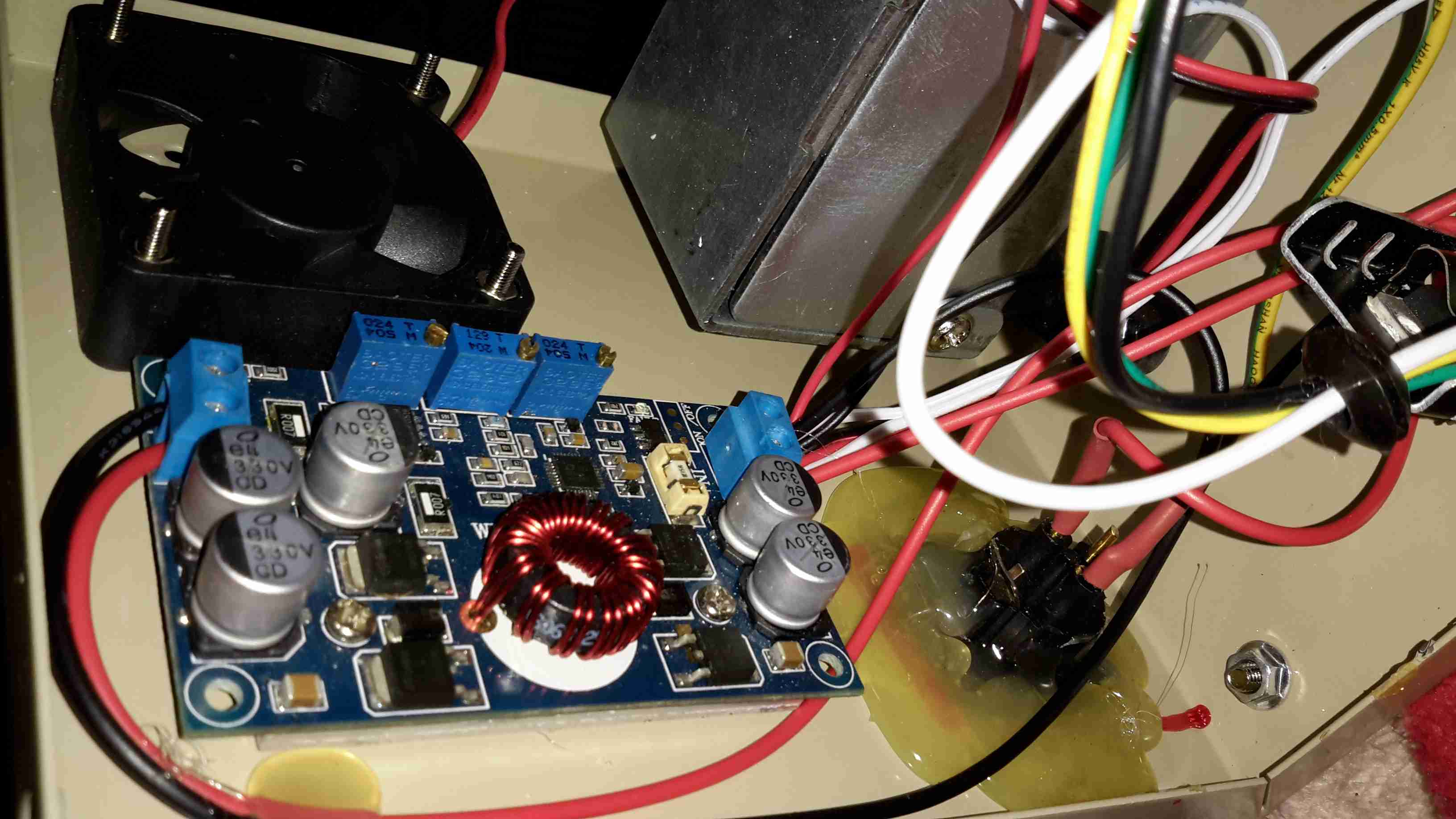
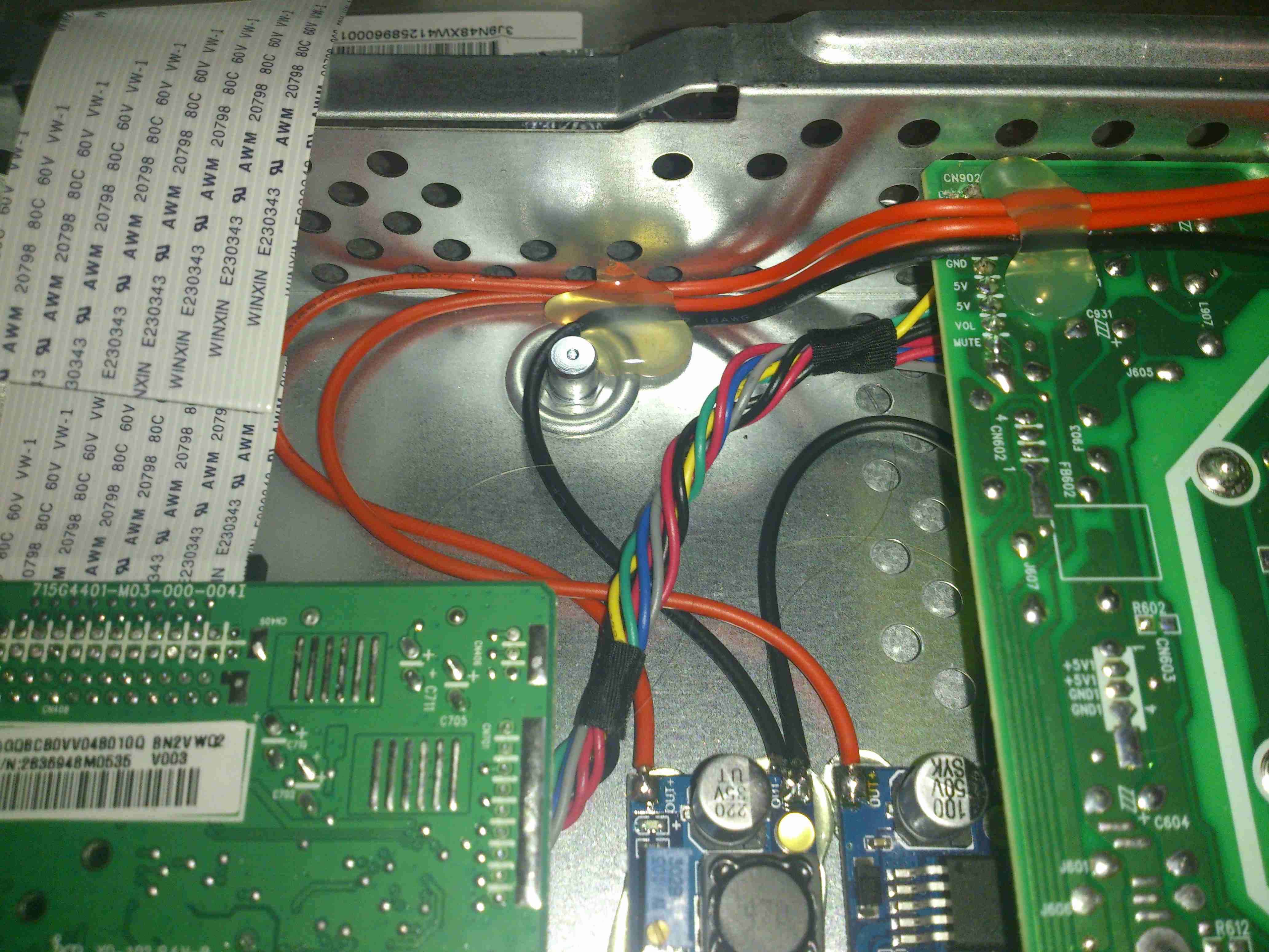
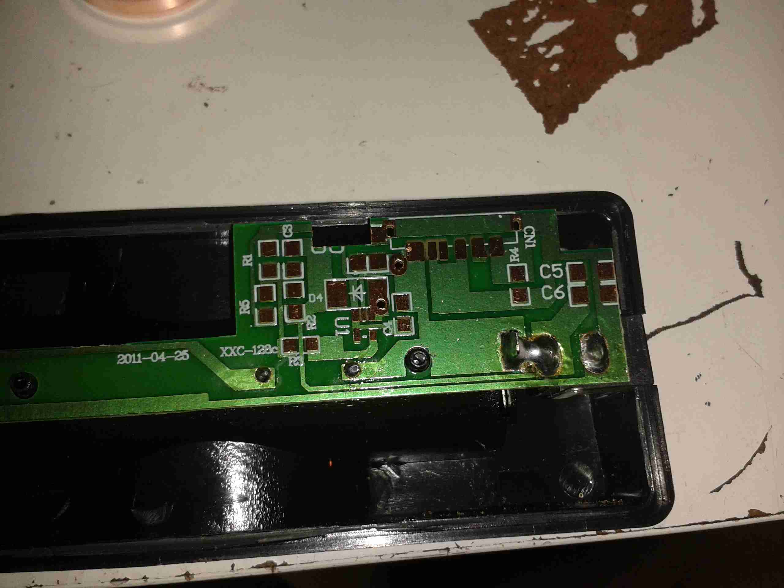
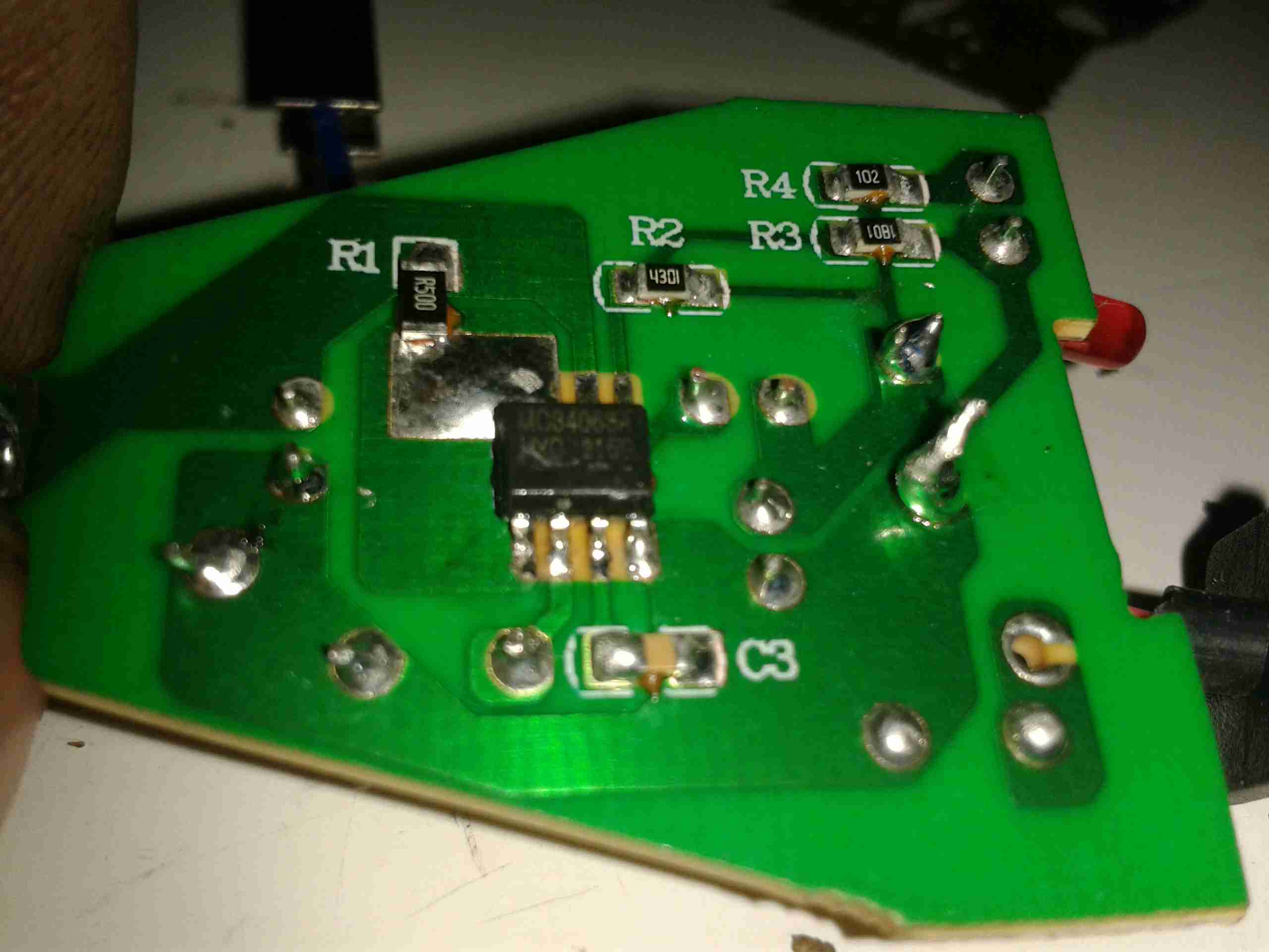
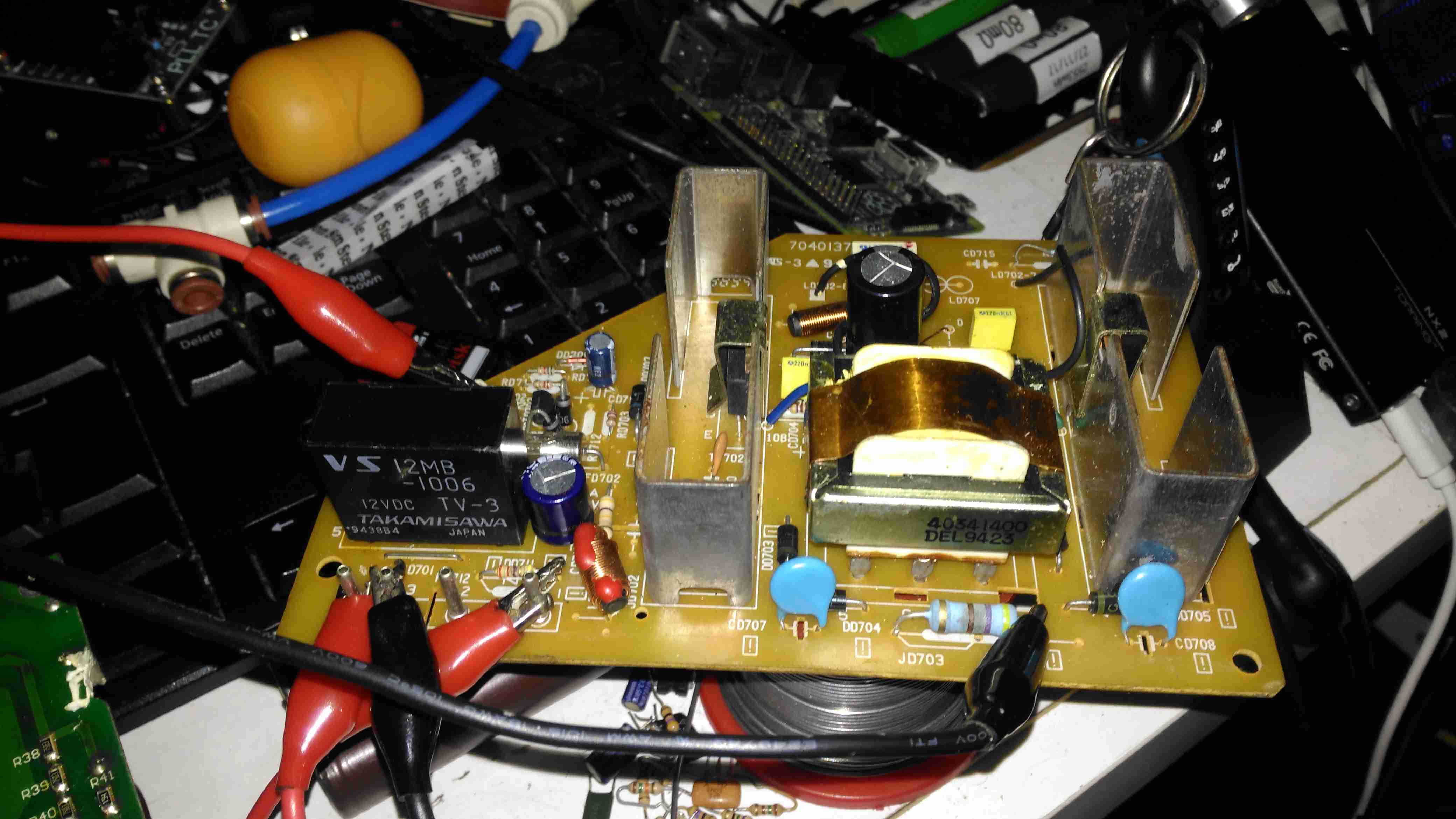
A trio of headers connect all the control & sense signals to the front panel PCB, which contains all the control logic. This unit is sensing all output voltages, output current & PSU rail voltages.

Front Panel LEDs
Front Panel LEDs

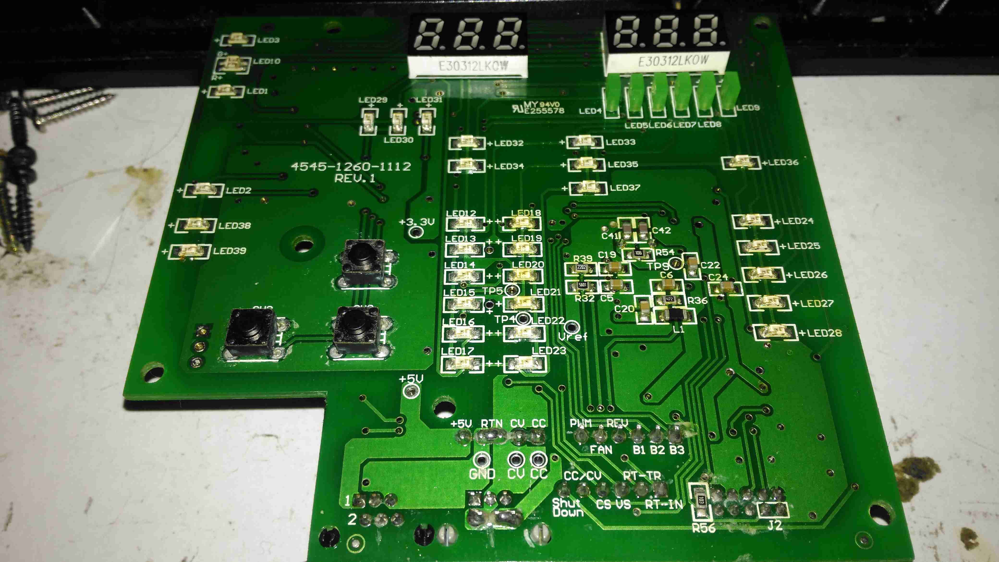
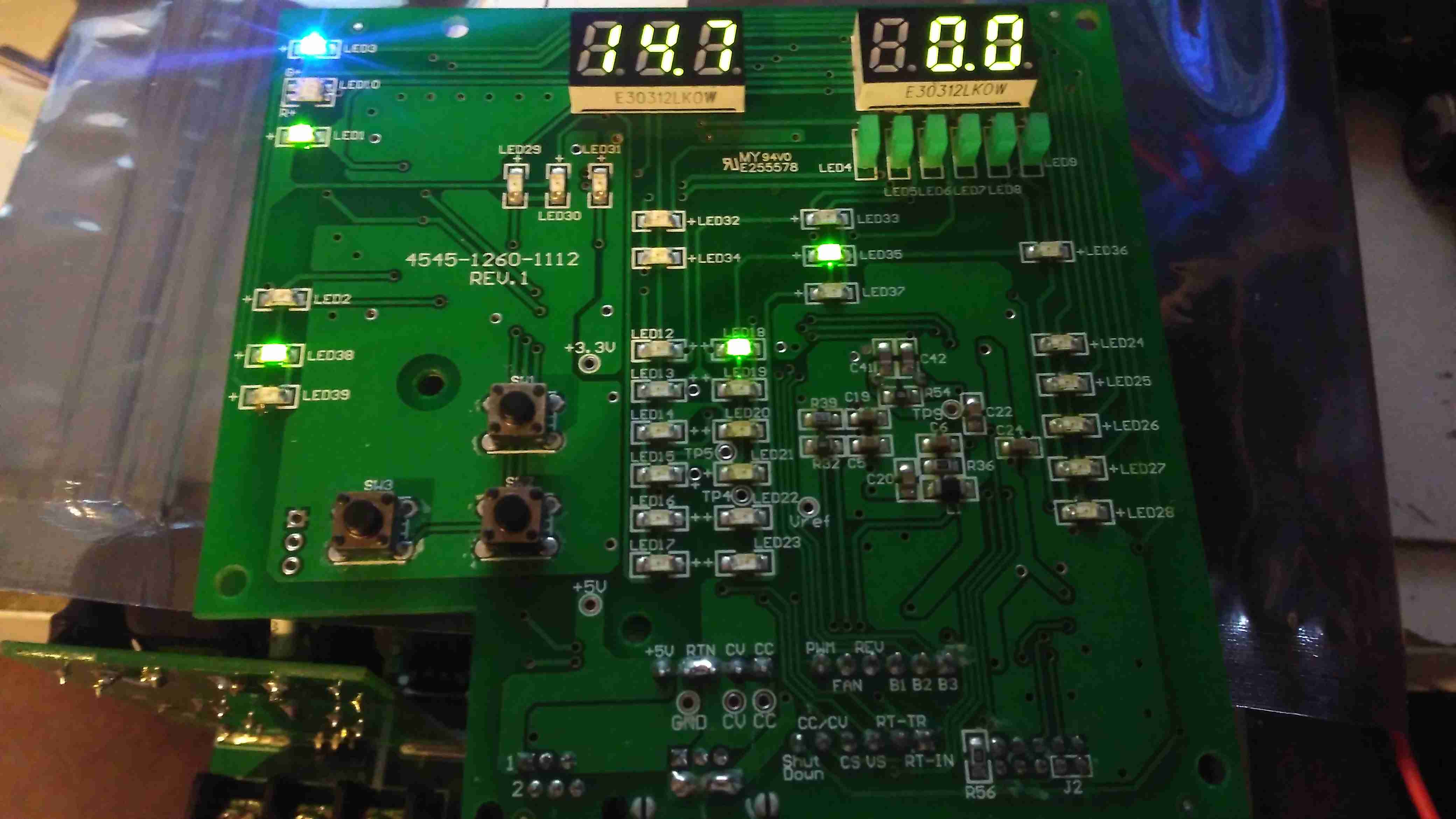
The front panel is stuffed with LEDs & 7-segment displays to show the current mode, charging voltage & current. There’s 2 tactile switches for adjustments.

Front Panel Reverse
Front Panel Reverse

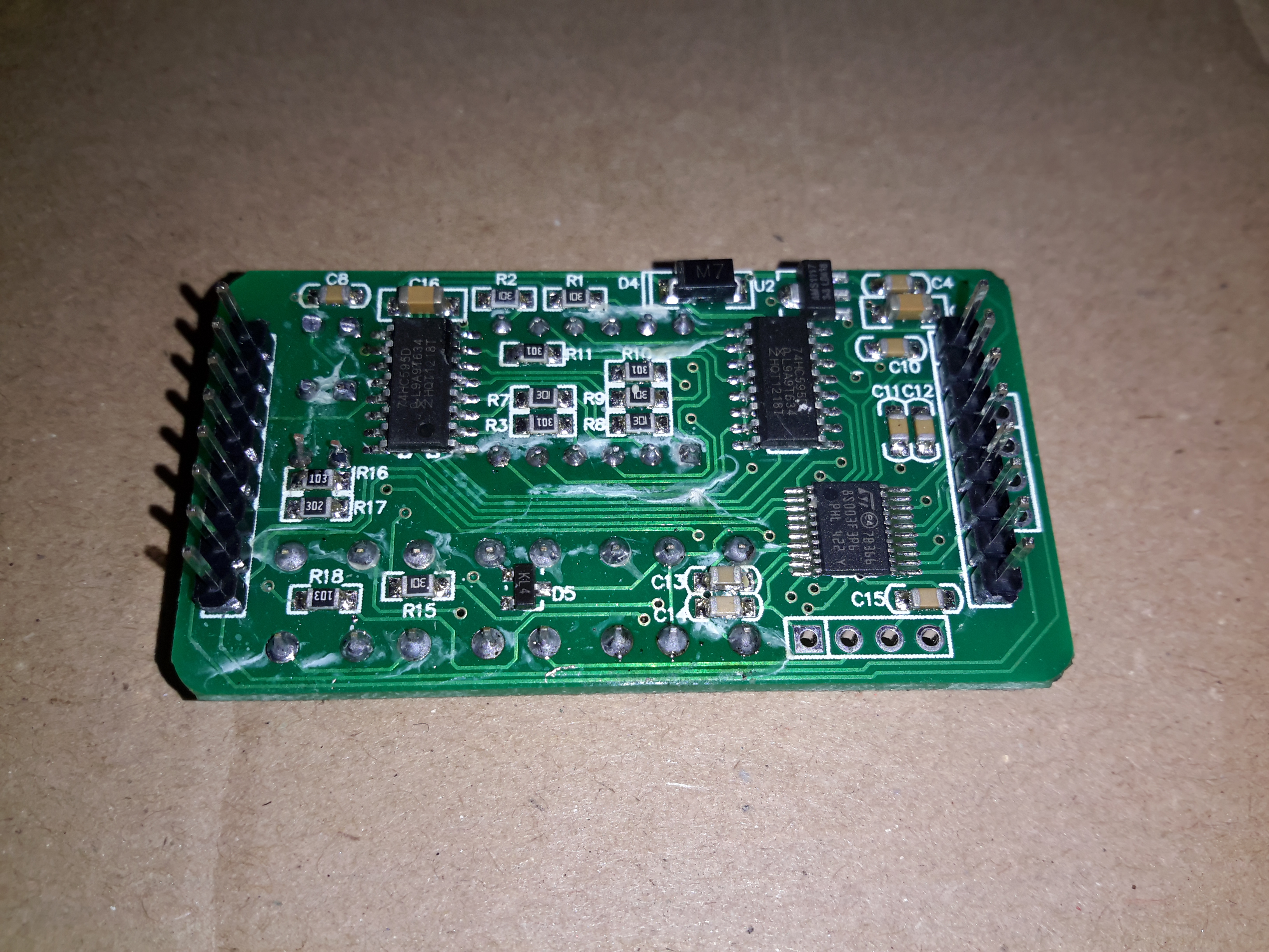
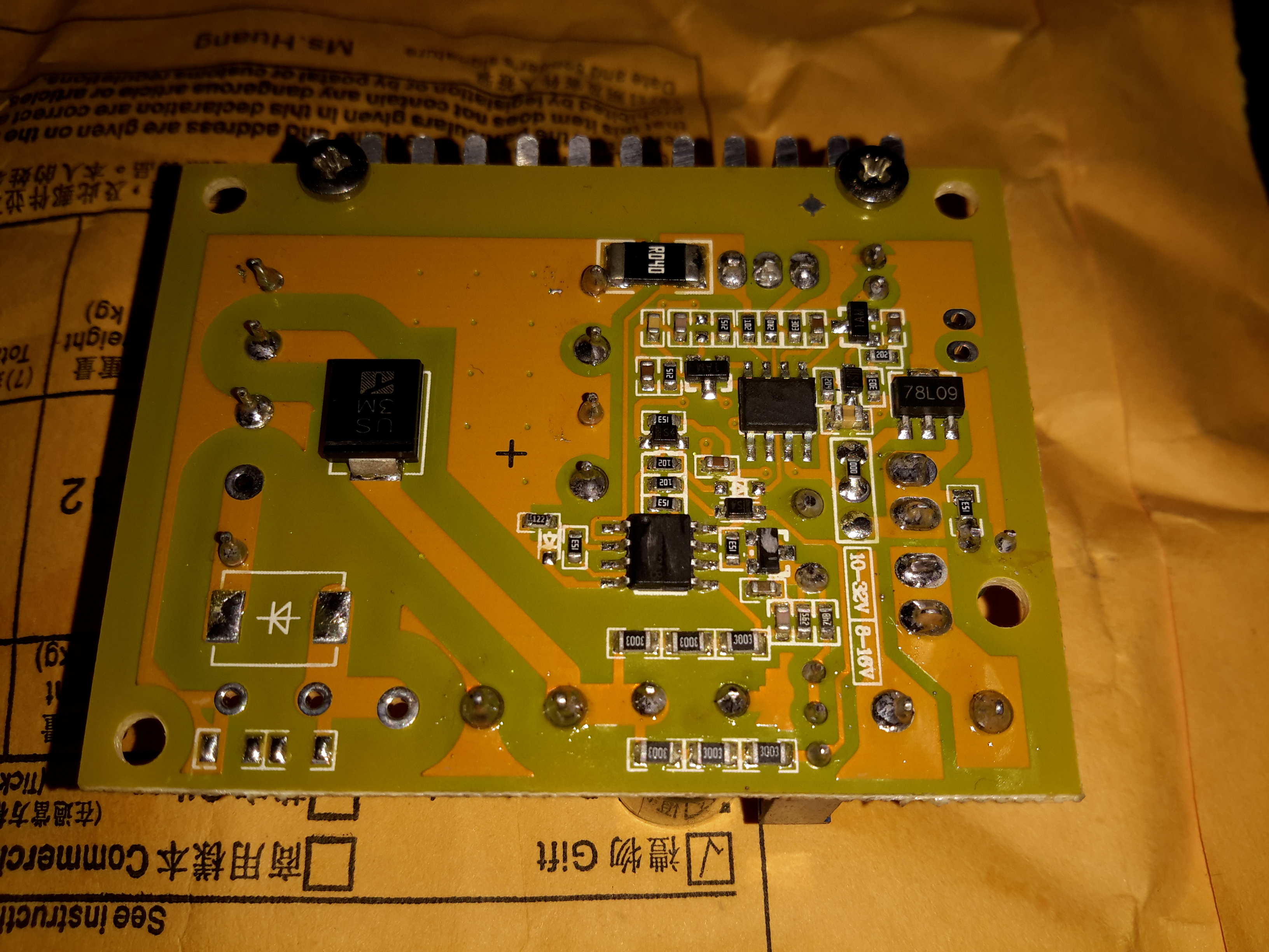
The reverse of the board has the main microcontroller – again identifying this is impossible due to the heavy conformal coat. The LEDs are being driven through a 74HC245D CMOS Octal Bus Transceiver.


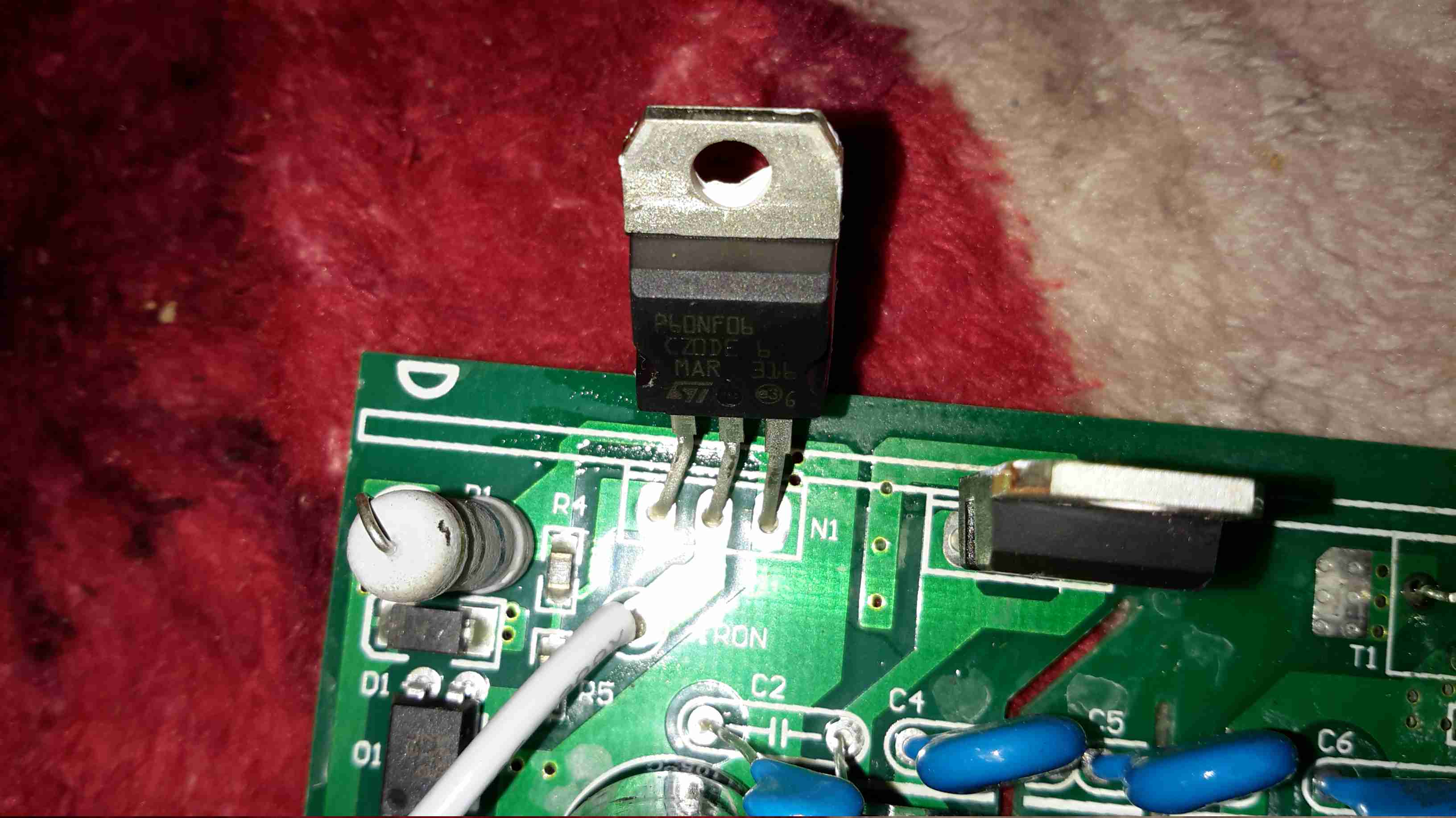
Now on to the repair! I’m not particularly impressed with only getting 4 years from this unit, they are very expensive as already mentioned, so I would expect a longer lifespan. The input fuse had blown in this case, leaving me with a totally dead charger. A quick multimeter test on the input stage of the unit showed a dead short – the main AC input bridge rectifier has gone short circuit.

Bridge Rectifier Removed

Here the defective bridge has been desoldered from the board. It’s a KBU1008 10A 800v part. Once this was removed I confirmed there was no longer an input short, on either the AC side or the DC output side to the PFC circuit.

Testing The Rectifier

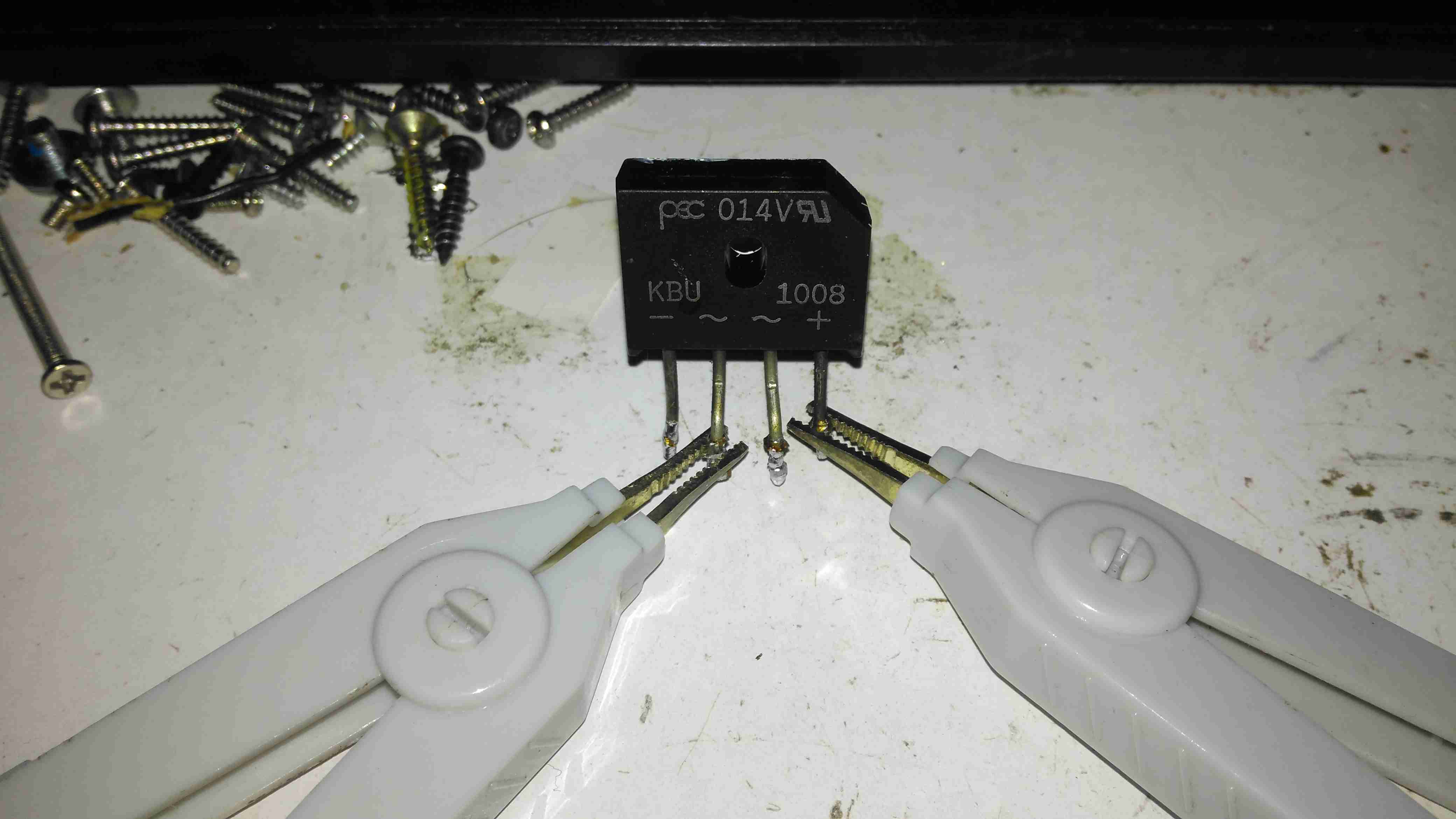
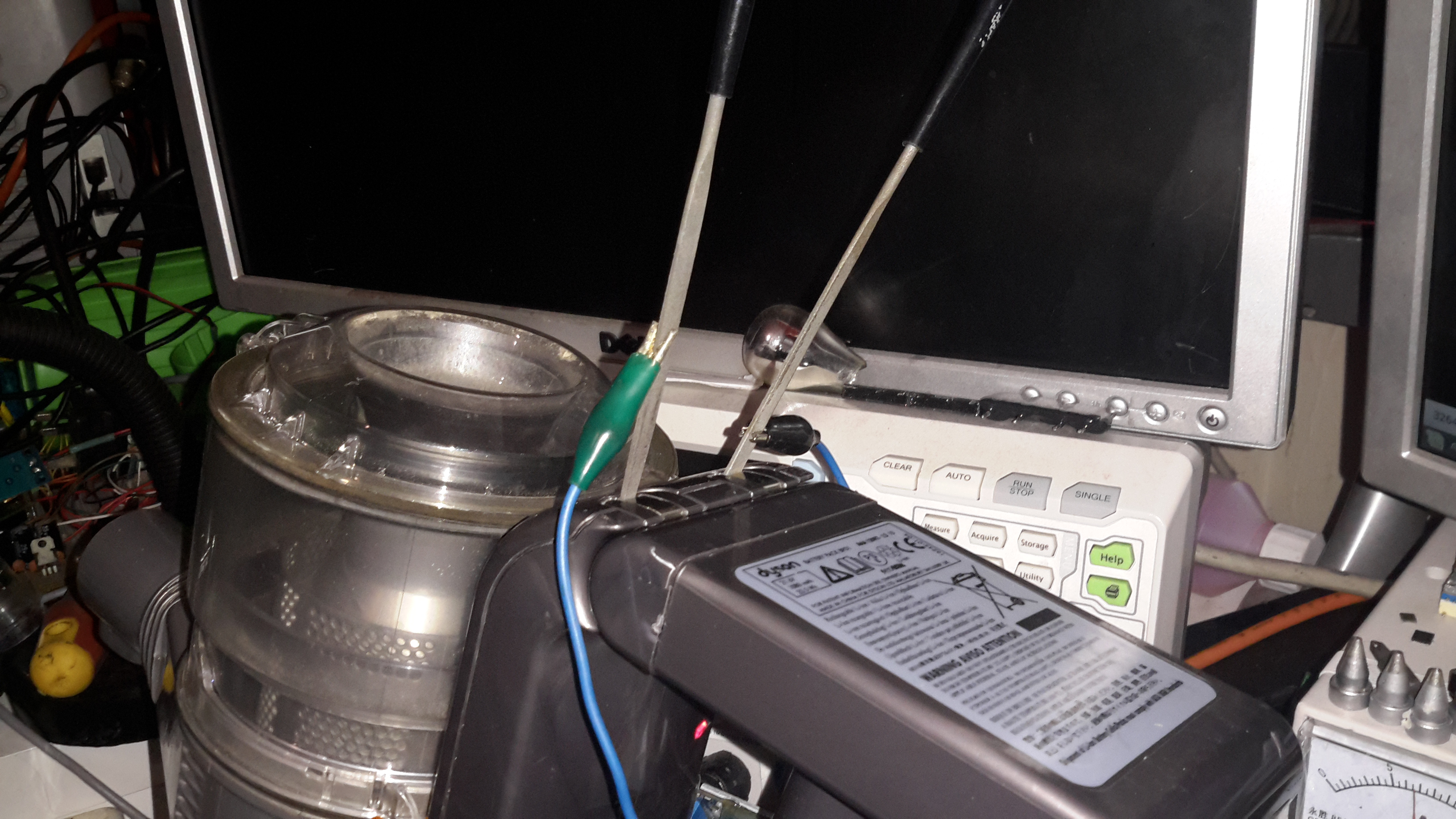
Time to stick the desoldered bridge on the milliohm meter & see how badly it has failed.

Yep, Definitely Shorted

I’d say 31mΩ would qualify as a short. It’s no wonder the 4A input fuse blew instantly. There is no sign of excessive heat around the rectifier, so I’m not sure why this would have failed, it’s certainly over-rated for the 10A charger.

Testing Without Rectifier

Now the defective diode bridge has been removed from the circuit, it’s time to apply some controlled power to see if anything else has failed. For this I used a module from one of my previous teardowns – the inverter from a portable TV.

Test Inverter
Test Inverter

This neat little unit outputs 330v DC at a few dozen watts, plenty enough to power up the charger with a small load for testing purposes. The charger does pull the voltage of this converter down significantly, to about 100v, but it still provides just enough to get things going.

It's Alive!
It’s Alive!

After applying some direct DC power to the input, it’s ALIVE! Certainly makes a change from the usual SMPS failures I come across, where a single component causes a chain reaction that writes off everything.

Replacement Rectifier

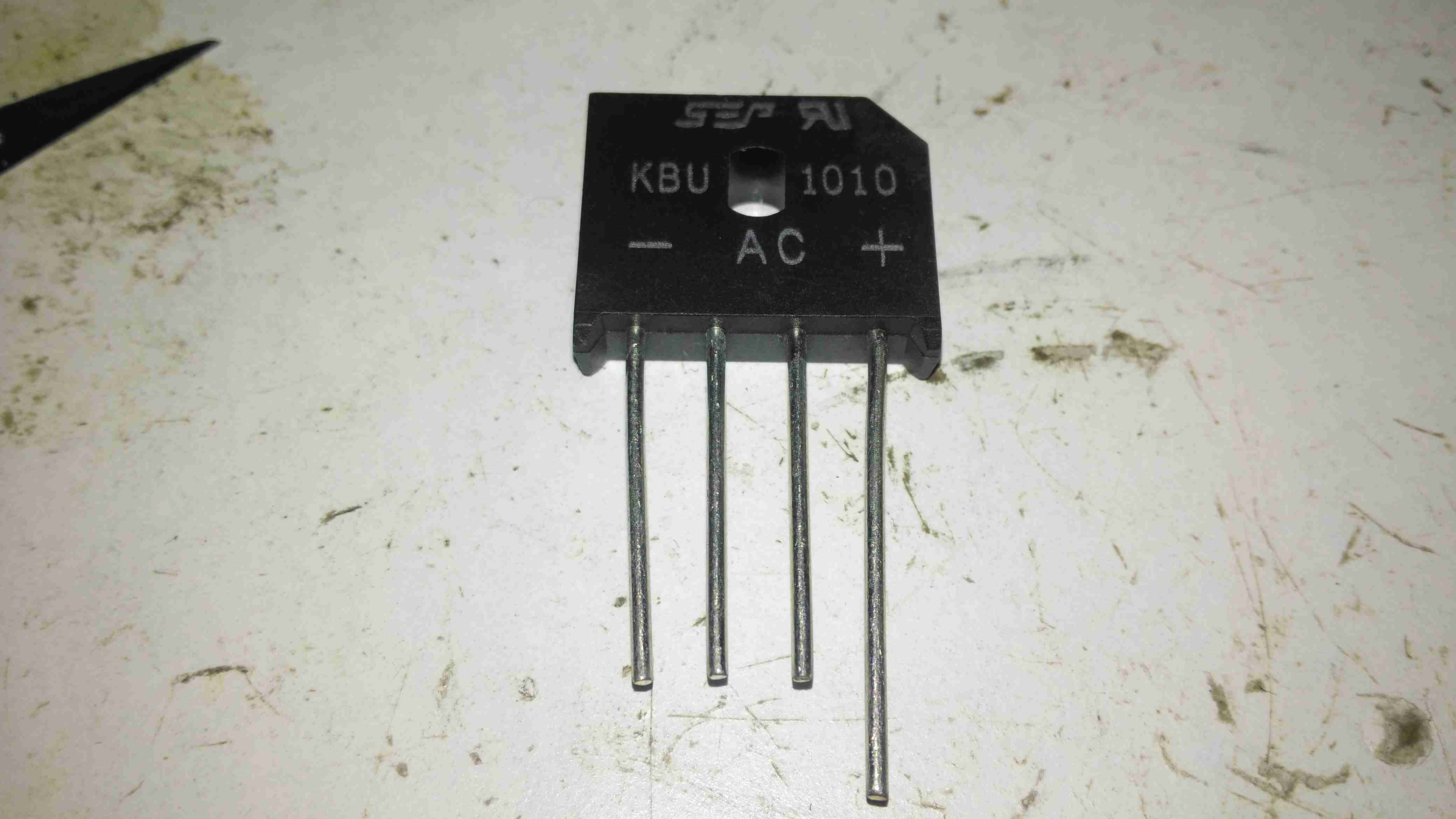
Unfortunately I couldn’t find the exact same rectifier to replace the shorted one, so I had to go for the KBU1010, which is rated for 1000v instead of 800v, but the Vf rating (Forward Voltage), is the same, so it won’t dissipate any more power.

Soldered In
Soldered In

Here’s the new rectifier soldered into place on the PCB & bolted to it’s heatsink, with some decent thermal compound in between.

Input Board
Input Board

Here is the factory fuse, a soldered in device. I’ll be replacing this with standard clips for 20x5mm fuses to make replacement in the future easier, the required hole pattern in the PCB is already present. Most of the mains input filtering is also on this little daughterboard.

Fuse Replaced
Fuse Replaced

Now the fuse has been replaced with a standard one, which is much more easily replaceable. This fuse shouldn’t blow however, unless another fault develops.

Full Load Test
Full Load Test

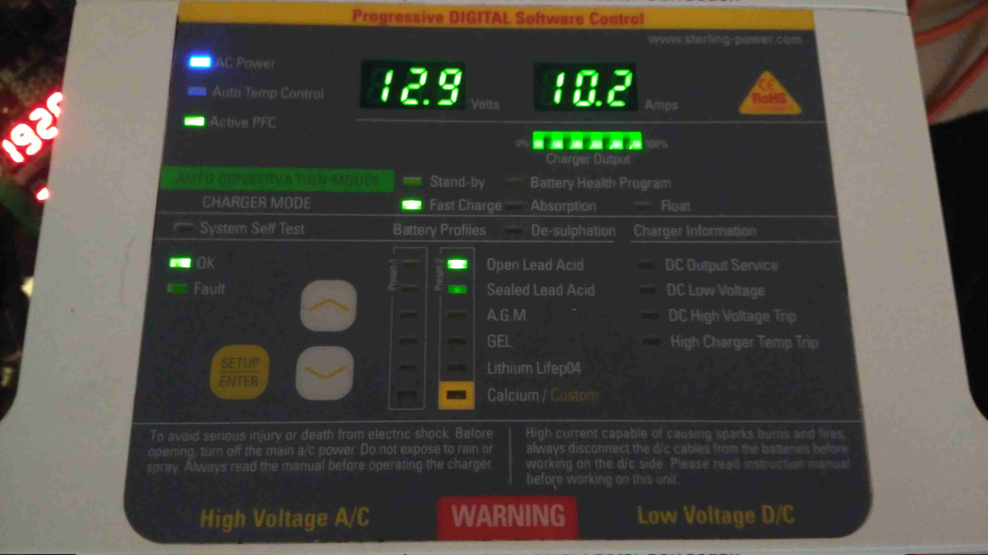
Now everything is back together, a full load test charging a 200Ah 12v battery for a few hours will tell me if the fix is good. This charger won’t be going back into service onboard the boat, it’s being replaced anyway with a new 50A charger, to better suit the larger loads we have now. It won’t be a Sterling though, as they are far too expensive. I’ll report back if anything fails!

Posted on 8 Comments

Contec CMS-50F Pulse Oximeter Teardown

Rear Case
Rear Case

The rear has the specifications, laser-marked into the plastic. The serial numbers are just sticky labels though, and will come off easily with use.

Contec CMS-50F
Contec CMS-50F

This is the Contec CMS-50F wrist-mounted pulse oximeter unit, which has the capability to record data continuously to onboard memory, to be read out at a later time via a USB-Serial link. There is software supplied with the unit for this purpose, although it suffers from the usual Chinese quality problems. The hardware of this unit is rather well made, the firmware has some niggles but is otherwise fully functional, however the PC software looks completely rushed, is of low quality & just has enough functionality to kind-of pass as usable.

Top Cover Removed
Top Cover Removed

A total of 4 screws hold the casing together, once these are removed the top comes off. The large colour OLED display covers nearly all of the board here. The single button below is the user interface. The connection to the probe is made via the Lemo-style connector on the lower right.

Lithium Cell
Lithium Cell

Power is provided by a relatively large lithium-ion cell, rated at 1.78Wh.

Main Processor
Main Processor

All the heavy lifting work of the LCD, serial comms, etc are handled by this large Texas Instruments microcontroller, a MSP430F247. The clock crystal is just to the left, with the programming pins. I’m not sure of the purpose of the small IC in the top left corner, I couldn’t find any reference to the markings.

Aux Processor
Aux Processor

The actual pulse oximetry sensor readings seem to be dealth with by a secondary microcontroller, a Texas Instruments M430F1232 Mixed-Signal micro. This has it’s own clock crystal just underneath. The connections to the probe socket are to the right of this µC, while the programming bus is broken out to vias just above. The final devices on this side of the board are 3 linear regulators, supplying the rails to run all the logic in this device.

Main PCB Rear
Main PCB Rear

The rear of the PCB has the SiLabs CL2102 USB-Serial interface IC, the large Winbond 25X40CLNIG 512KByte SPI flash for recording oximetry data, and some of the power support components. The RTC crystal is also located here at the top of the board. Up in the top left corner is a Texas Instruments TPS61041 Boost converter, with it’s associated components. This is probably supplying the main voltage for the OLED display module.

Posted on Leave a comment

Bargain Bin USB-ODB Interface

ODB Adaptor
ODB Adaptor

This is a little bit of kit I got to talk to the Webasto TT-V I salvaged from a scrap Jaguar S-Type, and converts USB-RS232 to the standard car diagnostic ODB connector. (These are a much cheaper option at £4 than the official Webasto diagnostic adaptor & loom which is over £90.

PCB Top
PCB Top

There’s really not much to this adaptor, the only signals that are routed to the ODB connector seem to be the +12v on pin 16, K-Line on Pin 7 & L-Line on pin 15. The main IC here is a CH340 USB-Serial interface, with some glue logic in the form of an LM339 quad comparator.

PCB Reverse
PCB Reverse

The reverse side of the PCB only has the power indicator LED.

Posted on Leave a comment

IC Decap – TDA3606 Multi Regulator With Battery Sense

This is a chip aimed at the automotive market – this is a low power voltage regulator for supplying power to microcontrollers, for instance in a CD player.

TDA3606 Die
TDA3606 Die

The TDA3606 is a voltage regulator intended to supply a microprocessor (e.g. in car radio applications). Because of low voltage operation of the application, a low-voltage drop regulator is used in the TDA3606. This regulator will switch on when the supply voltage exceeds 7.5 V for the first time and will switch off again when the output voltage of the regulator drops below 2.4 V. When the regulator is switched on, the RES1  and RES2 outputs (RES2 can only be HIGH when RES1 is HIGH) will go HIGH after a fixed delay time (fixed by an external delay capacitor) to generate a reset to the microprocessor. RES1 will go HIGH by an internal pull-up resistor of 4.7 kΩ, and is used to initialize the microprocessor. RES2 is used to indicate that the regulator output voltage is within its voltage range. This start-up feature is built-in to secure a smooth start-up of the microprocessor at first connection, without uncontrolled switching of the regulator during the start-up sequence. All output pins are fully protected. The regulator is protected against load dump and short-circuit (foldback
current protection). Interfacing with the microprocessor can be accomplished by means of a battery Schmitt-trigger and output buffer (simple full/semi on/off logic applications). The battery output will go HIGH when the battery input voltage exceeds the HIGH threshold level.

Posted on Leave a comment

IC Decap – TA7291 H-Bridge DC Motor Driver

Here’s a jellybean chip – a DC motor driver. This device has all the logic to drive a small motor, such as that used to drive the tray of a CD drive in both directions. The control logic is at the bottom of the die, while the main power transistors are at the top, in H-Bridge formation.

TA7291 Die
TA7291 Die
Posted on Leave a comment

IC Decap – MaxLinear MXL261 DOCSIS3 Tuner / Demodulator

Time for more silicon pr0n! When Virgin Media supplied me with a new modem, they requested I “recycle” the old one, so naturally it got gutted for the component parts. This particular IC is the frontend of the RF tuner. Unfortunately no datasheet is available, but I did manage to find some info in a press release. The sections are clearly identifiable, the RF section is on the left, while the rest of the demodulating logic is hidden on the right under a metal layer.

MXL261 Die
MXL261 Die – Click to Embiggen!

The MxL261 is based on MaxLinear’s low-power, digital CMOS process RF and mixed-signal technology.  It is a single-die, global standards, digital cable front end with integrated splitter, two 100MHz wideband tuners, four QAM demodulators and a four-channel-wide IF output.

Posted on 3 Comments

Anker PowerPort Speed 5 USB Rapid Charger Teardown

Front
Front

Here’s a piece of tech that is growing all the more important in recent times, with devices with huge battery capacities, a quick charger. This unit supports Qualcomm’s Quick Charge 3 standard, where the device being charged can negotiate with the charger for a higher-power link, by increasing the bus voltage past the usual 5v.

Rear
Rear

The casing feels rather nice on this unit, sturdy & well designed. All the legends on the case are laser marked, apart from the front side logo which is part of the injection moulding.

Specifications
Specifications

The power capacity of this charger is pretty impressive, with outputs for QC3 from 3.6-6.5v at 3A, up to 12v 1.5A. Standard USB charging is limited at 4.8A for the other 3 ports.

Ports
Ports

The two of the 5 USB ports are colour coded blue on the QC3 ports. The other 3 are standard 5v ports, the only thing that doesn’t make sense in the ratings is the overall current rating of the 5v supply (4.8A), and the rated current of each of the ports (2.4A) – this is 7.2A total rather than 4.8A.

Top Removed
Top Removed

The casing is glued together at the seam, but it gave in to some percussive attack with a screwdriver handle. The inside of this supply is mostly hidden by the large heatspreader on the top.

Main PCB Bottom
Main PCB Bottom

This is a nicely designed board, the creepage distances are at least 8mm between the primary & secondary sides, the bottom also has a conformal coating, with extra silicone around the primary-side switching transistor pins, presumably to decrease the chances of the board flashing over between the close pins.
On the lower 3 USB ports can be seen the 3 SOT-23 USB charge control ICs. These are probably similar to the Texas Instruments TPS2514 controllers, which I’ve experimented with before, however I can’t read the numbers due to the conformal coating. The other semiconductors on this side of the board are part of the voltage feedback circuits for the SMPS. The 5v supply optocoupler is in the centre bottom of the board.

Heatsink Removed
Heatsink Removed

Desoldering the pair of primary side transistors allowed me to easily remove the heatspreader from the supply. There’s thermal pads & grease over everything to get rid of the heat. Here can be seen there are two transformers, forming completely separate supplies for the standard USB side of things & the QC3 side. Measuring the voltages on the main filter capacitors showed me the difference – the QC3 supply is held at 14.2v, and is managed through other circuits further on in the power chain. There’s plenty of mains filtering on the input, as well as common-mode chokes on the DC outputs before they reach the USB ports.

Quick Charge 3 DC-DC Converters

Here’s where the QC3 magic happens, a small DC-DC buck converter for each of the two ports. The data lines are also connected to these modules, so all the control logic is located on these too. The TO-220 device to the left is the main rectifier.

Posted on Leave a comment

AIX Gigabit Ethernet To USB Bridge

USB To Ethernet
USB To Ethernet

Here’s a chap eBay USB-To-Ethernet dongle I obtained for use with the Raspberry Pi Zero. This one is getting torn down permanently, as it’s rather unreliable. It seems to like having random fits where it’ll not enumerate on the USB bus. The silicon in the ICs will eventually make it here once I manage to get a new microscope 😉

Main Chipset
Main Chipset

This is quite a heavily packed PCB, with the main Asix AX88178 on the left. This IC contains all of the logic for implementing the Ethernet link over USB, except the PHY. It’s clock crystal is in the top left corner.

Reverse Side
Reverse Side

Not much on the reverse side, there’s a 3.3v linear regulator at top left, the SOIC is an Atmel AT93C66A 4KB EEPROM for configuration data.

Vitesse PHY
Vitesse PHY

The final IC in the chain is the Vitesse VSC8211 Gigabit PHY, with it’s clock crystal below. This interfaces the Ethernet MAC in the Asix IC to the magjack on the right.

Posted on Leave a comment

Behringer DEQ2496 Mastering Processor

Bootscreen
Bootscreen

I was recently given this unit, along with another Behringer sound processor to repair, as the units were both displaying booting problems. This first one is a rather swish Mastering Processor, which has many features I’ll leave to Behringer to explain 😉

Input Board & Relays

All the inputs are on the back of this 19″ rackmount bit of kit, nothing much on this PCB other than the connectors & a couple of switching relays.

Main Processor PCB
Main Processor PCB

All the magic is done on the main processor PCB, which is host to 3 Analog Devices DSP processors:

ADSP-BF531 BlackFin DSP. This one is probably handling most of the audio processing, as it’s the most powerful DSP onboard at 600Mhz. There’s a ROM on board above this for the firmware & a single RAM chip. On the right are a pair of ADSP-21065  DSP processors at a lower clock rate of 66MHz. To the left is some glue logic to interface the user controls & dot-matrix LCD.

PSU Module
PSU Module

The PSU in this unit is a pretty standard looking SMPS, with some extra noise filtering & shielding. The main transformer is underneath the mu-metal shield in the centre of the board.

Posted on Leave a comment

Mercedes Benz Temic Central Locking / Immobilizer Module Teardown

Mercedes Benz Temic Module

The other day I was given a random pile of car electronic parts from the scrap bin at the local garage, so I decided to do a few teardowns. This first one is a Temic Central Locking / Immobiliser module from a Mercedes van. Judging by the 125kHz stamped on the label, this also has RFID capability.

PCB
PCB

The casing just unclips, revealing the PCB. Surprisingly for an automotive module, there is no conformal coating on this (they’re usually heavily coated in protective lacquer to prevent moisture ingress).

Microcontroller
Microcontroller

The large IC from Motorola I’m assuming to be a microcontroller, but I didn’t manage to find anything from the markings. There’s not much else in here apart from some glue logic, and what I think is the 125Khz toroidal antenna in the top left corner.

Posted on Leave a comment

LG Flatron 22EA53VQ-P Power Issue

I was recently given a pretty nice LED backlit 1080p LG monitor, with the instruction that it wouldn’t power on correctly. The monitor would power on as far as the standby light, but when fully powered on, would flash the backlight momentarily then shut down. A power supply issue was immediately suspected.

LCD Logic Board
LCD Logic Board

I popped the covers off the monitor itself first, thinking that it was an electrolytic gone bad in the backlight DC-DC converter. Not to mention the fact that cracking into a wall-wart type of PSU is only occasionally possible without the use of anger & large hammers. (Cracking the glue with the handle of a screwdriver doesn’t work so well when the factory went a bit nuts with the glue/ultrasonic welder). As can be seen in the photo, there’s not much inside these monitors, the logic is a single-chip solution, the rest of the PCB is dedicated to supplying the power rails for the various circuits. On the left is the power input & the DC-DC converter for the backlight, along with the DC-DC converter supplying the logic circuits. None of the capacitors here are damaged, everything looks good.
I then measured the output of the PSU, which under no load was the correct 19v DC. However applying any load caused the output voltage to drop like a proverbial brick. Applying a full load of 1.3A saw the output voltage drop so severely that the PSU tripped on it’s UVLO.

200mA Load
200mA Load

At 200mA of load the factory PSU is already dropping to 18v, with a 5.3kHz switching frequency appearing.

500mA Load
500mA Load

At higher load the frequency increases to 11.5kHz & the output voltage has dropped to 11.86v!

750mA Load
750mA Load

750mA was as high as I could make the supply go without it tripping itself out – the UVLO circuit trips at 9v. 12.6kHz is now riding on the severely low DC at this point.

PSU Ratings
PSU Ratings

The power supply is supposed to be rated at 1.3A at 19v, however with this fault it’s getting nowhere near that. The LG brand is on this PSU but it’s contracted out to Shenzen Honor Electric Co. Ltd.

Output Electrolytic
Output Electrolytic

Here’s the problem with this PSU. The output electrolytic has ballooned. I don’t have an ESR tester, but this cap has gone way past it’s sell-by date. It’s position right next to the heatsink with the output rectifier diodes has probably cooked it. The PSU isn’t that badly built for a Chinese one – there’s plenty of creepage distance on the PCB & even a couple of isolation slots.

Posted on Leave a comment

MingHe D3806 Buck-Boost DC-DC Converter

DC-DC Converter
DC-DC Converter

Here’s a useful buck-boost DC-DC converter from eBay, this one will do 36v DC at 6A maximum output current. Voltage & current are selected on the push buttons, when the output is enabled either the output voltage or the output current can be displayed in real time.

Display PCB
Display PCB

Here’s the display PCB, which also has the STM32 microcontroller that does all the magic. There appears to be a serial link on the left side, I’ve not yet managed to get round to hooking it into a serial adaptor to see if there’s anything useful on it.

Display Drive & Microcontroller

The bottom of the board holds the micro & the display multiplexing glue logic.

Main PCB
Main PCB

Not much on the mainboard apart from the large switching inductors & power devices. There’s also a SMPS PWM controller, probably being controlled from the micro.

Posted on Leave a comment

Aspen Universal Condensate Pump

Universal Peristaltic Condensate Pump

Here’s another piece of commercial gear, from an industrial air conditioning unit. These pumps are used to drain the condensate from the evaporator unit, so water doesn’t end up raining down from the ceiling.

Pump Head
Pump Head

This is a peristaltic pump, with a silicone hose forming the pumping element.

Rear Panel
Rear Panel

The test switch & electrical connections are on the back, along with the data label.

Power & Sensor Socket

The electrical connections are all on a single 5-pin socket. Along with 240v AC mains, there are a pair of thermistors connected to the unit, which switch the pump on when a 5°C temperature difference across the evaporator coil is detected. When air is cooled, it’s capacity for moisture drops, so the water condenses out on the coil.

Roller Wheel
Roller Wheel

Here the front cover has been removed from the pump, showing the silicone tube & roller wheel. The wheel was originally Cadmium-plated, but exposure to the elements has oxidized this into highly toxic Cadmium Oxide.

Pump Rollers
Pump Rollers

Here you can see the rollers. These pinch the tube at the inlet, and the rotation carries a slug of liquid through the tube to the outlet side.

Pump Tube
Pump Tube

Here’s the tube itself, the main wearing part of the pump. This is replaceable as a spare part.

Motor & Gearbox
Motor & Gearbox

Inside the casing is a shaded-pole motor, connected to a large gearbox, to give the slow rotation for the pump head. The rated speed is 51RPM.

Control PCB
Control PCB

There’s not much to the control PCB. The large resistor forms a voltage dropper, to reduce the mains 240v to a more suitable level for the logic. There’s a TL062C Low-Power JFET Op-Amp & a CD4060BCM 14-stage binary ripple counter forming the logic. The set point is adjustable via the potentiometer.

Pump Triac
Pump Triac

The pump motor is switched via this Z7M SMD triac, not much switching power is needed here as the motor is only a very small shaded-pole type.

Posted on Leave a comment

ETI Thermamite Catering Thermometer

Catering Thermometer

Here’s another bit of commercial gear, a catering thermometer. These are used to check the internal temperature of foods such as meat, to ensure they’re cooked through.

This was given to me with some damage, the battery cover is missing & the plastic casing itself is cracked.

Battery Compartment
Battery Compartment

Power is provided by 3 AAA cells, for 4.5v

Main PCB
Main PCB

There’s not much to these units, the large LCD at the top is driven by the IC in the centre. A programming header is also present on the board near the edge.

Microcontroller
Microcontroller

The core logic is taken care of with a Texas Instruments M430F4250 MSP430 Mixed-Signal Microcontroller. This MCU has onboard 16-bit Sigma-Delta A/D converter, 16-bit D/A converter & LCD driver. Clock is provided by a 32.768kHz crystal.
The probe itself is just a simple thermistor bonded into a stainless steel rod.

Posted on Leave a comment

Sky+ HD Set Top Box

Sky Box
Sky Box

Time for another teardown! I managed to fish this Sky+ box out of a skip, but to protect the guilty, all serial numbers have been removed.
These are pretty smart devices, with DVR capability on board.

Ports 1
Ports 1

There’s a lot of ports on these units, from RS-232 serial, POTS modem, eSATA, HDMI, USB, Ethernet, SCART, Optical, digital outputs & even composite video.

Ports 2
Ports 2
Ports 3
Ports 3
Top Panel
Top Panel

Removing the top plastic cover reveals the operation buttons & the built in WiFi adaptor, which is USB connected to the main logic board.

Front Panel
Front Panel

The PCB on the front of the chassis has all the indicators, and the IR Receiver for the remote.

Cover Removed
Cover Removed

Removing the top shield of the chassis reveals the innards. The PSU is on the top right, 500GB SATA disk drive in the bottom centre. The main logic PCB is top centre.

Logic PCB
Logic PCB

Here’s the main logic PCB. The massive heatsink in the middle is cooling the main SoC, below.

SoC
SoC

The main SoC in this unit is a Broadcom BCM7335 HD PVR Satellite System-On-Chip. It’s surrounded by it’s boot flash, a Spansion GL512P10FFCR1 512Mbit NOR device. It’s also got some DRAM around the left edge.

Smart Card Reader
Smart Card Reader

The smart card reader is on the PSU PCB, the controller here is an NXP TDA8024

PSU PCB
PSU PCB

The PSU itself is a pretty standard SMPS, so I won’t go too far into that particular bit. The logic PCB attaches to the large pin header on the left of the PSU, some of the analogue video outputs are also on this board.
There’s also a Microchip PIC16F726 microcontroller on this PCB, next to the pin header. Judging by the PCB traces, this handles everything on the user control panel.

Power Supplies
Power Supplies

Some local supplies are provided on the logic board for the main SoC, the IC in the centre here is an Allegro A92 DC-DC converter. I didn’t manage to find a datasheet for this one.

LNB Front End
LNB Front End

The RF front end for the satellite input is a Broadcom BCM3445 Low Noise Amplifier & Splitter, again not much info on this one.

RS232 Section
RS232 Section

The standard MAX232 is used for the serial interface. I imagine this is for diagnostics.

Modem
Modem

The POTS modem section is handled by a Si2457 System-Side device & Si3018 Line-Side device pair.

Posted on 1 Comment

eBay High Voltage DC-DC Converter Module

High Voltage DC-DC
High Voltage DC-DC

Going through eBay recently looking for parts for a couple of CRT-based projects, I came across these DC-DC converters.
Apparently rated from 45-390v DC output at 200mA, these should be ideal for driving some of the electrodes (focus, screen, grid) in a CRT.
Above is the top of the board, input voltage header on the left, output voltage adjust in the centre & output voltage header on the right.
This module has a mini-automotive fuse, at 10A for input protection.
On the heatsink is mounted the main switching MOSFET, a RU7088R from Ruichips. This FET is fairly heavily rated at 70v 80A, with 6.5mΩ on-resistance.

PCB Bottom
PCB Bottom

The bottom of the board has the control components, with a pair of ICs. Unfortunately the numbers have been scrubbed off, so no identification here. The output from the transformer is rectified with a single large SMD diode on the left side of the board.
There’s also plenty of isolation gap between the HV output trace & the low voltage logic side of the circuit, the two being bridged only by a resistive divider for output voltage measurement.

Posted on Leave a comment

Sony Xperia T Teardown

Back Cover Removed
Back Cover Removed

Since this phone has been in my drawer for some time, I figured it was time for a teardown. (It’s never going to see any more use).
The back cover on these phones is easily removed, as it’s just clipped on.

Motherboard
Motherboard

Once the back cover is removed, the Li-Polymer cell is exposed, along with the logic board. Pretty much all of the PCB is under RF shields.

Motherboard Removed
Motherboard Removed
Battery Management
Battery Management

Under the small RF can on the back of the board is the battery management circuitry & the charger. There’s an extra connection to the cell for temperature monitoring. Just under that circuitry is the eMMC flash storage.
Just to the left of the battery circuit is the NFC transceiver IC, from NXP.

Battery Flex
Battery Flex

The cell is connected to the main board with a FFC, with a very small SMT connector, although not as small as the more modern Xperia series phones.

RF Section
RF Section

The other side of the mainboard holds the large RF transceiver section, with a Qualcomm RTR8600 multiband transceiver IC. In the bottom corner is a Skyworks SKY77351-32 Quad-band power amplifier IC, along with 3 other power amplifier ICs, also from Skyworks.

Gyro & Audio Codec
Gyro & Audio Codec

The top corner of the board holds the various sensors, including an Invensense MPU-3050 3-axis gyro. To the right of that is the Audio Codec, a WCD9310 from Qualcomm.

Logic & CPU Section
Logic & CPU Section

Everything is controlled from the last section on the board, with the main CPU & RAM in a PoP (Package-On-Package) configuration. Under the main CPU is the main power management IC, also from Qualcomm. No datasheet for this one unfortunately, but it gives it’s purpose away by being surrounded by large inductors & capacitors.

Posted on Leave a comment

Digital Angle Gauge

Front
Front

Here’s a useful tool for the kit, a digital angle gauge/protractor. These use a silicon sensor to show the number of degrees the unit is out of level.

Magnets!
Magnets!

Magnets are provided in the base, so the tool can attach to any ferrous surface.

Battery Box
Battery Box

Power is provided by a single AAA cell.

Main PCB
Main PCB

Removing the rear cover reveals the brains of the unit, and there’s not much to it at all. The main microcontroller is a CoB-type device, so no part numbers available from that one.

Sensing Element
Sensing Element

The IC to the left of the main microcontroller is the sensing element. There’s no markings on this inclinometer IC so I’m not sure of the specs, but it will be a 3D-MEMS device of some sort.

Power Supply
Power Supply

The other side of the PCB has the power supply for the logic, and a serial EEPROM, probably storing calibration data.

Posted on 14 Comments

Dyson DC16 Handheld Teardown

DC16
DC16

The Dyson DC16 is one of the older handheld vacuums, before the introduction of the “Digital Motor”. (Marketing obviously didn’t think “Switched Reluctance Motor” sounded quite as good).

These vacuums have a very large DC brush motor driving the suction turbine instead, the same as would be found in a cordless power tool.

Control PCB
Control PCB

Popping the front cap off with the ID label, reveals the brains of the vacuum. The two large terminals at the right are for charging, which is only done at 550mA (0.5C). There are two PIC microcontrollers in here, along with a large choke, DC-DC converter for supplying the logic most likely. The larger of the MCUs, a PIC16HV785, is probably doing the soft-start PWM on the main motor, the smaller of the two, a PIC16F684 I’m sure is doing battery charging & power management. The motor has a PCB on it’s tail end, with a very large MOSFET, a pair of heavy leads connect directly from the battery connector to the motor.
Just out of sight on the bottom left edge of the board is a Hall Effect Sensor, this detects the presence of the filter by means of a small magnet, the vacuum will not start without a filter fitted.

Battery Pack
Battery Pack

The battery pack is a large custom job, obviously. 4 terminals mean there’s slightly more in here than just the cells.

Battery Cracked
Battery Cracked

Luckily, instead of ultrasonic or solvent welding the case, these Dyson batteries are just snapped together. Some mild attack with a pair of screwdrivers allows the end cap to be removed with minimal damage.

Cells
Cells

The cells were lightly hot-glued into the shell, but that can easily be solved with a drop of Isopropanol to dissolve the glue bond. The pack itself is made up of 6 Sony US18650VT High-Drain 18650 Li-Ion cells in series for 21.6v nominal. These are rated at a max of 20A discharge current, 10A charge current, and 1.3Ah capacity nominal.
There’s no intelligence in this battery pack, the extra pair of terminals are for a thermistor, so the PIC in the main body knows what temperature the pack is at – it certainly gets warm while in use due to the high current draw.

Motor
Motor

Hidden in the back side of the main body is the motor. Unfortunately I wasn’t able to get this out without doing some damage, as the wiring isn’t long enough to free the unit without some surgery.

Turbine
Turbine

The suction is generated by a smaller version of the centrifugal high-speed blowers used in full size vacuums. Not much to see here.

Unofficial Charger
Unofficial Charger

Since I got this without a charger, I had to improvise. The factory power supply is just a 28v power brick, all the charging logic is in the vacuum itself, so I didn’t have to worry about such nasties as over-charging. I have since fitted the battery pack with a standard Li-Po balance cable, so it can be used with my ProCell charger, which will charge the pack in 35 minutes, instead of the 3 hours of the original charger.

Posted on Leave a comment

De La Rue Coin Counting Machine

Here’s some teardown photos of an old De La Rue coin counter, used in businesses for rapid counting of change into large bags.

Mechanism
Mechanism

An overview of the whole mechanical system of the counter. Coins are loaded into the drum at the rear of the machine, which sorts them into a row for the rubber belt to pick up & run through the counter. The coin type to be sorted is selected by turning the control knobs on the right.
The control knobs adjust the width & height of the coin channel so only the correct sized coins will be counted.

PSU & Switching
PSU & Switching

The counter is driven by a basic AC induction motor, the motor power relay & reversing relay is on this PCB, along with the 5v switching supply for the main CPU board.
The SMPS on this board looks like a standard mains unit, but it’s got one big difference. Under the frame next to the main motor is a relatively large transformer, with a 35v output. This AC is fed into the SMPS section of the PSU board to be converted to 5v DC for the logic.
I’m not sure why it’s been done this way, and have never seen anything similar before.
The edge of the coin channel can be seen here, the black star wheel rotates when a coin passes & registers the count.

Controller PCB
Controller PCB

Here’s the main controller PCB, IC date codes put the unit to about 1995. The main CPU is a NEC UPD8049HC 8-bit micro, no flash or EEPROM on this old CPU, simply mask ROM. Coin readout is done on the 4 7-segment LED displays. Not much to this counter, it’s both electronically & mechanically simple.

Counter Sensor
Counter Sensor

Coin counting is done by the star wheel mentioned above, which drives the interrupter disc on this photo-gate. The solenoid locks the counter shaft to prevent over or under counting when a set number of coins is to be counted.

Motor Run Capacitor
Motor Run Capacitor

Under the frame, here on the left is the small induction motor, only 6W, 4-pole. The run cap for the motor is in the centre, and the 35v transformer is just visible behind it.

Main Motor Drive
Main Motor Drive

Main drive to the coin sorting mech is through rubber belts, and bevel gears drive the coin drum.

Posted on Leave a comment

Duratool ZD-915 12v Conversion

Inkeeping with everything else in my shack being low voltage operated, I had planned from the outset to convert the desoldering station to 12v operation. It turns out this has been the easiest tool to convert in my shack so far.

PSU Outputs
PSU Outputs

The factory SMPS is a fairly straightforward 18v 12A unit, with only a single small oddity: the desoldering gun’s heating element is controlled from inside the supply.

Iron MOSFET
Iron MOSFET

Next to the output rectifier on the heatsink is a large MOSFET, in this case a STP60NF06 from ST Micro. This is a fairly beefy FET at 60v & 60A capacity, RDS On of <0.016Ω.
This is driven via an opto-isolator from the main logic board. I’ve not yet looked at the waveform on the scope, but I suspect this is also being PWM’d to control temperature better when close to the set point.

Iron Element Controller

Rather than fire up the soldering iron & build a new element controller circuit (Lazy Mode™), I opted to take a saw to the original power supply. I cut the DC output section of the PCB off the rest of the supply & attached this piece back to the frame of the base unit. I also added a small heatsink to the MOSFET to make sure it stays cool.

12v Power Supply
12v Power Supply

Since the fan & vacuum pump are both already 12v rated, those are connected directly to the DC input socket, that I’ve installed in place of the original IEC mains socket. The 18v for the heating element is generated by a 10A DC-DC converter, again from eBay.

Oddly, the iron itself is rated at 24v 80W, but the factory supply is only rated to 18v. I’m not sure why they’ve derated the system, but as the station already draws up to 10A from a 13.8v supply, increasing the voltage any further would start giving my DC supplies a problem, so it can stay at 18v for now.

Posted on Leave a comment

ViewSonic VA2232W-LED Monitor 12v Conversion

ID Label
ID Label

On the quest to get things on board replaced that are heavy users of power, the monitor in the main cabin was next. The original CCFL-backlit monitor was very heavy on 12v power, at 5A. This meant falling asleep watching TV would result in severely flattened batteries.

Replacement with a suitable LED-backlit monitor was definitely required. The cheapest on eBay was a ViewSonic VA2232W-LED, so I took to work converting it from 240v to 12v operation.

Back Cover Removed
Back Cover Removed

There are no screws holding these monitors together, so a spudger & frequent swearing got the back off. The shield holding the circuitry is also not screwed down, only attached to the back of the LCD panel with aluminium shielding tape.

Power PCB Trackside
Power PCB Trackside

Once the tape has been cut, the main power board is accessible. The large IC on the left is the main backlight LED driver.

In this case the monitor requires a pair of rails from the supply, 18.5v for the backlight circuitry & 5v for the logic.

DC-DC Regulators
DC-DC Regulators

A pair of DC-DC converters has been fitted in the small space between the power & control boards.

PCB Connection Points

To save me some work & keep maximum compatibility, I’ve not modified the existing supply, just attached the new DC-DC converter outputs onto the corresponding outputs of the factory PSU. The 12v input leads are routed out of the same gap as the mains IEC connector, with some hot glue over the mains input solder points to provide some more insulation.

Wiring Tidied
Wiring Tidied

The wiring is tidied up with hot glue so the back cover will go back on.

Total current draw at 12v is 1.4A.

Posted on Leave a comment

5-Port HDMI Switch

HDMI Switch
HDMI Switch

Here’s another quick teardown, a cheap 5-port HDMI switch box. This is used to allow a single input on a monitor to be used by 5 different external HDMI devices, without having to mess about plugging things in.

Power & Remote
Power & Remote

Here’s the DC barrel jack & 3.5mm TRS jack for power & remote control. There’s a little IR decoder & remote that go with this for hands free switching.

PCB Top
PCB Top

Here’s the PCB out of it’s plastic housing. The main logic is a pair of PI3HDMI303 3:1 HDMI switches from Pericom Semiconductor. These are cascaded for the 5-ports, the first 3 input HDMI ports are switched through both ICs to reach the output.
These HDMI switch ICs are operated with TTL input pins, the combination of these pins held either high or low determines the input port that appears on the output.
There’s a button on the left for switching between inputs, with a row of 5 LED indicators.

PCB Bottom
PCB Bottom

Not much on the bottom side, a lot of passives & bypass capacitors. There’s a 3.3v LDO regulator on the left for supplying the main rail to the active switch ICs. The IC on the right doesn’t have any numbering at all, but I’m presuming it’s a microcontroller, dealing with the IR remote input & pushbutton inputs to switch the inputs.

Posted on Leave a comment

Maplin 3W LED Torch Charger Fail

A member of the family recently bought one of these torches from Maplin electronics, and the included chargers for the 18650 lithium-ion cells leave a lot to be desired.

Torch
Torch

Here’s what’s supplied. The torch itself is OK – very bright, and a good size. Me being cynical of overpriced Chinese equipment with lithium batteries, I decided to look in the charging base & the cigar-lighter adaptor to see if there was any actual charging logic.

Charger
Charger

Answer – nope. Not a single active component in here. It’s just a jack connected to the battery terminals. There’s all the space there to fit a proper charging circuit, but it’s been left out to save money.

OK then, is it inside the cigarette lighter adaptor?

Lighter Adaptor
Lighter Adaptor

Nope. Not a single sign of anything resembling a Lithium-Ion charger IC. There’s a standard MC34063A 1.5A Buck converter IC on the bottom of the PCB, this is what’s giving the low voltage output for the torch.

Charger Bottom
Charger Bottom

Here’s the IC – just a buck converter. The output voltage here is 4.3v. This is higher than the safe charging voltage of a lithium ion cell, of 4.2v.

The cells supplied are “protected” versions, having charge/discharge protection circuitry built onto the end of the cell on a small PCB, this makes the cell slightly longer than a bare 18650, so it’s easy to tell them apart.
The manufacturers in this case are relying on that protection circuit on the cell to prevent an overcharge condition – this isn’t the purpose they’re designed for, and charging this way is very stressful for the cells. I wouldn’t like to leave one of these units charging unattended, as a battery explosion might result.

More to come shortly when I build a proper charger for this torch, so it can be recharged without fearing an alkali metal fire!

73s for now folks!