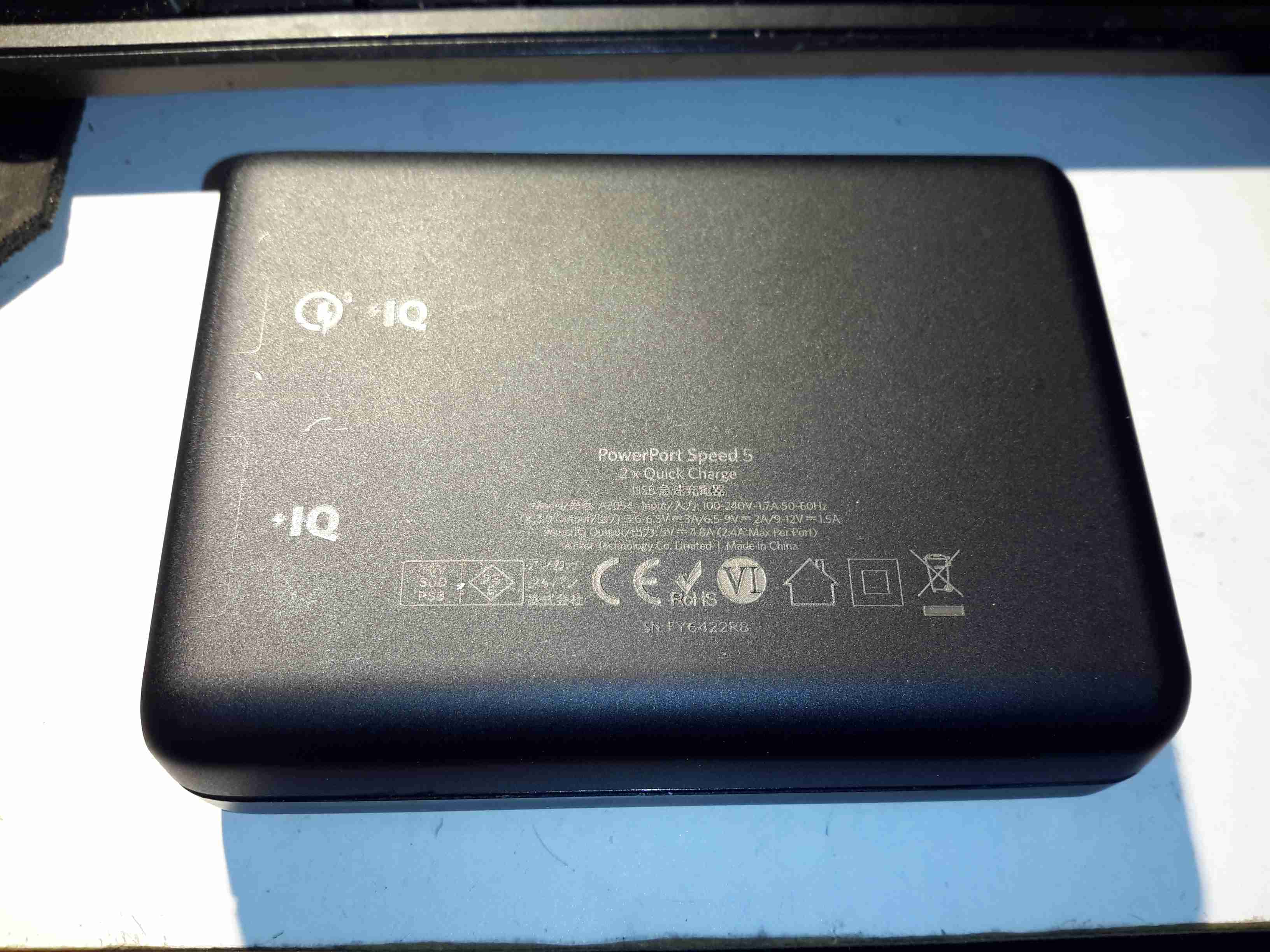
Here’s a piece of tech that is growing all the more important in recent times, with devices with huge battery capacities, a quick charger. This unit supports Qualcomm’s Quick Charge 3 standard, where the device being charged can negotiate with the charger for a higher-power link, by increasing the bus voltage past the usual 5v.
The casing feels rather nice on this unit, sturdy & well designed. All the legends on the case are laser marked, apart from the front side logo which is part of the injection moulding.
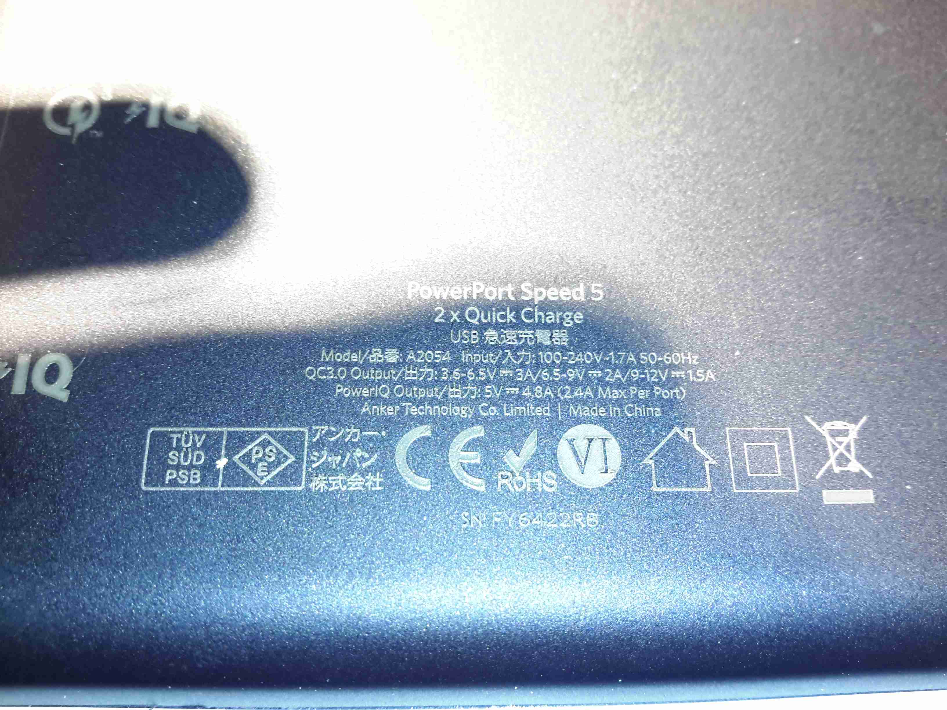
The power capacity of this charger is pretty impressive, with outputs for QC3 from 3.6-6.5v at 3A, up to 12v 1.5A. Standard USB charging is limited at 4.8A for the other 3 ports.
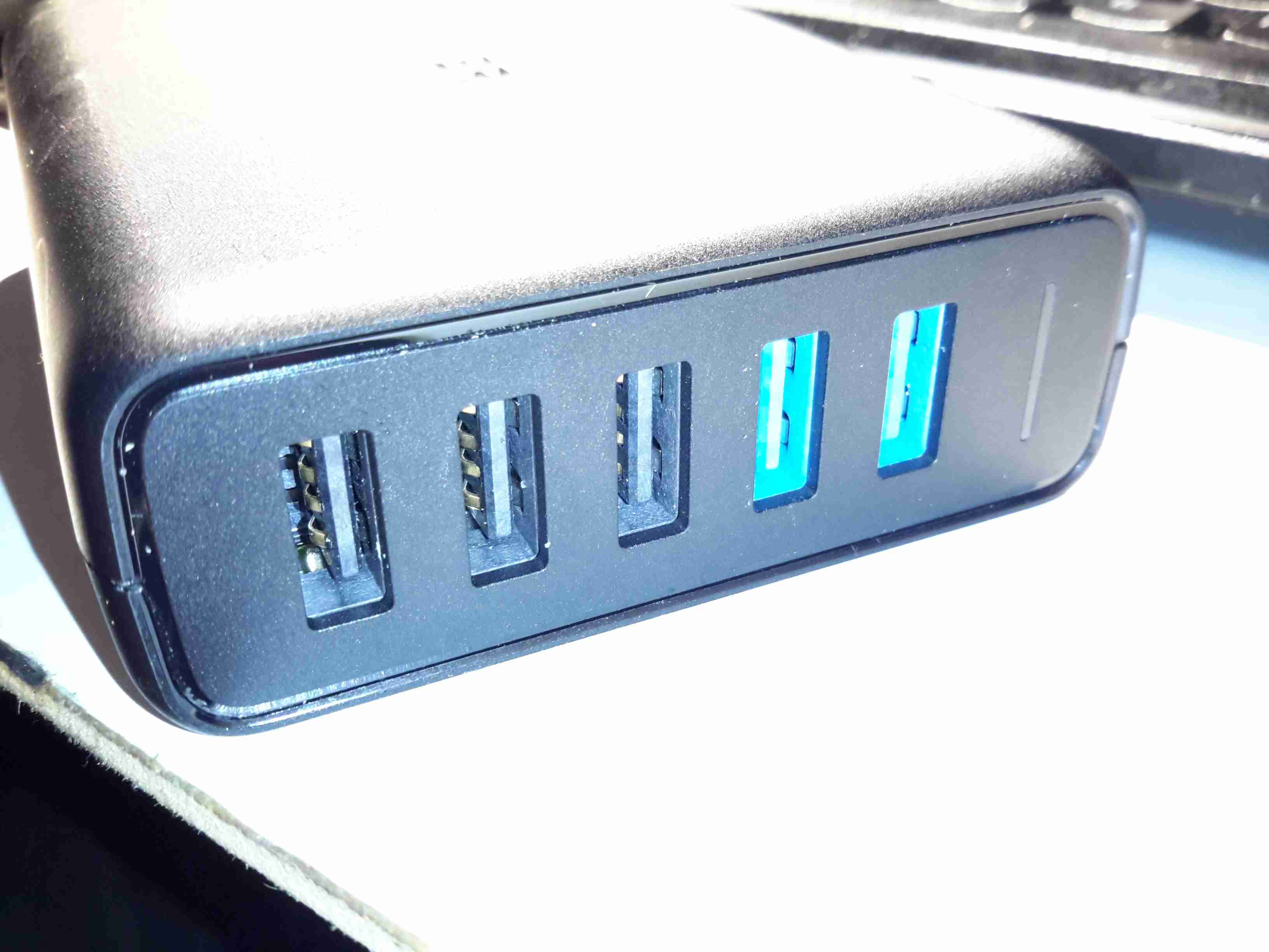
The two of the 5 USB ports are colour coded blue on the QC3 ports. The other 3 are standard 5v ports, the only thing that doesn’t make sense in the ratings is the overall current rating of the 5v supply (4.8A), and the rated current of each of the ports (2.4A) – this is 7.2A total rather than 4.8A.
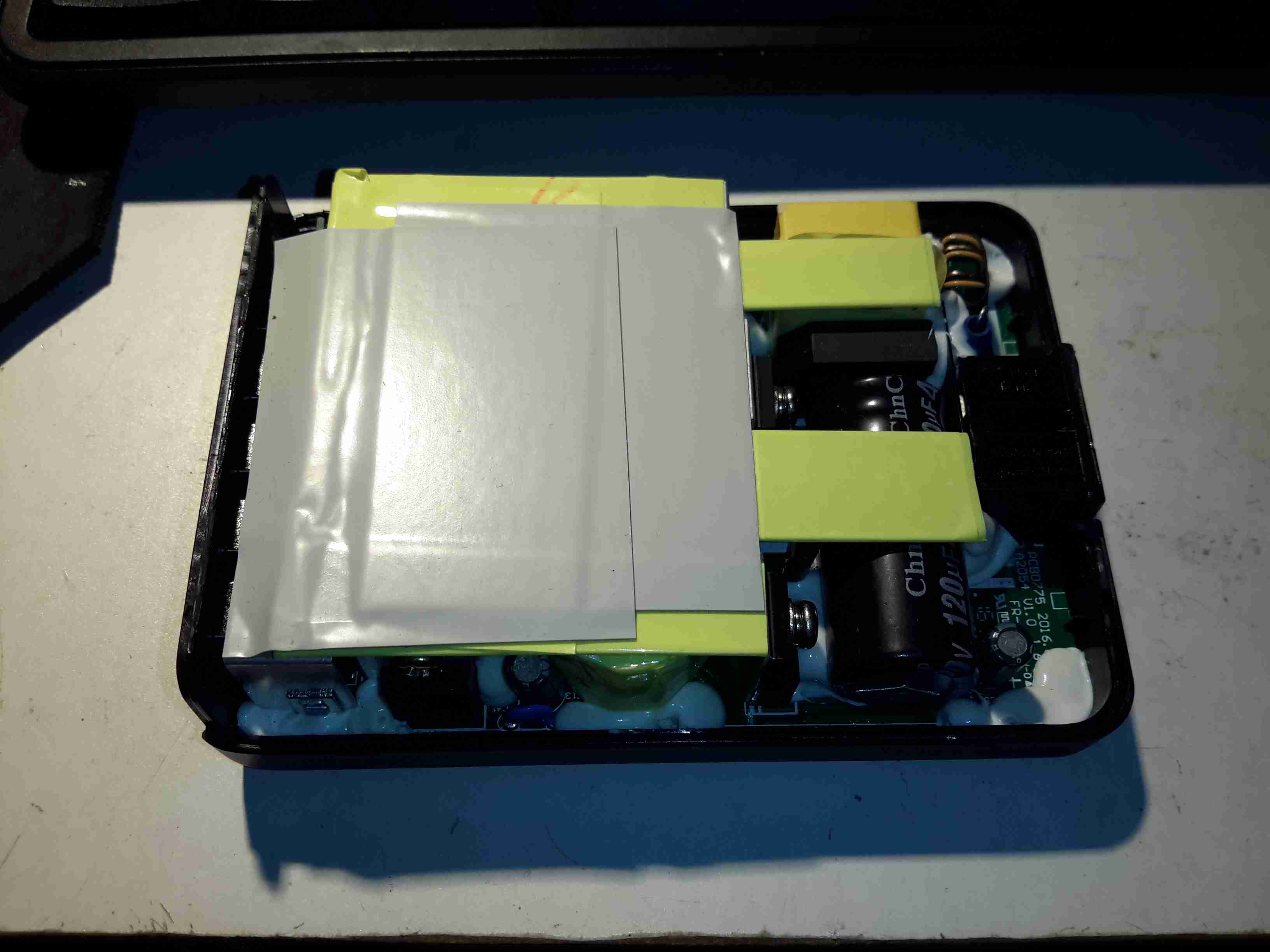
The casing is glued together at the seam, but it gave in to some percussive attack with a screwdriver handle. The inside of this supply is mostly hidden by the large heatspreader on the top.
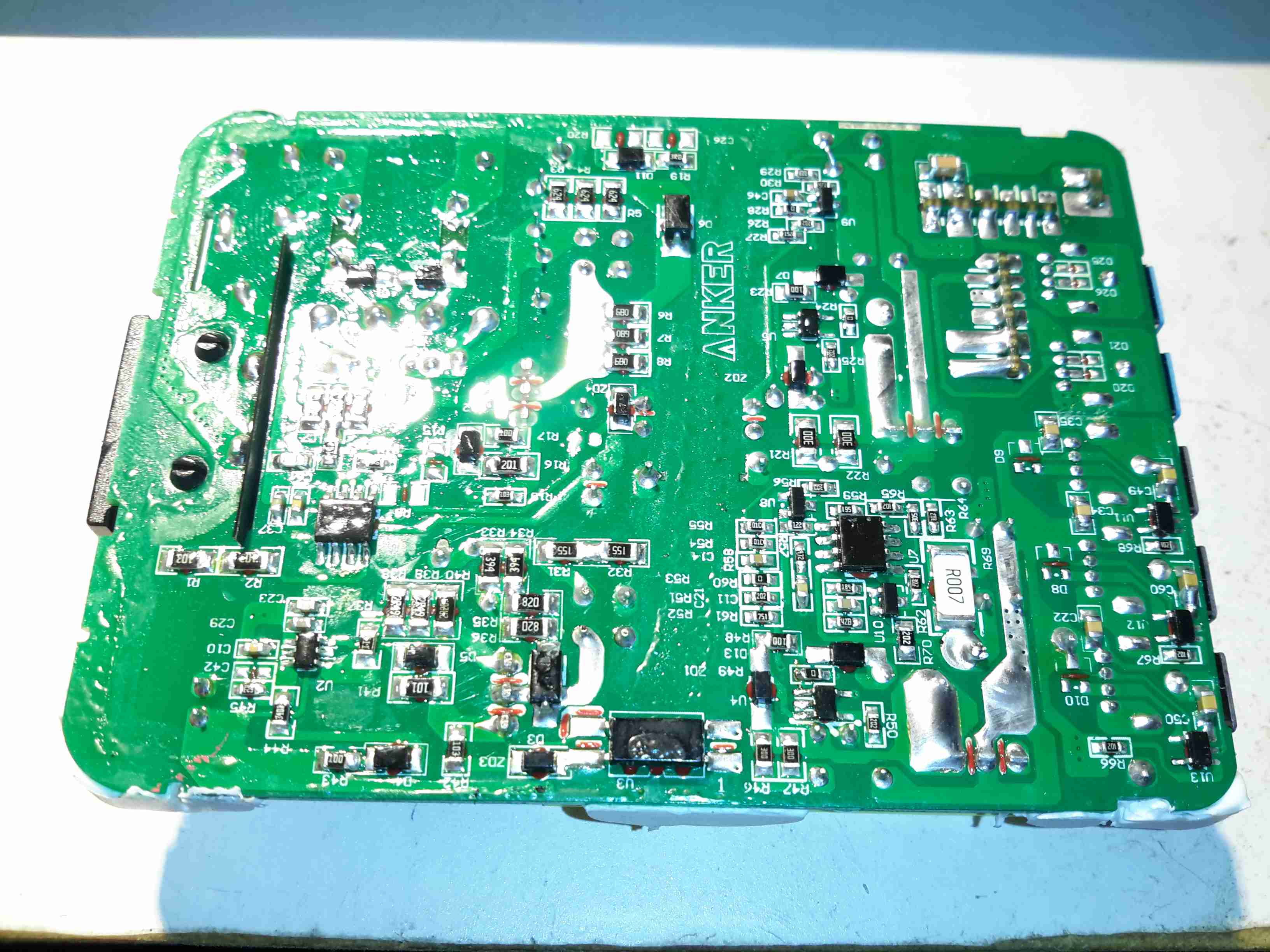
This is a nicely designed board, the creepage distances are at least 8mm between the primary & secondary sides, the bottom also has a conformal coating, with extra silicone around the primary-side switching transistor pins, presumably to decrease the chances of the board flashing over between the close pins.
On the lower 3 USB ports can be seen the 3 SOT-23 USB charge control ICs. These are probably similar to the Texas Instruments TPS2514 controllers, which I’ve experimented with before, however I can’t read the numbers due to the conformal coating. The other semiconductors on this side of the board are part of the voltage feedback circuits for the SMPS. The 5v supply optocoupler is in the centre bottom of the board.
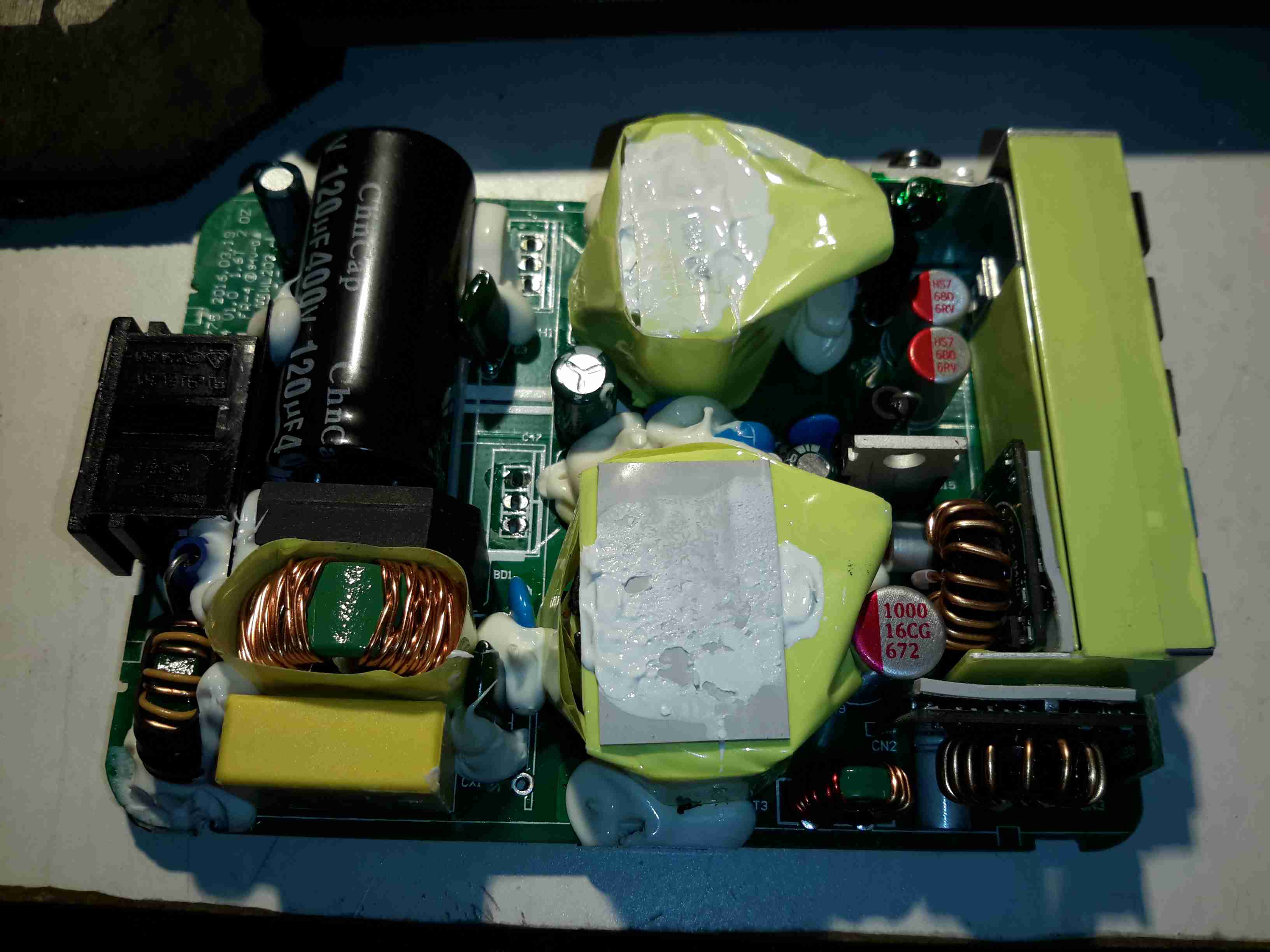
Desoldering the pair of primary side transistors allowed me to easily remove the heatspreader from the supply. There’s thermal pads & grease over everything to get rid of the heat. Here can be seen there are two transformers, forming completely separate supplies for the standard USB side of things & the QC3 side. Measuring the voltages on the main filter capacitors showed me the difference – the QC3 supply is held at 14.2v, and is managed through other circuits further on in the power chain. There’s plenty of mains filtering on the input, as well as common-mode chokes on the DC outputs before they reach the USB ports.
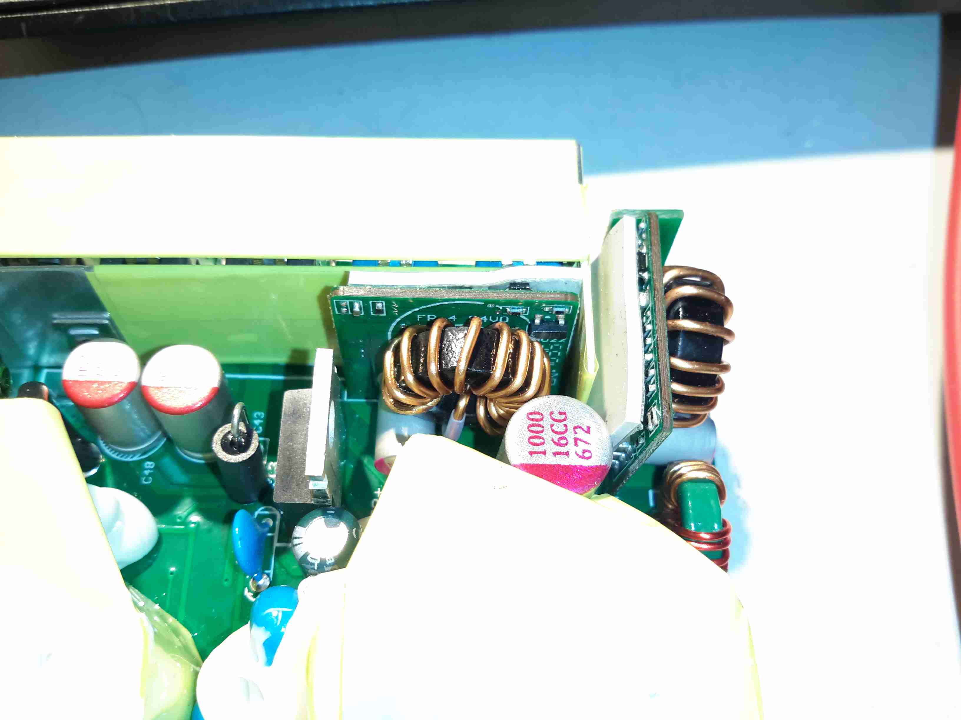
Here’s where the QC3 magic happens, a small DC-DC buck converter for each of the two ports. The data lines are also connected to these modules, so all the control logic is located on these too. The TO-220 device to the left is the main rectifier.
