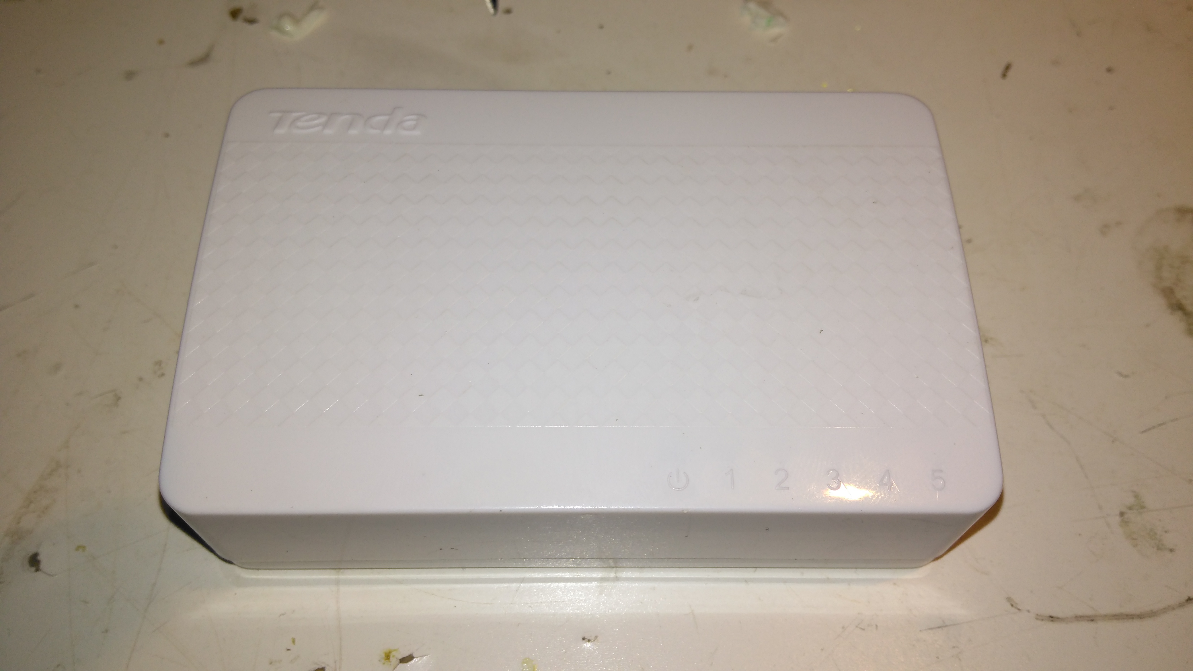
Here’s a tiny ethernet switch from the great fle market that is eBay – the Tenda S105. This unit has 5 ports, but only supports 10/100M. Still, for something so small it’s not bad.
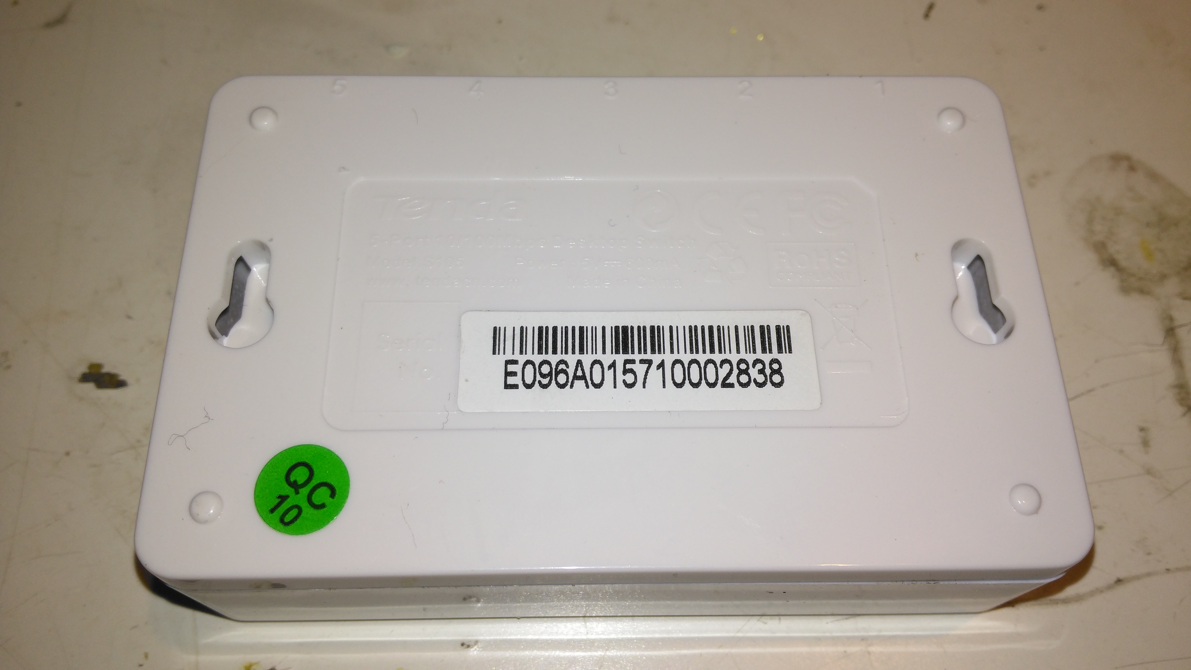
Bottom
Not much on the bottom, there’s a pair of screw hooks for mounting this to a surface.
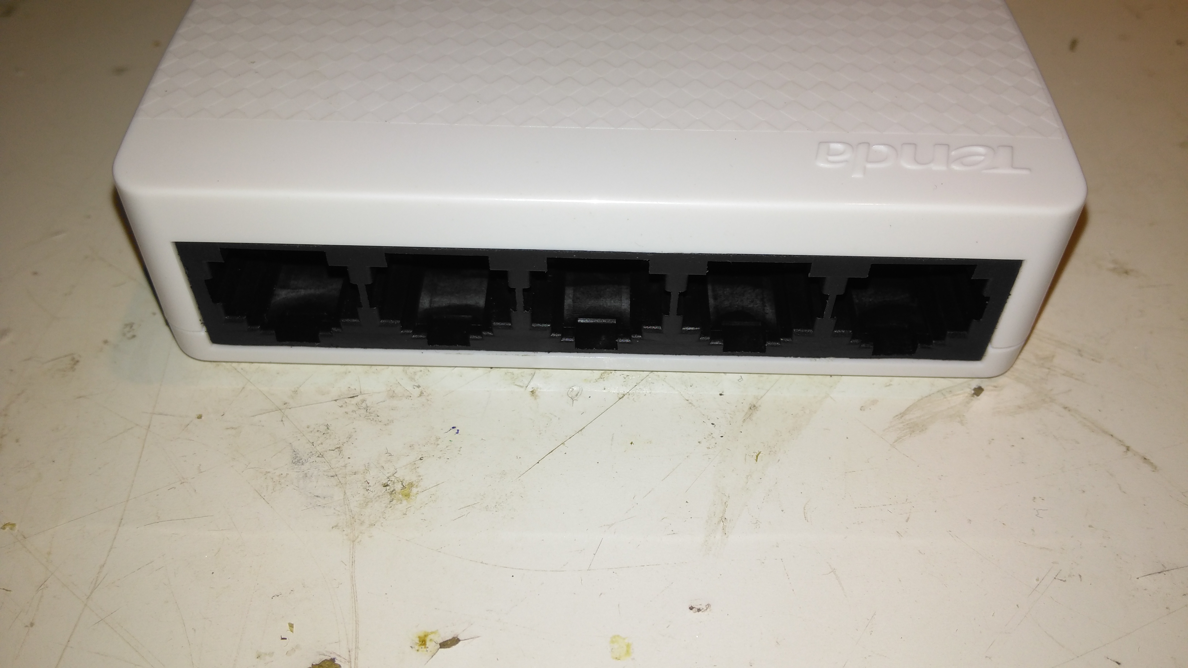
Ports
The 5 ports on the front actually have the pins for the unused pairs of the ethernet cables removed – saving every penny here.
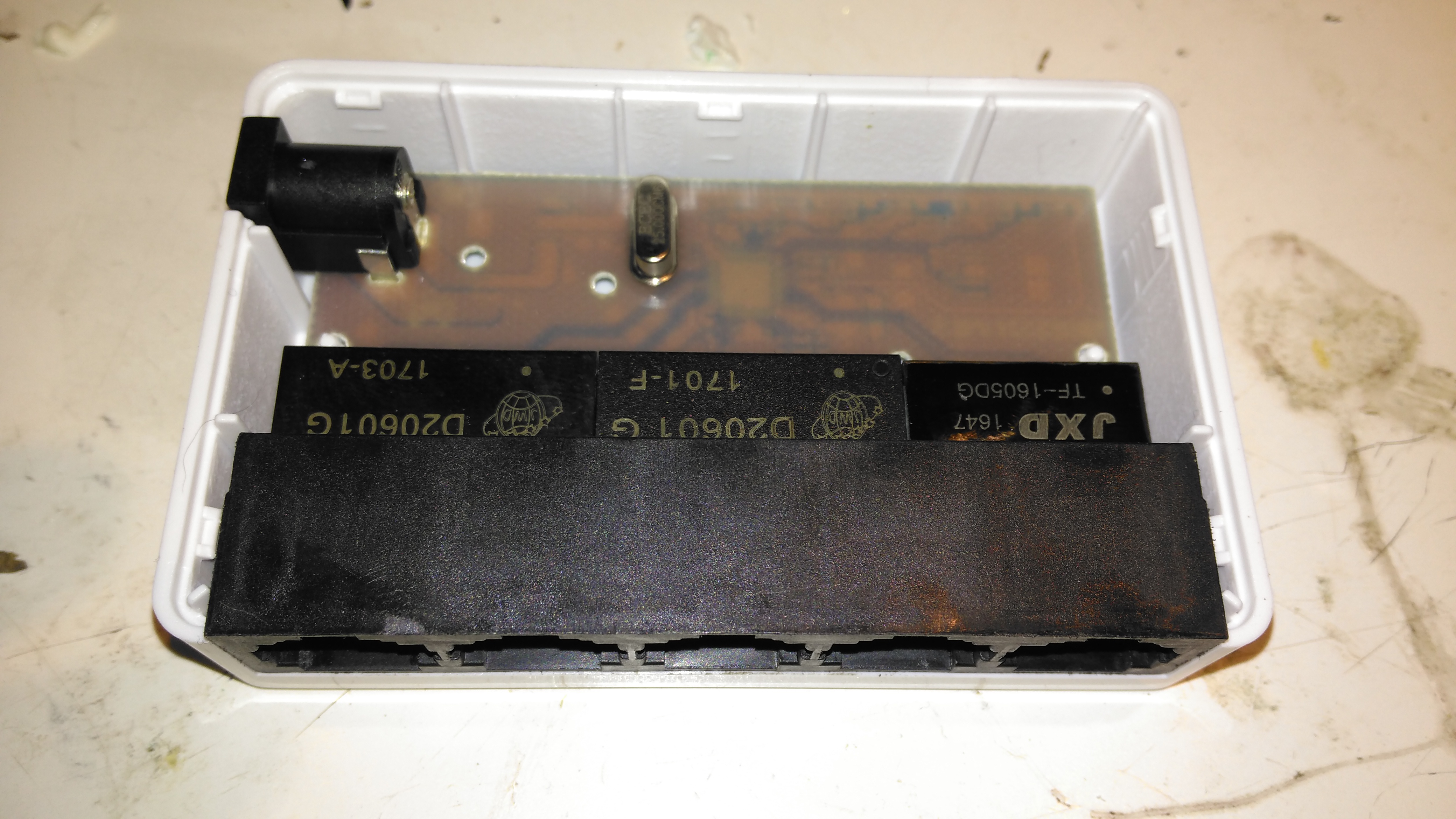
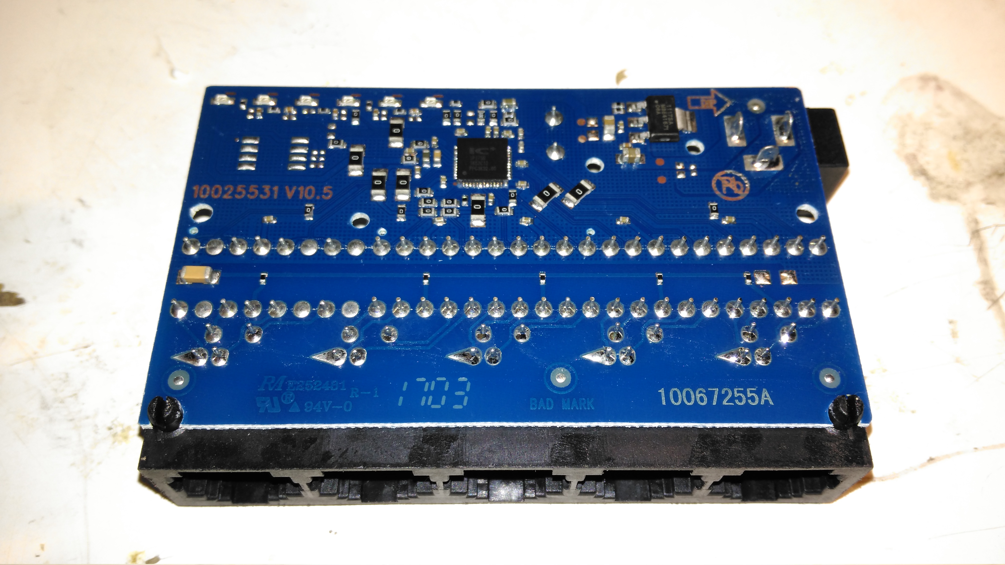
PCB Top
The casing just unclips, revealing the small PCB. Nothing much on the top, just the connectors, isolating transformers & the crystal for the switch IC.
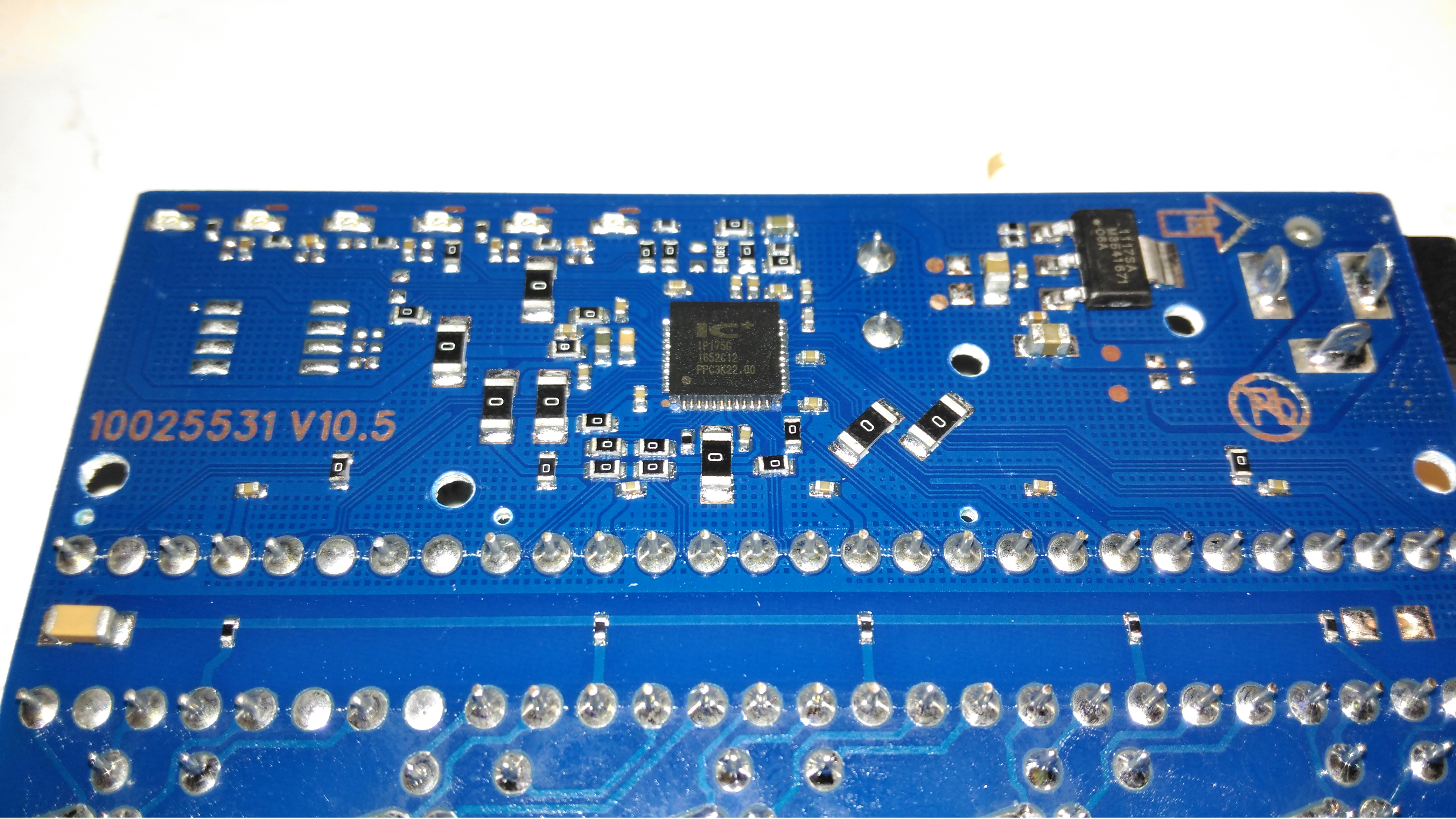
PCB Bottom
The bottom of the PCB is a little more busy, mainly with decoupling components. There’s a 3.3v linear regulator to step down the 5v input for the switch IC.
Switch IC
The IC doing all the data switching is an IP175G 5-Port 10/100 Switch from IC+ Corp. No datasheet available for this, but it’s going to be a bog-standard switch.
A few months ago I did a teardown on this Anker PowerPort Speed 5 USB charger, but I didn’t get round to detailing the conversion to 12v I had to do, so I’ll get to that now I’ve got a couple more to convert over.
Power Module
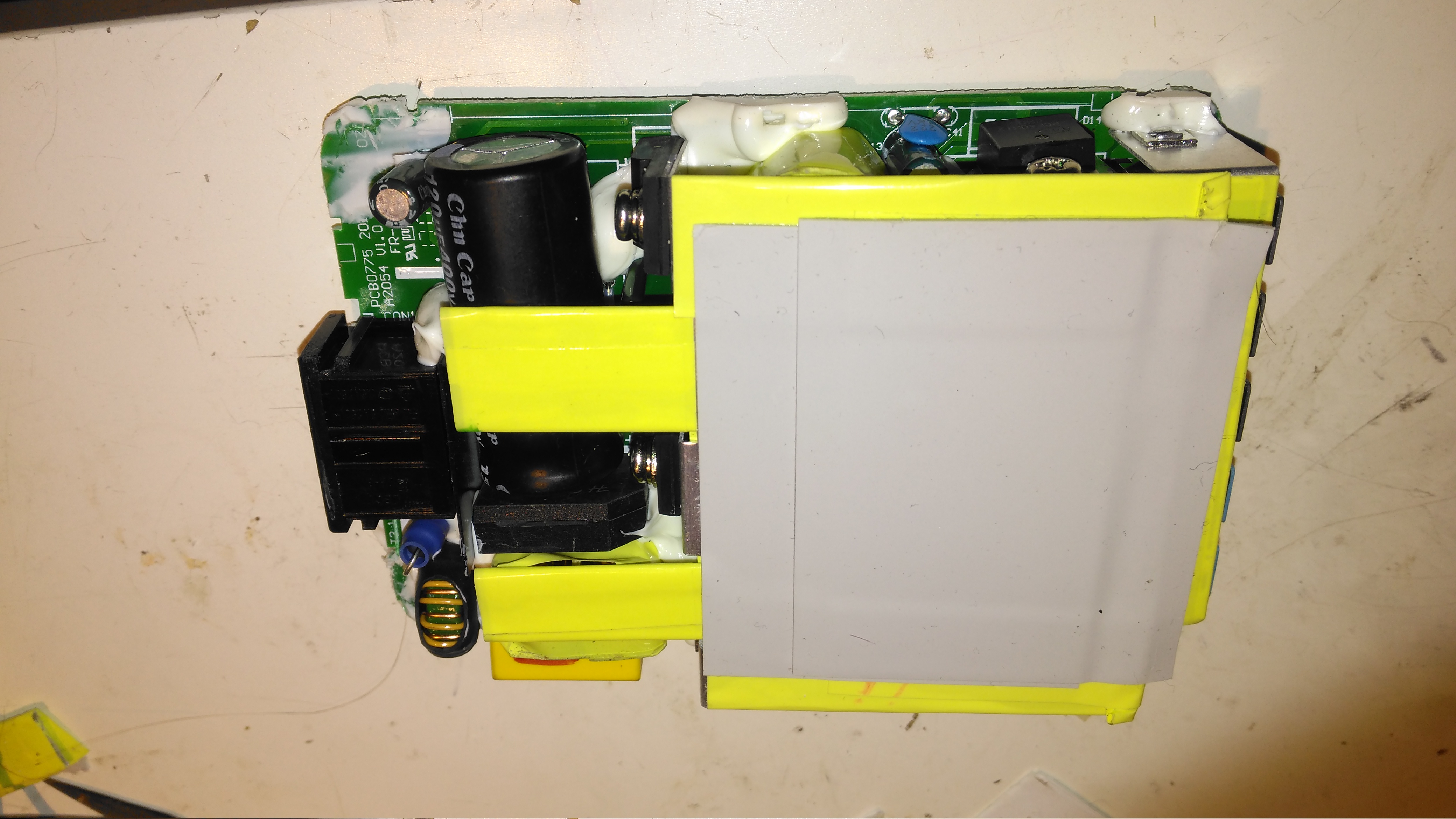
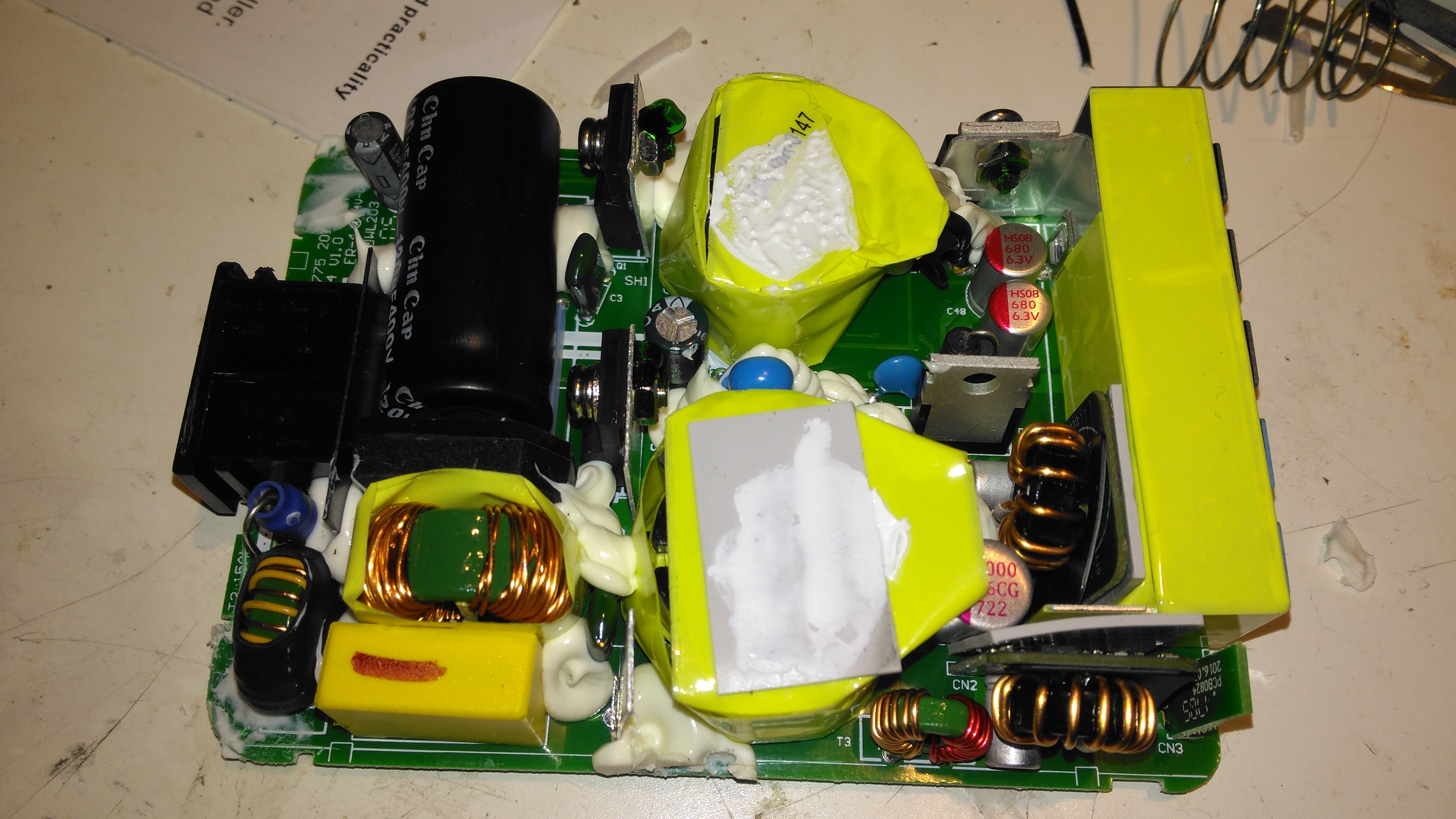
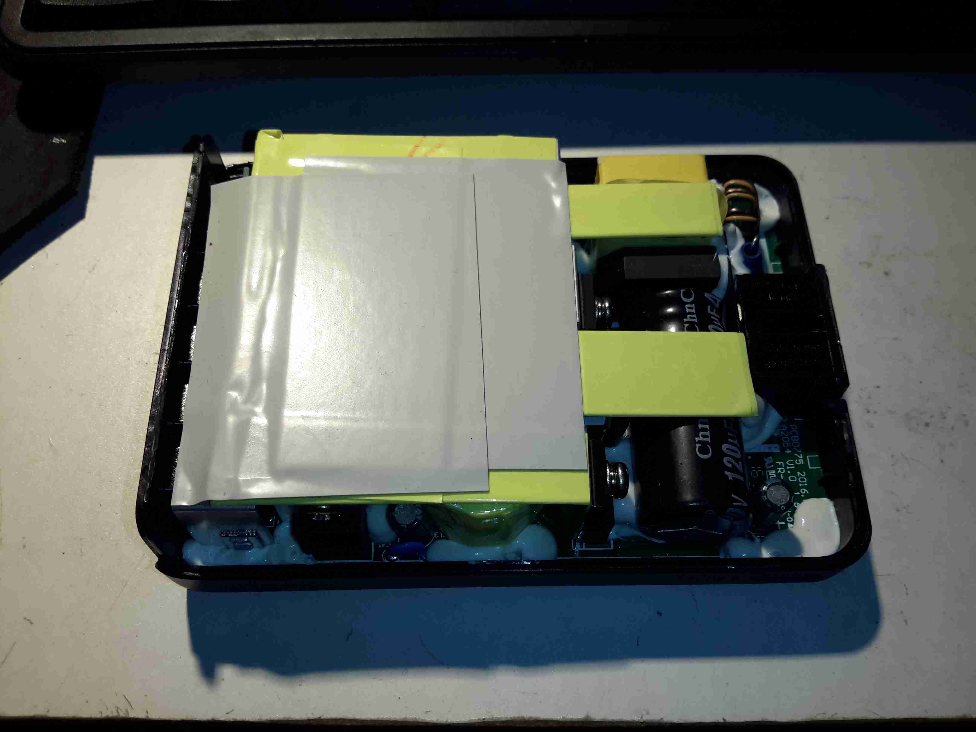
Here’s the internals of the Anker charger once I’ve removed the casing – which like many things these days, is glued together. (Joints can be cracked with a screwdriver handle without damaging the case). There’s lots of heatsinking in here to cool the primary side switching devices & the pot core transformers, so this is the first thing to get removed.
Heatsink Removed
Once the heatsink has been removed, the pot core transformers are visible, wrapped in yellow tape. There’s some more heatsink pads & thermal grease here, to conduct heat better. The transformers, primary side switching components & input filter capacitor have to go.
Primary Side Components Removed
Here’s the PCB once all the now redundant mains conversion components have been deleted. I’ve left the input filtering & bridge rectifier in place, as this solves the issue of the figure-8 cable on the input being reversible, polarity of the input doesn’t matter with the bridge. I’ve removed the main filter capacitor to make enough room for the DC-DC converters to be fitted.
Tails Installed
Installing the tails to connect everything together is the next step, this charger requires two power supplies – the QC3 circuits need 14.4v to supply the multi-voltage modules, the remaining 3 standard ports require 5v. The DC input tails are soldered into place where the main filter capacitor was, while the outputs are fitted to the spot the transformer secondary windings ended up. I’ve left the factory Schottky rectifiers in place on the secondary side to make things a little more simple, the output voltages of both the DC-DC converters does need to be increased slightly to compensate for the diode drops though. I’ve also bypassed the mains input fuse, as at 12v the input current is going to be substantially higher than when used on mains voltage.
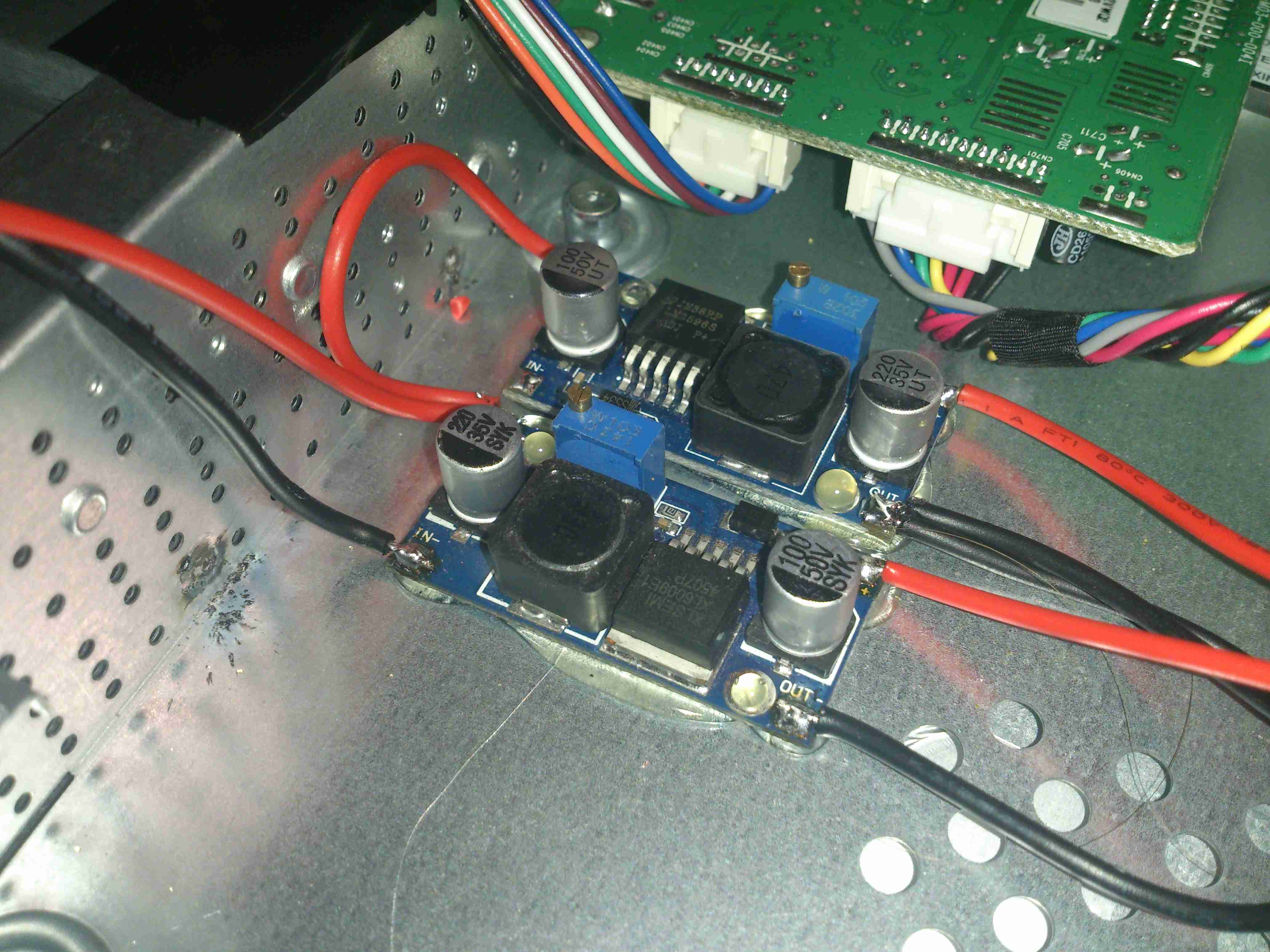
DC-DC Converters Installed
With a squeeze both the boost converter & the buck converter fit into place on the PCB.
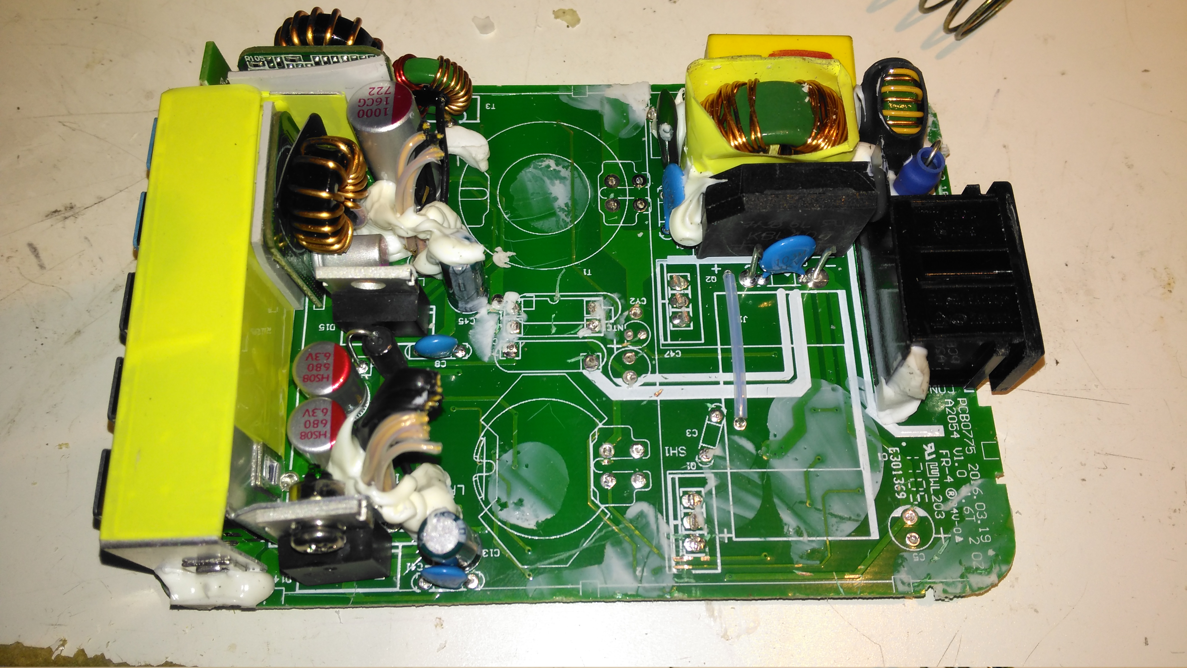
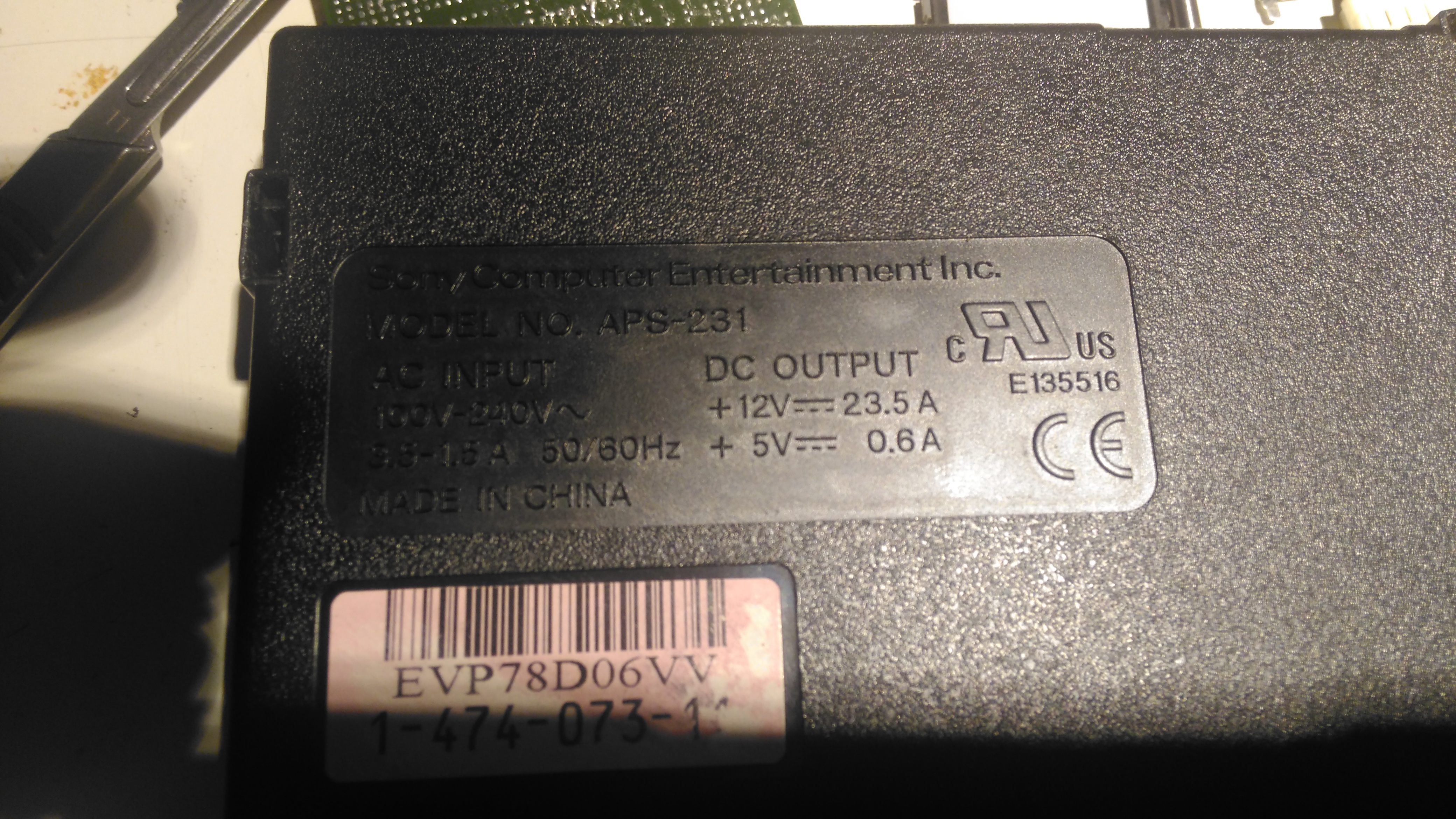
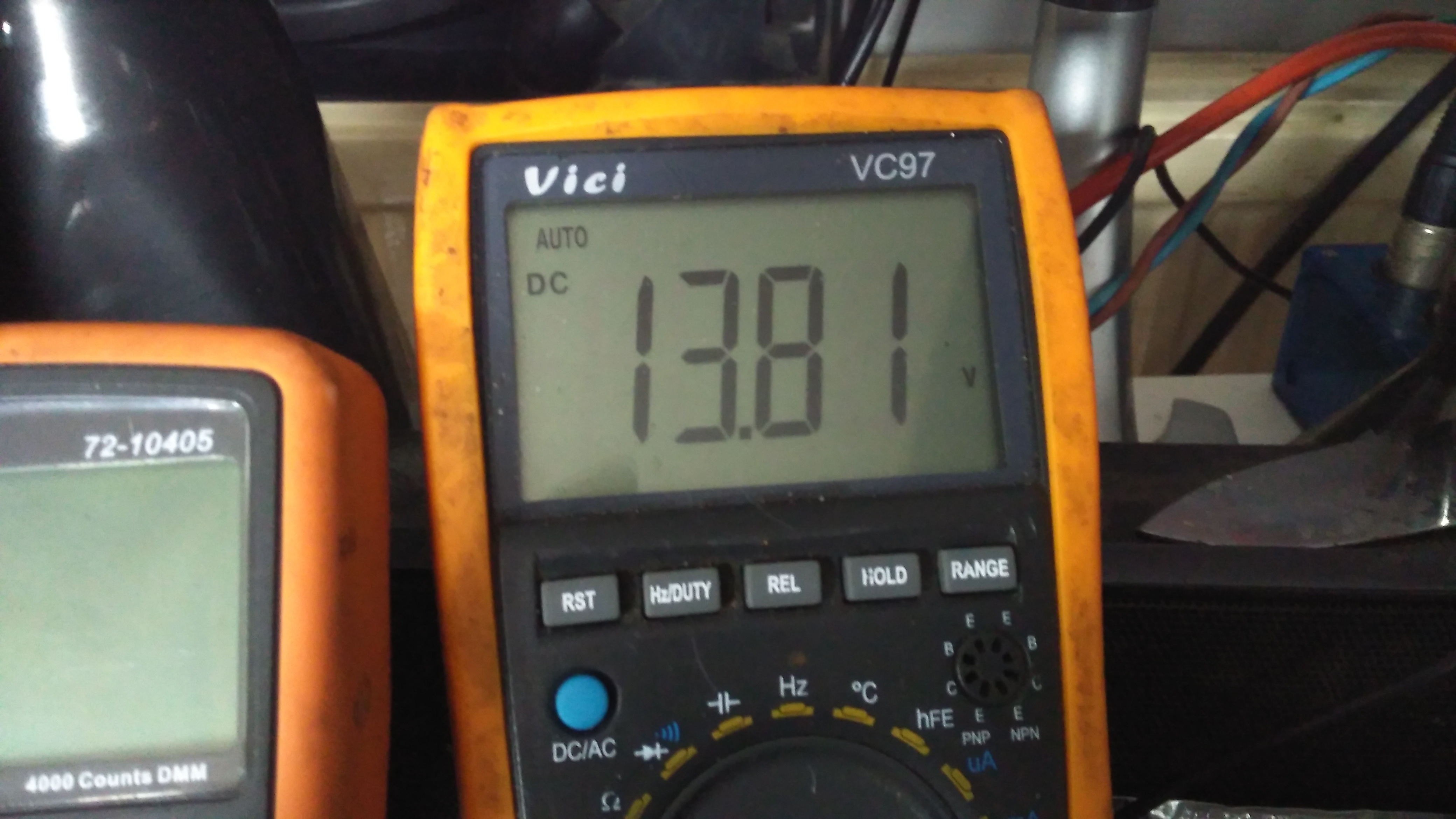
I was recently given a Sony PS3 with a dead disc drive, and since I’m not a console gamer I figured I’d see if there were any handy parts inside. Turns out these units contain a rather nice SMPS, the Sony APS-231 with a high power 12v rail, rated at 23.5A. A bit of searching around discovered a thread on the BadCaps Forums about voltage modding these supplies for a 13.8v output, suitable for my Ham radio gear.
These supplies are controlled by a Sony CXA8038A, for which there is very little information. Active PFC is included, along with synchronous rectification which increases the efficiency of the supply, and in turn, reduces the waste heat output from the rectifiers.
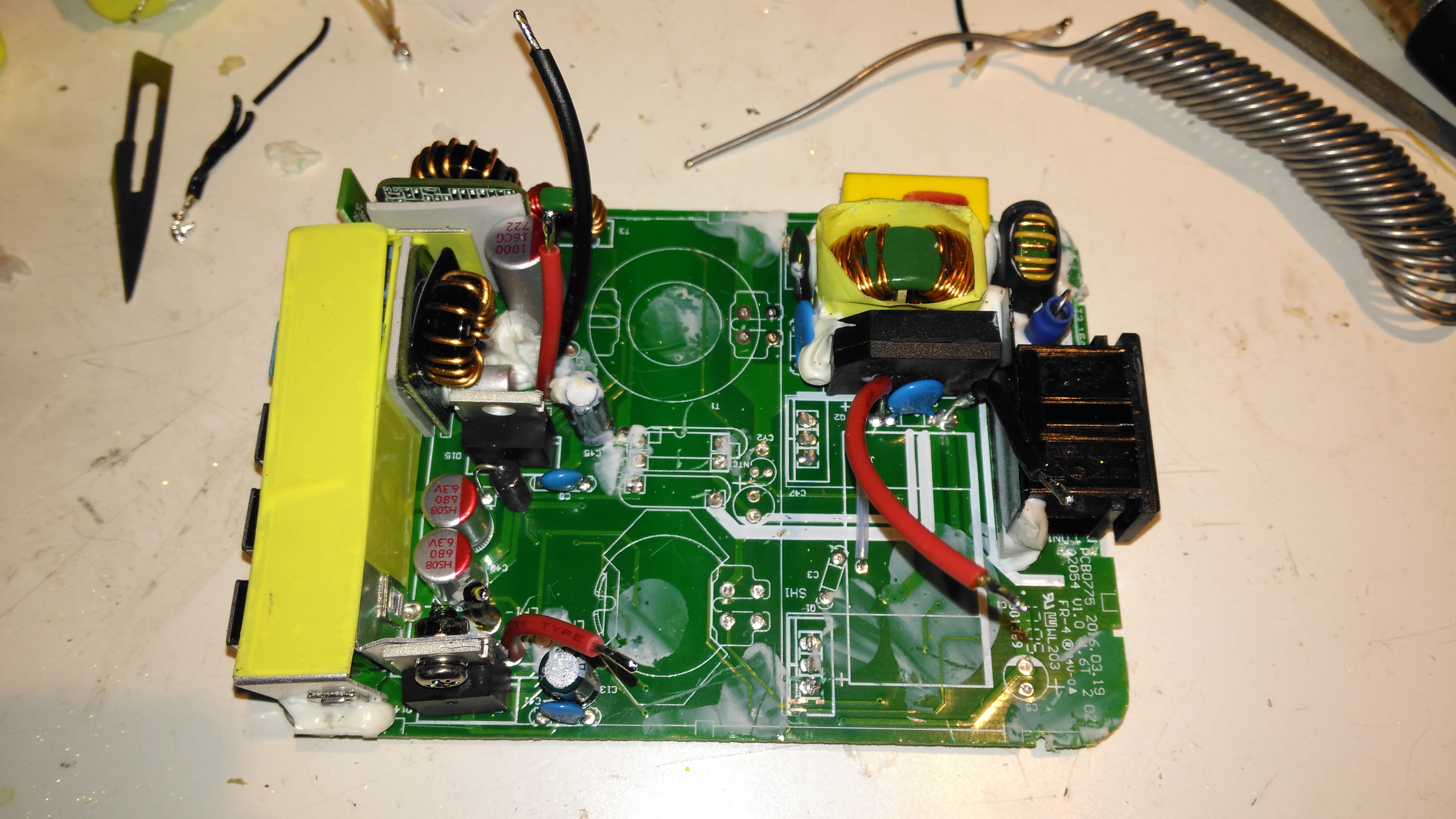
Regulation Section
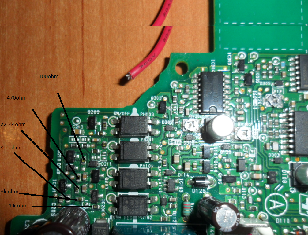
Like many of the SMPS units I’ve seen, the output voltage is controlled by referencing it to an adjustable shunt reference, and adjusting the set point of this reference will in turn adjust the output voltage of the supply, this is done in circuit by a single resistor.
Here’s the regulator section of the PSU, with the resistors labelled. The one we’re after changing is the 800Ω one between pins 2 & 3 of the TS2431 shunt reference. It’s a very small 0402 size resistor, located right next to the filter electrolytic for the 5v standby supply circuit. A fine tip on the soldering iron is required to get this resistor removed.
Attachment Points
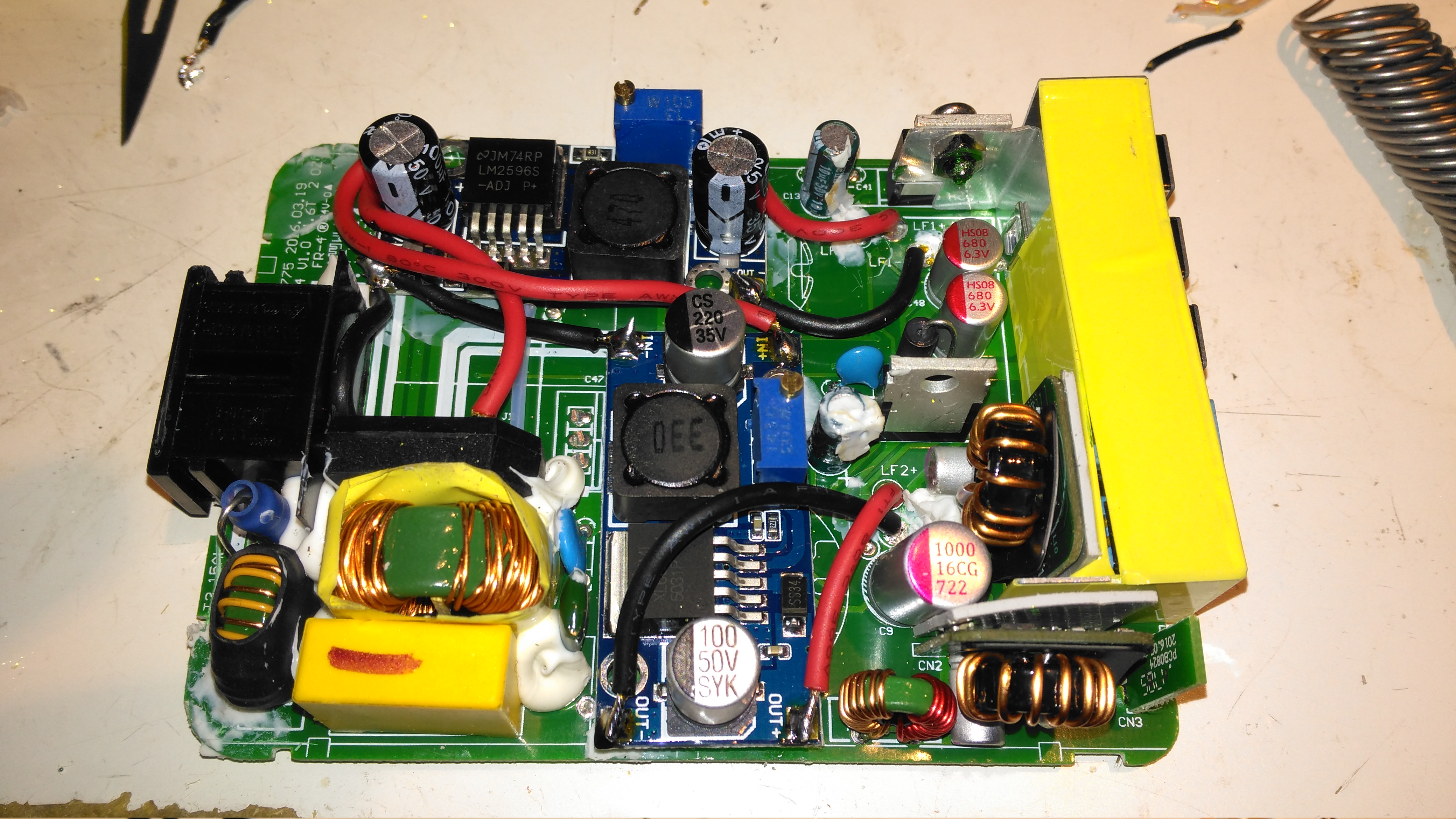
Once this resistor is removed from the circuit, a 1KΩ 18-turn potentiometer is fitted in it’s place, from the Anode (Pin 3) to the Ref. (Pin 2) pins of the TS2431 shunt reference. I initally set the potentiometer to be the same 800Ω as the factory set resistor, to make sure the supply would start up at a sensible voltage before I did the adjustment.
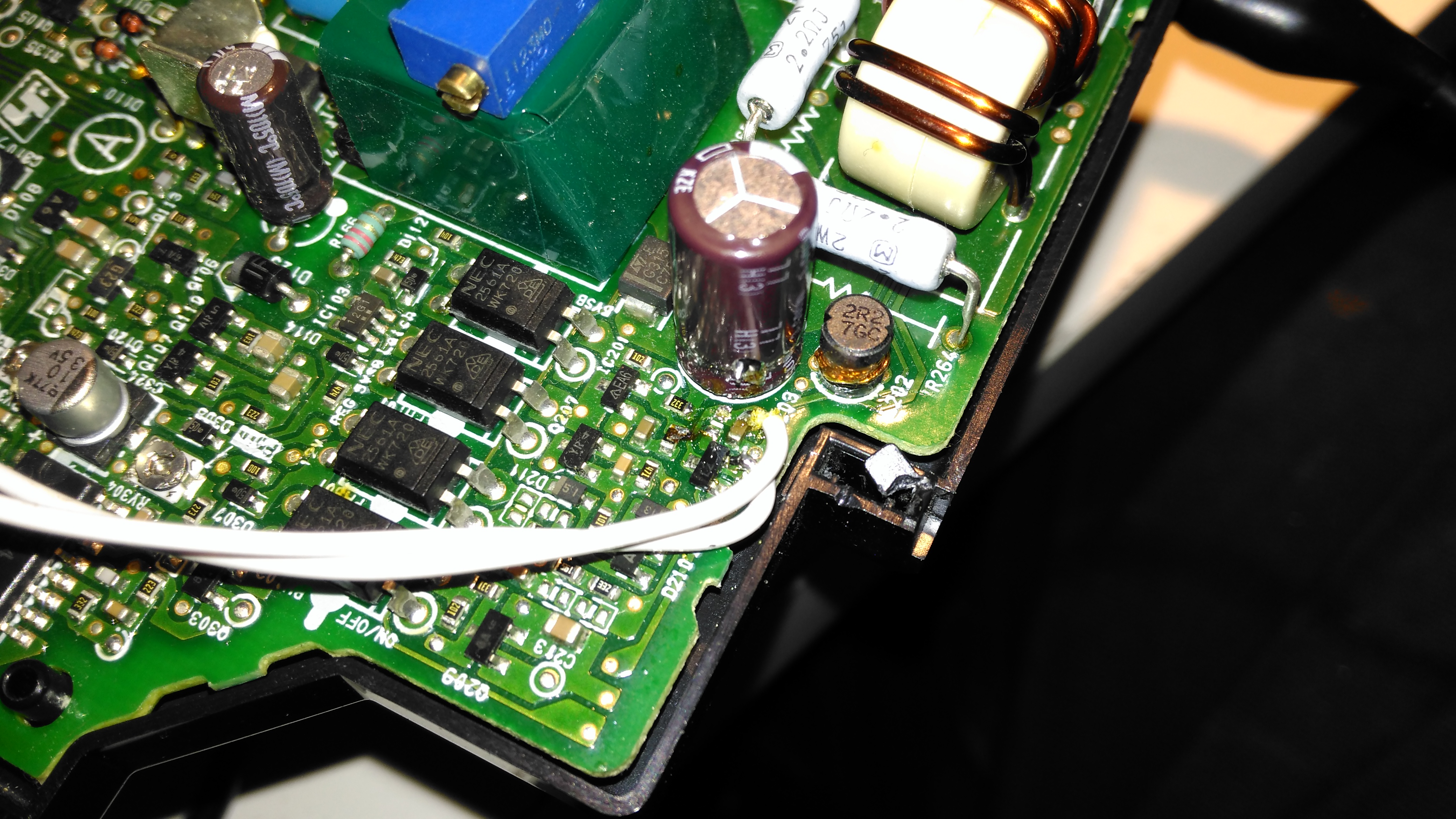
Potentiometer
The pot is secured to the top of the standby supply transformer with a drop of CA glue to stop everything moving around. The supply can now be adjusted to a higher setpoint voltage – 13.8v is about the maxumum, as the OVP cuts the supply out at between 13.9v-14v.
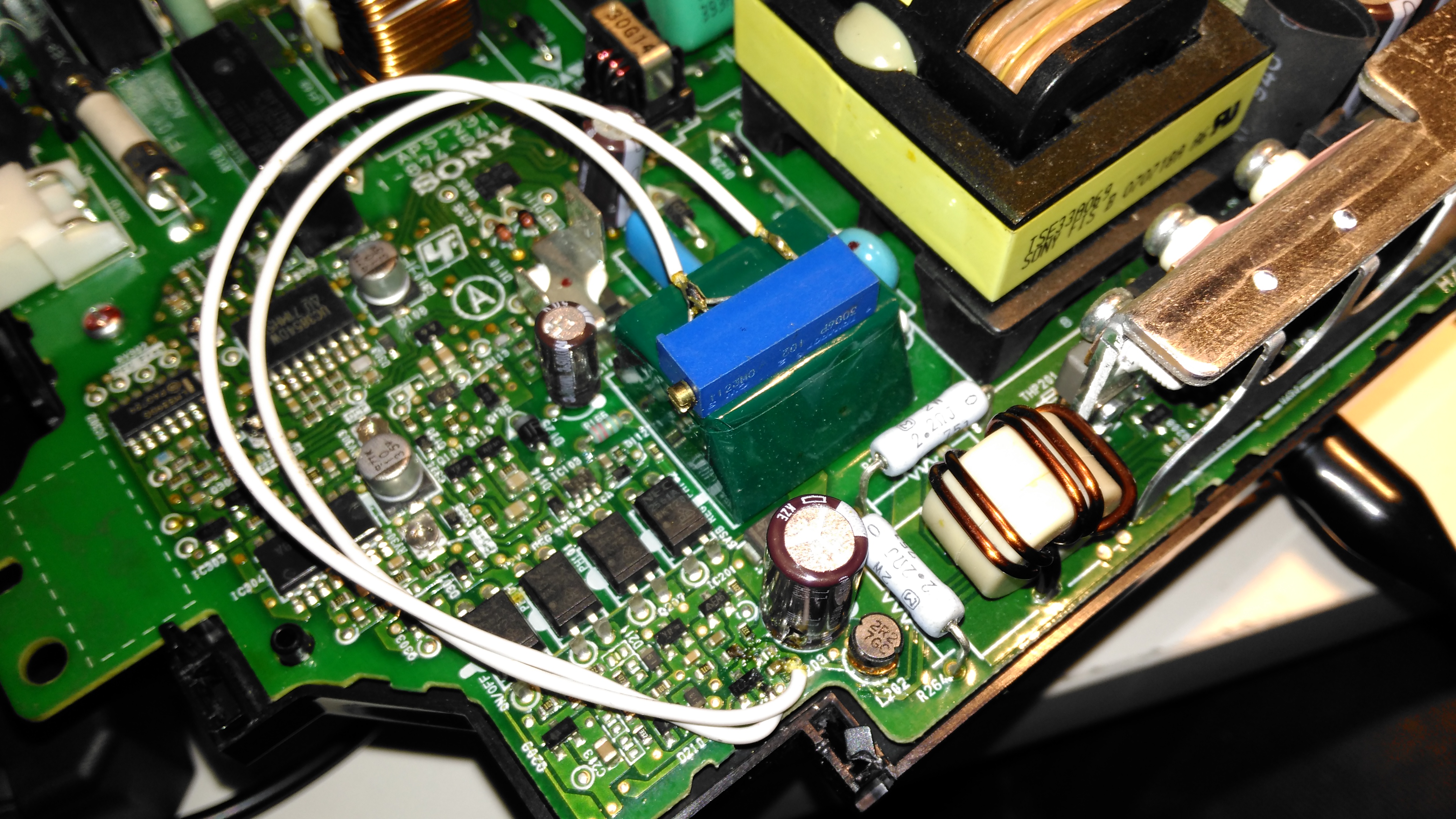
Modded Voltage
After doing some testing at roughly 50% of the supply’s rated load, everything seems to be stable, and nothing is heating up more than I’d expect.
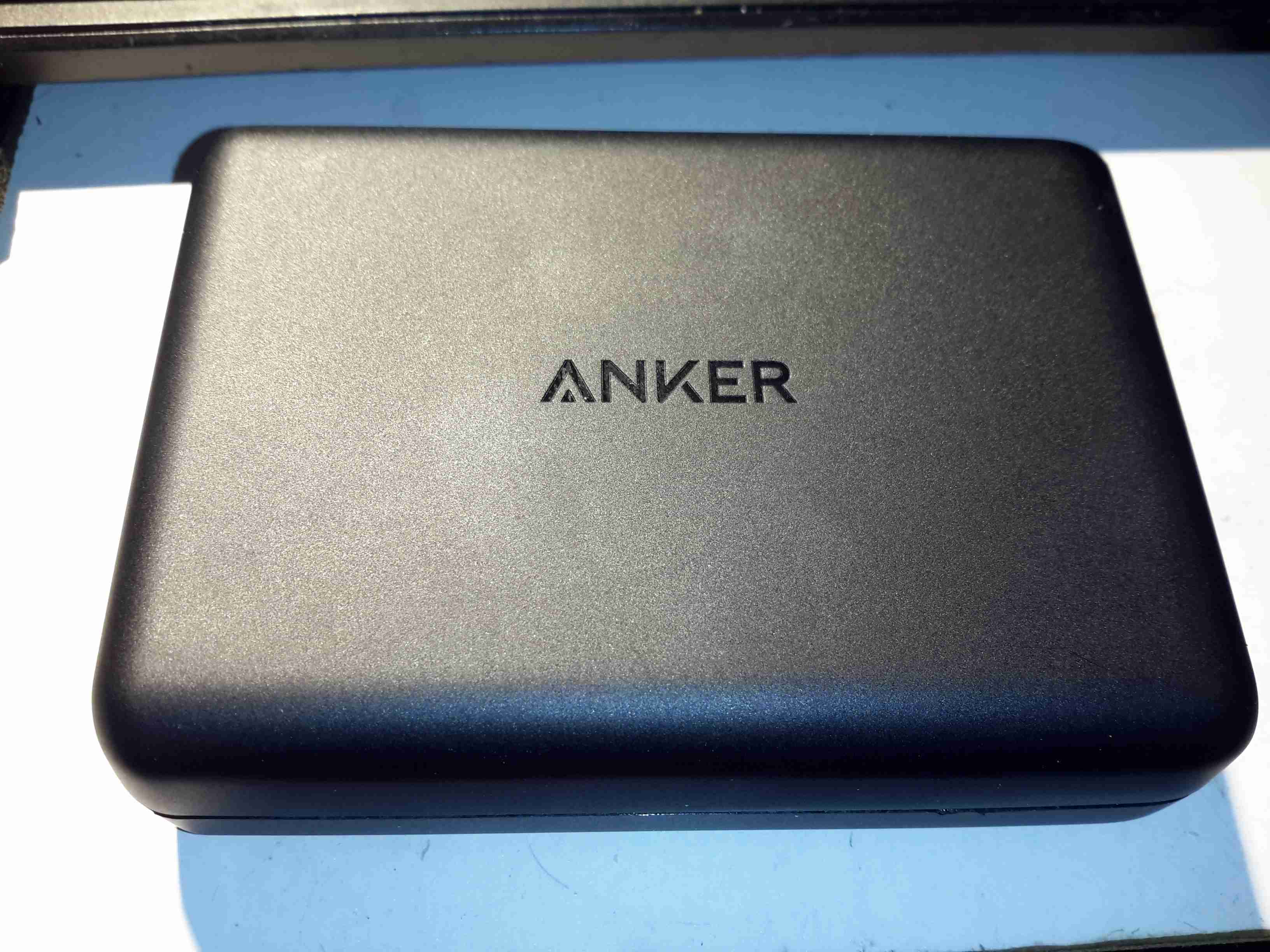
Here’s a piece of tech that is growing all the more important in recent times, with devices with huge battery capacities, a quick charger. This unit supports Qualcomm’s Quick Charge 3 standard, where the device being charged can negotiate with the charger for a higher-power link, by increasing the bus voltage past the usual 5v.
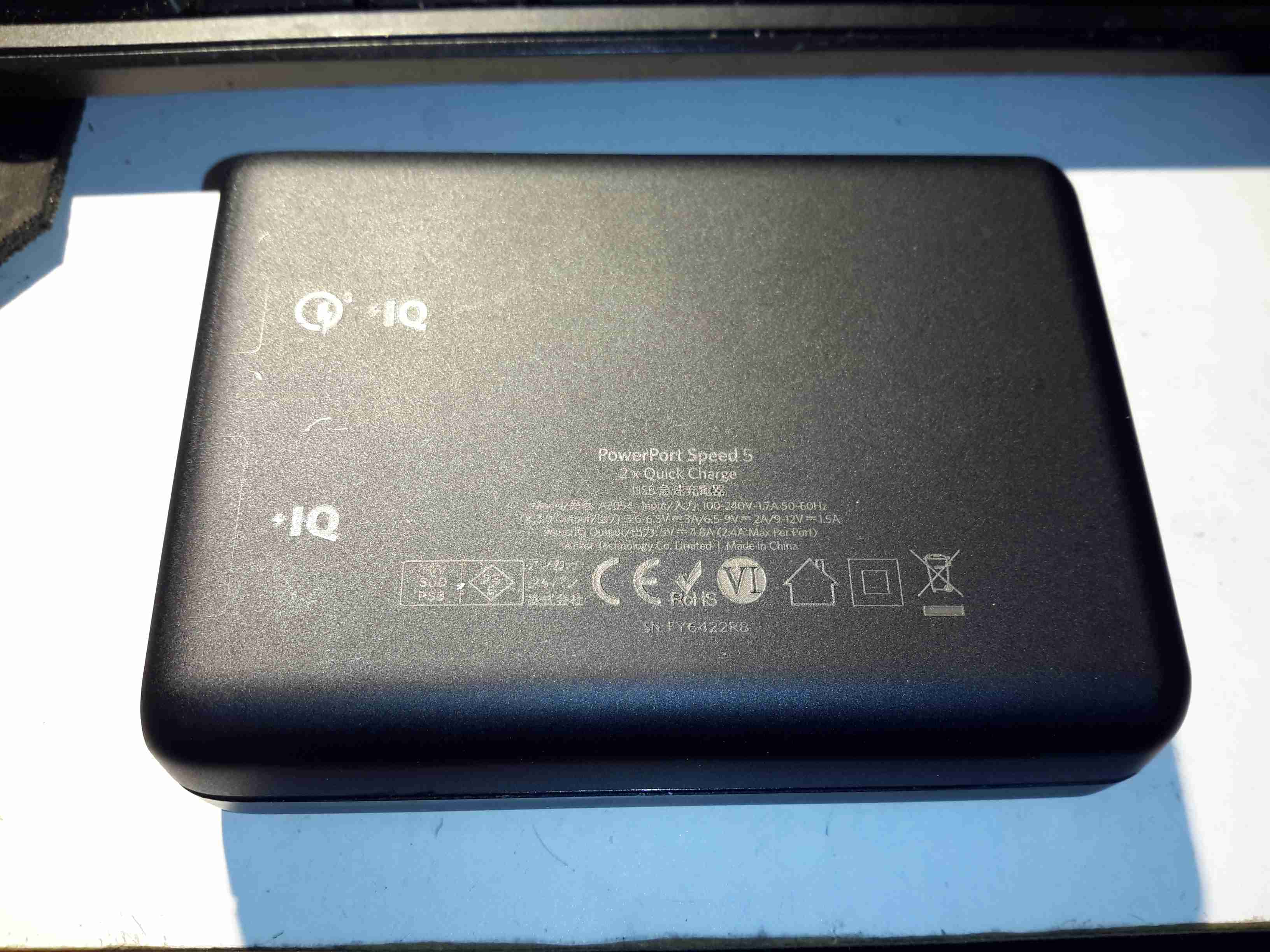
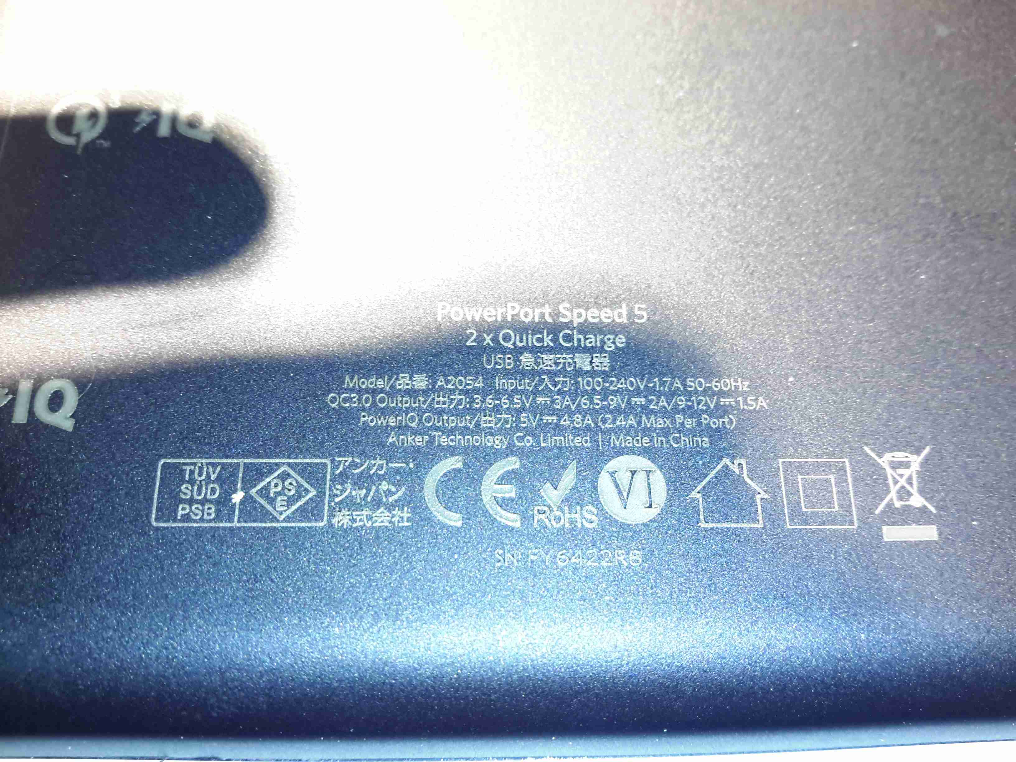
Rear
The casing feels rather nice on this unit, sturdy & well designed. All the legends on the case are laser marked, apart from the front side logo which is part of the injection moulding.
Specifications
The power capacity of this charger is pretty impressive, with outputs for QC3 from 3.6-6.5v at 3A, up to 12v 1.5A. Standard USB charging is limited at 4.8A for the other 3 ports.
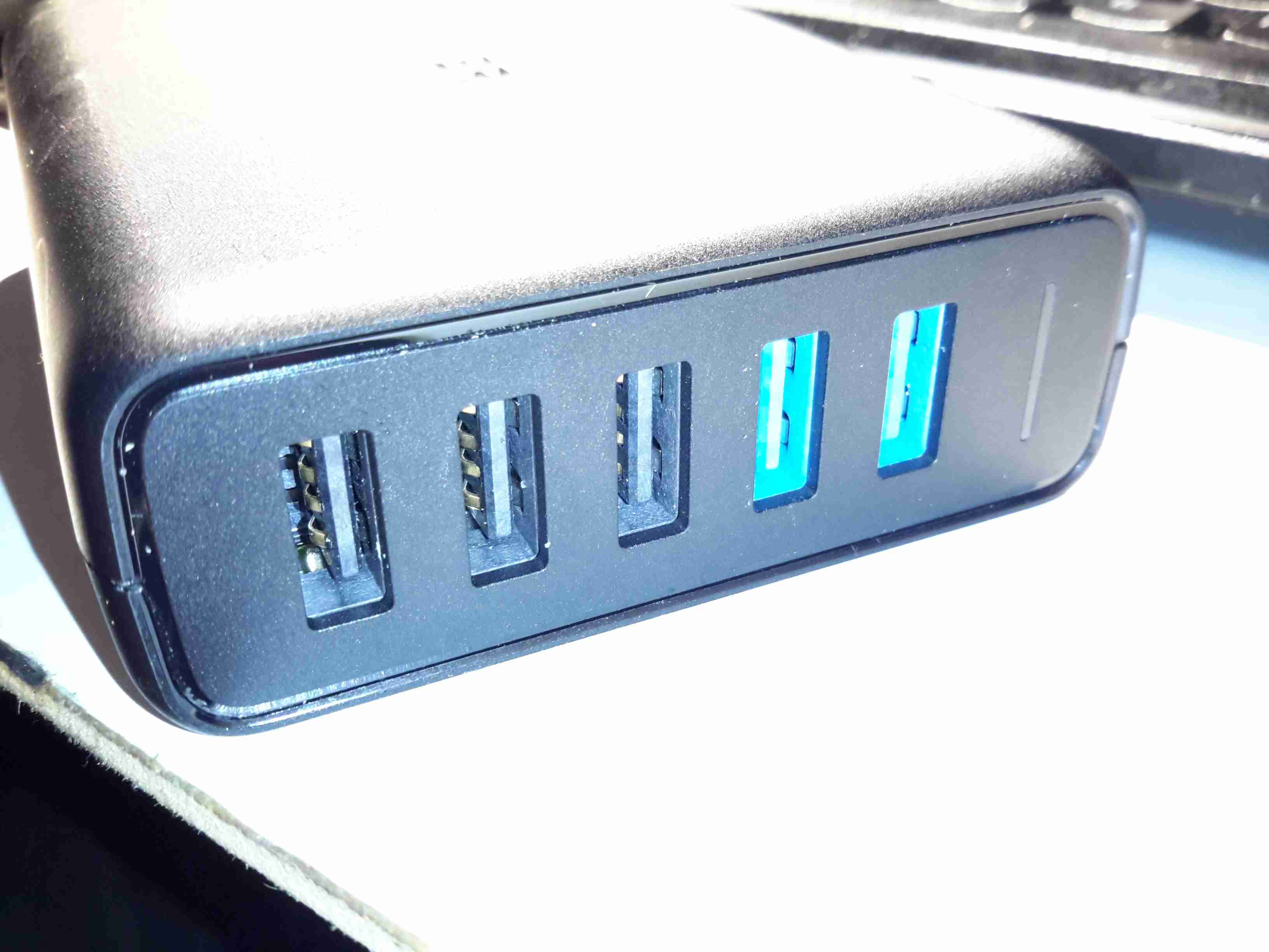
Ports
The two of the 5 USB ports are colour coded blue on the QC3 ports. The other 3 are standard 5v ports, the only thing that doesn’t make sense in the ratings is the overall current rating of the 5v supply (4.8A), and the rated current of each of the ports (2.4A) – this is 7.2A total rather than 4.8A.
Top Removed
The casing is glued together at the seam, but it gave in to some percussive attack with a screwdriver handle. The inside of this supply is mostly hidden by the large heatspreader on the top.
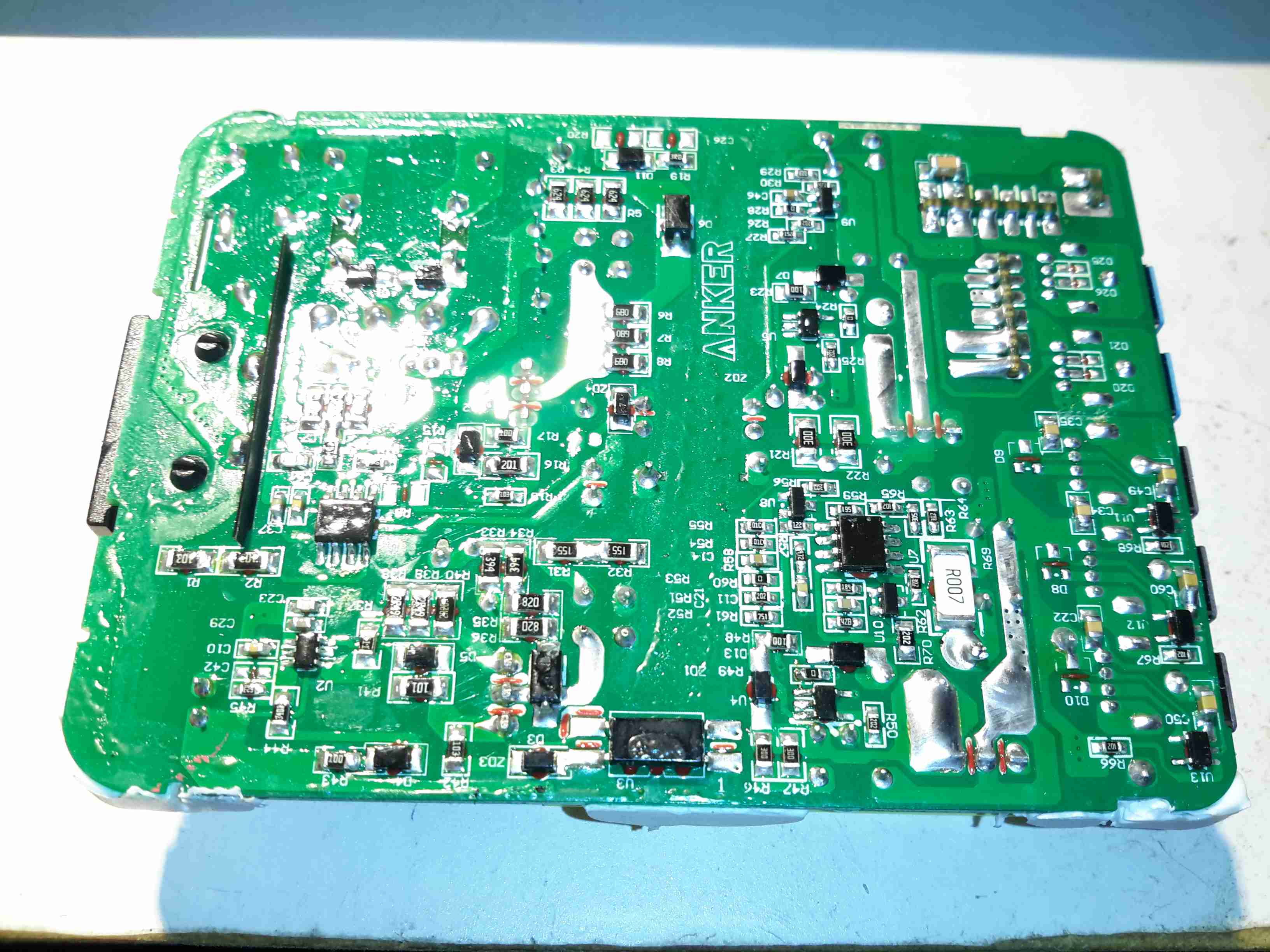
Main PCB Bottom
This is a nicely designed board, the creepage distances are at least 8mm between the primary & secondary sides, the bottom also has a conformal coating, with extra silicone around the primary-side switching transistor pins, presumably to decrease the chances of the board flashing over between the close pins.
On the lower 3 USB ports can be seen the 3 SOT-23 USB charge control ICs. These are probably similar to the Texas Instruments TPS2514 controllers, which I’ve experimented with before, however I can’t read the numbers due to the conformal coating. The other semiconductors on this side of the board are part of the voltage feedback circuits for the SMPS. The 5v supply optocoupler is in the centre bottom of the board.
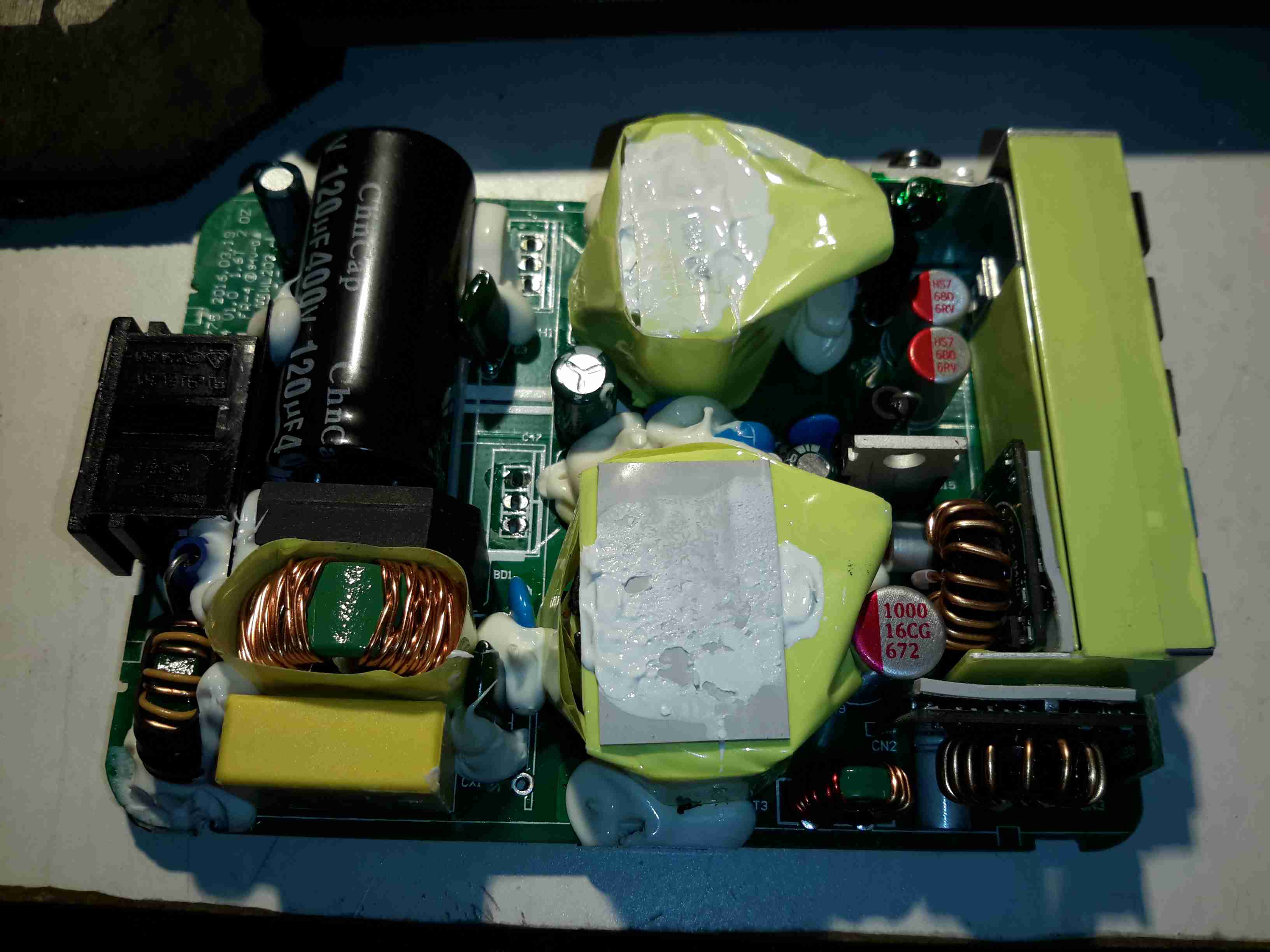
Heatsink Removed
Desoldering the pair of primary side transistors allowed me to easily remove the heatspreader from the supply. There’s thermal pads & grease over everything to get rid of the heat. Here can be seen there are two transformers, forming completely separate supplies for the standard USB side of things & the QC3 side. Measuring the voltages on the main filter capacitors showed me the difference – the QC3 supply is held at 14.2v, and is managed through other circuits further on in the power chain. There’s plenty of mains filtering on the input, as well as common-mode chokes on the DC outputs before they reach the USB ports.
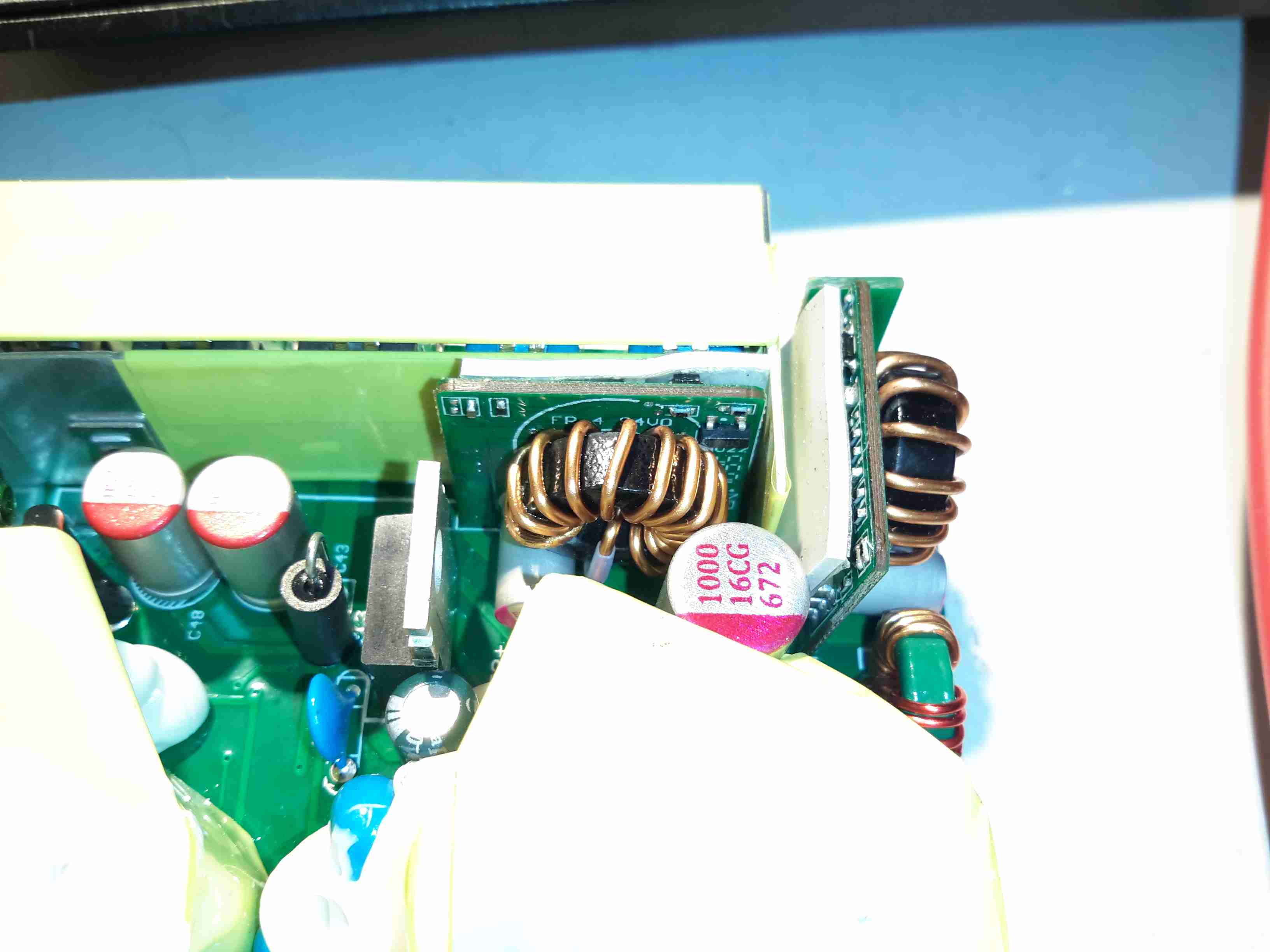
Quick Charge 3 DC-DC Converters
Here’s where the QC3 magic happens, a small DC-DC buck converter for each of the two ports. The data lines are also connected to these modules, so all the control logic is located on these too. The TO-220 device to the left is the main rectifier.
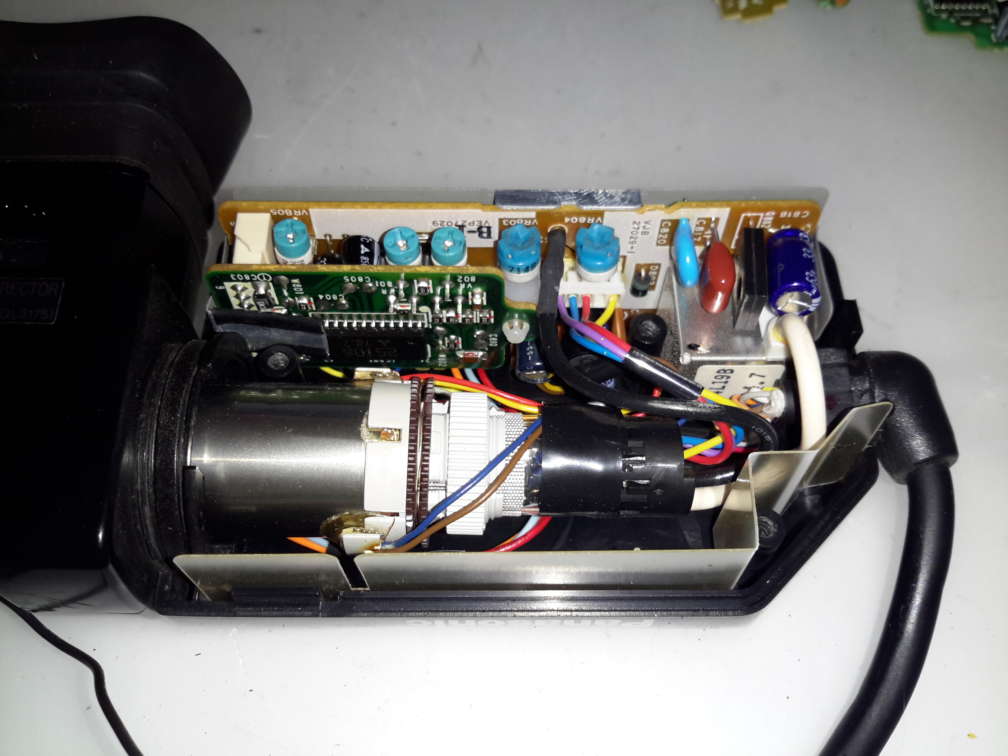
The old Panasonic NV-M5 has the standard for the time CRT based viewfinder assembly, which will happily take a composite video signal from an external source.
This viewfinder has many more connections than I would have expected, as it has an input for the iris signal, which places a movable marker on the edge of the display. This unit also has a pair of outputs for the vertical & horizontal deflection signals, I imagine for sync, but I’ve never seen these signals as an output on a viewfinder before.
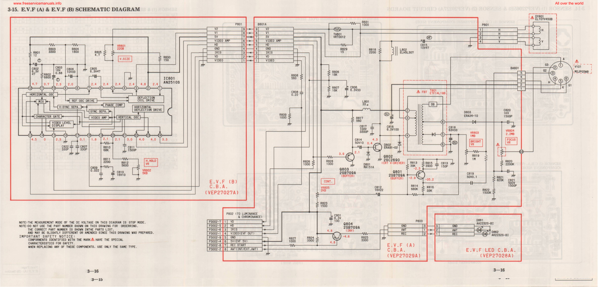
EVF Schematic
Luckily I managed to get a service manual for the camera with a full schematic.
This unit takes a 5v input, as opposed to the 8-12v inputs on previous cameras, so watch out for this! There’s also no reverse polarity protection either.
Pins
Making the iris marker vanish from the screen is easy, just put a solder bridge between pins 15 & 16 of the drive IC. The important pins on the interface connector are as follows:
Pin 3: GND
Pin 4: Video Input
Pin 5: Video GND
Pins 6: +5v Supply
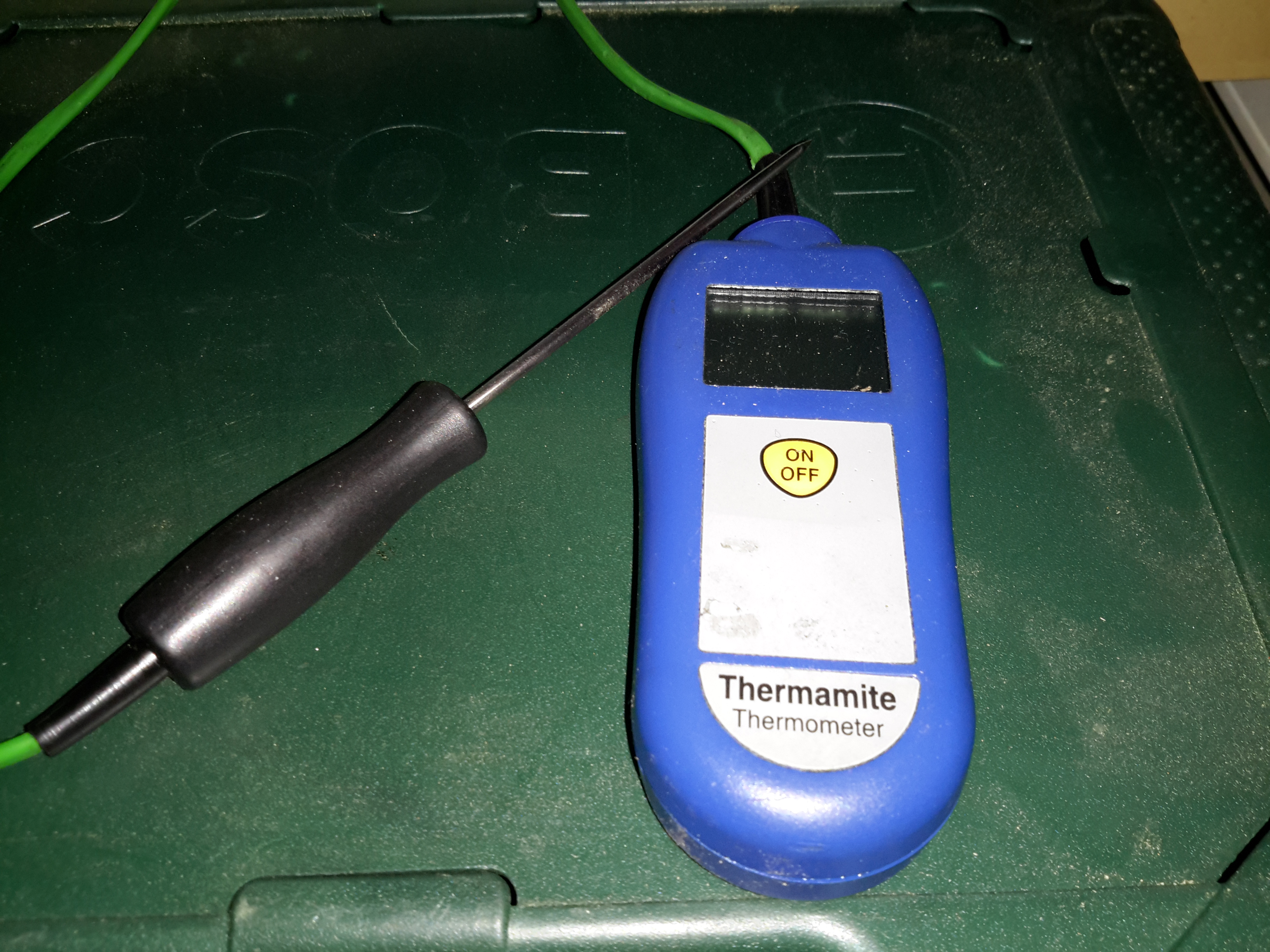
Here’s another bit of commercial gear, a catering thermometer. These are used to check the internal temperature of foods such as meat, to ensure they’re cooked through.
This was given to me with some damage, the battery cover is missing & the plastic casing itself is cracked.
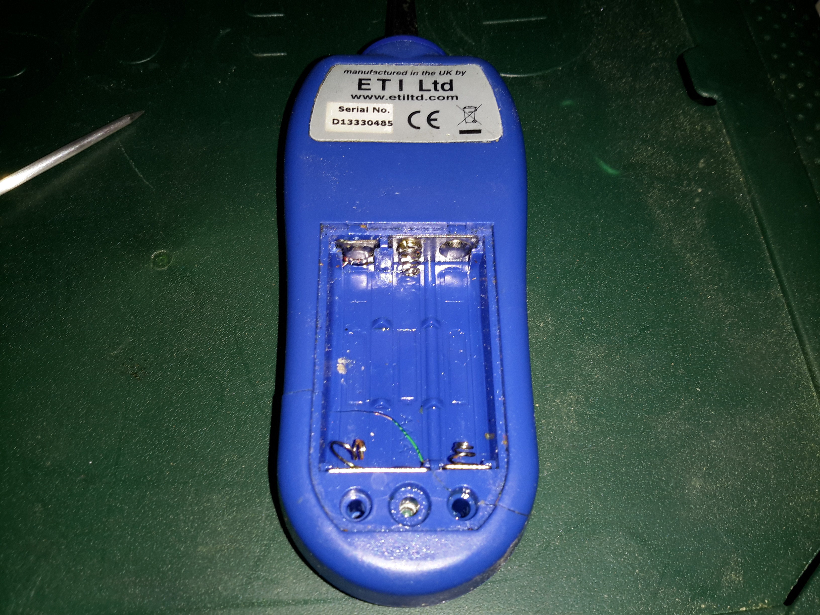
Battery Compartment
Power is provided by 3 AAA cells, for 4.5v
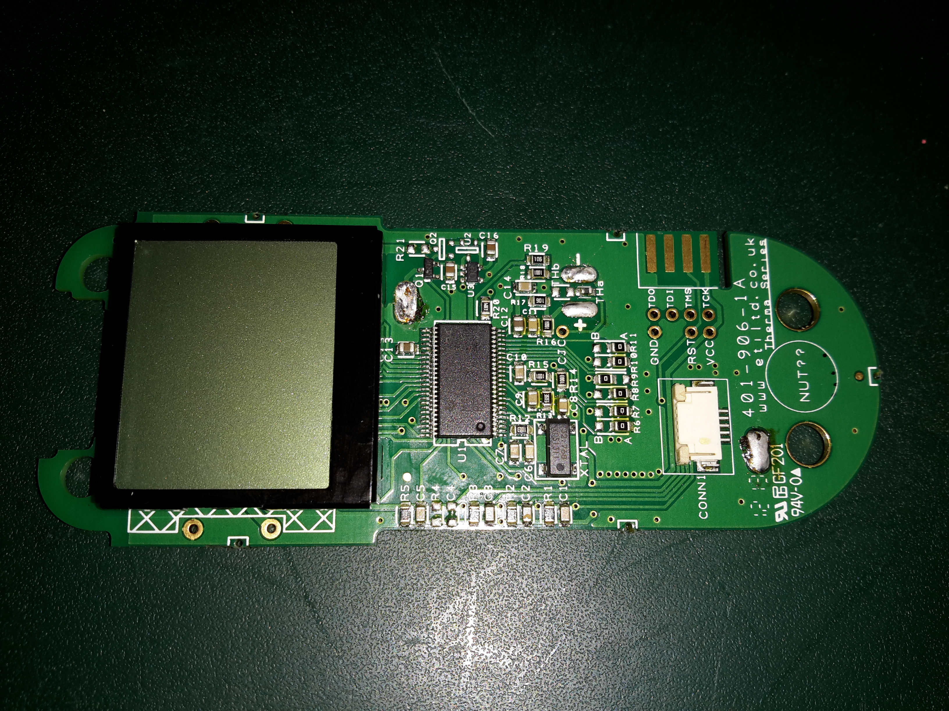
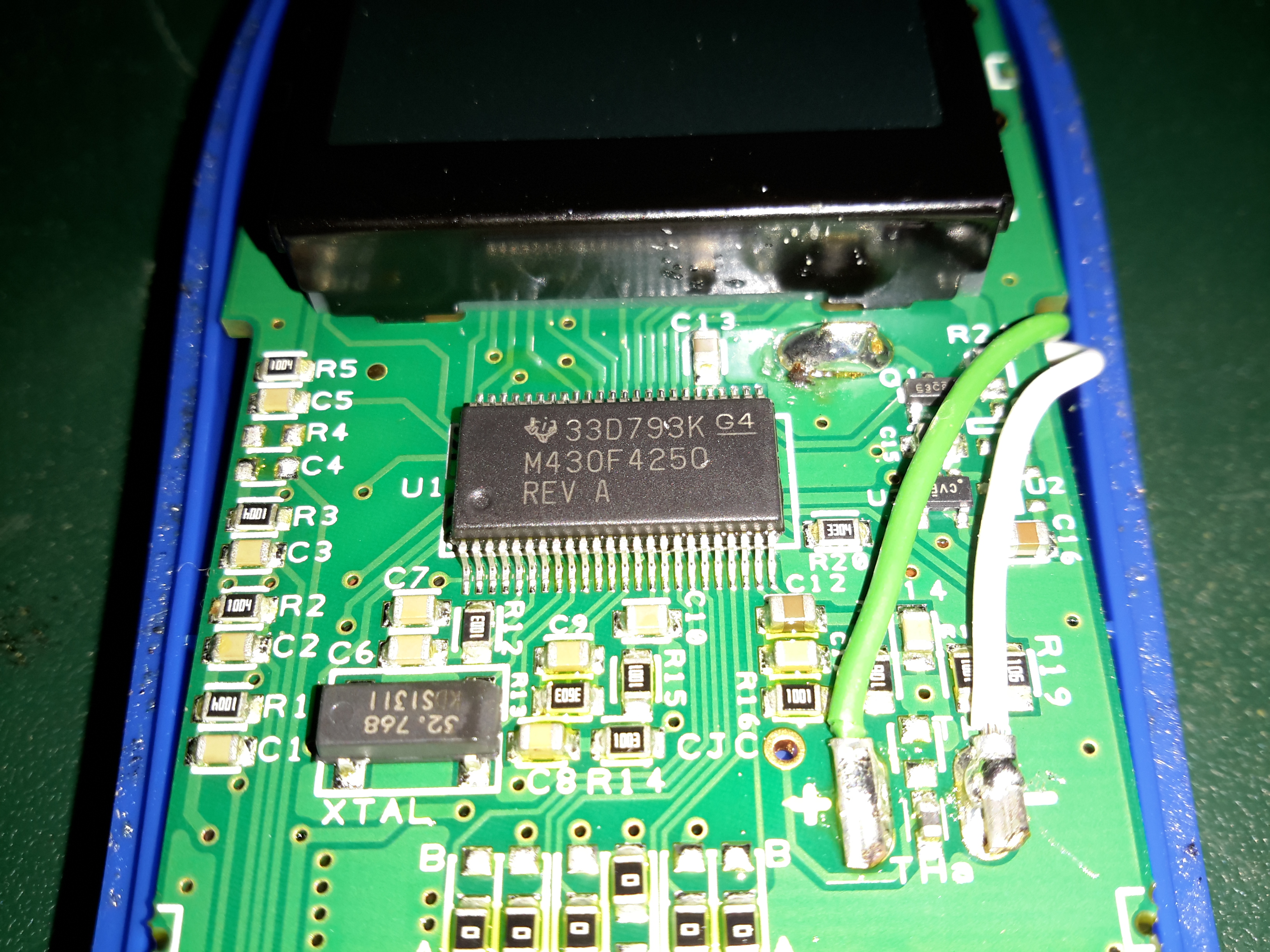
Main PCB
There’s not much to these units, the large LCD at the top is driven by the IC in the centre. A programming header is also present on the board near the edge.
Microcontroller
The core logic is taken care of with a Texas Instruments M430F4250 MSP430 Mixed-Signal Microcontroller. This MCU has onboard 16-bit Sigma-Delta A/D converter, 16-bit D/A converter & LCD driver. Clock is provided by a 32.768kHz crystal.
The probe itself is just a simple thermistor bonded into a stainless steel rod.
On the quest to get things on board replaced that are heavy users of power, the monitor in the main cabin was next. The original CCFL-backlit monitor was very heavy on 12v power, at 5A. This meant falling asleep watching TV would result in severely flattened batteries.
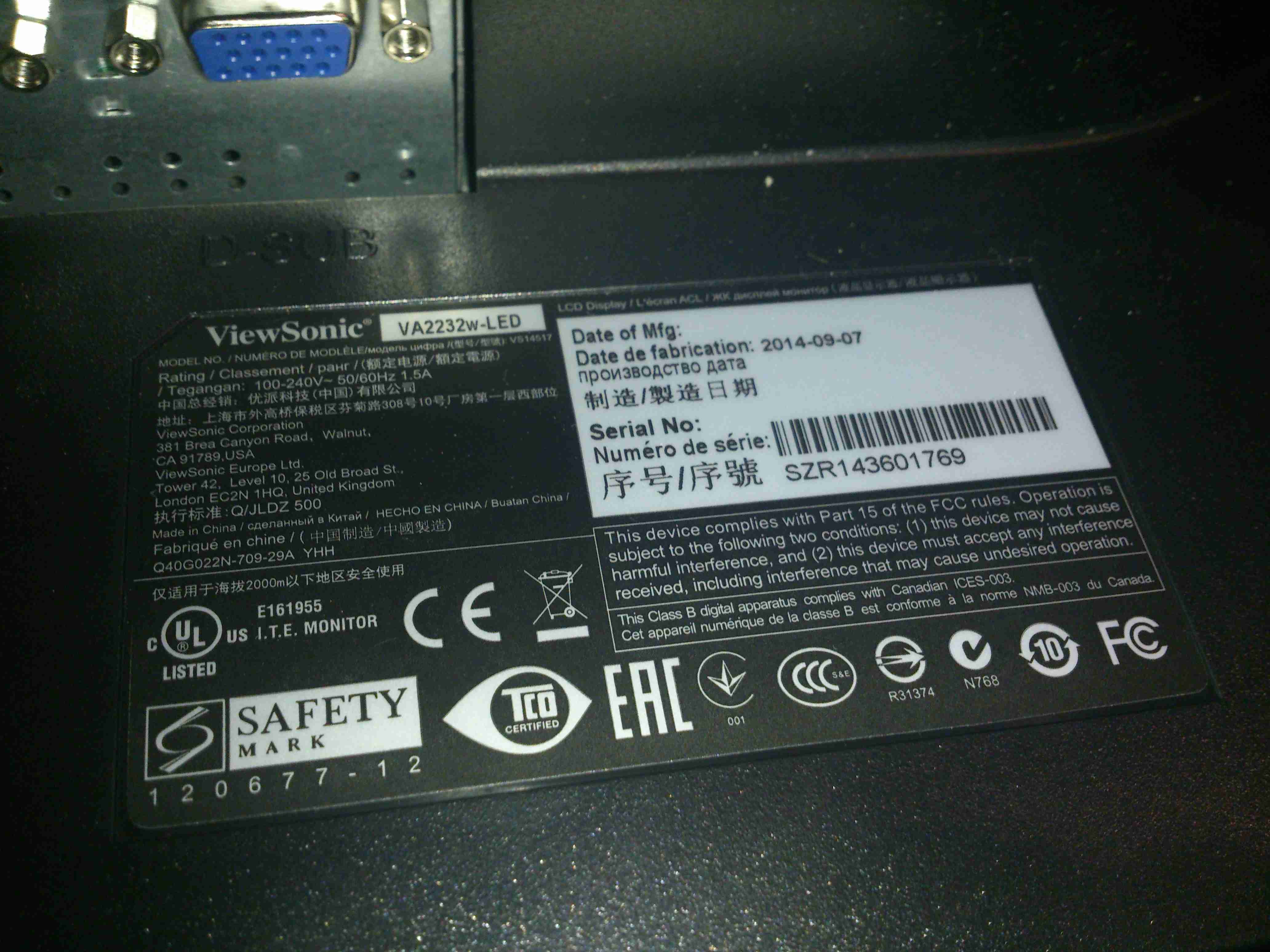
Replacement with a suitable LED-backlit monitor was definitely required. The cheapest on eBay was a ViewSonic VA2232W-LED, so I took to work converting it from 240v to 12v operation.
Back Cover Removed
There are no screws holding these monitors together, so a spudger & frequent swearing got the back off. The shield holding the circuitry is also not screwed down, only attached to the back of the LCD panel with aluminium shielding tape.
Power PCB Trackside
Once the tape has been cut, the main power board is accessible. The large IC on the left is the main backlight LED driver.
In this case the monitor requires a pair of rails from the supply, 18.5v for the backlight circuitry & 5v for the logic.
DC-DC Regulators
A pair of DC-DC converters has been fitted in the small space between the power & control boards.
PCB Connection Points
To save me some work & keep maximum compatibility, I’ve not modified the existing supply, just attached the new DC-DC converter outputs onto the corresponding outputs of the factory PSU. The 12v input leads are routed out of the same gap as the mains IEC connector, with some hot glue over the mains input solder points to provide some more insulation.
Wiring Tidied
The wiring is tidied up with hot glue so the back cover will go back on.
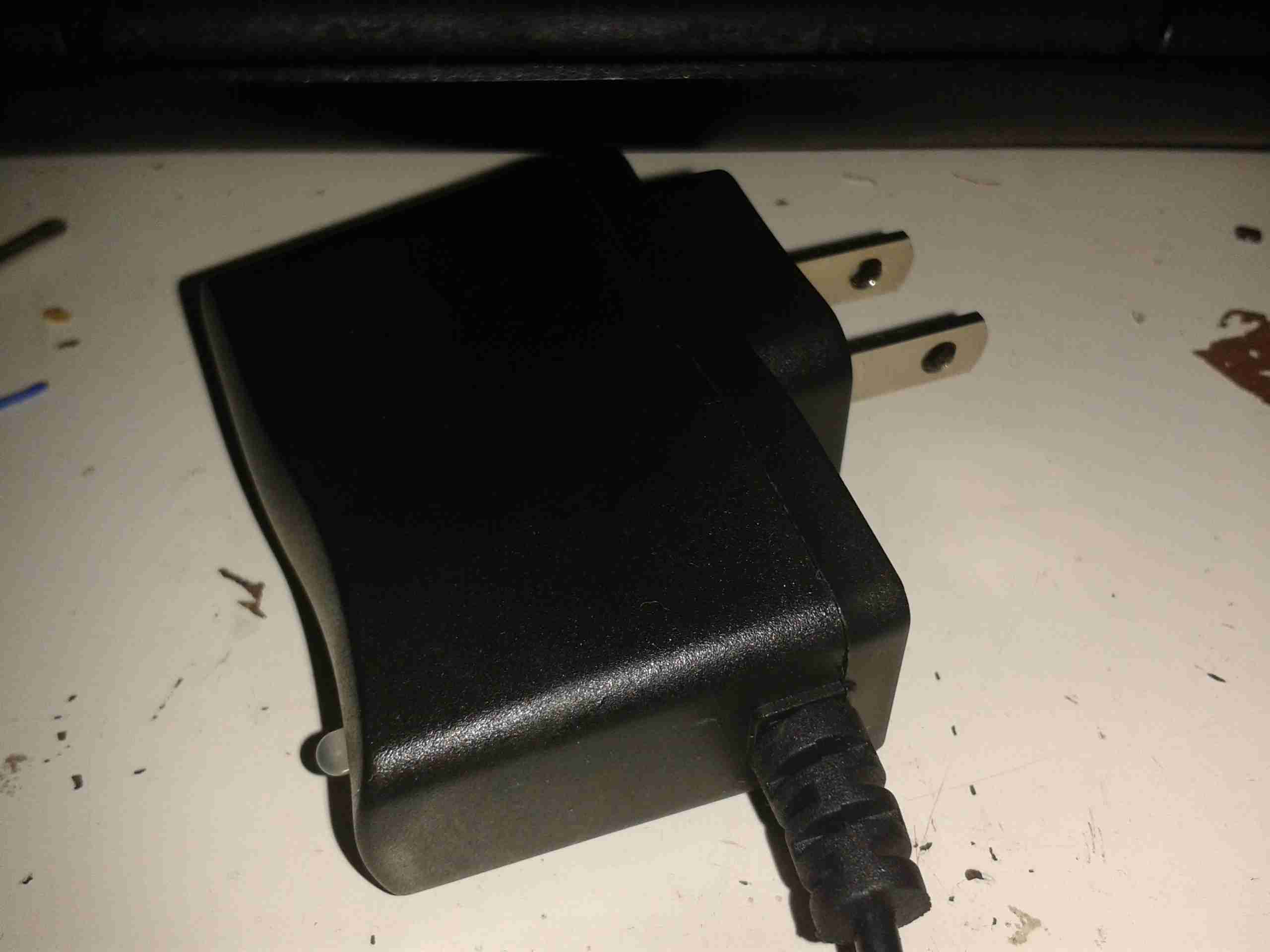
I almost forgot about this bit of kit, that came with one of my LED torches as a Lithium Ion charger. As I never plug in anything that comes from China via eBay, here’s the teardown & analysis.
Another Lethal Charger?
Here’s the unit itself. It’s very light, and is clearly intended for American NEMA power points.
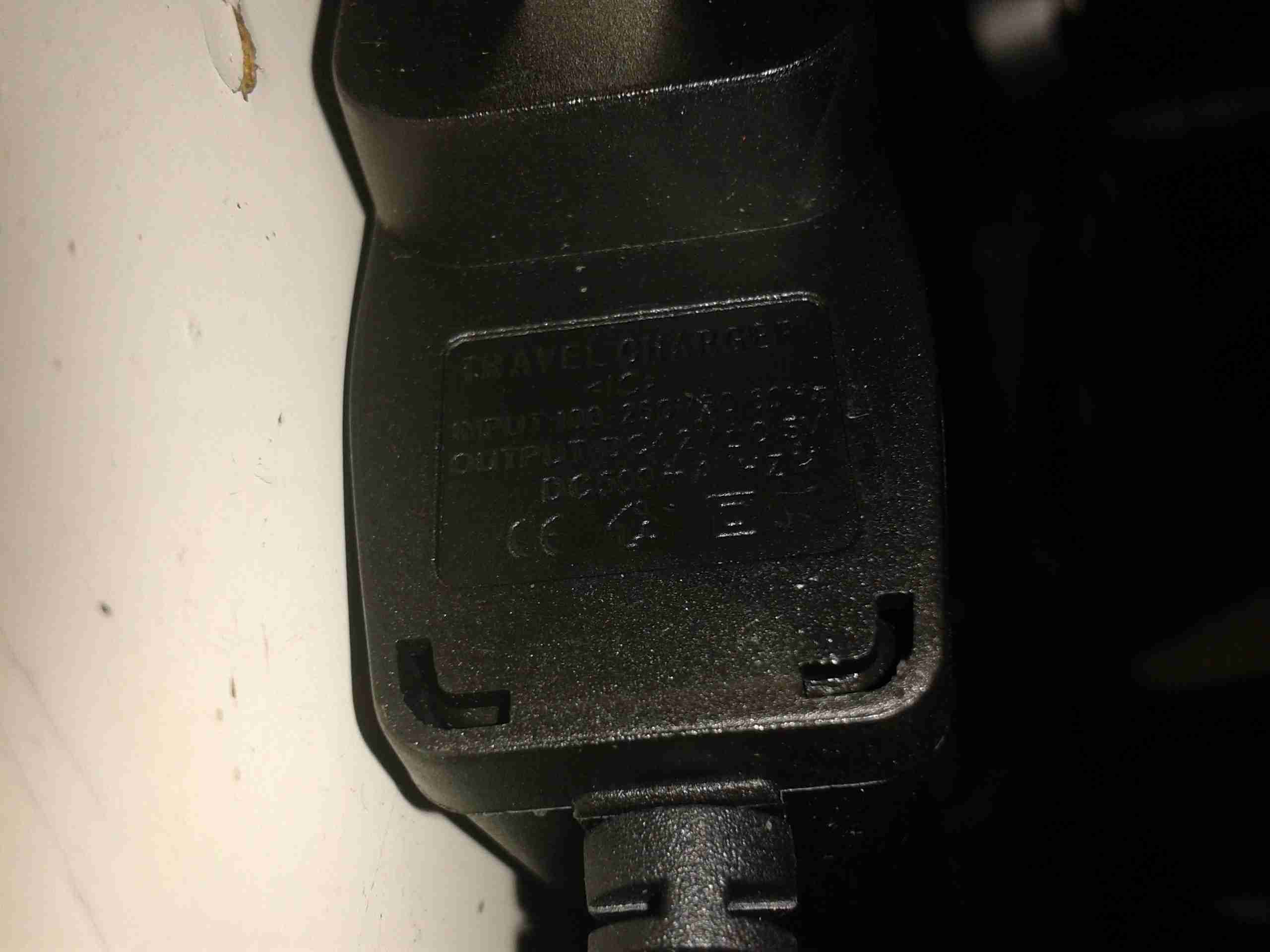
Specs
Claimed specifications are 100-240v AC input, making it universal, and 4.2v DC out ±0.5v at 500mA.
Considering the size of the output wire, if this can actually output rated voltage at rated current I’ll be surprised.
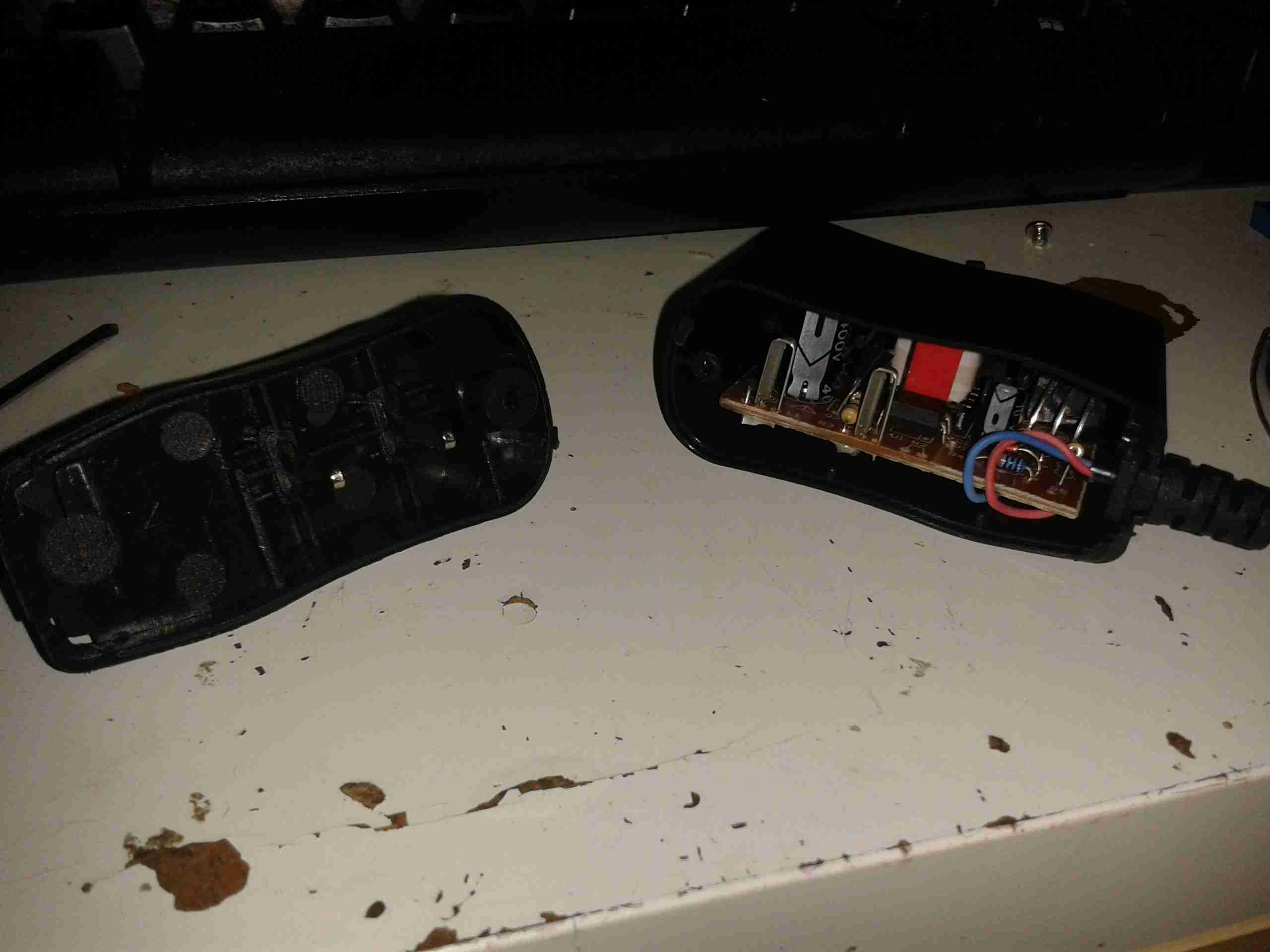
Opened
Here’s the adaptor opened up. There’s no mains wiring to speak of, the mains pins simply push into tags on the PCB.
PCB Top
Top of the SMPS PCB. As usual with Chinese gear, it’s very simple, very cheap and likely very dangerous. There’s no real fusing on the mains input, only half-wave rectification & no EMI filtering.
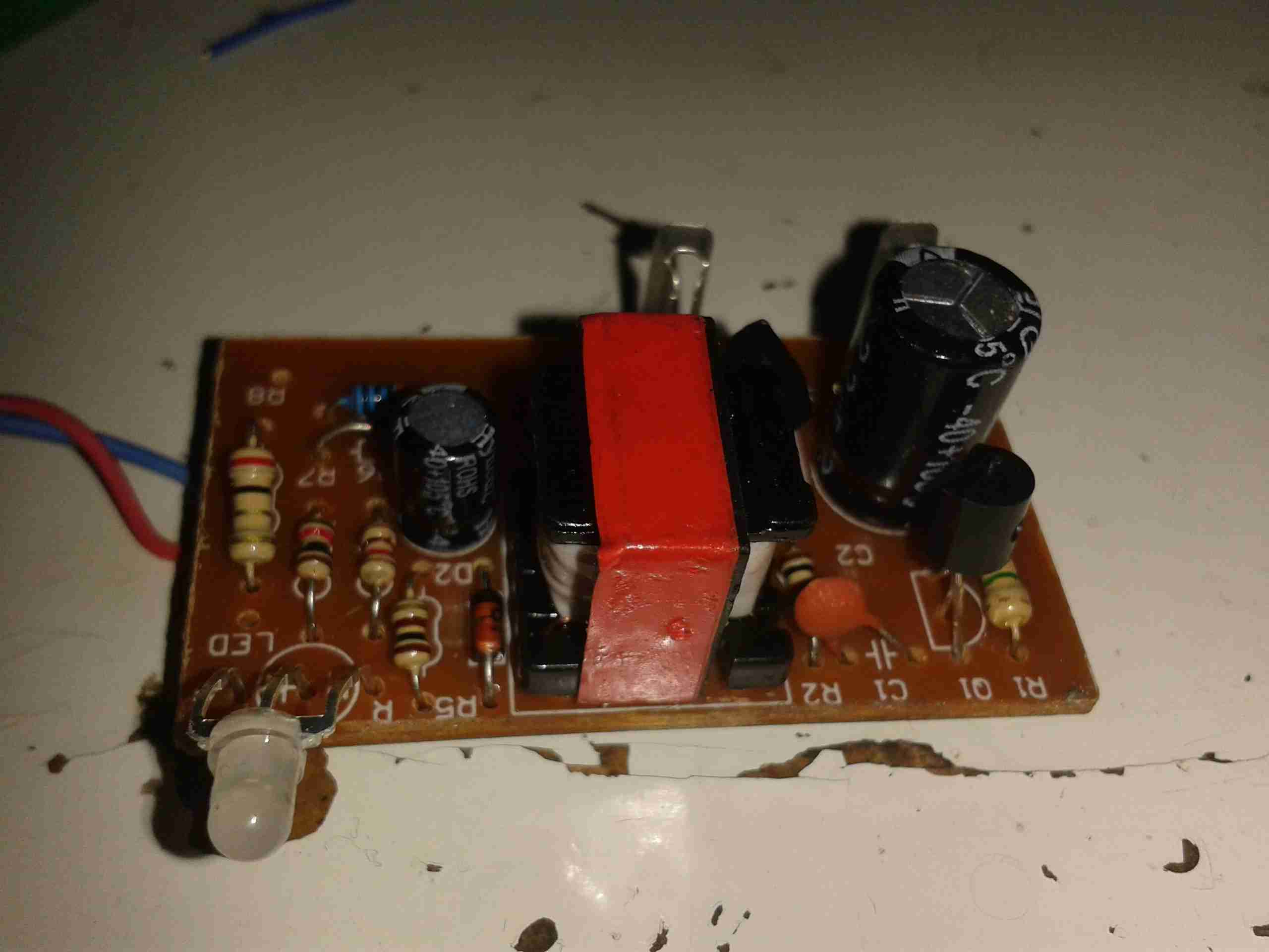
PCB Bottom
Here’s the bottom of the PCB. At least there’s a fairly sized gap between the mains & the output for isolation. The wiggly bit of track next to one of the mains input tags is supposed to be a fuse – I somehow doubt that it has the required breaking characteristics to actually pass any safety standards. Obviously a proper fuse or fusible resistor was far too expensive for these.
The output wiring on the left is thinner than hair, I’d say at least 28AWG, and probably can’t carry 500mA without suffering extreme volt drop.
A while back I posted about a 3M Touch Systems industrial monitor that I’d been given. I had previously paired it with a Raspberry Pi Model B+, but for general desktop use it was just a little on the slow side.
Since the release of the Raspberry Pi 2, with it’s 4-core ARM Cortex CPU, things are much improved, so I figured I’d post an update with the latest on the system.
The monitor I’ve used is a commercial one, used in such things as POS terminals, service kiosks, etc. It’s a fairly old unit, but it’s built like a tank.
3M Panel
It’s built around a Samsung LTM170EI-A01 System-On-Panel, these are unusual in that all the control electronics & backlighting are built into the panel itself, instead of requiring an external converter board to take VGA to the required LVDS that LCD panels use for their interface.
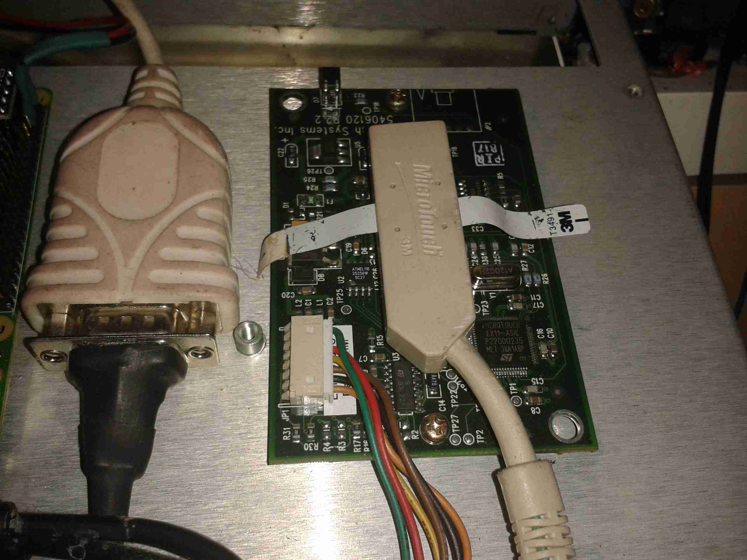
The touch section is a 3M Microtouch EXII series controller, with a surface capacitive touch overlay.
Touch Controller
Above is the touch controller PCB, with it’s USB-Serial converter to interface with the Pi.
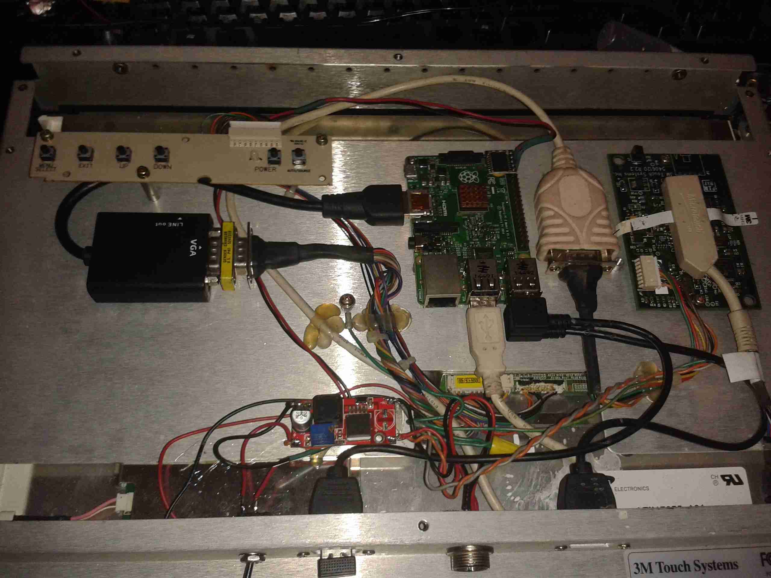
As there is much spare space inside the back of this monitor, I have mounted the Pi on a couple of spare screw posts, fitted USB ports where the original VGA & Serial connectors were in the casing, and added voltage regulation to provide the Pi with it’s required 5v.
Overview
Here’s the entire back of the panel, the Pi in the middle interfaces with a HDMI-VGA adaptor for the monitor, and the serial adaptor on the right for the touch. A small voltage regulator at the bottom of the unit is providing the 5v rail. There’s a switch at the bottom next to one of the USB ports to control power to the Pi itself. The panel won’t detect the resolution properly if they’re both powered on at the same time.
At 13.8v, the device pulls about 2A from the supply, which seems to be typical for a CCFL backlighted LCD.
Now the Raspberry Pi 2 has been released, it’s much more responsive for desktop applications, especially with a slight overclock.
Shameless Plug
A full disk image enabled for Desktop & 3M touch monitors is available below for others that have similar panels. This image only works for the Pi 2!
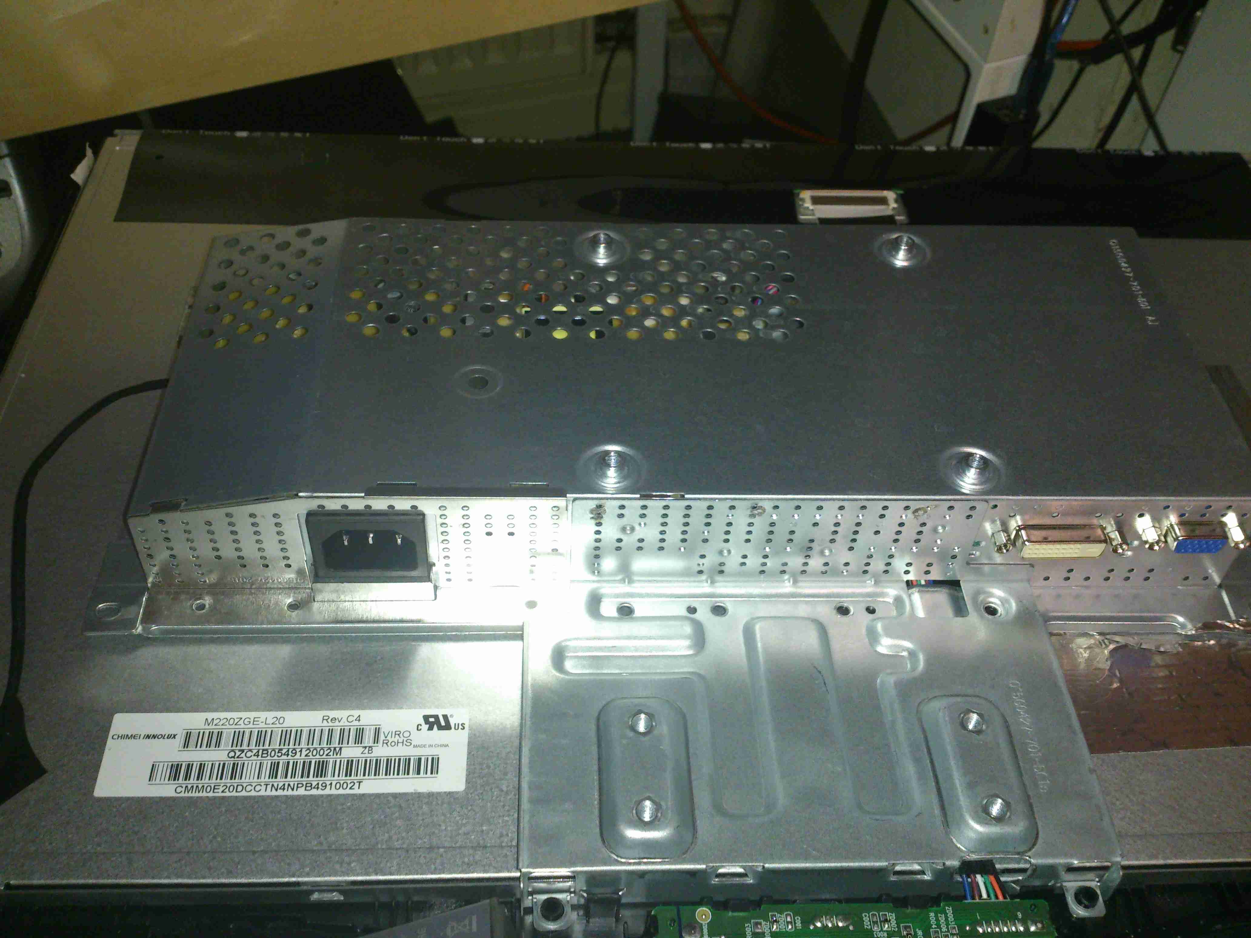
My other monitors are a different model, and have a slightly different main PCB inside, but the process is mostly the same for converting these to 12v supply.
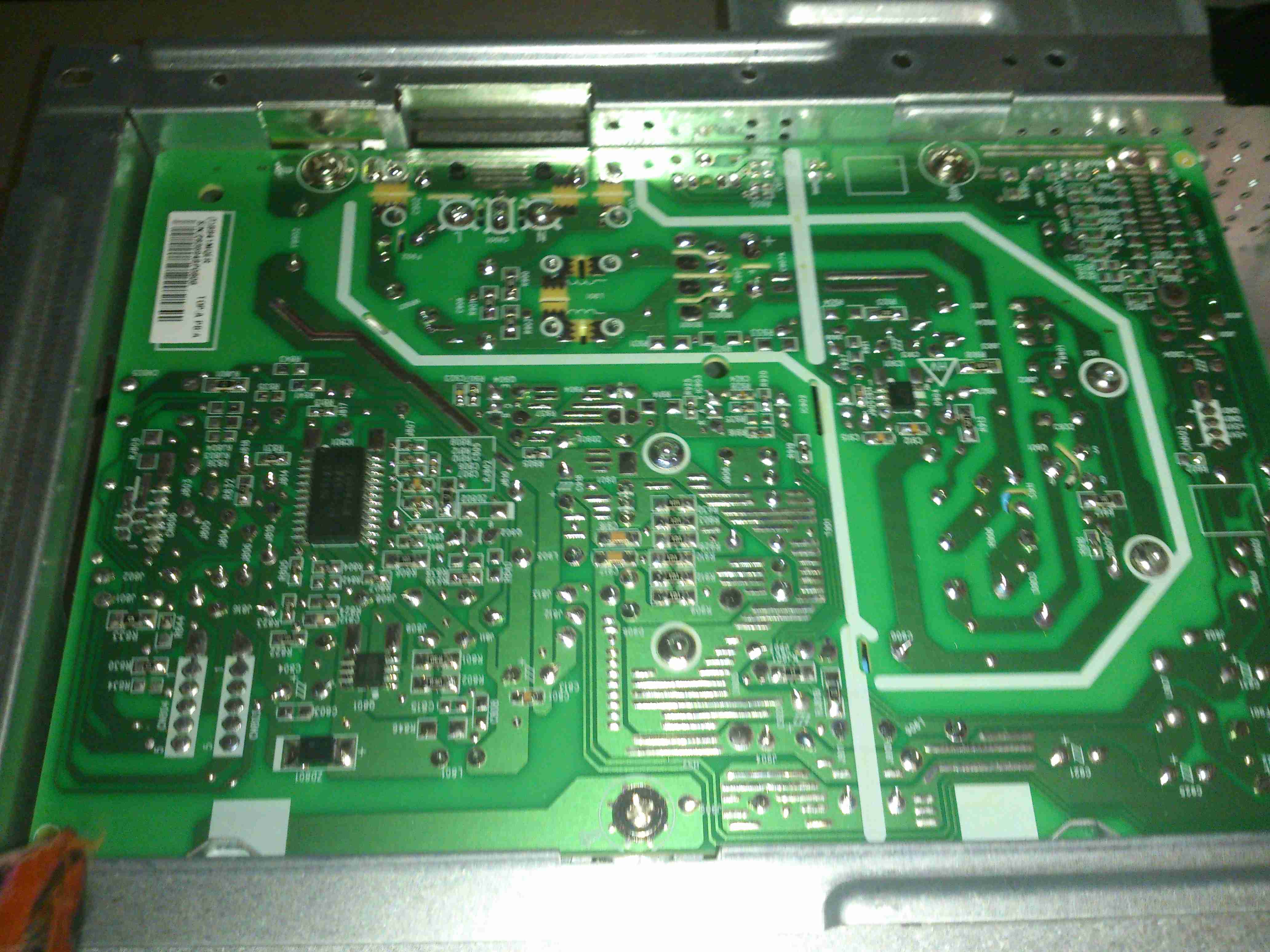
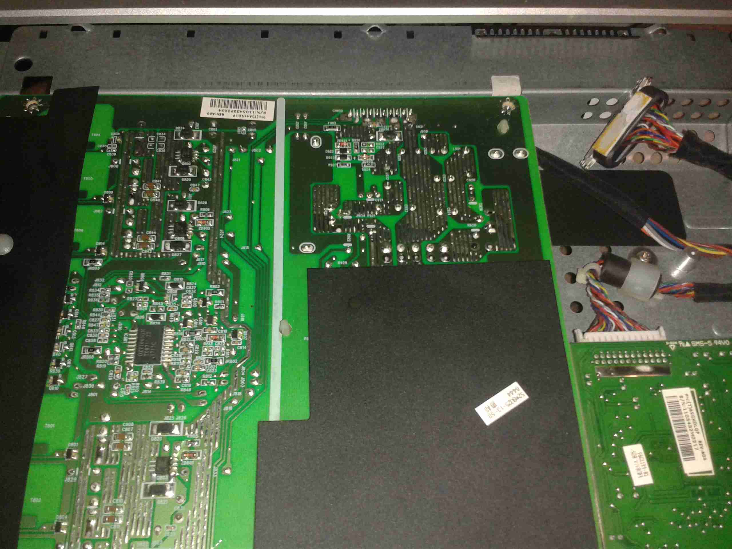
Main PCB
In this monitor type, there is only a single board, with all the PSU & logic, instead of separate boards for each function.
PSU Closeup
This monitor is slightly different in it’s power supply layout. The mains supply provides only a single 12v rail, which is then stepped down by a switching converter to 5v, then by smaller linear regulators to 3.3v & 1.8v for the logic. This makes my life easier since I don’t have to worry about any power conversion at all.
PCB Reverse
Here’s the backside of the PCB, the mains PSU section is in the centre.
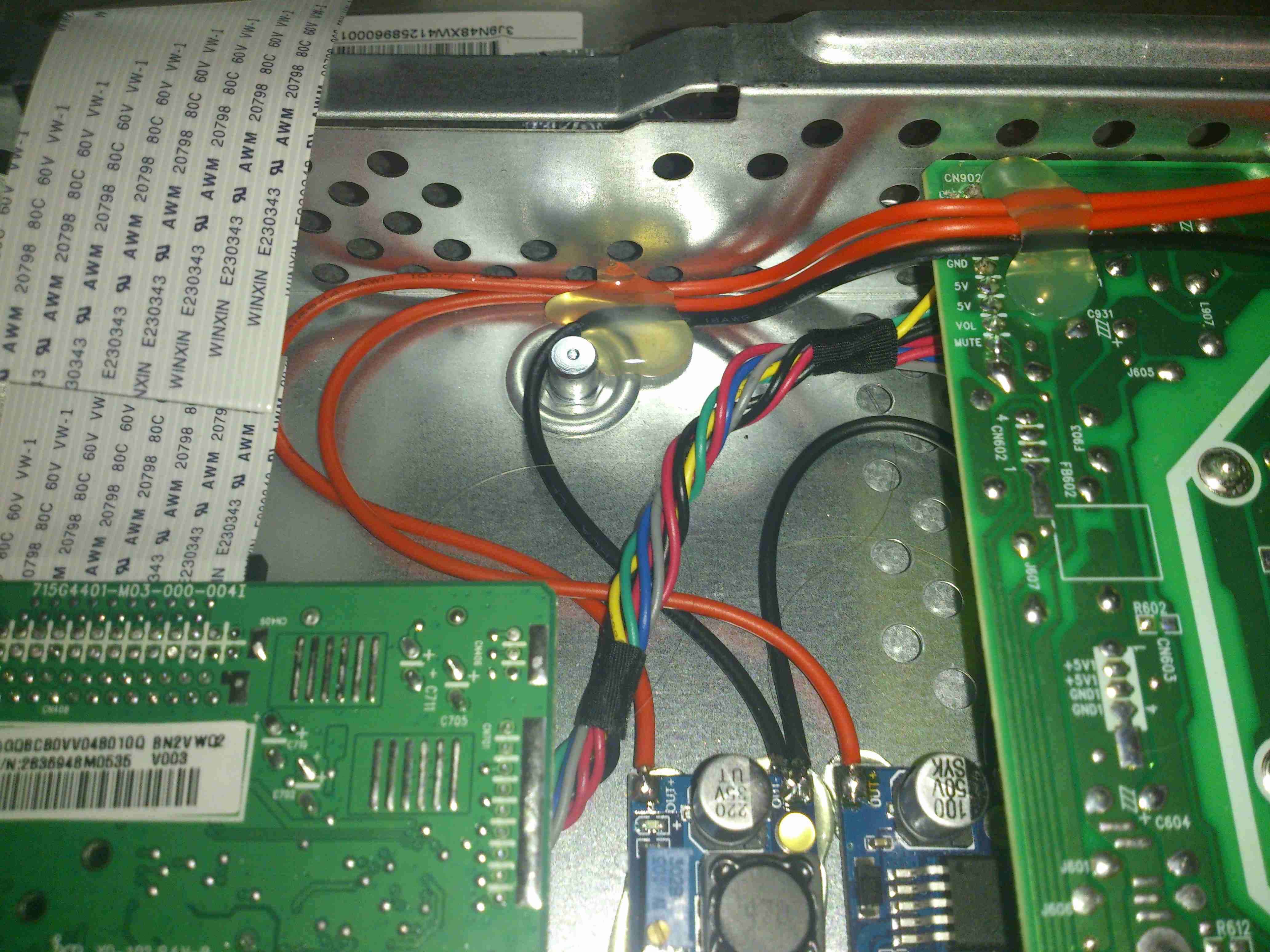
Attachment Points
Here’s the pair of 12v supply wires soldered onto the main board, onto the common GND connection on the left, and the main +12v rail on the right. I’ve not bothered with colour coding the wiring here, just used whatever I had to hand that was heavy enough to cope with a couple amps.
12v Socket
A small mod later with a cone drill & the 12v input socket is mounted in the LCD frame.
Casing Mod
Some light removal of plastic & the back cover fits back on. Current draw at 13.8v is ~2A.
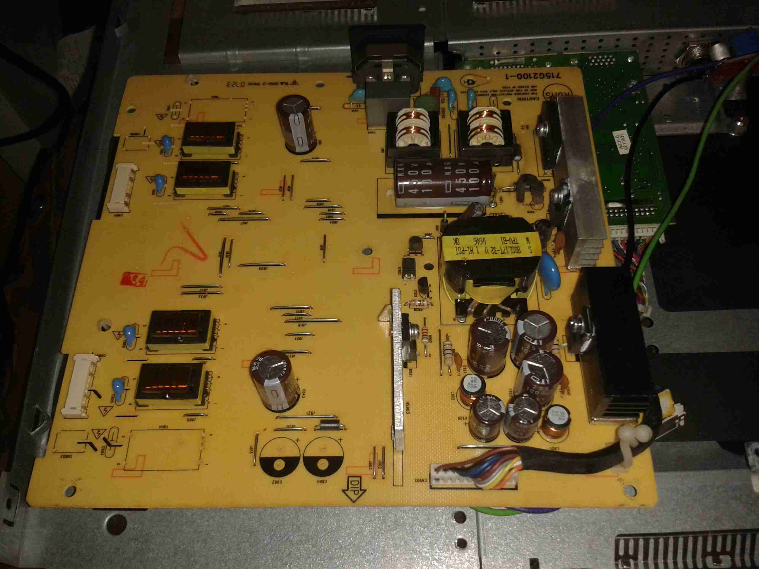
I’m still on my crusade of removing every trace of 240v mains power from my shack, so next up are my computer monitors.
I have 4 Dell monitors, of various models, hooked up to my main PC.
The monitor here is a Dell E207WFPc 20″ widescreen model. There will be more when I manage to get the others apart to do the conversion. However I’m hoping that the PSU boards are mostly the same.
Panel Removed
There are no screws holding these monitors together, the front bezel is simply clicked into place in the back casing, these clips are the only thing that holds the relatively heavy glass LCD panel & it’s supporting frame! The image above shows the panel removed. The large board on the left is the power supply & backlight inverter, the smaller one on the right is the interface board to convert the DVI or VGA to LVDS for the LCD panel itself.
PSU Board
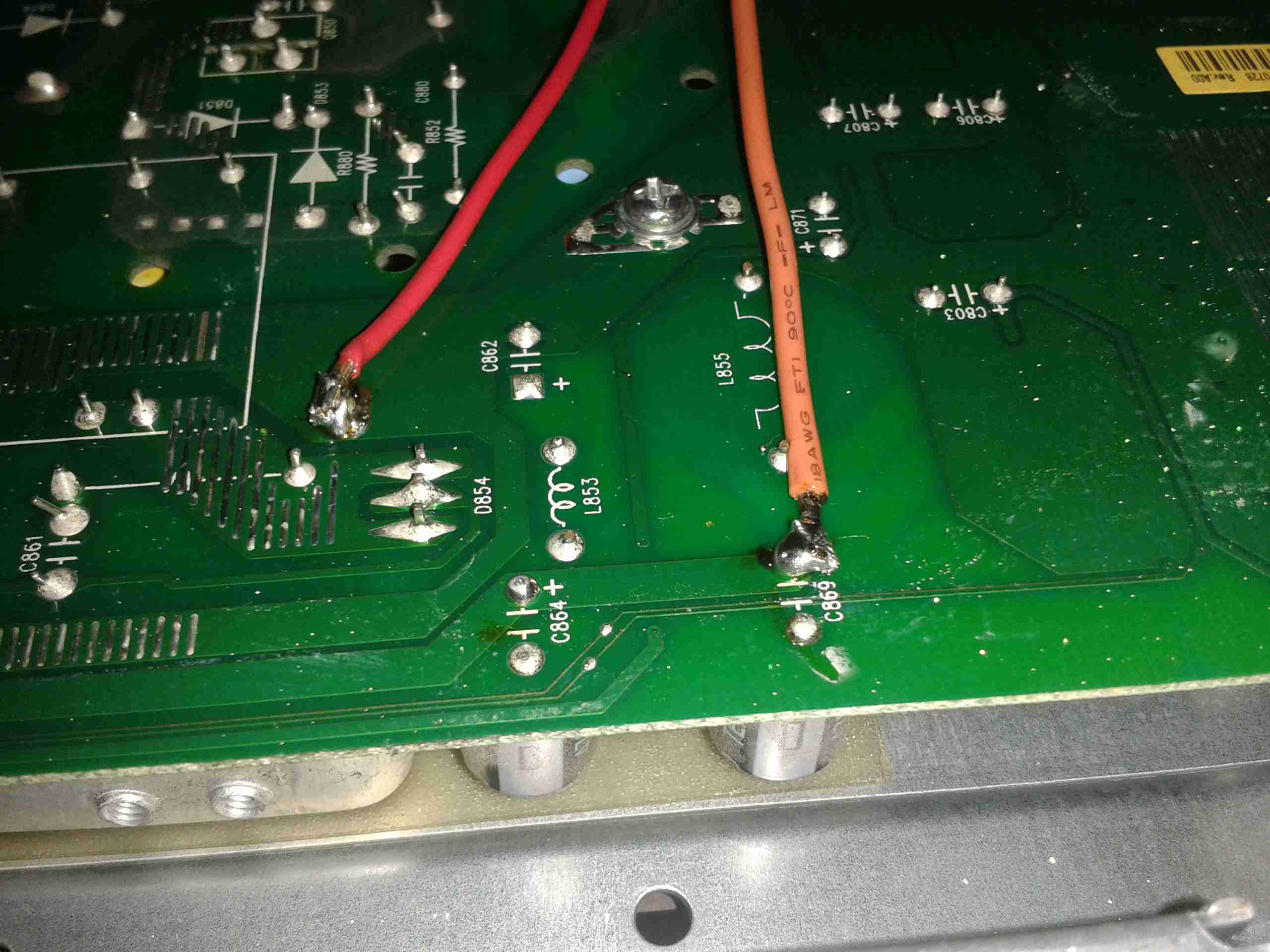
Here’s a closeup of the PSU board, the connector at centre right at the top of the PCB is the main power output, and also has a couple of signals to control the backlight inverter section of the PSU, on the left side. The PSU requirements for this monitor are relatively simple, at 14.5v for the backlight & 5v for the logic board.
PSU
Here’s the top of the PSU board, very simple with the mains supply on the right side, and the backlight inverter transformers on the left.
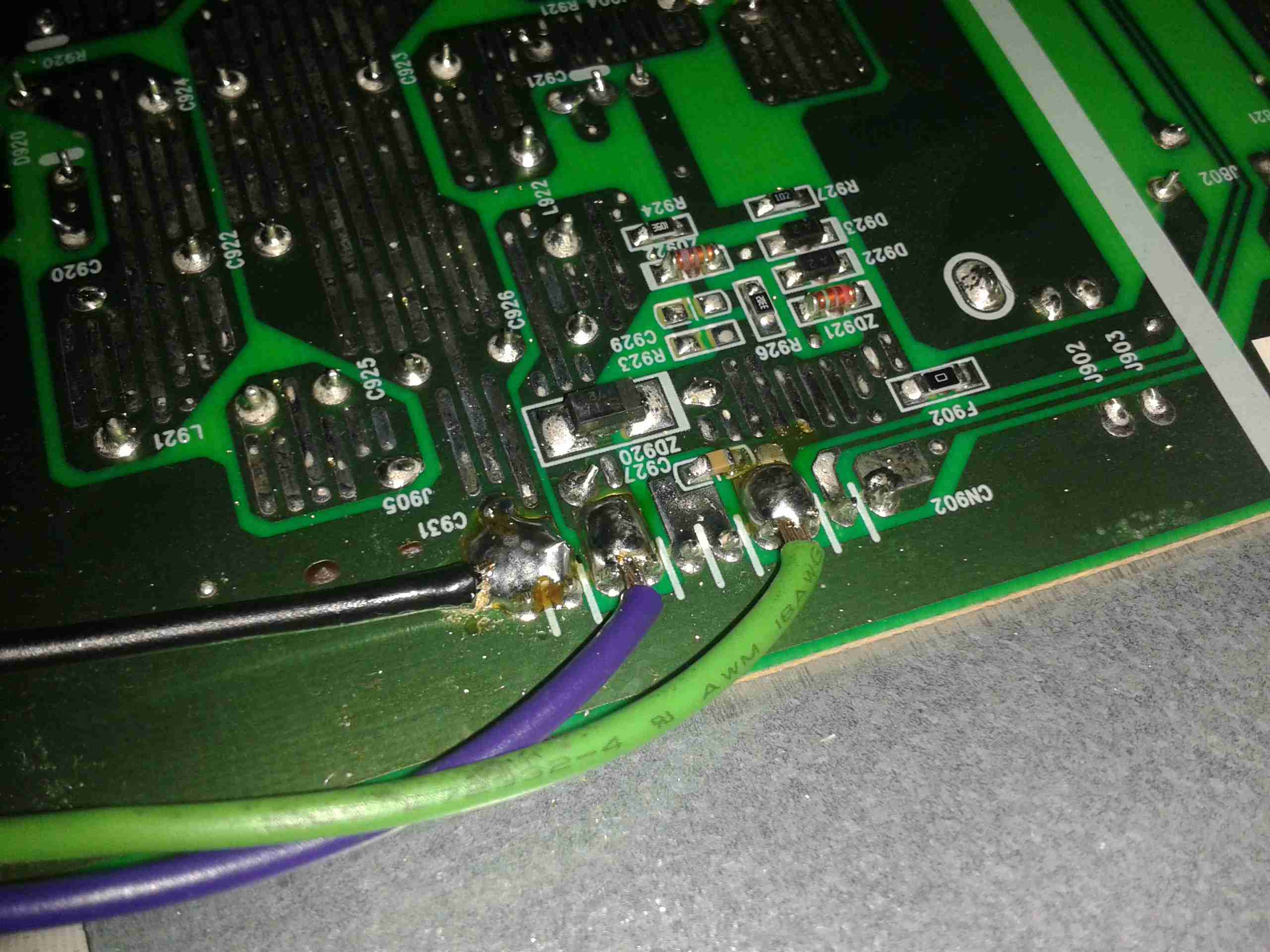
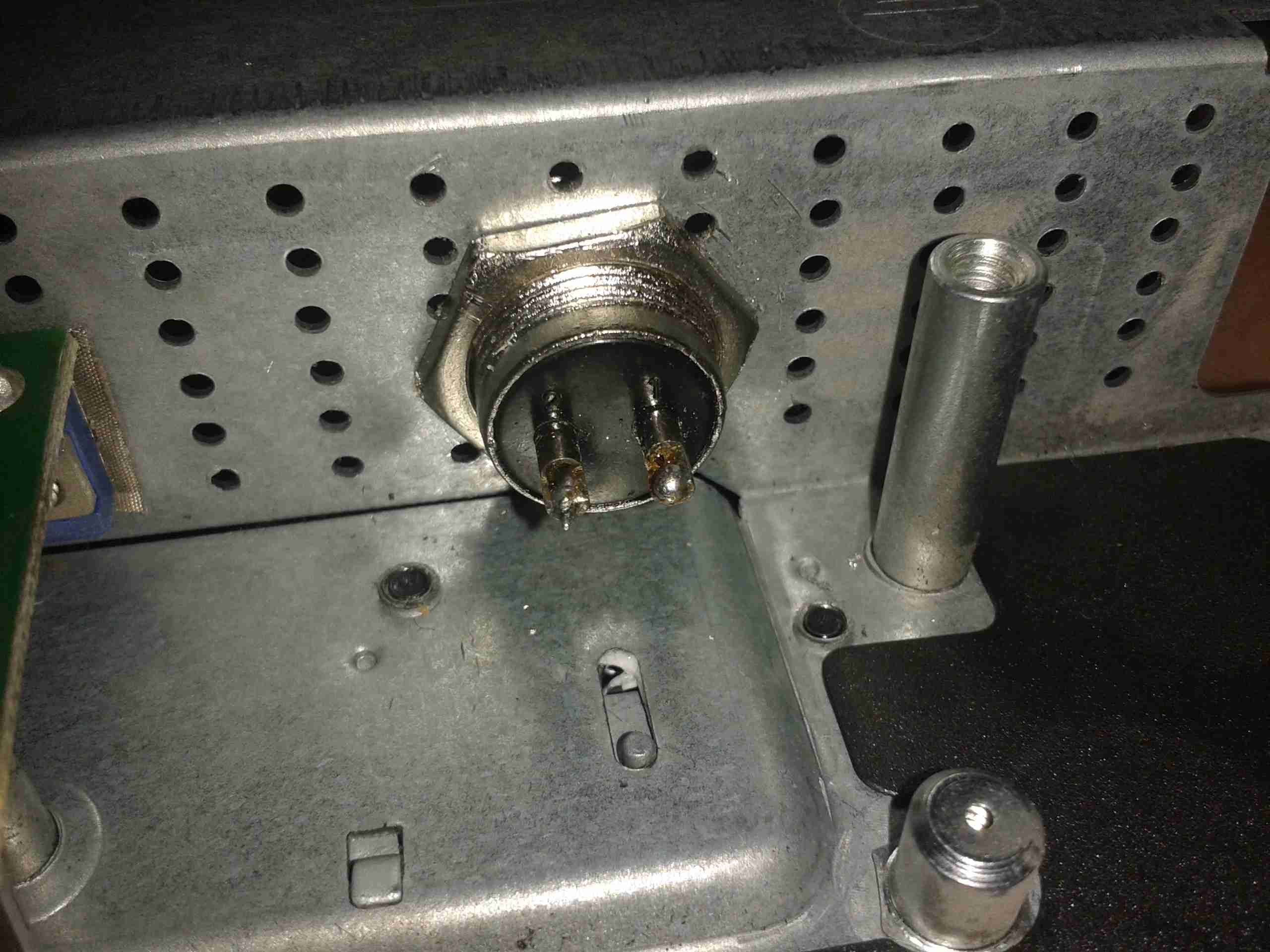
Hooked In
Here I’ve hooked into the power rails on the supply, to attach my own 12v regulators. The green wire is +14.5v, and the purple is +5v. Black is common ground.
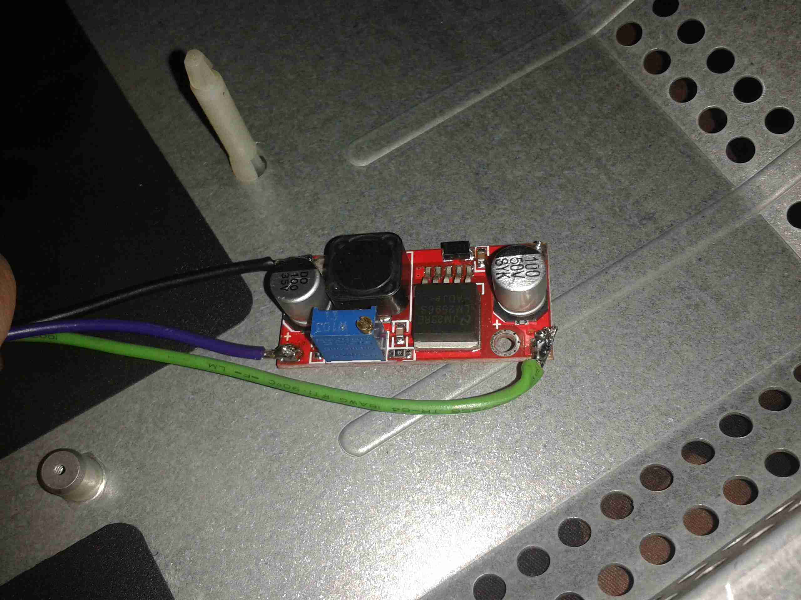
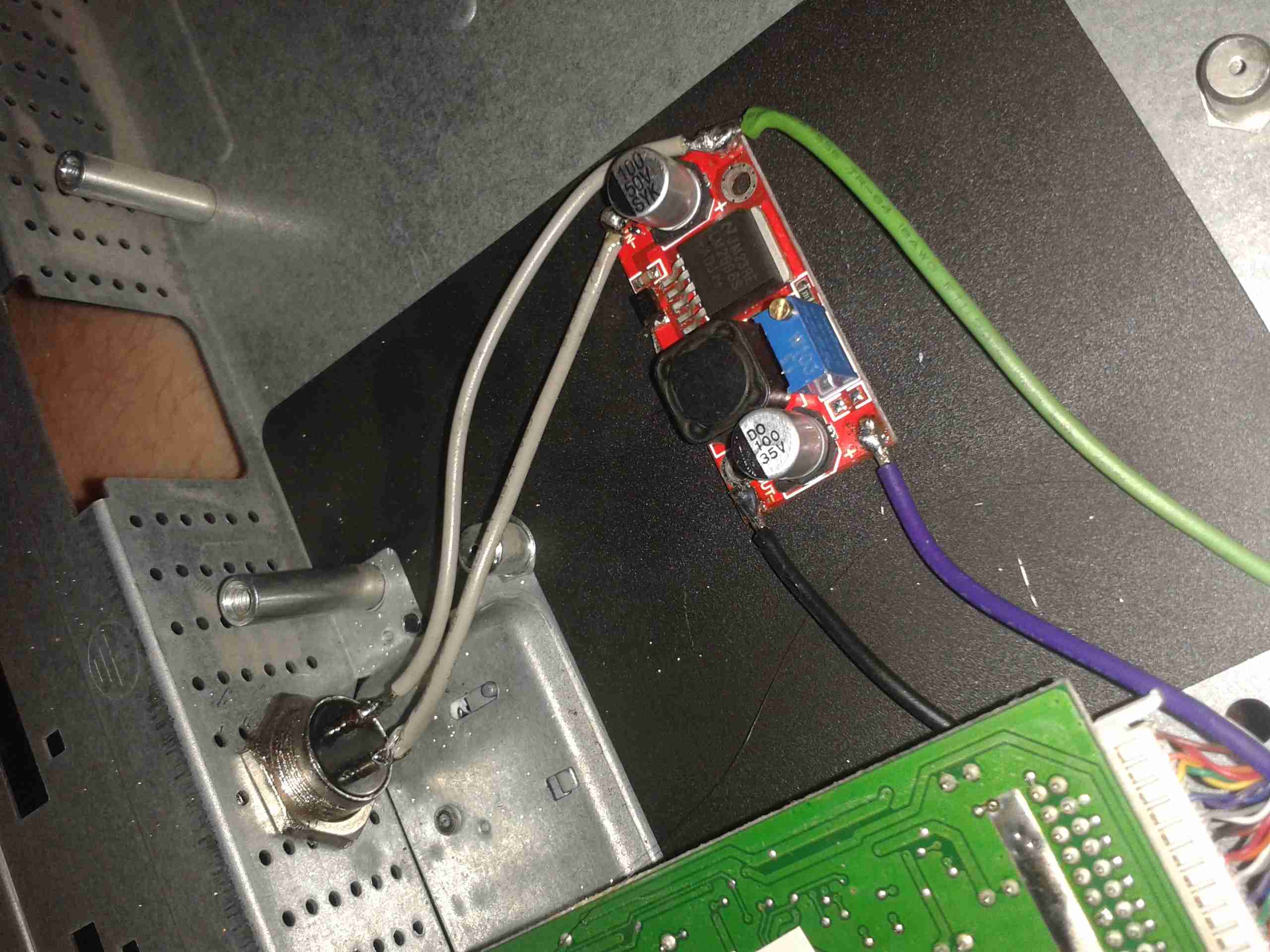
5v Regulator
On doing some testing, the backlight inverter section doesn’t seem to mind voltages between 11.5-14.5v, so a separate regulator isn’t required there. Even running off batteries that’s within the range of both charging & discharging. The only regulator required is a 5v one to reduce the input voltage for the logic PCB.
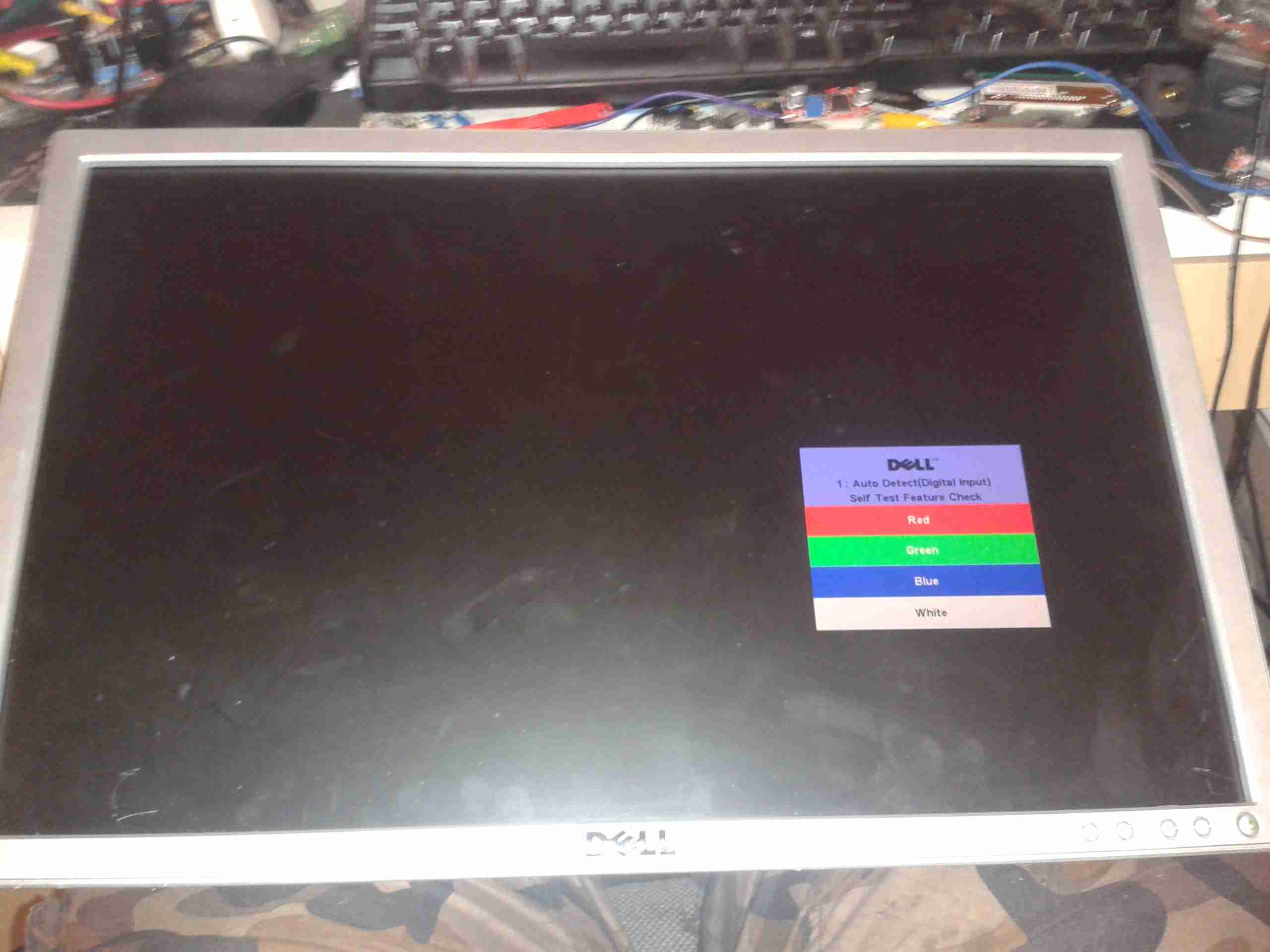
First Test
On applying some 12v power to the regulator input, we have light! Current draw at 12.5v is 2.65A for a power consumption of 33W.
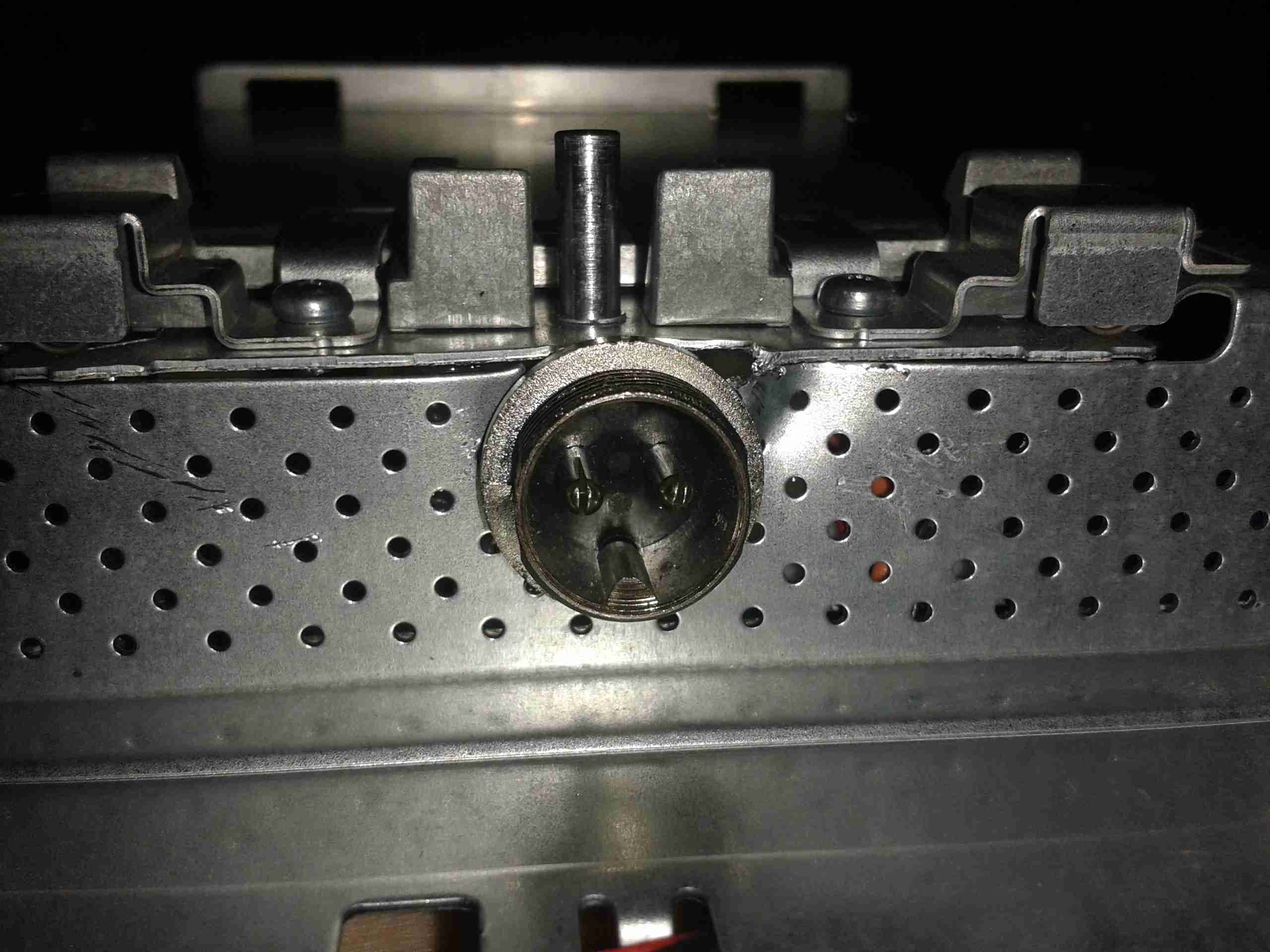
12v Input
There’s plenty of room in the back casing to mount a 12v input socket, I have left the mains supply intact so it can be used on dual supply.
Final Wiring
Here’s the 5v regulator mounted on the back of the casing, all wired up & ready to go.
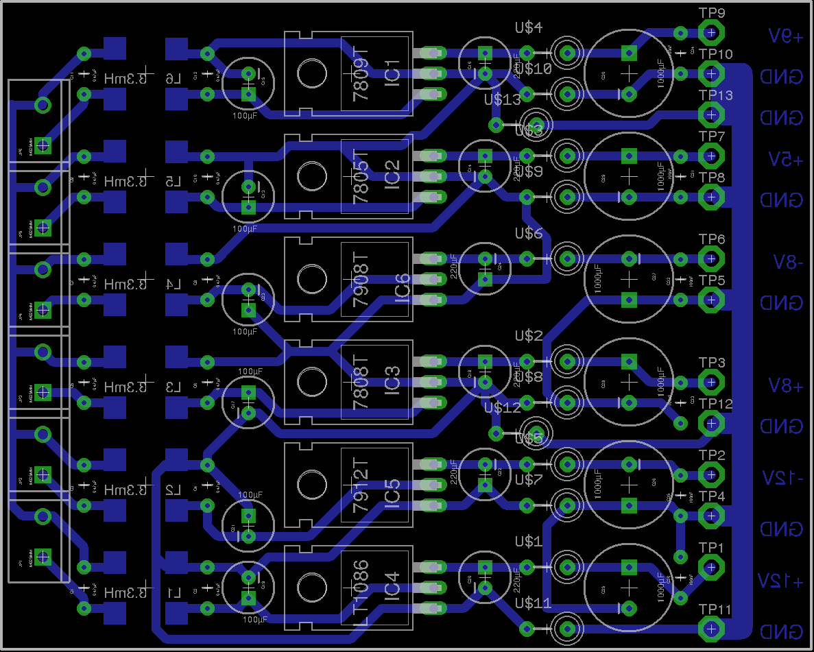
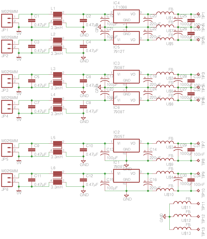
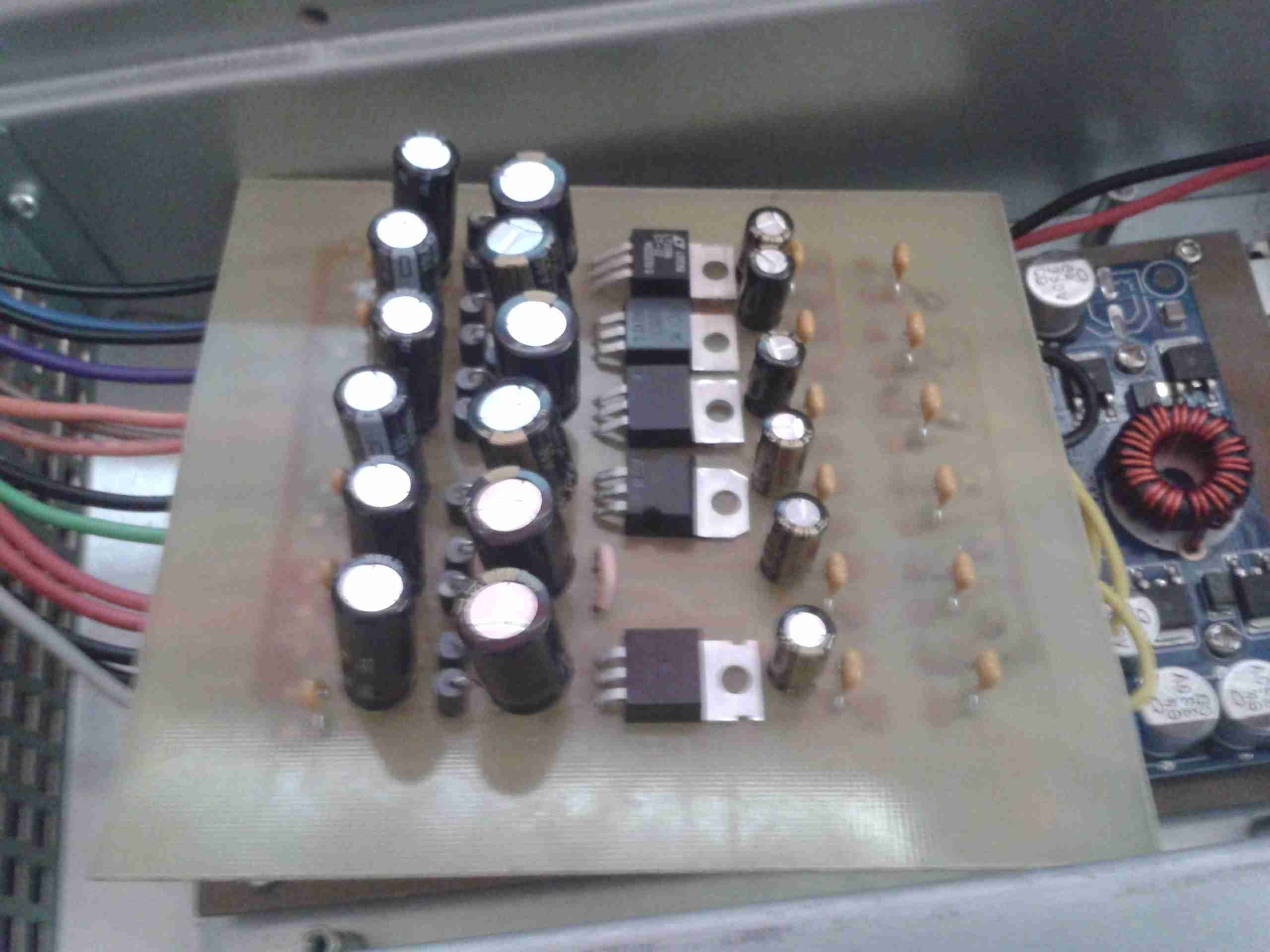
Finally, here’s the last part of the Rigol 12v DC Power Supply project, the linear post regulation section to remove some of the ripple.
I have made a couple of layout adjustments since the last post about this part of the project – a little more filtering on the DC outputs. As usual the Eagle project files are at the bottom of the post for those who might find them useful.
Updated PCBUpdated Schematic
Completed PCB
Here’s the completed PCB, partially installed in the back of the scope. The missing regulator is the 5v one, since I already have a source of clean 5v from my original attempt at the supply, it’s not a problem not using a linear after the switcher. The filtering is the same on all channels, input from the switchers is on the right, outputs to the scope on the left.
PCB Bottom
Here’s the bottom of the PCB, with the common mode input chokes. The design of this board has allowed me to remove a couple of the switching modules as well, as I can use a single bipolar supply to run both sets of bipolar regulators on this board. This should help remove some of the noise also.
The ripple level has now dropped to lower than it was originally on the mains supply! Current draw at 13.8v DC is about 1.75A.
Since I fitted my scope with a SMPS based 12v input supply, there has been a noise problem on very low volts/div settings, this noise isn’t present on the mains supply, so I can only think it’s coming from the switching frequencies of the various DC-DC modules I’ve used.
Scope Ripple
Because of this I’ve designed a linear post-regulation stage for the supply, to remove the RFI from the DC rails.
This board takes the outputs from the DC-DC converters, removes all the noise & outputs clean DC onto the mainboard of the scope.
As the scope internally uses regulation to get the voltages lower, I’ve found that I don’t have to match the outputs of the mains supply exactly, for the +/-17.5v rails, 12v is perfectly fine instead.
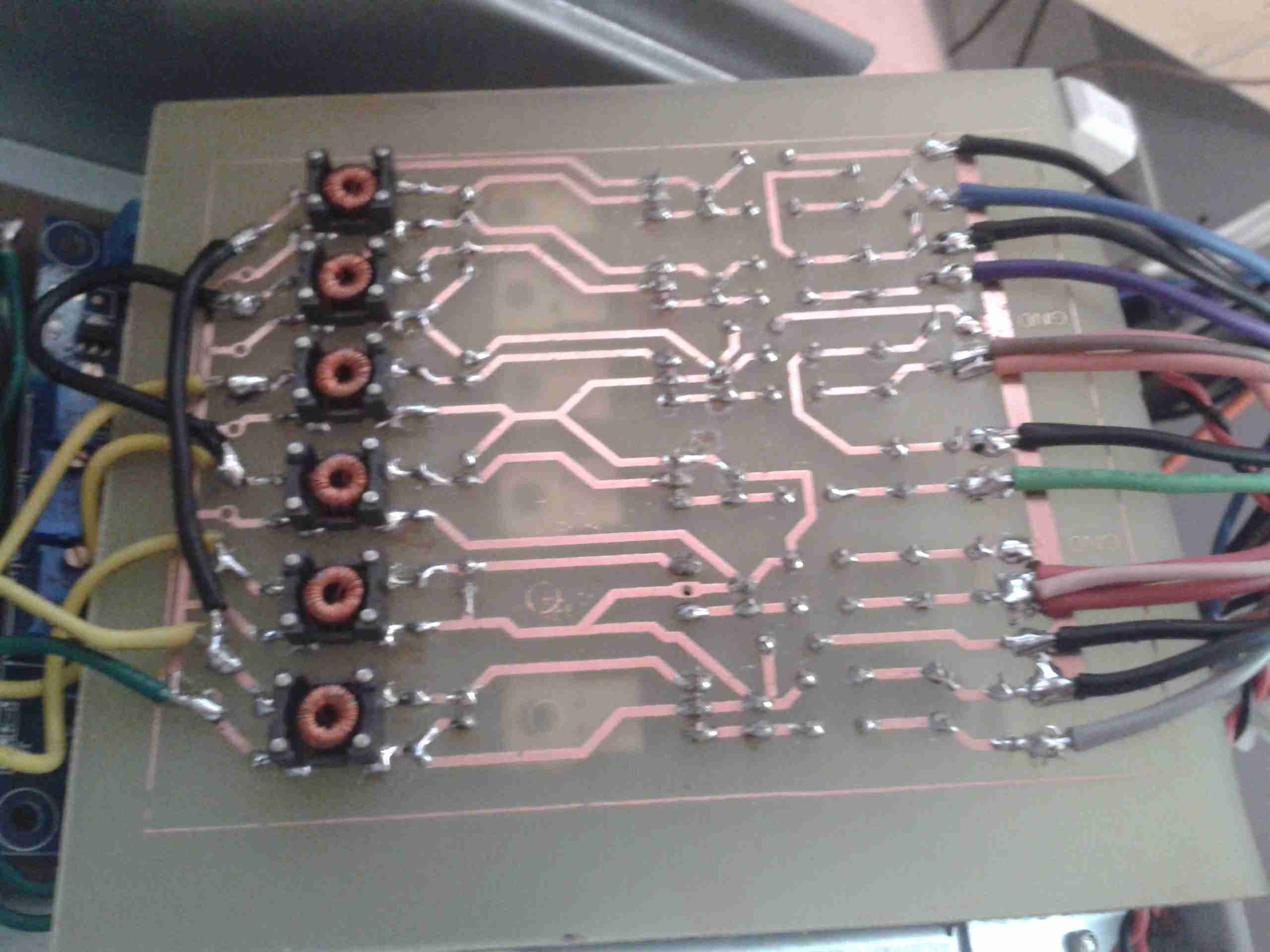
Scope Linear PSU
Here’s the PCB layout, with the 6 common mode filters on the input (left), linear regulator ICs in the centre & the output filters on the right.
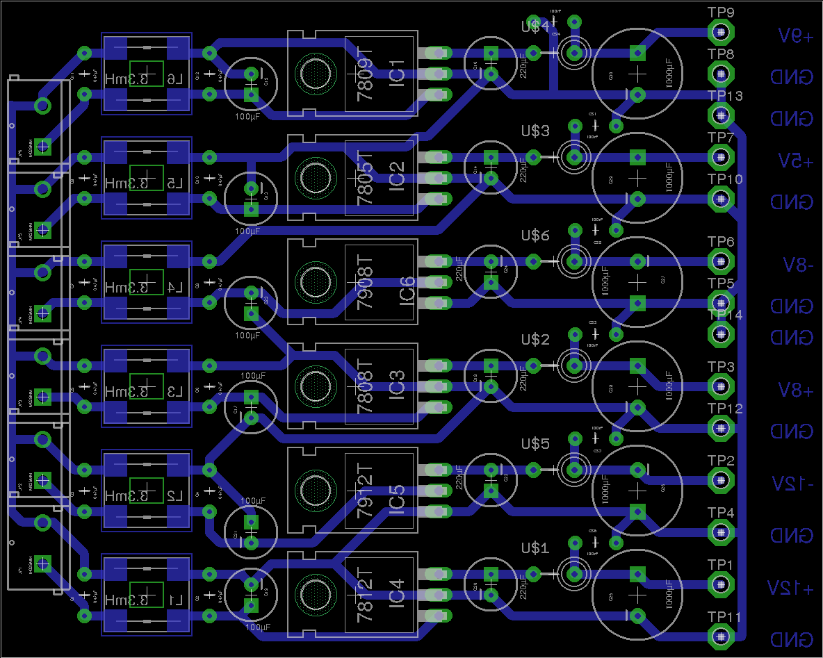
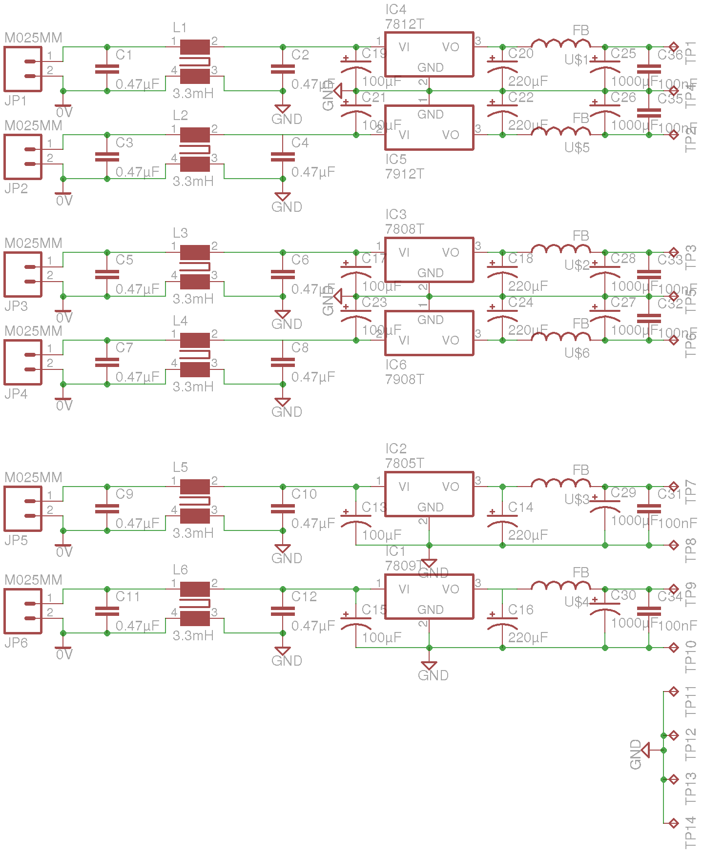
Scope Linear PSU
Here’s the schematic layout, as usual the Eagle Project files are in the link below, I’ll update when I have built the board & tested!
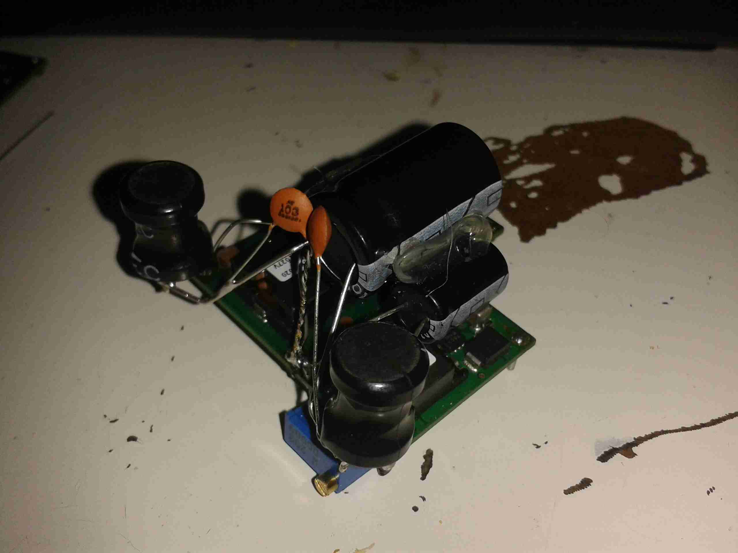
Here’s some testing of the first bipolar supply for the Rigol scope. This is the +/-7.5v supply.
Bipolar Supply
Above is the supply built with it’s output filtering. The modules used are a PTN78020W for the positive rail & a PTN78060A for the negative rail.
Under a 1A load across the total 15v output, here’s some scope traces of the ripple on the supply:
+7.5v Rail
Here’s the ripple on the +7.5v rail of the supply, there’s about 75mV of total ripple.
-7.5v Rail
And here’s the -7.5v rail, the ripple on this is slightly lower, at about 50mV. This should be more than satisfactory as the scope has onboard linear regulation after the switching supply.
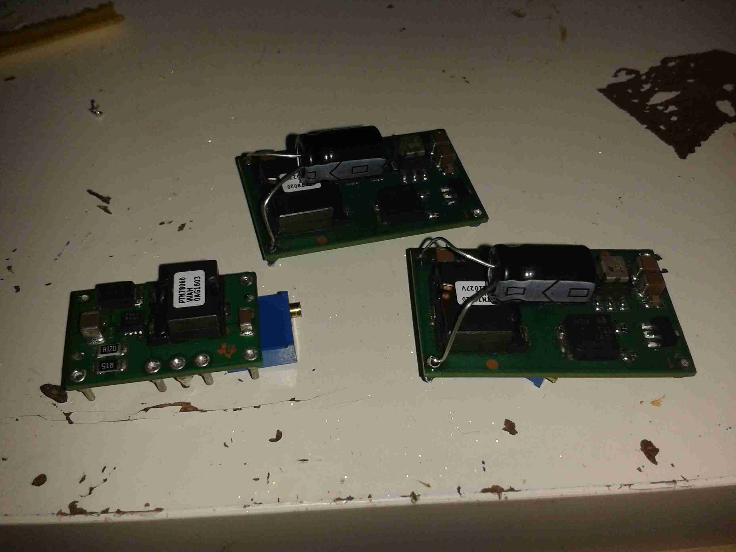
While searching around for regulators to convert my new scope to 12v power, I remembered I had some DC-DC modules from Texas Instruments that I’d got a while ago. Luckily a couple of these are inverting controllers, that will go down to -15v DC at 15W/3A capacity.
I’ve had to order a new module from TI to do the -17v rail, but in the meantime I’ve been getting the other regulators set up & ready to go.
The DC-DC module I’ve got for the -7.5v rail is the PTN78060A type, and the +7.5v & +5v rails will be provided by the PTN78020W 6A buck regulators.
These regulators are rated well above what the scope actually draws, so I shouldn’t have any issues with power.
DC-DC Modules
Here’s the regulators for the 5v, 7.5v & -7.5v rails, with multiturn potentiometers attached for setting the voltage output accurately. I’ve also attached a couple of electrolytics on the output for some more filtering. I’ll add on some more LC filters on the output to keep the noise down to an absolute minimum. These are set up ready with the exact same output voltage as the existing mains AC switching supply, when the final regulator arrives from TI I will put everything together & get some proper rail readings.
There won’t be a proper PCB for this, as I don’t have the parts in Eagle CAD, and I simply don’t have the energy to draw them out from the datasheets.
Since everything in my shack is run from 12v, I thought it would be handy to convert my new scope to 12v as well, as 99% of the places I find myself needing test gear are off grid, with no access to mains supplies.
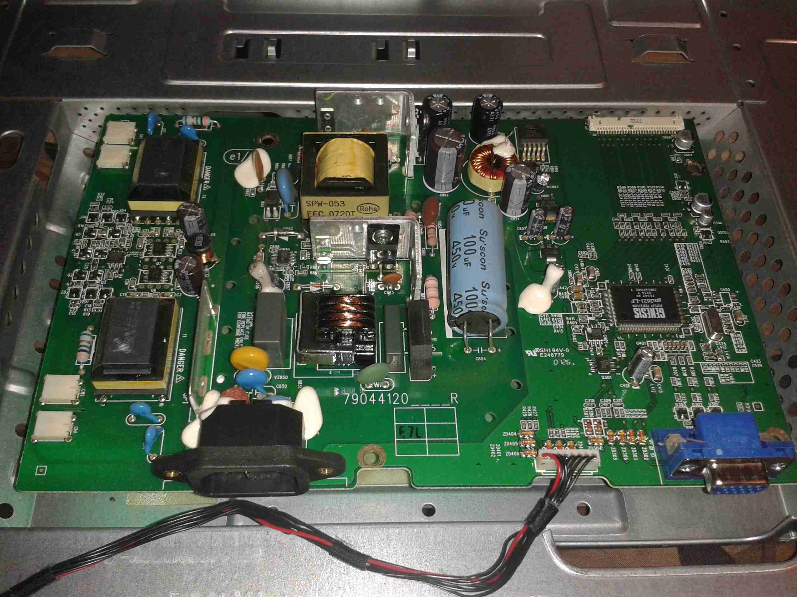
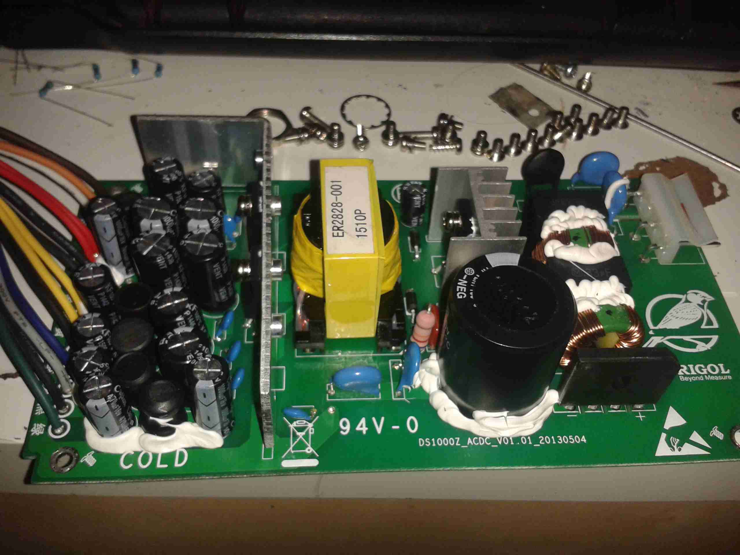
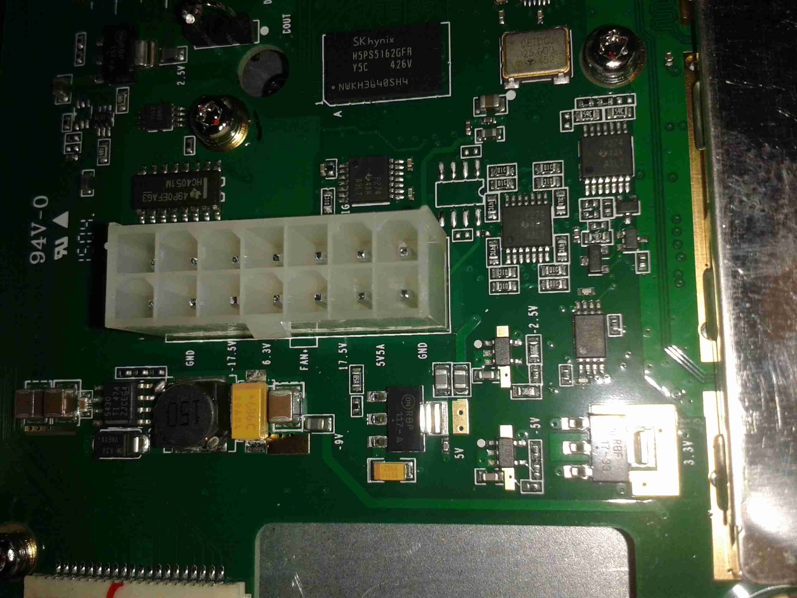
Mains PSU
Here’s the factory mains SMPS unit from the back of the scope. This is a nice multi-rail unit, with several different outputs, the table below details the wiring of the PSU.
Connector Pin
PCB Pin
Signal
Measured Voltage
Mainboard
Rectifier Rating
Wire Colour
5
1
AC_TRIG
N/A
AC_TRIG
N/A
BROWN
2
2
+9v_GND
N/A
FAN --
NA
ORANGE
11
3
+9V
10.16V
FAN +
2A
WHITE
6
4
+5V
5.1V
5V5A
20A
RED
13
5
+5V
5.1V
5V5A
20A
RED
7
6
GND
N/A
GND
N/A
BLACK
8
7
GND
N/A
GND
N/A
BLACK
3
8
+7.5V
6.9V
6.3V
20A
YELLOW
10
9
+7.5V
6.9V
6.3V
20A
YELLOW
1
10
GND
N/A
GND
N/A
BLACK
12
11
17.5V
17.51V
17.5V
2A
BLUE
9
12
-17.5V
-17.36V
-17.5V
2A
GREY
14
13
GND
N/A
GND
N/A
BLACK
4
14
-7.5V
-6.84V
-7.5V
2A
GREEN
The only feature I will lose if I make this switch is AC line triggering, but I never use that anyway, so it’s not a big issue for me.
Since I have been able to locate the connector, the plan is to design a replacement low voltage supply unit for the scope, with the same footprint as the original AC mains supply. This will allow me to do a direct swap without causing any damage or modifying the original supply.
This method will allow me to swap the 240v supply back into the scope if I ever come to need it.
I’m planning to use the LTC3863 DC-DC Controller from Linear Tech to generate the negative rails, this will go down to -150v on the output, so it’s pretty much perfect to generate them.
PSU Output Side
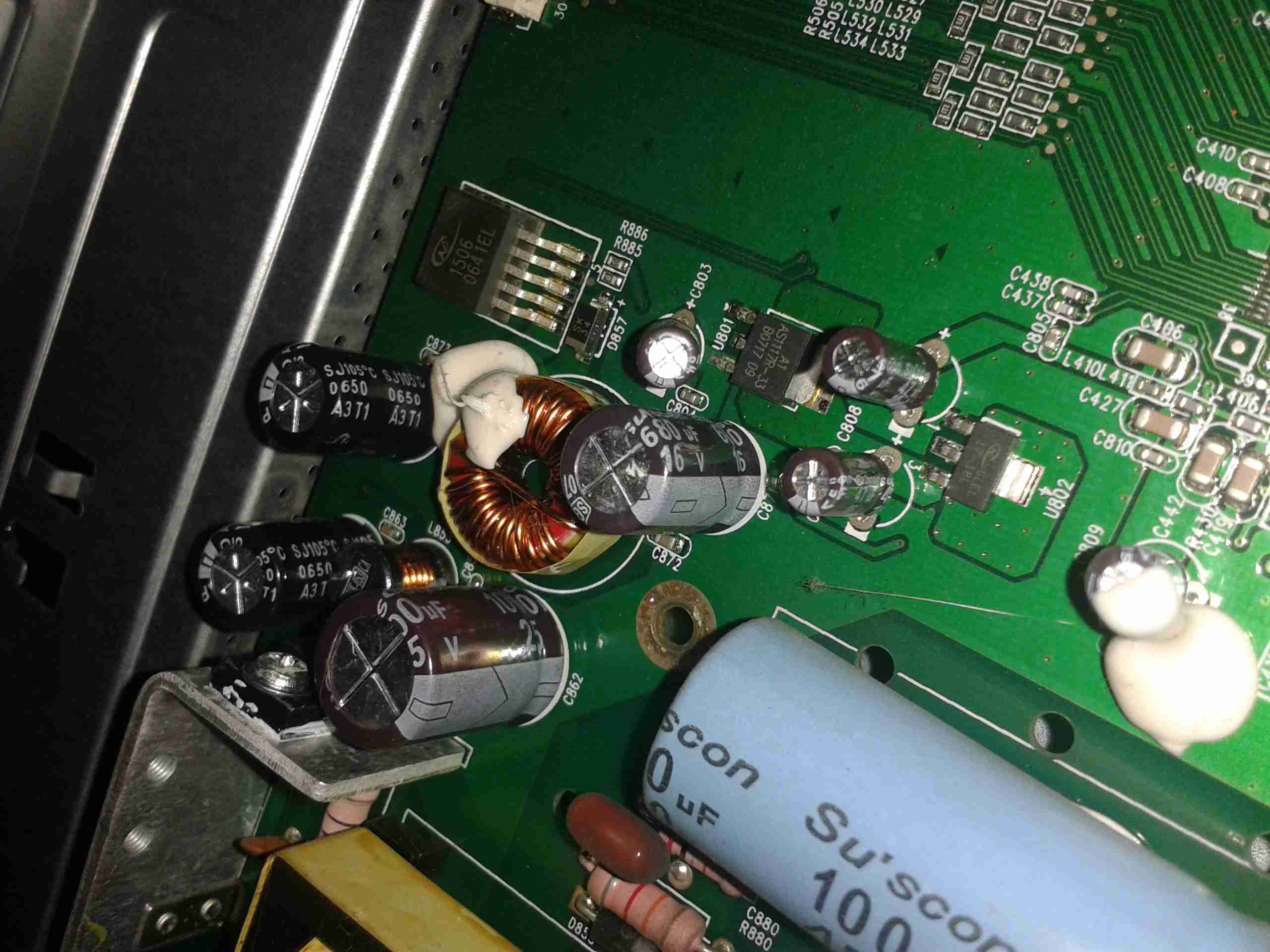
Here’s the output side of the mains PSU, it has a lot of filtering on the output rails, the two TO220 devices are the output rectifiers for the +5v & +7.5v rails, these are rated at 20A, 60V.
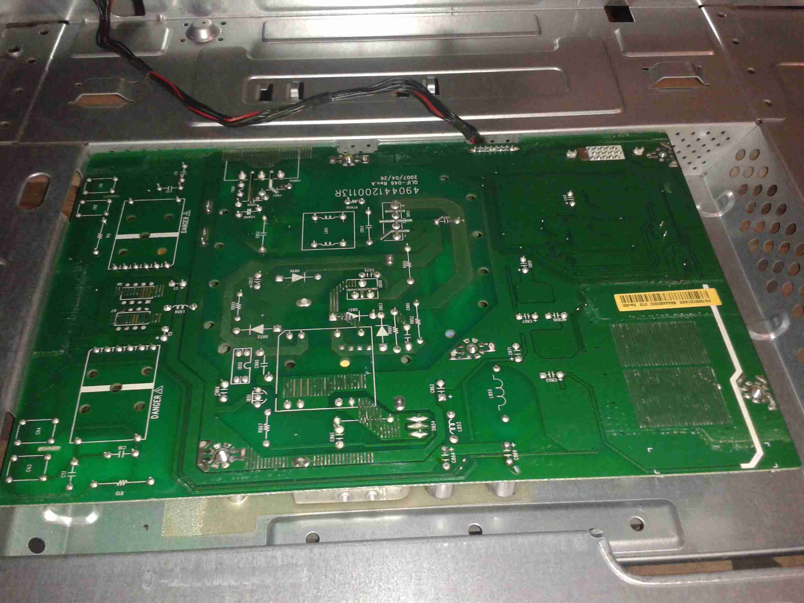
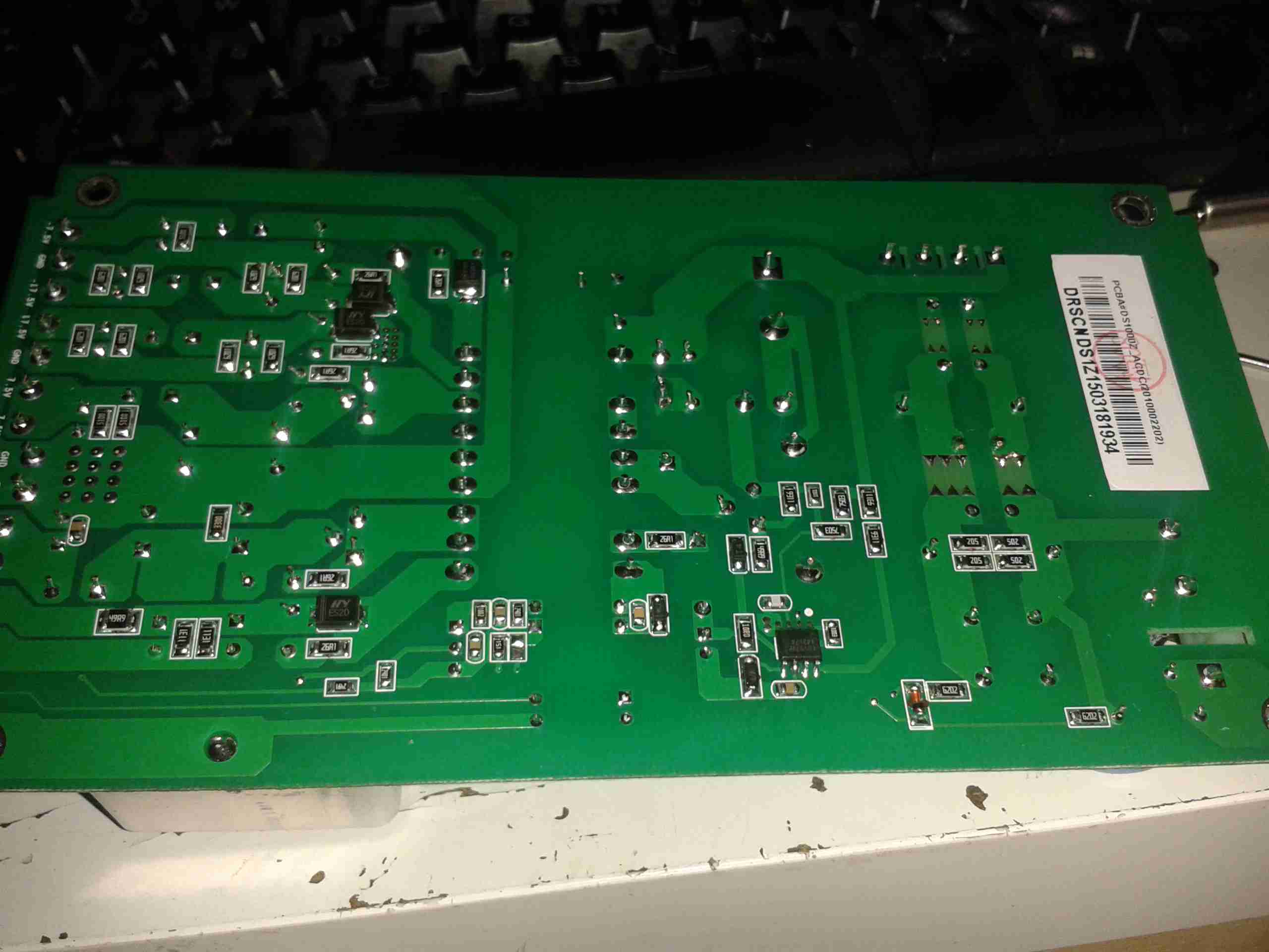
PCB Bottom
Here’s the bottom side of the PCB. It’s a really nicely designed PSU, massive isolation gap, spark gaps on the primary side & good filtering. The output side on the left has the rectifier diodes for the other voltage rails, these are only 2A rated, so designing the inverting supply to generate the negative rails will be pretty easy.
From looking at the PCB markings on both the mainboard & the PSU, the +9v rail seems to be used to drive the fan, both silkscreen markings indicate this.
The voltages marked on the PSU & the mainboard connector don’t quite match up though, there’s a small variation in the stated voltage between the two. This is most likely because all of the regulation of the supplies seems to be done on the mainboard, there are several linear regulators, and a few DC-DC switchers. Providing that the replacement supply isn’t noisy it should work fine.
This is backed up by the fact that the mains PSU only seems to regulate the +5v rail – on measuring the rails that’s the only one that’s close to spec.
Mainboard Power
Here’s the mainboard power connector, with it’s silkscreen labelling on the pins. (Very useful). As can be seen here, there’s at least 5 regulators, of both switching & linear types here, generating both positive & negative rails.
Having now tested the supply I wrote about in my previous post, I can now say that it’s nameplate rating far exceeds it’s actual capability.
On running the supply under load, at 6.5A the operating frequency drops into the audible range, a big sign of overload. (It makes an irritating continuous chirping noise). The output voltage also drops to 10.5v.
The temperature of the unit while it’s been running under such a load is also questionable, the external casing gets hot enough to cause burns, I haven’t yet been able to stick a thermocouple into the case to see what the internal temperature is.
I’m currently talking with the eBay seller (wwwstation) regarding this, however they are arguing that the supply is only for LEDs & CCTV cameras.
However those two loads are very different, and the supply has no internal regulation for supplying LEDs. As a simple switchmode supply, any load is suitable, providing it’s within the load rating of the supply.
I would estimate that the supply is only capable of 5A as an upper limit.
They are requesting that I return the supply, but I’m yet to find out if they’re going to cover return postage. The item as listed is not as described, and I will escalate things if required.
I will update this post when I hear more back from the eBay seller.
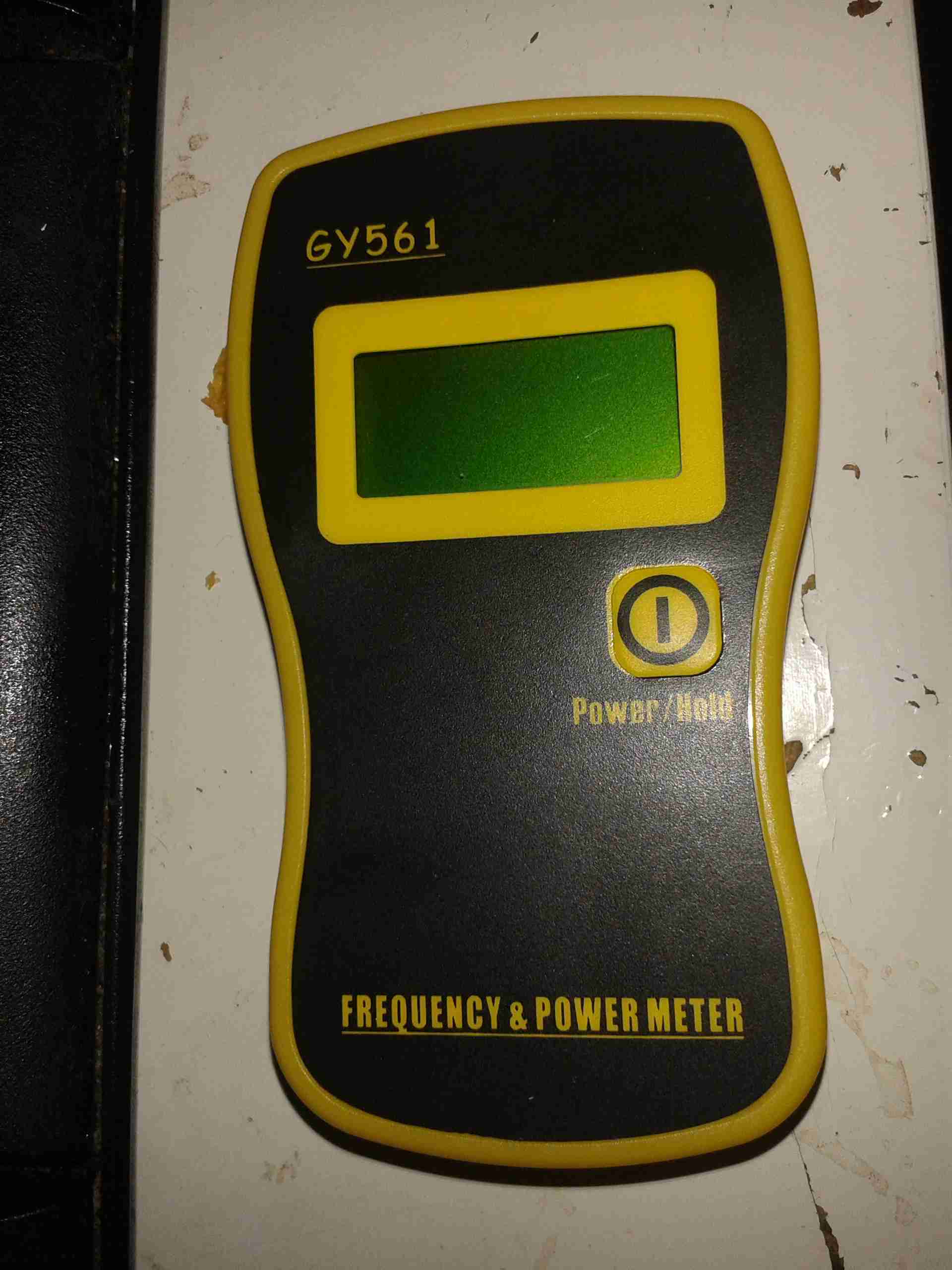
The latest addition to my radio shack is the GY561 frequency & power meter, which has already come in useful for measuring the output power of all my radios.
GY561
It’s a small device, roughly the same size & weight as a stock UV-5R. Power is provided by 3 AAA cells.
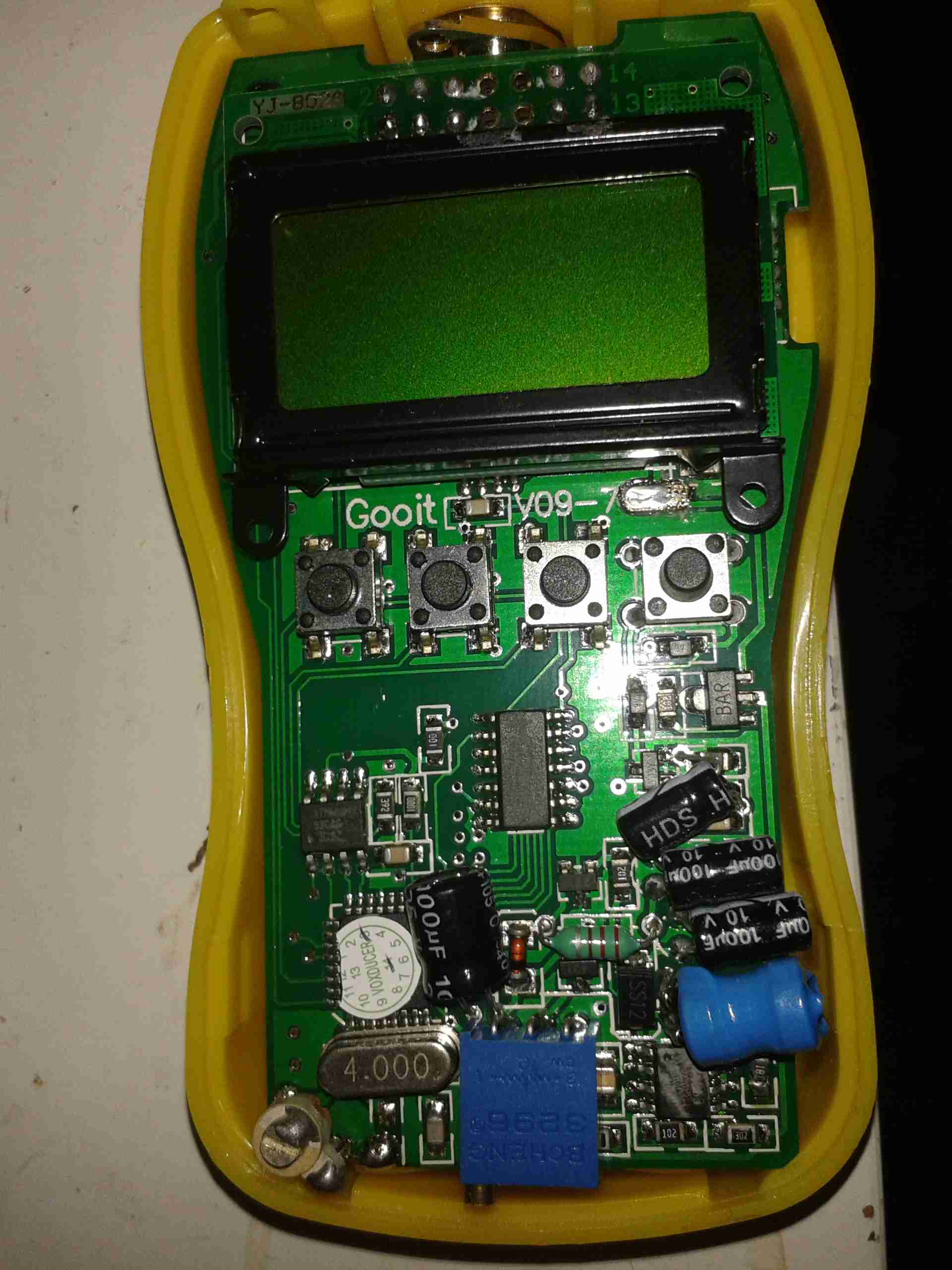
Display
The display is a standard HD44780 8×2 module. The display on this unit isn’t backlit, so no operating in the dark.
Cover Removed
The cover pops off easily to allow access to the internals, without having to remove any screws!
The 4 screws on the back of the unit hold the heatsink plate for the 50W 50Ω dummy load resistor.
Removing the cover reveals a couple of adjustments, for frequency & RF power calibration.
There are also 3 tactile switches that aren’t on the front panel. According to the manual (which in itself is a masterpiece of Chinglish), they are used to software calibrate the unit if an accurate RF power source is available. I will attempt to do a reasonable translation when time allows.
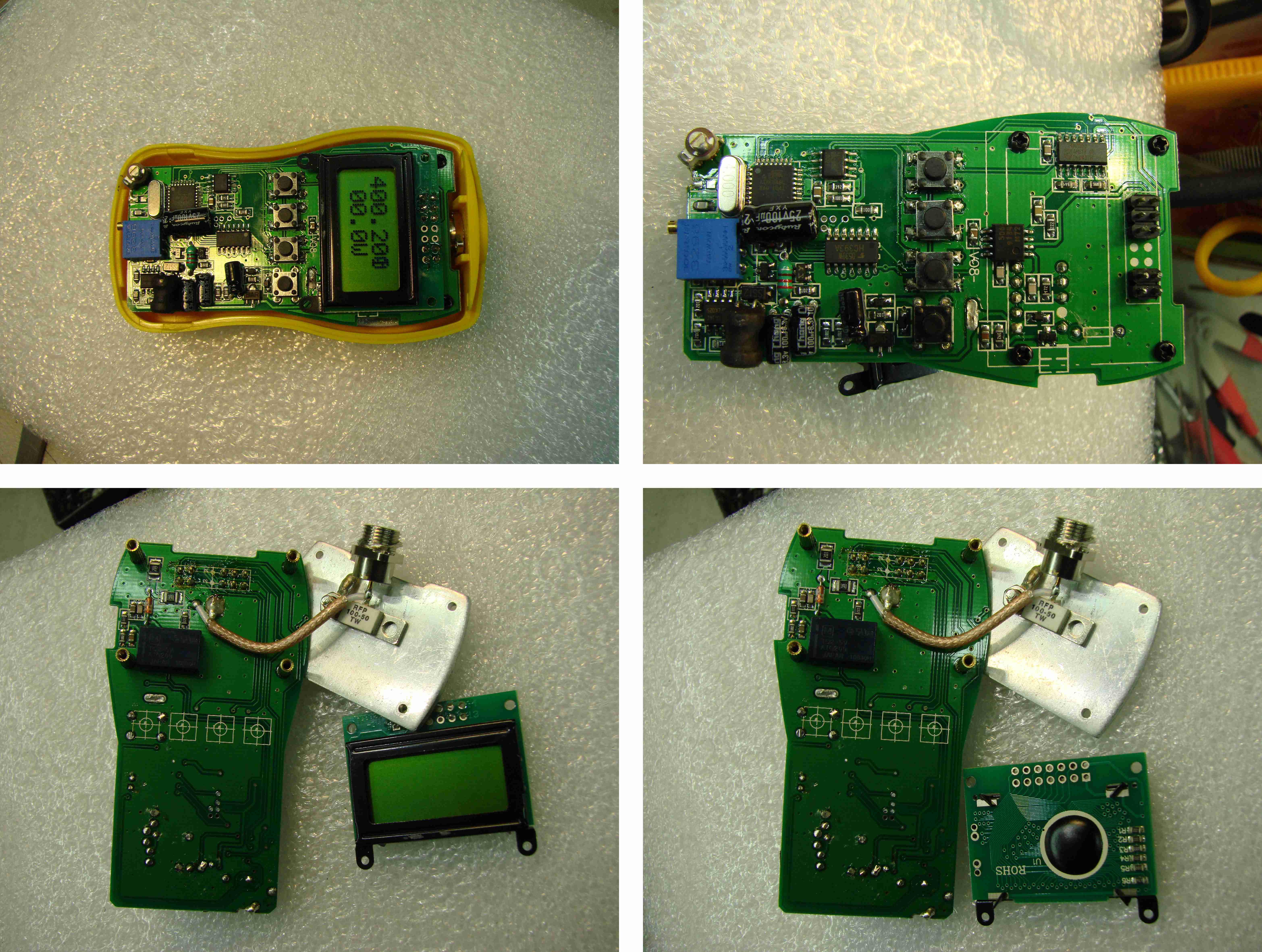
Disassembly further than this involves some desoldering in awkward places, so a search of the internet revealed an image of the rest of the internal components. In the case of my meter, all the part numbers have been scrubbed off the ICs in an attempt to hide their purpose. While it’s possible to cross-reference IC databooks & find the part numbers manually, this process is a time consuming one. Luckily the image I managed to locate doesn’t have the numbers scrubbed.
Total Disassembly
Under the LCD is some 74HC series logic, and a prescaler IC as seen in the previous frequency counter post. However in this unit the prescaler is a MB506 microwave band version to handle the higher frequencies specified.
In this case however the main microcontroller is an ATMEGA8L.
This is complemented by a SN54HC393 4-bit binary counter for the frequency side of things. This seems to make it much more usable down to lower frequencies, although the manual is very generous in this regard, stating that it’s capable of reading down to 1kHz. In practice I’ve found the lowest it reliably reads the frequency input is 10MHz, using my AD9850 DDS VFO Module as a signal source.
It did however read slightly high on all readings with the DDS, but this could have been due to the low power output of the frequency source.
Just like the other frequency counter module, this also uses a trimmer capacitor to adjust the microcontroller’s clock frequency to adjust the calibration.
The power supply circuitry is in the bottom left corner of the board, in this case a small switching supply. The switching regulator is needed to boost the +4.5v of the batteries to +5v for the logic.
Also, as the batteries discharge & their terminal voltage drops, the switching regulator will allow the circuit to carry on functioning. At present I am unsure of the lower battery voltage limit on the meter, but AAA cells are usually considered dead at 0.8v terminal voltage. (2.4v total for the 3 cells).
When turned on this meter draws 52mA from the battery, and assuming 1200mAh capacity for a decent brand-name AAA cell, this should give a battery life of 23 hours continuous use.
On the back of the main PCB is a 5v relay, which seems to be switching an input attenuator for higher power levels, although I only managed to trigger it on the 2m band.
Finally, right at the back attached to an aluminium plate, is the 50Ω dummy load resistor. This component will make up most of the cost of building these, at roughly £15.
On my DVM, this termination reads at about 46Ω, because of the other components on the board are skewing the reading. There are a pair of SMT resistors, at 200Ω & 390Ω in series, and these are connected across the 50Ω RF resistor, giving a total resistance of 46.094Ω.
This isn’t ideal, and the impedance mismatch will probably affect the calibration of the unit somewhat.
The heatsinking provided by the aluminium plate is minimal, and the unit gets noticeably warm within a couple of minutes measuring higher power levels.
High power readings should definitely be limited to very short periods, to prevent overheating.
The RF is sampled from the dummy load with a short piece of Teflon coax.
There’s a rubber duck antenna included, but this is pretty useless unless it’s almost in contact with the transmitting antenna, as there’s no input amplification. It might be handy for detecting RF emissions from power supplies, etc.
For the total cost involved I’m not expecting miracles as far as accuracy is concerned, (the manual states +/-10% on power readings).
The frequency readout does seem to be pretty much spot on though, and the ability to calibrate against a known source is handy if I need some more accuracy in the future.
I’ve also done an SWR test on the dummy load, and the results aren’t good.
At 145.500 MHz, the SWR is 3:1, while at 433.500 it’s closer to 4:1. This is probably due to the lower than 50Ω I measured at the meter’s connector.
These SWR readings also wander around somewhat as the load resistor warms up under power.
I’ll probably also replace the AAA cells with a LiPo cell & associated charge/protection circuitry, to make the unit chargeable via USB. Avoiding disposable batteries is the goal.
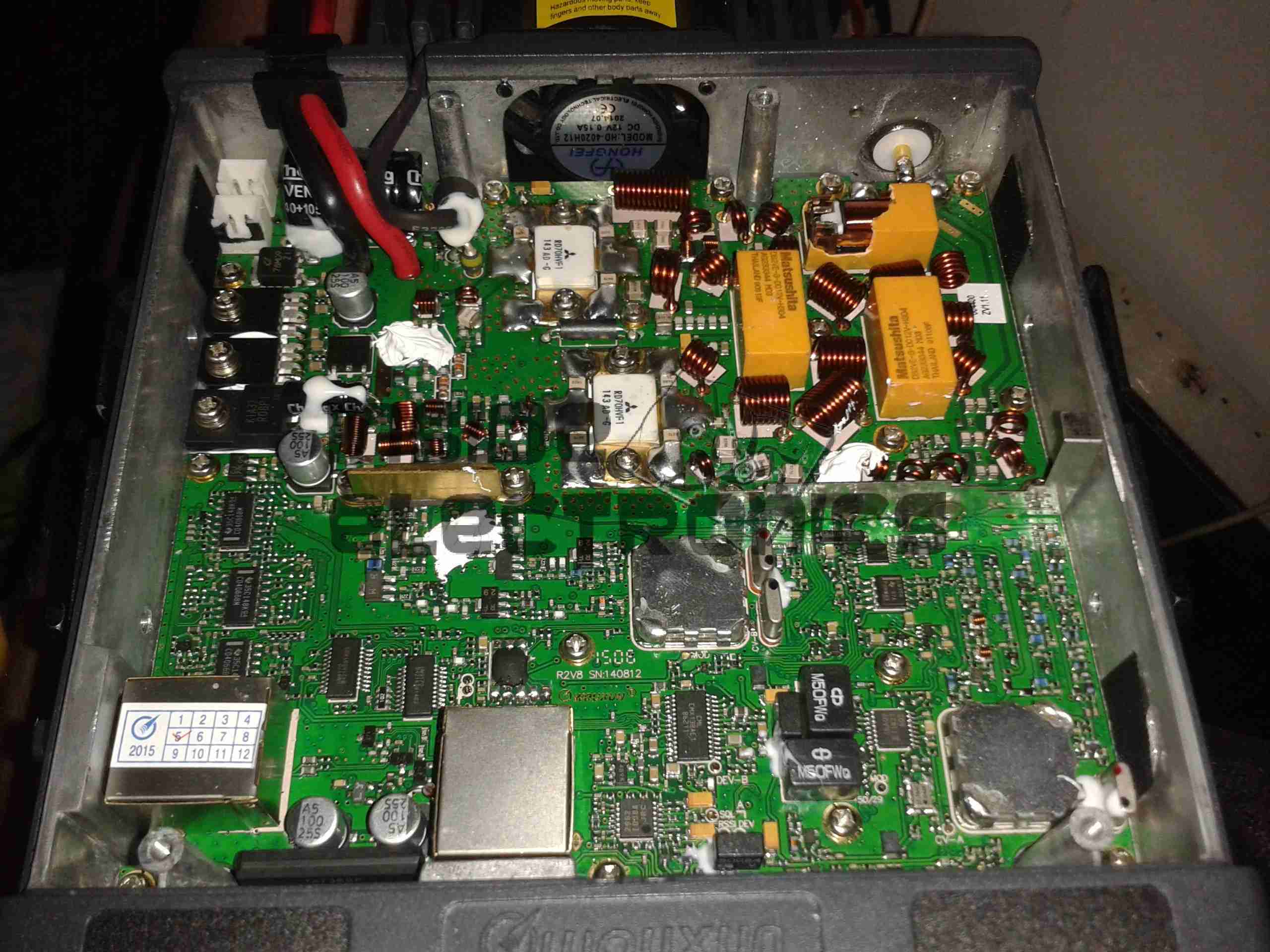
Following on from my review, here are some internal views & detail on the components used in this radio. Below is an overview of the main PCB with the top plate removed from the radio.
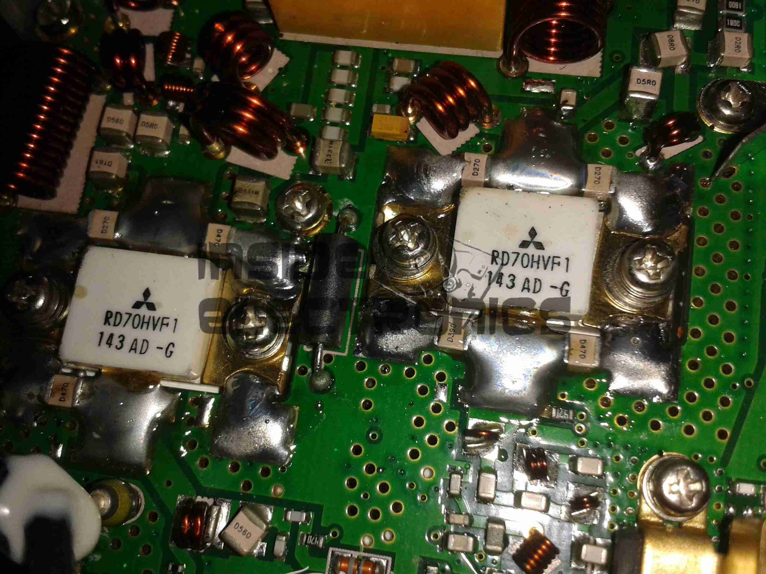
Cover RemovedRF Final Amplifier Stage
Most visible are these MOSFETs, which are Mitsubishi RD70HVF1 VHF/UHF power devices. Rated for a maximum of 75W output power at 12.5v (absolute maximum of 150W, these are used well within their power ratings. They are joined to the PCB with heavy soldering, with bypass caps tacked right on to the leads.
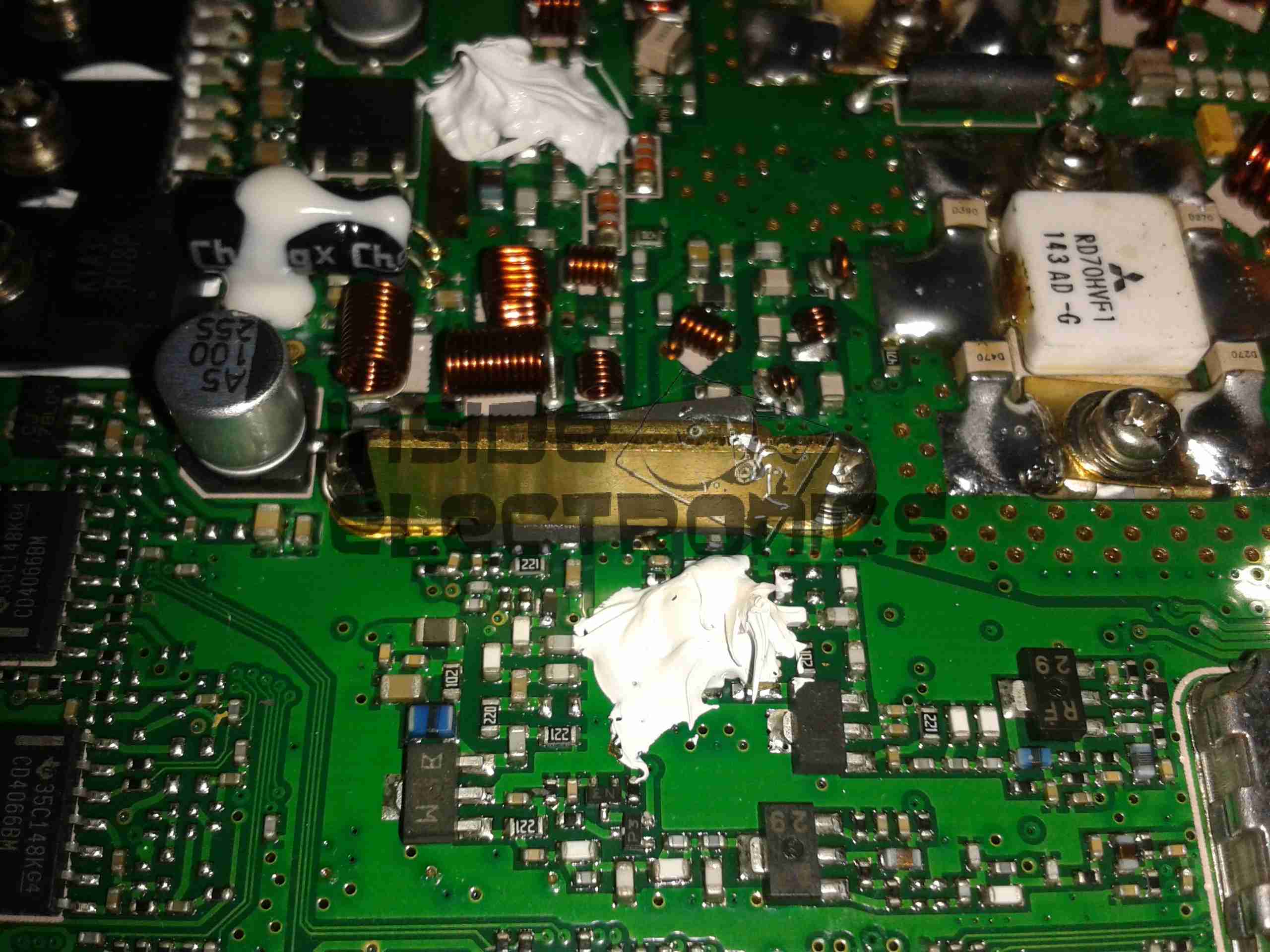
RF Pre Drivers
Here is the RF pre-driver stage, with intermediate transistors hidden under the small brass heatspreader.
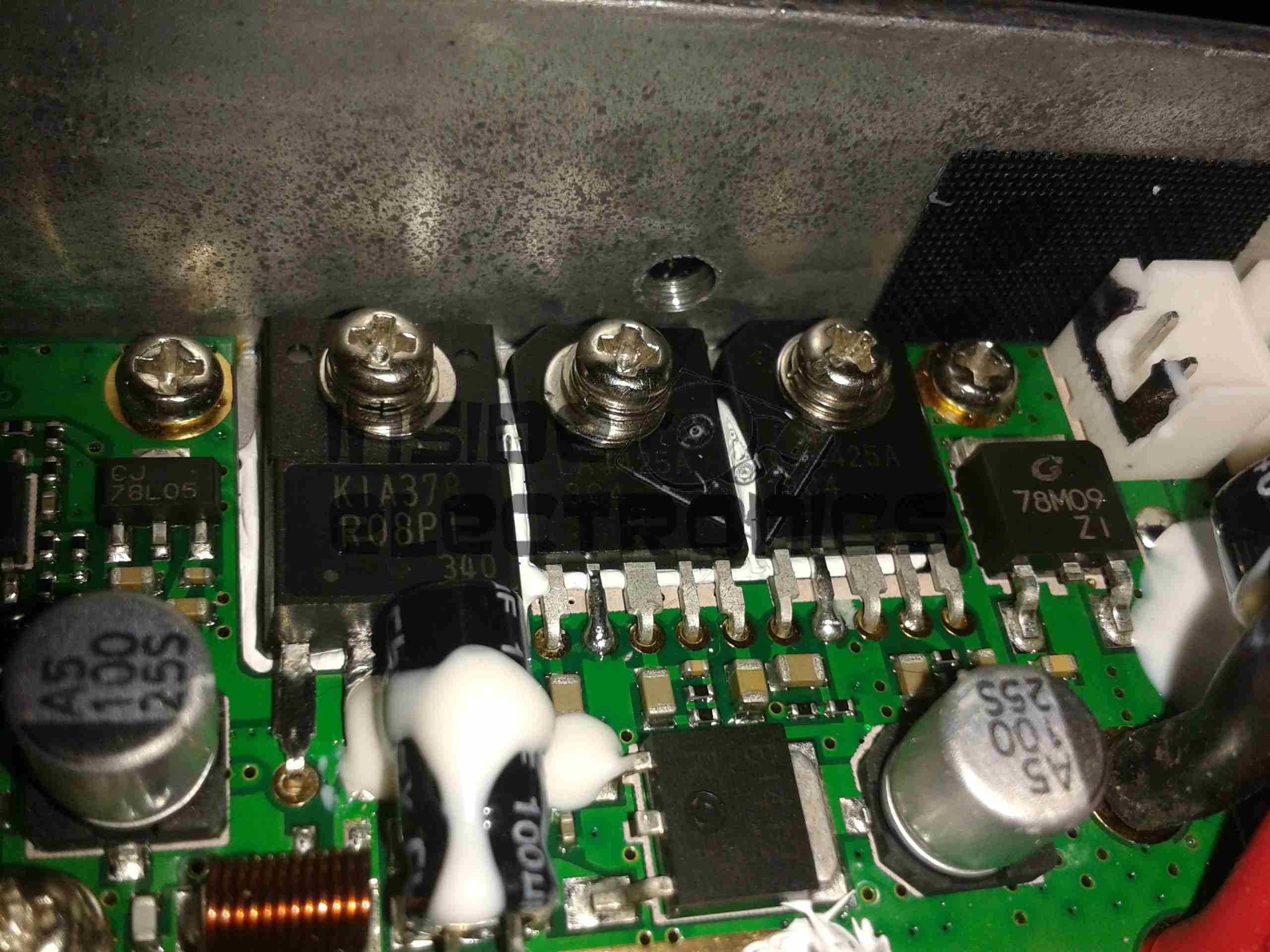
Power Section
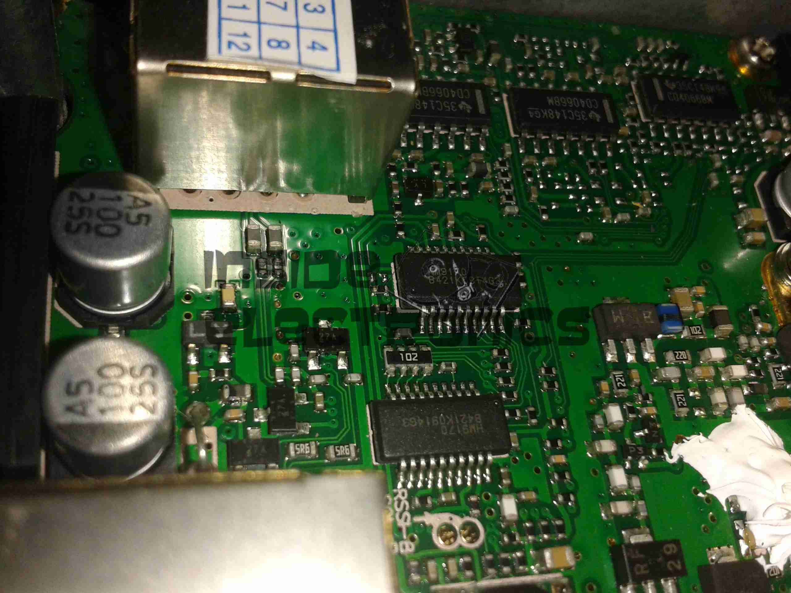
In the top left corner of the radio, near the power input leads, is the power supply & audio amplifier section. Clearly visible are the pair of LA4425A 5W audio power amplifier ICs, these drive the speakers on the top of the radio. Either side of these parts are a 7809 & a 7805 – both linear regulators providing +9v & +5v logic supplies respectively. The large TO220 package device is a KIA378R08PI 3A LDO regulator with ON/OFF control, this one outputs +8v. Just visible in the top right corner are the sockets for the speaker connections.
DTMF Circuits
Here are the two ICs for dealing with DTMF tones, they are HM9170 receivers.
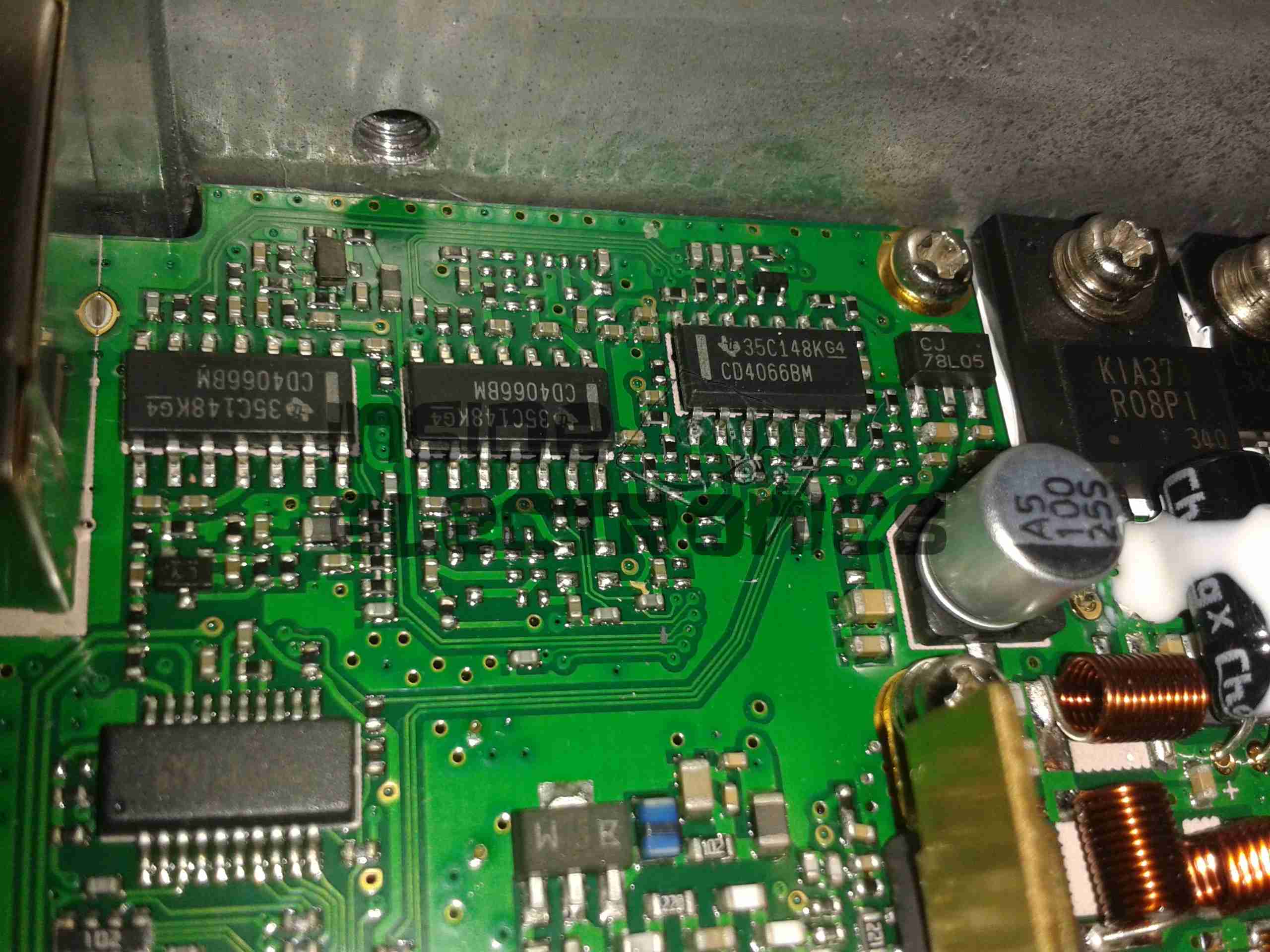
Glue Logic
In the corner next to the interface jack, there are some CD4066B Quad Bilateral switches. These make sense since the interface jack has more than a single purpose, these will switch signals depending on what is connected.
RF Section
Here are visible the RF cans for the oscillators, the crystals visible next to the can at the top. The shields are soldered on, so no opening these unfortunately.
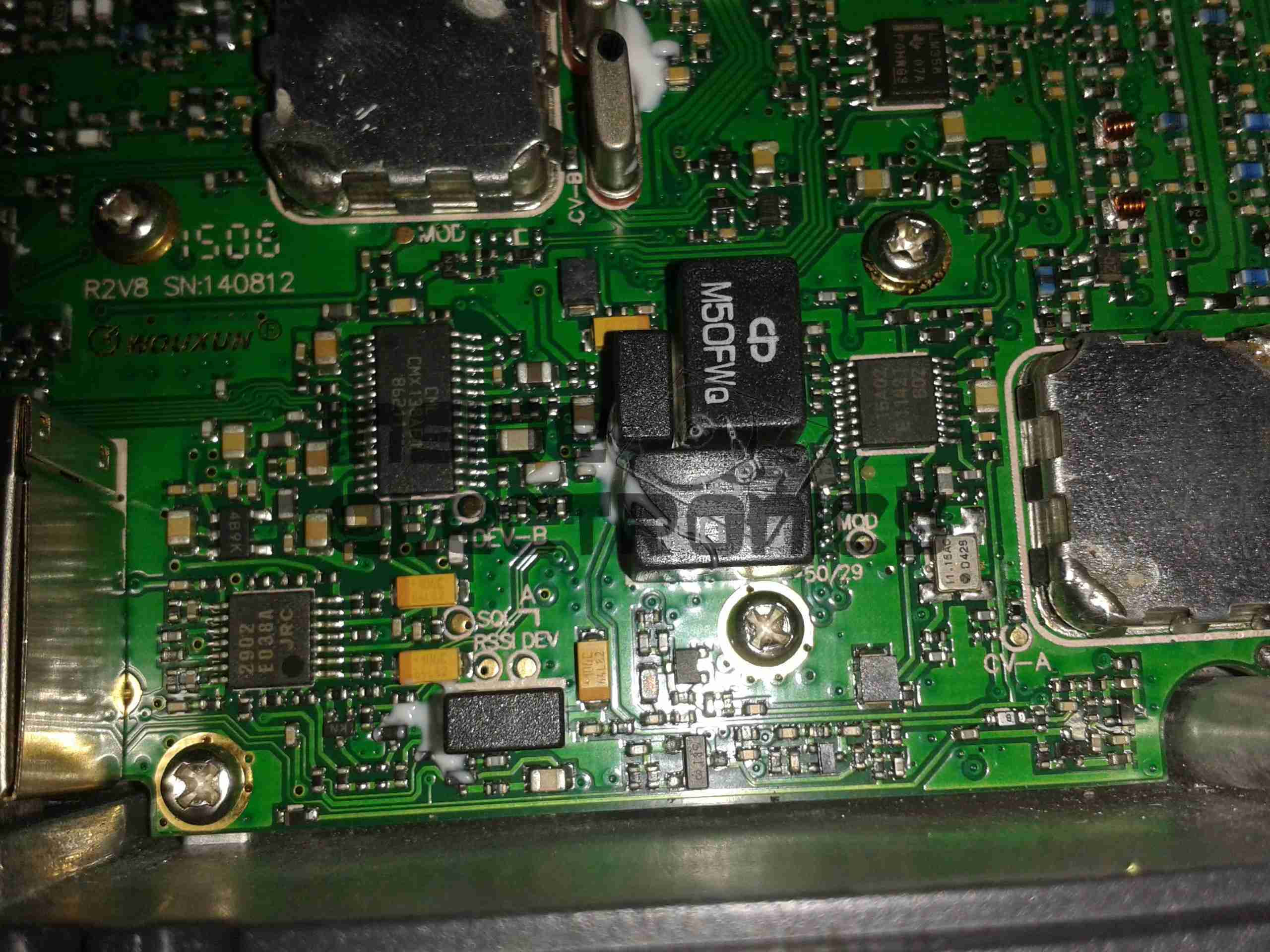
Also visible in this image is a CMX138A Audio Scrambler & Sub-Audio Signalling processor. This IC deals with the Voice Inversion Scrambling feature of the radio, & processes the incoming audio before being sent to the modulator.
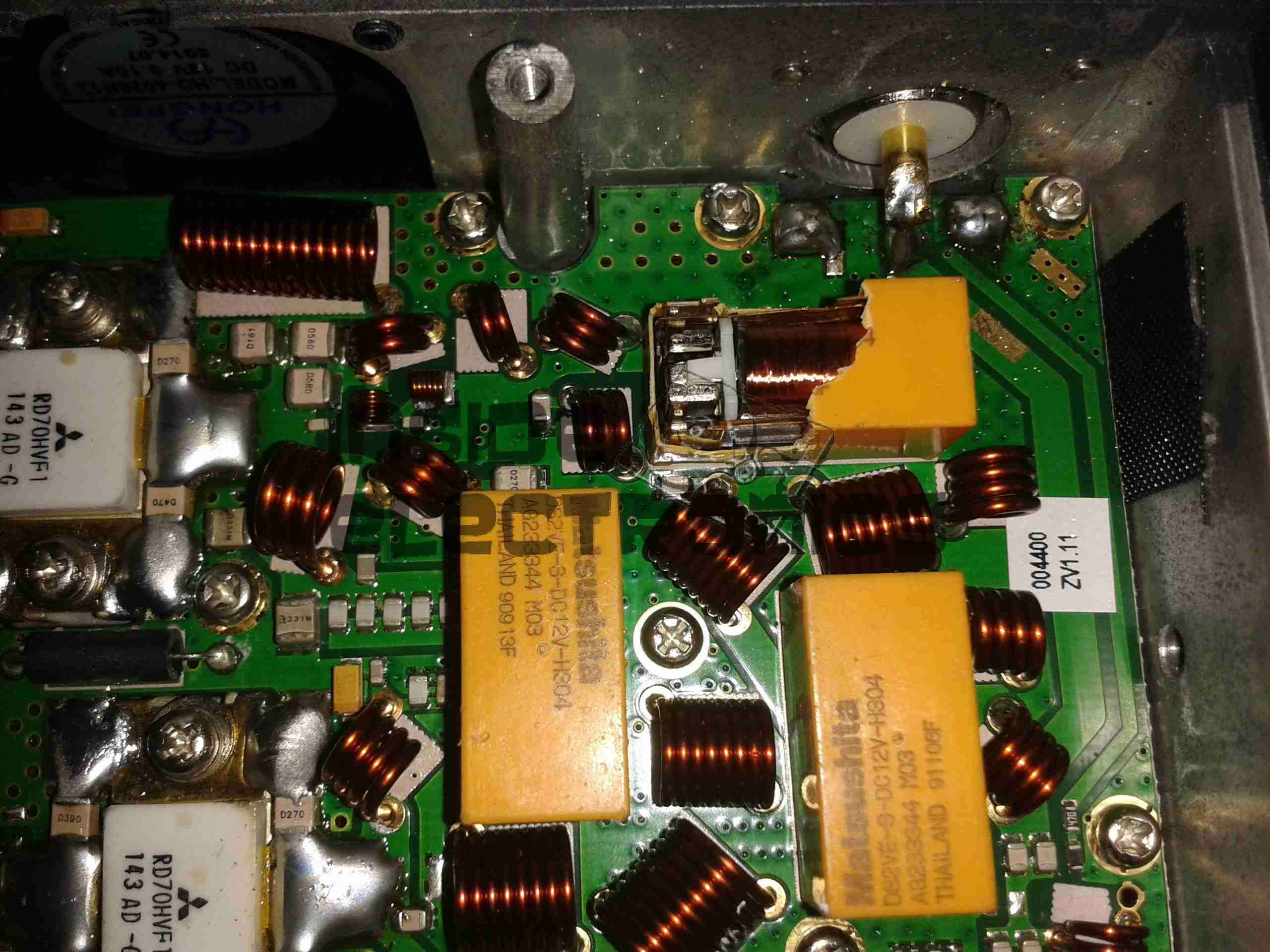
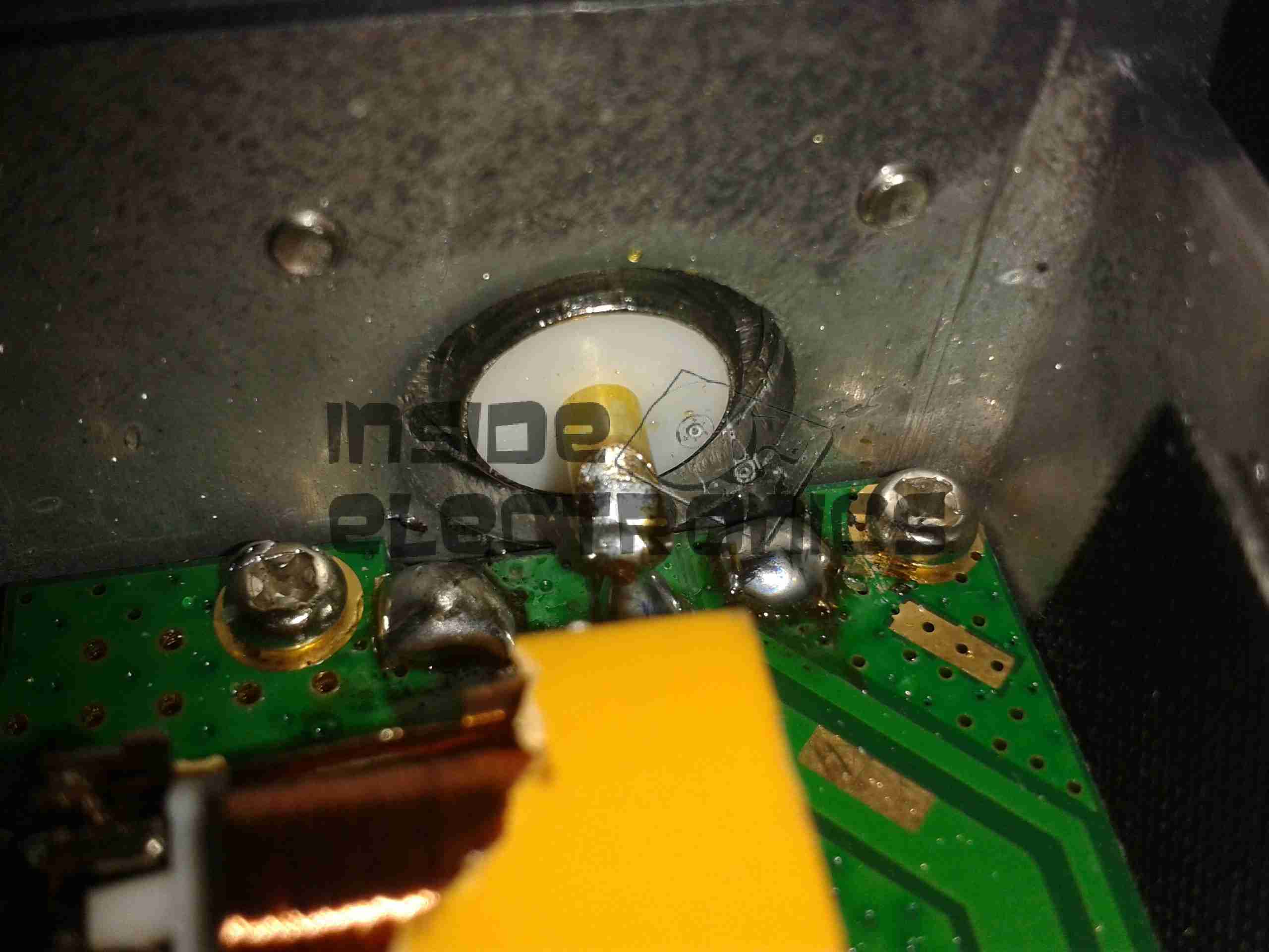
Output Filter Network
Shown here is the RF output filter network, this radio uses relays for switching instead of PIN diodes, I imagine for cost reasons. The relay closest to the RF output socket has had a slight accident 🙂 This is slated to be replaced soon.
RF Output Jack
Finally, the RF output jack.
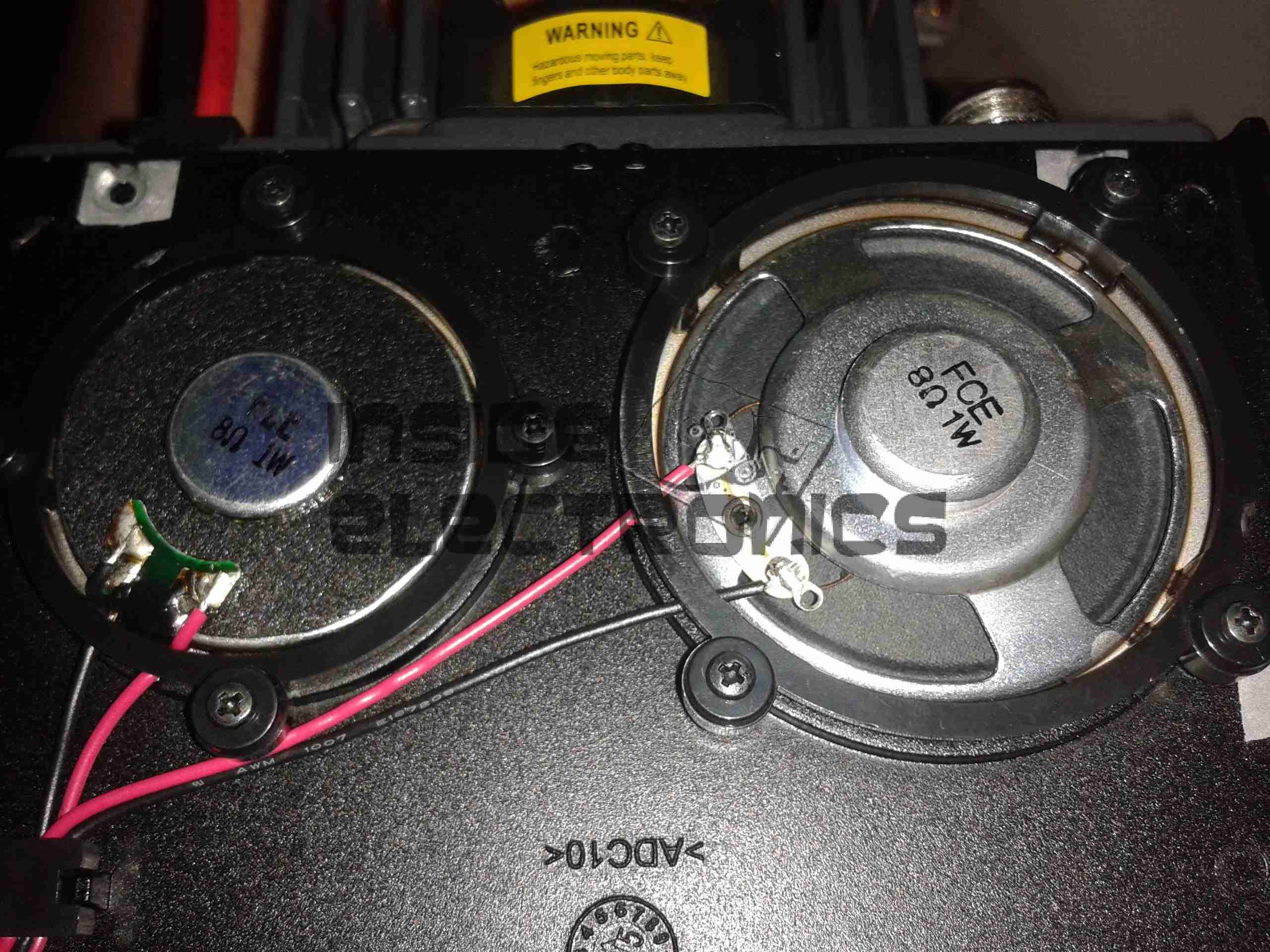
Audio Speakers
Here the speakers are shown, attached to the bottom of the top plate. They are both rated 8Ω 1W.
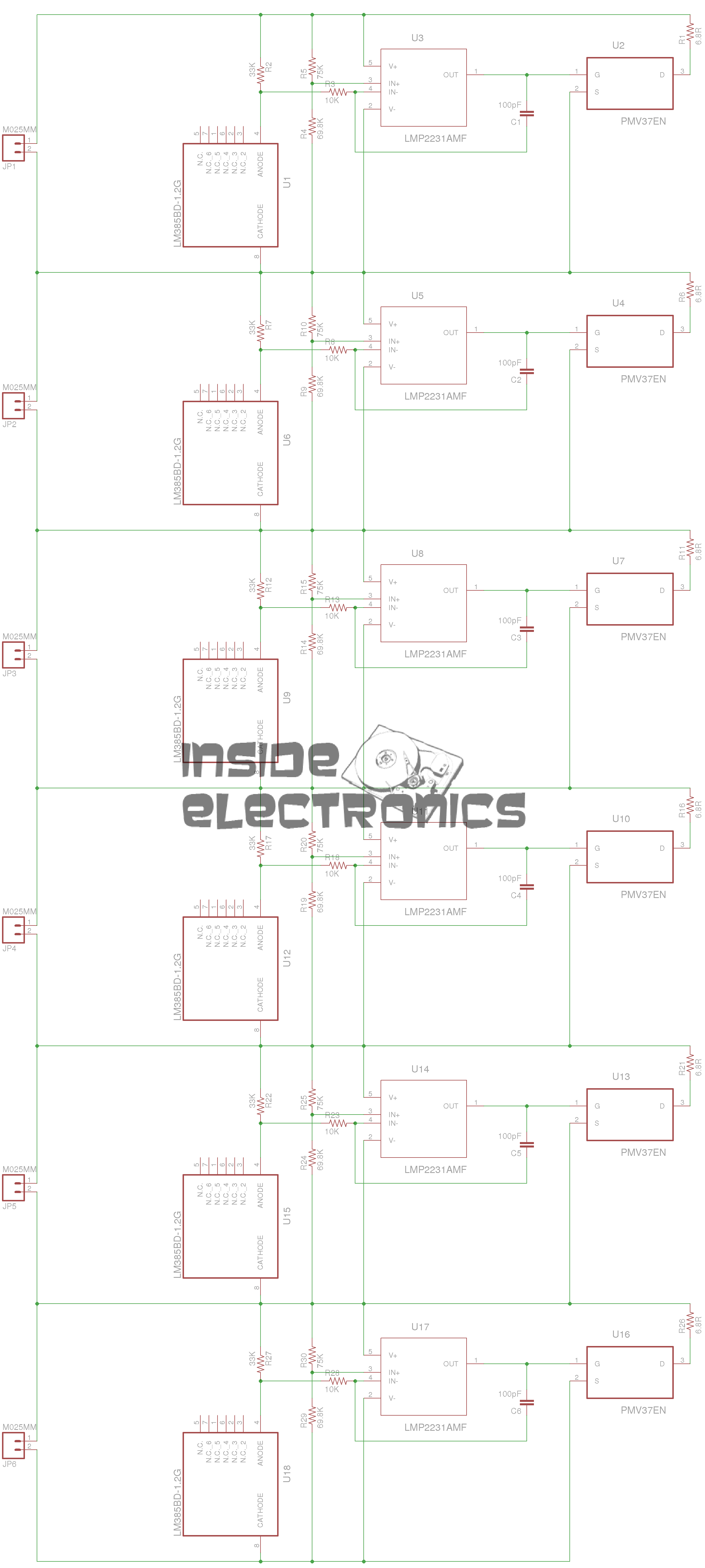
Here’s another active balancing circuit for large ultracapacitor banks, this one is designed for a series string of 6, at 2.5v per capacitor.
Based on the design here, I have transcribed the circuit into Eagle & designed a PCB layout.
Ultracap Balancer Circuit – Click to Embiggen
As can be seen from the circuit diagram above, this is just 6 copies of the circuit from the above link, with screw terminals to attach to the capacitor string.
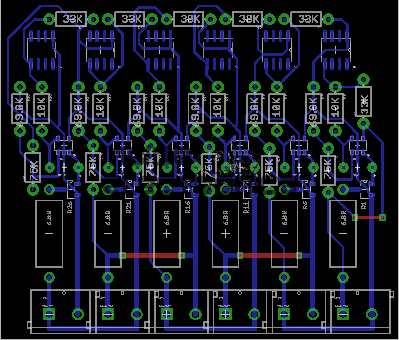
Ultracap Balancer PCB
And here’s the PCB. the MOSFETs & OpAmps are very small SMT parts, so require a steady hand in soldering. This board can easily be etched by hand as there’s only 3 links on the top side. No need for a double sided PCB.
As always, the Eagle project files & my Eagle library collection are available below:
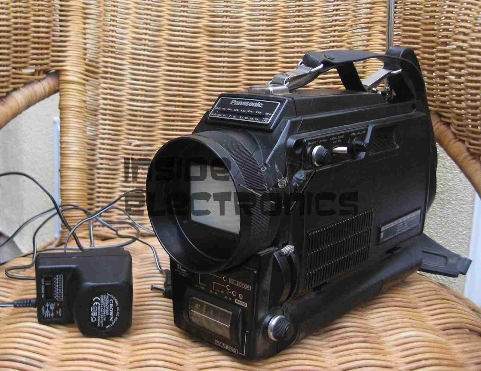
I recently managed to score a 3″ B&W portable TV on eBay, a Panasonic TR-3000G. As these old units are now useless, thanks to the switch off of analogue TV signalling, I figured I could find a composite signal internally & drive the CRT with an external source.
Panasonic TR-3000G
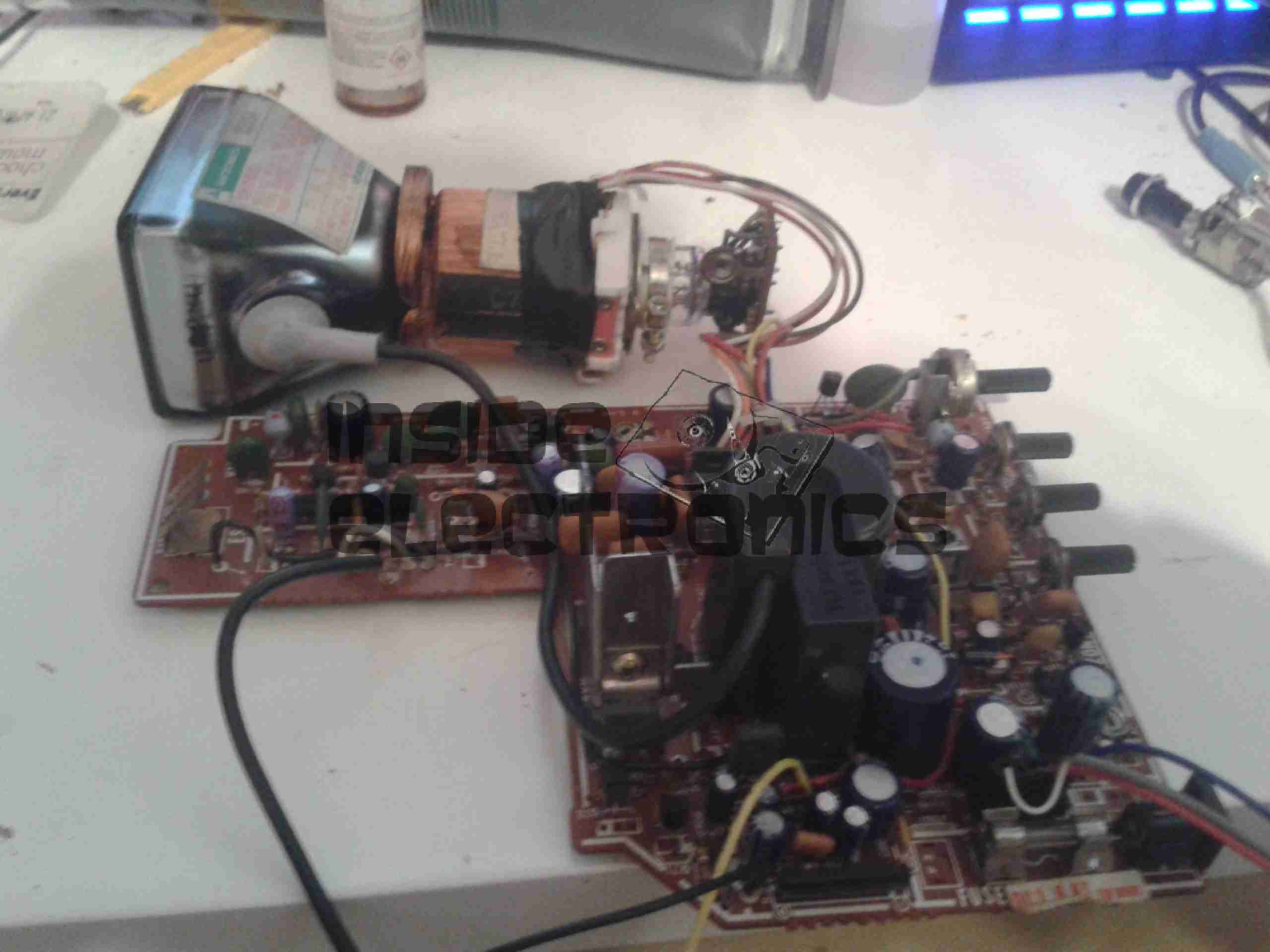
Here’s the TV in it’s native state. Running from 9v DC, or 6 D size cells. I’m guessing from somewhere around the 1970’s. Here is the CRT & associated drive circuitry, removed from the casing:
CRT Module
After dissecting the loom wiring between the CRT board & the RF/tuner board, I figured out I had to short out Pins 1,2 & 5 on the H header to get the CRT to operate straight from the power switch. This board also generates the required voltages & signals to drive the RF tuner section. I have removed the loom from this, as the PCB operates fine without. It doesn’t seem to be fussy about power input either: it’s specified at 9v, but seems to operate fine between 7.5v & 14.5v DC without issue.
Video Connections
Tracing the wiring from the tuner PCB revealed a length of coax snaking off to the section marked Video/Sync. I successfully found the composite input!
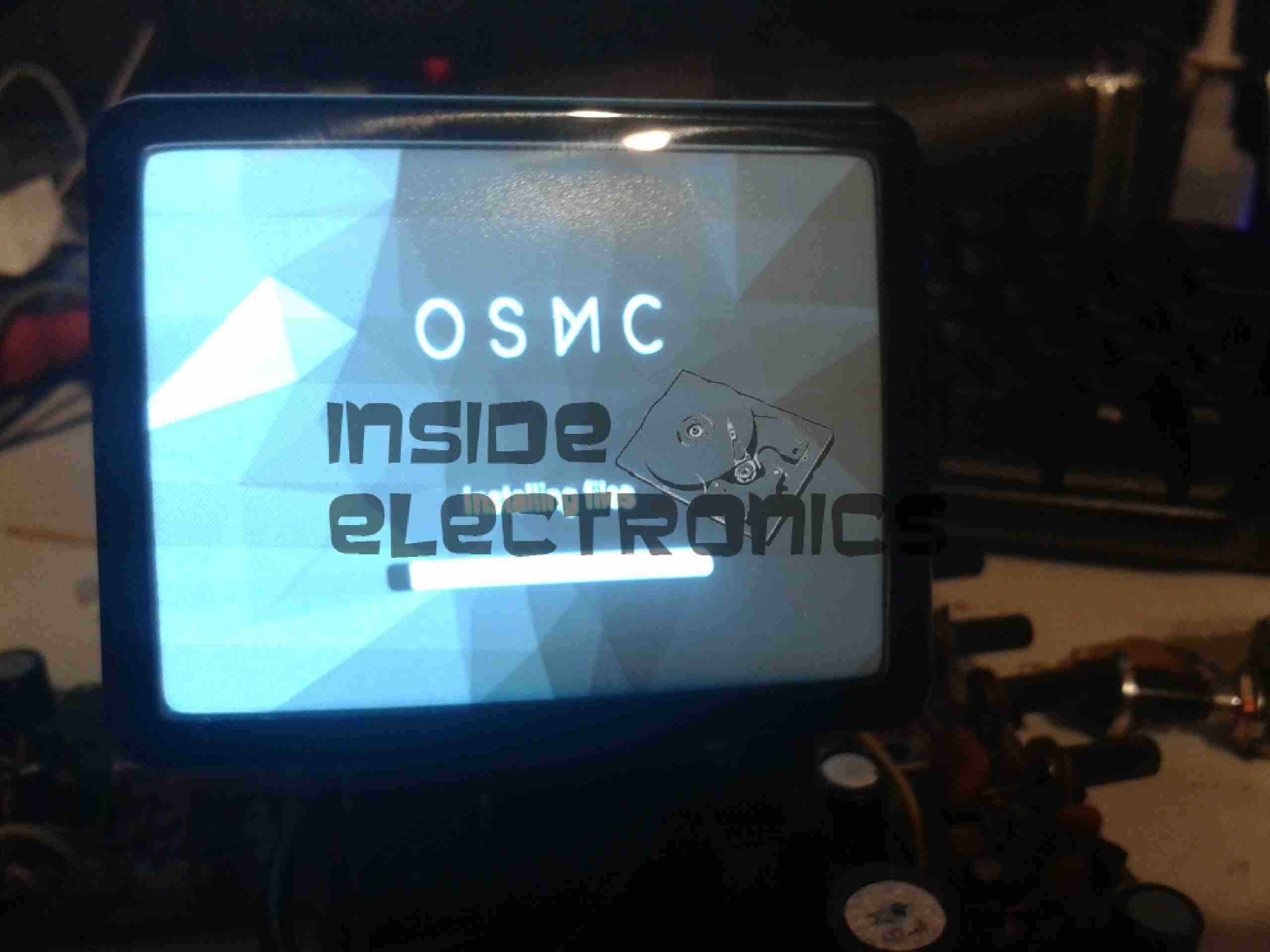
Running OSMC
A quick bit of wiring to a Raspberry Pi, & we have stable video! For such an old unit, the picture quality is brilliant, very sharp focus.
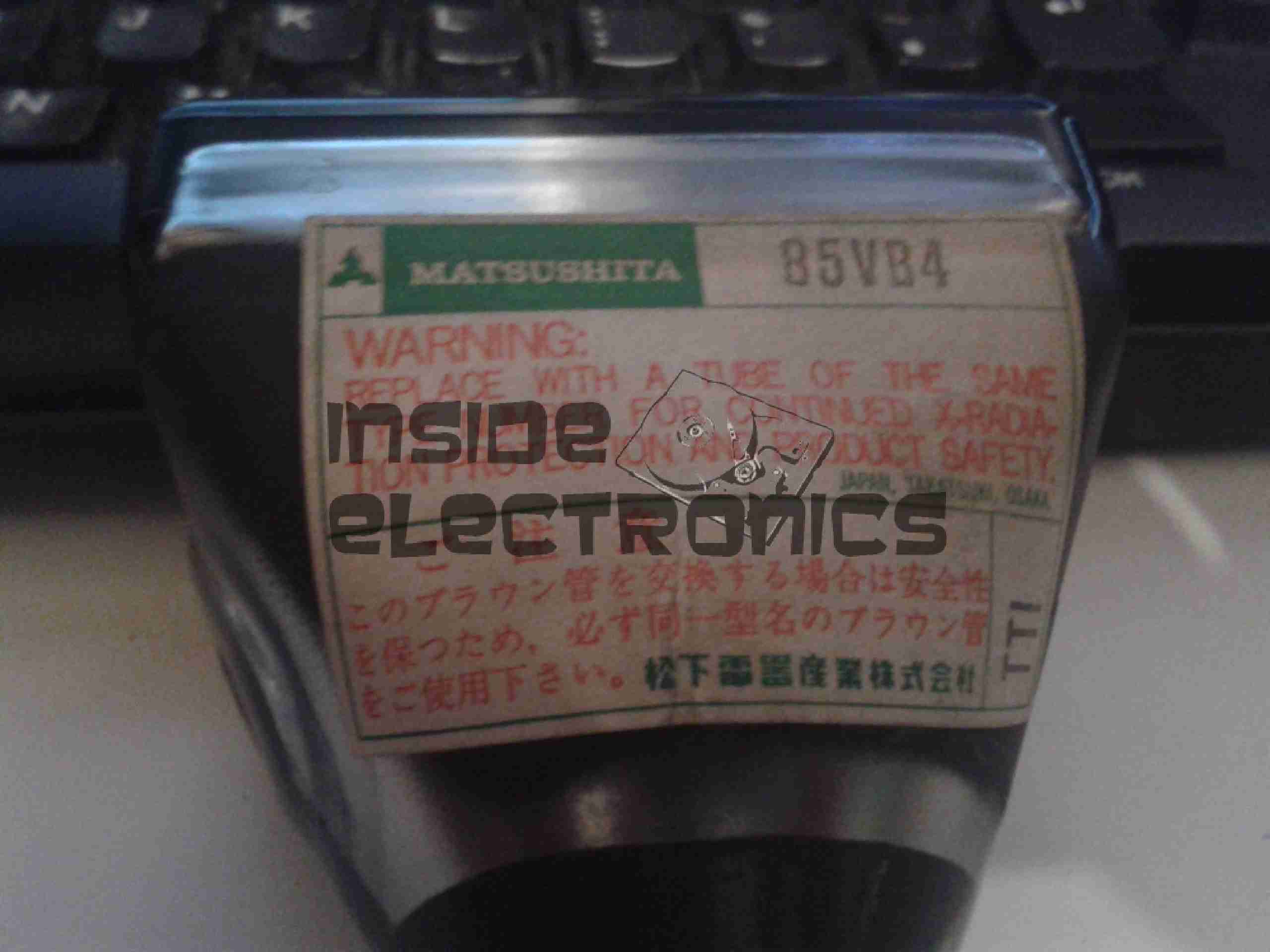
Matsushita 85VB4 CRT
Closeup of the CRT itself. I haven’t been able to find much data on this unit, but I’m guessing it’s similar to many commercial viewfinder CRTs.
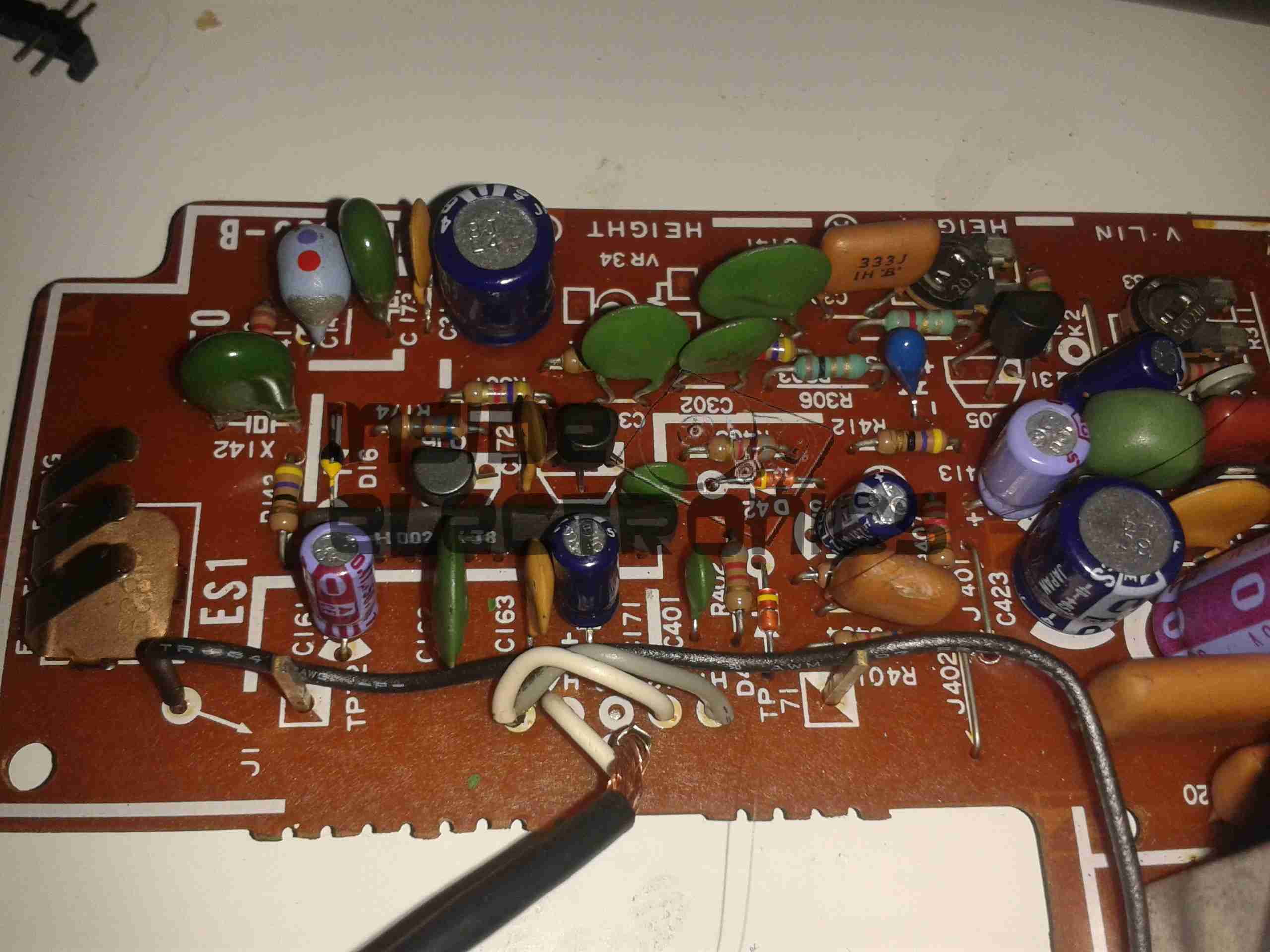
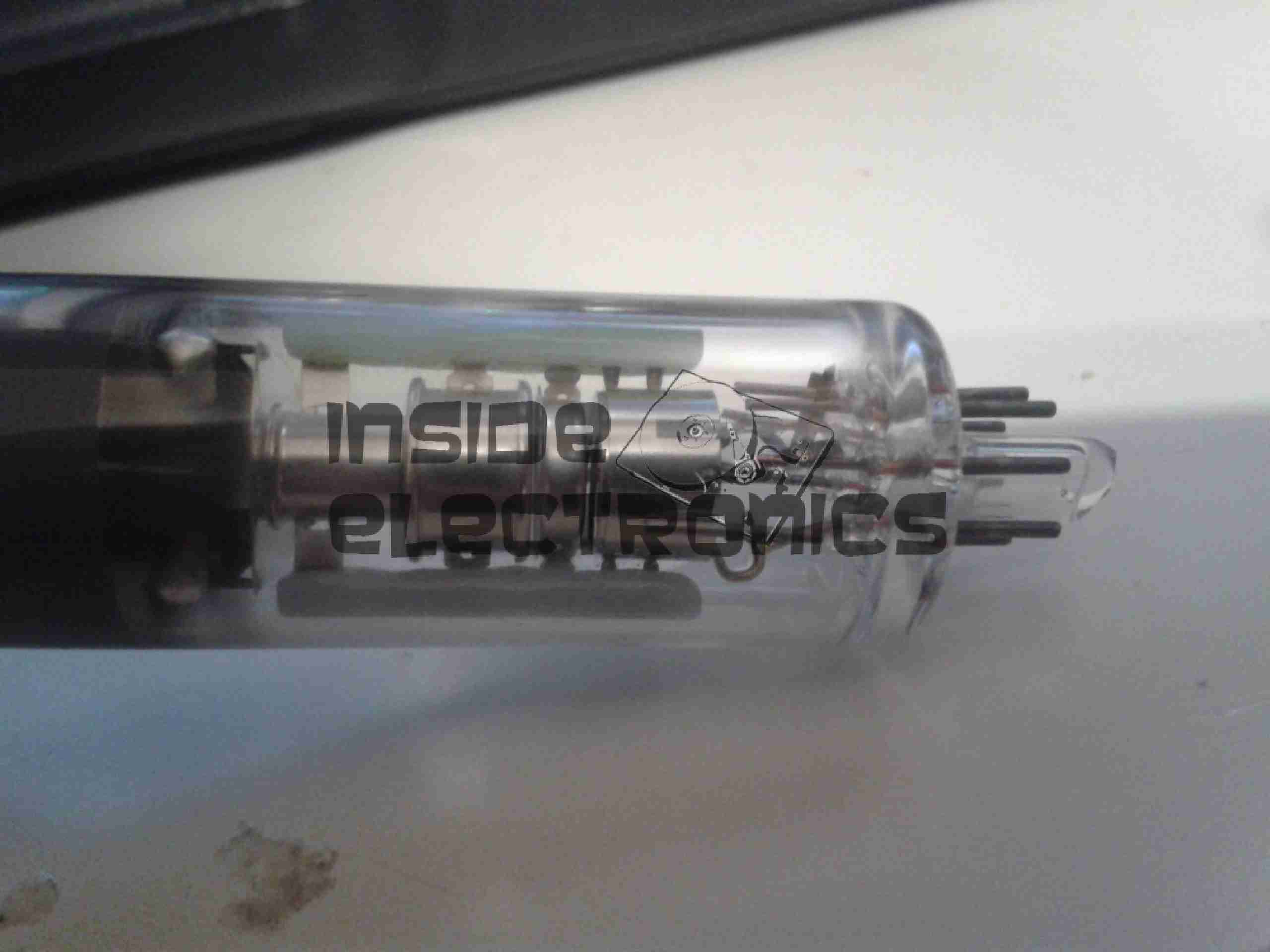
Electron Gun Closeup
Amazingly, there isn’t a single IC in the video circuitry, it’s all discrete components. This probably accounts for the large overall size of the control PCB. Viewfinder CRTs from a few years later on are usually driven with a single IC & a few passives that provide all the same functions.
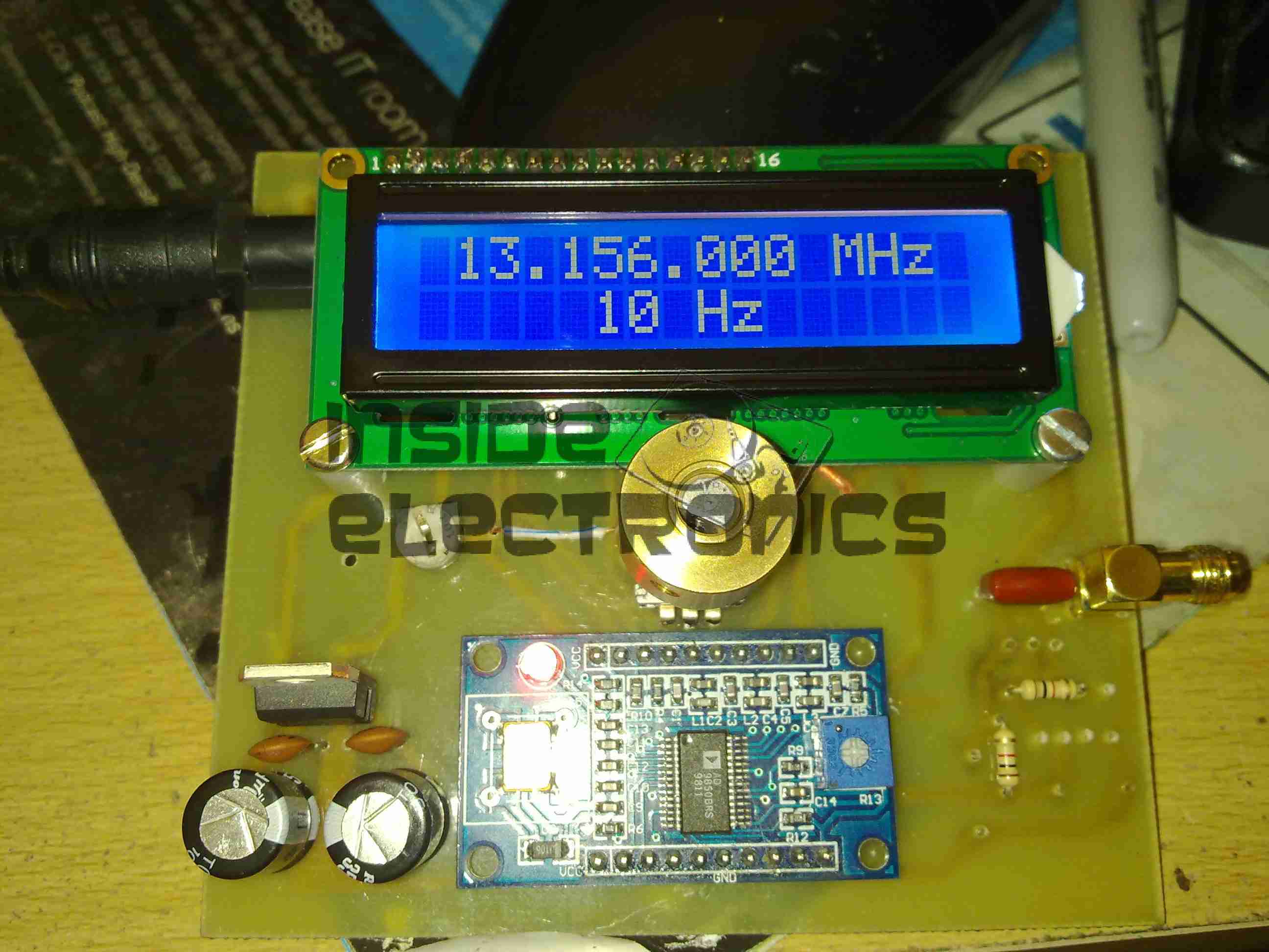
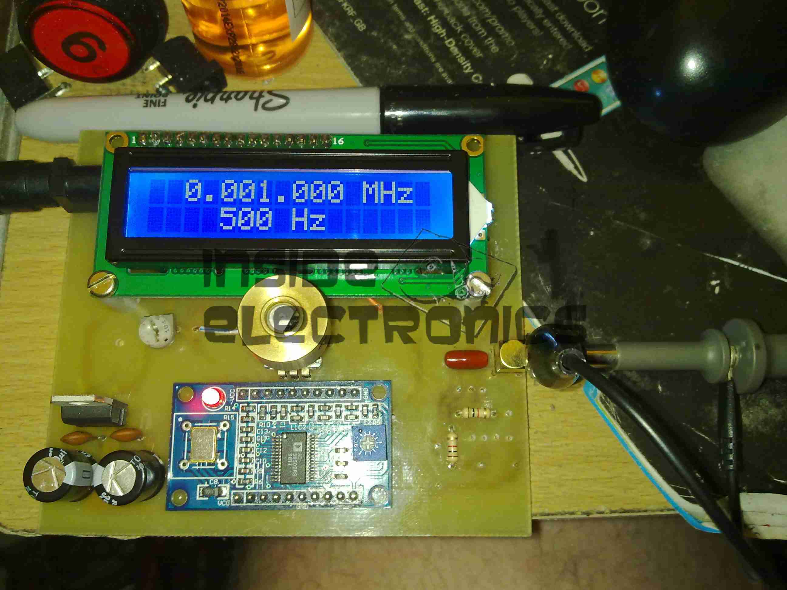
Continuing from my previous post where I published an Eagle design layout for AD7C‘s Arduino powered VFO, here is a completed board.
I have made some alterations to the design since posting, which are reflected in the artwork download in that post, mainly due to Eagle having a slight psychotic episode making me ground one of the display control signals!
AD9850 VFO
The amplifier section is unpopulated & bypassed as I was getting some bad distortion effects from that section, some more work is needed there.
The Arduino Pro Mini is situated under the display, and the 5v rail is provided by the LM7805 on the lower left corner.
Current draw at 12v input is 150mA, for a power of 1.8W total. About 1W of this is dissipated in the LM7805 regulator, so I have also done a layout with an LM2574 Switching Regulator.
The SMPS version should draw a lot let power, as less is being dissipated in the power supply, but this version is more complex.
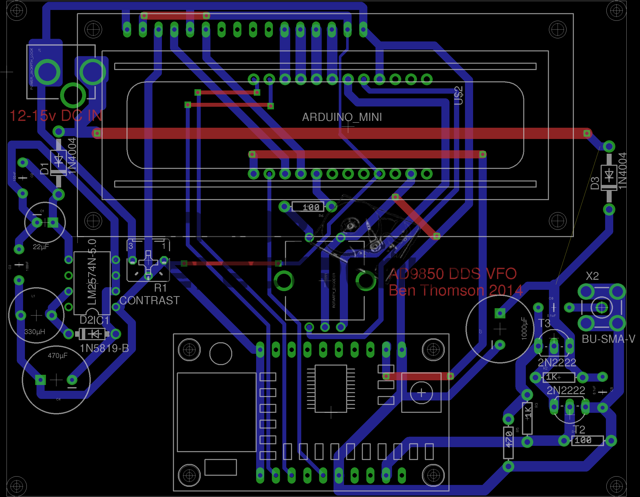
DDS VFO-SMPS
Here the SMPS circuit can be seen on the left hand side of the board, completely replacing the linear regulator.
I have not yet built this design, so I don’t know what kind of effect this will have on the output signal, versus the linear regulator. I have a feeling that the switching frequency of the LM2574 (52kHz) might produce some interference on the output of the DDS module. However I have designed this section to the standards in the datasheet, so this should be minimal.
Nevertheless this version is included in the Downloads section at the bottom of this post.
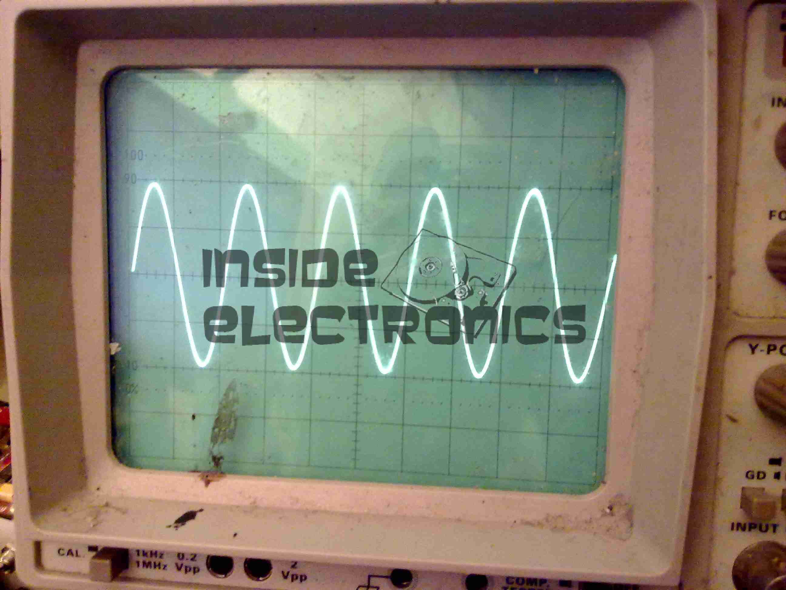
The output coupled through a 100nF capacitor is very clean, as can be seen below, outputting a 1kHz signal. Oscilloscope scale is 0.5ms/div & 1V/div.
VFO Output (Mucky ‘Scope)Scope Connected
Thanks again to Rich over at AD7C for the very useful tool design!
Linked below is the Eagle design files for this project, along with my libraries used to create it.
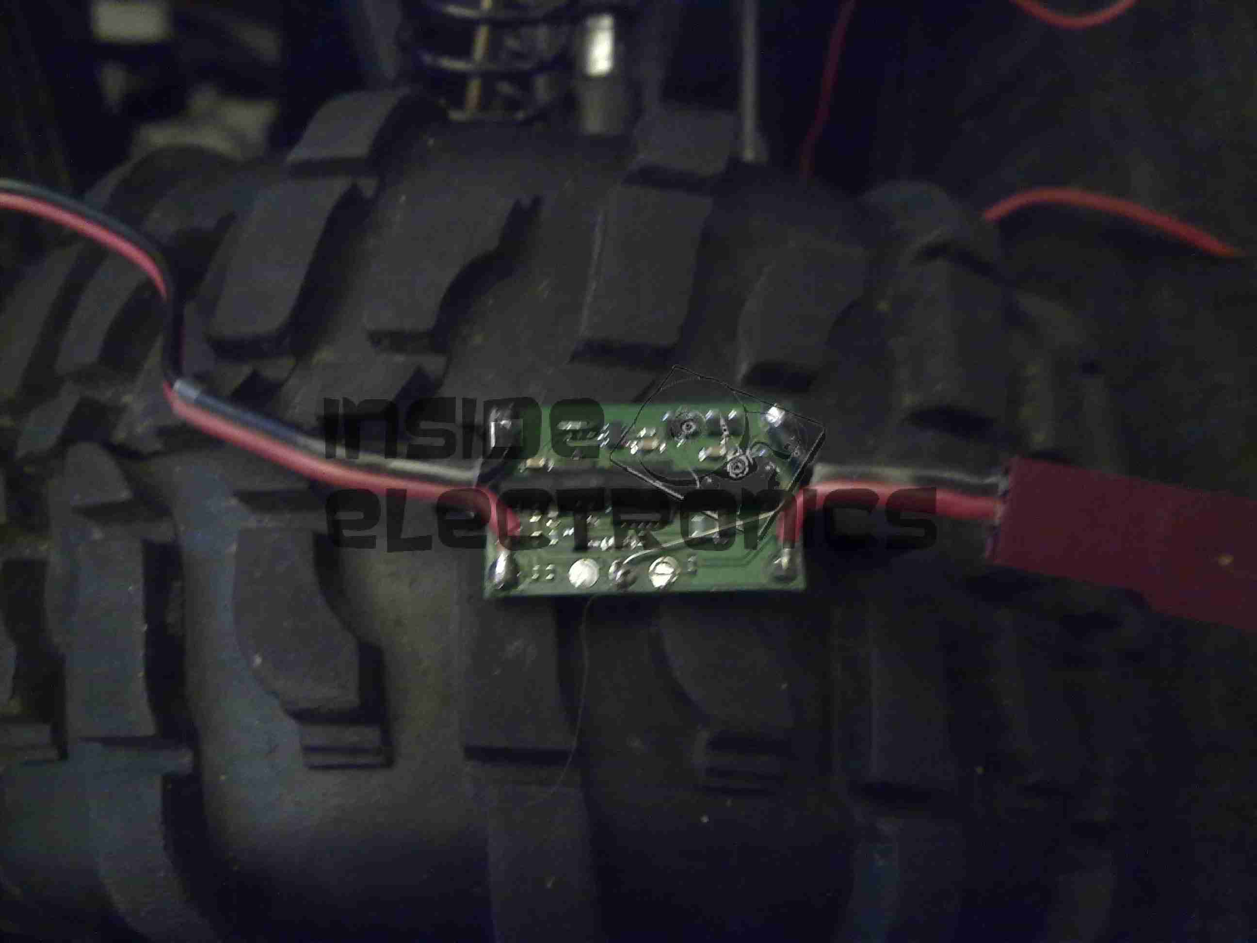
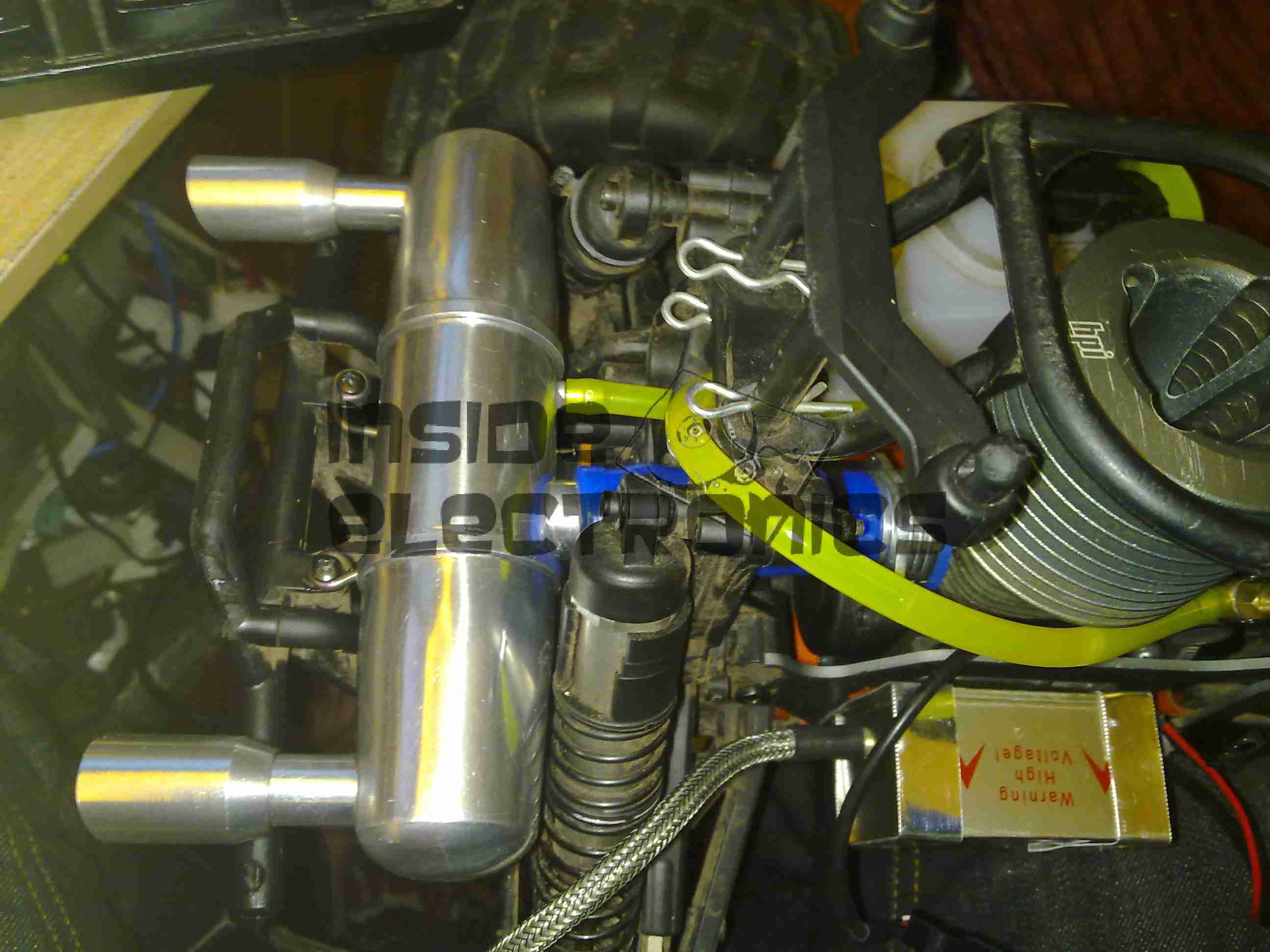
To provide more run time with the conversion to petrol & spark ignition, I have also upgraded the on-board electronics supply to compensate for the extra ~650mA draw of the ignition module.
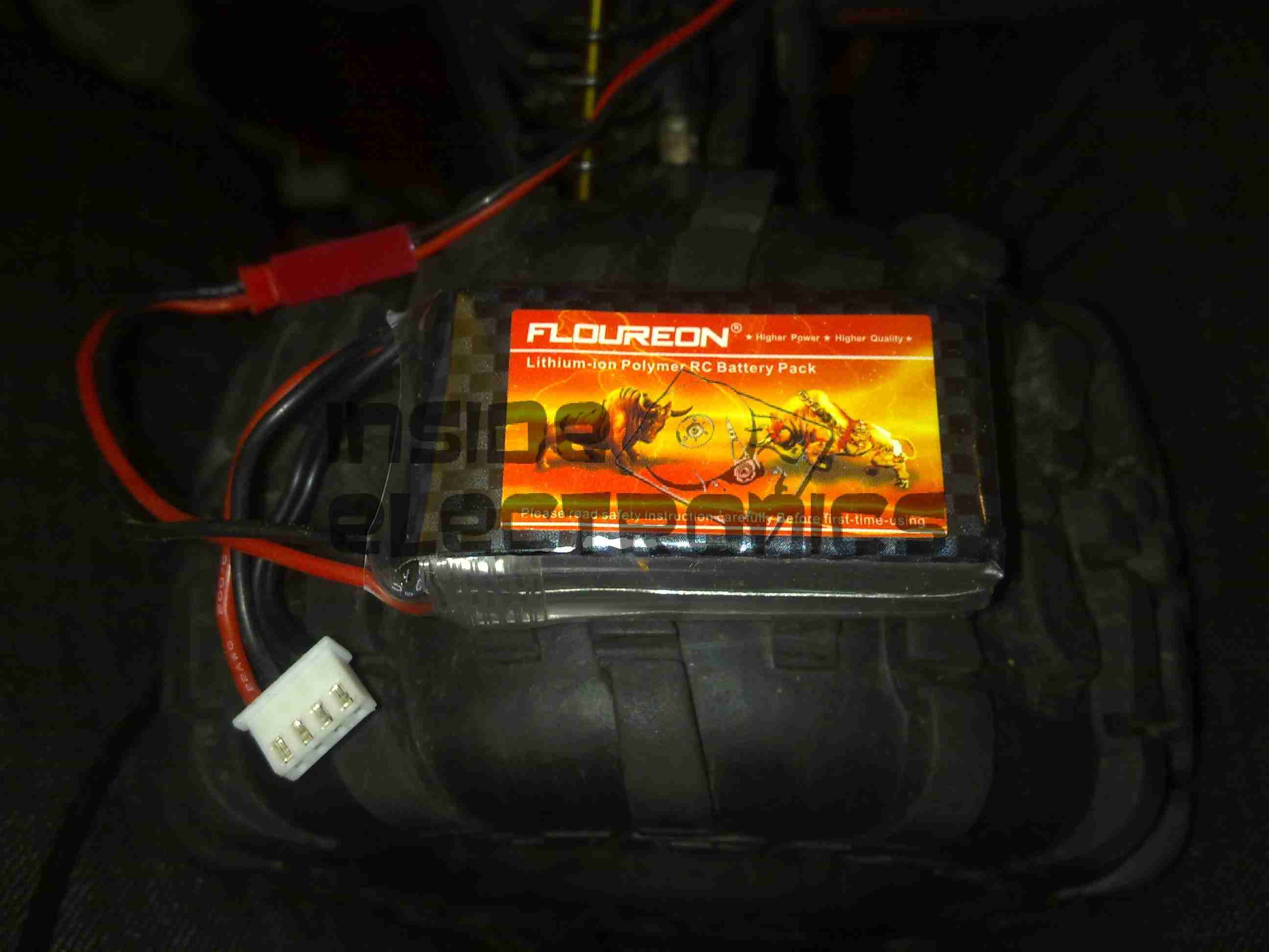
This modification is centred around a 3S Lithium-Polymer battery pack, providing a nominal 11.1v to a voltage regulator, which steps down this higher voltage to the ~6v required by the receiver & servo electronics.
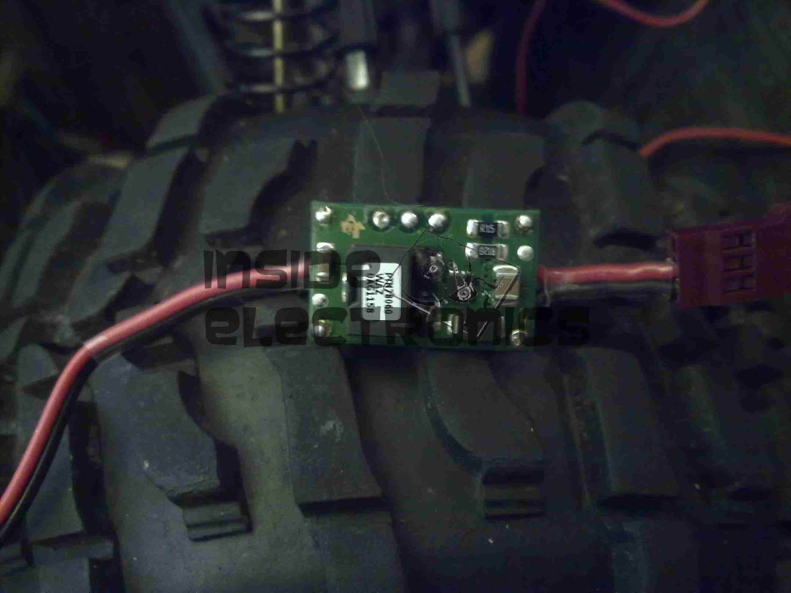
Power RegulatorPower Regulator
The regulator, shown above, is a Texas Instruments PTN78060WAZ wide-input voltage adjustable regulator. This module has an exceptionally high efficiency of ~96% at it’s full output current of 3A. The output voltage is set by a precision resistor, soldered to the back of the module, in this case 6.5v. Standard RC connectors are used on the regulator to allow connection between the power switch & the radio receiver.
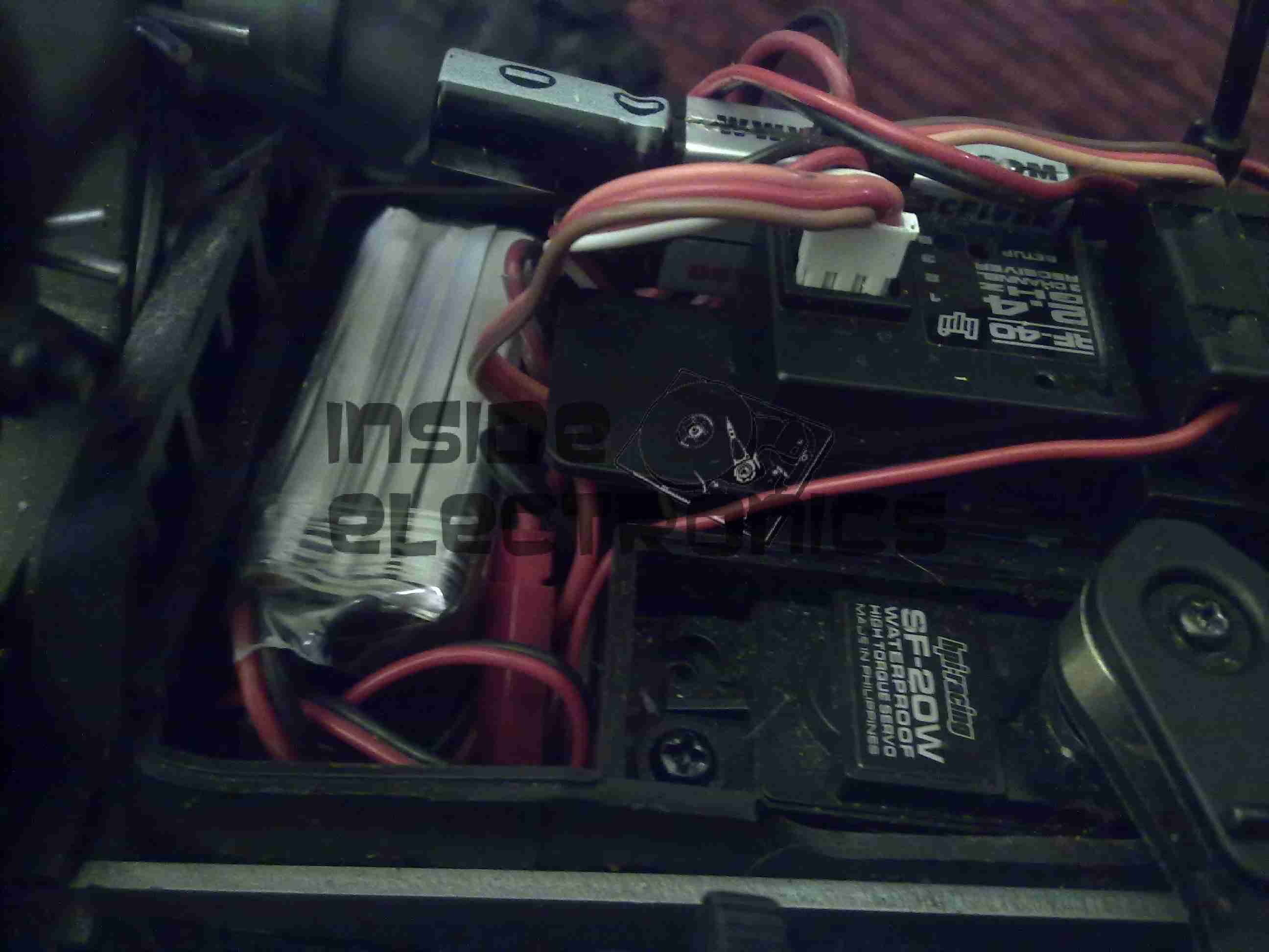
Receiver Box
Everything tucked away into place inside the receiver box. The 3S 1000mAh LiPo fits perfectly in the space where the original Ni-Mh hump pack was located.
The completely stable output voltage of the regulator over the discharge curve of the new battery gives a much more stable supply to the radio & ignition, so I should experience fewer dropouts. Plus the fact that the engine now relies on power from the receiver pack to run, it’s a built in fail safe – if the power dies to the receiver, the engine also cuts out.
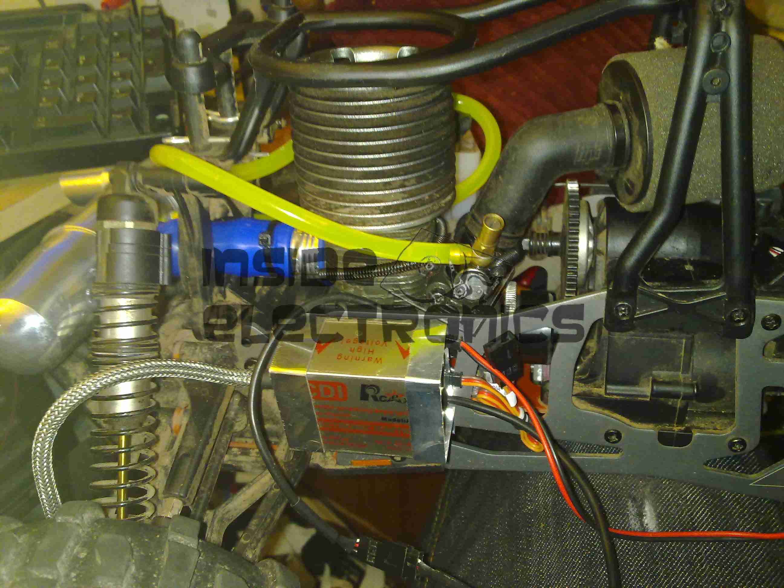
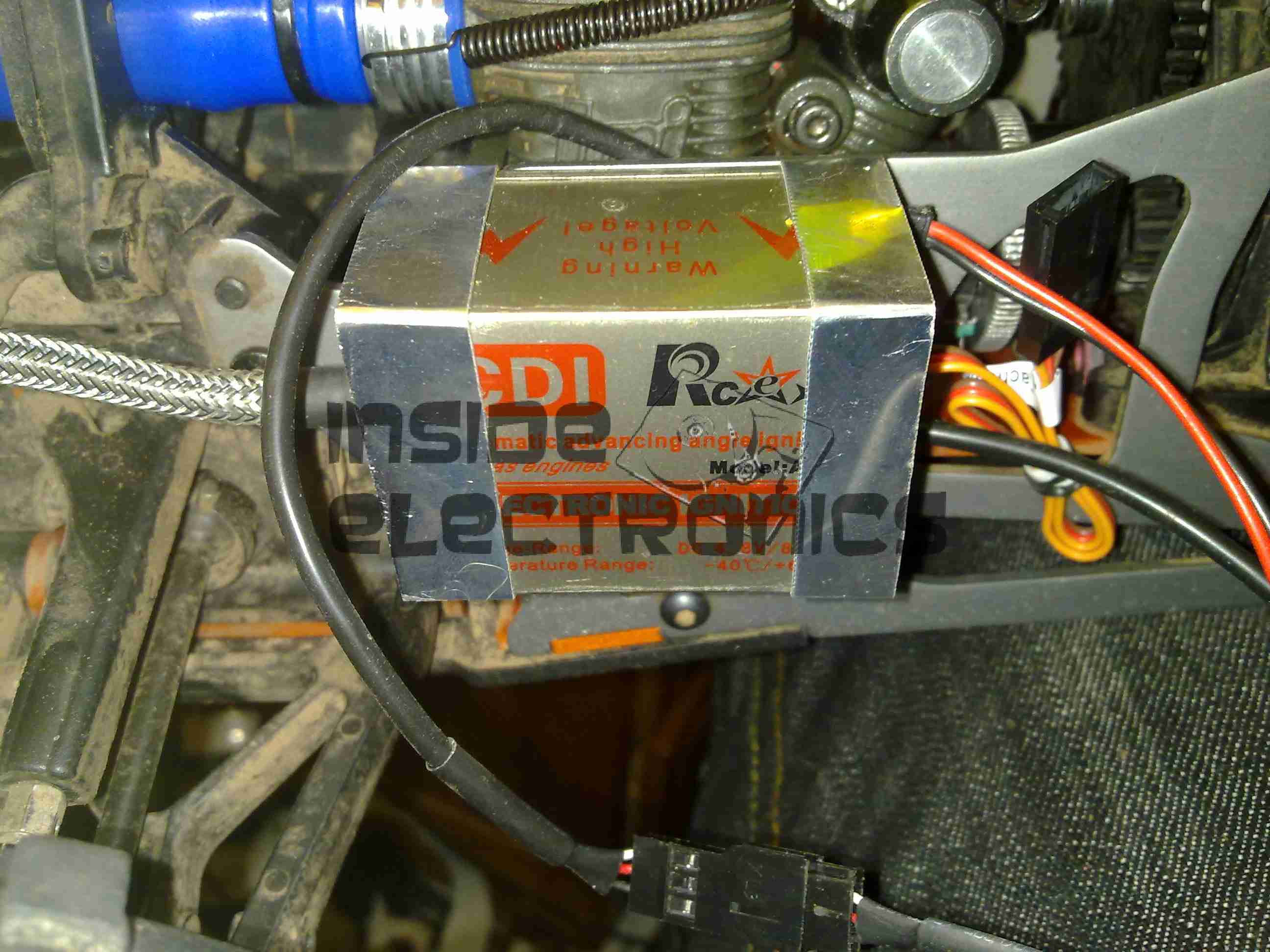
The engine now with it’s required ignition sensor, it is now mounted back on the chassis of the model. I have replaced the stock side exhaust with a rear silencer, so I could fit the ignition module in place next to the engine.
For the mounting, I fabricated a pair of brackets from 0.5mm aluminium, bent around the module & secured with the screws that attach the engine bed plate to the TVPs. The ignition HT lead can be routed up in front of the rear shock tower to clear all moving suspension parts, with the LT wiring tucked into the frame under the engine.
In this location the module is within the profile of the model chassis so it shouldn’t get hit by anything in service.
Rear Exhaust
New exhaust silencer fitted to the back of the model. This saves much space on the side of the model & allows the oily exhaust to be discharged away from the back wheel – no more mess to wipe up.
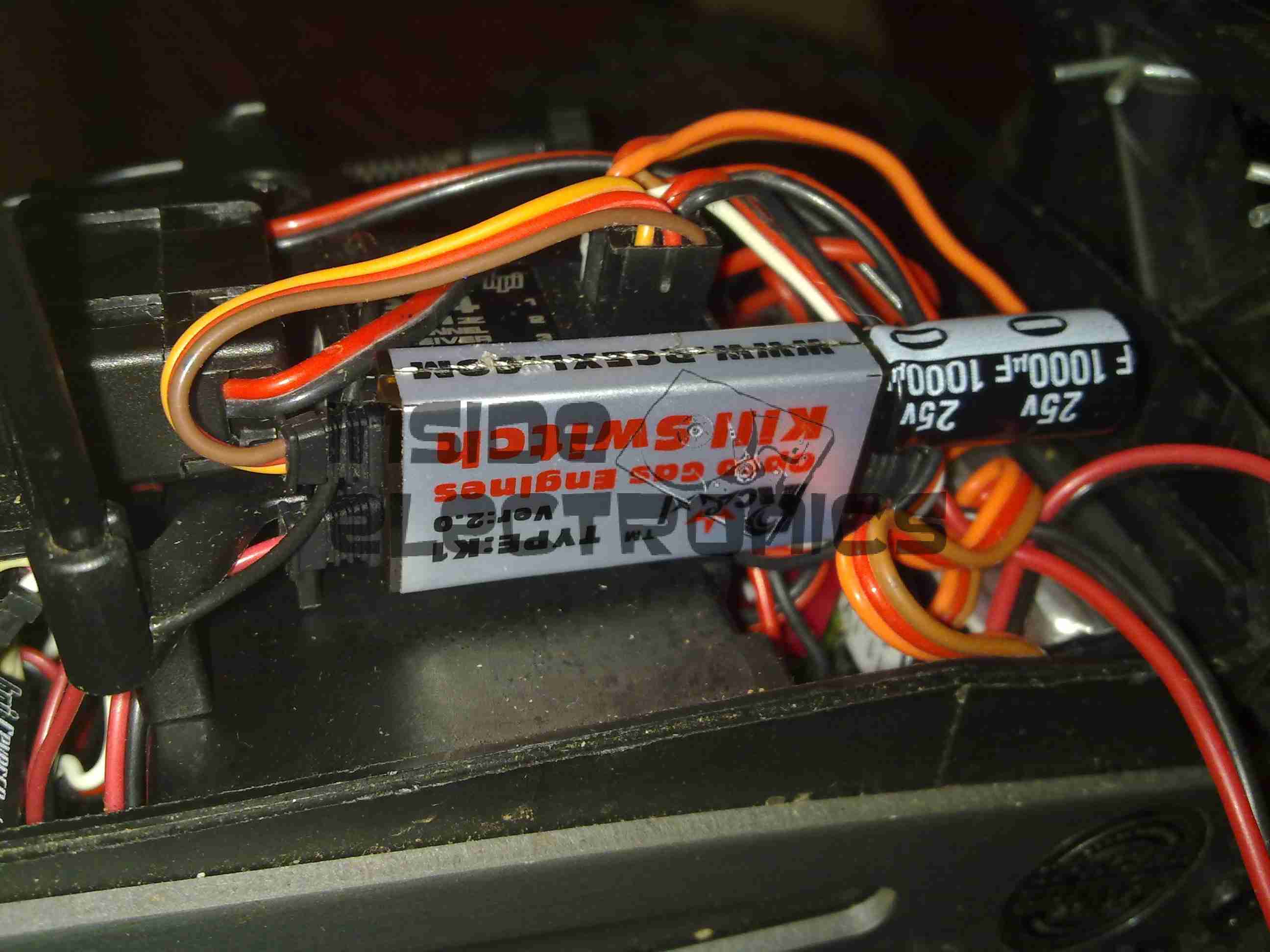
Kill Switch
The ignition switch fitted into the receiver box. This is wired into channel 3 of the TF-40 radio, allowing me to remotely kill the engine in case of emergency. I have fitted a 25v 1000µF capacitor to smooth out any power fluctuations from the ignition module.
The radio is running from a 11.1v 1Ah 3S LiPo pack connected to a voltage regulator to give a constant 6.5v for the electronics. I found this is much more reliable than the standard 5-cell Ni-MH hump packs.
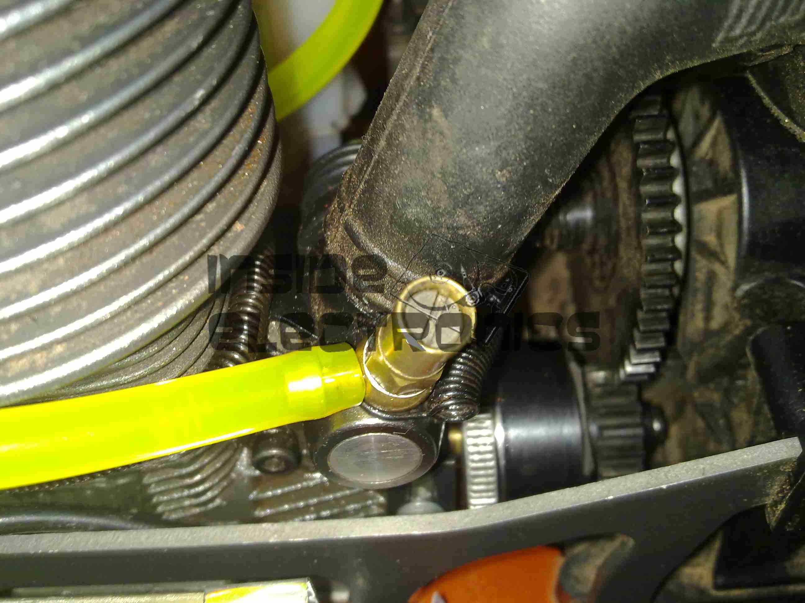
Fuel Tank
The stock silicone fuel tubing has been replaced with Tygon tubing to withstand the conversion to petrol.
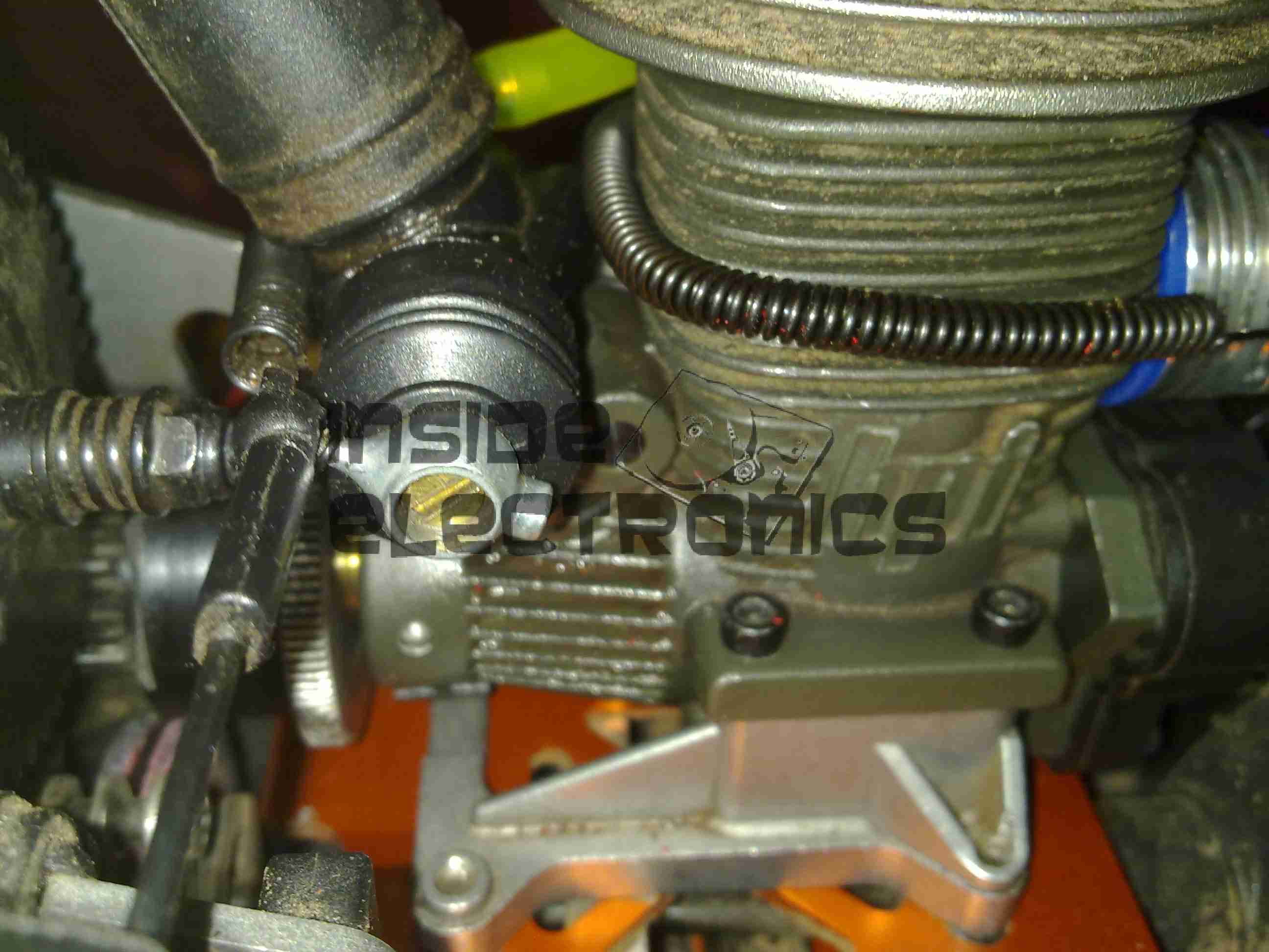
High Speed Needle
High speed needle tweaked to provide a basic running setting on petrol. This is set to ~1.5mm below flush with the needle housing.
Low Speed Needle
Low speed needle tweaked to provide a basic running setting on petrol. This is set to ~1.73mm from flush with the needle housing.
As petrol is a much higher energy density fuel, it requires much more air than the methanol glow fuel – ergo much leaner settings.
The settings listed should allow an engine to run – if nowhere near perfectly as they are still rather rich. It’s a good starting point for eventual tuning.
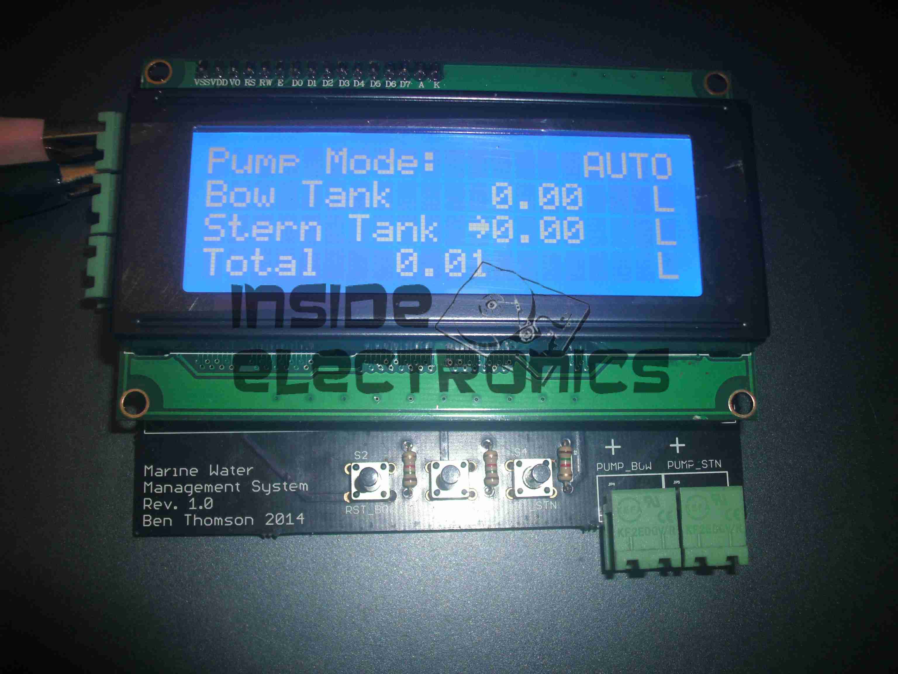
Having two separate water tanks on nb Tanya Louise, with individual pumps, meant that monitoring water levels in tanks & keeping them topped up without emptying & having to reprime pumps every time was a hassle.
To this end I have designed & built this device, to monitor water usage from the individual tanks & automatically switch over when the tank in use nears empty, alerting the user in the process so the empty tanks can be refilled.
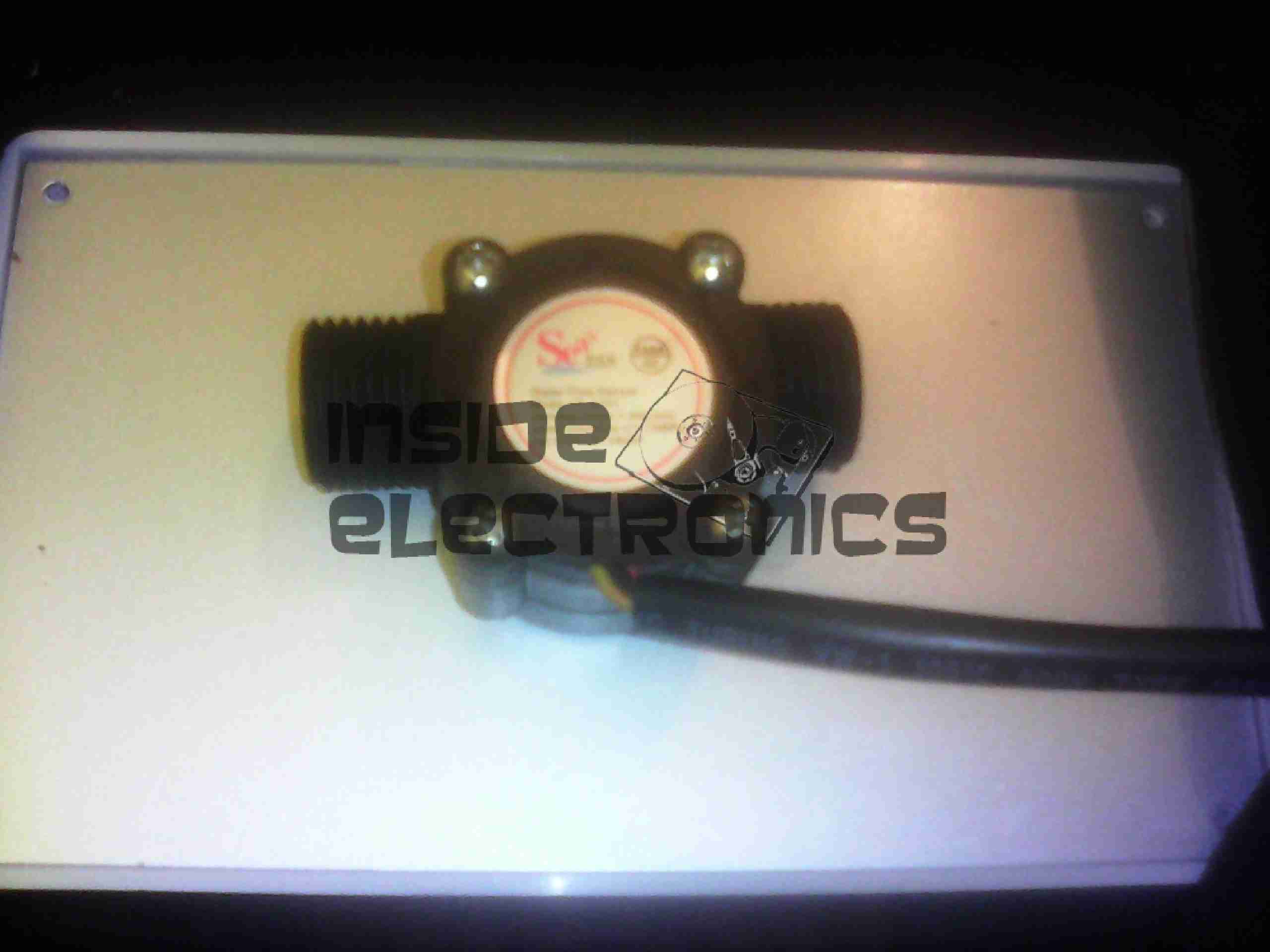
Based around an ATMega328, the unit reads a pair of sensors, fitted into the suction line of each pump from the tanks. The calculated flow is displayed on the 20×4 LCD, & logged to EEPROM, in case of power failure.
Water Flow Sensor
When the tank in use reaches a preset number of litres flowed, (currently hardcoded, but user input will be implemented soon), the pump is disabled & the other tank pump is enabled. This is also indicated on the display by the arrow to the left of the flow register. Tank switching is alerted by the built in beeper.
It is also possible to manually select a tank to use, & disable automatic operation.
Resetting the individual tank registers is done by a pair of pushbuttons, the total flow register is non-resettable, unless a hard reset is performed to clear the onboard EEPROM.
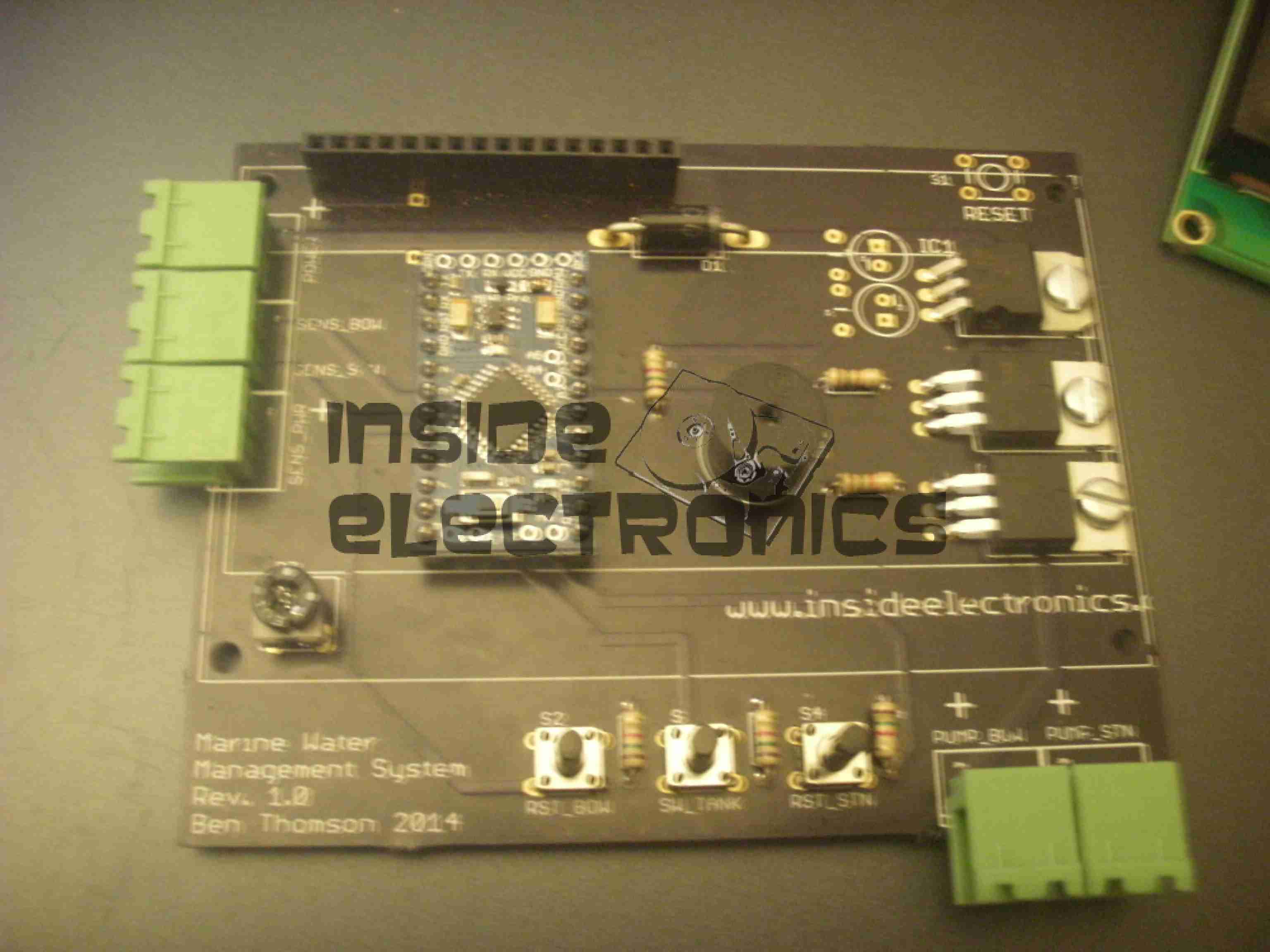
Main PCB
View of the main PCB is above, with the central Arduino Pro Mini module hosting the backend code. 12-24v power input, sensor input & 5v sensor power output is on the connectors on the left, while the pair of pump outputs is on the bottom right, switched by a pair of IRFZ44N logic-level MOSFETS. Onboard 5v power for the logic is provided by the LM7805 top right.
Code & PCB design is still under development, but I will most likely post the design files & Arduino sketch once some more polishing has been done.
Tip Jar
If you’ve found my content useful, please consider leaving a donation by clicking the Tip Jar below!
All collected funds go towards new content & the costs of keeping the server online.