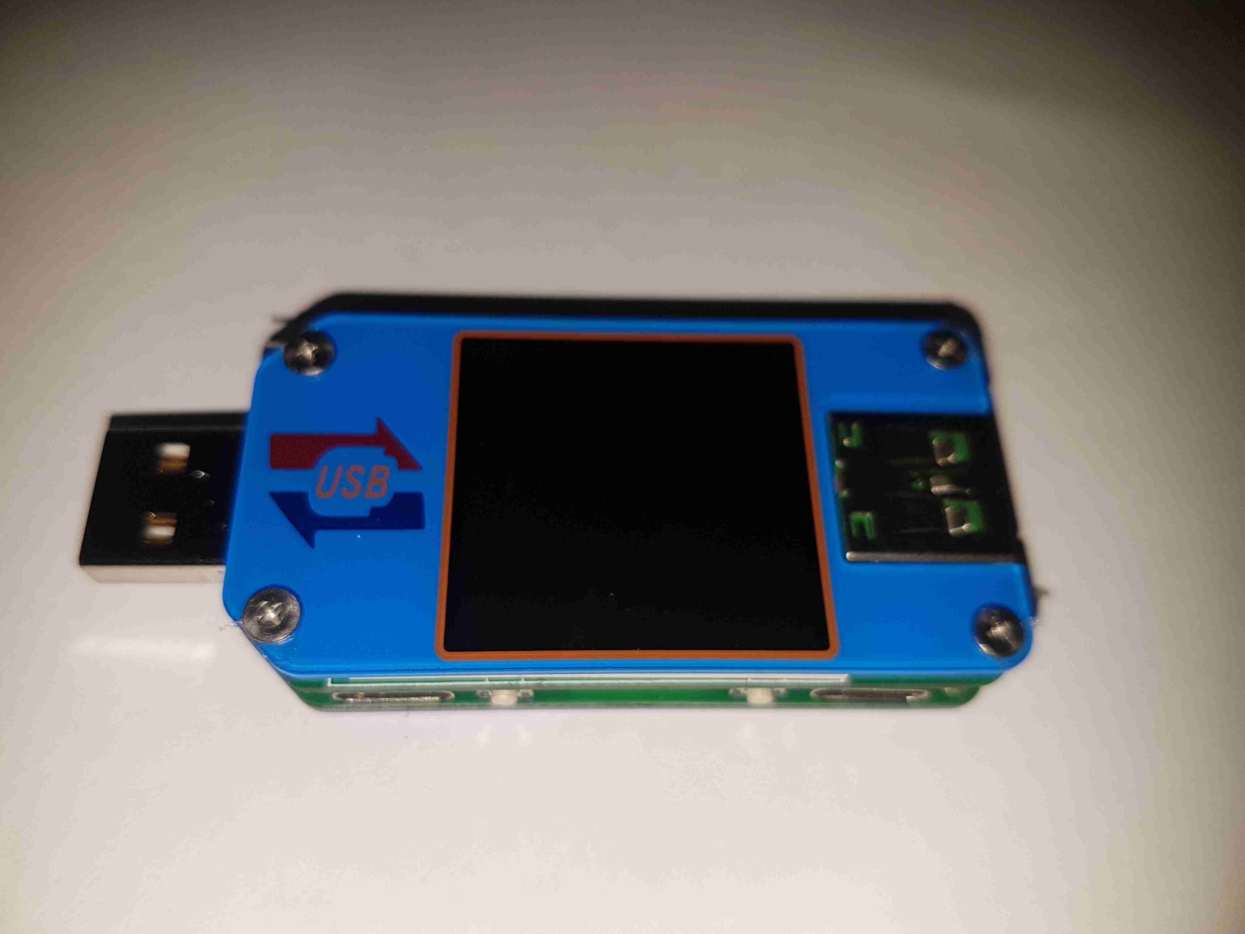
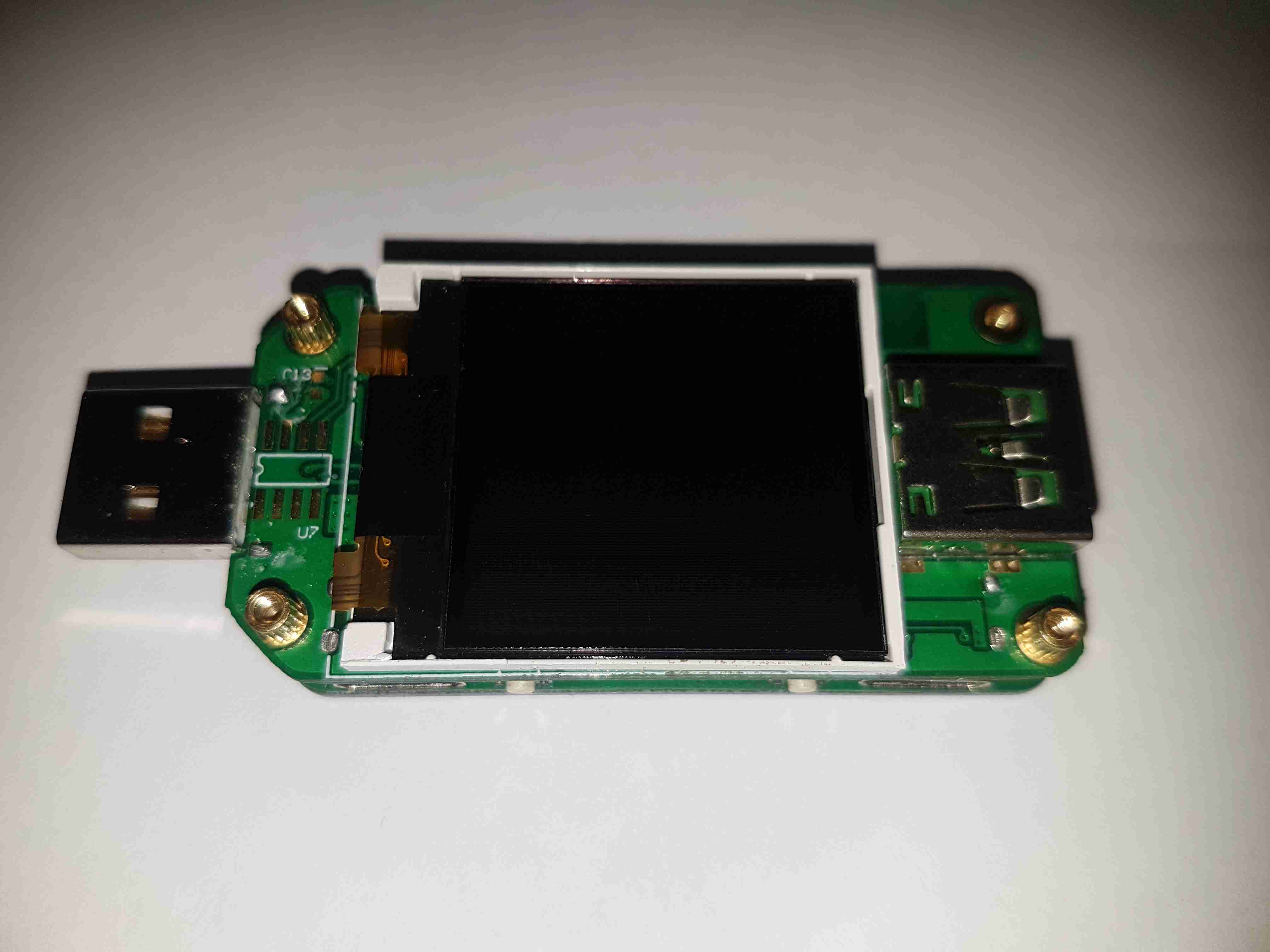
Here’s a nice little feature-packed USB power meter, the UM25C. This unit has USB-C along with the usual USB type A connectors, along with a bluetooth radio for remote monitoring of stats via a Windows or Android app. Construction is nice, it’s a stack of two PCBs, and polycarbonate cover plates, secured together with brass posts & screws.
Back Cover
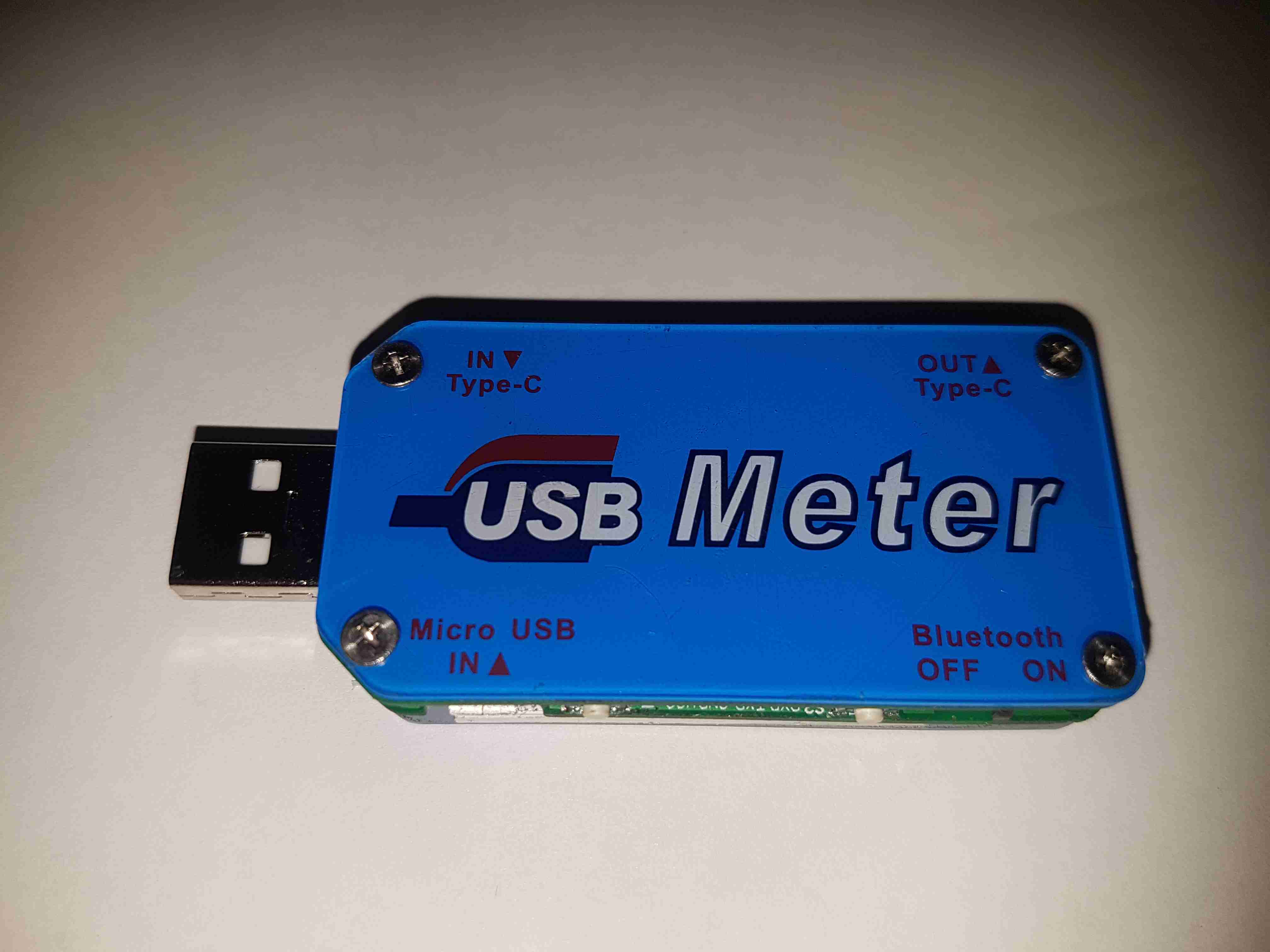
The back cover has the legend for all the side connectors, along with the logo.
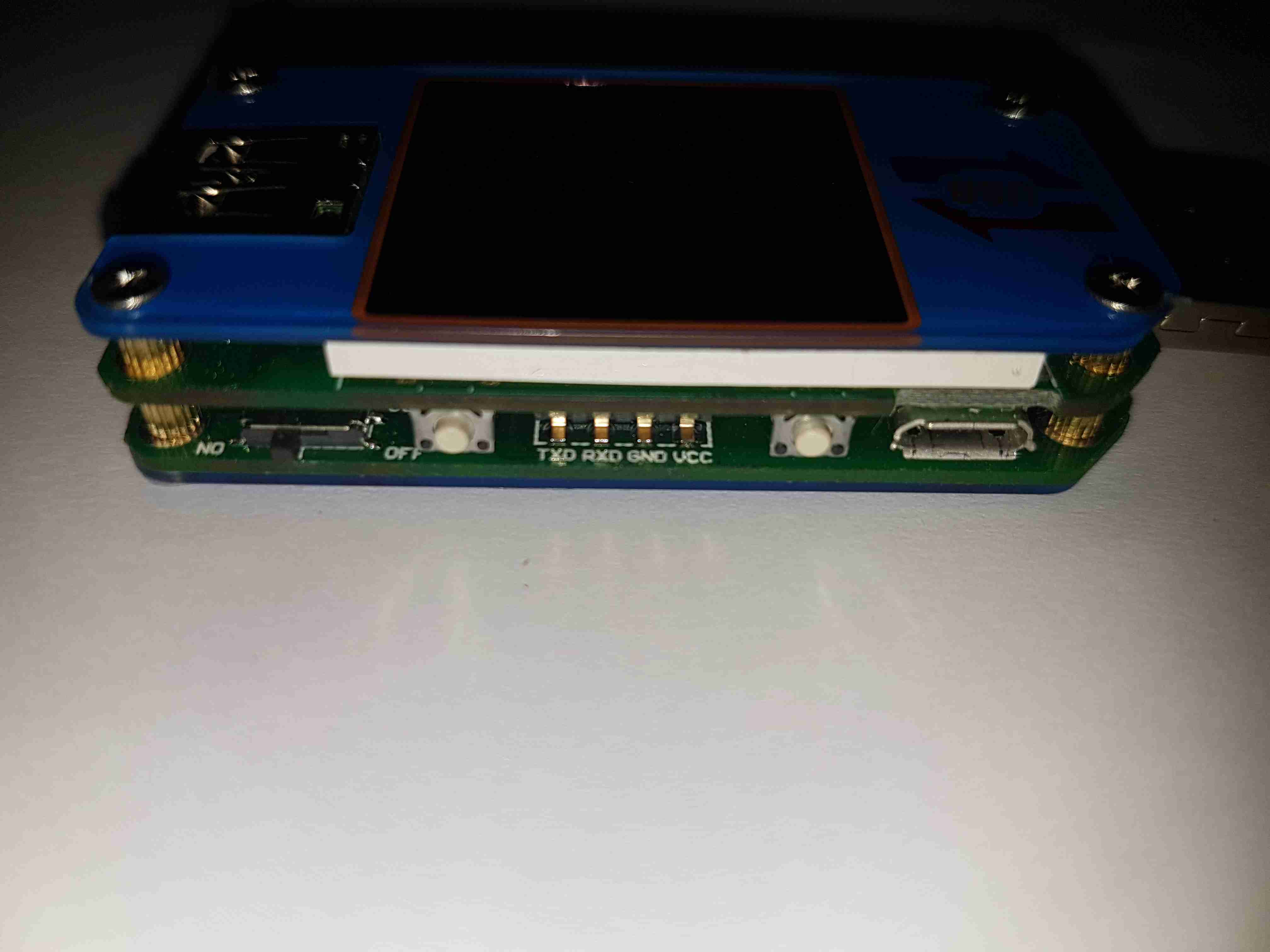
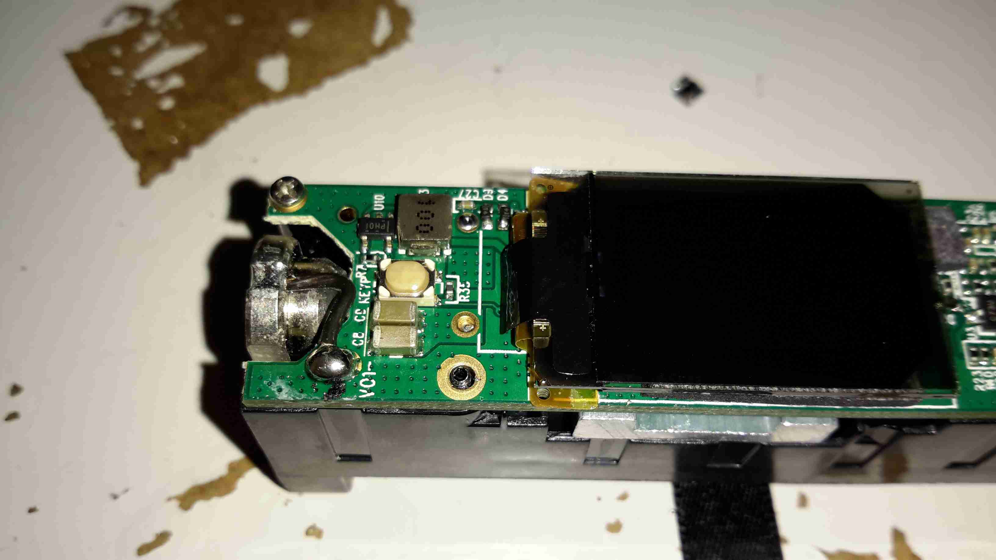
USB Micro Input
Down the sides are the user interface buttons, and here the Micro-B input connector. The 4-pin header is visible here that takes serial data down to the bluetooth section.
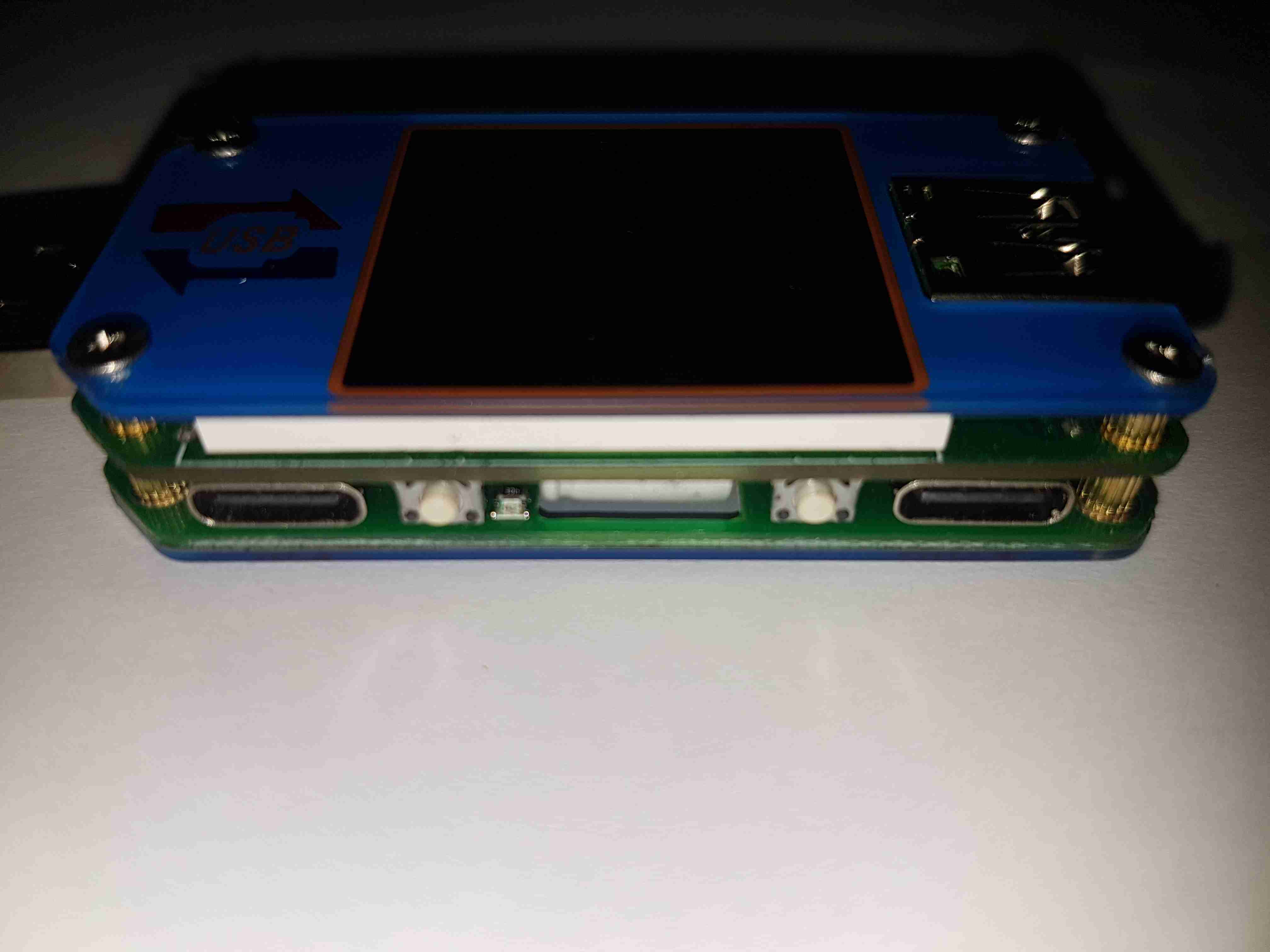
USB-C Connectors
The other side has the remaining pair of buttons, and the USB-C I/O. I don’t yet own anything USB-C based, but this is good future proofing.
LCD Display
Removing the top plastic cover plate reveals the small 1″ TFT LCD module. This will be hot-bar soldered underneath the screen. There’s an unused footprint next to the USB input connector, judging by the pin layout it’s probably for a I²C EEPROM.
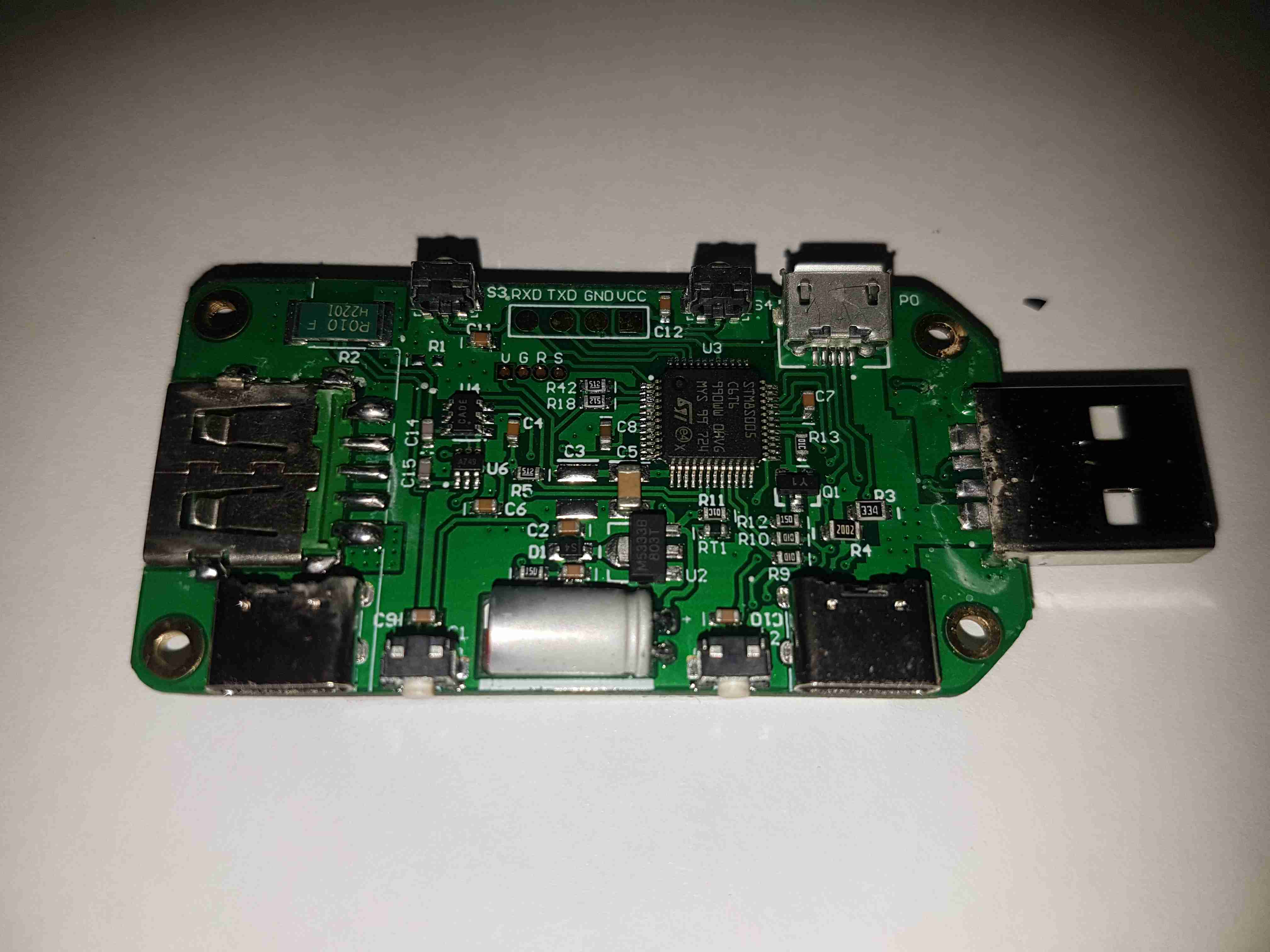
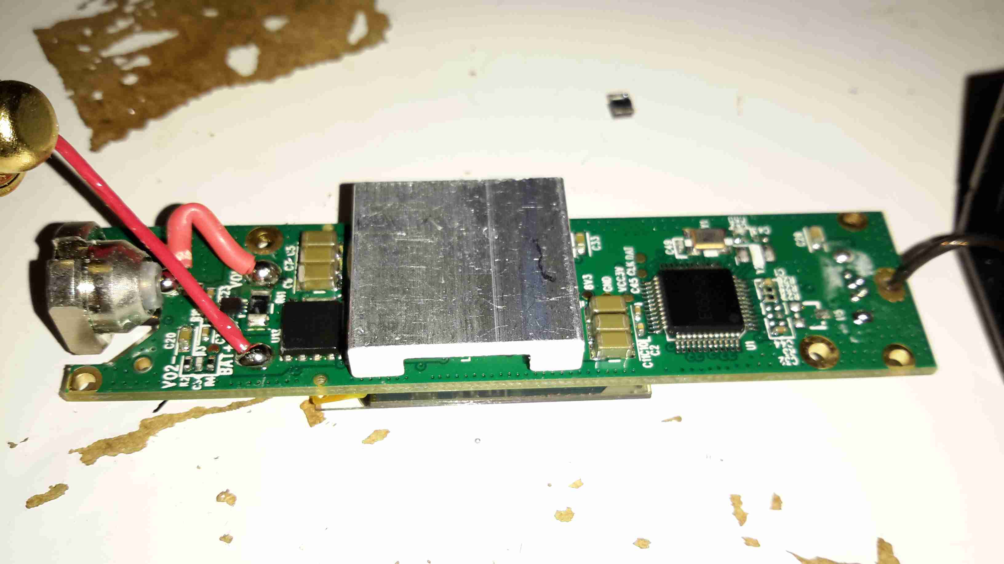
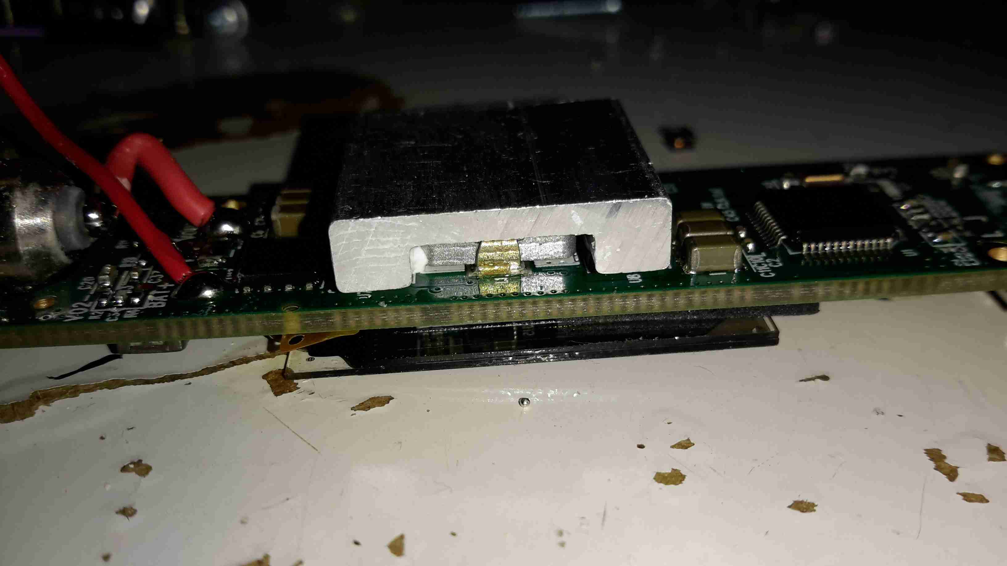
Main Board Components
The underside of the top PCB has all the main components. The brains of the operation is a ST STM8S005C6T6 microcontroller. It’s at the basic end of the STM range, with a 16MHz clock, 32K flash, EEPROM, 10-bit ADC, SPI, UART & I²C. The main 0.010Ω current shunt is placed at the top left of the board in the negative rail. A couple of SOT-23 components in the centre of the board, I haven’t been able to identify properly, but I think they may be MOSFETs. The large electrolytic filter capacitor has a slot routed into the PCB to allow it to be laid flat. Providing the main power rail is a SOT-89 M5333B 3.3v LDO regulator.
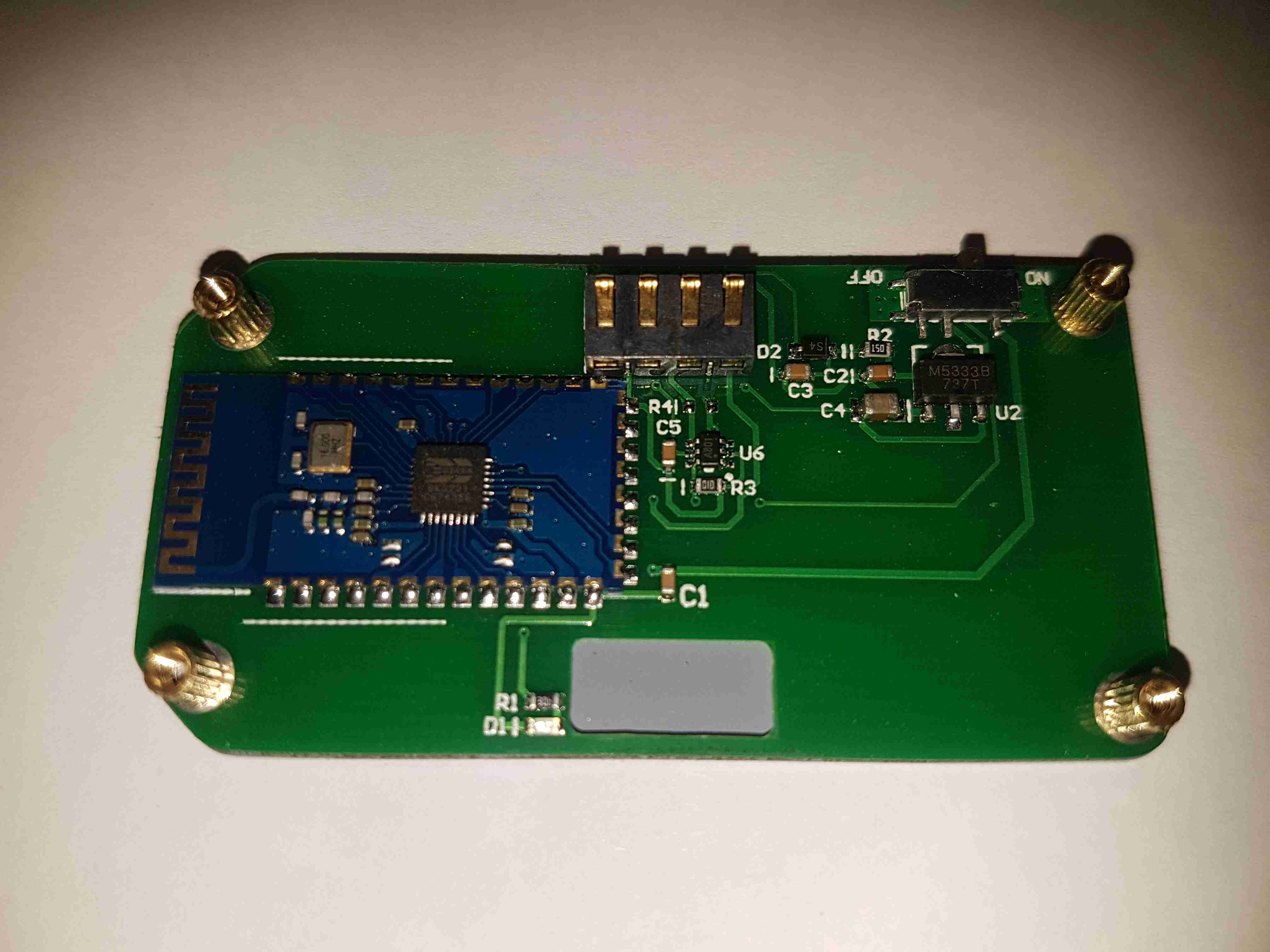
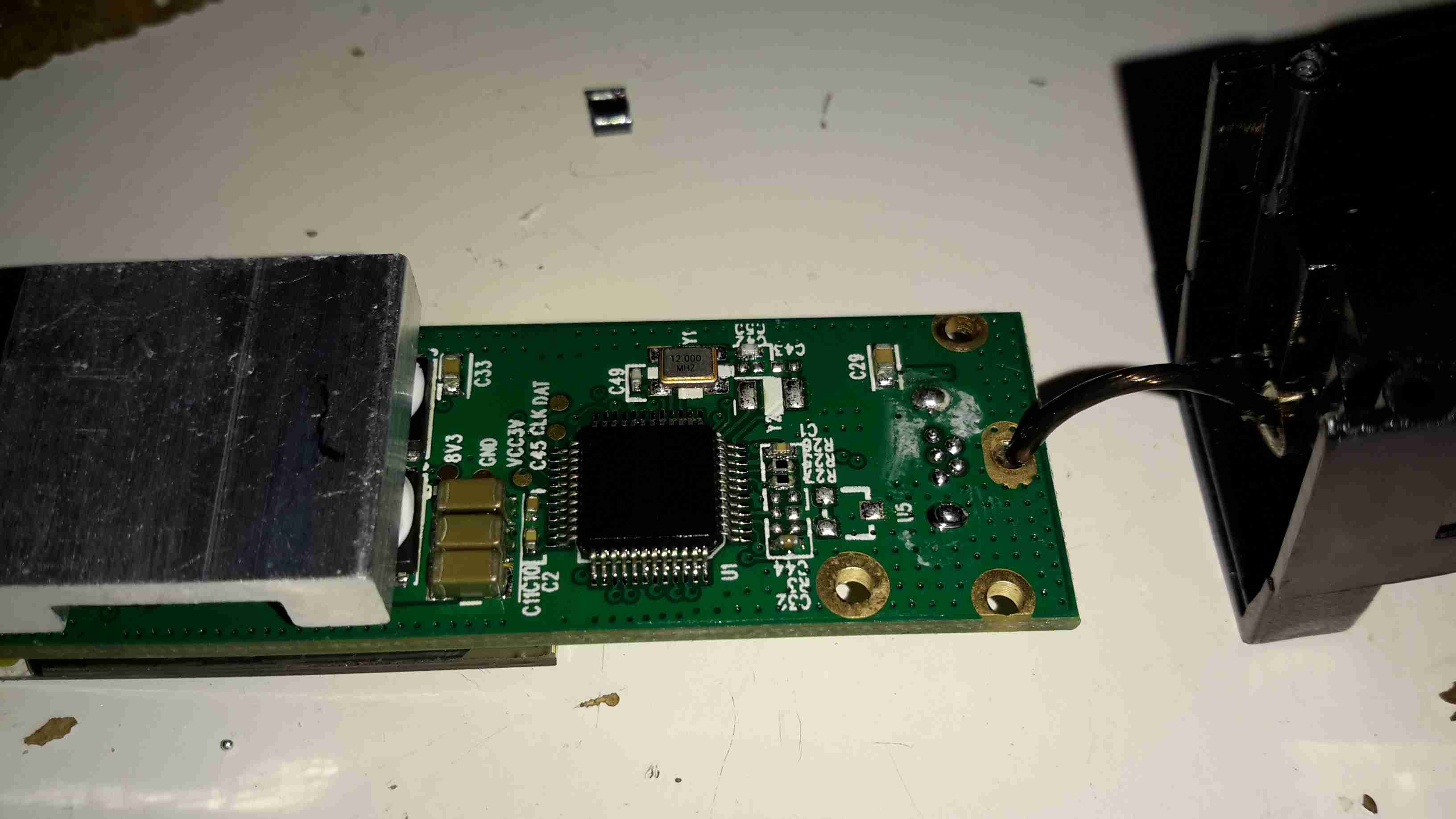
Bluetooth Radio
The bottom board contains the bluetooth radio module, this is a BK3231 Bluetooth HID SoC. The only profile advertised by this unit is a serial port. There’s a local 3.3v LDO regulator & support components, along with an indicator LED.
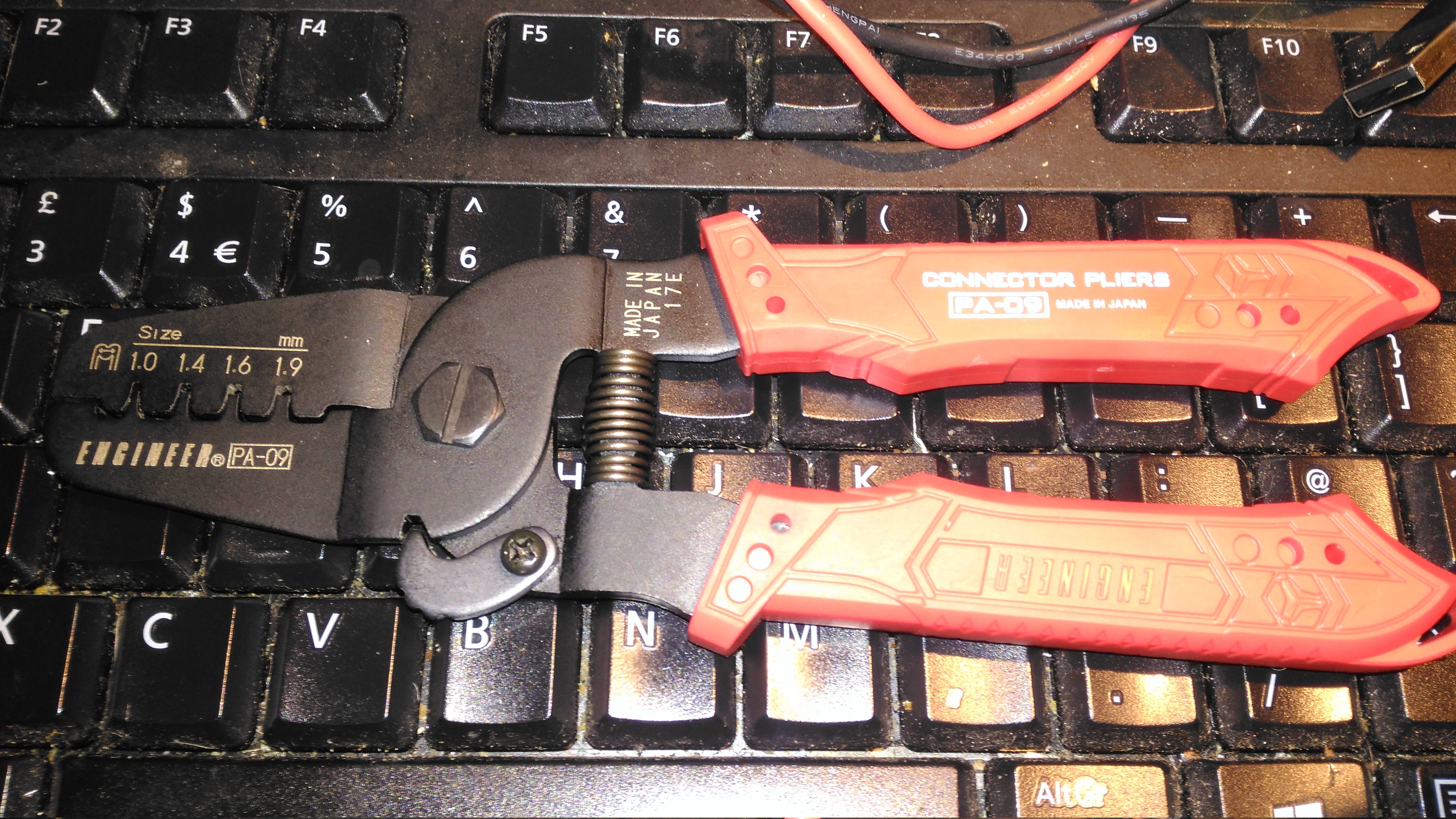
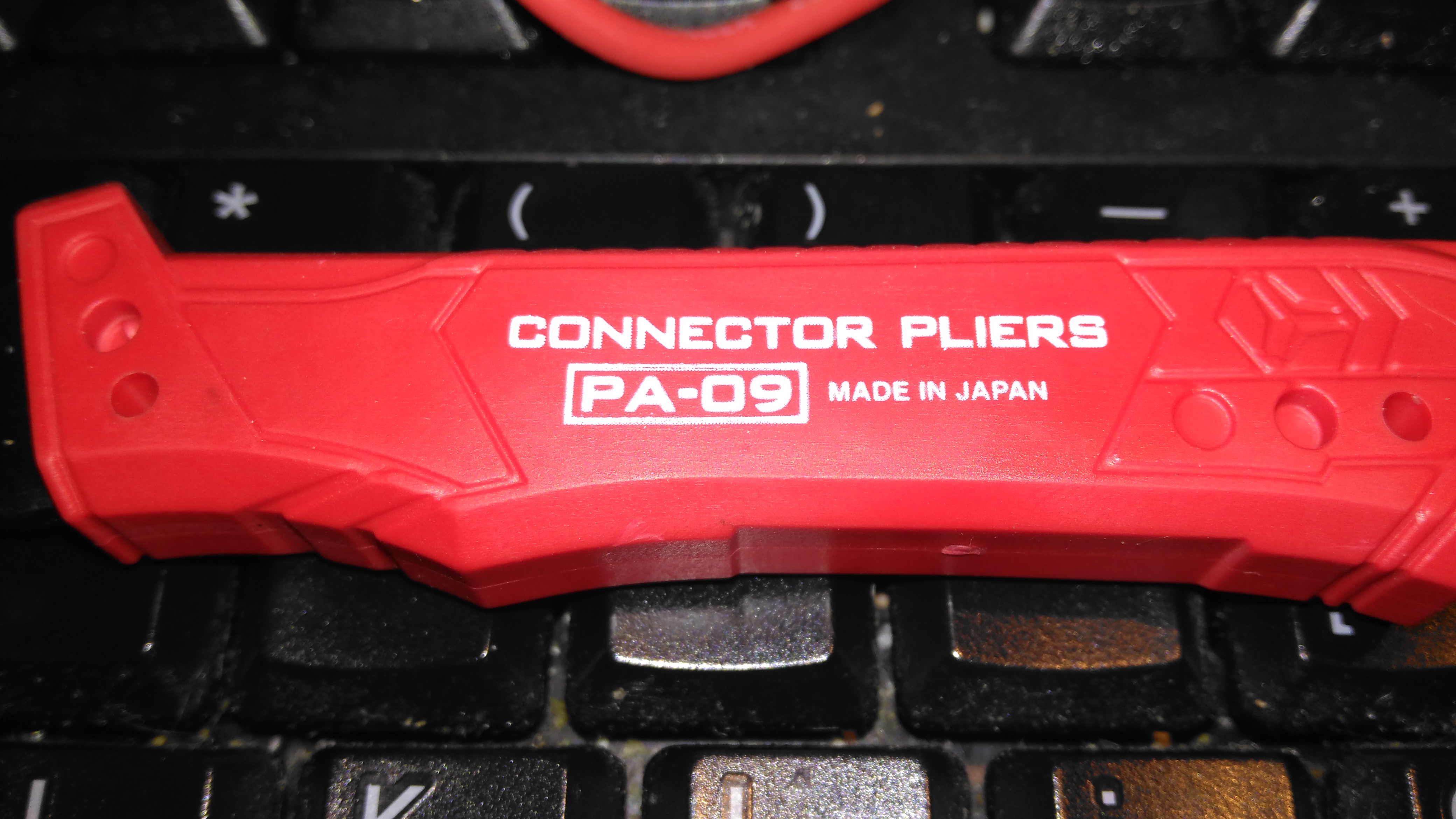
For a while now I’ve been attaching terminals such as Molex KK Dupont, & JST PH to wire ends with a lot of patience & a very fine soldering iron, however this method takes a lot of time, and with terminals like Dupont types, the terminal won’t fit into the connector body properly unless it’s crimped correctly. Official tools from the likes of JST or Molex are hilariously expensive, (~£250 for the Molex KK tool), and each tool only does a single connector series, so these are out of the picture. The cheapest available tool (~£40) for these types of terminals is the Engineer PA-09:
Engineer PA-09
These are simple crimping pliers, with no niceties like a ratchet mechanism, but nonetheless they work very well for the cost. The PA-09 can handle terminals from 1mm-1.9mm, there is another tool, the PA-21, which crimps terminals from 1.6mm-2.5mm. The fit & finish is good – proper steel (S55C high carbon steel according to Engineer), not the steel-plated-cheese that most cheap Chinese tools are fabricated from, the handles are solid & comfortable.
Handles
The rubber handles are press-fit onto the steel frame arms of the pliers, and don’t slip off readily.
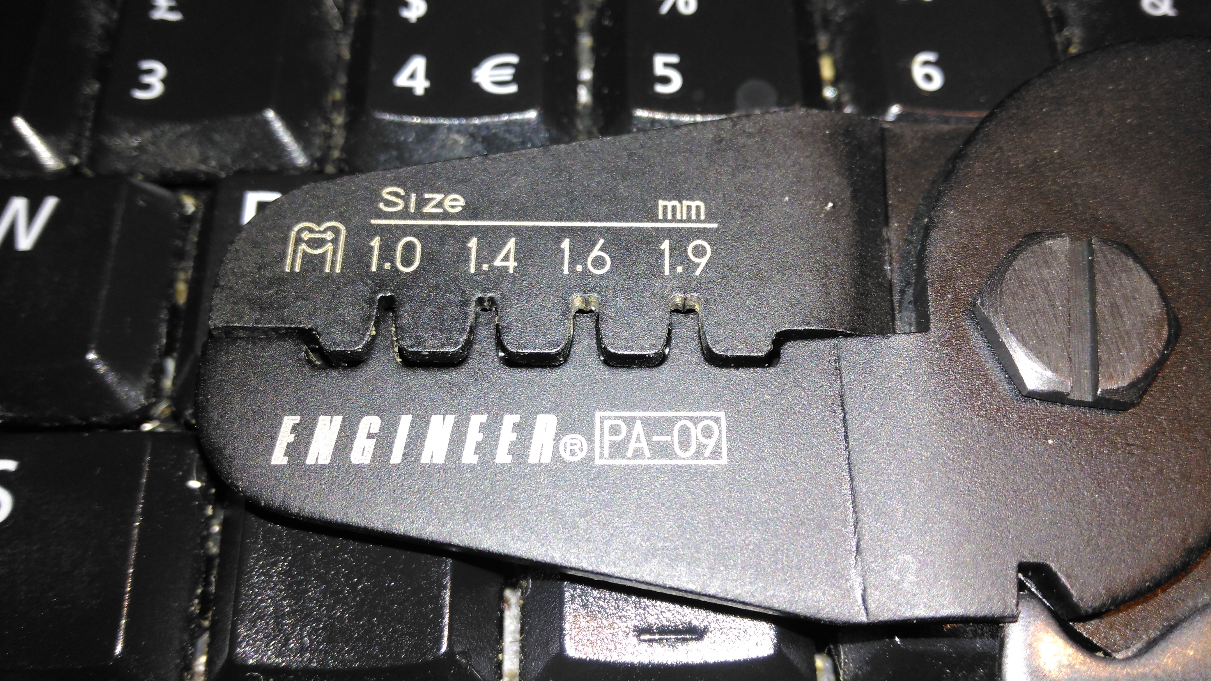
Die Head
The dies are well formed in the steel, and seem to be machined rather than stamped on a press, however the black oxide finish hides any machining marks. The smallest 1mm dies do seem to be a little fragile as they’re so small, so wouldn’t take much abuse without shearing off.
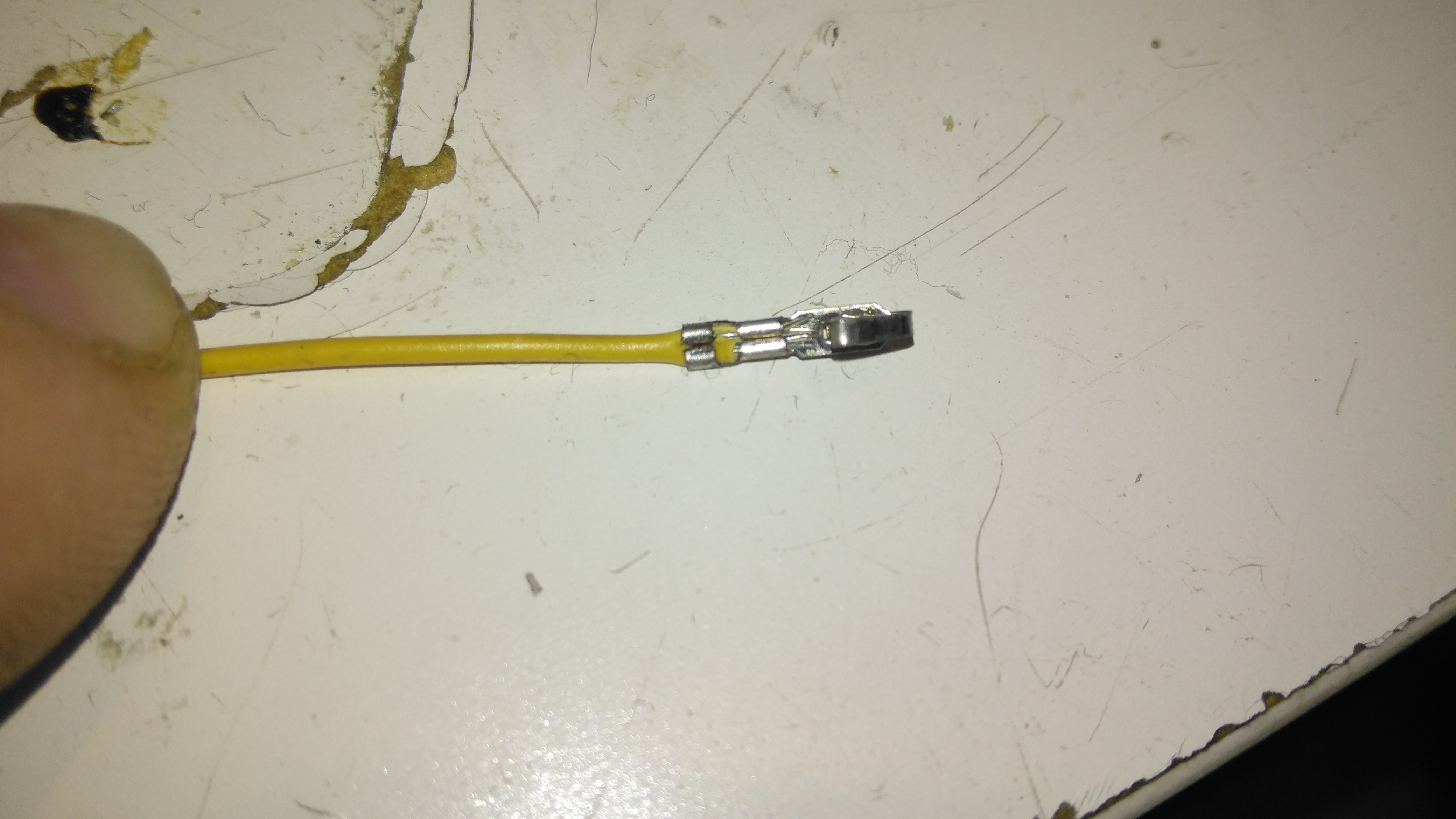
Crimped Molex KK Pin
Here’s a Molex KK pin that’s been crimped with the PA-09. The insulation crimp has pierced the insulation slightly, but this isn’t much of a problem. The conductor crimp is nice & tight, and everything is small enough to fit correctly into the plastic connector body. The trick with these tools is getting a feel for when the crimp is done – squeeze too tightly & the contact deforms, not tightly enough & the wire will just pull out of the terminal. The official tools also crimp both the conductor & insulation at the same time, and they also hold the terminal in place while the wire is inserted. In these cheaper tools, the crimps are done separately, but they do hold on to the contact securely enough for the wire to be inserted properly with your spare hand.
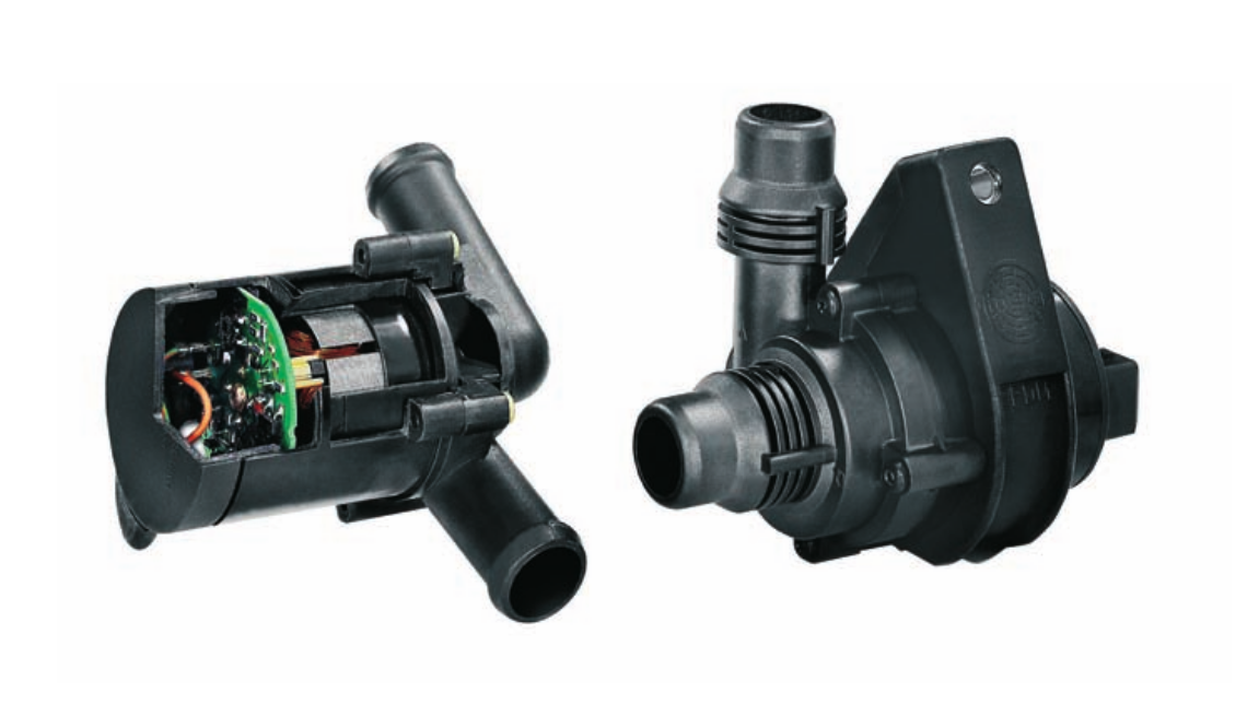
With some recent upgrades to the boat’s heating system, the hot water circulation pumps we’ve been using are becoming far too small for the job. After the original Johnson Marine circulation pump died of old age (the brushes wore down so far the springs ate the commutator) some time ago, it was replaced with a Pierburg WUP1 circulation pump from a BMW. (As we’re moored next to a BMW garage, these are easily obtainable & much cheaper than the marine pumps).
WUP1 Cutaway
These are also brushless, where as the standard Johnson ones are brushed PM motors – the result here is a much longer working life, due to fewer moving parts.
The rated flow & pressure on these pumps is pretty pathetic, at 13L/min at 0.1bar head pressure. As the boat’s heating system is plumbed in 15mm pipe instead of 22mm this low pressure doesn’t translate to a decent flow rate. Turns out it’s pretty difficult to shove lots of water through ~110ft of 15mm pipe ;). Oddly enough, the very low flow rate of the system was never a problem for the “high output” back boiler on the stove – I suspect the “high output” specification is a bit optimistic.
This issue was recently made worse with the addition of a Webasto Thermo Top C 5kW diesel-fired water heater, which does have it’s own circulation pump but the system flow rate was still far too low to allow the heater to operate properly. The result was a rapidly cycling heater as it couldn’t dump the generated hot water into the rest of the system fast enough.
The easiest solution to the problem here is a larger pump with a higher head pressure capability. (The more difficult route would be completely re-piping the system in 22mm to lower the flow resistance). Luckily Pierburg produce a few pumps in the range that would fit the job.
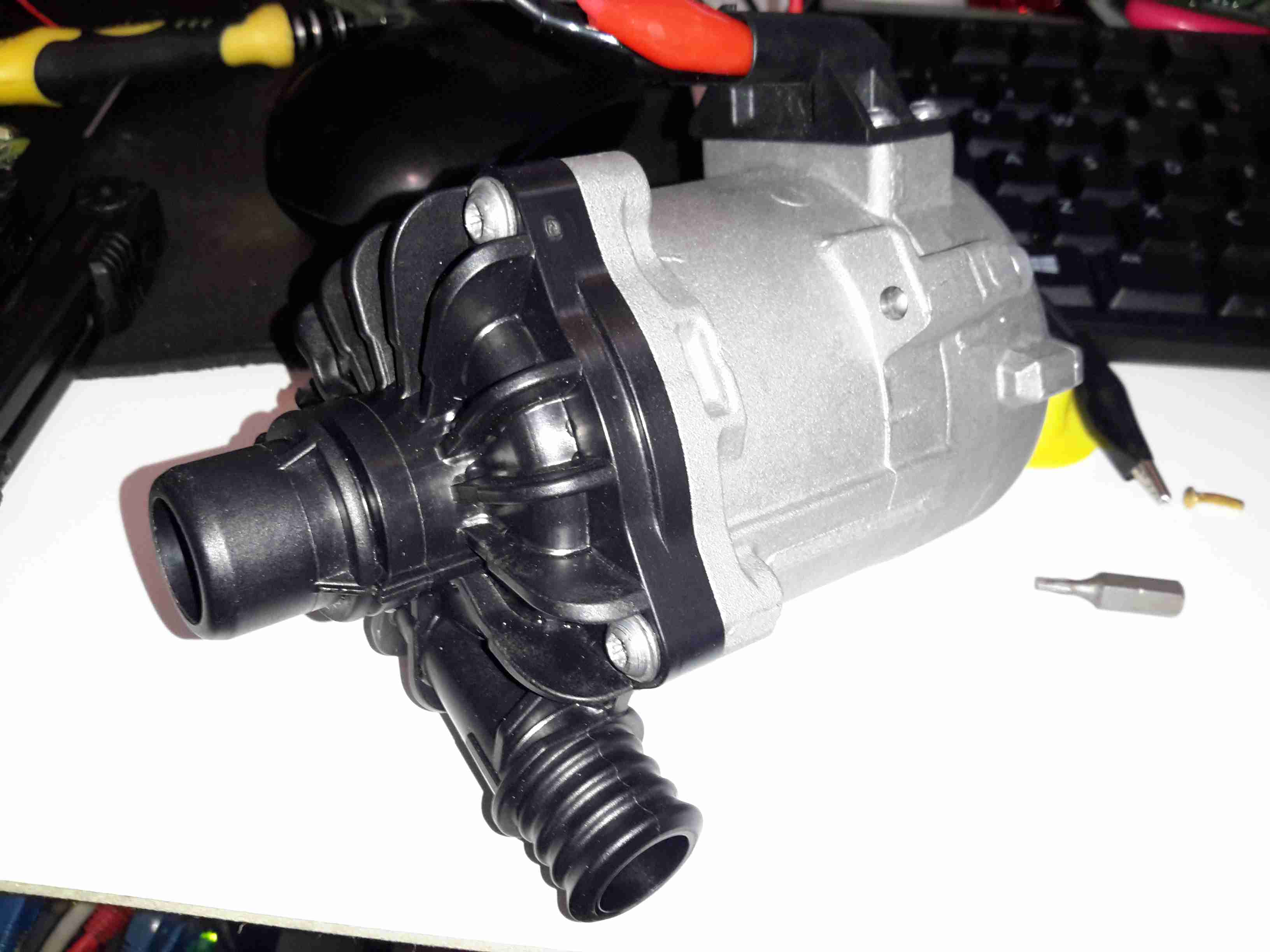
Pierburg CWA-50
Here’s the next size up from the original WUP1 pump, the CWA50. These are rated at a much more sensible 25L/min at 0.6bar head pressure. It’s physically a bit larger, but the connector sizes are the same, which makes the install onto the existing hoses easier. (For those that are interested, the hose connectors used on BMW vehicles for the cooling system components are NormaQuick PS3 type. These snap into place with an O-Ring & are retained by a spring clip).
The CWA50 draws considerably more power than the WUP1 (4.5A vs 1.5A), and are controllable with a PWM signal on the connector, but I haven’t used this feature. The PWM pin is simply tied to the positive supply to keep the pump running at maximum speed.
Once this pump was installed the head pressure immediately increased on the gauge from the 1 bar static pressure to 1.5 bar, indicating the pump is running at about it’s highest efficiency point. The higher water flow has so far kept the Webasto happy, there will be more to come with further improvements!
CWA-50 Pump Teardown
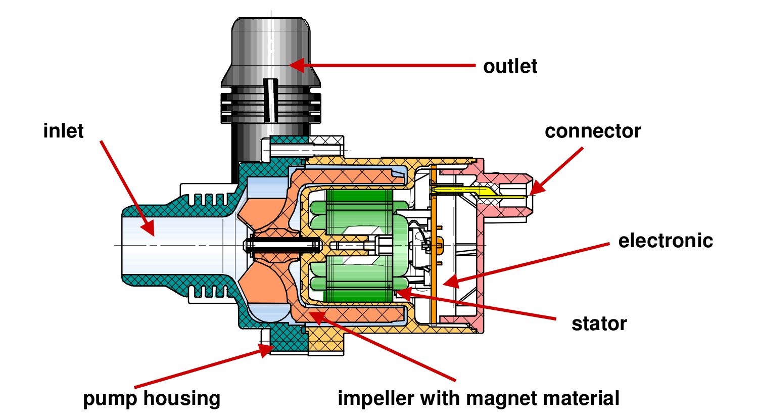
CWA50 Cutaway
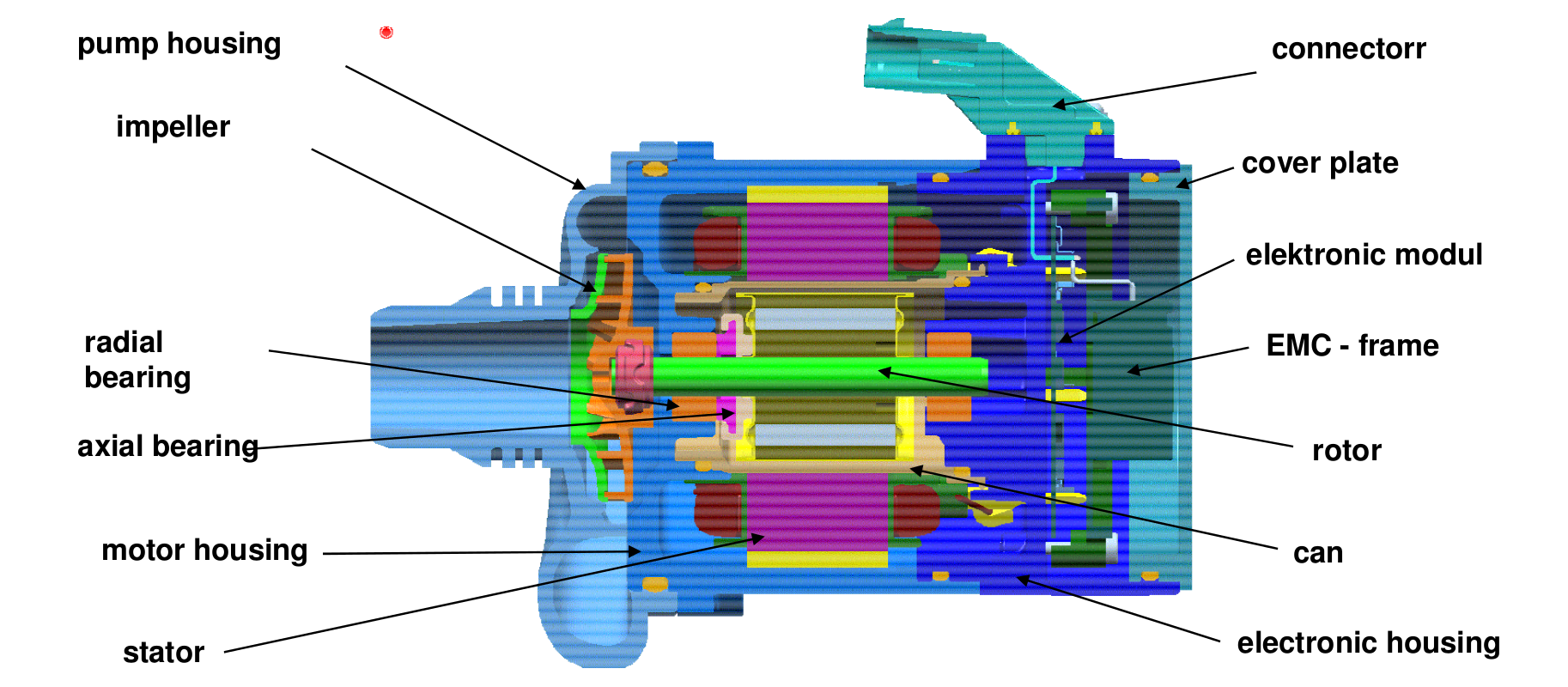
Above is a cutaway drawing of the new pump. These have a drilling through the shaft allows water to pass from the high pressure outlet fitting, through the internals of the pump & returns through the shaft to the inlet. This keeps the bearings cool & lubricated. The control & power drive circuitry for the 3-phase brushless motor is attached to the back & uses the water flowing through the rotor chamber as a heatsink. Overall these are very well made pumps.
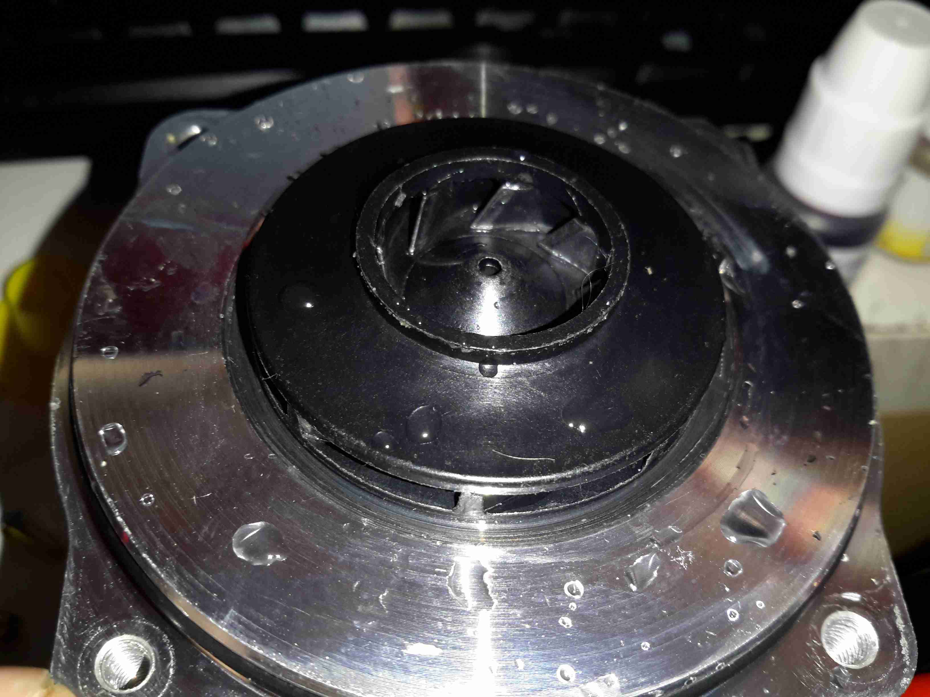
Impeller
Here’s the impeller of the pump, which is very small considering the amount of power this unit has. The return port for the lubricating water can be seen in the centre of the impeller face.
3-Phase Driver
Inside the back of the pump is the control module. The main microcontroller is hiding under the plastic frame which holds the large power chokes & the main filter electrolytic.
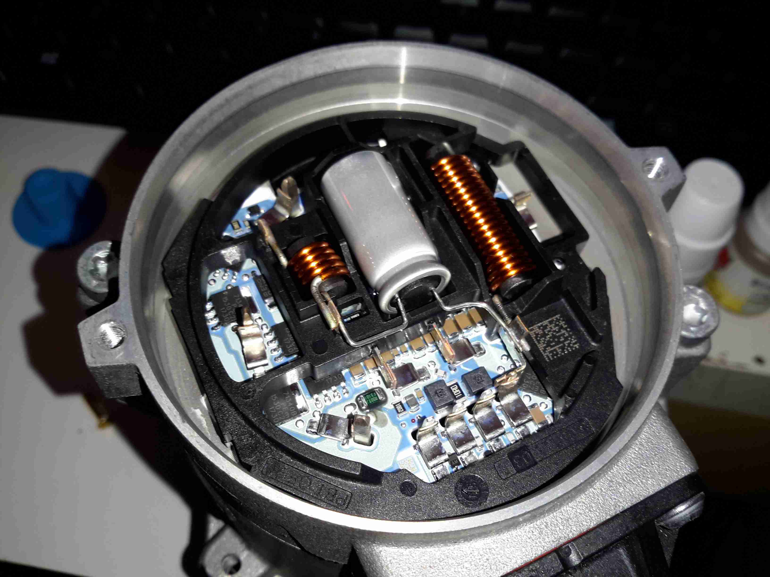
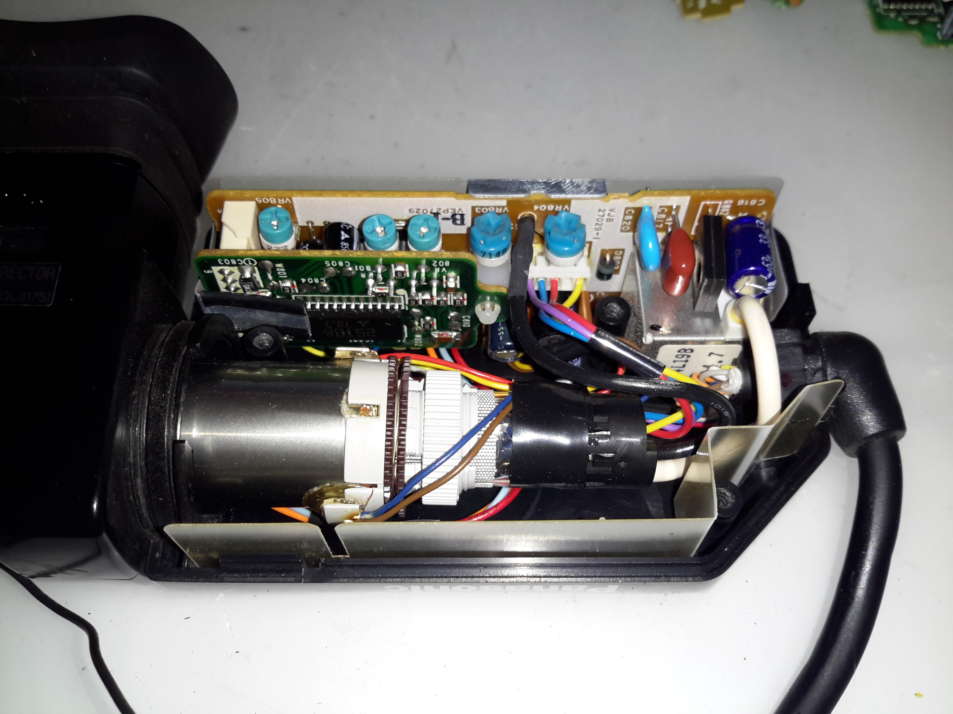
The old Panasonic NV-M5 has the standard for the time CRT based viewfinder assembly, which will happily take a composite video signal from an external source.
This viewfinder has many more connections than I would have expected, as it has an input for the iris signal, which places a movable marker on the edge of the display. This unit also has a pair of outputs for the vertical & horizontal deflection signals, I imagine for sync, but I’ve never seen these signals as an output on a viewfinder before.
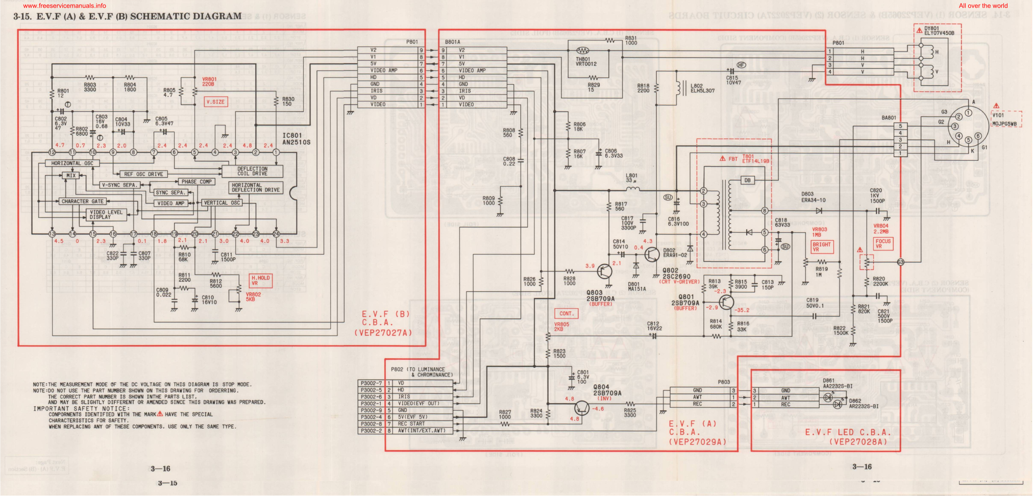
EVF Schematic
Luckily I managed to get a service manual for the camera with a full schematic.
This unit takes a 5v input, as opposed to the 8-12v inputs on previous cameras, so watch out for this! There’s also no reverse polarity protection either.
Pins
Making the iris marker vanish from the screen is easy, just put a solder bridge between pins 15 & 16 of the drive IC. The important pins on the interface connector are as follows:
Pin 3: GND
Pin 4: Video Input
Pin 5: Video GND
Pins 6: +5v Supply
Here’s another Dyson teardown, in my efforts to understand how marketing have got hold of relatively simple technology & managed to charge extortionate amounts of money for it.
This is the DC35, the model after the introduction of the brushless digital motor.
Back Cap Removed
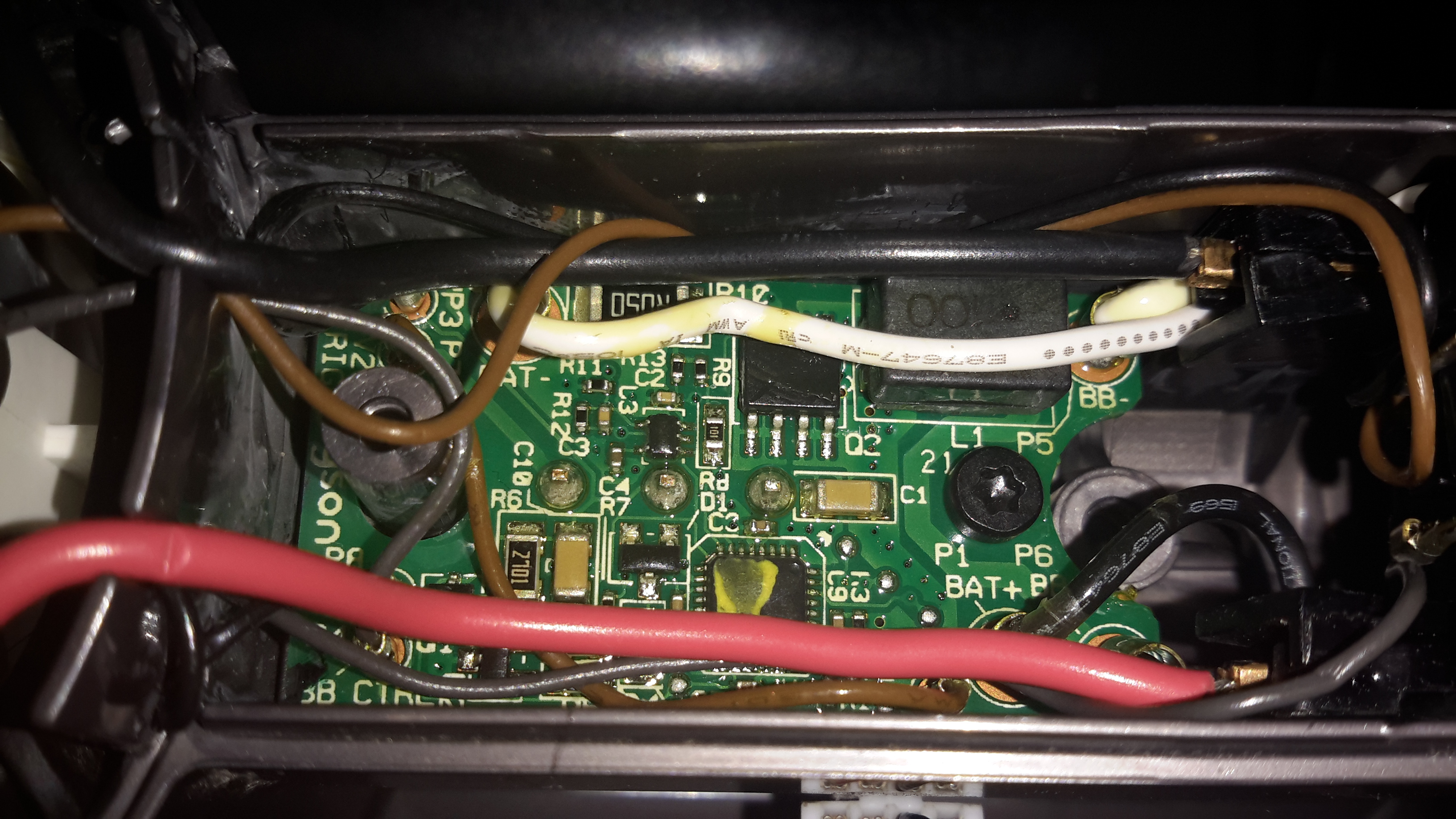
On this version the mouldings have been changed, and the back cover comes off, after removing the battery retaining screw. It’s attached with some fairly vicious clips, so some force is required. Once the cap is removed, all the electronics are visible. On the left is the motor itself, with it’s control & drive PCB. There’s another PCB on the trigger, with even more electronics. The battery connector is on the right.
Trigger PCB
Here’s the trigger PCB, which appears to deal with DC-DC conversion for powering the brush attachments. The QFN IC with yellow paint on it is an Atmel ATTiny461 8-bit microcontroller. This is probably controlling the DC-DC & might also be doing some battery authentication.
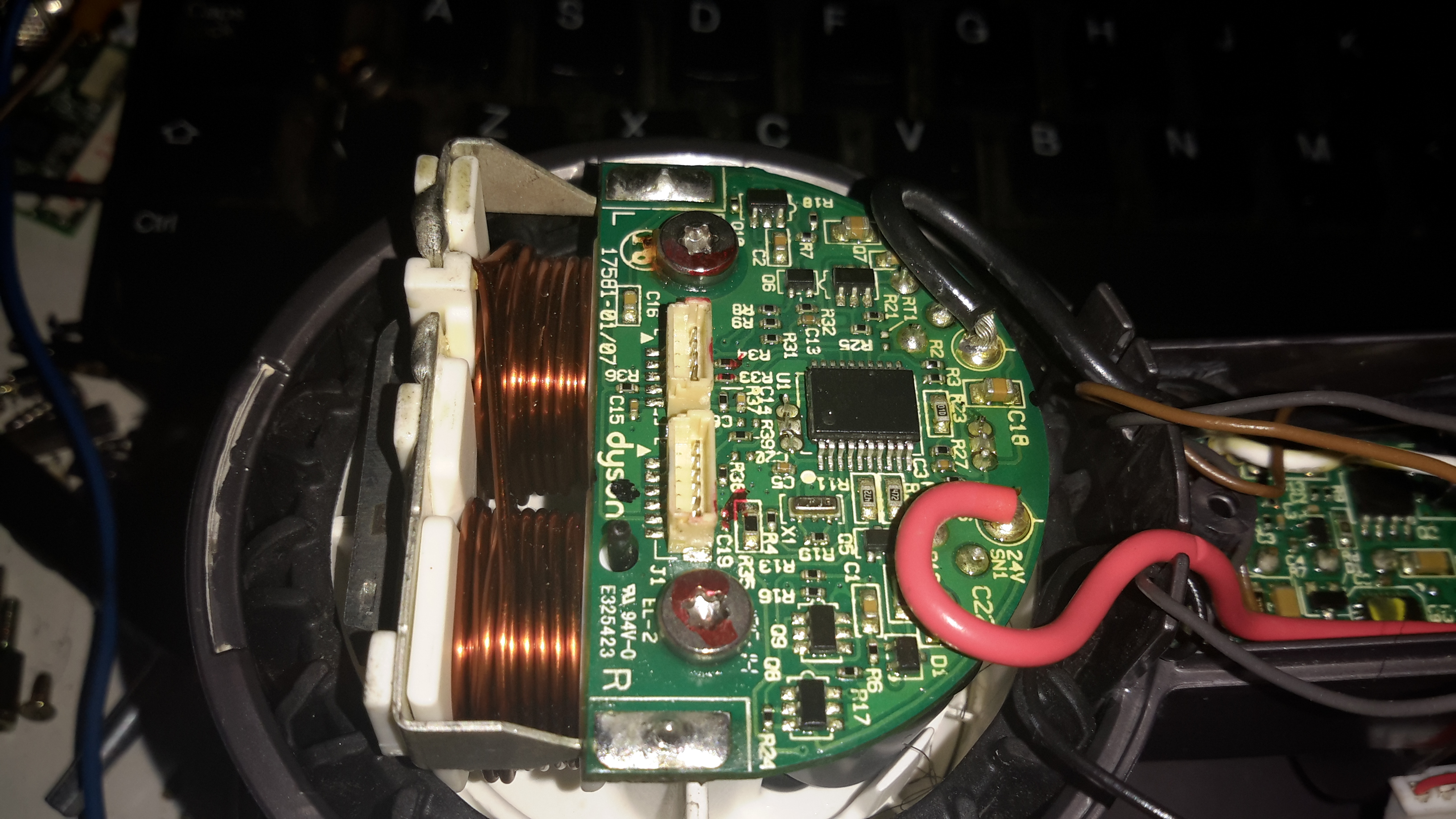
“Digital Motor”
Here’s the motor & it’s board. The windings on the stator are extremely heavy, which makes sense considering it’s rated at 200W. The main control IC is a PIC16F690 from Microchip. Instead of using an off the shelf controller, this no doubt contains software for generating the waveforms that drive the brushless motor. It also appears to communicate with the other PCBs for battery authentication.
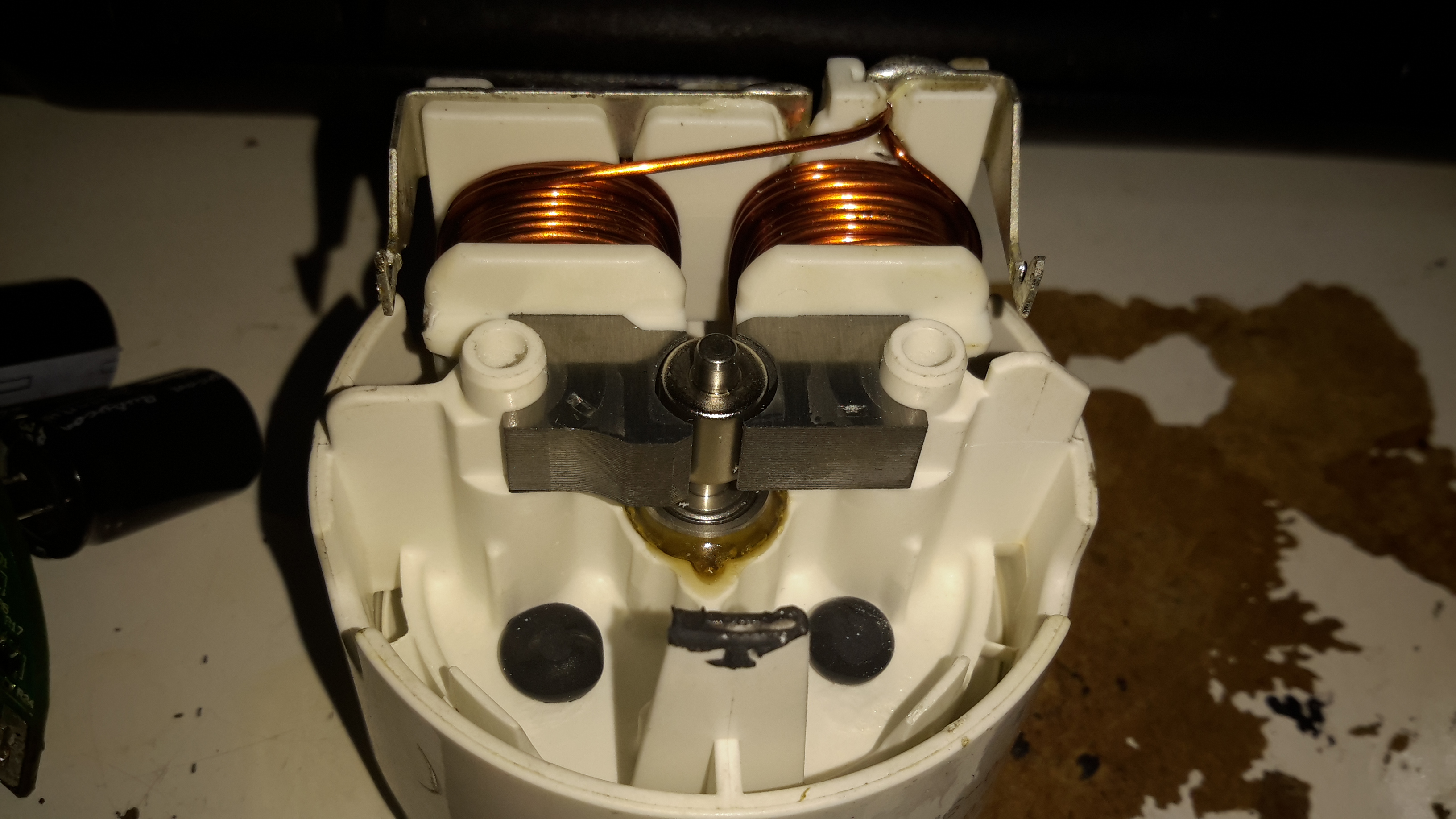
Stator
Desoldering the board allows it to be removed from the motor itself. The pair of windings are connected in anti-phase, to create alternating North-South poles depending on polarity. Since the existing controller is unusable due to software authentication with the other parts, I might have a go at building my own driver circuit for this with an Arduino or similar.
Blower Assembly
The blower assembly is simple plastic mouldings, pressed together then solvent welded at the seam.
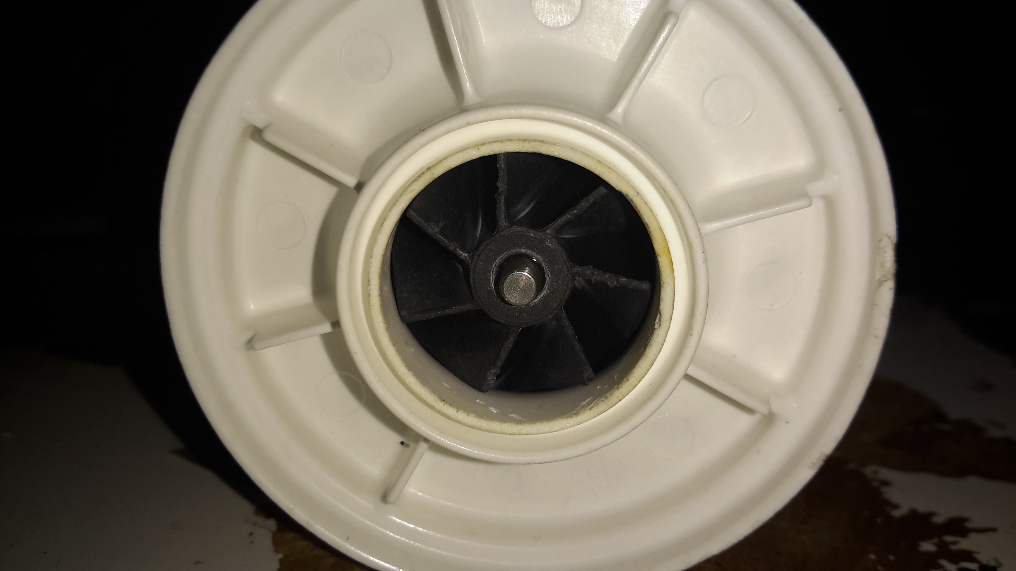
Impeller
The impeller is just a centrifugal compressor wheel, identical to what’s used in engine turbochargers.
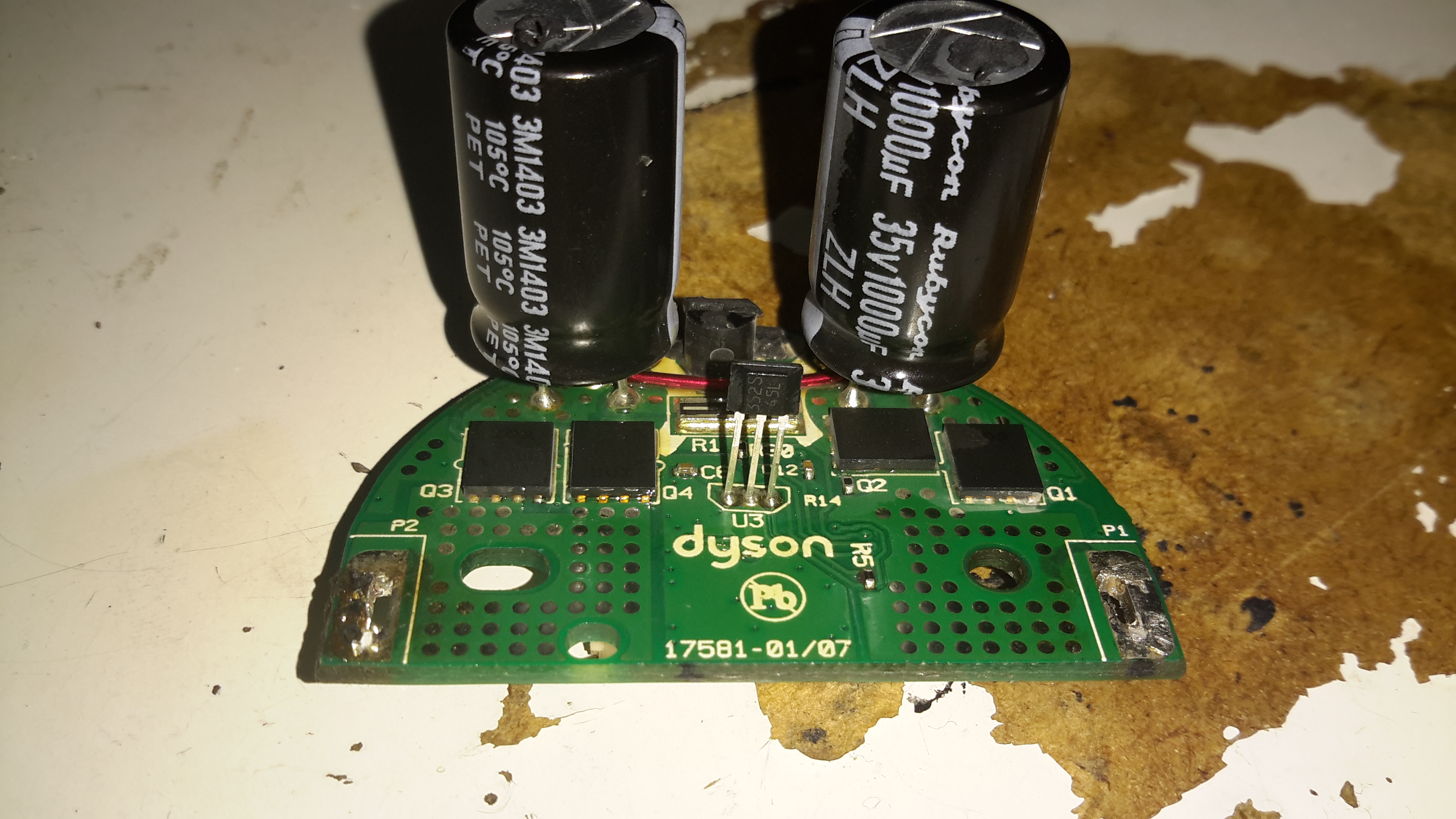
Motor Control Board
The inside face of the control PCB holds the 4 very large MOSFETs, IRFH7932PbF from International Rectifier. These are rated at 30v 20A a piece, and are probably wired in a H-Bridge. There’s a bipolar Hall switch to sense rotor position & rotation speed, and an enormous pair of capacitors on the main power bus.
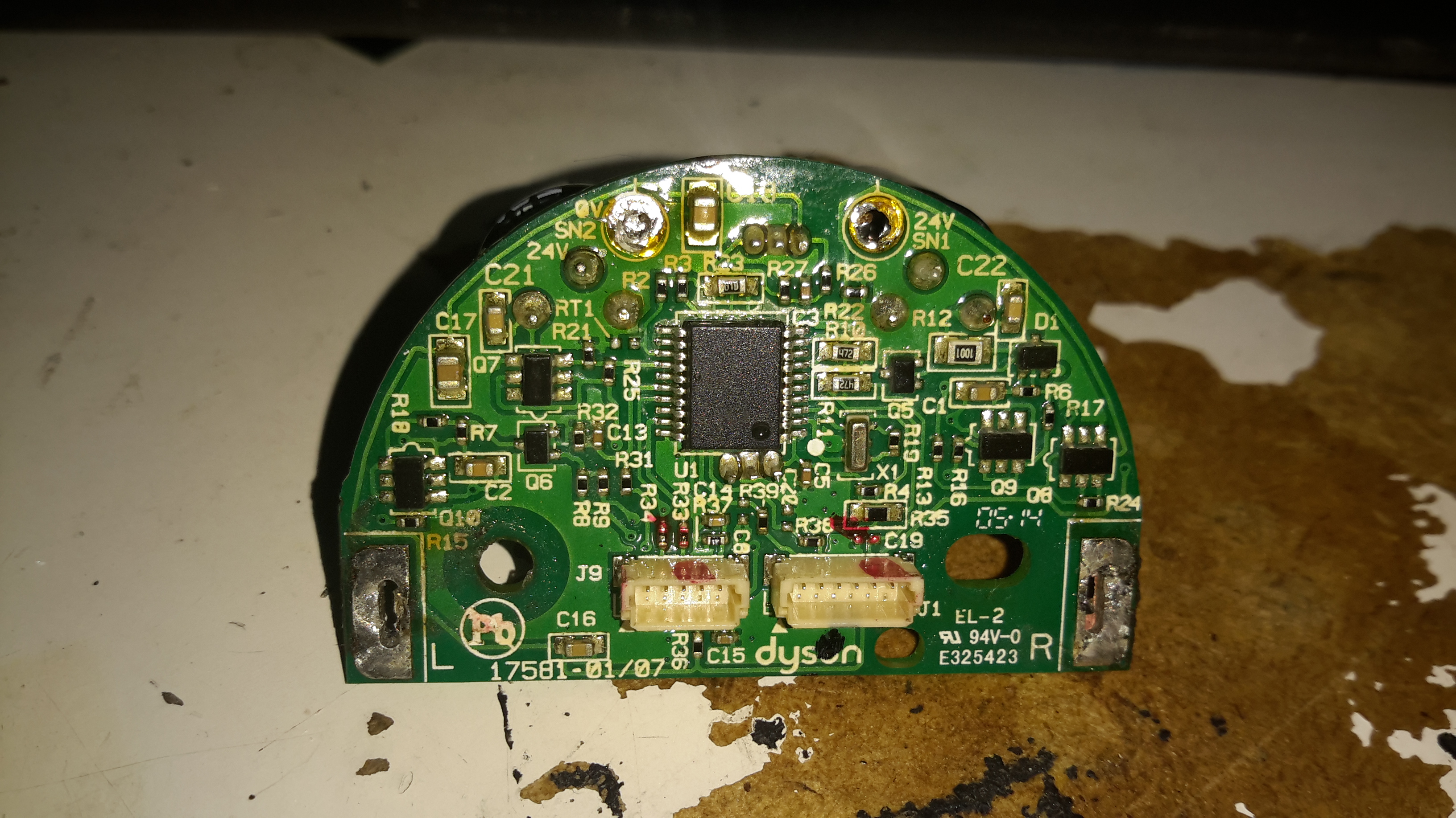
Motor Control Board Reverse
Not much on the other side of the PCB other than the microcontroller and associated gate drive stuff for the FETs.
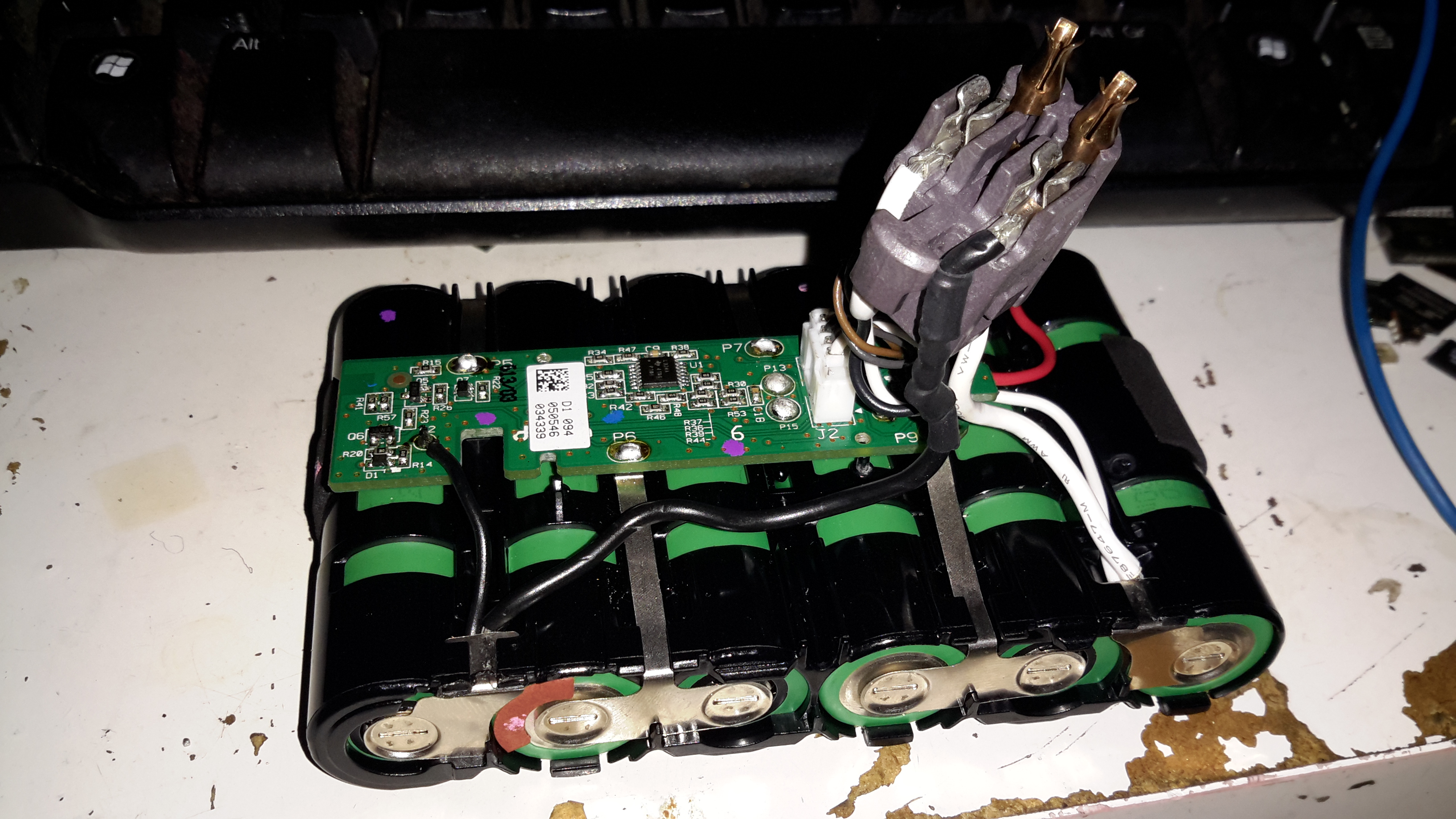
Battery Pack Opened
The battery pack is similar to the DC16 in it’s construction, a heavily clipped together plastic casing holding 6 lithium cells. In this one though there’s a full battery management system. The IC on the top of the board above is a quad Op-Amp, probably for measuring cell voltages.
Battery BMS Bottom
The other side of the BMS board is packed with components. I wasn’t able to identify the QFN IC here, as it’s got a custom part number, but it’s most definitely communicating with the main motor MCU via I²C over the two small terminals on the battery connector.
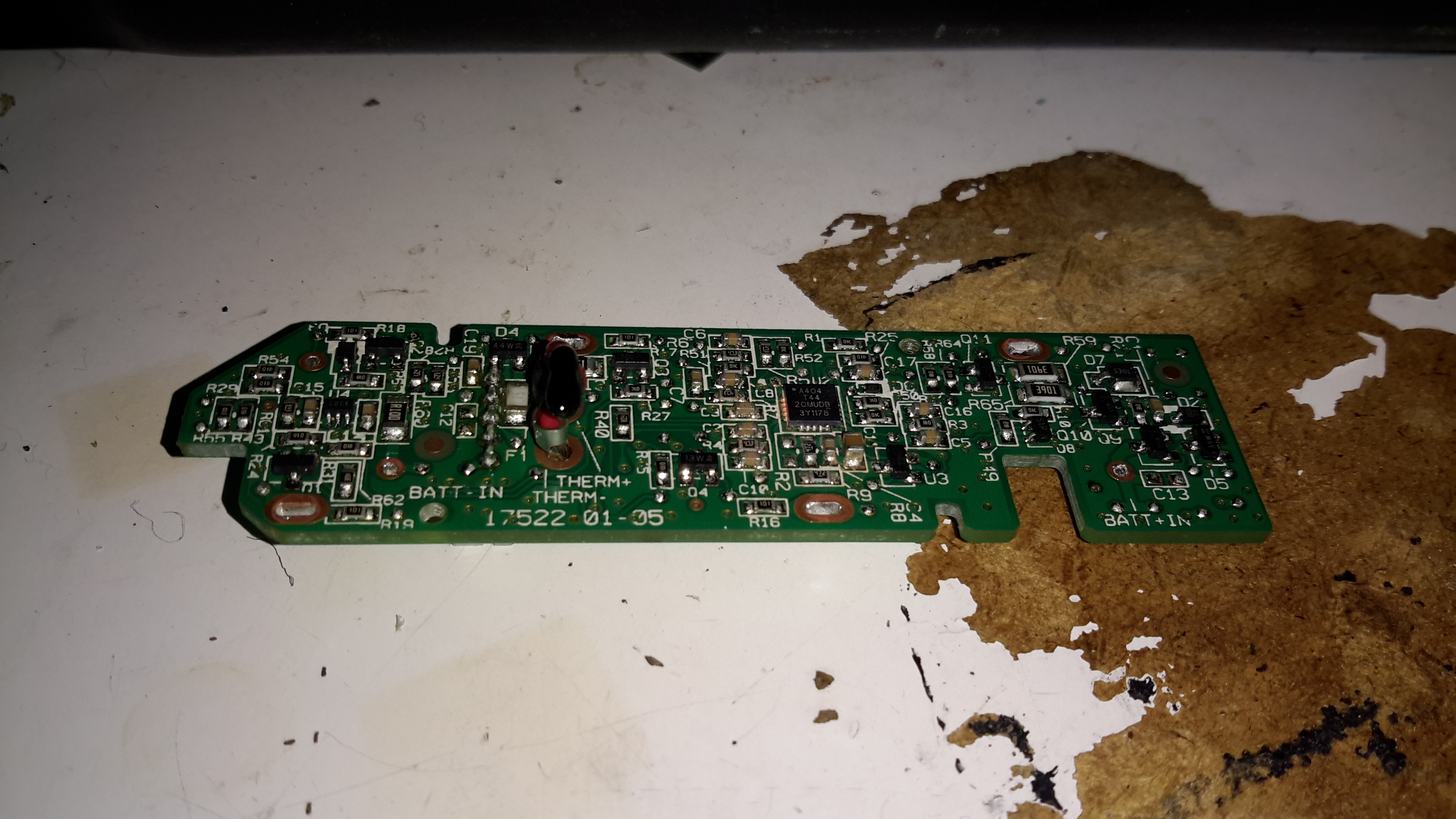
Here’s an old HDSPA 3G USB modem stick that I got with a mobile phone contact many years ago. As it’s now very old tech, and I have a faster modem, not to mention that I’m no longer with Orange (Robbing <expletive>), here’s a teardown of the device!
Cover Removed
The top shell is just clipped into place, while a pair of very small screws hold down the orange piece at left to hold the PCB stack in the casing. Not much to see here, but it’s clear that there’s a lot crammed into a very small space.
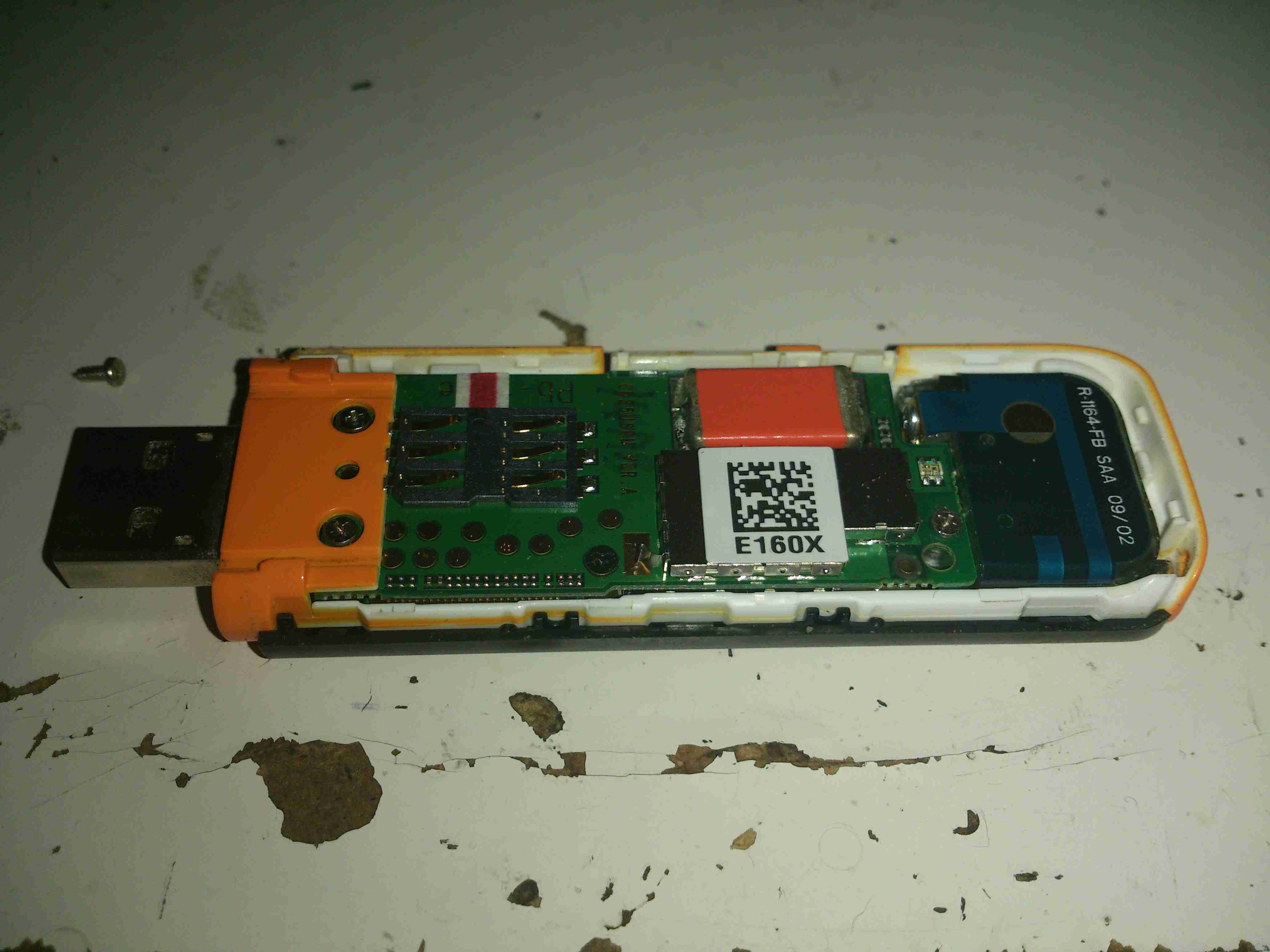
PCB Assembly
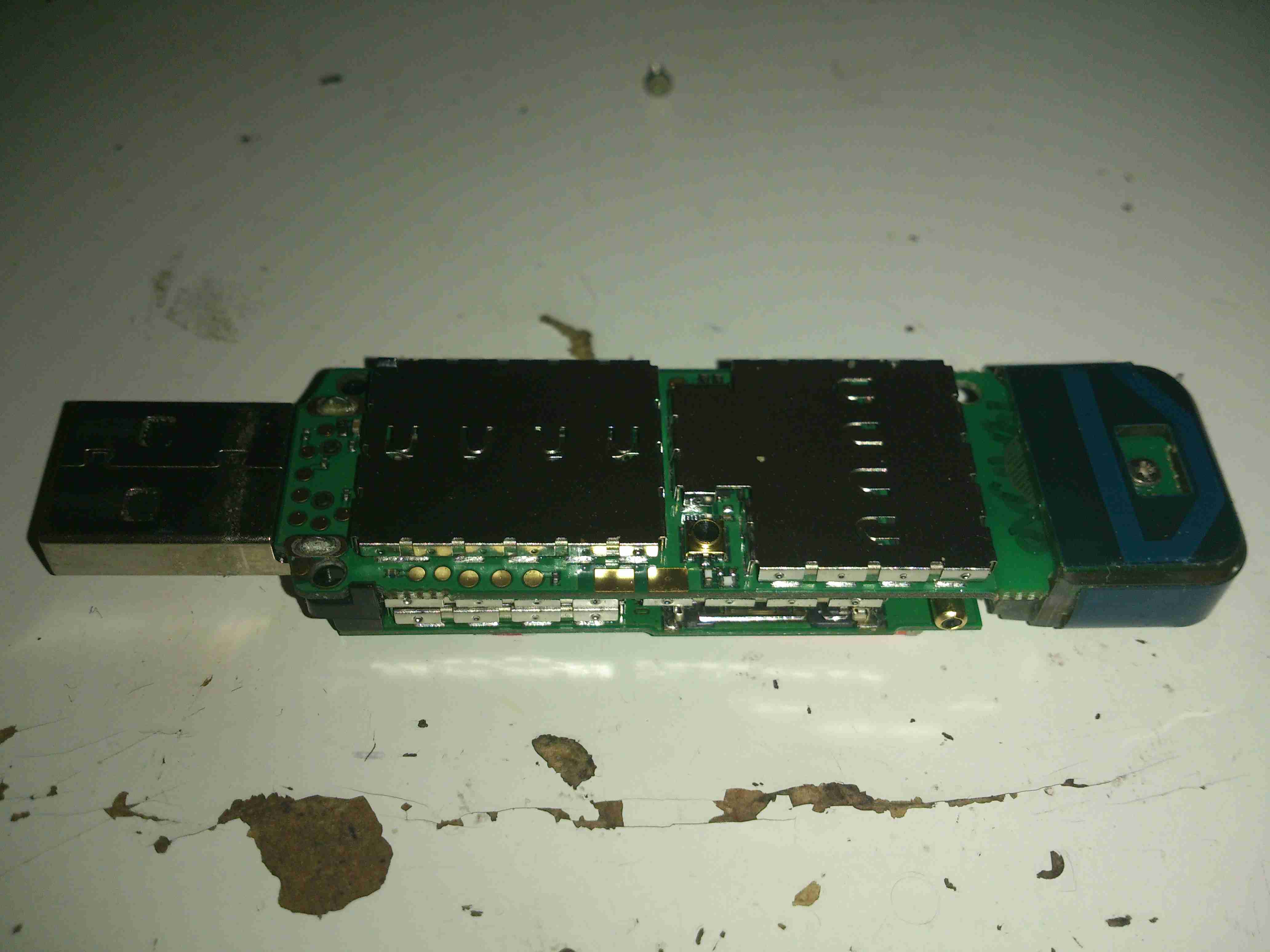
Here’s the PCB stack removed from the outer casing. The main antenna is on the right, attached with another small screw. Every IC on the boards is covered with an RF can. No problems there, pliers to the rescue!
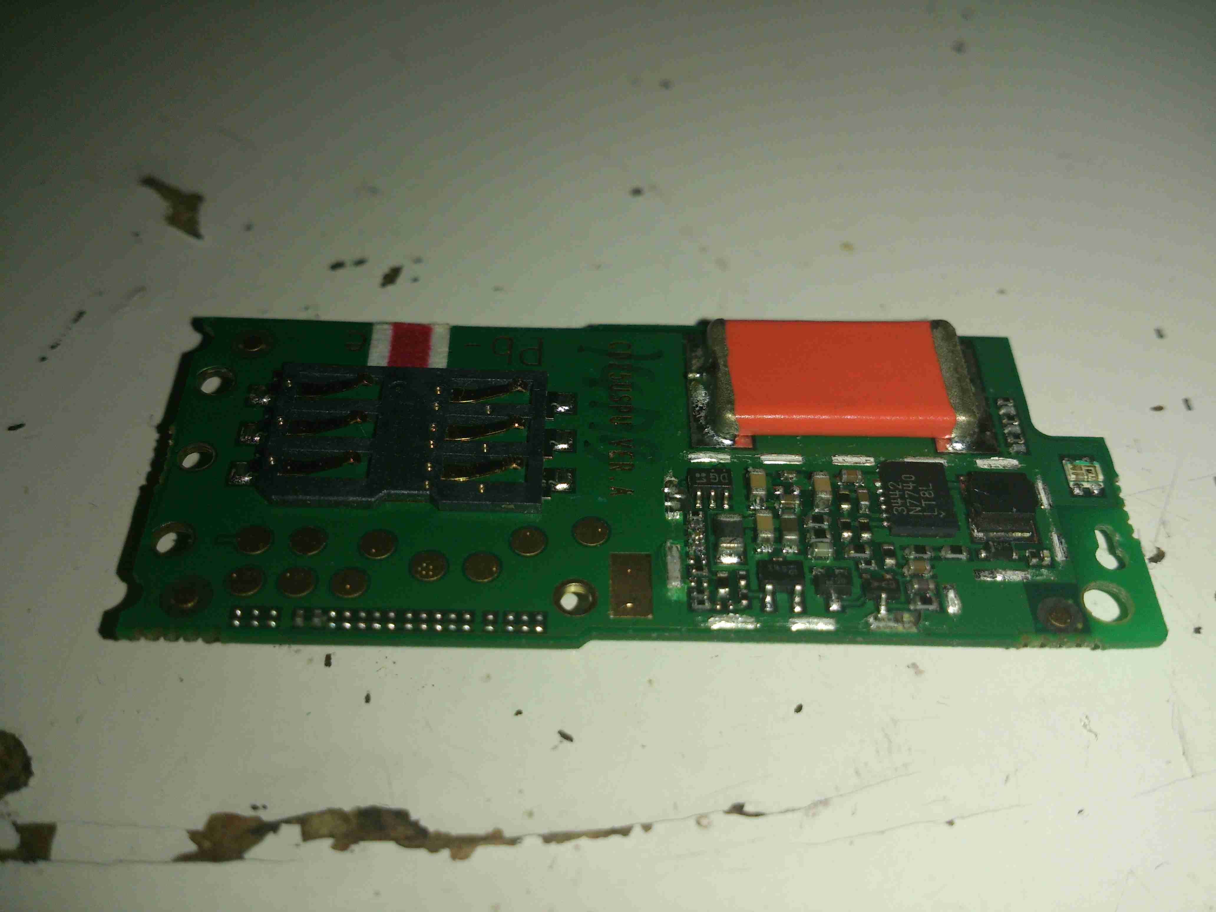
SD Card Slot
Here’s the top PCB, all the shields have been removed. On the left is a Qualcomm PM6658 Power Management IC with integrated USB transceiver. This is surrounded by many of the power management circuits.
The integrated SD Card slot is on the right side. with what looks to be a local switching regulator for supply voltage. This might also provide the SIM card with it’s power supply.
PSU & SIM Contacts
The other side of the top board reveals more power management, with another switching regulator, and a truly massive capacitor at the top edge. I’m guessing this is a solid Tantalum.
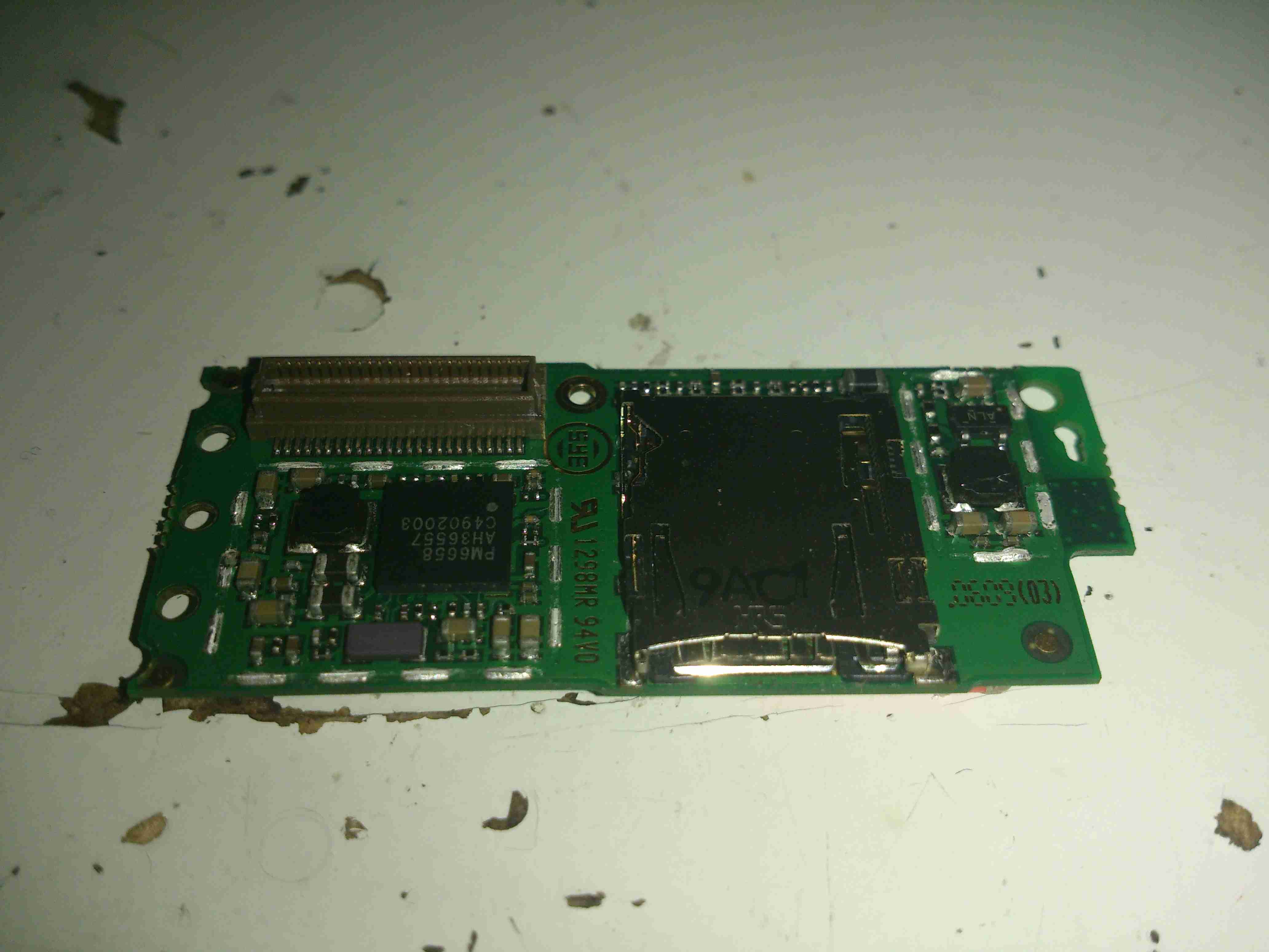
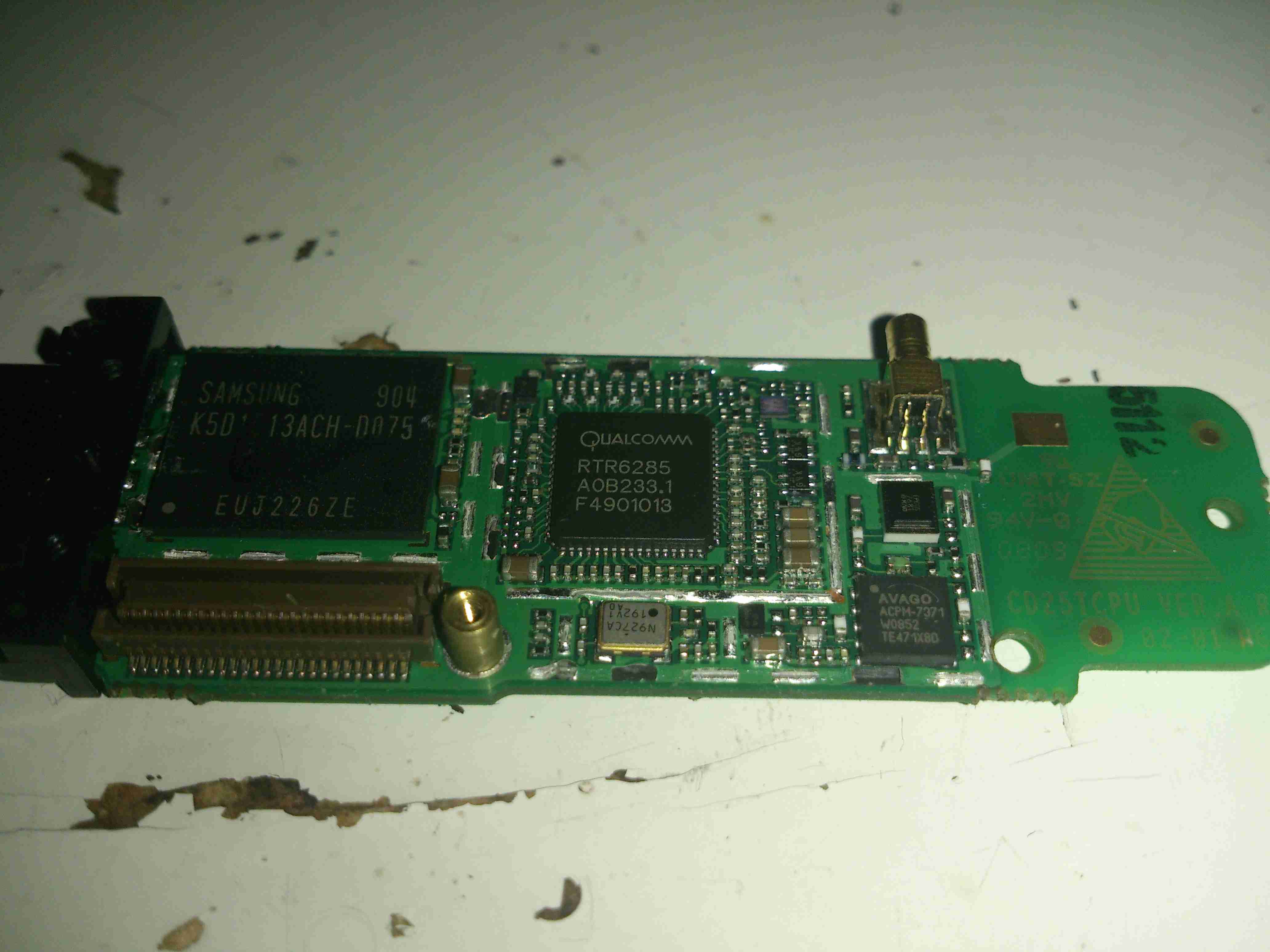
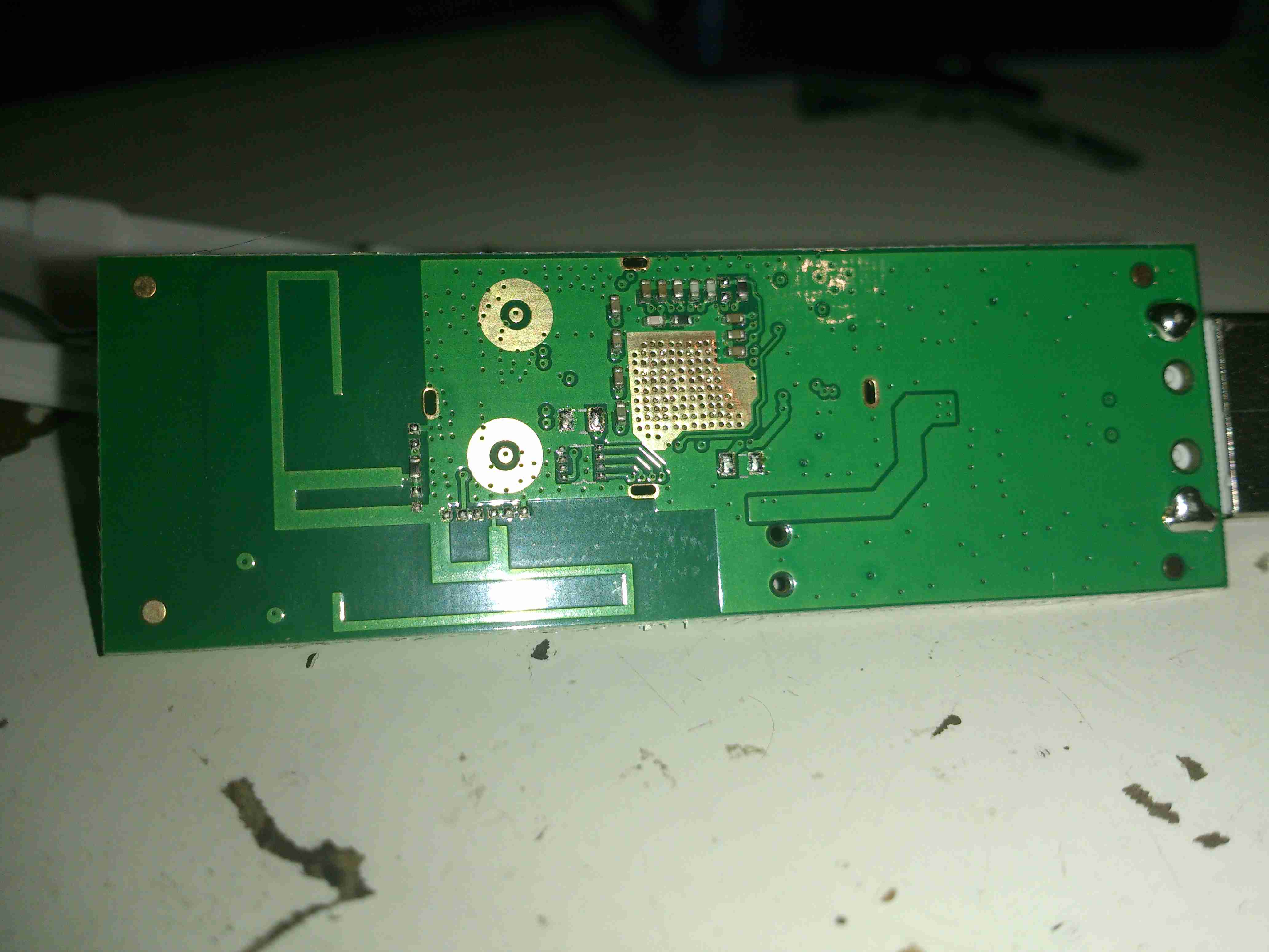
Main Chipset PCB
The other PCB holds the main chipset & RF circuits. On the left here is a Samsung MCP K5D1G13ACH IC. This one is a multiple chip package, having 1Gbit of NAND Flash & 512Mbit of mobile SDRAM.
To it’s right is a Qualcomm RTR6285 RF Transceiver. This IC supports multiband GSM/EDGE/UMTS frequencies & also has a GPS receive amplifier included.
At bottom right is an Avago ACPM7371 Wide-Band 4×4 CDMA Power Amplifier. The external antenna connector is top right.
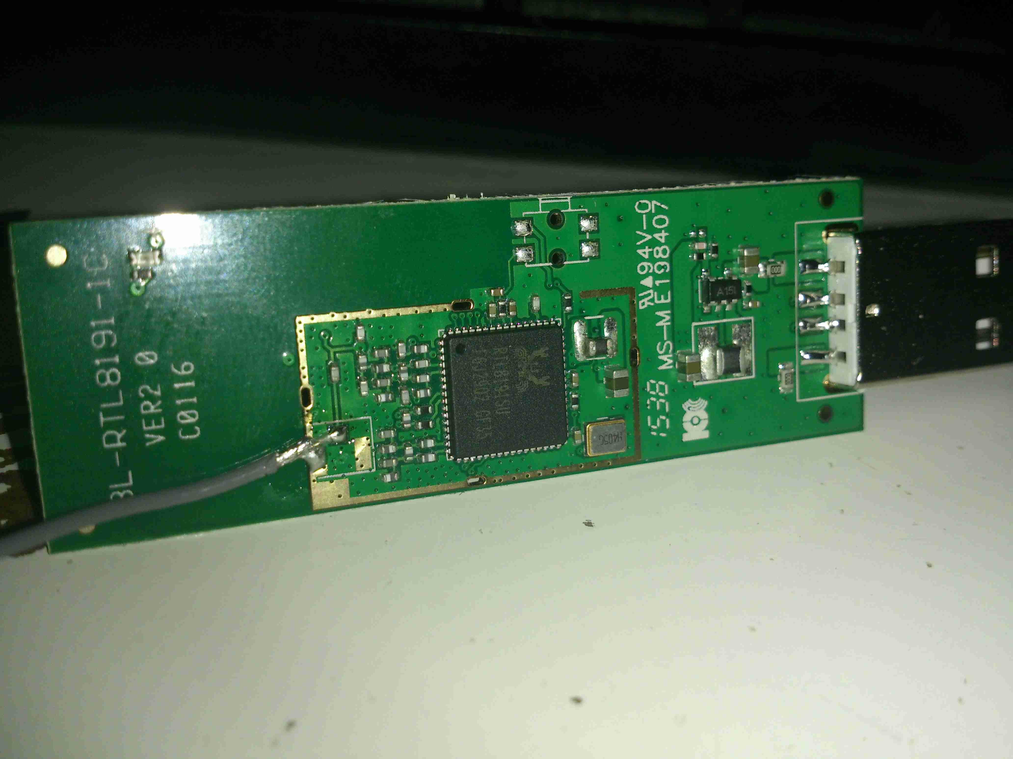
Main Chipset PCB Reverse
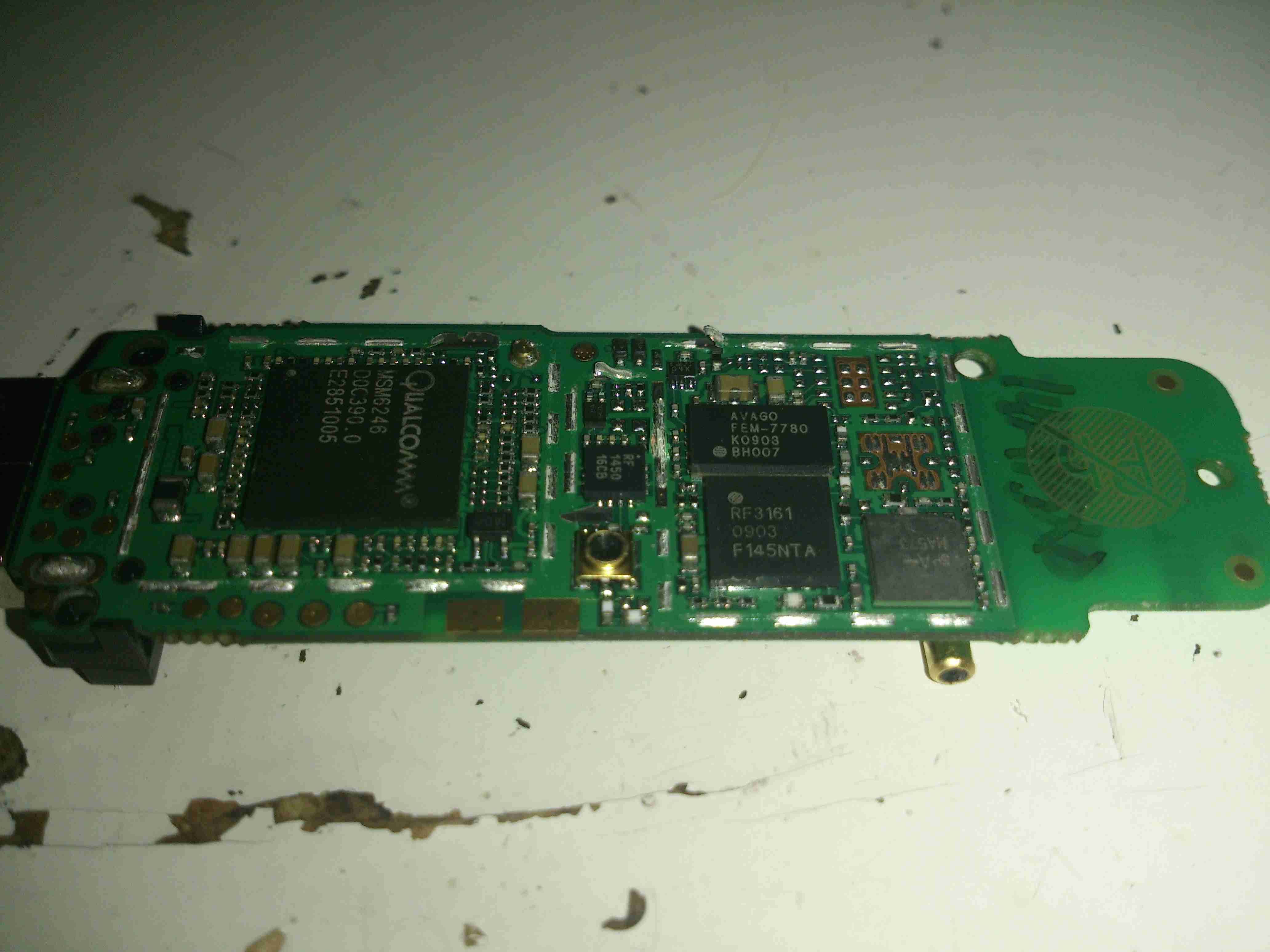
On the other side of the main PCB is a Qualcomm MSM6246 Baseband processor. Not sure about this one as I can’t find anything resembling a datasheet. Another micro-coax connector is in the centre, probably for factory test purposes, as it’s not accessible from the outside.
Just above the coax connector is a Qorvo RF1450 SP4T (single-pole 4-throw) High Power (34.5dBm) GSM RF Switch.
Upper right is an Avago FEM-7780 UMTS2100 4×7 Front End Module.
Under that is an RFMD RF3163 Quad-Band RF Power Amplifier Module.
I’ve been a vaper now for many years, after giving up the evil weed that is tobacco. Here’s my latest acquisition in the vaping world, the JoyeTech eVIC 60W. This one is branded by Totally Wicked as the Forza VT60.
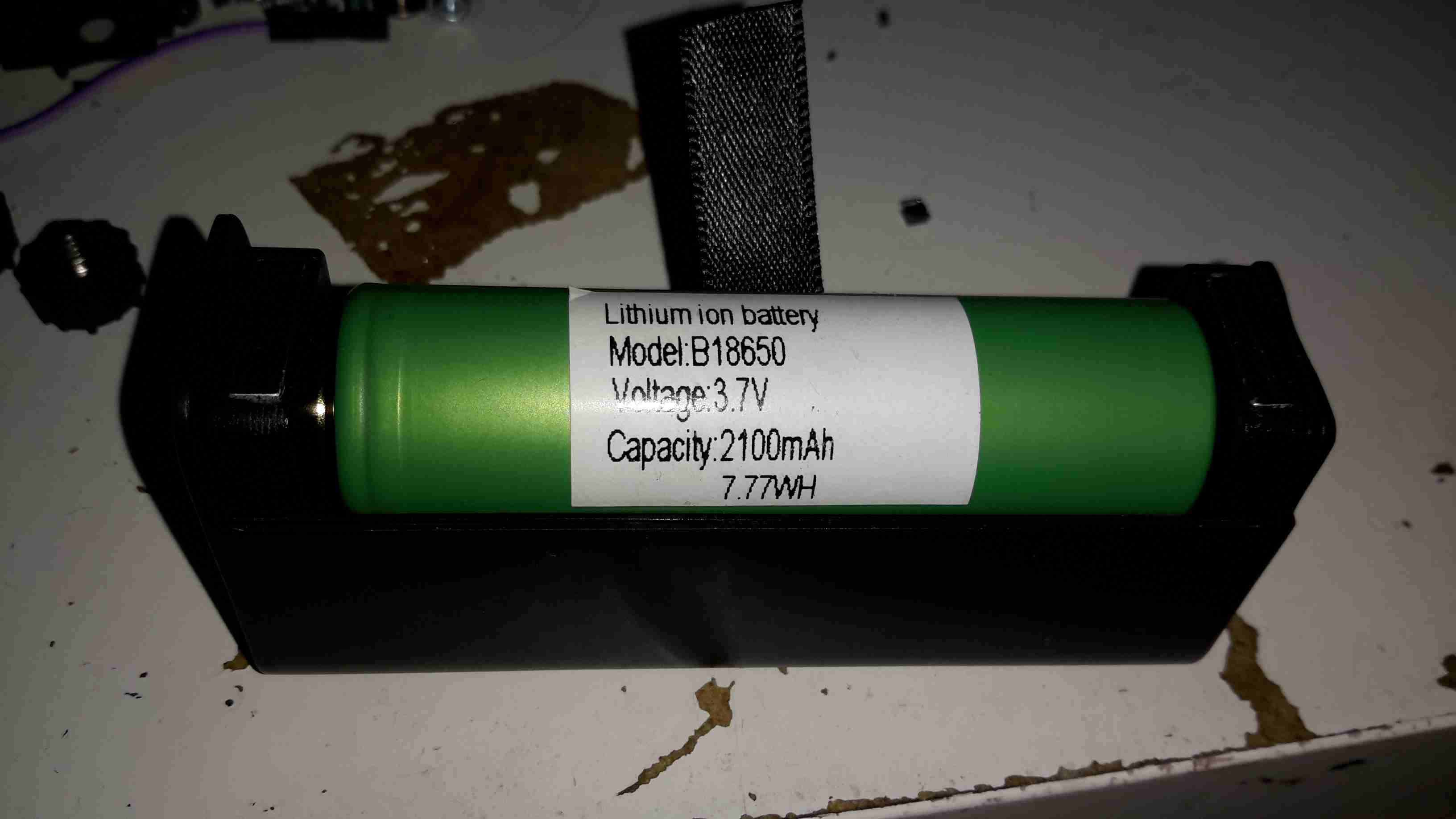
18650 Cell
Powered by a single 18650 Li-Ion cell, this one is a Sony VTC4 series, 2100mAh.
Under the battery a pair of screws hold the electronics in the main cast alloy casing.
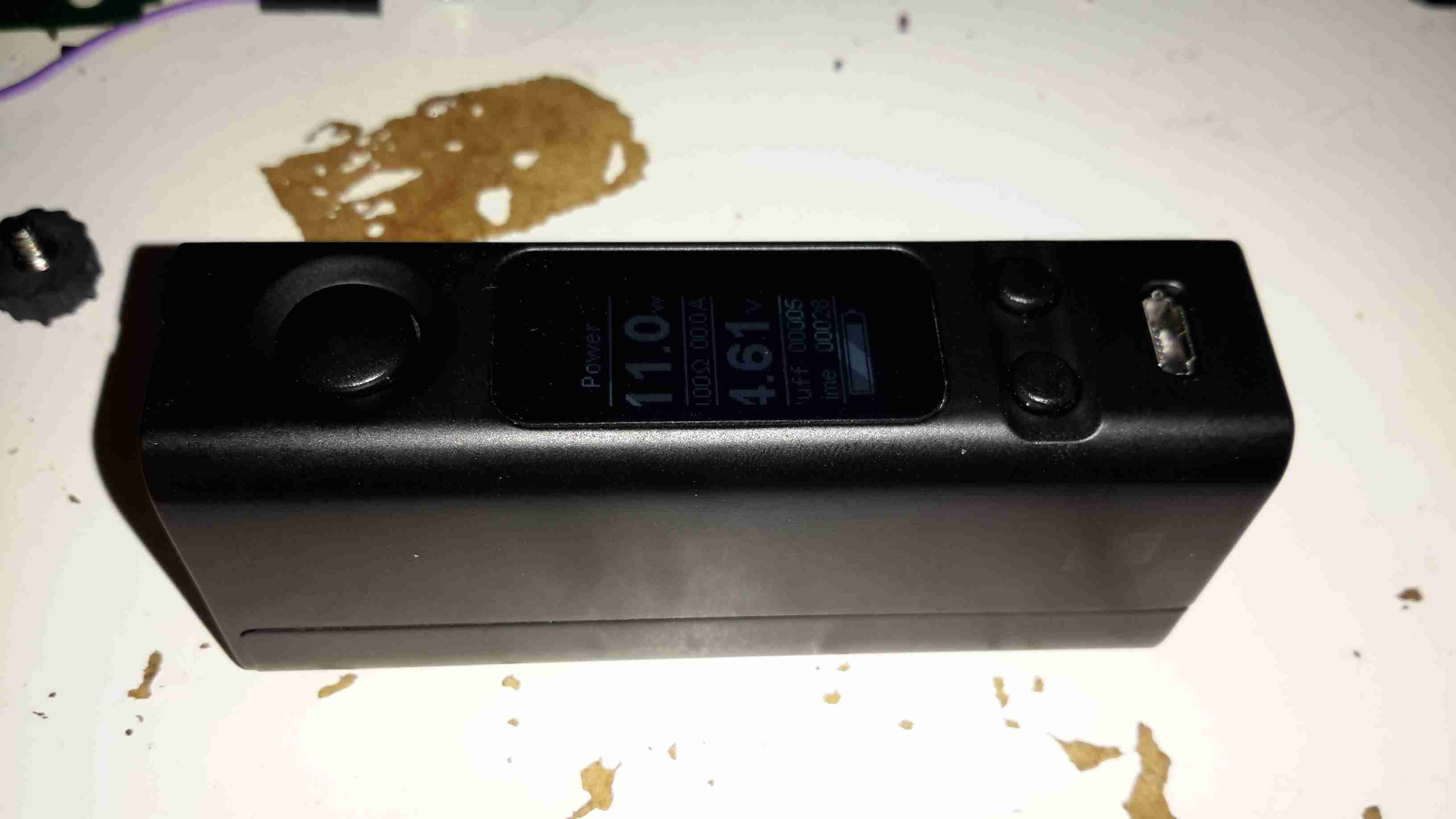
OLED Display
After removing the screws, the entire internal assembly comes out of the case, here’s the top of the PCB with the large OLED display in the centre.
USB Jack
On the right side of the board is the USB jack for charging & firmware updates. The adjustment buttons are also at this end.
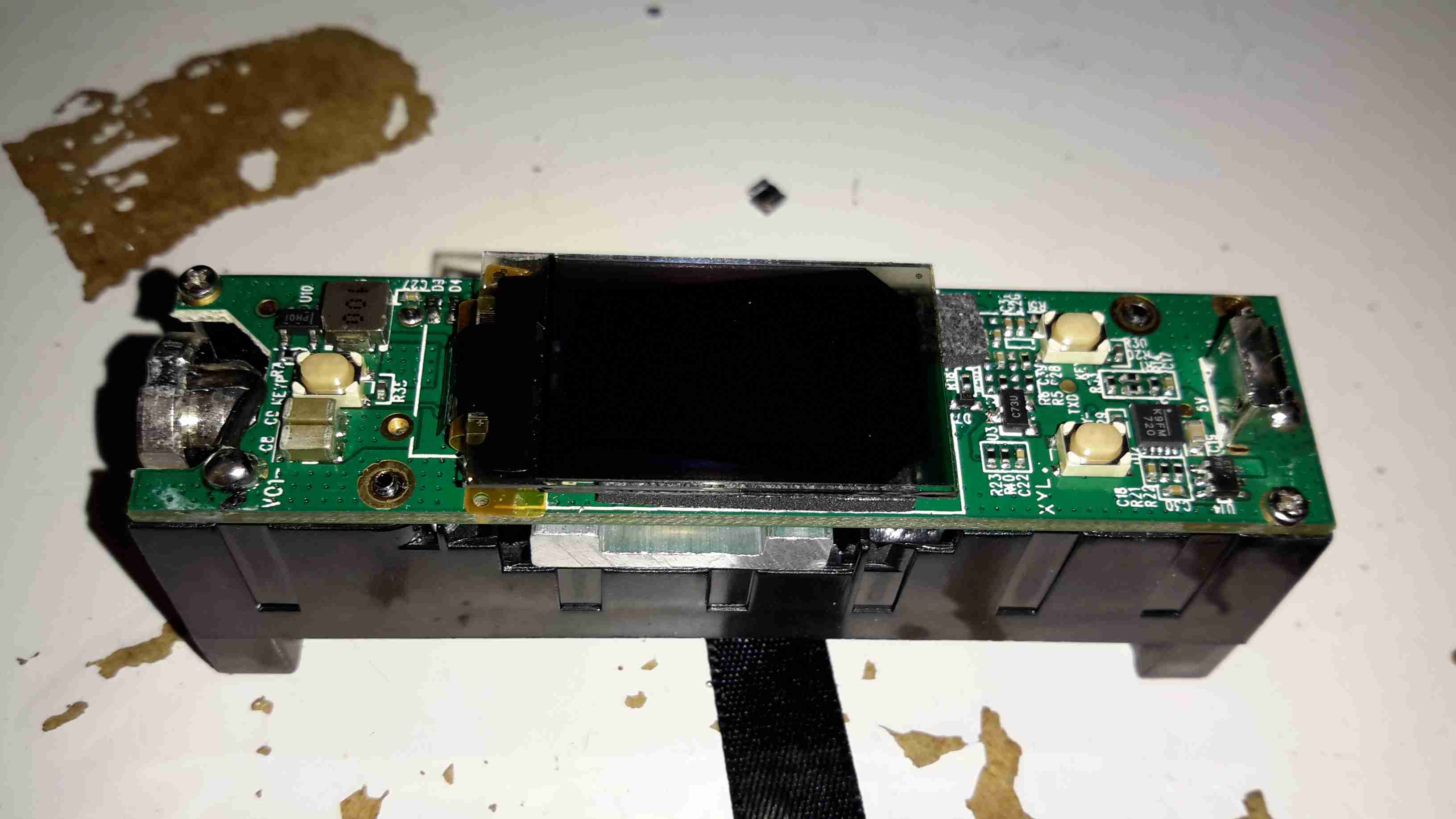
Output
On the left side of the board is the main output connector & the fire button. Unlike many eCigs I’ve torn down before, the wiring in this one is very beefy – it has to be to handle the high currents used with some atomizers – up to 10A.
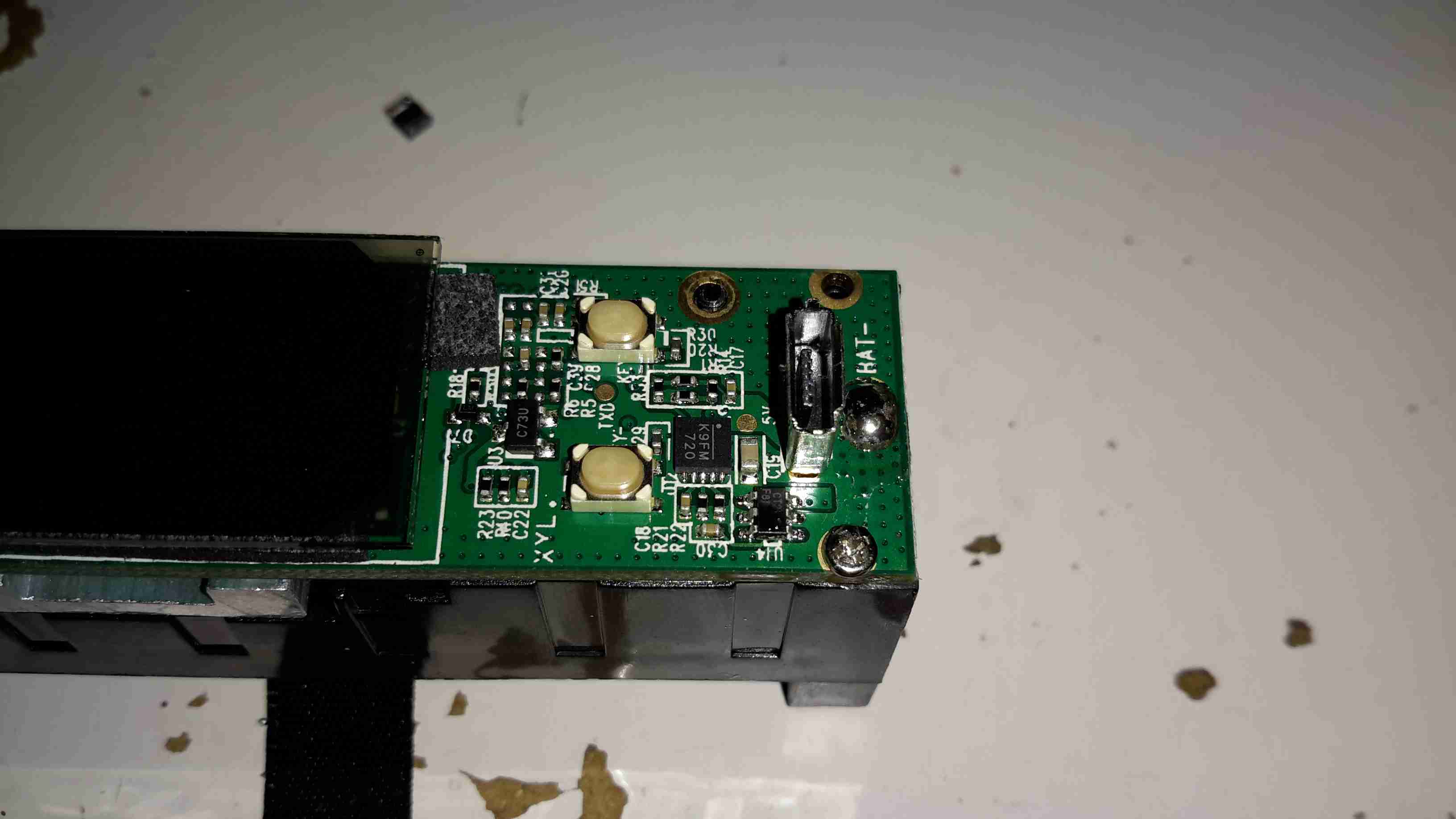
PCB Reverse
Removing the board from the battery holder shows the main power circuitry & MCU. The aluminium heatsink is thermally bonded to the switching MOSFETs, a pair under each end. The switching inductor is under the gap in the centre of the heatsink.
DC-DC Converter
A close up of the heatsink shows the very slim inductor under the heatsink.
Microcontroller
The main MCU in this unit has a very strange part number, which I’ve been unable to find information on, but it’s probably 8081 based.
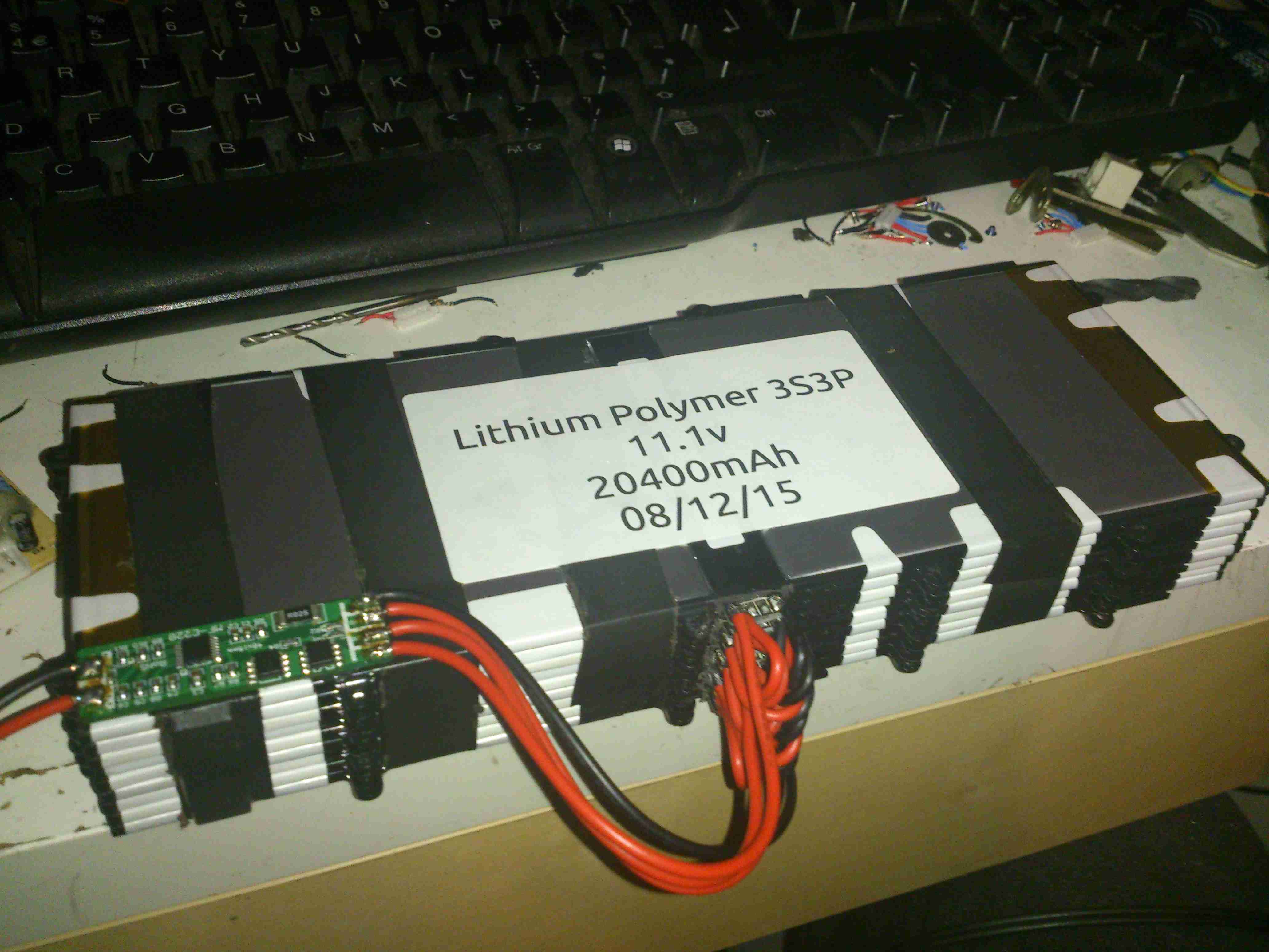
In the past, I’ve used RC type LiPo packs for my mobile power requirements, but these tend to be a bit bulky, since they’re designed for very high discharge current capability – powering large motors in models is a heavy job.
I recently came across some Samsung Galaxy Tab 10.1 battery packs on eBay very cheaply, at £2.95 a piece. For this price I get 6800mAh of capacity at 4.2v, for my 12v requirements, 3 packs must be connected in series, for a total output of 12.6v fully charged.
For an initial pack, I got 9 of these units, to be connected in 3 sets of 3 to make 20Ah total capacity.There are no control electronics built into these batteries – it’s simply a pair of 3400mAh cells connected in parallel through internal polyfuses, and an ID EEPROM for the Tab to identify the battery.
This means I can just bring the cell connections together with the original PCB, without having to mess with the welded cell tabs.
Battery Pack
Here’s the pack with it’s cell connections finished & a lithium BCM connected. This chemistry requires close control of voltages to remain stable, and with a pack this large, a thermal runaway would be catastrophic.
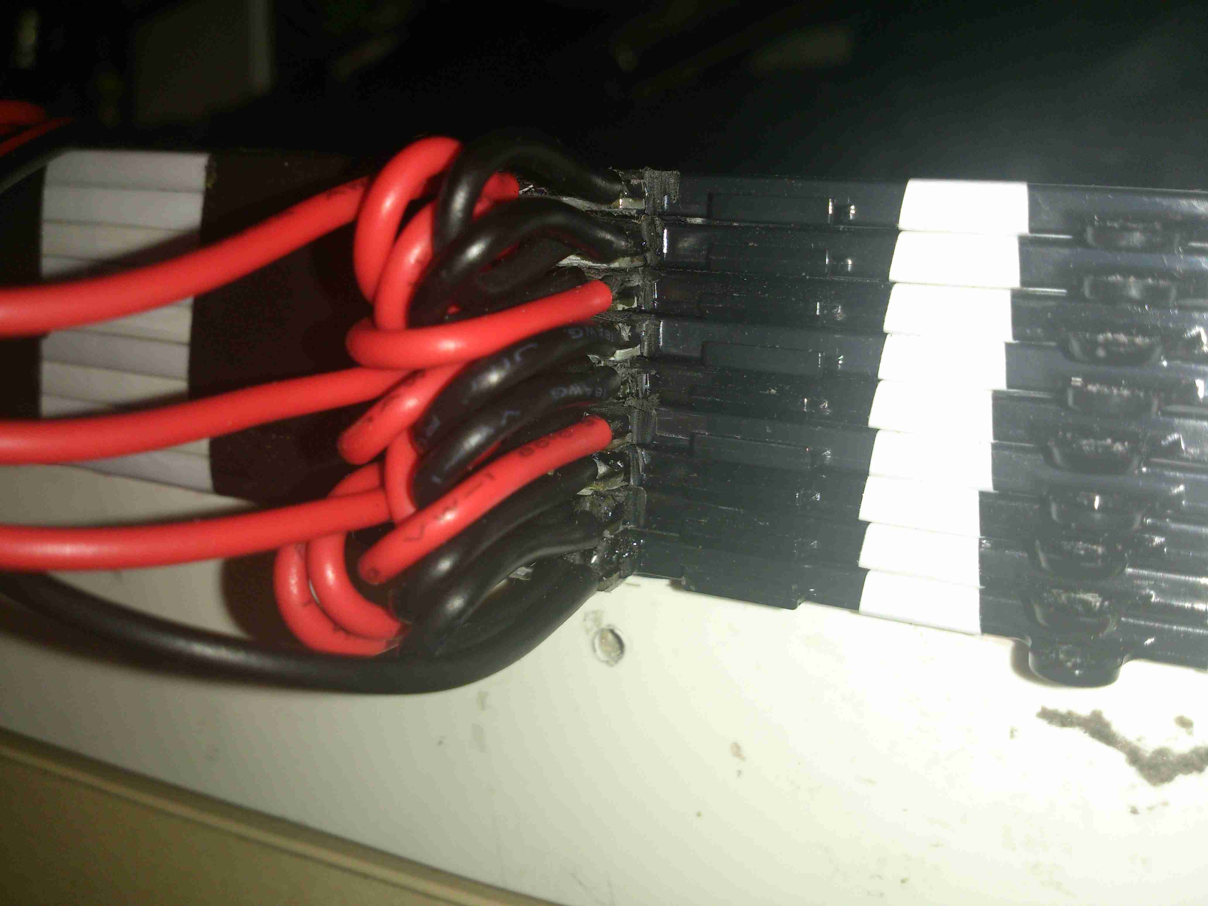
Cell Links
The OEM battery connector has been removed, and my series-parallel cell connections are soldered on, with extra lead-outs for balancing the pack. This was the most time-consuming part of the build.
If all goes well with the life of this pack for utility use, I’ll be building another 5 of these, for a total capacity of 120Ah. This will be extremely useful for portable use, as the weight is about half that of an equivalent lead-acid.
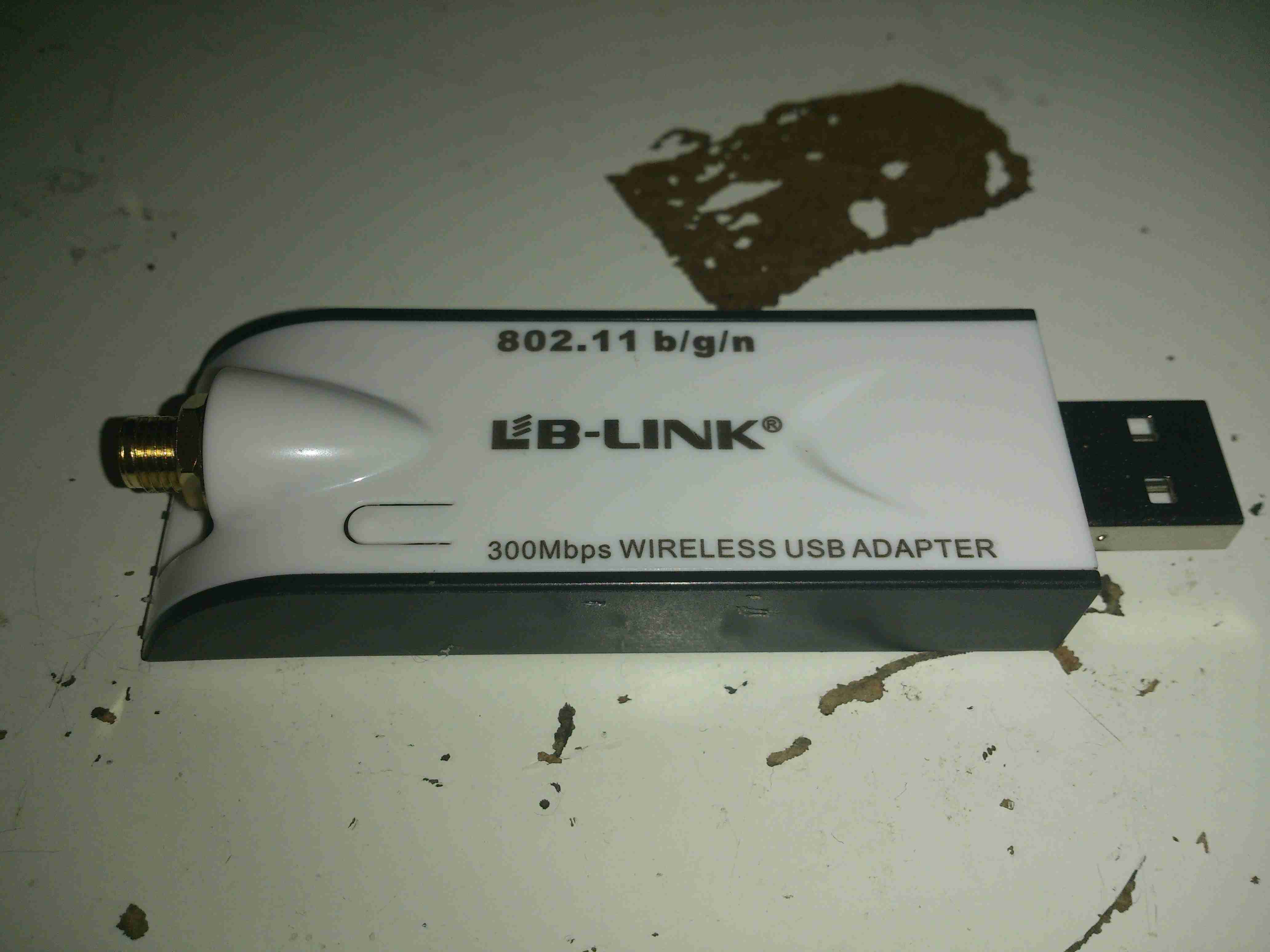
I needed a decent WiFi adaptor for my latest Pi LCD project, so after trawling eBay for cheapy USB adaptors, I found this one.
USB WiFi Dongle
Unlike most USB WiFi radios these days, it actually has a proper RP-SMA antenna connector, not the low-gain built in jobbies that never seem to work too well.
There are a few versions of this adaptor, all of which seem to use the same casing, there’s a button push cut into the plastic for a WPS button that doesn’t exist on this model. This is fine, as I don’t enable WPS on any of my network equipment anyway. (It’s insecure, and can be cracked in minutes).
MAC Address
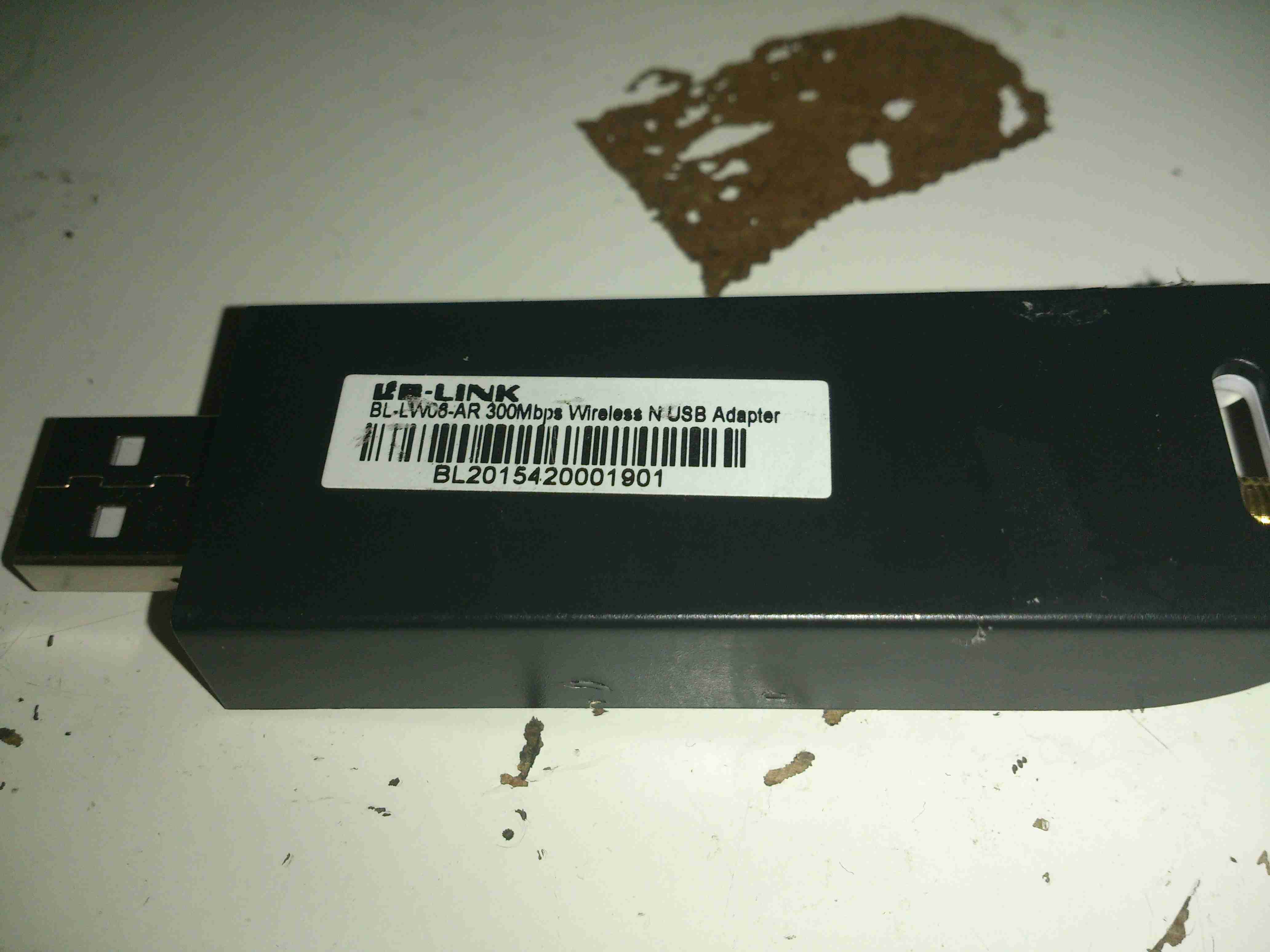
Here’s the rest of the essential details, the model is BL-LW08-AR, rated at 300Mbit/s.
PCB Reverse
Here’s the PCB removed from the casing, there are a pair of PCB antennas on here, but they’re not connected to the RF circuitry in this model, the links are missing.
Chipset
The chipset used is a Realtek RTL8191SU, there isn’t much more in this device, as it’s all built into the silicon.
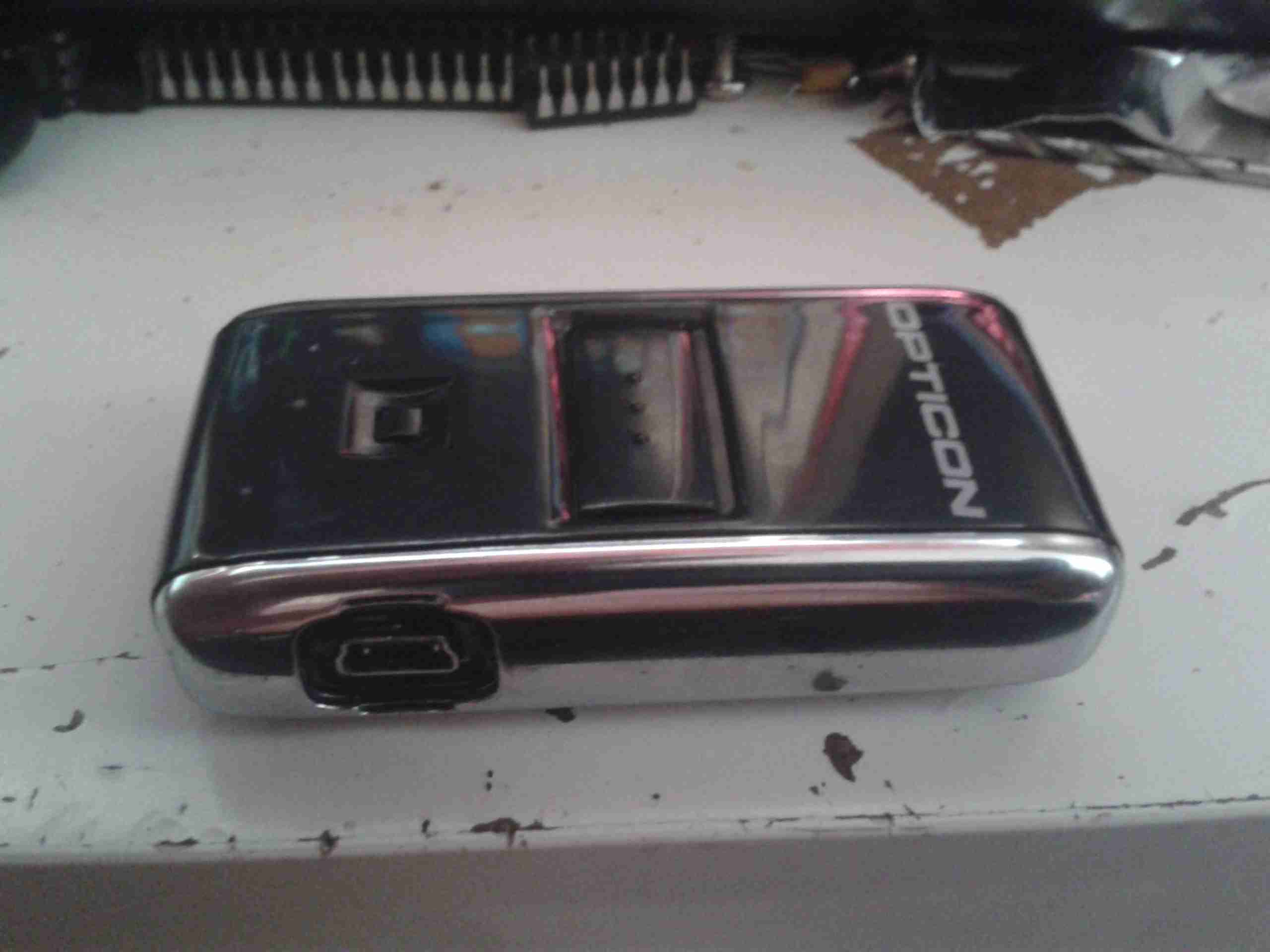
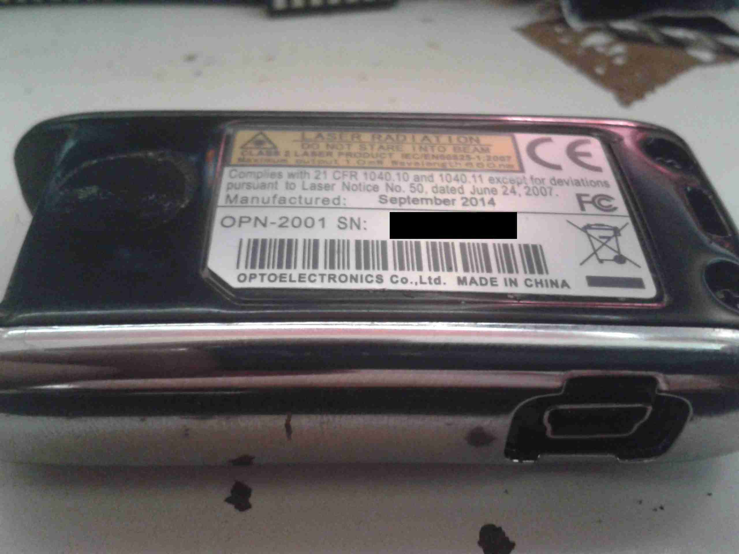
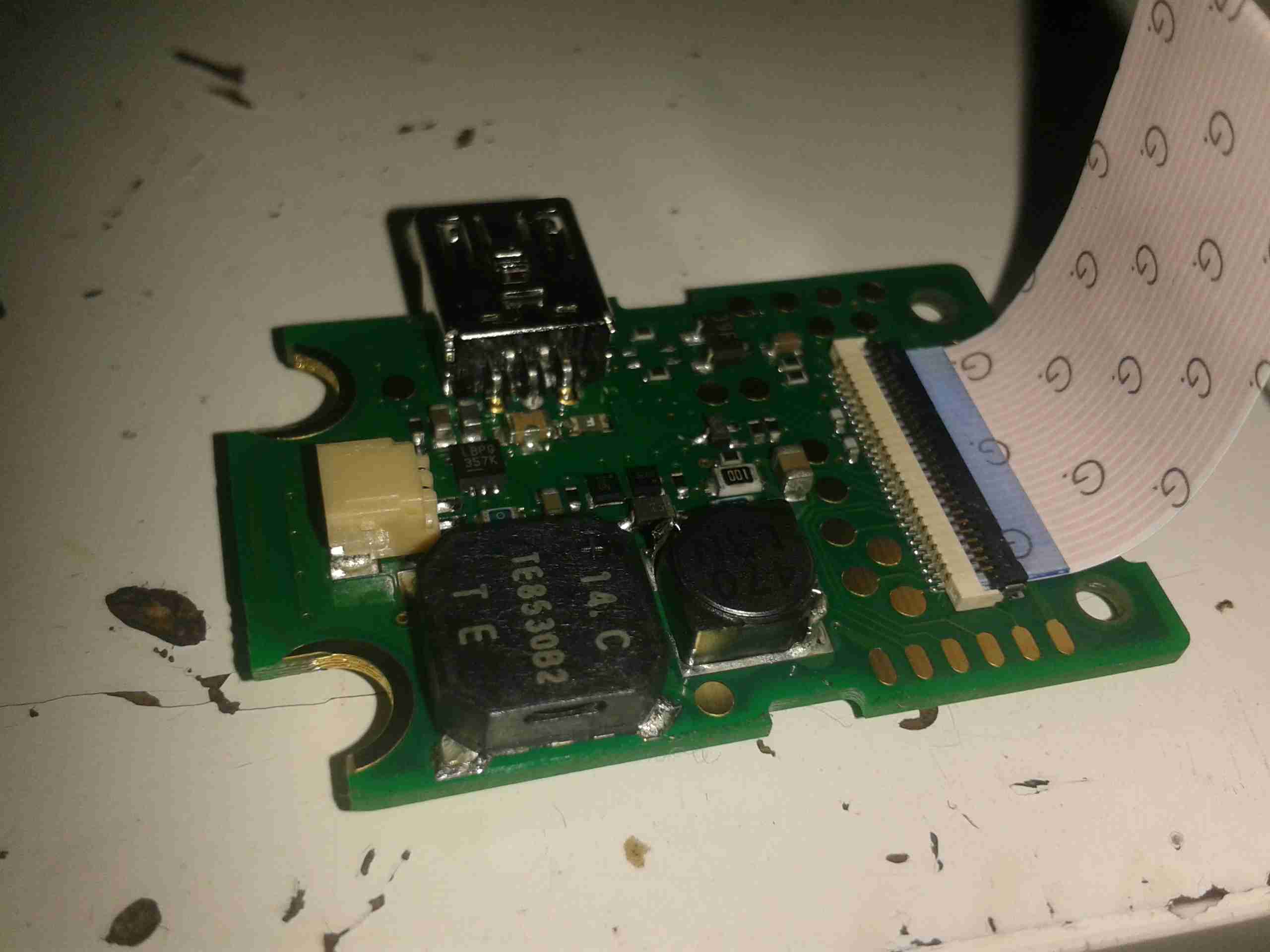
The OPN-2001 is a very small handheld barcode data collection device, used for stock keeping, inventory, etc.
It’s powered by an internal Li-Poly cell, at 150mAh, and has storage for 1000 barcodes in it’s internal memory.
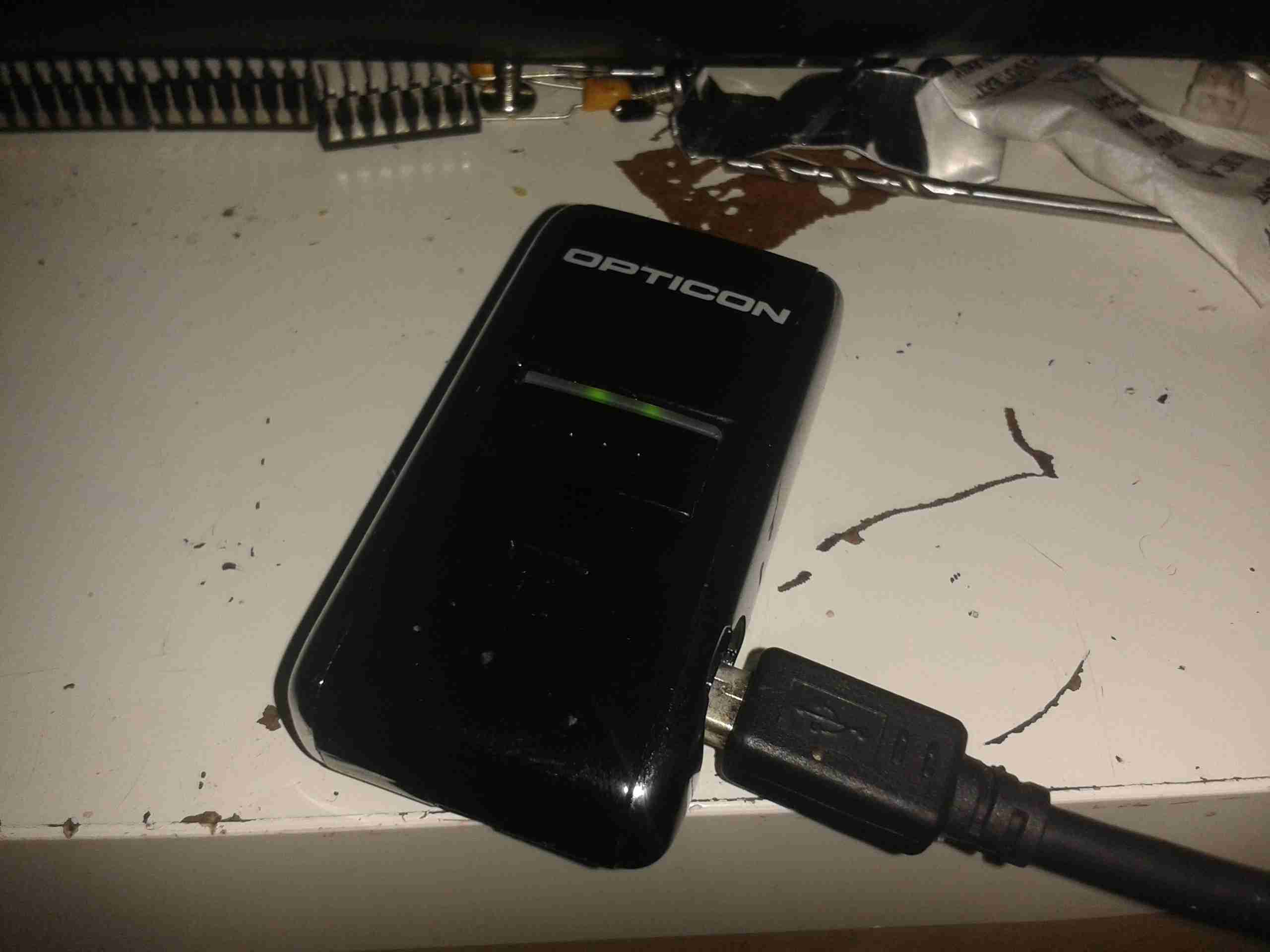
USB
The unit is charged via it’s USB port, the data can also be downloaded using this interface.
ID Label
Here’s the bottom of the unit with it’s label. Serial number removed to protect the guilty. 😉
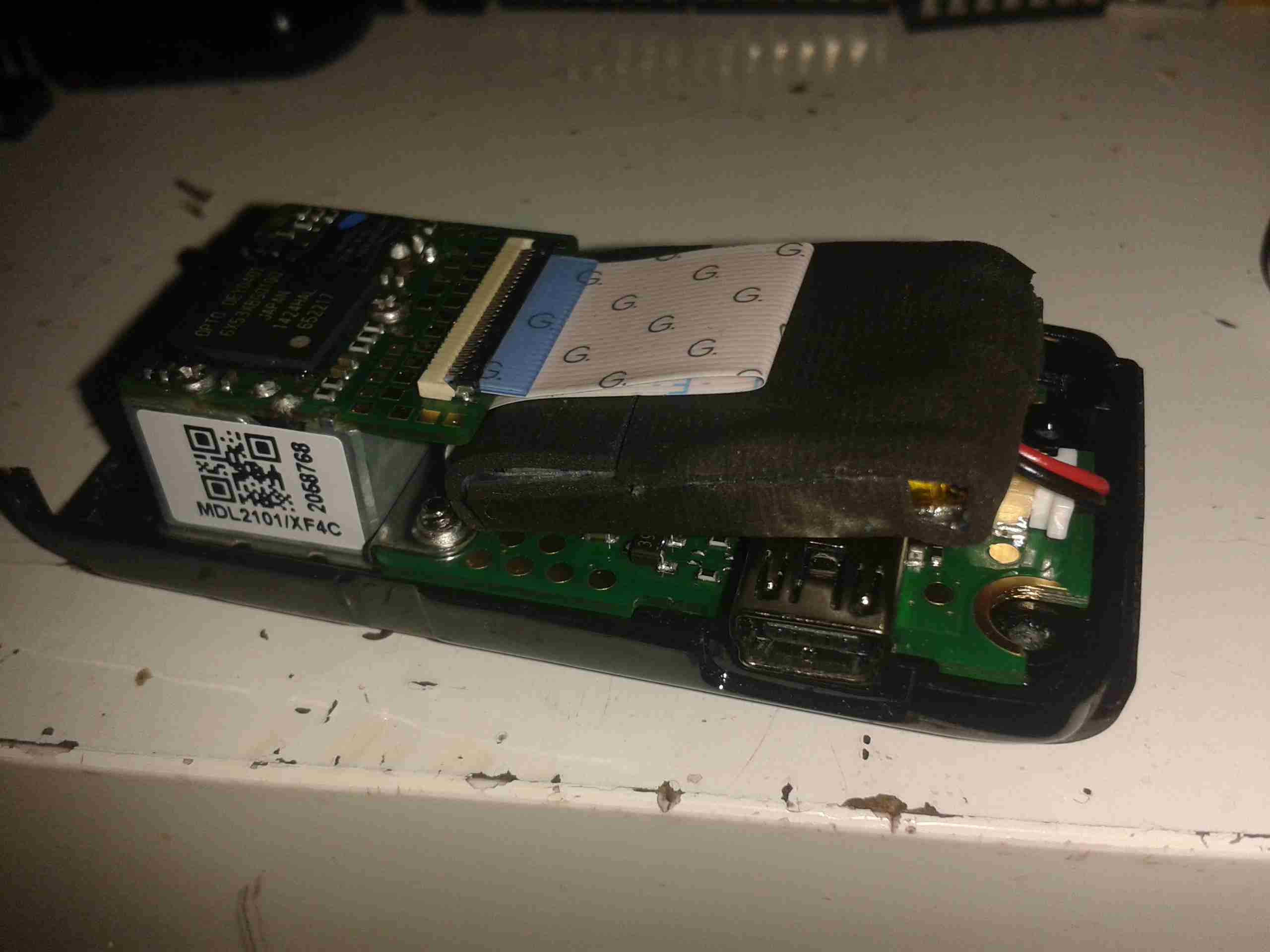
Cover Removed
Here the bottom cover has been removed from the scanner, showing the internals. The barcode engine is on the left, this contains all the hardware & logic for scanning & storing the barcode data. The Li-Poly cell is under the FFC cable wrapped in foam tape for protection.
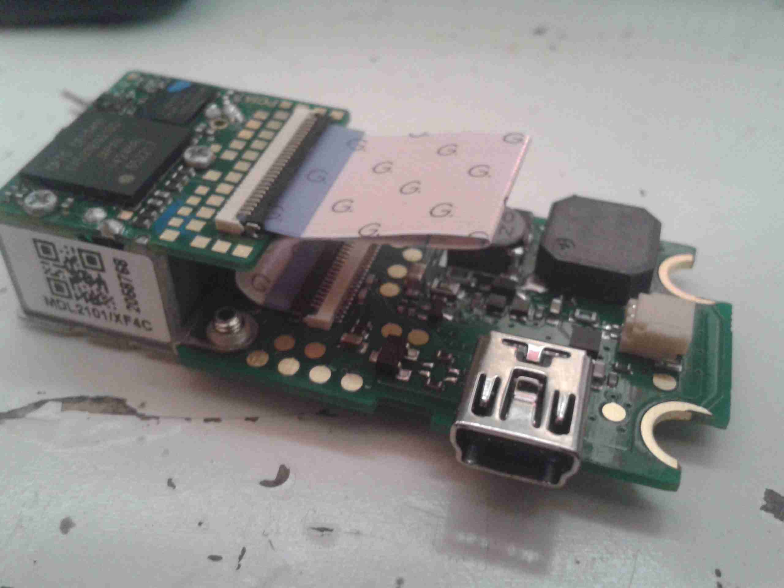
PCB Removed
Here’s the PCB & engine assembly removed from the casing. The lower PCB appears to just handle the user interface buttons, beeper & USB power & charging circuitry. All the processing logic is on the barcode engine itself.
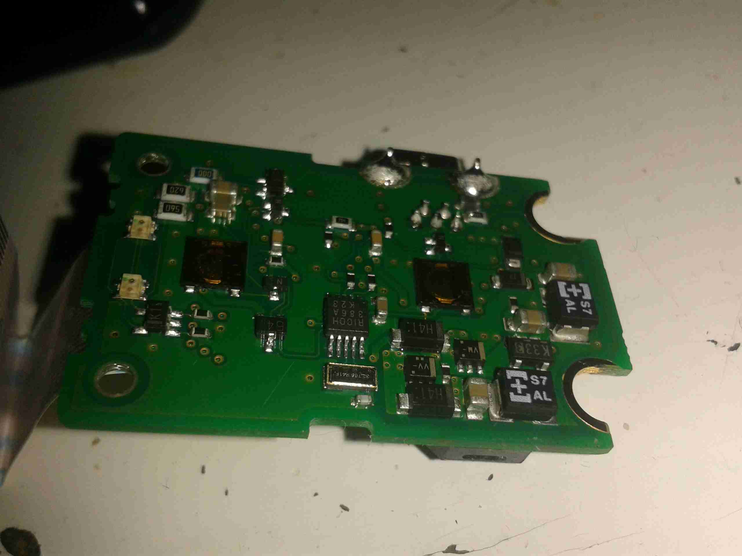
PCB Reverse
Here’s the back of the support PCB, with the pair of buttons for scanning & deleting barcodes. Also on this board is a 32kHz clock crystal & a Ricoh RV5C386A RTC IC. This communicates with the main processor via I²C for storing the date & time with the barcodes. At the bottom right corner are some of the power supply passives.
Support PCB
Here’s the other side of the support PCB, with the beeper, battery connector & the switching regulator to provide the barcode engine with 3.3v power.
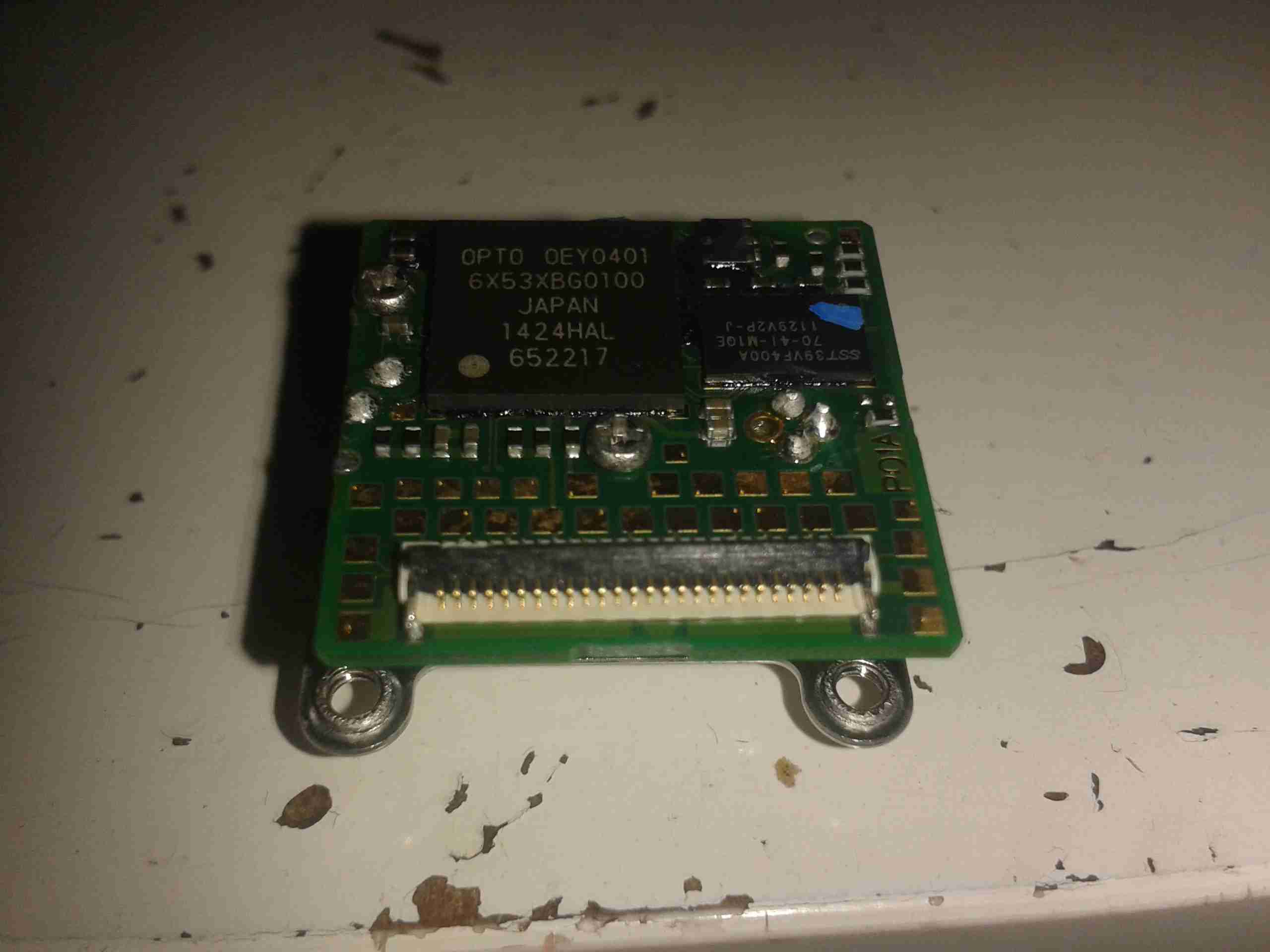
Barcode Engine
Here’s the barcode engine itself, which is absolutely tiny, at roughly 20mm square. The main processor & it’s associated Flash ROM are on this PCB. The main processor has an ARM7 32bit core, with 64kB of RAM, and onboard 512kB of ROM for program & barcode storage.
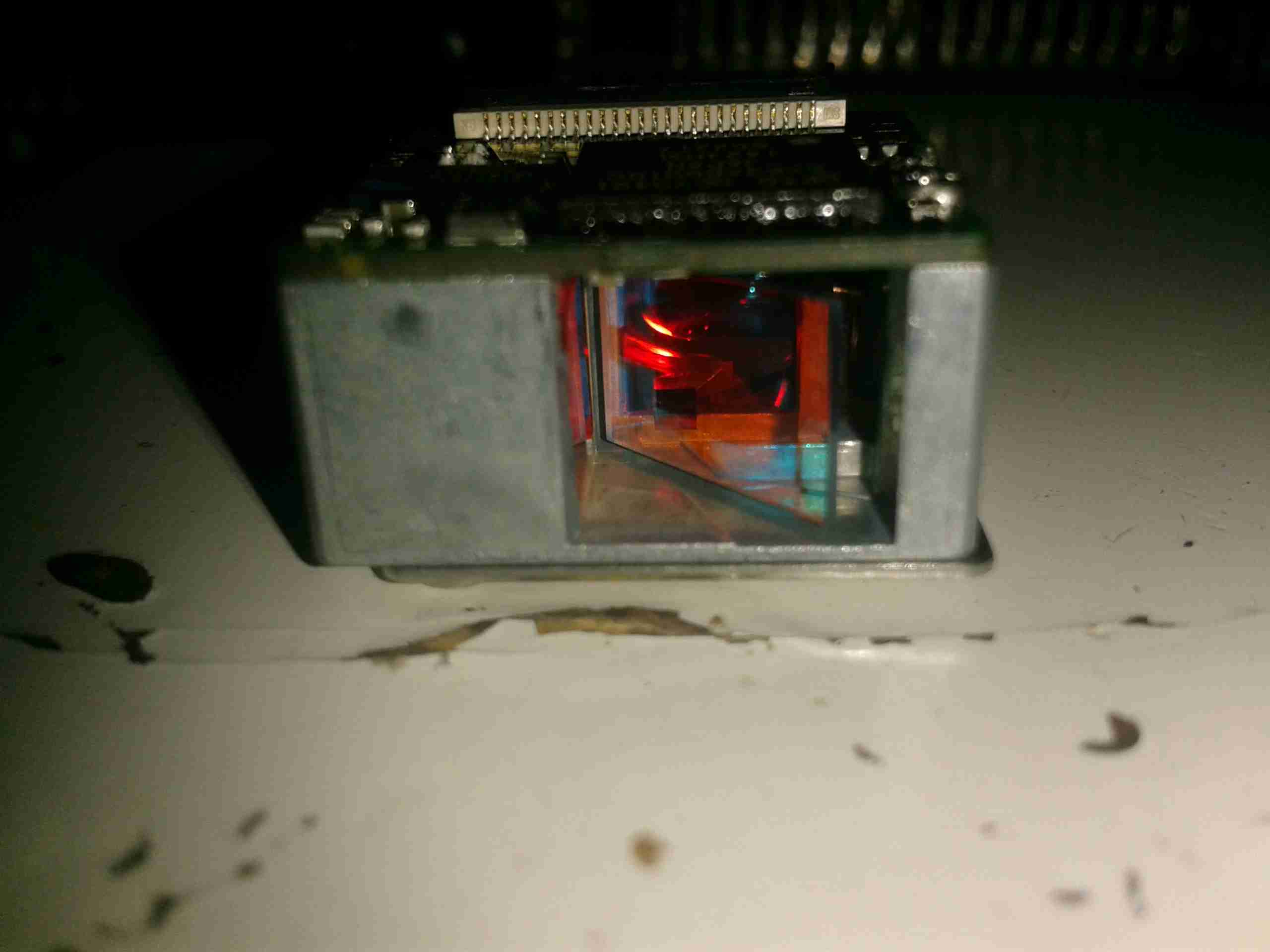
Mirror
Here’s the business end of the barcode engine, the mirror vibrates at 100Hz to produce the scan line. The laser diode is rated at 1mW, 650nm. This is in the deep red range.
As the crimp tool for the PSU connector in the Rigol scope is a very expensive piece of hardware, I decided to use pre-crimped terminals, from an ATX power connector. (They’re the same type).
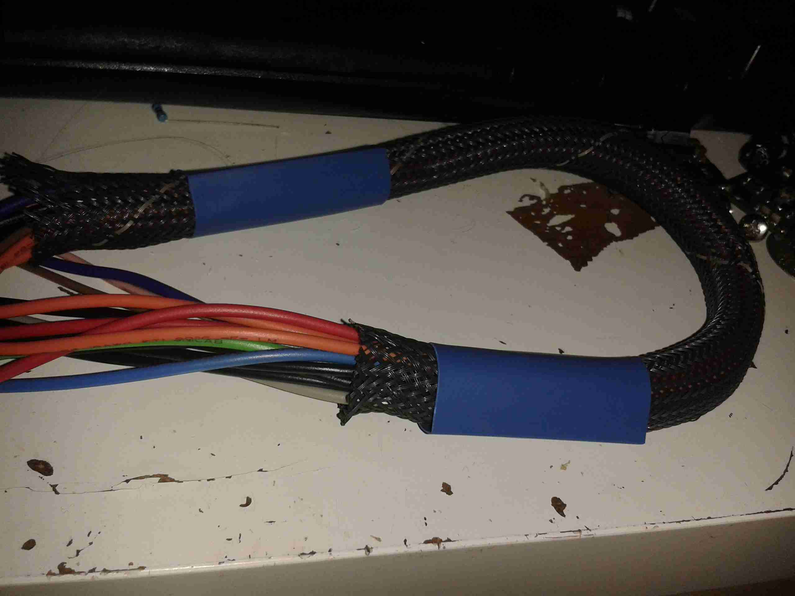
Wiring Loom
Here’s the partially completed loom, with the 13 cores for the power rails. The 14th pin is left out as that is for AC triggering, and this won’t be usable on a low voltage supply.
A couple of the pins have two wires, this is for voltage sensing at the connector to compensate for any voltage drop across the cable. The regulators I am using have provision for this feature.
Sleeving
To keep the wiring tidy, I dug a piece of braided loom sleeving out of the parts bin, this will be finished off with the heatshrink once the pins are inserted into the connector shell.
The remaining parts for the loom have been ordered from Farnell & I expect delivery tomorrow.
Since everything in my shack is run from 12v, I thought it would be handy to convert my new scope to 12v as well, as 99% of the places I find myself needing test gear are off grid, with no access to mains supplies.
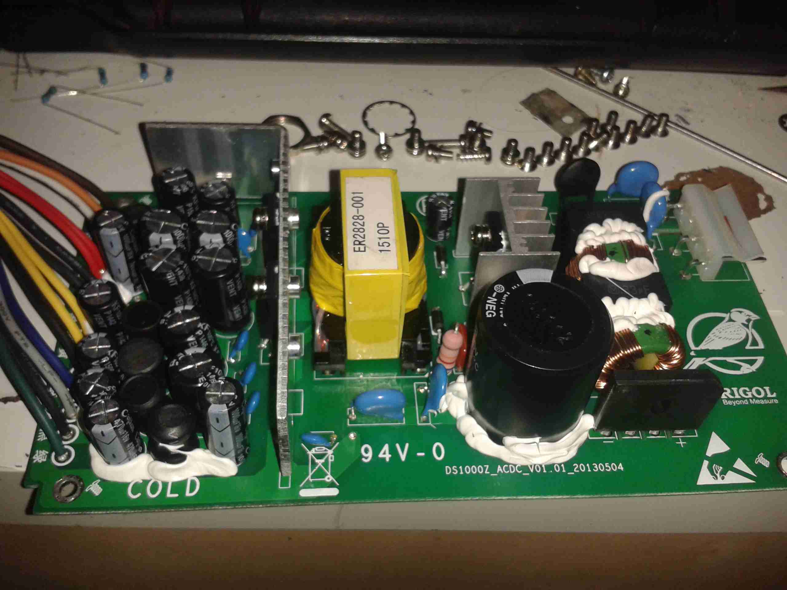
Mains PSU
Here’s the factory mains SMPS unit from the back of the scope. This is a nice multi-rail unit, with several different outputs, the table below details the wiring of the PSU.
Connector Pin
PCB Pin
Signal
Measured Voltage
Mainboard
Rectifier Rating
Wire Colour
5
1
AC_TRIG
N/A
AC_TRIG
N/A
BROWN
2
2
+9v_GND
N/A
FAN --
NA
ORANGE
11
3
+9V
10.16V
FAN +
2A
WHITE
6
4
+5V
5.1V
5V5A
20A
RED
13
5
+5V
5.1V
5V5A
20A
RED
7
6
GND
N/A
GND
N/A
BLACK
8
7
GND
N/A
GND
N/A
BLACK
3
8
+7.5V
6.9V
6.3V
20A
YELLOW
10
9
+7.5V
6.9V
6.3V
20A
YELLOW
1
10
GND
N/A
GND
N/A
BLACK
12
11
17.5V
17.51V
17.5V
2A
BLUE
9
12
-17.5V
-17.36V
-17.5V
2A
GREY
14
13
GND
N/A
GND
N/A
BLACK
4
14
-7.5V
-6.84V
-7.5V
2A
GREEN
The only feature I will lose if I make this switch is AC line triggering, but I never use that anyway, so it’s not a big issue for me.
Since I have been able to locate the connector, the plan is to design a replacement low voltage supply unit for the scope, with the same footprint as the original AC mains supply. This will allow me to do a direct swap without causing any damage or modifying the original supply.
This method will allow me to swap the 240v supply back into the scope if I ever come to need it.
I’m planning to use the LTC3863 DC-DC Controller from Linear Tech to generate the negative rails, this will go down to -150v on the output, so it’s pretty much perfect to generate them.
PSU Output Side
Here’s the output side of the mains PSU, it has a lot of filtering on the output rails, the two TO220 devices are the output rectifiers for the +5v & +7.5v rails, these are rated at 20A, 60V.
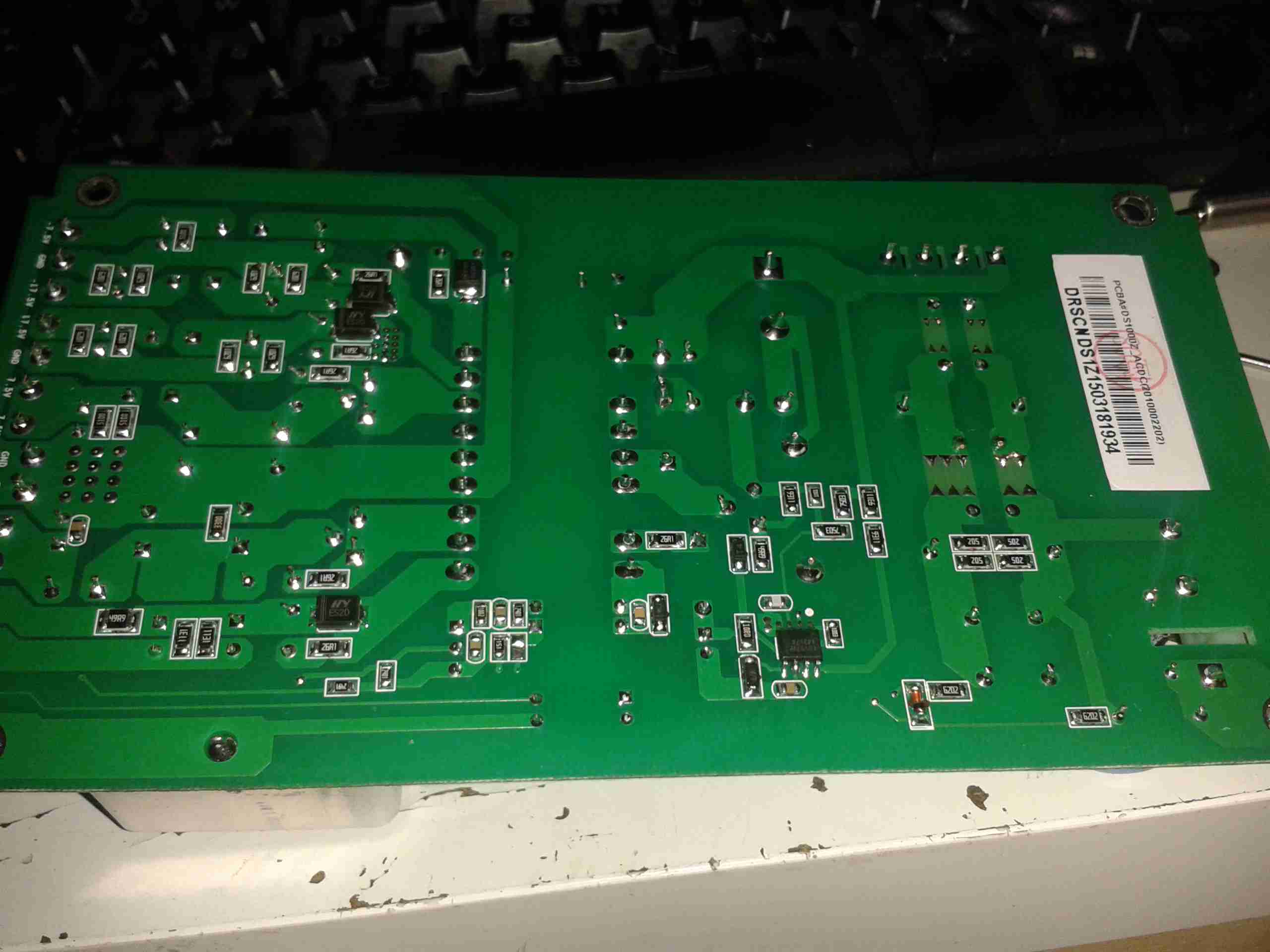
PCB Bottom
Here’s the bottom side of the PCB. It’s a really nicely designed PSU, massive isolation gap, spark gaps on the primary side & good filtering. The output side on the left has the rectifier diodes for the other voltage rails, these are only 2A rated, so designing the inverting supply to generate the negative rails will be pretty easy.
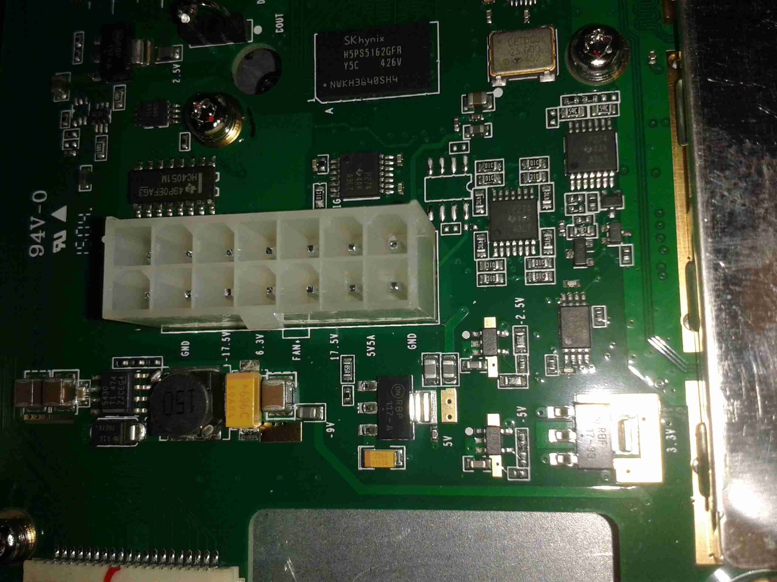
From looking at the PCB markings on both the mainboard & the PSU, the +9v rail seems to be used to drive the fan, both silkscreen markings indicate this.
The voltages marked on the PSU & the mainboard connector don’t quite match up though, there’s a small variation in the stated voltage between the two. This is most likely because all of the regulation of the supplies seems to be done on the mainboard, there are several linear regulators, and a few DC-DC switchers. Providing that the replacement supply isn’t noisy it should work fine.
This is backed up by the fact that the mains PSU only seems to regulate the +5v rail – on measuring the rails that’s the only one that’s close to spec.
Mainboard Power
Here’s the mainboard power connector, with it’s silkscreen labelling on the pins. (Very useful). As can be seen here, there’s at least 5 regulators, of both switching & linear types here, generating both positive & negative rails.
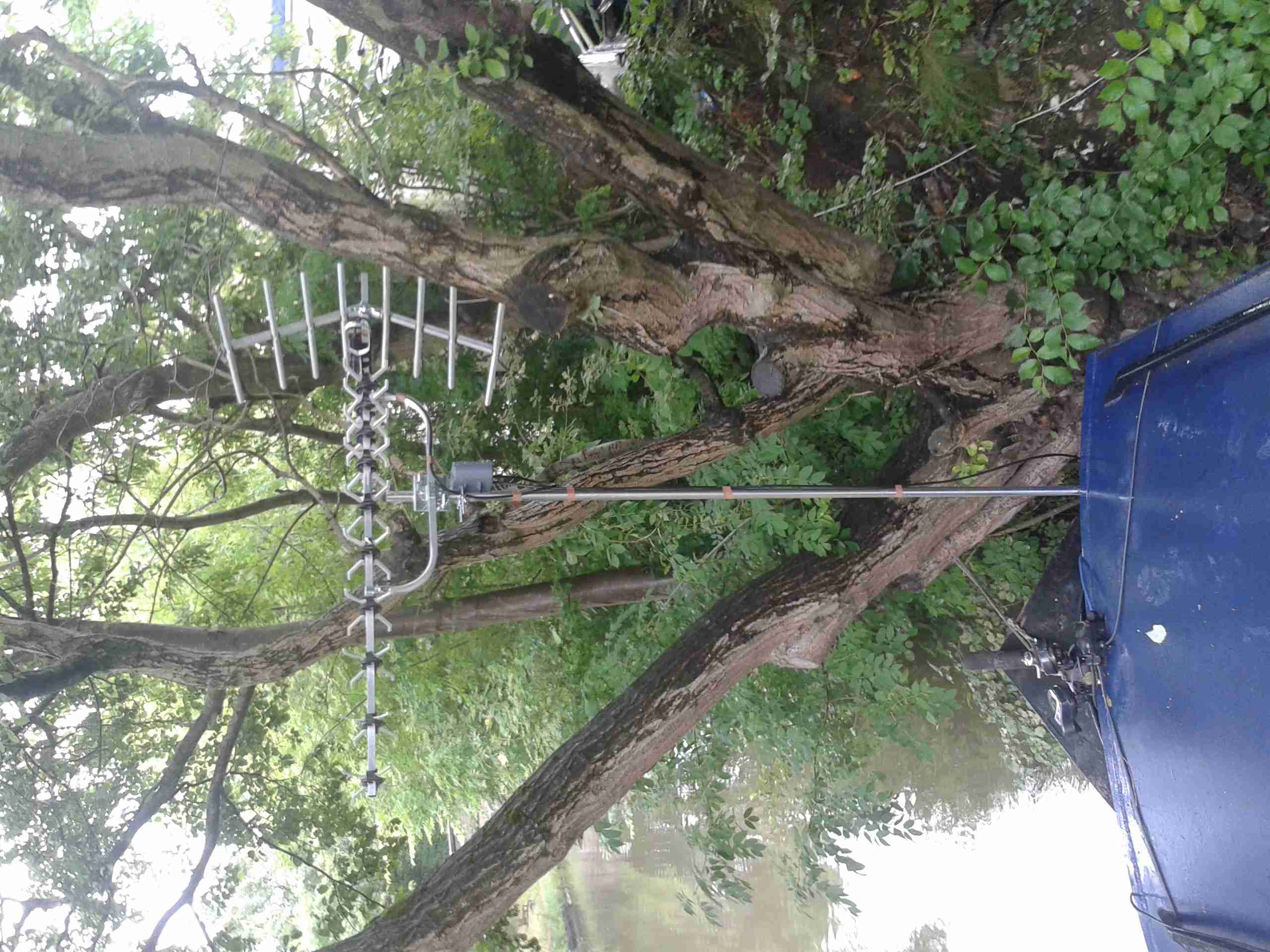
Here’s the final instalment of the new high gain TV antenna & it’s masthead amplifier.
High Gain Antenna
Here’s the new antenna on it’s removable mast. This apparently will give 13db of gain over the old antenna. The masthead amplifier box is mounted just below.
Amplifier
Here’s the amplifier just below the antenna. I do hope the seals on this hold against the weather! The amplifier inside isn’t protected at all.
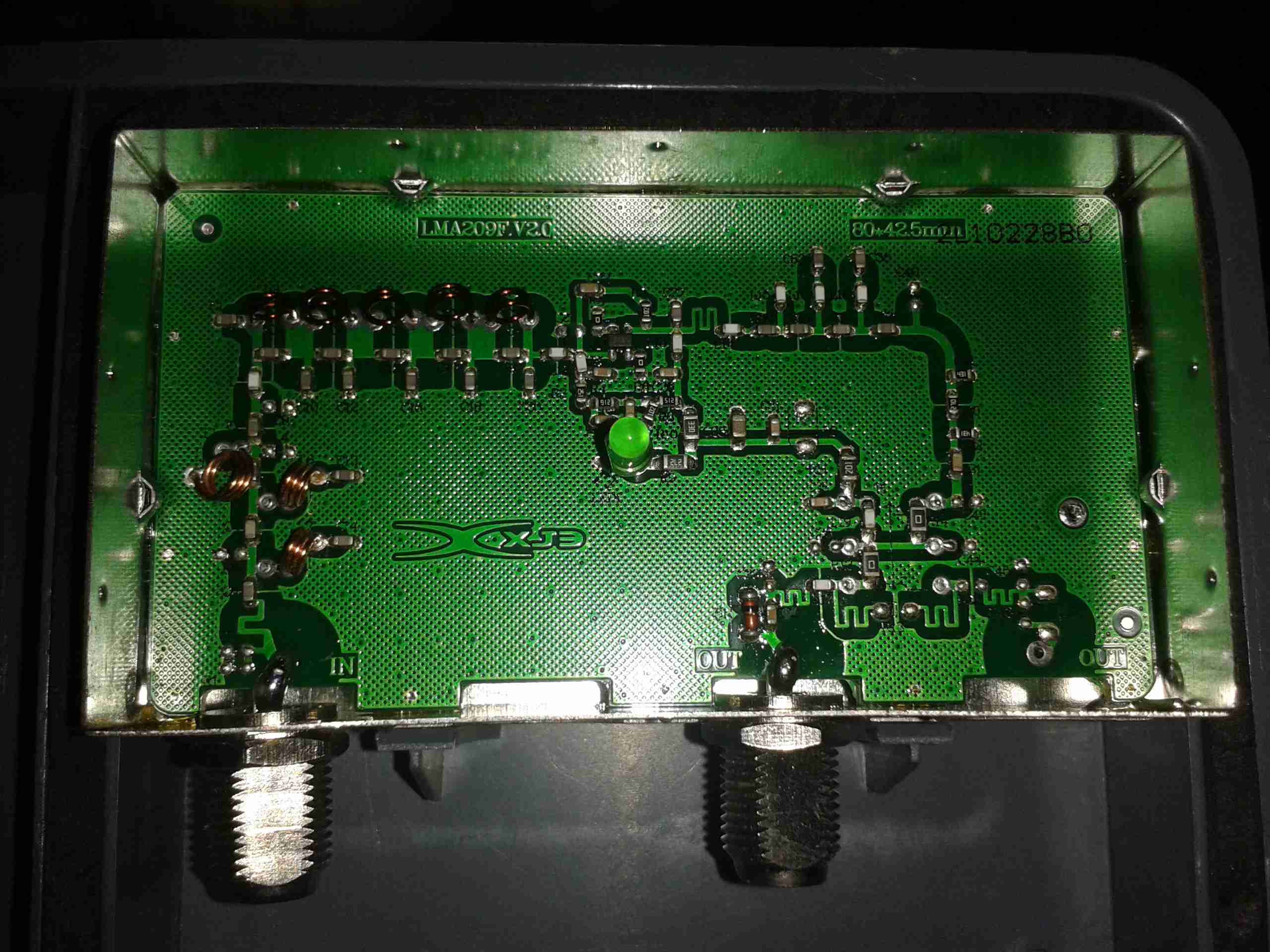
Amplifier Module
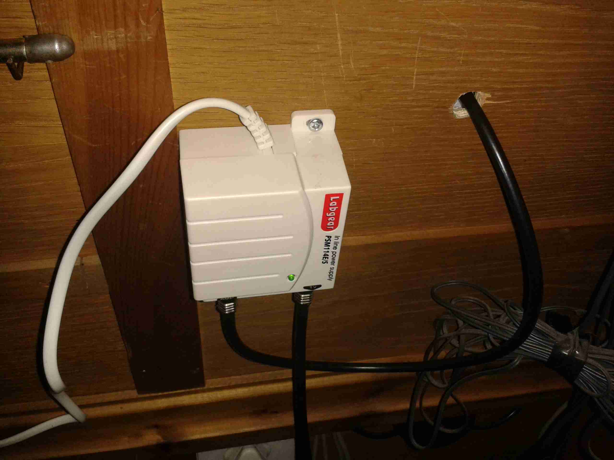
Here’s the module itself. This is powered by +12v injected into the coax with the power supply I previously modified. F-type connectors are used. (I don’t like these connector types, their lack of a true centre pin is poor design in my opinion).
Here’s the power supply, mounted behind the TV where the cable comes through the hull.
PSUAmplifier PCB
Here’s the inside of the amplifier module. It’s very simple, with some input filtering to block out 4G mobile signals, and a single amplifier transistor.
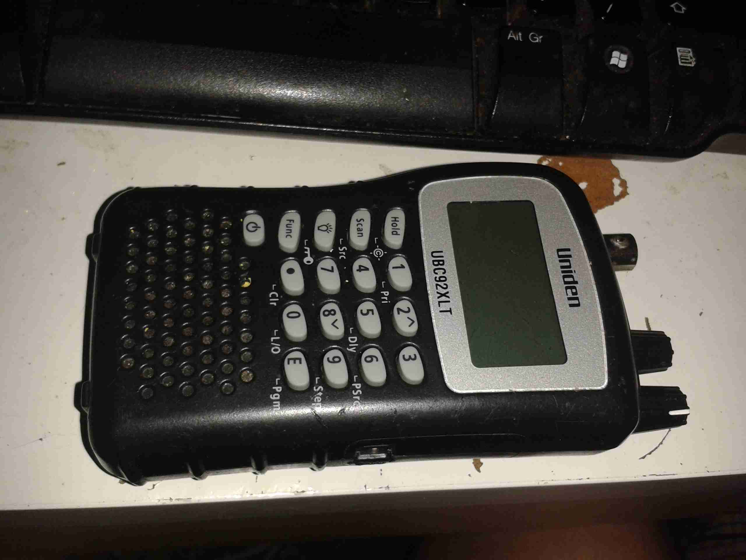
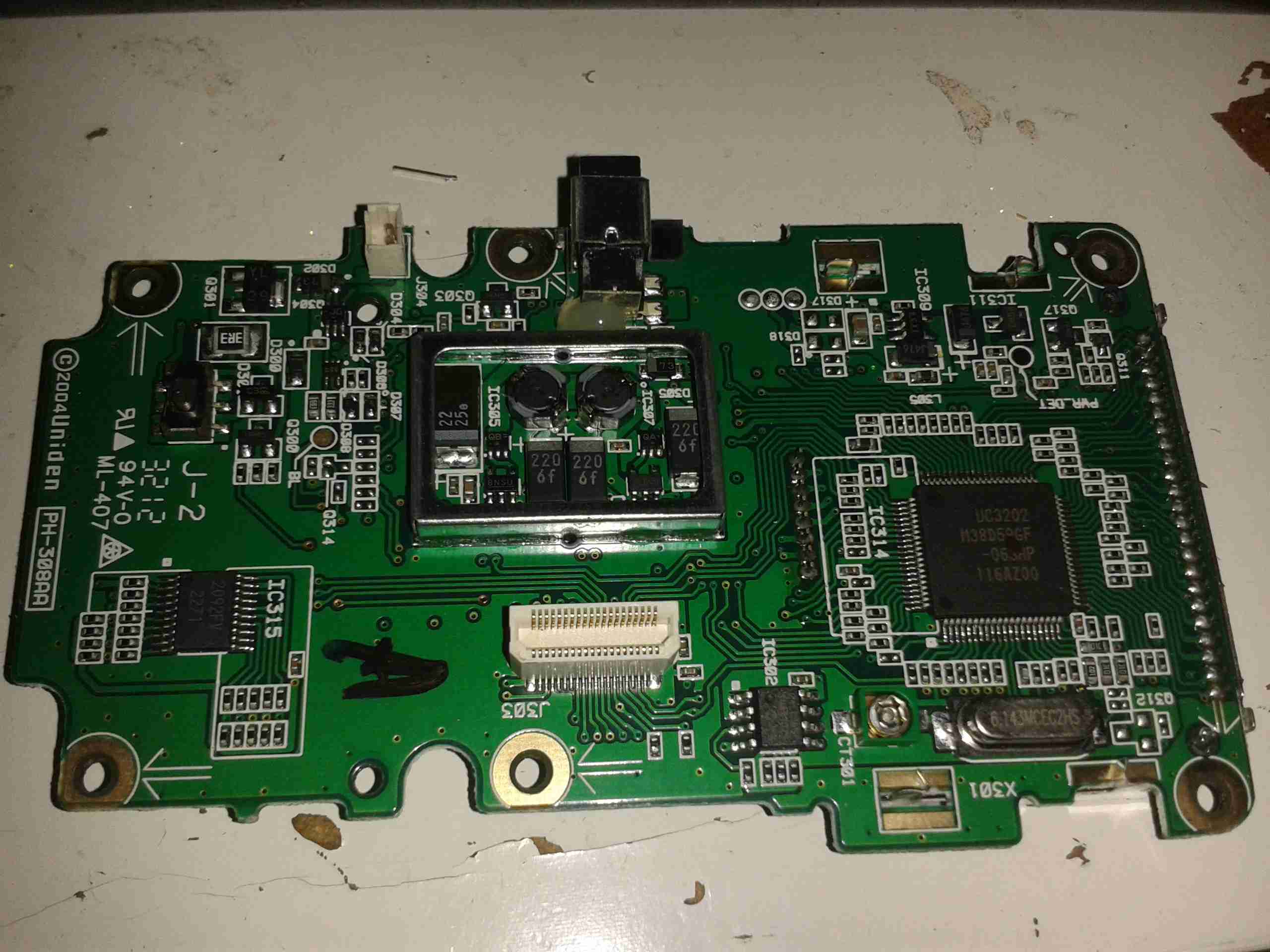
One bit of my equipment that I’ve never looked into is my scanner, a handheld Uniden unit. I got this when Maplin Electronics had them on special offer a few years ago.
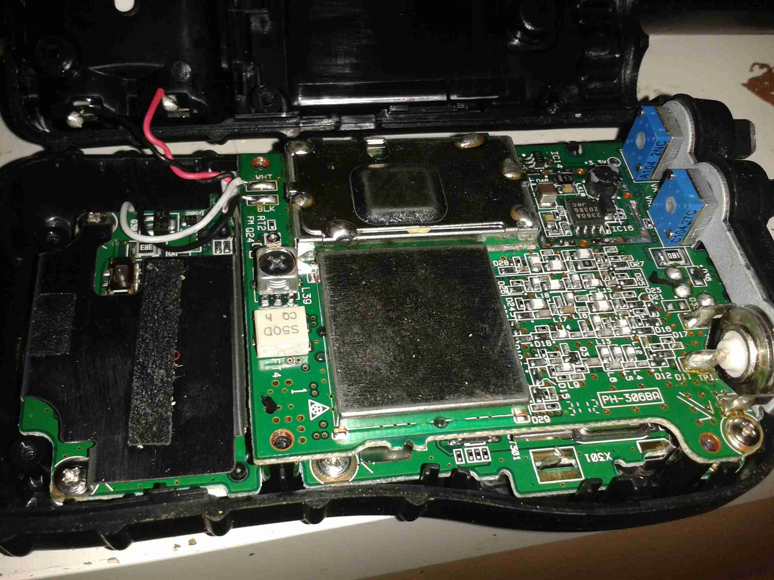
Uniden Scanner
Here’s the scanner itself, roughly the same size as a usual HT.
Back Cover Removed
Here the back cover has been removed, and the main RF board is visible at the top of the stack. Unfortunately the shielding cans are soldered on this unit, so no looking under there 🙁
On the right hand side of the board next to the antenna input is the main RF filter network, and it’s associated switching. The RF front end is under the shield closest to the front edge.
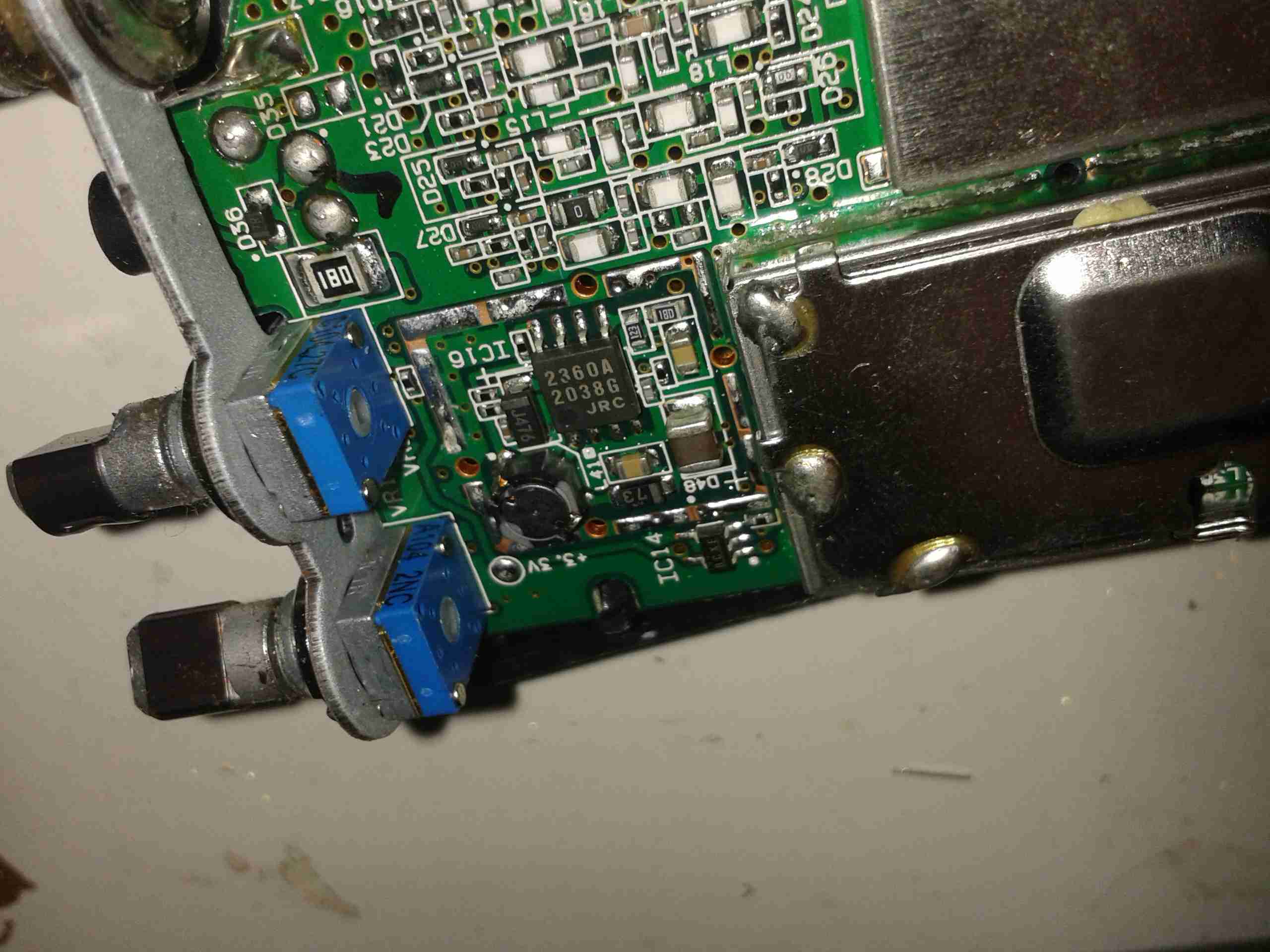
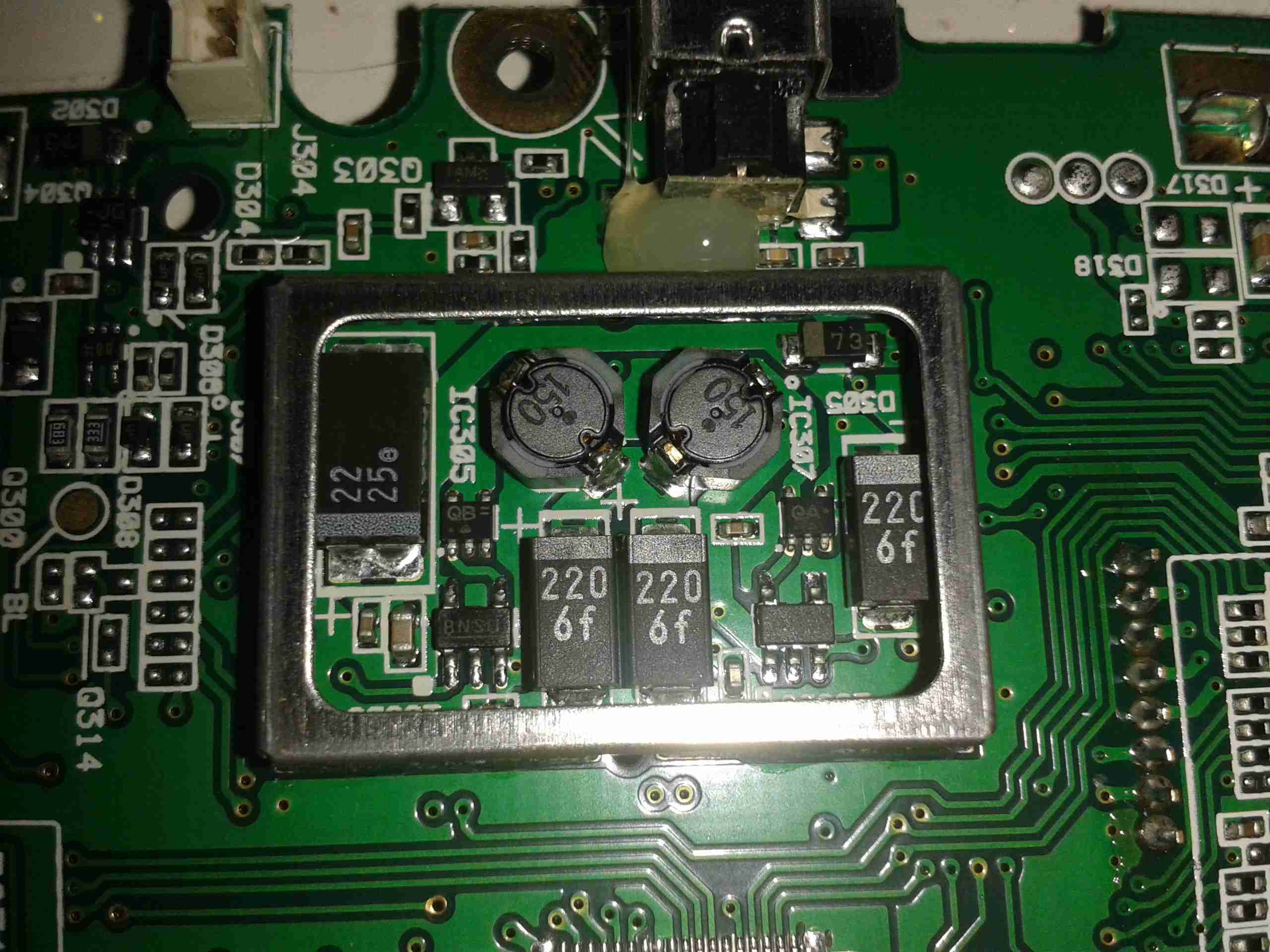
Controls & 3.3v Regulator
On the other side of the PCB is the Volume & Squelch potentiometers, along with a dedicated 3.3v switching supply. An NJM2360A High Precision DC/DC converter IC controls this one. A 3.3v test point is visible next to the regulator.
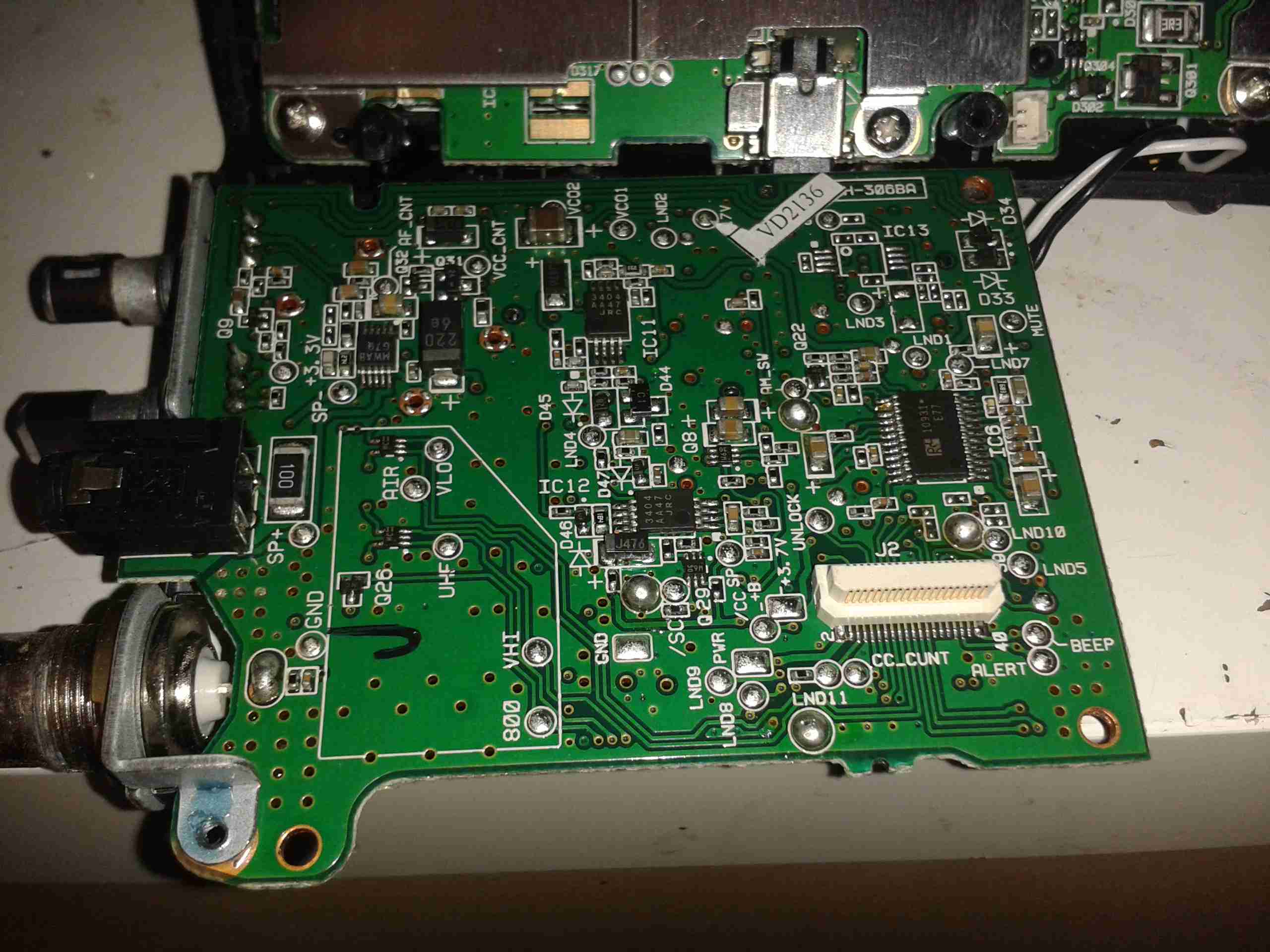
RF Board Reverse
Here’s the backside of the RF board, some more interesting parts here. There’s a pair of NJM3404A Single Supply Dual Op-Amp ICs, and a TK10931V Dual AM/FM IF Discriminator IC. This is the one that does all the back-end radio functionality. The audio amplifier for the internal speaker & external headphone jack is also on this PCB, top left. A board-to-board interconnect links this radio board with the main control board underneath.
Control PCB Front
Here’s the front of the control PCB, nothing much to see here, just the LCD & membrane keypad contacts.
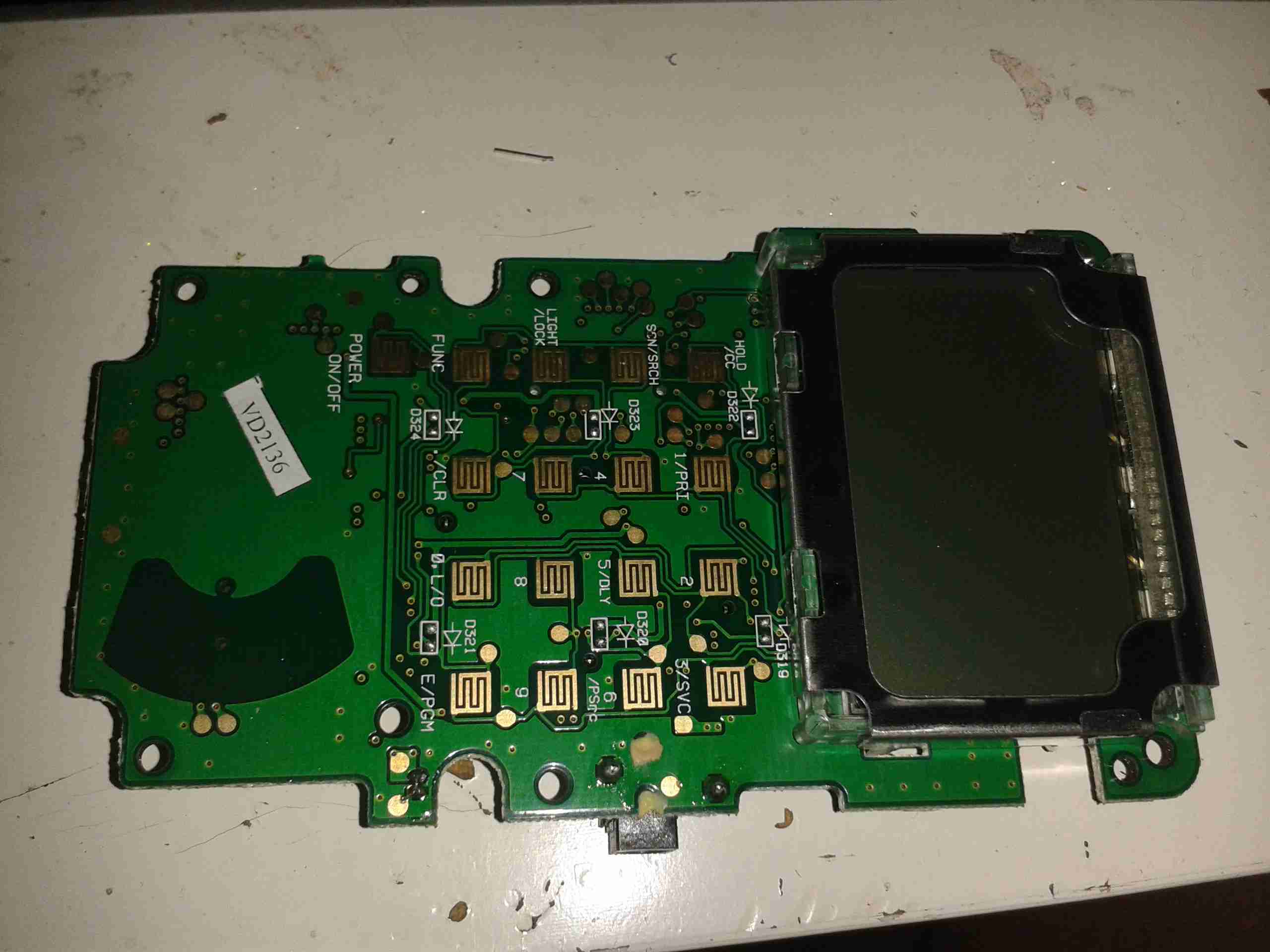
Control PCB Reverse
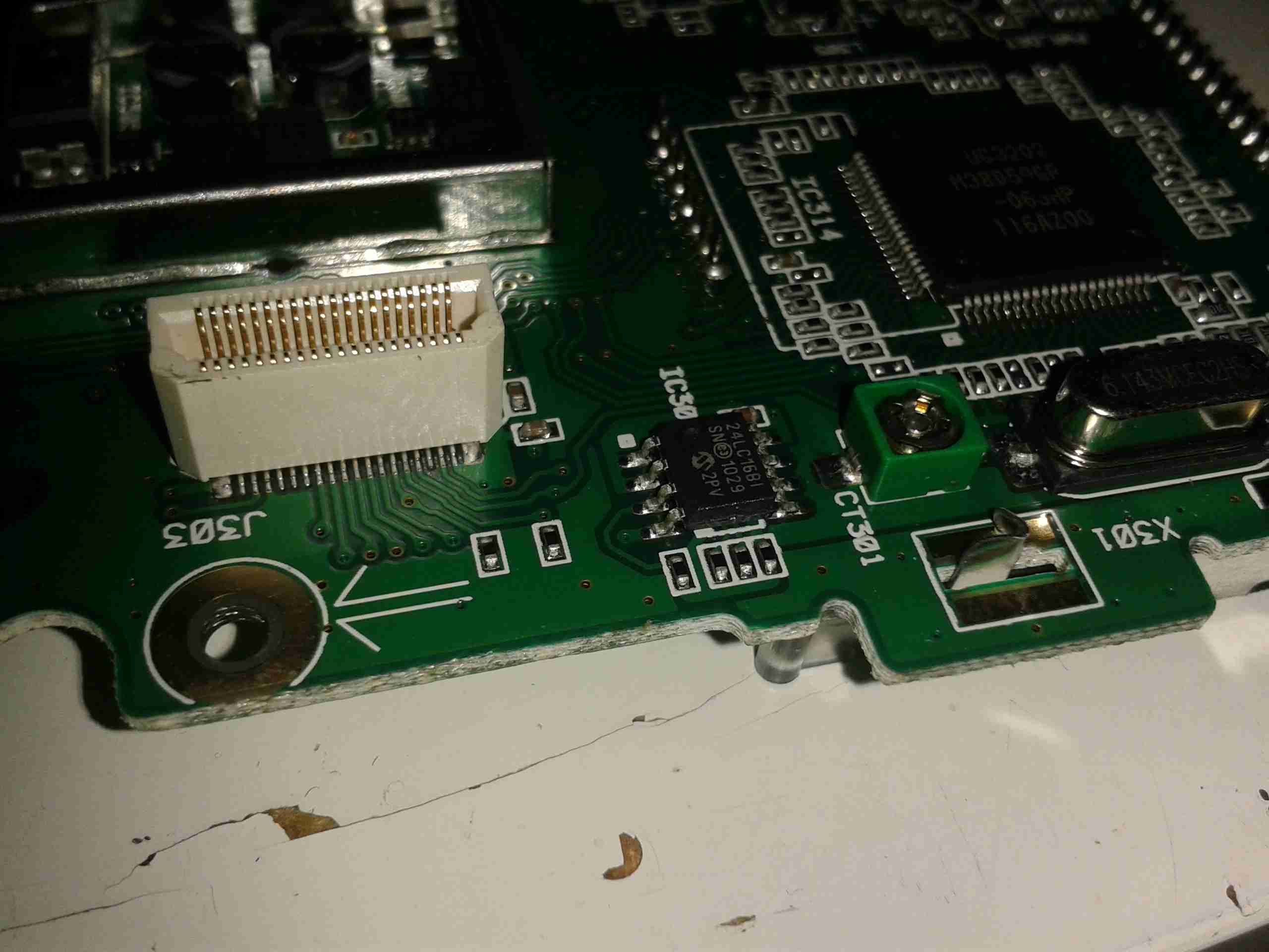
And here’s the reverse side of the control board. All the interesting bits are here. The main microcontroller is on the right, a Renesas M38D59GF, a fairly powerful MCU, with onboard LCD drive, A/D converter, serial interface, 60K of ROM & 2K of RAM. It’s 6.143MHz clock crystal is just below it.
The mating connector for the RF board is in the centre here.
There is also a Microchip 24LC168 16KB I²C EEPROM next to the main microcontroller. This is probably for storing user settings, frequencies, etc.
EEPROM
The rest of this board is dedicated to battery charging and power supply, in the centre is a dual switching controller, I can’t figure out the numbers on the tiny SOT23 components in here, but this is dealing with the DC 6v input & to the left of that is the circuitry for charging the NiMH cells included with the scanner.
PSU
The last bit of this PCB is a BU2092FV Serial In / Parallel Out 4 channel driver. Not sure what this one is doing, it might be doing some signal multiplexing for the RF board interface. Unfortunately the tracks from this IC are routed on the inner layers of the board so they can’t be traced out.
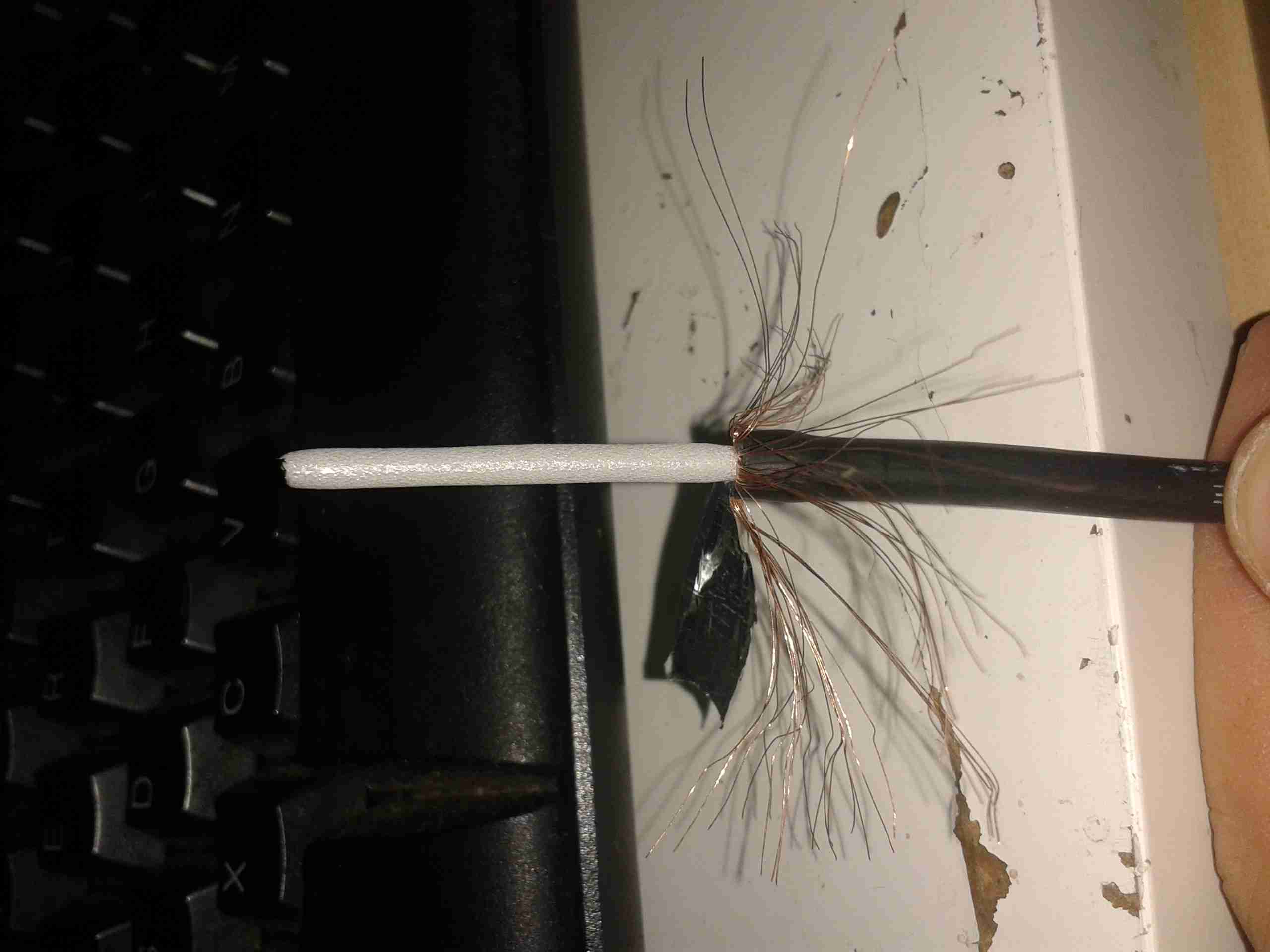
I thought I’d detail the process I use to fit an N-Type connector to a coax cable, as I don’t usually solder these connectors.
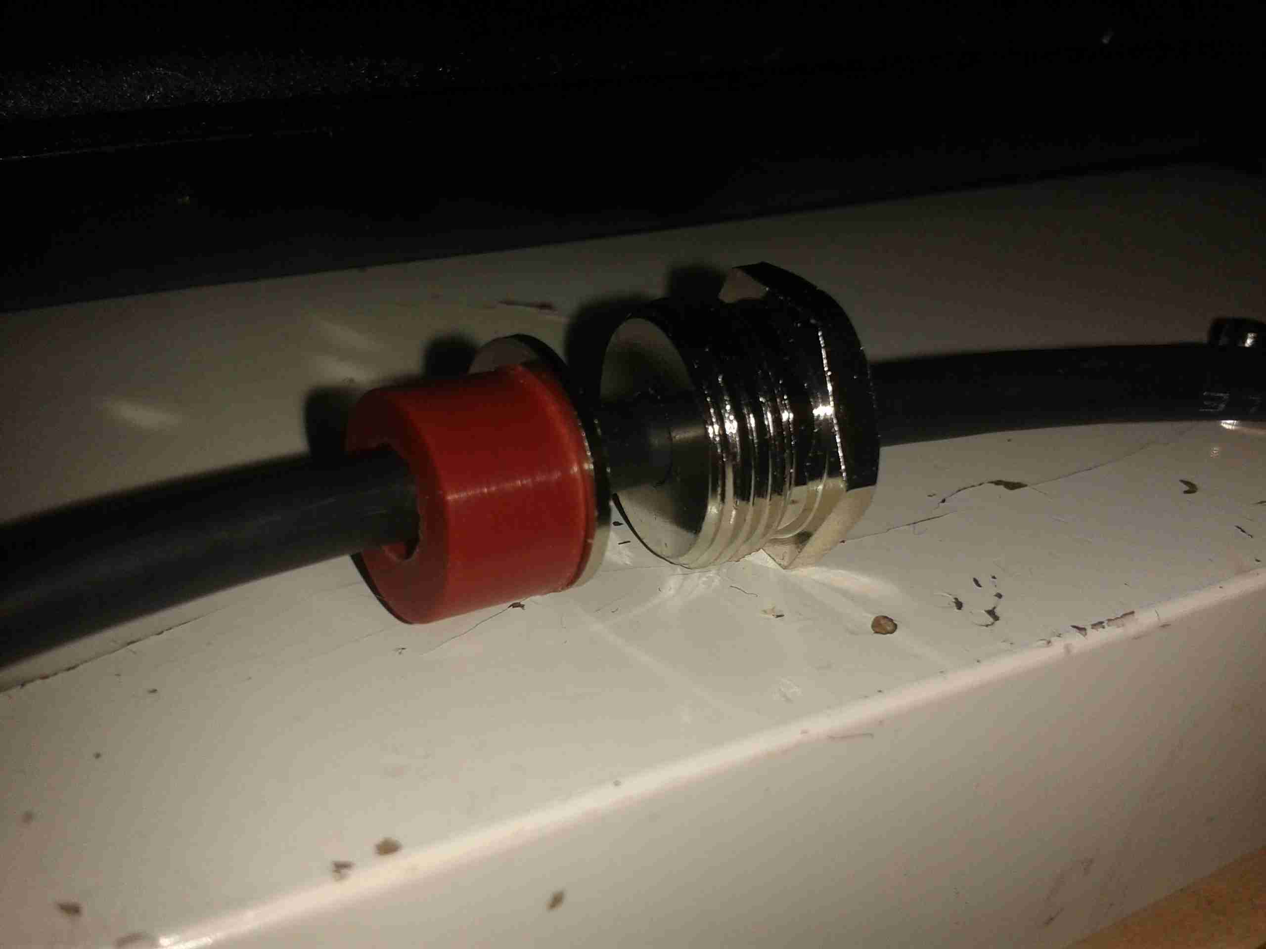
Backnut & Seal
Before stripping, fit the backnut, washer & rubber seal onto the cable.
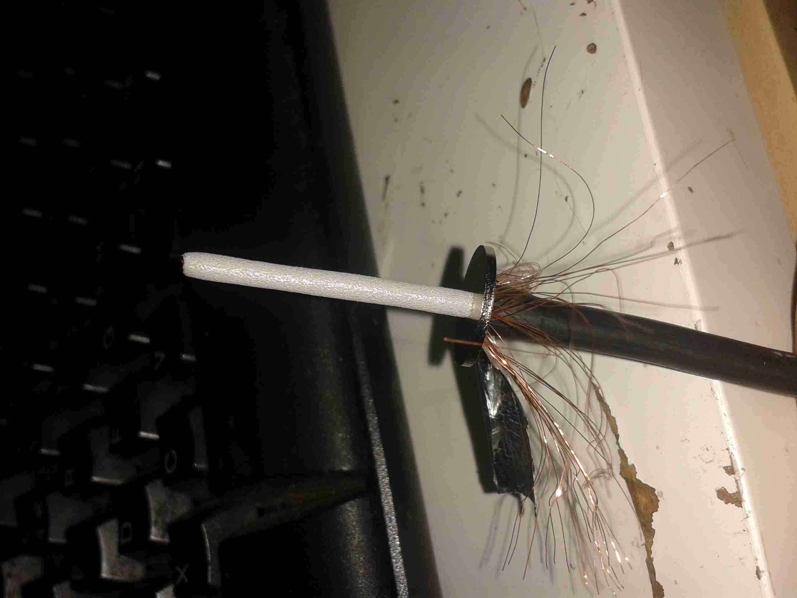
Stripped Coax
The cable is first stripped back to reveal the shield. This cable has a foil tape as well as the usual copper braid.
Shield Connection
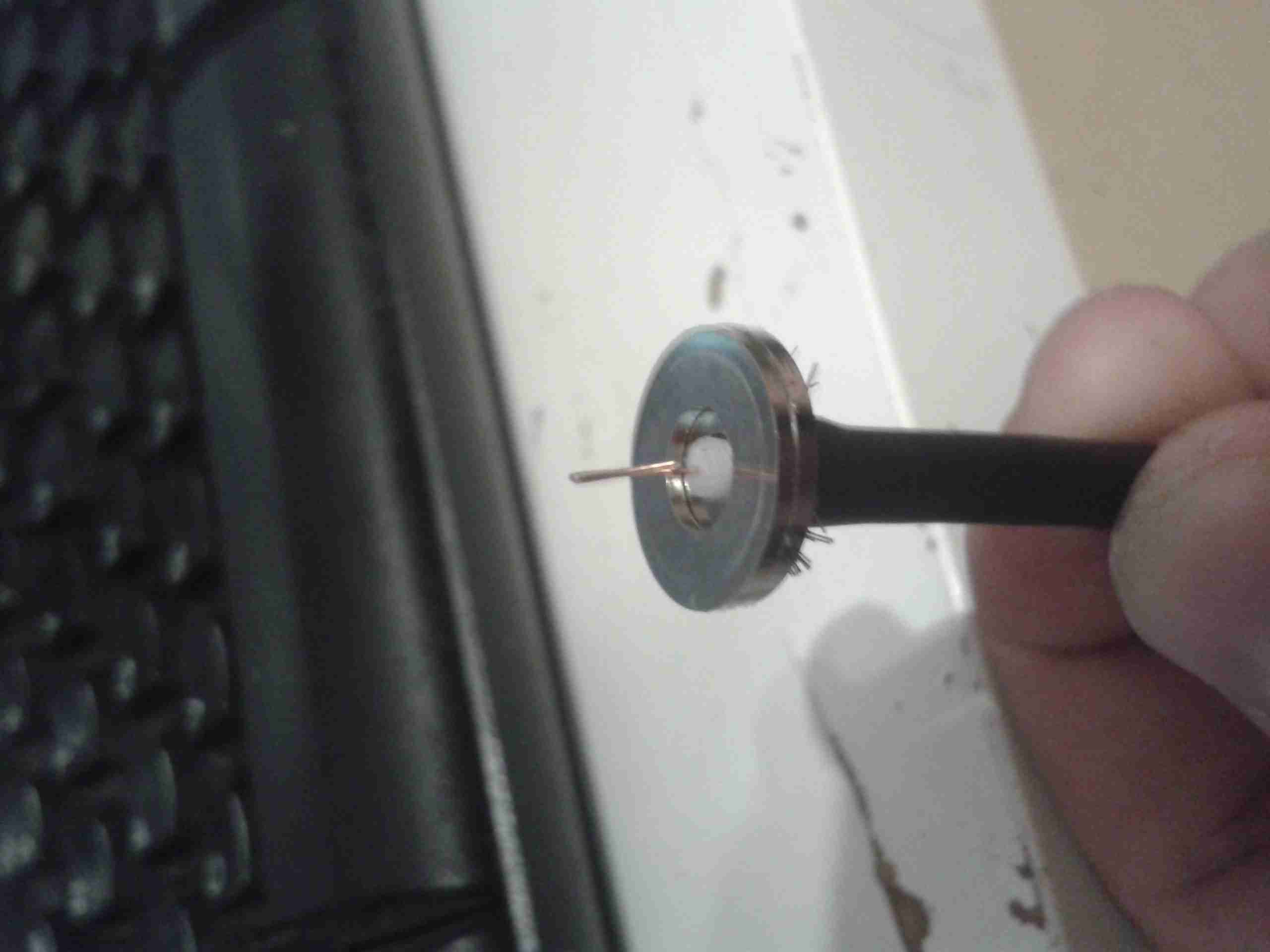
Once the inner core has been revealed, the shield washer is fitted. This has a knife edge on the inner diameter, to fit between the outer sheath & the shield, this makes the electrical connection.
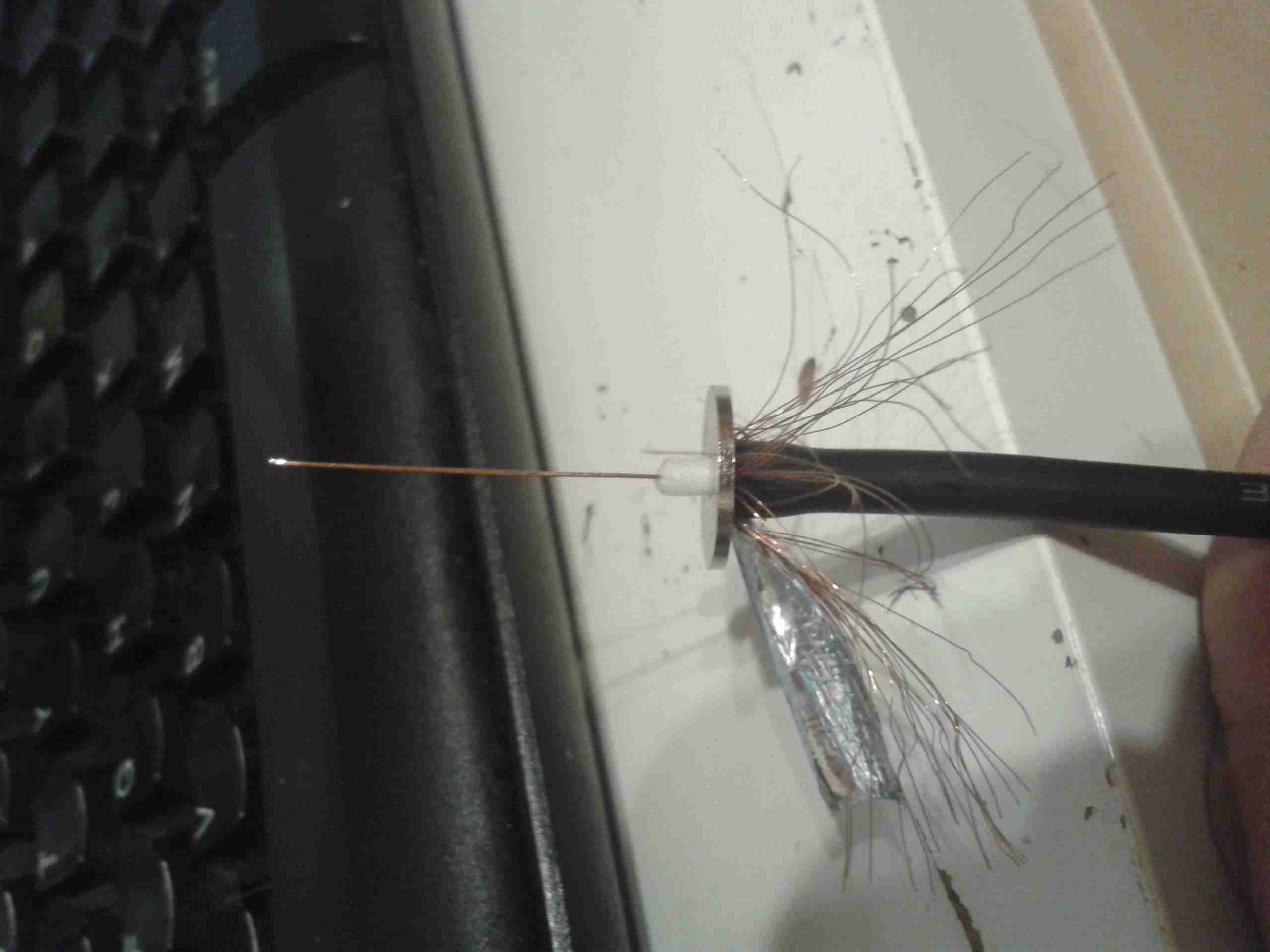
Inner Insulation
With the shield washer fitted, the inner insulation can be cut back, it should be just about level with the final washer when you’re done, this allows the connector to fit together properly.
Center Core Trimmed
Trim the center conductor to about double the length required, to allow it to be folded over, as shown. This allows the copper to spring back against the center pin of the connector when it’s fitted, to allow a good connection.
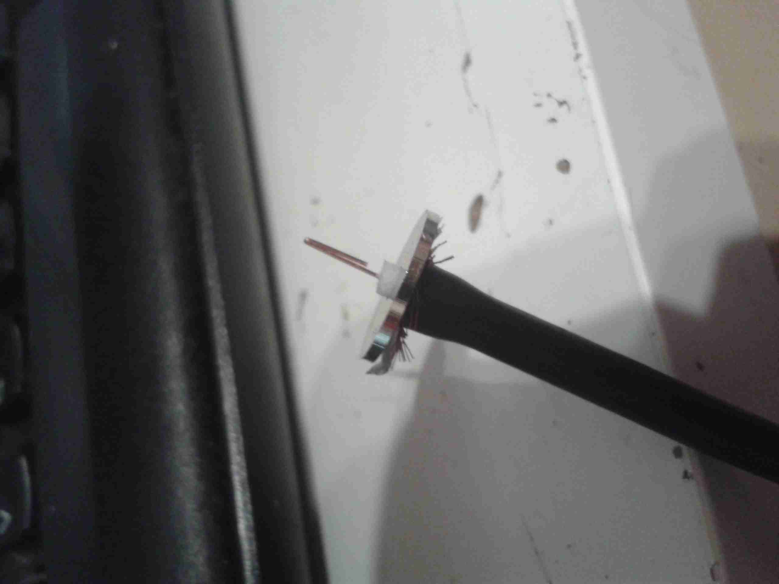
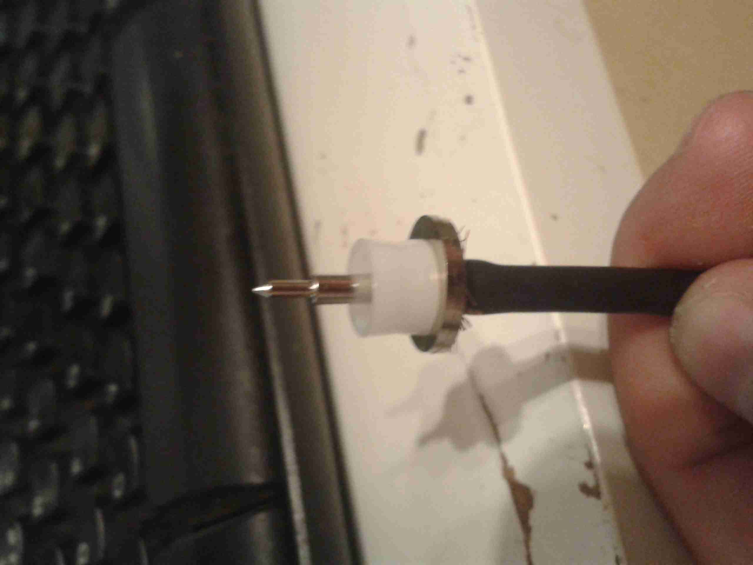
Final Washer
Here the final washer is fitted over the shield washer. The center insulation should be at the same level to allow the center pin to fit properly.
Center Terminal
Finally, the center pin is pushed over the inner conductor of the cable, with it’s insulating spacer. Soldering these usually results in the plastic melting and a ruined connector.
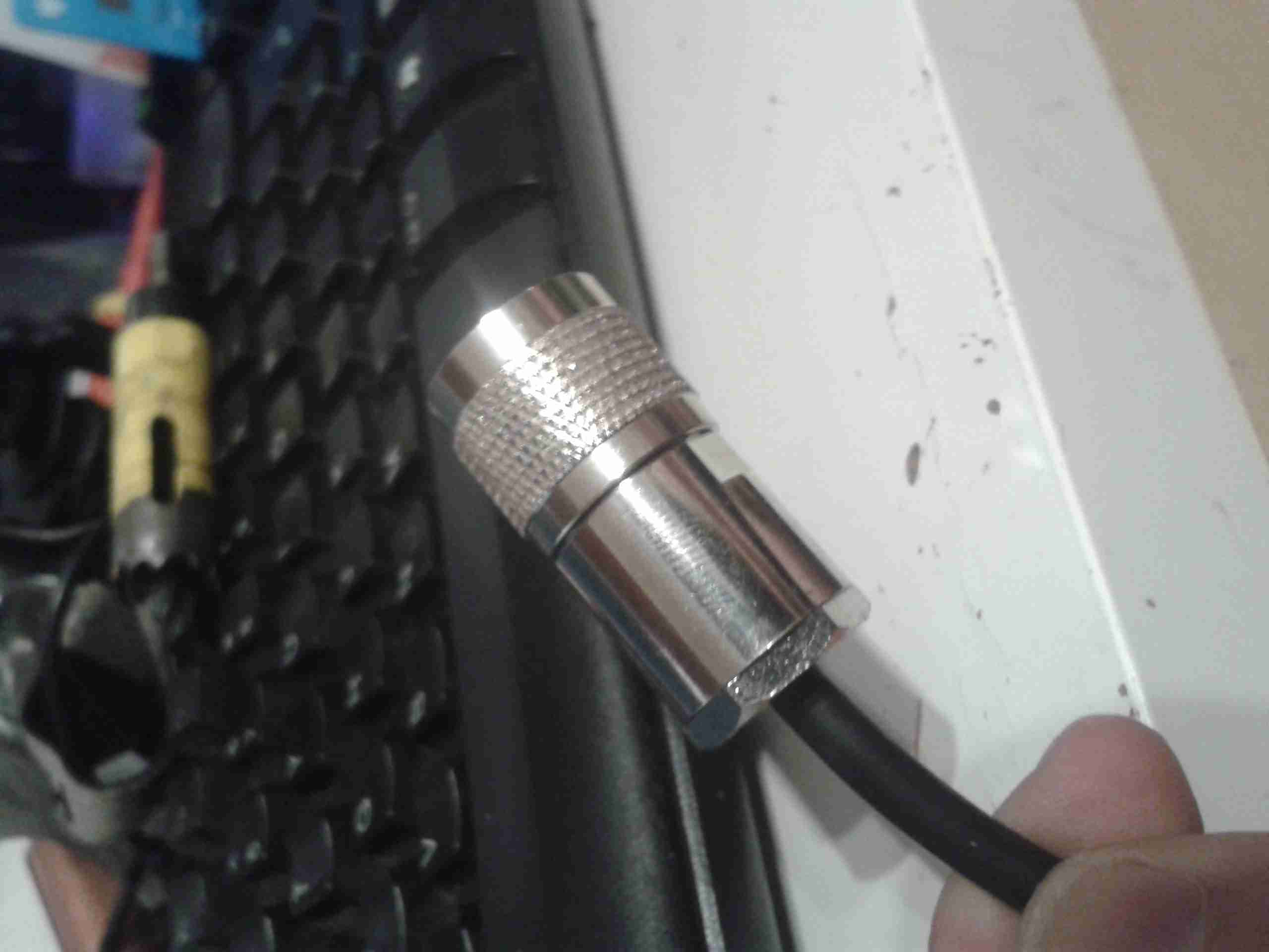
Finished Plug
Finished plug. Make sure the backnut is tightened fully home, without twisting the connector body itself. After I’m done with the termination, I use self-amalgamating tape to form a strain relief on the cable. This prevents it from breaking at the point where it enters the backnut.
I’ve been terminating these connectors this way for a long time & have not had any issues with SWR or bad connections, dispite the fact that I don’t solder them. This also has the advantage that fewer tools are required for the job & the connectors can easily be reused should the cable wear out.
There are times when I am frequently away from home base, usually either on the canal system or at a festival. During these times it’s very handy to be able to just grab a bag, without having to be concerned about sorting everything out.
This post will only detail the portable shack bag. The power supply kit that goes along with it with be detailed in another post.
The bag I use is an VHS Camcorder bag from the early 80’s. It’s very well built, & copes easily with the weight of all the radio gear.
Total weight for this system is 13.4lbs (6kg).
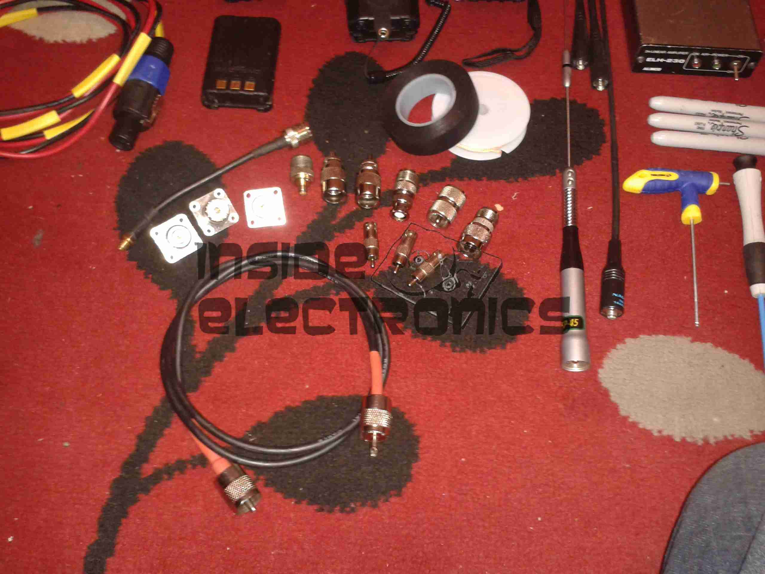
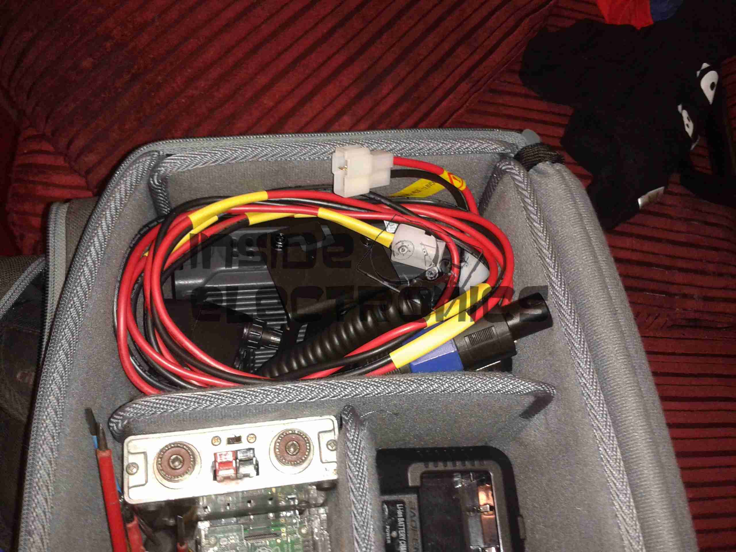
Mobile Radio Bag
Above is the bag packed. Obligatory International Ameteur Radio Symbol patch front & centre. Being an old camera bag, this easily slings over the shoulder, with it’s padded strap.
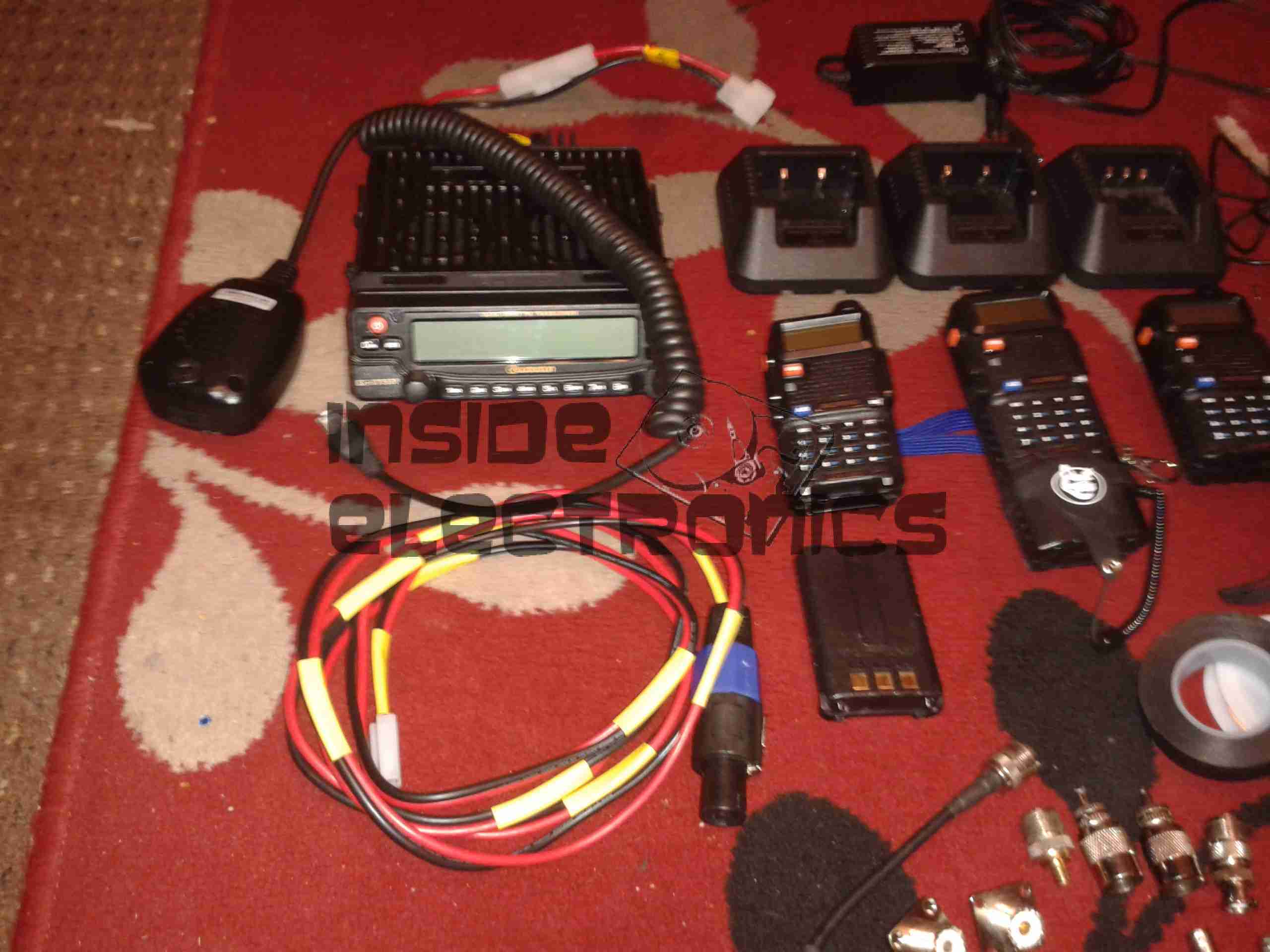
Current Equipment
Here is all the current equipment laid out. All the equipment to enable me to set up a station anywhere.
In the following photos I will go into the details.
Main Radio
First off, my main radio. This is the same Wouxun KG-UV950P mobile rig I have posted about previously. I have heatshrunk the power cable to keep it together & attached my standard power connector to the end. More on these later on.
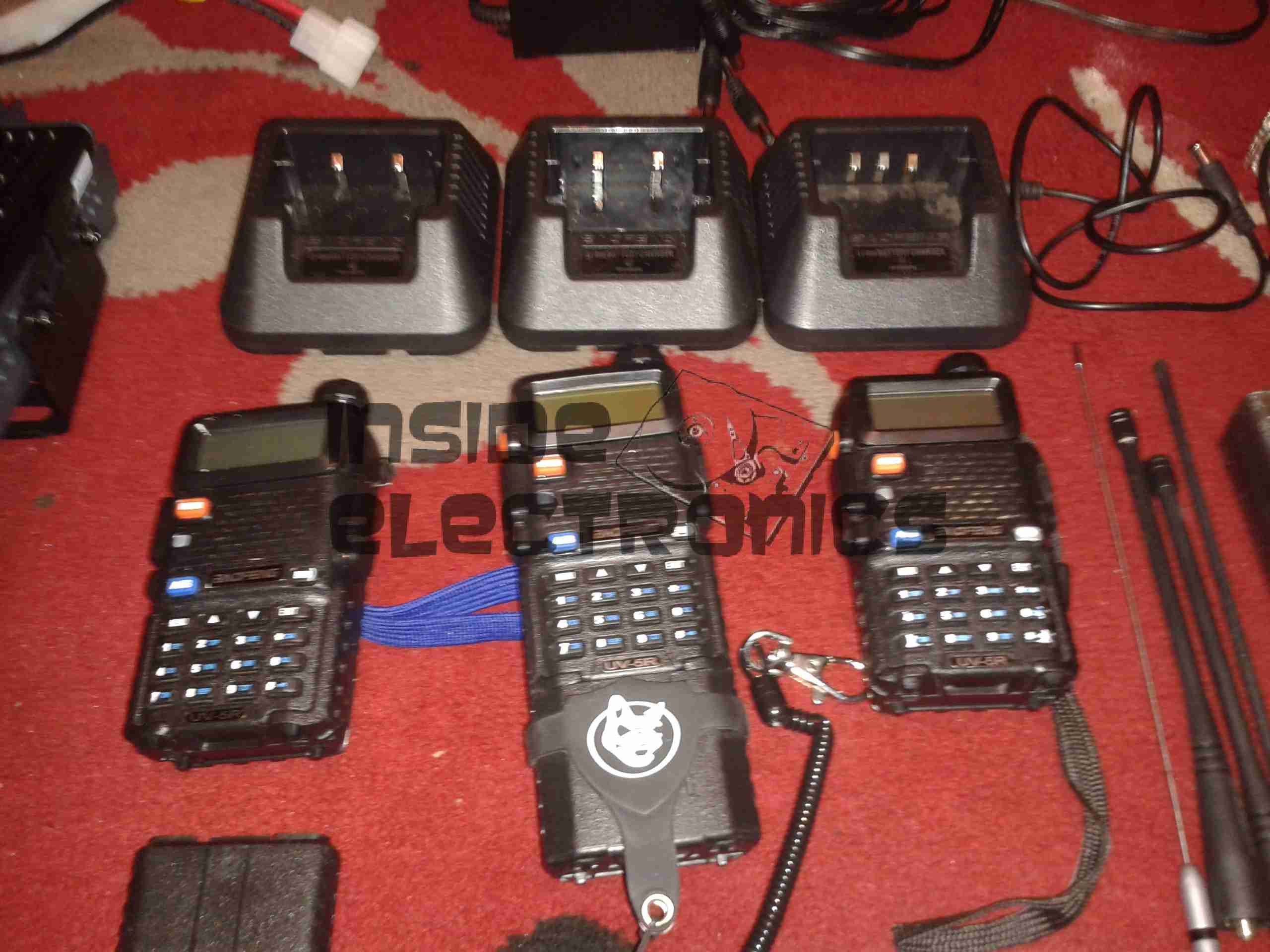
HTs
In the bag I also carry three Baofeng UV-5R handhelds. Extremely useful for short range site communications, along with their charger bases. The charging base on the right has been slightly modified to support charging of my main LED torch as well, which uses similar Li-Ion based packs as the Baofengs.
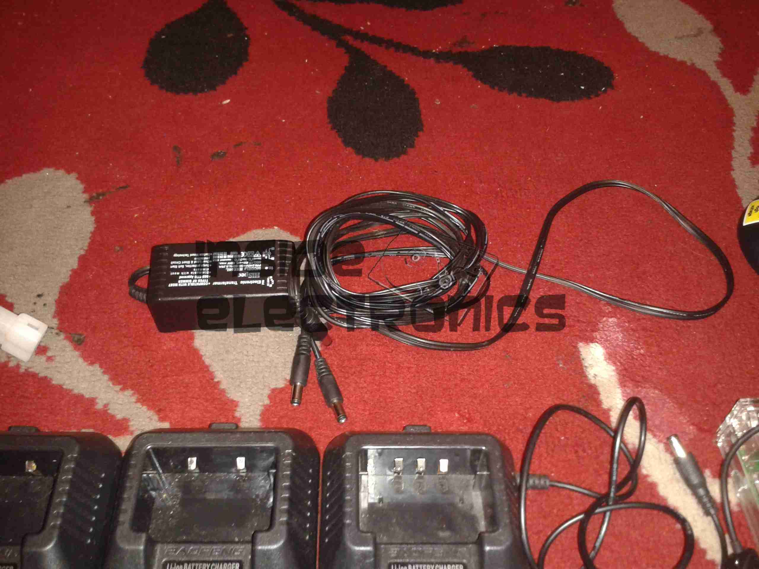
Baofeng 12v Charger
As the charger bases for the Baofeng HTs take a supply of 10v DC, I have constructed a 12v adaptor system for them. (Which utter prat of an engineer at Baofeng picked 10v?)
Linear Amplifier & SWR Meter
Also included is a small Alinco ELH-2320 35W 2m linear amplifier. This was given to me from the local HackSpace in Manchester. (They don’t have any ham members, besides myself). Also here is my small SWR & Power meter, SDR kit & a pair of syringes. These are filled respectively with Copaslip copper loaded grease, (very good for stopping fasteners exposed to the weather from seizing up), and dielectric silicone grease. (I use this stuff for filling connectors that are exposed to the weather – keeps the water out).
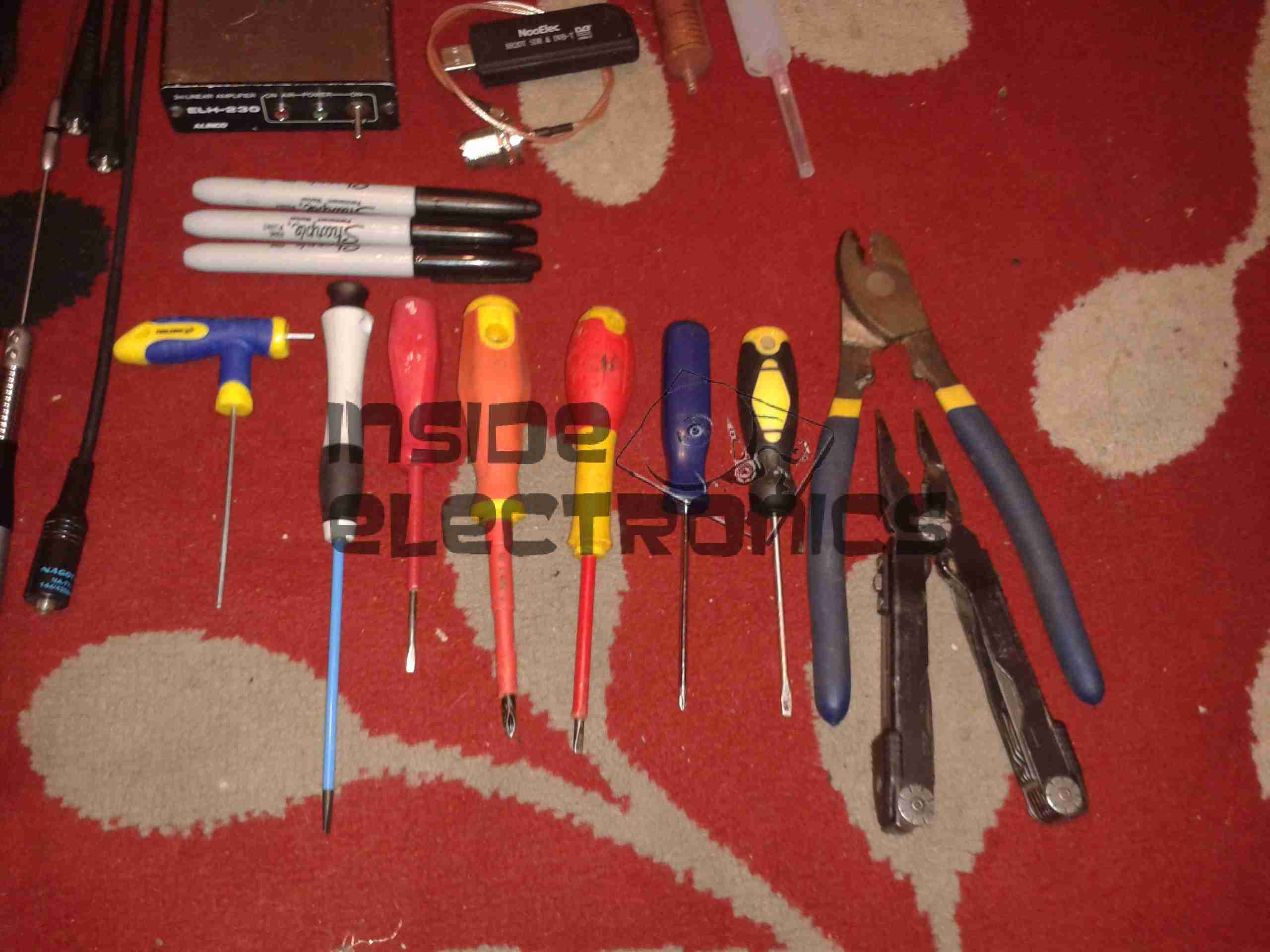
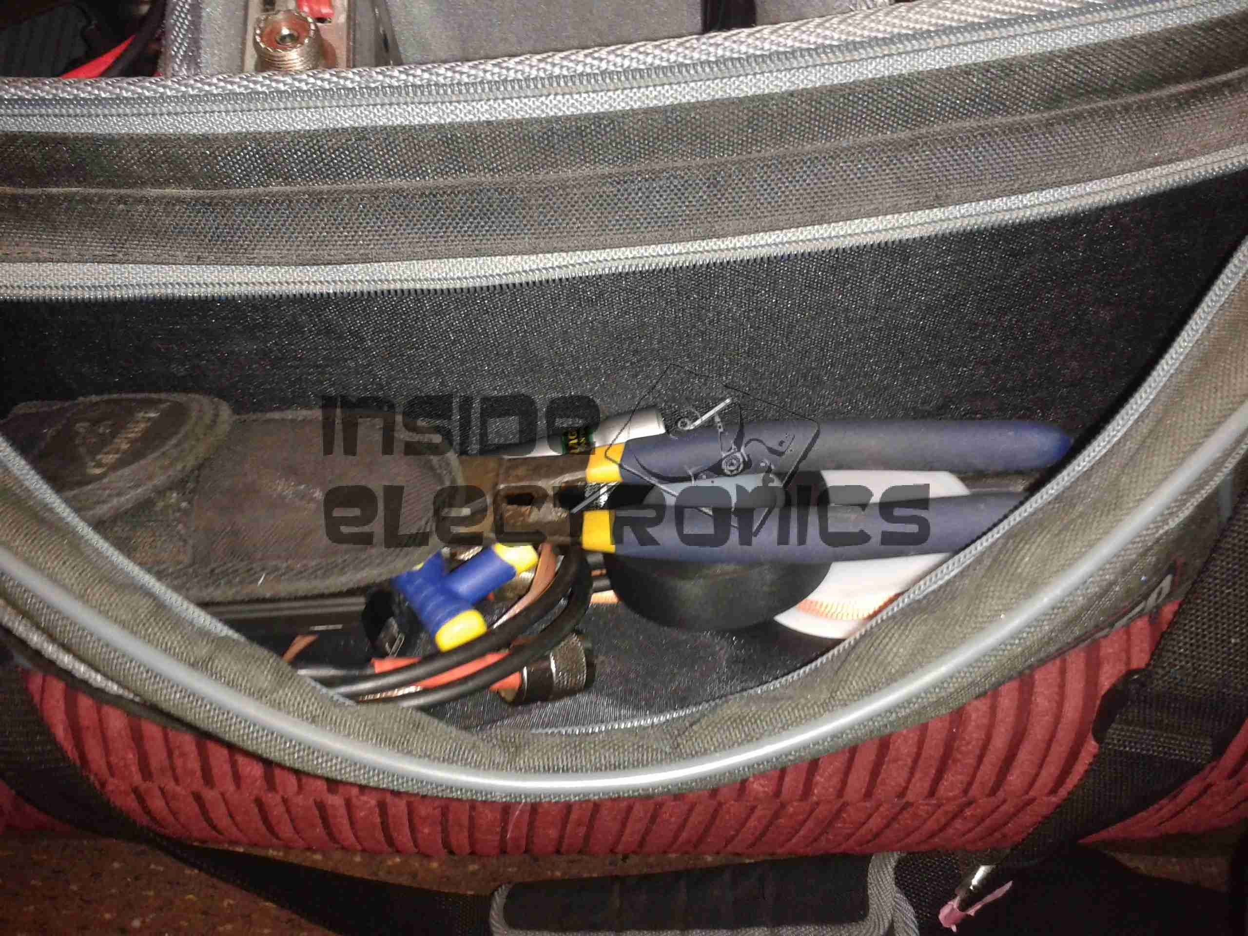
Tools
I always keep essential tools in the bag, here is the small selection of screwdrivers which fit pretty much any screw fastener around, my heavy-duty cable shears (these buggers can cut through starter cable in one go!) and my trusty Gerber Diesel multitool.
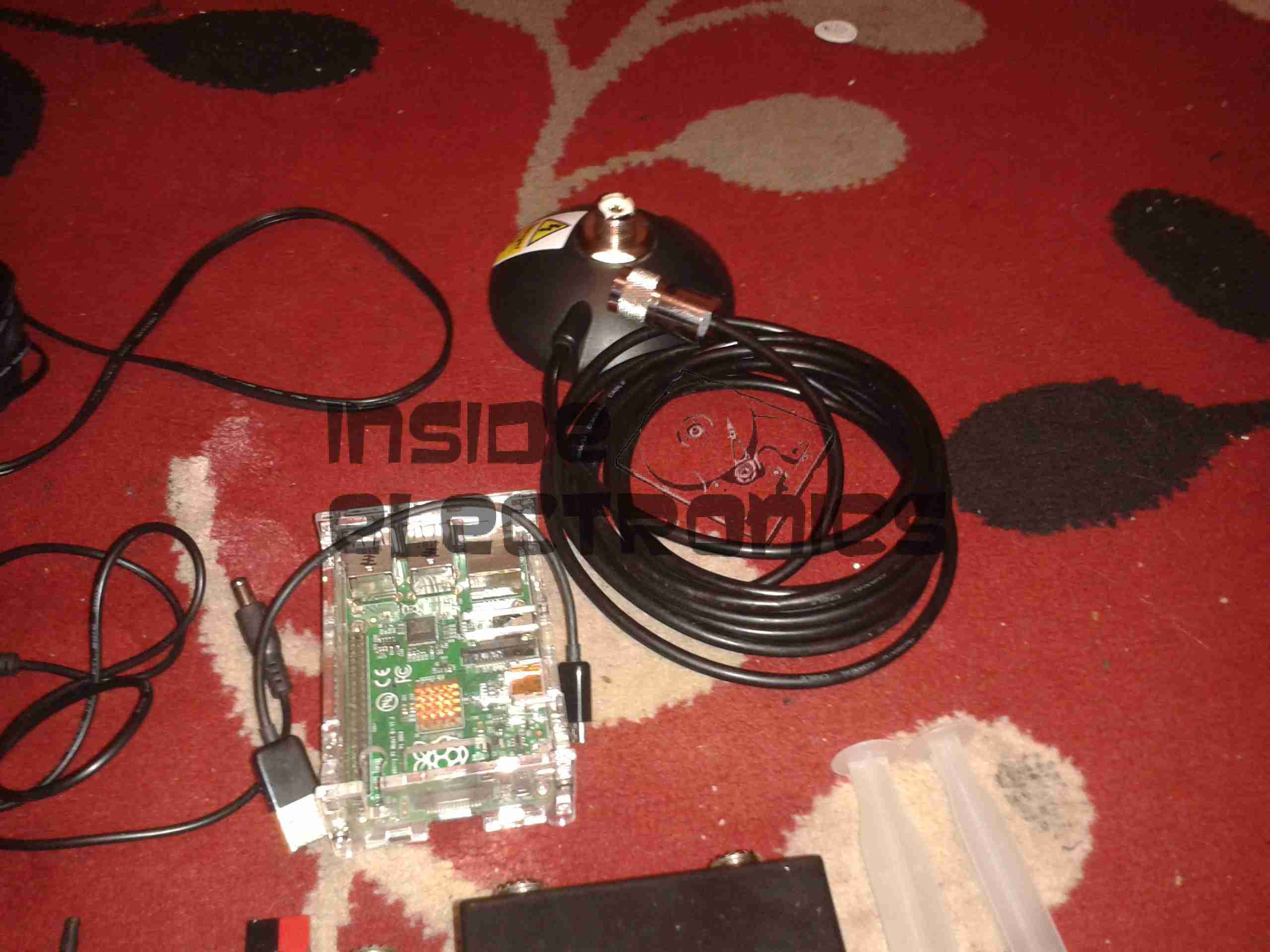
Magmount & Pi
Main antenna magmount & a spare Raspberry Pi.
Antenna, Patch Leads, Etc.
Finally, the antennas for the HTs, main dual-band antenna (Nagoya SP-45) for the magmount, a small selection of spare plugs, sockets & adaptors. Also here is a roll of self-amalgamating tape, very handy for waterproofing wiring connections (especially when used in conjunction with the silicone grease), & a roll of solder wick.
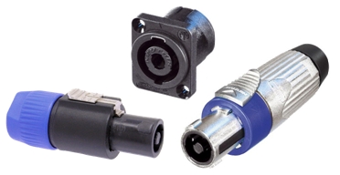
Now, the main power connectors of choice for my equipment are Neutrik SpeakOn type connectors:
Neutrik SpeakOn
These connectors have many advantages:
They are positive locking connectors. No more loose connections.
They have a high continuous current rating of 30A RMS.
Relatively weather resistant.
Also, they have two pairs of pins – and as some of my bigger non-radio related equipment is 24v, this allows me to use a single set of plugs for everything. Without having to worry about plugging a 12v device into a 24v socket, and letting out the magic blue genie.
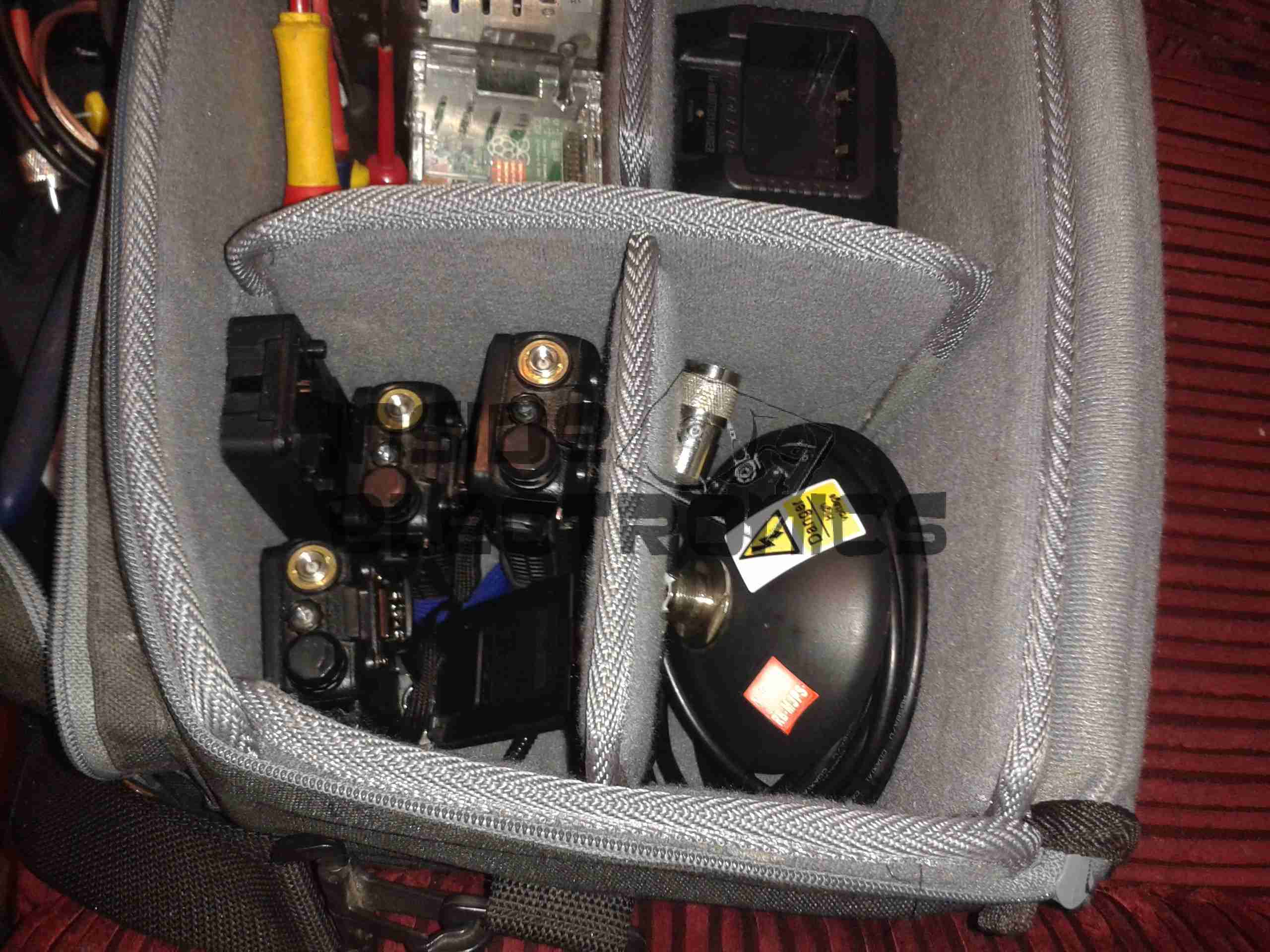
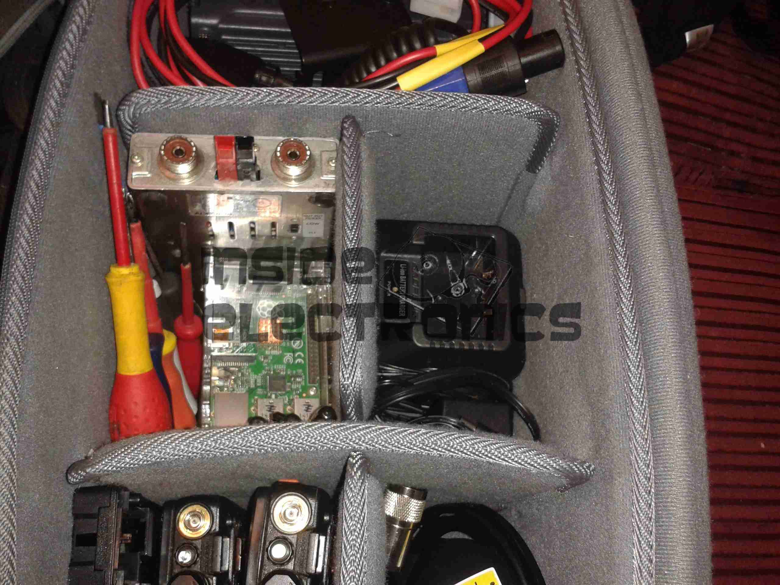
Once everything is packed up, here’s the bag:
Packed
Everything has a neat little pocket for easy access. Some closeups below.
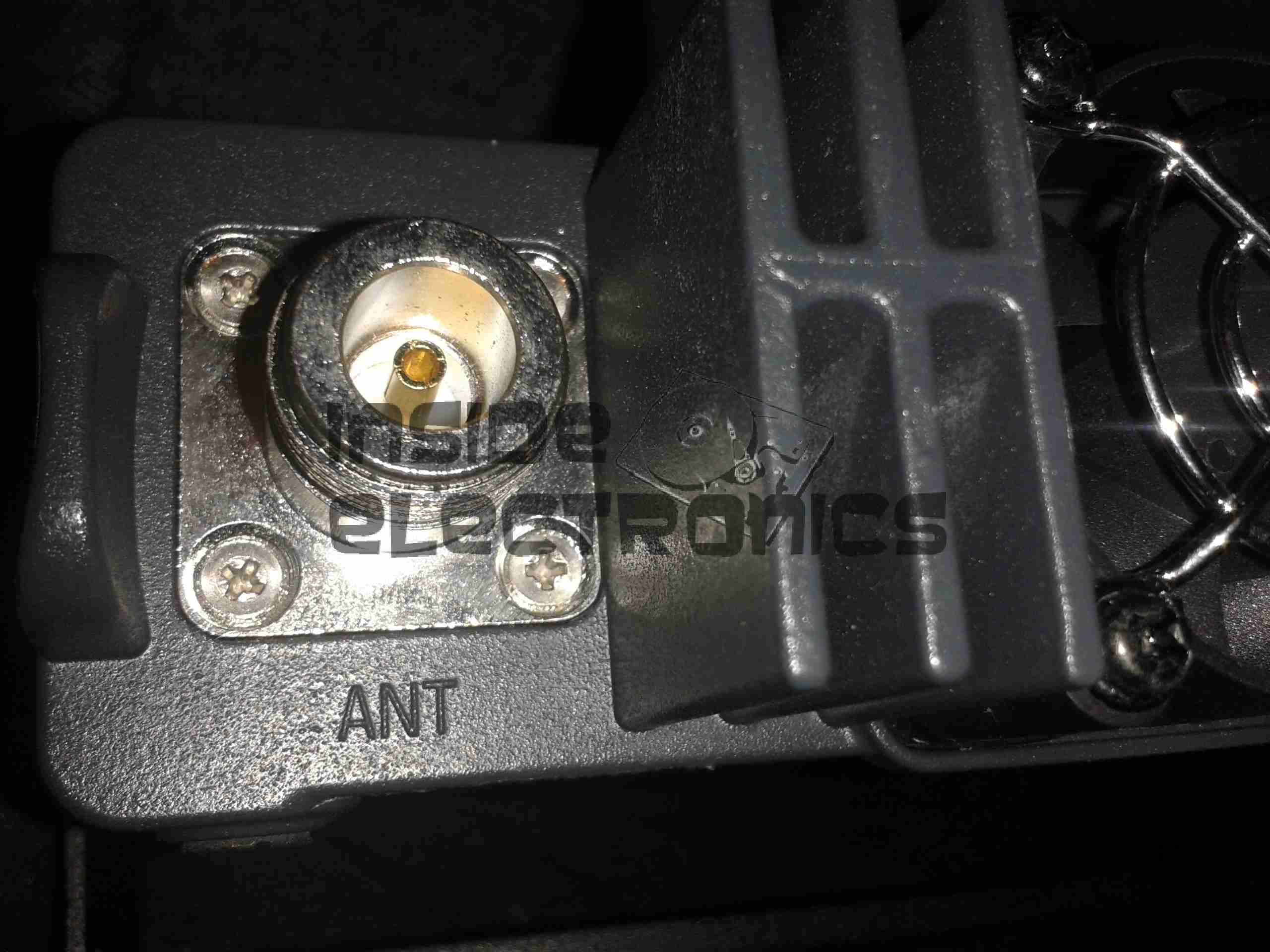
In my original review, I noted that this radio was supplied with a SO-259 socket for the antenna connection.
However I’m less than fond of these, due to their non-constant impedance, which can cause signal loss issues at VHF/UHF. Because of this, I’ve replaced it with a high quality N-type connector. These connectors are much better, as they are a constant 50Ω impedance, they’re weather resistant, and being rated to 11GHz, are more than sufficient for a radio that will only do up to 70cm.
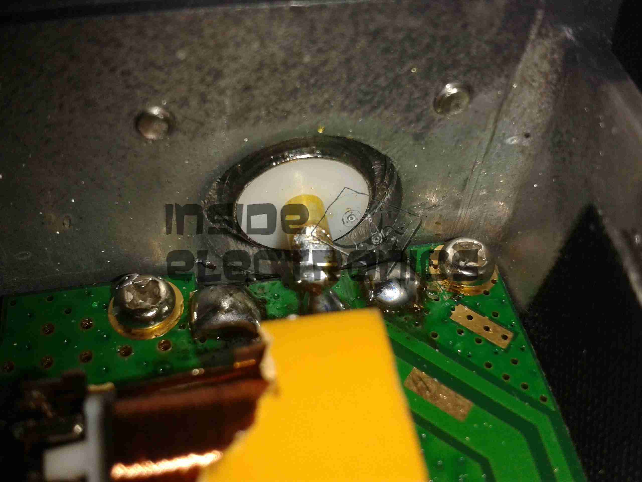
RF Output Jack
Here can be seen the point where the connection is made to the PCB.
I’ve already replaced the socket in this photo. The pair of solder pads either side of the central RF point were soldered to wings on the back of the original SO-259. As there are a pair of screws, also connected to the ground plane, there have been no signal issues with just using the frame of the radio as the ground point. Shown below is the original socket, with the ground wings.
Original SO-259
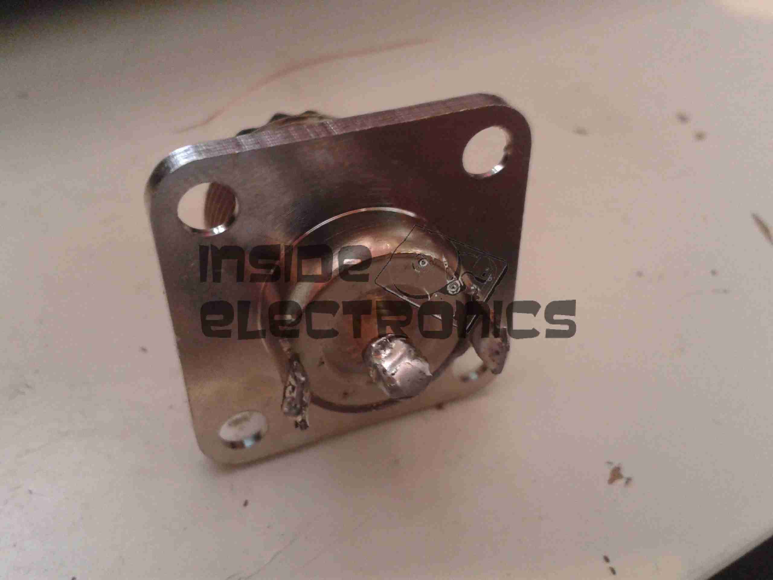
Finally, here is the back of the radio with it’s shiny new N connector.
New Connection
Chassis mount connectors are pretty standard, so this new connector fits perfectly into the same recess of the original. Looks like factory fitted!
I am now standardising on N connectors for everything in my radio shack, next on the project list for conversion is the SWR meter I recently acquired.
As the cable supplied with the panel is far too short, inflexible & does not even allow the cable gland on the terminal box to form a seal, I have replaced it with some high quality twin core guitar cable, with silicone insulation.
The cable is removable from the panel tail by means of a screwlock two pin connector.
On another note, I have noticed a side effect of fitting a switchmode regulator to the panel: it seems to have formed an MPPT-type regulator setup, as even in low light conditions, when the bare panel is outputting 18.5v at 50mA short circuit, with the switching regulator I can get a useable 13.25v at ~170mA.
This effect is increased in full light, where I can obtain 4.5A short circuit current & ~1.8A at 13.25v output.
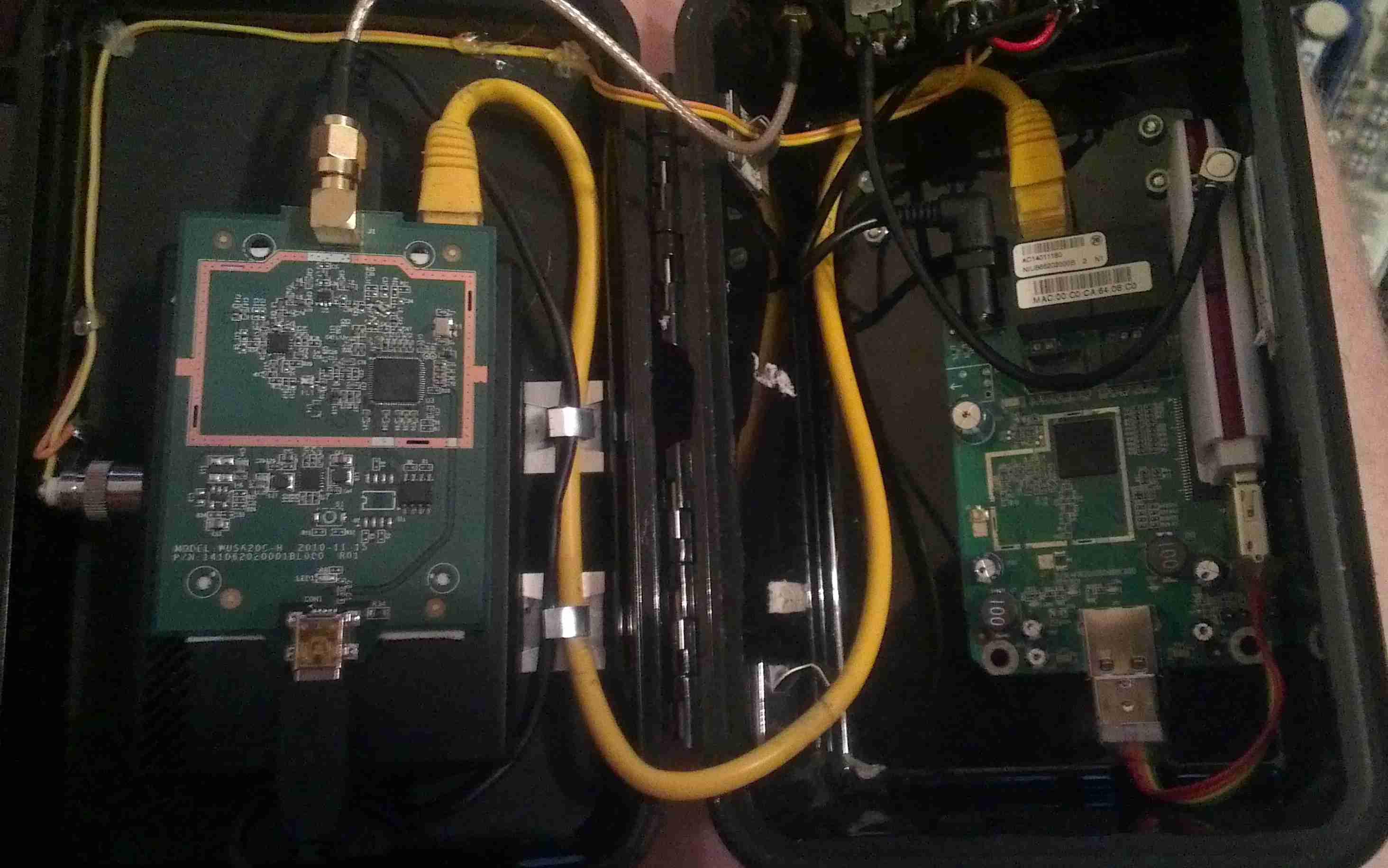
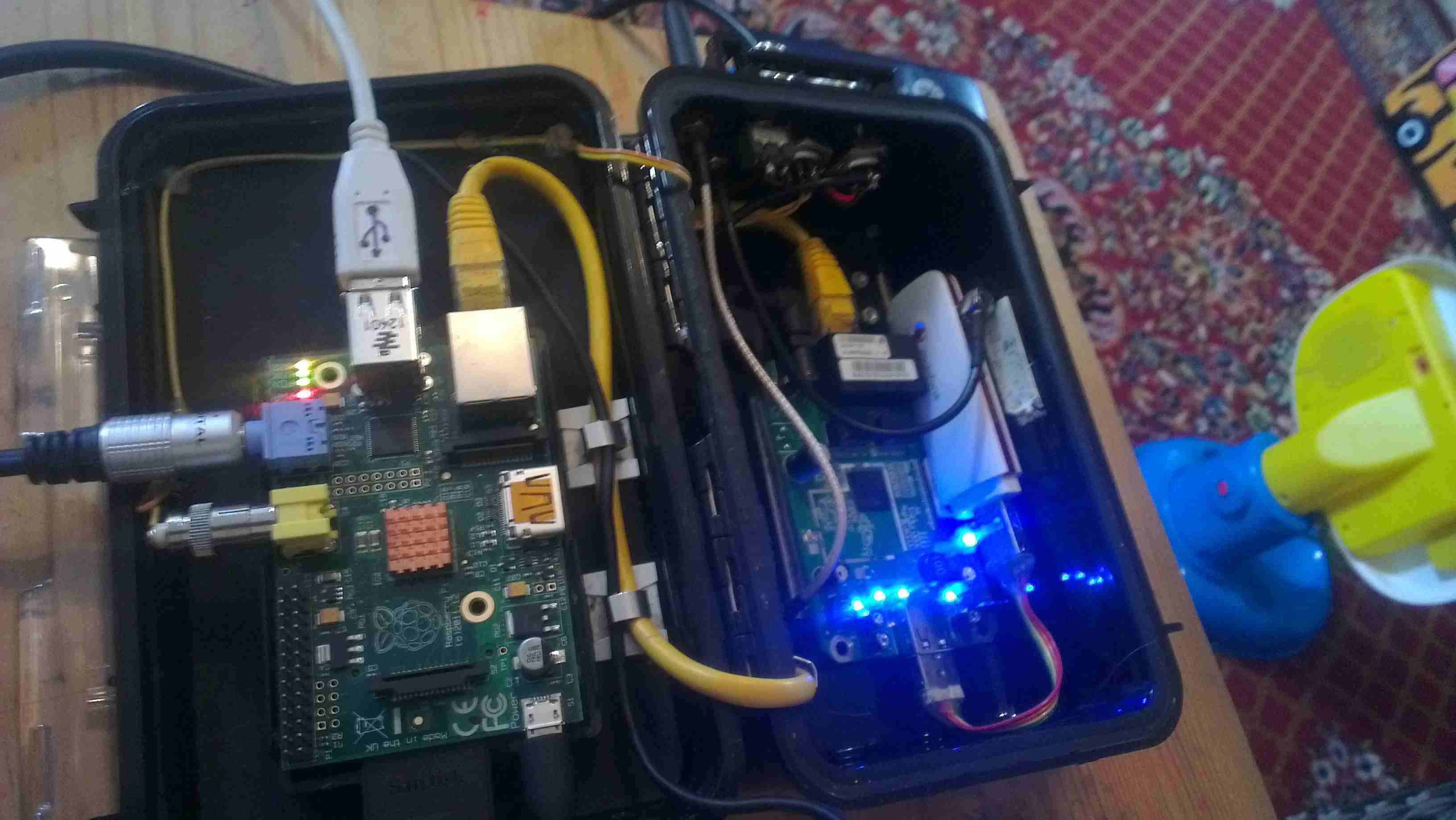
Here is the project I’m currently working on. A completely wearable computing platform based on the Raspberry Pi & the WiFi Pineapple.
Above can be seen the general overview of the current unit.
On the left:
Alfa AWUS036NHA USB High Power WiFi Network Interface
512MB Model B Raspberry Pi, 16GB SD card, running Raspbian & LXDE Desktop. Overclocked to 1GHz.
On the right:
WiFi Pineapple router board
USB 3G card.
The WiFi, Pineapple & 3G all have external antenna connections for a better signal & the whole unit locks onto the belt with a pair of clips.
The Raspberry Pi is using the composite video output to the 7″ LCD I am using, running at a resolution of 640×480. This gives a decent amount of desktop space while retaining readability of the display.
The case itself is a Pelican 1050 hard case, with it’s rubber lining removed. The belt clips are also a custom addition.
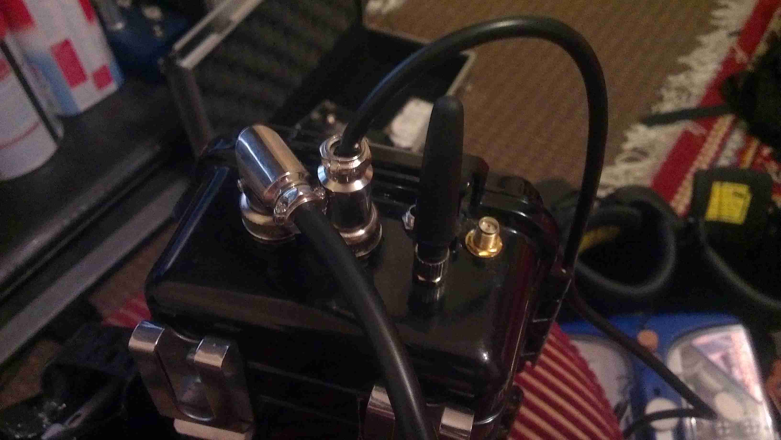
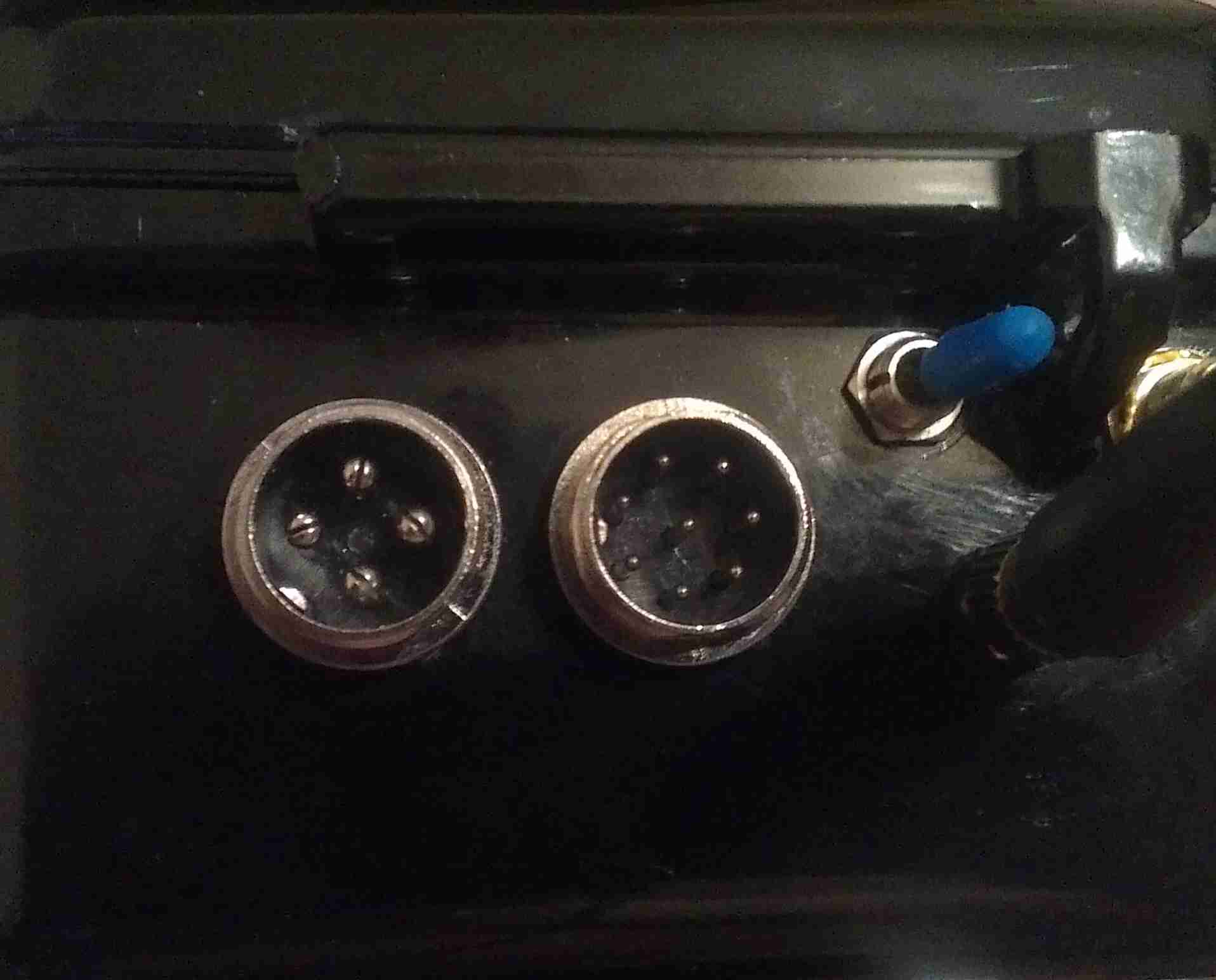
Connections
Here are the connections to the main unit, on the left is the main power connector, supplying +5v & +12v DC. The plug on the right is an 8-pin connection that carries two channels of video, mono audio & +12v power to the display.
Currently the only antenna fitted is the 3G.
Connectors
Closeup of the connections for power, audio & video. The toggle switch is redundant & will soon be replaced with a 3.5mm stereo jack for headphones, as an alternative to the mono audio built into the display.
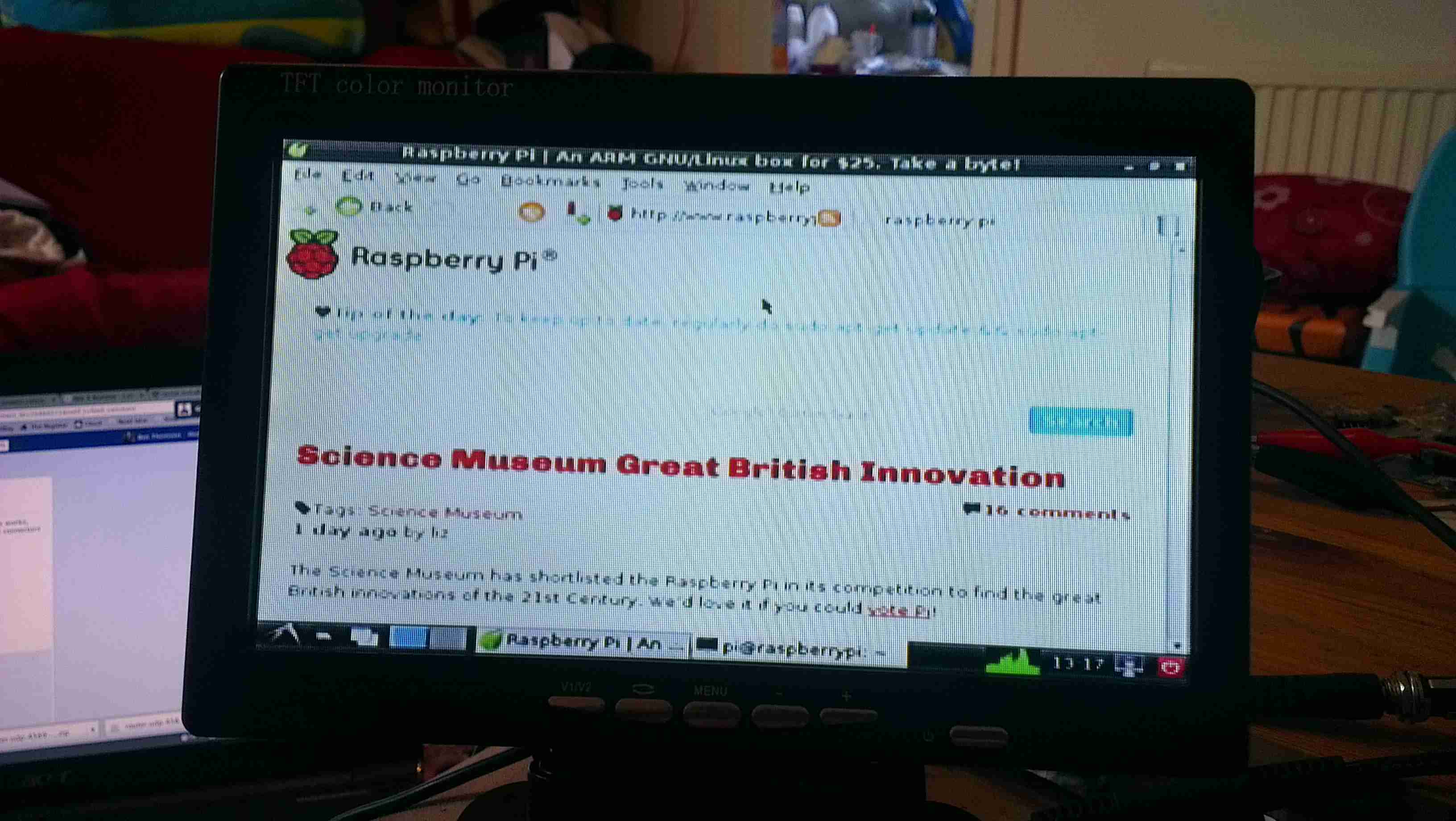
Test Run
Current state of test. Here the unit is running, provided with an internet connection through the Pineapple’s 3G radio, funneled into the Pi via it’s ethernet connection.
Pi Goodness!
Running on a car reversing camera monitor at 640×480 resolution. This works fairly well for the size of the monitor & the text is still large enough to be readable.
Stay tuned for Part 2 where I will build the power supply unit.
After seeing these on eBay for £8.99 I thought it might be a good deal – interfacing with the RasPi’s GPIO & it has built in power supplies.
As a kit, it was very easy to assemble, the PCB quality is high, and is a fairly good design. It worked first time, the regulators hold the rails at the right voltages.
However there are some issues with this board that bug me.
The documentation for the kit is *AWFUL*. No mention of the regulators on the parts list & which goes where – I had to carefully examine the schematics to find out those details.
The 4x 1N1007 diodes required weren’t even included in the kit! Luckily I had some 1N4148 high speed diodes lying around & even though they’re rated for 200mA continuous rather than the specified part’s 1A rating, the lack of heatsinking on the regulators wouldn’t allow use anywhere near 1A, so this isn’t much of a problem.
Component numbering on the silkscreen isn’t consistent – it jumps from R3 straight to R6! These issues could be slightly confusing for the novice builder, and considering the demographic of the RasPi, could be seen as big issues.
On the far left of the board are the 5v & 3.3v regulators, well placed on the edge of the board in case a heatsink may be required in the future. However the LM317 adjustable regulator is stuck right in the middle of the PCB – no chance of being able to fit a heatsink, & the device itself seems incredibly cheap – the heatsink tab on the back of the TO-220 is the thinnest I have ever seen. Not the usual 2-3mm thick copper of the 5v & 3.3v parts – but barely more than a mm thick, so it’s not going to be able to cope with much power dissipation without overheating quickly.
As the adjustable rail can go between ~2.5v – 10v, at the low end of the range the power dissipation is going to shoot through the roof.
The GPIO connector – this could have been done the other way, at the moment the ribbon cable has to be twisted to get both the Pi & the GPIO board the same way up. Just a slight fail there. See the image below
Plugged In
The power rails are not isolated out of the box – there is no connection between the 5v & 3.3v rails & the Pi’s GPIO, but the GND connections are linked together on the board.
Getting the ribbon cable through the hole in the ModMyPi case was a bit of a faff – the connector is too big! I had to squeeze the connector through at a 45° angle. The case is also remarkably tight around the connector once it’s fitted to the board – clearly the designers of the case didn’t test the an IDC connector in the case before making them!
Everything does fit though, after a little modification.
All Cased Up
Here is the unit all built up with the case. The top cover just about fits with the IDC connector on the GPIO header.
More to come once I get some time to do some interfacing!
This is a device to use an IDE or SATA interface drive via a USB connection. Here is the front of the device, IDE interface at the bottom, 2.5″ form factor.
PCB Top
PCB removed from the casing. USB cable exits the top, 12v DC power jack to the left.
SATA interface below the DC Jack.
Molex connector below SATA is the power output for the drive in use. This unit has a built in 5v regulator.
PCB Bottom
Bottom of the PCB showing the interface IC.
Drive Adaptor
Adaptor to plug into the 44-pin 2.5″ form factor IDE interface on the adaptor, converts to standard 40-pin 3.5″ IDE.
Power Cable
Power pigtail with standard Molex & SATA power plugs.
The parts arrived for my adjustable laser diode driver! Components here are an LM317K with heatsink, 100Ω 10-turn precision potentiometer, 15-turn counting dial & a 7-pin matching plug & socket.
Driver Schematic
Here is the schematic for the driver circuit. I have used a 7-pin socket for provisions for active cooling of bigger laser diodes. R1 sets the maximum current to the laser diode, while R2 is the power adjustment. This is all fed from the main 12v Ni-Cd pack built into the PSU. The LM317 is set up as a constant current source in this circuit.
Installed
Here the power adjust dial & the laser head connector have been installed in the front panel. Power is switched to the driver with the toggle switch to the right of the connector.
Regulator
The LM317 installed on the rear panel of the PSU with it’s heatsink.
Connection
Connections to the regulator, the output is fully isolated from the heatsink & rear panel.
This is detailing my portable multi-purpose power pack of my own design. Here is an overview, mainly showing the 4Ah 12v Ni-Cd battery pack.
Front Panel Right
Panel Features – Bottom: Car cigar lighter socket, main power keyswitch. Top: LED toggle switch, provision for upcoming laser project, Red main Power LED, 7A circuit breaker.
Front Panel Left
Top: Toggle switch serving post terminals, USB Port.
Post terminals supply unregulated 12v for external gadgets. USB port is standard 5v regulated for charging phones, PDAs etc.
Bottom: Pair of XLR connectors for external LED lights. Switches on their right control power & the knob controls brightness.
Additions are being made to this all the time, the latest being a 2W laser diode driver. Update to come soon!
For those that are interested, here is the ID label, this is a PSP-2003.
Front Removed
Here the front of the unit has been removed, showing the first internal components.
Screen Removed
Here is the unit with the LCD removed, here the mainboard is partially visible.
Left Pad
Left pad unit removed from the PSP, with the left speaker & the memory stick slot cover.
Left Pad Rear
Rear of the left pad assembly, showing the speaker.
Joypad
Joypad removed from the casing. Resistive unit.
Output Jack
Headphone/data board removed from the casing. This also has TV-Out on the PSP-200x series.
Mainboard
Mainboard removed. Main CPU is at the top. Sockets around the bottom connect to the UMD drive & UMD Drive.
CPU & GPU
Closeup of the main chipset. CPU is the top IC.
Mainboard Rear
Rear of the mainboard, Memory Stick socket on the right.
WiFi Chipset
Closeup of the WiFi chipset & the charging power socket on the right.
Charging Chipset
Closeup of the bettery connector & the charge controller IC.
UMD Drive
UMD Drive removed from the rear of the casing. This is a miniature DVD style drive, using a 635nm visible red laser.
UMD Drive Back
Rear of the UMD drive, showing the laser sled & drive motors. Both the spindle motor & the sled motor are 3-phase brushless type. The laser diode/photodiode array is at the top of the laser sled.
Tip Jar
If you’ve found my content useful, please consider leaving a donation by clicking the Tip Jar below!
All collected funds go towards new content & the costs of keeping the server online.