Posted on 10 Comments

Sterling ProCharge Ultra PCU1210 Teardown & Repair

The Sterling charger we’ve had on board nb Tanya Louise since Feb 2014 has bitten the dust, with 31220 hours on it’s internal clock. Since we’re a liveaboard boat, this charger has had a lot of use while we’re on the mooring during winter, when the solar bank isn’t outputting it’s full rate. First, a bit of a teardown to explore the unit, then onto the repair:

Active PFC Section
Active PFC Section

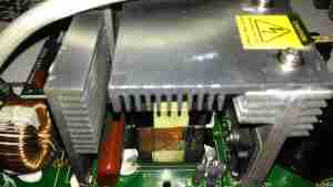
There’s the usual mains input filtering on the left, with the bridge rectifier on it’s heatsink.
Underneath the centre massive heatsinks is the main transformer (not visible here) & active PFC circuit. The device peeking out from underneath is the huge inductor needed for PFC. It’s associated switching MOSFET is to the right.
Logic PSU Section
Logic PSU Section

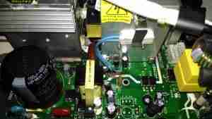
On the other side of the PFC section is the main DC rail filter electrolytic, a 450v 150µF part. Here some evidence of long-term heating can be seen in the adhesive around the base, it’s nearly completely turned black! It’s not a decent brand either, a Chinese CapXon.
The PCB fuse just behind it is in the DC feed to the main switching supply, so the input fuse only protects the filter & Active PFC circuitry. Luckily this fuse didn’t blow during the failure, telling me the fault was earlier in the power chain.
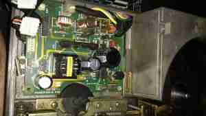
The logic circuits are powered by an independent switching supply in the centre, providing a +5v rail to the microcontroller. The fan header & control components are not populated in this 10A model, but I may end up retrofitting a fan anyway as this unit has always run a little too warm. The entire board is heavily conformal coated on both sides, to help with water resistance associated with being in a marine environment. This has worked well, as there isn’t a single trace of moisture anywhere, only dust from years of use.
There is some thermal protection for the main SMPS switching MOSFETS with the Klixon thermal fuse clipped to the heatsink.
DC Output Section
DC Output Section

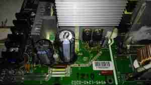
The DC output rectifiers are on the large heatsink in the centre, with a small bodge board fitted. Due to the heavy conformal coating on the board I can’t get the ID from this small 8-pin IC, but from the fact that the output rectifiers are in fact IRF1010E MOSFETS, rated at 84A a piece, this is an synchronous rectifier controller.
Oddly, the output filter electrolytics are a mix of Nichicon (nice), and CapXon (shite). A bit of penny pinching here, which if a little naff since these chargers are anything but cheap. (£244.80 at the time of writing).
Hiding just behind the electrolytics is a large choke, and a reverse-polarity protection diode, which is wired crowbar-style. Reversing the polarity here will blow the 15A DC bus fuse instantly, and may destroy this diode if it doesn’t blow quick enough.
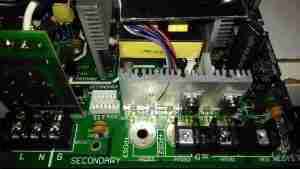
DC Outputs
DC Outputs

Right on the output end are a pair of large Ixys DSSK38 TO220 Dual 20A dual Schottky diodes, isolating the two outputs from each other, a nice margin on these for a 10A charger, since the diodes are paralleled each channel is capable of 40A. This prevents one bank discharging into another & allows the charger logic to monitor the voltages individually. The only issue here is the 400mV drop of these diodes introduce a little bit of inefficiency. To increase current capacity of the PCB, the aluminium heatsink is being used as the main positive busbar. From the sizing of the power components here, I would think that the same PCB & component load is used for all the chargers up to 40A, since both the PFC inductor & main power transformer are massive for a 10A output. There are unpopulated output components on this low-end model, to reduce the cost since they aren’t needed.
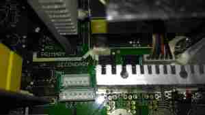
Front Panel Control Connections

A trio of headers connect all the control & sense signals to the front panel PCB, which contains all the control logic. This unit is sensing all output voltages, output current & PSU rail voltages.
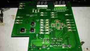
Front Panel LEDs
Front Panel LEDs

The front panel is stuffed with LEDs & 7-segment displays to show the current mode, charging voltage & current. There’s 2 tactile switches for adjustments.
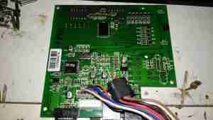
Front Panel Reverse
Front Panel Reverse

The reverse of the board has the main microcontroller – again identifying this is impossible due to the heavy conformal coat. The LEDs are being driven through a 74HC245D CMOS Octal Bus Transceiver.


Now on to the repair! I’m not particularly impressed with only getting 4 years from this unit, they are very expensive as already mentioned, so I would expect a longer lifespan. The input fuse had blown in this case, leaving me with a totally dead charger. A quick multimeter test on the input stage of the unit showed a dead short – the main AC input bridge rectifier has gone short circuit.
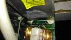
Bridge Rectifier Removed

Here the defective bridge has been desoldered from the board. It’s a KBU1008 10A 800v part. Once this was removed I confirmed there was no longer an input short, on either the AC side or the DC output side to the PFC circuit.
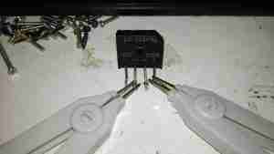
Testing The Rectifier

Time to stick the desoldered bridge on the milliohm meter & see how badly it has failed.
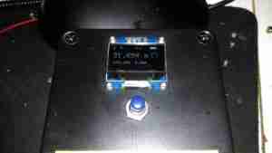
Yep, Definitely Shorted

I’d say 31mΩ would qualify as a short. It’s no wonder the 4A input fuse blew instantly. There is no sign of excessive heat around the rectifier, so I’m not sure why this would have failed, it’s certainly over-rated for the 10A charger.
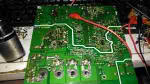
Testing Without Rectifier

Now the defective diode bridge has been removed from the circuit, it’s time to apply some controlled power to see if anything else has failed. For this I used a module from one of my previous teardowns – the inverter from a portable TV.
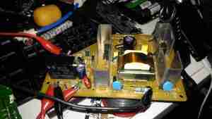
Test Inverter
Test Inverter

This neat little unit outputs 330v DC at a few dozen watts, plenty enough to power up the charger with a small load for testing purposes. The charger does pull the voltage of this converter down significantly, to about 100v, but it still provides just enough to get things going.
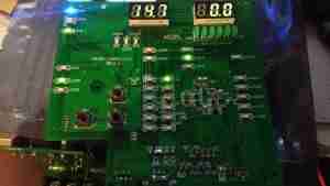
It's Alive!
It’s Alive!

After applying some direct DC power to the input, it’s ALIVE! Certainly makes a change from the usual SMPS failures I come across, where a single component causes a chain reaction that writes off everything.
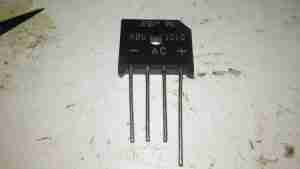
Replacement Rectifier

Unfortunately I couldn’t find the exact same rectifier to replace the shorted one, so I had to go for the KBU1010, which is rated for 1000v instead of 800v, but the Vf rating (Forward Voltage), is the same, so it won’t dissipate any more power.
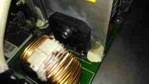
Soldered In
Soldered In

Here’s the new rectifier soldered into place on the PCB & bolted to it’s heatsink, with some decent thermal compound in between.
Input Board
Input Board

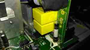
Here is the factory fuse, a soldered in device. I’ll be replacing this with standard clips for 20x5mm fuses to make replacement in the future easier, the required hole pattern in the PCB is already present. Most of the mains input filtering is also on this little daughterboard.
Fuse Replaced
Fuse Replaced

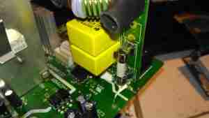
Now the fuse has been replaced with a standard one, which is much more easily replaceable. This fuse shouldn’t blow however, unless another fault develops.
Full Load Test
Full Load Test

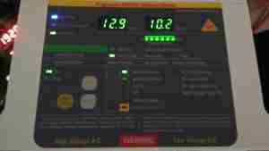
Now everything is back together, a full load test charging a 200Ah 12v battery for a few hours will tell me if the fix is good. This charger won’t be going back into service onboard the boat, it’s being replaced anyway with a new 50A charger, to better suit the larger loads we have now. It won’t be a Sterling though, as they are far too expensive. I’ll report back if anything fails!
Posted on Leave a comment

De La Rue Coin Counting Machine

Here’s some teardown photos of an old De La Rue coin counter, used in businesses for rapid counting of change into large bags.

Mechanism
Mechanism

An overview of the whole mechanical system of the counter. Coins are loaded into the drum at the rear of the machine, which sorts them into a row for the rubber belt to pick up & run through the counter. The coin type to be sorted is selected by turning the control knobs on the right.
The control knobs adjust the width & height of the coin channel so only the correct sized coins will be counted.

PSU & Switching
PSU & Switching

The counter is driven by a basic AC induction motor, the motor power relay & reversing relay is on this PCB, along with the 5v switching supply for the main CPU board.
The SMPS on this board looks like a standard mains unit, but it’s got one big difference. Under the frame next to the main motor is a relatively large transformer, with a 35v output. This AC is fed into the SMPS section of the PSU board to be converted to 5v DC for the logic.
I’m not sure why it’s been done this way, and have never seen anything similar before.
The edge of the coin channel can be seen here, the black star wheel rotates when a coin passes & registers the count.

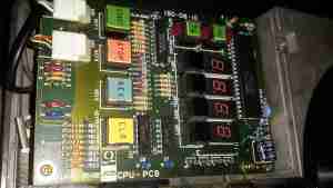
Controller PCB
Controller PCB

Here’s the main controller PCB, IC date codes put the unit to about 1995. The main CPU is a NEC UPD8049HC 8-bit micro, no flash or EEPROM on this old CPU, simply mask ROM. Coin readout is done on the 4 7-segment LED displays. Not much to this counter, it’s both electronically & mechanically simple.

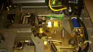
Counter Sensor
Counter Sensor

Coin counting is done by the star wheel mentioned above, which drives the interrupter disc on this photo-gate. The solenoid locks the counter shaft to prevent over or under counting when a set number of coins is to be counted.

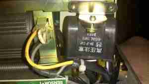
Motor Run Capacitor
Motor Run Capacitor

Under the frame, here on the left is the small induction motor, only 6W, 4-pole. The run cap for the motor is in the centre, and the 35v transformer is just visible behind it.

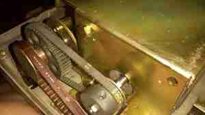
Main Motor Drive
Main Motor Drive

Main drive to the coin sorting mech is through rubber belts, and bevel gears drive the coin drum.

Posted on Leave a comment

15v Bipolar Supply Testing

Here’s some testing of the first bipolar supply for the Rigol scope. This is the +/-7.5v supply.

Bipolar Supply
Bipolar Supply

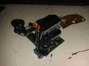
Above is the supply built with it’s output filtering. The modules used are a PTN78020W for the positive rail & a PTN78060A for the negative rail.

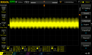
Under a 1A load across the total 15v output, here’s some scope traces of the ripple on the supply:

+7.5v Rail
+7.5v Rail

Here’s the ripple on the +7.5v rail of the supply, there’s about 75mV of total ripple.

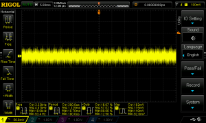
-7.5v Rail
-7.5v Rail

And here’s the -7.5v rail, the ripple on this is slightly lower, at about 50mV. This should be more than satisfactory as the scope has onboard linear regulation after the switching supply.

Posted on Leave a comment

Uniden UBC92XLT Teardown

One bit of my equipment that I’ve never looked into is my scanner, a handheld Uniden unit. I got this when Maplin Electronics had them on special offer a few years ago.

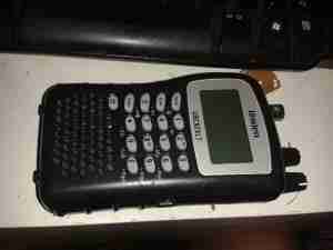
Uniden Scanner
Uniden Scanner

Here’s the scanner itself, roughly the same size as a usual HT.

Back Cover Removed
Back Cover Removed

Here the back cover has been removed, and the main RF board is visible at the top of the stack. Unfortunately the shielding cans are soldered on this unit, so no looking under there 🙁
On the right hand side of the board next to the antenna input is the main RF filter network, and it’s associated switching. The RF front end is under the shield closest to the front edge.

Controls & 3.3v Regulator

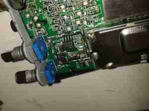
On the other side of the PCB is the Volume & Squelch potentiometers, along with a dedicated 3.3v switching supply. An NJM2360A High Precision DC/DC converter IC controls this one. A 3.3v test point is visible next to the regulator.

RF Board Reverse
RF Board Reverse

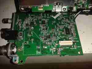
Here’s the backside of the RF board, some more interesting parts here. There’s a pair of NJM3404A Single Supply Dual Op-Amp ICs, and a TK10931V Dual AM/FM IF Discriminator IC. This is the one that does all the back-end radio functionality. The audio amplifier for the internal speaker & external headphone jack is also on this PCB, top left. A board-to-board interconnect links this radio board with the main control board underneath.

Control PCB Front
Control PCB Front

Here’s the front of the control PCB, nothing much to see here, just the LCD & membrane keypad contacts.

Control PCB Reverse
Control PCB Reverse

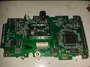
And here’s the reverse side of the control board. All the interesting bits are here. The main microcontroller is on the right, a Renesas M38D59GF, a fairly powerful MCU, with onboard LCD drive, A/D converter, serial interface, 60K of ROM & 2K of RAM. It’s 6.143MHz clock crystal is just below it.
The mating connector for the RF board is in the centre here.

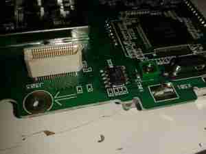
There is also a Microchip 24LC168 16KB I²C EEPROM next to the main microcontroller. This is probably for storing user settings, frequencies, etc.

EEPROM
EEPROM

The rest of this board is dedicated to battery charging and power supply, in the centre is a dual switching controller, I can’t figure out the numbers on the tiny SOT23 components in here, but this is dealing with the DC 6v input & to the left of that is the circuitry for charging the NiMH cells included with the scanner.

PSU
PSU

The last bit of this PCB is a BU2092FV Serial In / Parallel Out 4 channel driver. Not sure what this one is doing, it might be doing some signal multiplexing for the RF board interface. Unfortunately the tracks from this IC are routed on the inner layers of the board so they can’t be traced out.

Posted on 22 Comments

GY561 Frequency & Power Meter

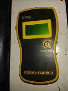
The latest addition to my radio shack is the GY561 frequency & power meter, which has already come in useful for measuring the output power of all my radios.

GY561
GY561

It’s a small device, roughly the same size & weight as a stock UV-5R. Power is provided by 3 AAA cells.

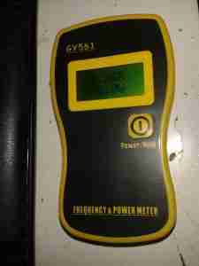
Display
Display

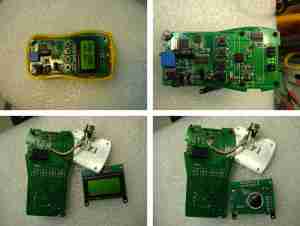
The display is a standard HD44780 8×2 module. The display on this unit isn’t backlit, so no operating in the dark.

Cover Removed
Cover Removed

The cover pops off easily to allow access to the internals, without having to remove any screws!
The 4 screws on the back of the unit hold the heatsink plate for the 50W 50Ω dummy load resistor.
Removing the cover reveals a couple of adjustments, for frequency & RF power calibration.

There are also 3 tactile switches that aren’t on the front panel. According to the manual (which in itself is a masterpiece of Chinglish), they are used to software calibrate the unit if an accurate RF power source is available. I will attempt to do a reasonable translation when time allows.

Disassembly further than this involves some desoldering in awkward places, so a search of the internet revealed an image of the rest of the internal components. In the case of my meter, all the part numbers have been scrubbed off the ICs in an attempt to hide their purpose. While it’s possible to cross-reference IC databooks & find the part numbers manually, this process is a time consuming one. Luckily the image I managed to locate doesn’t have the numbers scrubbed.

Total Disassembly
Total Disassembly

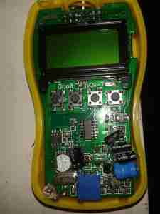
Under the LCD is some 74HC series logic, and a prescaler IC as seen in the previous frequency counter post. However in this unit the prescaler is a MB506 microwave band version to handle the higher frequencies specified.
In this case however the main microcontroller is an ATMEGA8L.
This is complemented by a SN54HC393 4-bit binary counter for the frequency side of things. This seems to make it much more usable down to lower frequencies, although the manual is very generous in this regard, stating that it’s capable of reading down to 1kHz. In practice I’ve found the lowest it reliably reads the frequency input is 10MHz, using my AD9850 DDS VFO Module as a signal source.
It did however read slightly high on all readings with the DDS, but this could have been due to the low power output of the frequency source.
Just like the other frequency counter module, this also uses a trimmer capacitor to adjust the microcontroller’s clock frequency to adjust the calibration.

The power supply circuitry is in the bottom left corner of the board, in this case a small switching supply. The switching regulator is needed to boost the +4.5v of the batteries to +5v for the logic.
Also, as the batteries discharge & their terminal voltage drops, the switching regulator will allow the circuit to carry on functioning. At present I am unsure of the lower battery voltage limit on the meter, but AAA cells are usually considered dead at 0.8v terminal voltage. (2.4v total for the 3 cells).
When turned on this meter draws 52mA from the battery, and assuming 1200mAh capacity for a decent brand-name AAA cell, this should give a battery life of 23 hours continuous use.

On the back of the main PCB is a 5v relay, which seems to be switching an input attenuator for higher power levels, although I only managed to trigger it on the 2m band.

Finally, right at the back attached to an aluminium plate, is the 50Ω dummy load resistor. This component will make up most of the cost of building these, at roughly £15.

On my DVM, this termination reads at about 46Ω, because of the other components on the board are skewing the reading. There are a pair of SMT resistors, at 200Ω & 390Ω in series, and these are connected across the 50Ω RF resistor, giving a total resistance of 46.094Ω.
This isn’t ideal, and the impedance mismatch will probably affect the calibration of the unit somewhat.

The heatsinking provided by the aluminium plate is minimal, and the unit gets noticeably warm within a couple of minutes measuring higher power levels.
High power readings should definitely be limited to very short periods, to prevent overheating.
The RF is sampled from the dummy load with a short piece of Teflon coax.

There’s a rubber duck antenna included, but this is pretty useless unless it’s almost in contact with the transmitting antenna, as there’s no input amplification. It might be handy for detecting RF emissions from power supplies, etc.

For the total cost involved I’m not expecting miracles as far as accuracy is concerned, (the manual states +/-10% on power readings).
The frequency readout does seem to be pretty much spot on though, and the ability to calibrate against a known source is handy if I need some more accuracy in the future.

I’ve also done an SWR test on the dummy load, and the results aren’t good.

At 145.500 MHz, the SWR is 3:1, while at 433.500 it’s closer to 4:1. This is probably due to the lower than 50Ω I measured at the meter’s connector.
These SWR readings also wander around somewhat as the load resistor warms up under power.

I’ll probably also replace the AAA cells with a LiPo cell & associated charge/protection circuitry, to make the unit chargeable via USB. Avoiding disposable batteries is the goal.