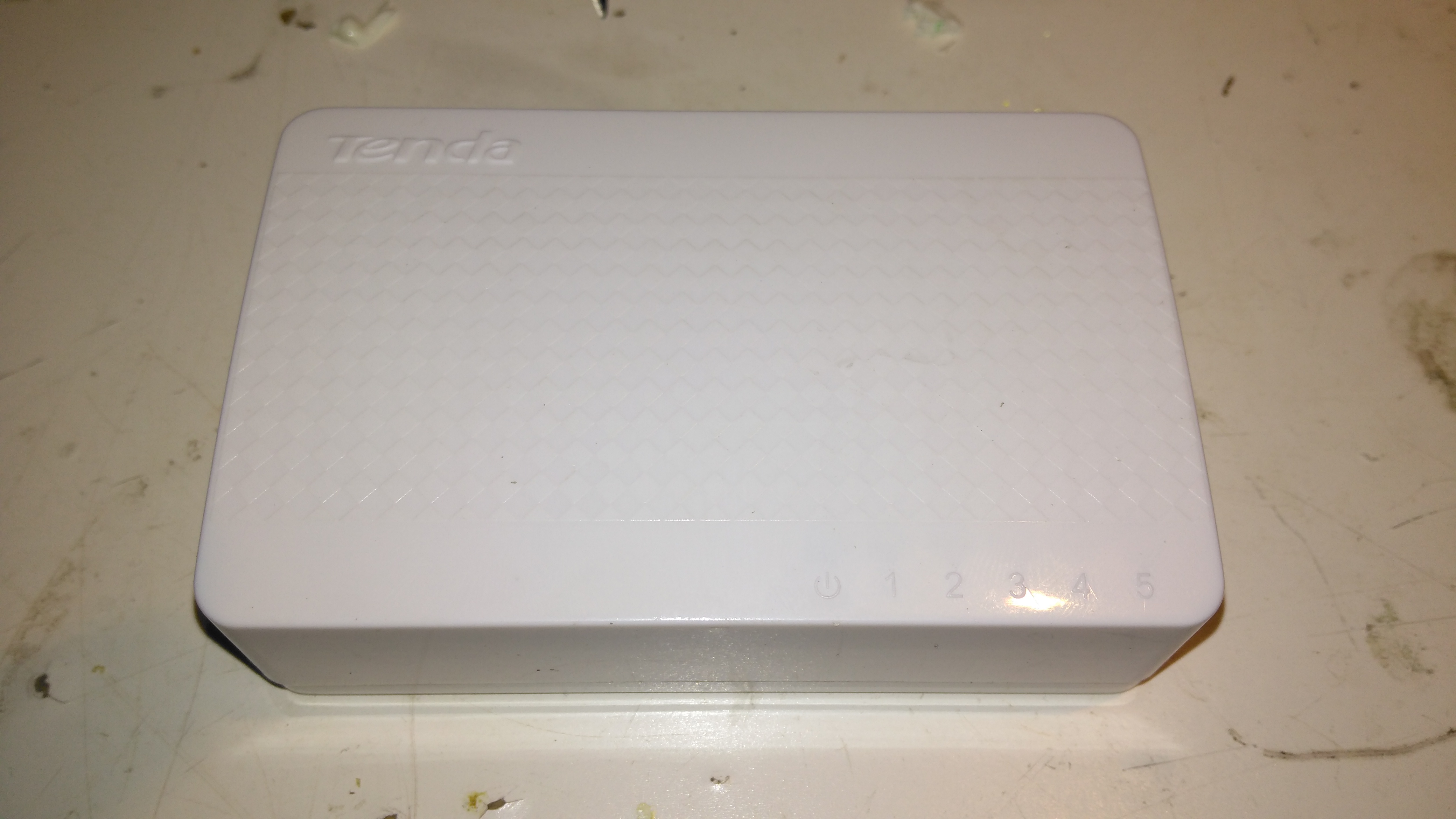
Here’s a tiny ethernet switch from the great fle market that is eBay – the Tenda S105. This unit has 5 ports, but only supports 10/100M. Still, for something so small it’s not bad.
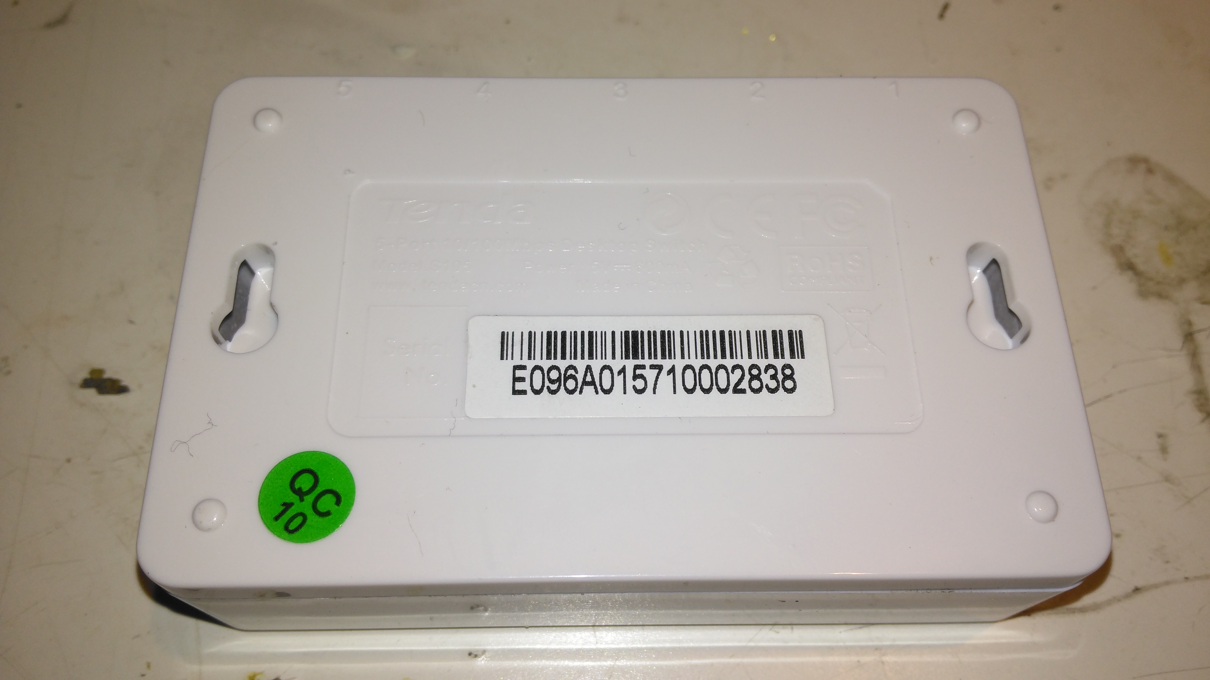
Bottom
Not much on the bottom, there’s a pair of screw hooks for mounting this to a surface.
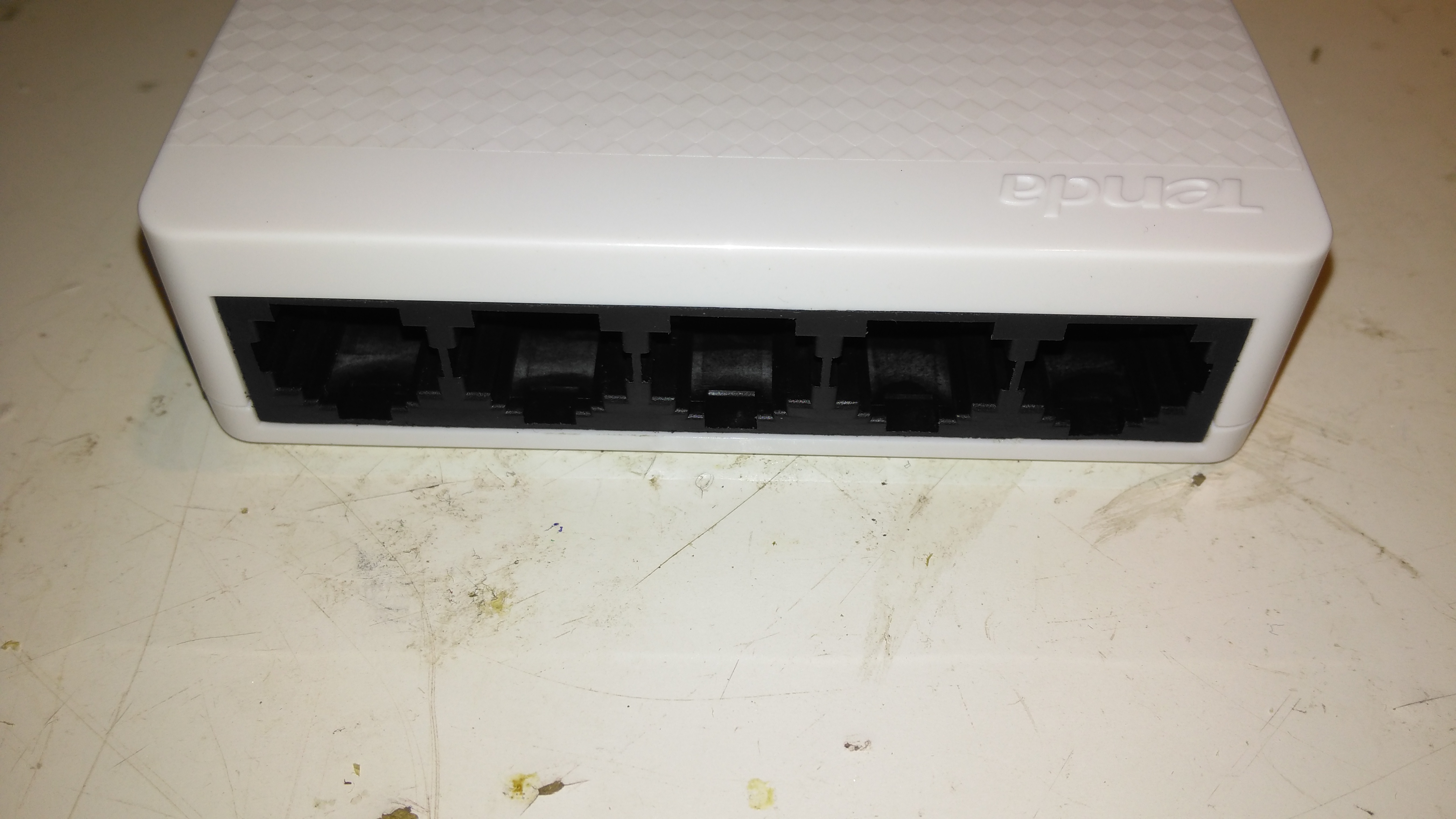
Ports
The 5 ports on the front actually have the pins for the unused pairs of the ethernet cables removed – saving every penny here.
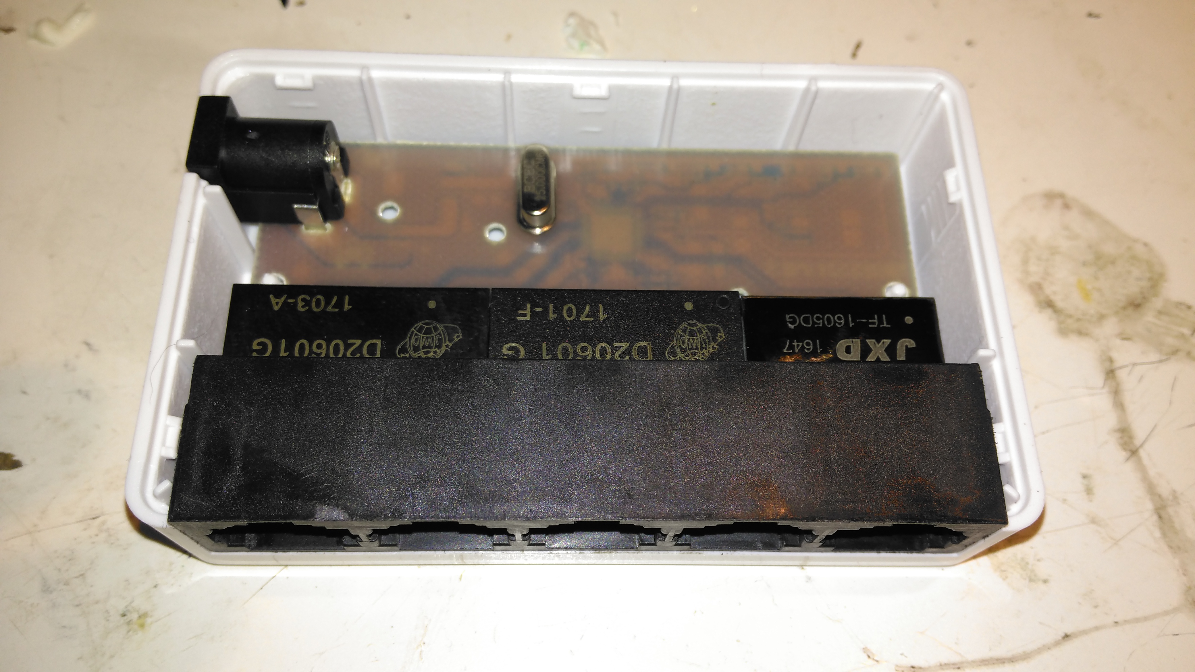
PCB Top
The casing just unclips, revealing the small PCB. Nothing much on the top, just the connectors, isolating transformers & the crystal for the switch IC.
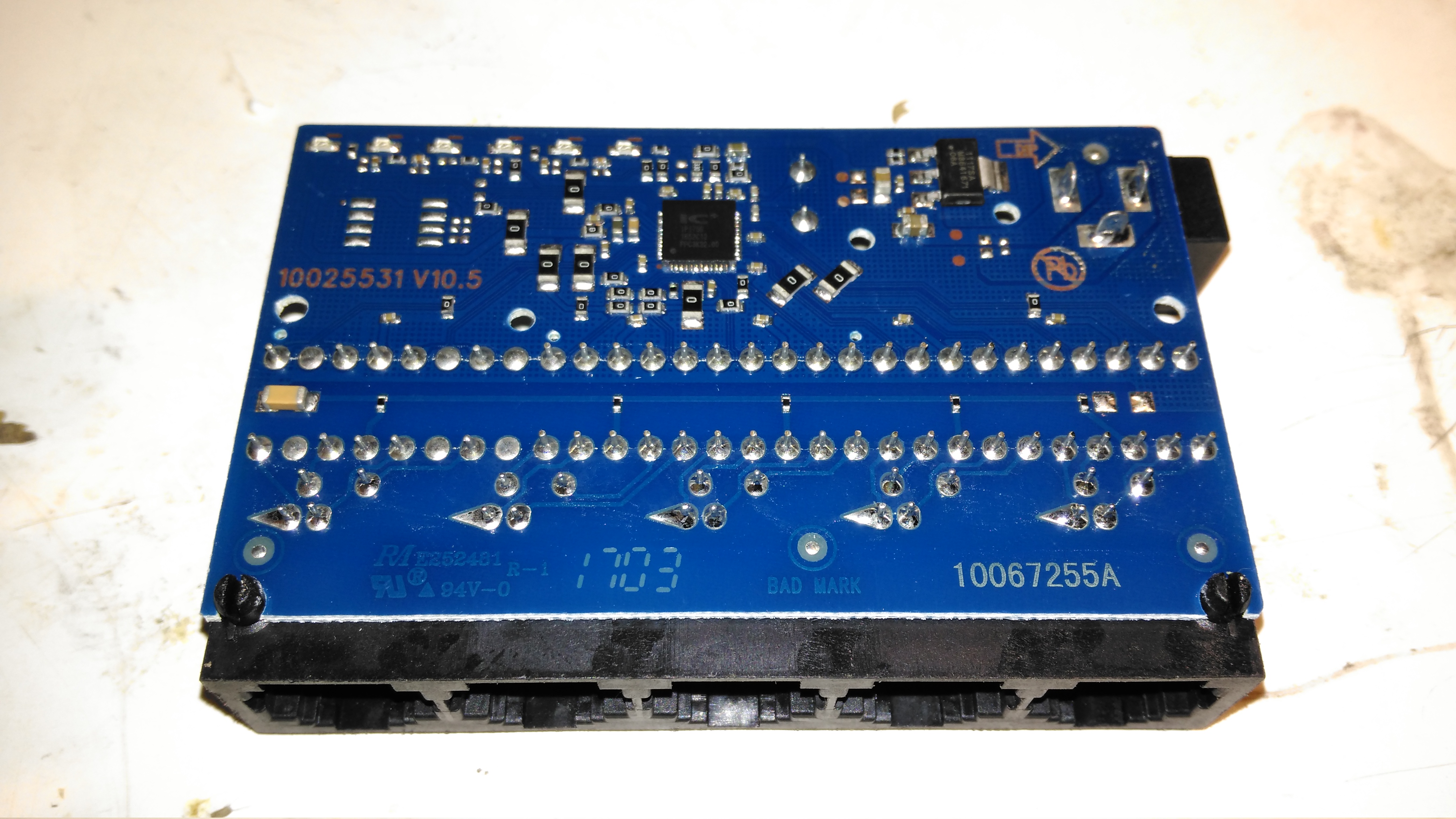
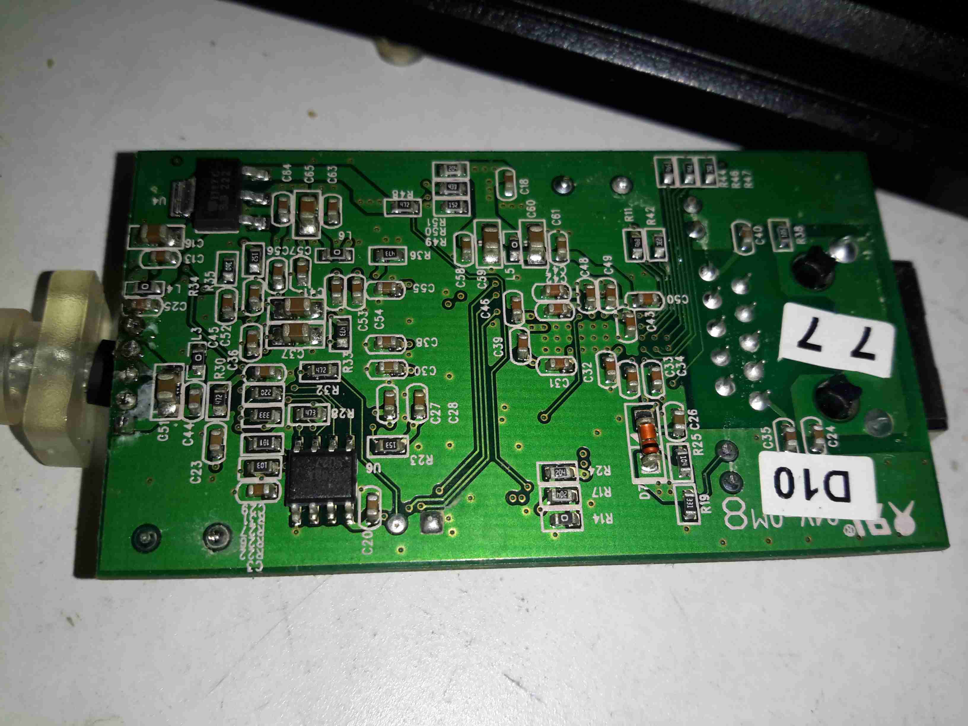
PCB Bottom
The bottom of the PCB is a little more busy, mainly with decoupling components. There’s a 3.3v linear regulator to step down the 5v input for the switch IC.
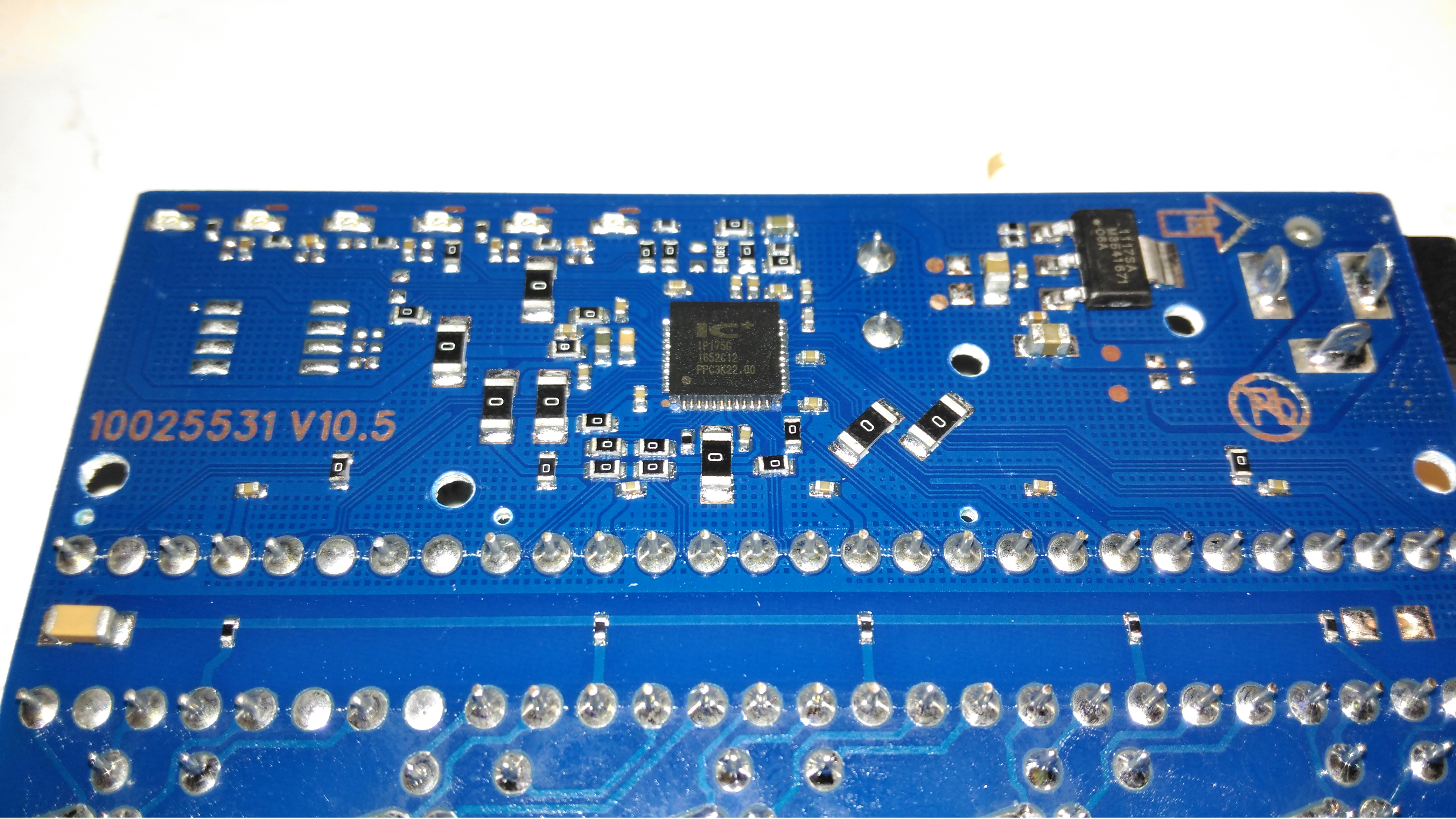
Switch IC
The IC doing all the data switching is an IP175G 5-Port 10/100 Switch from IC+ Corp. No datasheet available for this, but it’s going to be a bog-standard switch.
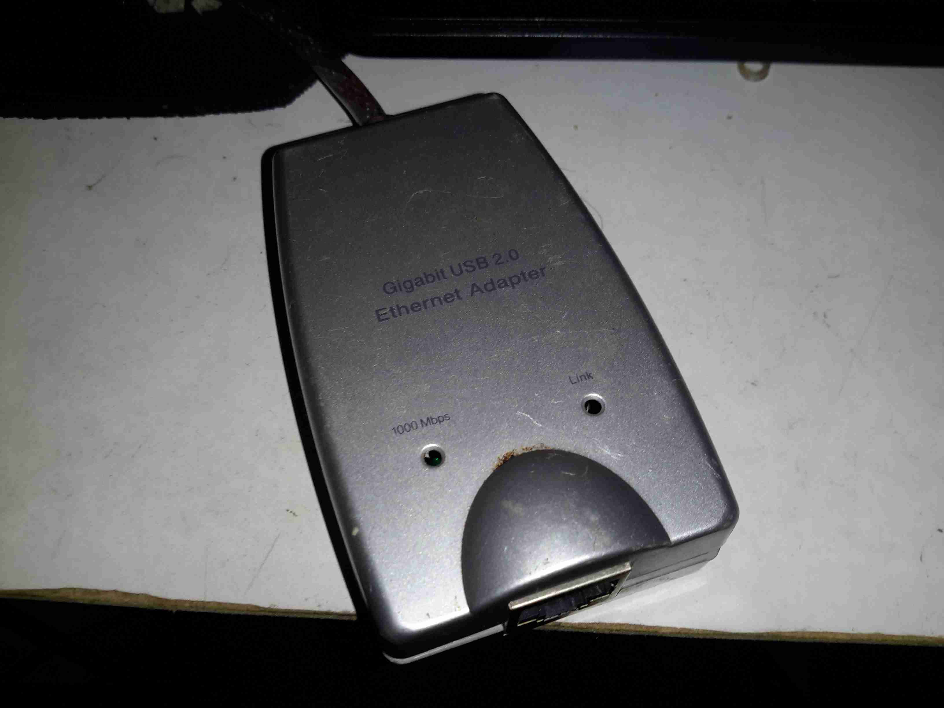
Here’s a chap eBay USB-To-Ethernet dongle I obtained for use with the Raspberry Pi Zero. This one is getting torn down permanently, as it’s rather unreliable. It seems to like having random fits where it’ll not enumerate on the USB bus. The silicon in the ICs will eventually make it here once I manage to get a new microscope 😉
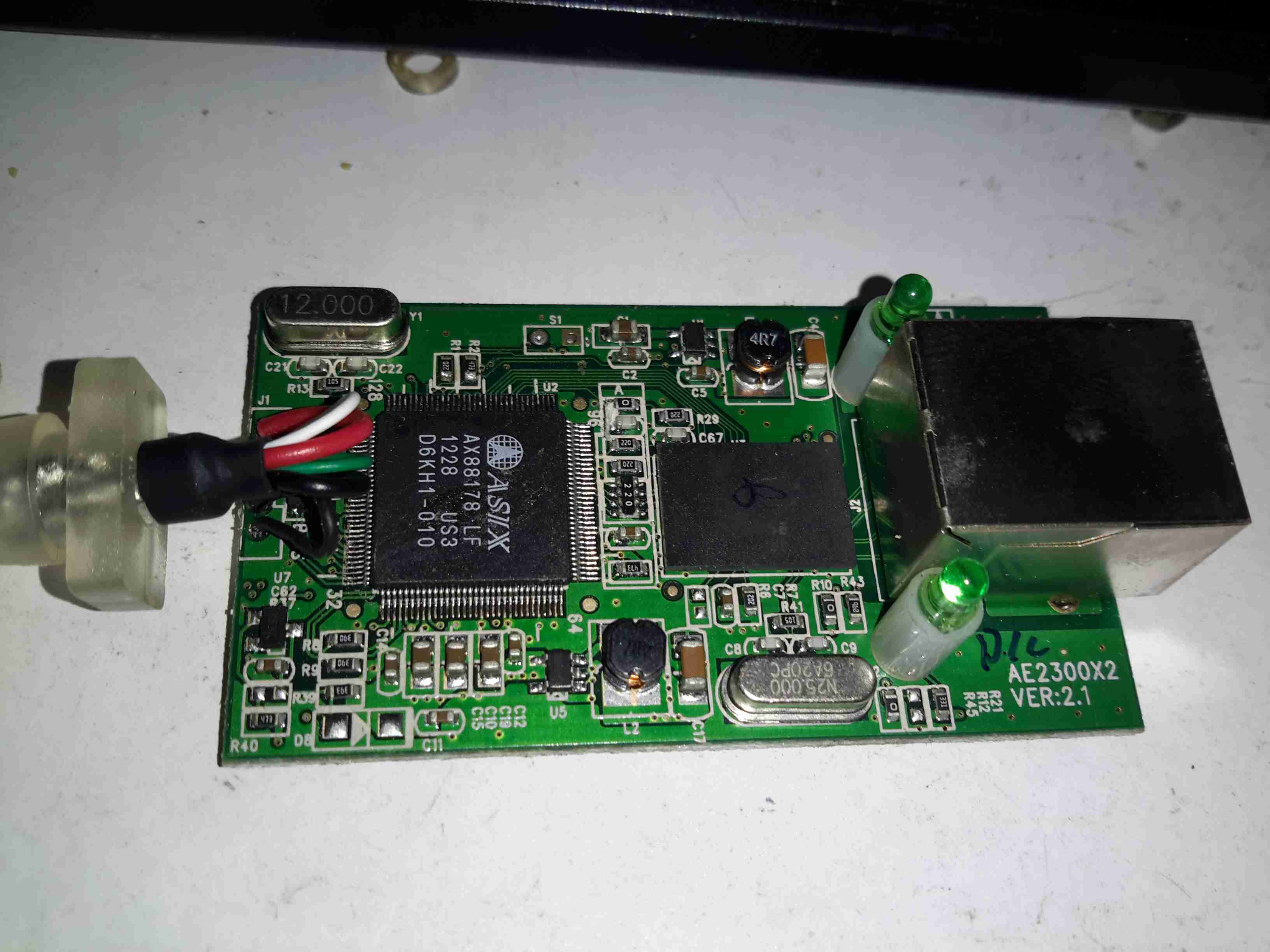
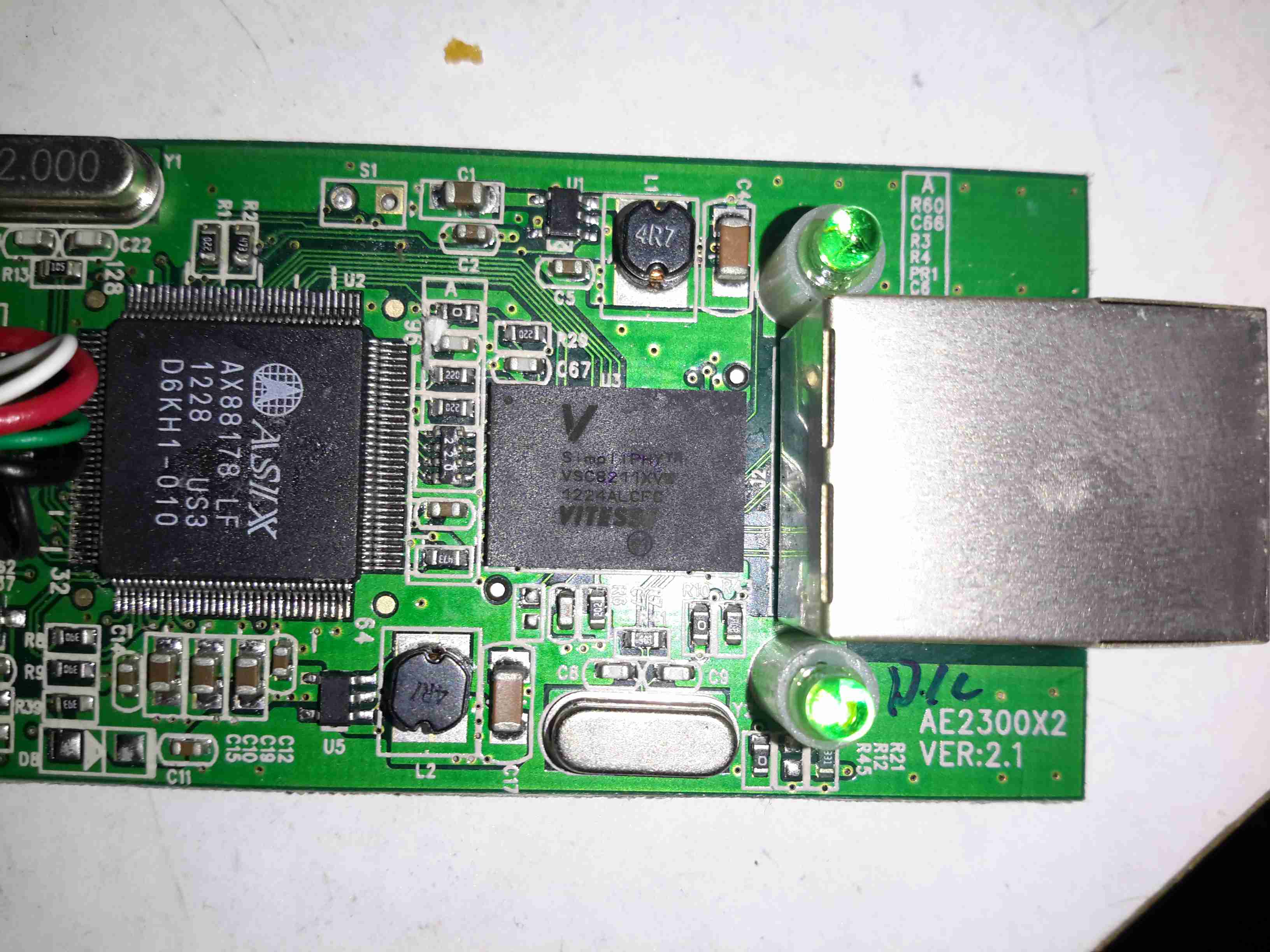
Main Chipset
This is quite a heavily packed PCB, with the main Asix AX88178 on the left. This IC contains all of the logic for implementing the Ethernet link over USB, except the PHY. It’s clock crystal is in the top left corner.
Reverse Side
Not much on the reverse side, there’s a 3.3v linear regulator at top left, the SOIC is an Atmel AT93C66A 4KB EEPROM for configuration data.
Vitesse PHY
The final IC in the chain is the Vitesse VSC8211 Gigabit PHY, with it’s clock crystal below. This interfaces the Ethernet MAC in the Asix IC to the magjack on the right.
Time for another random teardown, a signal splitter for HDMI. These units are available very cheap these days on eBay. This one splits the incoming signal into two to drive more than one display from the same signal source.
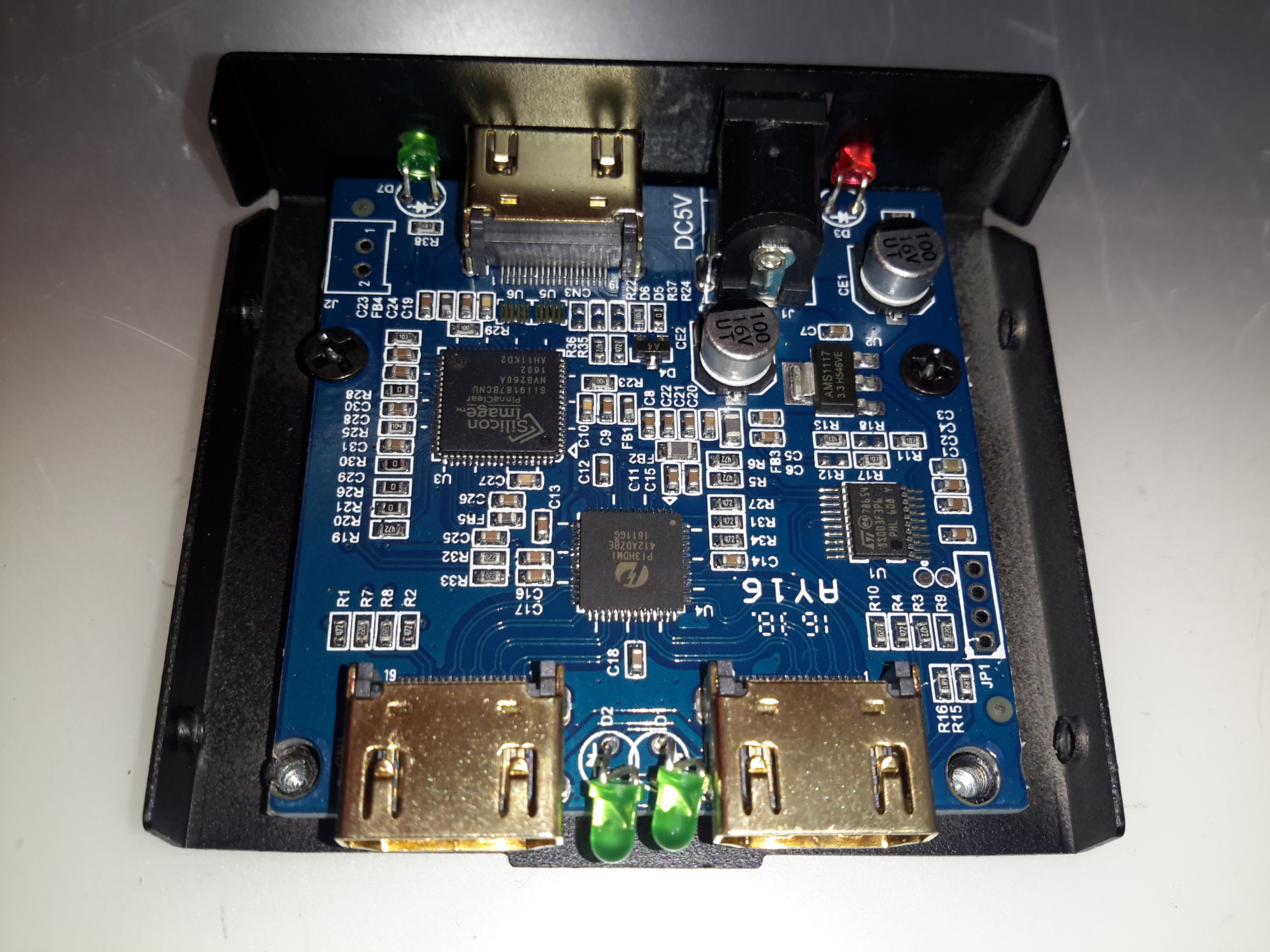
Main PCB
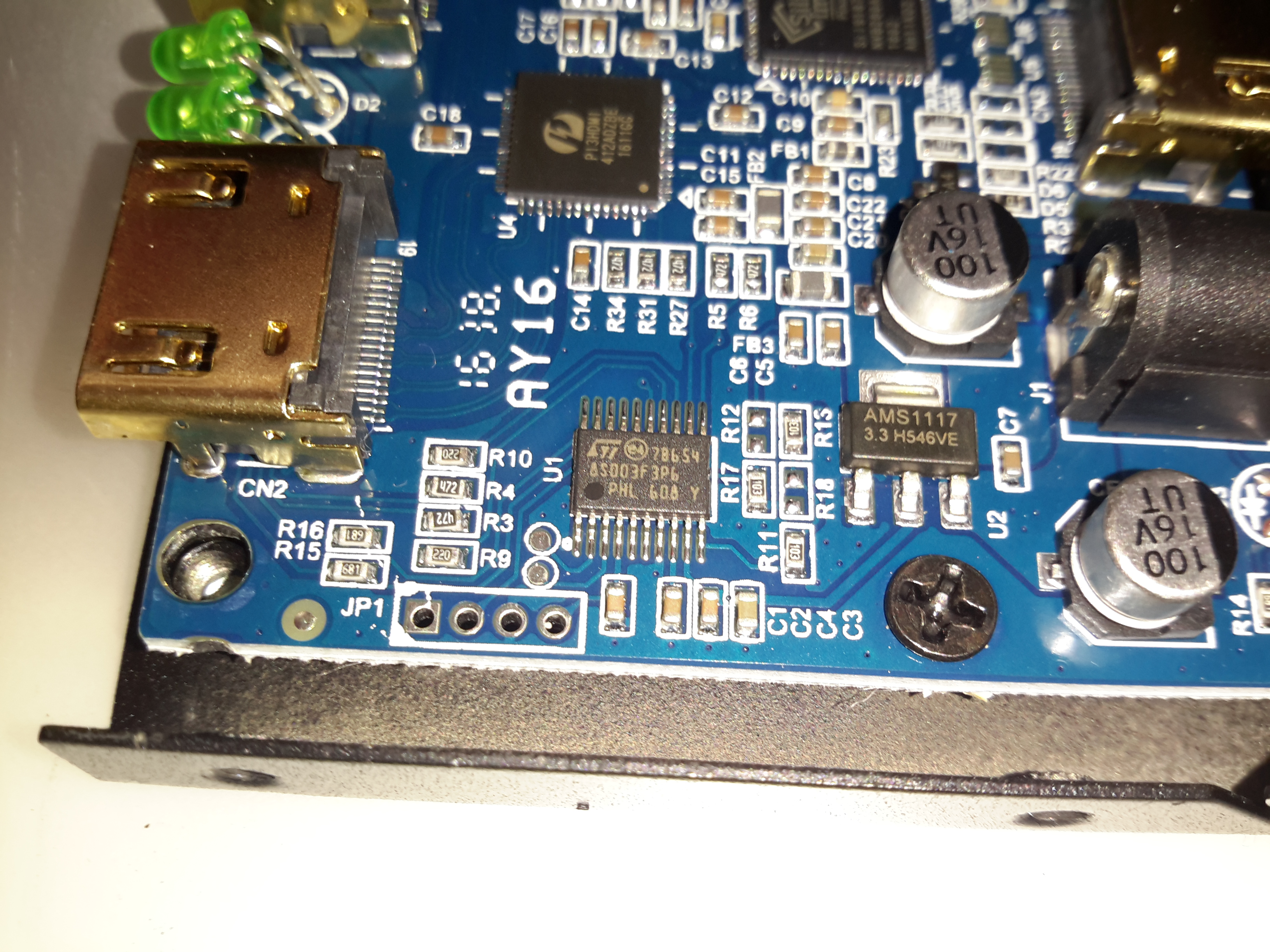
The stamped alloy casing comes apart easily with the removal of a few screws. The PCB inside is rather densely packed with components.
Chipset
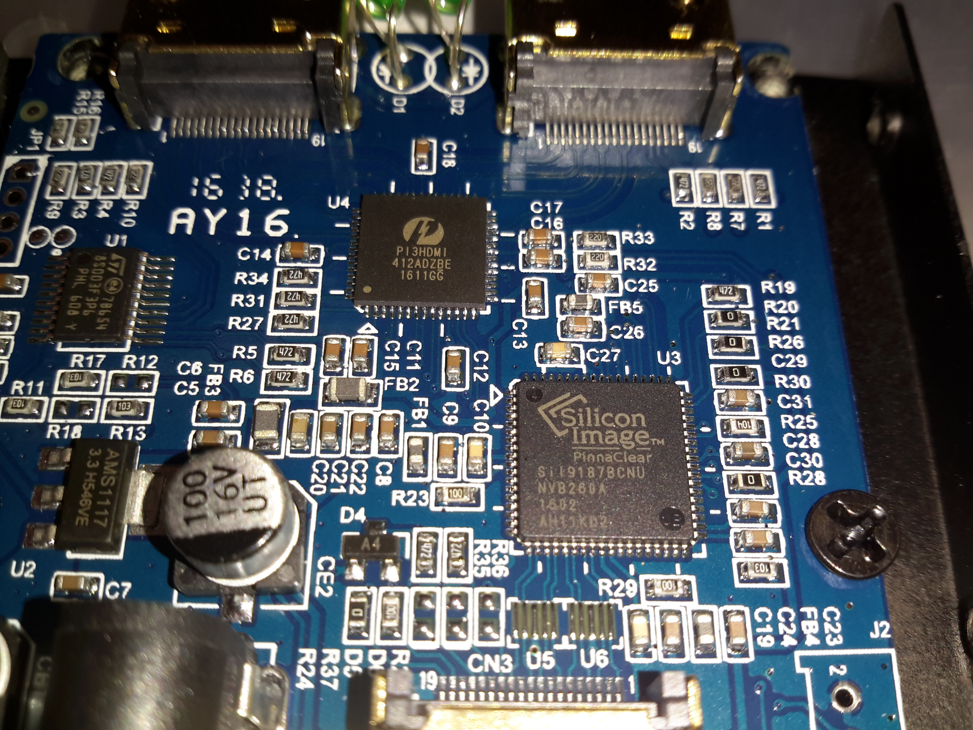
The main IC on the incoming signal is a Silicon Image Sil9187B HDMI Port Processor, with a single input & 4 outputs. In this case the chip is used as a repeater to amplify the incoming signal. the signal path then gets fed into a Pericom PI3HDMI412 HDMI Demux, which then splits the signal into two for the output ports.
Microcontroller
The main pair of ICs processing the video signals are controlled over I²C, with this STM32 microcontroller. The 4 pads to the lower left are for the STLink programmer. The main 3.3v power rail is provided by the LM1117 linear regulator on the right.
As I’ve been posting some photos of decapped ICs lately, I thought I’d share the process I use personally for those that might want to give it a go 😉
The usual method for removing the epoxy package from the silicon is to use hot, concentrated Nitric Acid. Besides the obvious risks of having hot acids around, the decomposition products of the acid, namely NO² (Nitrogen Dioxide) & NO (Nitrogen Oxide), are toxic and corrosive. So until I can get the required fume hood together to make sure I’m not going to corrode the place away, I’ll leave this process to proper labs ;).
The method I use is heat based, using a Propane torch to destroy the epoxy package, without damaging the Silicon die too much.
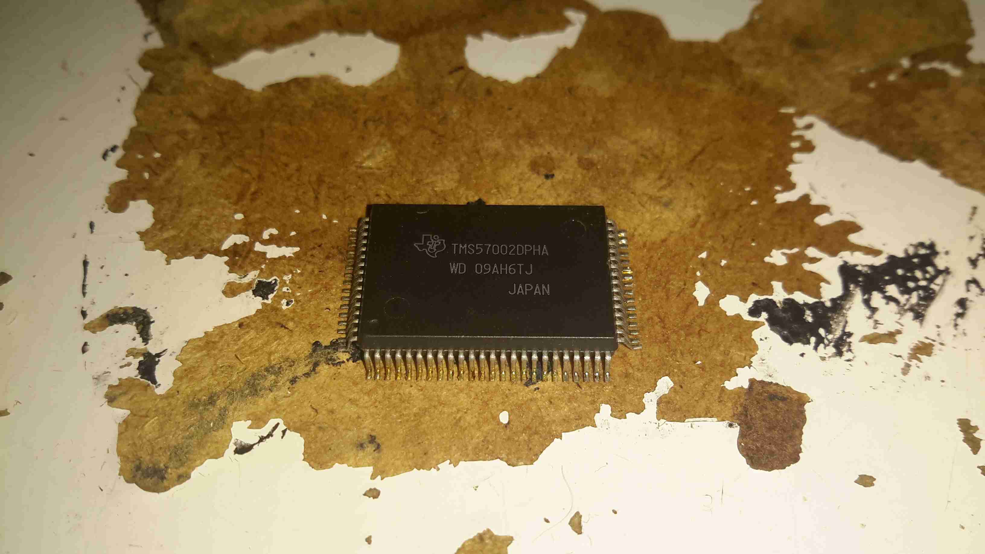
TMS57002 Audio DSP
I start off, obviously, with a desoldered IC, the one above an old audio DSP from TI. I usually desolder en-masse for this with a heat gun, stripping the entire board in one go.
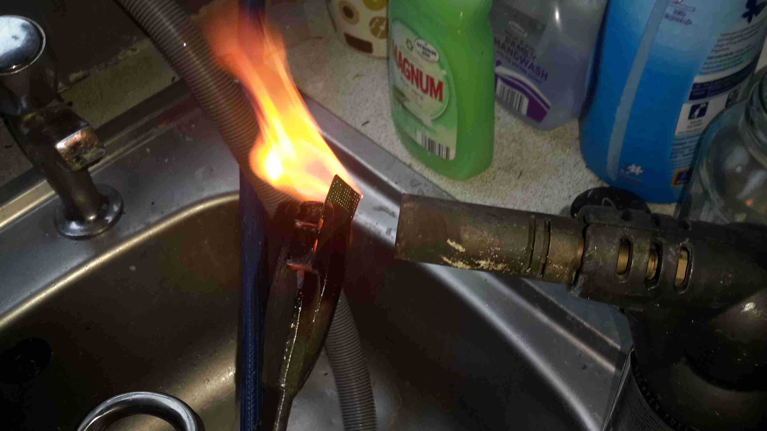
FLAMES!
Next is to apply the torch to the IC. A bit of practice is required here to get the heat level & time exactly right, overheating will cause the die to oxidize & blacken or residual epoxy to stick to the surface.
I usually apply the torch until the package just about stops emitting it’s own yellow flames, meaning the epoxy is almost completely burned away. I also keep the torch flame away from the centre of the IC, where the die is located.
Breathing the fumes from this process isn’t recommended, no doubt besides the obvious soot, the burning plastic will be emitting many compounds not brilliant for Human health!
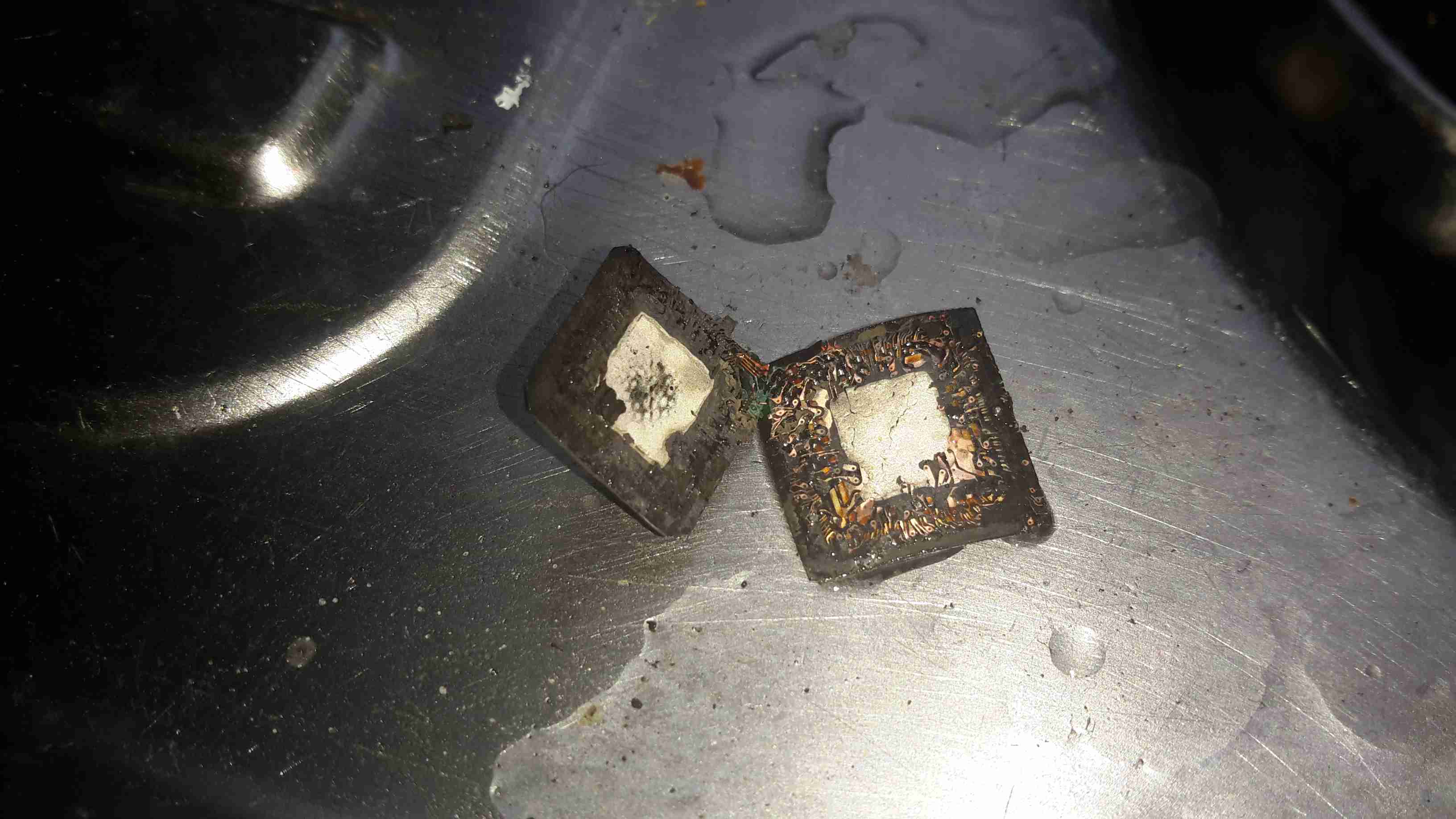
Once the IC is roasted to taste, it’s quenched in cold water for a few seconds. Sometimes this causes such a high thermal shock that the leadframe cracks off the epoxy around the die perfectly.
All Your Die Belong To Us
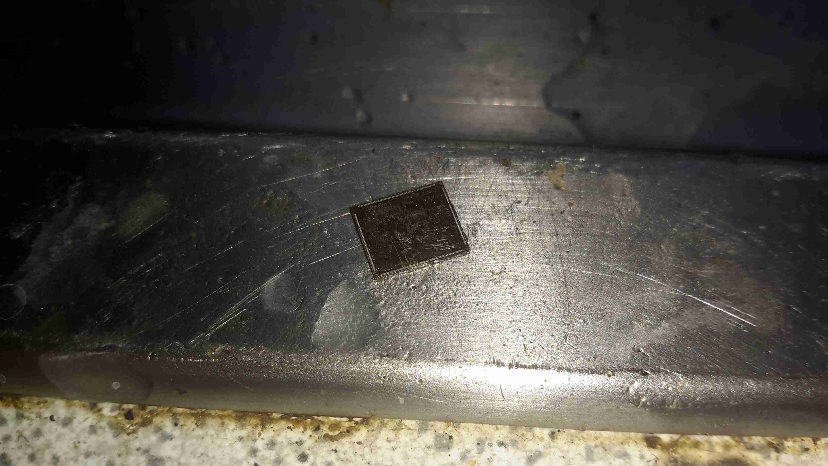
Now that the epoxy has been destroyed, it breaks apart easily, and is picked away until I uncover the die itself. (It’s the silver bit in the middle of the left half). The heat from the torch usually destroys the Silver epoxy holding the die to the leadframe, and can be removed easily from the remaining package.
Decapped
BGA packages are usually the easiest to decap, flip-chip packages are a total pain due to the solder balls being on the front side of the die, I haven’t managed to get a good result here yet, I’ll probably need to chemically remove the first layer of the die to get at the interesting bits 😉
Slide
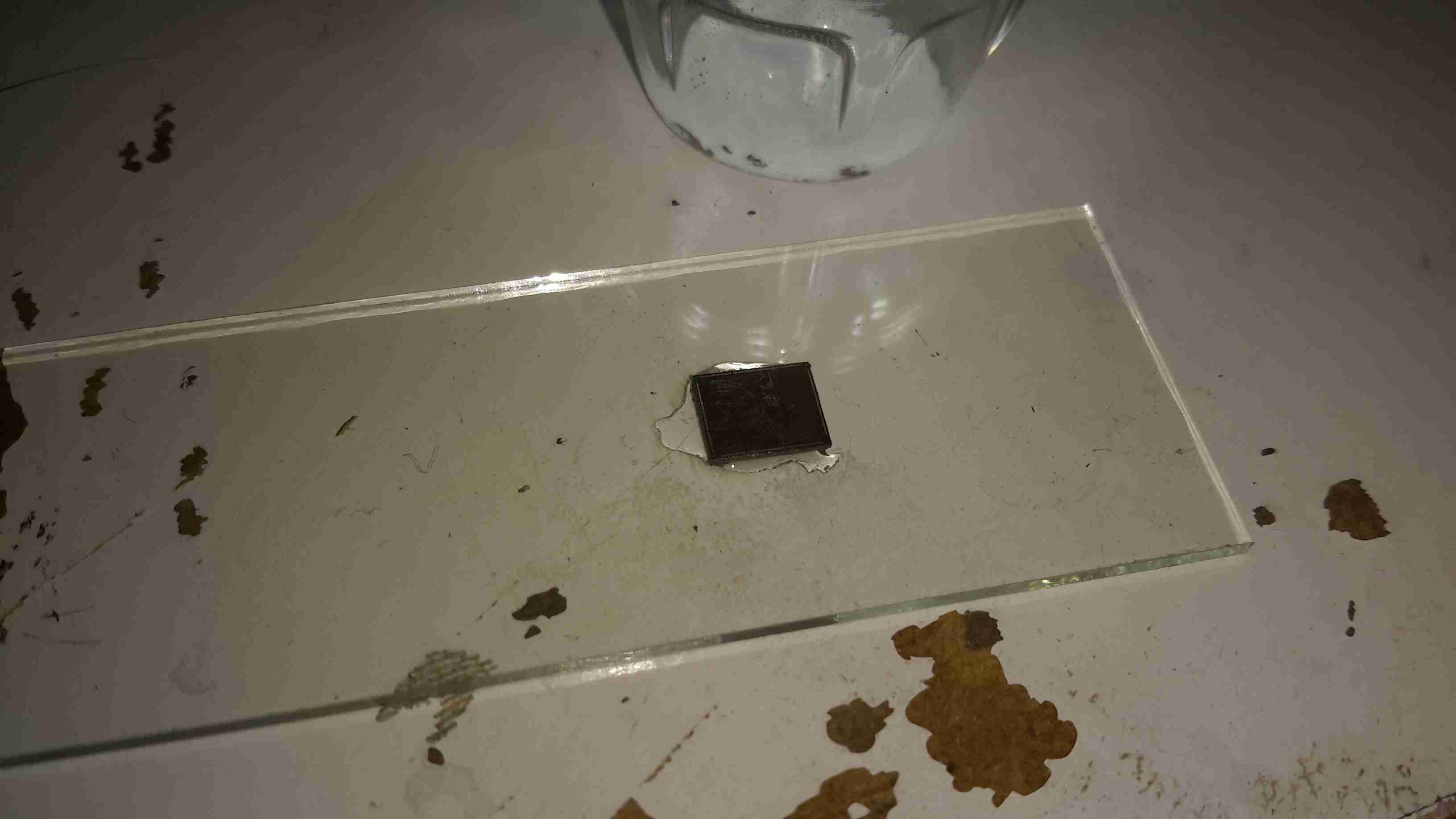
Once the die has been rinsed in clean water & inspected, it’s mounted on a glass microscope slide with a small spot of Cyanoacrylate glue to make handling easier.
Some dies require some cleaning after decapping, for this I use 99% Isopropanol & 99% Acetone, on the end of a cotton bud. Any residual epoxy flakes or oxide stuck to the die can be relatively easily removed with a fingernail – turns out fingernails are hard enough to remove the contamination, but not hard enough to damage the die features.
Once cleaning is complete, the slide is marked with the die identification, and the photographing can begin.
Microscope Mods
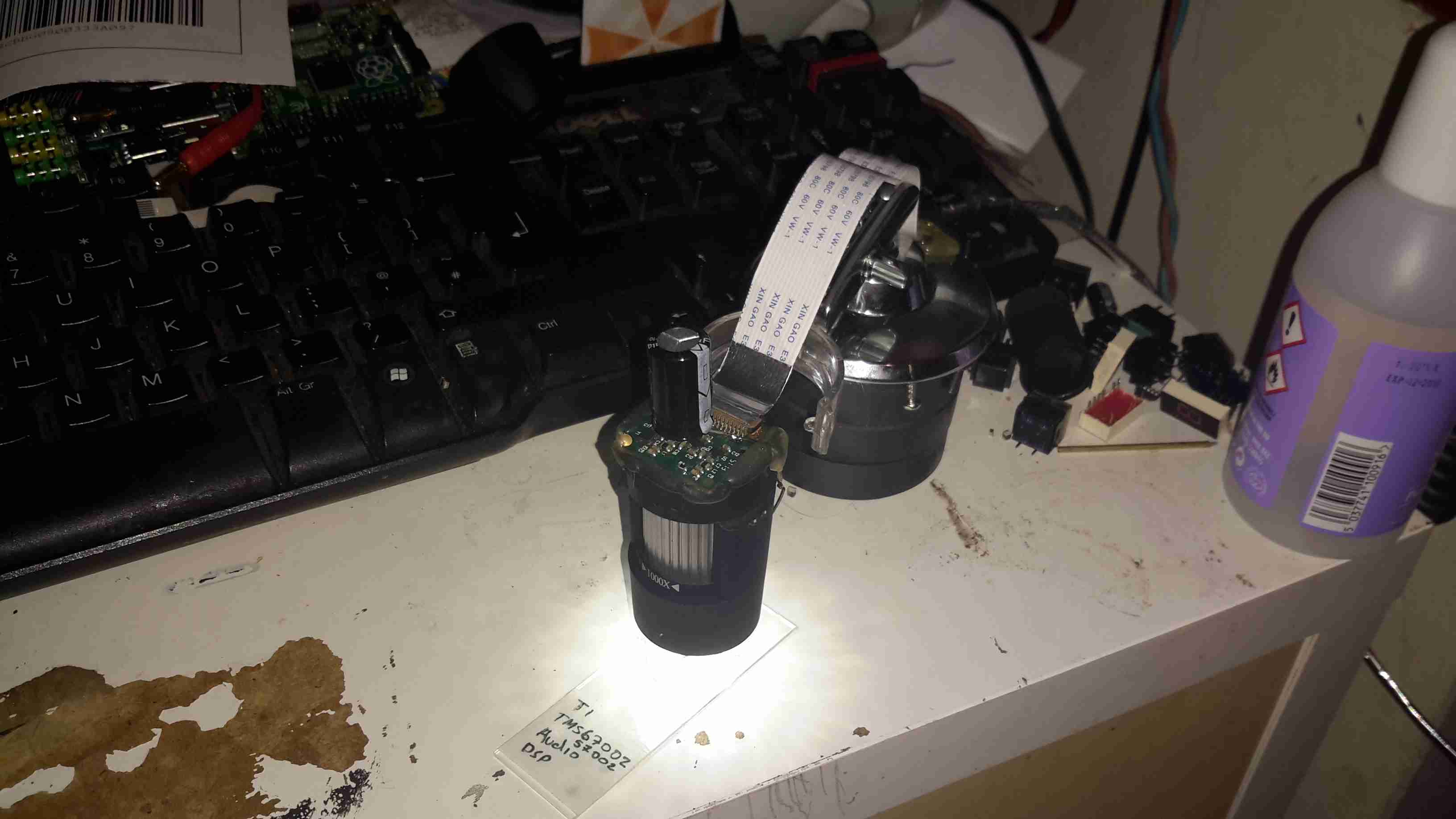
I had bought a cheap eBay USB microscope to get started, as I can’t currently afford a proper metallurgical microscope, but I found the resolution of 640×480 very poor. Some modification was required!
Modified Microscope
I’ve removed the original sensor board from the back of the optics assembly & attached a Raspberry Pi camera board. The ring that held the original sensor board has been cut down to a minimum, as the Pi camera PCB is slightly too big to fit inside.
The stock ring of LEDs is run direct from the 3.3v power rail on the camera, through a 4.7Ω resistor, for ~80mA. I also added a 1000µF capacitor across the 3.3v supply to compensate a bit for the long cable – when a frame is captured the power draw of the camera increases & causes a bit of voltage drop.
The stock lens was removed from the Pi camera module by careful use of a razor blade – being too rough here *WILL* damage the sensor die or the gold bond wires, which are very close to the edge of the lens housing, so be gentle!
Mounting Base
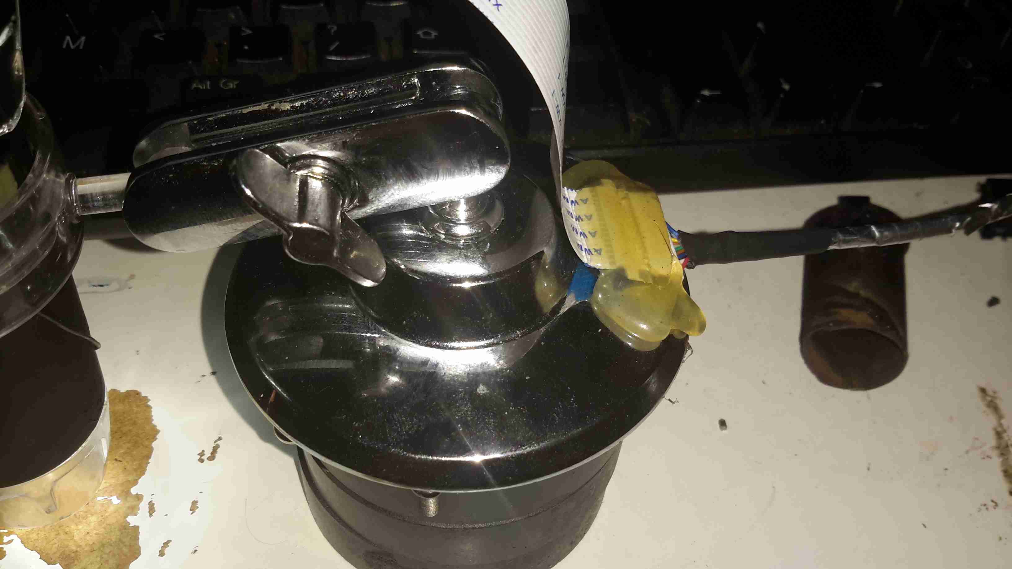
The existing mount for the microscope is pretty poor, so I’ve used a couple of surplus ceramic ring magnets as a better base, this also gives me the option of raising or lowering the base by adding or removing magnets.
To get more length between the Pi & the camera, I bought a 1-meter cable extension kit from Pi-Cables over at eBay, cables this long *definitely* require shielding in my space, which is a pretty aggressive RF environment, or interference appears on the display. Not surprising considering the high data rates the cable carries.
The FFC interface is hot-glued to the back of the microscope mount for stability, for handheld use the FFC is pretty flexible & doesn’t apply any force to the scope.
Die Photography
Since I modified the scope with a Raspberry Pi camera module, everything is done through the Pi itself, and the raspistill command.
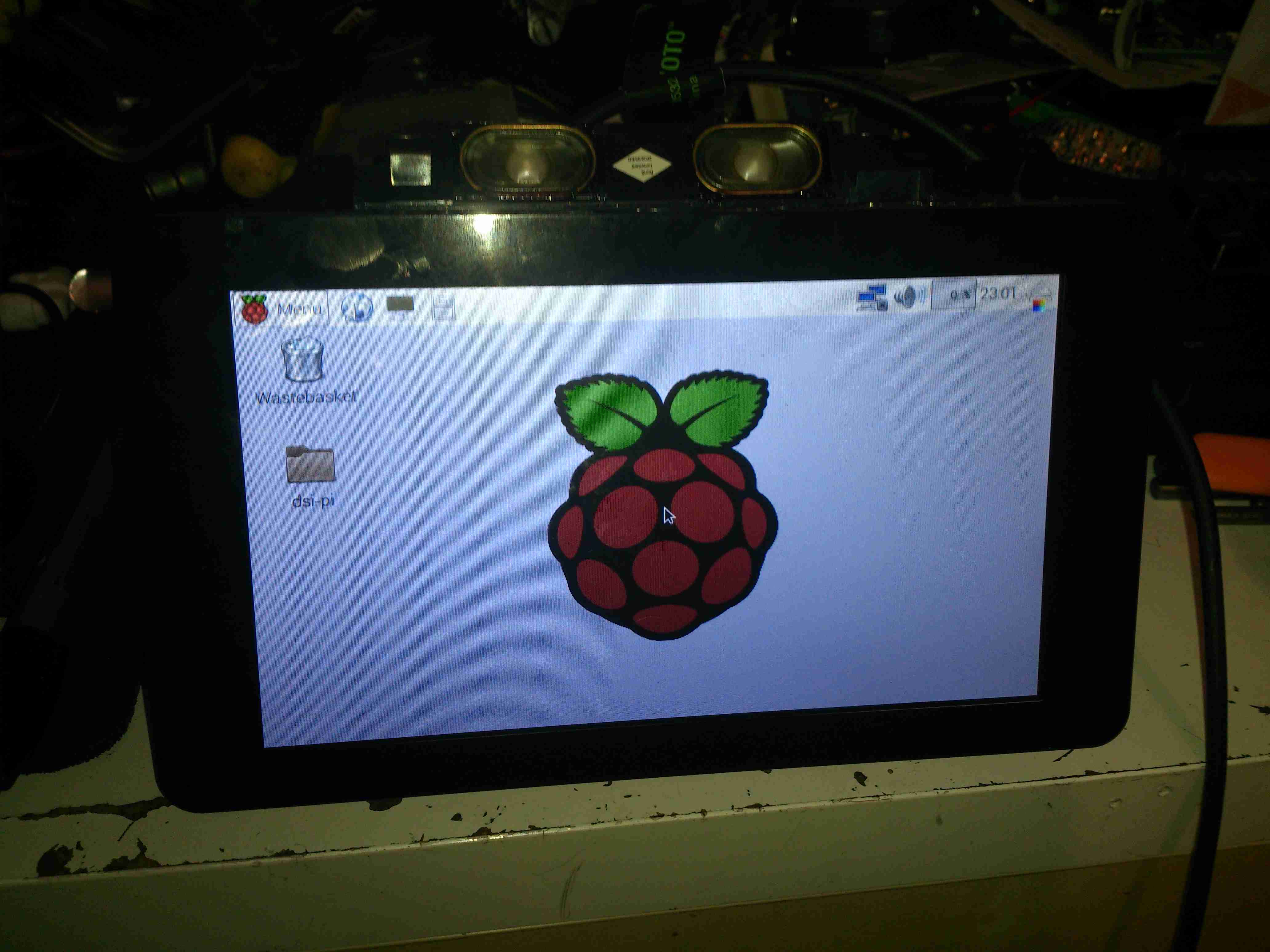
Pi LCD
The command I’m currently using to capture the images is:
raspistill -ex auto -awb auto -mm matrix -br 62 -q 100 -vf -hf -f -t 0 -k -v -o CHIPNAME_%03d.jpg
This command waits between each frame for the ENTER key to be pressed, allowing me to position the scope between shots. Pi control & file transfer is done via SSH, while I use the 7″ touch LCD as a viewfinder.
The direct overhead illumination provided by the stock ring of LEDs isn’t ideal for some die shots, so I’m planning on fitting some off-centre LEDs to improve the resulting images.
Image Processing
Obviously I can’t get an ultra-high resolution image with a single shot, due to the focal length, so I have to take many shots (30-180 per die), and stitch them together into a single image.
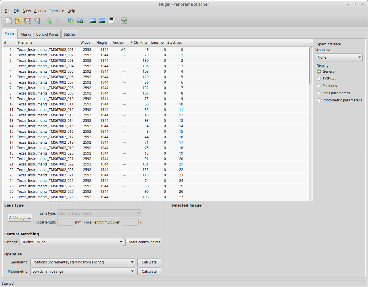
For this I use Hugin, an open-source panorama photo stitching package.
Hugin
Here’s Hugin with the photos loaded in from the Raspberry Pi. To start with I use Hugin’s built in CPFind to process the images for control points. The trick with getting good control points is making sure the images have a high level of overlap, between 50-80%, this way the software doesn’t get confused & stick the images together incorrectly.
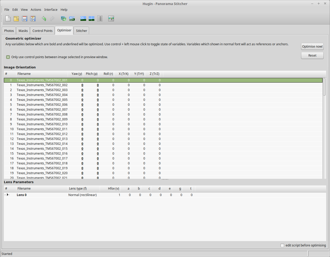
Optimiser
After the control points are generated, which for a large number of high resolution images can take some time, I run the optimiser with only Yaw & Pitch selected for all images.
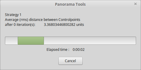
Optimising
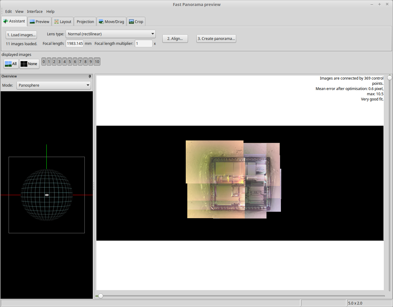
If all goes well, the resulting optimisation will get the distance between control points to less than 0.3 pixels.
Panorama Preview
After the control points & optimisation is done, the resulting image can be previewed before generation.
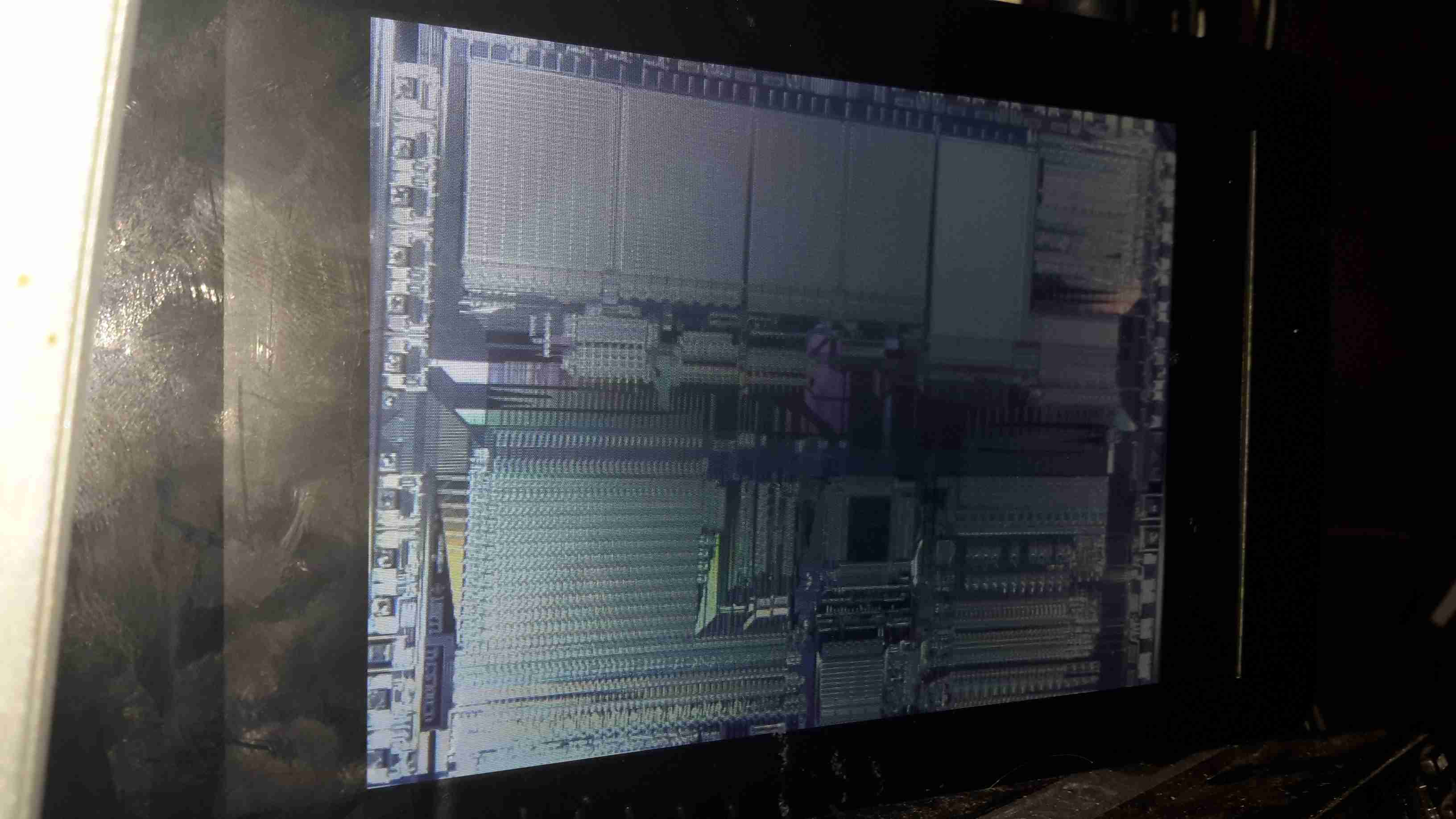
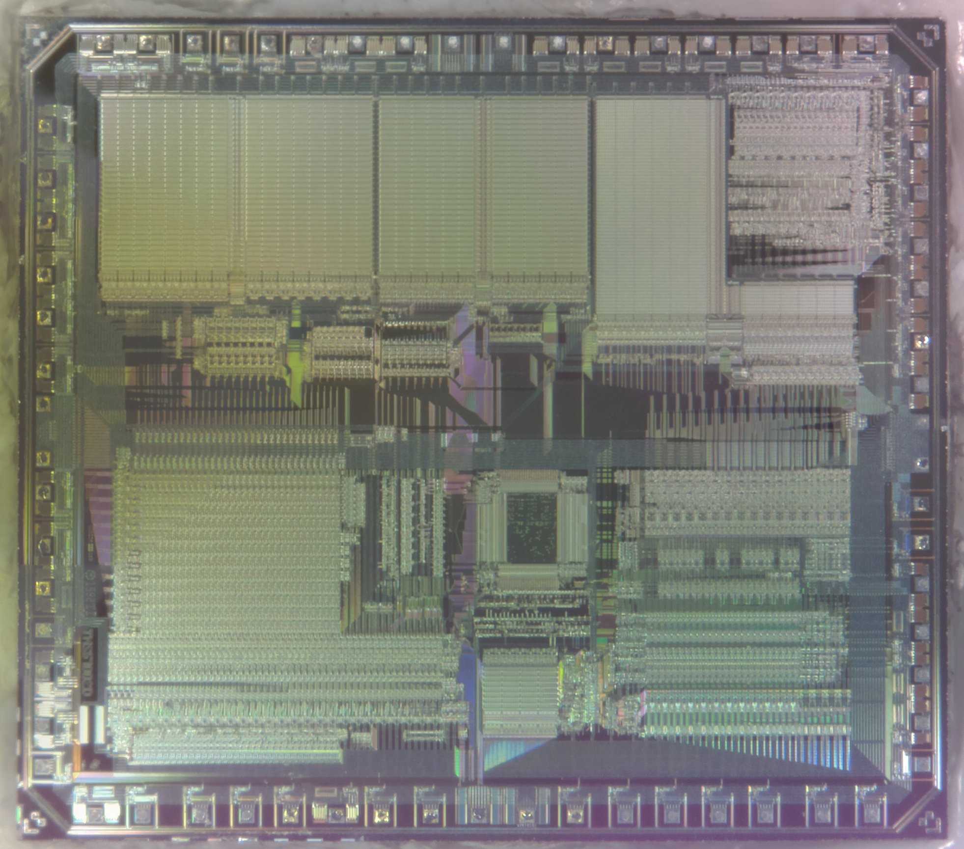
Texas Instruments TMS67002
After all the image processing, the resulting die image should look something like the above, with no noticeable gaps.
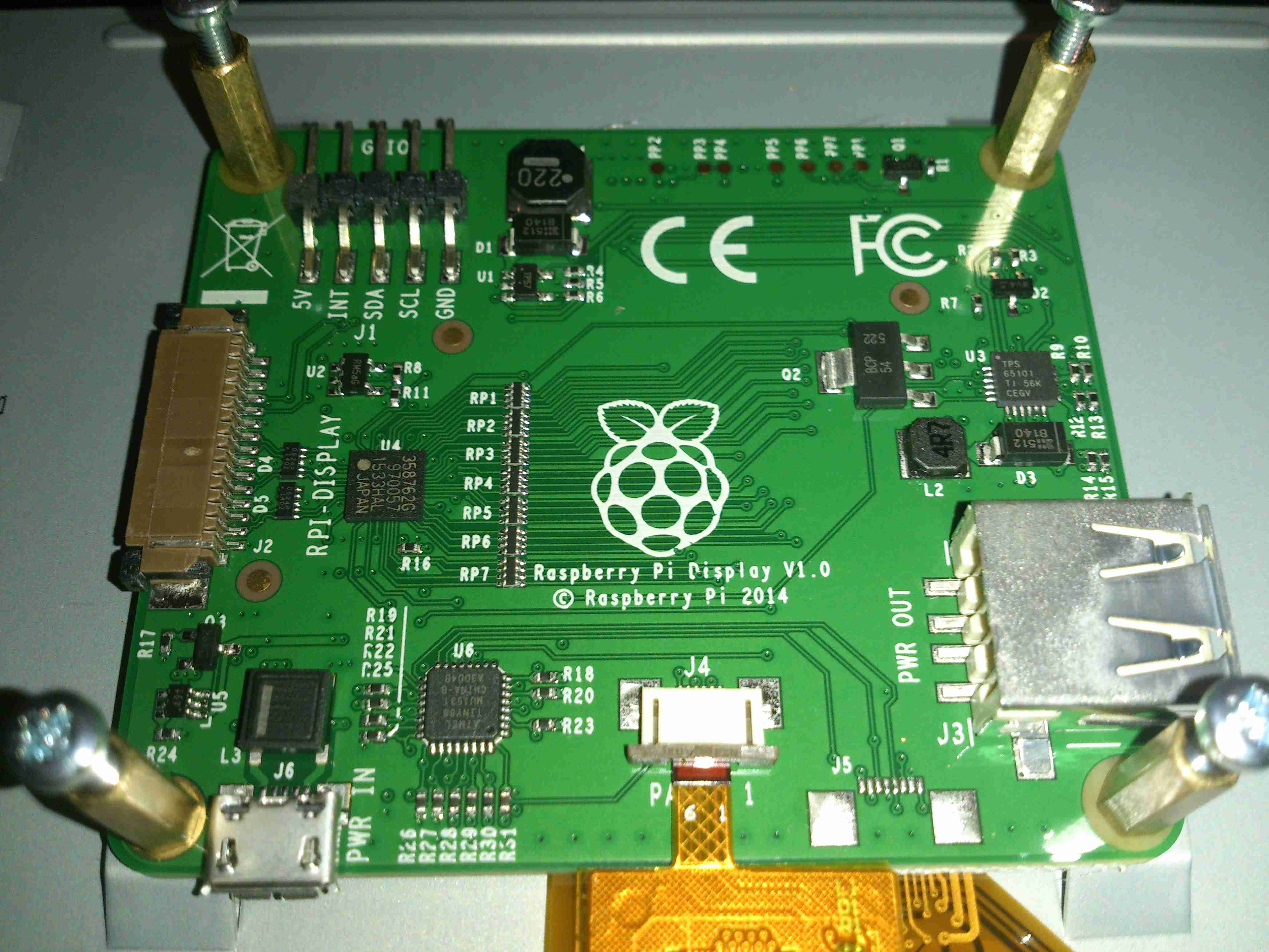
Finally the Raspberry Pi Foundation have released an official LCD for the DSI connector on the Pi. When these were announced, I placed an order straight away, but due to demand it’s taken quite a while for it to arrive in the post.
Interface PCB
The LCD itself is an RGB panel, to interface the Pi via the MIPI DSI port, some signal conversion is required. A small PCB is mounted on the back of the LCD to do this conversion. It also handles the power supply rails required by the LCD itself & interfacing the touch screen.
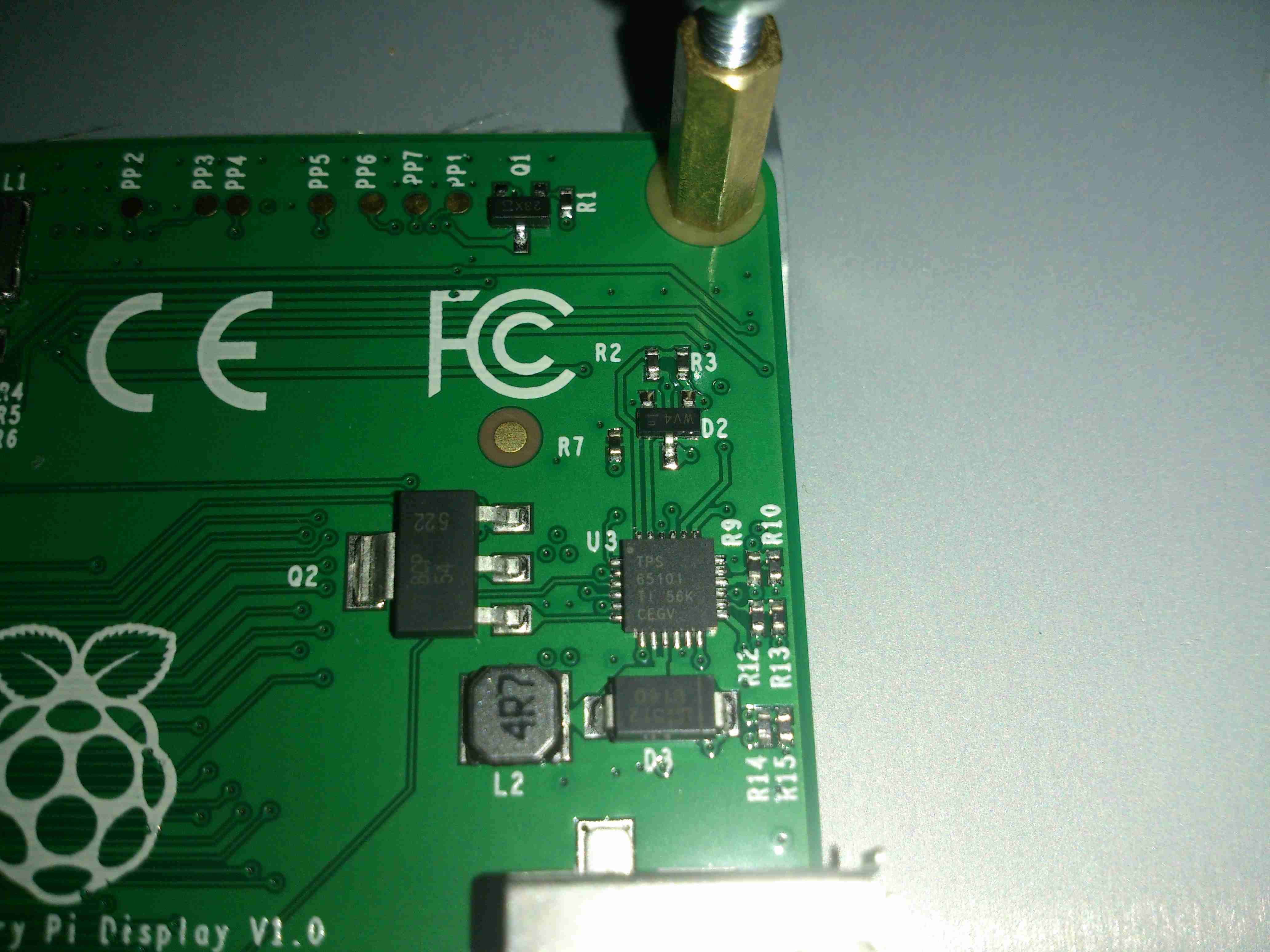
LCD Power Supply
Taking care of the power supply is a Texas Instruments TPS65101 triple output LCD power supply IC. This also has a built in linear regulator to supply 3.3v for the rest of the circuitry on board. The large transistor to the left of the IC is the pass transistor for this regulator.
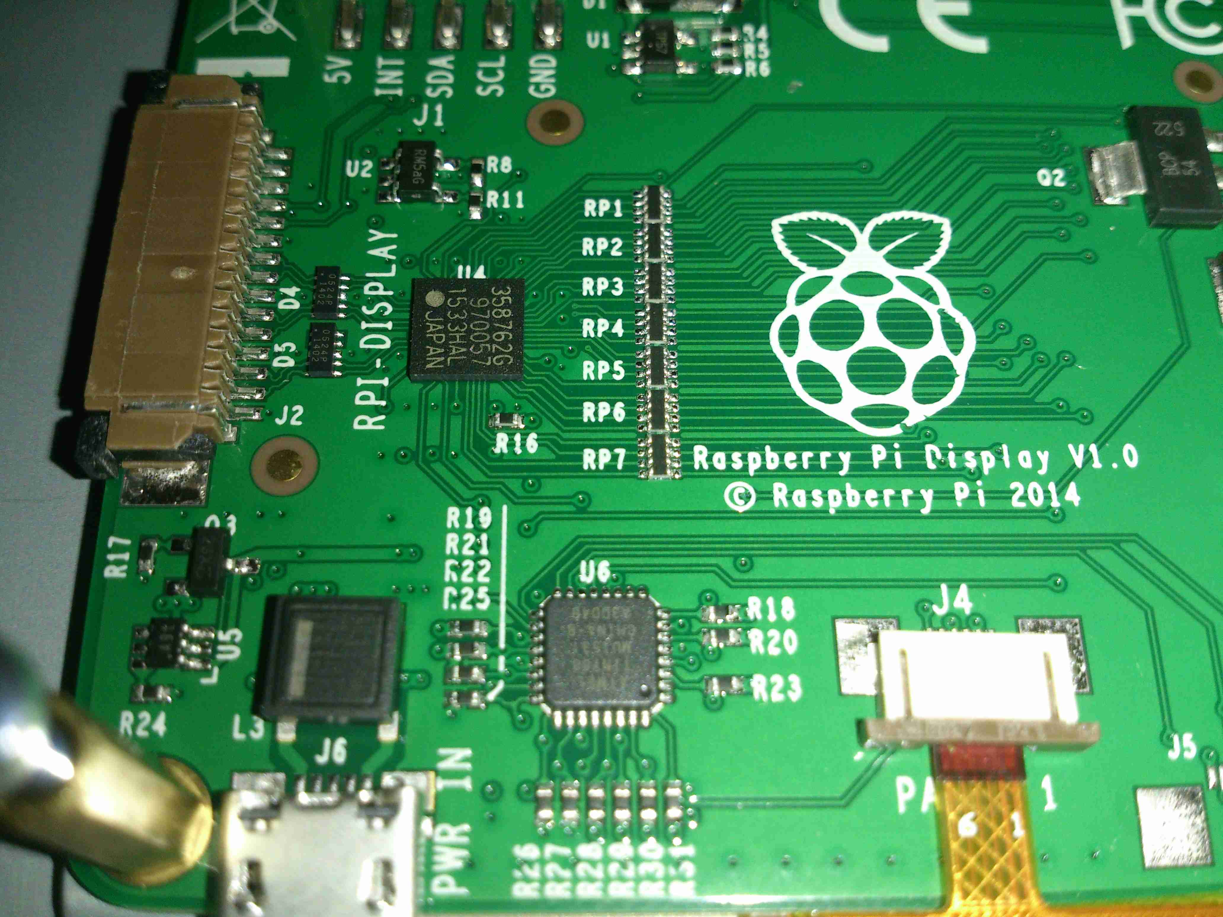
Main Controller
The video signal comes in on the FFC connector on the left, into the BGA IC. I’ve not managed to identify this component, but it’s doing the conversion from serial video from the Pi to parallel RGB for the LCD.
There’s also an Atmel ATtiny88 on the board below the main video conversion IC, not sure what this is doing.
The touch controller itself is mounted on the flex of the LCD, in this case it’s a FT5406.
Raspberry Pi LCD
Here’s the LCD in operation. It’s not the highest resolution out there, but it leaves the GPIO & HDMI ports free for other uses.
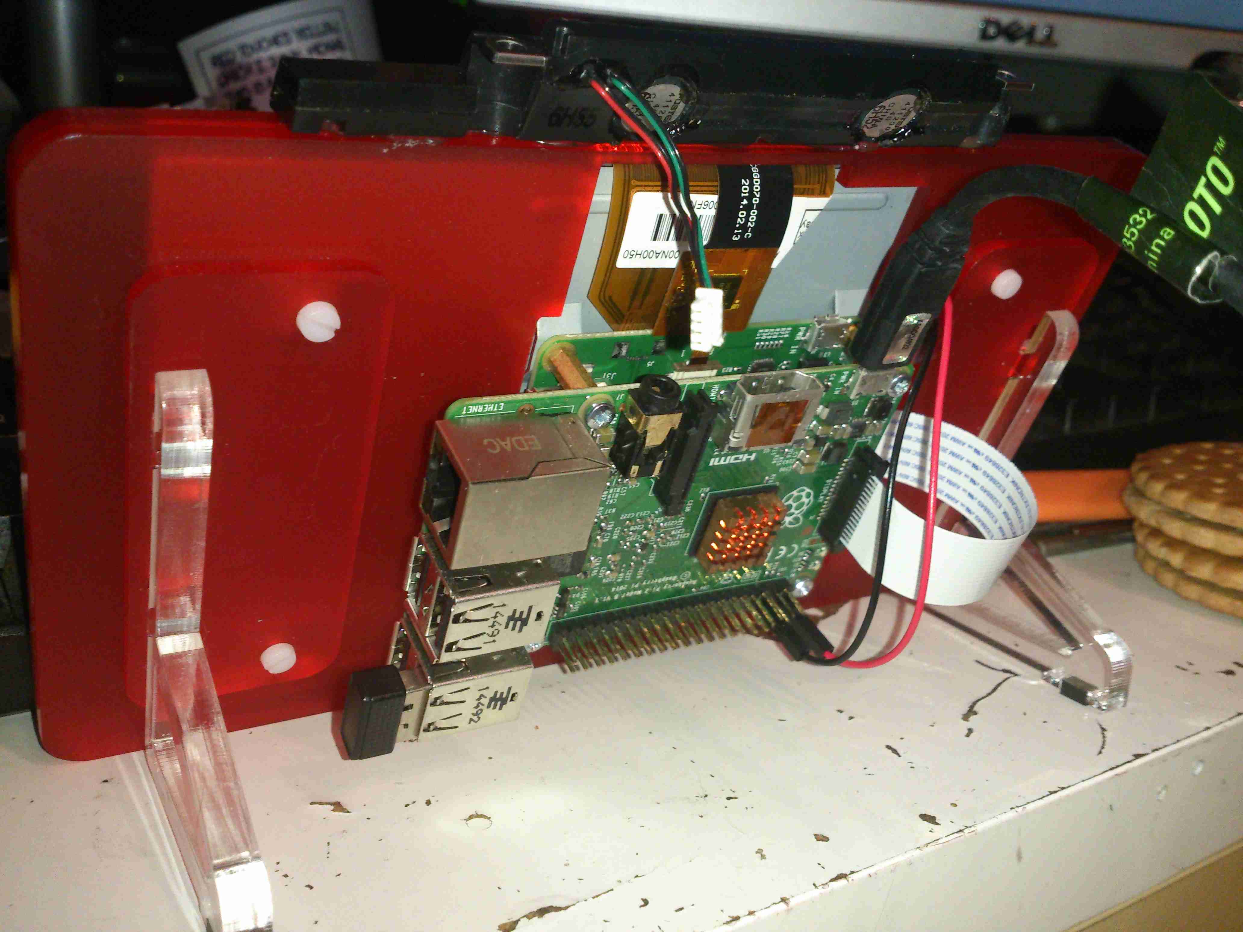
Pi Mounted
The Pi screws to the back of the LCD & is connected with a flat flex cable & a pair of power jumpers. I’ve added a couple of small speakers to the top edge of the LCD to provide sound. (More to come on this bit).
My other monitors are a different model, and have a slightly different main PCB inside, but the process is mostly the same for converting these to 12v supply.
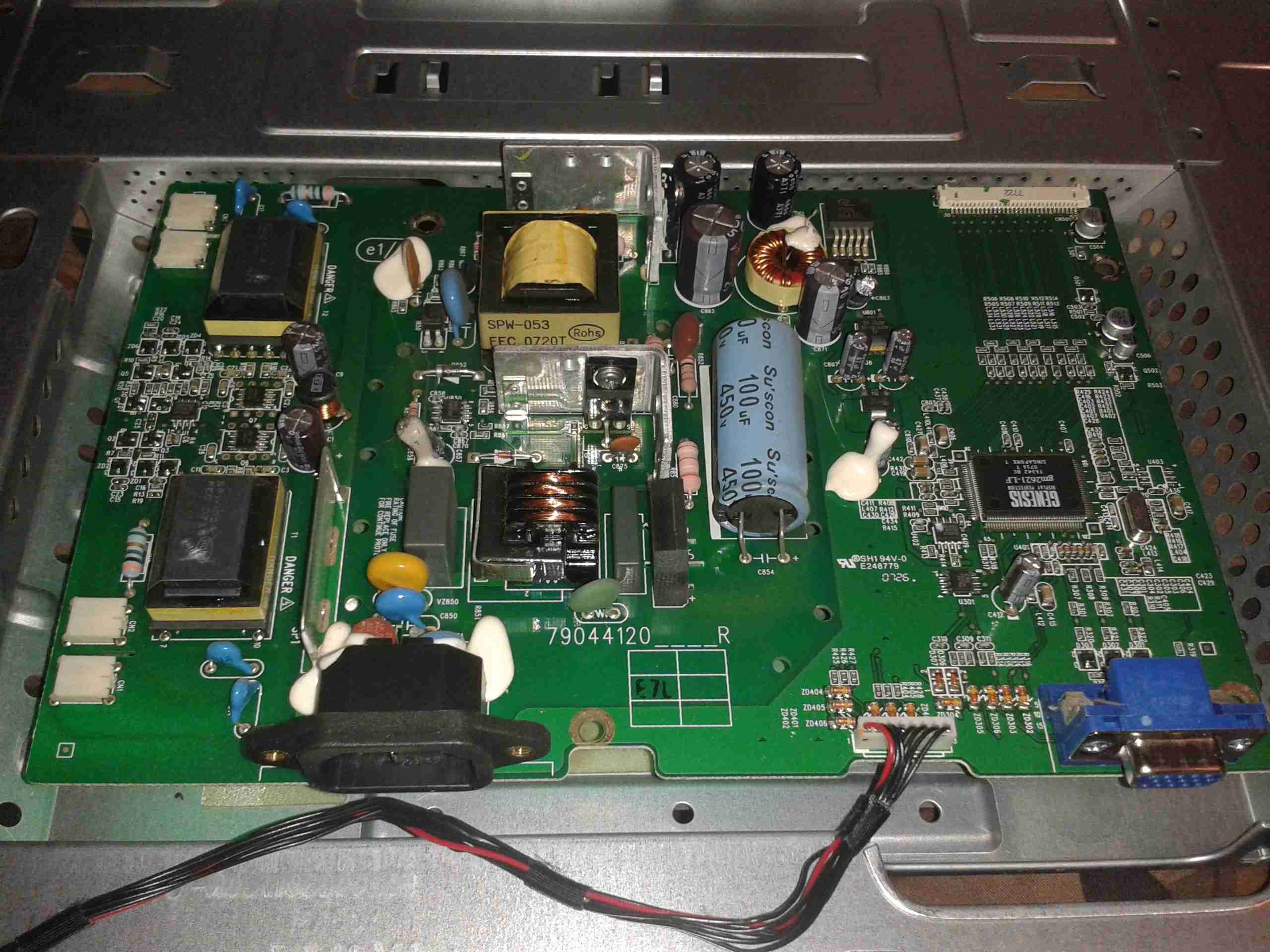
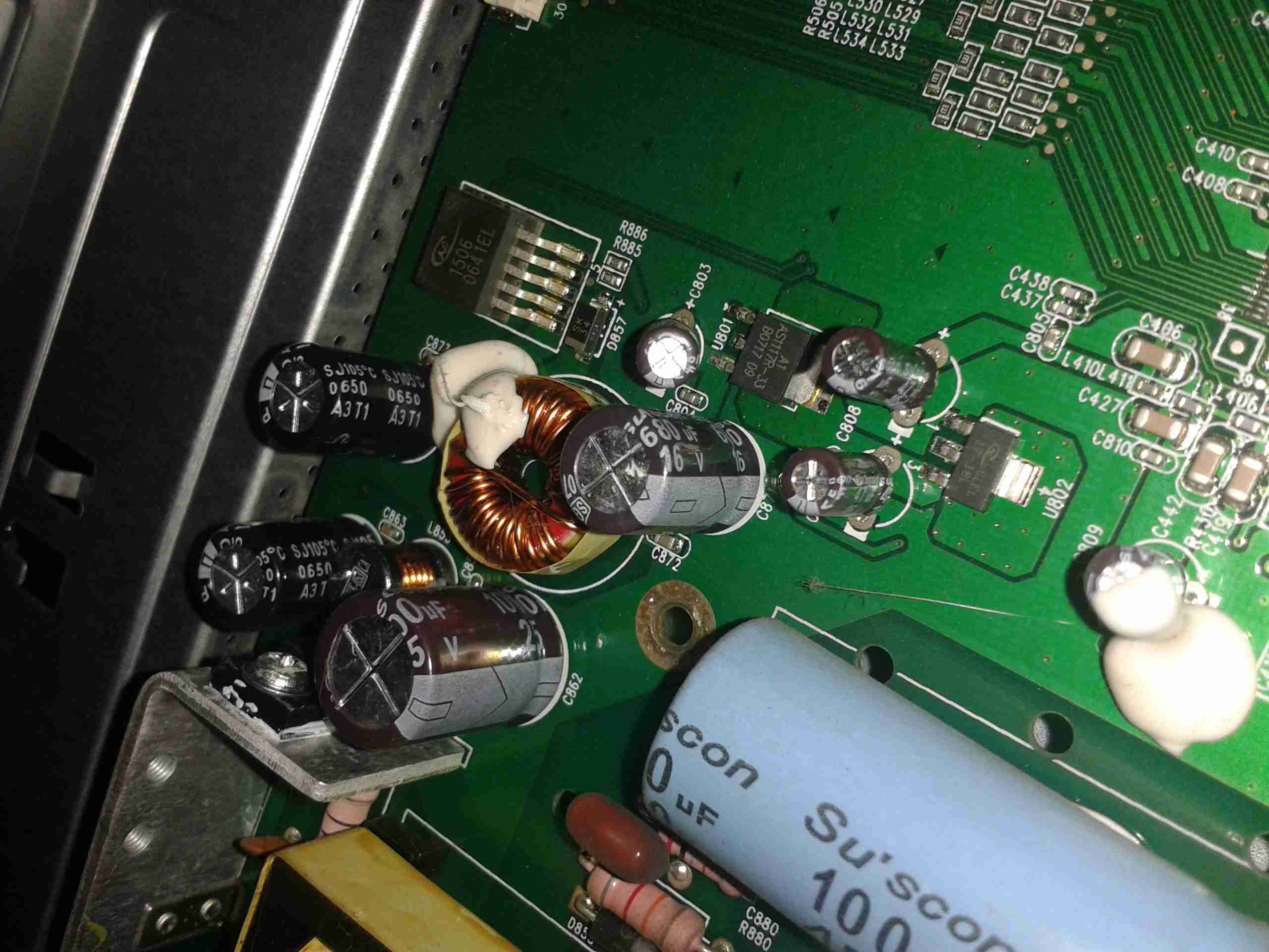
Main PCB
In this monitor type, there is only a single board, with all the PSU & logic, instead of separate boards for each function.
PSU Closeup
This monitor is slightly different in it’s power supply layout. The mains supply provides only a single 12v rail, which is then stepped down by a switching converter to 5v, then by smaller linear regulators to 3.3v & 1.8v for the logic. This makes my life easier since I don’t have to worry about any power conversion at all.
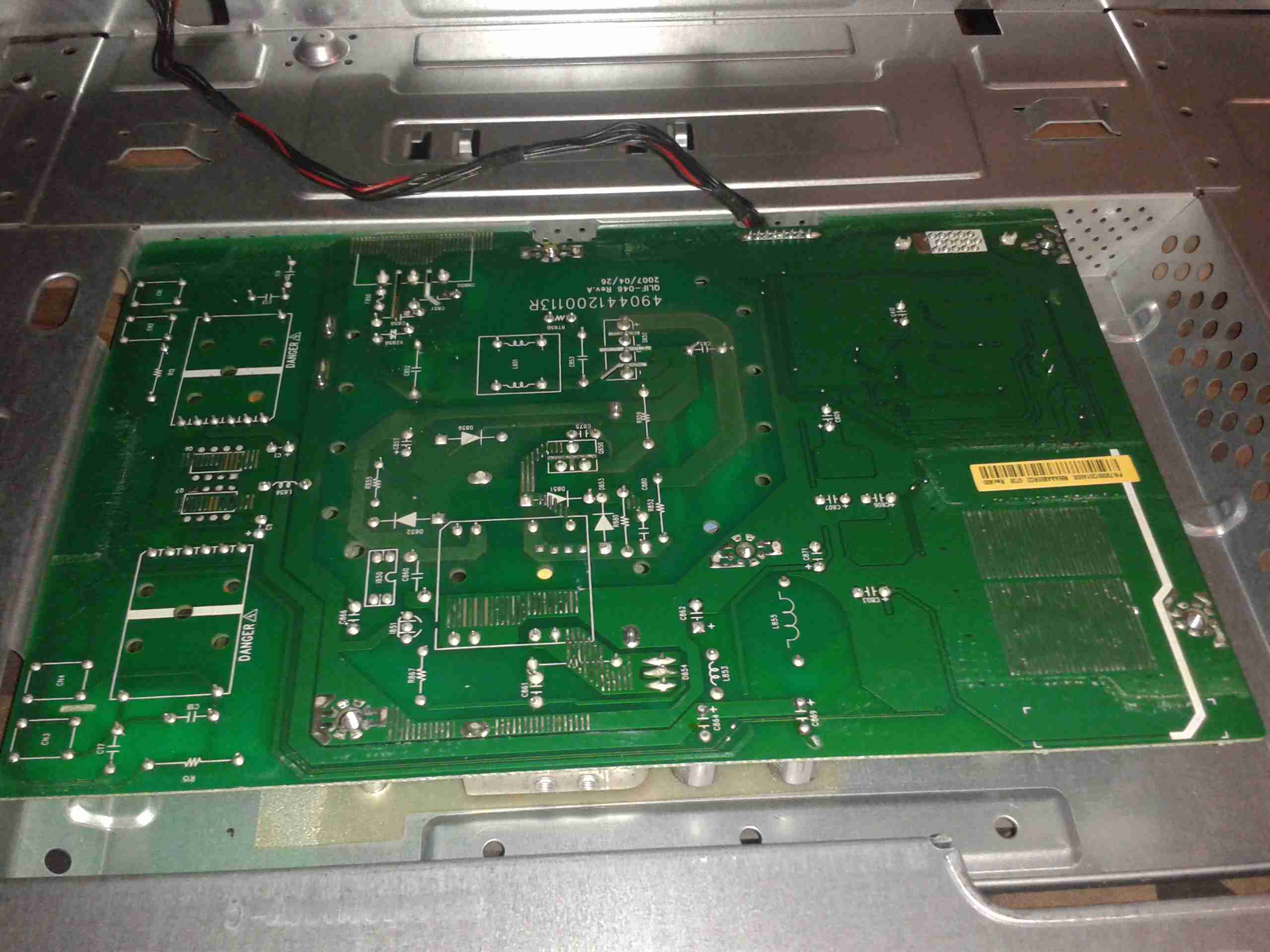
PCB Reverse
Here’s the backside of the PCB, the mains PSU section is in the centre.
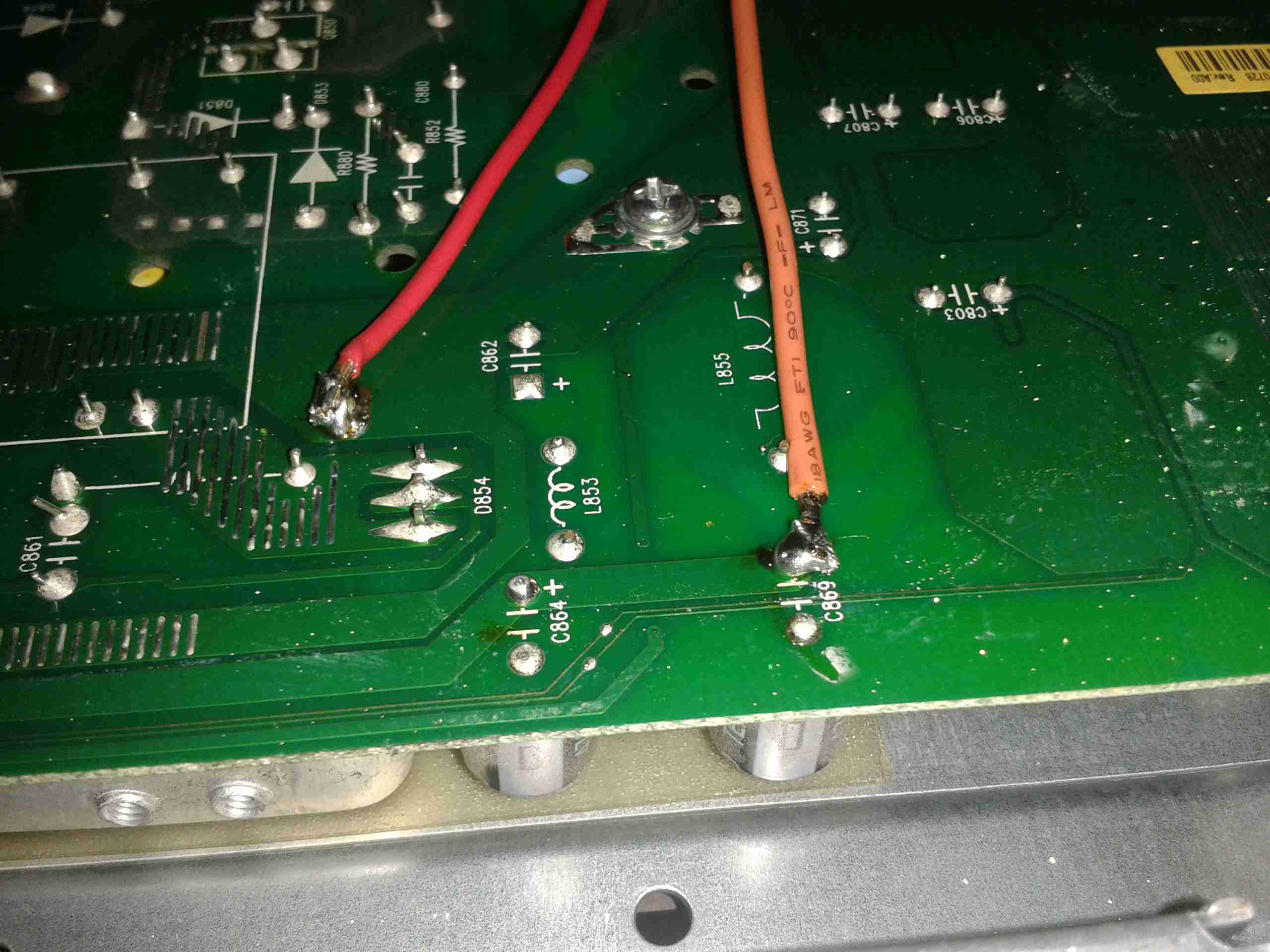
Attachment Points
Here’s the pair of 12v supply wires soldered onto the main board, onto the common GND connection on the left, and the main +12v rail on the right. I’ve not bothered with colour coding the wiring here, just used whatever I had to hand that was heavy enough to cope with a couple amps.
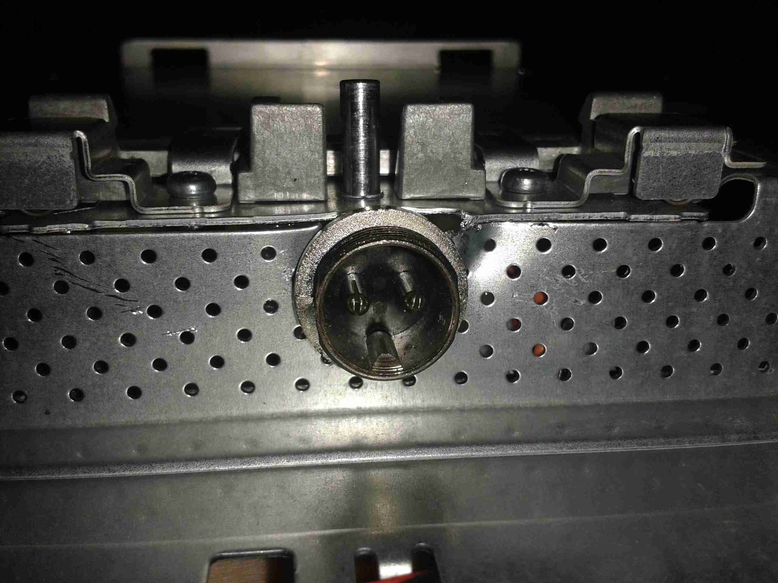
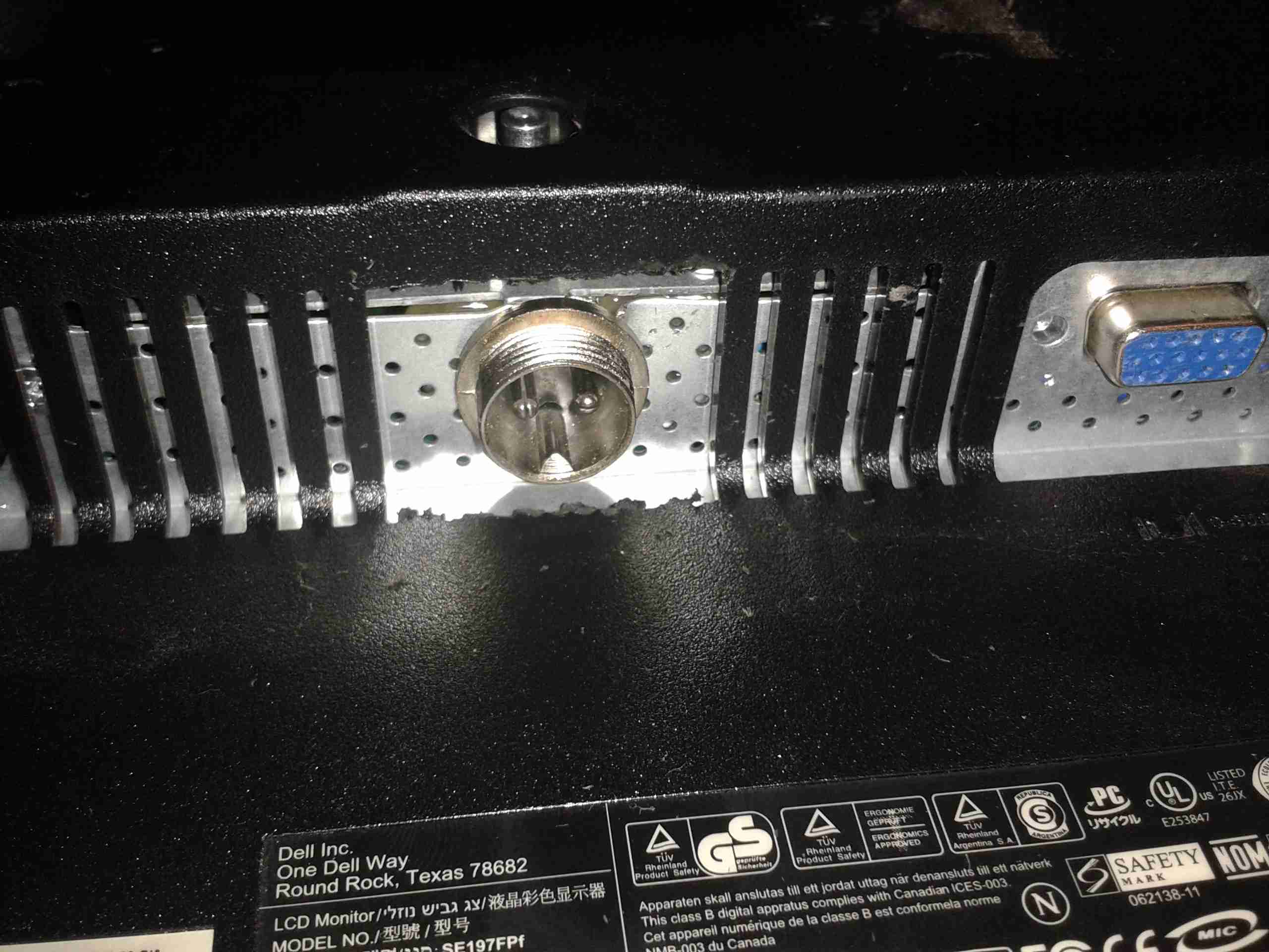
12v Socket
A small mod later with a cone drill & the 12v input socket is mounted in the LCD frame.
Casing Mod
Some light removal of plastic & the back cover fits back on. Current draw at 13.8v is ~2A.
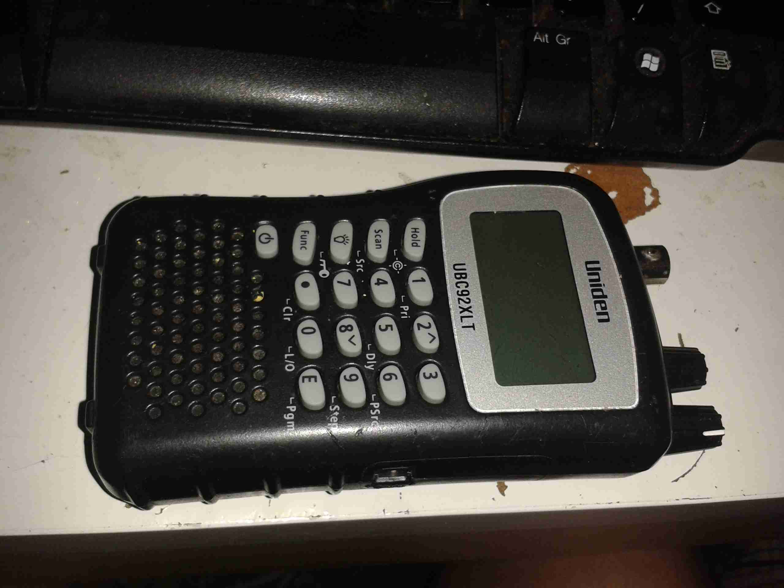
One bit of my equipment that I’ve never looked into is my scanner, a handheld Uniden unit. I got this when Maplin Electronics had them on special offer a few years ago.
Uniden Scanner
Here’s the scanner itself, roughly the same size as a usual HT.
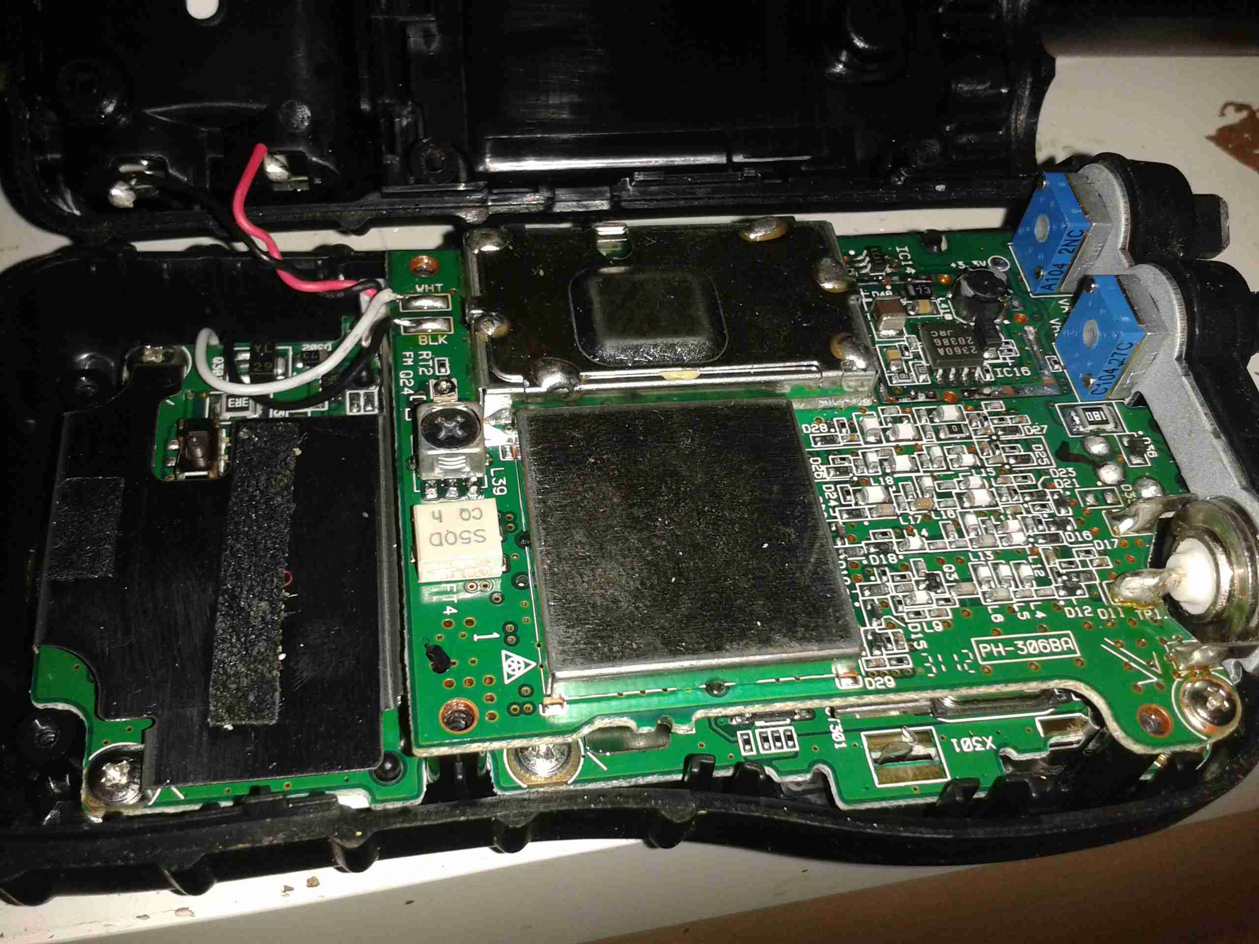
Back Cover Removed
Here the back cover has been removed, and the main RF board is visible at the top of the stack. Unfortunately the shielding cans are soldered on this unit, so no looking under there 🙁
On the right hand side of the board next to the antenna input is the main RF filter network, and it’s associated switching. The RF front end is under the shield closest to the front edge.
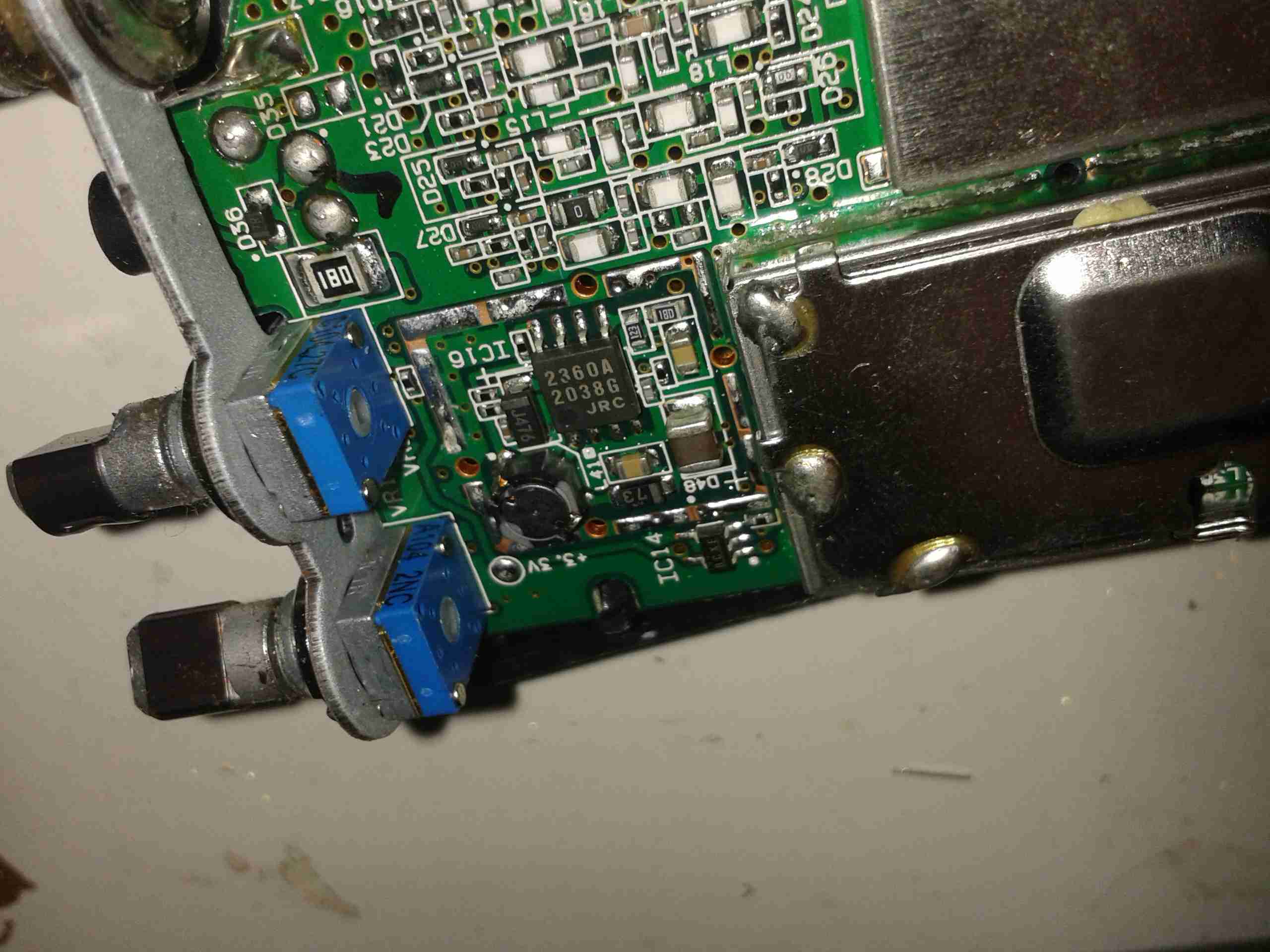
Controls & 3.3v Regulator
On the other side of the PCB is the Volume & Squelch potentiometers, along with a dedicated 3.3v switching supply. An NJM2360A High Precision DC/DC converter IC controls this one. A 3.3v test point is visible next to the regulator.
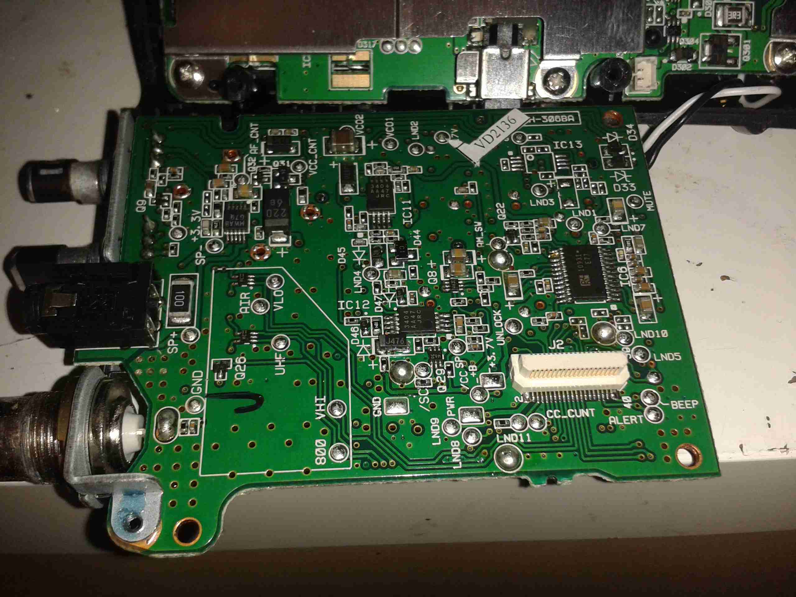
RF Board Reverse
Here’s the backside of the RF board, some more interesting parts here. There’s a pair of NJM3404A Single Supply Dual Op-Amp ICs, and a TK10931V Dual AM/FM IF Discriminator IC. This is the one that does all the back-end radio functionality. The audio amplifier for the internal speaker & external headphone jack is also on this PCB, top left. A board-to-board interconnect links this radio board with the main control board underneath.
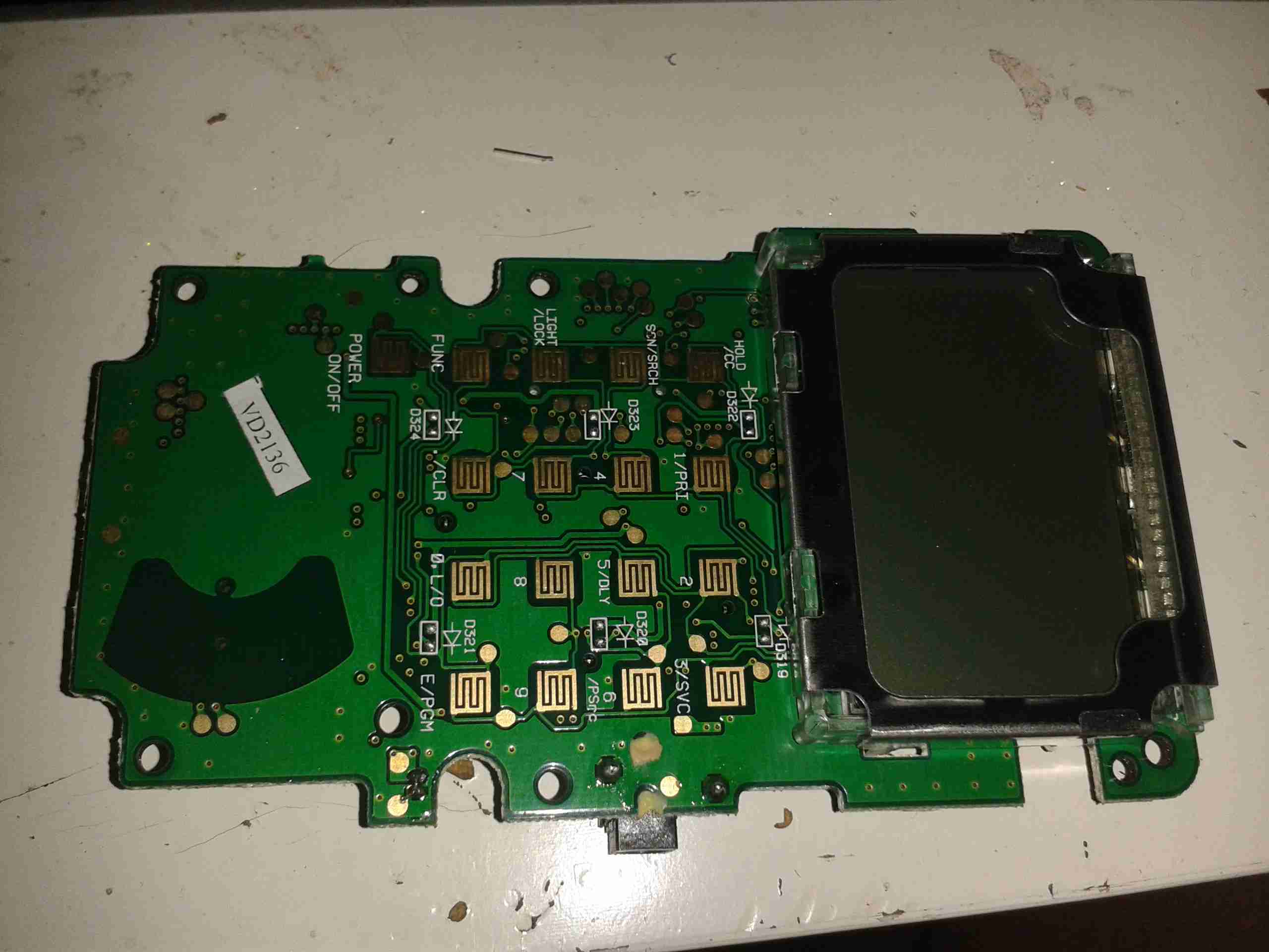
Control PCB Front
Here’s the front of the control PCB, nothing much to see here, just the LCD & membrane keypad contacts.
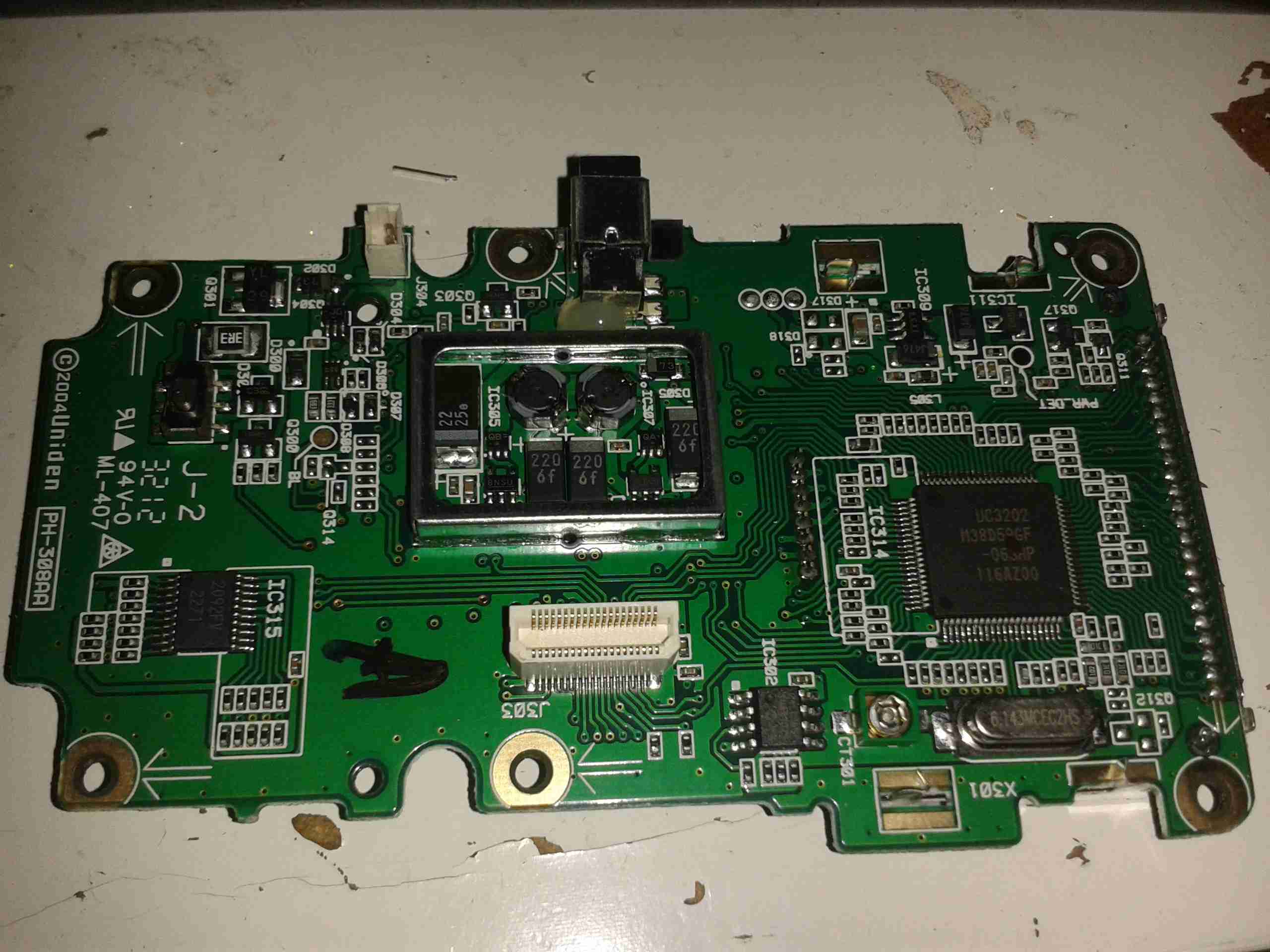
Control PCB Reverse
And here’s the reverse side of the control board. All the interesting bits are here. The main microcontroller is on the right, a Renesas M38D59GF, a fairly powerful MCU, with onboard LCD drive, A/D converter, serial interface, 60K of ROM & 2K of RAM. It’s 6.143MHz clock crystal is just below it.
The mating connector for the RF board is in the centre here.
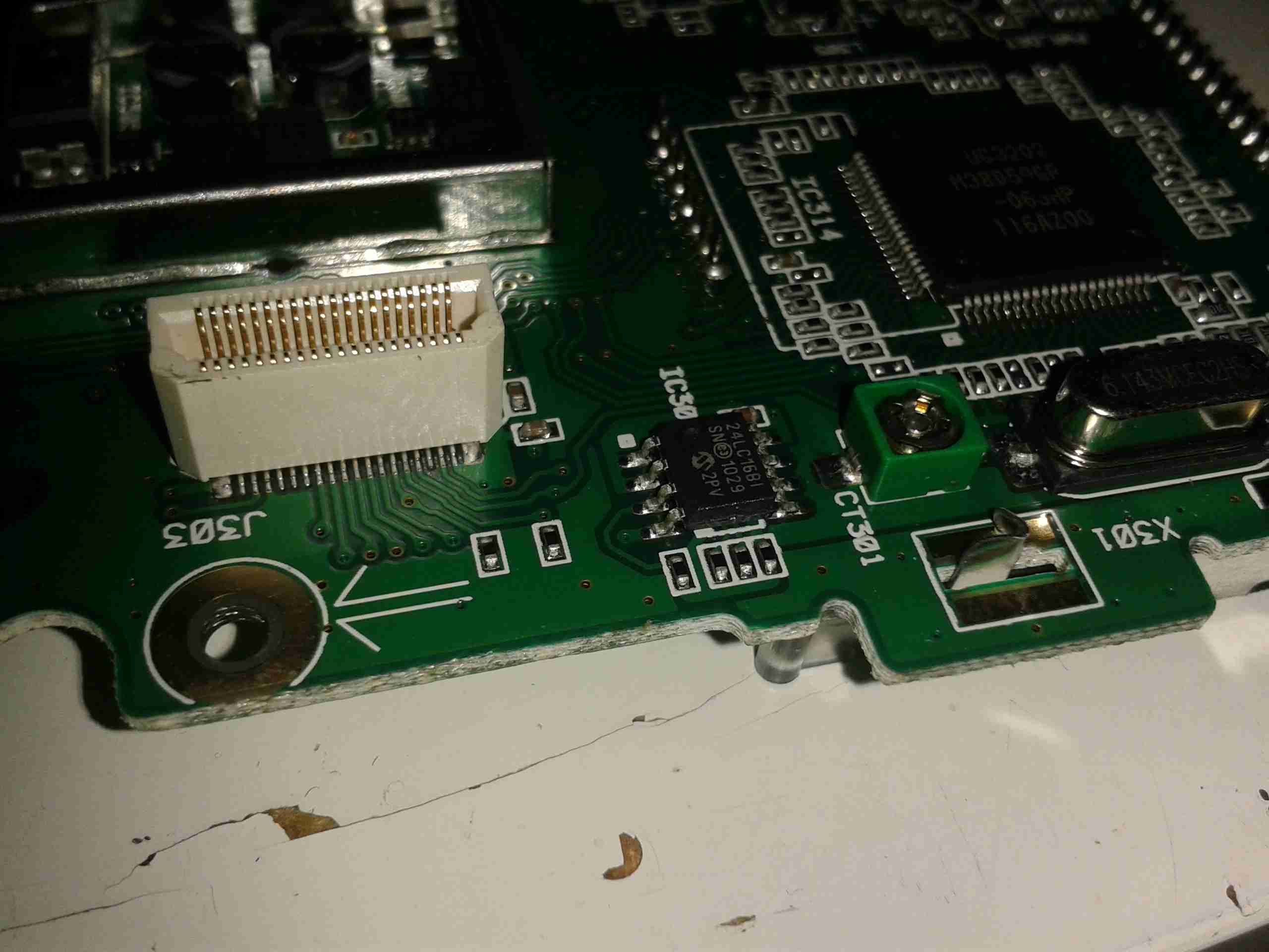
There is also a Microchip 24LC168 16KB I²C EEPROM next to the main microcontroller. This is probably for storing user settings, frequencies, etc.
EEPROM
The rest of this board is dedicated to battery charging and power supply, in the centre is a dual switching controller, I can’t figure out the numbers on the tiny SOT23 components in here, but this is dealing with the DC 6v input & to the left of that is the circuitry for charging the NiMH cells included with the scanner.
PSU
The last bit of this PCB is a BU2092FV Serial In / Parallel Out 4 channel driver. Not sure what this one is doing, it might be doing some signal multiplexing for the RF board interface. Unfortunately the tracks from this IC are routed on the inner layers of the board so they can’t be traced out.
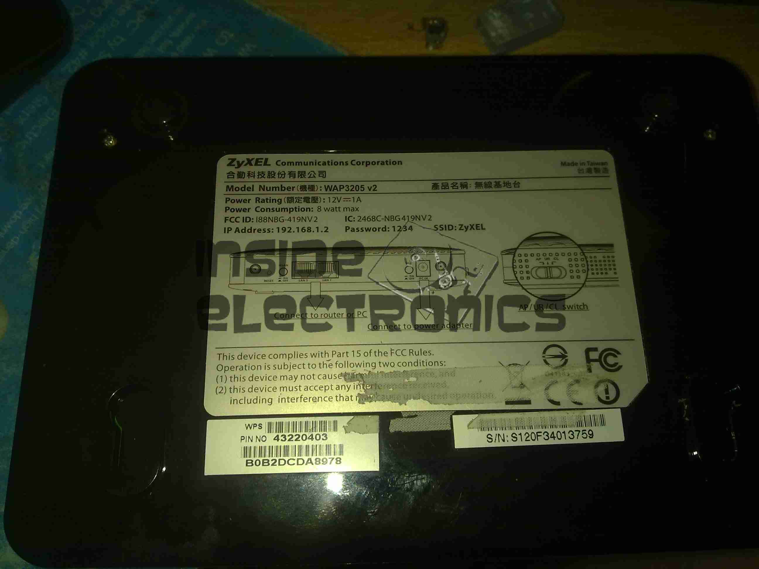
Here is a ZyXel WAP3205 WiFi Access Point that has suffered a reverse polarity event, due to an incorrect power supply being used with the unit.
ZyXEL WAP3205
While most electronic gadgets are protected against reverse polarity with a blocking diode, this unit certainly wasn’t. Applying +12v DC the wrong way round resulted in this:
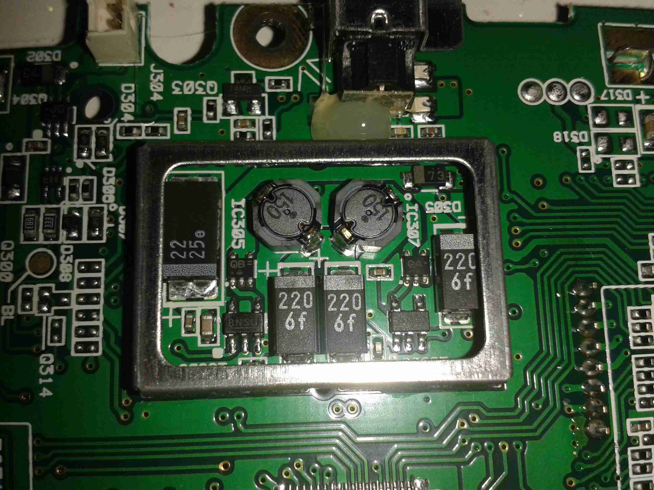
Blown Switchmode IC (Fuzzy Focus)
That is the remains of the 3.3v regulator IC, blown to smithereens & it even attempted an arson attack. Luckily this was the only damaged component, & I was able to repair the unit by replacing the switching IC with a standalone regulator. (Replacing the IC would have been preferable, if there was anything left of it to obtain a part number from).
I scraped away the pins of the IC to clear the short on the input supply, removed the switching inductor, & tacked on an adjustable regulator module set to 3.3v. Luckily the voltage of the supply is handily marked on the PCB next to the circuit.
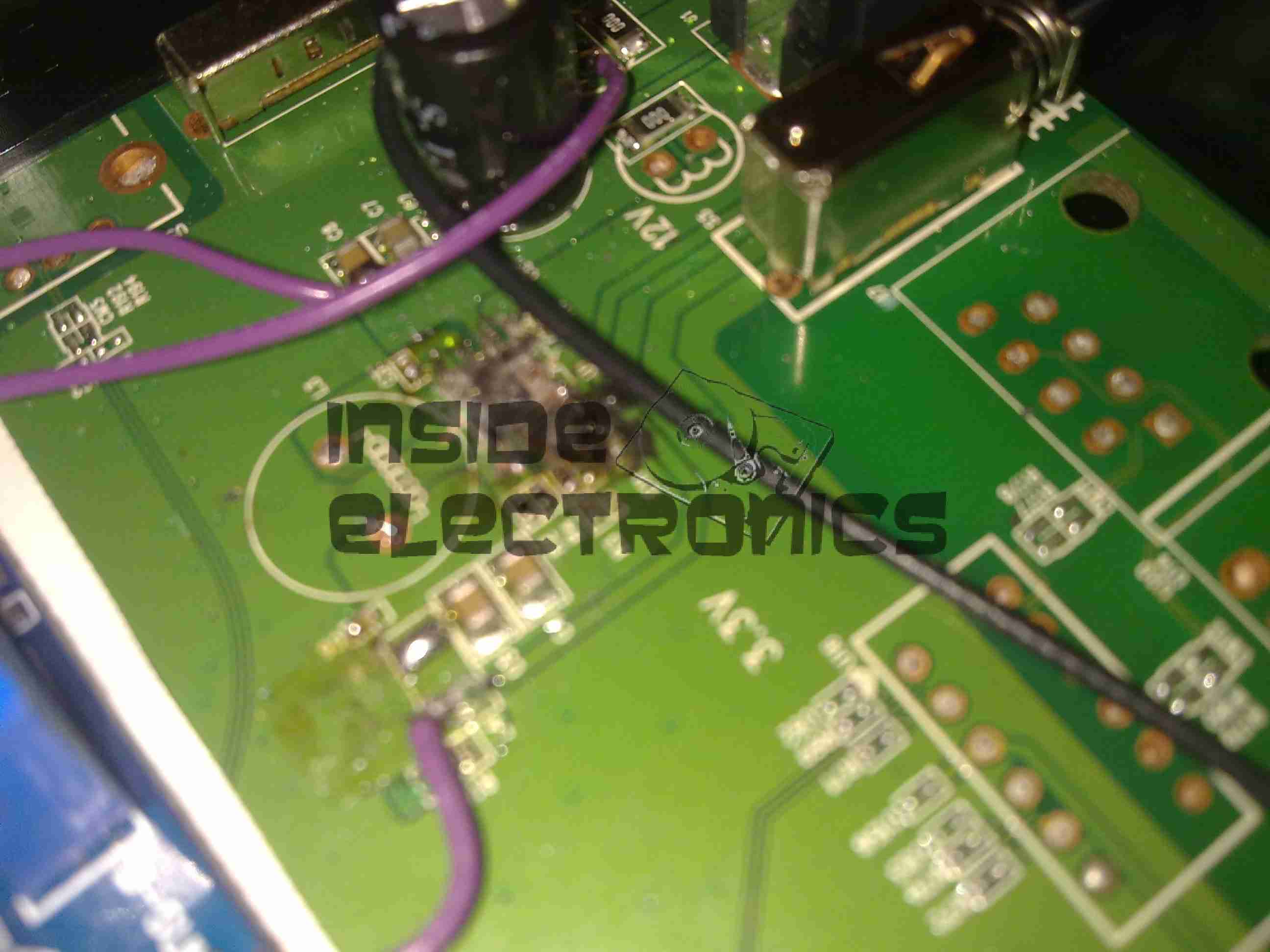
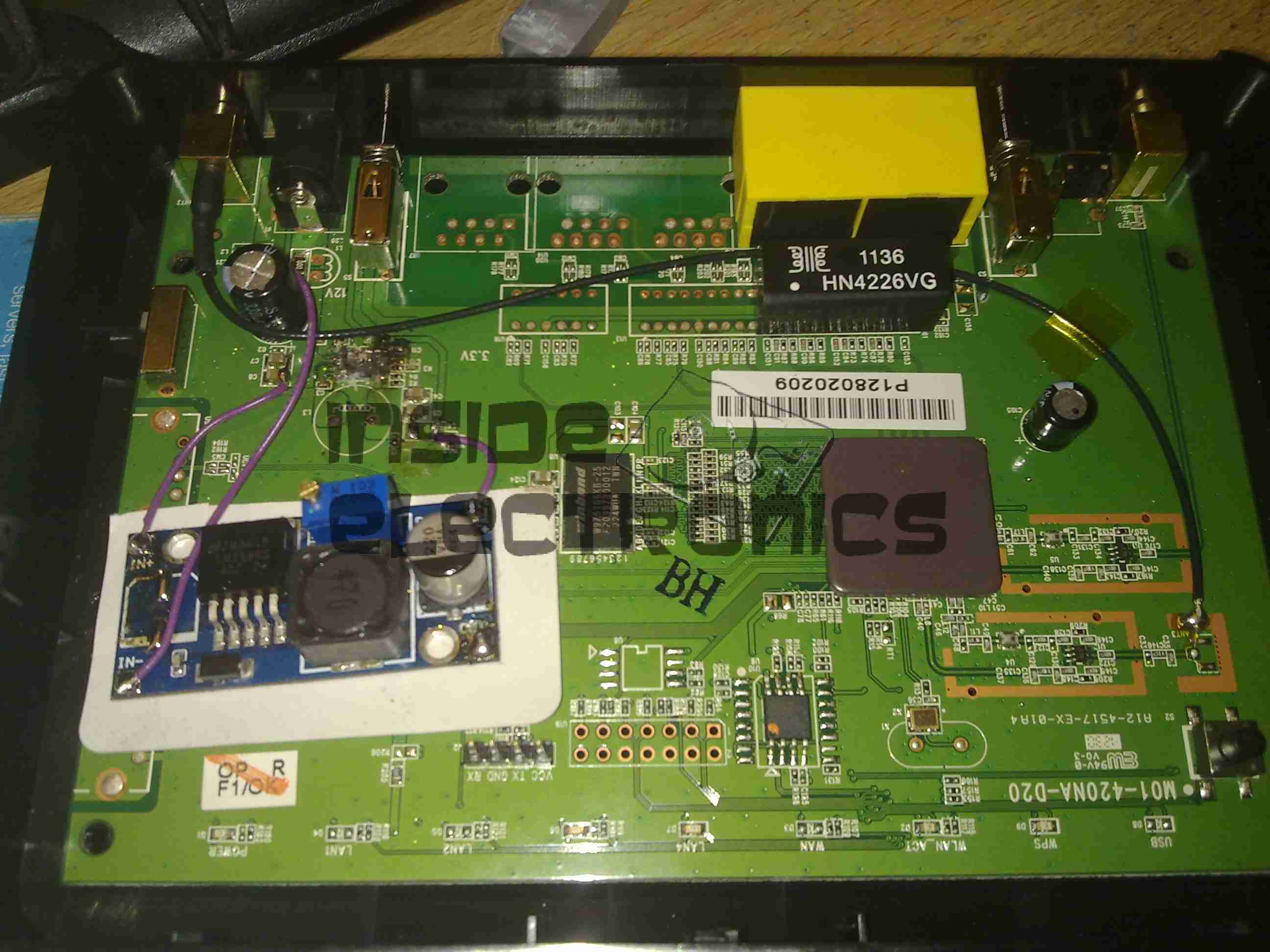
Replacement PSU
Replacement SMPS in place on top of the PCB. The output of the supply is connected to one of the pads of L4 (on my unit just an 0 ohm link), the +12v input is connected to the + rail side of C8 & C7 & the final ground connection is hooked in to the back of the barrel jack.
After this replacement, the unit booted straight up as if nothing had happened. All the logic is undamaged!
After seeing these on eBay for £8.99 I thought it might be a good deal – interfacing with the RasPi’s GPIO & it has built in power supplies.
As a kit, it was very easy to assemble, the PCB quality is high, and is a fairly good design. It worked first time, the regulators hold the rails at the right voltages.
However there are some issues with this board that bug me.
The documentation for the kit is *AWFUL*. No mention of the regulators on the parts list & which goes where – I had to carefully examine the schematics to find out those details.
The 4x 1N1007 diodes required weren’t even included in the kit! Luckily I had some 1N4148 high speed diodes lying around & even though they’re rated for 200mA continuous rather than the specified part’s 1A rating, the lack of heatsinking on the regulators wouldn’t allow use anywhere near 1A, so this isn’t much of a problem.
Component numbering on the silkscreen isn’t consistent – it jumps from R3 straight to R6! These issues could be slightly confusing for the novice builder, and considering the demographic of the RasPi, could be seen as big issues.
On the far left of the board are the 5v & 3.3v regulators, well placed on the edge of the board in case a heatsink may be required in the future. However the LM317 adjustable regulator is stuck right in the middle of the PCB – no chance of being able to fit a heatsink, & the device itself seems incredibly cheap – the heatsink tab on the back of the TO-220 is the thinnest I have ever seen. Not the usual 2-3mm thick copper of the 5v & 3.3v parts – but barely more than a mm thick, so it’s not going to be able to cope with much power dissipation without overheating quickly.
As the adjustable rail can go between ~2.5v – 10v, at the low end of the range the power dissipation is going to shoot through the roof.
The GPIO connector – this could have been done the other way, at the moment the ribbon cable has to be twisted to get both the Pi & the GPIO board the same way up. Just a slight fail there. See the image below
Plugged In
The power rails are not isolated out of the box – there is no connection between the 5v & 3.3v rails & the Pi’s GPIO, but the GND connections are linked together on the board.
Getting the ribbon cable through the hole in the ModMyPi case was a bit of a faff – the connector is too big! I had to squeeze the connector through at a 45° angle. The case is also remarkably tight around the connector once it’s fitted to the board – clearly the designers of the case didn’t test the an IDC connector in the case before making them!
Everything does fit though, after a little modification.
All Cased Up
Here is the unit all built up with the case. The top cover just about fits with the IDC connector on the GPIO header.
More to come once I get some time to do some interfacing!
This is an old USB 1.1 hub that was recently retired from service on some servers. Top of the unit visible here.
Bottom Label
Bottom label shows that this is a model F5U021 hub, a rather old unit.
PCB Front
PCB is here removed from the casing, Indicator LEDs along the bottom edge of the board, power supply is on the left. Connectors on the top edge are external power, USB host, & the 4 USB outputs. Yellow devices are polyswitch fuses for the 500mA at 5v each port must supply.
USB Hub IC
This is the USB Hub Controller IC, which is a Texas Instruments TUSB2046B device. Power filter capacitors next to the USB ports are visible here also, along with 2 of the polyswitches.
Power Supply
The power supply section of the unit, which supplies regulated 5v to the ports, while supplying regulated 3.3v to the hub controller IC. Large TO-220 IC is the 5v regulator. Smaller IC just under the power selector switch is the 3.3v regulator for the hub IC. The switch selects between Host powered or external power for the hub.
This is a device designed to reset Epson brand ink cartridges that are reportedly out of ink, so they again report full to the printer Here is the front of the unit, with the guide for attaching to a cartridge.
PCB Back
Back of the device removed. 3 button cells provide power to the PCB. Indicator LED sticks out of the top of the device for reset confirmation.
Row of pads on far left edge of the PCB are presumably a programming header for the uC on the other side of the board.
PCB Front
Here is the front of the PCB, main feature being the grid of pogo pins to connect to the cartridge chip. IC on lower right of that is a MSP430F2131 uController, a Texas Instruments part.
The IC directly to the left of the pogo pin bed is a voltage regulator, to step down the ~4.5v of the batteries down to the ~3.3v that the uC requires.
Tip Jar
If you’ve found my content useful, please consider leaving a donation by clicking the Tip Jar below!
All collected funds go towards new content & the costs of keeping the server online.