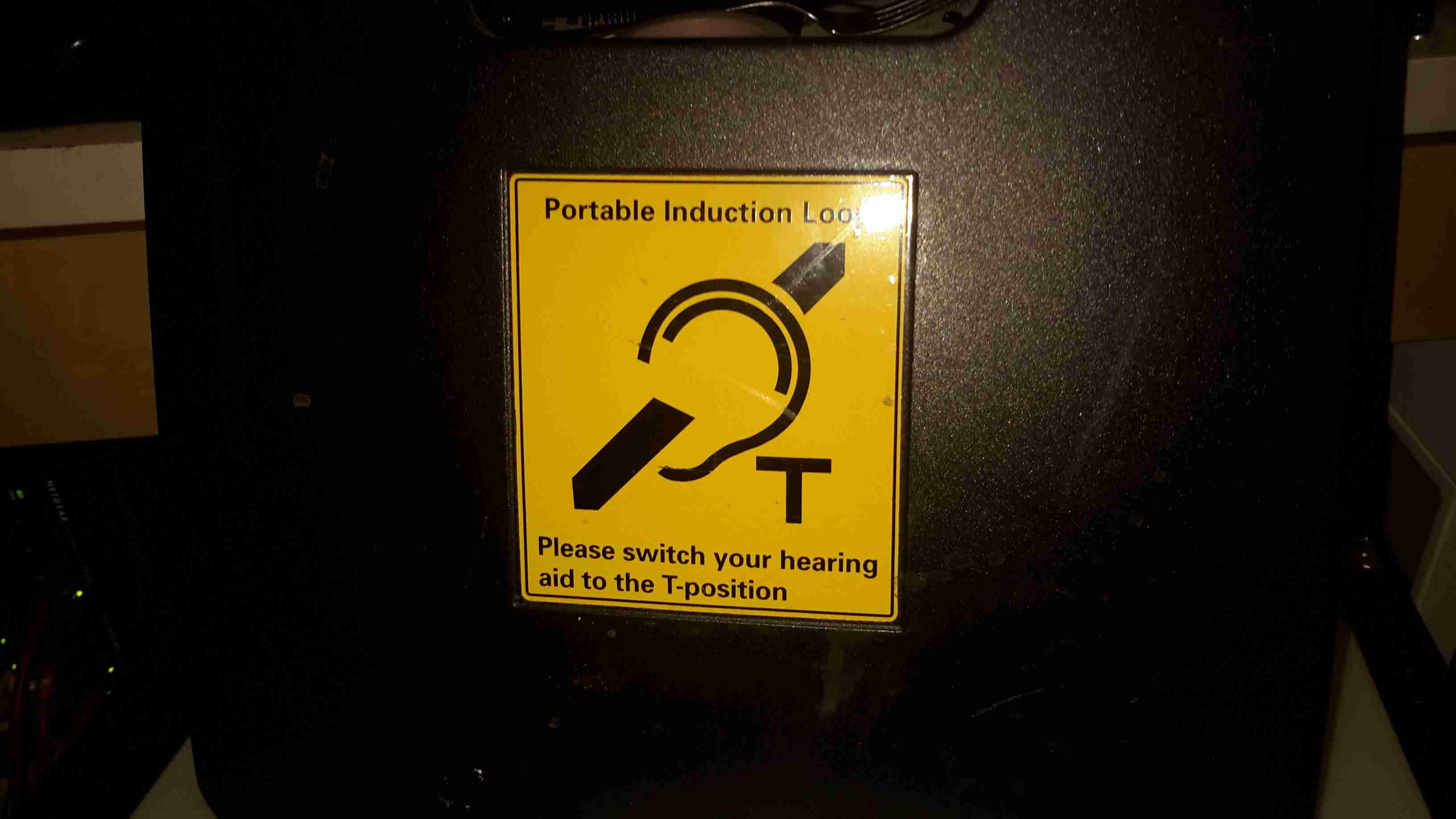
These units are used to broadcast local audio, such as from a public address system or local microphone. They accomplish this by producing a modulated magnetic field that a hearing aid is capable of picking up.
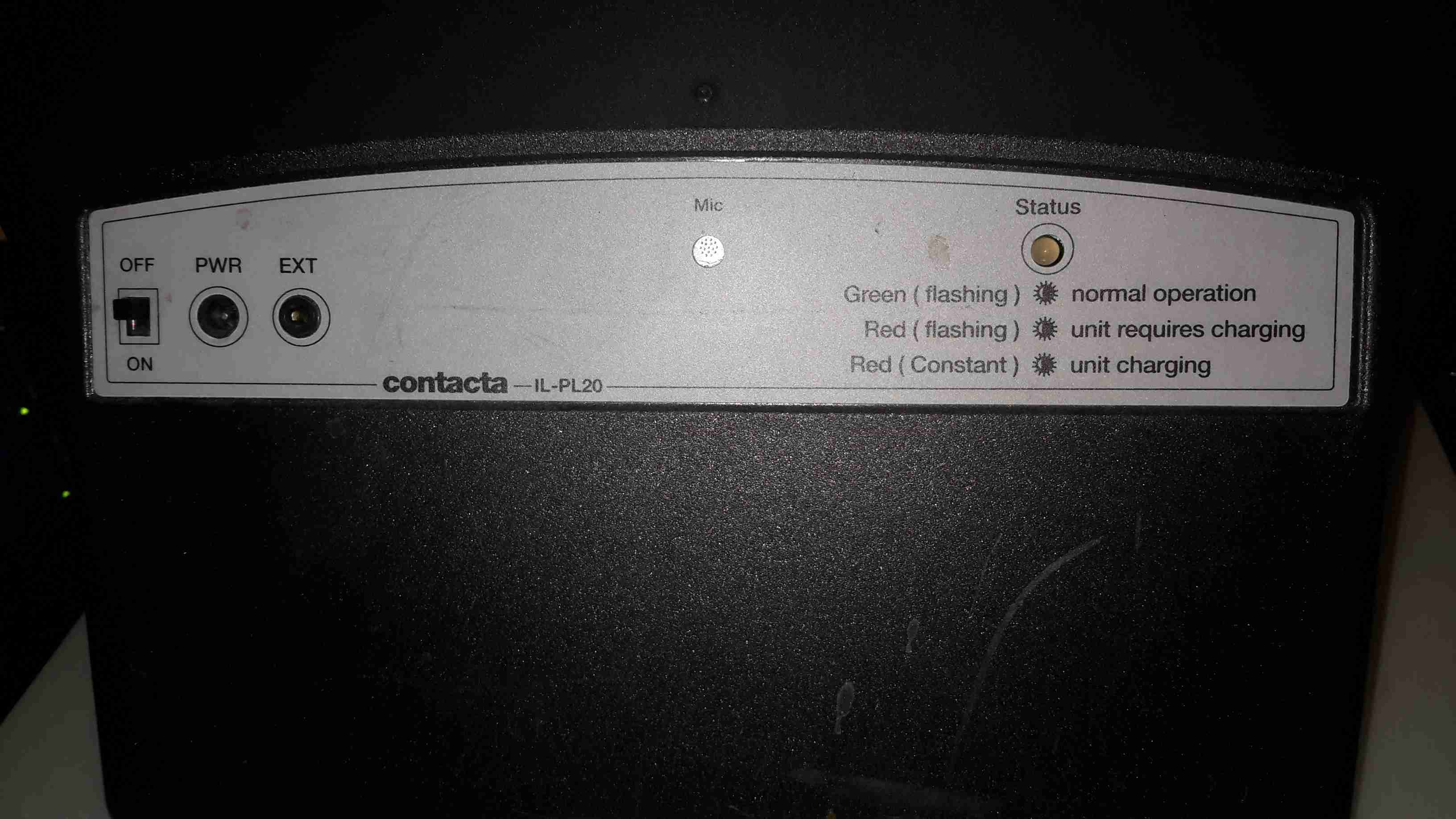
Back Panel
Not many controls on this bit of equipment. A bi-colour LED for status indications, a microphone, external audio input, charging input & a power switch.
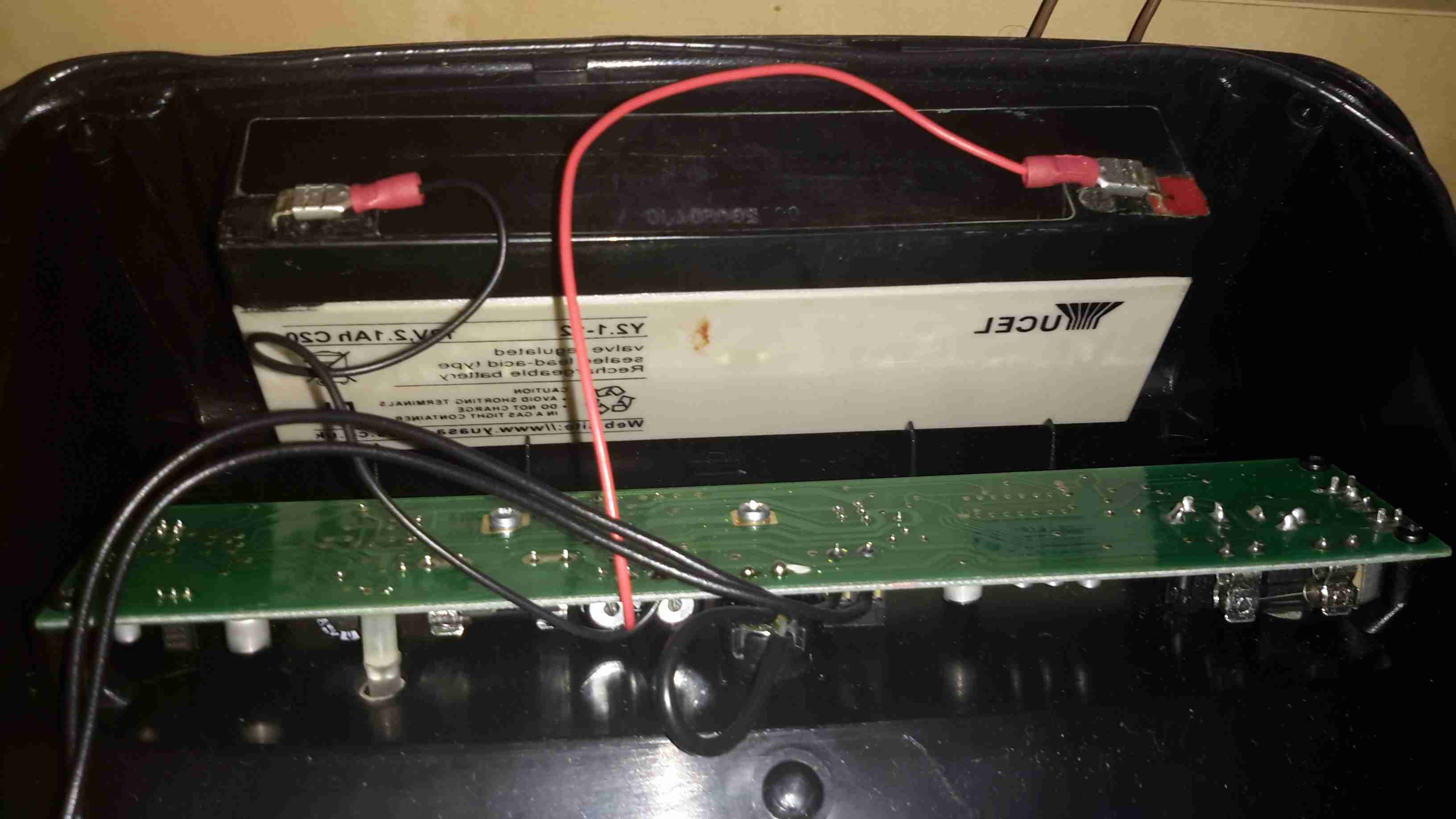
Internals
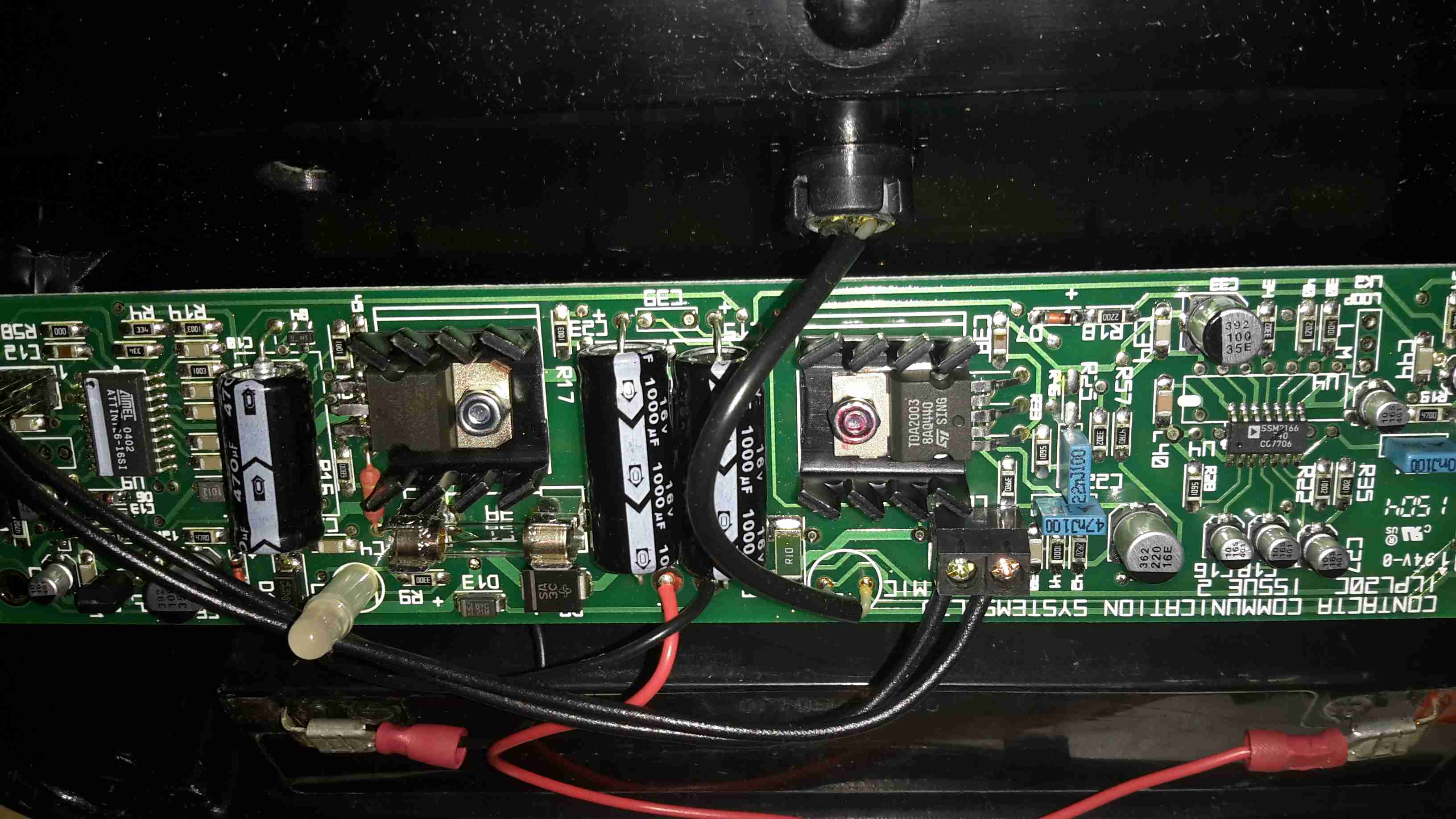
Popping the cover off reveals a small lead-acid battery, 2.1Ah at 12v. This is used when the loop is unplugged.
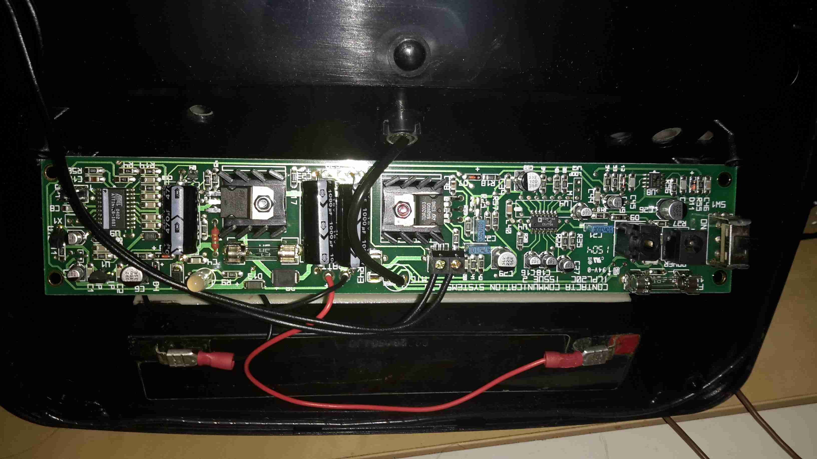
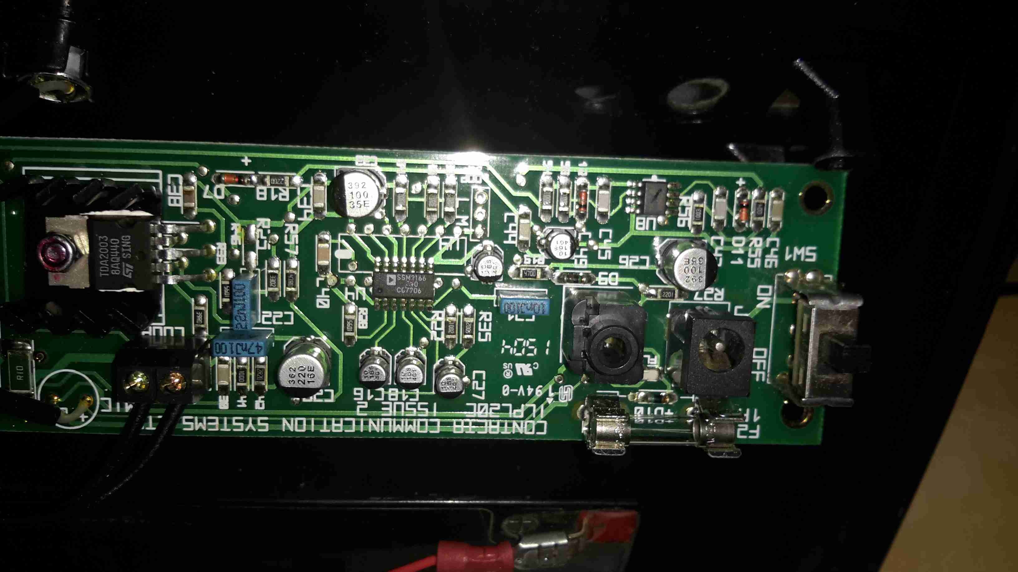
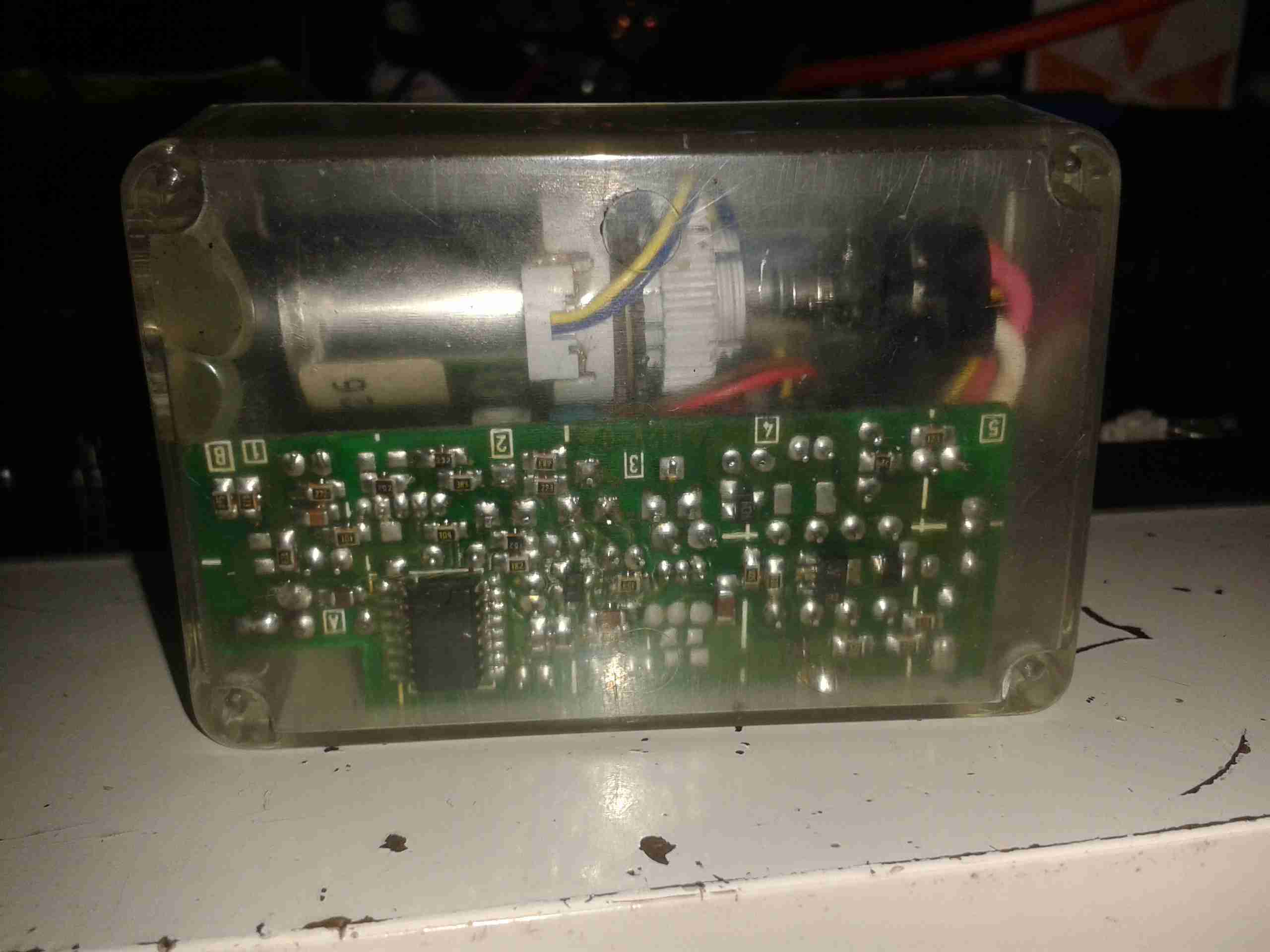
Main PCB
Here’s the main PCB, which takes care of the audio & battery charging. The inductive loop itself is just visible as the tape-covered wire bundle around the edge of the casing.
Audio & Power Input
Here’s the input section of the main PCB. The microphone input is handled by a SSM2166 front-end preamplifier from Analog Devices.
Power Amplifier
This audio is then fed into a TDA2003 10W Mono Power Amplifier IC, which directly drives the induction coil as if it were a speaker. Any suitable receiving coil & amplifier can then receive the signal & change it back into audio.
I’ve had a couple of viewfinder CRT modules for a while, & haven’t done much with them, so I decided to make a very small B&W monitor.
CRT
I ordered a small transparent ABS box when I made a large order with Farnell, that turned out to be just about the perfect size for the project! The CRT & PCB barely fit into the space. The face of the CRT itself is about 17mm across.
Module Installed
Here’s the main PCB & tube fully installed into the case. Barely enough room for a regulator left over!
Power is provided by a simple LM7809 IC to take a standard 12v input.
Module Rear
Rear of the case, showing the fit of the control board.
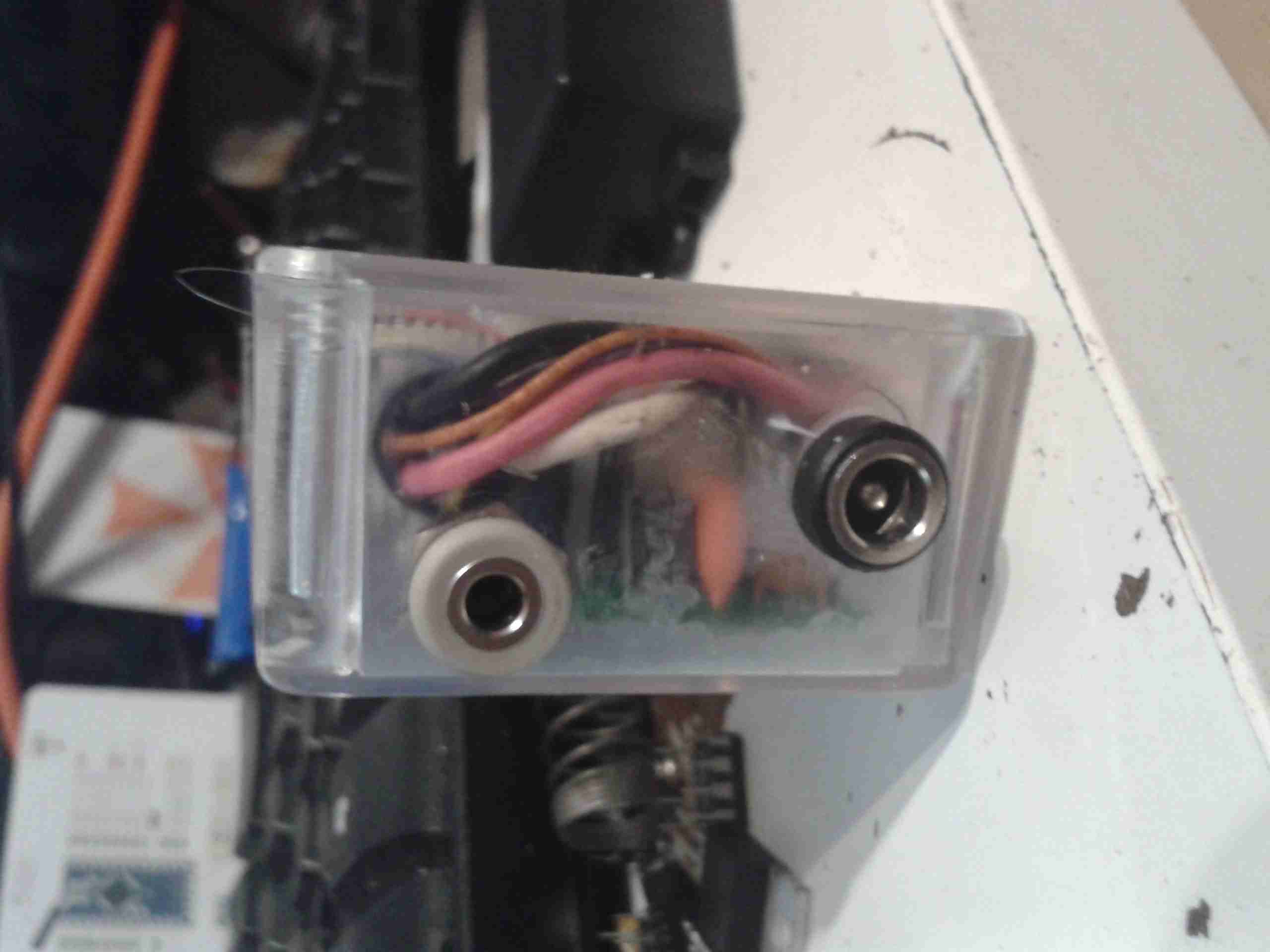
Connections
Here’s the back of the monitor, with the DC input jack & a 3.5mm 4-pole jack for audio & video. This allows simple connection to many devices, including the one I’ll use the most – the Raspberry Pi.
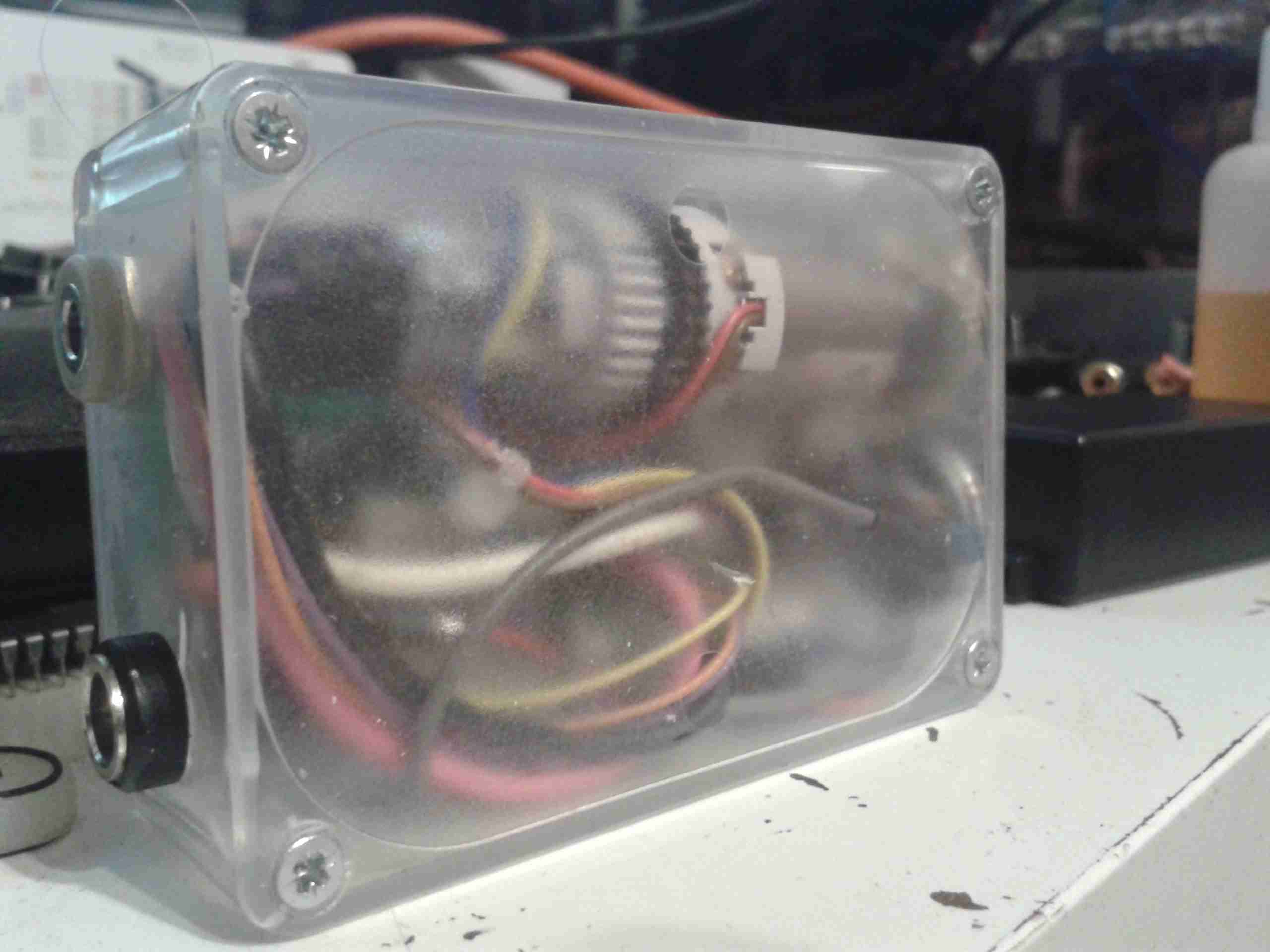
Completed
Completed monitor. Audio is handled by a very small 20mm speaker, currently mounted just below the CRT face.
Current draw from a 13.8v supply is 117mA.
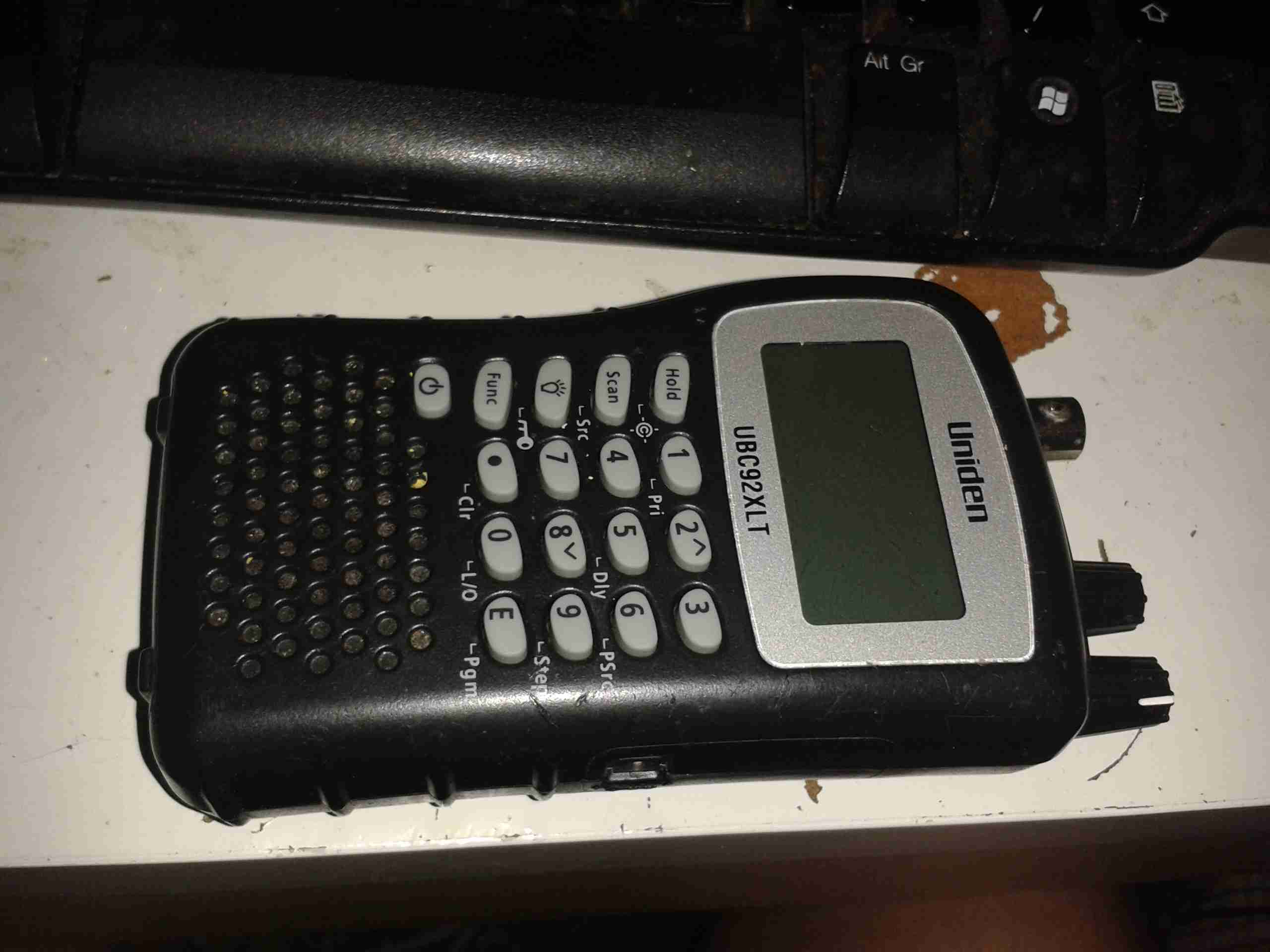
One bit of my equipment that I’ve never looked into is my scanner, a handheld Uniden unit. I got this when Maplin Electronics had them on special offer a few years ago.
Uniden Scanner
Here’s the scanner itself, roughly the same size as a usual HT.
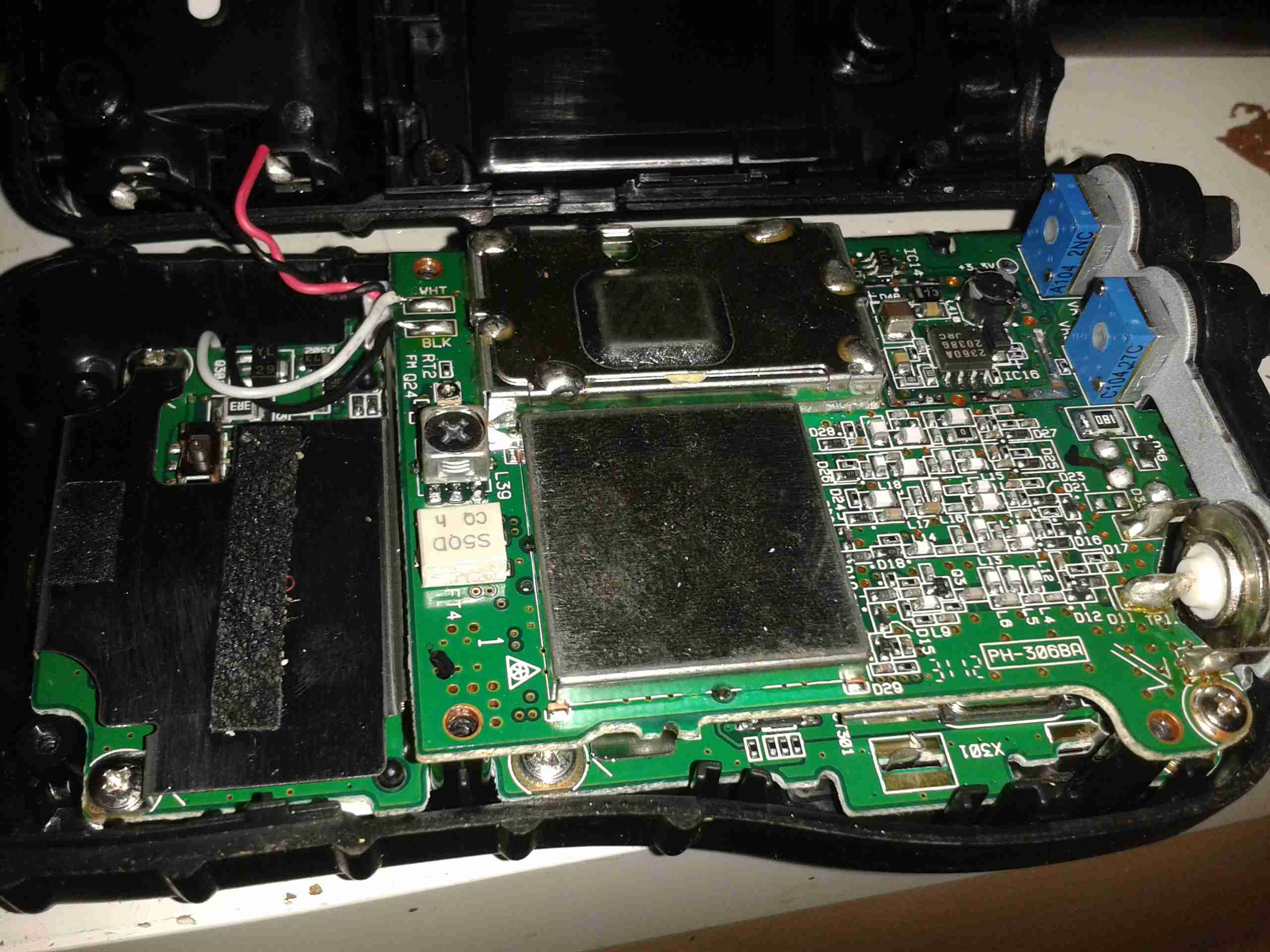
Back Cover Removed
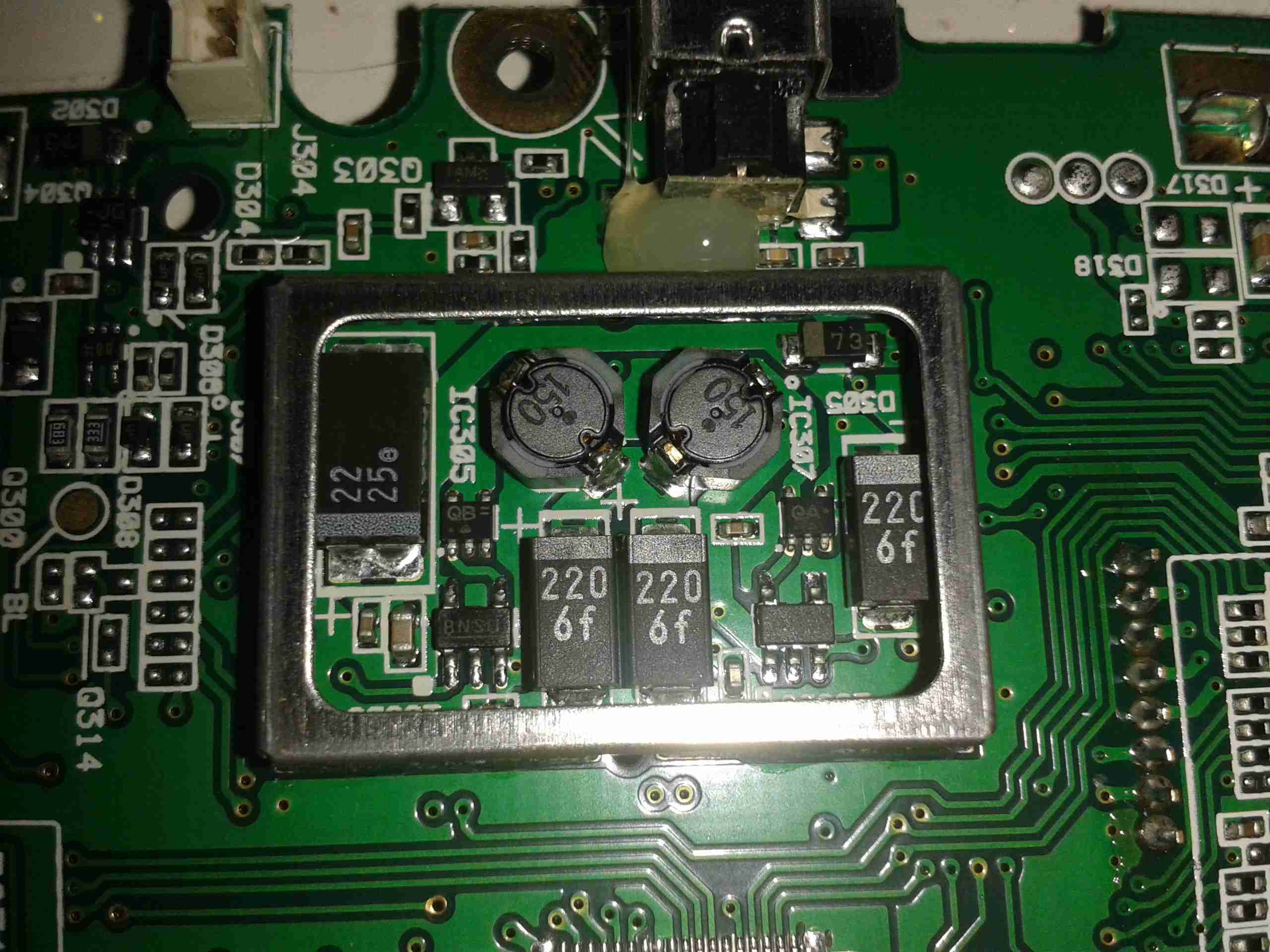
Here the back cover has been removed, and the main RF board is visible at the top of the stack. Unfortunately the shielding cans are soldered on this unit, so no looking under there 🙁
On the right hand side of the board next to the antenna input is the main RF filter network, and it’s associated switching. The RF front end is under the shield closest to the front edge.
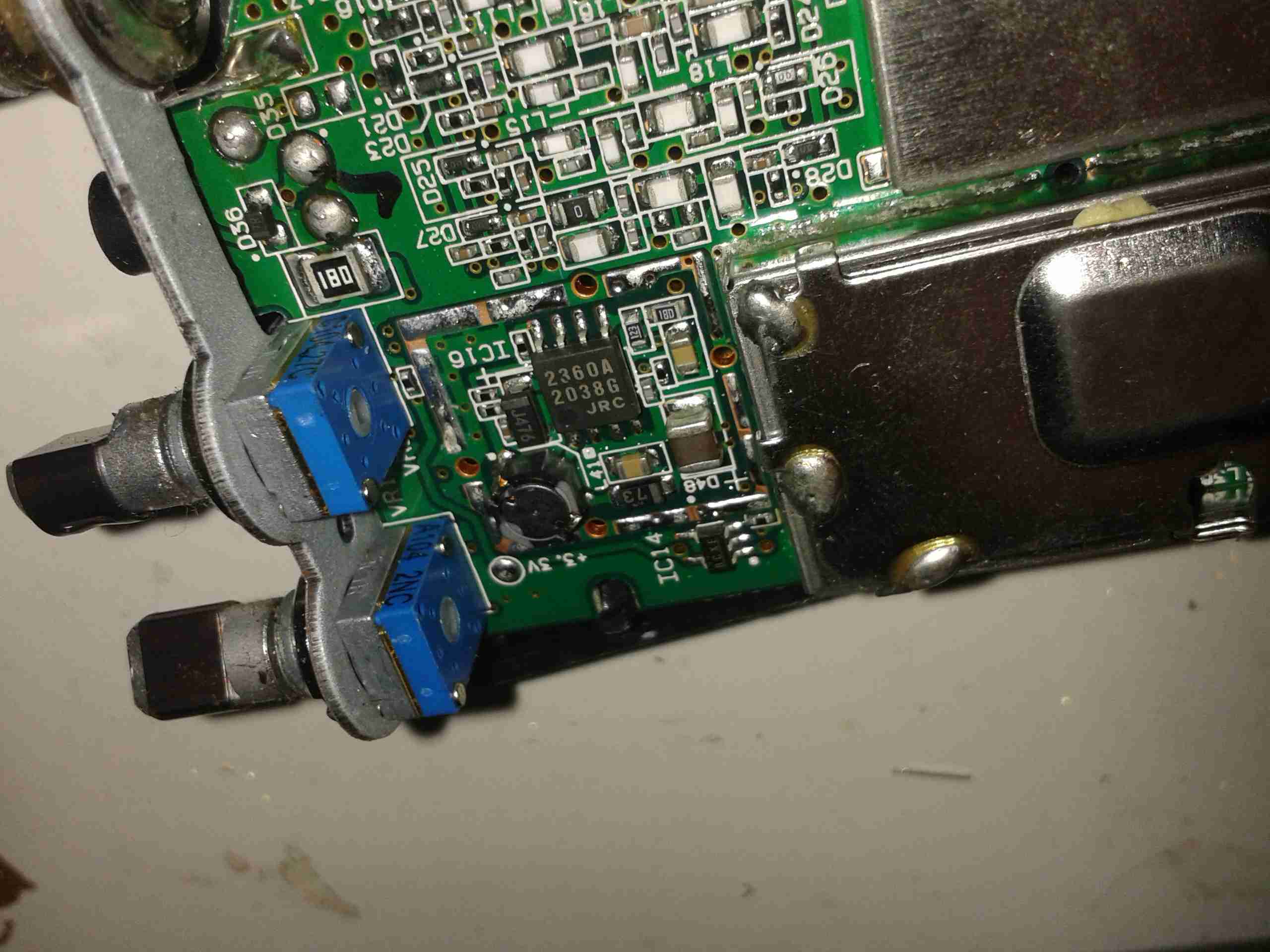
Controls & 3.3v Regulator
On the other side of the PCB is the Volume & Squelch potentiometers, along with a dedicated 3.3v switching supply. An NJM2360A High Precision DC/DC converter IC controls this one. A 3.3v test point is visible next to the regulator.
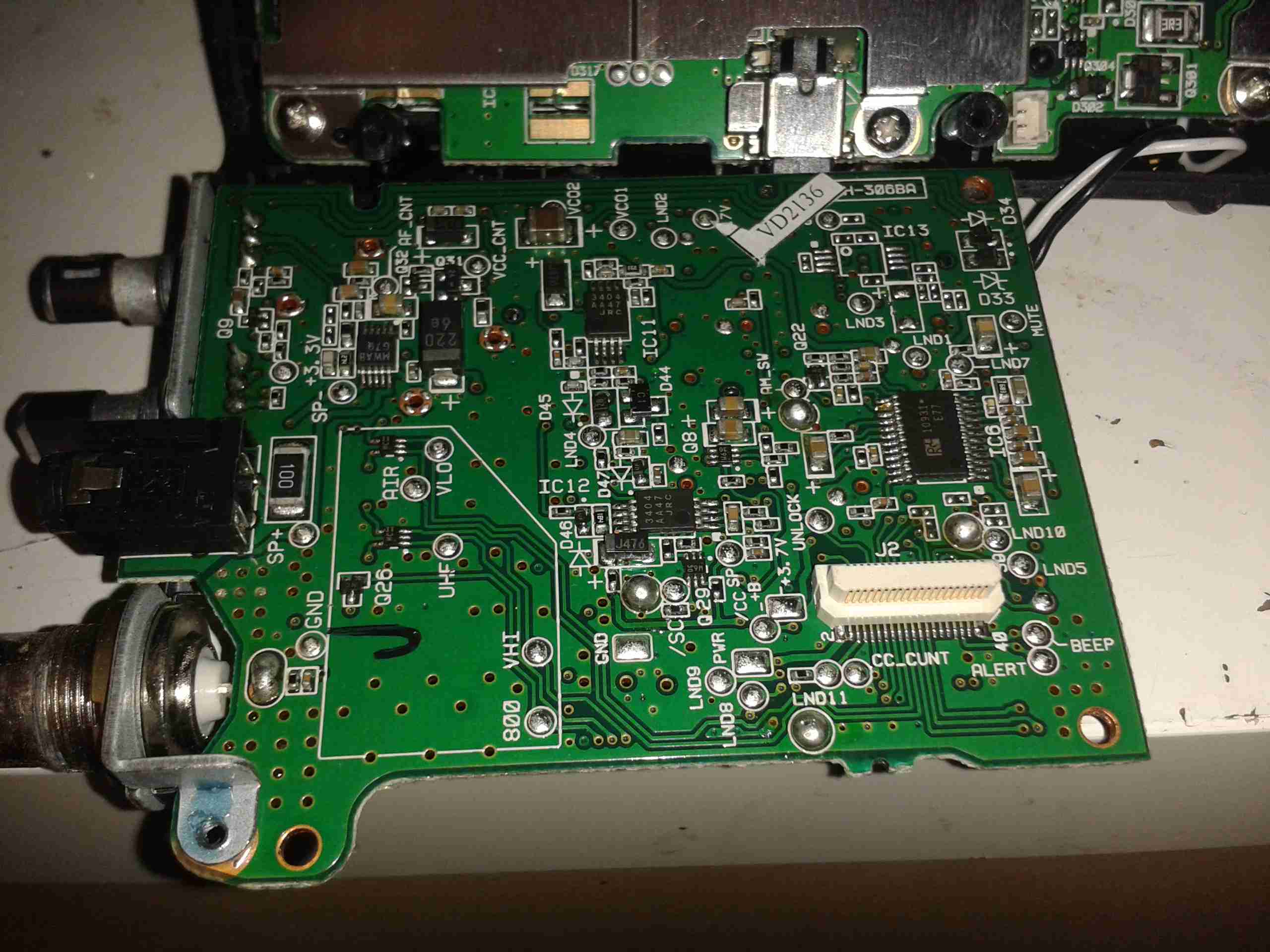
RF Board Reverse
Here’s the backside of the RF board, some more interesting parts here. There’s a pair of NJM3404A Single Supply Dual Op-Amp ICs, and a TK10931V Dual AM/FM IF Discriminator IC. This is the one that does all the back-end radio functionality. The audio amplifier for the internal speaker & external headphone jack is also on this PCB, top left. A board-to-board interconnect links this radio board with the main control board underneath.
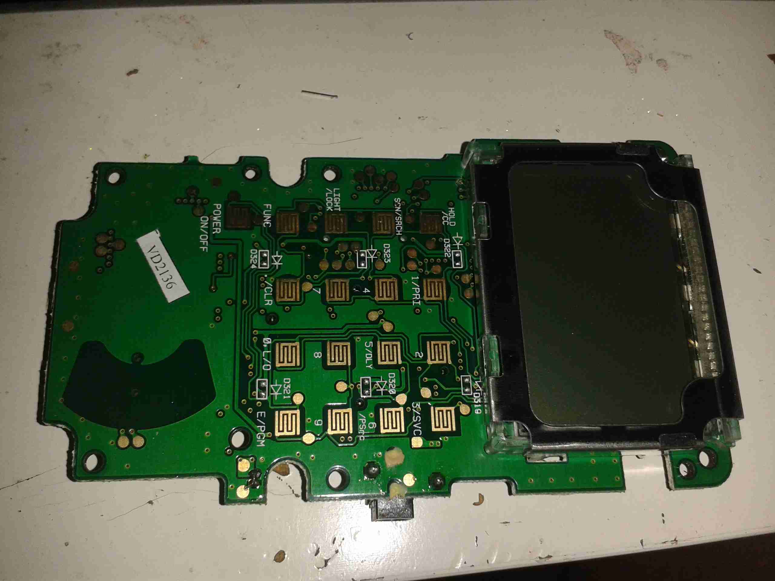
Control PCB Front
Here’s the front of the control PCB, nothing much to see here, just the LCD & membrane keypad contacts.
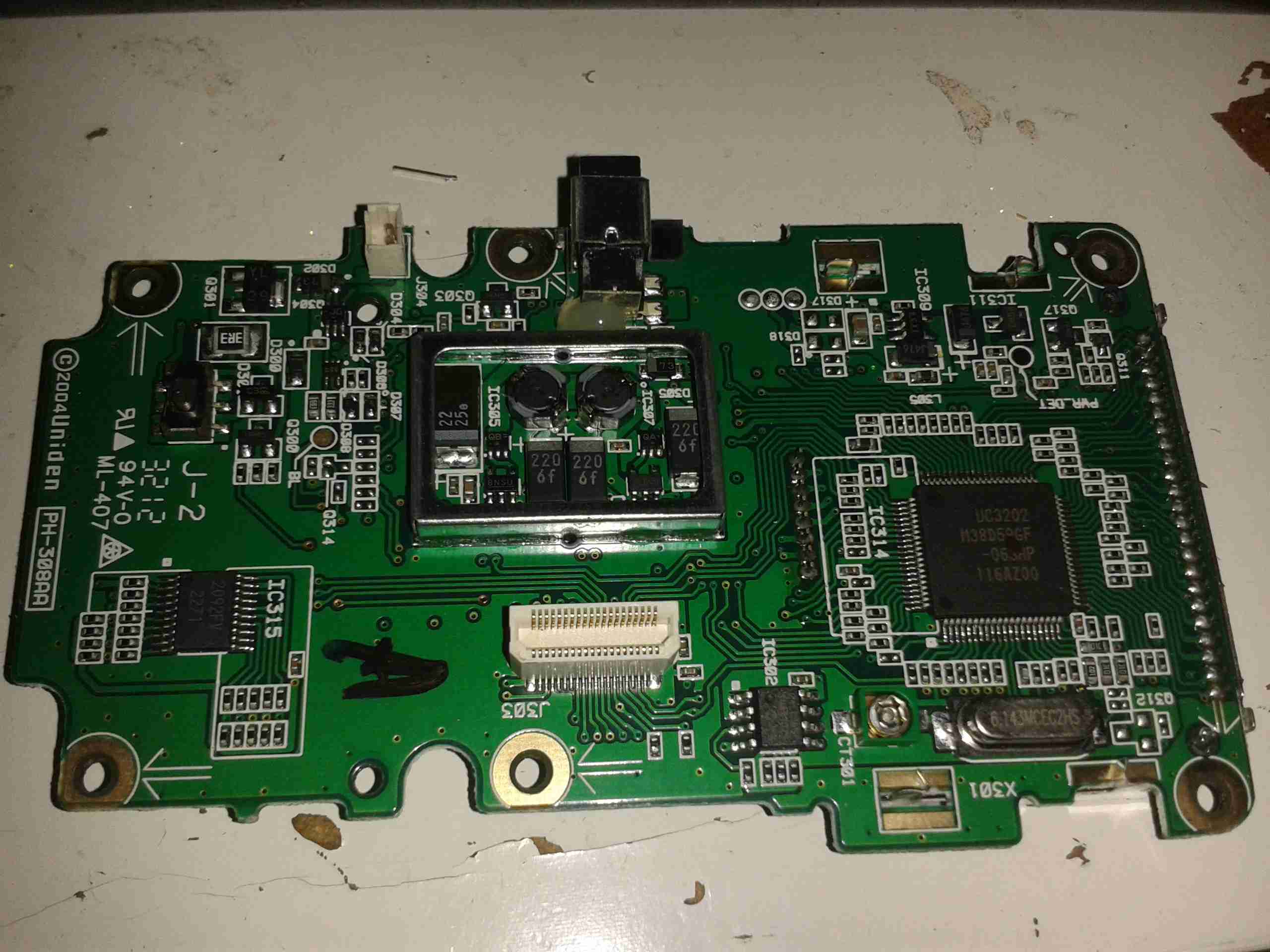
Control PCB Reverse
And here’s the reverse side of the control board. All the interesting bits are here. The main microcontroller is on the right, a Renesas M38D59GF, a fairly powerful MCU, with onboard LCD drive, A/D converter, serial interface, 60K of ROM & 2K of RAM. It’s 6.143MHz clock crystal is just below it.
The mating connector for the RF board is in the centre here.
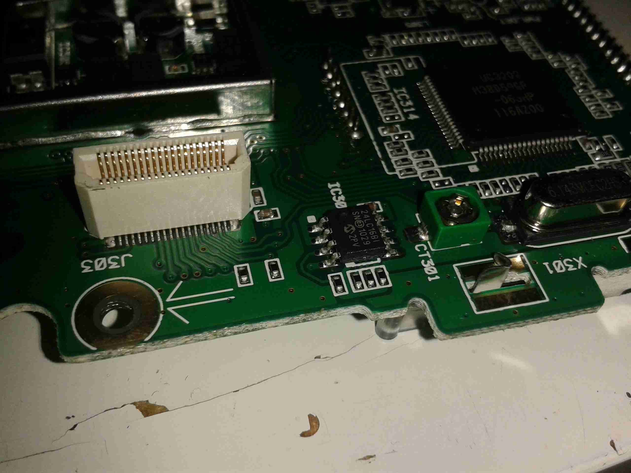
There is also a Microchip 24LC168 16KB I²C EEPROM next to the main microcontroller. This is probably for storing user settings, frequencies, etc.
EEPROM
The rest of this board is dedicated to battery charging and power supply, in the centre is a dual switching controller, I can’t figure out the numbers on the tiny SOT23 components in here, but this is dealing with the DC 6v input & to the left of that is the circuitry for charging the NiMH cells included with the scanner.
PSU
The last bit of this PCB is a BU2092FV Serial In / Parallel Out 4 channel driver. Not sure what this one is doing, it might be doing some signal multiplexing for the RF board interface. Unfortunately the tracks from this IC are routed on the inner layers of the board so they can’t be traced out.
Following on from my review, here are some internal views & detail on the components used in this radio. Below is an overview of the main PCB with the top plate removed from the radio.
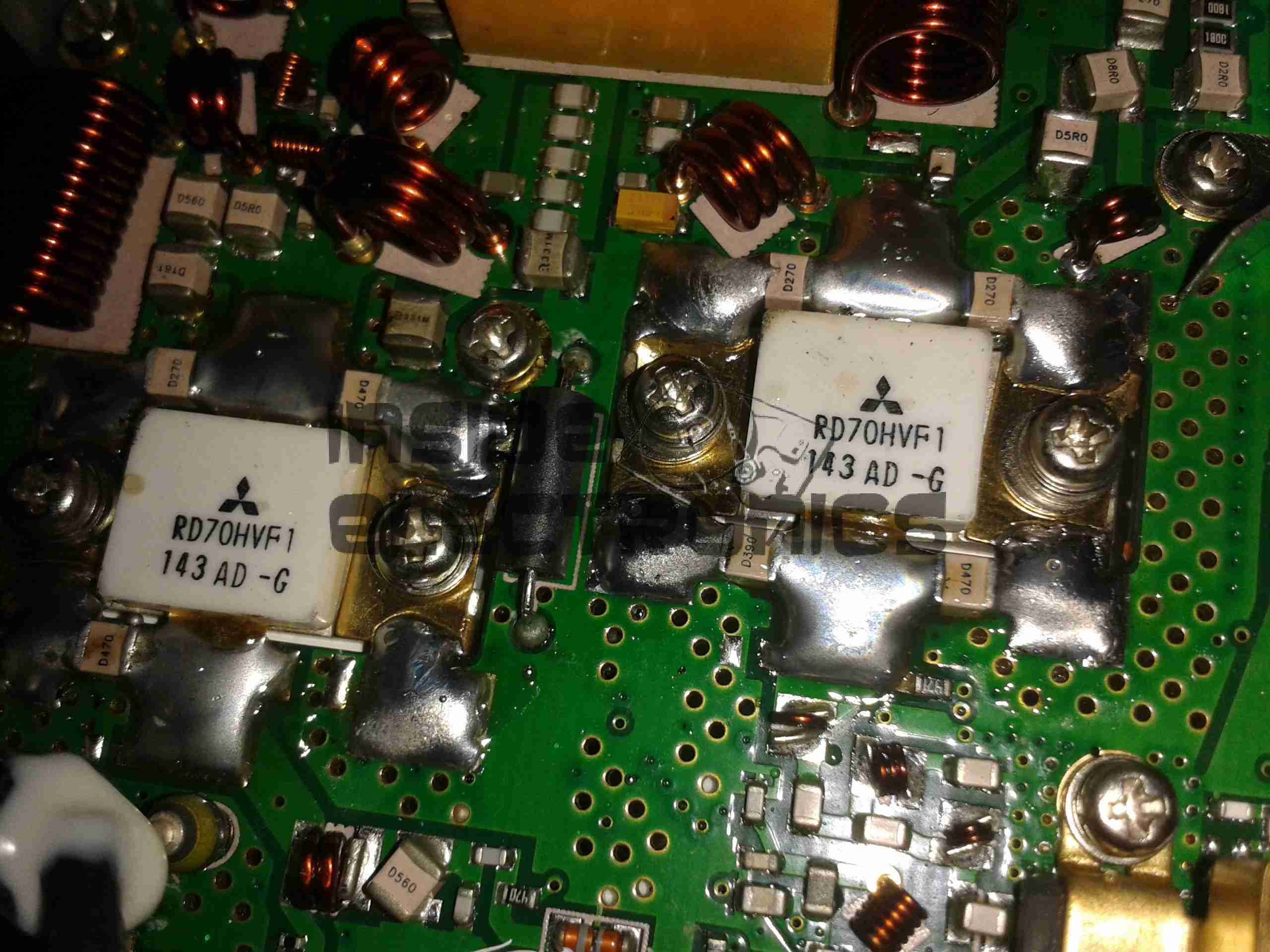
Cover RemovedRF Final Amplifier Stage
Most visible are these MOSFETs, which are Mitsubishi RD70HVF1 VHF/UHF power devices. Rated for a maximum of 75W output power at 12.5v (absolute maximum of 150W, these are used well within their power ratings. They are joined to the PCB with heavy soldering, with bypass caps tacked right on to the leads.
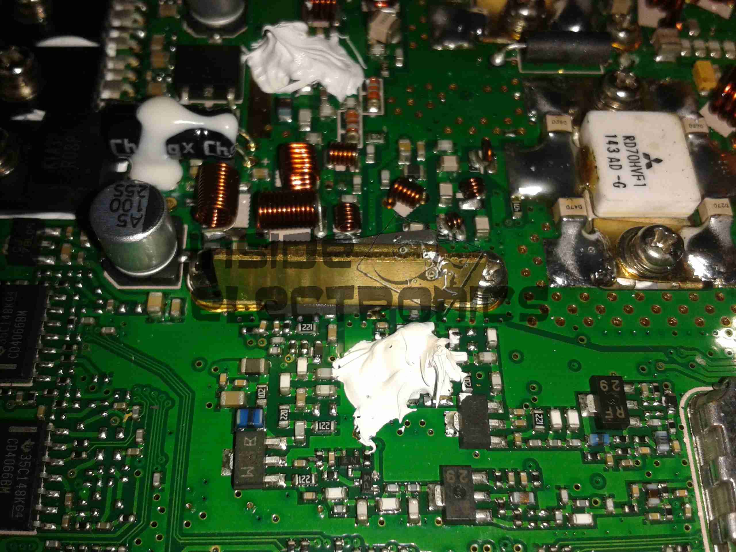
RF Pre Drivers
Here is the RF pre-driver stage, with intermediate transistors hidden under the small brass heatspreader.
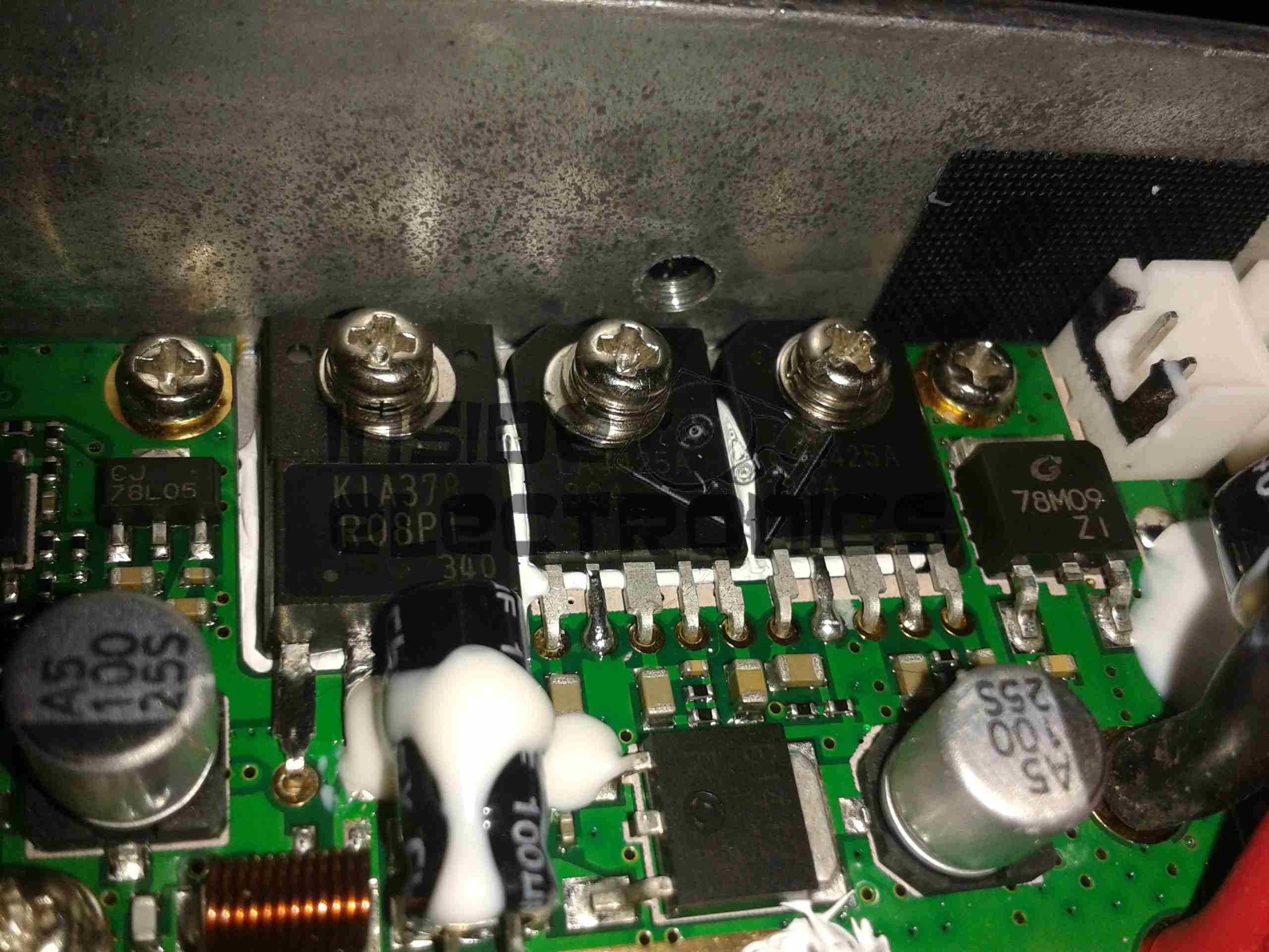
Power Section
In the top left corner of the radio, near the power input leads, is the power supply & audio amplifier section. Clearly visible are the pair of LA4425A 5W audio power amplifier ICs, these drive the speakers on the top of the radio. Either side of these parts are a 7809 & a 7805 – both linear regulators providing +9v & +5v logic supplies respectively. The large TO220 package device is a KIA378R08PI 3A LDO regulator with ON/OFF control, this one outputs +8v. Just visible in the top right corner are the sockets for the speaker connections.
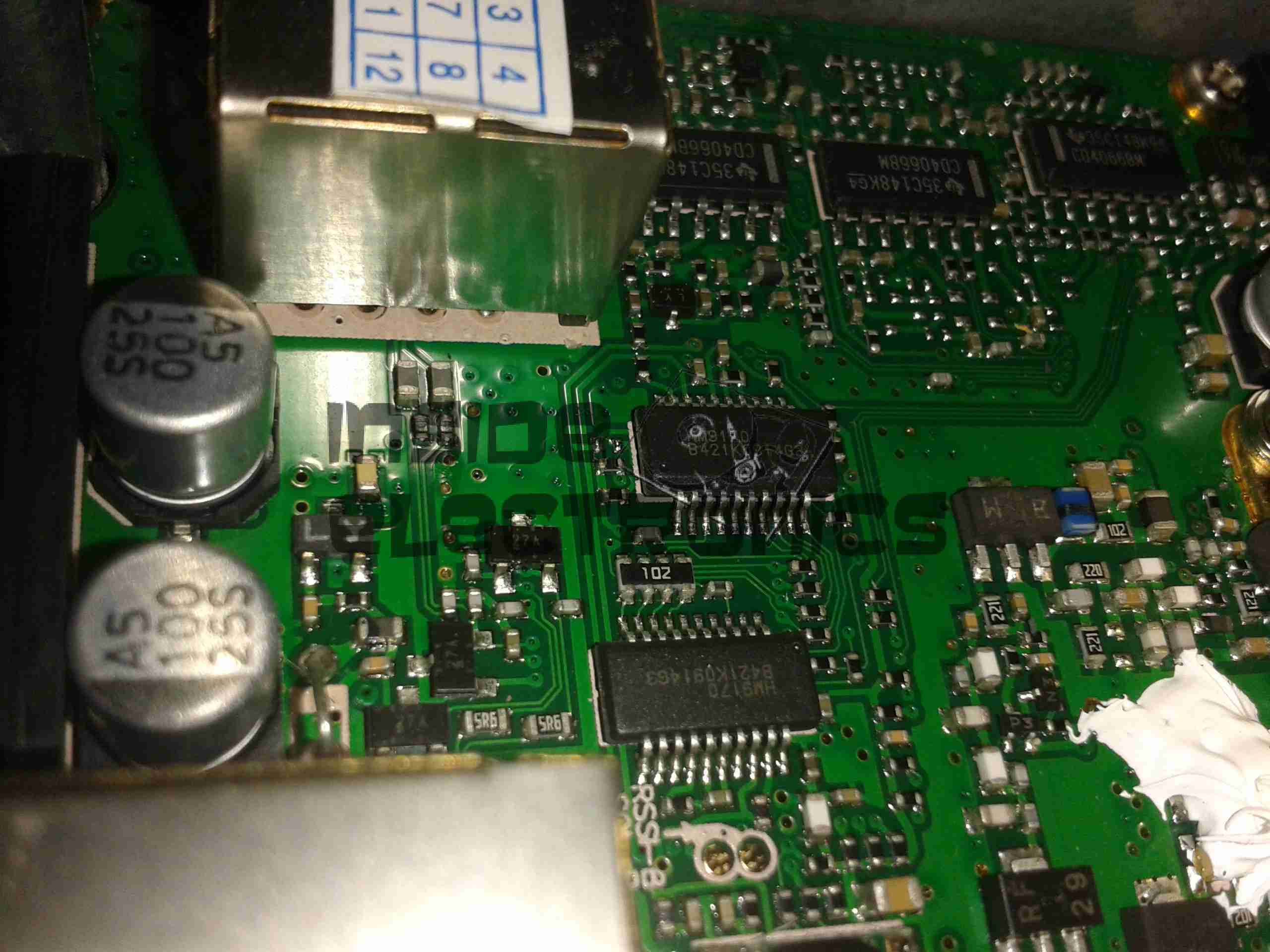
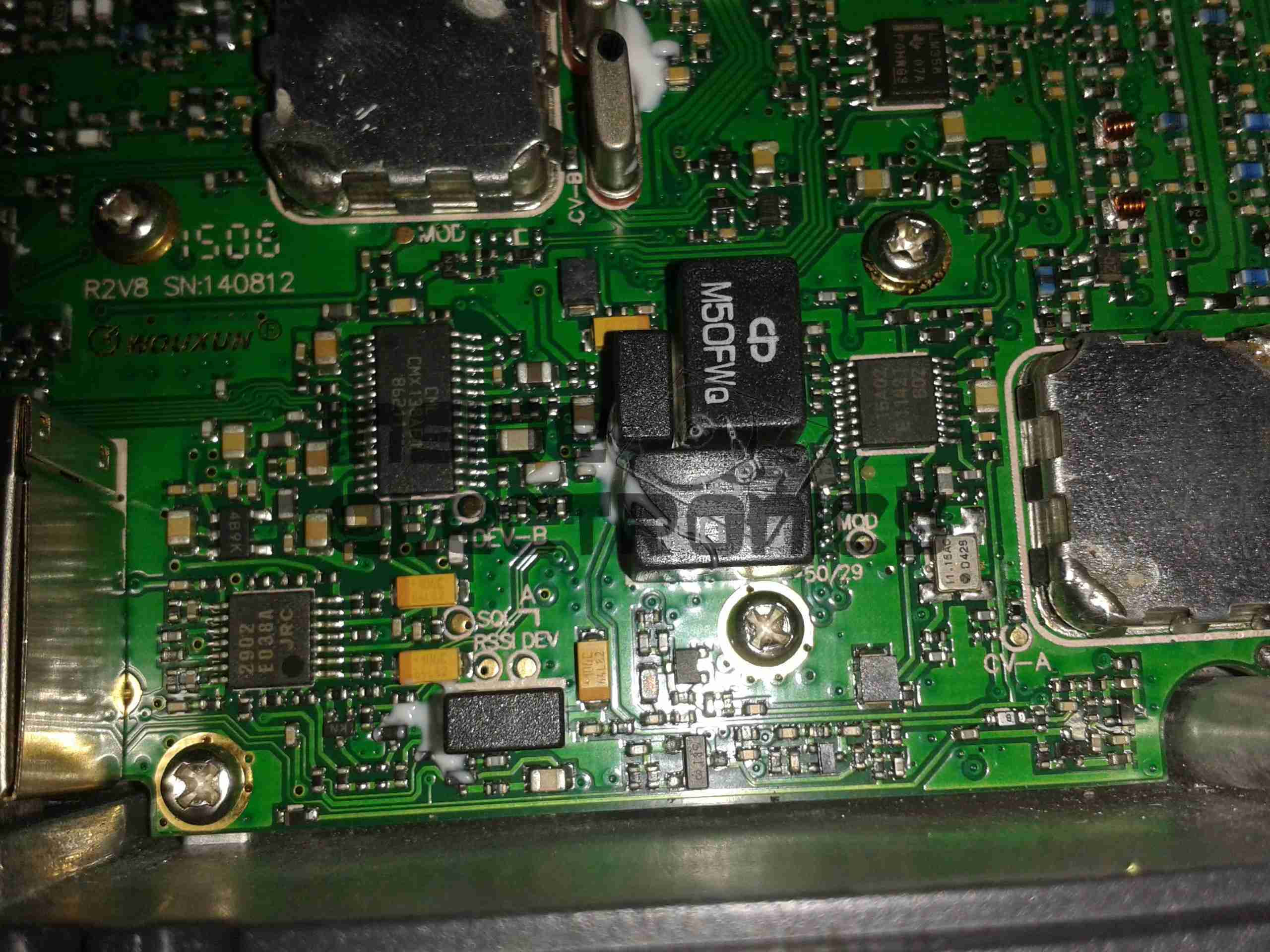
DTMF Circuits
Here are the two ICs for dealing with DTMF tones, they are HM9170 receivers.
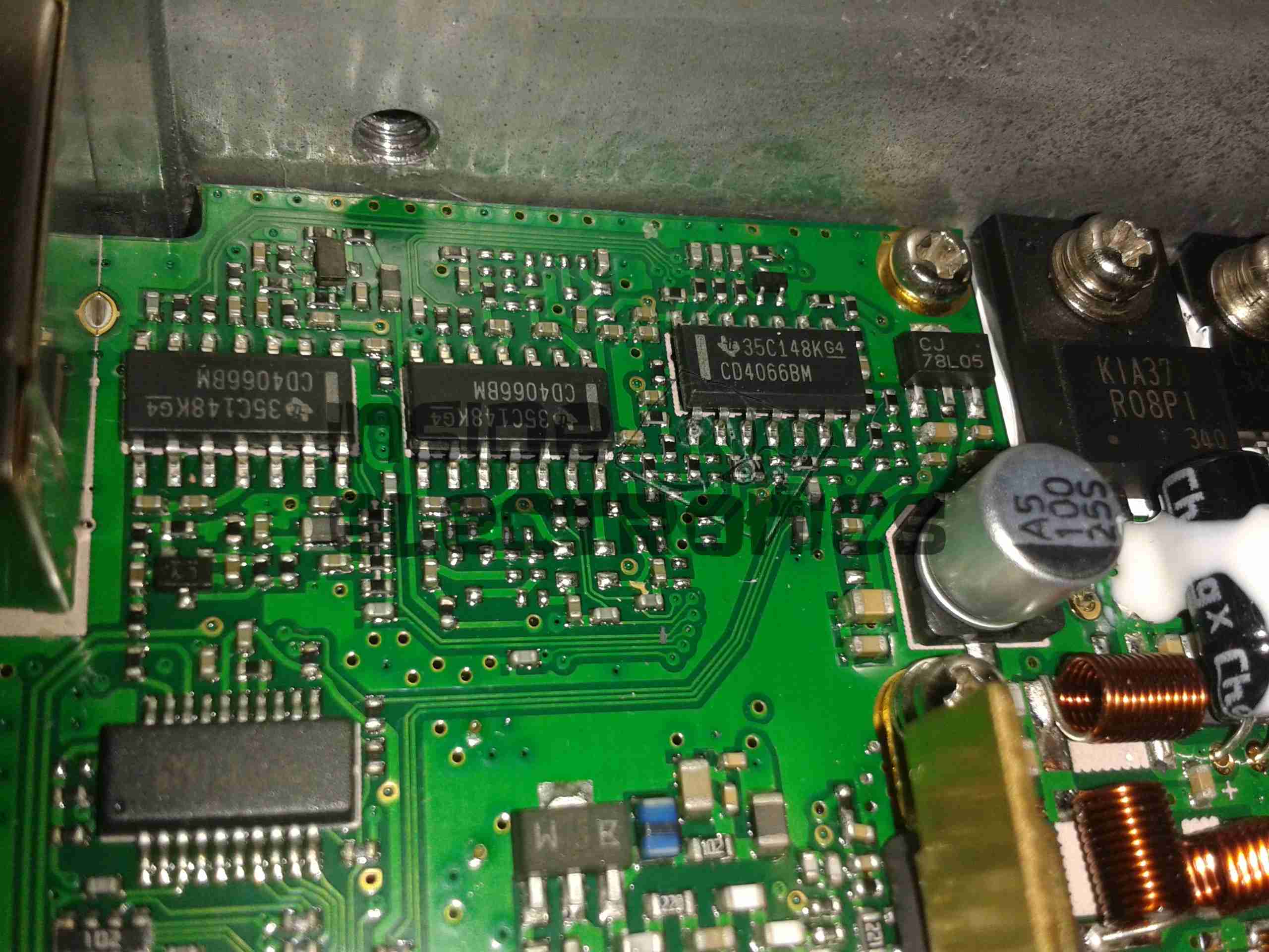
Glue Logic
In the corner next to the interface jack, there are some CD4066B Quad Bilateral switches. These make sense since the interface jack has more than a single purpose, these will switch signals depending on what is connected.
RF Section
Here are visible the RF cans for the oscillators, the crystals visible next to the can at the top. The shields are soldered on, so no opening these unfortunately.
Also visible in this image is a CMX138A Audio Scrambler & Sub-Audio Signalling processor. This IC deals with the Voice Inversion Scrambling feature of the radio, & processes the incoming audio before being sent to the modulator.
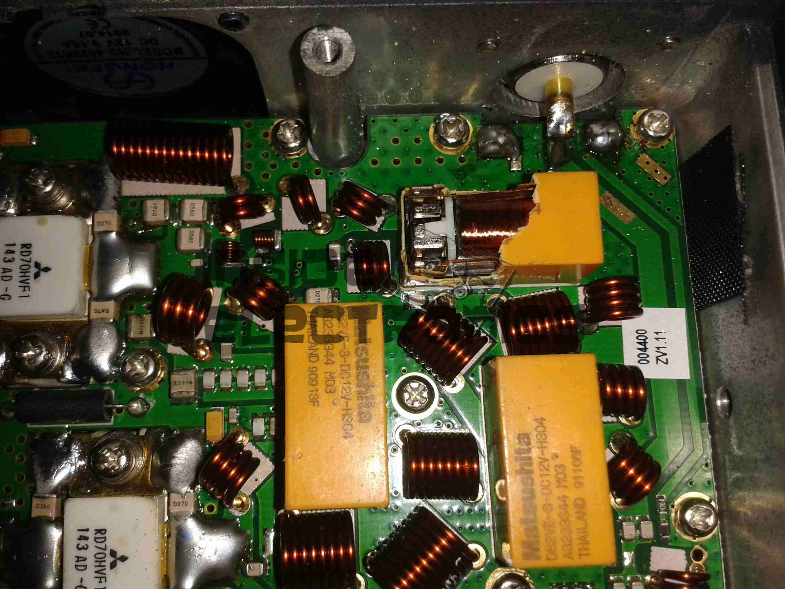
Output Filter Network
Shown here is the RF output filter network, this radio uses relays for switching instead of PIN diodes, I imagine for cost reasons. The relay closest to the RF output socket has had a slight accident 🙂 This is slated to be replaced soon.
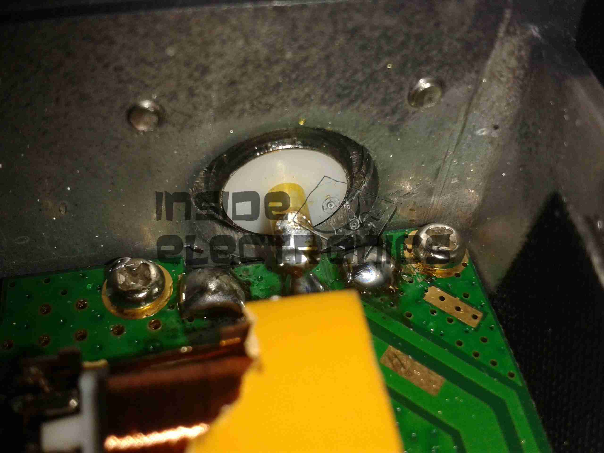
RF Output Jack
Finally, the RF output jack.
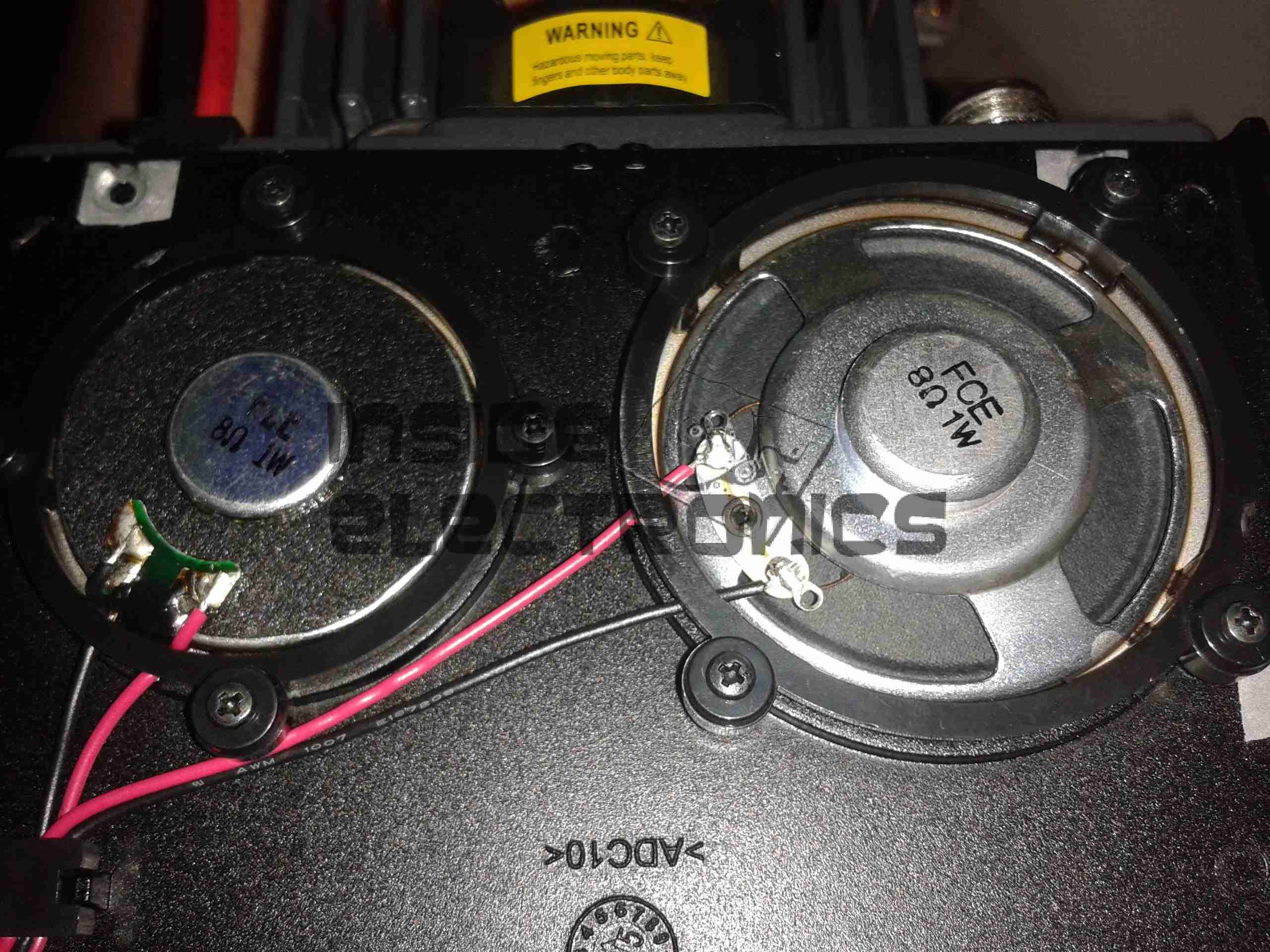
Audio Speakers
Here the speakers are shown, attached to the bottom of the top plate. They are both rated 8Ω 1W.
These speakers are available free from Pringles, with two packs bought. Normally running on 3x AAA cells, I have made modifications to include a high capacity Li-Ion battery & USB charging.
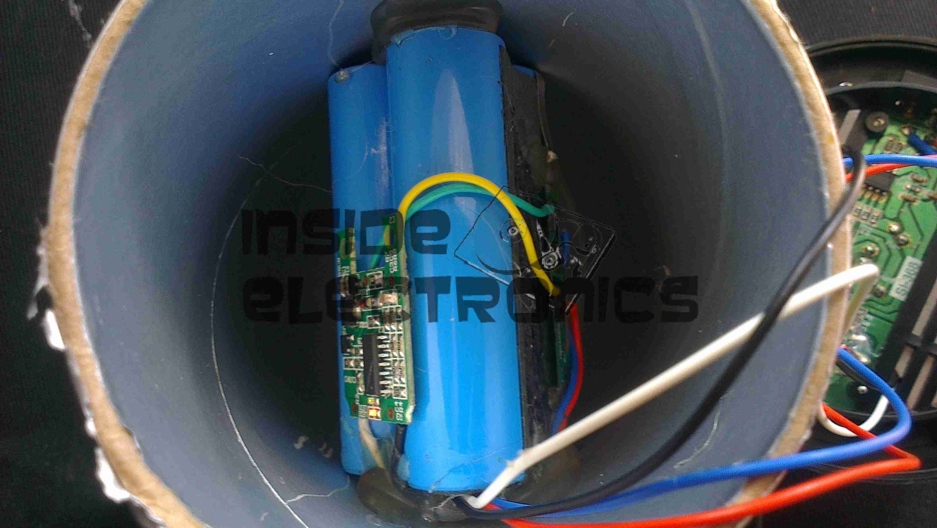
18650 Battery
New battery is 3x 18650 Li-Ion cells in parallel, providing ~6600mAh of capacity. These are hot glued inside the top of the tube under the speaker, with the charging & cell protection logic.
The battery charging logic is salvaged from an old USB eCig charger, these are single cell lithium chargers in a small form factor ideal for other uses. Charging current is ~450mA.
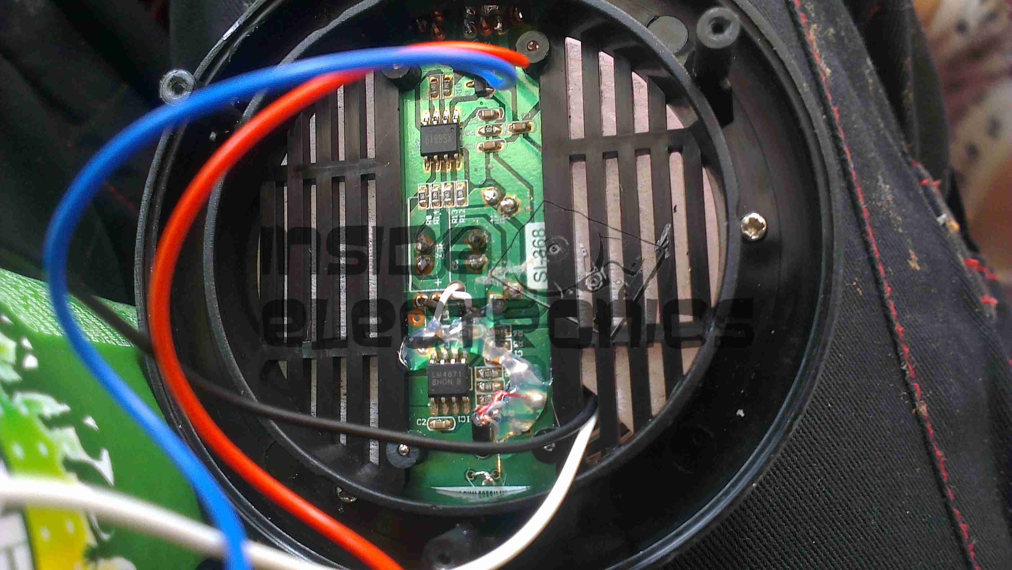
Amplifier Board
The cells are connected to the same points as the original AAA cells, with the other pair of wires going into the top of the device to connect to the MicroUSB charging port.
The amplifier in this is a LM4871 3W Mono amplifier IC, connected to a 6Ω 1W speaker.
The other IC on the board is unidentifiable, but provides the flashing LED function to the beat of the music.
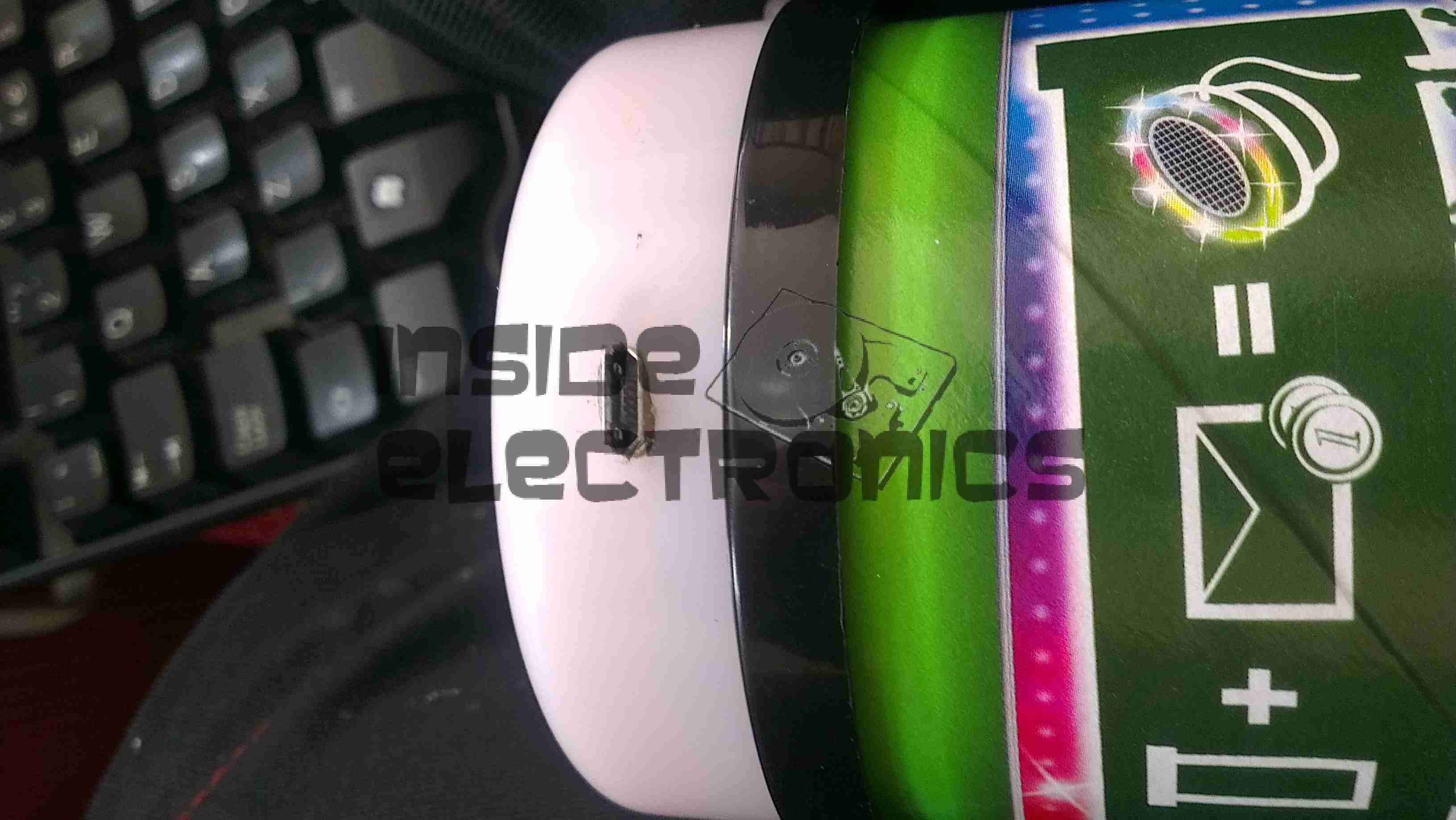
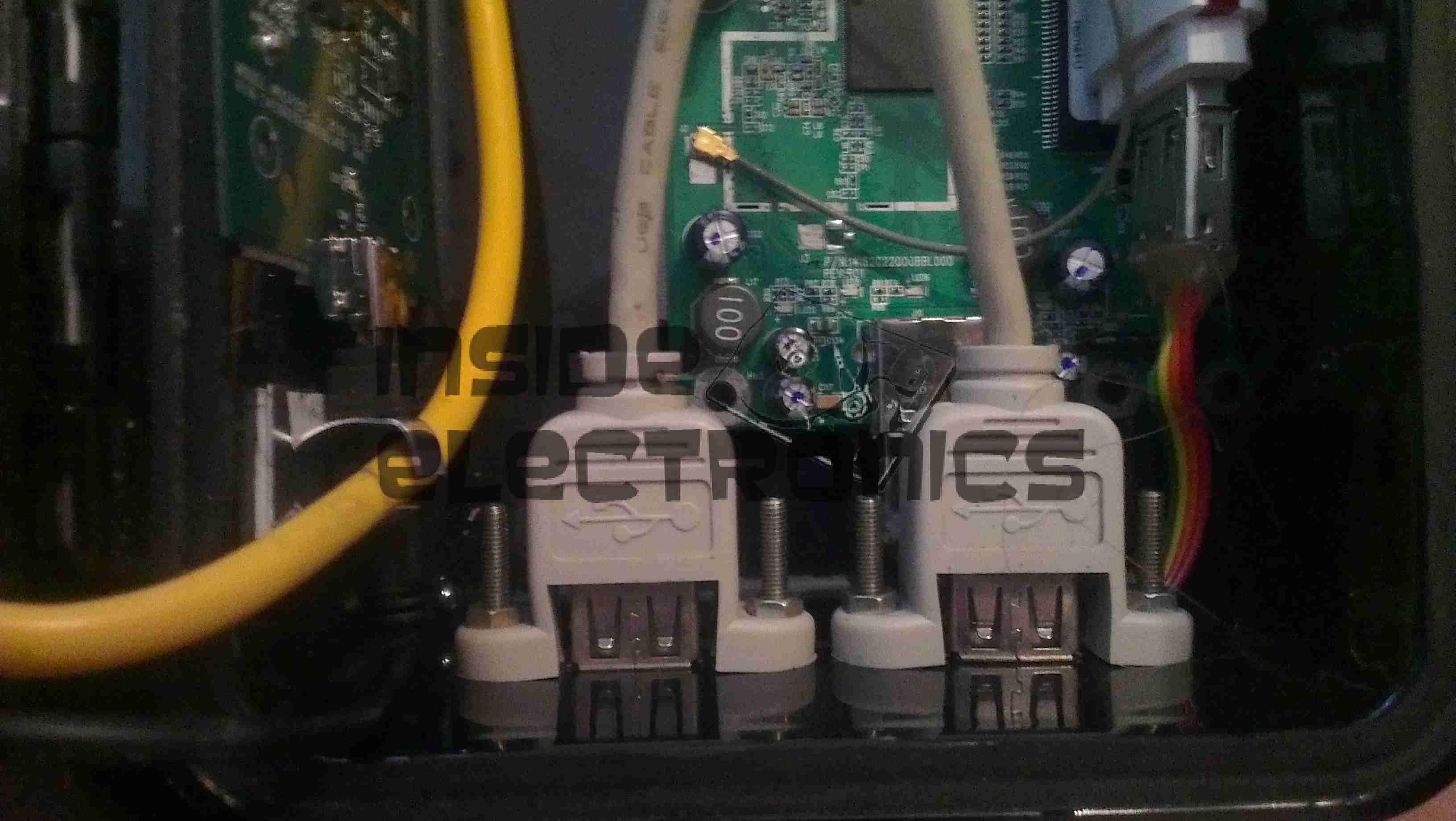
For convenience, a pair of USB ports have been fitted to the wearable Pi, which open on the bottom of the unit. These will be hardwired into a 4-port USB hub which will also support the wireless adaptor for the mini-keyboard that is to be used with the device.
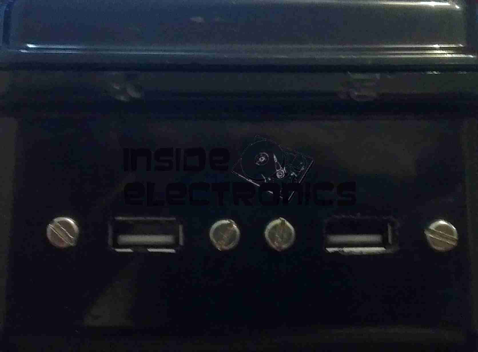
USBs
The two USB ports on the bottom of the casing.
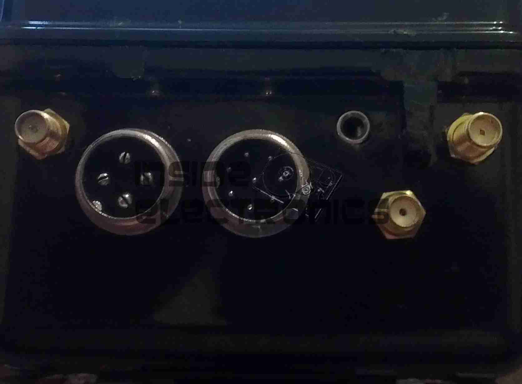
External Connections
The external connectors are also complete. The audio jack & second WiFi antenna port are fitted.
The audio is normally routed to the LCD display speaker, until a jack is plugged into the 3.5mm socket.
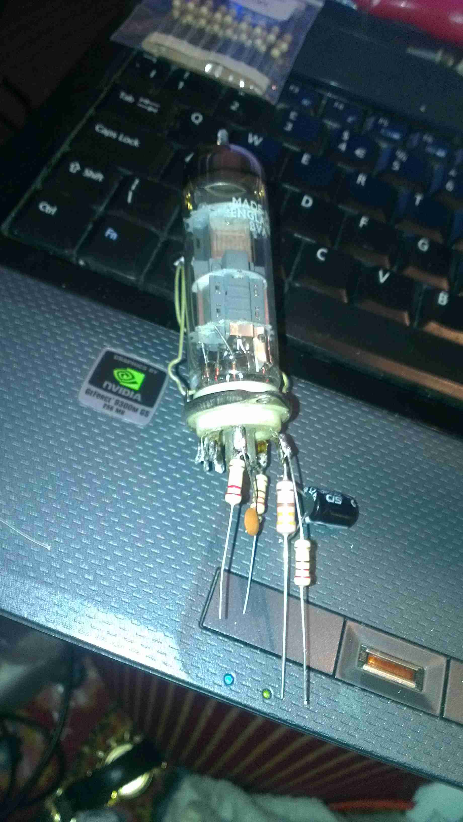
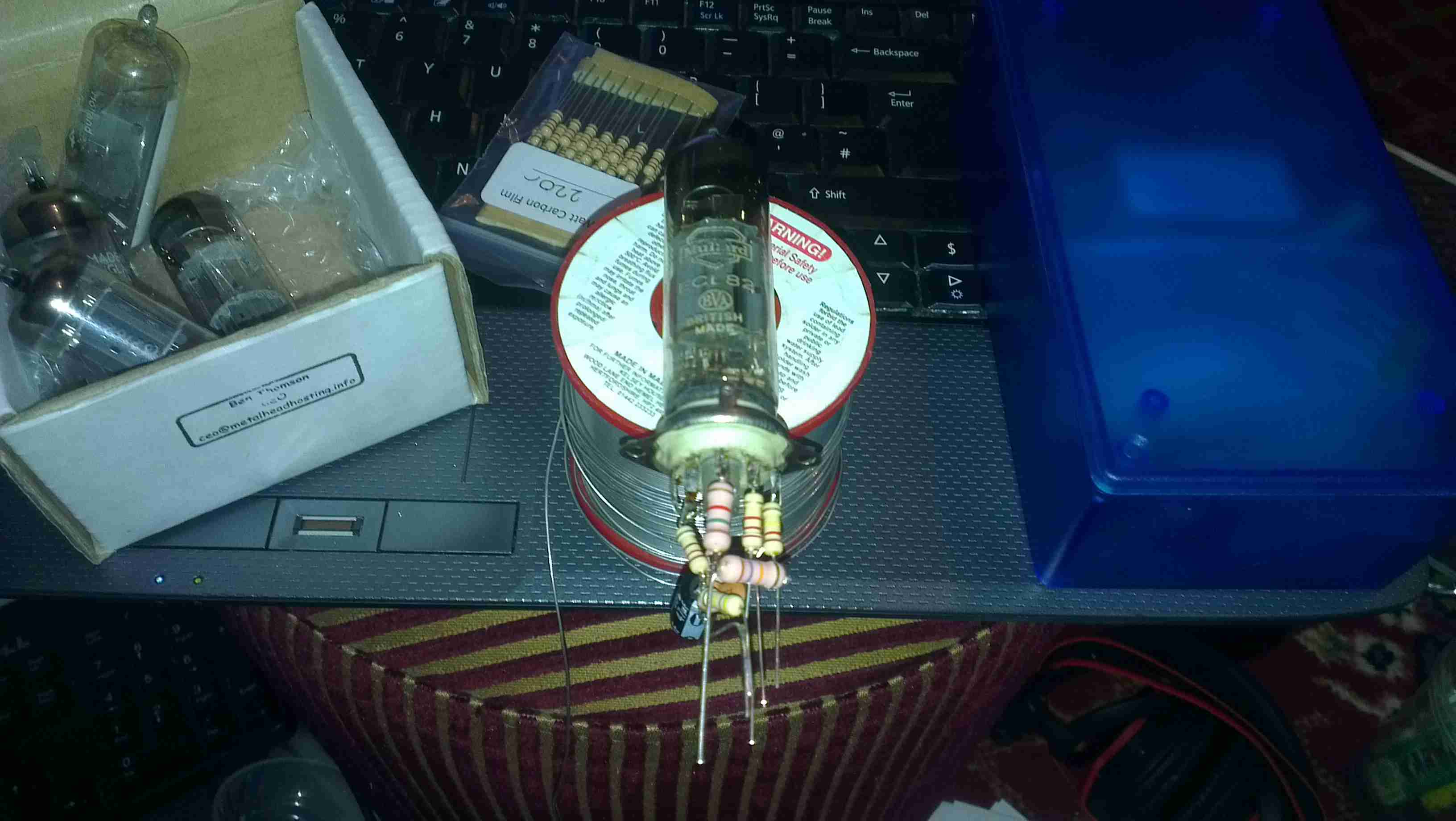
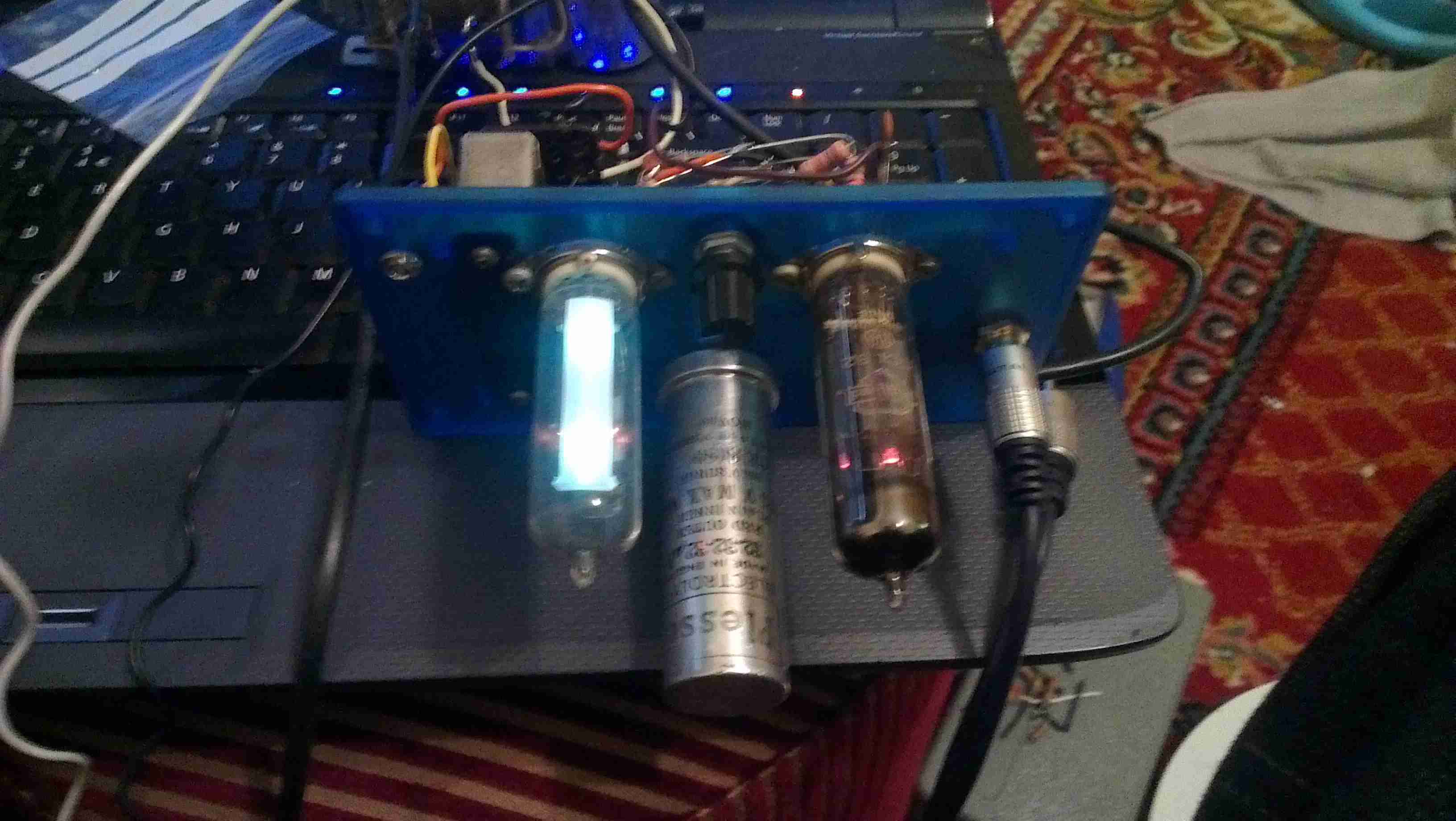
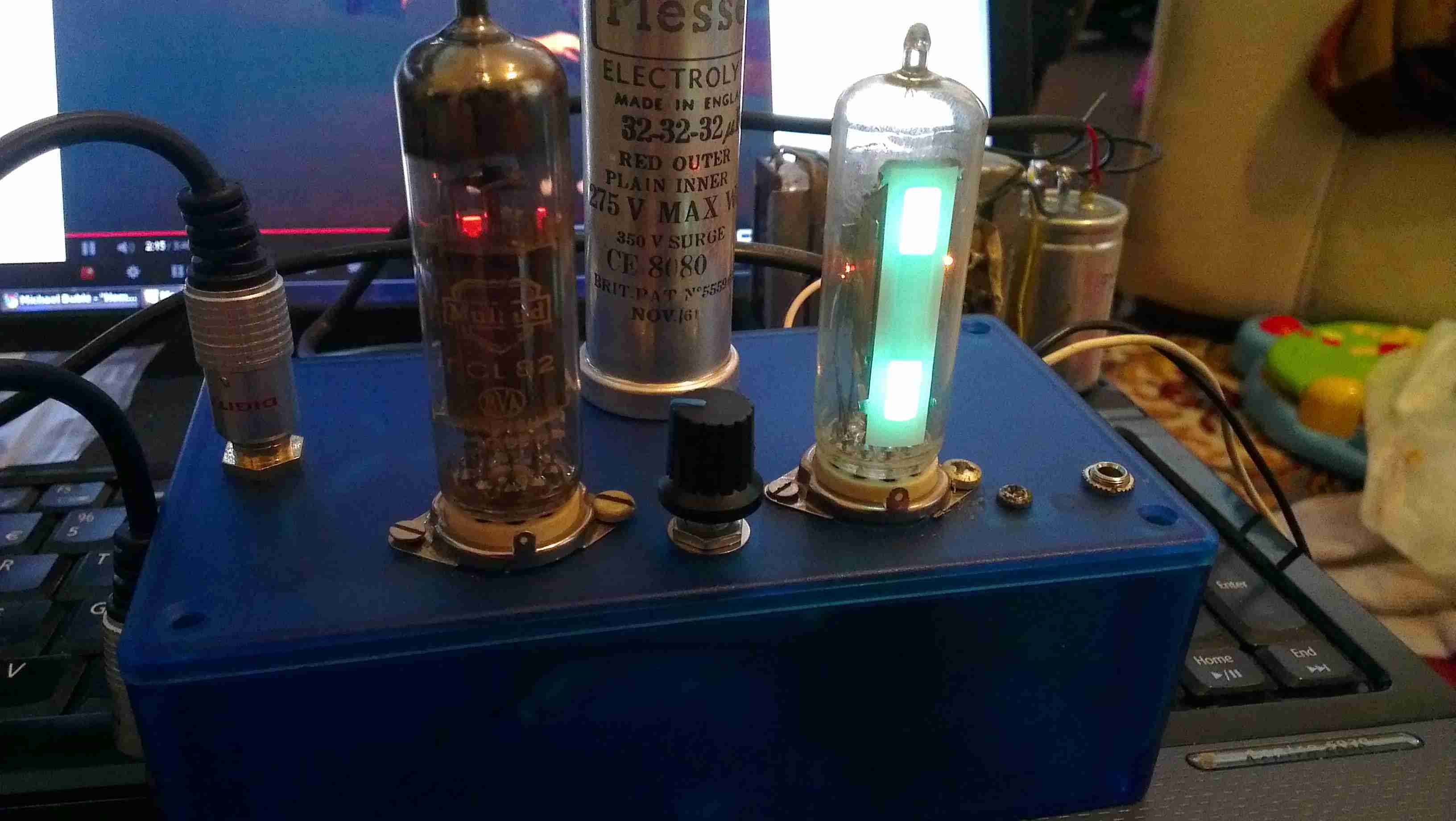
Here are a few details of a valve amplifier I am building, using the valve related parts from a 1960’s reel to reel tape recorder.
This amplifier is based on an a Mullard ECL82 triode/pentode valve, with an EM84 magic eye tube for level indication.
Beginnings Of The Amplifier
Here the first components are being soldered to the tags on the valve holder, there are so few components that a PCB is not required, everything can be rats-nested onto the valve holders.
Progress
Progressing with the amplifier section componentry, all resistors are either 1/2W or 2W.
Valve Sockets Fitted
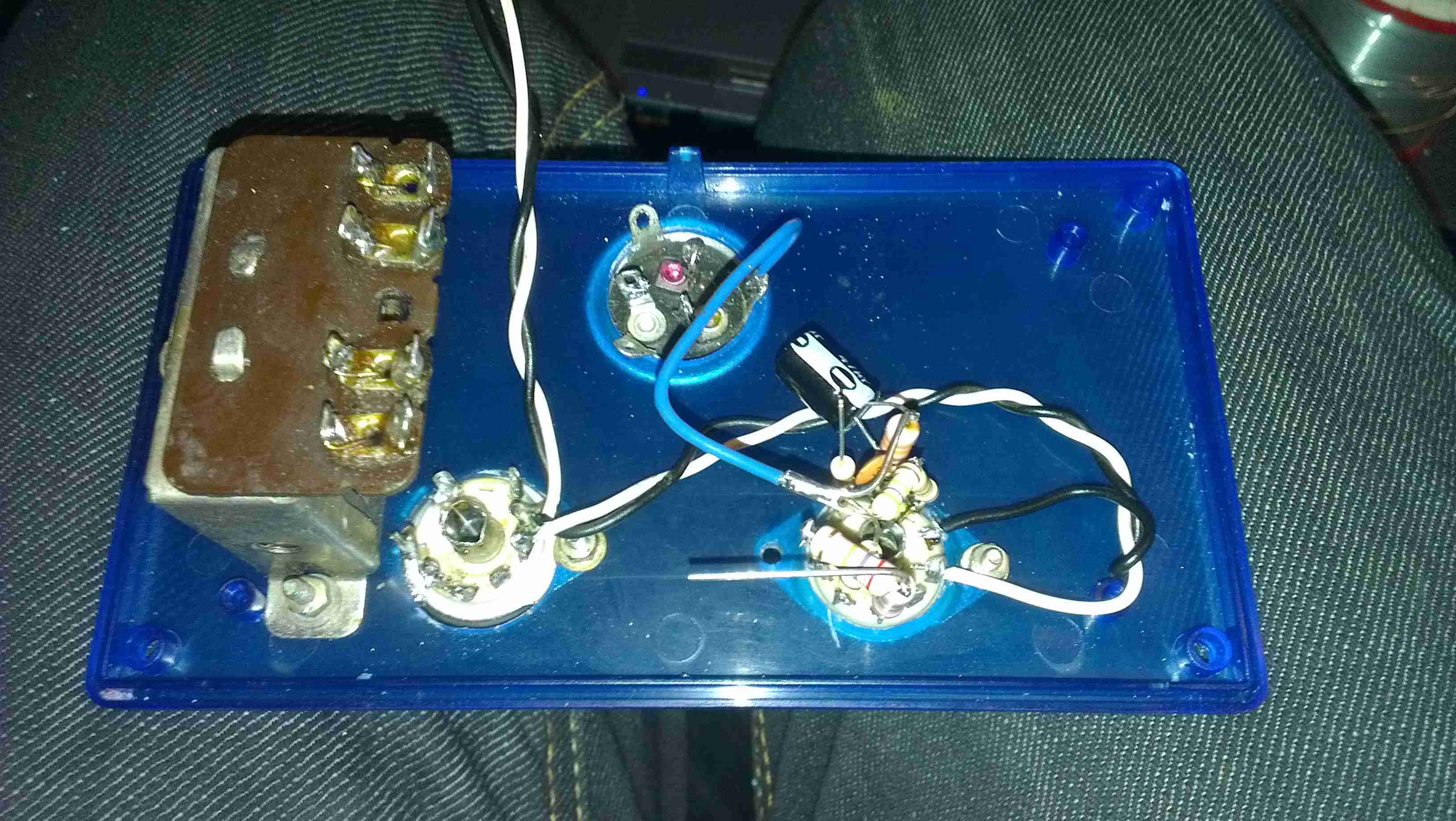
Here the valve holders have been fitted, along with the output transformer, DC smoothing capacitor & the filament wiring, into the top of the plastic housing. At this point all the components that complete the amplifier section are soldered to the bottom of the right hand valve holder.
Wiring
Starting the wiring between the valves & the power supply components. The volume control pot is fitted between the valve holders.
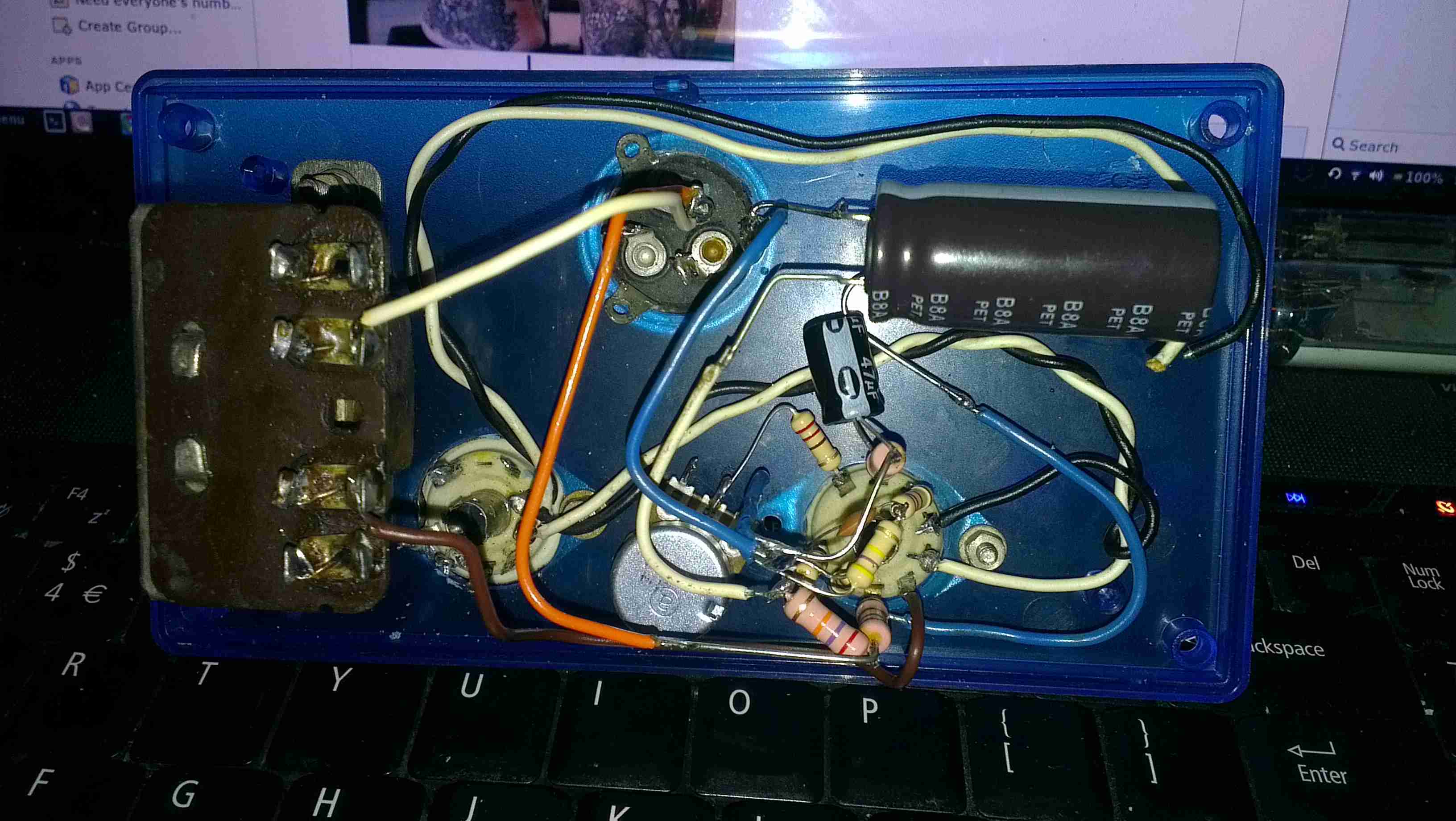
Valves Test Fit
The valves here are test fitted into their sockets, the aluminium can at the back is a triple 32uF 250v electrolytic capacitor for smoothing the B+ rail.
Amplifier Section First Test
First test of the amplifier, with the speaker from the 1960’s tape recorder from which the valves came from. the 200v DC B+ supply & the 6.3v AC filament supply is derived from the mains transformer in the background.
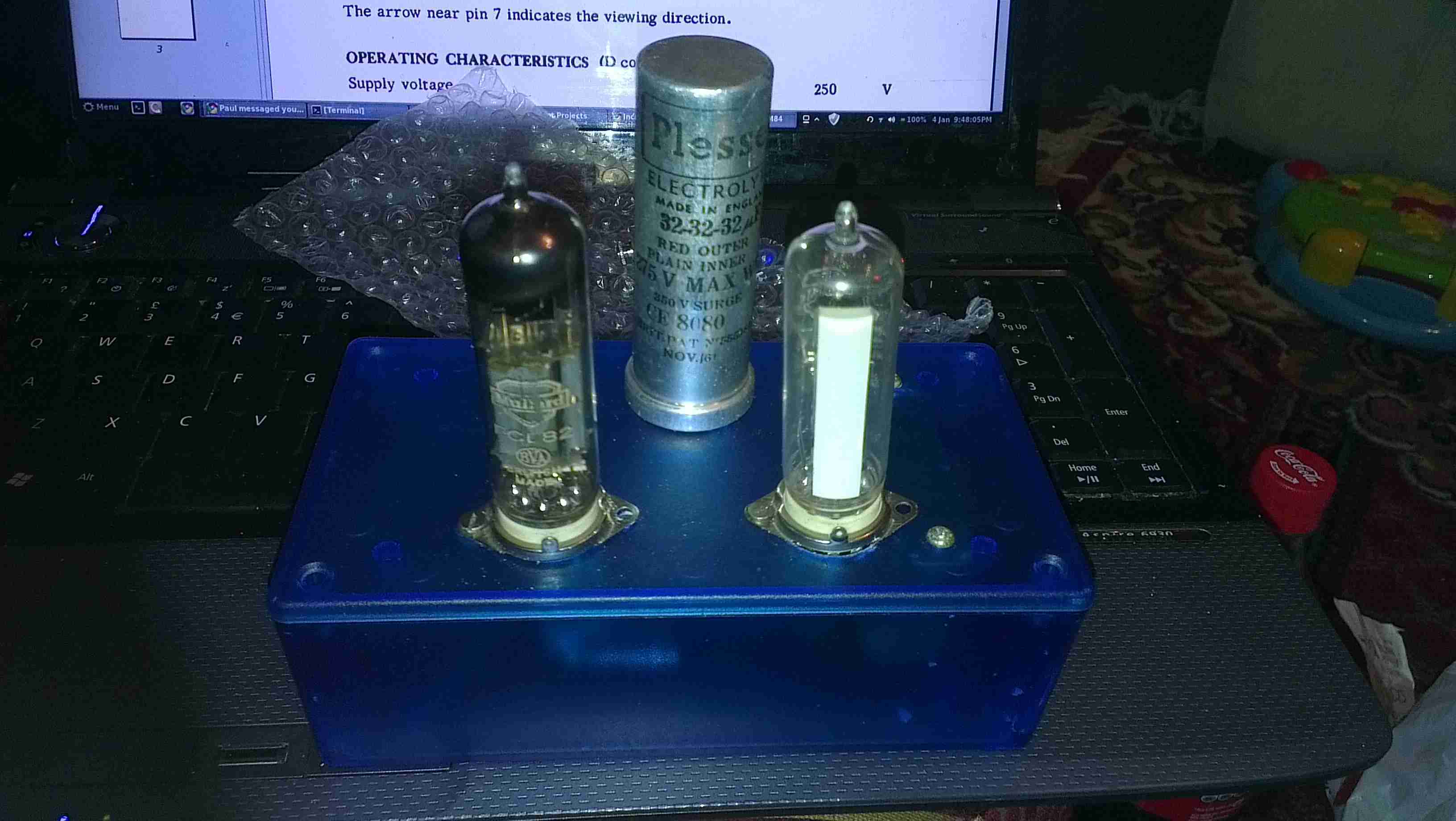
Magic Eye Tube Added
Here the magic eye tube has been fitted & is getting it’s initial tuning to the amplifier section. This requires selecting combinations of anode & grid resistors to set the gap between the bars while at no signal & picking a coupling RC network to give the desired response curve.
Final Test
Here both valves are fitted & the unit is sitting on it’s case for final audio testing. the cathodes of the ECL82 can be clearly seen glowing dull red here.
In the final section, I will build a SMPS power supply into the unit to allow it to be powered from a single 12v DC power supply.
Here is a Sanyo tape recorder, with built in voice activation. Takes standard audio cassettes.
Here visible is the speaker on the left, microphone is on the right of the tape window. The tape counter is at the top.
Back Removed
Back cover removed from the unit, showing the PCB & the connections. The IC is the controller/amplifier.
PCB
Top of the PCB, control switches, volume potentiometer & microphone/headphone sockets on the right. DC power jack top left. Switch bottom centre senses what mode the tape drive is in.
Tape Deck
Rear of the tape deck, main drive motor is bottom right, driving the capstan through a drive belt. This drives the tape spools through a series of gears & clutches. Belt going to top left drives the tape counter.
Drive
Front of the tape drive. Read/write head is top centre. Blue head is bulk erase head used during recording.
For those that are interested, here is the ID label, this is a PSP-2003.
Front Removed
Here the front of the unit has been removed, showing the first internal components.
Screen Removed
Here is the unit with the LCD removed, here the mainboard is partially visible.
Left Pad
Left pad unit removed from the PSP, with the left speaker & the memory stick slot cover.
Left Pad Rear
Rear of the left pad assembly, showing the speaker.
Joypad
Joypad removed from the casing. Resistive unit.
Output Jack
Headphone/data board removed from the casing. This also has TV-Out on the PSP-200x series.
Mainboard
Mainboard removed. Main CPU is at the top. Sockets around the bottom connect to the UMD drive & UMD Drive.
CPU & GPU
Closeup of the main chipset. CPU is the top IC.
Mainboard Rear
Rear of the mainboard, Memory Stick socket on the right.
WiFi Chipset
Closeup of the WiFi chipset & the charging power socket on the right.
Charging Chipset
Closeup of the bettery connector & the charge controller IC.
UMD Drive
UMD Drive removed from the rear of the casing. This is a miniature DVD style drive, using a 635nm visible red laser.
UMD Drive Back
Rear of the UMD drive, showing the laser sled & drive motors. Both the spindle motor & the sled motor are 3-phase brushless type. The laser diode/photodiode array is at the top of the laser sled.
This is an old cordless landline phone, with dead handset batteries.
Handset Radio Board
Here’s the handset with the back removed. Shown is the radio TX/RX board, underneath is the keyboard PCB with the speaker & mic. All the FM radio tuning coils are visible & a LT450GW electromechanical filter.
Handset Radio Board Bottom
Radio PCB removed from the housing showing the main CPU controlling the unit, a Motorola MC13109FB.
Keypad Board
The keypad PCB, with also holds the microphone & speaker.
Handset Keypad Board Bottom
Bottom of the keypad board, which holds a LSC526534DW 8-Bit µC & a AT93C46R serial EEPROM for phone number storage.
Base Main Board
Here’s the base unit with it’s top cover removed. Black square object on far right of image is the microphone for intercom use, power supply section is top left, phone interface bottom left, FM radio is centre. Battery snap for power backup is bottom right.
Power Supply Section
PSU section of the board on the left here, 9v AC input socket at the bottom, with bridge rectifier diodes & main filter capacitor above. Two green transformers on the right are for audio impedance matching. Another LT450GW filter is visible at the top, part of the base unit FM transceiver.
ICs
Another 8-bit µC, this time a LSC526535P, paired with another AT93C46 EEPROM. Blue blob is 3.58MHz crystal resonator for the MCU clock. The SEC IC is a KS58015 4-bit binary to DTMF dialer IC. This is controlled by the µC.
Base Main Board Bottom
Underside of the base unit Main PCB, showing the matching MC13109FB IC for the radio functions.
Here is a more modern phone, the Motorola V360v. Features include Dual screens, 640×480 VGA camera, full col
our TFT Main LCD, SD-Micro slot.
Here on the back the grey scale LCD can be seen, with the camera lens to the right of the Motorola logo
Keypad
Here the phone is opened showing the keypad & the full colour TFT LCD display.
Battery Compartment
Here the battery is removed from the unit, showing the SIM connector. The antenna cover is still on at the bottom.
Antenna
The antenna cover has been removed in this shot, the antenna is the white section at the bottom, With the loudspeaker & the external antenna connector hidden at the right.
PCB
Here is the main PCB. Parts from left are the Bluetooth module at the top, supplied by Broadcom, the SD Card socket at the bottom. Main CPU next to that is the Freescale SC29343VKP. Above right of the CPU is the Freescale SC13890P23A Charger, Power & Audio IC. Below is the SIM card socket. Under the main CPU is the Intel Flash memory IC. ICs inside the shields are the RF sections for transmit & receive.
Cover Removed
Rear of the display unit showing the monochrome LCD. The camera module on the bottom left. Ear speaker on the far right of the unit.
Main LCD
Main colour TFT LCD.
Camera
Camera module removed from the LCD unit.
Vibra-Motor
The vibration motor attached to one of the LCD looms.
Another phone from the mid 90s. This is the nokia 7110.
Slider Open
Here the slider is open showing the keypad.
Battery Removed
Here the battery is removed, a Li-Ion unit.
Battery
The battery cell & protection circuit removed from the casing.
Rear Of PCB
This is the rear of the PCB removed from the housing. Data & charging ports on the right hand side f the board.
Front Of PCB
Front of the PCB with the RF sections at the left hand side & the keypad contacts on the right.
RF Sections
Closeup of the RF sections of the board, big silver rectangular cans are VCO units.
SIM Connector
Closeup of the top rear section of the PCB, with SIM cnnector, battery contacts, IR tranciever at the far left. Bottom centre is the external antenna connector.
CPU
The logic section of the board, Large chip is CPU, to right of that is the ROM storing the machine code. Other chips are unknown custom parts.
Mic & Speaker
The Mic & the loudspeaker removed from it’s housing.
LCD
LCD from the front of the unit, SPI interfaced. Flex PCB also contains the power button, loudspeaker contacts & a temperature sensor.
Scroll Wheel
The scroll wheel removed from the front housing.
Vibra-Motor
Tiny vibration motor removed from the rear housing, alerts the user to a text or phone call.
Here is a phone from the mid 90s, the Ericsson GA628. Here visible is the front of the unit with keypad, & single line monochrome LCD for number display.
Battery & Rear
Here the battery is removed from the phone, showing the SIM card socket. At the top under the antenna stub is the socket for an external antenna.
Front Removed
Here the front is removed from the phone, PCB on left, rear of keypad on right. Microphone is at bottom of keypad, with speaker at the top. Top right of the PCB is the ringer buzzer, left is shield for RF amplifier.
Main PCB
Here is the back of the main PCB, RF sections on left & centre. Processing & memory on right.
Battery
This phone had a Ni-Mh battery, before Li-Ion batteries were introduced.
LCD
The LCD from the front of the phone is shown here. A simple dot matrix single line unit.
Tip Jar
If you’ve found my content useful, please consider leaving a donation by clicking the Tip Jar below!
All collected funds go towards new content & the costs of keeping the server online.