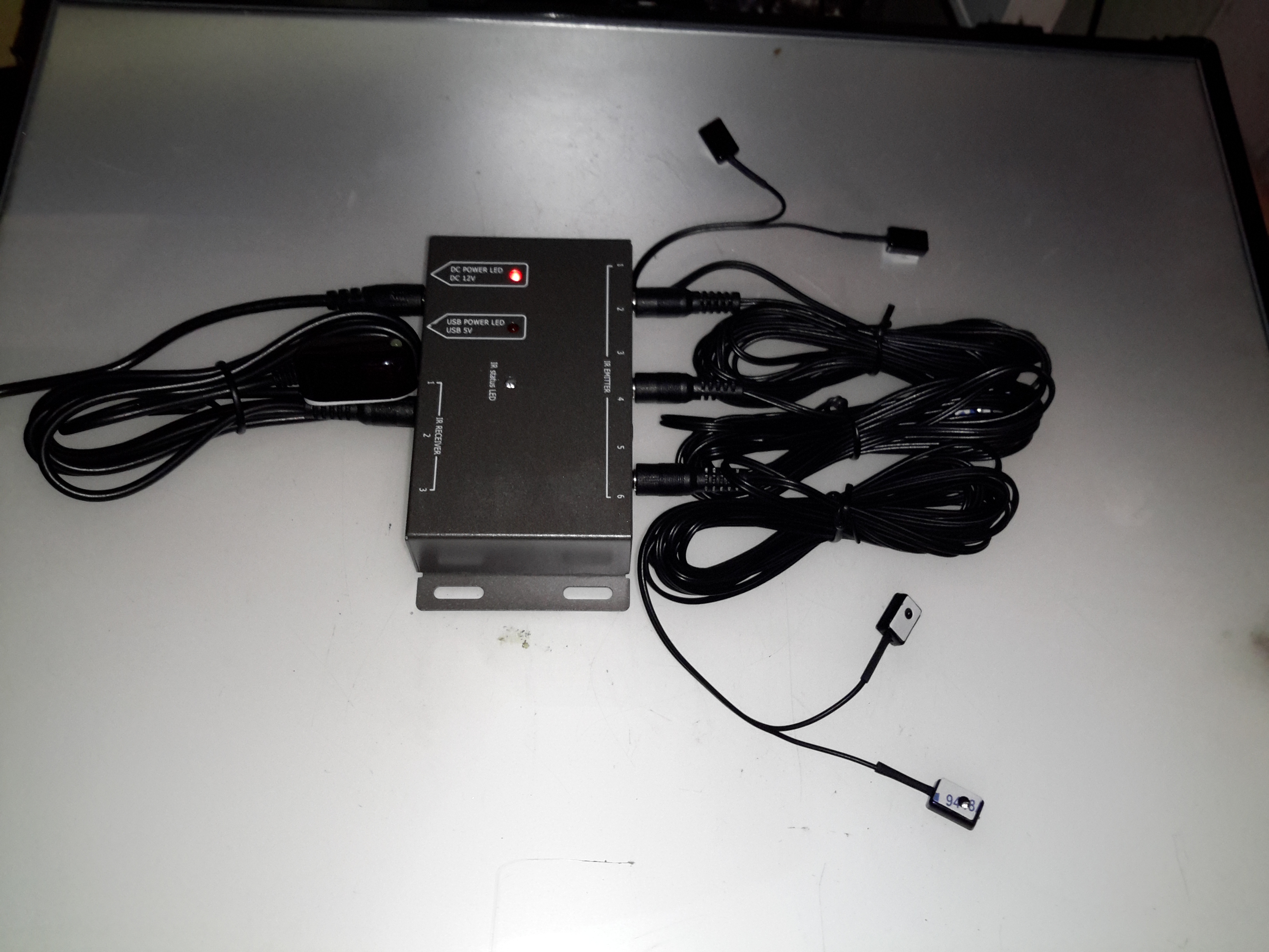
Here’s another random gadget for teardown, this time an IR remote control repeater module. These would be used where you need to operate a DVD player, set top box, etc in another room from the TV that you happen to be watching. An IR receiver sends it’s signal down to the repeater box, which then drives IR LEDs to repeat the signal.
Repeater Module
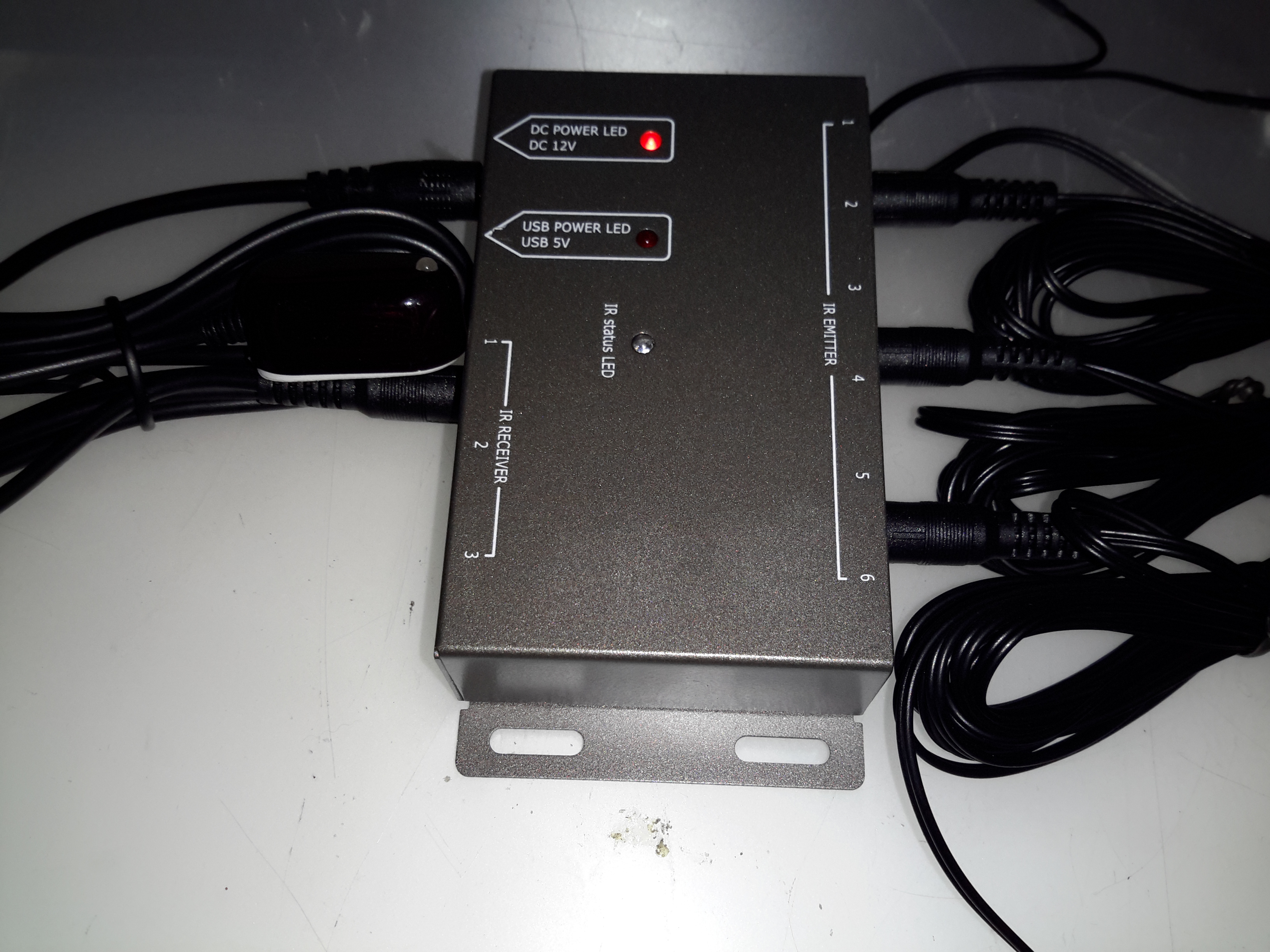
Not much to day about the exterior of this module, the IR input is on the left, up to 3 receivers can be connected. The outputs are on the right, up to 6 repeater LEDs can be plugged in. Connections are done through standard 3.5mm jacks.
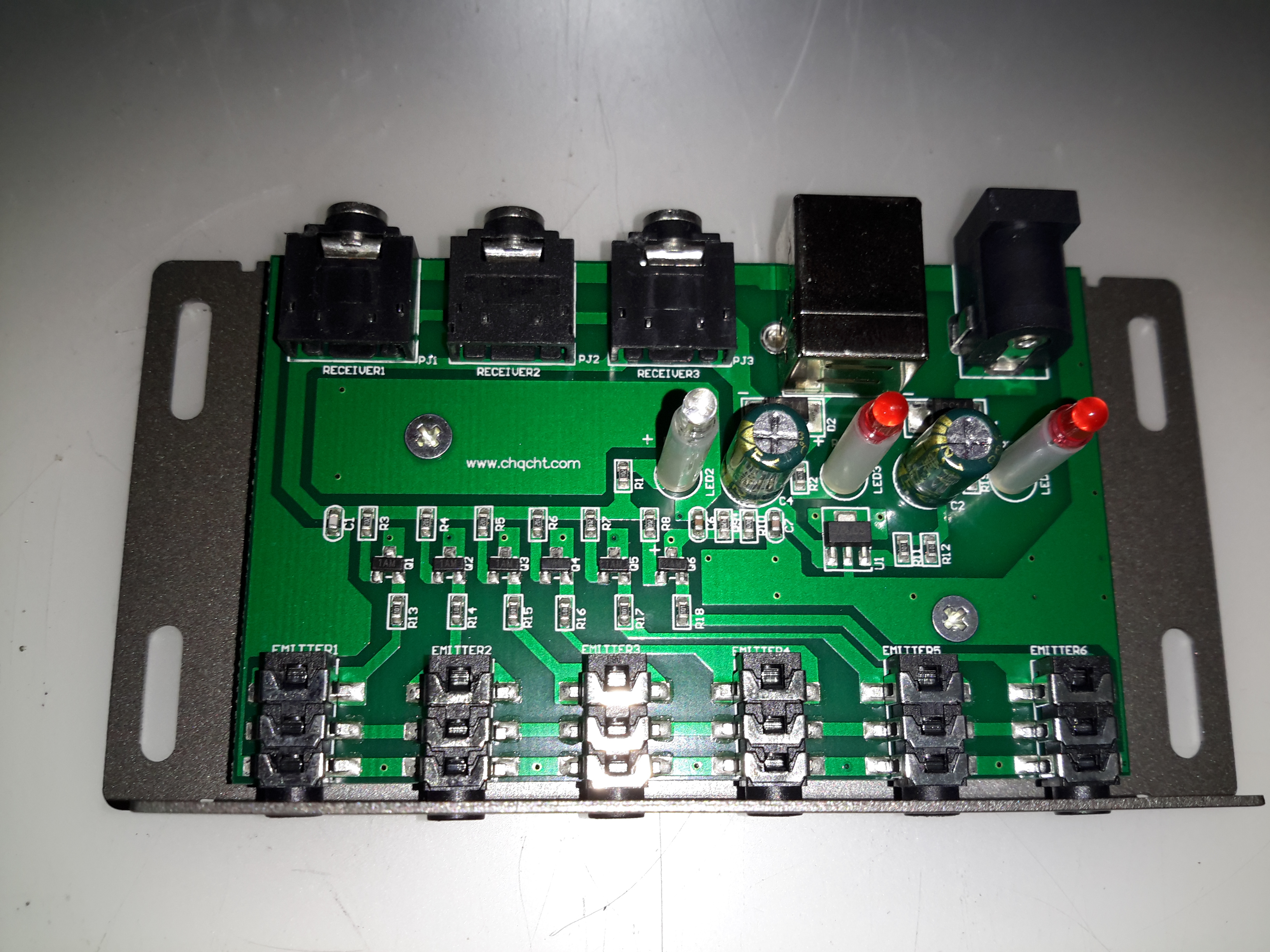
Repeater PCB
Not much inside this one at all, there are 6 transistors which each drive an LED output. This “dumb” configuration keeps things very simple, no signal processing has to be done. Power is either provided by a 12v input, which is fed into a 7805 linear regulator, or direct from USB.
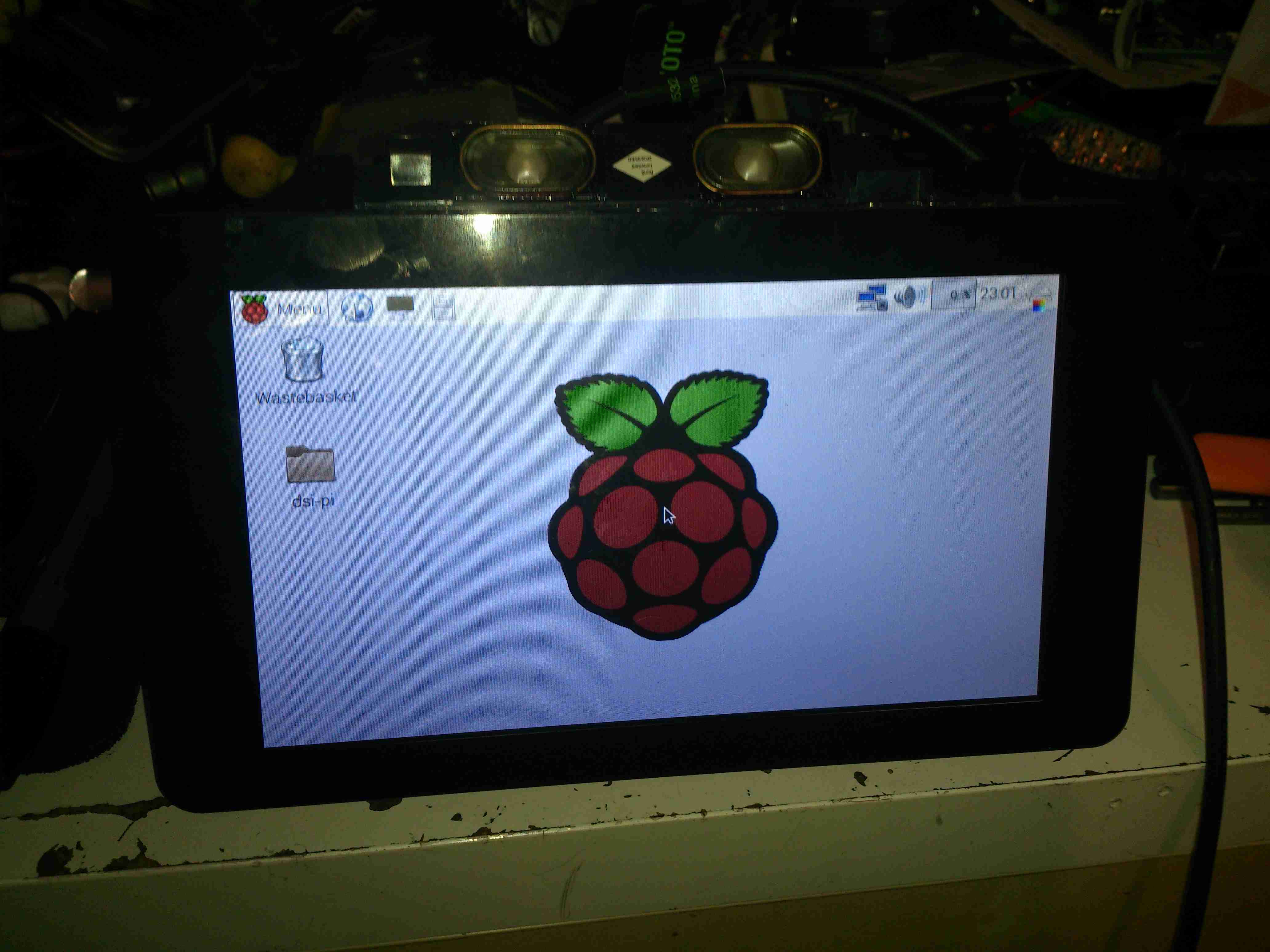
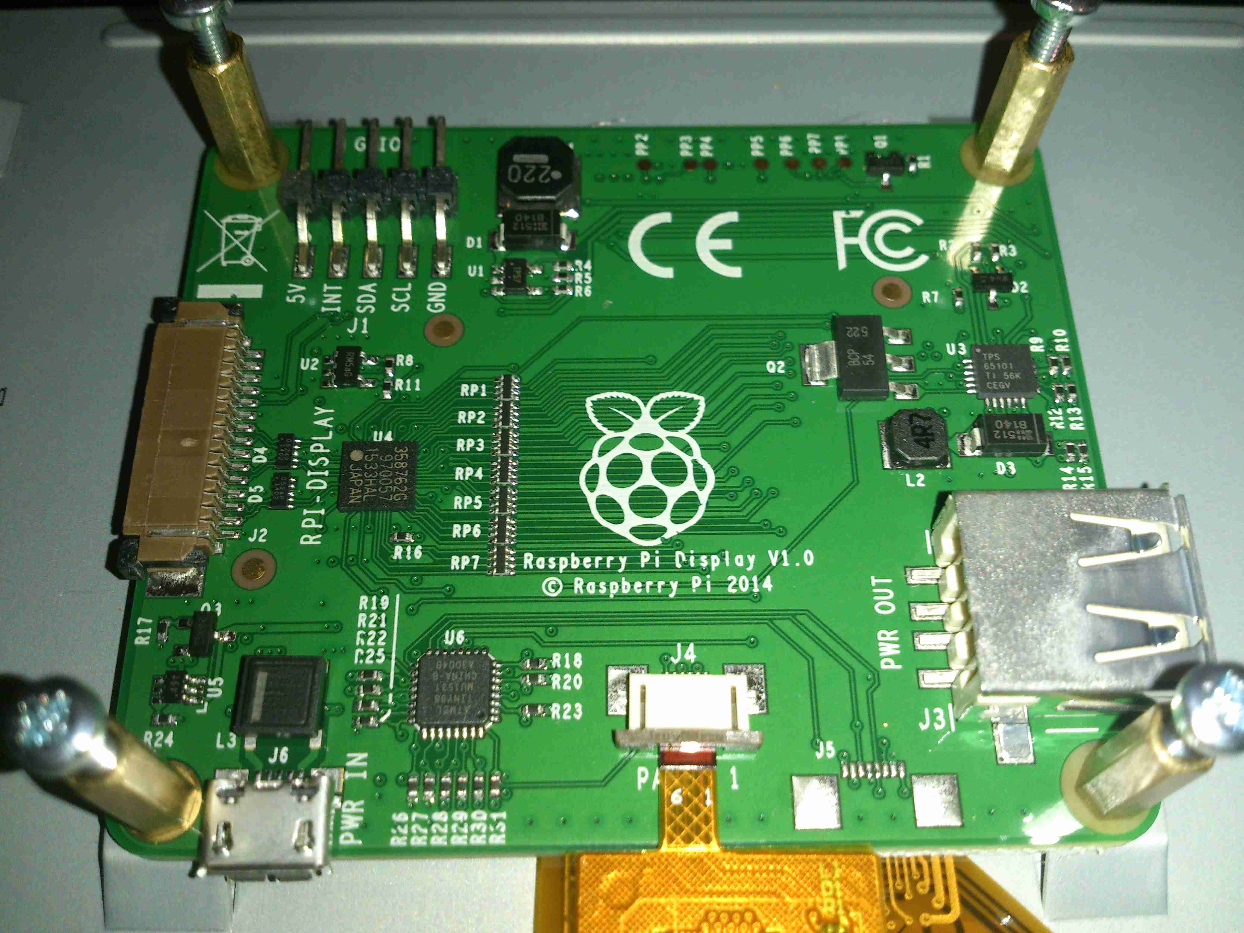
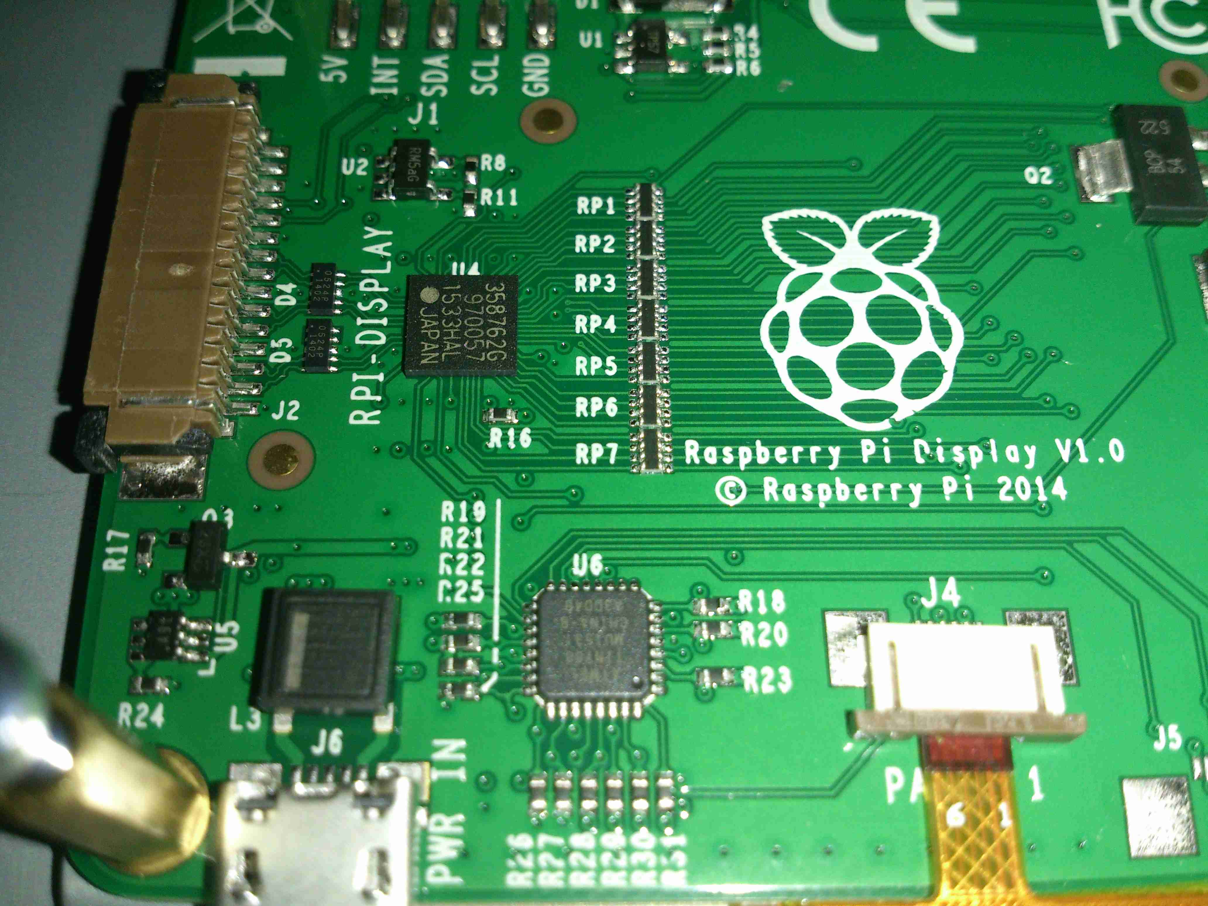
Finally the Raspberry Pi Foundation have released an official LCD for the DSI connector on the Pi. When these were announced, I placed an order straight away, but due to demand it’s taken quite a while for it to arrive in the post.
Interface PCB
The LCD itself is an RGB panel, to interface the Pi via the MIPI DSI port, some signal conversion is required. A small PCB is mounted on the back of the LCD to do this conversion. It also handles the power supply rails required by the LCD itself & interfacing the touch screen.
LCD Power Supply
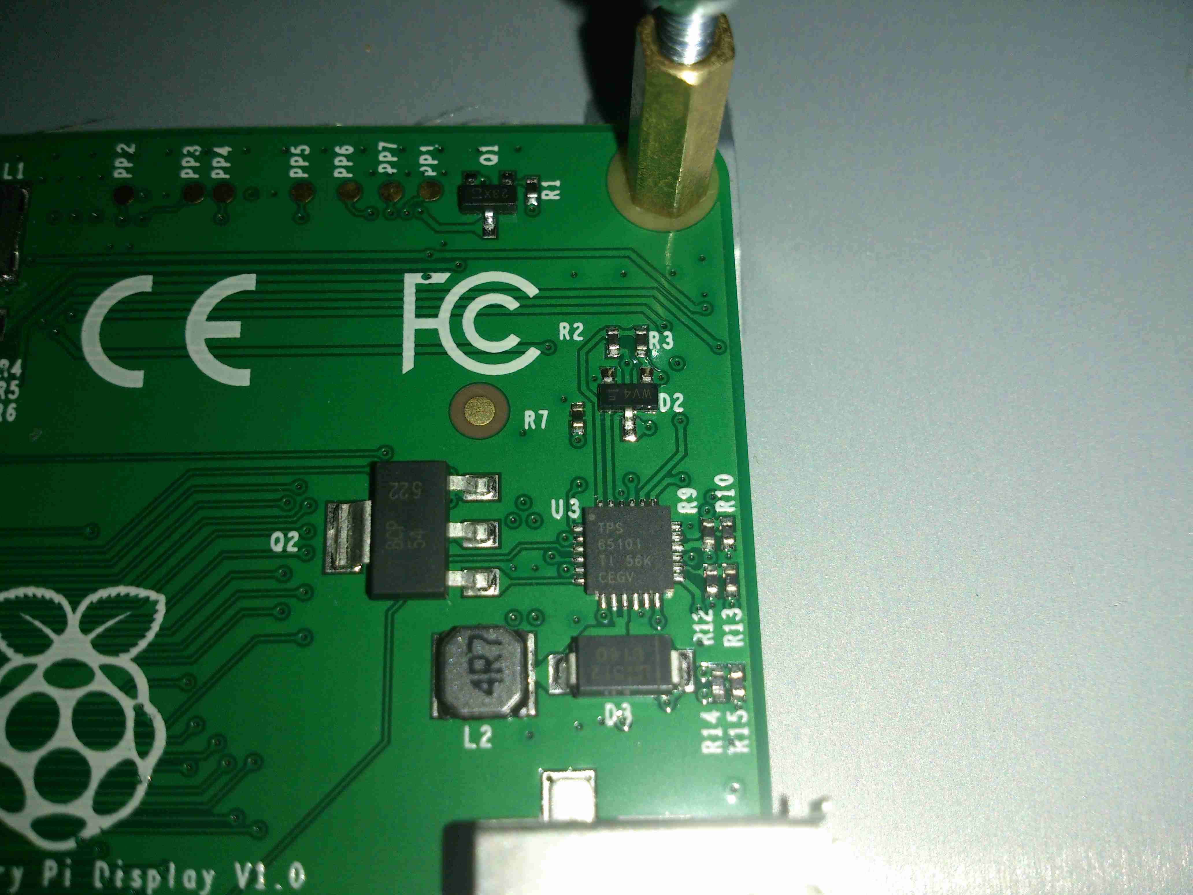
Taking care of the power supply is a Texas Instruments TPS65101 triple output LCD power supply IC. This also has a built in linear regulator to supply 3.3v for the rest of the circuitry on board. The large transistor to the left of the IC is the pass transistor for this regulator.
Main Controller
The video signal comes in on the FFC connector on the left, into the BGA IC. I’ve not managed to identify this component, but it’s doing the conversion from serial video from the Pi to parallel RGB for the LCD.
There’s also an Atmel ATtiny88 on the board below the main video conversion IC, not sure what this is doing.
The touch controller itself is mounted on the flex of the LCD, in this case it’s a FT5406.
Raspberry Pi LCD
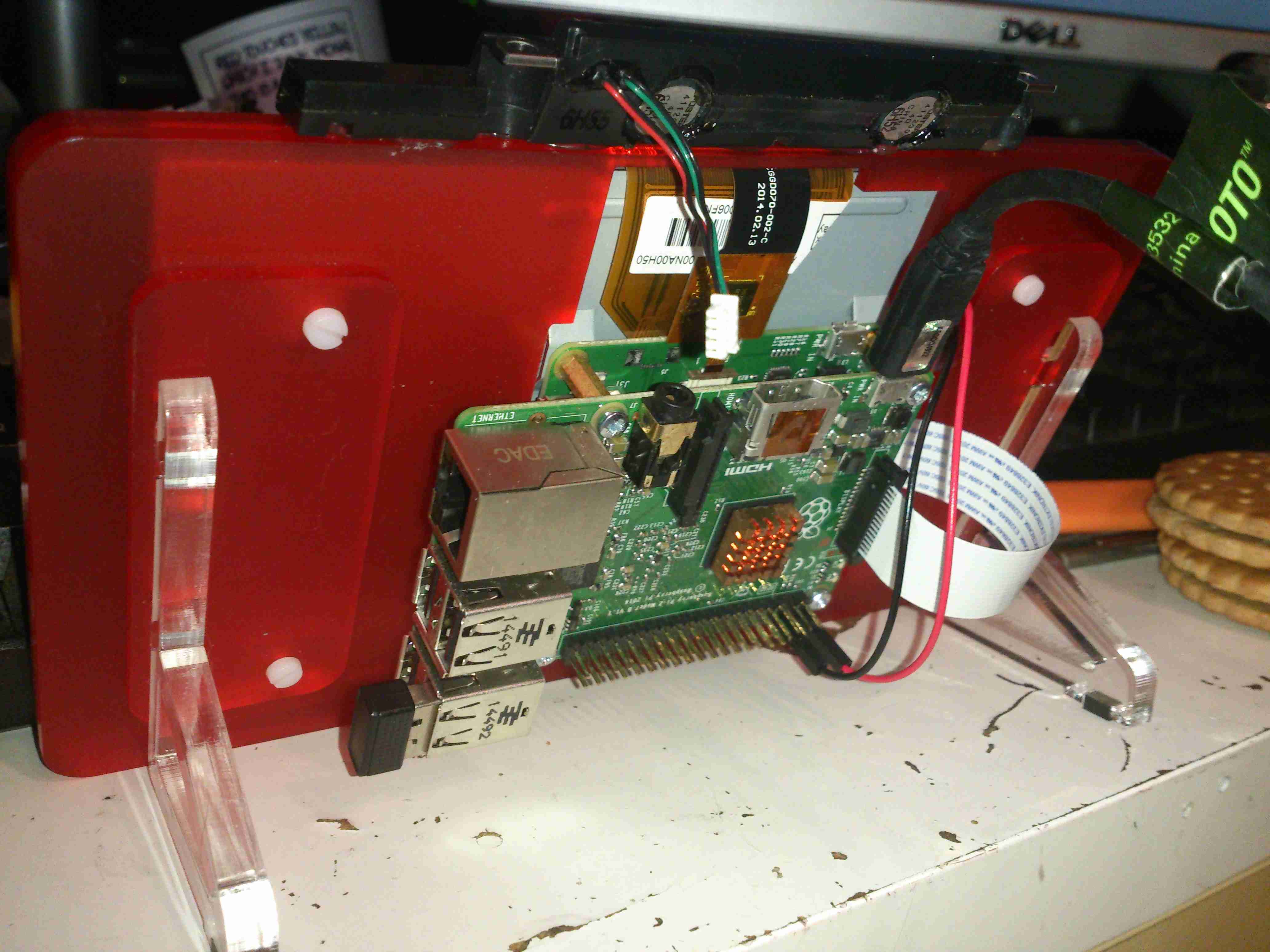
Here’s the LCD in operation. It’s not the highest resolution out there, but it leaves the GPIO & HDMI ports free for other uses.
Pi Mounted
The Pi screws to the back of the LCD & is connected with a flat flex cable & a pair of power jumpers. I’ve added a couple of small speakers to the top edge of the LCD to provide sound. (More to come on this bit).
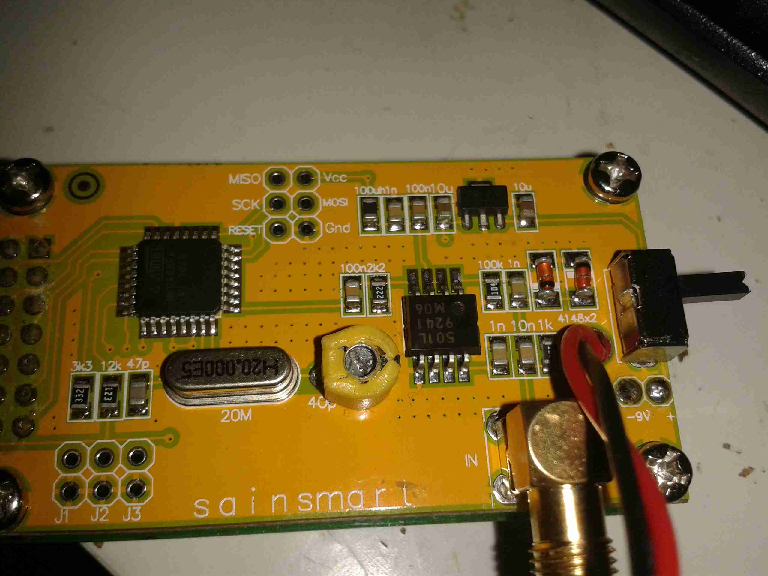
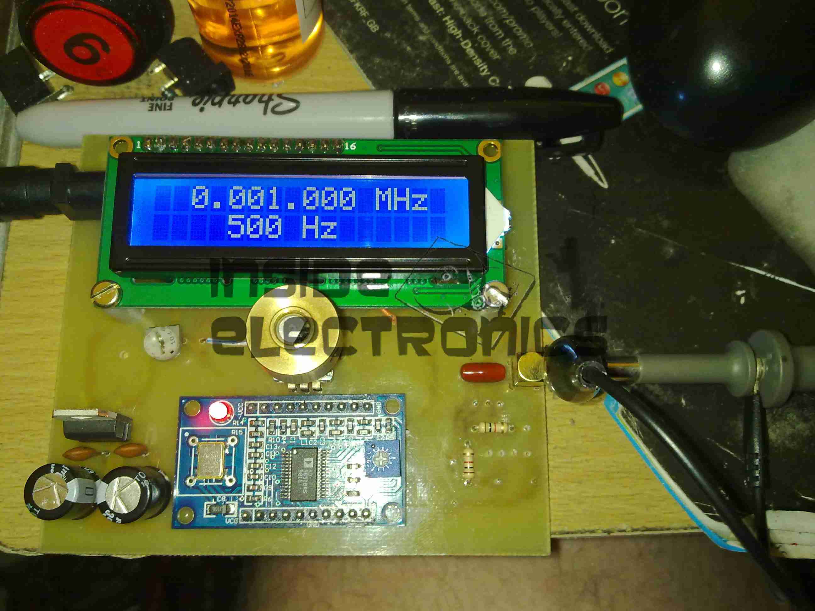
Here’s a quick look at a Sainsmart frequency counter module. These are useful little gadgets, showing the locked frequency on a small LCD display.
It’s built around an ATMega328 microcontroller (µC), and an MB501L Prescaler IC. The circuit for this is very simple, and is easily traced out from the board.
Frequency Counter
Here’s the back of the board, with the µC on the left & the prescaler IC on the right. This uses a rather novel method for calibration, which is the trimmer capacitor next to the crystal. This trimmer varies the frequency of the µC’s oscillator, affecting the calibration.
Input protection is provided by a pair of 1N4148 diodes in inverse parallel. These will clamp the input to +/-1v.
The prescaler IC is set to 1/64 divide ratio. This means that for an input frequency of 433MHz, it will output a frequency of 6.765625MHz to the µC.
The software in the µC will then calculate the input frequency from this intermediate frequency. This is done because the ATMega controllers aren’t very cabable of measuring such high frequencies.
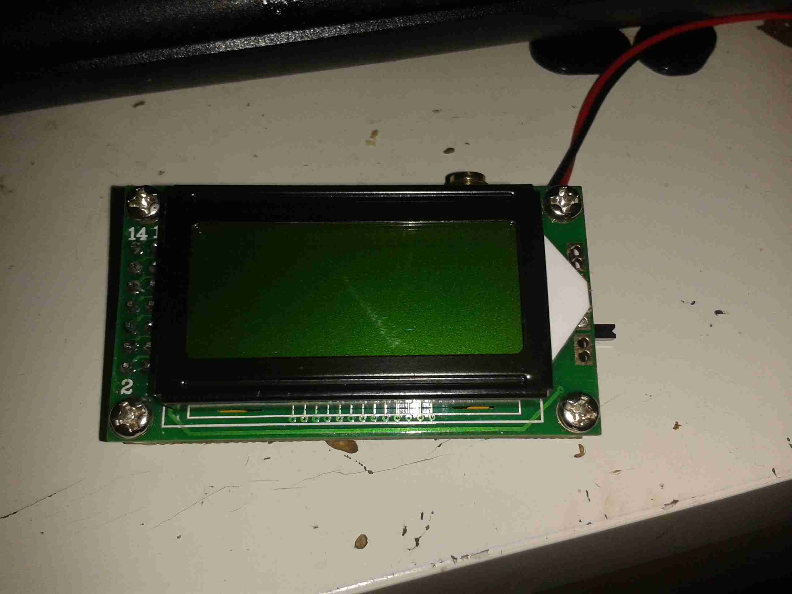
The calculated frequency is then displayed on the LCD. This is a standard HD44780 display module.
LCD
Power is provided by a 9v PP3 battery, which is then regulated down by a standard LM7805 linear regulator.
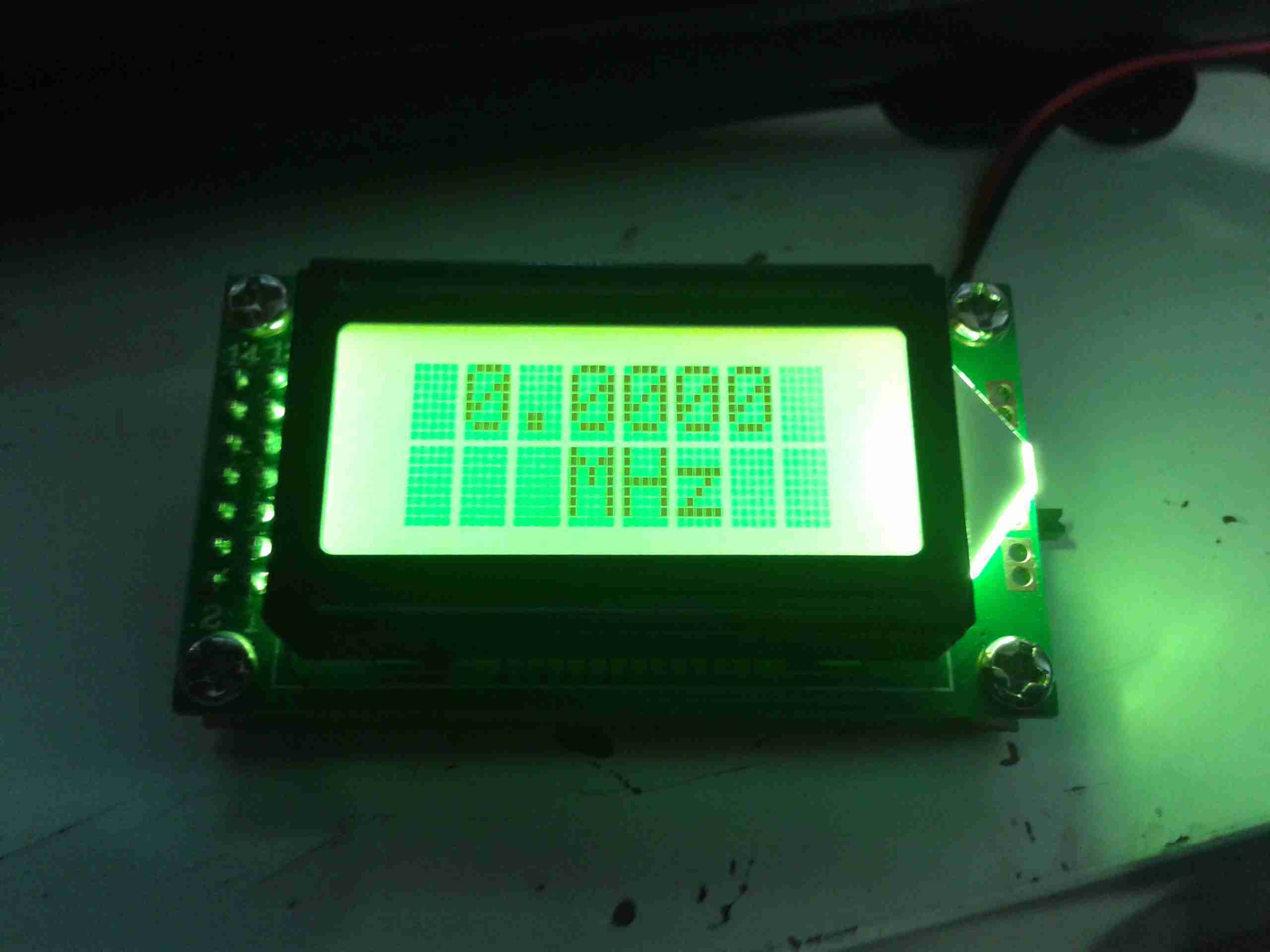
Readout
I’ve found it’s not very accurate at all at the lower frequencies, when I fed it 40MHz from a signal generator it displayed a frequency of around 74MHz. This is probably due to the prescaler & the software not being configured for such a low input. In the case for 40MHz input the scaled frequency would have been 625kHz.
Following on from my review, here are some internal views & detail on the components used in this radio. Below is an overview of the main PCB with the top plate removed from the radio.
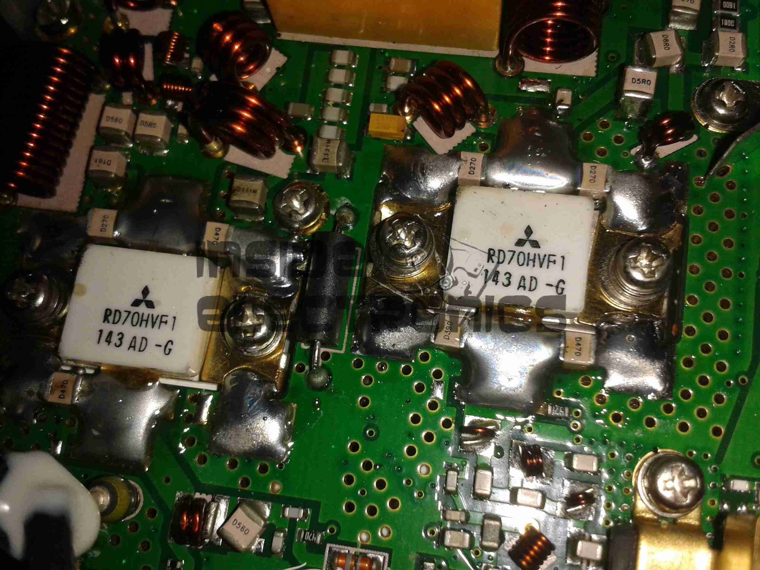
Cover RemovedRF Final Amplifier Stage
Most visible are these MOSFETs, which are Mitsubishi RD70HVF1 VHF/UHF power devices. Rated for a maximum of 75W output power at 12.5v (absolute maximum of 150W, these are used well within their power ratings. They are joined to the PCB with heavy soldering, with bypass caps tacked right on to the leads.
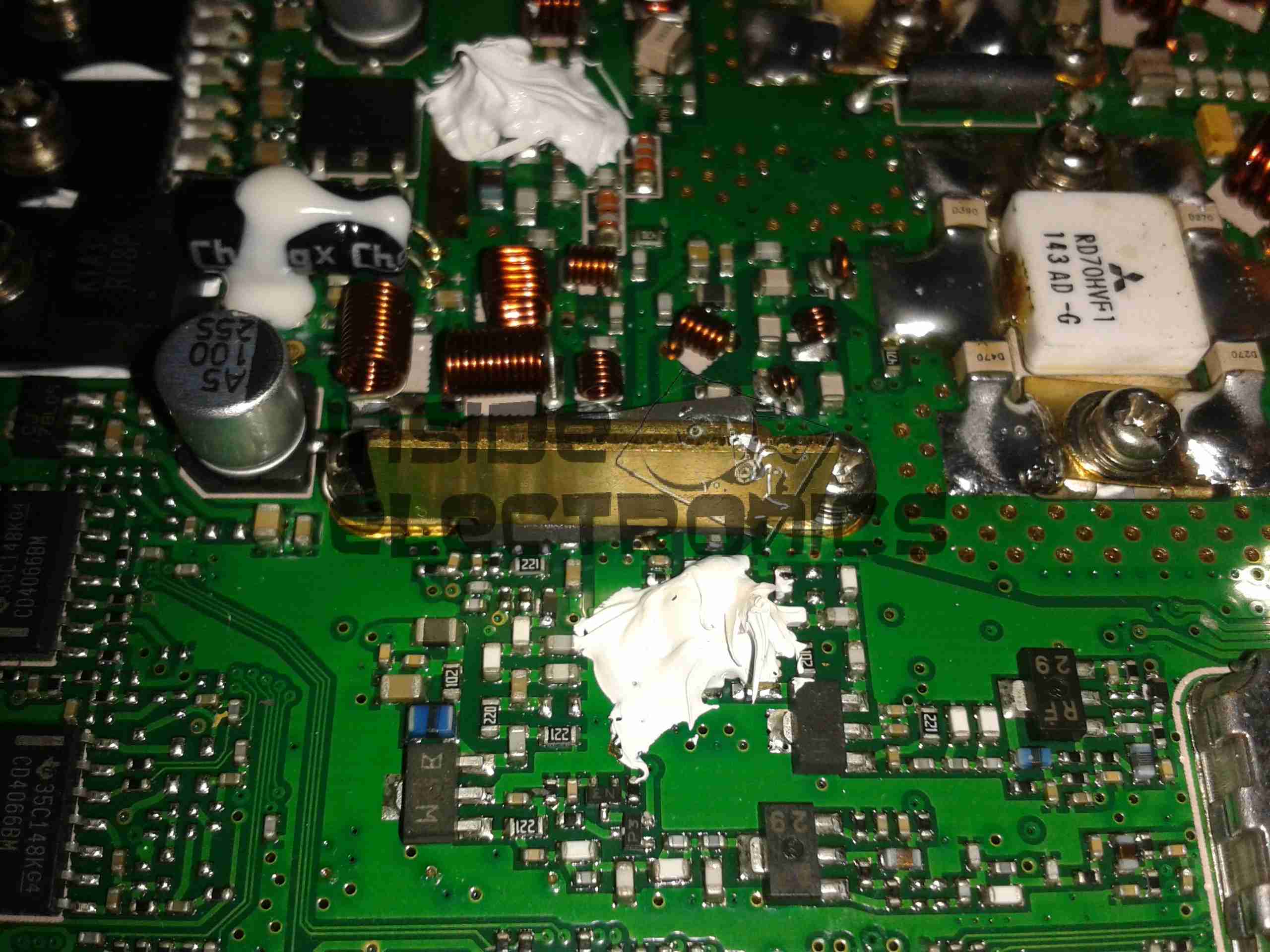
RF Pre Drivers
Here is the RF pre-driver stage, with intermediate transistors hidden under the small brass heatspreader.
Power Section
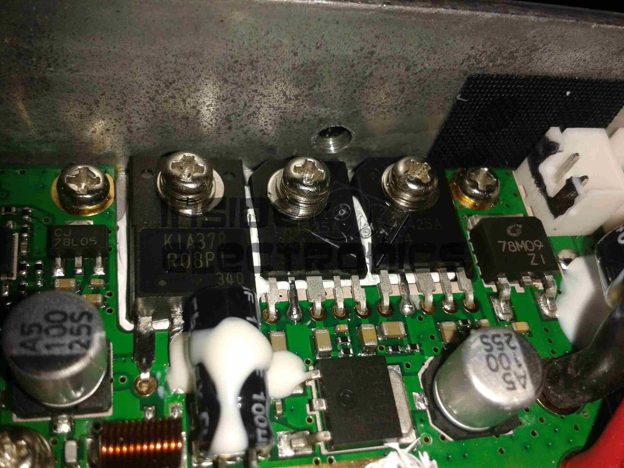
In the top left corner of the radio, near the power input leads, is the power supply & audio amplifier section. Clearly visible are the pair of LA4425A 5W audio power amplifier ICs, these drive the speakers on the top of the radio. Either side of these parts are a 7809 & a 7805 – both linear regulators providing +9v & +5v logic supplies respectively. The large TO220 package device is a KIA378R08PI 3A LDO regulator with ON/OFF control, this one outputs +8v. Just visible in the top right corner are the sockets for the speaker connections.
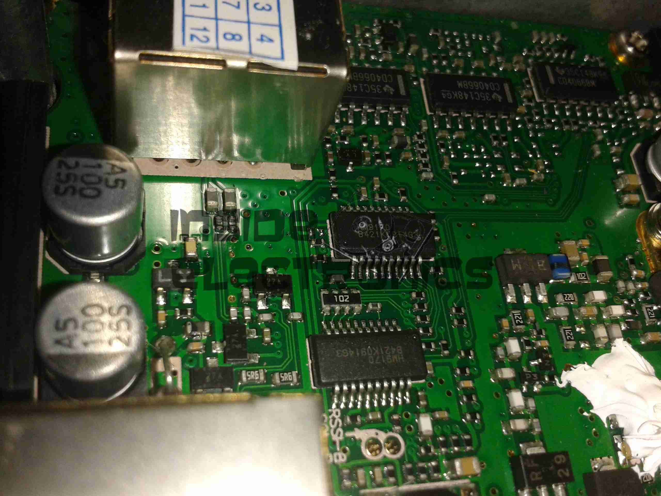
DTMF Circuits
Here are the two ICs for dealing with DTMF tones, they are HM9170 receivers.
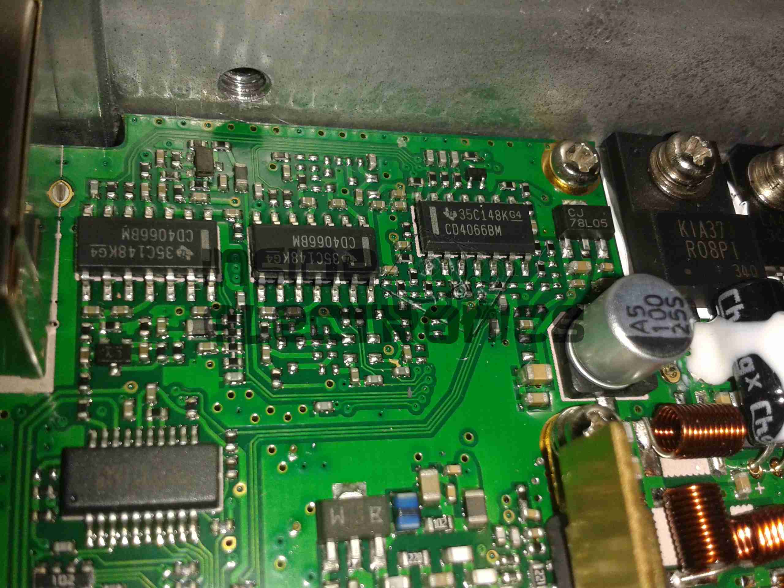
Glue Logic
In the corner next to the interface jack, there are some CD4066B Quad Bilateral switches. These make sense since the interface jack has more than a single purpose, these will switch signals depending on what is connected.
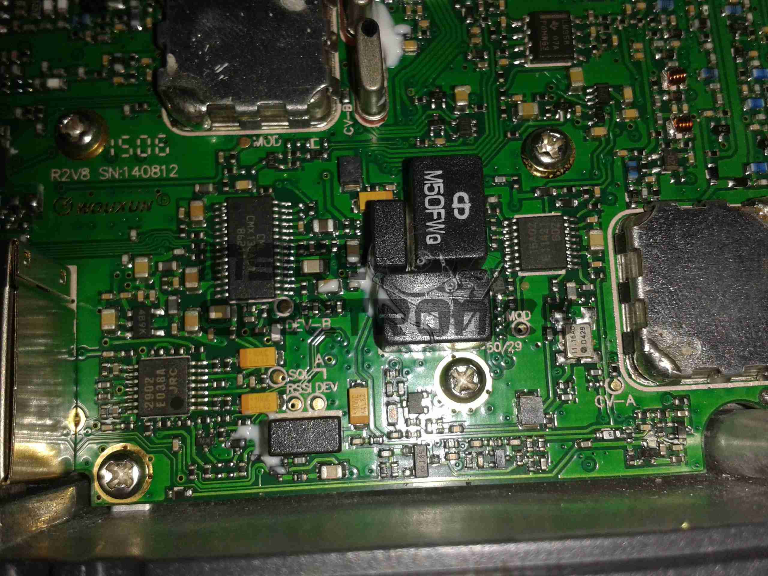
RF Section
Here are visible the RF cans for the oscillators, the crystals visible next to the can at the top. The shields are soldered on, so no opening these unfortunately.
Also visible in this image is a CMX138A Audio Scrambler & Sub-Audio Signalling processor. This IC deals with the Voice Inversion Scrambling feature of the radio, & processes the incoming audio before being sent to the modulator.
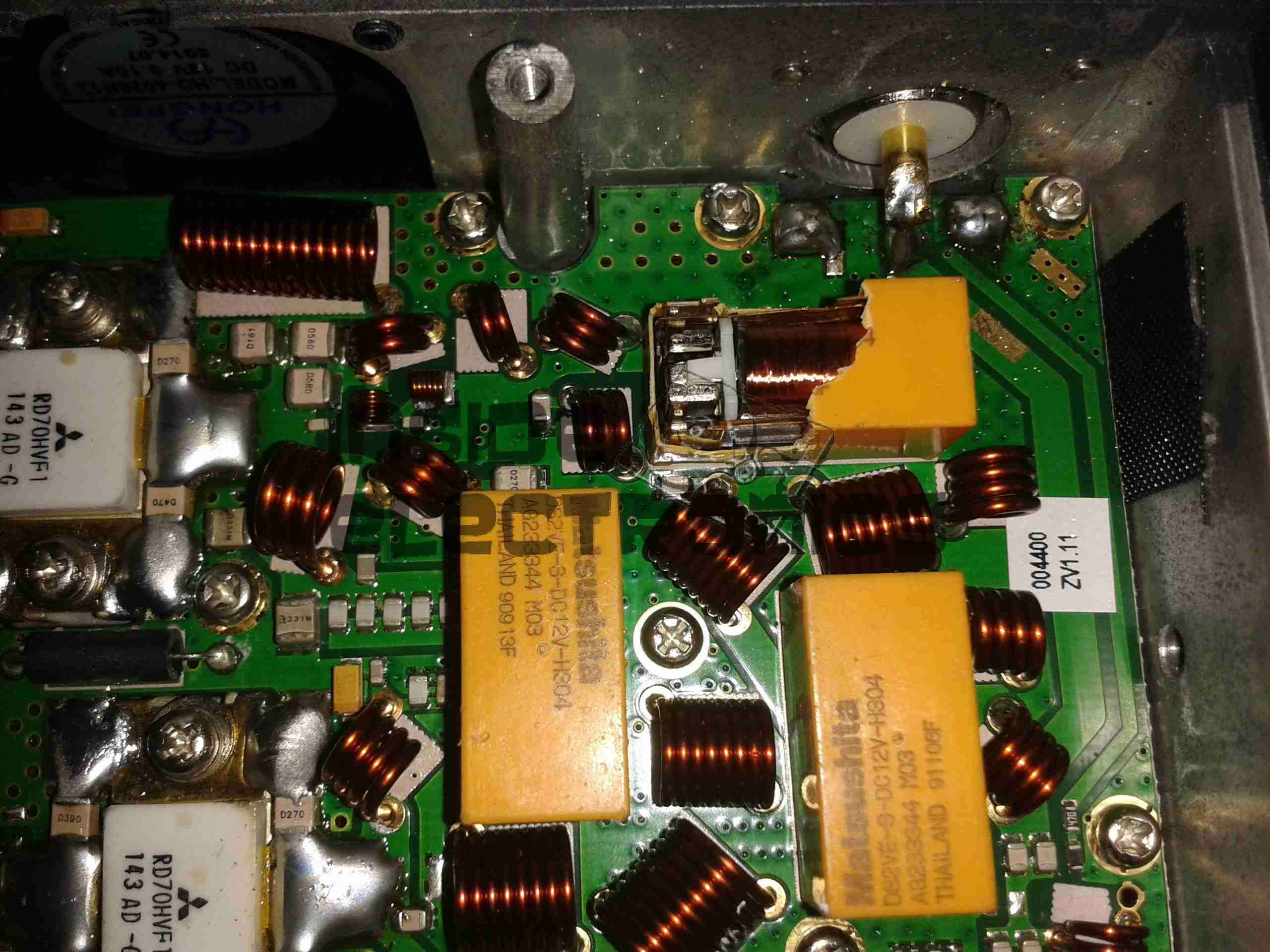
Output Filter Network
Shown here is the RF output filter network, this radio uses relays for switching instead of PIN diodes, I imagine for cost reasons. The relay closest to the RF output socket has had a slight accident 🙂 This is slated to be replaced soon.
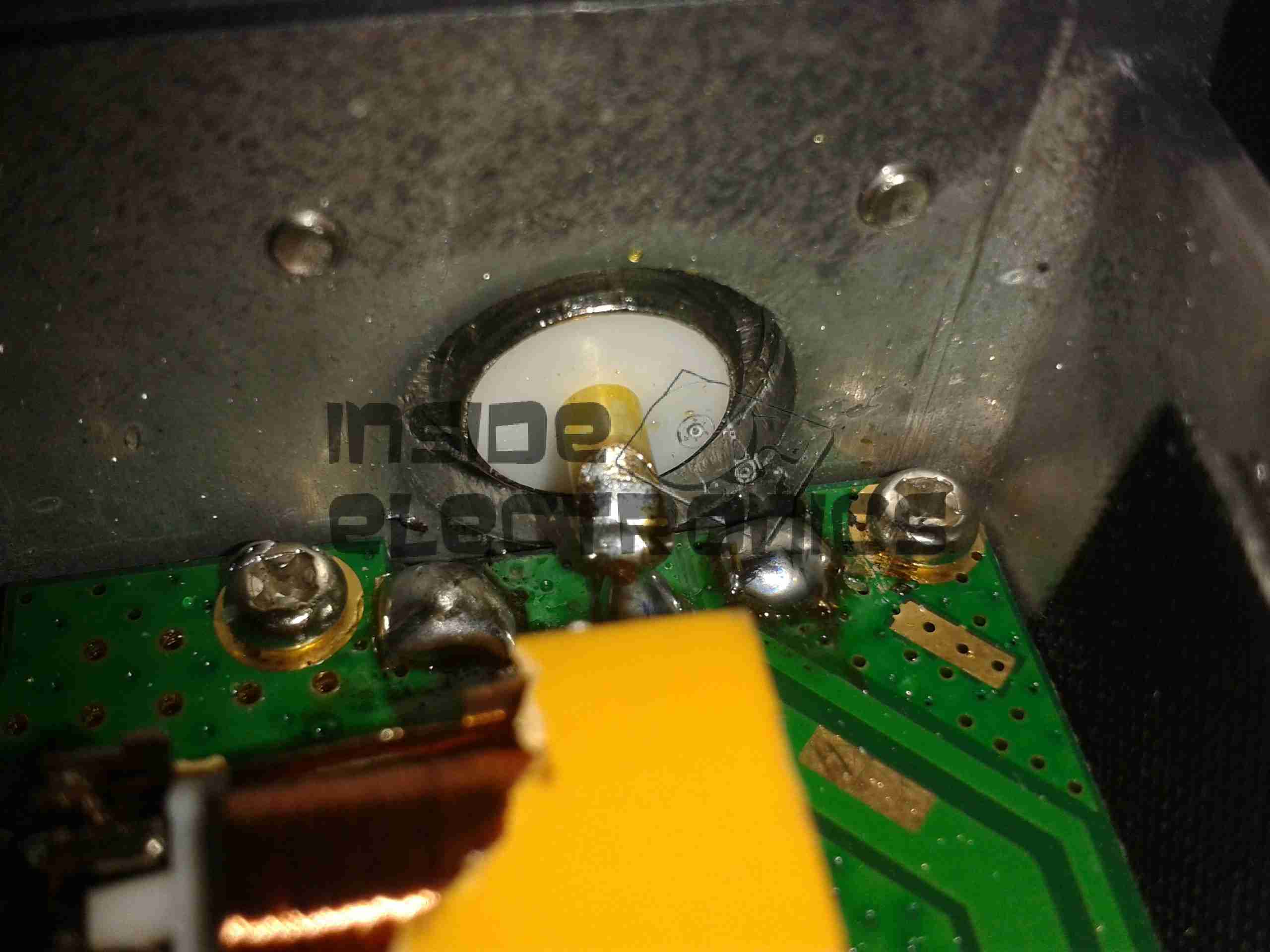
RF Output Jack
Finally, the RF output jack.
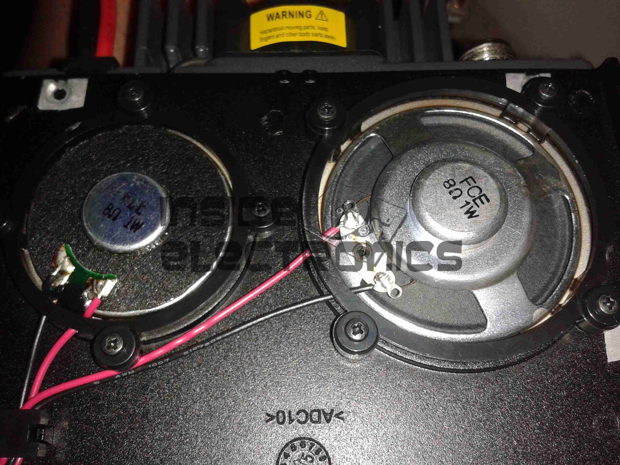
Audio Speakers
Here the speakers are shown, attached to the bottom of the top plate. They are both rated 8Ω 1W.
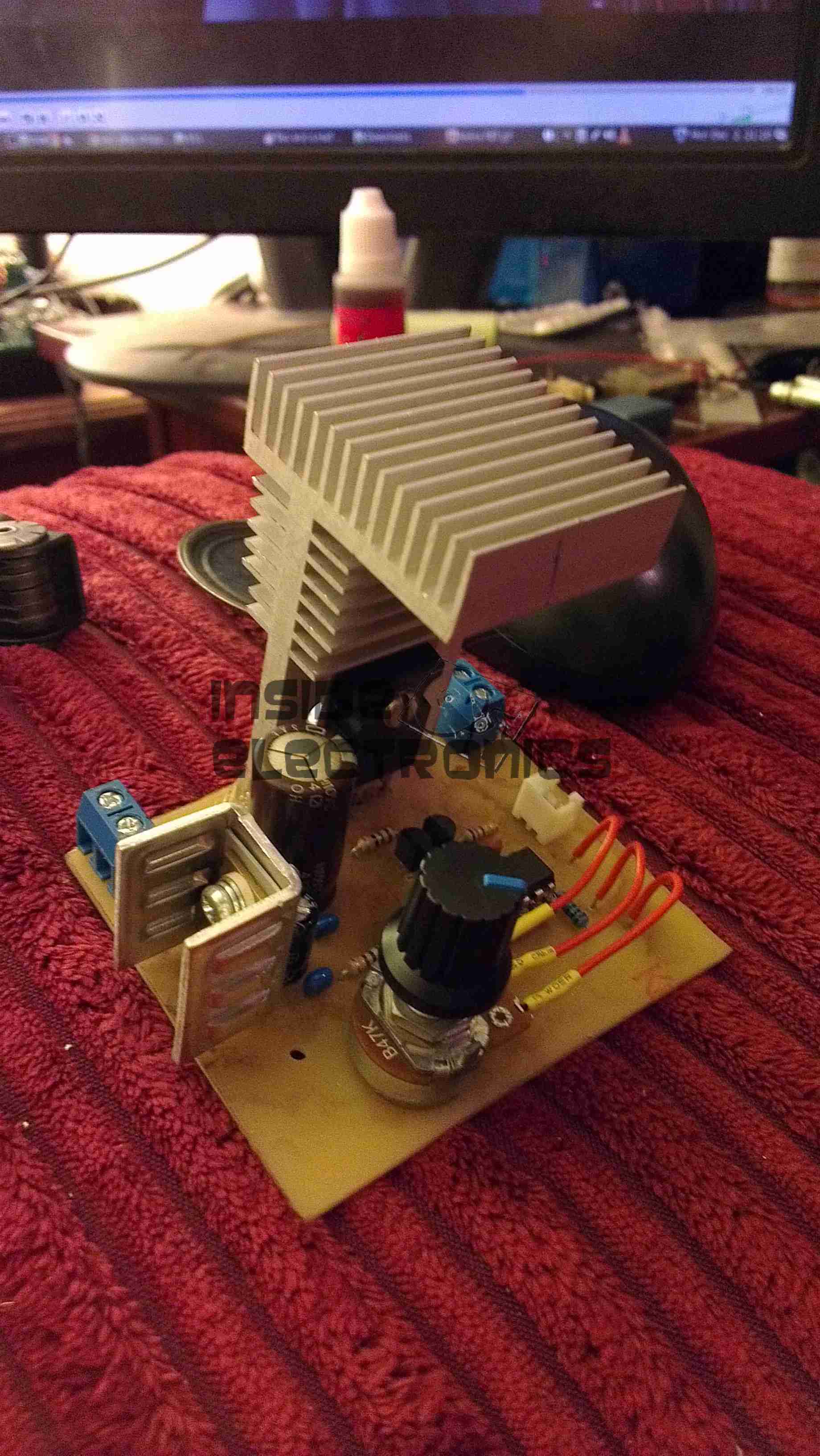
After watching a video over at Scullcom Hobby Electronics on YouTube, I figured I’d build one of these precision references to calibrate my multimeters.
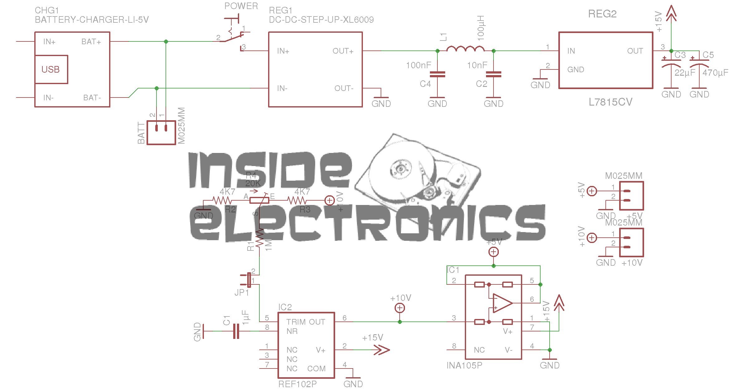
It’s based around a REF102P 10v precision reference & an INA105P precision unity gain differential amplifier.
For full information, check out the video, I won’t go into the details here, just my particular circuit & PCB layout.
In the video, Veroboard is used. I’m not too fond of the stuff personally. I find it far too easy to make mistakes & it never quite looks good enough. To this end I have spun a board in Eagle, as usual.
Precision Ref SCH – Click to Embiggen
Here’s the schematic layout, the same as is in the video.
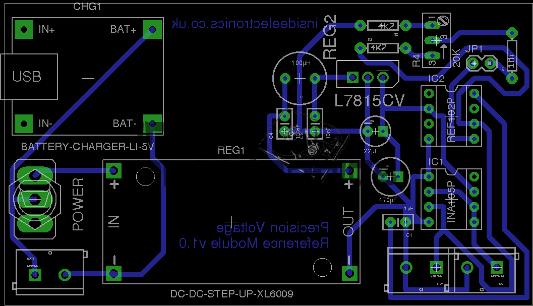
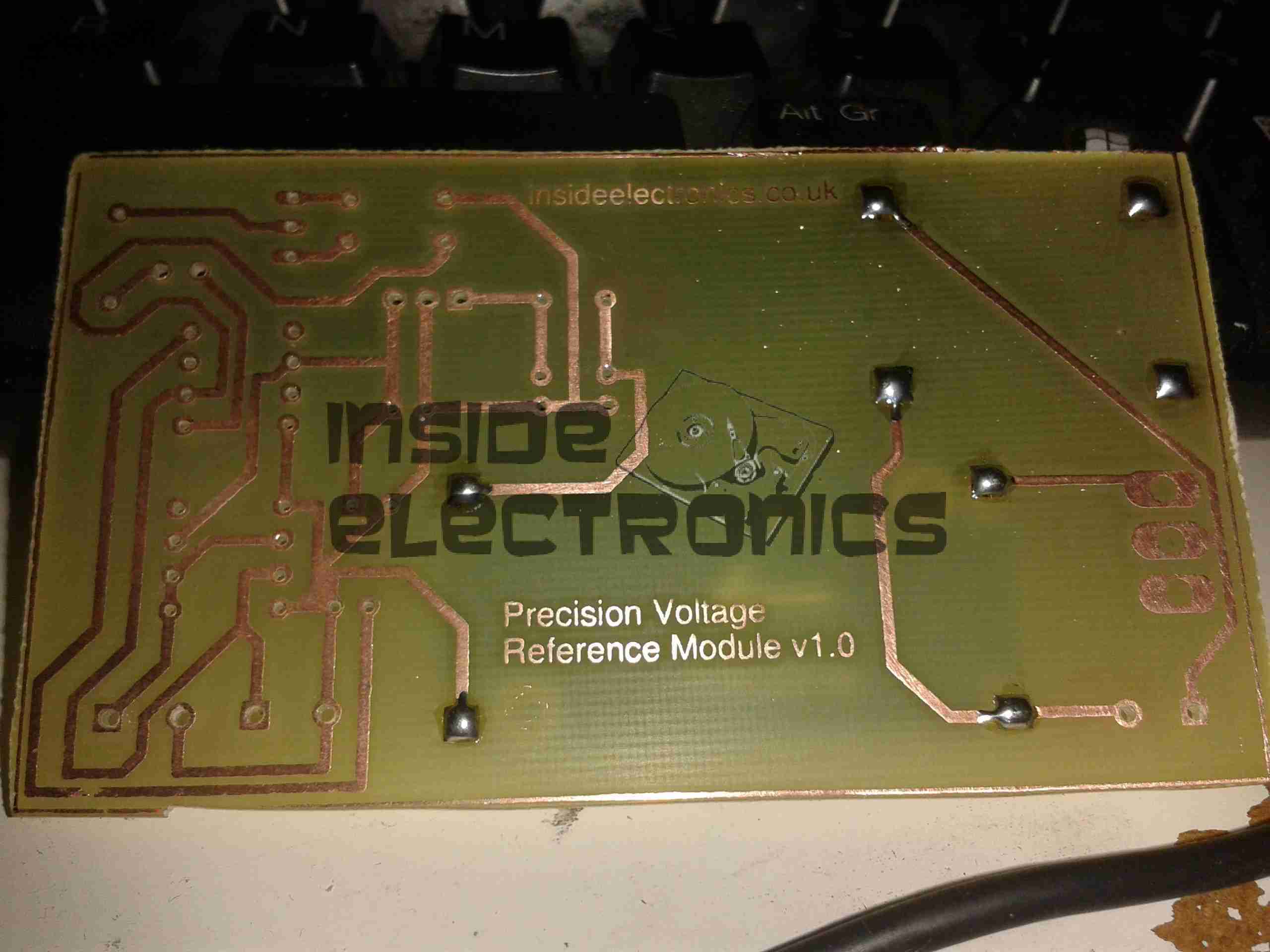
Precision Ref BRD
As usual, the Eagle CAD layout files can be found at the bottom of the post.
And the associated PCB layout. I have added the option to be able to tweak the output, to get a more accurate calibration, which can be added by connecting JP1 on the PCB.
As in the original build, this unit uses pre-built DC-DC converter & Li-Ion charger modules. A handy Eagle library can be found online for these parts.
I have however left off the battery monitor section of the circuit, since I plan to use a protected lithium cell for power. This also allowed me to keep the board size down, & use a single sided layout.
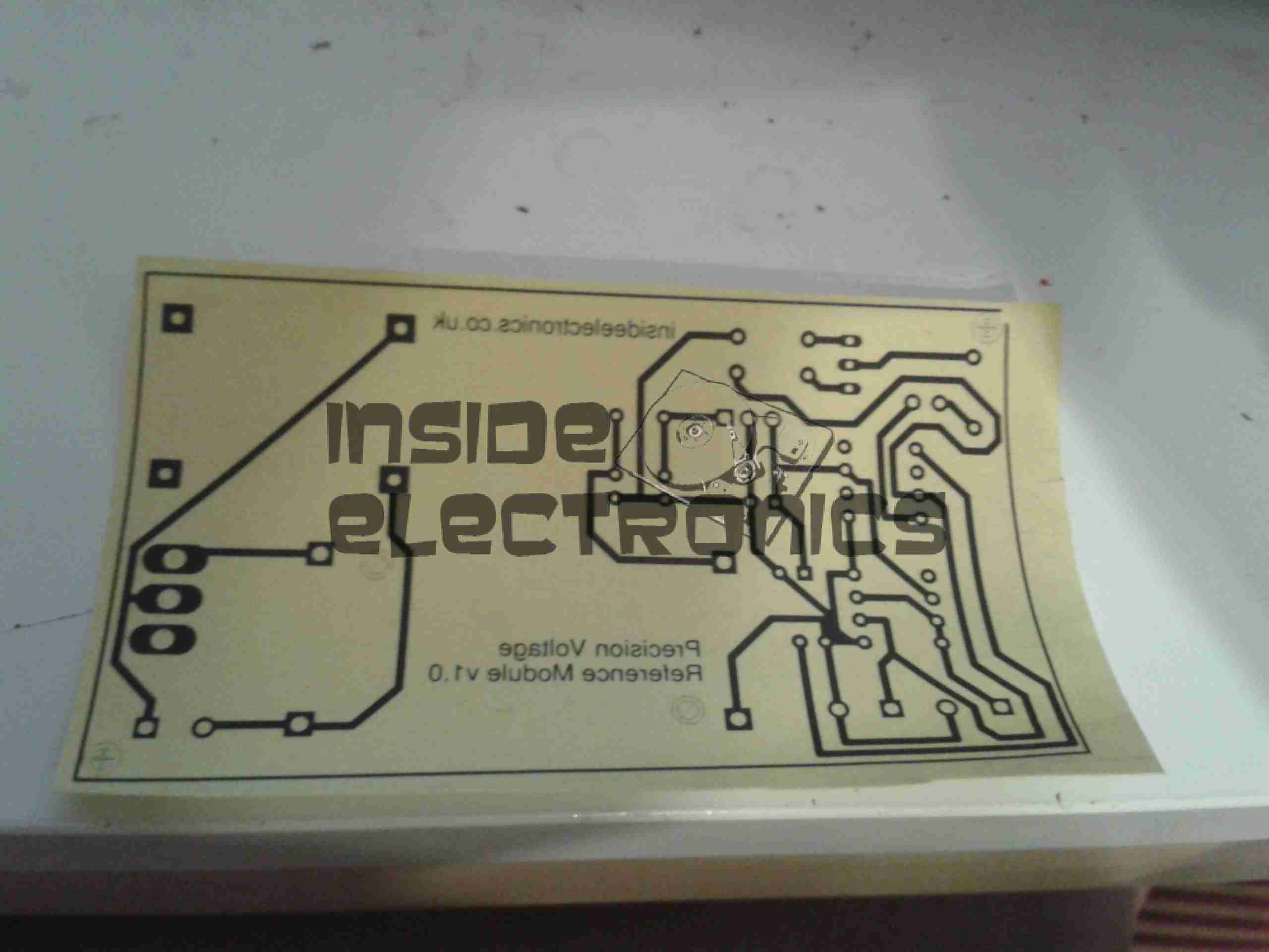
Toner Transfer Paper
Here’s the track layout ready to iron onto the copper clad board. I use the popular toner transfer system with special paper from eBay, this stuff has a coating that allows the toner to easily be transferred to the PCB without having to mess about with soaking in water & scraping paper off.
Ironed On
Here’s the paper having just been ironed onto the copper. After waiting for the board to cool off the paper is peeled off, leaving just the toner on the PCB.
Etched PCB
PCB just out of the etch tank, drilled & with the solder pins for the modules installed. Only one issue with the transfer, in the bottom left corner of the board is visible, a very small section of copper was over etched.
This is easily fixed with a small piece of wire.
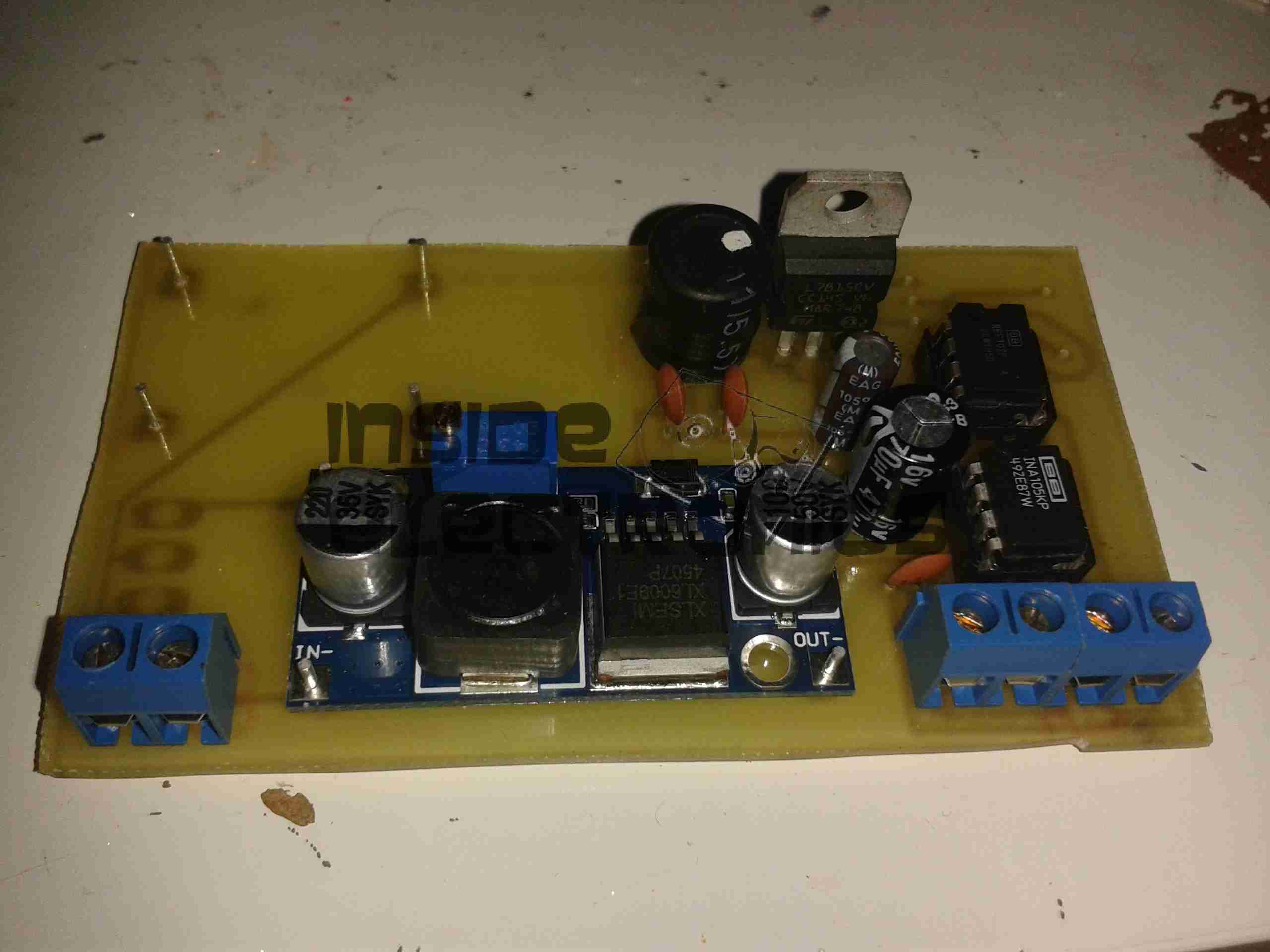
Components Populated
Main components populated. The DC-DC converter is set at 24v output, which the linear regulator then drops down to the +15v rail for the reference IC. The linear section of the regulator, along with the LC filter on the output of the switching regulator produce a low-ripple supply.
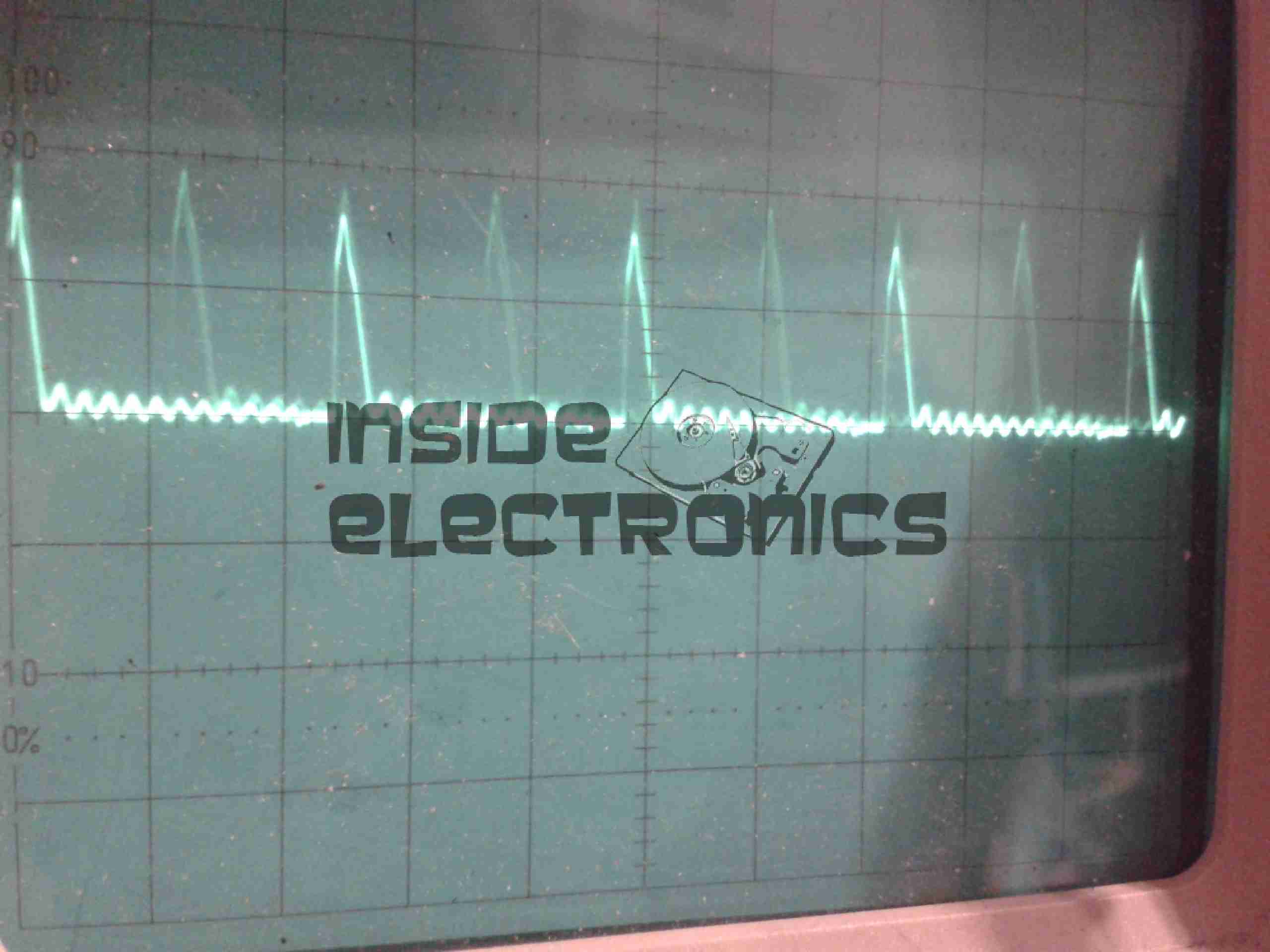
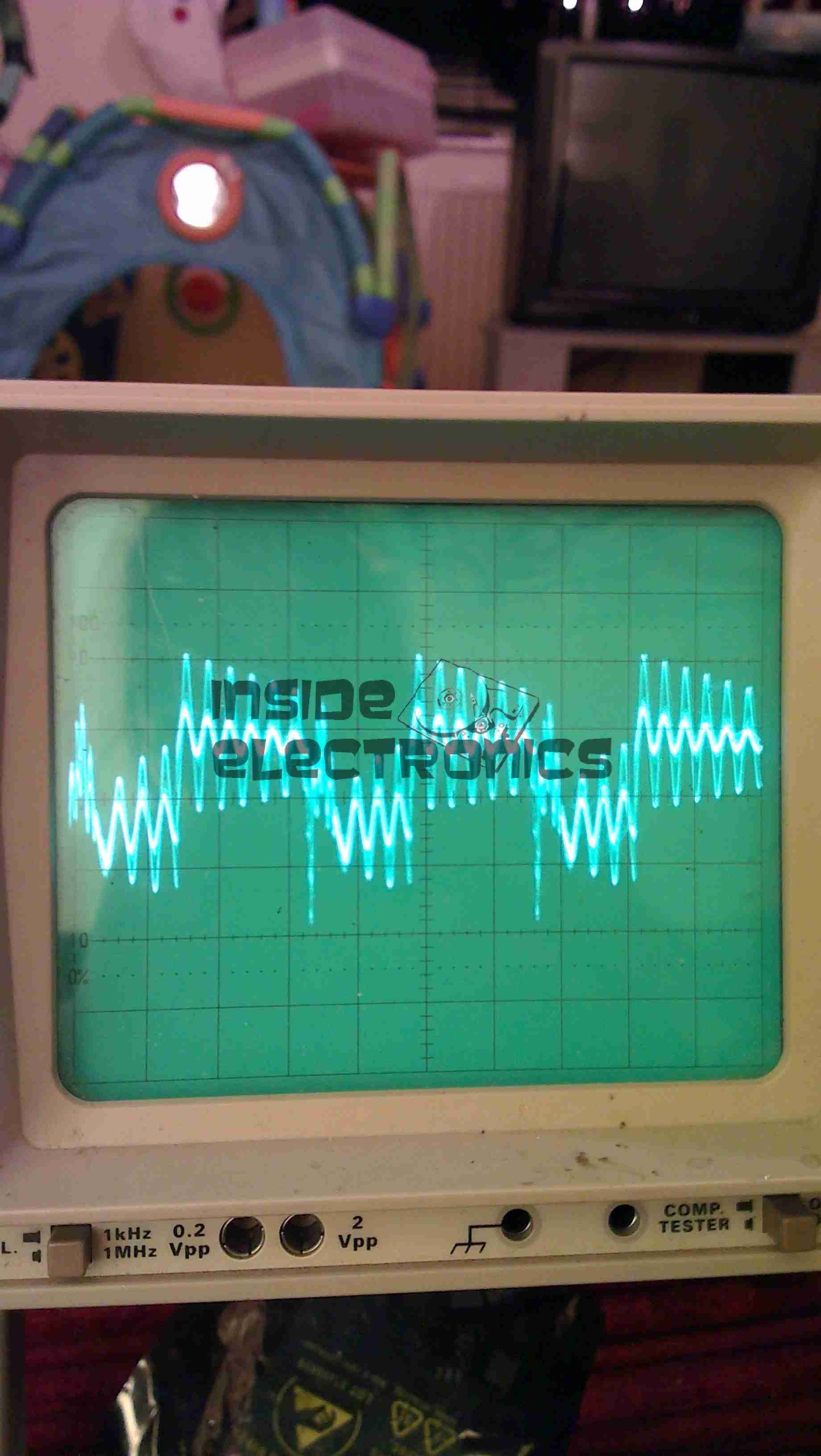
SMPS Ripple
Here’s the scope reading the AC ripple on the output of the DC-DC converter. Scale is 100mV/Div. Roughly 150mV of ripple is riding on top of the DC rail.
Linear PSU Ripple
And here’s the output from the linear regulator, scale of 50mV/Div. Ripple has been reduced to ~15mV for the reference IC.
In total the circuit as built has a power consumption of ~0.5W, most of which is being dissipated as heat in the linear part of the PSU.
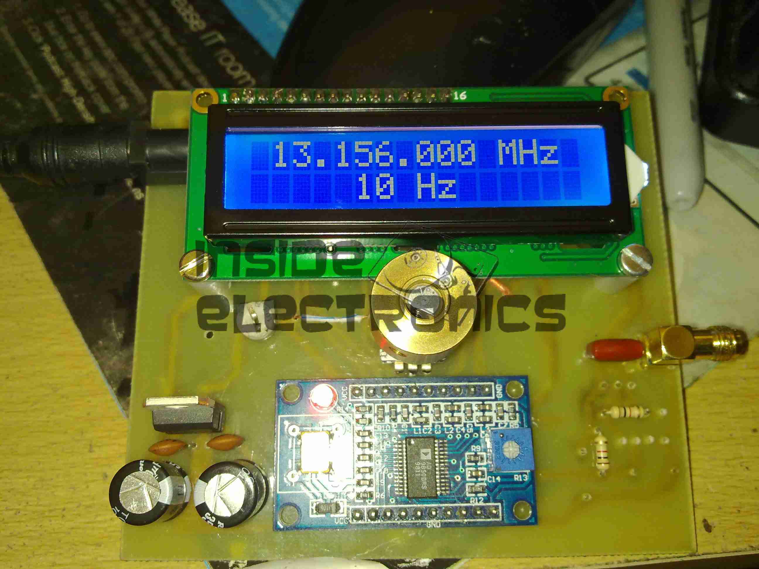
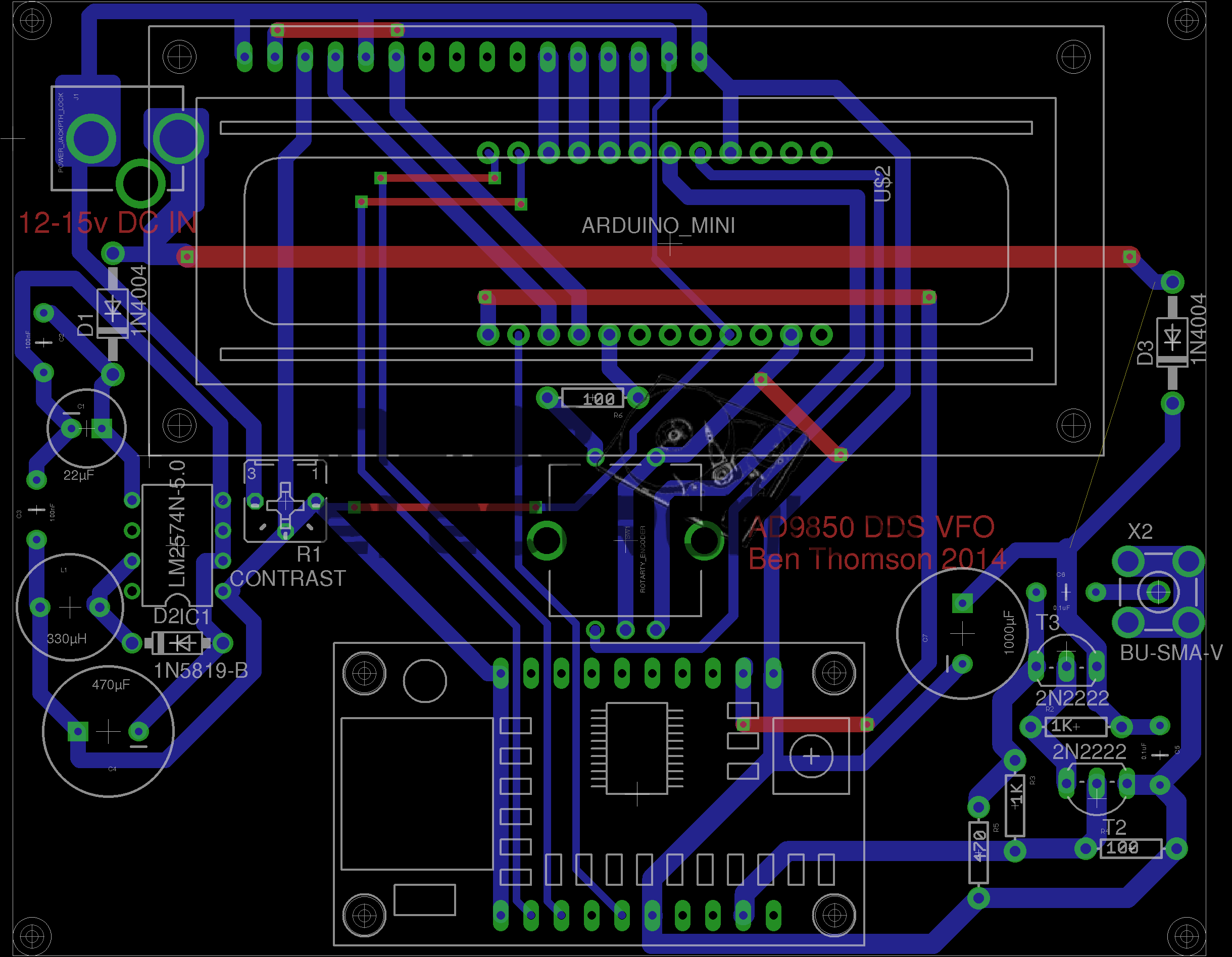
Continuing from my previous post where I published an Eagle design layout for AD7C‘s Arduino powered VFO, here is a completed board.
I have made some alterations to the design since posting, which are reflected in the artwork download in that post, mainly due to Eagle having a slight psychotic episode making me ground one of the display control signals!
AD9850 VFO
The amplifier section is unpopulated & bypassed as I was getting some bad distortion effects from that section, some more work is needed there.
The Arduino Pro Mini is situated under the display, and the 5v rail is provided by the LM7805 on the lower left corner.
Current draw at 12v input is 150mA, for a power of 1.8W total. About 1W of this is dissipated in the LM7805 regulator, so I have also done a layout with an LM2574 Switching Regulator.
The SMPS version should draw a lot let power, as less is being dissipated in the power supply, but this version is more complex.
DDS VFO-SMPS
Here the SMPS circuit can be seen on the left hand side of the board, completely replacing the linear regulator.
I have not yet built this design, so I don’t know what kind of effect this will have on the output signal, versus the linear regulator. I have a feeling that the switching frequency of the LM2574 (52kHz) might produce some interference on the output of the DDS module. However I have designed this section to the standards in the datasheet, so this should be minimal.
Nevertheless this version is included in the Downloads section at the bottom of this post.
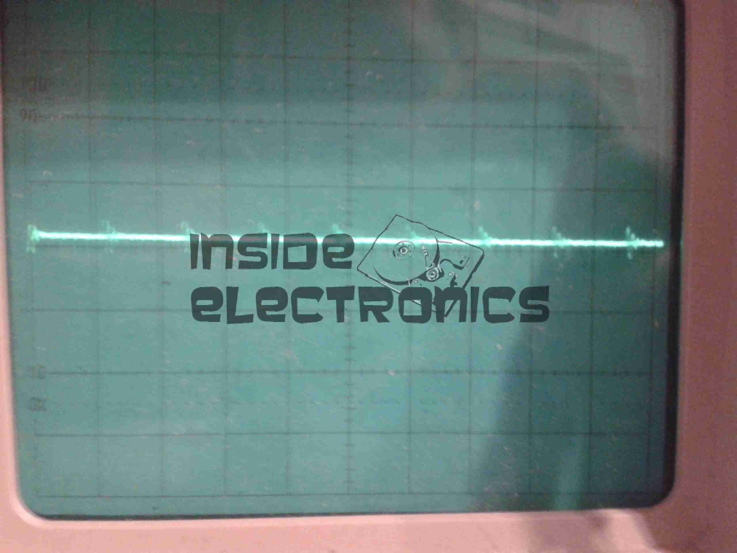
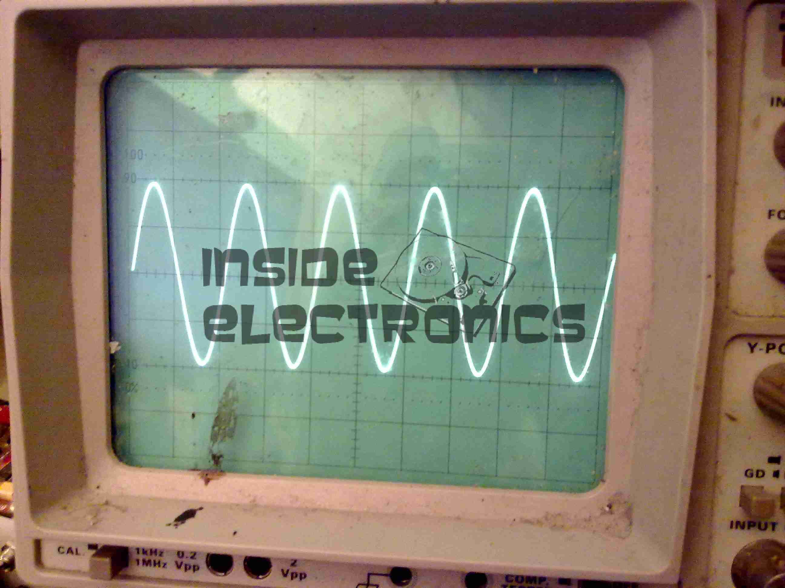
The output coupled through a 100nF capacitor is very clean, as can be seen below, outputting a 1kHz signal. Oscilloscope scale is 0.5ms/div & 1V/div.
VFO Output (Mucky ‘Scope)Scope Connected
Thanks again to Rich over at AD7C for the very useful tool design!
Linked below is the Eagle design files for this project, along with my libraries used to create it.
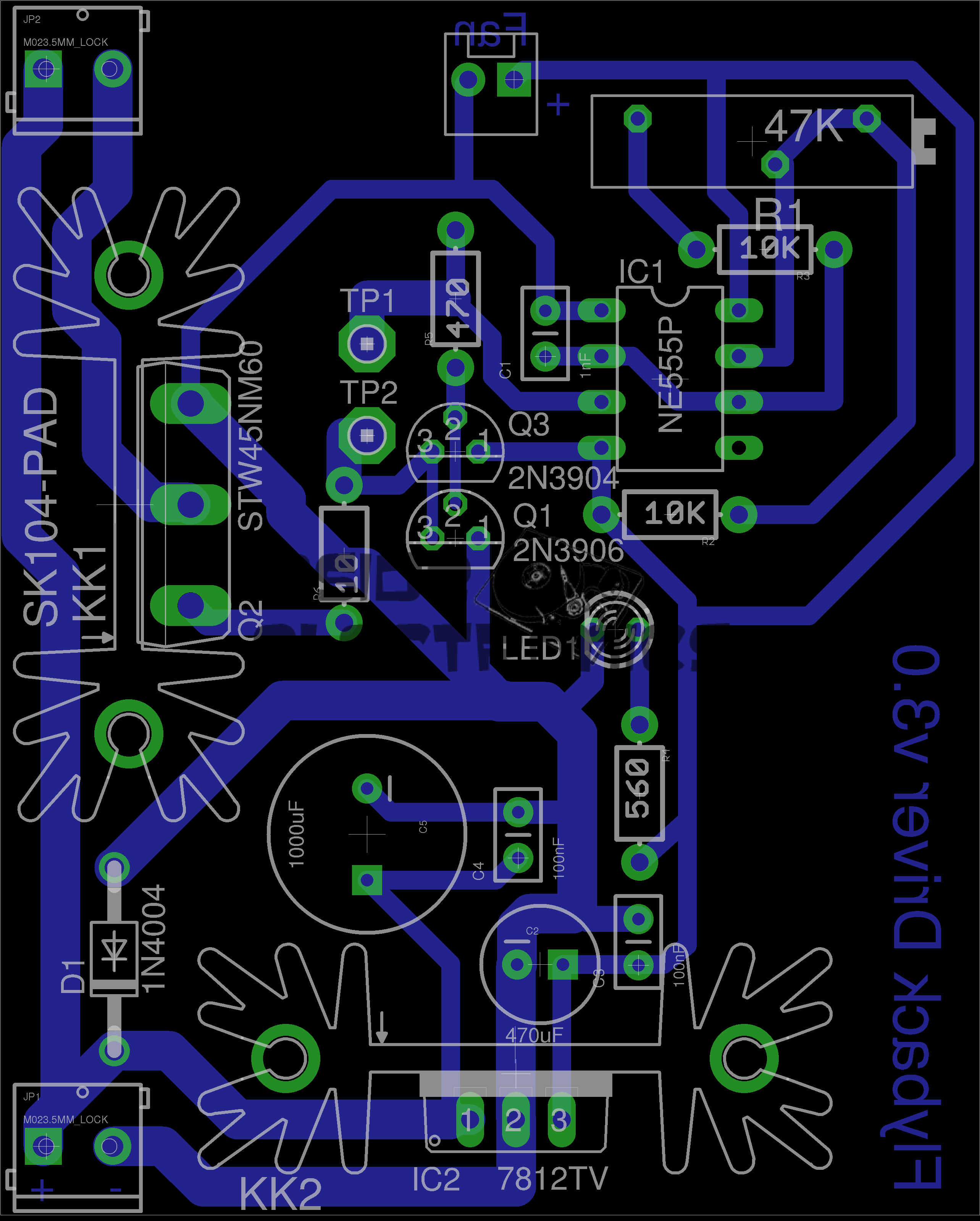
Here is a simple 555 timer based flyback transformer driver, with the PCB designed by myself for some HV experiments. Above is the Eagle CAD board layout.
The 555 timer is in astable mode, generating a frequency from about 22kHz to 55kHz, depending on the position of the potentiometer. The variable frequency is to allow the circuit to be tuned to the resonant frequency of the flyback transformer in use.
This is switched through a pair of buffer transistors into a large STW45NM60 MOSFET, rated at 650v 45A.
Input power is 15-30v DC, as the oscillator circuit is fed from an independent LM7812 linear supply.
Provision is also made on the PCB for attaching a 12v fan to cool the MOSFET & linear regulator.
Initial Board
Board initially built, with the heatsink on the linear regulator fitted. I used a panel mount potentiometer in this case as I had no multiturn 47K pots in stock.
PCB Traces
Bottom of the PCB. The main current carrying traces have been bulked up with copper wire to help carry the potentially high currents on the MOSFET while driving a large transformer.
This board was etched using the no-peel toner transfer method, using parchement paper as the transfer medium.
MOSFET Heatsinked
Main MOSFET now fitted with a surplus heatsink from an old switchmode power supply. A Fan could be fitted to the top of this sink to cope with higher power levels.
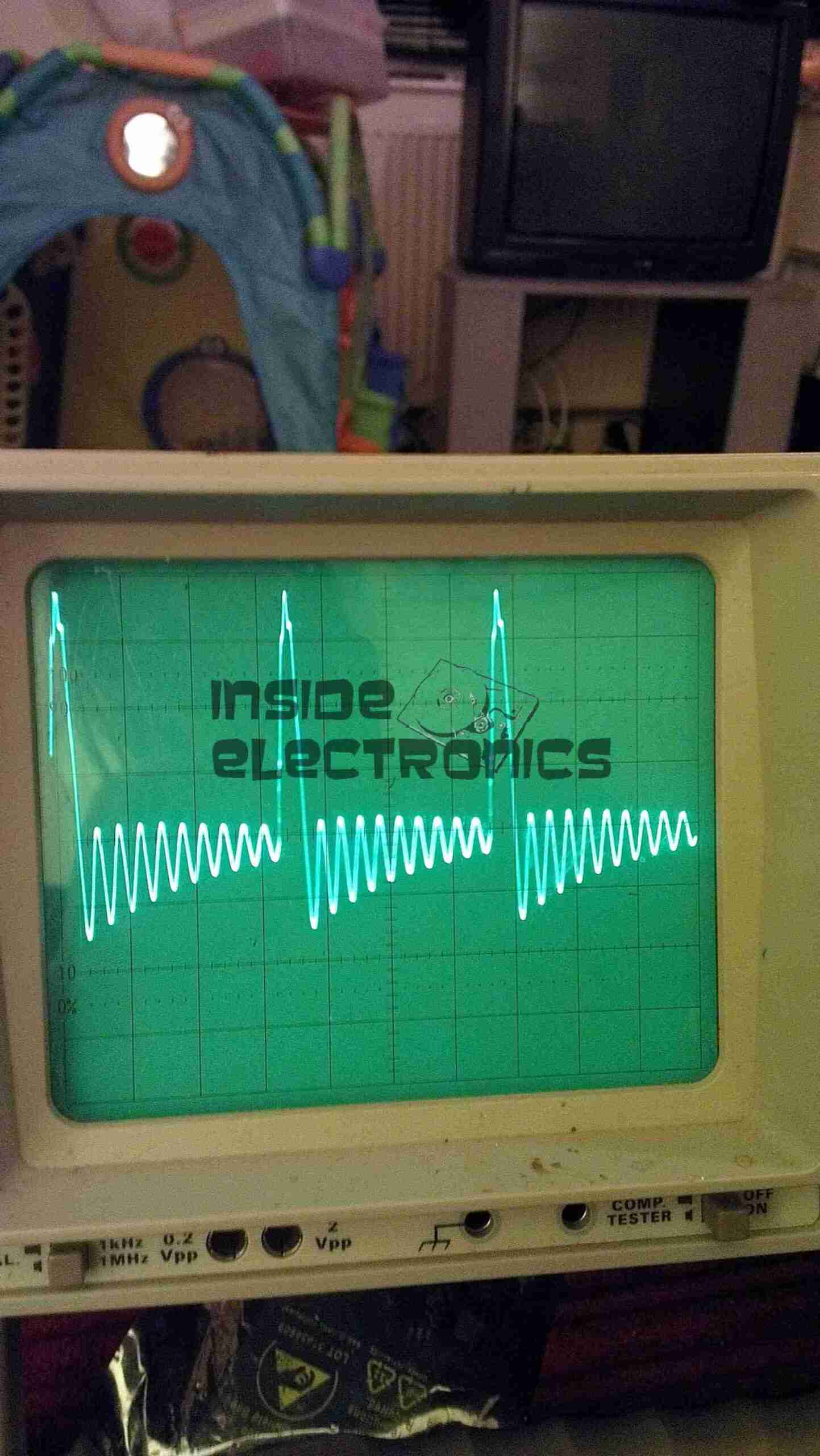
Gate Drive Waveform
This is the gate drive waveform while a transformer is connected, the primary is causing some ringing on the oscillator. The waveform without an attached load is a much cleaner square wave.
Flyback Secondary Waveform
I obtained a waveform of the flyback secondary output by capacitively coupling the oscilloscope probe through the insulation of the HT wire. The pulses of HV can be seen with the decaying ringing of the transformer between cycles.
Corona DischargeArc Discharge
Corona & arc discharges at 12v input voltage.
Download the Eagle schematic files here: [download id=”5561″]
After seeing these on eBay for £8.99 I thought it might be a good deal – interfacing with the RasPi’s GPIO & it has built in power supplies.
As a kit, it was very easy to assemble, the PCB quality is high, and is a fairly good design. It worked first time, the regulators hold the rails at the right voltages.
However there are some issues with this board that bug me.
The documentation for the kit is *AWFUL*. No mention of the regulators on the parts list & which goes where – I had to carefully examine the schematics to find out those details.
The 4x 1N1007 diodes required weren’t even included in the kit! Luckily I had some 1N4148 high speed diodes lying around & even though they’re rated for 200mA continuous rather than the specified part’s 1A rating, the lack of heatsinking on the regulators wouldn’t allow use anywhere near 1A, so this isn’t much of a problem.
Component numbering on the silkscreen isn’t consistent – it jumps from R3 straight to R6! These issues could be slightly confusing for the novice builder, and considering the demographic of the RasPi, could be seen as big issues.
On the far left of the board are the 5v & 3.3v regulators, well placed on the edge of the board in case a heatsink may be required in the future. However the LM317 adjustable regulator is stuck right in the middle of the PCB – no chance of being able to fit a heatsink, & the device itself seems incredibly cheap – the heatsink tab on the back of the TO-220 is the thinnest I have ever seen. Not the usual 2-3mm thick copper of the 5v & 3.3v parts – but barely more than a mm thick, so it’s not going to be able to cope with much power dissipation without overheating quickly.
As the adjustable rail can go between ~2.5v – 10v, at the low end of the range the power dissipation is going to shoot through the roof.
The GPIO connector – this could have been done the other way, at the moment the ribbon cable has to be twisted to get both the Pi & the GPIO board the same way up. Just a slight fail there. See the image below
Plugged In
The power rails are not isolated out of the box – there is no connection between the 5v & 3.3v rails & the Pi’s GPIO, but the GND connections are linked together on the board.
Getting the ribbon cable through the hole in the ModMyPi case was a bit of a faff – the connector is too big! I had to squeeze the connector through at a 45° angle. The case is also remarkably tight around the connector once it’s fitted to the board – clearly the designers of the case didn’t test the an IDC connector in the case before making them!
Everything does fit though, after a little modification.
All Cased Up
Here is the unit all built up with the case. The top cover just about fits with the IDC connector on the GPIO header.
More to come once I get some time to do some interfacing!
Tip Jar
If you’ve found my content useful, please consider leaving a donation by clicking the Tip Jar below!
All collected funds go towards new content & the costs of keeping the server online.