Posted on Leave a comment

UM25C USB Power Meter

UM25C USB Power Meter

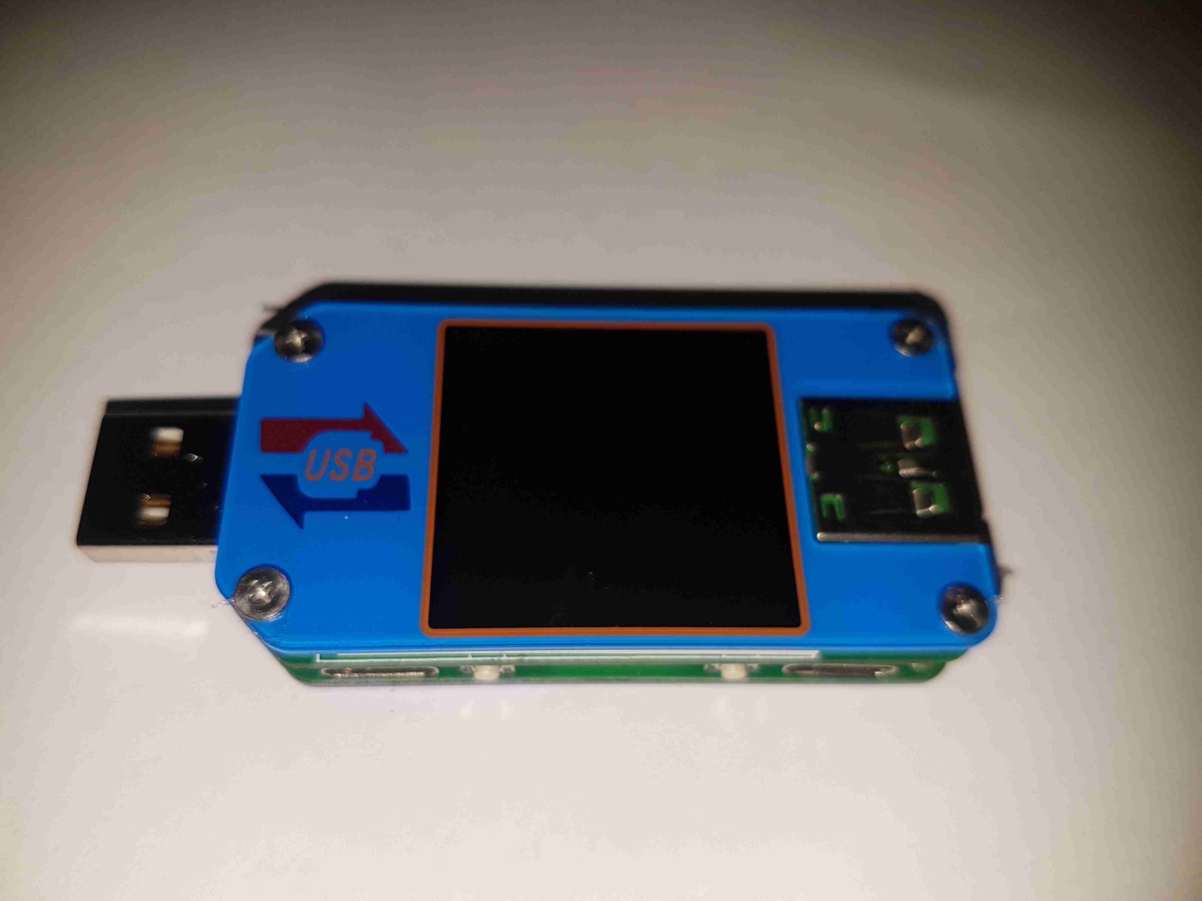
Here’s a nice little feature-packed USB power meter, the UM25C. This unit has USB-C along with the usual USB type A connectors, along with a bluetooth radio for remote monitoring of stats via a Windows or Android app. Construction is nice, it’s a stack of two PCBs, and polycarbonate cover plates, secured together with brass posts & screws.

Back Cover
Back Cover

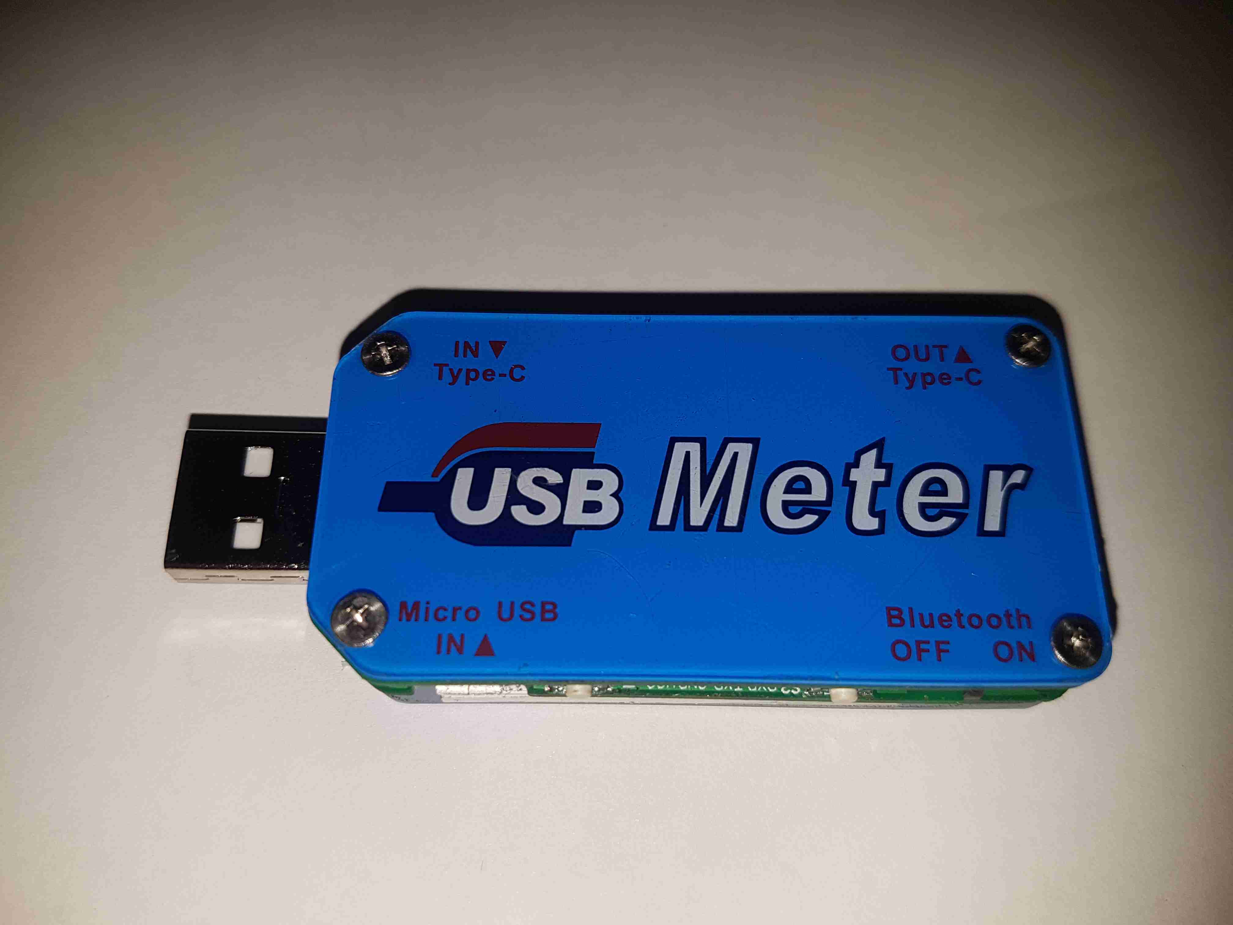
The back cover has the legend for all the side connectors, along with the logo.

USB Micro Input
USB Micro Input

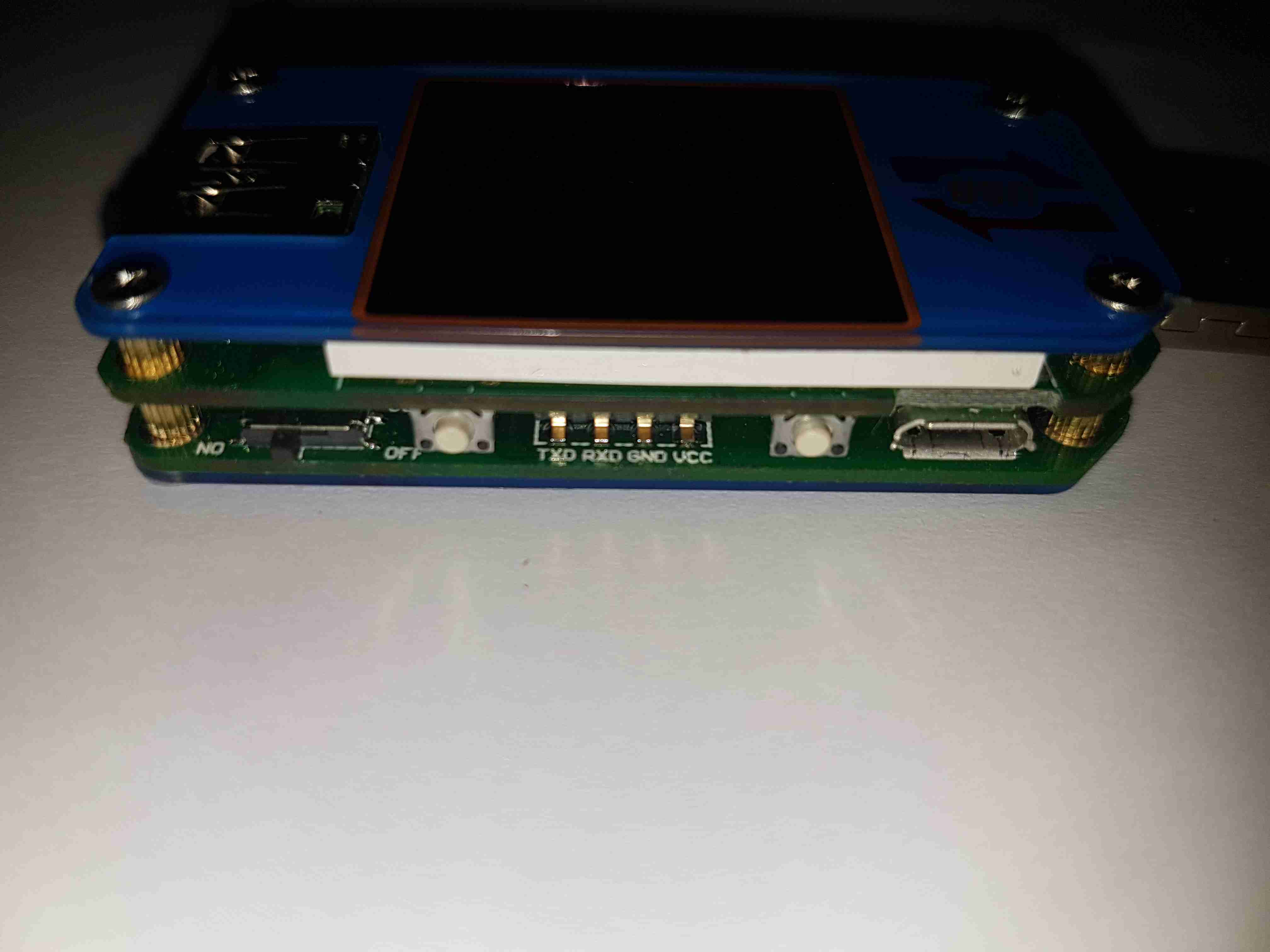
Down the sides are the user interface buttons, and here the Micro-B input connector. The 4-pin header is visible here that takes serial data down to the bluetooth section.

USB-C Connectors
USB-C Connectors

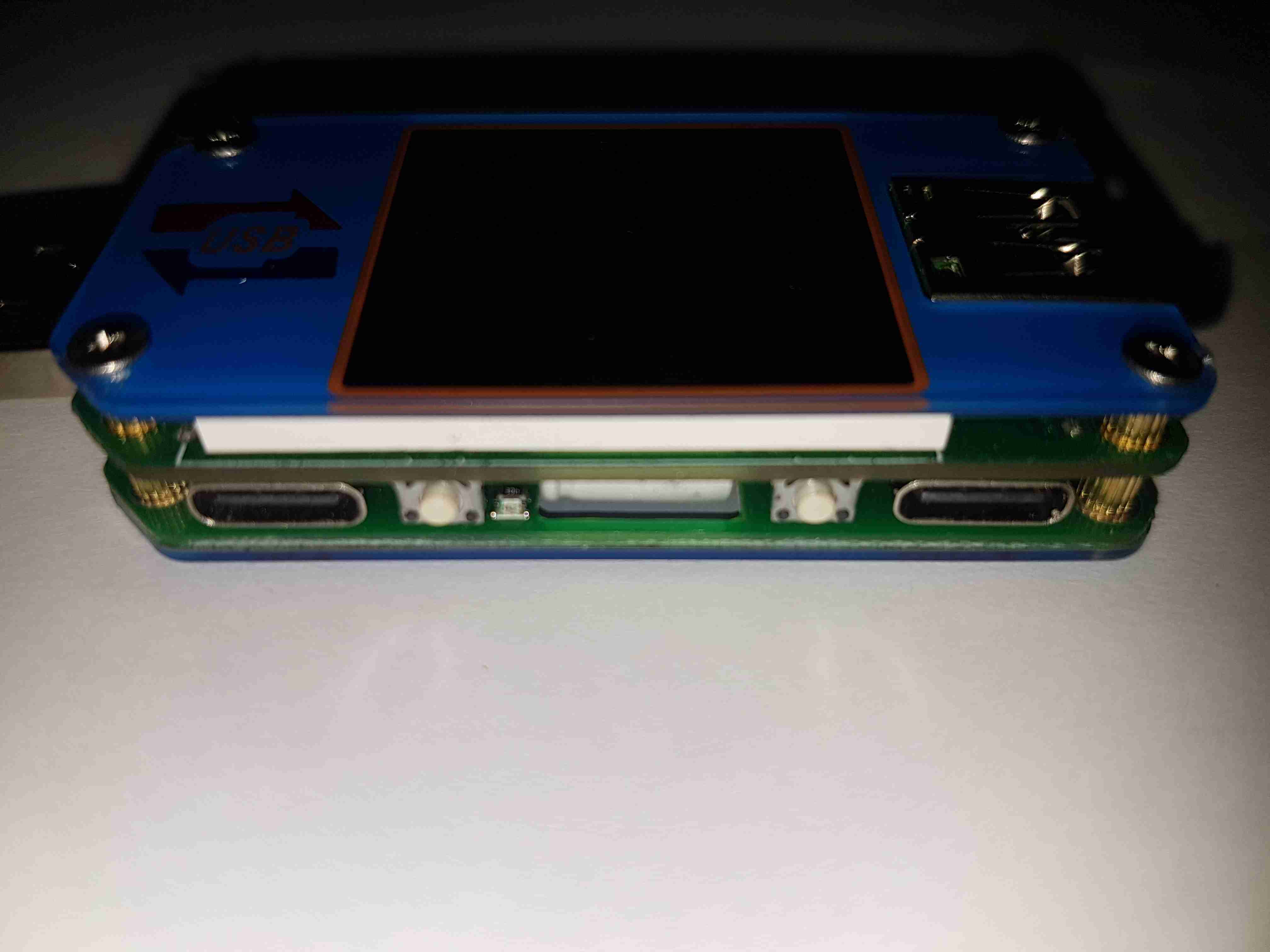
The other side has the remaining pair of buttons, and the USB-C I/O. I don’t yet own anything USB-C based, but this is good future proofing.

LCD Display
LCD Display

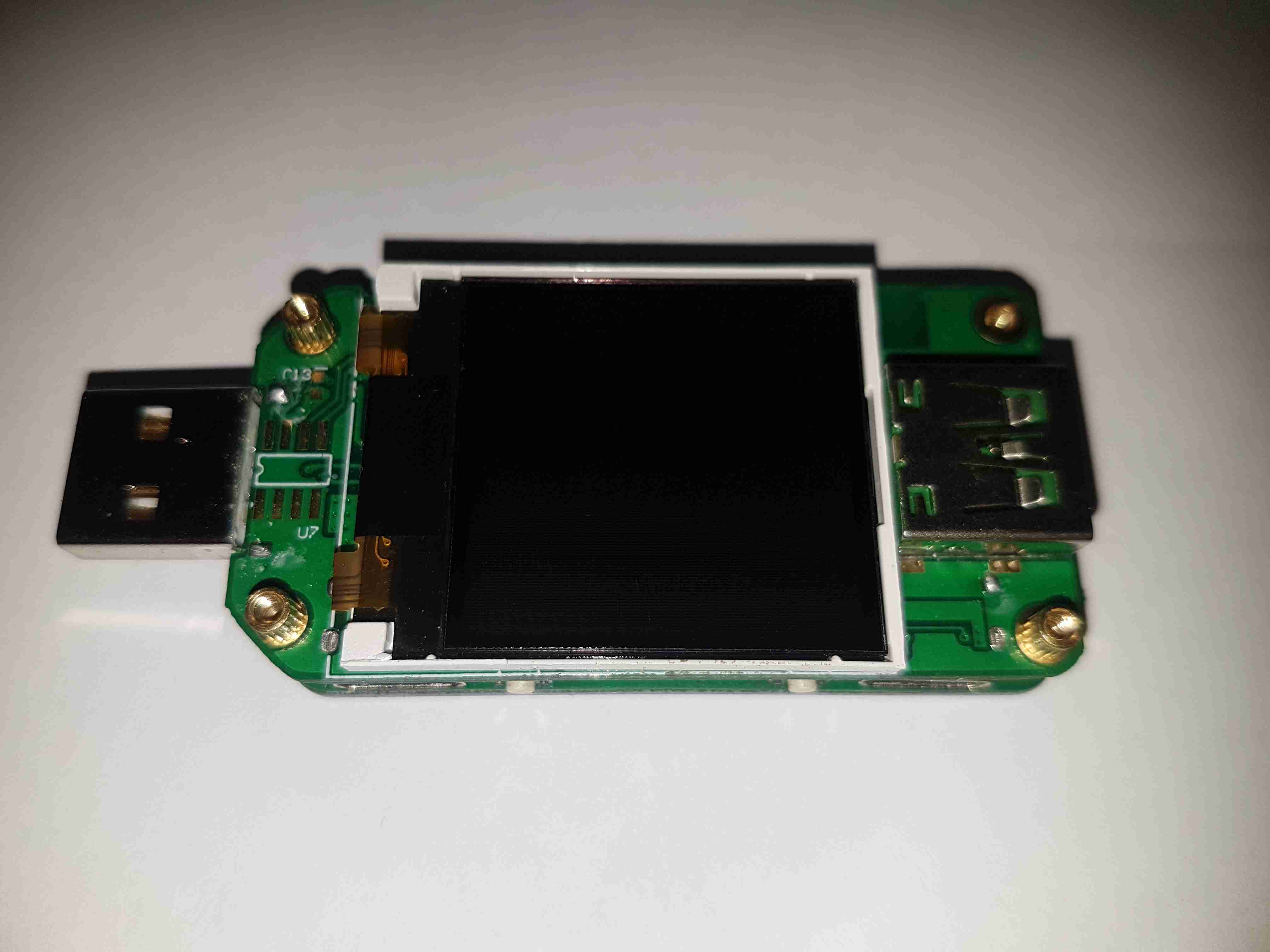
Removing the top plastic cover plate reveals the small 1″ TFT LCD module. This will be hot-bar soldered underneath the screen. There’s an unused footprint next to the USB input connector, judging by the pin layout it’s probably for a I²C EEPROM.

Main Board Components

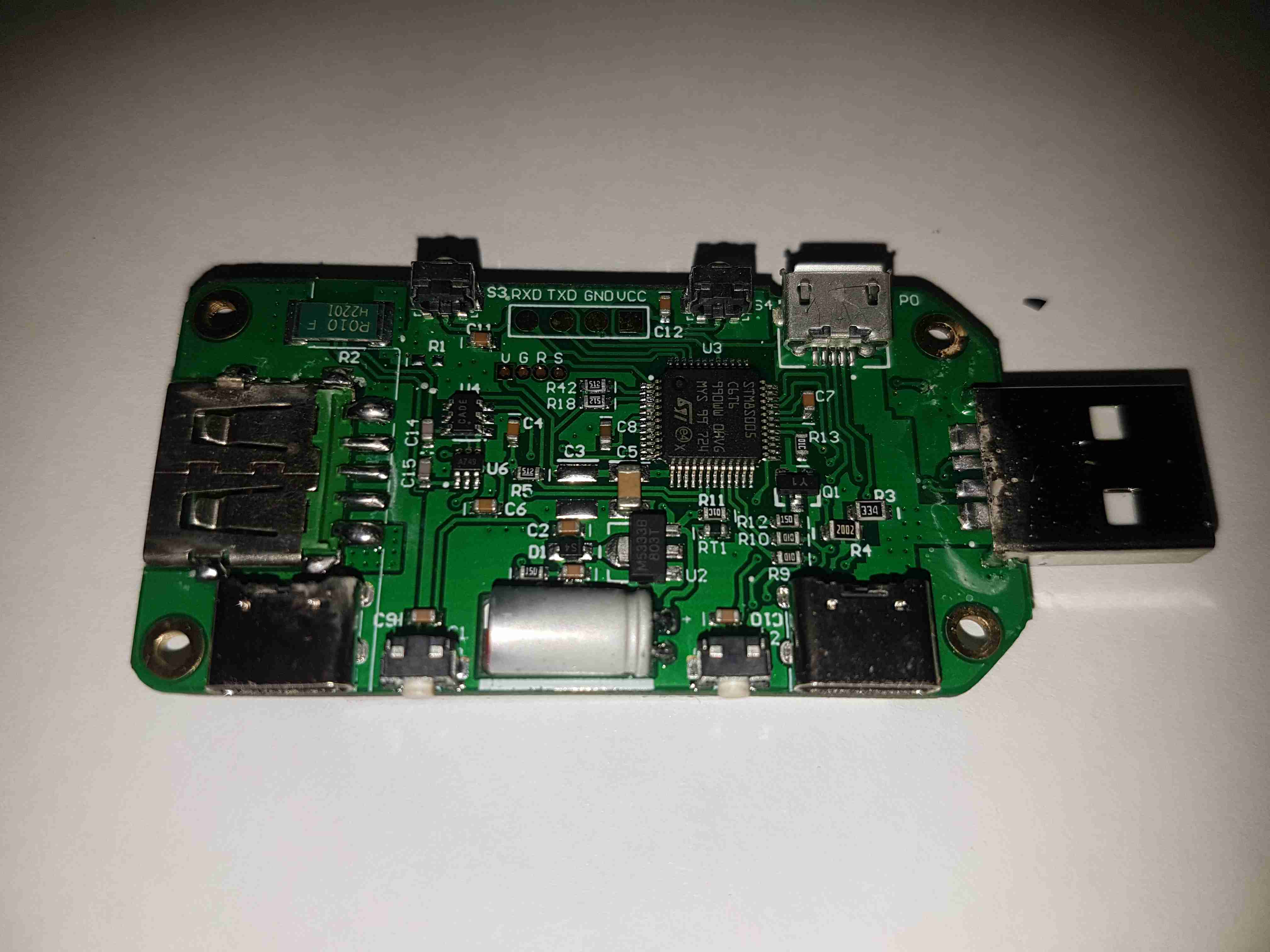
The underside of the top PCB has all the main components. The brains of the operation is a ST STM8S005C6T6 microcontroller. It’s at the basic end of the STM range, with a 16MHz clock, 32K flash, EEPROM, 10-bit ADC, SPI, UART & I²C. The main 0.010Ω current shunt is placed at the top left of the board in the negative rail. A couple of SOT-23 components in the centre of the board, I haven’t been able to identify properly, but I think they may be MOSFETs. The large electrolytic filter capacitor has a slot routed into the PCB to allow it to be laid flat. Providing the main power rail is a SOT-89 M5333B 3.3v LDO regulator.

Bluetooth Radio
Bluetooth Radio

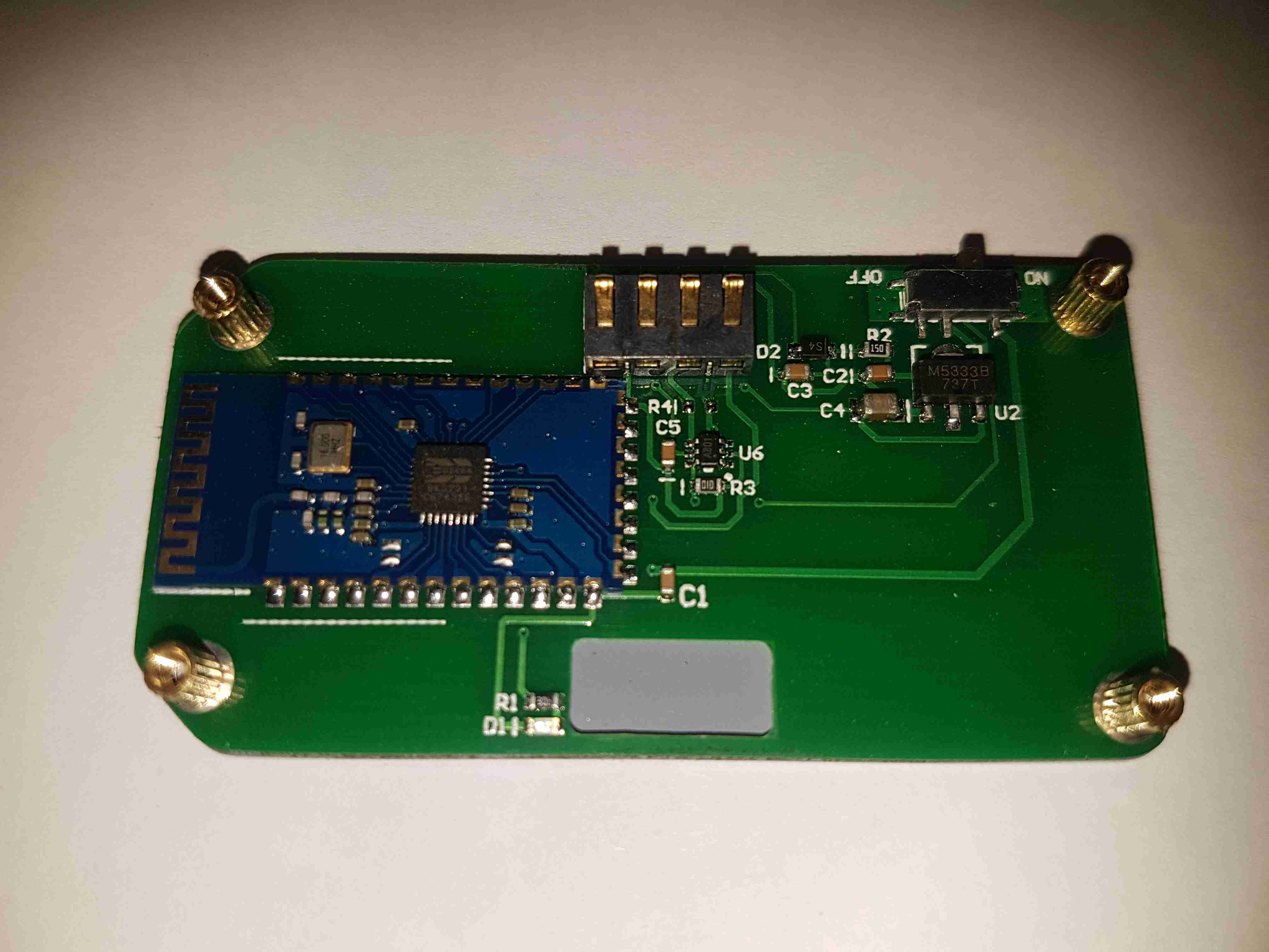
The bottom board contains the bluetooth radio module, this is a BK3231 Bluetooth HID SoC. The only profile advertised by this unit is a serial port. There’s a local 3.3v LDO regulator & support components, along with an indicator LED.

Posted on Leave a comment

Dell SE197FPf Monitor 12v Conversion

My other monitors are a different model, and have a slightly different main PCB inside, but the process is mostly the same for converting these to 12v supply.

Main PCB
Main PCB

In this monitor type, there is only a single board, with all the PSU & logic, instead of separate boards for each function.

PSU Closeup
PSU Closeup

This monitor is slightly different in it’s power supply layout. The mains supply provides only a single 12v rail, which is then stepped down by a switching converter to 5v, then by smaller linear regulators to 3.3v & 1.8v for the logic. This makes my life easier since I don’t have to worry about any power conversion at all.

PCB Reverse
PCB Reverse

Here’s the backside of the PCB, the mains PSU section is in the centre.

Attachment Points
Attachment Points

Here’s the pair of 12v supply wires soldered onto the main board, onto the common GND connection on the left, and the main +12v rail on the right. I’ve not bothered with colour coding the wiring here, just used whatever I had to hand that was heavy enough to cope with a couple amps.

12v Socket
12v Socket

A small mod later with a cone drill & the 12v input socket is mounted in the LCD frame.

Casing Mod
Casing Mod

Some light removal of plastic & the back cover fits back on. Current draw at 13.8v is ~2A.

Posted on Leave a comment

Rigol DS1054Z DC Power Supply – Linear Post Regulation

Finally, here’s the last part of the Rigol 12v DC Power Supply project, the linear post regulation section to remove some of the ripple.

I have made a couple of layout adjustments since the last post about this part of the project – a little more filtering on the DC outputs. As usual the Eagle project files are at the bottom of the post for those who might find them useful.

Updated PCB
Updated PCB
Updated Schematic
Updated Schematic


Completed PCB
Completed PCB

Here’s the completed PCB, partially installed in the back of the scope. The missing regulator is the 5v one, since I already have a source of clean 5v from my original attempt at the supply, it’s not a problem not using a linear after the switcher. The filtering is the same on all channels, input from the switchers is on the right, outputs to the scope on the left.

PCB Bottom
PCB Bottom

Here’s the bottom of the PCB, with the common mode input chokes. The design of this board has allowed me to remove a couple of the switching modules as well, as I can use a single bipolar supply to run both sets of bipolar regulators on this board. This should help remove some of the noise also.

The ripple level has now dropped to lower than it was originally on the mains supply! Current draw at 13.8v DC is about 1.75A.

Scope Ripple
Scope Ripple

[download id=”5589″]

Posted on Leave a comment

AD9850 VFO Board

Continuing from my previous post where I published an Eagle design layout for AD7C‘s Arduino powered VFO, here is a completed board.

I have made some alterations to the design since posting, which are reflected in the artwork download in that post, mainly due to Eagle having a slight psychotic episode making me ground one of the display control signals!

AD9850 VFO
AD9850 VFO

The amplifier section is unpopulated & bypassed as I was getting some bad distortion effects from that section, some more work is needed there.
The Arduino Pro Mini is situated under the display, and the 5v rail is provided by the LM7805 on the lower left corner.

Current draw at 12v input is 150mA, for a power of 1.8W total. About 1W of this is dissipated in the LM7805 regulator, so I have also done a layout with an LM2574 Switching Regulator.
The SMPS version should draw a lot let power, as less is being dissipated in the power supply, but this version is more complex.

DDS VFO-SMPS
DDS VFO-SMPS

Here the SMPS circuit can be seen on the left hand side of the board, completely replacing the linear regulator.
I have not yet built this design, so I don’t know what kind of effect this will have on the output signal, versus the linear regulator. I have a feeling that the switching frequency of the LM2574 (52kHz) might produce some interference on the output of the DDS module. However I have designed this section to the standards in the datasheet, so this should be minimal.

Nevertheless this version is included in the Downloads section at the bottom of this post.

The output coupled through a 100nF capacitor is very clean, as can be seen below, outputting a 1kHz signal. Oscilloscope scale is 0.5ms/div & 1V/div.

VFO Output
VFO Output (Mucky ‘Scope)
Scope Connected
Scope Connected


Thanks again to Rich over at AD7C for the very useful tool design!

Linked below is the Eagle design files for this project, along with my libraries used to create it.

[download id=”5571″]

[download id=”5573″]

[download id=”5575″]

Posted on Leave a comment

Wearable Raspberry Pi – Some Adjustments

USB Hub
USB Hub

As the first USB hub I was using was certainly not stable – it would not enumerate between boots & to get it working again would require waiting around 12 hours before applying power, it has been replaced. This is a cheapie eBay USB hub, of the type shown below.

These hubs are fantastic for hobbyists, as the connections for power & data are broken out on the internal PCB into a very convenient row of pads, perfect for integration into many projects.

Breakout Hub
Breakout Hub

I now have two internal spare USB ports, for the inbuilt keyboard/mouse receiver & the GPS receiver I plan to integrate into the build.

These hubs are also made in 7-port versions, however I am not sure if these have the same kind of breakout board internally. As they have the same cable layout, I would assume so.


Connector Panel
Connector Panel

Here is a closeup of the back of the connectors, showing a couple of additions.

I have added a pair of 470µF capacitors across the power rails, to further smooth out the ripple in the switching power supply, as I was having noise issues on the display.

Also, there is a new reset button added between the main interface connectors, which will be wired into the pair of pads that the Raspberry Pi has to reset the CPU.
This can be used as a power switch in the event the Pi is powered down when not in use & also to reset the unit if it becomes unresponsive.


Posted on 5 Comments

Rare Veroboard Design Tools – Stripboard Magic

Stripboard Magic

Stripboard Magic is a Windows application for designing PCB layouts on stripboard (aka prototyping board, aka Veroboard). It was released by a British company called Ambyr which ceased trading a long time ago.

The interface is a quite primitive and a little strange but the program is functional even on Windows XP. It also works great under wine in Linux, at least with version 0.9.38 and above as this is all I have checked. It should probably work on older versions too. I haven’t tried it on Vista though.

It can be a handy program when called upon and I have successfully used it a few times when throwing together random small circuits. Due to the interface I would imagine it to be a bit clumsy for very large circuits. The biggest gripe I have with it is the inability to change the orientation of components on the board, so some circuits tend to be slightly larger than they need to be.

I downloaded a copy of Stripboard Magic 1.0 back in the 90’s and recently just found it lying about on my computer. As I would consider it to well and truly be abandonware and as it seems to be a little sought after by some hobbyists I have provided a link to download it below.

[download id=”5624″]

Here are some screenshots showing the schematic view (top) and board layout view (bottom):


Stripboard Designer

Another hard to find app these days is Stripboard Designer, mirrored here for people who wish to use it.

[download id=”5626″]

[download id=”5628″]