While searching around for regulators to convert my new scope to 12v power, I remembered I had some DC-DC modules from Texas Instruments that I’d got a while ago. Luckily a couple of these are inverting controllers, that will go down to -15v DC at 15W/3A capacity.
I’ve had to order a new module from TI to do the -17v rail, but in the meantime I’ve been getting the other regulators set up & ready to go.
The DC-DC module I’ve got for the -7.5v rail is the PTN78060A type, and the +7.5v & +5v rails will be provided by the PTN78020W 6A buck regulators.
These regulators are rated well above what the scope actually draws, so I shouldn’t have any issues with power.
DC-DC Modules
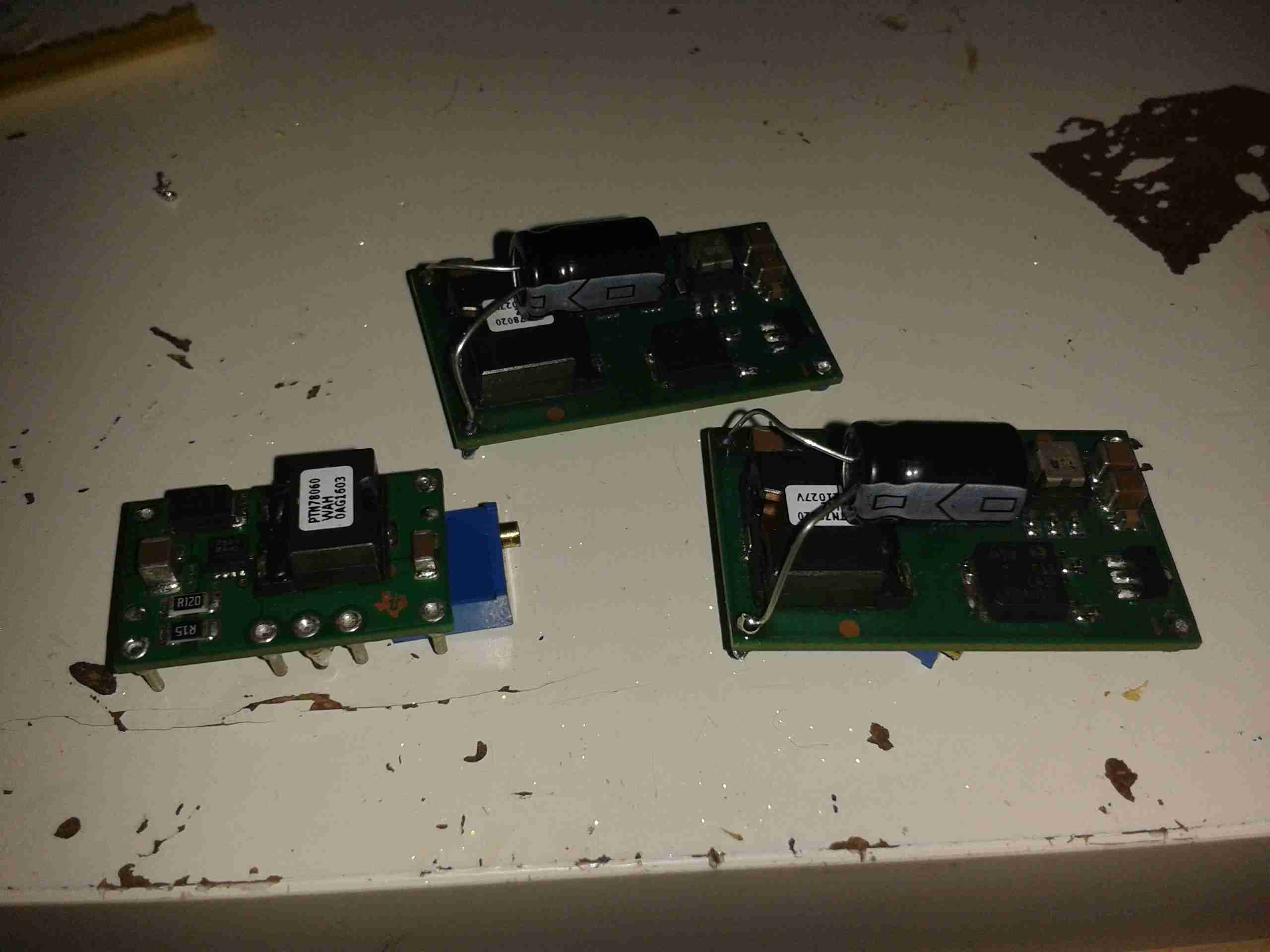
Here’s the regulators for the 5v, 7.5v & -7.5v rails, with multiturn potentiometers attached for setting the voltage output accurately. I’ve also attached a couple of electrolytics on the output for some more filtering. I’ll add on some more LC filters on the output to keep the noise down to an absolute minimum. These are set up ready with the exact same output voltage as the existing mains AC switching supply, when the final regulator arrives from TI I will put everything together & get some proper rail readings.
There won’t be a proper PCB for this, as I don’t have the parts in Eagle CAD, and I simply don’t have the energy to draw them out from the datasheets.
I recently posted about a small analog SWR/Power meter I got from eBay, and figured it needed some improvement.
After some web searching I located a project by ON7EQ, an Arduino sketch to read SWR & RF power from any SWR bridge.
The Arduino code is on the original author’s page above, his copyright restrictions forbid me to reproduce it here.
I have also noticed a small glitch in the code when it is flashed to a blank arduino: The display will show scrambled characters as if it has crashed. However pushing the buttons a few times & rebooting the Arduino seems to fix this. I think it’s related to the EEPROM being blank on a new Arduino board.
I have run a board up in Eagle for testing, shown below is the layout:
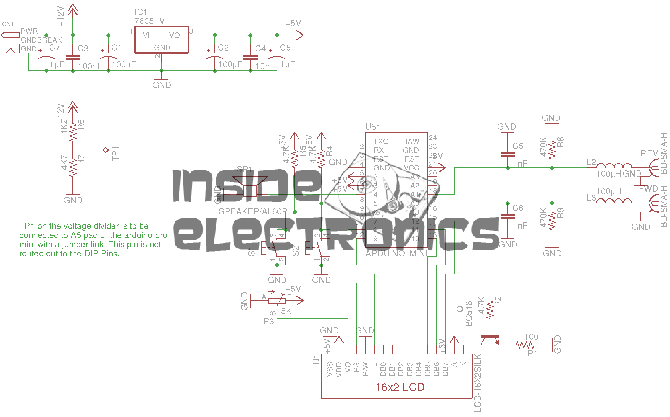
SWR Meter SCH
The Schematic is the same as is given on ON7EQ’s site. Update: ON7EQ has kindly let me know I’ve mixed up R6 & R7, so make sure they’re switched round when the board is built ;). Fitting the resistors the wrong way around may damage the µC with overvoltage.
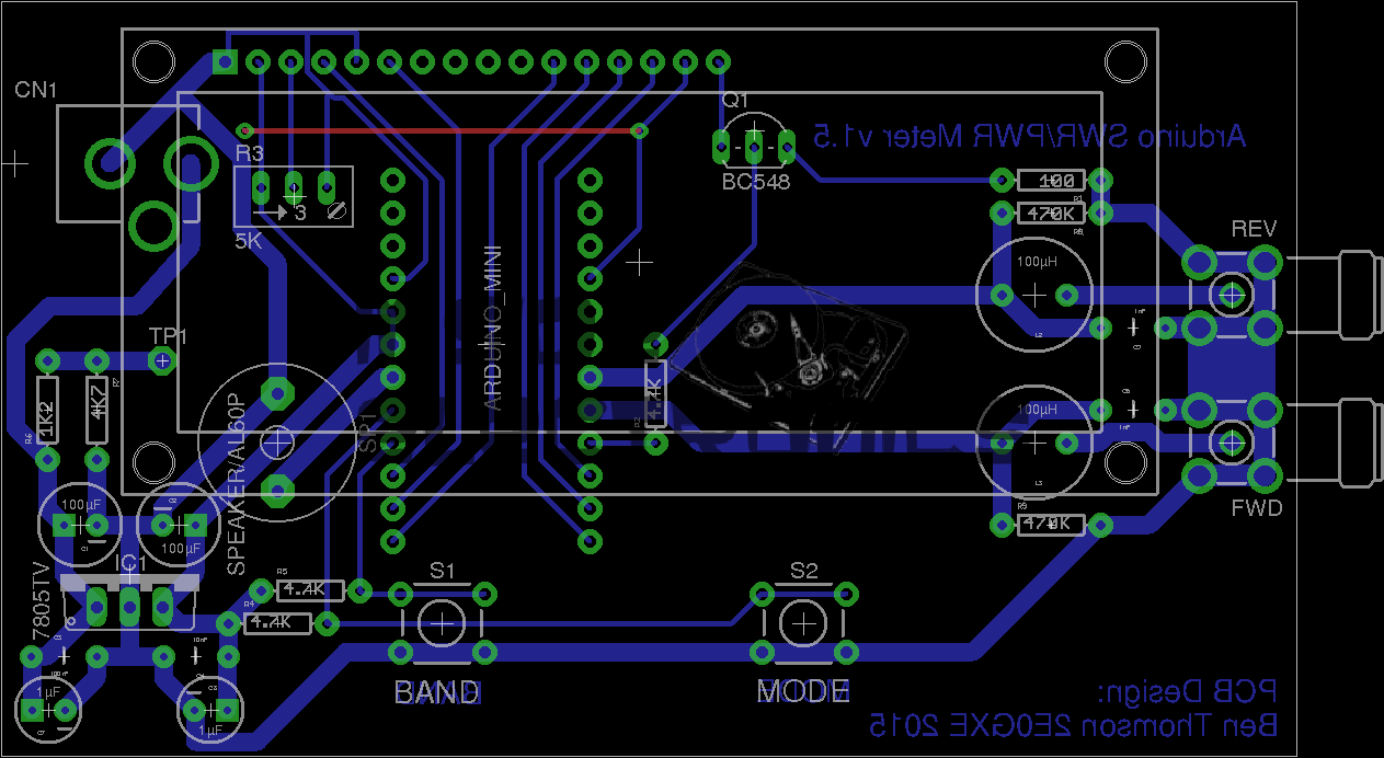
SWR Meter PCB
Here’s the PCB layout. I’ve kept it as simple as possible with only a single link on the top side of the board.
PCB Top
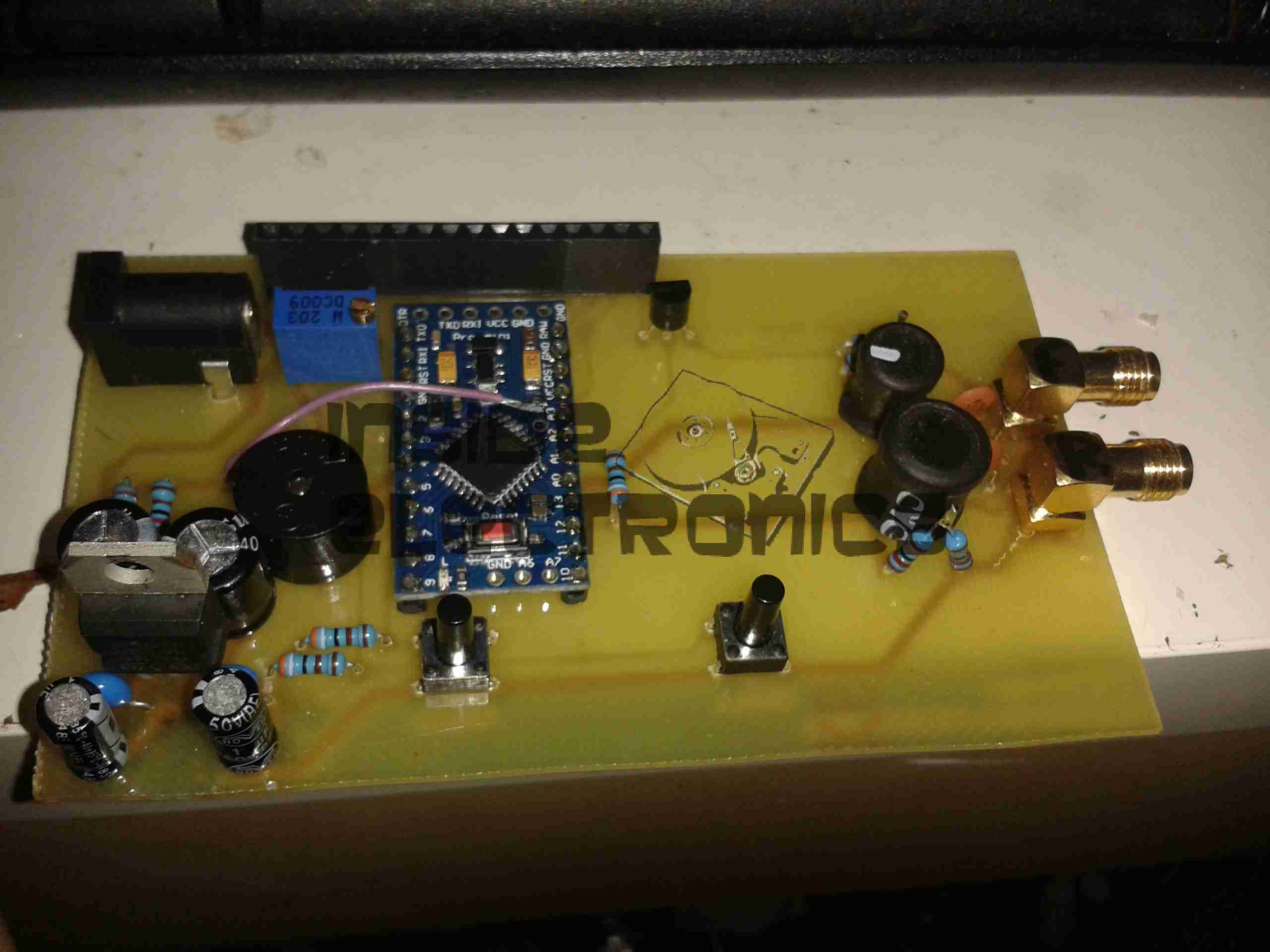
Here’s the freshly completed PCB ready to rock. Arduino Pro mini sits in the center doing all the work.
The link over to A5 on the arduino can be seen here, this allows the code to detect the supply voltage, useful for battery operation.
On the right hand edge of the PCB are the pair of SMA connectors to interface with the SWR bridge. Some RF filtering is provided on the inputs.
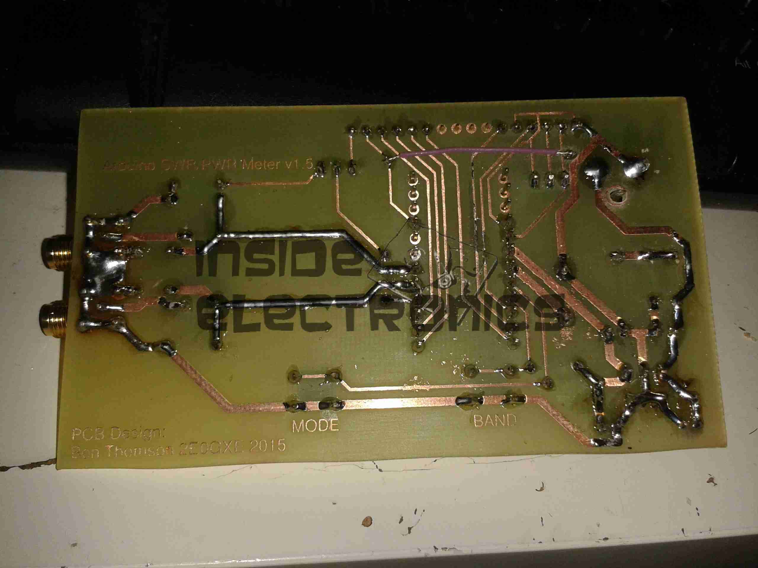
PCB Bottom
Trackside view of the PCB. This was etched using my tweaked toner transfer method.
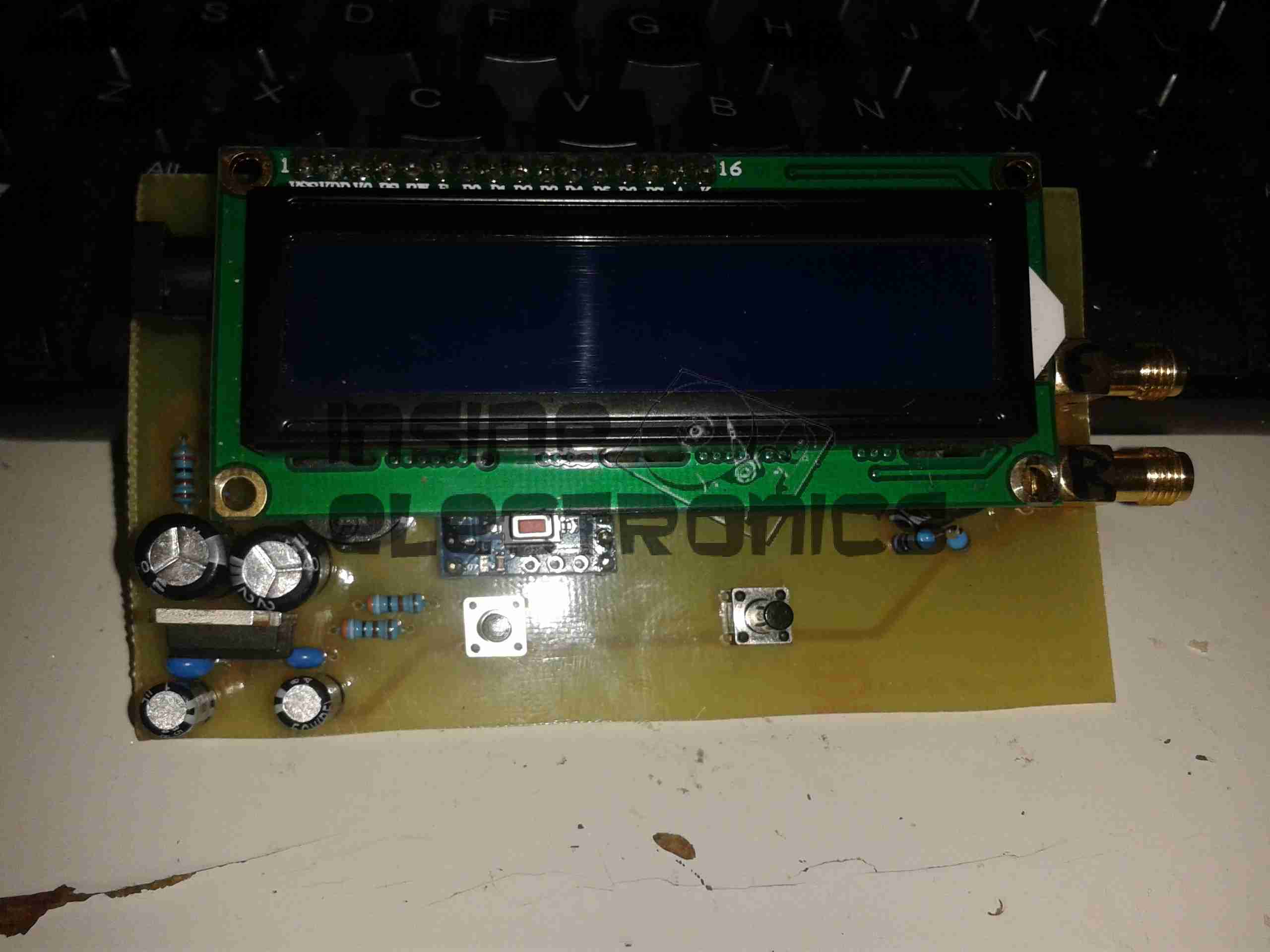
LCD Fitted
Here the board has it’s 16×2 LCD module.
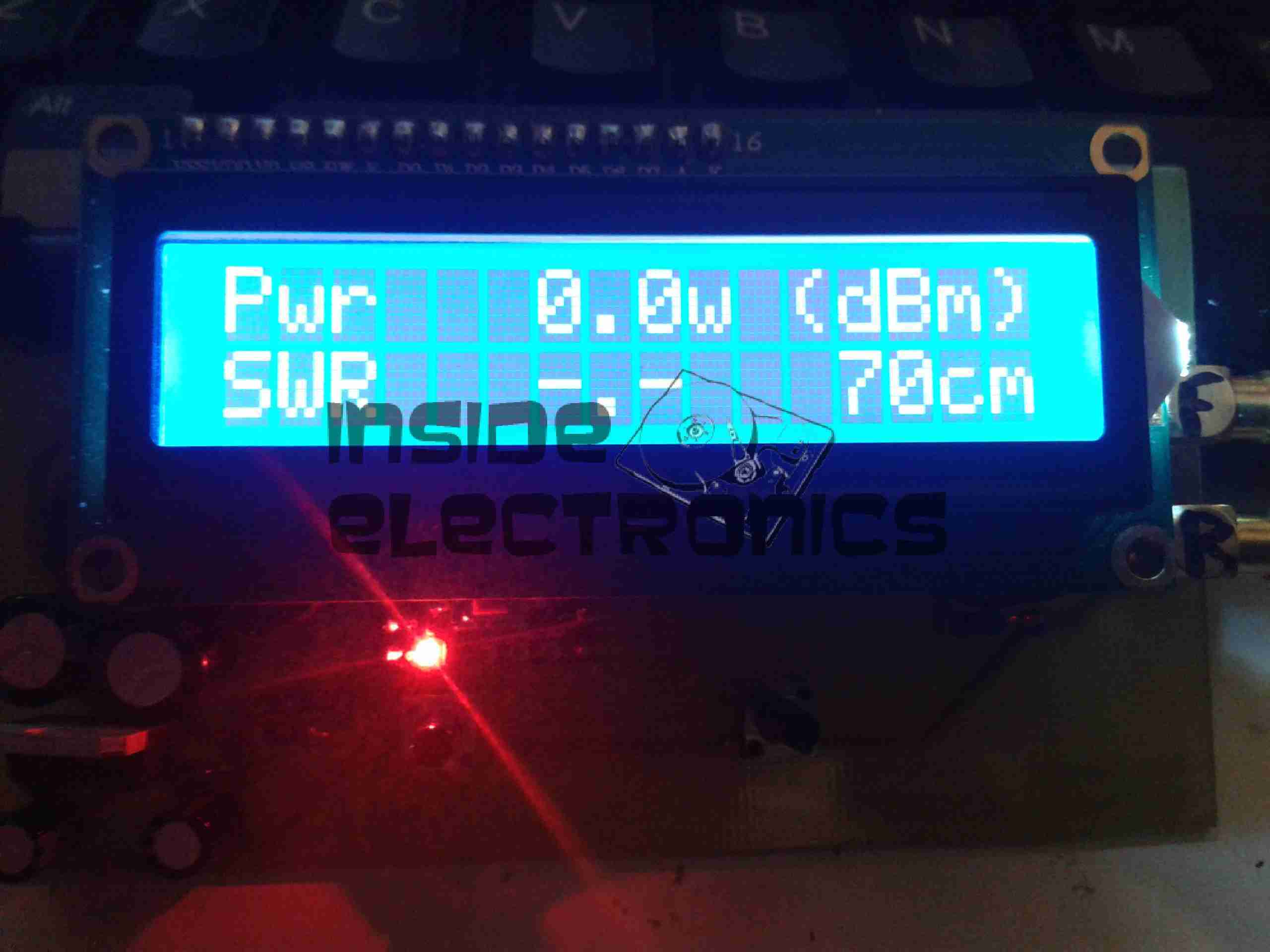
Online
Board powered & working. Here it’s set to the 70cm band. The pair of buttons on the bottom edge of the board change bands & operating modes.
As usual, the Eagle layout files are available below, along with the libraries I use.
[download id=”5585″]
[download id=”5573″]
More to come on this when some components arrive to interface this board with the SWR bridge in the eBay meter.
After watching a video over at Scullcom Hobby Electronics on YouTube, I figured I’d build one of these precision references to calibrate my multimeters.
It’s based around a REF102P 10v precision reference & an INA105P precision unity gain differential amplifier.
For full information, check out the video, I won’t go into the details here, just my particular circuit & PCB layout.
In the video, Veroboard is used. I’m not too fond of the stuff personally. I find it far too easy to make mistakes & it never quite looks good enough. To this end I have spun a board in Eagle, as usual.
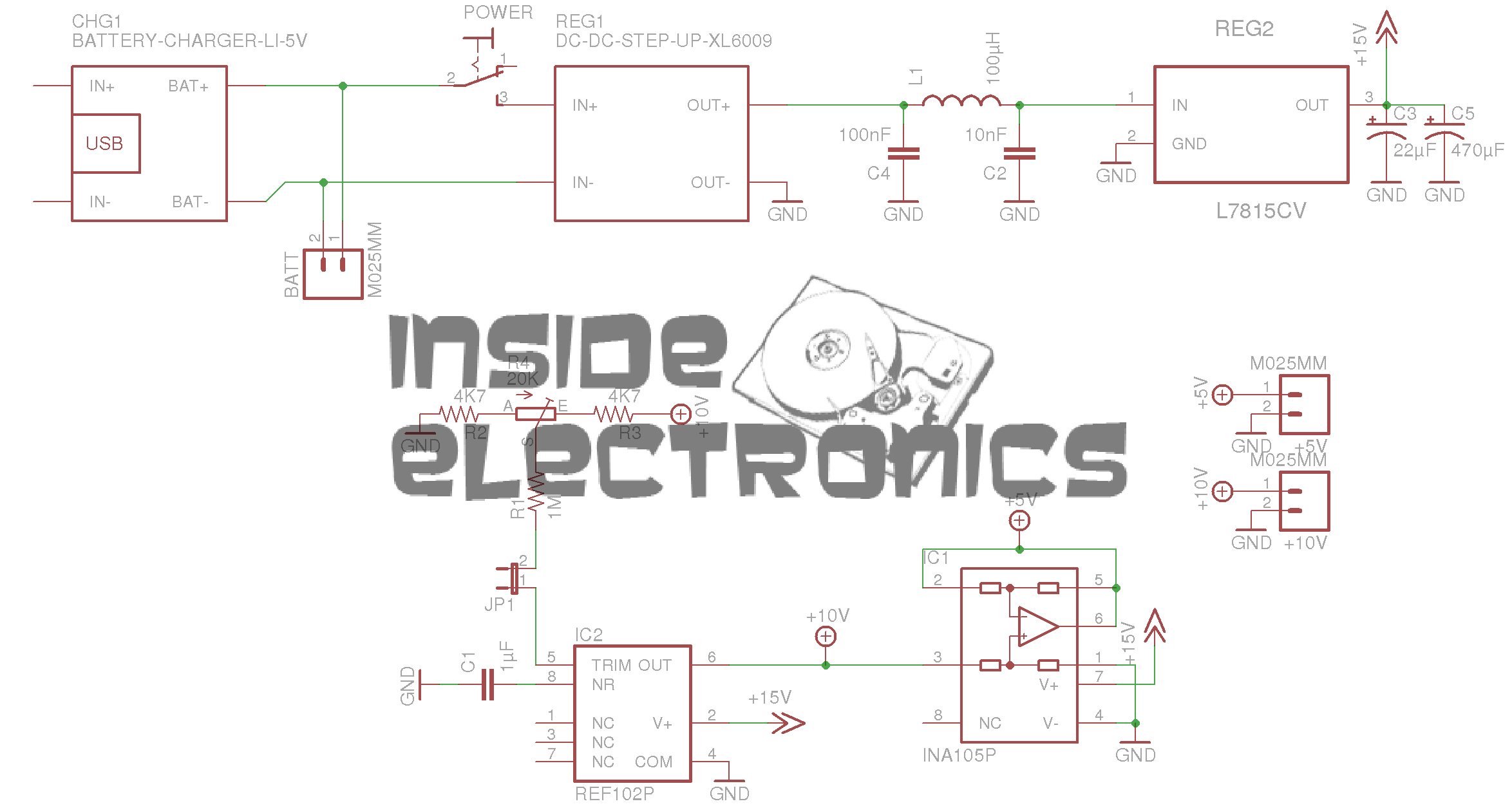
Precision Ref SCH – Click to Embiggen
Here’s the schematic layout, the same as is in the video.
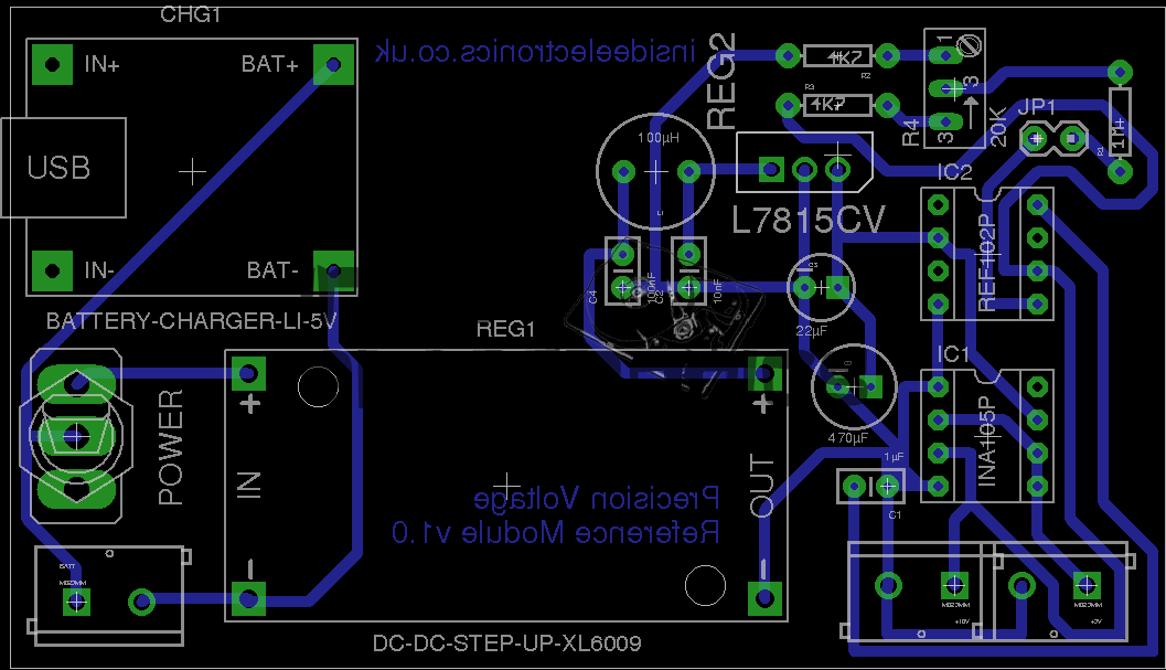
Precision Ref BRD
As usual, the Eagle CAD layout files can be found at the bottom of the post.
And the associated PCB layout. I have added the option to be able to tweak the output, to get a more accurate calibration, which can be added by connecting JP1 on the PCB.
As in the original build, this unit uses pre-built DC-DC converter & Li-Ion charger modules. A handy Eagle library can be found online for these parts.
I have however left off the battery monitor section of the circuit, since I plan to use a protected lithium cell for power. This also allowed me to keep the board size down, & use a single sided layout.
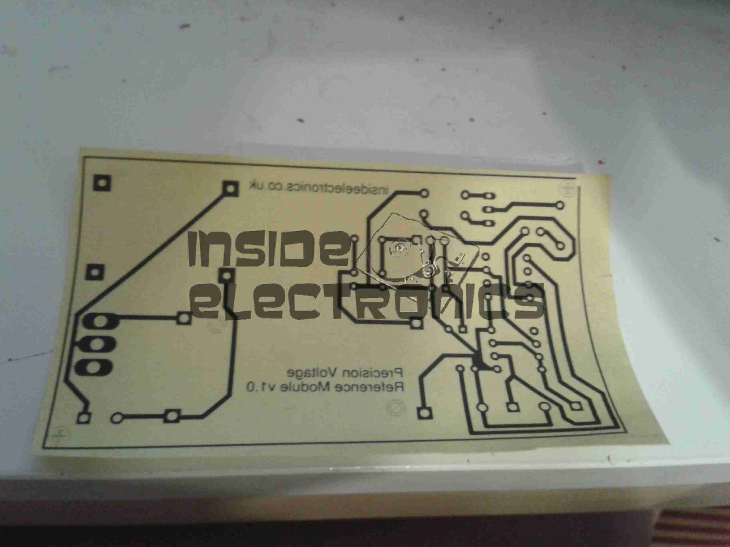
Toner Transfer Paper
Here’s the track layout ready to iron onto the copper clad board. I use the popular toner transfer system with special paper from eBay, this stuff has a coating that allows the toner to easily be transferred to the PCB without having to mess about with soaking in water & scraping paper off.
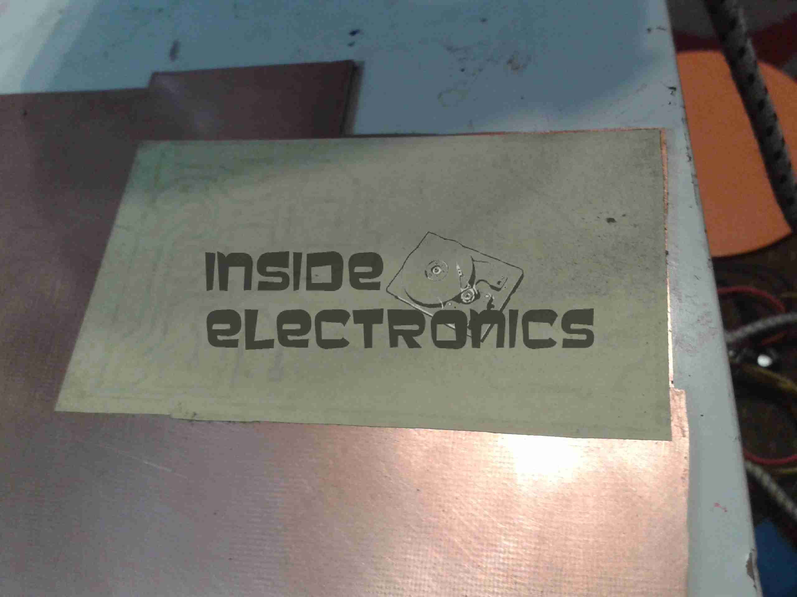
Ironed On
Here’s the paper having just been ironed onto the copper. After waiting for the board to cool off the paper is peeled off, leaving just the toner on the PCB.
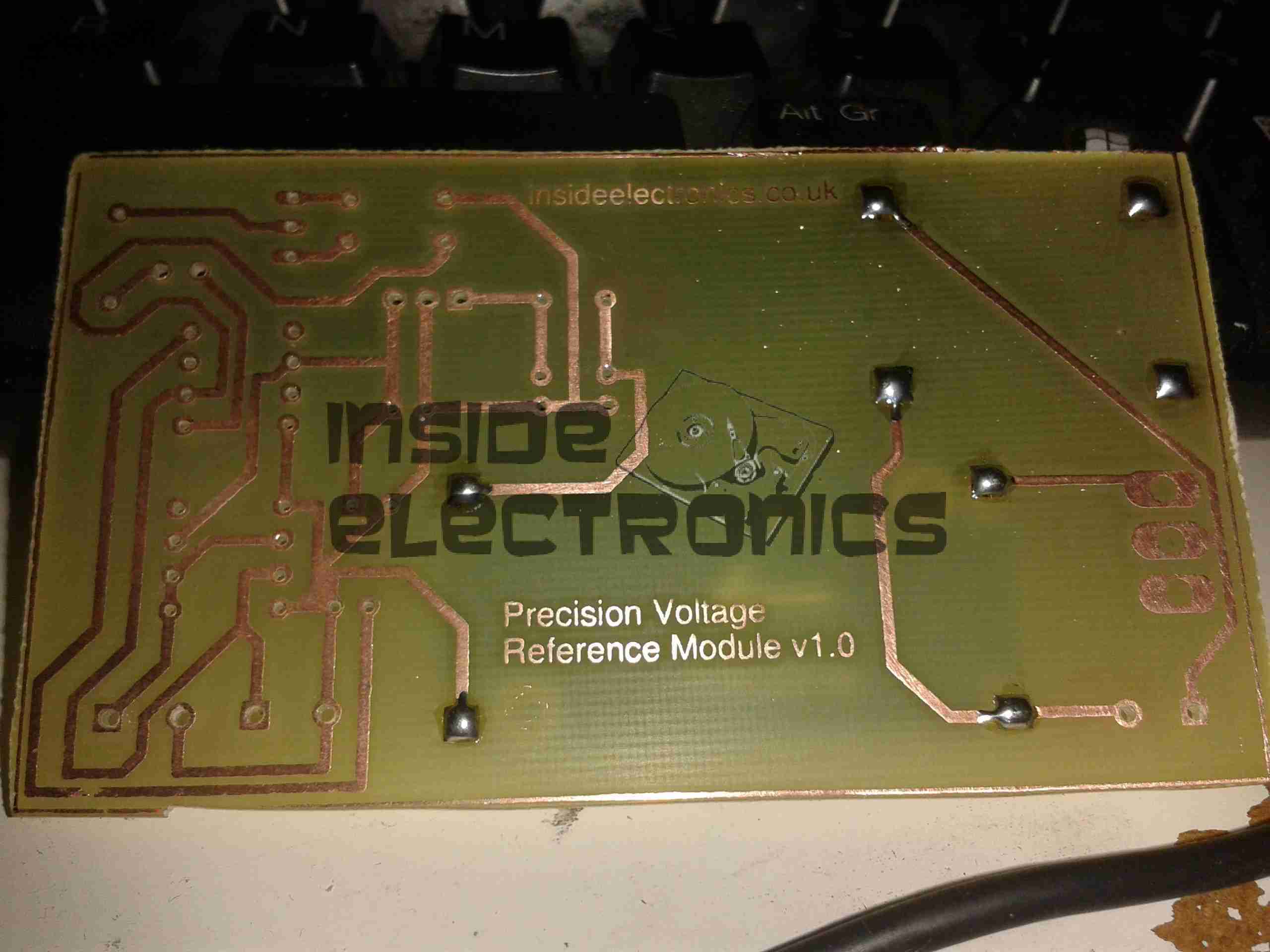
Etched PCB
PCB just out of the etch tank, drilled & with the solder pins for the modules installed. Only one issue with the transfer, in the bottom left corner of the board is visible, a very small section of copper was over etched.
This is easily fixed with a small piece of wire.
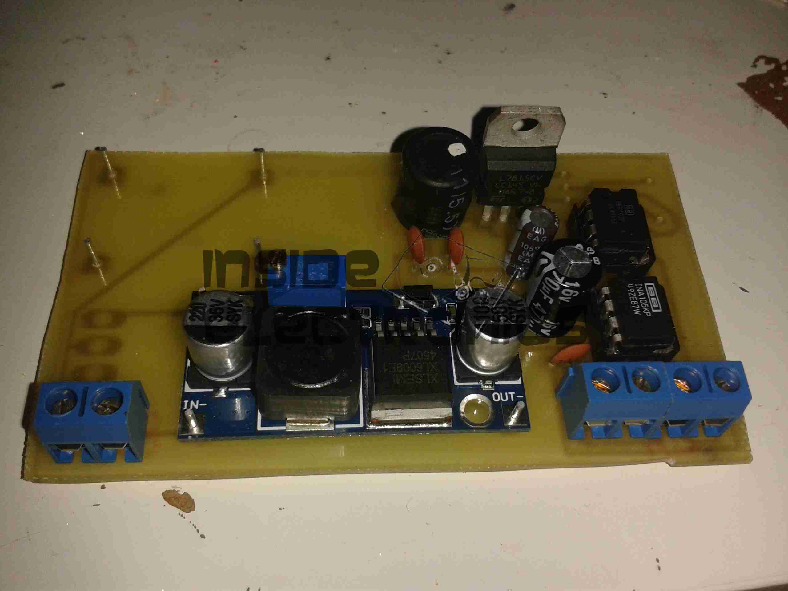
Components Populated
Main components populated. The DC-DC converter is set at 24v output, which the linear regulator then drops down to the +15v rail for the reference IC. The linear section of the regulator, along with the LC filter on the output of the switching regulator produce a low-ripple supply.
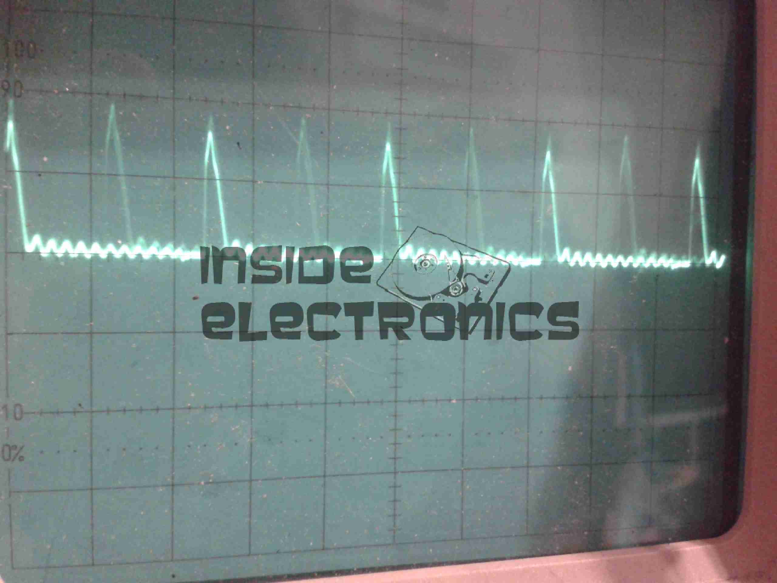
SMPS Ripple
Here’s the scope reading the AC ripple on the output of the DC-DC converter. Scale is 100mV/Div. Roughly 150mV of ripple is riding on top of the DC rail.
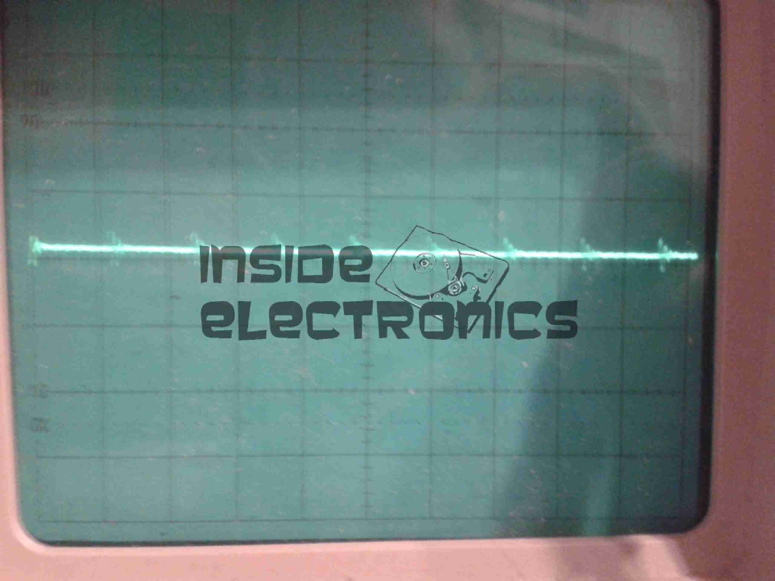
Linear PSU Ripple
And here’s the output from the linear regulator, scale of 50mV/Div. Ripple has been reduced to ~15mV for the reference IC.
In total the circuit as built has a power consumption of ~0.5W, most of which is being dissipated as heat in the linear part of the PSU.
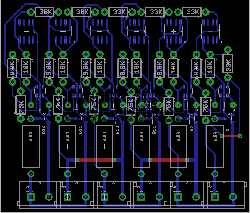
Here’s another active balancing circuit for large ultracapacitor banks, this one is designed for a series string of 6, at 2.5v per capacitor.
Based on the design here, I have transcribed the circuit into Eagle & designed a PCB layout.
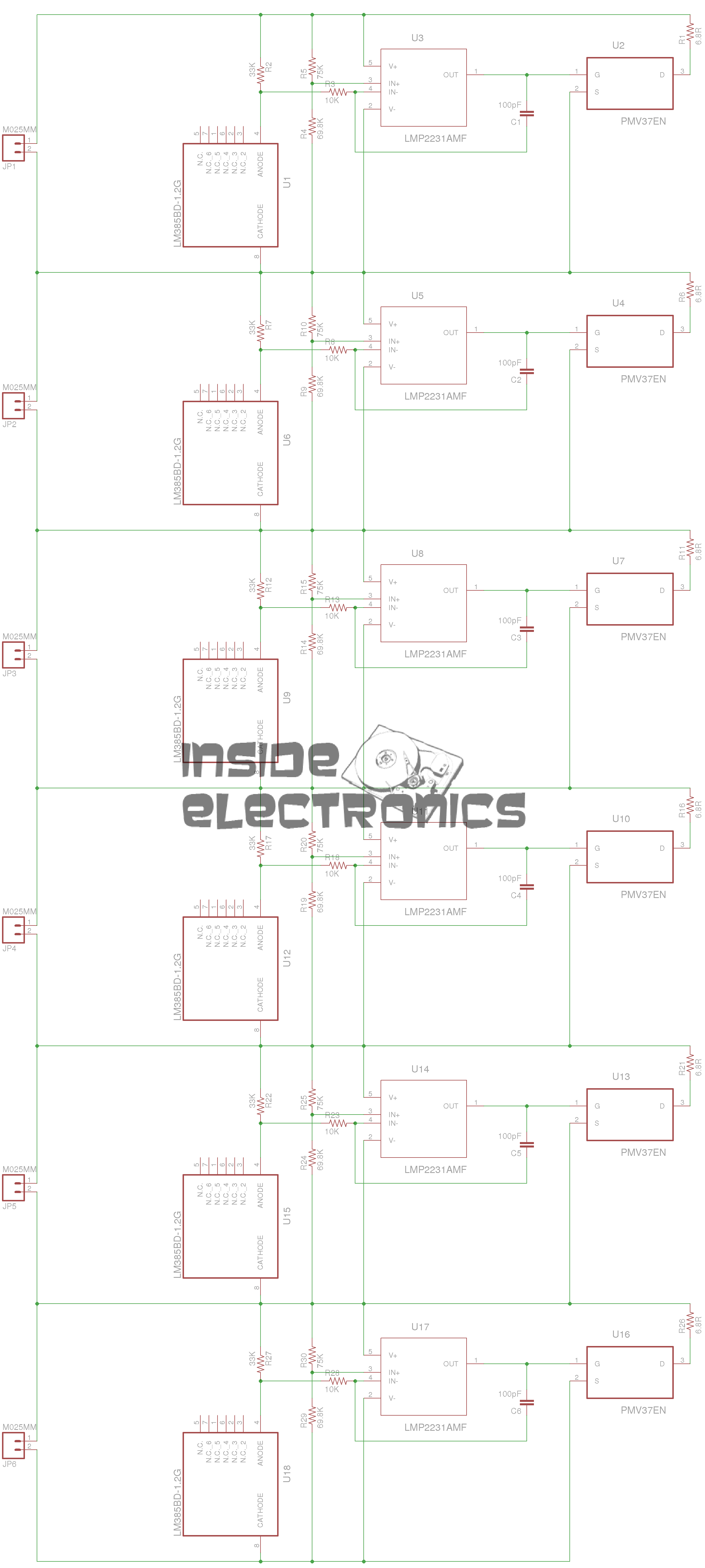
Ultracap Balancer Circuit – Click to Embiggen
As can be seen from the circuit diagram above, this is just 6 copies of the circuit from the above link, with screw terminals to attach to the capacitor string.
Ultracap Balancer PCB
And here’s the PCB. the MOSFETs & OpAmps are very small SMT parts, so require a steady hand in soldering. This board can easily be etched by hand as there’s only 3 links on the top side. No need for a double sided PCB.
As always, the Eagle project files & my Eagle library collection are available below:
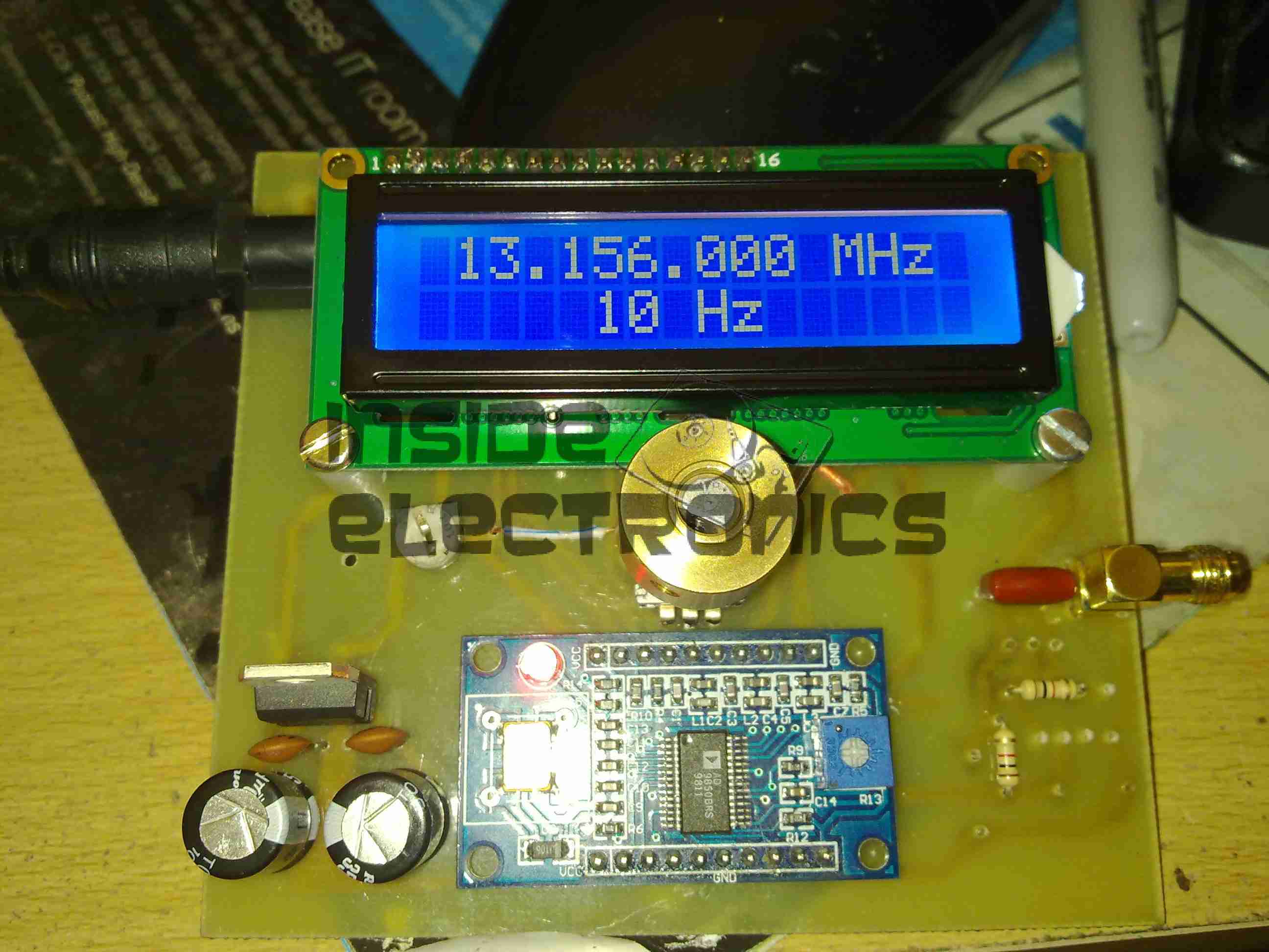
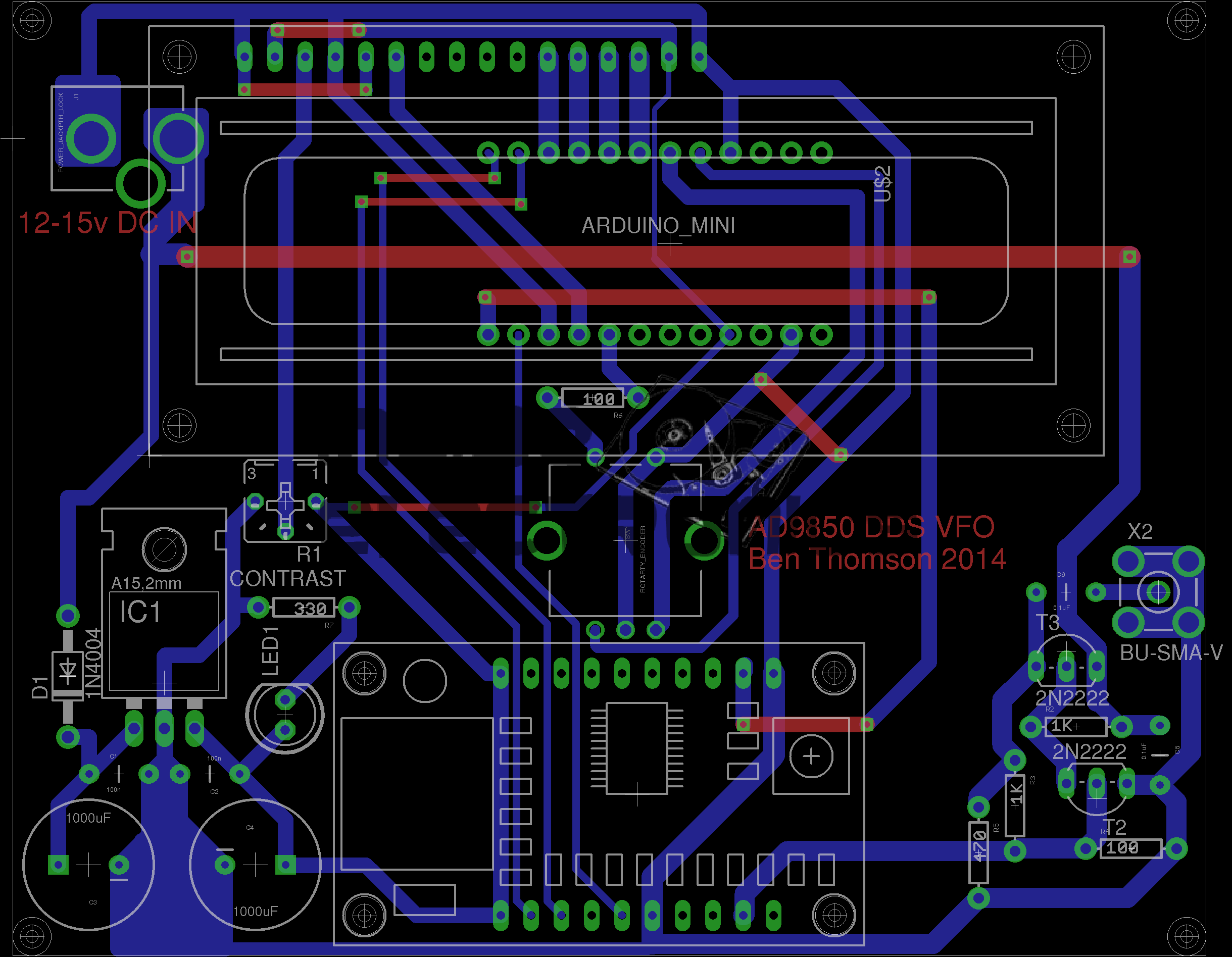
Continuing from my previous post where I published an Eagle design layout for AD7C‘s Arduino powered VFO, here is a completed board.
I have made some alterations to the design since posting, which are reflected in the artwork download in that post, mainly due to Eagle having a slight psychotic episode making me ground one of the display control signals!
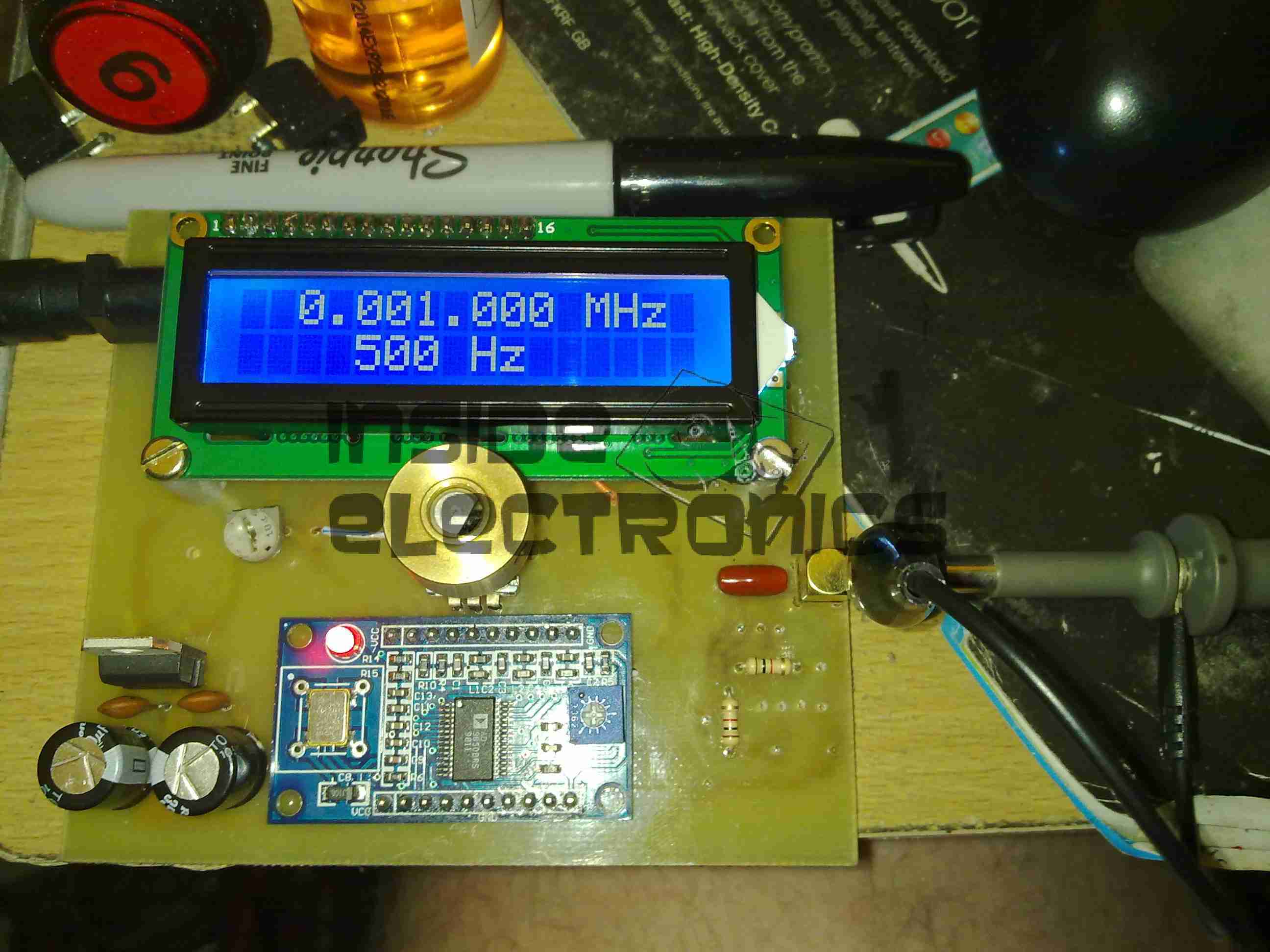
AD9850 VFO
The amplifier section is unpopulated & bypassed as I was getting some bad distortion effects from that section, some more work is needed there.
The Arduino Pro Mini is situated under the display, and the 5v rail is provided by the LM7805 on the lower left corner.
Current draw at 12v input is 150mA, for a power of 1.8W total. About 1W of this is dissipated in the LM7805 regulator, so I have also done a layout with an LM2574 Switching Regulator.
The SMPS version should draw a lot let power, as less is being dissipated in the power supply, but this version is more complex.
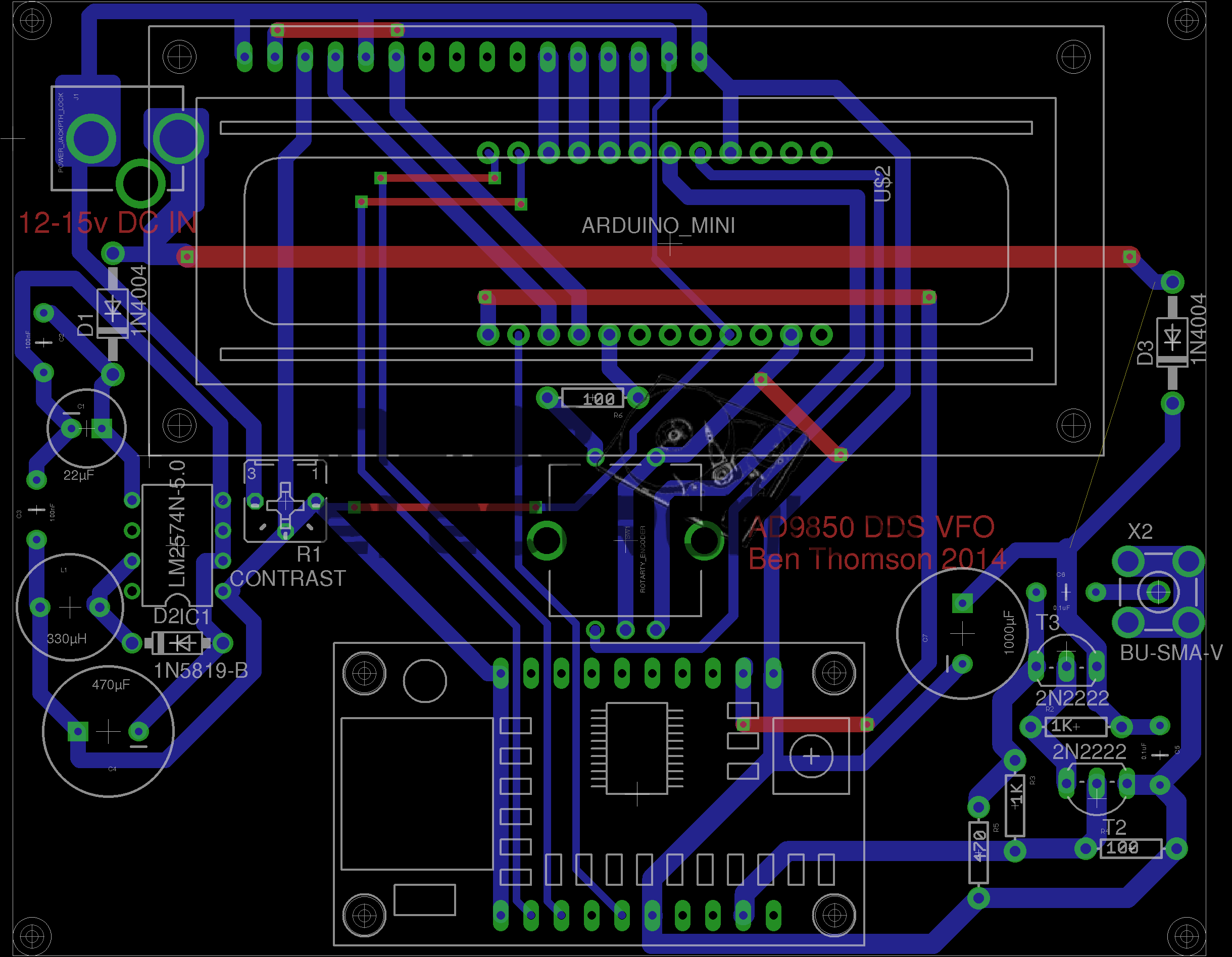
DDS VFO-SMPS
Here the SMPS circuit can be seen on the left hand side of the board, completely replacing the linear regulator.
I have not yet built this design, so I don’t know what kind of effect this will have on the output signal, versus the linear regulator. I have a feeling that the switching frequency of the LM2574 (52kHz) might produce some interference on the output of the DDS module. However I have designed this section to the standards in the datasheet, so this should be minimal.
Nevertheless this version is included in the Downloads section at the bottom of this post.
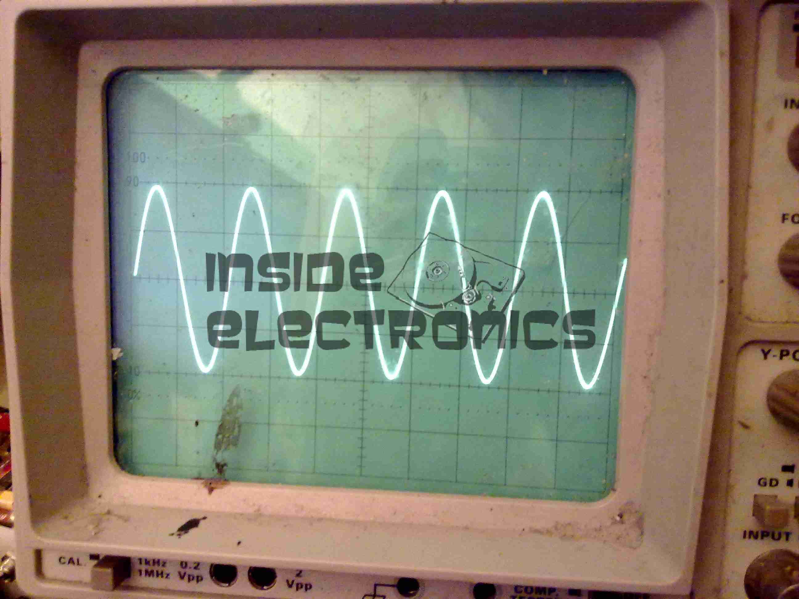
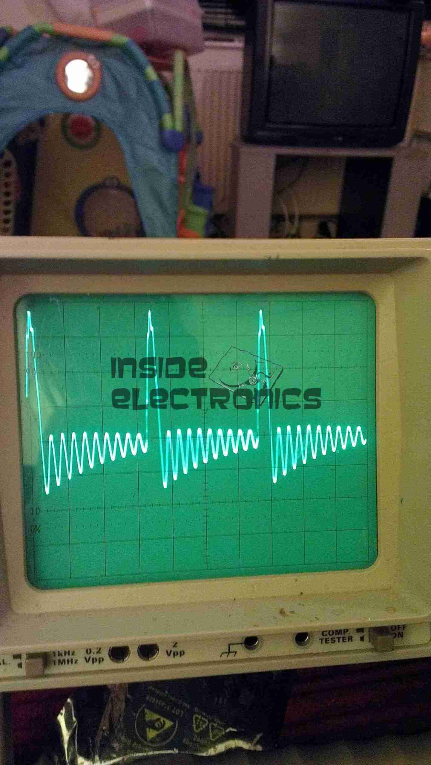
The output coupled through a 100nF capacitor is very clean, as can be seen below, outputting a 1kHz signal. Oscilloscope scale is 0.5ms/div & 1V/div.
VFO Output (Mucky ‘Scope)Scope Connected
Thanks again to Rich over at AD7C for the very useful tool design!
Linked below is the Eagle design files for this project, along with my libraries used to create it.
I recently came across a design for an Arduino controlled AD9850 DDS module, created by AD7C, so I figured I would release my Eagle CAD design for the PCB here.
It is a mainly single-sided layout, only a few links on the top side are needed so this is easy to etch with the toner transfer method.
My version uses an Arduino Pro Mini, as the modular format is much easier to work with than a bare ATMega 328.
RF output is via a SMA connector & has a built in amplifier to compensate for the low level generated by the DDS Module.
DDS VFO
Version 2 Update: Added reverse polarity protection, added power indicator LED, beefed up tracks around the DC Jack.
[download id=”5571″]
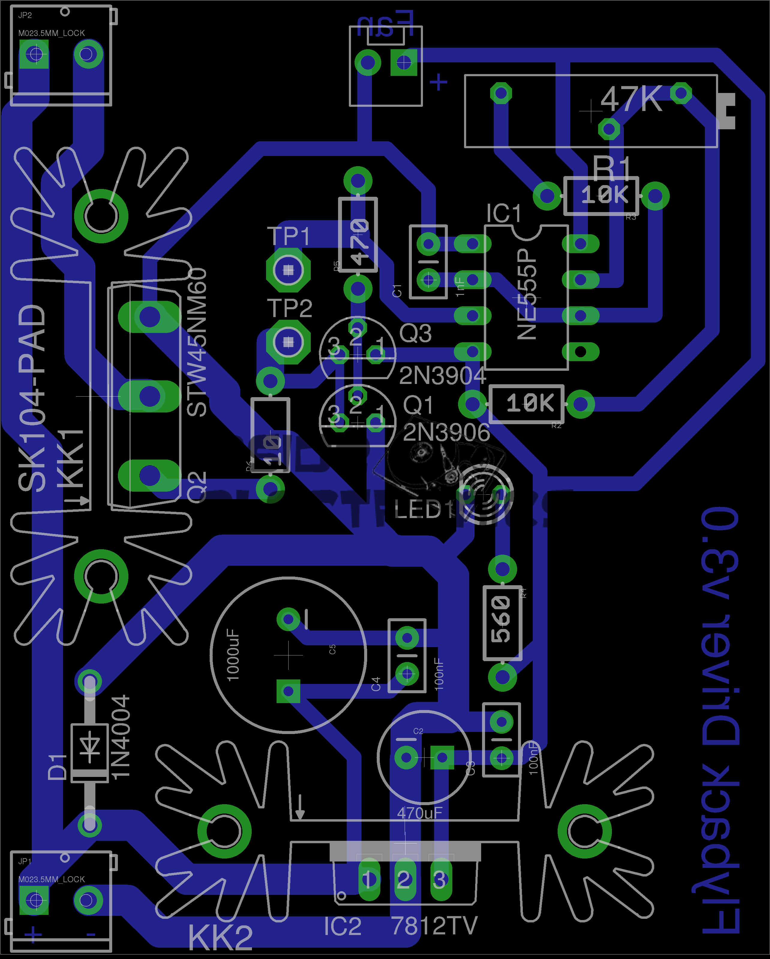
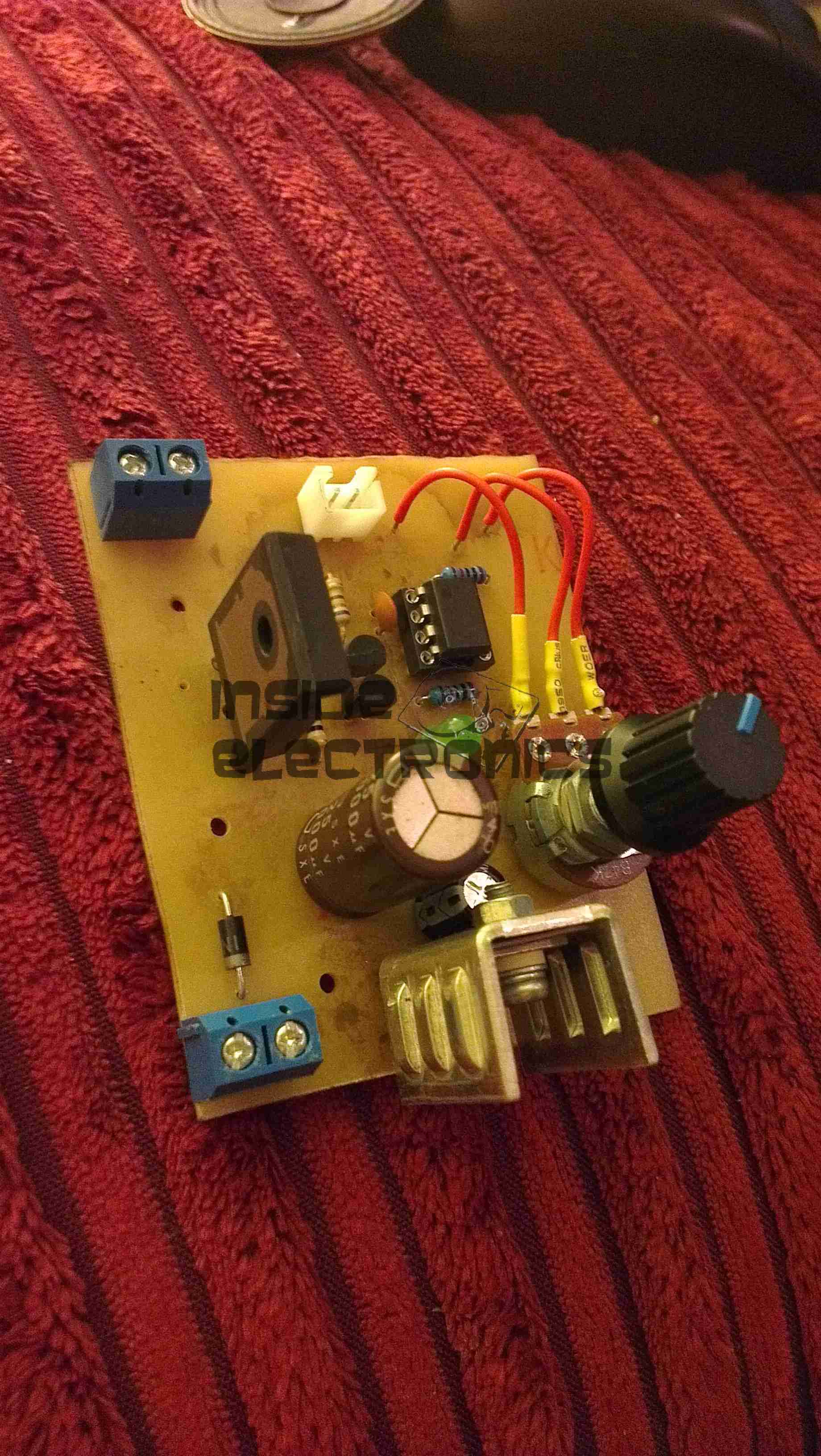
Here is a simple 555 timer based flyback transformer driver, with the PCB designed by myself for some HV experiments. Above is the Eagle CAD board layout.
The 555 timer is in astable mode, generating a frequency from about 22kHz to 55kHz, depending on the position of the potentiometer. The variable frequency is to allow the circuit to be tuned to the resonant frequency of the flyback transformer in use.
This is switched through a pair of buffer transistors into a large STW45NM60 MOSFET, rated at 650v 45A.
Input power is 15-30v DC, as the oscillator circuit is fed from an independent LM7812 linear supply.
Provision is also made on the PCB for attaching a 12v fan to cool the MOSFET & linear regulator.
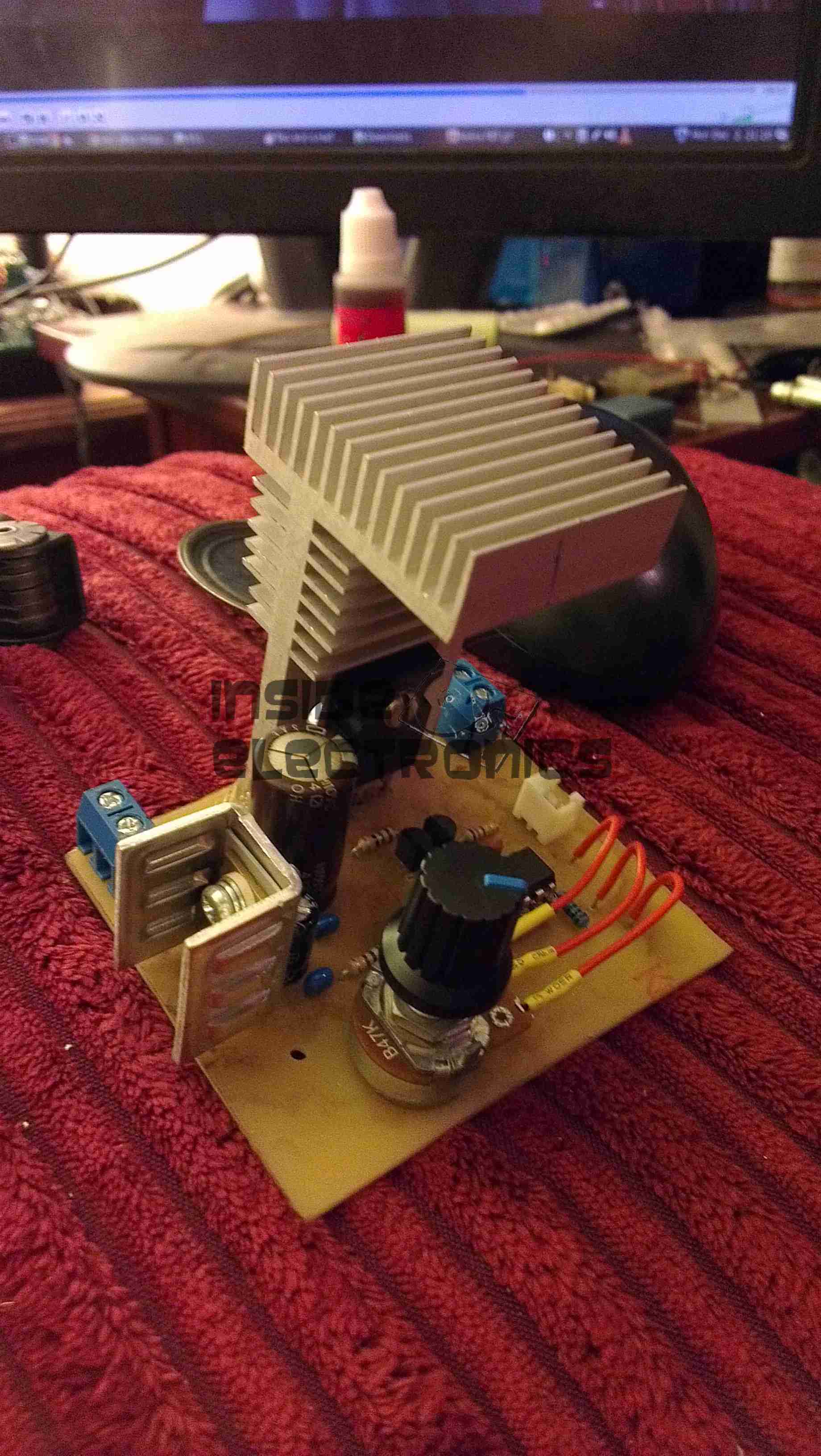
Initial Board
Board initially built, with the heatsink on the linear regulator fitted. I used a panel mount potentiometer in this case as I had no multiturn 47K pots in stock.
PCB Traces
Bottom of the PCB. The main current carrying traces have been bulked up with copper wire to help carry the potentially high currents on the MOSFET while driving a large transformer.
This board was etched using the no-peel toner transfer method, using parchement paper as the transfer medium.
MOSFET Heatsinked
Main MOSFET now fitted with a surplus heatsink from an old switchmode power supply. A Fan could be fitted to the top of this sink to cope with higher power levels.
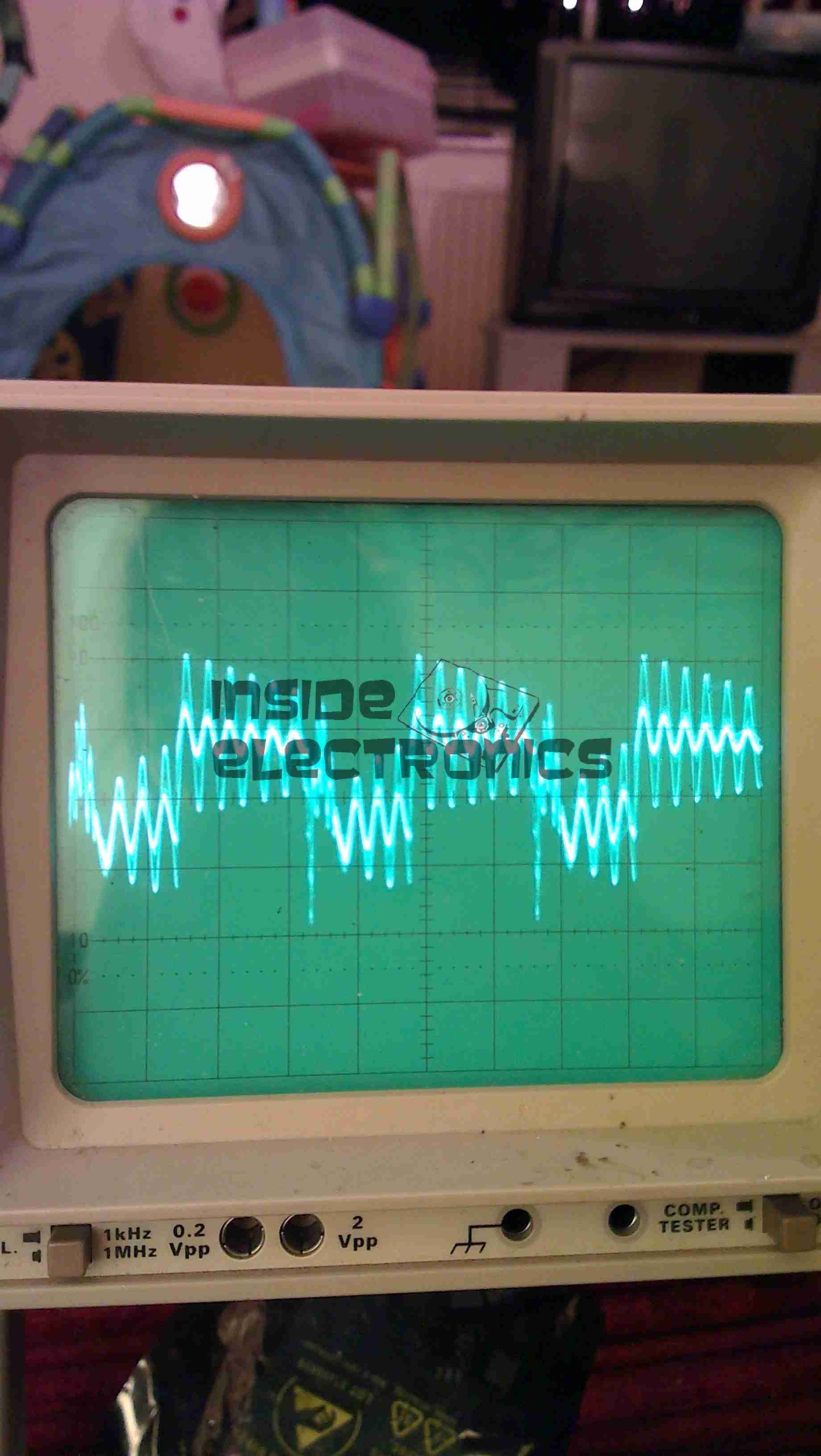
Gate Drive Waveform
This is the gate drive waveform while a transformer is connected, the primary is causing some ringing on the oscillator. The waveform without an attached load is a much cleaner square wave.
Flyback Secondary Waveform
I obtained a waveform of the flyback secondary output by capacitively coupling the oscilloscope probe through the insulation of the HT wire. The pulses of HV can be seen with the decaying ringing of the transformer between cycles.
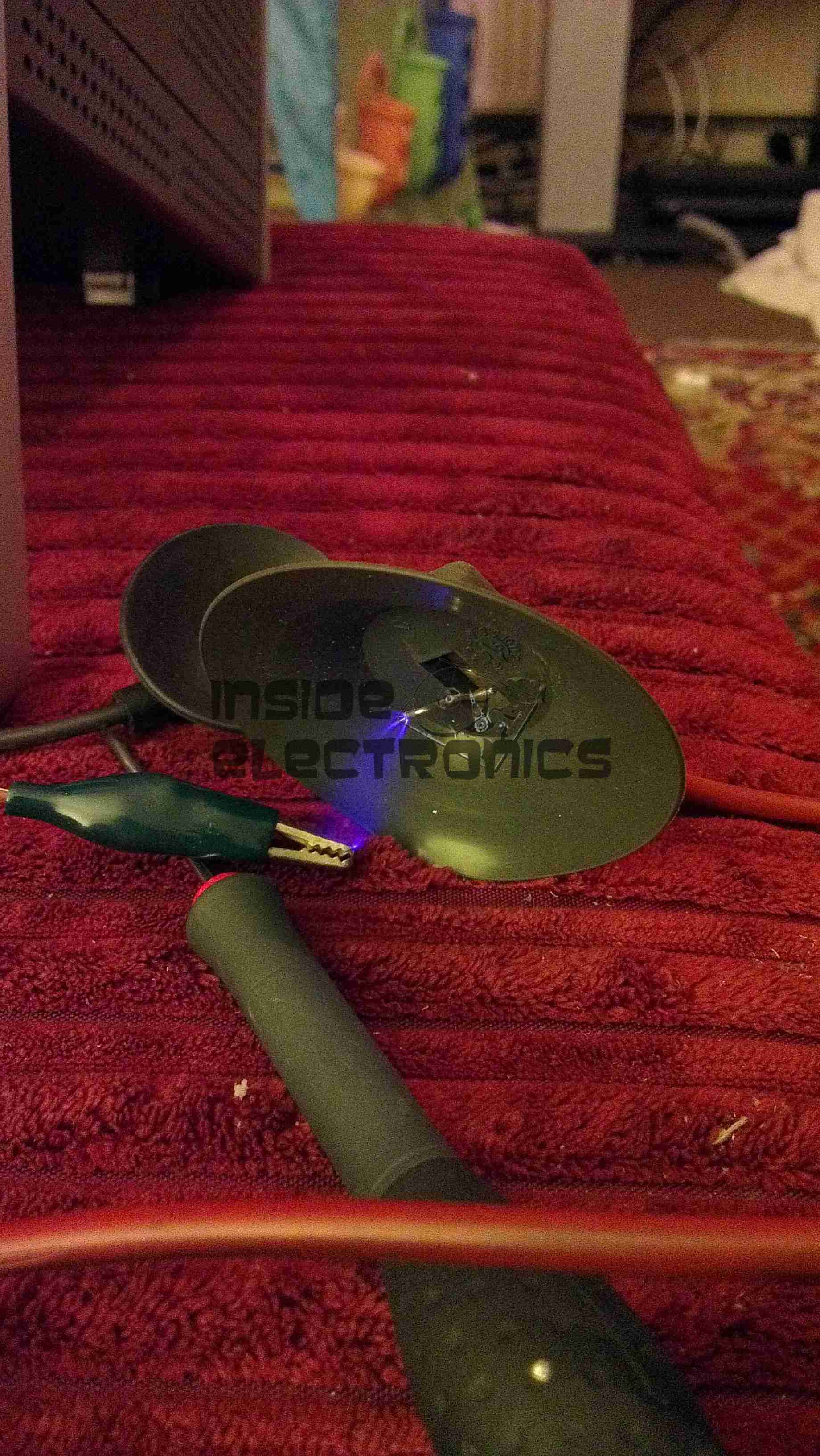
Corona DischargeArc Discharge
Corona & arc discharges at 12v input voltage.
Download the Eagle schematic files here: [download id=”5561″]
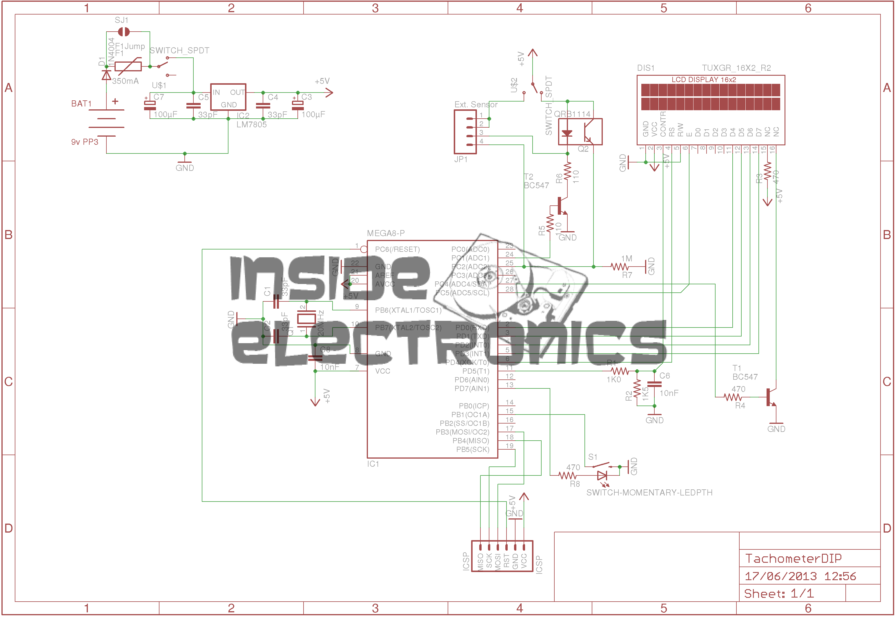
Here is an AVR powered optical tachometer design, that I adapted from the schematic found here.
I made a couple of changes to the circuit & designed a PCB & power supply module to be built in. The original design specified a surface mount IR LED/Photodiode pair, however my adjustment includes a larger IR reflectance sensor built onto the edge of the board, along with a Molex connector & a switch to select an externally mounted sensor instead of the onboard one.
There is also an onboard LM7805 based power supply, designed with a PCB mount PP3 battery box.
The power supply can also be protected by a 350mA polyfuse if desired. If this part isn’t fitted, then a pair of solder bridge pads are provided within the footprint for the fuse to short out the pads.
For more information on the basic design, please see the original post with the link at the top of the page.
Schematic
Here is an archive of the firmware & the Eagle CAD files for the PCB & schematic design.
Tip Jar
If you’ve found my content useful, please consider leaving a donation by clicking the Tip Jar below!
All collected funds go towards new content & the costs of keeping the server online.