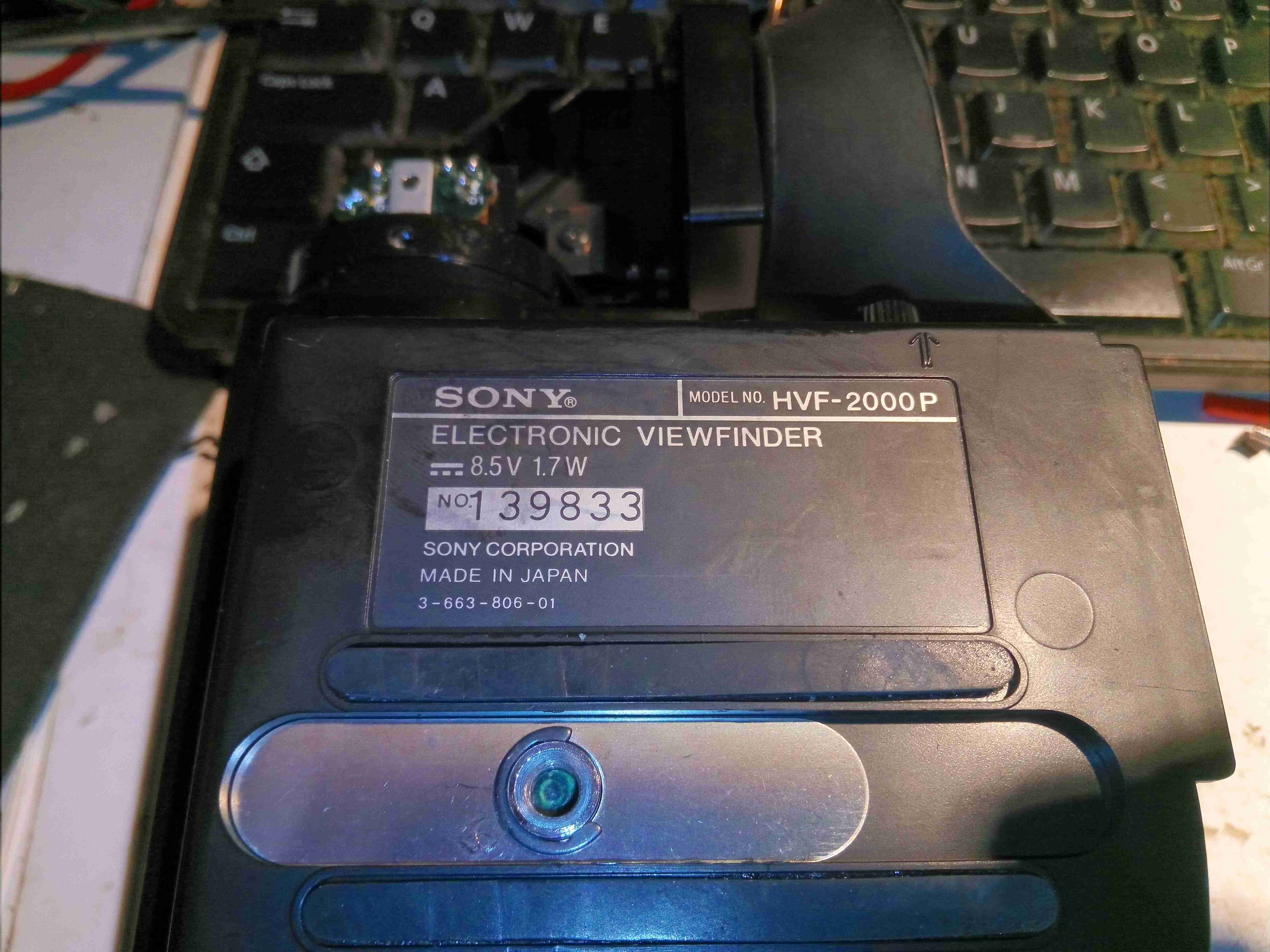
Well, it’s time for another viewfinder hack! I’ve been after one of these for a while, this is from an early 1980’s era Sony Trinicon camera, and instead of the tiny ½” round CRT display, these have a 1.5″ square CRT – a Matsushita 40CB4. Luckily I managed to score a pair of these from eBay for very little money. Update: The second camera’s viewfinder module turned out to have a dead flyback transformer, but at least I have a good spare CRT & the rest of the support components. More to come later on the teardown of the camera itself.
Mirror & Eyecup Assembly
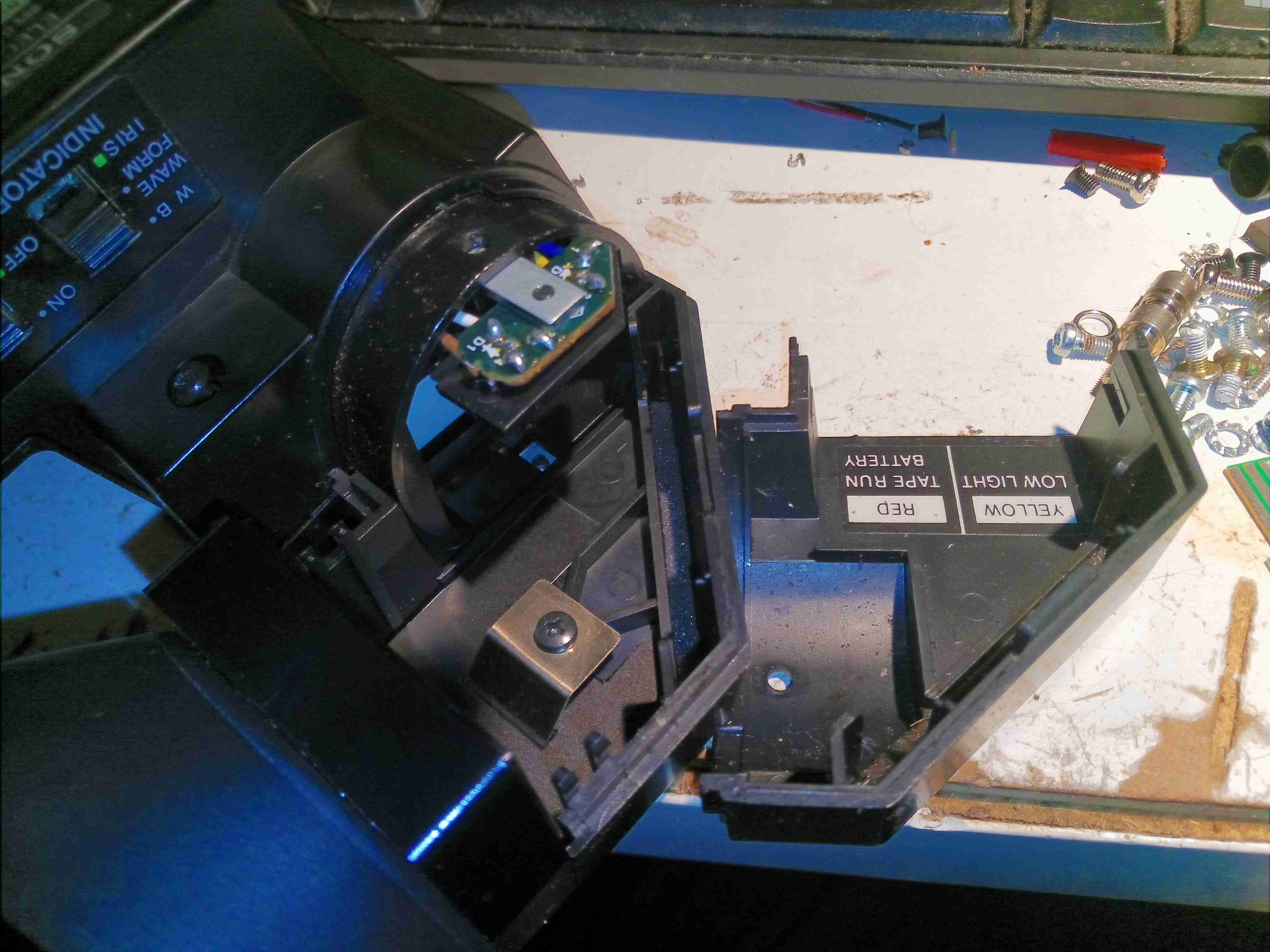
The eyecup assembly with the magnifying lens & turning mirror is easy to remove, with clips & a single screw holding it onto the CRT holder sticking out of the side of the main casing.
Top Cover Removed
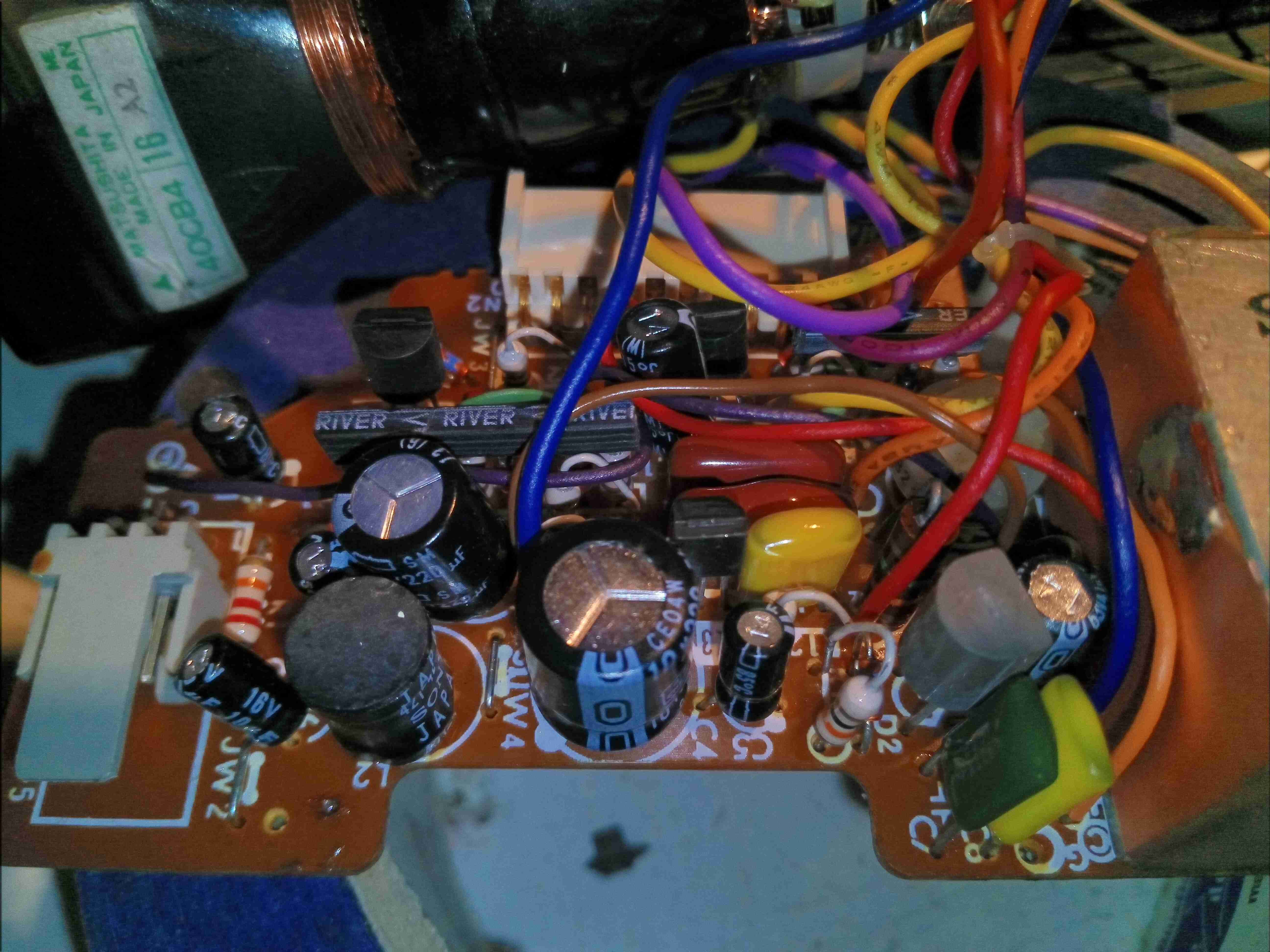
Removing some screws around the case allows the top cover to be removed, revealing the electronics. There’s certainly more in here than the later camera viewfinders, in this unit there are two boards slotted together with a board-to-board interconnect at the bottom. The CRT is at the top of the photo, hiding inside the plastic housing & deflection yoke assembly.
Bare PCBs & CRT
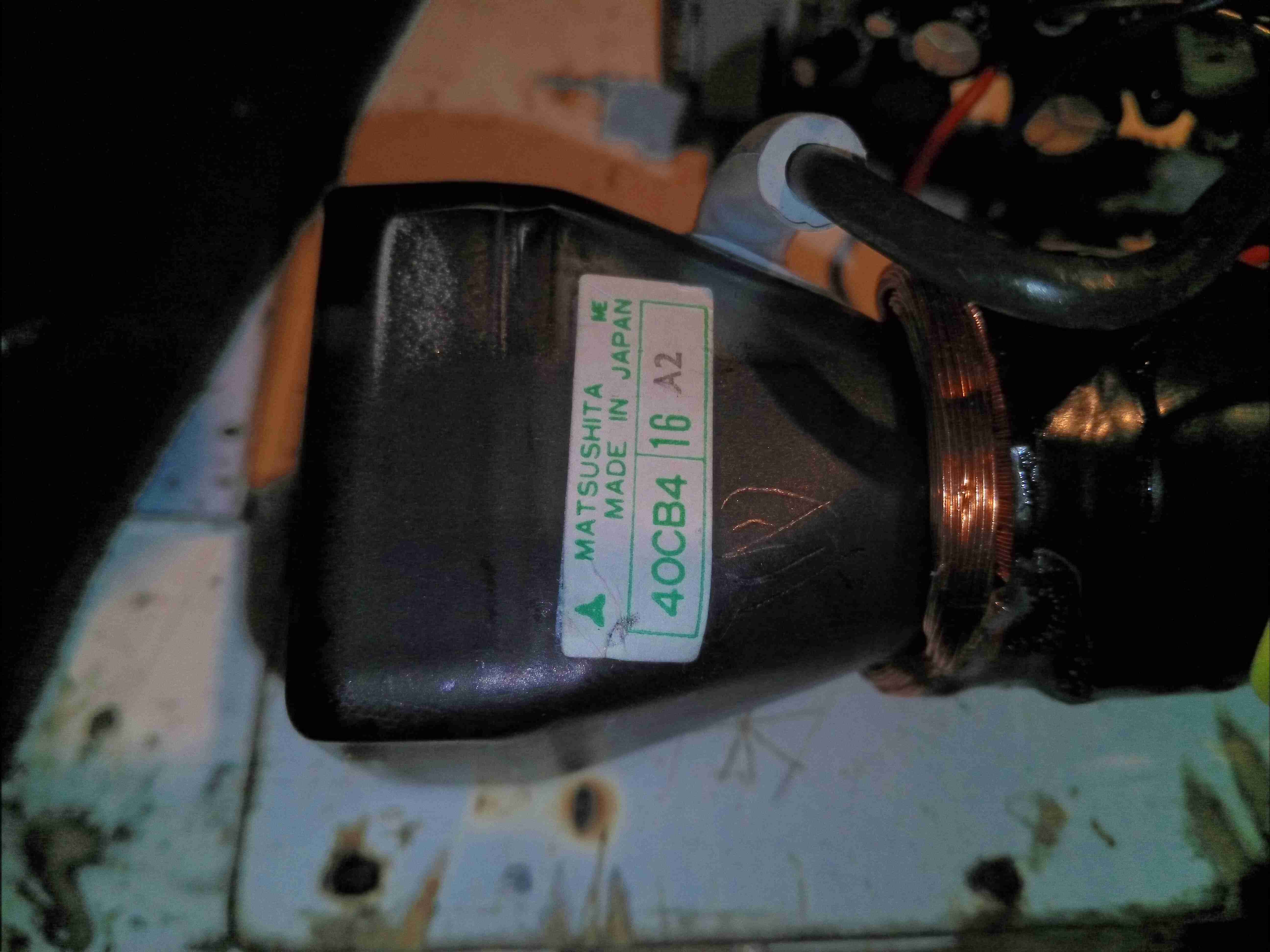
Here’s the CRT & one of the control boards removed from the case, having been stripped of the heatshrink tube that held the final anode lead in place. Just like on larger CRTs, this viewfinder has the final anode on a cavity connector fused into the bell, instead of being led out to a pin on the base. This is probably due to the much higher anode voltage of 5kV, a big jump from the 2kV on the ½” round tubes.
40CB4 CRT Label
Yup, it’s definitely the elusive 40CB4. Apparently these CRTs are still manufactured to this day for professional camera viewfinders, as the resolution of this small vacuum tube is still better than similarly sized modern tech such as LCDs or OLEDs. The phosphor used is type P4 – ZnS:Ag+(Zn,Cd)S:Ag, with an aluminized overcoat.
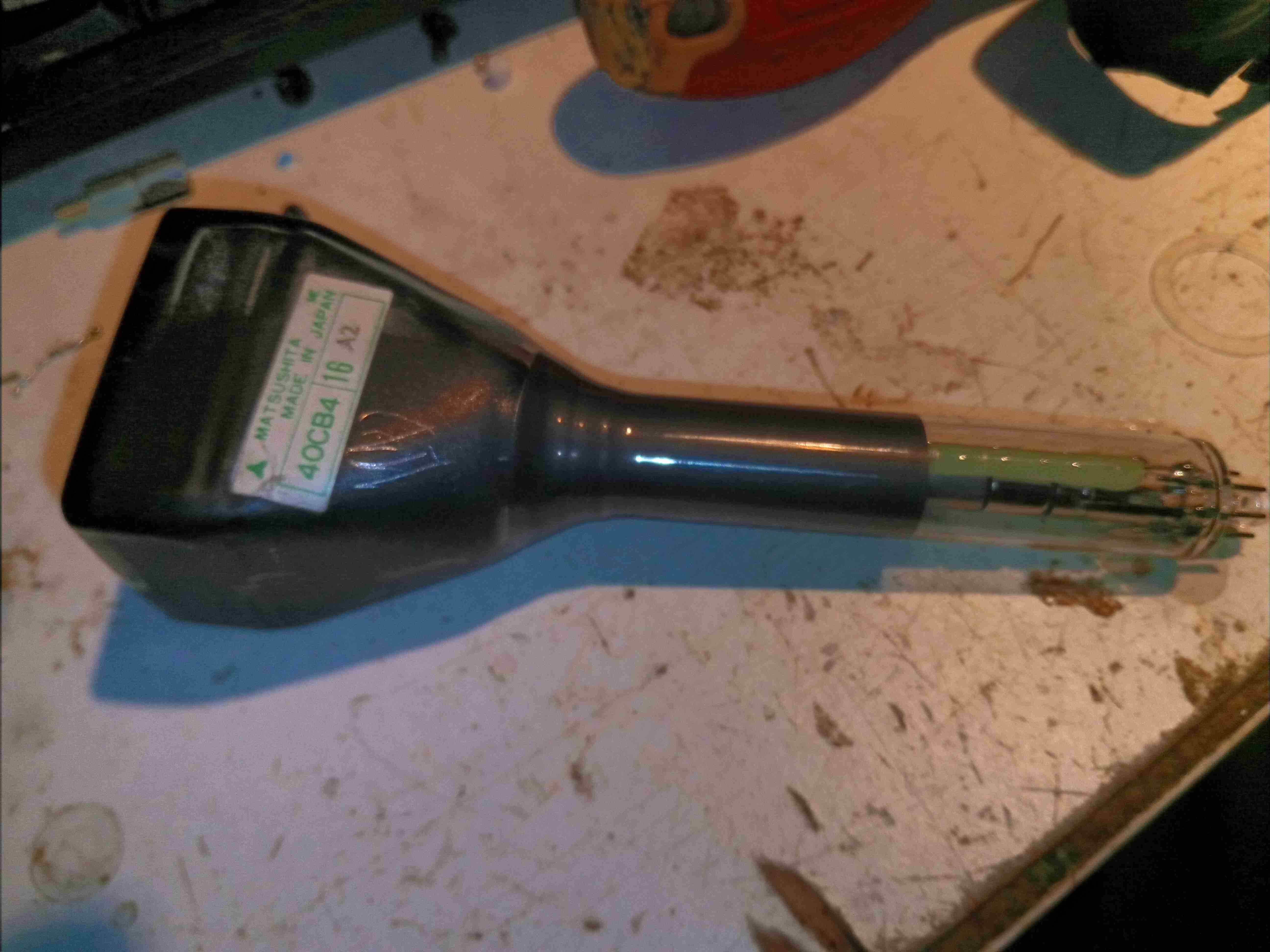
Bare 40CB4 CRT
After the base connector & deflection yoke are removed from the tube, the very long neck can be seen, this long glass neck apparently giving better focus & resolution than the stubbier tubes.
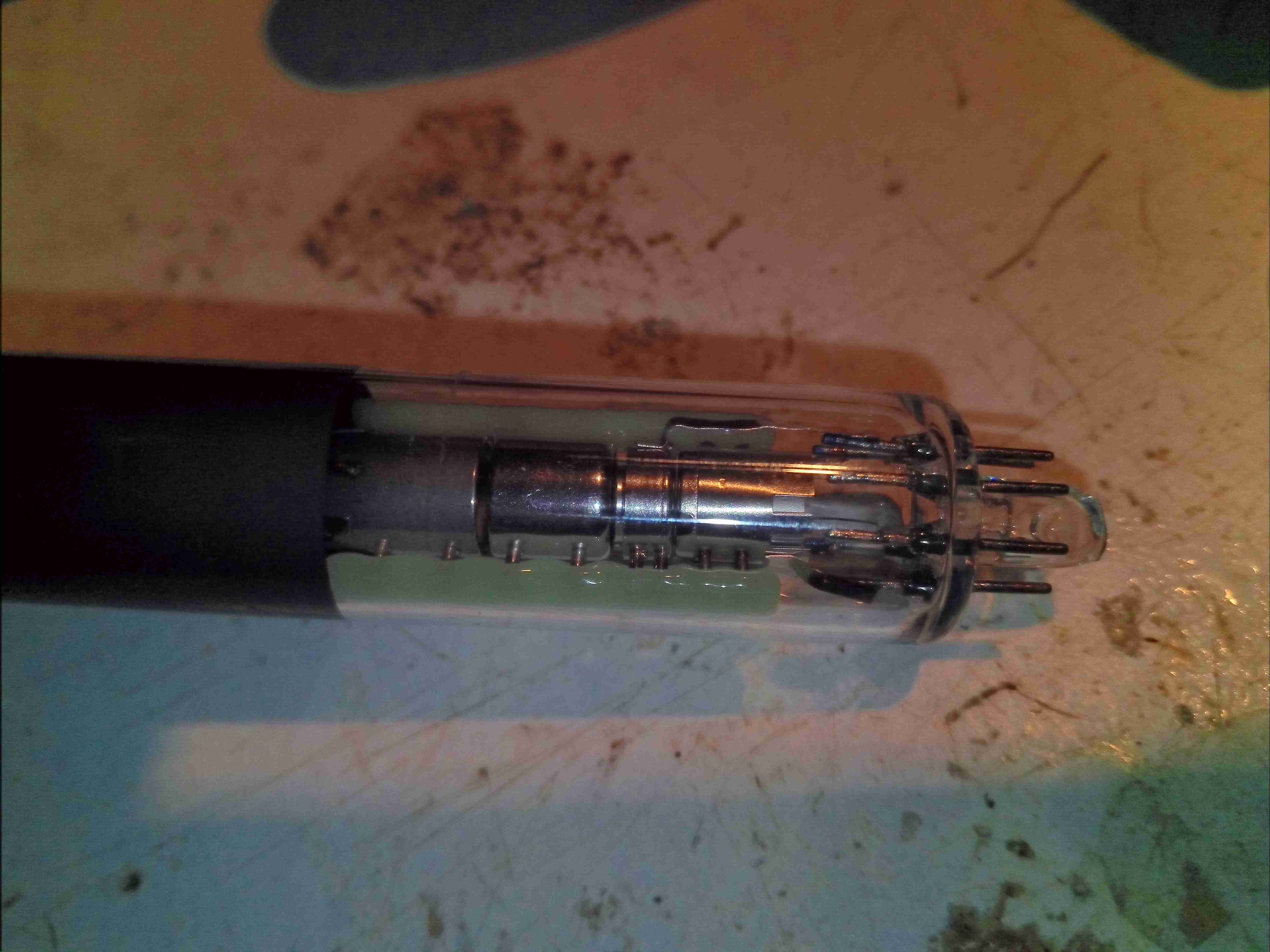
Electron Gun
The electron gun is the usual single unit as usually found in monochrome tubes.
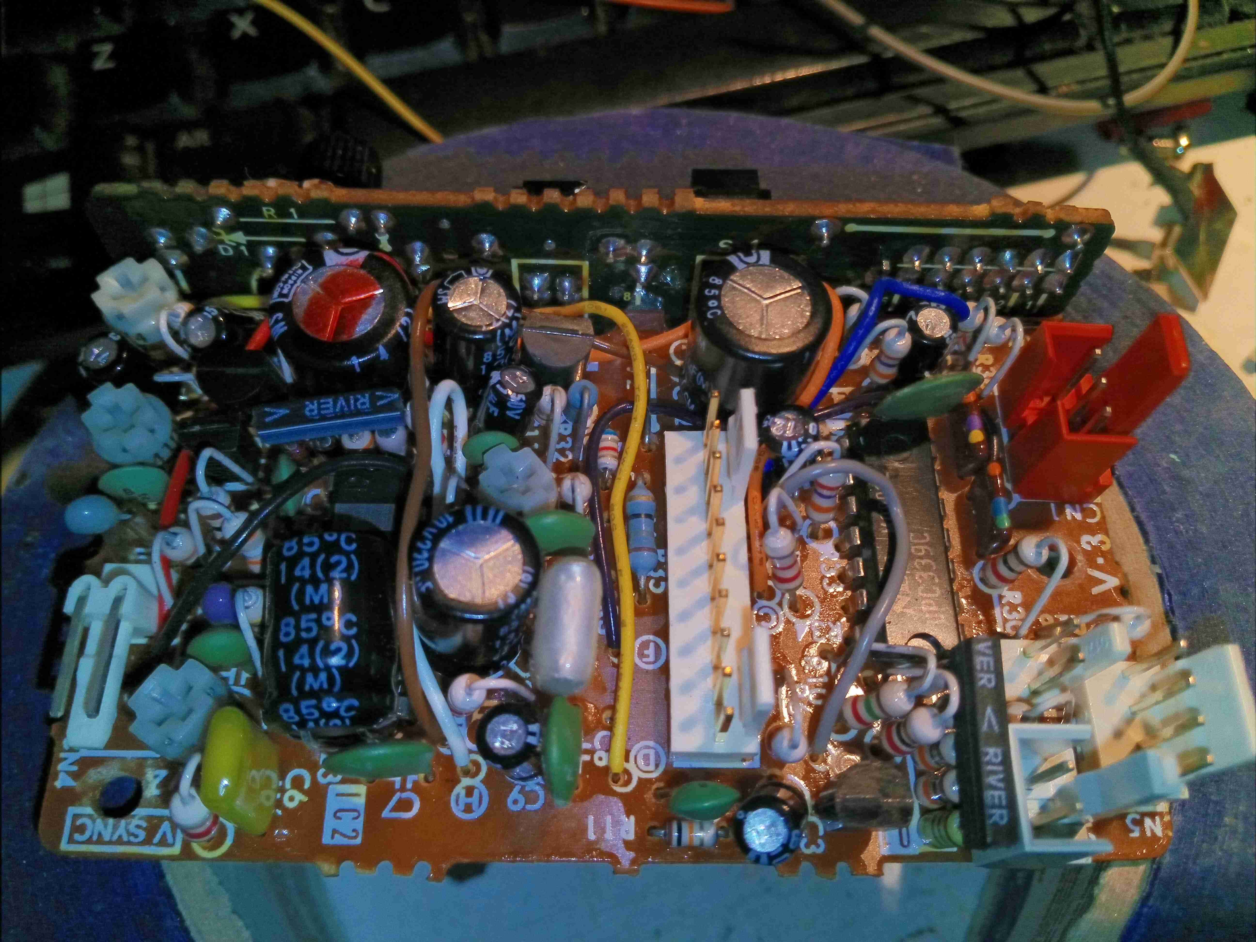
Deflection Board
The bottom board in the assembly has all the control circuitry for the CRT, including the HA11244 deflection IC, composite sync separator & vertical deflection drive circuit. There are also circuits here to display a video waveform on the CRT, along with iris & white balance markers.
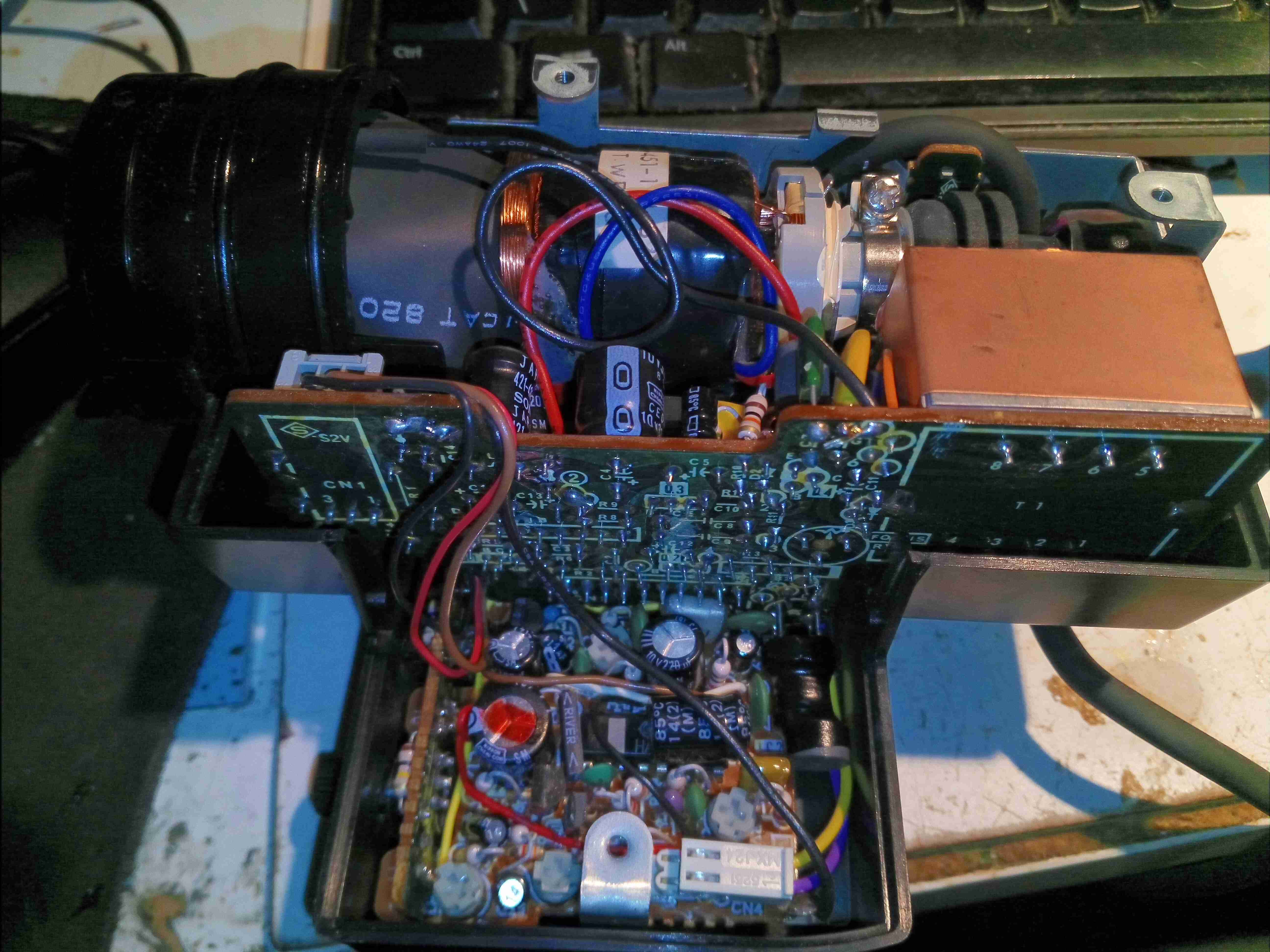
Horizontal Board
The other board has the horizontal drive circuitry, along with the video input amplifier. Despite the attempt to miniaturize the entire assembly, these are still well packed boards. Some of the resistors & diodes are bussed together in custom SIL hybrid modules to save PCB space. Like all the other CRT viewfinders, these units are meant for viewing via a mirror – the horizontal deflection coil connections need to be reversed to show a correct image without the mirror. The Red & Blue wires to the yoke need to be swapped here.
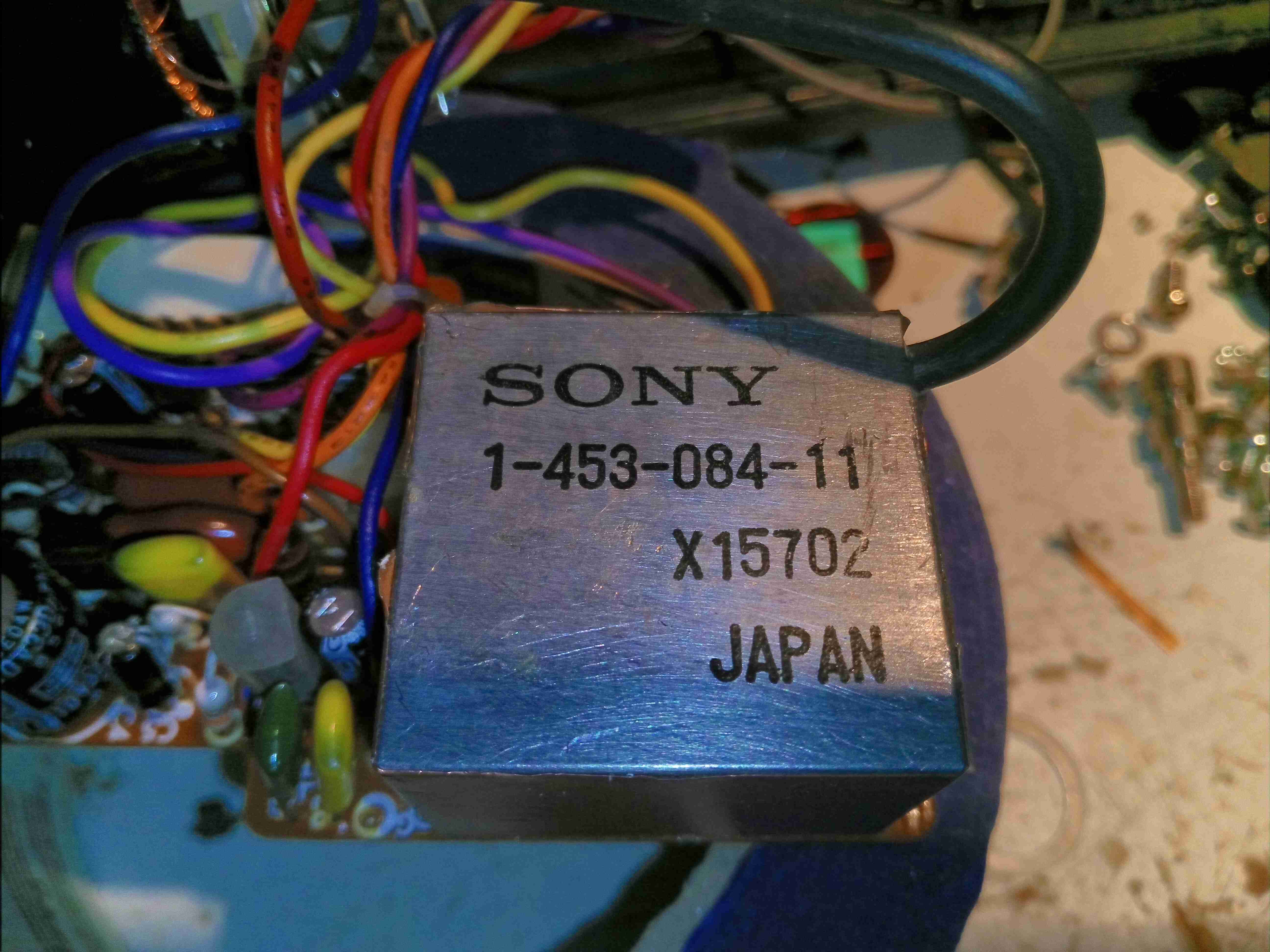
Flyback Transformer
The horizontal board on this unit also supports the flyback transformer, which is massive compared to the other viewfinder circuits. Biasing, focus & filament supplies for the CRT are also derived from this transformer, via auxiliary windings.
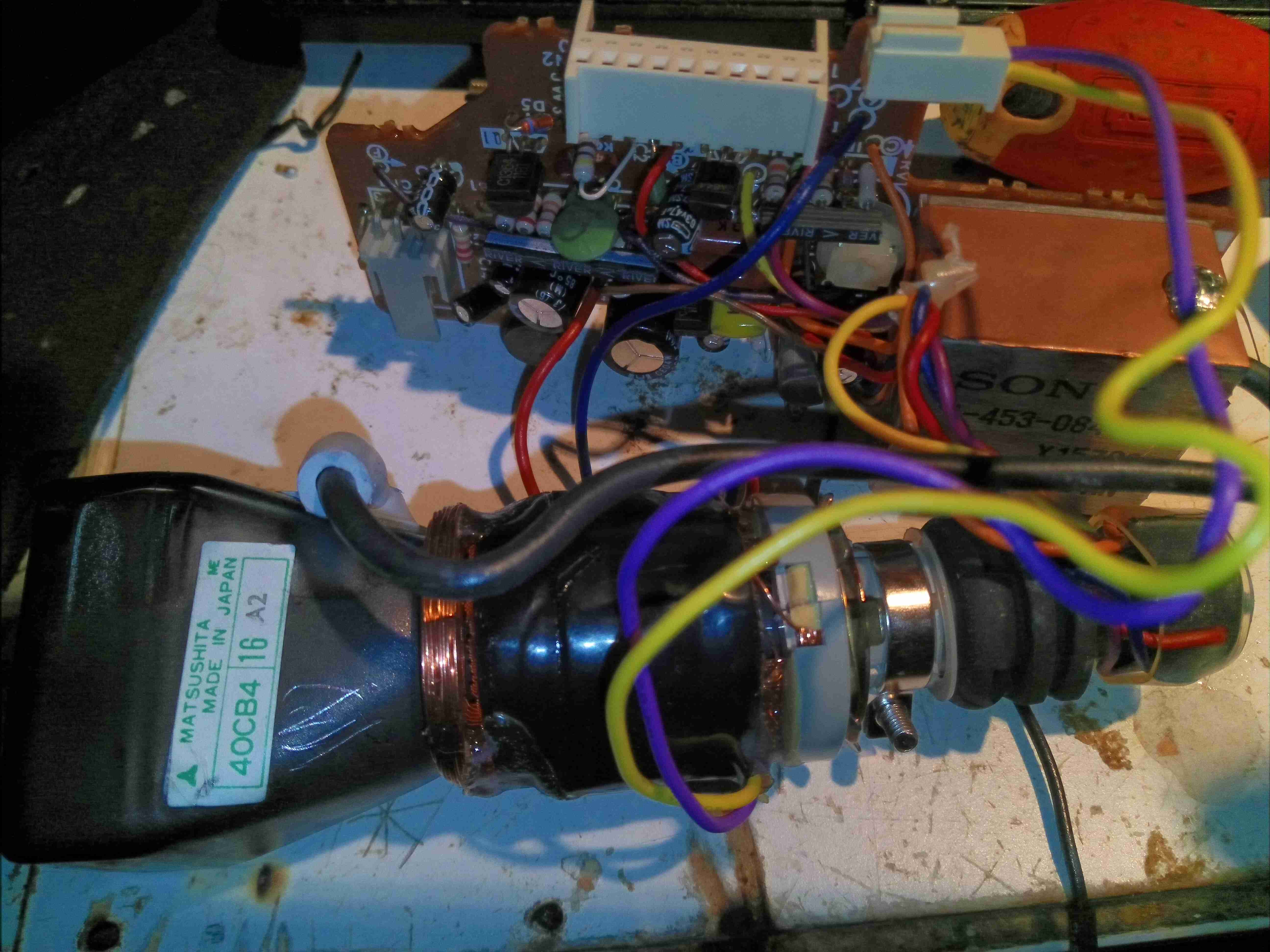
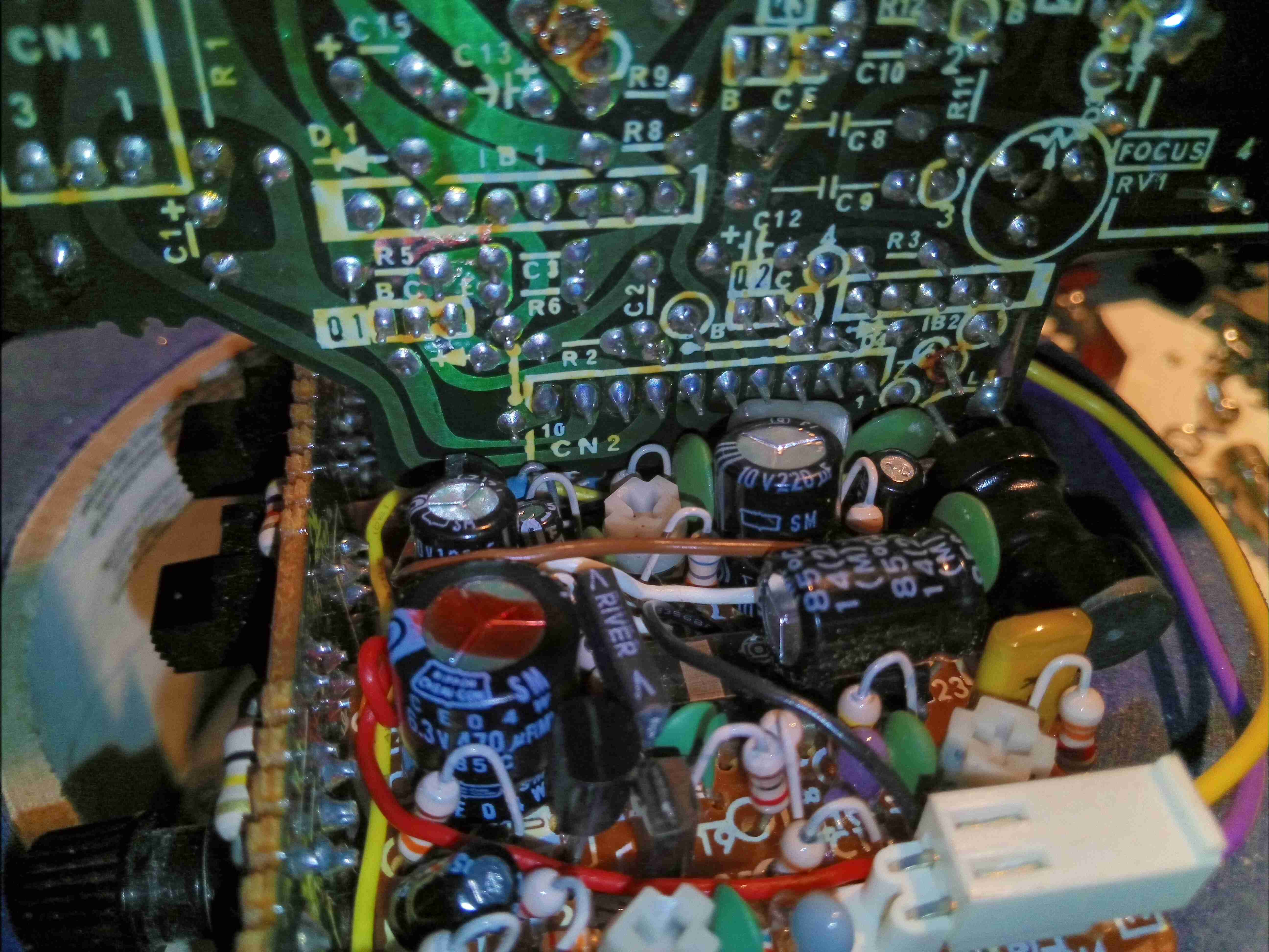
Boards Connected
The boards slot together in the centre to form the fully operational circuit.
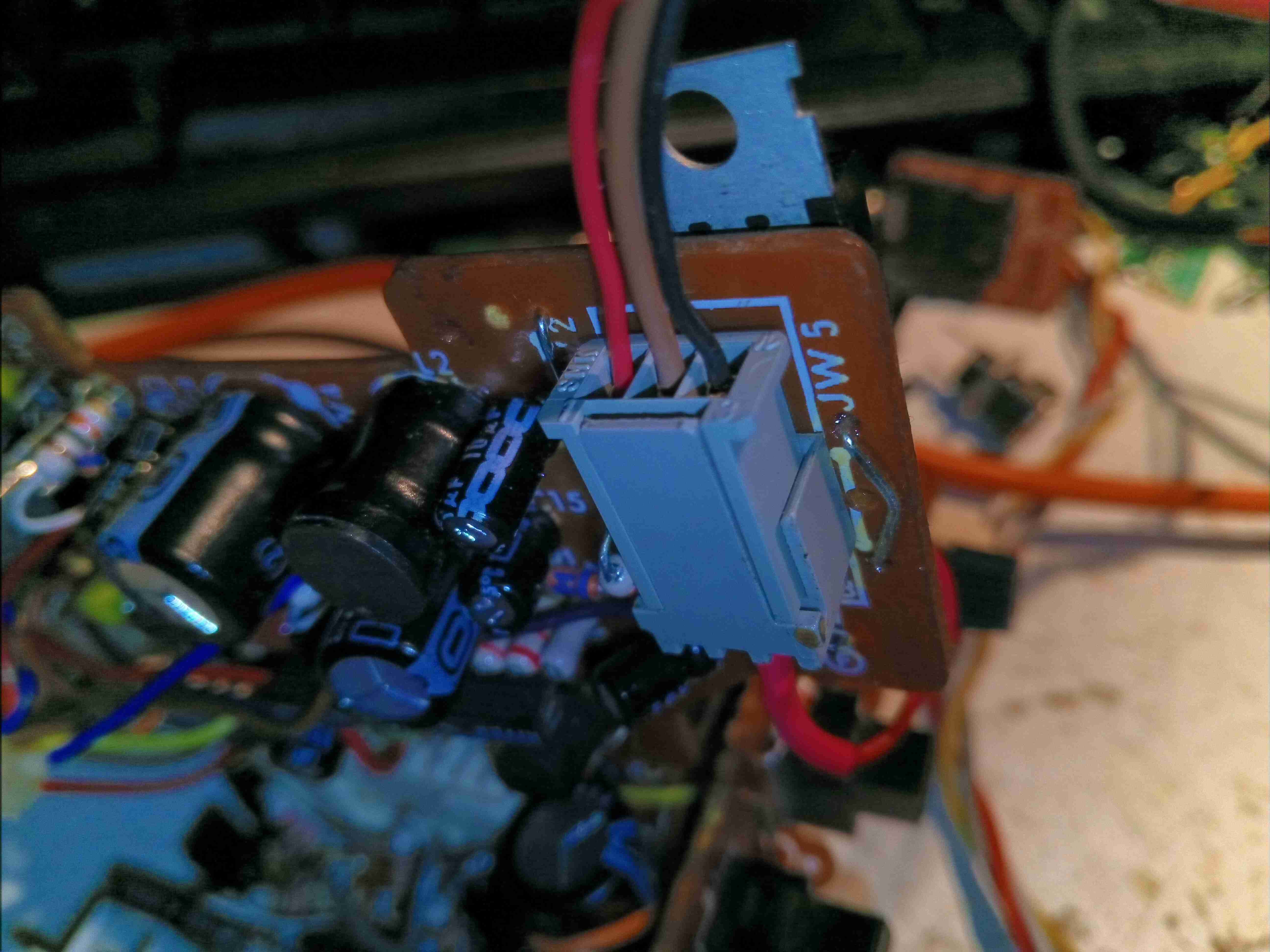
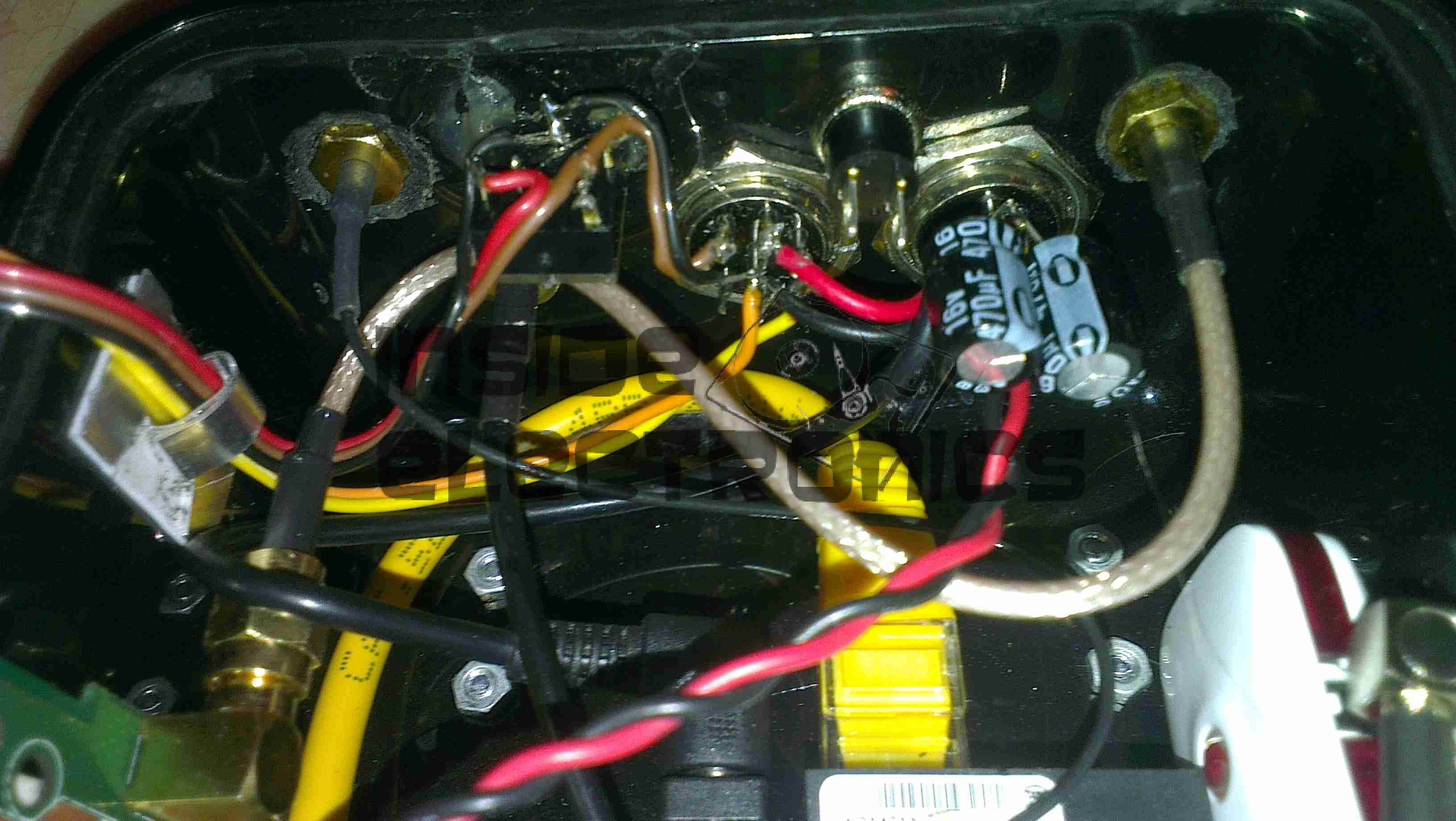
Video Input
Out of the 3 plugs emerging from the cable feeding the viiewfinder, only this one is important, on the horizontal drive board. Black is ground, Brown +8.5v & red is composite video input. There’s also a resistor tied into the positive rail to the video input pin, which pulls it high to 8.5v – this is R1 right next to this connector. Desolder this 22K resistor to help protect anything feeding a signal into the unit, like a RPi, it’s not needed for normal operation.
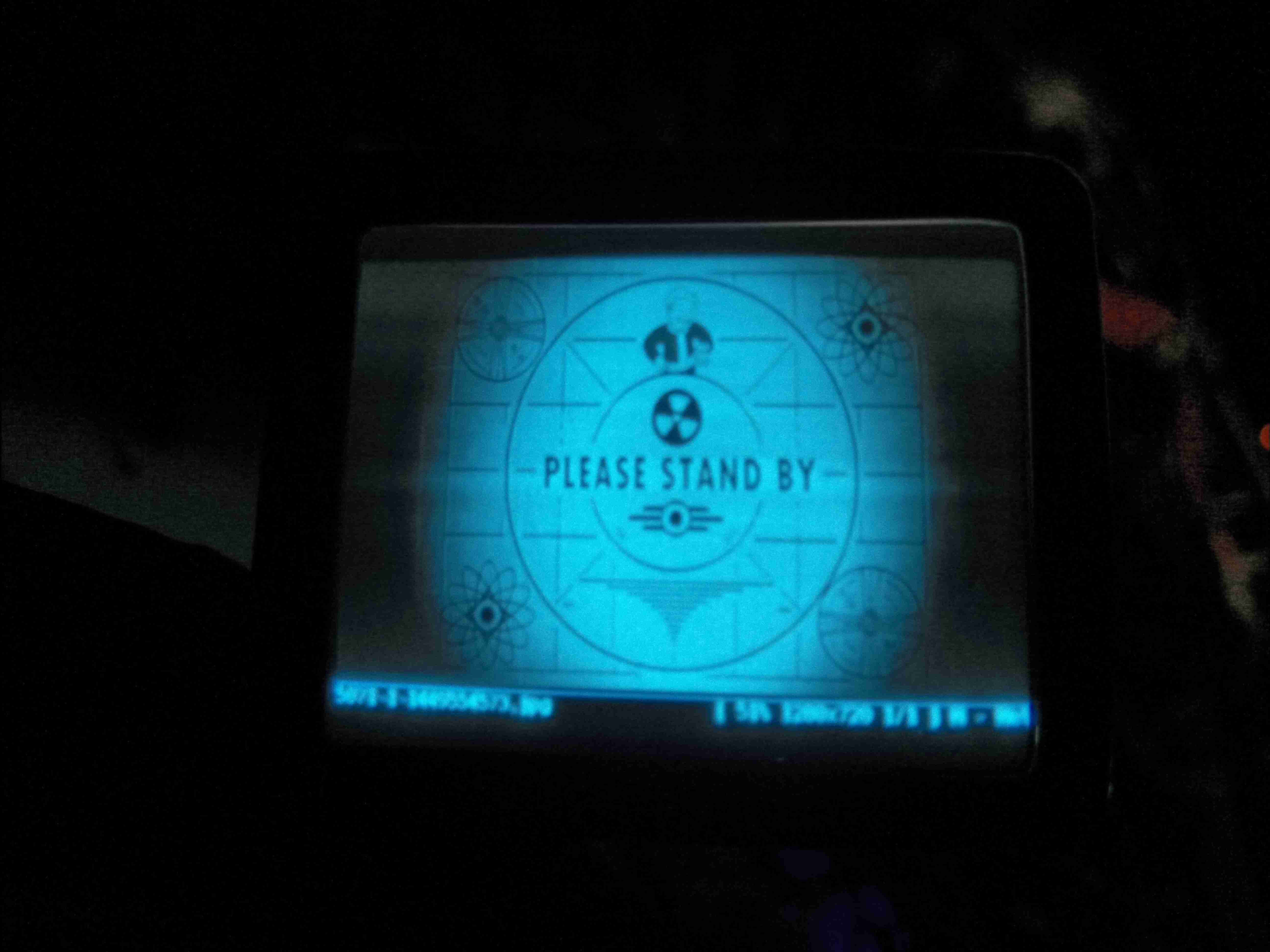
Fallout!
As usual for a CRT post, the Fallout loading screen on the display. The picture quality isn’t as good as it should be, probably due to the noisy buck-converter I have rigged up for testing. If it doesn’t get better with a linear regulator, I’ll start replacing the 39 year old electrolytic capacitors. Current draw is 130mA at 7.5v. Schematics for this unit & the CRT datasheet are available below:
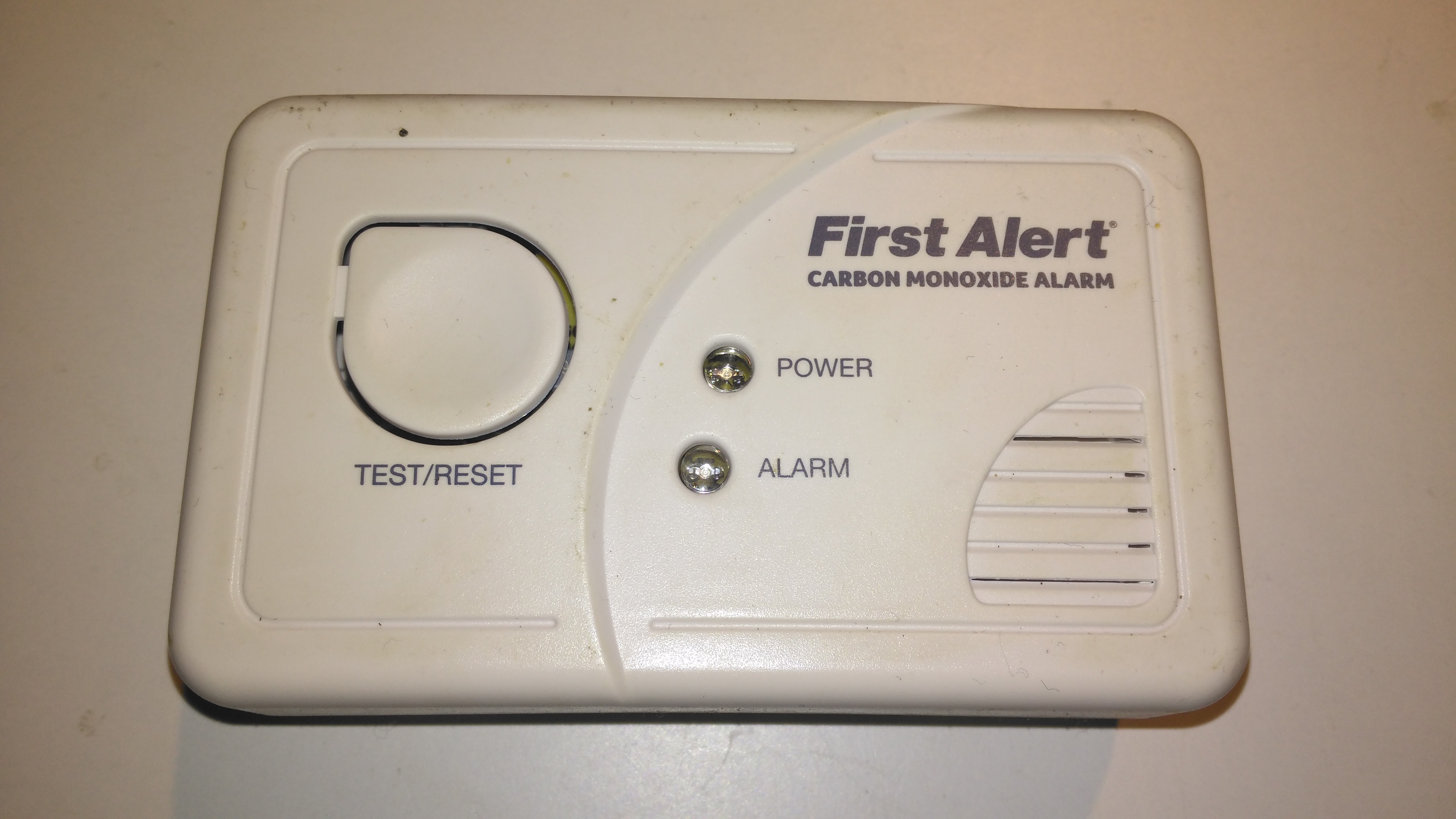
Here’s another domestic CO Alarm, this one a cheaper build than the FireAngel ones usually use, these don’t have a display with the current CO PPM reading, just a couple of LEDs for status & Alarm.
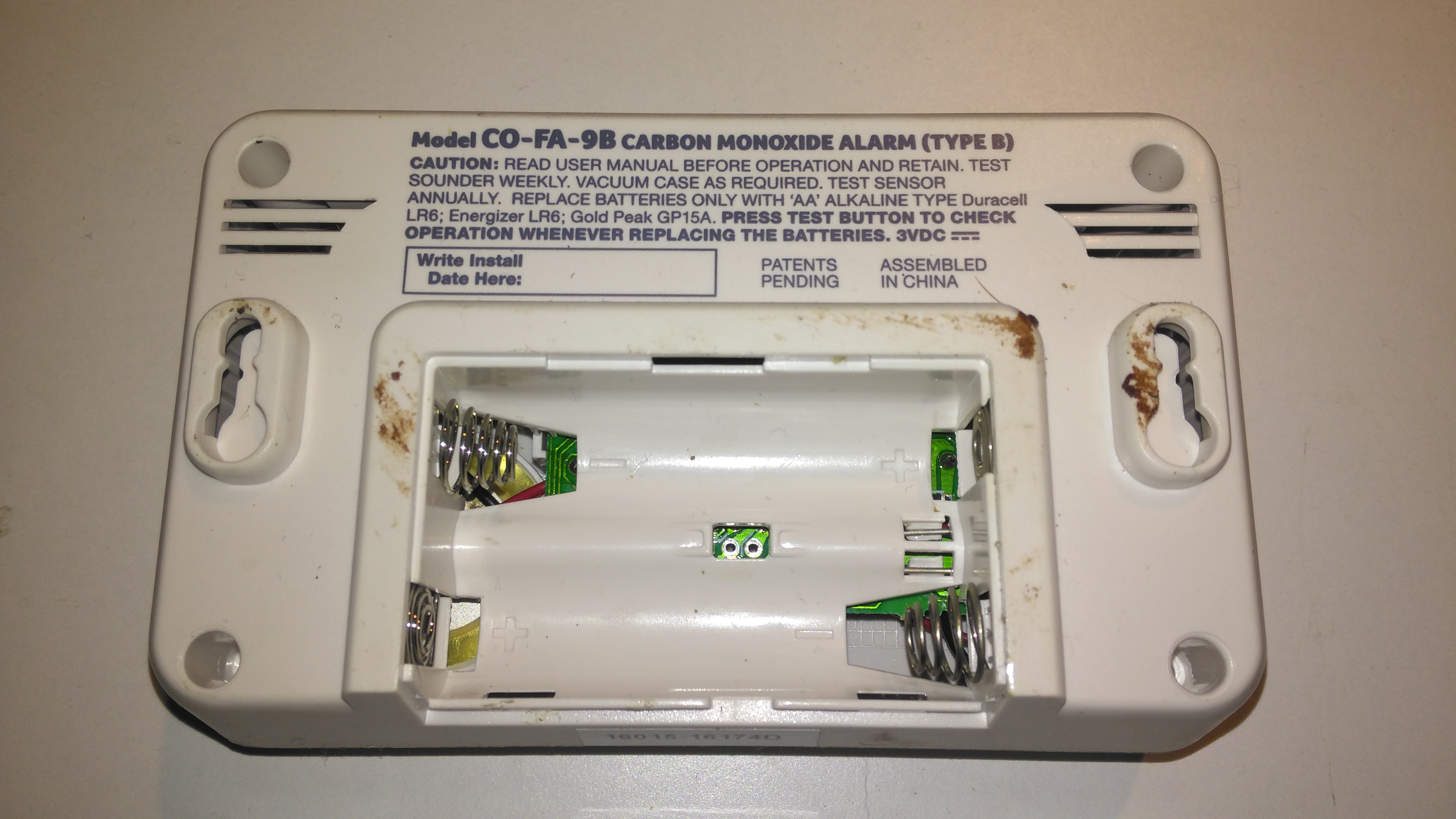
Rear
This alarm also doesn’t have the 10-year lithium cell for power, taking AA cells instead. The alarm does have the usual low battery alert bleeps common with smoke alarms though, so you’ll get a fair reminder to replace them.
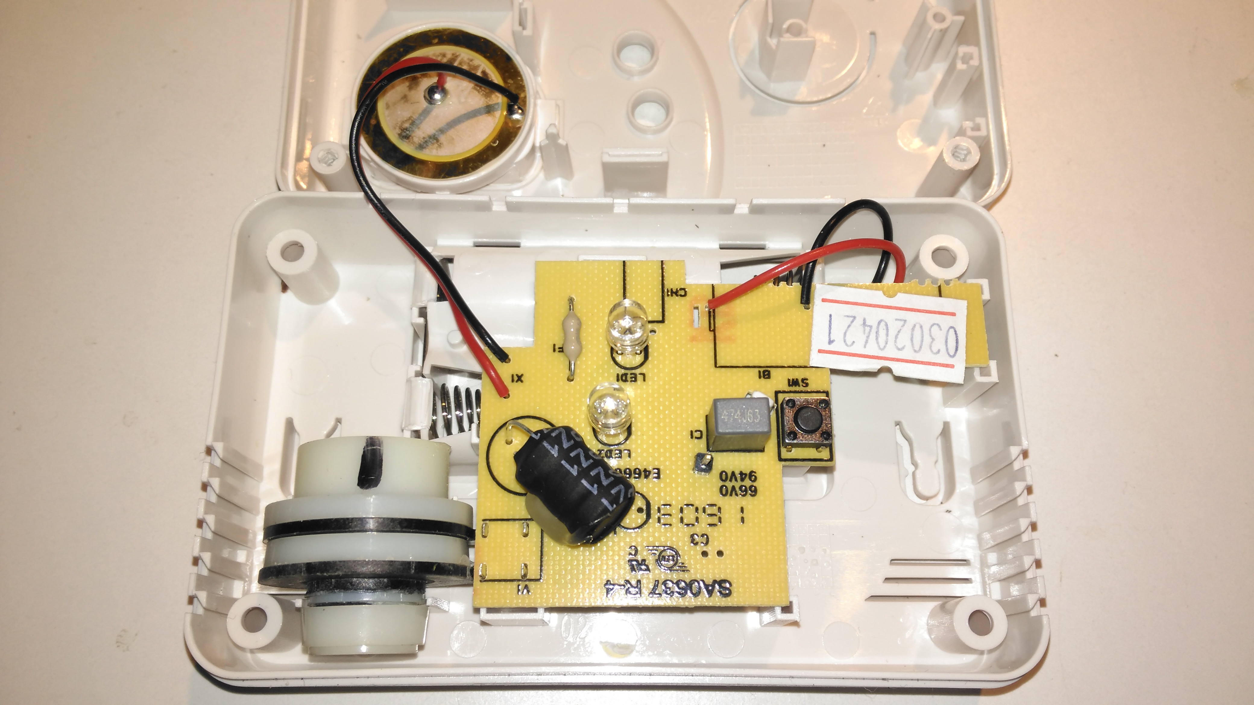
Internals
Not much at all on the inside. The CO sensor cell is the same one as used in the FireAngel alarms, I have never managed to find who manufactures these sensors, or a datasheet for them unfortunately.
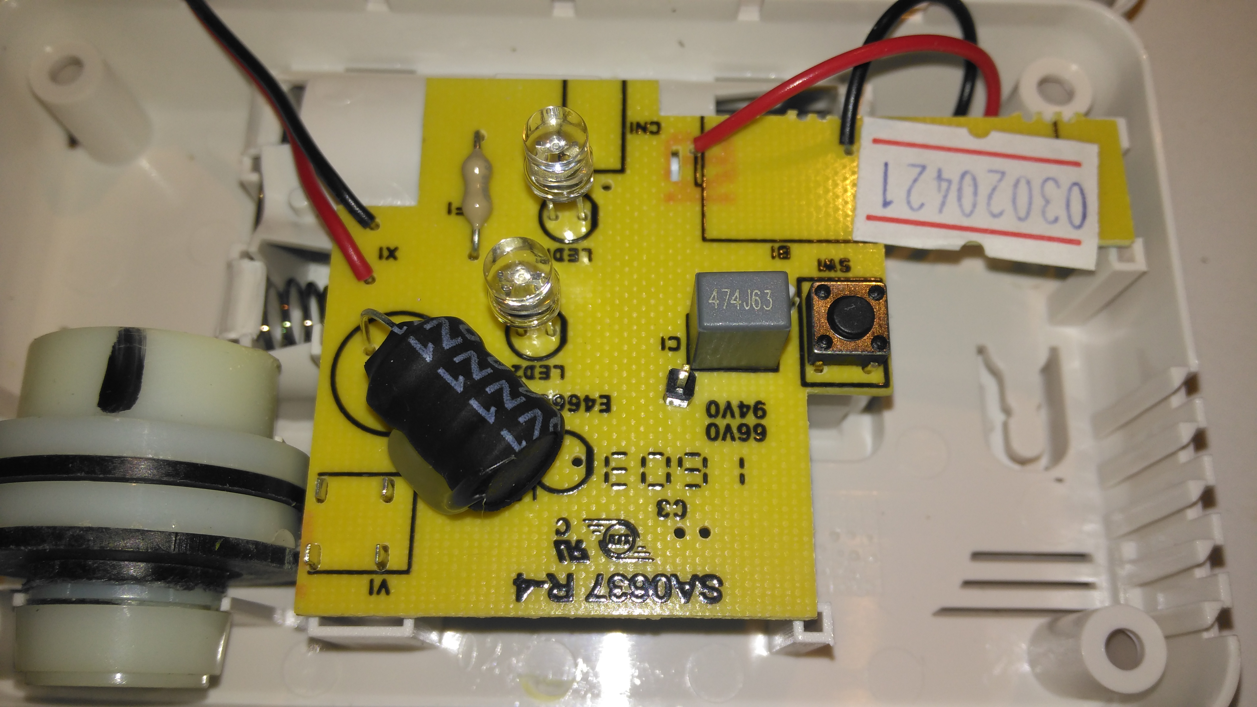
PCB Top
The top of the single sided PCB has the transformer for driving the Piezo sounder, the LEDs & the test button.
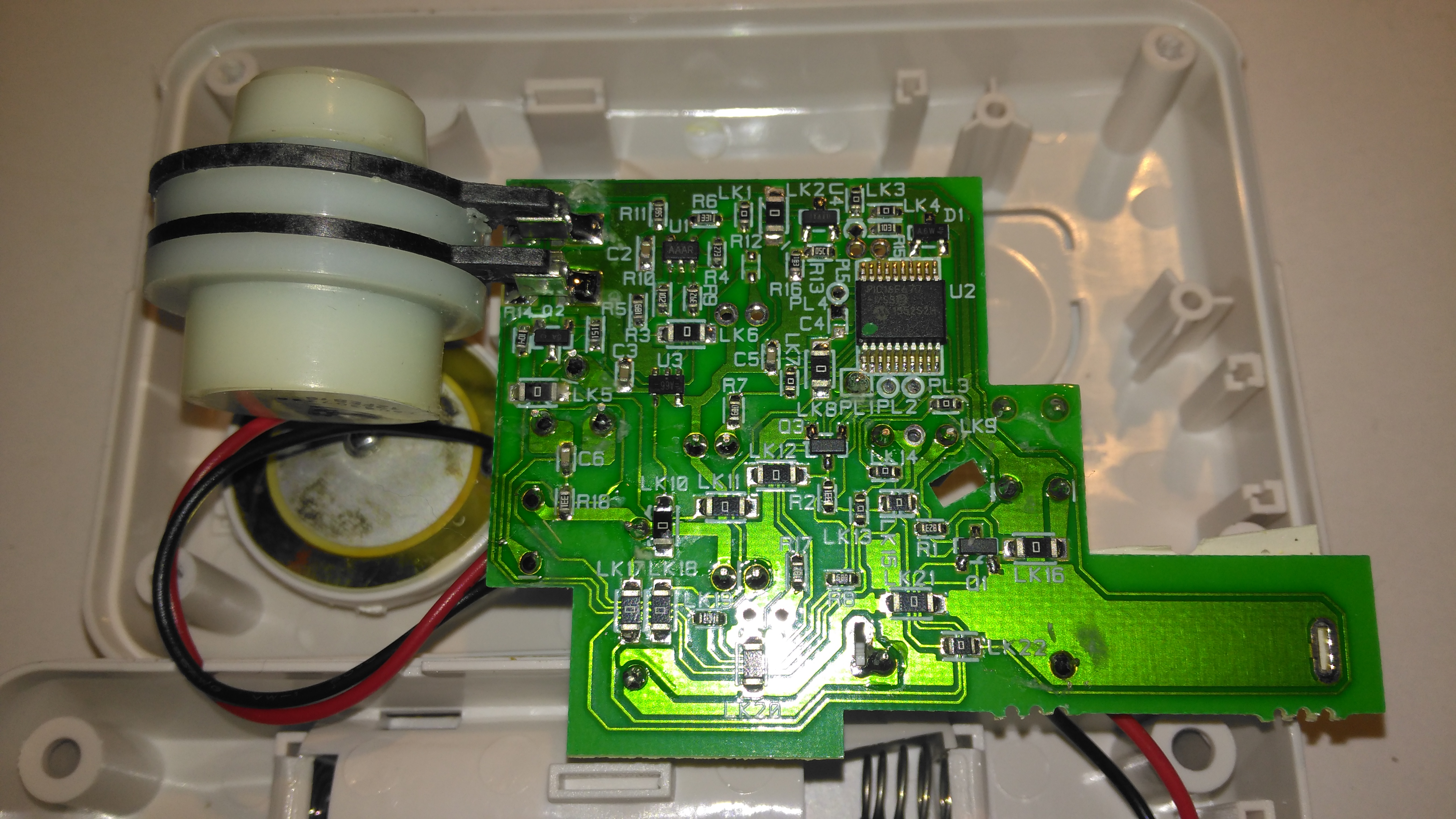
PCB Bottom
All the magic happens on the bottom of the PCB. The controlling microcontroller is on the top right, with the sensor front end on the top left.
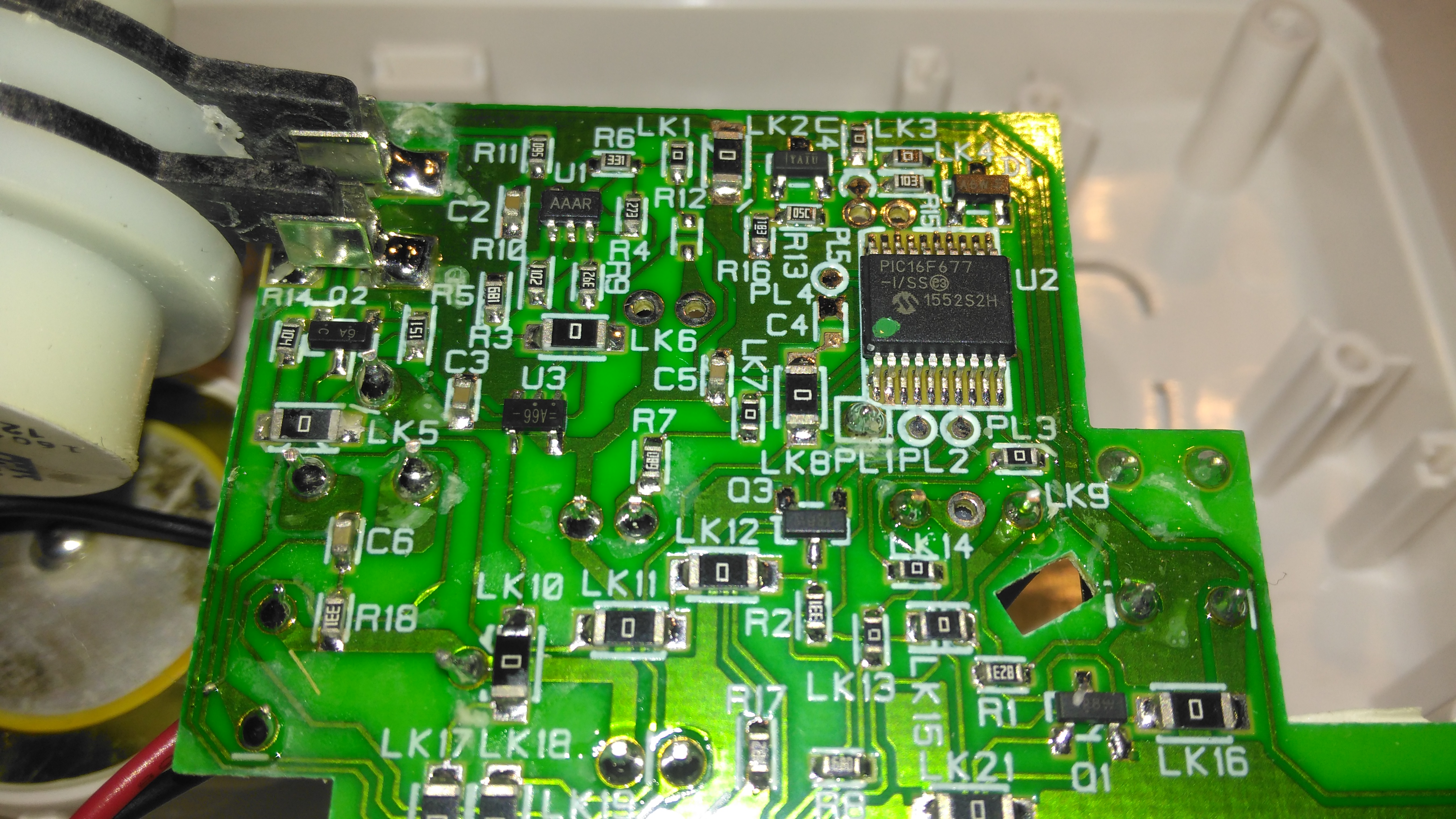
Circuitry Closeup
The microcontroller used here is a Microchip PIC16F677. I’ve not managed to find datasheets for the front end components, but these will just be a low-noise op-amp & it’s ancillaries. There will also be a reference voltage regulator. The terminals on these sensors are made of conductive plastic, probably loaded with carbon.
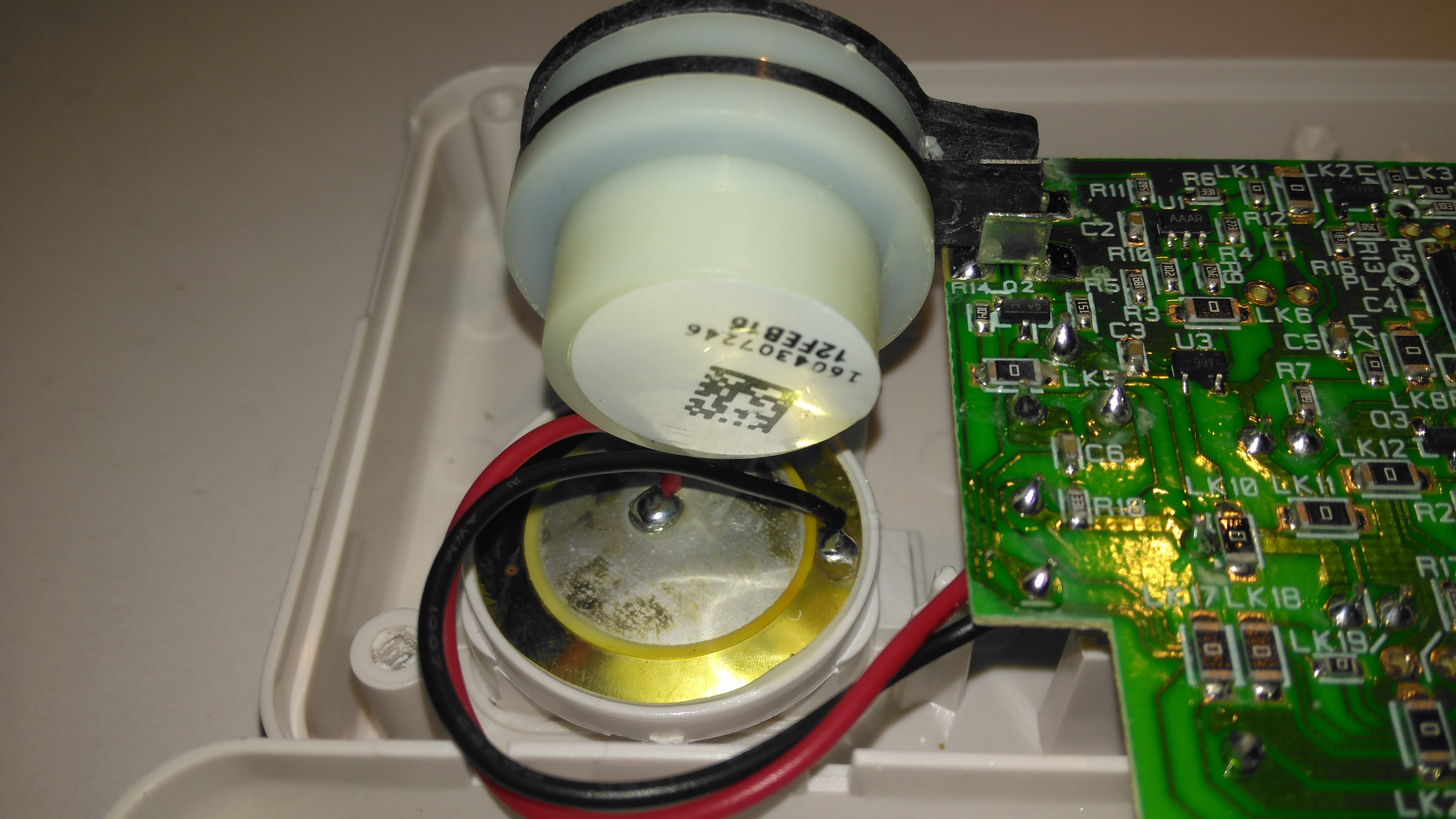
Sensor Cell & Piezo Disc
The expiry date is handily on a label on the back of the sensor, the Piezo sounder is just underneath in it’s sound chamber.
During the rebuild of the wheelchair motors for the support trolley, I found myself needing an accurate milliohm meter to test the armature windings with. Commercial instruments like these are expensive, but some Google searching found a milliohm meter project based around the Arduino from Circuit Cellar.
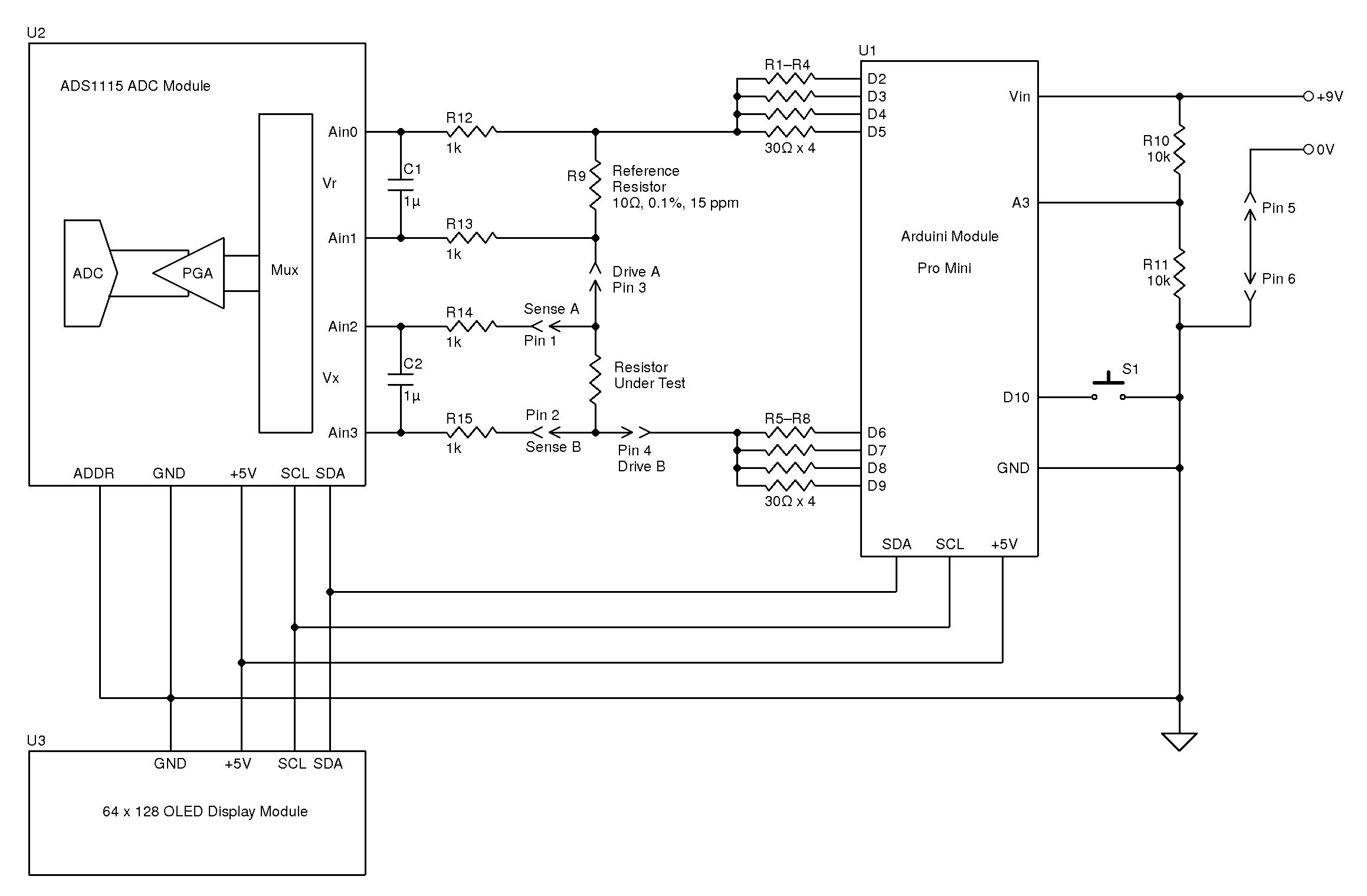
Circuit Diagram
Here’s the original author’s circuit diagram, paralleling nearly all of the Arduino’s digital output pins together to source/sink the test current, an ADS1115 ADC to take more accurate readings, with the results displayed on a jellybean 128×64 OLED module. The most expensive part here is the 10Ω 0.1% 15ppm reference resistor, R9.
I decided to make some small adjustments to the power supply section of the project, to include a rechargeable lithium cell rather than a 9v PP3 battery. This required some small changes to the Arduino sketch, a DC-DC boost converter to supply 5v from the 3.7v of a lithium cell, a charger module for said cell, and with the battery voltage being within the input range of the analogue inputs, the voltage divider on A3 was removed. A new display icon was also added in to indicate when the battery is being charged, this uses another digital input pin for input voltage sensing.
I also made some basic changes to the way an unreadable resistance is displayed, showing “OL” instead of “—–“, and the meter sends the reading out over the I²C bus, for future expansion purposes. The address the data is directed to is set to 0x50.
I’ve not etched a PCB for this as I couldn’t be bothered with the messy etchant, so I built this on a matrix board instead.
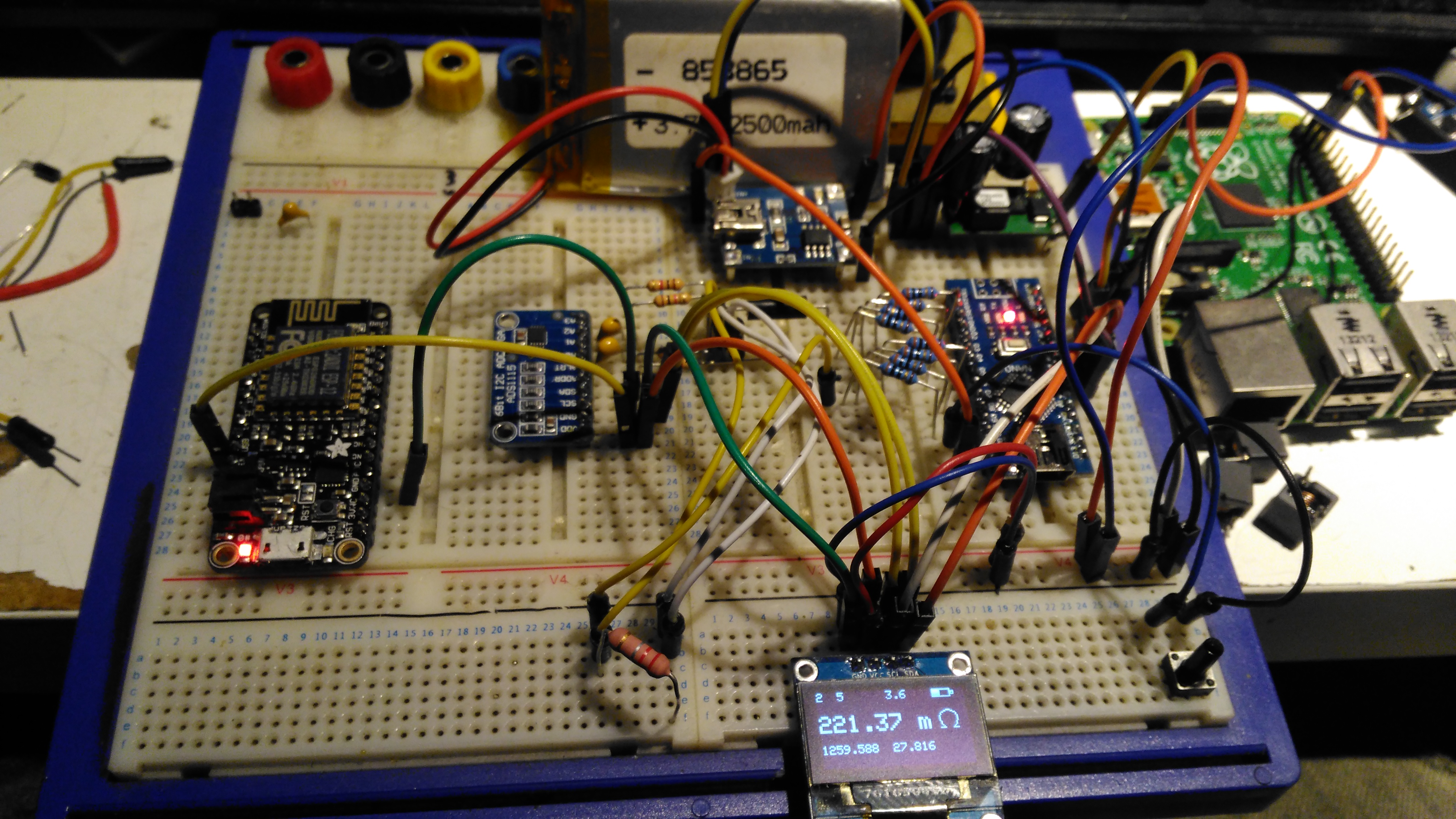
Final Prototype
Since I made some changes to both the software and the hardware components, I decided to prototype the changes on breadboard. The lithium cell is at the top of the image. with the charger module & DC-DC converter. The Arduino Nano is on the right, the ADC & reference resistor on the left, and the display at the bottom.
The Raspberry Pi & ESP8266 module are being used in this case to discharge the battery quicker to make sure the battery level calibration was correct, and to make sure the DC-DC converter would continue to function throughout the battery voltage range.
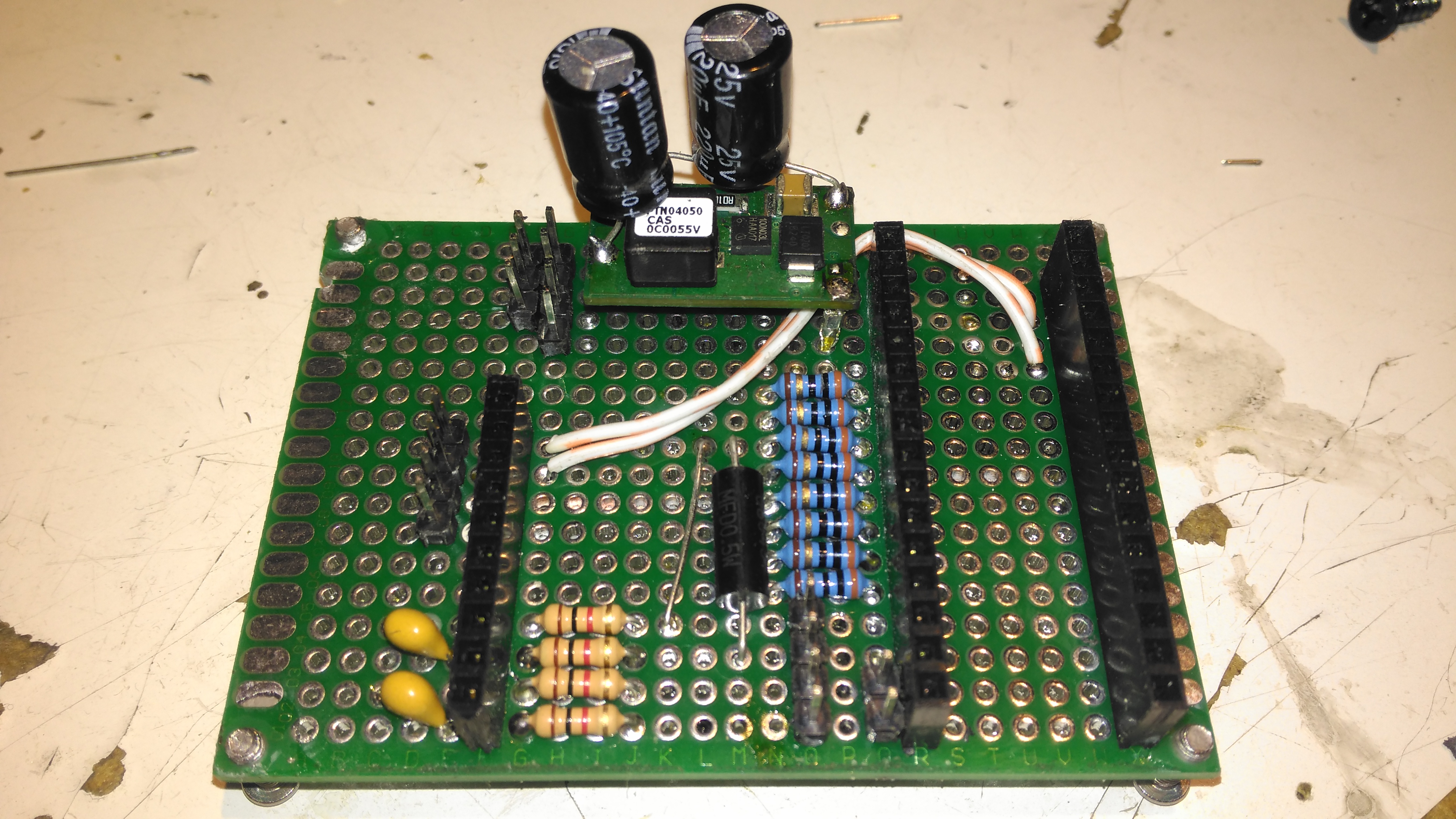
Matrix Board Passives
Here’s the final board with the passive components installed, along with the DC-DC converter. I used a Texas Instruments PTN04050 boost module for power as I had one spare.
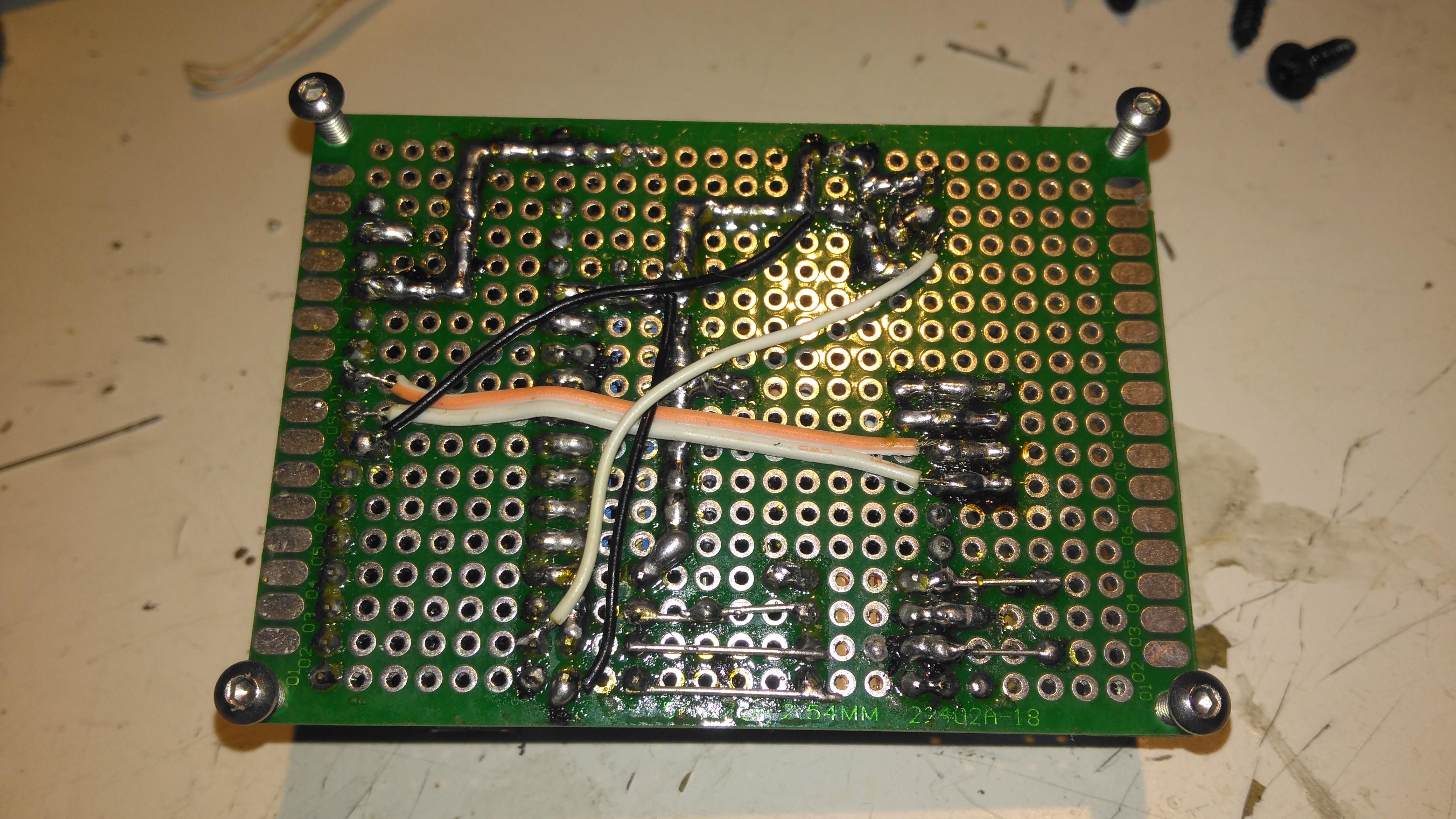
Matrix Board Rear
The bottom of the board has most of the wire jumpers for the I²C bus, and power sensing.
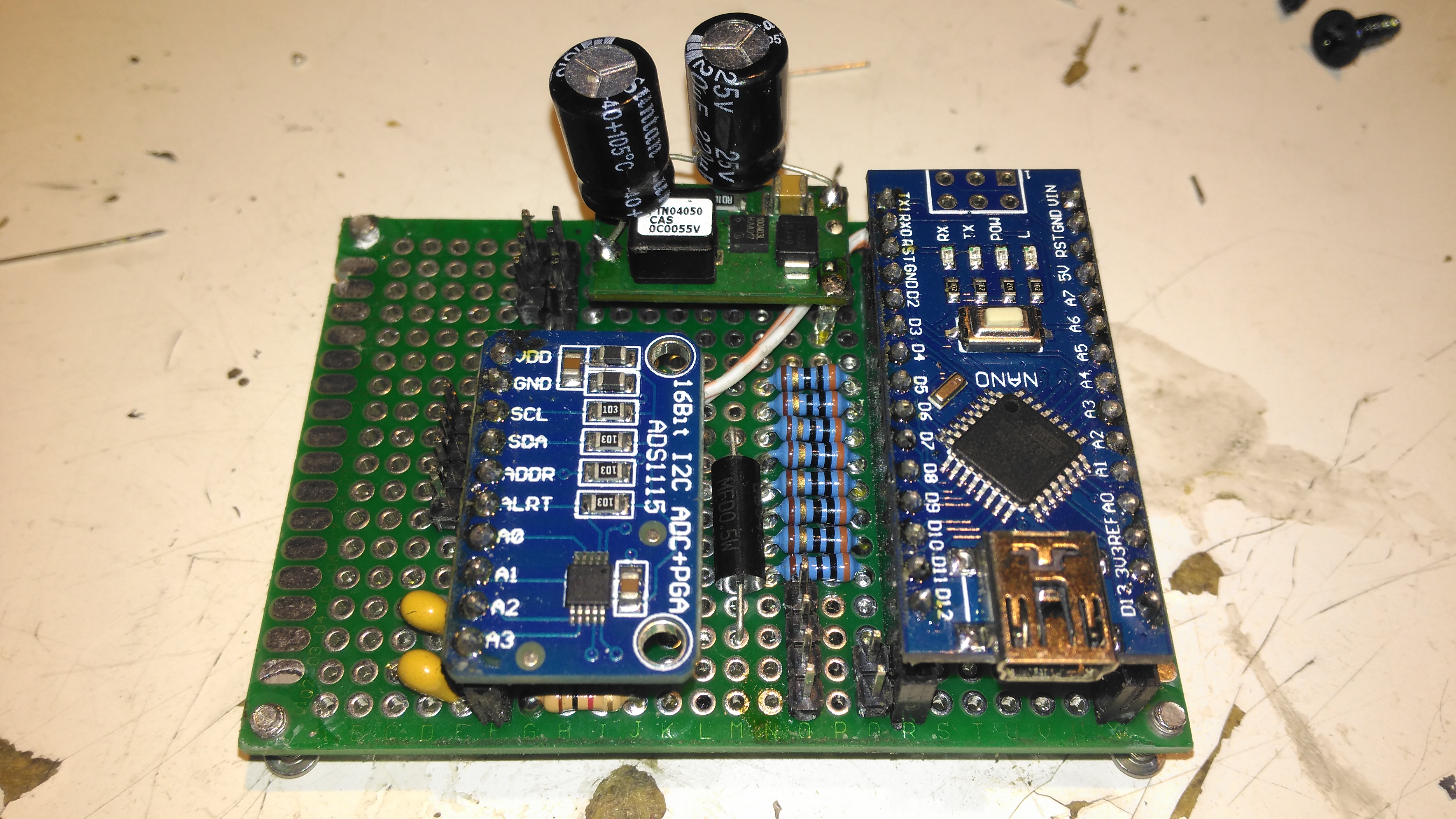
Matrix Board Modules
Here’s both modules installed on the board. I used an Arduino Nano instead of the Arduino Pro Mini that the original used as these were the parts I had in stock. Routing the analogue pins is also easier on the Mini, as they’re brought out to pins in the DIP footprint, instead of requiring wire links to odd spots on the module. To secure the PCB into the case without having to drill any holes, I tapped the corner holes of the matrix board M2.5 & threaded cap head screws in. These are then spot glued to the bottom of the case to secure the finished board.
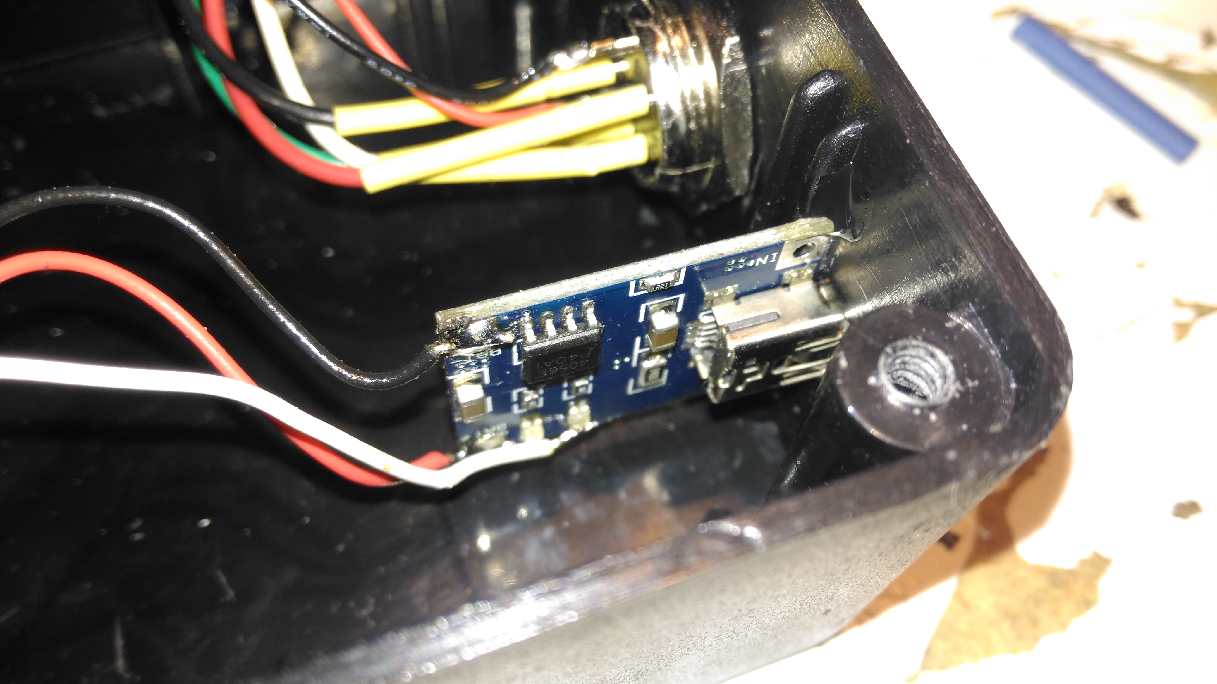
Lithium Charger
The lithium charger module is attached to the side of the enclosure, the third white wire is for input sensing – when the USB cable is plugged in a charge icon is shown on the OLED display.
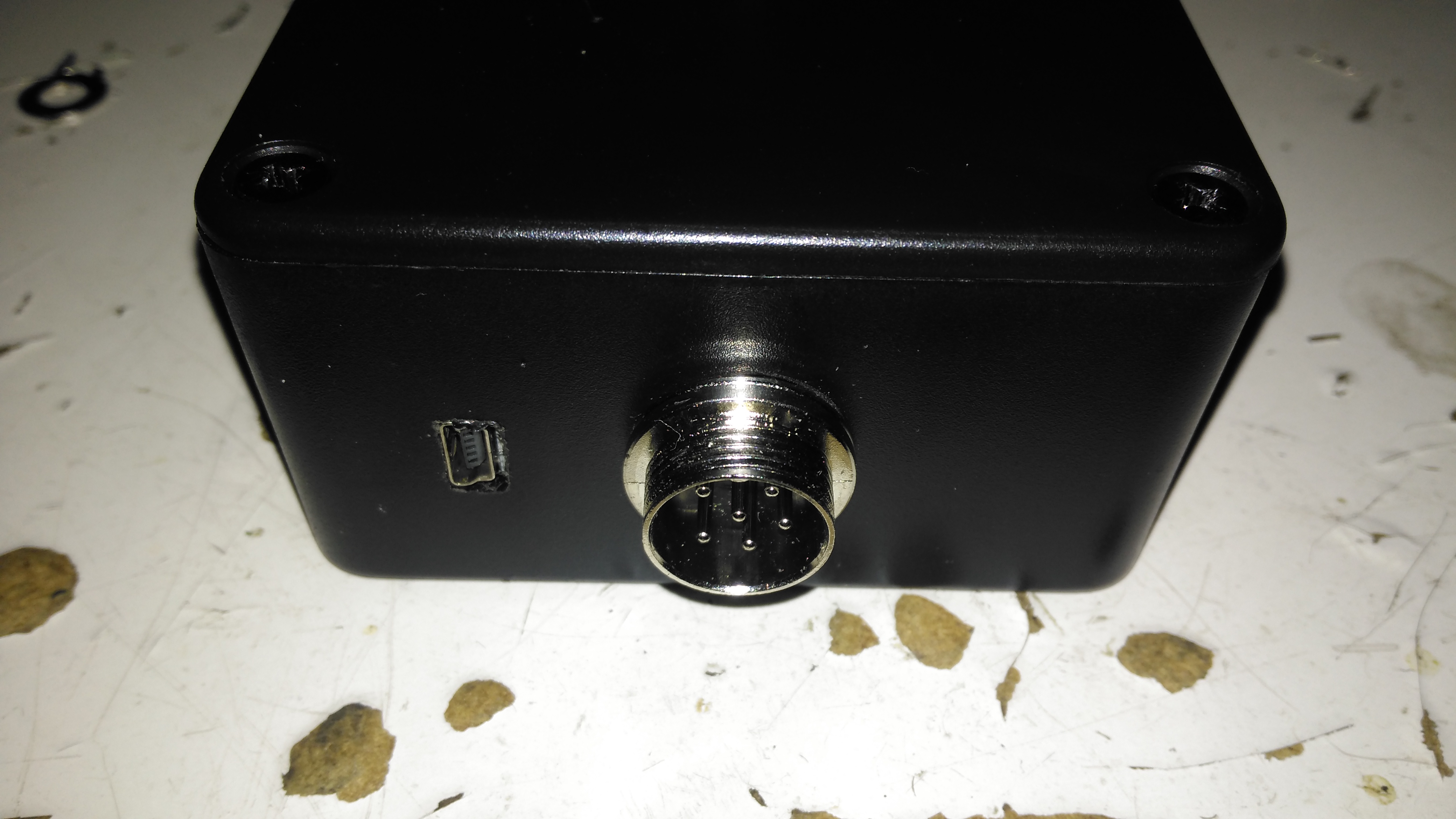
Input Connections
The inputs on the side of the enclosure. I’ve used the same 6-pin round connector for the probes, power is applied to the Arduino when the probes are plugged in.
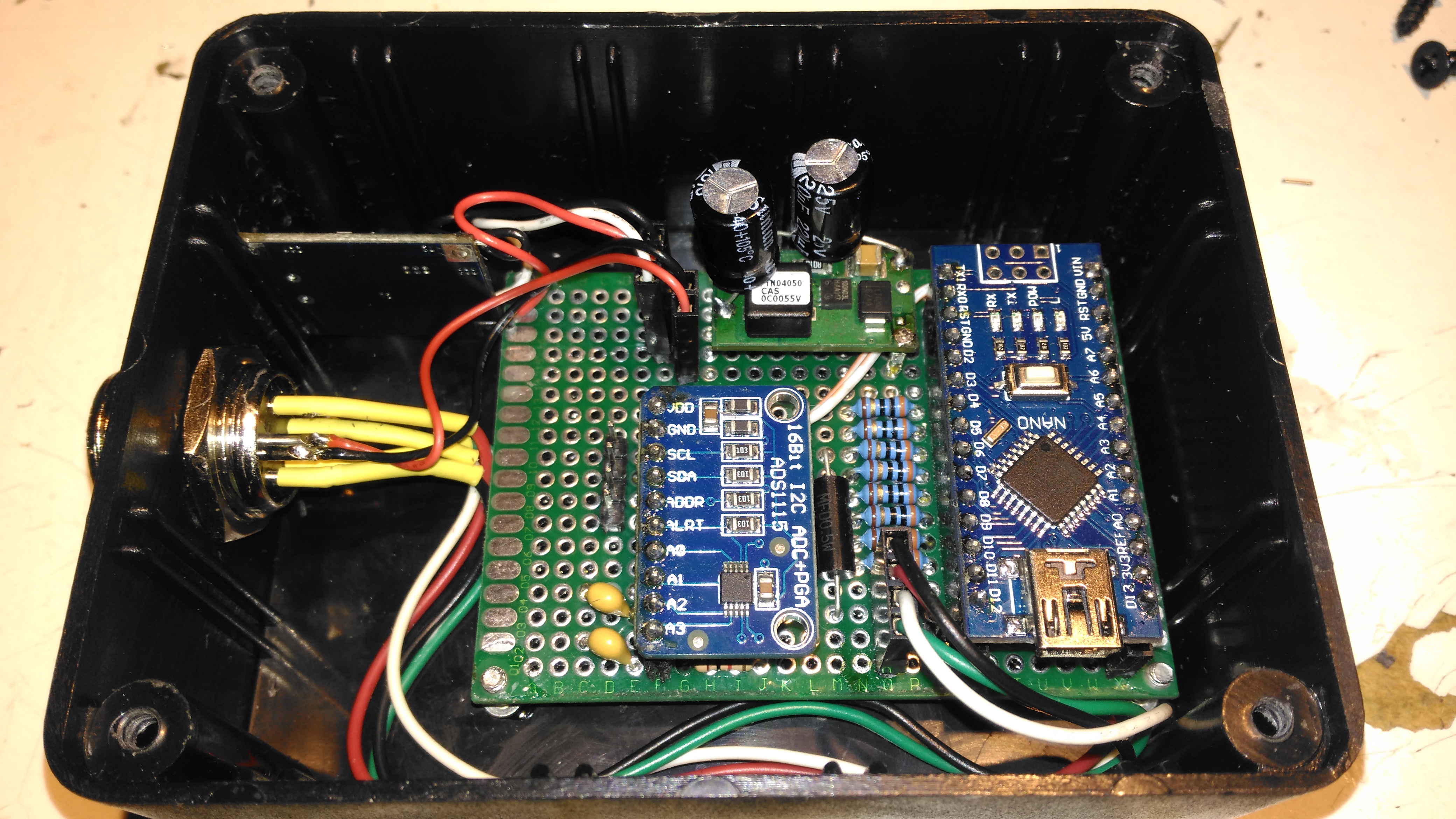
Module Installed
Everything installed in the enclosure – it’s a pretty tight fit especially with the lithium cell in place.
Meter Top Cover
The top cover has the Measure button, and the OLED display panel, the latter secured to the case with M2.5 cap head screws.
Kelvin Clips
Finally, the measurement loom, with Kelvin clips. These were an eBay buy, keeping things cheap. These clips seem to be fairly well built, even if the hinges are plastic. I doubt they’re actually gold-plated, more likely to be brass. I haven’t noticed any error introduced by these cheap clips so far.
The modified sketch is below:
// ---------------------------------------------------------------------------------------------
//  Simple, accurate milliohmeter
//
//  (c) Mark Driedger 2015
//
//  - Determines resistance using 4 wire measurement of voltage across a series connected
//  reference resistor (Rr, 10 ohm, 0.1%) and test resistor (Rx)
//  - range of accurate measurement is roughly 50 mohm to 10Kohm
//  - Uses Arduino digital I/O ports to deliver the test current, alternating polarity to cancel
//  offset errors (synchronous detector)
//  - 4 I/O pins are used for each leg of the test current to increase test current
//  - Averages 2 cycles and 100 samples/cycle
//  - Uses a 16 bit ADC ADS1115 with 16x PGA to improve accuracy
//
//  Version History
//    May 24/15    v1.0-v4.0
//      - initial development versions
//    May 27/15    v5.0
//      - changed display to I2C
//      - backed out low power module since it seemed to cause serial port upload problems
// ---------------------------------------------------------------------------------------------

#include <Wire.h>
#include <SPI.h>
#include <Adafruit_GFX.h>
#include <Adafruit_SSD1306.h>
//#include <LowPower.h>

#if (SSD1306_LCDHEIGHT != 64)
#error("Height incorrect, please fix Adafruit_SSD1306.h!");
#endif

// ---------------------------------------------------------------------------------------------
//  I/O port usage
// ---------------------------------------------------------------------------------------------
//    serial port (debug and s/w download)    0, 1
//    I²C interface to ADC & display          A4, A5
//    positive drive                          2, 3, 4, 5
//    push to test input                      8
//    unused                                  9, 10, 11, A0, A1, A2, A6, A7
//    negative drive                          6, 7, 8, 9
//    battery voltage monitor                 A3
//    debug output                            13

#define  P_PushToTest  10       // push button (measure), active low
#define  P_Debug       13
#define  CHG           12

//  ADS1115 mux and gain settings
#define  ADS1115_CH01  0x00    // p = AIN0, n = AIN1
#define  ADS1115_CH03  0x01    // ... etc
#define  ADS1115_CH13  0x02
#define  ADS1115_CH23  0x03
#define  ADS1115_CH0G  0x04    // p = AIN0, n = GND
#define  ADS1115_CH1G  0x05    // ... etc
#define  ADS1115_CH2G  0x06
#define  ADS1115_CH3G  0x07

#define  ADS1115_6p144  0x00   // +/- 6.144 V full scale
#define  ADS1115_4p096  0x01   // +/- 4.096 V full scale
#define  ADS1115_2p048  0x02   // +/- 2.048 V full scale
#define  ADS1115_1p024  0x03   // +/- 1.024 V full scale
#define  ADS1115_0p512  0x04   // +/- 0.512 V full scale
#define  ADS1115_0p256  0x05   // +/- 0.256 V full scale
#define  ADS1115_0p256B 0x06   // same as ADS1115_0p256
#define  ADS1115_0p256C 0x07   // same as ADS1115_0p256

Adafruit_SSD1306   display(0);               // using I2C interface, no reset pin
static int         debug_mode = 0;           // true in debug mode

float ADS1115read(byte channel, byte gain)
//--------------------------------------------------------------------------------------
//  reads a single sample from the ADS1115 ADC at a given mux (channel) and gain setting
//  - channel is 3 bit channel number/mux setting (one of ADS1115_CHxx)
//  - gain is 3 bit PGA gain setting (one of ADS1115_xpxxx)
//  - returns voltage in volts
//  - uses single shot mode, polling for conversion complete, default I2C address
//  - conversion takes approximatly 9.25 msec
//--------------------------------------------------------------------------------------
  {
  const int    address = 0x48;      // ADS1115 I2C address, A0=0, A1=0
  byte         hiByte, loByte;
  int          r;
  float        x;

  channel &= 0x07;                  // constrain to 3 bits
  gain    &= 0x07;

  hiByte = B10000001 | (channel<<4) | (gain<<1);    // conversion start command
  loByte = B10000011;

  Wire.beginTransmission(address);  // send conversion start command
  Wire.write(0x01);                 // address the config register
  Wire.write(hiByte);               // ...and send config register value
  Wire.write(loByte);
  Wire.endTransmission();

   do                               // loop until conversion complete
    {
    Wire.requestFrom(address, 2);   // config register is still addressed
    while(Wire.available())
      {
      hiByte = Wire.read();         // ... and read config register
      loByte = Wire.read();
      }
    }
  while ((hiByte & 0x80)==0);       // upper bit (OS) is conversion complete

  Wire.beginTransmission(address);
  Wire.write(0x00);                 // address the conversion register
  Wire.endTransmission();

  Wire.requestFrom(address, 2);     // ... and get 2 byte result
  while(Wire.available())
    {
    hiByte = Wire.read();
    loByte = Wire.read();
    }

  r = loByte | hiByte<<8;           // convert to 16 bit int
  switch(gain)                      // ... and now convert to volts
    {
      case ADS1115_6p144:  x = r * 6.144 / 32768.0; break;
      case ADS1115_4p096:  x = r * 4.096 / 32768.0; break;
      case ADS1115_2p048:  x = r * 2.048 / 32768.0; break;
      case ADS1115_1p024:  x = r * 1.024 / 32768.0; break;
      case ADS1115_0p512:  x = r * 0.512 / 32768.0; break;
      case ADS1115_0p256:
      case ADS1115_0p256B:
      case ADS1115_0p256C: x = r * 0.256 / 32768.0; break;
    }
  return x;
  }

// ---------------------------------------------------------------------------------------------
//  Drive functions
//   - ports 4-7 and A0-A3 are used to differentially drive resistor under test
//   - the ports are resistively summed to increase current capability
//   - DriveOff() disables the drive, setting the bits to input
//   - DriveOn()  enables the drive,  setting the bits to output
//   - DriveP()   enables drive with positive current flow (from ports 4-7 to ports A0-A3)
//   - DriveN()   enables drive with negative current flow
// ---------------------------------------------------------------------------------------------
void DriveP()
  {
    DriveOff();
    digitalWrite( 2, HIGH);
    digitalWrite( 3, HIGH);
    digitalWrite( 4, HIGH);
    digitalWrite( 5, HIGH);
    digitalWrite( 6, LOW);
    digitalWrite( 7, LOW);
    digitalWrite( 8, LOW);
    digitalWrite( 9, LOW);
    DriveOn();
  }

void DriveN()
  {
    DriveOff();
    digitalWrite( 2, LOW);
    digitalWrite( 3, LOW);
    digitalWrite( 4, LOW);
    digitalWrite( 5, LOW);
    digitalWrite( 6, HIGH);
    digitalWrite( 7, HIGH);
    digitalWrite( 8, HIGH);
    digitalWrite( 9, HIGH);
    DriveOn();
  }

void DriveOn()
  {
    pinMode( 2, OUTPUT);      // enable source/sink in pairs
    pinMode( 6, OUTPUT);
    pinMode( 3, OUTPUT);
    pinMode( 7, OUTPUT);
    pinMode( 4, OUTPUT);
    pinMode( 8, OUTPUT);
    pinMode( 5, OUTPUT);
    pinMode( 9, OUTPUT);
    delayMicroseconds(5000);  // 5ms delay
  }

void DriveOff()
  {
    pinMode( 2, INPUT);       // disable source/sink in pairs
    pinMode( 6, INPUT);
    pinMode( 3, INPUT);
    pinMode( 7, INPUT);
    pinMode( 4, INPUT);
    pinMode( 8, INPUT);
    pinMode( 5, INPUT);
    pinMode( 9, INPUT);
  }

int CalcPGA(float x)
// ---------------------------------------------------------------------------------------------
//   Calculate optimum PGA setting based on a sample voltage, x, read at lowest PGA gain
//     - returns the highest PGA gain that allows x to be read with 10% headroom
// ---------------------------------------------------------------------------------------------
  {
    x = abs(x);
    if (x>3.680) return ADS1115_6p144;
    if (x>1.840) return ADS1115_4p096;
    if (x>0.920) return ADS1115_2p048;
    if (x>0.460) return ADS1115_1p024;
    if (x>0.230) return ADS1115_0p512;
    else         return ADS1115_0p256;
  }

void BatteryIcon(float charge)
// ---------------------------------------------------------------------------------------------
//   Draw a battery charge icon into the display buffer without refreshing the display
//     - charge ranges from 0.0 (empty) to 1.0 (full)
// ---------------------------------------------------------------------------------------------
  {
    static const unsigned char PROGMEM chg[] =     // Battery Charge Icon
    { 0x1c, 0x18, 0x38, 0x3c, 0x18, 0x10, 0x20, 0x00 };

    int w = constrain(charge, 0.0, 1.0)*16;  // 0 to 16 pixels wide depending on charge
    display.drawRect(100, 0, 16, 7, WHITE);  // outline
    display.drawRect(116, 2,  3, 3, WHITE);  // nib
    display.fillRect(100, 0,  w, 7, WHITE);  // charge indication

    //battery charging indication
    pinMode(CHG, INPUT);
    if (digitalRead(CHG) == HIGH)
      display.drawBitmap(91, 0, chg, 8, 8, WHITE);
  }

void f2str(float x, int N, char *c)
// ---------------------------------------------------------------------------------------------
//    Converts a floating point number x to a string c with N digits of precision
//     - *c must be a string array of length at least N+3 (N + '-', '.', '\0')
//     - x must be have than N leading digits (before decimal) or "#\0" is returned
// ---------------------------------------------------------------------------------------------
  {
  int     j, k, r;
  float   y;

  if (x<0.0)                    // handle negative numbers
    {
      *c++ = '-';
      x = -x;
    }
  for (j=0; x>=1.0; j++)        // j digits before decimal point
    x /= 10.0;                  // .. and scale x to be < 1.0

  if (j>N)                      // return error string if too many digits
    {
      *c++ = '#';
      *c++ = '\0';
      return;
    }

  y = pow(10, (float) N);       // round to N digits
  x = round(x * y) / y;
  if (x>1.0)                    // if 1st digit rounded up ...
    {
      x /= 10.0;                // then normalize back down 1 digit
      j++;
    }

  for (k=0; k<N; k++)
    {
      r = (int) (x*10.0);        // leading digit as int
      x = x*10-r;                // remove leading digit and shift 1 digit

      *c++ = r + '0';            // add leading digit to string
      if (k==j-1 && k!=N-1)      // add decimal point after j digits
        *c++ = '.';              // ... unless there are N digits before decimal
    }
  *c++ = '\0';
  }

void DisplayResistance(float x)
// ---------------------------------------------------------------------------------------------
//    Adds the resistance value, x, to the display buffer without refreshing the display
//      - converts to kohm, milliohm or microohm if necessary
// ---------------------------------------------------------------------------------------------
  {
    static const unsigned char PROGMEM omega_bmp[] =     // omega (ohm) symbol
    { B00000011, B11000000,
      B00001100, B00110000,
      B00110000, B00001100,
      B01000000, B00000010,
      B01000000, B00000010,
      B10000000, B00000001,
      B10000000, B00000001,
      B10000000, B00000001,
      B10000000, B00000001,
      B10000000, B00000001,
      B01000000, B00000010,
      B01000000, B00000010,
      B01000000, B00000010,
      B00100000, B00000100,
      B00010000, B00001000,
      B11111000, B00011111 };

    char  s[8];
    char  prefix;

    if (x>=1000.0)          // display in killo ohms
      {
        x /= 1000.0;
        prefix = 'k';
      }
    else if (x<0.001)       // display in micro ohms
      {
        x *= 1000000.0;
        prefix = 0xe5;    // mu
      }
    else if (x<1.0)         // display in milli ohms
      {
        x *= 1000.0;
        prefix = 'm';
      }
    else
      prefix = ' ';         // display in ohms

    f2str(x, 5, s);

    // display computed resistance
    display.setTextSize(2);
    display.setTextColor(WHITE);
    display.setCursor(0,20);
    display.print(s);

    // display prefix
    display.setCursor(85,20);
    display.print(prefix);

    // display omega (ohms) symbol
    display.drawBitmap(103, 18, omega_bmp, 16, 16, WHITE);
  }

void DisplayDebug(int a, int b, float x, float y, float Vbat)
// ---------------------------------------------------------------------------------------------
//    Adds debug info to the display buffer without showing the updated display
//      - Adds 2 ints (a, b) and a float(Vbat) to the top line and 2 floats (x, y)
//      to the bottom line+, all in small (size 1) text
// ---------------------------------------------------------------------------------------------
  {
    // display x, y in lower left, small font
    display.setTextSize(1);
    display.setCursor(0,45);
    display.print(x,3);
    display.print("  ");
    display.print(y,3);

    // display a, b in upper left, small font
    display.setTextSize(1);
    display.setCursor(0,0);
    display.print(a);
    display.print("  ");
    display.print(b);

    // display Vbat in upper middle, small font
    display.setTextSize(1);
    display.setCursor(60,0);
    display.print(Vbat,1);
  }

void DisplayStr(char *s)
// ---------------------------------------------------------------------------------------------
//    Adds a string, s, to the display buffer without refreshing the display @ (0,20)
// ---------------------------------------------------------------------------------------------
  {
    display.setTextSize(2);
    display.setTextColor(WHITE);
    display.setCursor(8,20);
    display.print(s);
  }

#ifdef TESTMODE
void loop()
  {
    while (digitalRead(P_PushToTest))
      ;
    DriveP();
    display.clearDisplay();
    DisplayStr("Drive: +");
    display.display();
    delay(250);

    while (digitalRead(P_PushToTest))
      ;
    DriveN();
    display.clearDisplay();
    DisplayStr("Drive: -");
    display.display();
    delay(250);

    while (digitalRead(P_PushToTest))
      ;
    DriveOff();
    display.clearDisplay();
    DisplayStr("Drive: Off");
    display.display();
    delay(250);
  }
#endif

void setup()
// ---------------------------------------------------------------------------------------------
//    - initializae display and I/O ports
// ---------------------------------------------------------------------------------------------
  {
    DriveOff();                                    // disable current drive
    Wire.begin();                                  // join I2C bus
    display.begin(SSD1306_SWITCHCAPVCC, 0x3c, 0);  // initialize display @ address 0x3c, no reset
    pinMode(P_PushToTest, INPUT_PULLUP);           // measure push button switch, active low
    debug_mode = !digitalRead(P_PushToTest);       // if pushed during power on, then debug mode
    pinMode(P_Debug, OUTPUT);                      // debug port
  }

void loop()
// ---------------------------------------------------------------------------------------------
//    main measurement loop
// ---------------------------------------------------------------------------------------------
  {
    const float      Rr = 10.0;             // reference resistor value, ohms
    const float      Rcal = 1.002419;       // calibration factor
    const int        N = 2;                 // number of cycles to average
    const int        M = 50;                // samples per half cycle
    static long      Toff;
    double           Rx;                    // calculated resistor under test, ohms
    byte             PGAr, PGAx;            // PGA gains (r = reference, x = test resistors)
    float            Vr, Vx, Wx, Wr;        // voltages in V
    float            Rn;                    // calculated resistor under test, ohms, single sample
    double           Avgr, Avgx;            // average ADC readings in mV
    int              j, k, n;
    float            Vbat;                  // battery voltage in V (from 2:1 divider)
    char             serialbuff[10];        // Buffer for sending the reading over I²C

    display.clearDisplay();
    DisplayStr("measuring");
    display.display();

    // determine PGA gains
    DriveP();
    Wr =  ADS1115read(ADS1115_CH01, ADS1115_6p144);
    Wx =  ADS1115read(ADS1115_CH23, ADS1115_6p144);
    DriveN();
    Vr = -ADS1115read(ADS1115_CH01, ADS1115_6p144);
    Vx = -ADS1115read(ADS1115_CH23, ADS1115_6p144);

    //  measure battery voltage ... while drive is on so there is a load
    Vbat = analogRead(A3)*5.0/1024.0;    // 2:1 divider (5V FS) on 4.2v lithium battery

    DriveOff();

    PGAr = CalcPGA(max(Vr, Wr));           // determine optimum PGA gains
    PGAx = CalcPGA(max(Vx, Wx));

    // measure resistance using synchronous detection
    Avgr = Avgx = 0.0;                     // clear averages
    Rx = 0.0;
    n = 0;
    for (j=0; j<N; j++)                    // for each cycle
      {
        DriveP();                          // turn on drive, positive
        for (k=0; k<M; k++)
          {
            digitalWrite(P_Debug, 1);
            Vx = ADS1115read(ADS1115_CH23, PGAx);
            digitalWrite(P_Debug, 0);
            Vr = ADS1115read(ADS1115_CH01, PGAr);
            Avgx += Vx;
            Avgr += Vr;
            Rn = Vx/Vr;
            if (Rn>0.0 && Rn<10000.0)
              {
              Rx += Rn;
              n++;
              }
          }

        DriveN();                          // turn on drive, negative
        for (k=0; k<M; k++)
          {
            digitalWrite(P_Debug, 1);
            Vx = ADS1115read(ADS1115_CH23, PGAx);
            digitalWrite(P_Debug, 0);
            Vr = ADS1115read(ADS1115_CH01, PGAr);
            Avgx -= Vx;
            Avgr -= Vr;
            Rn = Vx/Vr;
            if (Rn>0.0 && Rn<10000.0)
              {
              Rx += Rn;
              n++;
              }
          }
      }

    DriveOff();
    Rx   *= Rr * Rcal / n;                 // apply calibration factor and compute average
    Avgr *= 1000.0 / (2.0*N*M);            // average in mV
    Avgx *= 1000.0 / (2.0*N*M);

    // display the results ... battery icon, Rx measurement, debug info if requested
    display.clearDisplay();                // ... and display result
    BatteryIcon((Vbat-3.0)/(4.2-3.0));     // 7.5V = 0%, 9V = 100%
    //display.drawLine(0, 8, 127, 8, WHITE); //Draw separator line under icons
    if (n==0){                              // no measurement taken ...
      display.setTextSize(2);
      display.setCursor(51,20);
      display.print(F("OL"));
    }
      //DisplayStr("-----");
    else
      DisplayResistance(Rx);
    //Send Reading via I²C
      Wire.beginTransmission(0x50);
      Wire.write(dtostrf(Rx, 5, 5, serialbuff));
      Wire.endTransmission();
    if (debug_mode)
      DisplayDebug(PGAr, PGAx, Avgr, Avgx, Vbat);
    display.display();                     // show the display

    // and then wait for next measurement request
    Toff = millis()+60000L;
    while(digitalRead(P_PushToTest))       // loop until measure button pressed
      {
        // Enter power down state for 120ms with ADC and BOD module disabled
        //LowPower.powerDown(SLEEP_120MS, ADC_OFF, BOD_OFF);
        if (millis()>Toff)                 // after 7 seconds ...
          {
            display.clearDisplay();        // clear display
            display.display();
          }
      }
  }
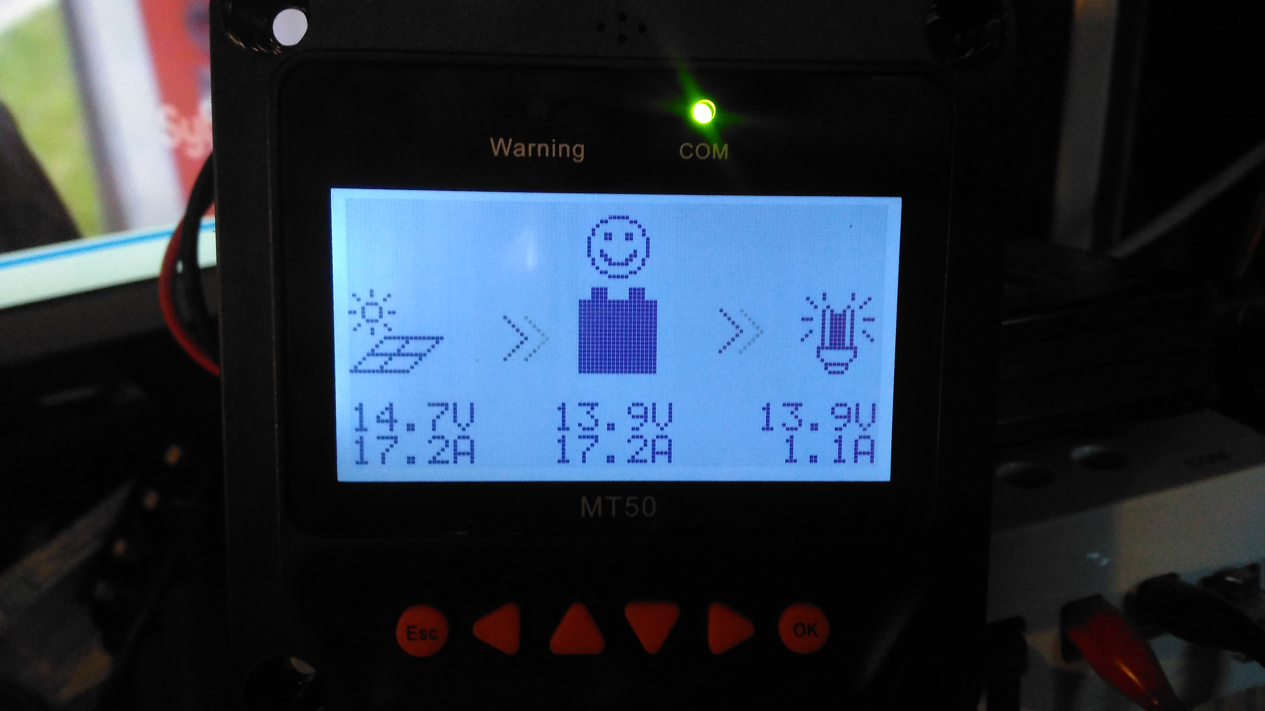
Here’s the MT50 controller from EpEver, that interfaces with it’s Tracer MPPT solar charge controllers, and gives access to more programming options on the charge controllers, without the need for a laptop. The display is a large dot-matrix unit, with built in backlight. Above is the display on the default page, showing power information for the entire system.
PCB Rear
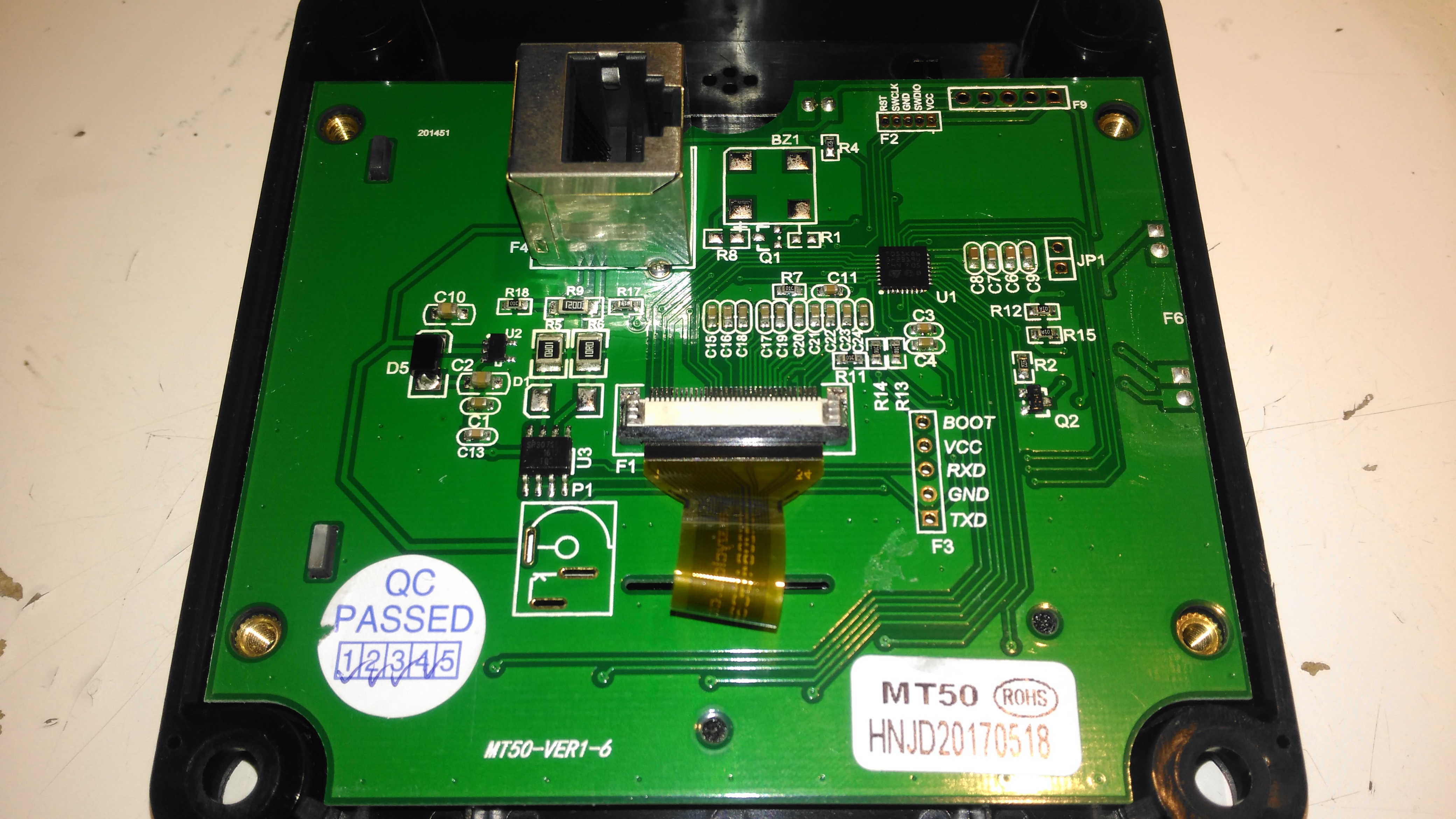
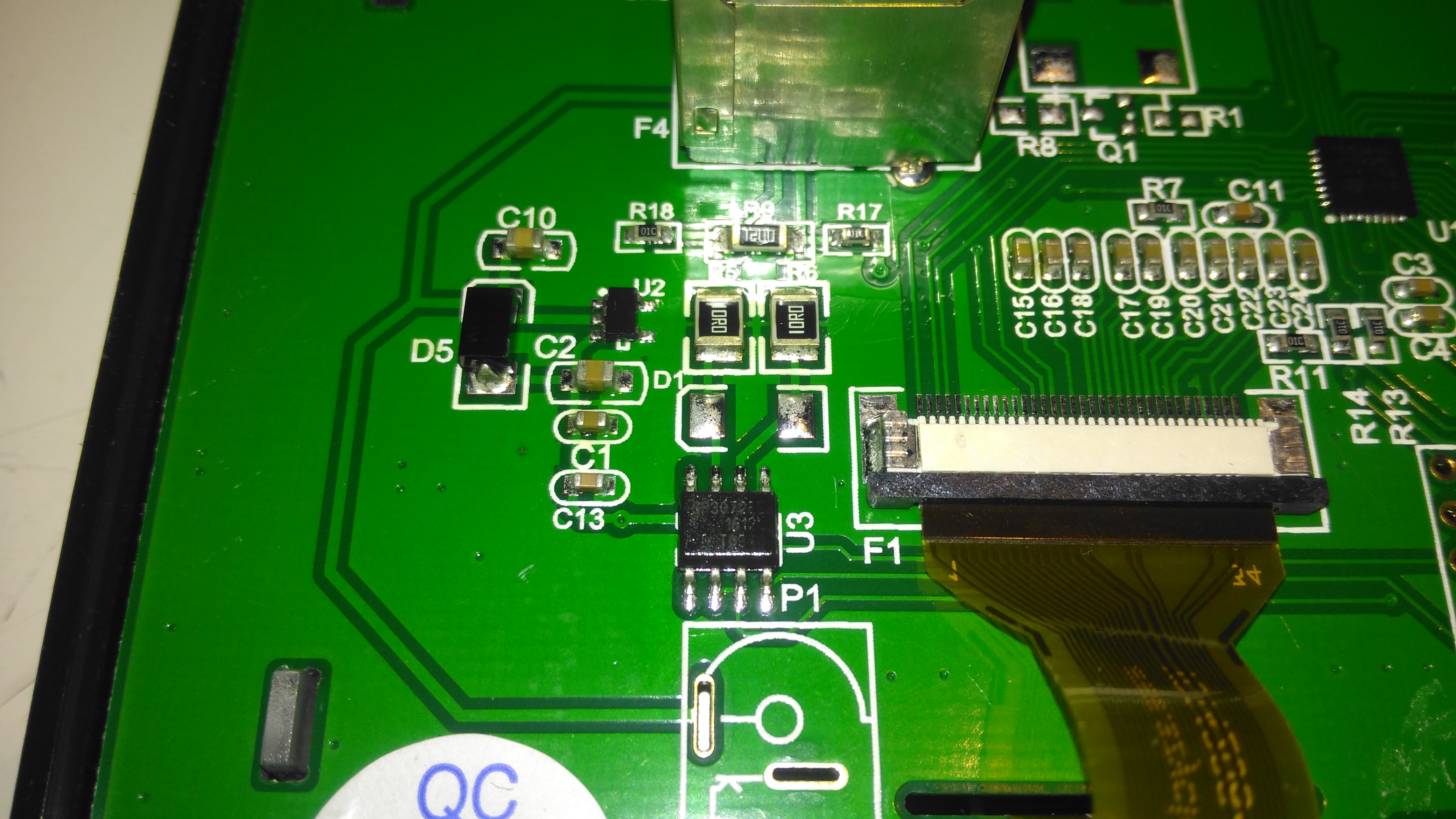
The rear plastic cover is held in place by 4 machine screws, which thread into brass inserts in the plastic frame – nice high quality touch on the design here, no cheap self tapping plastic screws. Both power & data arrive via an Ethernet cable, but the communication here is RS-485, and not compatible with Ethernet! The PCB is pretty sparse, with comms & power on the left, LCD connection in the centre, and the microcontroller on the right.
RS-485 Transceiver
On the left of the board is the RS0485 transceiver, and a small voltage regulator. There’s also a spot for a DC barrel jack, which isn’t included in this model for local power supply.
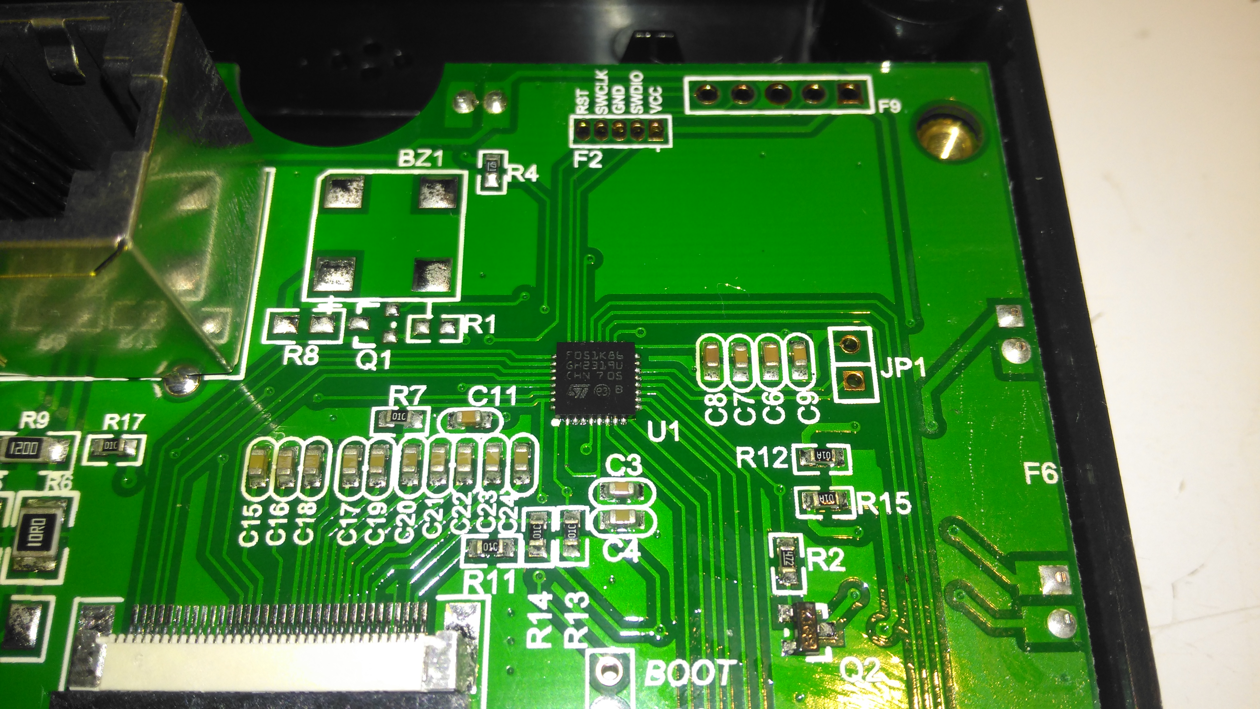
STM32 Microcontroller
The other side of the board holds the main microcontroller which communicates with the charge controller. This is a STM32F051K8 from ST Microelectronics. With a 48MHz ARM Cortex M0 core, and up to 64K of flash, this is a pretty powerful MCU that has very little to do in this application.
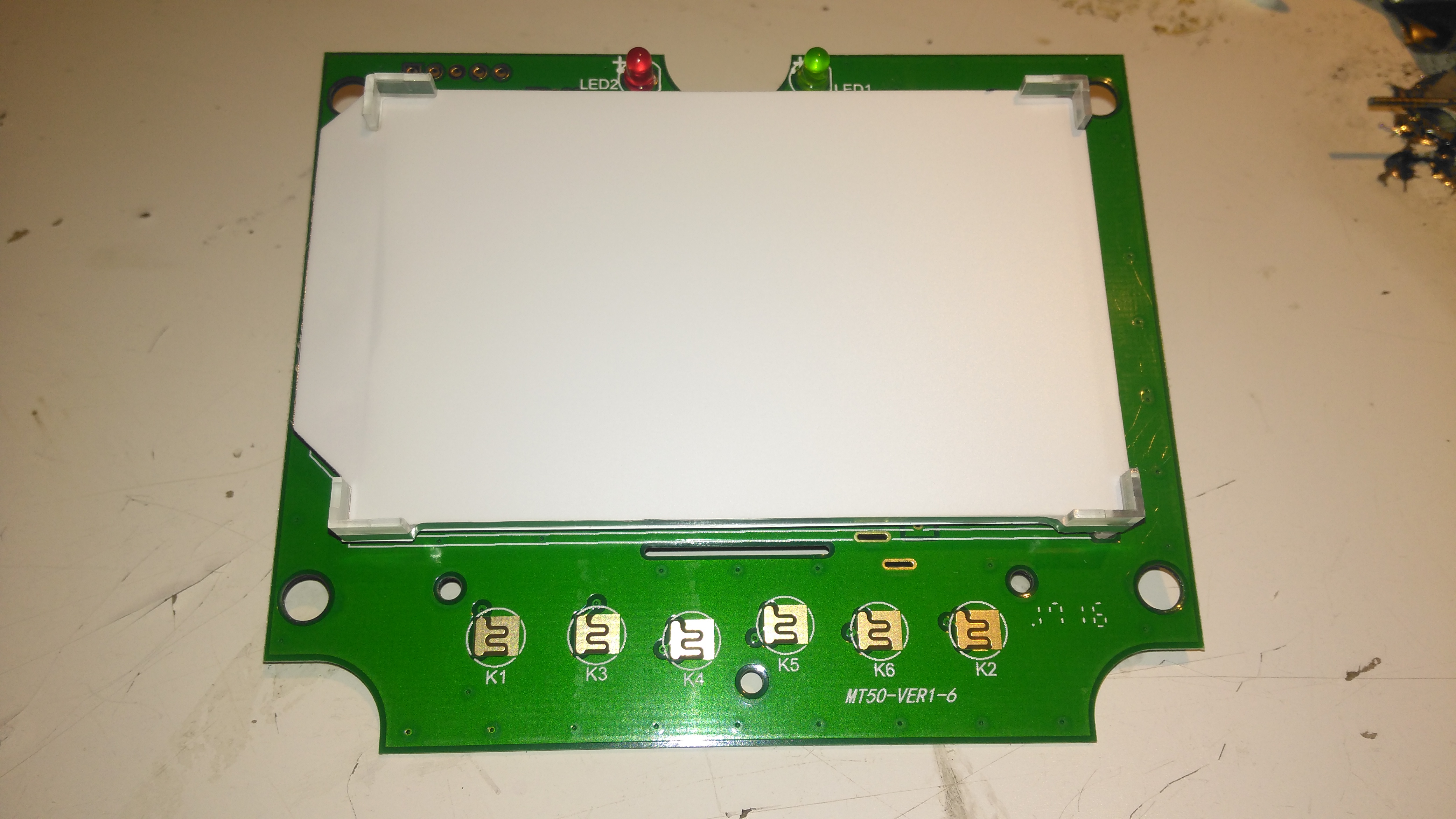
PCB Front
The front of the PCB has the ENIG contacts of the front panel buttons, and the LCD backlight assembly. There’s nothing else under the plastic backlight spreader either.
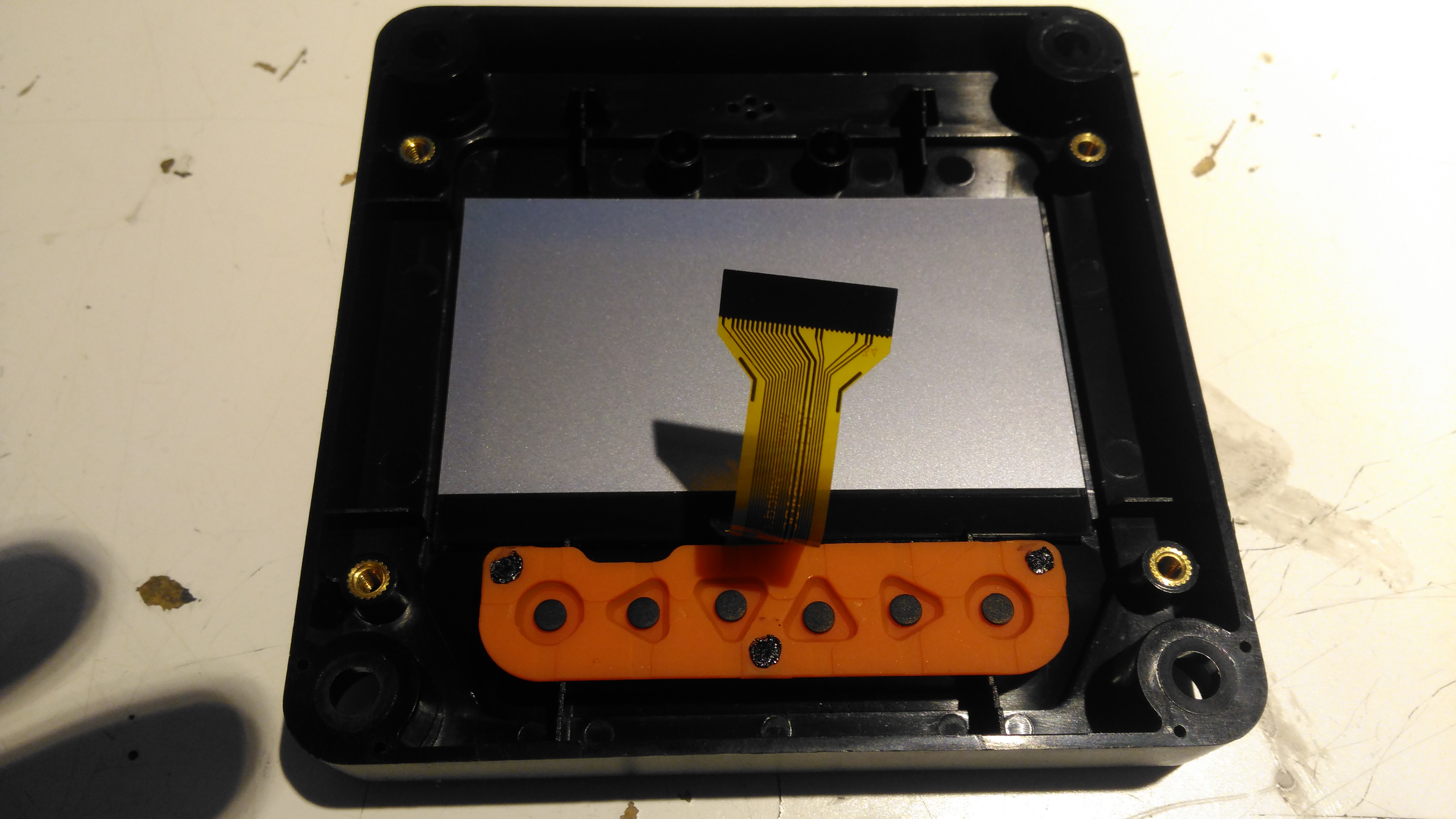
LCD Rear
The front case holds the LCD module in place with glue, and the rubber buttons are placed underneath, which is heat staked in place.
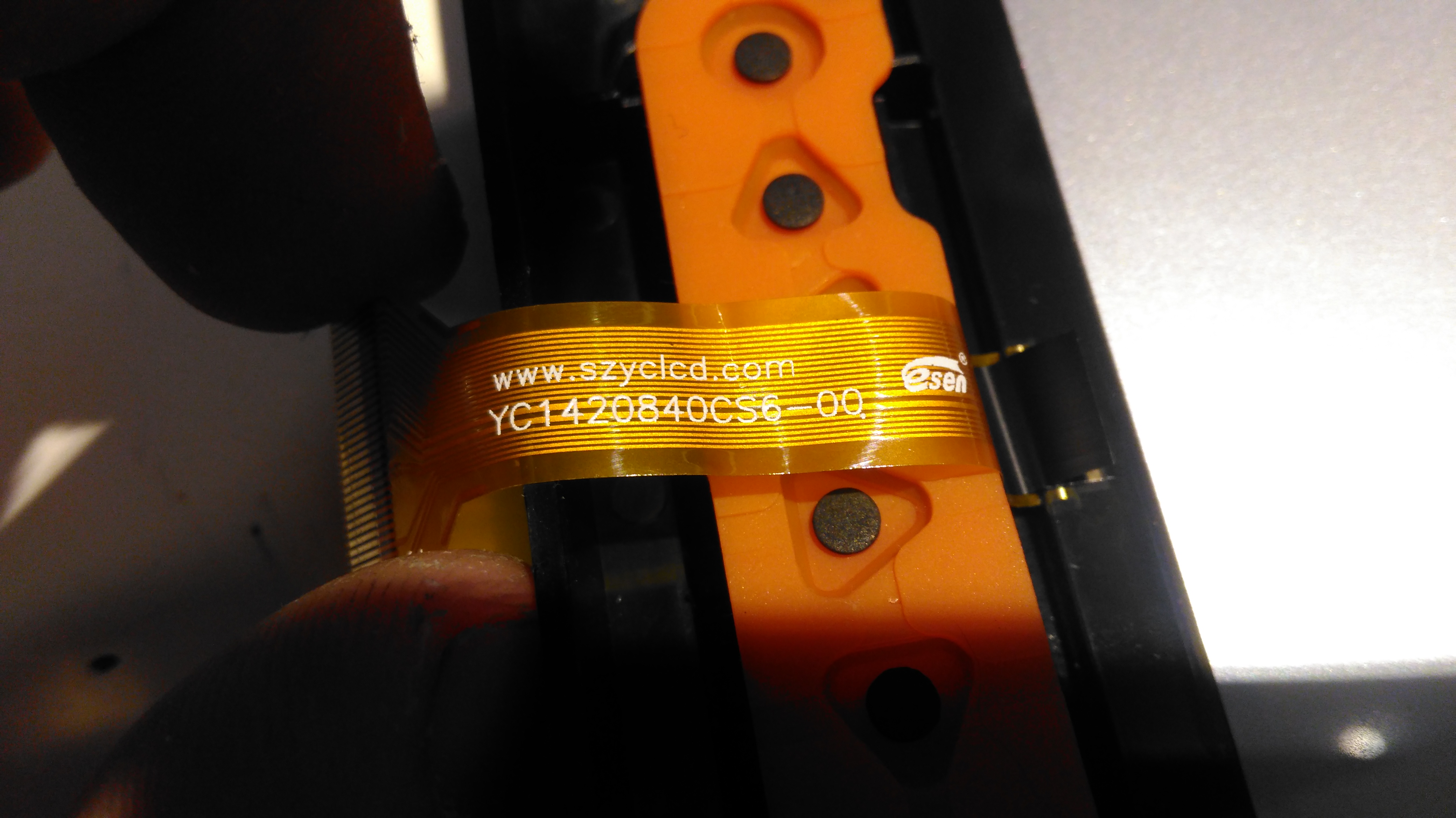
LCD Model
The LCD is a YC1420840CS6 from eCen in China. Couldn’t find much out about this specific LCD.
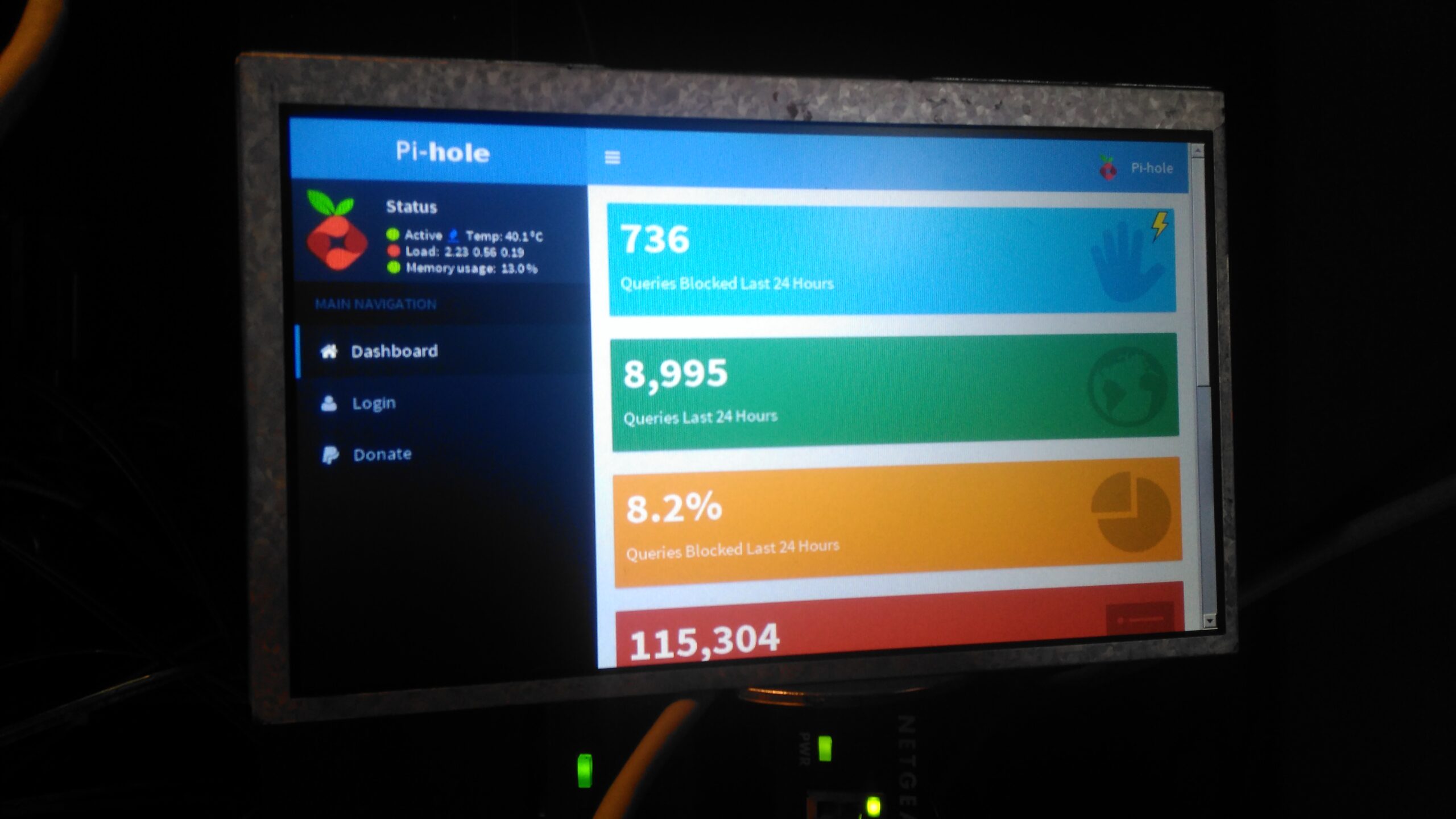
On my home network I have a system running PiHole – a DNS server that blocks all unwanted traffic, such as ads. Since I have an official Pi LCD with a broken touch panel, I decided to use the bare LCD as a status display for PiHole.
This requires some extra packages installing onto the base system after PiHole is installed & configured, and the interface automatically starts on bootup. I used the latest Raspbian Jessie Minimal image for this system, and ran everything over a SSH connection.
First thing, get the required packages installed onto the Pi:
Once these are installed, it’s time to configure the startup script for Midori to display the status page. Create StartMidori.sh in /home/pi and fill with the following:
#!/bin/sh export DISPLAY=:0
xset -dpms
xset s off
xset s noblank
unclutter &
matchbox-window-manager &
midori -e Fullscreen -a http://127.0.0.1/admin/
This script disables all power management on the system to keep the LCD on, starts unclutter to hide the mouse pointer and finally starts the Matchbox Window Manager to run Midori, which itself is set to fullscreen mode, and the URL of the admin panel is provided.
The next step is to test, give the script executable permissions, and run the script:
Once this is run, the LCD should come to life after a short delay with the PiHole stats screen. Close the test & return to the terminal by hitting CTRL+C.
Now the Pi can be configured to autorun this script on boot, the first thing to do here is to enable autologin on the console. This can be done with raspi-config, select Option 3 (Boot Options), then Option B1 (Desktop/CLI), then Option B2 (Console Autologin). When prompted to reboot, select No, as we’ll be finishing off the config before we reboot the system.
The next file to edit is /etc/rc.local, add the command to start the status browser up:
#!/bin/sh -e
#
# rc.local
#
# This script is executed at the end of each multiuser runlevel.
# Make sure that the script will "exit 0" on success or any other
# value on error.
#
# In order to enable or disable this script just change the execution
# bits.
#
# By default this script does nothing.

# Print the IP address
_IP=$(hostname -I) || true
if [ "$_IP" ]; then
  printf "My IP address is %s\n" "$_IP"
fi
sudo xinit /home/pi/StartMidori.sh &
exit 0
Here I’ve added in the command just above “exit 0”. This will start the browser as the last thing on bootup. The Pi can now be rebooted, and the status display should start on boot!
As many will already know, we lost a guiding light in the Rock World last week, Chester Bennington of Linkin Park. I am reposting the message from the other bandmembers here, being one of the first bands I ever listened to of this genre. As someone with mental illness, seeing someone identify their depression, and having it still kill them is rather disturbing.
RIP Chester, Forever With Us In Song
Dear Chester,
Our hearts are broken. The shockwaves of grief and denial are still sweeping through our family as we come to grips with what has happened.
You touched so many lives, maybe even more than you realized. In the past few days, we’ve seen an outpouring of love and support, both public and private, from around the world. Talinda and the family appreciate it, and want the world to know that you were the best husband, son, and father; the family will never be whole without you.
Talking with you about the years ahead together, your excitement was infectious. Your absence leaves a void that can never be filled—a boisterous, funny, ambitious, creative, kind, generous voice in the room is missing. We’re trying to remind ourselves that the demons who took you away from us were always part of the deal. After all, it was the way you sang about those demons that made everyone fall in love with you in the first place. You fearlessly put them on display, and in doing so, brought us together and taught us to be more human. You had the biggest heart, and managed to wear it on your sleeve.
Our love for making and performing music is inextinguishable. While we don’t know what path our future may take, we know that each of our lives was made better by you. Thank you for that gift. We love you, and miss you so much.
This is another automotive part, this one was found lurking inside an LCD info display from a BMW. I didn’t manage to find a datasheet for this one, the neither the part number on the package or the wafer code on the die itself revealed anything.
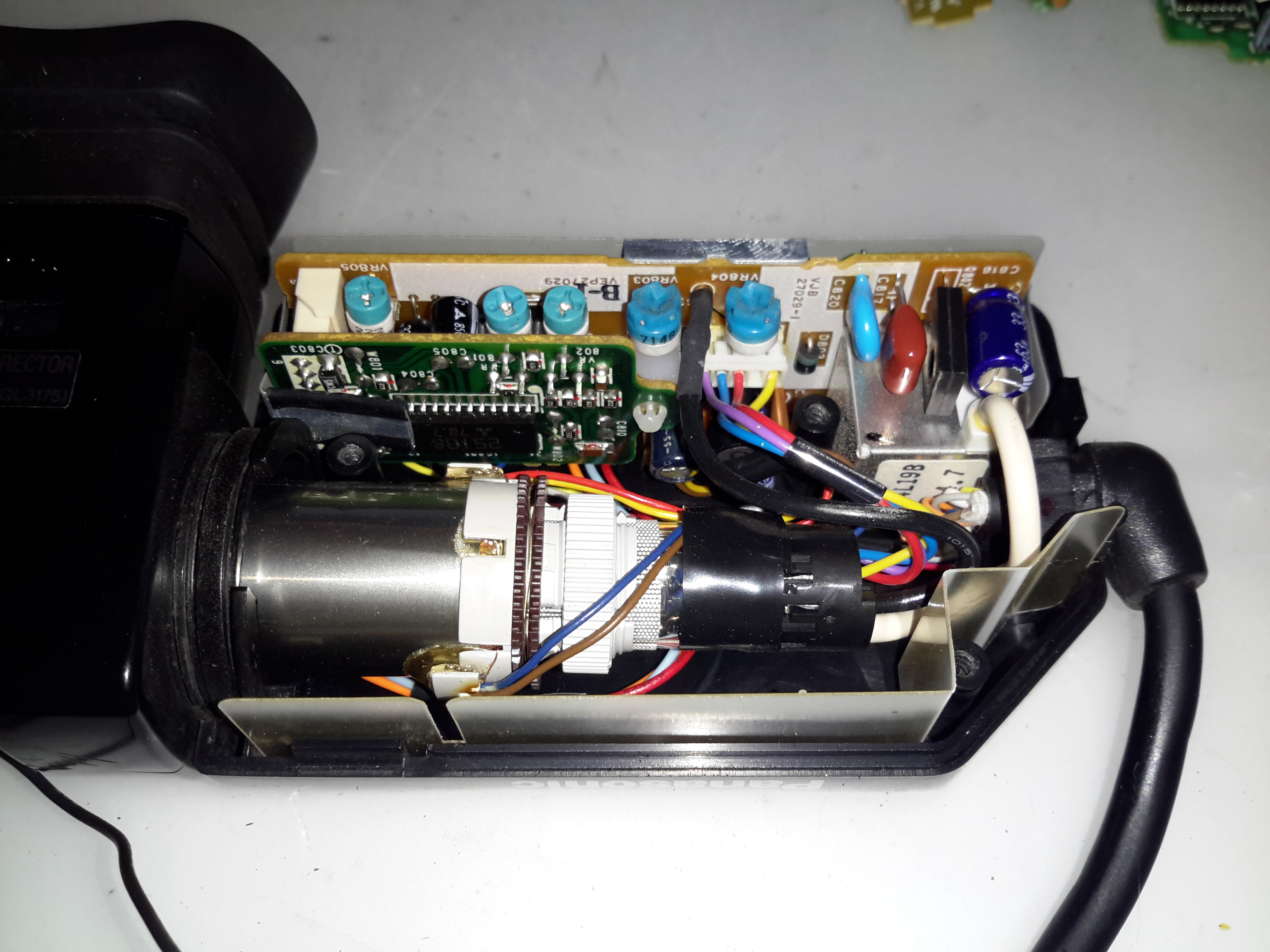
The old Panasonic NV-M5 has the standard for the time CRT based viewfinder assembly, which will happily take a composite video signal from an external source.
This viewfinder has many more connections than I would have expected, as it has an input for the iris signal, which places a movable marker on the edge of the display. This unit also has a pair of outputs for the vertical & horizontal deflection signals, I imagine for sync, but I’ve never seen these signals as an output on a viewfinder before.
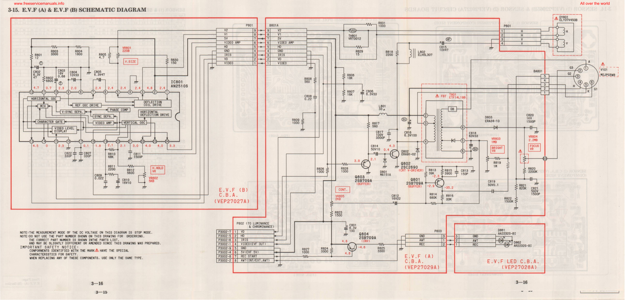
EVF Schematic
Luckily I managed to get a service manual for the camera with a full schematic.
This unit takes a 5v input, as opposed to the 8-12v inputs on previous cameras, so watch out for this! There’s also no reverse polarity protection either.
Pins
Making the iris marker vanish from the screen is easy, just put a solder bridge between pins 15 & 16 of the drive IC. The important pins on the interface connector are as follows:
Pin 3: GND
Pin 4: Video Input
Pin 5: Video GND
Pins 6: +5v Supply
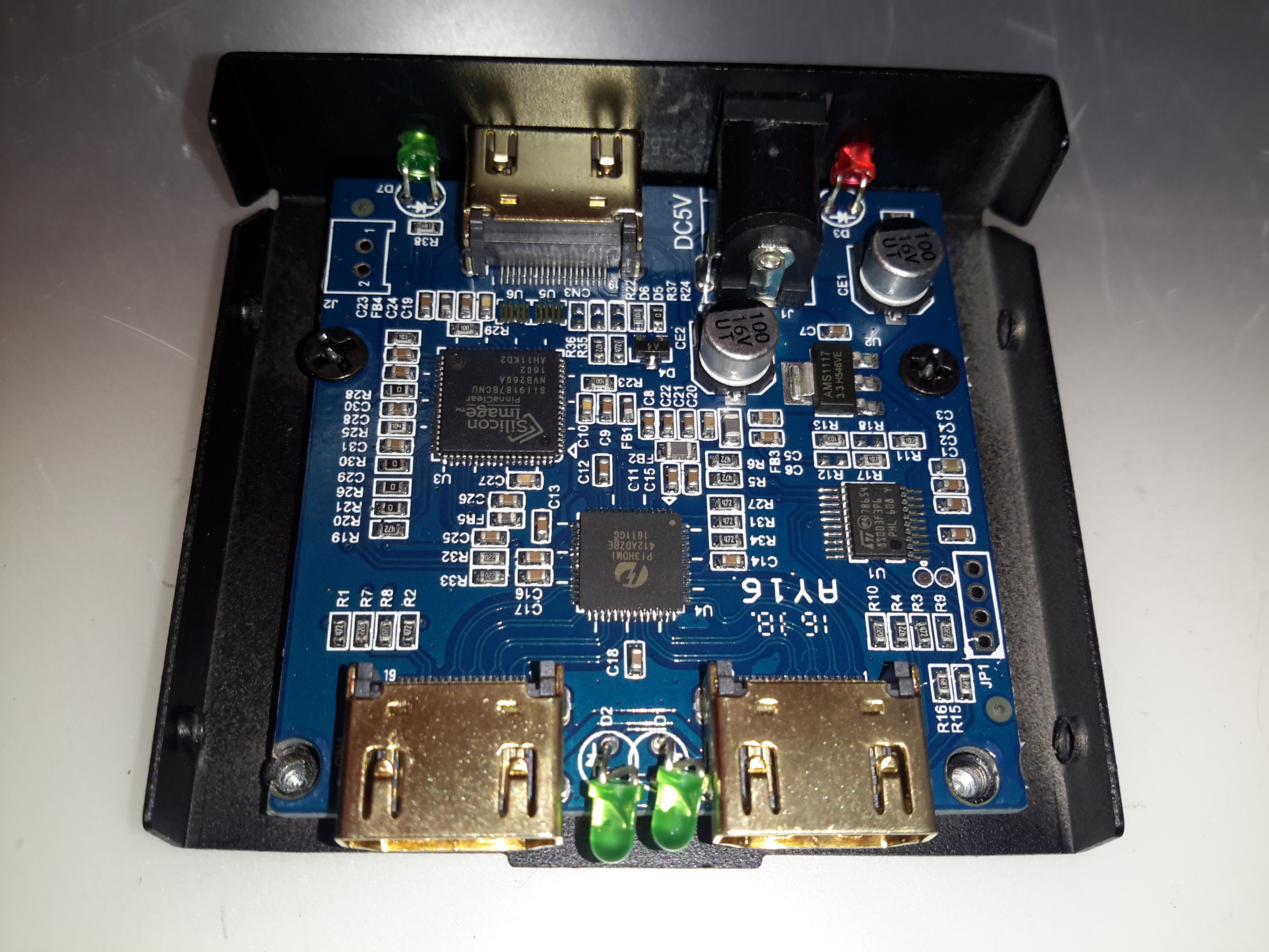
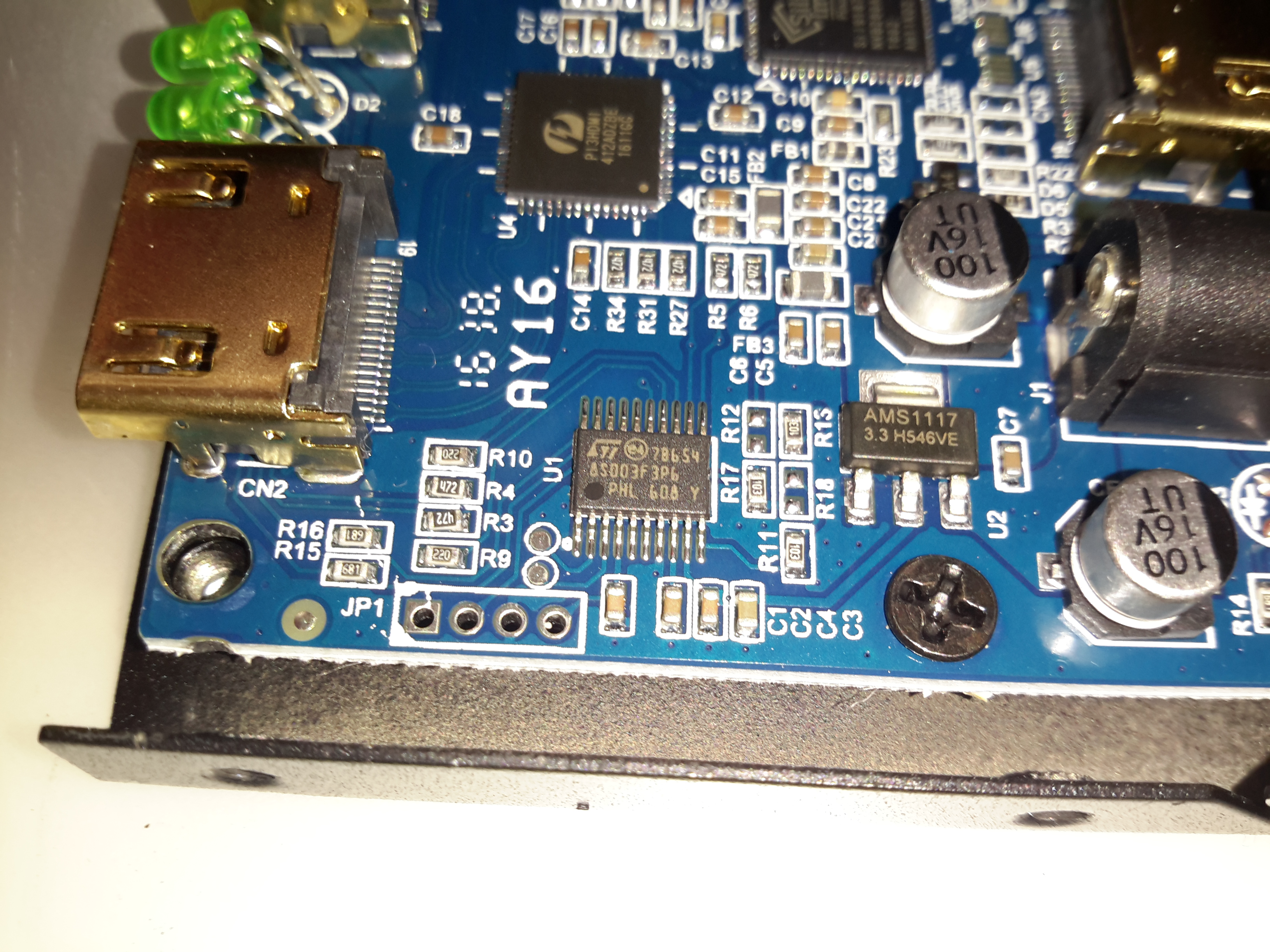
Time for another random teardown, a signal splitter for HDMI. These units are available very cheap these days on eBay. This one splits the incoming signal into two to drive more than one display from the same signal source.
Main PCB
The stamped alloy casing comes apart easily with the removal of a few screws. The PCB inside is rather densely packed with components.
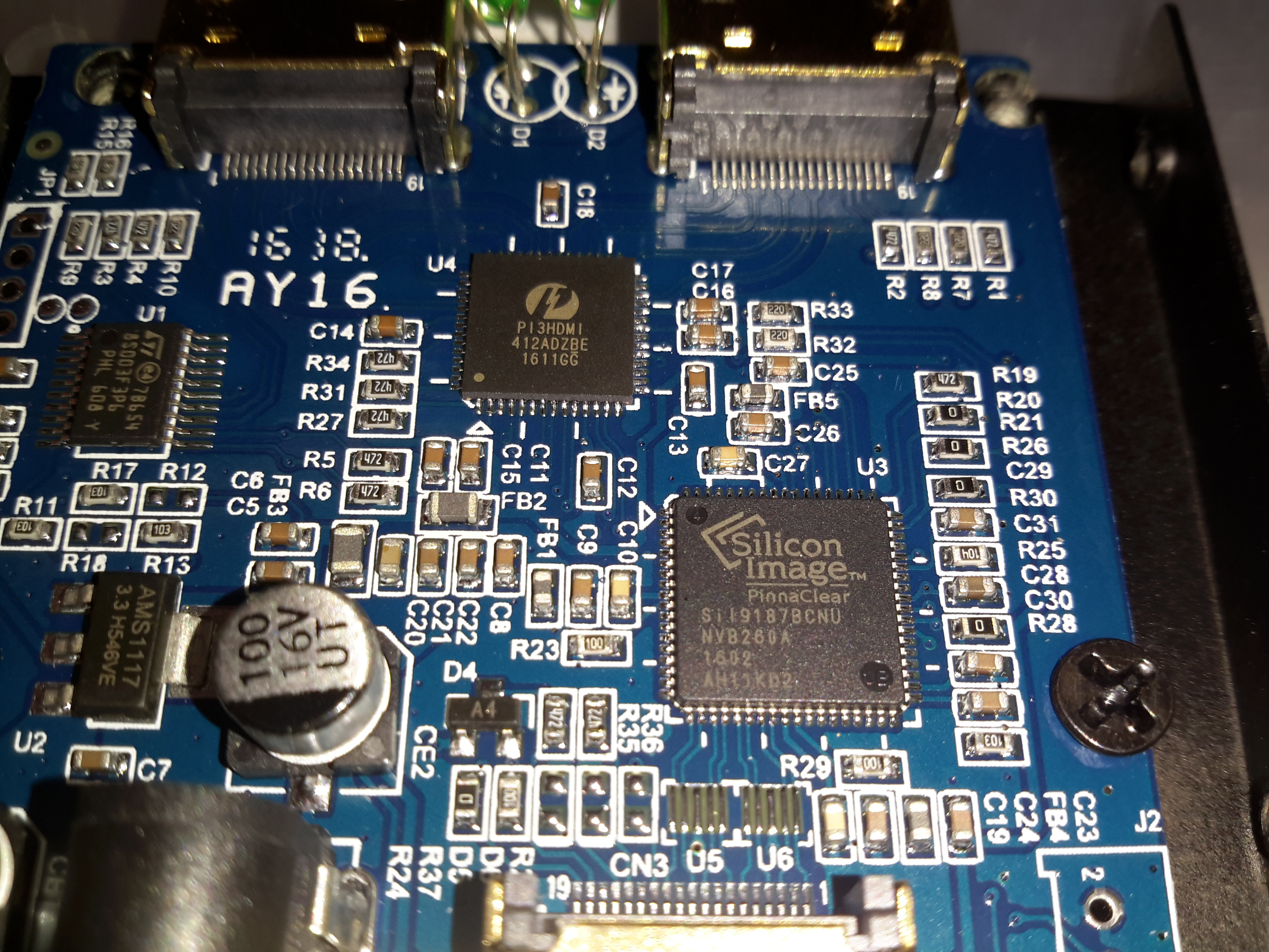
Chipset
The main IC on the incoming signal is a Silicon Image Sil9187B HDMI Port Processor, with a single input & 4 outputs. In this case the chip is used as a repeater to amplify the incoming signal. the signal path then gets fed into a Pericom PI3HDMI412 HDMI Demux, which then splits the signal into two for the output ports.
Microcontroller
The main pair of ICs processing the video signals are controlled over I²C, with this STM32 microcontroller. The 4 pads to the lower left are for the STLink programmer. The main 3.3v power rail is provided by the LM1117 linear regulator on the right.
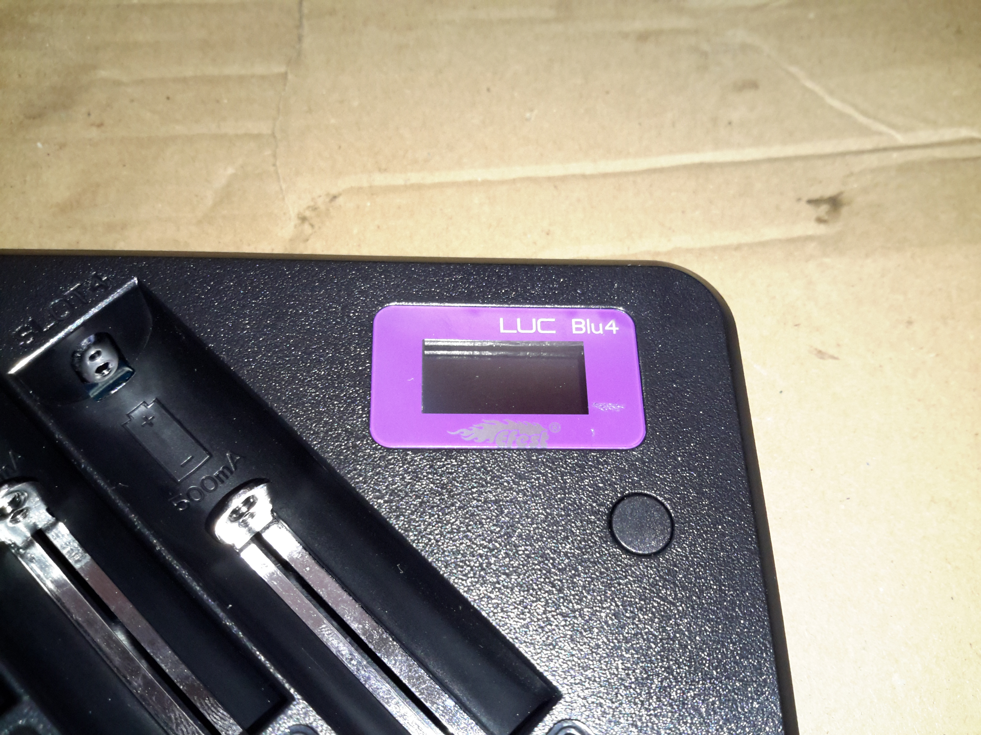
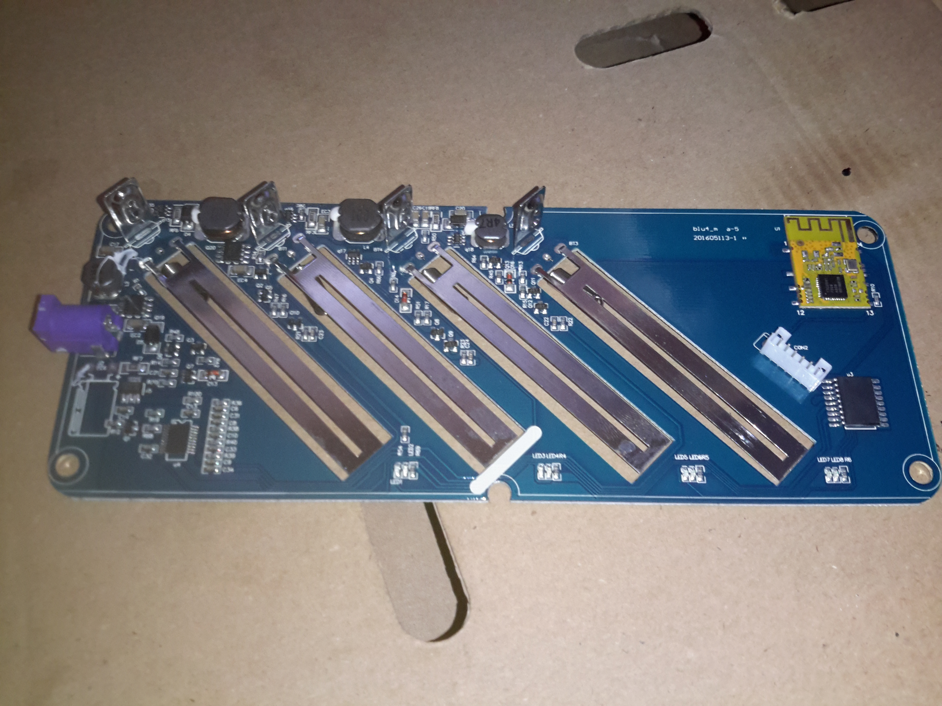
Here’s another battery charger designed for lithium chemistry cells, the BLU4. This charger doesn’t display much on it’s built in LCD, apart from basic cell voltage & charging current limits, as it has a built in Bluetooth module that will link into an Android or iOS app.
Above the charger is operating with 4 brand new cells, at a current of 500mA per cell. If only a pair of cells is being charged, the current can be increased to 1A per cell.
LCD
Not much in the way of user interface on the charger, a tiny LCD & single button for cycling through the display options.
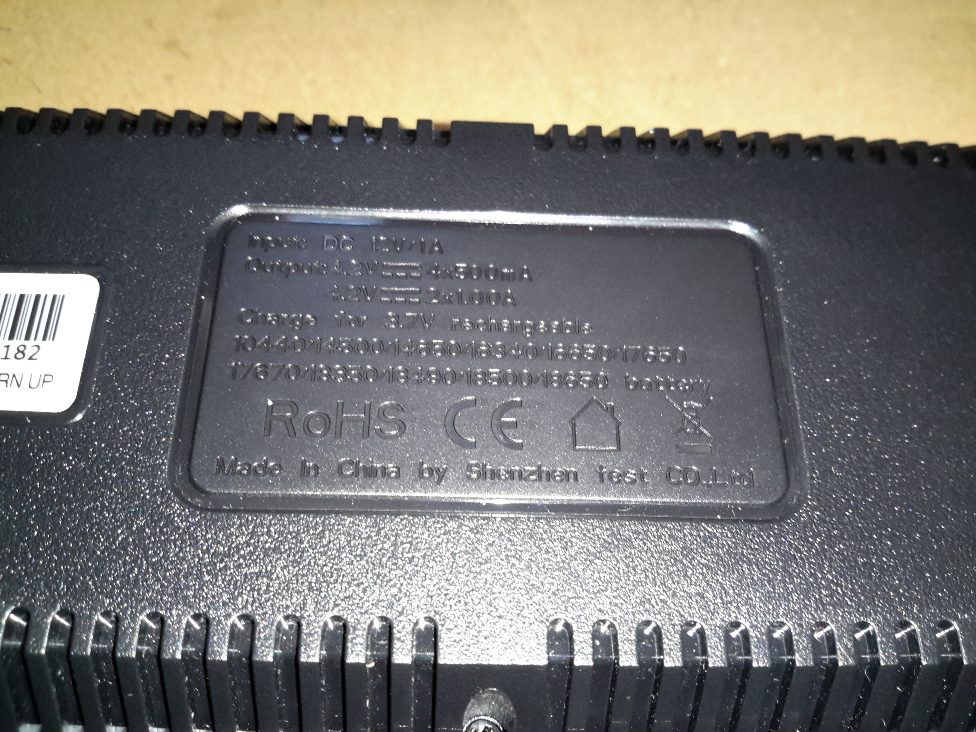
Dataplate
The usual stuff on the data plate, the charger accepts an input of 12v DC at 1A.
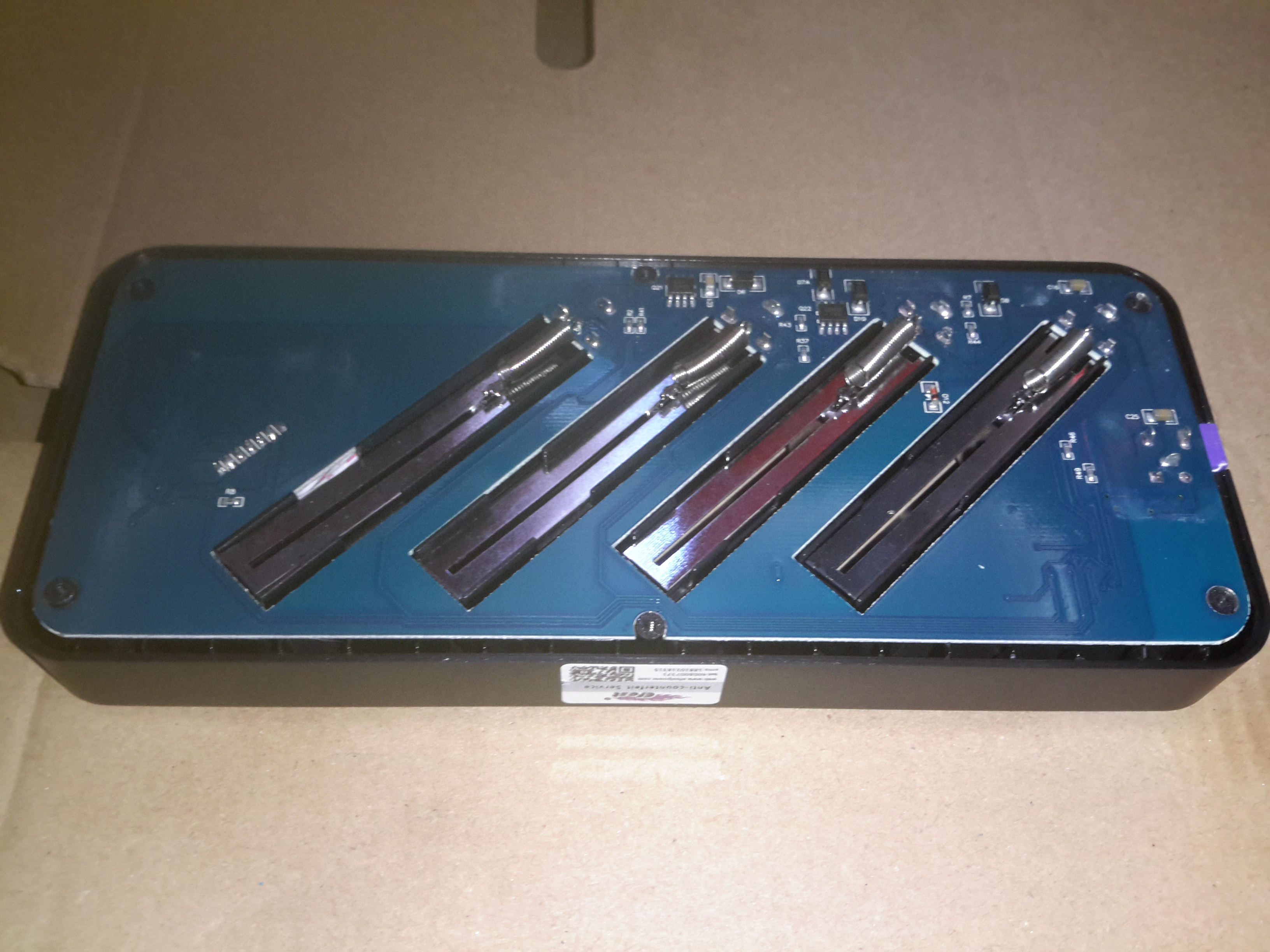
Bottom Cover Removed
Removing the 6 screws on the bottom of the casing allows the board to be seen. Not much on the bottom, the 4 cell negative connections can be seen, with their springs for adjusting for cell length.
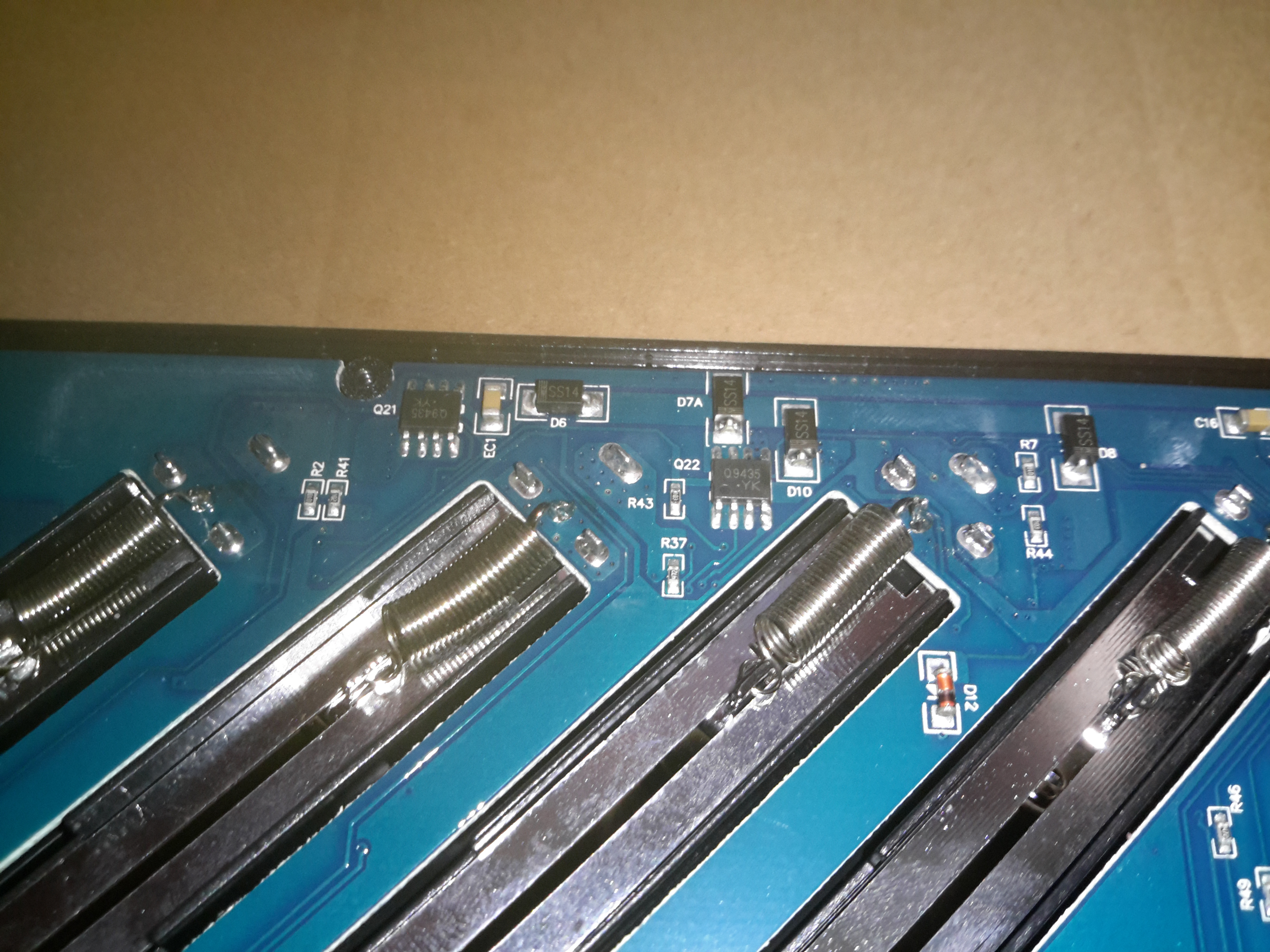
MOSFETs
There’s a couple of P-Channel FETs on the bottom side for the charging circuits, along with some diodes.
Main PCB
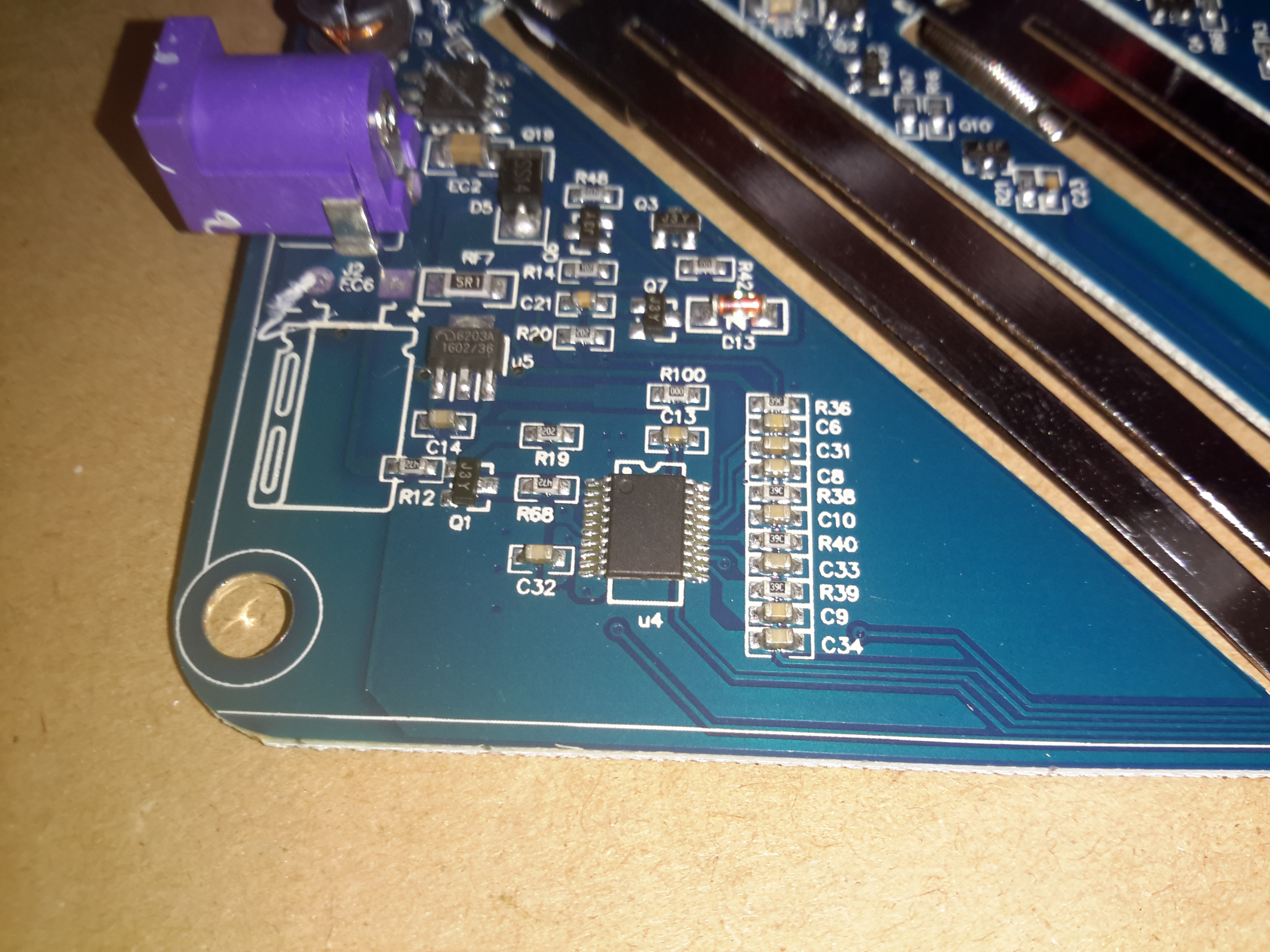
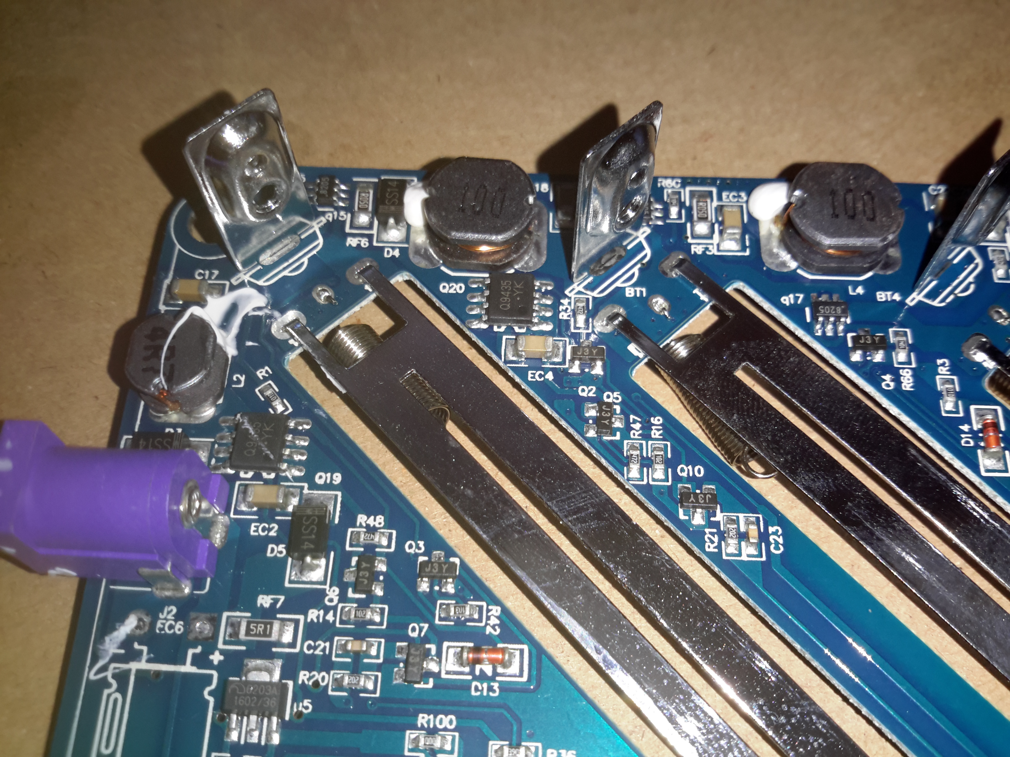
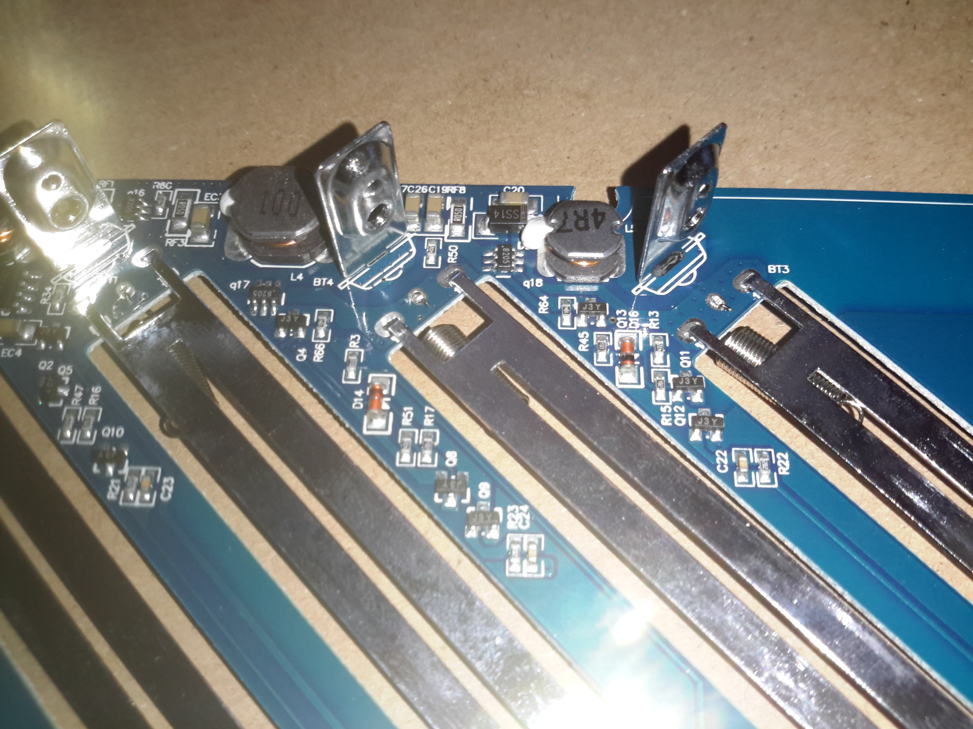
The main PCB is easily removed after the springs are unhooked from the terminals. Most of the power circuitry is located on the top side near the power input. There are 4 DC-DC converters on board for stepping the input 12v down to the 4.2v required to charge a lithium cell.
Second Controller
Not entirely sure what this IC is in the bottom corner, as it’s completely unmarked. I’m guessing it’s a microcontroller though.
DC Input Side
The top left of the board is crammed with the DC-DC converters, all the FETs are in SO8 packages.
DC-DC Converters
One pair of DC-DC inductors is larger than the other pair, for reasons I’m unsure of.
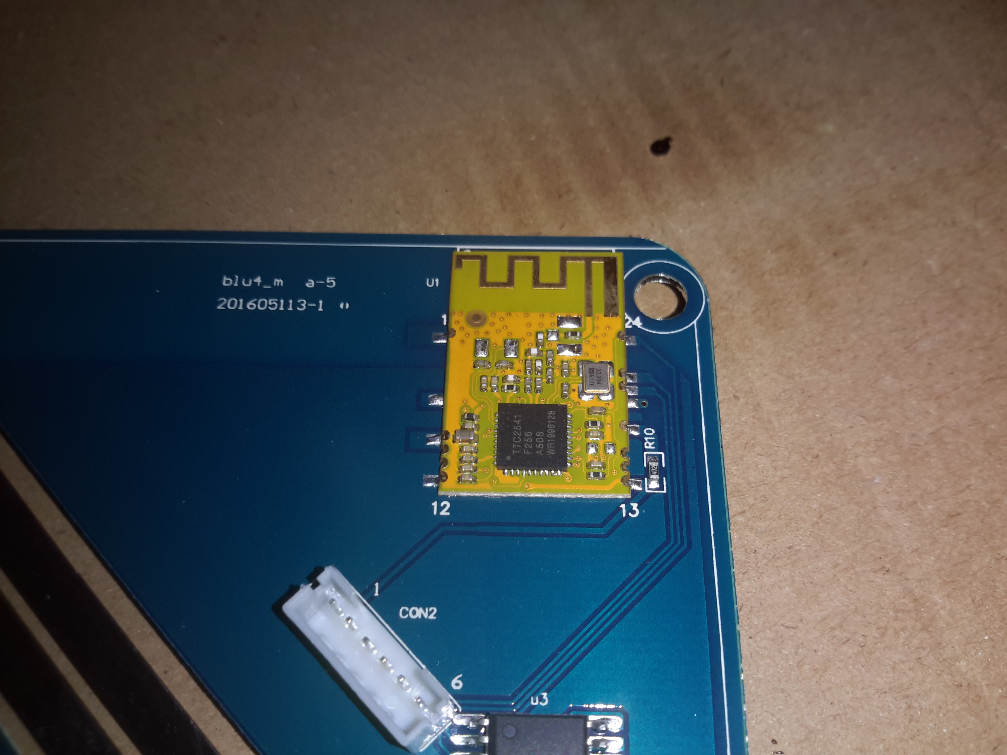
Bluetooth Module
Bluetooth connectivity is provided by this module, which is based around a TTC2541 BLE IC.
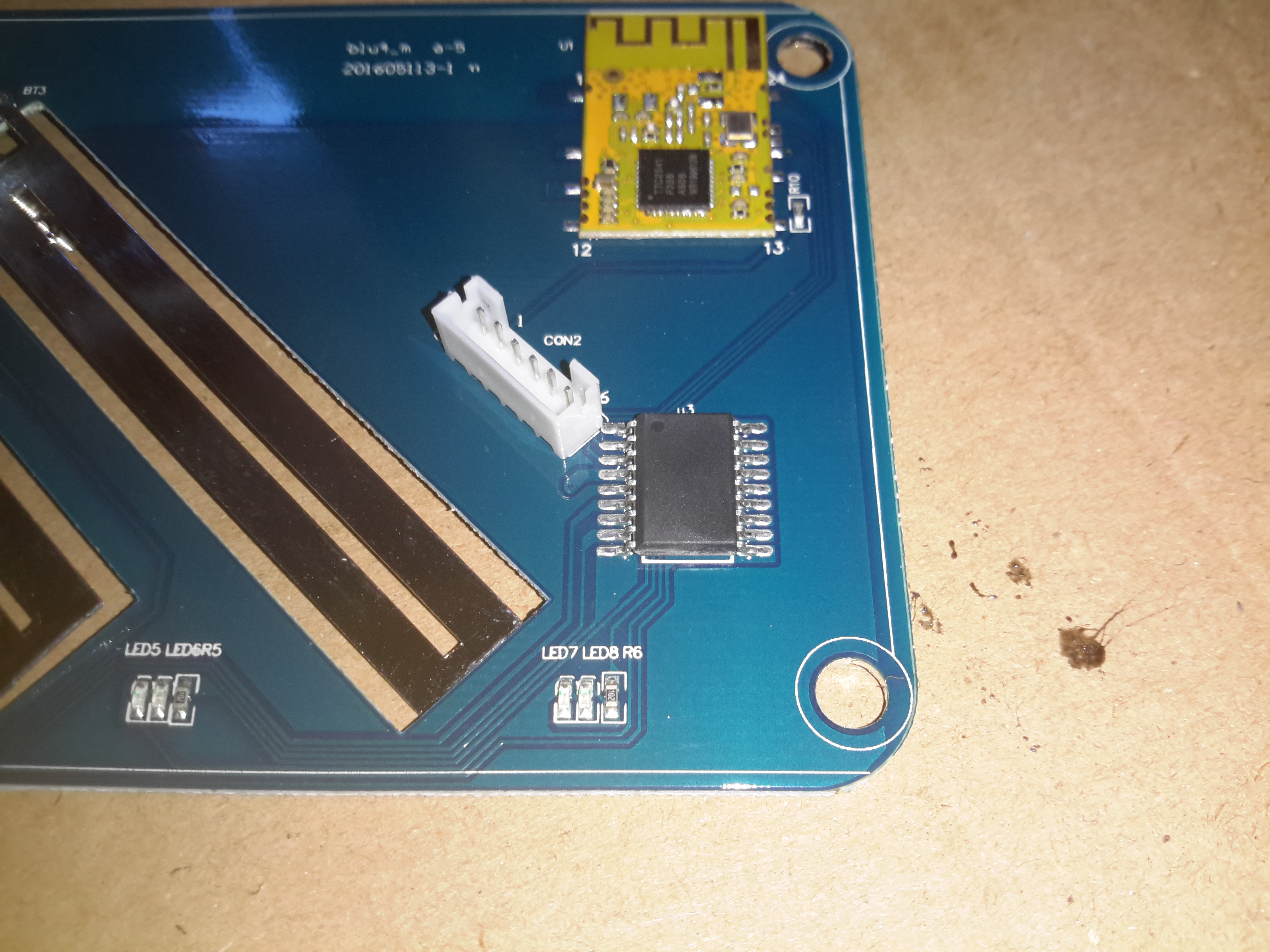
Microcontroller
Below the Bluetooth module is yet another completely unmarked IC, the direct link to the BLE interface probably means it’s another microcontroller. The Socket to the left of the IC is the connector for the front panel LCD & button.
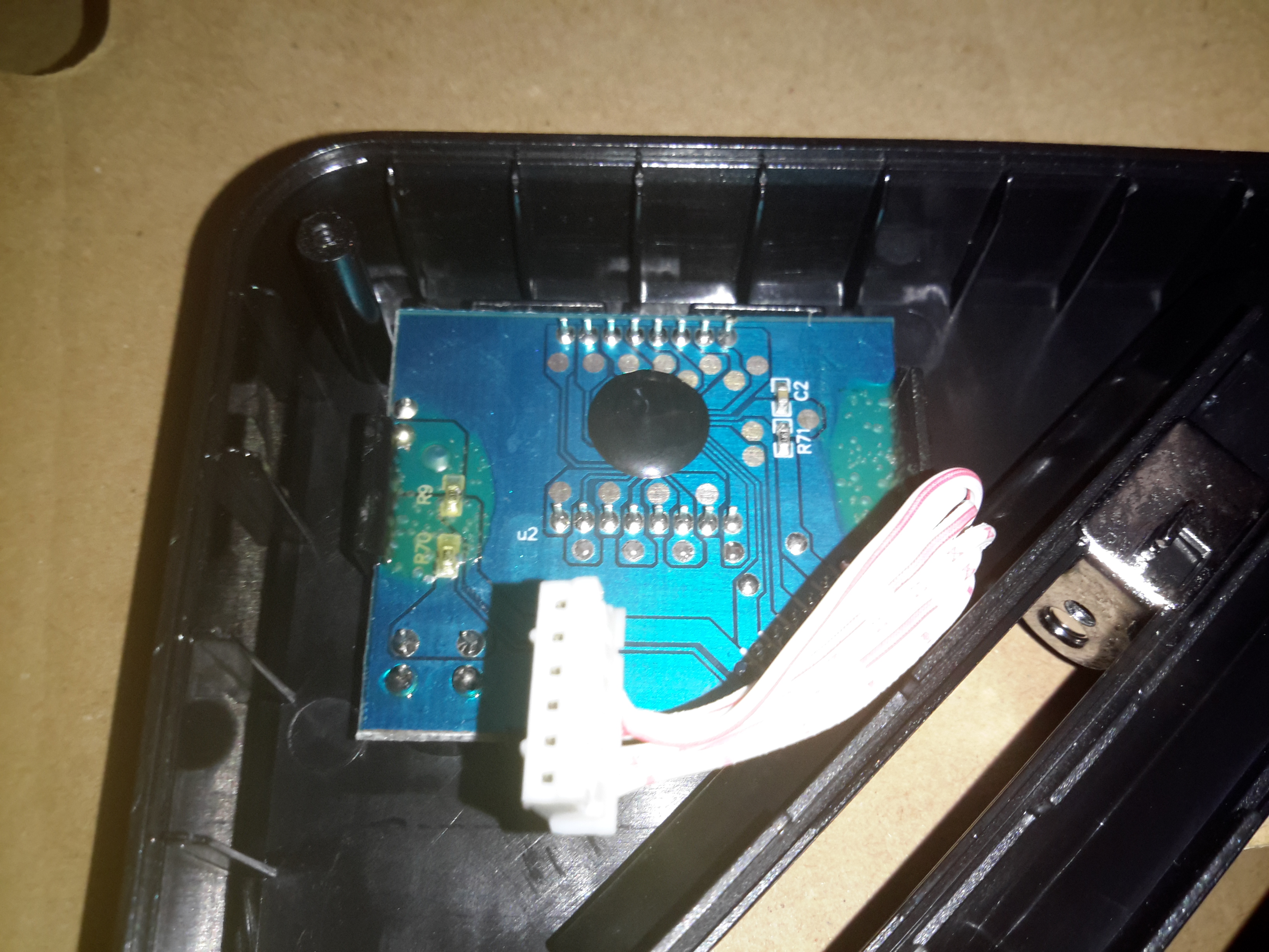
LCD PCB
There’s not much to the LCD itself, so I won’t remove this board. The LCD controller is a COB type device, from the number of connections it most likely communicates with the micro via serial.
I recently came across these on eBay, so I thought I’d grab one to see how they function, with all the metrics they display, there’s potential here for them to be very useful indeed.
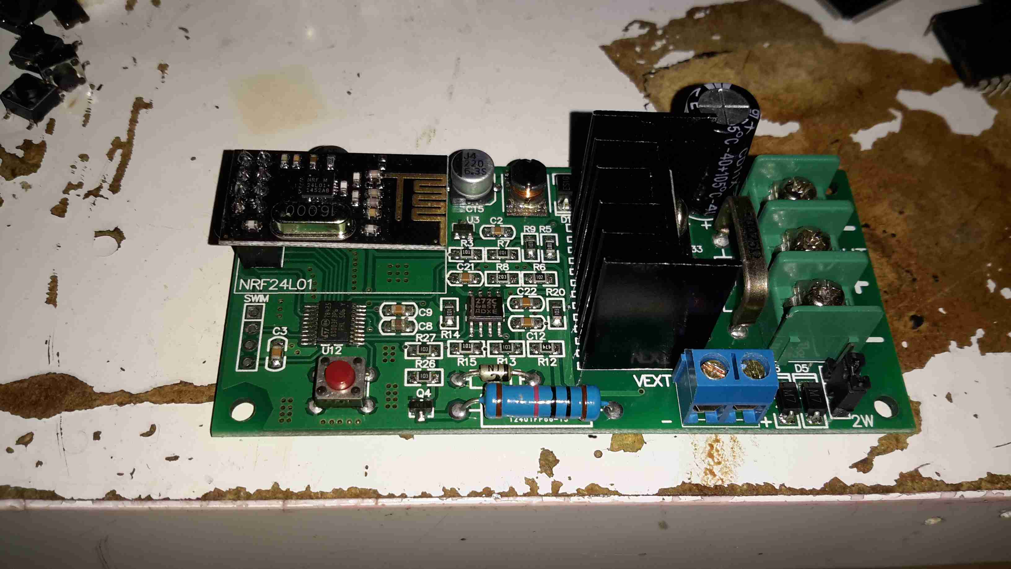
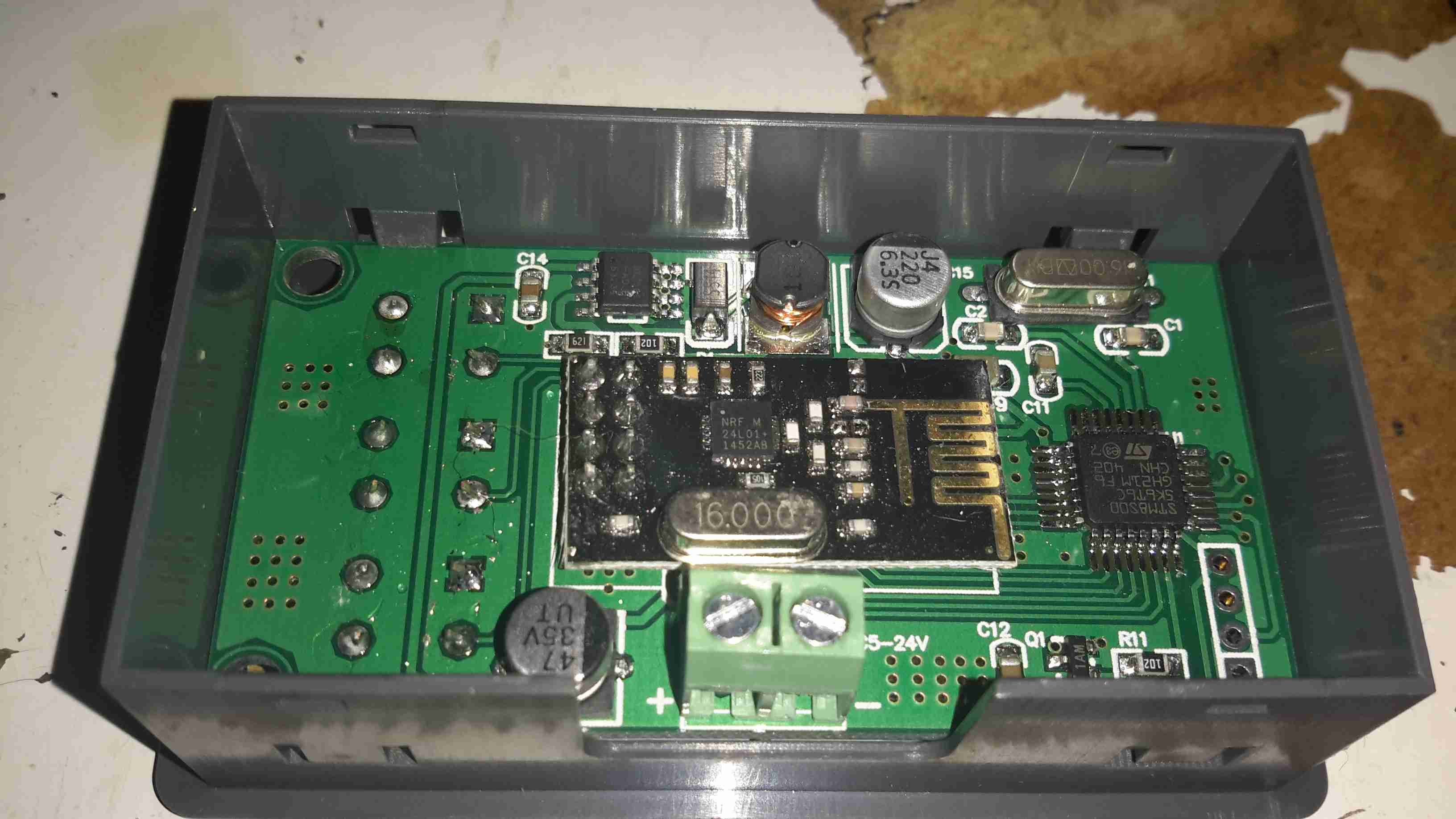
One of the best parts is that no wiring is required between the sensor board & the LCD head unit – everything is transmitted over a 2.4GHz data link using NRF24L01 modules.
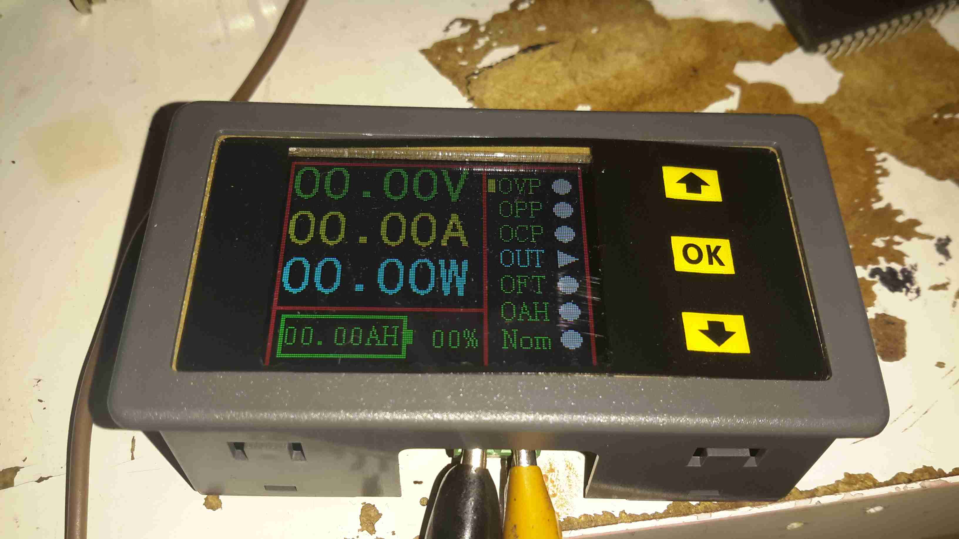
Above is the display unit, with it’s colour LCD display. Many features are available on this, & they appear to be designed for battery powered systems.
Monitor PCB
Another PCB handles the current & voltage sensing, so this one can be mounted as close to the high current wiring as possible.
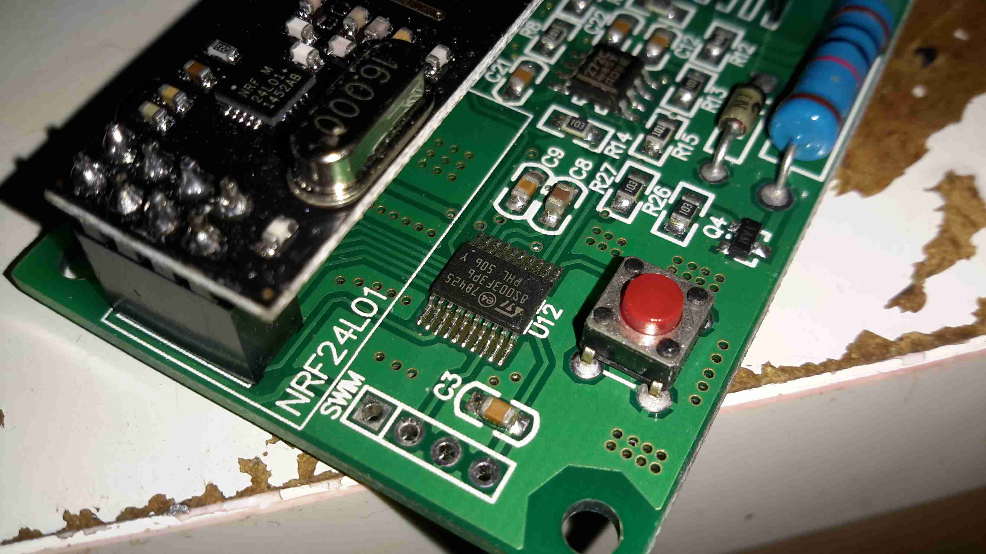
Monitor PCB Microcontroller
The transmitter PCB is controlled with an STM8S003F3 microcontroller from ST Microelectronics. This is a Flash based STM with 8KB of ROM, 1KB of RAM & 10-bit ADC. The NRF24L01 transceiver module is just to the left.
There’s only a single button on this board, for pairing both ends of the link.
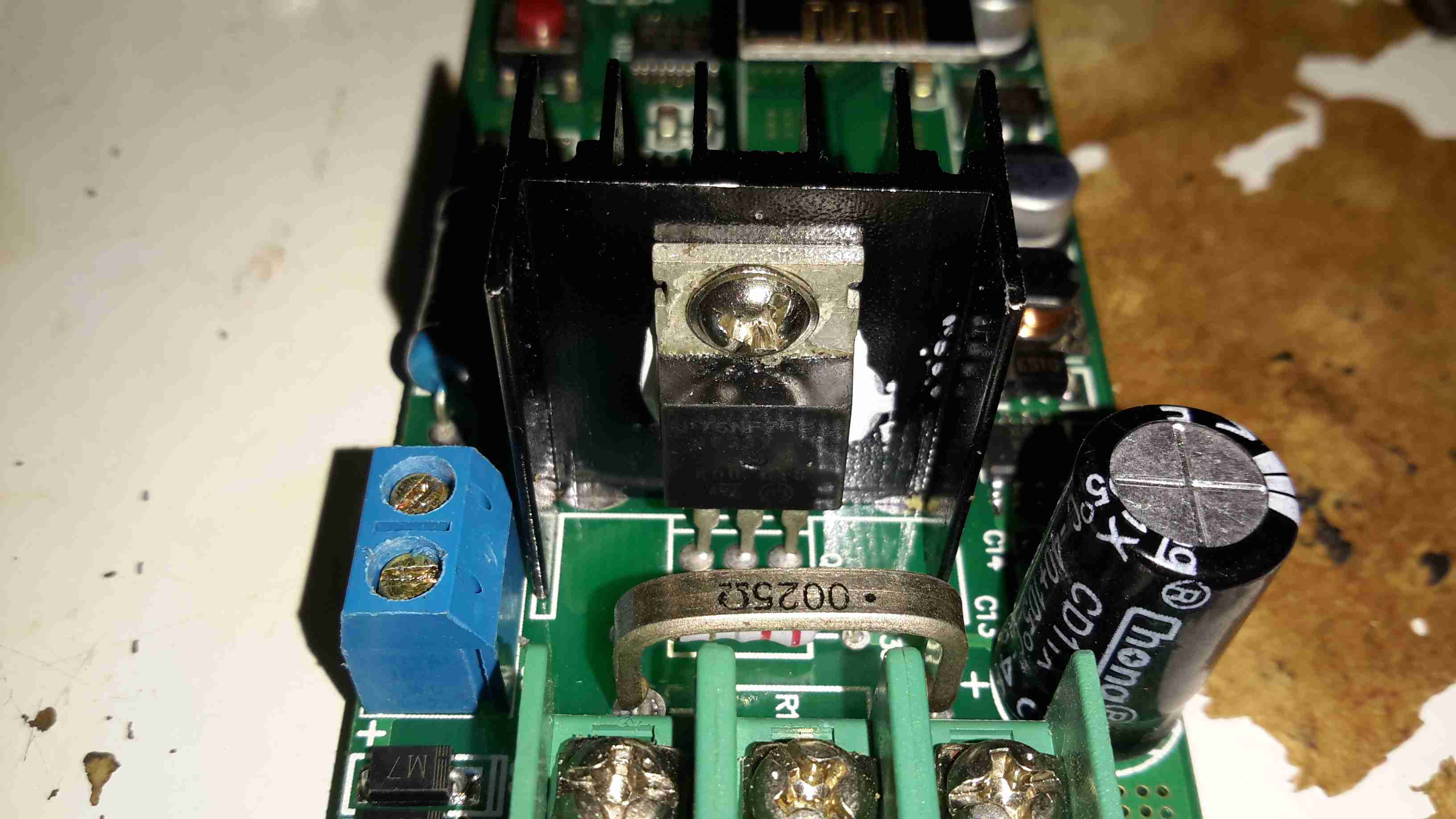
Output MOSFET
The high current end of the board has the 0.0025Ω current shunt & the output switch MOSFET, a STP75NF75 75v 75A FET, also from ST Microelectronics. A separate power source can be provided for the logic via the blue terminal block instead of powering from the source being measured.
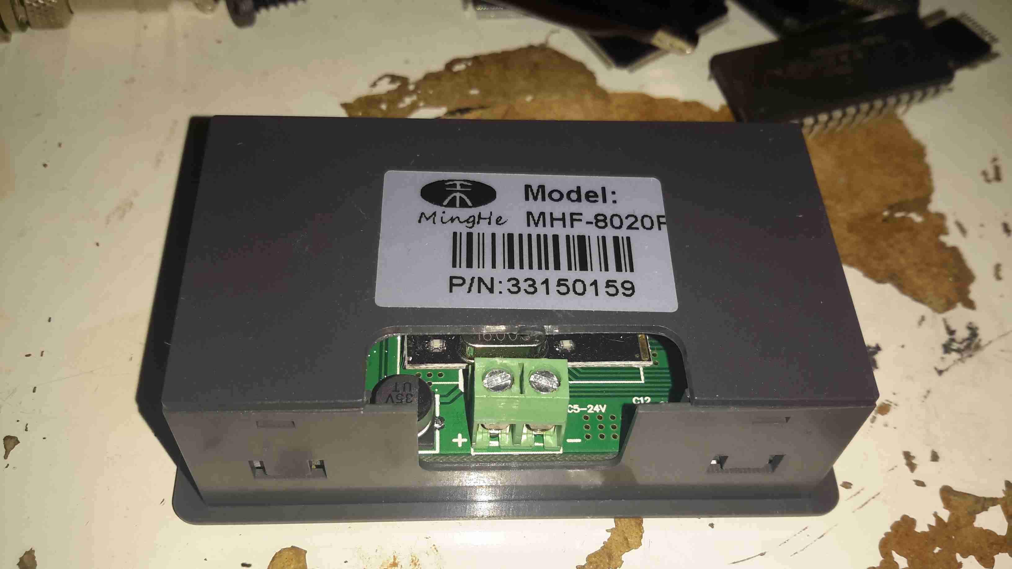
LCD Unit Rear
Here’s the display unit, only a pair of power terminals are provided, 5-24v wide-range input is catered for.
LCD Unit PCB
Unclipping the back of the board reveals the PCB, with another 2.4GHz NRF24L01 module, and a STM8S005K6 microcontroller in this case. The switching power supply that handles the wide input voltage is along the top edge of the board.
Unfortunately I didn’t get any instruction manual with this, so some guesswork & translation of the finest Chinglish was required to get my head round the way everything works. To make life a little easier for others that might have this issue, here’s a list of functions & how to make them work.
LCD Closeup
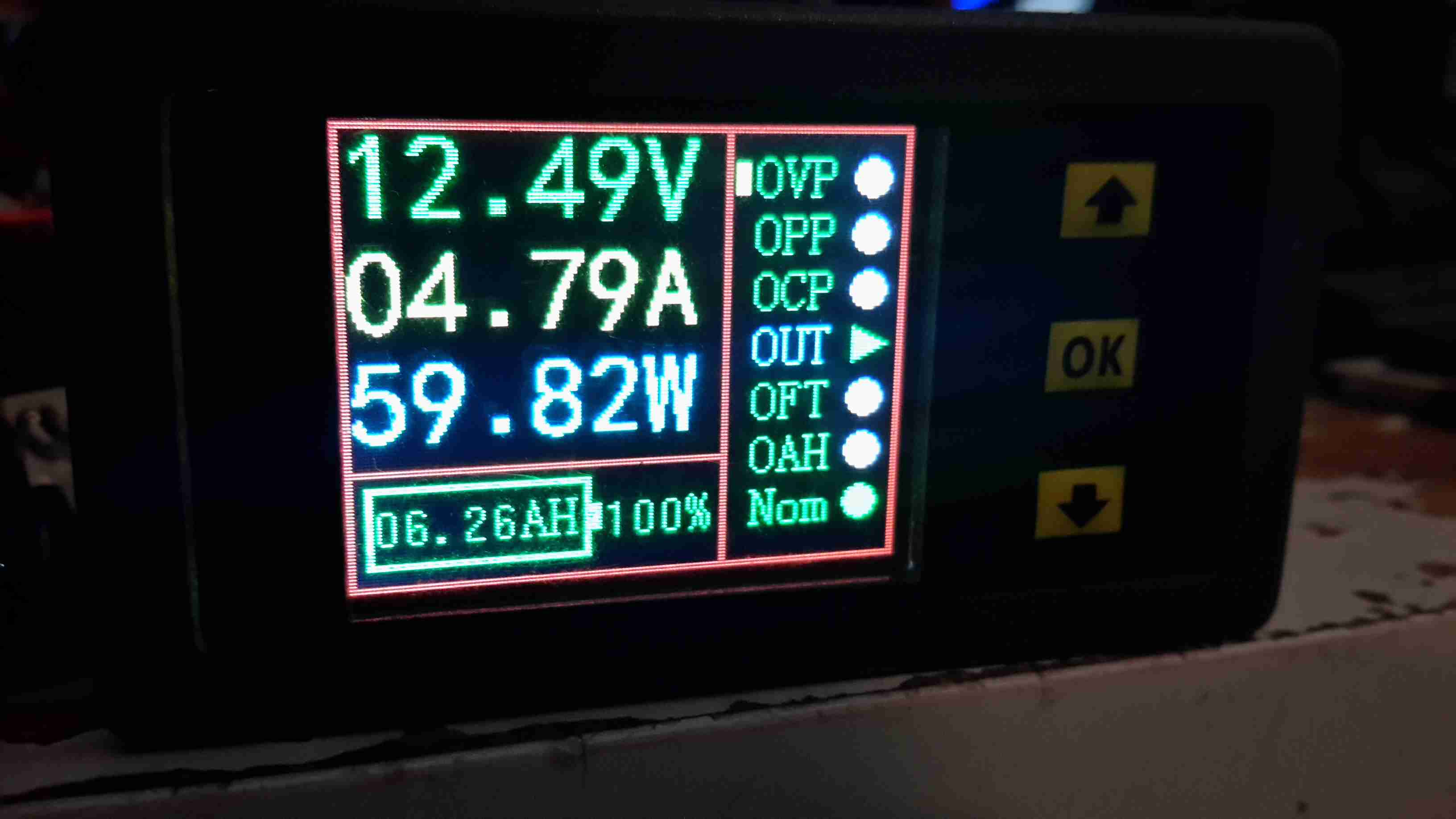
On the right edge of the board is the function list, a quick press of the OK button turns a function ON/OFF, while holding it allows the threshold to be set.
When the output is disabled by one of the protection functions, turning that function OFF will immediately enable the output again.
The UP/DOWN buttons obviously function to select the desired function with the cursor just to the left of the labels. Less obviously though, pressing the UP button while the very top function is selected will change the Amp-Hours display to a battery capacity icon, while pressing DOWN while the very bottom function is selected will change the Watts display to Hours.
The round circle to the right displays the status of a function. Green for OK/ON Grey for FAULT/OFF.
OVP: Over voltage protection. This will turn off the load when the measured voltage exceeds the set threshold.
OPP: Over power protection. This function prevents a load from pulling more than a specified number of watts from the supply.
OCP: Over current protection. This one’s a little more obvious, it’ll disable the output when the current measured exceeds the specified limit.
OUT: This one is the status of the output MOSFET. Can also be used to manually enable/disable the output.
OFT: Over time protection. This one could be useful when charging batteries, if the output is enabled for longer than the specified time, the output will toggle off.
OAH: Over Amp-Hours protection. If the counted Amp-Hours exceeds the set limit, the output will be disabled.
Nom: This one indicates the status of the RF data link between the modules, and can be used to set the channel they operate on.
Pairing is achieved by holding the OK button, selecting the channel on the LCD unit, and then pressing the button on the transmitter board. After a few seconds, (it appears to scan through all addresses until it gets a response) the display will resume updating.
This function would be required if there are more than a single meter within RF range of each other.
I’ve not yet had a proper play with all the protection functions, but a quick mess with the OVP setting proved it was very over-sensitive. Setting the protection voltage to 15v triggered the protection with the measured voltage between 12.5v-13.8v. More experimentation is required here I think, but as I plan to just use these for power monitoring, I’ll most likely leave all the advanced functions disabled.
As I’ve been posting some photos of decapped ICs lately, I thought I’d share the process I use personally for those that might want to give it a go 😉
The usual method for removing the epoxy package from the silicon is to use hot, concentrated Nitric Acid. Besides the obvious risks of having hot acids around, the decomposition products of the acid, namely NO² (Nitrogen Dioxide) & NO (Nitrogen Oxide), are toxic and corrosive. So until I can get the required fume hood together to make sure I’m not going to corrode the place away, I’ll leave this process to proper labs ;).
The method I use is heat based, using a Propane torch to destroy the epoxy package, without damaging the Silicon die too much.
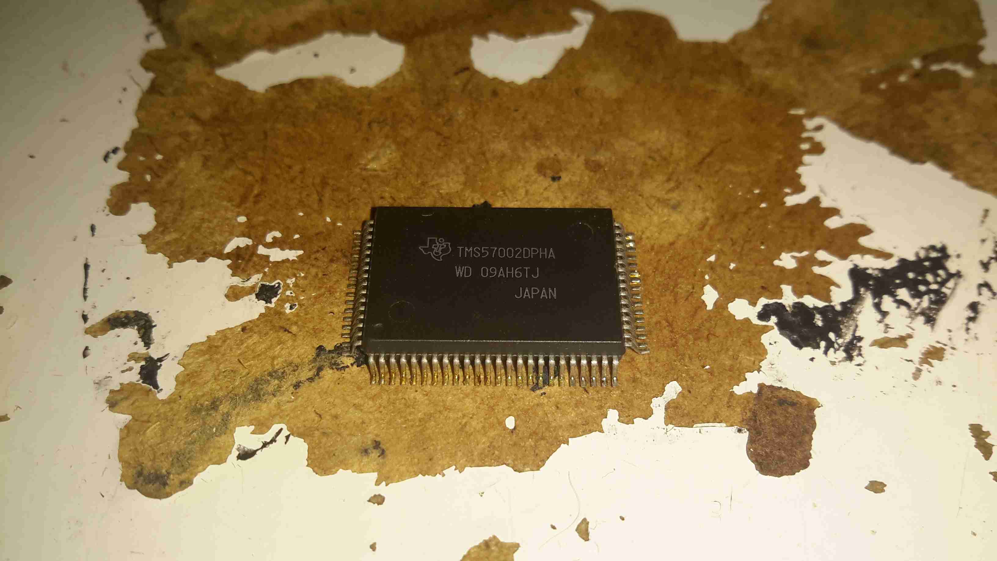
TMS57002 Audio DSP
I start off, obviously, with a desoldered IC, the one above an old audio DSP from TI. I usually desolder en-masse for this with a heat gun, stripping the entire board in one go.
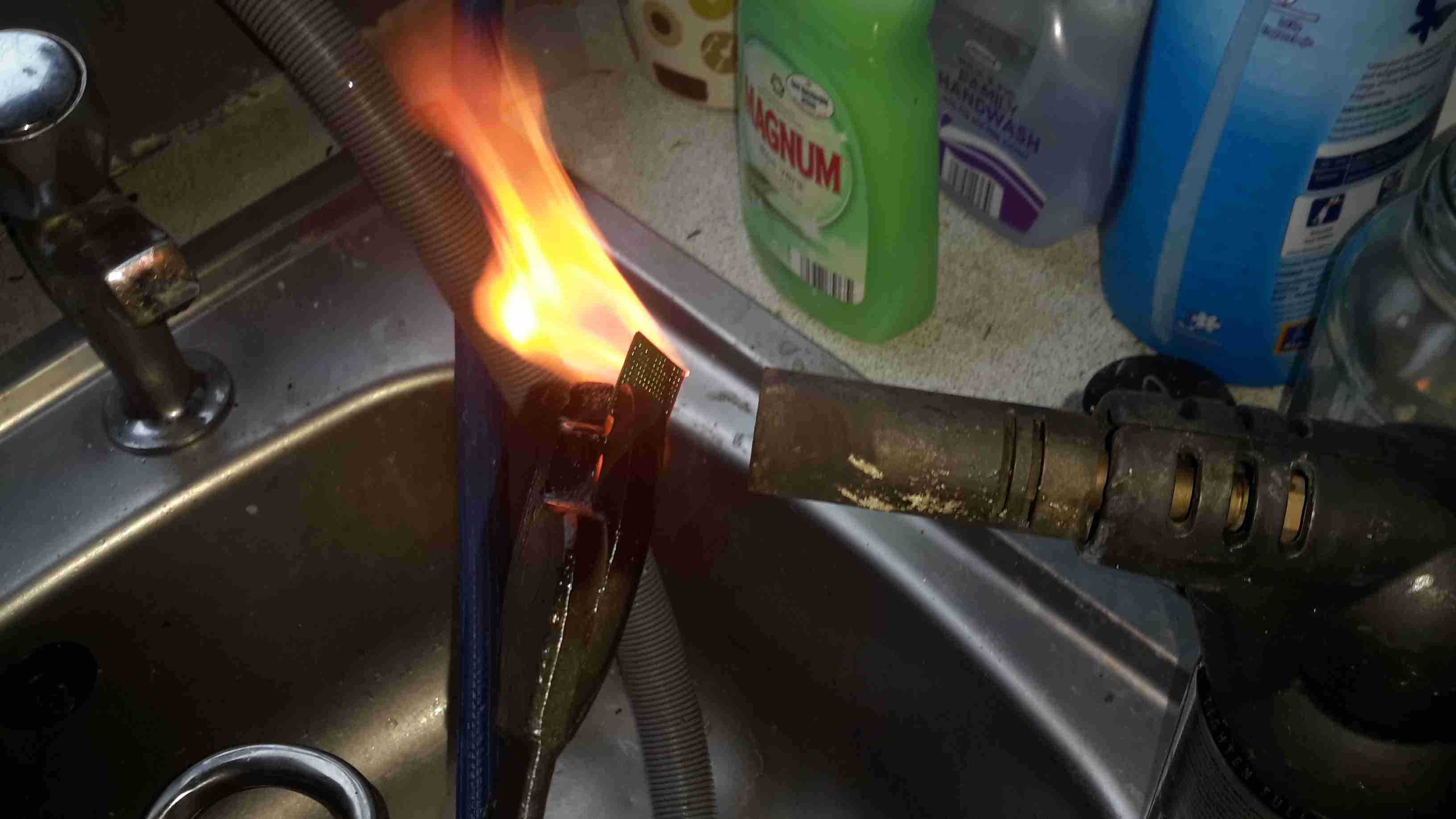
FLAMES!
Next is to apply the torch to the IC. A bit of practice is required here to get the heat level & time exactly right, overheating will cause the die to oxidize & blacken or residual epoxy to stick to the surface.
I usually apply the torch until the package just about stops emitting it’s own yellow flames, meaning the epoxy is almost completely burned away. I also keep the torch flame away from the centre of the IC, where the die is located.
Breathing the fumes from this process isn’t recommended, no doubt besides the obvious soot, the burning plastic will be emitting many compounds not brilliant for Human health!
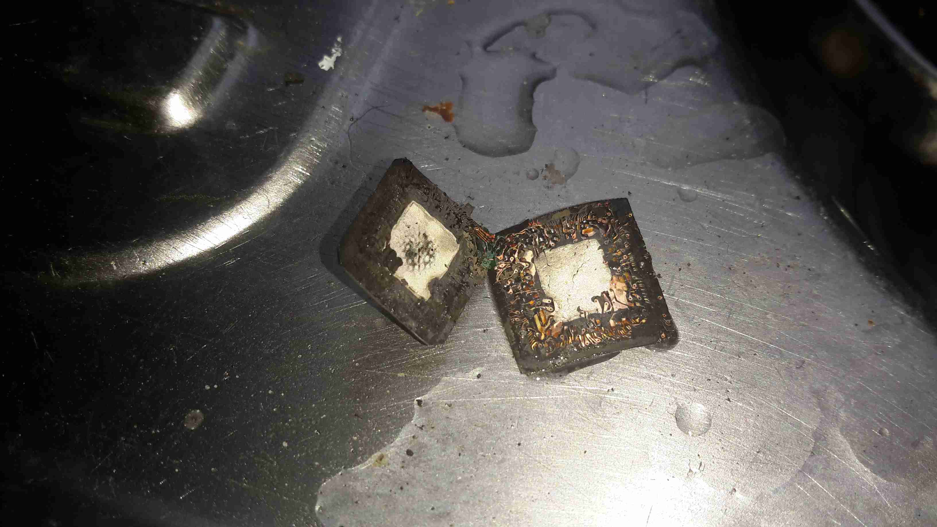
Once the IC is roasted to taste, it’s quenched in cold water for a few seconds. Sometimes this causes such a high thermal shock that the leadframe cracks off the epoxy around the die perfectly.
All Your Die Belong To Us
Now that the epoxy has been destroyed, it breaks apart easily, and is picked away until I uncover the die itself. (It’s the silver bit in the middle of the left half). The heat from the torch usually destroys the Silver epoxy holding the die to the leadframe, and can be removed easily from the remaining package.
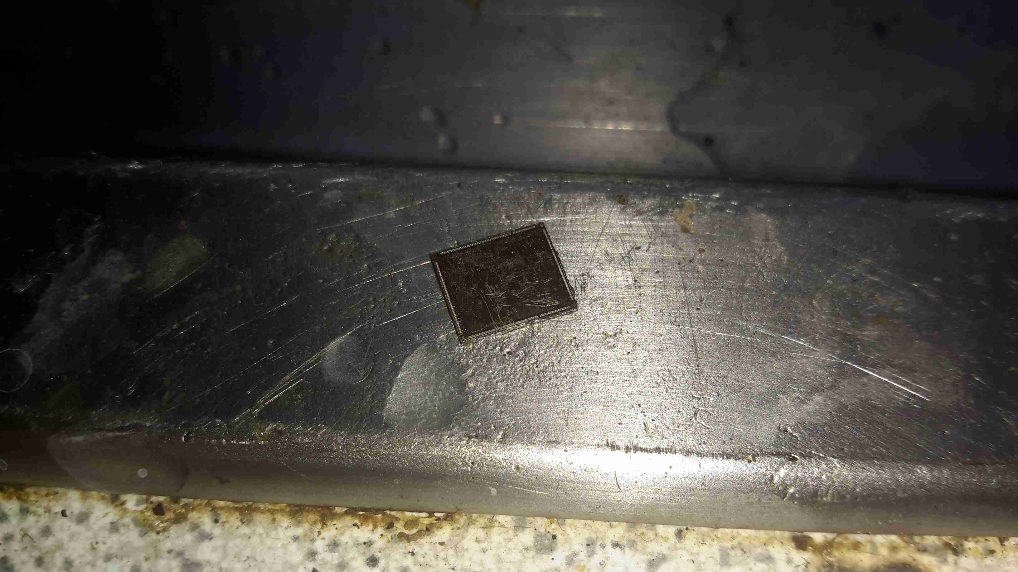
Decapped
BGA packages are usually the easiest to decap, flip-chip packages are a total pain due to the solder balls being on the front side of the die, I haven’t managed to get a good result here yet, I’ll probably need to chemically remove the first layer of the die to get at the interesting bits 😉
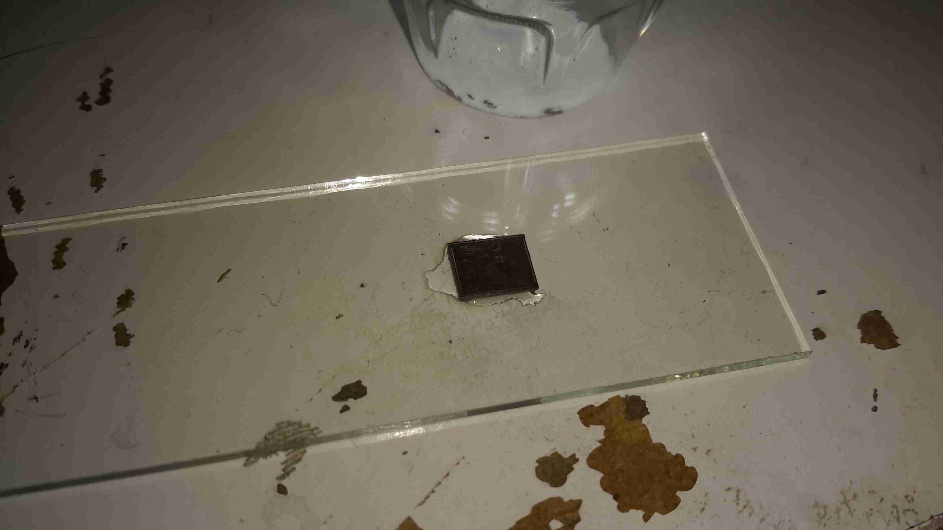
Slide
Once the die has been rinsed in clean water & inspected, it’s mounted on a glass microscope slide with a small spot of Cyanoacrylate glue to make handling easier.
Some dies require some cleaning after decapping, for this I use 99% Isopropanol & 99% Acetone, on the end of a cotton bud. Any residual epoxy flakes or oxide stuck to the die can be relatively easily removed with a fingernail – turns out fingernails are hard enough to remove the contamination, but not hard enough to damage the die features.
Once cleaning is complete, the slide is marked with the die identification, and the photographing can begin.
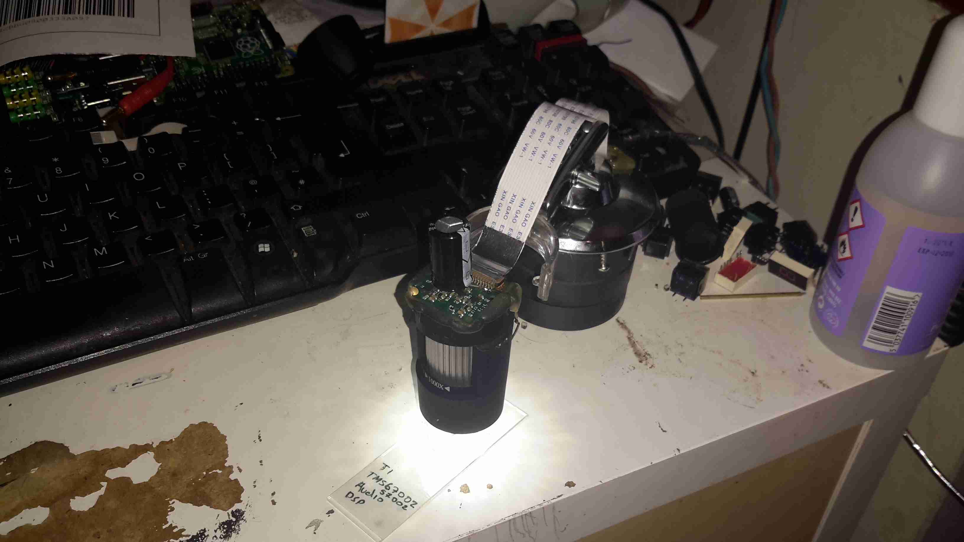
Microscope Mods
I had bought a cheap eBay USB microscope to get started, as I can’t currently afford a proper metallurgical microscope, but I found the resolution of 640×480 very poor. Some modification was required!
Modified Microscope
I’ve removed the original sensor board from the back of the optics assembly & attached a Raspberry Pi camera board. The ring that held the original sensor board has been cut down to a minimum, as the Pi camera PCB is slightly too big to fit inside.
The stock ring of LEDs is run direct from the 3.3v power rail on the camera, through a 4.7Ω resistor, for ~80mA. I also added a 1000µF capacitor across the 3.3v supply to compensate a bit for the long cable – when a frame is captured the power draw of the camera increases & causes a bit of voltage drop.
The stock lens was removed from the Pi camera module by careful use of a razor blade – being too rough here *WILL* damage the sensor die or the gold bond wires, which are very close to the edge of the lens housing, so be gentle!
Mounting Base
The existing mount for the microscope is pretty poor, so I’ve used a couple of surplus ceramic ring magnets as a better base, this also gives me the option of raising or lowering the base by adding or removing magnets.
To get more length between the Pi & the camera, I bought a 1-meter cable extension kit from Pi-Cables over at eBay, cables this long *definitely* require shielding in my space, which is a pretty aggressive RF environment, or interference appears on the display. Not surprising considering the high data rates the cable carries.
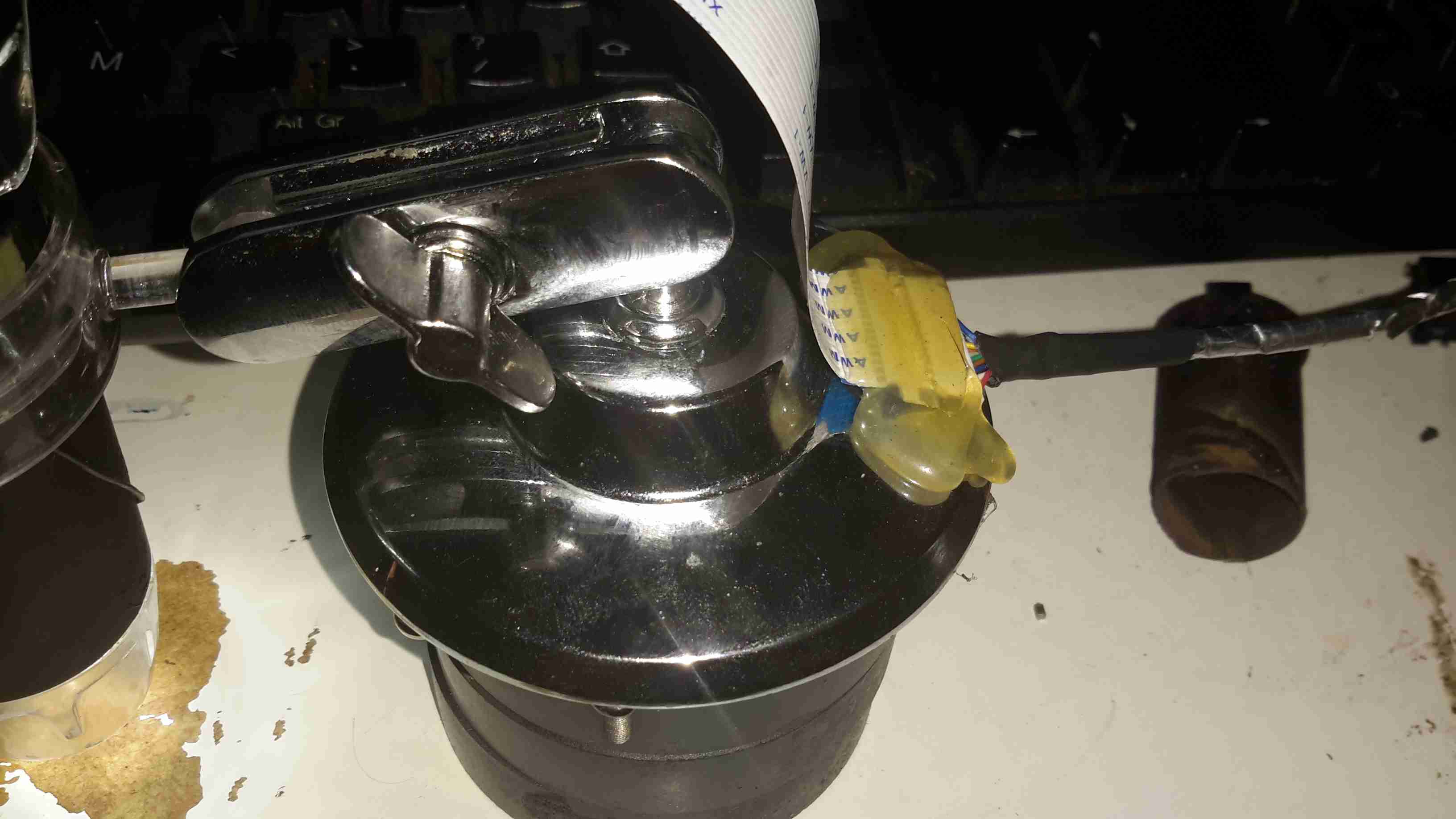
The FFC interface is hot-glued to the back of the microscope mount for stability, for handheld use the FFC is pretty flexible & doesn’t apply any force to the scope.
Die Photography
Since I modified the scope with a Raspberry Pi camera module, everything is done through the Pi itself, and the raspistill command.
Pi LCD
The command I’m currently using to capture the images is:
raspistill -ex auto -awb auto -mm matrix -br 62 -q 100 -vf -hf -f -t 0 -k -v -o CHIPNAME_%03d.jpg
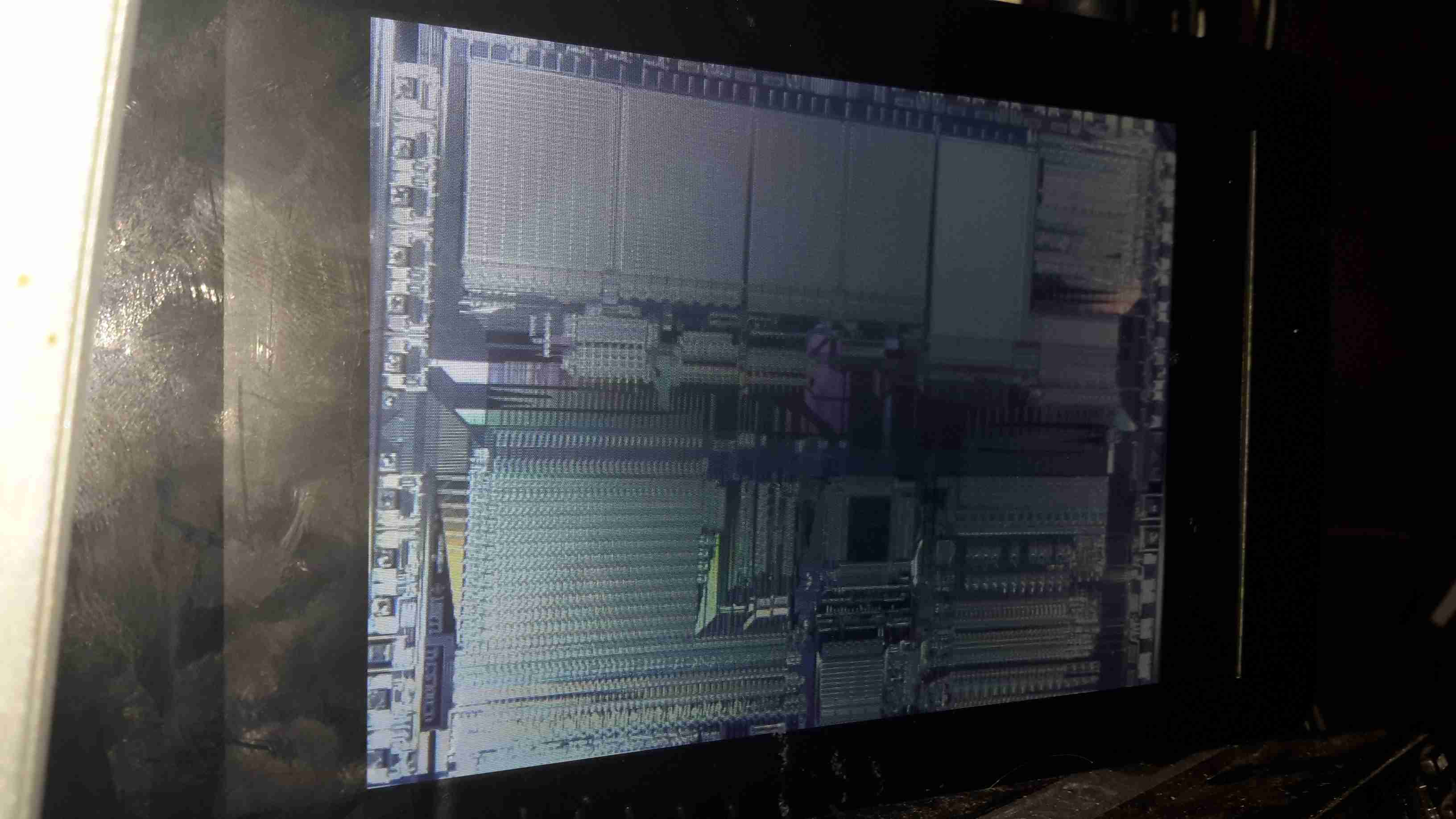
This command waits between each frame for the ENTER key to be pressed, allowing me to position the scope between shots. Pi control & file transfer is done via SSH, while I use the 7″ touch LCD as a viewfinder.
The direct overhead illumination provided by the stock ring of LEDs isn’t ideal for some die shots, so I’m planning on fitting some off-centre LEDs to improve the resulting images.
Image Processing
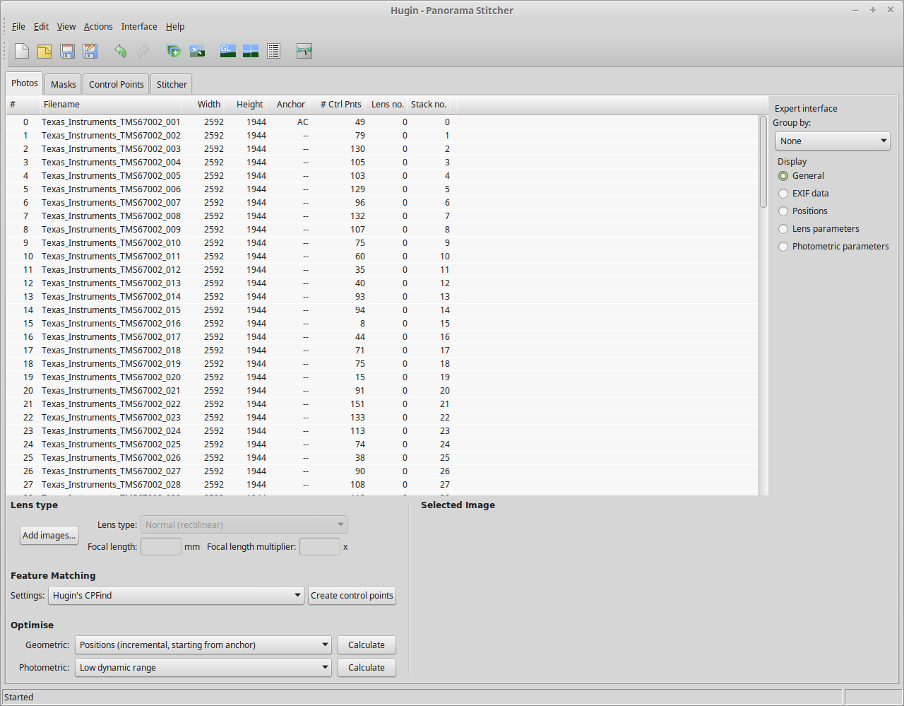
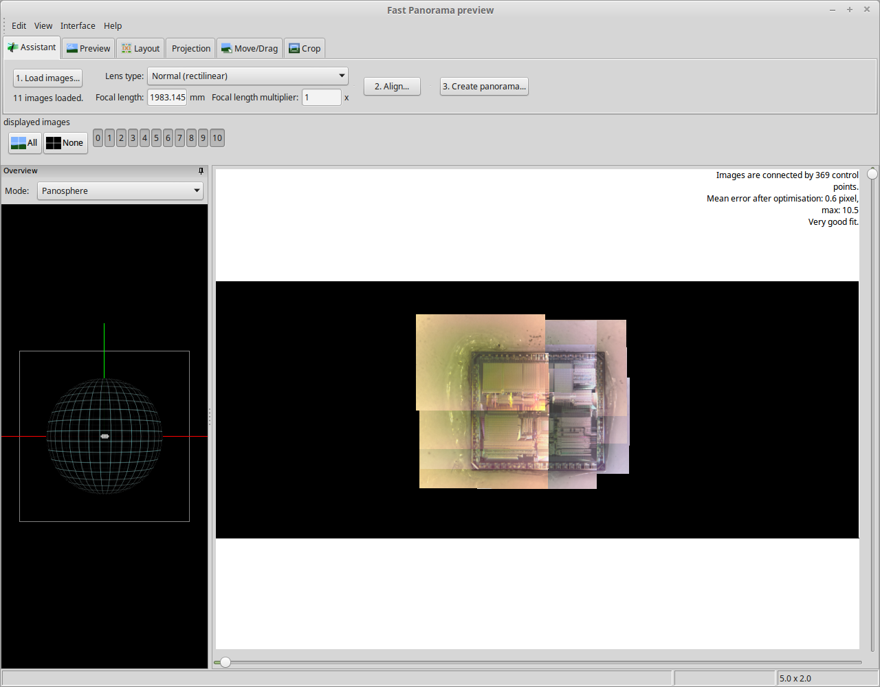
Obviously I can’t get an ultra-high resolution image with a single shot, due to the focal length, so I have to take many shots (30-180 per die), and stitch them together into a single image.
For this I use Hugin, an open-source panorama photo stitching package.
Hugin
Here’s Hugin with the photos loaded in from the Raspberry Pi. To start with I use Hugin’s built in CPFind to process the images for control points. The trick with getting good control points is making sure the images have a high level of overlap, between 50-80%, this way the software doesn’t get confused & stick the images together incorrectly.
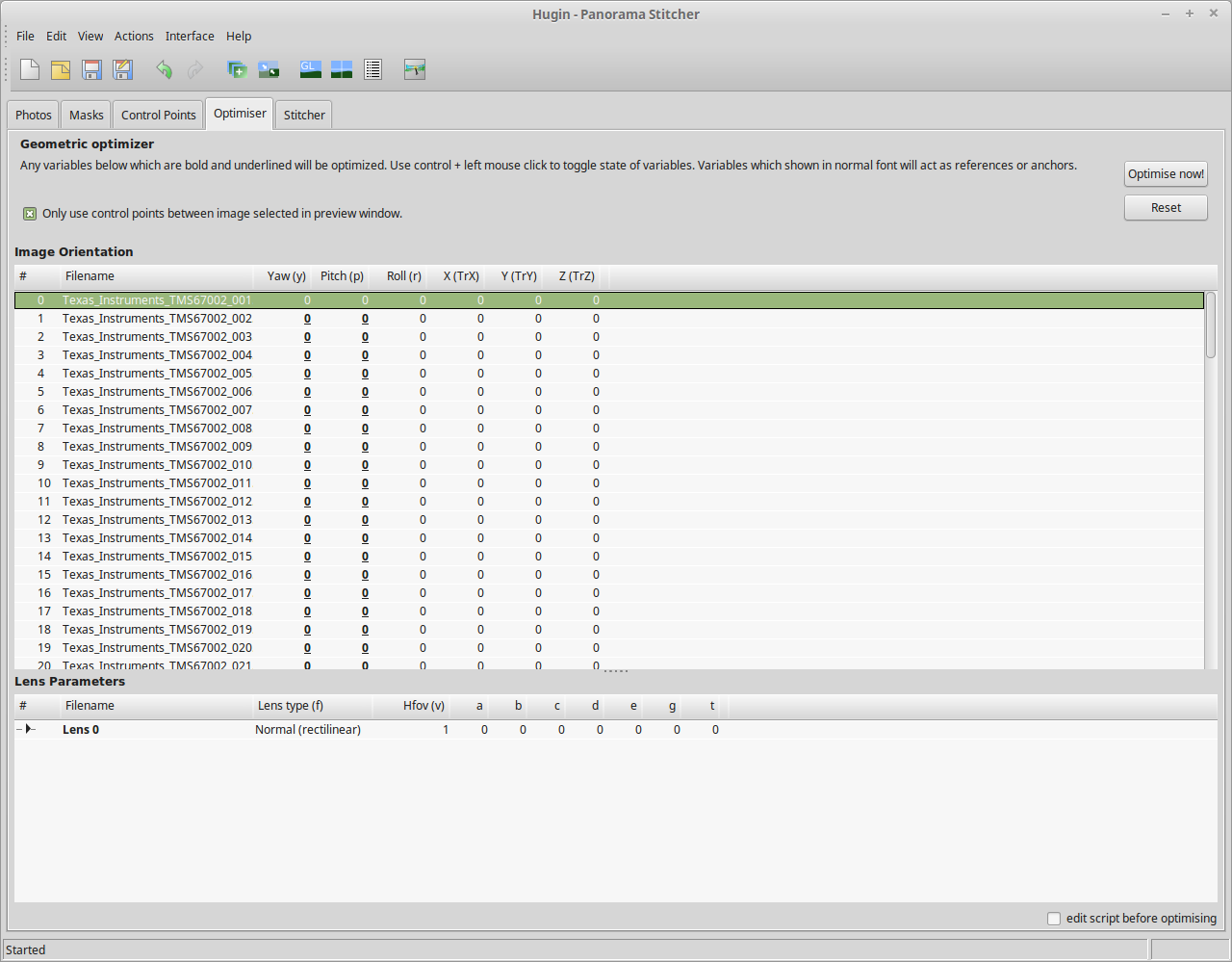
Optimiser
After the control points are generated, which for a large number of high resolution images can take some time, I run the optimiser with only Yaw & Pitch selected for all images.
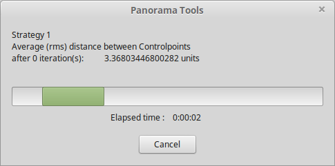
Optimising
If all goes well, the resulting optimisation will get the distance between control points to less than 0.3 pixels.
Panorama Preview
After the control points & optimisation is done, the resulting image can be previewed before generation.
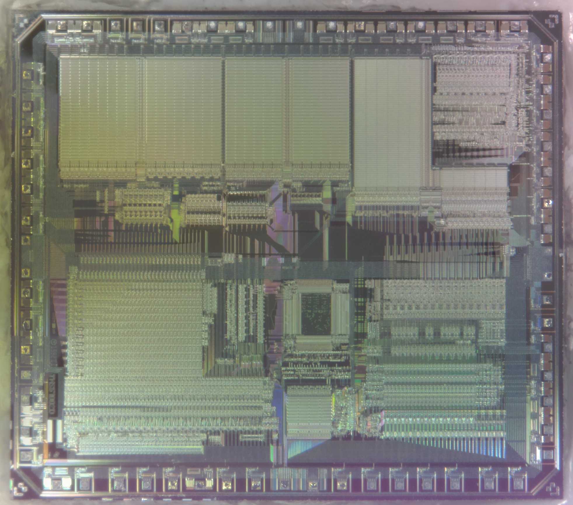
Texas Instruments TMS67002
After all the image processing, the resulting die image should look something like the above, with no noticeable gaps.
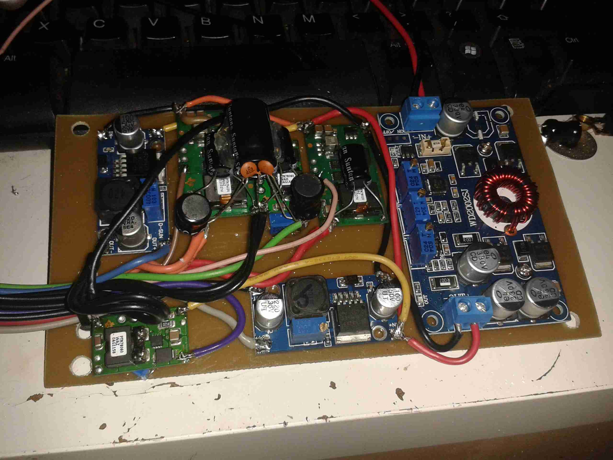
All of the parts I required to complete the supply arrived this morning. After several hours of building, here’s what I came up with:
12v Power Supply
I’ve mounted everything on a piece of FR4 PCB, with it’s copper plane grounded to the case. This backing board is the same size as the original PSU PCB to allow it to be screwed into the same location in the scope.
The power comes in via the converter on the right, which outputs a single 24v rail for the rest of the supplies. The other 6 supplies then generate the individual voltage rails that the scope requires. The use of a single input supply allows this system to operate at voltages up to 30v DC, so it’s good for both 12v & 24v systems.
Scope Ripple
At present the only issue is with some ripple on one of the supplies, this is showing up on the scope display with no input connected at the lowest volts/division. Parts are on order from Farnell to build some common mode filters to remove this from the DC output.
On a 13.8v supply, the scope draws about 1.5A total from the supply, giving a total power consumption of 20.7W. This is with all 4 channels enabled.
My wiring assignments & DC-DC converter ratings are in the table below
Connector Pin
PCB Pin
Signal
Mainboard
DC-DC Rating
Wire Colour
1
10
GND
GND
N/A
BLACK
2
2
+9v_GND
FAN --
NA
BLACK
3
8
+7.5V
6.3V
6A
ORANGE
4
14
-7.5V
-7.5V
2A
GREEN
5
1
NOT USED
AC_TRIG
N/A
NOT USED
6
4
+5V
5V5A
6A
RED
7
6
GND
GND
N/A
BLACK
8
7
GND
GND
N/A
BLACK
9
12
-17.5V
-17.5V
3A
PURPLE
10
9
+7.5V
6.3V
6A
ORANGE
11
3
+9V
FAN +
1A
GREY
12
11
17.5V
17.5V
3A
BLUE
13
5
+5V
5V5A
6A
RED
14
13
GND
GND
N/A
BLACK
Stay tuned for the final section of this build with the power supply filtering & main DC input connections!
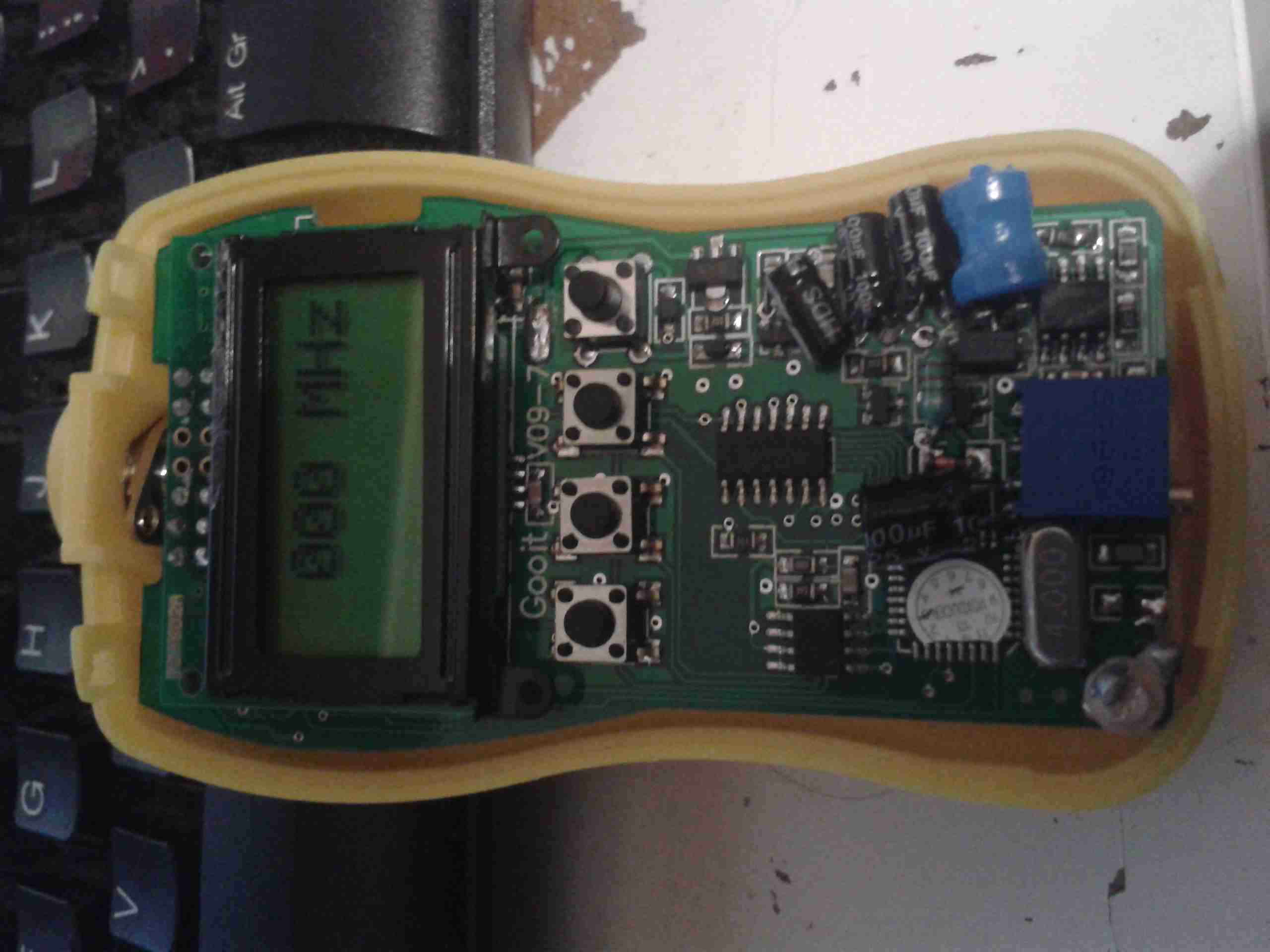
Unfortunately the manual for the eBay GY561 Frequency & RF Power Meter is very badly translated, but I think I have figured out the calibration procedure, so here it goes 🙂
Initial Screen
On removing the front cover, which is just clipped on, there are 4 buttons. The only button that is usually available is the one on the far right, the power button.
I will term these buttons A, B, C, D, starting from the left side.
To get into the initial calibration screen, in the above image, hold button A while the power button (D) is pressed. Release the power button (D), then release button A.
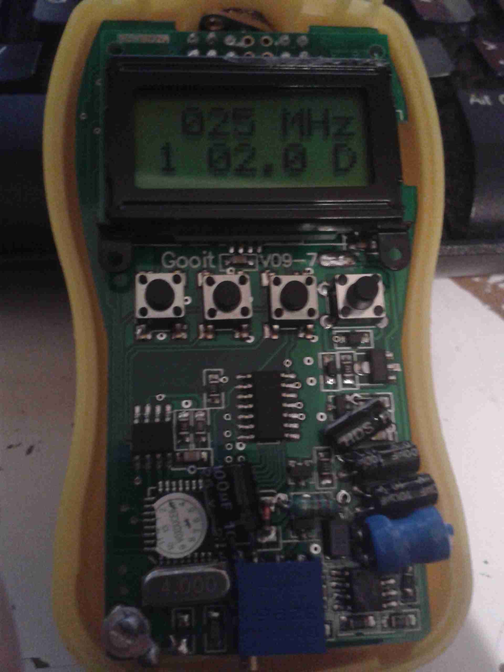
The meter will show the screen above, where the frequency to calibrate can be chosen. This goes in 5MHz steps, 0-500MHz, using the B button to go down in frequency, and the C button to go up.
Once you’ve selected the frequency you wish to calibrate against, press button A, and the following screen will appear:
Frequency Calibration Screen
On this screen, the actual calibration can be done.
The number in the bottom left signifies the power level setting, from 1-5. The centre number is the calibration setting in Watts. The D in the bottom corner signifies that the setting is at the factory default.
Button C will cycle through the power level settings, for 2W, 5W, 10W 20W, 40W. This allows calibration at different power levels per frequency.
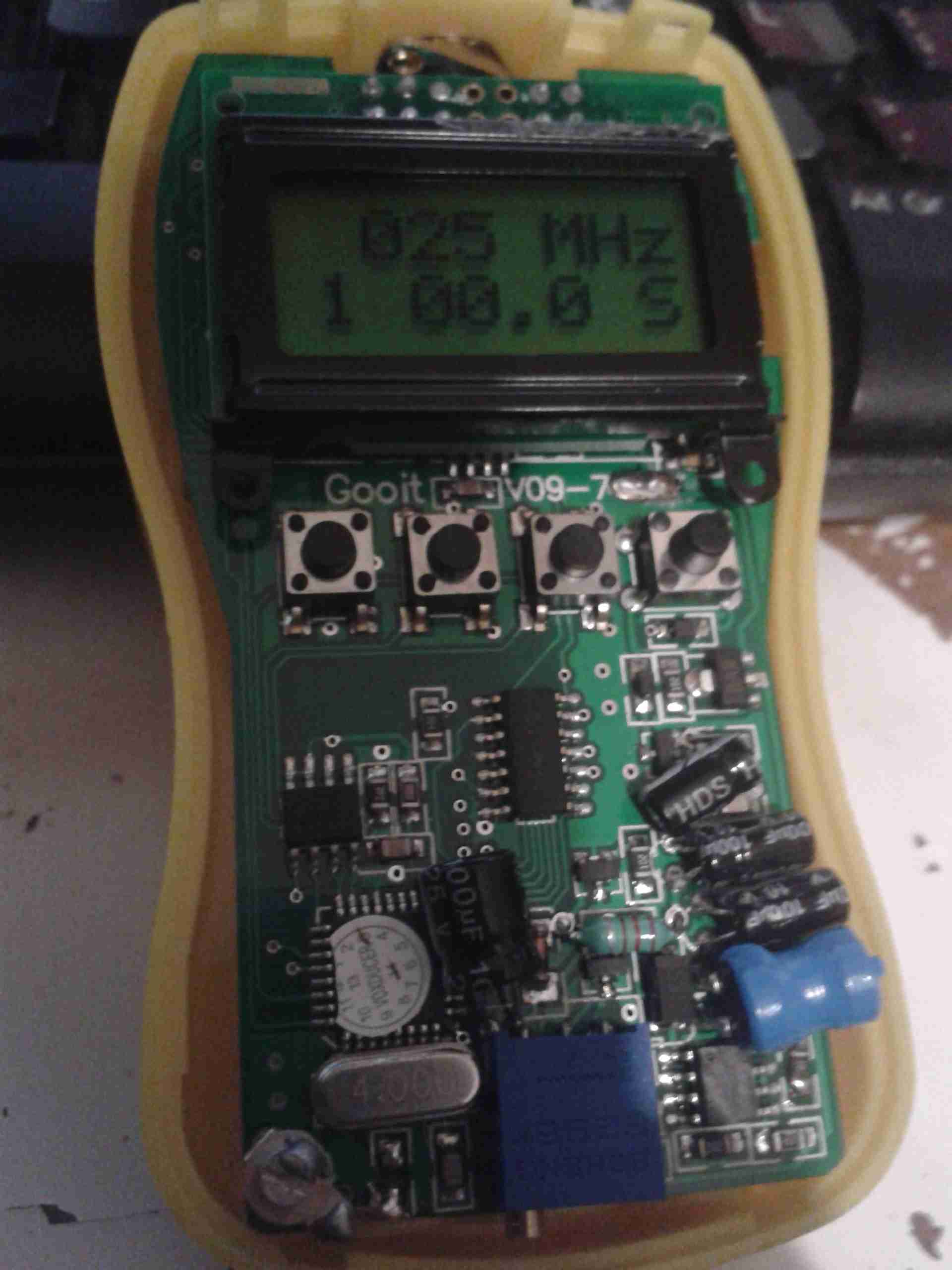
Once you have the frequency to calibrate, and you’ve selected the power level to calibrate at, connect a known RF power source to the input of the unit.
At this point, key the transmitter, and press button A. The display will change to the following:
Calibration Stage 2
When on this screen, you can set the power level of your RF source. Use the A key for +0.1W, the B key for +1W, and the C key for +10W.
Once you’ve keyed in the power of your source, press button D to save the setting. The “S” in the bottom corner will change to a “C”, to indicate a user calibration has been entered:
Calibration Complete
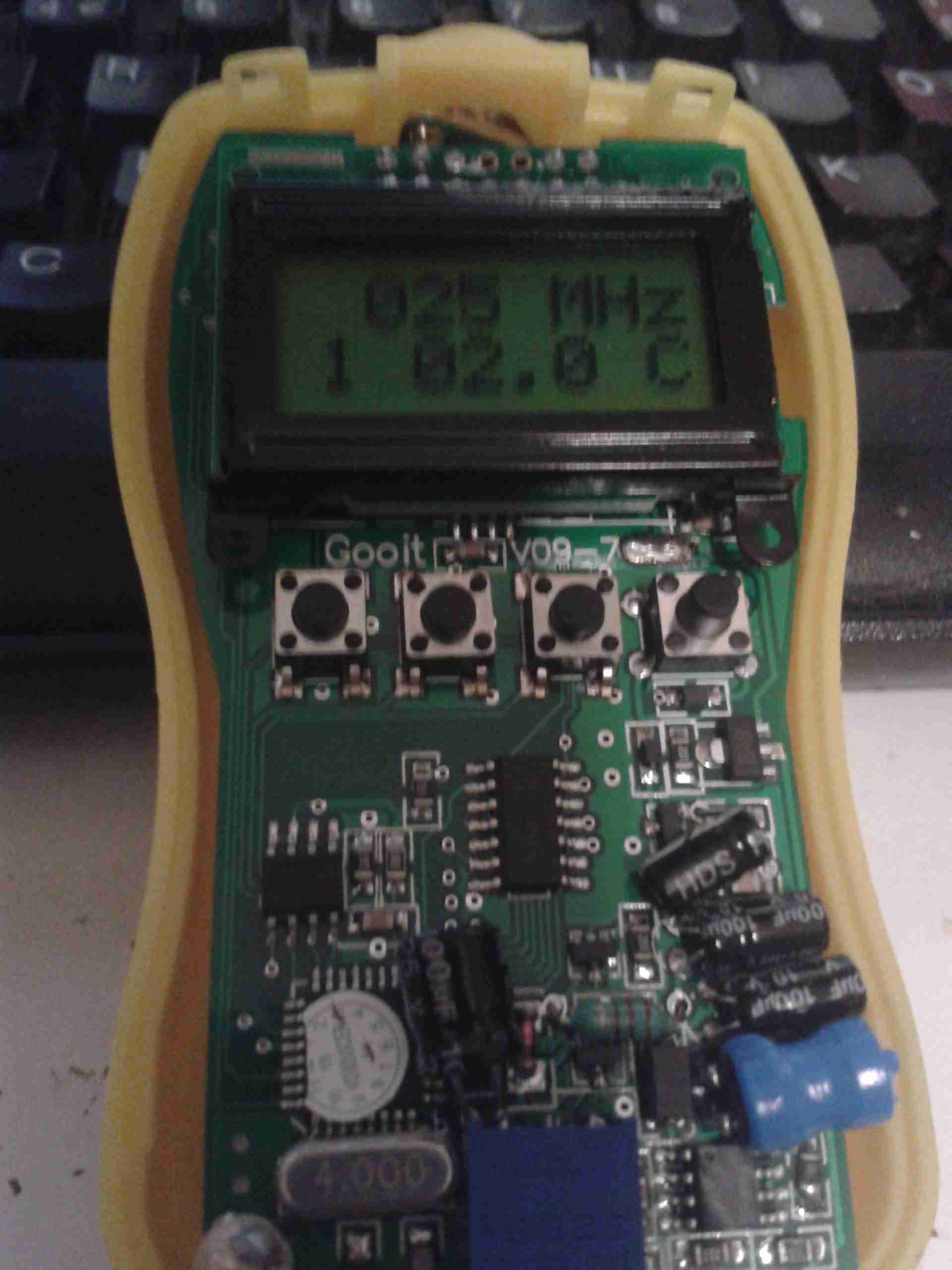
If you make a mistake with entering the power level, press the “C” key to cycle up to 60W, once at this level, another press of the button will reset the reading to zero. You can then enter the power level again.
If you wish to revert a user-entered setting to the factory default, press button B on the page above. The “D” will reappear in the bottom corner to indicate the setting has been restored.
At this point you can either press button C to calibrate at another power level for this frequency, or press button D to go back to the frequency selection.
Press button D again when at the frequency selection page to turn the unit off. The unit will then power up normally next time the power button (D) is pressed.
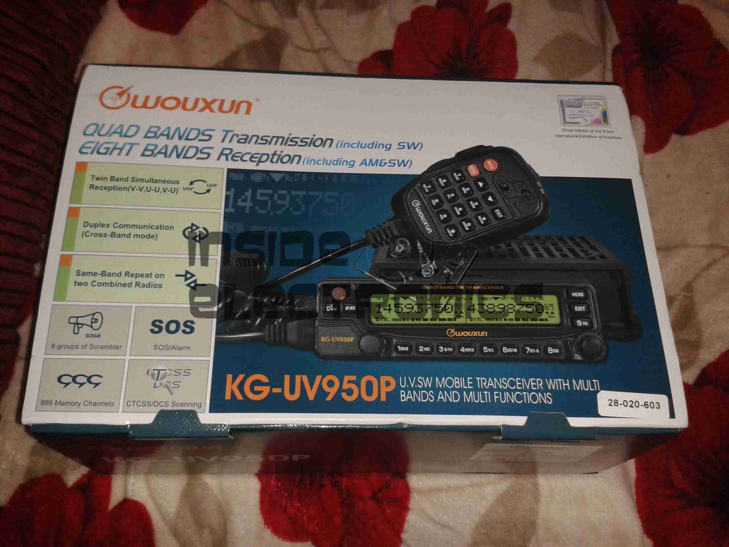
After running on handies for all of my Ameteur Radio life, I figured it was time for a new radio, this time a base station/mobile rig, & after some looking around I decided on the Wouxun KG-UV950P.
Shown below is the radio as delivered:
Wouxun Boxed
This radio has the capability to transmit quad-band, on 6m, 10m, 2m & 70cm. It also has the capability to receive on no fewer than eight bands. Also included in the feature set is airband receive, & broadcast FM receive.
TX power is up to 50W on 2m, 40W on 70cm, & 10W on 6m/10m.
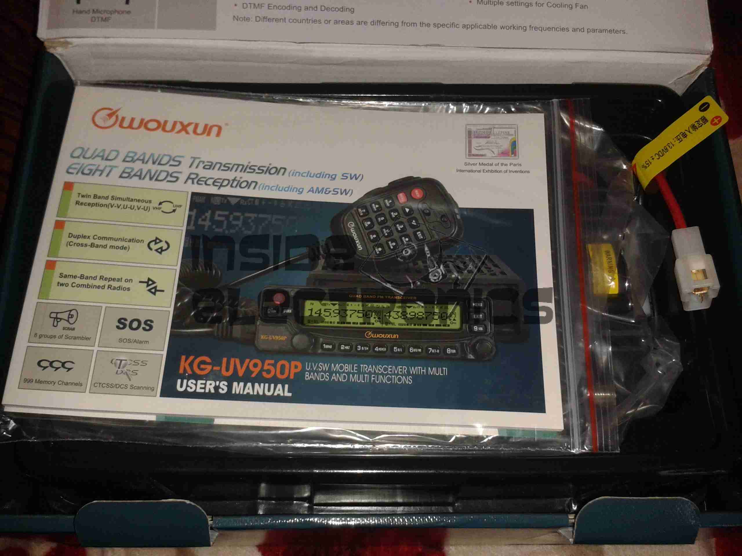
Opened
For once with a Chinese piece of electronic equipment, the manual is very well printed, and in very good English.
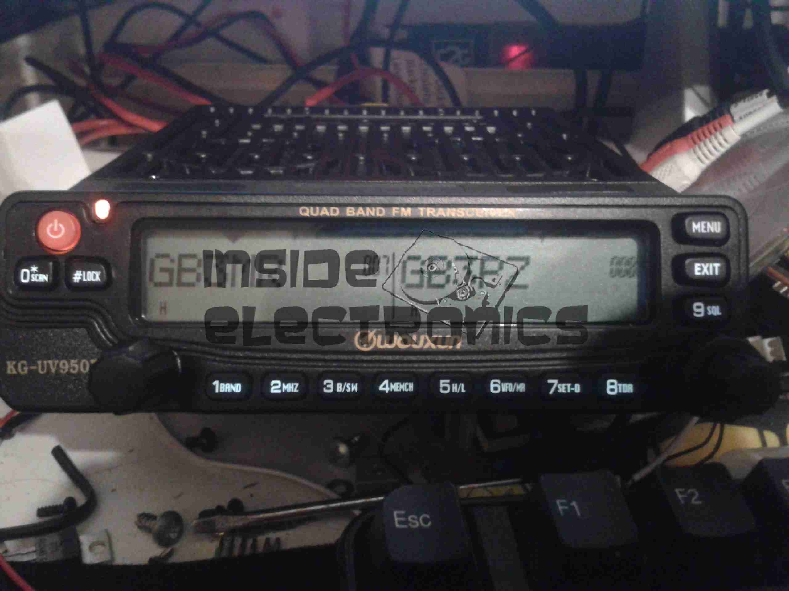
Radio Operating
Here is the radio in operation, connected to my 65A 12v power supply. I have the radio set here monitoring a couple of the local 70cm repeaters.
The display is nice & large – easy to see at a glance which station you’re tuned to. The backlight is also software settable to different colours.
Status indicators on the top edge of the display can be a bit difficult to see unless the panel is directly facing the user though, not to mention that they are rather small.
This radio is true dual-watch, in that both VFOs can be receiving at the same time, this is effected by a pair of speakers on the top panel:
Speakers
The left VFO speaker is smaller than the right, so the sound levels differ slightly, but overall sound quality is excellent. There is also provision on the back of the unit to connect external speakers.
The dual volume controls on the right hand bottom corner of the control panel are fairly decent, if a little twitchy at times. There is also a fair amount of distortion on the audio at the higher volume levels.
The controls themselves are potentiometers, but the controller appears to read the setpoint with an ADC – this means that if the control is set to just the right point, the selected level will jump around on the display & never settle down.
The radio itself is built from a solid aluminium casting, mostly for heatsinking of the main RF output stage MOSFETs. This gives the radio a very rugged construction.
A small fan is provided on the rear for cooling when required. This can be set in software to either be constantly running, (it’s pretty much silent, so this is advantageous), or only run when in TX mode. The fan will also automatically come on when a high internal temperature is detected.
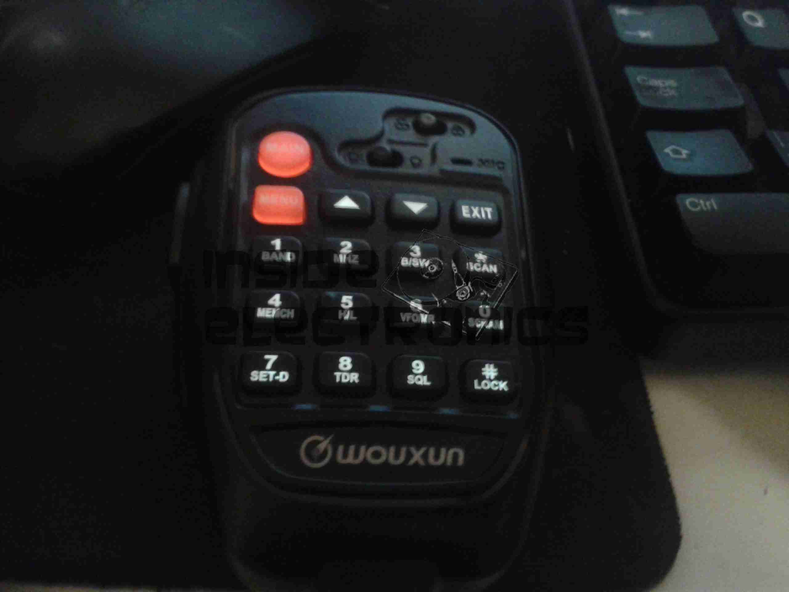
Hand Mic
Here is the microphone. Like the main unit of the radio this is also very solidly built, fits nicely in the hand & the PTT has a nice easy action, which helps to prevent straining hands while keeping the TX keyed.
Conveniently, all of the controls required to operate the radio are duplicated on this mic, along with a control lock switch, & backlighting for the buttons.
Another Speaker
Another output speaker is placed in the back of the mic. This one can be activated through the menu system, to either use the main body speakers, the mic mounted one, or both.
A mounting hook for the mic is provided to attach to any convenient surface.
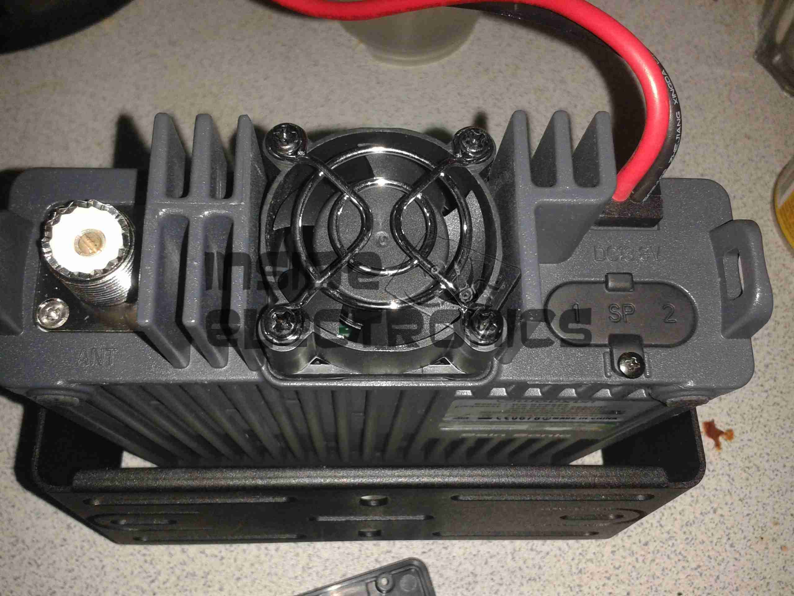
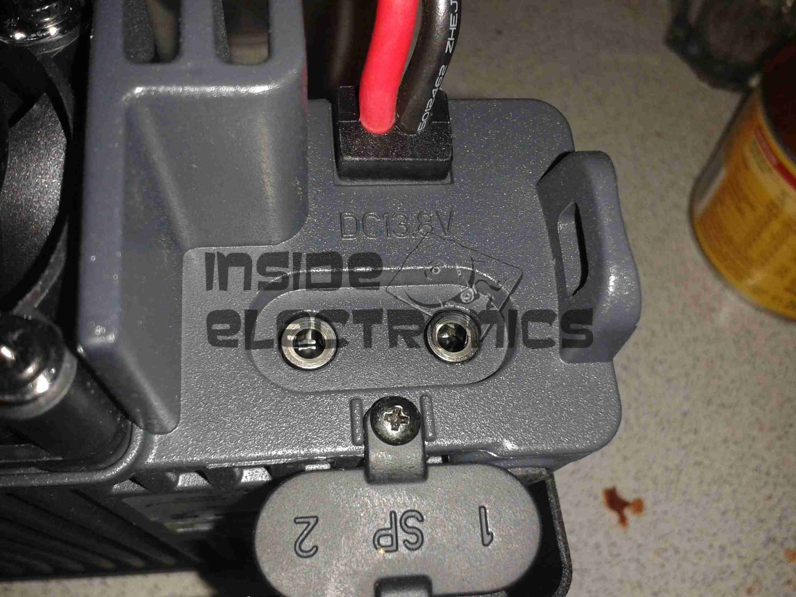
Radio Back
Here’s the back of the radio, with some of the big heatsink fins, the fan in the centre. To the left is the PL259 RF output, this looks to be a high quality Teflon insulated one. On the right are the power input leads & the external speaker outputs.
External Speaker Sockets
The external speaker connections are via 3.5mm jacks. I haven’t yet tested this feature.
Remote Mounting Plate
The control panel of this radio is detachable from the main body, and a pair of adaptors are provided. This either allows the radio display to be angled upwards toward the user, set parallel, or even mounted remotely. A control extension cable is provided to allow the main body to be mounted a fair distance away.
External Interface Connectors
On the left of the radio is the PC control & programming port, & the mic connector. Wouxun *really* like RJ-45 connectors, they’ve used them for everything on this radio.
Also visible here is the tilted faceplate adaptor.
The supplied software to program the radio, while functional, is absolutely horrific. Hopefully someone will add support for this radio into CHIRP. Anything would be an improvement in this area.
Everything considered, I like this radio. It’s very solidly built, easy to use, and sounds brilliant.
TX audio is great, (or so my other contacts tell me).
Unsurprisingly, the unit gets warm while transmitting, however on high power, it does get uncomfortably warm, and the built in fan does little in the way of helping when a long QSO is in progress. I may remedy this at some stage with a more powerful fan. A little more airflow would do wonders.
If the programming software was built as well as the radio, I’d have zero serious complaints.
At full power, the radio pulls ~10A from the power supply, at 12.9v DC.
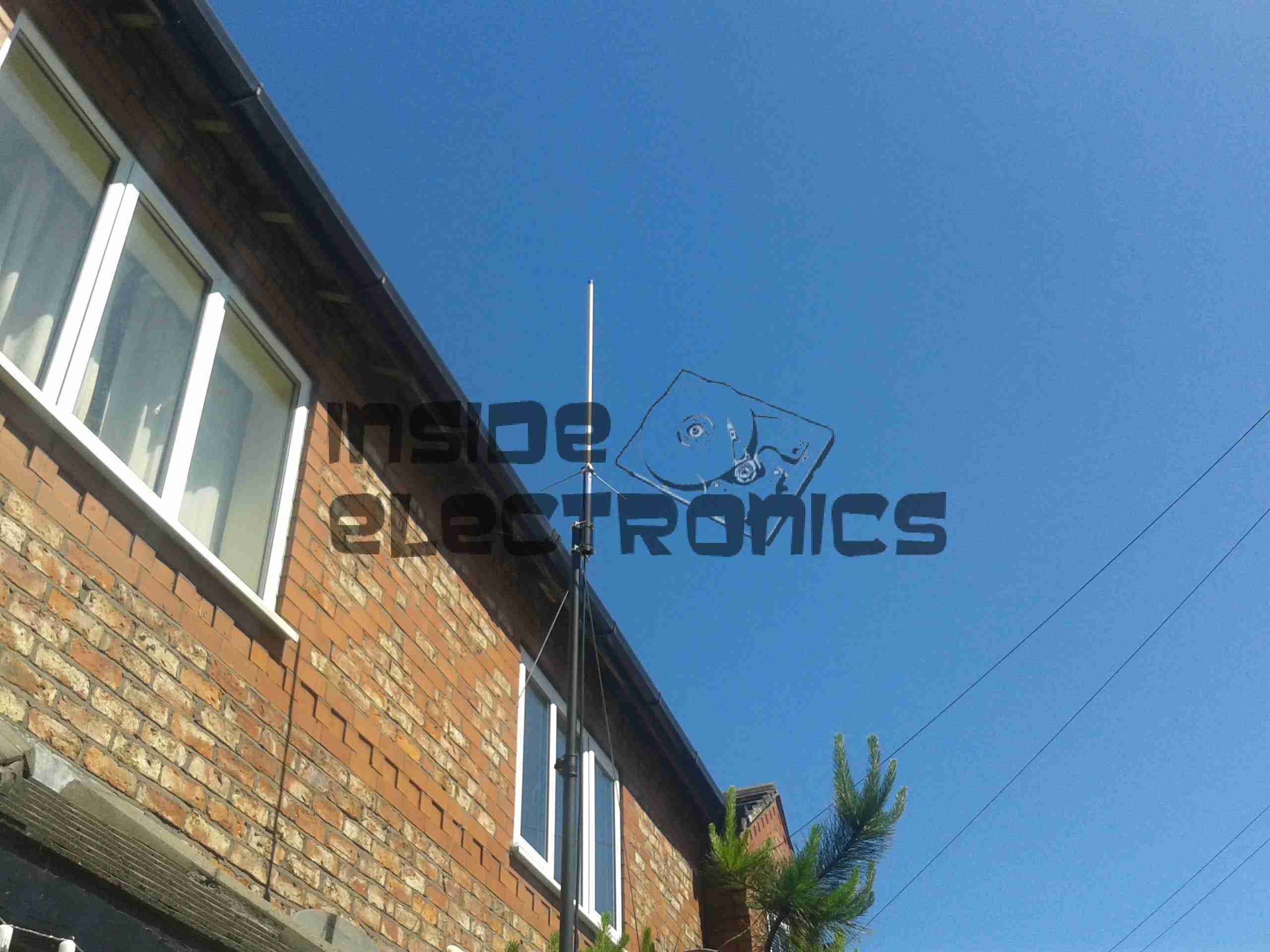
As for the antenna I’m currently using, it’s a Diamond X30, mounted on a modified PA speaker stand, at ~30 feet above ground. The feeder is high quality RG-213.
TX Antenna
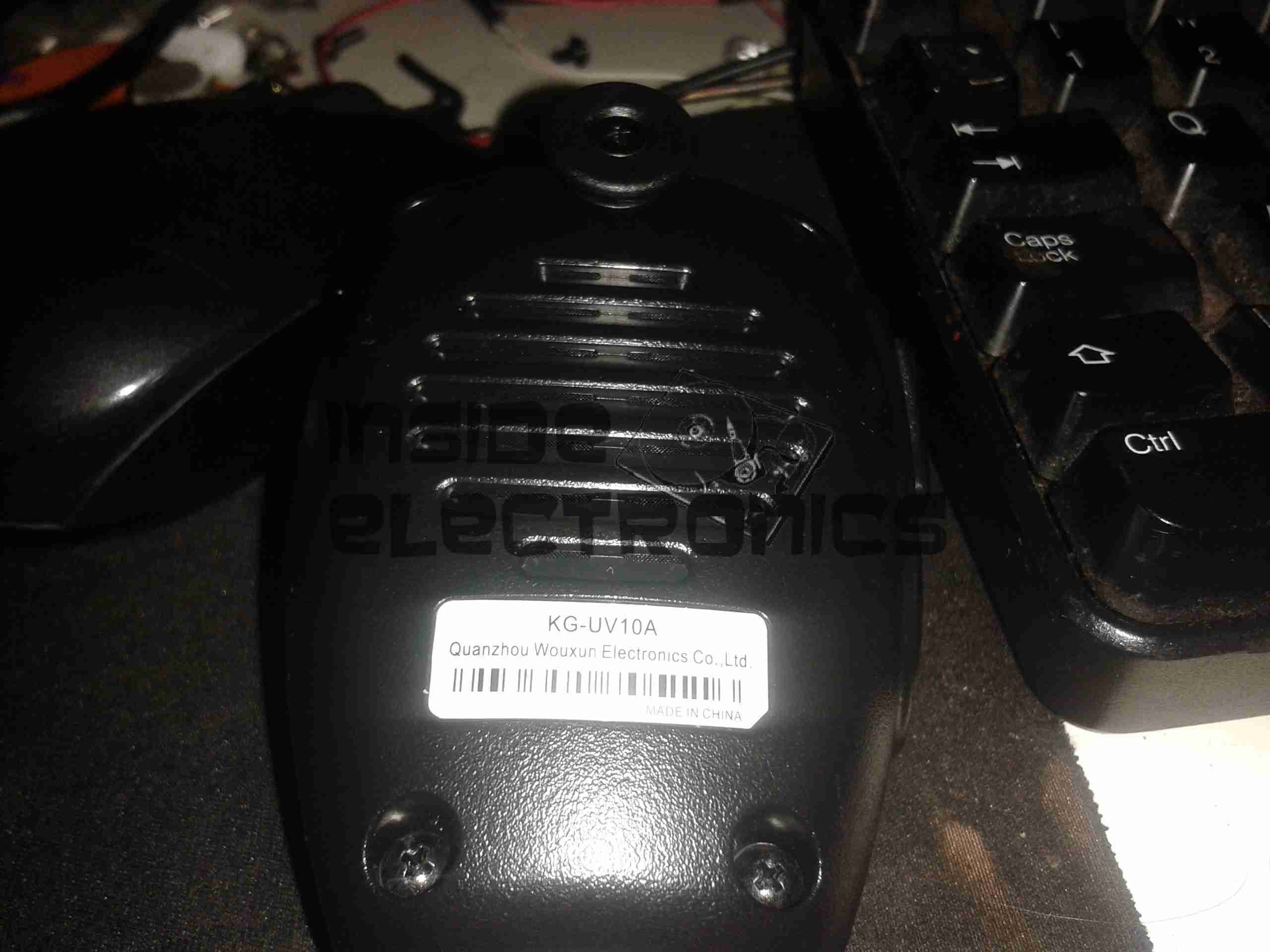
When I manage to get the set disconnected, a partial teardown will be posted, with some intimate details about the internals. Stay tuned!
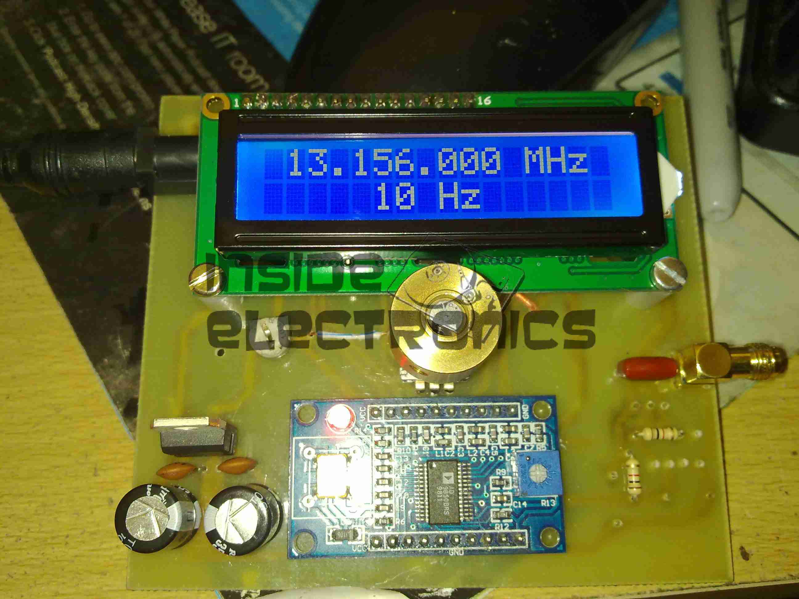
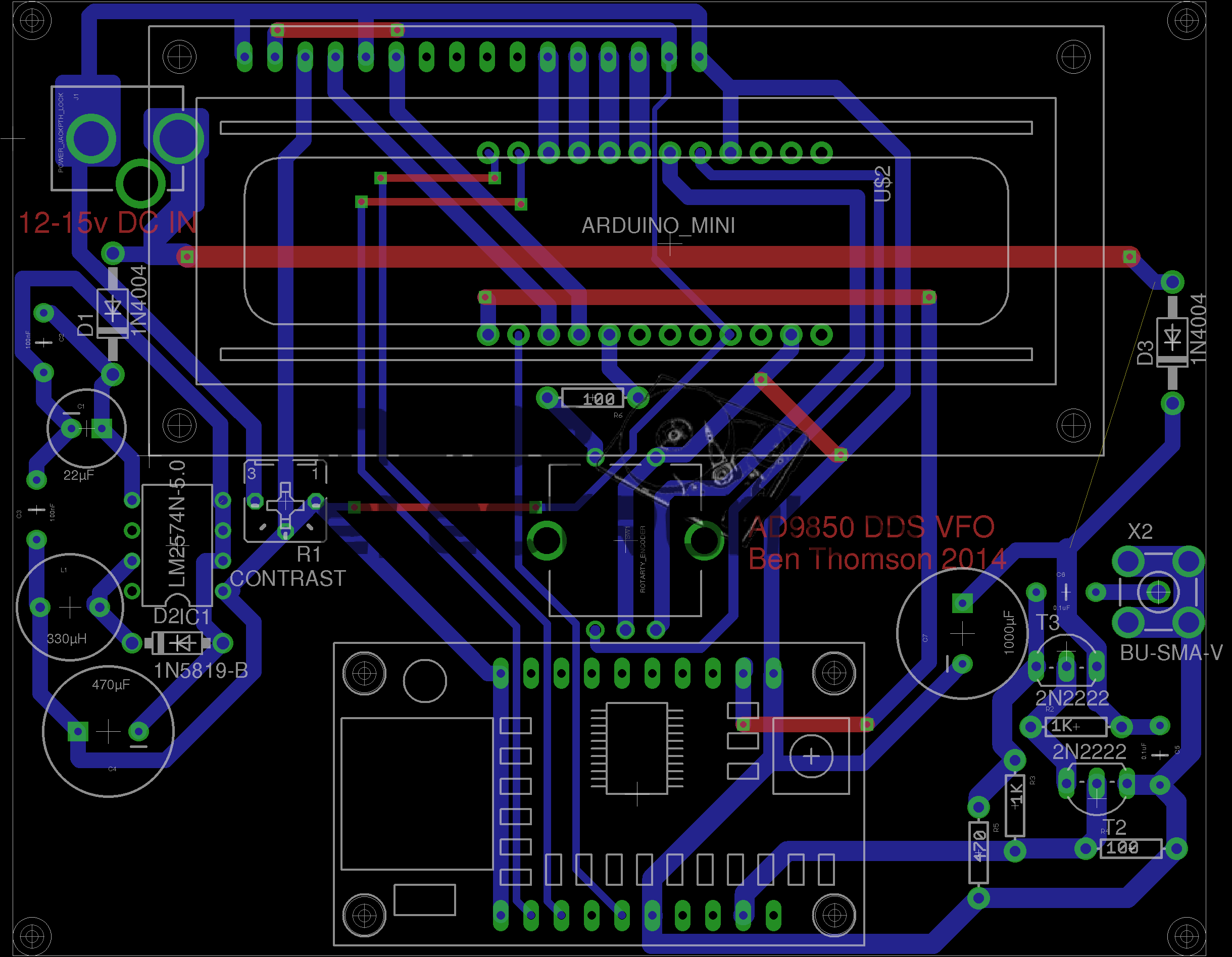
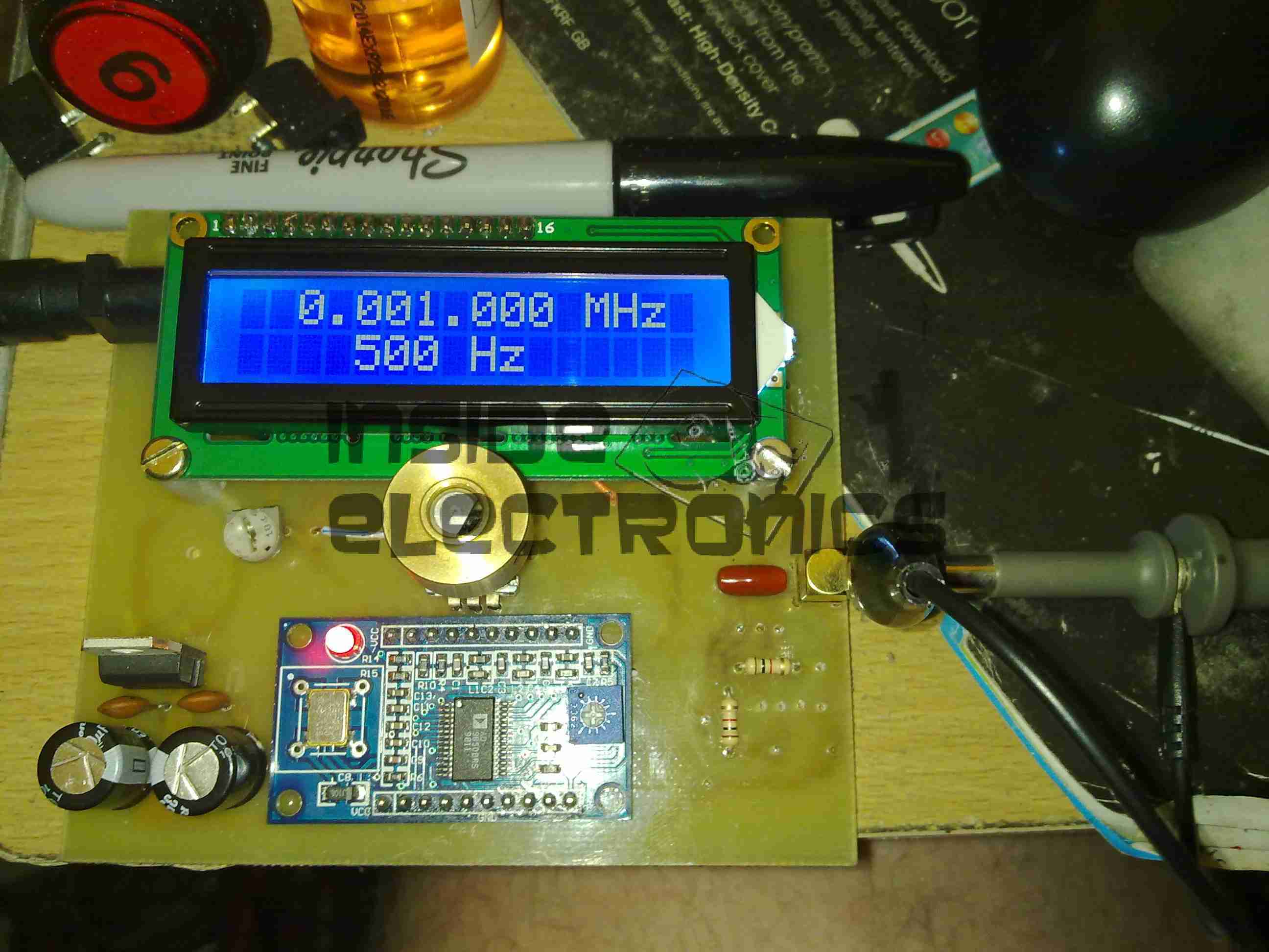
Continuing from my previous post where I published an Eagle design layout for AD7C‘s Arduino powered VFO, here is a completed board.
I have made some alterations to the design since posting, which are reflected in the artwork download in that post, mainly due to Eagle having a slight psychotic episode making me ground one of the display control signals!
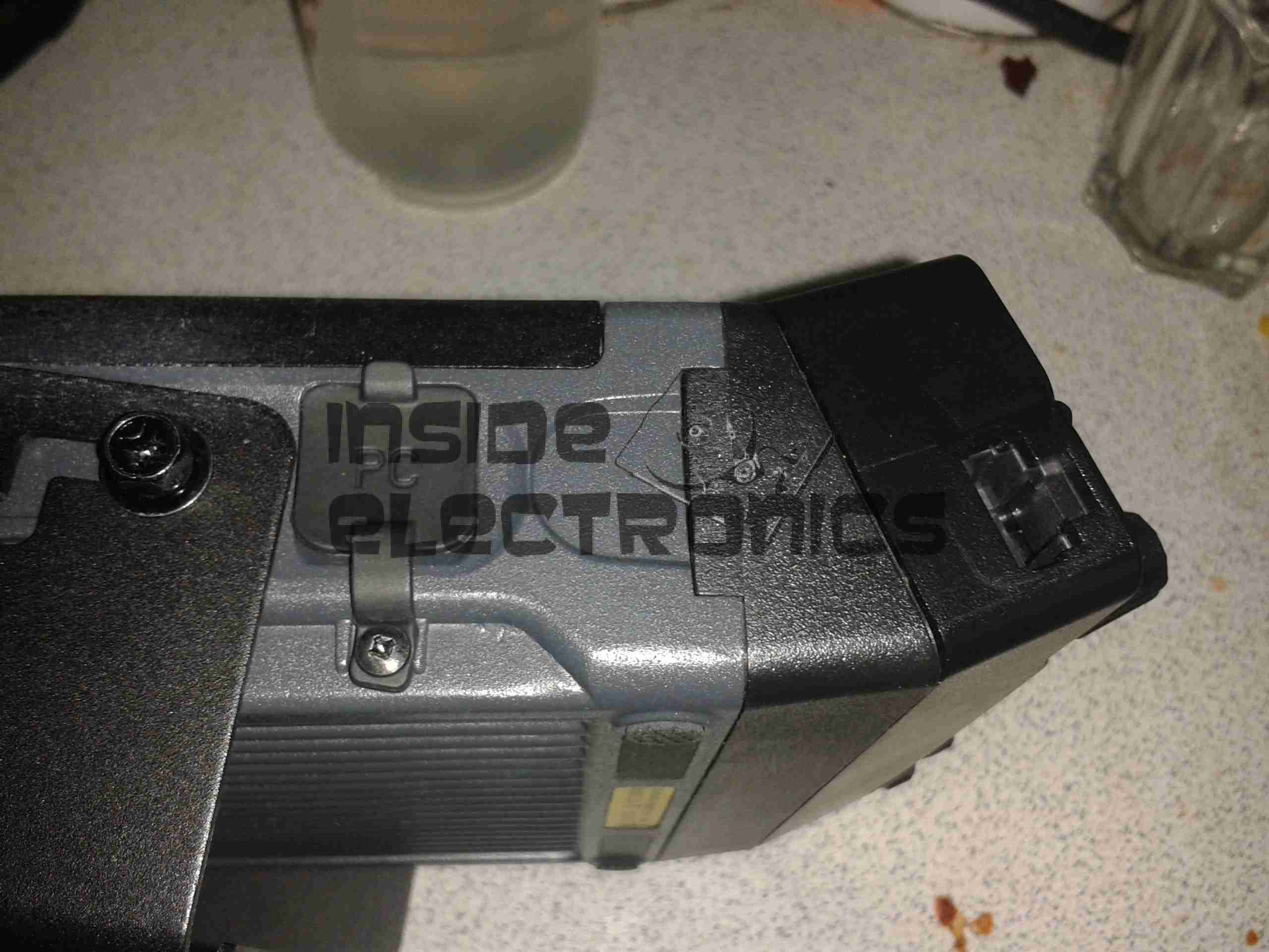
AD9850 VFO
The amplifier section is unpopulated & bypassed as I was getting some bad distortion effects from that section, some more work is needed there.
The Arduino Pro Mini is situated under the display, and the 5v rail is provided by the LM7805 on the lower left corner.
Current draw at 12v input is 150mA, for a power of 1.8W total. About 1W of this is dissipated in the LM7805 regulator, so I have also done a layout with an LM2574 Switching Regulator.
The SMPS version should draw a lot let power, as less is being dissipated in the power supply, but this version is more complex.
DDS VFO-SMPS
Here the SMPS circuit can be seen on the left hand side of the board, completely replacing the linear regulator.
I have not yet built this design, so I don’t know what kind of effect this will have on the output signal, versus the linear regulator. I have a feeling that the switching frequency of the LM2574 (52kHz) might produce some interference on the output of the DDS module. However I have designed this section to the standards in the datasheet, so this should be minimal.
Nevertheless this version is included in the Downloads section at the bottom of this post.
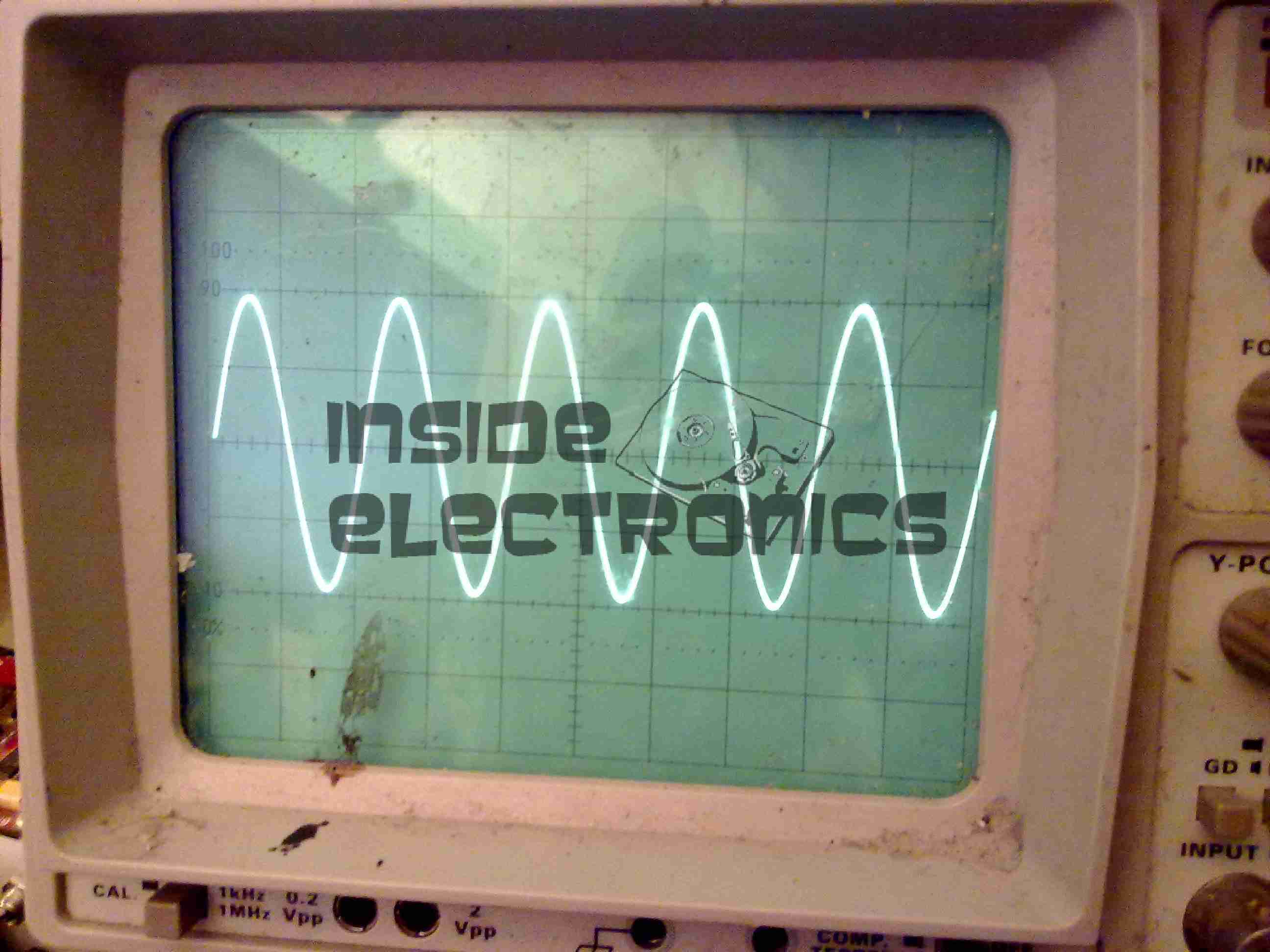
The output coupled through a 100nF capacitor is very clean, as can be seen below, outputting a 1kHz signal. Oscilloscope scale is 0.5ms/div & 1V/div.
VFO Output (Mucky ‘Scope)Scope Connected
Thanks again to Rich over at AD7C for the very useful tool design!
Linked below is the Eagle design files for this project, along with my libraries used to create it.
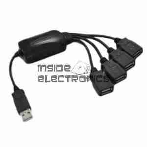
As the first USB hub I was using was certainly not stable – it would not enumerate between boots & to get it working again would require waiting around 12 hours before applying power, it has been replaced. This is a cheapie eBay USB hub, of the type shown below.
These hubs are fantastic for hobbyists, as the connections for power & data are broken out on the internal PCB into a very convenient row of pads, perfect for integration into many projects.
Breakout Hub
I now have two internal spare USB ports, for the inbuilt keyboard/mouse receiver & the GPS receiver I plan to integrate into the build.
These hubs are also made in 7-port versions, however I am not sure if these have the same kind of breakout board internally. As they have the same cable layout, I would assume so.
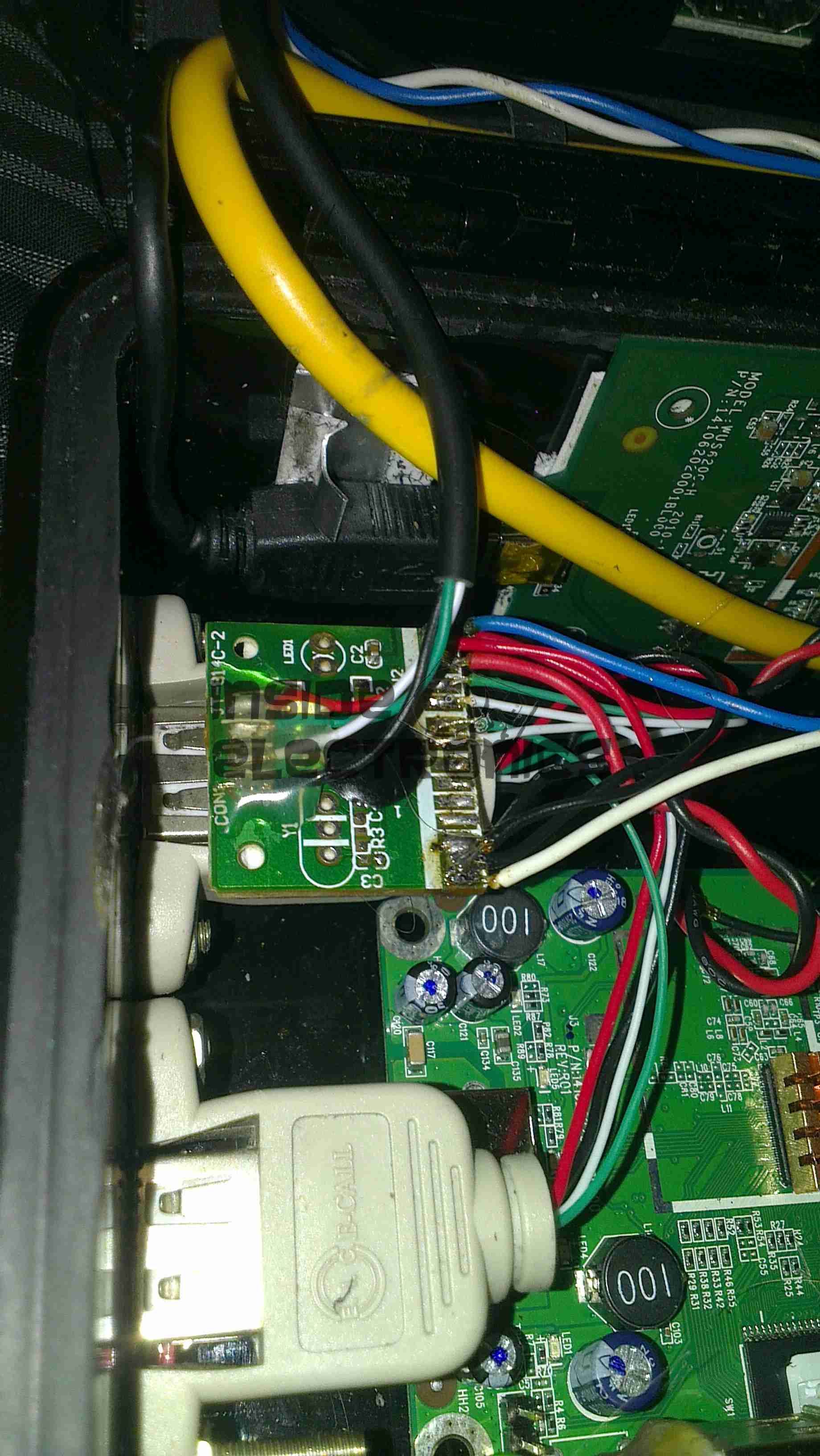
Connector Panel
Here is a closeup of the back of the connectors, showing a couple of additions.
I have added a pair of 470µF capacitors across the power rails, to further smooth out the ripple in the switching power supply, as I was having noise issues on the display.
Also, there is a new reset button added between the main interface connectors, which will be wired into the pair of pads that the Raspberry Pi has to reset the CPU.
This can be used as a power switch in the event the Pi is powered down when not in use & also to reset the unit if it becomes unresponsive.
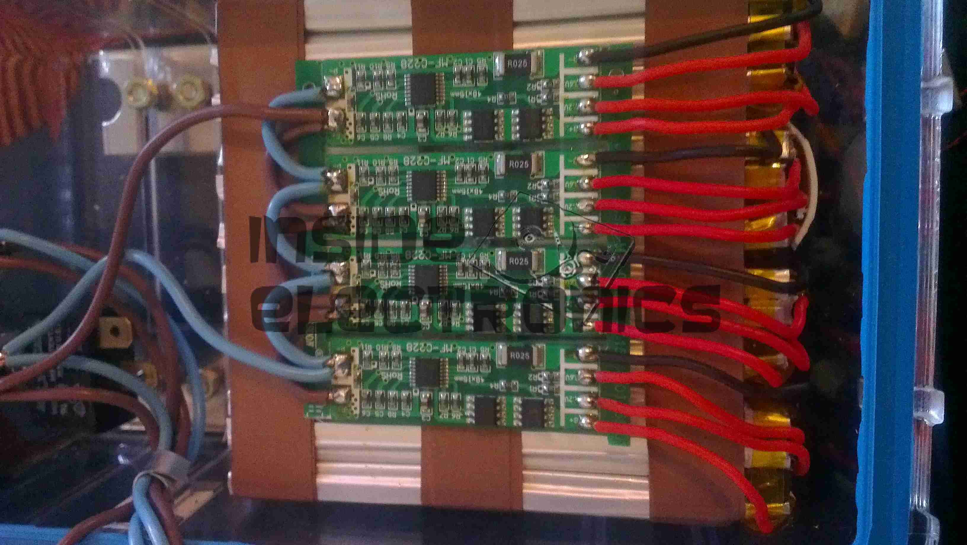
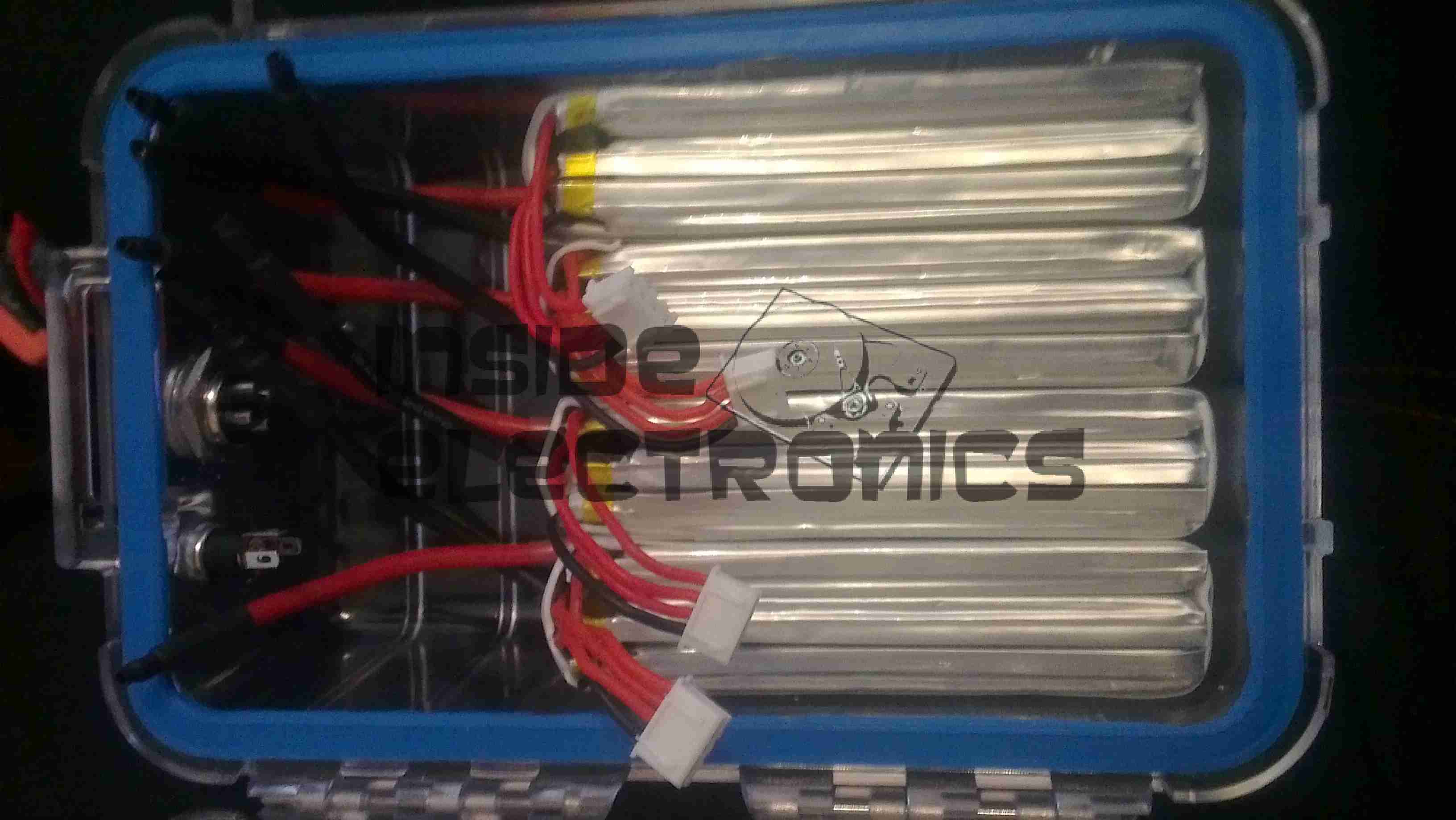
The final part for the battery pack has finally arrived, the PCM boards. These modules protect the cells by cutting off the power at overcharge, undercharge & overcurrent. Each cell is connected individually on the right, 12v power appears on the left connections. These modules also ensure that all the cells in the pack are balanced.
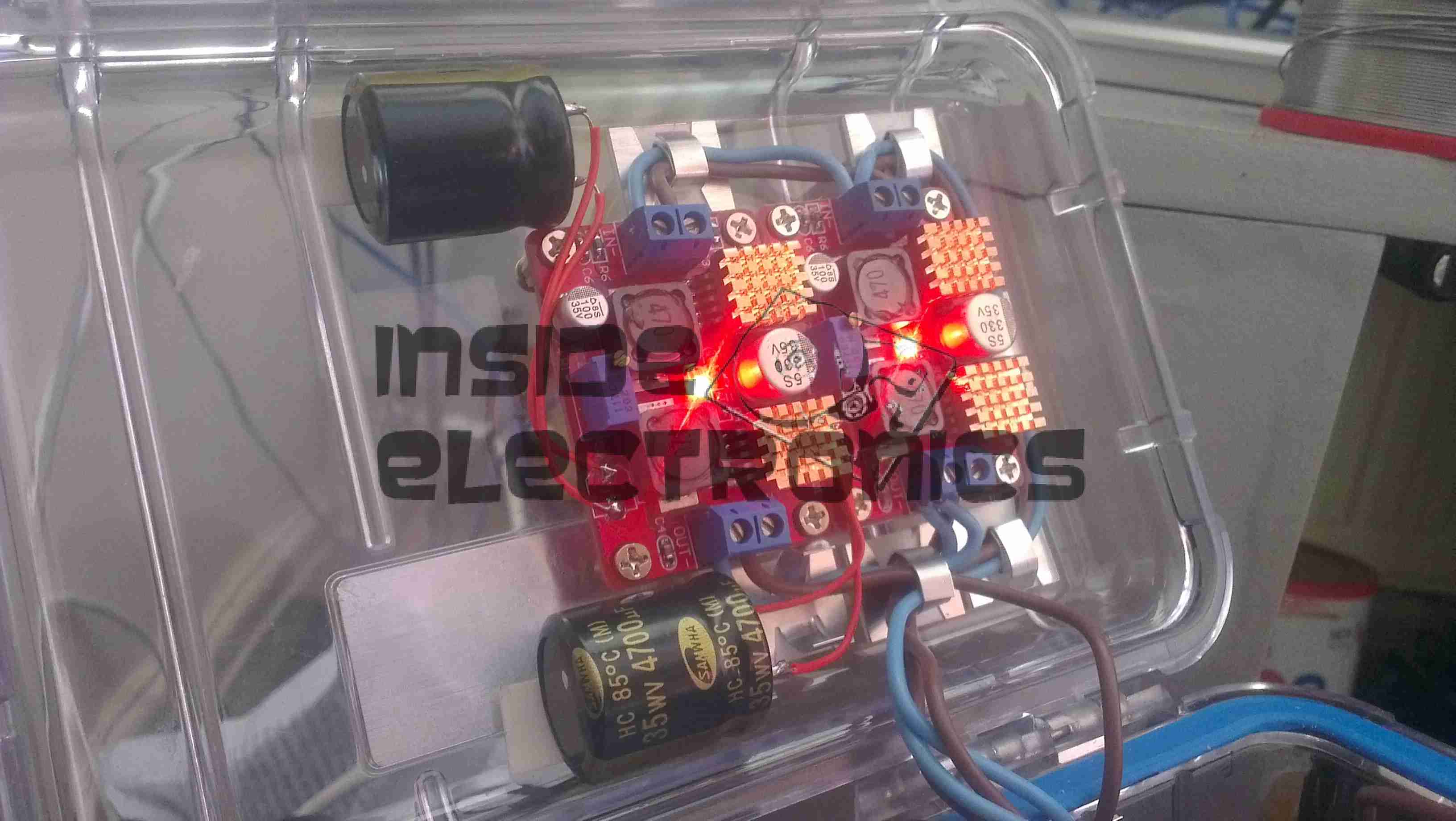
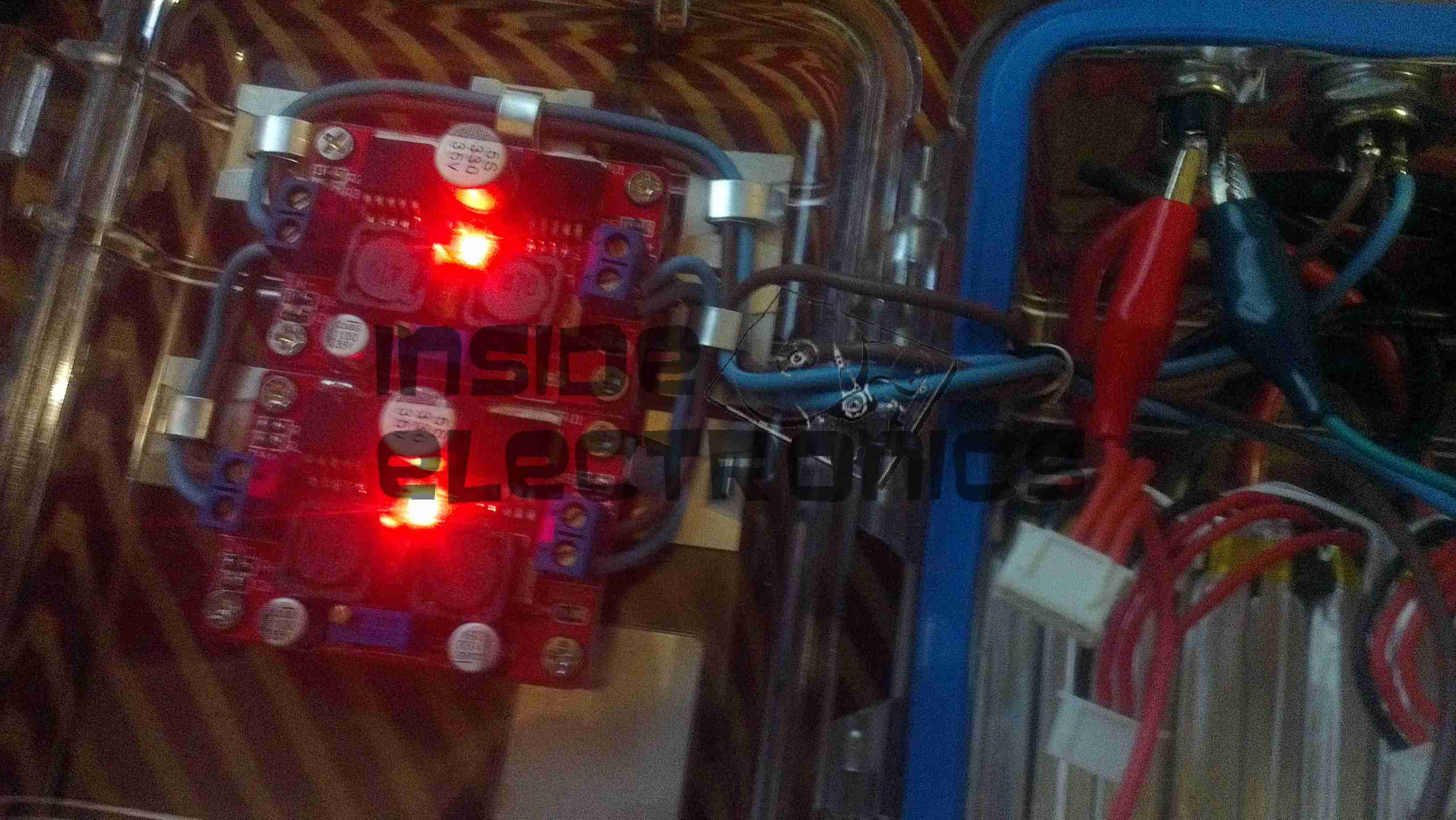
A few modifications were required to the SMPS modules to make the power rails stable enough to run the Pi & it’s monitor. Without these the rails were so noisy that instability was being caused.
I have replaced the 100µF output capacitors & replaced them with 35v 4700µF caps. This provides a much lower output ripple.
There are also heatsinks attached to the converter ICs to help spread the heat.
Progress is finally starting on the power supply unit for the Pi, fitted into the same case style as the Pi itself, this is an 8Ah Li-Poly battery pack with built in voltage regulation.
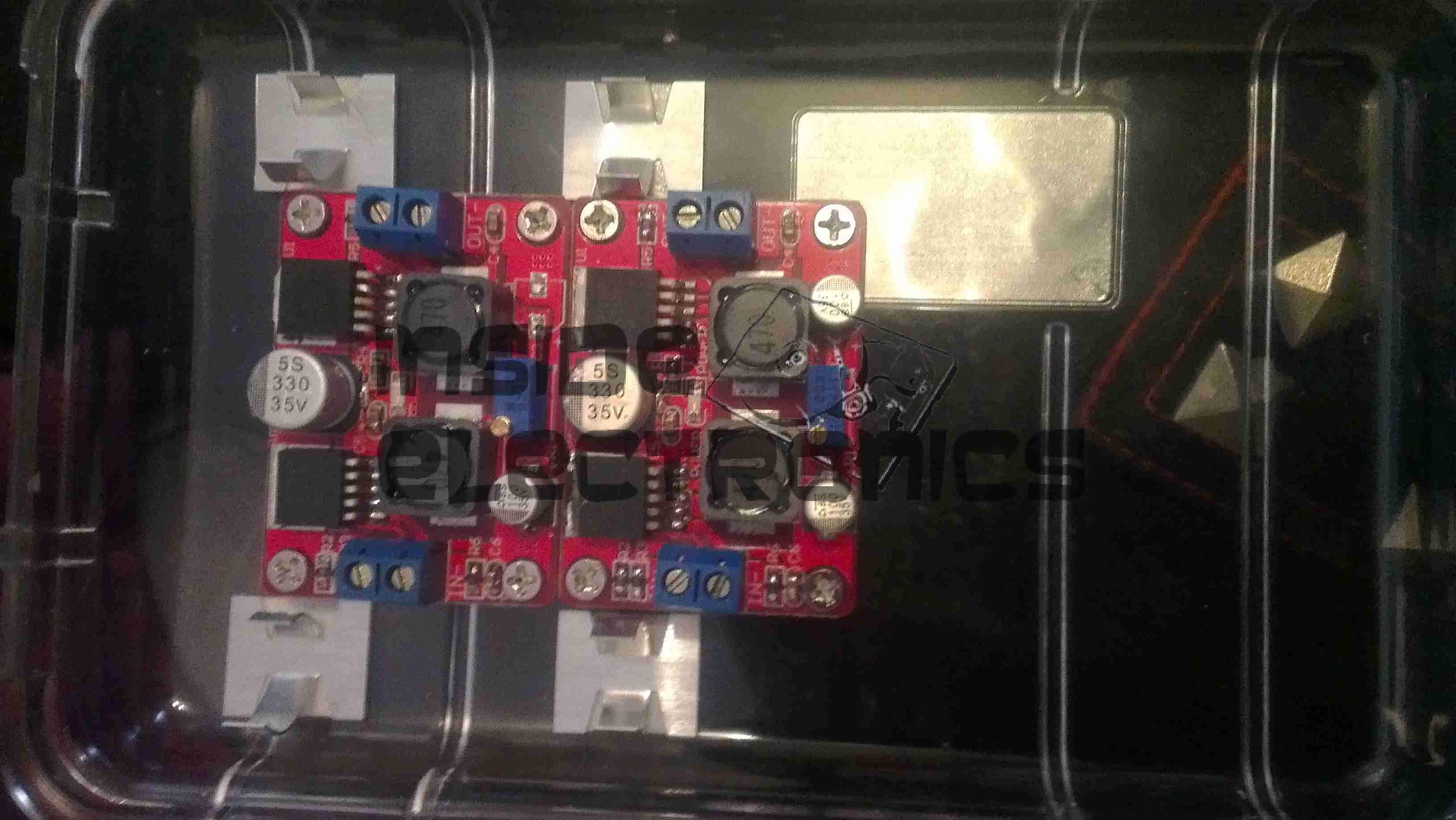
Regulator Boards
Here are the regulators, fixed to the top of the enclosure. These provide the 12v & 5v power rails for the Pi unit, at a max 3A per rail.
Battery Pack
In the main body of the case the battery pack is fitted. This is made up of 4 3-cell Li-Poly RC battery packs, rated at 2Ah each. All wired in parallel this will provide a total of 8Ah at 12.6v when fully charged.
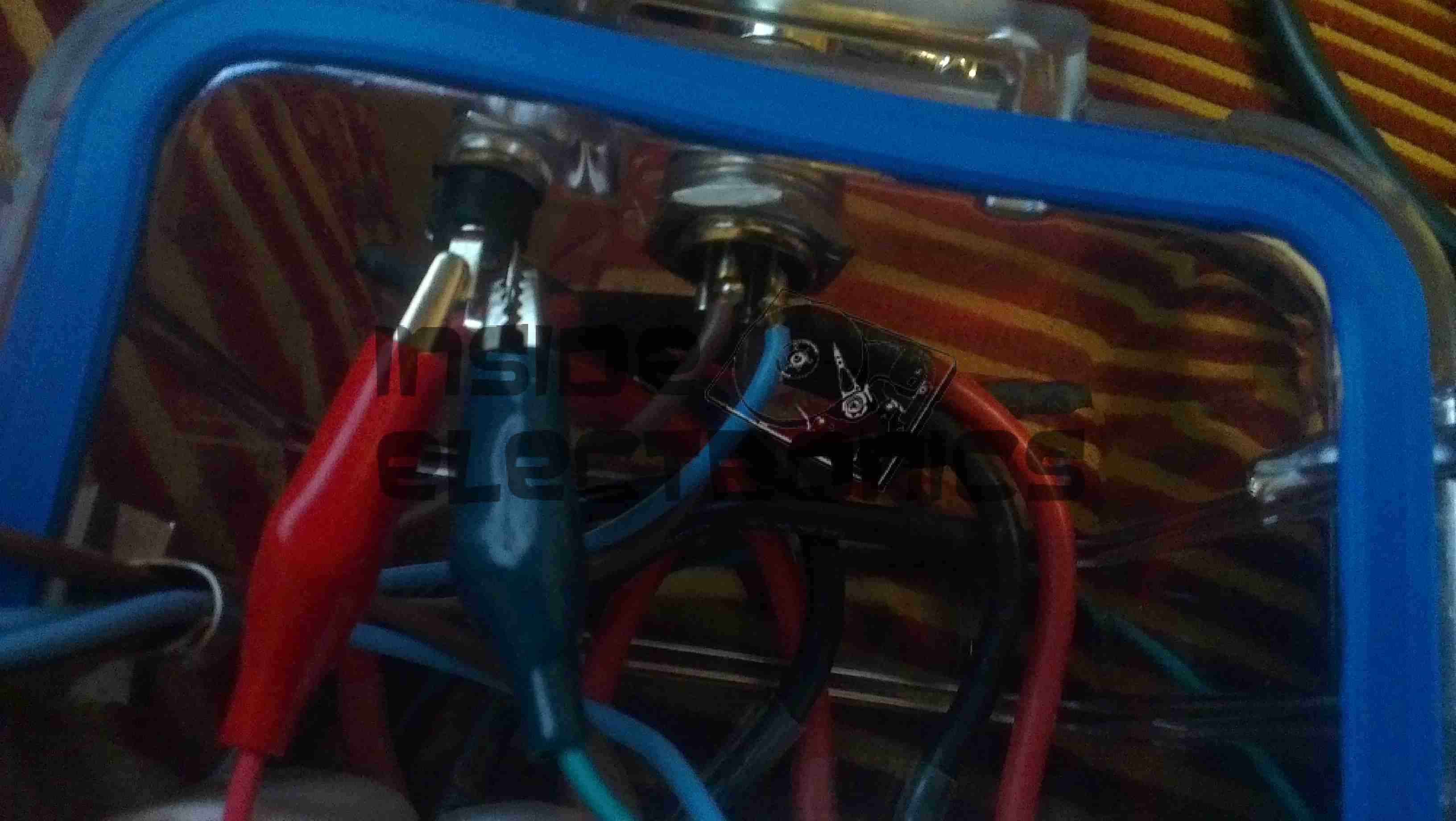
Powered Up
Here the regulators are powered up from a 13v supply for testing. I have discovered at full load these modules have very bad ripple, so I will be adding extra smoothing capacitors to the power rails to compensate for this.
I/O
Here are the connectors on the top of the unit, outputting the two power rails to the Pi & the DC barrel jack that will be used to charge the pack.
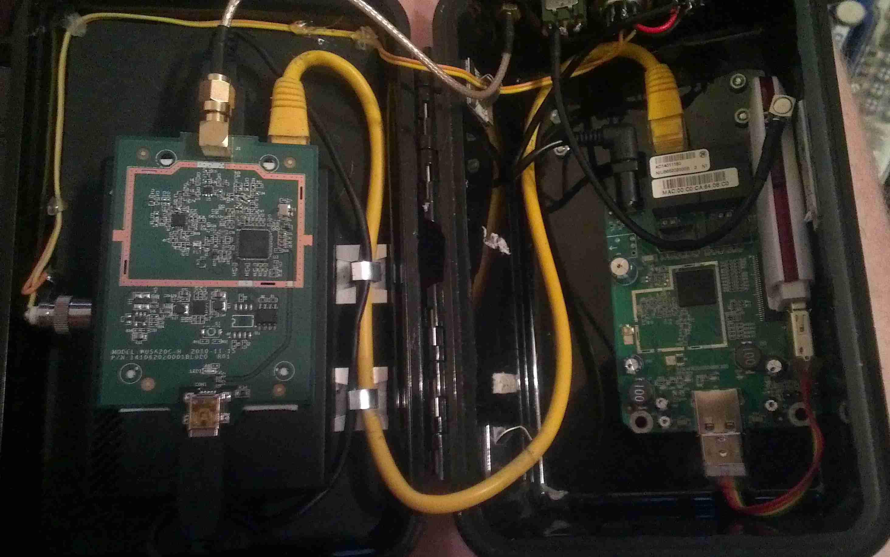
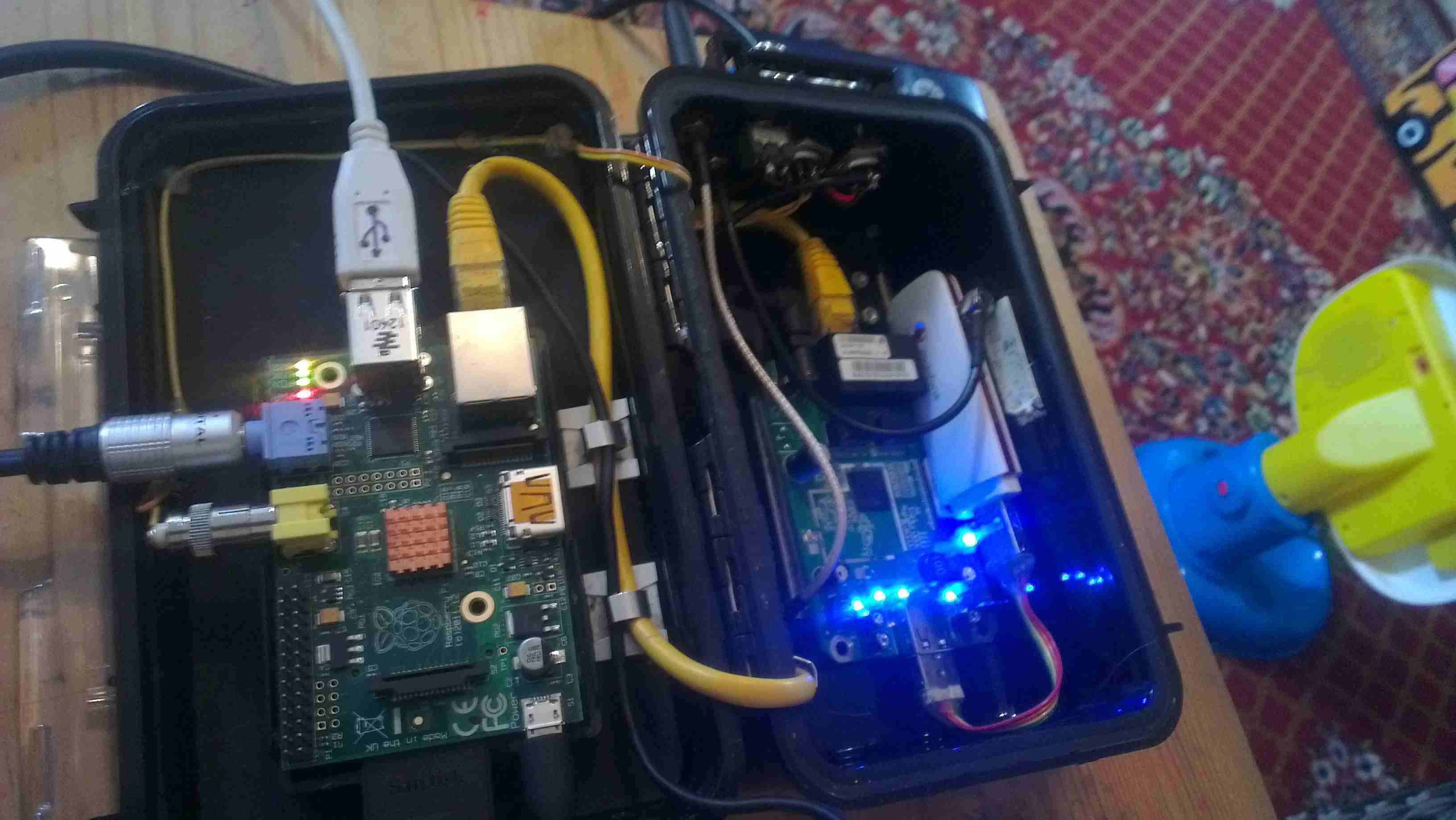
Here is the project I’m currently working on. A completely wearable computing platform based on the Raspberry Pi & the WiFi Pineapple.
Above can be seen the general overview of the current unit.
On the left:
Alfa AWUS036NHA USB High Power WiFi Network Interface
512MB Model B Raspberry Pi, 16GB SD card, running Raspbian & LXDE Desktop. Overclocked to 1GHz.
On the right:
WiFi Pineapple router board
USB 3G card.
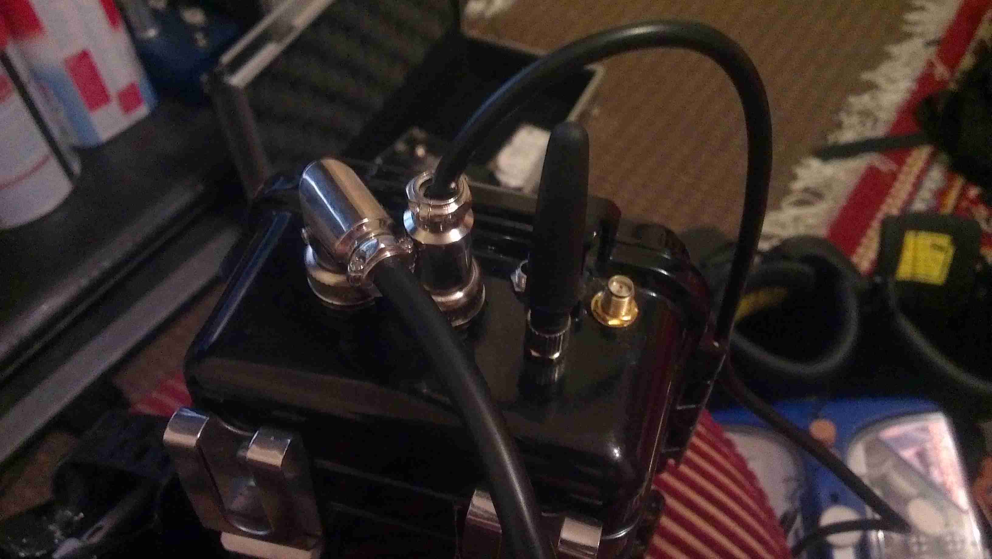
The WiFi, Pineapple & 3G all have external antenna connections for a better signal & the whole unit locks onto the belt with a pair of clips.
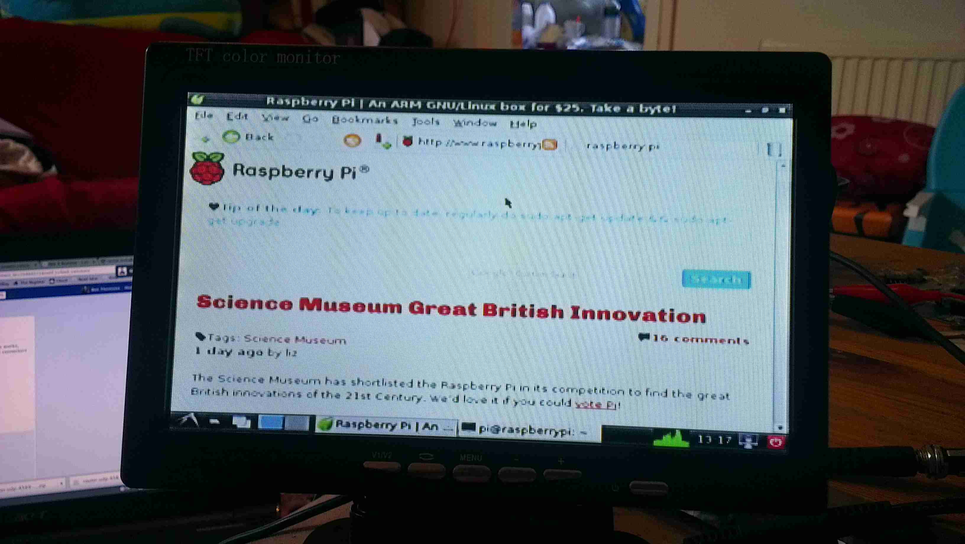
The Raspberry Pi is using the composite video output to the 7″ LCD I am using, running at a resolution of 640×480. This gives a decent amount of desktop space while retaining readability of the display.
The case itself is a Pelican 1050 hard case, with it’s rubber lining removed. The belt clips are also a custom addition.
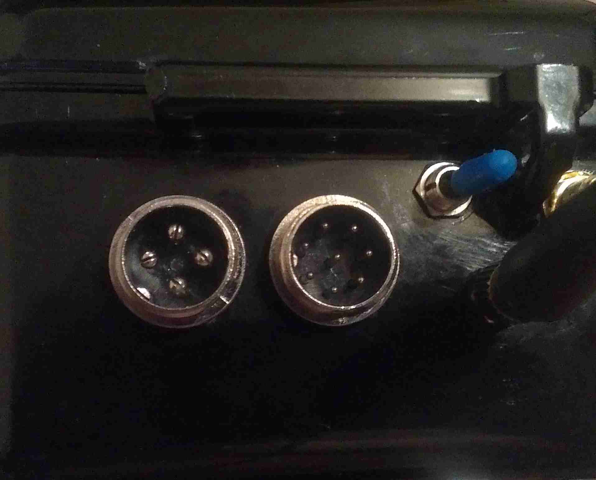
Connections
Here are the connections to the main unit, on the left is the main power connector, supplying +5v & +12v DC. The plug on the right is an 8-pin connection that carries two channels of video, mono audio & +12v power to the display.
Currently the only antenna fitted is the 3G.
Connectors
Closeup of the connections for power, audio & video. The toggle switch is redundant & will soon be replaced with a 3.5mm stereo jack for headphones, as an alternative to the mono audio built into the display.
Test Run
Current state of test. Here the unit is running, provided with an internet connection through the Pineapple’s 3G radio, funneled into the Pi via it’s ethernet connection.
Pi Goodness!
Running on a car reversing camera monitor at 640×480 resolution. This works fairly well for the size of the monitor & the text is still large enough to be readable.
Stay tuned for Part 2 where I will build the power supply unit.
Finally, some protection for my Raspberry Pi! The PCB fit is slightly loose, but that was quickly sorted with the application of a couple of spots of hot glue in the corners.
Unfortunately, the case is a couple of mm too small to fit the main board from the Pico Projector inside, so I won’t be butchering that into the case with the Pi as yet. What is required is an interface to the display engine from the Pi’s DSI interface.
Pi Cased Up
The pi all boxed. up. The only thing that this case would now require is a lightpipe to direct the LED’s light to the openings in the case, as they are very difficult to see at present.
Here are the viewfinder electronics from a 1984 Hitachi VHS Movie VM-1200E Camcorder. These small CRT based displays accept composite video as input, plus 5-12v DC for power.
Screen
Here is the front face of the CRT, diameter is 0.5″.
Power Board
Closeup view of the PCB, there are several adjustments & a pair of connectors. Socket in the upper left corner is the power/video input. Pinout is as follows:
Brown – GND
Red – Video Input
Orange – +12v DC
Yellow – Record LED
The potentiometers on the PCB from left:
H. ADJ
V. ADJ
BRIGHT
FOCUS
PCB Part Number reads: EM6-PCB
This unit utilises the BA7125L deflection IC.
Solderside
Reverse side of the PCB, very few SMT components on this board.
Tube Assembly
Here is an overall view of the CRT assembly with scan coils. Tube model is NEC C1M52P45.
Electron Gun
Closeup view of the CRT neck, showing the electron gun assembly.
CCTV Camera
The old CCTV camera used to feed a composite signal to the CRT board. Sanyo VCC-ZM300P.
CCTV Camera Connections
Connections at the back of the camera. Red & Black pair of wires lead to 12v power supply, Green & Black pair lead to the CRT board’s power pins. Seperate green wire is pushed into the BNC video connector for the video feed. video ground is provided by the PSU’s ground connection.
Connections
Finally the connections at the CRT drive board, left to right, +12v, Video, GND.
This is a cheap Sigma branded keychain photoframe. User buttons for power & selecting photos are on the left.
There are two white LEDs on the bottom edge that function as a torch as well.
Display
Front of the unit removed, showing the LCD module. The USB jack is bottom left, next to the pair of white LEDs & above that is the 32kHz watch crystal that the CPU uses for timekeeping.
Back Removed
Here the back has been removed showing the 3.7v Li-Ion cell used to provide power.
Display Folded Back
Here the display has been removed from the PCB exposing the chipset.
Chipset
Here the CPU blob-top chip & a flash memory IC are visible. The CPU is a Sitronix ST2205U.
Here is the casing split, with the main CPU board & display on the right, & the RF tranciever board on the left.
Main CPU
View of the main CPU board, with the mic & loudspeaker on the right hand side.
The channel display is on the reverse side of the PCB.
RF Board
View of the RF board, with it’s brass shielding attached. This radio will transmit at 5W max.
RF Shields Removed
Shielding removed, power regulation bottom right corner of the board, tranciever on the left.
PCB Front
CPU board removed from the casing, showing the LCD & the user buttons to the left.
Tip Jar
If you’ve found my content useful, please consider leaving a donation by clicking the Tip Jar below!
All collected funds go towards new content & the costs of keeping the server online.