Since I seem to be the local go-to for any dead electrical equipment, this brand-new Silverline polisher has landed on my desk. Purchased cheap from an auction this was dead on arrival. Checking the fuse revealed nothing suspect, so a quick teardown to find the fault was required.
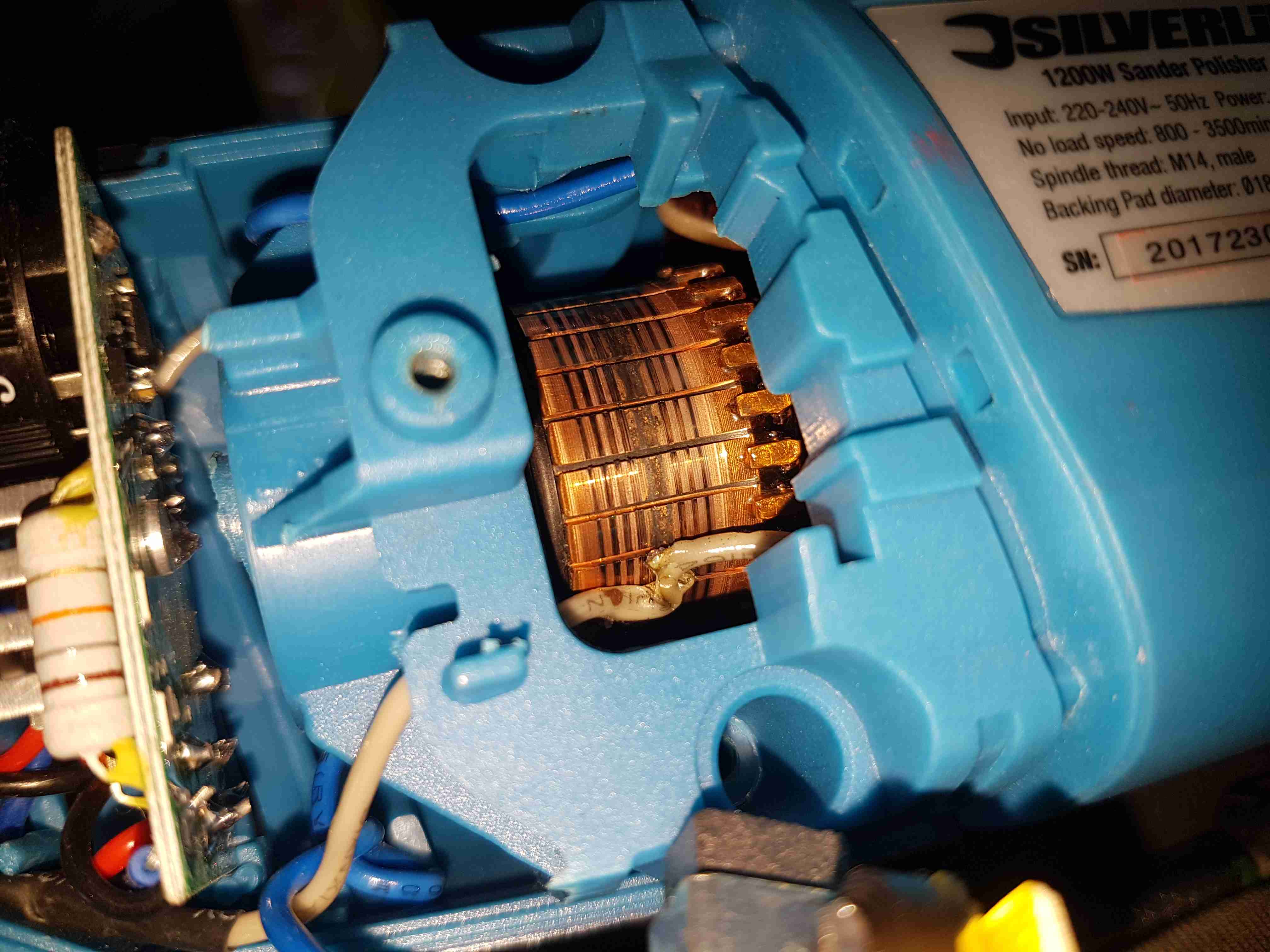
Above is a photo of the commutator with the brush holder removed, and the source of the issue. The connection onto the field winding of the universal motor has been left unsecured, as a result it’s managed to move into contact with the commutator.
This has done a pretty good job of chewing it’s way through the wire entirely. There is some minor damage to the commutator segments, but it’s still smooth, and shouldn’t damage the brushes.
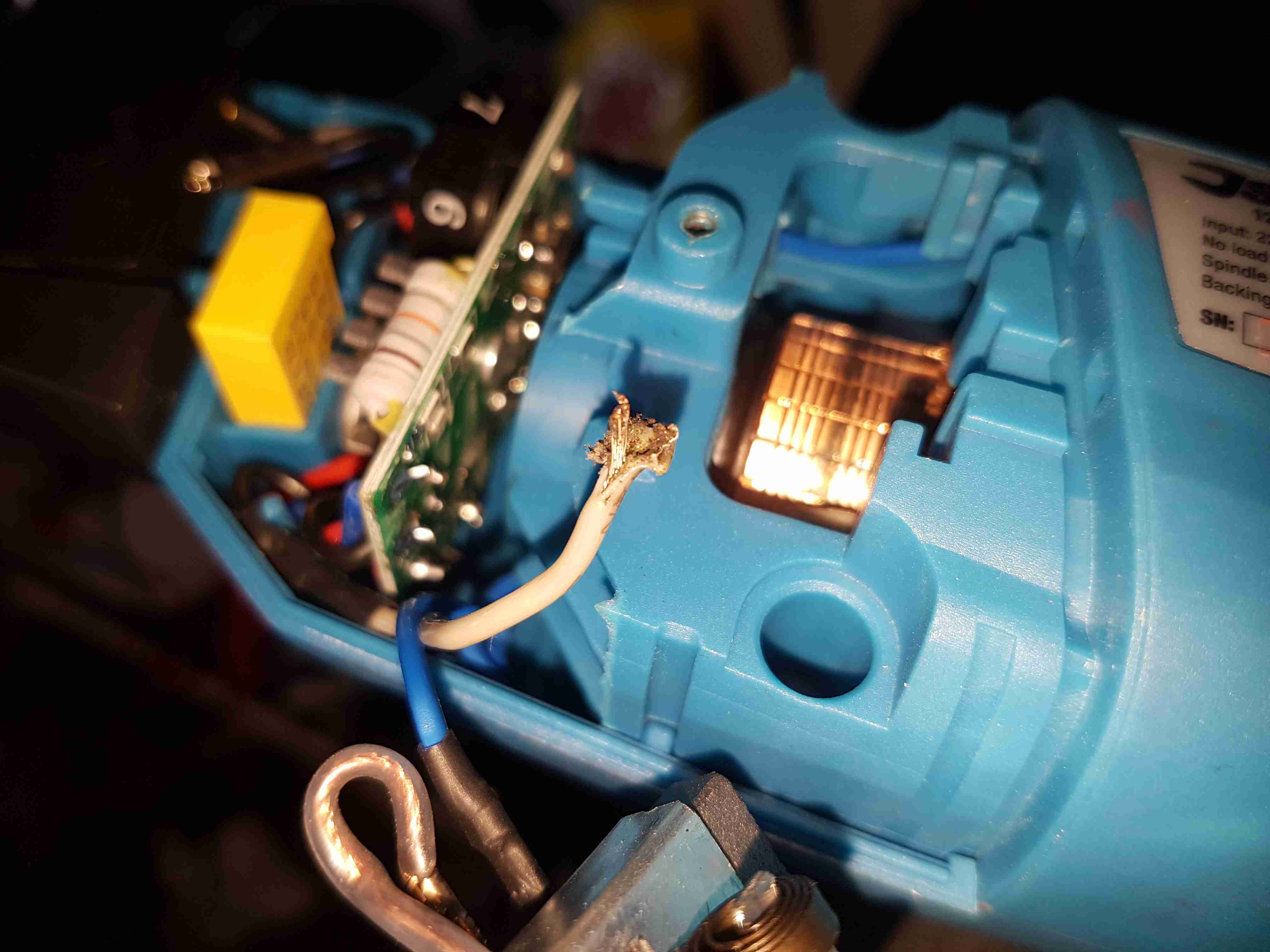
Chewed Wire
A quick pull on what’s left of the wire reveals the extent of the problem. It’s entirely burned through! Unfortunately the stator assembly with the field windings is pressed into the plastic housing, so it’s not removable. An in-place solder joint was required to the very short remains of the wire inside the housing. Once this was done the polisher sprang to life immediately, with no other damage.
This unit probably ended up at an auction as a factory reject, or a customer return to a retail outlet. If the latter, I would seriously question the quality control procedures of Silverline tools. 😉
A few months ago I did a teardown on this Anker PowerPort Speed 5 USB charger, but I didn’t get round to detailing the conversion to 12v I had to do, so I’ll get to that now I’ve got a couple more to convert over.
Power Module
Here’s the internals of the Anker charger once I’ve removed the casing – which like many things these days, is glued together. (Joints can be cracked with a screwdriver handle without damaging the case). There’s lots of heatsinking in here to cool the primary side switching devices & the pot core transformers, so this is the first thing to get removed.
Heatsink Removed
Once the heatsink has been removed, the pot core transformers are visible, wrapped in yellow tape. There’s some more heatsink pads & thermal grease here, to conduct heat better. The transformers, primary side switching components & input filter capacitor have to go.
Primary Side Components Removed
Here’s the PCB once all the now redundant mains conversion components have been deleted. I’ve left the input filtering & bridge rectifier in place, as this solves the issue of the figure-8 cable on the input being reversible, polarity of the input doesn’t matter with the bridge. I’ve removed the main filter capacitor to make enough room for the DC-DC converters to be fitted.
Tails Installed
Installing the tails to connect everything together is the next step, this charger requires two power supplies – the QC3 circuits need 14.4v to supply the multi-voltage modules, the remaining 3 standard ports require 5v. The DC input tails are soldered into place where the main filter capacitor was, while the outputs are fitted to the spot the transformer secondary windings ended up. I’ve left the factory Schottky rectifiers in place on the secondary side to make things a little more simple, the output voltages of both the DC-DC converters does need to be increased slightly to compensate for the diode drops though. I’ve also bypassed the mains input fuse, as at 12v the input current is going to be substantially higher than when used on mains voltage.
DC-DC Converters Installed
With a squeeze both the boost converter & the buck converter fit into place on the PCB.
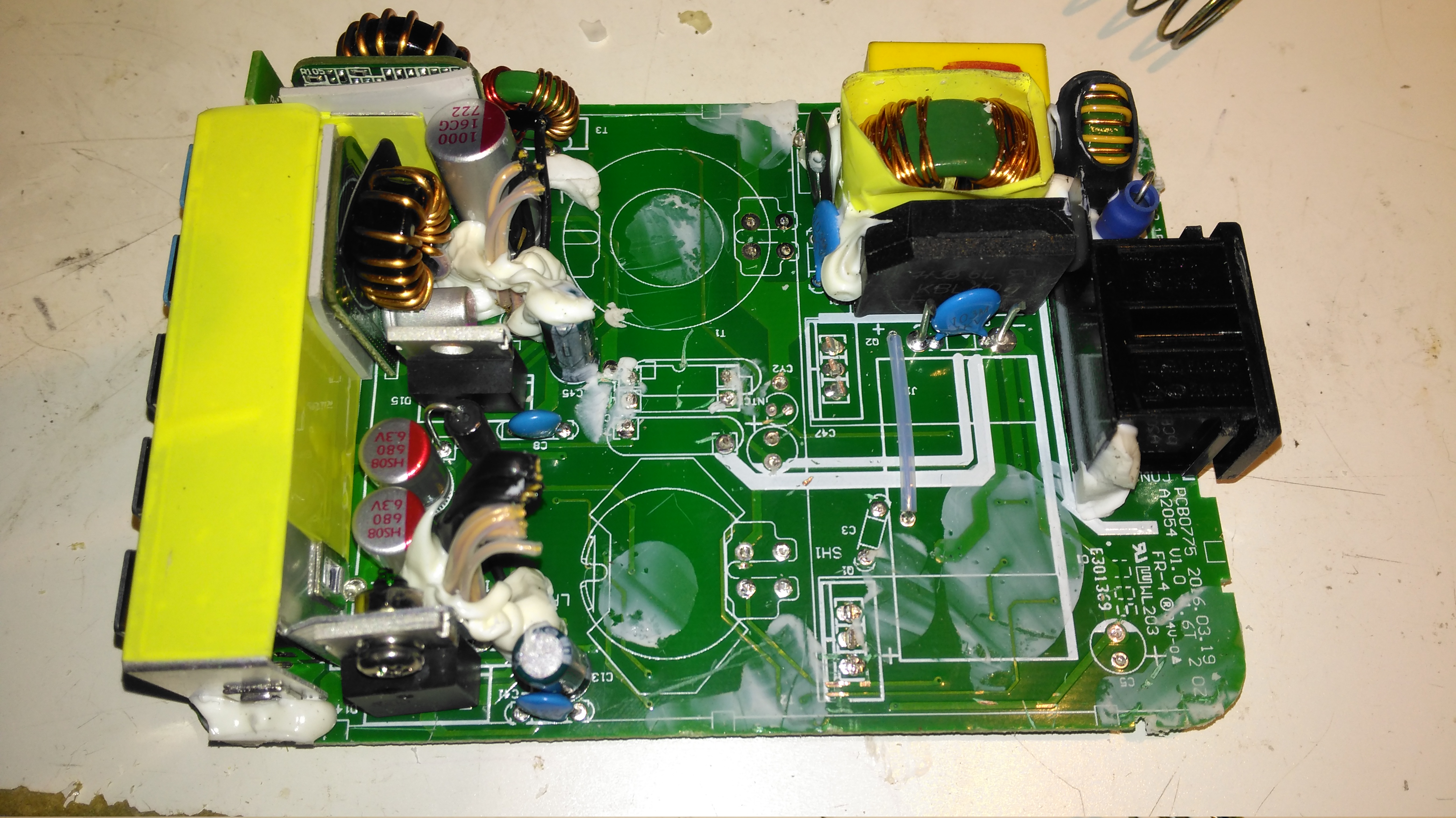
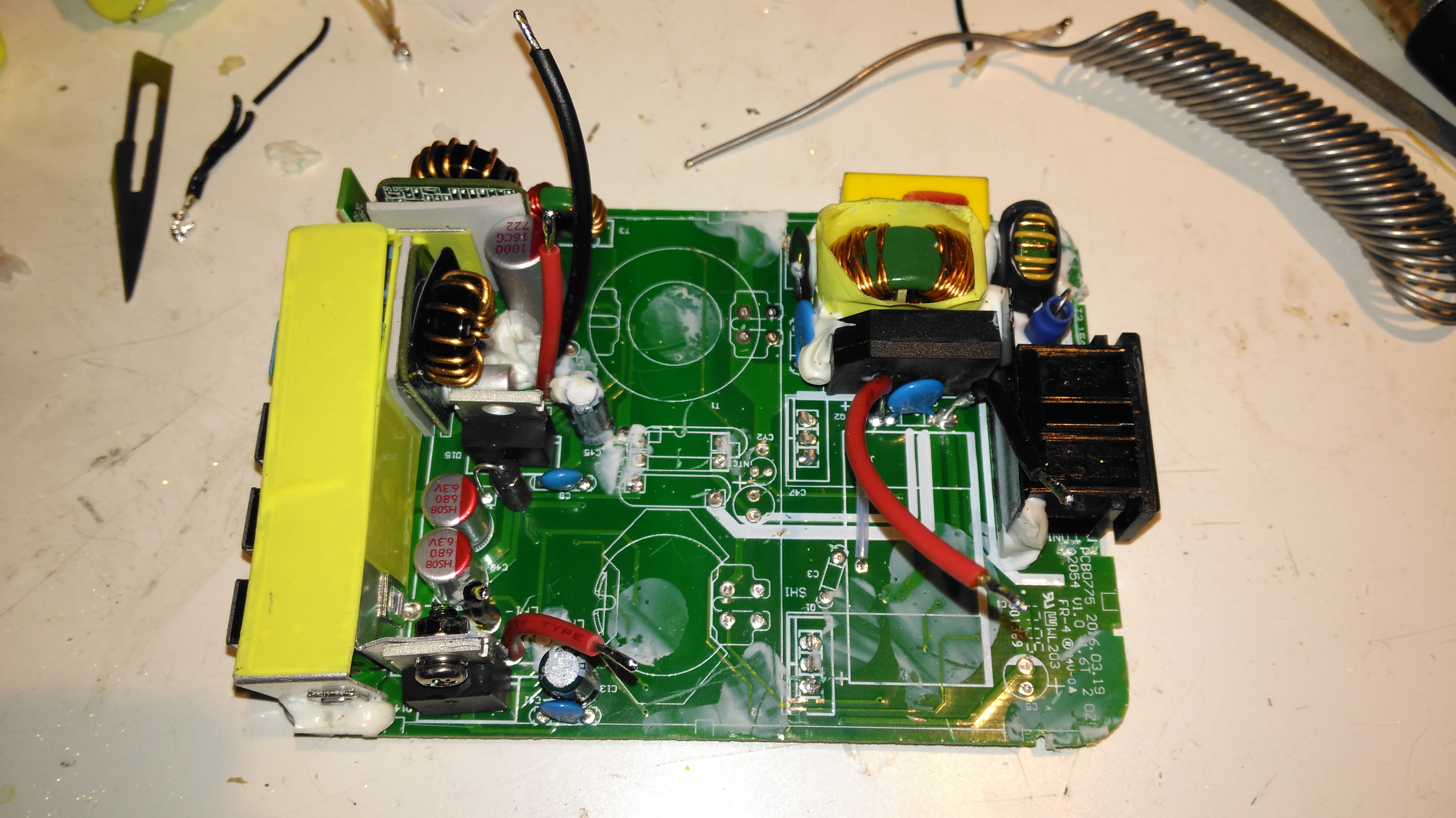
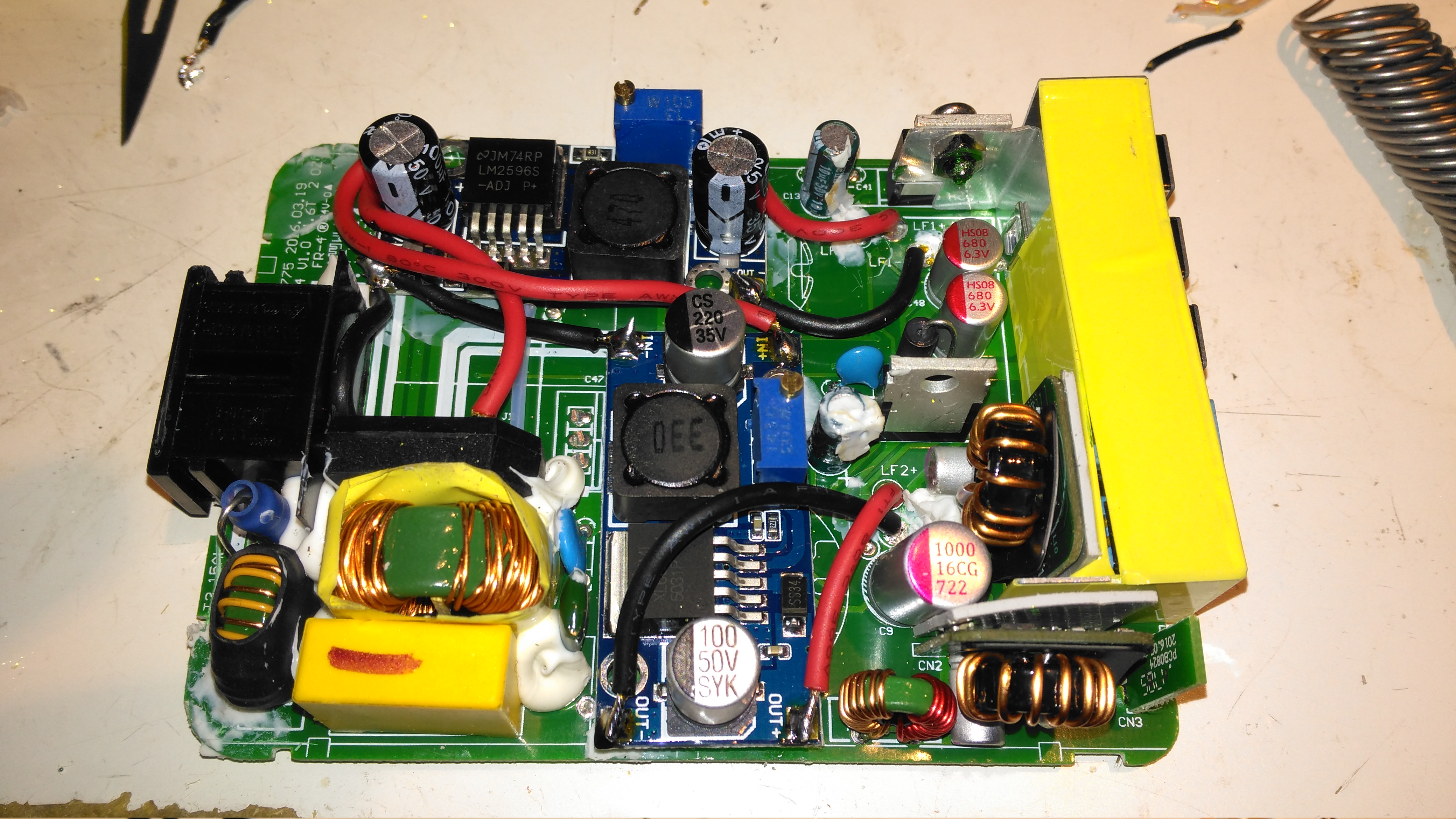
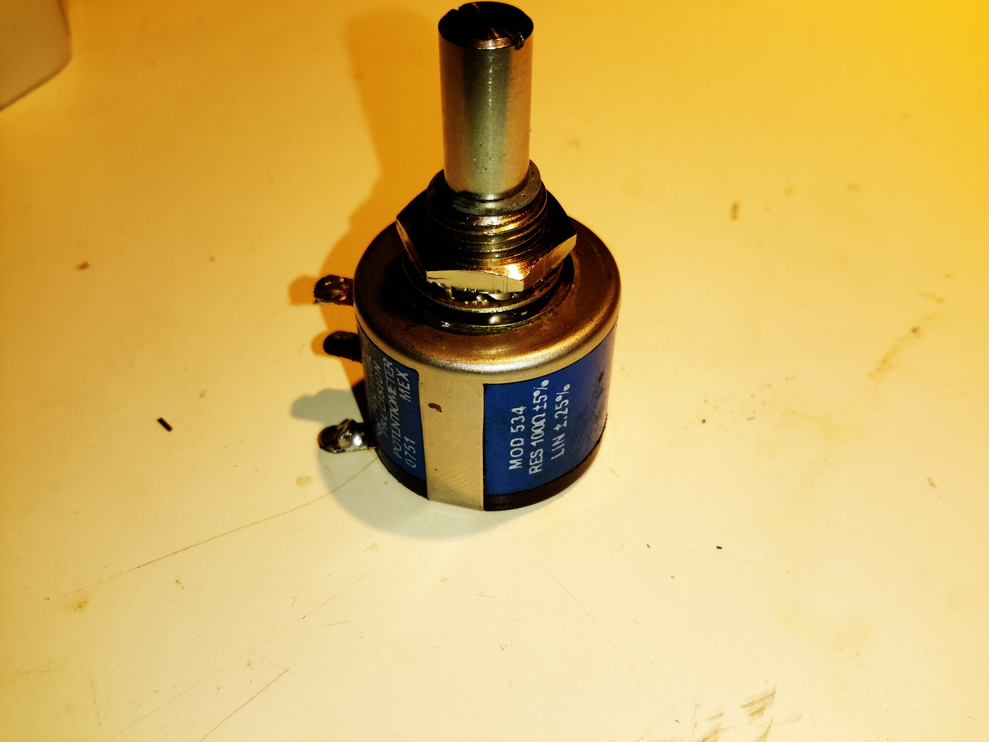
I recently used a Vishay Spectrol Precision 10-turn potentiometer in my latest PSU project, and since these clip together instead of being ultrasonically welded like Bourns potentiometers, I decided to do a quick teardown for the blog. I didn’t find much in the way of how these pots worked from a search, so here we go!
Vishay Spectrol Precision 10-Turn
Here’s a pot of the same spec as I used in the previous project, again from my random used junk bin. This is a 100Ω, 5% wirewound potentiometer. The shaft is secured in the centre bushing with a snap ring, this is easily removed with a pair of needlenose pliers.
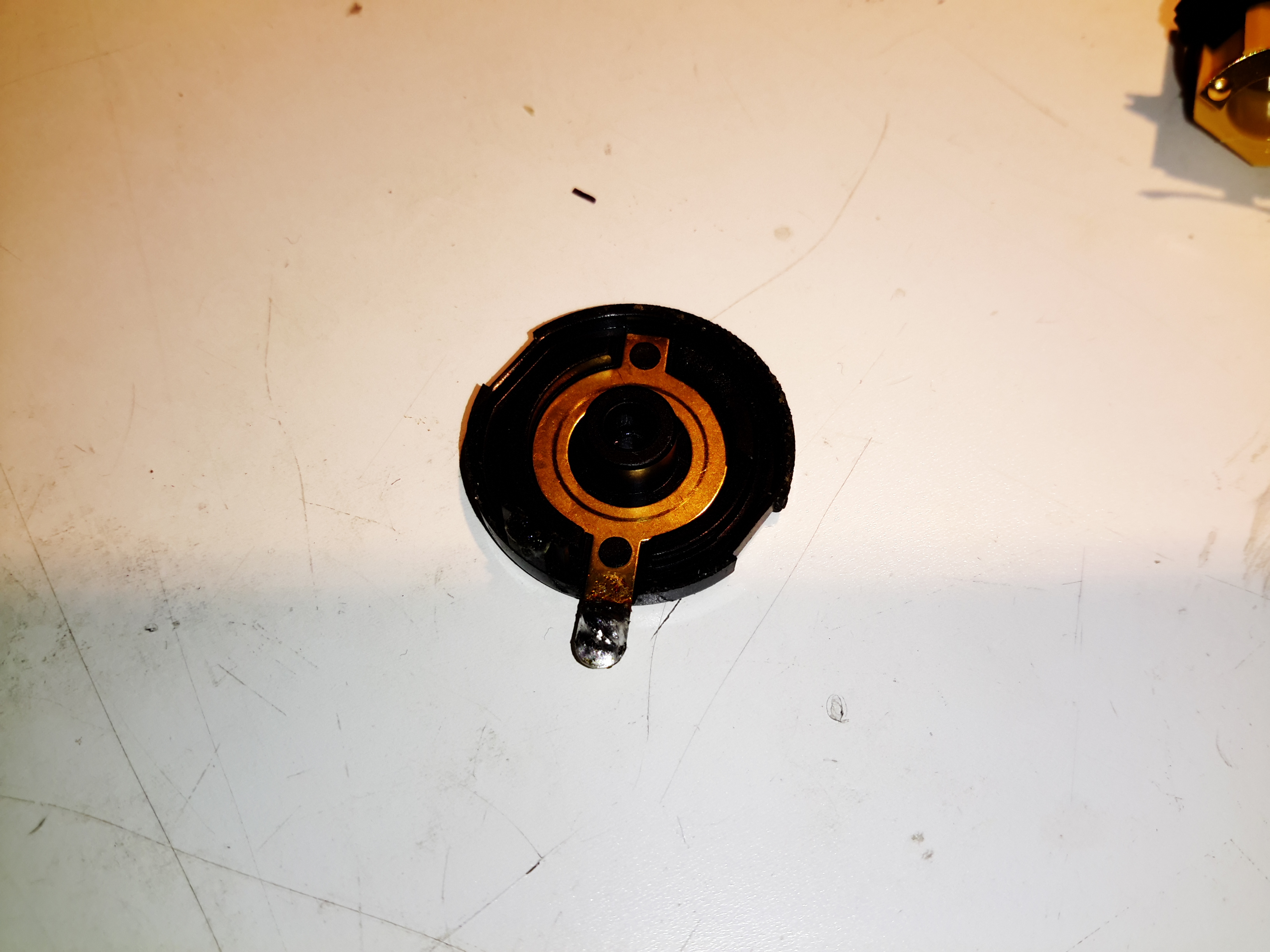
Wiper Stationary Contact
After unclipping the back cover, the stationary part of the wiper contact is visible in the back plastic cover.
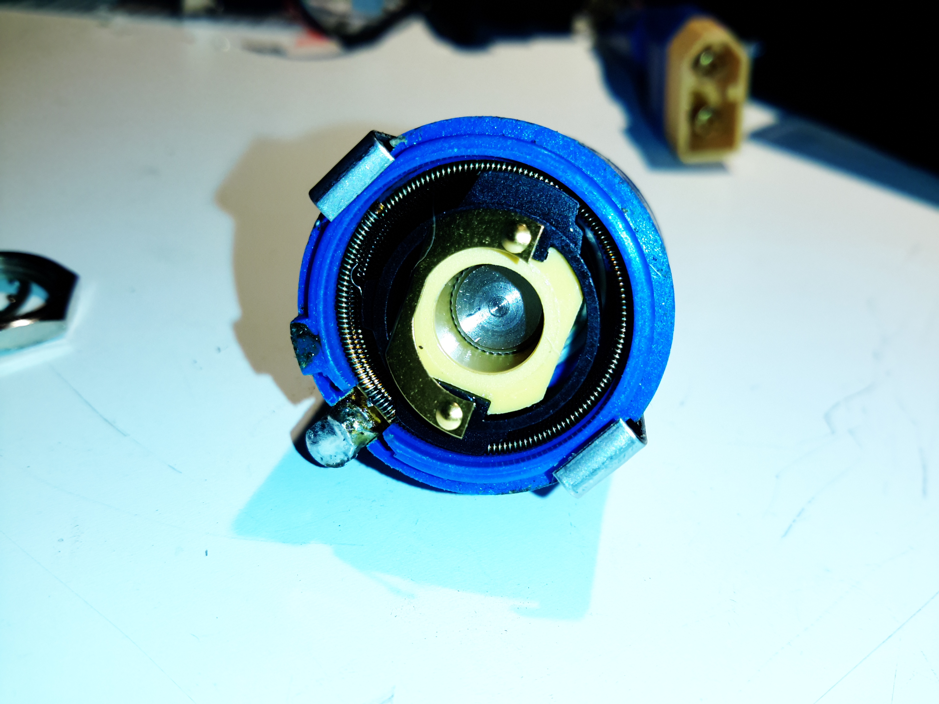
Back Cover Removed
Inside the back of the potentiometer shows the inner workings. These devices have a large helical winding of resistance wire around the inner diameter of the casing, the wiper tracks this helix as the potentiometer is turned.
Centre Contact & Shaft
As the wiper must move axially as it winds around the spiral of resistance wire, the contact is mounted on a pair of guides so it can slide back & forth. The electrical connection is made via another spring contact that runs down the side of the plastic shaft insert. Two notches cut into the black plastic wiper frame engage with the round profile of the resistance winding like a screw into a nut, keeping the wiper in perfect alignment as it travels the full length of the winding. I suspect all these moving contacts are made of Beryllium Copper in this rather expensive component as this alloy is very flexible, as well as being a very good electrical conductor.
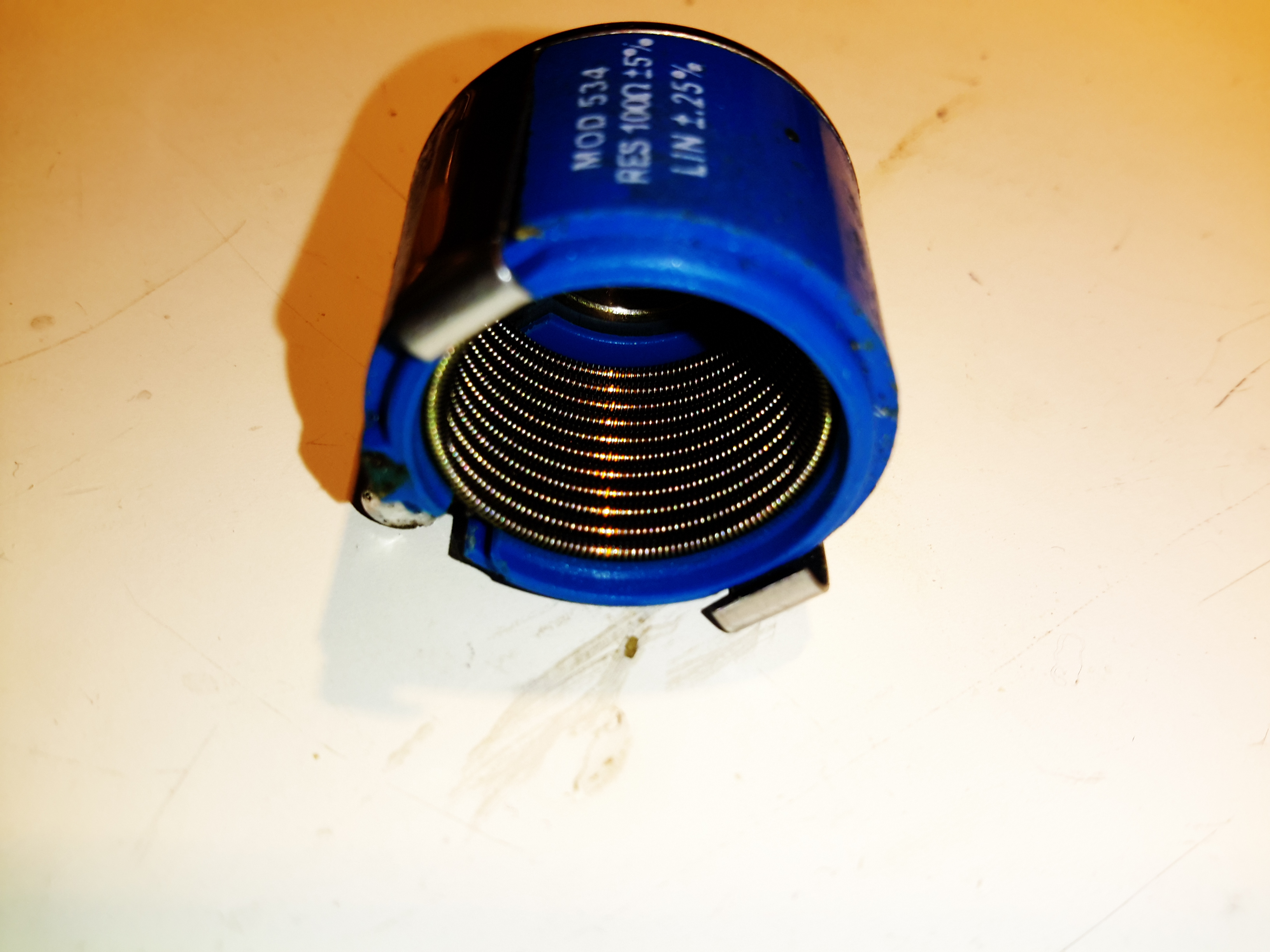
Resistance Winding
With the centre shaft & it’s wiper contact removed from the shell, the helix of resistance wire can be seen inside. Oddly, the former the resistance wire is wound around appears to be metal, possibly copper, but to keep the entire thing from shorting itself out this must be coated in insulation.
I posted a while back a teardown of the VM Superhub 2 router, as VM has “upgraded” to a rebranded Arris TG2492S/CE CM. Alas Virgin Media in their wisdom have decided that simple router features like being able to change the LAN subnet & DHCP server range are far too complex to trust to the Great Unwashed, so they’ve removed them entirely from the firmware, and locked the local LAN onto the 192.168.0.0/24 range.
As my network is already numbered in the 10.0.0.0/16 range, with several statically addressed devices present and other systems relying on these static assignments, using this router would have meant renumbering everything.
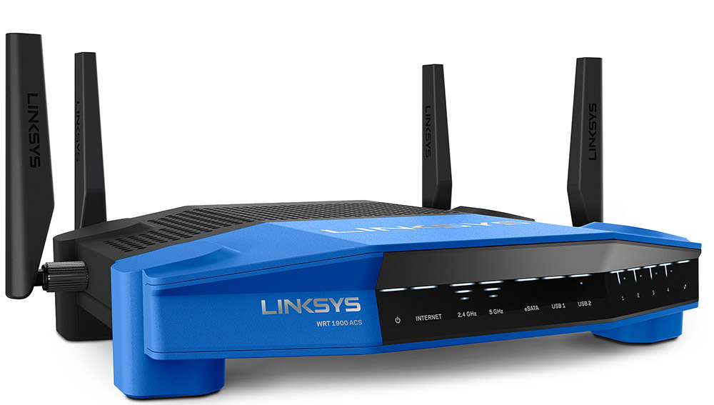
Luckily Virgin had the decency to leave the “modem mode” option in the firmware, effectively disabling the WiFi & routing functions & allowing the connection of a third-party router. Some searching for a suitable replacement for the core of my network turned up the Linksys WRT1900ACS. While I waited for this to arrive, some temporary workarounds were needed to make everything function well enough with VM’s crap router.
WRT1900ACS
These routers have been designed as a modern replacement for the venerable WRT54G series of routers from some time ago, with full support for OpenWRT/DD-WRT firmware, and with a beefy 1.6GHz dual core CPU & 512MB of RAM I doubt I’ll be able to knock this one over with too much network traffic! This was pretty much the most powerful router I could afford, and should mean I don’t need to upgrade for a long time. (No teardown of this yet, as it’s taking care of the network at present. Maybe some point in the future I’ll take the plunge).
The stock firmware isn’t totally awful, and has some nice features, but I decided it needed to be replaced with DD-WRT for more security & future flexibility. I’ll leave the firmware flashing stuff for another post 😉
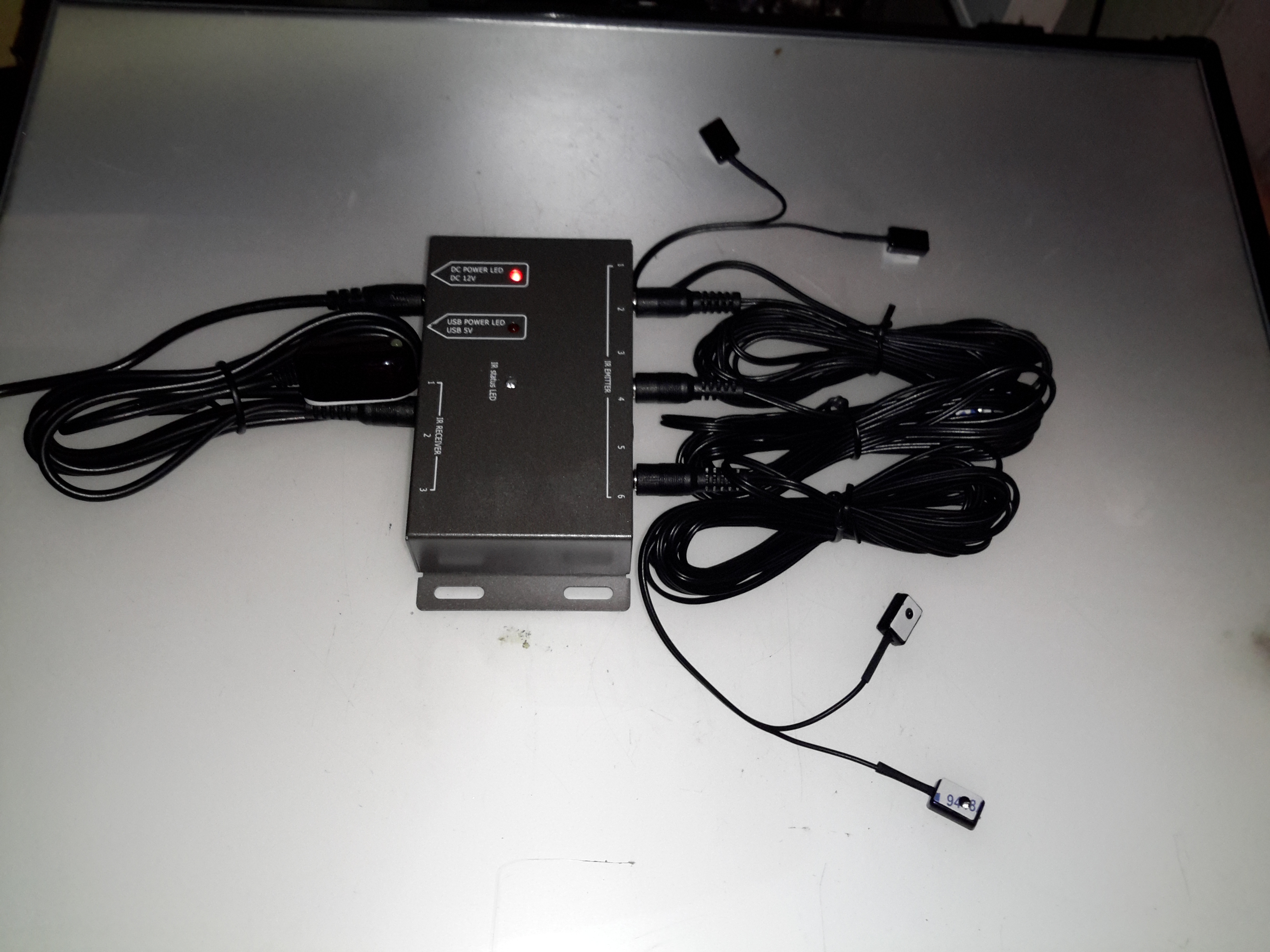
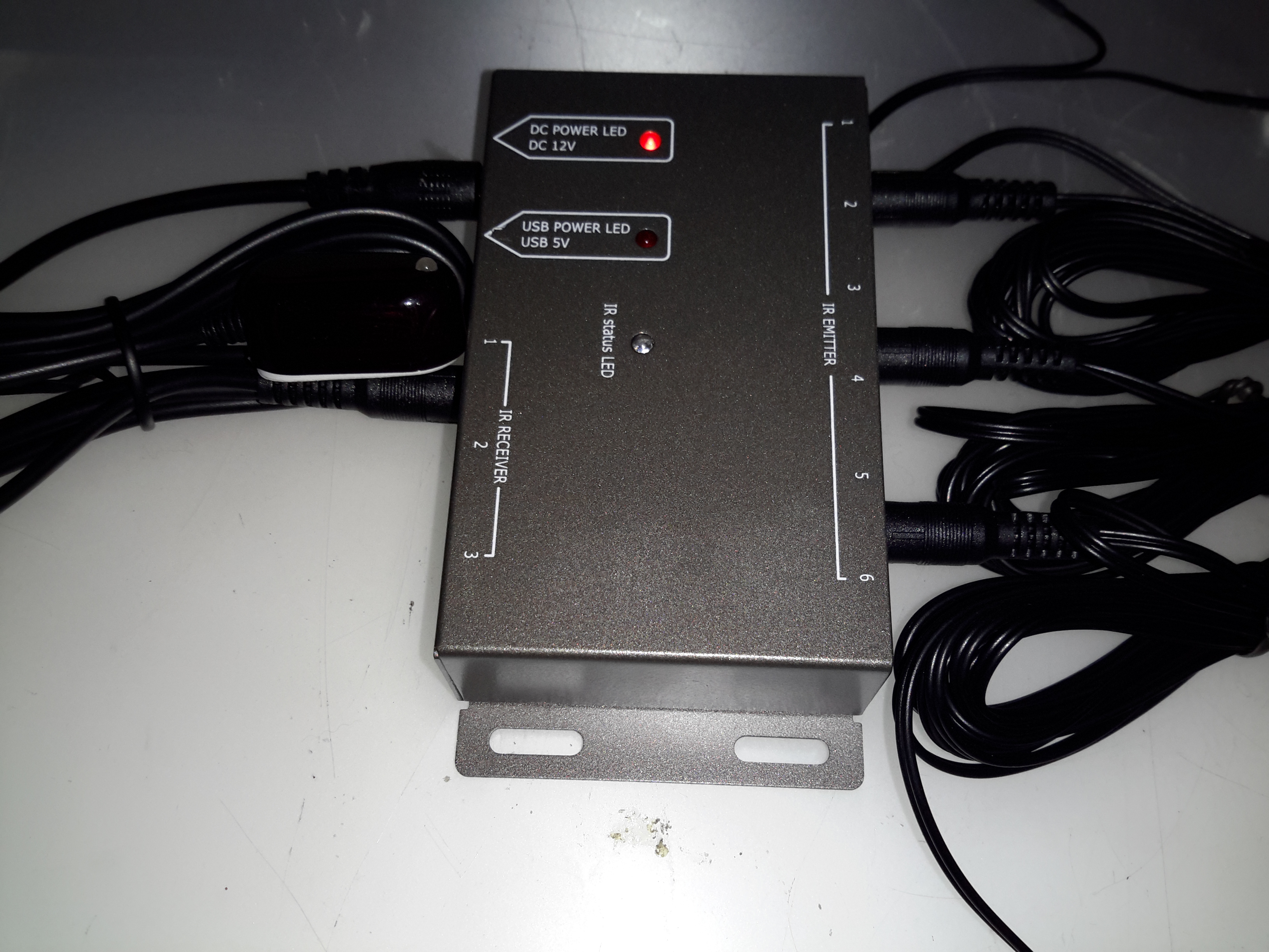
Here’s another random gadget for teardown, this time an IR remote control repeater module. These would be used where you need to operate a DVD player, set top box, etc in another room from the TV that you happen to be watching. An IR receiver sends it’s signal down to the repeater box, which then drives IR LEDs to repeat the signal.
Repeater Module
Not much to day about the exterior of this module, the IR input is on the left, up to 3 receivers can be connected. The outputs are on the right, up to 6 repeater LEDs can be plugged in. Connections are done through standard 3.5mm jacks.
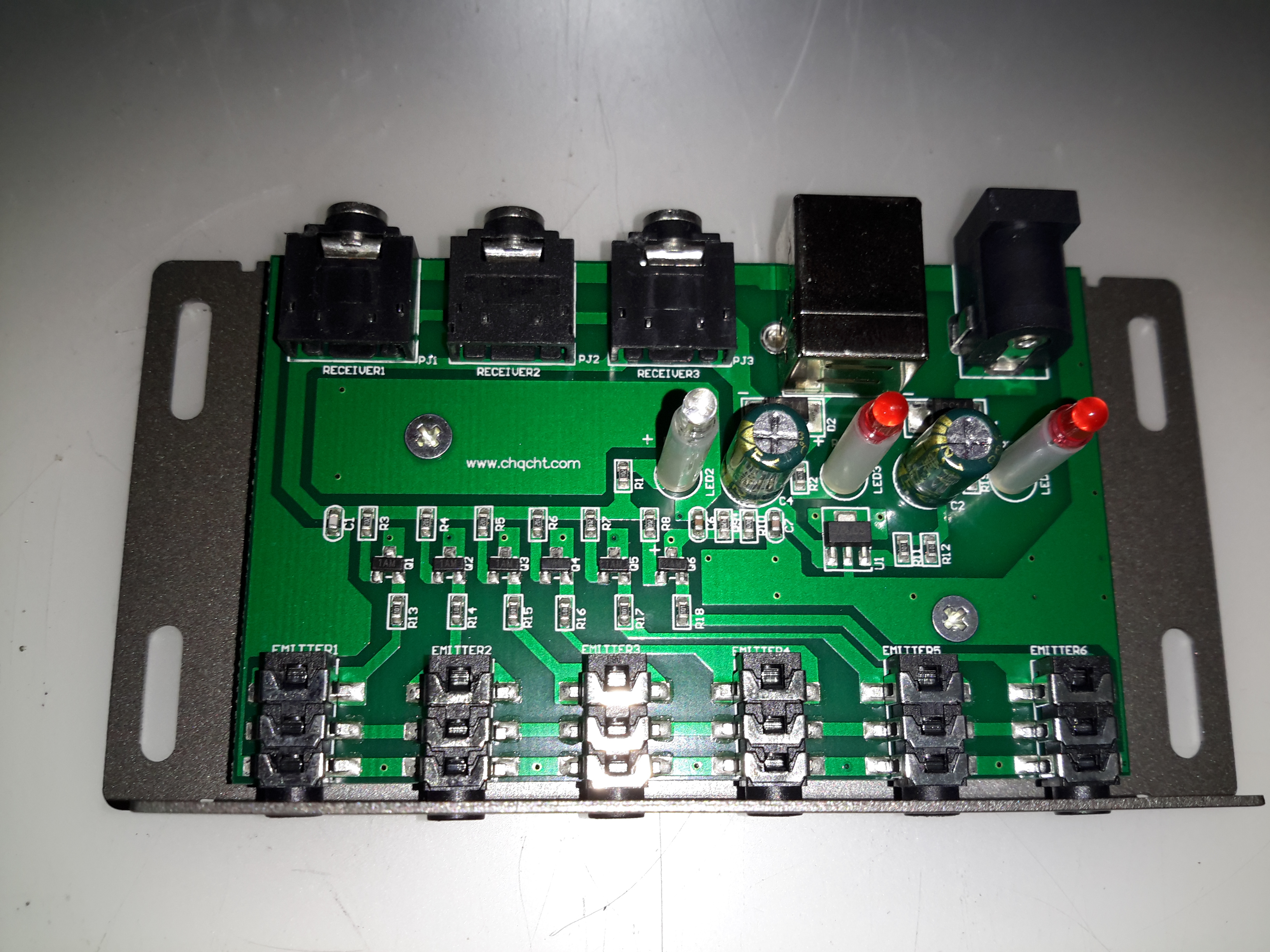
Repeater PCB
Not much inside this one at all, there are 6 transistors which each drive an LED output. This “dumb” configuration keeps things very simple, no signal processing has to be done. Power is either provided by a 12v input, which is fed into a 7805 linear regulator, or direct from USB.
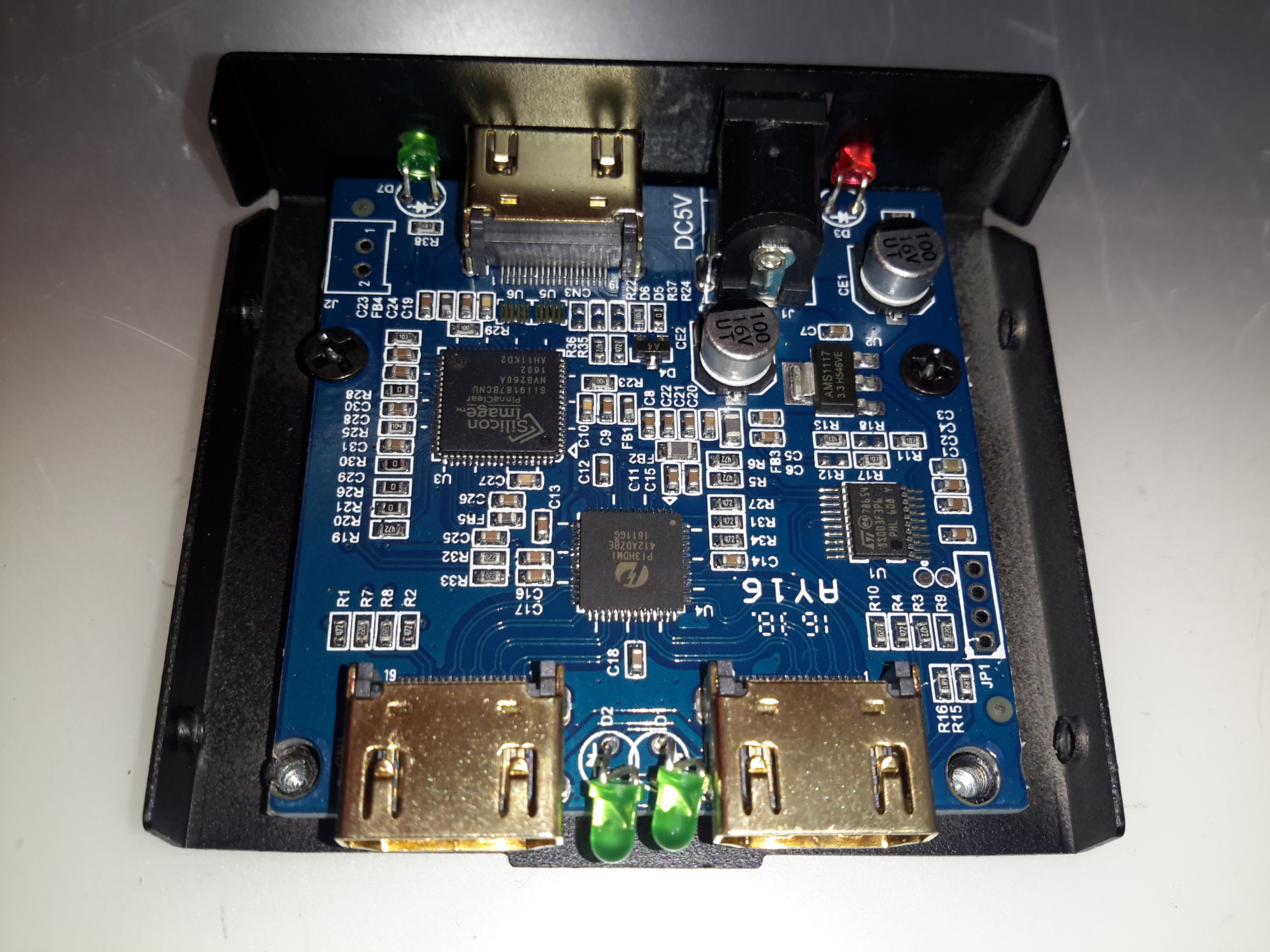
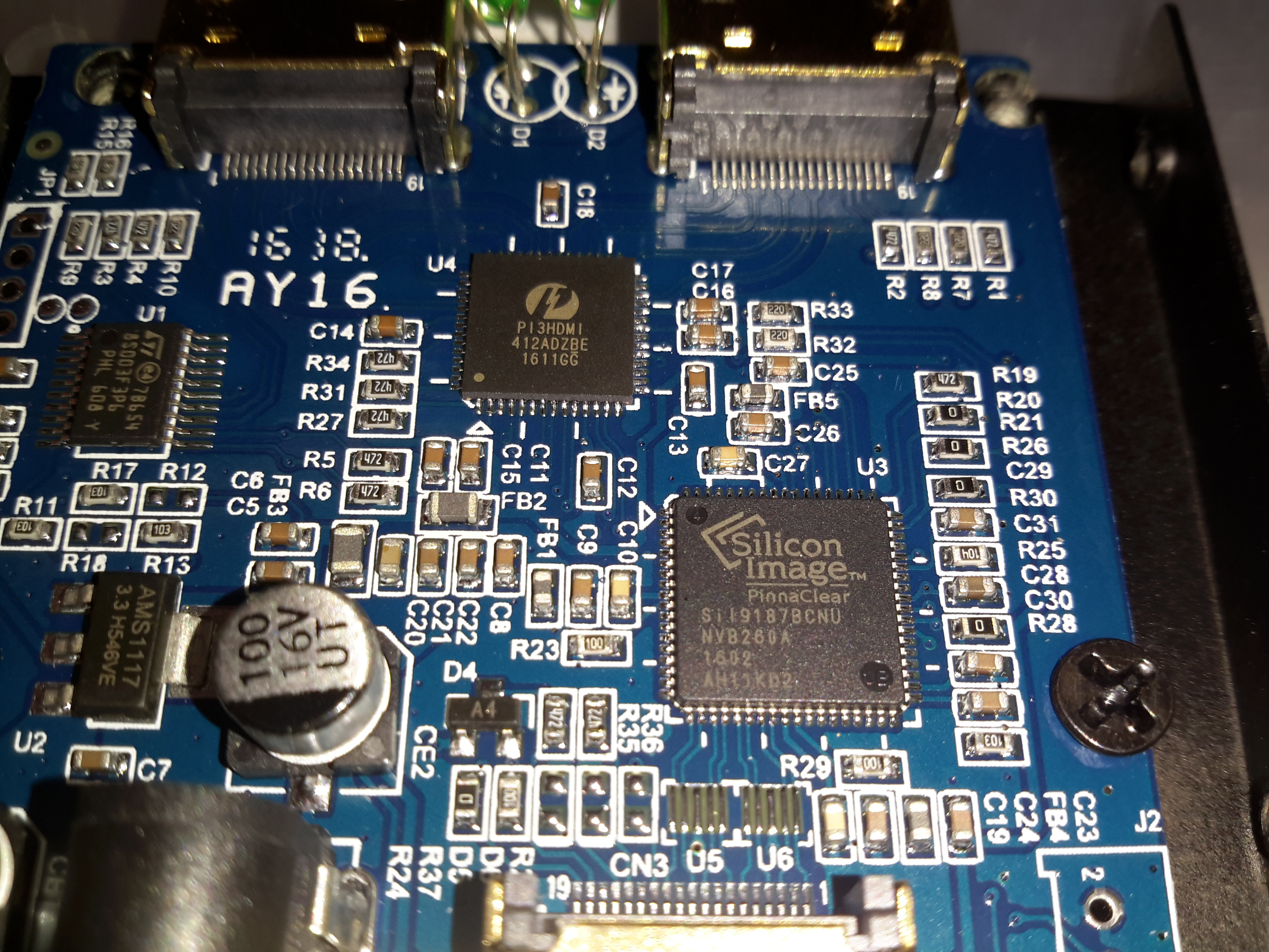
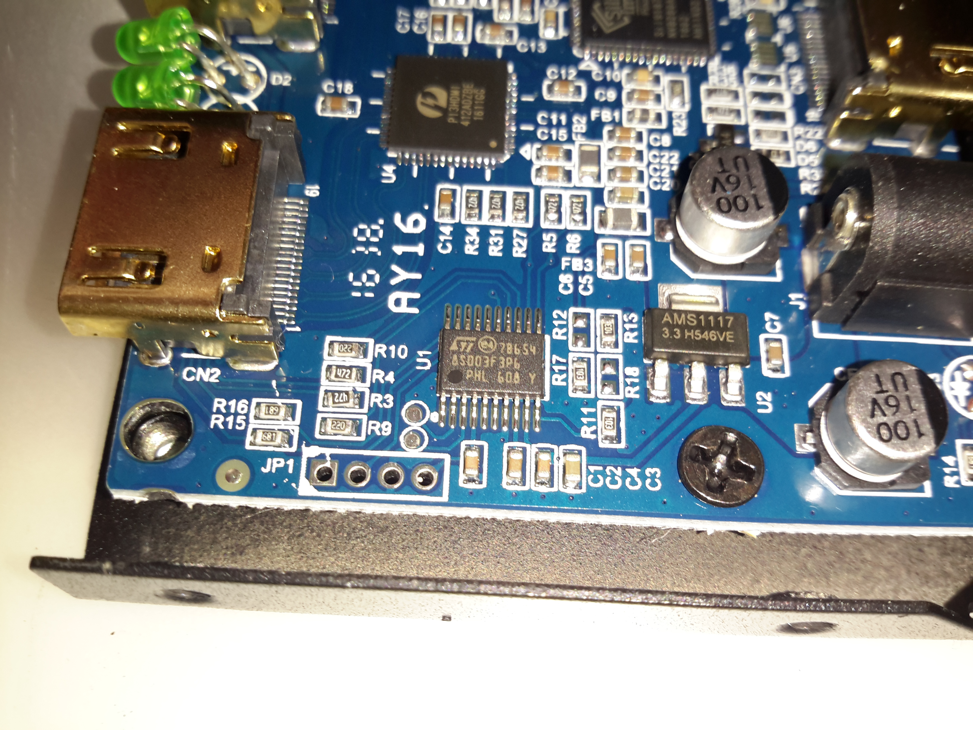
Time for another random teardown, a signal splitter for HDMI. These units are available very cheap these days on eBay. This one splits the incoming signal into two to drive more than one display from the same signal source.
Main PCB
The stamped alloy casing comes apart easily with the removal of a few screws. The PCB inside is rather densely packed with components.
Chipset
The main IC on the incoming signal is a Silicon Image Sil9187B HDMI Port Processor, with a single input & 4 outputs. In this case the chip is used as a repeater to amplify the incoming signal. the signal path then gets fed into a Pericom PI3HDMI412 HDMI Demux, which then splits the signal into two for the output ports.
Microcontroller
The main pair of ICs processing the video signals are controlled over I²C, with this STM32 microcontroller. The 4 pads to the lower left are for the STLink programmer. The main 3.3v power rail is provided by the LM1117 linear regulator on the right.
Another random teardown from the junk box time!
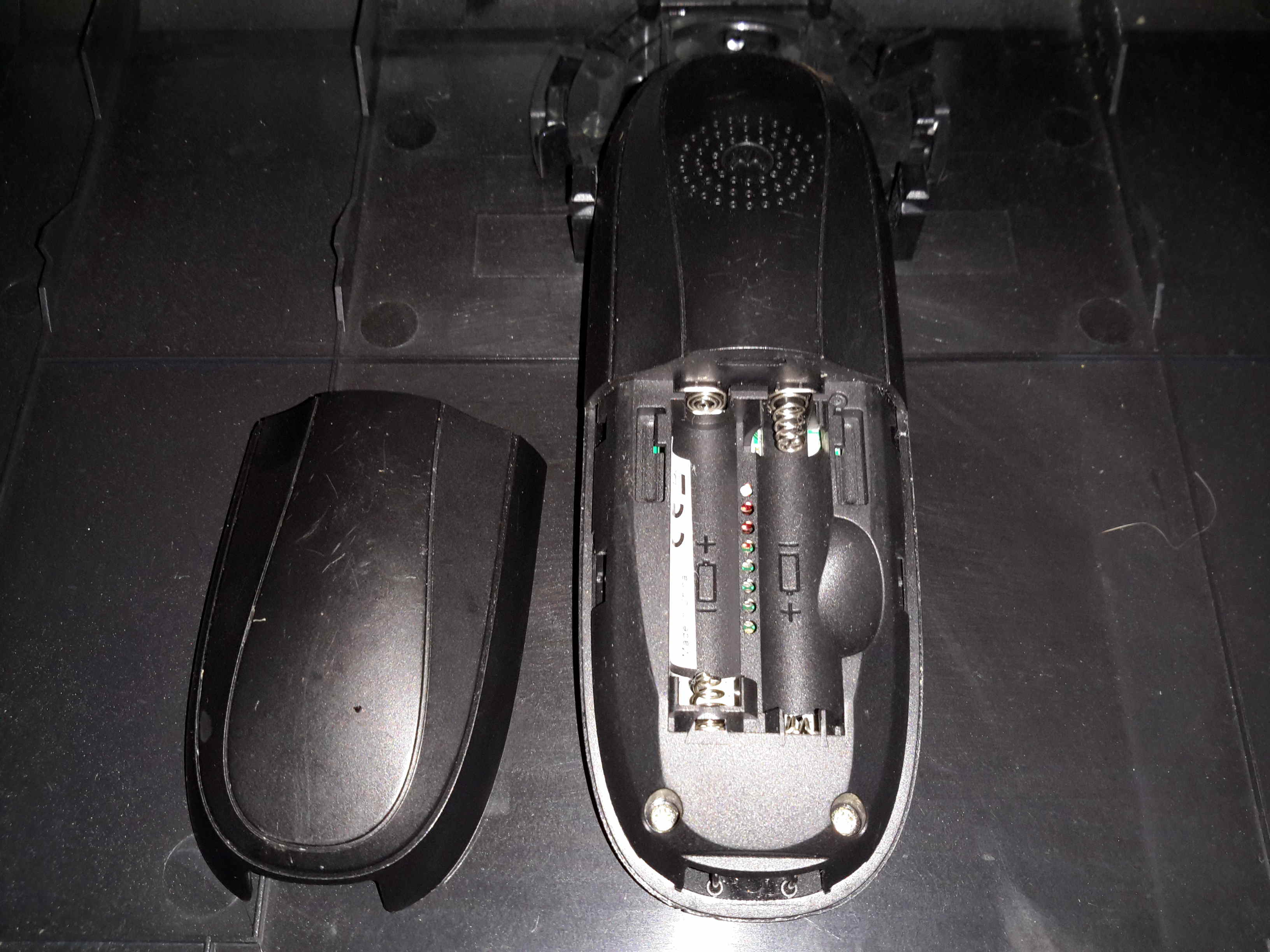
Here’s an old Motorola DECT landline phone, no use to me as I’ve not used a landline for many years.
Battery Compartment
Not much on the back, other than the battery compartment for a pair of AAA rechargables. The base unit contains the charger.
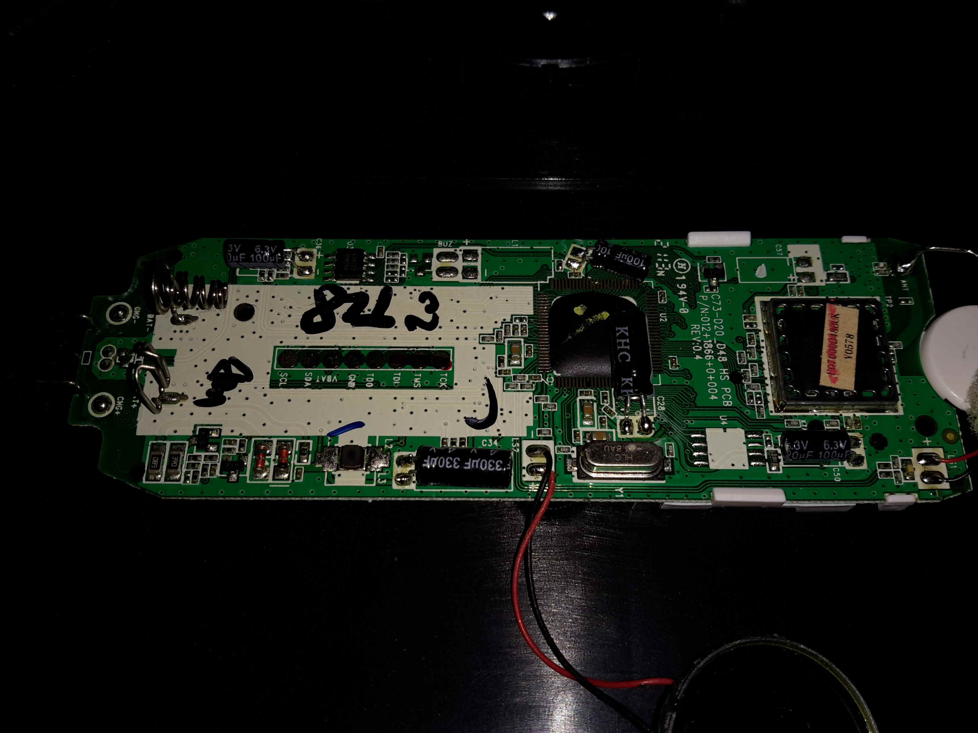
Main PCB
Here’s the main PCB removed from it’s casing. There’s not really much going on, one of the main ICs, which is probably a microcontroller, is a COB device, so no part numbers from there. There’s a row of pads for programming the device at the factory. The RF section is on a dedicated IC, a DE19RF19ZCNC from DSP Group. I couldn’t find much on this part, but it’s one of a range of DECT/VoIP DSP devices.
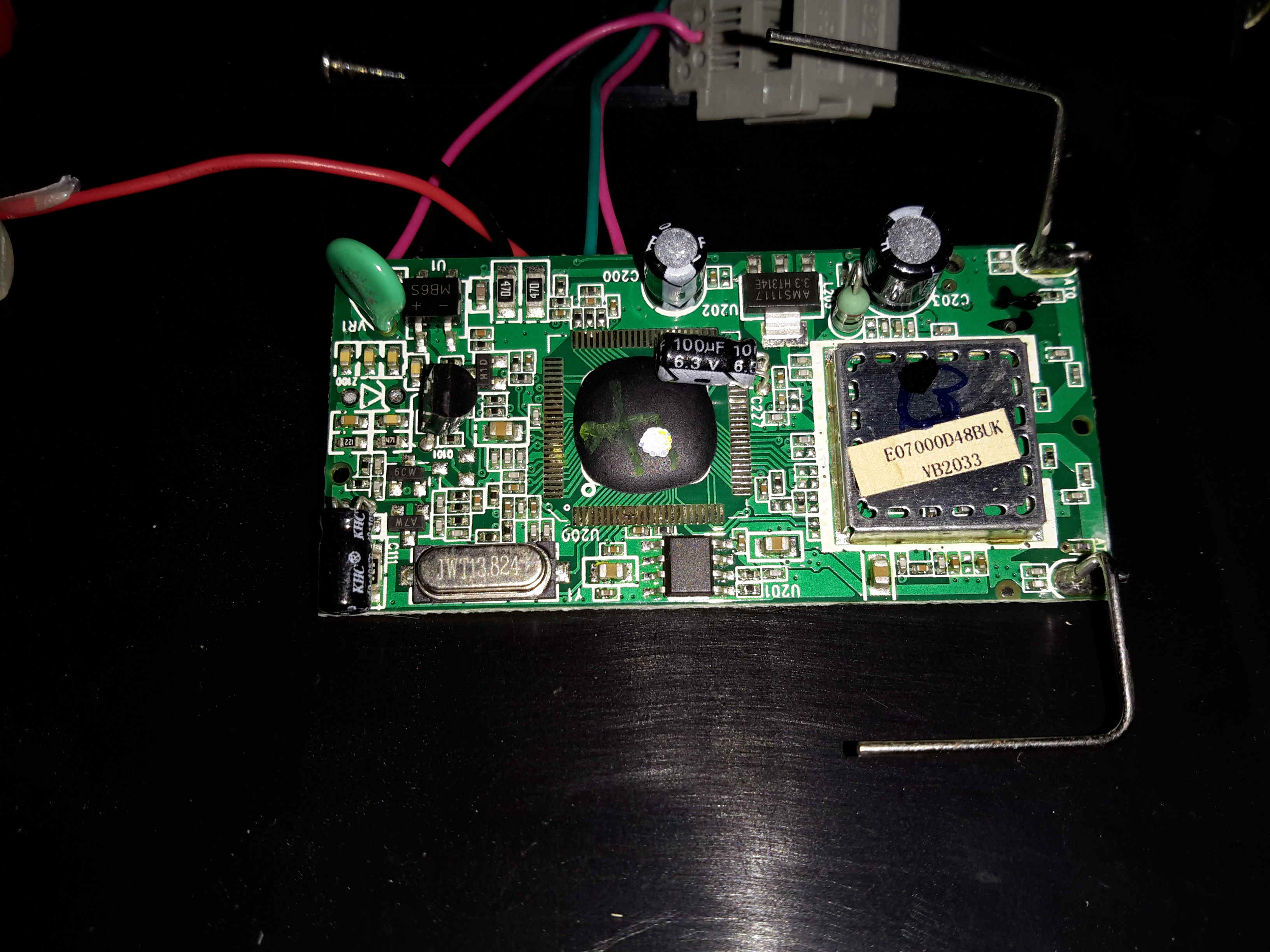
Base Unit PCB
Inside the base unit is a similar board, just without the keypad. Main microcontroller is again a COB device, the RF IC is under the shield.
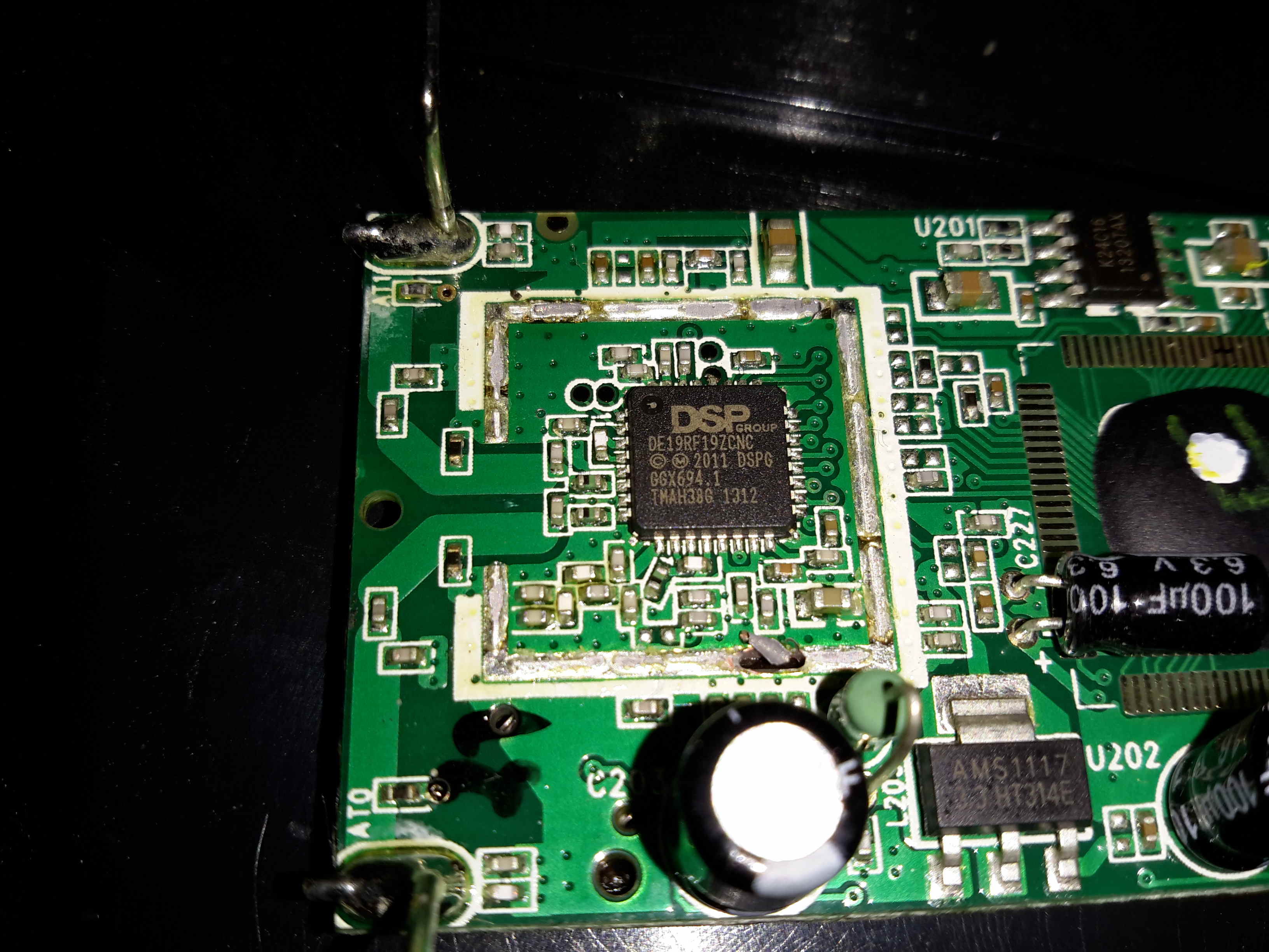
Main Chipset
Removing the shield reveals the same IC as in the handset, only this PCB has a pair of antennas.
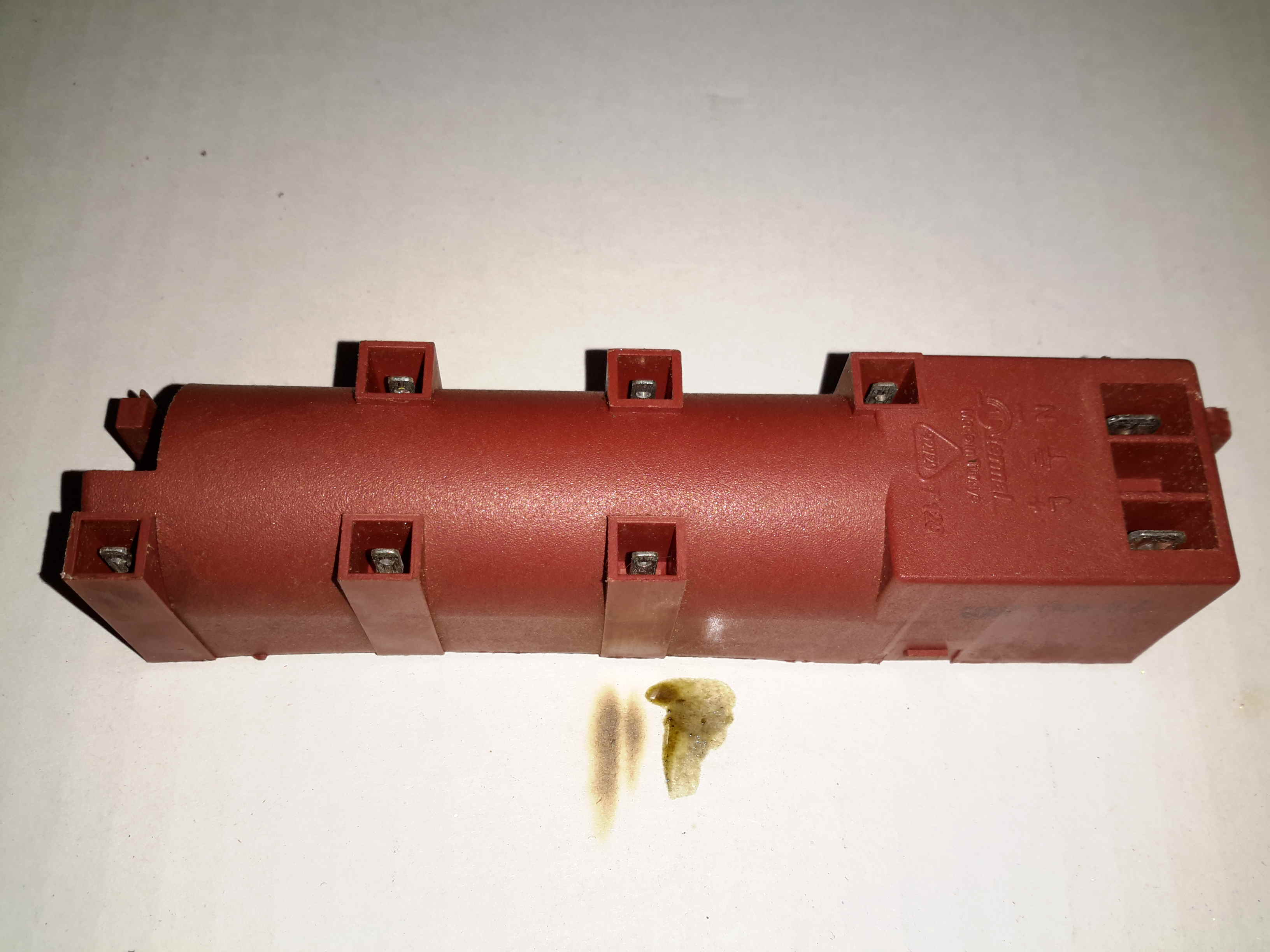
Here’s a quick teardown of an ignition transformer, used on gas fired ovens & hobs. This unit takes mains 240v AC & uses a transformer to step the voltage to several kV, at a low current to ignite the burners.
Bottom
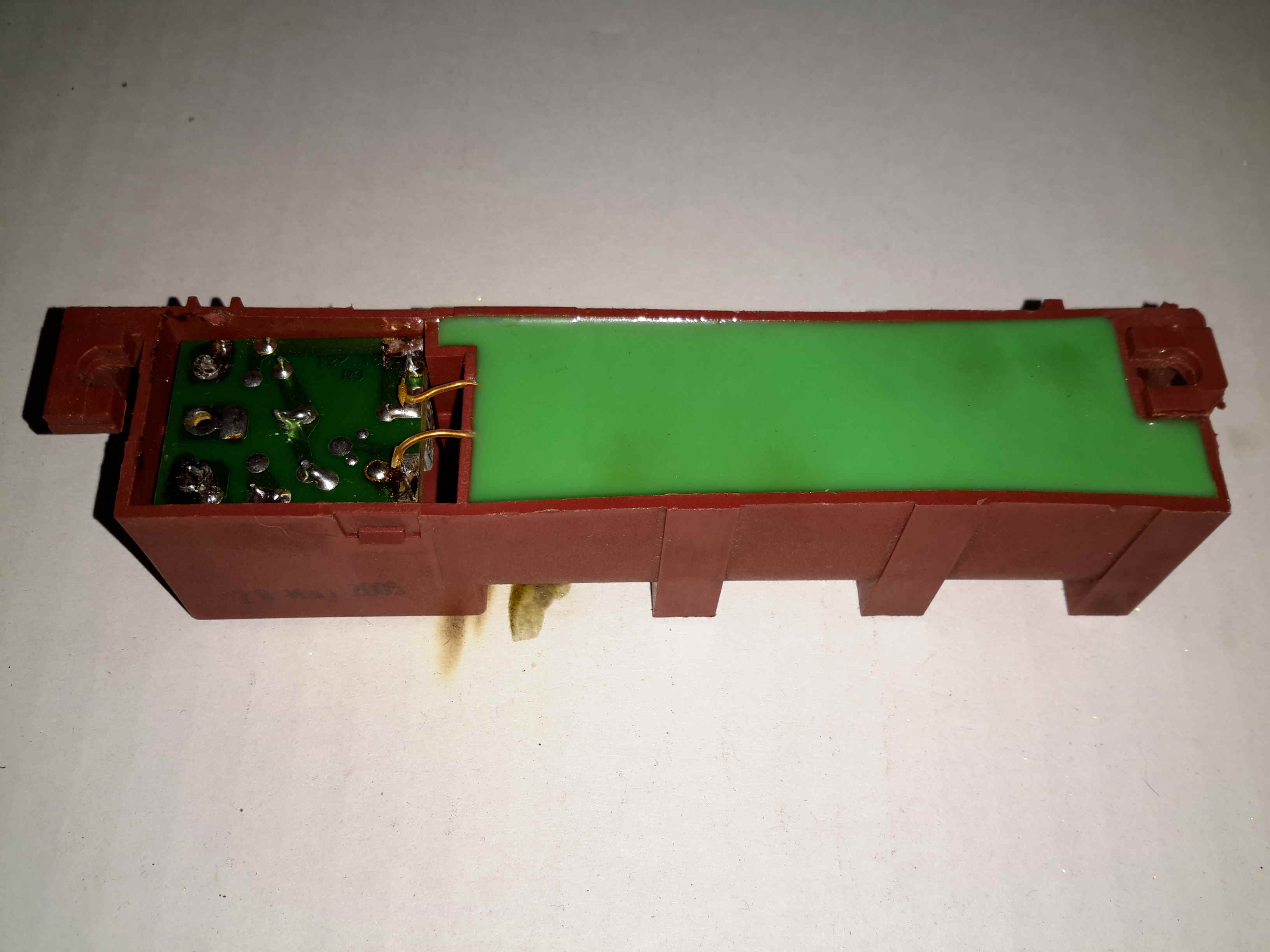
The transformer section is completely potted in Epoxy resin for insulation, but the driver circuitry is exposed, with a pair of leads from the primary winding exposed
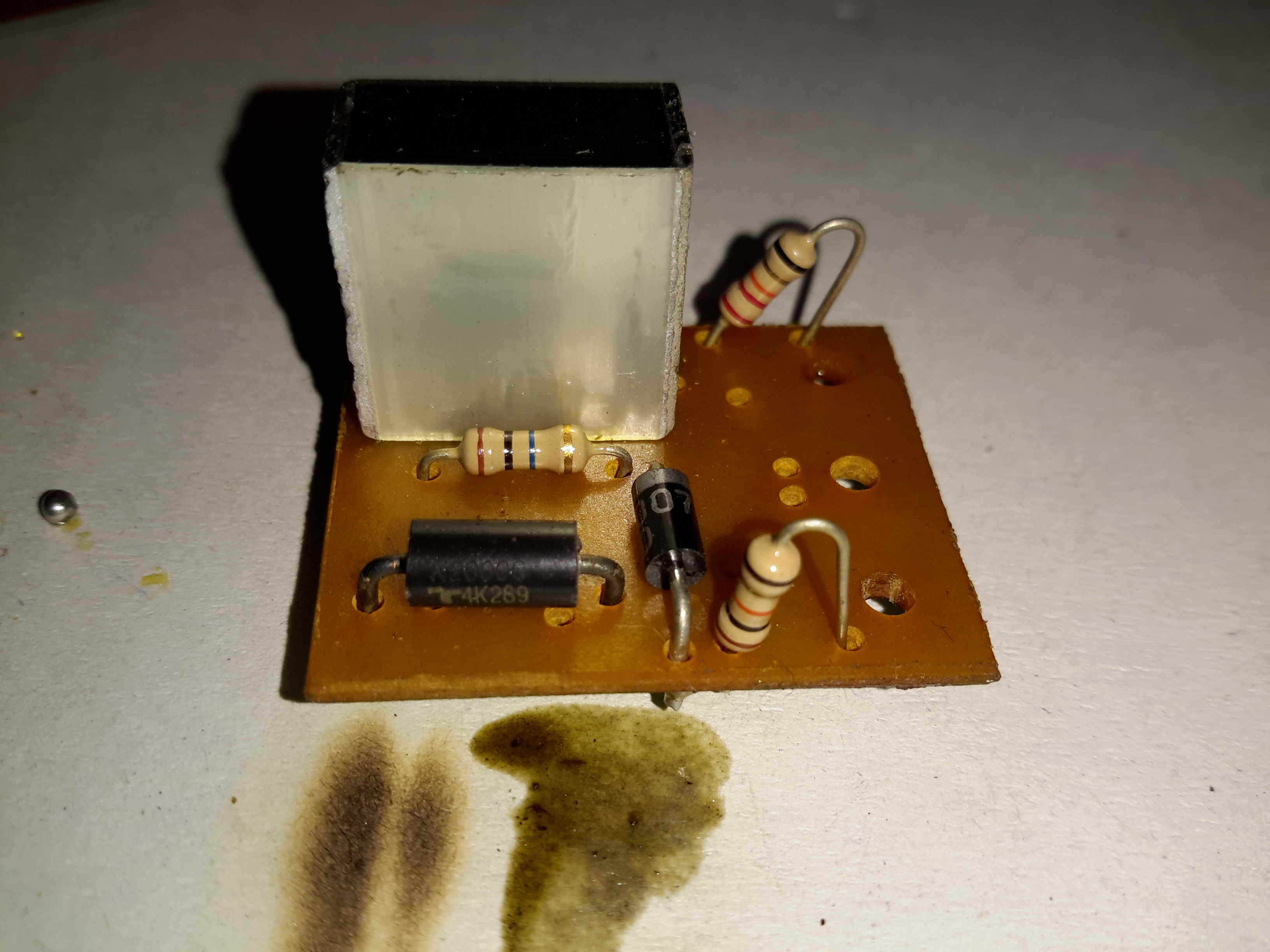
Driver PCB
The drive is very simple. The incoming AC flows through a series resistor through a half-wave rectifier to charge up a 2.2µF film capacitor. Once the voltage on the capacitor reaches a certain level, a DIAC in series with the transformer primary fires, discharging the capacitor through the primary.
The current spike induces a very high voltage on the secondary winding, this then arcs across a gap in the gas flow to start ignition.
Since this phone has been in my drawer for some time, I figured it was time for a teardown. (It’s never going to see any more use).
The back cover on these phones is easily removed, as it’s just clipped on.
Motherboard
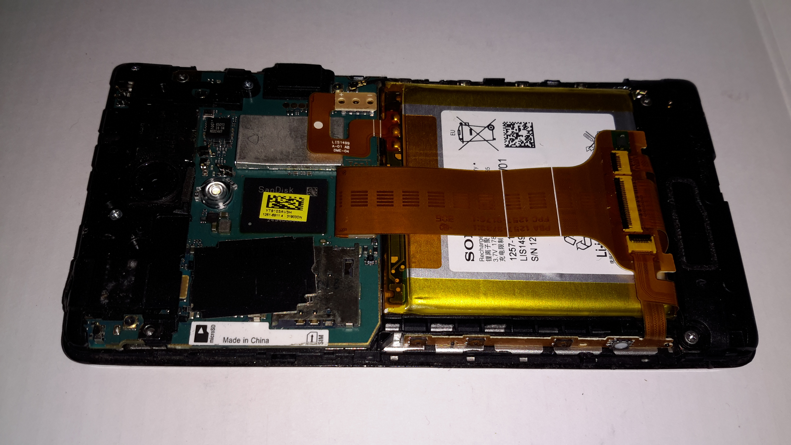
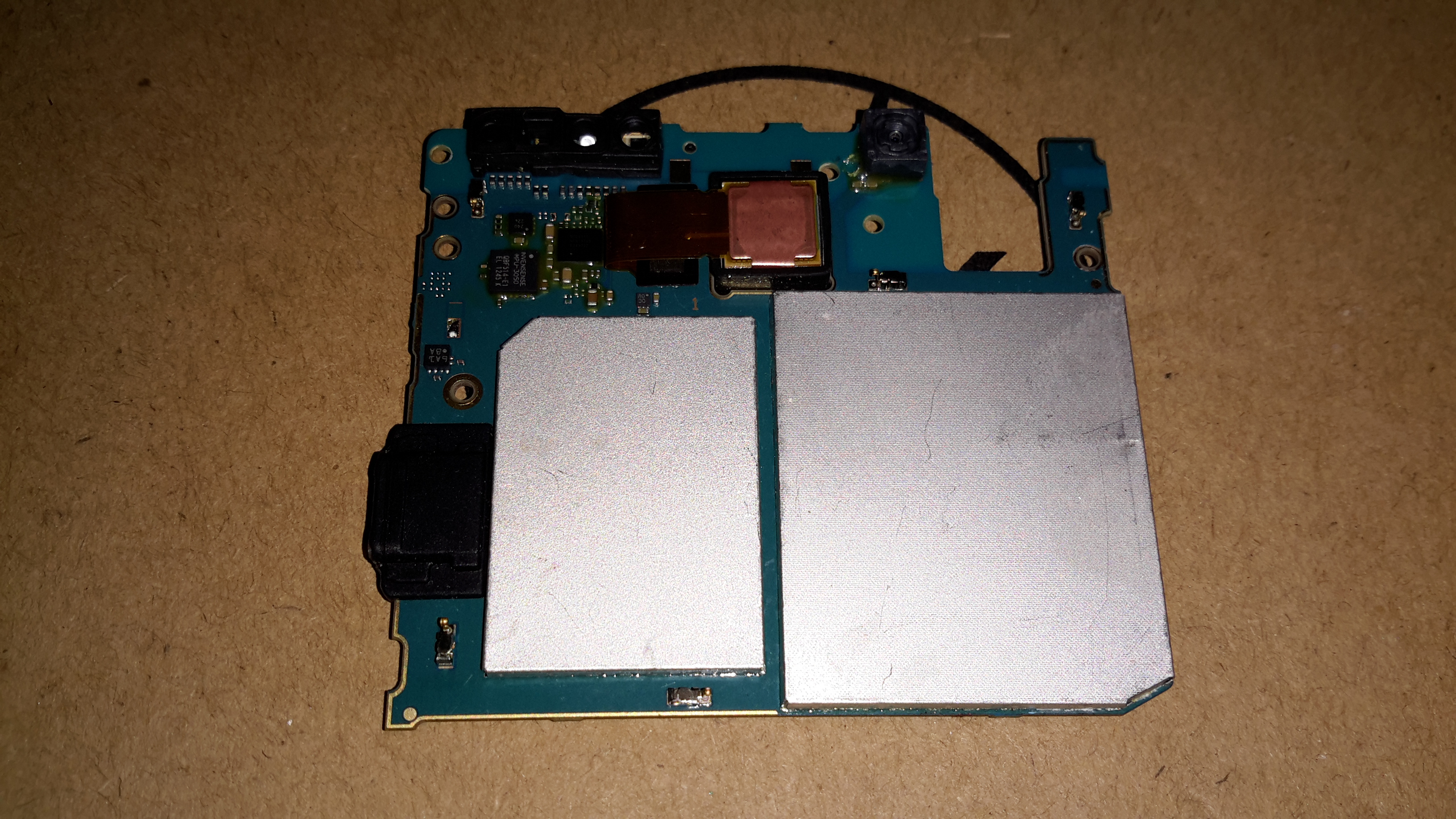
Once the back cover is removed, the Li-Polymer cell is exposed, along with the logic board. Pretty much all of the PCB is under RF shields.
Motherboard RemovedBattery Management
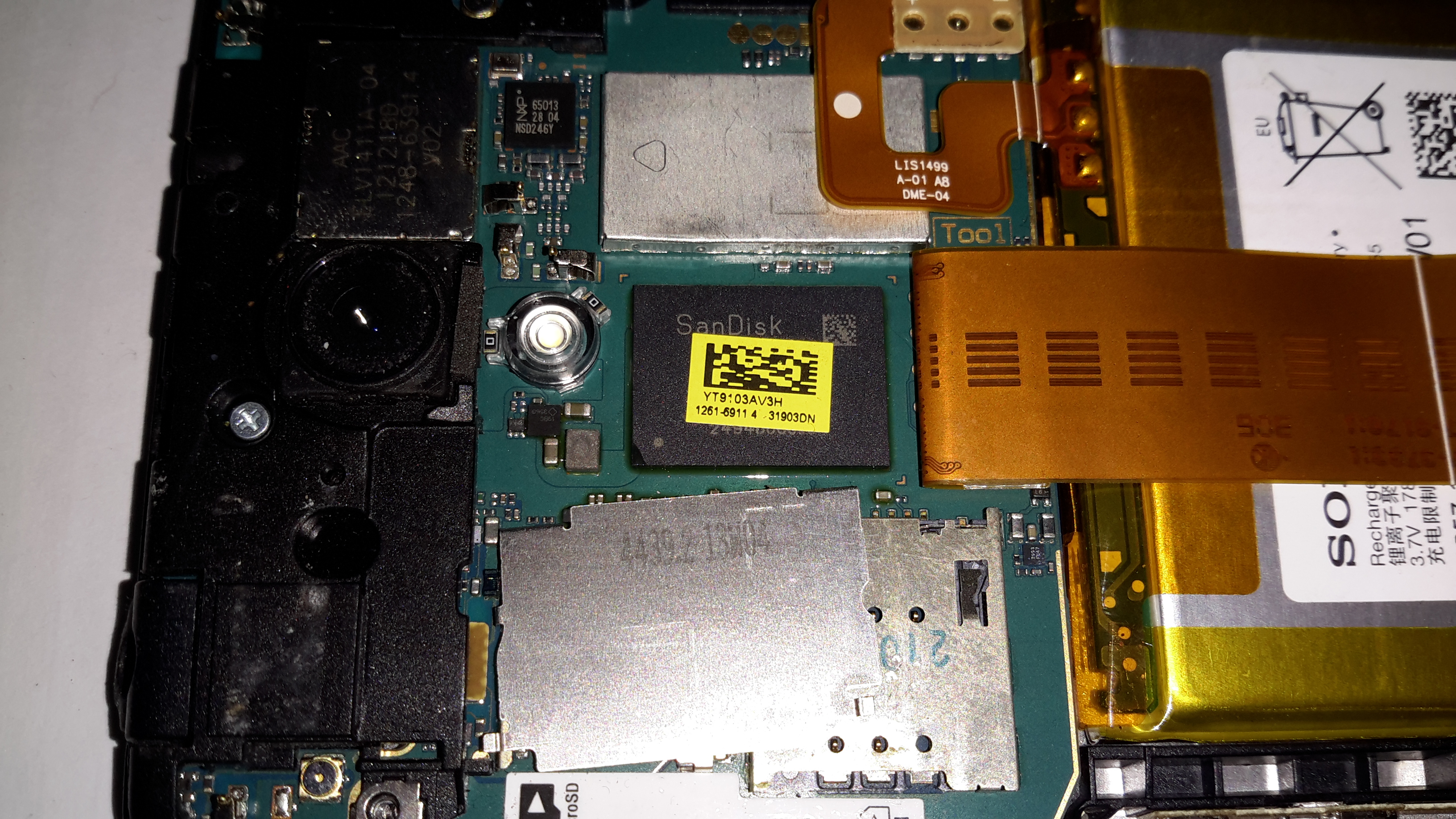
Under the small RF can on the back of the board is the battery management circuitry & the charger. There’s an extra connection to the cell for temperature monitoring. Just under that circuitry is the eMMC flash storage.
Just to the left of the battery circuit is the NFC transceiver IC, from NXP.
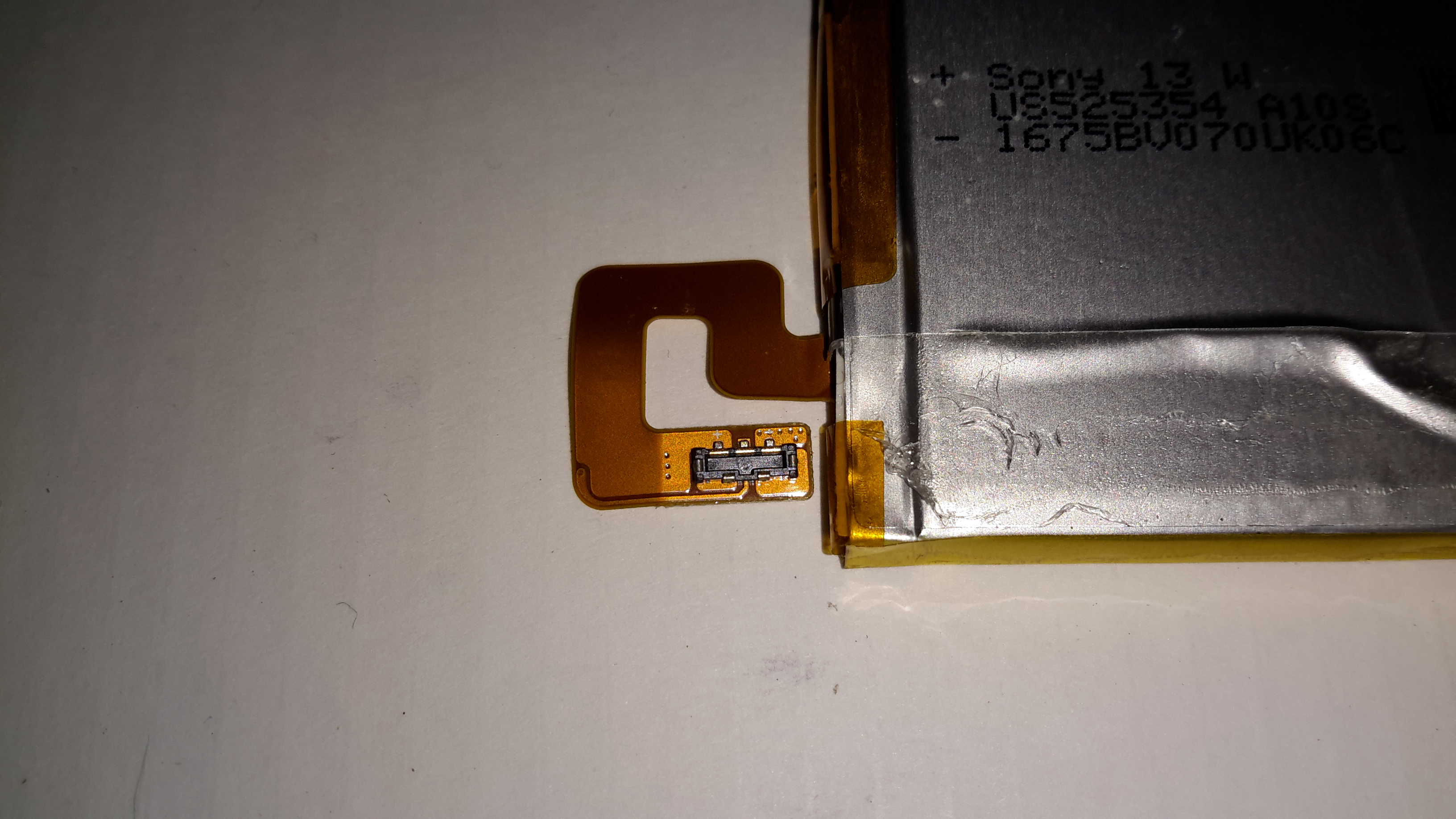
Battery Flex
The cell is connected to the main board with a FFC, with a very small SMT connector, although not as small as the more modern Xperia series phones.
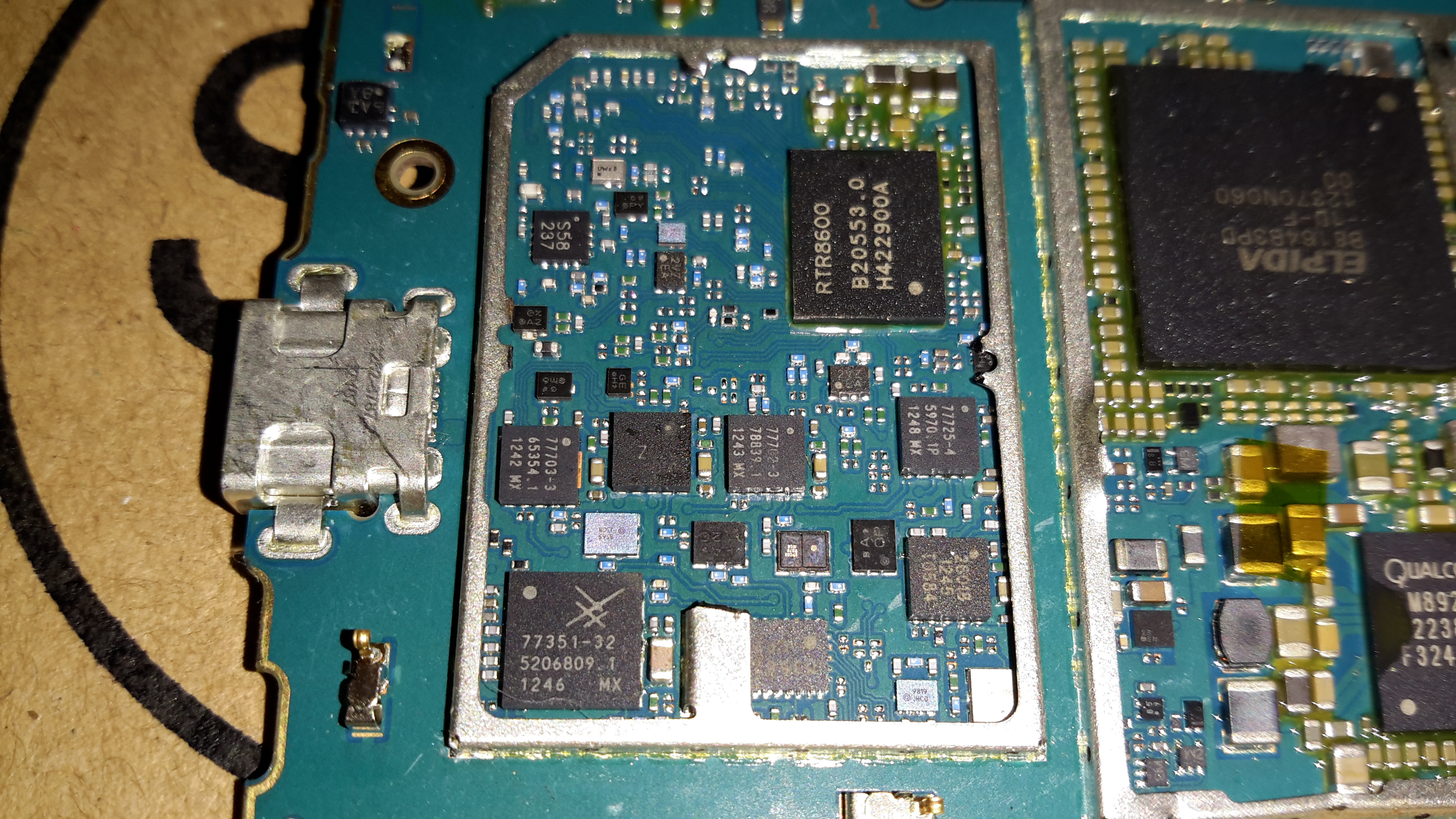
RF Section
The other side of the mainboard holds the large RF transceiver section, with a Qualcomm RTR8600 multiband transceiver IC. In the bottom corner is a Skyworks SKY77351-32 Quad-band power amplifier IC, along with 3 other power amplifier ICs, also from Skyworks.
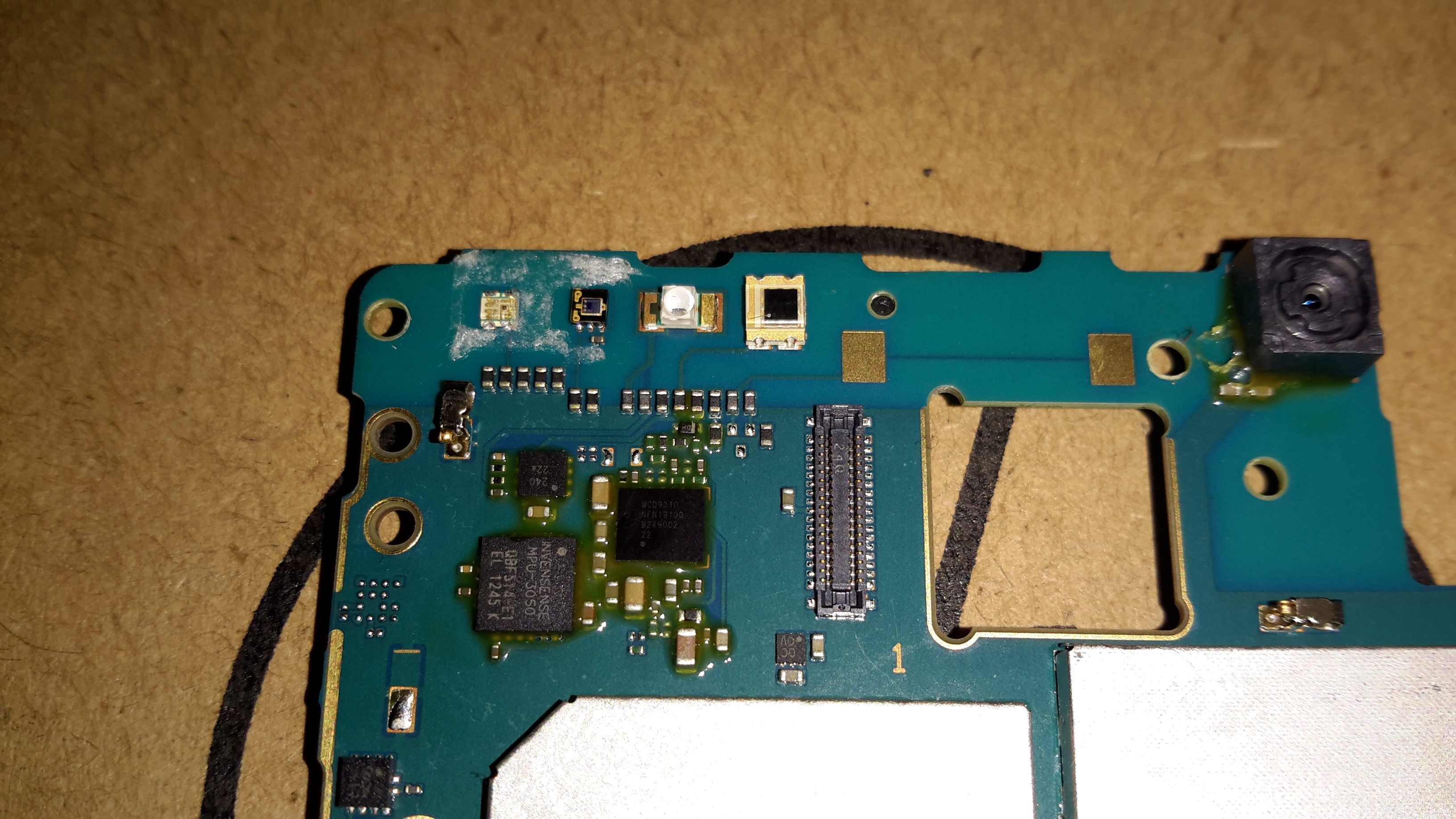
Gyro & Audio Codec
The top corner of the board holds the various sensors, including an Invensense MPU-3050 3-axis gyro. To the right of that is the Audio Codec, a WCD9310 from Qualcomm.
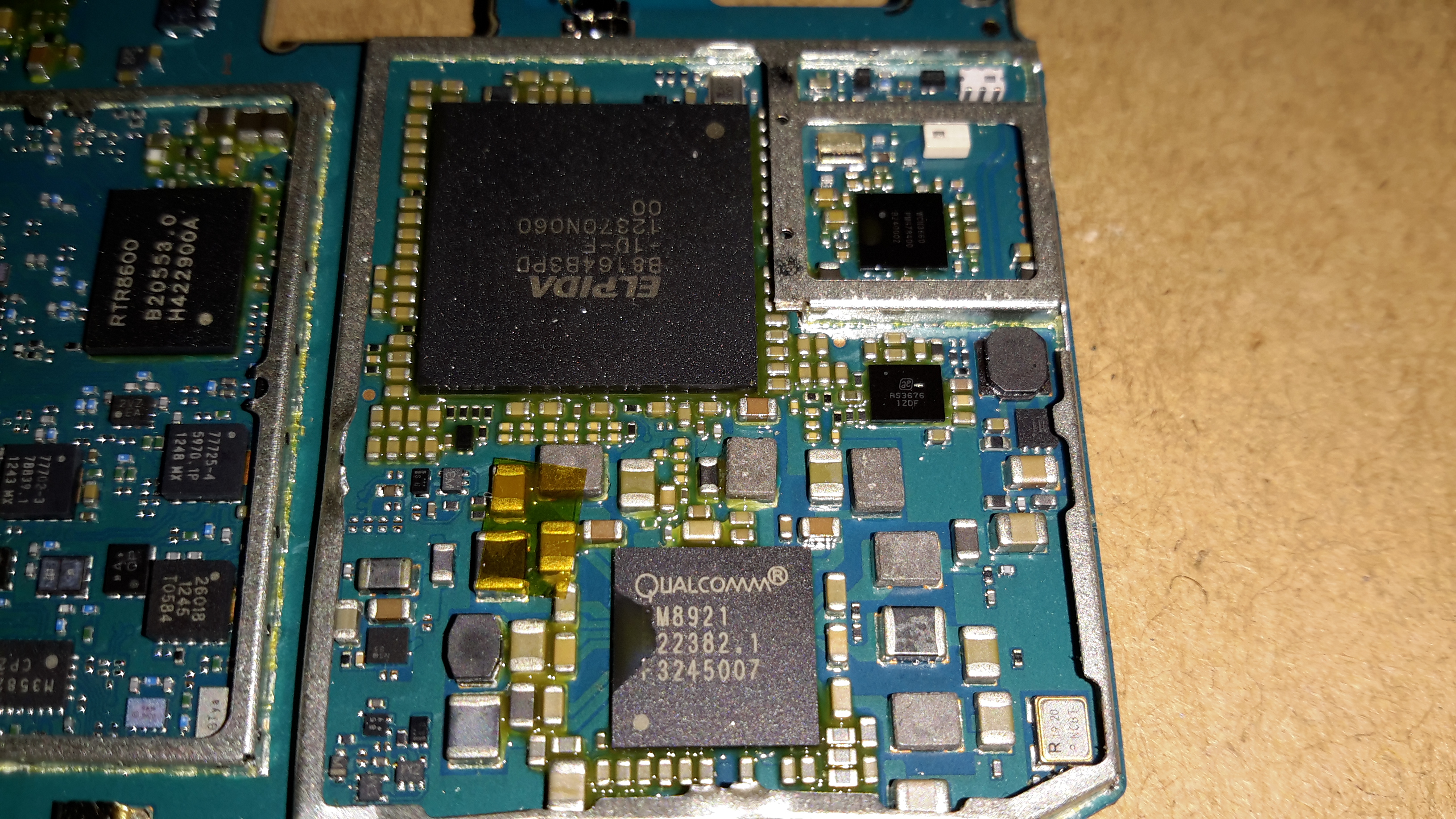
Logic & CPU Section
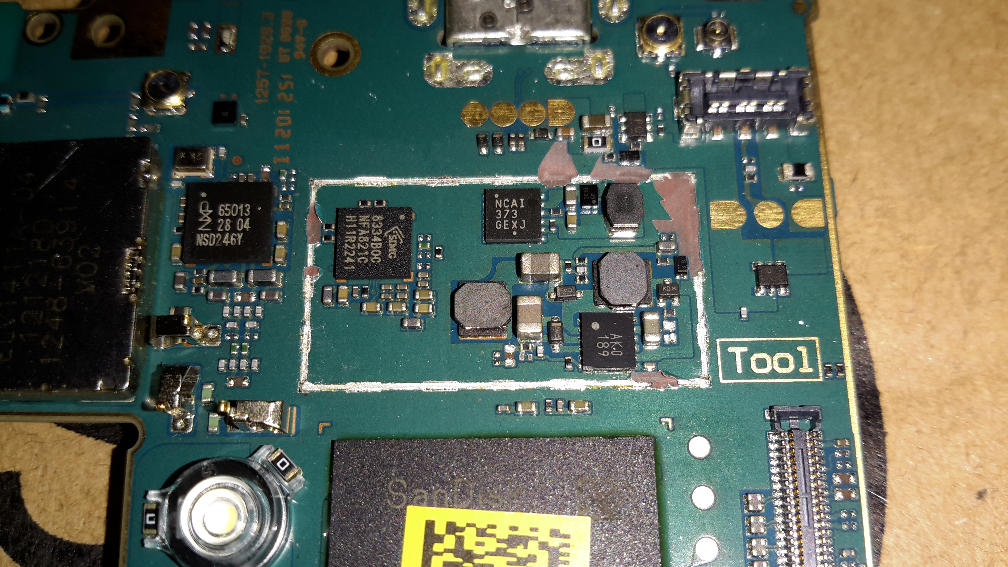
Everything is controlled from the last section on the board, with the main CPU & RAM in a PoP (Package-On-Package) configuration. Under the main CPU is the main power management IC, also from Qualcomm. No datasheet for this one unfortunately, but it gives it’s purpose away by being surrounded by large inductors & capacitors.
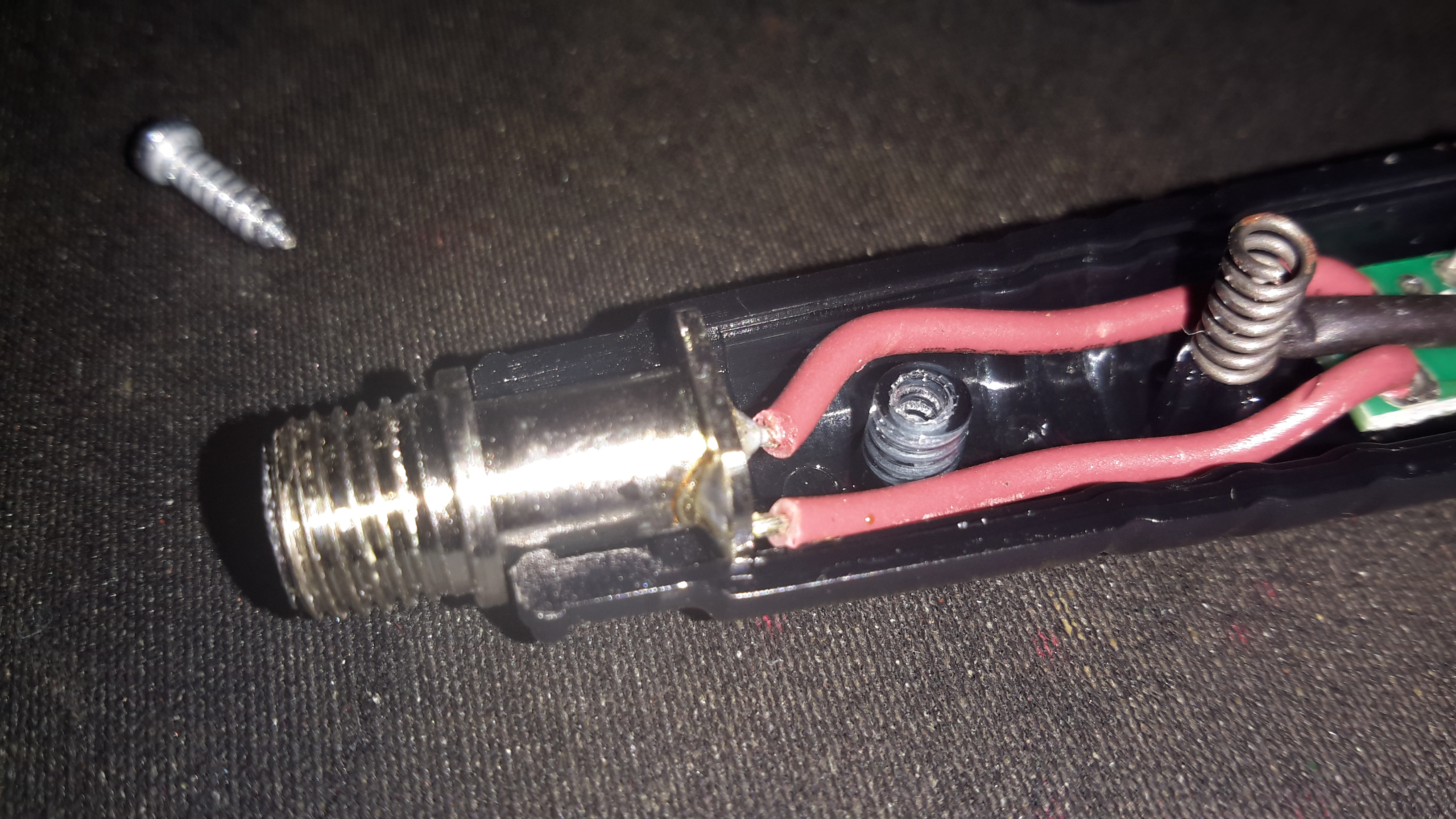
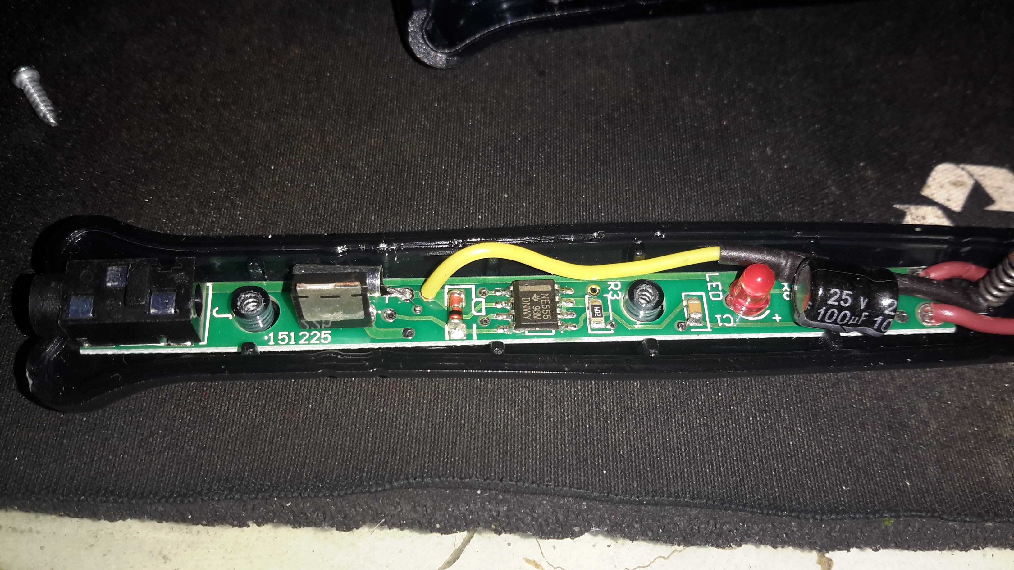
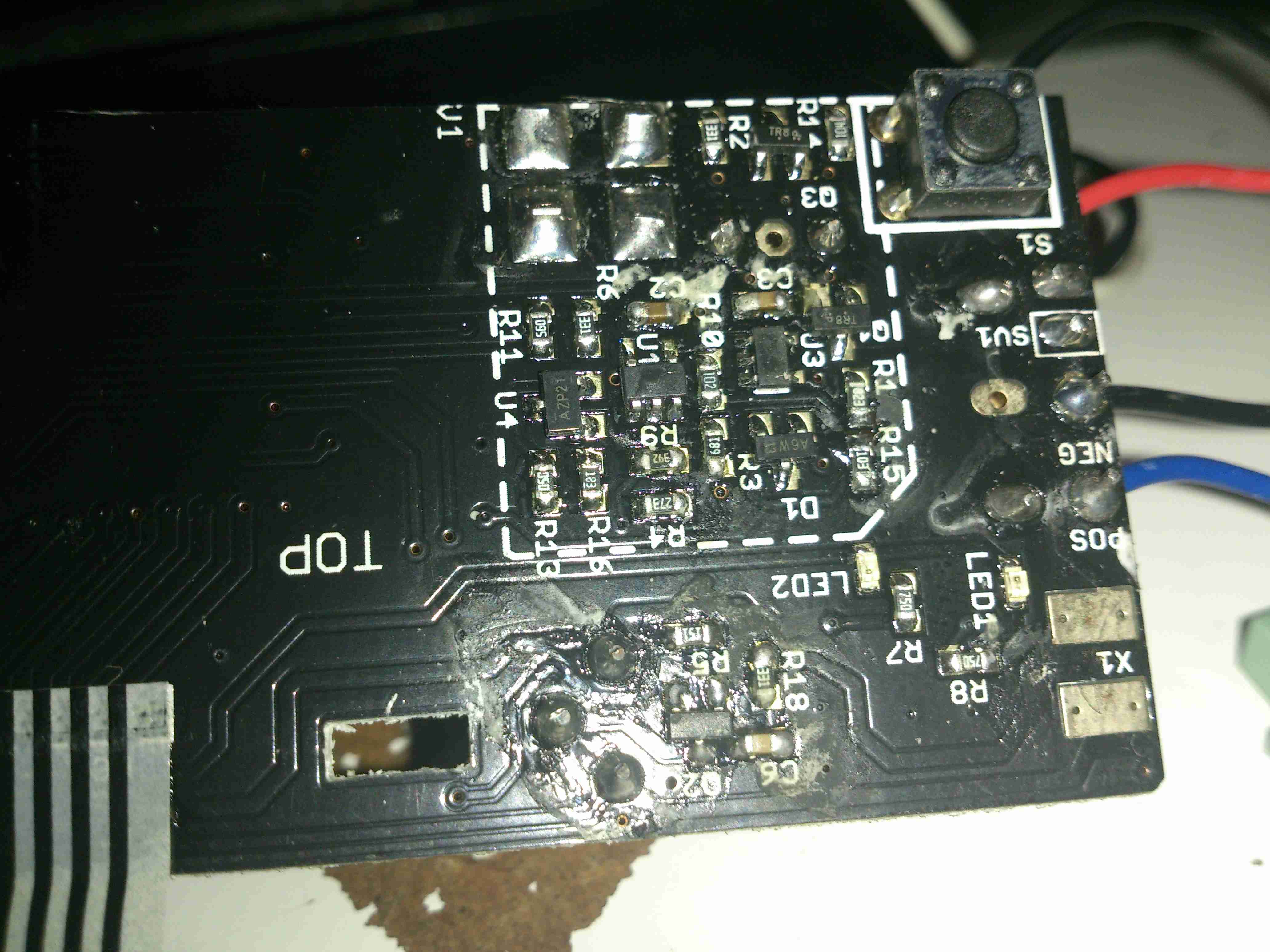
Here’s a novel little gadget, a USB powered soldering iron. The heating tip on these is very small & might be useful for very small SMD work. Bigger joints not so much, as it’s only rated at 8W. (Still breaks the USB standard of 2.5W from a single port).
These irons aren’t actually too bad to use, as long as the limitations in power are respected. Since nearly everything has a USB power port these days, it could make for a handy emergency soldering iron.
Heater Socket
The heater & soldering bit are a single unit, not designed to be replaced separately. (I’ve not managed to find replacement elements, but at £3 for the entire iron, it would be pretty pointless).
Above is the socket where the heater plugs in, safely isolating the plastic body from any stray heat.
DC Input Jack
The DC input is a 3.5mm audio jack, a non-standard USB to 3.5mm jack cable is supplied. Such non-standard cables have the potential to damage equipment that isn’t expecting to see 5v on an audio input if it’s used incorrectly.
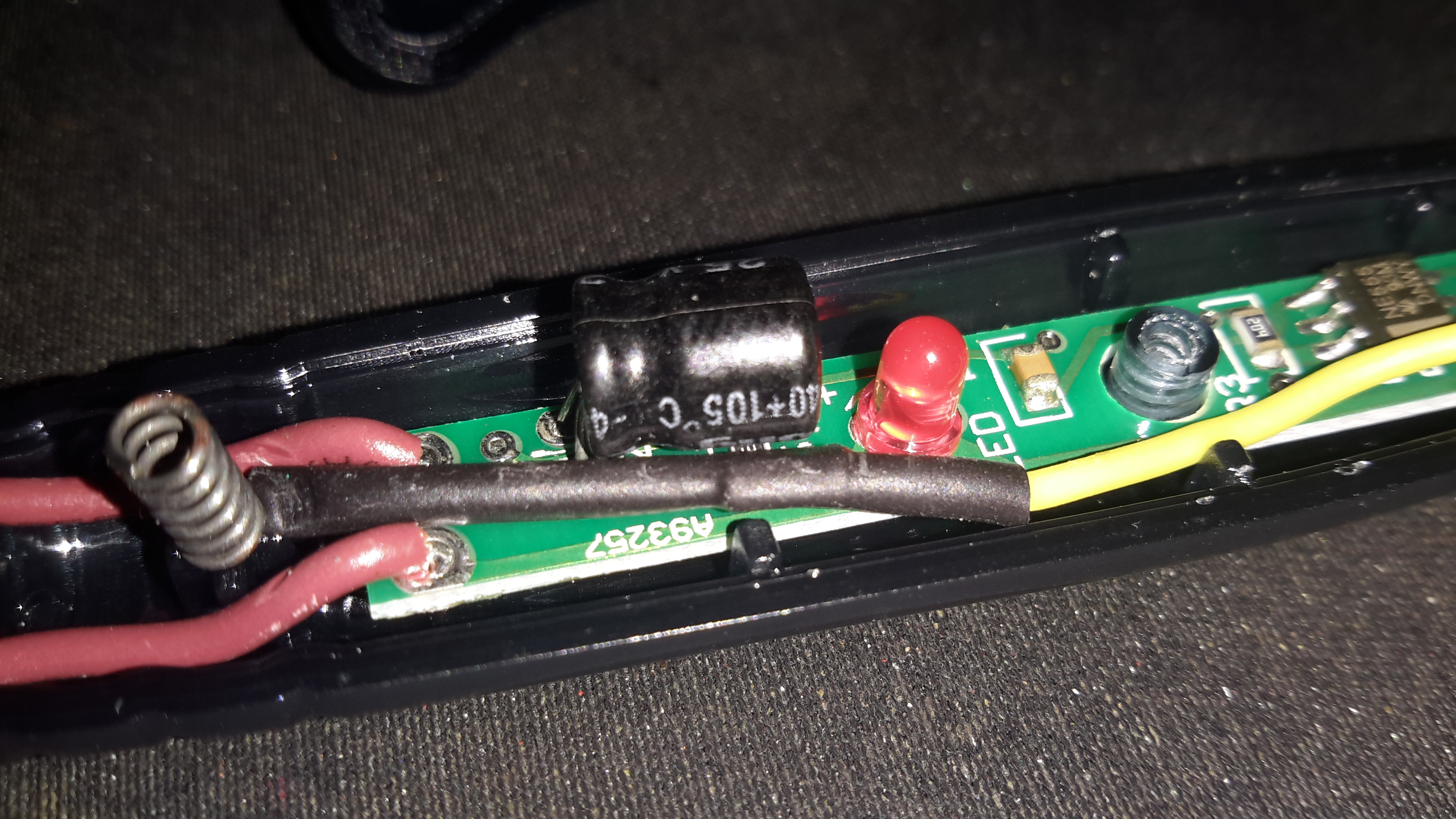
Touch Sensor & LED
There isn’t actually a switch on this unit for power management, but a clever arrangement of a touch button & vibration switch. The vertical spring in the photo above makes contact with a steel ball bearing pressed into the plastic housing, forming the touch contact.
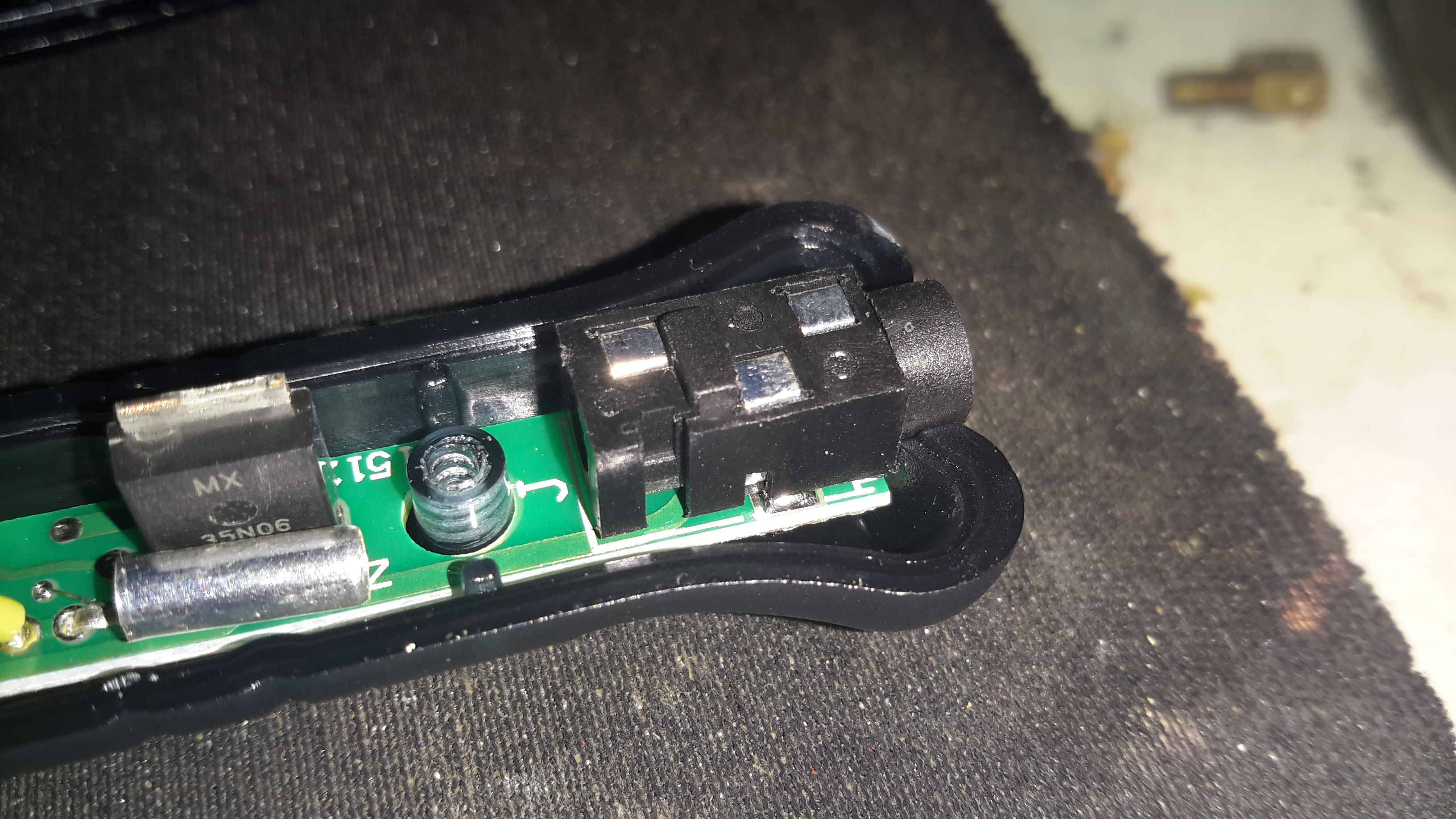
MOSFET
The large MOSFET here is switching the main heater current, the silver cylinder in front is the vibration switch, connected in parallel with the touch button.
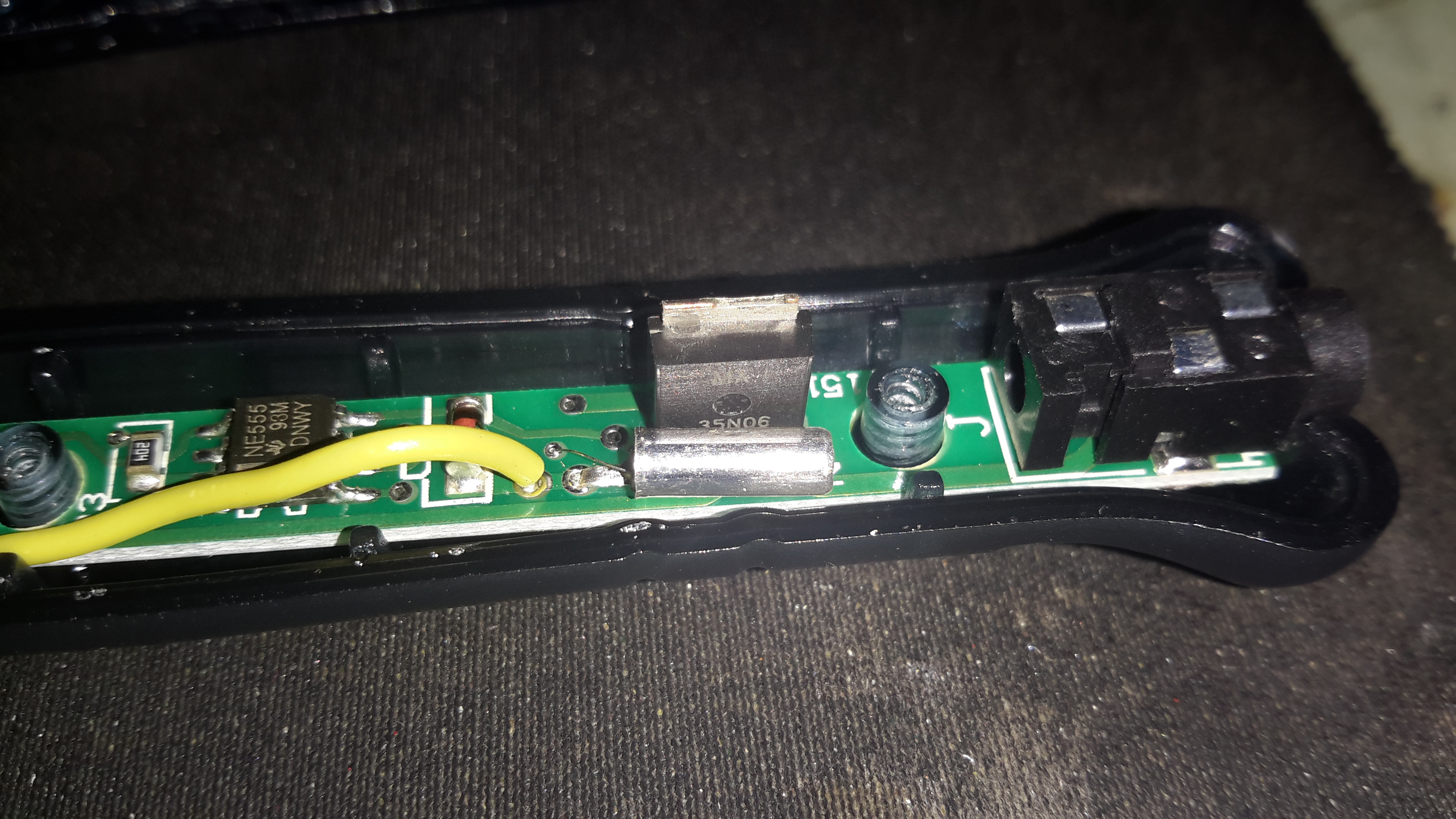
PCB
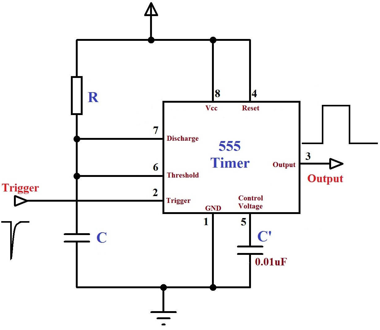
The main controller is very simple. It’s a 555 timer configured in monostable mode. Below is a schematic showing the basic circuit.
555 Monostable
Big Clive also did a teardown & review of this iron. Head over to YouTube to watch.
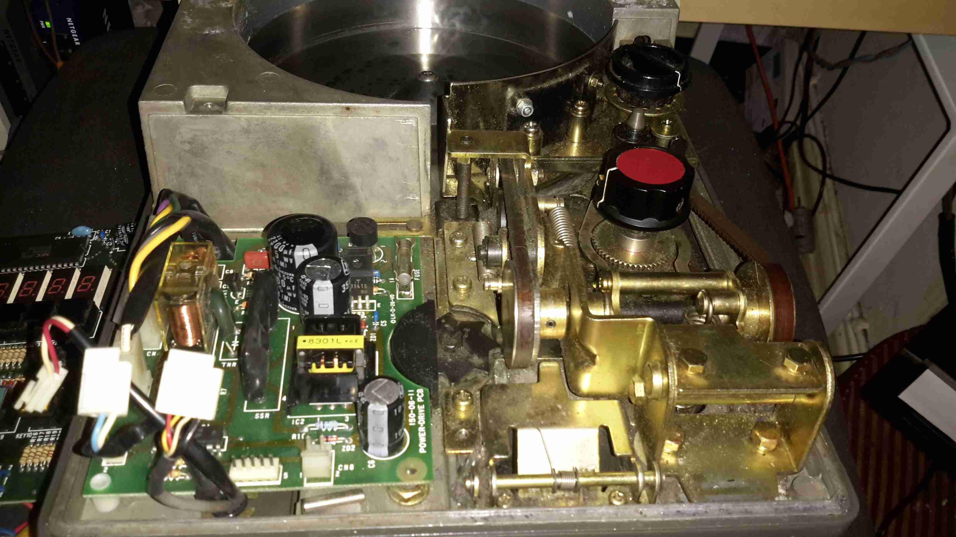
Here’s some teardown photos of an old De La Rue coin counter, used in businesses for rapid counting of change into large bags.
Mechanism
An overview of the whole mechanical system of the counter. Coins are loaded into the drum at the rear of the machine, which sorts them into a row for the rubber belt to pick up & run through the counter. The coin type to be sorted is selected by turning the control knobs on the right.
The control knobs adjust the width & height of the coin channel so only the correct sized coins will be counted.
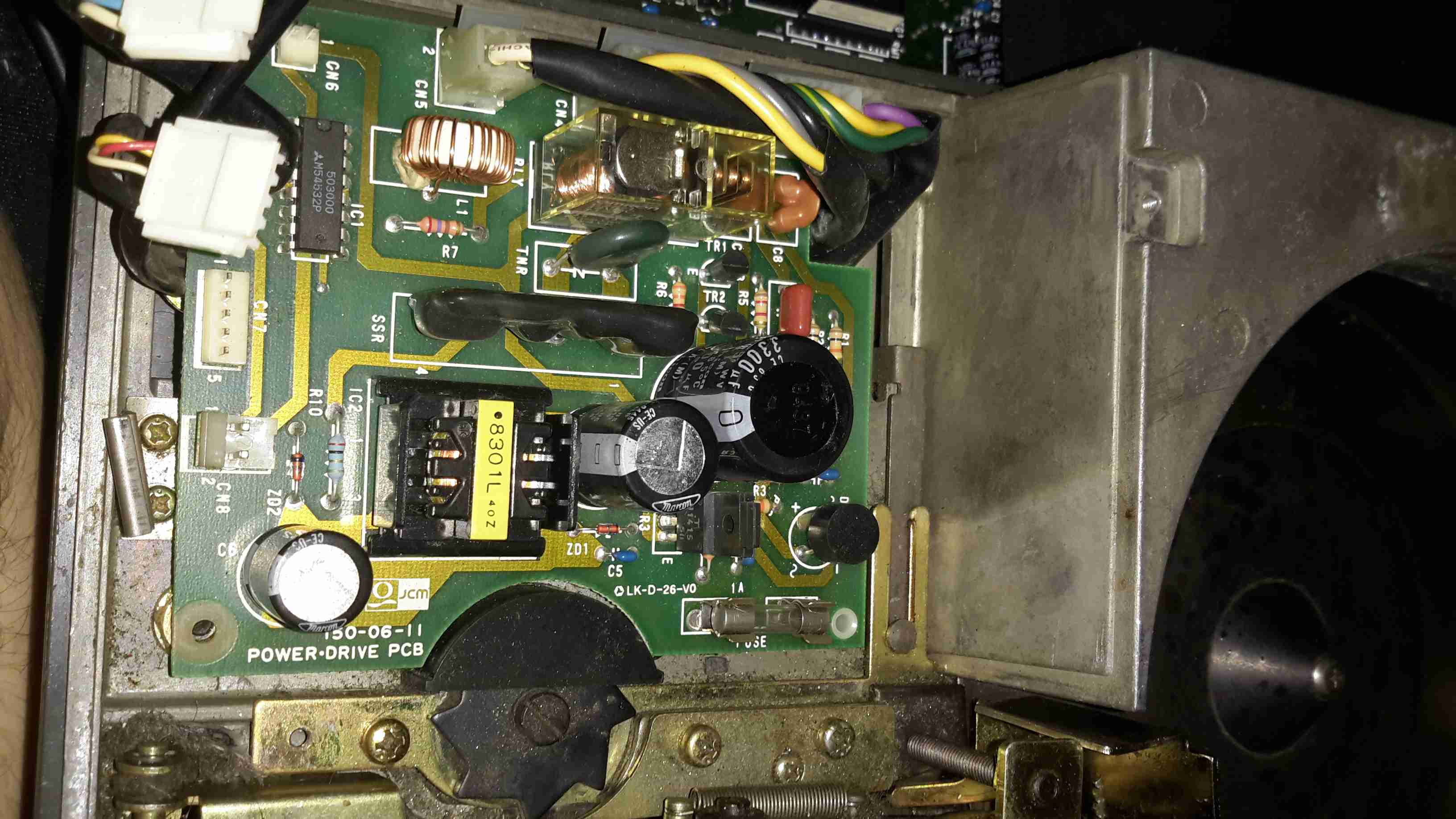
PSU & Switching
The counter is driven by a basic AC induction motor, the motor power relay & reversing relay is on this PCB, along with the 5v switching supply for the main CPU board.
The SMPS on this board looks like a standard mains unit, but it’s got one big difference. Under the frame next to the main motor is a relatively large transformer, with a 35v output. This AC is fed into the SMPS section of the PSU board to be converted to 5v DC for the logic.
I’m not sure why it’s been done this way, and have never seen anything similar before.
The edge of the coin channel can be seen here, the black star wheel rotates when a coin passes & registers the count.
Controller PCB
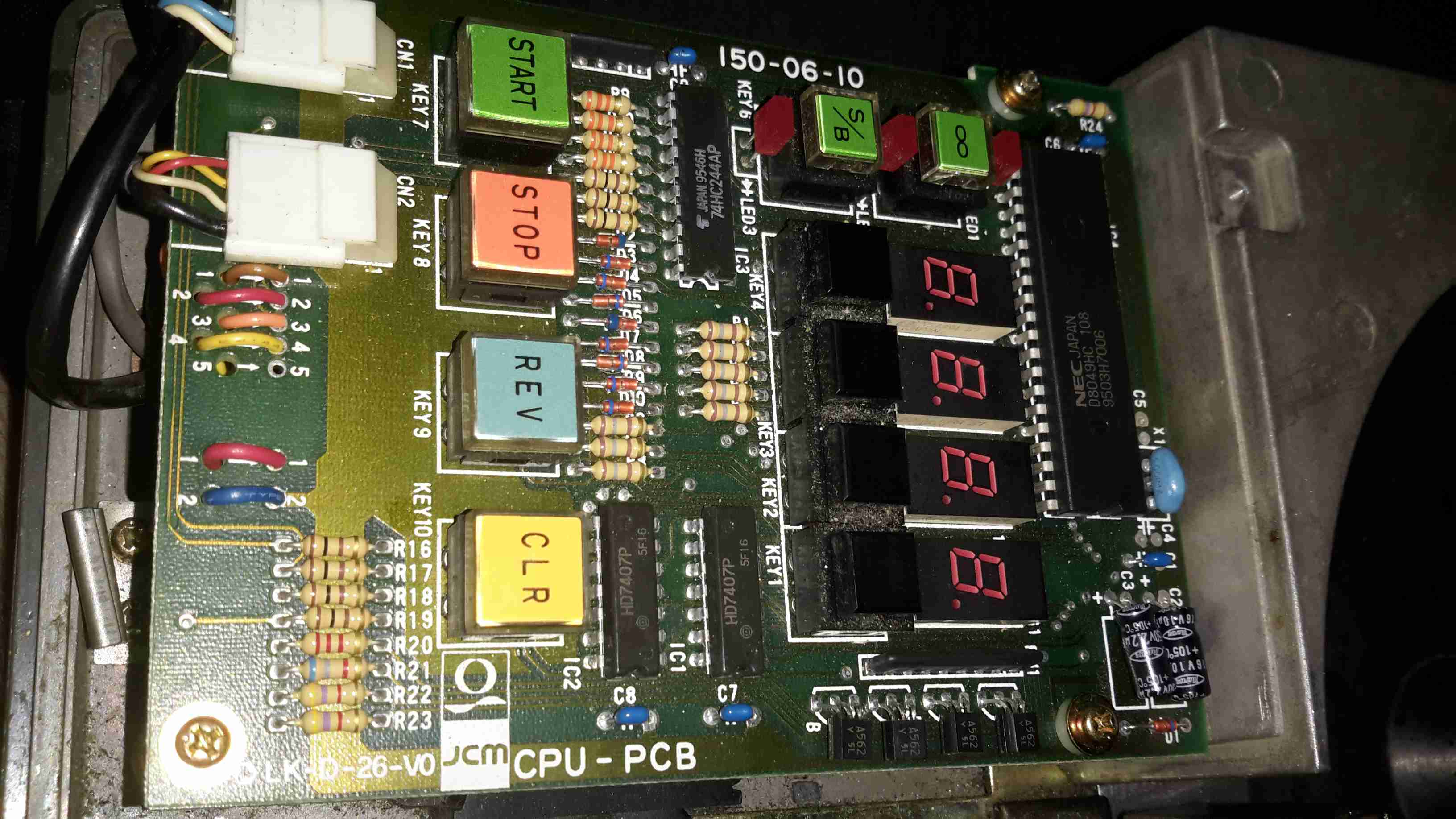
Here’s the main controller PCB, IC date codes put the unit to about 1995. The main CPU is a NEC UPD8049HC 8-bit micro, no flash or EEPROM on this old CPU, simply mask ROM. Coin readout is done on the 4 7-segment LED displays. Not much to this counter, it’s both electronically & mechanically simple.
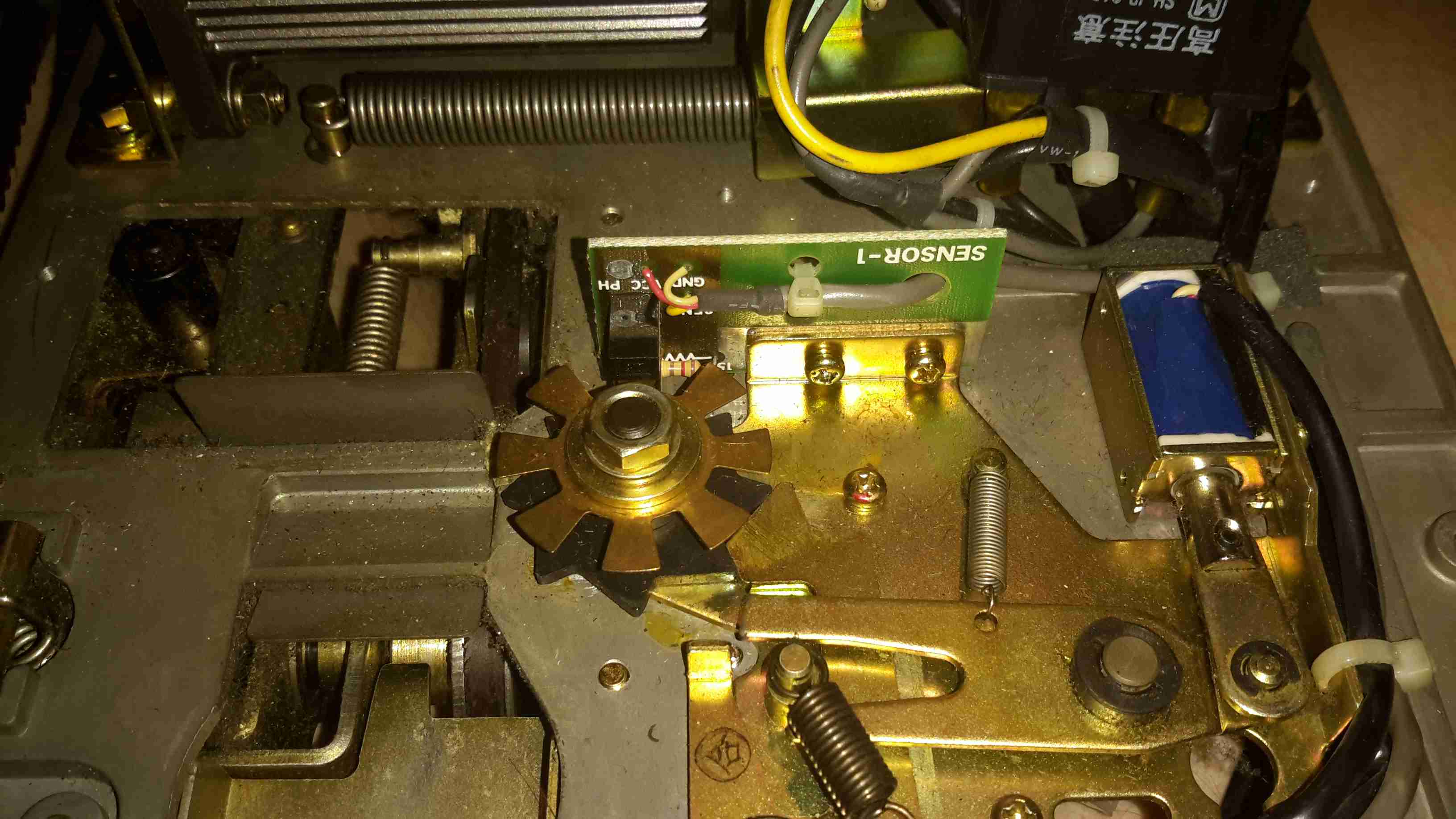
Counter Sensor
Coin counting is done by the star wheel mentioned above, which drives the interrupter disc on this photo-gate. The solenoid locks the counter shaft to prevent over or under counting when a set number of coins is to be counted.
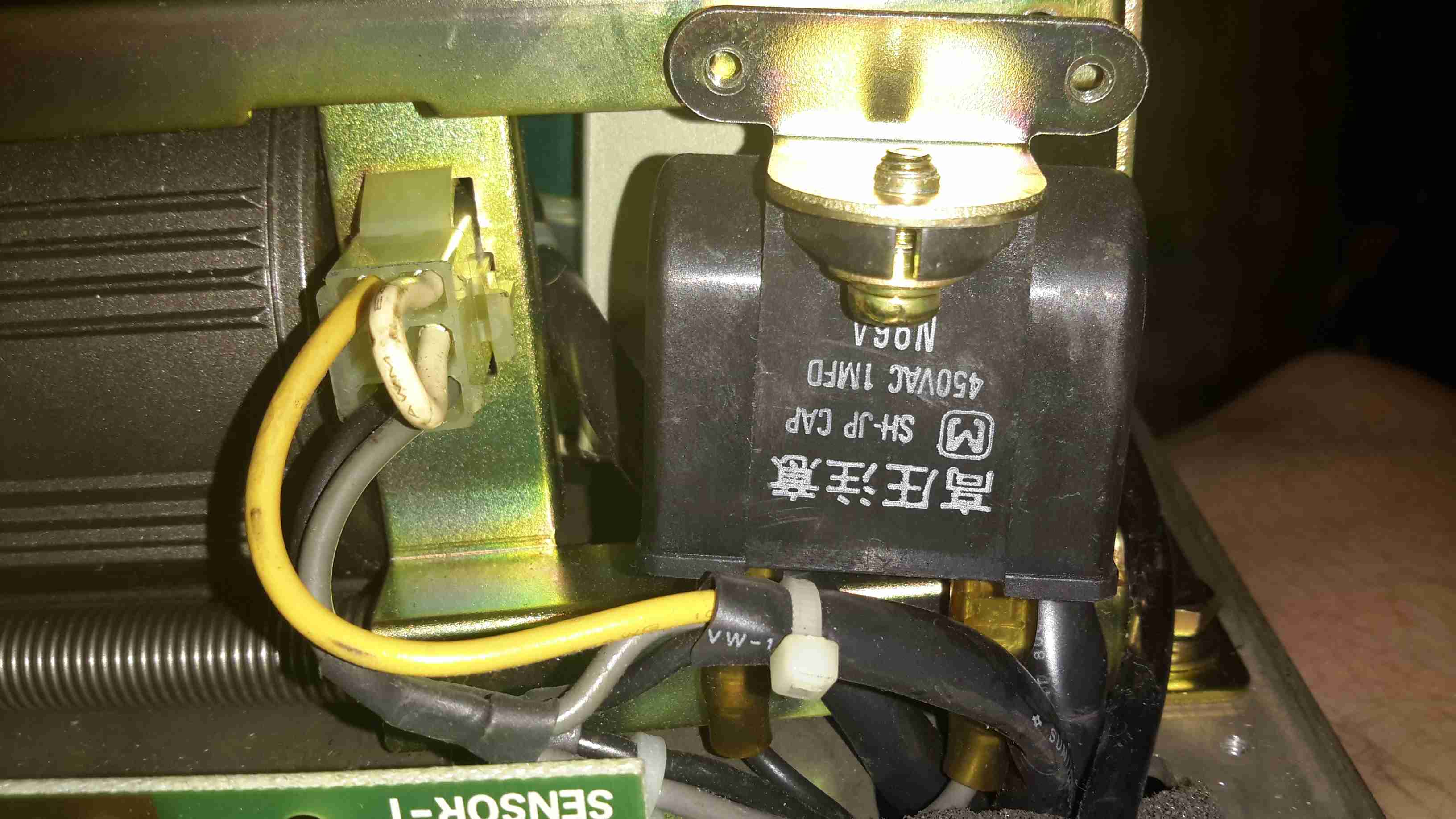
Motor Run Capacitor
Under the frame, here on the left is the small induction motor, only 6W, 4-pole. The run cap for the motor is in the centre, and the 35v transformer is just visible behind it.
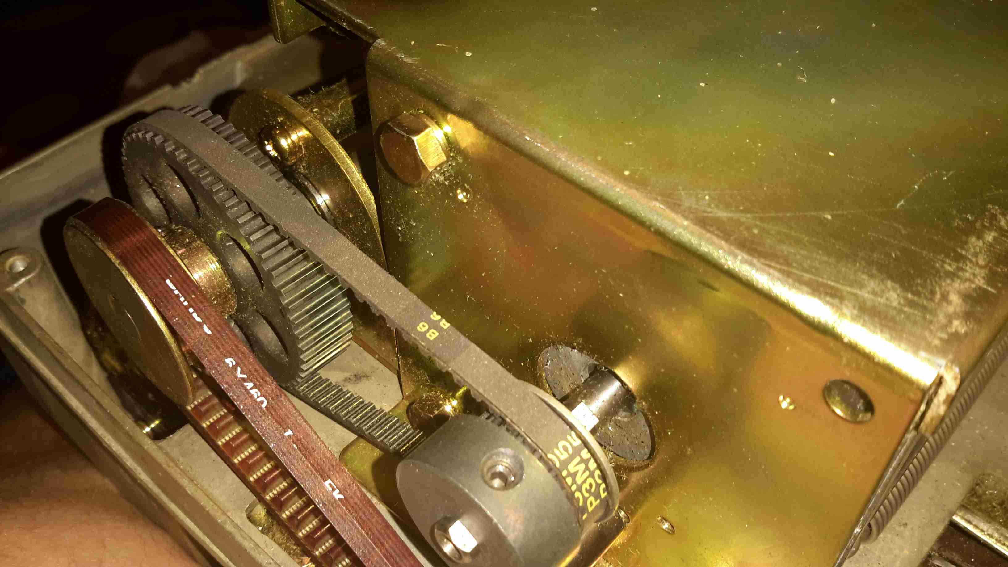
Main Motor Drive
Main drive to the coin sorting mech is through rubber belts, and bevel gears drive the coin drum.
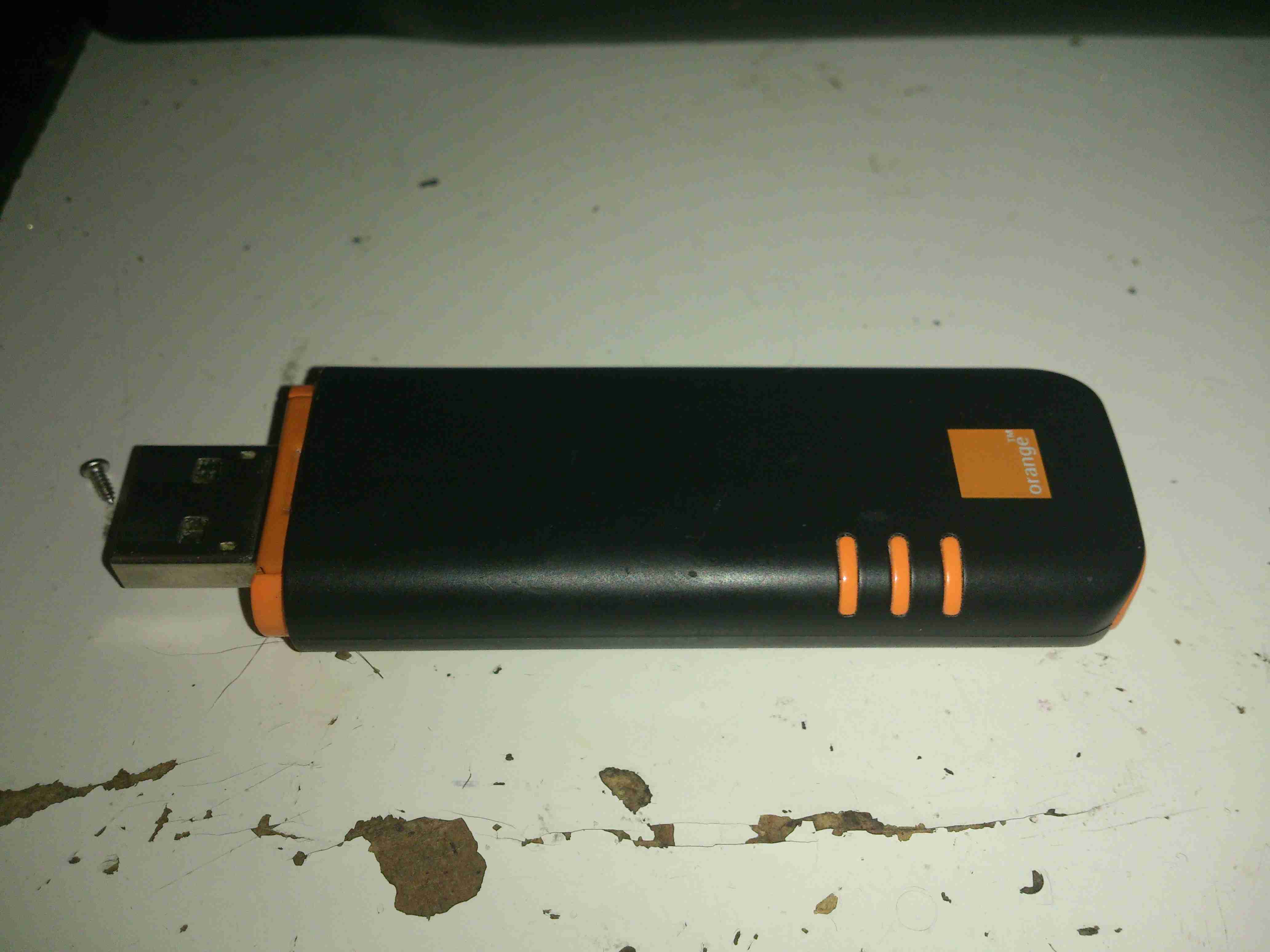
Here’s an old HDSPA 3G USB modem stick that I got with a mobile phone contact many years ago. As it’s now very old tech, and I have a faster modem, not to mention that I’m no longer with Orange (Robbing <expletive>), here’s a teardown of the device!
Cover Removed
The top shell is just clipped into place, while a pair of very small screws hold down the orange piece at left to hold the PCB stack in the casing. Not much to see here, but it’s clear that there’s a lot crammed into a very small space.
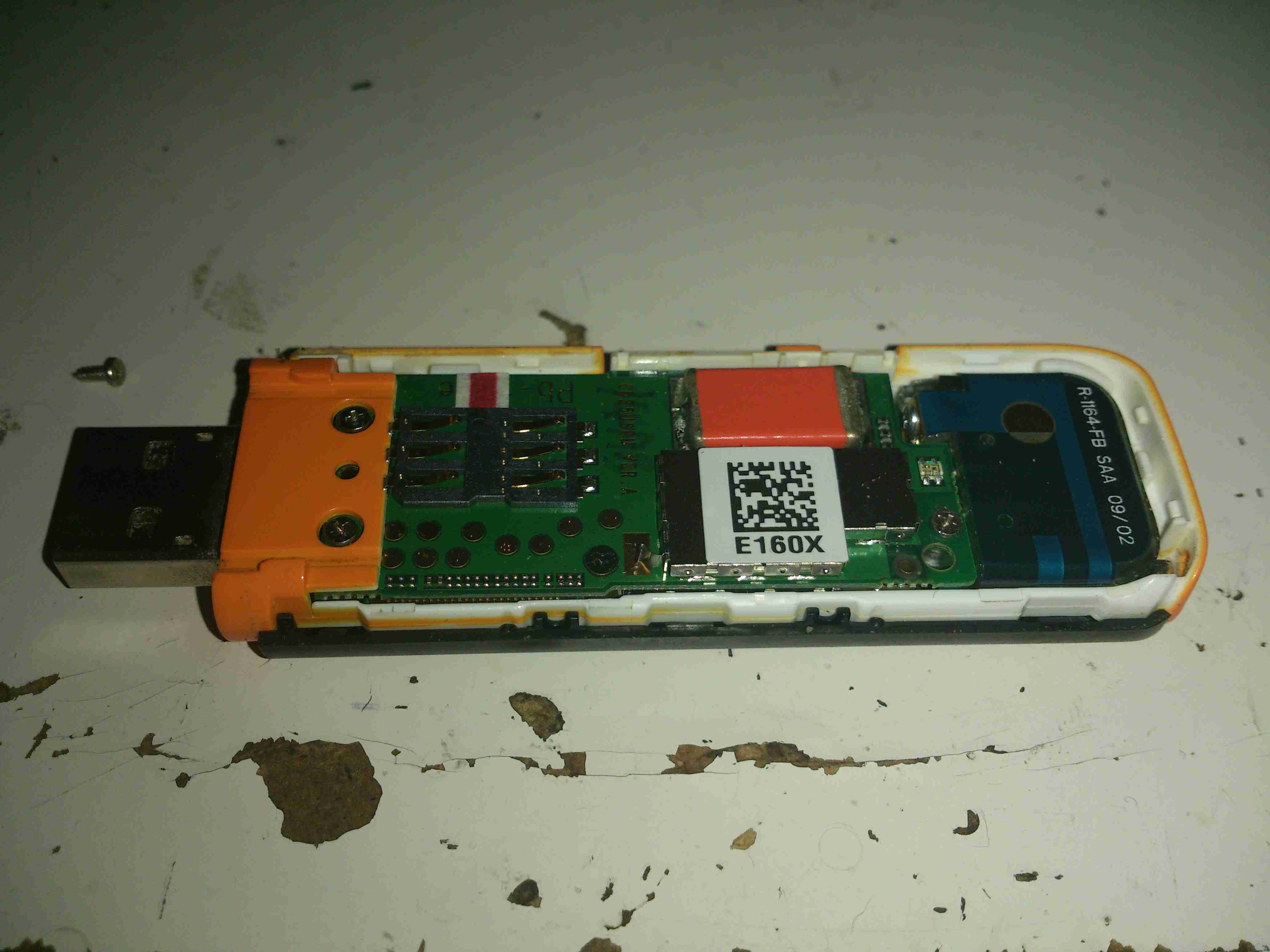
PCB Assembly
Here’s the PCB stack removed from the outer casing. The main antenna is on the right, attached with another small screw. Every IC on the boards is covered with an RF can. No problems there, pliers to the rescue!
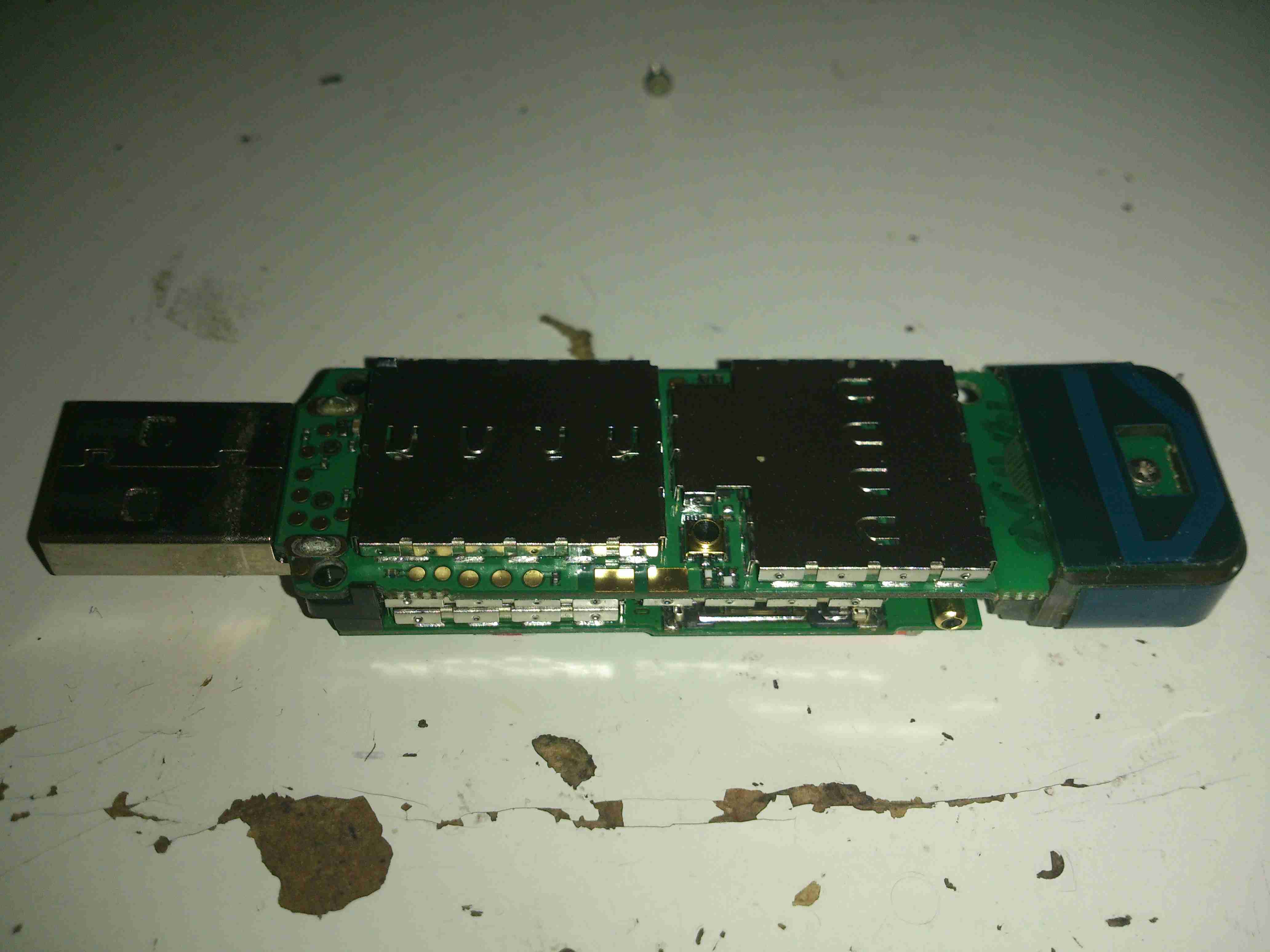
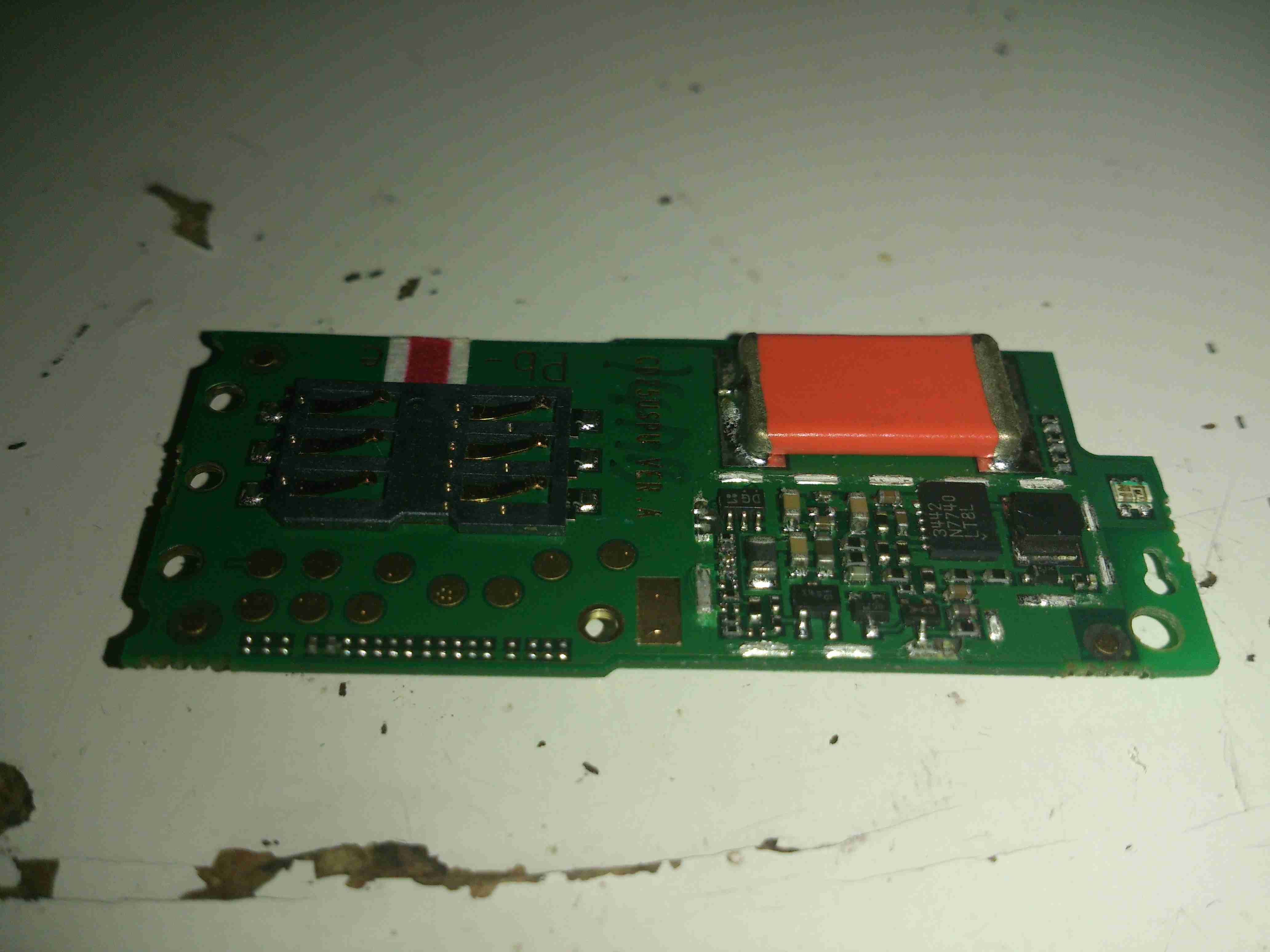
SD Card Slot
Here’s the top PCB, all the shields have been removed. On the left is a Qualcomm PM6658 Power Management IC with integrated USB transceiver. This is surrounded by many of the power management circuits.
The integrated SD Card slot is on the right side. with what looks to be a local switching regulator for supply voltage. This might also provide the SIM card with it’s power supply.
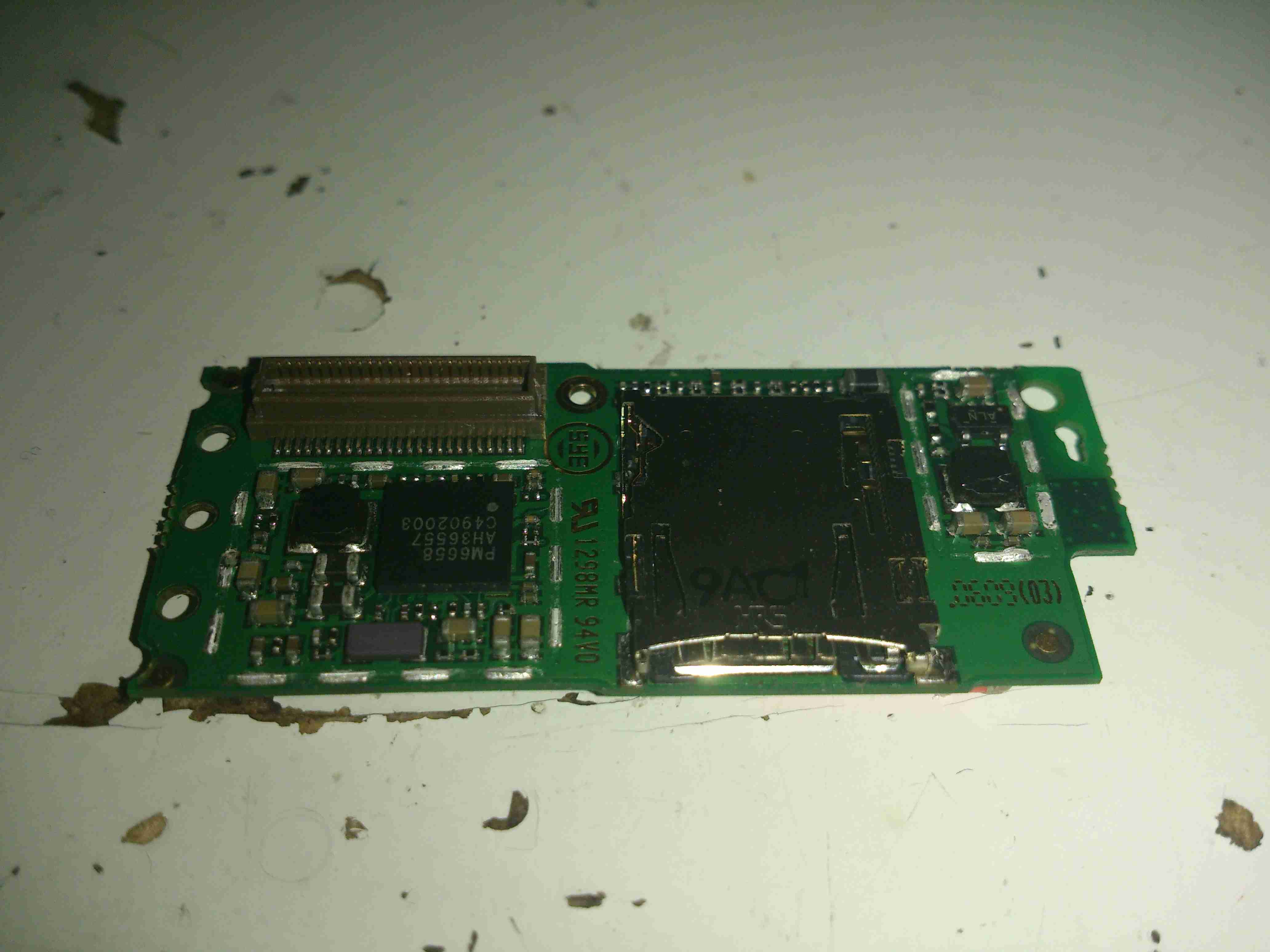
PSU & SIM Contacts
The other side of the top board reveals more power management, with another switching regulator, and a truly massive capacitor at the top edge. I’m guessing this is a solid Tantalum.
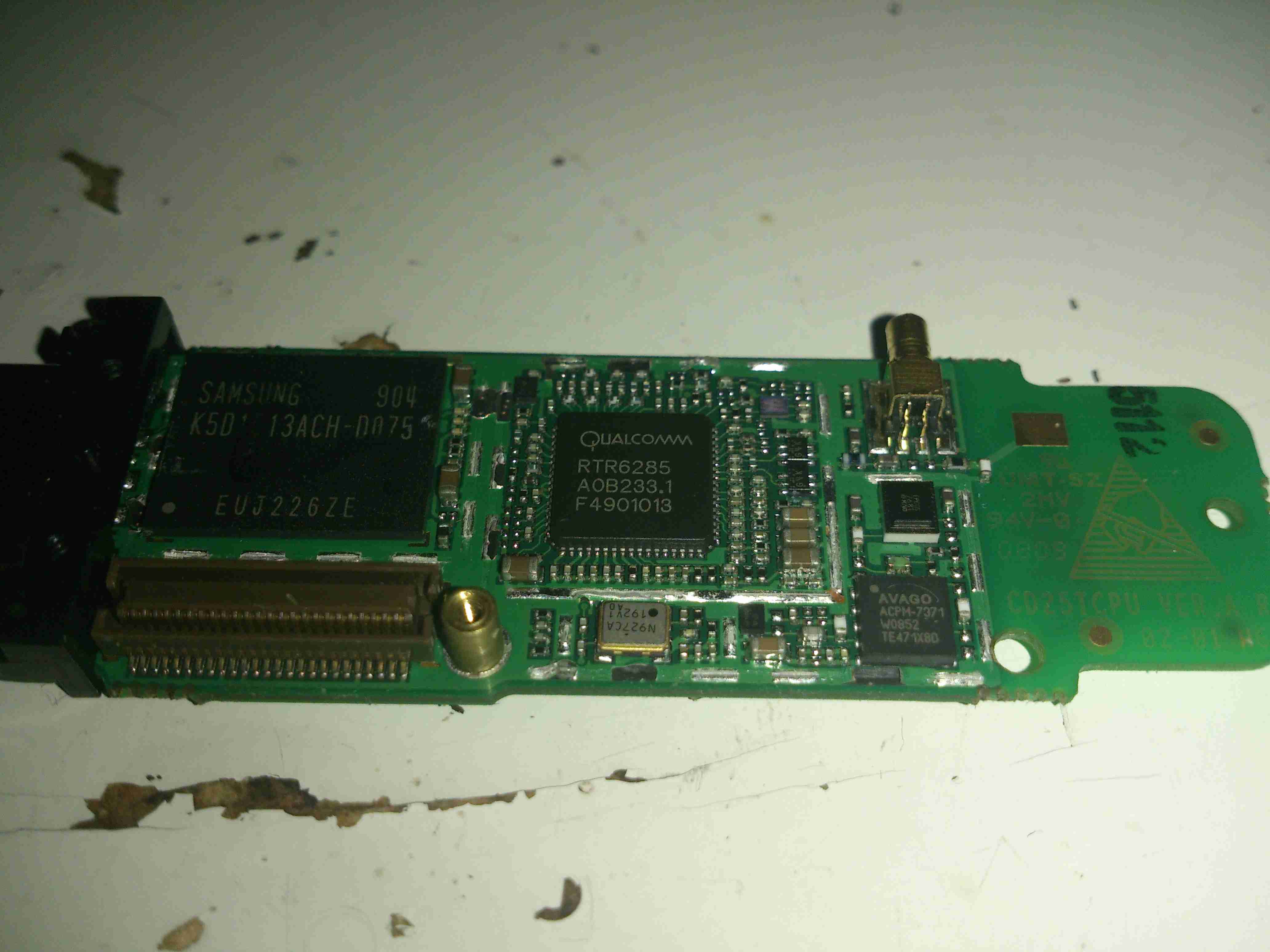
Main Chipset PCB
The other PCB holds the main chipset & RF circuits. On the left here is a Samsung MCP K5D1G13ACH IC. This one is a multiple chip package, having 1Gbit of NAND Flash & 512Mbit of mobile SDRAM.
To it’s right is a Qualcomm RTR6285 RF Transceiver. This IC supports multiband GSM/EDGE/UMTS frequencies & also has a GPS receive amplifier included.
At bottom right is an Avago ACPM7371 Wide-Band 4×4 CDMA Power Amplifier. The external antenna connector is top right.
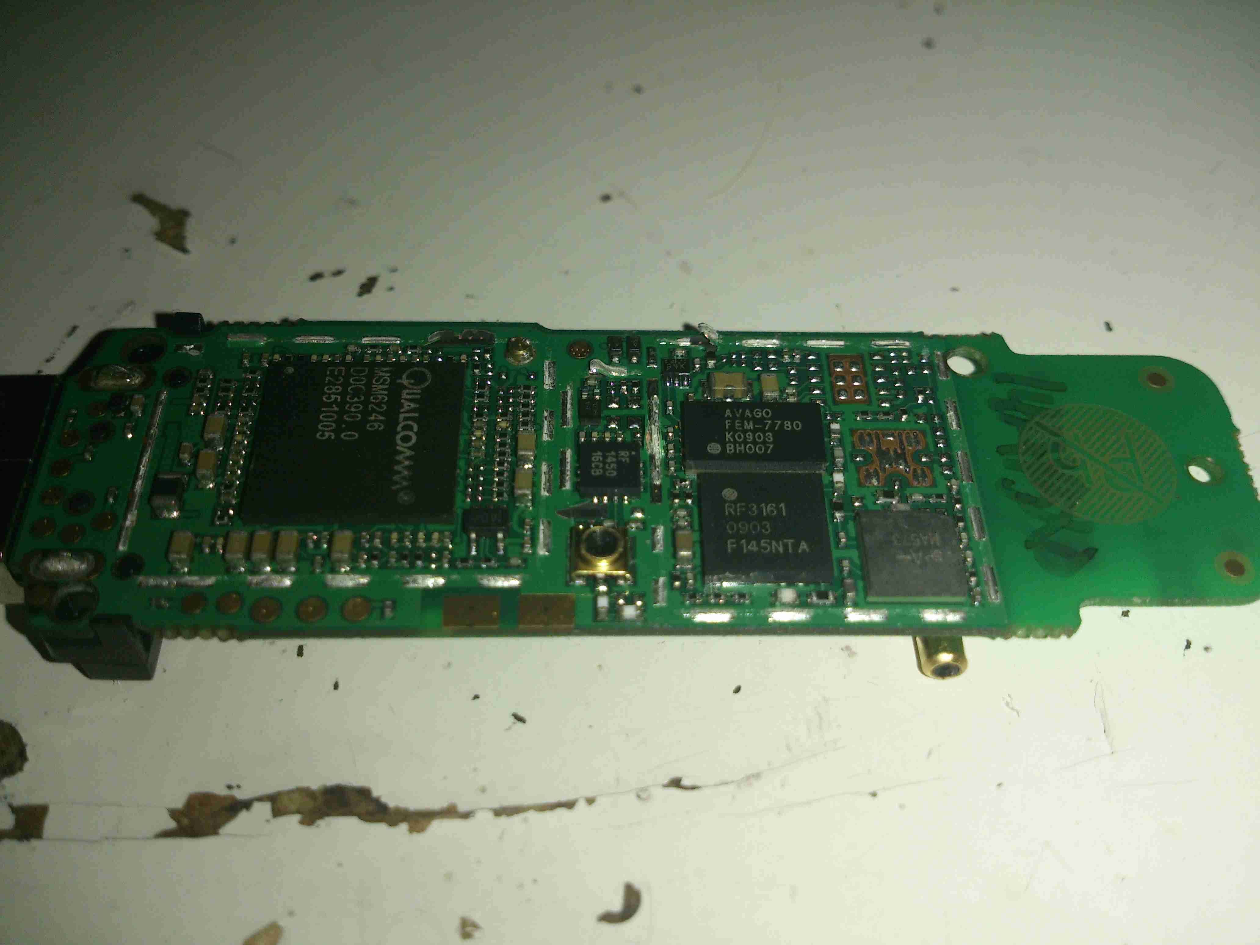
Main Chipset PCB Reverse
On the other side of the main PCB is a Qualcomm MSM6246 Baseband processor. Not sure about this one as I can’t find anything resembling a datasheet. Another micro-coax connector is in the centre, probably for factory test purposes, as it’s not accessible from the outside.
Just above the coax connector is a Qorvo RF1450 SP4T (single-pole 4-throw) High Power (34.5dBm) GSM RF Switch.
Upper right is an Avago FEM-7780 UMTS2100 4×7 Front End Module.
Under that is an RFMD RF3163 Quad-Band RF Power Amplifier Module.
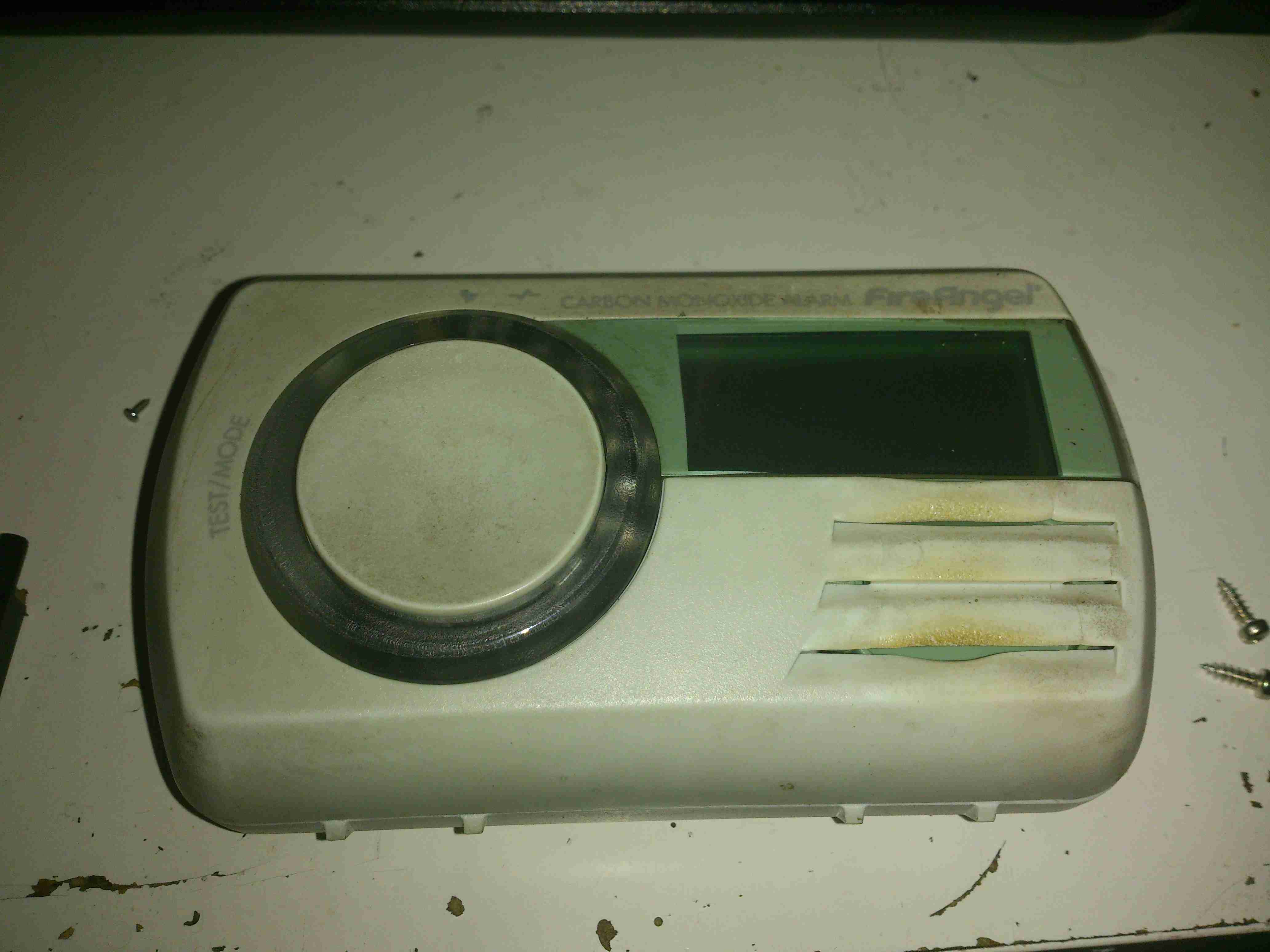
This detector has now been retired from service since it’s a fair bit out of date. So here’s the teardown!
Information
Unlike older detectors, this unit has a built in battery that never needs replacing during the life of the sensor, so once the unit reaches it’s expiry date it’s just trashed as a whole.
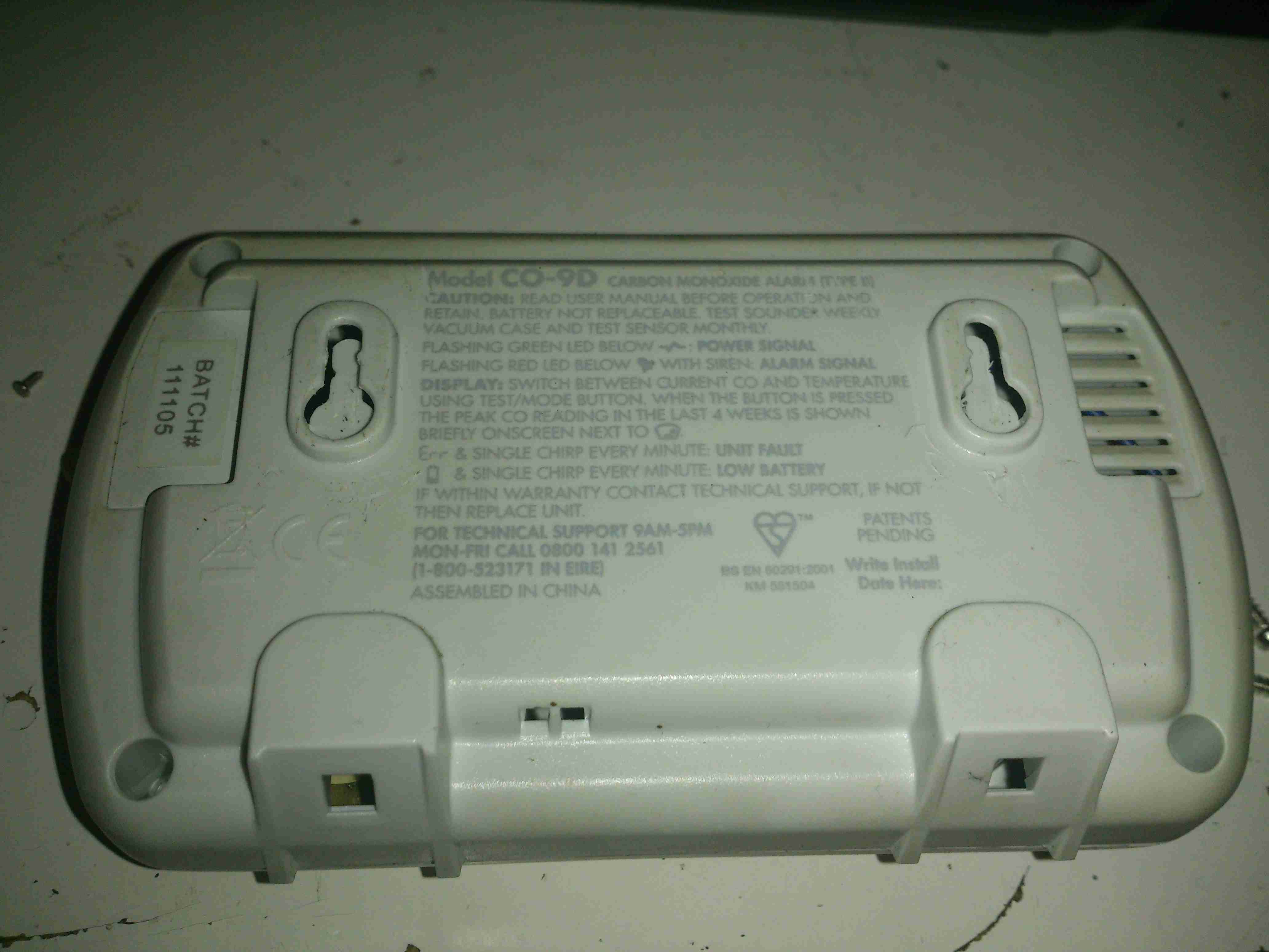
Cover Removed
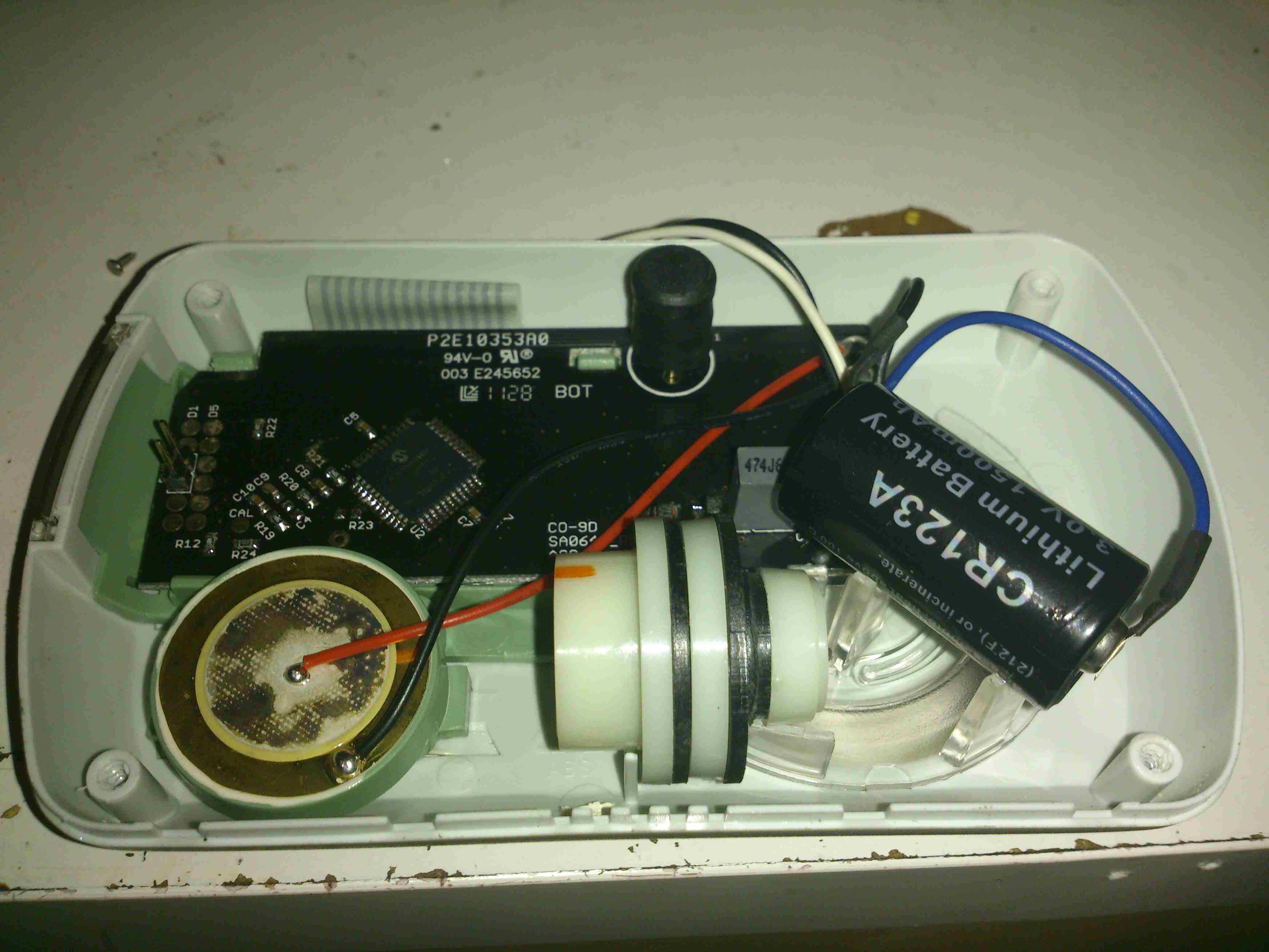
4 screws hold the cover on, here’s the internals of the detector. There’s a 3v CR123A LiMnO² cell at the right for power, rated at 1500mAh. A 7 year life is quite remarkable on a single cell!
The sensor is just to the left of the lithium cell, and is of quite unusual construction. Previous CO sensor cells I’ve seen have been small cylinders with a pair of brass pins. This one appears to use a conductive plastic as the connections. These sensors contain H²SO⁴ so they’re a bit hazardous to open.
There are no manufacturer markings on the sensor & I’ve not been able to find any similarly shaped devices, so I’m unsure of it’s specifications.
The alarm sounder is on the left, the usual Piezo disc with a resonator to increase the loudness.
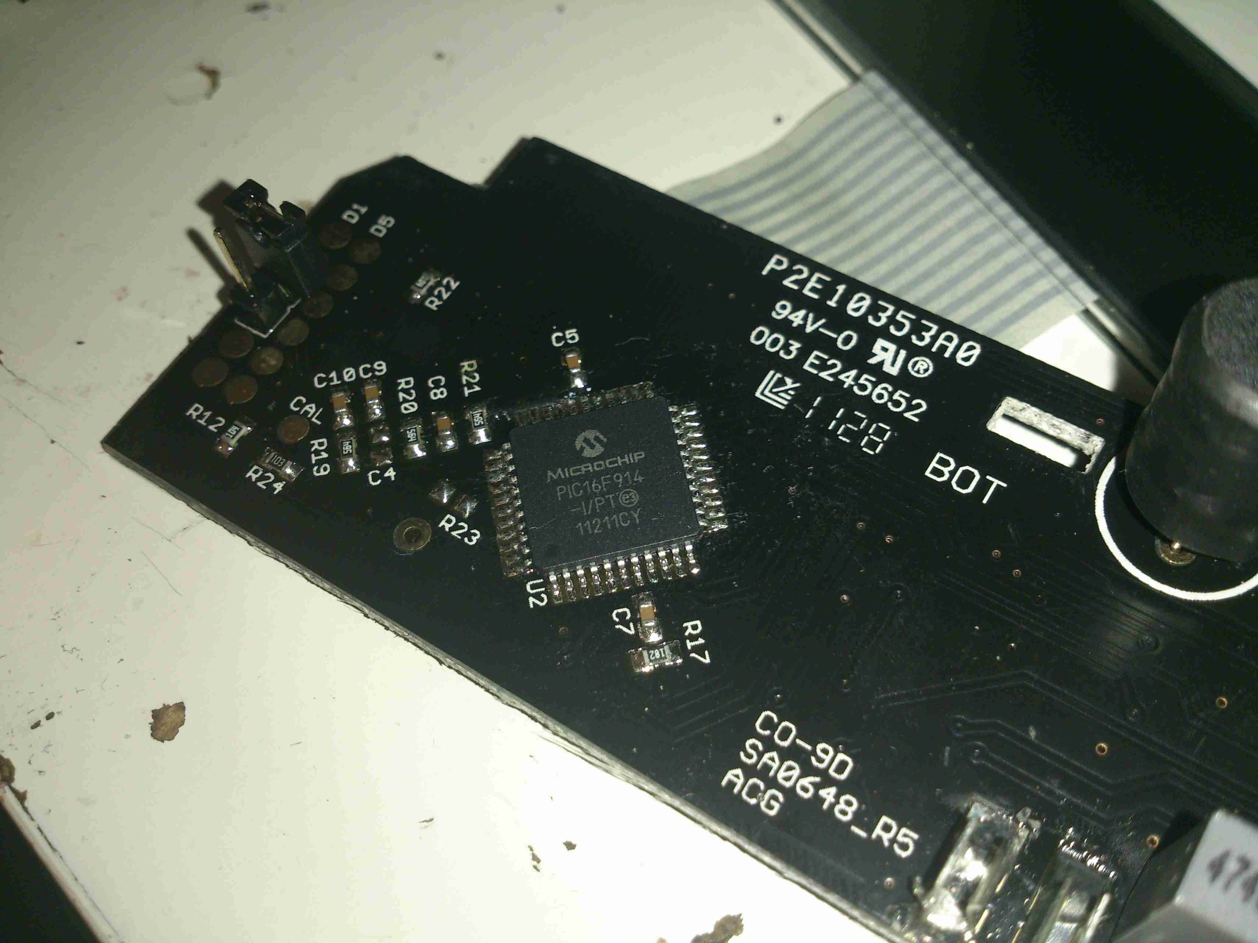
Microcontroller
The brains of the device are provided by a Microchip PIC16F914 microcontroller. This is a fairly advanced device, with many onboard features, and NanoWatt™ technology, standby power consumption is <100nA according to Microchip’s Datasheet. This would explain the incredible battery life.
The choke just at the right edge of the photo is actually a transformer to drive the Piezo sounder at high voltage.
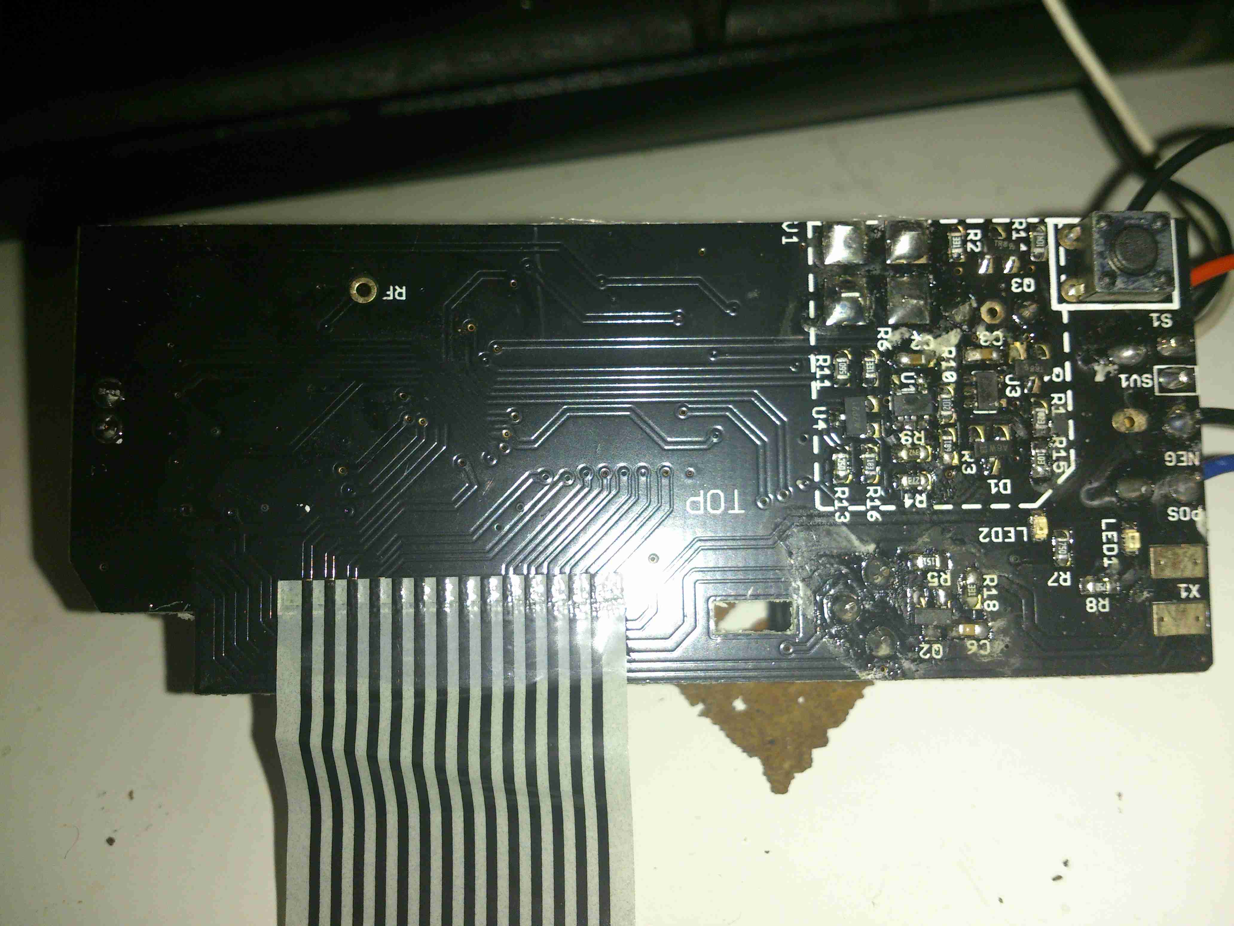
PCB Reverse
Here’s the PCB with the LCD frame removed. Not much to see on the this side, the silence/test button top right & the front end for the sensor.
Sensor Front End Amplifier
Here’s a closer look at the front end for the CO sensor cell itself. I haven’t been able to decode the SMT markings on the SOT packages, but I’m guessing that there’s a pair of OpAmps & a voltage reference.
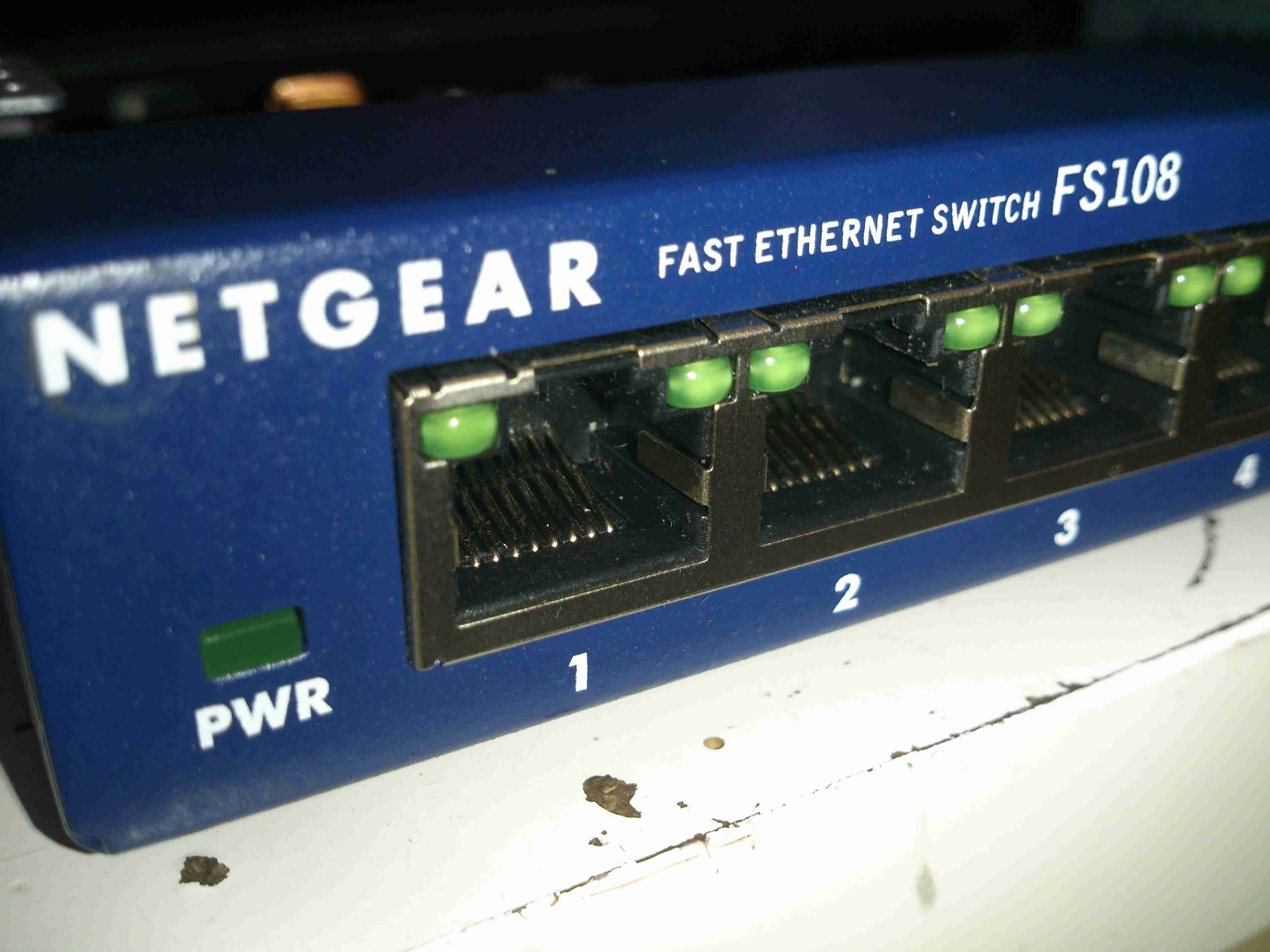
During the replacement of the networking onboard nb Tanya Louise with gigabit, the main 8-port distribution switch was also changed. Here’s a quick teardown of the old one.
Netgear FS108
This has been quite a reliable switch for the internal networking on board, but the time has come to switch over to something a little faster. This switch will be getting repurposed for the slower devices on my network, such as the radiation monitor & the raspberry Pi systems.
Cover Removed
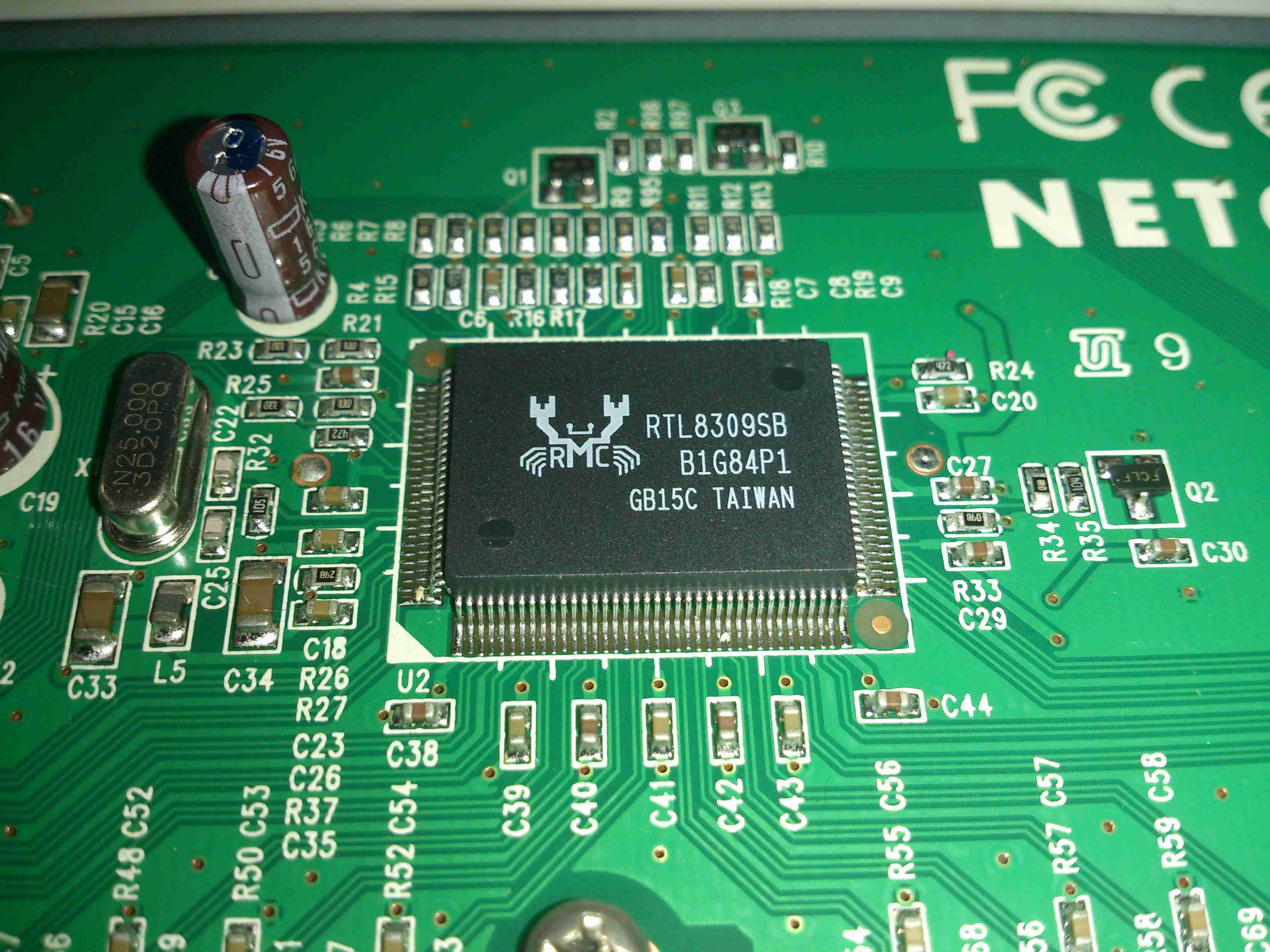
Here’s the top removed from the switch. It’s a very simple construction, with a small power supply section & the main switch IC in the centre.
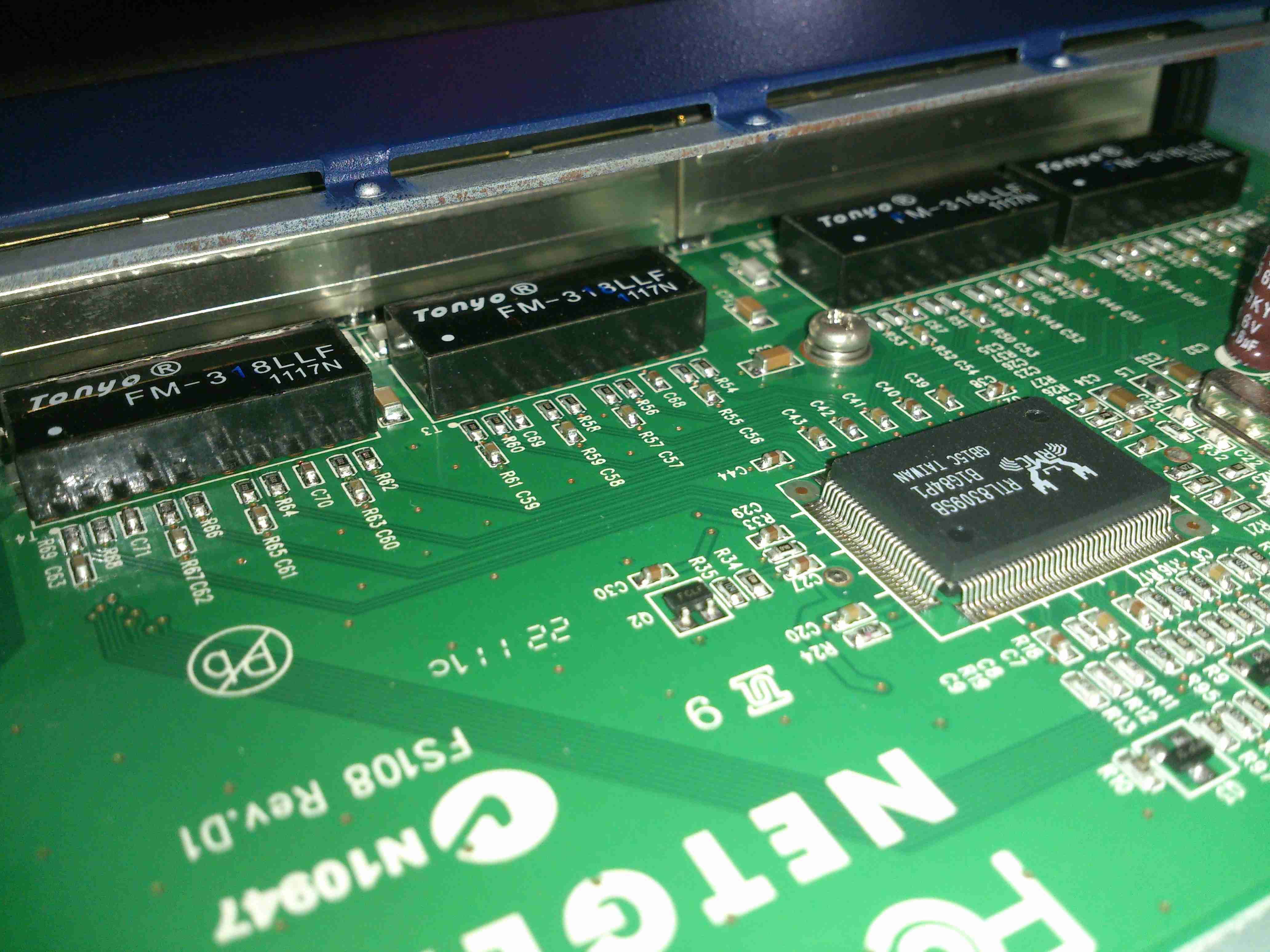
Main Switch IC
All the magic happens in this main IC, a Realtek RTL8309SB Fast Ethernet switch. This is a feature-packed IC, with support for VLAN tagging, but being in a small unmanaged switch the extra features aren’t used.
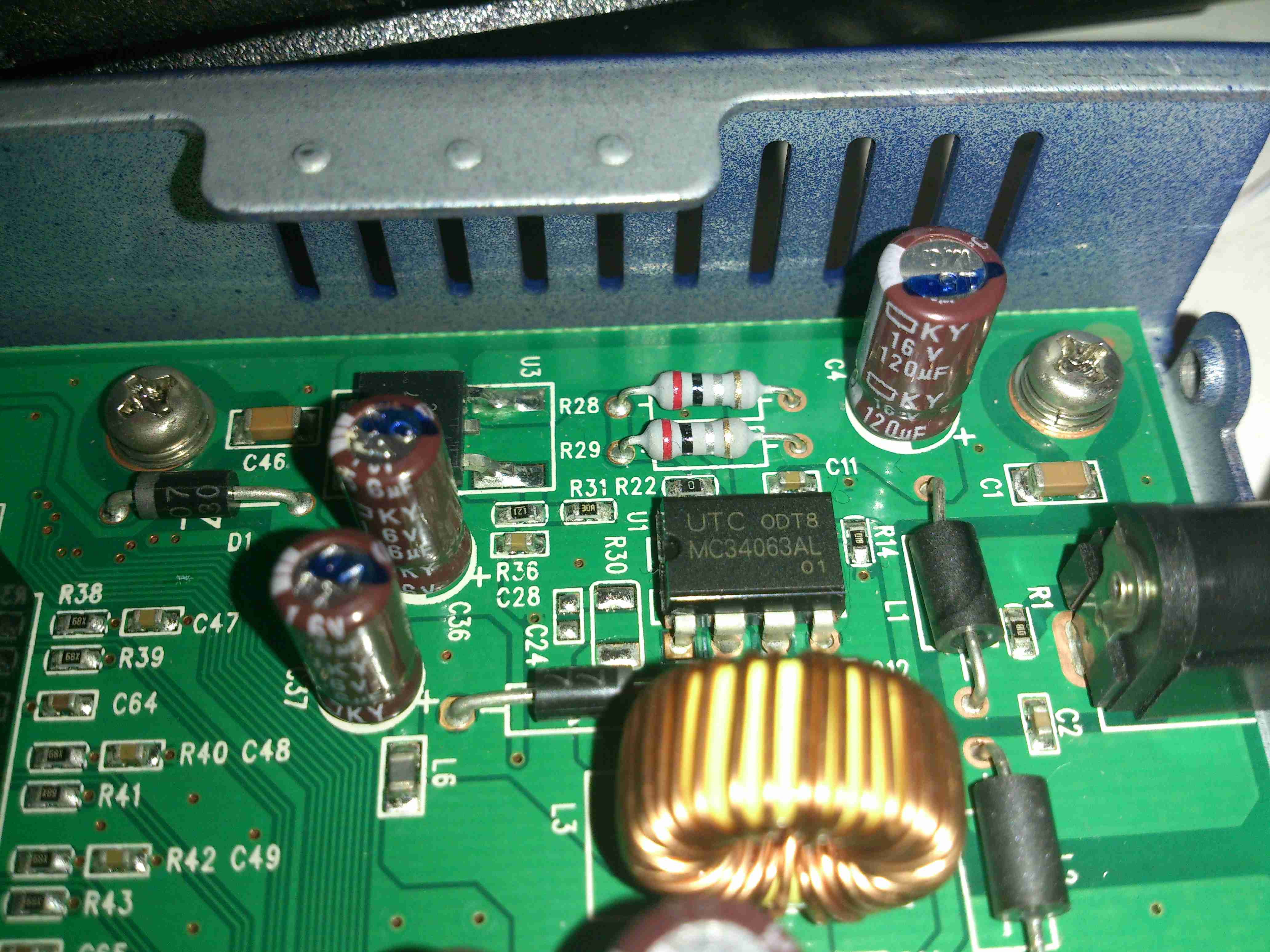
Power Supply
Main power supply is provided by a jelly bean MC34063 DC-DC converter, and an adjustable LM1117 linear regulator. Nothing much special here.
Ethernet Magnetics
The only other parts are the magnetics for the ethernet interfaces, behind the ports themselves.
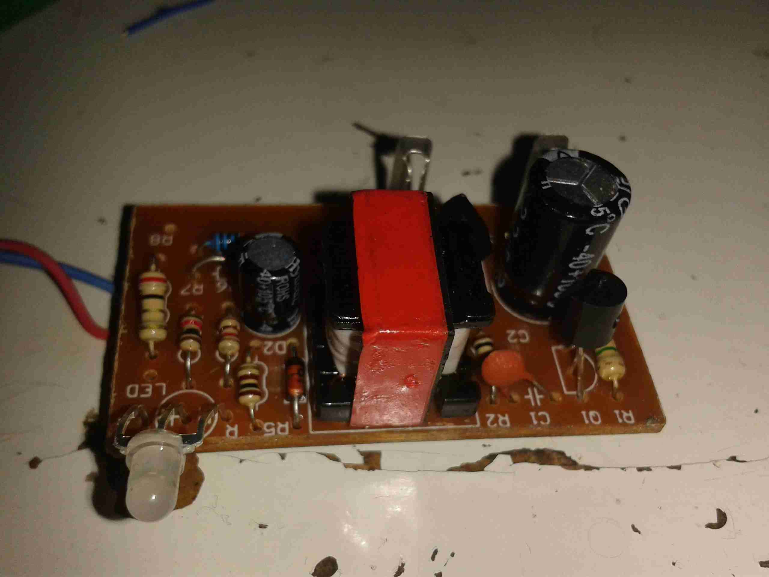
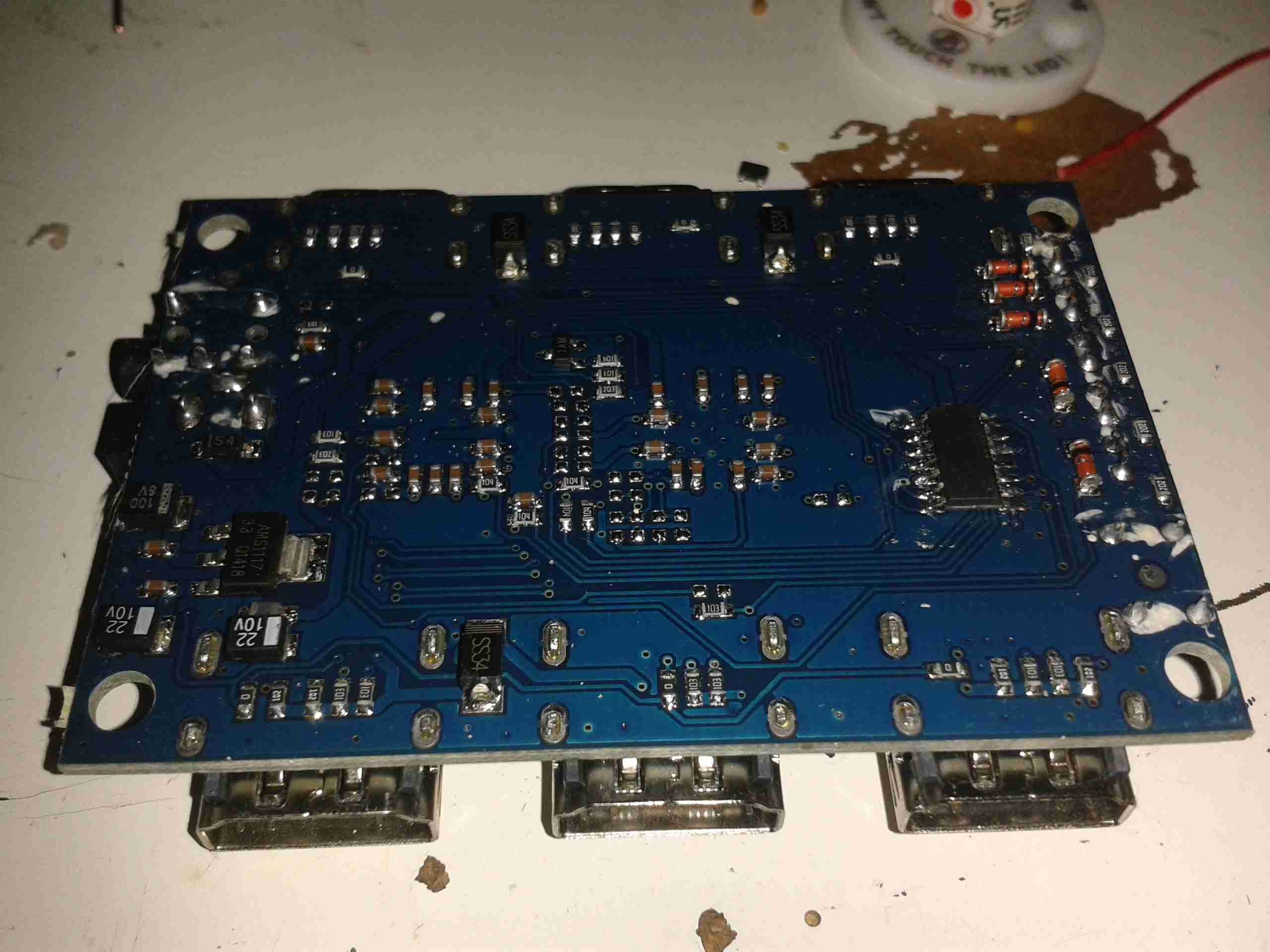
I almost forgot about this bit of kit, that came with one of my LED torches as a Lithium Ion charger. As I never plug in anything that comes from China via eBay, here’s the teardown & analysis.
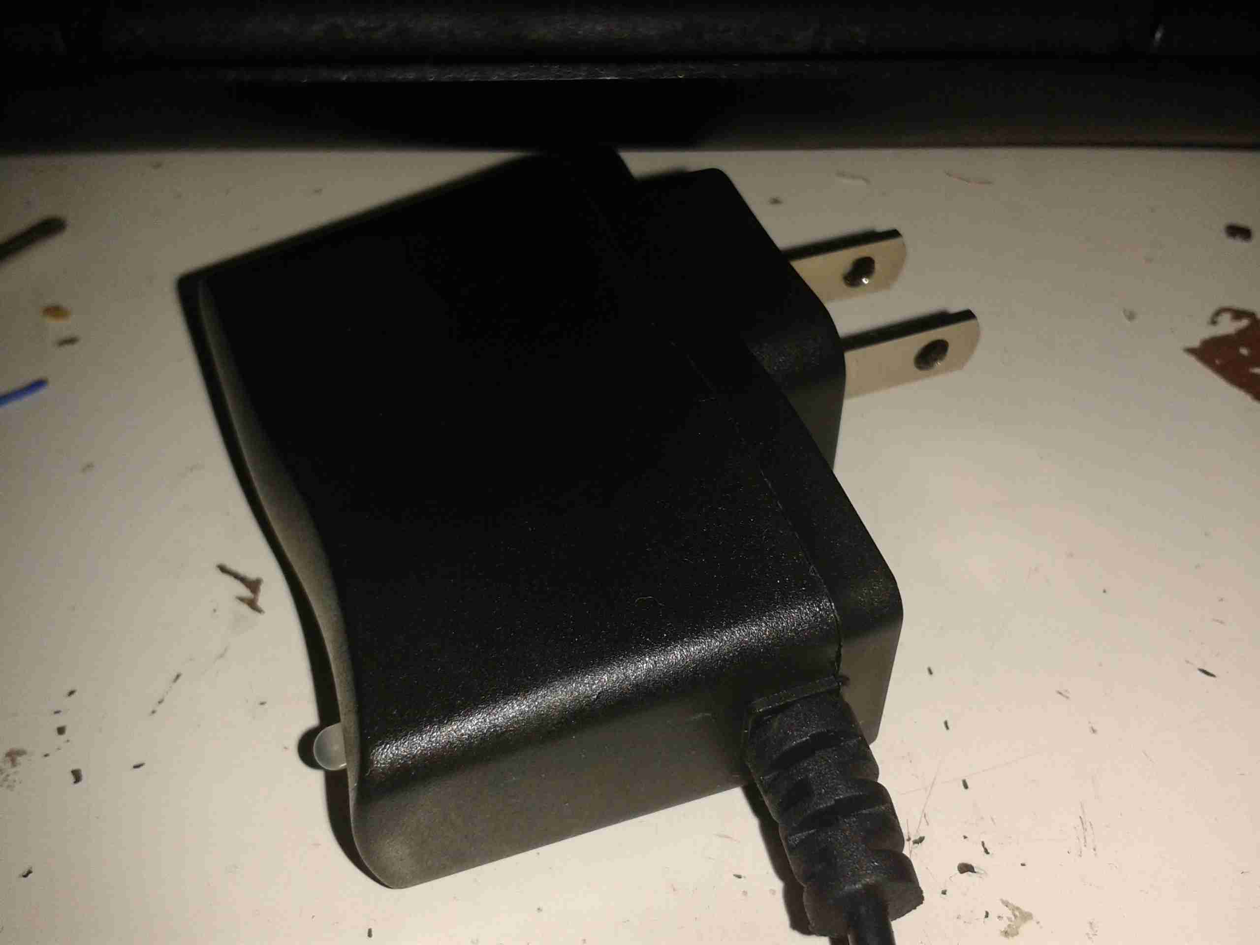
Another Lethal Charger?
Here’s the unit itself. It’s very light, and is clearly intended for American NEMA power points.
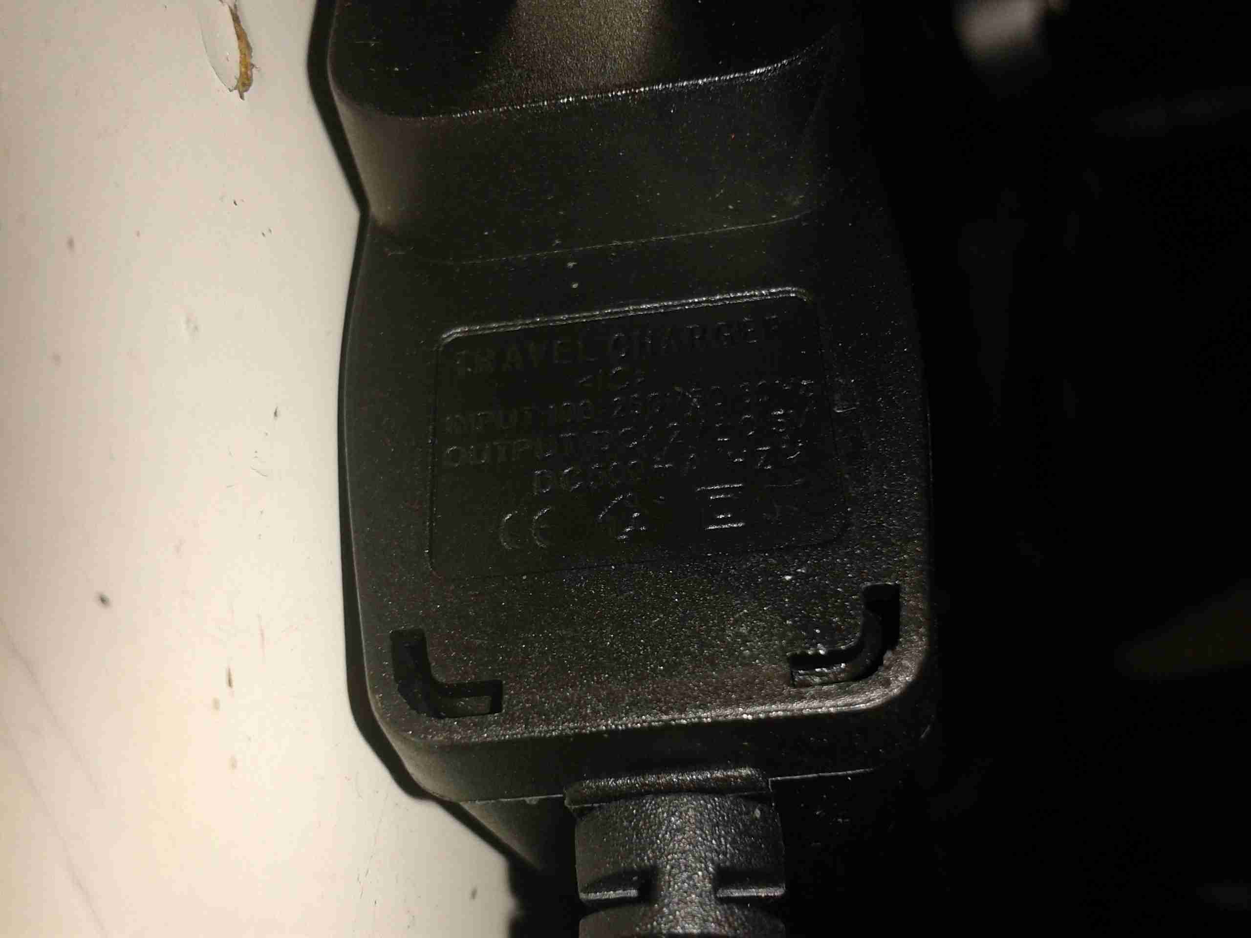
Specs
Claimed specifications are 100-240v AC input, making it universal, and 4.2v DC out ±0.5v at 500mA.
Considering the size of the output wire, if this can actually output rated voltage at rated current I’ll be surprised.
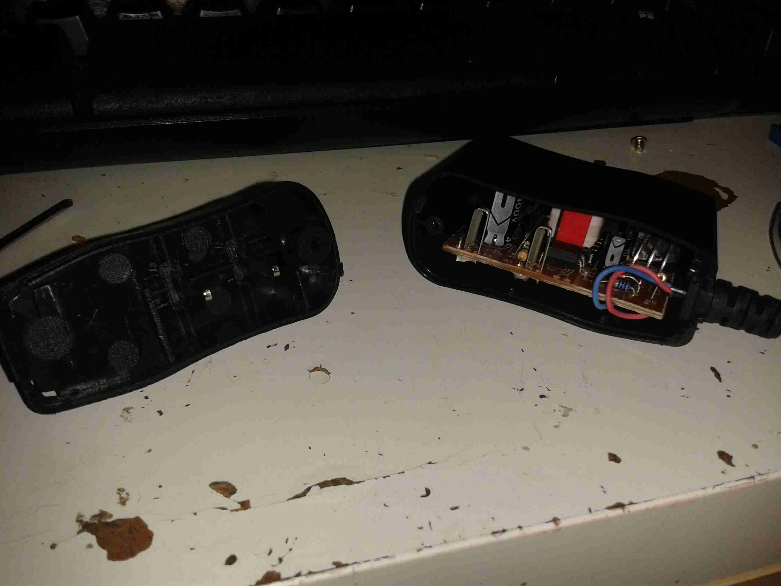
Opened
Here’s the adaptor opened up. There’s no mains wiring to speak of, the mains pins simply push into tags on the PCB.
PCB Top
Top of the SMPS PCB. As usual with Chinese gear, it’s very simple, very cheap and likely very dangerous. There’s no real fusing on the mains input, only half-wave rectification & no EMI filtering.
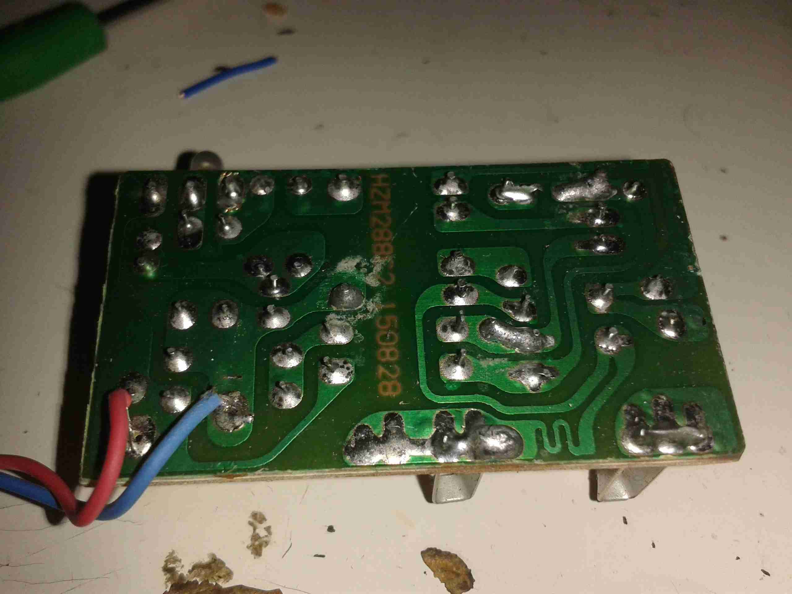
PCB Bottom
Here’s the bottom of the PCB. At least there’s a fairly sized gap between the mains & the output for isolation. The wiggly bit of track next to one of the mains input tags is supposed to be a fuse – I somehow doubt that it has the required breaking characteristics to actually pass any safety standards. Obviously a proper fuse or fusible resistor was far too expensive for these.
The output wiring on the left is thinner than hair, I’d say at least 28AWG, and probably can’t carry 500mA without suffering extreme volt drop.
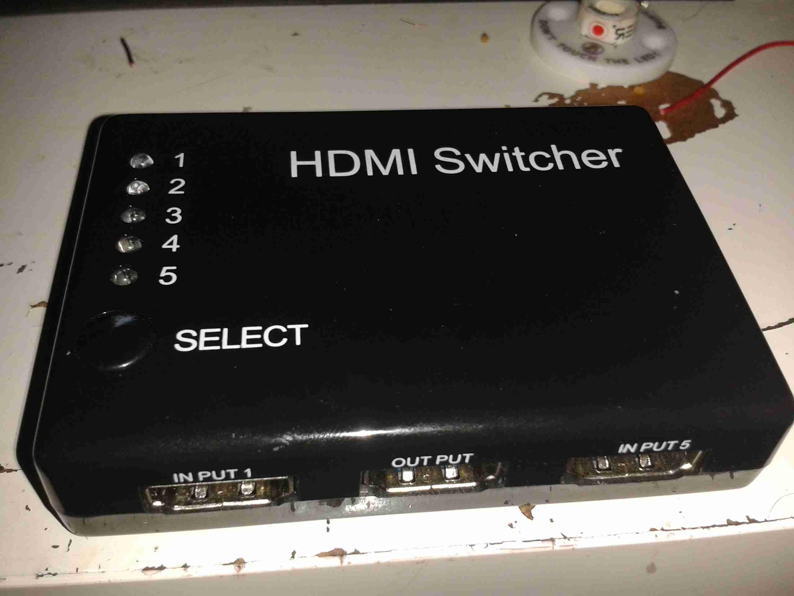
Here’s another quick teardown, a cheap 5-port HDMI switch box. This is used to allow a single input on a monitor to be used by 5 different external HDMI devices, without having to mess about plugging things in.
Power & Remote
Here’s the DC barrel jack & 3.5mm TRS jack for power & remote control. There’s a little IR decoder & remote that go with this for hands free switching.
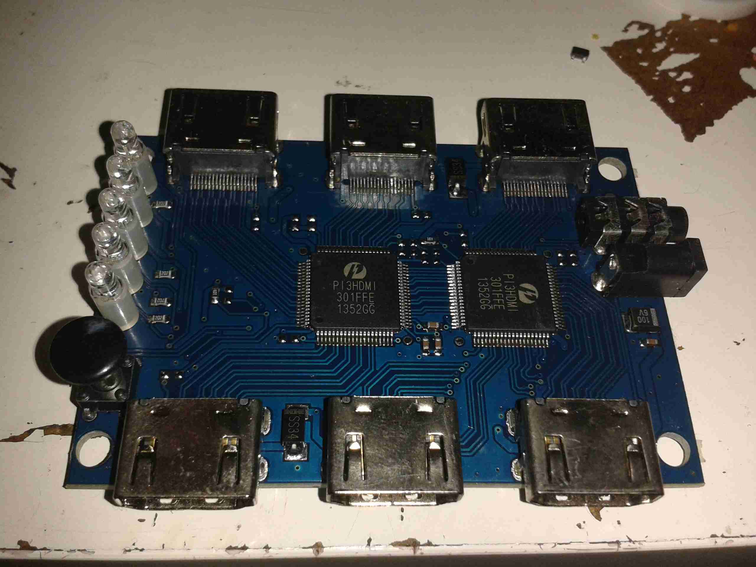
PCB Top
Here’s the PCB out of it’s plastic housing. The main logic is a pair of PI3HDMI303 3:1 HDMI switches from Pericom Semiconductor. These are cascaded for the 5-ports, the first 3 input HDMI ports are switched through both ICs to reach the output.
These HDMI switch ICs are operated with TTL input pins, the combination of these pins held either high or low determines the input port that appears on the output.
There’s a button on the left for switching between inputs, with a row of 5 LED indicators.
PCB Bottom
Not much on the bottom side, a lot of passives & bypass capacitors. There’s a 3.3v LDO regulator on the left for supplying the main rail to the active switch ICs. The IC on the right doesn’t have any numbering at all, but I’m presuming it’s a microcontroller, dealing with the IR remote input & pushbutton inputs to switch the inputs.
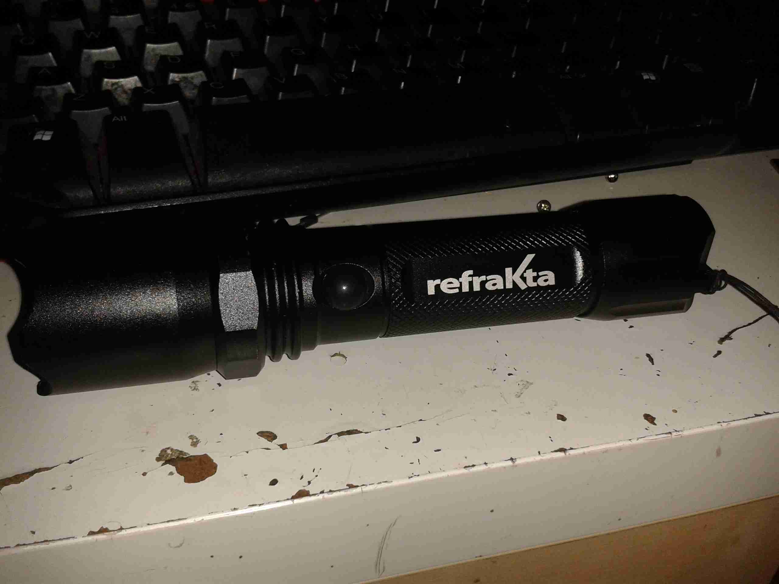
Following on from the teardown & analysis of the charger, here’s the torch itself under the spotlight.
LED Torch
Here’s the torch itself, it’s a sturdy device, made of aluminium. Power is provided by a single 18650 Li-Ion cell.
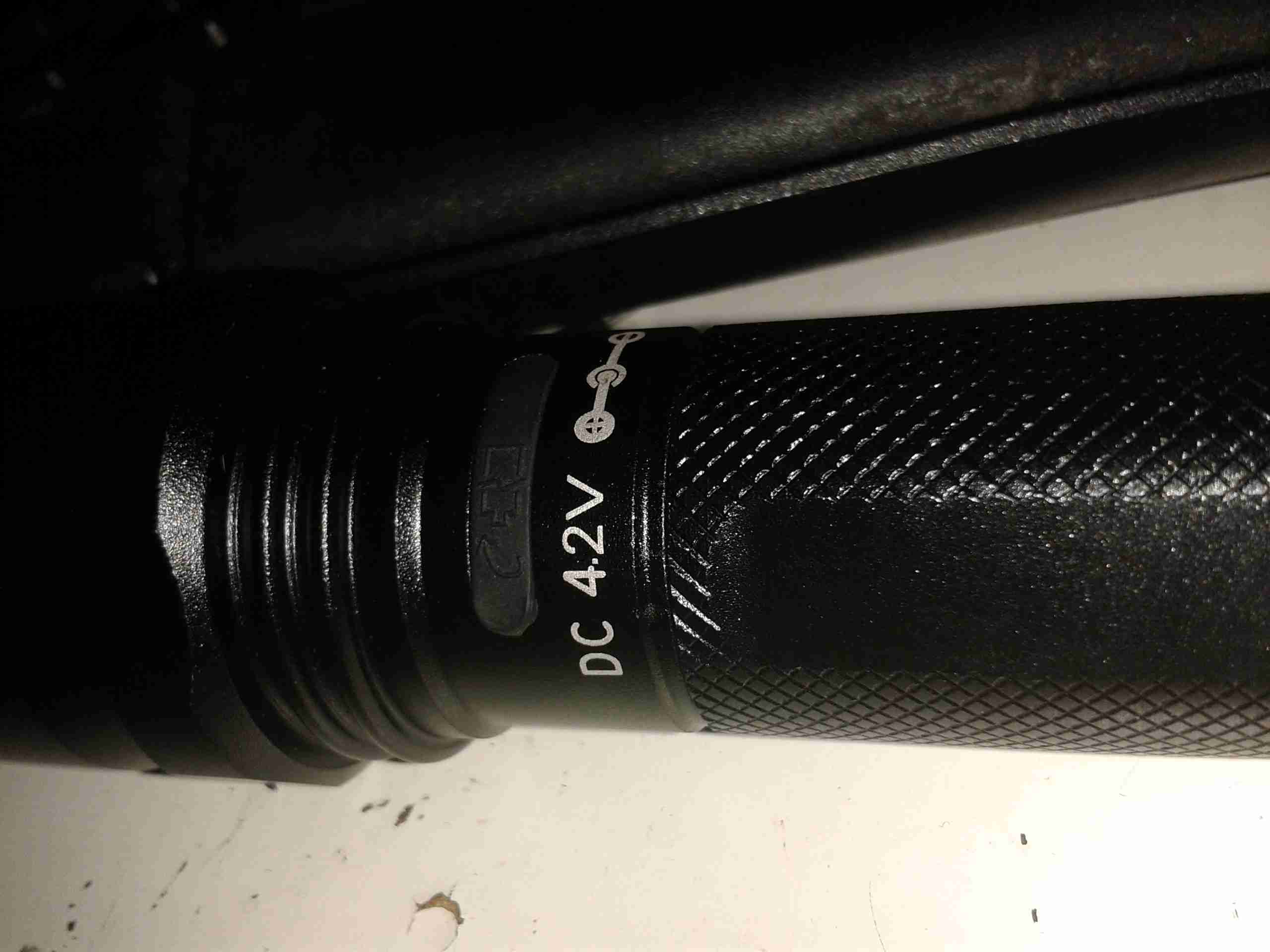
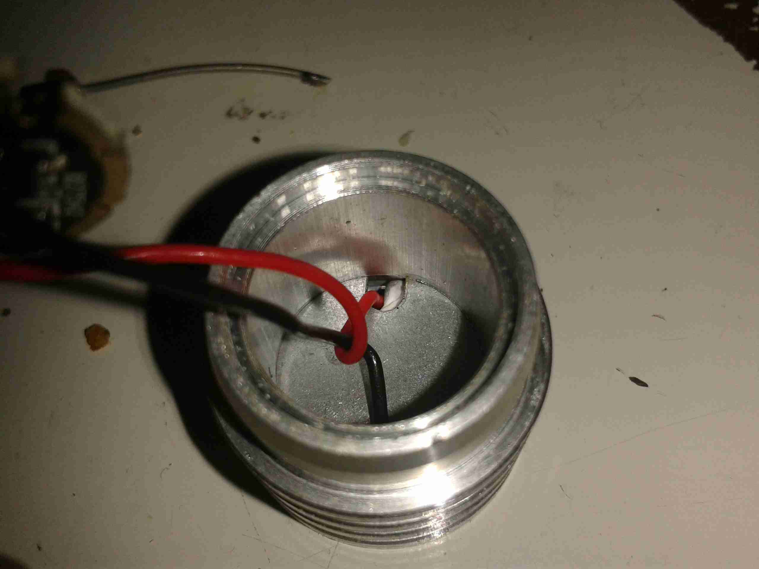
Charging Port
Here’s the charging port on the torch, there’s no electronics in here for controlling the charge, the socket is simply connected directly to the Li-Ion cell, and requires a proper external charger.
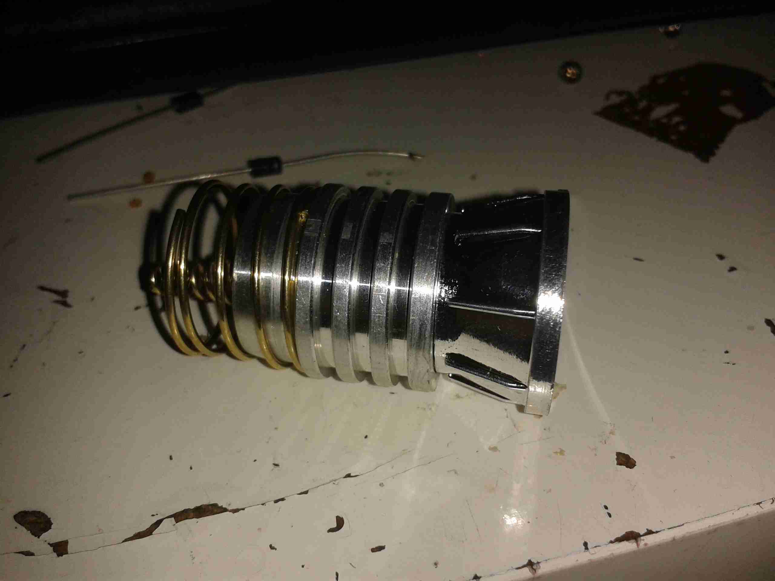
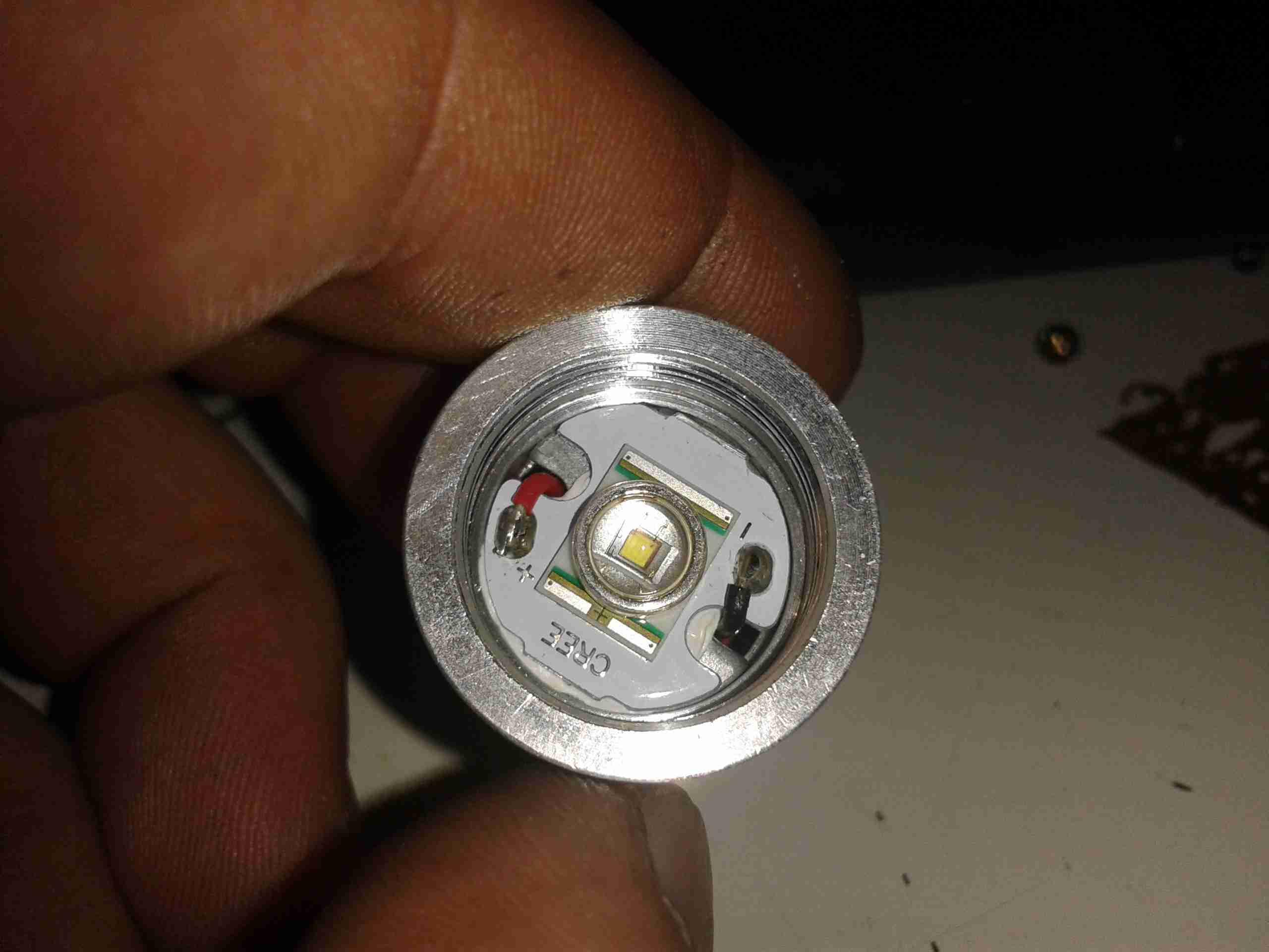
LED Pill
Unscrewing the lens gives access to the LED core, this also unscrews from the torch body itself, leaving the power switch & the battery in the body.
LED Module
Unscrewing the aluminised plastic reflector reveals the LED itself. Being a new device, I expected an XM-L or XM-L2 Cree LED in here, but it’s actually an XR-E model, a significantly older technology, rated at max 1A of drive current.
LED Back
Popping the control PCB out from the pill reveals a lot of empty space, but the back of the LED is completely covered by a heatsinking plate, which is conducting heat to the main body of the torch.
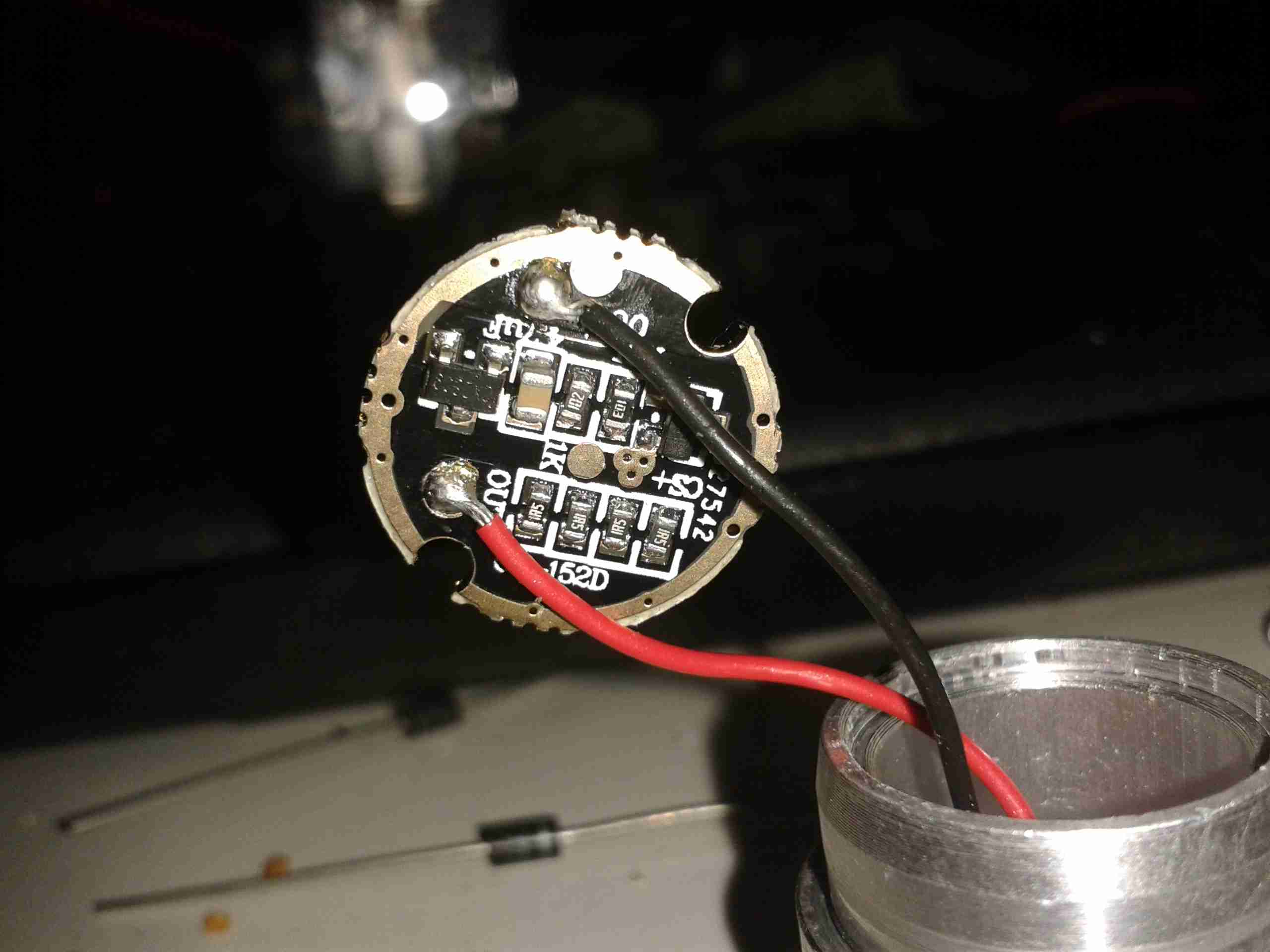
Control PCB
Not much to see on the control PCB, just a bunch of limiting resistors, and a multi-mode LED driver IC in a SOT-23 package. There’s no proper constant-current LED driver, and as the battery discharges the torch will dim, until the low voltage cutout on the cell turns things off completely.
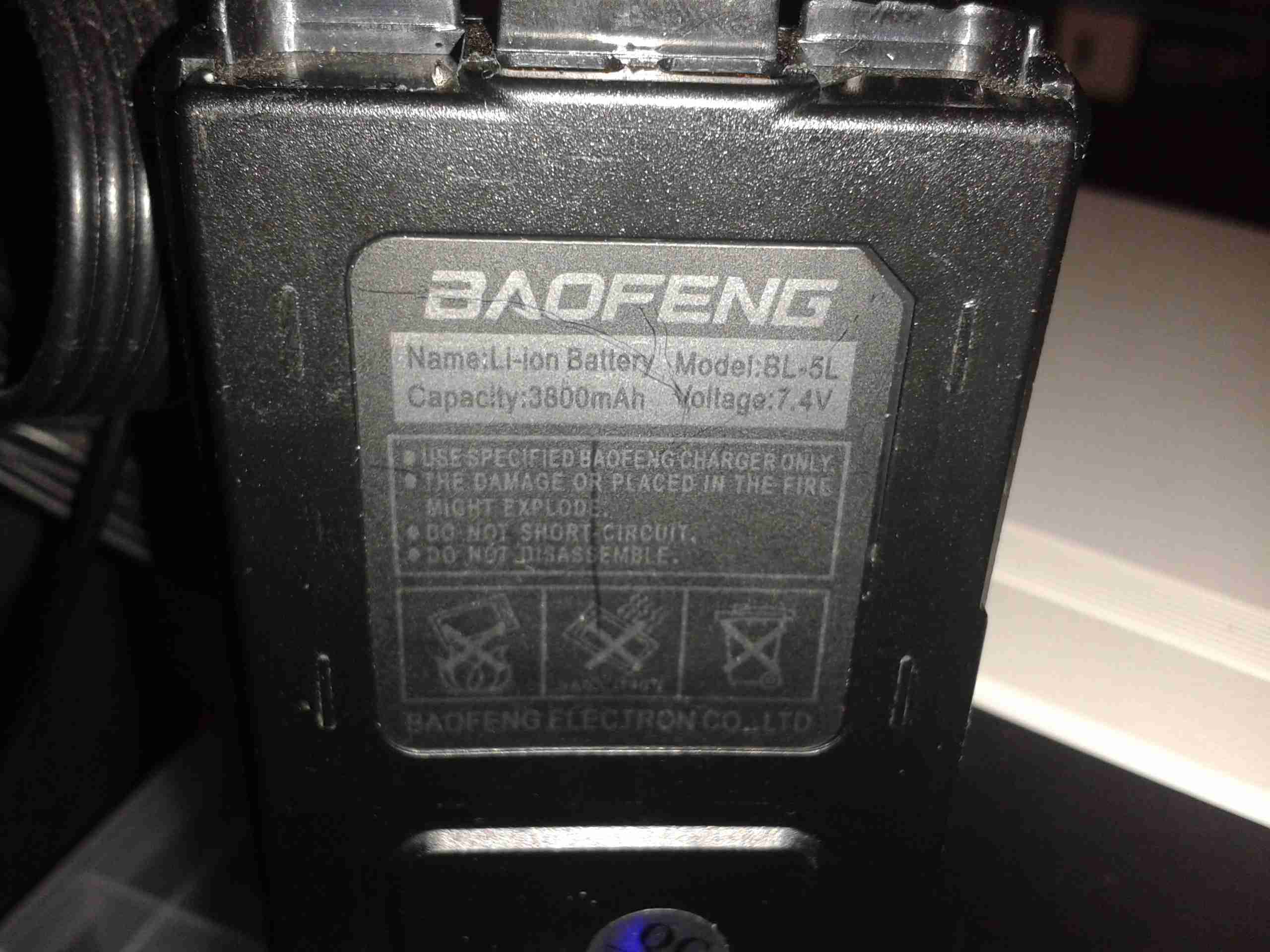
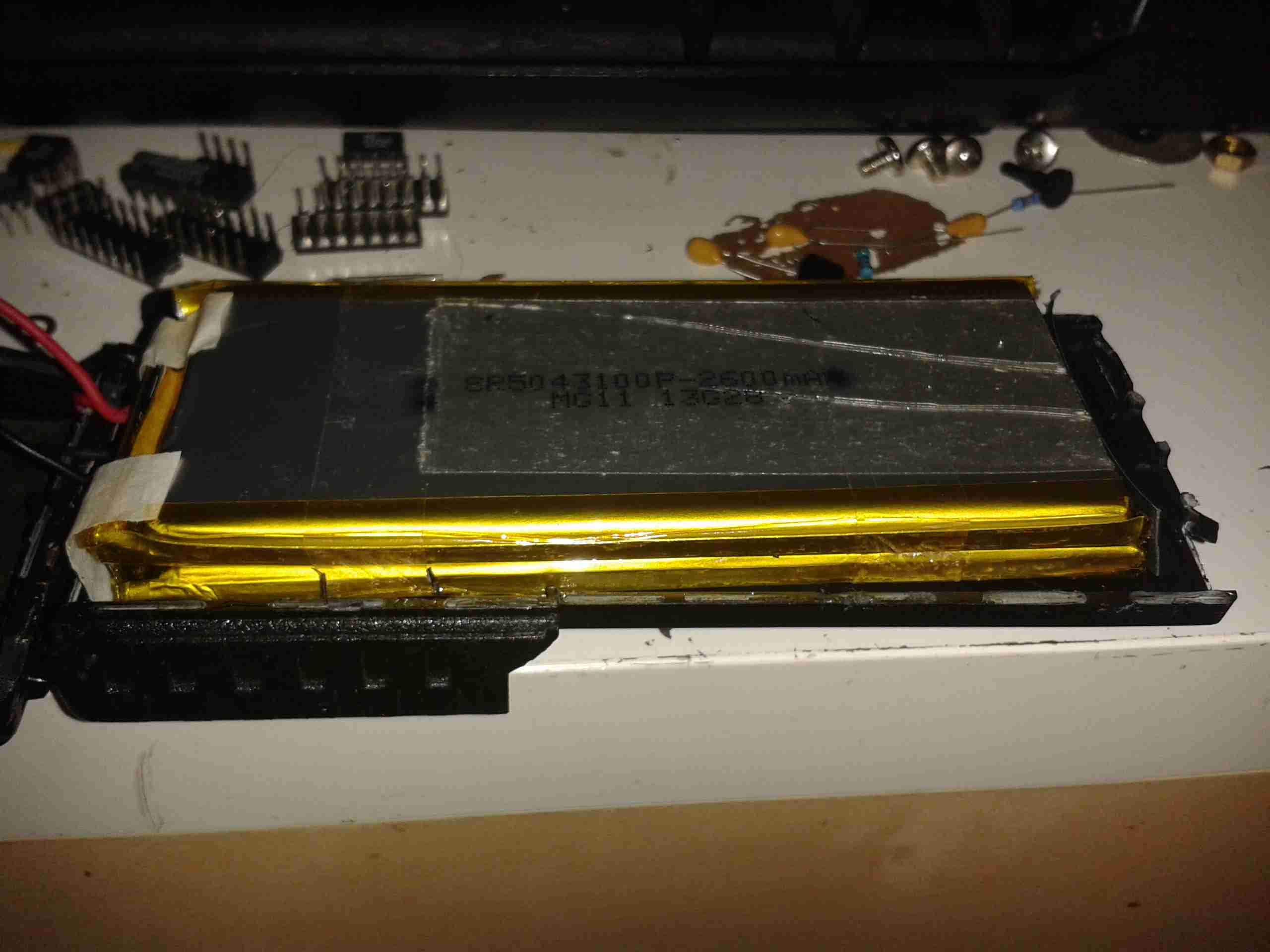
I’ve had a couple of larger batteries for my UV-5Rs for some time now, and decided to do a quick teardown to see if they’re actually the capacity claimed.
BL-5L Battery
Here’s the label, claiming 3800mAh (3.8Ah) of battery capacity.
These batteries are held together with glue, but a good way to get these kinds of things open is by whacking the seams with the handle of a screwdriver. This cracks the glue without damaging the casing.
Battery Cracked Open
After a few minutes of cracking the seams, the battery comes right open. The pair of wires link the protection board on the cells to the DC terminals on the top of the pack. The charging terminals are under the cardboard insulator on the right.
Cells
Here’s the other half of the case, with the cells themselves. These are wired in series for a 7.2v pack, and at a capacity of 2600mAh (2.6Ah) printed on them, the label clearly lies about the capacity.
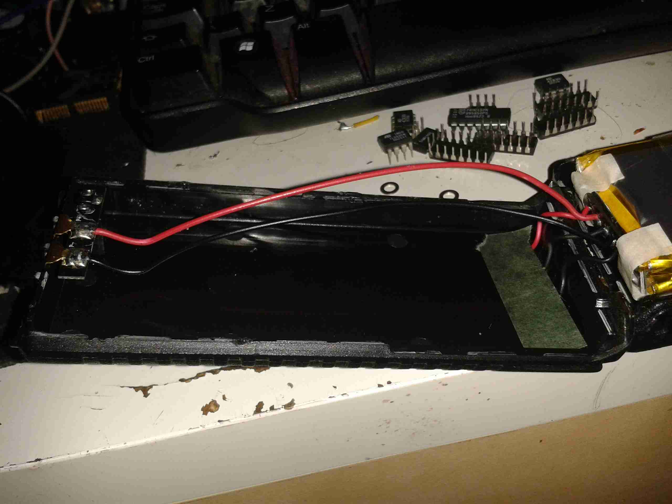
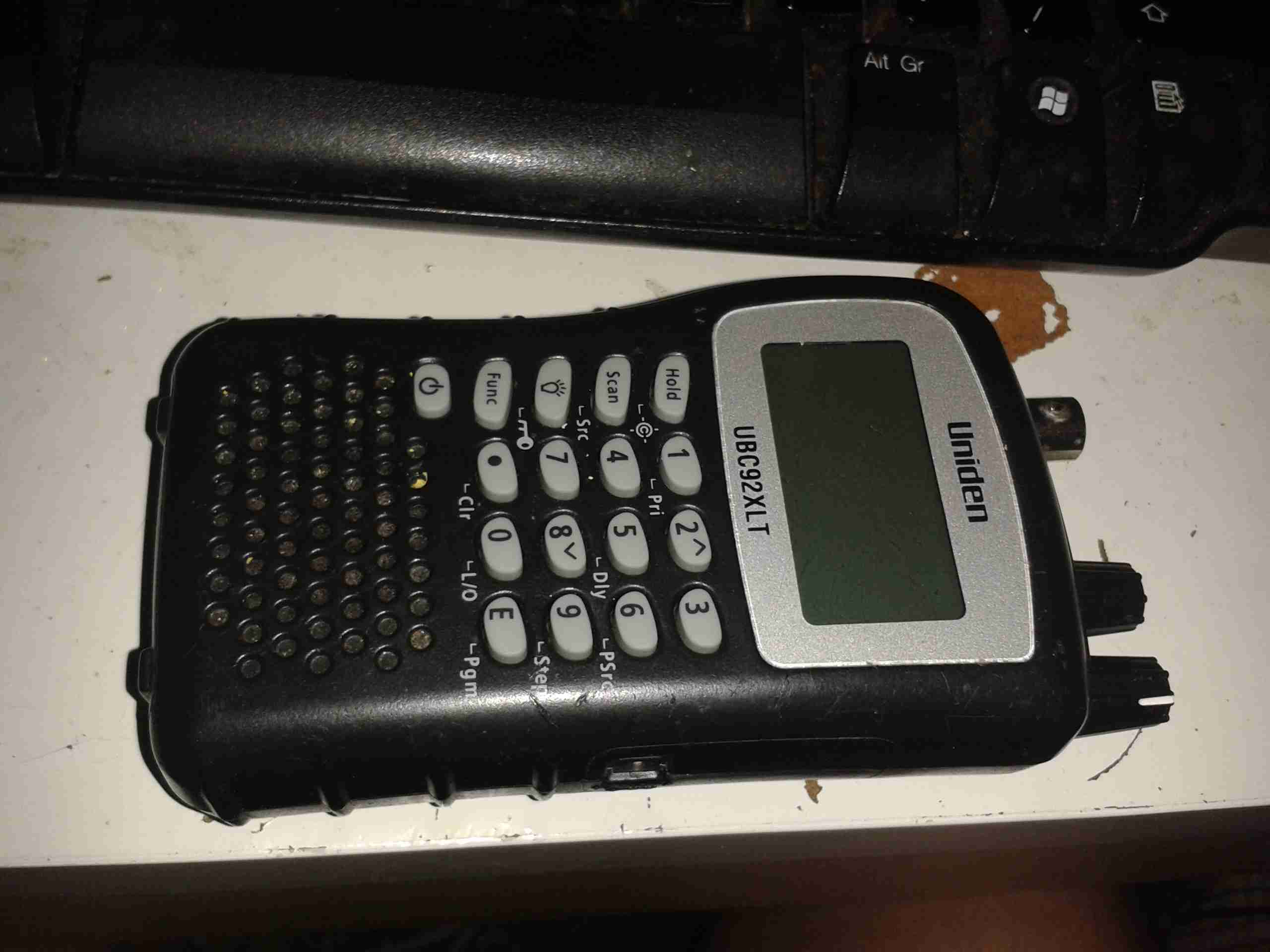
One bit of my equipment that I’ve never looked into is my scanner, a handheld Uniden unit. I got this when Maplin Electronics had them on special offer a few years ago.
Uniden Scanner
Here’s the scanner itself, roughly the same size as a usual HT.
Back Cover Removed
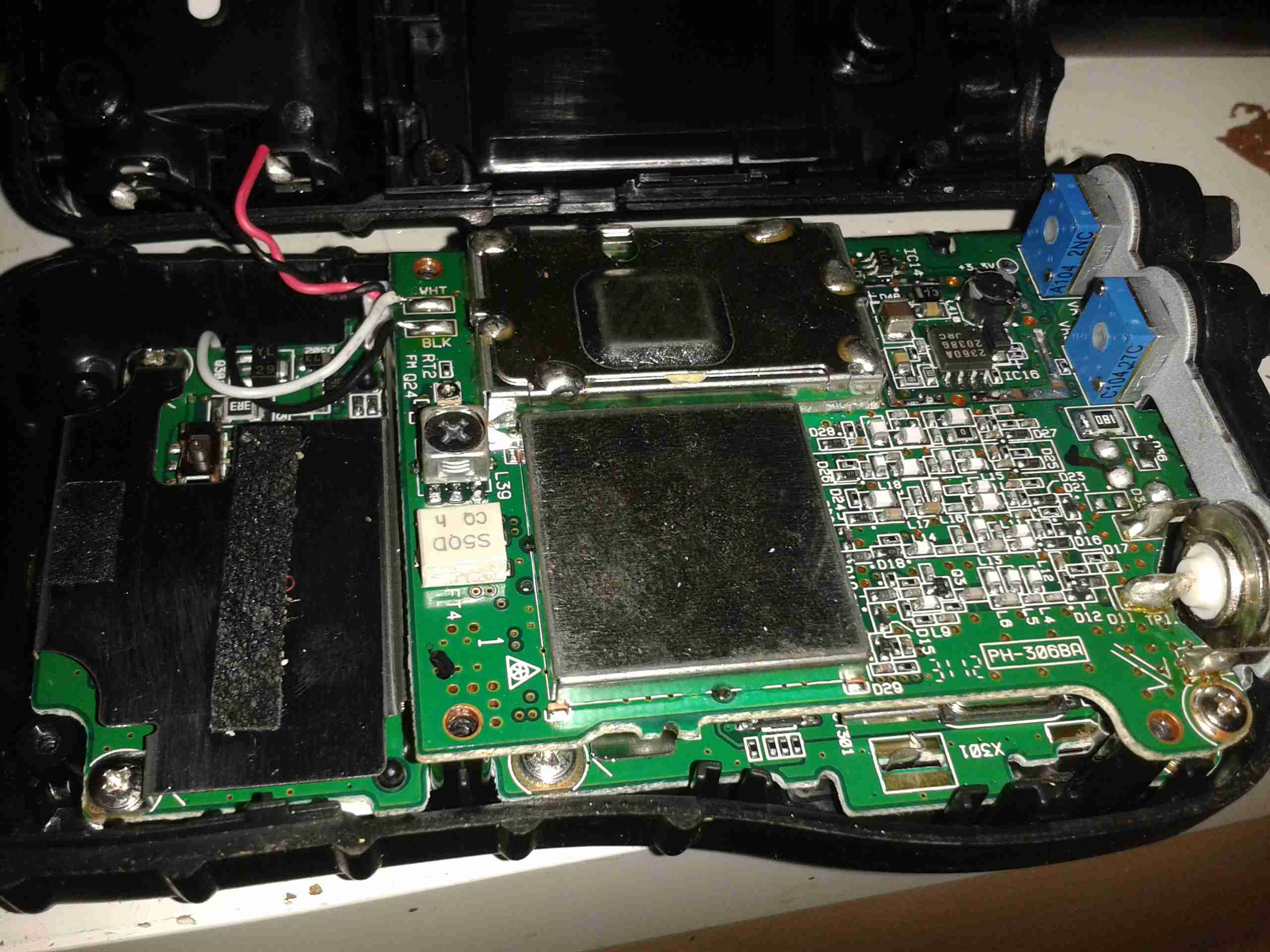
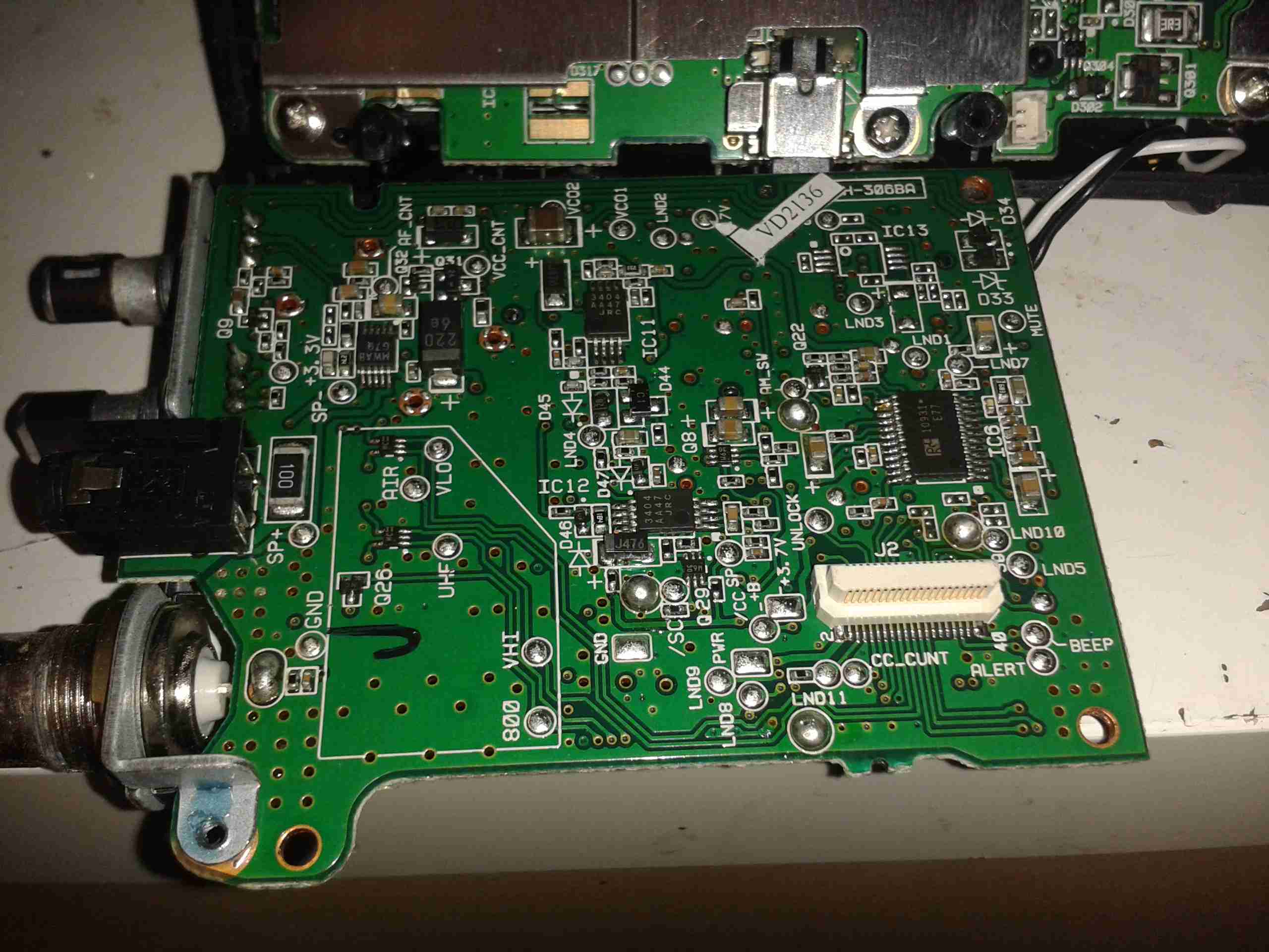
Here the back cover has been removed, and the main RF board is visible at the top of the stack. Unfortunately the shielding cans are soldered on this unit, so no looking under there 🙁
On the right hand side of the board next to the antenna input is the main RF filter network, and it’s associated switching. The RF front end is under the shield closest to the front edge.
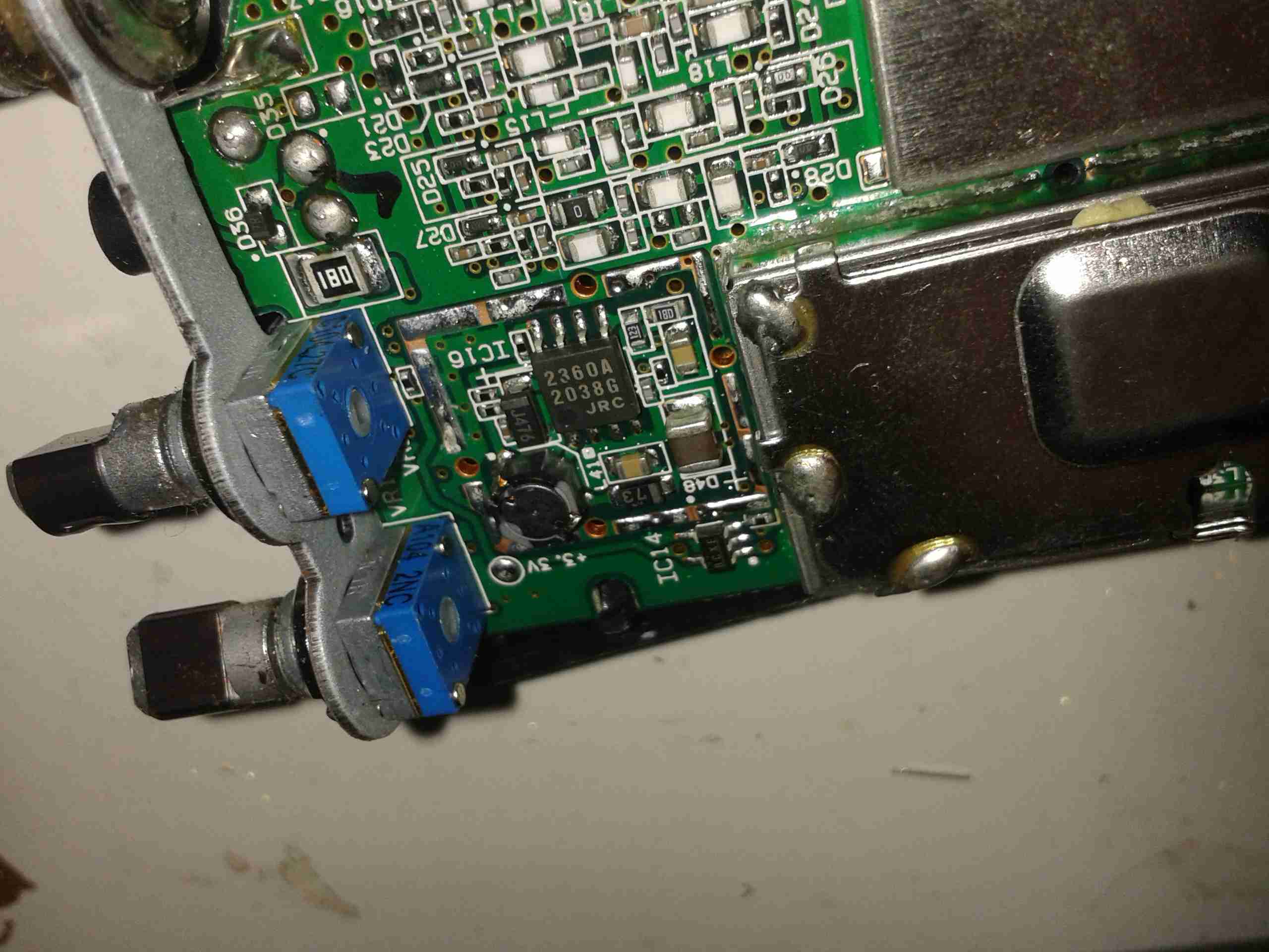
Controls & 3.3v Regulator
On the other side of the PCB is the Volume & Squelch potentiometers, along with a dedicated 3.3v switching supply. An NJM2360A High Precision DC/DC converter IC controls this one. A 3.3v test point is visible next to the regulator.
RF Board Reverse
Here’s the backside of the RF board, some more interesting parts here. There’s a pair of NJM3404A Single Supply Dual Op-Amp ICs, and a TK10931V Dual AM/FM IF Discriminator IC. This is the one that does all the back-end radio functionality. The audio amplifier for the internal speaker & external headphone jack is also on this PCB, top left. A board-to-board interconnect links this radio board with the main control board underneath.
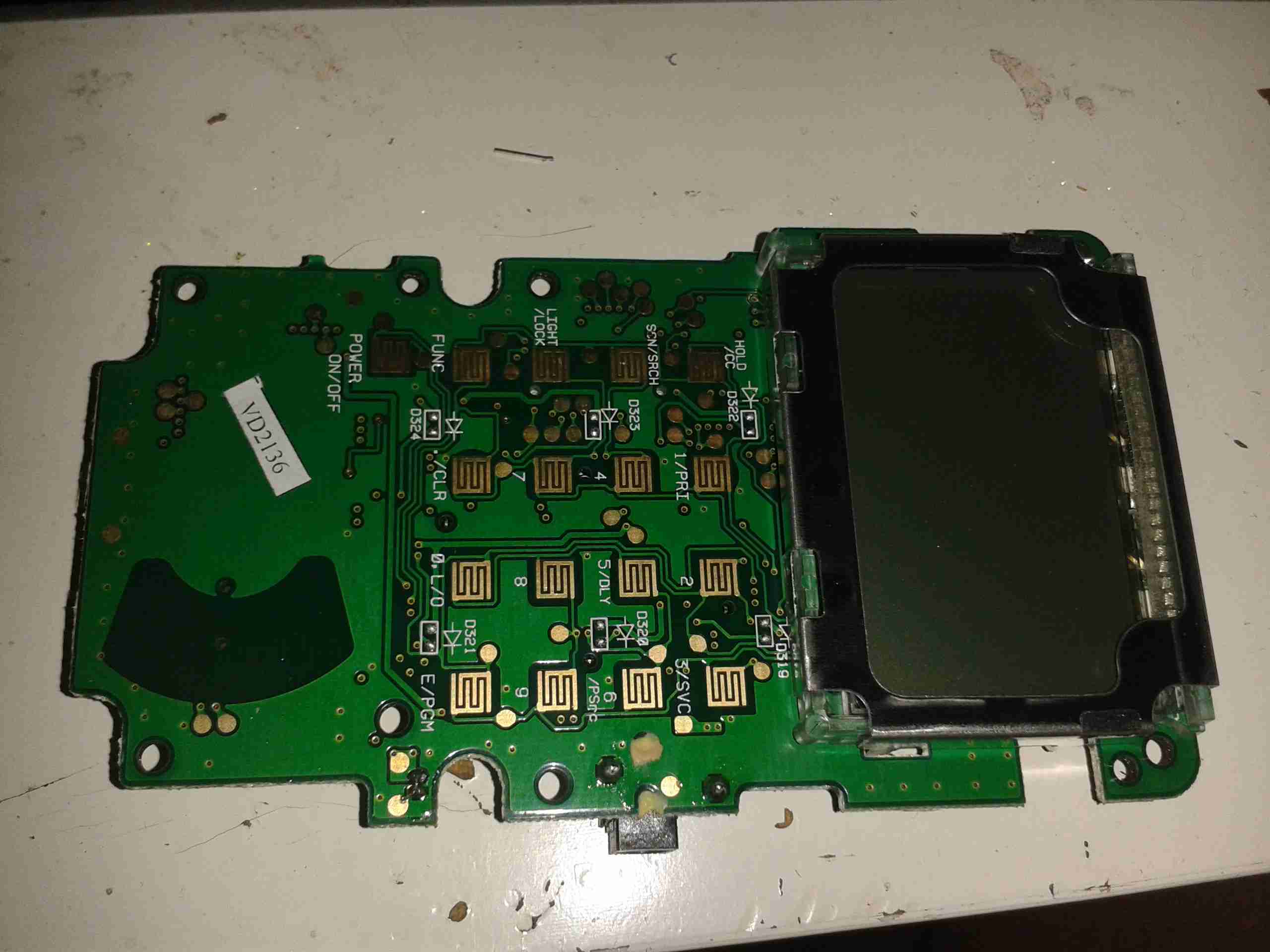
Control PCB Front
Here’s the front of the control PCB, nothing much to see here, just the LCD & membrane keypad contacts.
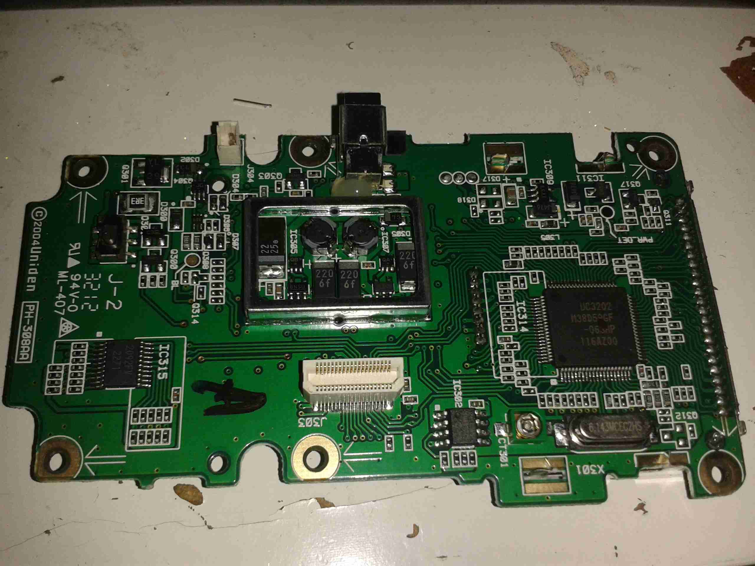
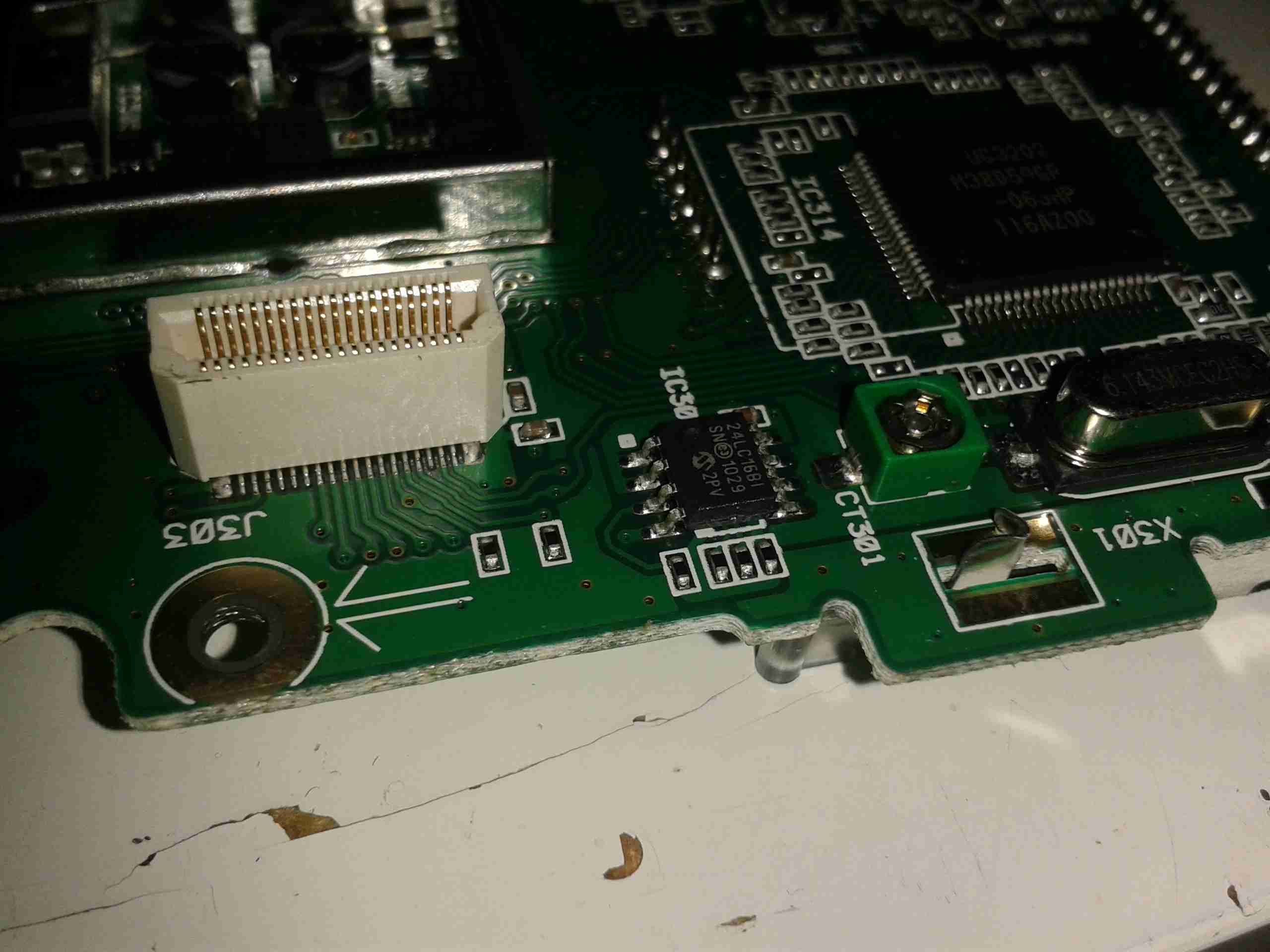
Control PCB Reverse
And here’s the reverse side of the control board. All the interesting bits are here. The main microcontroller is on the right, a Renesas M38D59GF, a fairly powerful MCU, with onboard LCD drive, A/D converter, serial interface, 60K of ROM & 2K of RAM. It’s 6.143MHz clock crystal is just below it.
The mating connector for the RF board is in the centre here.
There is also a Microchip 24LC168 16KB I²C EEPROM next to the main microcontroller. This is probably for storing user settings, frequencies, etc.
EEPROM
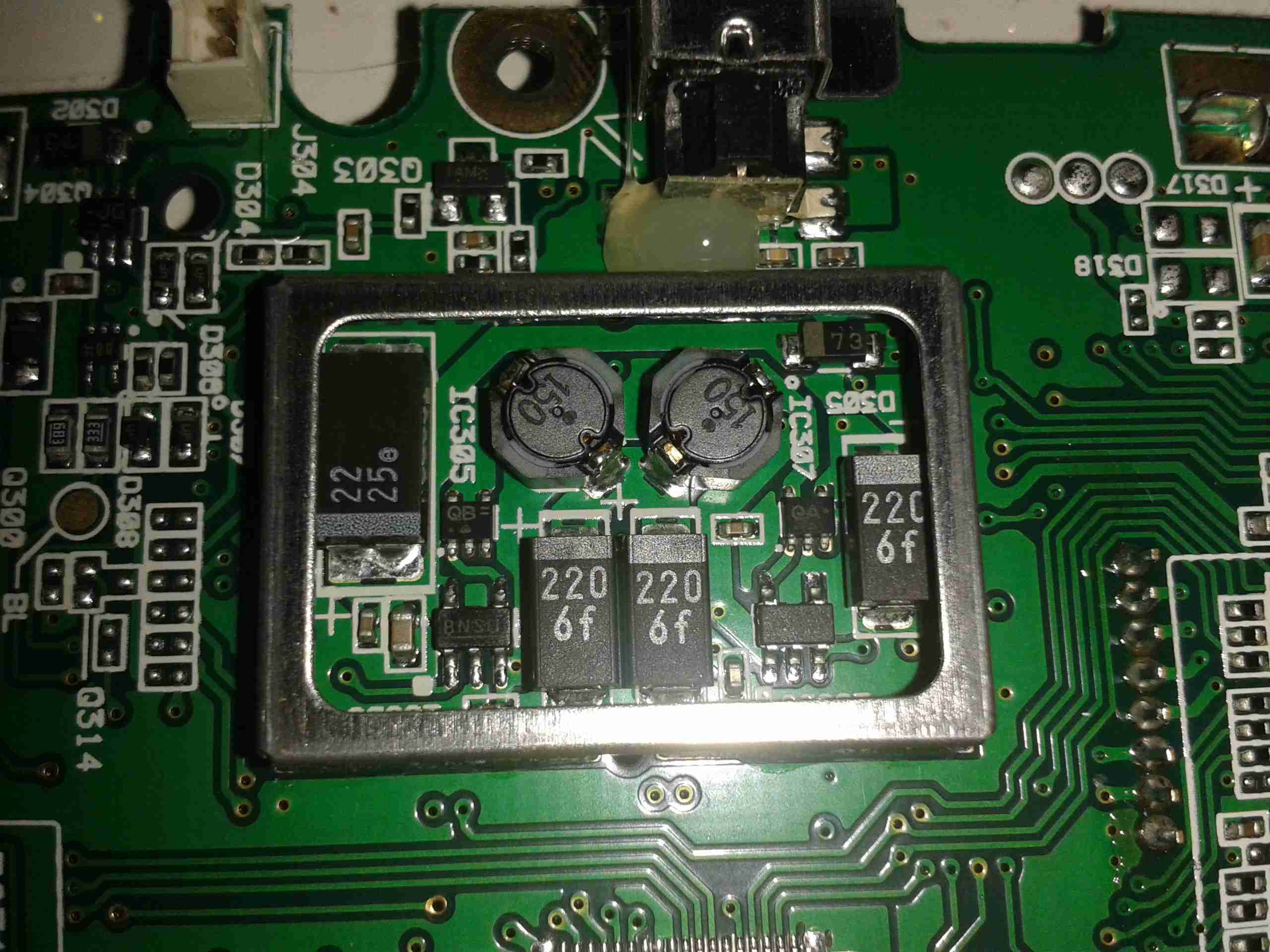
The rest of this board is dedicated to battery charging and power supply, in the centre is a dual switching controller, I can’t figure out the numbers on the tiny SOT23 components in here, but this is dealing with the DC 6v input & to the left of that is the circuitry for charging the NiMH cells included with the scanner.
PSU
The last bit of this PCB is a BU2092FV Serial In / Parallel Out 4 channel driver. Not sure what this one is doing, it might be doing some signal multiplexing for the RF board interface. Unfortunately the tracks from this IC are routed on the inner layers of the board so they can’t be traced out.
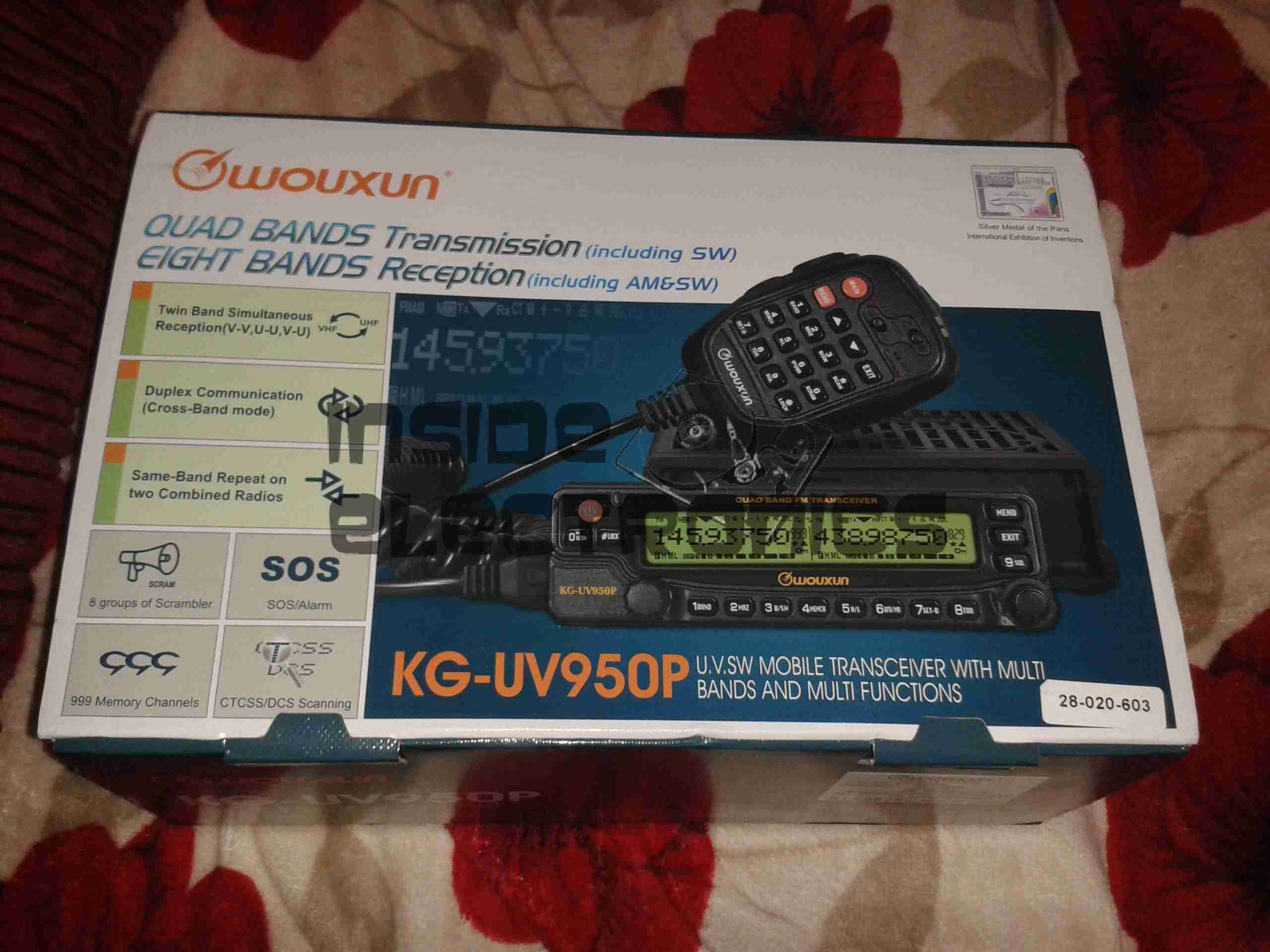
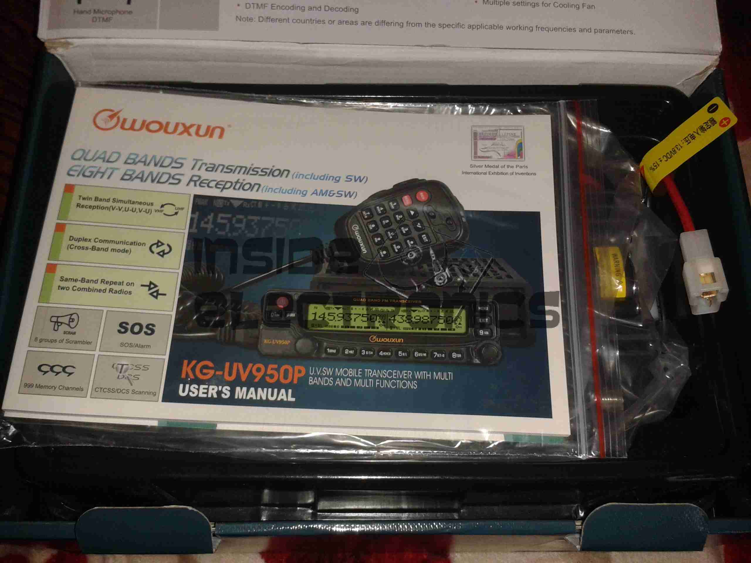
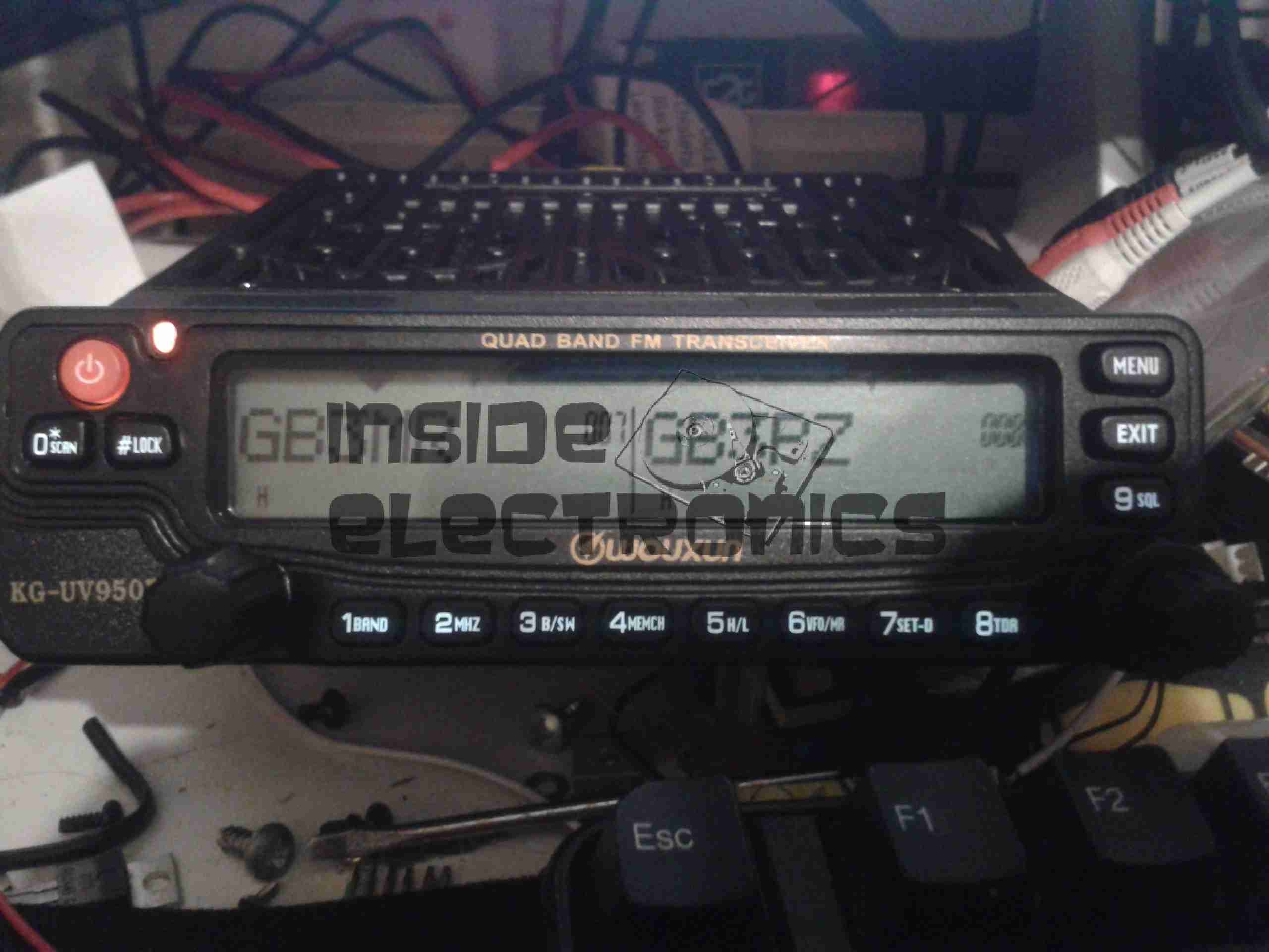
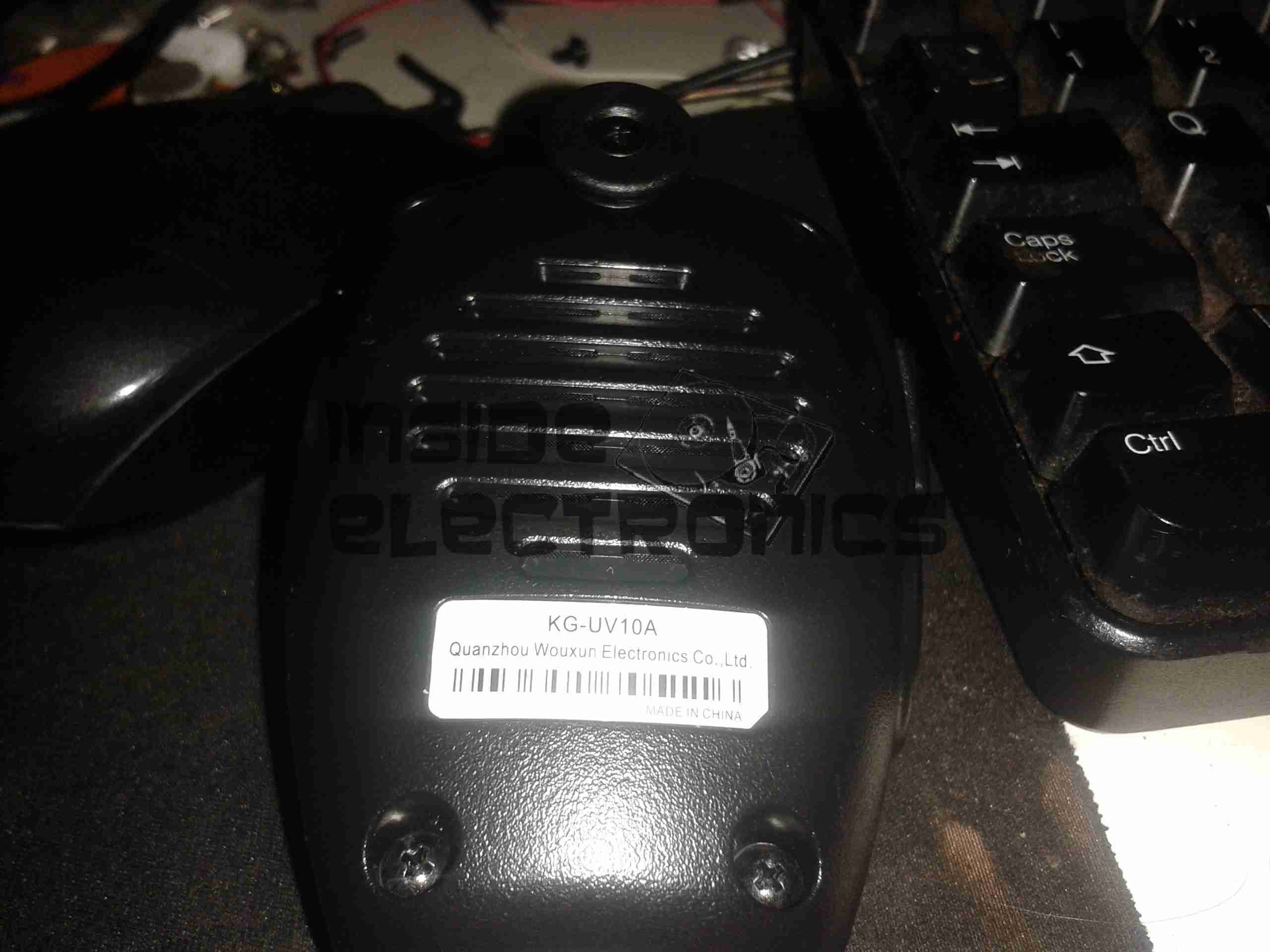
After running on handies for all of my Ameteur Radio life, I figured it was time for a new radio, this time a base station/mobile rig, & after some looking around I decided on the Wouxun KG-UV950P.
Shown below is the radio as delivered:
Wouxun Boxed
This radio has the capability to transmit quad-band, on 6m, 10m, 2m & 70cm. It also has the capability to receive on no fewer than eight bands. Also included in the feature set is airband receive, & broadcast FM receive.
TX power is up to 50W on 2m, 40W on 70cm, & 10W on 6m/10m.
Opened
For once with a Chinese piece of electronic equipment, the manual is very well printed, and in very good English.
Radio Operating
Here is the radio in operation, connected to my 65A 12v power supply. I have the radio set here monitoring a couple of the local 70cm repeaters.
The display is nice & large – easy to see at a glance which station you’re tuned to. The backlight is also software settable to different colours.
Status indicators on the top edge of the display can be a bit difficult to see unless the panel is directly facing the user though, not to mention that they are rather small.
This radio is true dual-watch, in that both VFOs can be receiving at the same time, this is effected by a pair of speakers on the top panel:
Speakers
The left VFO speaker is smaller than the right, so the sound levels differ slightly, but overall sound quality is excellent. There is also provision on the back of the unit to connect external speakers.
The dual volume controls on the right hand bottom corner of the control panel are fairly decent, if a little twitchy at times. There is also a fair amount of distortion on the audio at the higher volume levels.
The controls themselves are potentiometers, but the controller appears to read the setpoint with an ADC – this means that if the control is set to just the right point, the selected level will jump around on the display & never settle down.
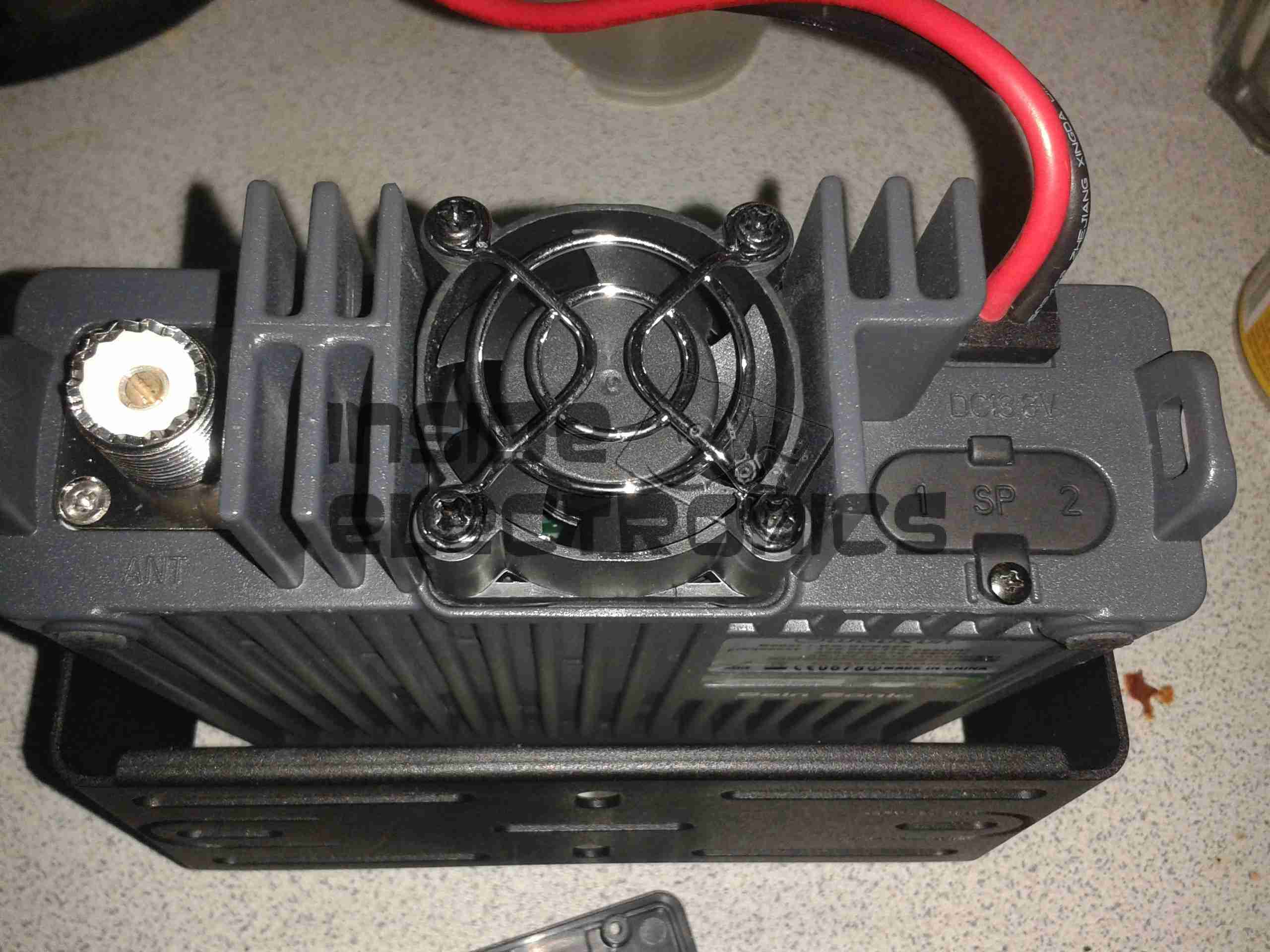
The radio itself is built from a solid aluminium casting, mostly for heatsinking of the main RF output stage MOSFETs. This gives the radio a very rugged construction.
A small fan is provided on the rear for cooling when required. This can be set in software to either be constantly running, (it’s pretty much silent, so this is advantageous), or only run when in TX mode. The fan will also automatically come on when a high internal temperature is detected.
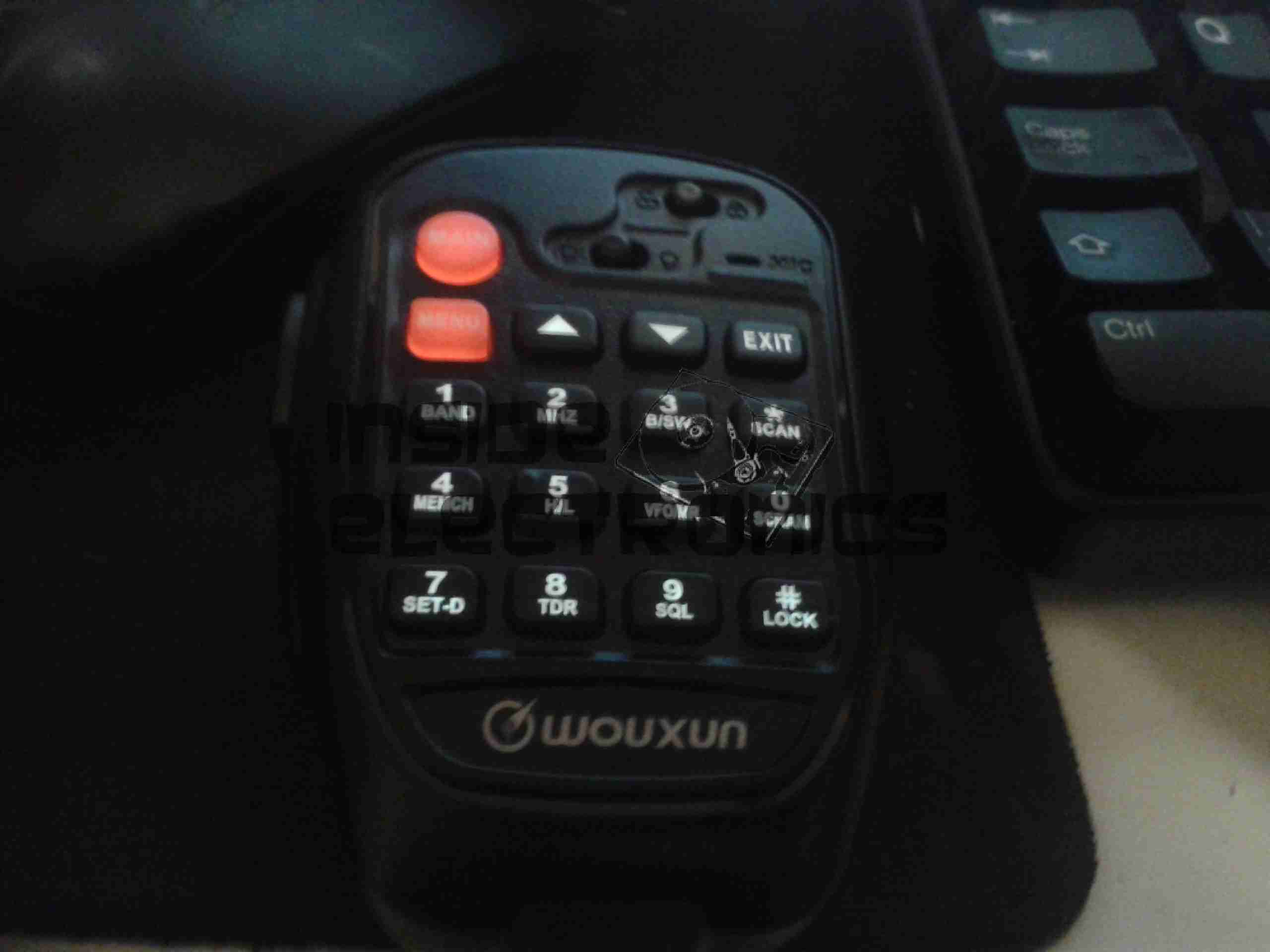
Hand Mic
Here is the microphone. Like the main unit of the radio this is also very solidly built, fits nicely in the hand & the PTT has a nice easy action, which helps to prevent straining hands while keeping the TX keyed.
Conveniently, all of the controls required to operate the radio are duplicated on this mic, along with a control lock switch, & backlighting for the buttons.
Another Speaker
Another output speaker is placed in the back of the mic. This one can be activated through the menu system, to either use the main body speakers, the mic mounted one, or both.
A mounting hook for the mic is provided to attach to any convenient surface.
Radio Back
Here’s the back of the radio, with some of the big heatsink fins, the fan in the centre. To the left is the PL259 RF output, this looks to be a high quality Teflon insulated one. On the right are the power input leads & the external speaker outputs.
External Speaker Sockets
The external speaker connections are via 3.5mm jacks. I haven’t yet tested this feature.
Remote Mounting Plate
The control panel of this radio is detachable from the main body, and a pair of adaptors are provided. This either allows the radio display to be angled upwards toward the user, set parallel, or even mounted remotely. A control extension cable is provided to allow the main body to be mounted a fair distance away.
External Interface Connectors
On the left of the radio is the PC control & programming port, & the mic connector. Wouxun *really* like RJ-45 connectors, they’ve used them for everything on this radio.
Also visible here is the tilted faceplate adaptor.
The supplied software to program the radio, while functional, is absolutely horrific. Hopefully someone will add support for this radio into CHIRP. Anything would be an improvement in this area.
Everything considered, I like this radio. It’s very solidly built, easy to use, and sounds brilliant.
TX audio is great, (or so my other contacts tell me).
Unsurprisingly, the unit gets warm while transmitting, however on high power, it does get uncomfortably warm, and the built in fan does little in the way of helping when a long QSO is in progress. I may remedy this at some stage with a more powerful fan. A little more airflow would do wonders.
If the programming software was built as well as the radio, I’d have zero serious complaints.
At full power, the radio pulls ~10A from the power supply, at 12.9v DC.
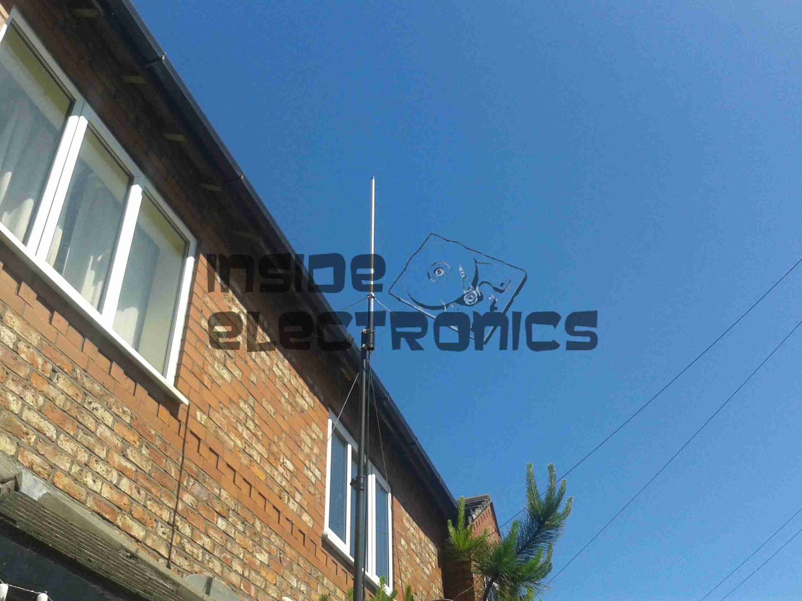
As for the antenna I’m currently using, it’s a Diamond X30, mounted on a modified PA speaker stand, at ~30 feet above ground. The feeder is high quality RG-213.
TX Antenna
When I manage to get the set disconnected, a partial teardown will be posted, with some intimate details about the internals. Stay tuned!
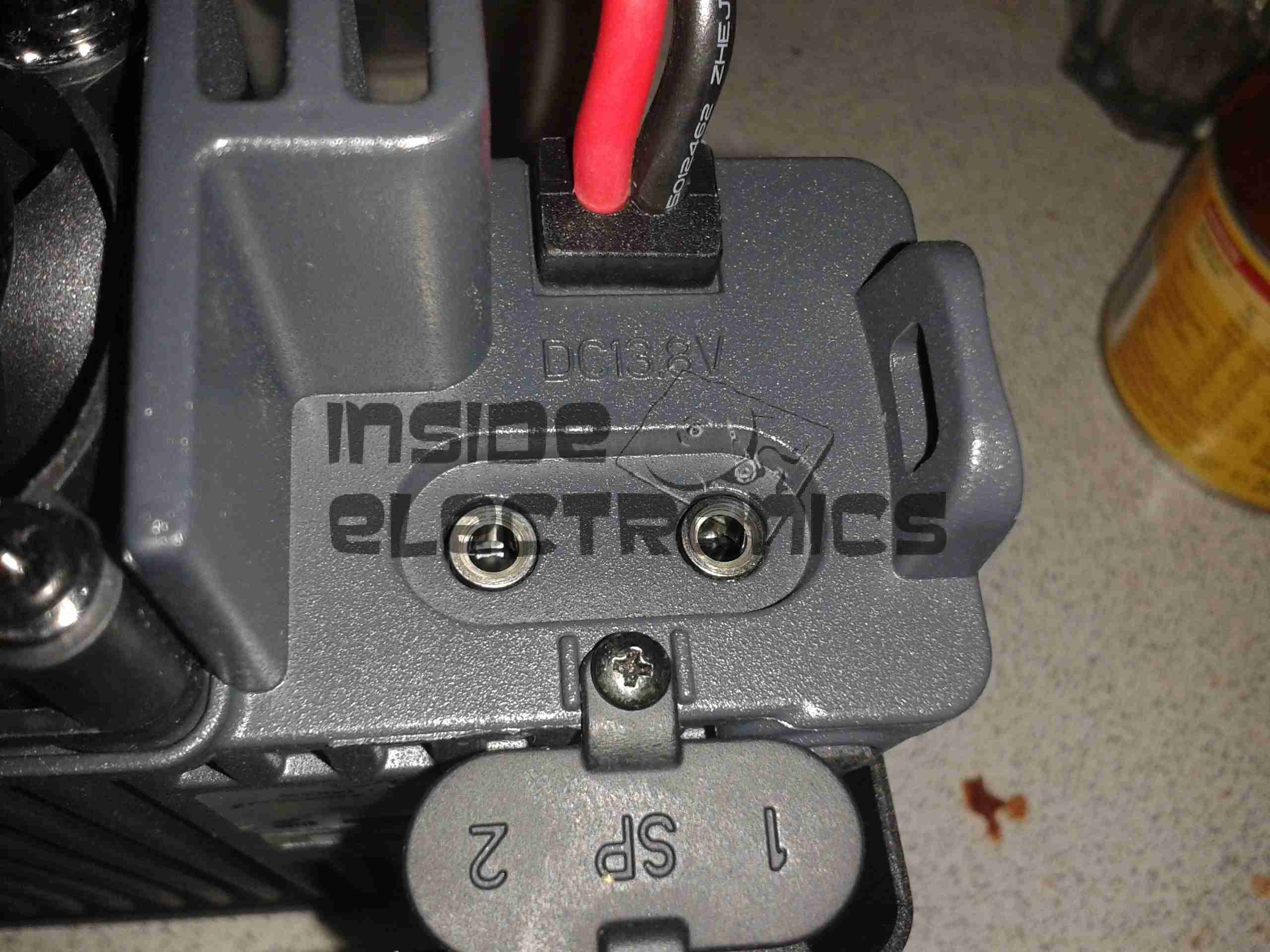
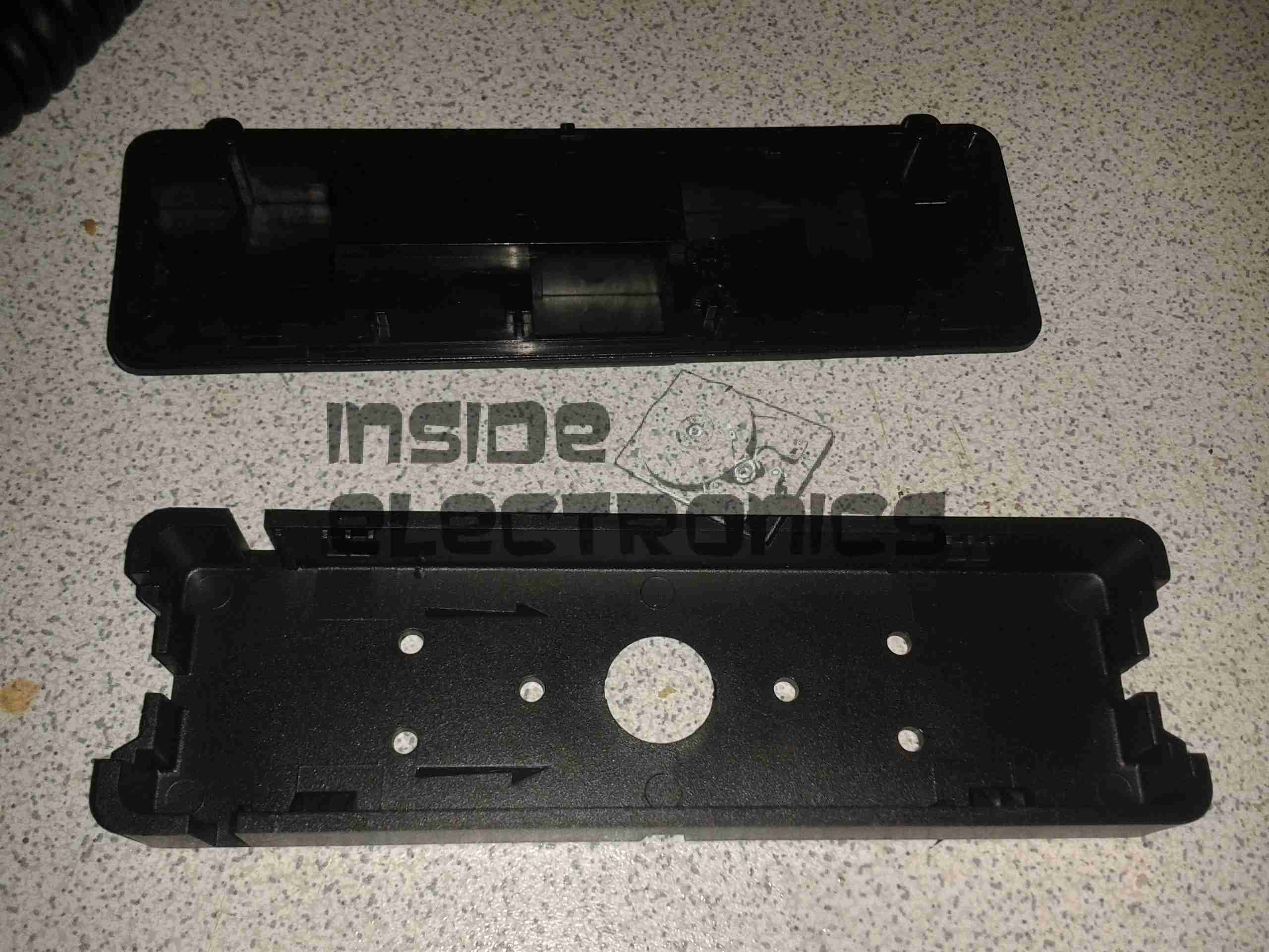
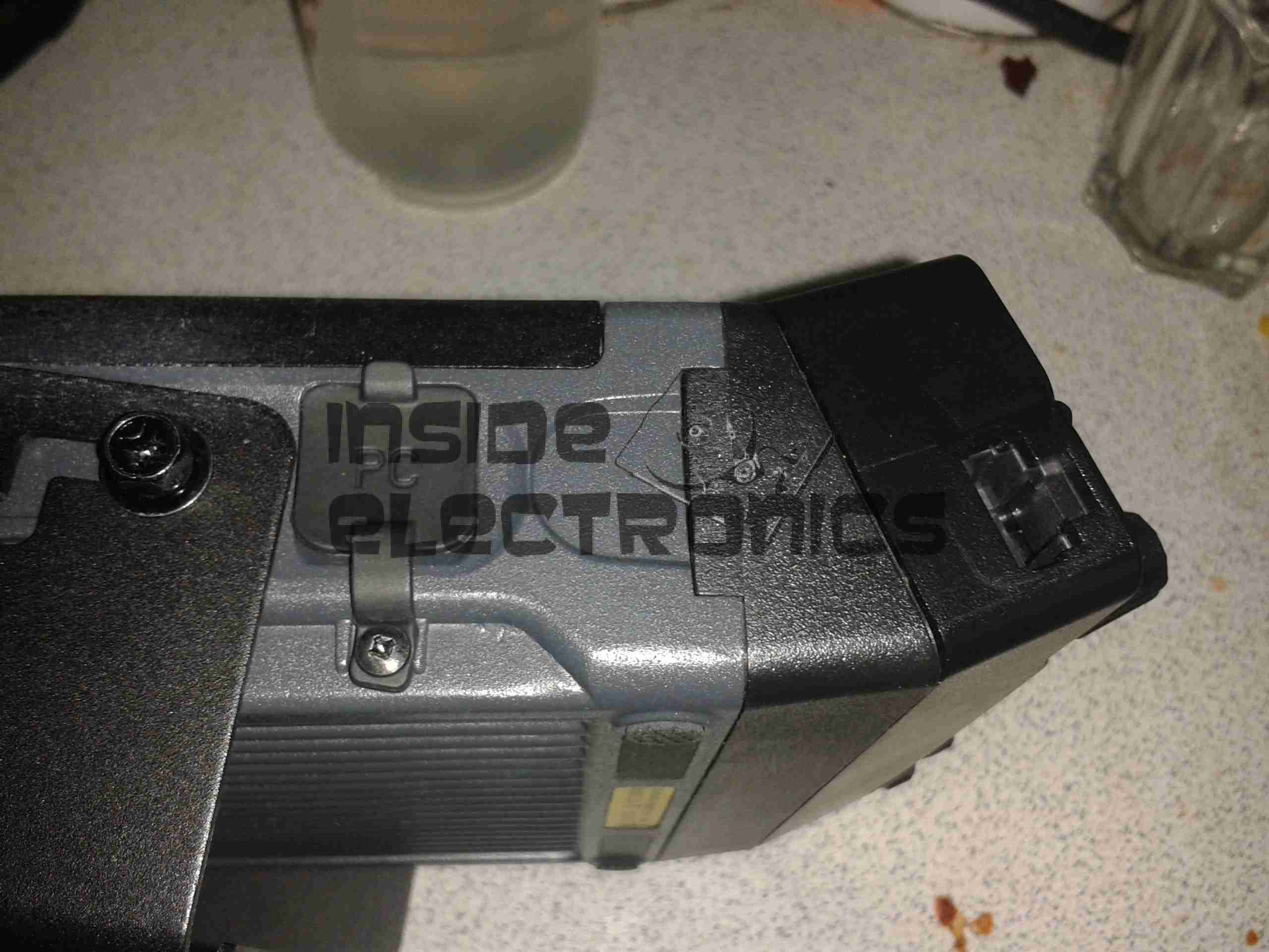
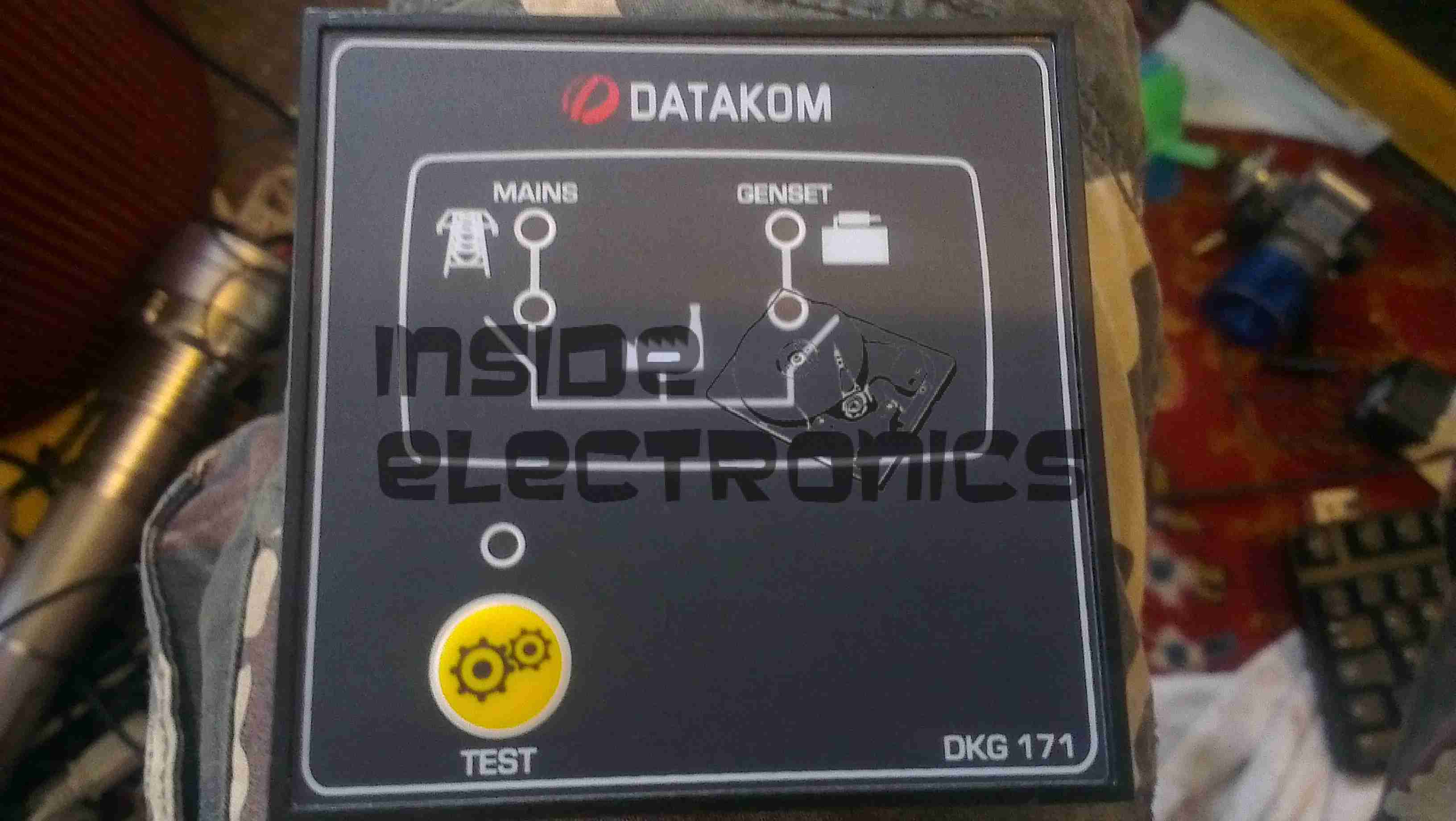
Here is a teardown of the Datakom DKG-171 generator transfer controller. Here is the front of the unit, with the pictogram of the system, the indicator LEDs & the generator test button.
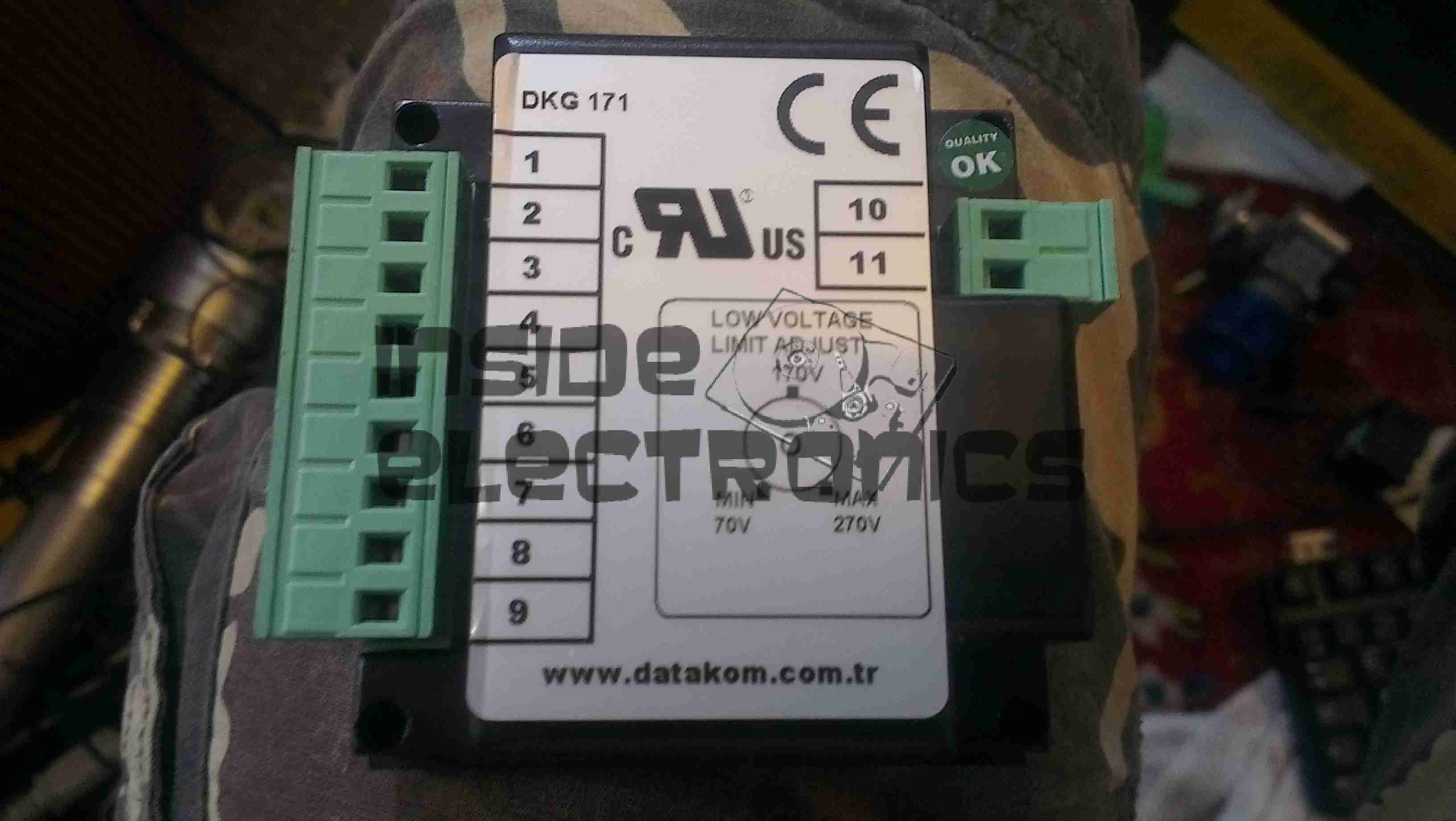
Rear
The rear of the unit features the connection points for the mains, generator & generator control I/O.
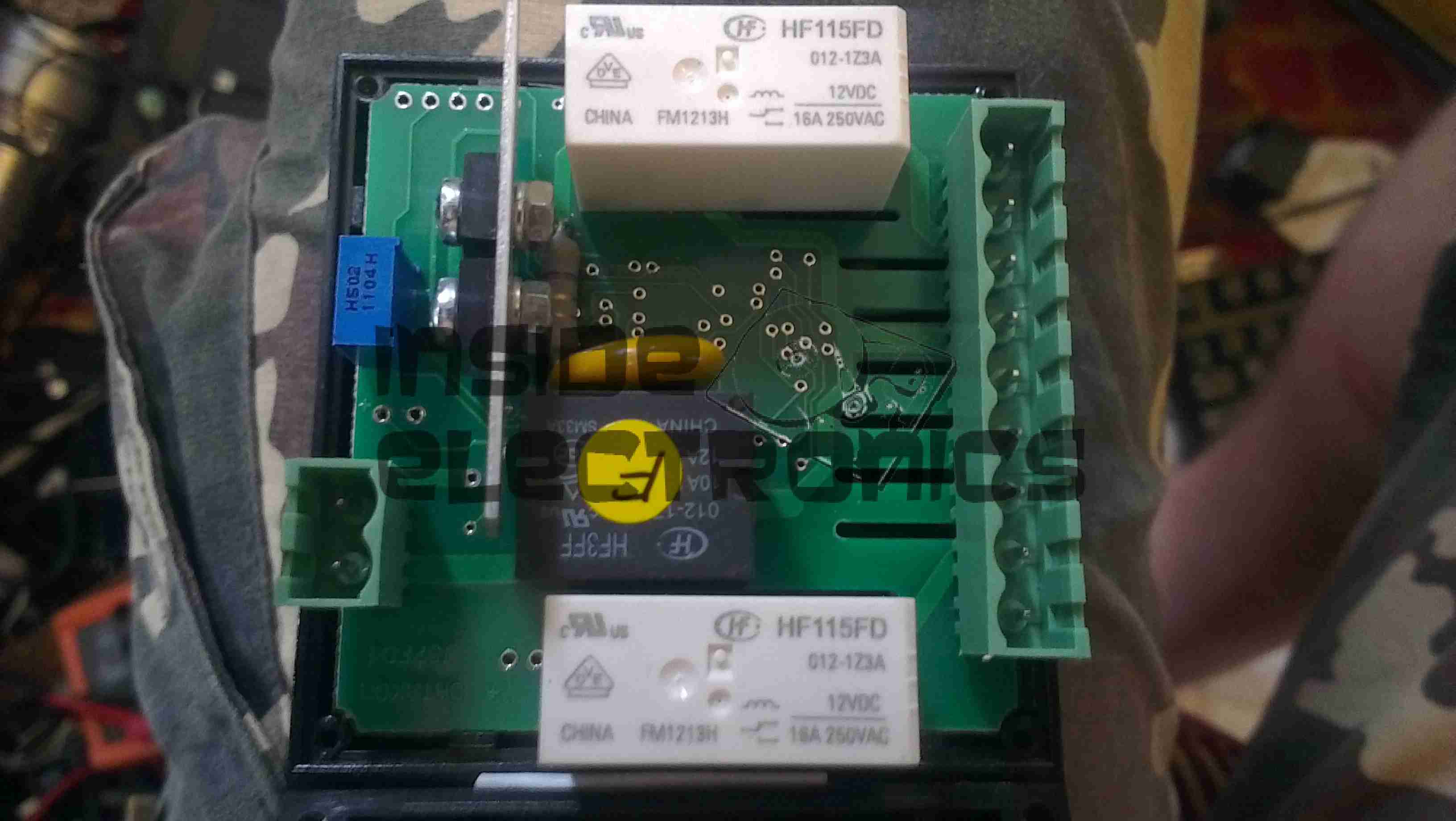
PCB Rear
Rear of the PCB with the control relays. The two larger relays switch in the remote contactors to switch the mains supply over between the grid & the generator, while the smaller relay switches 12v power out to a terminal to automatically start the generator.
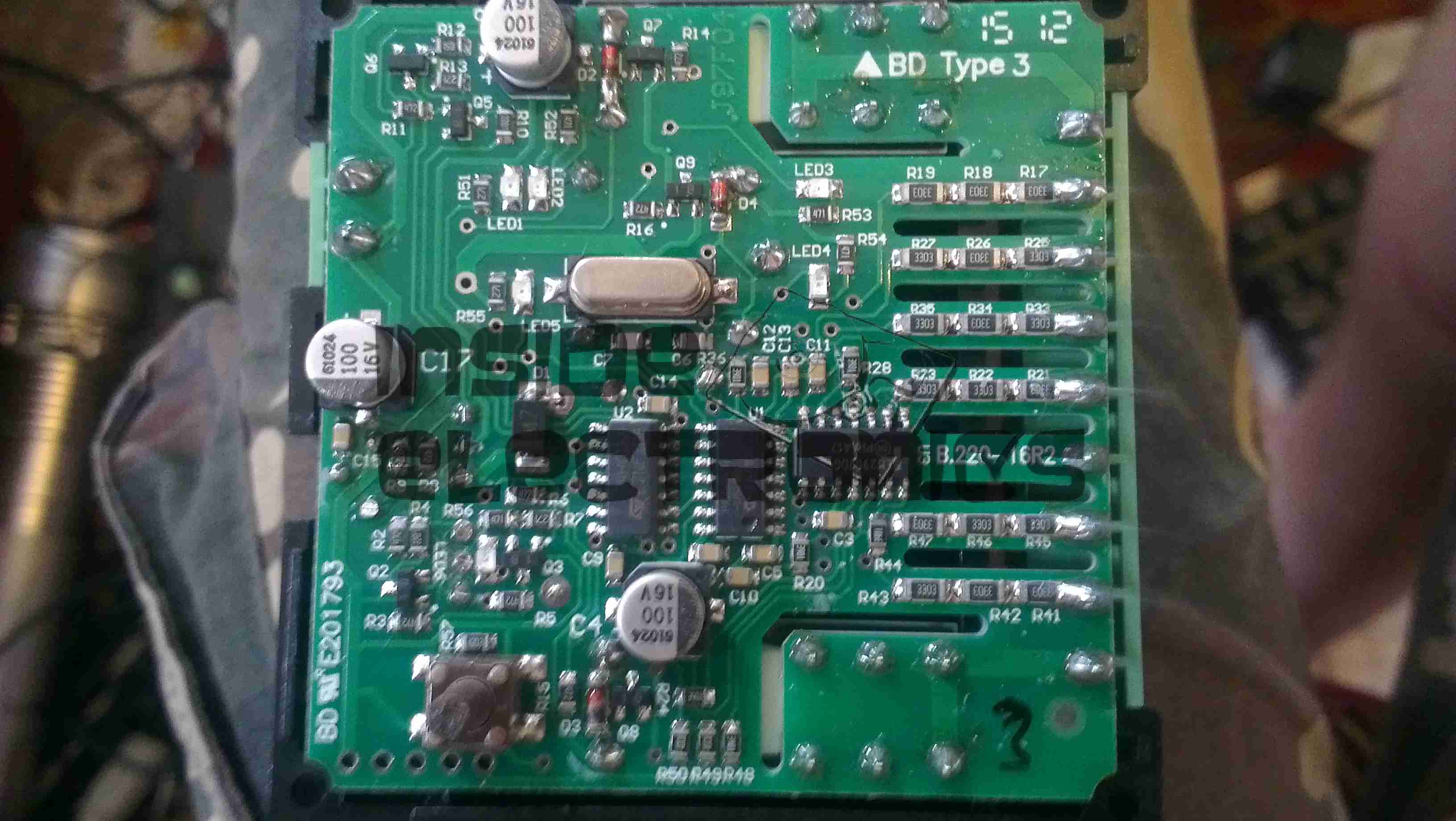
PCB Front
Front of the PCB with the control logic & main PIC microcontroller.
Here’s the teardown of the projector itself! On the right is the info label from the projector, which covers the flex ribbon to the VGA/composite input board below.
This unit is held together with Allen screws, but is easy to get apart.
PicoP Display Engine
Here’s the insides of the projector, with just the top cover removed. The main board can be seen under the shielding can, the Micro HDMI connector is on the left & the MicroUSB connection is on the right. The USB connection is solely for charging the battery & provides no data interface to the unit.
On top of the main board is the shield can covering the PicoP Display Engine driver board, this shield was soldered on so no peek inside unfortunately!
Laser Module
The laser module itself is in the front of the unit, the laser assemblies are closest to the camera, on the left is the Direct Doubled Green module, in the centre is the blue diode, and the red diode on the right. Inside the module itself is an arrangement of mirrors & beamsplitters, used to combine the RGB beams from the lasers into a single beam to create any colour in the spectrum.
Module Innards
Here is the module innards revealed, the laser mounts are at the top of the screen, the green module is still mounted on the base casting.
The three dichroic mirrors in the frame do the beam combining, which is then bounced onto the mirror on the far left of the frame, down below the MEMs. From there a final mirror directs the light onto the MEMs scanning mirror before it leaves through the output window.
A trio of photodiodes caters for beam brightness control & colour control, these are located behind the last dichroic turning mirror in the centre of the picture.
Green Module Cavity
This is inside the green laser module, showing the complexity of the device. This laser module is about the size of a UK 5p coin!
Green Module Labeled
And here on the left is the module components labelled.
Main PCB Top
Here is the main PCB, with the unit’s main ARM CPU on the right, manufactured by ST.
User buttons are along the sides.
Main PCB Bottom
Other side of the main board, with ICs that handle video input from the HDMI connector, battery charging via the USB port & various other management.
As I’m building a portable “media center” with my first Pi, I was looking for a suitable screen. I remembered the existence of these:
ShowWX+ HDMI Pico Projector
A laser pico projector combined with a Pi, in a small enough package would make a fantastic
little portable media player. So £220 was shelled out 🙂
Along with the case for my Pi coming from Mod My Pi, I am aiming for a device as small as possible. At some point I will fit the Pi into the same package as the projector, if it can be cannibalised in such a way 🙂
Check back for an update with running images of the projector, powered from the Pi’s HDMI output.
I will also be doing the standard teardown of the projector when time allows 🙂
Bootnote:
Micro HDMI Connections: These are CRAP. They don’t stand up to any form of day-to-day use, and the projector began displaying a blue screen with “INVALID VIDEO MODE” as soon as anything was plugged into the Micro HDMI port. A quick attack with a jeweller’s screwdriver fixed the port, as it had become loose.
Not strictly teardown related, but here is the Linux version of the RTL8187B WiFi chipset driver for all those who require it, it’s not available on the Realtek website:
If you’ve found my content useful, please consider leaving a donation by clicking the Tip Jar below!
All collected funds go towards new content & the costs of keeping the server online.