Posted on Leave a comment

Huawei E160E USB HSDPA Modem

E160E Modem
Huawei E160E Modem

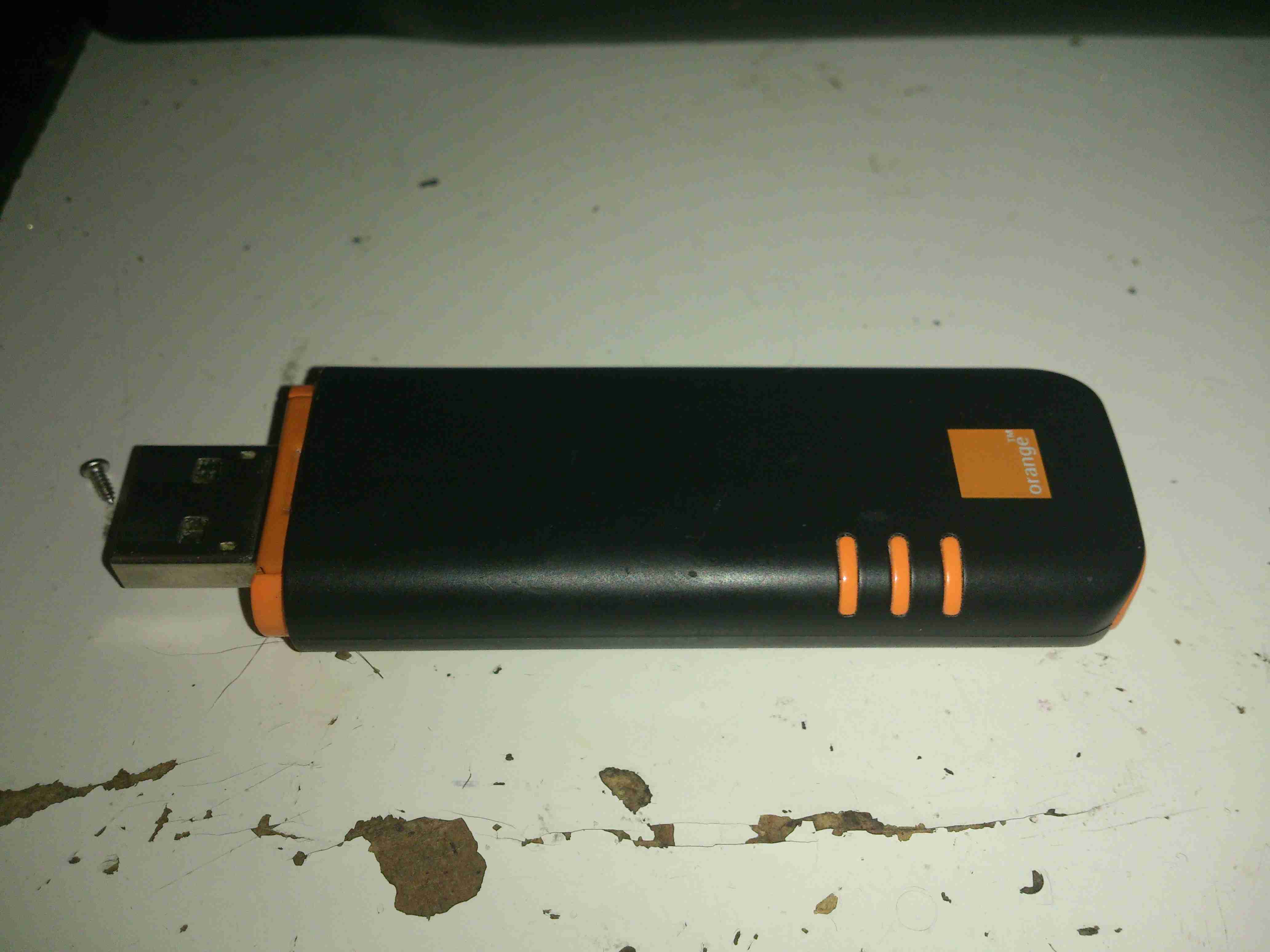
Here’s an old HDSPA 3G USB modem stick that I got with a mobile phone contact many years ago. As it’s now very old tech, and I have a faster modem, not to mention that I’m no longer with Orange (Robbing <expletive>), here’s a teardown of the device!

Cover Removed
Cover Removed

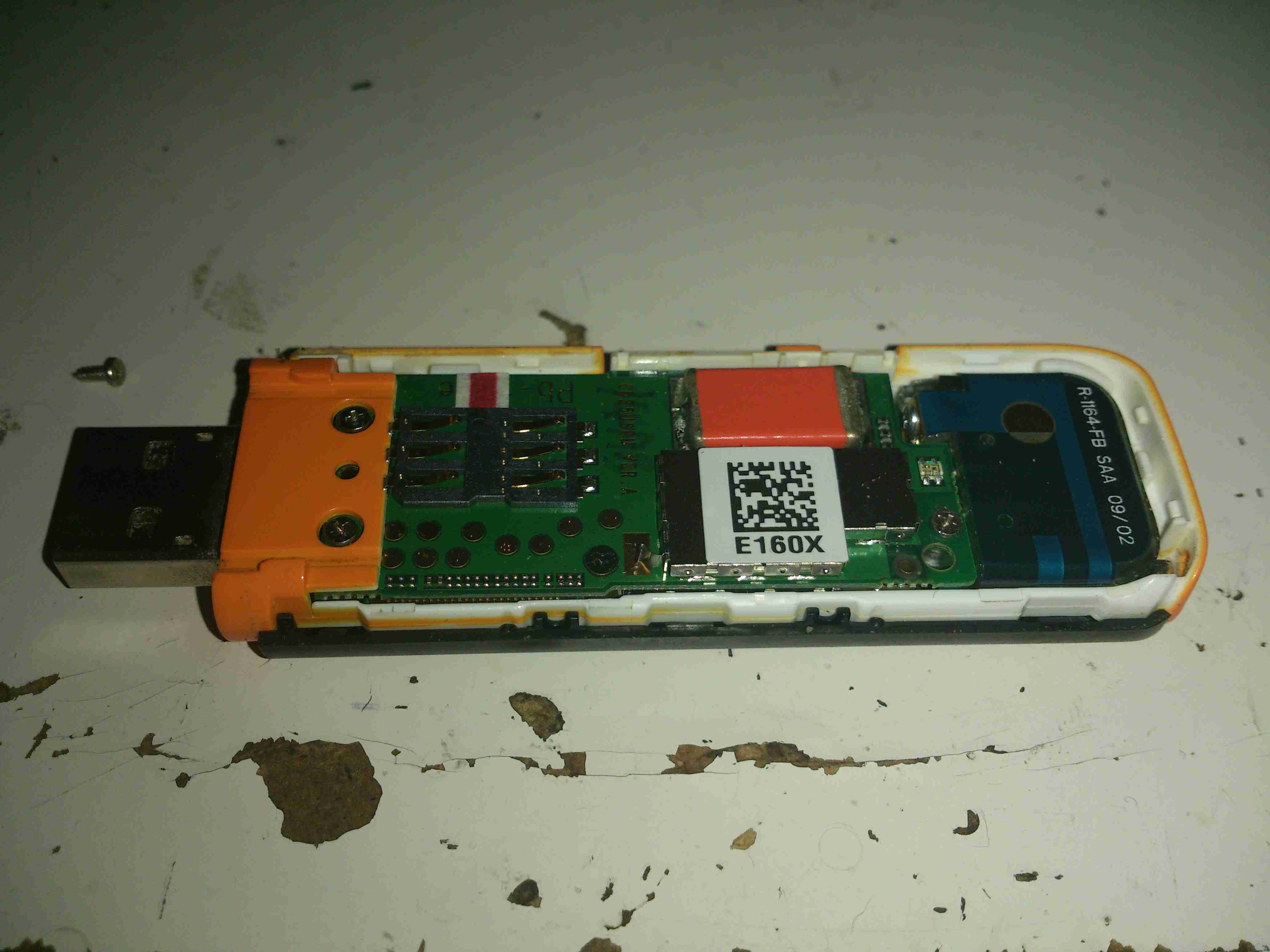
The top shell is just clipped into place, while a pair of very small screws hold down the orange piece at left to hold the PCB stack in the casing. Not much to see here, but it’s clear that there’s a lot crammed into a very small space.

PCB Assembly
PCB Assembly

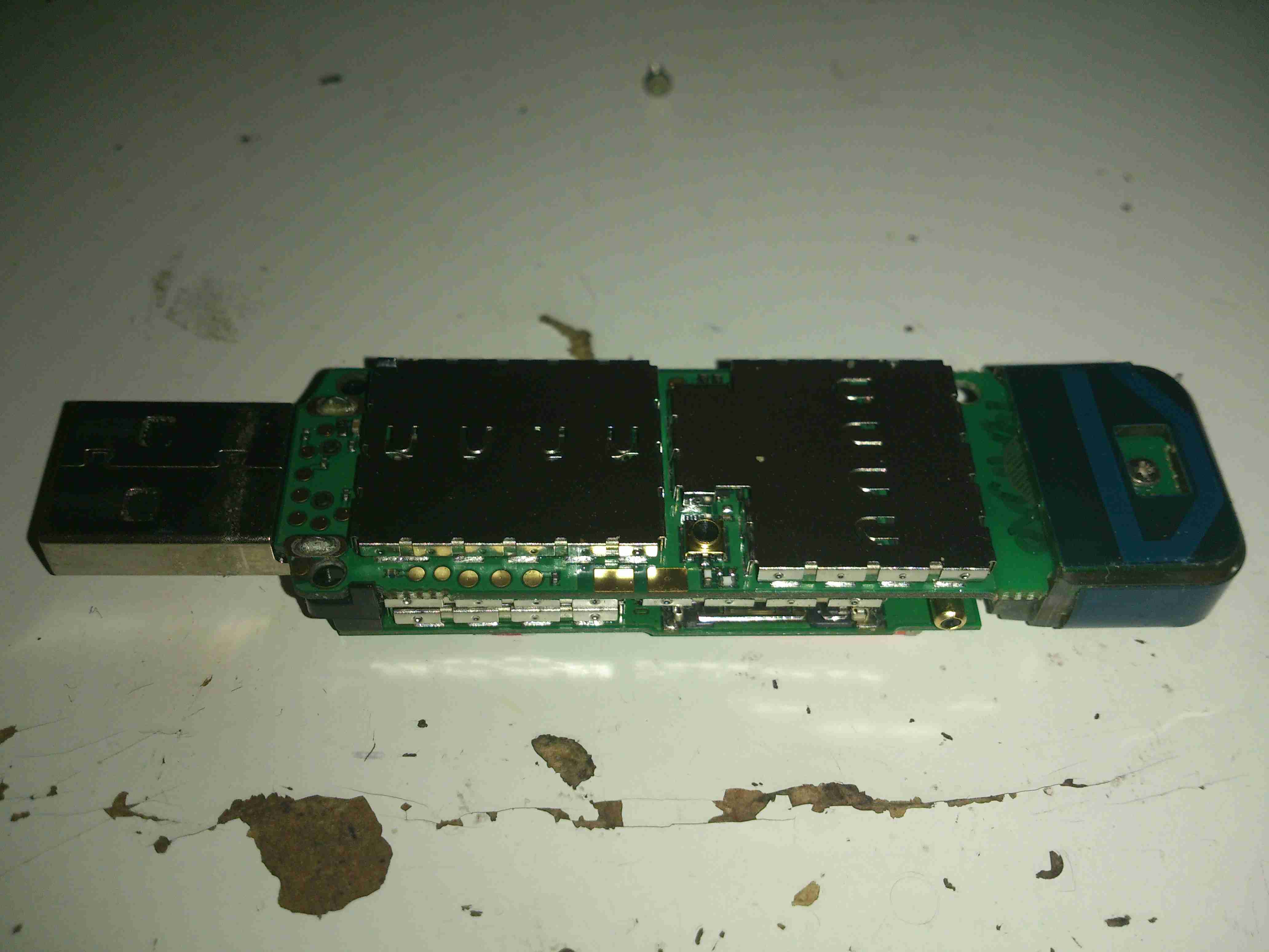
Here’s the PCB stack removed from the outer casing. The main antenna is on the right, attached with another small screw. Every IC on the boards is covered with an RF can. No problems there, pliers to the rescue!

SD Card Slot
SD Card Slot

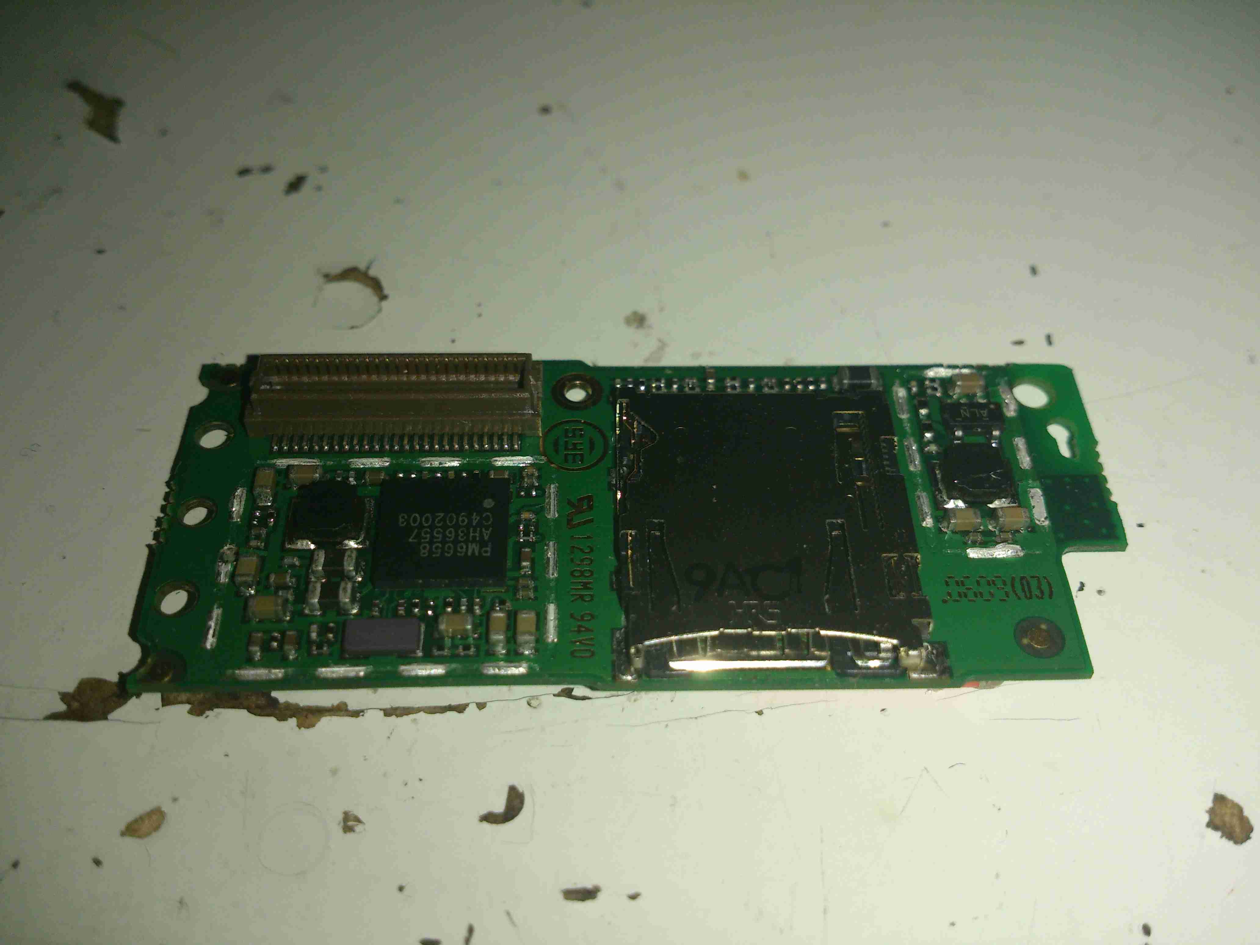
Here’s the top PCB, all the shields have been removed. On the left is a Qualcomm PM6658 Power Management IC with integrated USB transceiver. This is surrounded by many of the power management circuits.
The integrated SD Card slot is on the right side. with what looks to be a local switching regulator for supply voltage. This might also provide the SIM card with it’s power supply.

PSU & SIM Contacts
PSU & SIM Contacts

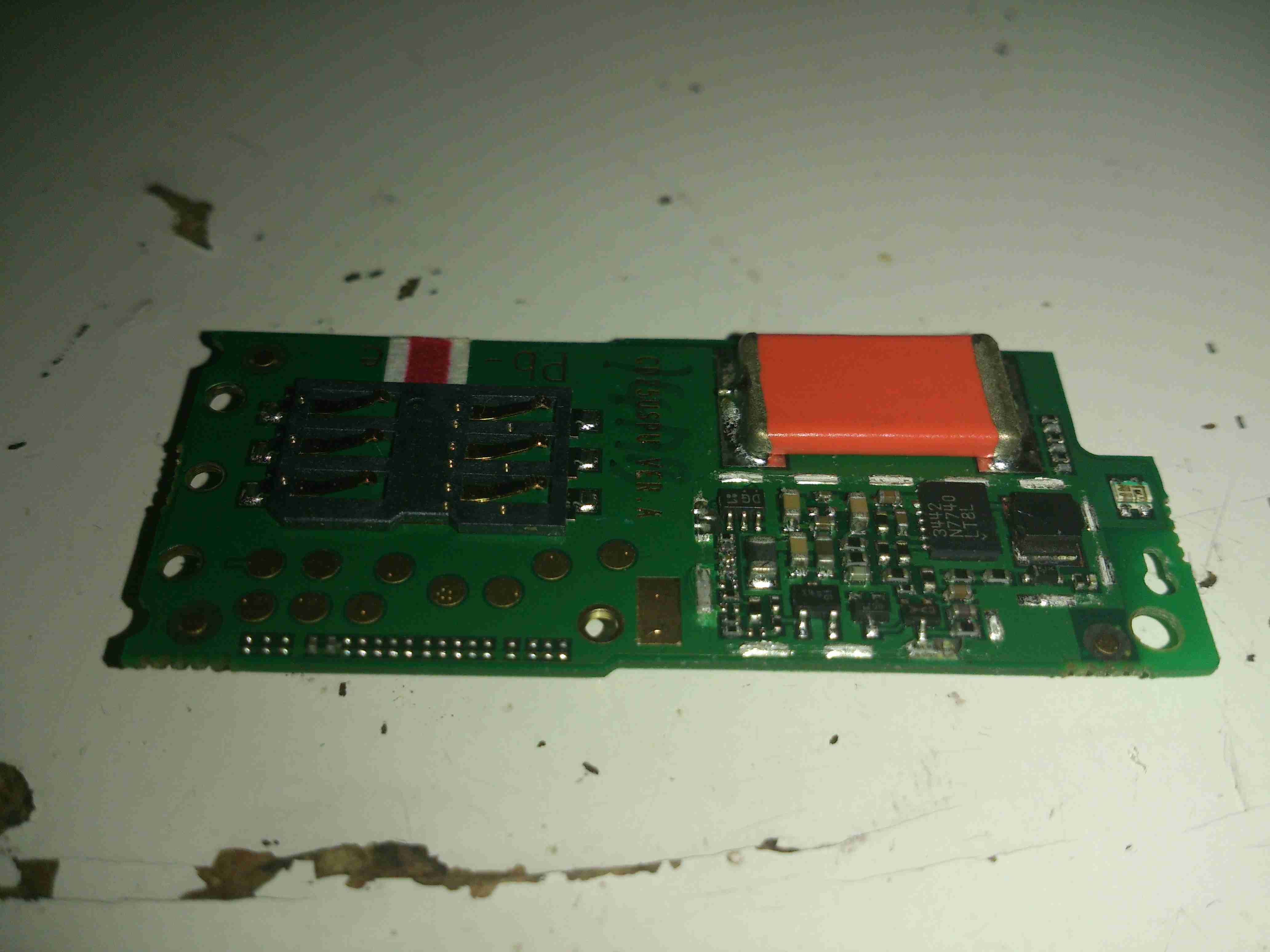
The other side of the top board reveals more power management, with another switching regulator, and a truly massive capacitor at the top edge. I’m guessing this is a solid Tantalum.

Main Chipset PCB
Main Chipset PCB

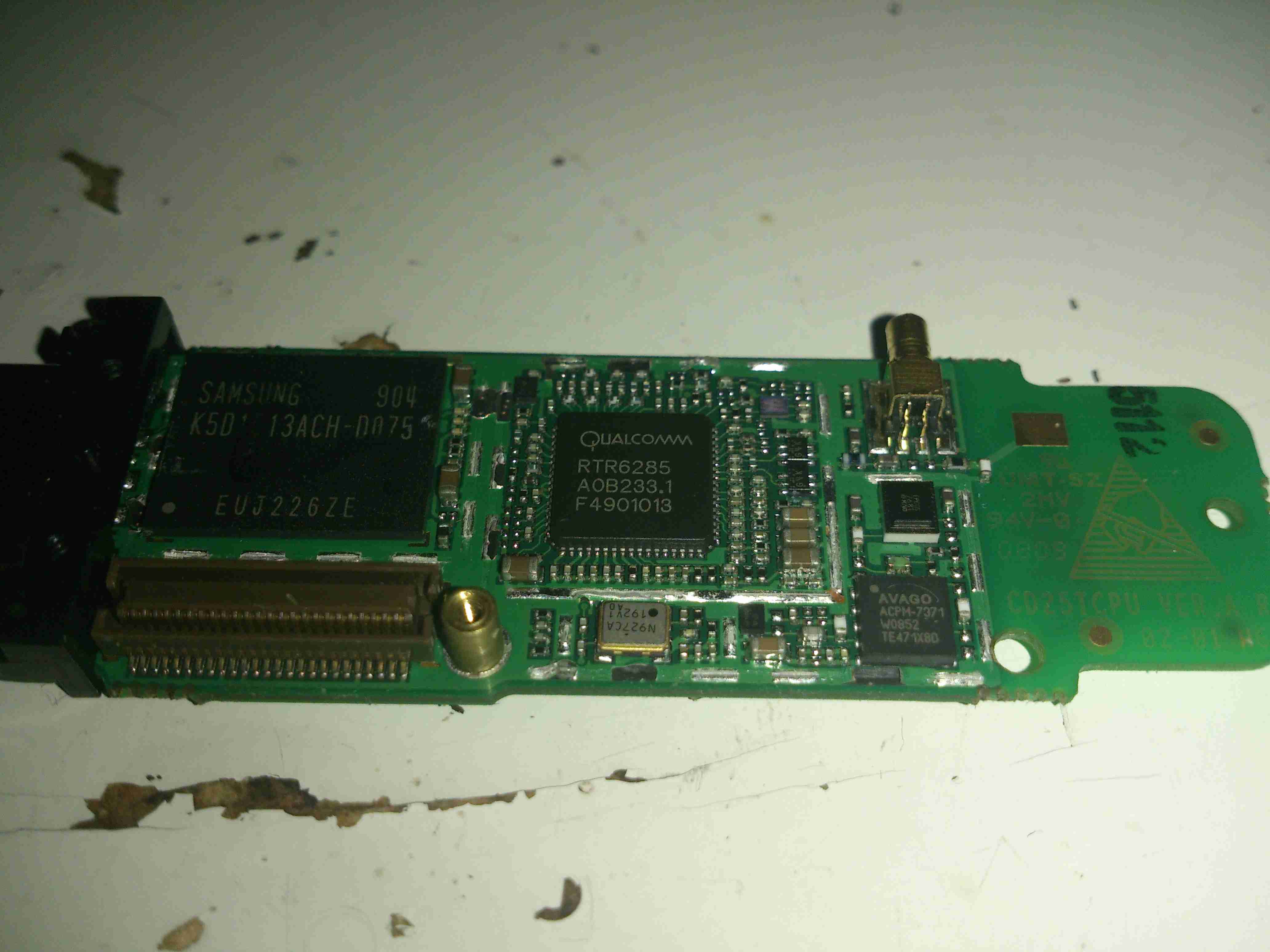
The other PCB holds the main chipset & RF circuits. On the left here is a Samsung MCP K5D1G13ACH IC. This one is a multiple chip package, having 1Gbit of NAND Flash & 512Mbit of mobile SDRAM.
To it’s right is a Qualcomm RTR6285 RF Transceiver. This IC supports multiband GSM/EDGE/UMTS frequencies & also has a GPS receive amplifier included.
At bottom right is an Avago ACPM7371 Wide-Band 4×4 CDMA Power Amplifier. The external antenna connector is top right.

Main Chipset PCB Reverse

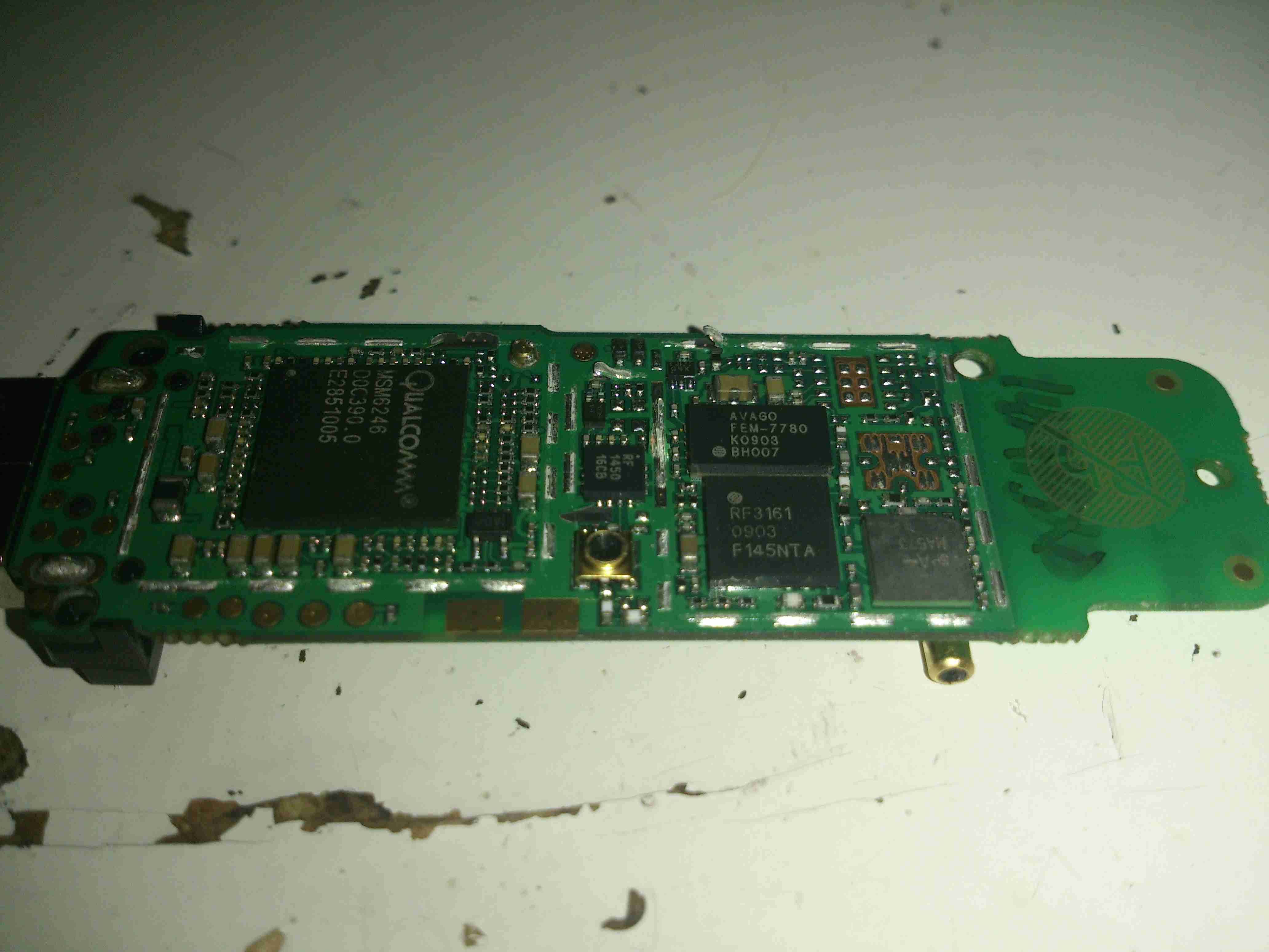
On the other side of the main PCB is a Qualcomm MSM6246 Baseband processor. Not sure about this one as I can’t find anything resembling a datasheet. Another micro-coax connector is in the centre, probably for factory test purposes, as it’s not accessible from the outside.
Just above the coax connector is a Qorvo RF1450 SP4T (single-pole 4-throw) High Power (34.5dBm) GSM RF Switch.
Upper right is an Avago FEM-7780 UMTS2100 4×7 Front End Module.
Under that is an RFMD RF3163 Quad-Band RF Power Amplifier Module.

Posted on 2 Comments

Maplin 600W “Modified Sine” Power Inverter

Maplin 600W Inverter

I’m no fan of power inverters. In my experience they’re horrifically inefficient, have power appetites that make engine starter motors look like electric toothbrushes & reduce the life expectancy of lead-acid batteries to no more than a few days.
However I have decided to do a little analysis on a cheapo “600W” model that Maplin Electronics sells.

Cover Removed
Cover Removed

After a serious amount of metallic abuse, the bottom cover eventually came off. The sheet of steel used to close the bottom of the aluminium extrusion was wedged into place with what was probably a 10 ton hydraulic press.
As can be seen from the PCB, there’s no massive 50Hz power transformer, but a pair of high frequency switching transformers. Obviously this is to lighten the weight & the cost of the magnetics, but it does nothing for the quality of the AC output waveform.

DC Input End
DC Input End

The 12v DC from the battery comes in on very heavy 8-gauge cables, this device is fused at 75A!

DC Fuses
DC Fuses

Here’s the fusing arrangement on the DC input stage, just 3 standard blade-type automotive fuses. Interestingly, these are very difficult to get at without a large hammer & some swearing, so I imagine if the user manages to blow these Maplin just expect the device to be thrown out.

Input DC-DC Switching MOSFETs

On the input side, the DC is switched into the pair of transformers to create a bipolar high voltage DC supply.

High Voltage Rectifiers

The large rectifier diodes on the outputs of the transformers feed into the 400v 100µF smoothing capacitors.
As mains AC is obviously a bipolar waveform, I’m guessing this is generating a ±150v DC supply.

Output MOSFETs
Output MOSFETs

After the high voltage is rectified & smoothed, it’s switched through 4 more MOSFETs on the other side of the PCB to create the main AC output.

The label states this is a modified-sine output, so I’d expect something on the scope that looks like this:

Inverter Waveforms
Inverter Waveforms

Modified-sine doesn’t look as bad as just a pure square output, but I suspect it’s a little hard on inductive loads & rectifiers.

However, after connecting the scope, here’s the actual waveform:

Actual Waveform
Actual Waveform

It’s horrific. It’s not even symmetrical. There isn’t even a true “neutral” either. The same waveform (in antiphase) is on the other mains socket terminal. This gives an RMS output voltage of 284v. Needless to say I didn’t try it under load, as I don’t possess anything I don’t mind destroying. (This is when incandescent lamps are *really* useful. Bloody EU ;)).

About the only thing that it’s accurate at reproducing is the 50Hz output, which it does pretty damn well.

System Microcontroller

As is usual these days, the whole system is controlled via a microcontroller.

Posted on Leave a comment

Wouxun KG-UV950P Teardown & Analysis

Following on from my review, here are some internal views & detail on the components used in this radio. Below is an overview of the main PCB with the top plate removed from the radio.

Cover Removed
Cover Removed
RF Final Amplifier Stage

Most visible are these MOSFETs, which are Mitsubishi RD70HVF1 VHF/UHF power devices.  Rated for a maximum of 75W output power at 12.5v (absolute maximum of 150W, these are used well within their power ratings. They are joined to the PCB with heavy soldering, with bypass caps tacked right on to the leads.

RF Pre Drivers
RF Pre Drivers

Here is the RF pre-driver stage, with intermediate transistors hidden under the small brass heatspreader.

Power Section
Power Section

In the top left corner of the radio, near the power input leads, is the power supply & audio amplifier section. Clearly visible are the pair of LA4425A 5W audio power amplifier ICs, these drive the speakers on the top of the radio. Either side of these parts are a 7809 & a 7805 – both linear regulators providing +9v & +5v logic supplies respectively. The large TO220 package device is a KIA378R08PI 3A LDO regulator with ON/OFF control, this one outputs +8v. Just visible in the top right corner are the sockets for the speaker connections.

DTMF Circuits
DTMF Circuits

Here are the two ICs for dealing with DTMF tones, they are HM9170 receivers.

Glue Logic
Glue Logic

In the corner next to the interface jack, there are some CD4066B Quad Bilateral switches. These make sense since the interface jack has more than a single purpose, these will switch signals depending on what is connected.

RF Section
RF Section

Here are visible the RF cans for the oscillators, the crystals visible next to the can at the top. The shields are soldered on, so no opening these unfortunately.
Also visible in this image is a CMX138A Audio Scrambler & Sub-Audio Signalling processor. This IC deals with the Voice Inversion Scrambling feature of the radio, & processes the incoming audio before being sent to the modulator.

Output Filter Network

Shown here is the RF output filter network, this radio uses relays for switching instead of PIN diodes, I imagine for cost reasons. The relay closest to the RF output socket has had a slight accident 🙂 This is slated to be replaced soon.

RF Output Jack
RF Output Jack

Finally, the RF output jack.

Audio Speakers
Audio Speakers

Here the speakers are shown, attached to the bottom of the top plate. They are both rated 8Ω 1W.

Posted on Leave a comment

Quantum LTO2 CL1001 Tape Drive Teardown

Drive Top
Drive Top

I have recently begun to create an archive of all my personal data, and since LTO2 tape drives offer significant capacity (200GB/400GB) per tape, longevity is very high (up to 30 years in archive), & relatively low cost, this is the technology I’ve chosen to use for my long term archiving needs.

Unfortunately, this drive was DOA, due to being dropped in shipping. This drop broke the SCSI LVD connector on the back of the unit, & bent the frame, as can be seen below.

Broken SCSI
Broken SCSI

As this drive is unusable, it made for a good teardown candidate.

Cover Removed
Cover Removed

Here the top cover of the drive has been removed, showing the top of the main logic PCB. The large silver IC in the top corner is the main CPU for the drive. It’s a custom part, but it does have an ARM core.

The two Hitachi ICs are the R/W head interface chipset, while the smaller LSI IC is the SCSI controller.
The tape transport & loading mech can be seen in the lower half of the picture.

Main Logic
Main Logic

Close up of the main logic.

Tape Spool
Tape Spool

Here the main logic PCB has been removed, showing the tape take up spool. The data cartridges have only one spool to make the size smaller. When the tape is loaded, the drive grabs onto the leader pin at the end of the tape & feeds it onto this spool.
The head assembly is just above the spool.

Bottom Plate Removed

Bottom of the drive with the cover plate removed. Here the spindle drive motors are visible, both brushless 3-Phase units. Both of these motors are driven by a single controller IC on the other side of the lower logic PCB.

Head Drive Motor
Head Drive Motor

The head is moved up & down the face of the tape by this stepper motor for coarse control, while fine control is provided by a voice coil assembly buried inside the head mount.

Tape Head Assembly
Tape Head Assembly

The face of the tape R/W head. This unit contains 2 sets of 8 heads, one of which writes to the tape, the other then reads the written data back right after to verify integrity.

Cartridge Load Motor

The tape cartridge loading motor. I originally thought that this was a standard brushed motor, but it has a ribbon cable emerging, this must be some sort of brushless arrangement.

A replacement drive is on the way, I shall be documenting some more of my archiving efforts & system setup once that unit arrives.

Posted on Leave a comment

Routemaster Control Unit

This is the control unit for a Routemaster system, that downloads traffic information for the area local to the vehicle.

Unit Overview
Unit Overview

Here is an overview of the unit, in it’s aluminium box.


Here is the unit with the top cover removed, showing the pair of PCBs. The bottom PCB is the main control PCB, the top one holds an IC similar to a SIM card & part of the radio.

Cover Removed
Cover Removed


Main PCB Top
Main PCB Top

Here is the main PCB removed from the casing, contains the program ROM & microcontroller. for the system


Daughtercard view. This holds another programmed CPLD, the custom SIM-like IC & the RTC battery, along with some power conversion circuitry.

Daughterboard Top
Daughterboard Top


Radio Receiver
Radio Receiver

This is the radio receiver, looks to be AM, the large loop antenna can be seen at the bottom of the box.

Posted on Leave a comment

Vintage Optical Block

Top
Top

I thought this would be of interest, as it’s from a drive circa 2001, (DVD-CD-RW).

It’s the biggest & most complex optical block I’ve ever seen, with totally separate beam paths for the IR CD beam & the visible DVD beam. It also combines the use of bare laser diodes & combined diode/photodiode array modules for the pickup.


Cover Removed
Cover Removed

Here’s a look at the optics inside the sled, on the left is a bare laser diode & photodiode array, for the CD reading, and the bottom right has the DVD combined LD/PD array module. The beam from the CD diode has to pass though some very complex beam forming optics & a prism to fold it round to the final turning mirror to the objective lens at top center.
There are also two separate photodiodes which are picking up the waste beam from the prisms, most likely for power control.

Posted on Leave a comment

Tool-less UK Mains Plug

Plug Bottom
Plug Bottom

This is a standard 13A UK main power plug – with a twist. This one requires no tools to open or connect.
The top cover is slid off the top, after turning the red cam with a coin to unlock it.

Plug Top
Plug Top

Manufactured by Plugco – a Google search of this company returns no results.

Cover Removed
Cover Removed

Top cover removed from the plug, as is standard with UK mains plugs the live conductor is fused – 3A in this case. The conductors are clamped into the fittings in a row along the top edge of the plug.

Wire Clamps
Wire Clamps

Closeup of the wire clamps. Conductor is placed in the slot & snapped closed.

This is an old plug & they do not appear to be available these days, for unknown reasons. Being able to change a plug without a screwdriver has it’s advantages 🙂

Posted on Leave a comment

IDE Zip Drive

Top
Top

An old IDE interface Zip drive. This fits in a standard 3.5″ bay.

Cover Removed
Cover Removed

Top cover removed from the drive, IDE & power interfaces at the top, in centre is the eject solenoid assembly & the head assembly. Bottom is the spindle drive motor.

Head Assembly
Head Assembly

Head assembly with the top magnet removed. Voice coil is on the left, with the head preamp IC next to it. Head chips are on the end of the arm inside the parking sleeve on the right. Blue lever is the head lock.

Controller
Controller

Controller PCB removed from the casing.

Spindle Motor
Spindle Motor

Spindle motor. This is a 3-phase DC brushless type motor. Magnetic ring on the top engages with the hub of the Zip disk when insterted into the drive.

Magnets
Magnets

Magnets that interact with the voice coil on the head assembly.

Head Armature
Head Armature

Head armature assembly removed from the drive. The arm is supported by a pair of linear bearings & a stainless steel rod.

Posted on Leave a comment

iPod

Front
Front

Old iPod with damaged screen. Here is the front with the Click Wheel.

Cover Removed
Cover Removed

Cover removed from the back, here the HDD is the biggest visible part.

Mainboard
Mainboard

Back cover removed from the unit, here is the back of the screen & the main PCB.

Back Cover
Back Cover

Back cover with the battery & headphone jack PCB.

Battery
Battery

Closeup of the Li-Ion battery.

Front Removed
Front Removed

Front removed from the unit, the touch sensitive Click Wheel PCB is folded away from the mainboard here.

Buttons
Buttons

Tactile switches underneath the Click Wheel.

HDD
HDD

1.8″ hard drive. Toshiba MK3008GAL.

Posted on Leave a comment

Chicom “500W” ATX PSU

Cover Removed
Cover Removed

Here is a cheapo 500W rated ATX PSU that has totally borked itself, probably due to the unit NOT actually being capable of 500W. All 3 of the switching transistors were shorted, causing the ensuing carnage:

AC Input
AC Input

Here is the AC input to the PCB. Note the vapourised element inside the input fuse on the left. There is no PFC/filtering built into this supply, being as cheap as it is links have been installed in place of the RFI chokes.

Input Side
Input Side

Main filter capacitors & bridge rectifier diodes. PCB shows signs of excessive heating.

Filter Caps Removed
Filter Caps Removed

Filter capacitors have been removed from the PCB here, showing some cooked components. Resistor & diode next to the heatsink are the in the biasing network for the main switching transistors.

Heatsinks Removed
Heatsinks Removed

Heatsink has been removed, note the remaining pin from one of the switching transistors still attached to the PCB & not the transistor 🙂

Transformers
Transformers

Output side of the PSU, with heatsink removed. Main transformer on  the right, transformers centre & left are the 5vSB  transformer & feedback transformer.

Output Side
Output Side

Output side of the unit, filter capacitors, choke & rectifier diodes are visible here attached to their heatsink.

Comparator
Comparator

Comparator IC that deals with regulation of the outputs & overvoltage protection.