Posted on Leave a comment

Wireless Energy Management SmartSensor

Cover Removed
Cover Removed

Here’s another random bit of RF tech, I’m told this is a wireless energy management sensor, however I wasn’t able to find anything similar on the interwebs. It’s powered by a standard 9v PP3 battery.

Microcontroller
Microcontroller

System control is handled by this Microchip PIC18F2520 Enhanced Flash microcontroller, this has an onboard 10-bit ADC & nanoWatt technology according to their datasheet. There’s a 4MHz crystal providing the clock, with a small SOT-23 voltage regulator in the bottom corner. There’s a screw terminal header & a plug header, but I’ve no idea what these would be used for. Maybe connecting an external voltage/current sensor & a programming header? The tactile button I imagine is for pairing the unit with it’s controller.

PCB Bottom
PCB Bottom

The bottom of the PCB is almost entirely taken up by a Radiocrafts RC1240 433MHz RF transceiver. Underneath there’s a large 10kΩ resistor, maybe a current transformer load resistor, and a TCLT1600 optocoupler. Just from the opto it’s clear this unit is intended to interface in some way to the mains grid. The antenna is connected at top right, in a footprint for a SMA connector, but this isn’t fitted.

Posted on 2 Comments

Maplin A24GU Wireless Audio Module Teardown

Transmitter
Transmitter

This is a pair of modules that Maplin was selling some time back, to send stereo audio over a 2.4GHz radio link. The transmitter identifies as a USB sound card, I’ve personally used these units to transmit audio about 60ft. The transmitter, above, has a single button for pairing with the receiver below.

Receiver
Receiver

The receiver unit has a large external antenna, a link status LED & volume buttons, these directly control the volume level on the host PC via the sound card drivers.

Receiver PCB Top
Receiver PCB Top

Popping the case open on the receiver reveals a large PCB, holding the chipset, along with the audio output jacks & Mini-USB power input. The antenna Coax is soldered to the PCB.

Receiver PCB Bottom
Receiver PCB Bottom

The top of the board has the control buttons, and the status LED.

Receiver Chipset
Receiver Chipset

The chipset used here is a Nordic Semiconductor nRF20Z01 2.4GHz Stereo Audio Streamer, there’s a small microcontroller which does all the register magic on the RF transceiver. The RF chain is at the top of the photo, audio outputs on the top left, and the micro USB power input & voltage regulators at bottom left.

Transmitter PCB Top
Transmitter PCB Top

The transmitter PCB has a Sonix USB Audio Codec, to interface with the host PC. This is then fed into another Nordic Semi part on the opposite side of the board:

Transmitter PCB Bottom

The bottom of the transmitter has the RF section, and another small control microcontroller.

Posted on 2 Comments

PiHole Status Display – Official Raspberry Pi LCD

PiHole Status Display

On my home network I have a system running PiHole – a DNS server that blocks all unwanted traffic, such as ads. Since I have an official Pi LCD with a broken touch panel, I decided to use the bare LCD as a status display for PiHole.

This requires some extra packages installing onto the base system after PiHole is installed & configured, and the interface automatically starts on bootup. I used the latest Raspbian Jessie Minimal image for this system, and ran everything over a SSH connection.

First thing, get the required packages installed onto the Pi:

Once these are installed, it’s time to configure the startup script for Midori to display the status page. Create StartMidori.sh in /home/pi and fill with the following:

This script disables all power management on the system to keep the LCD on, starts unclutter to hide the mouse pointer and finally starts the Matchbox Window Manager to run Midori, which itself is set to fullscreen mode, and the URL of the admin panel is provided.
The next step is to test, give the script executable permissions, and run the script:

Once this is run, the LCD should come to life after a short delay with the PiHole stats screen. Close the test & return to the terminal by hitting CTRL+C.

Now the Pi can be configured to autorun this script on boot, the first thing to do here is to enable autologin on the console. This can be done with raspi-config, select Option 3 (Boot Options), then Option B1 (Desktop/CLI), then Option B2 (Console Autologin). When prompted to reboot, select No, as we’ll be finishing off the config before we reboot the system.

The next file to edit is /etc/rc.local, add the command to start the status browser up:

Here I’ve added in the command just above “exit 0”. This will start the browser as the last thing on bootup. The Pi can now be rebooted, and the status display should start on boot!

PiHole Status Display
Posted on 2 Comments

PowerAdd Pilot X7 20,000mAh Powerbank & Fast Charging Mod

PowerAdd Pilot X7
PowerAdd Pilot X7

Here’s the biggest portable USB powerbank I’ve seen yet – the PowerAdd Pilot X7, this comes with a 20Ah (20,000mAh) capacity. This pack is pretty heavy, but this isn’t surprising considering the capacity.

USB Ports & LED
USB Ports & LED

The front of the pack houses the usual USB ports, in this case rated at 3.4A total between the ports. There’s a white LED in the centre as a small torch, activated by double-clicking the button. A single click of the button lights up the 4 blue LEDs under the housing that indicate remaining battery capacity. Factory charging is via a standard µUSB connector in the side, at a maximum of 2A.

PCB Front
PCB Front

The front of the PCB holds the USB ports, along with most of the main control circuitry. At top left is a string of FS8025A dual-MOSFETs all in parallel for a current carrying capacity of 15A total, to the right of these is the ubiquitous DW01 Lithium-Ion protection IC. These 4 components make up the battery protection – stopping both an overcharge & overdischarge. The larger IC below is an EG1501 multi-purpose power controller.

This chip is doing all of the heavy lifting in this power pack, dealing with all the DC-DC conversion for the USB ports, charge control of the battery pack, controlling the battery level indicator LEDs & controlling the torch LED in the centre.

EG1501 Example
EG1501 Example

The datasheet is in Chinese, but it does have an example application circuit, which is very similar to the circuitry used in this powerbank. A toroidal inductor is nestled next to the right-hand USB port for the DC-DC converter, and the remaining IC next to it is a CW3004 Dual-Channel USB Charging Controller, which automatically sets the data pins on the USB ports to the correct levels to ensure high-current charging of the devices plugged in. This IC replaces the resistors R3-R6 in the schematic above.
The DC-DC converter section of the power chain is designed with high efficiency in mind, not using any diodes, but synchronous rectification instead.

PCB Back
PCB Back

The back of the PCB just has a few discrete transistors, the user interface button, and a small SO8 IC with no markings at all. I’m going to assume this is a generic microcontroller, (U2 in the schematic) & is just there to interface the user button to the power controller via I²C.

Cells
Cells

Not many markings on the cells indicating their capacity, but a full discharge test at 4A gave me a resulting capacity of 21Ah – slightly above the nameplate rating. There are two cells in here in parallel, ~10Ah capacity each.

XT60 Battery Connector

The only issue with powerbanks this large is the amount of time they require to recharge themselves – at this unit’s maximum of 2A through the µUSB port, it’s about 22 hours! Here I’ve fitted an XT60 connector, to interface to my Turnigy Accucell 6 charger, increasing the charging current capacity to 6A, and reducing the full-charge time to 7 hours. This splits to 3A charge per cell, and after some testing the cells don’t seem to mind this higher charging current.

Battery Connector Wiring

The new charging connector is directly connected to the battery at the control PCB, there’s just enough room to get a pair of wires down the casing over the cells.

Posted on Leave a comment

Blog Housekeeping & More Of The Same

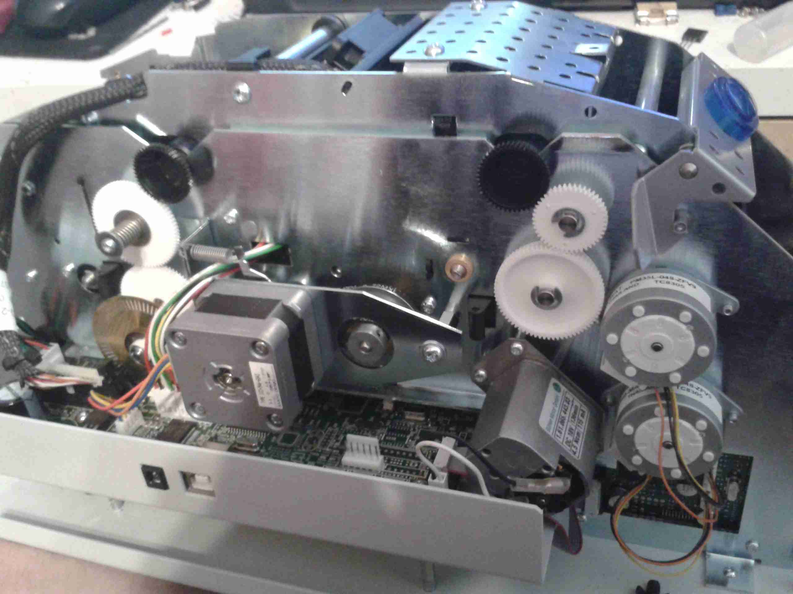
Since I’ve been working on the backend servers a lot over the past few days, I’ve decided it was time to get some broken things on the blog fixed.

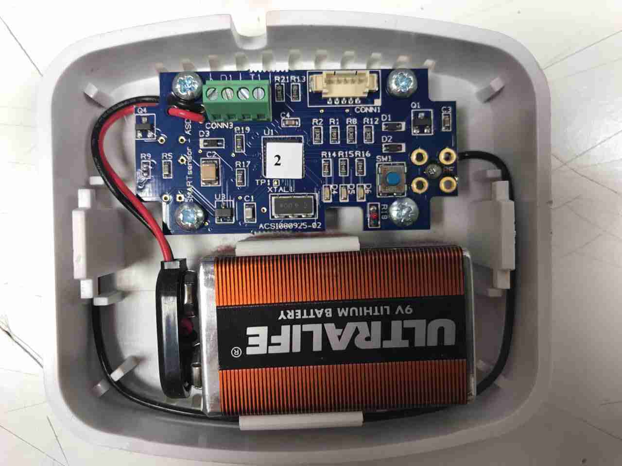
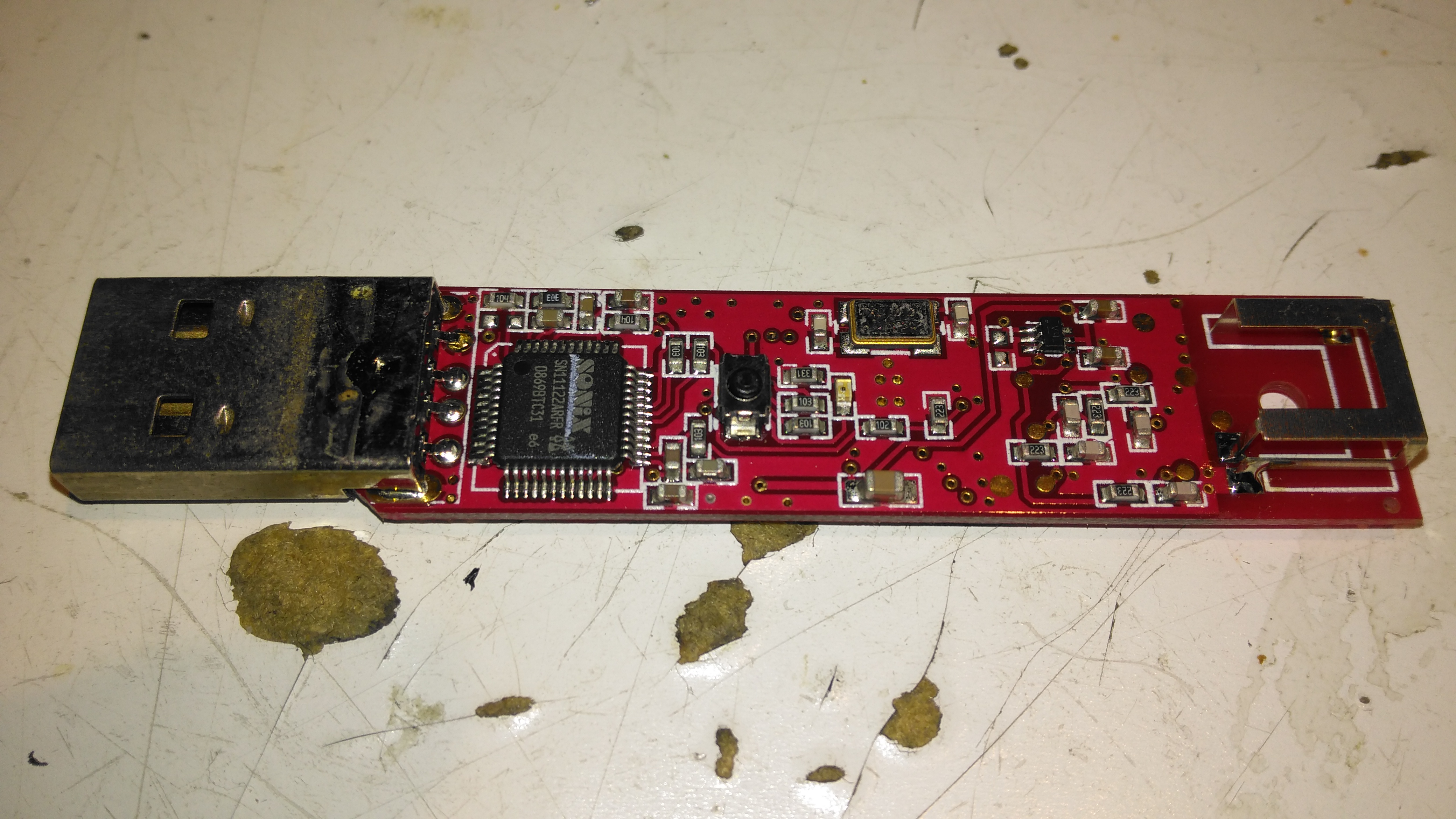
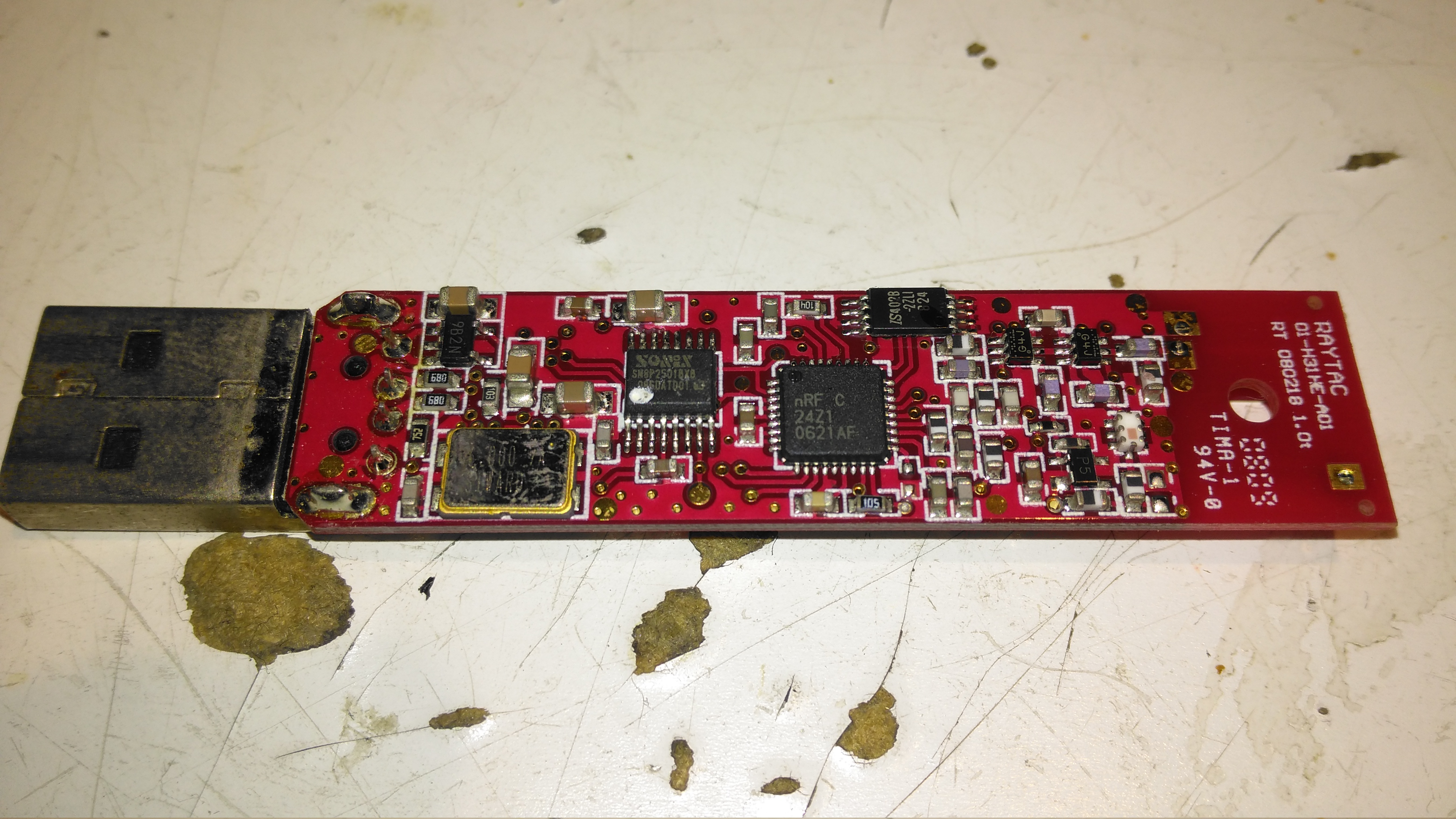
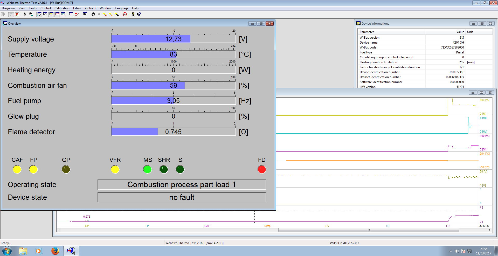
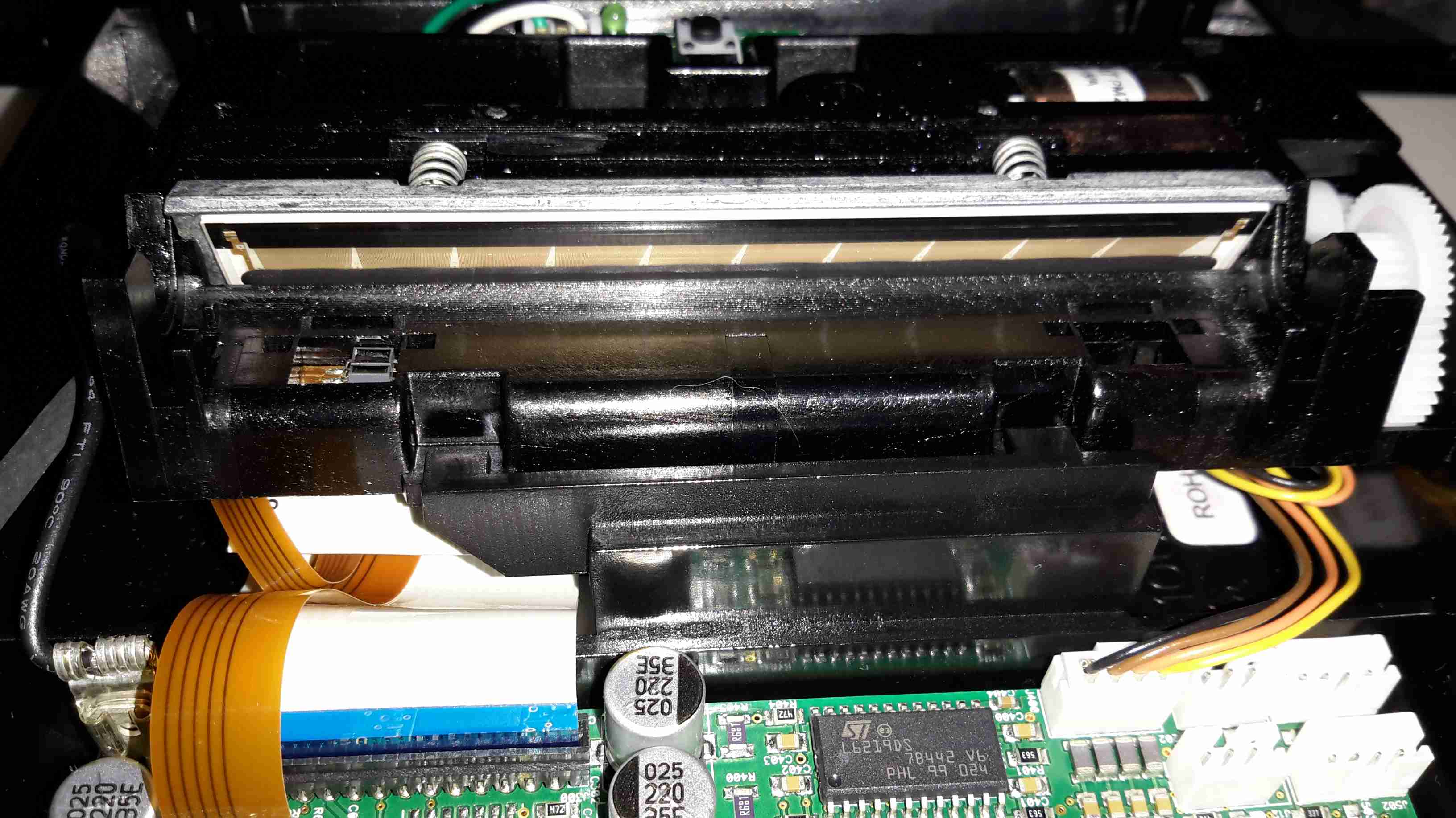
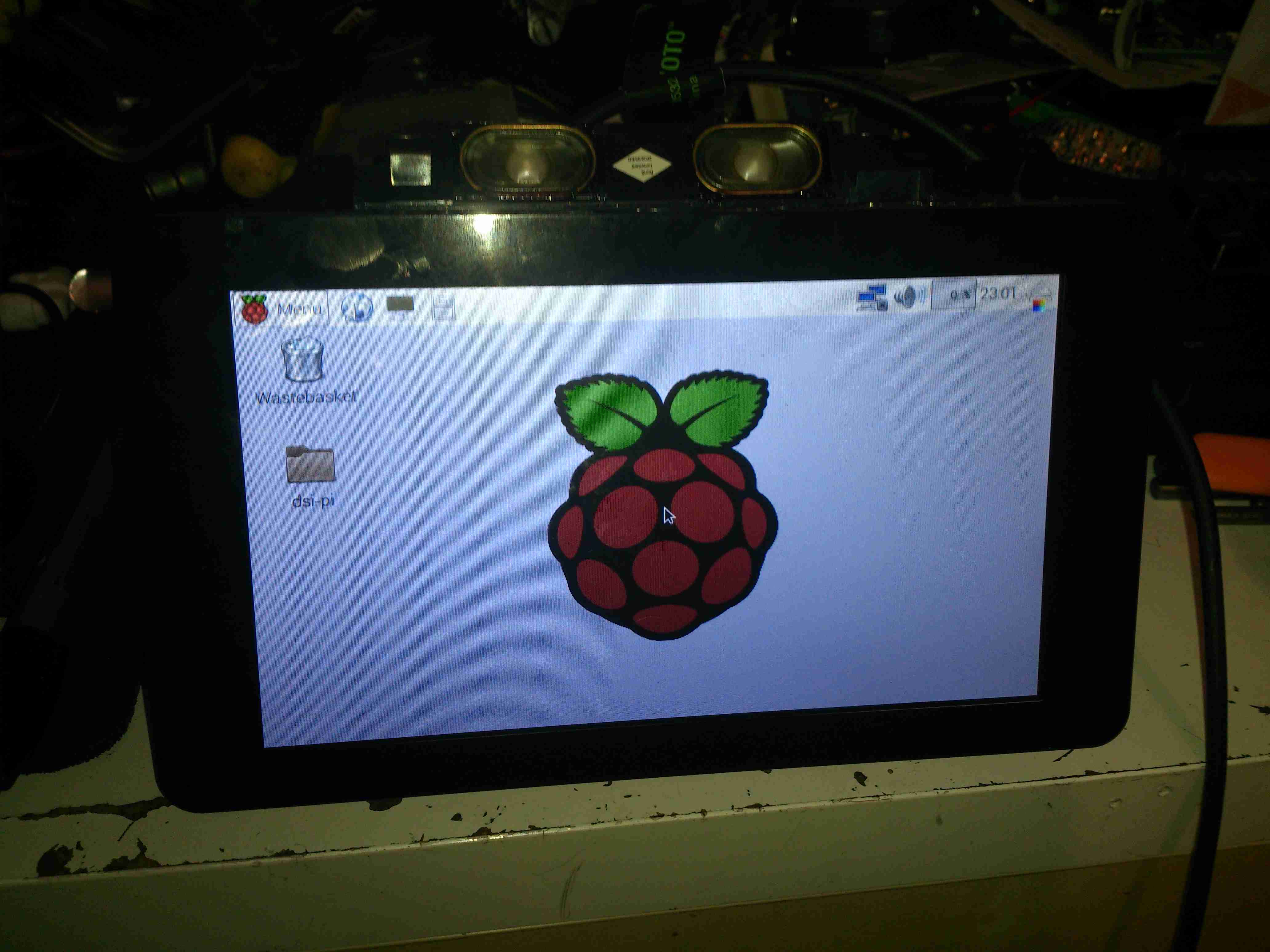
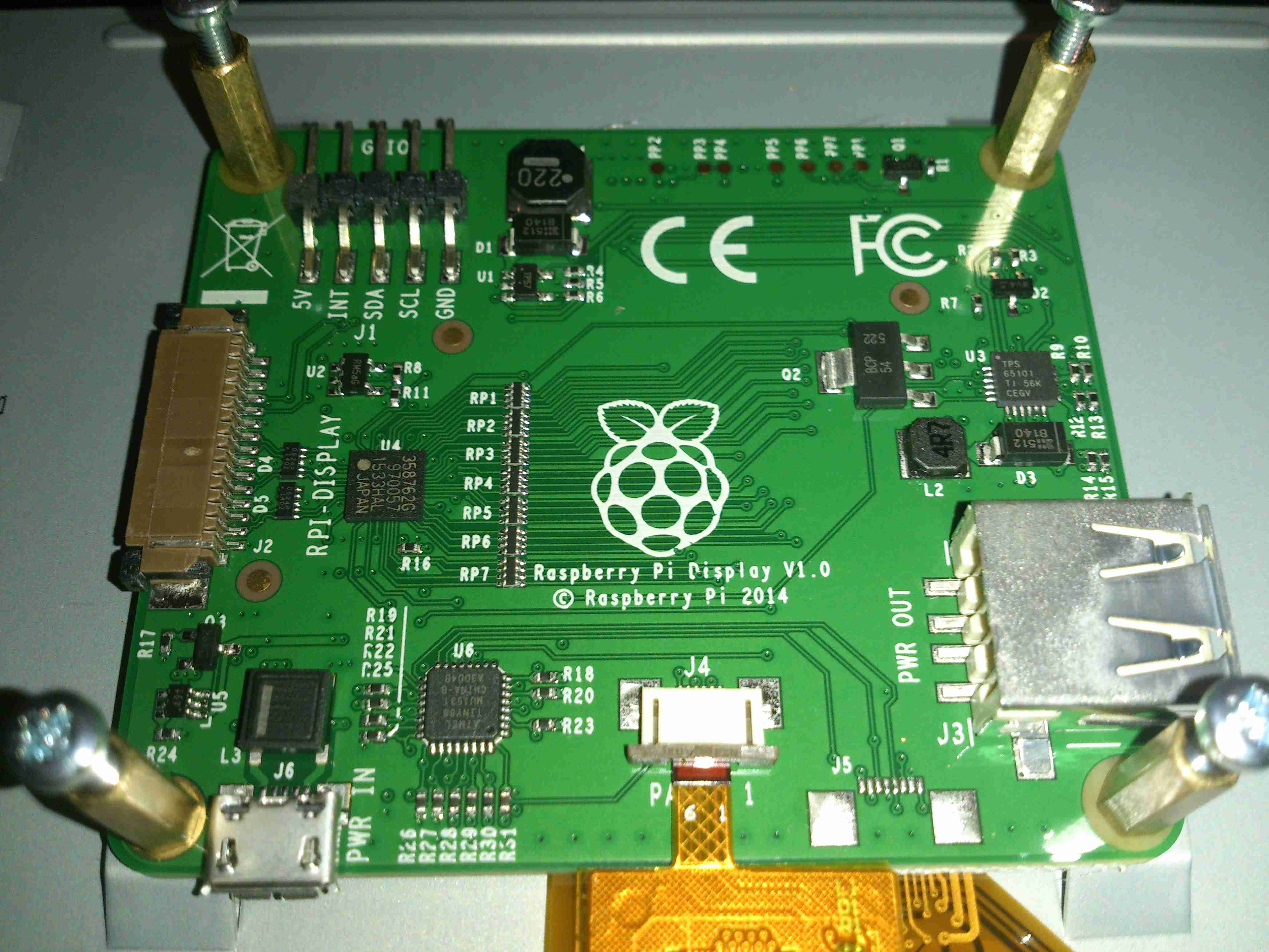
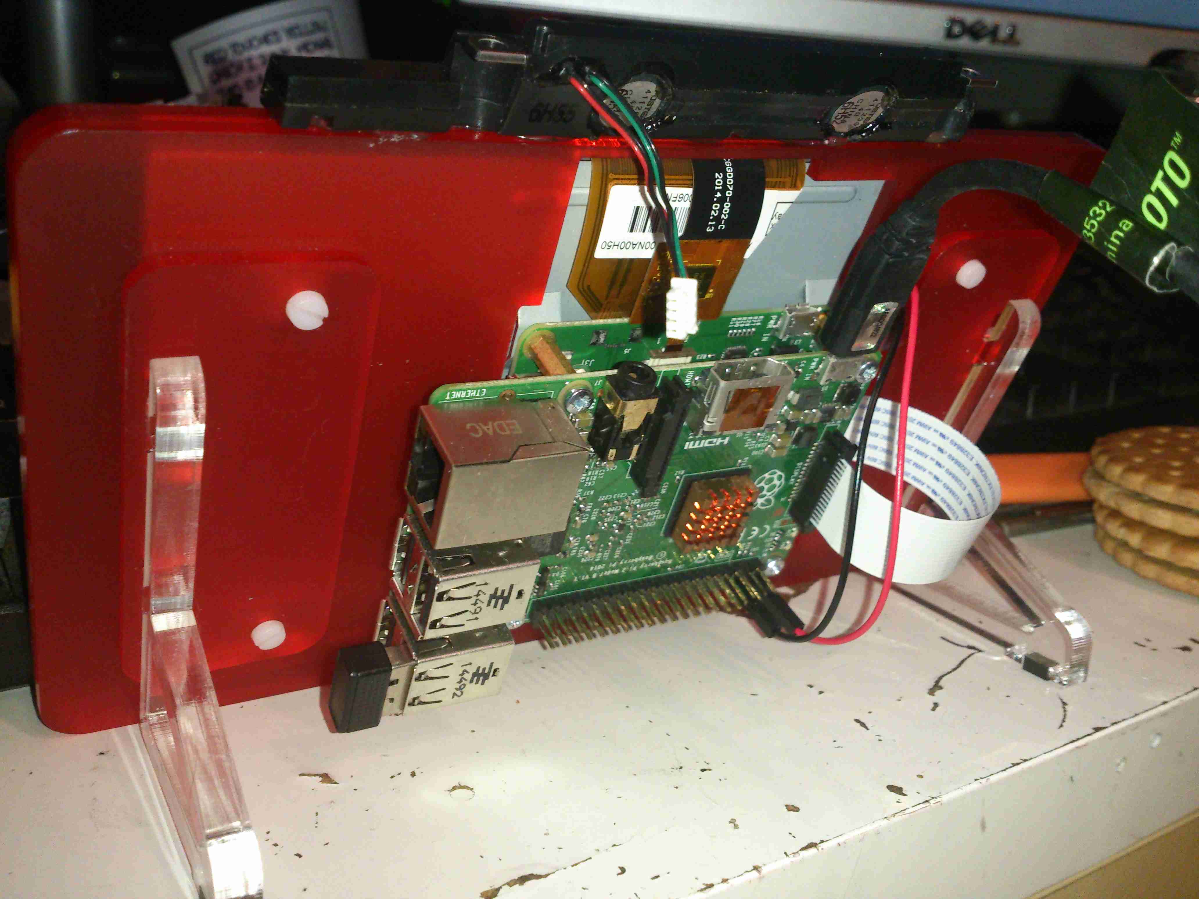
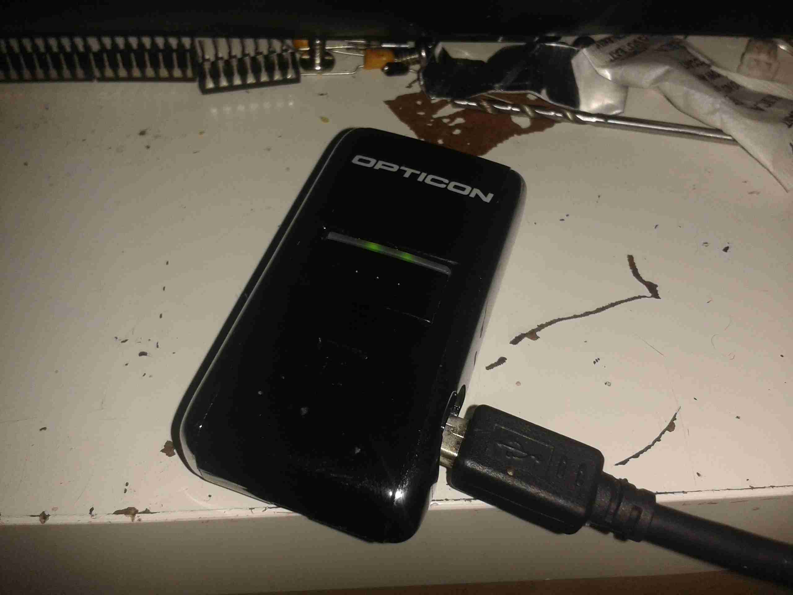
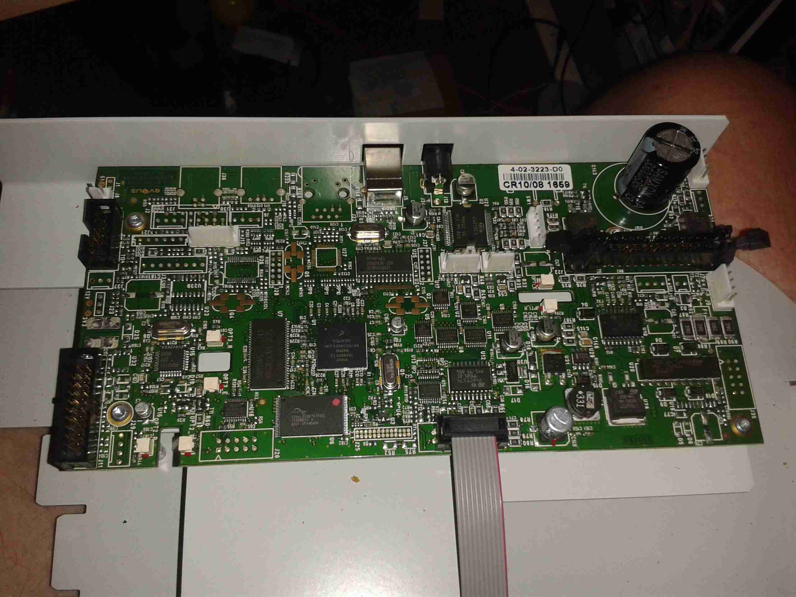
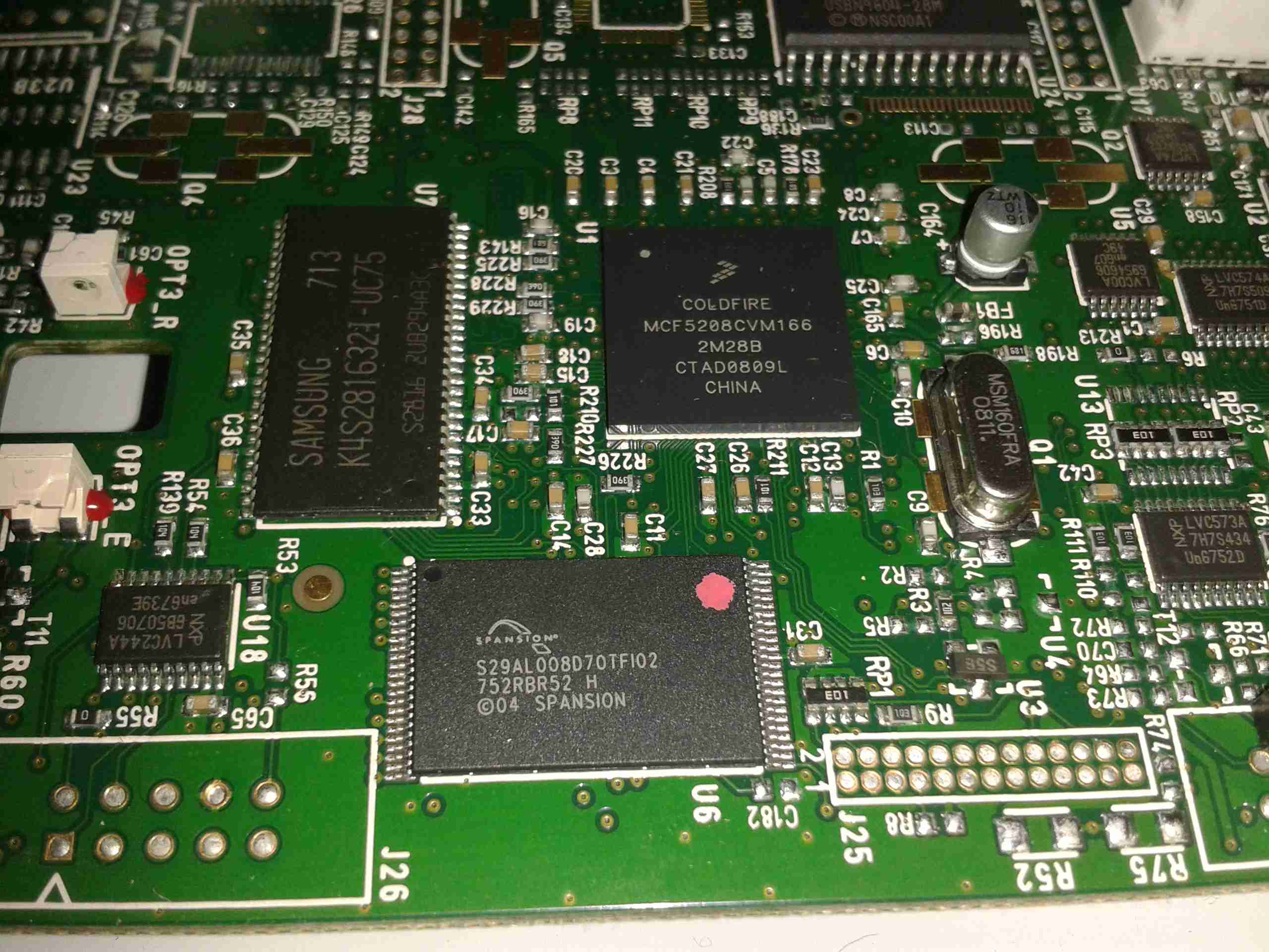
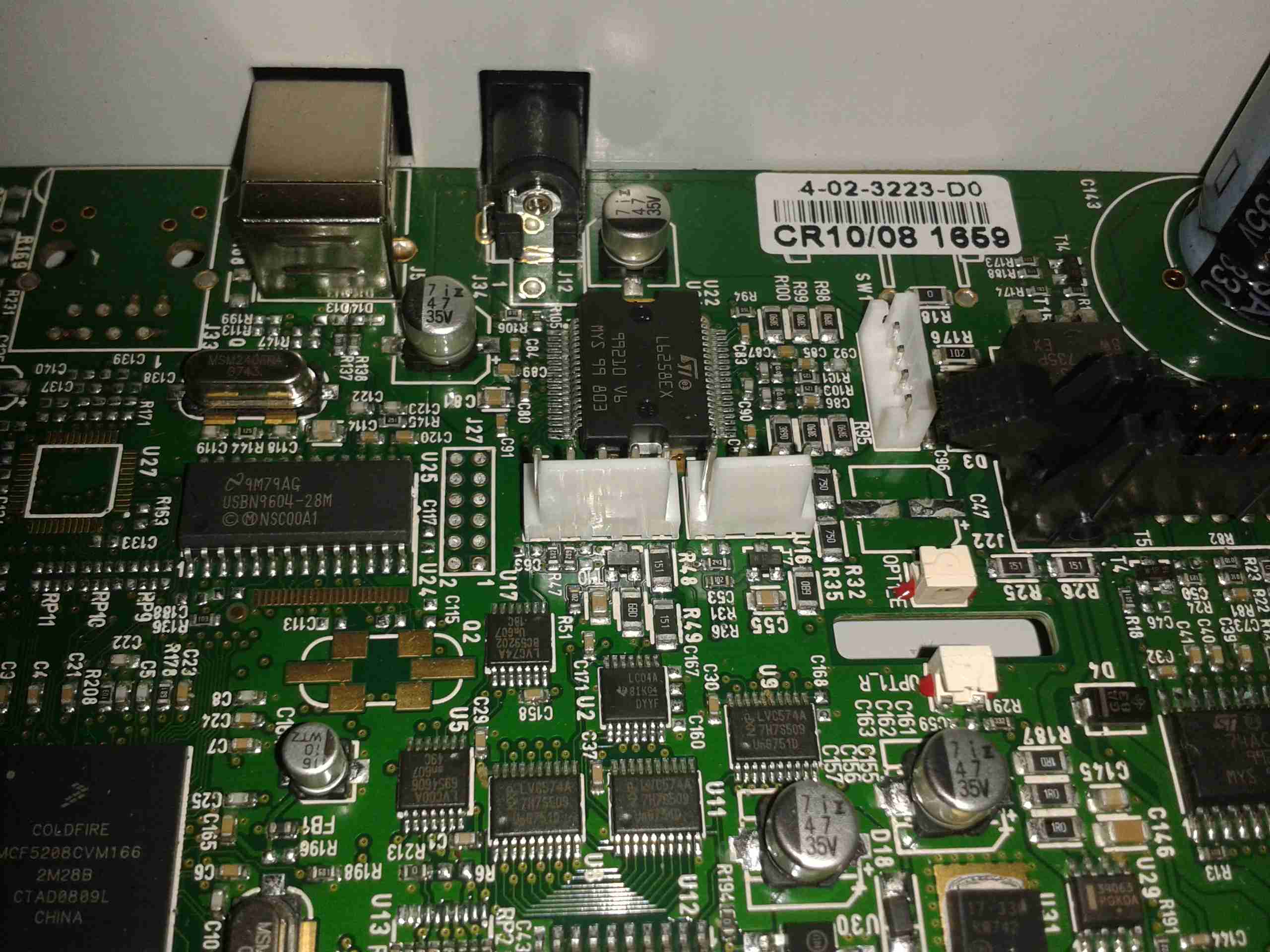
Firstly, the radiation monitor graphs. Originally I was using a Raspberry Pi to grab the data from the local monitor, and that was connecting via FTP to the server over in the datacentre to push it’s graph images. Since the server is now on the same local network as the monitor, there’s no need to faff about with FTP servers, so I’ve rejigged things with some perl scripts from cristianst85 over on GitHub, running on the web server itself.
I deviated from the suggested place to put the scripts on the server & opted to store everything within the Experimental Engineering hosting space, so it gets backed up at the same time as everything else on a nightly basis.

This is also accessible from the menu at top left, the script pulls data from the monitor & updates the images every 60 seconds via a cron job.

I’ve removed a couple of dead pages from the blog system, along with some backend tidying of the filesystem. Over the years things have gotten quite messy behind the scenes. This blog is actually getting quite large on disk, I’ve hit the 15GB mark, not including the database!

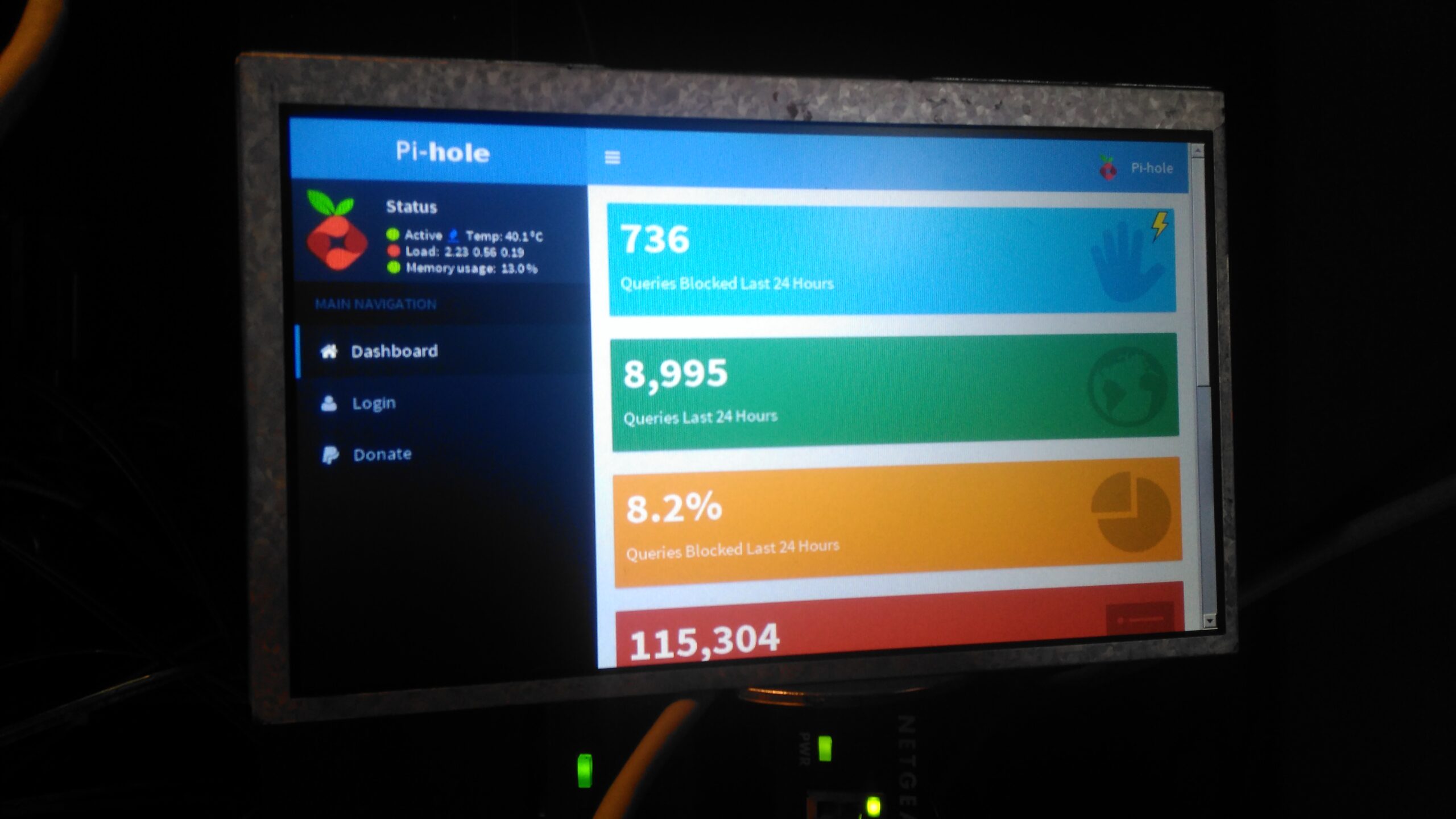
Caching is enabled for all posts on the blog now, this should help speed things up for repeat visitors, but as most of my content is (large) image based, this might be of limited help. I’m currently tuning the MySQL server for the load conditions, but this takes time, as every time I change some configuration settings I have to watch how things go for a few days, before tweaking some more.

Server Control Panels – More Of The Same

Sorry Sentora. I tried, and failed to convert over to using it as my new server control panel. Unfortunately it just doesn’t give me the same level of control over my systems, so I’ll be sticking with Virtualmin for the foreseeable future. Sentora stores everything in, (to me at least), very odd places under /var/ and gave me some odd results with “www.” versions of websites – some www. hosts would work fine, others wouldn’t at all & just redirect to the Sentora login interface instead. This wasn’t consistient between hosting accounts either, and since I didn’t have much time to get the migration underway, this problem was the main nail in the coffin.

Just storing everything under the sun in /var/ makes life a bit more awkward with the base CentOS install, as it allocates very little space to / by default, (no separate /var partition in default CentOS), giving most of the disk space to /home. Virtualmin on the other hand, stores website public files & Maildirs under /home, saving /var for MySQL databases & misc stuff.

The backup system provided is also utterly useless, there’s no restore function at all, and just piles everything in the account into a single archive. By comparison, Virtualmin has a very comprehensive backup system built in, that supports total automation of the process, along with full automatic restore functionality for when it’s needed.

Sentora did have some good points though:
It handled E-Mail logins & mail filters much more gracefully than Virtualmin does, and comes with Roundcube already built into the interface ready to use. With Virtualmin the options are to use the Usermin side of the system for E-Mail, which I find utterly awful to use, or install a webmail client under one of the hosted domains (my personal choice).
Mail filtering is taken care of with Sieve under Sentora, while Procmail does the job under Virtualmin.

Sentora does have a nicer, simpler, more friendly interface, but it hides most of the low-level system stuff away, while under Virtualmin *everything* on the system is accessible, and it provides control interfaces for all the common server daemons.

Posted on 11 Comments

Jaguar S-Type Aux Heater / Webasto Thermo Top V Part 2 – W-Bus Diagnostics

As I mentioned in the previous post, these heaters have a standard interface that’s used for control & diagnostics, the W-Bus. This is transmitted over the K-Line of the vehicle bus, and all heaters, regardless of firmware modifications done by the various car manufacturers respond to this interface. Official Webasto diagnostic adaptors are available, but these are just a very expensive serial adaptor. A much cheaper option is a ~£5 Universal ODB adaptor.

ODB2
ODB2

Above shows the signals on the ODB connector – the ones we’re interested in here are Pin 16, the +12v supply, and Pin 7, K-Line. Connect Pin 16 to the positive supply to the heater, and Pin 7 to Pin 2 on the Webasto heater. (Valid for all TT-V heaters).

Device Selection
Device Selection

Once these two connections are made to the heater, fire up the Thermo Test software. The screen above will be displayed. Pick W-Bus at top left.

COM Port Selection
COM Port Selection

First thing, connect the ODB adaptor to USB, and change to the correct COM port in Thermo Test. There may be several in the list, but a newly connected USB device should show up with the highest COM number.

Thermo Test
Thermo Test

Once Thermo Test is running, start communications by going to the Diagnosis Menu > Start Diagnostic (F2 keyboard shortcut).

Initialized
Initialized

After a few seconds, communication will be established. This will show faults, if any are present, and allow testing of the heater & it’s component parts. A summary report can be generated with Diagnosis > View Summary:

This shows all the important stuff, including running hours. (5388Hrs on this heater!). Most importantly, there are no faults listed.

Heater Running
Heater Running

The heater can be fully tested by issuing a start command from the Command Menu > Parking Heating option. Obviously cooling water will be required for this, along with an external water pump. (The water pump control output on these heaters seems to be totally disabled in firmware, as they rely on the engine’s coolant pump). I used a bucket of water along with a small centrifugal pump to provide the cooling. During this test I noted that the firmware is much more aggressive in these units. The marine versions shut down at ~72°C water temperature, whereas these don’t so the same until ~90°C.

Now I’ve managed to communicate with the heater, I’ll get onto building a standalone controller so I can dispense with the Windows VM for control.

Posted on 1 Comment

Panasonic NV-M5 CRT Viewfinder Hack

Viewfinder Circuits
Viewfinder Circuits


The old Panasonic NV-M5 has the standard for the time CRT based viewfinder assembly, which will happily take a composite video signal from an external source.

This viewfinder has many more connections than I would have expected, as it has an input for the iris signal, which places a movable marker on the edge of the display. This unit also has a pair of outputs for the vertical & horizontal deflection signals, I imagine for sync, but I’ve never seen these signals as an output on a viewfinder before.

EVF Schematic
EVF Schematic

Luckily I managed to get a service manual for the camera with a full schematic.
This unit takes a 5v input, as opposed to the 8-12v inputs on previous cameras, so watch out for this! There’s also no reverse polarity protection either.

Pins
Pins

Making the iris marker vanish from the screen is easy, just put a solder bridge between pins 15 & 16 of the drive IC. The important pins on the interface connector are as follows:

Pin 3: GND
Pin 4: Video Input
Pin 5: Video GND
Pins 6: +5v Supply

Posted on Leave a comment

Behringer DEQ2496 Mastering Processor

Bootscreen
Bootscreen

I was recently given this unit, along with another Behringer sound processor to repair, as the units were both displaying booting problems. This first one is a rather swish Mastering Processor, which has many features I’ll leave to Behringer to explain 😉

Input Board & Relays

All the inputs are on the back of this 19″ rackmount bit of kit, nothing much on this PCB other than the connectors & a couple of switching relays.

Main Processor PCB
Main Processor PCB

All the magic is done on the main processor PCB, which is host to 3 Analog Devices DSP processors:

ADSP-BF531 BlackFin DSP. This one is probably handling most of the audio processing, as it’s the most powerful DSP onboard at 600Mhz. There’s a ROM on board above this for the firmware & a single RAM chip. On the right are a pair of ADSP-21065  DSP processors at a lower clock rate of 66MHz. To the left is some glue logic to interface the user controls & dot-matrix LCD.

PSU Module
PSU Module

The PSU in this unit is a pretty standard looking SMPS, with some extra noise filtering & shielding. The main transformer is underneath the mu-metal shield in the centre of the board.

Posted on Leave a comment

Boat Stuff: Bowman Oil Cooler

Bowman Oil Cooler
Bowman Oil Cooler

To solve some engine oil overheating problems on board nb Tanya Louise, we decided to replace the air-over-oil cooler, with an water-over-oil cooler, with separate cooling drawn straight from the canal, as the skin tanks are already overloaded with having to cope with not only cooling the engine coolant, but also the hydraulic system oil as well.
These units aren’t cheap in the slightest, but the construction quality & engineering is fantastic.

Tube End Plate
Tube End Plate

Unbolting the end cover reveals the brass tube end plate, soldered to all the core tubes in the cooler. An O-Ring at each end seals both the end cover & the interface between the tube plate & the outer casing.

End Caps
End Caps

The end caps have baffles cast in to direct the cooling water in a serpentine path, so the oil gets the best chance at dissipating it’s heat to the water.

Tube Stack
Tube Stack

The oil side of the system is on the outside of the tubes, again baffles placed along the stack direct the oil over the highest surface area possible.

Outer Shell
Outer Shell

The outer shell is just a machined alloy casting, with no internal features.

Posted on Leave a comment

Pilot LPG Monitoring System

Pilot Gas Monitor
Pilot Gas Monitor

In my mind, the most dangerous thing onboard any boat is the LPG system, as the gas is heavier than air, any leaks tend to collect in the bilges, just waiting for an ignition source. To mitigate this possibility, we’re fitting a gas monitoring system that will sound an alarm & cut off the supply in case of a leak.

Monitor Unit
Monitor Unit

Here’s the monitor itself, the two sensor model. It’s nice & compact, and the alarm is loud enough to wake the dead.

Control Board
Control Board

Not much inside in the way of circuitry, the brains of the operation is a Microchip PIC16F716 8-bit microcontroller with an onboard A/D converter (needed to interface with the sensors), running at 4MHz. The solenoid valve is driven with a ULN2803 Darlington transistor array.
The alarm Piezo sounder can be seen to the right of the ICs, above that is a simple LM7805 linear regulator providing power to the electronics.

Remote Sensor
Remote Sensor

The pair of remote sensors come with 3.5m of cable, a good thing since the mounting points for these are going to be rather far from the main unit in our installation.

Sensor Element
Sensor Element

The sensor itself is a SP-15A Tin Oxide semiconductor type, most sensitive to butane & propane. Unlike the Chinese El-Cheapo versions on eBay, these are high quality sensors. After whiffing some gas from a lighter at one of the sensors, the alarm triggered instantly & tripped the solenoid off.

Solenoid Valve
Solenoid Valve

The solenoid valve goes into the gas supply line after the bottle regulator, in this case I’ve already fitted the adaptors to take the 10mm gas line to the 1/2″ BSP threads on the valve itself. This brass lump is a bit heavy, so support will be needed to prevent vibration compromising the gas line.

Posted on Leave a comment

IC Decap: Motorola XPC860PZP50D4 Communications Controller

XPC860PZP50D4 Package

This is a System On Chip from Motorola, designed for network routing applications. This chip contains a hell of a feature set, so I’ll just include an excerpt from the datasheet:

XPC860PZP50D4 Die
XPC860PZP50D4 Die

Posted on Leave a comment

General Electric A735 Digital Camera Teardown

Front
Front

This camera has now been retired after many years of heavy use. Exposure to a 3-year old has caused severe damage to the lens mechanism, which no longer functions correctly.

Rear Panel
Rear Panel

Pretty much standard interface for a digital camera, with a nice large LCD for it’s time.

Front Cover Removed
Front Cover Removed

With the front cover removed, the lens assembly & battery compartment is exposed.

Rear Cover Removed
Rear Cover Removed

Removing the rear cover exposes the LCD module & the main PCB, the interface tactile switches are on the right under a protective layer of Kapton tape.

Main Chipset
Main Chipset

Flipping the LCD out of it’s mounting bracket reveals the main camera chipset. The CPU is a NovaTek NT96432BG, no doubt a SoC of some kind, but I couldn’t find any information. Firmware & inbuilt storage is on a Hynix HY27US08561A 256MBit NAND Flash, with a Hynix HY5DU561622FTP-D43 256Mbit DRAM for system memory.
I couldn’t find any info on the other two chips on this side of the board, but one is probably a motor driver for the lens, while the other must be the front end for the CCD sensor input to the SoC.

Main PCB Reverse
Main PCB Reverse

The other side of the PCB handles the SD card slot & power management. All the required DC rails are provided for by a RT9917 7-Channel DC-DC converter from RichTek, an IC designed specifically for digital camera applications.
Top left above the SD card slot is the trigger circuitry for the Xenon flash tube & the RTC backup battery.

Main PCB Removed
Main PCB Removed

Once the main PCB is out of the frame, the back of the lens module with the CCD is accessible. Just to the left is the high-voltage photoflash capacitor, 110µF 330v. These can give quite the kick when charged! Luckily this camera has been off long enough for the charge to bleed off.

Sensor
Sensor

Finally, here’s the 7-Megapixel CCD sensor removed from the lens assembly, with it’s built in IR cut filter over the top. I couldn’t find any make or model numbers on this part, as the Aluminium mounting bracket behind is bonded to the back of the sensor with epoxy, blocking access to any part information.

Die images of the chipset to come once I get round to decapping them!

Posted on Leave a comment

Nanoptix “Spill-Proof” Thermal Receipt Printer

Nanoptix Spill-Proof Thermal Printer

I have yet another receipt printer, this one appears to be brand new. It’s possibly the smallest thermal 80mm printer I have at the moment, and has both USB & Serial interfaces.

Controller PCB
Controller PCB

There’s not much to these printers at all. Removing a single screw allows the case halves to separate, showing the guts. The controller is based around a Texas Instruments TMS320VC5509AFixed-Point DSP. It’s associated Flash ROM & RAM are to the right.
Power supply is dealt with in the top right of the PCB, with the interface ports further left.

Print Head
Print Head

Here’s the thermal mechanism itself, with the large print head. The stepper motor to drive the paper through the printer is just peeking out at top right. The paper present sensor is just under the left hand side of the print head.

Posted on Leave a comment

Mini Teardown: Eberspacher 701 BT Controller

It’s well known that there are two versions of the 701 type controller available for Eberspacher heaters, the version with the blue logo is the official un-restricted model, while the version with the white logo is a version built for BT that restricts the heater to 1 hour runtime & has no diagnostics built in.
As these devices are microcontroller driven, I assumed that the hardware would be the same, only the code running in the micro being the bit that Eberspacher changed. This option would certainly have been the lowest cost.

Controller PCB Rear
Controller PCB Rear

Here’s the PCB removed from the plastic housing. There are definitely some differences that I can tell. As the un-restricted version has an extra wire for the diagnostic serial interface, and this board has no unpopulated parts, the PCB is definitely a different version.
In the centre is a Microchip PIC16C622 microcontroller, the OTP version in this case for cost reductions. (I may try reading the binary from this chip in the future, chances are it’s code protected though).
Below the micro is an NXP PCF8577C 32-segment LCD controller, this has an I²C interface to the PIC.
The temperature control function on these heaters is done via applying a resistance to one of the control lines, between 1750Ω-2180Ω, ±80Ω. (Very odd values these, not to mention no standard components can create this range easily, bloody engineers >_<). This is accomplished in hardware with a BU2092F I²C shift register from Rohm, which is connected to a bank of resistors. The microcontroller will switch combinations of these into the circuit to get the range of resistances required.
The rest of the circuit is local power regulation & filtering.

Controller PCB Front

There’s not much on the other side of the PCB, just the LCD itself & the contacts for the buttons.

Posted on Leave a comment

Official Raspberry Pi 7″ Touch LCD

Raspberry Pi LCD
Raspberry Pi LCD

Finally the Raspberry Pi Foundation have released an official LCD for the DSI connector on the Pi. When these were announced, I placed an order straight away, but due to demand it’s taken quite a while for it to arrive in the post.

Interface PCB
Interface PCB

The LCD itself is an RGB panel, to interface the Pi via the MIPI DSI port, some signal conversion is required. A small PCB is mounted on the back of the LCD to do this conversion. It also handles the power supply rails required by the LCD itself & interfacing the touch screen.

LCD Power Supply
LCD Power Supply

Taking care of the power supply is a Texas Instruments TPS65101 triple output LCD power supply IC. This also has a built in linear regulator to supply 3.3v for the rest of the circuitry on board. The large transistor to the left of the IC is the pass transistor for this regulator.

Main Controller
Main Controller

The video signal comes in on the FFC connector on the left, into the BGA IC. I’ve not managed to identify this component, but it’s doing the conversion from serial video from the Pi to parallel RGB for the LCD.
There’s also an Atmel ATtiny88 on the board below the main video conversion IC, not sure what this is doing.
The touch controller itself is mounted on the flex of the LCD, in this case it’s a FT5406.

Raspberry Pi LCD
Raspberry Pi LCD

Here’s the LCD in operation. It’s not the highest resolution out there, but it leaves the GPIO & HDMI ports free for other uses.

Pi Mounted
Pi Mounted

The Pi screws to the back of the LCD & is connected with a flat flex cable & a pair of power jumpers. I’ve added a couple of small speakers to the top edge of the LCD to provide sound. (More to come on this bit).


Posted on 10 Comments

3M Microtouch 17″ Raspberry Pi Touch PC

A while back I posted about a 3M Touch Systems industrial monitor that I’d been given. I had previously paired it with a Raspberry Pi Model B+, but for general desktop use it was just a little on the slow side.

Since the release of the Raspberry Pi 2, with it’s 4-core ARM Cortex CPU, things are much improved, so I figured I’d post an update with the latest on the system.

The monitor I’ve used is a commercial one, used in such things as POS terminals, service kiosks, etc. It’s a fairly old unit, but it’s built like a tank.

3M Panel
3M Panel

It’s built around a Samsung LTM170EI-A01 System-On-Panel, these are unusual in that all the control electronics & backlighting are built into the panel itself, instead of requiring an external converter board to take VGA to the required LVDS that LCD panels use for their interface.

The touch section is a 3M Microtouch EXII series controller, with a surface capacitive touch overlay.

Touch Controller
Touch Controller

Above is the touch controller PCB, with it’s USB-Serial converter to interface with the Pi.

As there is much spare space inside the back of this monitor, I have mounted the Pi on a couple of spare screw posts, fitted USB ports where the original VGA & Serial connectors were in the casing, and added voltage regulation to provide the Pi with it’s required 5v.

Overview
Overview

Here’s the entire back of the panel, the Pi in the middle interfaces with a HDMI-VGA adaptor for the monitor, and the serial adaptor on the right for the touch. A small voltage regulator at the bottom of the unit is providing the 5v rail. There’s a switch at the bottom next to one of the USB ports to control power to the Pi itself. The panel won’t detect the resolution properly if they’re both powered on at the same time.

At 13.8v, the device pulls about 2A from the supply, which seems to be typical for a CCFL backlighted LCD.
Now the Raspberry Pi 2 has been released, it’s much more responsive for desktop applications, especially with a slight overclock.

Shameless Plug
Shameless Plug

A full disk image enabled for Desktop & 3M touch monitors is available below for others that have similar panels. This image only works for the Pi 2!

[download id=”5591″]

Posted on Leave a comment

Opticon OPN-2001 Barcode Scanner

OPN-2001
OPN-2001

Random teardown time!

The OPN-2001 is a very small handheld barcode data collection device, used for stock keeping, inventory, etc.

It’s powered by an internal Li-Poly cell, at 150mAh, and has storage for 1000 barcodes in it’s internal memory.

USB
USB

The unit is charged via it’s USB port, the data can also be downloaded using this interface.

ID Label
ID Label

Here’s the bottom of the unit with it’s label. Serial number removed to protect the guilty. 😉

Cover Removed
Cover Removed

Here the bottom cover has been removed from the scanner, showing the internals. The barcode engine is on the left, this contains all the hardware & logic for scanning & storing the barcode data. The Li-Poly cell is under the FFC cable wrapped in foam tape for protection.

PCB Removed
PCB Removed

Here’s the PCB & engine assembly removed from the casing. The lower PCB appears to just handle the user interface buttons, beeper & USB power & charging circuitry. All the processing logic is on the barcode engine itself.

PCB Reverse
PCB Reverse

Here’s the back of the support PCB, with the pair of buttons for scanning & deleting barcodes. Also on this board is a 32kHz clock crystal & a Ricoh RV5C386A RTC IC. This communicates with the main processor via I²C for storing the date & time with the barcodes. At the bottom right corner are some of the power supply passives.

Support PCB
Support PCB

Here’s the other side of the support PCB, with the beeper, battery connector & the switching regulator to provide the barcode engine with 3.3v power.

Barcode Engine
Barcode Engine

Here’s the barcode engine itself, which is absolutely tiny, at roughly 20mm square. The main processor & it’s associated Flash ROM are on this PCB. The main processor has an ARM7 32bit core, with 64kB of RAM, and onboard 512kB of ROM for program & barcode storage.

Mirror
Mirror

Here’s the business end of the barcode engine, the mirror vibrates at 100Hz to produce the scan line. The laser diode is rated at 1mW, 650nm. This is in the deep red range.


Posted on 3 Comments

Evolis Dualys3 Card Printer Teardown

I recently dug out my other card printer to fit it with a 12v regulator, (it’s 24v at the moment), and figured I’d do a teardown post while I had the thing in bits.

This is a less industrial unit than my Zebra P330i, but unlike the Zebra, it has automatic duplexing, it doesn’t have Ethernet connectivity though.

Unlike domestic printers, which are built down to a price, these machines are very much built up to a spec, and feature some very high quality components.

Naked Printer
Naked Printer

Here’s the mechanism with the cowling removed. This is the main drive side of the printer, with the main drive stepper at left, ribbon take-up spool motor lower right, and the duplex module stepper motors at far right.

Main Motor Drive
Main Motor Drive

The main drive motor runs the various rollers in the card path through a pair of synchronous belts, shown here.

Main Stepper
Main Stepper

The stepper itself is a quality ball-bearing Sanyo Denki bipolar motor.

Main Stepper Driver
Main Stepper Driver

Electrical drive is provided to the stepper with a L6258EX DMOS universal motor driver. This chip can also drive DC motors as well as steppers.

Ribbon Supply Spool
Ribbon Supply Spool

Here is the encoder geared onto the ribbon supply spool. This is used to monitor the speed the ribbon is moving relative to the card.

Printer Top
Printer Top

Here’s a top view through the printer, the blue roller on the left cleans the card as it’s pulled from the feeder, the gold coloured spool to it’s right is the ribbon supply reel. The cooling fan on the right serves to stop the print head overheating during heavy use.

Spool Take Up Motor
Spool Take Up Motor

The spool take-up reel is powered by another very high quality motor, a Buhler DC gearmotor. These printers are very heavily over engineered!
This motor drives the spool through an O-Ring belt, before the gear above. This allows the drive to slip in the event the ribbon jams, preventing it from breaking.

Duplex Unit Stepper Drivers

The pair of steppers that operate the duplexing unit are driven by a separate board, with a pair of L6219DS bipolar stepper driver ICs. There are also a couple of opto-sensors on this board for the output hopper.


Main Control PCB
Main Control PCB

All the mechanisms of the printer are controlled from this main PCB, which handles all logic & power supply functions. Sections on the board are unpopulated, these would be for the Ethernet interface, smart card programming & magstripe programming.

Main CPU
Main CPU

The brains of the operation is this ColdFire MCF5208CVM166 32-bit microprocessor. It features 16KB of RAM, 8KB of cache, DMA controller, 3 UARTs, SPI, 10/100M Ethernet and low power management. This is a fairly powerful processor, running at 166MHz.
It’s paired with an external 128Mbit SDRAM from Samsung, and a Spansion 8Mbit boot sector flash, for firmware storage.

USB Interface & Power Input

Here the USB interface IC is located. It’s a USBN9604 from Texas Instruments, this interfaces with the main CPU via serial.

Posted on Leave a comment

nb Tanya Louise Radio Install Part 1

I often find myself carrying by go bag up to the boat during trips, so I can do some radio. However at 16lbs it’s a pain on public transport. A fixed radio was required! Another Wouxun GK-UV950P was ordered, and the fact that the head unit is detachable from this radio makes a clean install much easier.

Mounting Bracket
Mounting Bracket

I found a nice spot under a shelf for the main radio unit, above is the mounting bracket installed.
This location is pretty much directly behind where the head unit is placed, but the audio is a bit muffled by the wooden frame of the boat & some external speakers will be required for the future.

Main Radio Unit
Main Radio Unit

Here’s the main radio unit mounted on it’s bracket, with the speakers facing down to improve the audio slightly. I used the supplied interface cable for the head unit, even though it’s too long. I do have the tools to swage on new RJ-45s, but the stuff is a pain to terminate nicely & I really just couldn’t be bothered. So it’s just coiled up with some ties to keep it tidy. Main power is provided directly from the main DC bus. (880Ah total battery capacity, plus 90A engine alternator, 40A solar capacity).

Rat's Nest
Rat’s Nest

Here’s the main DC bus, with the distribution bars. With the addition of new circuits over the years, this has become a little messy. At some point some labelling would be a good idea!

Radio Face Plate
Radio Face Plate

Finally, the head unit is installed in a spot on the main panel. It does stick out a little more than I’d like, but it’s a lot of very dusty work with the router to make a nice hole to sink it further in. All my local repeaters & 2m/70cm simplex are programmed in at the moment.

Antenna Magmount
Antenna Magmount

I’ve got a Nagoya SP-80 antenna on a magmount for the radio, a magmount being used due to the many low bridges & trees on the canal. (It’s on the roof next to the first solar panel above). I prefer it to just fall over instead of having the antenna bend if anything hits it!

Part 2 will be coming soon with details of the permanent antenna feeder.

73s for now!

Posted on Leave a comment

Uniden UBC92XLT Teardown

One bit of my equipment that I’ve never looked into is my scanner, a handheld Uniden unit. I got this when Maplin Electronics had them on special offer a few years ago.

Uniden Scanner
Uniden Scanner

Here’s the scanner itself, roughly the same size as a usual HT.

Back Cover Removed
Back Cover Removed

Here the back cover has been removed, and the main RF board is visible at the top of the stack. Unfortunately the shielding cans are soldered on this unit, so no looking under there 🙁
On the right hand side of the board next to the antenna input is the main RF filter network, and it’s associated switching. The RF front end is under the shield closest to the front edge.

Controls & 3.3v Regulator

On the other side of the PCB is the Volume & Squelch potentiometers, along with a dedicated 3.3v switching supply. An NJM2360A High Precision DC/DC converter IC controls this one. A 3.3v test point is visible next to the regulator.

RF Board Reverse
RF Board Reverse

Here’s the backside of the RF board, some more interesting parts here. There’s a pair of NJM3404A Single Supply Dual Op-Amp ICs, and a TK10931V Dual AM/FM IF Discriminator IC. This is the one that does all the back-end radio functionality. The audio amplifier for the internal speaker & external headphone jack is also on this PCB, top left. A board-to-board interconnect links this radio board with the main control board underneath.

Control PCB Front
Control PCB Front

Here’s the front of the control PCB, nothing much to see here, just the LCD & membrane keypad contacts.

Control PCB Reverse
Control PCB Reverse

And here’s the reverse side of the control board. All the interesting bits are here. The main microcontroller is on the right, a Renesas M38D59GF, a fairly powerful MCU, with onboard LCD drive, A/D converter, serial interface, 60K of ROM & 2K of RAM. It’s 6.143MHz clock crystal is just below it.
The mating connector for the RF board is in the centre here.

There is also a Microchip 24LC168 16KB I²C EEPROM next to the main microcontroller. This is probably for storing user settings, frequencies, etc.

EEPROM
EEPROM

The rest of this board is dedicated to battery charging and power supply, in the centre is a dual switching controller, I can’t figure out the numbers on the tiny SOT23 components in here, but this is dealing with the DC 6v input & to the left of that is the circuitry for charging the NiMH cells included with the scanner.

PSU
PSU

The last bit of this PCB is a BU2092FV Serial In / Parallel Out 4 channel driver. Not sure what this one is doing, it might be doing some signal multiplexing for the RF board interface. Unfortunately the tracks from this IC are routed on the inner layers of the board so they can’t be traced out.

Posted on 3 Comments

Arduino Based SWR/PWR Meter – The Board

I recently posted about a small analog SWR/Power meter I got from eBay, and figured it needed some improvement.

After some web searching I located a project by ON7EQ, an Arduino sketch to read SWR & RF power from any SWR bridge.
The Arduino code is on the original author’s page above, his copyright restrictions forbid me to reproduce it here.

I have also noticed a small glitch in the code when it is flashed to a blank arduino: The display will show scrambled characters as if it has crashed. However pushing the buttons a few times & rebooting the Arduino seems to fix this. I think it’s related to the EEPROM being blank on a new Arduino board.

I have run a board up in Eagle for testing, shown below is the layout:

SWR Meter SCH
SWR Meter SCH

The Schematic is the same as is given on ON7EQ’s site.
Update: ON7EQ has kindly let me know I’ve mixed up R6 & R7, so make sure they’re switched round when the board is built ;). Fitting the resistors the wrong way around may damage the µC with overvoltage.

SWR Meter PCB
SWR Meter PCB

Here’s the PCB layout. I’ve kept it as simple as possible with only a single link on the top side of the board.

PCB Top
PCB Top

Here’s the freshly completed PCB ready to rock. Arduino Pro mini sits in the center doing all the work.
The link over to A5 on the arduino can be seen here, this allows the code to detect the supply voltage, useful for battery operation.
On the right hand edge of the PCB are the pair of SMA connectors to interface with the SWR bridge. Some RF filtering is provided on the inputs.

PCB Bottom
PCB Bottom

Trackside view of the PCB. This was etched using my tweaked toner transfer method.

LCD Fitted
LCD Fitted

Here the board has it’s 16×2 LCD module.

Online
Online

Board powered & working. Here it’s set to the 70cm band. The pair of buttons on the bottom edge of the board change bands & operating modes.
As usual, the Eagle layout files are available below, along with the libraries I use.

[download id=”5585″]

[download id=”5573″]

More to come on this when some components arrive to interface this board with the SWR bridge in the eBay meter.

Posted on Leave a comment

Wouxun KG-UV950P Teardown & Analysis

Following on from my review, here are some internal views & detail on the components used in this radio. Below is an overview of the main PCB with the top plate removed from the radio.

Cover Removed
Cover Removed
RF Final Amplifier Stage

Most visible are these MOSFETs, which are Mitsubishi RD70HVF1 VHF/UHF power devices.  Rated for a maximum of 75W output power at 12.5v (absolute maximum of 150W, these are used well within their power ratings. They are joined to the PCB with heavy soldering, with bypass caps tacked right on to the leads.

RF Pre Drivers
RF Pre Drivers

Here is the RF pre-driver stage, with intermediate transistors hidden under the small brass heatspreader.

Power Section
Power Section

In the top left corner of the radio, near the power input leads, is the power supply & audio amplifier section. Clearly visible are the pair of LA4425A 5W audio power amplifier ICs, these drive the speakers on the top of the radio. Either side of these parts are a 7809 & a 7805 – both linear regulators providing +9v & +5v logic supplies respectively. The large TO220 package device is a KIA378R08PI 3A LDO regulator with ON/OFF control, this one outputs +8v. Just visible in the top right corner are the sockets for the speaker connections.

DTMF Circuits
DTMF Circuits

Here are the two ICs for dealing with DTMF tones, they are HM9170 receivers.

Glue Logic
Glue Logic

In the corner next to the interface jack, there are some CD4066B Quad Bilateral switches. These make sense since the interface jack has more than a single purpose, these will switch signals depending on what is connected.

RF Section
RF Section

Here are visible the RF cans for the oscillators, the crystals visible next to the can at the top. The shields are soldered on, so no opening these unfortunately.
Also visible in this image is a CMX138A Audio Scrambler & Sub-Audio Signalling processor. This IC deals with the Voice Inversion Scrambling feature of the radio, & processes the incoming audio before being sent to the modulator.

Output Filter Network

Shown here is the RF output filter network, this radio uses relays for switching instead of PIN diodes, I imagine for cost reasons. The relay closest to the RF output socket has had a slight accident 🙂 This is slated to be replaced soon.

RF Output Jack
RF Output Jack

Finally, the RF output jack.

Audio Speakers
Audio Speakers

Here the speakers are shown, attached to the bottom of the top plate. They are both rated 8Ω 1W.

Posted on 1 Comment

FE-5680A Rubidium Frequency Standard – Initial Teardown

Physics Package
Physics Package

Here is a quick look inside the FE-5060A Rubidium Frequency Standard. Above you can see the entire physics package, with the rubidium lamp housing on the right hand side. The ribbon cable running into the resonator cavity has the power & signal traces for the internal heater, temperature sensor & Helmholtz coil.

Lamp End
Lamp End

Here is the lamp end of the physics package, with the voltage regulator & RF driver for the lamp. The FETs soldered to the back of the housing are being used as heaters to maintain a constant temperature on the lamp in operation.
The temperature sensor can be seen between the two FETs, with a single copper wire running around the housing to connect to it.

Main frequency synth board. This contains the RS-232 interface & the AD9830A from Analog Devices. This IC is a direct digital synthesizer & waveform generator.


Synthesizer Board
Synthesizer Board
Posted on Leave a comment

Wearable Raspberry Pi – Some Adjustments

USB Hub
USB Hub

As the first USB hub I was using was certainly not stable – it would not enumerate between boots & to get it working again would require waiting around 12 hours before applying power, it has been replaced. This is a cheapie eBay USB hub, of the type shown below.

These hubs are fantastic for hobbyists, as the connections for power & data are broken out on the internal PCB into a very convenient row of pads, perfect for integration into many projects.

Breakout Hub
Breakout Hub

I now have two internal spare USB ports, for the inbuilt keyboard/mouse receiver & the GPS receiver I plan to integrate into the build.

These hubs are also made in 7-port versions, however I am not sure if these have the same kind of breakout board internally. As they have the same cable layout, I would assume so.


Connector Panel
Connector Panel

Here is a closeup of the back of the connectors, showing a couple of additions.

I have added a pair of 470µF capacitors across the power rails, to further smooth out the ripple in the switching power supply, as I was having noise issues on the display.

Also, there is a new reset button added between the main interface connectors, which will be wired into the pair of pads that the Raspberry Pi has to reset the CPU.
This can be used as a power switch in the event the Pi is powered down when not in use & also to reset the unit if it becomes unresponsive.


Posted on Leave a comment

445nm Laser TTL Interface

TTL Interface
TTL Interface

In preparation for my laser scanner project, I have modified my existing 445nm laser to accept a TTL blanking input. The laser driver is already enabled for this & just required an extra connection to interface with my laser scanner showboard. I have used an 8-pin connection to allow the same cable & interface to be used with an RGB laser system, when it arrives. The signals are as follows, from top centre, anti-clockwise:

Pin 1: +12v Power
Pin 2: Blue TTL
Pin3: GND
Pin 4: Green TTL
Pin 5: GND
Pin 6: Red TTL
Pin 7: GND
Centre: Power GND


Custom TTL Cable
Custom TTL Cable

Here is the custom 8 core cable, which connects to the laser scanner show board. This cable allows the laser to be used for projection while still retaining the portable function & the keylock arming switch. When plugged in the cable bypasses the keyswitch & provides 12v DC direct to the laser driver.