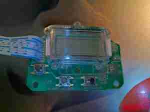
Here’s a DMD Android-based projector from China. This has quite good resolution at 720p native, although the install of Android present is very outdated, and the internal battery has a very short life due to the power draw of the unit.
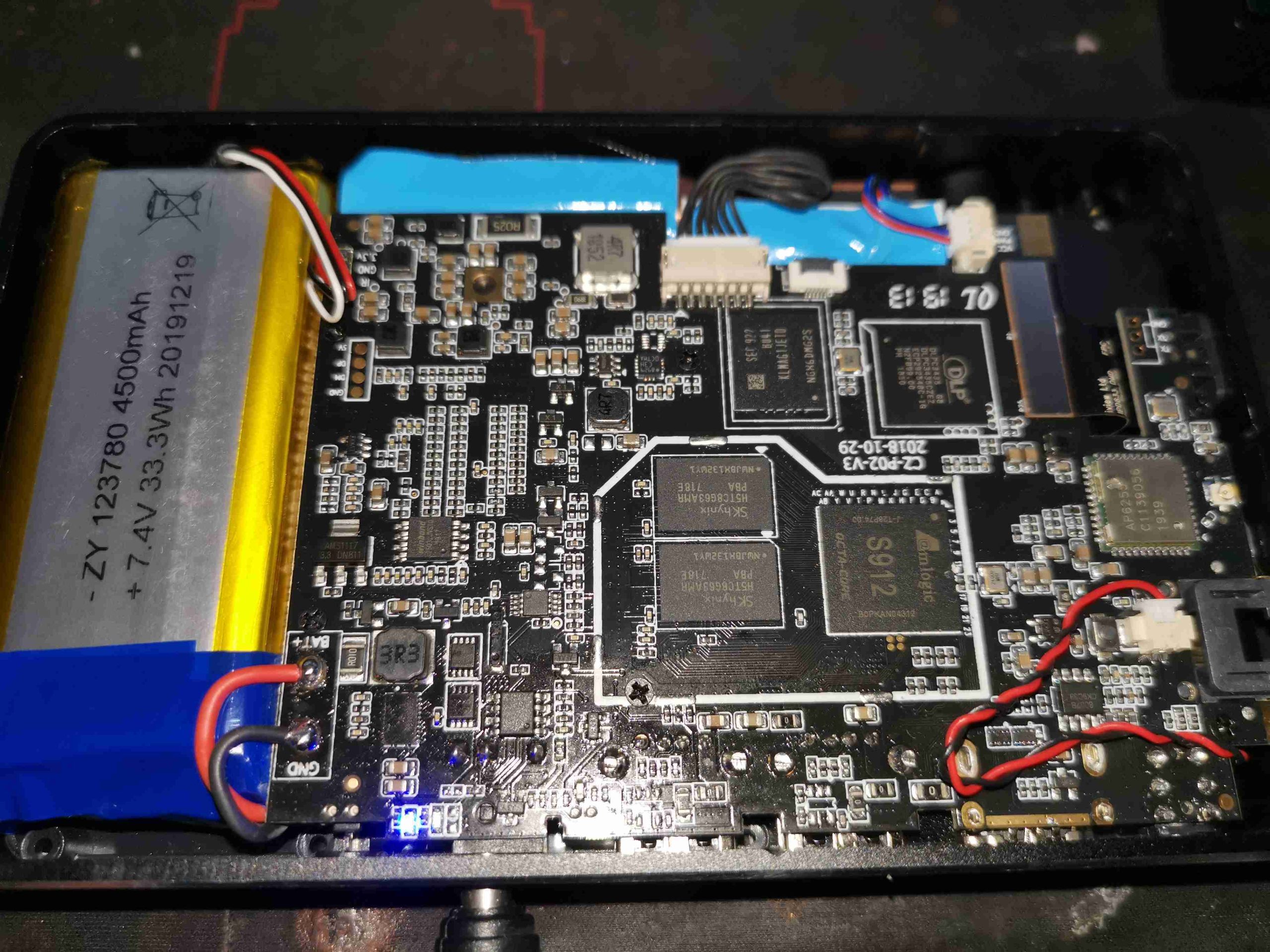
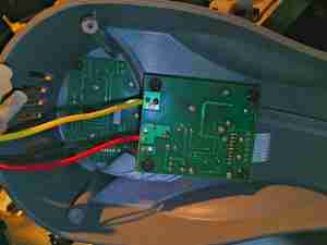
The top of the main PCB is above, and this has one half of the DMD chipset, and the SoC, Flash & RAM for the Android part of the projector.
Touchpad
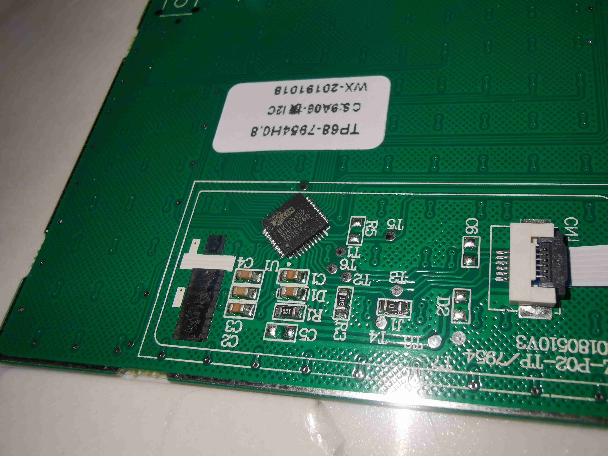
The top of the unit has touch buttons and mousepad for operation, in addition to an IR remote, the bottom of the lid moulding has the touch controller for those buttons and pad.
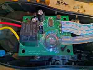
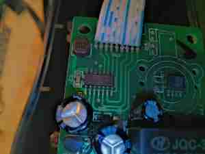
Mainboard
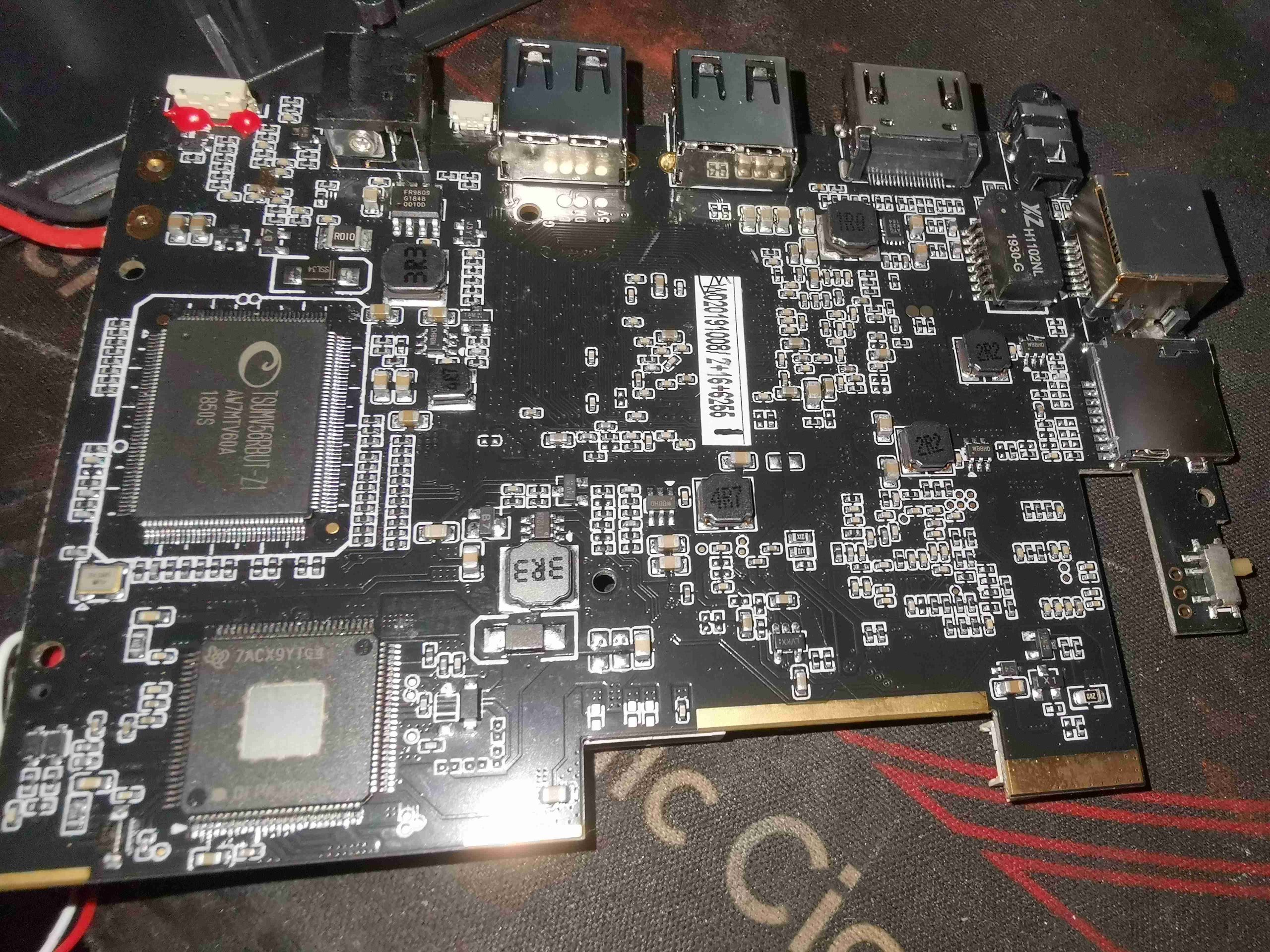
Removing the mainboard shows the rest of the chipset. The large IC at bottom left is one half of the DMD control chipset, and the large IC above that is a video switch to enable either the built in Android or external HDMI interfaces. The rest of the components here are power supply and general support.
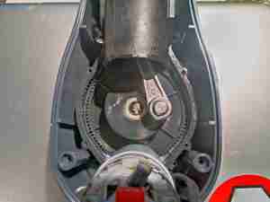
Projector Module
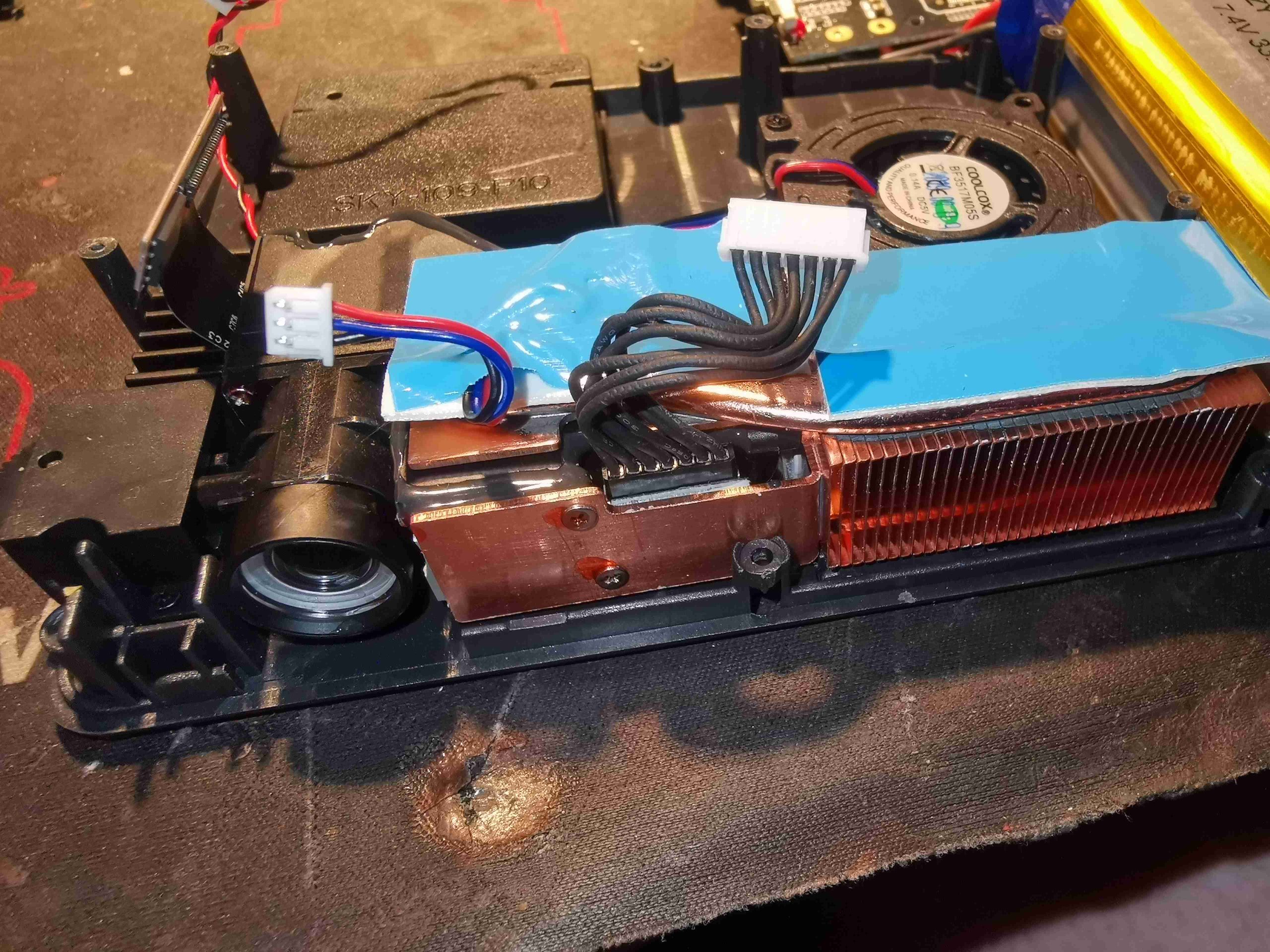
Under the mainboard is the projector module itself. Mostly heatsink just to cope with the high power LEDs, there’s a fan in the rear section that keeps everything cool.
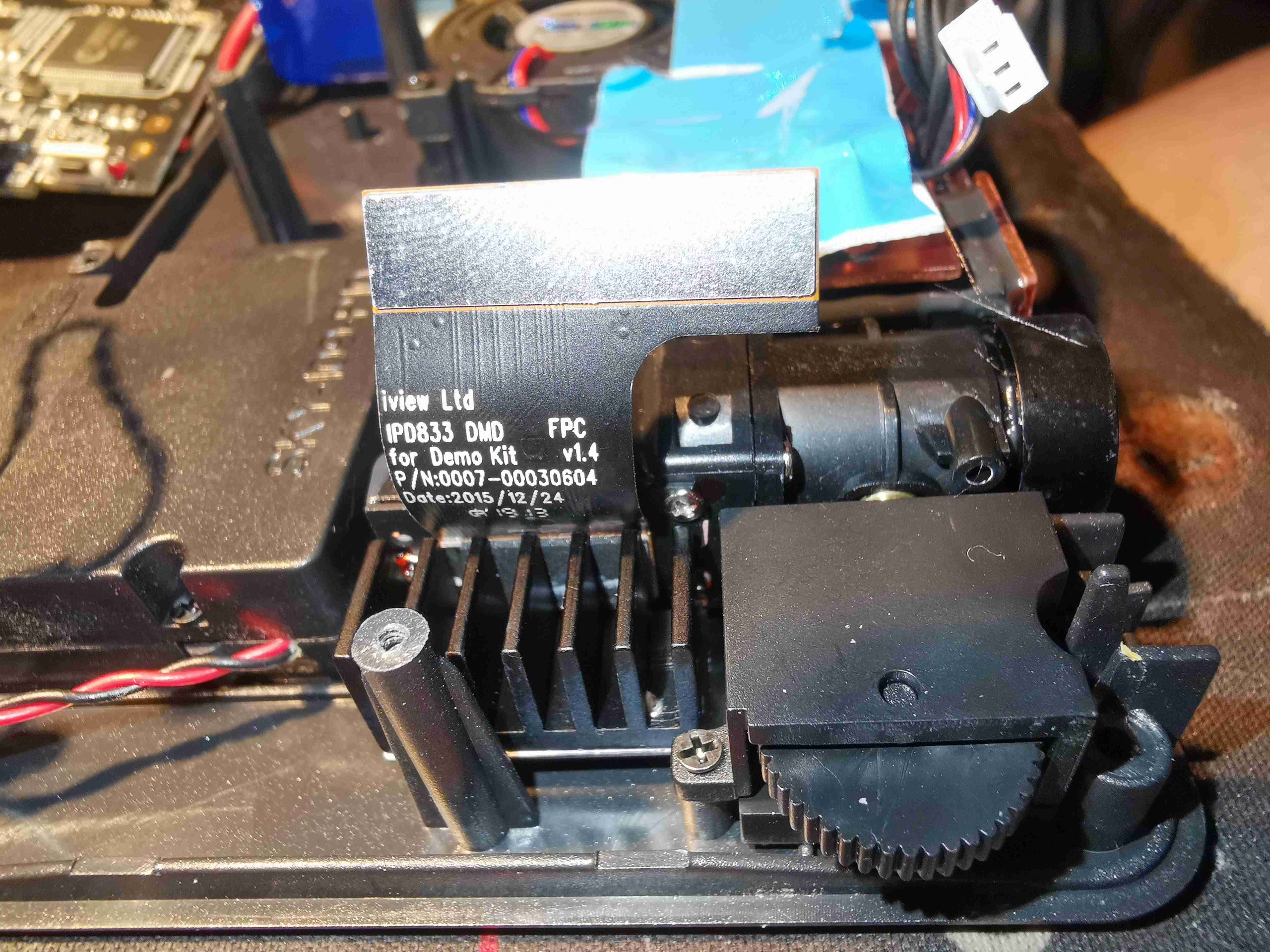
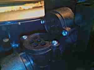
DMD Heatsink
The DMD module is definitely from a development kit – it’s hidden behind this small heatsink. The wheel in the foreground is for main focus.
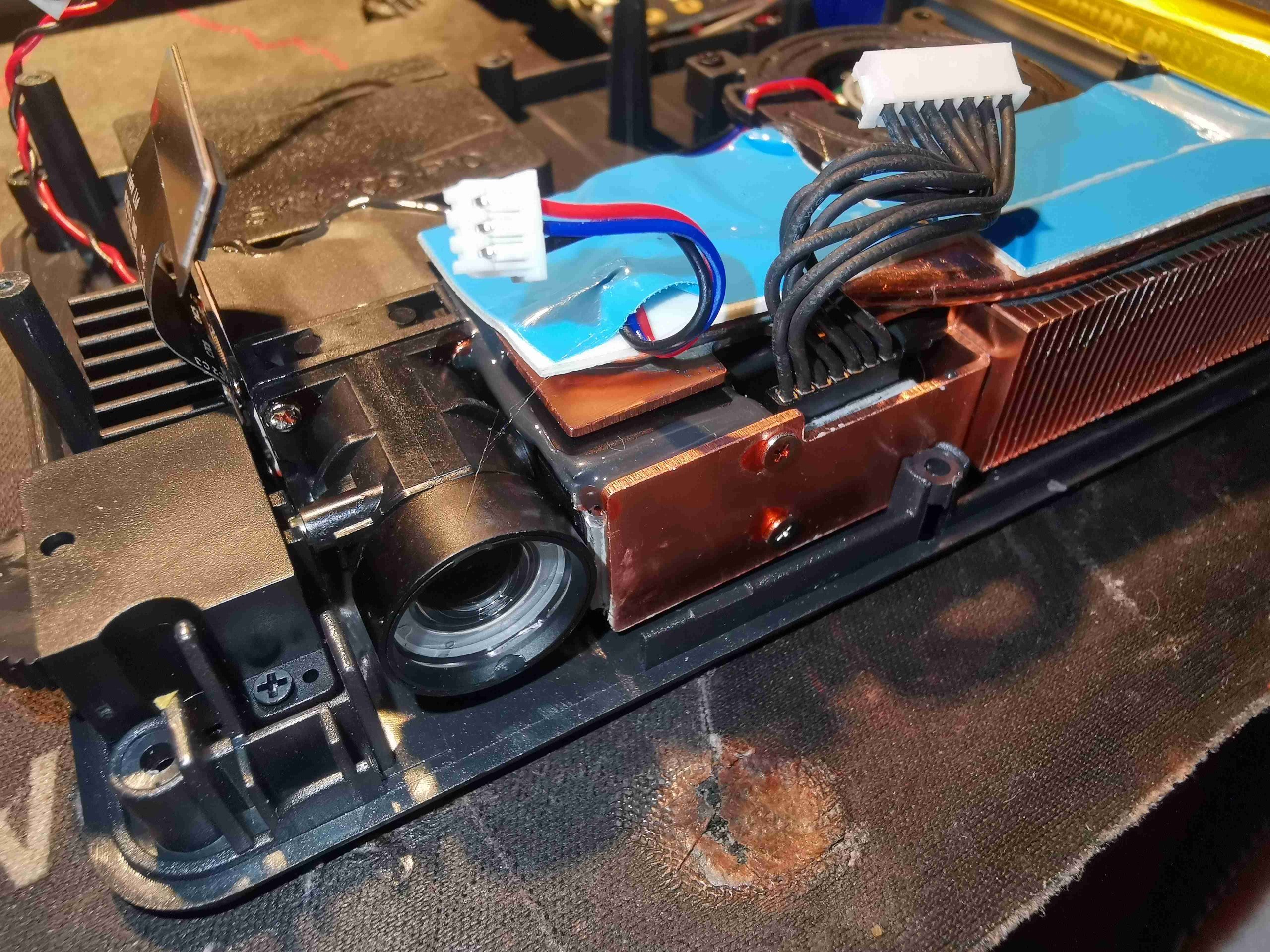
LED Module
On the front of the unit, behind the copper plate is the main RGB LED module, which is switched by the DMD chipset for full colour output from the main lens to the left.
Recently I figured it was about time I treated myself to a brand-new laptop, and as I was also in the market for a tablet at the same time, I figured I’d go with one of the “convertible” types that are about these days.
The HP x360 series are locally available to me for fairly reasonable prices, so I decided to go with one of these. With a Core i7-1165G7 11th Gen CPU, and factory with 16GB of RAM (upgradeable), and 512GB of NVMe SSD for storage as standard, I figured that this would be a snappy little laptop just for my general day to day use. Unfortunately my local supplier (Curry’s PC World), don’t actually give the model number, but it’s their stock code 676743.
As every machine does, they come with Windows pre-loaded, which is rather a pain. I’ve not used Windows in a production environment for over a decade, and I don’t plan on starting again now, so the first thingto do is image the NVMe SSD (having a backup of the original image is handy), and firing up a Linux Mint bootable USB. I did need to enter the BIOS to disable Secure Boot for this to work correctly.
There were some issues with the standard version of Mint 20.3 – namely no touch screen and no mousepad. It’s certainly not uncommon for really new hardware to have support issues in minstream builds of Linux, and as Mint 20.3 by default runs on Kernel version 5.4, this needed to be upgraded. (For reference Mint Edge Edition does come with a later version of the kernel as standard, but I didn’t have an image to hand).
The touchscreen controller and mousepad are both Elan products – an ELAN0749 04F3:31A5 for the mouse, and an ELAN2514 04F3:2CF3 for the touchscreen. Both are operated over I²C.
Once the kernel was updated to version 5.13, there were no more issues with the mousepad, and the touchscreen works es you expect a touchscreen to work. The only bug I’ve found so far is with the included smart pen – once the pen is detected finger touch stops working, and the only way to get it back is a full reboot, which is most annoying. This isn’t a massive issue for me, but hopefully driver support for the ELAN touchscreen controllers will improve with time.
Another upgrade I did straight away since I had the parts hanging around was to upgrade the RAM to a full 32GB. This is a very simple swapover – the bottom of the laptop does need to be removed, the screws for which are underneath the rubber feet on the bottom panel, which can be peeled back gently with fine tweezers for access. There are 5 screws in total.
Before the RAM upgrade, the system was quick under Linux – with a full 32GB there is much more capability. The NVMe drive is also replaceable, so this will probably get upgraded with time to at least 1TB.
Overall, I’m very happy with this HP laptop, I will post an update after I’ve had some time to get to know it better.
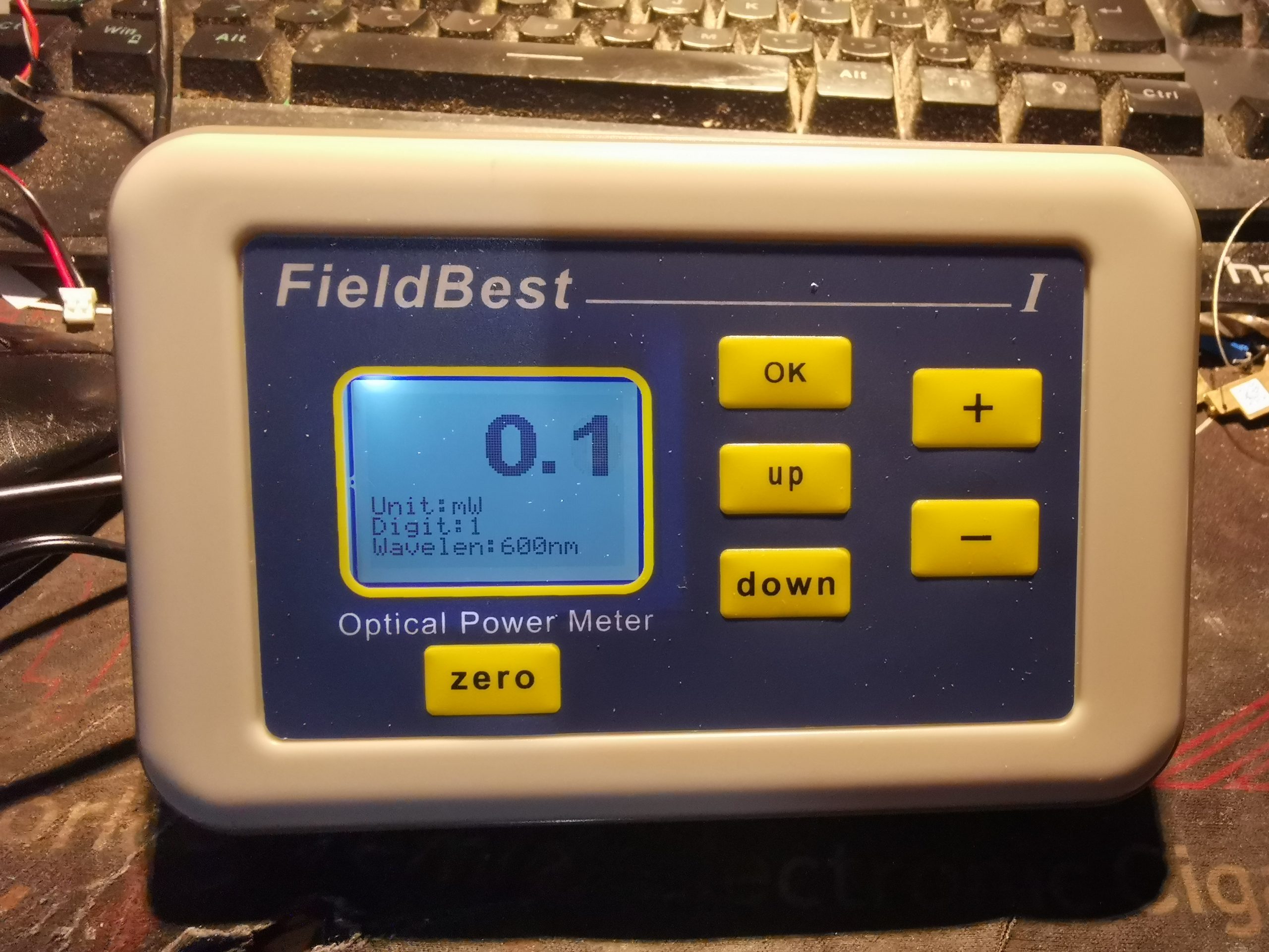
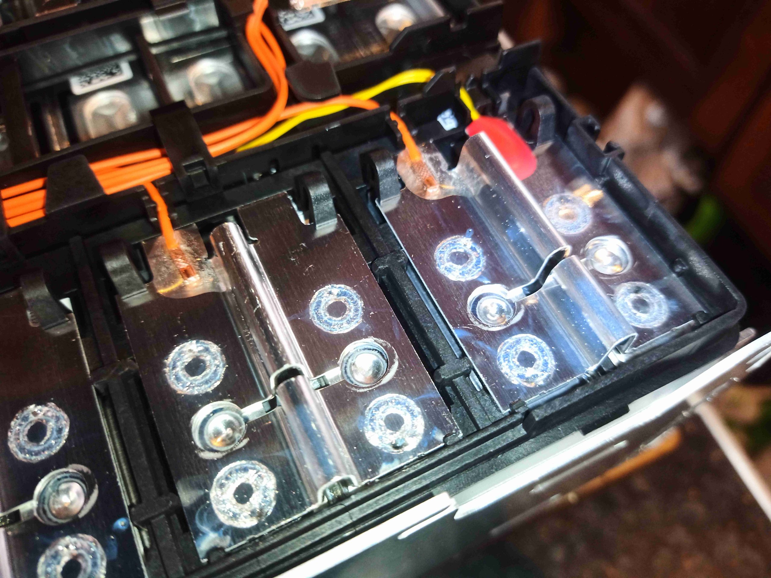
Since I’m building optical power meters at the moment, I figured it was time to see what the Chinese have to offer in this department, and these meters were on offer over on AliExpress, at over 50% off. This is the Fieldbest I meter, and I got two versions – the 1mW-2W & 10mW-50W model, with thermopile sensors. A graphical LCD provides the user interface, and there is also USB serial present for logging to a PC with software. These units appear to be made by a company called “Fastlaser Tech”, but I can’t seem to find much about them.
Rear Panel
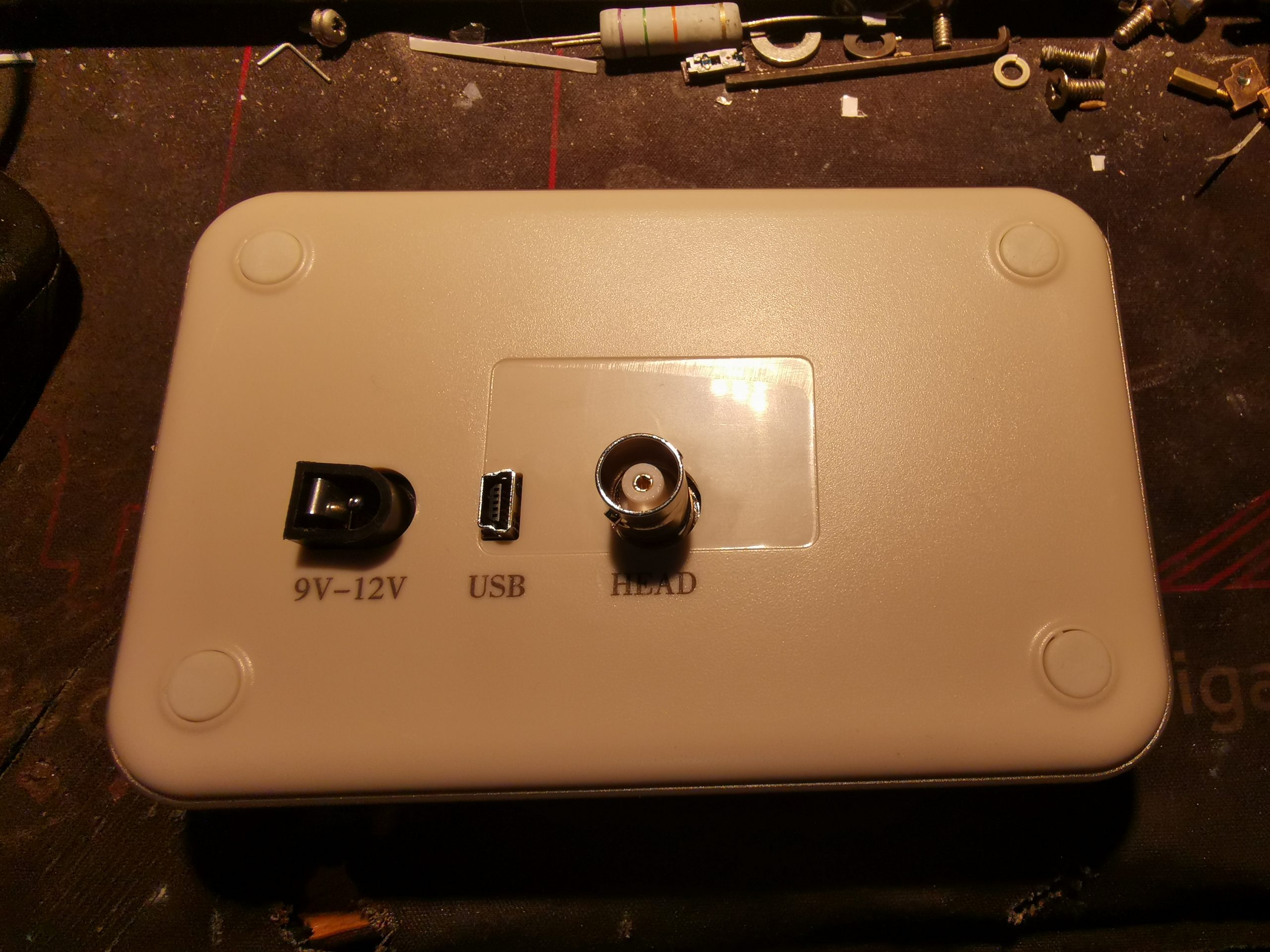
The rear panel has the power input, USB & the signal connection on BNC from the sensor head.
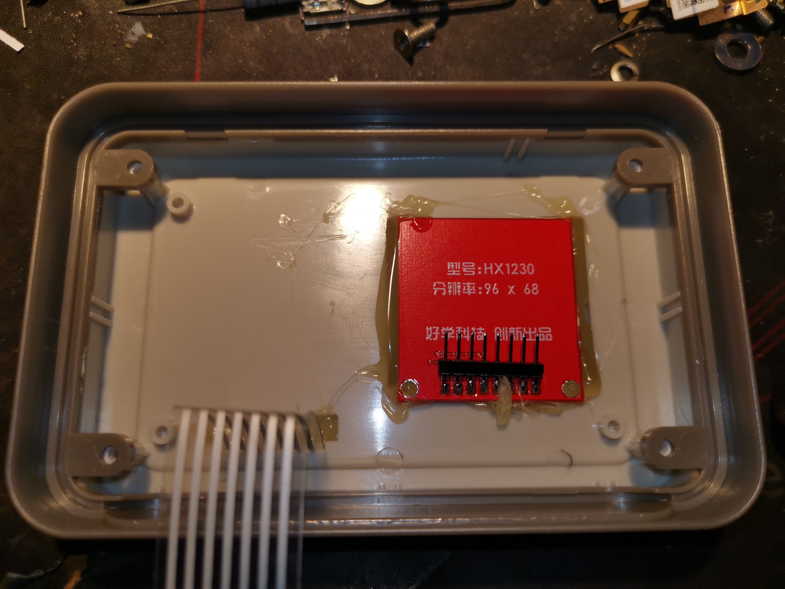
Front Cover
Inside the front cover there is a standard HX1230 LCD, and the flex to the front panel buttons. The LCD itself is rather roughly hot-glued in place.
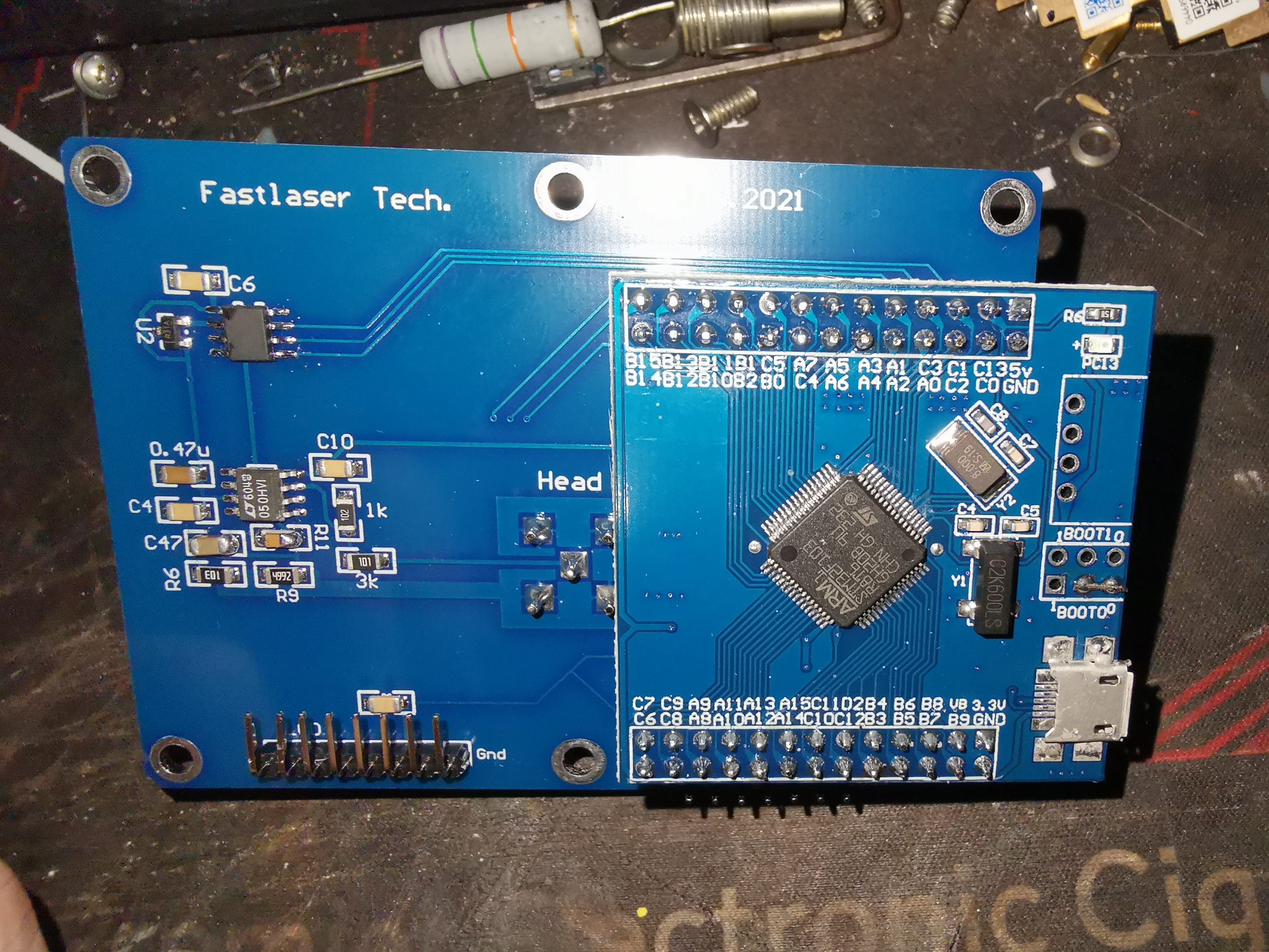
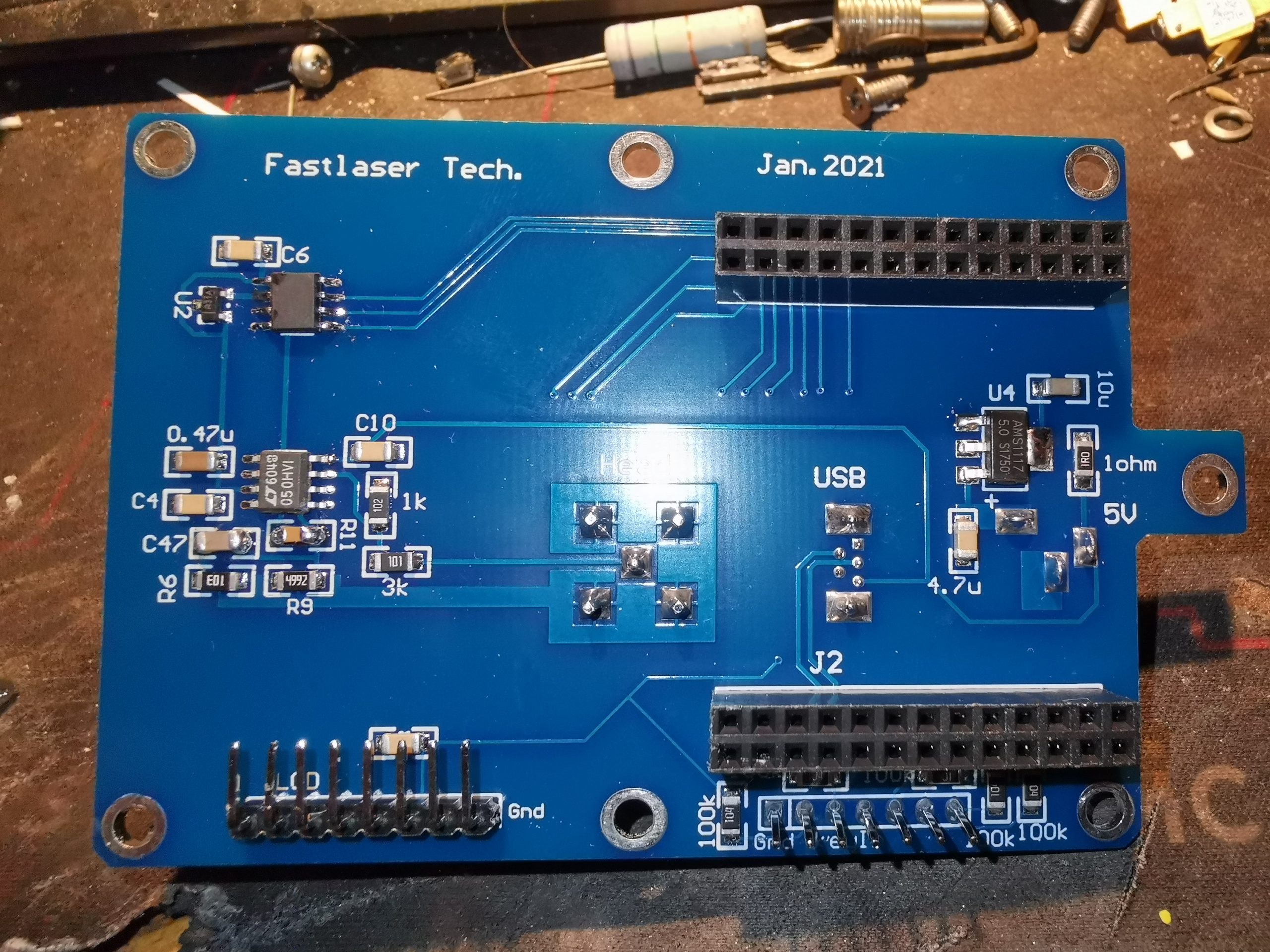
Boards Assembled
The PCB stack normally sits inside the rear cover, ans holds all the electronics required to run the meter. The main microcontroller is on a separate daughterboard, and looks a lot like a dev board! The input stages from the sensor head are on the left hand side of the PCB.
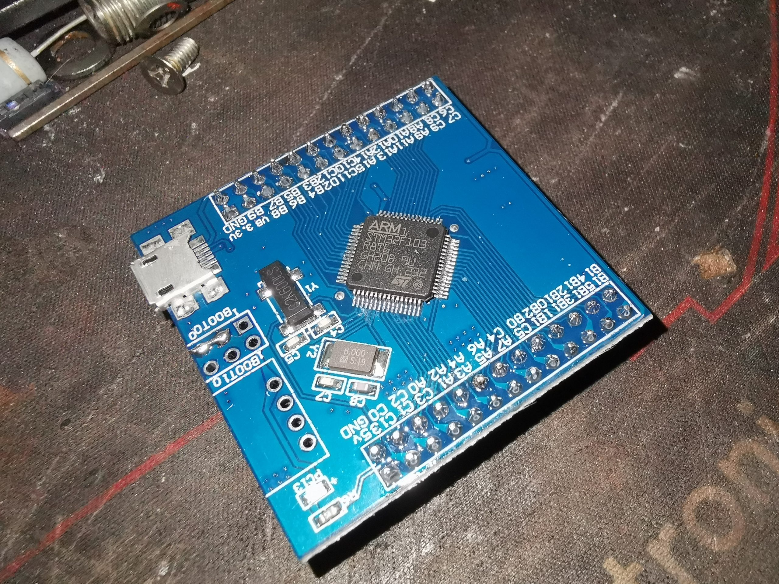
MCU Board
Here’s the MCU daughterboard, hosting the support components for the STM32F107 microcontroller. There’s a USB port on this board too, not sure what that one does yet.
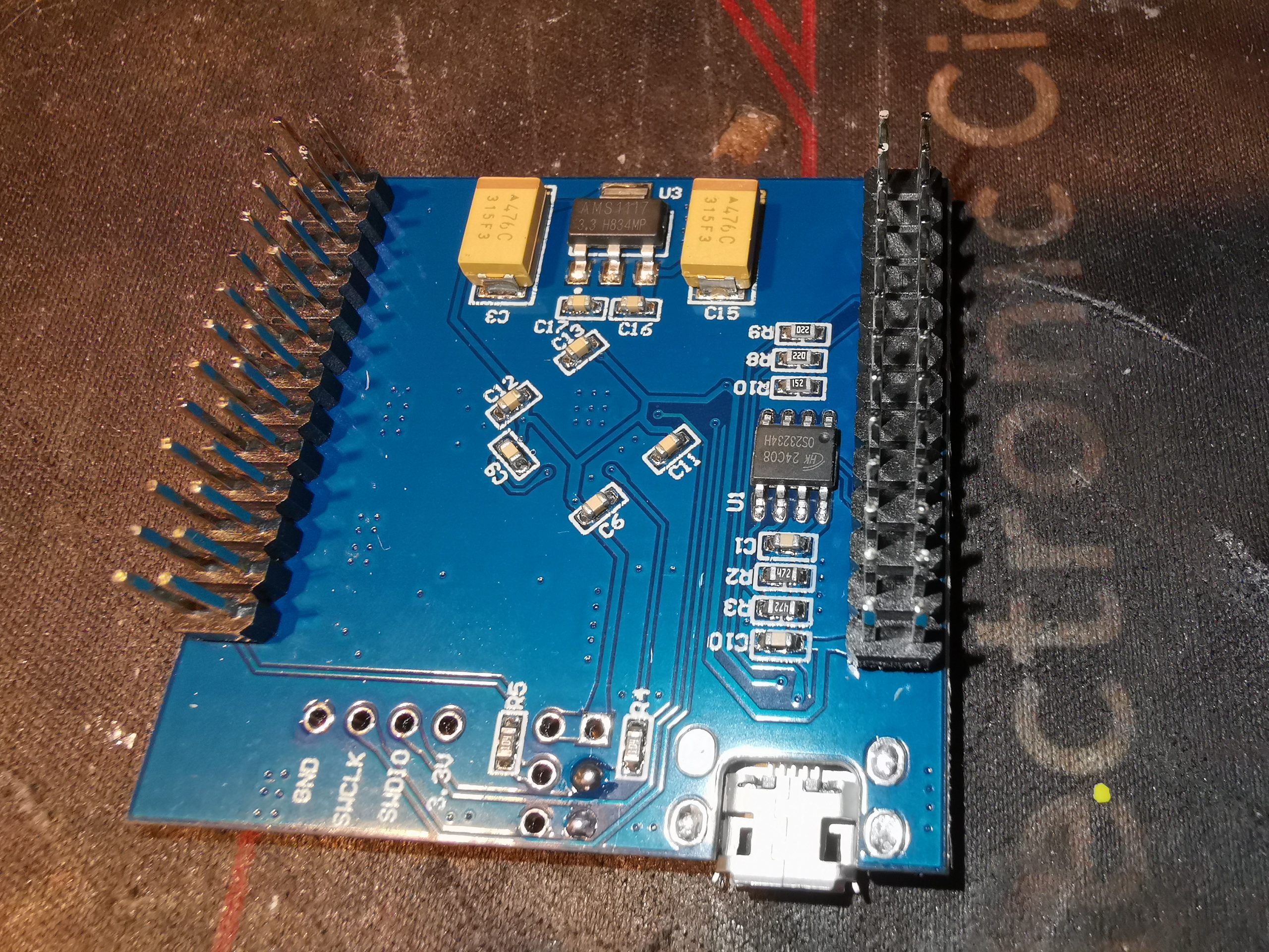
MCU Board Rear
Here’s the other side of the PCB, with a small EEPROM, and voltage regulator. The programming pins are on the bottom left.
Mainboard
Here’s the mainboard without the MCU daughterboard. Not much on these boards, very sparsely populated indeed!
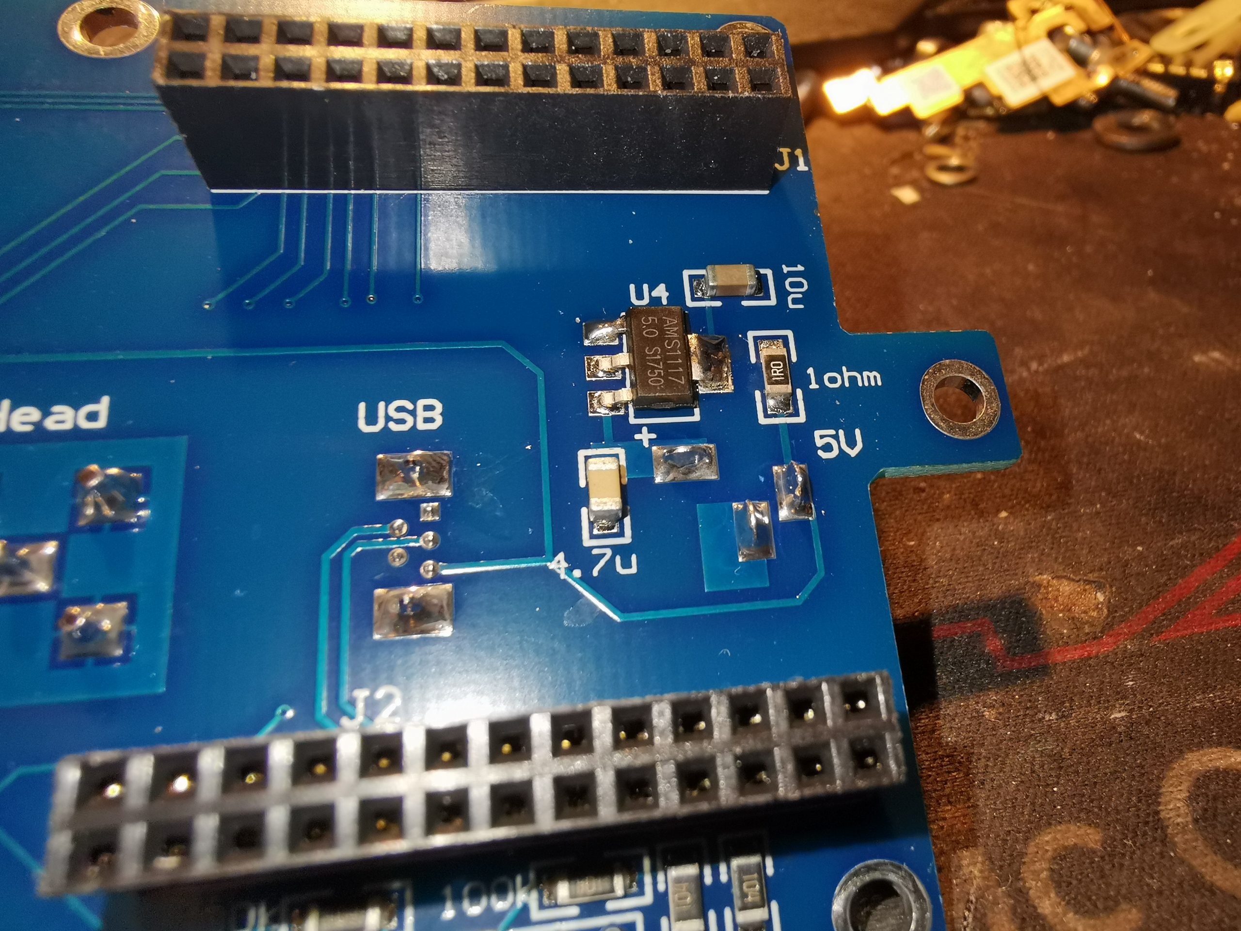
Voltage Regulator
There’s a AMS1117-5.0 regulator on the right, which takes the 9-12v input from the external PSU down to a 5v rail, very simple.
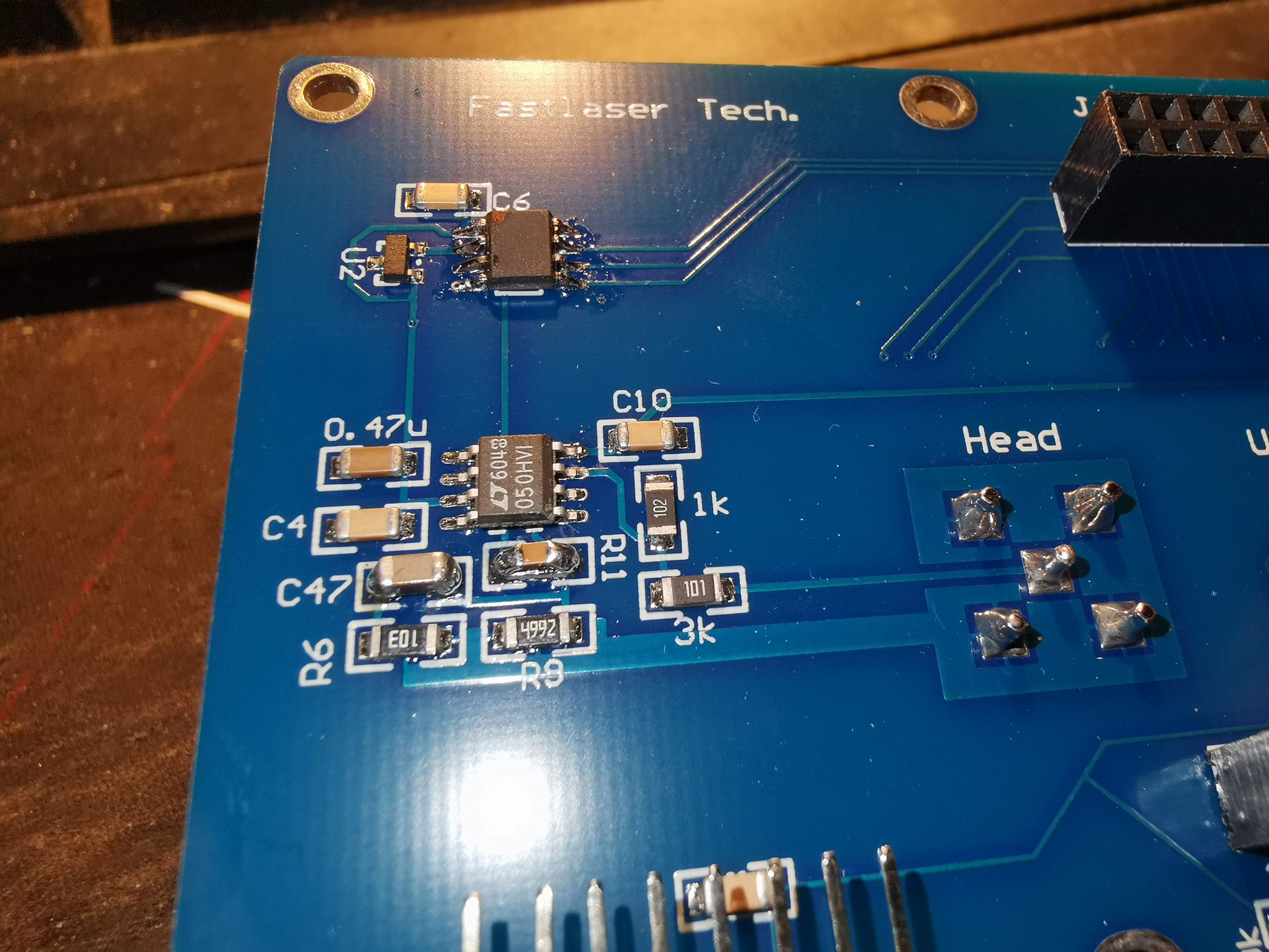
Sensor Head Input Circuitry
The input stage & A/D converter are on the left side of the board, consisting of an LT6004 dual Op-Amp, likely configured as a transimpedance amplifier, and a small A/D converter, which has had the number scrubbed off. It’s been said many times before that this is pointless, as it’s not too difficult to work out what parts have been used. In this case, everything matches to the LTC1286 12-Bit successive approximation sampling converter from Linear Tech, and it’s being controlled via SPI from the main microcontroller. A TL431 in a SOT23-3 package handles the need for a local stable voltage reference.
The time has come yet again, to reduce my rack footprint. For the last 5 years or so, this blog has been hosted on a small HP MicroServer Gen8, as at the time I needed a new host machine, and for some reason they were going by their thousands for rock-bottom cash. That machine has faithfully worked 24/7, without many gripes, but it’s time to concentrate things down to requiring less physical hardware.
What’s enabled me to sort this out, is performing a hardware rebuild on my main file server, which has for years been a Heath-Robinson affair.
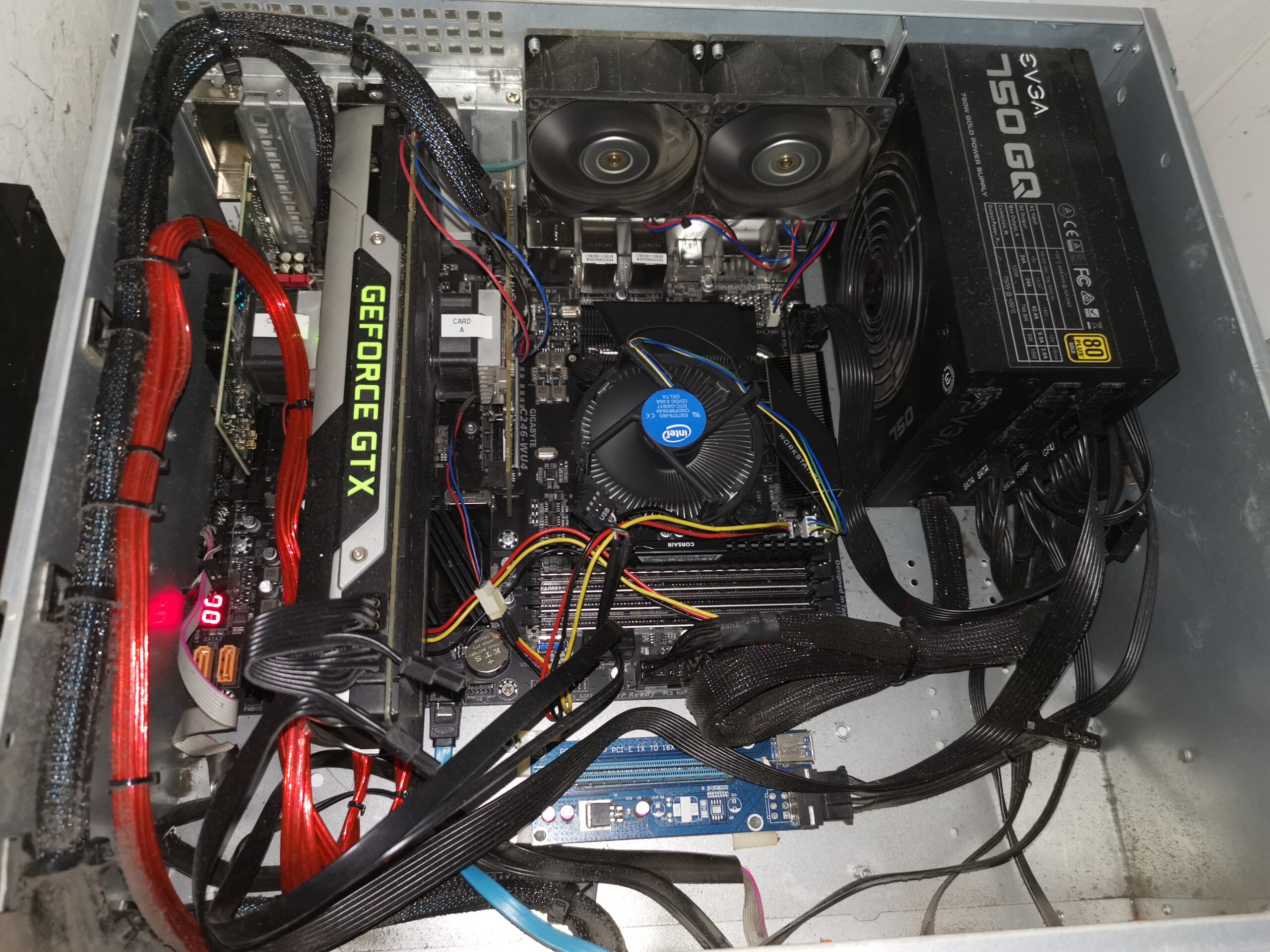
GPU & RAID Cards
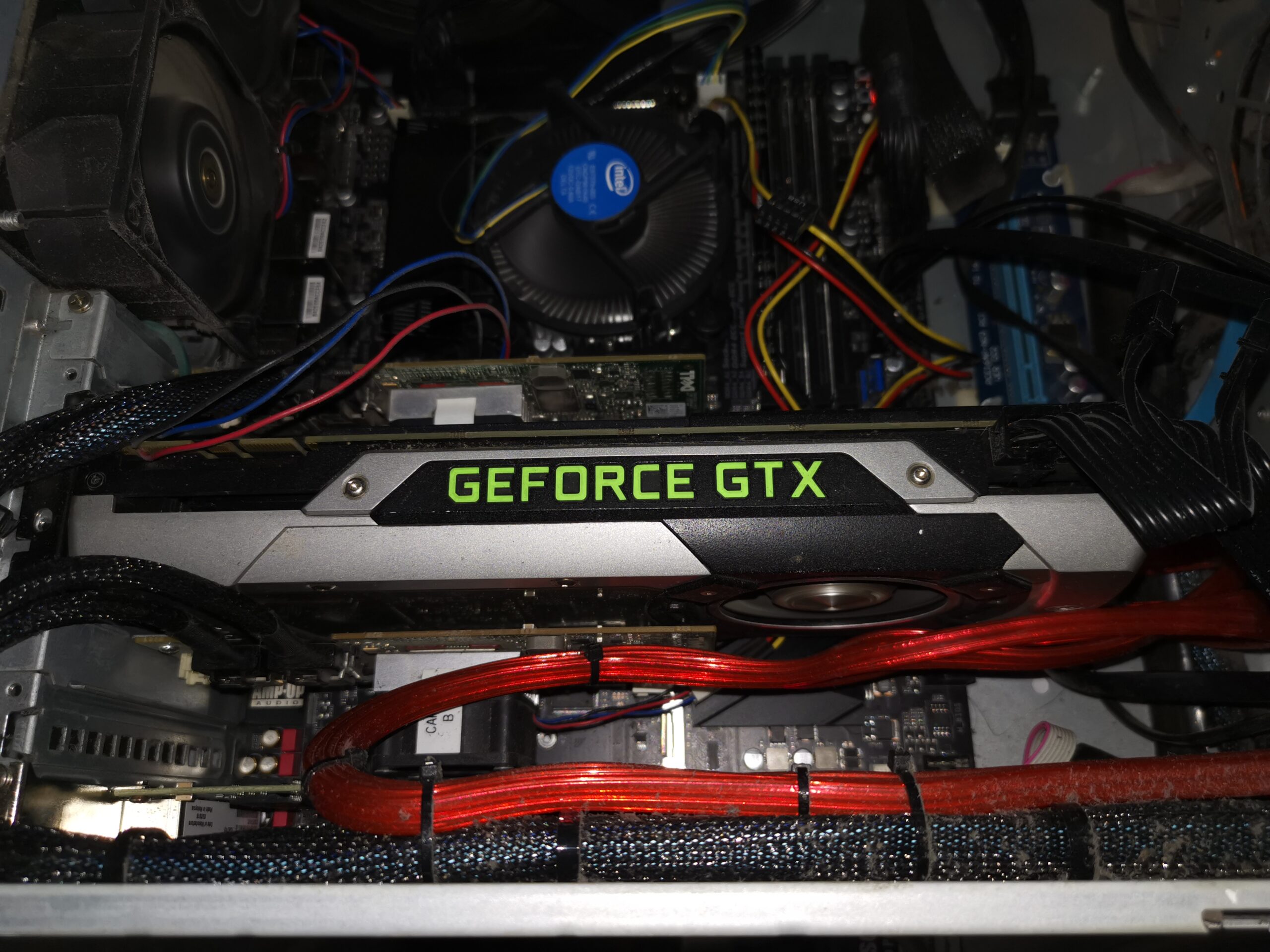
Well, the file server got ANOTHER upgrade, quite quickly. The motherboard was replaced again, this time with a new board, new Corsair RAM & a new Intel i7-9700F 8-Core CPU. As this server also runs video transcoding services, the tiny GPU got pulled & replaced with a spare nVidia GTX980 I had just for that task. My LSI RAID cards are still used as HBAs, just as JBOD, since Linux is running the main disk array via mdadm.
Server Internals
Once this upgrade was completed, with space for resource expansion – the motherboard supports up to 128GB RAM, at the moment there’s 32GB in there due to the eye-watering cost of RAM at the present time – there was scope for running some Virtualisation for other services.
Still running OpenMediaVault, based around Debian 10, I installed the Kernel KVM modules & QEMU, along with Cockpit for control. Going this route was dictated by VirtualBox not being directly supported in Debian 10, for reasons I don’t know.
Once all this was installed, and a network bridge set up for the VMs through a spare network interface, I brought up a pair of Debian 10 servers – one for PiHole which had up until this point been running on a spare Raspberry Pi for the last 6 or so years (I think the SD card is totally shot at this point!), and one for my web App server.
At the moment, all the VMs are running from the main RAID6 spinning rust array, which is a little slow, but the next planned upgrade is to move the VM subsystem to it’s own RAID10 array of disks, hopefully speeding things up – there are just enough SATA ports left on the motherboard to accommodate 6 more drives, and with both 5.25″ disk bays being available for caddies, this should be a simple fix.
As a result, I’m down to a single server powering my entire online domain, and a reduction in power usage!
Well, while working on the boat’s engine, I was surprised by this little sod, who’d managed to crawl into the air intake skin fitting on the transom, and got very irritated at the engine being fired up! How the little dude avoided getting sucked into one of the cylinders, I have no idea! The wee mouse was recovered from the air intake & released on the towpath.
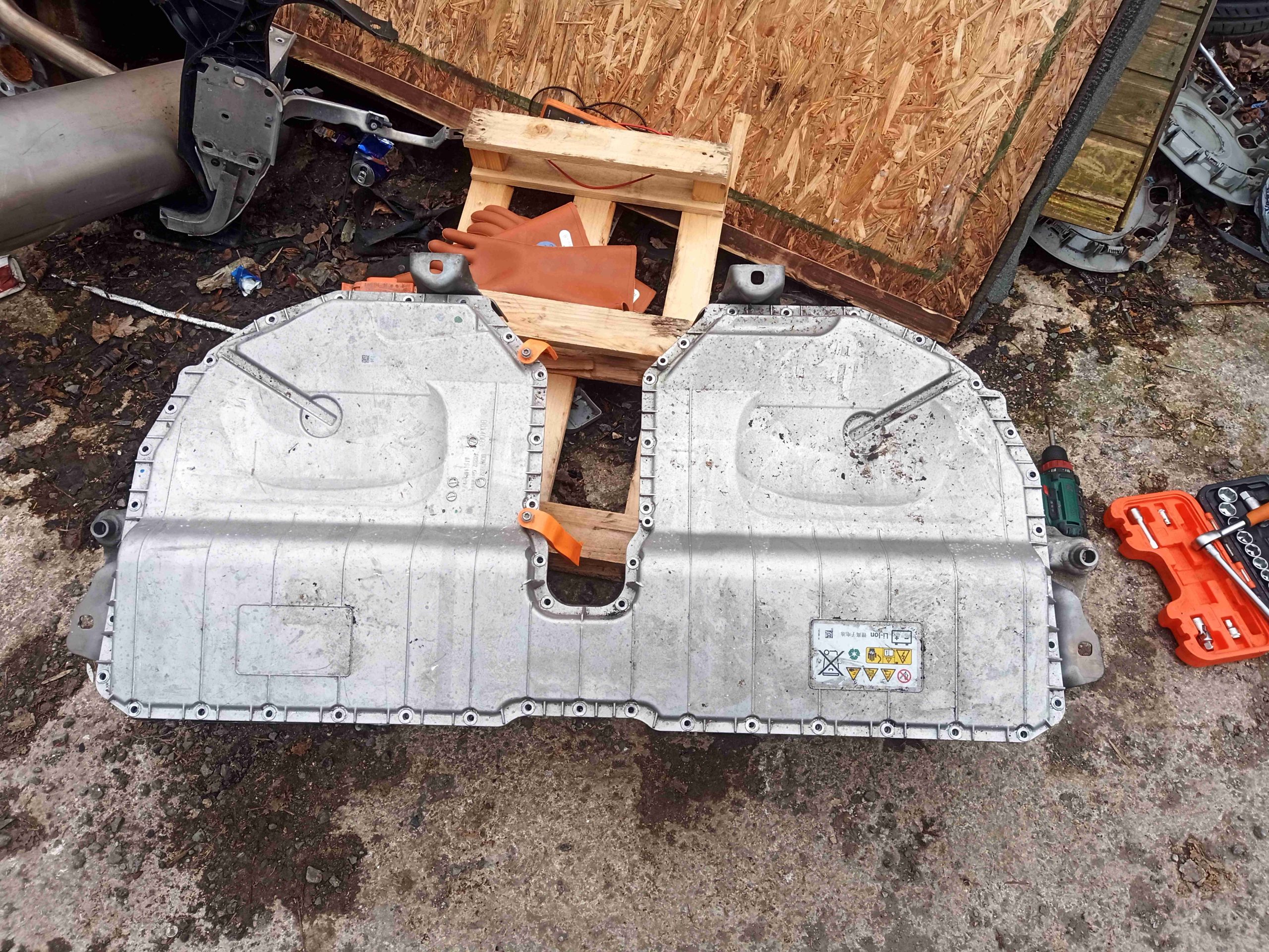
Here’s something I didn’t think I’d be doing! Here’s a teardown of a BMW 5 Series G30 530E Hybrid Battery pack – a monster 351V, 9.2kWh Lithium pack, obtained for it’s cells to replace the boat’s aging lead acids.
This is something I didn’t have the safety gear to do right of the bat – opening one of these packs is a potentially lethal exercise, with 6 unfused battery modules in series, quite capable of blowing pieces off a nice conductive sack of salt water like a person. Cue the purchase of high-voltage rated gloves for protection, just while I got the pack split into something more manageable.
Needless to say, the combination of current capacity & voltage present in EV or Hybrid vehicle battery packs is nothing short of lethal, and these units should be treated with considerable respect.
Hybrid Battery Pack
Here’s the beast of a battery. Enclosed in an aluminium cast housing, it’s very heavy, and definitely not a one-man lift!
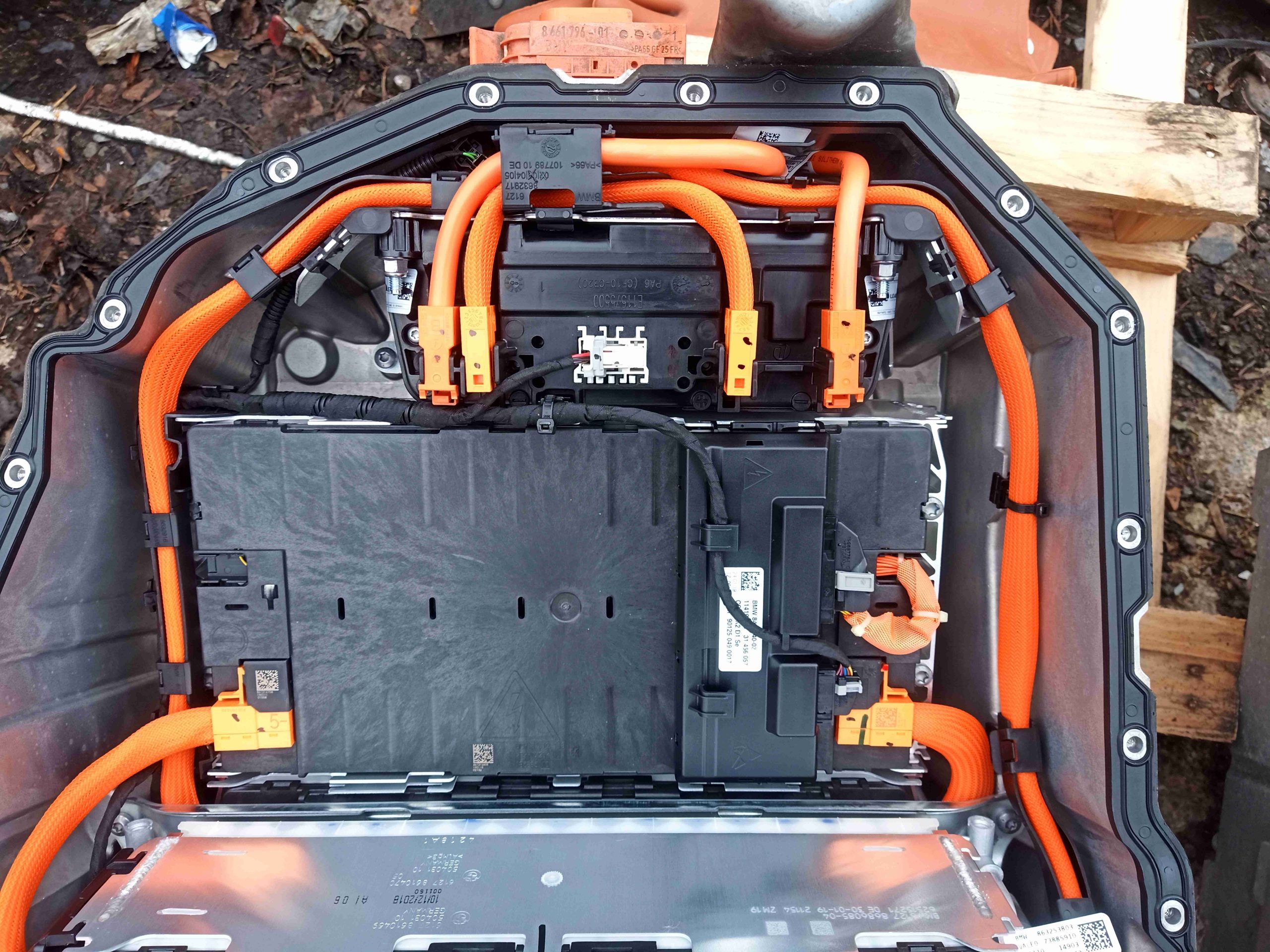
Cover Removed
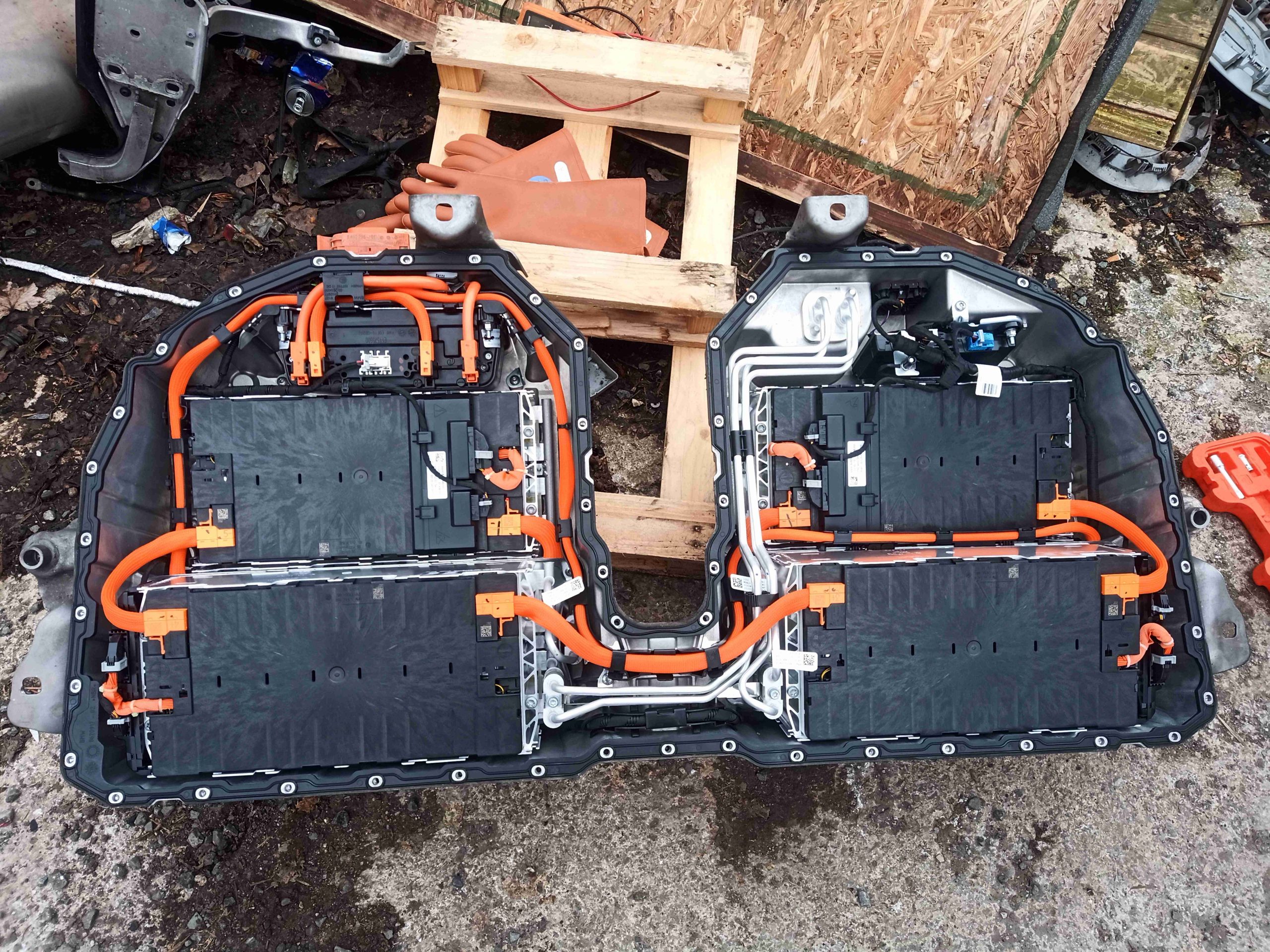
After removing the top cover, secured by combination Torx/10mm hex bolts, the internals of the pack are visible. There’s no sealant on the cover, just a large rubber gasket, so this came off easily. There are 6 individual modules in this pack, all wired in series with massive links. There’s also a cooling system for each battery module, supplied with refrigerant from the car’s AC system – there’s a TXV mounted on the side of the battery pack. I didn’t see any heaters present, but I don’t know if BMW have done any neat reverse-cycle magic to also heat the modules if required using the AC system on the car.
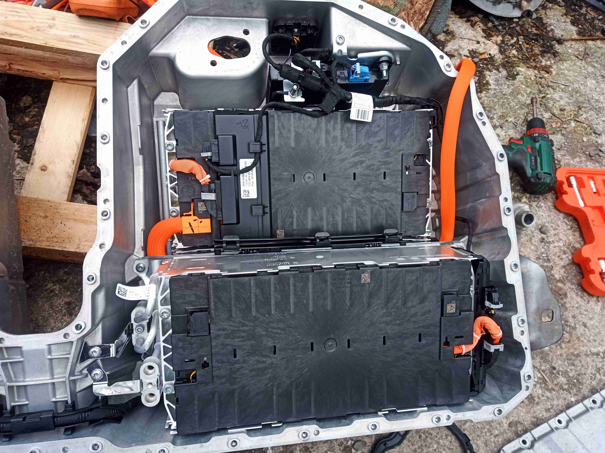
Left Side Modules
The modules are arranged 3 to a side, double-stacked at the back, then a single module at the front. The pack would normally sit under the rear seats of the vehicle, hence the unusual shape. The refrigerant lines going to the evaporators on this side of the pack can be seen in the bottom right corner.
Output Cables & Contactor Pack
The main contactor pack is on the left side, just behind the massive DC output connector. I’ll dig into this in another post later on.
Right Side Modules
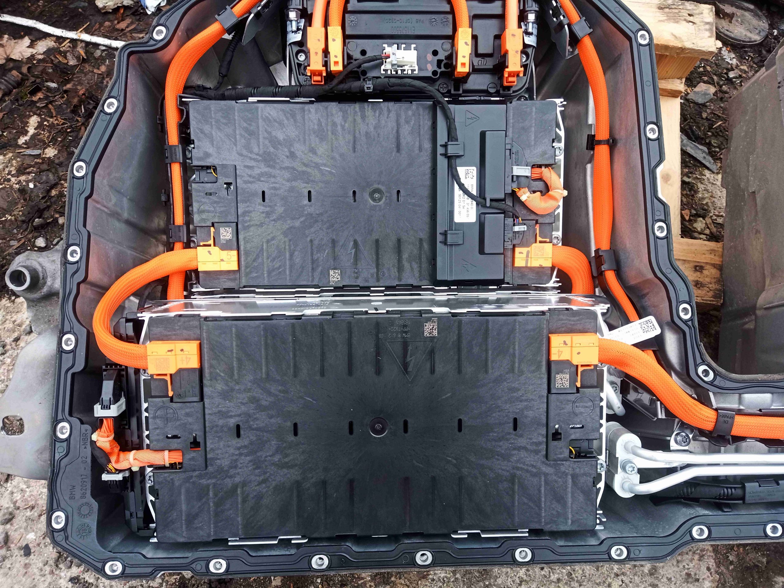
The right side of the pack is arranged much the same as the left, the main difference here being the battery ECU is tucked in at the top here, along with the interface connector to the car, and the refrigerant lines to the TXV on the outside, which I’ve already removed. Each module has a cell balance control unit, in this case one is mounted on the top of a module, and on the side of the module in the lower right corner.
Cooling Evaporator
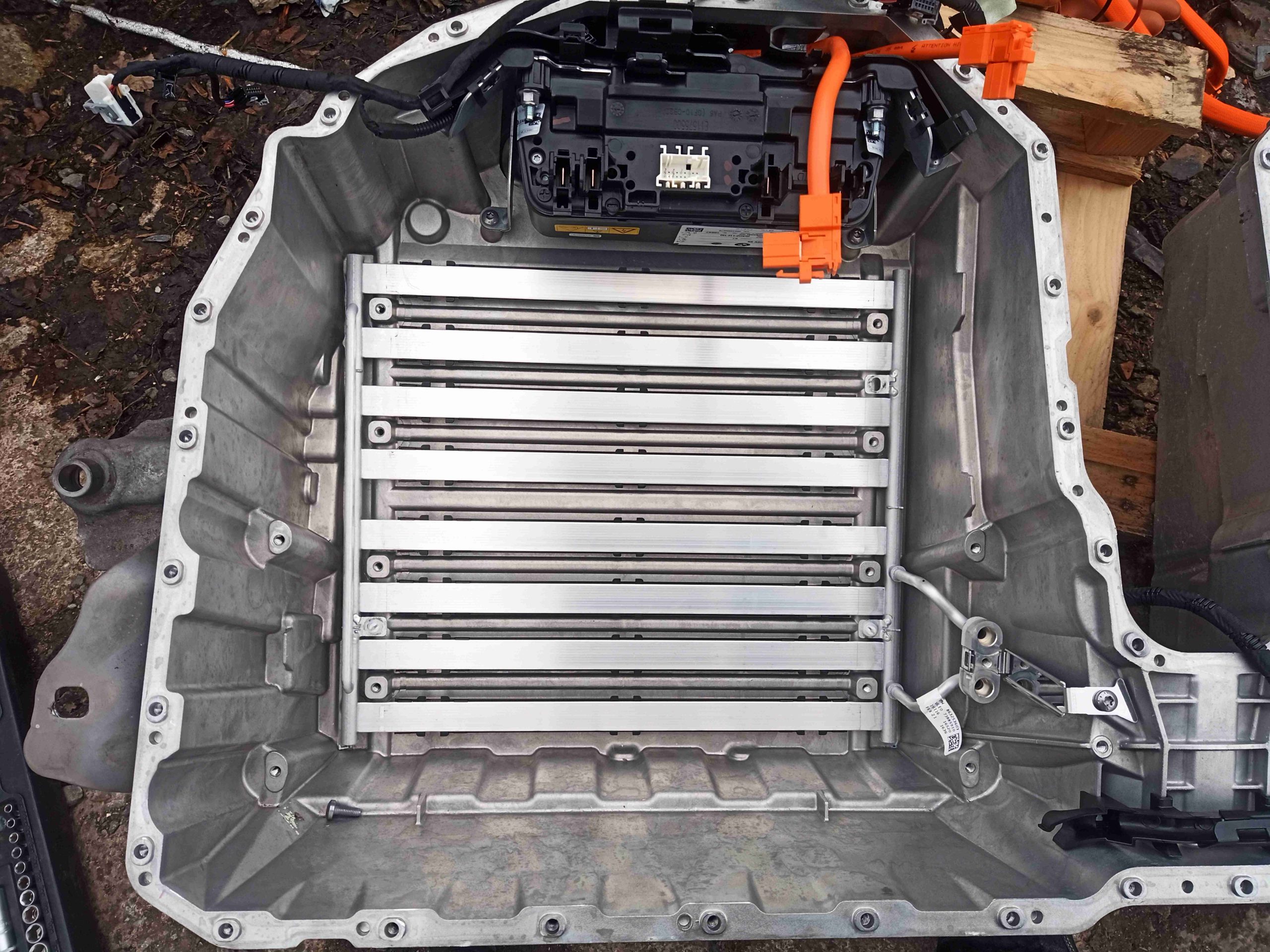
Once all the modules have been removed, the evaporator matrix is visible on the bottom, a series of very thin aluminium tubes, designed for the best contact with the aluminium frame of the battery modules.
Module Cell Layout
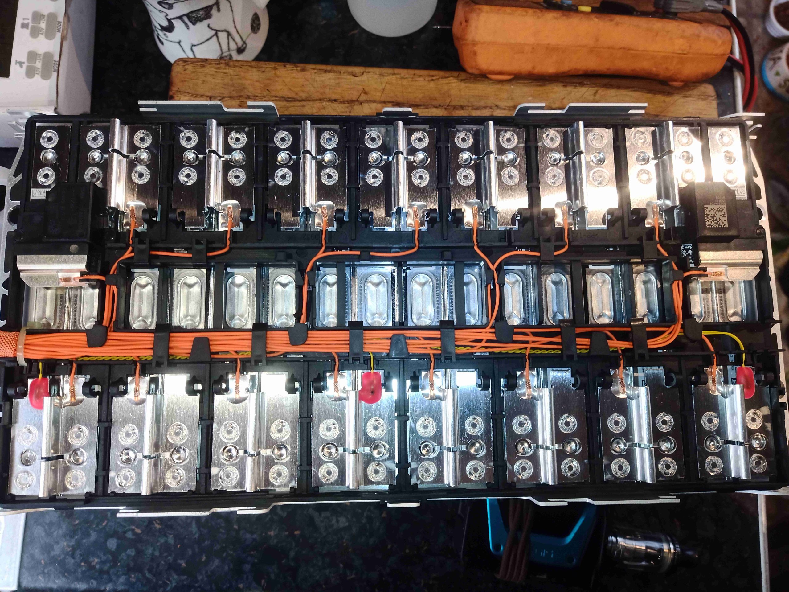
Popping the plastic insulating cover off the battery module reveals the internal construction. I’ve not been able to find exact data on these cells, but I’m assuming them to be a similar chemistry to the ones used in the BMW i3 packs, so 4.15v Max, 3.68v nominal, 2.7v Minimum. The alloy frame itself is of laser welded construction, and there are 16 cells in series per module, giving about 58.8v per module. These will need to be reconfigured as 4 sets of 4 cells in series for 14.72v.
All the individual cell taps are nicely loomed down the middle of the module to each cell, and there are 3 temperature sensors per module (the red epoxy blobs).
Cell Welded Links
The individual cell links are laser welded to the terminals of the cells, so this does make life a little more difficult when it comes to reconfiguring them. The links appear to be made from Aluminium, so soldering is going to be a bit more tricky than usual.
These days USB powerbanks are very common – ranging in capacity from about 1Ah, to about 20Ah. Internally, they’ve all got much the same format:
Lithium Ion cylindrical or Lithium polymer pouch cells for energy storage
DC-DC boost converter
Microcontroller & LED Battery Gauge Display
Lithium cell protection & charge control
As the maximum voltage of a lithium cell for common chemistries is 4.2v, there needs to be a DC-DC converter to boost the voltage up to 5v for the USB ports – There are dedicated chipsets designed for powerbank use available everywhere for this part, and this section is going to be the most energy-wasteful part of the system.
To get a handle on the discharge efficiency of these units, I ran some tests with a constant current load, on different powerbanks from different manufacturers. All were in the range from 5Ah-20Ah, and all had ports rated for 2.1A Max output current.
The load was set for a nominal 2A current, and the powerbanks were fully charged before a discharge cycle. All powerbanks were in new condition to ensure that age-related degradation of the cells wasn’t going to be much of a factor.
Without further ado, here’s some test results:
Nameplate Capacity (Wh @3.7v Cell Nominal)
Nameplate Capacity (Ah)
Measured Capacity (Wh, Calculated @5V Output)
Measured Capacity (Ah)
Ah Efficiency %
44.4Wh
12Ah
31.65
6.33Ah
52.75
37Wh
10Ah
33.8
6.76Ah
67.6
74Wh
20Ah
56.5
11.3Ah
56.5
22.2Wh
6Ah
17.9
3.58Ah
59.67
18.5Wh
5Ah
15.04
3.01Ah
60.2
18.5Wh
5Ah
12.45
2.49Ah
49.8
22.2Wh
6Ah
19
3.80Ah
63.33
37Wh
10Ah
30.85
6.17Ah
61.7
55.5Wh
15Ah
48.6
9.72Ah
64.8
18.5Wh
5Ah
15.25
3.05Ah
61
Overall, these efficiency numbers are pretty poor with an average of 59.735% across these 9 samples. I expected at least high 80’s for efficiency on powerbank DC-DC converters, which must be pretty well specialised for the input voltage range by now. I suspect this is mostly to do with keeping costs down in mass production.
It occurred to me the other day that I’ve been running this blog now for over 10 years! This is the second iteration, as the first was lost in a server crash shortly after it went live. (Wasn’t so good with backups back then!). In that time the traffic to the blog has grown exponentially, who’d have thought that people would actually like reading most of the waffle that comes out of my brain! 😉
2020 Stats
It seems the global Covid-19 Pandemic actually had an effect on my visitor numbers as well.
At the moment things are becoming a little cluttered on the back end, and there are a few errors that need sorting on the front end – thanks to some of my readers for pointing some of those out!
Site Theming
I’ve also been using the same theme for most of that time, but it’s beginning to show now with many updates over the years, and no updates to the theme code, that I’m going to start having some issues with the next versions of PHP, so this will have to change. This does join up with another project I have going, for a small webshop. The current theme unfortunately isn’t compatible with the most popular WordPress commerce plugins.
Broken Downloads
Thanks again to my readers for catching this one! It seems most of the downloads on the site have become broken, although I’m not sure why. I have changed over the Download plugin, and I am in the process of slowly moving over the shortcodes to the new system, so they will all be operational again.
On-Disk Size
Over the last decade or so of running, this blog has grown massively in size on disk – the usage currently stands at around 80GB. I really do need to reduce this footprint, so some time will have to be taken going through the backend filesystem to prune out any crap.
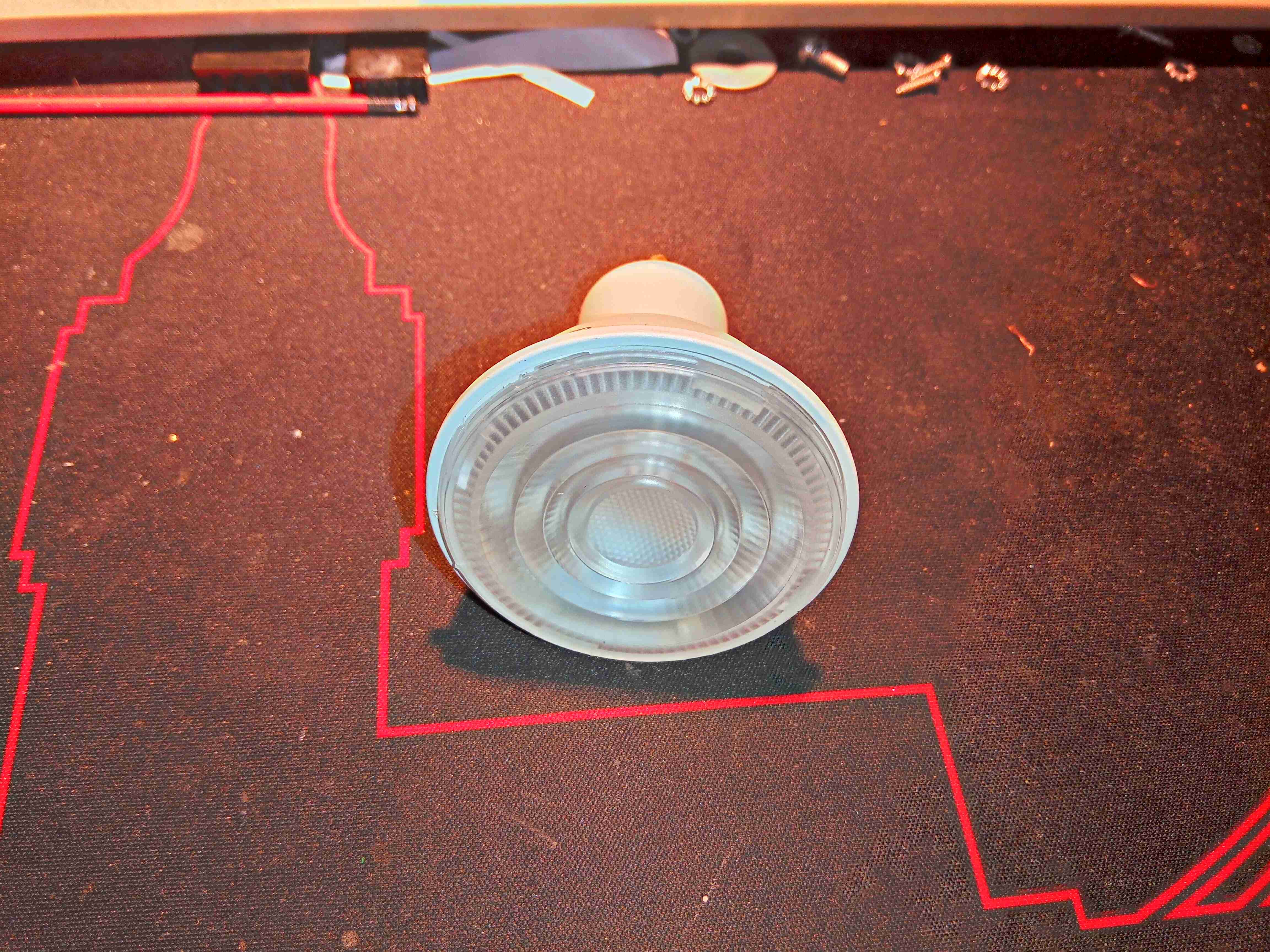
Here’s a recently failed 5W GU10 lamp, which is completely dead – not even a single LED still shining.
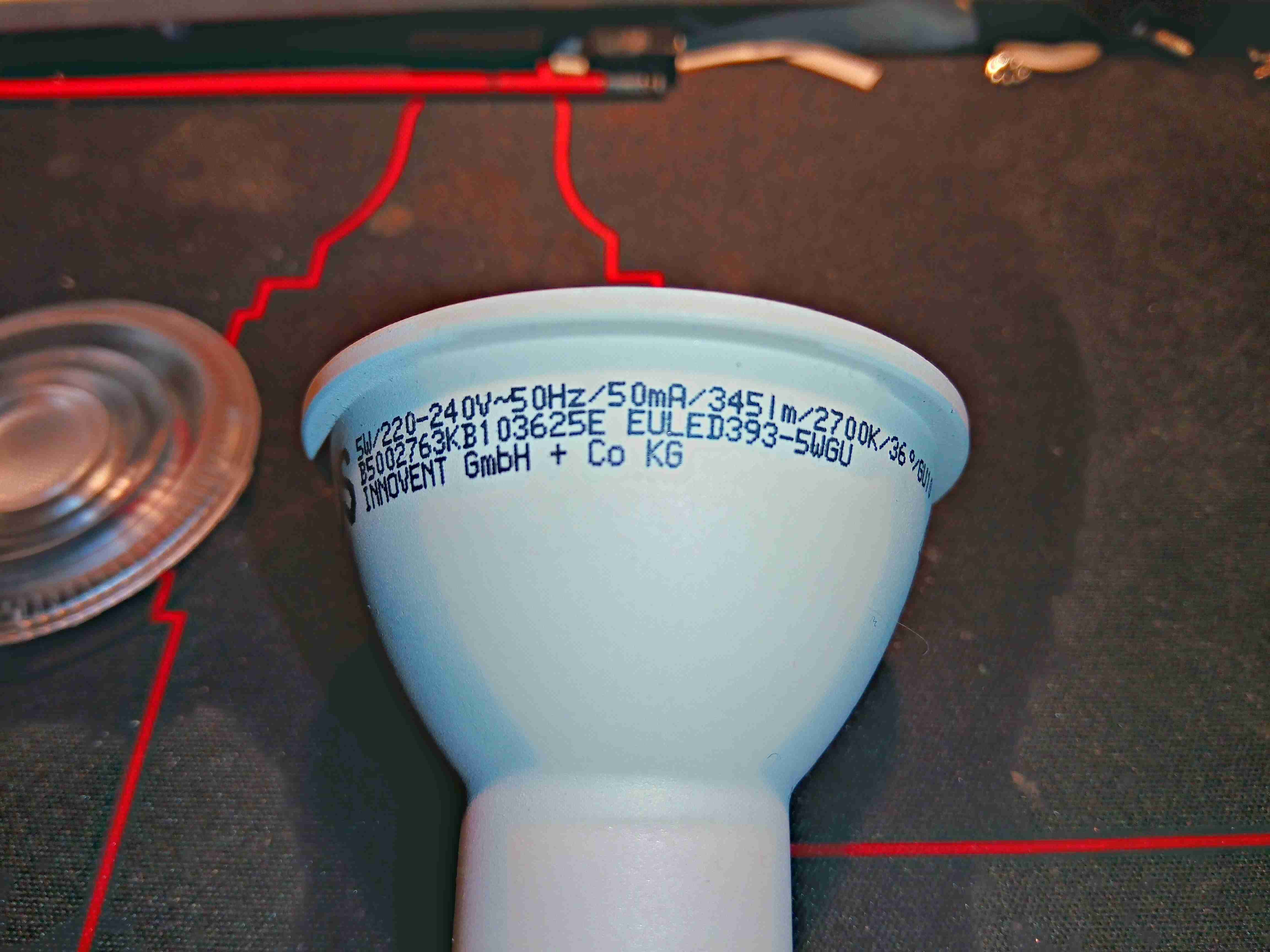
Markings
According to the markings, this lamp draws 50mA at 230v & outputs 345 lumens
Lens Removed
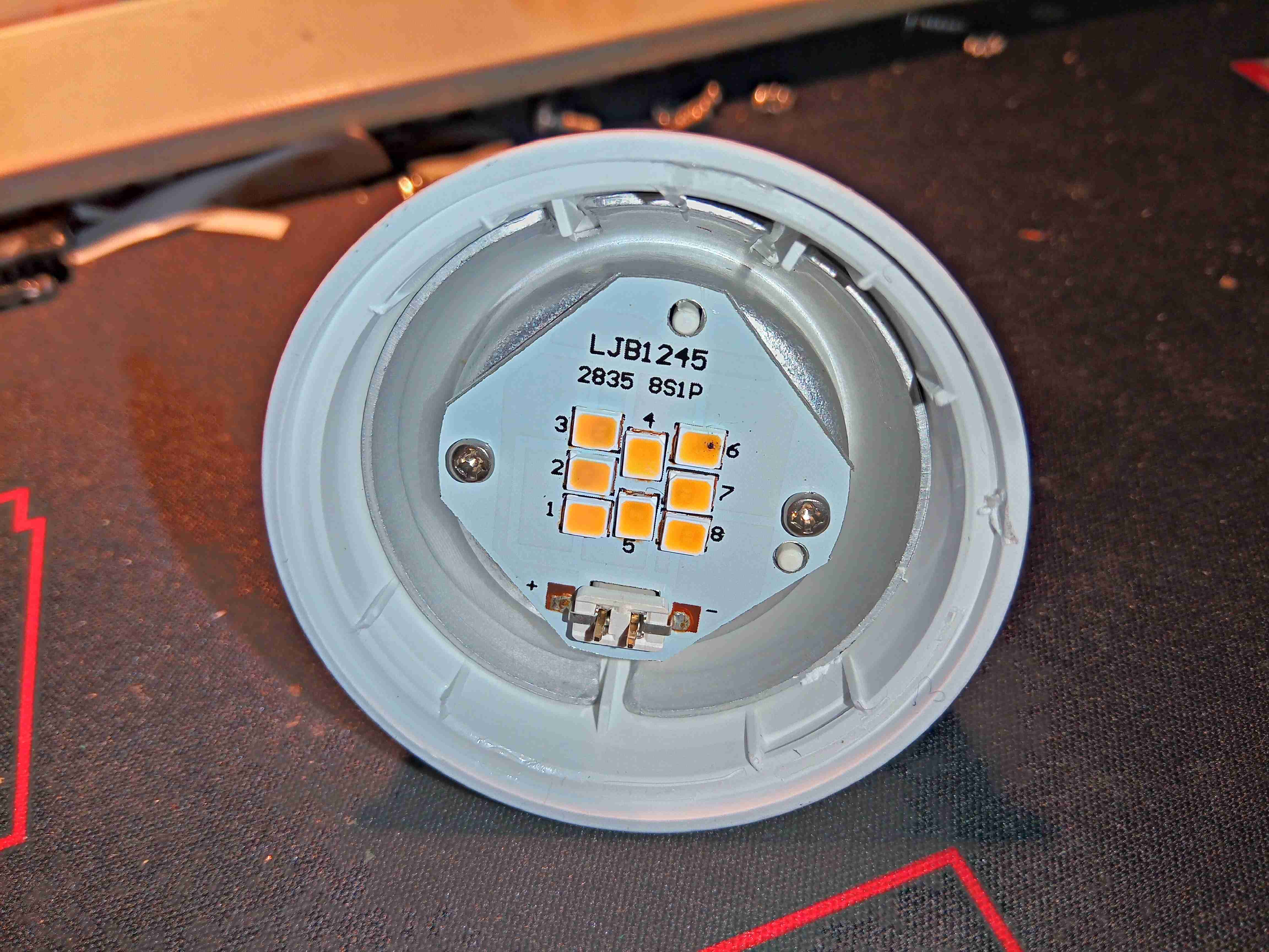
After popping the lens off the body, the failure mode is obvious. The top right LED has the Black Spot Of Death, where one of the LED dies has catastrophically failed in service. As these lamps usually have all the multi-die LEDs in series, a single failure will cause the lamp to totally fail. Running LEDs hard, with little cooling is a common cause of this kind of failure. There isn’t much in the way of heatsinking in this lamp, as the outer casing is plastic, and even though the LEDs are soldered to an aluminium cored PCB, the only other heatsink is the aluminium base for the PCB, which is in contact with the outer plastic.
PSU
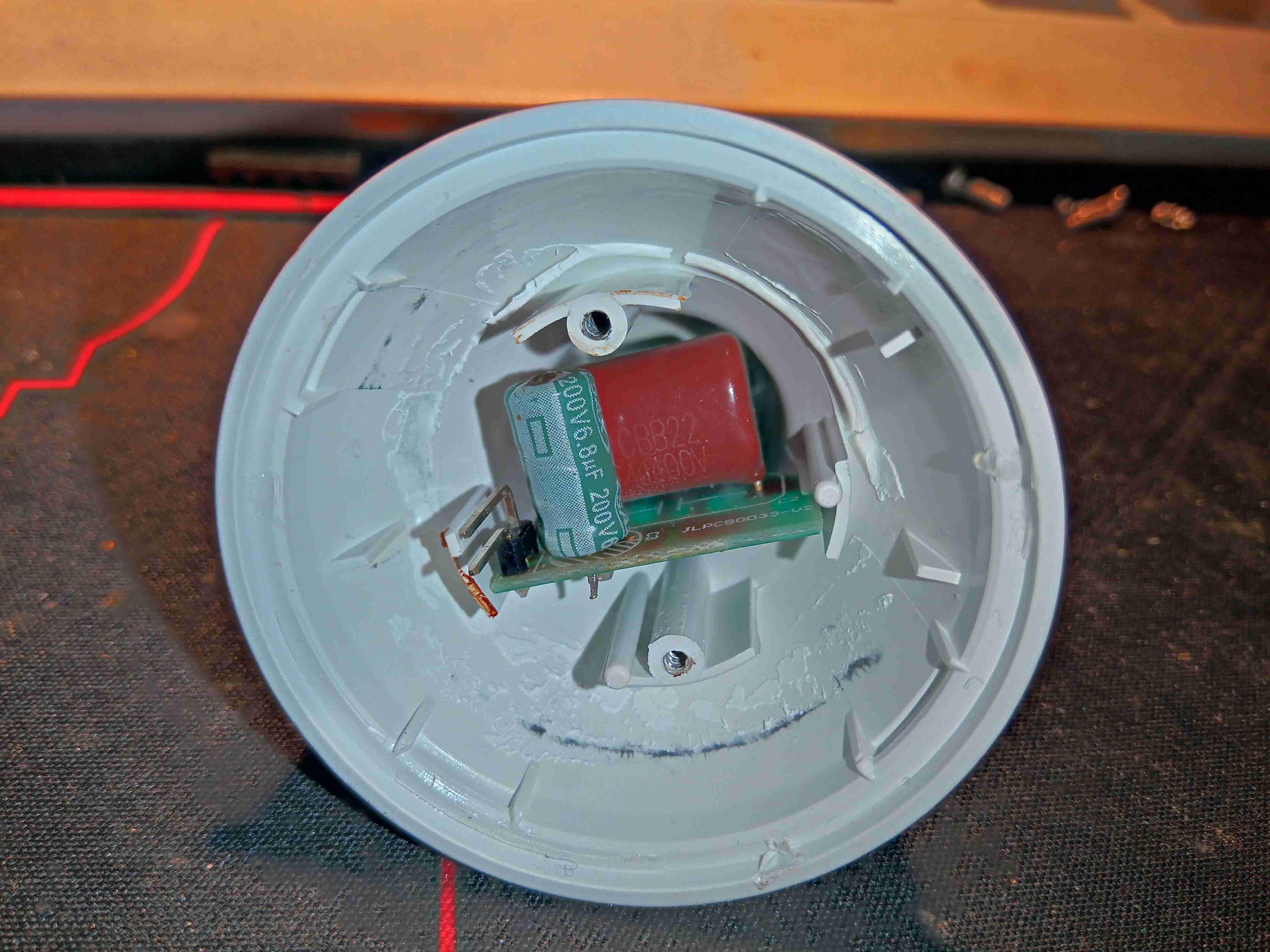
Removing the LED board & backing plate allows access to the power supply in the rear of the lamp. There’s no switching supply in this one, just a large film capacitor.
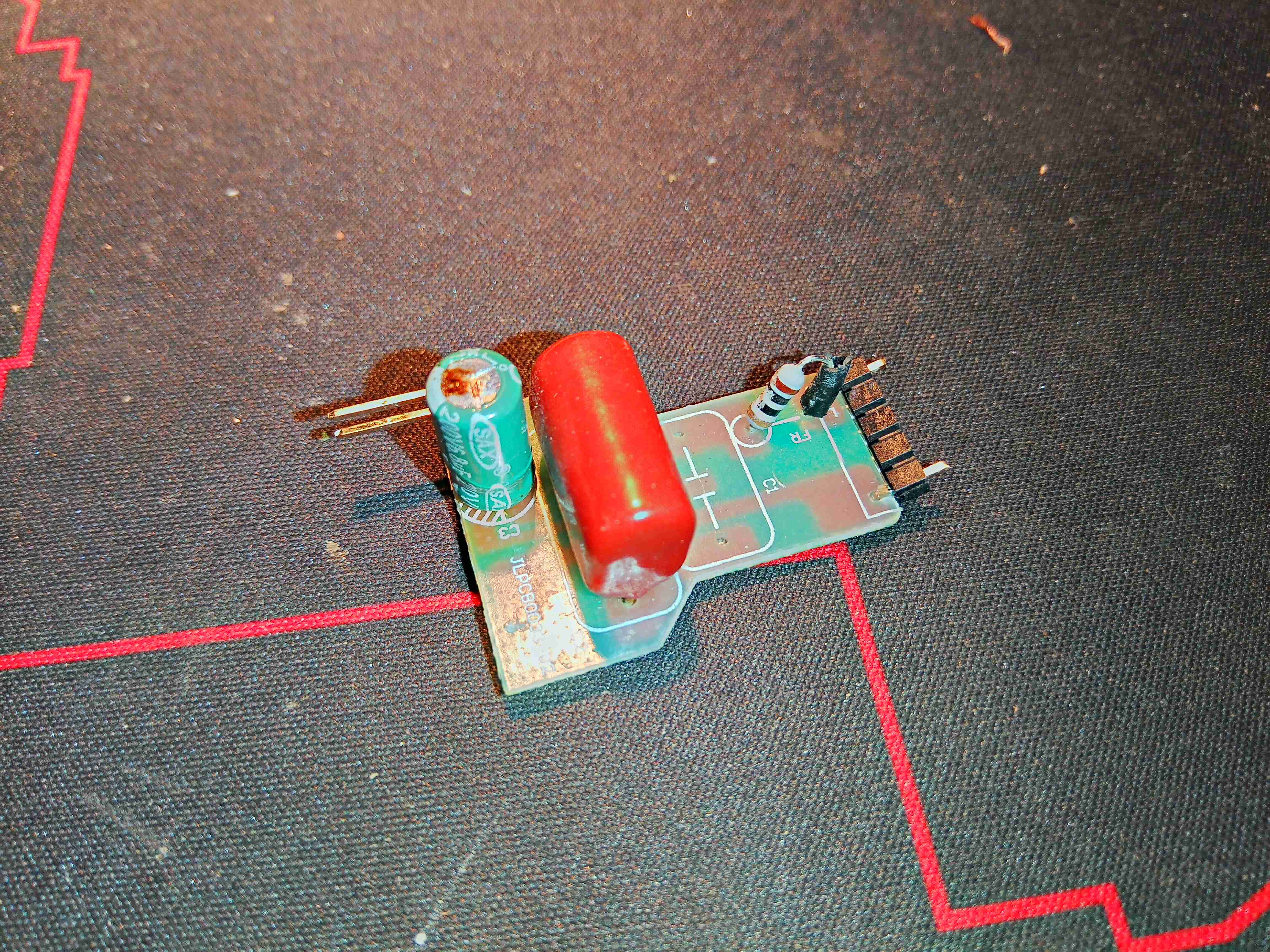
Capacitive Dropper
Snipping the pins off the back allows the PCB to be removed, exposing the capacitive dropper from the mains. The output electrolytic cap has also failed on this board, as can be seen from the opened vent on the top.
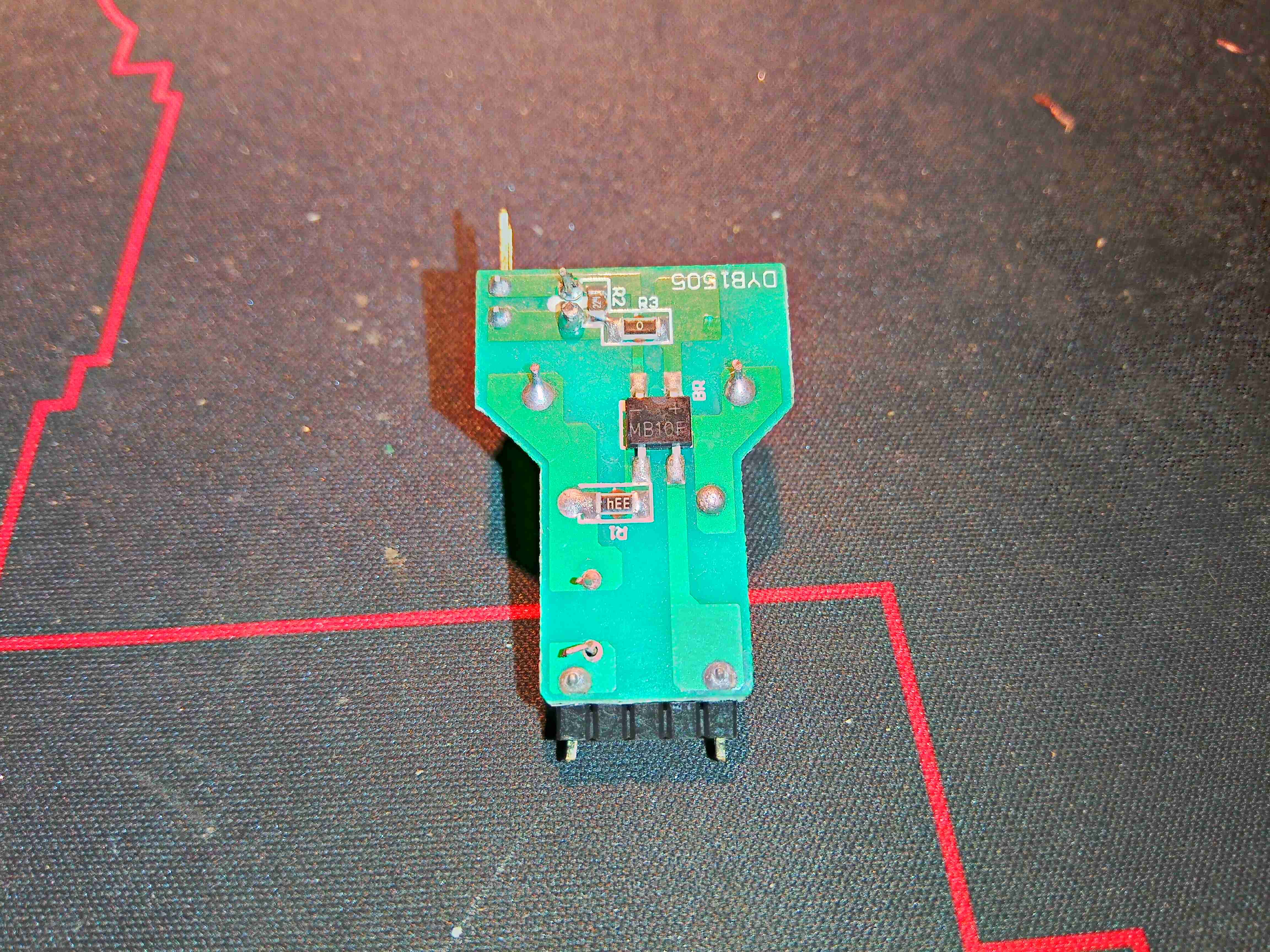
PCB Reverse
There isn’t much on the back side of the board, apart from the bridge rectifier & a couple of resistors.
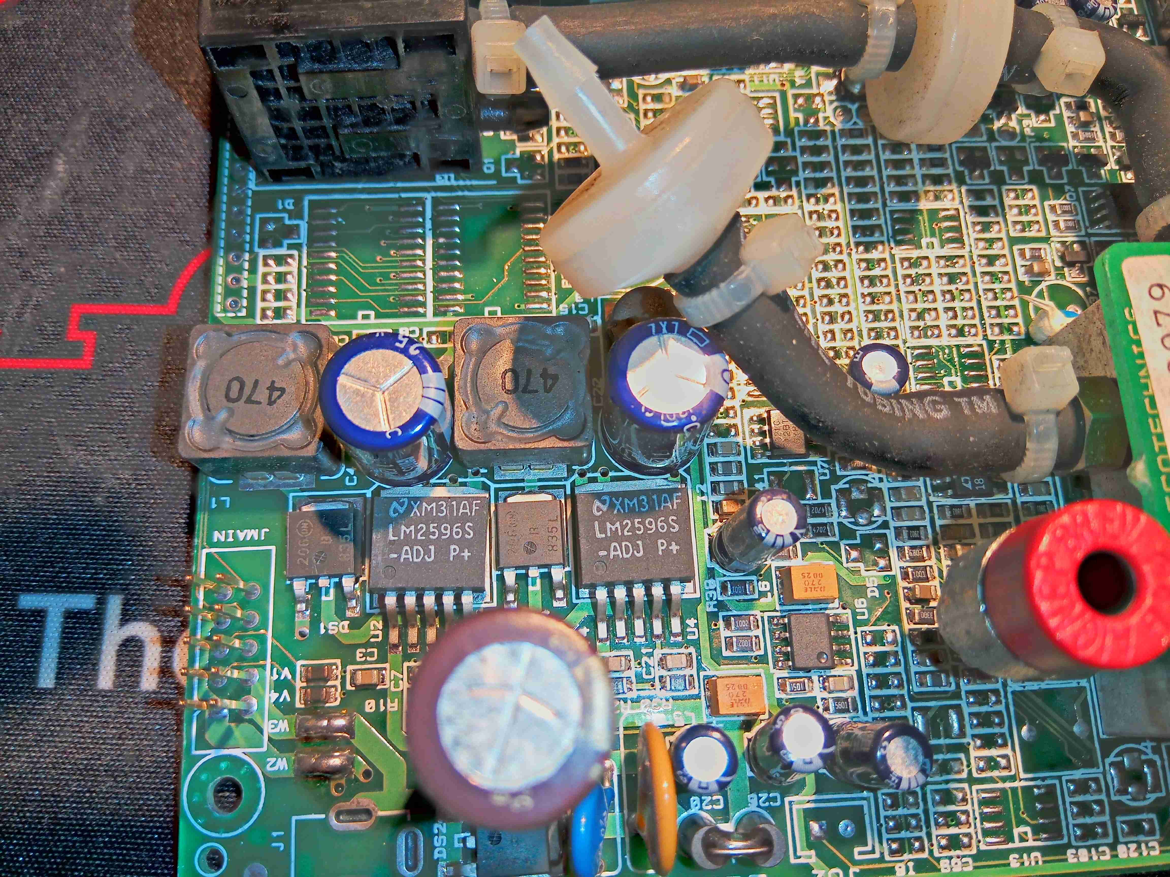
This unit recently appeared on eBay, as a spare part from a refrigerant charging machine, and I figured it would make a good explorational post. This unit analyses the purity of R-134a refrigerant gas, using an Infrared sensor cell, and communicates over RS-232.
The sensor cell itself is at the top right of the board, we’ll get to that later on. There’s a small diaphragm pump at the lower right, for purging the cell with air. The port with the red cap is the outlet, and the remaining open hose barb is the input of gas to be tested. This would connect to a flow regulator & solenoid valve that the board controls.
It’s pretty clear that this board has multiple applications from all the unpopulated components. There’s space for a keypad, indicator LEDs & an LCD on board, so maybe this can also be fitted to a handheld analyser?
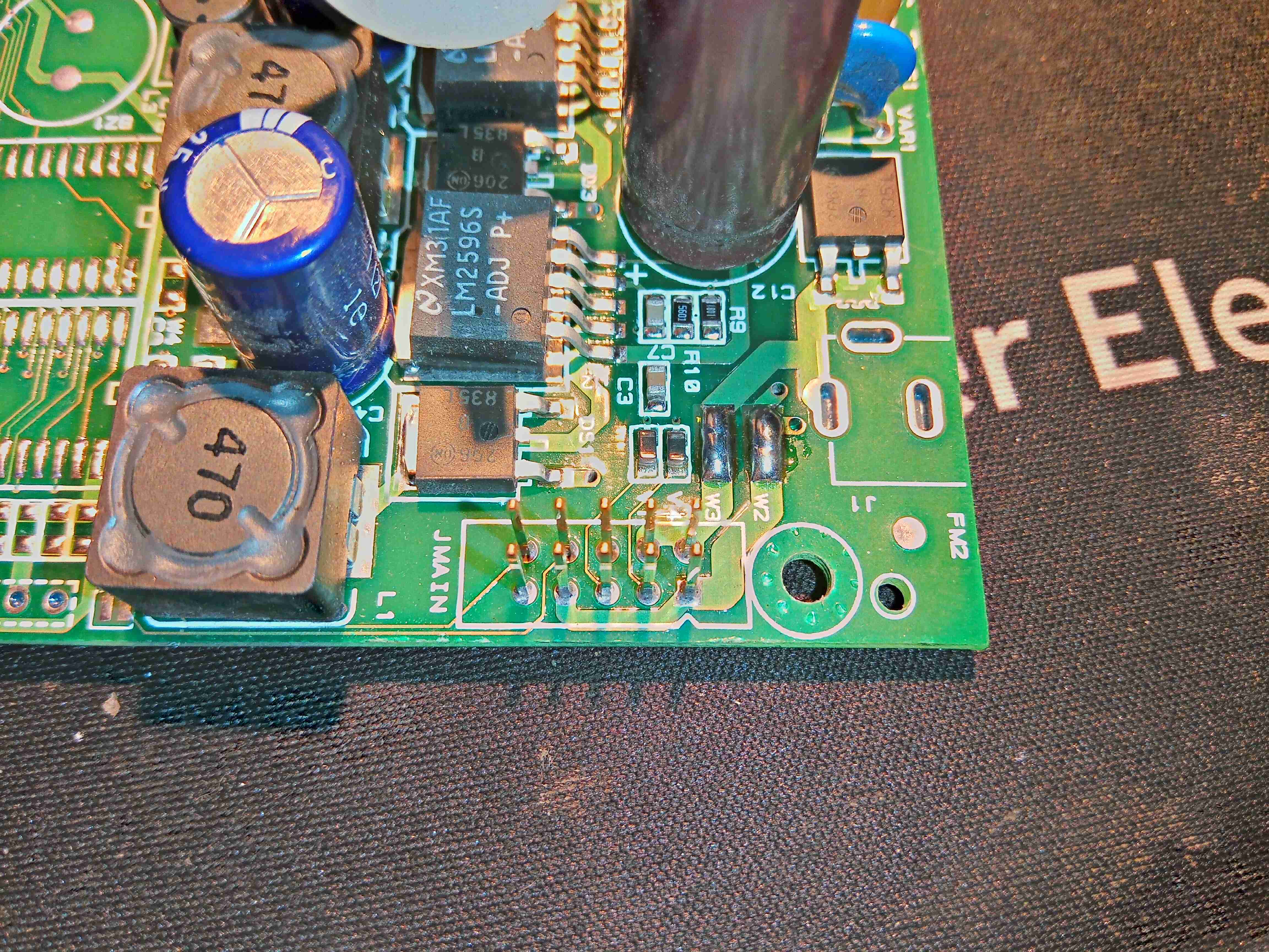
Power Supply
From looking at the input circuitry, I can surmise that the input voltage is somewhere between 12-24v DC, as there is a 35v input electrolytic filter capacitor. There’s a couple of switching regulators which generate 5v & 3.3v rails for the board, with some input fusing.
Main Connector
There’s two serial links on this board, driven from the main microcontroller – the primary one is on the connector marked JMAIN, along with the power input & a couple of other unknown signals.
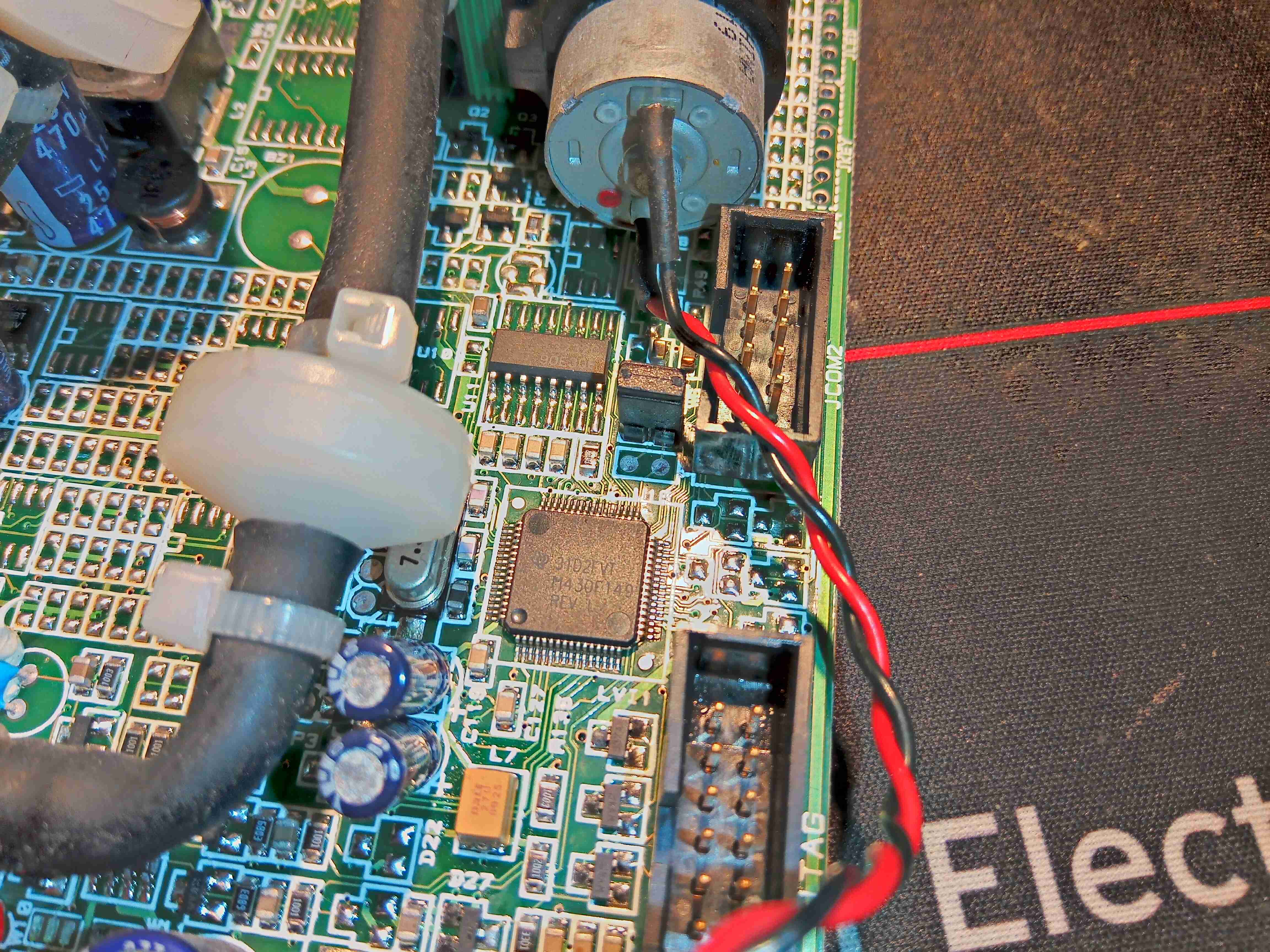
MSP430 Microcontroller
Over on the other side of the board is the brains of the operation – an MSP430 microcontroller, with an RS232 transceiver IC & another RS-232 port marked COM2. The remaining connector is a JTAG port for the micro.
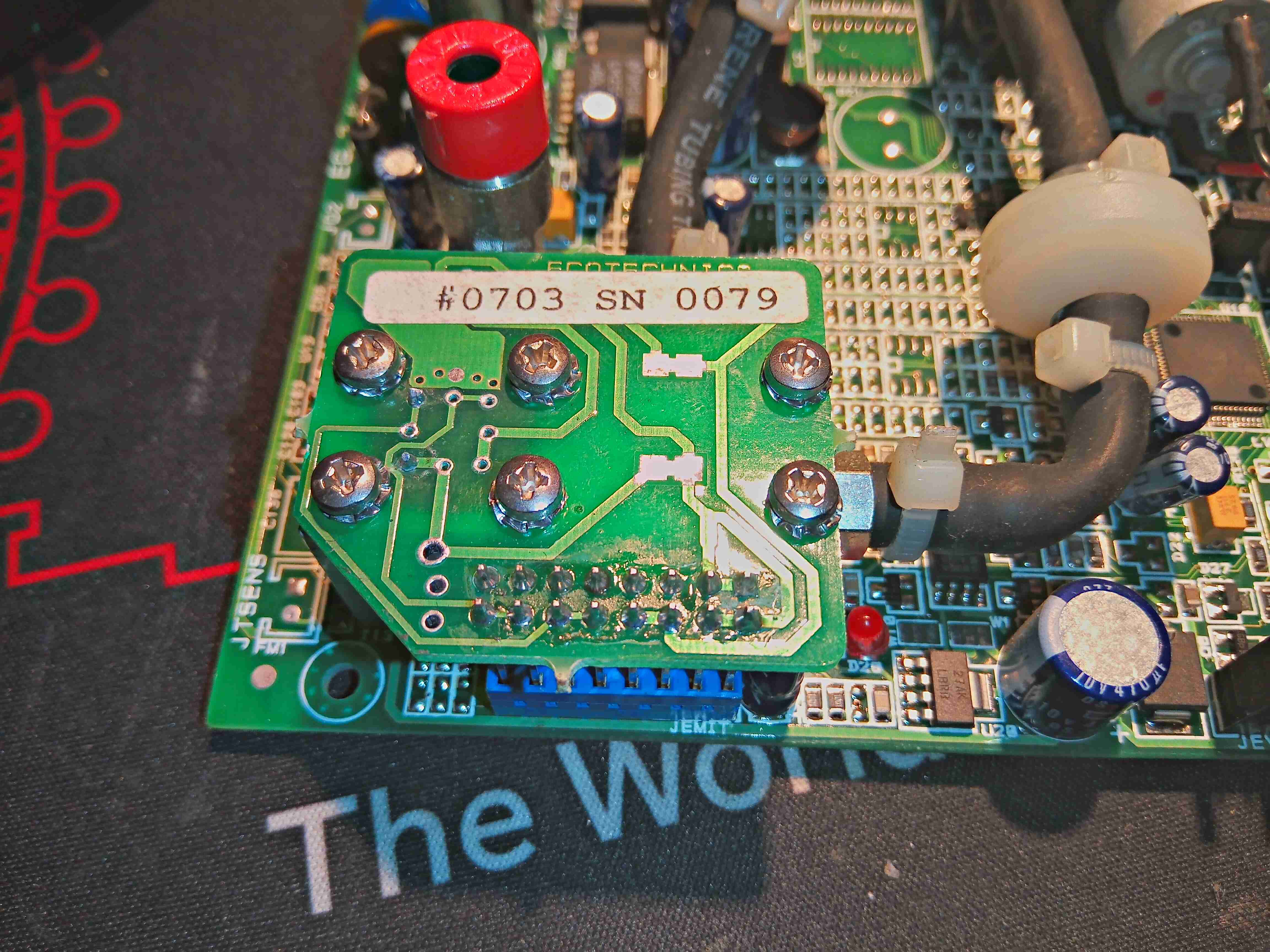
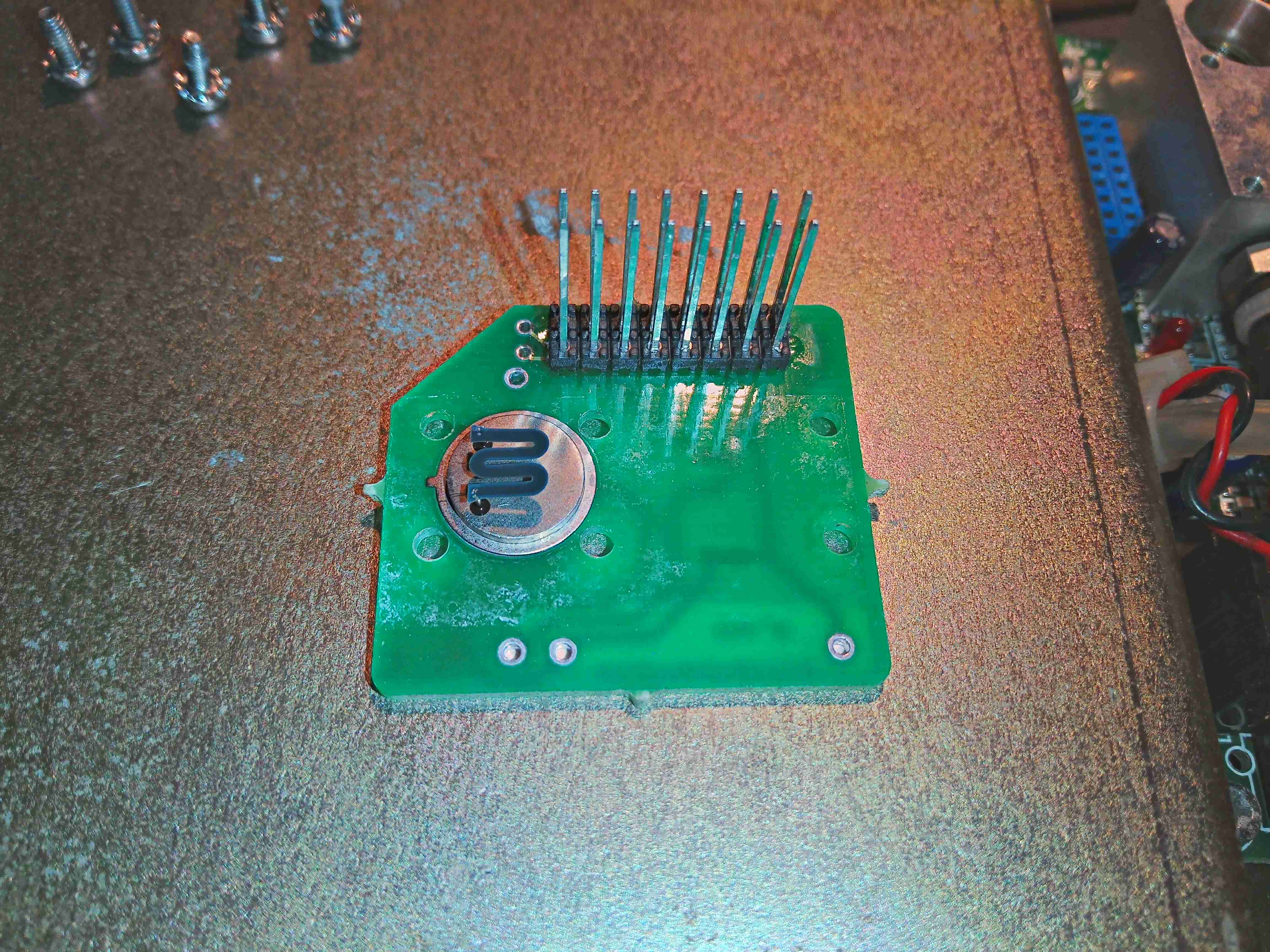
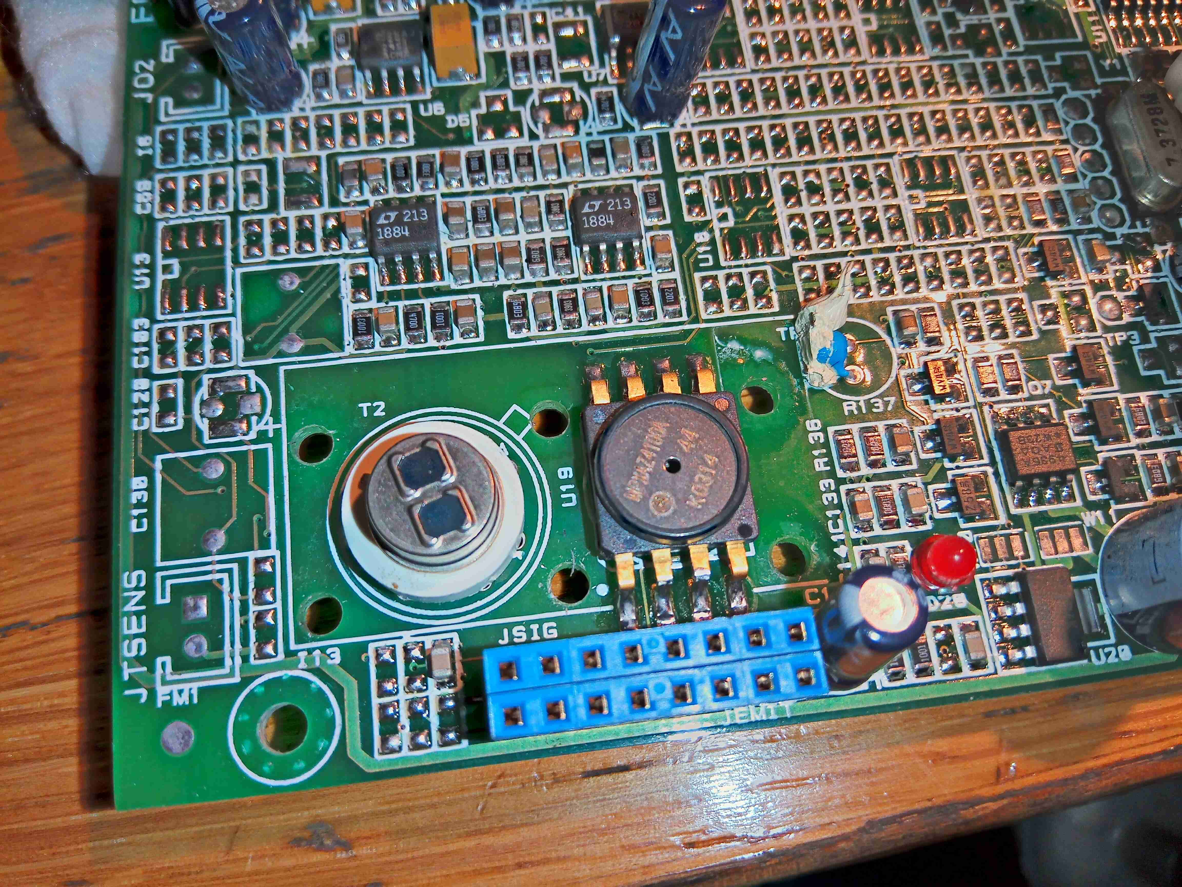
Gas Analysis Cell
Here’s the gas analyser cell itself, sandwiched under another board. There’s a temperature sensor on the side of the cell at the bottom, and even though there’s many pins on the header here, only a couple are actually used for the IR emitter.
IR Emitter
Removing the screws from the top allows the board to be removed, which exposes the Mid-IR emitter component with an exposed element. This looks to be very fragile, so I won’t be messing with this much. From metering the connections, this appears to be driven at about 2v from the microcontroller.
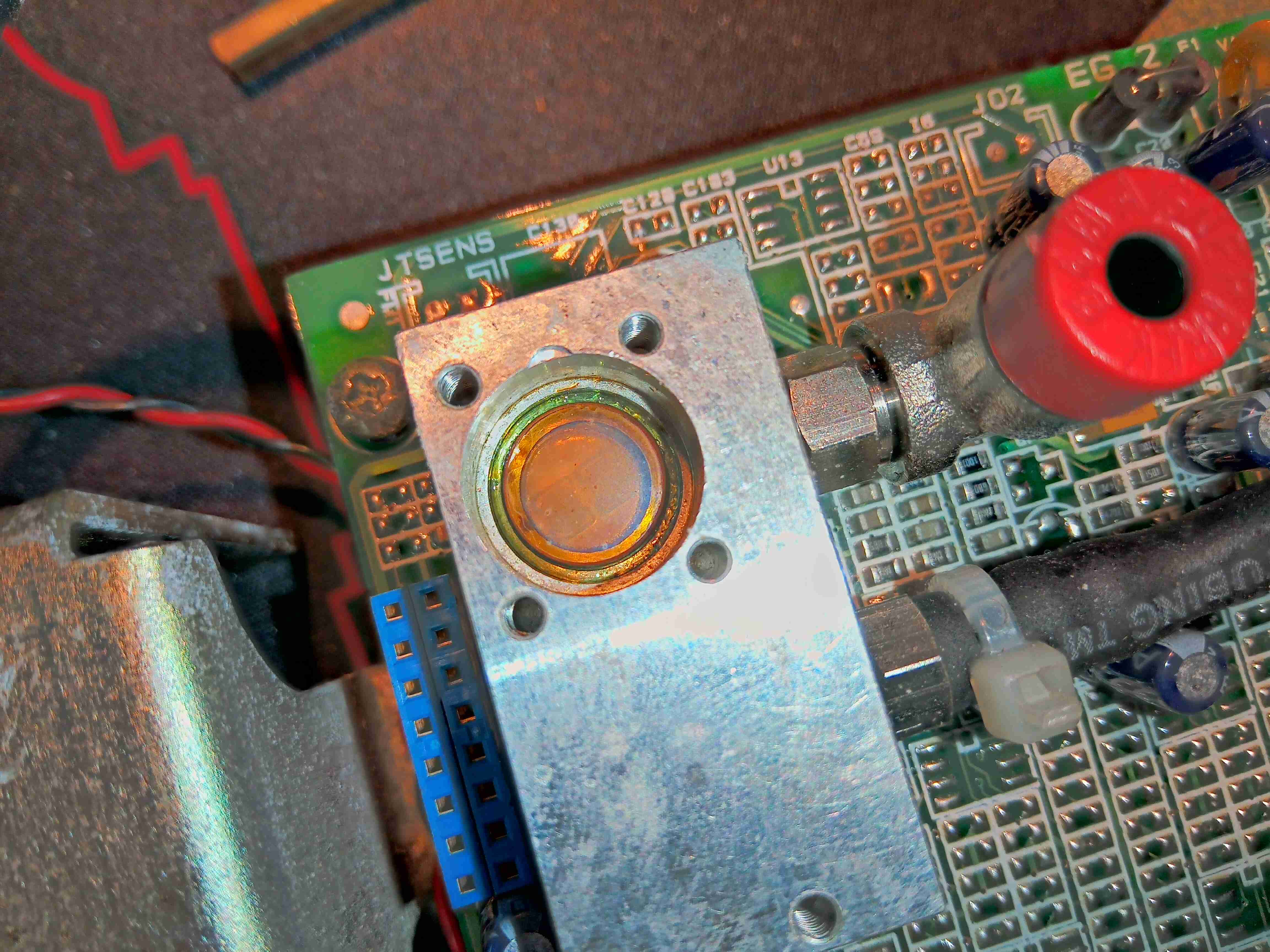
Top Of Gas Cell
The window into the gas cell looks to be made of something exotic – considering the IR application & the colour, this is probably Zinc Selenide.
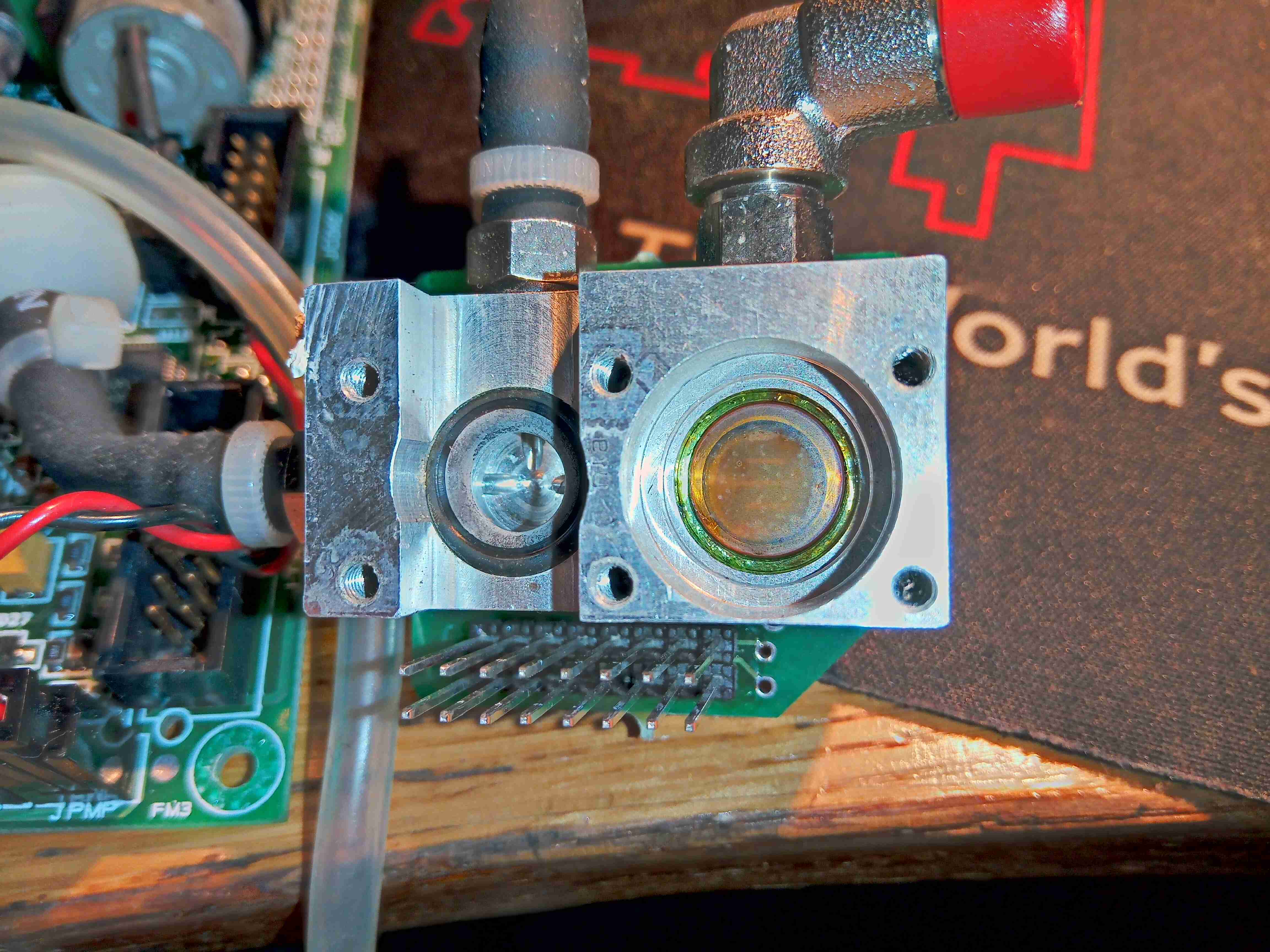
Gas Test Cell
Removing some more screws on the bottom exposes the bottom of the cell with another IR window, and an O-Ring where a pressure sensor sits.
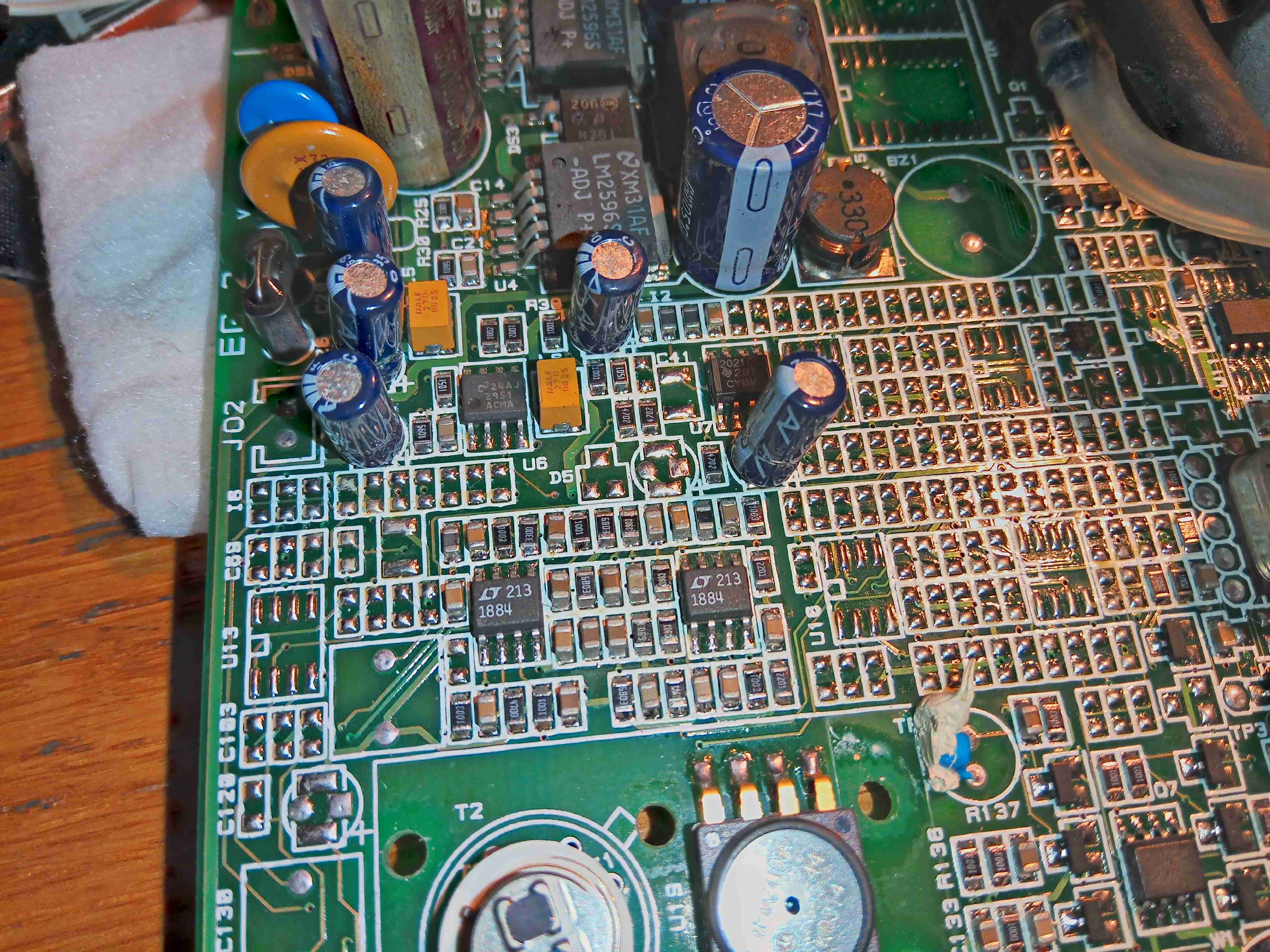
Output Amplifiers
There’s a couple of very accurate LT1884 Rail-To-Rail Precision Op-Amps next to the cell, most likely used to measure the output from the sensor itself.
Mid-IR Sensor & Pressure Sensor
Finally, there is a dual-window thermopile sensor, and a pressure sensor. I wasn’t able to get any information on either of these, but I did find some ranges of sensors for Mid-IR measurement operations, that mentions a wavelength around 10µm for R-134a spectroscopy.
I will try to get this module going & measuring some gases, if I can work out how to talk to it – I already know the serial lines so it’s just working out a command set. If anyone has any information on these, please do get in touch! A service manual for the refrigerant machine this came out of would be good!
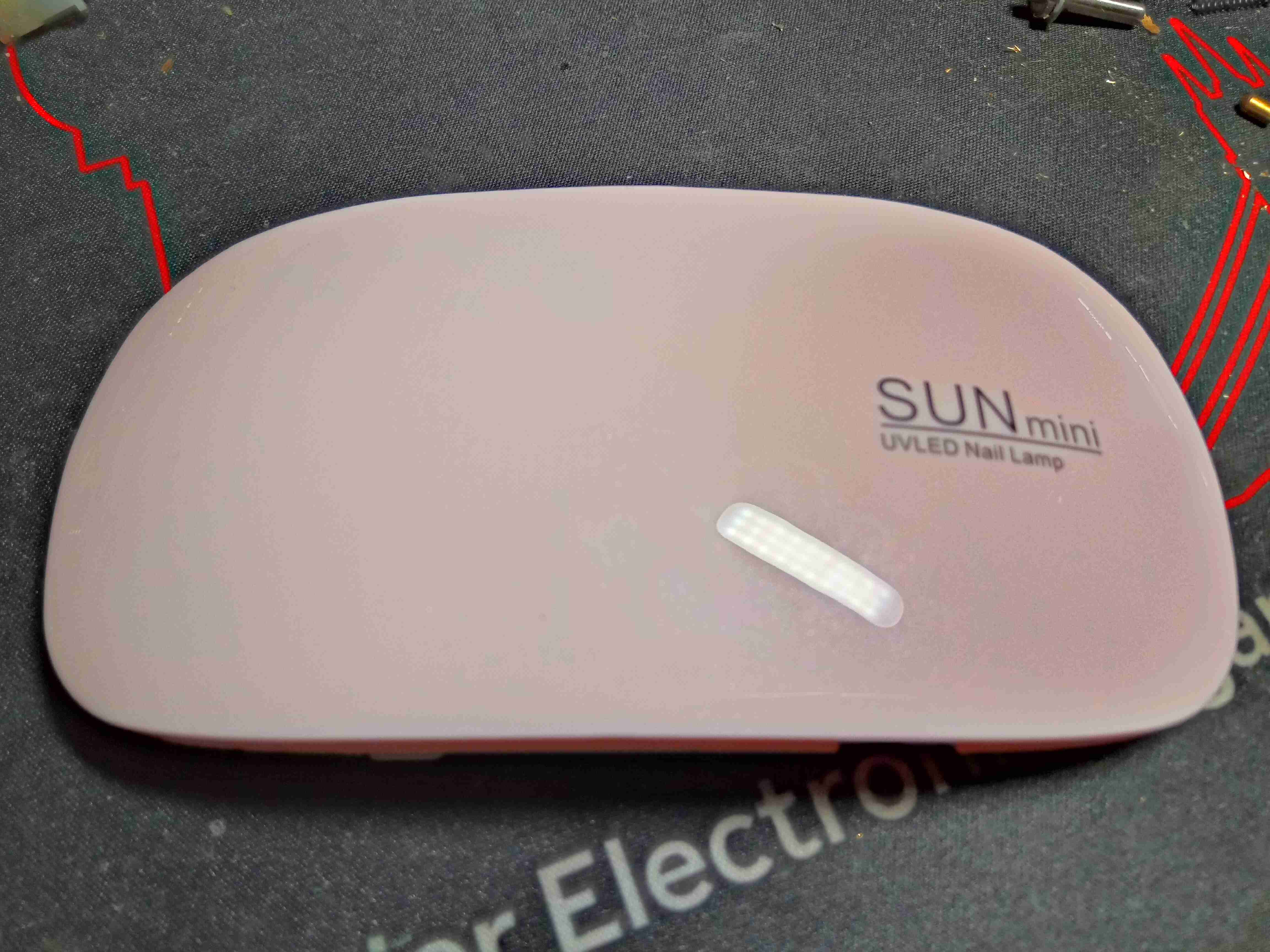
Time for another eBay delight! This is a little UV lamp for curing false nail glues. These are definitely taking over from the older Fluoroescent tube based units, and seem to work well enough. In my case, they work well for exposing UV-sensitive PCB substrates for etching as well!
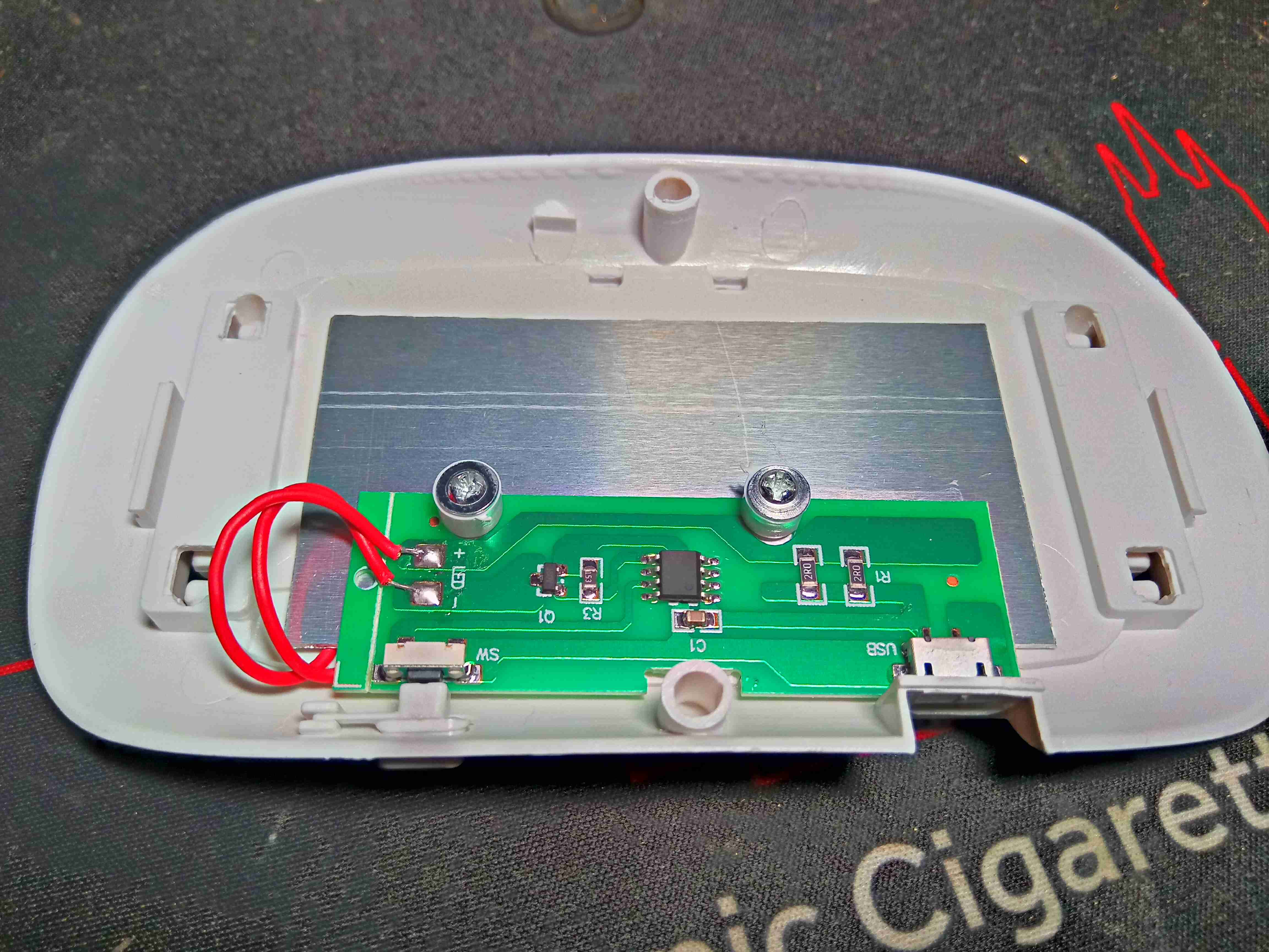
Here the cover has been unclipped from the body, no screws externally. There’s a small PCB, which holds an unmarked microcontroller, the USB input, the power & timer button, and a MOSFET for switching the LED current. A pair of 2Ω resistors in parallel on the right limit current through the LED array, in this case to 1.25A for an output power of 1.56W.
Lamp Bottom
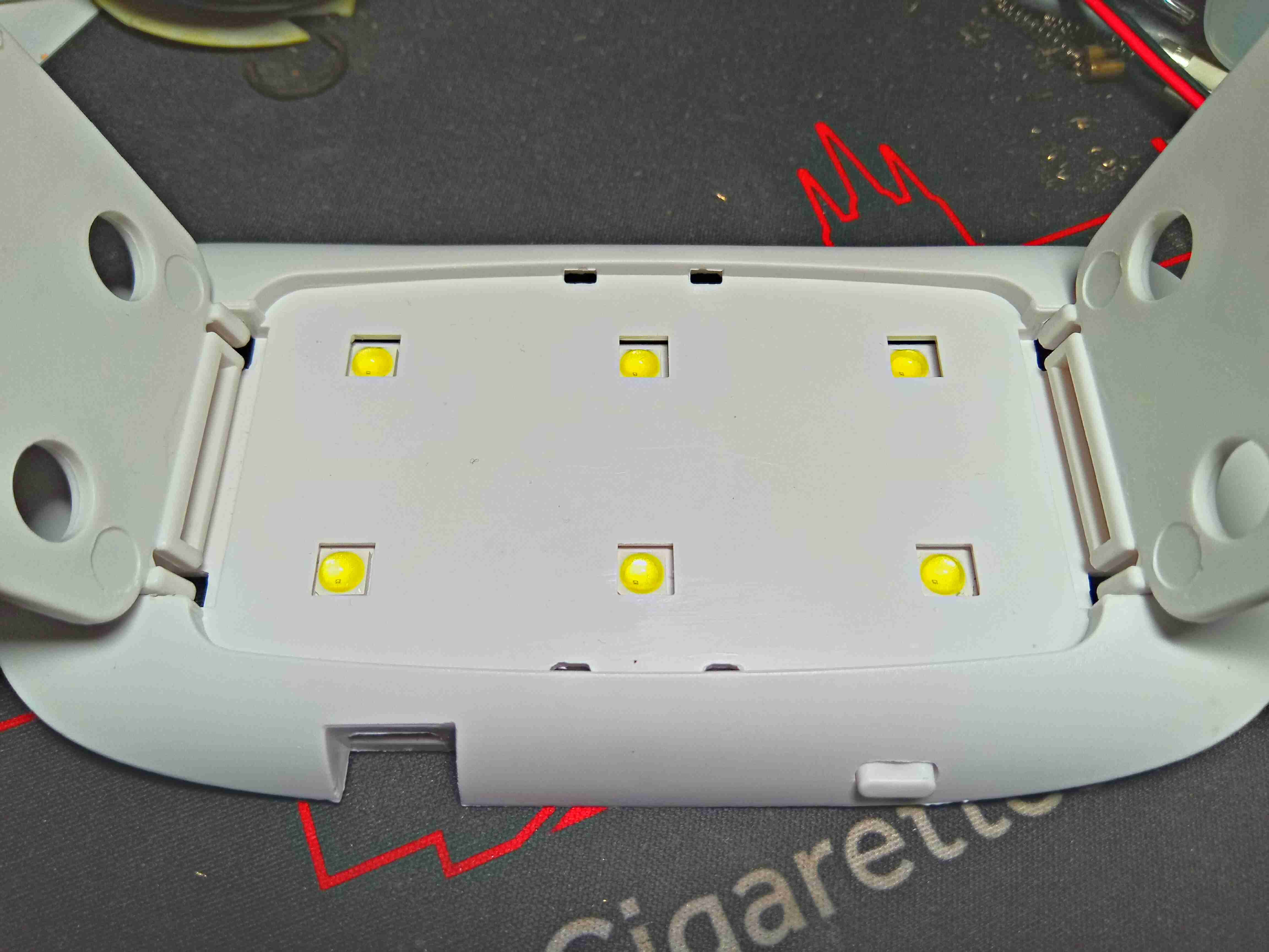
Underneath the body are the apertures for the high-power UV LEDs. In this case there are 6 LEDs, each with a pair of dies of differing wavelengths. The legs fold up for storage.
LED PCB
Removing the 2 screws inside allows the boards to come loose, and this is the front of the aluminium-cored PCB supporting the LEDs. In this case they are all wired in parallel.
It seems the standard of driving in the UK is dropping by the day:
This dude either really didn’t want to wait, or was blind. If this wasn’t on a 20MPH limit residential road, the result may have been a little different…
Even after he’s forced to move back to his side of the road, he tries to have a go at me for the situation. There will no doubt be more clips like this to come!
Here’s a useful device, for detecting leaks in refrigerant systems. These units use a high-voltage ionisation detection method using a probe at the tip with a sharp needle, similar to an ioniser to detect changes in conductivity of the surrounding gas.
PCB Top
Removing the front case of the unit reveals the PCB, with it’s row of indicator LEDs on the top. The high voltage transformer is on the right, with it’s switching transistor. The probe swan neck is on the left.
PCB Right
The PCB is fairly heavily populated, and all a single-sided load, no doubt to reduce manufacturing costs. The main power input from the battery is on the bottom left, with a small switching regulator to the right supplying power to the control logic & microcontroller. There’s a multi-turn potentiometer, probably for adjusting the output voltage of the HT section. The header in the centre of the board is the connection point of the membrane keypad on the front of the unit.
PCB Left
Not much more to see on the left side of the board, there’s the connection for the buzzer far left, and the main switching MOSFET for the high voltage transformer in the centre. The high voltage output is on a JST connector bottom right! I suspect the HV converter is fully under the control of the microcontroller in this unit, as there doesn’t appear to be any other control function present.
Microcontroller
The main microcontroller is an ATMEGA48, with it’s programming header on the far right of the board.
High Voltage Output
Finally, there’s the high voltage output section of the board with a couple of anti-tracking slots to prevent flashover. There’s a rectification diode, in half wave, a small smoothing capacitor before the string of current limiting resistors on the output of the unit to the probe. I haven’t been able to work out where the microcontroller is actually getting the gas conductivity measurement from – it may be measuring the input current drawn by the HV converter or it may be measuring the output current via one of the current-limiting resistors on the HV output.
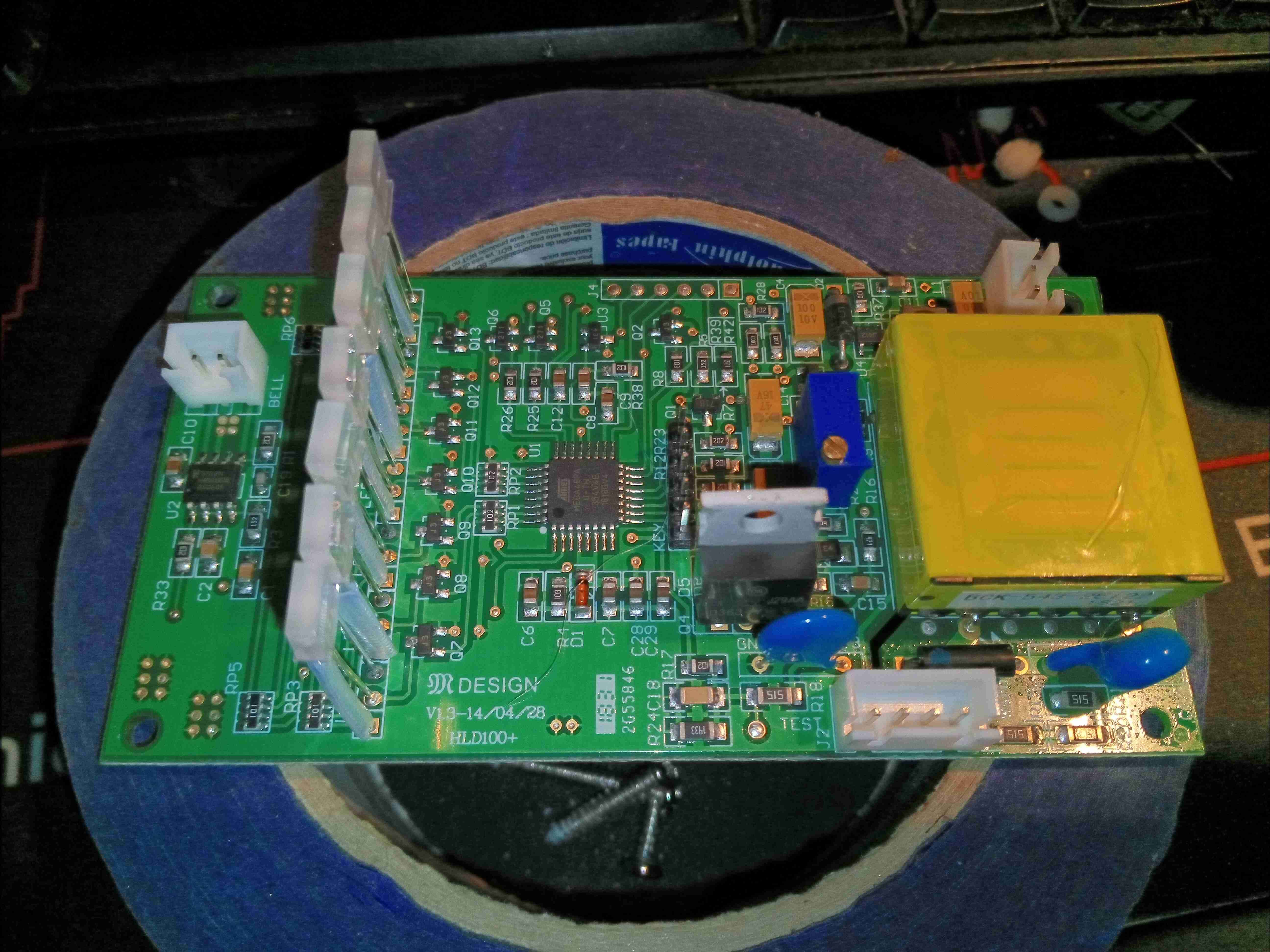
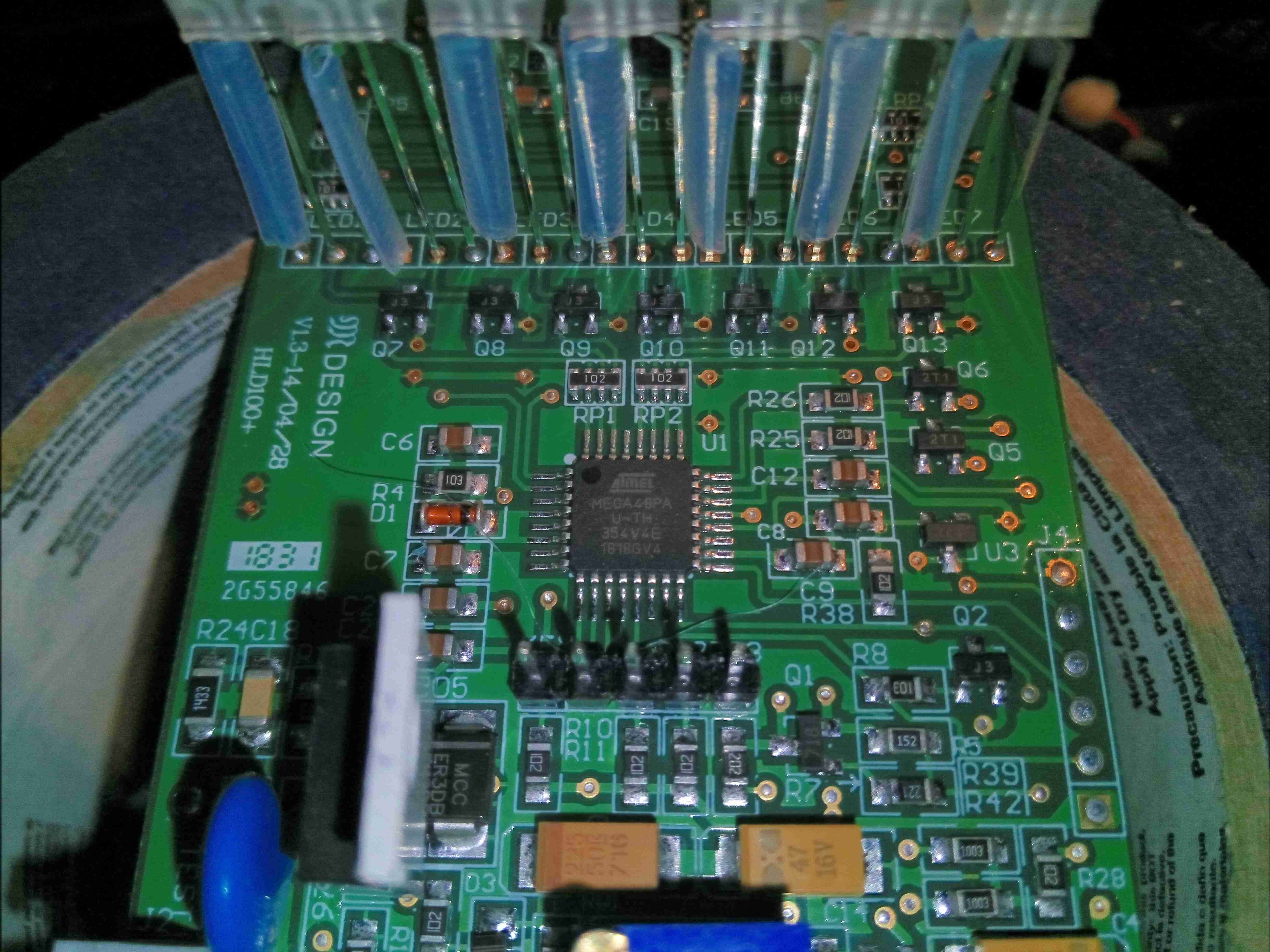
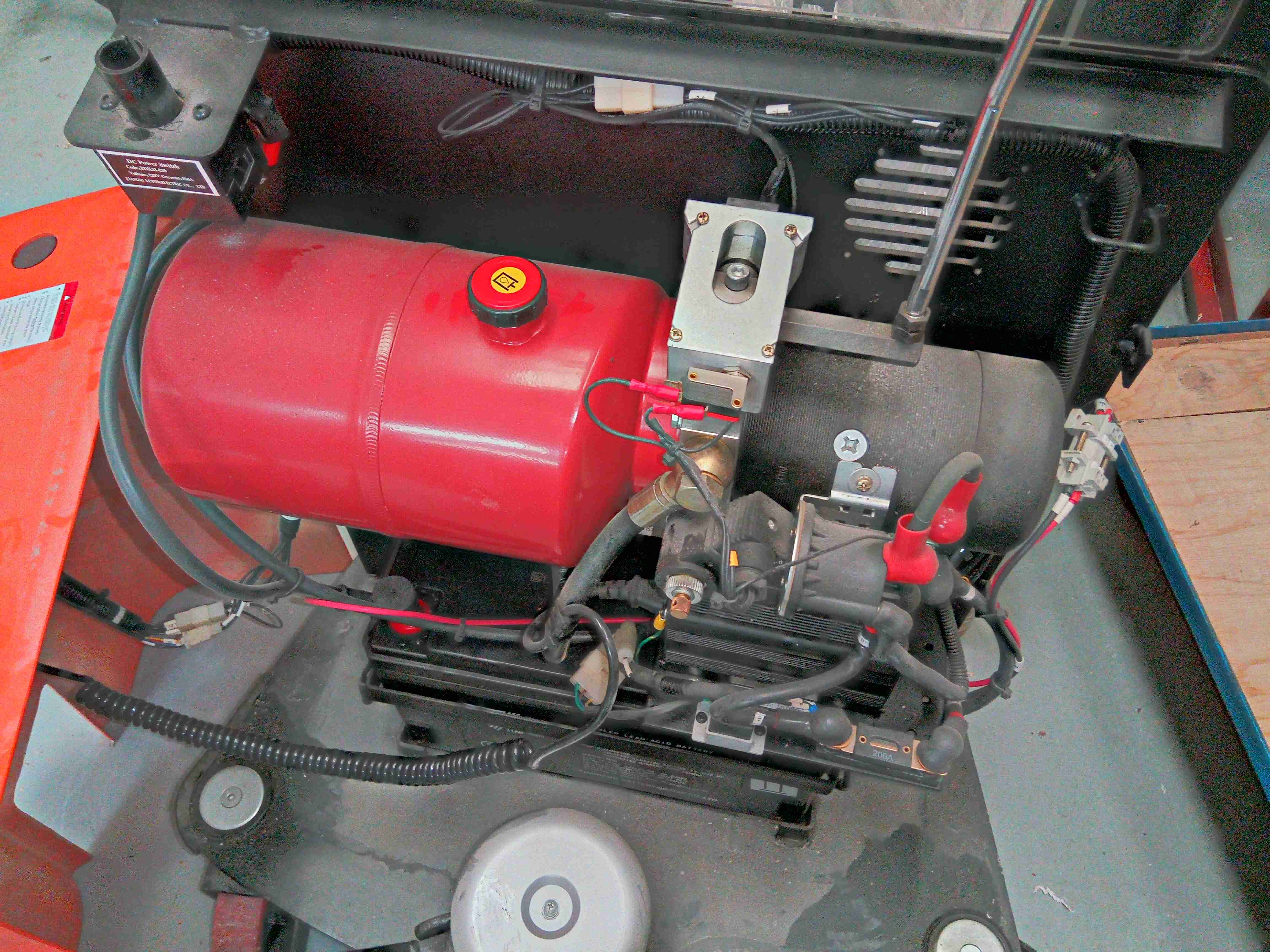
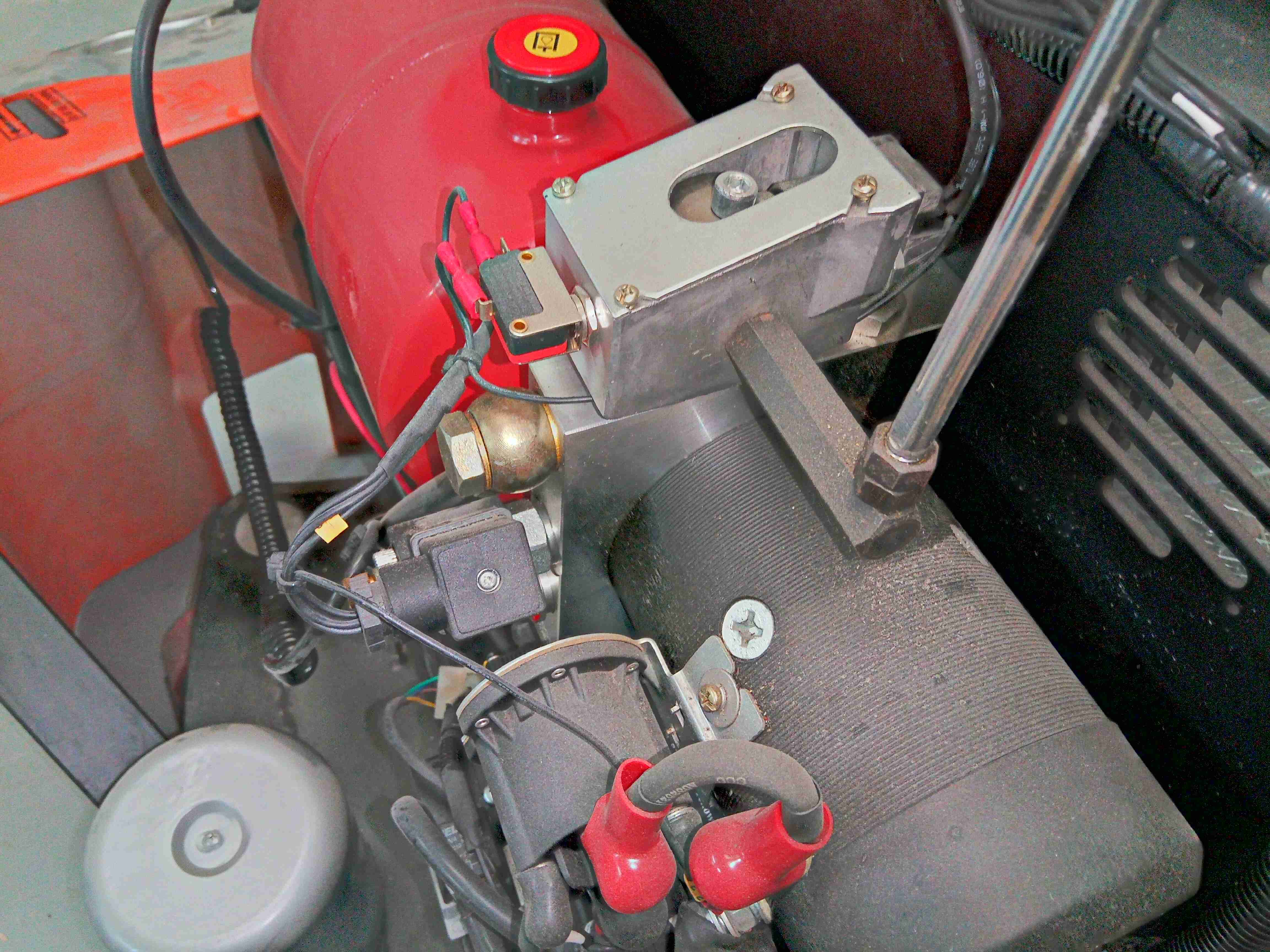
At work we have a human-propelled hydraulic stacker, which recently started to drop under load, with no valve operation. I immediately suspected the lowering valve on the hydraulic pump unit, so set to work getting a replacement fitted.
Unit Overview
After removing the GRP cover of the mechanics bay, the main hydraulic unit is visible mounted on the top of the frame. Powered by a large 12v SLA battery below, the hydraulic power pack consists of a large 12v motor, gear pump, valve block & hydraulic oil tank. The valve we’re after is hidden at the moment inside the control lever mounting.
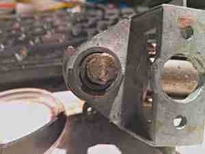
Hydraulic Valve Block
Here’s a better view of the control lever mountings. There’s a pair of microswitches for activating the lowering speed-control valve, and the main contactor which switches the high current to the main motor.
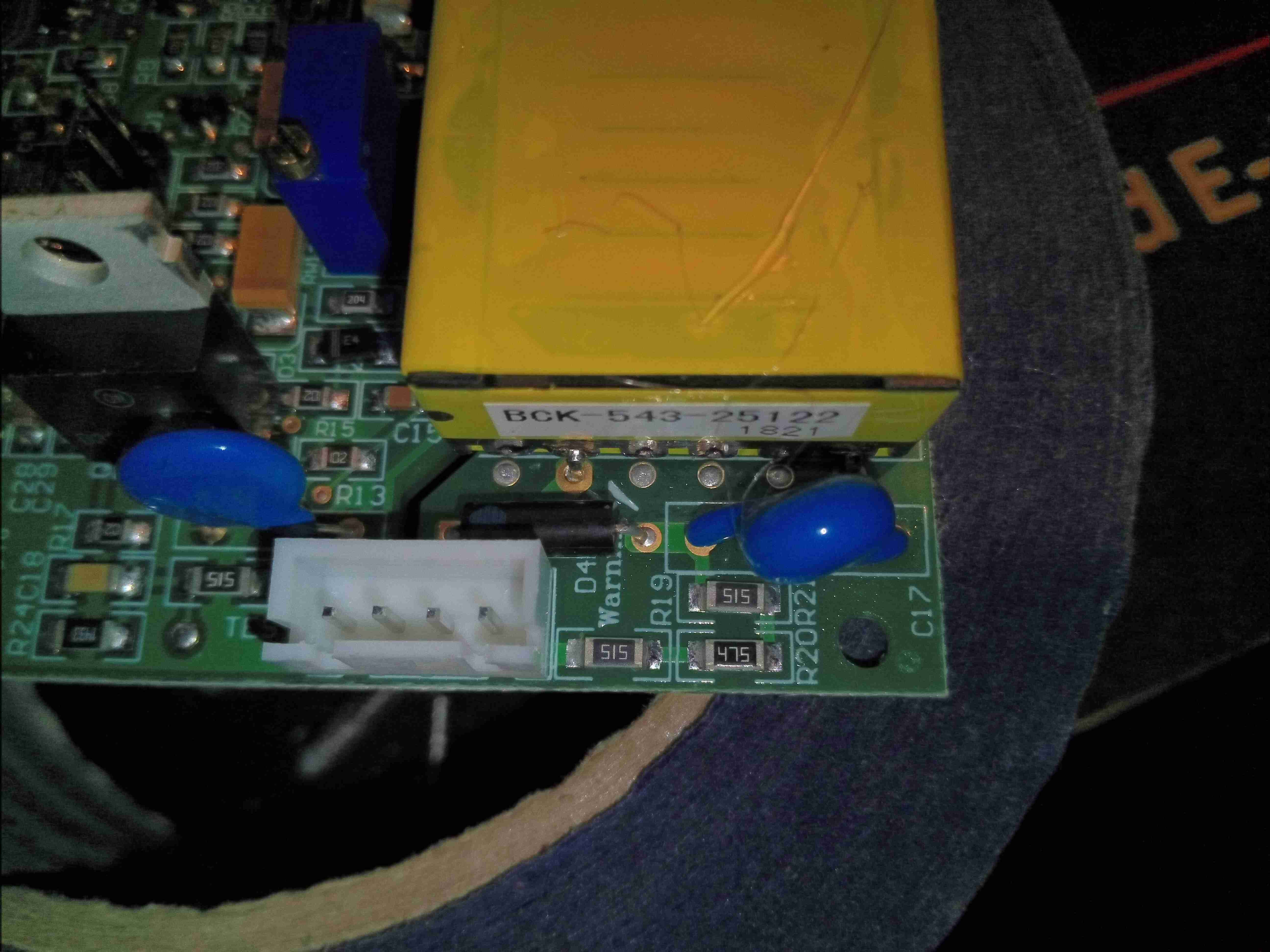
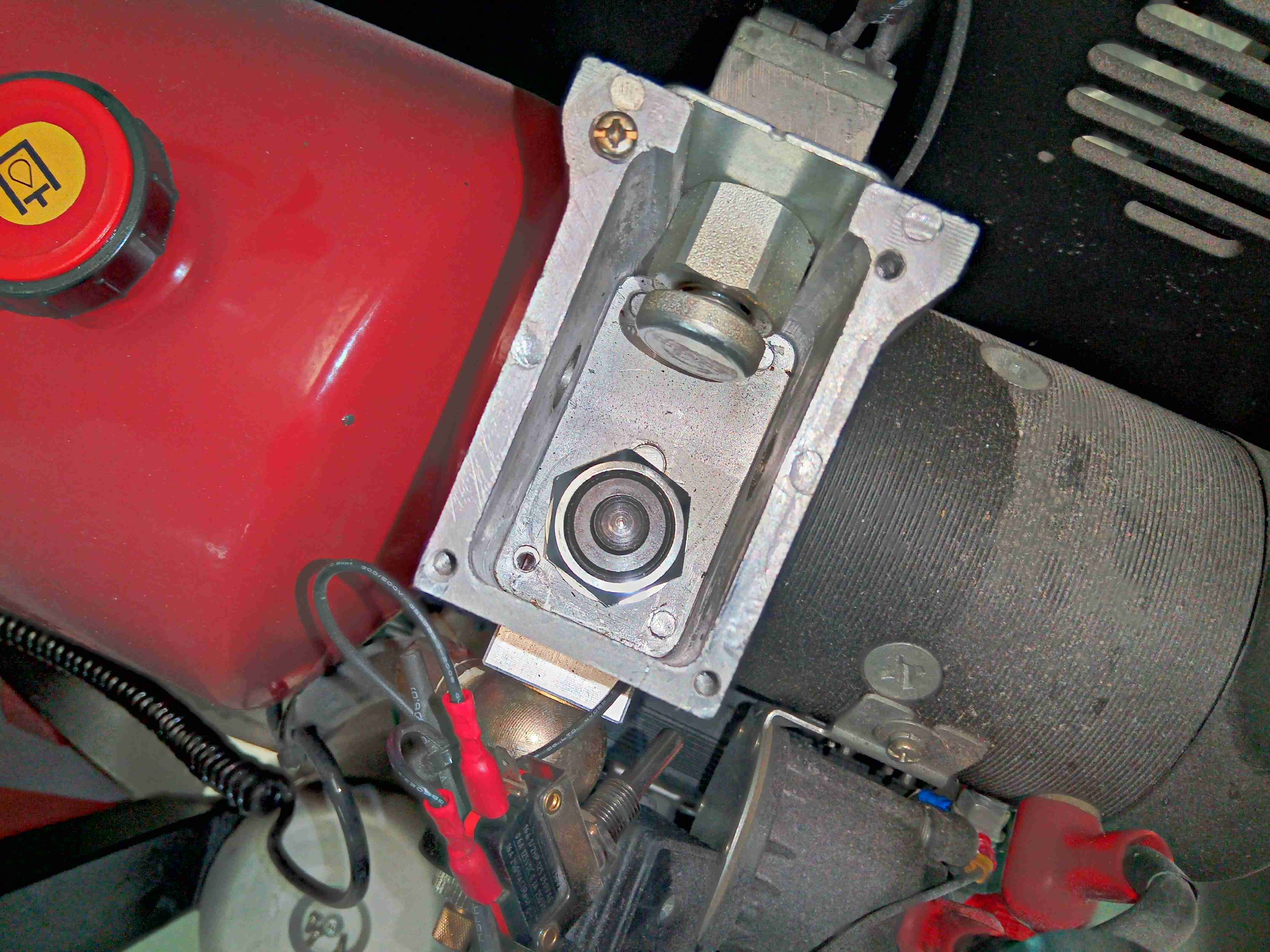
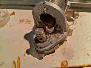
Lowering Valve Mounting
Removing the actuator cam & control lever reveals the valve hiding at the bottom of the mounting cage. I’ve removed the microswitch which operates the lowering speed control valve to gain better access, but the main switch that operates the contactor can stay in place at the top.
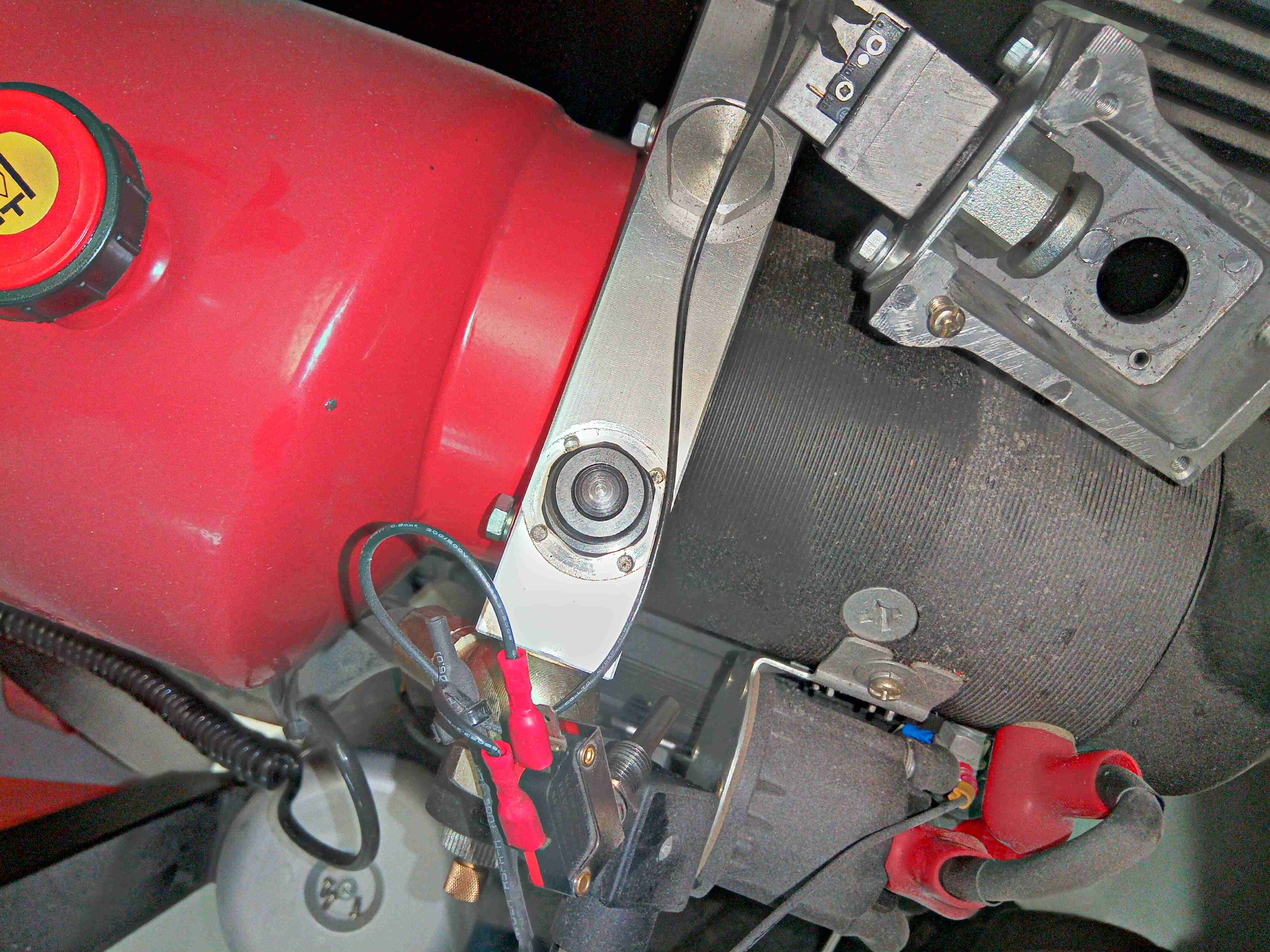
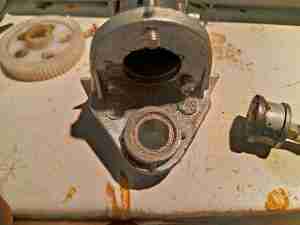
Bare Valve
Getting in with a 1″ socket allows the retaining nut holding the mounting cage to be removed, showing the actual valve in the hydraulic block.
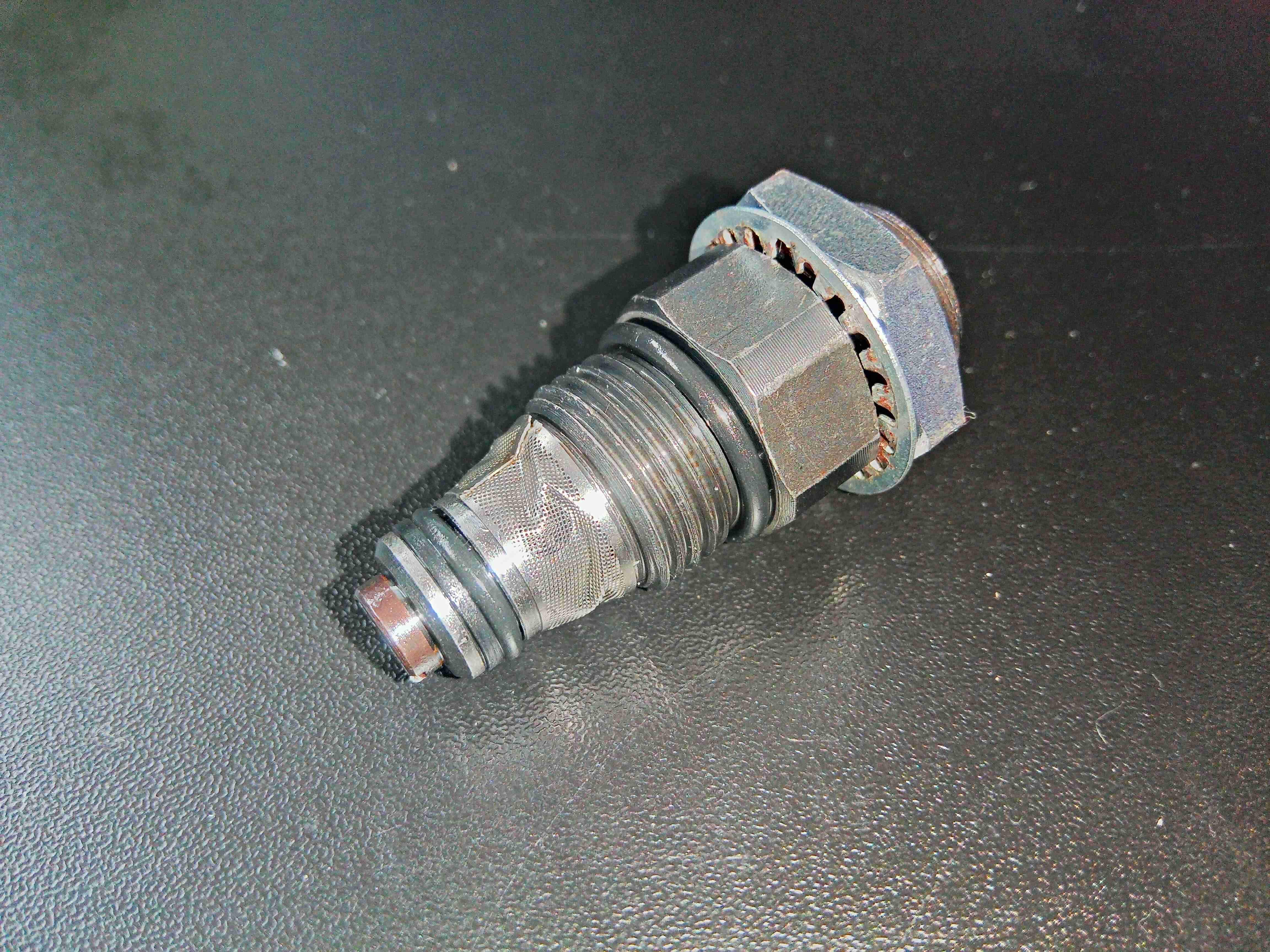
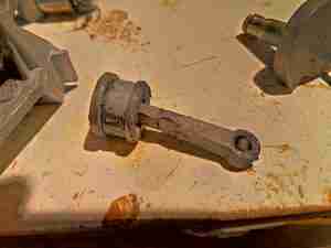
Old Valve
The valve is removed by simply unscrewing it from the main unit. Here’s where cleanliness comes in – the hydraulic system is now open to the environment, and the close tolerances in the valves & main pump will not tolerate dirt & grit getting in! This is a simple poppet valve, the main seal actually being a metal-to-metal tapered surface, and the problem this one has had is the O-Ring seals have failed. The rubber has gone very hard over the 4 years this unit has been in service, and have started to disintegrate. This is still a perfectly serviceable valve once the seals are changed, even if the filter screen has been a little damaged.
Replacement Valve Fitted
I’ve fitted the new valve to the hydraulic block here, and a test done to ensure the load is held on the hydraulic cylinder. Reassembly is simply the reverse of teardown.
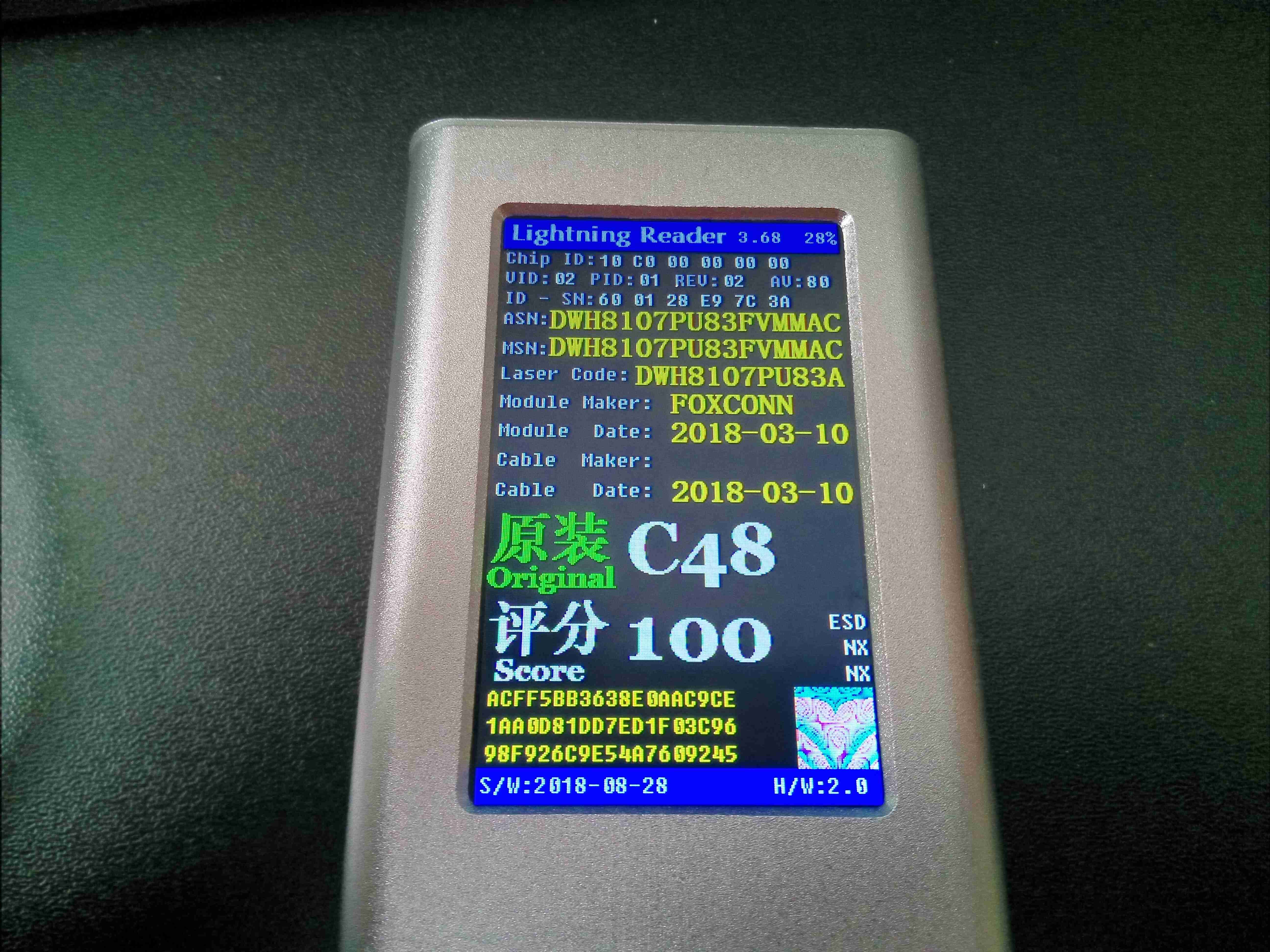
Apple’s Lightning cables are one of a new breed of cable – these have active electronics in the connectors, to allow the device to identify the type of cable being used. This is a little unit that reads out all the internal parameters of the ID chip inside the connector. As can be seen from the image above, the ID chip contains quite a bit of information, from device manufacturer & serial number to chip type & date of manufacture. This unit also gives a “score” of whether the cable is a genuine Apple type, or a Chinese clone, with a scale of 0-100.
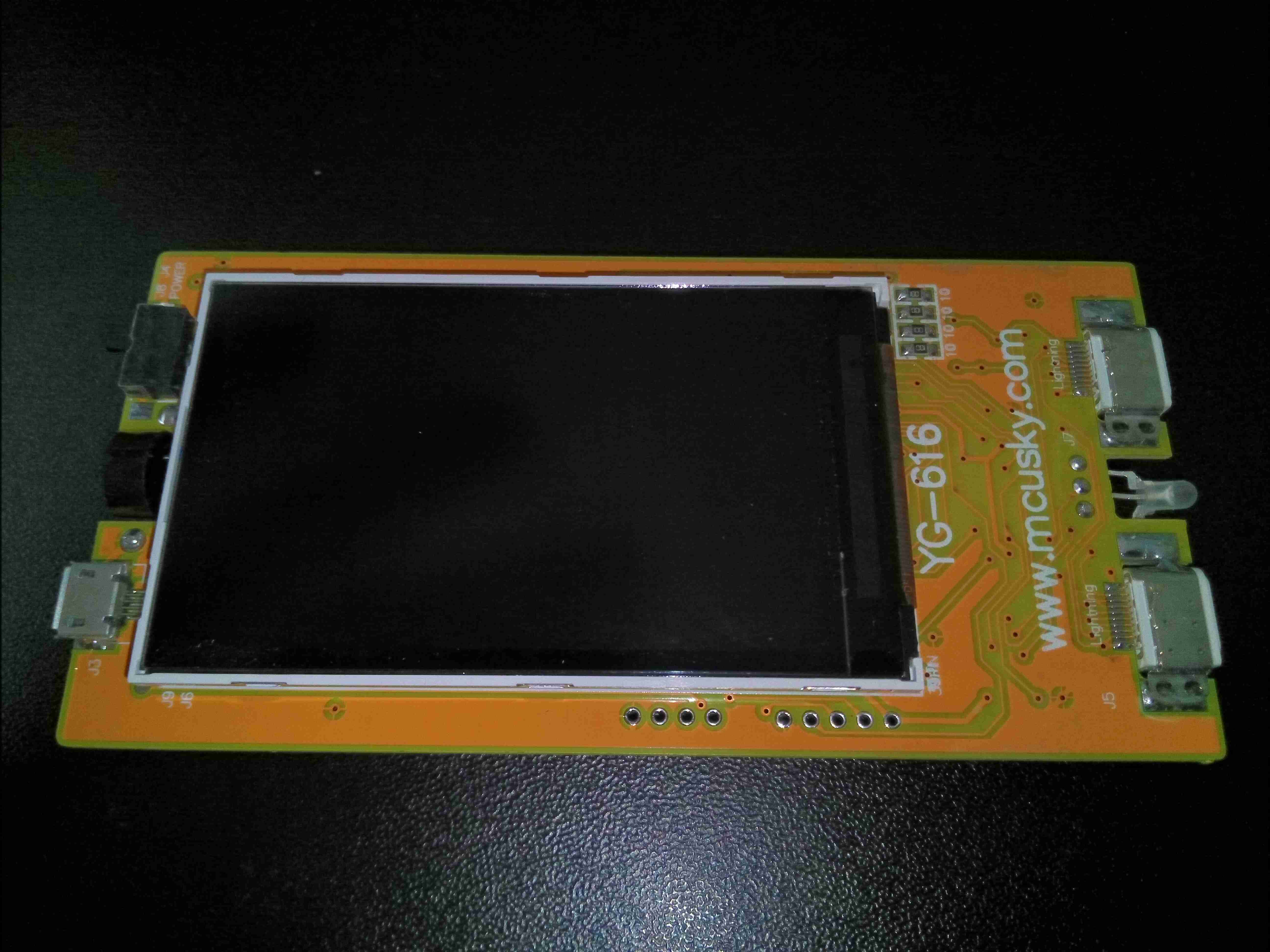
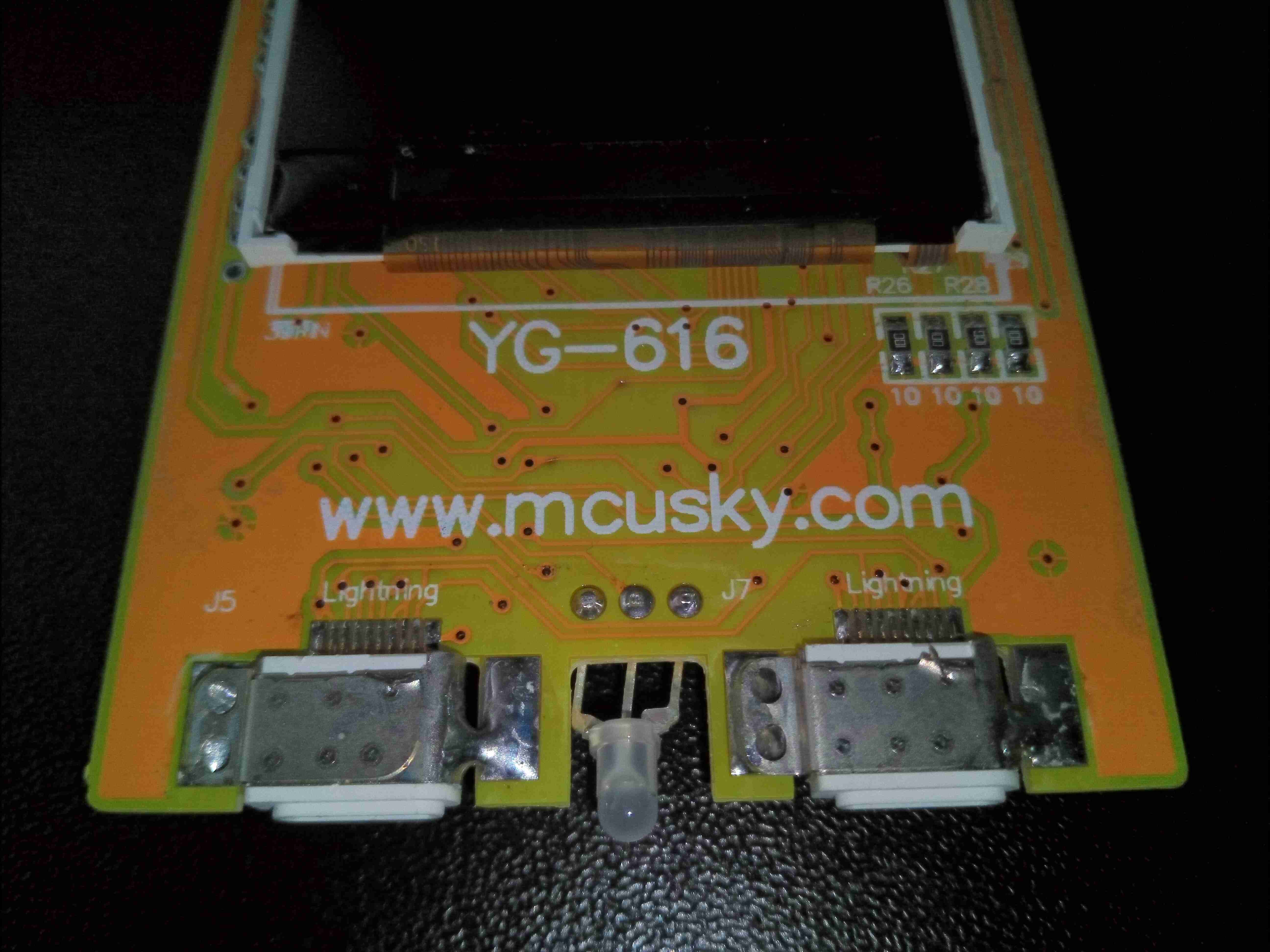
PCB Front
Pulling the PCB from the extruded aluminium case shows the large TFT LCD on the front of the board, with the µUSB charging port on the left side of the board, with the power switch & beeper. The right hand side of the board has a pair of Lightning connectors, which appear to be connected in parallel, and a status LED.
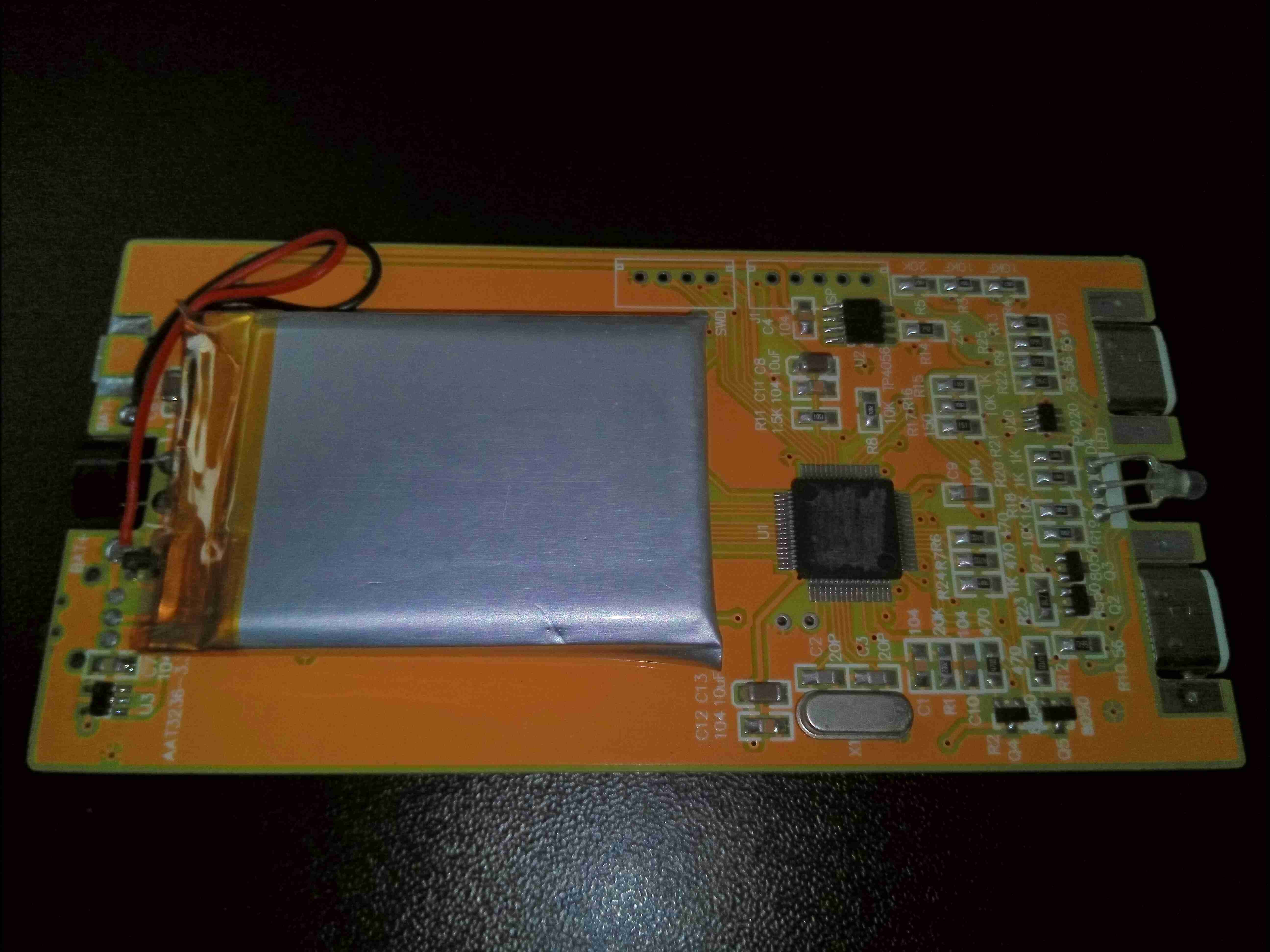
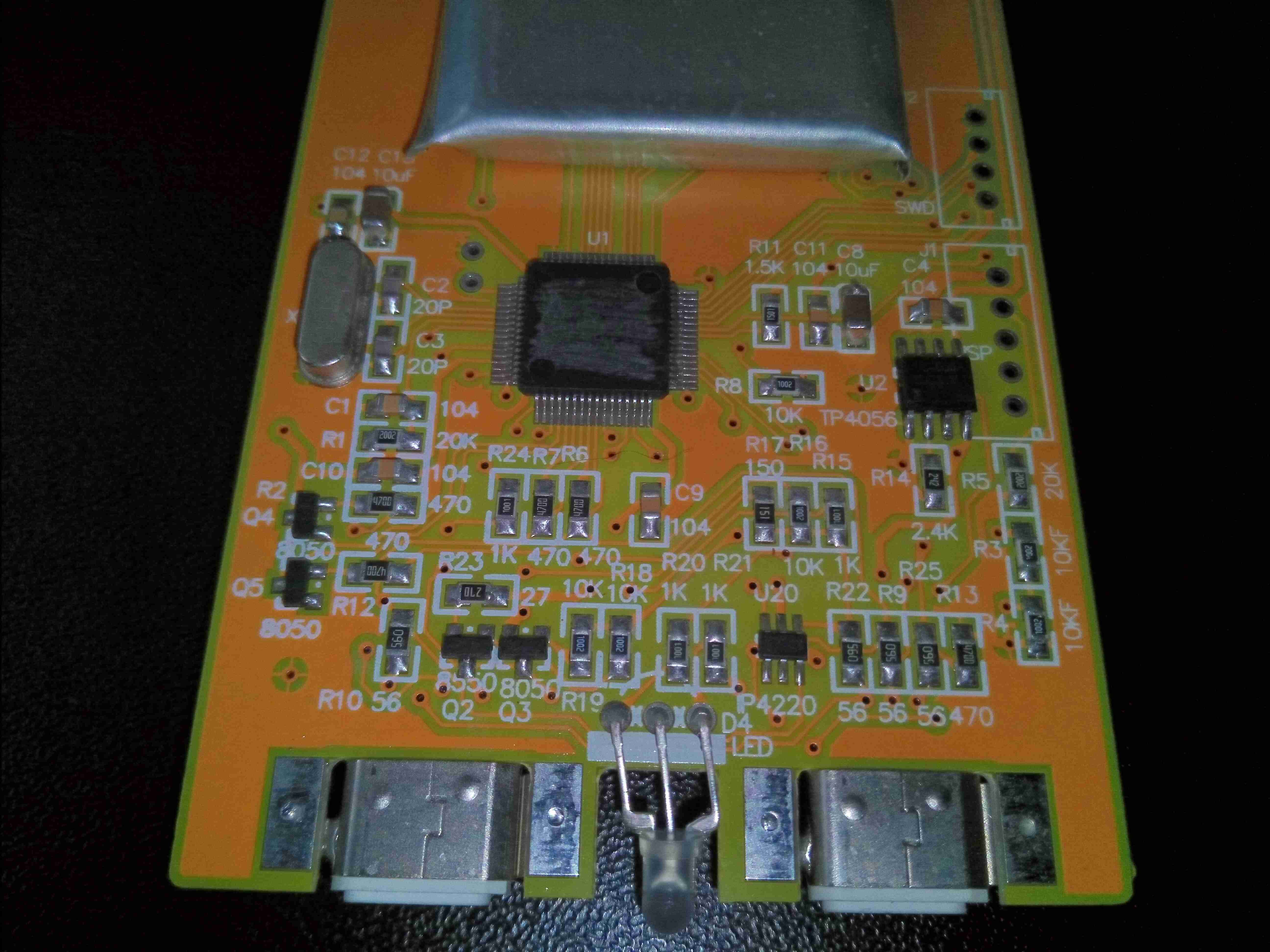
Internal PCB
The rear of the PCB has all the electronics, along with the small Li-Po cell used for power. Next to the battery on the left is a 3.3v linear regulator. The right side of the board has the main microcontroller and support electronics.
Connectors
Here’s a closeup of the connector end of the board, with the manufacturer’s web address clearly marked. Heading over to the website shows a company which produces all types of industrial electronics test equipment.
Main Chipset
Here’s where the magic happens. There’s a large microcontroller in the centre, which unfortunately has had the number scrubbed off, but it’s probably an STM32 variant, going off the ST-LINK SWD programming port. There’s a TP4056 lithium charger IC, and some discreet NPN transistors. The only other active component here is the IP4220 ESD Protection diode pack. Rather handily, all the component value identifiers are printed on the PCB silkscreen, apart from the microcontroller part number!
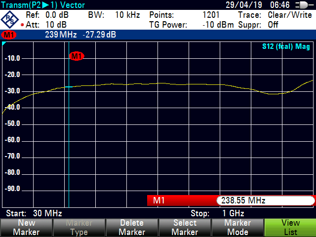
Since I wrote the post about the RF SWR & Power meter, I’ve been meaning to get around to a redesign of the board with a built-in directional coupler, and that time has finally come.
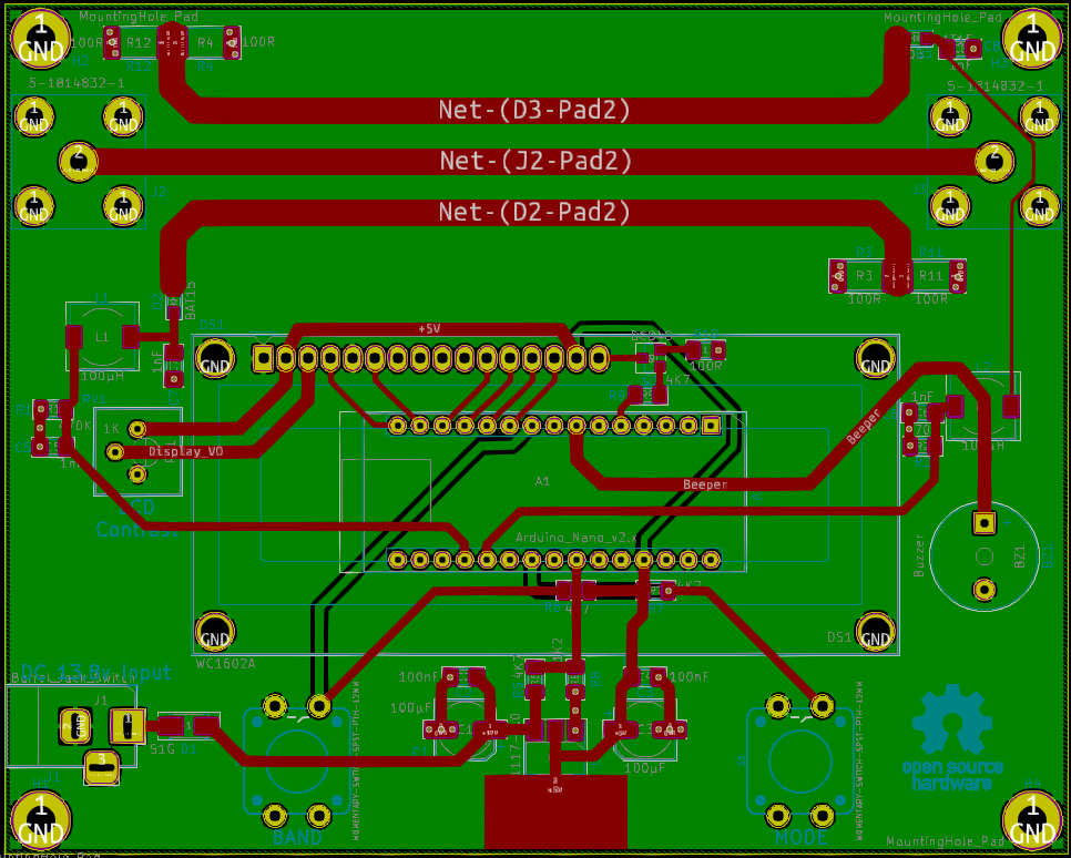
PCB Rev 2.1
So, here’s what I came up with. It’s pretty much the same as the first version on the acquisition & digital sections, but now there’s a built in directional coupler at the top edge of the board. Footprints are provided for N-Type connectors for the RF section. The effective length of the coupler is about 78mm, with 3mm wide tracks, with 2.8mm separation between the transmission line & the pickup lines.
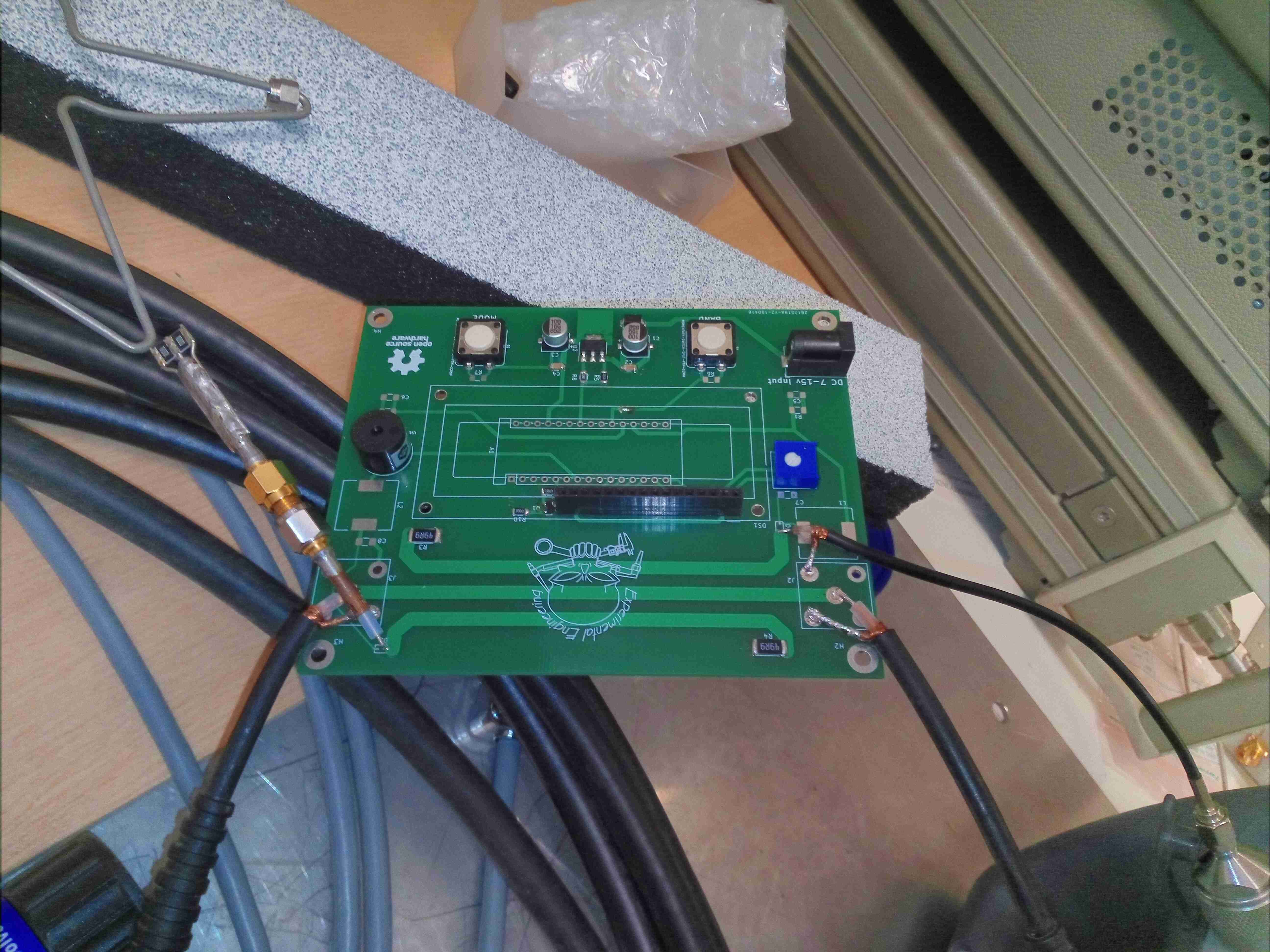
Network Analyser Setup
A quick turnaround from JLCPCB gave me some prototype PCBs to play with, and above I have a test board set up on a Network Analyser. I’ve got the unused parts terminated at 50Ω, and this gave me the following plots:
Forward Coupling
The response is pretty flat across the range at about -25dB coupling, rolling off at about 200MHz at the bottom end due to the relatively short length of the coupler. There’s a bit of a dip at ~700MHz, but I suspect that is down to one of the test cables used.
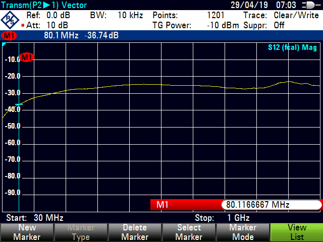
Reverse Coupling
The reverse power coupler gives a very similar result, with the 700MHz+ dip going in reverse. I suspect things aren’t that perfect due to the coupler tracks not being quite symmetrical. Revision 2.2 of the board should give me some slightly better results.
Well, this came as a little surprise. This is the PSU from a Microchip PICMASTER Universal Development System from 1993, intended for the old UV-erasable devices. On being plugged in, the PSU ran for about 10 minutes before a small explosion occurred, accompanied by an indescribable acrid smell. The photo above shows one of the X2 capacitors, across the AC input line has violently exploded, blowing the fuse (literally!) from it’s clips, and showering the inside of the PSU with bits of foil & paper. There’s another two of these on the other side of the common-mode choke, which are also showing signs of failure, however the fuse link disconnection has saved the others from the same fate.
All of these capacitors would need to be replaced with modern versions, but the PSU should still function fine afterwards. If I actually do the repair on this ancient system, I’ll do a further post.
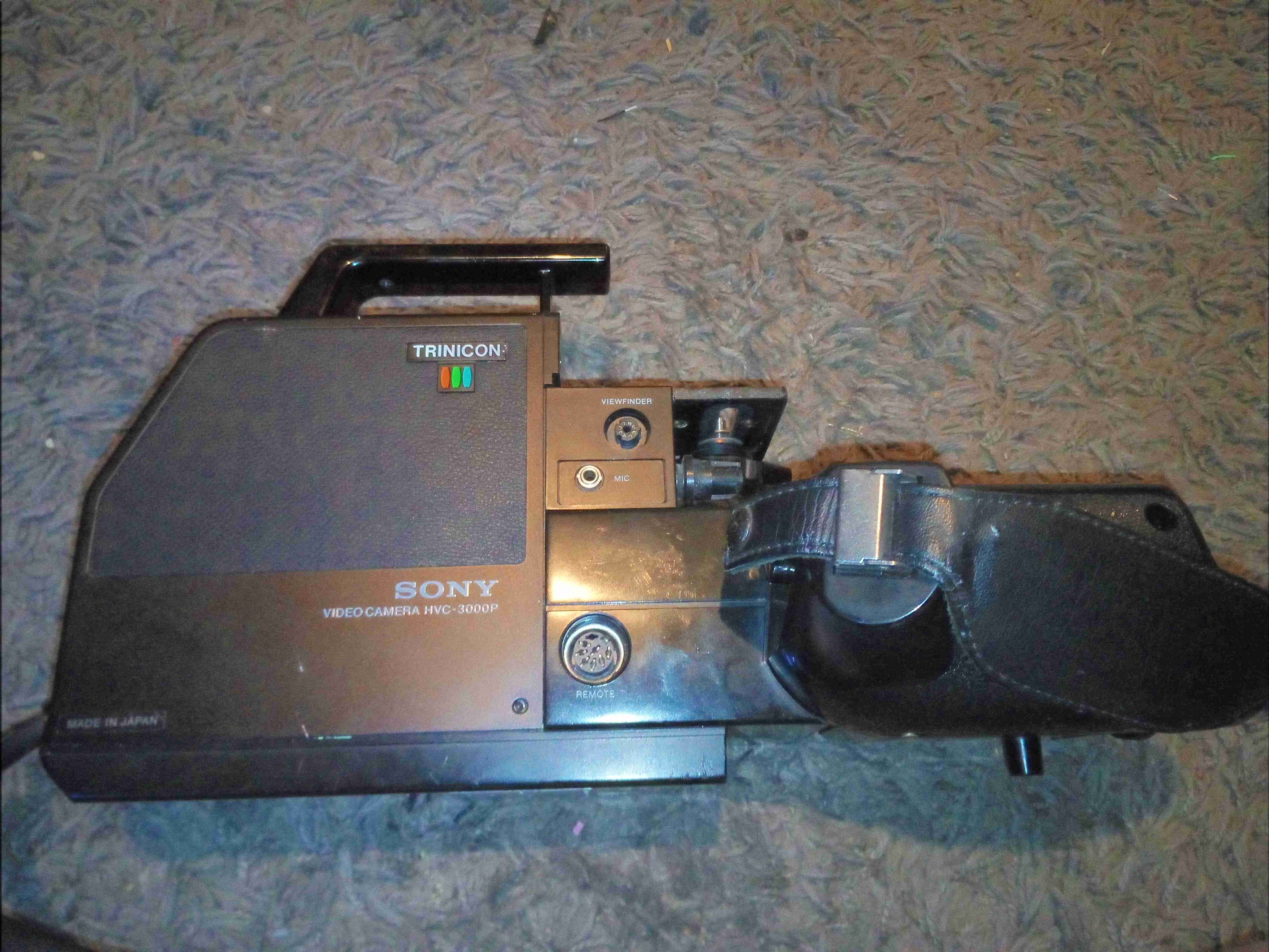
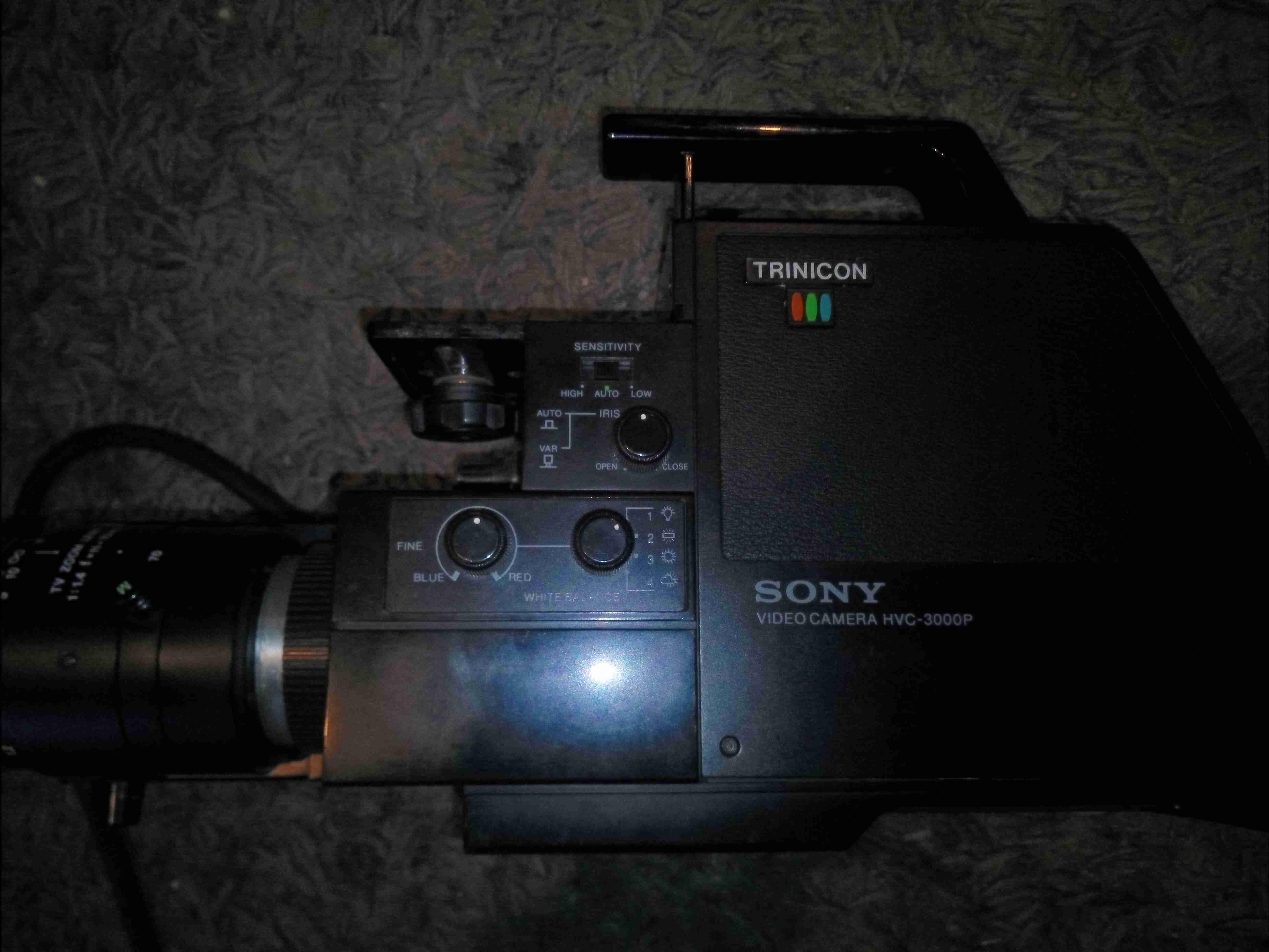
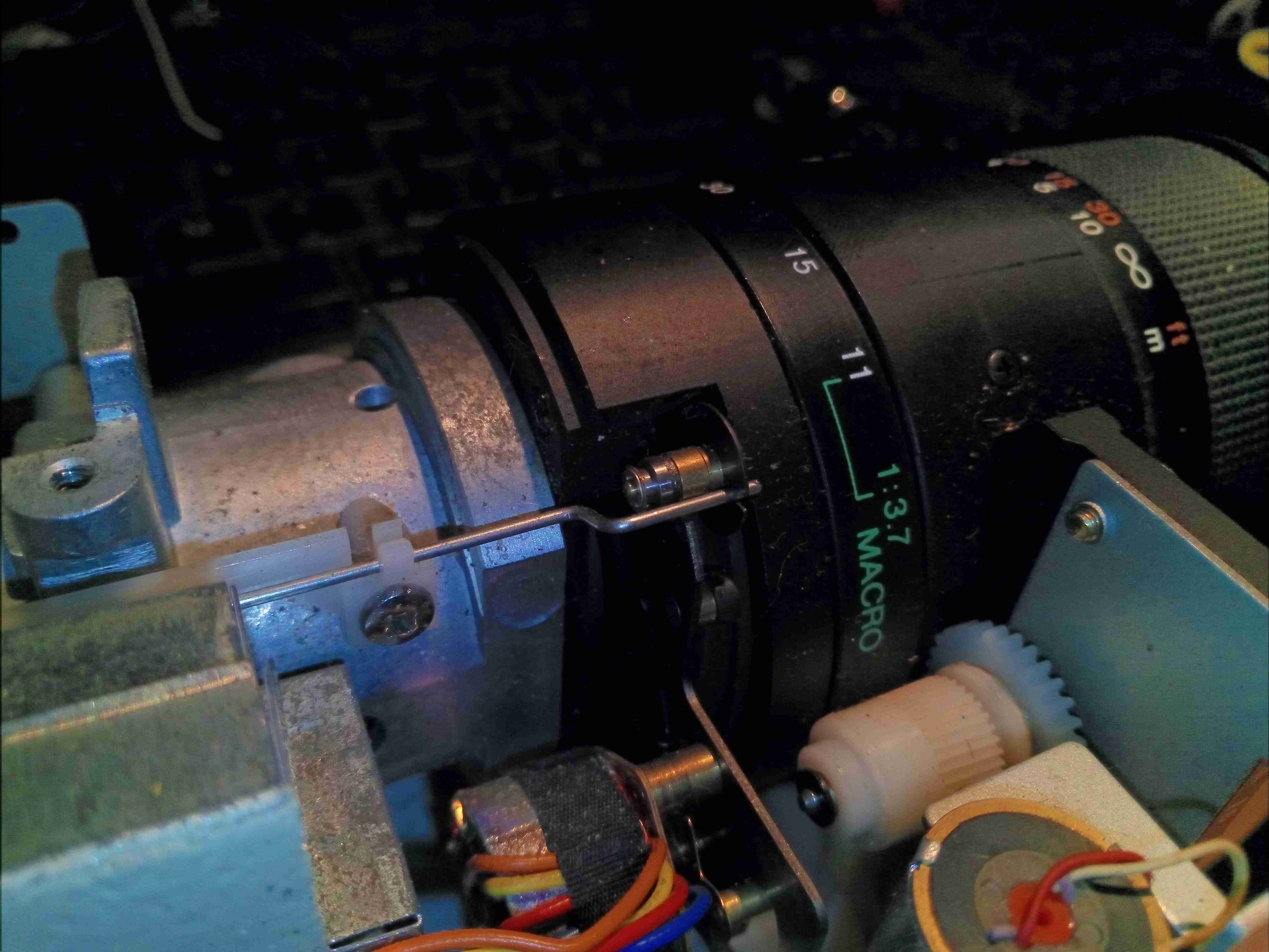
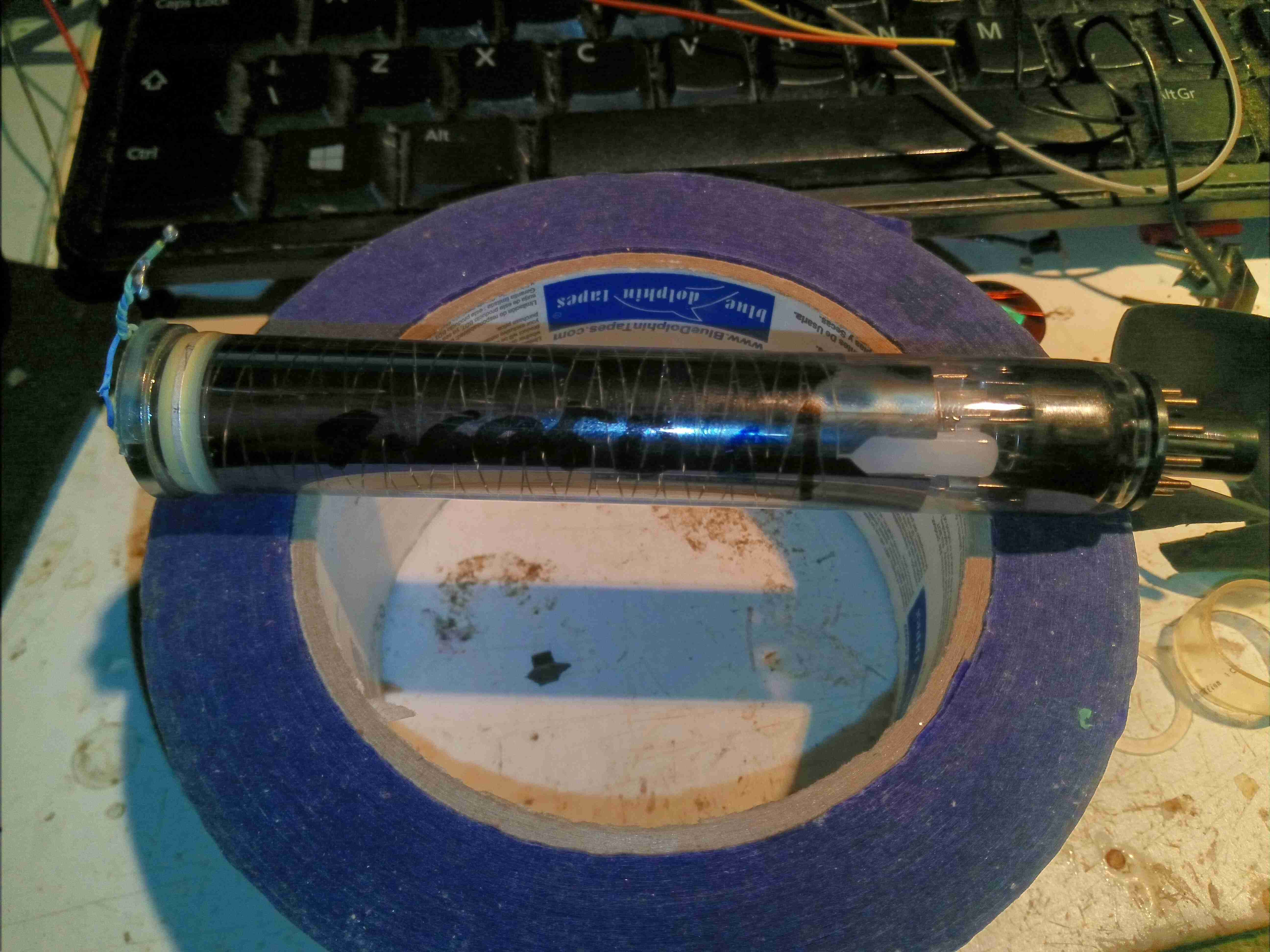
Following on from the viewfinder teardown, here’s the rest of the camera. This unit dates back to 1980, and is made almost exclusively of cast aluminium. Very little plastic has been used here & only for the bits that the user comes into contact with. This camera is based around the Sony Trinicon camera tube system, technology dating back before CCDs. There aren’t many controls on this side of the camera, only the record button, which is hidden behind the camera handgrip.
Camera Right
The other side of the camera has most of the controls for the picture.
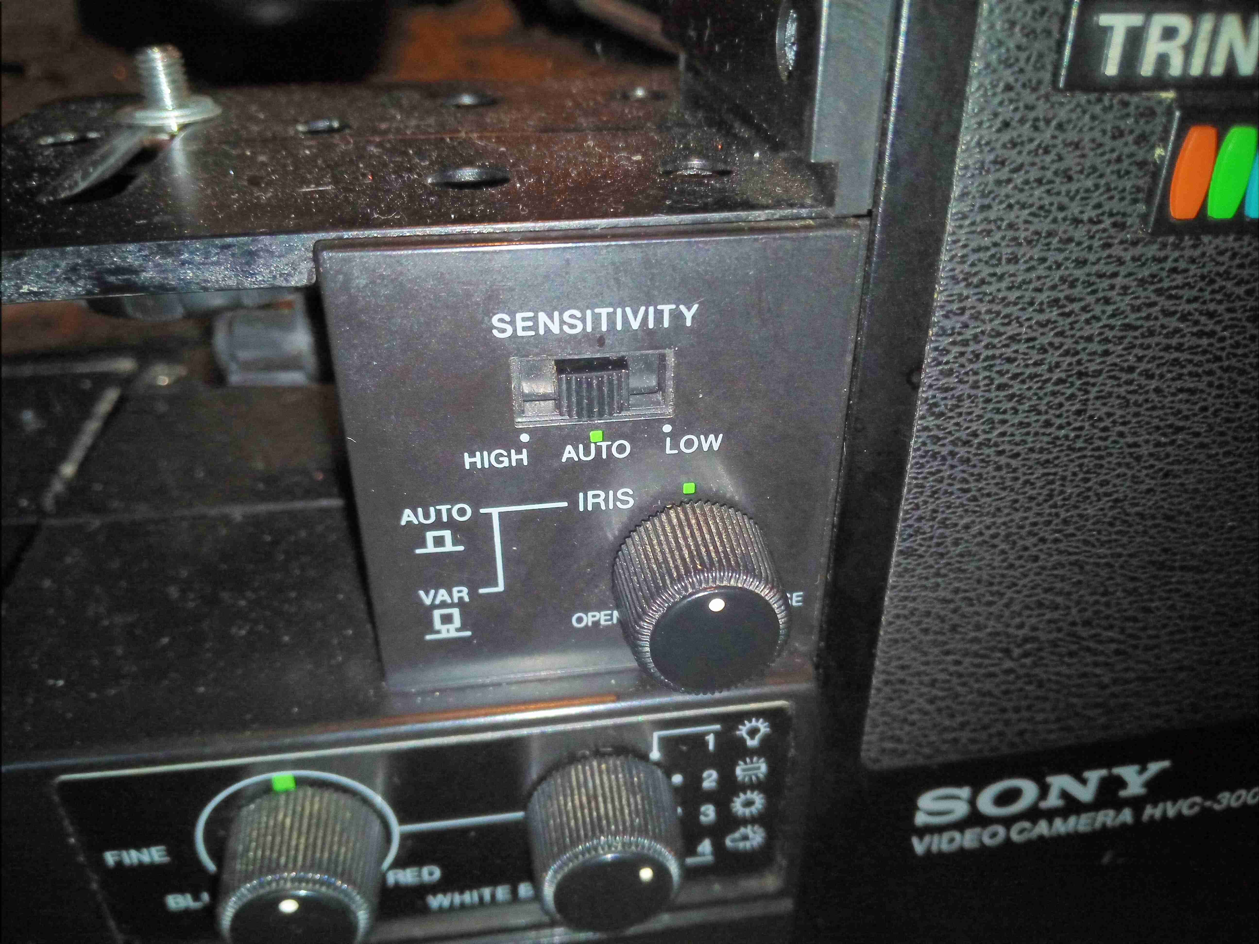
Image Controls
The image controls inclue auto / manual iris, white balance & colour balance.
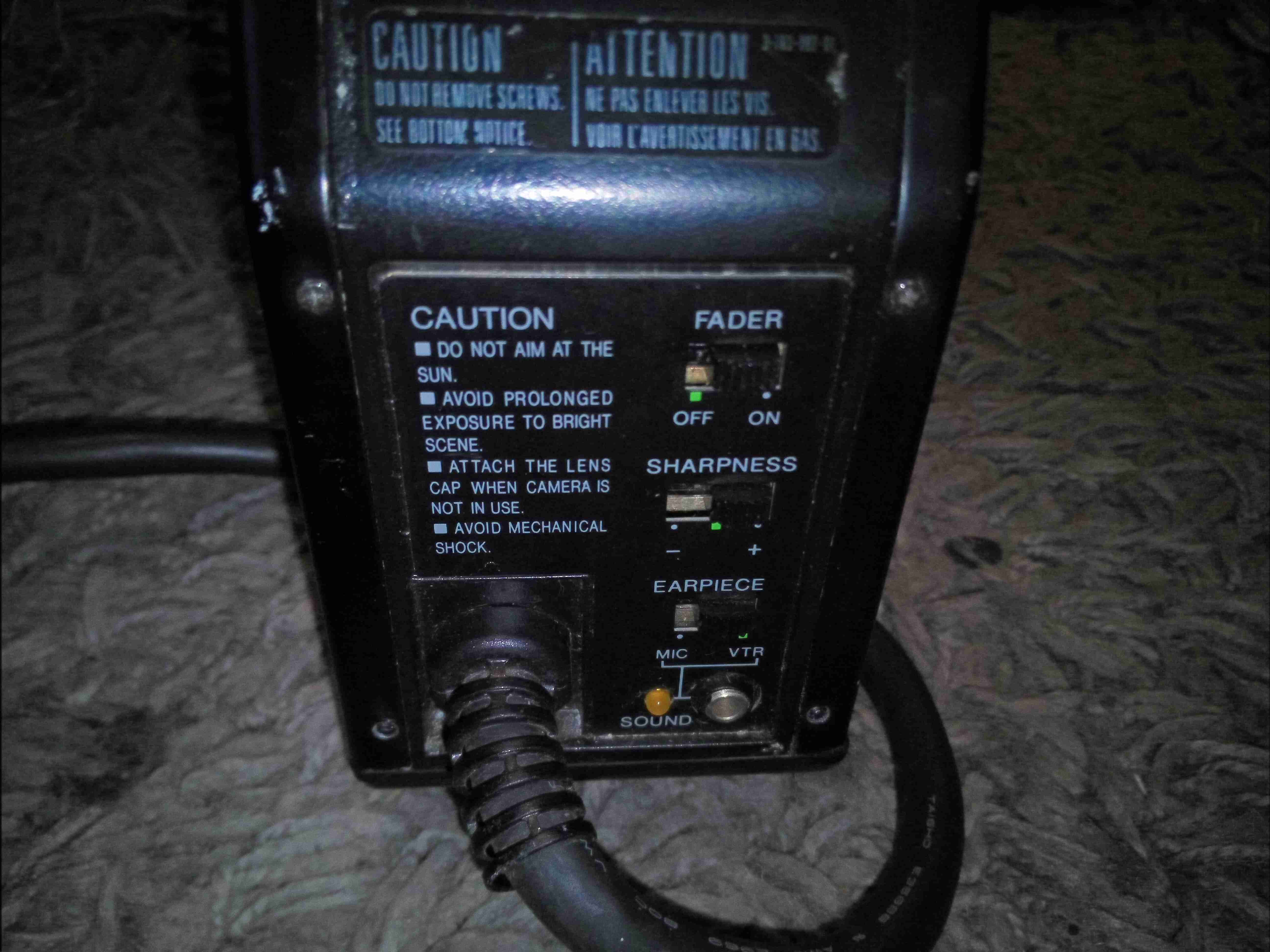
Rear Panel
Sharpness & fader controls are on the back of the camera, along with the umbilical cable which would have connected to a Betamax recorder.
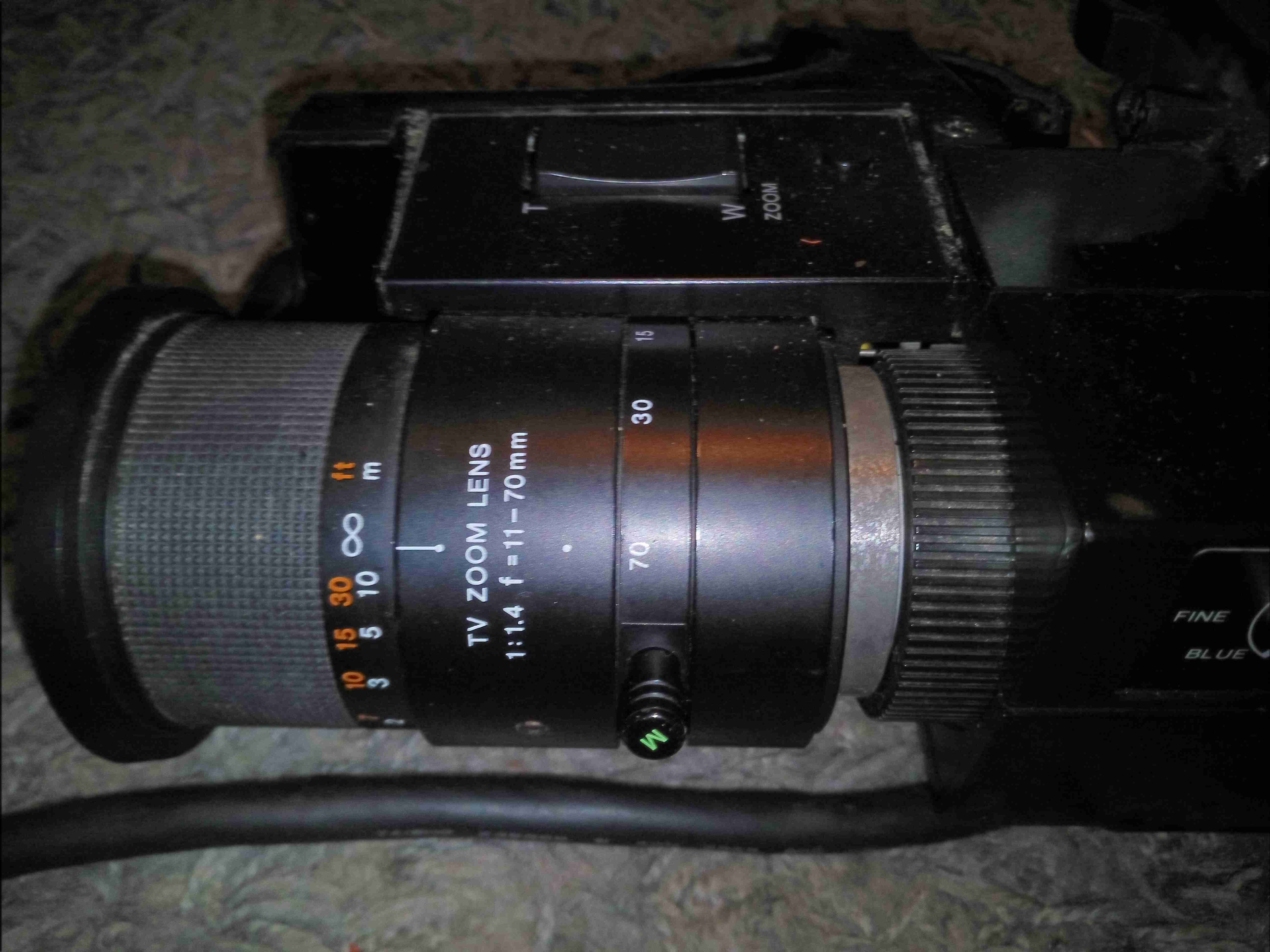
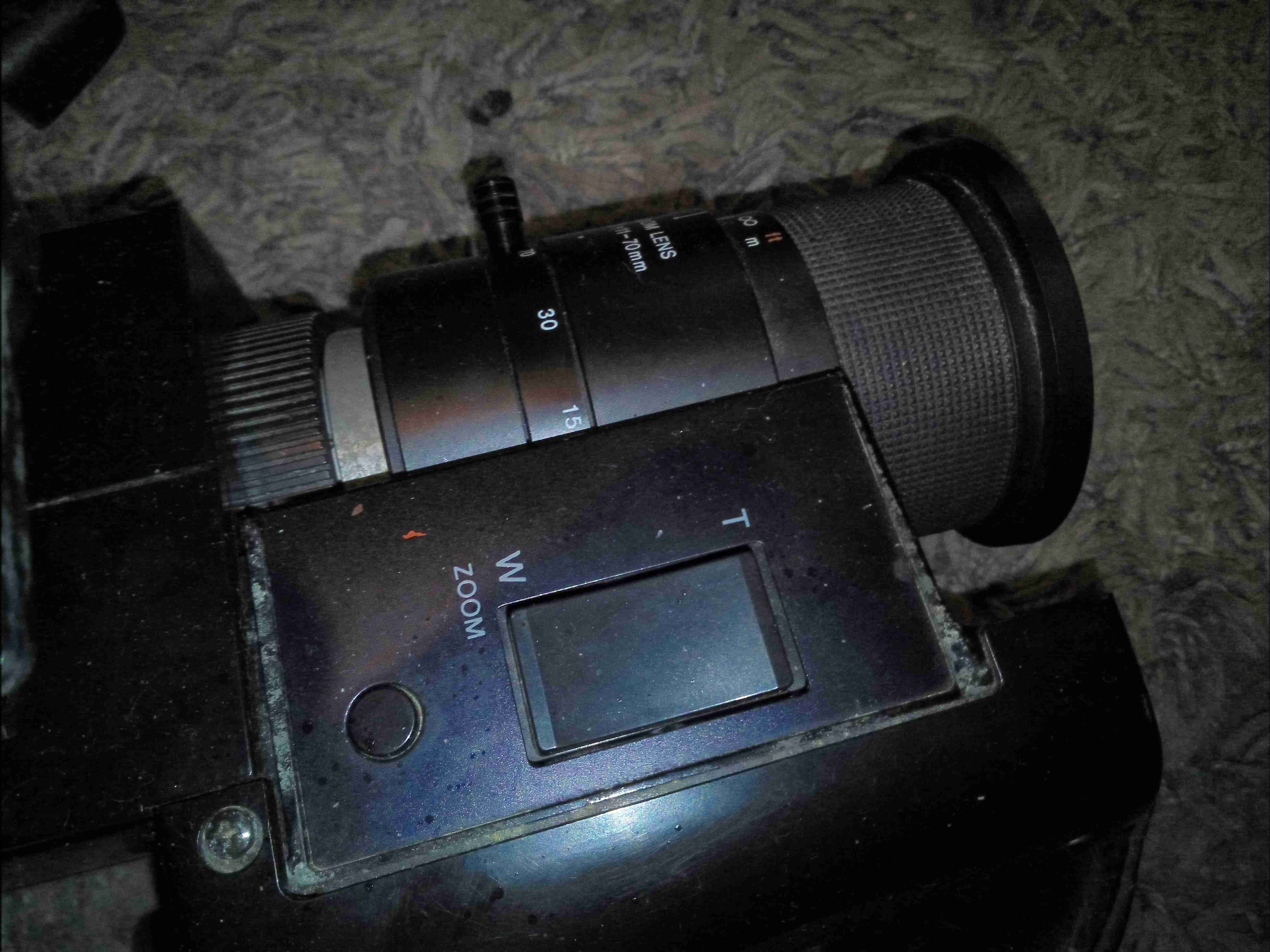
Main Lens
The lens on this camera is massive, at least a kilo of optical glass. Focus control is manual, with both auto & manual zoom control.
Lens Zoom Control
The Zoom controls are on top of the grip, with a button to the rear of the control which I have no idea about. The internal belts are a bit rotted with age so the zoom function doesn’t work great.
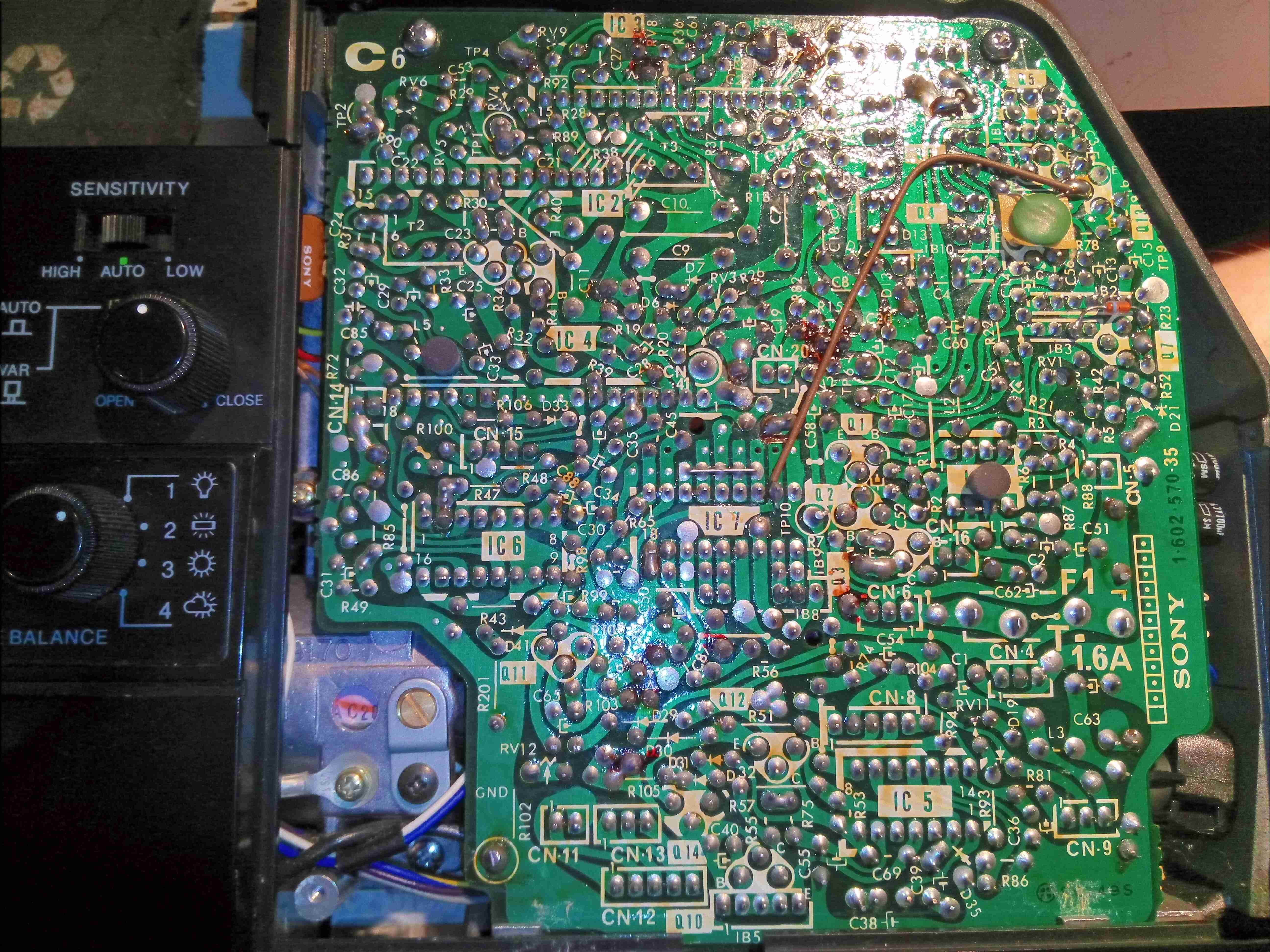
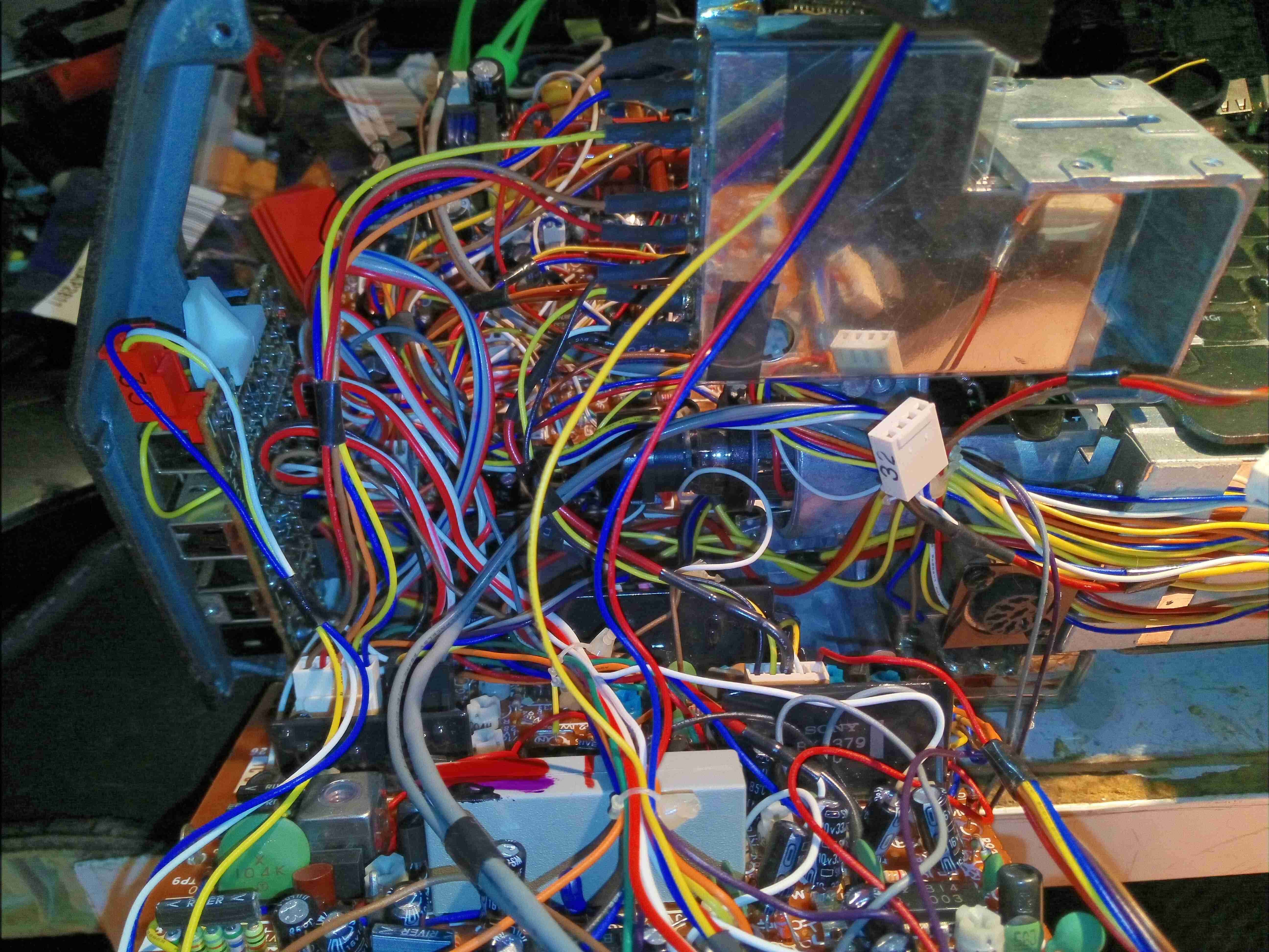
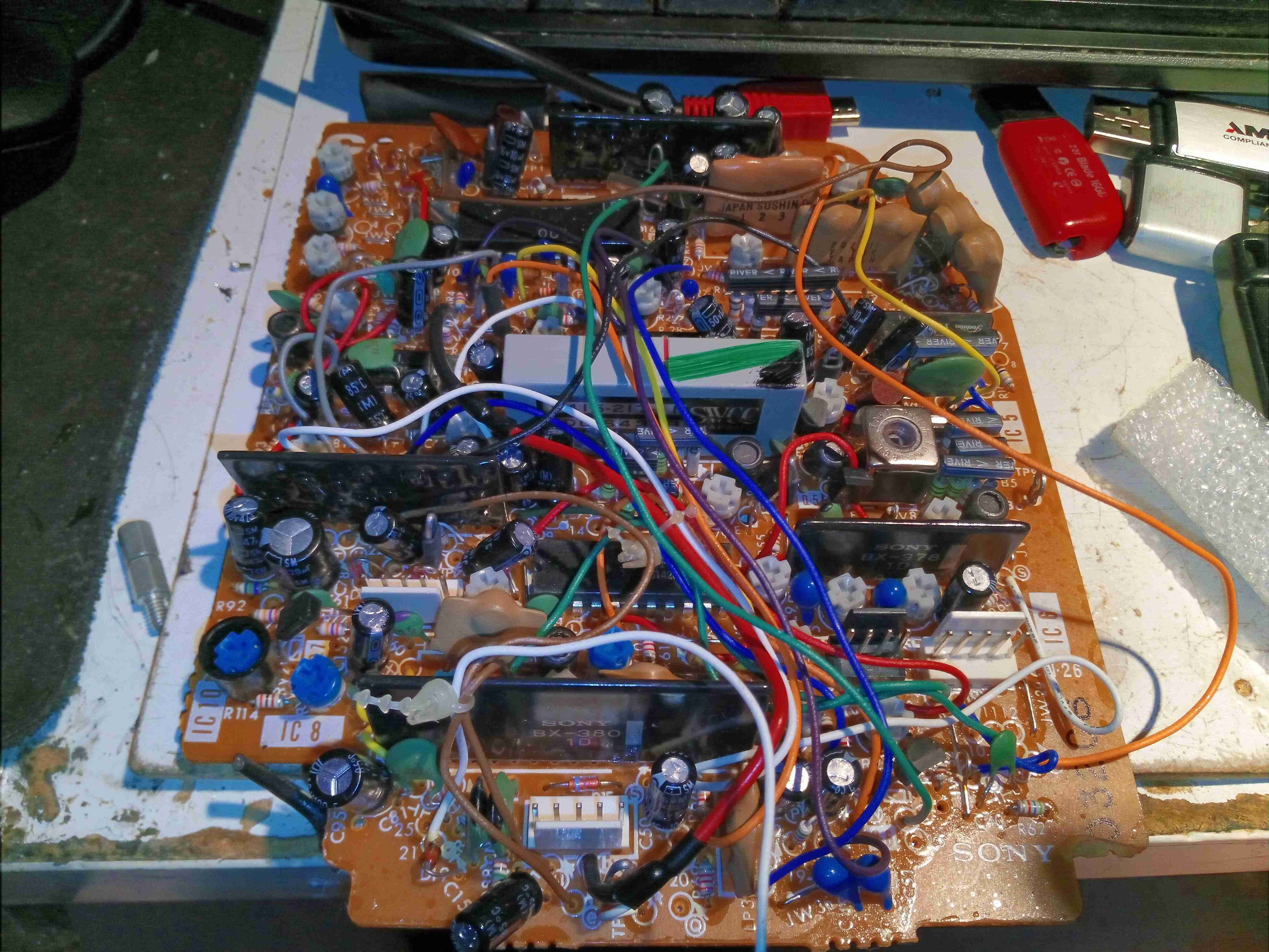
Trinicon Control Board
After removing the side covers, the two large PCBs become visible. These units are absolutely packed with electronics. On this side is the Trinicon tube control board, generating all the high voltages for electron beam acceleration, focus & electrostatic deflection of the beam. There’s around 500 volts knocking around on this board, with some rather specialised hybrid modules doing all the high voltage magic.
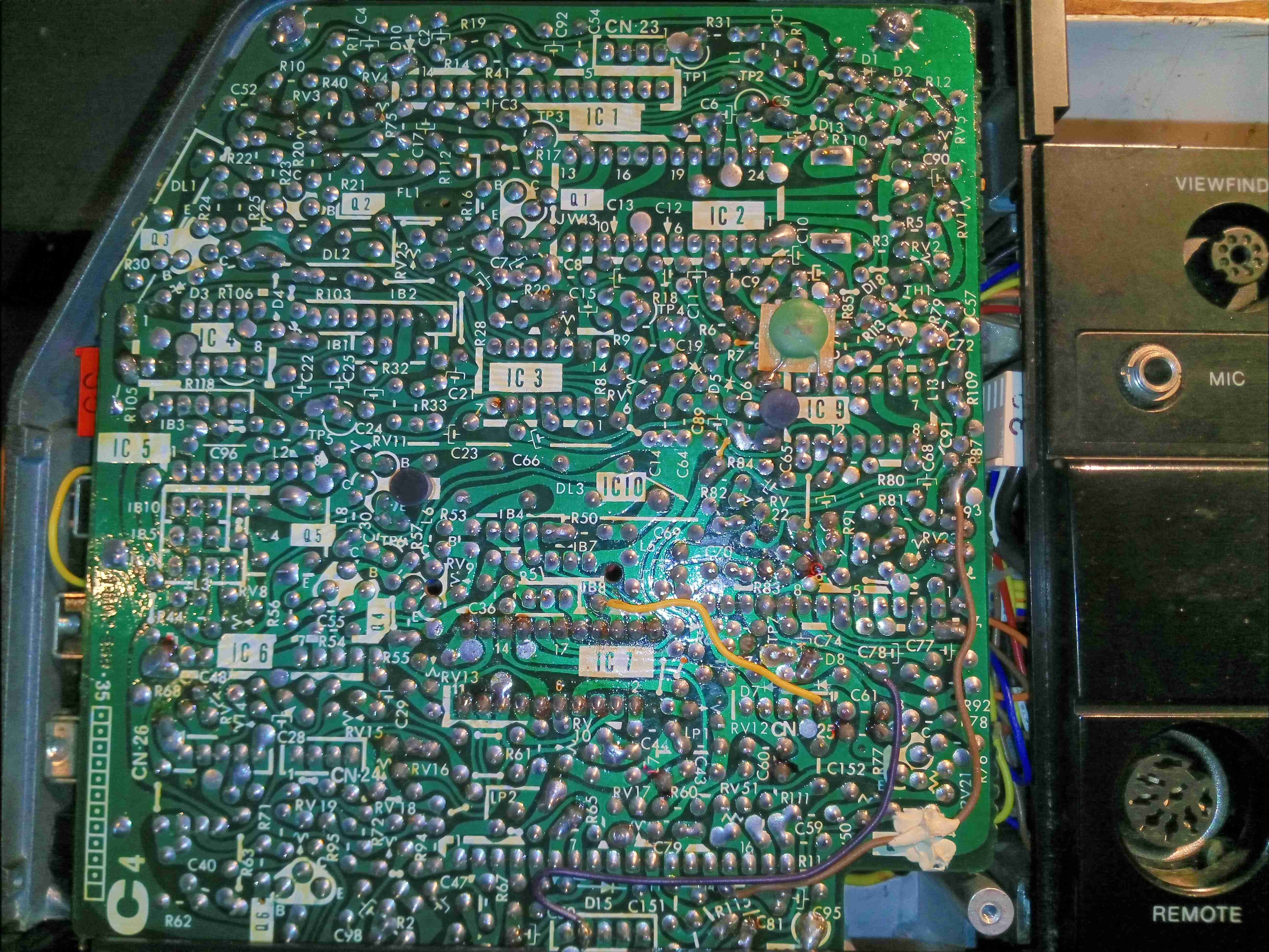
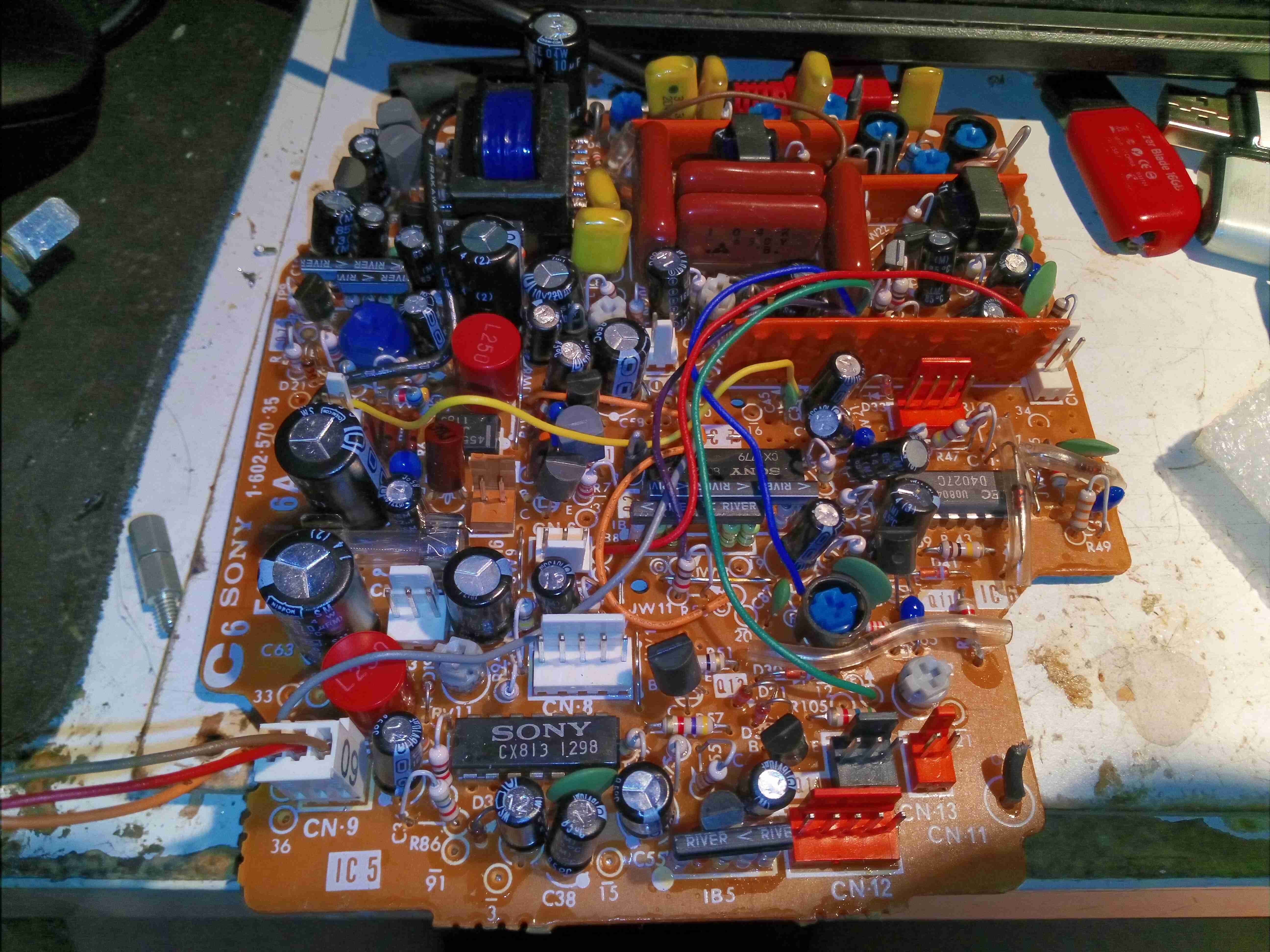
Video Process Board
The other side of the camera has the video process board, which performs all the colour separation of the video signal from the tube, processes the resulting signals into a composite video signal, and finally sends it down the umbilical.
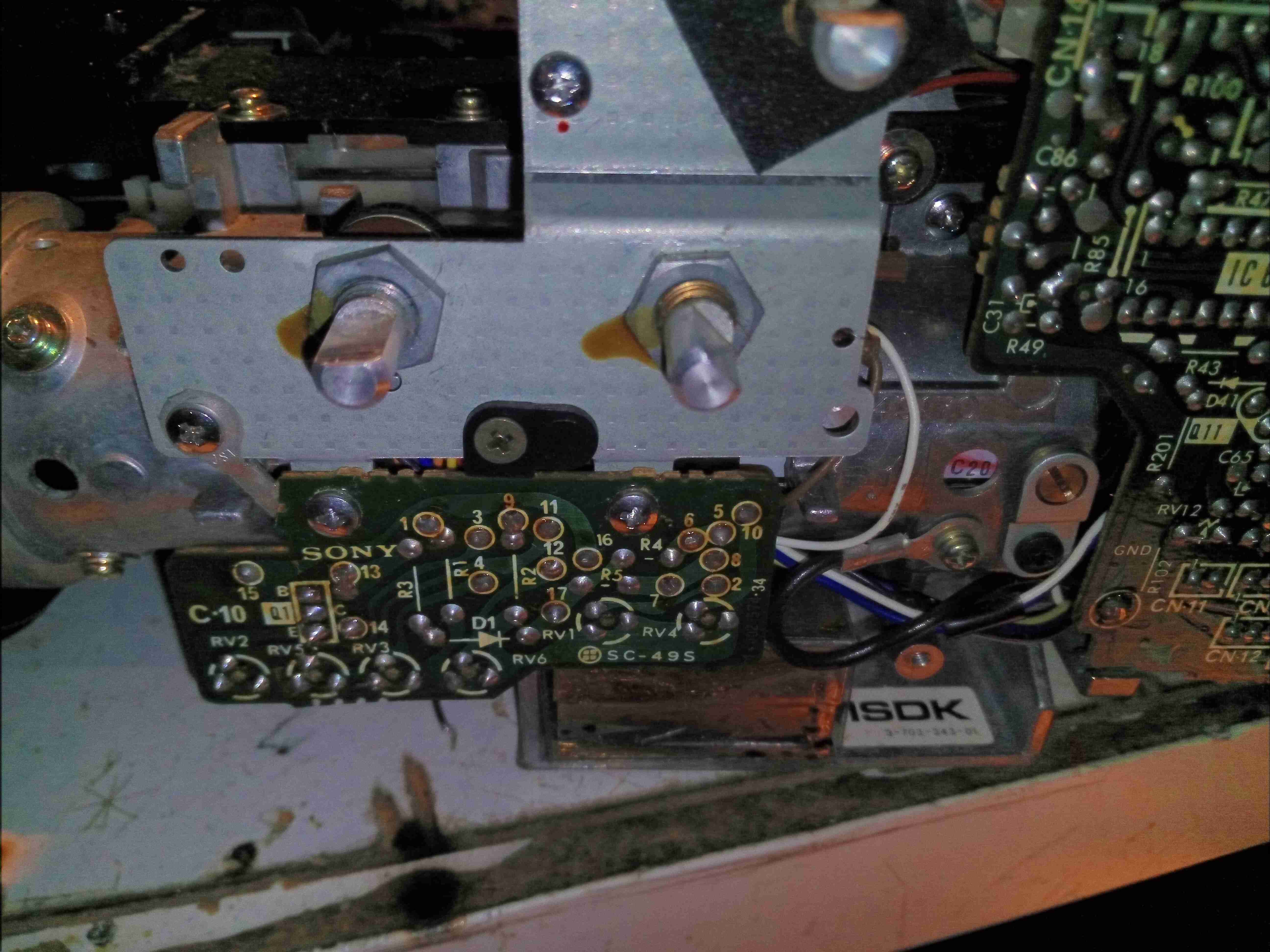
Bare Controls
Removing some of the remaining covers exposes the bare video controls, and a small PCB just underneath covered in trimpots to set factory levels.
White Balance Filter Arm
The white balance is partially electronic & partially mechanical. This lever actuates a filter inside the lens assrembly.
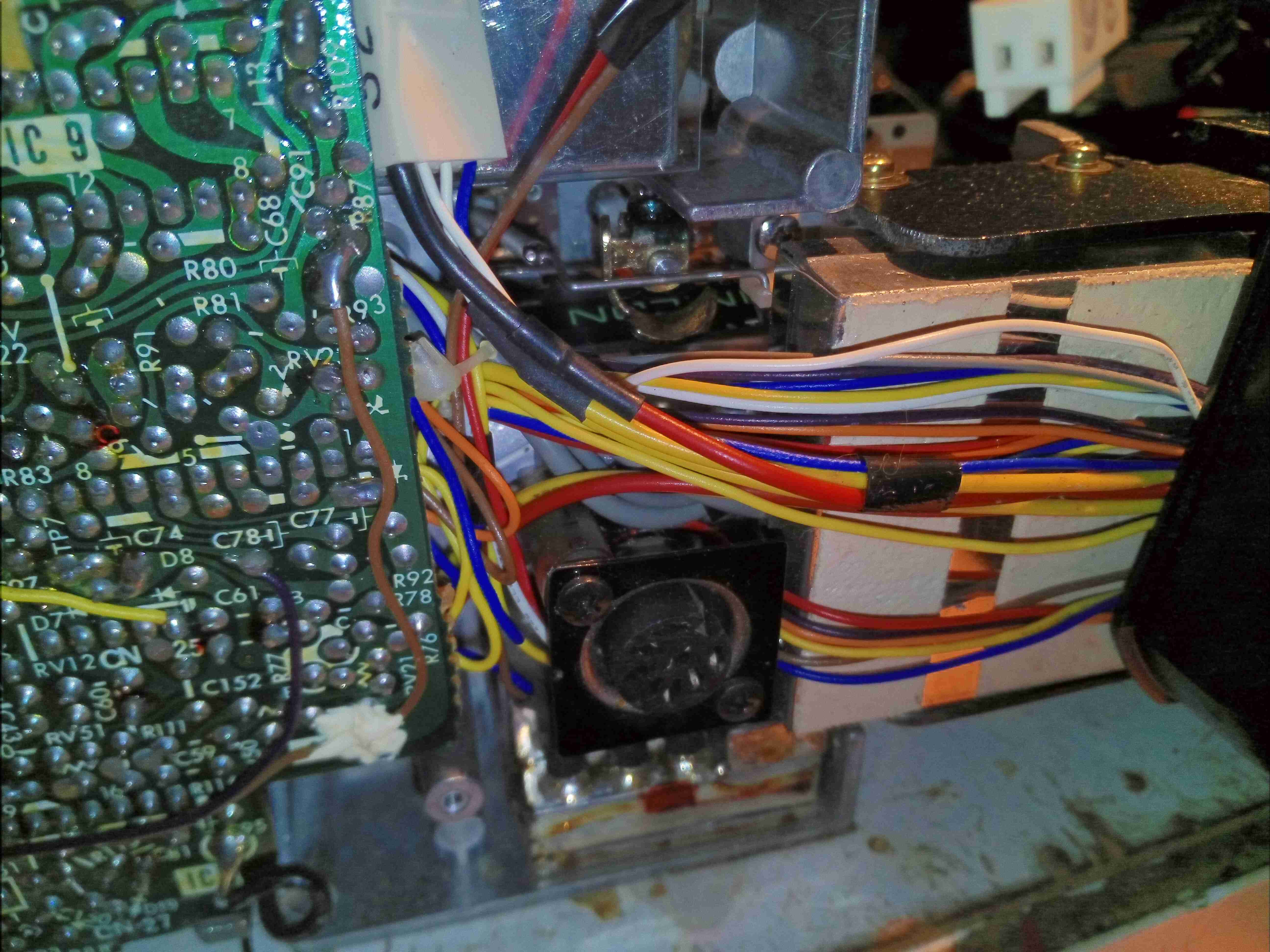
Remote Connector
A DIN connector offers remote control ability. The large loom of wires disappearing off to the right is dealing with the zoom mechanism & the onboard microphone amplifier. Just under the DIN connector hides the system power supply, inside a soldered can. The can under the white tape is the head end amplifier for the Trinicon video tube.
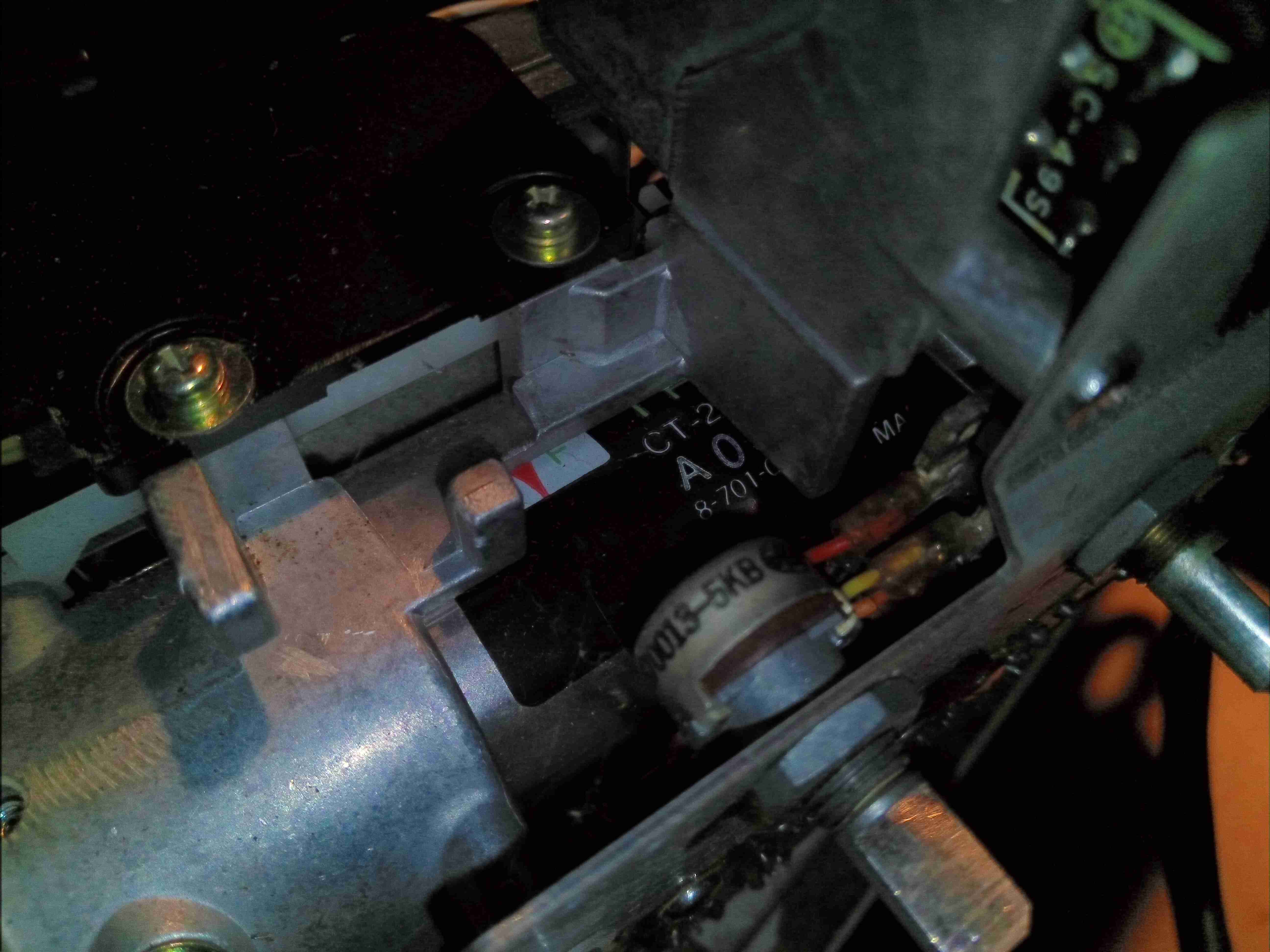
Trinicon Mount
Hiding in the centre of the camera inside the casting is the Trinicon tube assembly itself. The label can just be seen here.
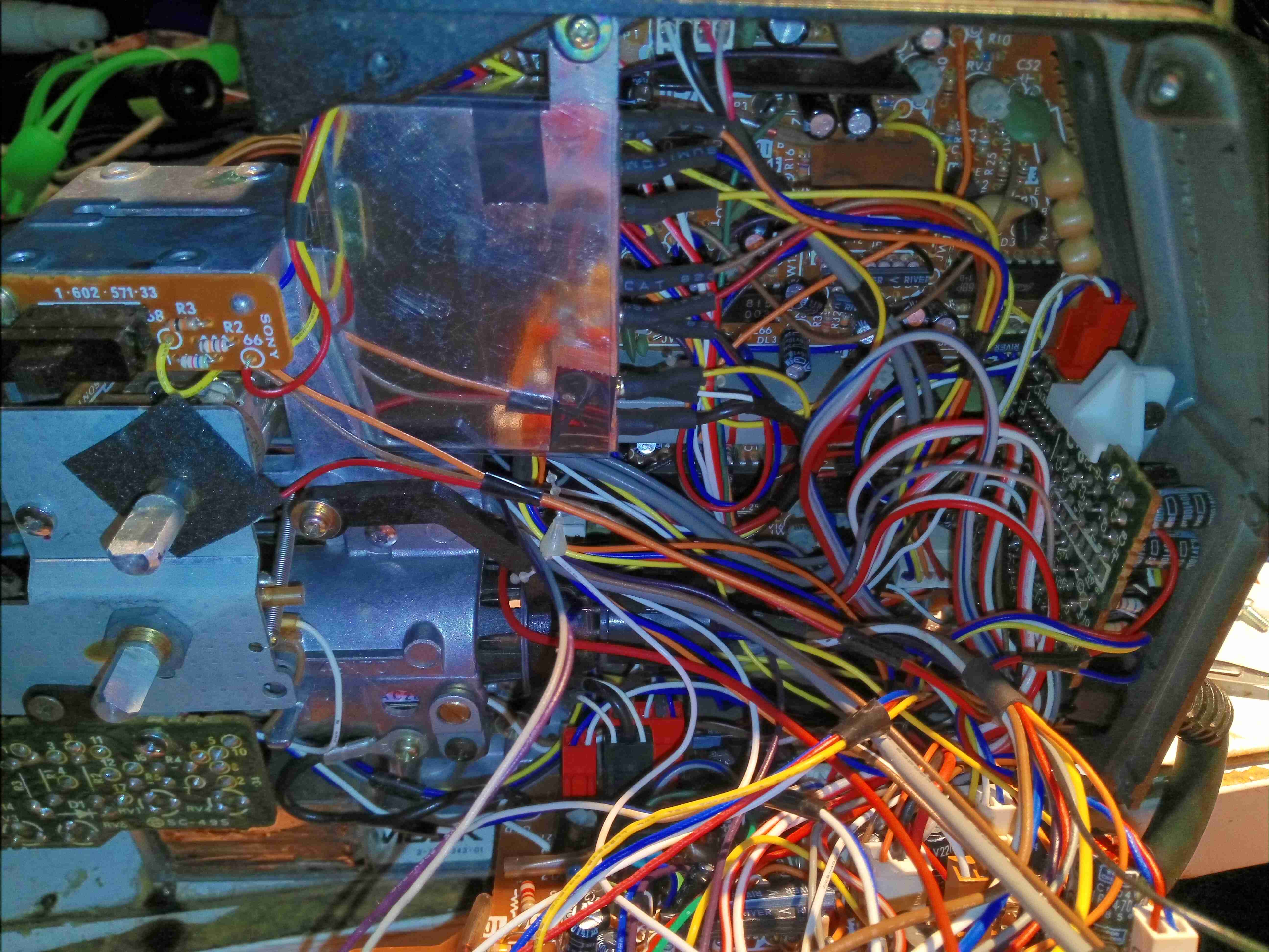
Camera Internals 1
As is typical of 1980’s electronic design, the main boards swing down & are designed to slot into the base casting folded out for repairs. Internally the unit is a rat’s nest of wiring loom. There’s also another shielding can in here nestled between the boards – this is the video sync generator circuit.
Camera Internals 2
The other side gives a better view of the video sync generator can. I’ll dive into the individual modules later on.
Lens Zoom Assembly
Under the remaining side cover is the zoom assembly & microphone amplifier board. More massive wiring loom hides within.
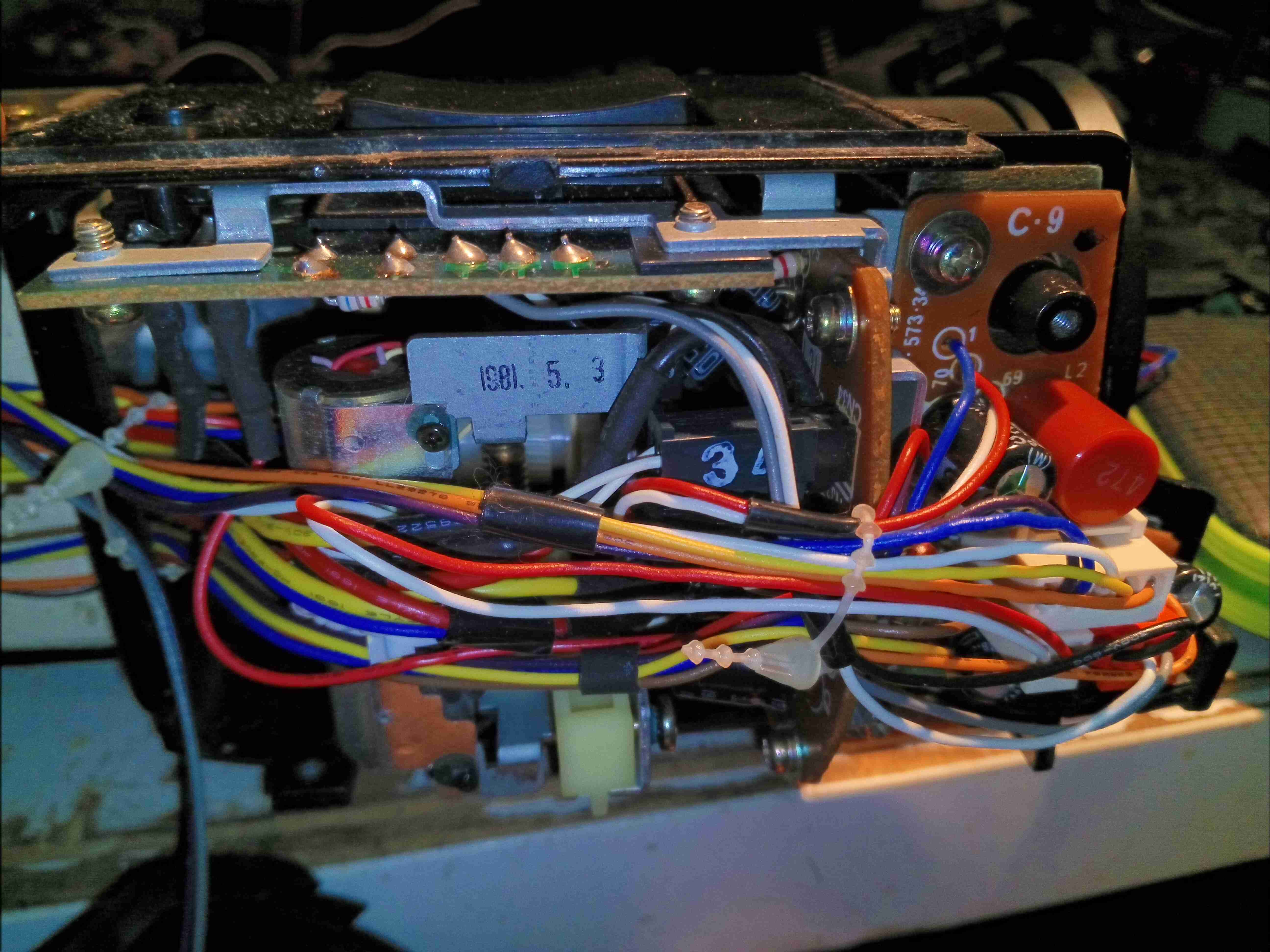
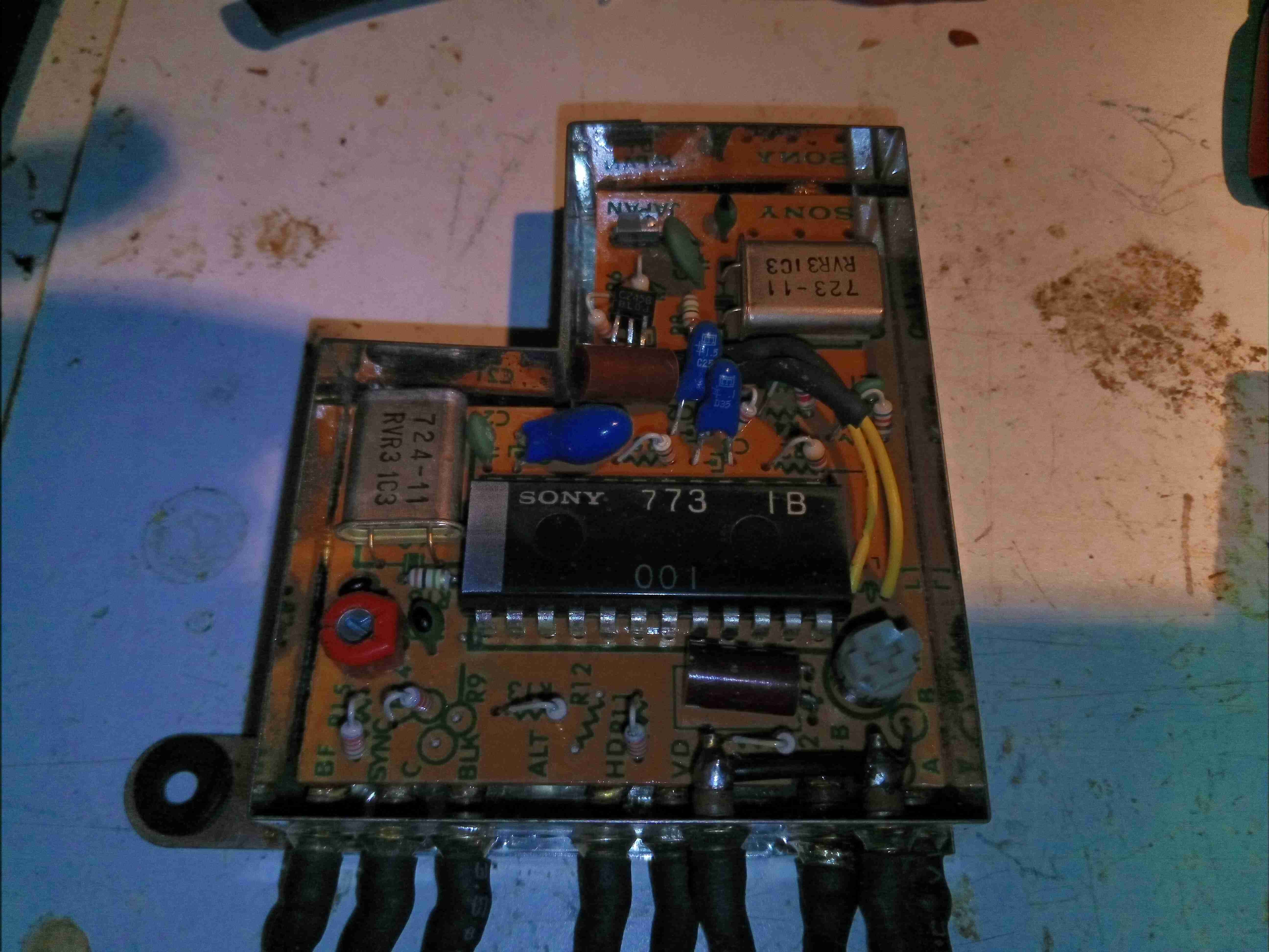
Video Sync Generator
The video sync generator is pretty sparse inside, just a large Sony CX773 Sync Generator IC, with a pair of crystals. There are a couple of adjustments in here for video sync frequencies.
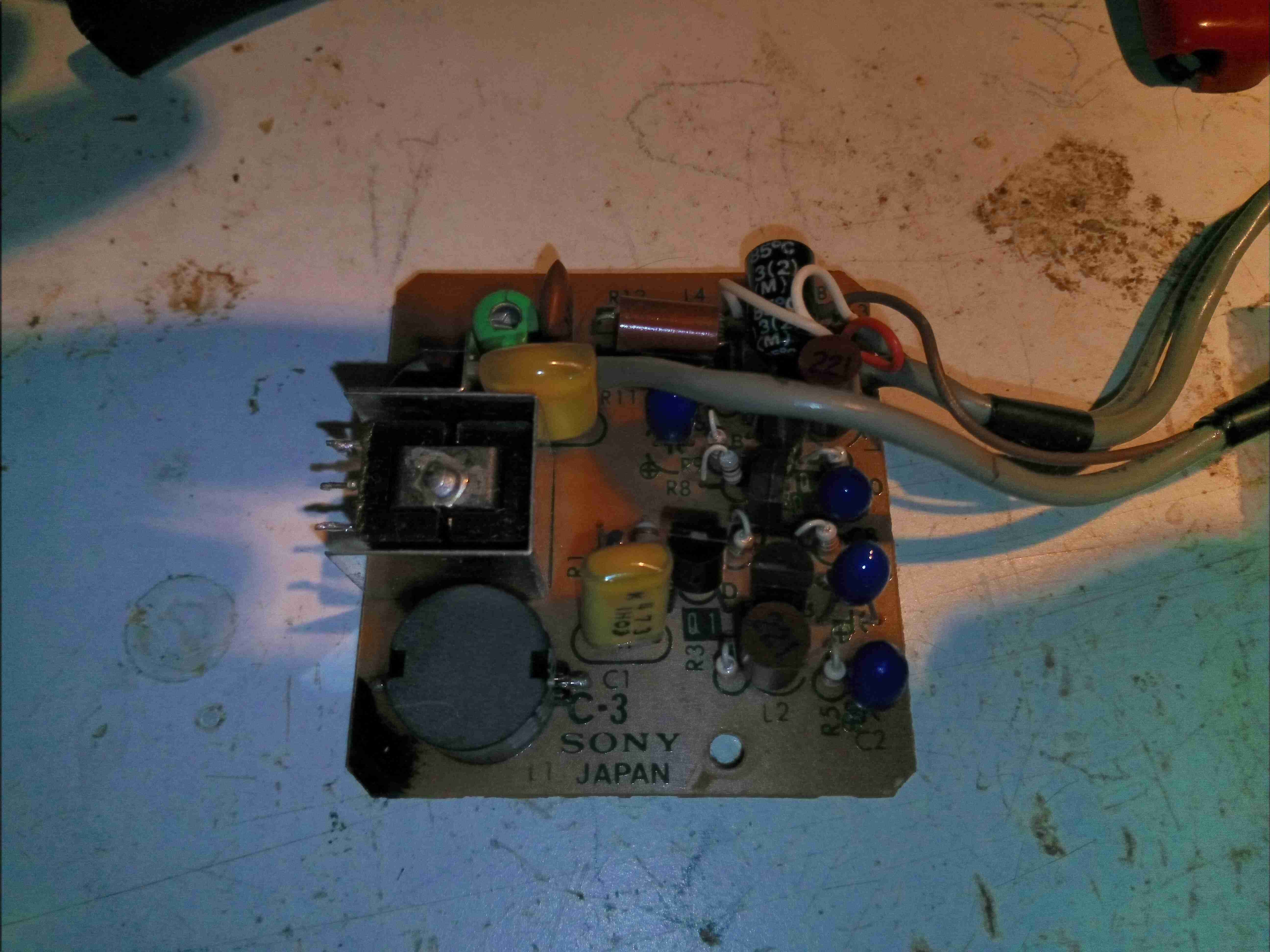
Head End Amplifier
Removed from it’s shielding can, here is the head end amplifier for the Trinicon tube. This very sensitive JFET input amplifier feeds into the main video process board.
Input Transformer
The Trinicon tube target connects to this input transformer on the front of the amplifier board.
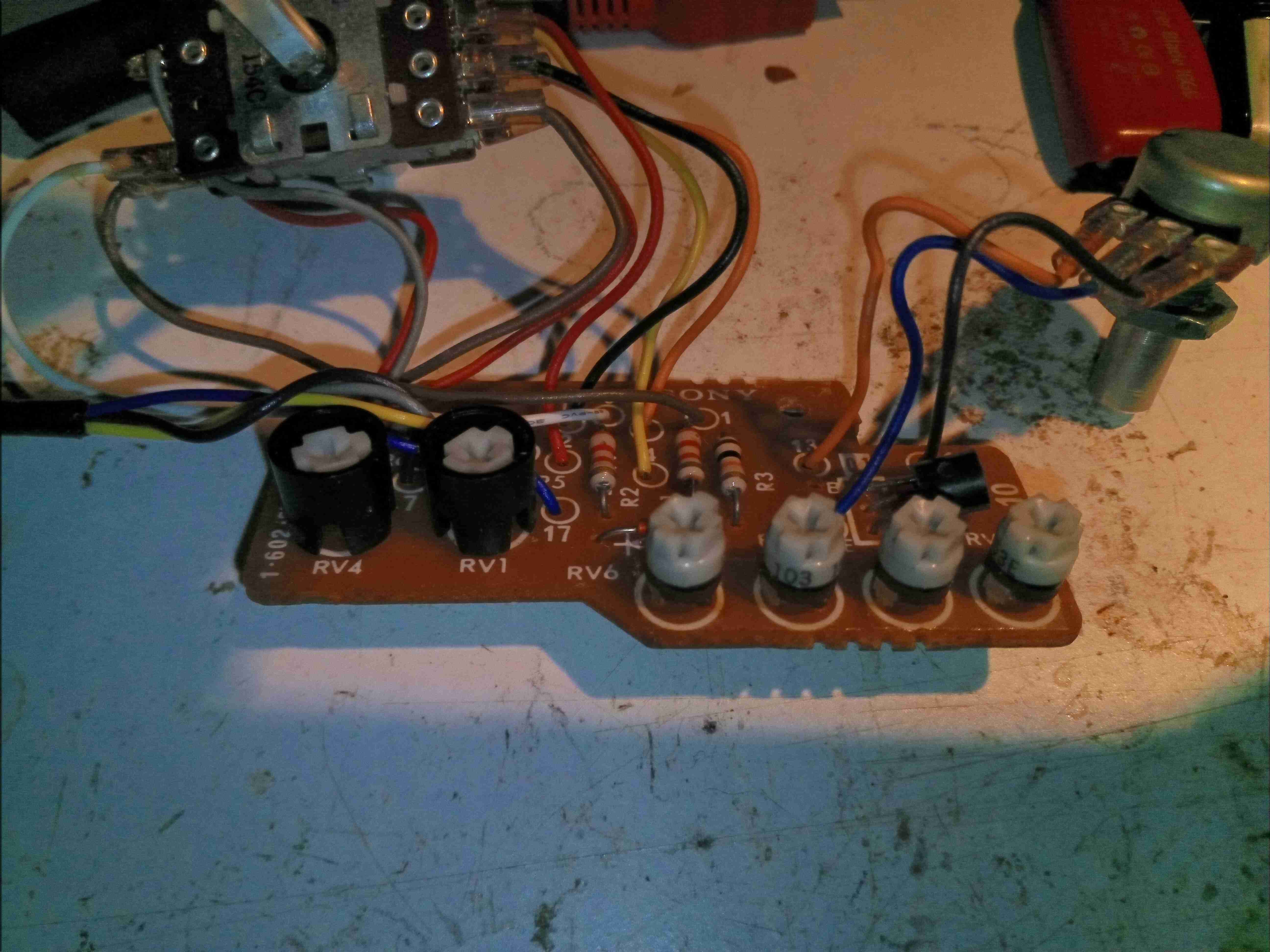
Internal Video Adjustments
The internal white balance controls are on this small PCB, mounted under the user-accessible controls.
Vidicon Control Board
Here’s the main control board responsible for the Trinicon tube & exposure control. Down near the front is the auto-iris circuit, nearer the centre is timing control & at the top is the high voltage power supply & deflection generator ICs.
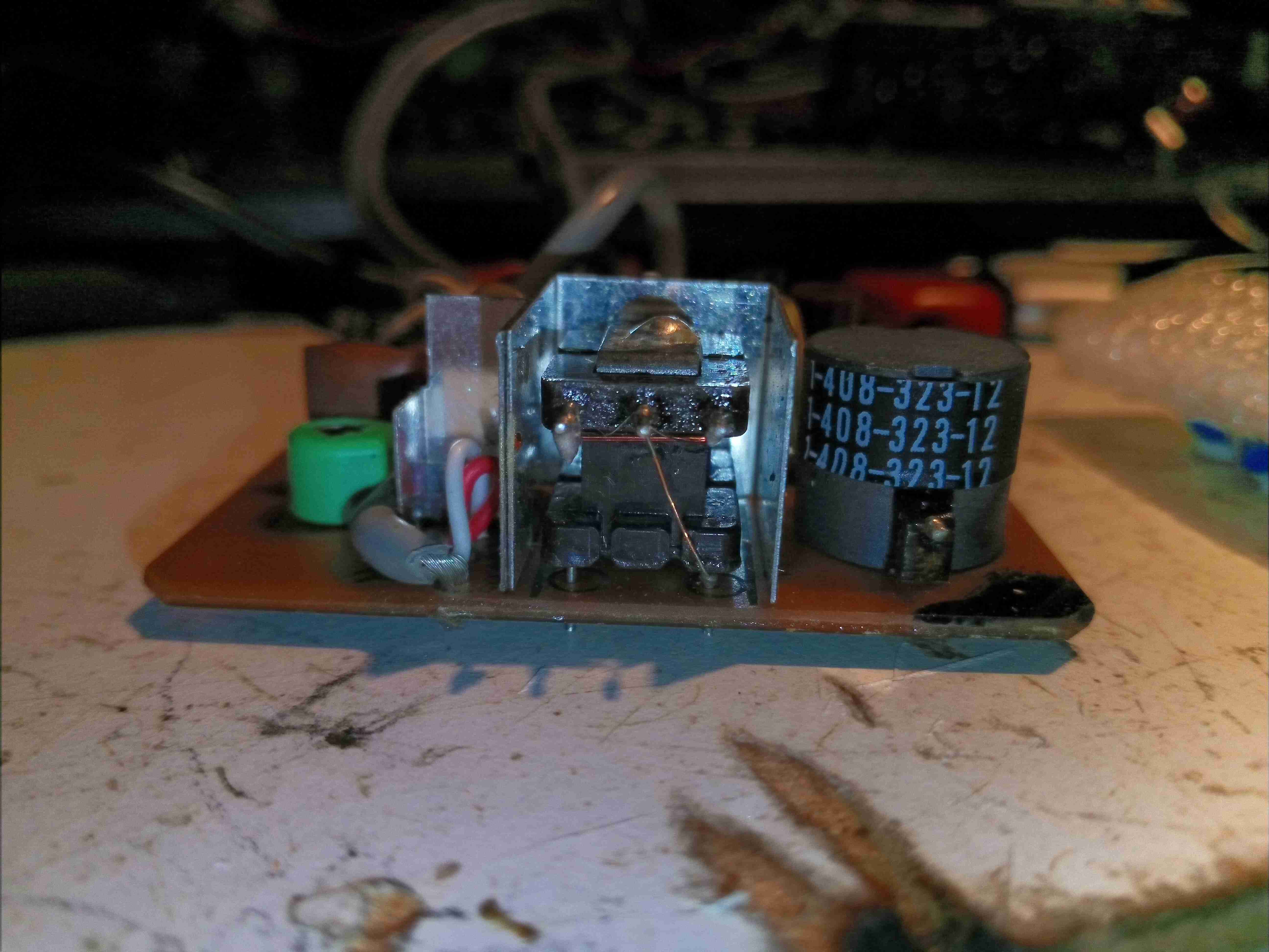
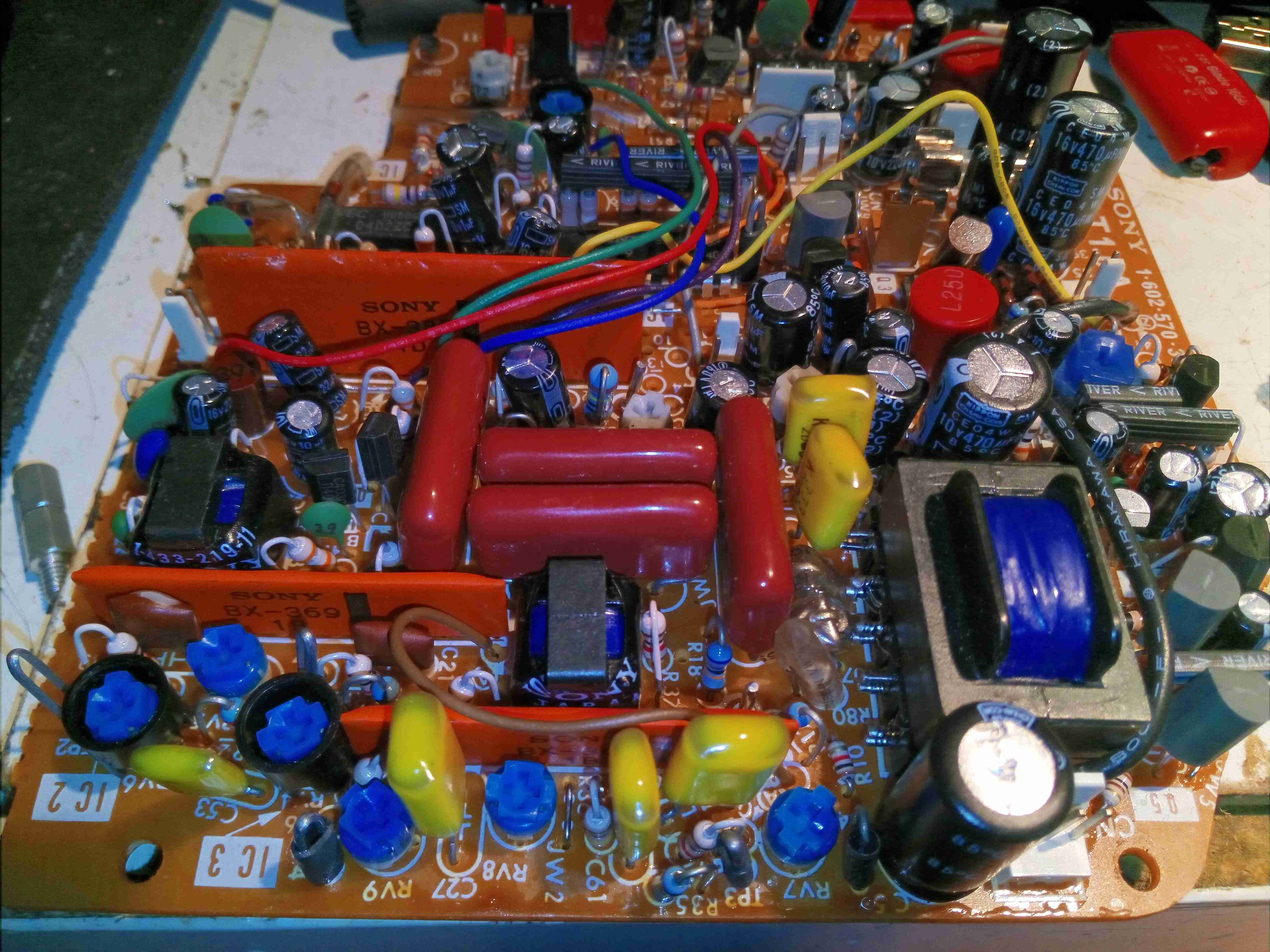
High Voltage Section
Here’s the high voltage section, the main transformer at right generating the voltages required to drive the video tube. The large orange hybrids here are a pair of BX369 high-voltage sawtooth generators that create the deflection waveforms for the tube. The other large hybrid is a BX382 Fader Control.
Video Process Board
The other large board contains all the video process circuitry, all analogue of course. There are a lot of manual adjustment pots on this board.
Lens Barrel
After removing the lens assembly, the tube assembly is visible inside the barrel casting. Not much to see yet, just the IR filter assembly.
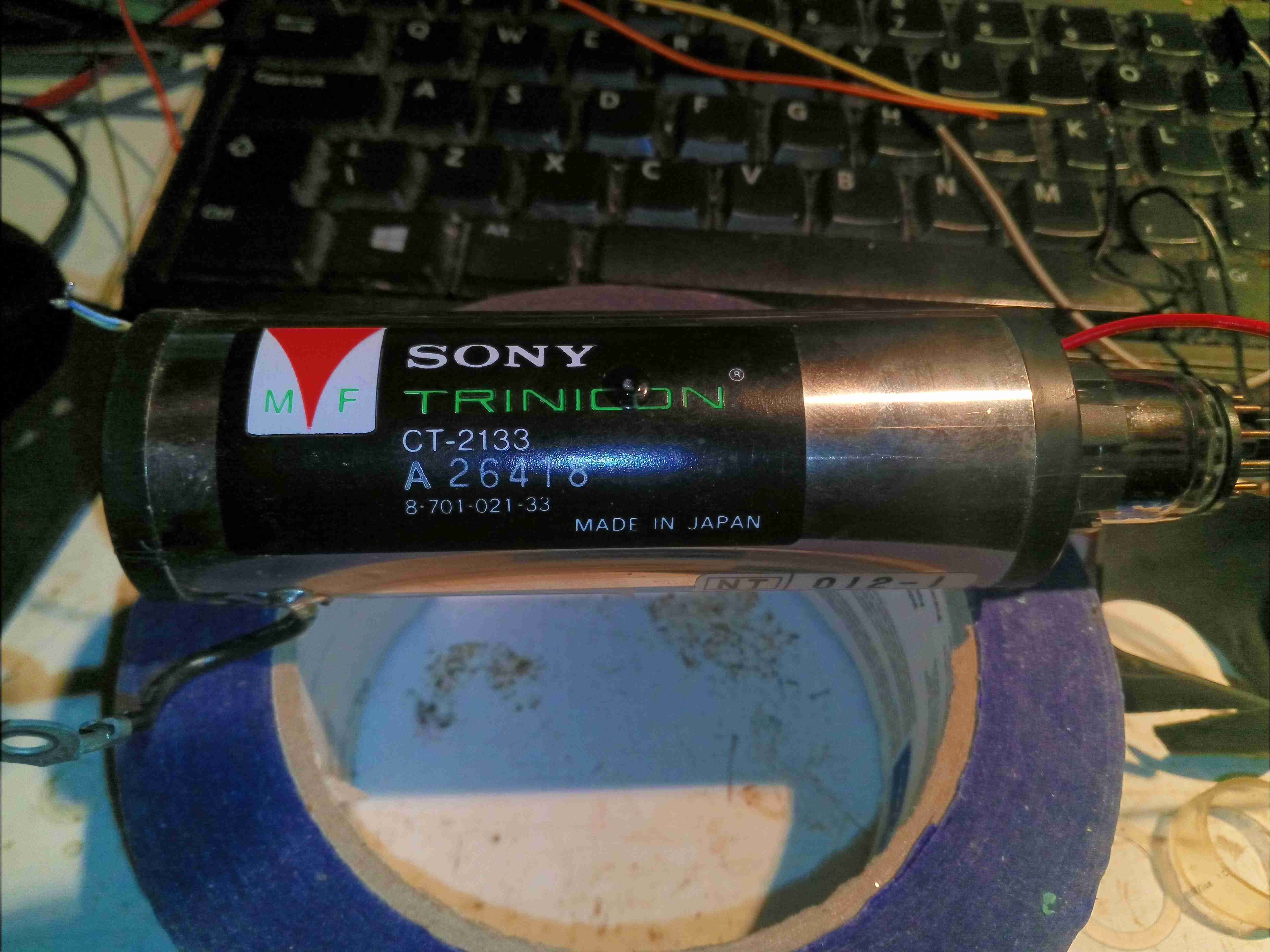
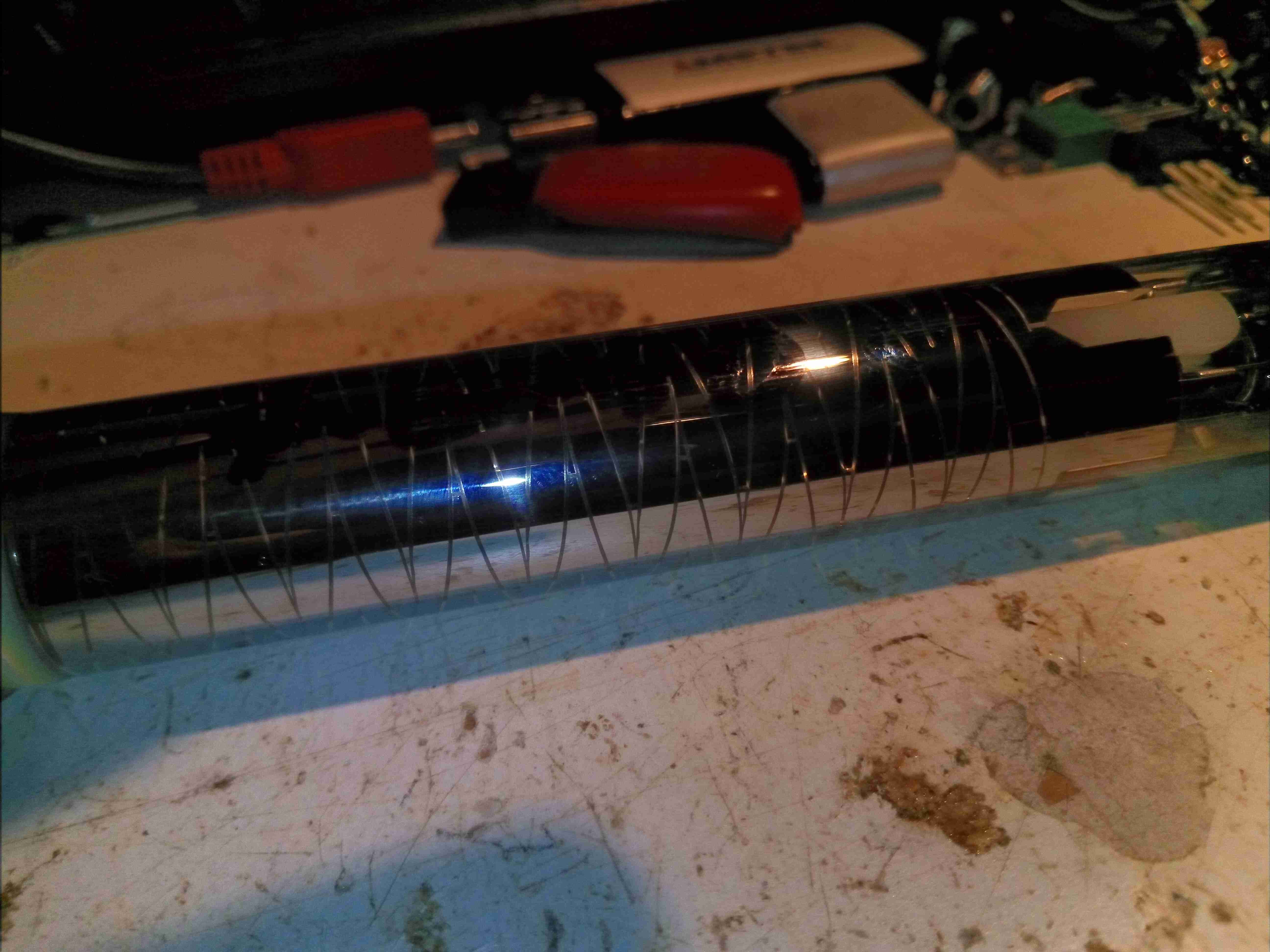
Trinicon Tube Assembly
Here’s the unit removed from the camera. Unfortunately this tube is dead – it shows a lot of target burn on the resulting image, and very bad ghosting on what poor image there is. The Trinicon tube itself is encased in the focus coil assembly, the windings of which are hidden under the shielding.
IR Filter
The IR filter is locked into the front of the tube, on a bayonet fitting. The twin target wires are running off to the left, where they would connect to the head end amplifier.
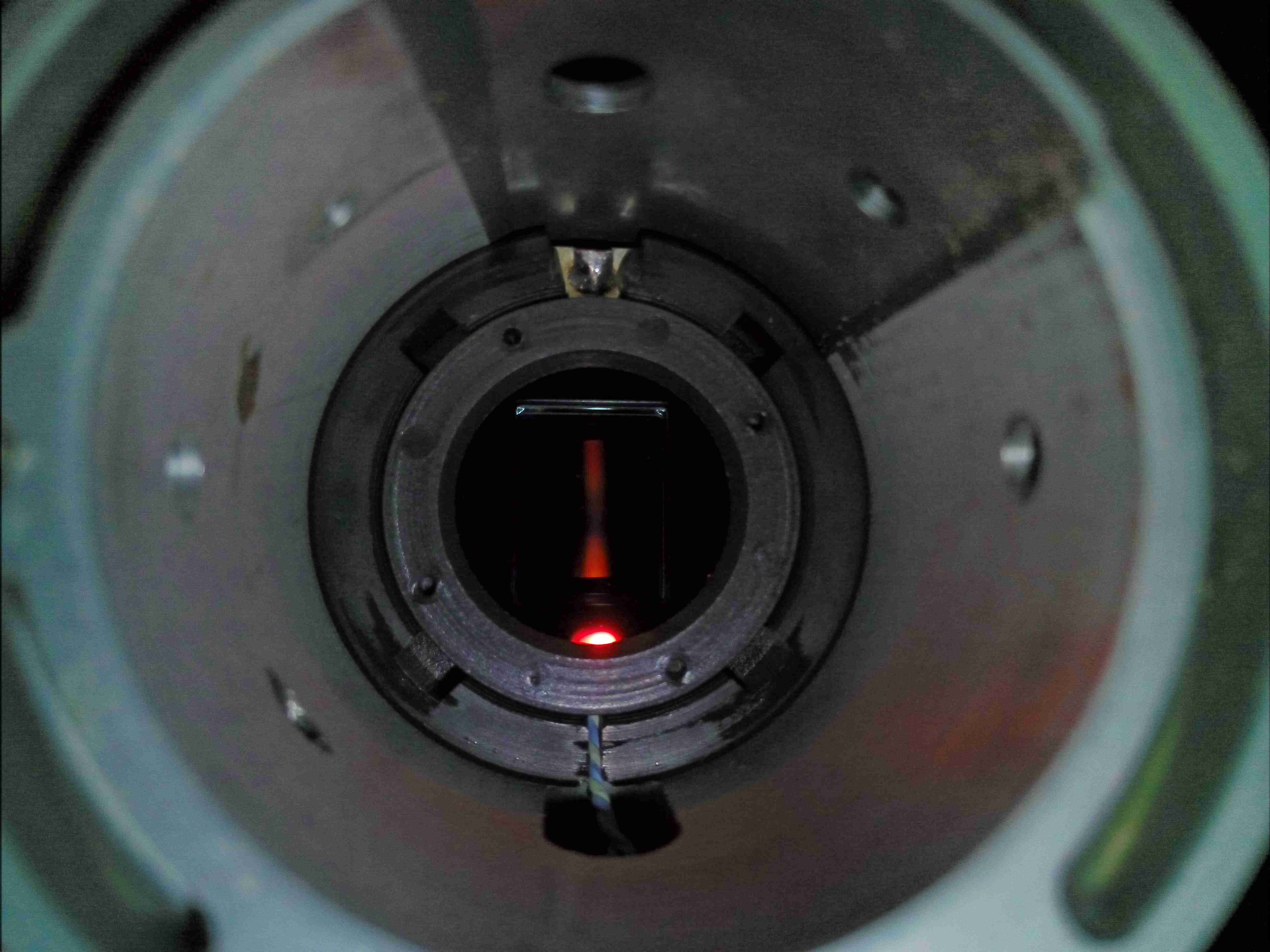
Bare Tube
After removing the IR filter glass, the Trinicon tube itself is removed from the focus coil assembly. There’s an electron gun at the rear of the tube, like all CRTs, although this one works in reverse – sensing an image projected on the front instead of generating one.
Deflection Plates
It’s a little difficult to see, but the electrostatic deflection electrodes in this tube are created from the aluminium flashing on the inside of the glass, in a zig-zag pattern. The interleaving electrodes are connected to base pins by spring contacts at the electron gun end of the tube.
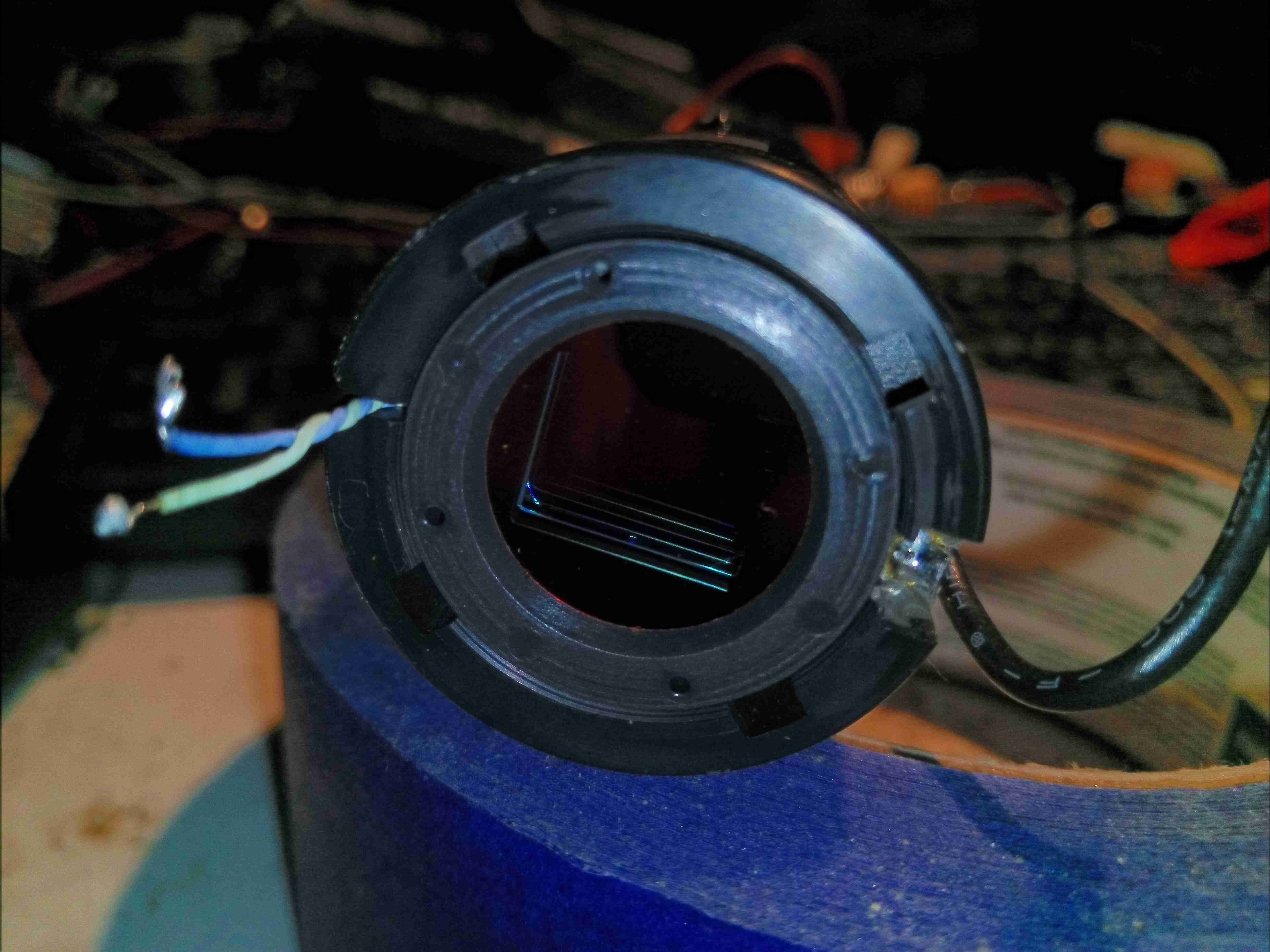
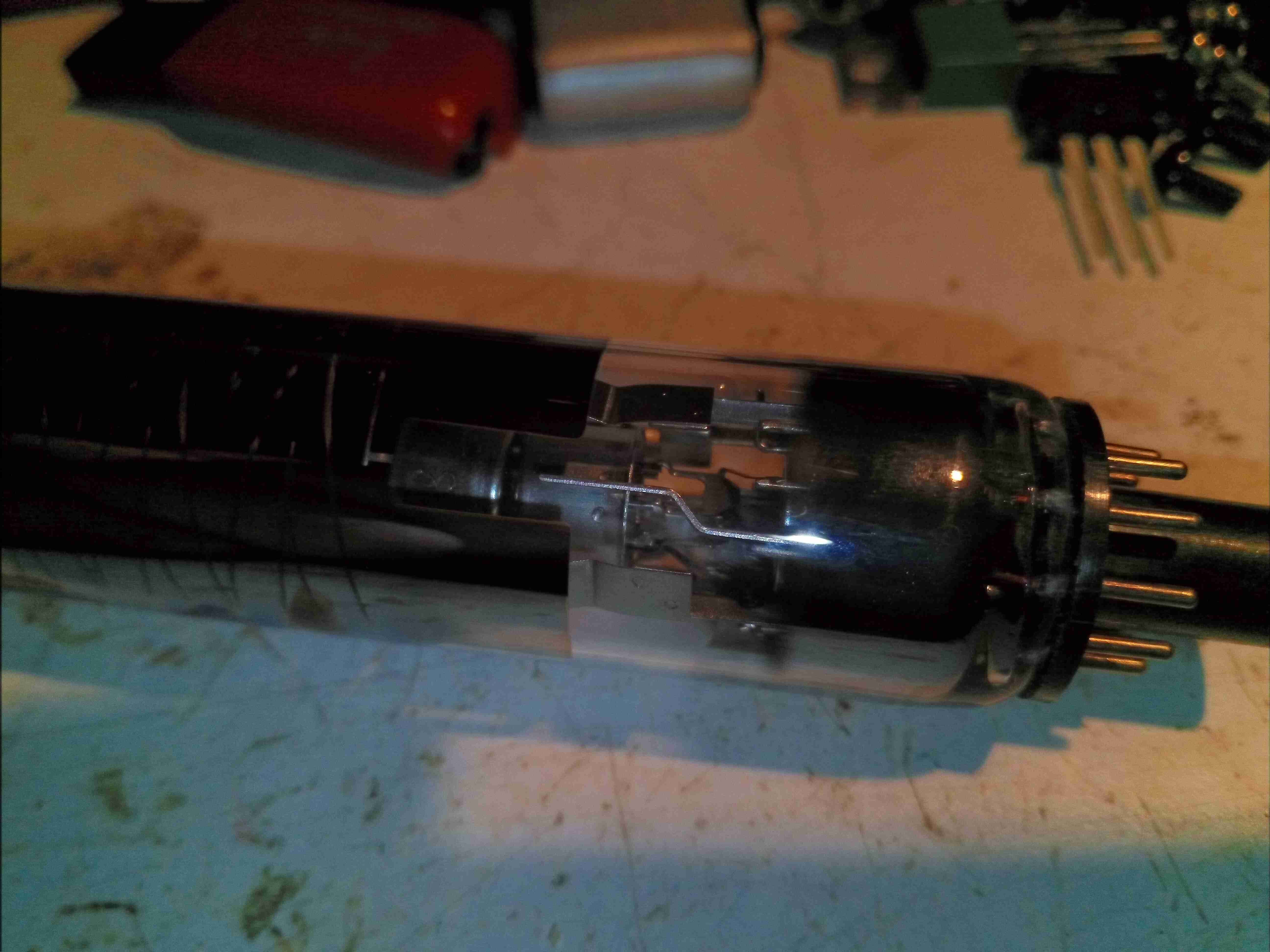
Electron Gun
The electron gun is mostly hidden by the getter flash & the deflection electrodes, but the cathode can is visible through the glass, along with the spring contacts that make a connection to the deflection electrodes. This is also a very short gun – it doesn’t extend more than about 5mm into the deflection zone. The rest of the tube up to the target is empty space.
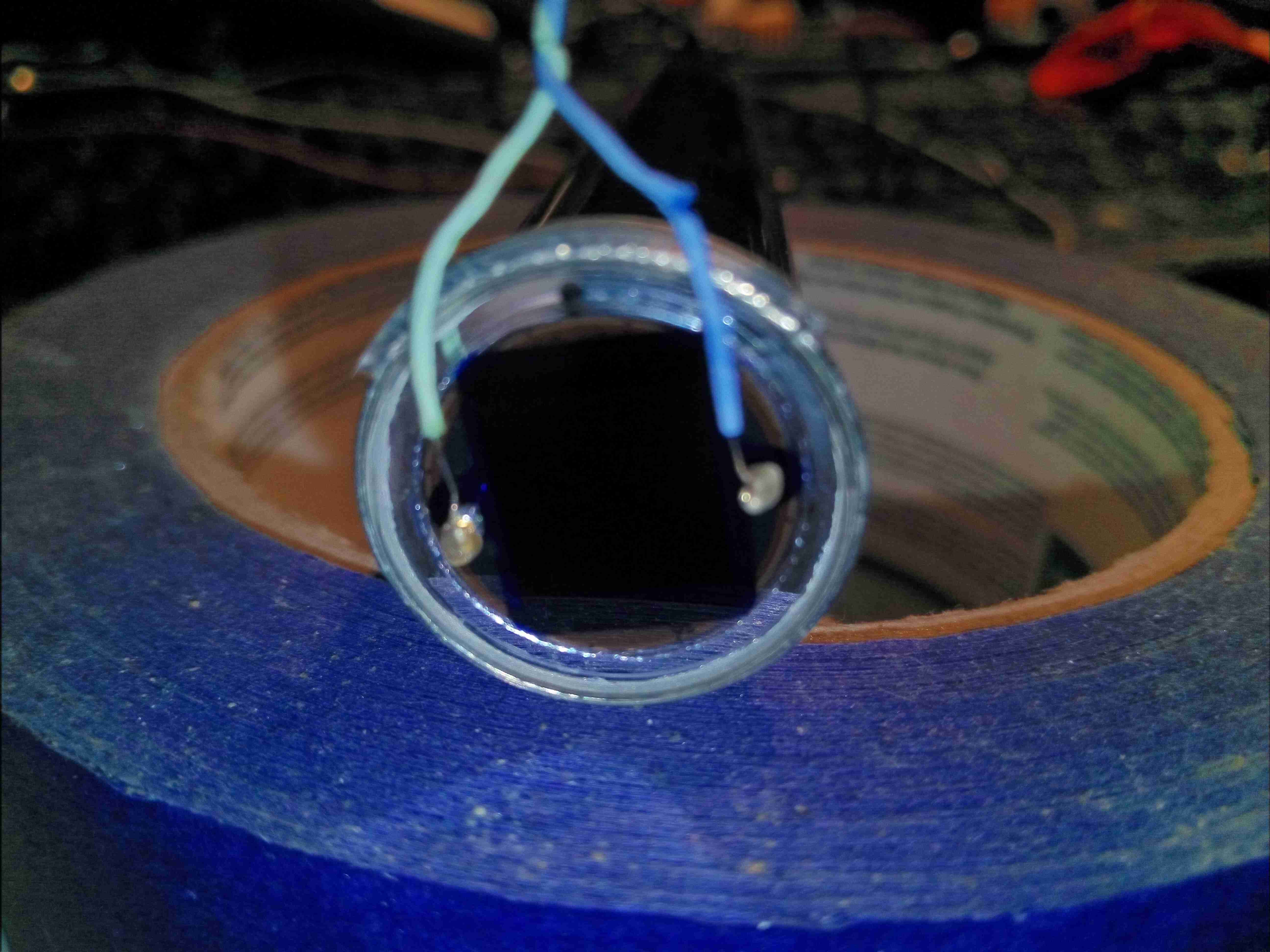
Target
Finally, here’s the target end of the tube. I’m not sure how the wires are attached to the terminals – it certainly isn’t solder, maybe conductive adhesive?
It uses a vertically striped RGB colour filter over the faceplate of an otherwise standard Vidicon imaging tube to segment the scan into corresponding red, green and blue segments. It is used mostly in low-end consumer cameras, though Sony also used it in some moderate cost professional cameras in the 1980s.
Although the idea of using colour stripe filters over the target was not new, the Trinicon was the only tube to use the primary RGB colours. This necessitated an additional electrode buried in the target to detect where the scanning electron beam was relative to the stripe filter. Previous colour stripe systems had used colours where the colour circuitry was able to separate the colours purely from the relative amplitudes of the signals. As a result, the Trinicon featured a larger dynamic range of operation.
I have the service manuals below for the HVP-2000P & the HVP-4000P, which are very similar cameras, so these may be useful to anyone who has one of these!
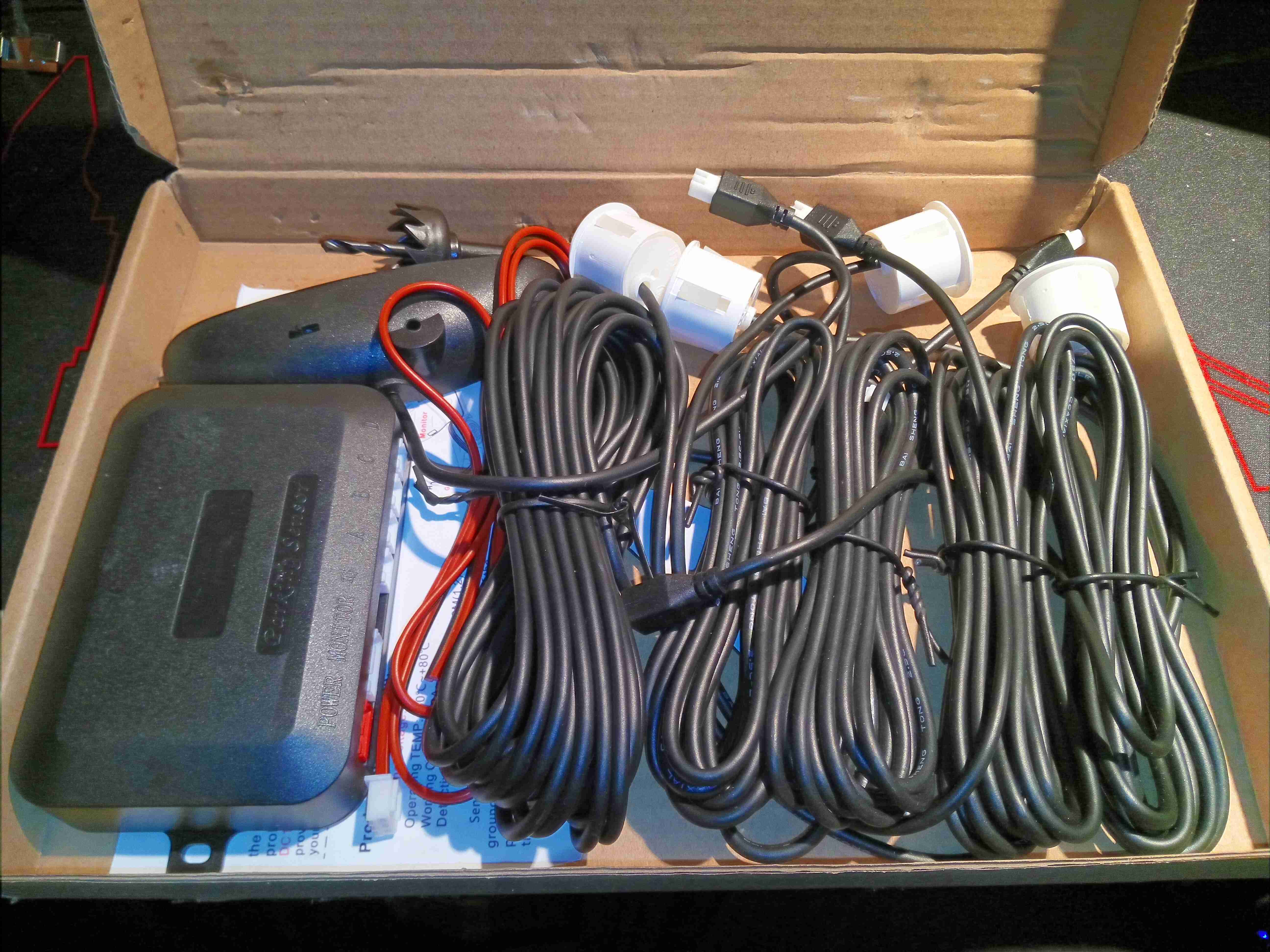
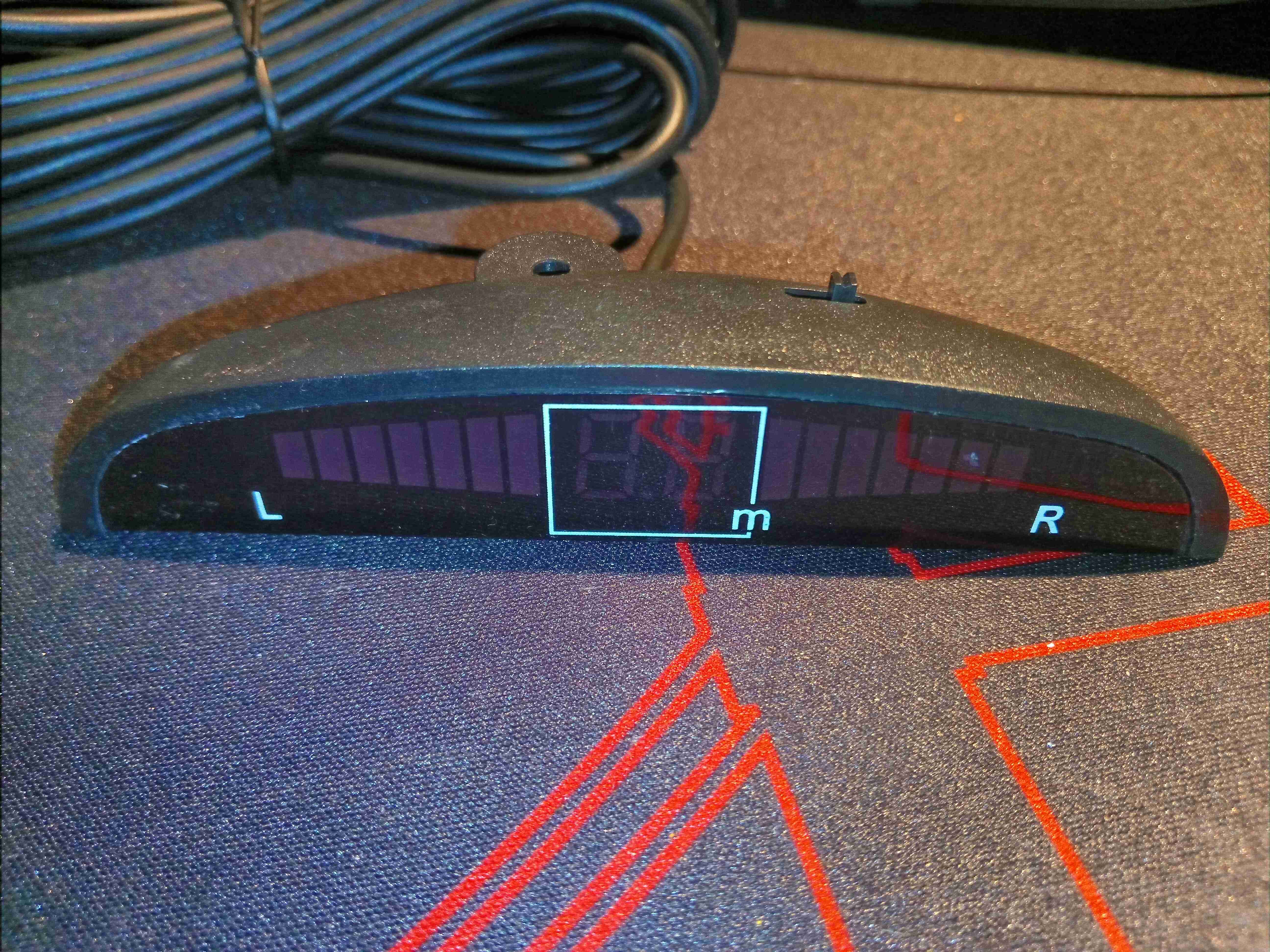
This is a cheap kit from eBay, to retrofit an older car with ultrasonic parking sensors. 4 sensors are included in the kit, along with a hole saw to fit them to the bumper. There’s a small controller module, and a display module that fits onto the dash of the car.
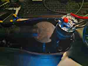
Controller Module
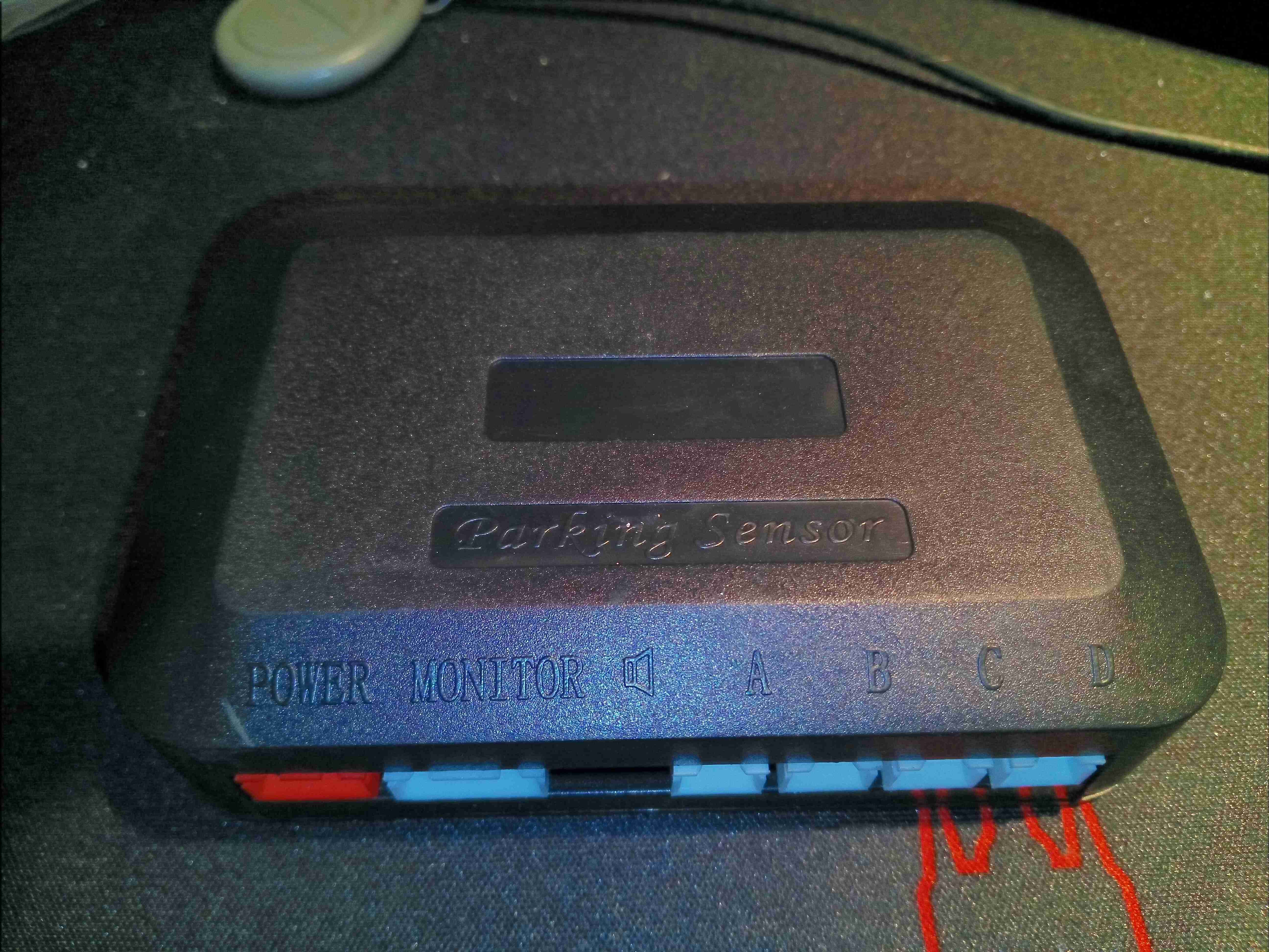
Here’s the controller module, with it’s row of connectors along the front. The unit gets it’s power from the reversing light circuit, via the red connector.
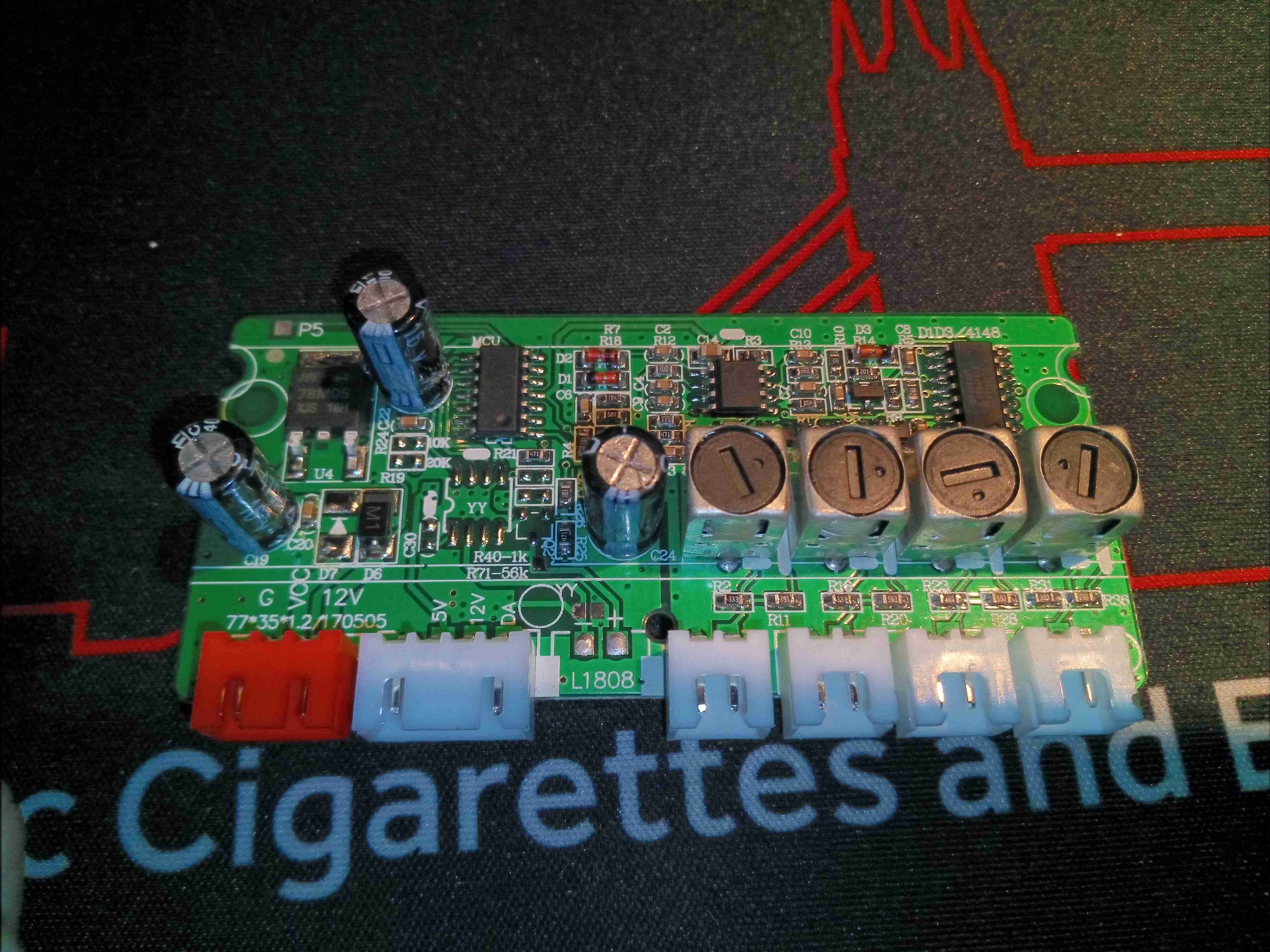
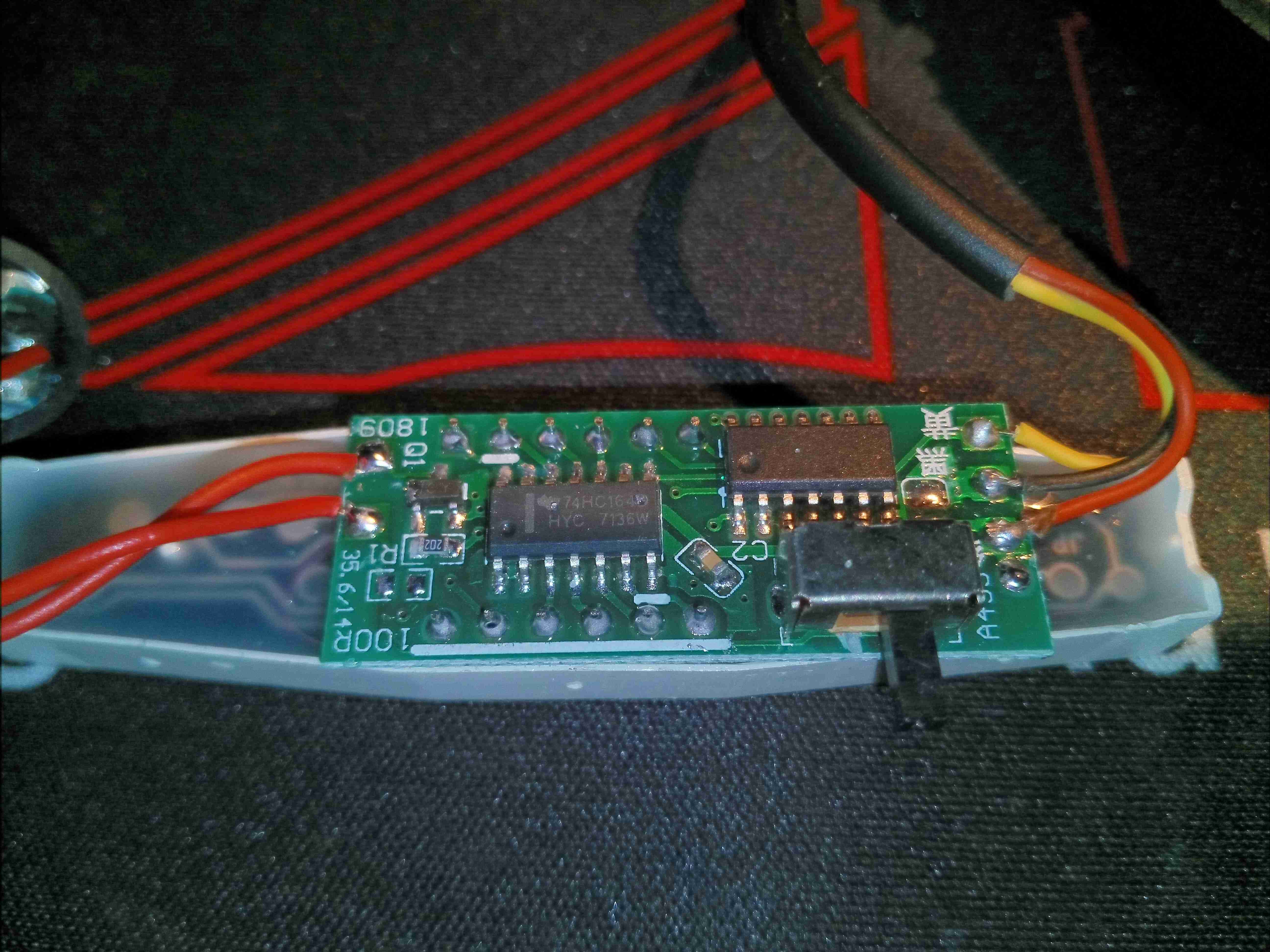
Main Controller PCB
Removing a couple of screws allows the PCB to be removed. There’s quite a bit on this board, including 4 tunable inductors for the ultrasonic transducers. There’s a linear voltage regulator on the left which supplies power to the electronics, and a completely unmarked microcontroller.
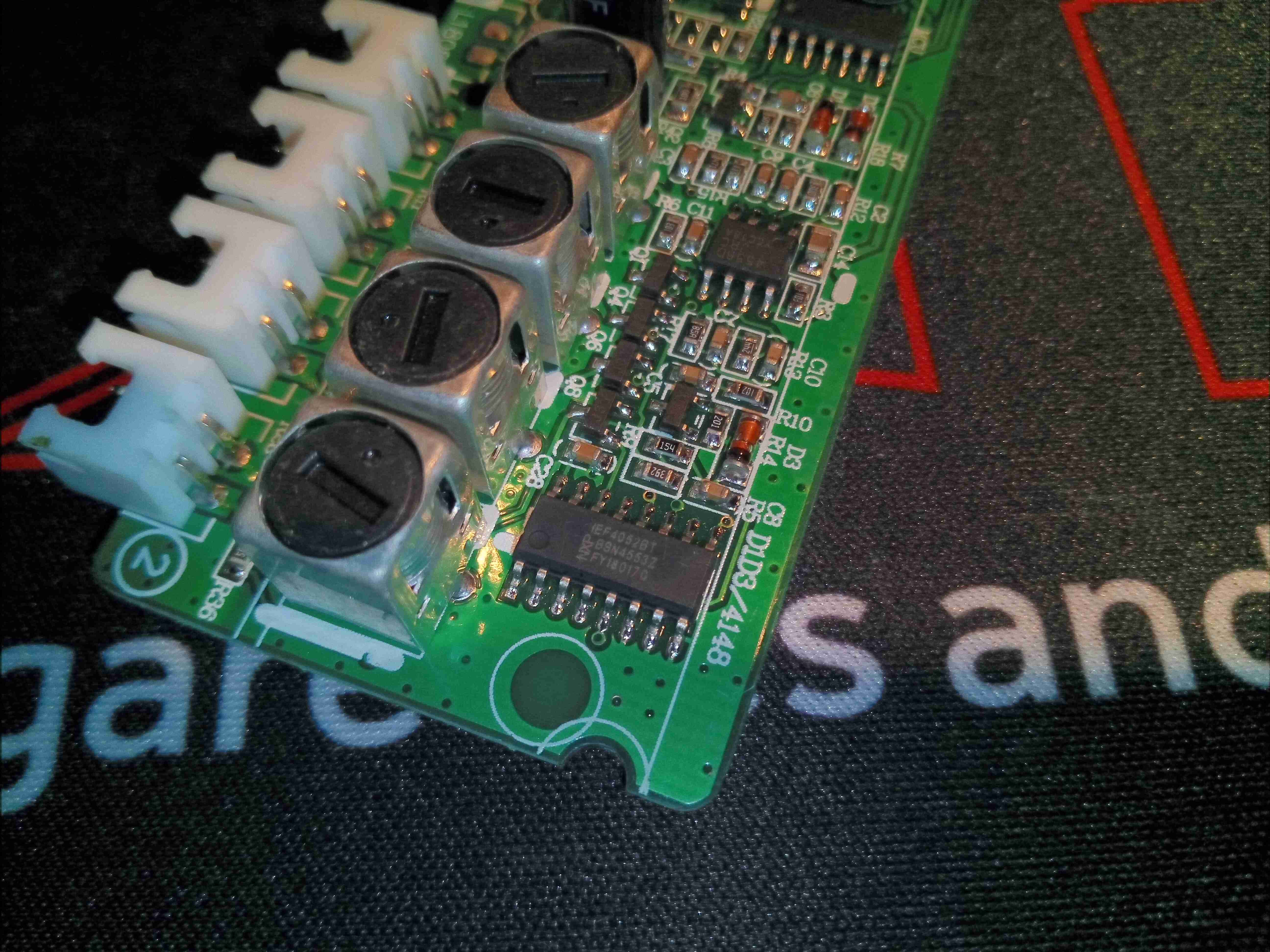
Electronics Closeup
A closer look at the analogue end of the board shows a JRC4558D dual Op-Amp, and an NXP HEF4052B analogue multiplexer. As the microcontroller is unmarked I have no data for that one.
Dash Display
The dash display is housed in another small plastic box, with bargraphs for each side of the car & an overall distance meter.
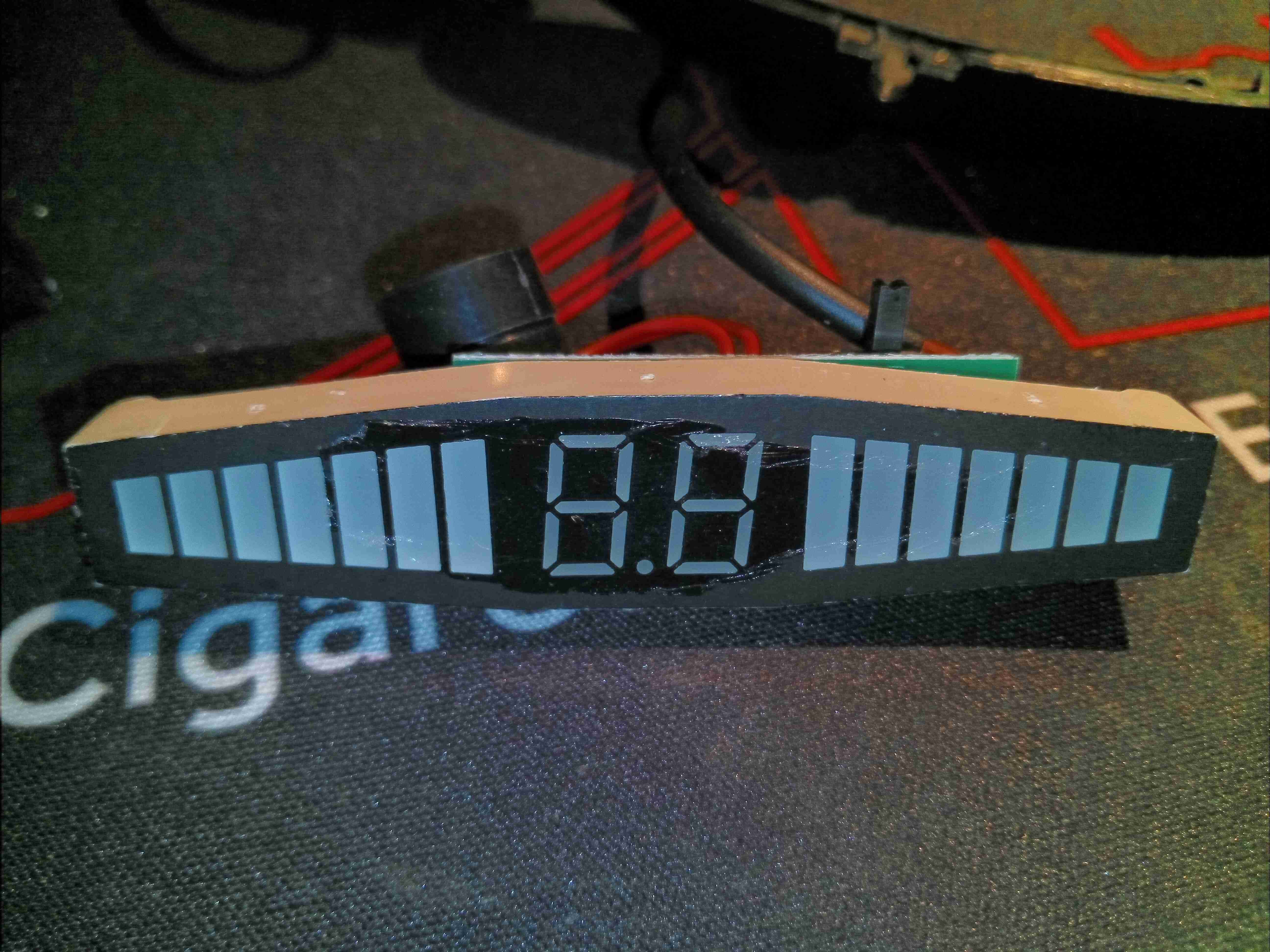
Display Module
Clearly this is a custom module, with the tapered bargraph LEDs on each side & the 7-segment display in the centre. There’s a beeper which works like every factory-fitted unit does, increasing in rate as the distance closes.
Display PCB
The back of the display module has the driver PCB, with yet another unmarked microcontroller, and a TI 74HC164 serial shift register as a display driver. There’s only 3 wires in the loom from the controller, so some sort of 1-wire protocol must be being used, while I²C is the most likely protocol to be talking to the display driver circuit. There’s also a small switch for muting the beeper.
Here’s another piece of tech, the electric air pump that’s available as an optional extra with Airbeam tents. I expected this to be a centrifugal blower, but instead it’s a large reciprocating air compressor – even if the construction quality is a little dubious for a device that costs over £70.
Pump Section
The internal parts of this pump are almost entirely made of plastic – not what I’d expect for an air compressor.
Valves
The valves are located on the end of the cylinder, the right hand on is the intake valve, the right is an pressure relief valve. The outlet valve is hidden inside the tube.
Drive Motor
The drive motor has the same model number as the overall pump, likely made specifically for this unit. This motor does have some cooling from a fan on the armature.
Crankshaft
After the cover has been removed from the pump unit, the main drive is visible. The driven gear is made of plastic, most likely nylon. The motor pinion is of brass. Ball bearings are used on the crank gear, but it appears that the big end bearing is a simple bushing on the steel pin.
Plastic Piston
The working cylinder & piston are also made of plastic, so I don’t hold up much hope of this unit wearing well, even though the plastic feels like Nylon 66, glass fibre reinforced. Plenty of grease has been applied to the moving parts at least, to help keep the friction down. The 20 minute limit on operating time most likely has a lot to do with the almost entirely plastic construction – the adiabatic heating of the air as it’s compressed will make short work of the relatively low melting point of the Nylon.
Electronics Section
The electronics are on a pair of PCBs tucked into the upper cover, one dealing with the pressure measurement, microcontroller & power control, and the other dealing with the display & buttons.
Power Control Board
The power control board has a 10A relay to switch power to the motor, along with a small microcontroller & pressure sensor, which is under the plastic adaptor on the PCB.
Display Board
The display is a standard 7-segment LCD, with a zebra strip connection to the PCB. Underneath hides the LCD controller itself. I’m not going to take this one off, as zebra strips don’t usually work properly once removed.
Microcontroller
The microcontroller is an Atmel ATTINY24A with 2K of onboard flash. The pressure sensor is on the right, although I haven’t been able to decode the laser-etched number on the top. Power is handled by a small linear regulator at the bottom edge of the board, with a couple of large electrolytics for filtering.
Power Control Board
Here’s an overall view of the power control board, with a better view of the pressure sensor & relay. This also gives a hint to the actual manufacturer of the pump – with the model number HB-630A. Since this unit is rated by their own admission at 13.5A, the 10A relay is likely to take a real beating over time. I measured 11A current draw at 7PSI output pressure.
Cheap car air compressors for inflating tyres are so cheap these days it’s almost impossible not to have to cut some corners. This one has failed catastrophically! These units are usually very poorly cooled, being housed in a closed plastic casing, with no airflow to speak of. The motor on this unit was fine, but the rest of the mechanical parts have taken a real beating.
Main Drive
I’ve removed the motor from the compressor head, leaving the main plastic drive gear exposed. The originally D keyed hole is now completely round, having been melted at some stage, the gear then just spins on the shaft without transmitting any drive.
Shaft Bearing
Here’s the crank main bearing, just a simple sleeve. There’s extreme wear present, about 2mm in total! This bearing has probably run dry of lubricant, then the steel shaft has just chewed through the relatively soft metal of the bearing, which is probably pot metal.
Bearing Wear
I’ve turned the shaft round here to show the large gap between the shaft & bearing bushing.
Main Bearing
This is what’s left of the bearing, complete with a coating of swarf.
Crankpin
The big end bearing of the connecting rod is also damaged – probably due to the play introduced by the rapidly disintegrating main bearing. At some stage the crankpin has worn through the rod enough for it to slip out entirely, leaving the piston stationary.
Piston Assembly
Wear in the side of the connecting rod shows that the spinning crank has been wearing it away for quite a while, eventually the rod probably fell into just the right spot to jam the crank, causing the failure of the main drive gear.
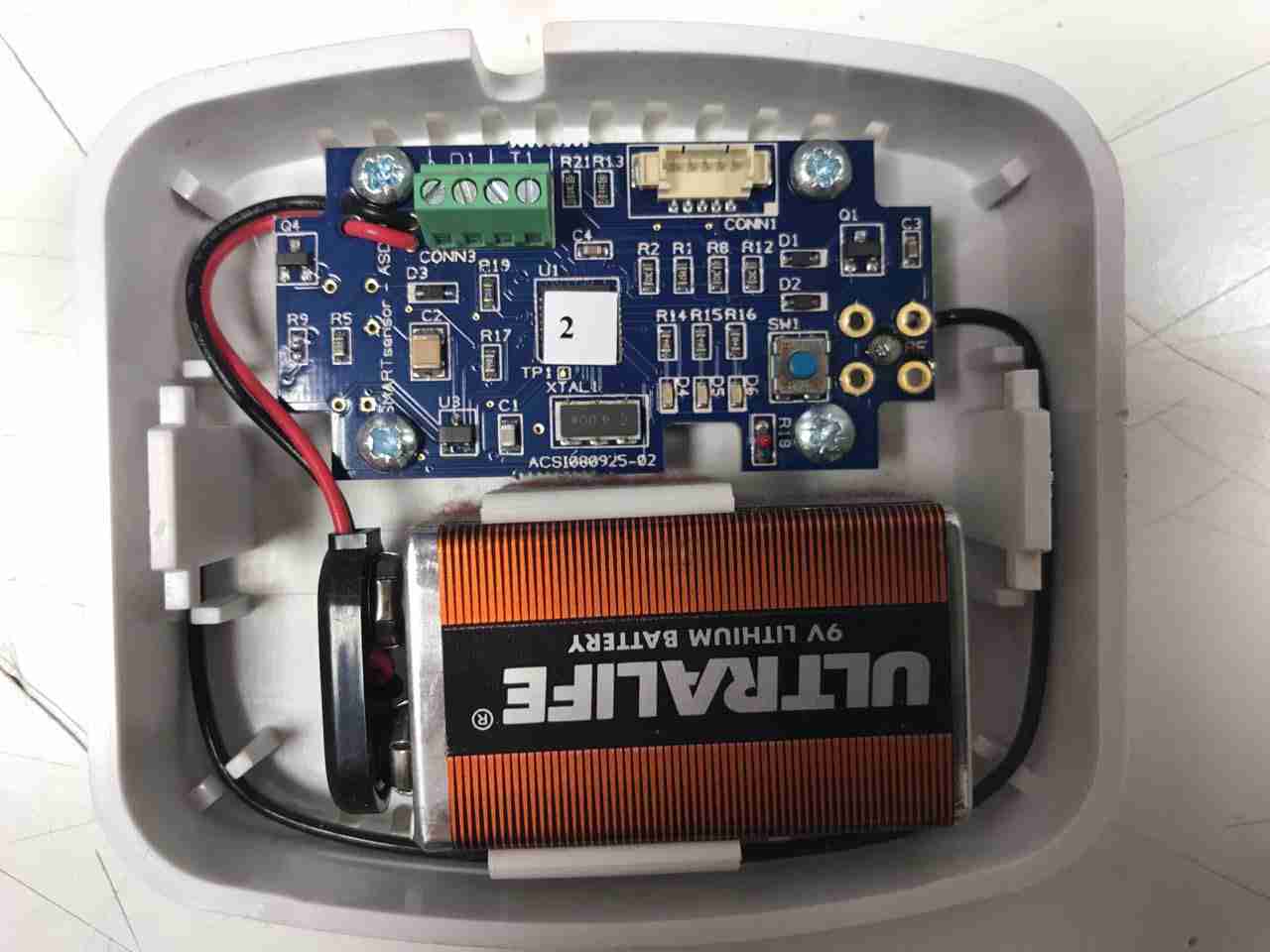
Here’s another random bit of RF tech, I’m told this is a wireless energy management sensor, however I wasn’t able to find anything similar on the interwebs. It’s powered by a standard 9v PP3 battery.
Microcontroller
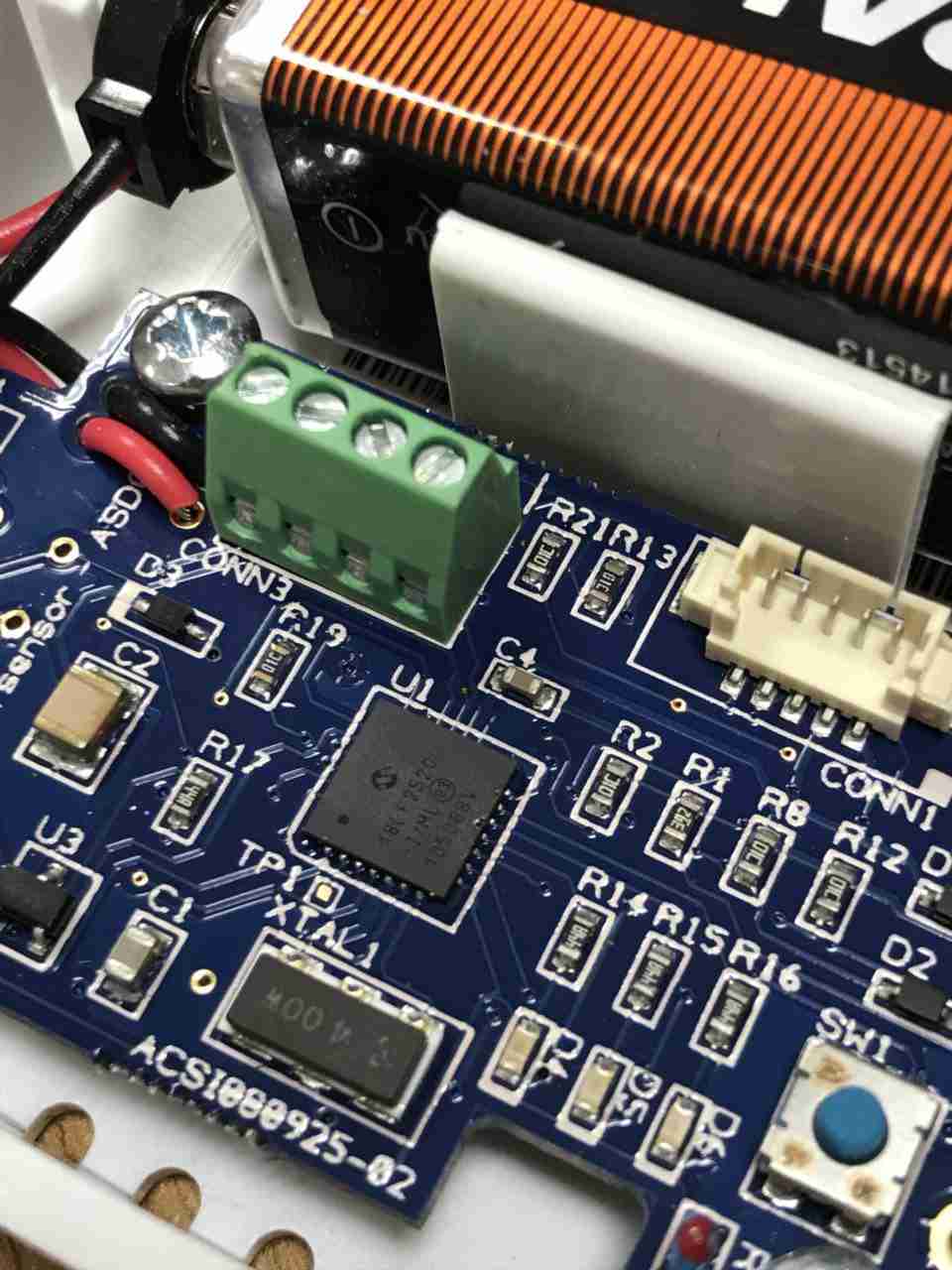
System control is handled by this Microchip PIC18F2520 Enhanced Flash microcontroller, this has an onboard 10-bit ADC & nanoWatt technology according to their datasheet. There’s a 4MHz crystal providing the clock, with a small SOT-23 voltage regulator in the bottom corner. There’s a screw terminal header & a plug header, but I’ve no idea what these would be used for. Maybe connecting an external voltage/current sensor & a programming header? The tactile button I imagine is for pairing the unit with it’s controller.
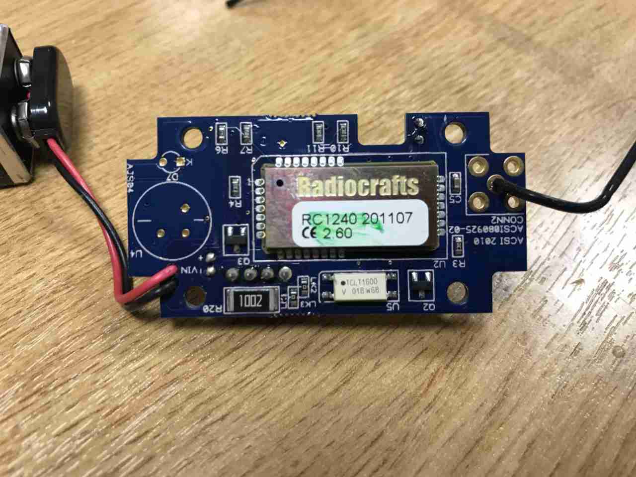
PCB Bottom
The bottom of the PCB is almost entirely taken up by a Radiocrafts RC1240 433MHz RF transceiver. Underneath there’s a large 10kΩ resistor, maybe a current transformer load resistor, and a TCLT1600 optocoupler. Just from the opto it’s clear this unit is intended to interface in some way to the mains grid. The antenna is connected at top right, in a footprint for a SMA connector, but this isn’t fitted.
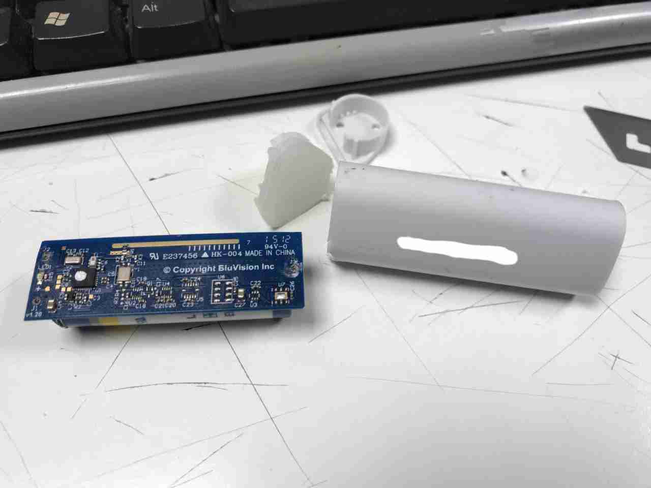
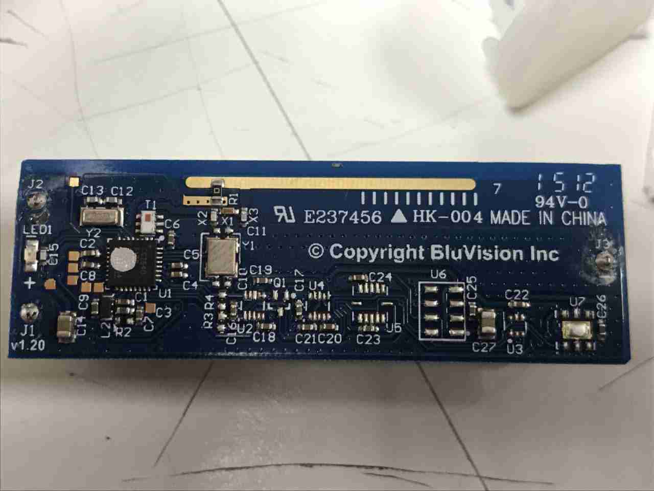
These photos were sent over to me by a friend, an interesting piece of tech that’s used in the retail industry. This is a BluVision BLE Beacon, which as far as I can tell is used to provide some automated customer assistance. From their website it seems they can also be used for high-price asset protection & tracking. These units don’t appear to be serviceable, being completely sealed & only having a primary cell. I’m not sure what they cost but it seems to be an expensive way to contact clients with adverts etc.
Component Side
There’s not much populated on this PCB, the main component here is the CC2640 SimpleLink ultra-low-power wireless microcontroller for Bluetooth Low Energy. It’s a fairly powerful CPU, with an ARM Cortex M3 core, 129KB of flash & up to 48MHz clock speed. There’s a couple of crystals, one of which is most likely a 32,768kHz low-power sleep watch crystal, while the other will be the full clock frequency used while it’s operating. Unfortunately I can’t make the markings out from the photos. There doesn’t appear to be any significant power supply components, so this must be running direct from the battery underneath.
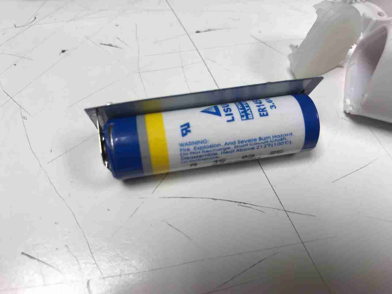
2.2Ah 3.6v Lithium Cell
The other side of the PCB has a single primary lithium cell, rated at 3.6v, 2.2Ah. The factory spec sheet specifies a 2.2 year life at 0dBm TX Power, Running 24/7, 100ms advertisement rate.
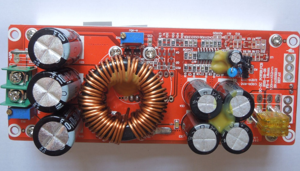
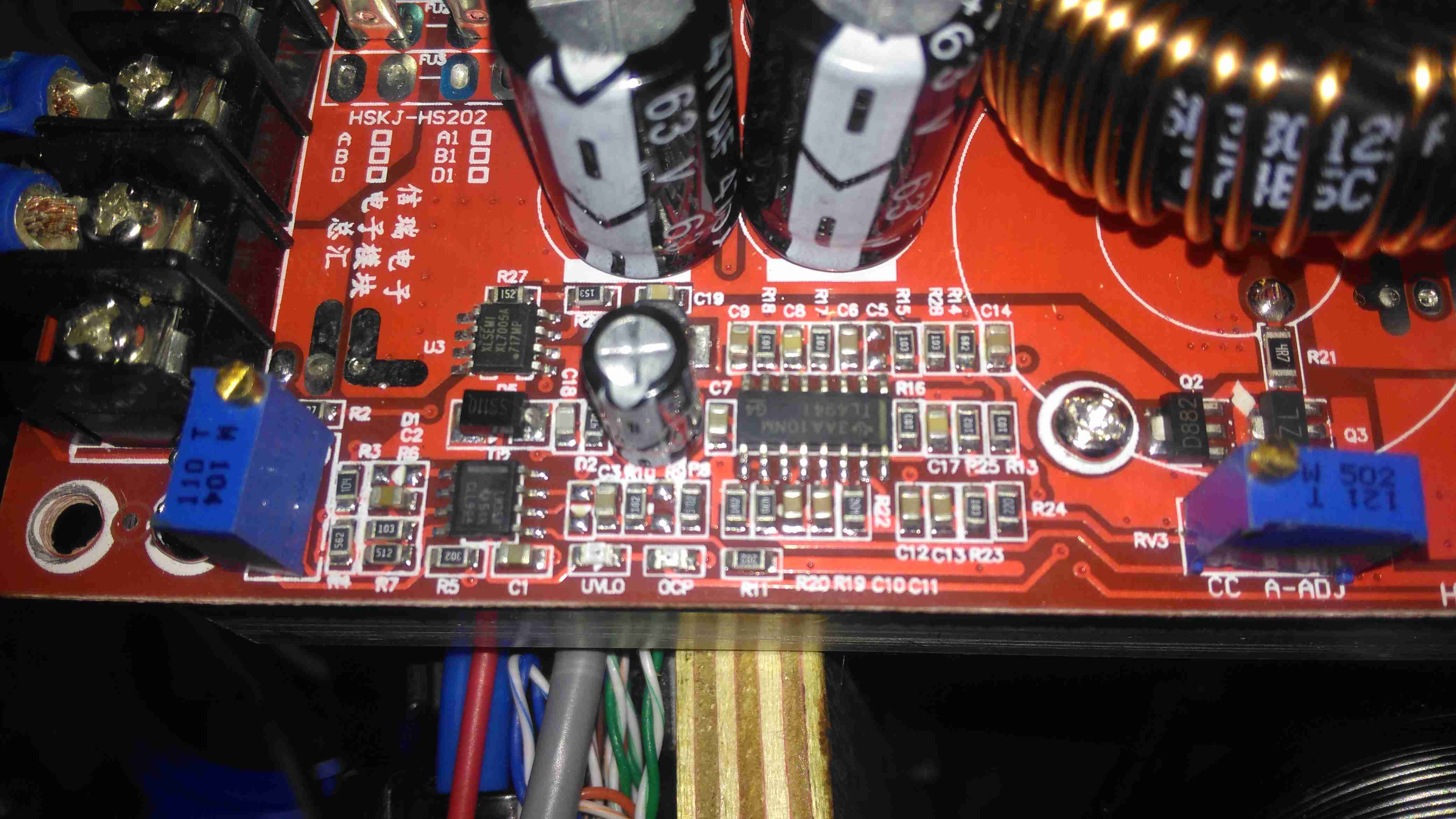
Ah the curse of the Chinese Electronics strikes again. These large DC-DC boost converters have become very common on the likes of AliExpress & eBay, and this time my order has arrived DOA… On applying power, the output LED lights up dimly, and no matter how I twiddle the adjustment pots, the output never rises above the input voltage.
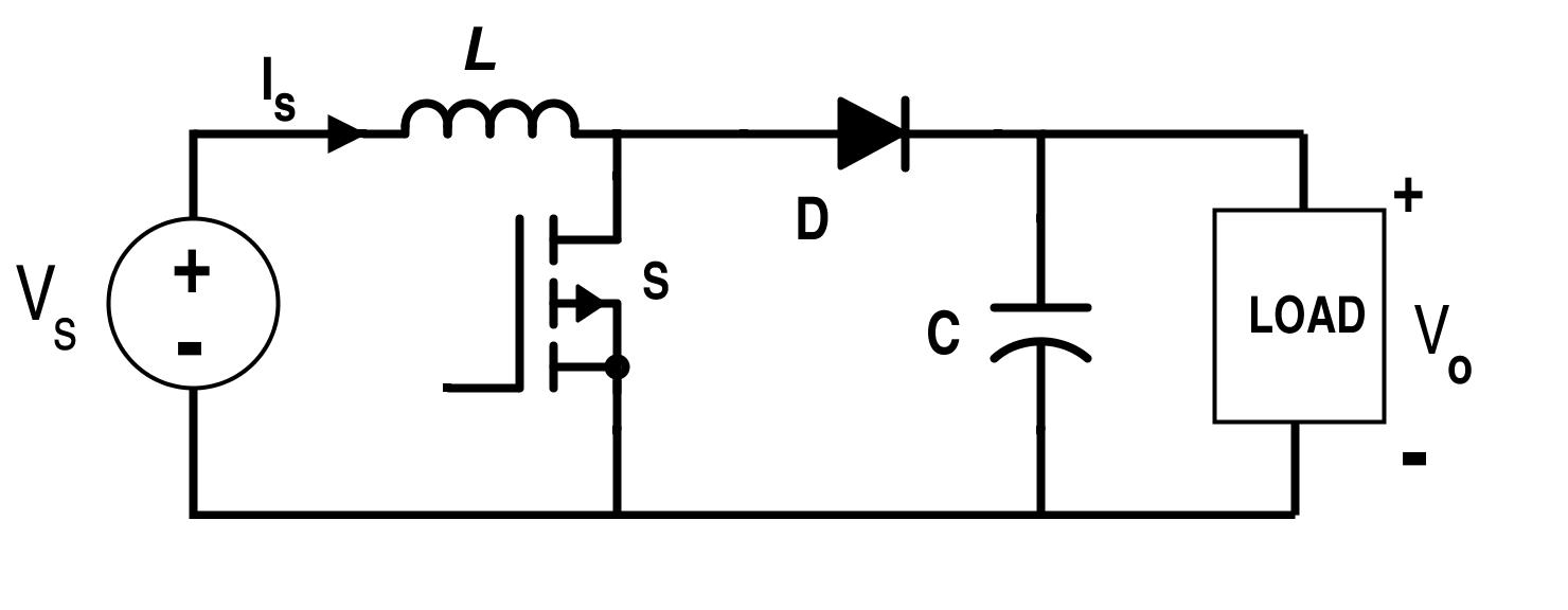
Boost Converter Topology
From the usual topology above, we can assume that the switching converter isn’t working, so the input voltage is just being directly fed through to the output. The switching IC on these converters is a TL494,
Control Circuitry
The switching IC on these converters is a TL494,with it’s surrounding support components, including a LM358 dual Op-Amp. Power for this lot is supplied from the input via a small DC-DC converter controlled by an XL Semi XL7001 Buck Converter IC. Some testing revealed that power was getting to the XL7001, but the output to the switching controller was at zero volts.
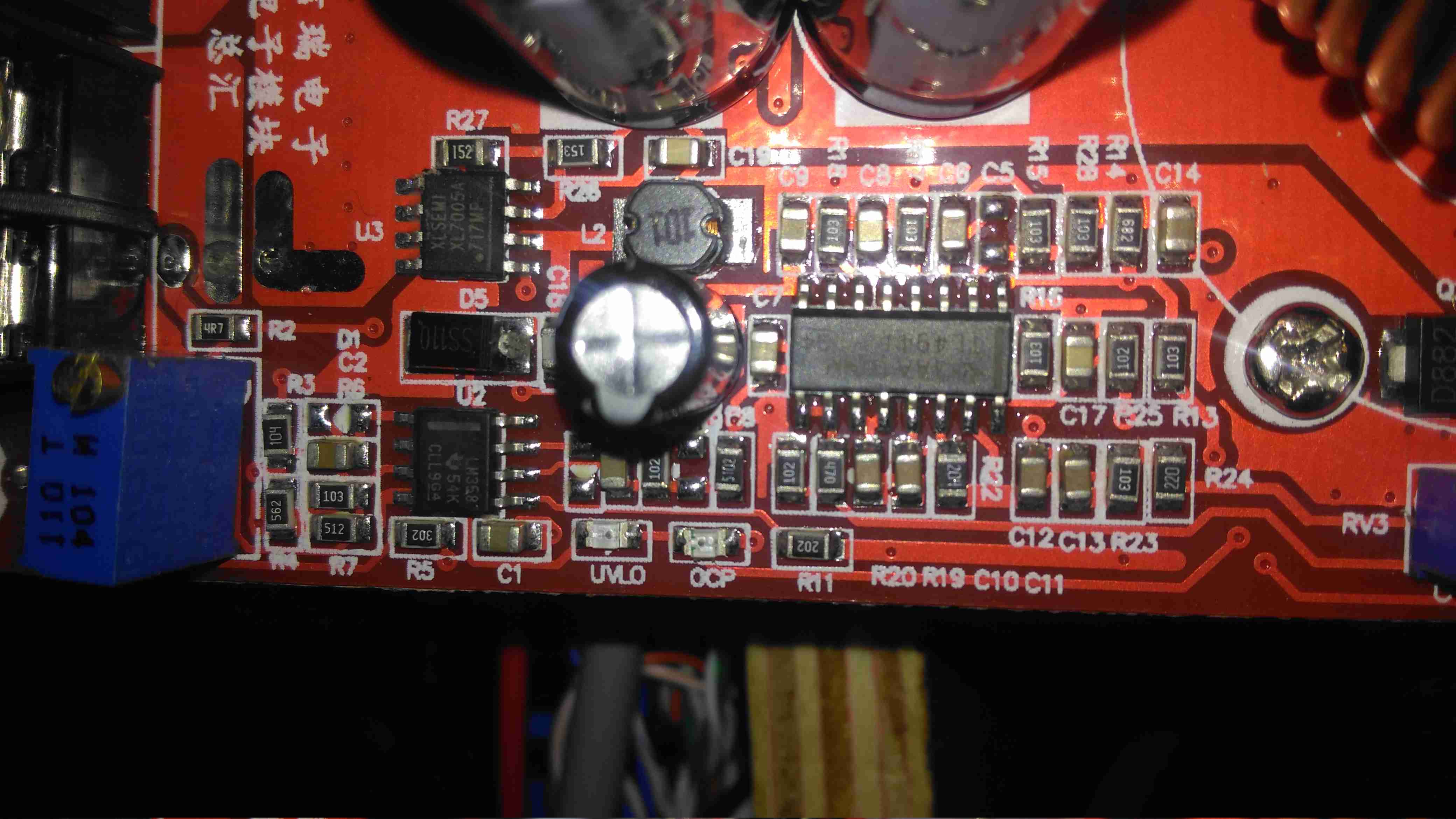
Inductor
The 100µH inductor for this buck converter is hidden behind the output electrolytic, and a quick prod with a multimeter revealed this inductor to be open circuit. That would certainly explain the no-output situation. Luckily I had an old converter that was burned out. (Don’t try to pull anything near their manufacturer “rating” from these units – it’s utter lies, more about this below).
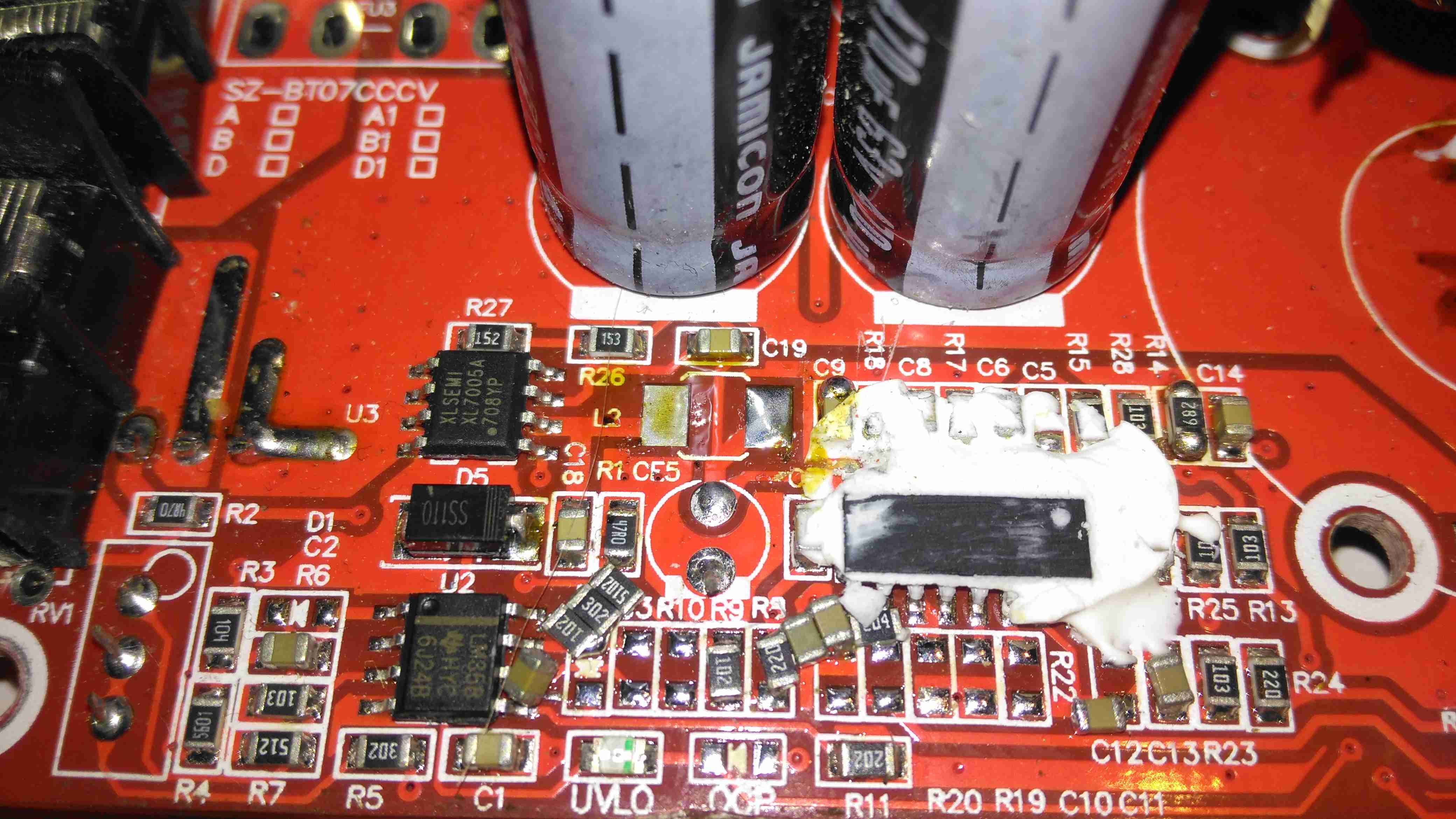
Donor Converter
The good inductor from this donor unit has been desoldered here, it’s supposed to be L2. This one had a heatsink siliconed to the top of the TL494 PWM IC, presumably for cooling, so this was peeled off to give some access.
After this inductor was grafted into place on the dead converter, everything sprang to life as normal. I fail to see how this issue wouldn’t have been caught during manufacture, but they’re probably not even testing them before shipping to the distributor.
The sensational ratings are also utter crap – they quote 1.2kW max power, which at 12v input would be 100A. Their max input rating is given as 20A, so 240W max input power. Pulling this level of power from such a cheaply designed converter isn’t going to be reliably possible, the input terminals aren’t even rated to anywhere near 20A, so these would be the first to melt, swiftly followed by everything else. Some of these units come with a fan fitted from the factory, but these are as cheaply made as possible, with bearings made of cheese. As a result they seize solid within a couple of days of use.
Proper converters from companies like TDK-Lambda or muRata rated for these power levels are huge, with BOLTS for terminals, but they’re considerably more expensive. These Chinese units are handy though, as long as they are run at a power level that’s realistic.
A big thanks to my grandad, the collector of all the things, breeder of tropical fish & budgies. A rock of the family for my 29 years on this earth, and who took me in for 5 years during a particularly difficult time of my life, and supported me entirely. It has been an honour to return that kindness in helping you complete your final journey to a funeral I am certain you would have liked. You will be very sorely missed now you’re gone, but you will never be forgotten.
Rest in Peace, 20th March 2018
Tip Jar
If you’ve found my content useful, please consider leaving a donation by clicking the Tip Jar below!
All collected funds go towards new content & the costs of keeping the server online.