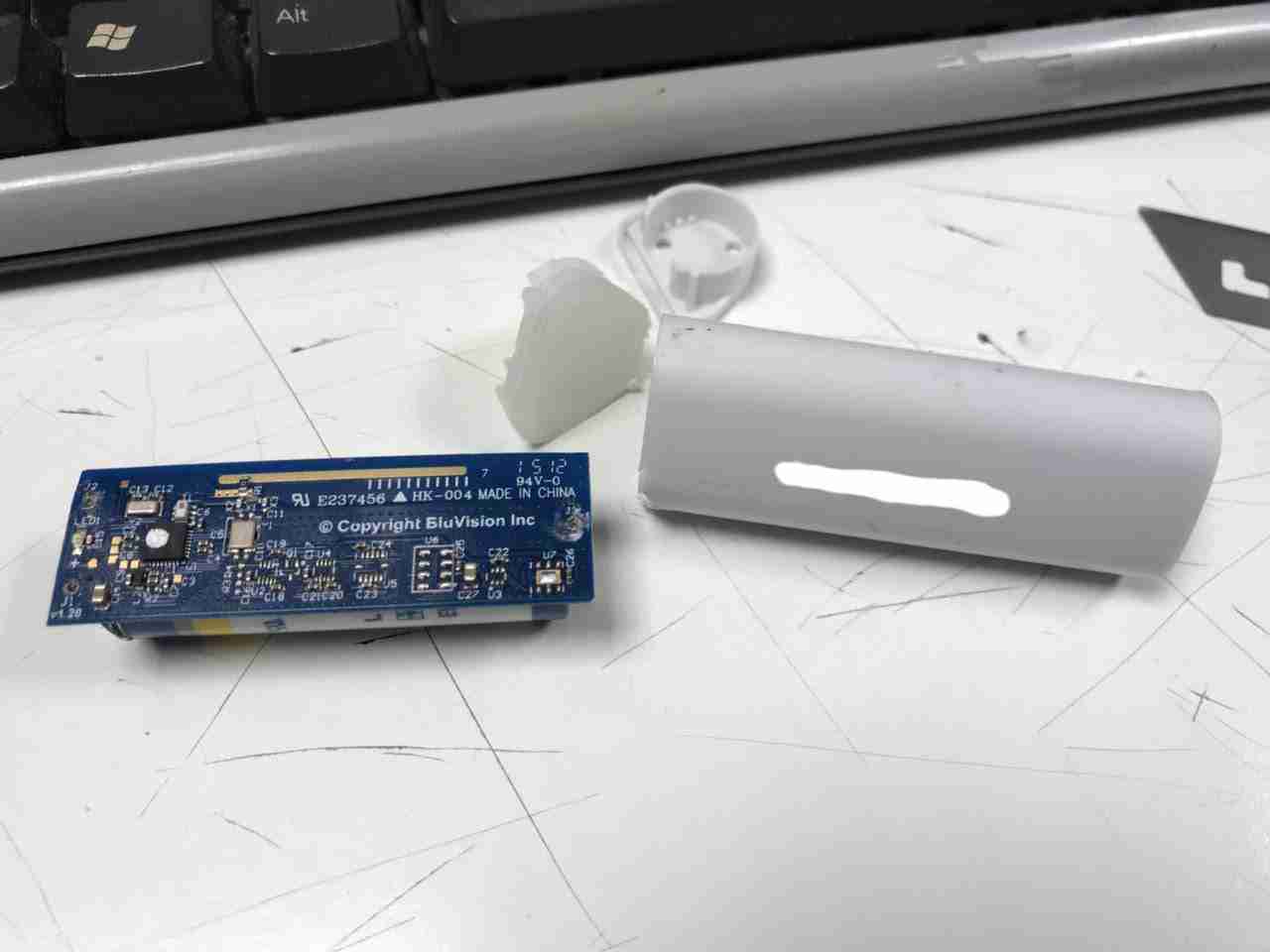
These photos were sent over to me by a friend, an interesting piece of tech that’s used in the retail industry. This is a BluVision BLE Beacon, which as far as I can tell is used to provide some automated customer assistance. From their website it seems they can also be used for high-price asset protection & tracking. These units don’t appear to be serviceable, being completely sealed & only having a primary cell. I’m not sure what they cost but it seems to be an expensive way to contact clients with adverts etc.
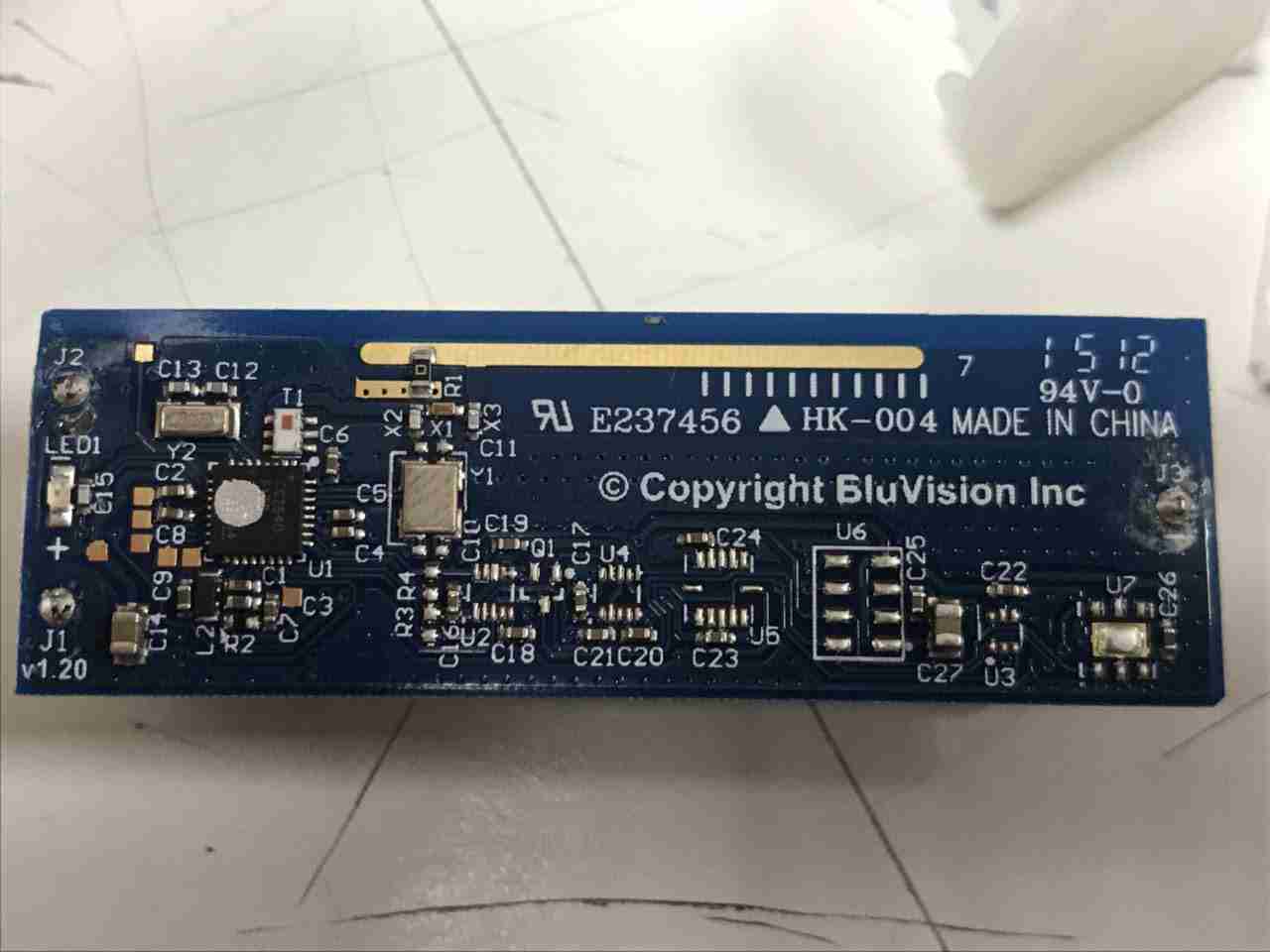
Component Side
There’s not much populated on this PCB, the main component here is the CC2640 SimpleLink ultra-low-power wireless microcontroller for Bluetooth Low Energy. It’s a fairly powerful CPU, with an ARM Cortex M3 core, 129KB of flash & up to 48MHz clock speed. There’s a couple of crystals, one of which is most likely a 32,768kHz low-power sleep watch crystal, while the other will be the full clock frequency used while it’s operating. Unfortunately I can’t make the markings out from the photos. There doesn’t appear to be any significant power supply components, so this must be running direct from the battery underneath.
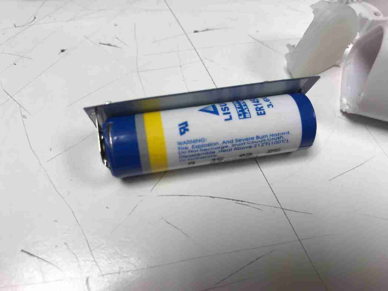
2.2Ah 3.6v Lithium Cell
The other side of the PCB has a single primary lithium cell, rated at 3.6v, 2.2Ah. The factory spec sheet specifies a 2.2 year life at 0dBm TX Power, Running 24/7, 100ms advertisement rate.
The rear has the specifications, laser-marked into the plastic. The serial numbers are just sticky labels though, and will come off easily with use.
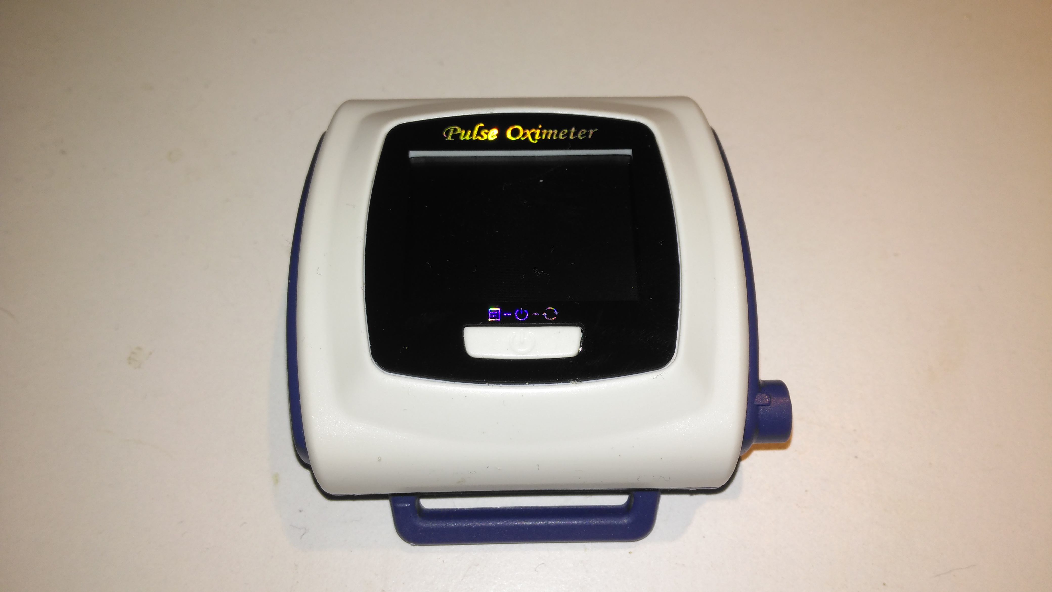
Contec CMS-50F
This is the Contec CMS-50F wrist-mounted pulse oximeter unit, which has the capability to record data continuously to onboard memory, to be read out at a later time via a USB-Serial link. There is software supplied with the unit for this purpose, although it suffers from the usual Chinese quality problems. The hardware of this unit is rather well made, the firmware has some niggles but is otherwise fully functional, however the PC software looks completely rushed, is of low quality & just has enough functionality to kind-of pass as usable.
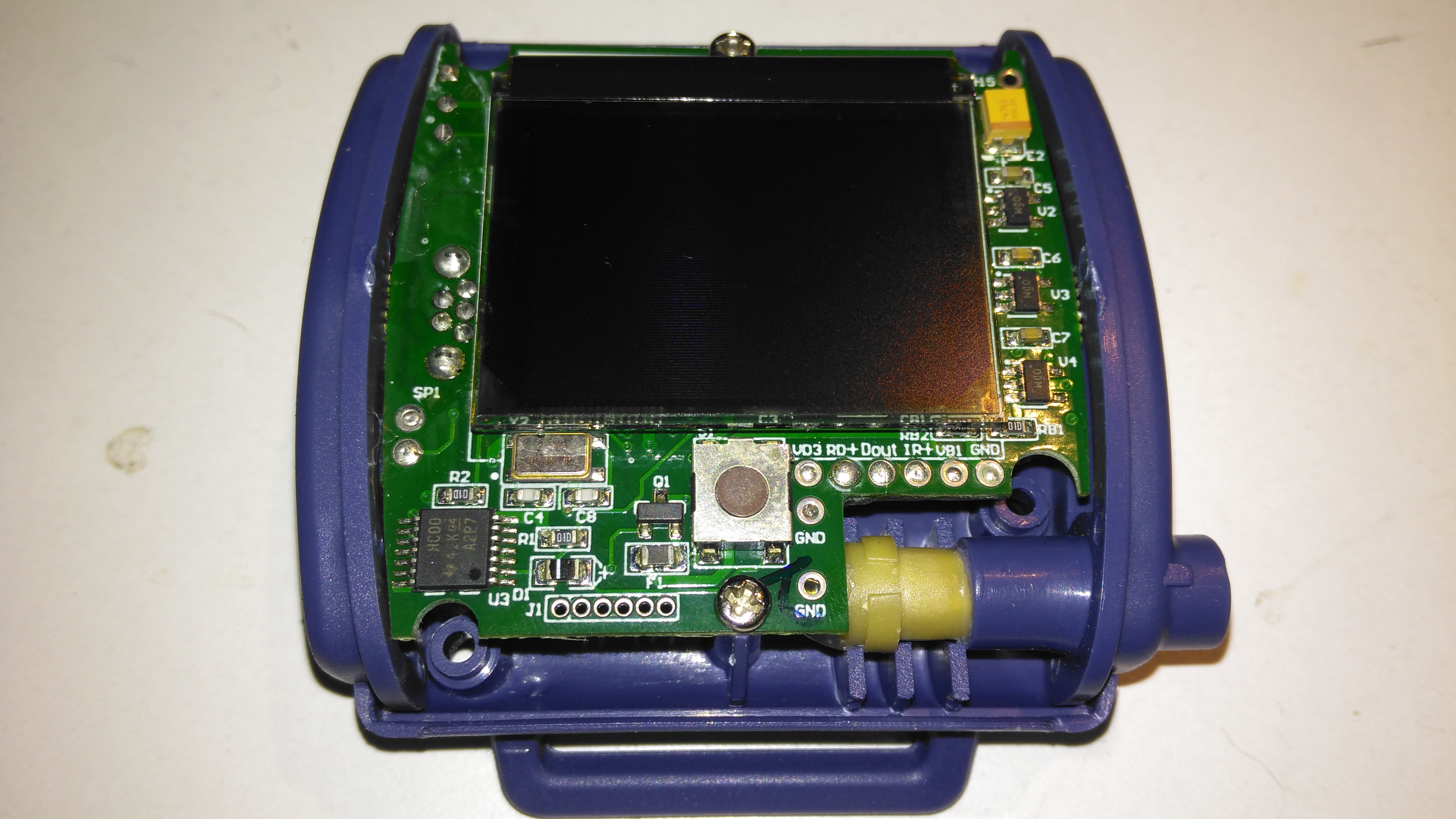
Top Cover Removed
A total of 4 screws hold the casing together, once these are removed the top comes off. The large colour OLED display covers nearly all of the board here. The single button below is the user interface. The connection to the probe is made via the Lemo-style connector on the lower right.
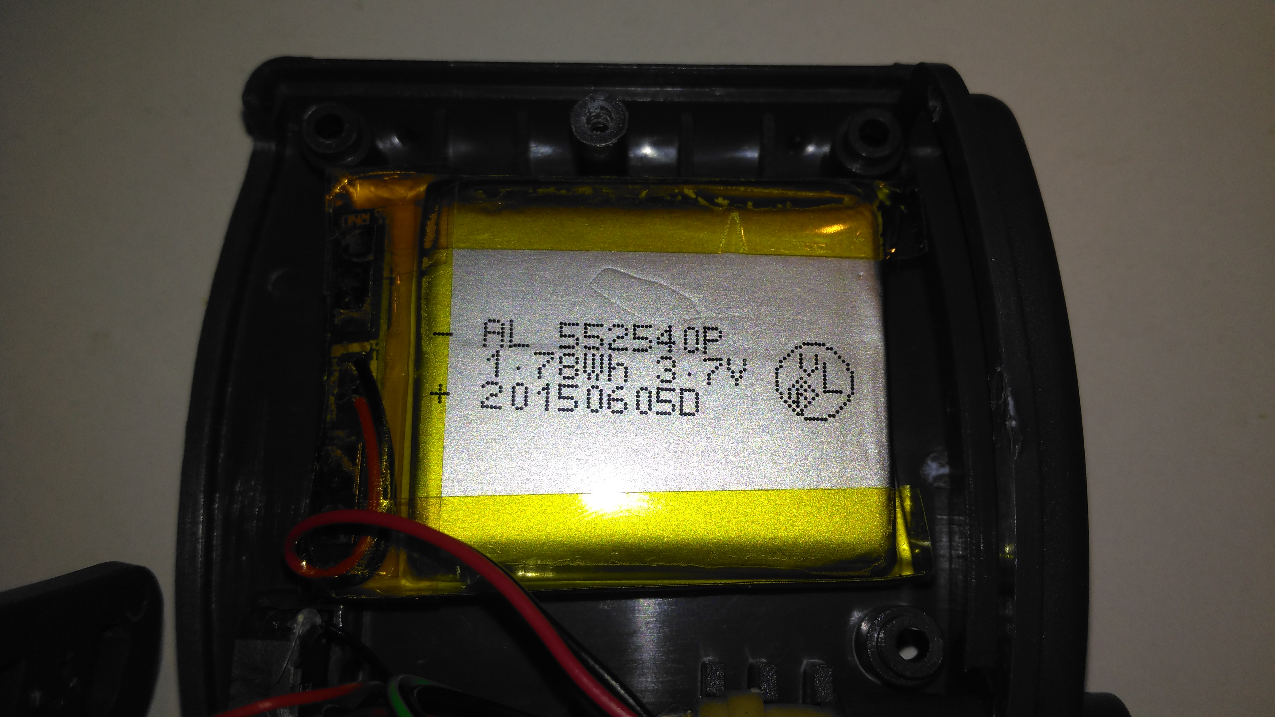
Lithium Cell
Power is provided by a relatively large lithium-ion cell, rated at 1.78Wh.
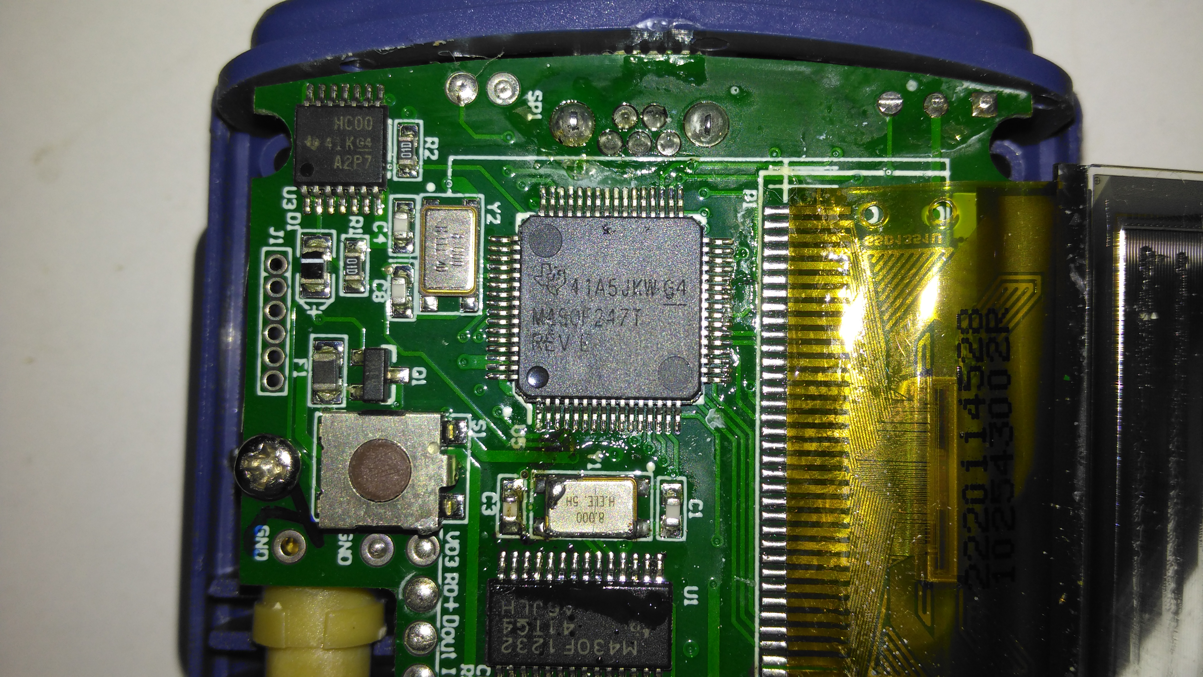
Main Processor
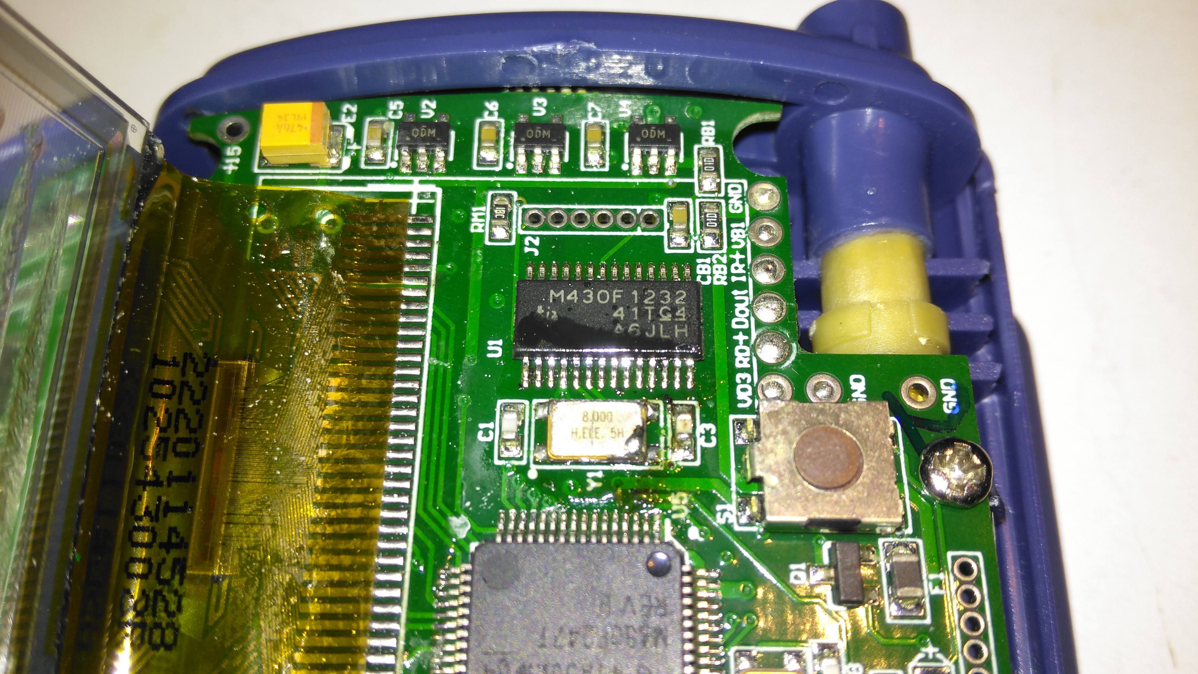
All the heavy lifting work of the LCD, serial comms, etc are handled by this large Texas Instruments microcontroller, a MSP430F247. The clock crystal is just to the left, with the programming pins. I’m not sure of the purpose of the small IC in the top left corner, I couldn’t find any reference to the markings.
Aux Processor
The actual pulse oximetry sensor readings seem to be dealth with by a secondary microcontroller, a Texas Instruments M430F1232 Mixed-Signal micro. This has it’s own clock crystal just underneath. The connections to the probe socket are to the right of this µC, while the programming bus is broken out to vias just above. The final devices on this side of the board are 3 linear regulators, supplying the rails to run all the logic in this device.
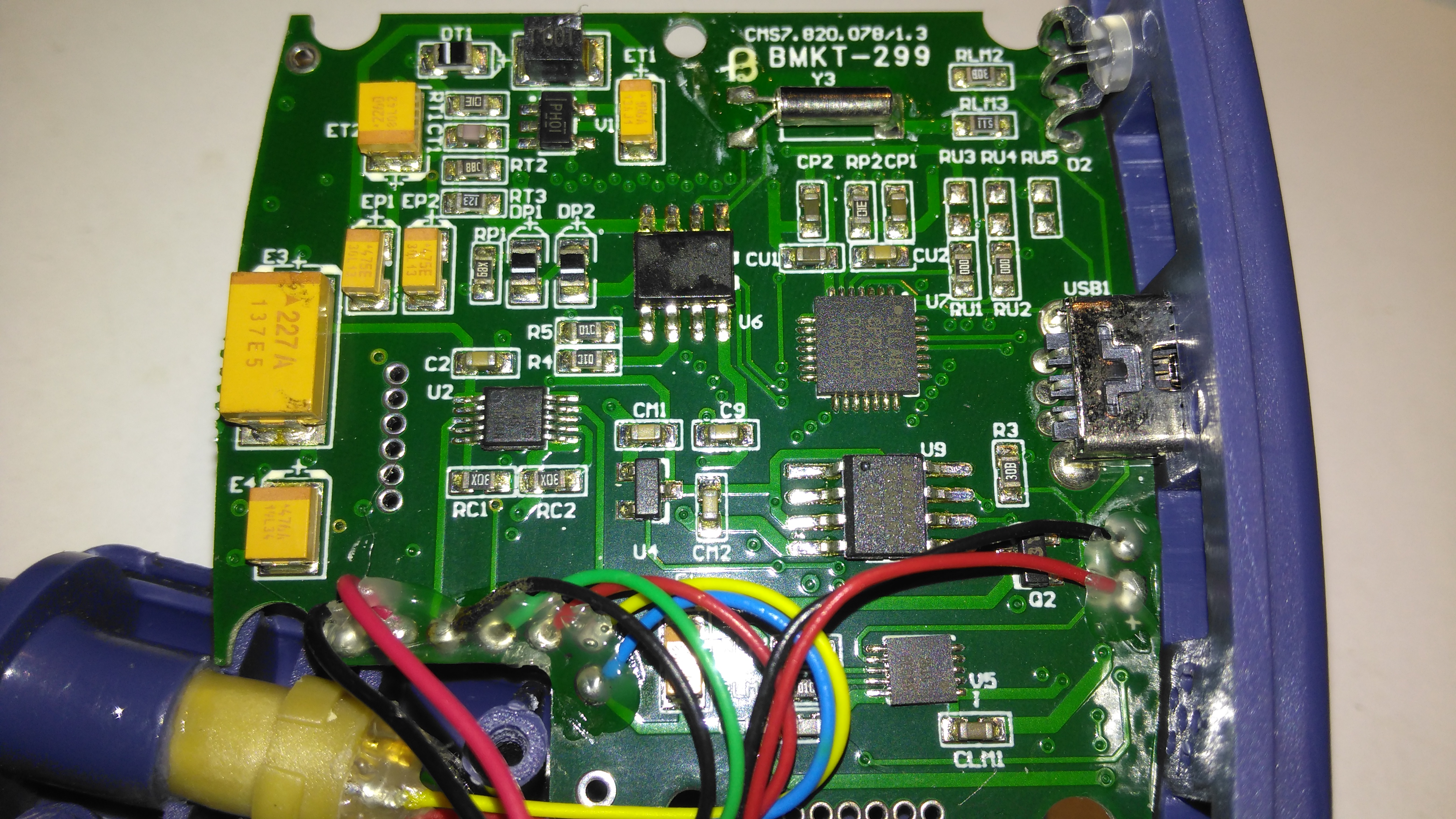
Main PCB Rear
The rear of the PCB has the SiLabs CL2102 USB-Serial interface IC, the large Winbond 25X40CLNIG 512KByte SPI flash for recording oximetry data, and some of the power support components. The RTC crystal is also located here at the top of the board. Up in the top left corner is a Texas Instruments TPS61041 Boost converter, with it’s associated components. This is probably supplying the main voltage for the OLED display module.
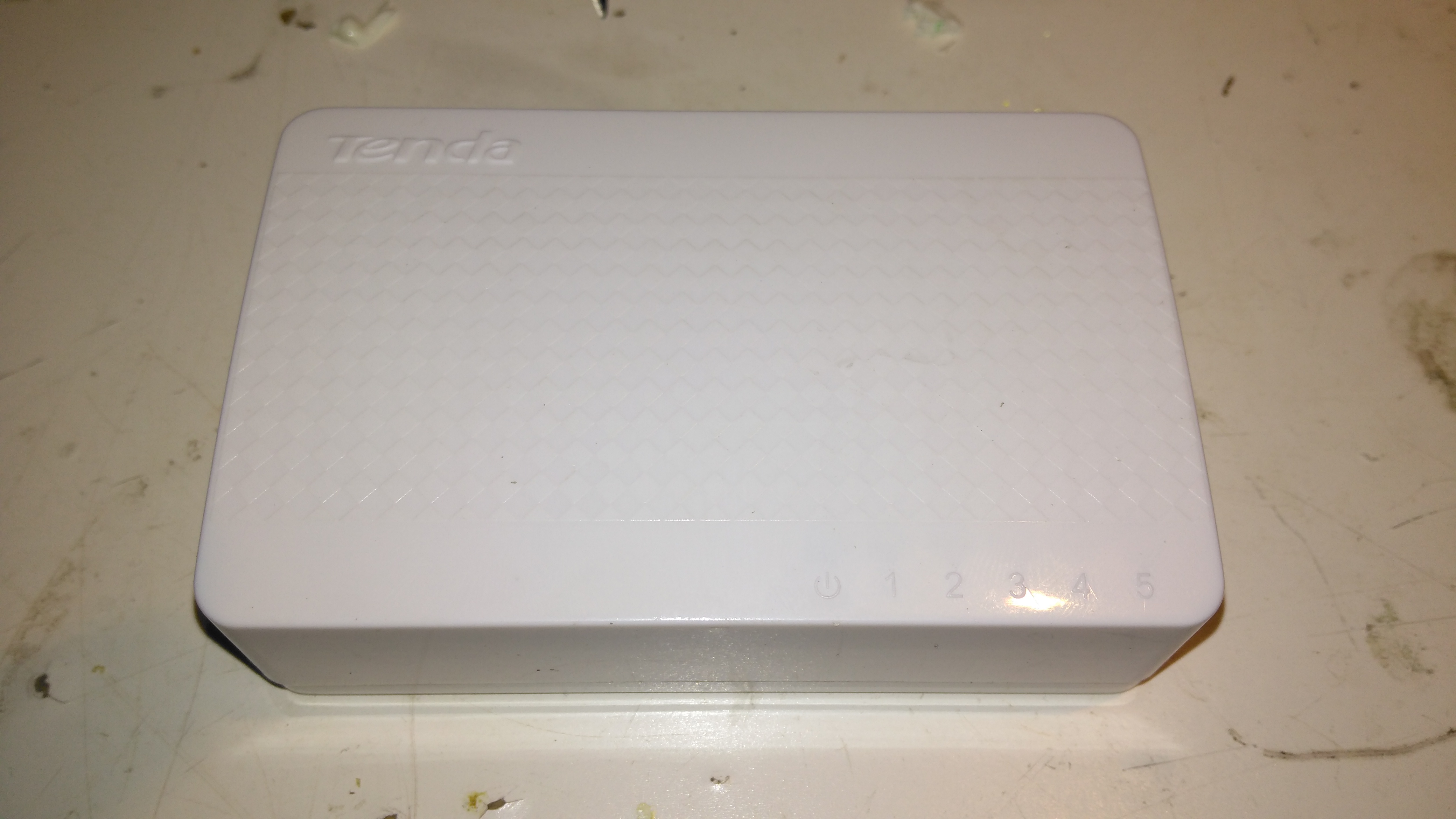
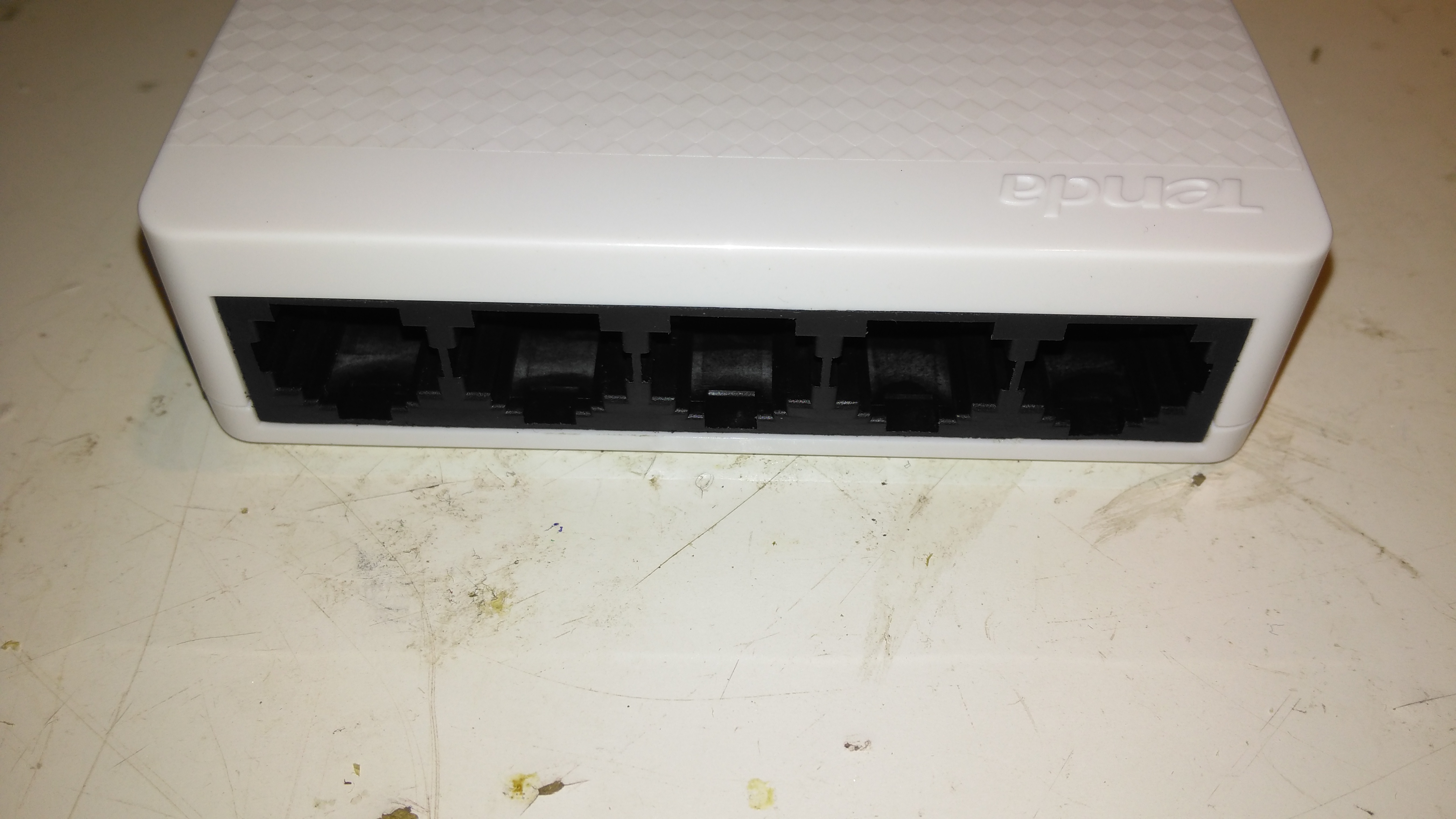
Here’s a tiny ethernet switch from the great fle market that is eBay – the Tenda S105. This unit has 5 ports, but only supports 10/100M. Still, for something so small it’s not bad.
Bottom
Not much on the bottom, there’s a pair of screw hooks for mounting this to a surface.
Ports
The 5 ports on the front actually have the pins for the unused pairs of the ethernet cables removed – saving every penny here.
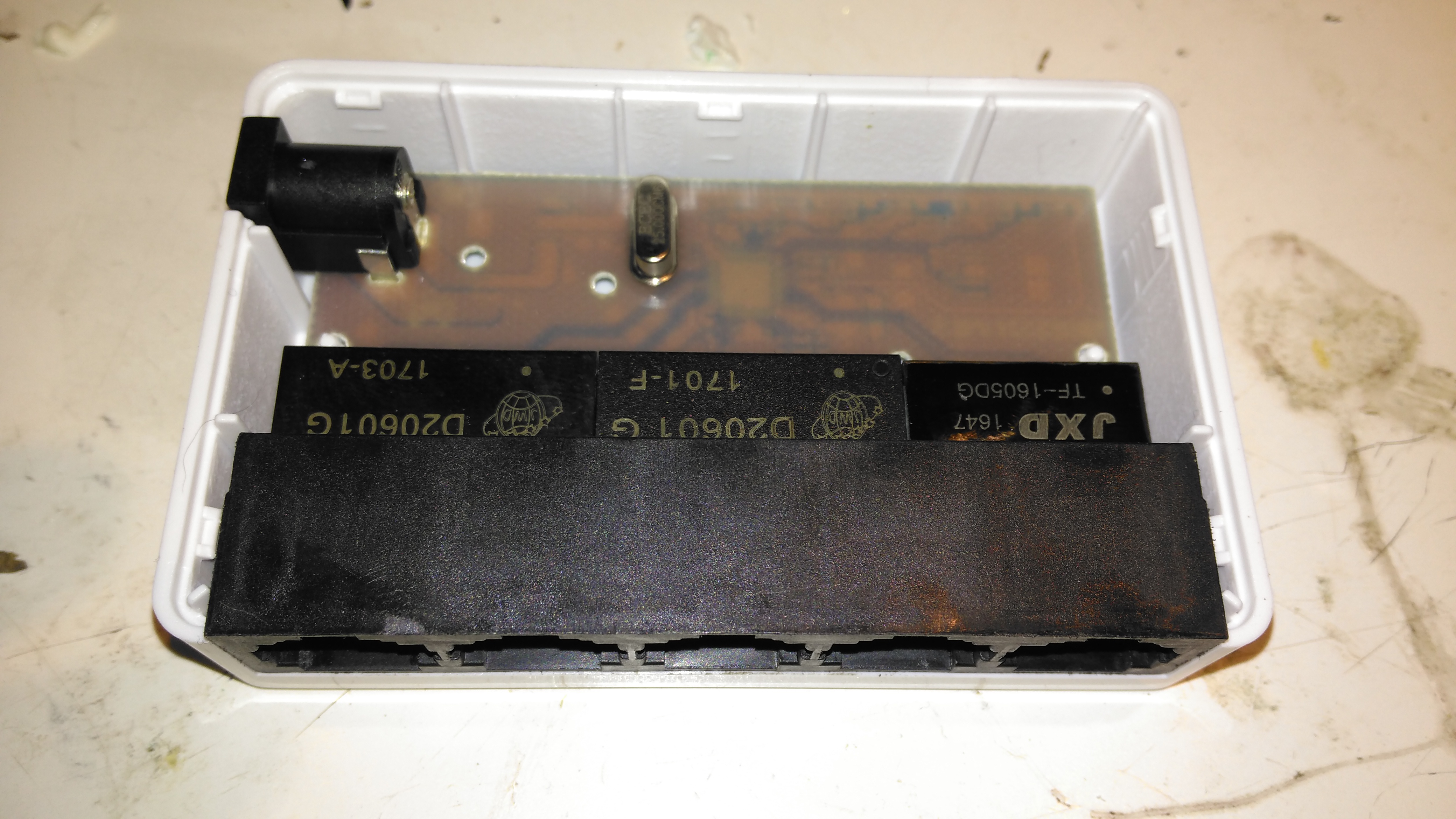
PCB Top
The casing just unclips, revealing the small PCB. Nothing much on the top, just the connectors, isolating transformers & the crystal for the switch IC.
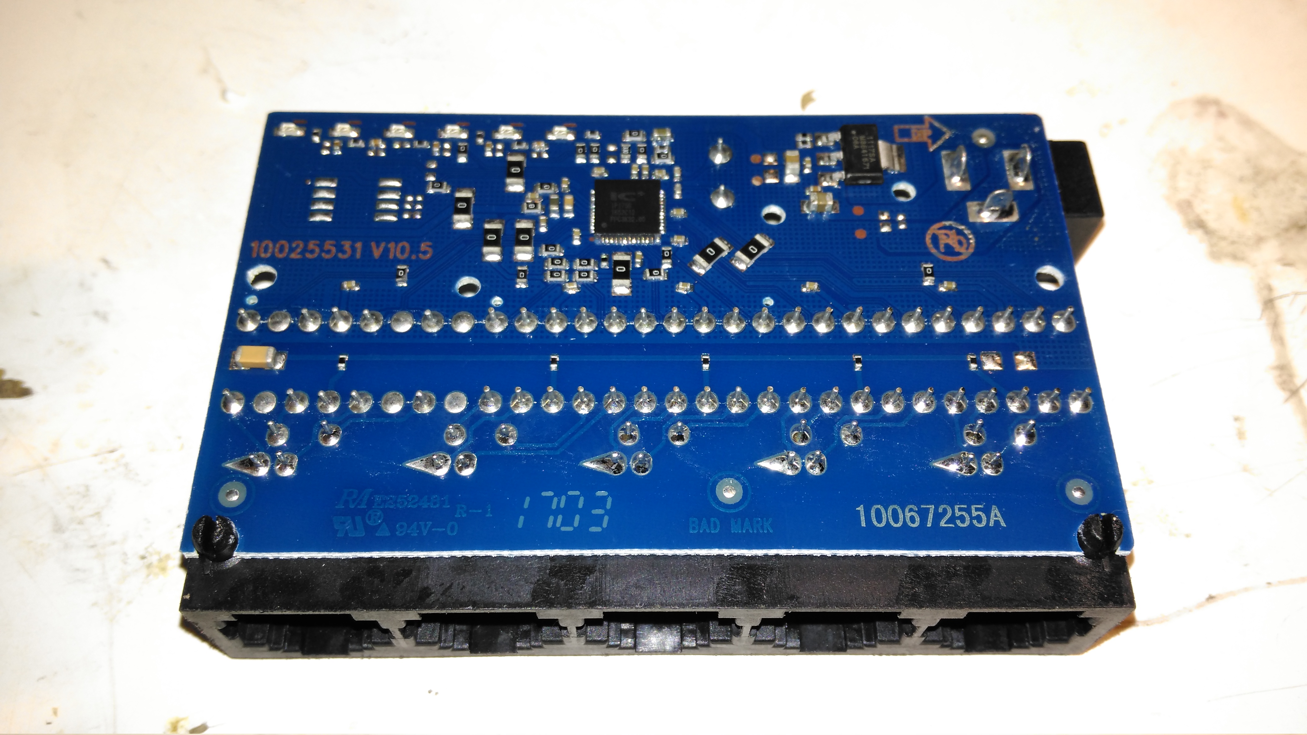
PCB Bottom
The bottom of the PCB is a little more busy, mainly with decoupling components. There’s a 3.3v linear regulator to step down the 5v input for the switch IC.
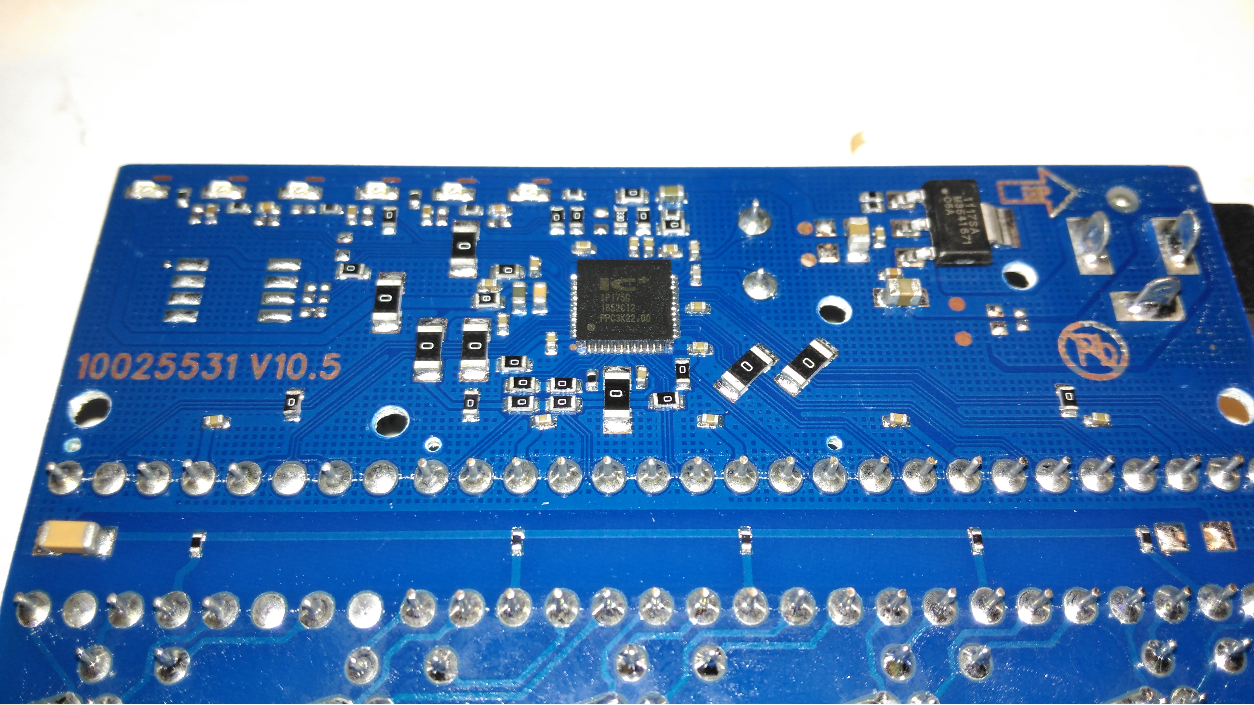
Switch IC
The IC doing all the data switching is an IP175G 5-Port 10/100 Switch from IC+ Corp. No datasheet available for this, but it’s going to be a bog-standard switch.
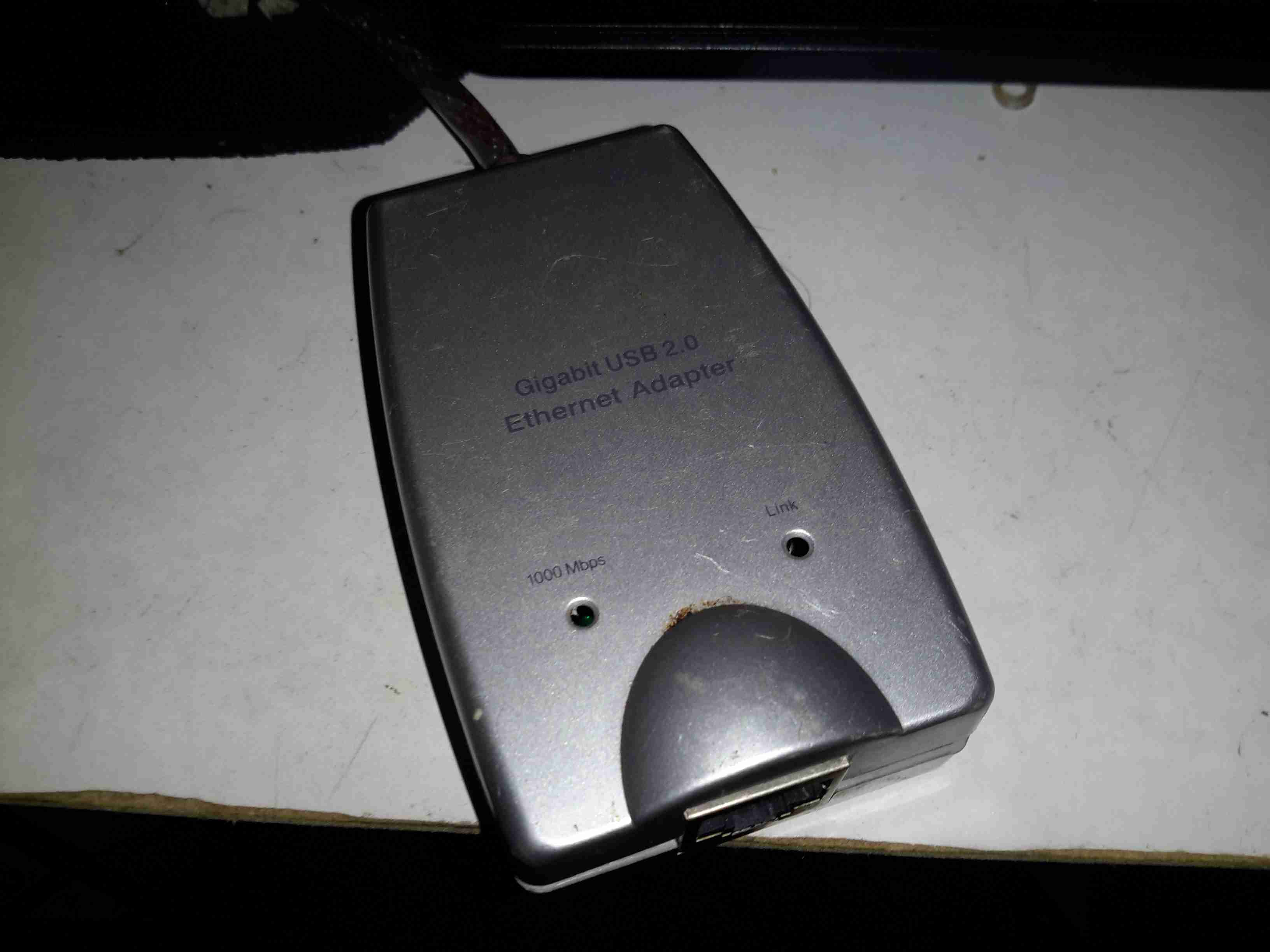
Here’s a chap eBay USB-To-Ethernet dongle I obtained for use with the Raspberry Pi Zero. This one is getting torn down permanently, as it’s rather unreliable. It seems to like having random fits where it’ll not enumerate on the USB bus. The silicon in the ICs will eventually make it here once I manage to get a new microscope 😉
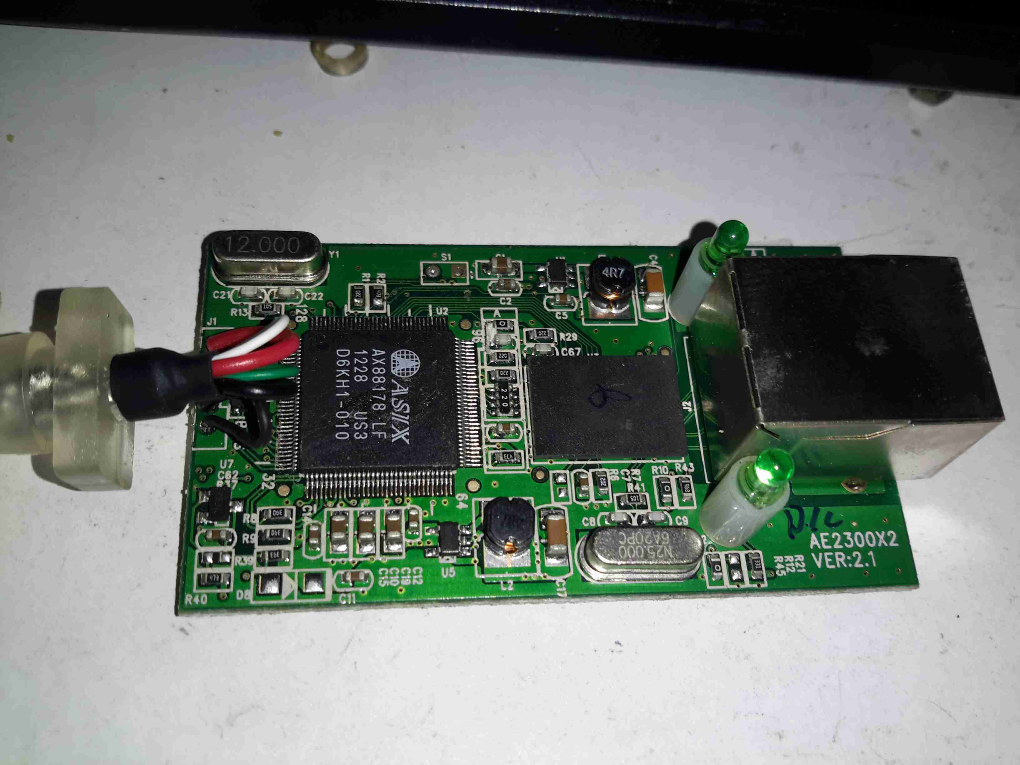
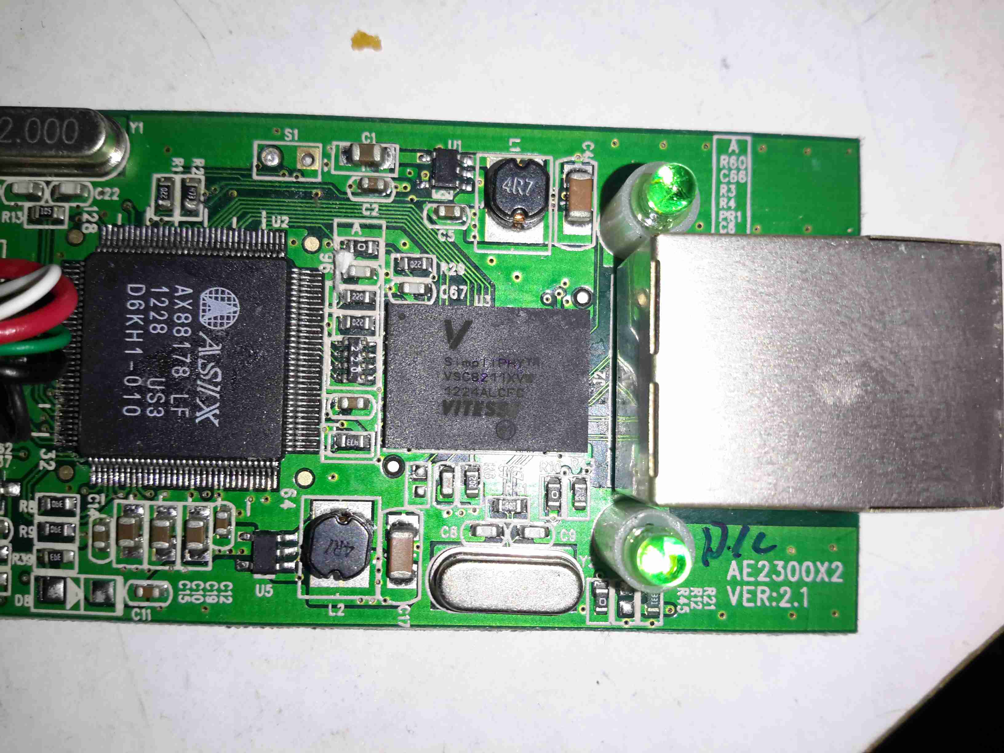
Main Chipset
This is quite a heavily packed PCB, with the main Asix AX88178 on the left. This IC contains all of the logic for implementing the Ethernet link over USB, except the PHY. It’s clock crystal is in the top left corner.
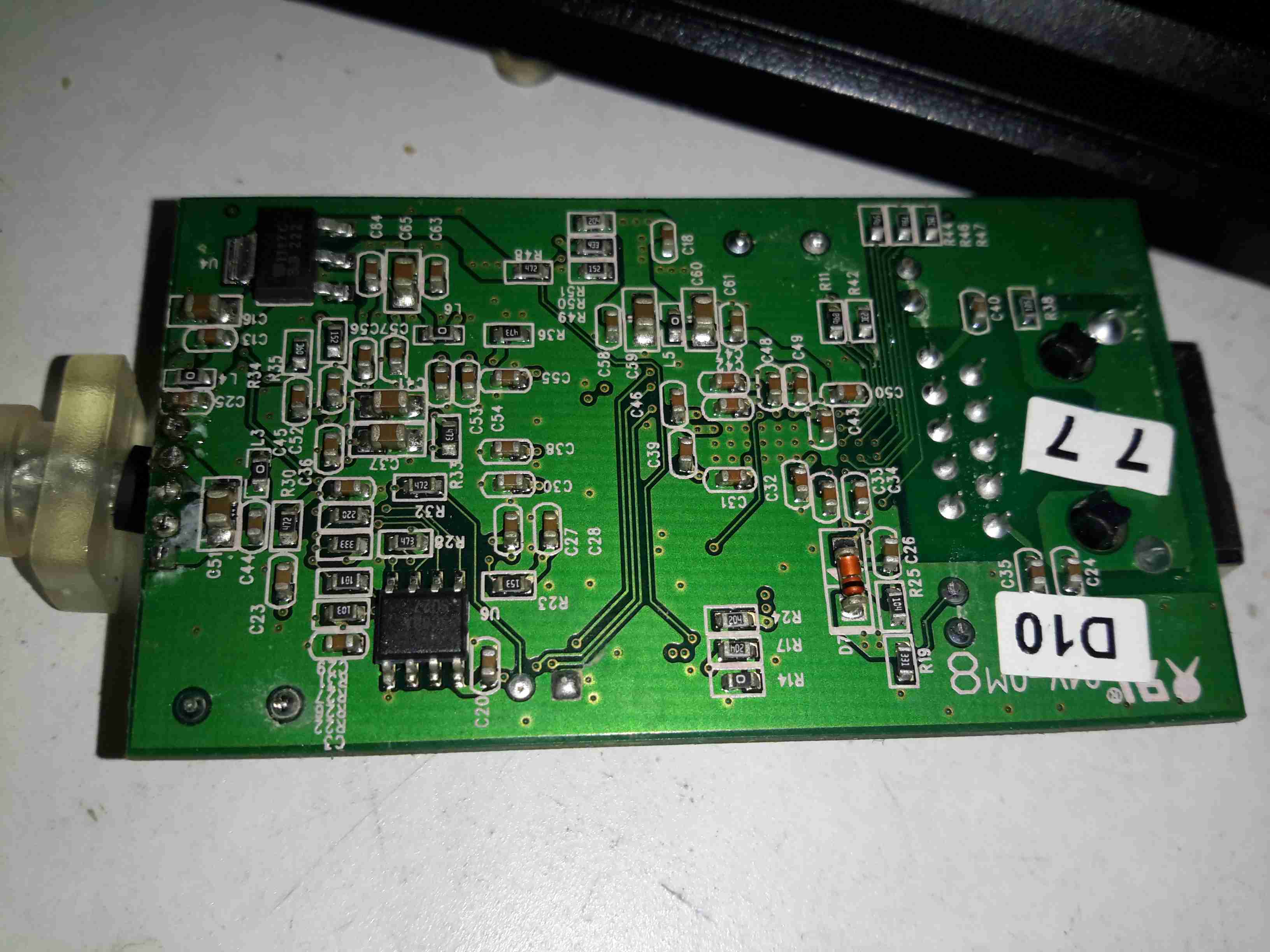
Reverse Side
Not much on the reverse side, there’s a 3.3v linear regulator at top left, the SOIC is an Atmel AT93C66A 4KB EEPROM for configuration data.
Vitesse PHY
The final IC in the chain is the Vitesse VSC8211 Gigabit PHY, with it’s clock crystal below. This interfaces the Ethernet MAC in the Asix IC to the magjack on the right.
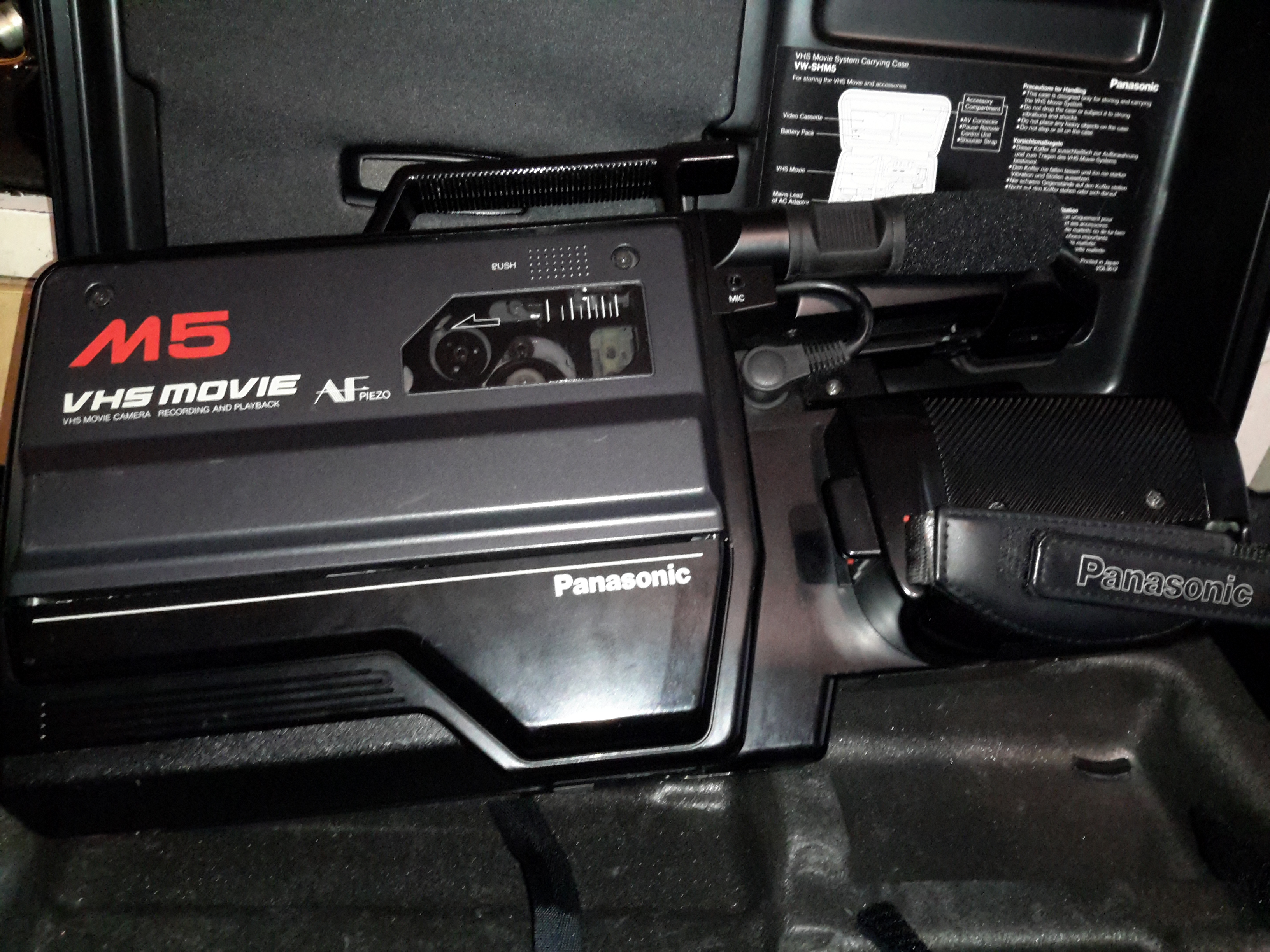
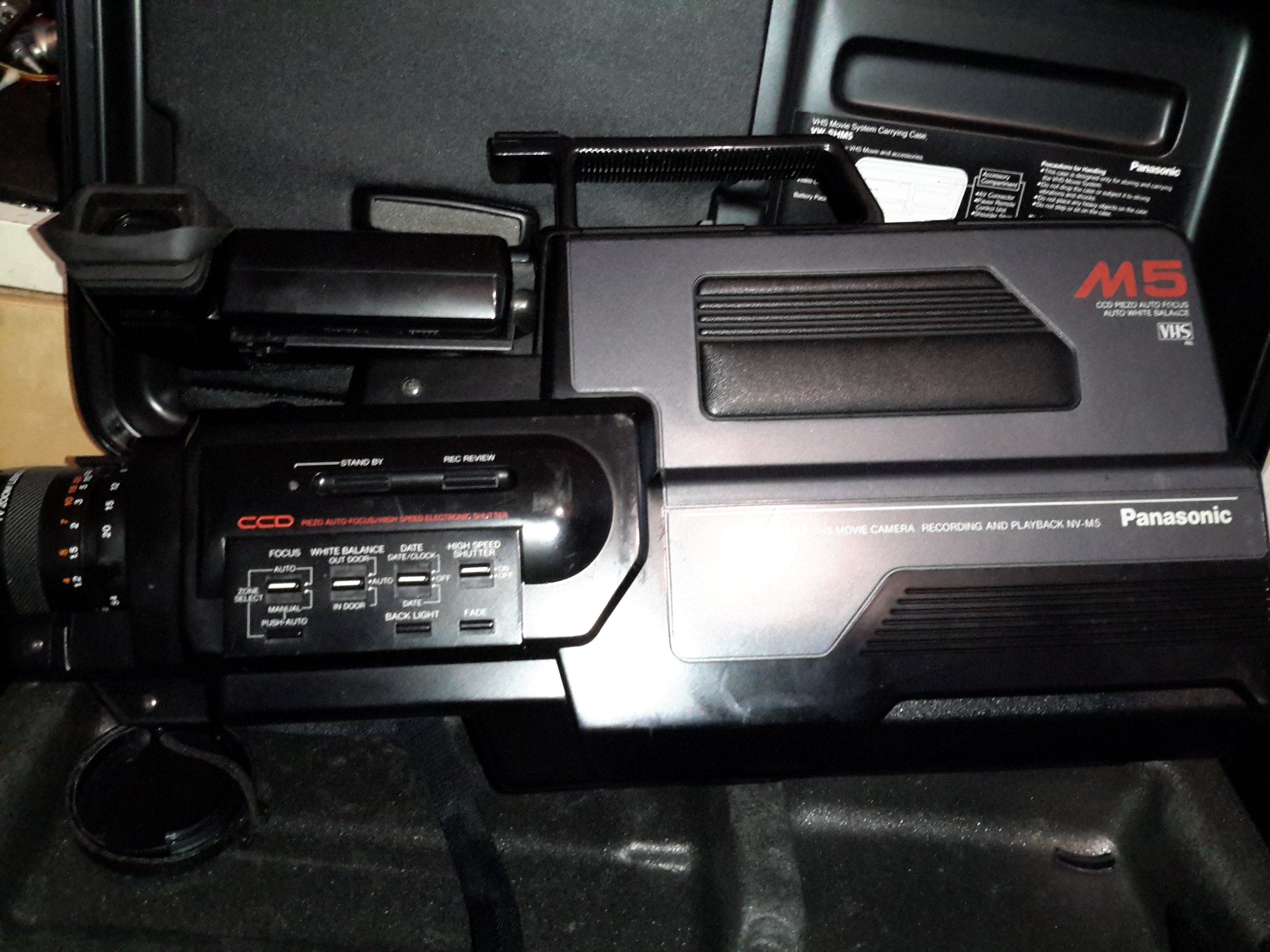
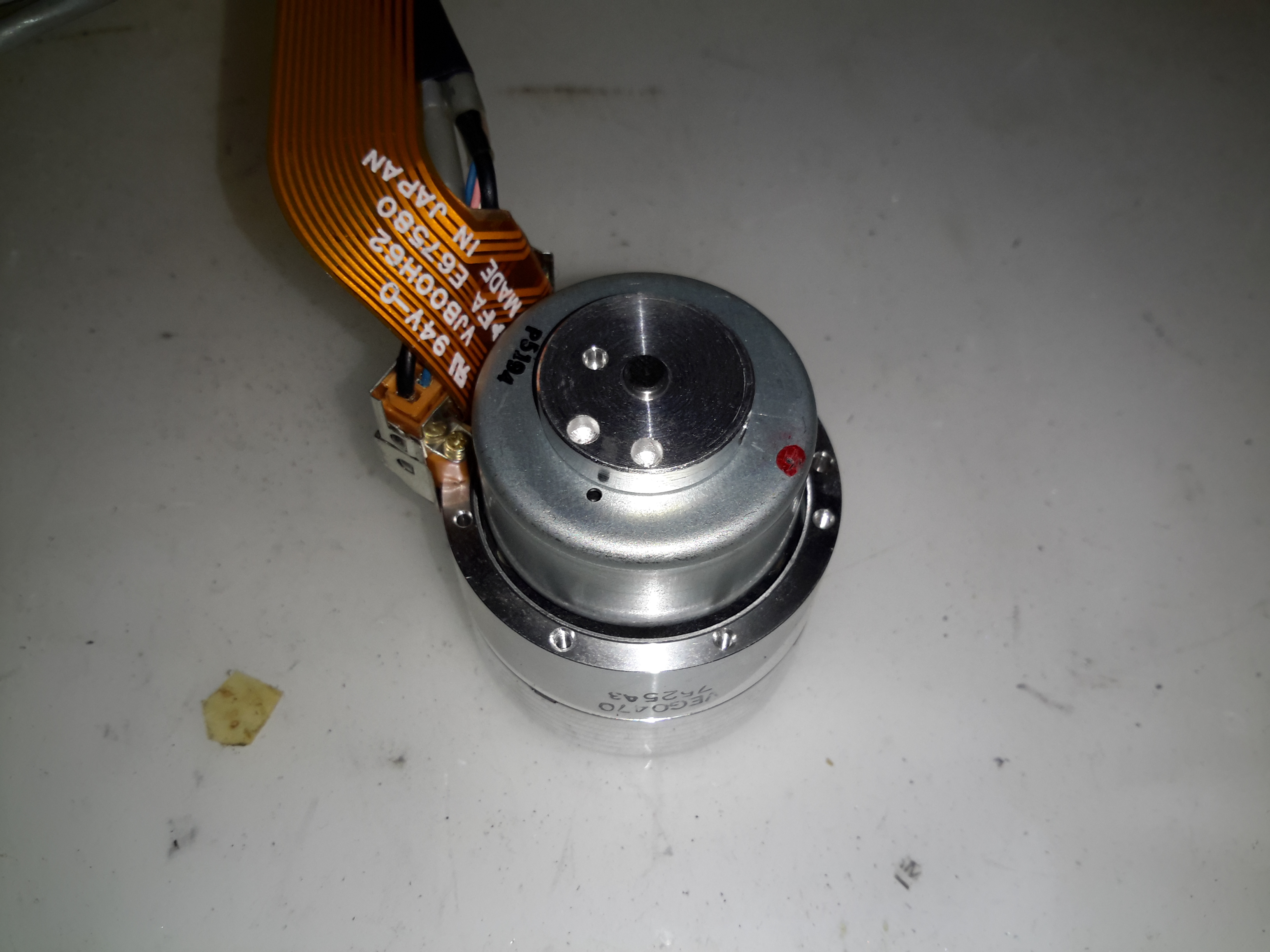
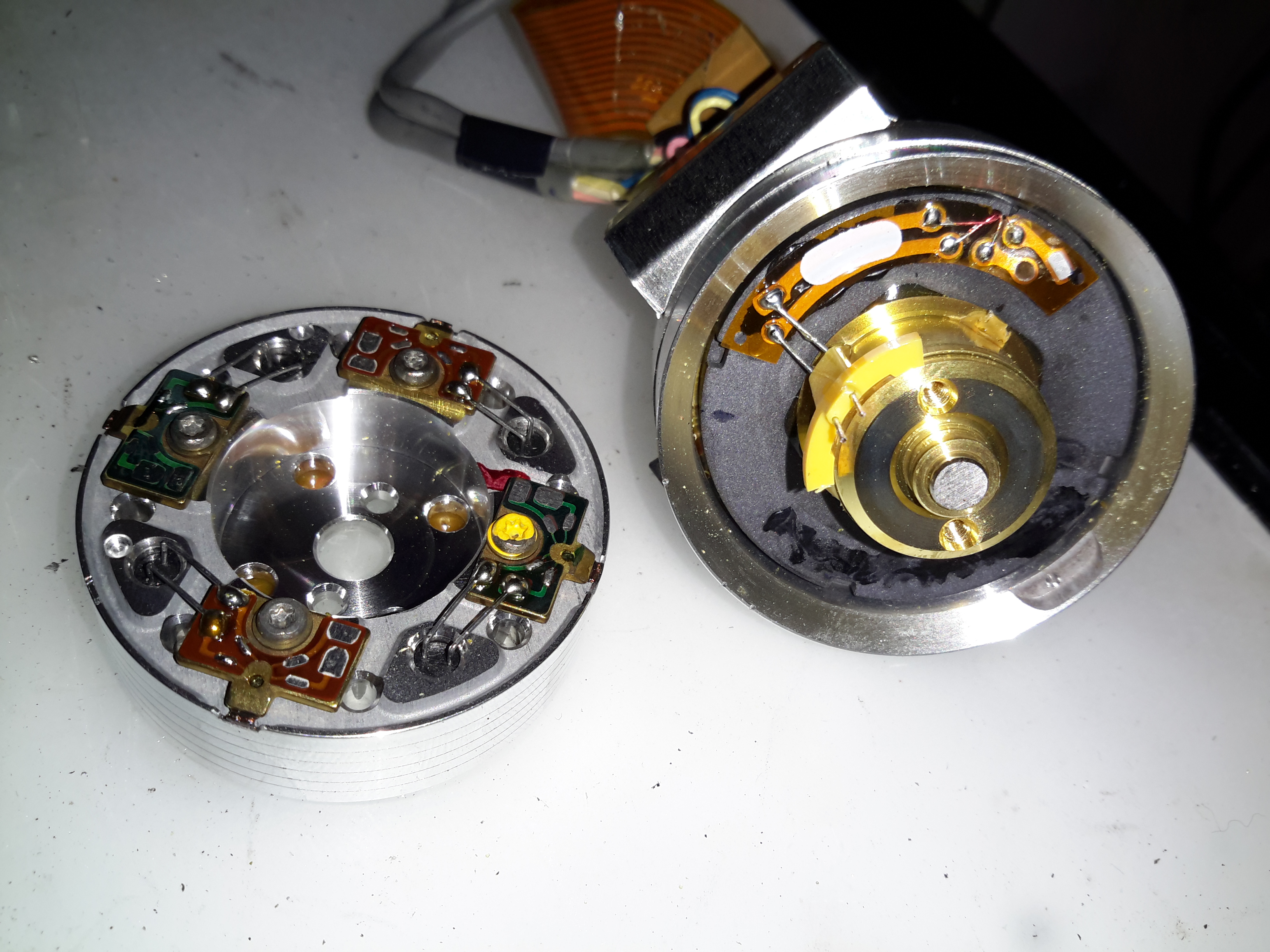
Time foe some more retro tech! This is a 1980’s vintage CCD-based VHS camcorder from Panasonic, the NV-M5. There are a lot of parts to one of these (unlike modern cameras), so I’ll split this post into several sections to make things easier to read (and easier to keep track of what I’m talking about :)).
Left Side
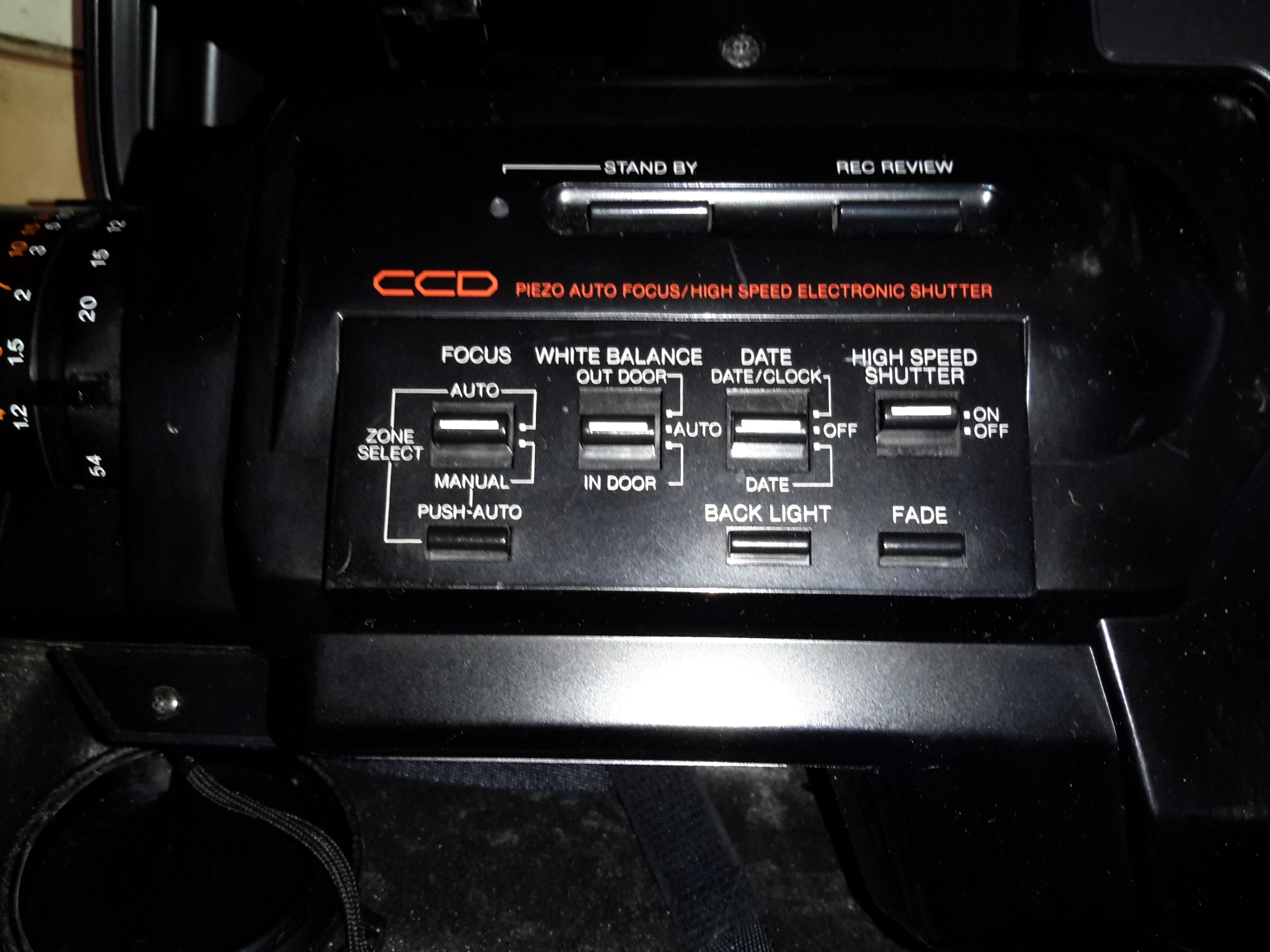
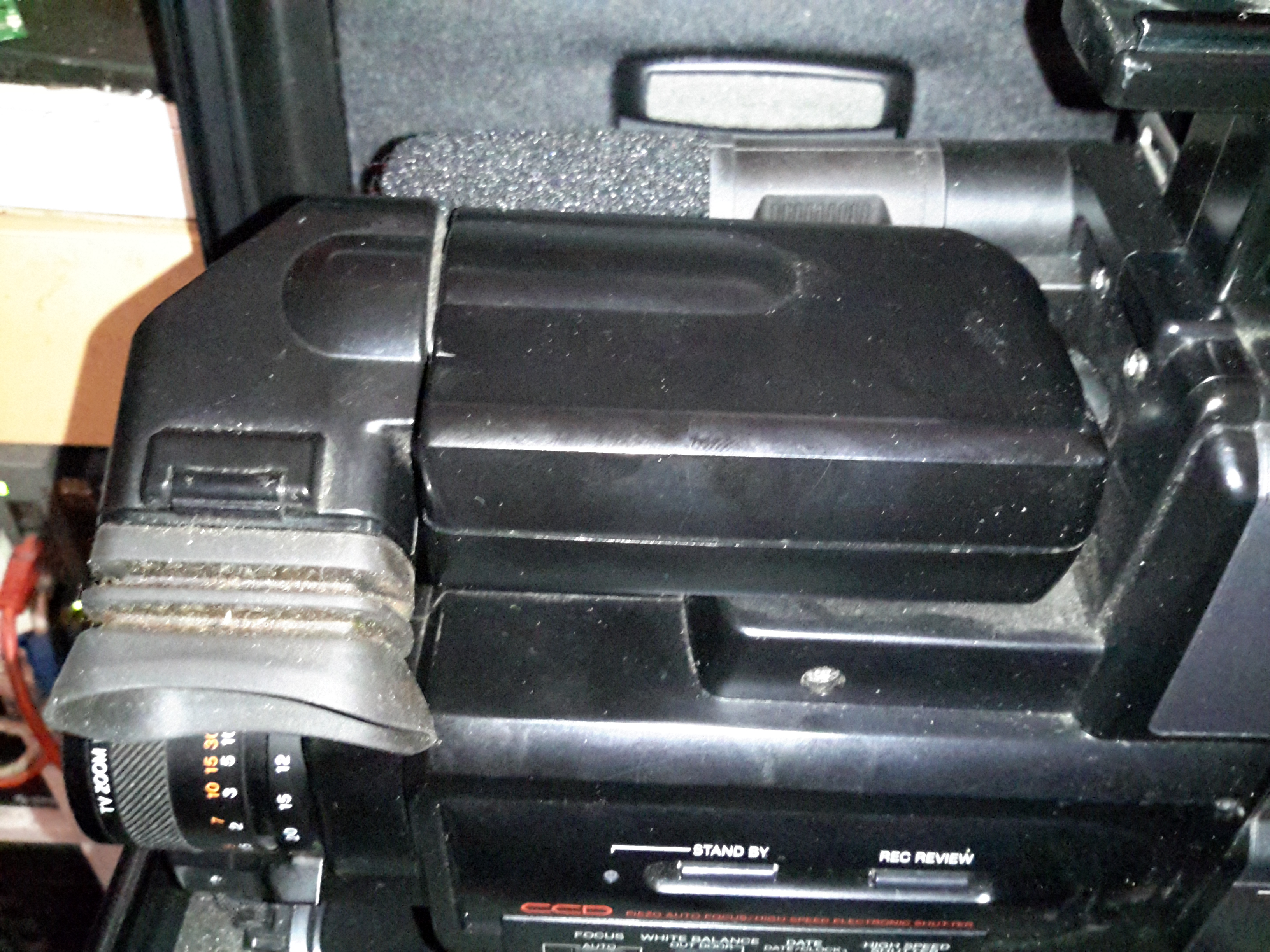
The left side of the camera holds the autofocus, white balance, shutter speed & date controls.
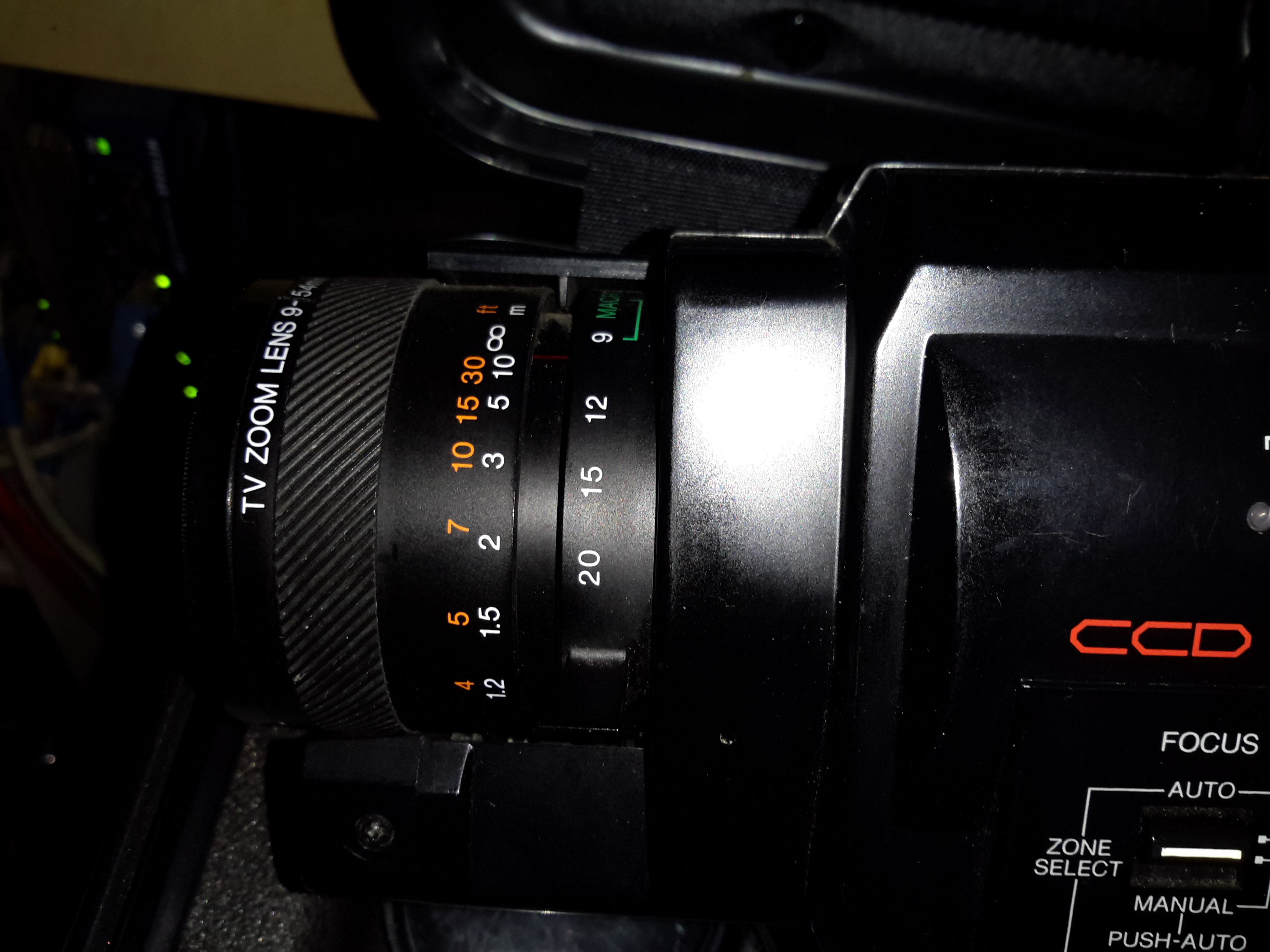
Left Side ControlsLens Adjustments
The lens is fully adjustable, with either manual or motorized automatic control.
Rear Panel
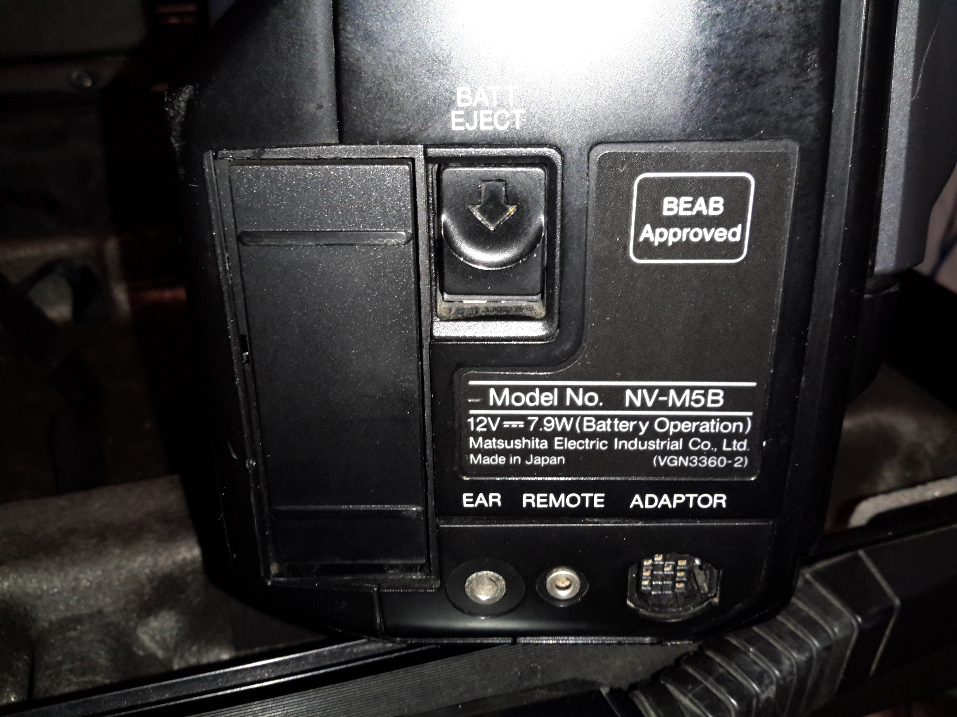
The back panel has the battery slot, a very strange looking DC input connector, remote control connector & the earphone jack.
Top Controls
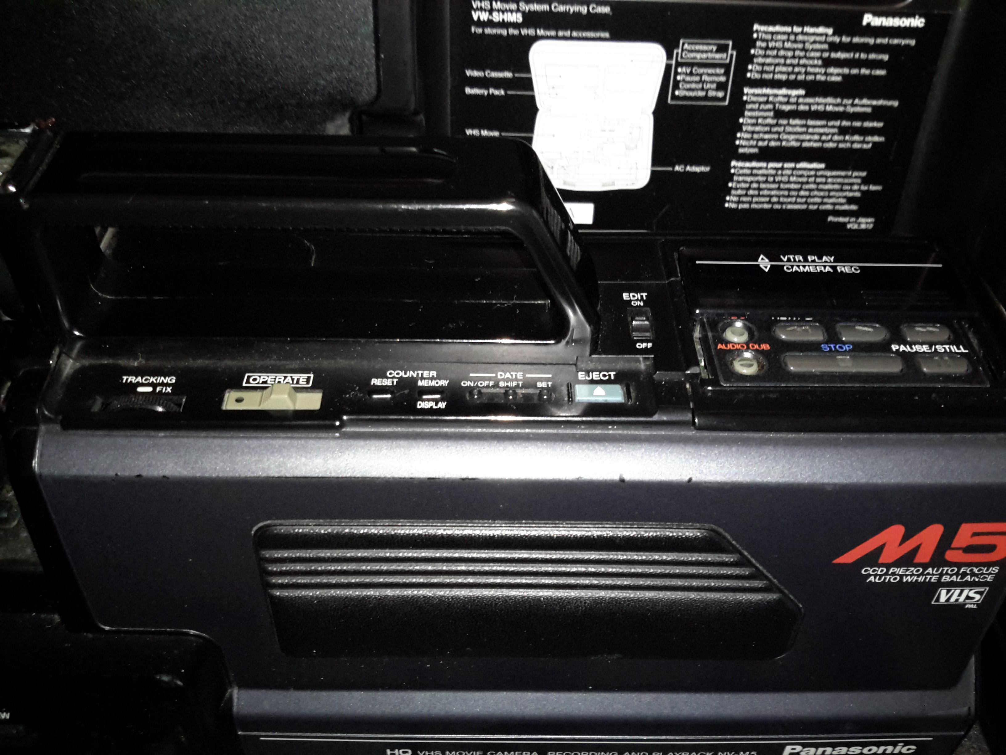
The top panel of the camera holds the main power controls, manual tape tracking & the tape transport control panel.
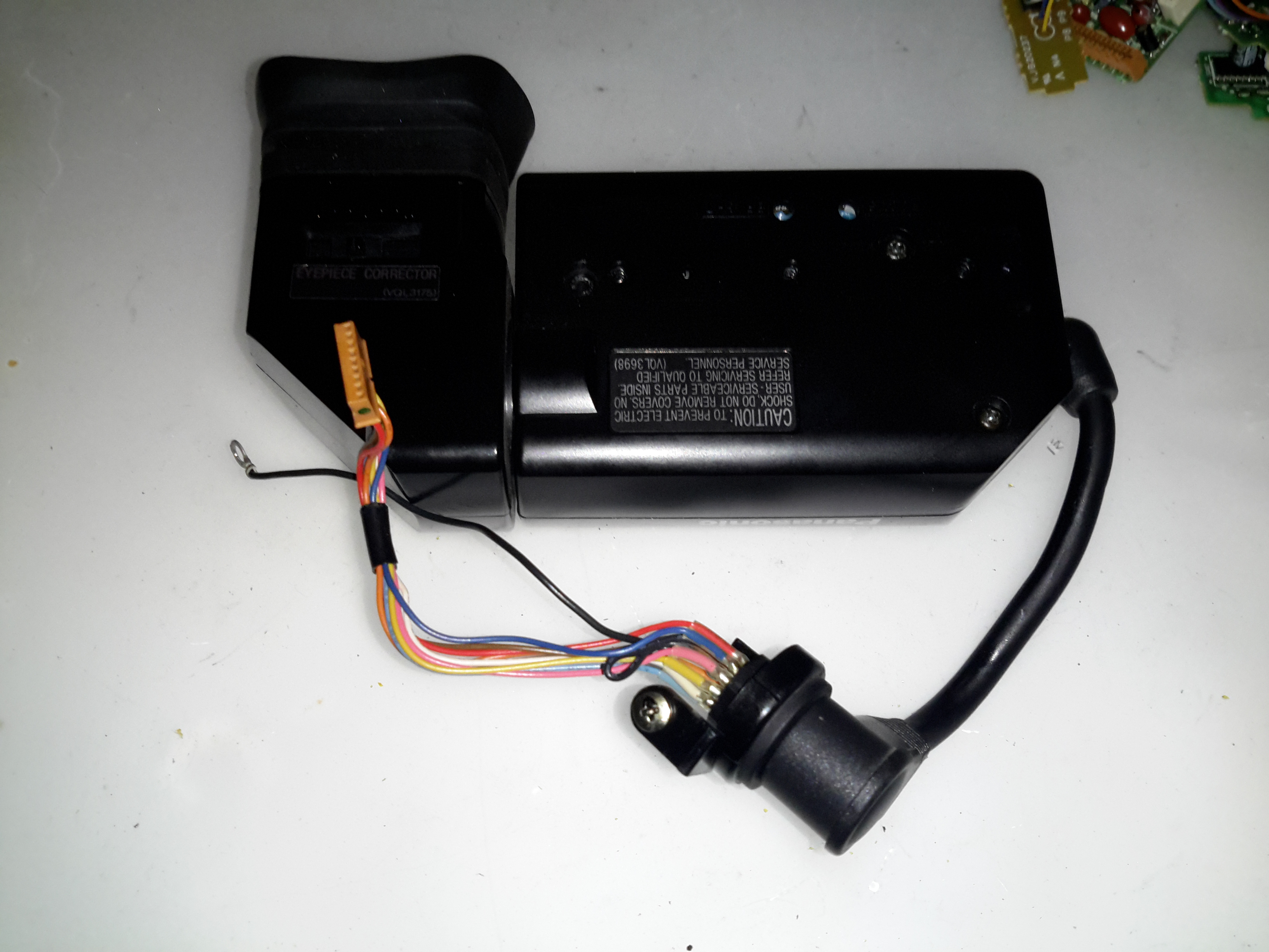
Viewfinder
The viewfinder is mounted on a swivel mount. There’s a CRT based composite monitor in here. Hack ahoy!
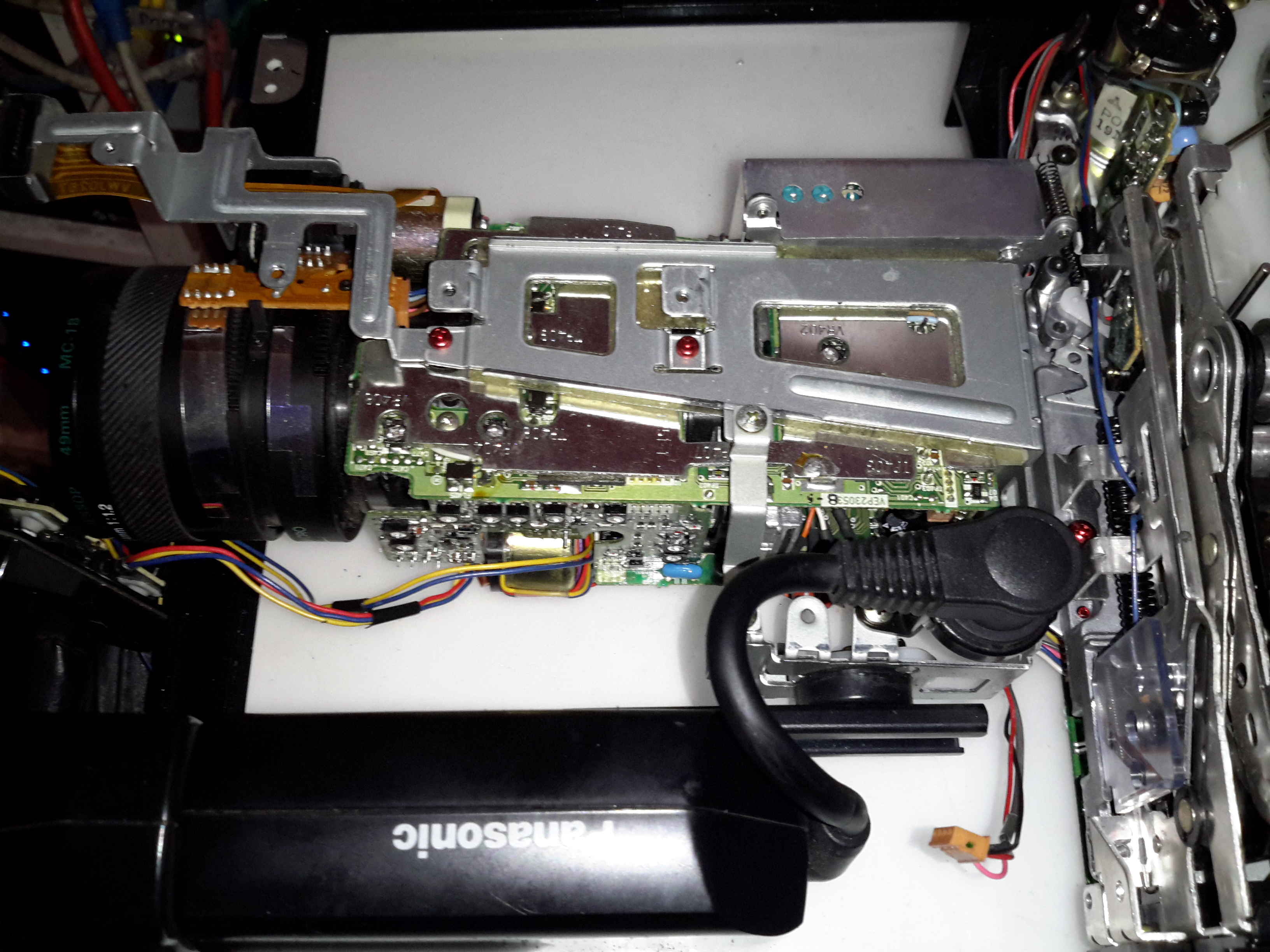
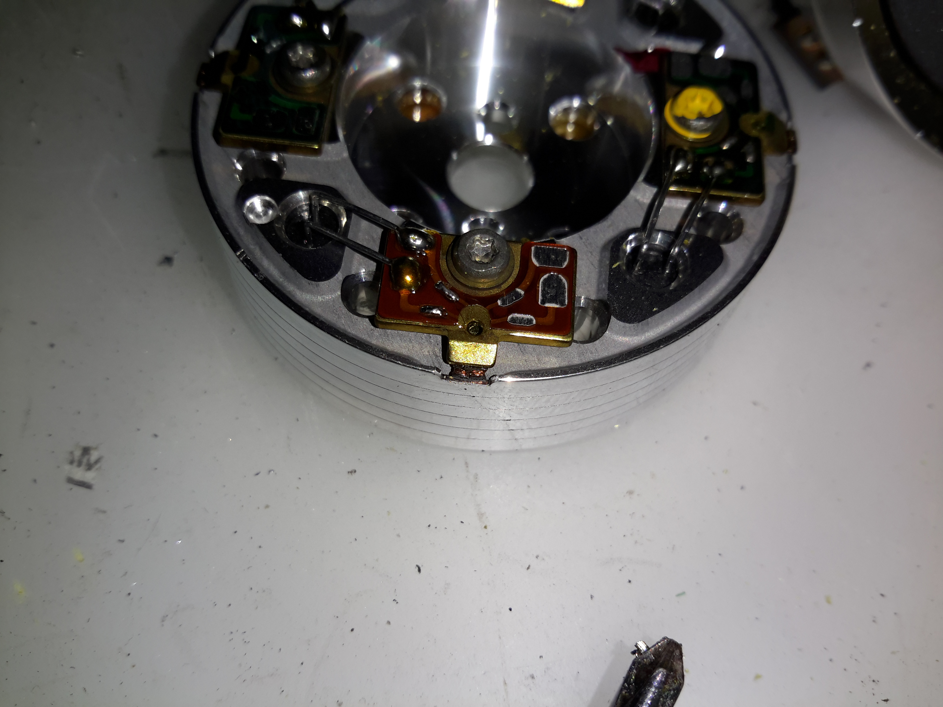
Camera Section
Process Board Assembly
Here’s the camera section of the camcorder, and is totally packed with electronics! There’s at least half a dozen separate boards in here, all fitted together around the optics tube assembly.
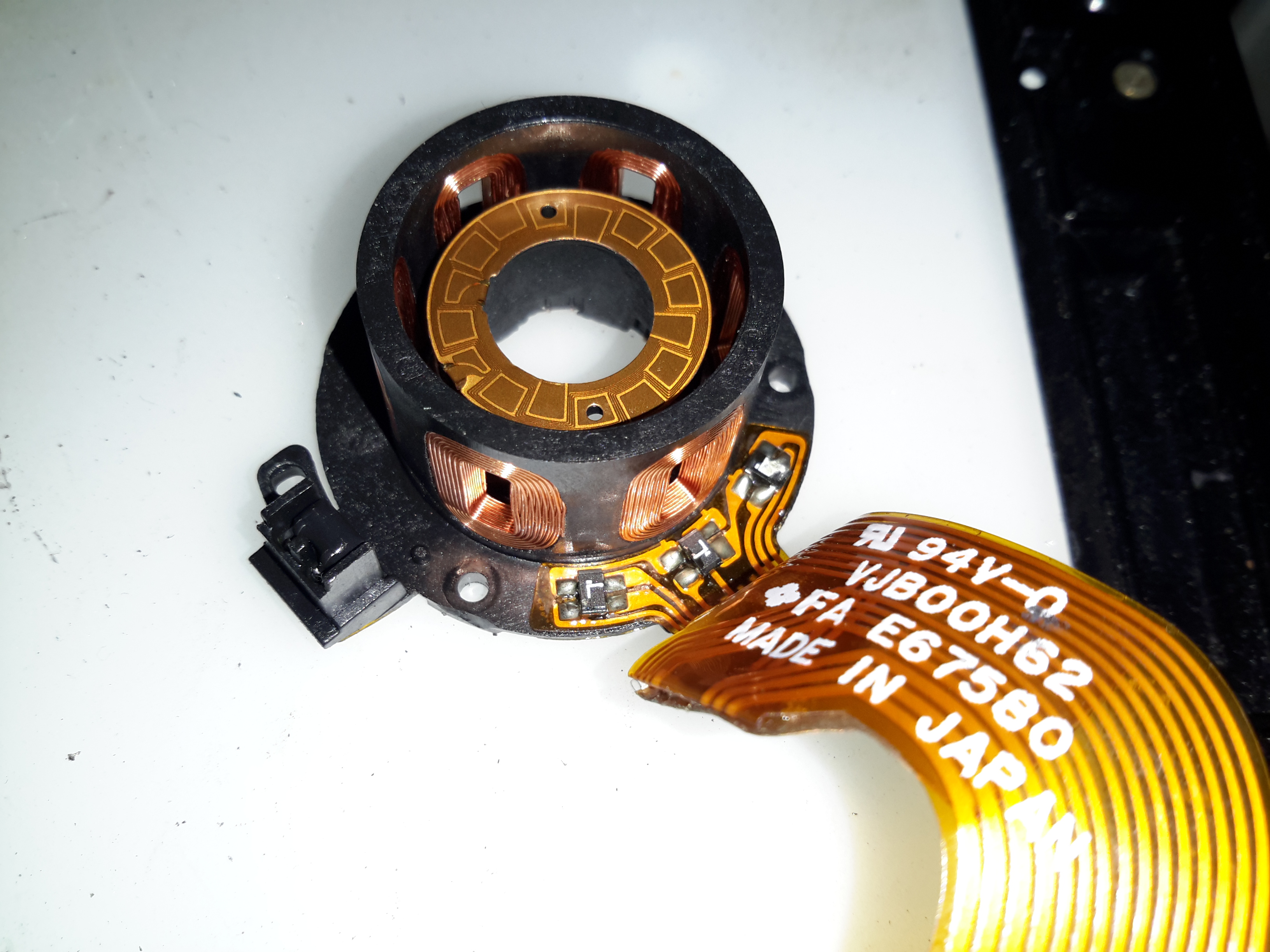
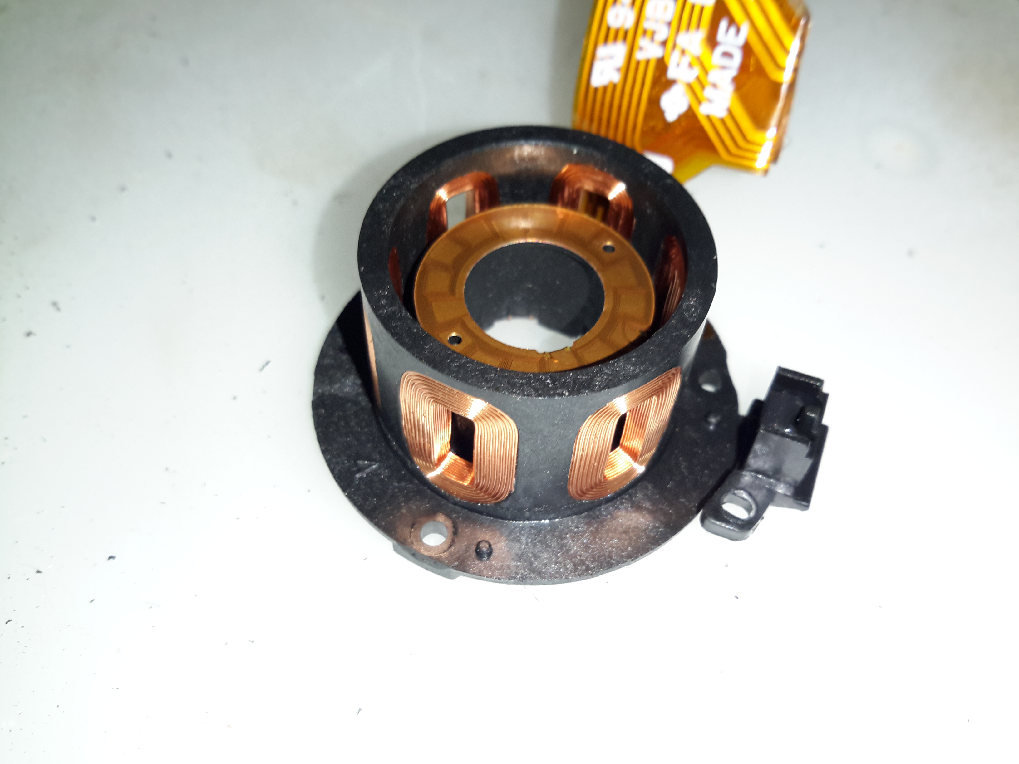
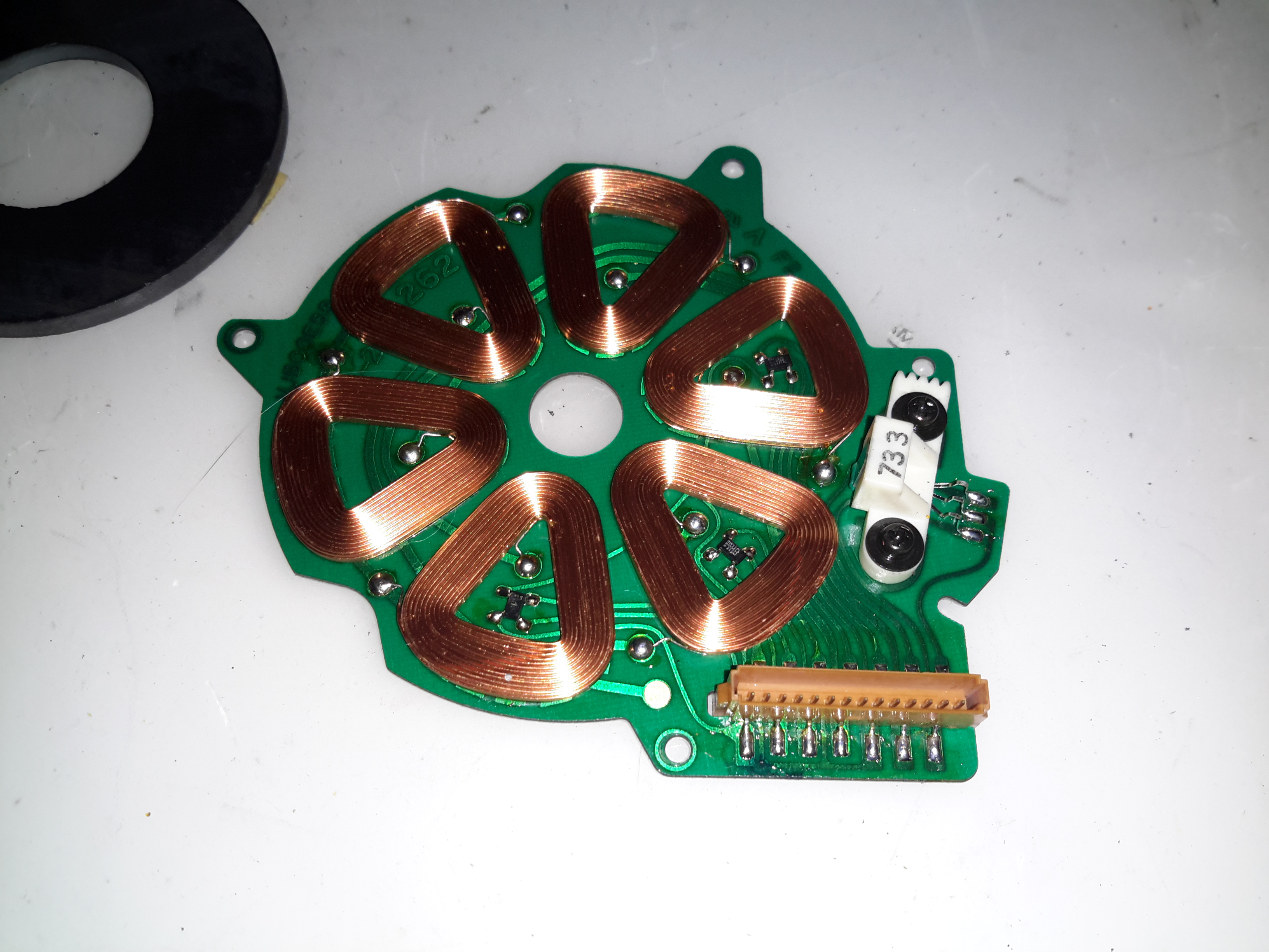
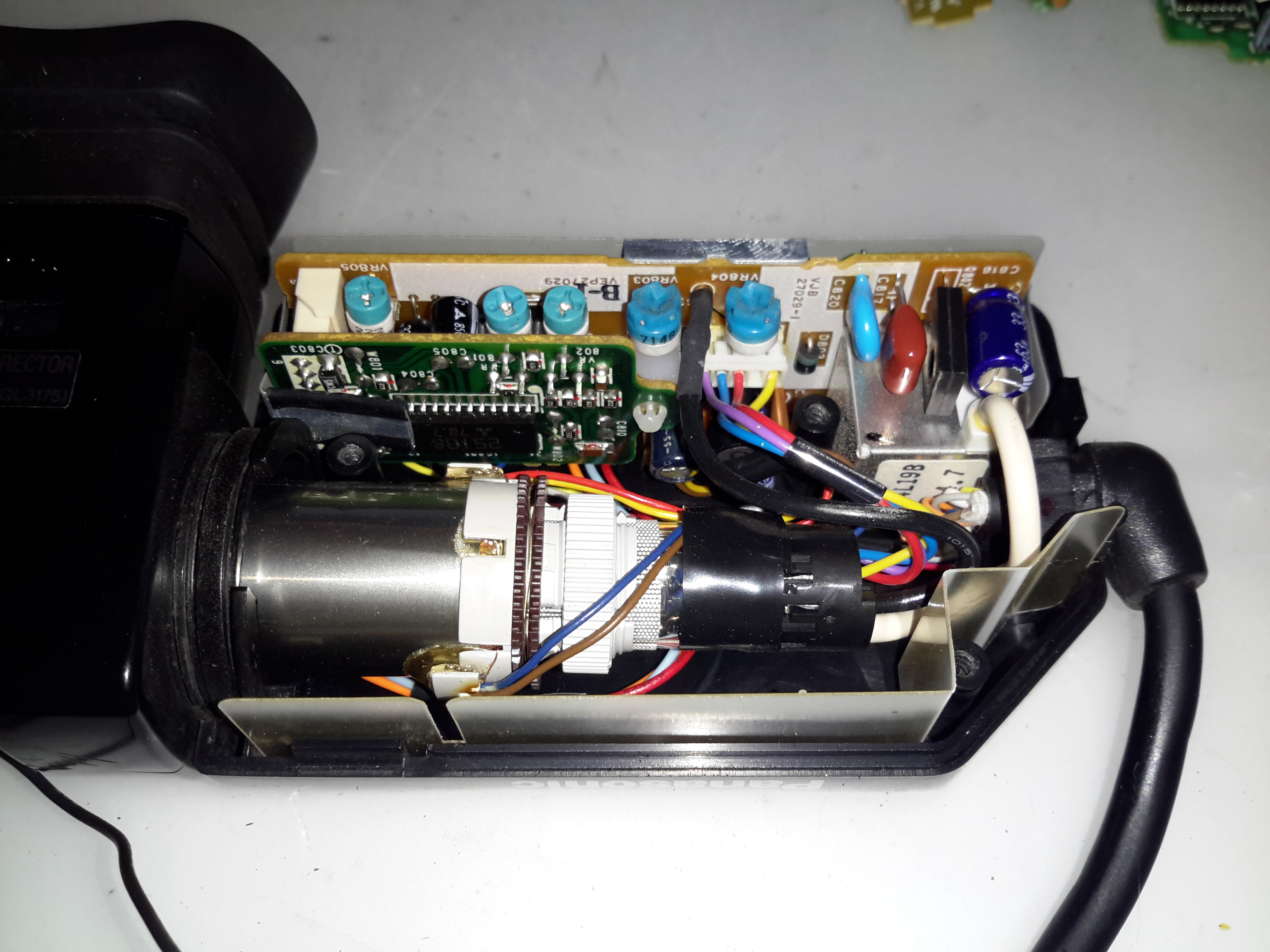
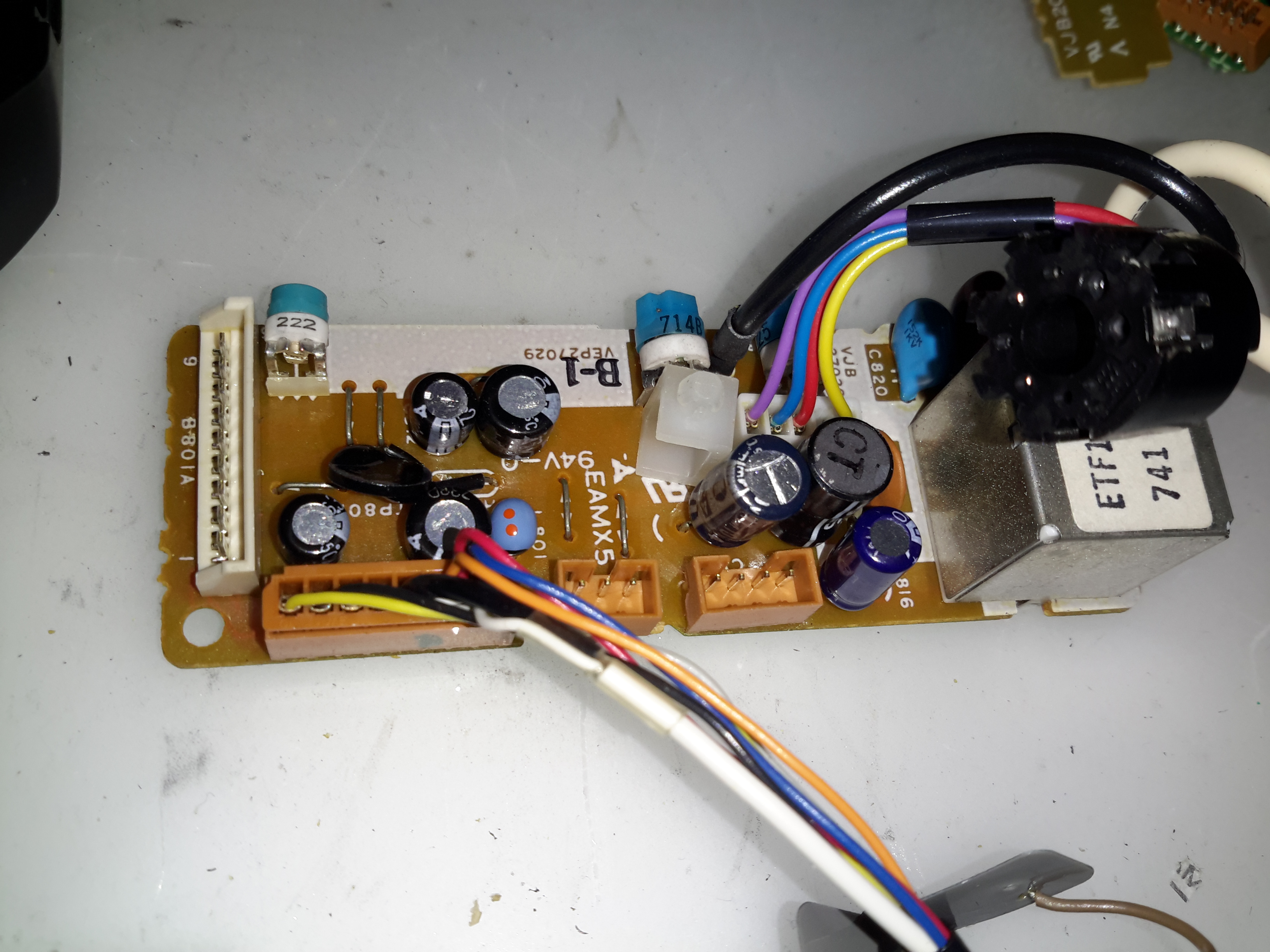
AWB PCB
On the top of the assembly is the Automatic White Balance PCB. Many adjustments here to get everything set right. Not much on the other side of this board other than a bunch of Op-Amps. The iris stepper motor is fitted in a milled opening in the PCB, this connects to one of the other PCBs in the camera module.
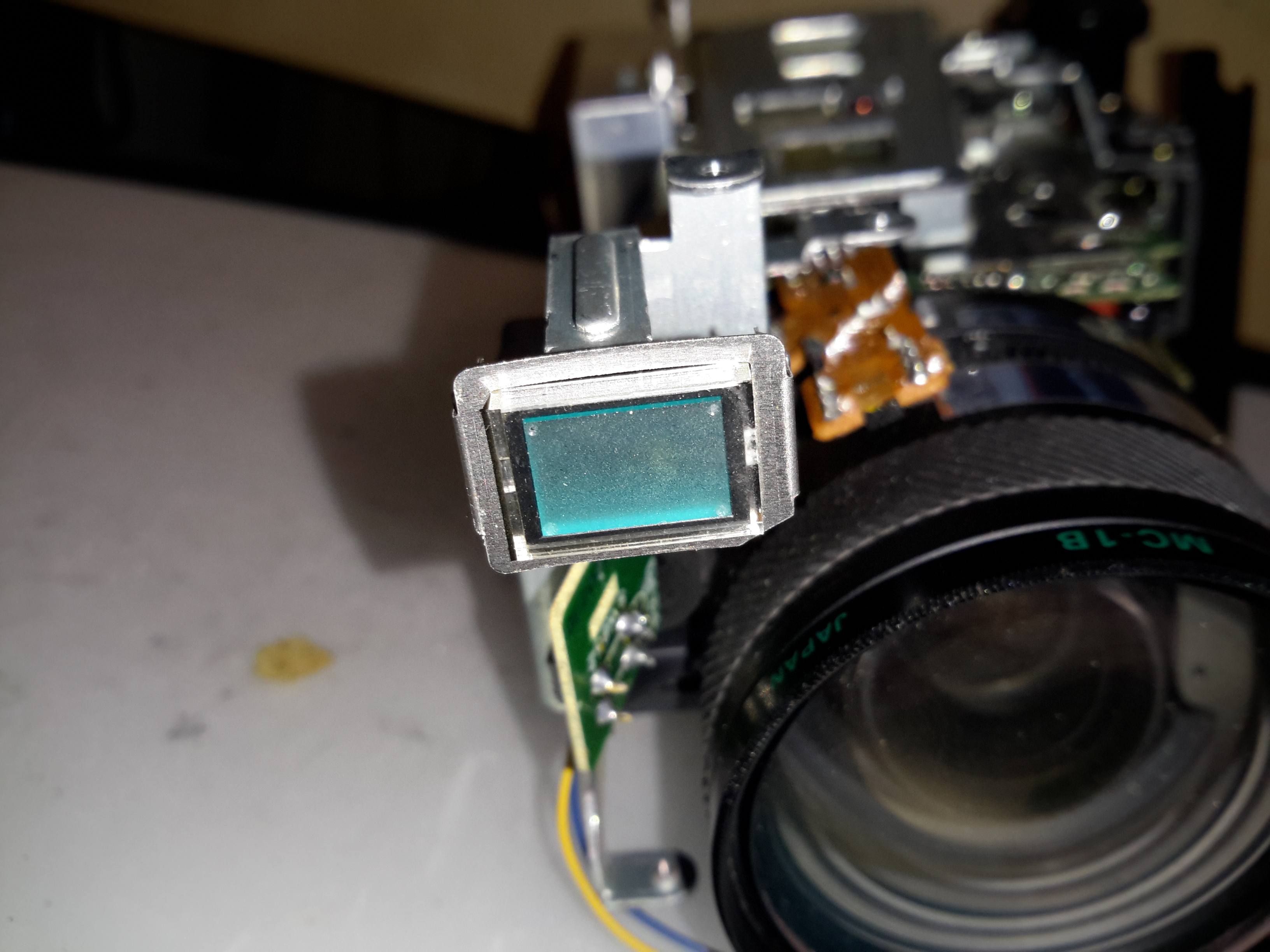
AWB Sensor
Here’s the AWB sensor, mounted next to the lens. I’m not all to certain how this works, but the service manual has the pinout, and there are outputs for all the colour channels, RGB. So it’s probably a trio of photodiodes with filters.
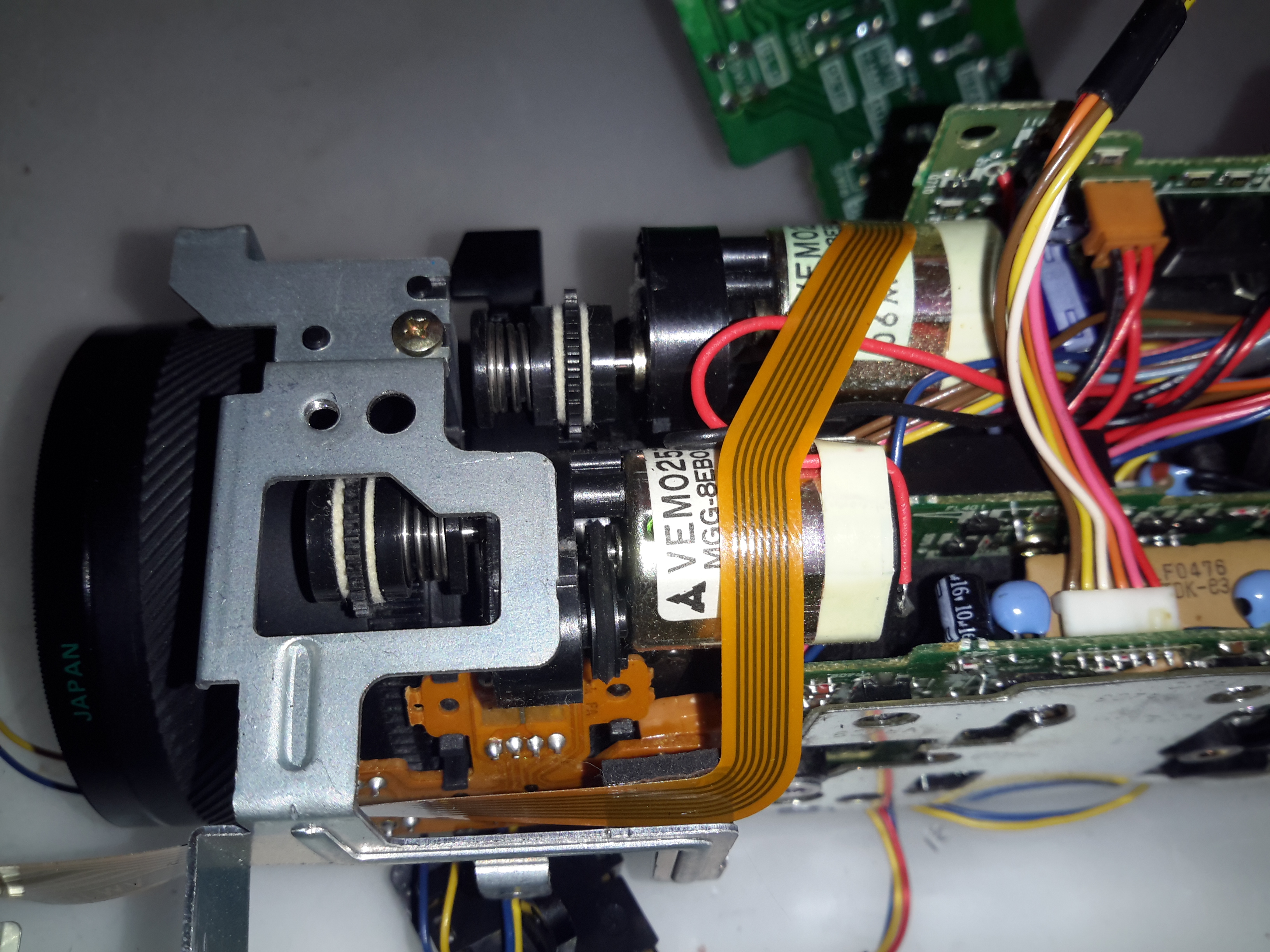
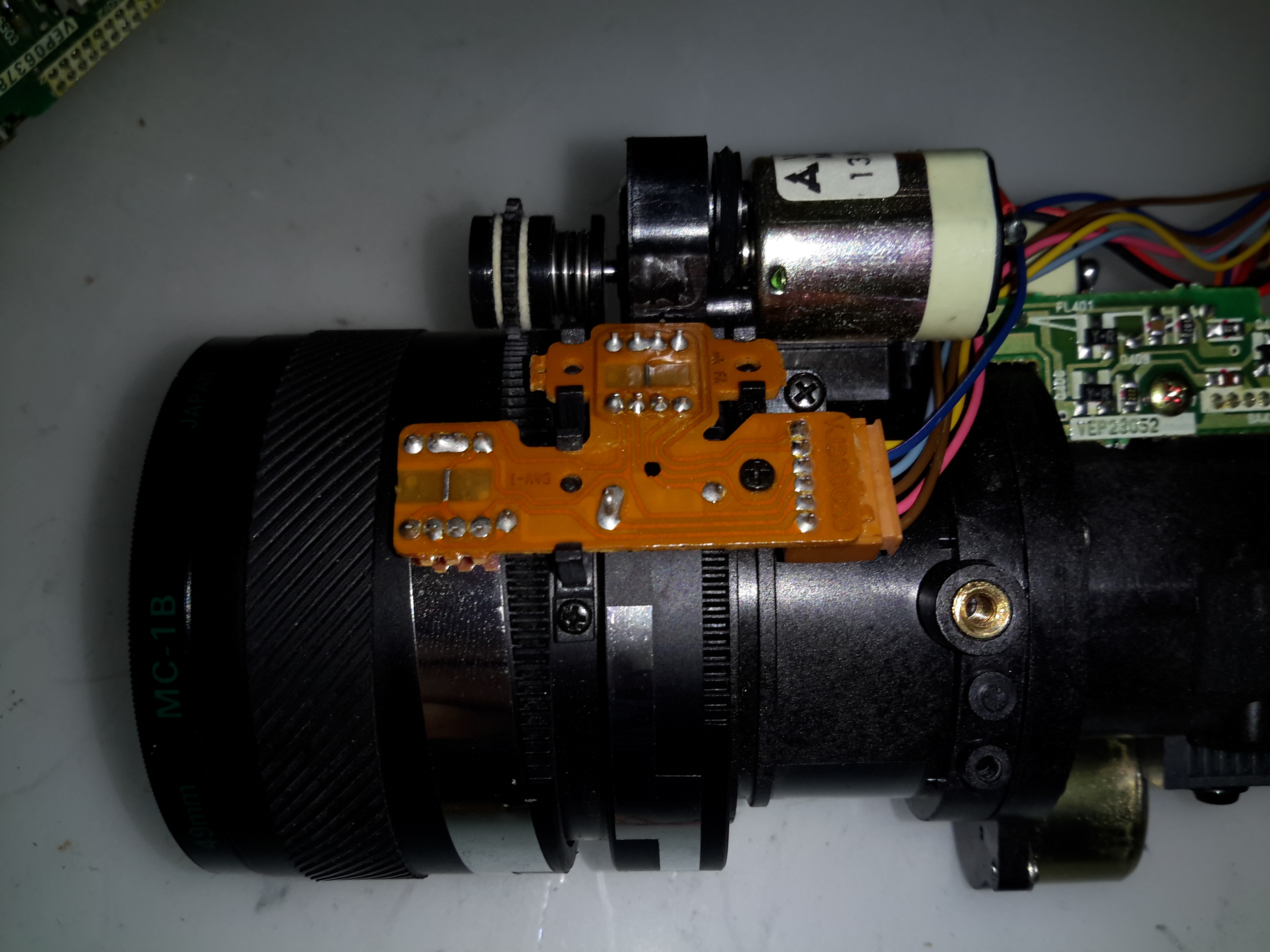
Focus & Zoom Motors
Focus & Zoom are controlled with a pair of DC gear motors. The manual operation is feasible through the use of slip clutches in the final drive pinion onto the lens barrel.
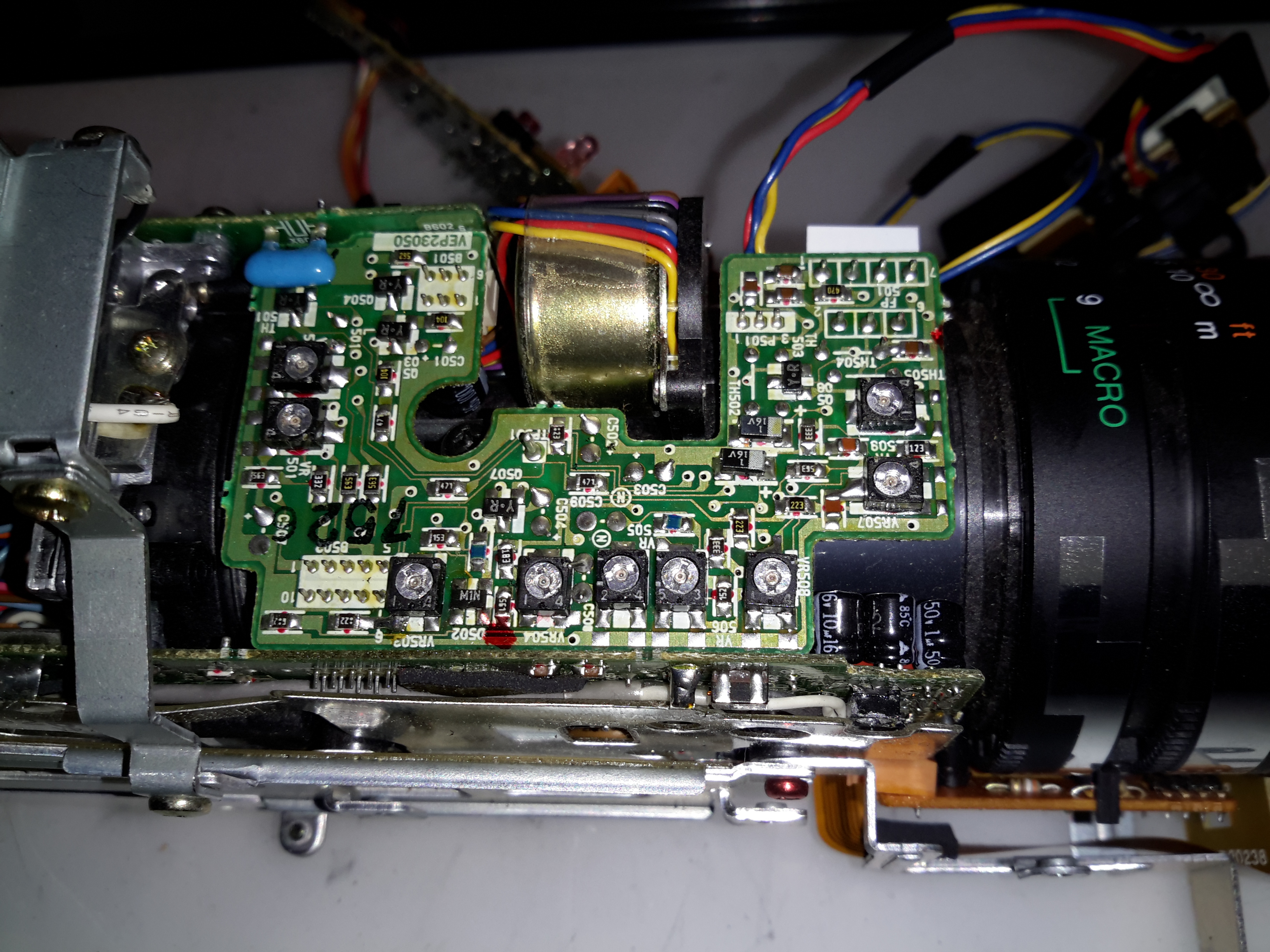
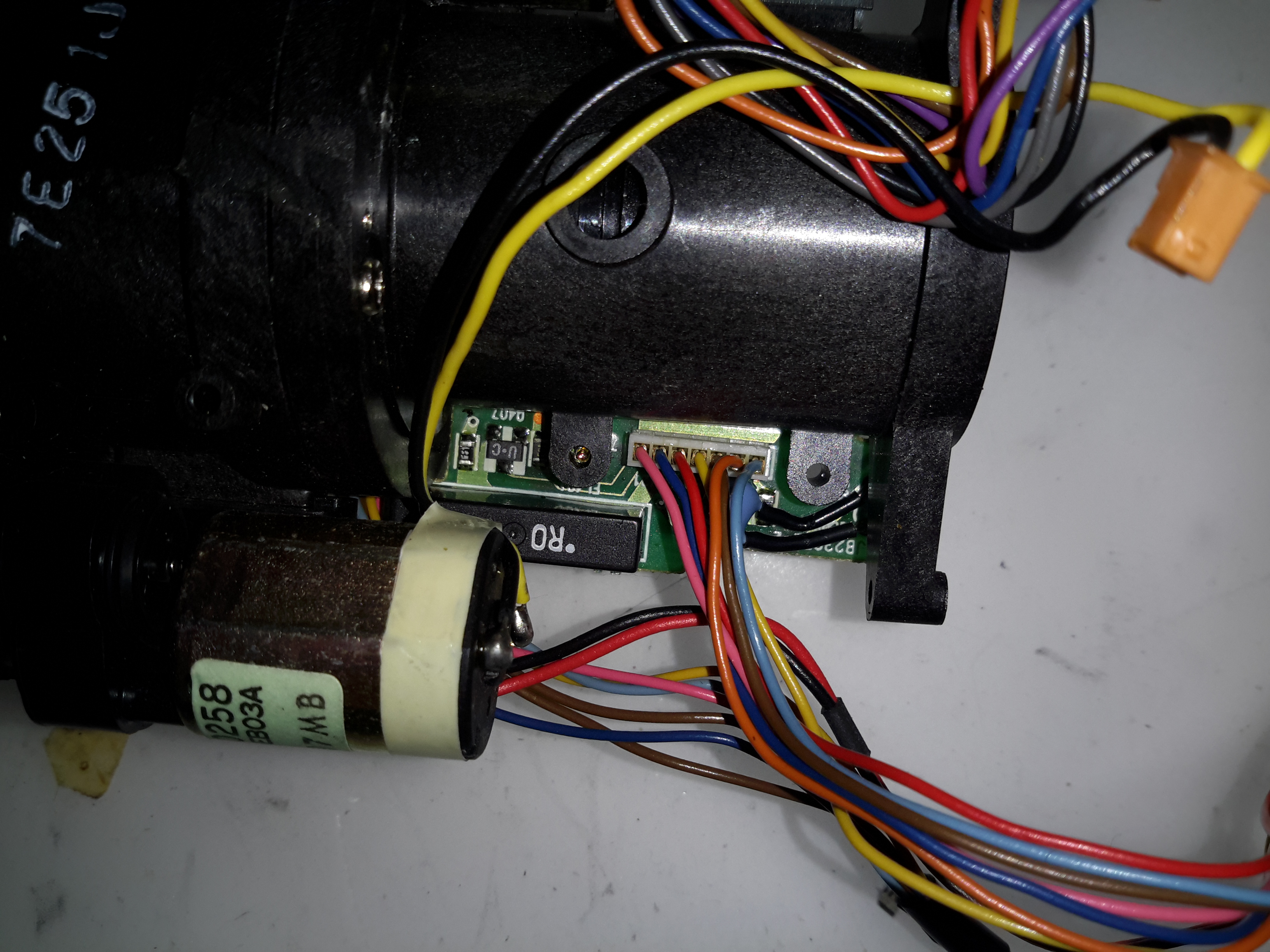
Process Board
The main camera section process board is above. This board does all the signal processing for the CCD, has the bias voltage supplies and houses the control sections for the motorized parts of the optics assembly. There are quite a few dipped Tantalum capacitors on pigtails, instead of being directly board mounted. This was probably done due to space requirements on the PCB itself.
Under the steel shield on this board is some of the main signal processing for the CCD.
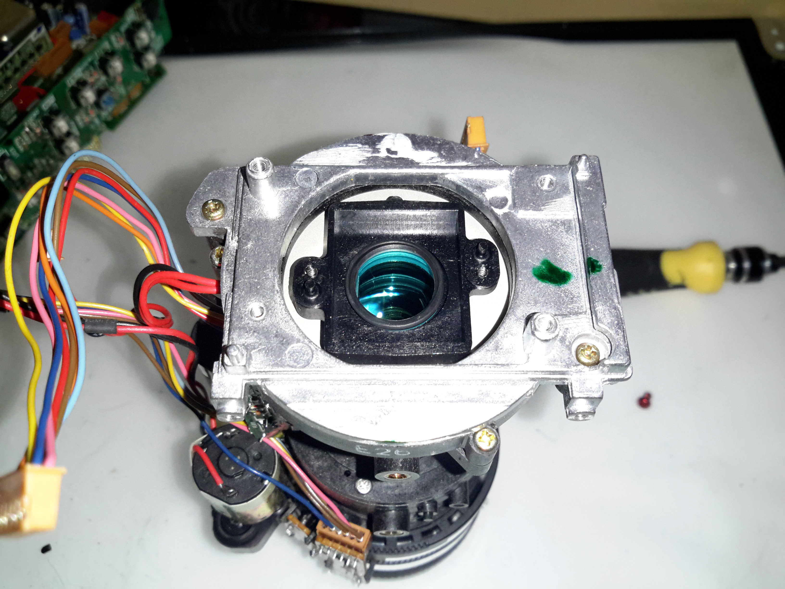
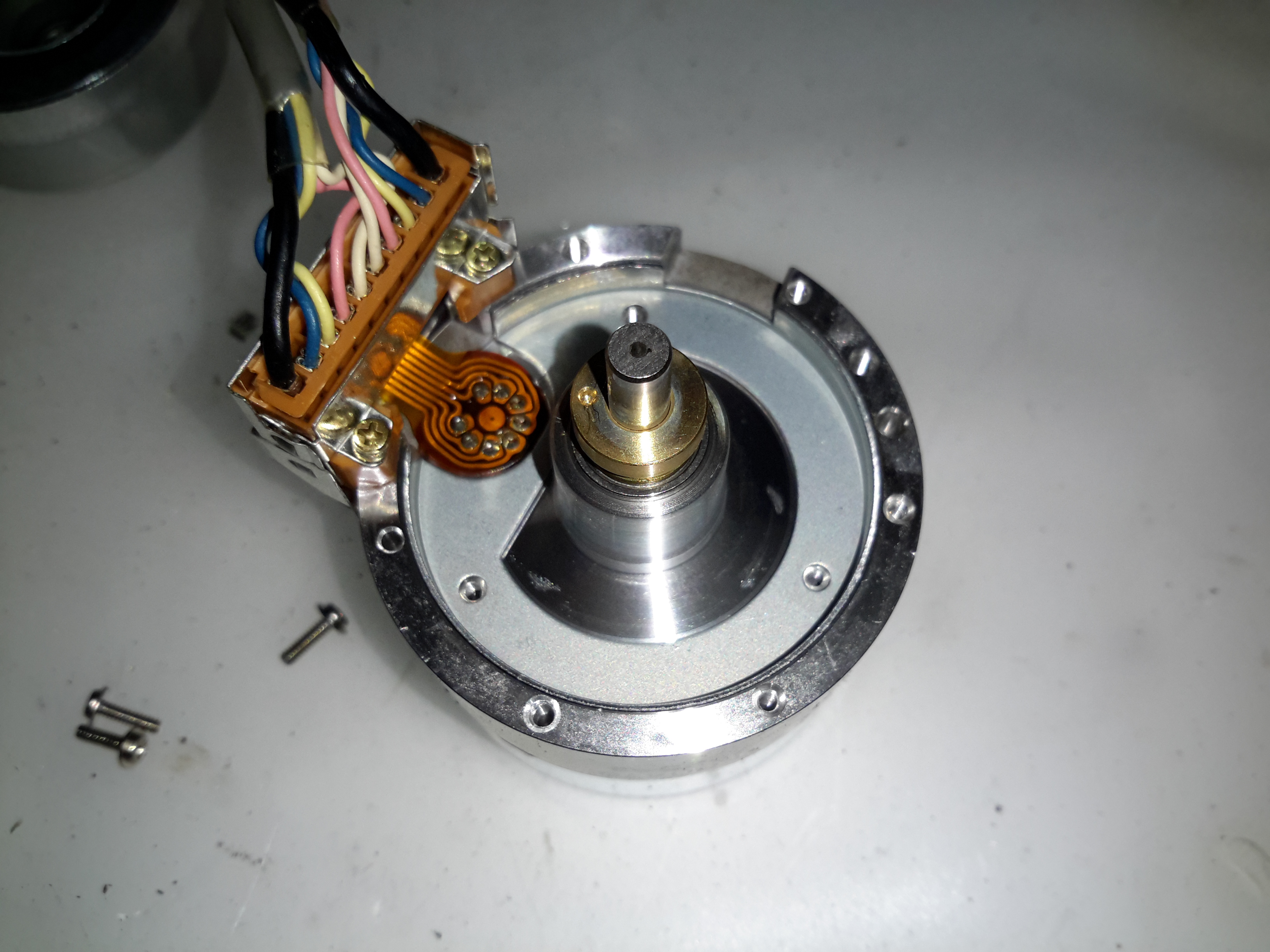
Optics Assembly
The back of the optics tube is a heavy casting, to supress vibration. This will be more clear later on.
Position Sensor Flex
The position of the lens elements is determined by reflective strips on the barrel & sensors on this flex PCB.
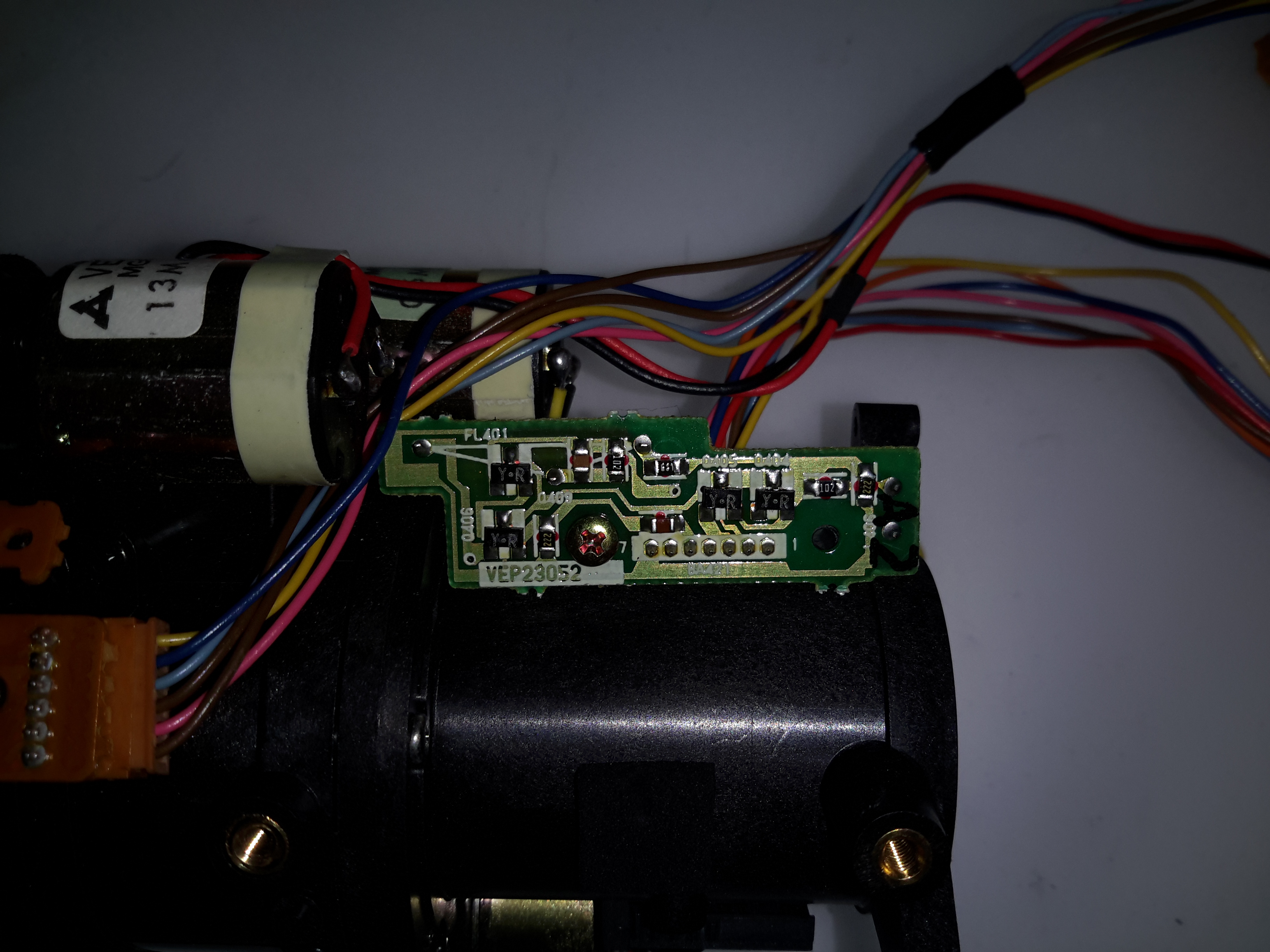
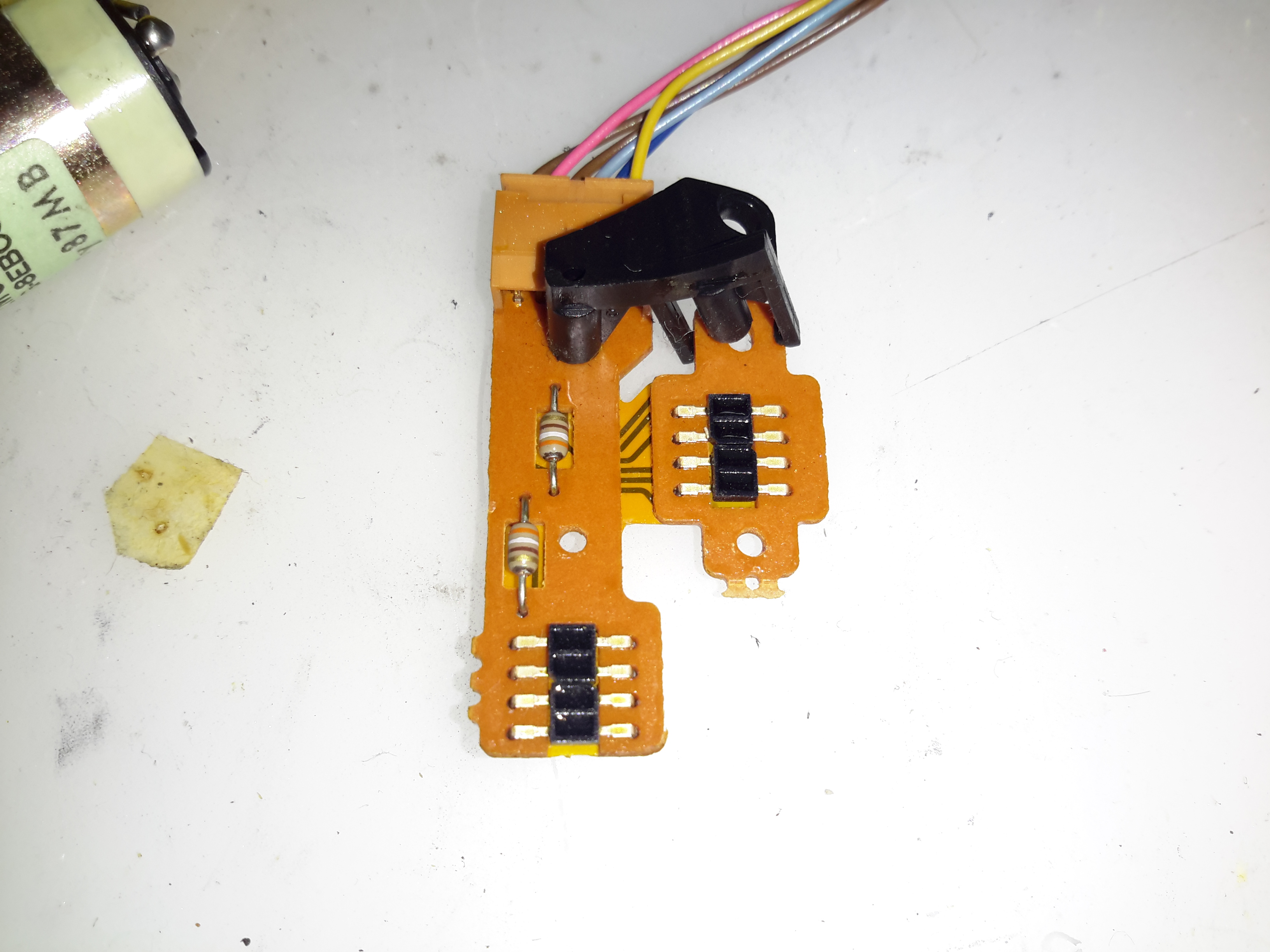
Sub Process Board
There’s another small board tucked into the side of the tube, this hooks into the process PCB.
Process Delay Line
According to the schematic, there’s nothing much on this board, just a delay line & a few transistors.
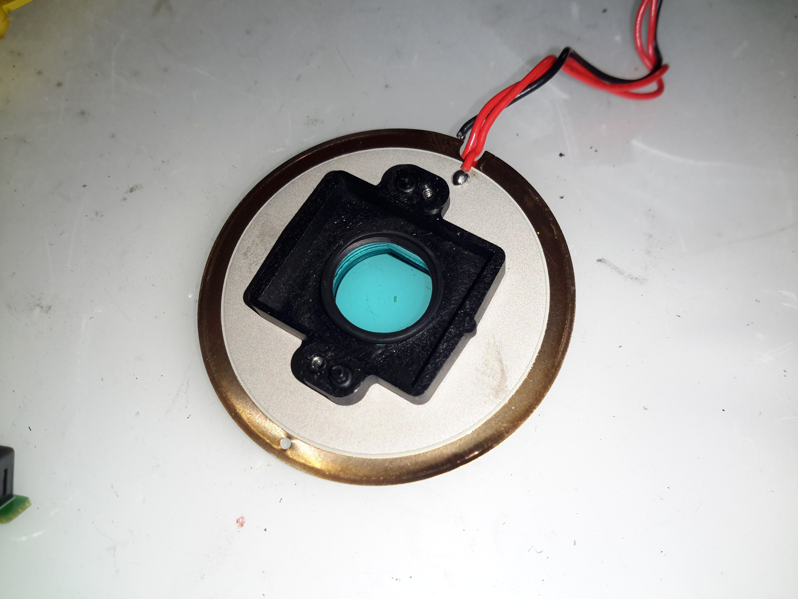
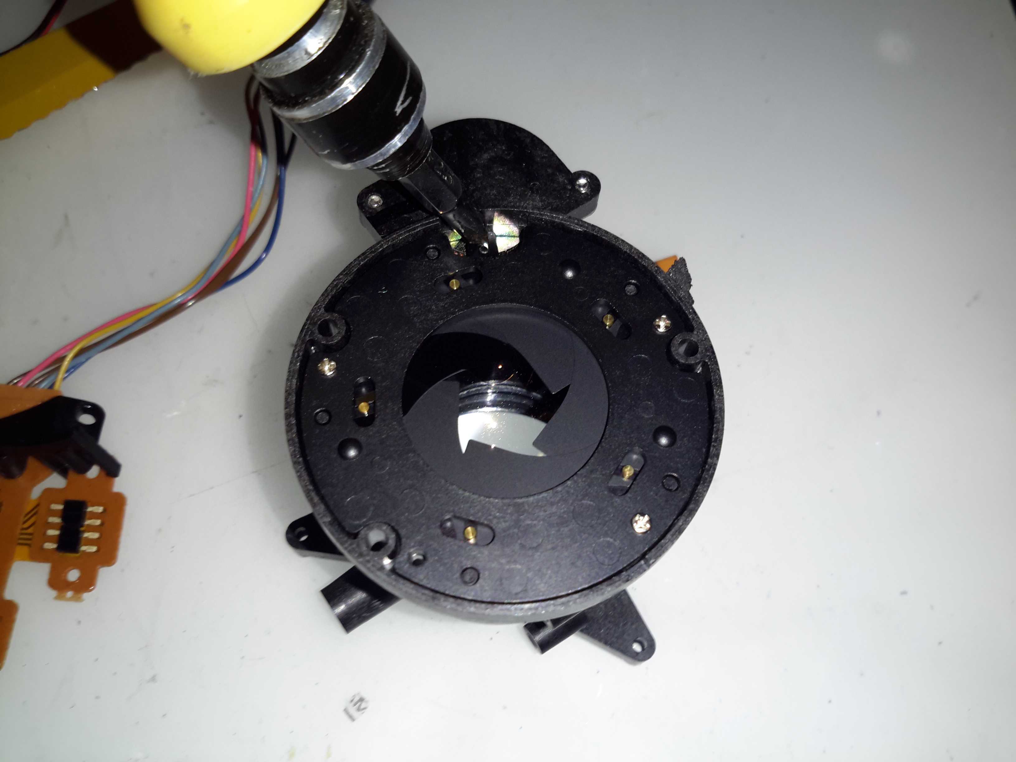
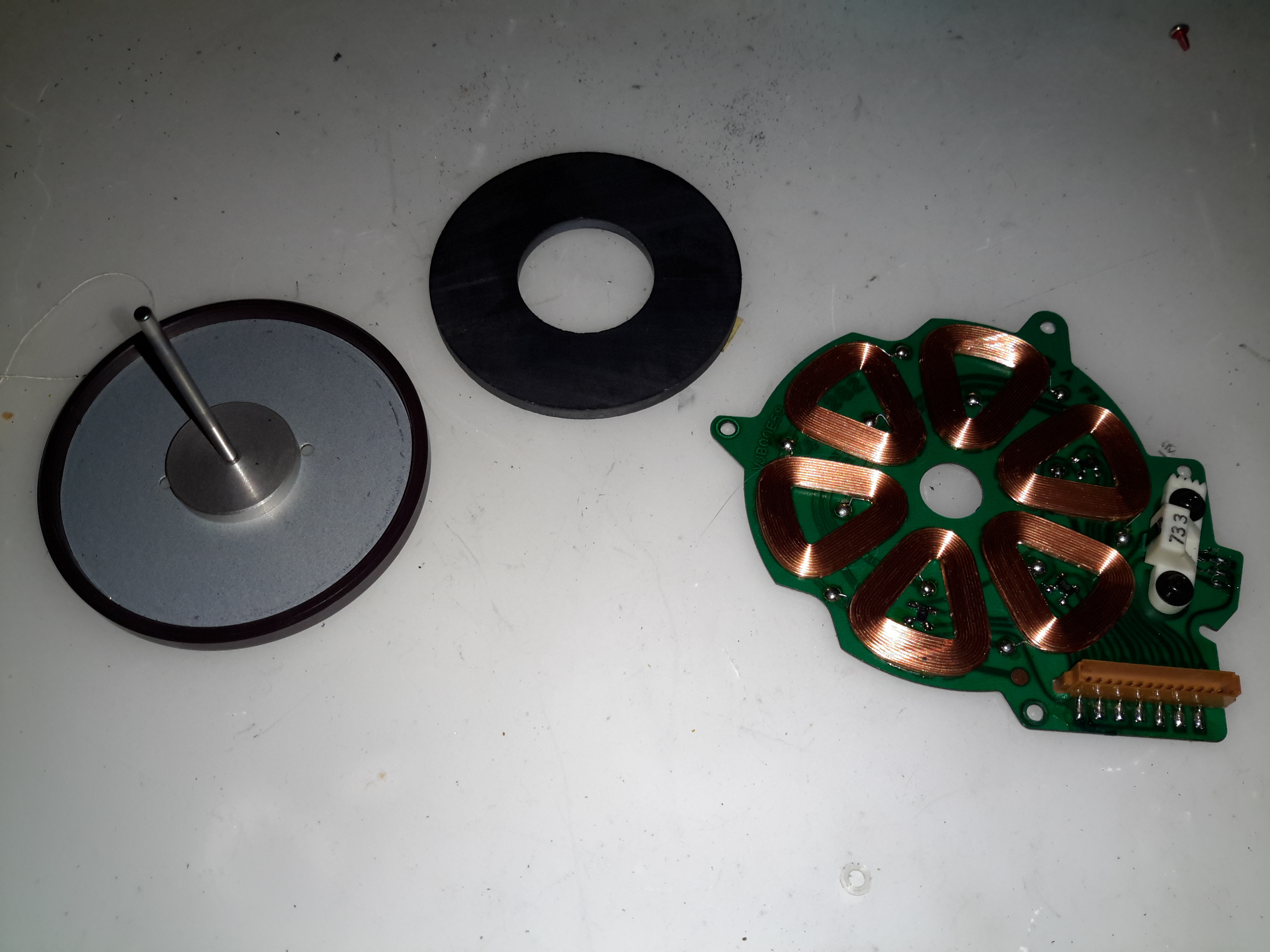
Piezo Focus Disc
Here’s the reason for the heavy alloy casing at the CCD mounting end of the optics: the fine focus adjustment is done with a piezoelectric disc, the entire CCD assembly is mounted to this board. Applying voltage to the electrodes moves the assembly slightly to alter the position of the CCD. The blue glass in the centre of the unit is the IR filter.
IR Relective Sensors
The barrel position sensors are these IR-reflective type.
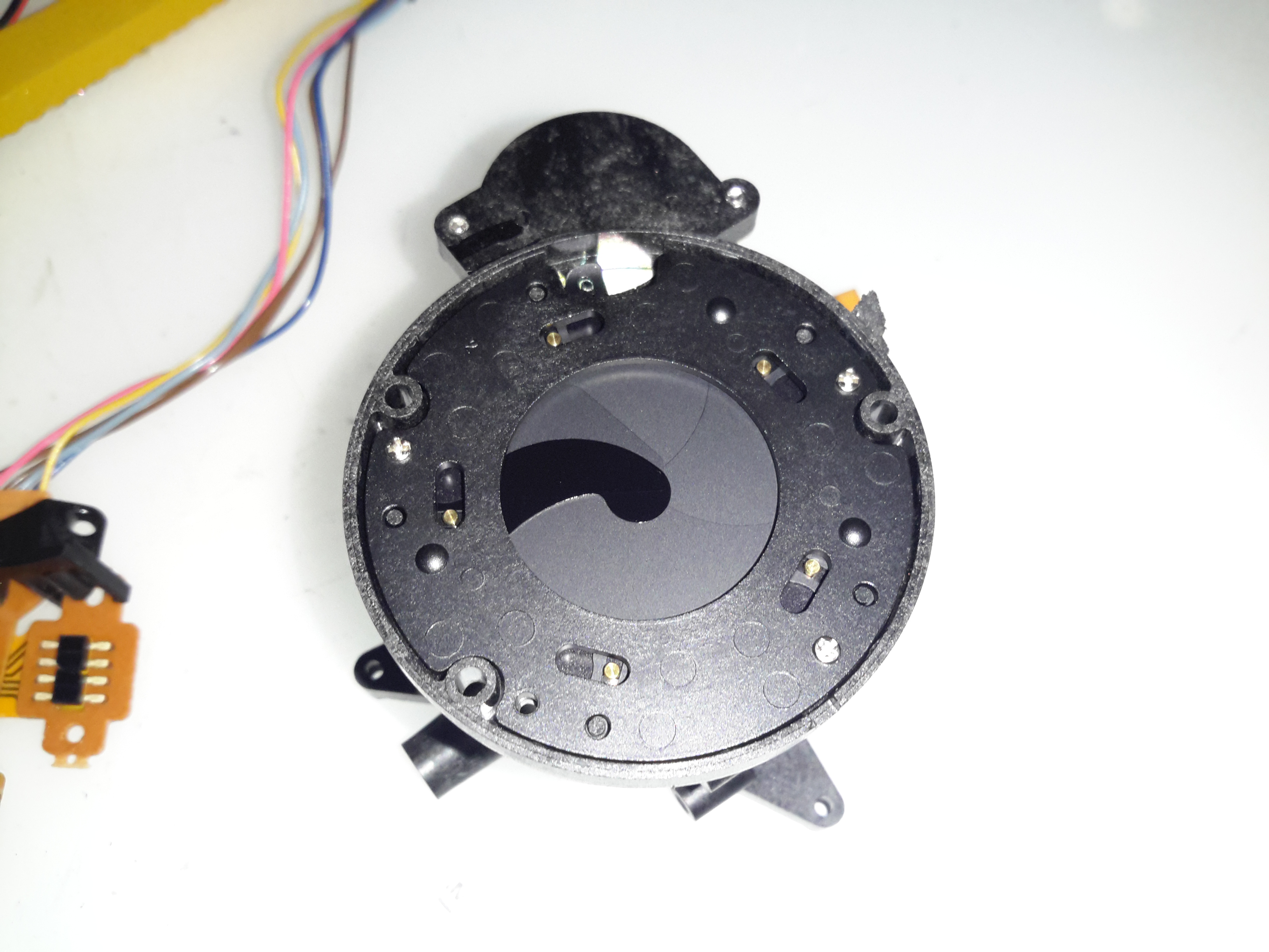
Iris Assembly
The iris is mounted just before the CCD, this is controlled with a galvanometer-type device with position sensors incorporated.
Iris Opening
Pushing on the operating lever with the end of my screwdriver opens the leaves of the iris against the return spring.
Tape Transport & Main Control
Main Control Board
Tucked into the side of the main body of the unit is the main system control board. This PCB houses all the vital functions of the camera: Power Supply, Servo Control, Colour Control,Video Amplifiers, etc.
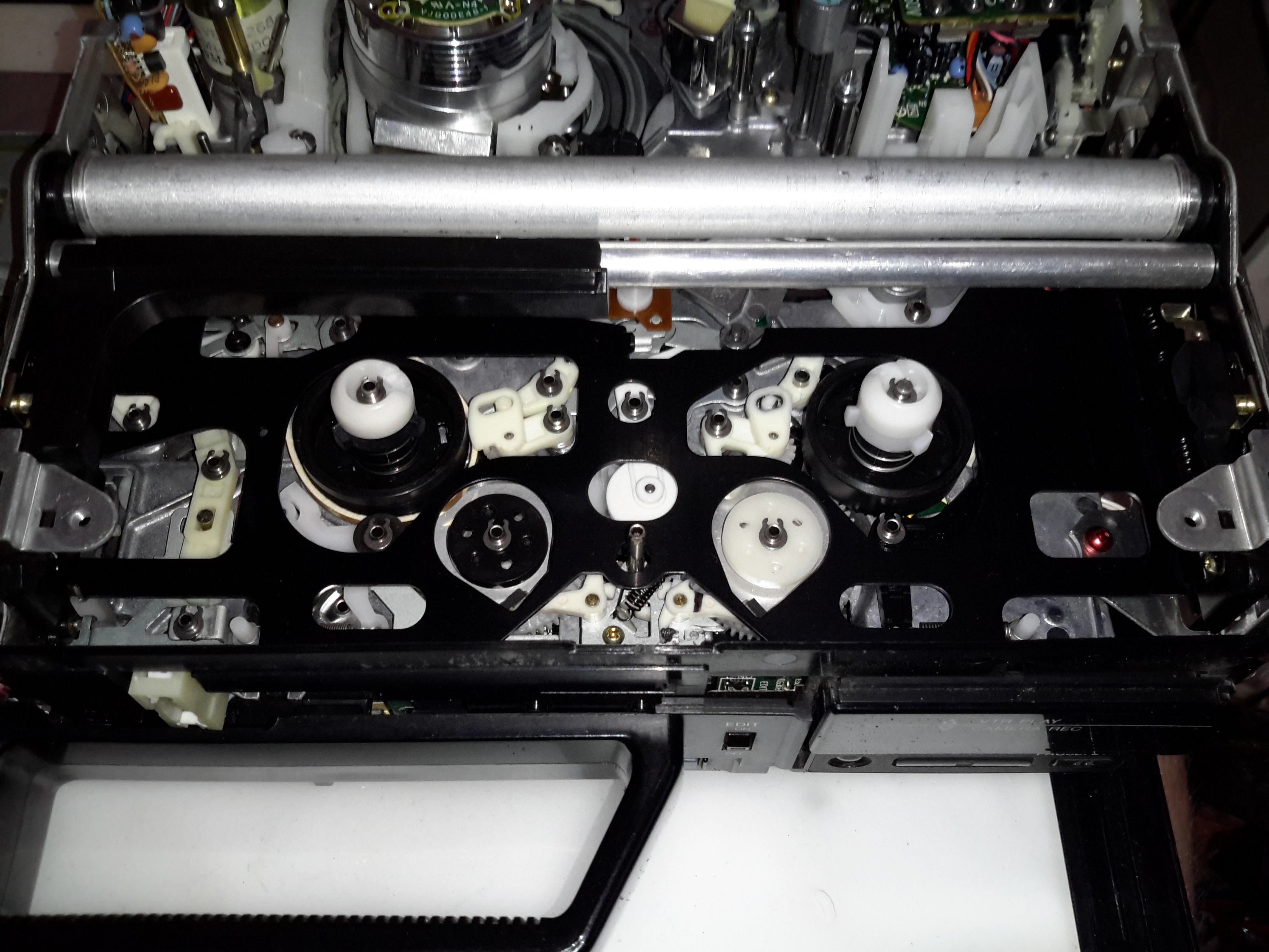
Tape Drum
Here’s the main tape transport mechanism, this is made of steel & aluminium stampings for structural support. The drum used in this transport is noticeably smaller than a standard VHS drum, the tape is wrapped around more of the drum surface to compensate.
Tape Transport
The VHS tape sits in this carriage & the spools drive the supply & take up reels in the cartridge.
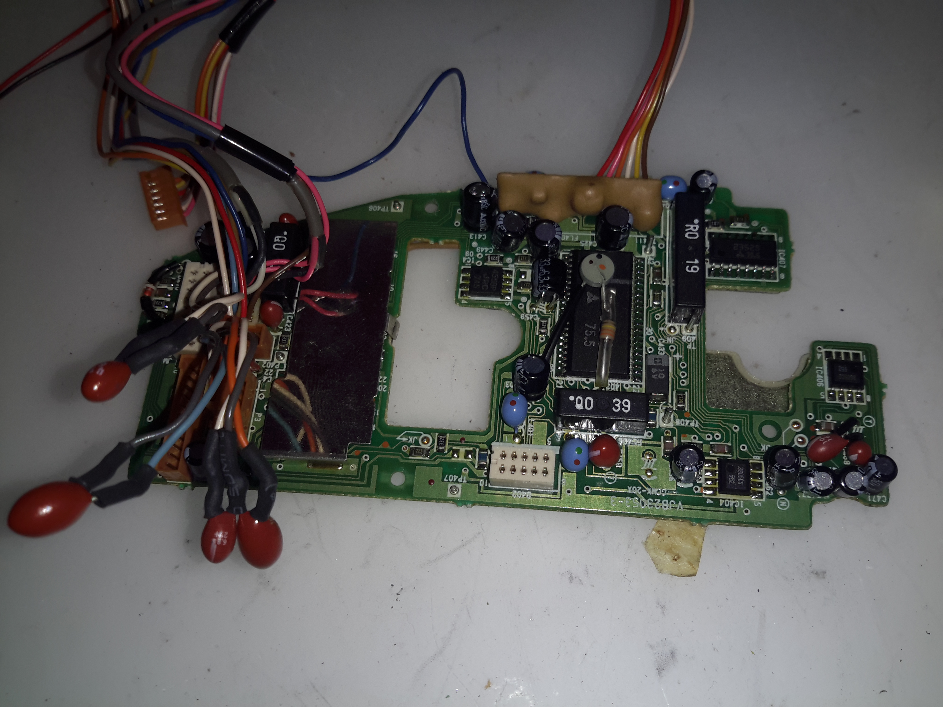
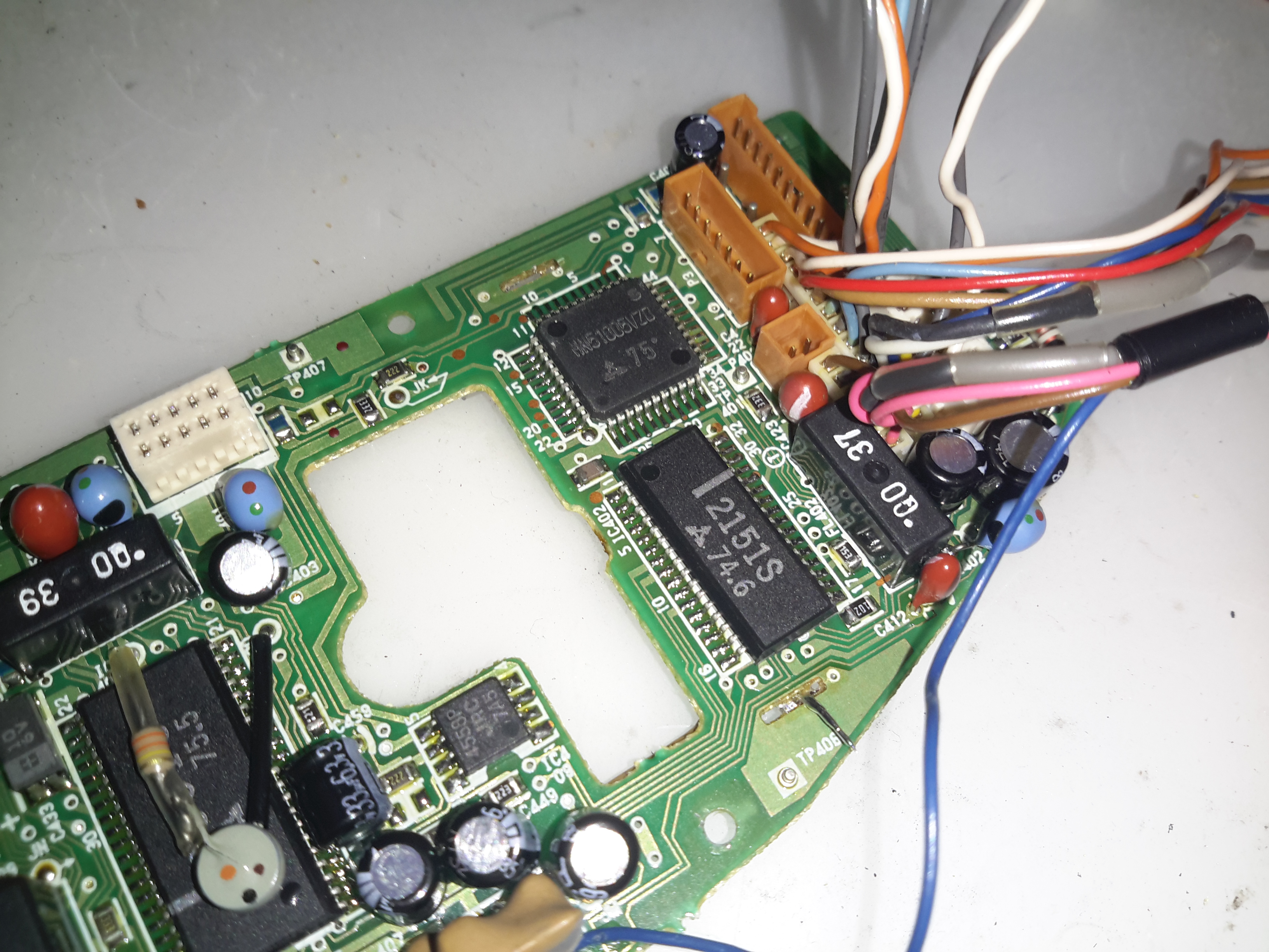
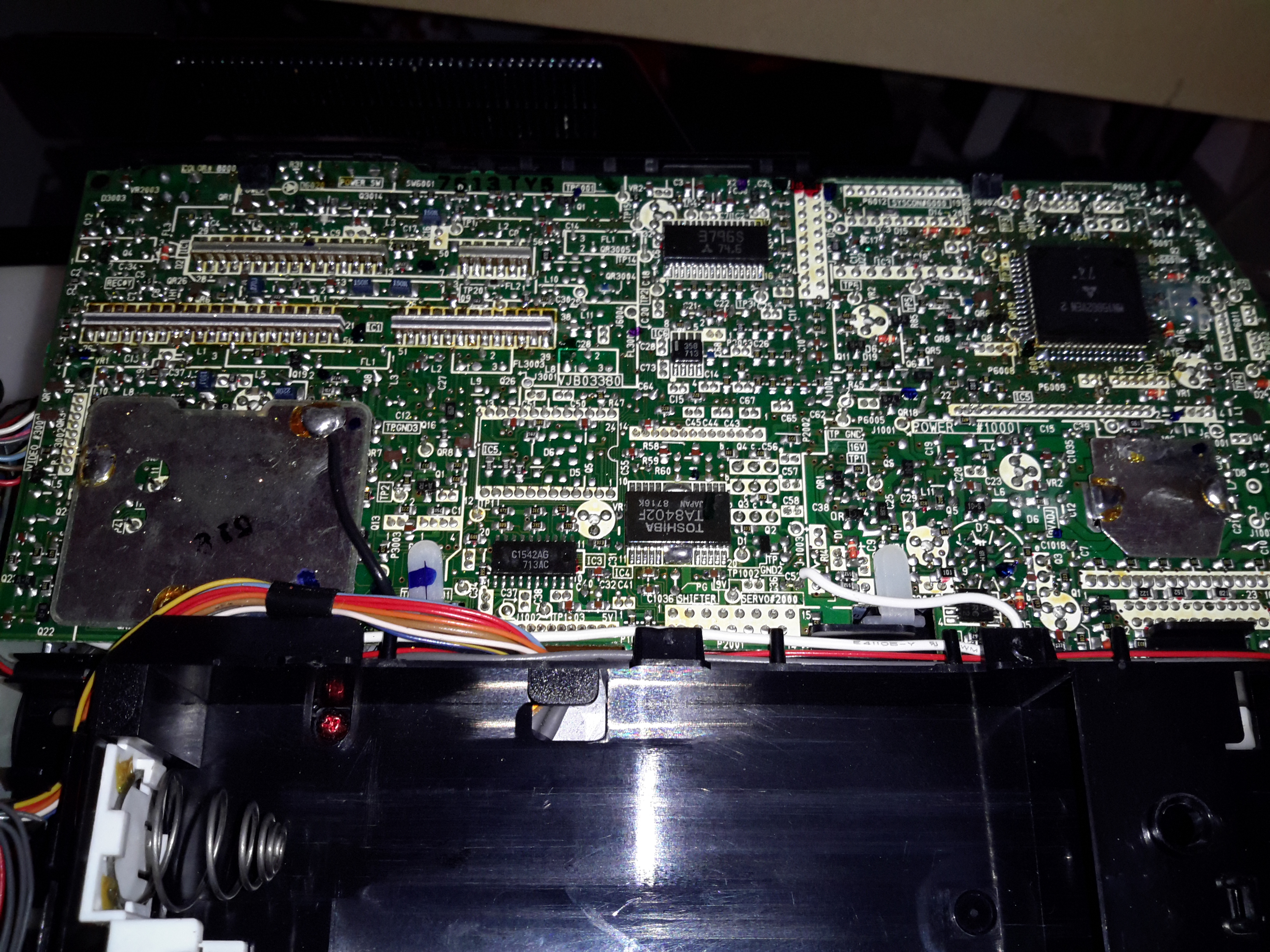
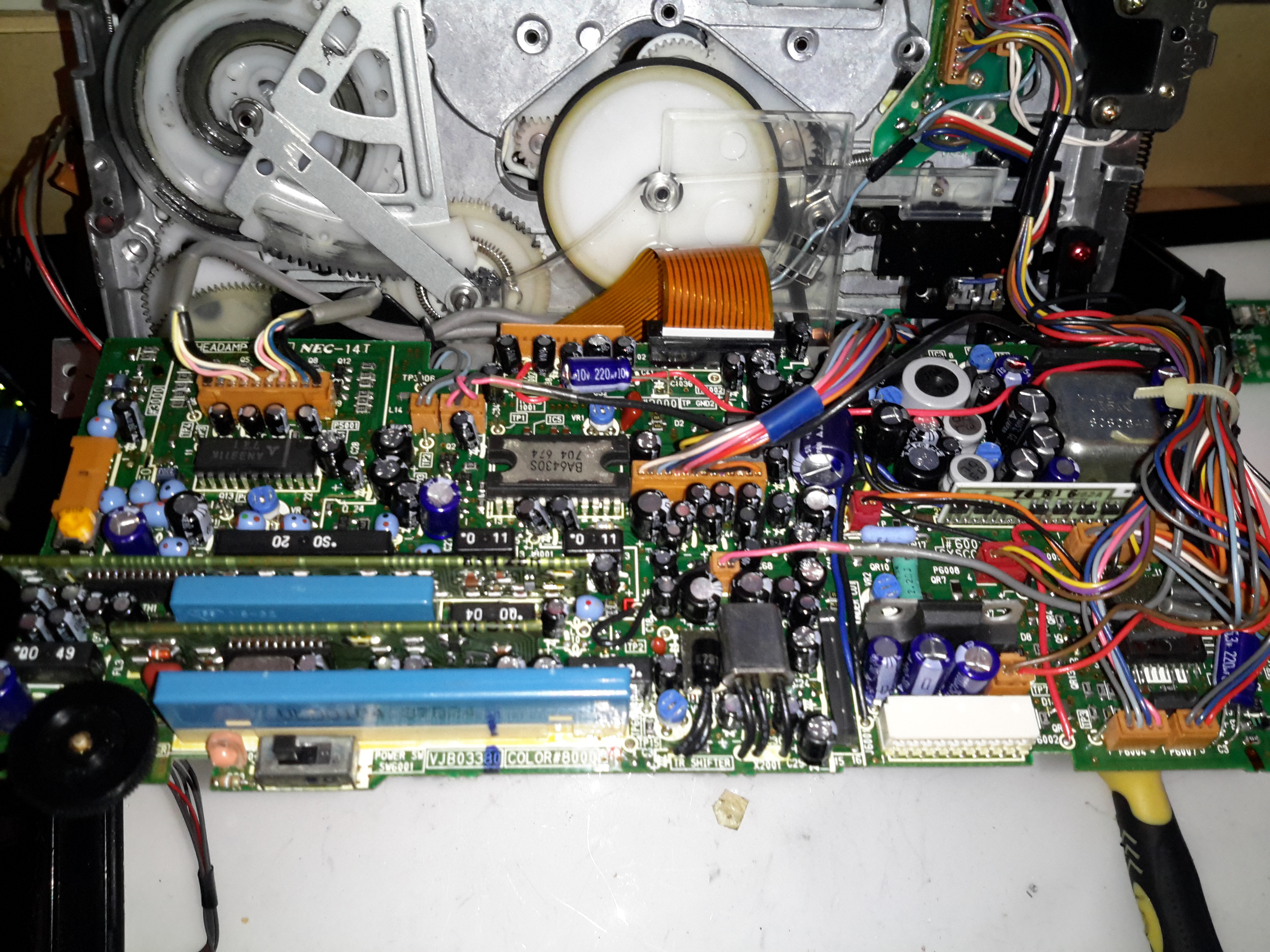
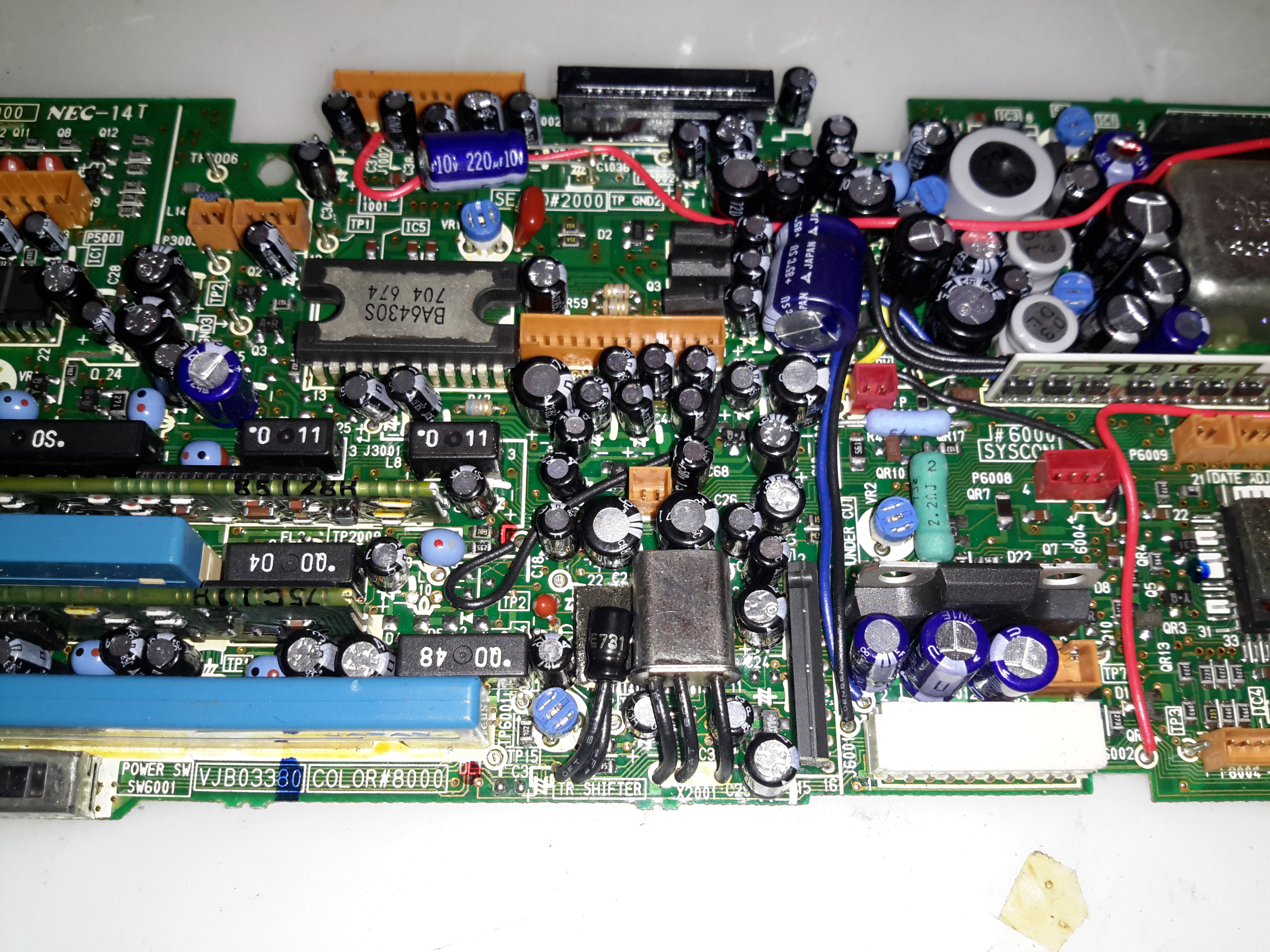
Main Control PCB
Here’s the component side of the main control PCB. This one is very densely packed with parts, I wouldn’t like to try & troubleshoot something like this!
Main PCB Left
The left side has the video head amp at the top, a Panasonic AN3311K 4-head video amp. Below that is video processing, the blue components are the analogue delay lines. There are a couple of hybrid flat-flex PCBs tucked in between with a couple of ICs & many passives. These hybrids handle the luma & chroma signals.
Top left is the capstan motor driver a Rohm BA6430S. The transport motors are all 3-phase brushless, with exception of the loading motor, which is a brushed DC type.
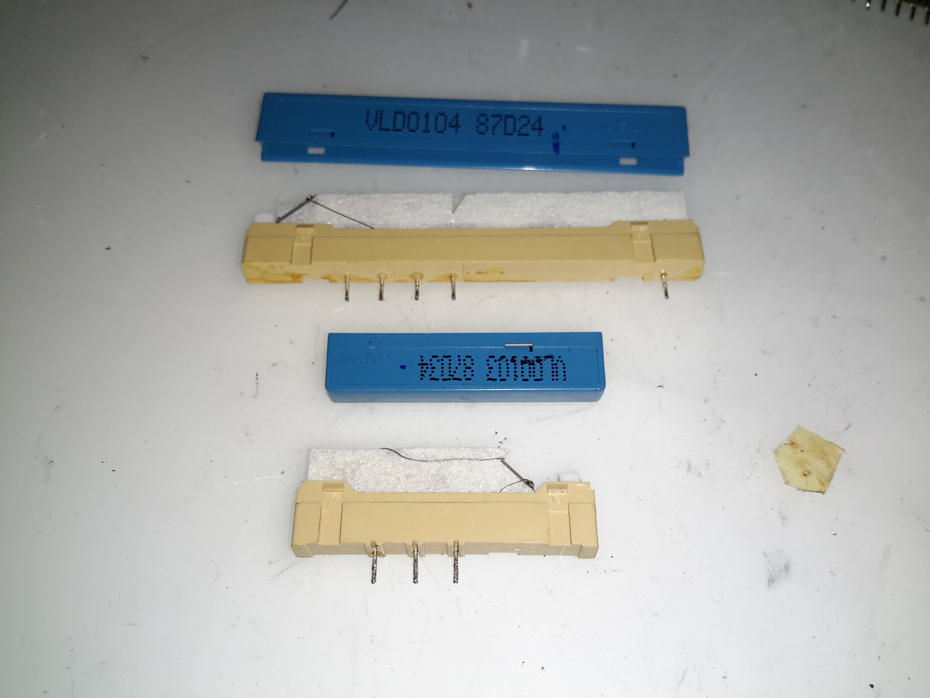
Delay Line
Here’s what is inside the delay lines for the analogue video circuits. The plastic casing holds a felt liner, inside which is the delay line itself.
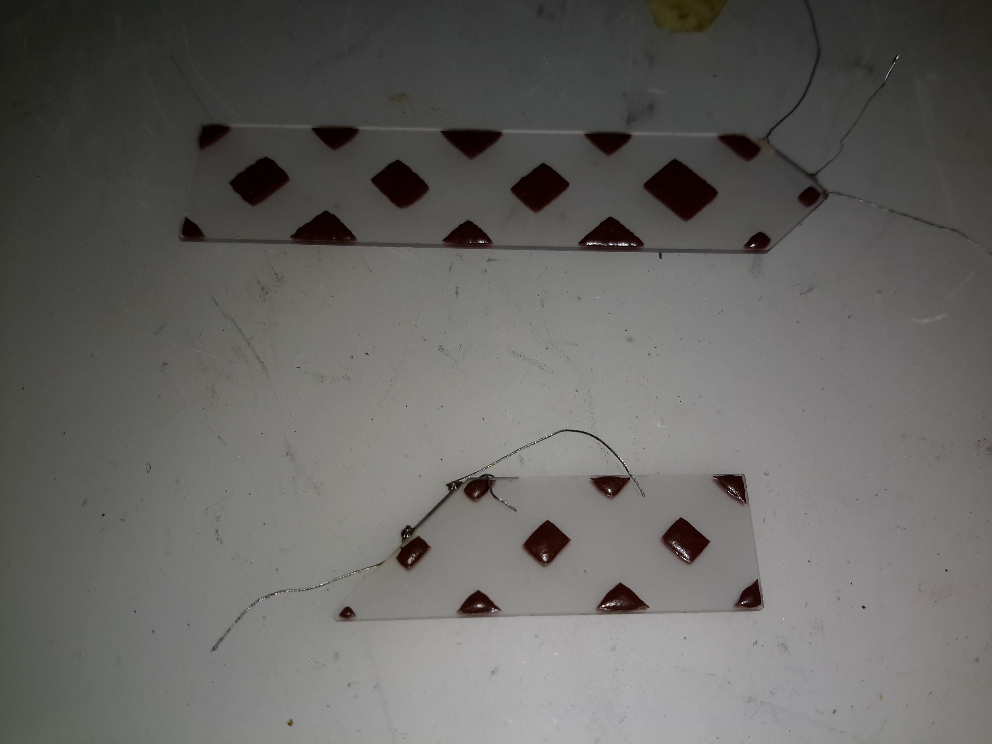
Internal Glass
The delay is created by sending an acoustic signal through the quartz crystal inside the device by a piezoelectric transducer, bouncing it off the walls of the crystal before returning it to a similar transducer.
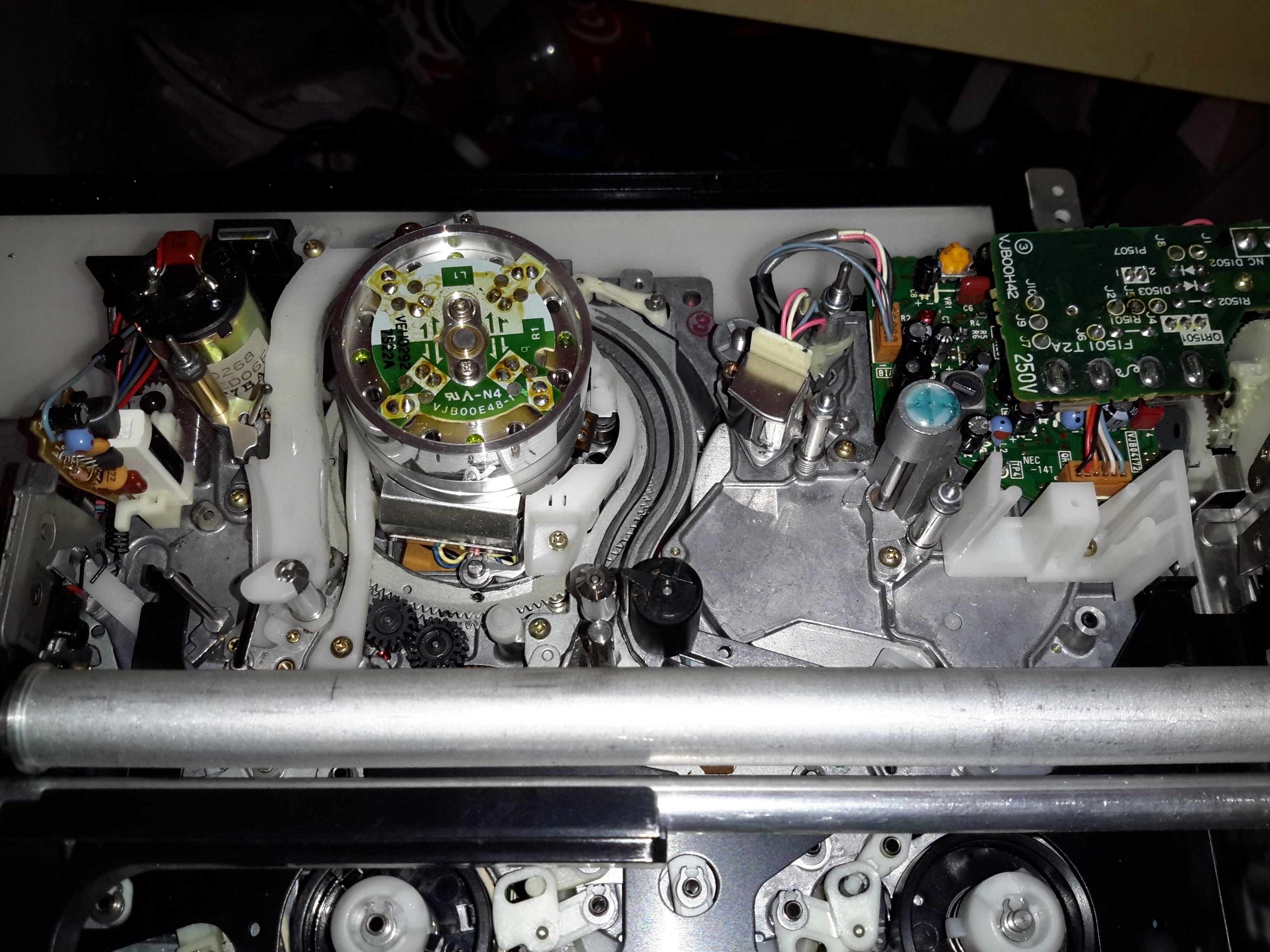
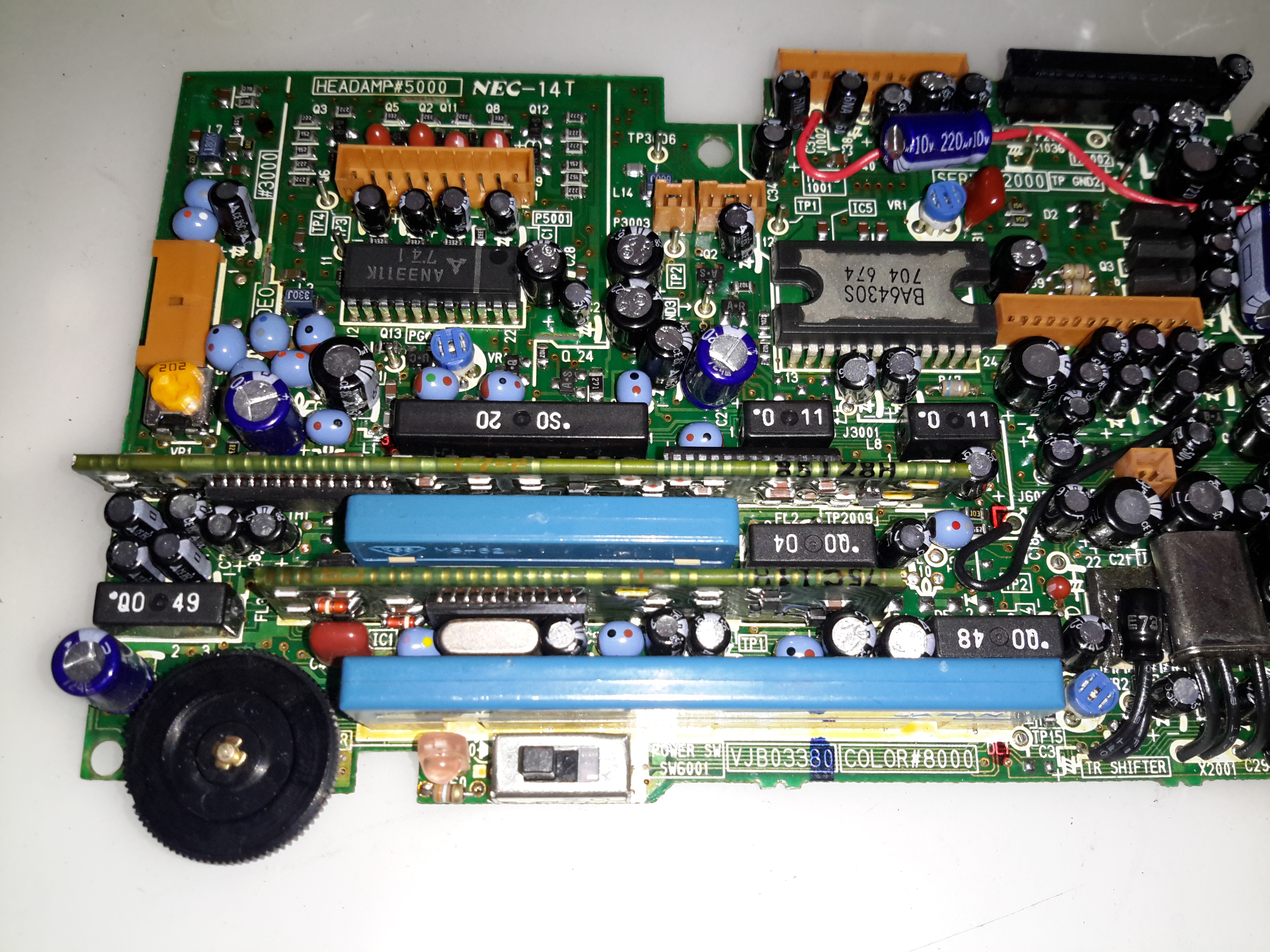
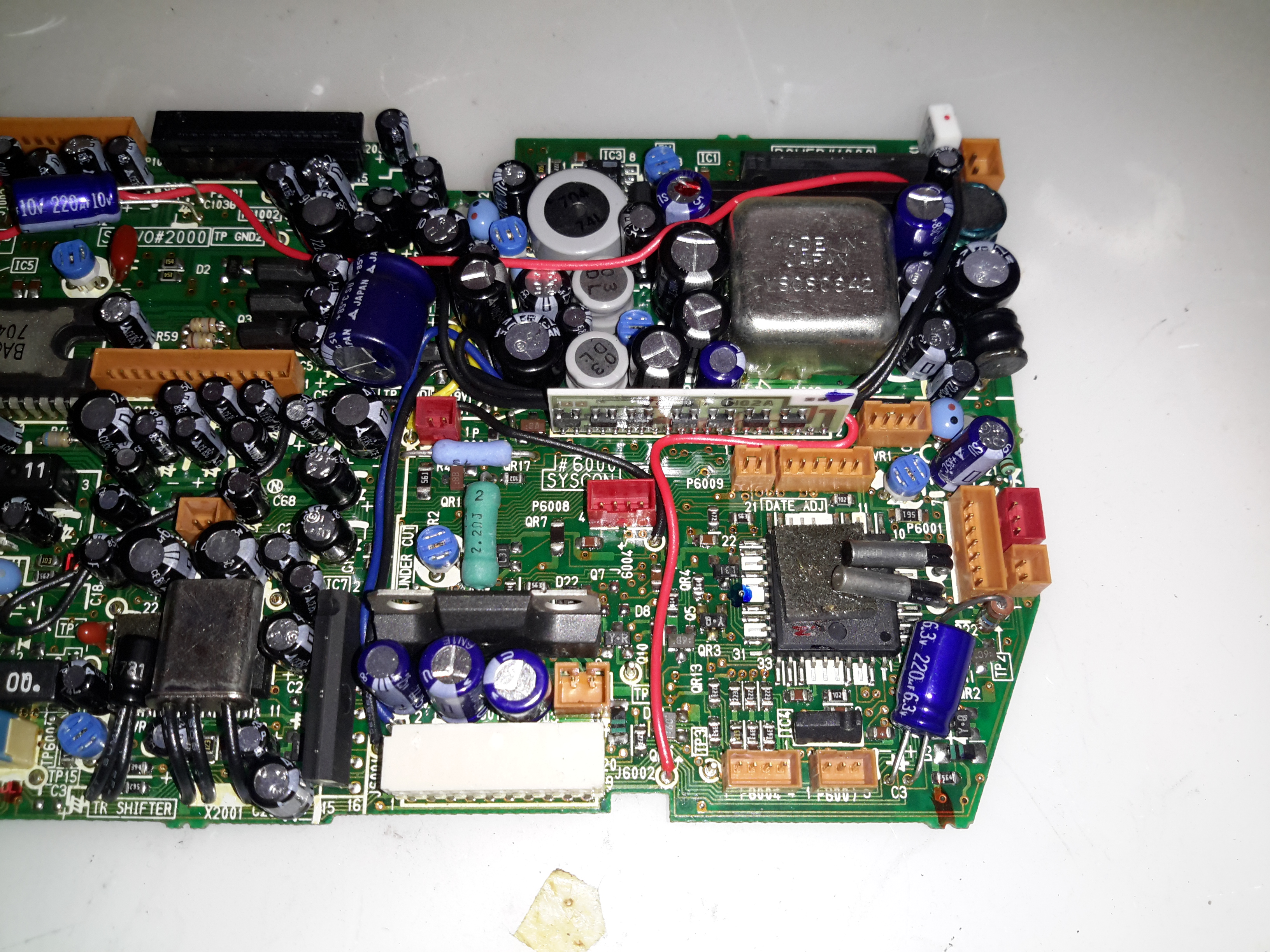
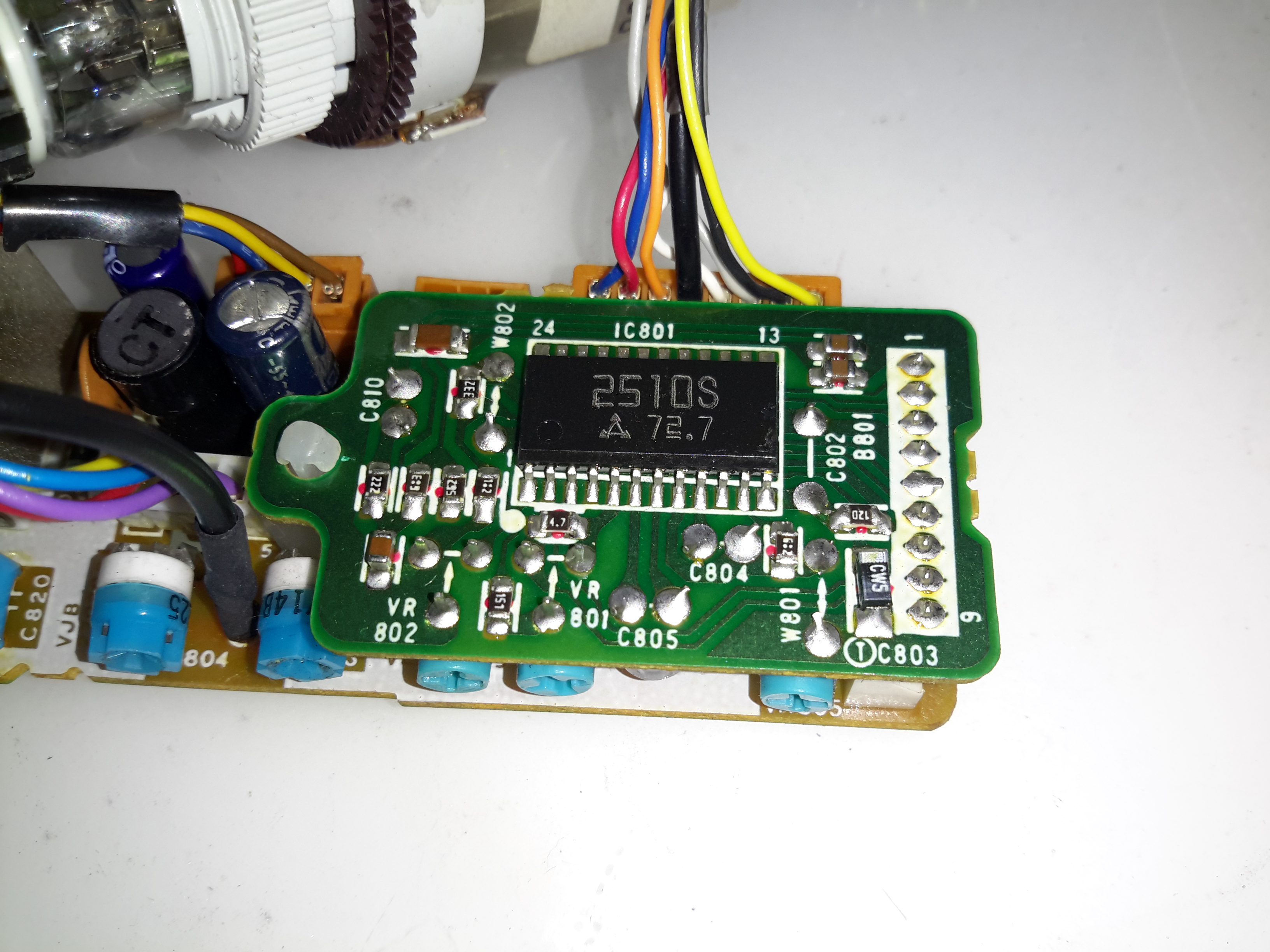
Main PCB Centre
Here’s the centre of the board, the strange crystal at bottom centre is the clock crystal for the head drum servo. Why it has 3 pins I’m not sure, only the two pins to the crystal inside are shown connected on the schematic. Maybe grounding the case?
The main servo controls for the head drum & the capstan motor are top centre, these get a control signal from the tape to lock the speed of the relative components.
Main PCB Right
Here’s the right hand side. The main power supply circuitry is at top right, with a large can containing 4 switching inductors & a ferrite pot core transformer. All these converters are controlled by a single BA6149 6-channel DC-DC converter controller IC via a ULN2003 transistor array.
The ceramic hybrid board next to the PSU has 7 switch transistors for driving various indicator LEDs.
The large tabbed IC bottom centre is the loading motor drive, an IC from Mitsubishi, the M54543. This has bidirectional DC control of the motor & built in braking functions. The large quad flat pack IC on the right is the MN1237A on-screen character generator, with the two clock crystals for the main microcontroller.
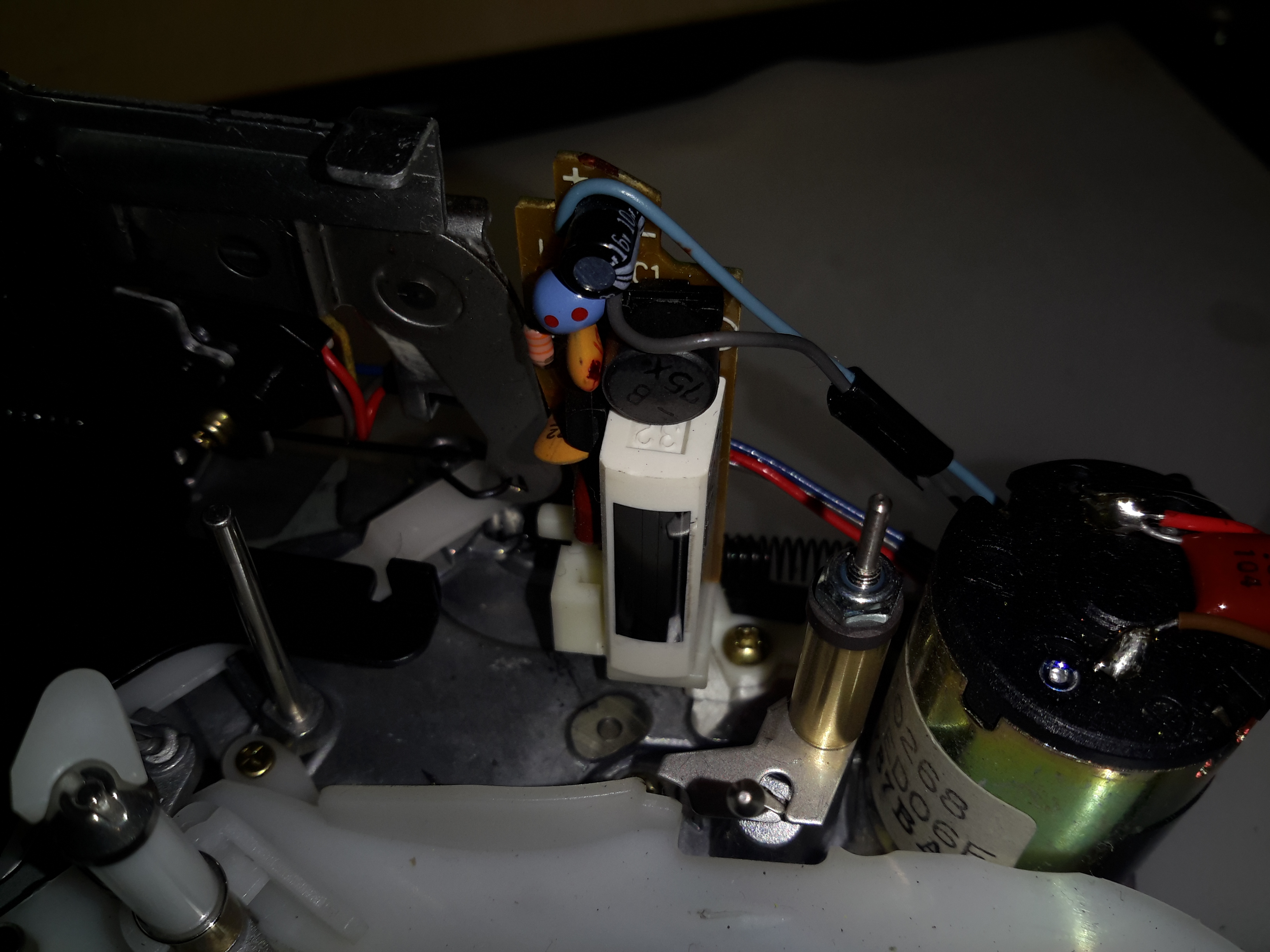
Erase Head
The full erase head has it’s power supply & oscillator on board, applying 9v to this board results in an AC signal to the head, which erases the old recording from the tape before the new recording is laid down by the flying heads on the drum.
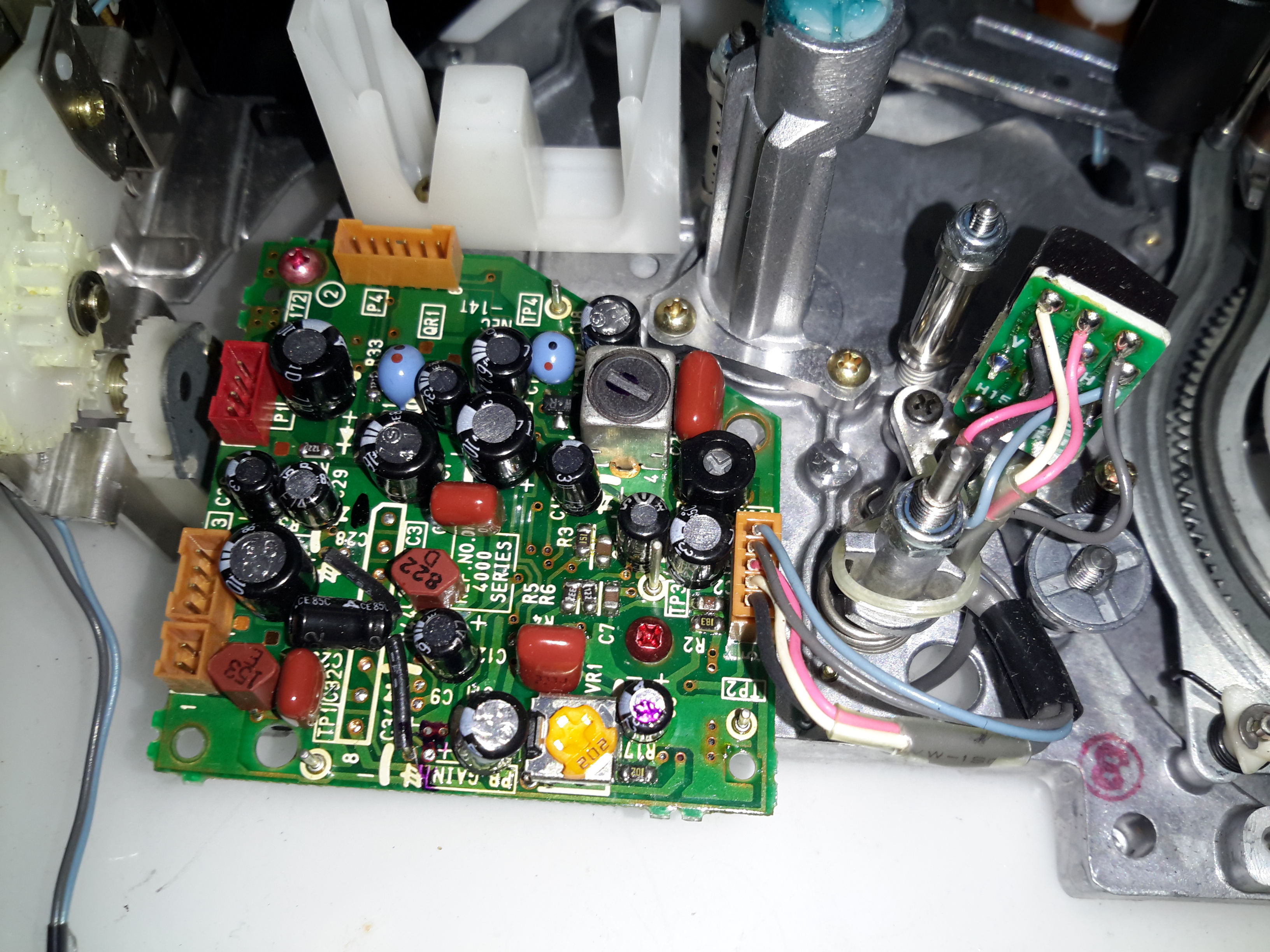
Audio Control PCB
The Audio & Control head is connected to this PCB, which handles both reading back audio from the tape & recording new audio tracks. The audio bias oscillator is on this board, & the onboard microphone feeds it’s signal here. The control head is fed directly through to the servo section of the main board.
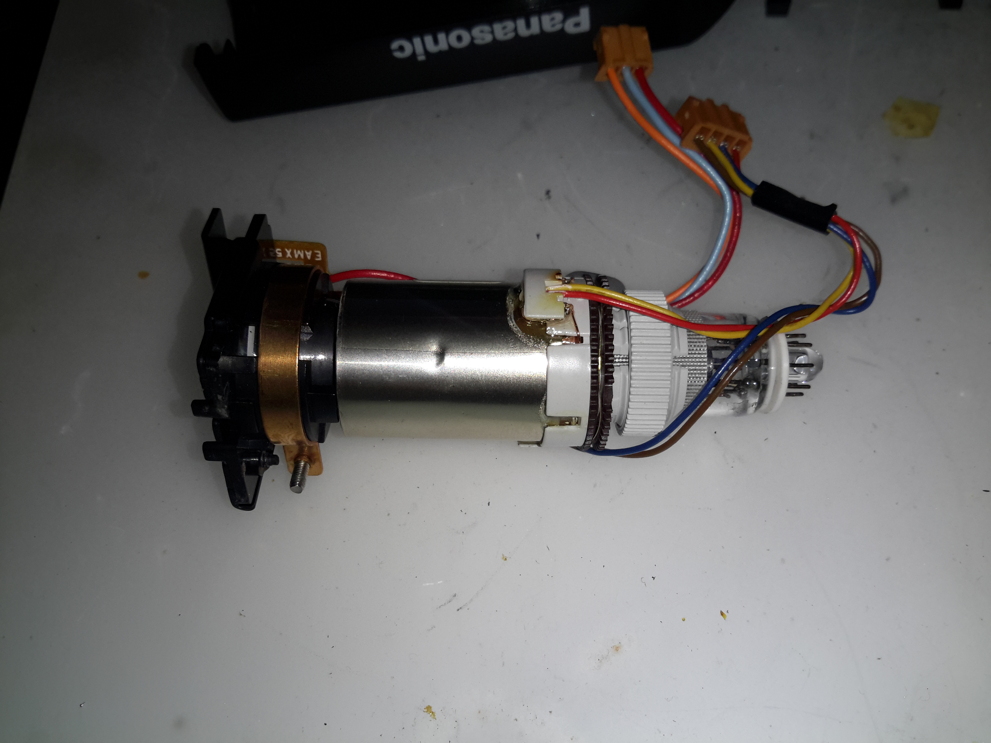
Drum Motor
The motor that drives the head drum is another DC brushless 3-phase type.
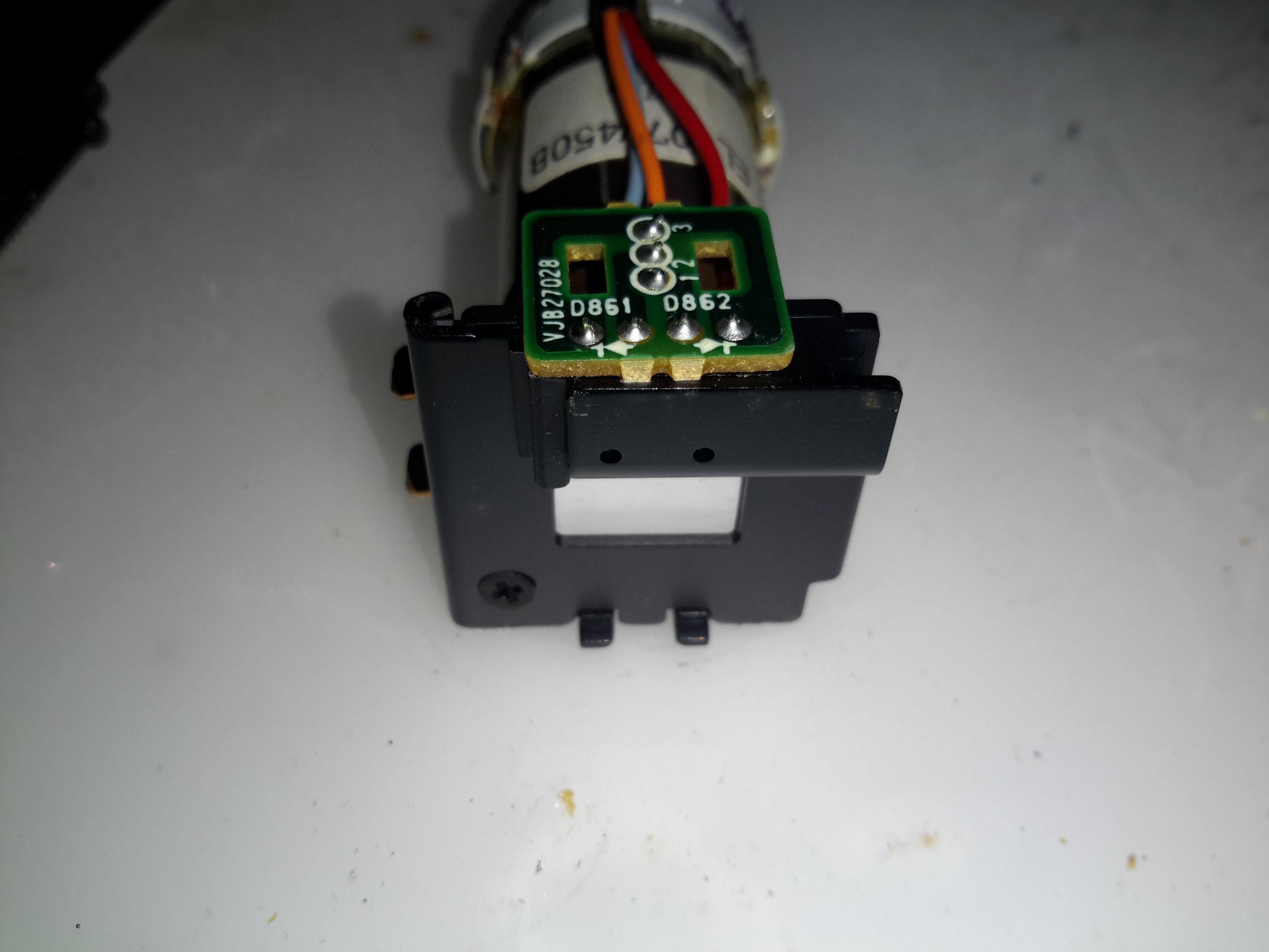
Hall Sensors
These 3 Hall sensors are used by the motor drive to determine the rotor position & time commutation accordingly.
Stator
The stator on this motor is of interesting construction, with no laminated core, the coils are moulded into the plastic holder. The tach sensor is on the side of the stator core. This senses a small magnet on the outside of the rotor to determine rotational speed. For PAL recordings, the drum rotates at 1500 RPM.
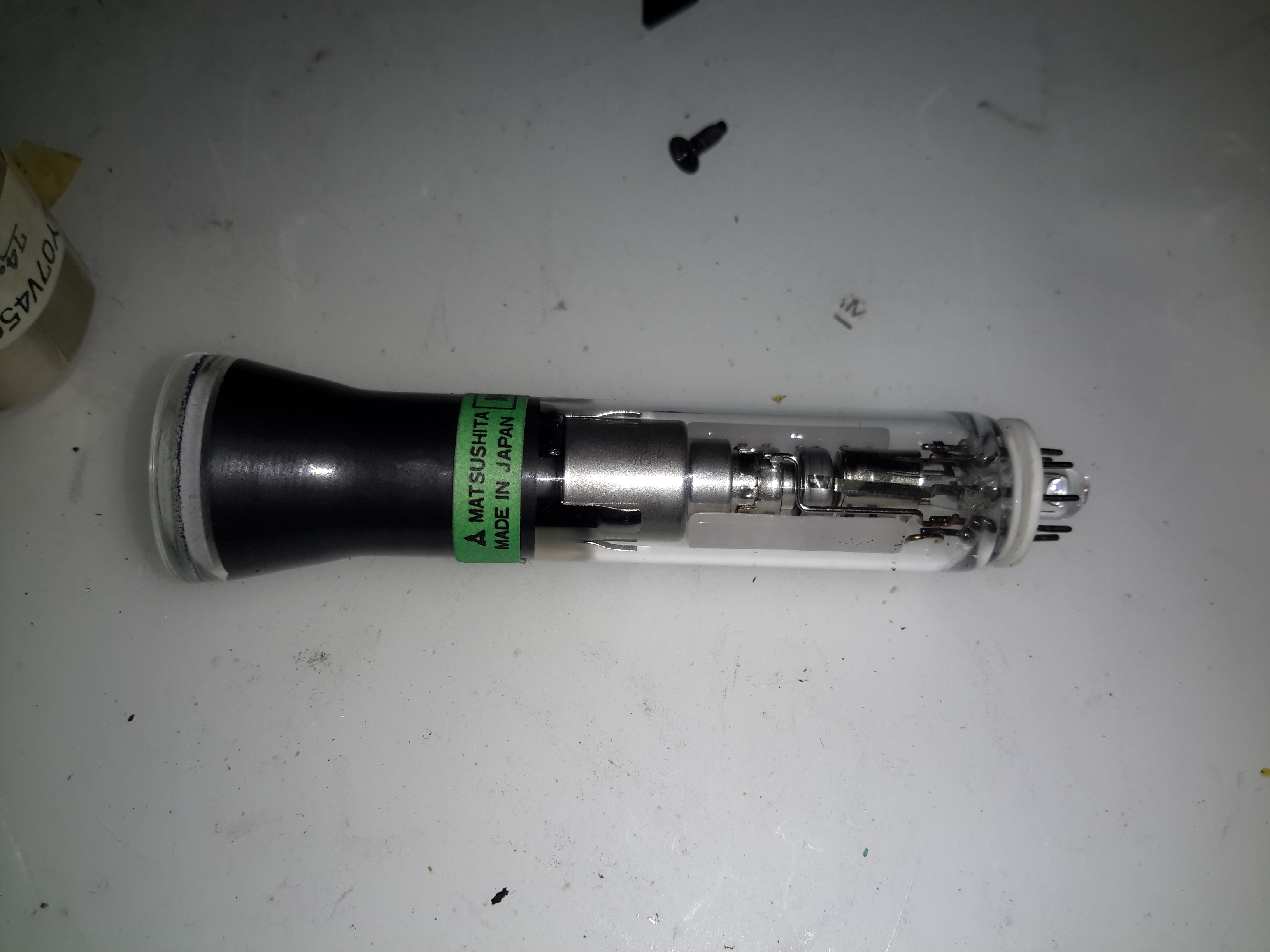
Motor Removed
Not much under the stator other than the bearing housing & the feedthrough to the rotary transformer.
Head Disc
The heads are mounted onto the top disc of the drum, 4 heads in this recorder. The signals are transmitted to the rotating section through the ferrite rotary transformer on the bottom section.
Head Chip
The tiny winding of the ferrite video head can just about be seen on the end of the brass mounting.
Capstan Motor Components
The capstan motor is similar to the drum motor, only this one is flat. The rotor has a ferrite magnet, in this case it wasn’t glued in place, just held by it’s magnetic field.
Capstan Motor Stator
The PCB on this motor has a steel backing to complete the magnetic circuit, the coils for the 3 motor phases are simply glued in place. The Hall sensors on this motor are placed in the middle of the windings though.
Again there is a tach sensor on the edge of the board that communicates the speed back to the controller. This allows the servo to remain locked at constant speed.
Viewfinder
Viewfinder Assembly
As usual with these cameras, this section is the CRT based viewfinder. These units take the composite signal from the camera to display the scene. This one has many more pins than the usual viewfinder. I’ll hack a manual input into this, but I’ll leave that for another post.
Viewfinder Circuits
Being an older camera than the ones I’ve had before, this one is on a pair of PCBs, which are both single-sided.
Main Viewfinder Board
The main board has all the power components for driving the CRT & some of the adjustments. The main HV flyback transformer is on the right. This part creates both the final anode voltage for the tube & the focus/grid voltages.
Viewfinder Control PCB Top
The viewfinder control IC is on a separate daughter board in this camera, with two more controls.
Control IC
The control IC is a Matsushita AN2510S, this has all the logic required to separate the sync pulses from the composite signal & generate an image on the CRT.
Viewfinder CRT Frame
The recording indicator LEDs are mounted in the frame of the CRT & appear above the image in the viewfinder.
Viewfinder CRT With Yoke
Here the CRT has been separated from the rest of the circuitry with just the deflection yoke still attached.
M01JPG5WB CRT
The electron gun in this viewfinder CRT is massive in comparison to the others that I have seen, and the neck of the tube is also much wider. These old tubes were very well manufactured.
Viewfinder Optics
A simple mirror & magnifying lens completes the viewfinder unit.
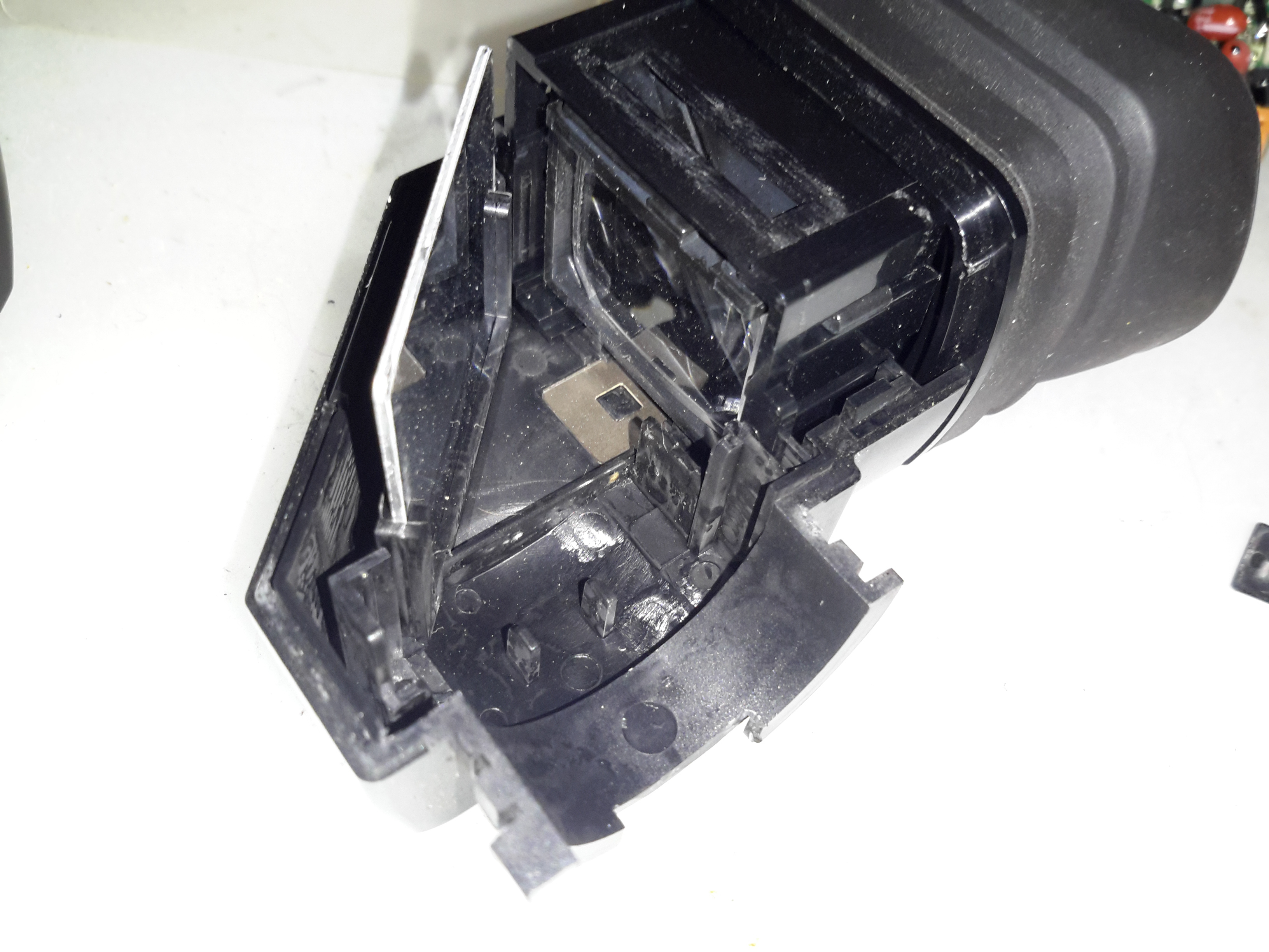
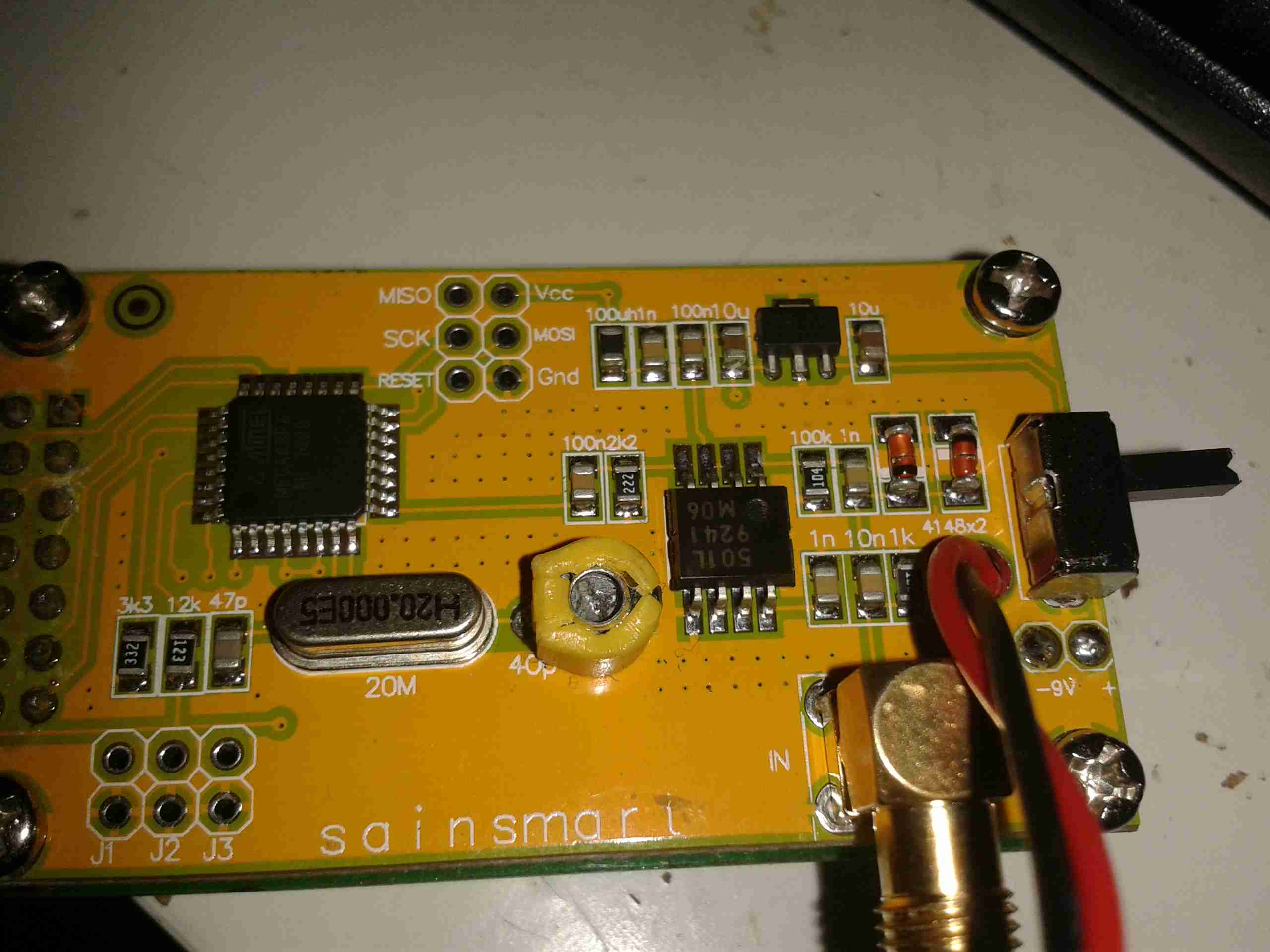
Here’s a quick look at a Sainsmart frequency counter module. These are useful little gadgets, showing the locked frequency on a small LCD display.
It’s built around an ATMega328 microcontroller (µC), and an MB501L Prescaler IC. The circuit for this is very simple, and is easily traced out from the board.
Frequency Counter
Here’s the back of the board, with the µC on the left & the prescaler IC on the right. This uses a rather novel method for calibration, which is the trimmer capacitor next to the crystal. This trimmer varies the frequency of the µC’s oscillator, affecting the calibration.
Input protection is provided by a pair of 1N4148 diodes in inverse parallel. These will clamp the input to +/-1v.
The prescaler IC is set to 1/64 divide ratio. This means that for an input frequency of 433MHz, it will output a frequency of 6.765625MHz to the µC.
The software in the µC will then calculate the input frequency from this intermediate frequency. This is done because the ATMega controllers aren’t very cabable of measuring such high frequencies.
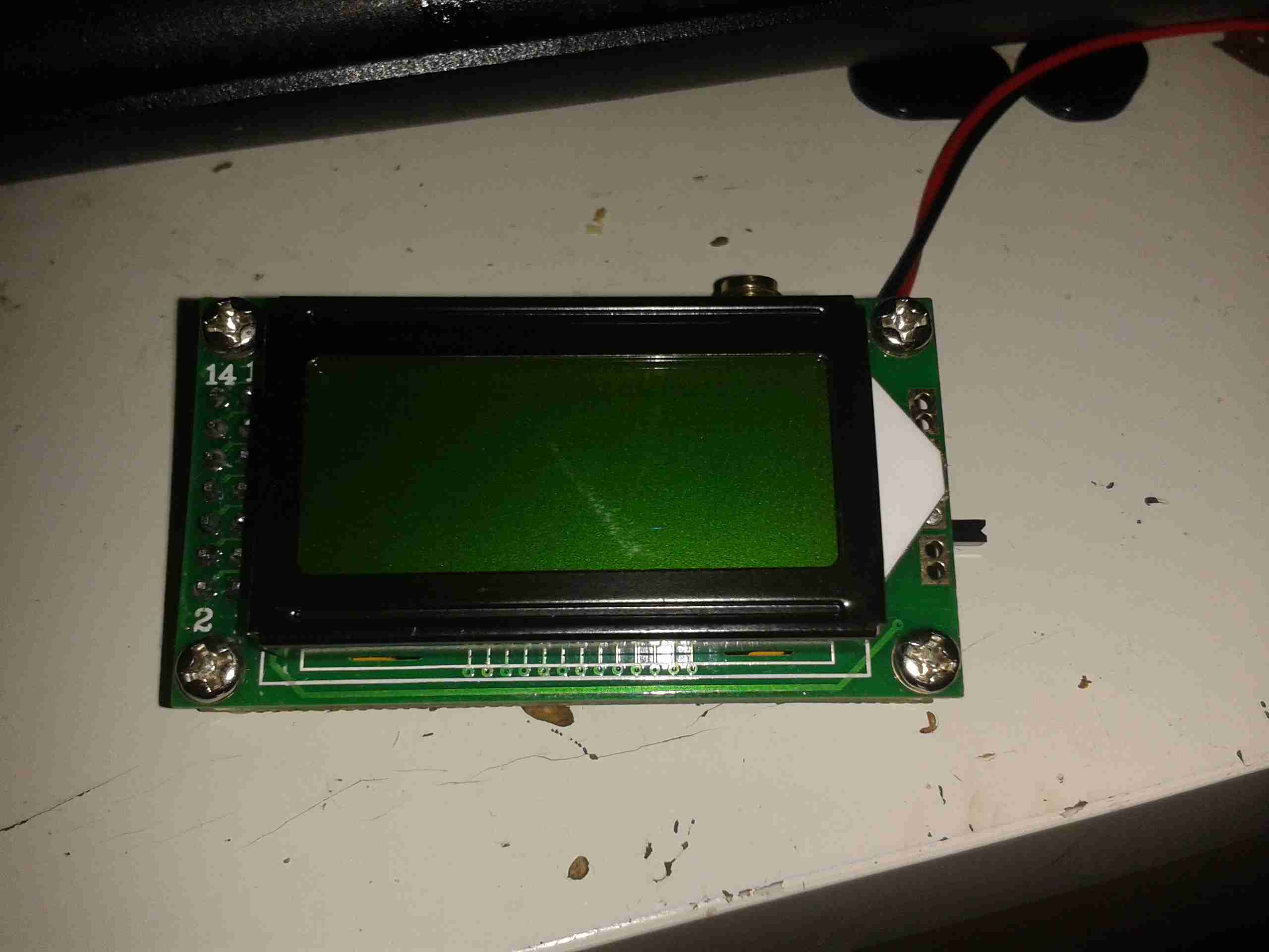
The calculated frequency is then displayed on the LCD. This is a standard HD44780 display module.
LCD
Power is provided by a 9v PP3 battery, which is then regulated down by a standard LM7805 linear regulator.
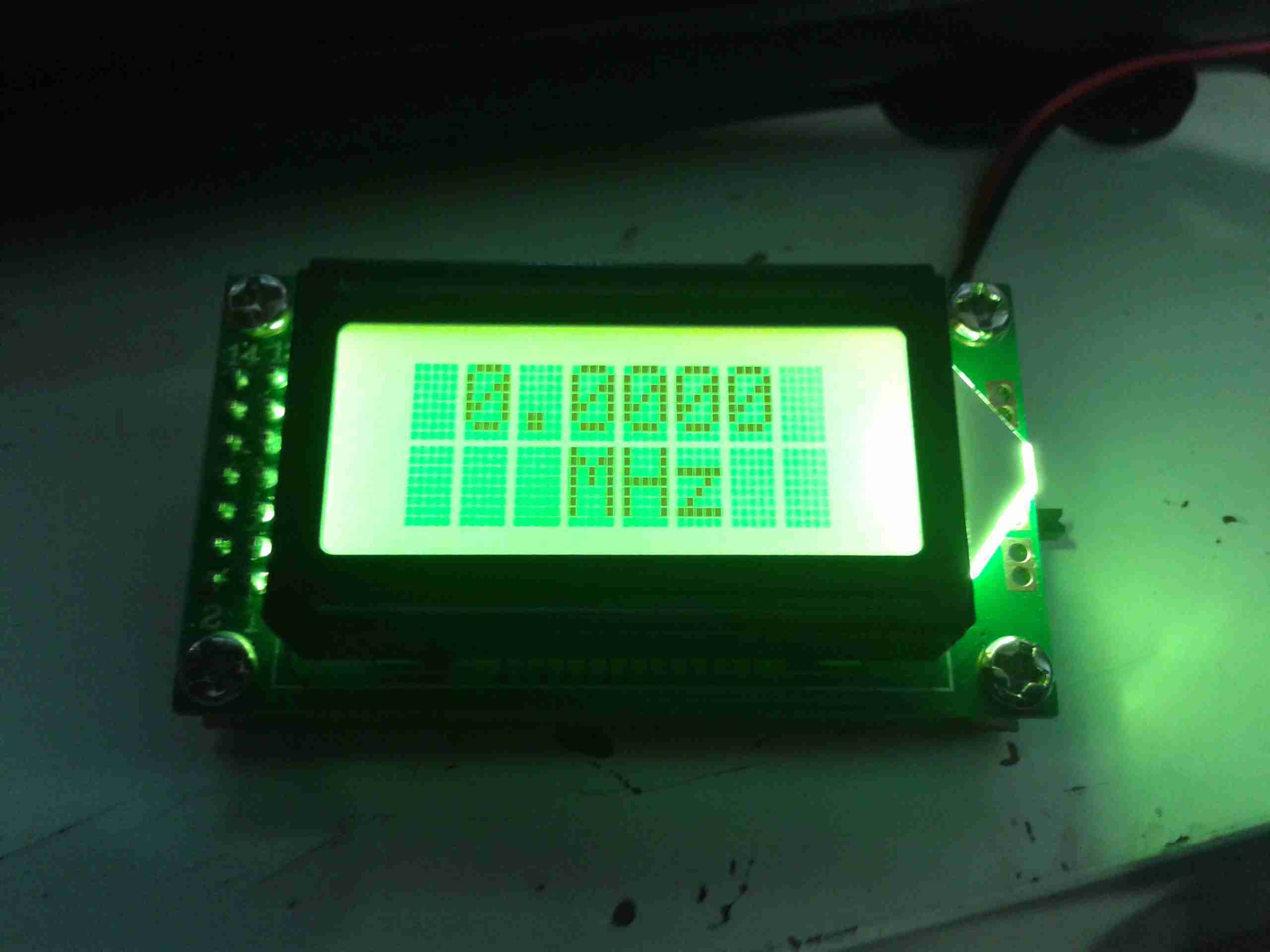
Readout
I’ve found it’s not very accurate at all at the lower frequencies, when I fed it 40MHz from a signal generator it displayed a frequency of around 74MHz. This is probably due to the prescaler & the software not being configured for such a low input. In the case for 40MHz input the scaled frequency would have been 625kHz.
This is a cheap Sigma branded keychain photoframe. User buttons for power & selecting photos are on the left.
There are two white LEDs on the bottom edge that function as a torch as well.
Display
Front of the unit removed, showing the LCD module. The USB jack is bottom left, next to the pair of white LEDs & above that is the 32kHz watch crystal that the CPU uses for timekeeping.
Back Removed
Here the back has been removed showing the 3.7v Li-Ion cell used to provide power.
Display Folded Back
Here the display has been removed from the PCB exposing the chipset.
Chipset
Here the CPU blob-top chip & a flash memory IC are visible. The CPU is a Sitronix ST2205U.
Here is an old Belkin Wireless G network card. This is a PCMCIA version.
Bottom Label
Here is the bottom of the device, with all the details.
Antenna
Plastic antenna cover removed, showing the pair of 2.4GHz etched antennae. There is a pair of LEDs on the upper left of the PCB showing activity & link status.
PCB
Overall view of the PCB, antennae on the left, RF chipset in centre, WiFi controller IC on right, and PCMCIA socket on far right. Can below wireless controller is a quartz crystal for the clock.
Chipset
Closeup of the chipset, a Ralink RT2560F wireless controller on the right & a RT2525L transceiver on the left.
This is an old cordless landline phone, with dead handset batteries.
Handset Radio Board
Here’s the handset with the back removed. Shown is the radio TX/RX board, underneath is the keyboard PCB with the speaker & mic. All the FM radio tuning coils are visible & a LT450GW electromechanical filter.
Handset Radio Board Bottom
Radio PCB removed from the housing showing the main CPU controlling the unit, a Motorola MC13109FB.
Keypad Board
The keypad PCB, with also holds the microphone & speaker.
Handset Keypad Board Bottom
Bottom of the keypad board, which holds a LSC526534DW 8-Bit µC & a AT93C46R serial EEPROM for phone number storage.
Base Main Board
Here’s the base unit with it’s top cover removed. Black square object on far right of image is the microphone for intercom use, power supply section is top left, phone interface bottom left, FM radio is centre. Battery snap for power backup is bottom right.
Power Supply Section
PSU section of the board on the left here, 9v AC input socket at the bottom, with bridge rectifier diodes & main filter capacitor above. Two green transformers on the right are for audio impedance matching. Another LT450GW filter is visible at the top, part of the base unit FM transceiver.
ICs
Another 8-bit µC, this time a LSC526535P, paired with another AT93C46 EEPROM. Blue blob is 3.58MHz crystal resonator for the MCU clock. The SEC IC is a KS58015 4-bit binary to DTMF dialer IC. This is controlled by the µC.
Base Main Board Bottom
Underside of the base unit Main PCB, showing the matching MC13109FB IC for the radio functions.
This is a little security measure you get with Internet Banking with the Co-Op, generates codes to confirm your identity using your bank card. About the size of a pocket calculator, this is the keypad & screen.
Card Slot
The rear of the unit, the card slots into the top, manufactured by Gemalto Digital Security.
Card Contacts
Outer back cover removed, showing the 8 contacts for the chip on the bank card, the 2 contacts below that switch on power when a card is inserted. Power comes from 2 lithium coin cells in the compartment on the lower left.
PCB Rear
PCB removed from the casing, showing the internal components. Two large pads at top left are battery connections, while the only IC on the board is the main CPU, under the card connector. 6MHz oscillator & 32Khz crystal on board for processing & timekeeping. LCD screen connection at far right.
Keypad Contacts
Reverse side of the PCB, with the keypad contacts. LCD on right, with programming interface pads at side of keypad.
Here is a cheap chinese made flash drive given out for free by Westlaw UK. Capacity 512MB
PCB
Here is the PCB removed from the casing, USB connector on the left, followed by the clock crystal for the flash controller, a CBM2092, which is a Chipsbank part. 512MB flash memory IC, unknown maker. Access LED on far right of the board.
This is a HP PhotoSmart 375 portable photo printer. With built in card reader, screen & PictBridge.
Top of the printer showing the UI Buttons & Screen.
Front
Front of the unit, card reader slots at the top, Pictbridge USB connector at top left. Paper out slot at bottom. Cartridge door is on the right.
Cartridge Door
Here the cartridge door is open. Takes HP 95 Tri-Colour Inkjet Cartridge.
Battery Compartment
Battery compartment on the bottom of the unit. A Li-Ion battery pack can be installed here for mobile photo printing.
Bottom Label
Specifications label.
USB + Power
Power adaptor & USB connection for PC use.
Paper Tray
Rear door opened. Showing the paper feed tray.
Paper Feeder
Rear door has been removed in this shot. Paper feed roller & platen roller can be seen here.
Rear Cover Paper Feeder
Paper holder attached to rear door.
Top Cover
Bottom of the top cover, with connections for the buttons & LCD panel.
Main PCB
This is the main PCB of the unit. Controls all aspects of the printer. CPU in center, card reader sockets are along bottom edge. various support circuitry surrounds the CPU.
Rear
Rear shell has been removed here. Showing the main frame & the carriage drive motor on the left.
Carriage Drive
Closeup of the carriage drive motor & timing belt system. All the motors in this printer are DC servo motors, not steppers.
Main Drive Motor
Main drive motor, feeds paper, drives rollers, operates cleaning mechanism for the inkjets.
Shaft Encoder
Mainshaft encoder. Main drive motor is bottom right hand side with timing belt drive.
CPU
Closeup of the CPU. This is a Phillips ARM chip, unknown spec.
Card Reader Sockets
Detail of the card reader sockets, this unit takes all current types of Flash memory card.
This is the Current Cost CC128 Real Time Power Meter. Shown here is the display unit, British Gas issued these free to some customers.
This unit measures current power draw in Watts, cost of power currently being used (requires unit price to be set), overall kWh usage over the past 1, 7 or 30 days & power trends during the day, night & evening. Also displays current time & current room temperature.
Display PCB
Here the front panel of the display has been un-clipped. At the bottom are the RJ-45 serial port & power connections.
This unit uses a PIC micro-controller as it’s CPU (PIC18F85J90) Just above & left of the CPU is the 433MHz SPD radio receiver module. The chips on the right of the CPU are a 25LC128 SPI serial EEPROM for data storage & a 74HC4060 14 stage binary counter, to which is connected the 32kHz clock crystal. The red wire around the top of the display is the antenna for the radio receiver.
For more info on the CC128 in general, the serial port & software for computer data logging, see this link
See this link for Current Cost’s list of software
Processor & Radio
Closeup of the ICs on the mainboard.
Transmitter Unit
Here we have the transmitter unit, with Current Transformer (CT). The red clamp fits around one of the electric meter tails & read the current going to the various circuits. This unit is powered by 2x D cells, rated at a life of 7 years.
Transmitter PCB
The PCB inside the transmitter. Again very minimal design, unknown controller IC, 433MHz radio transmitter on right hand side with wire antenna. Two barrel connectors on left hand side of board allow connection of up to two more CT clamps for measurement of 3-phase power. Centre of board is unmarked header. (ICSP?)
Current Transformer
CT unit. Inside is a coil of wire & an iron core which surrounds the cable to be measured.
PIC18F85J90
Tip Jar
If you’ve found my content useful, please consider leaving a donation by clicking the Tip Jar below!
All collected funds go towards new content & the costs of keeping the server online.