Posted on Leave a comment

HP 5087-7048 Directional Coupler Teardown

Directional Coupler
Directional Coupler
Directional Coupler

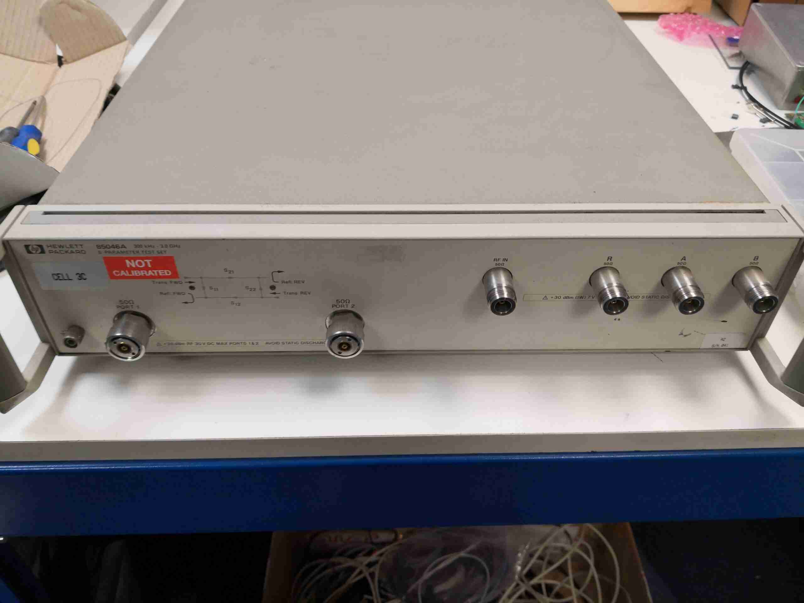
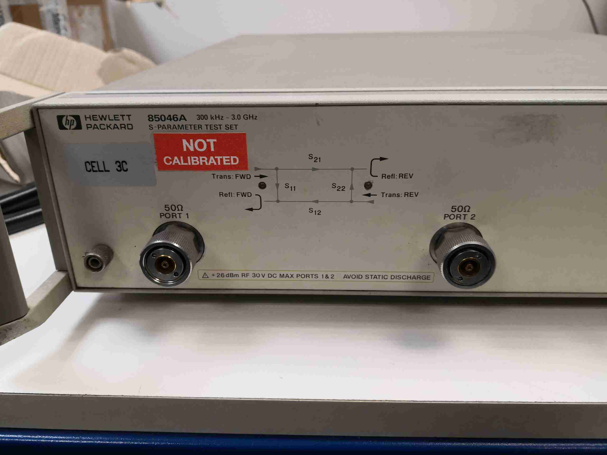
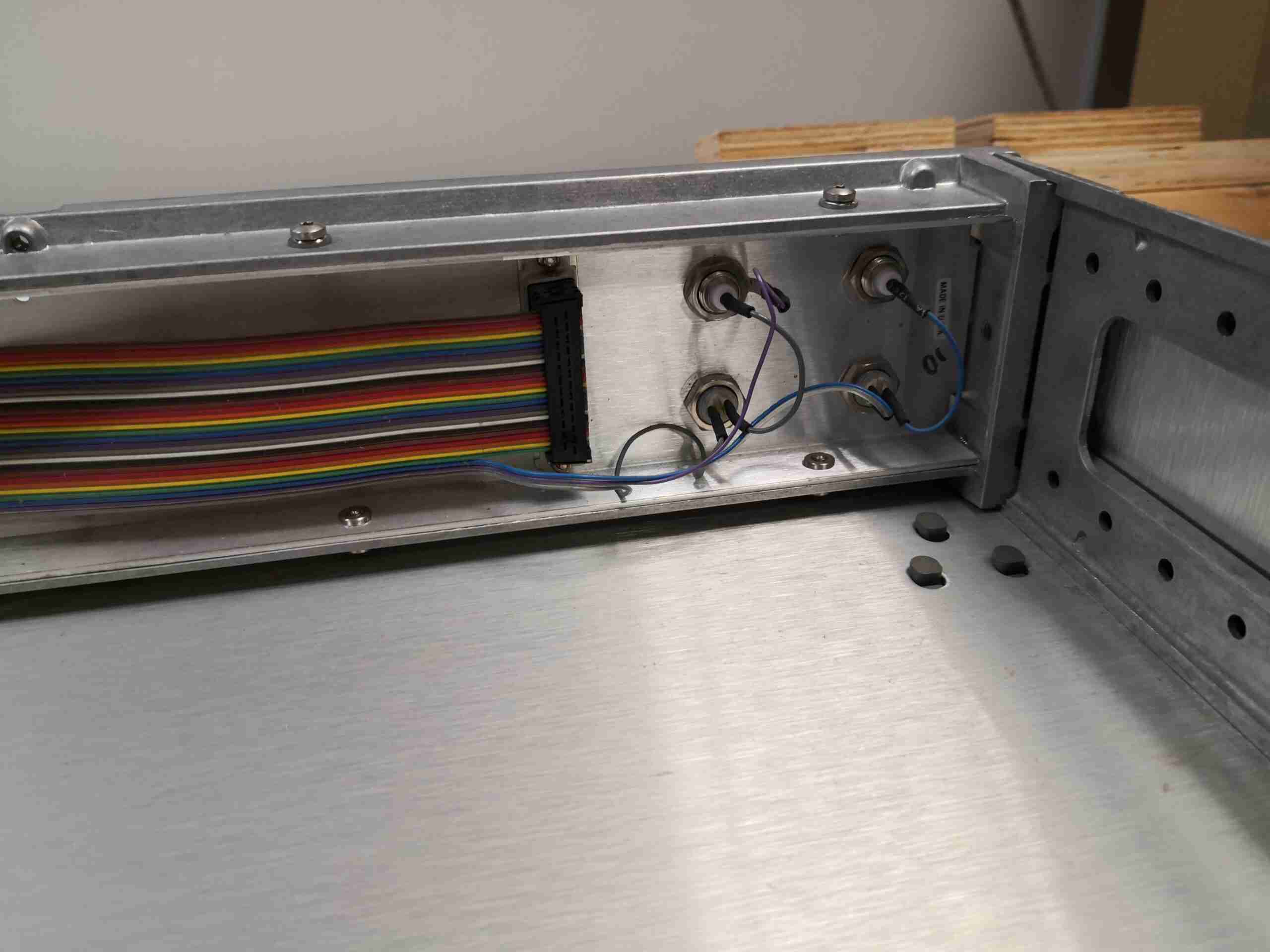
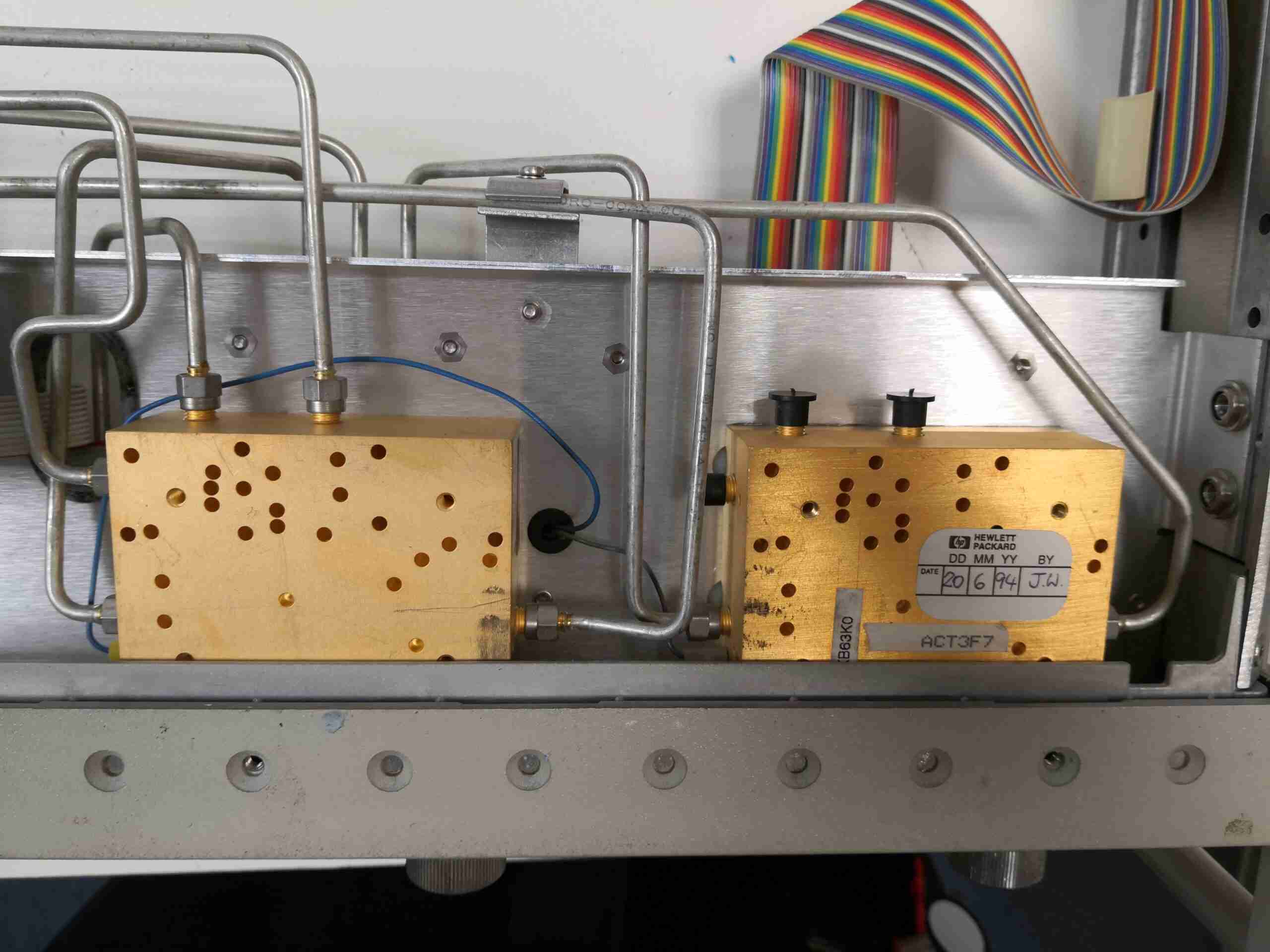
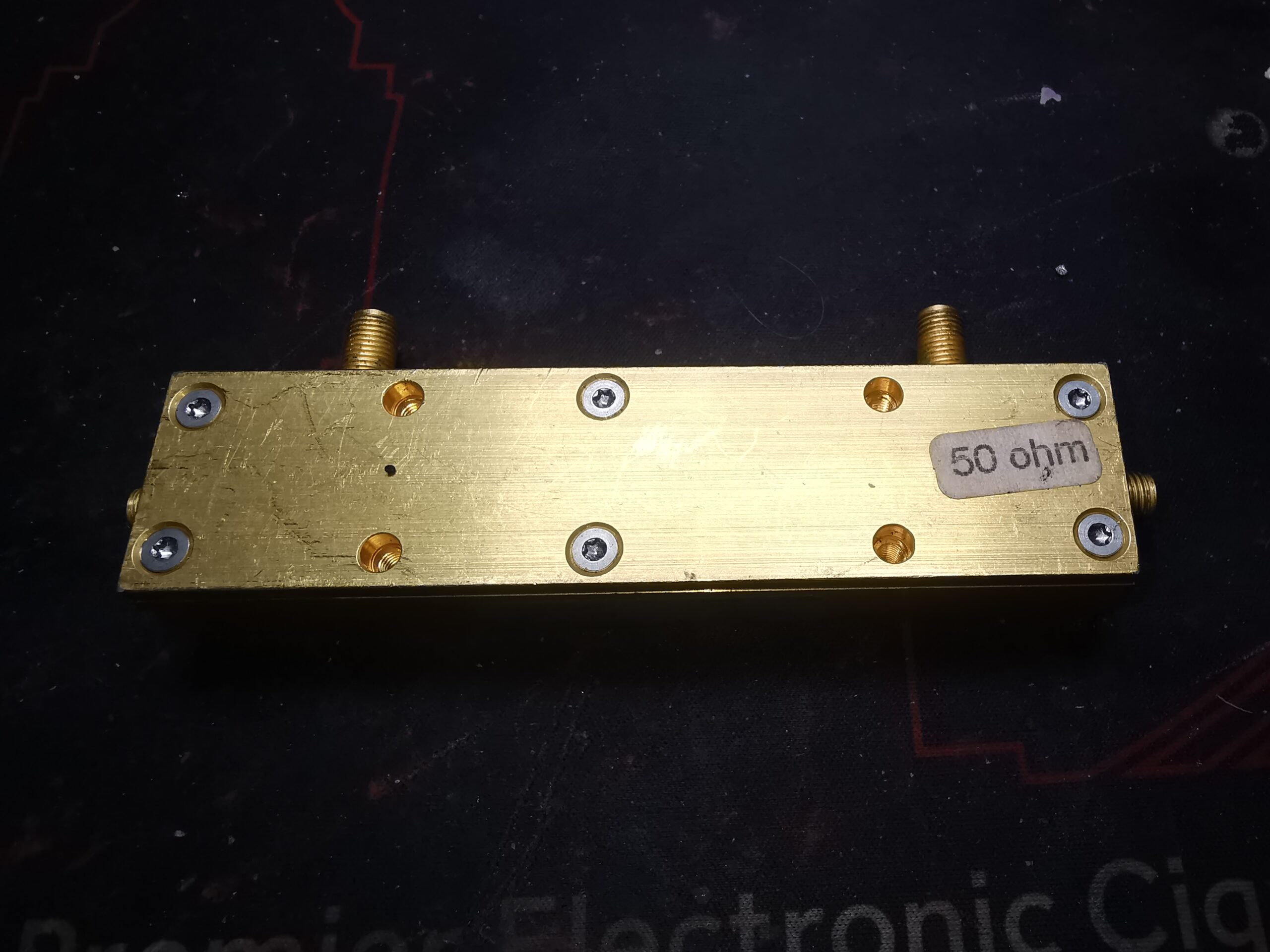
Time for some more RF component teardowns, here’s a very high quality Directional Coupler from HP, I believe this was part of a Vector Network Analyser at some stage. The main body appears to be made of Brass, but the entire unit looks like it’s Gold plated – the shine is far too good to be just Brass! Connections are via SMA connectors.

Label
Label

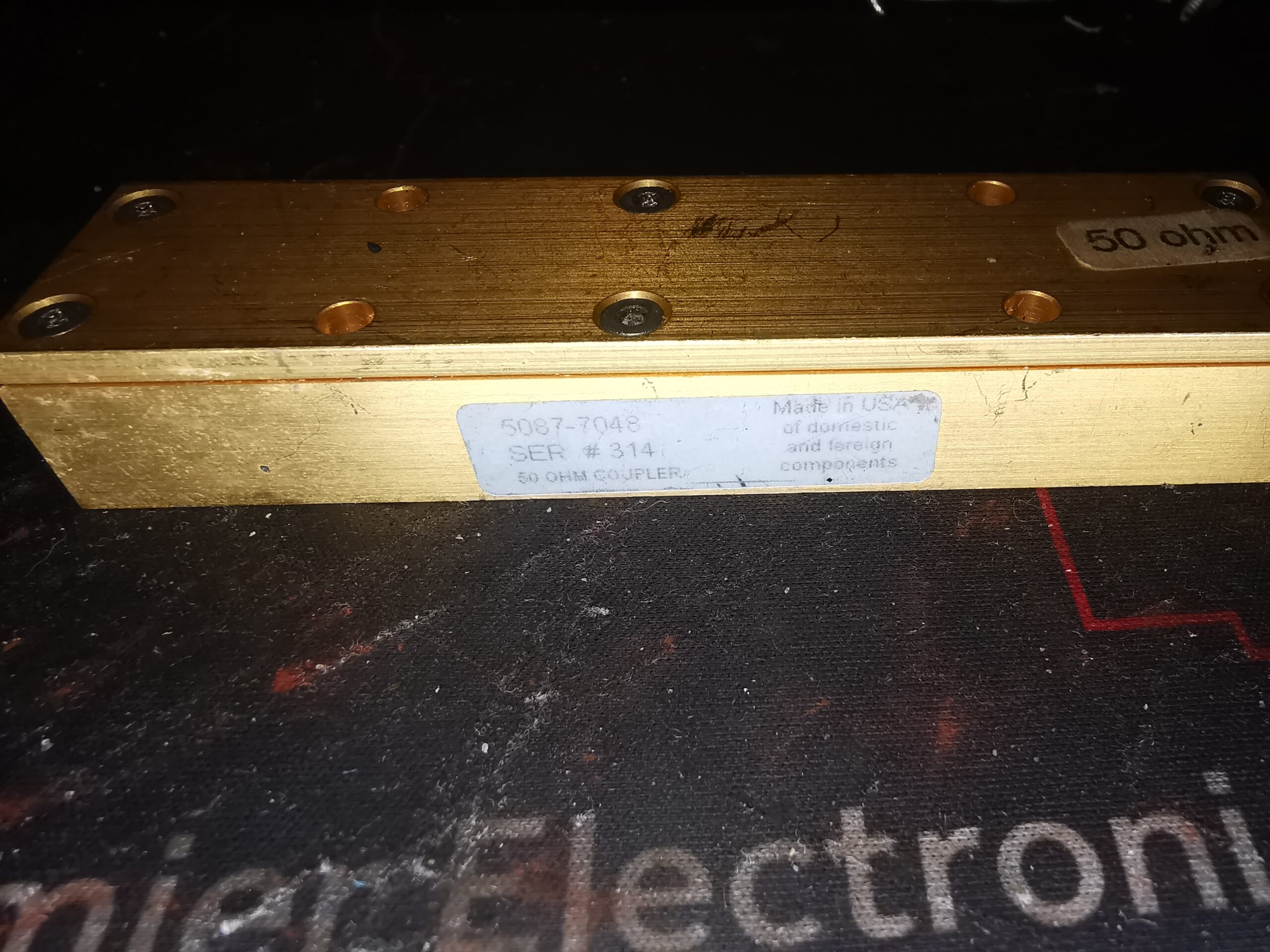
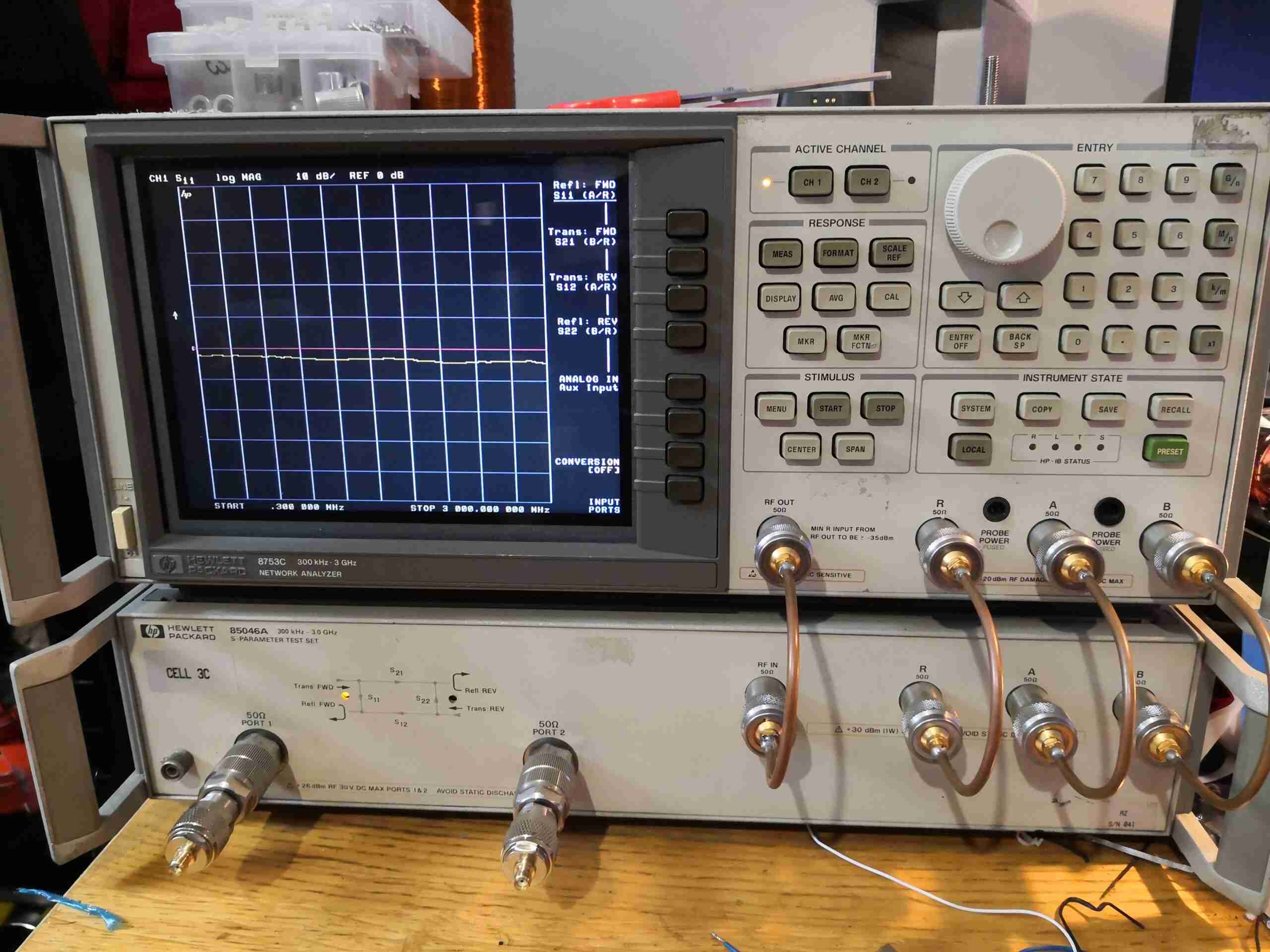
There isn’t much on the label to explain what the specifications are unfortunately. Nothing that can’t be found out with a quick look on a VNA though.

Cover Removed
Cover Removed

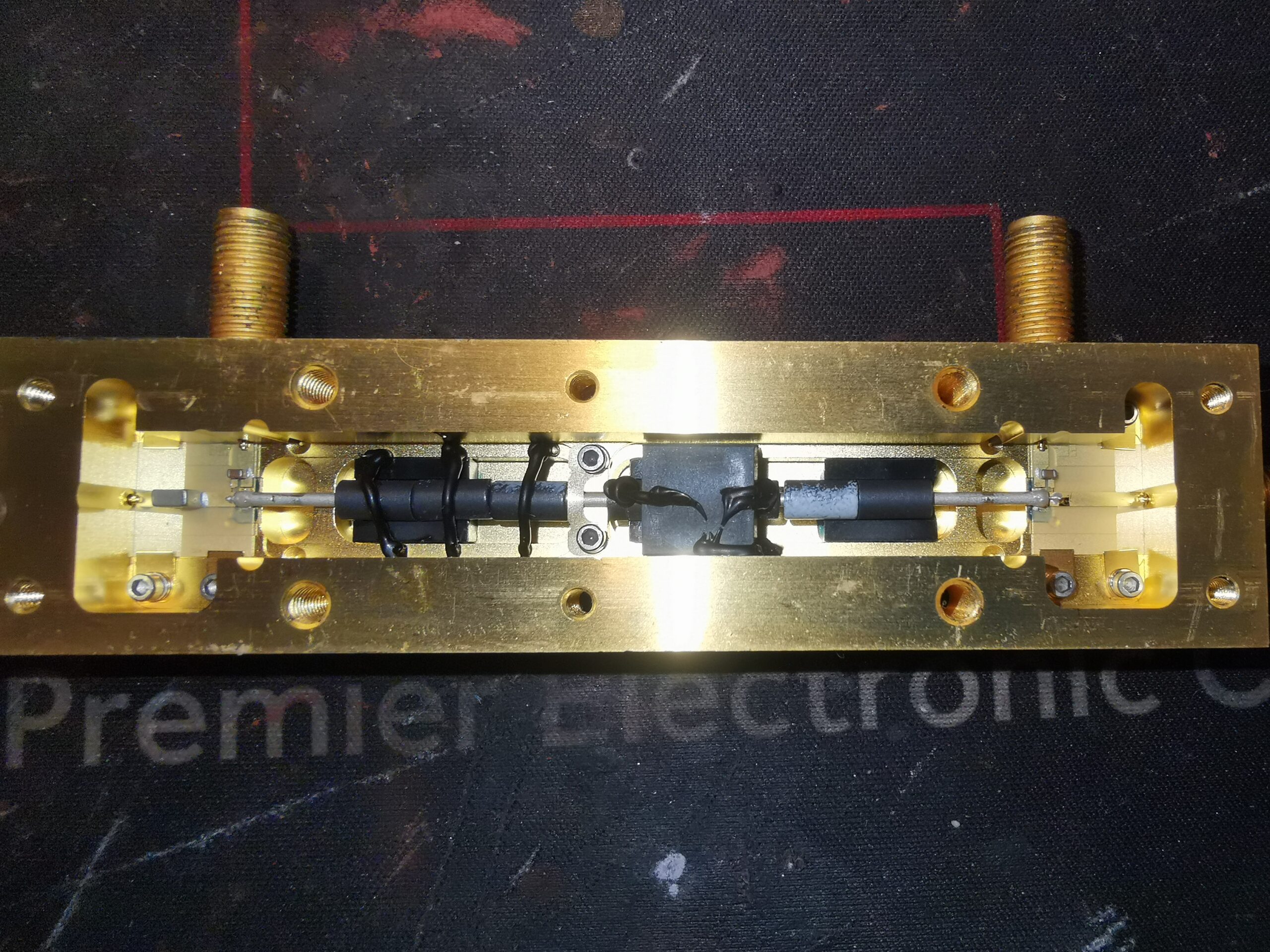
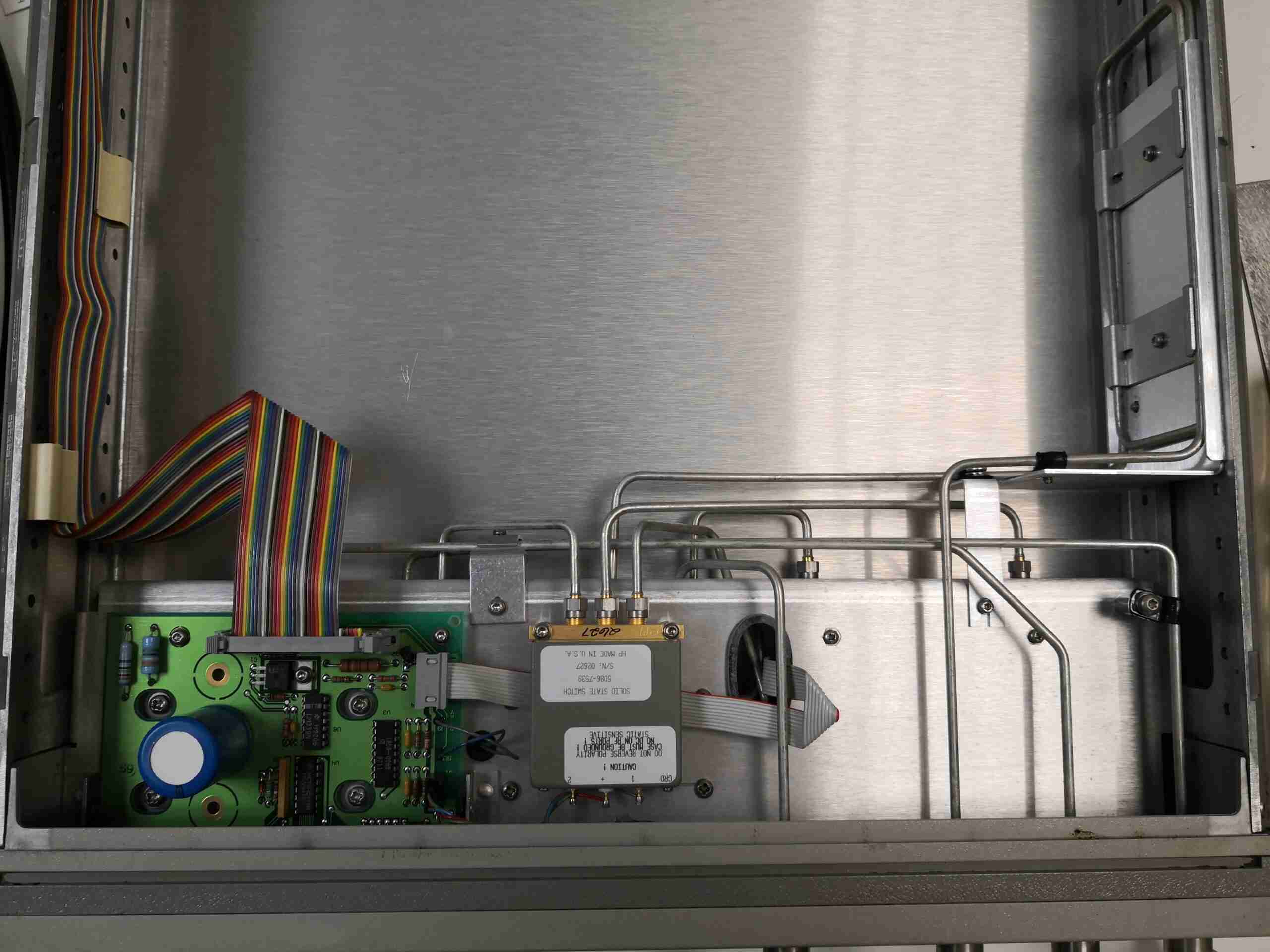
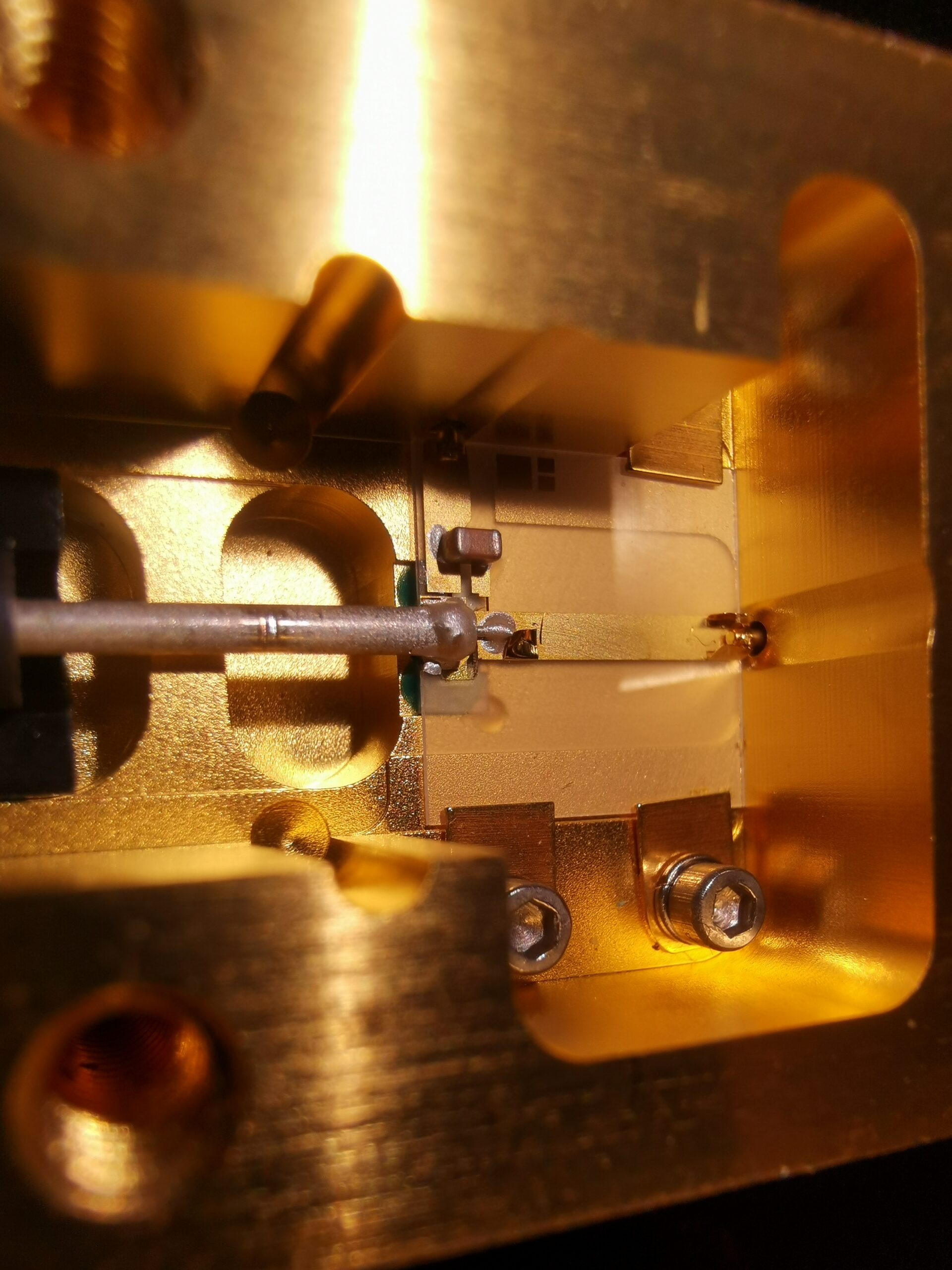
After removing the 6 Torx screws securing the top cap of the coupler, the internal components are revealed. There is no RF gasket or seal on the top cover, and relies on flat machining for an RF seal.

Internal Components
Internal Components

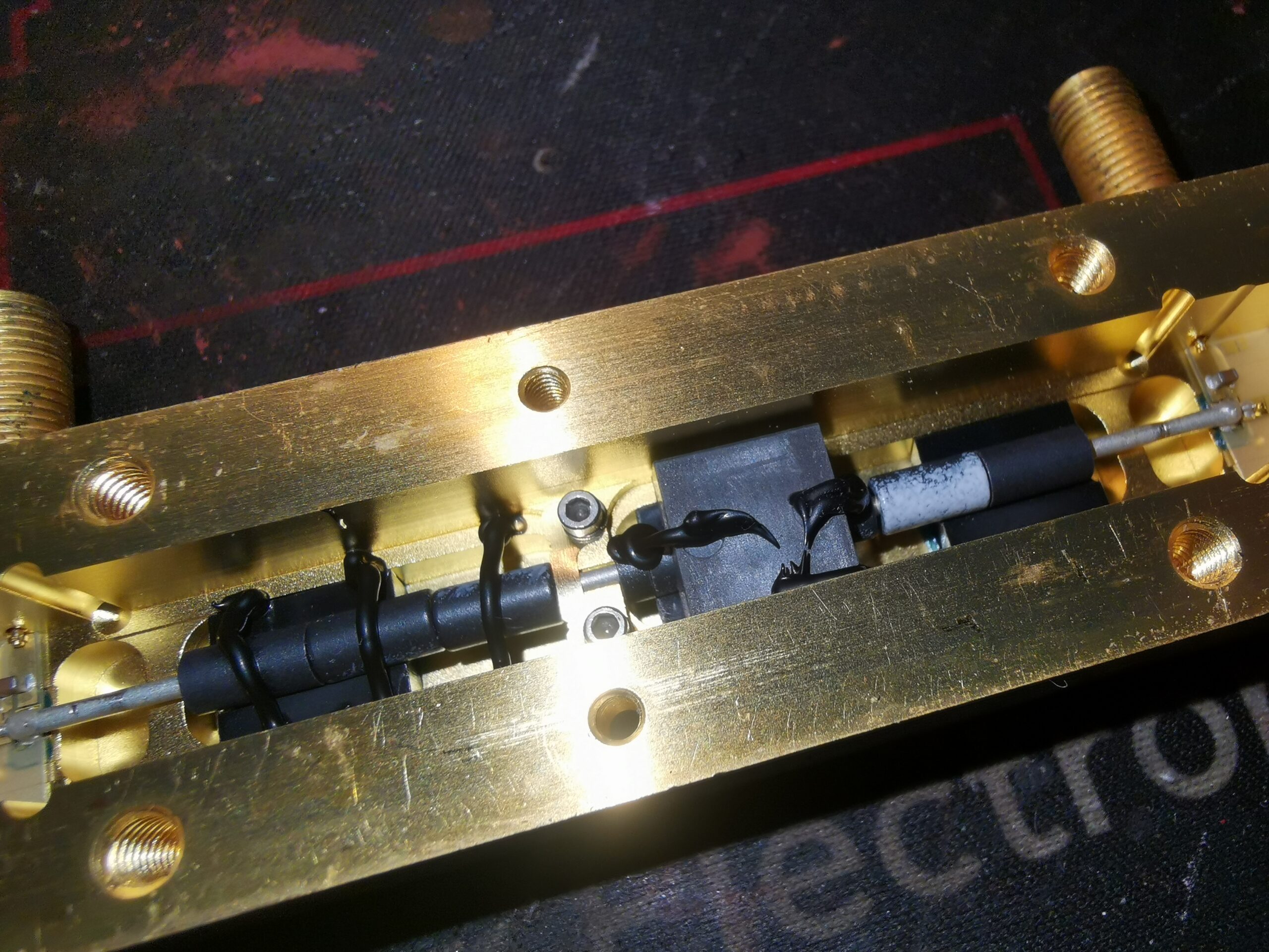
The internal construction of this unit is a little different from what I’ve seen before in directional couplers. The arrangement is usually parallel copper tracks on a suitable RF substrate, but in this case, HP have used a very small diameter Coaxial cable, covered with ferrite sleeves on the outer shield. The large square block in the middle is rubber, and may just be to stabilise the assembly. It may also be loaded with ferrite powder to give some RF properties too.
The ferrite cores are secured in place with beads of black silicone, again probably to prevent movement under vibration.

Input End
Input End

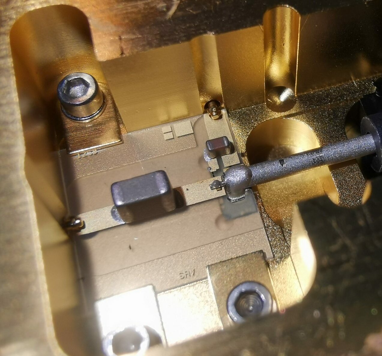
The input of this coupler is AC coupled via a capacitor, and then fed into the centre core of the Coax. The forward power output pin, visible at the top of the track, is coupled to the centre core of the coax by a tiny carbon track making up a resistor, via another ceramic capacitor. The track is more directly coupled via another carbon trace to the outer shield of the Coax. I believe this coupler is damaged, as the carbon trace that goes via the capacitor has a break in the centre, but the coupler does seemingly still work.

Output End
Output End

The other end of the coupler is very similar, although with no main line coupling capacitor, it’s direct fed to the SMA here. The reverse power output is connected the same way as the other, with a network. The carbon trace here though doesn’t have a break.

Posted on Leave a comment

HP 8753C Display LCD Replacement

Completed Install
Completed Install

Since I inherited an old HP 8753C Network Analyser from work, I figured updating a few things to relatively modern standards would be good. The factory CRT, being 28 years old, is definitely getting a little tired, not to mention being slow to warm up. I read over on the EEVBlog forums about a DIY modification to integrate an LCD display into place instead. There was also the option of a ready-made kit for these instruments which would integrate an LCD, but the cost at over £300 was very prohibitive!

CRT Pinout
CRT Pinout

The CRT display unit is a self-contained Sony unit, taking RGBHV signalling from the graphics control card of the analyser. Power is 65v DC which will definitely come in handy for powering the new LCD & control gear, after some conversion.

Test Wiring
Test Wiring

Doing a quick test with some wiring stuck into the video connector from the graphics controller, proved that I could get a decent video signal out of the unit! The only signals used here are RGB, along with the vertical & horizontal sync.

GBS-8200 Converter Board

The video is converted to VGA by way of a GBS-8200 arcade machine video conversion board, which will take many different video formats & spit out standard VGA signalling. The power supply to the left is a standard 100-240v to 12v PSU, which is happy to run at 6t5v DC input voltage, albeit with a ~5 second delay on output startup when power is applied. This is due to the massive 6.6MΩ resistance of the startup resistor chain, which I did reduce by 50% to 3.3MΩ with no effect. Since it does start OK even with the delay, I think I’ll not tinker with it any further. I doubt I could pull the full rated power from it with such a low input voltage, but all included, this mod draws less than 600mA at 12v.
A custom 20-pin IDC cable was made up to connect to the analyser’s graphics board, and this was then broken out into the required RGB & sync signals. Quite a few of the grounds are unused, I’ve not yet noticed any issues with EMC or instability.

Sync Combiner
Sync Combiner

There is a quad-XOR gate deadbugged to the PCB, which is taking the separate sync signals & combining them into a composite sync. The conversion board does have separate sync inputs, but for some reason doesn’t sync when they’re applied separately. This gate IC is powered from the 3.3v rail of the converter board, with the power lines tacked across one of the decoupling caps for the DRAM IC.

LCD Control PCBs
LCD Control PCBs

The donor 8.4″ LCD came from eBay in the form of a POS auxiliary display. I pulled the panel from the plastic casing, along with the control boards, and attached them all to the back. This LCD also had a sheet of toughened glass attached to the front, no doubt to protect against the Great Unwashed while in use! This was also removed.

Control Boards Mounted

A cut piece of plexiglas allows the boards to be mounted in the cavernous space the CRT once occupied, with some brass standoffs. 12v power & VGA are routed down to the LCD on the front of the analyser.

LCD Wiring
LCD Wiring

The LCD itself is tacked in place with cyanoacrylate glue to the securing clips for the glass front panel, which is more than enough to hold things in place. The input board which just has the VGA connector & power connector is glued edge-on to the metal back panel of the LCD, and is under little strain so this joint should survive OK.

Posted on Leave a comment

HP 85046A 3GHz S-Parameter Test Set Teardown

Front Panel
Front Panel

This enormous box is the S-Parameter Test Set from a HP 8753C 3GHz network analyser. This unit contains the required components to automate the testing process for items such as cables, antennas & RF networks.

7mm Test Ports
7mm Test Ports

The main EUT test ports are APC-7mm type connectors – a very expensive genderless RF connector that provides very repeatable coaxial connections.

N-Type Analyser Interconnects

The interconnects for the RF input, Reference output back to the analyser, A&B ports are N-Type, and should be connected to the main unit with phase-matched cables.

Lid Removed
Lid Removed

On removing the lid, it’s almost a completely empty box! All the RF magic is done in the first 150mm behind the front pane, apart from a coil of semi-rigid coax on the right, which will be to match the lengths of cables in the unit for phase purposes. There’s not much visible on the top here, just the control board, which takes signalling from the main analyser unit, and only has some glue logic & comparators. There’s a very nice 3-port solid-state RF switch in the centre, for switching between S12 & S21 measurements rapidly, a function that would not be possible with a mechanical relay. All the internal connections are made with semi-rigid coaxial cable, fitted with SMA connectors.

Rear Panel Connections

The back of the case just has the 25-way D connector for control, and a pair of BNC connections & 500mA fuses for DC biasing the output ports where required by the EUT.

Power Splitter & Directional Couplers

Underneath the centre panel is where most of the RF magic happens. These two blocks, which are integrated with the test ports contain bias tees for each port, a power splitter for the RF reference back to the analyser & directional couplers for reading back the forward & reverse RF power from each test port.

Step Attenuator
Step Attenuator

The final component in here is a 70dB step attenuator, adjustable in 10dB steps.

Posted on Leave a comment

HP Photosmart 375

Top
Top

This is a HP PhotoSmart 375 portable photo printer. With built in card reader, screen & PictBridge.
Top of the printer showing the UI Buttons & Screen.

Front
Front

Front of the unit, card reader slots at the top, Pictbridge USB connector at top left. Paper out slot at bottom. Cartridge door is on the right.

Cartridge Door
Cartridge Door

Here the cartridge door is open. Takes HP 95 Tri-Colour Inkjet Cartridge.

Battery Compartment
Battery Compartment

Battery compartment on the bottom of the unit. A Li-Ion battery pack can be installed here for mobile photo printing.

Bottom Label
Bottom Label

Specifications label.

USB + Power
USB + Power

Power adaptor & USB connection for PC use.

Paper Tray
Paper Tray

Rear door opened. Showing the paper feed tray.

Paper Feeder
Paper Feeder

Rear door has been removed in this shot. Paper feed roller & platen roller can be seen here.

Rear Cover Paper Feeder

Paper holder attached to rear door.

Top Cover
Top Cover

Bottom of the top cover, with connections for the buttons & LCD panel.

Main PCB
Main PCB

This is the main PCB of the unit. Controls all aspects of the printer. CPU in center, card reader sockets are along bottom edge. various support circuitry surrounds the CPU.

Rear
Rear

Rear shell has been removed here. Showing the main frame & the carriage drive motor on the left.

Carriage Drive
Carriage Drive

Closeup of the carriage drive motor & timing belt system. All the motors in this printer are DC servo motors, not steppers.

Main Drive Motor
Main Drive Motor

Main drive motor, feeds paper, drives rollers, operates cleaning mechanism for the inkjets.

Shaft Encoder
Shaft Encoder

Mainshaft encoder. Main drive motor is bottom right hand side with timing belt drive.

CPU
CPU

Closeup of the CPU. This is a Phillips ARM chip, unknown spec.

Card Reader Sockets
Card Reader Sockets

Detail of the card reader sockets, this unit takes all current types of Flash memory card.

HP 95 Tri-color Inkjet Print Cartridge