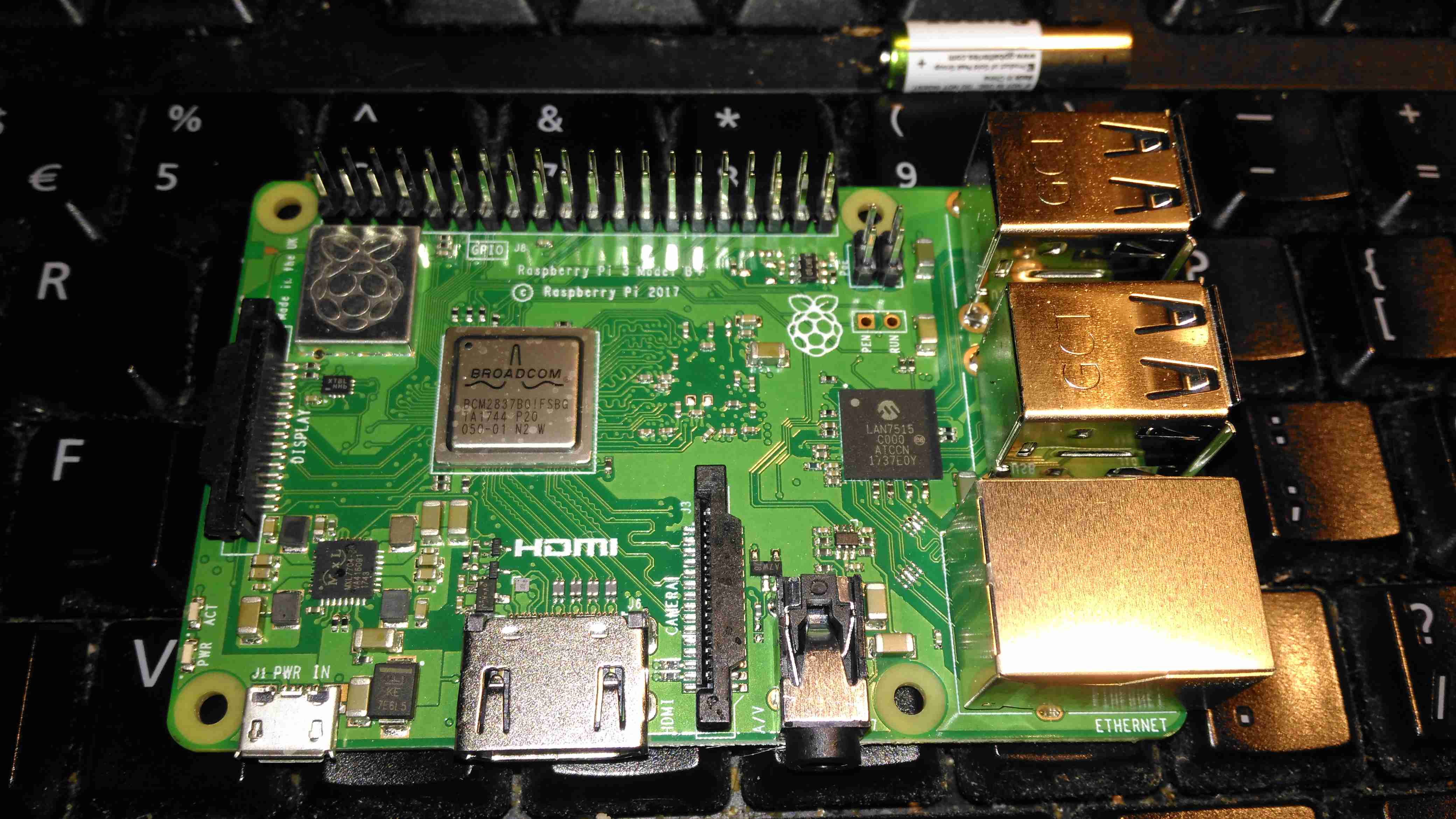
Yesterday, the Raspberry Pi community got a nice surprise – a new Pi! This one has some improved features over the previous RPi 3 Model B:
Improved CPU – 64-Bit 1.4GHz Quad-Core BCM2837B0
Improved WiFi – Dual Band 802.11b/g/n/ac. This is now under a shield on the top of the board.
Improved Ethernet – The USB/Ethernet IC has been replaced with a LAN7515, supporting gigabit ethernet. The backhaul is still over USB2 though, so this would max out at about 300Mbit/s
PoE Support – There’s a new 4-pin header, and a matching HAT for power over ethernet support.
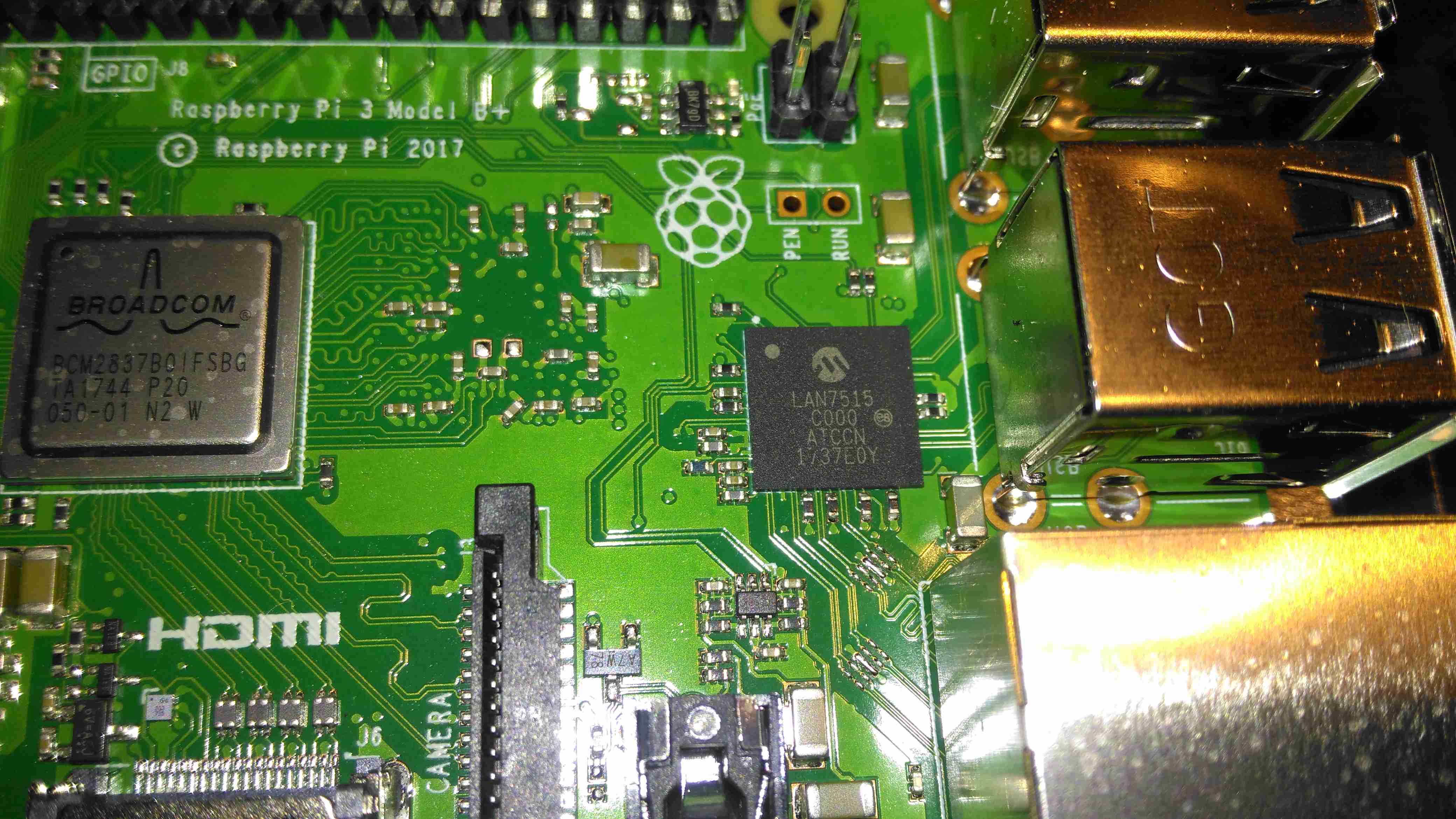
Chipset
The USB/LAN Controller is now a BGA package, supporting gigabit ethernet. The USB connections are still USB2 though, limiting total bandwidth. This shouldn’t be much of an issue though, since anything over the 100Mbit connection we’ve had previously is an improvement.
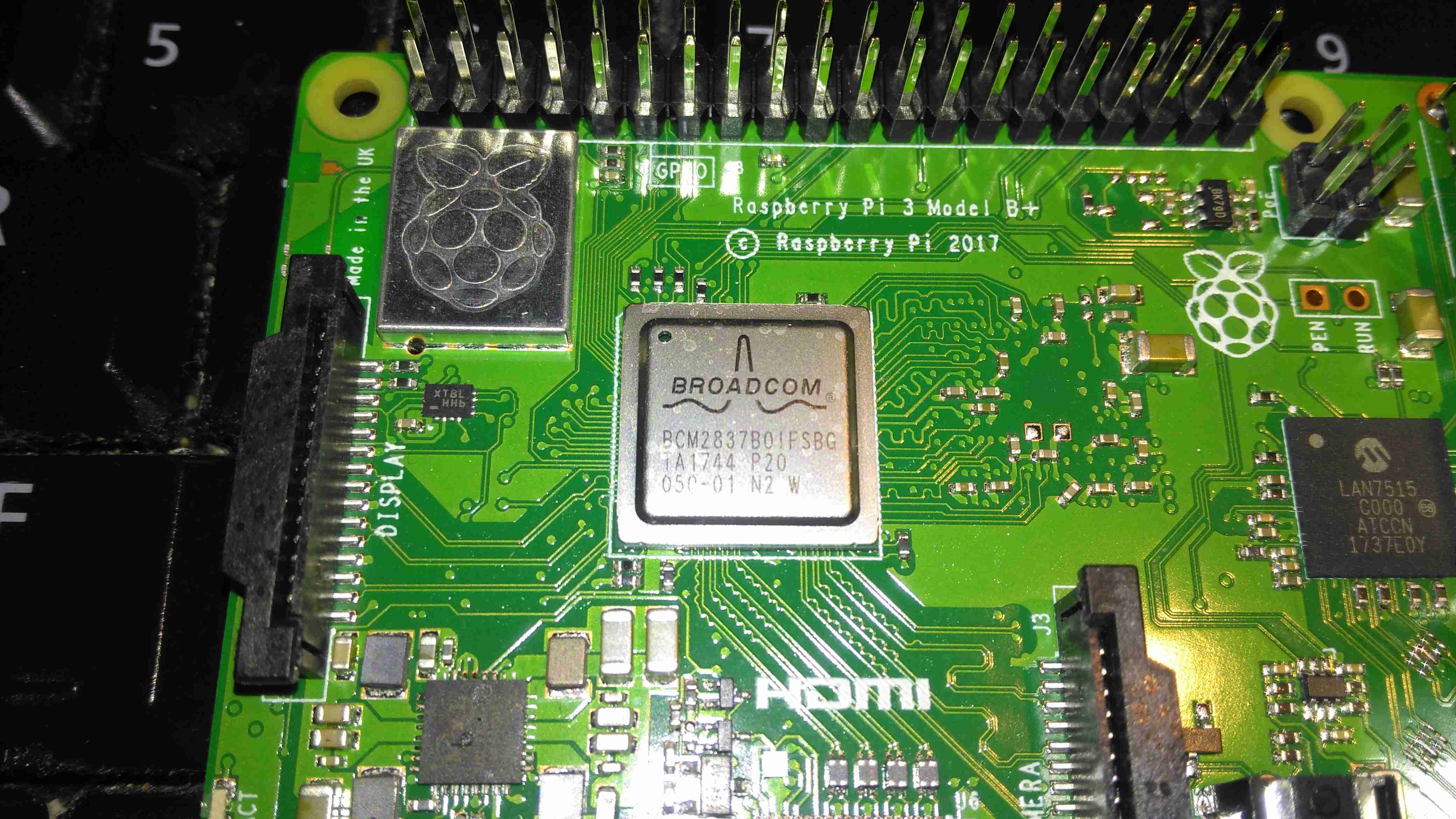
CPU & Radio
The CPU now has a metal heatspreader on top of the die, no doubt to help with cooling under heavy loads. As far as I know, it’s still the same silicon under the hood though. The WiFi radio is under the shielding can to the top left, with the PCB trace antenna down the left edge of the board.
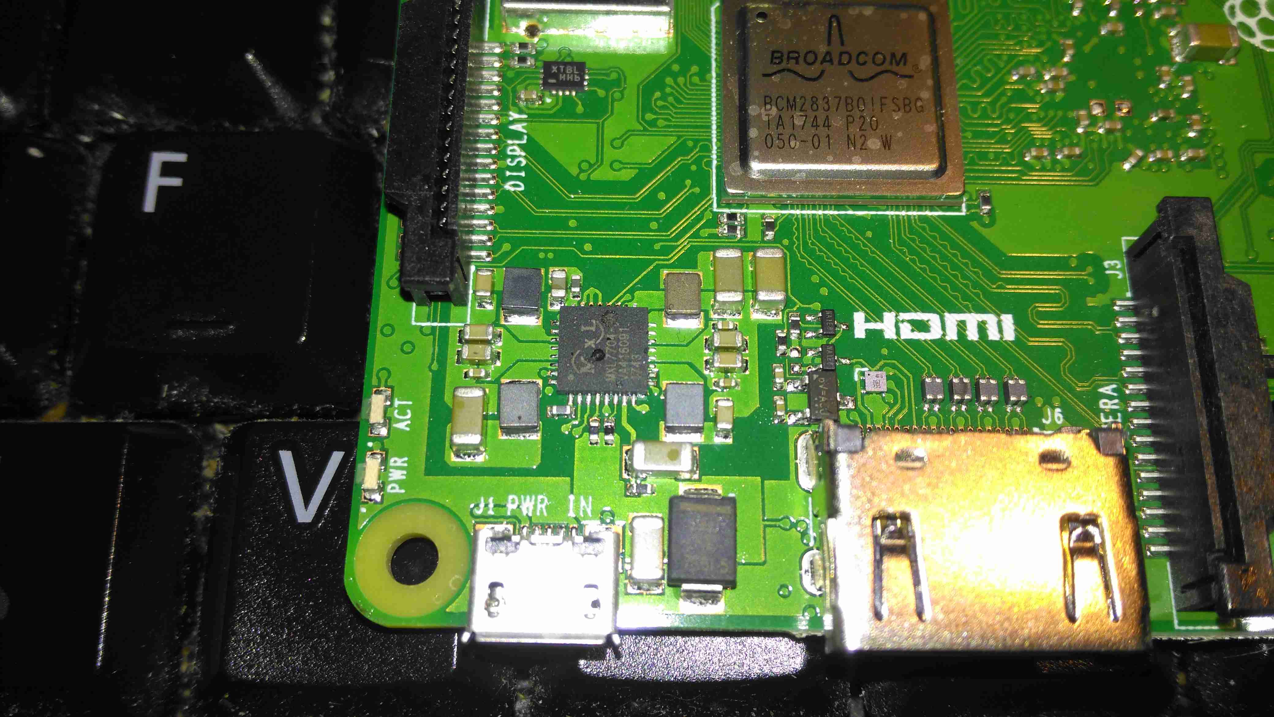
Power Controller
The power supplies are handled on this new Pi by the MaxLinear MxL7704, from what I can tell from MaxLinear’s page, it seems to be somewhat of a collaborative effort to find something that would do the best job, since they apparently worked with the Foundation to get this one right. This IC apparently includes four synchronous step-down buck regulators that provide system, memory, I/O and core power from 1.5A to 4A. An on-board 100mA LDO provides clean 1.5V to 3.6V power for analog sub-systems. This PMIC utilizes a conditional sequencing state machine that is flexible enough to meet the requirements of virtually any processor.
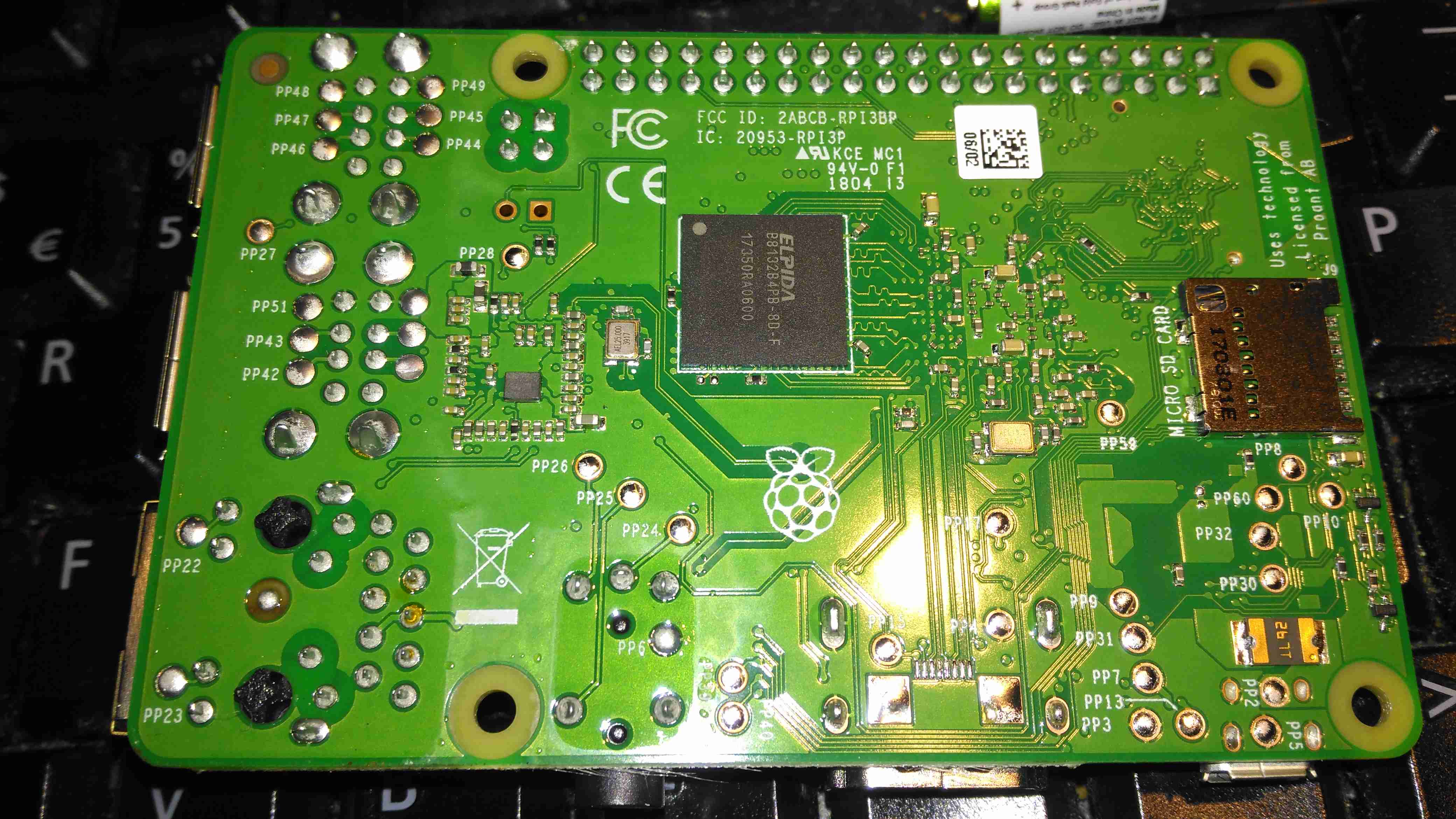
PCB Bottom
The bottom of the PCB has the Elpida 1GB RAM package, which is LPDDR2, along with the MicroSD slot.
A quick benchmark running Raspbian Lite & a SanDisk Ultra 32GB Class 10 SD card gives some nice results:
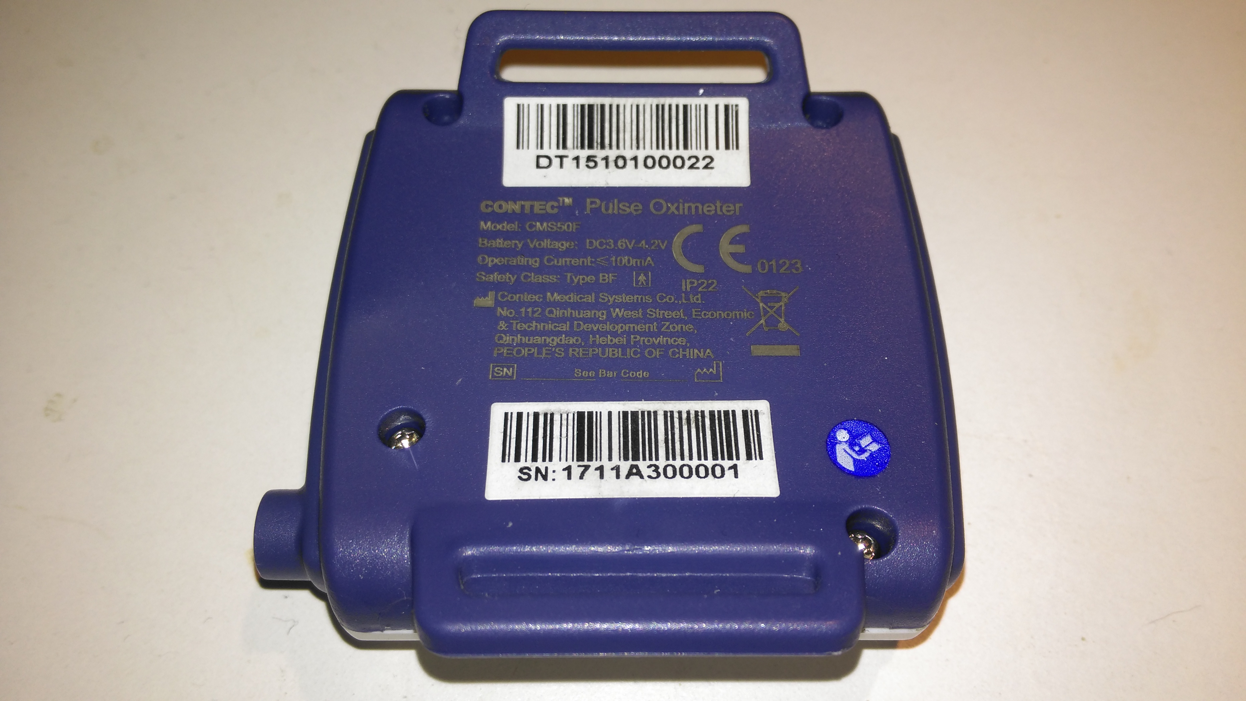
The rear has the specifications, laser-marked into the plastic. The serial numbers are just sticky labels though, and will come off easily with use.
Contec CMS-50F
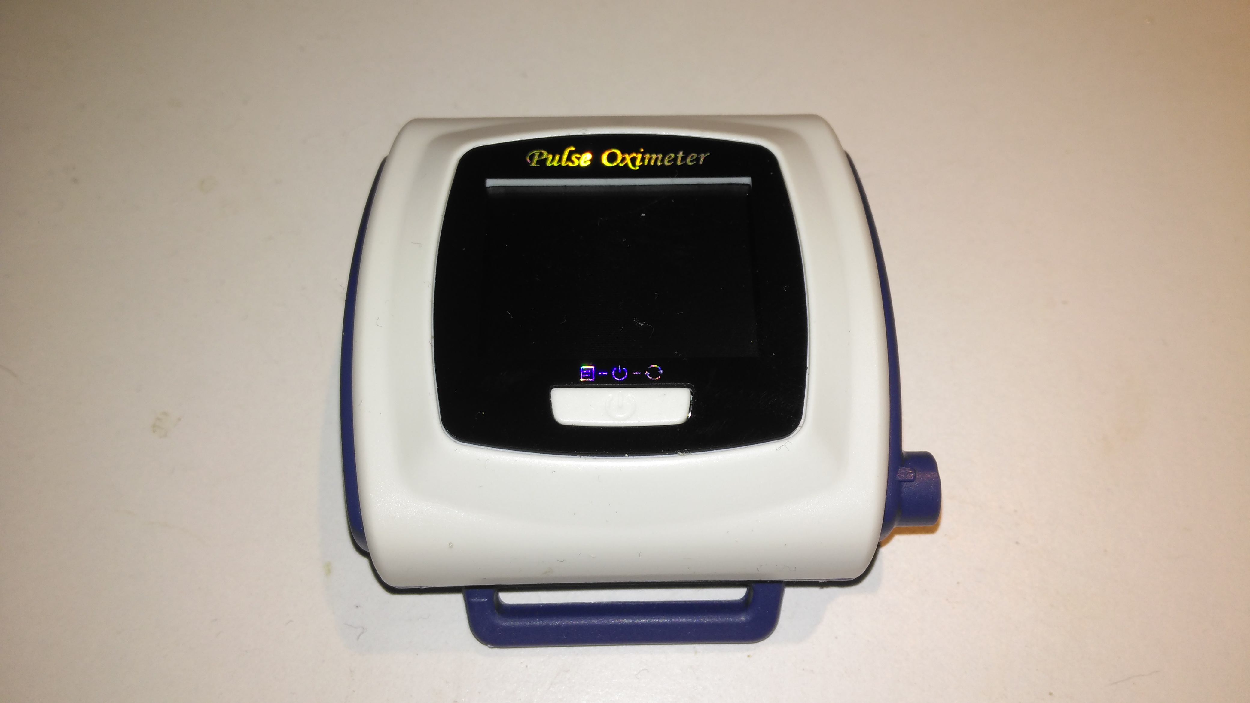
This is the Contec CMS-50F wrist-mounted pulse oximeter unit, which has the capability to record data continuously to onboard memory, to be read out at a later time via a USB-Serial link. There is software supplied with the unit for this purpose, although it suffers from the usual Chinese quality problems. The hardware of this unit is rather well made, the firmware has some niggles but is otherwise fully functional, however the PC software looks completely rushed, is of low quality & just has enough functionality to kind-of pass as usable.
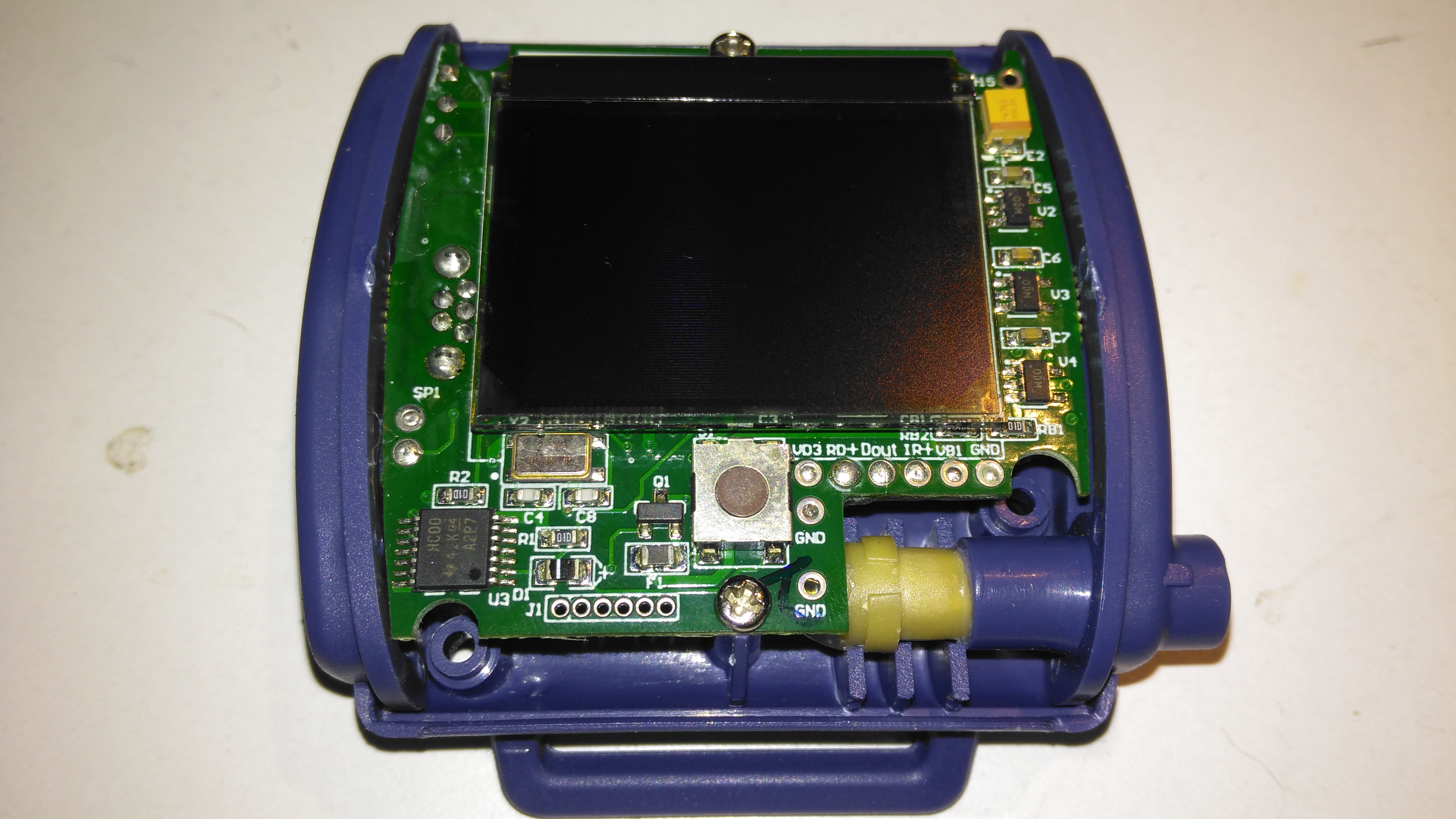
Top Cover Removed
A total of 4 screws hold the casing together, once these are removed the top comes off. The large colour OLED display covers nearly all of the board here. The single button below is the user interface. The connection to the probe is made via the Lemo-style connector on the lower right.
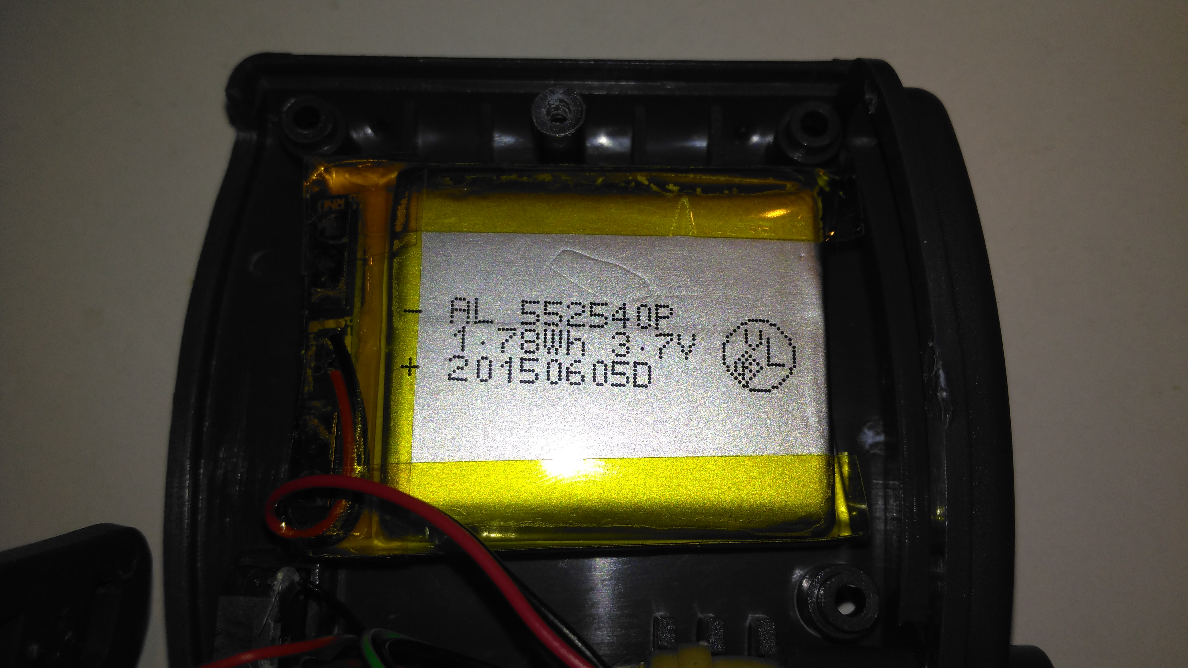
Lithium Cell
Power is provided by a relatively large lithium-ion cell, rated at 1.78Wh.
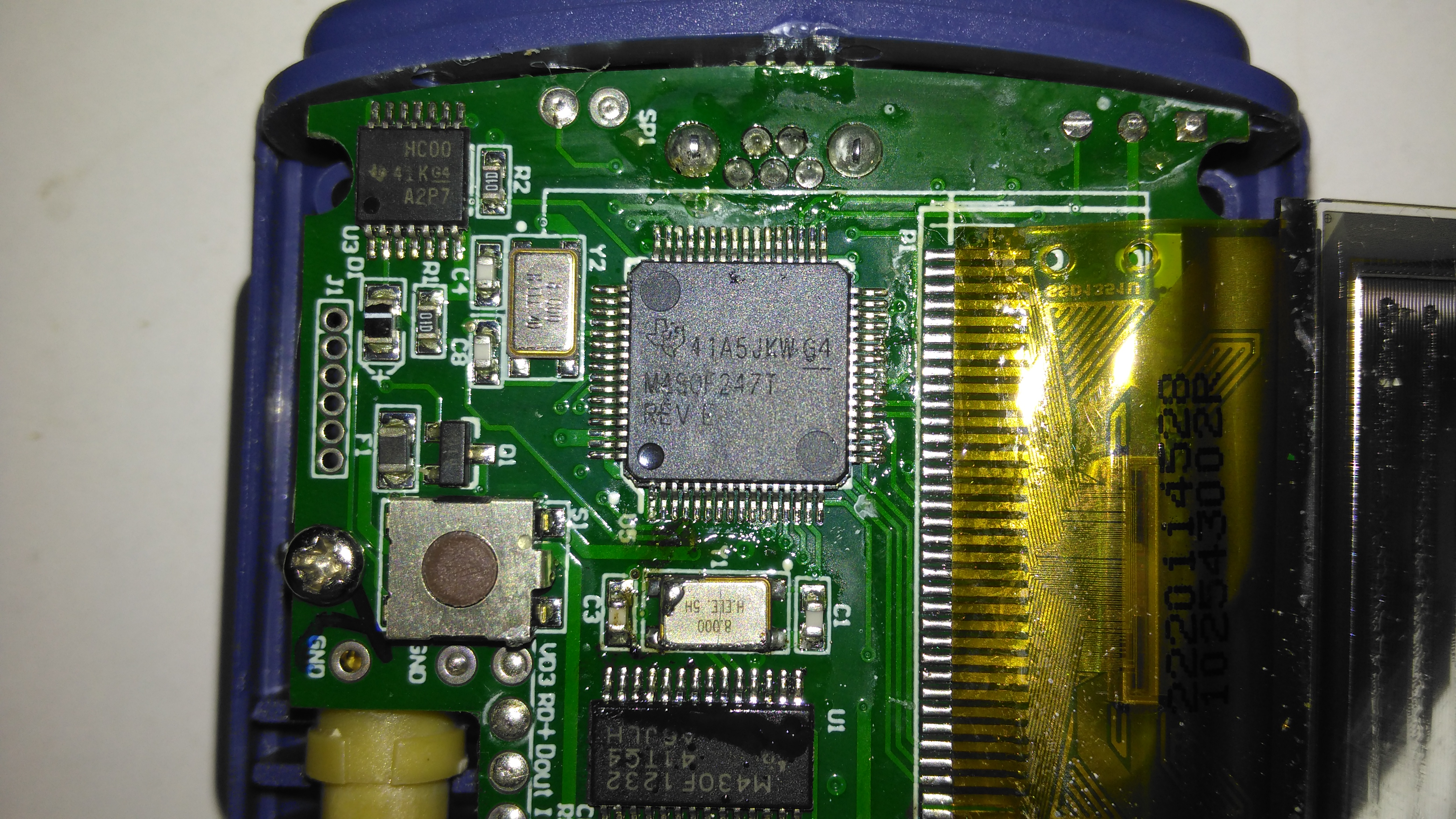
Main Processor
All the heavy lifting work of the LCD, serial comms, etc are handled by this large Texas Instruments microcontroller, a MSP430F247. The clock crystal is just to the left, with the programming pins. I’m not sure of the purpose of the small IC in the top left corner, I couldn’t find any reference to the markings.
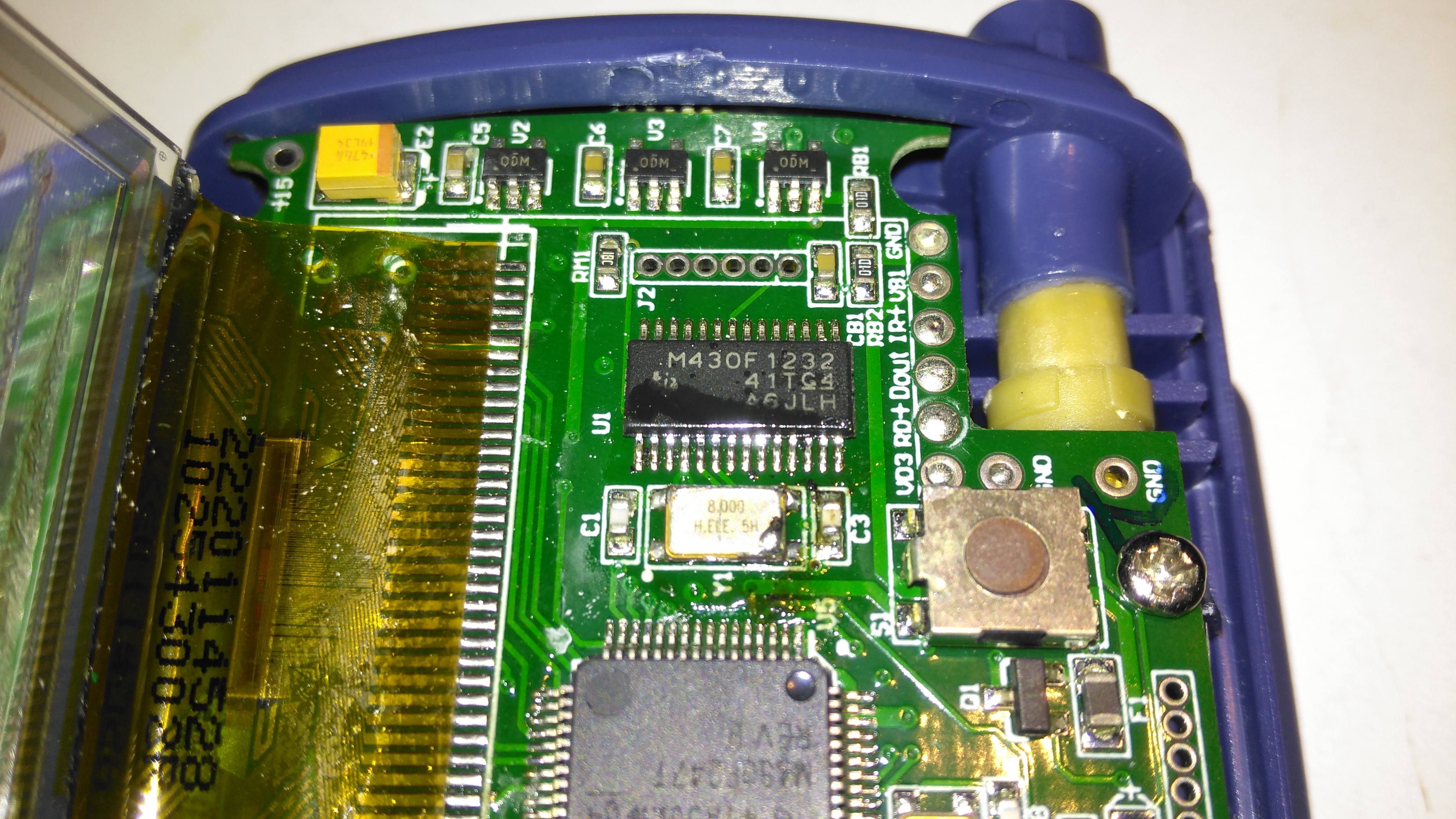
Aux Processor
The actual pulse oximetry sensor readings seem to be dealth with by a secondary microcontroller, a Texas Instruments M430F1232 Mixed-Signal micro. This has it’s own clock crystal just underneath. The connections to the probe socket are to the right of this µC, while the programming bus is broken out to vias just above. The final devices on this side of the board are 3 linear regulators, supplying the rails to run all the logic in this device.
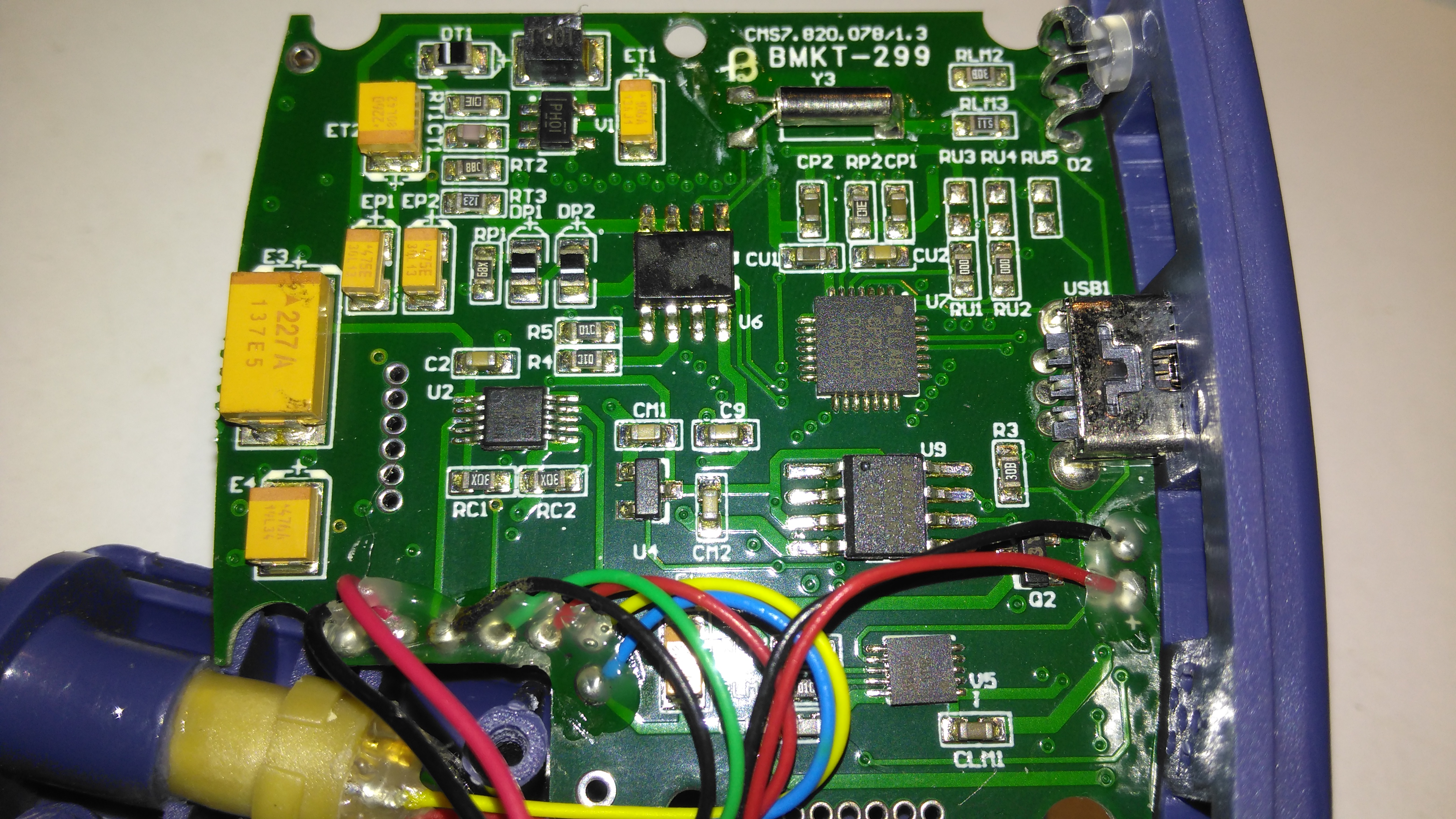
Main PCB Rear
The rear of the PCB has the SiLabs CL2102 USB-Serial interface IC, the large Winbond 25X40CLNIG 512KByte SPI flash for recording oximetry data, and some of the power support components. The RTC crystal is also located here at the top of the board. Up in the top left corner is a Texas Instruments TPS61041 Boost converter, with it’s associated components. This is probably supplying the main voltage for the OLED display module.
Over the past few weeks, the host I’ve been with for over 3 years, OVH, announced a rather large price increase of 20% because of Brexit – the current universal excuse to squeeze the customer for more cash. This change has sent the price of my dedicated server solution with them to over £45 a month. Doing some napkin-calculation gave me £18 a month in extra power to run a small server locally. So I’ve decided to bring the hosting solution back to my local network & run from my domestic internet link, which at 200Mbit/s DL & 20Mbit/s UL should be plenty fast enough to handle the modest levels of traffic I usually get.
Obviously, some hardware was required for this, so I obtained this beauty cheap on eBay:
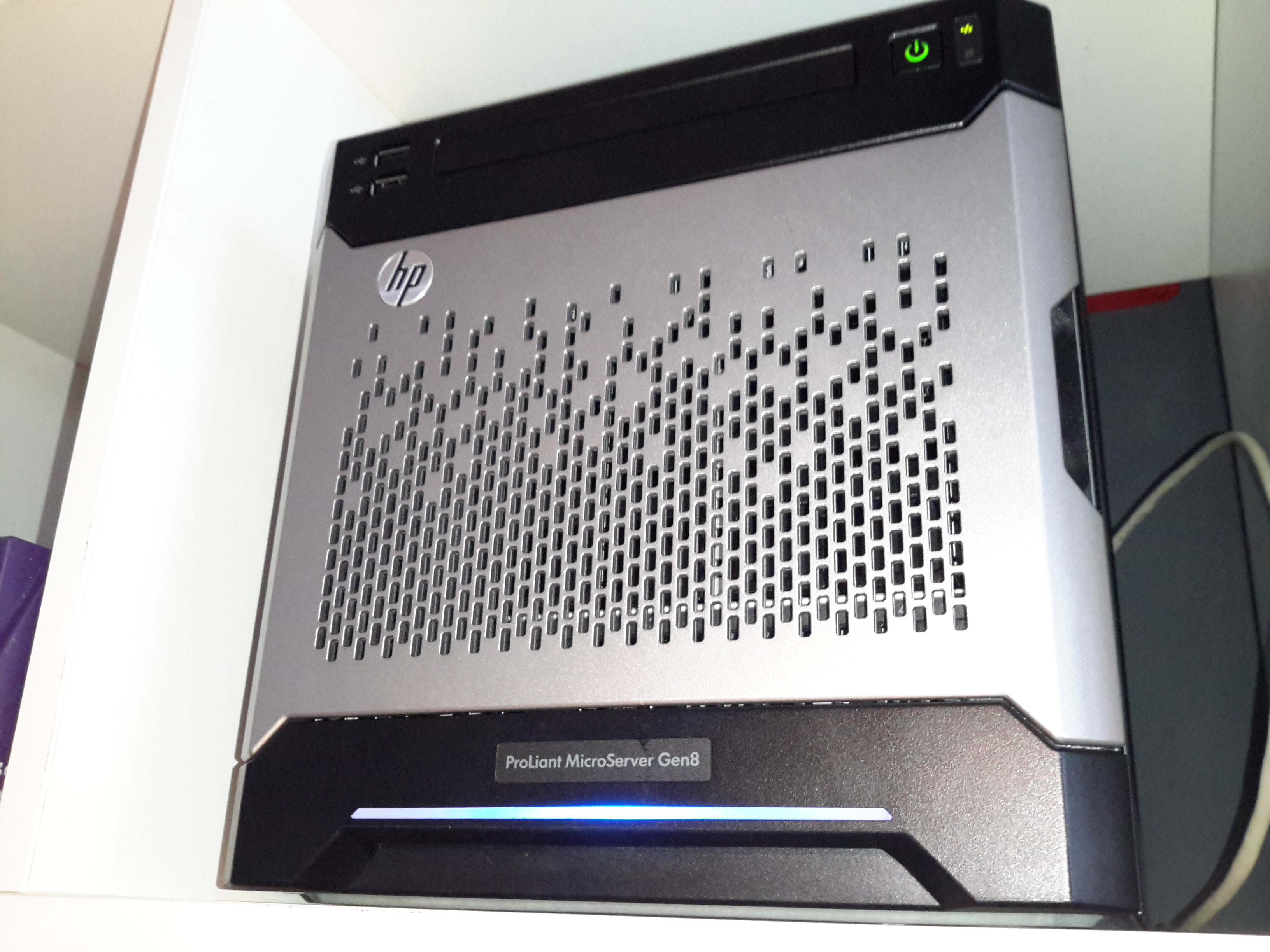
HP Proliant MicroServer Gen 8
This is a Gen 8 HP Proliant Microserver, very small & quiet, perfect for the job. This came with 4GB of RAM installed from the factory, and a Celeron G1610T running at 2.3GHz. Both are a little limited, so some upgrades will be made to the system.
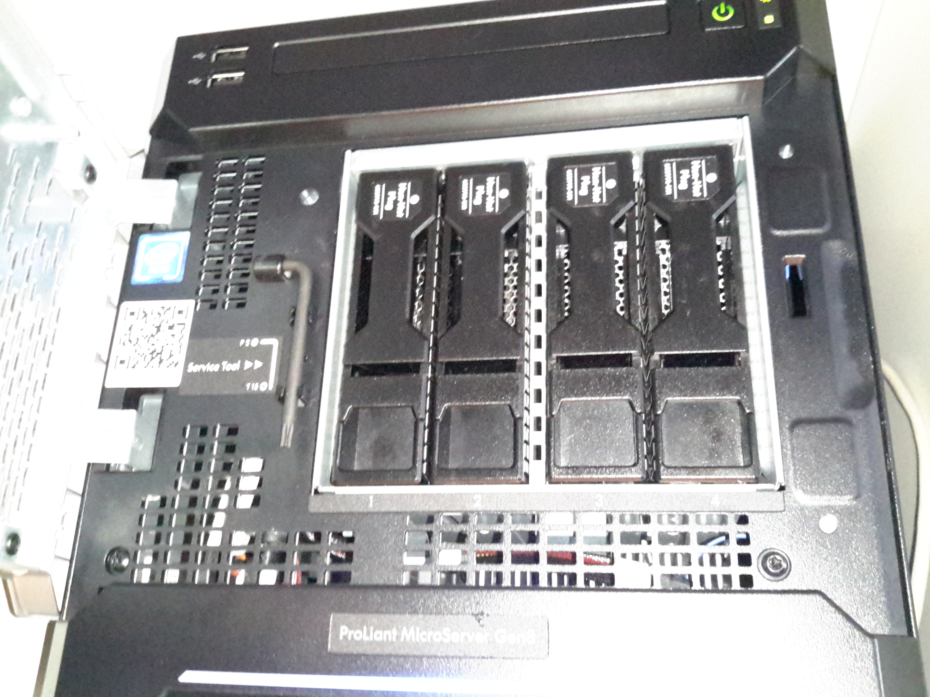
Disk Bays
4 SATA drive bays are located behind the magnetically-locked front door, there’s a 250GB boot disk in here along with a pair of 500GB disks in RAID1 to handle the website files & databases. For my online file hosting site, the server has a backend NFS link direct to Volantis – my 28TB storage server. This arrangement keeps the large file storage side of things off the web server disks & on a NAS, where it should be.
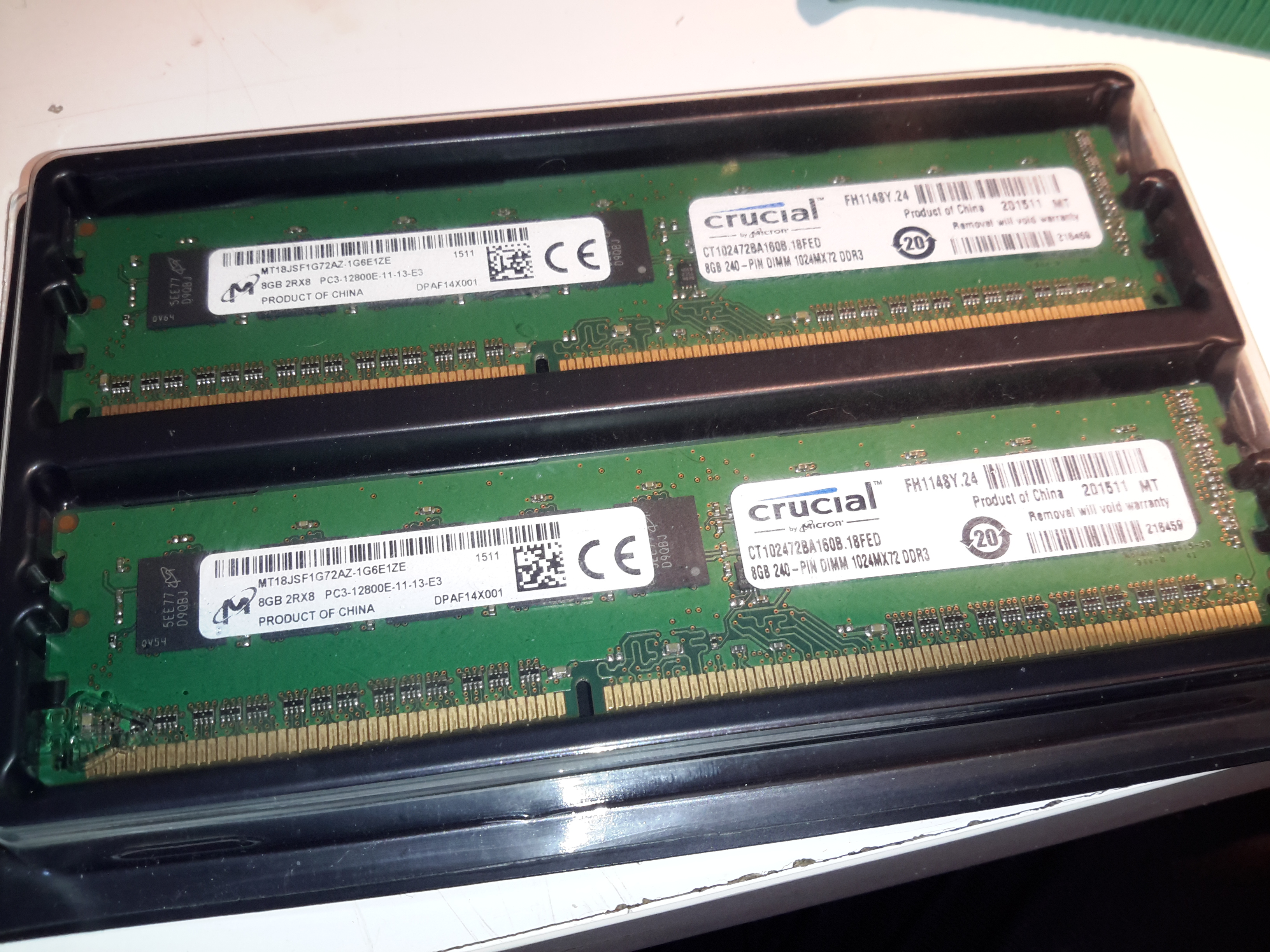
Extra RAM
First thing is a RAM upgrade to the full supported capacity of 16GB. This being a Proliant server machine, doesn’t take anything of a standard flavour, it’s requirements are DDR3-10600E or DDR3-12800E (the E in here being ECC). This memory is both eye-wateringly expensive & difficult to find anywhere in stock. It’s much cheaper & easier to find the ECC Registered variety, but alas this isn’t compatible.
Over the past 48 hours or so, I’ve been migrating everything over to the new baby server, with a couple of associated teething problems, but everything seems to have gone well so far. The remaining job to get everything running as it should is an external mail relay – sending any kind of email from a dynamic IP / domestic ISP usually gets it spam binned by the big providers instantly, regardless of it actually being spam or not – more to come on that setup & configuring postfix to use an external SMTP relay server soon!
If anyone does find something weird going on with the blog, do let me know via the contact page or comments!
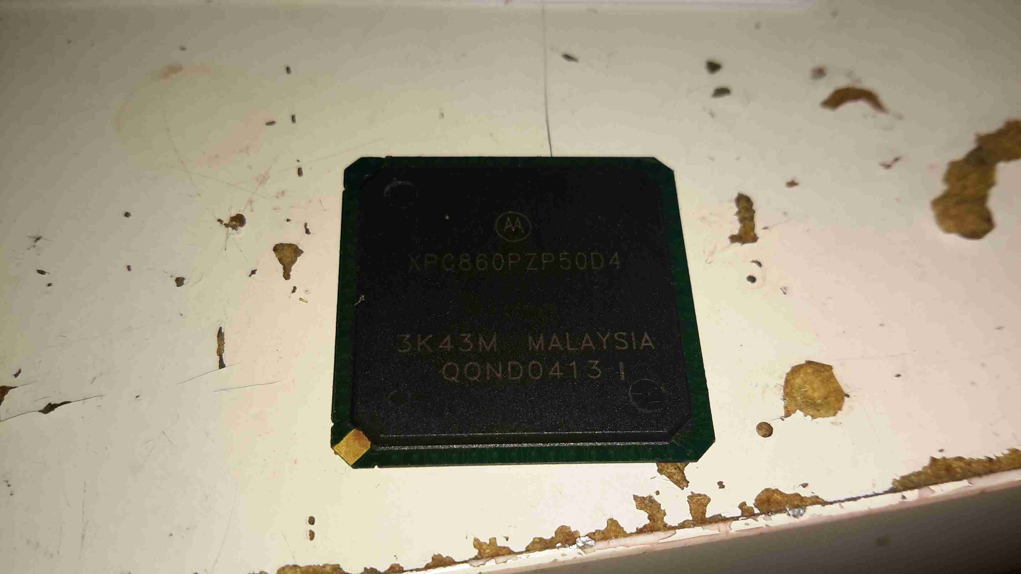
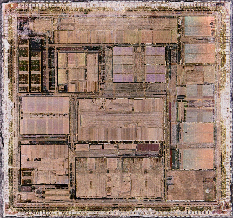
This is a System On Chip from Motorola, designed for network routing applications. This chip contains a hell of a feature set, so I’ll just include an excerpt from the datasheet:
XPC860PZP50D4 Die
Embedded single-issue, 32-bit MPC8xx core (implementing the PowerPC
architecture) with thirty-two 32-bit general-purpose registers (GPRs)
— The core performs branch prediction with conditional prefetch, without
conditional execution
— 4- or 8-Kbyte data cache and 4- or 16-Kbyte instruction cache (see Table 1)
– 16-Kbyte instruction caches are four-way, set-associative with 256 sets;
4-Kbyte instruction caches are two-way, set-associative with 128 sets.
– 8-Kbyte data caches are two-way, set-associative with 256 sets; 4-Kbyte data
caches are two-way, set-associative with 128 sets.
– Cache coherency for both instruction and data caches is maintained on 128-bit
(4-word) cache blocks.
– Caches are physically addressed, implement a least recently used (LRU)
replacement algorithm, and are lockable on a cache block basis.
— Instruction and data caches are two-way, set-associative, physically addressed,
LRU replacement, and lockable on-line granularity.
— MMUs with 32-entry TLB, fully associative instruction, and data TLBs
— MMUs support multiple page sizes of 4, 16, and 512 Kbytes, and 8 Mbytes; 16
virtual address spaces and 16 protection groups
— Advanced on-chip-emulation debug mode
Up to 32-bit data bus (dynamic bus sizing for 8, 16, and 32 bits)
32 address lines
Operates at up to 80 MHz
Memory controller (eight banks)
— Contains complete dynamic RAM (DRAM) controller
— Each bank can be a chip select or RAS to support a DRAM bank
— Up to 15 wait states programmable per memory bank
— Glueless interface to DRAM, SIMMS, SRAM, EPROM, Flash EPROM, and
other memory devices.
— DRAM controller programmable to support most size and speed memory
interfaces
— Four CAS lines, four WE lines, one OE line
— Boot chip-select available at reset (options for 8-, 16-, or 32-bit memory)
— Variable block sizes (32 Kbyte to 256 Mbyte)
— Selectable write protection
— On-chip bus arbitration logic
General-purpose timers
— Four 16-bit timers or two 32-bit timers
— Gate mode can enable/disable counting
— Interrupt can be masked on reference match and event capture
System integration unit (SIU)
— Bus monitor
— Software watchdog
— Periodic interrupt timer (PIT)
— Low-power stop mode
— Clock synthesizer
— Decrementer, time base, and real-time clock (RTC) from the PowerPC
architecture
— Reset controller
— IEEE 1149.1 test access port (JTAG)
Interrupts
— Seven external interrupt request (IRQ) lines
— 12 port pins with interrupt capability
— 23 internal interrupt sources
— Programmable priority between SCCs
— Programmable highest priority request
10/100 Mbps Ethernet support, fully compliant with the IEEE 802.3u Standard (not
available when using ATM over UTOPIA interface)
ATM support compliant with ATM forum UNI 4.0 specification
— Cell processing up to 50–70 Mbps at 50-MHz system clock
— Cell multiplexing/demultiplexing
— Support of AAL5 and AAL0 protocols on a per-VC basis. AAL0 support enables
OAM and software implementation of other protocols).
— ATM pace control (APC) scheduler, providing direct support for constant bit rate
(CBR) and unspecified bit rate (UBR) and providing control mechanisms
enabling software support of available bit rate (ABR)
— Physical interface support for UTOPIA (10/100-Mbps is not supported with this
interface) and byte-aligned serial (for example, T1/E1/ADSL)
— UTOPIA-mode ATM supports level-1 master with cell-level handshake,
multi-PHY (up to 4 physical layer devices), connection to 25-, 51-, or 155-Mbps
framers, and UTOPIA/system clock ratios of 1/2 or 1/3.
— Serial-mode ATM connection supports transmission convergence (TC) function
for T1/E1/ADSL lines; cell delineation; cell payload scrambling/descrambling;
automatic idle/unassigned cell insertion/stripping; header error control (HEC)
generation, checking, and statistics.
Communications processor module (CPM)
— RISC communications processor (CP)
— Communication-specific commands (for example, GRACEFUL STOP TRANSMIT ,
ENTER HUNT MODE , and RESTART TRANSMIT )
— Supports continuous mode transmission and reception on all serial channels
— Up to 8Kbytes of dual-port RAM
— 16 serial DMA (SDMA) channels
— Three parallel I/O registers with open-drain capability
Four baud-rate generators (BRGs)
— Independent (can be connected to any SCC or SMC)
— Allow changes during operation
— Autobaud support option
Four serial communications controllers (SCCs)
— Ethernet/IEEE 802.3 optional on SCC1–4, supporting full 10-Mbps operation
(available only on specially programmed devices).
— HDLC/SDLC (all channels supported at 2 Mbps)
— HDLC bus (implements an HDLC-based local area network (LAN))
— Asynchronous HDLC to support PPP (point-to-point protocol)
— AppleTalk
— Universal asynchronous receiver transmitter (UART)
— Synchronous UART
— Serial infrared (IrDA)
— Binary synchronous communication (BISYNC)
— Totally transparent (bit streams)
— Totally transparent (frame based with optional cyclic redundancy check (CRC))
Two SMCs (serial management channels)
— UART
— Transparent
— General circuit interface (GCI) controller
— Can be connected to the time-division multiplexed (TDM) channels
One SPI (serial peripheral interface)
— Supports master and slave modes
— Supports multimaster operation on the same bus
One I 2 C (inter-integrated circuit) port
— Supports master and slave modes
— Multiple-master environment support
Time-slot assigner (TSA)
— Allows SCCs and SMCs to run in multiplexed and/or non-multiplexed operation
— Supports T1, CEPT, PCM highway, ISDN basic rate, ISDN primary rate, user
defined
— 1- or 8-bit resolution
— Allows independent transmit and receive routing, frame synchronization,
clocking
— Allows dynamic changes
— Can be internally connected to six serial channels (four SCCs and two SMCs)
Parallel interface port (PIP)
— Centronics interface support
— Supports fast connection between compatible ports on the MPC860 or the
MC68360
PCMCIA interface
— Master (socket) interface, release 2.1 compliant
— Supports two independent PCMCIA sockets
— Eight memory or I/O windows supported
Low power support
— Full on—all units fully powered
— Doze—core functional units disabled, except time base decrementer, PLL,
memory controller, RTC, and CPM in low-power standby
— Sleep—all units disabled, except RTC and PIT, PLL active for fast wake up
— Deep sleep—all units disabled including PLL, except RTC and PIT
— Power down mode— all units powered down, except PLL, RTC, PIT, time base,
and decrementer
Debug interface
— Eight comparators: four operate on instruction address, two operate on data
address, and two operate on data
— Supports conditions: = ≠ < >
— Each watchpoint can generate a break-point internally
3.3 V operation with 5-V TTL compatibility except EXTAL and EXTCLK
357-pin ball grid array (BGA) package
Alas, my old trusty Hameg HM303 30MHz oscilloscope has finally died. I’ve had this scope for many years, an eBay buy when I noticed they were going cheap.
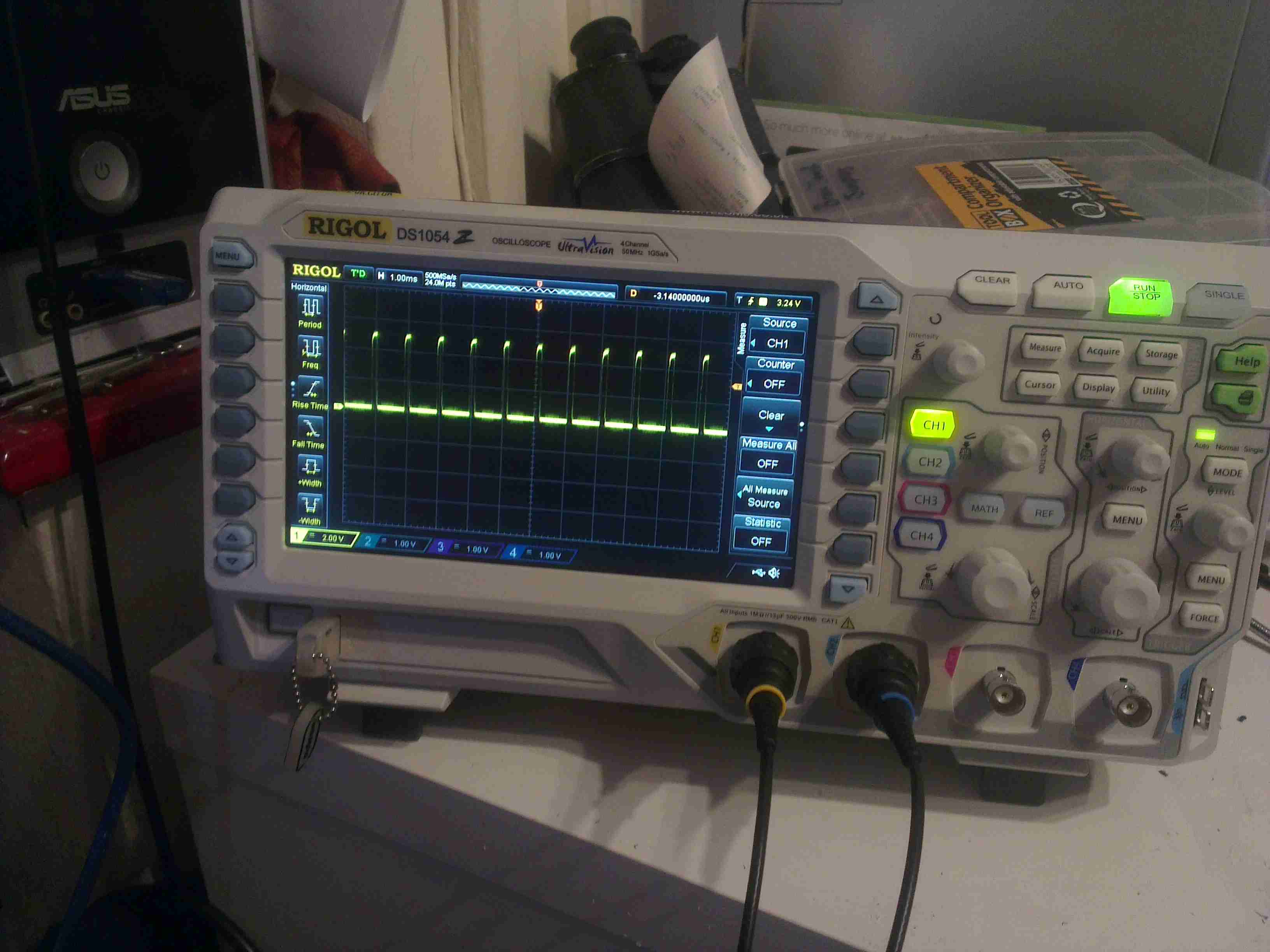
It’s been replaced with a brand new Rigol DS1054Z, a 4-channel 50MHz DSO.
Scope
This is a big jump from the old analogue CRT scope I was using, it’s certainly going to be a steep learning curve!
System Info
I chose this scope through the help of the EEVBlog & it’s associated forums. Through this I discovered that I could upgrade the scope with a key to enable some extra features! In the above screenshot, the key has been applied, and the model number now shown is the DS1104Z.
This is the next scope up in the model chain, with many more triggering options, serial decoders, higher memory depth, recording & 100MHz bandwidth. While I rarely need to measure anything higher than in the kHz range, these options will definitely come in useful! The list of installed options is below:
Installed Options
And now for some sample waveforms, the scope has the option to save screenshots to USB flash disks, so when I make posts with waveforms in the future, the need to photo the screen of the scope is gone!
This is a cheap Sigma branded keychain photoframe. User buttons for power & selecting photos are on the left.
There are two white LEDs on the bottom edge that function as a torch as well.
Display
Front of the unit removed, showing the LCD module. The USB jack is bottom left, next to the pair of white LEDs & above that is the 32kHz watch crystal that the CPU uses for timekeeping.
Back Removed
Here the back has been removed showing the 3.7v Li-Ion cell used to provide power.
Display Folded Back
Here the display has been removed from the PCB exposing the chipset.
Chipset
Here the CPU blob-top chip & a flash memory IC are visible. The CPU is a Sitronix ST2205U.
Here is one of the first USB tuners that was available from Hauppauge Computer Works. Totally analog tuner of course, this model required 2 cables – a USB interface & a sound cable for the audio output of the tuner.
I/O
A/V connections.
Label
For those who are interested. Here is the label with the model details.
Antenna Connection
Connection to an external antenna.
PCB Bottom
Bottom of the PCB.
PCB Top
Top of the PCB showing the USB interface IC (top left), cache memory (top right) & the main tuner assembly.
Here is a cheap chinese made flash drive given out for free by Westlaw UK. Capacity 512MB
PCB
Here is the PCB removed from the casing, USB connector on the left, followed by the clock crystal for the flash controller, a CBM2092, which is a Chipsbank part. 512MB flash memory IC, unknown maker. Access LED on far right of the board.
This is a HP PhotoSmart 375 portable photo printer. With built in card reader, screen & PictBridge.
Top of the printer showing the UI Buttons & Screen.
Front
Front of the unit, card reader slots at the top, Pictbridge USB connector at top left. Paper out slot at bottom. Cartridge door is on the right.
Cartridge Door
Here the cartridge door is open. Takes HP 95 Tri-Colour Inkjet Cartridge.
Battery Compartment
Battery compartment on the bottom of the unit. A Li-Ion battery pack can be installed here for mobile photo printing.
Bottom Label
Specifications label.
USB + Power
Power adaptor & USB connection for PC use.
Paper Tray
Rear door opened. Showing the paper feed tray.
Paper Feeder
Rear door has been removed in this shot. Paper feed roller & platen roller can be seen here.
Rear Cover Paper Feeder
Paper holder attached to rear door.
Top Cover
Bottom of the top cover, with connections for the buttons & LCD panel.
Main PCB
This is the main PCB of the unit. Controls all aspects of the printer. CPU in center, card reader sockets are along bottom edge. various support circuitry surrounds the CPU.
Rear
Rear shell has been removed here. Showing the main frame & the carriage drive motor on the left.
Carriage Drive
Closeup of the carriage drive motor & timing belt system. All the motors in this printer are DC servo motors, not steppers.
Main Drive Motor
Main drive motor, feeds paper, drives rollers, operates cleaning mechanism for the inkjets.
Shaft Encoder
Mainshaft encoder. Main drive motor is bottom right hand side with timing belt drive.
CPU
Closeup of the CPU. This is a Phillips ARM chip, unknown spec.
Card Reader Sockets
Detail of the card reader sockets, this unit takes all current types of Flash memory card.
HP 95 Tri-color Inkjet Print Cartridge
Tip Jar
If you’ve found my content useful, please consider leaving a donation by clicking the Tip Jar below!
All collected funds go towards new content & the costs of keeping the server online.