Posted on Leave a comment

Tenma 72-10405 DMM Teardown

Tenma DMM
Tenma DMM

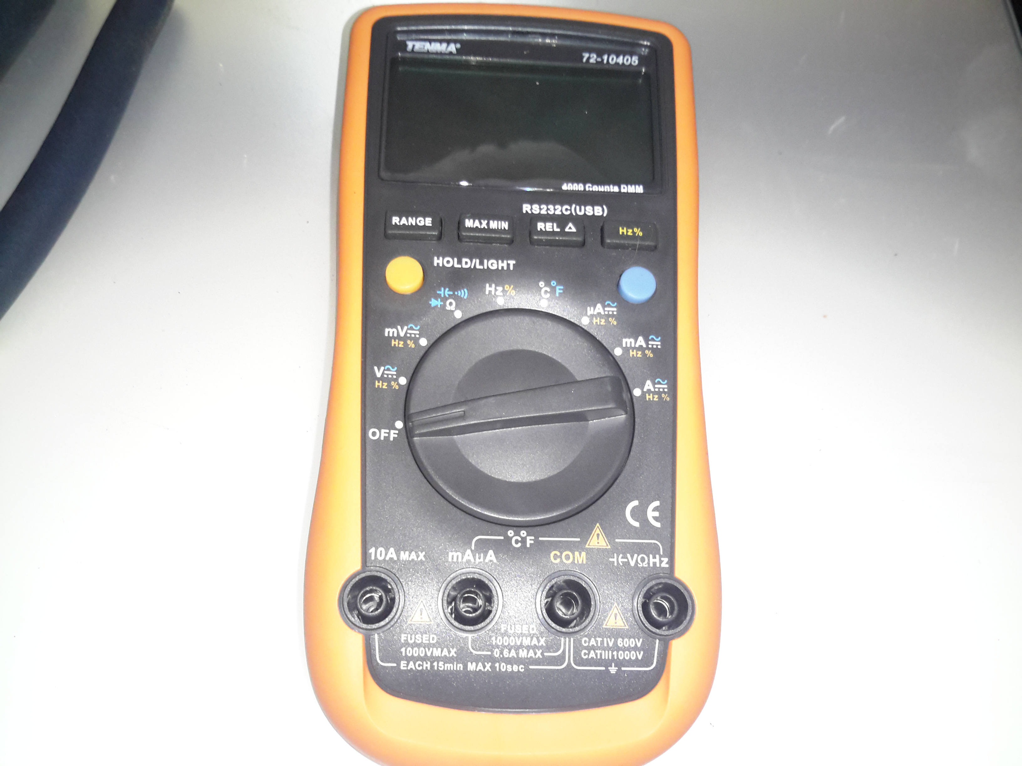
Well it’s time for a new DMM. After the last pair of eBay El-Cheapo Chinese meters just didn’t last very well, I decided a proper meter was required. This one is a Tenma 72-10405, stocked by Farnell for under £60. Not quite as many festures as the cheapo Chinese meters, but I expect this one to be a bit more reliable.

PCB Rear
PCB Rear

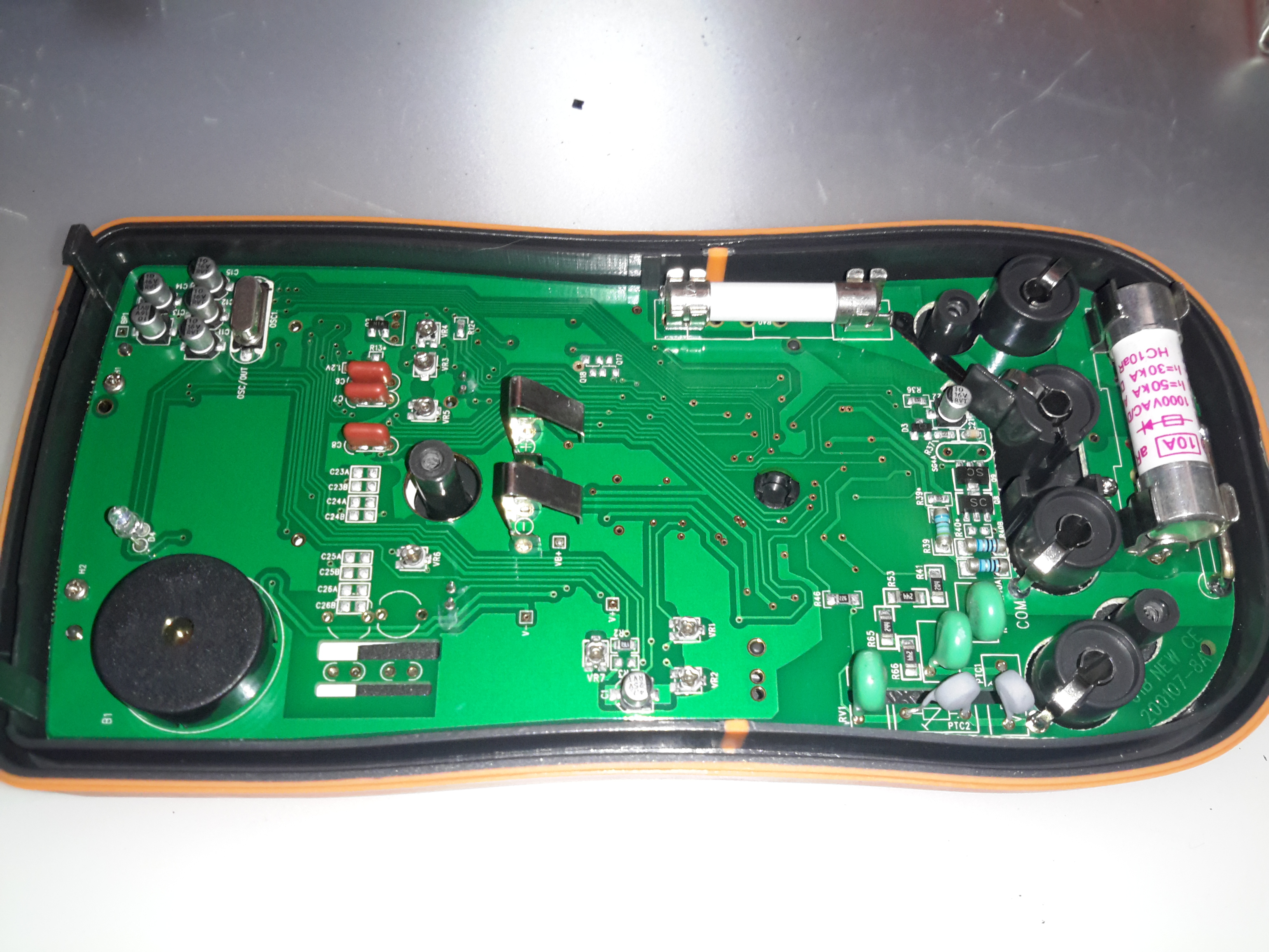
Since I can’t have anything without seeing how it’s put together, here’s the inside of the DMM. (Fuse access is only possible by taking the back cover off as well. The 9v PP3 battery has a seperate cover).

PCB Rear Bottom
PCB Rear Bottom

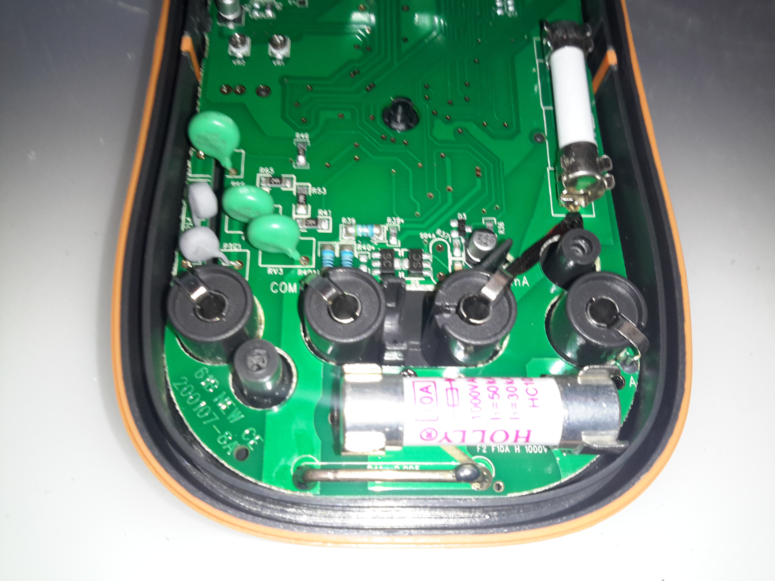
He’s the input section of the meter, with the 10A HRC fuse & current shunt for the high-amps range. The other fuse above is for the mA/µA ranges. The back cover has a wide lip around the edge, that slots into a recess in the front cover, presumably for blast protection if the meter should meet a sticky end. The HRC fuses are a definite improvement over the cheap DMMs, they only have 15mm glass fuses, and no blast protection built into the casing.
There are some MOVs for input protection on the volts/ohms jack, the jacks themselves are nothing more than stampings though.

PCB Rear Top
PCB Rear Top

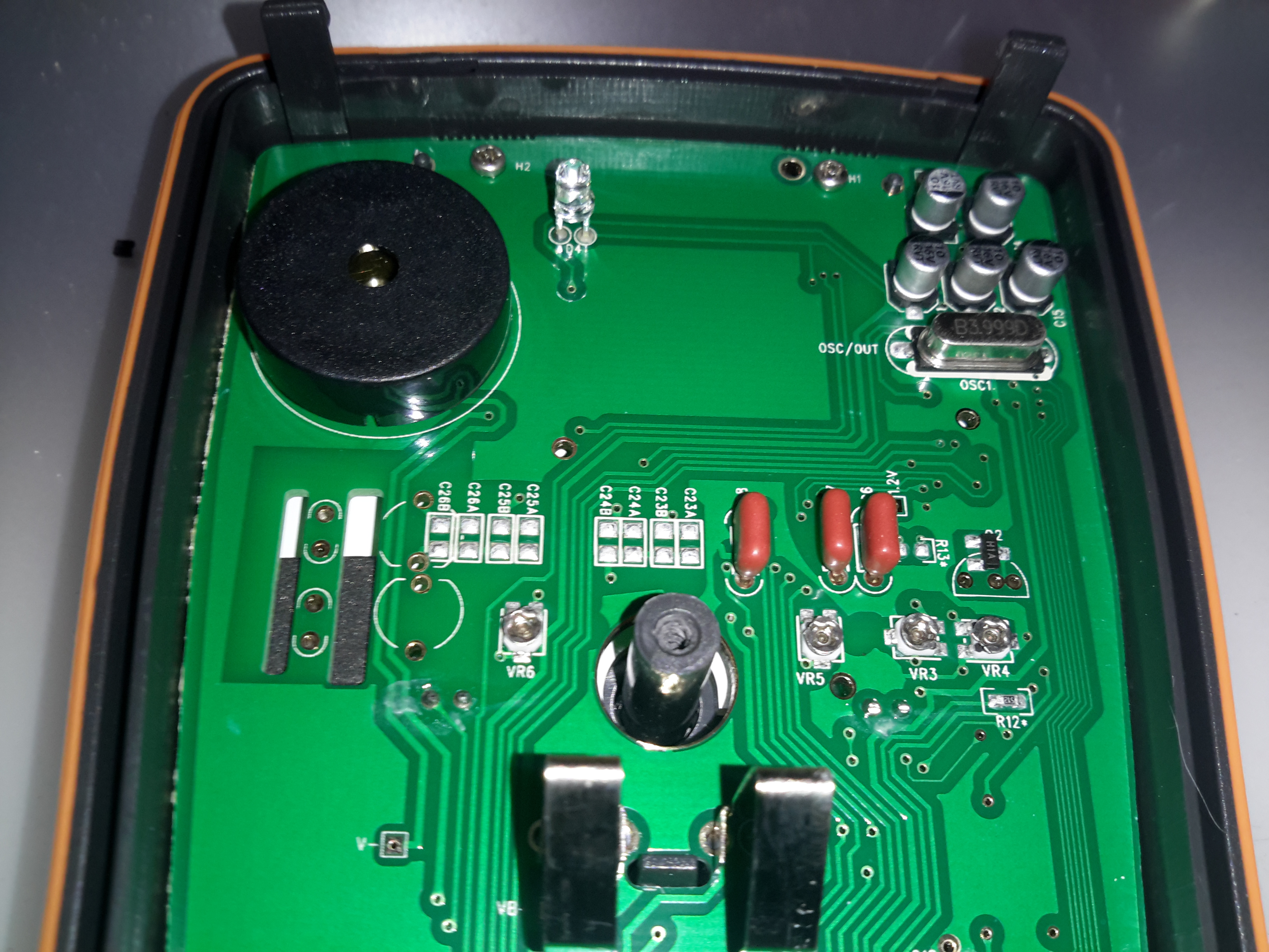
Not much at the other side of the board, there’s the IR LED for the RS232 interface & the beeper.

PCB Front
PCB Front

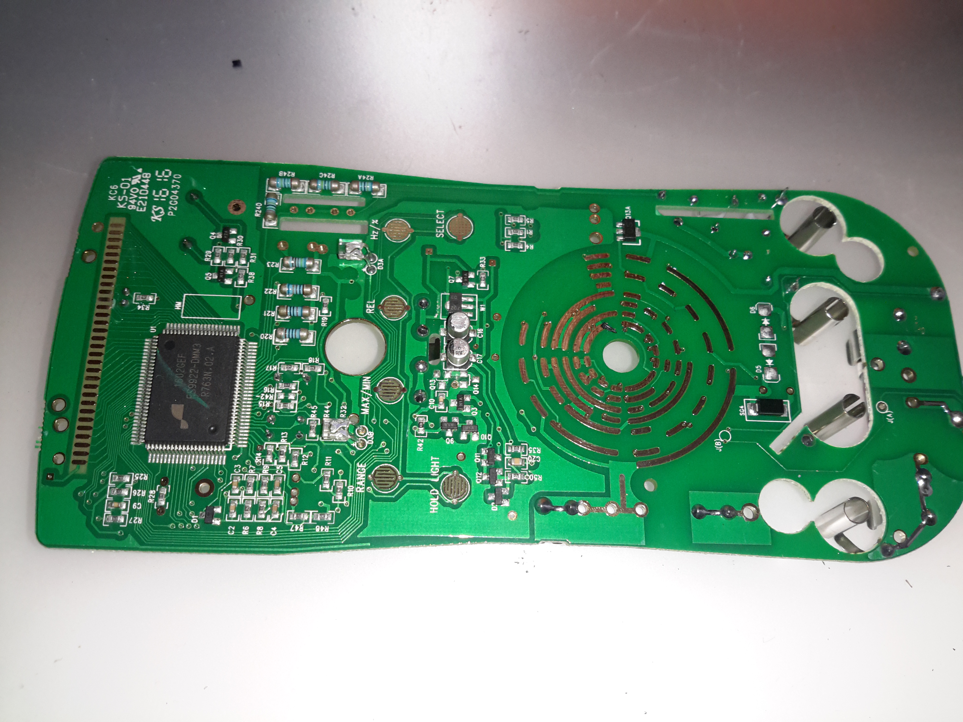
Most of the other components are on the other side of the PCB under the LCD display. The range switch is in the centre, while the main chipset is on the left.

DMM Chipset
DMM Chipset

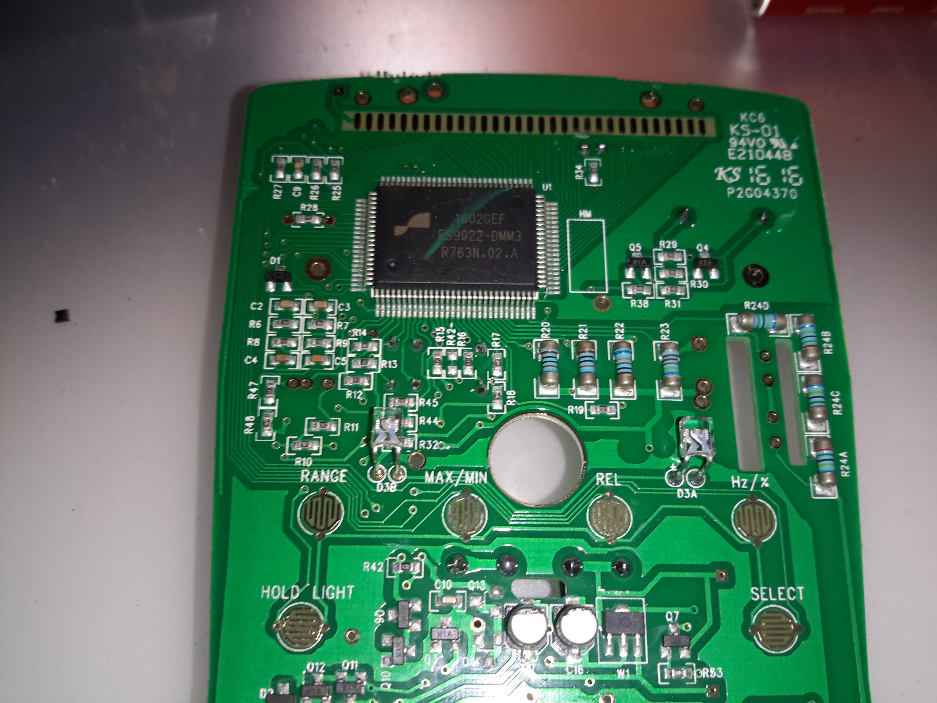
The chipset of this meter is a FS9922-DMM3 from Fortune Semiconductor, this is a dedicated DMM chipset with built in ADCs & microcontroller.

Posted on Leave a comment

Cisco 2G Fibre Channel SFP Module

2G Fibre Tranciever
2G Fibre Transceiver

Here is a 2Gbit Fibre Channel transceiver from Cisco Systems in SFP module format.

Shield Removed
Shield Removed


Here the shield has been removed from the bottom of the module (it just clips off). The bottom of the PCB can be seen, with the copper interface on the left & the rubber boots over the photodiode & 850 nm laser on the right.

PCB Bottom
PCB Bottom

Here the PCB has been completely removed from the frame, the fibre ends slide into the rubber tubes on the right.

PCB Top
PCB Top


Top of the PCB, showing the chipset. There are a pair of adjustment pots under some glue, next to the chipset, presumably for adjusting laser power & receive sensitivity. The laser diode & photodiode are inside the soldered cans on the right hand side of the board, with the optics required to couple the 850nm near-IR light into the fibre.

Posted on Leave a comment

Sigma Mini Keychain LCD Photoframe

Front
Front

This is a cheap Sigma branded keychain photoframe. User buttons for power & selecting photos are on the left.
There are two white LEDs on the bottom edge that function as a torch as well.

Display
Display

Front of the unit removed, showing the LCD module. The USB jack is bottom left, next to the pair of white LEDs & above that is the 32kHz watch crystal that the CPU uses for timekeeping.

Back Removed
Back Removed

Here the back has been removed showing the 3.7v Li-Ion cell used to provide power.

Display Folded Back
Display Folded Back

Here the display has been removed from the PCB exposing the chipset.

Chipset
Chipset

Here the CPU blob-top chip & a flash memory IC are visible. The CPU is a Sitronix ST2205U.

Posted on Leave a comment

PCMCIA Ethernet Card

Front
Front

An old Xircom Ethernet card for a laptop. This uses the old 50 pin PCMCIA interface.

Rear
Rear

Rear of the card with the MAC address & card spec details.

PCB
PCB

PCB removed from the outer shield. Xircom ethernet chipset centre. Special socket on the right fits a RJ-45 adaptor lead.

Posted on Leave a comment

Garmin eTrex

Front
Front

Pocket sized GPS navigator. Here is shown the greyscale dot matrix LCD.

Interface
Interface

Serial interface on the back of the unit. Pinout from left is +3v, Rx, Tx, GND.

PCB Back
PCB Back

PCB Removed from the casing. RTC backup battery in the centre of board, CPU & flash ROM on the left. GPS chipset is under the shield on the right.

PCB Front
PCB Front

Front of the PCB, GPS antenna on the right, LCD panel left.

LCD Removed
LCD Removed

LCD folded back from the PCB. Driver IC can be seen attached to the ribbon.

Electroluminescent Panel

LCD Panel backlight. Requires 200v AC at 20kHz to glow green.

GPS Reciever
GPS Reciever

GPS chipset with the shield removed.

Posted on Leave a comment

PSP Slim

Front
Front

Here is a PSP Slim that recently died.

Label
Label

For those that are interested, here is the ID label, this is a PSP-2003.

Front Removed
Front Removed

Here the front of the unit has been removed, showing the first internal components.

Screen Removed
Screen Removed

Here is the unit with the LCD removed, here the mainboard is partially visible.

Left Pad
Left Pad

Left pad unit removed from the PSP, with the left speaker & the memory stick slot cover.

Left Pad Rear
Left Pad Rear

Rear of the left pad assembly, showing the speaker.

Joypad
Joypad

Joypad removed from the casing. Resistive unit.

Output Jack
Output Jack

Headphone/data board removed from the casing. This also has TV-Out on the PSP-200x series.

Mainboard
Mainboard

Mainboard removed. Main CPU is at the top. Sockets around the bottom connect to the UMD drive & UMD Drive.

CPU & GPU
CPU & GPU

Closeup of the main chipset. CPU is the top IC.

Mainboard Rear
Mainboard Rear

Rear of the mainboard, Memory Stick socket on the right.

WiFi Chipset
WiFi Chipset

Closeup of the WiFi chipset & the charging power socket on the right.

Charging Chipset
Charging Chipset

Closeup of the bettery connector & the charge controller IC.

UMD Drive
UMD Drive

UMD Drive removed from the rear of the casing. This is a miniature DVD style drive, using a 635nm visible red laser.

UMD Drive Back
UMD Drive Back

Rear of the UMD drive, showing the laser sled & drive motors. Both the spindle motor & the sled motor are 3-phase brushless type. The laser diode/photodiode array is at the top of the laser sled.

Posted on Leave a comment

Belkin PCMCIA Wi-Fi Card

Top label
Top label

Here is an old Belkin Wireless G network card. This is a PCMCIA version.

Bottom Label
Bottom Label

Here is the bottom of the device, with all the details.

Antenna
Antenna

Plastic antenna cover removed, showing the pair of 2.4GHz etched antennae. There is a pair of LEDs on the upper left of the PCB showing activity & link status.

PCB
PCB

Overall view of the PCB, antennae on the left, RF chipset in centre, WiFi controller IC on right, and PCMCIA socket on far right. Can below wireless controller is a quartz crystal for the clock.

Chipset
Chipset

Closeup of the chipset, a Ralink RT2560F wireless controller on the right & a RT2525L transceiver on the left.