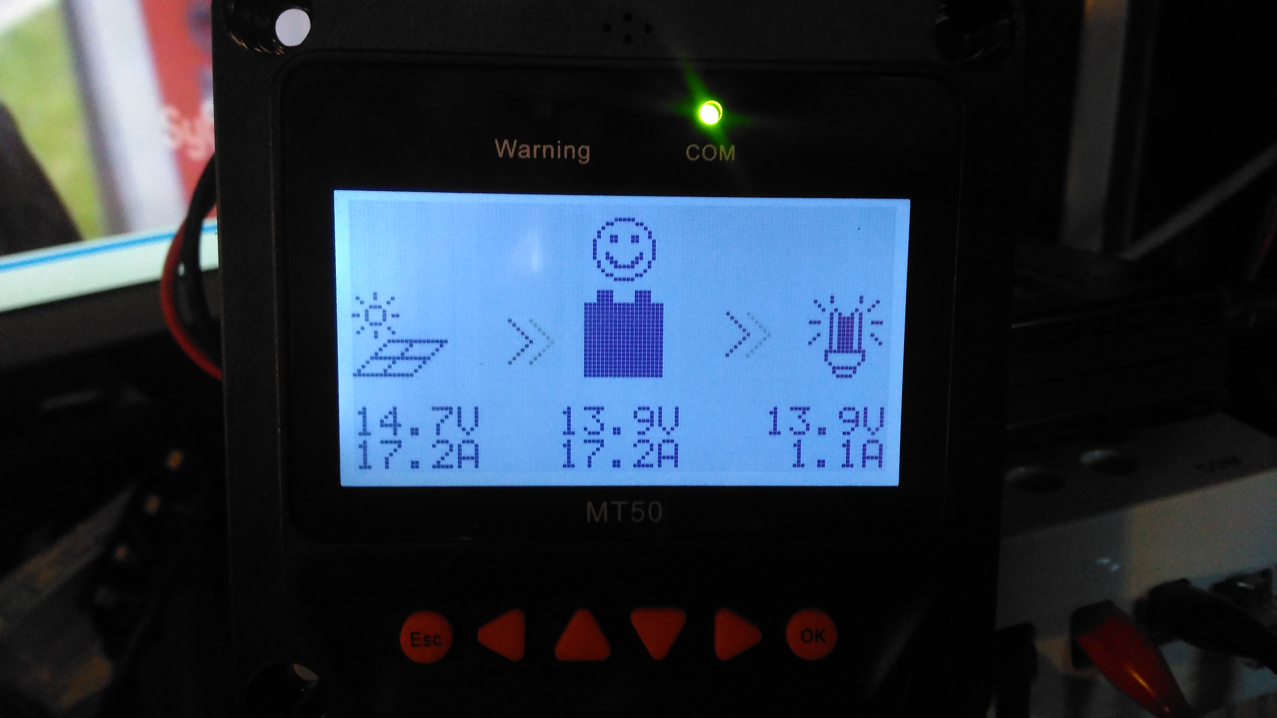
Here’s the MT50 controller from EpEver, that interfaces with it’s Tracer MPPT solar charge controllers, and gives access to more programming options on the charge controllers, without the need for a laptop. The display is a large dot-matrix unit, with built in backlight. Above is the display on the default page, showing power information for the entire system.
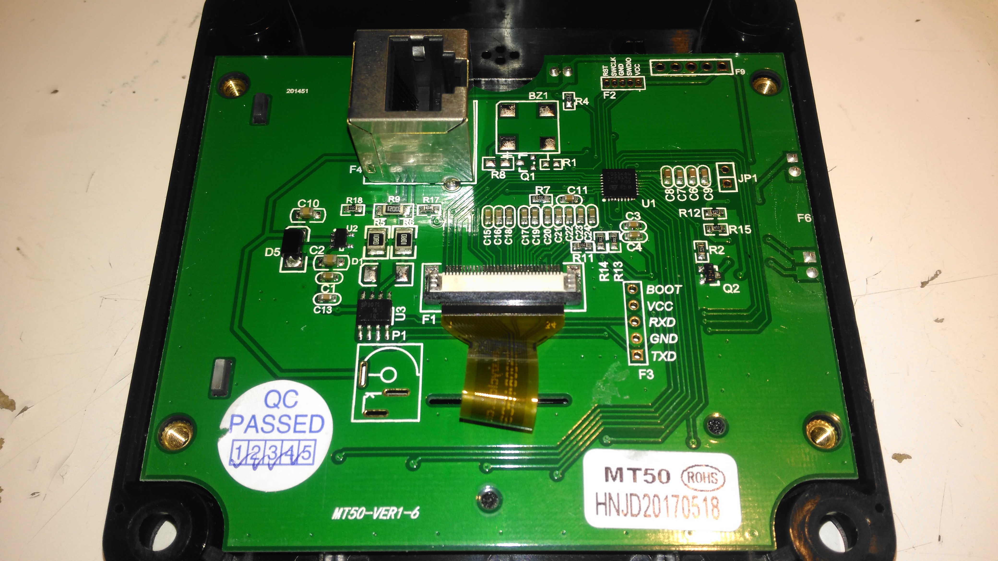
PCB Rear
The rear plastic cover is held in place by 4 machine screws, which thread into brass inserts in the plastic frame – nice high quality touch on the design here, no cheap self tapping plastic screws. Both power & data arrive via an Ethernet cable, but the communication here is RS-485, and not compatible with Ethernet! The PCB is pretty sparse, with comms & power on the left, LCD connection in the centre, and the microcontroller on the right.
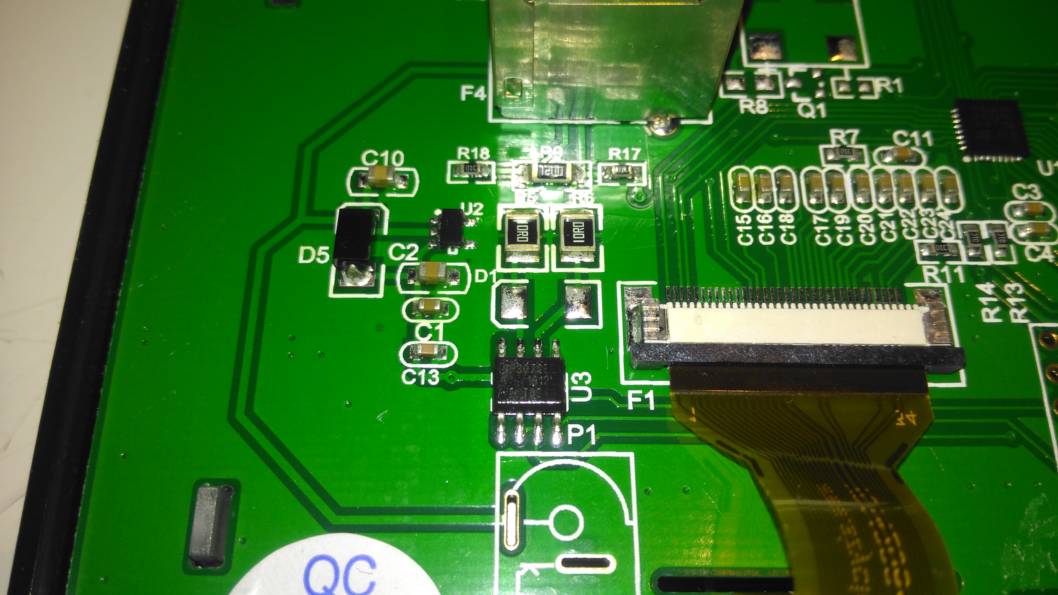
RS-485 Transceiver
On the left of the board is the RS0485 transceiver, and a small voltage regulator. There’s also a spot for a DC barrel jack, which isn’t included in this model for local power supply.
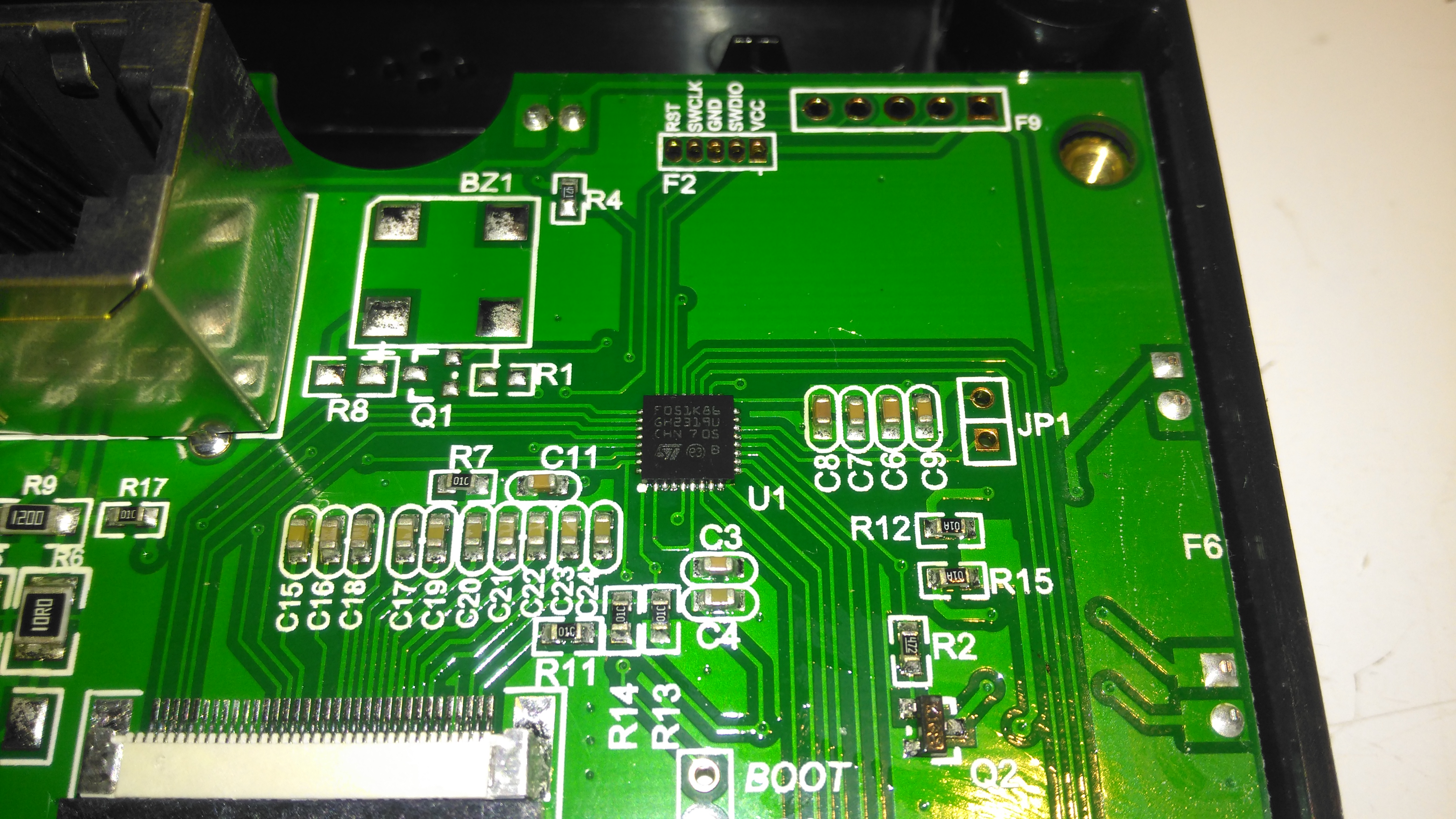
STM32 Microcontroller
The other side of the board holds the main microcontroller which communicates with the charge controller. This is a STM32F051K8 from ST Microelectronics. With a 48MHz ARM Cortex M0 core, and up to 64K of flash, this is a pretty powerful MCU that has very little to do in this application.
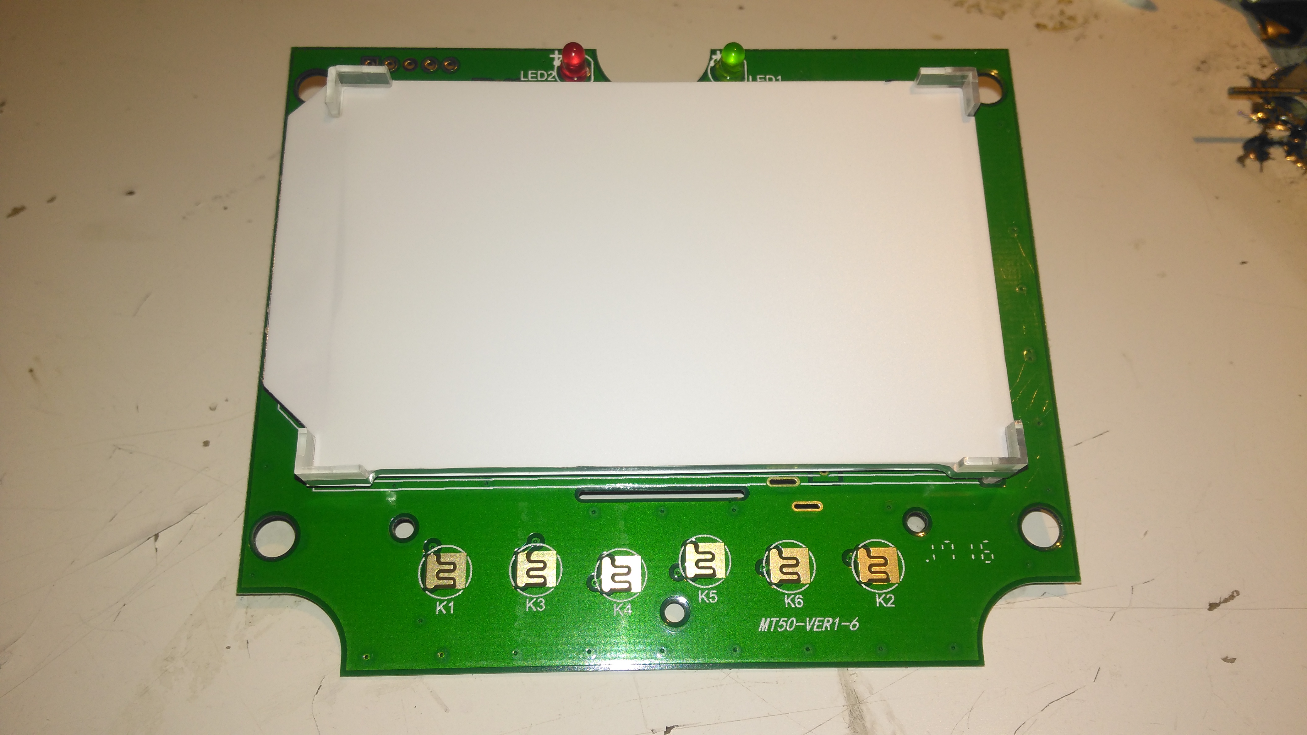
PCB Front
The front of the PCB has the ENIG contacts of the front panel buttons, and the LCD backlight assembly. There’s nothing else under the plastic backlight spreader either.
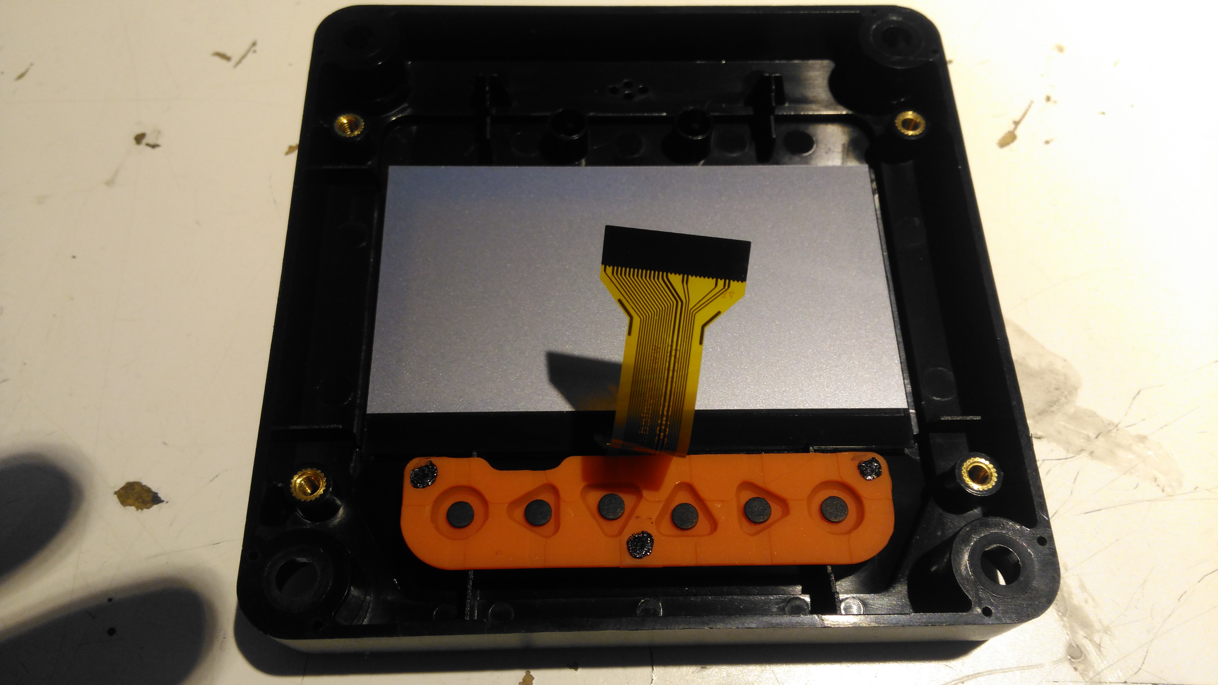
LCD Rear
The front case holds the LCD module in place with glue, and the rubber buttons are placed underneath, which is heat staked in place.
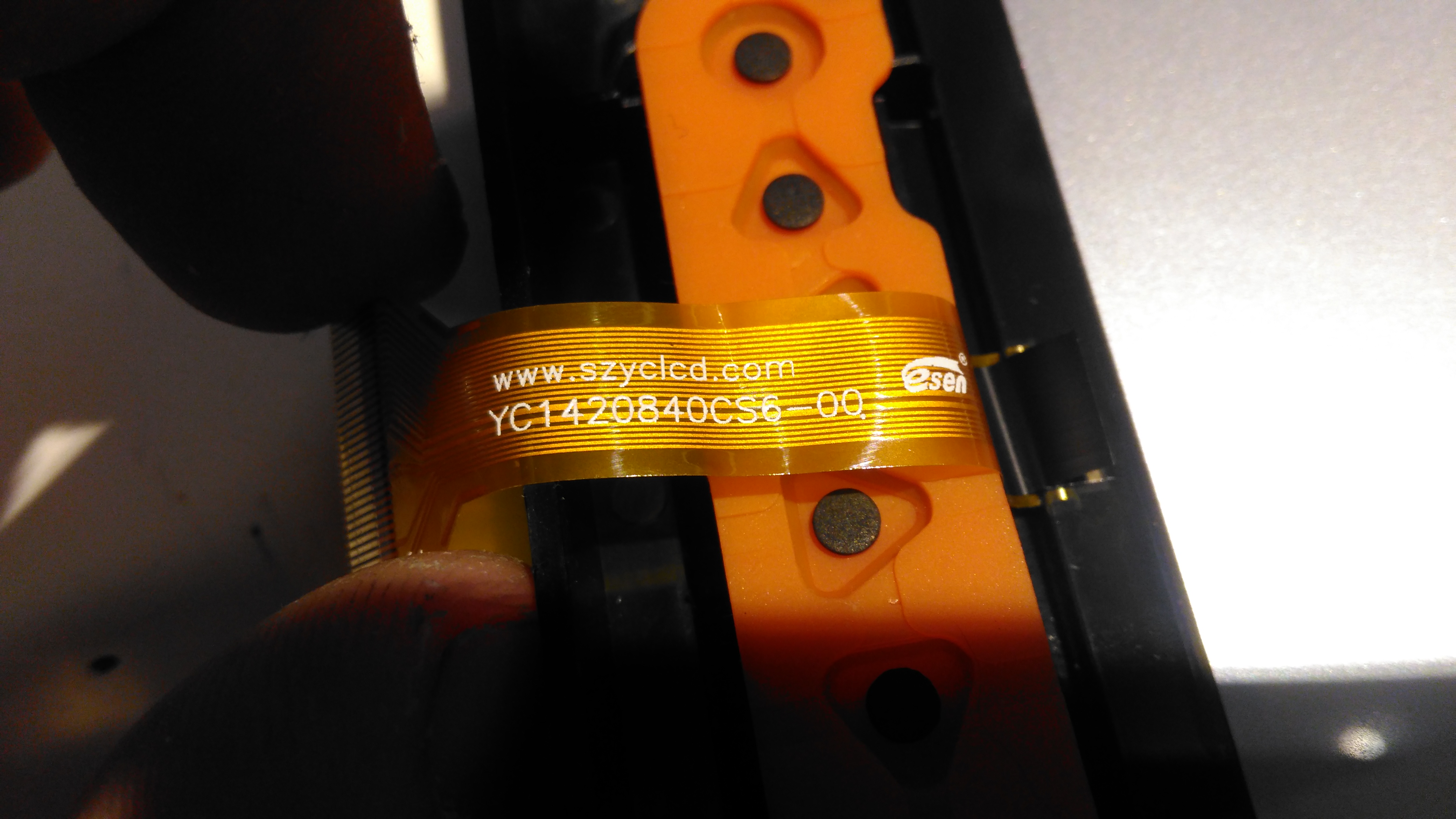
LCD Model
The LCD is a YC1420840CS6 from eCen in China. Couldn’t find much out about this specific LCD.
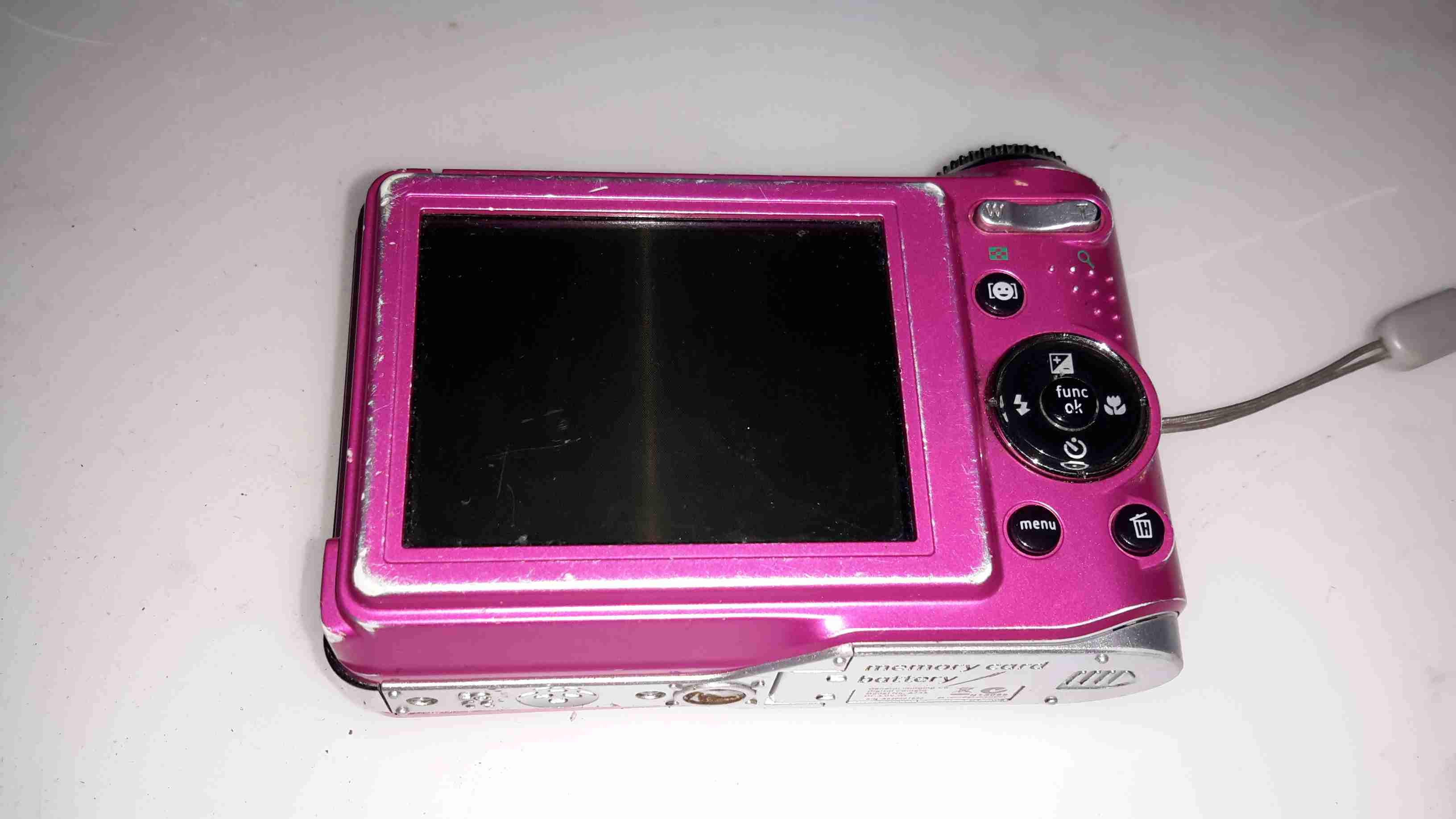
This camera has now been retired after many years of heavy use. Exposure to a 3-year old has caused severe damage to the lens mechanism, which no longer functions correctly.
Rear Panel
Pretty much standard interface for a digital camera, with a nice large LCD for it’s time.
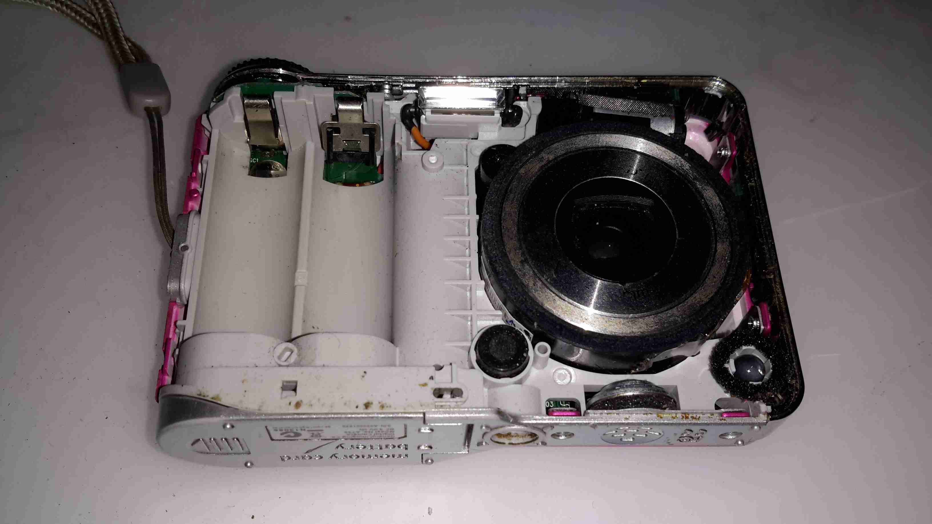
Front Cover Removed
With the front cover removed, the lens assembly & battery compartment is exposed.
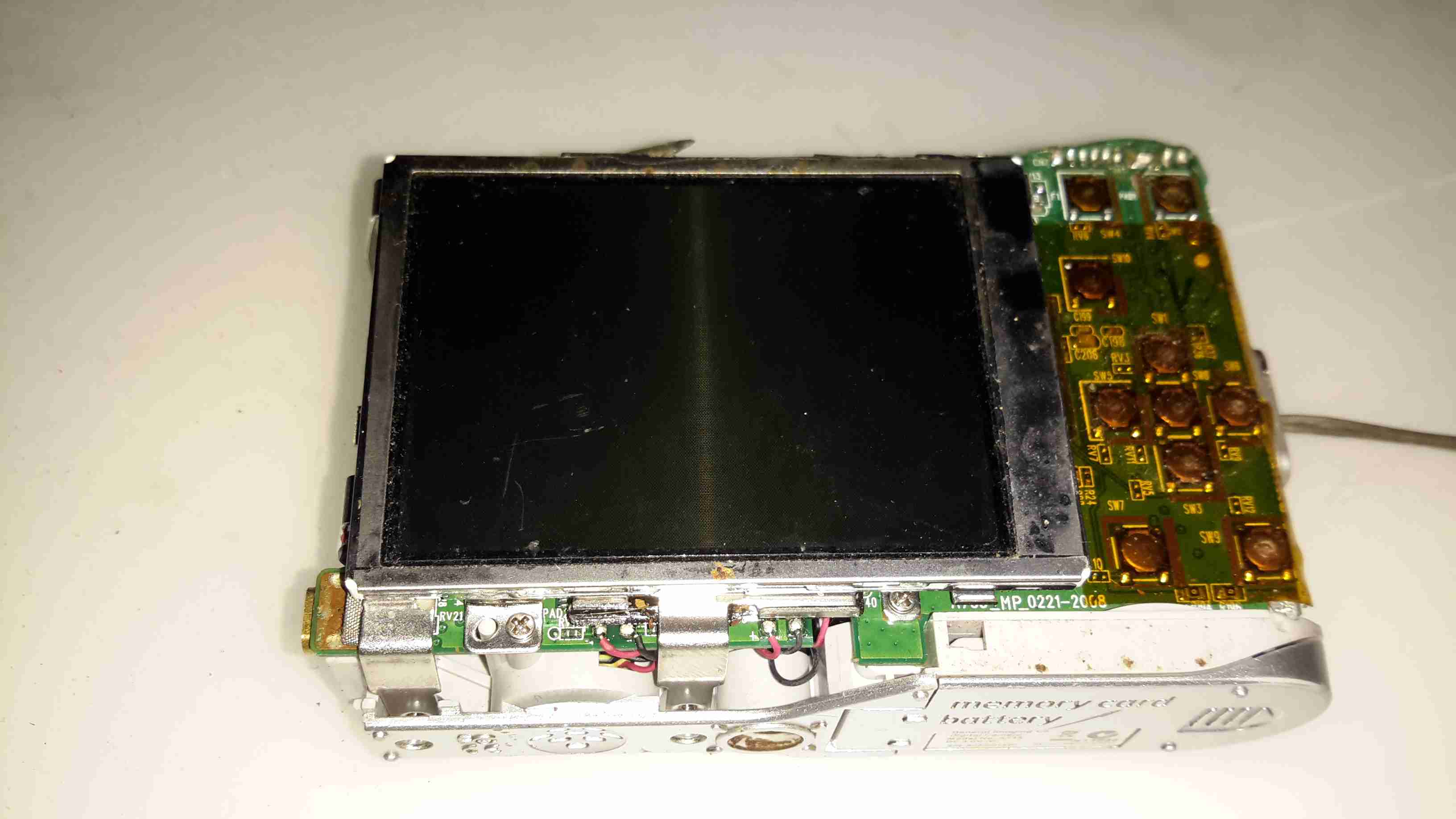
Rear Cover Removed
Removing the rear cover exposes the LCD module & the main PCB, the interface tactile switches are on the right under a protective layer of Kapton tape.
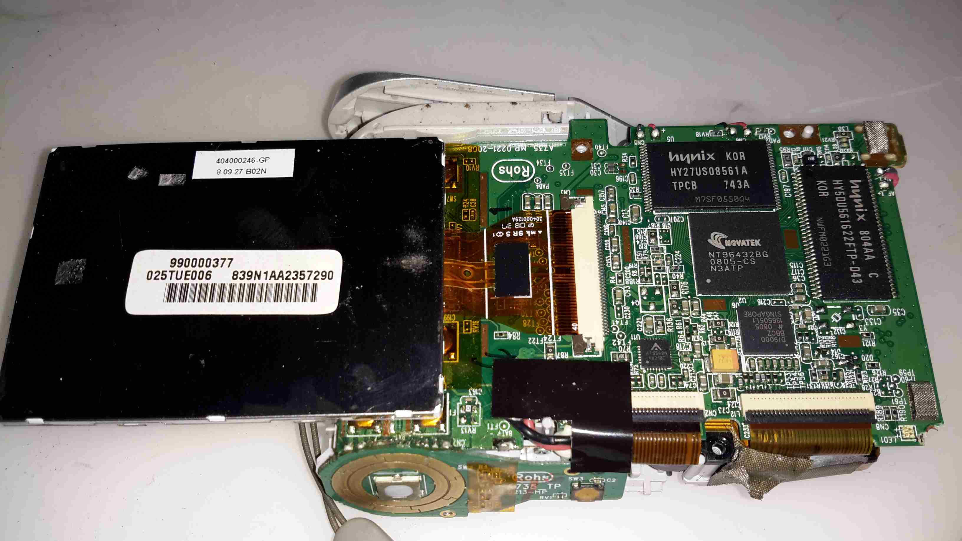
Main Chipset
Flipping the LCD out of it’s mounting bracket reveals the main camera chipset. The CPU is a NovaTek NT96432BG, no doubt a SoC of some kind, but I couldn’t find any information. Firmware & inbuilt storage is on a Hynix HY27US08561A 256MBit NAND Flash, with a Hynix HY5DU561622FTP-D43 256Mbit DRAM for system memory.
I couldn’t find any info on the other two chips on this side of the board, but one is probably a motor driver for the lens, while the other must be the front end for the CCD sensor input to the SoC.
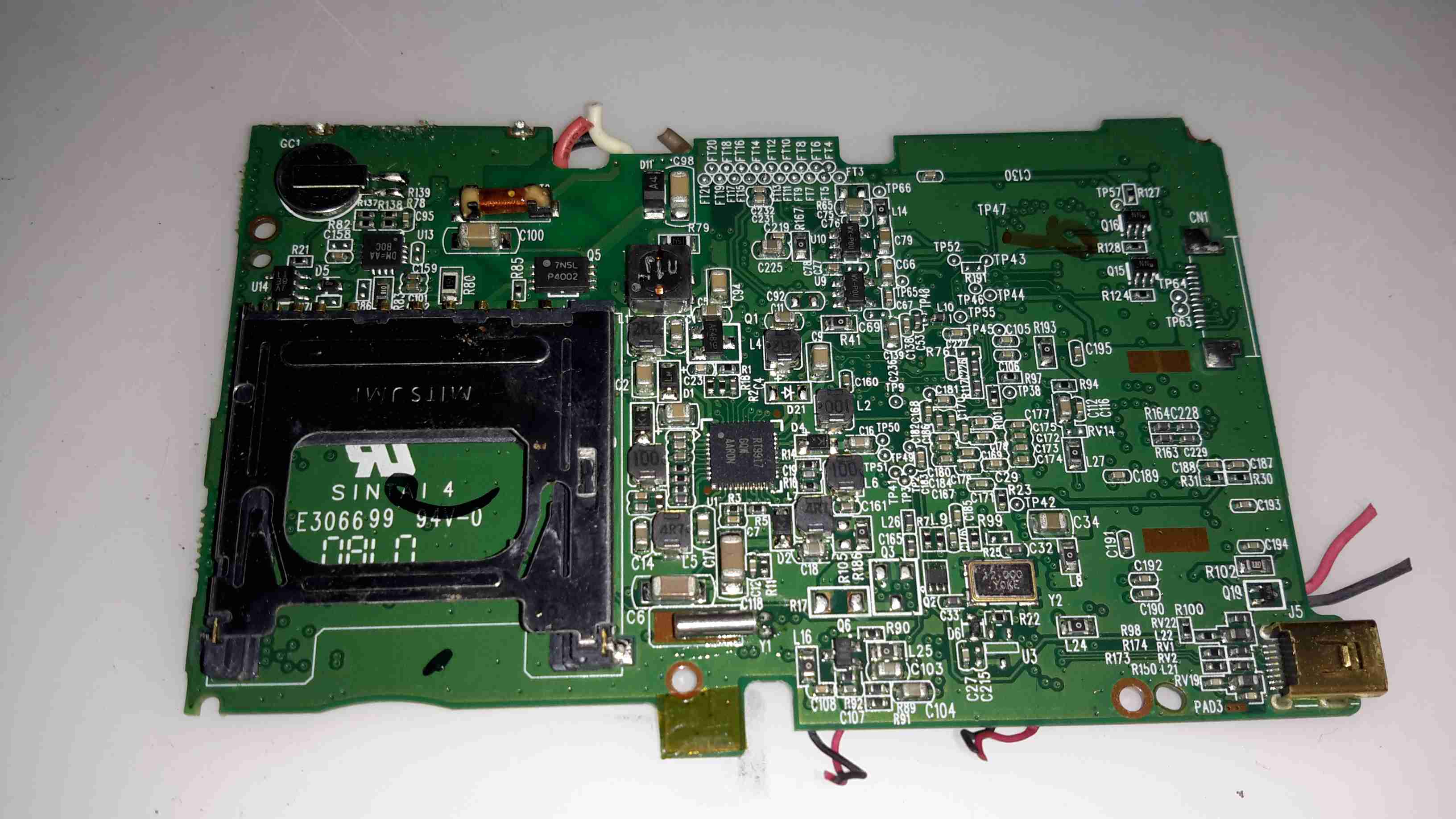
Main PCB Reverse
The other side of the PCB handles the SD card slot & power management. All the required DC rails are provided for by a RT9917 7-Channel DC-DC converter from RichTek, an IC designed specifically for digital camera applications.
Top left above the SD card slot is the trigger circuitry for the Xenon flash tube & the RTC backup battery.
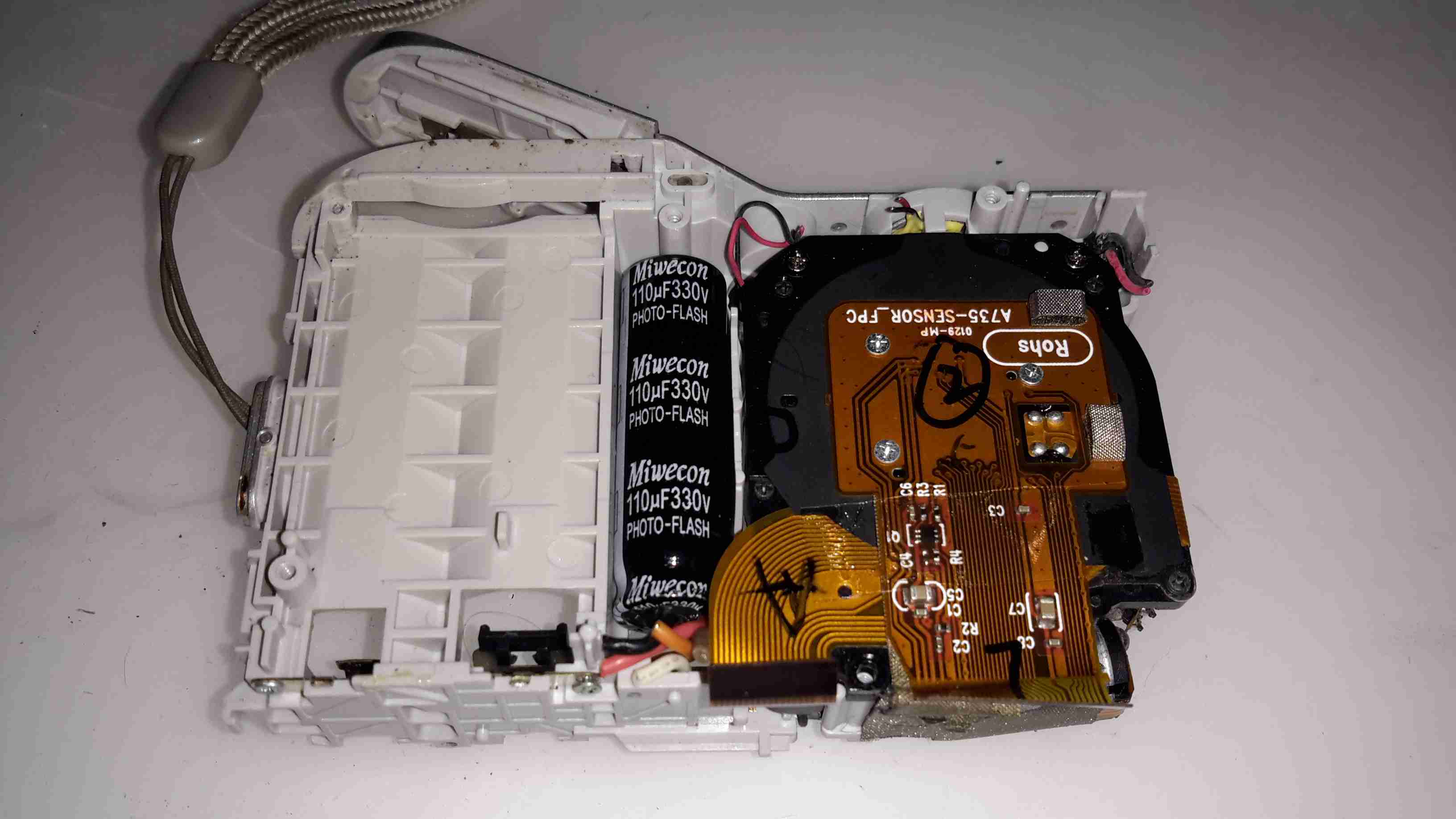
Main PCB Removed
Once the main PCB is out of the frame, the back of the lens module with the CCD is accessible. Just to the left is the high-voltage photoflash capacitor, 110µF 330v. These can give quite the kick when charged! Luckily this camera has been off long enough for the charge to bleed off.
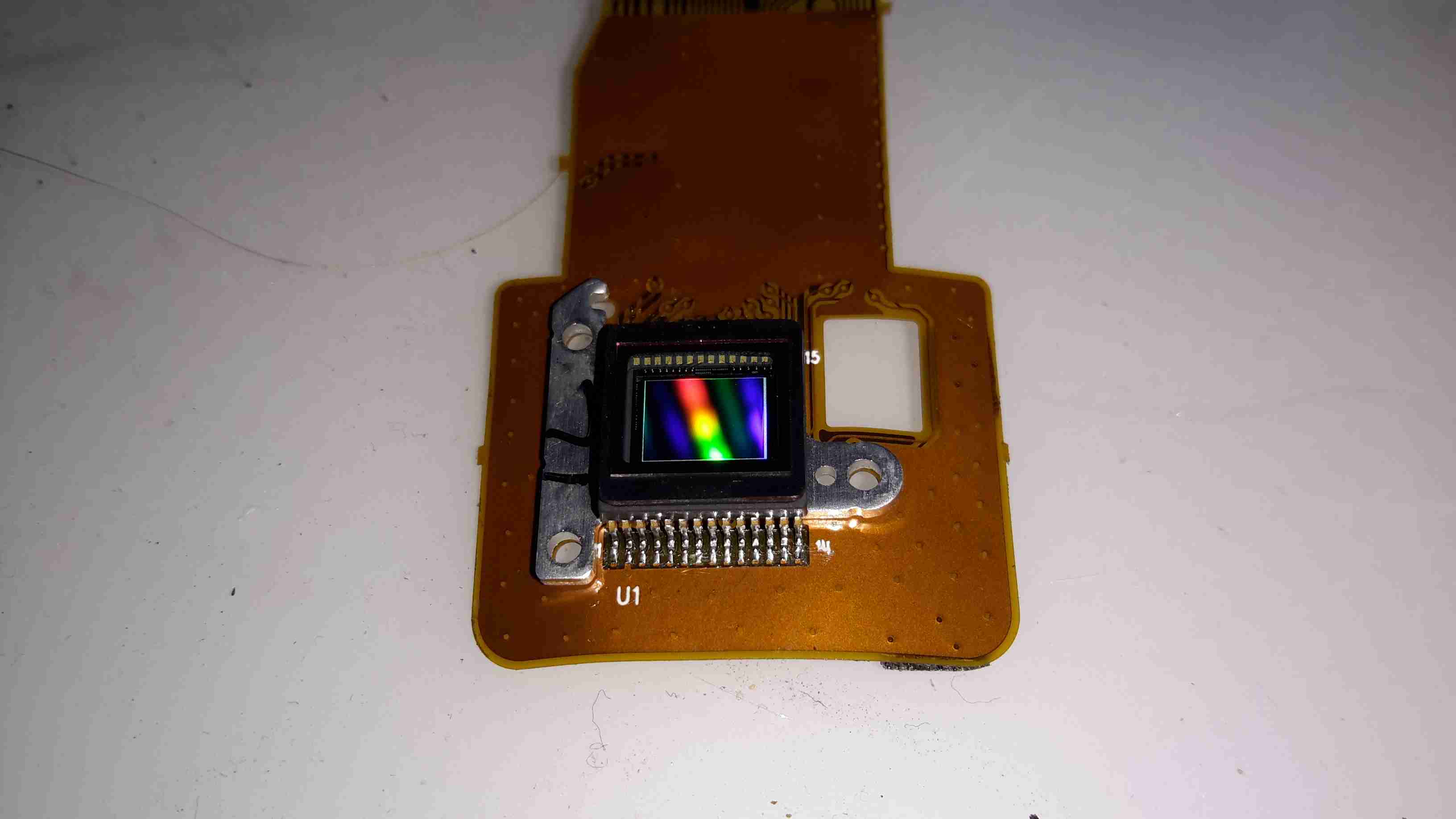
Sensor
Finally, here’s the 7-Megapixel CCD sensor removed from the lens assembly, with it’s built in IR cut filter over the top. I couldn’t find any make or model numbers on this part, as the Aluminium mounting bracket behind is bonded to the back of the sensor with epoxy, blocking access to any part information.
Die images of the chipset to come once I get round to decapping them!
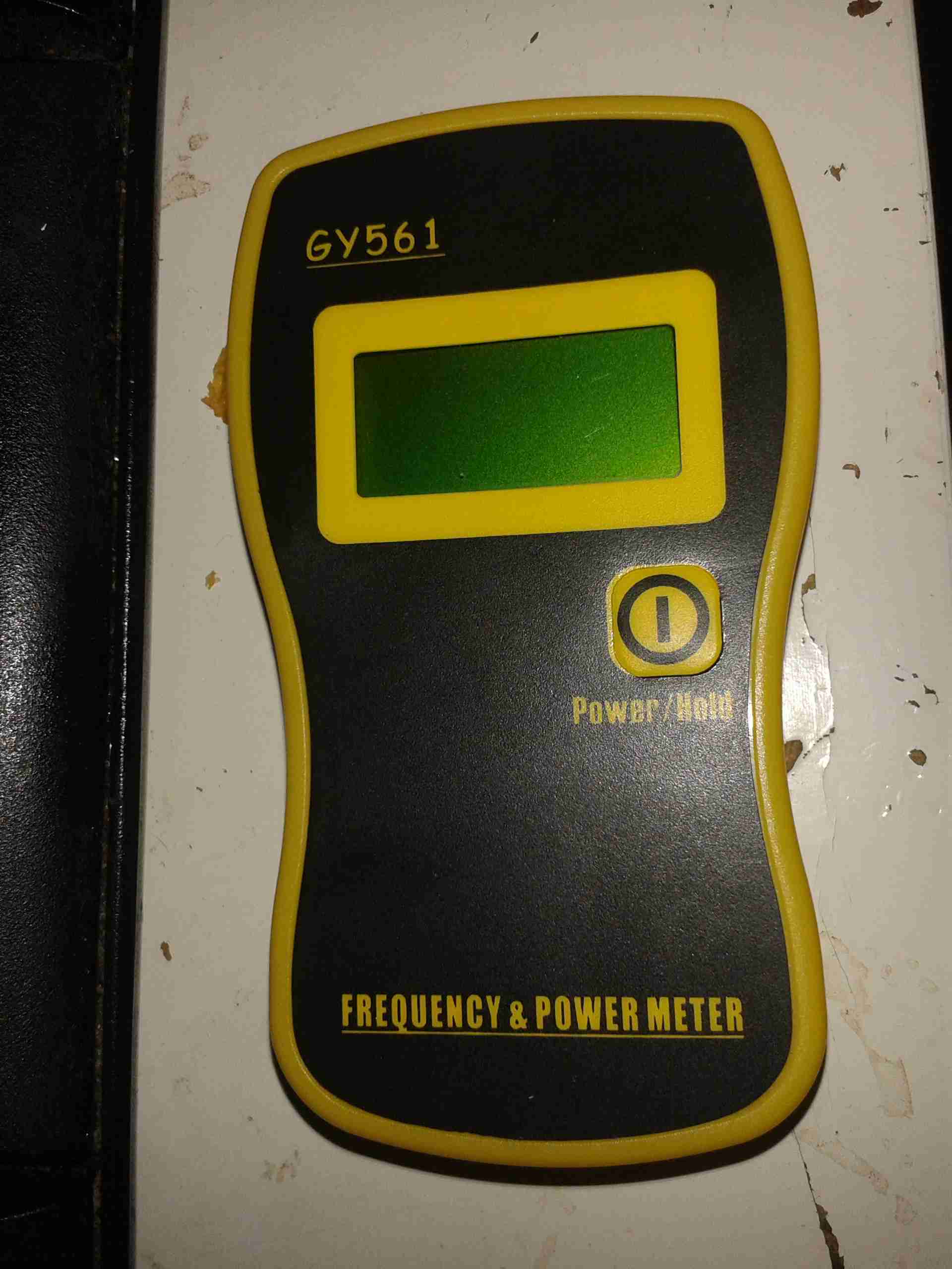
The latest addition to my radio shack is the GY561 frequency & power meter, which has already come in useful for measuring the output power of all my radios.
GY561
It’s a small device, roughly the same size & weight as a stock UV-5R. Power is provided by 3 AAA cells.
Display
The display is a standard HD44780 8×2 module. The display on this unit isn’t backlit, so no operating in the dark.
Cover Removed
The cover pops off easily to allow access to the internals, without having to remove any screws!
The 4 screws on the back of the unit hold the heatsink plate for the 50W 50Ω dummy load resistor.
Removing the cover reveals a couple of adjustments, for frequency & RF power calibration.
There are also 3 tactile switches that aren’t on the front panel. According to the manual (which in itself is a masterpiece of Chinglish), they are used to software calibrate the unit if an accurate RF power source is available. I will attempt to do a reasonable translation when time allows.
Disassembly further than this involves some desoldering in awkward places, so a search of the internet revealed an image of the rest of the internal components. In the case of my meter, all the part numbers have been scrubbed off the ICs in an attempt to hide their purpose. While it’s possible to cross-reference IC databooks & find the part numbers manually, this process is a time consuming one. Luckily the image I managed to locate doesn’t have the numbers scrubbed.
Total Disassembly
Under the LCD is some 74HC series logic, and a prescaler IC as seen in the previous frequency counter post. However in this unit the prescaler is a MB506 microwave band version to handle the higher frequencies specified.
In this case however the main microcontroller is an ATMEGA8L.
This is complemented by a SN54HC393 4-bit binary counter for the frequency side of things. This seems to make it much more usable down to lower frequencies, although the manual is very generous in this regard, stating that it’s capable of reading down to 1kHz. In practice I’ve found the lowest it reliably reads the frequency input is 10MHz, using my AD9850 DDS VFO Module as a signal source.
It did however read slightly high on all readings with the DDS, but this could have been due to the low power output of the frequency source.
Just like the other frequency counter module, this also uses a trimmer capacitor to adjust the microcontroller’s clock frequency to adjust the calibration.
The power supply circuitry is in the bottom left corner of the board, in this case a small switching supply. The switching regulator is needed to boost the +4.5v of the batteries to +5v for the logic.
Also, as the batteries discharge & their terminal voltage drops, the switching regulator will allow the circuit to carry on functioning. At present I am unsure of the lower battery voltage limit on the meter, but AAA cells are usually considered dead at 0.8v terminal voltage. (2.4v total for the 3 cells).
When turned on this meter draws 52mA from the battery, and assuming 1200mAh capacity for a decent brand-name AAA cell, this should give a battery life of 23 hours continuous use.
On the back of the main PCB is a 5v relay, which seems to be switching an input attenuator for higher power levels, although I only managed to trigger it on the 2m band.
Finally, right at the back attached to an aluminium plate, is the 50Ω dummy load resistor. This component will make up most of the cost of building these, at roughly £15.
On my DVM, this termination reads at about 46Ω, because of the other components on the board are skewing the reading. There are a pair of SMT resistors, at 200Ω & 390Ω in series, and these are connected across the 50Ω RF resistor, giving a total resistance of 46.094Ω.
This isn’t ideal, and the impedance mismatch will probably affect the calibration of the unit somewhat.
The heatsinking provided by the aluminium plate is minimal, and the unit gets noticeably warm within a couple of minutes measuring higher power levels.
High power readings should definitely be limited to very short periods, to prevent overheating.
The RF is sampled from the dummy load with a short piece of Teflon coax.
There’s a rubber duck antenna included, but this is pretty useless unless it’s almost in contact with the transmitting antenna, as there’s no input amplification. It might be handy for detecting RF emissions from power supplies, etc.
For the total cost involved I’m not expecting miracles as far as accuracy is concerned, (the manual states +/-10% on power readings).
The frequency readout does seem to be pretty much spot on though, and the ability to calibrate against a known source is handy if I need some more accuracy in the future.
I’ve also done an SWR test on the dummy load, and the results aren’t good.
At 145.500 MHz, the SWR is 3:1, while at 433.500 it’s closer to 4:1. This is probably due to the lower than 50Ω I measured at the meter’s connector.
These SWR readings also wander around somewhat as the load resistor warms up under power.
I’ll probably also replace the AAA cells with a LiPo cell & associated charge/protection circuitry, to make the unit chargeable via USB. Avoiding disposable batteries is the goal.
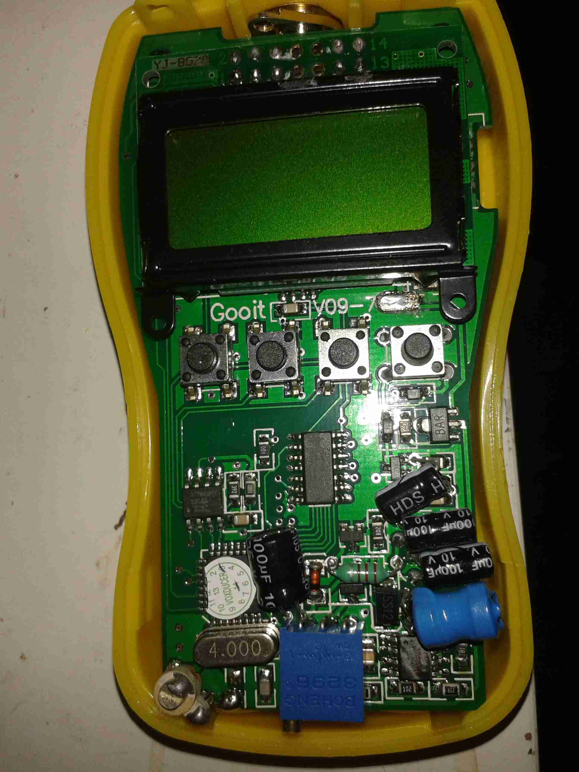
Here’s a quick look at a Sainsmart frequency counter module. These are useful little gadgets, showing the locked frequency on a small LCD display.
It’s built around an ATMega328 microcontroller (µC), and an MB501L Prescaler IC. The circuit for this is very simple, and is easily traced out from the board.
Frequency Counter
Here’s the back of the board, with the µC on the left & the prescaler IC on the right. This uses a rather novel method for calibration, which is the trimmer capacitor next to the crystal. This trimmer varies the frequency of the µC’s oscillator, affecting the calibration.
Input protection is provided by a pair of 1N4148 diodes in inverse parallel. These will clamp the input to +/-1v.
The prescaler IC is set to 1/64 divide ratio. This means that for an input frequency of 433MHz, it will output a frequency of 6.765625MHz to the µC.
The software in the µC will then calculate the input frequency from this intermediate frequency. This is done because the ATMega controllers aren’t very cabable of measuring such high frequencies.
The calculated frequency is then displayed on the LCD. This is a standard HD44780 display module.
LCD
Power is provided by a 9v PP3 battery, which is then regulated down by a standard LM7805 linear regulator.
Readout
I’ve found it’s not very accurate at all at the lower frequencies, when I fed it 40MHz from a signal generator it displayed a frequency of around 74MHz. This is probably due to the prescaler & the software not being configured for such a low input. In the case for 40MHz input the scaled frequency would have been 625kHz.
I recently posted about a small analog SWR/Power meter I got from eBay, and figured it needed some improvement.
After some web searching I located a project by ON7EQ, an Arduino sketch to read SWR & RF power from any SWR bridge.
The Arduino code is on the original author’s page above, his copyright restrictions forbid me to reproduce it here.
I have also noticed a small glitch in the code when it is flashed to a blank arduino: The display will show scrambled characters as if it has crashed. However pushing the buttons a few times & rebooting the Arduino seems to fix this. I think it’s related to the EEPROM being blank on a new Arduino board.
I have run a board up in Eagle for testing, shown below is the layout:
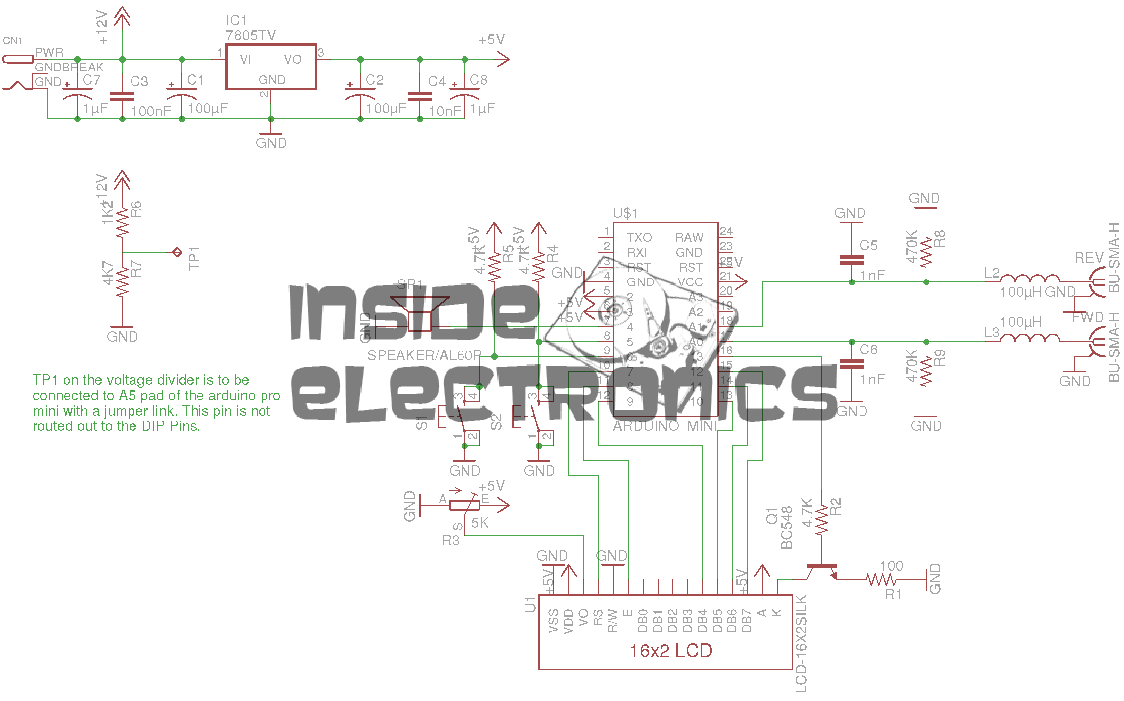
SWR Meter SCH
The Schematic is the same as is given on ON7EQ’s site. Update: ON7EQ has kindly let me know I’ve mixed up R6 & R7, so make sure they’re switched round when the board is built ;). Fitting the resistors the wrong way around may damage the µC with overvoltage.
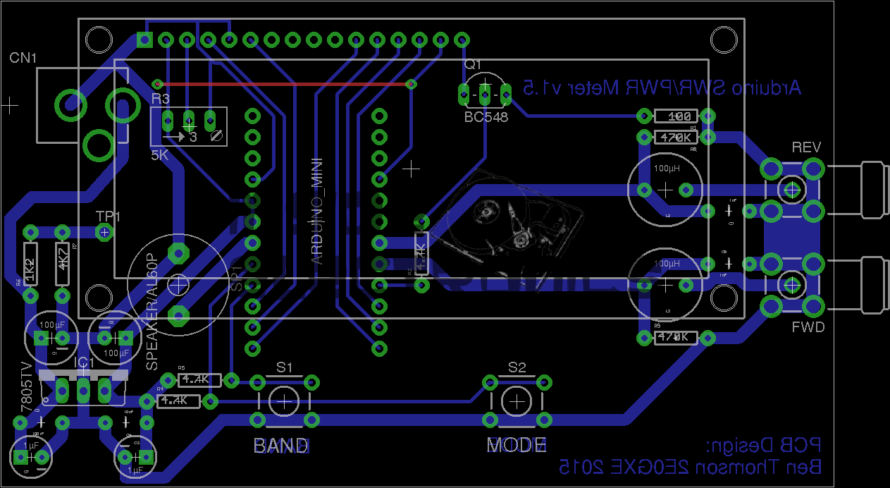
SWR Meter PCB
Here’s the PCB layout. I’ve kept it as simple as possible with only a single link on the top side of the board.
PCB Top
Here’s the freshly completed PCB ready to rock. Arduino Pro mini sits in the center doing all the work.
The link over to A5 on the arduino can be seen here, this allows the code to detect the supply voltage, useful for battery operation.
On the right hand edge of the PCB are the pair of SMA connectors to interface with the SWR bridge. Some RF filtering is provided on the inputs.
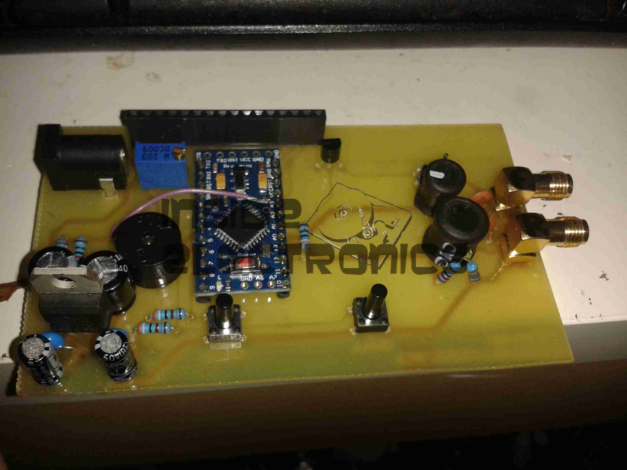
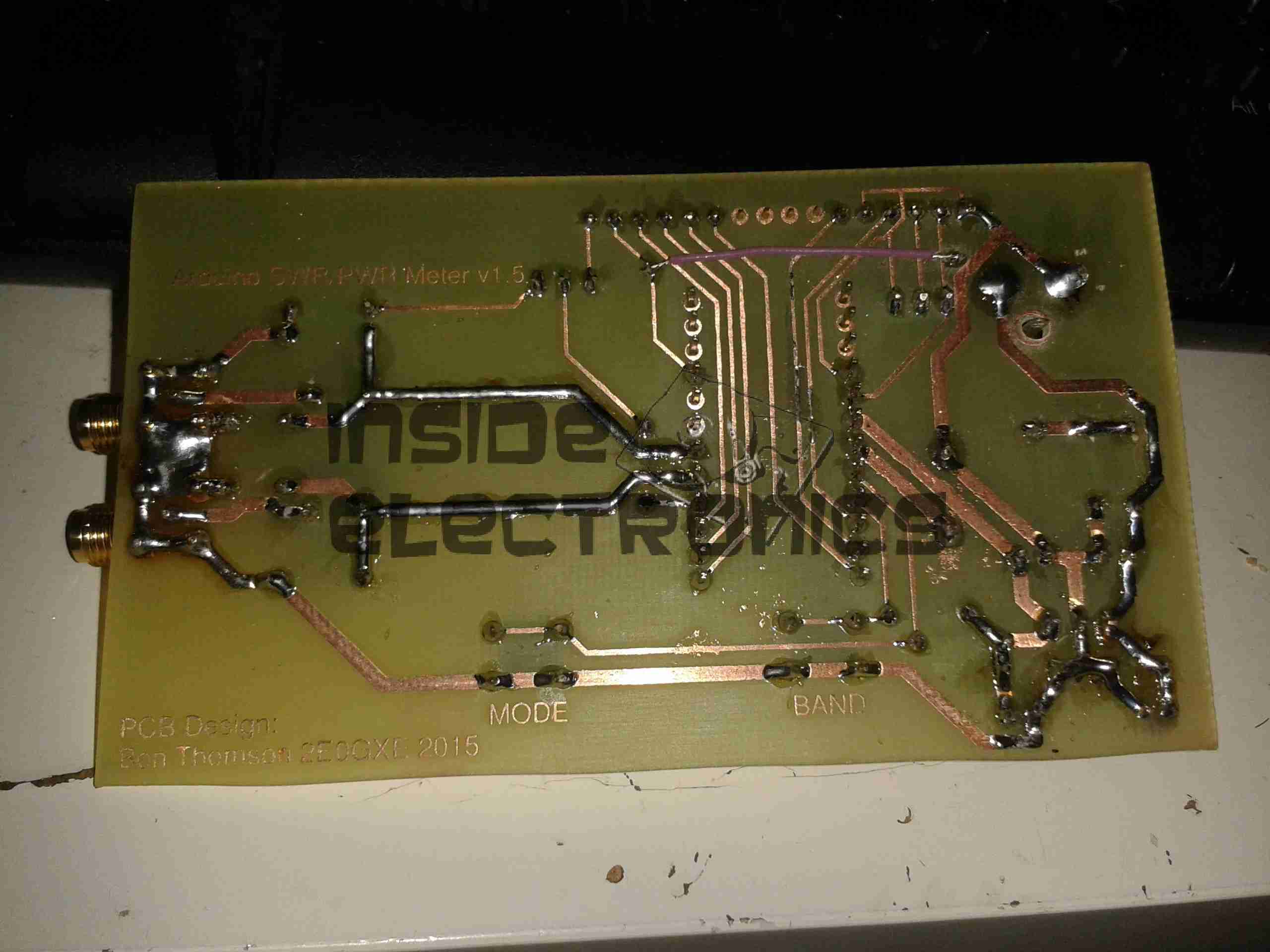
PCB Bottom
Trackside view of the PCB. This was etched using my tweaked toner transfer method.
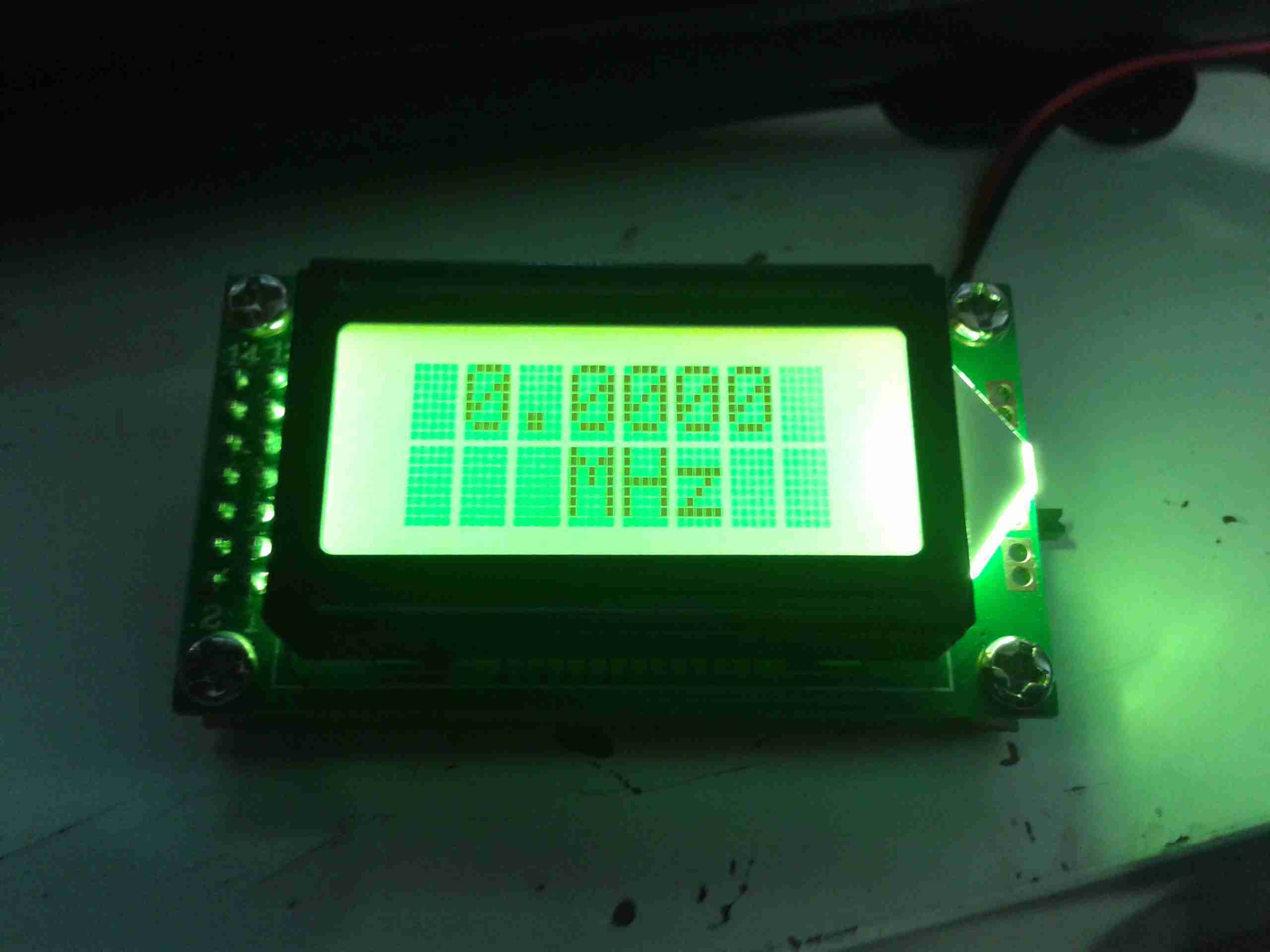
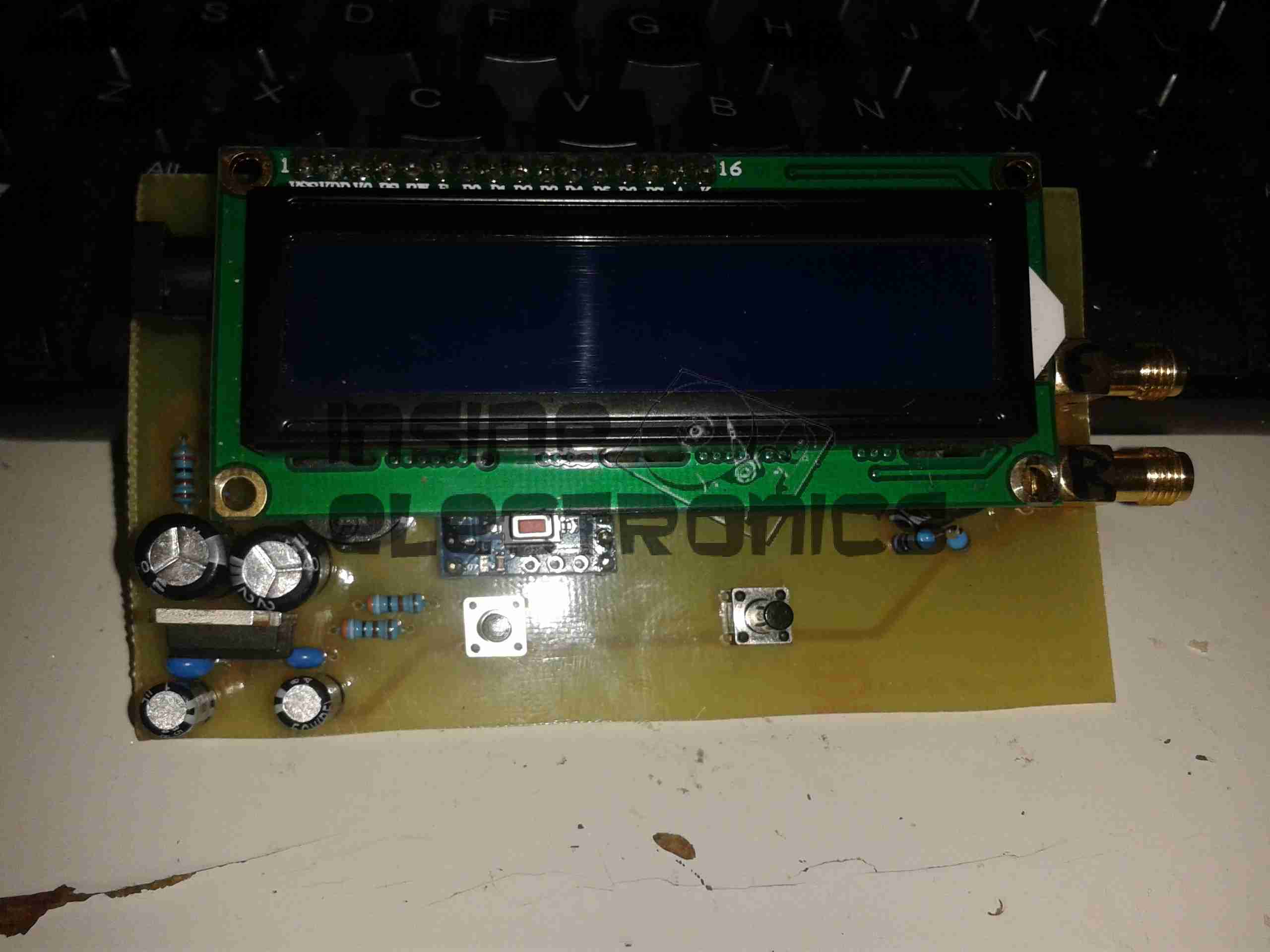
LCD Fitted
Here the board has it’s 16×2 LCD module.
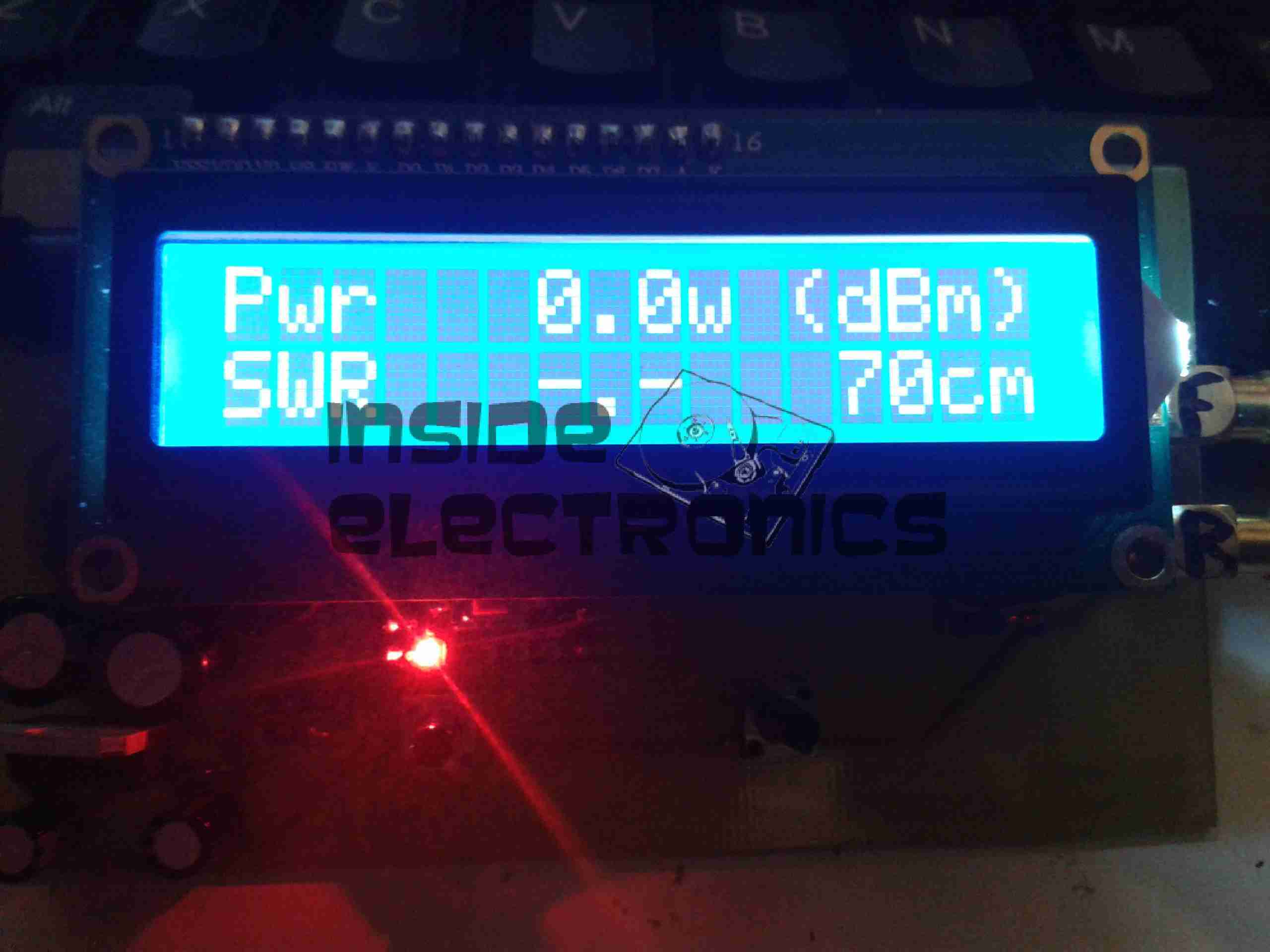
Online
Board powered & working. Here it’s set to the 70cm band. The pair of buttons on the bottom edge of the board change bands & operating modes.
As usual, the Eagle layout files are available below, along with the libraries I use.
[download id=”5585″]
[download id=”5573″]
More to come on this when some components arrive to interface this board with the SWR bridge in the eBay meter.
This is a cheap Sigma branded keychain photoframe. User buttons for power & selecting photos are on the left.
There are two white LEDs on the bottom edge that function as a torch as well.
Display
Front of the unit removed, showing the LCD module. The USB jack is bottom left, next to the pair of white LEDs & above that is the 32kHz watch crystal that the CPU uses for timekeeping.
Back Removed
Here the back has been removed showing the 3.7v Li-Ion cell used to provide power.
Display Folded Back
Here the display has been removed from the PCB exposing the chipset.
Chipset
Here the CPU blob-top chip & a flash memory IC are visible. The CPU is a Sitronix ST2205U.
A 5 megapixel digital camera from Vivitar. Visible here is the lens, viewfinder & flash.
Back
Rear of the unit showing the LCD & user control buttons.
Cover Removed
Front frame removed showing some of the internals. Shutter assembly & lens in centre, battery compartment at left.
Rear Cover Removed
Rear frame removede, showing the LCD module & tactile switches.
LCD
LCD module removed from the PCB
Flash PCB
Flash PCB removed. Transformer is fed with the 4.5v from the 3 AA cells & steps it up to ~300v DC for the flash capacitor. A pulse transformer energizes an electrode next to the Xenon flash tube with ~5kV to ionize the gas.
Main PCB
Main PCB removed. Internal flash ROM & RAM IC visible above the SD card socket. USB connector is at the top right, next to the piezo buzzer.
CPU
Main processor on reverse side of the PCB.
Image Sensor
Closeup of the CMOS image sensor with the lens assembly removed.
Tip Jar
If you’ve found my content useful, please consider leaving a donation by clicking the Tip Jar below!
All collected funds go towards new content & the costs of keeping the server online.