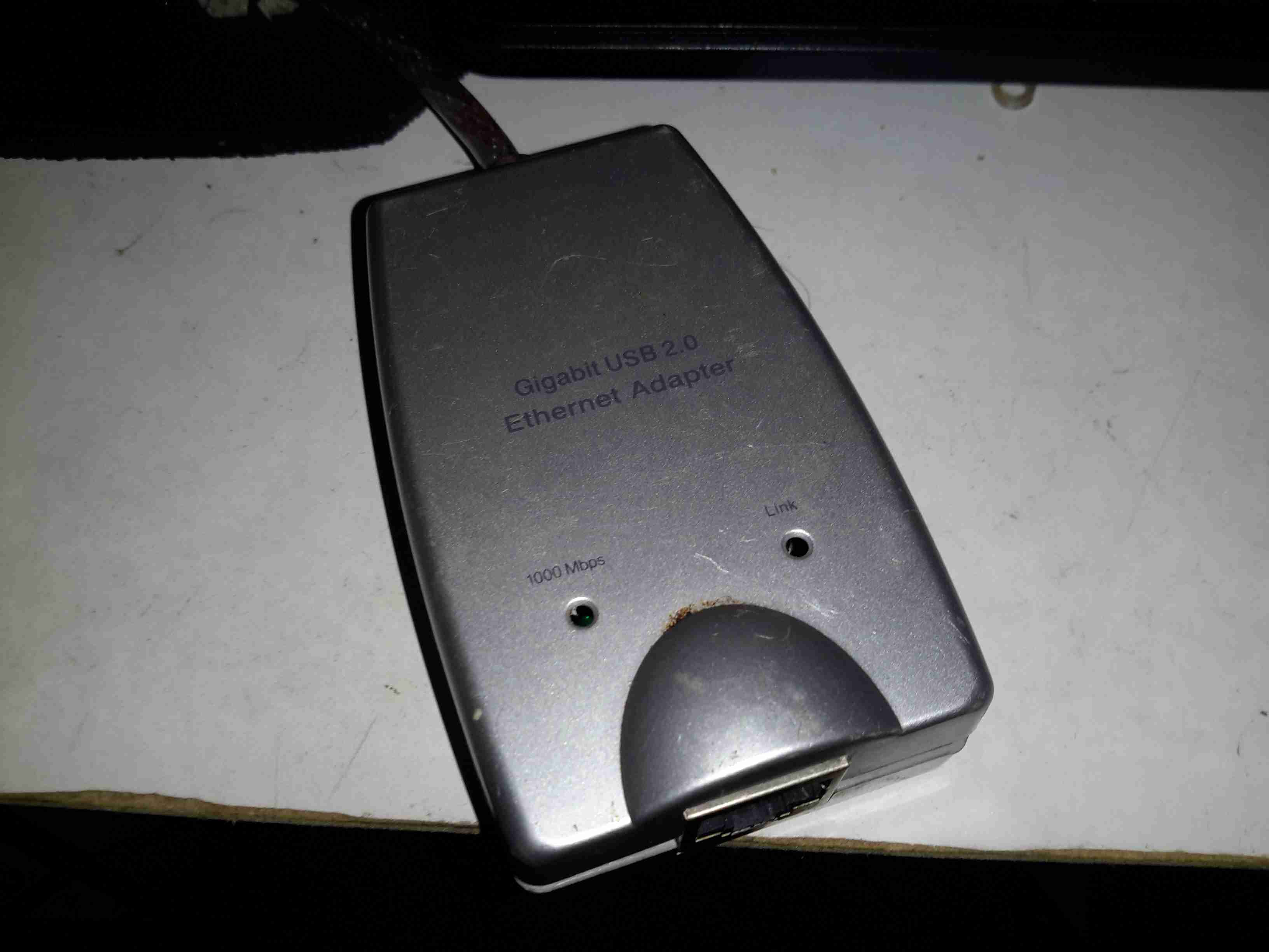
Here’s a chap eBay USB-To-Ethernet dongle I obtained for use with the Raspberry Pi Zero. This one is getting torn down permanently, as it’s rather unreliable. It seems to like having random fits where it’ll not enumerate on the USB bus. The silicon in the ICs will eventually make it here once I manage to get a new microscope 😉
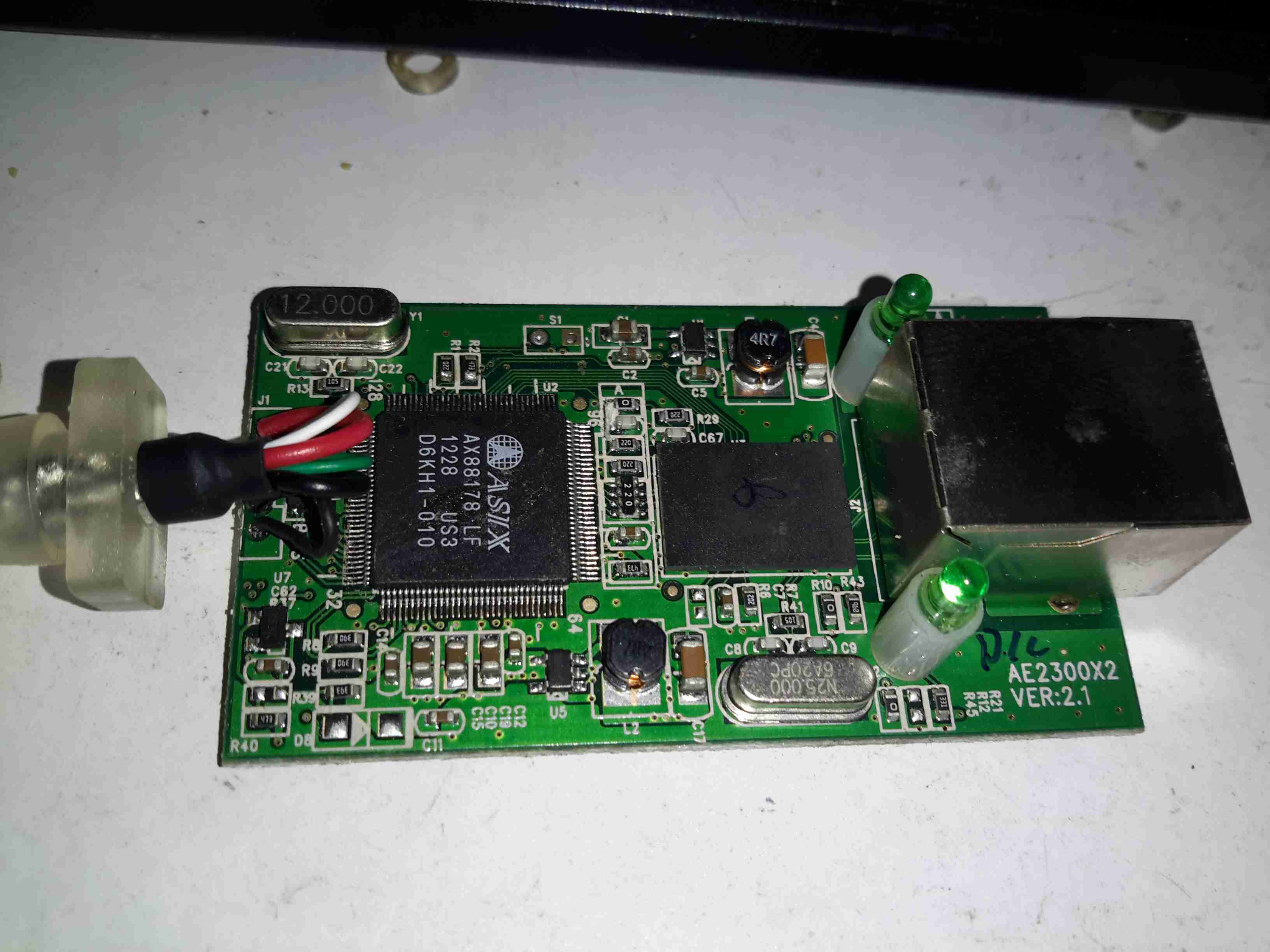
Main Chipset
This is quite a heavily packed PCB, with the main Asix AX88178 on the left. This IC contains all of the logic for implementing the Ethernet link over USB, except the PHY. It’s clock crystal is in the top left corner.
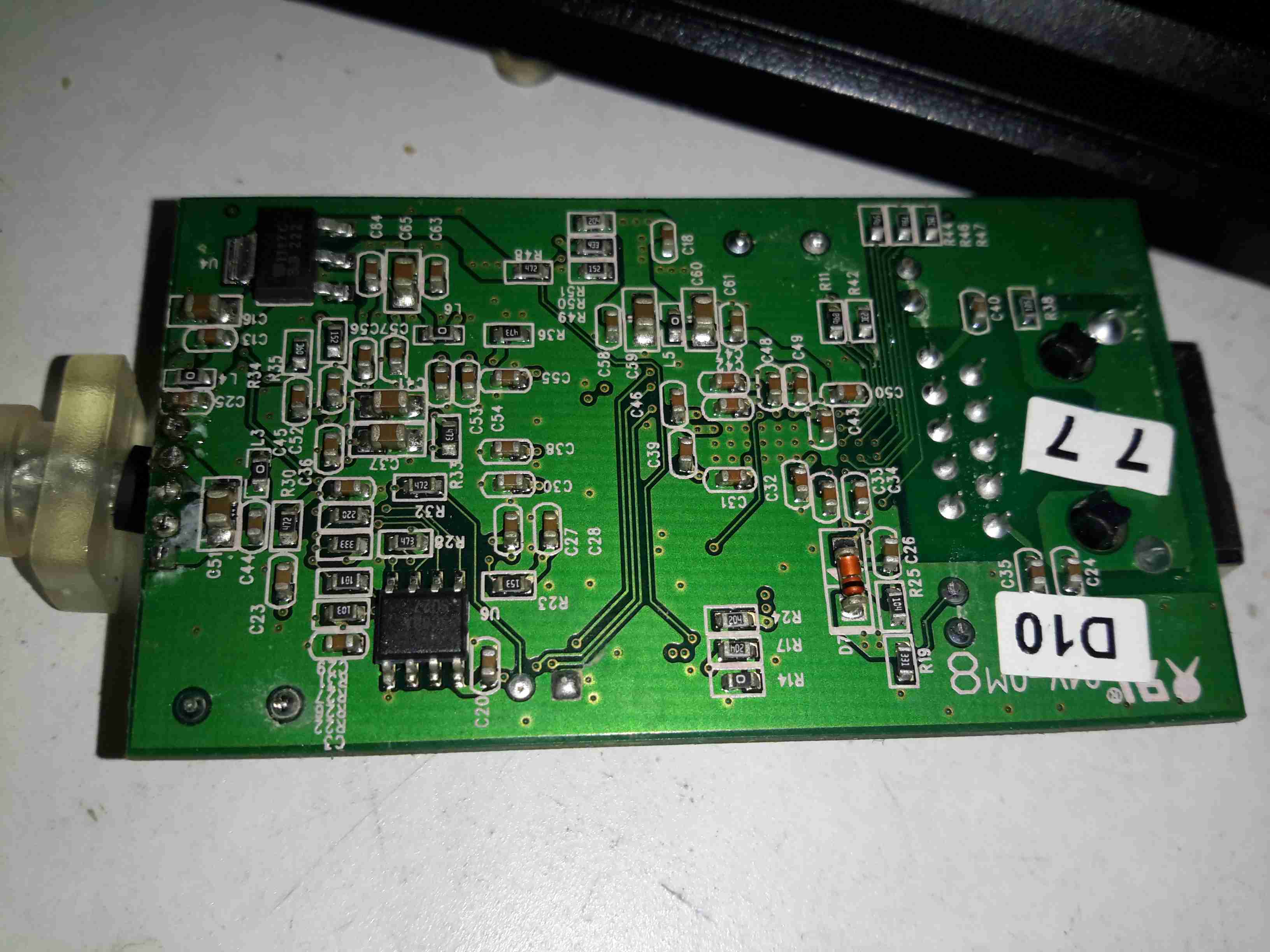
Reverse Side
Not much on the reverse side, there’s a 3.3v linear regulator at top left, the SOIC is an Atmel AT93C66A 4KB EEPROM for configuration data.
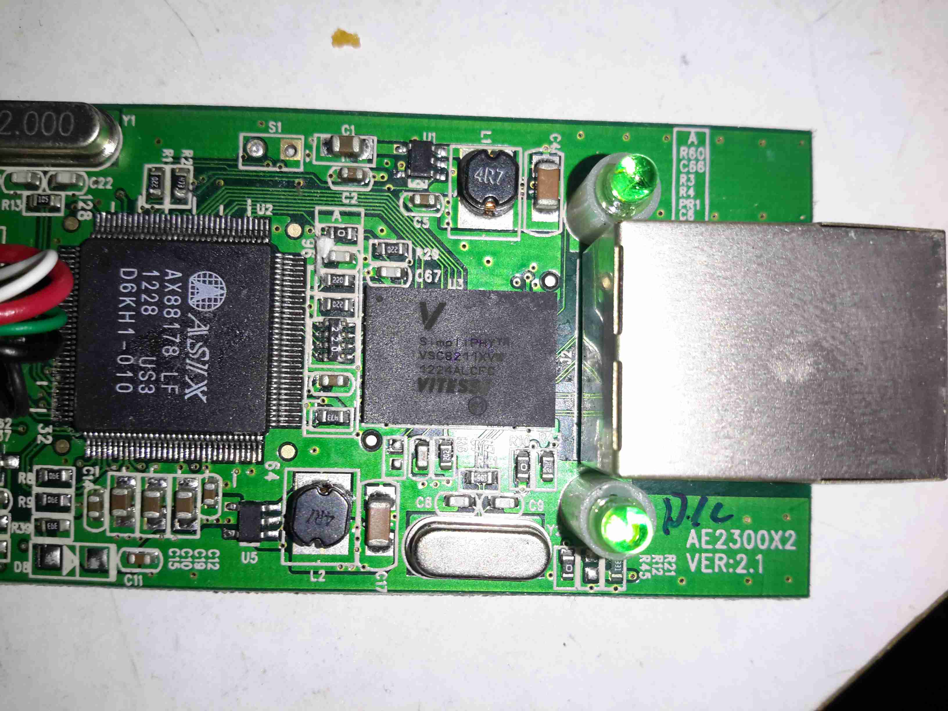
Vitesse PHY
The final IC in the chain is the Vitesse VSC8211 Gigabit PHY, with it’s clock crystal below. This interfaces the Ethernet MAC in the Asix IC to the magjack on the right.
Another random teardown from the junk box time!
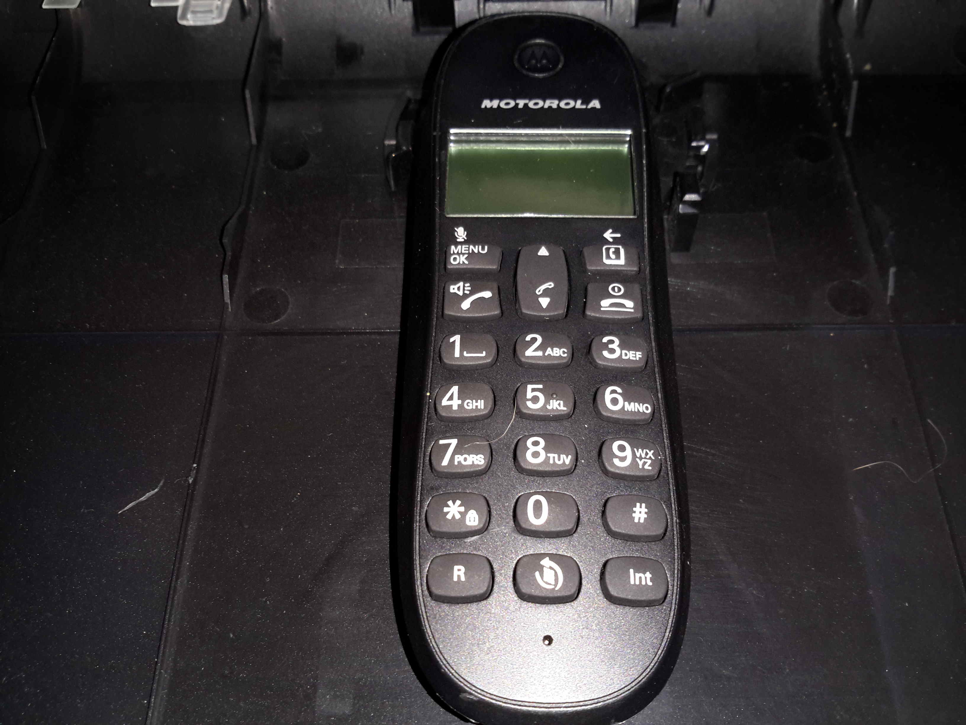
Here’s an old Motorola DECT landline phone, no use to me as I’ve not used a landline for many years.
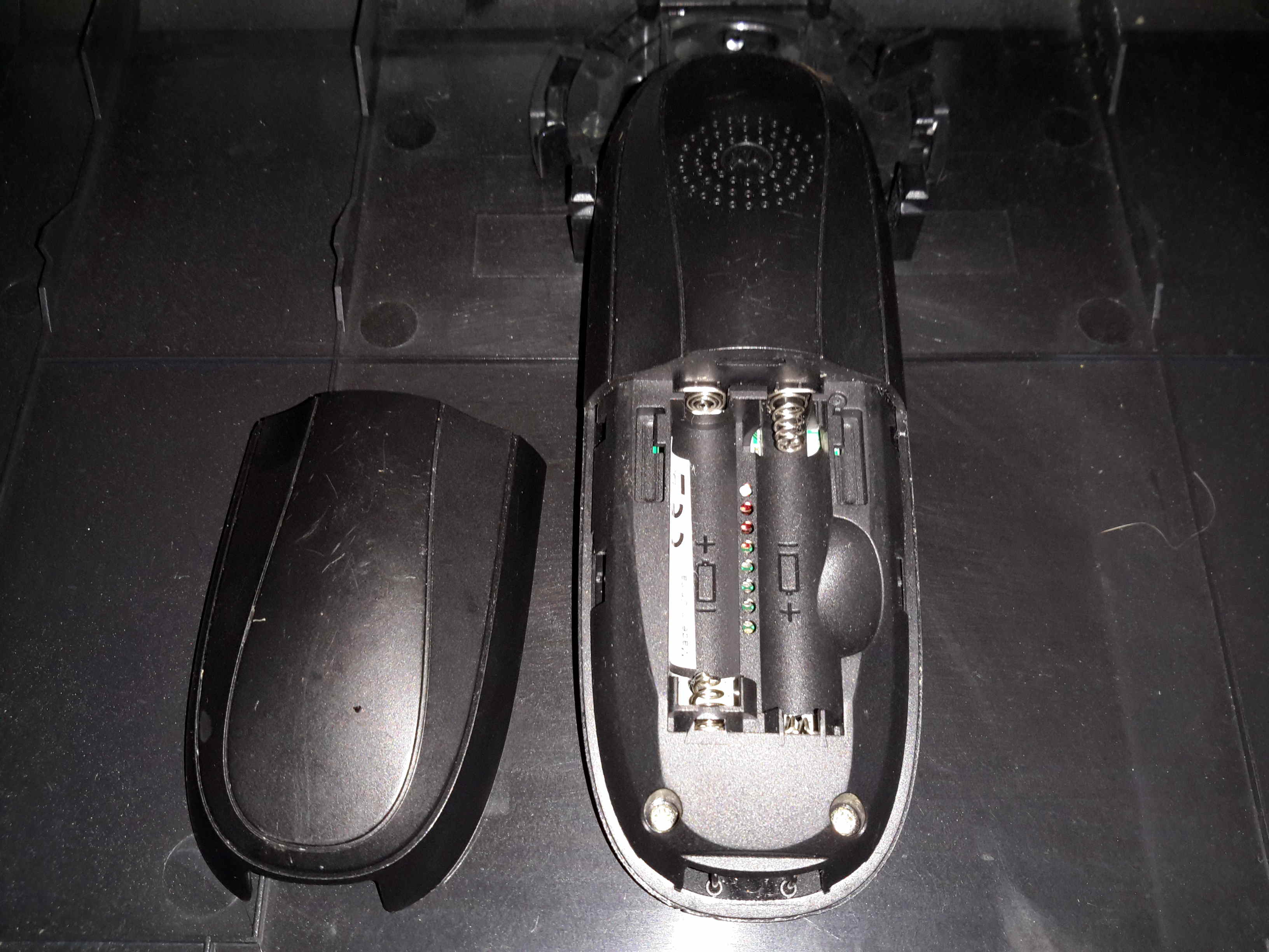
Battery Compartment
Not much on the back, other than the battery compartment for a pair of AAA rechargables. The base unit contains the charger.
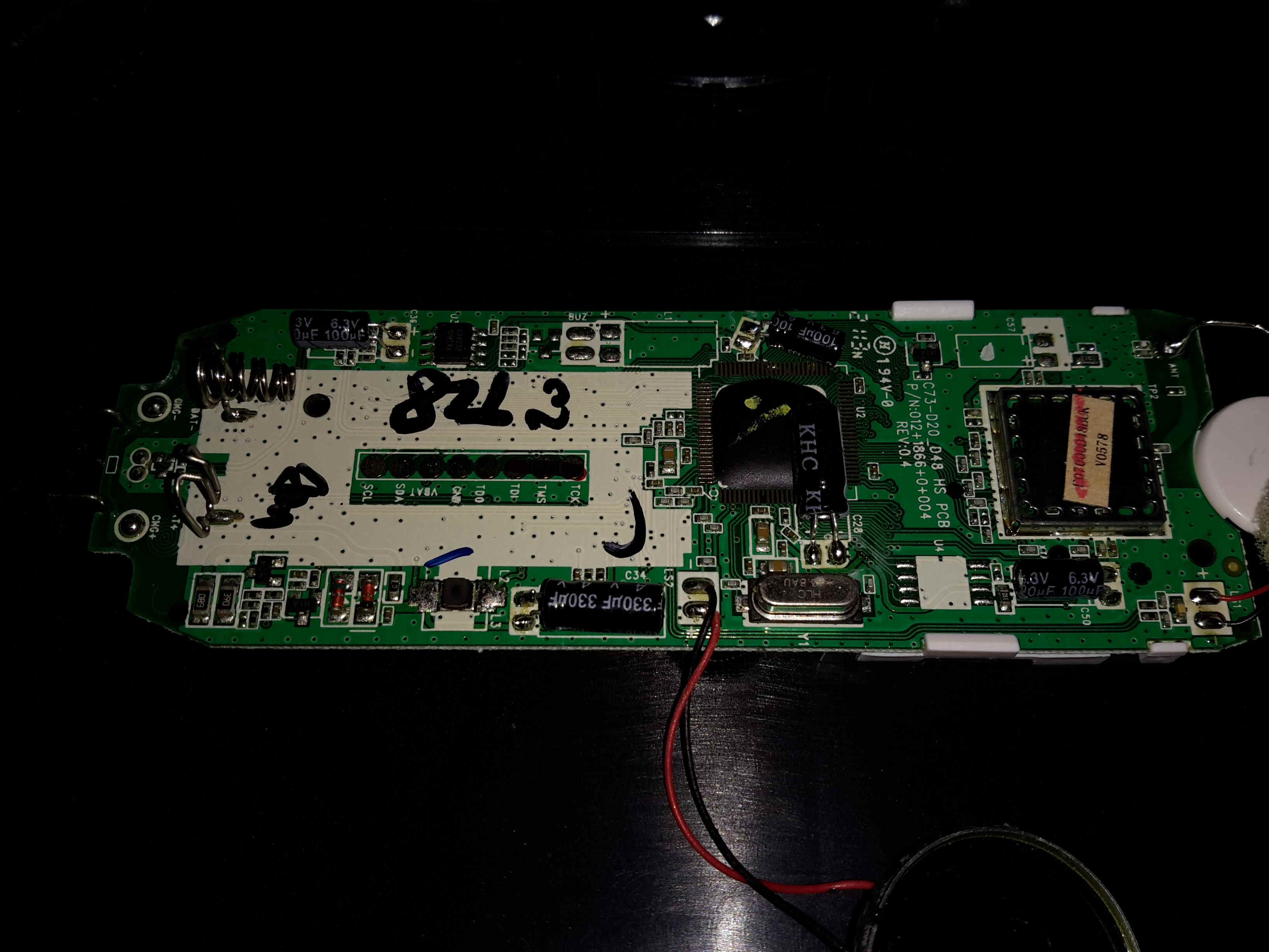
Main PCB
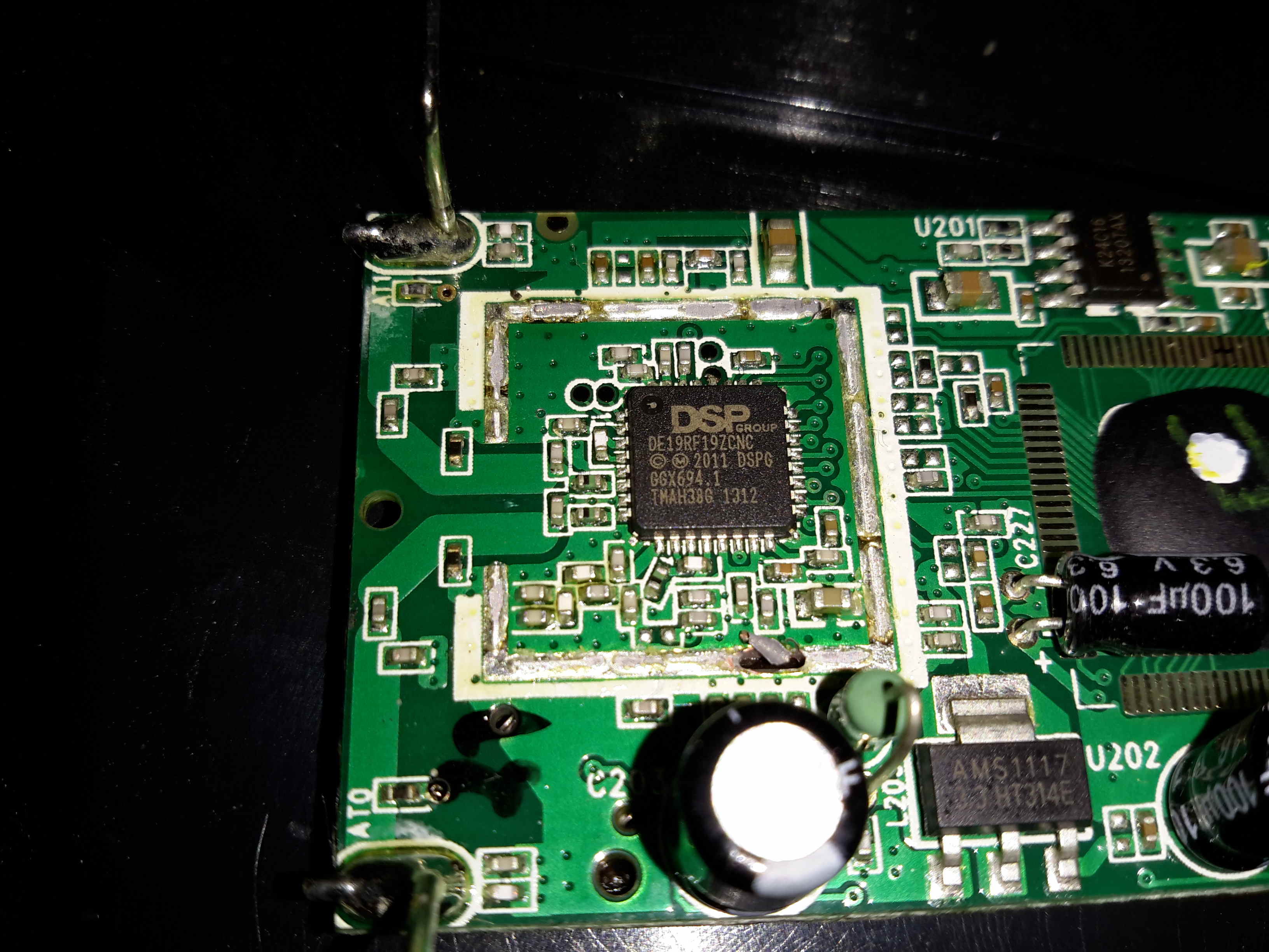
Here’s the main PCB removed from it’s casing. There’s not really much going on, one of the main ICs, which is probably a microcontroller, is a COB device, so no part numbers from there. There’s a row of pads for programming the device at the factory. The RF section is on a dedicated IC, a DE19RF19ZCNC from DSP Group. I couldn’t find much on this part, but it’s one of a range of DECT/VoIP DSP devices.
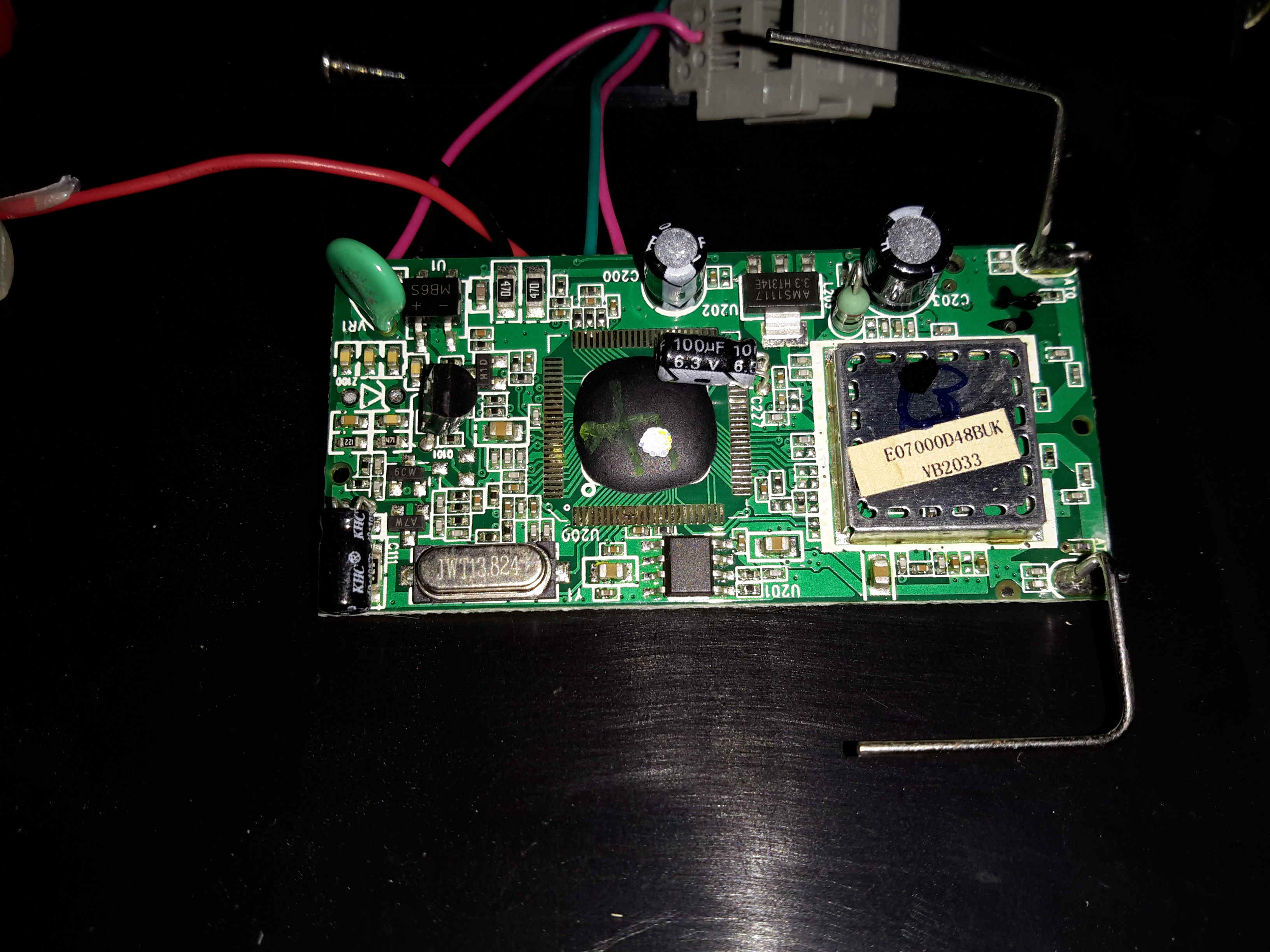
Base Unit PCB
Inside the base unit is a similar board, just without the keypad. Main microcontroller is again a COB device, the RF IC is under the shield.
Main Chipset
Removing the shield reveals the same IC as in the handset, only this PCB has a pair of antennas.
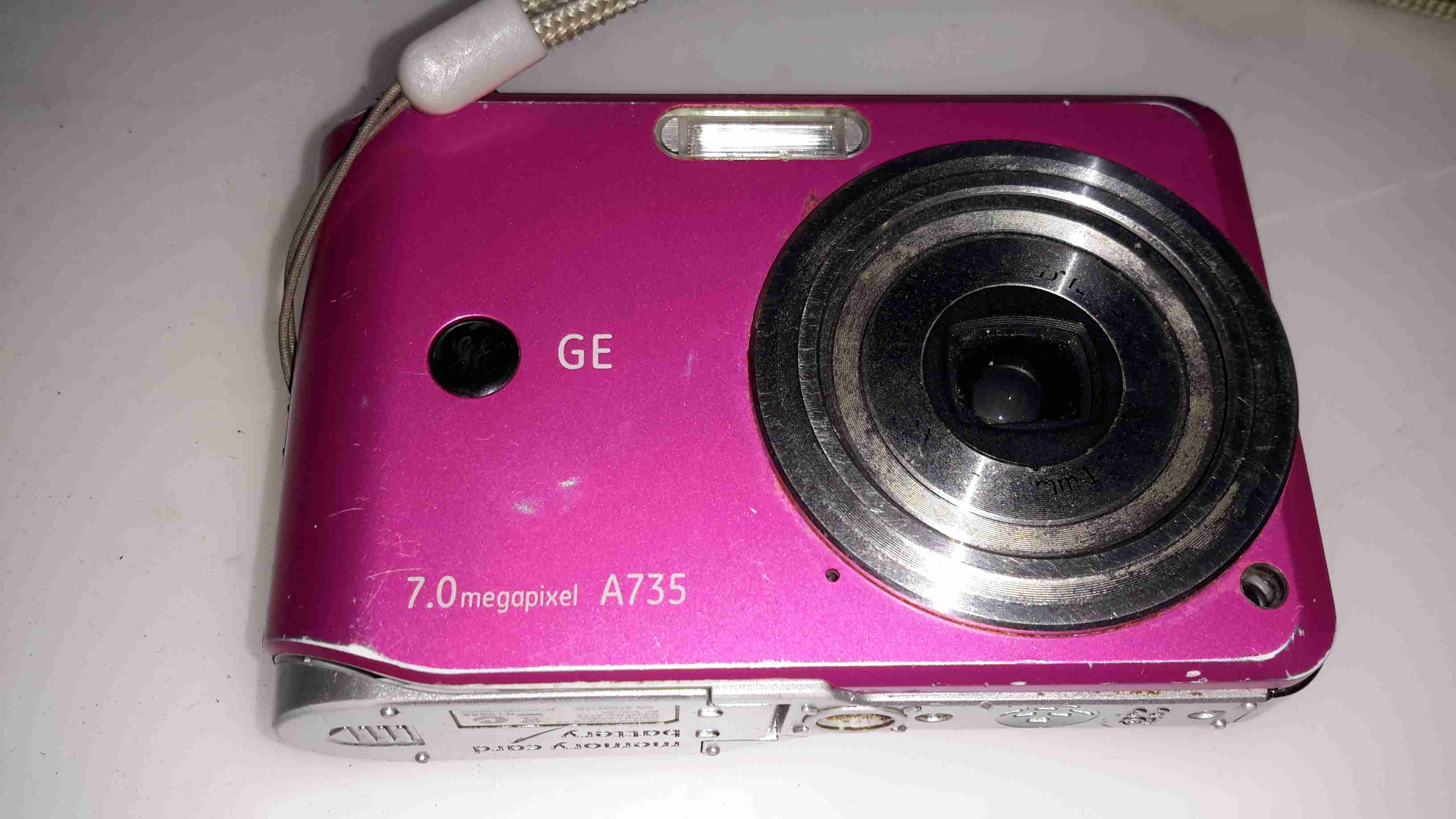
This camera has now been retired after many years of heavy use. Exposure to a 3-year old has caused severe damage to the lens mechanism, which no longer functions correctly.
Rear Panel
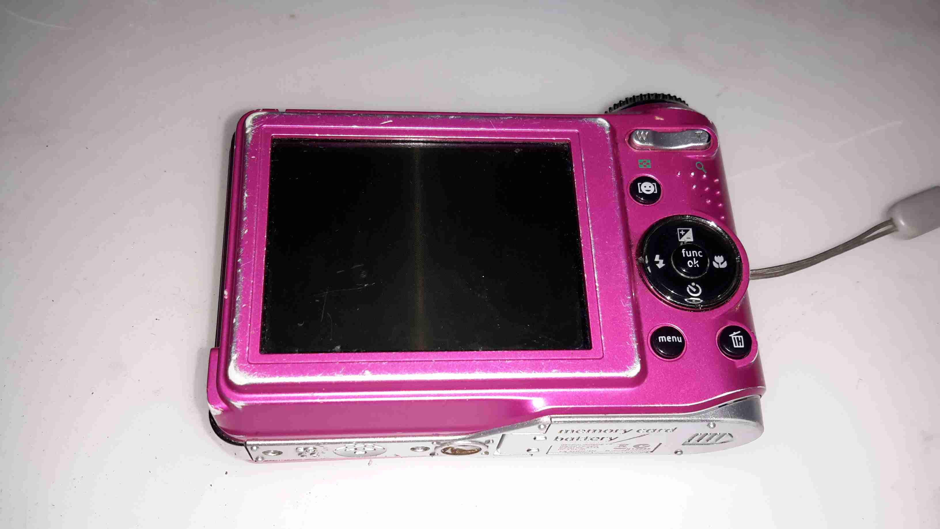
Pretty much standard interface for a digital camera, with a nice large LCD for it’s time.
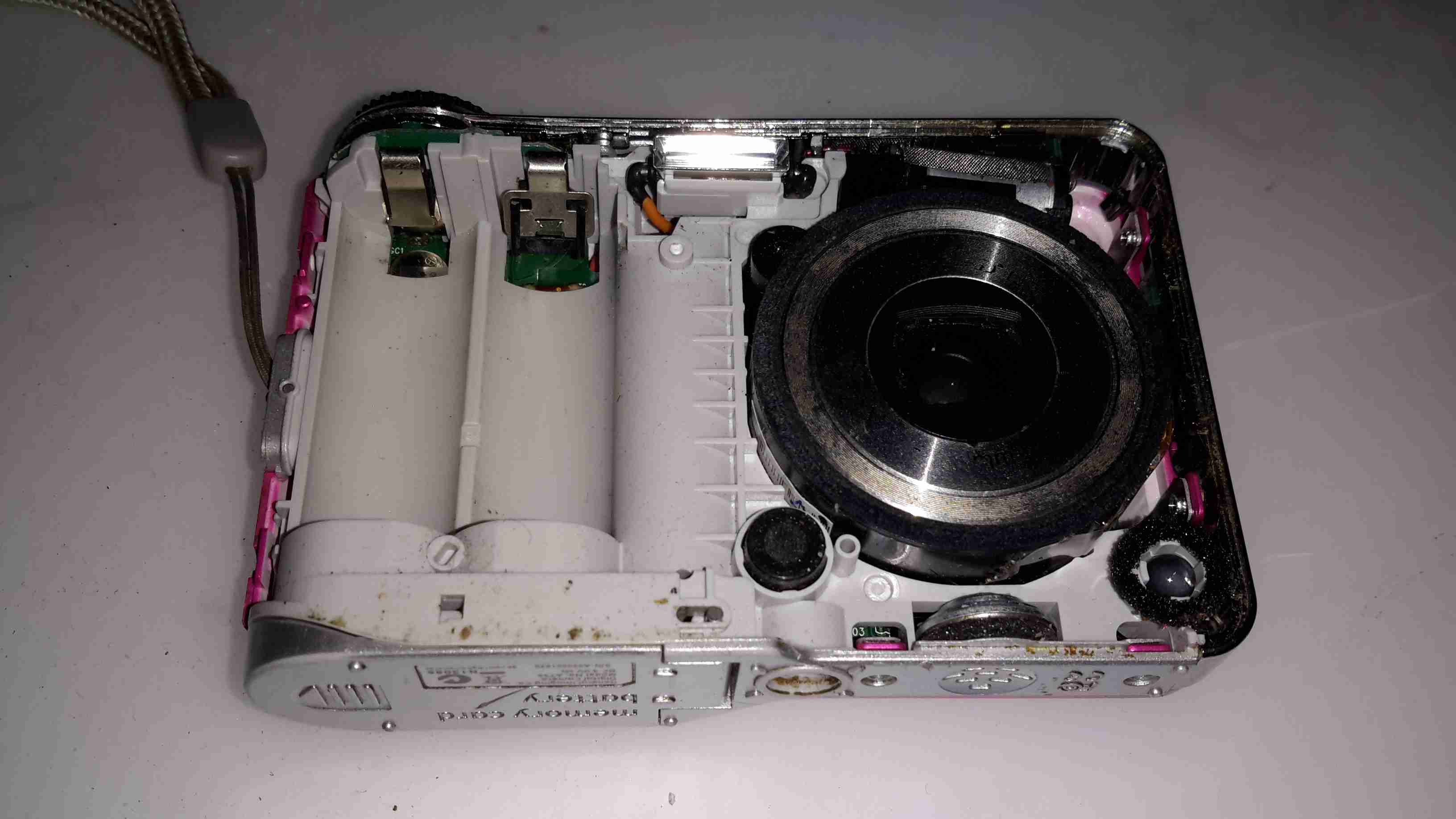
Front Cover Removed
With the front cover removed, the lens assembly & battery compartment is exposed.
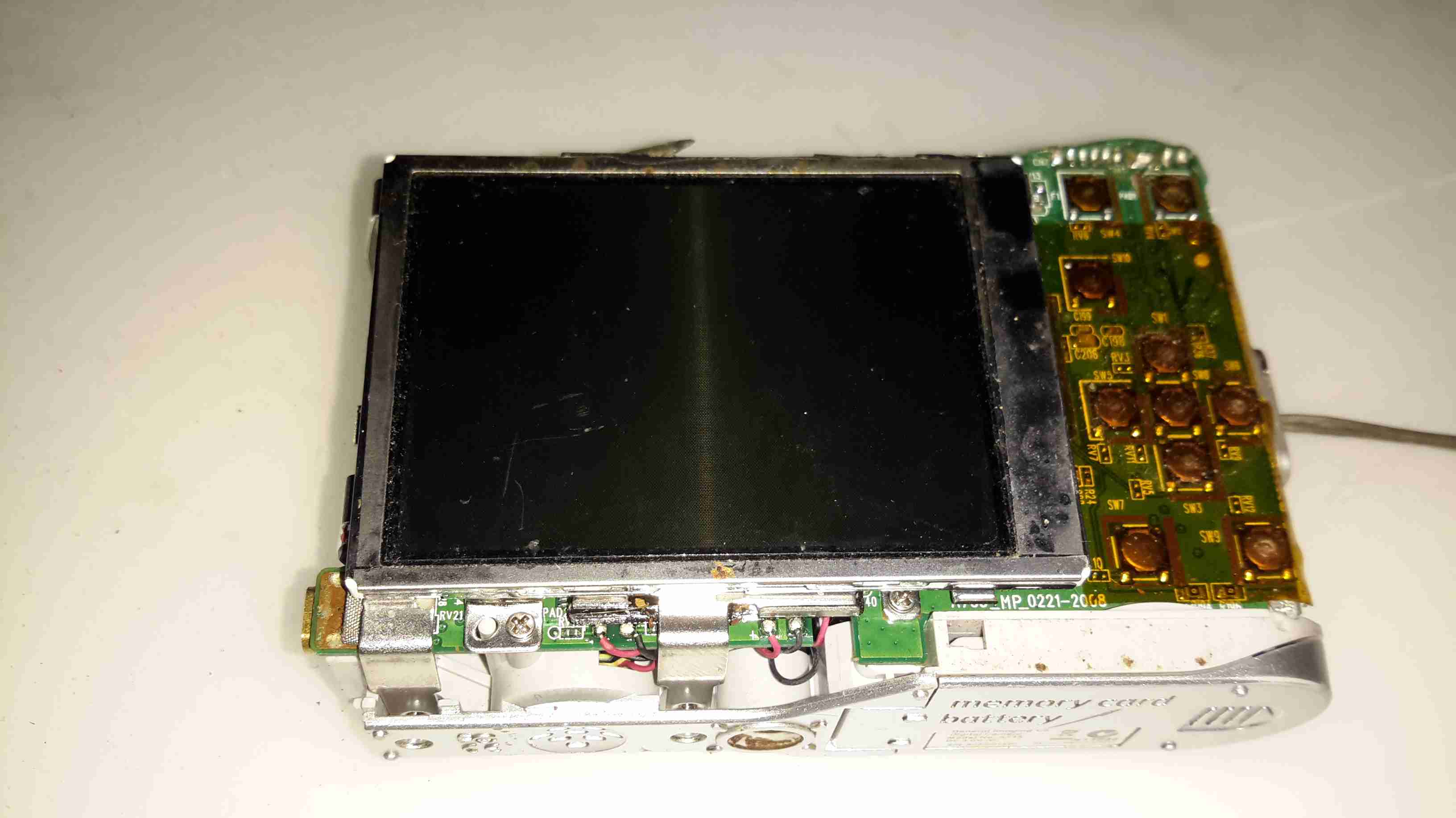
Rear Cover Removed
Removing the rear cover exposes the LCD module & the main PCB, the interface tactile switches are on the right under a protective layer of Kapton tape.
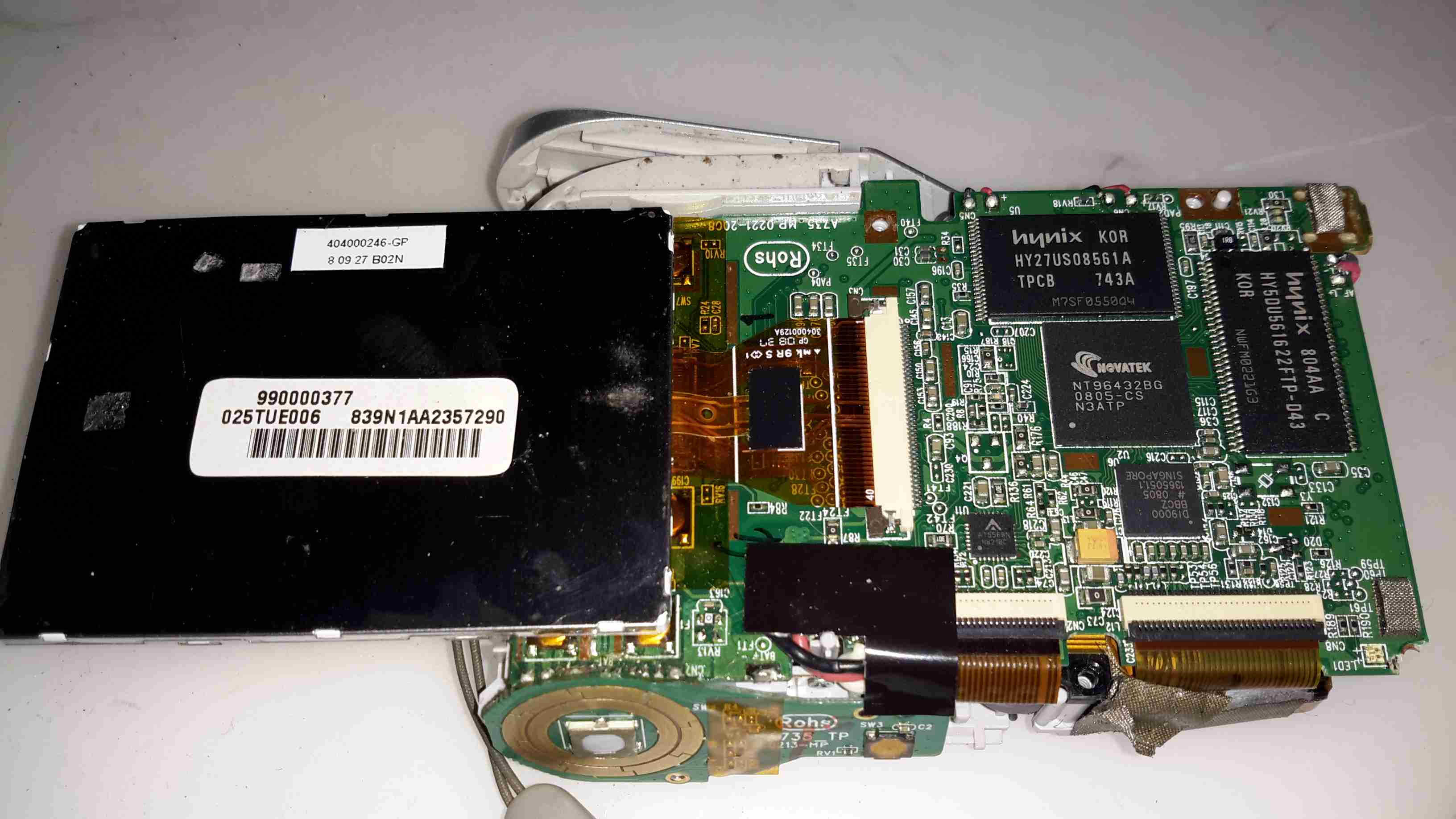
Main Chipset
Flipping the LCD out of it’s mounting bracket reveals the main camera chipset. The CPU is a NovaTek NT96432BG, no doubt a SoC of some kind, but I couldn’t find any information. Firmware & inbuilt storage is on a Hynix HY27US08561A 256MBit NAND Flash, with a Hynix HY5DU561622FTP-D43 256Mbit DRAM for system memory.
I couldn’t find any info on the other two chips on this side of the board, but one is probably a motor driver for the lens, while the other must be the front end for the CCD sensor input to the SoC.
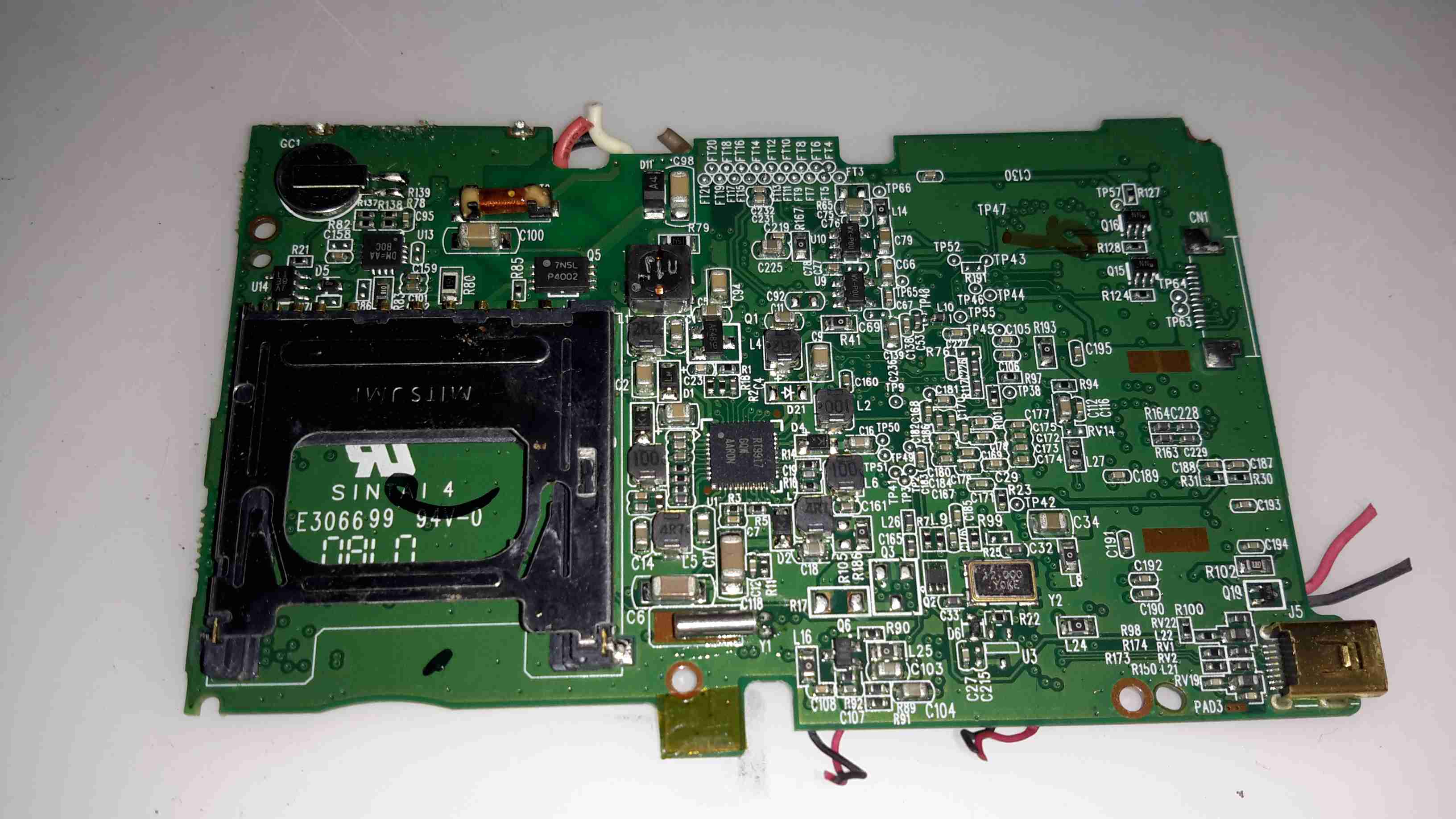
Main PCB Reverse
The other side of the PCB handles the SD card slot & power management. All the required DC rails are provided for by a RT9917 7-Channel DC-DC converter from RichTek, an IC designed specifically for digital camera applications.
Top left above the SD card slot is the trigger circuitry for the Xenon flash tube & the RTC backup battery.
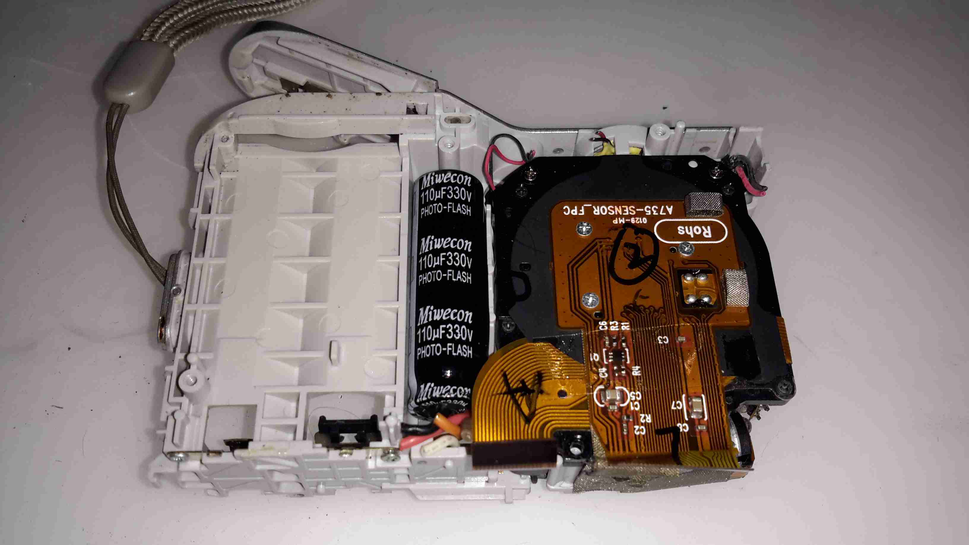
Main PCB Removed
Once the main PCB is out of the frame, the back of the lens module with the CCD is accessible. Just to the left is the high-voltage photoflash capacitor, 110µF 330v. These can give quite the kick when charged! Luckily this camera has been off long enough for the charge to bleed off.
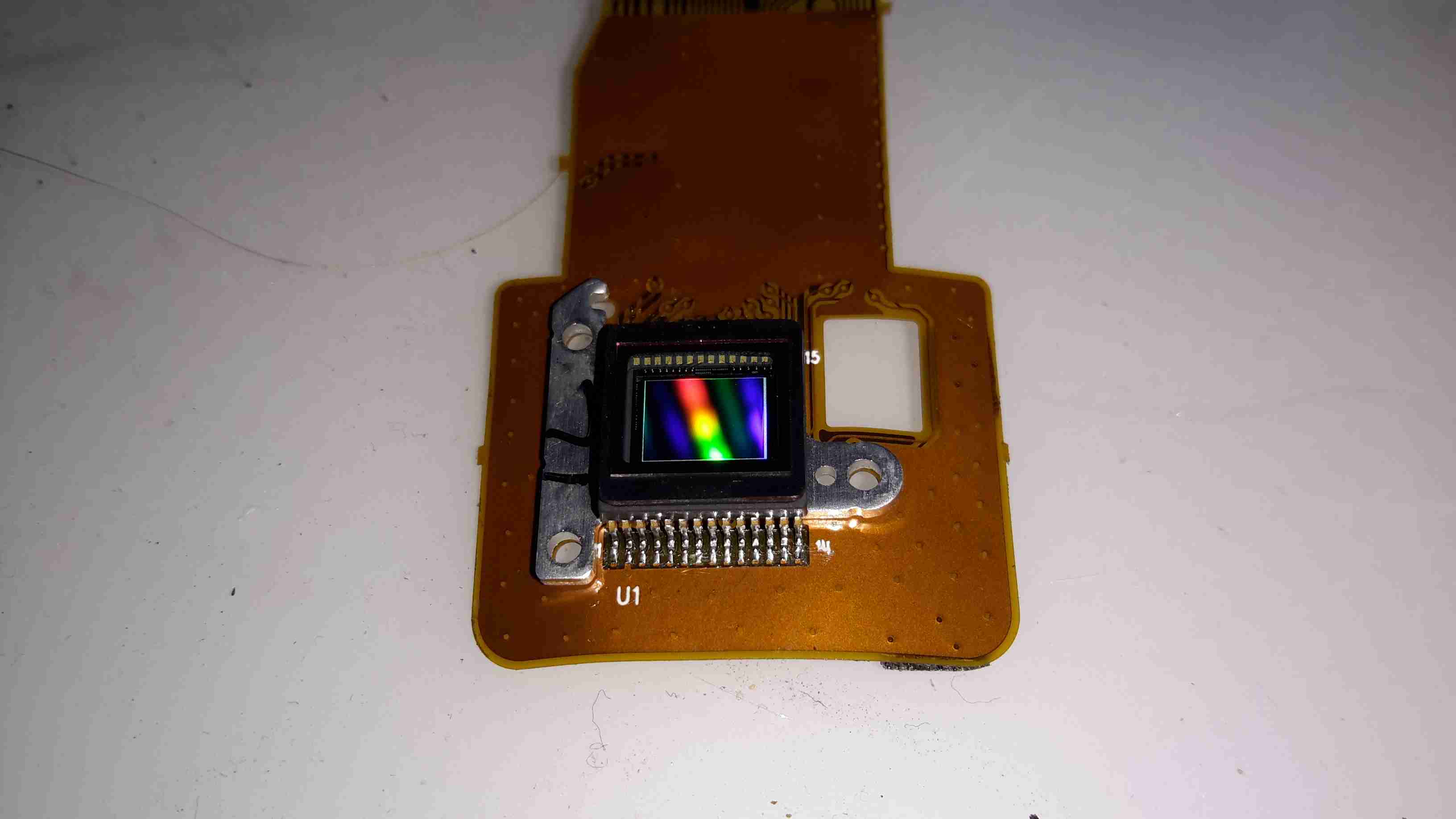
Sensor
Finally, here’s the 7-Megapixel CCD sensor removed from the lens assembly, with it’s built in IR cut filter over the top. I couldn’t find any make or model numbers on this part, as the Aluminium mounting bracket behind is bonded to the back of the sensor with epoxy, blocking access to any part information.
Die images of the chipset to come once I get round to decapping them!
Tip Jar
If you’ve found my content useful, please consider leaving a donation by clicking the Tip Jar below!
All collected funds go towards new content & the costs of keeping the server online.