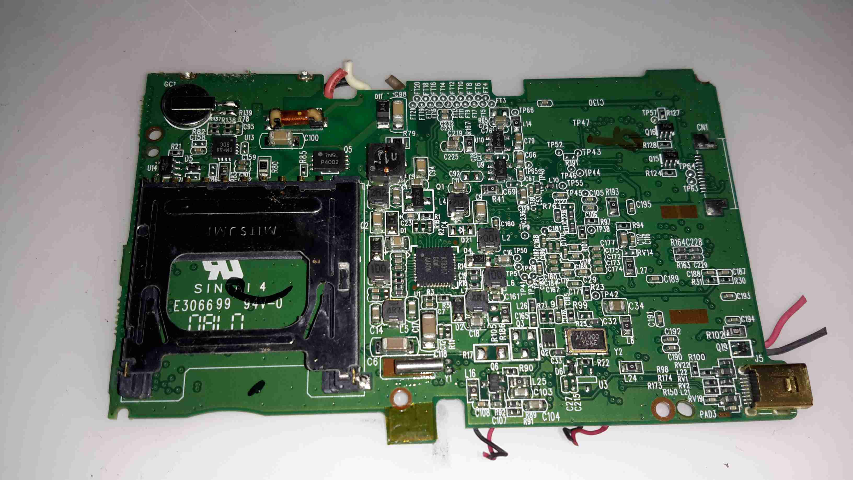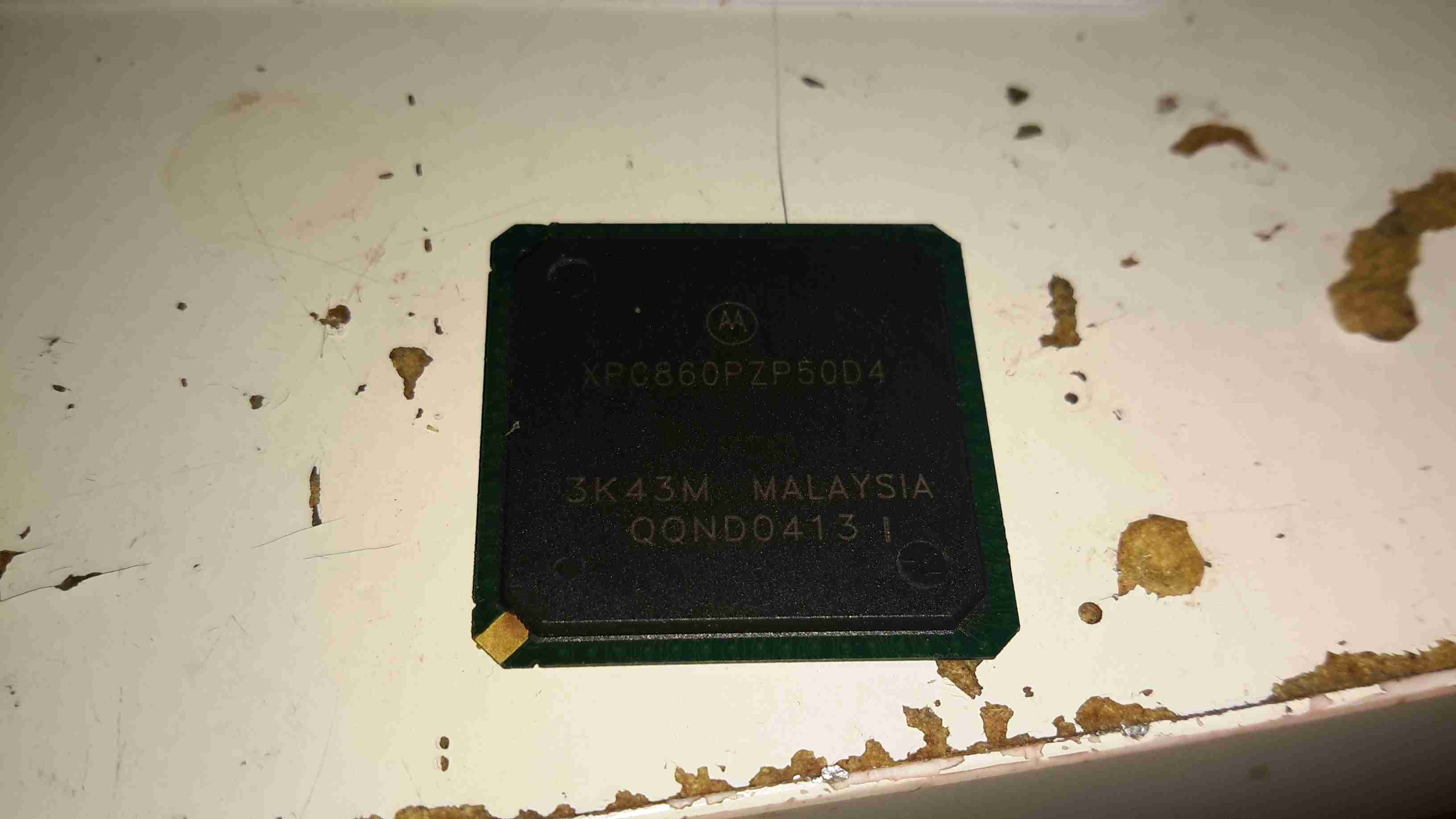
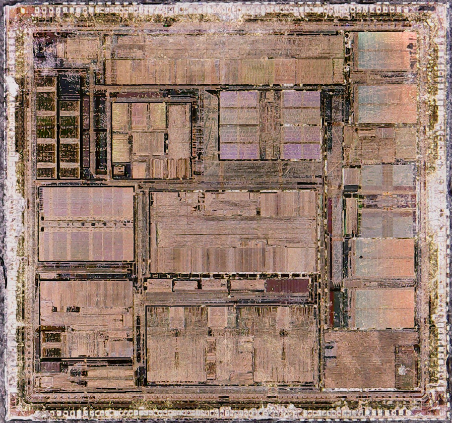
This is a System On Chip from Motorola, designed for network routing applications. This chip contains a hell of a feature set, so I’ll just include an excerpt from the datasheet:
Embedded single-issue, 32-bit MPC8xx core (implementing the PowerPC
architecture) with thirty-two 32-bit general-purpose registers (GPRs)
— The core performs branch prediction with conditional prefetch, without
conditional execution
— 4- or 8-Kbyte data cache and 4- or 16-Kbyte instruction cache (see Table 1)
– 16-Kbyte instruction caches are four-way, set-associative with 256 sets;
4-Kbyte instruction caches are two-way, set-associative with 128 sets.
– 8-Kbyte data caches are two-way, set-associative with 256 sets; 4-Kbyte data
caches are two-way, set-associative with 128 sets.
– Cache coherency for both instruction and data caches is maintained on 128-bit
(4-word) cache blocks.
– Caches are physically addressed, implement a least recently used (LRU)
replacement algorithm, and are lockable on a cache block basis.
— Instruction and data caches are two-way, set-associative, physically addressed,
LRU replacement, and lockable on-line granularity.
— MMUs with 32-entry TLB, fully associative instruction, and data TLBs
— MMUs support multiple page sizes of 4, 16, and 512 Kbytes, and 8 Mbytes; 16
virtual address spaces and 16 protection groups
— Advanced on-chip-emulation debug mode
Up to 32-bit data bus (dynamic bus sizing for 8, 16, and 32 bits)
32 address lines
Operates at up to 80 MHz
Memory controller (eight banks)
— Contains complete dynamic RAM (DRAM) controller
— Each bank can be a chip select or RAS to support a DRAM bank
— Up to 15 wait states programmable per memory bank
— Glueless interface to DRAM, SIMMS, SRAM, EPROM, Flash EPROM, and
other memory devices.
— DRAM controller programmable to support most size and speed memory
interfaces
— Four CAS lines, four WE lines, one OE line
— Boot chip-select available at reset (options for 8-, 16-, or 32-bit memory)
— Variable block sizes (32 Kbyte to 256 Mbyte)
— Selectable write protection
— On-chip bus arbitration logic
General-purpose timers
— Four 16-bit timers or two 32-bit timers
— Gate mode can enable/disable counting
— Interrupt can be masked on reference match and event capture
System integration unit (SIU)
— Bus monitor
— Software watchdog
— Periodic interrupt timer (PIT)
— Low-power stop mode
— Clock synthesizer
— Decrementer, time base, and real-time clock (RTC) from the PowerPC
architecture
— Reset controller
— IEEE 1149.1 test access port (JTAG)
Interrupts
— Seven external interrupt request (IRQ) lines
— 12 port pins with interrupt capability
— 23 internal interrupt sources
— Programmable priority between SCCs
— Programmable highest priority request
10/100 Mbps Ethernet support, fully compliant with the IEEE 802.3u Standard (not
available when using ATM over UTOPIA interface)
ATM support compliant with ATM forum UNI 4.0 specification
— Cell processing up to 50–70 Mbps at 50-MHz system clock
— Cell multiplexing/demultiplexing
— Support of AAL5 and AAL0 protocols on a per-VC basis. AAL0 support enables
OAM and software implementation of other protocols).
— ATM pace control (APC) scheduler, providing direct support for constant bit rate
(CBR) and unspecified bit rate (UBR) and providing control mechanisms
enabling software support of available bit rate (ABR)
— Physical interface support for UTOPIA (10/100-Mbps is not supported with this
interface) and byte-aligned serial (for example, T1/E1/ADSL)
— UTOPIA-mode ATM supports level-1 master with cell-level handshake,
multi-PHY (up to 4 physical layer devices), connection to 25-, 51-, or 155-Mbps
framers, and UTOPIA/system clock ratios of 1/2 or 1/3.
— Serial-mode ATM connection supports transmission convergence (TC) function
for T1/E1/ADSL lines; cell delineation; cell payload scrambling/descrambling;
automatic idle/unassigned cell insertion/stripping; header error control (HEC)
generation, checking, and statistics.
Communications processor module (CPM)
— RISC communications processor (CP)
— Communication-specific commands (for example, GRACEFUL STOP TRANSMIT ,
ENTER HUNT MODE , and RESTART TRANSMIT )
— Supports continuous mode transmission and reception on all serial channels
— Up to 8Kbytes of dual-port RAM
— 16 serial DMA (SDMA) channels
— Three parallel I/O registers with open-drain capability
Four baud-rate generators (BRGs)
— Independent (can be connected to any SCC or SMC)
— Allow changes during operation
— Autobaud support option
Four serial communications controllers (SCCs)
— Ethernet/IEEE 802.3 optional on SCC1–4, supporting full 10-Mbps operation
(available only on specially programmed devices).
— HDLC/SDLC (all channels supported at 2 Mbps)
— HDLC bus (implements an HDLC-based local area network (LAN))
— Asynchronous HDLC to support PPP (point-to-point protocol)
— AppleTalk
— Universal asynchronous receiver transmitter (UART)
— Synchronous UART
— Serial infrared (IrDA)
— Binary synchronous communication (BISYNC)
— Totally transparent (bit streams)
— Totally transparent (frame based with optional cyclic redundancy check (CRC))
Two SMCs (serial management channels)
— UART
— Transparent
— General circuit interface (GCI) controller
— Can be connected to the time-division multiplexed (TDM) channels
One SPI (serial peripheral interface)
— Supports master and slave modes
— Supports multimaster operation on the same bus
One I 2 C (inter-integrated circuit) port
— Supports master and slave modes
— Multiple-master environment support
Time-slot assigner (TSA)
— Allows SCCs and SMCs to run in multiplexed and/or non-multiplexed operation
— Supports T1, CEPT, PCM highway, ISDN basic rate, ISDN primary rate, user
defined
— 1- or 8-bit resolution
— Allows independent transmit and receive routing, frame synchronization,
clocking
— Allows dynamic changes
— Can be internally connected to six serial channels (four SCCs and two SMCs)
Parallel interface port (PIP)
— Centronics interface support
— Supports fast connection between compatible ports on the MPC860 or the
MC68360
PCMCIA interface
— Master (socket) interface, release 2.1 compliant
— Supports two independent PCMCIA sockets
— Eight memory or I/O windows supported
Low power support
— Full on—all units fully powered
— Doze—core functional units disabled, except time base decrementer, PLL,
memory controller, RTC, and CPM in low-power standby
— Sleep—all units disabled, except RTC and PIT, PLL active for fast wake up
— Deep sleep—all units disabled including PLL, except RTC and PIT
— Power down mode— all units powered down, except PLL, RTC, PIT, time base,
and decrementer
Debug interface
— Eight comparators: four operate on instruction address, two operate on data
address, and two operate on data
— Supports conditions: = ≠ < >
— Each watchpoint can generate a break-point internally
3.3 V operation with 5-V TTL compatibility except EXTAL and EXTCLK
357-pin ball grid array (BGA) package