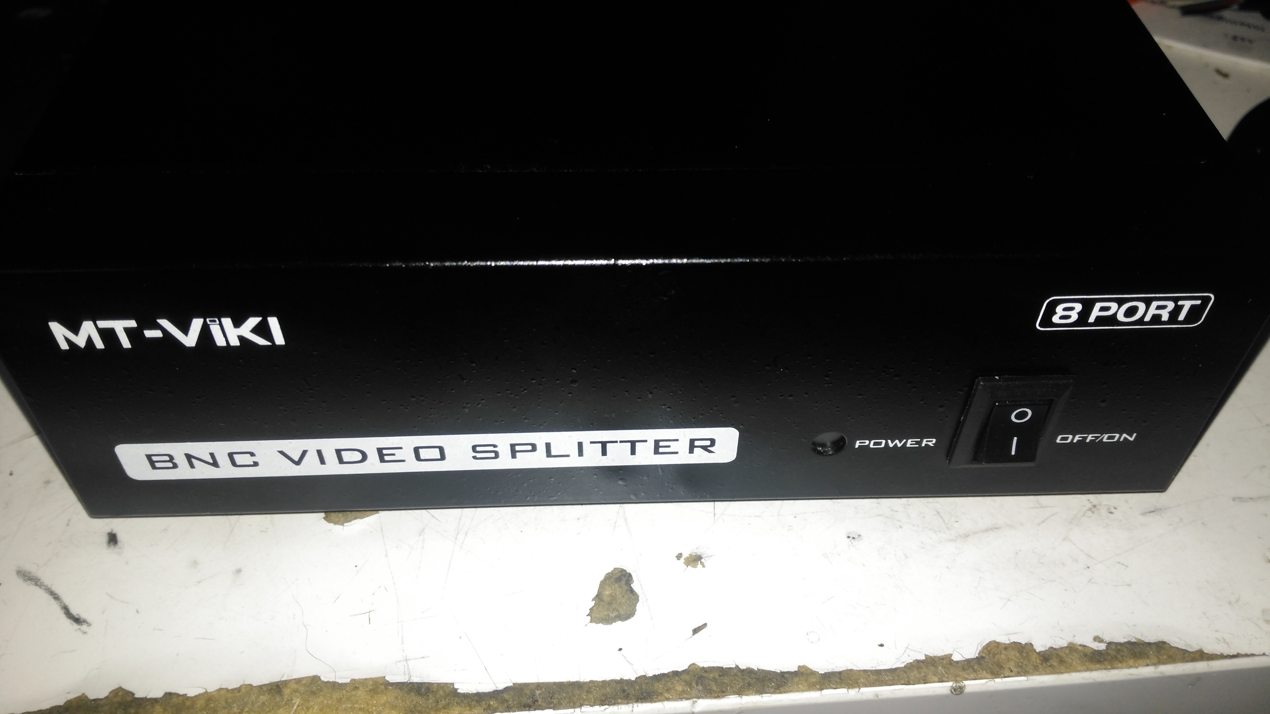
Time for another eBay special: this time it’s an 8-port video distribution amplifier, with BNC connections designed for commercial/industrial equipment. Not much on the front panel above, apart from the power switch & LED.
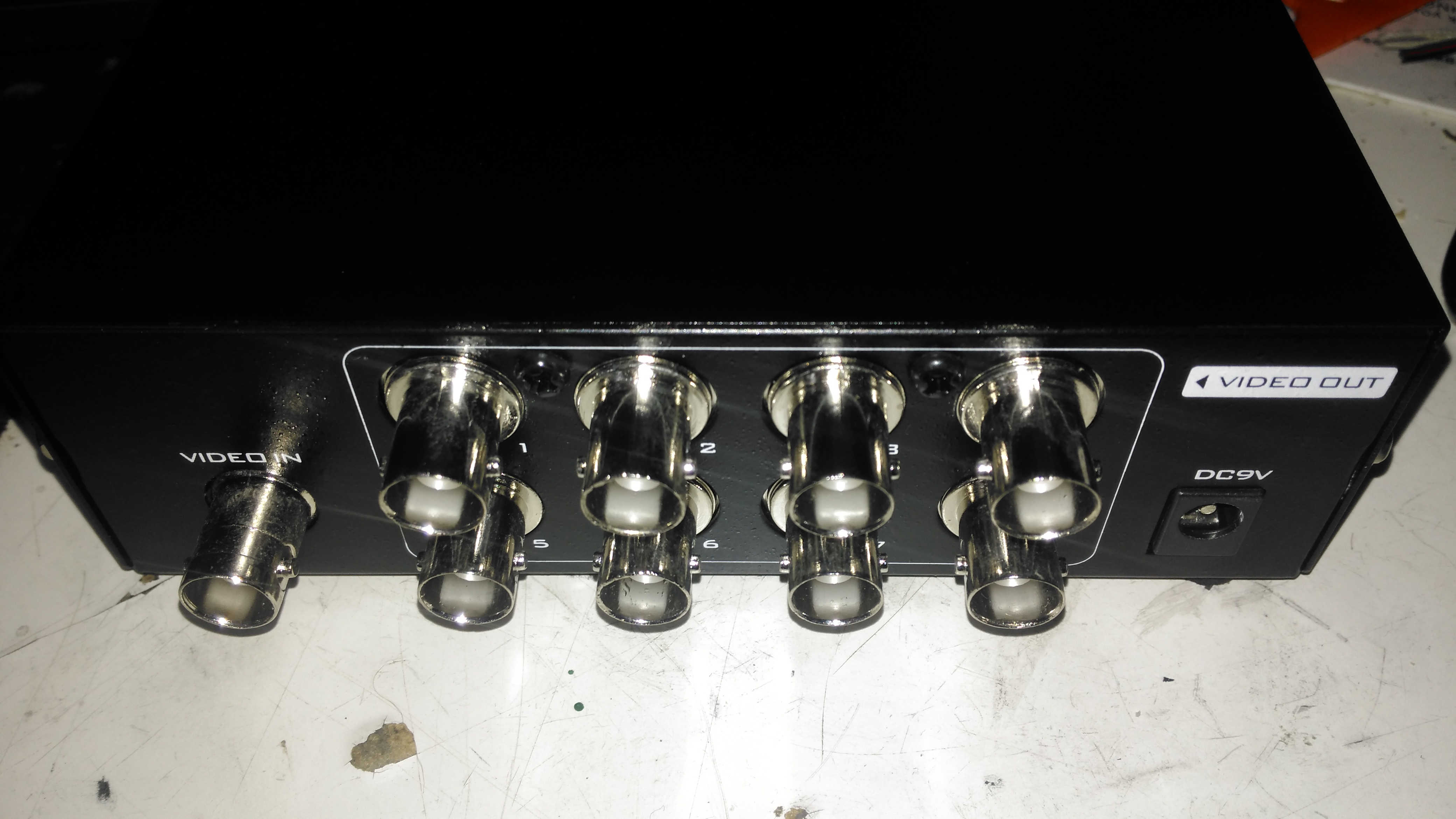
Rear Panel
The rear panel has all the connectors, input is on the left, while the outputs are in the centre. Power is supplied through the barrel jack on the right, 9v DC in this case.
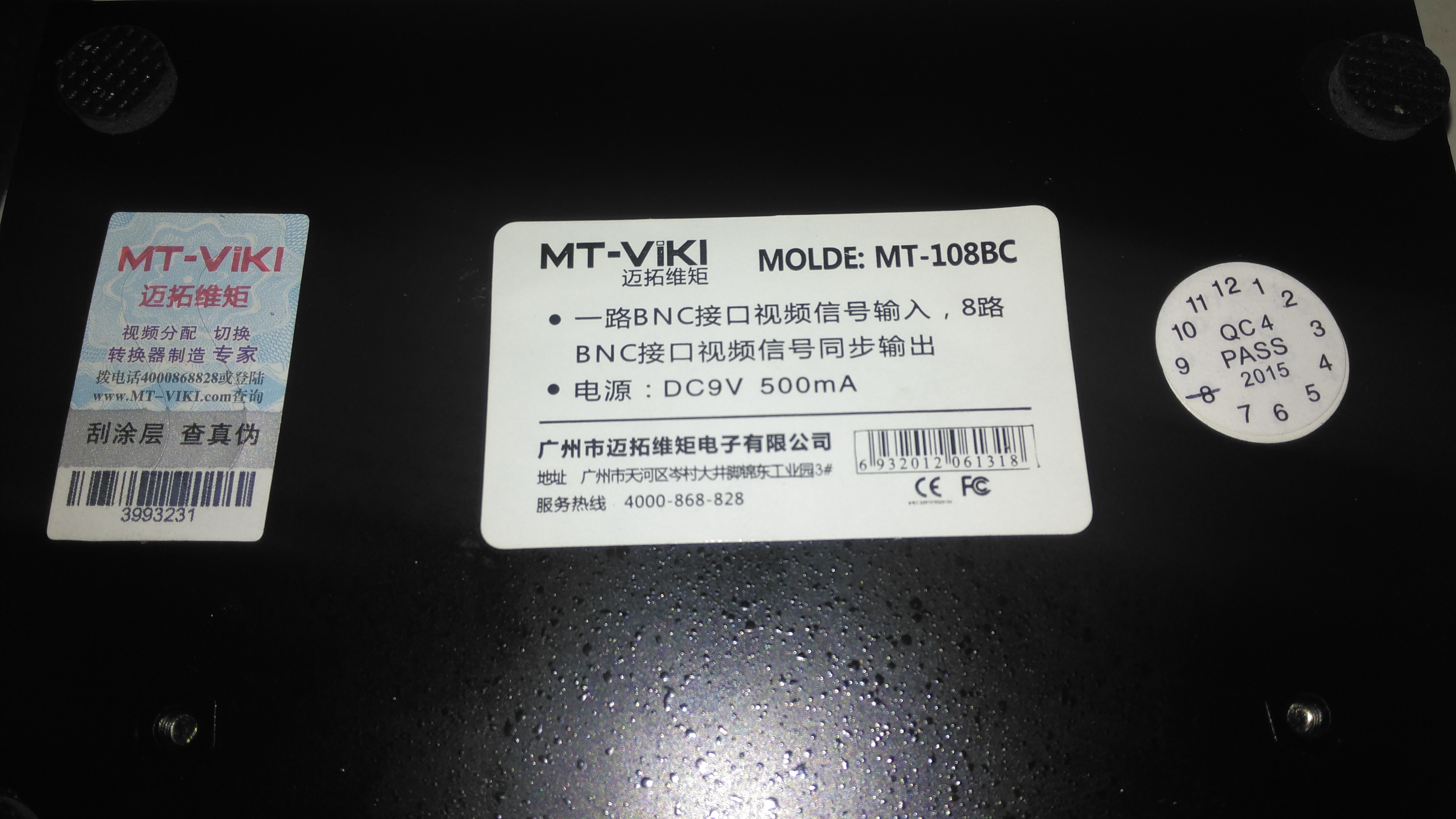
Data Label
Not much in English on the data labels, there’s also an authenticity label on the left to make sure you don’t get a fake.
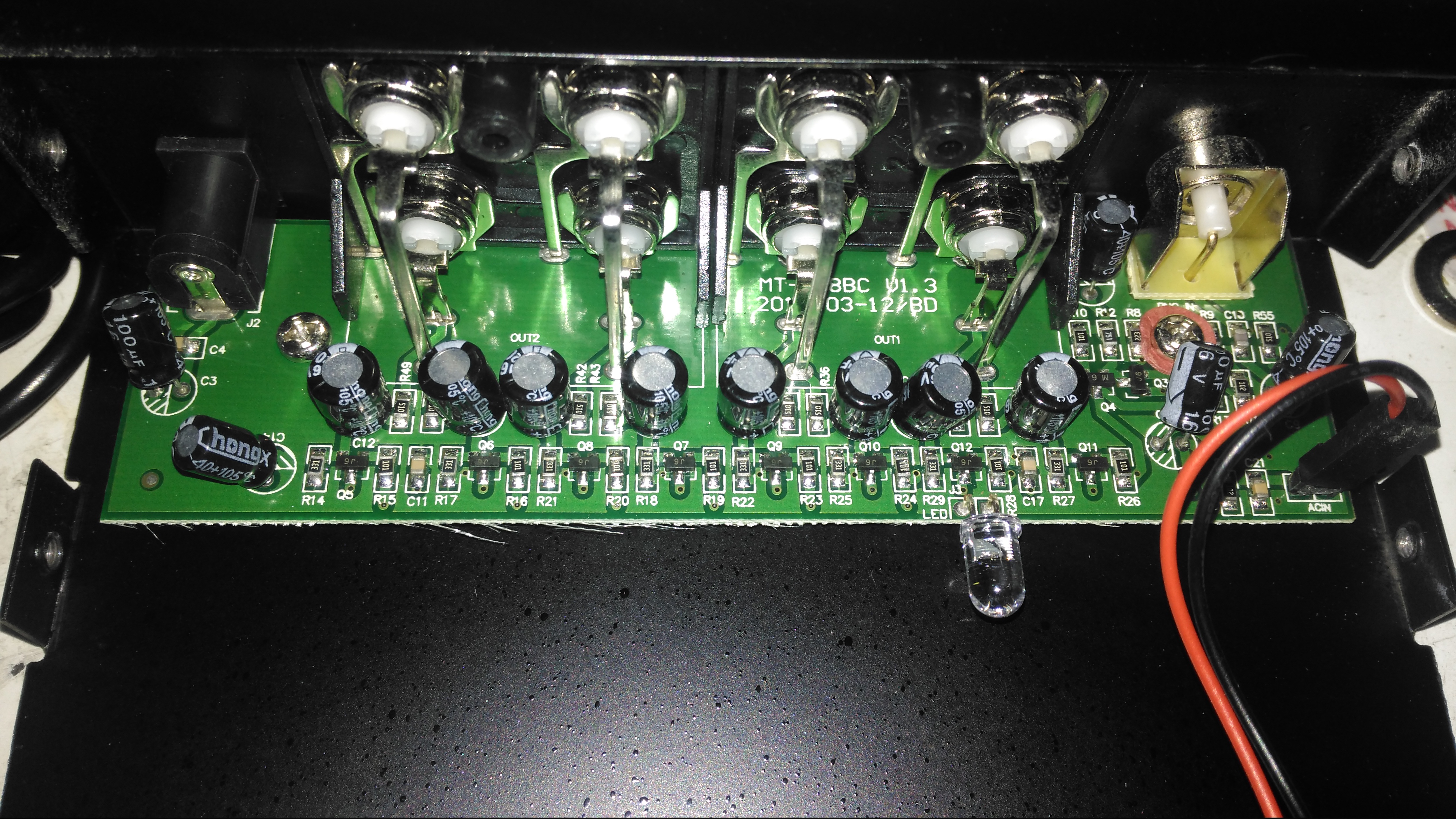
Amplifier Board
Taking the lid off reveals a very small PCB, taking up less than a third of the aluminium case! The input stage is on the right, composed of a pair of SOT-23 transistors to buffer the incoming signal. There’s an KST812M6 PNP & an S9014 NPN Epitaxial. The signal is then fed to the output stages, all individual S9014 NPN transistors to the output ports.
The power LED is just poking in the general direction of the hole in the front panel, so this isn’t likely to work very well – it’s going to illuminate the inside of the case more!
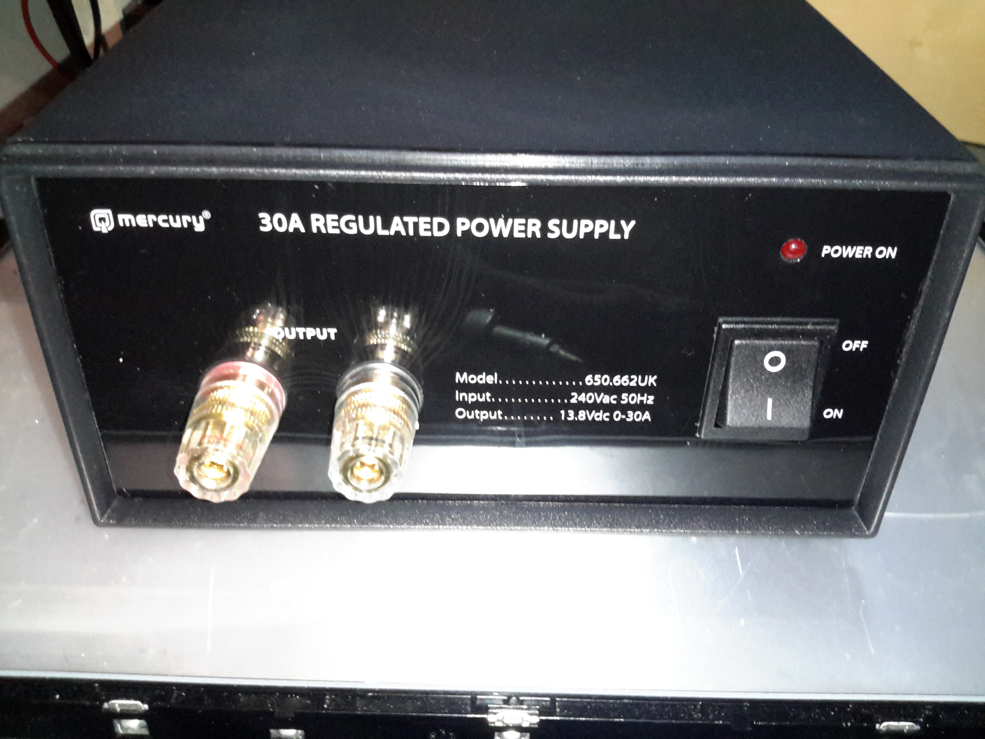
After having a couple of the cheap Chinese PSUs fail on me in a rather spectacular fashion, I decided to splash on a more expensive name-brand PSU, since constantly replacing PSUs at £15 a piece is going to get old pretty fast. This is the 30A model from Mercury, which seems to be pretty well built. It’s also significantly more expensive at £80. Power output is via the beefy binding posts on the front panel. There isn’t any metering on board, this is something I’ll probably change once I’ve ascertained it’s reliability. This is also a fixed voltage supply, at 13.8v.
Rear Panel
Not much on the rear panel, just the fuse & cooling fan. This isn’t temperature controlled, but it’s not loud. No IEC power socket here, the mains cable is hard wired.
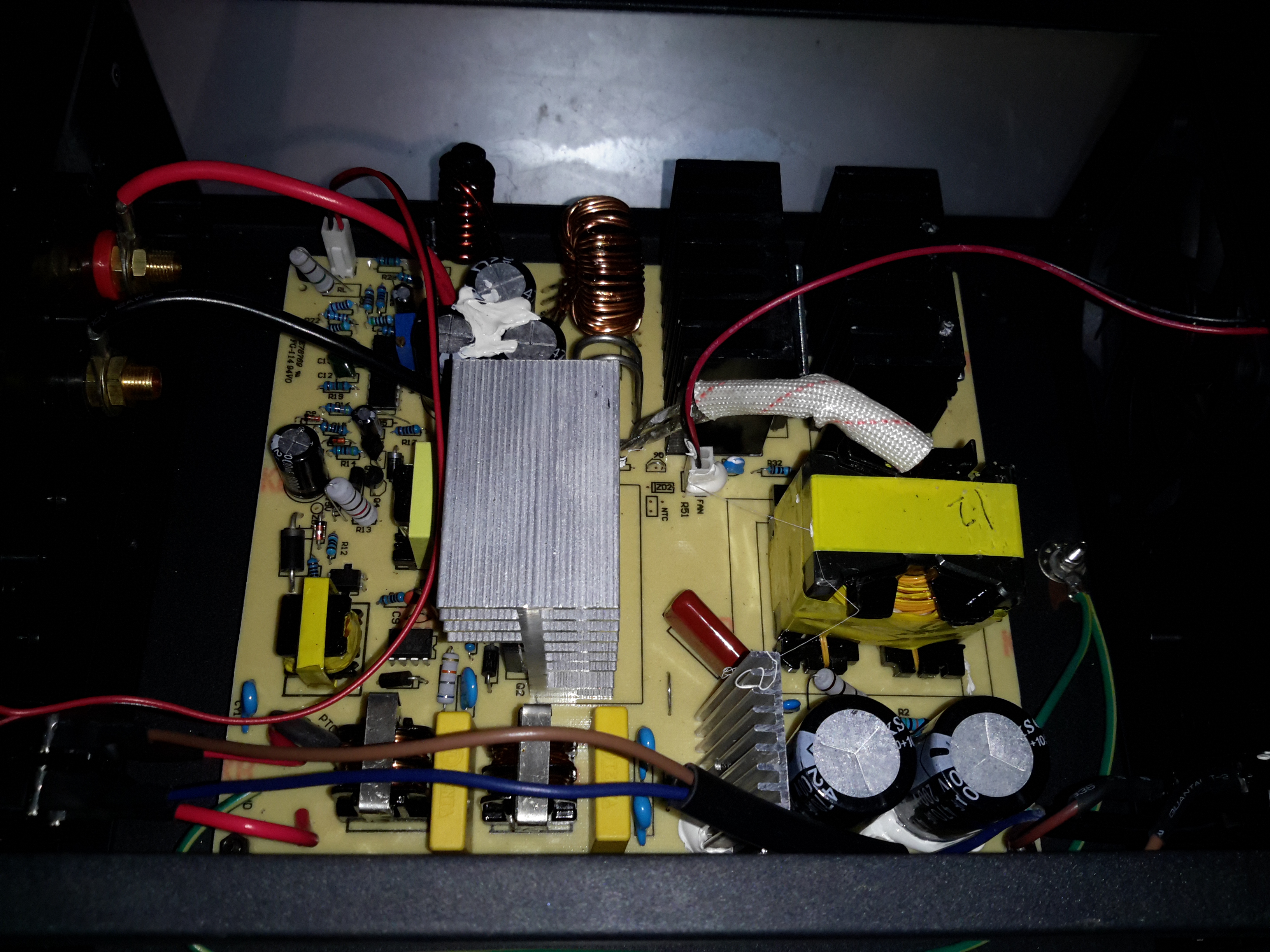
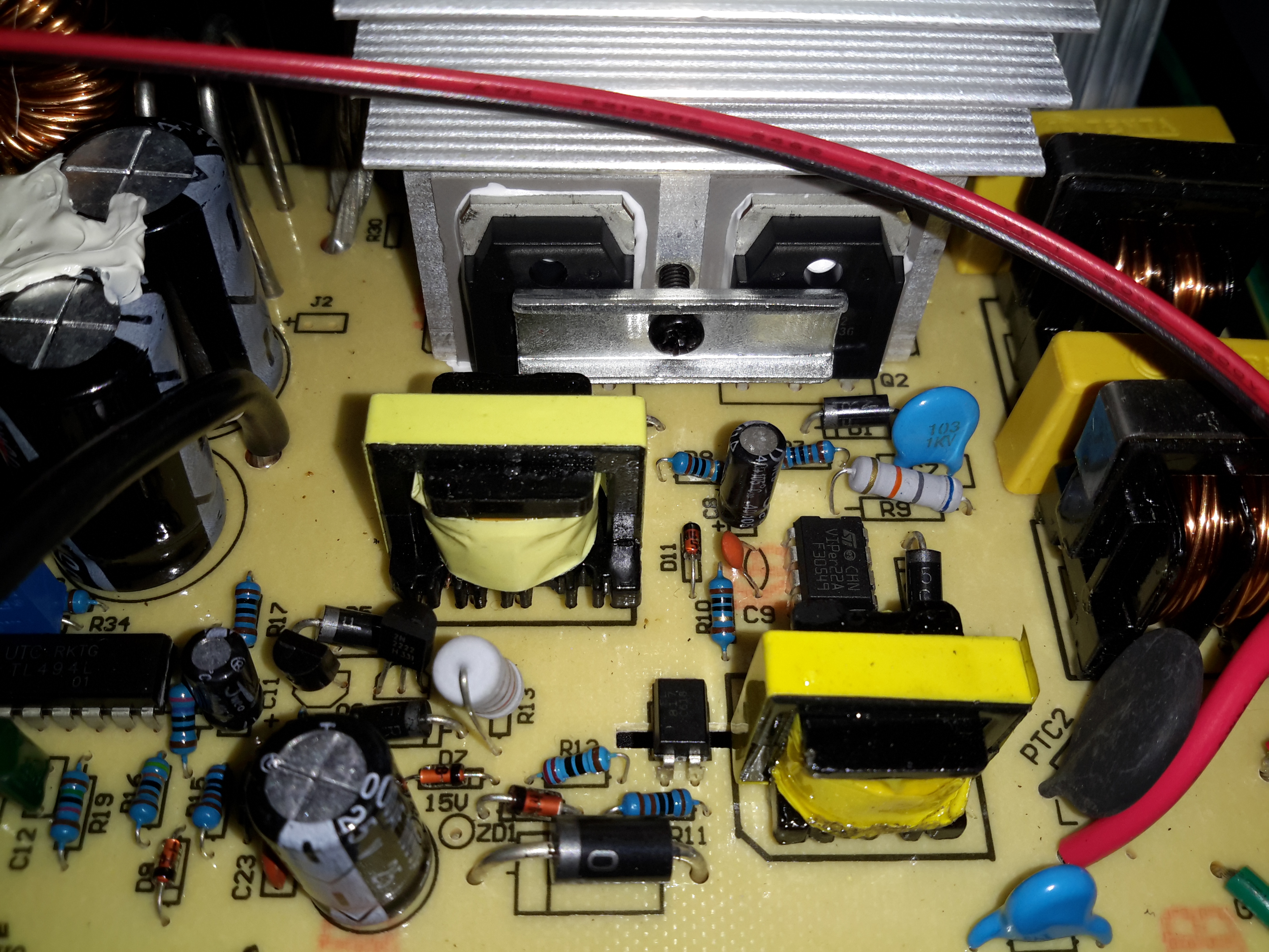
Main Board
Removing some spanner-type security screws reveals the power supply board itself. Everything on here is enormous to handle the 30A output current at 13.8v. The main primary side switching transistors are on the large silver heatsink in the centre of the board, feeding the huge ferrite transformer on the right.
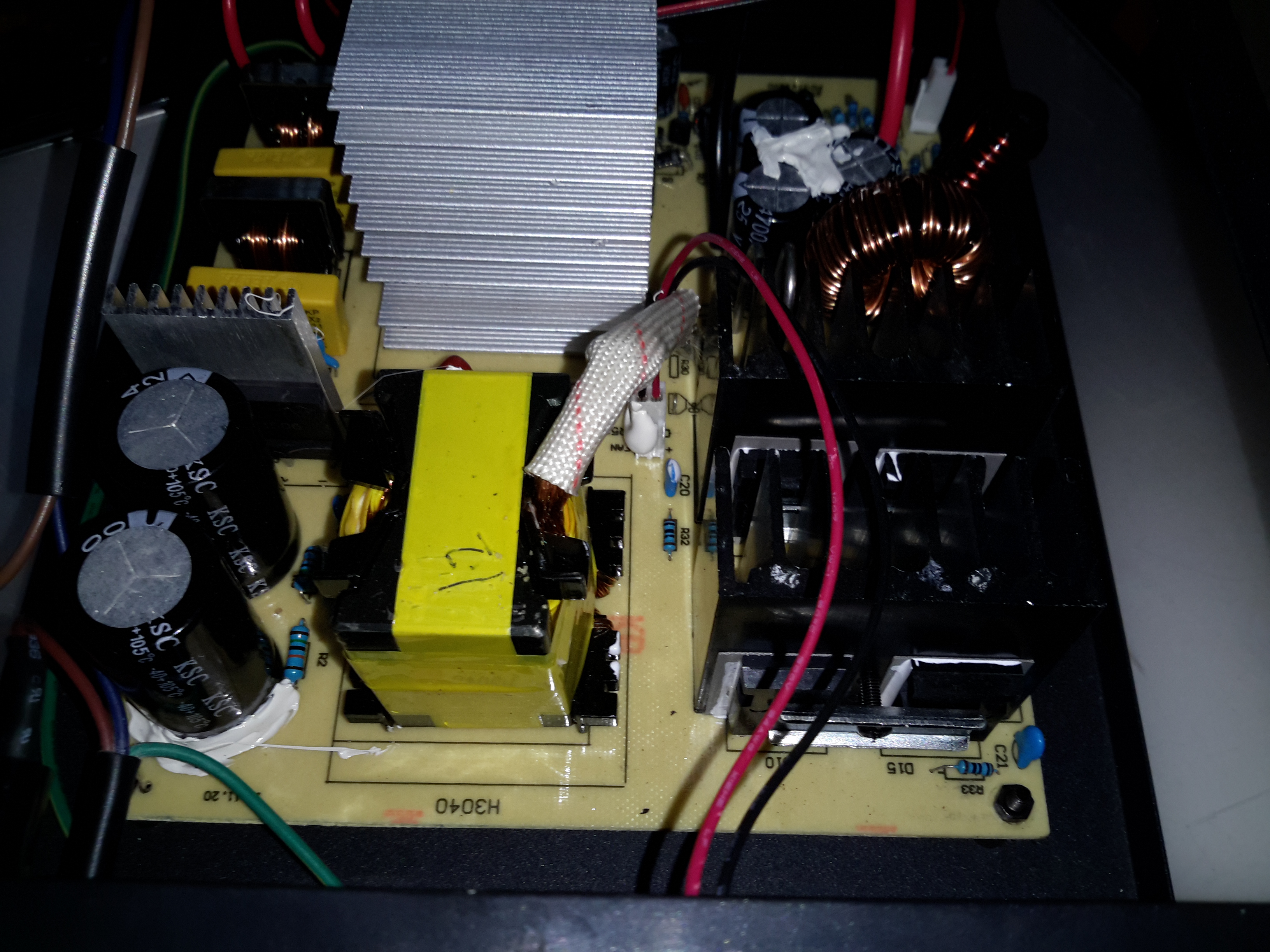
Transformer
The transformer’s low voltage output tap comes straight out instead of being on pins, due to the size of the winding cores. Four massive diodes are mounted on the black heatsinks for output rectification.
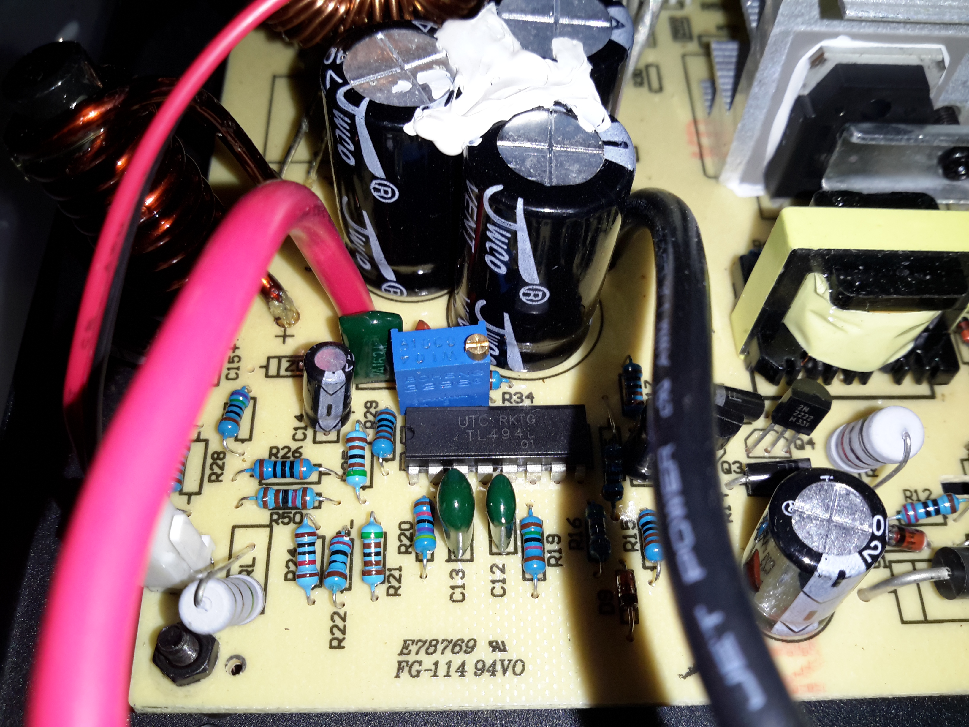
SMPS Controller
The supply is controlled via the jelly bean TL494 PWM controller IC. The multi-turn potentiometer doesn’t adjust the output voltage, more likely it adjusts the current limit.
Standby Supply
Power to initially start the supply is provided by a small SMPS circuit, with a VIPer22A Low Power Primary Switcher & small transformer on the lower right. The transformer upper left is the base drive transformer for the main high power supply.
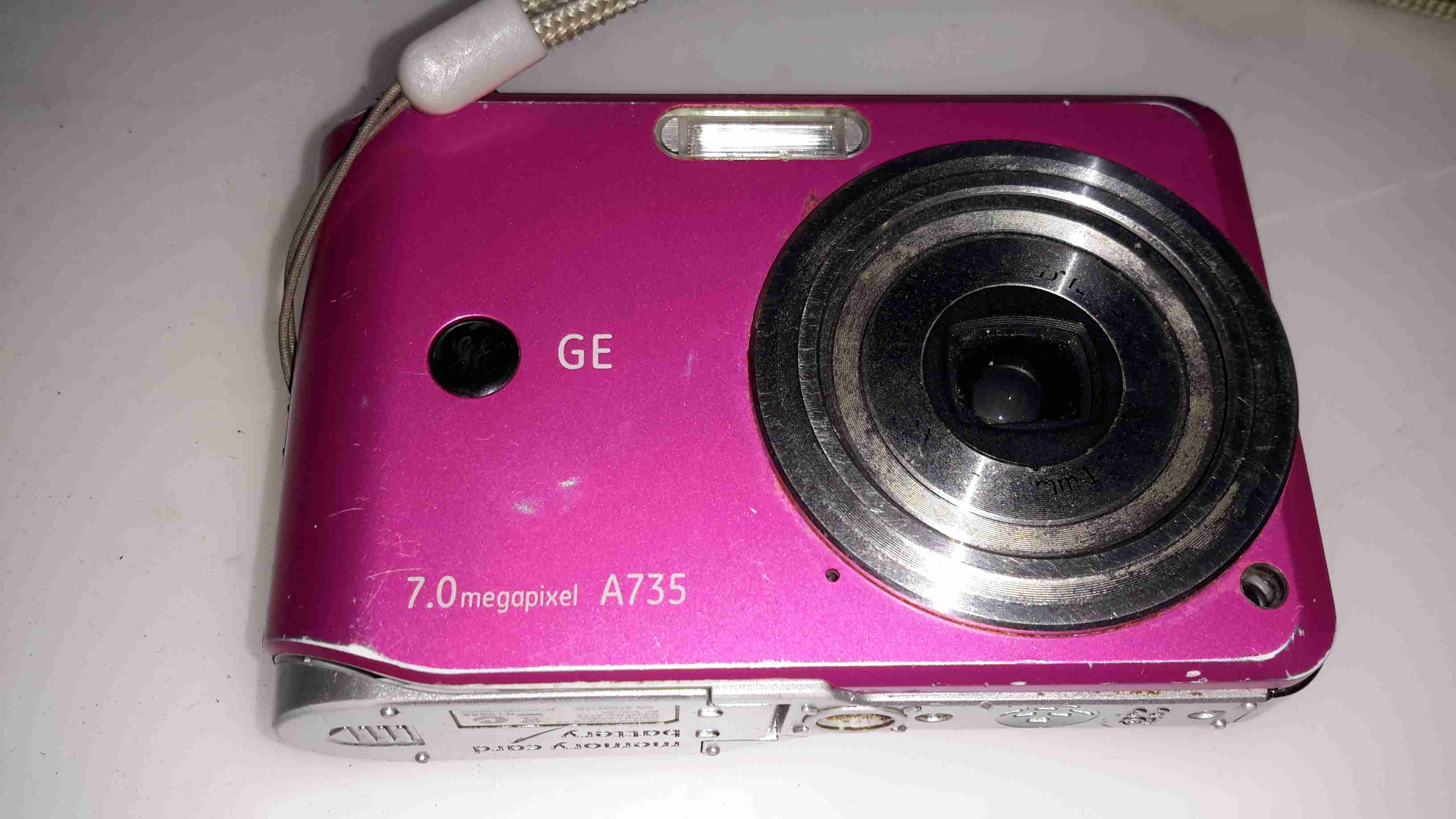
This camera has now been retired after many years of heavy use. Exposure to a 3-year old has caused severe damage to the lens mechanism, which no longer functions correctly.
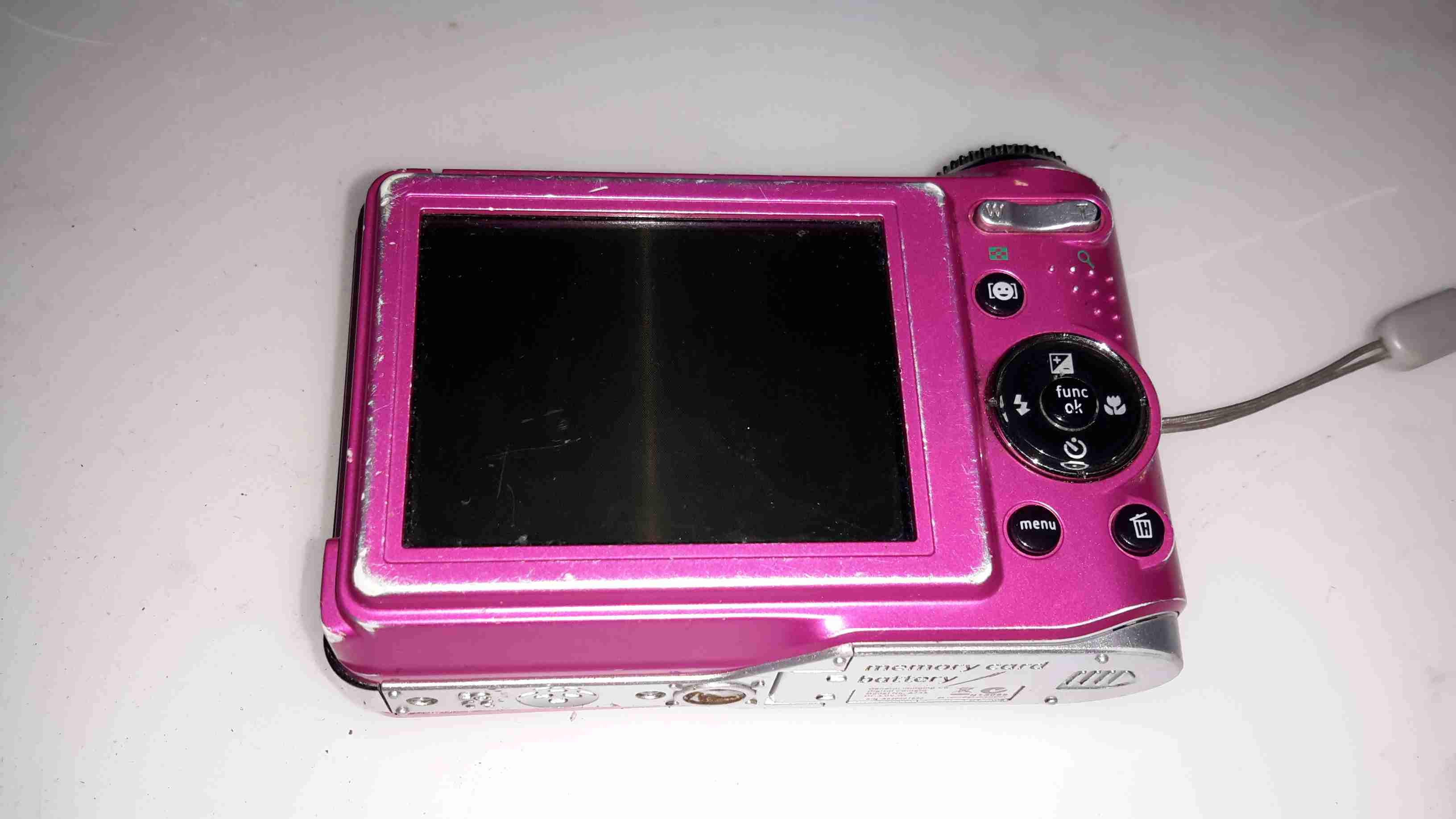
Rear Panel
Pretty much standard interface for a digital camera, with a nice large LCD for it’s time.
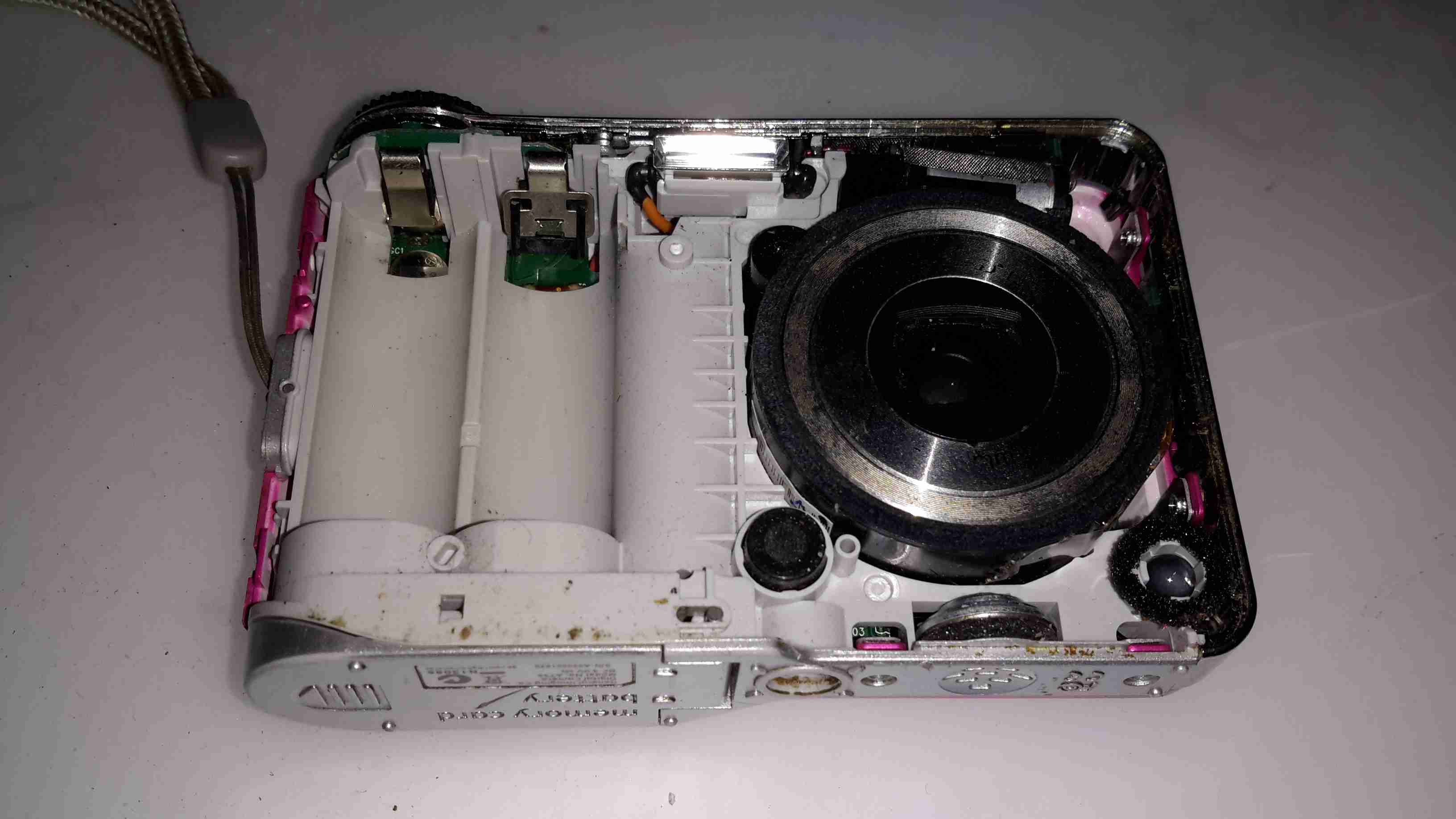
Front Cover Removed
With the front cover removed, the lens assembly & battery compartment is exposed.
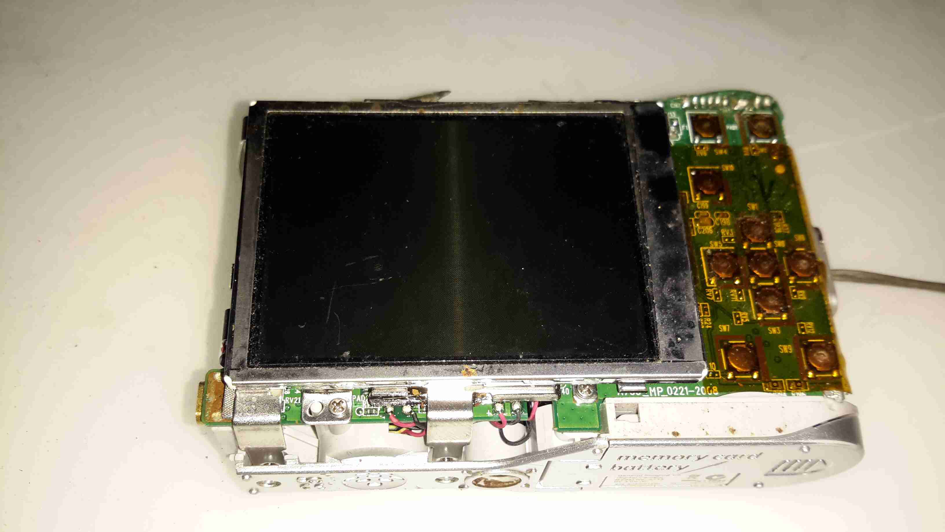
Rear Cover Removed
Removing the rear cover exposes the LCD module & the main PCB, the interface tactile switches are on the right under a protective layer of Kapton tape.
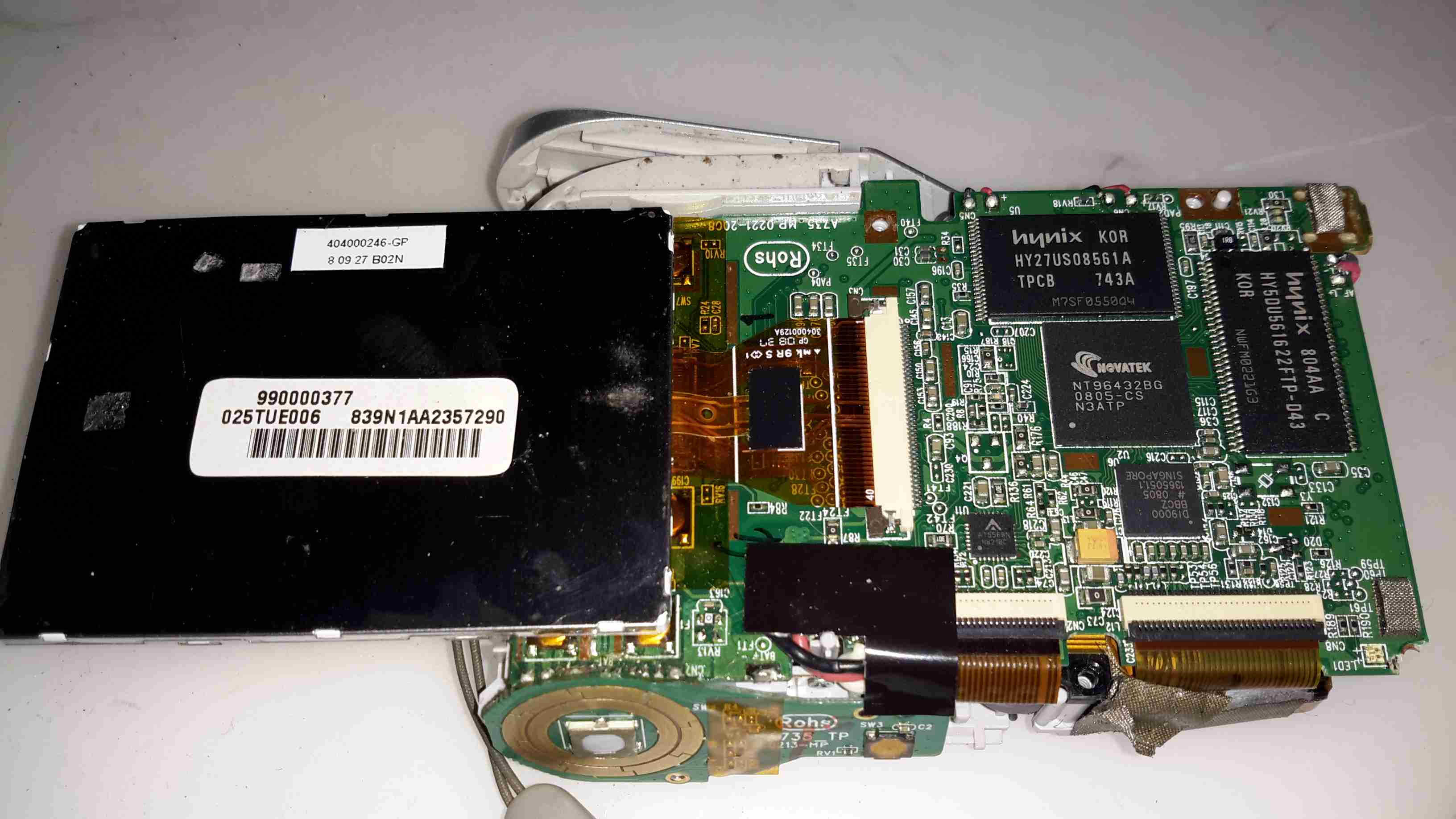
Main Chipset
Flipping the LCD out of it’s mounting bracket reveals the main camera chipset. The CPU is a NovaTek NT96432BG, no doubt a SoC of some kind, but I couldn’t find any information. Firmware & inbuilt storage is on a Hynix HY27US08561A 256MBit NAND Flash, with a Hynix HY5DU561622FTP-D43 256Mbit DRAM for system memory.
I couldn’t find any info on the other two chips on this side of the board, but one is probably a motor driver for the lens, while the other must be the front end for the CCD sensor input to the SoC.
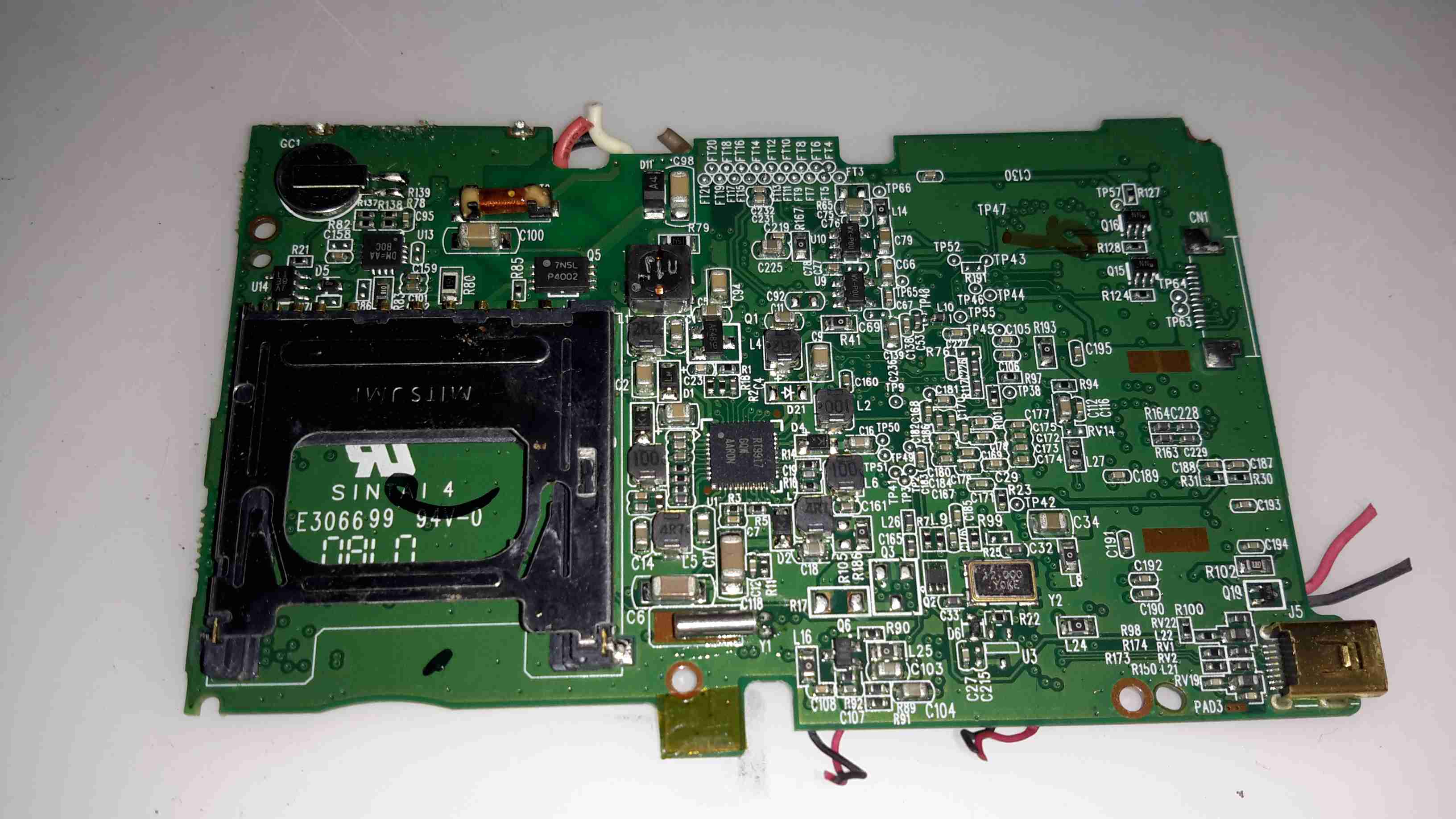
Main PCB Reverse
The other side of the PCB handles the SD card slot & power management. All the required DC rails are provided for by a RT9917 7-Channel DC-DC converter from RichTek, an IC designed specifically for digital camera applications.
Top left above the SD card slot is the trigger circuitry for the Xenon flash tube & the RTC backup battery.
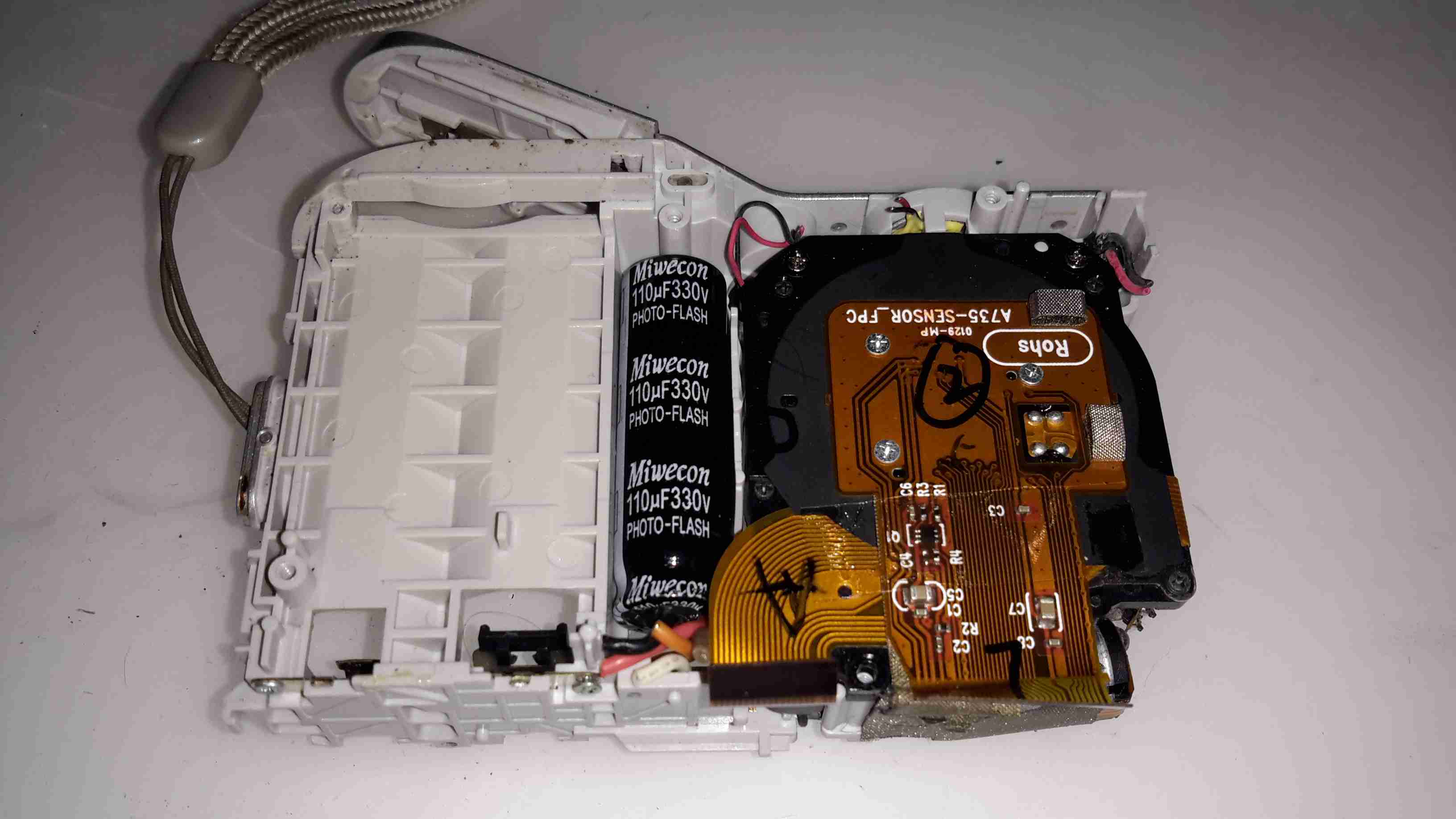
Main PCB Removed
Once the main PCB is out of the frame, the back of the lens module with the CCD is accessible. Just to the left is the high-voltage photoflash capacitor, 110µF 330v. These can give quite the kick when charged! Luckily this camera has been off long enough for the charge to bleed off.
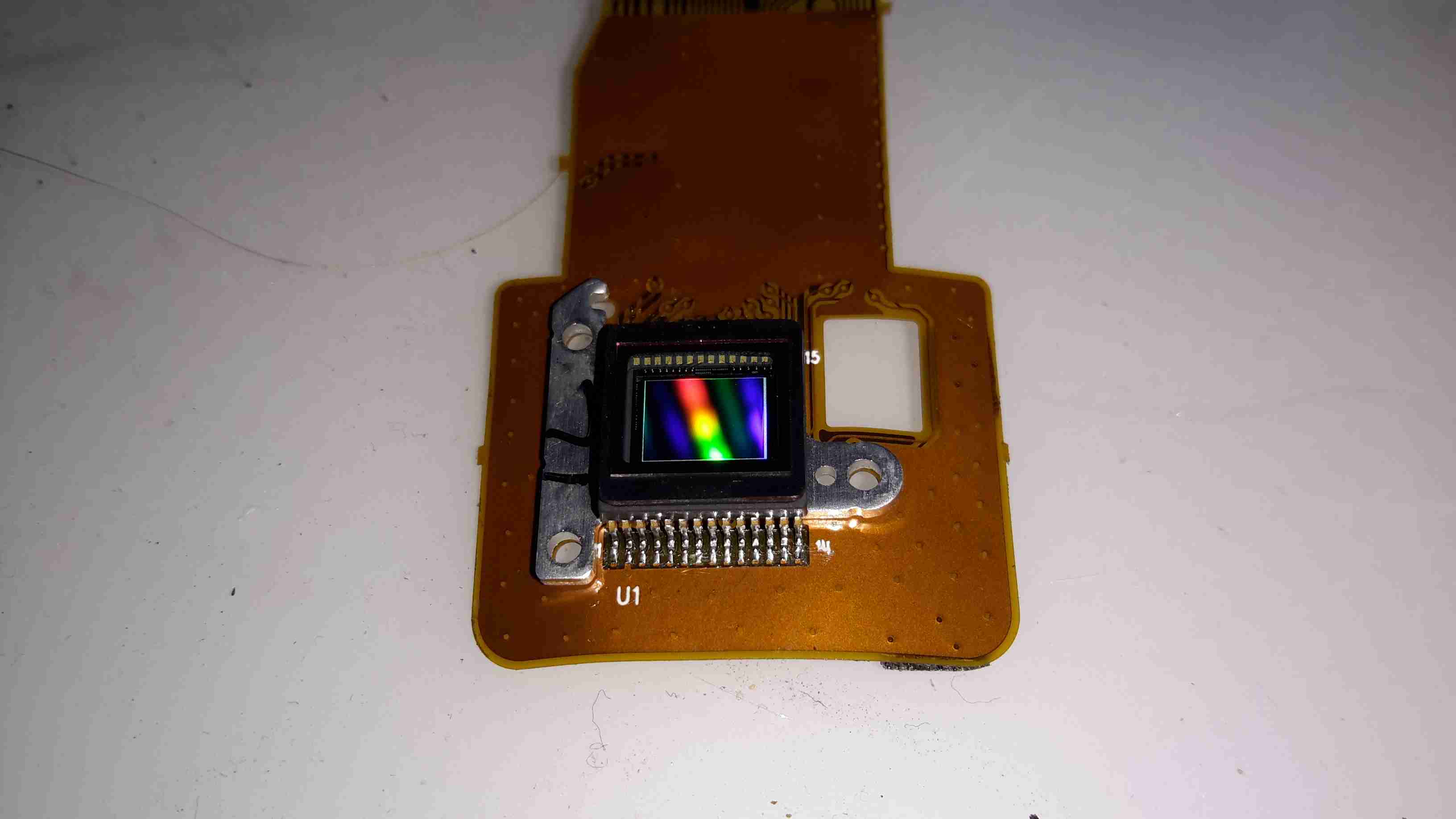
Sensor
Finally, here’s the 7-Megapixel CCD sensor removed from the lens assembly, with it’s built in IR cut filter over the top. I couldn’t find any make or model numbers on this part, as the Aluminium mounting bracket behind is bonded to the back of the sensor with epoxy, blocking access to any part information.
Die images of the chipset to come once I get round to decapping them!
This is a small audio mixer, marketed for camcorder audio dubbing.
Rear Panel
I/O Panel on the rear of the unit. Contains a small preamp, but will not drive speakers directly. Power is a 9v battery or plugpack.
PCB Front
Front of the PCB removed from the case. Mic preamp bottom right corner. Each channel has it’s own Preamp IC between the faders.
PCB Rear
Rear of the PCB.
Tip Jar
If you’ve found my content useful, please consider leaving a donation by clicking the Tip Jar below!
All collected funds go towards new content & the costs of keeping the server online.