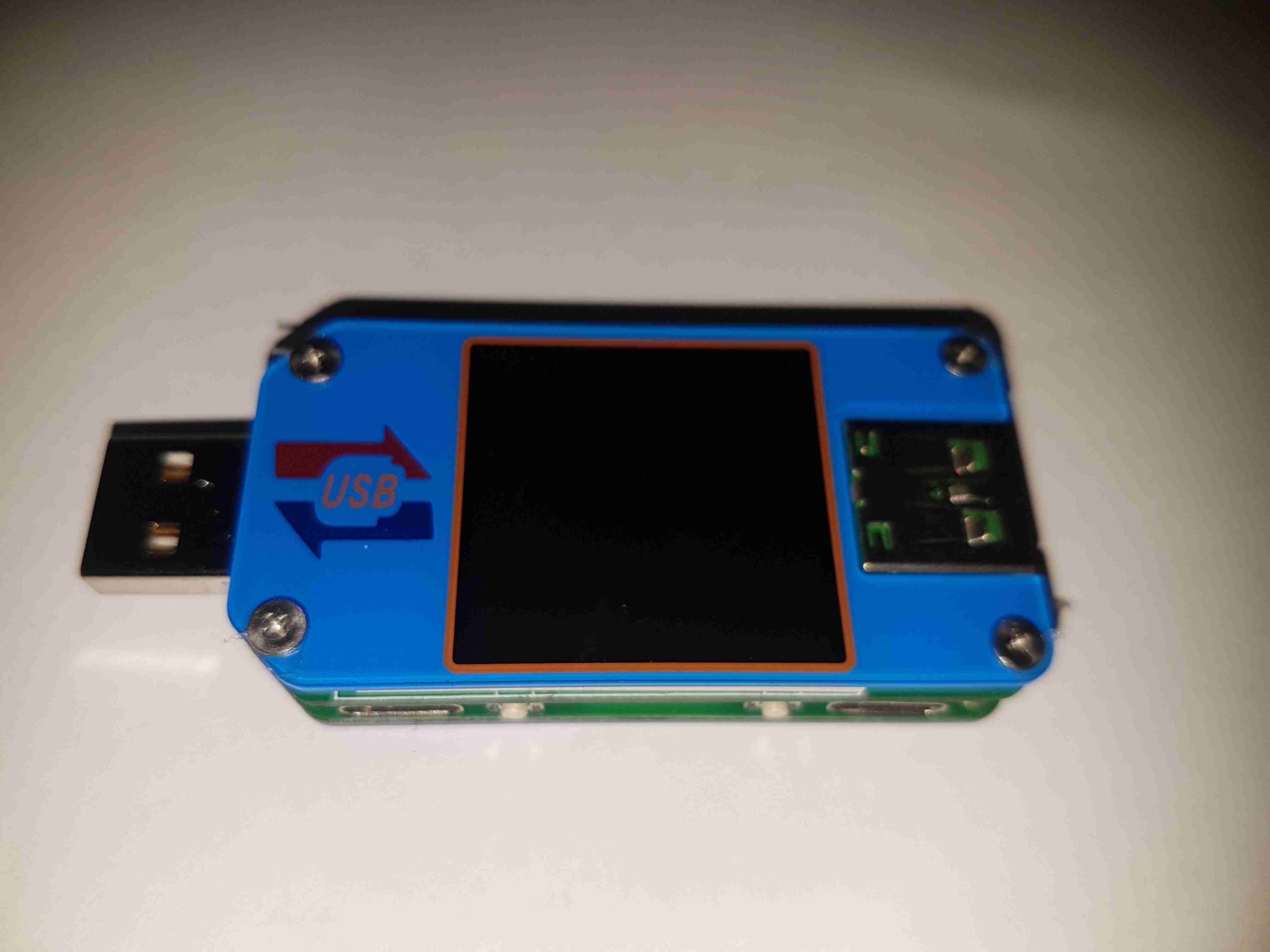
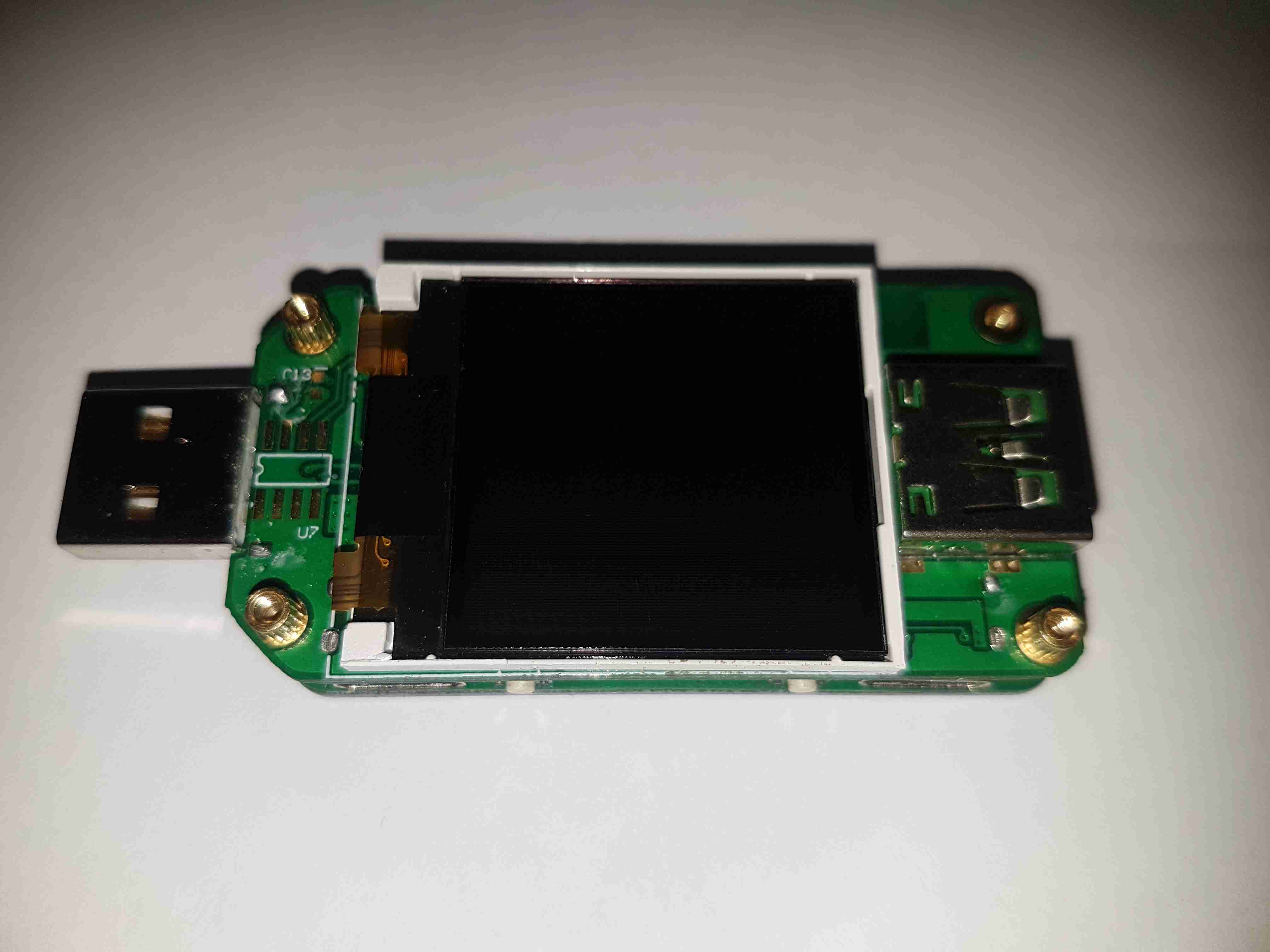
Here’s a nice little feature-packed USB power meter, the UM25C. This unit has USB-C along with the usual USB type A connectors, along with a bluetooth radio for remote monitoring of stats via a Windows or Android app. Construction is nice, it’s a stack of two PCBs, and polycarbonate cover plates, secured together with brass posts & screws.
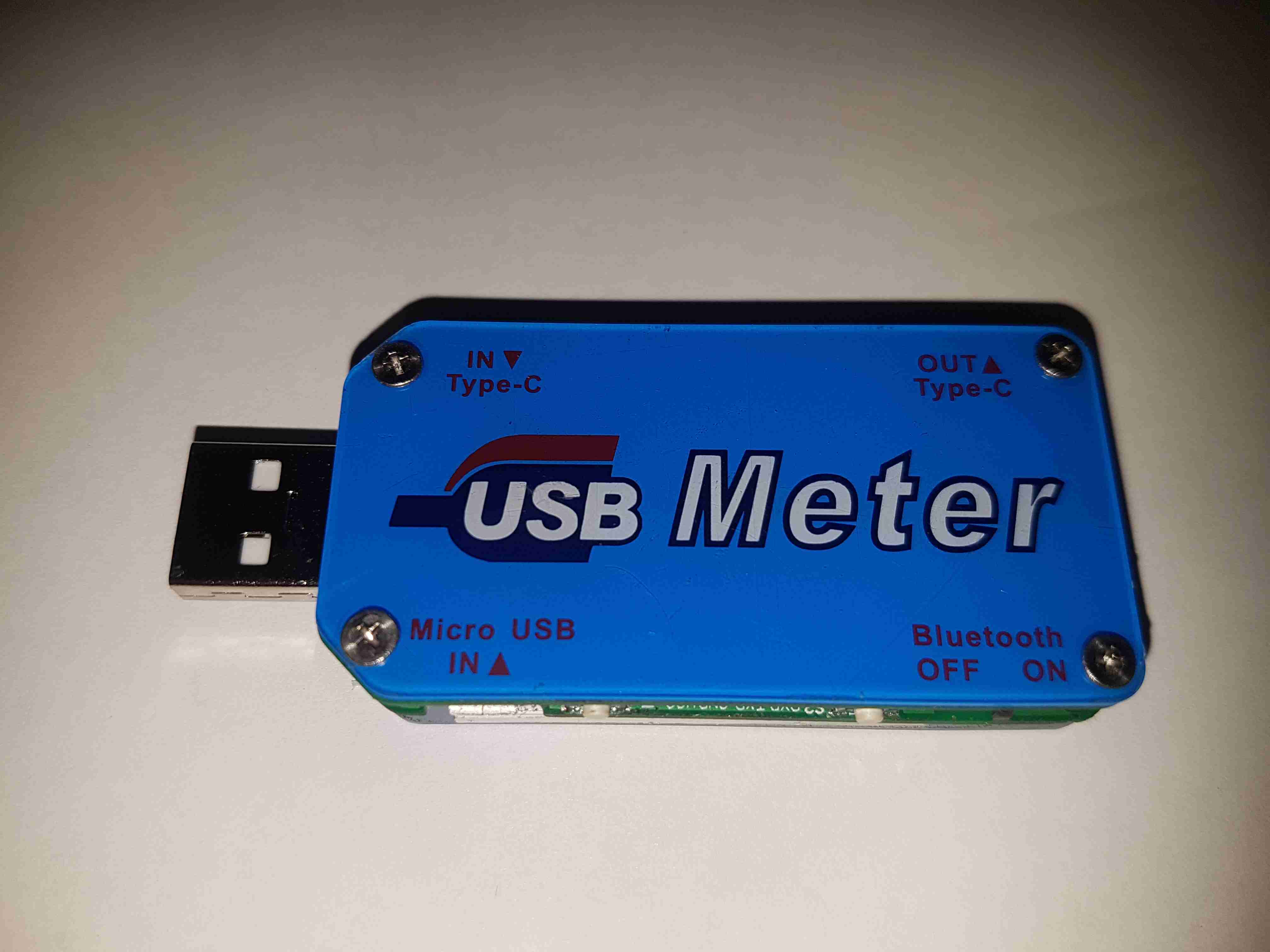
Back Cover
The back cover has the legend for all the side connectors, along with the logo.
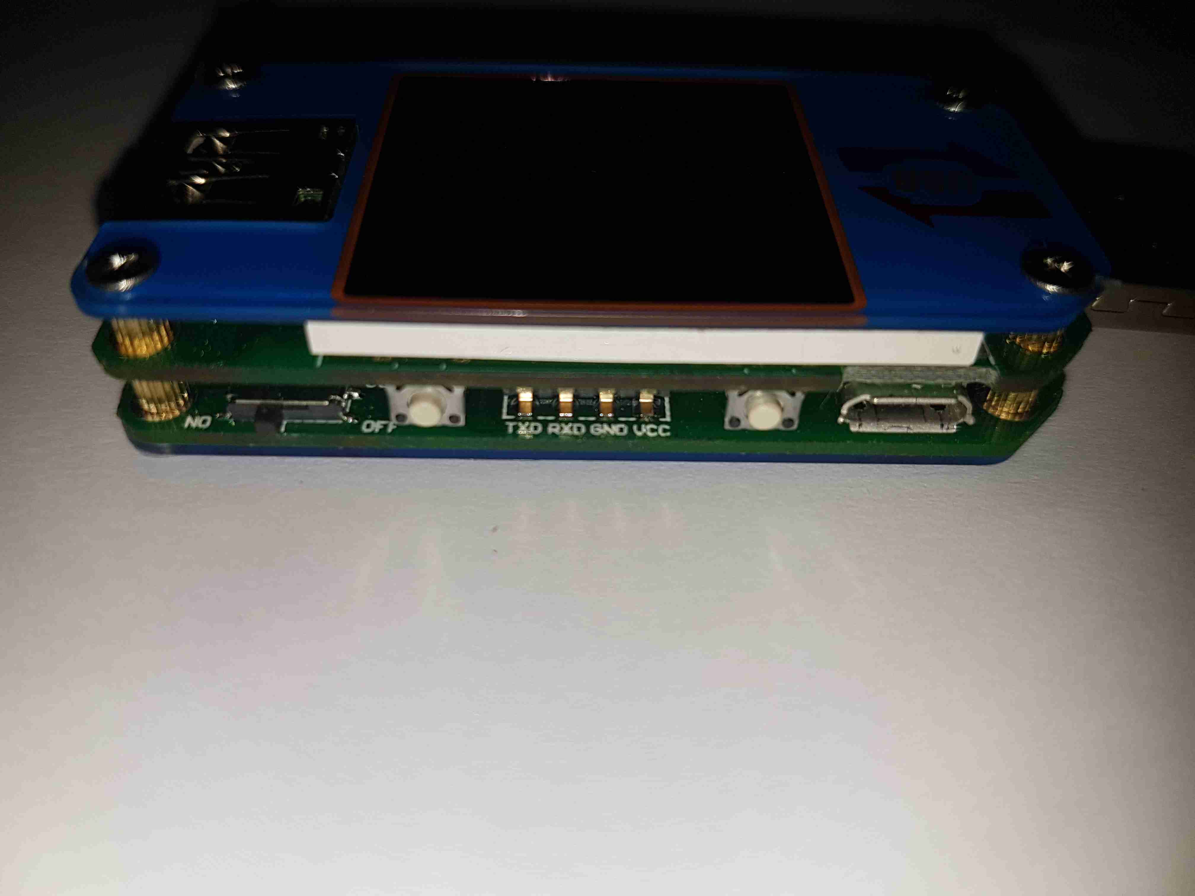
USB Micro Input
Down the sides are the user interface buttons, and here the Micro-B input connector. The 4-pin header is visible here that takes serial data down to the bluetooth section.
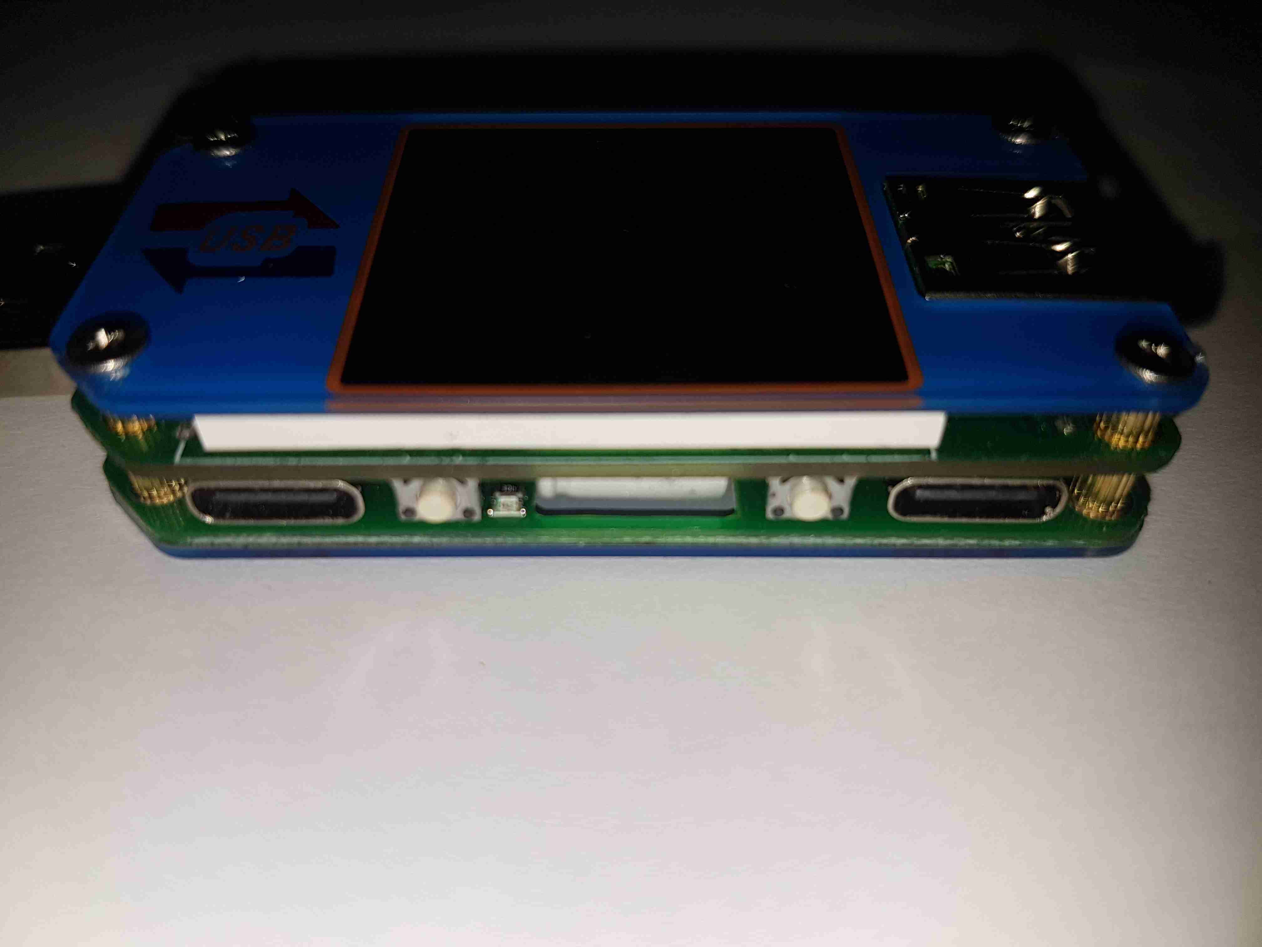
USB-C Connectors
The other side has the remaining pair of buttons, and the USB-C I/O. I don’t yet own anything USB-C based, but this is good future proofing.
LCD Display
Removing the top plastic cover plate reveals the small 1″ TFT LCD module. This will be hot-bar soldered underneath the screen. There’s an unused footprint next to the USB input connector, judging by the pin layout it’s probably for a I²C EEPROM.
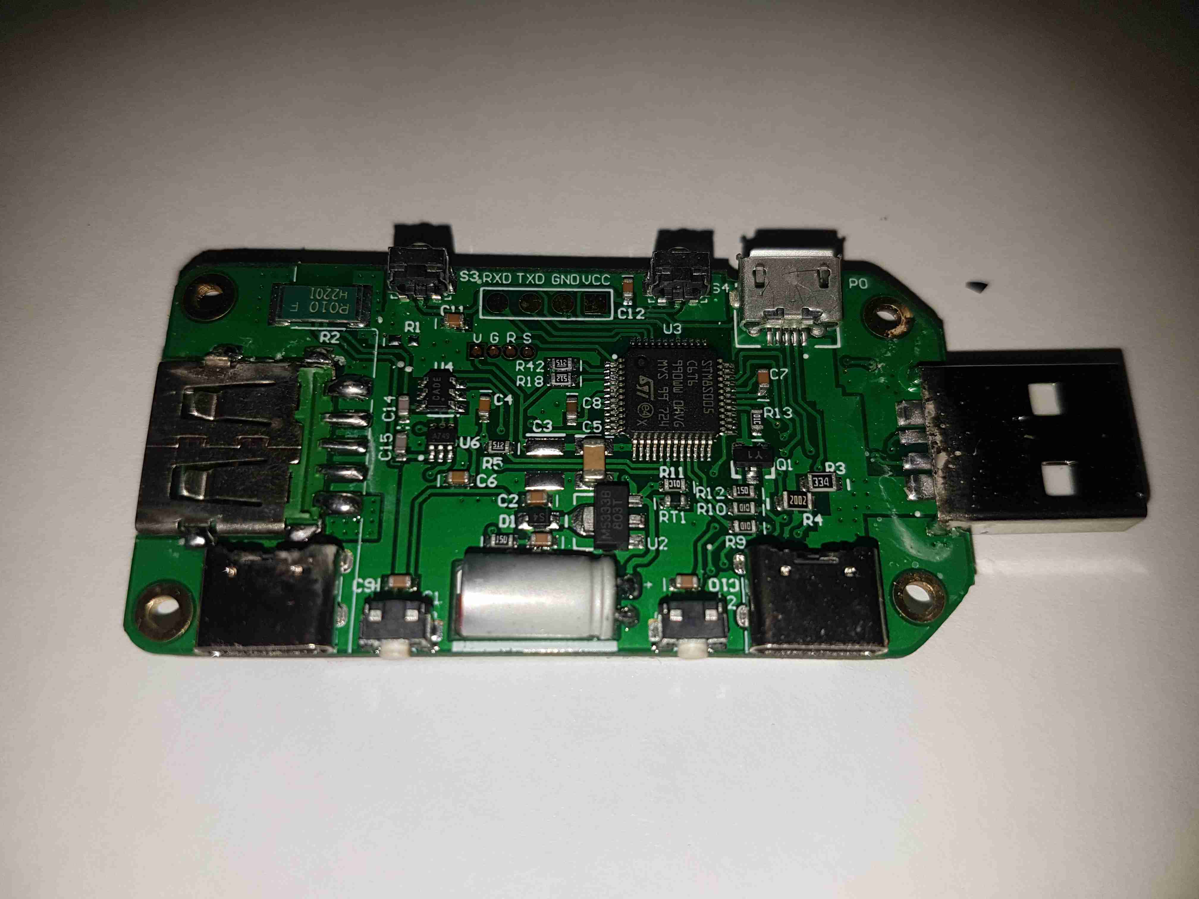
Main Board Components
The underside of the top PCB has all the main components. The brains of the operation is a ST STM8S005C6T6 microcontroller. It’s at the basic end of the STM range, with a 16MHz clock, 32K flash, EEPROM, 10-bit ADC, SPI, UART & I²C. The main 0.010Ω current shunt is placed at the top left of the board in the negative rail. A couple of SOT-23 components in the centre of the board, I haven’t been able to identify properly, but I think they may be MOSFETs. The large electrolytic filter capacitor has a slot routed into the PCB to allow it to be laid flat. Providing the main power rail is a SOT-89 M5333B 3.3v LDO regulator.
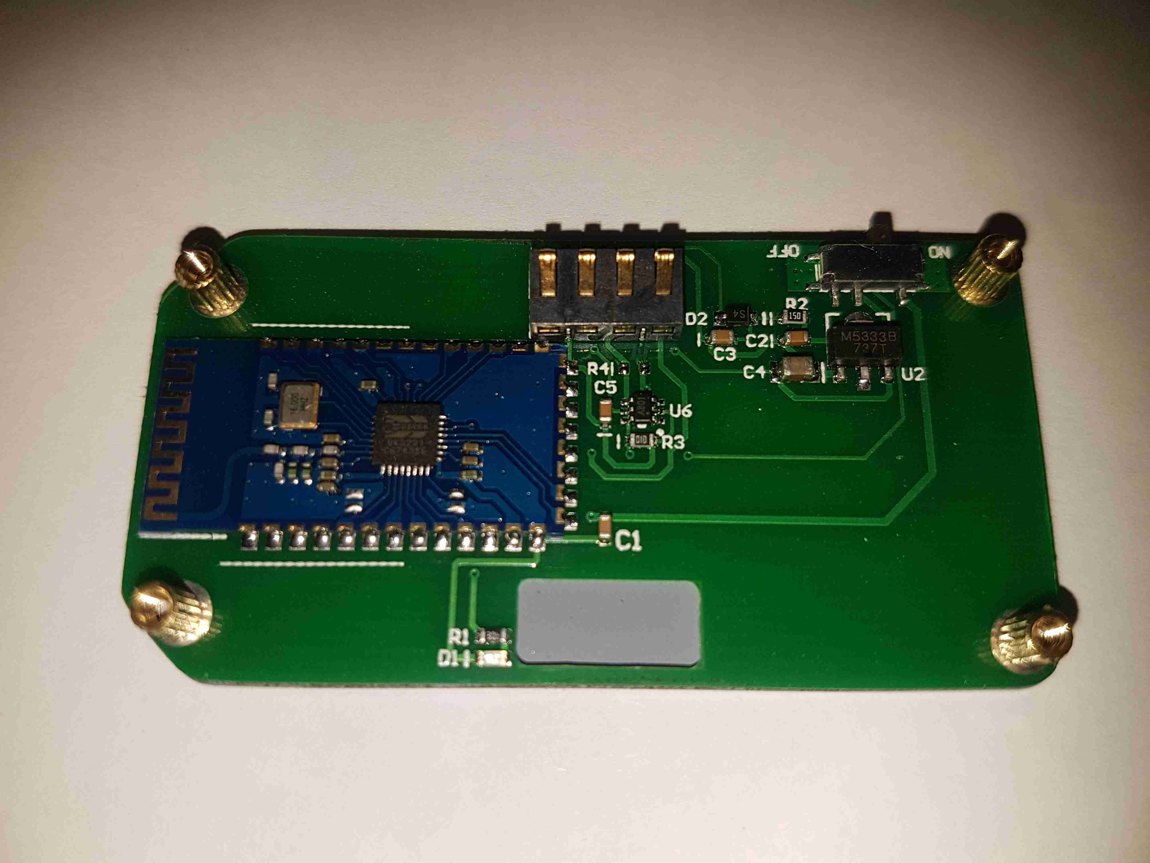
Bluetooth Radio
The bottom board contains the bluetooth radio module, this is a BK3231 Bluetooth HID SoC. The only profile advertised by this unit is a serial port. There’s a local 3.3v LDO regulator & support components, along with an indicator LED.
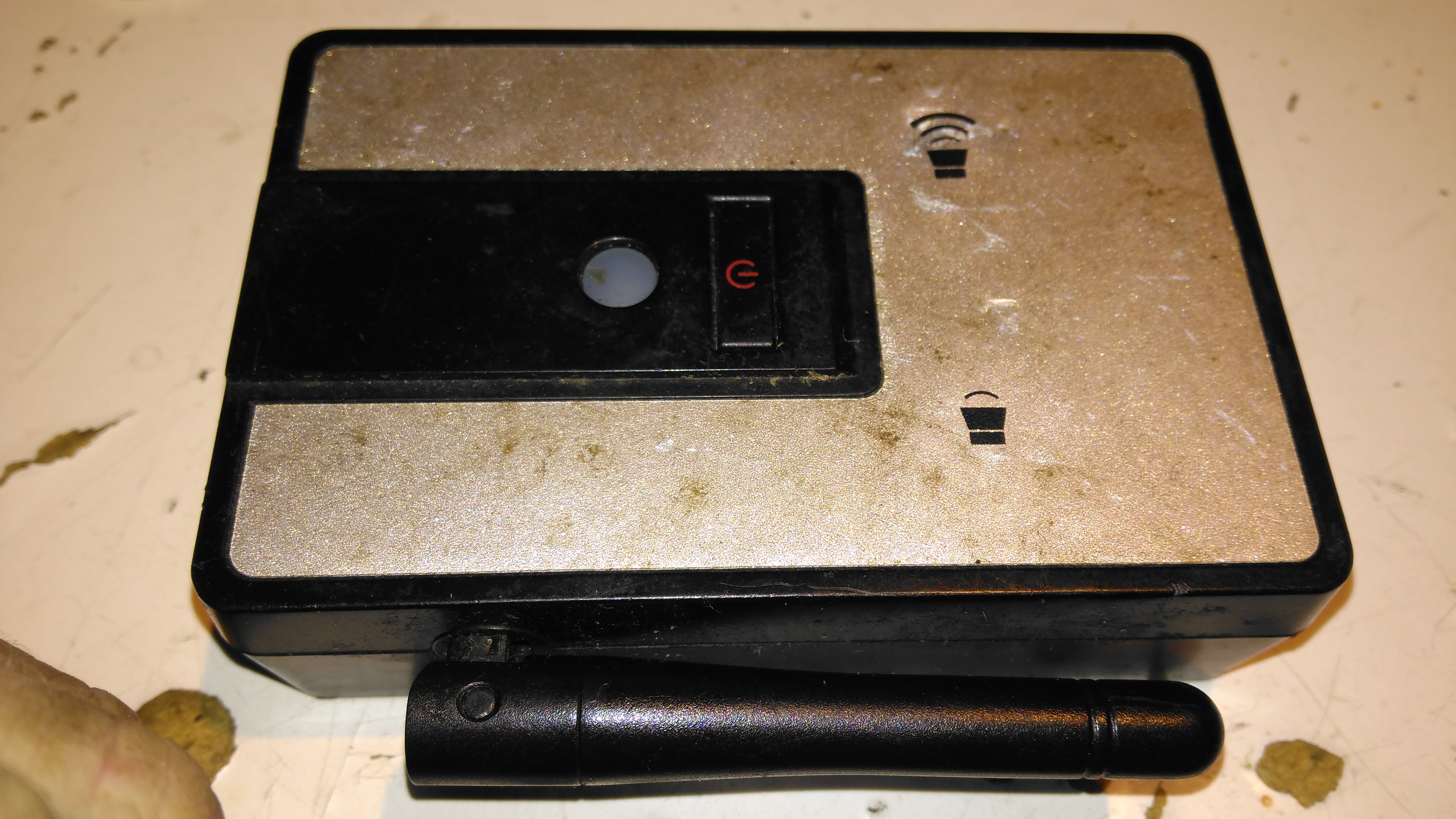
This is a pair of modules that Maplin was selling some time back, to send stereo audio over a 2.4GHz radio link. The transmitter identifies as a USB sound card, I’ve personally used these units to transmit audio about 60ft. The transmitter, above, has a single button for pairing with the receiver below.
Receiver
The receiver unit has a large external antenna, a link status LED & volume buttons, these directly control the volume level on the host PC via the sound card drivers.
Receiver PCB Top
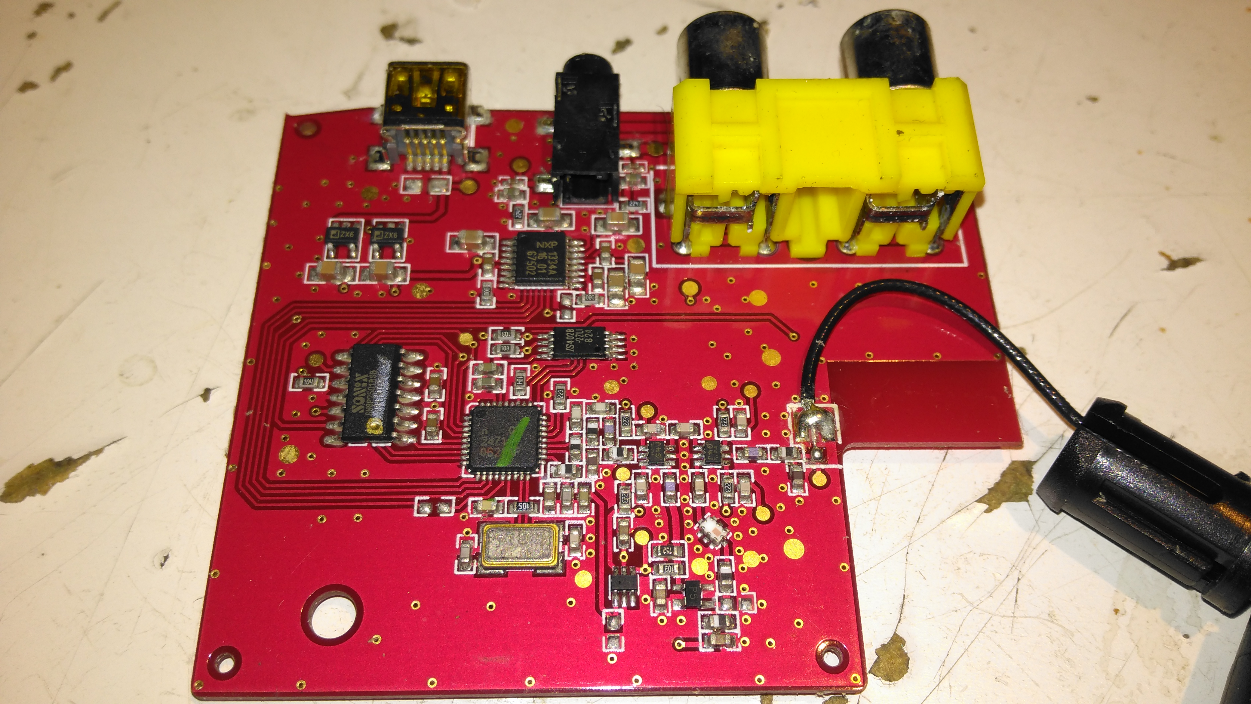
Popping the case open on the receiver reveals a large PCB, holding the chipset, along with the audio output jacks & Mini-USB power input. The antenna Coax is soldered to the PCB.
Receiver PCB Bottom
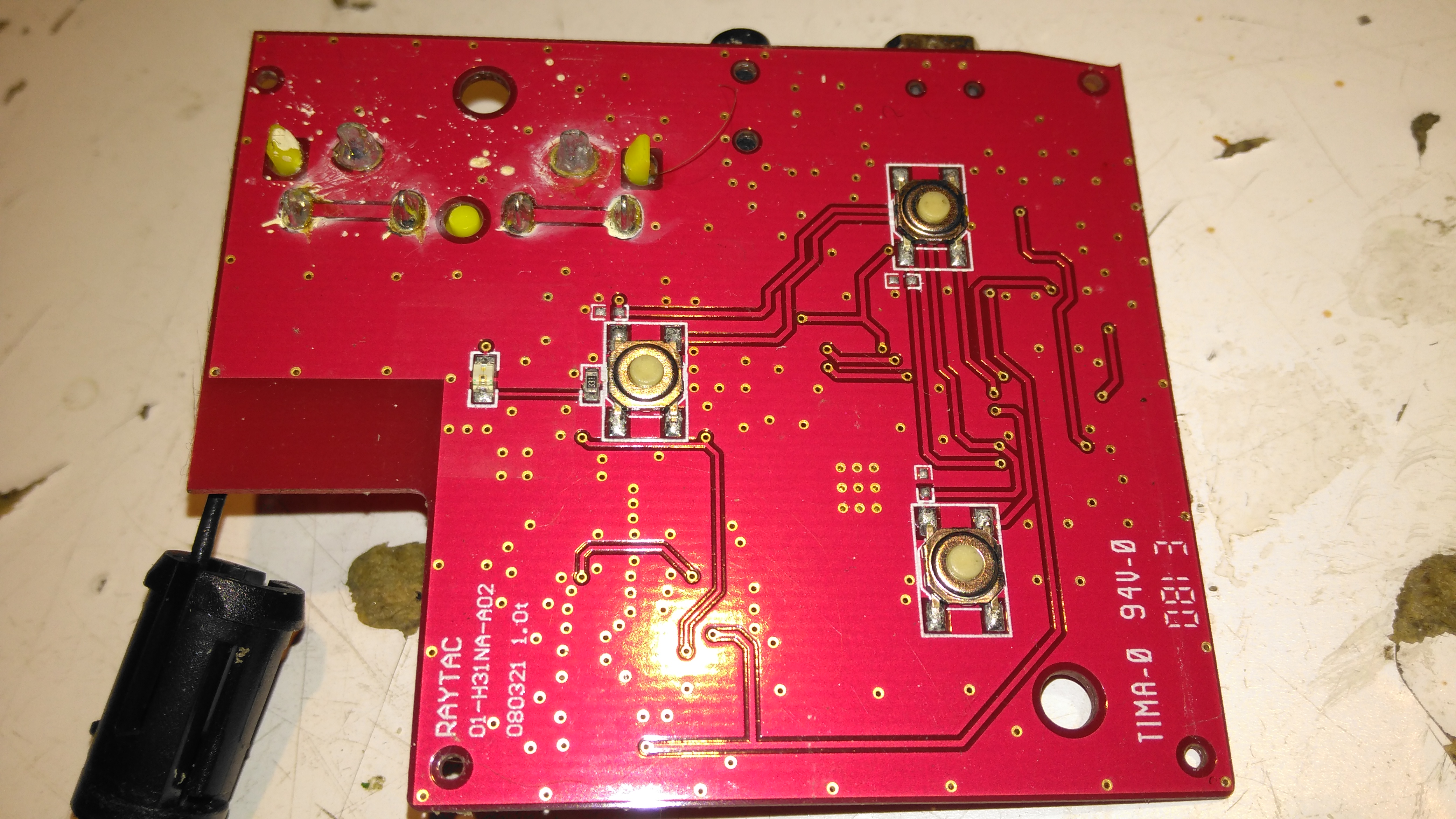
The top of the board has the control buttons, and the status LED.
Receiver Chipset
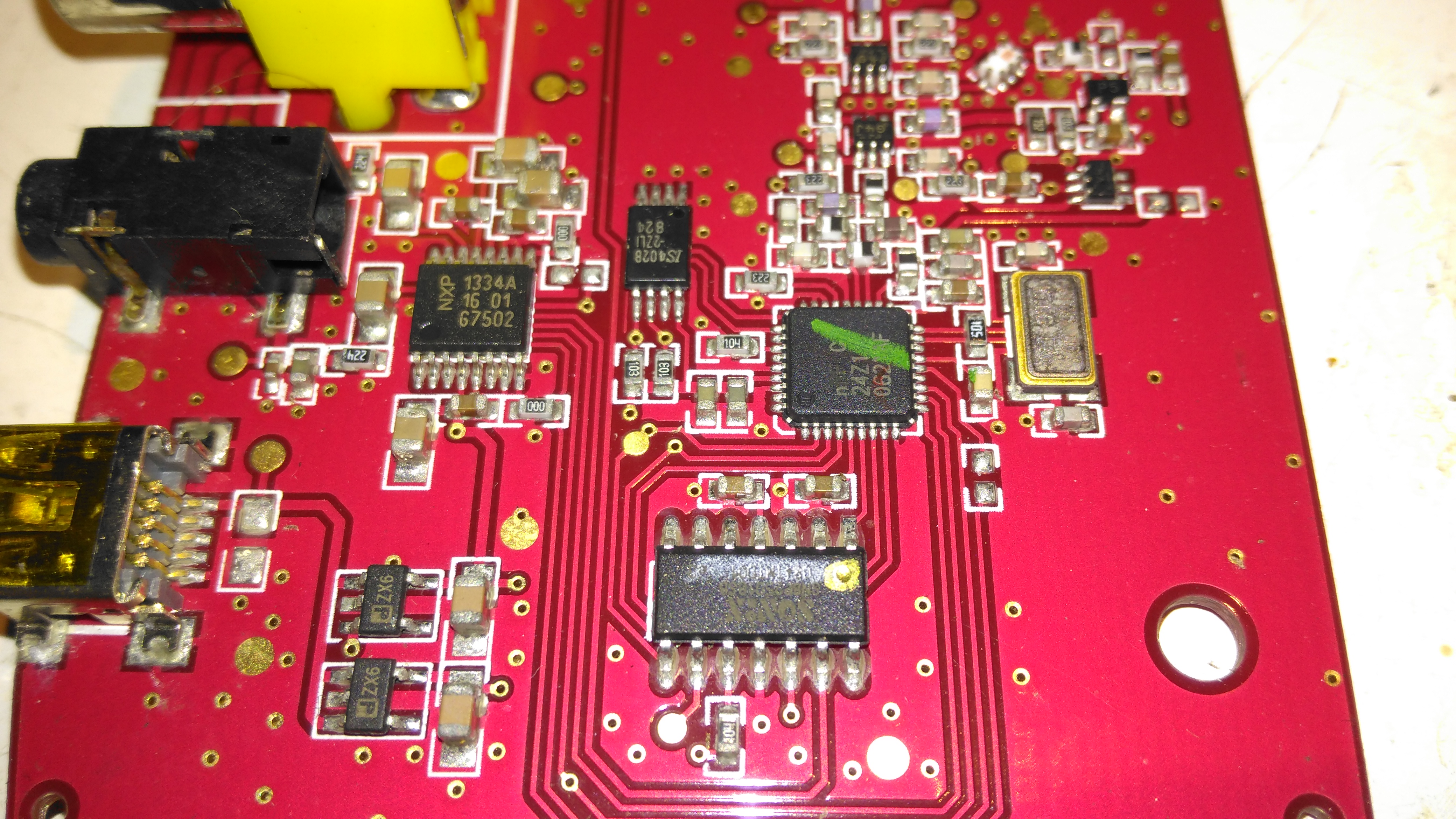
The chipset used here is a Nordic Semiconductor nRF20Z01 2.4GHz Stereo Audio Streamer, there’s a small microcontroller which does all the register magic on the RF transceiver. The RF chain is at the top of the photo, audio outputs on the top left, and the micro USB power input & voltage regulators at bottom left.
Transmitter PCB Top
The transmitter PCB has a Sonix USB Audio Codec, to interface with the host PC. This is then fed into another Nordic Semi part on the opposite side of the board:
Transmitter PCB Bottom
The bottom of the transmitter has the RF section, and another small control microcontroller.
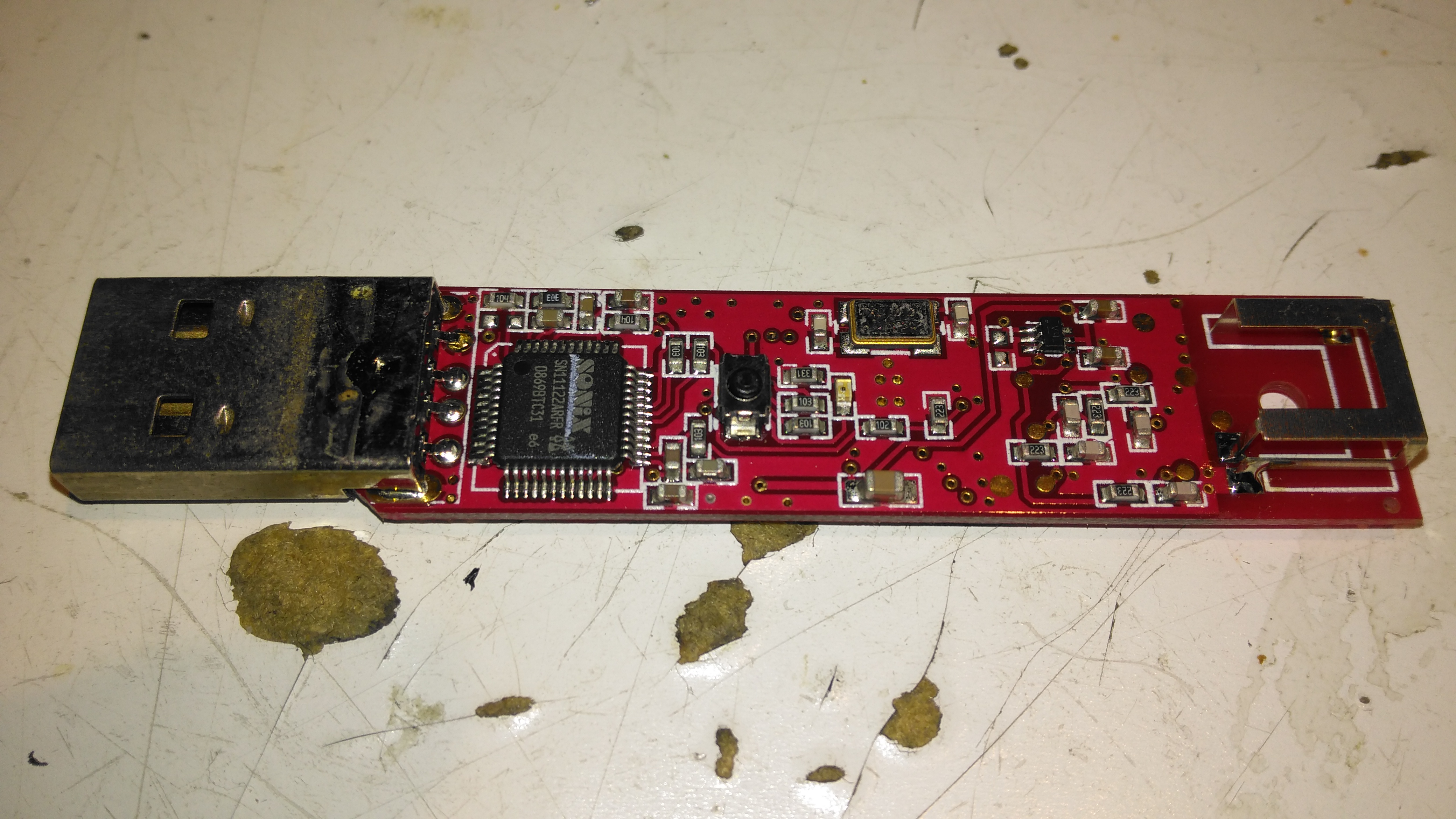
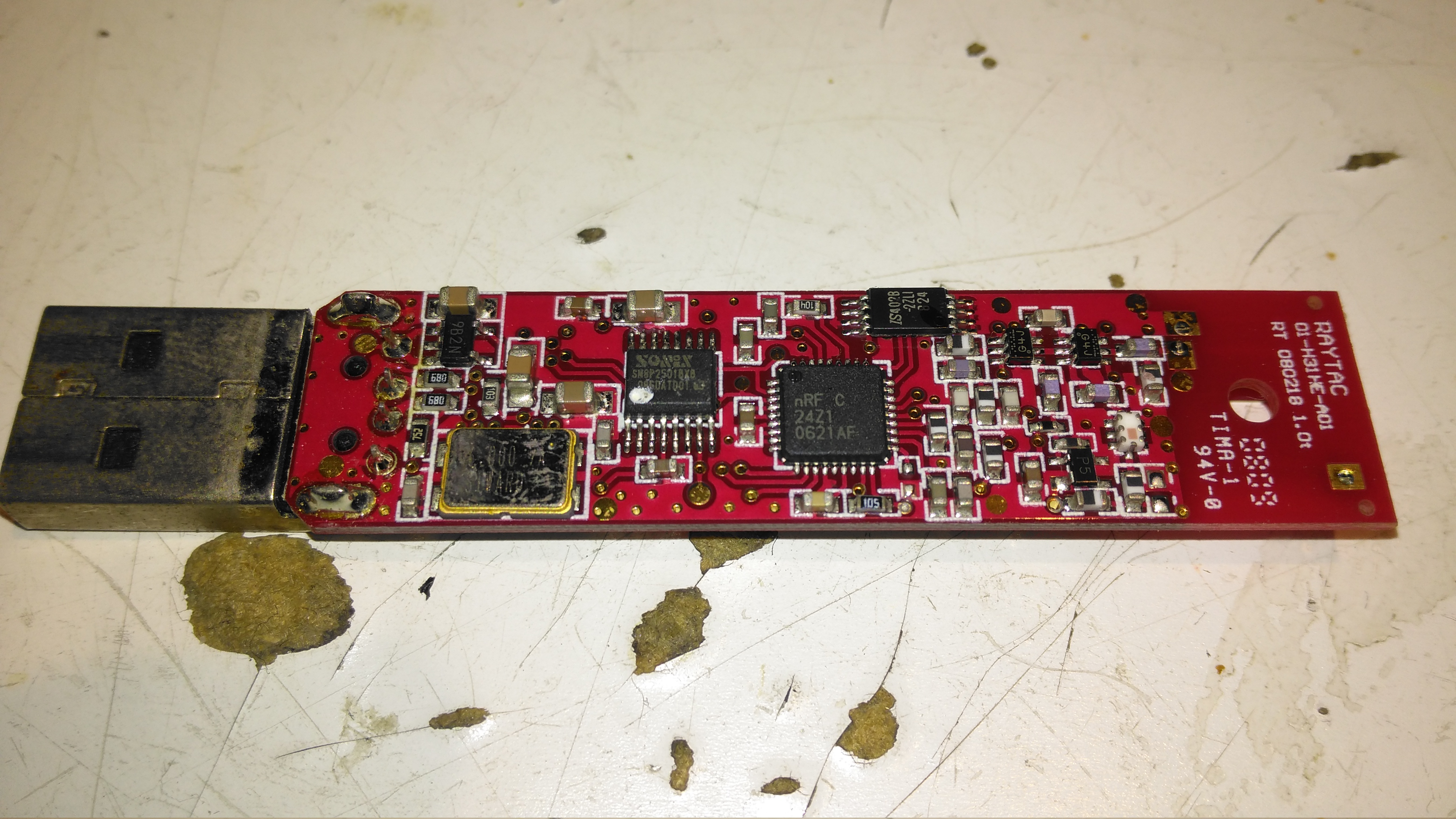
I thought it was time to add a bit of security to the gear I take camping, so this GPS tracker unit was sourced from eBay. This is a Rewire Security 103RS, a slightly customised version of the common Chinese TK103 GPS tracker.
Input Connections
The small module has all it’s power connections on one end of the unit, on a Molex multi-way block. The white connector is for a piezo-shock sensor – this interfaces with the alarm functionality of the unit. There’s an indicator LED for both the GPS & GSM status, and a switch for the backup battery.
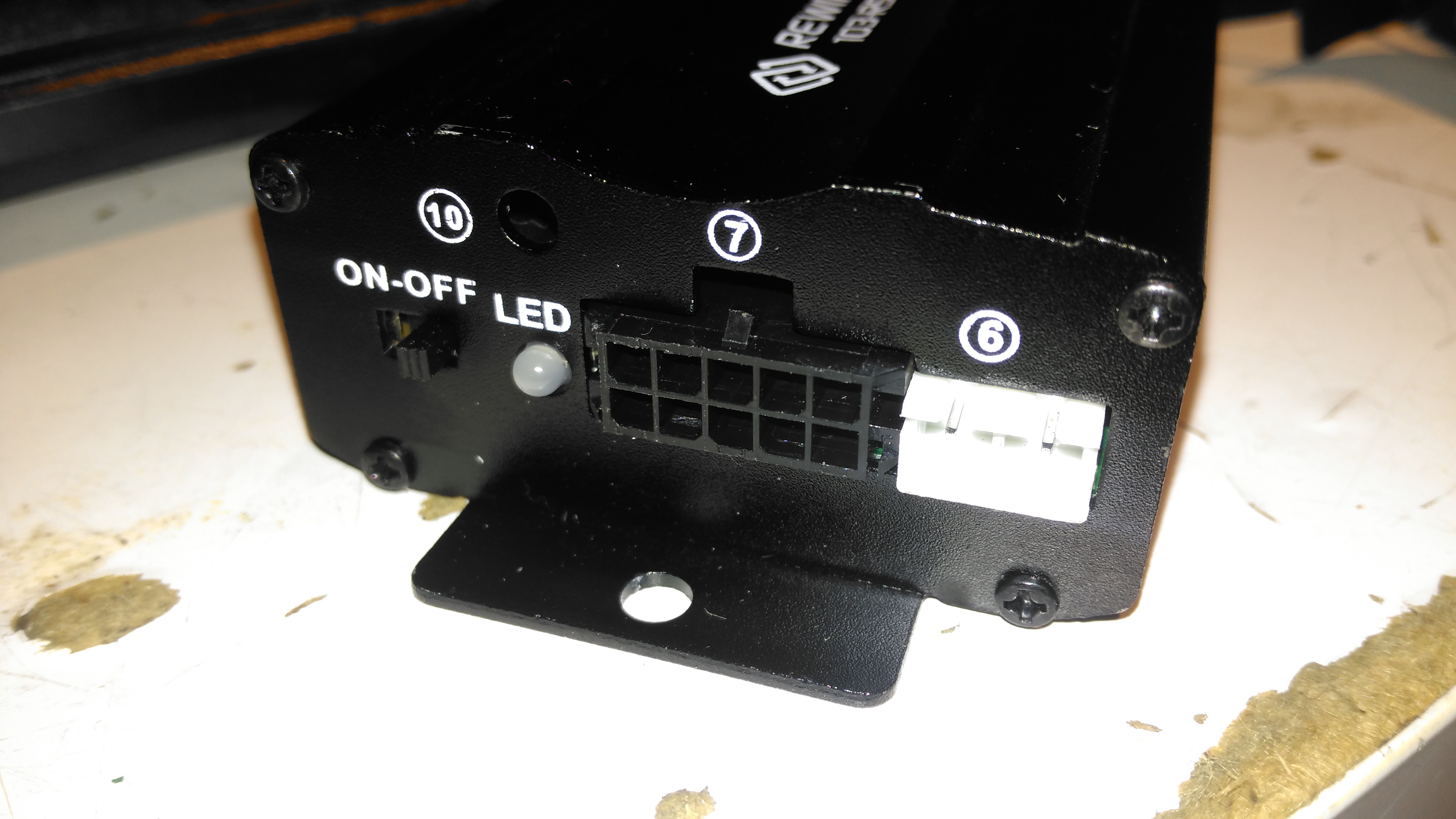
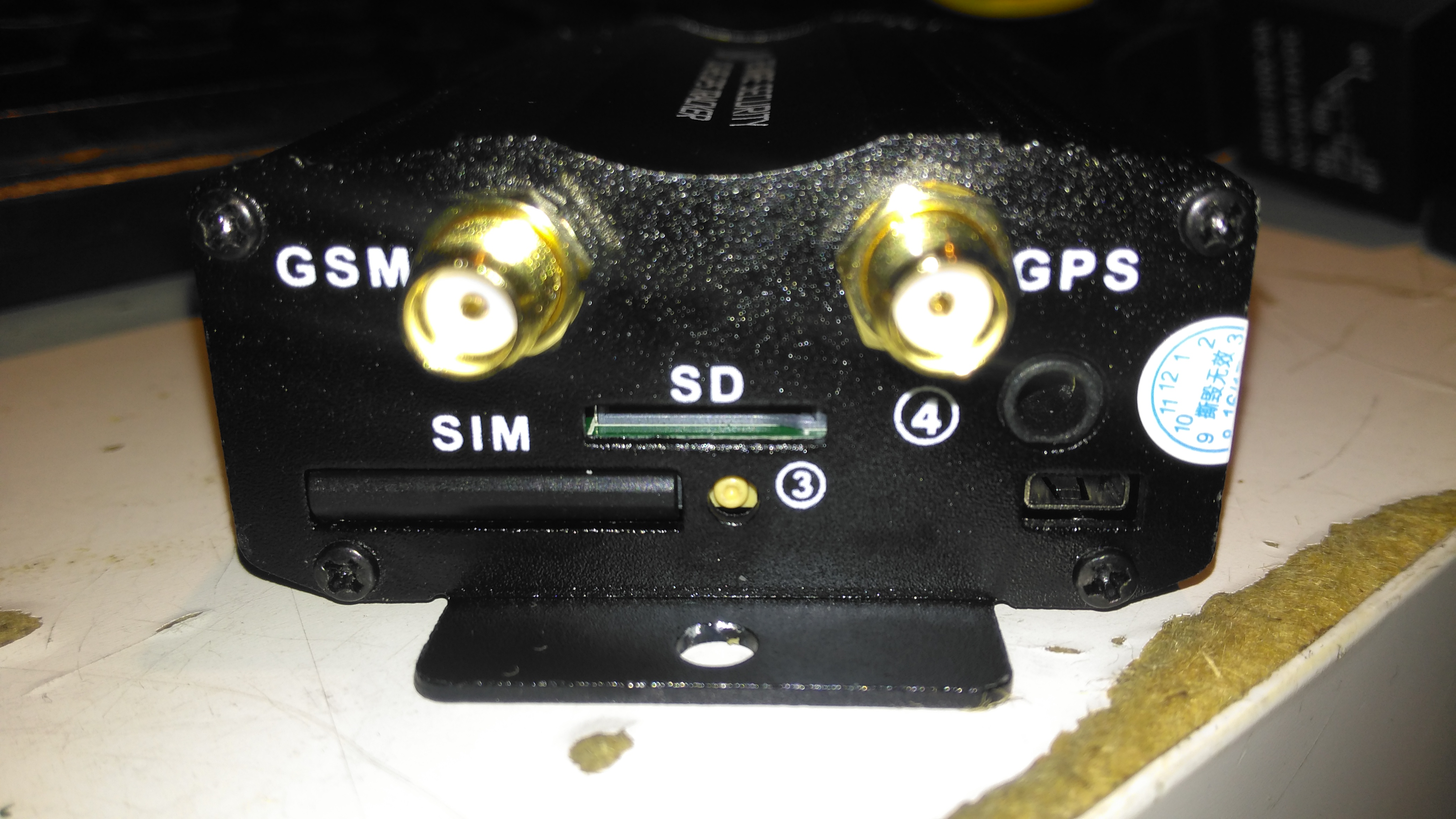
Antenna Connections
The other end has the antenna connections, microphone connection for the monitor function, along with the SIM & SD card slots.
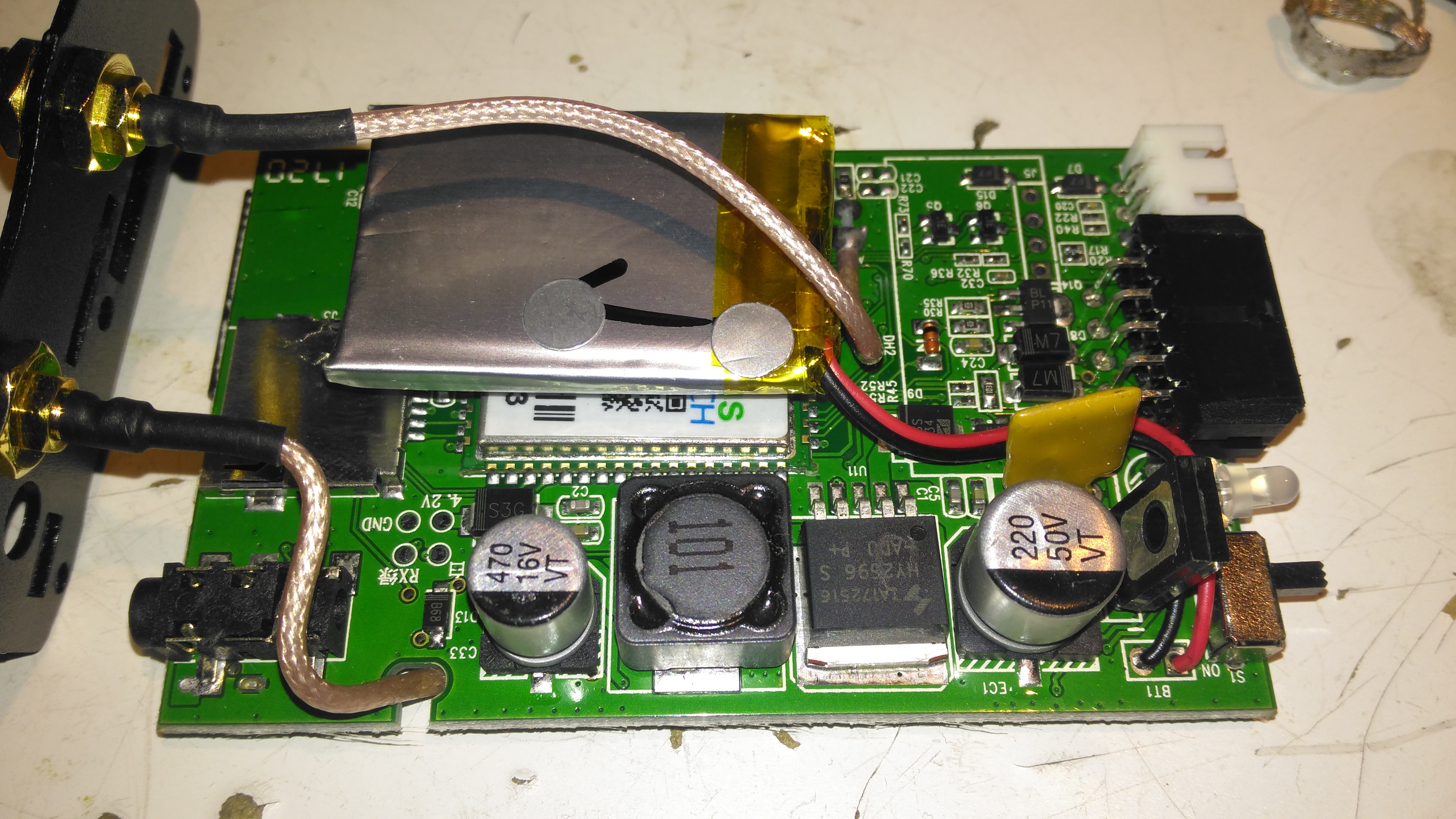
PCB Top
Once the end panel is removed, the PCB just slides out of the aluminium extruded casing. It’s pretty heavily packed with components in here. A switching regulator deals with the 12v input from the vehicle battery, and is protected by a polyfuse on the right. The GSM module is hiding under the Li-Po backup cell, unfortunately the sticky pad used to secure this wouldn’t come off without damaging something. The pigtails for both the GPS & GSM antennas are permanently soldered to the board here.
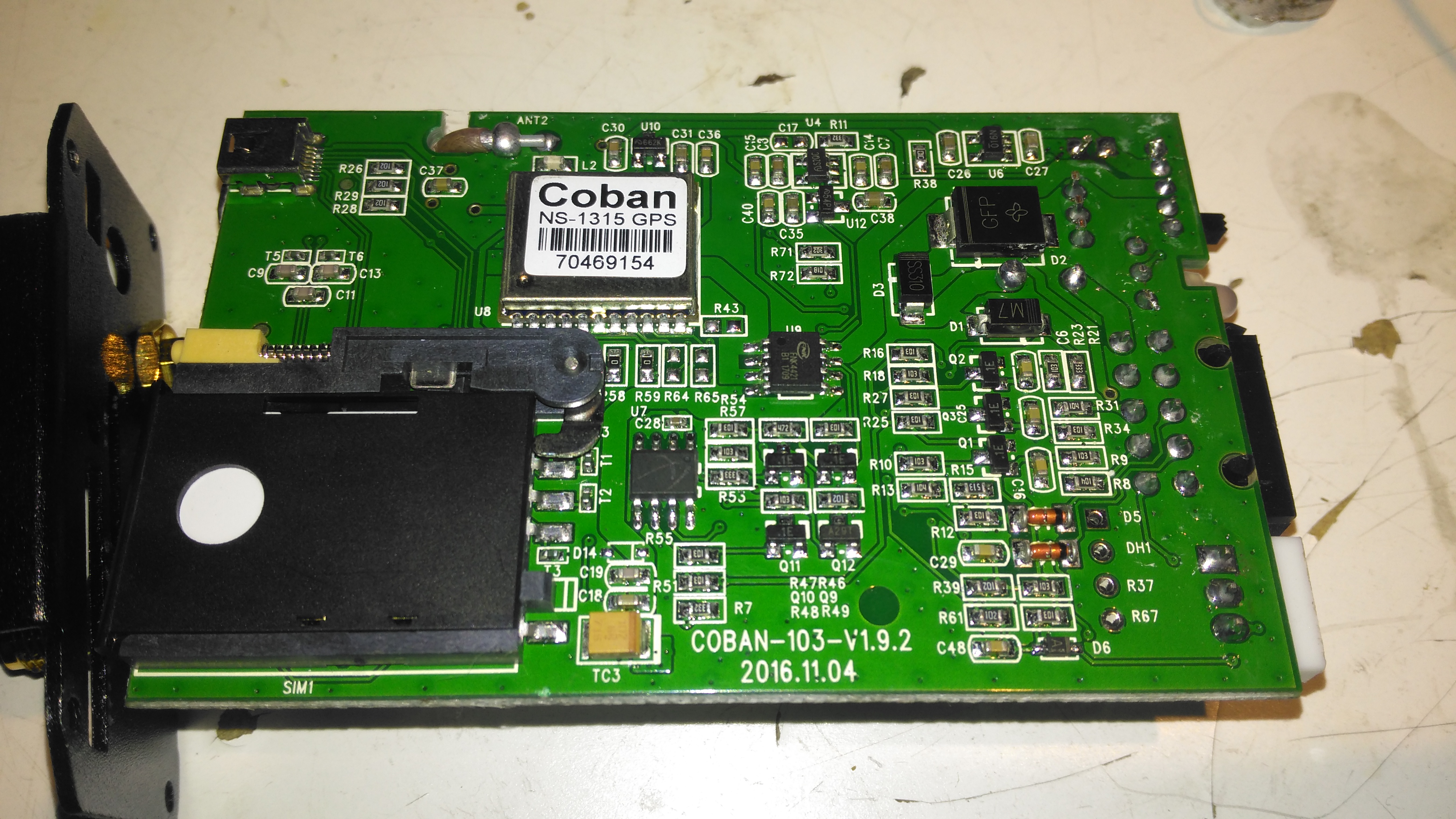
PCB Bottom
The bottom of the PCB has the GPS module, and mainly input protection & bypassing components. There is a FNK4421 Dual P-Channel MOSFET here as well, probably used for switching the external relay or alarm siren. The SIM socket for the GSM modem is located here in the corner.
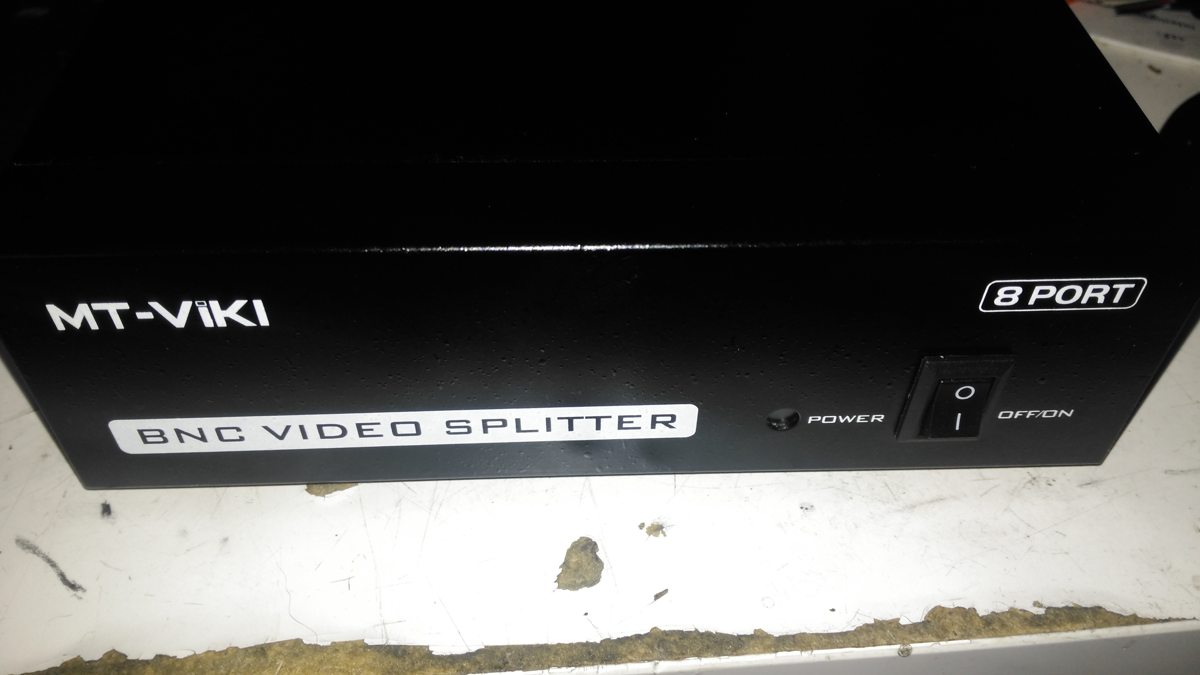
Time for another eBay special: this time it’s an 8-port video distribution amplifier, with BNC connections designed for commercial/industrial equipment. Not much on the front panel above, apart from the power switch & LED.
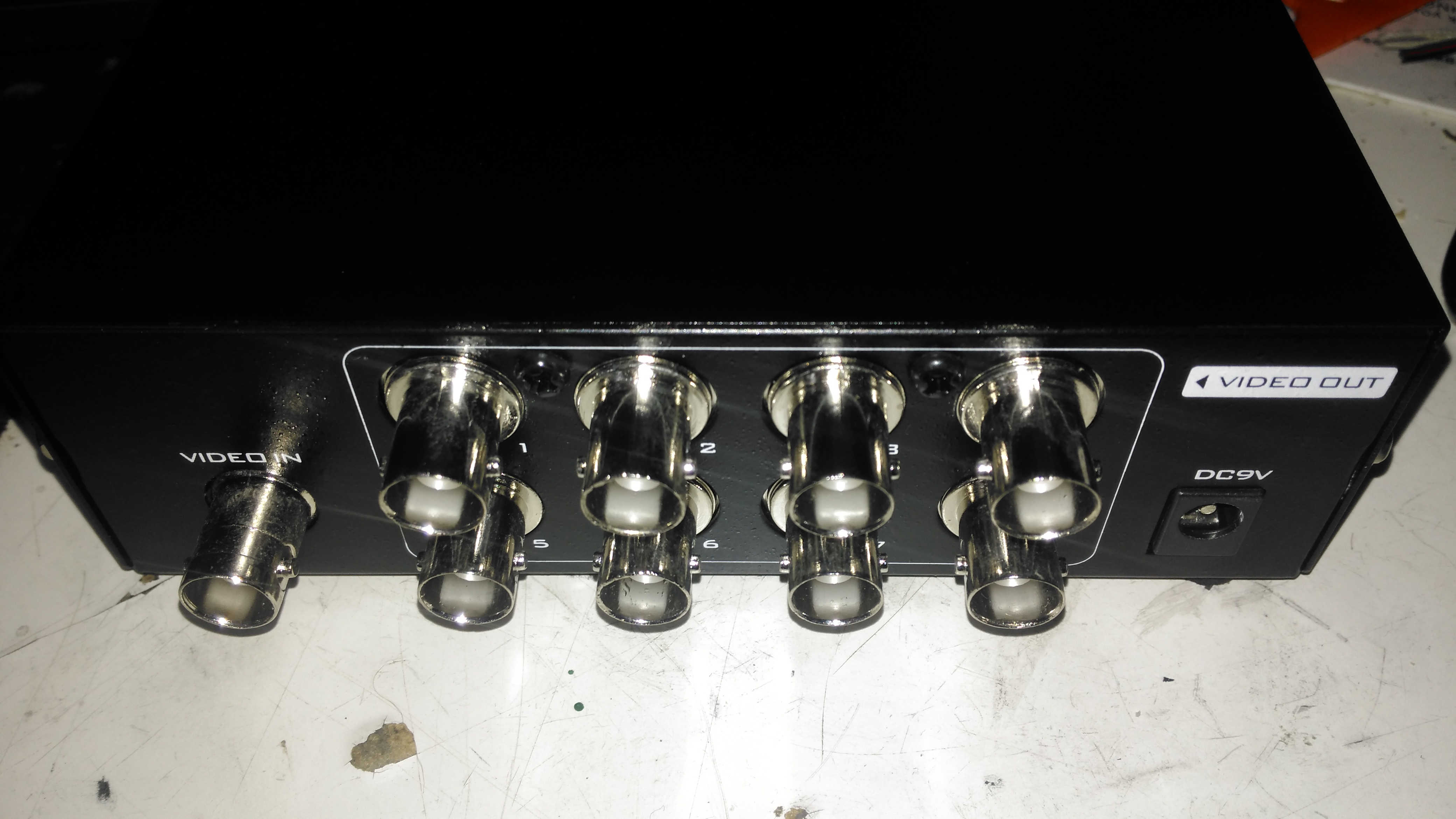
Rear Panel
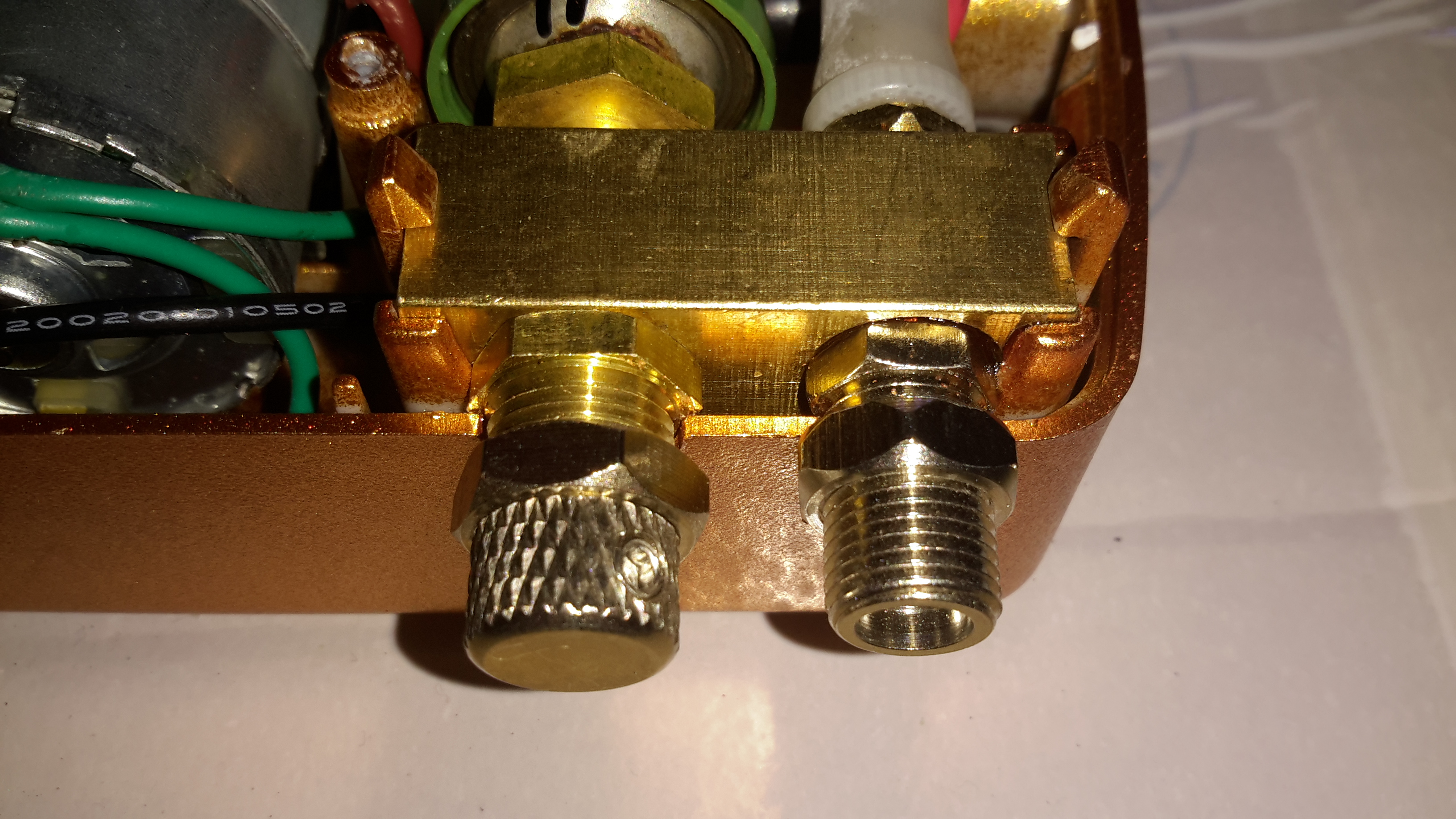
The rear panel has all the connectors, input is on the left, while the outputs are in the centre. Power is supplied through the barrel jack on the right, 9v DC in this case.
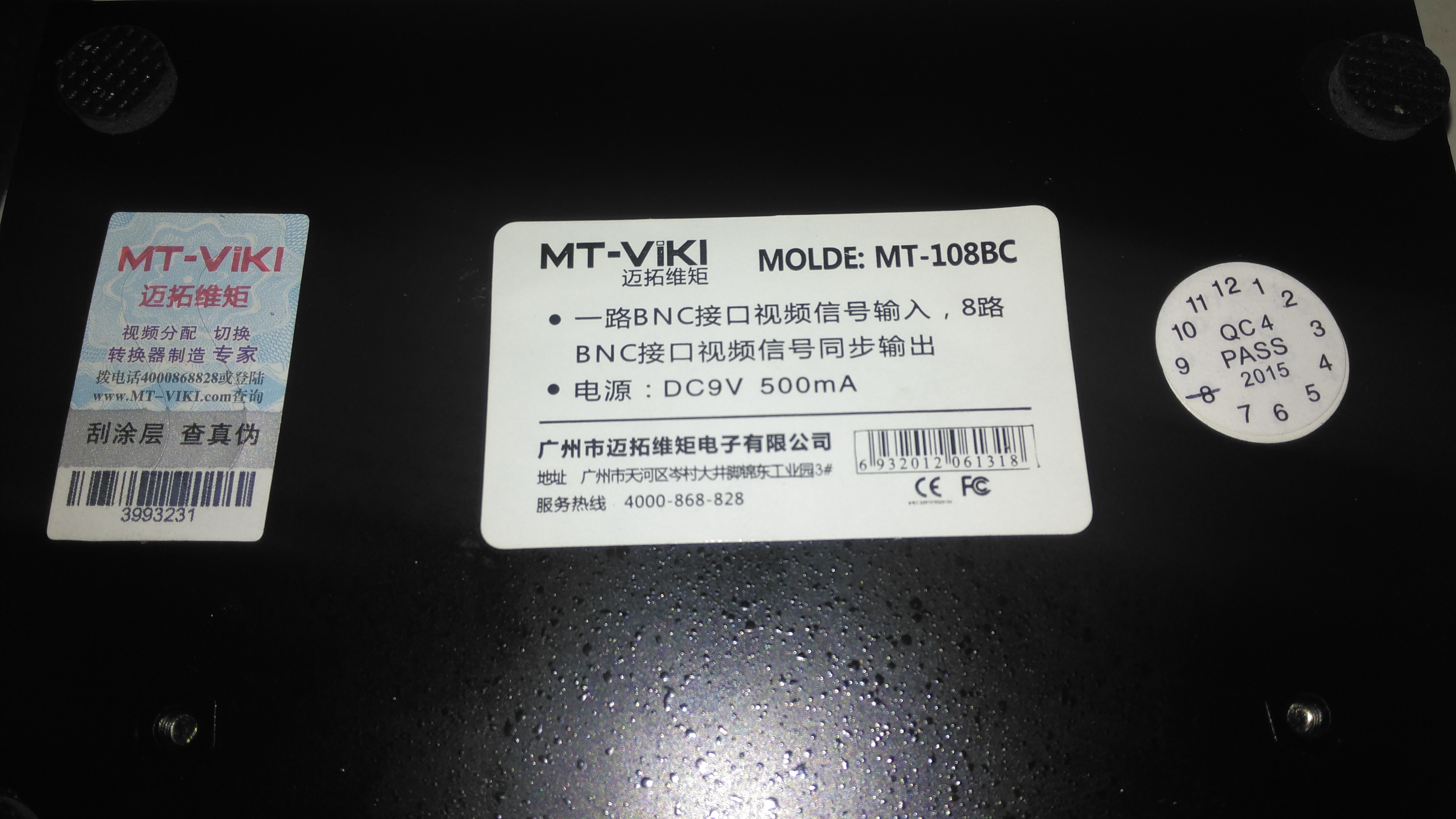
Data Label
Not much in English on the data labels, there’s also an authenticity label on the left to make sure you don’t get a fake.
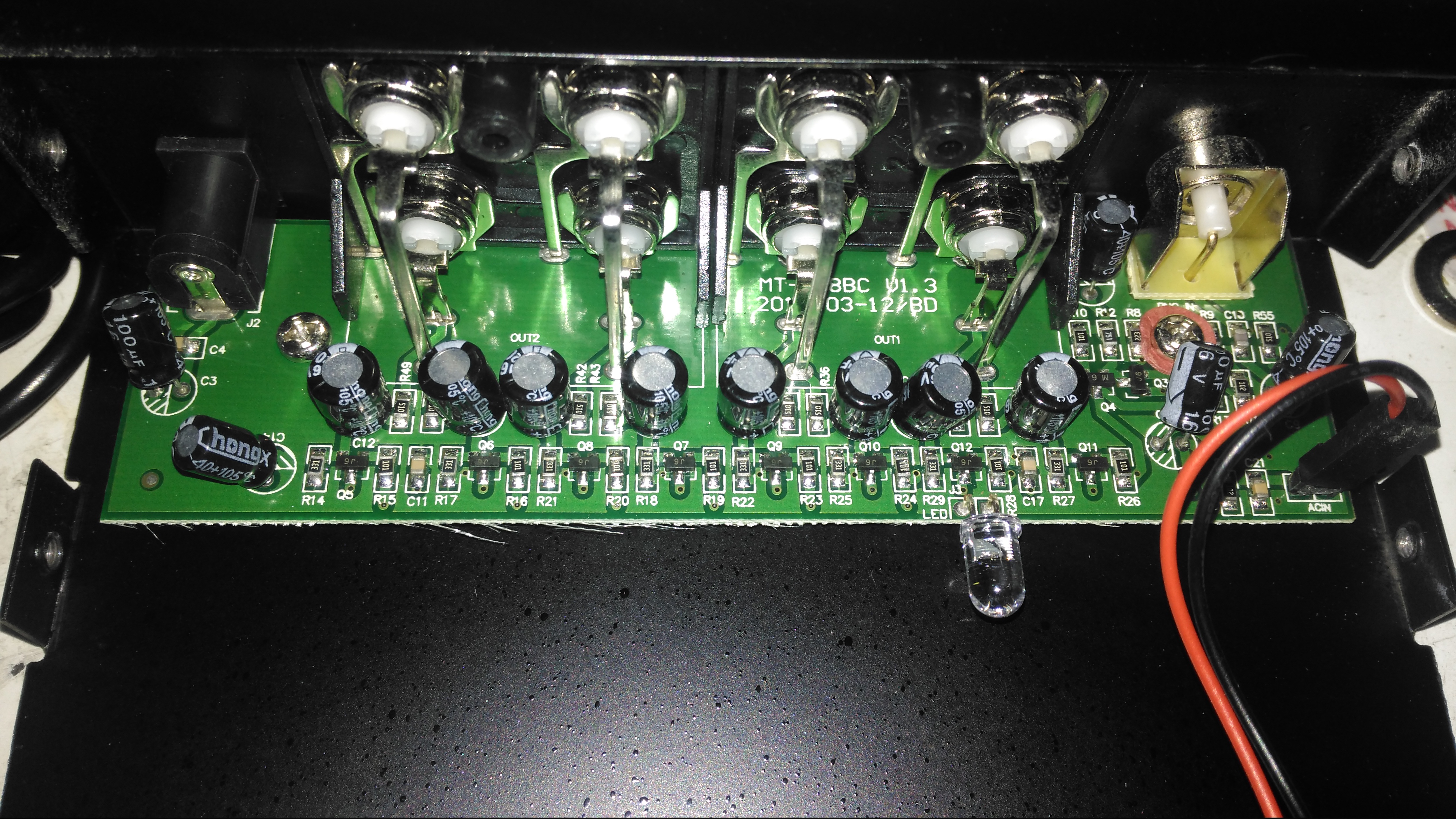
Amplifier Board
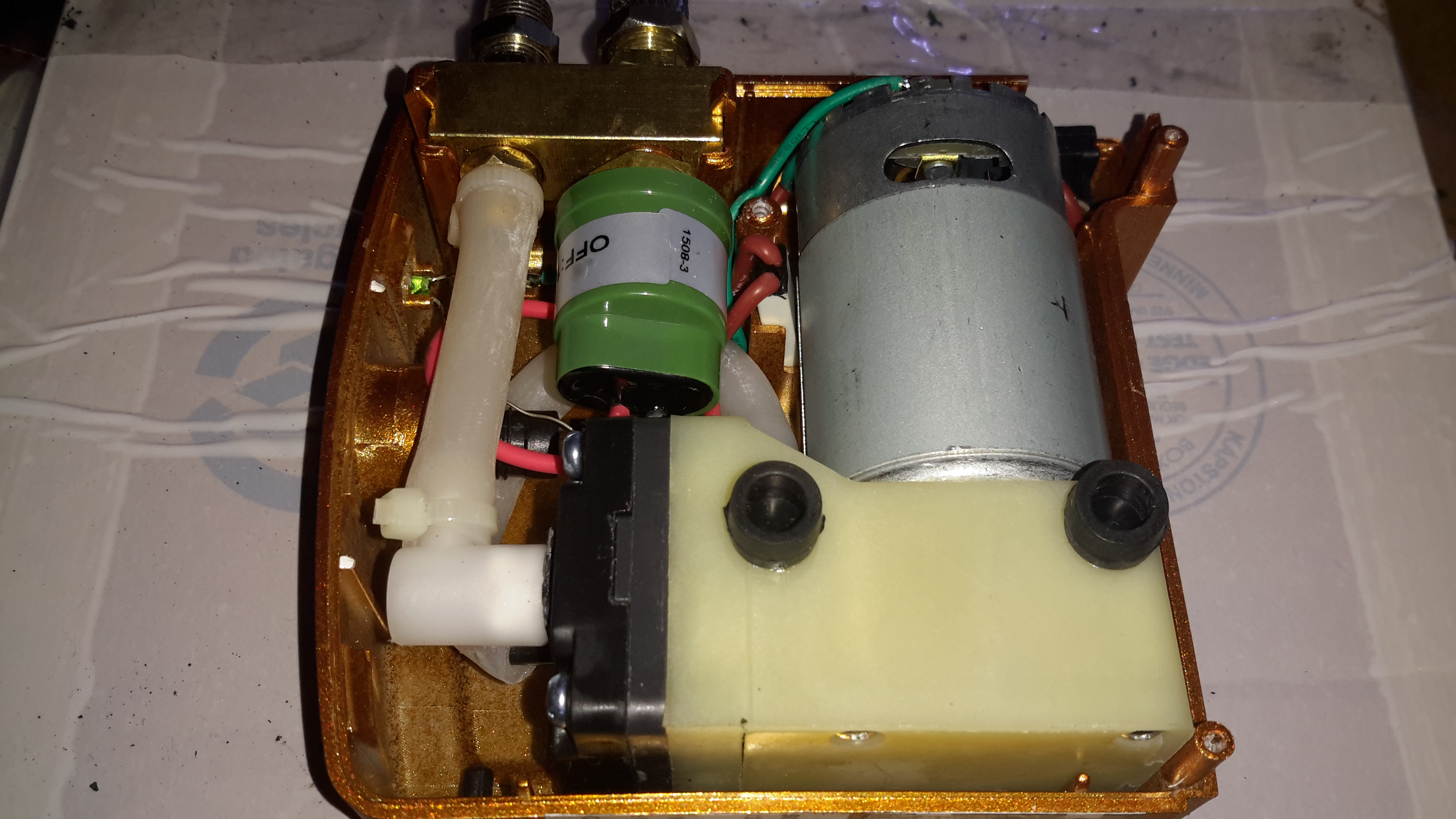
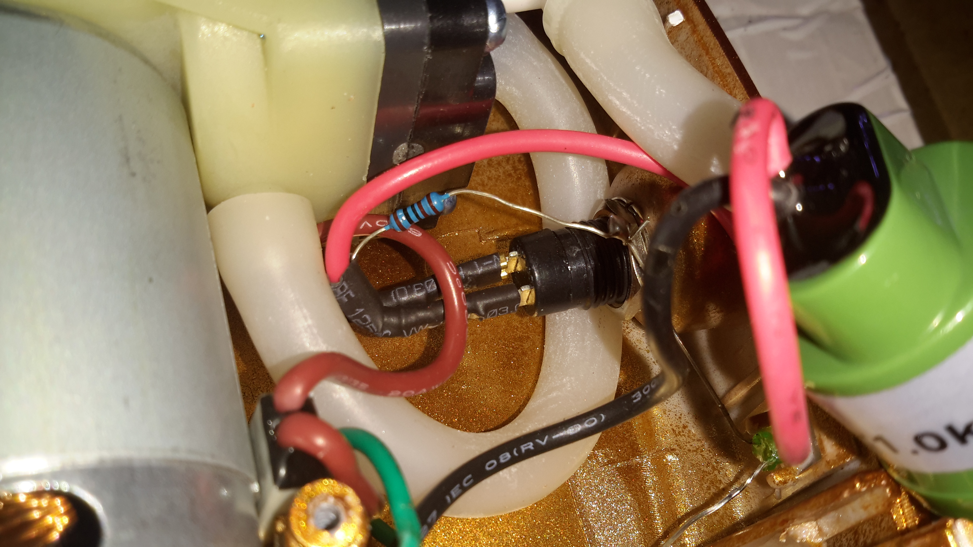
Taking the lid off reveals a very small PCB, taking up less than a third of the aluminium case! The input stage is on the right, composed of a pair of SOT-23 transistors to buffer the incoming signal. There’s an KST812M6 PNP & an S9014 NPN Epitaxial. The signal is then fed to the output stages, all individual S9014 NPN transistors to the output ports.
The power LED is just poking in the general direction of the hole in the front panel, so this isn’t likely to work very well – it’s going to illuminate the inside of the case more!
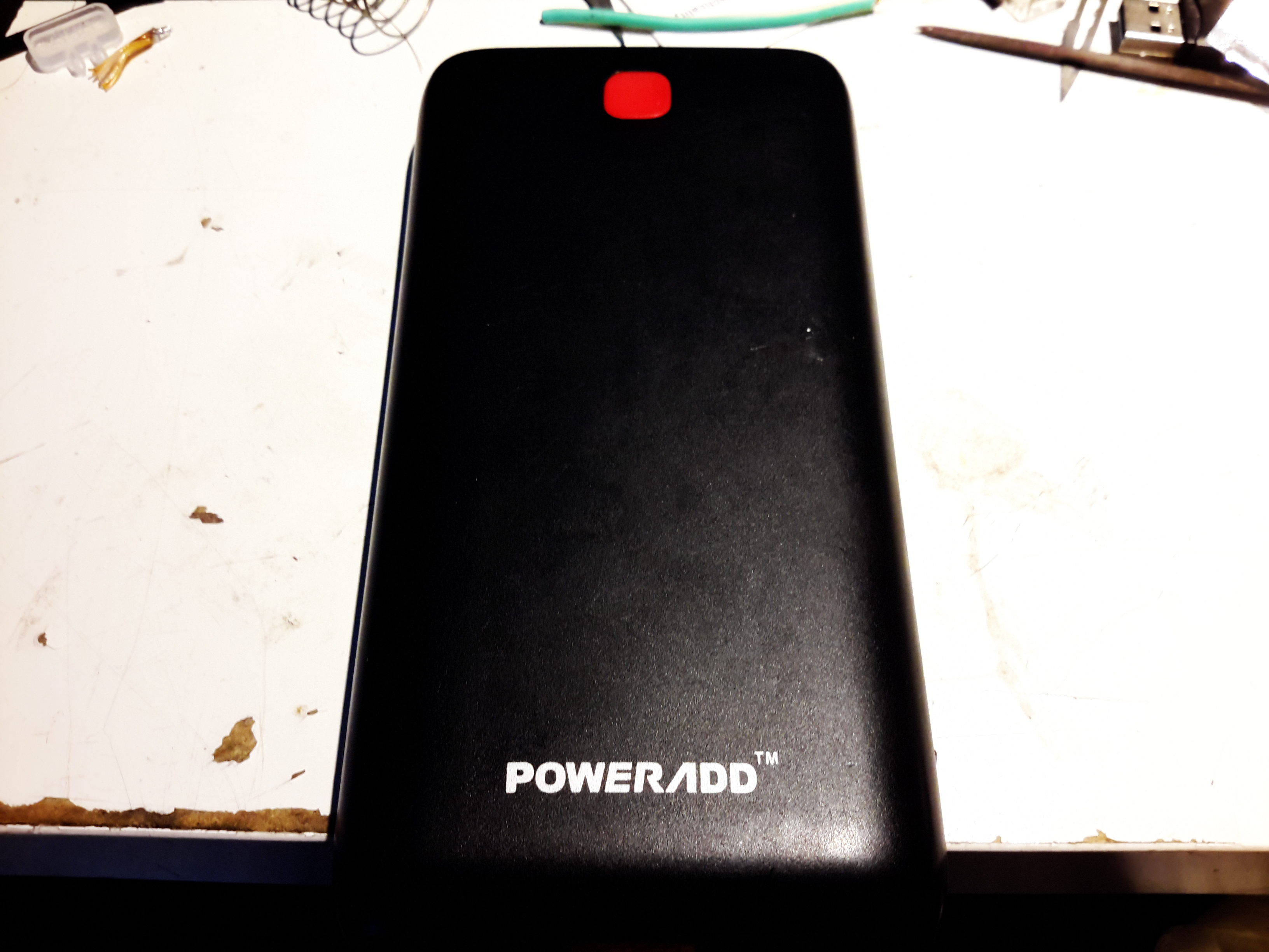
Here’s the biggest portable USB powerbank I’ve seen yet – the PowerAdd Pilot X7, this comes with a 20Ah (20,000mAh) capacity. This pack is pretty heavy, but this isn’t surprising considering the capacity.
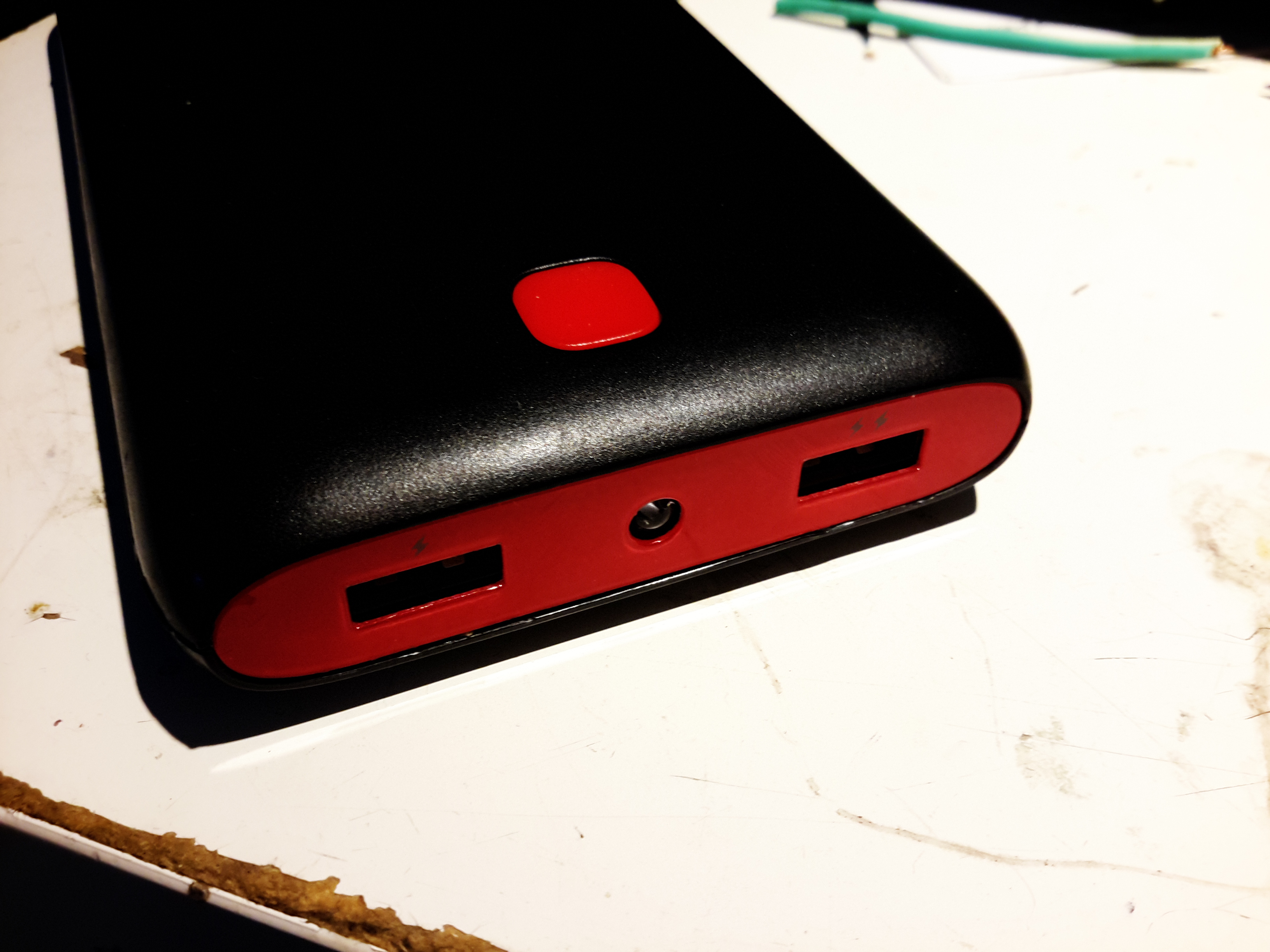
USB Ports & LED
The front of the pack houses the usual USB ports, in this case rated at 3.4A total between the ports. There’s a white LED in the centre as a small torch, activated by double-clicking the button. A single click of the button lights up the 4 blue LEDs under the housing that indicate remaining battery capacity. Factory charging is via a standard µUSB connector in the side, at a maximum of 2A.
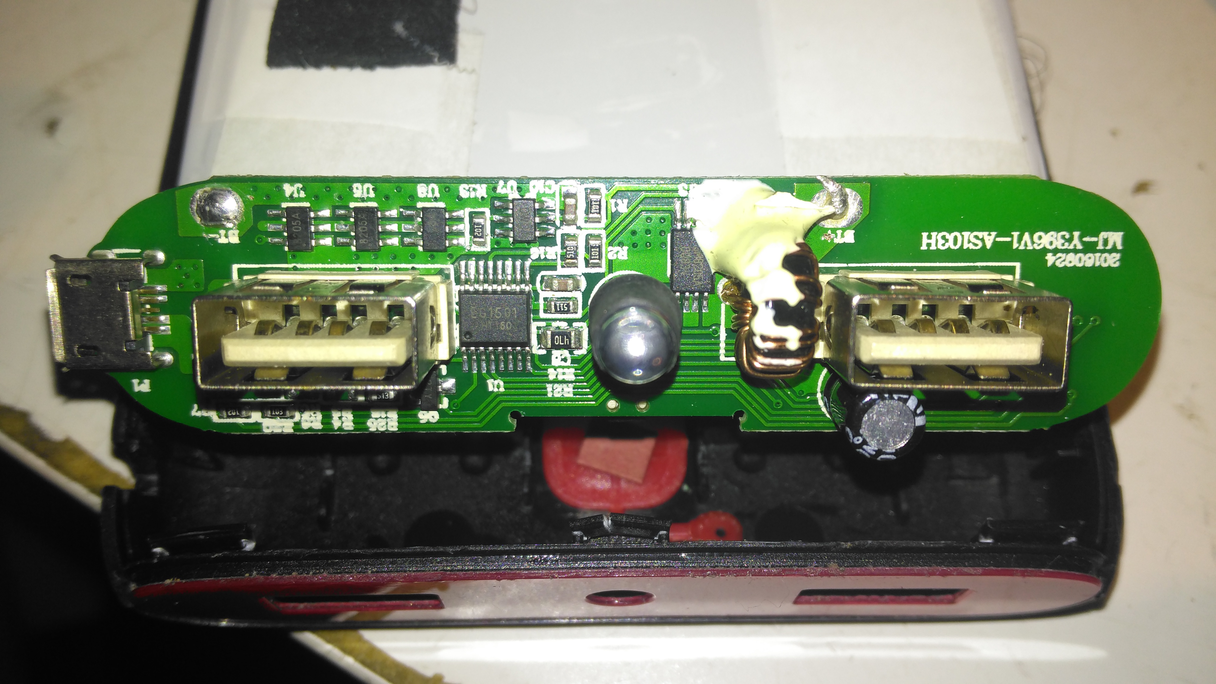
PCB Front
The front of the PCB holds the USB ports, along with most of the main control circuitry. At top left is a string of FS8025A dual-MOSFETs all in parallel for a current carrying capacity of 15A total, to the right of these is the ubiquitous DW01 Lithium-Ion protection IC. These 4 components make up the battery protection – stopping both an overcharge & overdischarge. The larger IC below is an EG1501 multi-purpose power controller.
This chip is doing all of the heavy lifting in this power pack, dealing with all the DC-DC conversion for the USB ports, charge control of the battery pack, controlling the battery level indicator LEDs & controlling the torch LED in the centre.
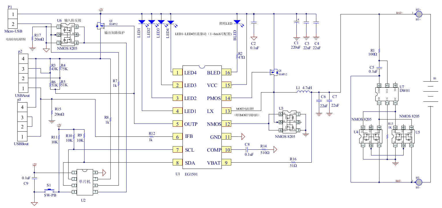
EG1501 Example
The datasheet is in Chinese, but it does have an example application circuit, which is very similar to the circuitry used in this powerbank. A toroidal inductor is nestled next to the right-hand USB port for the DC-DC converter, and the remaining IC next to it is a CW3004 Dual-Channel USB Charging Controller, which automatically sets the data pins on the USB ports to the correct levels to ensure high-current charging of the devices plugged in. This IC replaces the resistors R3-R6 in the schematic above.
The DC-DC converter section of the power chain is designed with high efficiency in mind, not using any diodes, but synchronous rectification instead.
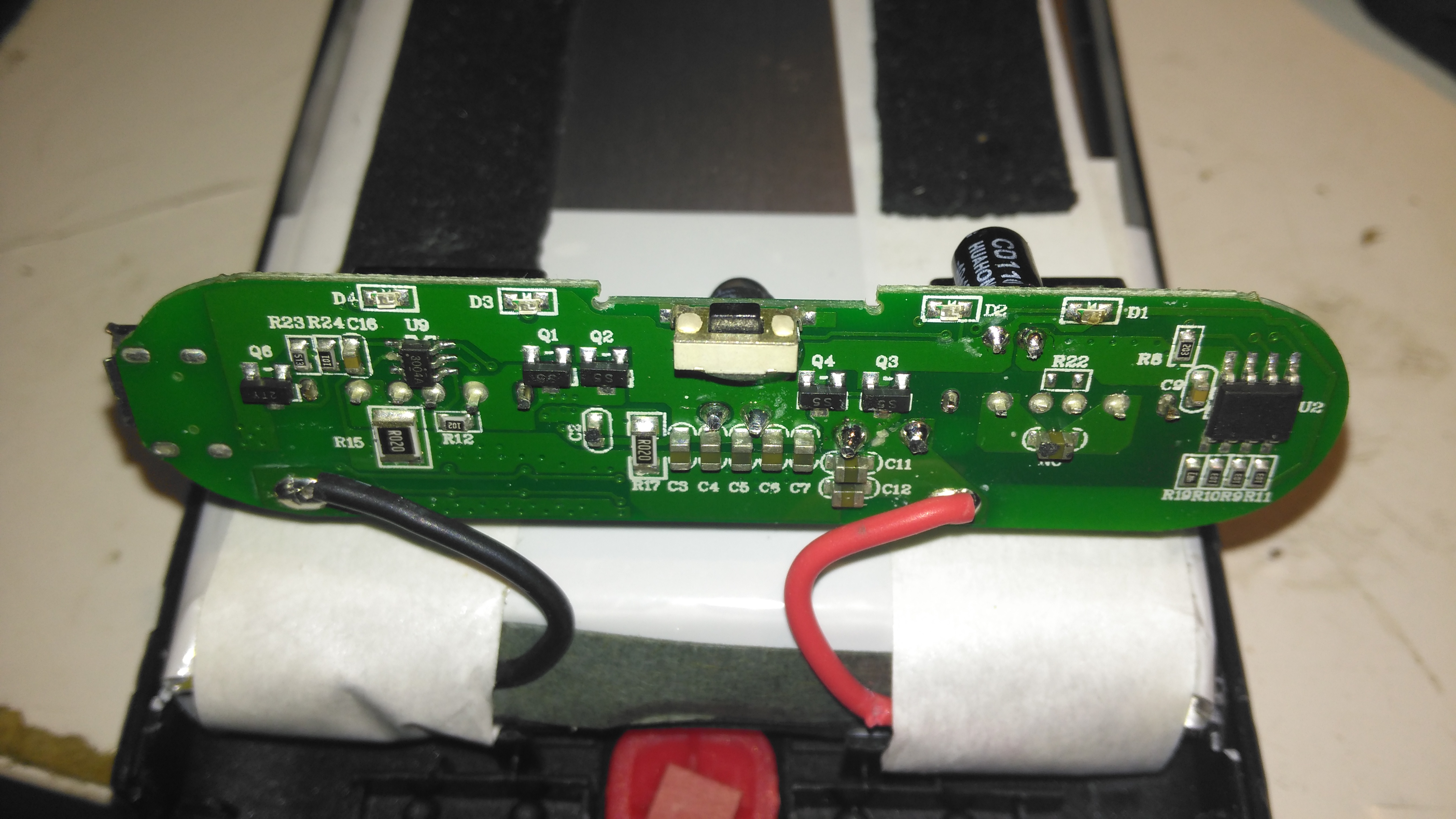
PCB Back
The back of the PCB just has a few discrete transistors, the user interface button, and a small SO8 IC with no markings at all. I’m going to assume this is a generic microcontroller, (U2 in the schematic) & is just there to interface the user button to the power controller via I²C.
Cells
Not many markings on the cells indicating their capacity, but a full discharge test at 4A gave me a resulting capacity of 21Ah – slightly above the nameplate rating. There are two cells in here in parallel, ~10Ah capacity each.
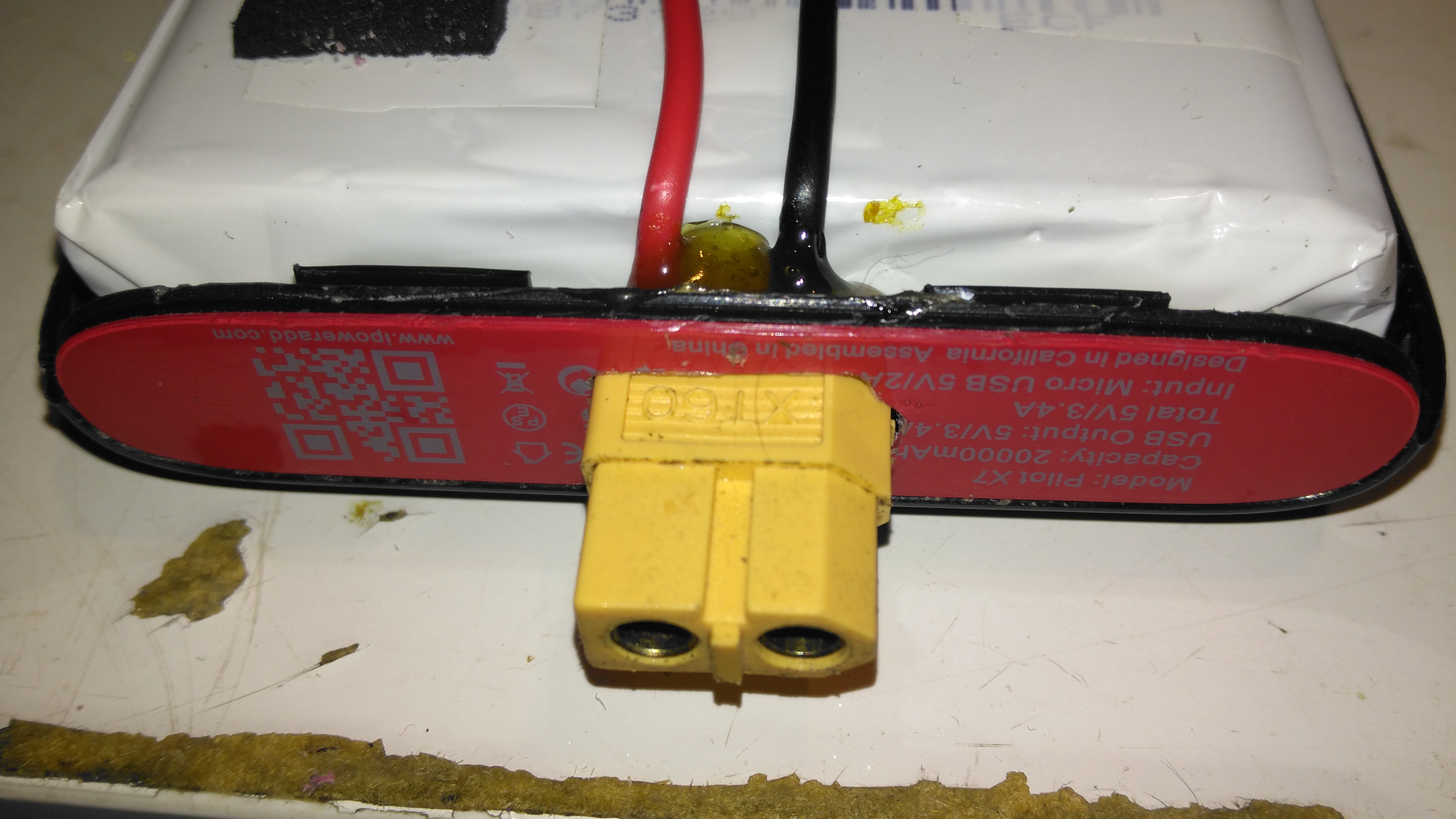
XT60 Battery Connector
The only issue with powerbanks this large is the amount of time they require to recharge themselves – at this unit’s maximum of 2A through the µUSB port, it’s about 22 hours! Here I’ve fitted an XT60 connector, to interface to my Turnigy Accucell 6 charger, increasing the charging current capacity to 6A, and reducing the full-charge time to 7 hours. This splits to 3A charge per cell, and after some testing the cells don’t seem to mind this higher charging current.
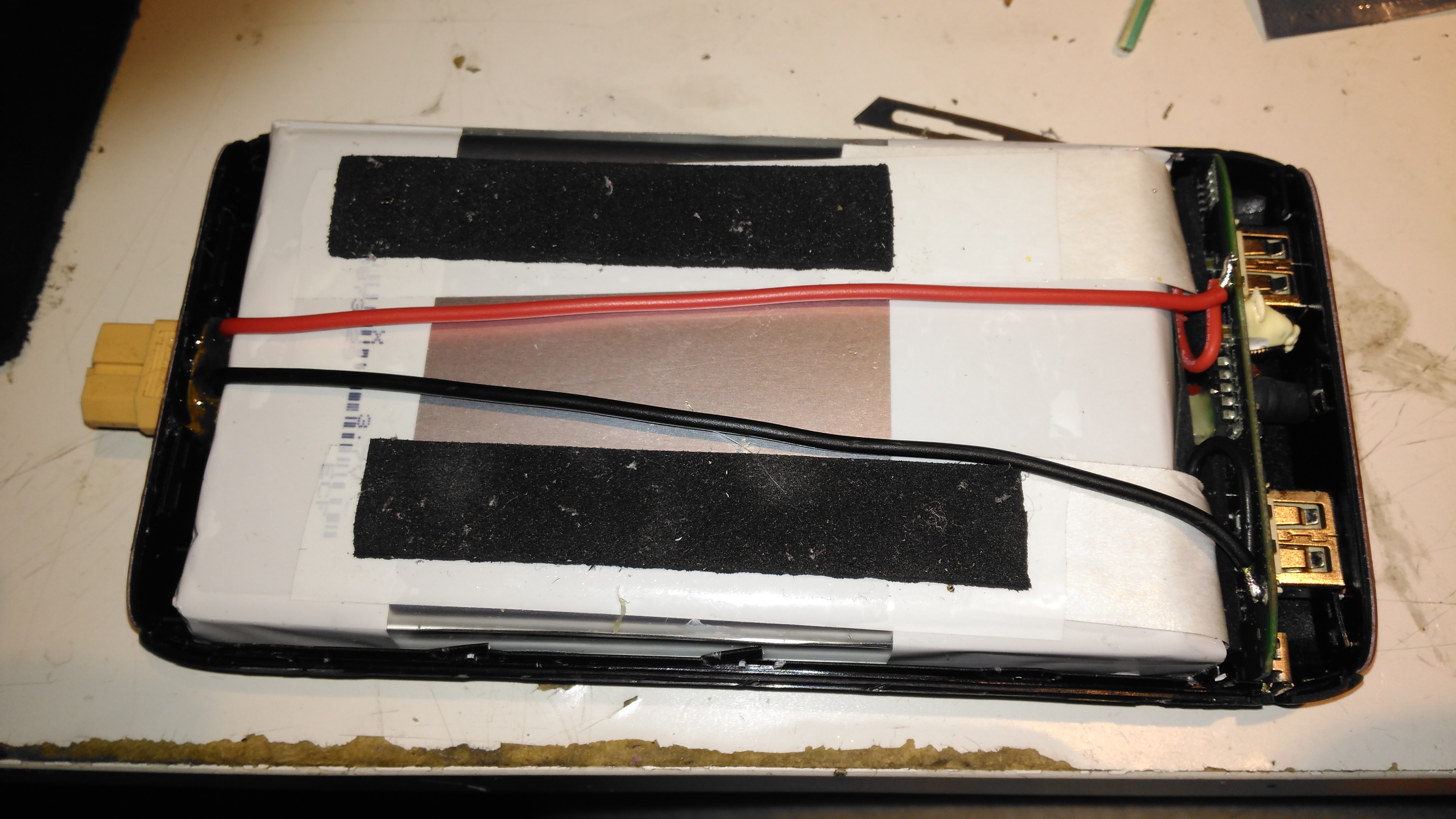
Battery Connector Wiring
The new charging connector is directly connected to the battery at the control PCB, there’s just enough room to get a pair of wires down the casing over the cells.
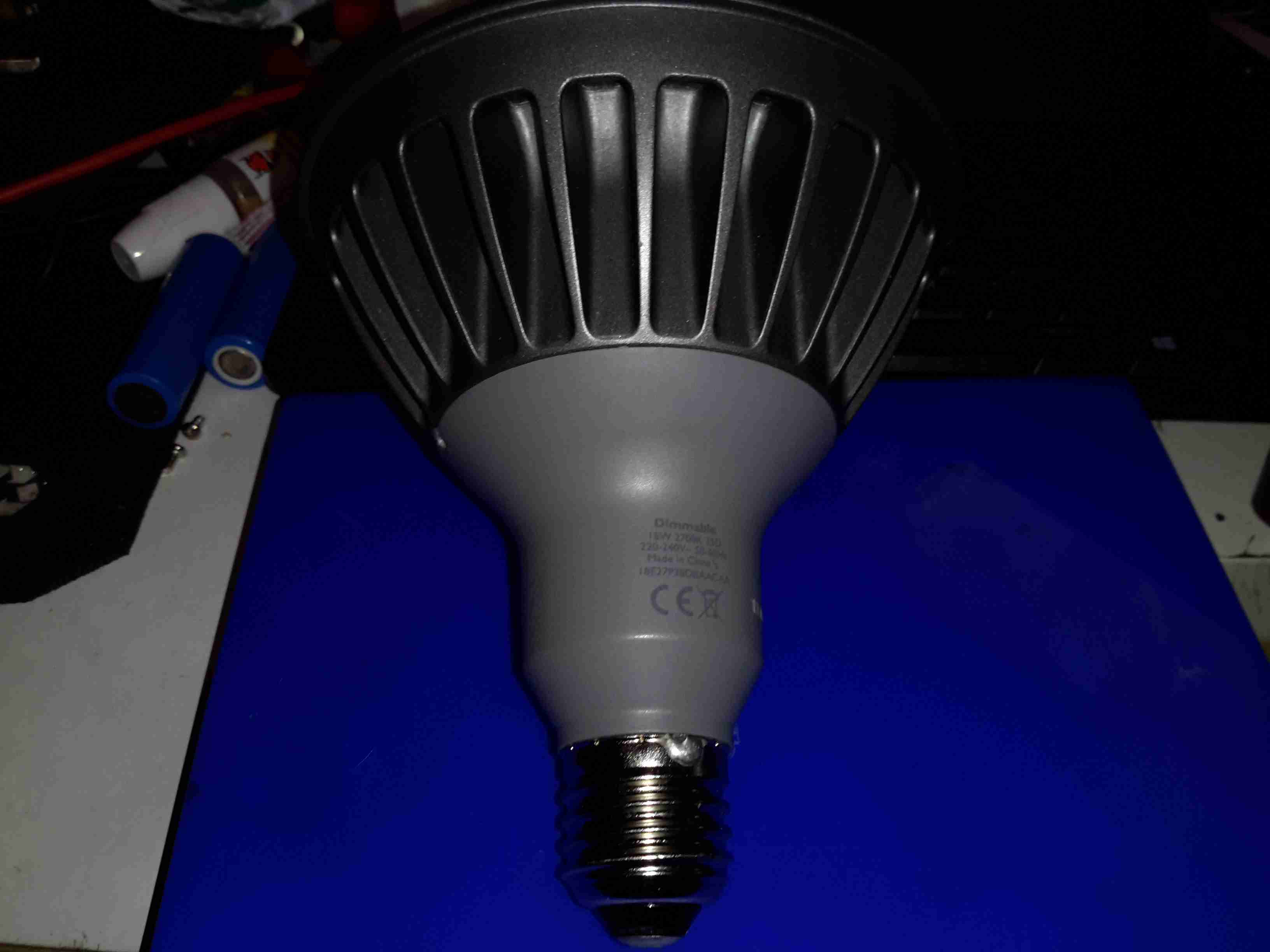
These large LED Philips PAR38 lamps were recently on clearance sale in my local T.N. Robinsons electrical contractors for about £3, so I decided to grab one in the hopes I might be able to hack it into a low-voltage LED lamp. These are full-size PAR38 format, with most of the bulk being the large aluminium heatsink on the front. The back section with the power supply module is secured with silicone, so some unreasonable force was required to liberate the two pieces.
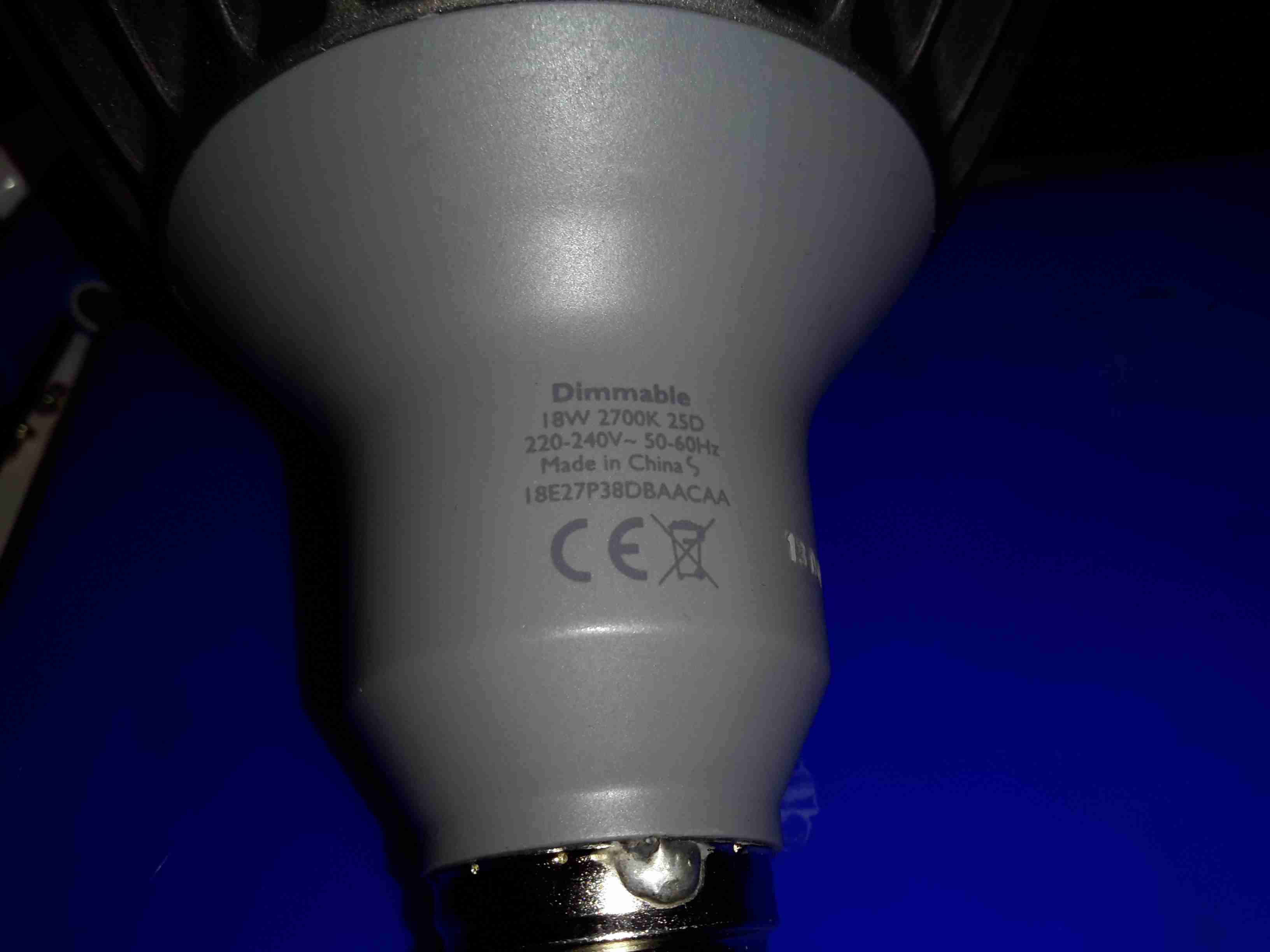
Specification
These lamps are rated at 18W in operation, and are surprisingly bright for this power level.
Lens
The front has the moulded multi-lens over the LEDs, to spread the light a bit further than the bare dies.
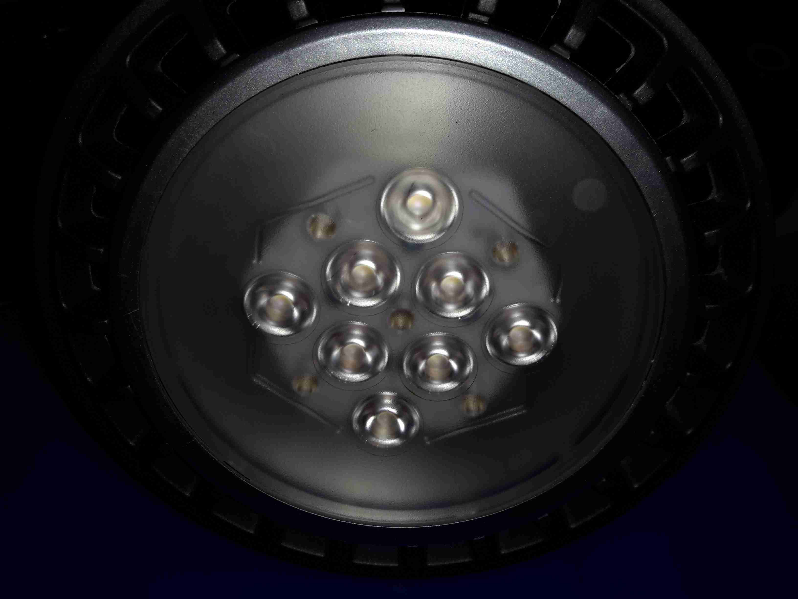
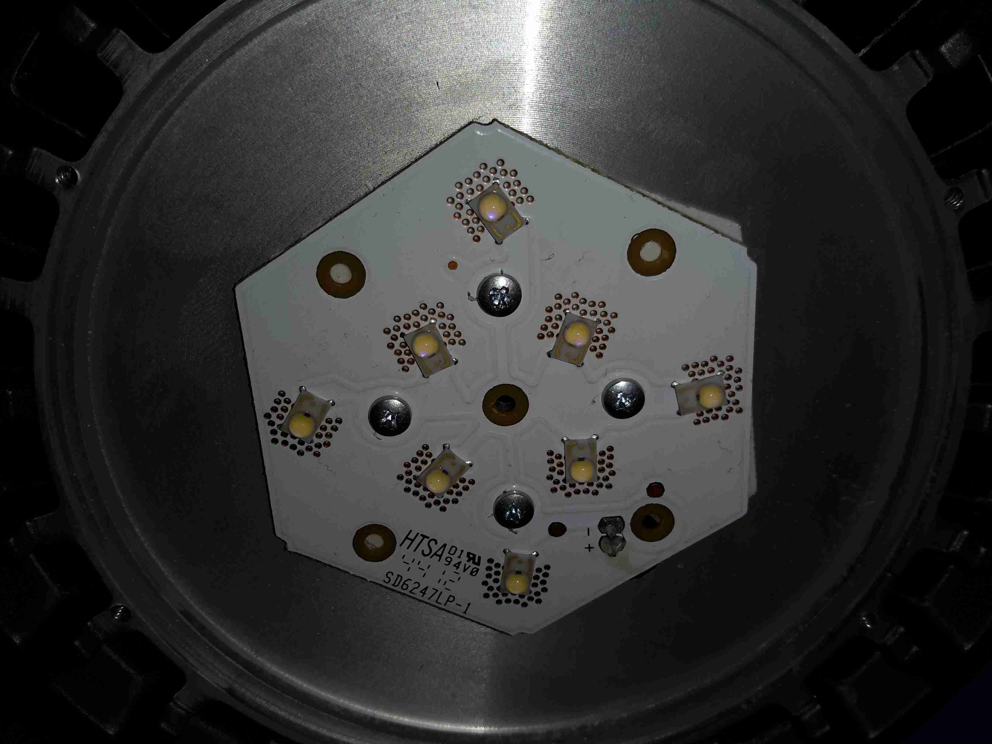
LED Array
The LED array is two series strings of 4 LEDs, for ~24v forward voltage. Unusual for a high power LED array, this PCB isn’t aluminium cored, but 0.8mm FR4. Heat is transferred to the copper plane on the backside by the dozens of vias around the Luxeon Rebel LEDs. There is a thermal pad under the PCB for improved heat transfer to the machined surface of the heatsink.
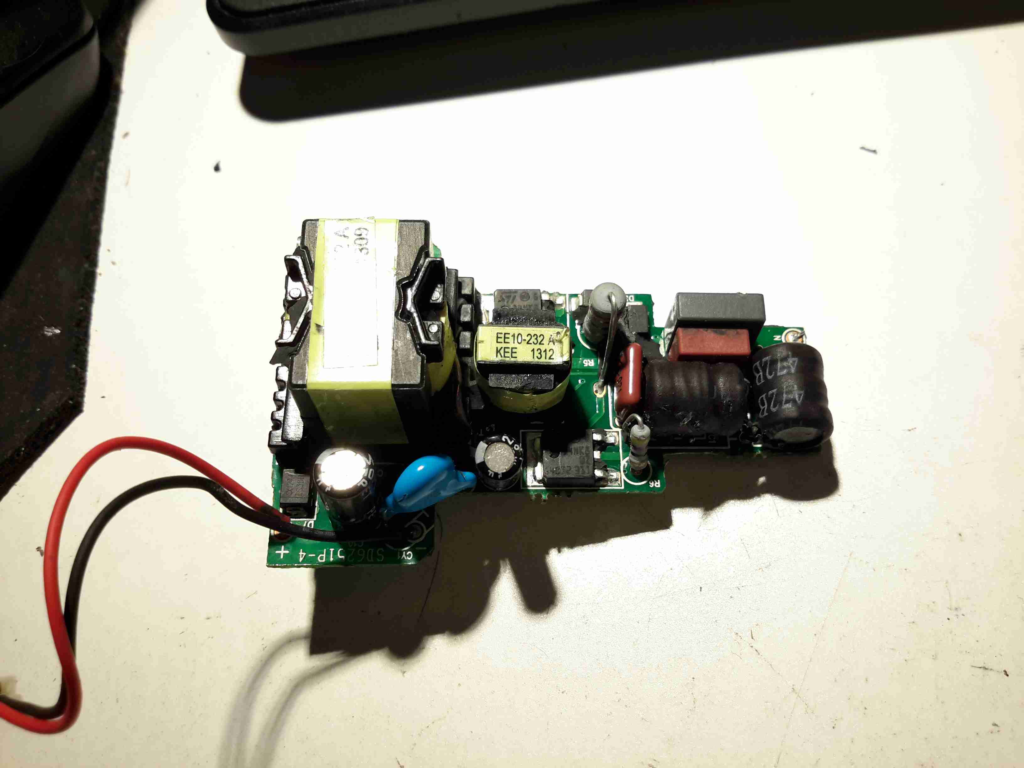
Control PCB Top
The power supply & control PCB is pretty well made, it’s an isolated converter, so no nasty mains on the LED connections.
This is a little bit of kit I got to talk to the Webasto TT-V I salvaged from a scrap Jaguar S-Type, and converts USB-RS232 to the standard car diagnostic ODB connector. (These are a much cheaper option at £4 than the official Webasto diagnostic adaptor & loom which is over £90.
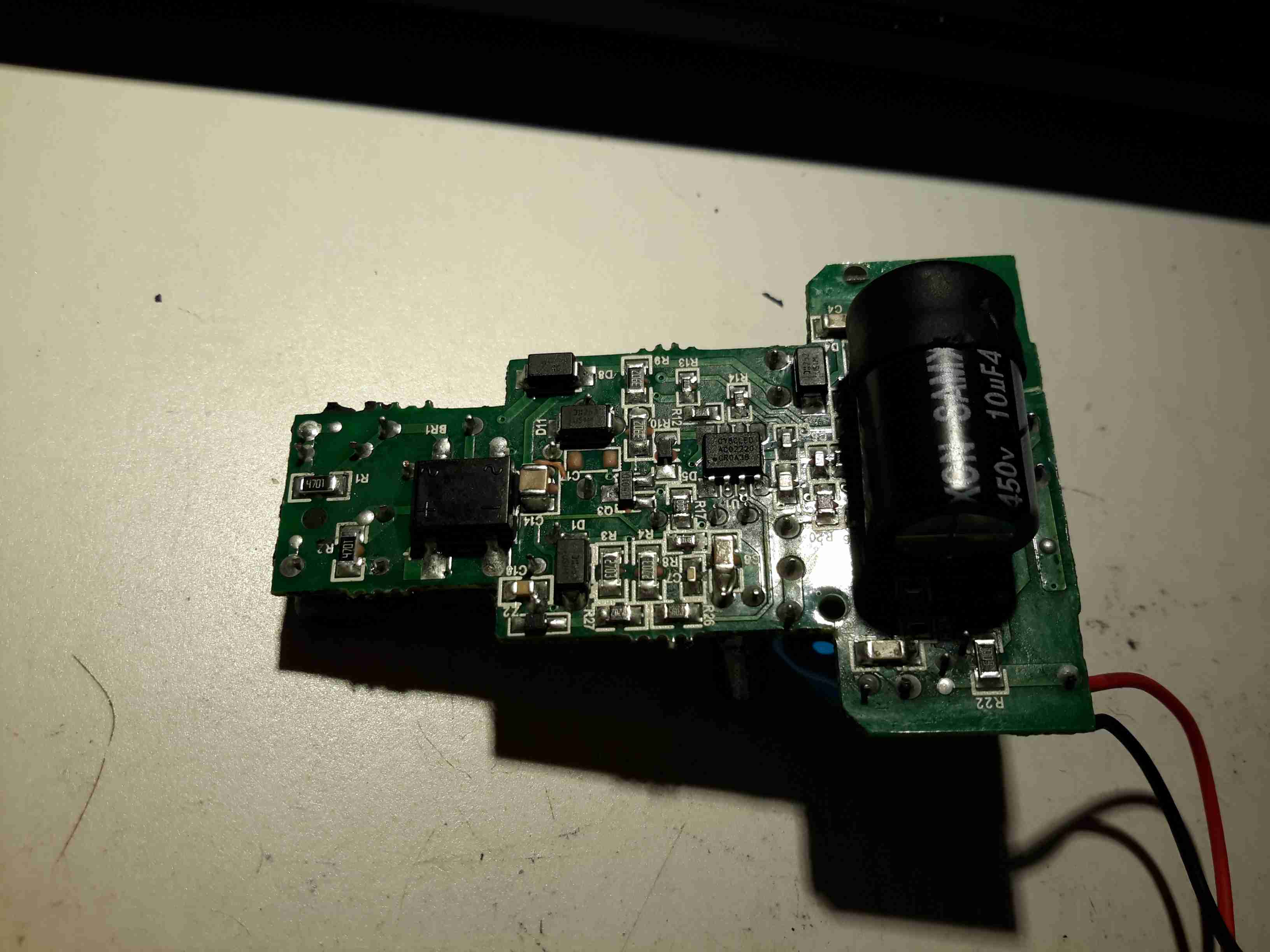
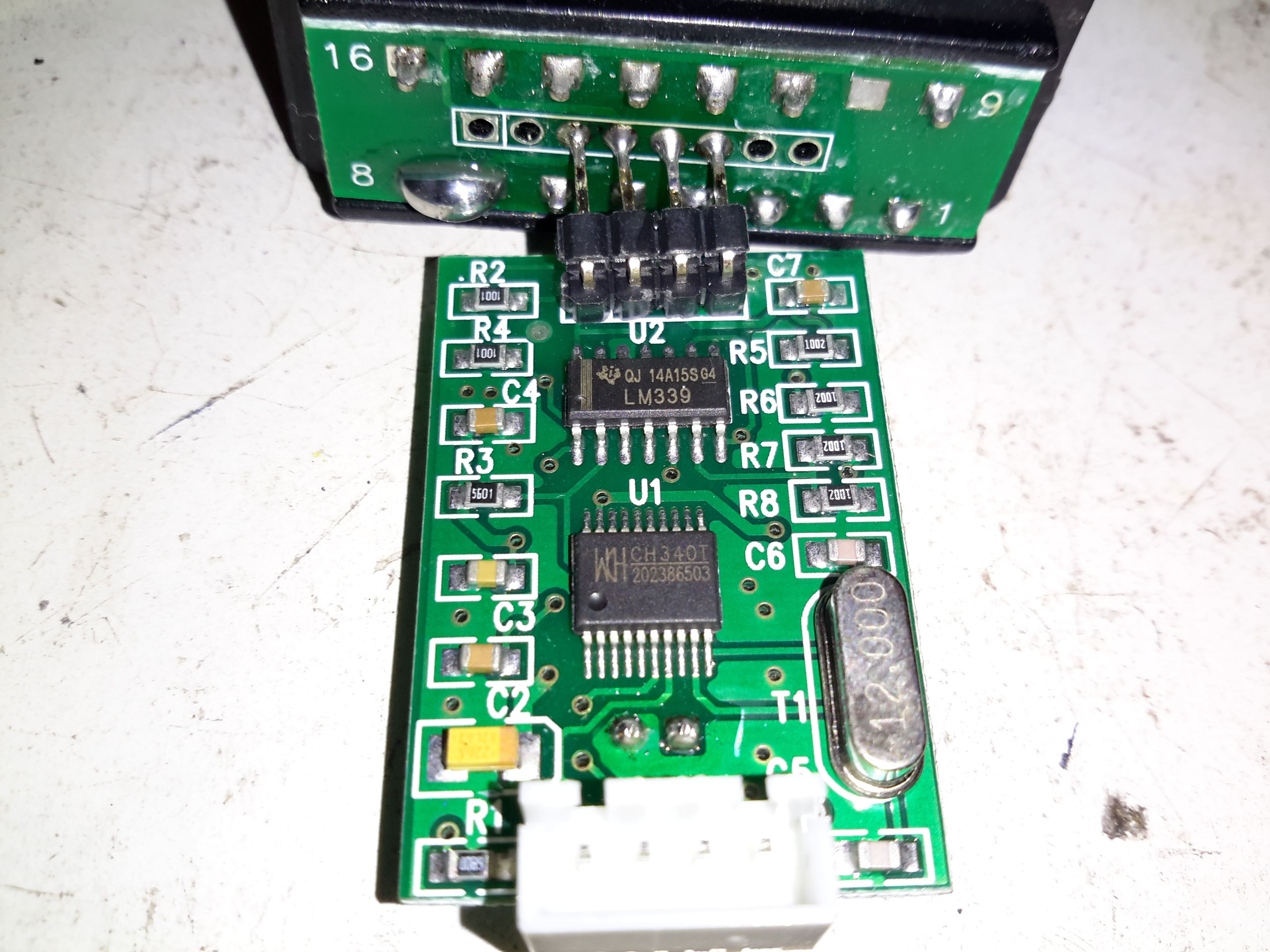
PCB Top
There’s really not much to this adaptor, the only signals that are routed to the ODB connector seem to be the +12v on pin 16, K-Line on Pin 7 & L-Line on pin 15. The main IC here is a CH340 USB-Serial interface, with some glue logic in the form of an LM339 quad comparator.
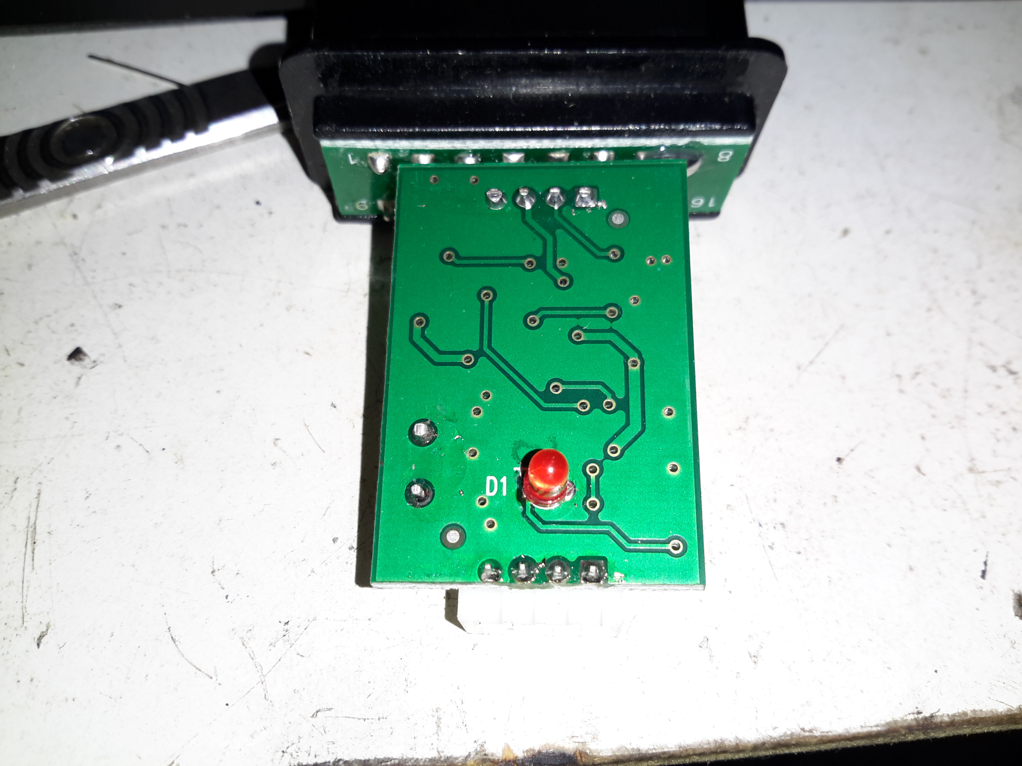
PCB Reverse
The reverse side of the PCB only has the power indicator LED.
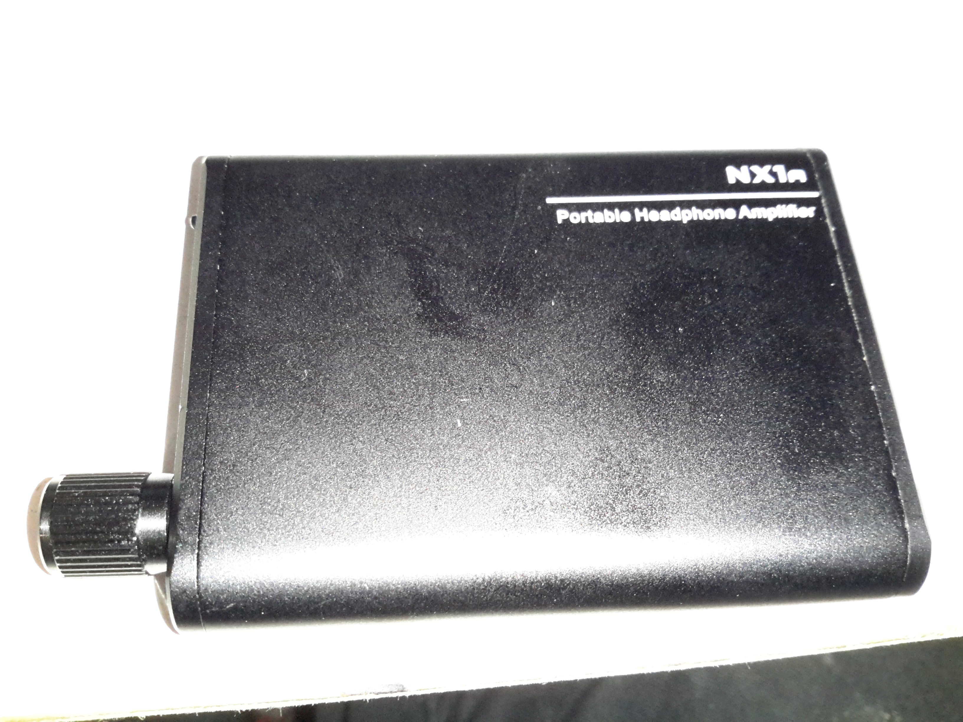
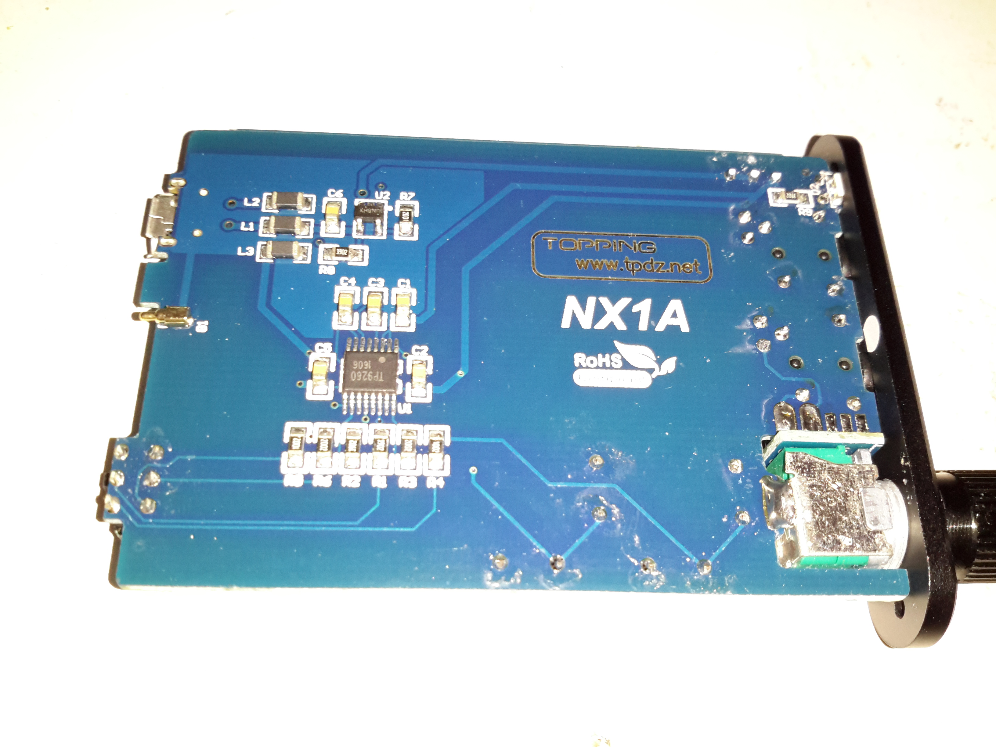
Time for another teardown! Here’s a pocket-sized headphone amplifier for use with mobile devices. This unit is powered by a built-in lithium cell, and can give some pretty impressive volume levels given it’s small size.
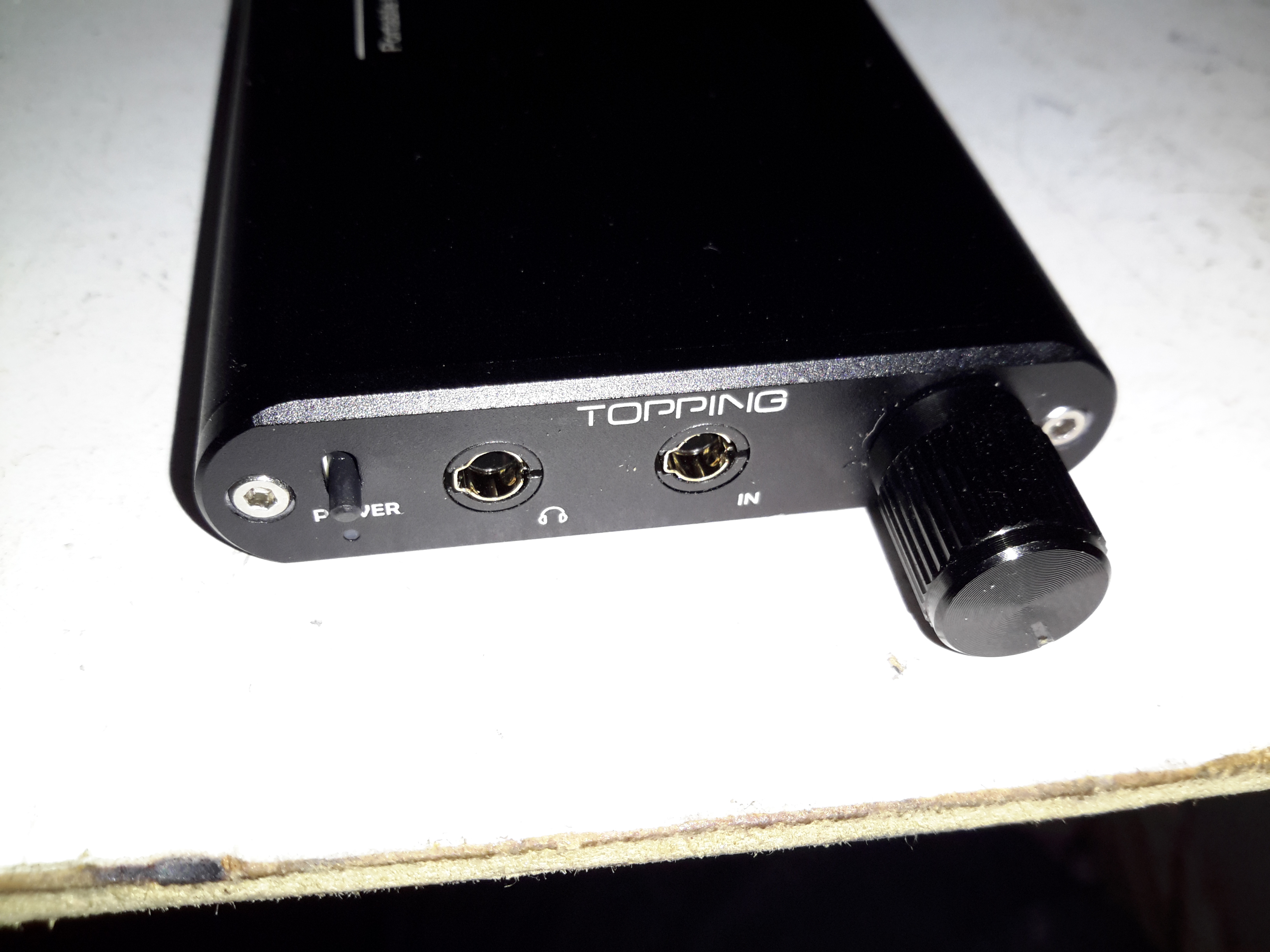
Audio Connections
The 3.5mm audio input & output jacks are on the front of the unit, along with the relatively enormous volume knob & power switch. There’s a little blue LED under the switch that lets the user know when the power is on, but this is a very sedate LED, using very little power.
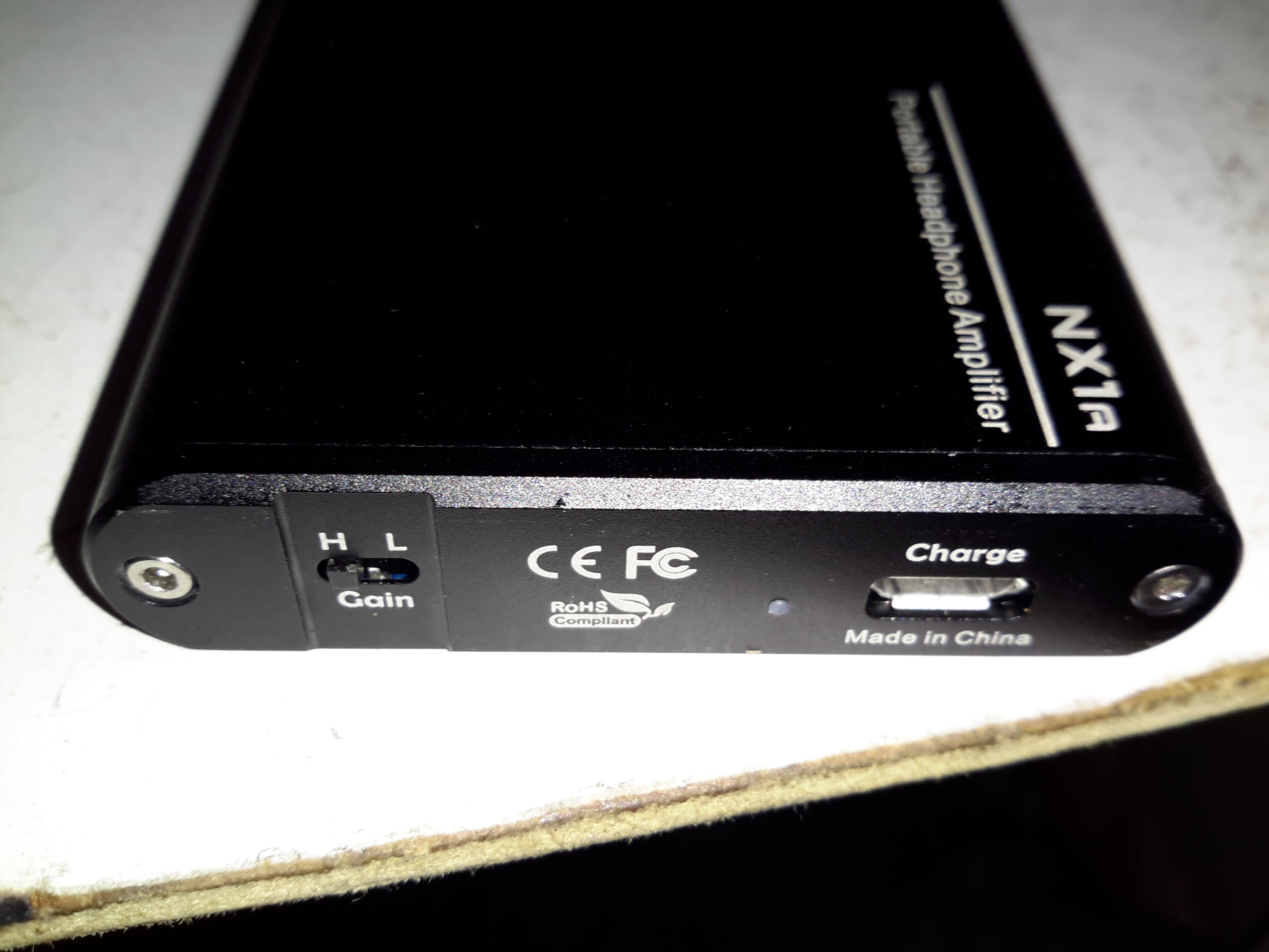
Gain & Charging
On the back is the High-Low gain switch, and the µUSB charging port. There’s another indicator LED to show that the internal cell is charging, in this case a red one.
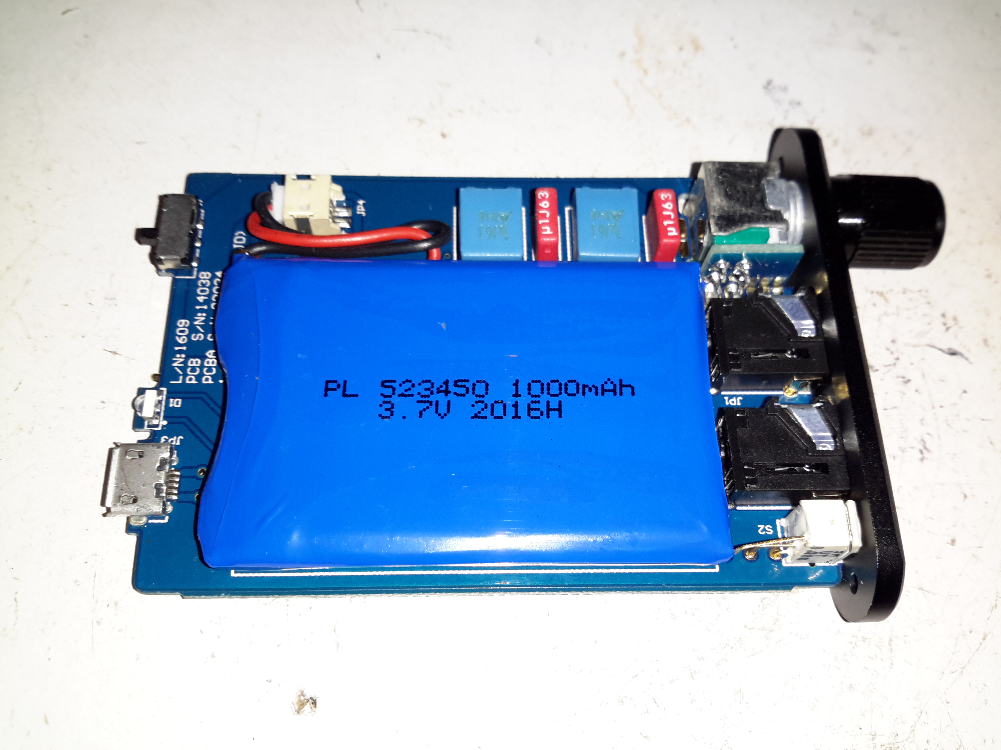
PCB Top
Removing a couple of cap screws allows the internals to slide out of the extruded aluminium casing. Most of the internal space is taken up by the 1Ah lithium cell, here on the top of the PCB secured by some double-sided tape. The volume potentiometer is mounted on a small daughterboard at right angles to get it to fit into the small vertical space in the case.
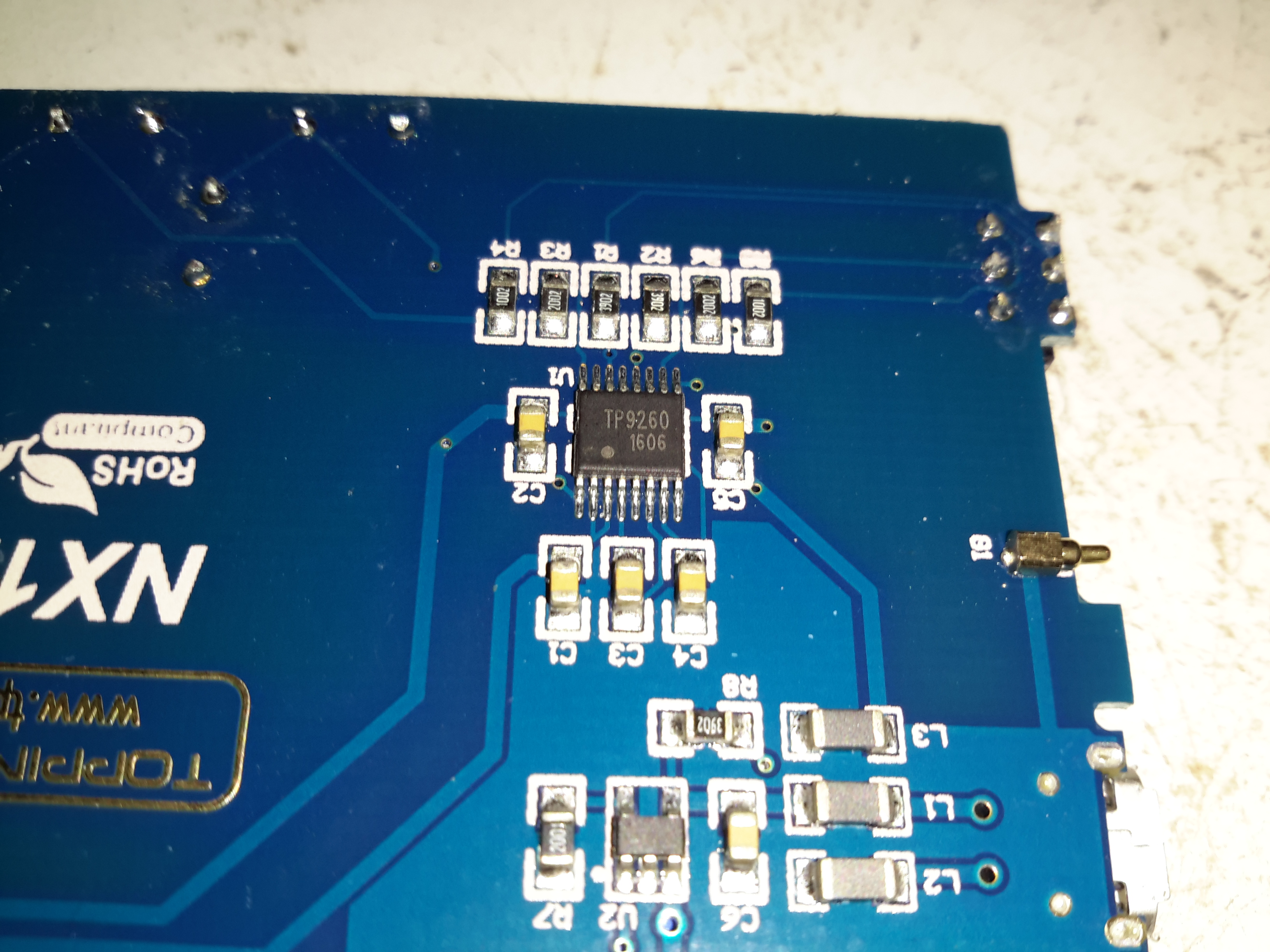
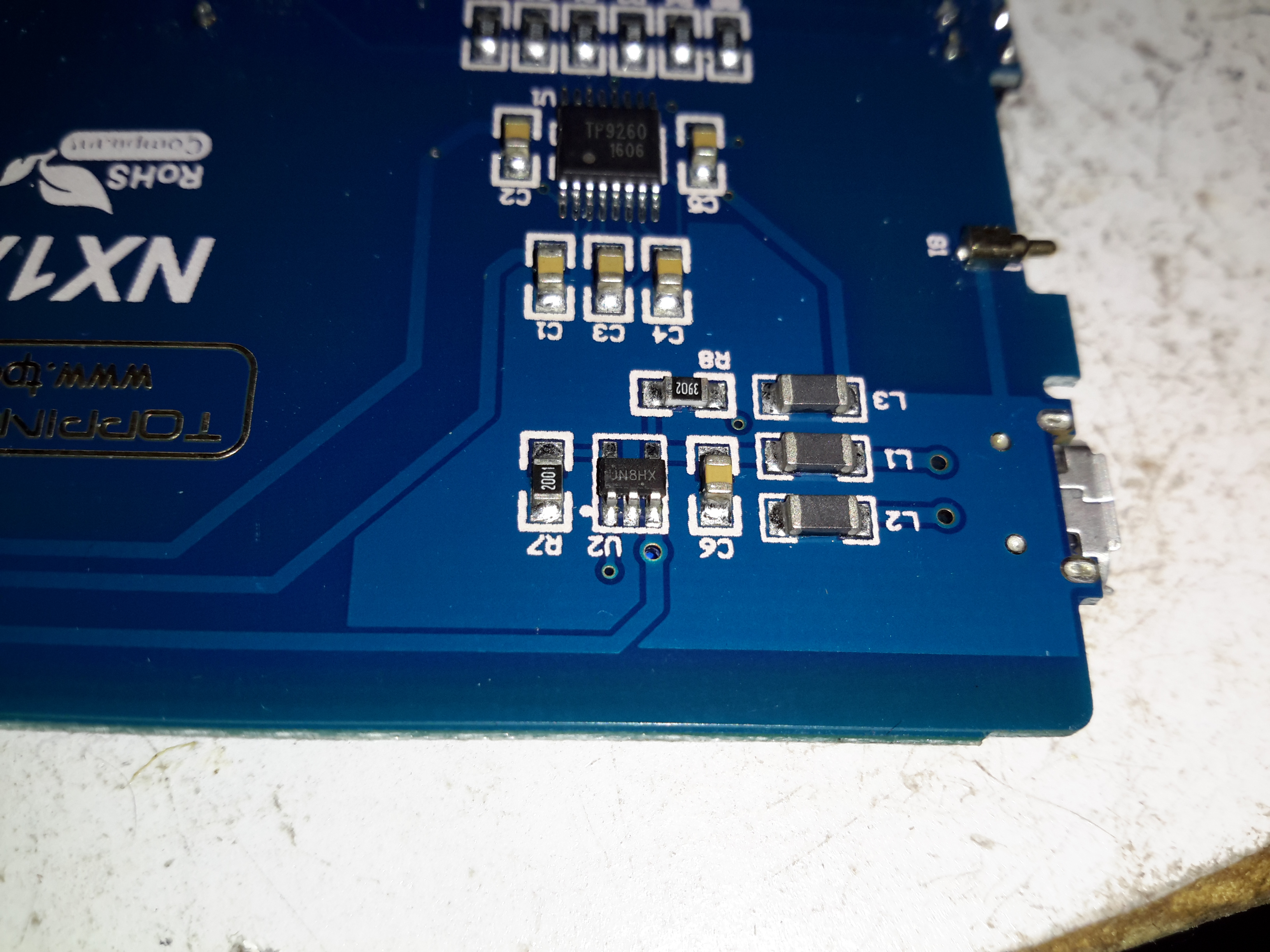
PCB Rear
The bottom of the PCB is equally as sparse – the only ICs being the main audio amp in the centre & the battery charger IC at the top.
Amplifier IC
The main audio amplifier is a TP9260, I couldn’t find a datasheet on this, so I’m unsure of what the specs are. The row of resistors above the IC are for the gain divider circuit. There’s also a pogo pin on the right that makes contact with the back panel of the case for grounding.
Battery Charger
Battery charging is taken care of by a UN8HX 500mA linear charging IC, not much special here.
This little amplifier seems to be pretty well made, considering the price point. The only issue I’ve had so far is the audio cables act like antennas, and when in close proximity to a phone some signal gets picked up & blasted into the headphones as interference.
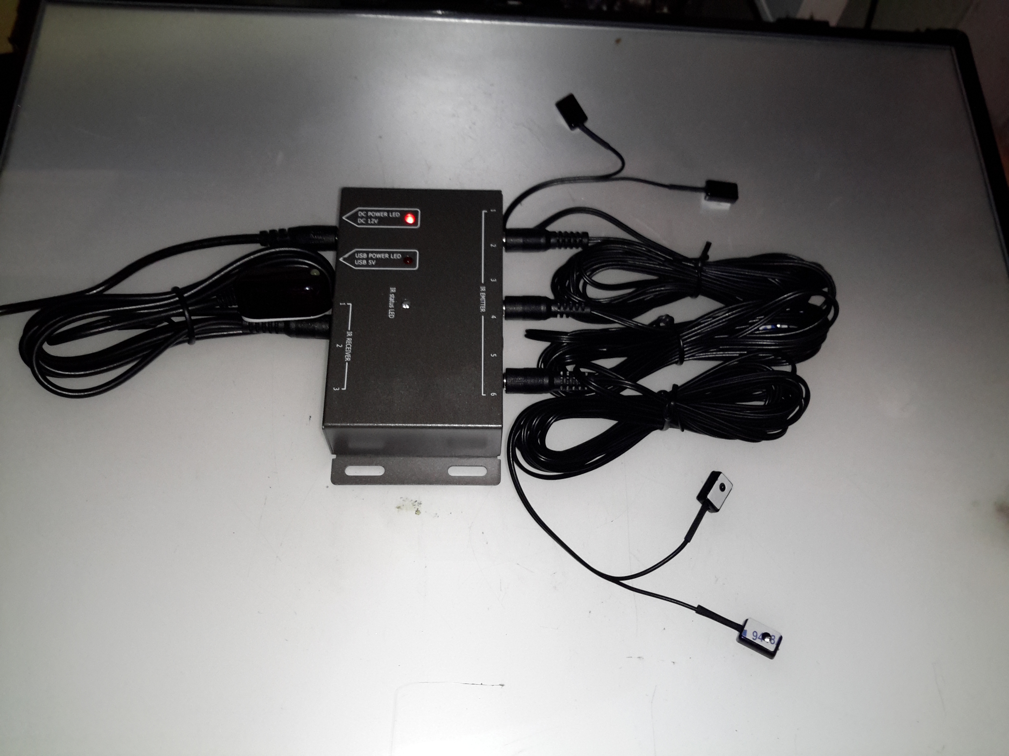
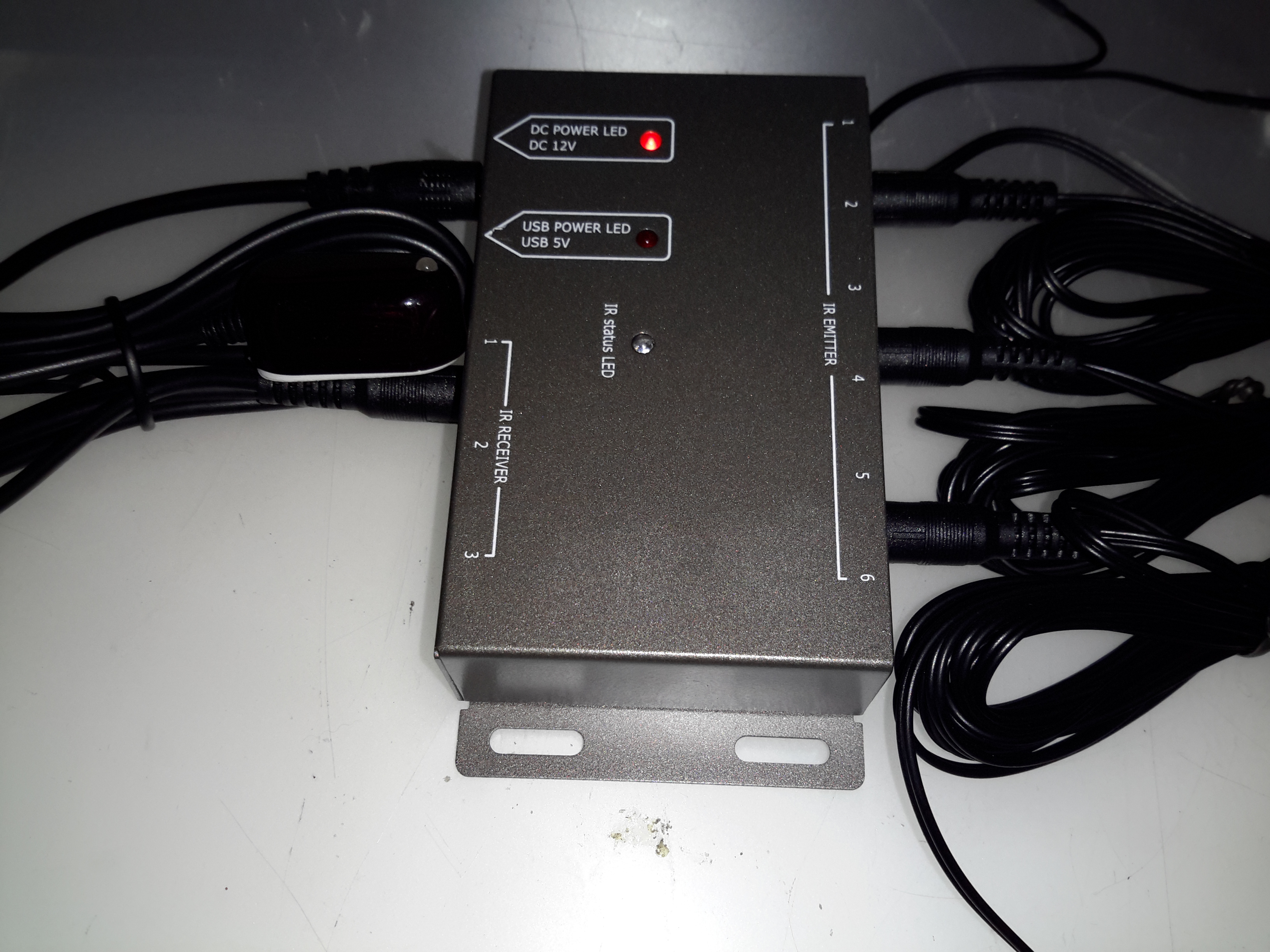
Here’s another random gadget for teardown, this time an IR remote control repeater module. These would be used where you need to operate a DVD player, set top box, etc in another room from the TV that you happen to be watching. An IR receiver sends it’s signal down to the repeater box, which then drives IR LEDs to repeat the signal.
Repeater Module
Not much to day about the exterior of this module, the IR input is on the left, up to 3 receivers can be connected. The outputs are on the right, up to 6 repeater LEDs can be plugged in. Connections are done through standard 3.5mm jacks.
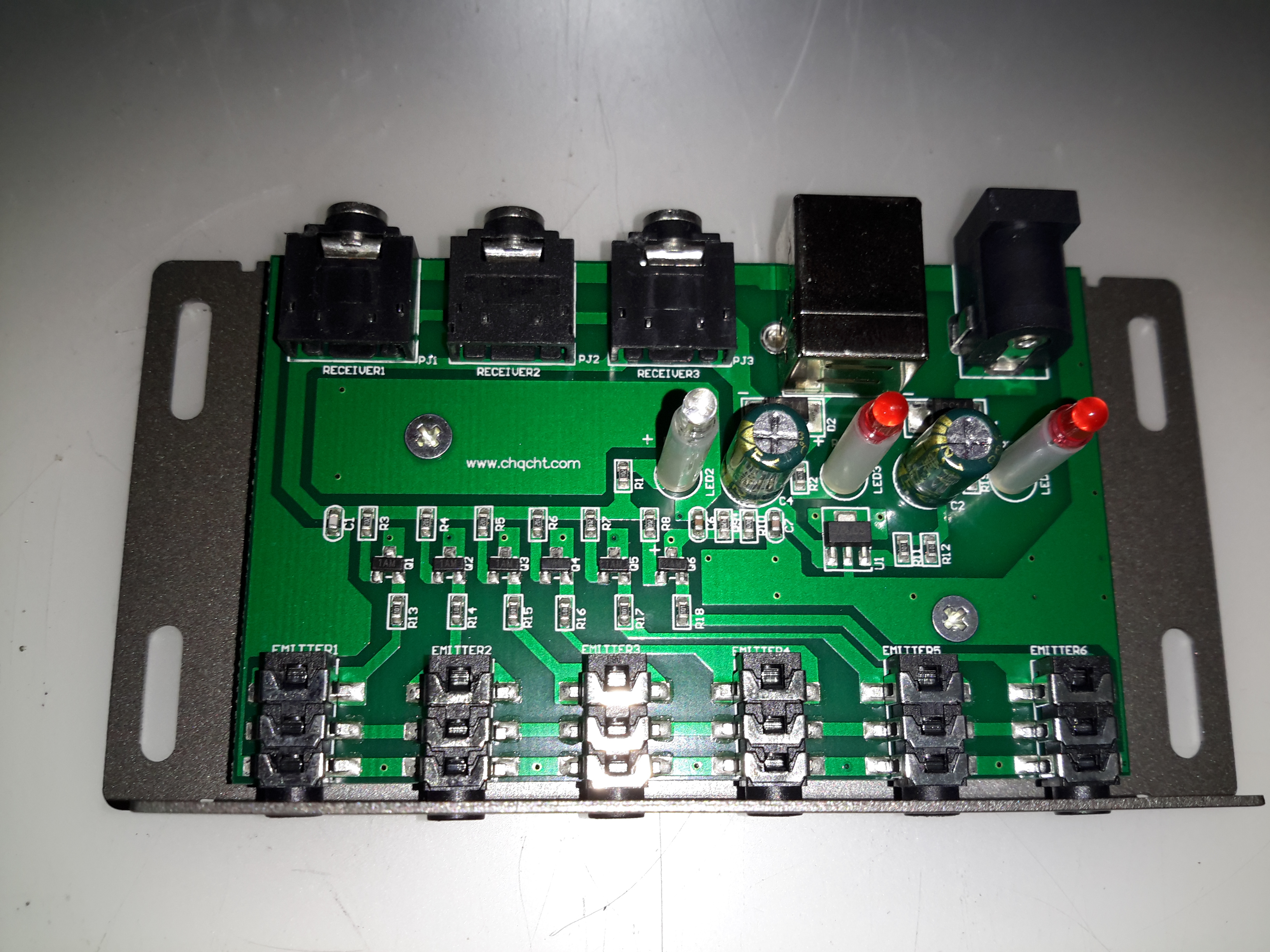
Repeater PCB
Not much inside this one at all, there are 6 transistors which each drive an LED output. This “dumb” configuration keeps things very simple, no signal processing has to be done. Power is either provided by a 12v input, which is fed into a 7805 linear regulator, or direct from USB.
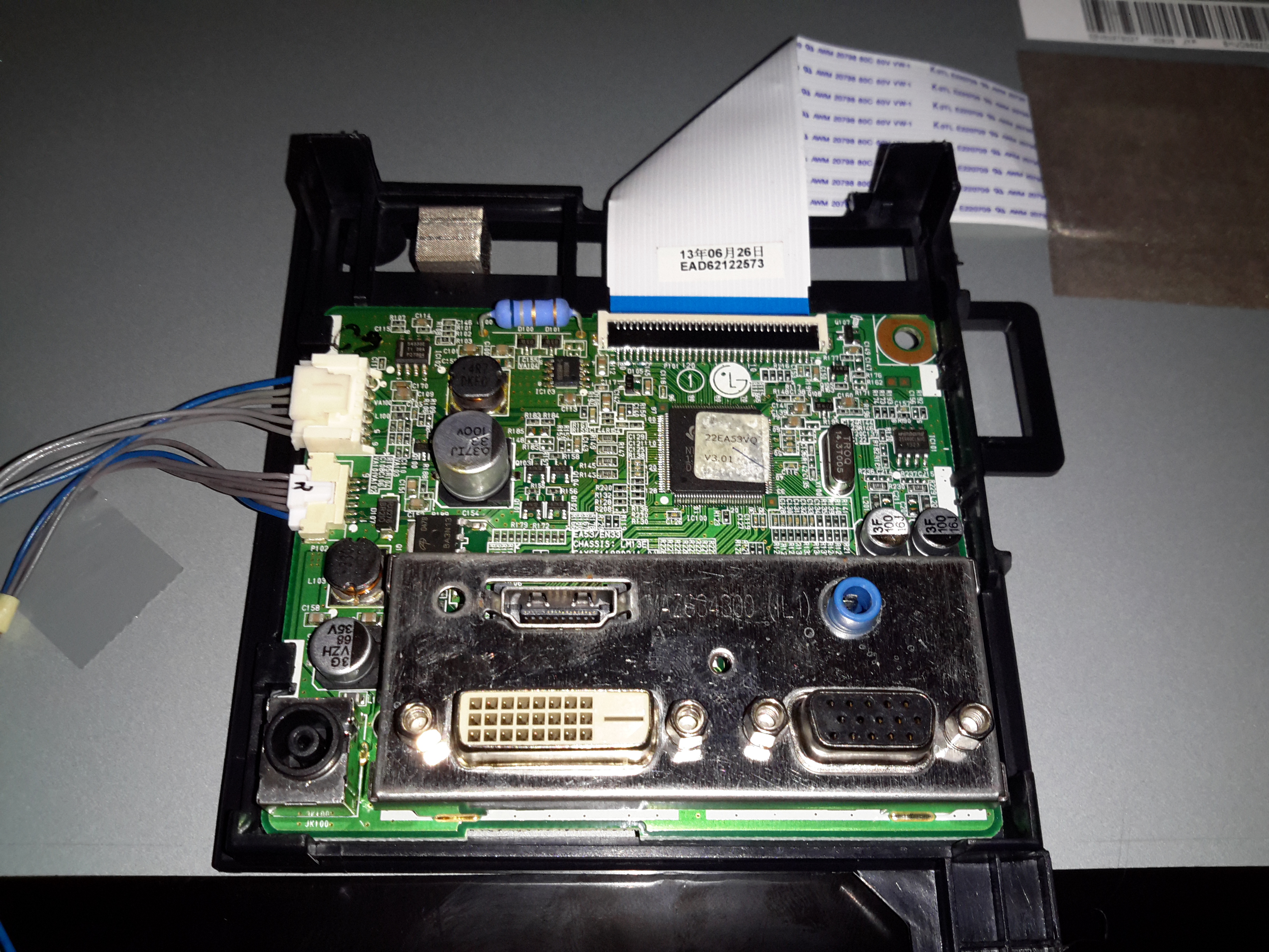
I was recently given a pretty nice LED backlit 1080p LG monitor, with the instruction that it wouldn’t power on correctly. The monitor would power on as far as the standby light, but when fully powered on, would flash the backlight momentarily then shut down. A power supply issue was immediately suspected.
LCD Logic Board
I popped the covers off the monitor itself first, thinking that it was an electrolytic gone bad in the backlight DC-DC converter. Not to mention the fact that cracking into a wall-wart type of PSU is only occasionally possible without the use of anger & large hammers. (Cracking the glue with the handle of a screwdriver doesn’t work so well when the factory went a bit nuts with the glue/ultrasonic welder). As can be seen in the photo, there’s not much inside these monitors, the logic is a single-chip solution, the rest of the PCB is dedicated to supplying the power rails for the various circuits. On the left is the power input & the DC-DC converter for the backlight, along with the DC-DC converter supplying the logic circuits. None of the capacitors here are damaged, everything looks good.
I then measured the output of the PSU, which under no load was the correct 19v DC. However applying any load caused the output voltage to drop like a proverbial brick. Applying a full load of 1.3A saw the output voltage drop so severely that the PSU tripped on it’s UVLO.
200mA Load
At 200mA of load the factory PSU is already dropping to 18v, with a 5.3kHz switching frequency appearing.
500mA Load
At higher load the frequency increases to 11.5kHz & the output voltage has dropped to 11.86v!
750mA Load
750mA was as high as I could make the supply go without it tripping itself out – the UVLO circuit trips at 9v. 12.6kHz is now riding on the severely low DC at this point.
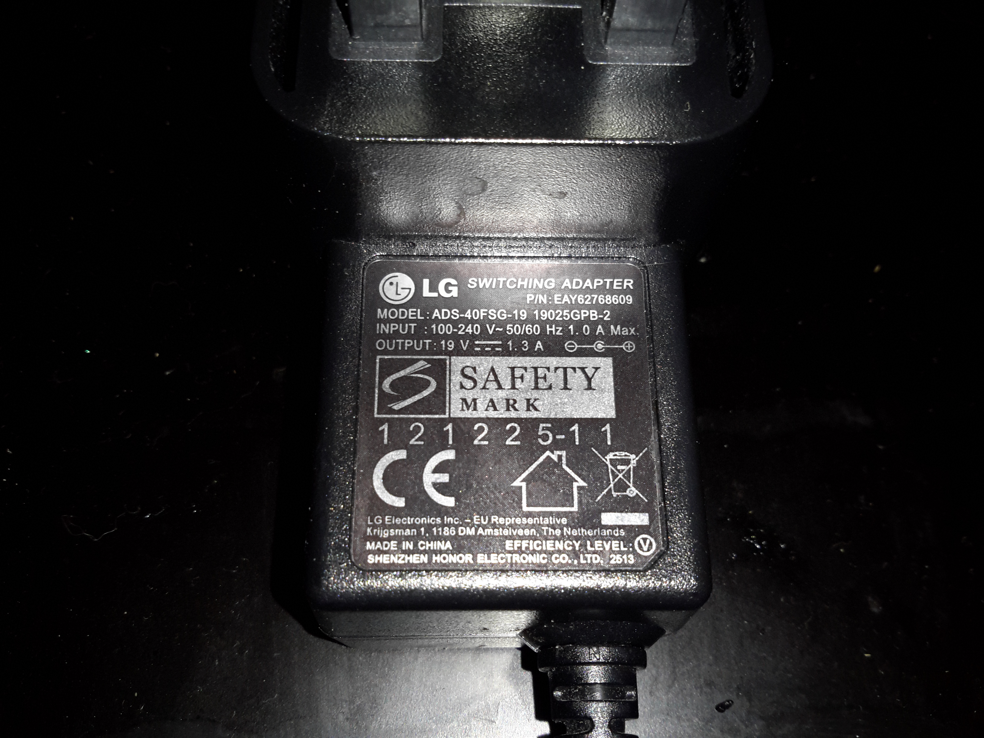
PSU Ratings
The power supply is supposed to be rated at 1.3A at 19v, however with this fault it’s getting nowhere near that. The LG brand is on this PSU but it’s contracted out to Shenzen Honor Electric Co. Ltd.
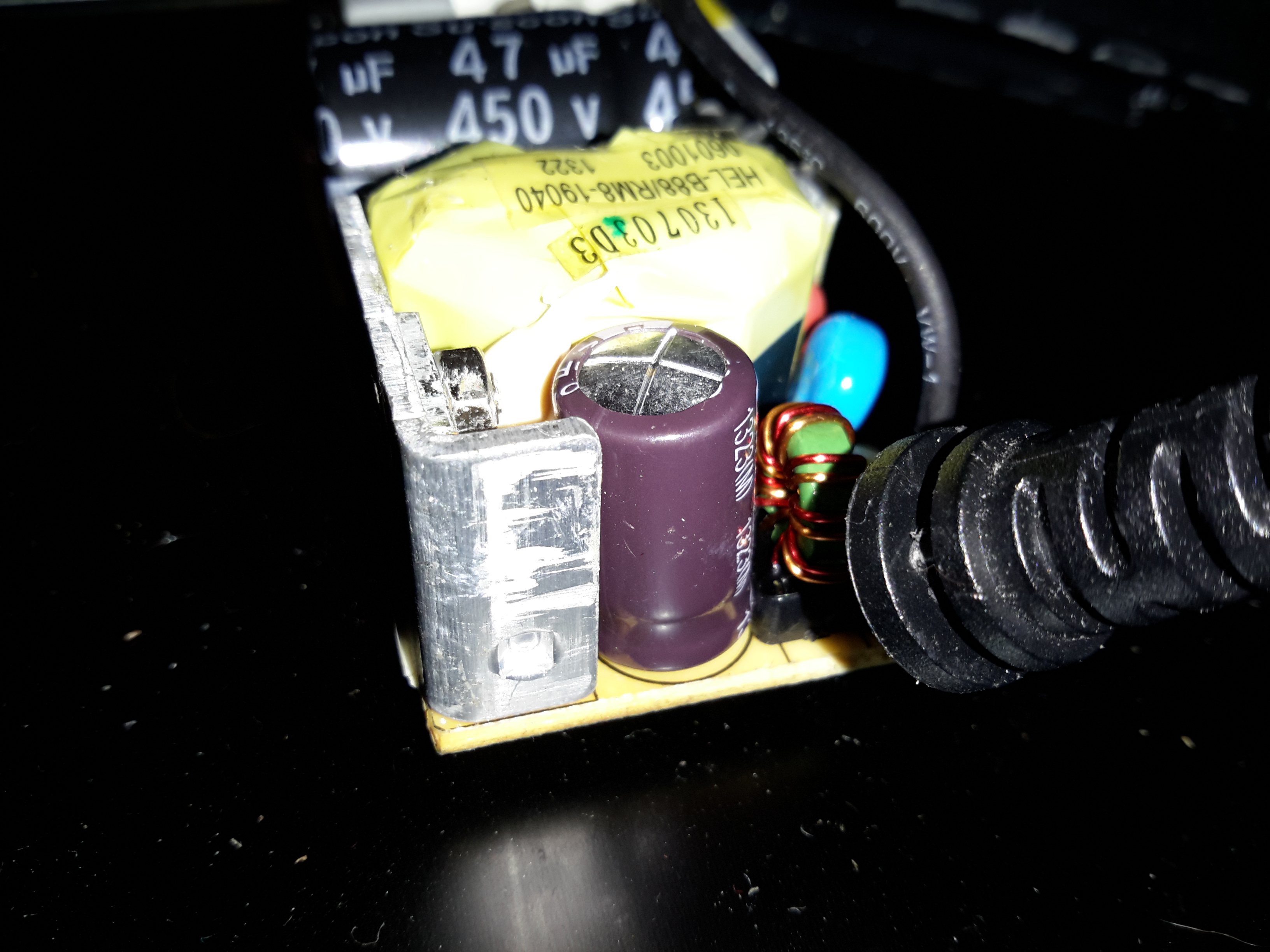
Output Electrolytic
Here’s the problem with this PSU. The output electrolytic has ballooned. I don’t have an ESR tester, but this cap has gone way past it’s sell-by date. It’s position right next to the heatsink with the output rectifier diodes has probably cooked it. The PSU isn’t that badly built for a Chinese one – there’s plenty of creepage distance on the PCB & even a couple of isolation slots.
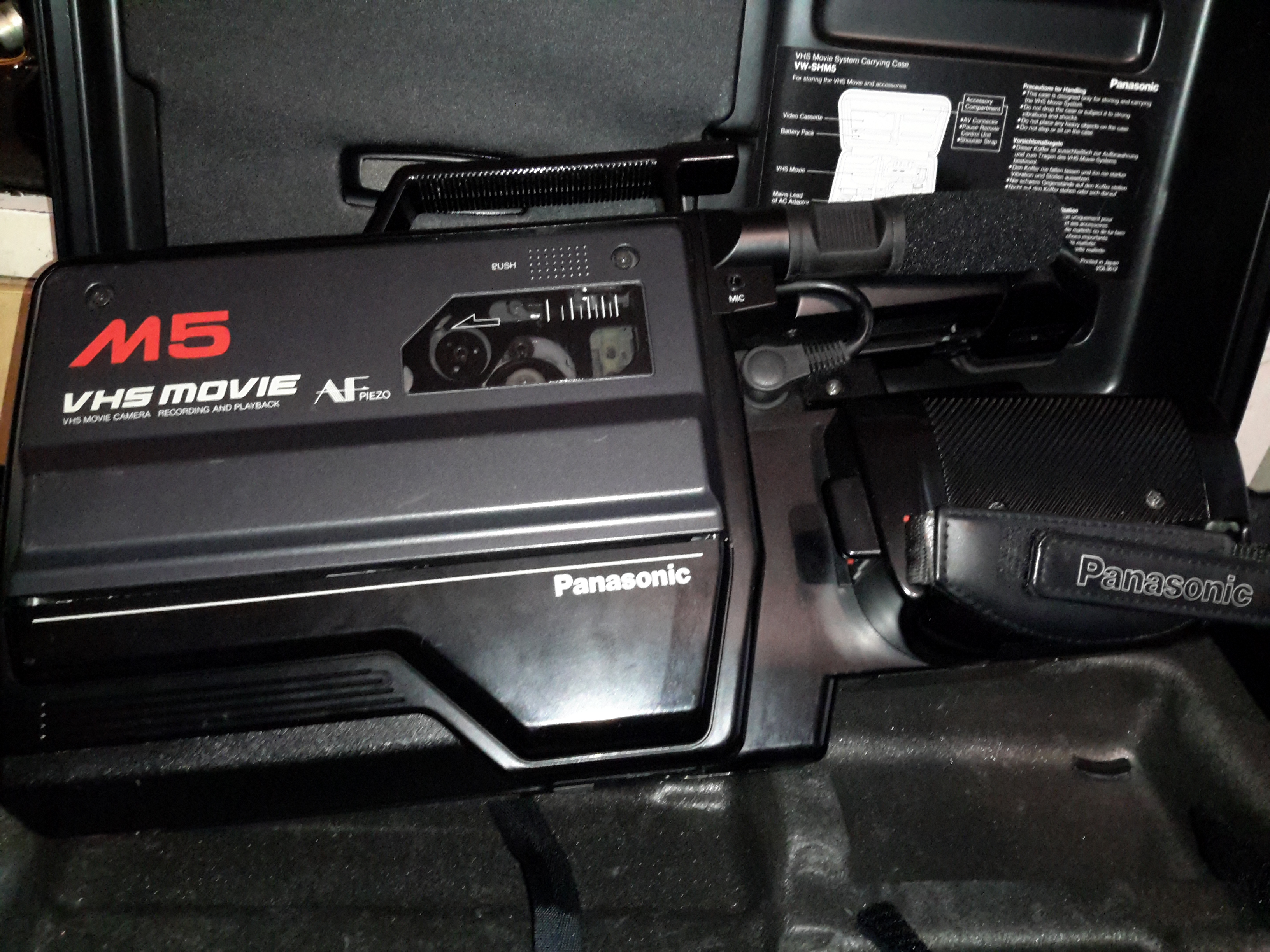
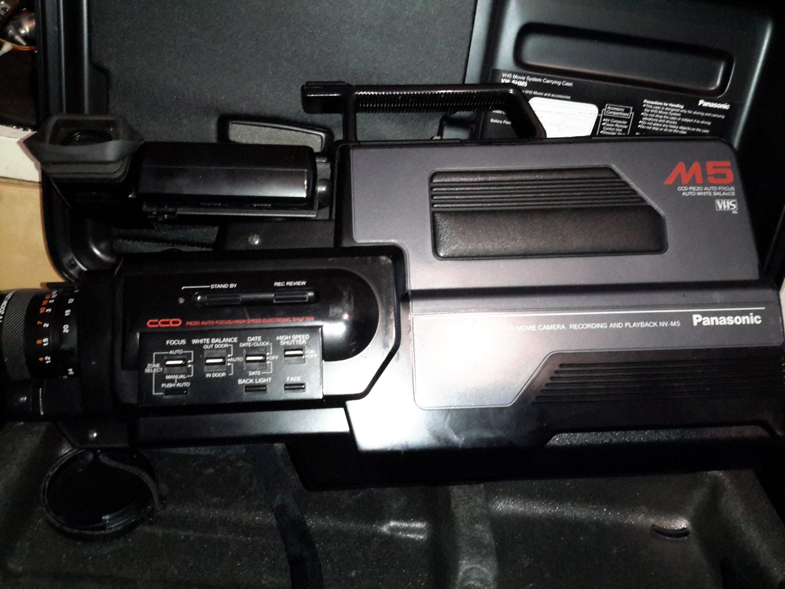
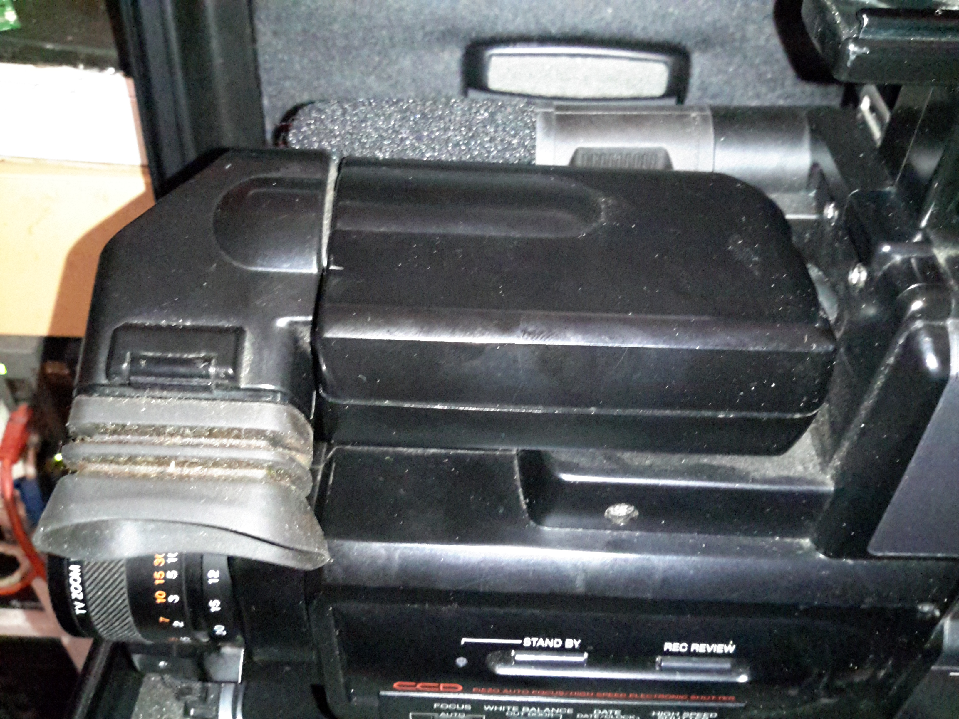
Time foe some more retro tech! This is a 1980’s vintage CCD-based VHS camcorder from Panasonic, the NV-M5. There are a lot of parts to one of these (unlike modern cameras), so I’ll split this post into several sections to make things easier to read (and easier to keep track of what I’m talking about :)).
Left Side
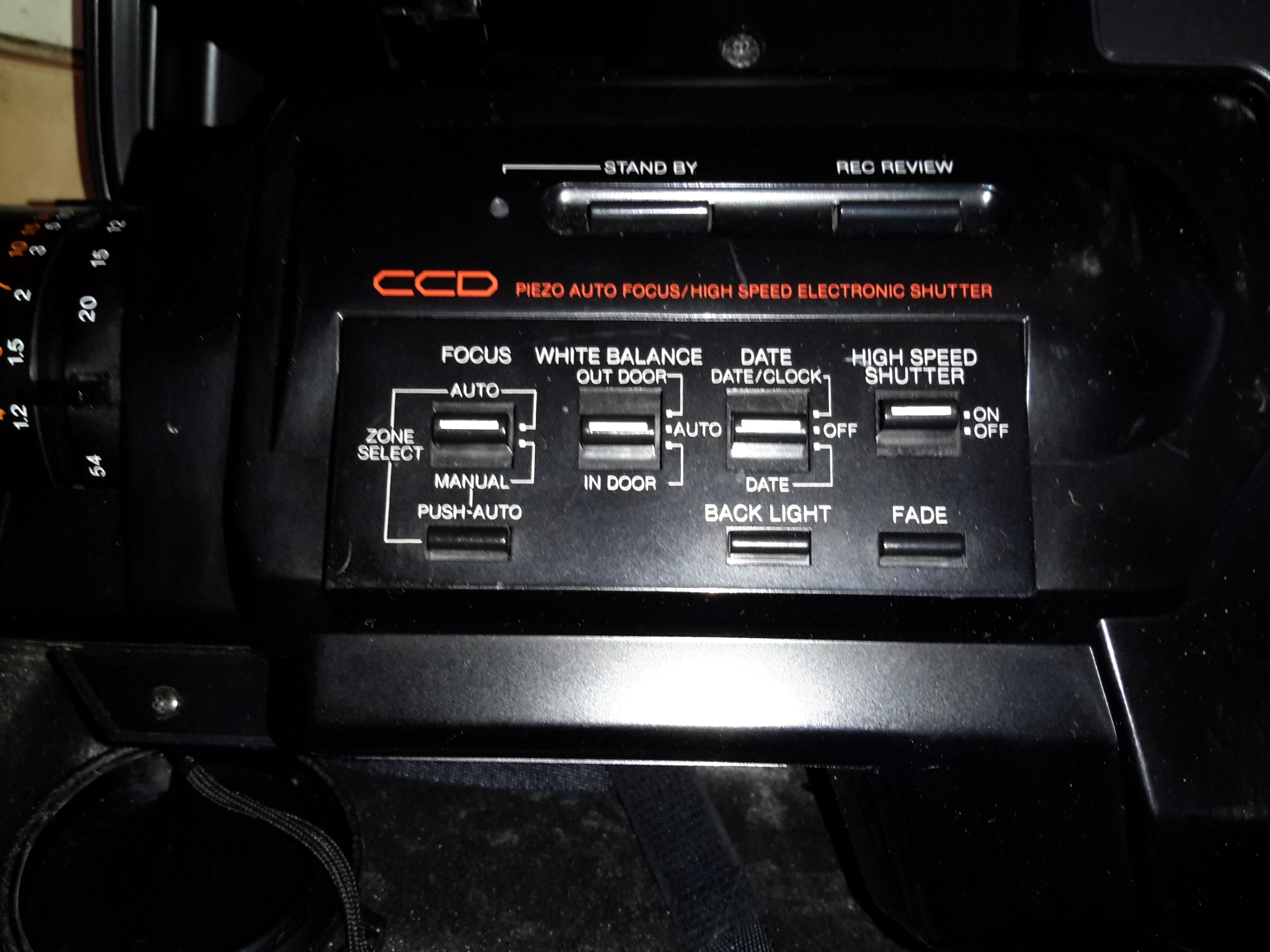
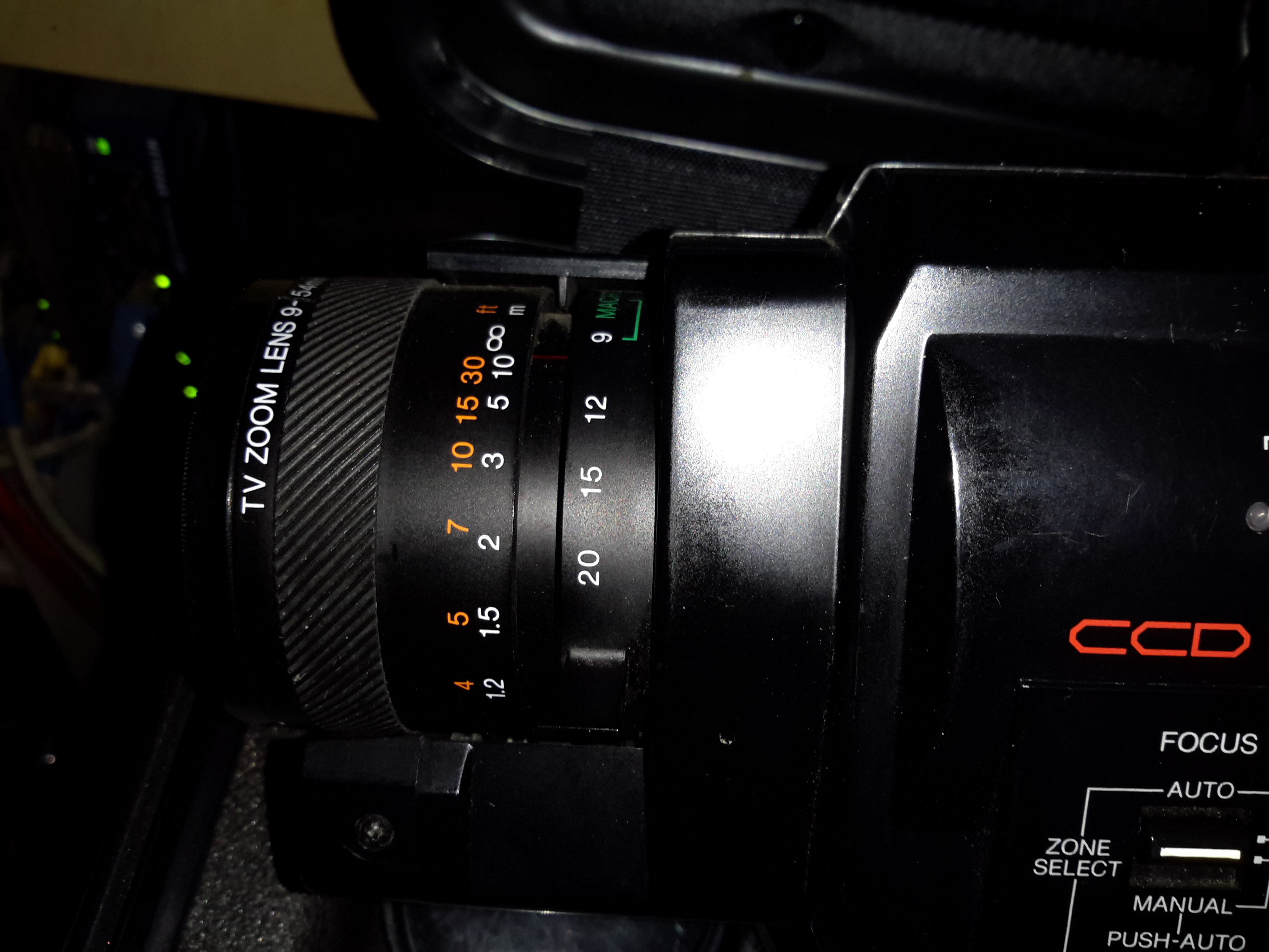
The left side of the camera holds the autofocus, white balance, shutter speed & date controls.
Left Side ControlsLens Adjustments
The lens is fully adjustable, with either manual or motorized automatic control.
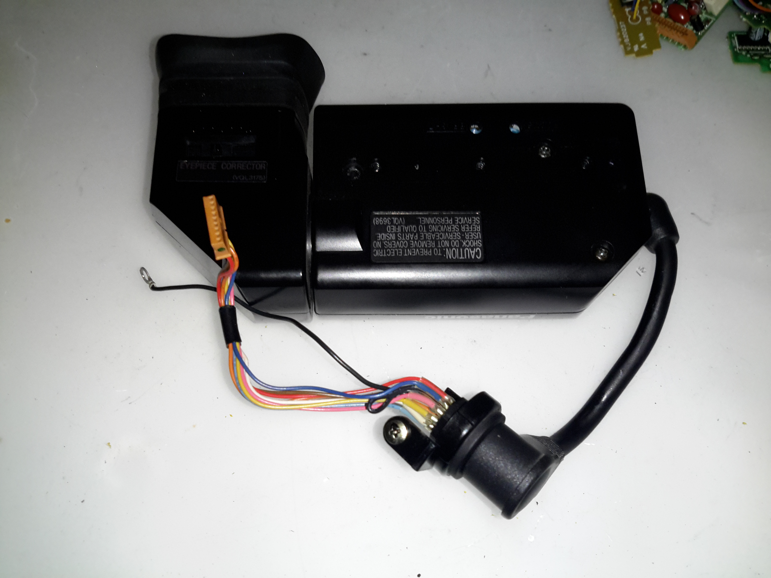
Rear Panel
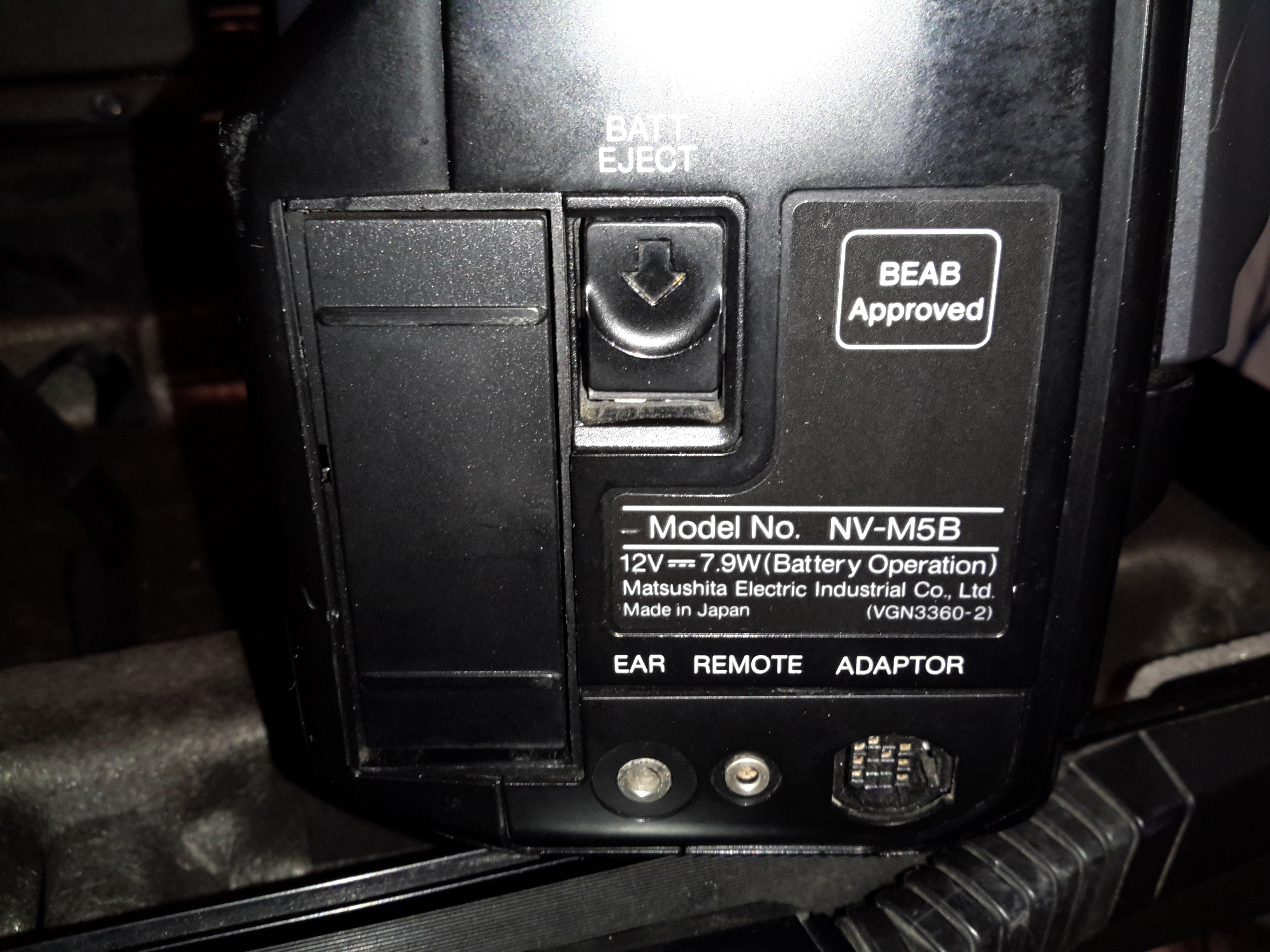
The back panel has the battery slot, a very strange looking DC input connector, remote control connector & the earphone jack.
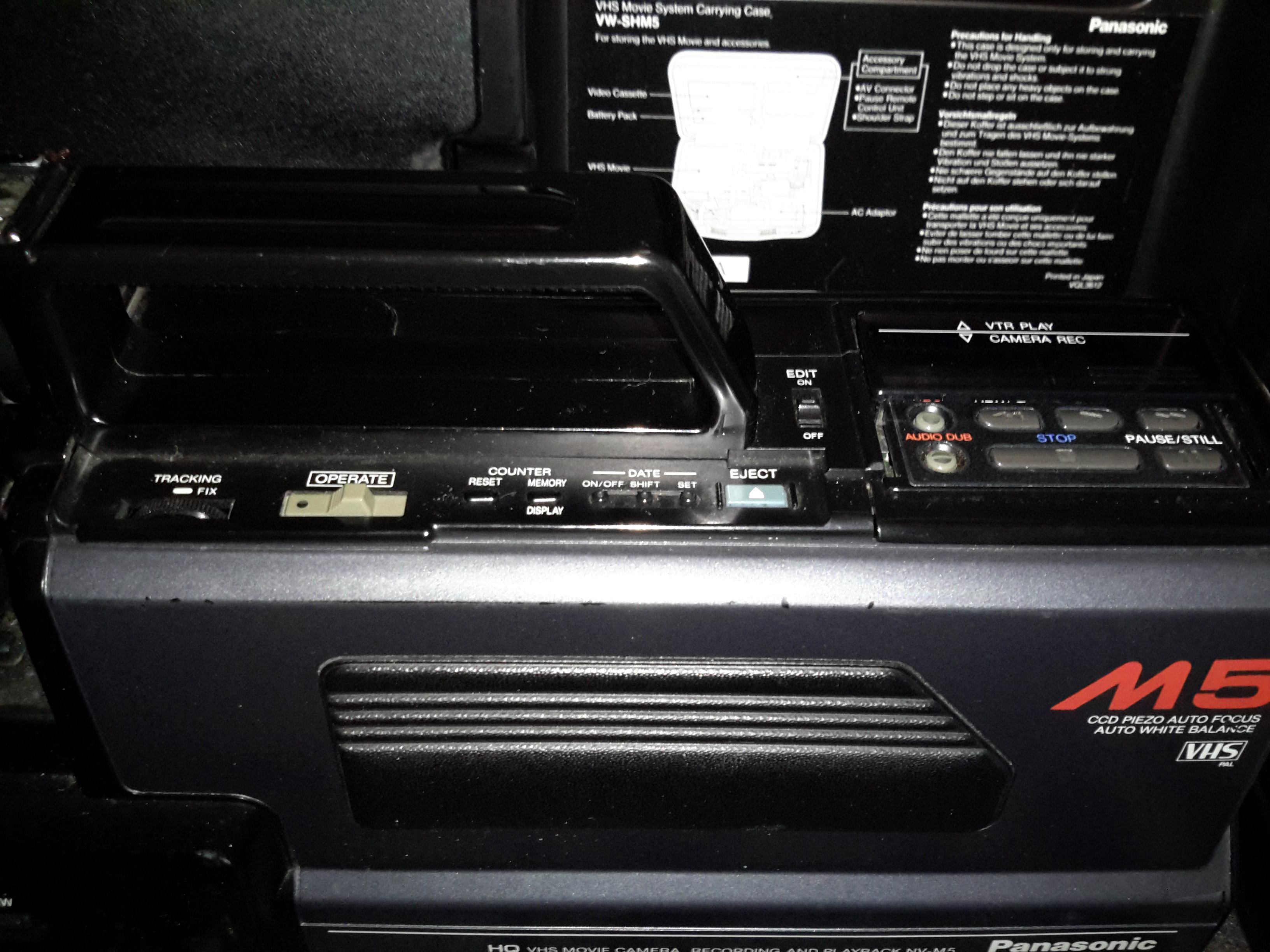
Top Controls
The top panel of the camera holds the main power controls, manual tape tracking & the tape transport control panel.
Viewfinder
The viewfinder is mounted on a swivel mount. There’s a CRT based composite monitor in here. Hack ahoy!
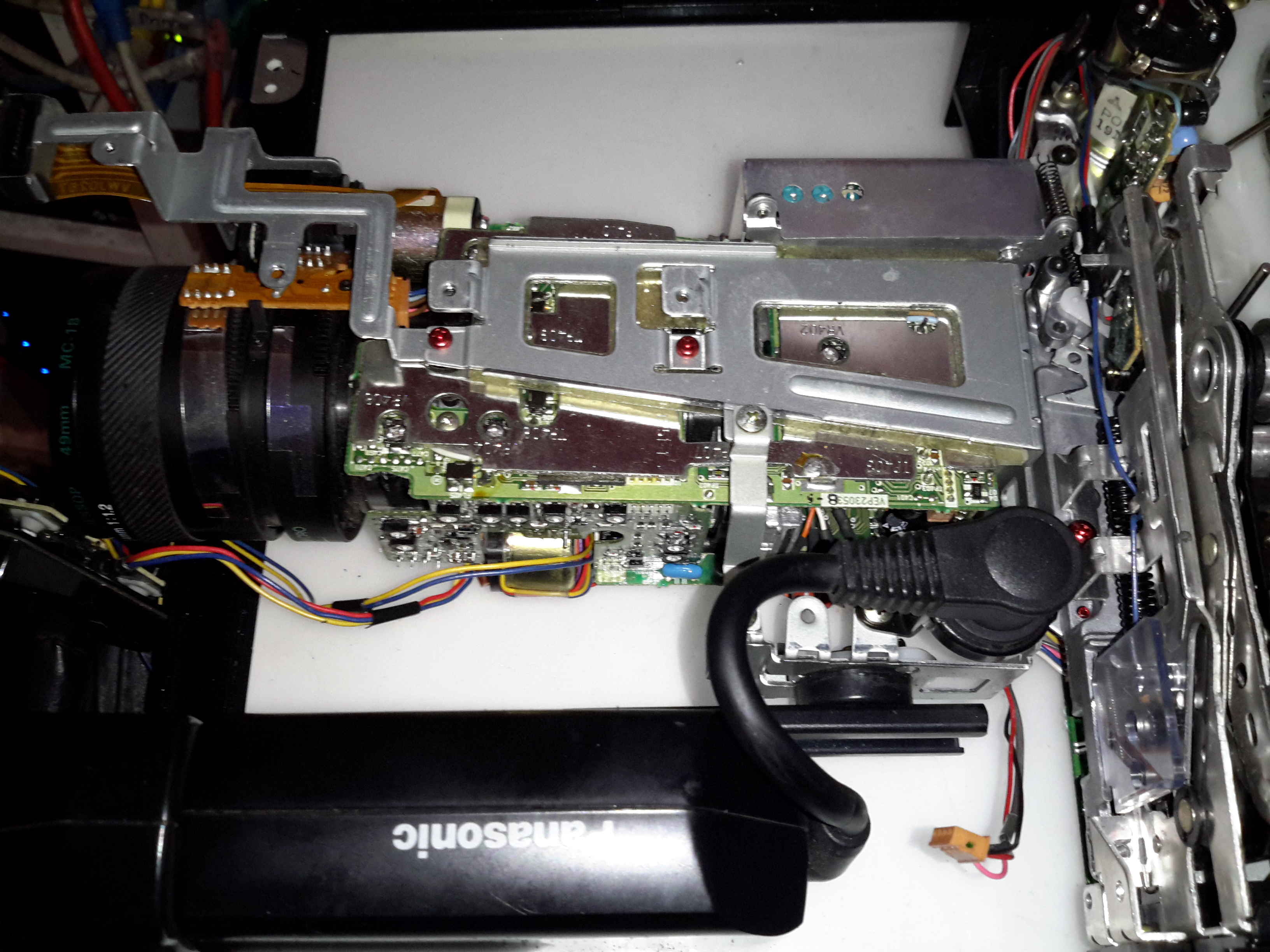
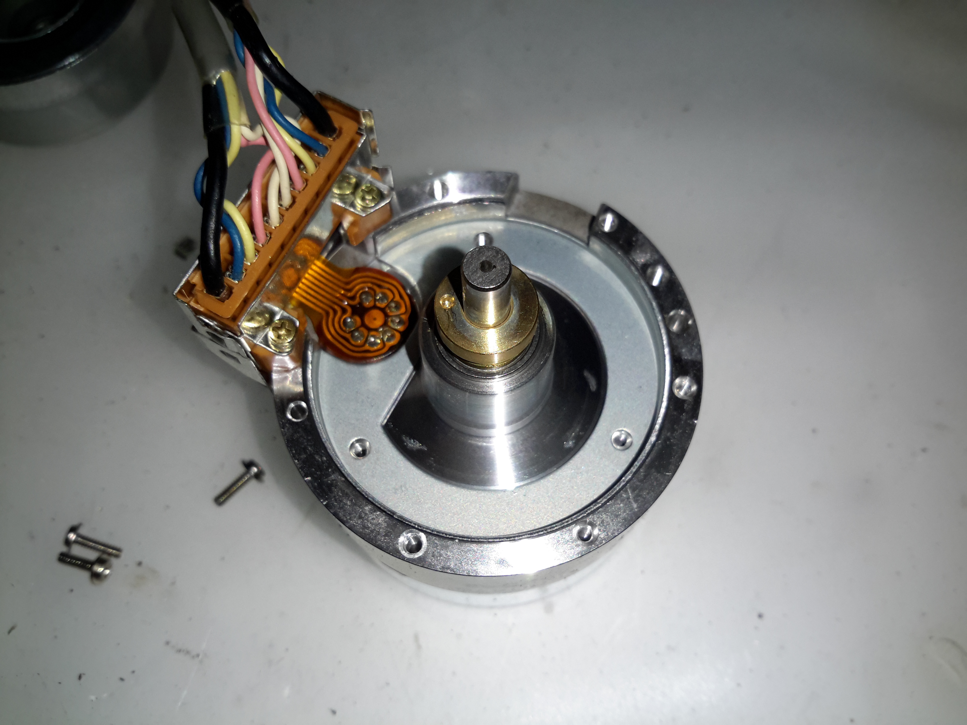
Camera Section
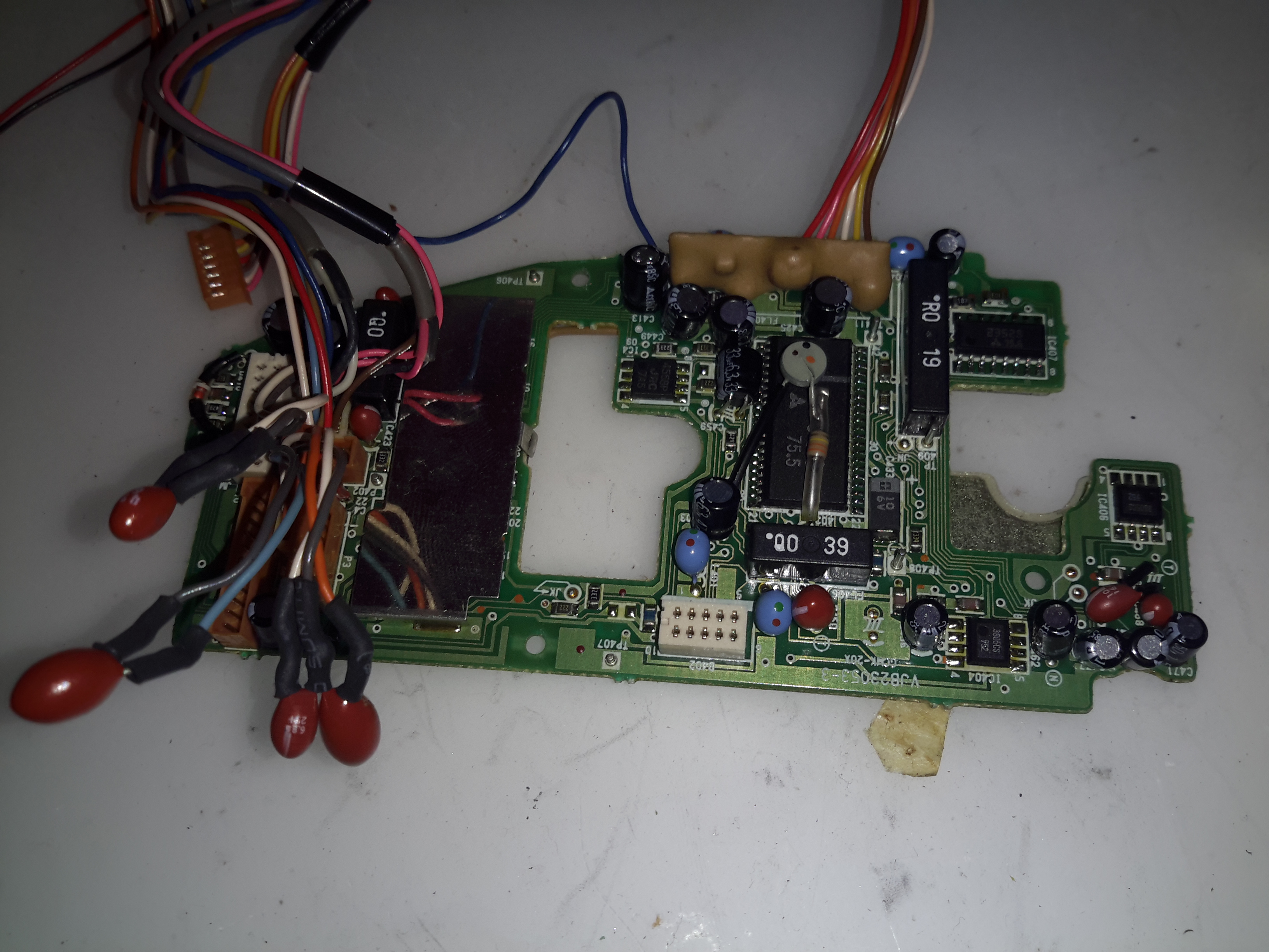
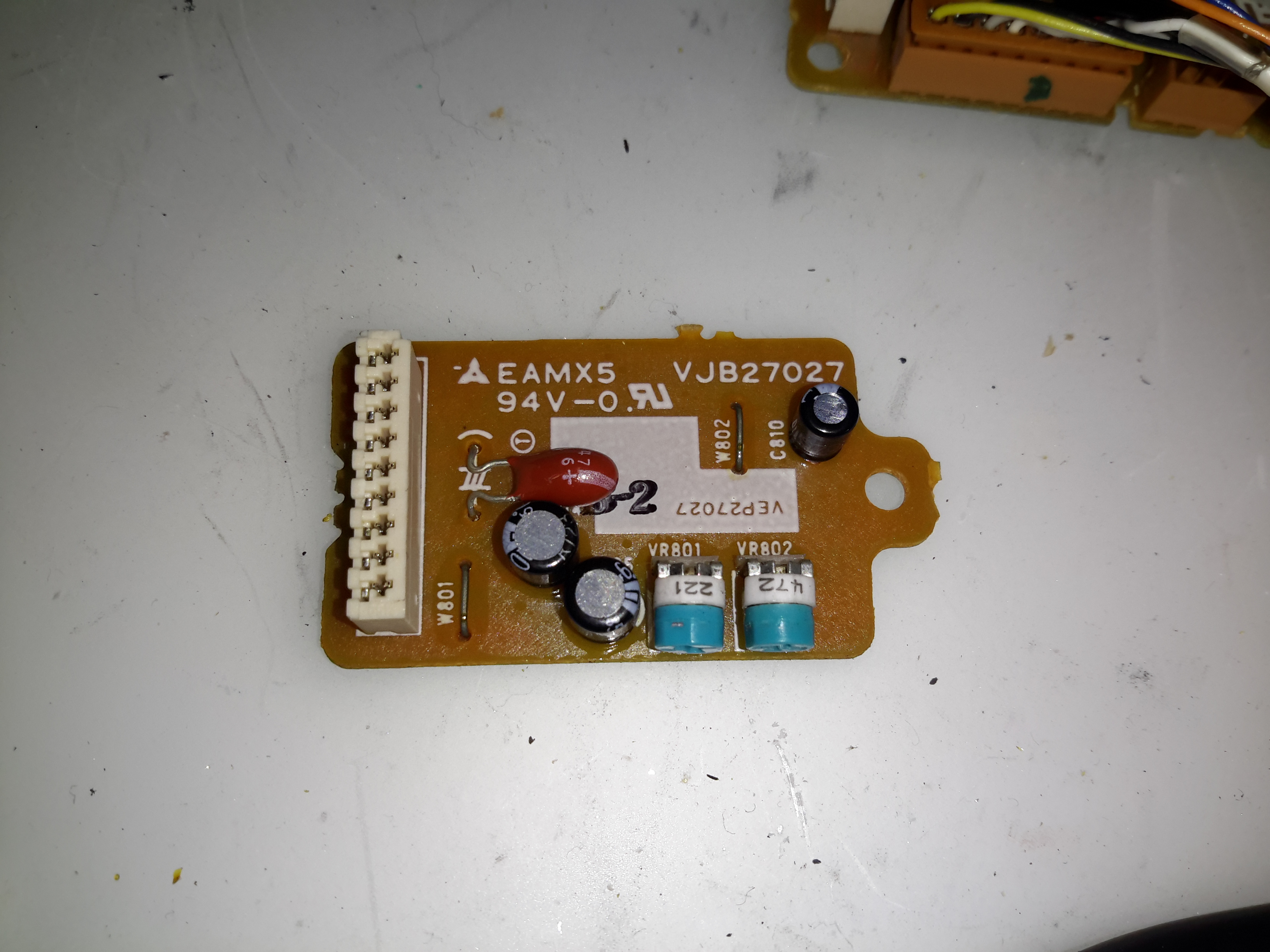
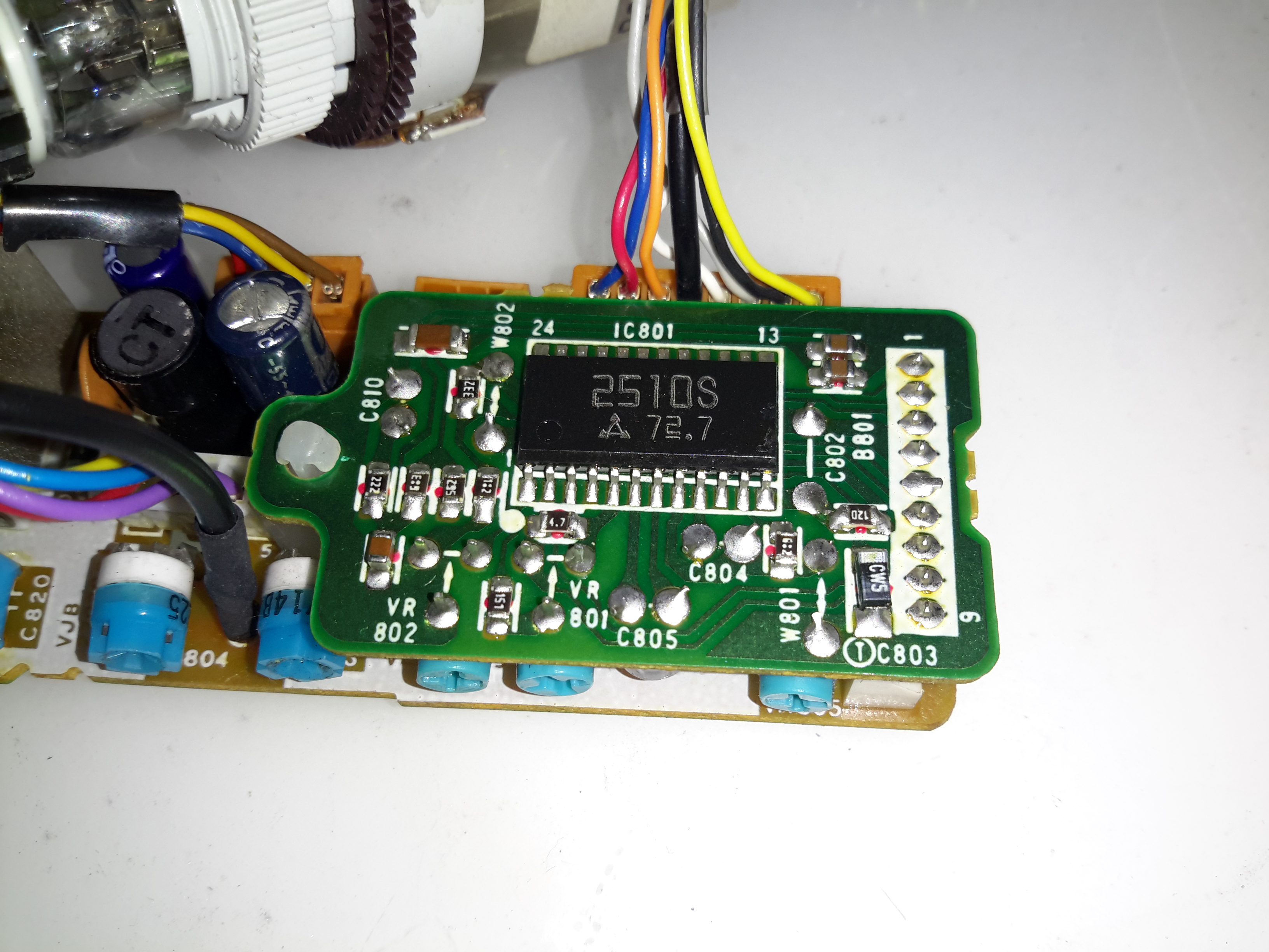
Process Board Assembly
Here’s the camera section of the camcorder, and is totally packed with electronics! There’s at least half a dozen separate boards in here, all fitted together around the optics tube assembly.
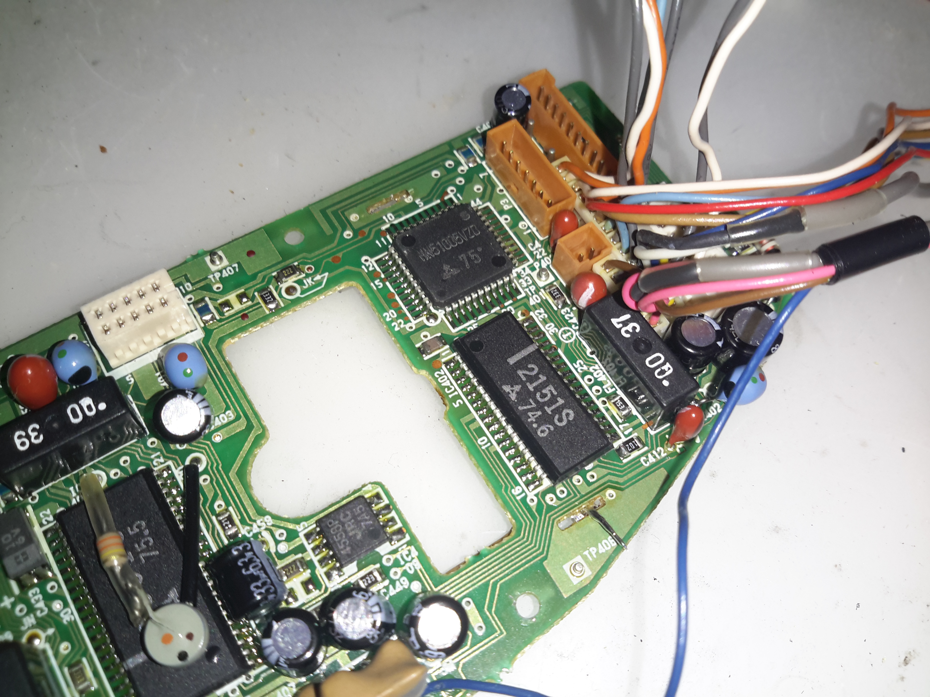
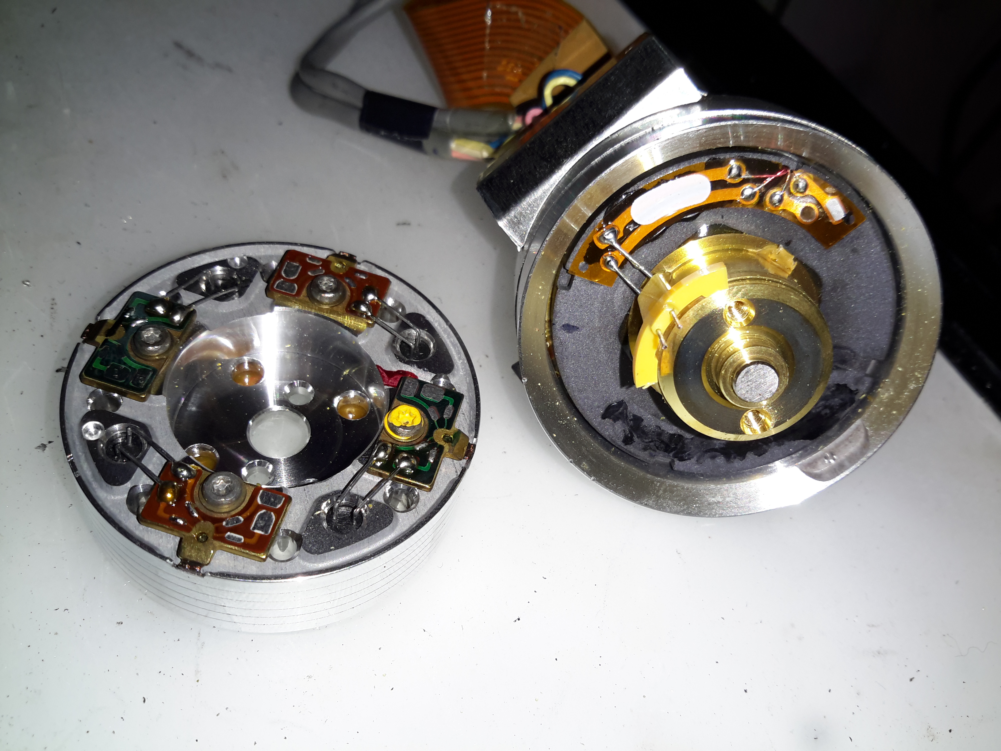
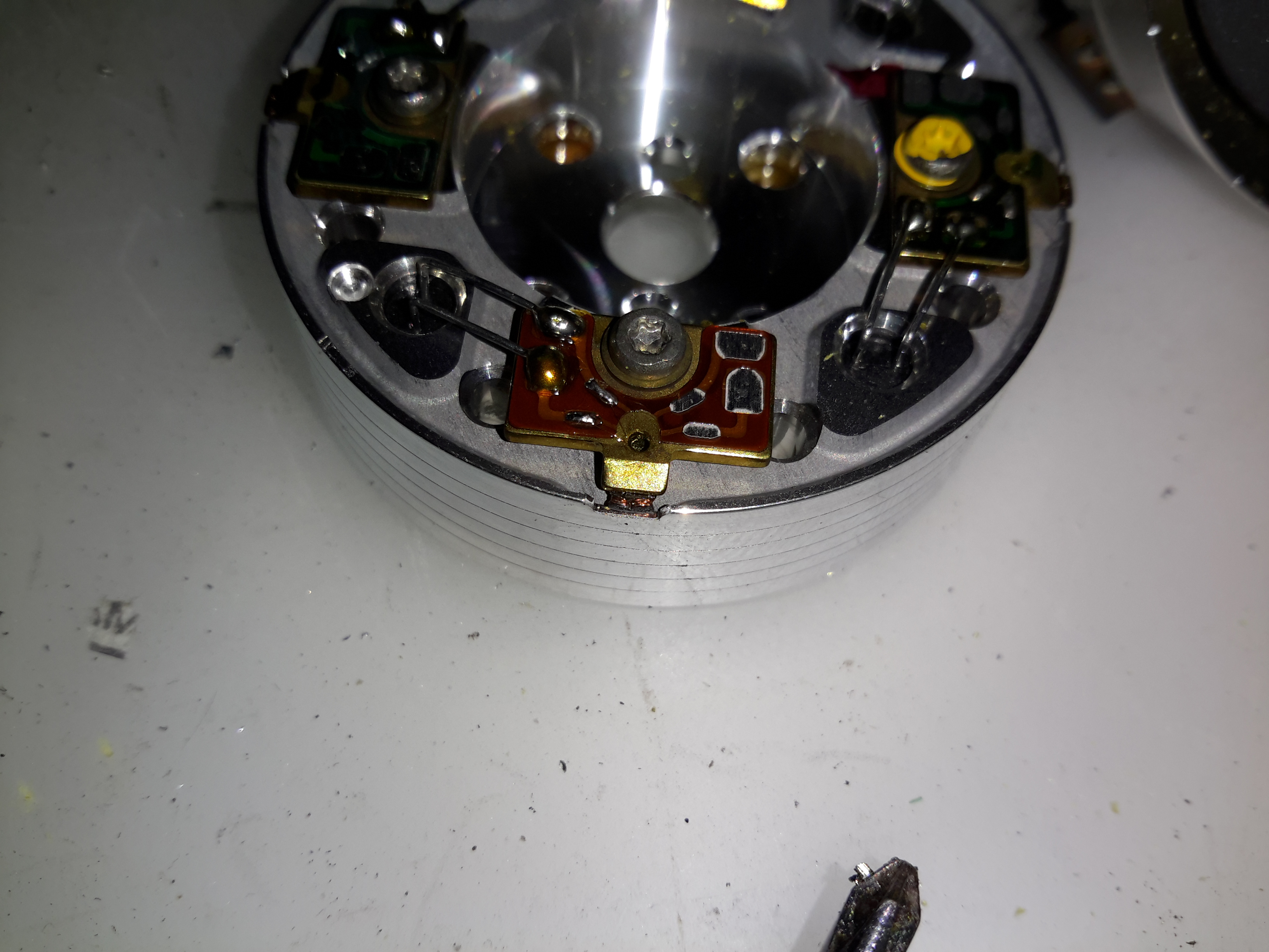
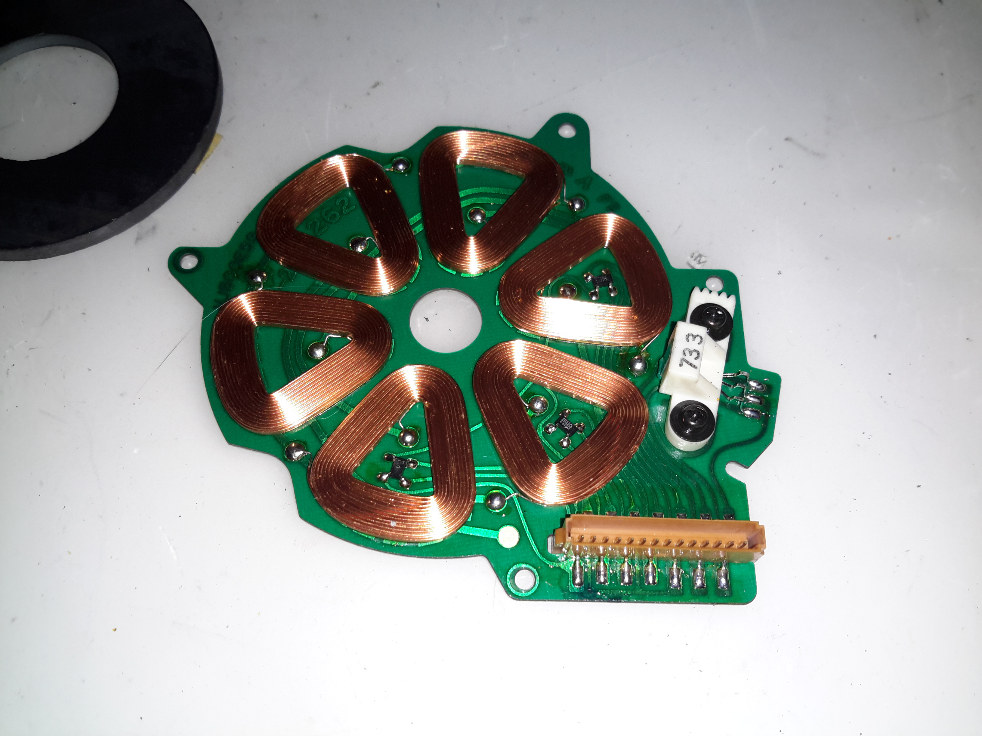
AWB PCB
On the top of the assembly is the Automatic White Balance PCB. Many adjustments here to get everything set right. Not much on the other side of this board other than a bunch of Op-Amps. The iris stepper motor is fitted in a milled opening in the PCB, this connects to one of the other PCBs in the camera module.
AWB Sensor
Here’s the AWB sensor, mounted next to the lens. I’m not all to certain how this works, but the service manual has the pinout, and there are outputs for all the colour channels, RGB. So it’s probably a trio of photodiodes with filters.
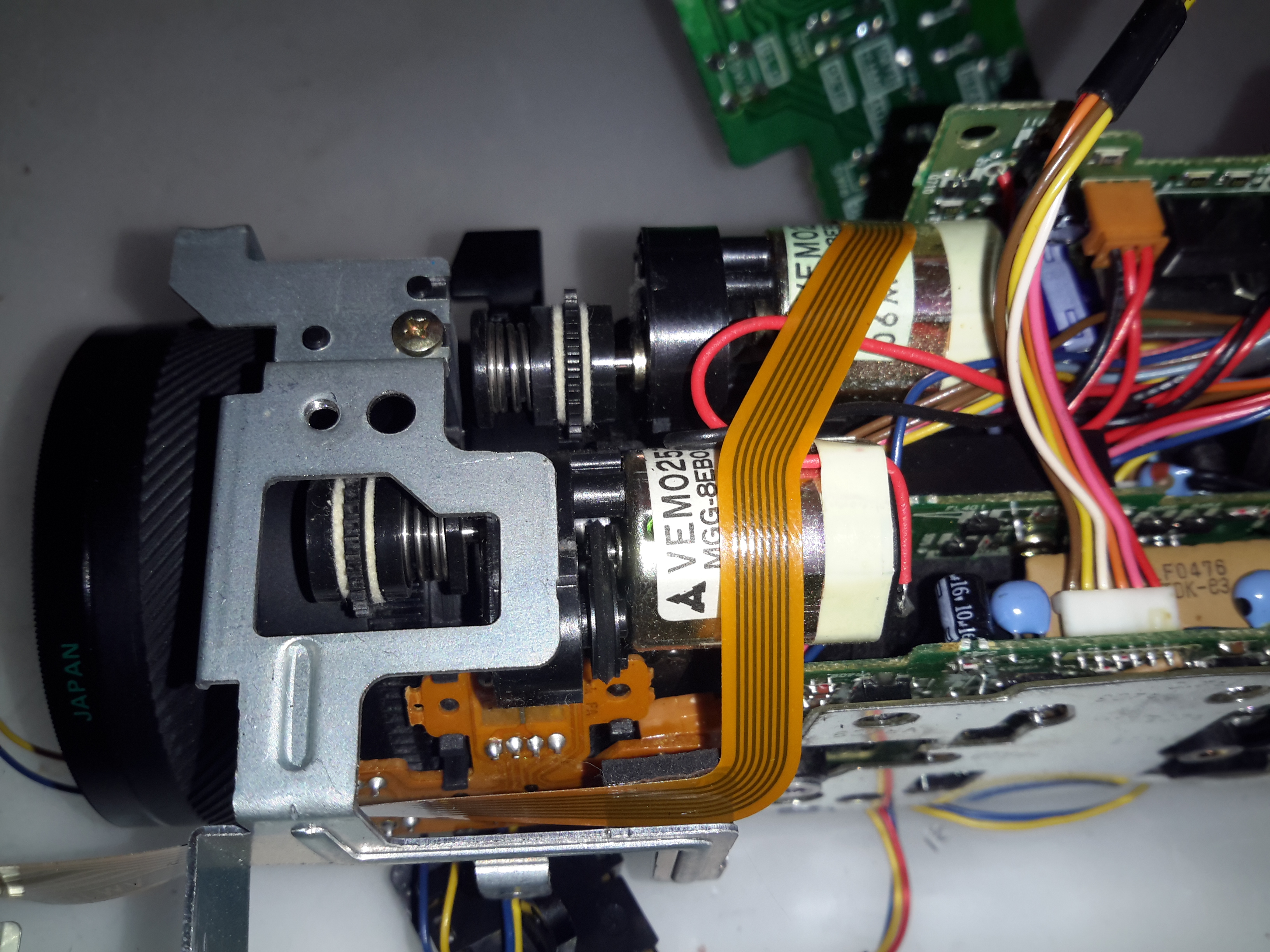
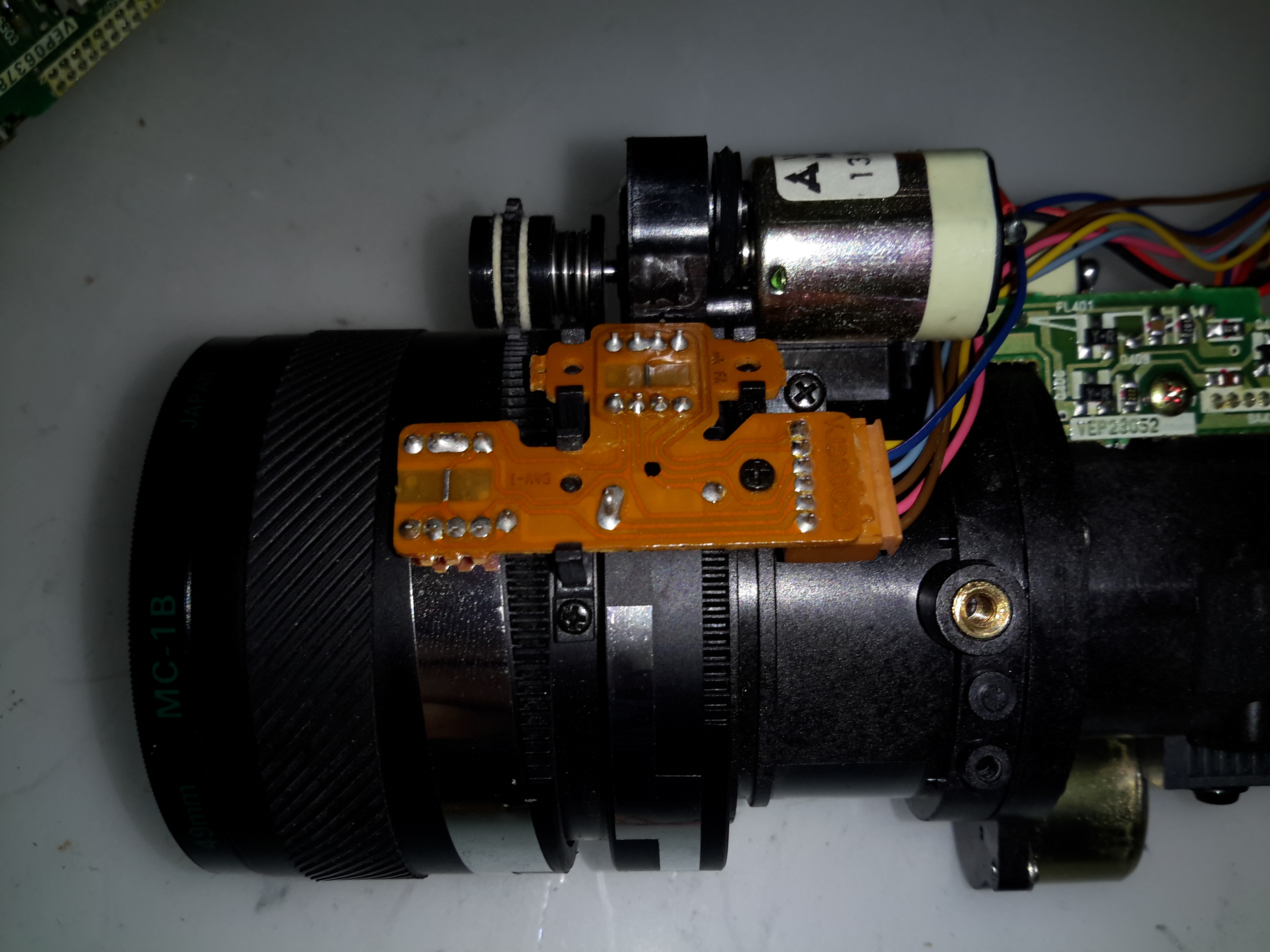
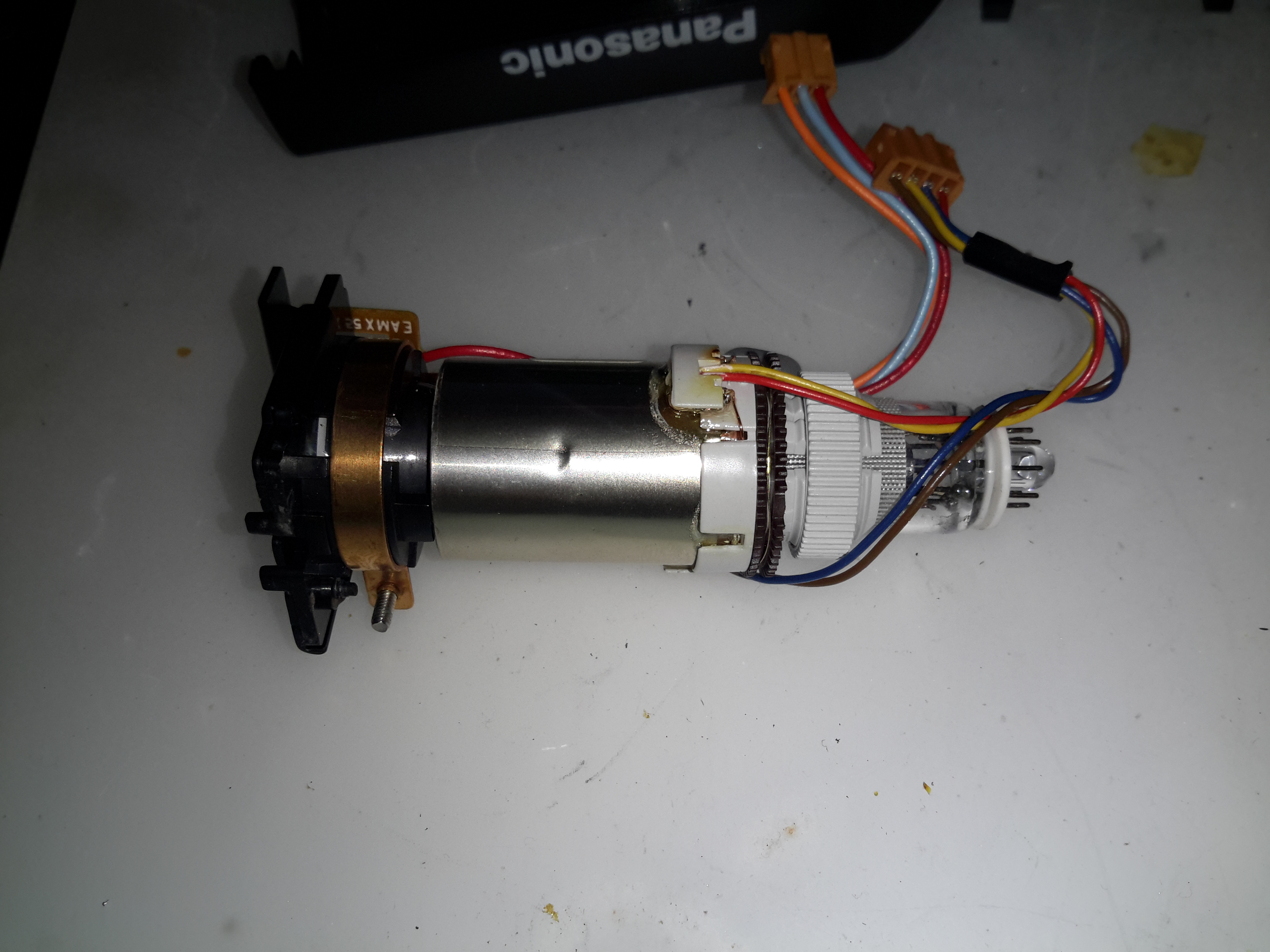
Focus & Zoom Motors
Focus & Zoom are controlled with a pair of DC gear motors. The manual operation is feasible through the use of slip clutches in the final drive pinion onto the lens barrel.
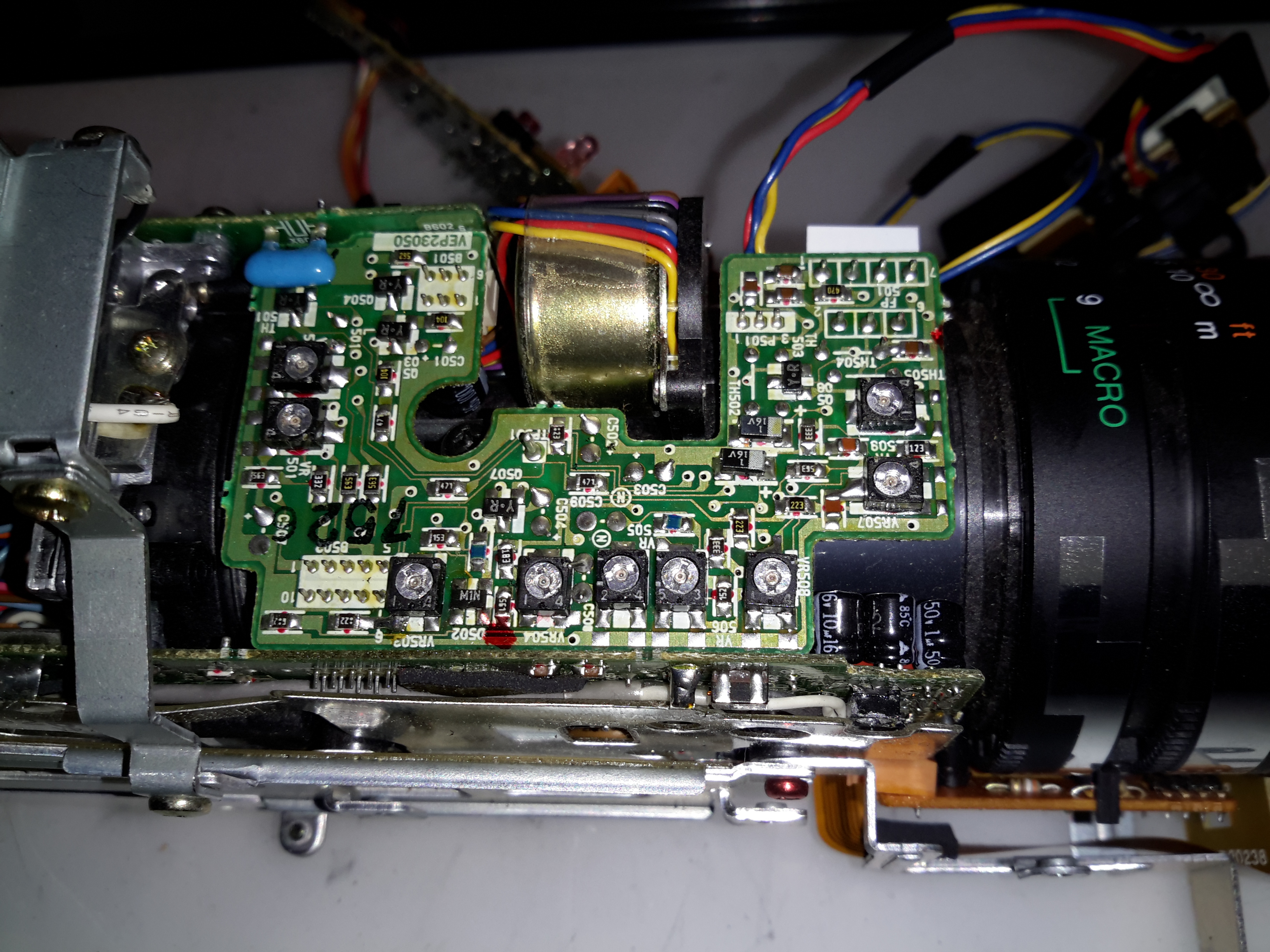
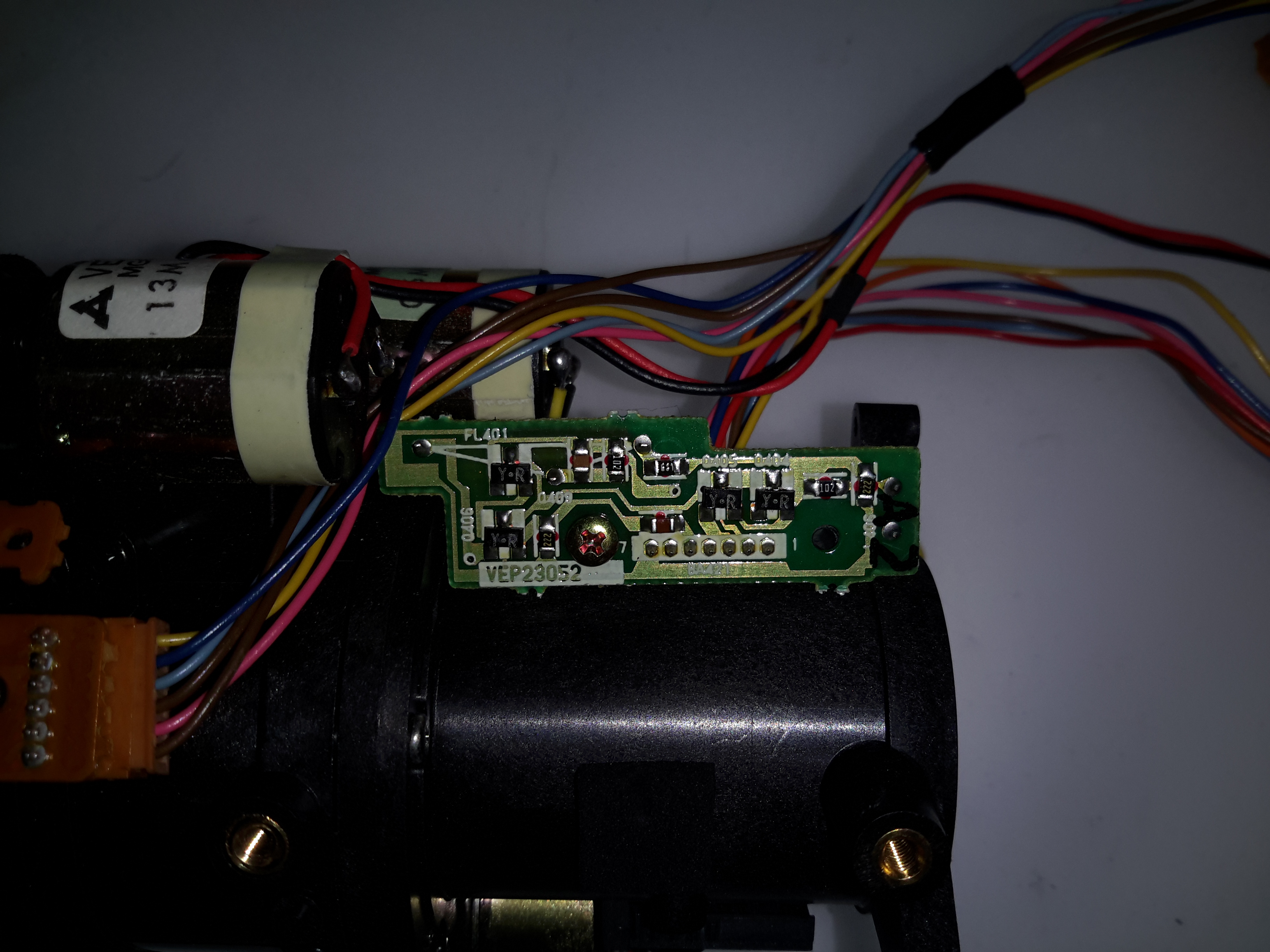
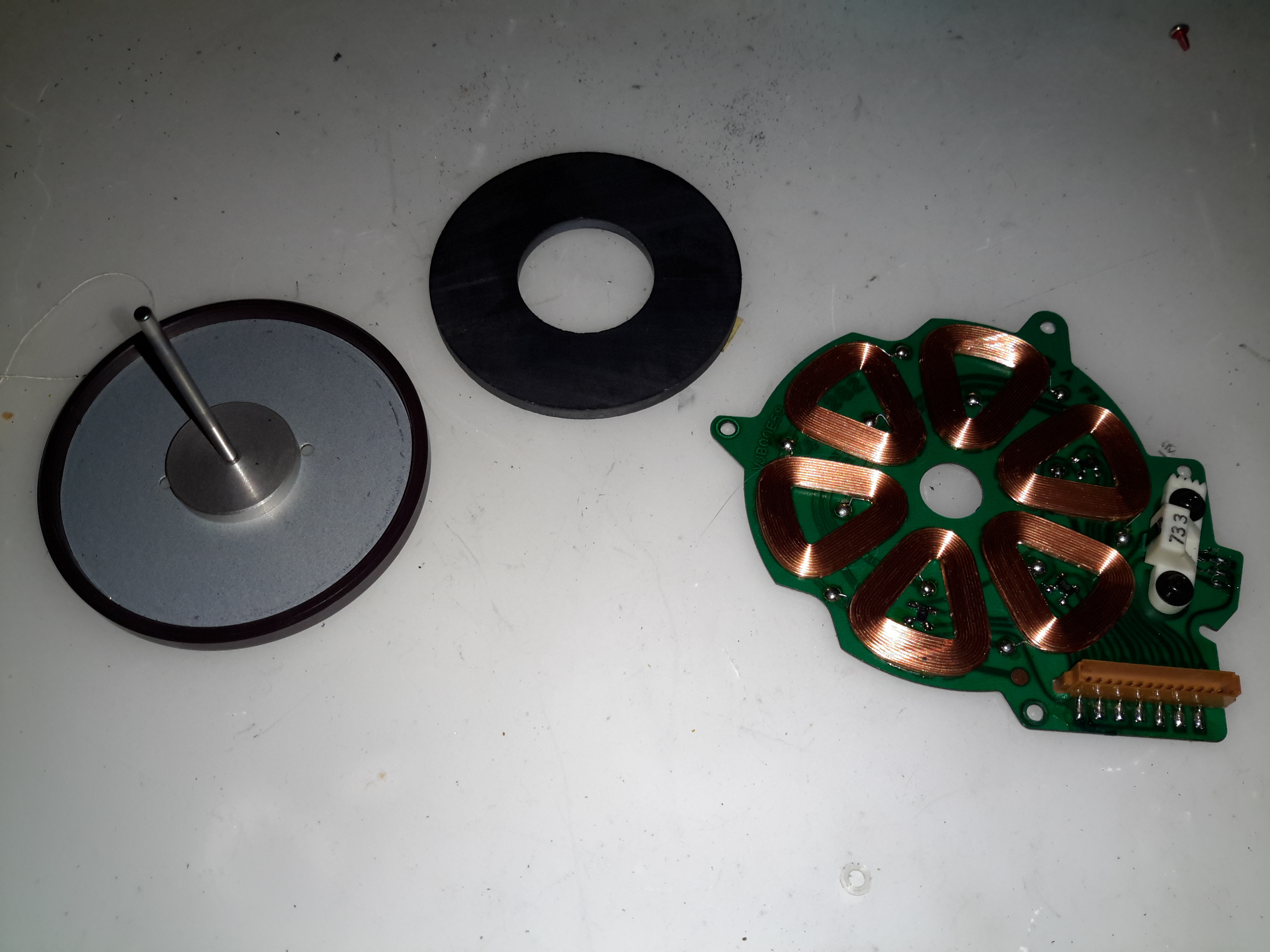
Process Board
The main camera section process board is above. This board does all the signal processing for the CCD, has the bias voltage supplies and houses the control sections for the motorized parts of the optics assembly. There are quite a few dipped Tantalum capacitors on pigtails, instead of being directly board mounted. This was probably done due to space requirements on the PCB itself.
Under the steel shield on this board is some of the main signal processing for the CCD.
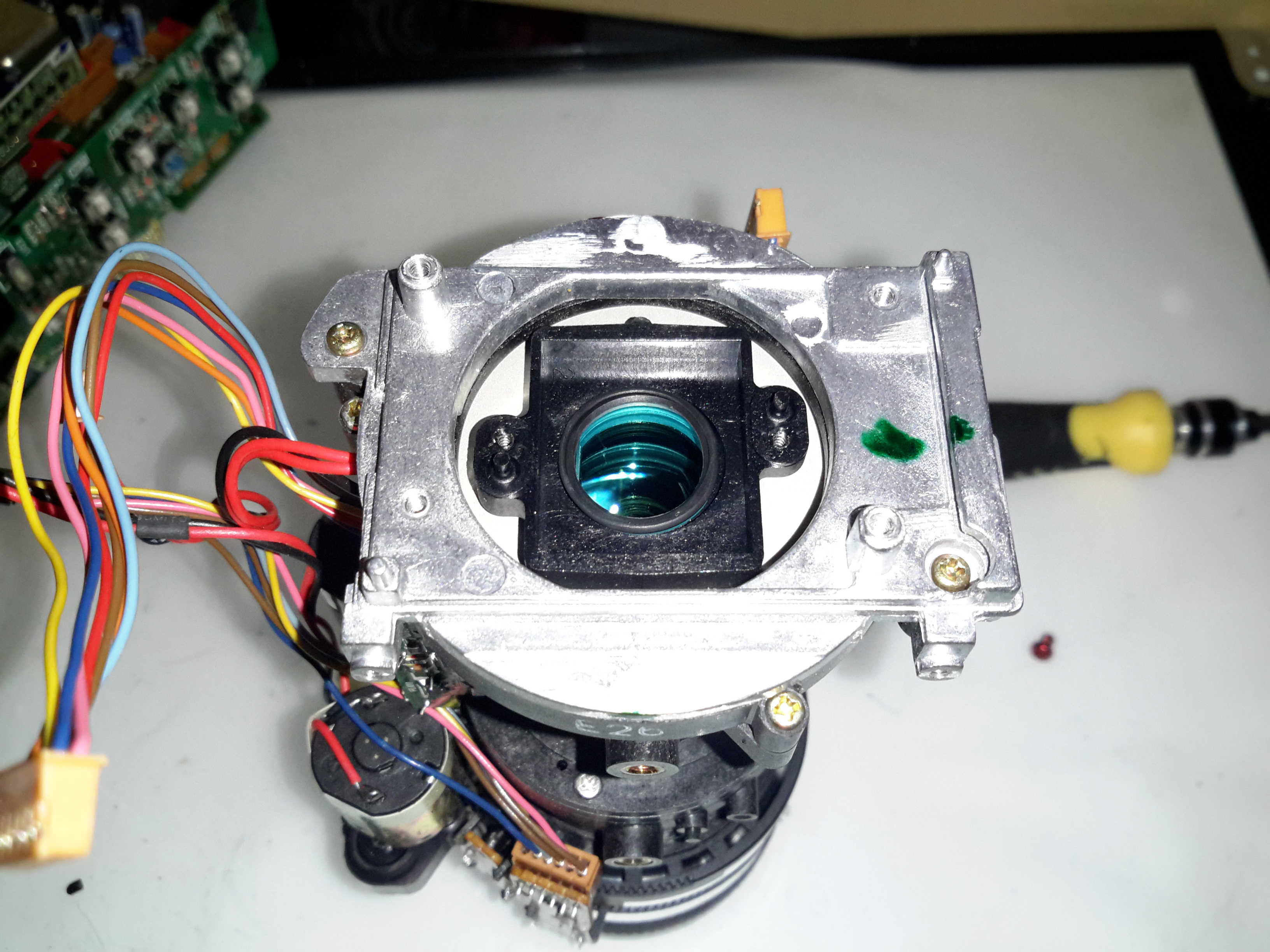
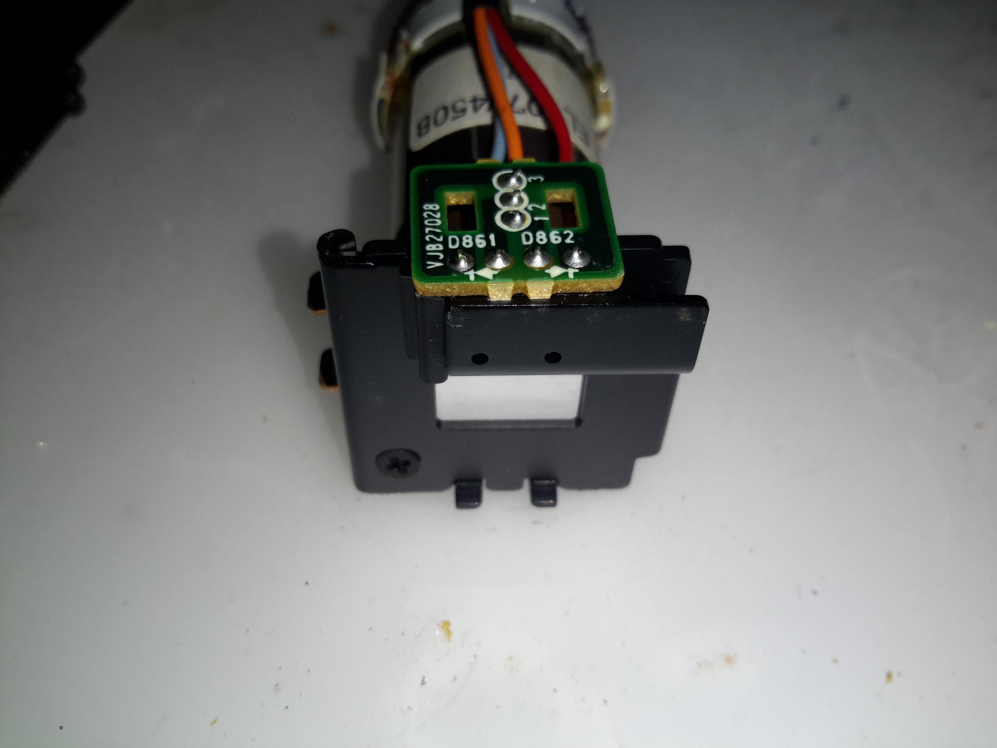
Optics Assembly
The back of the optics tube is a heavy casting, to supress vibration. This will be more clear later on.
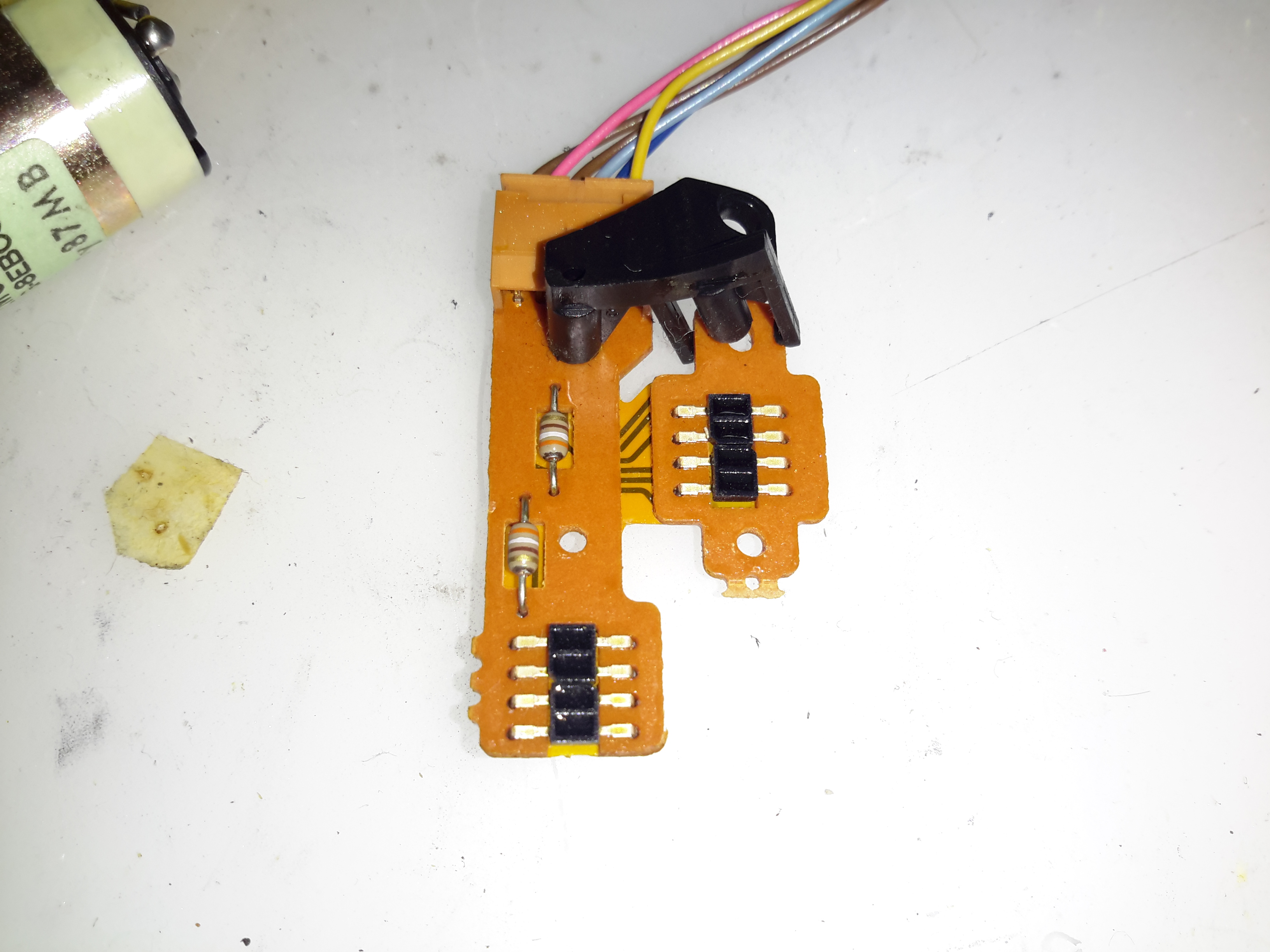
Position Sensor Flex
The position of the lens elements is determined by reflective strips on the barrel & sensors on this flex PCB.
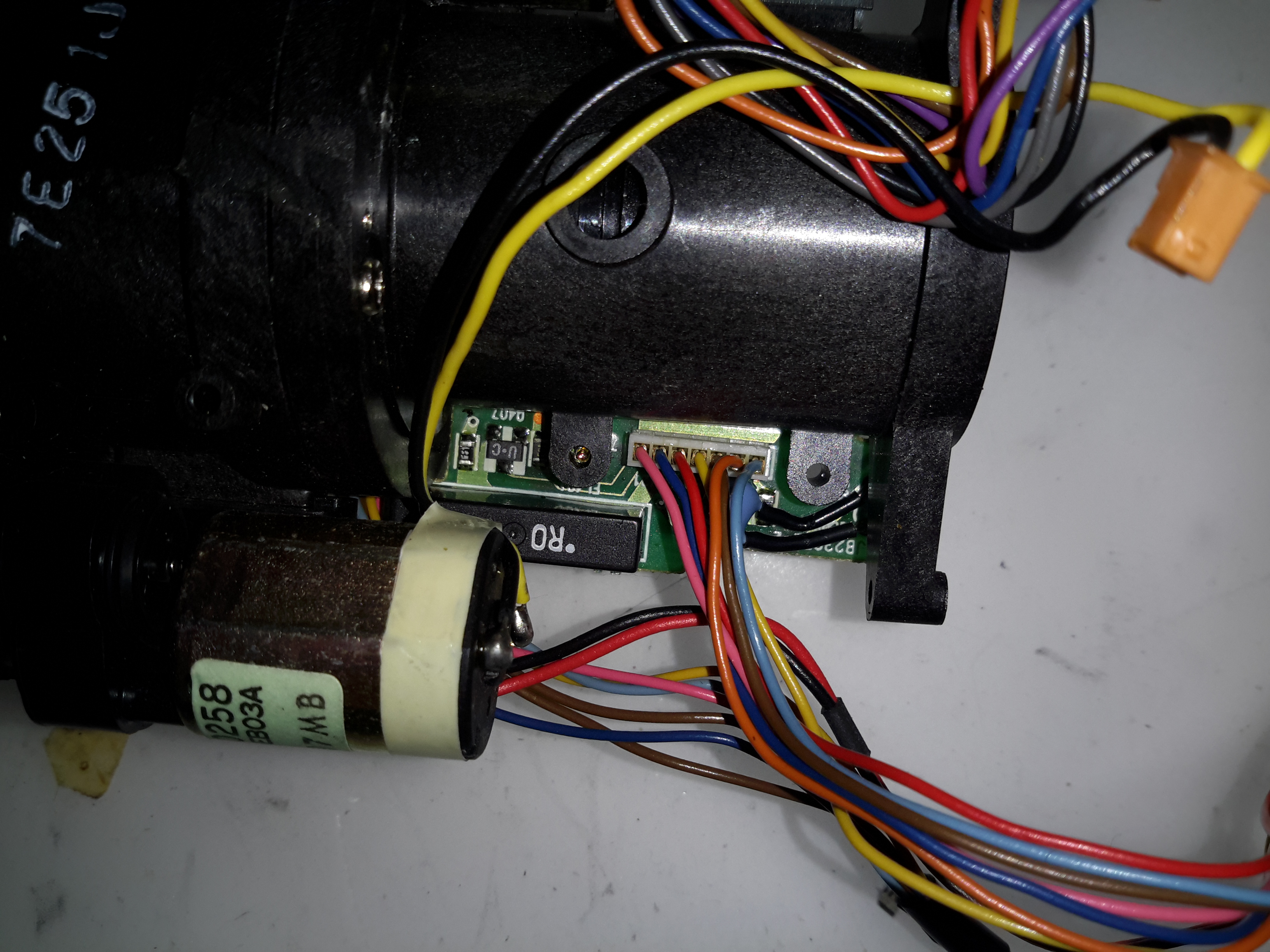
Sub Process Board
There’s another small board tucked into the side of the tube, this hooks into the process PCB.
Process Delay Line
According to the schematic, there’s nothing much on this board, just a delay line & a few transistors.
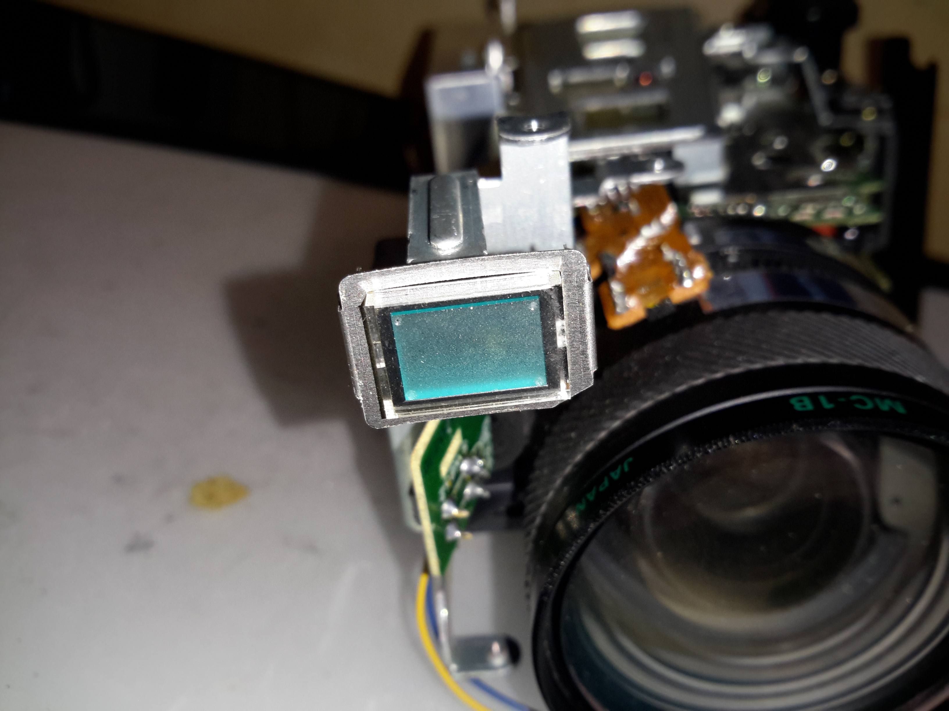
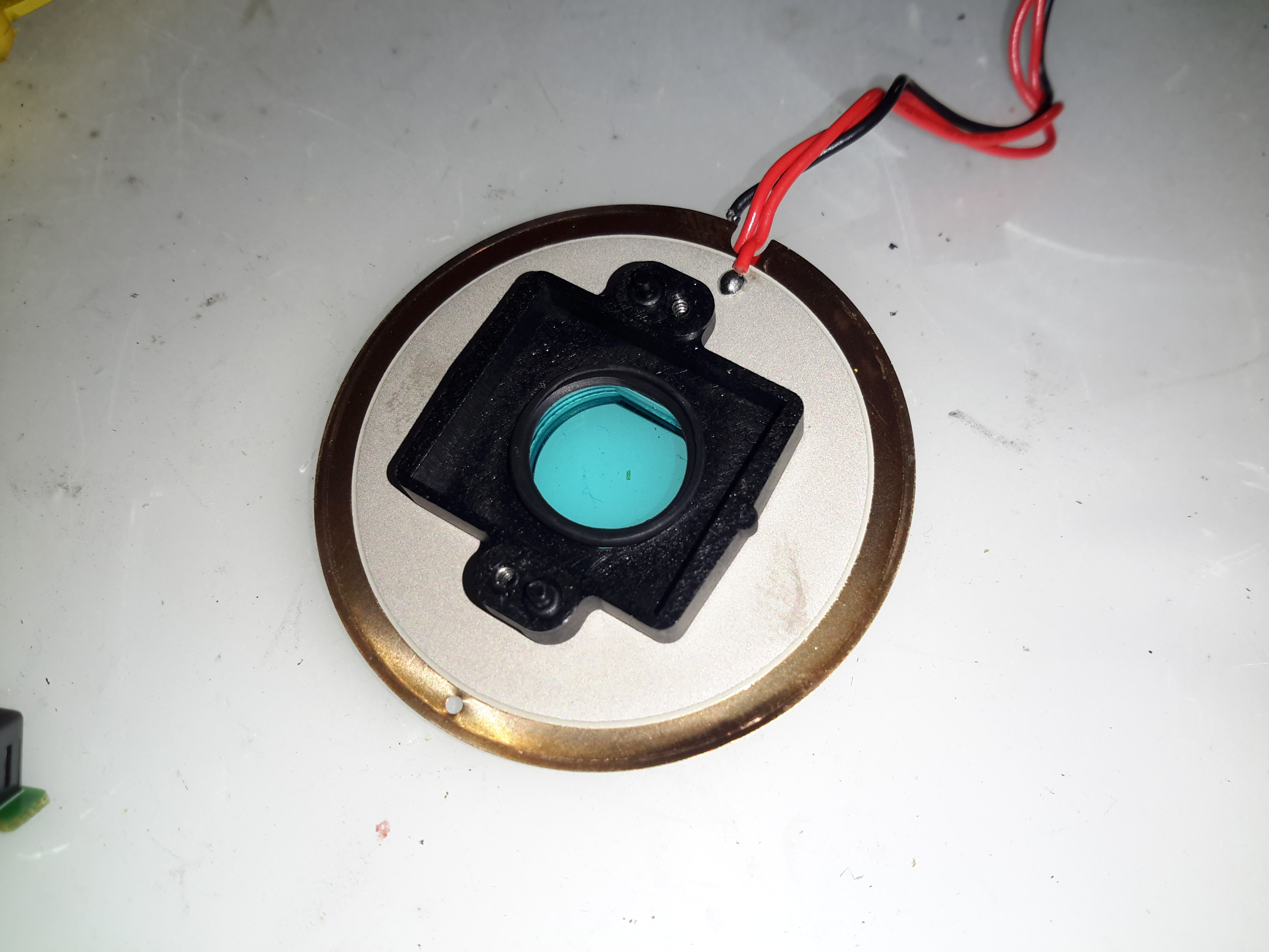
Piezo Focus Disc
Here’s the reason for the heavy alloy casing at the CCD mounting end of the optics: the fine focus adjustment is done with a piezoelectric disc, the entire CCD assembly is mounted to this board. Applying voltage to the electrodes moves the assembly slightly to alter the position of the CCD. The blue glass in the centre of the unit is the IR filter.
IR Relective Sensors
The barrel position sensors are these IR-reflective type.
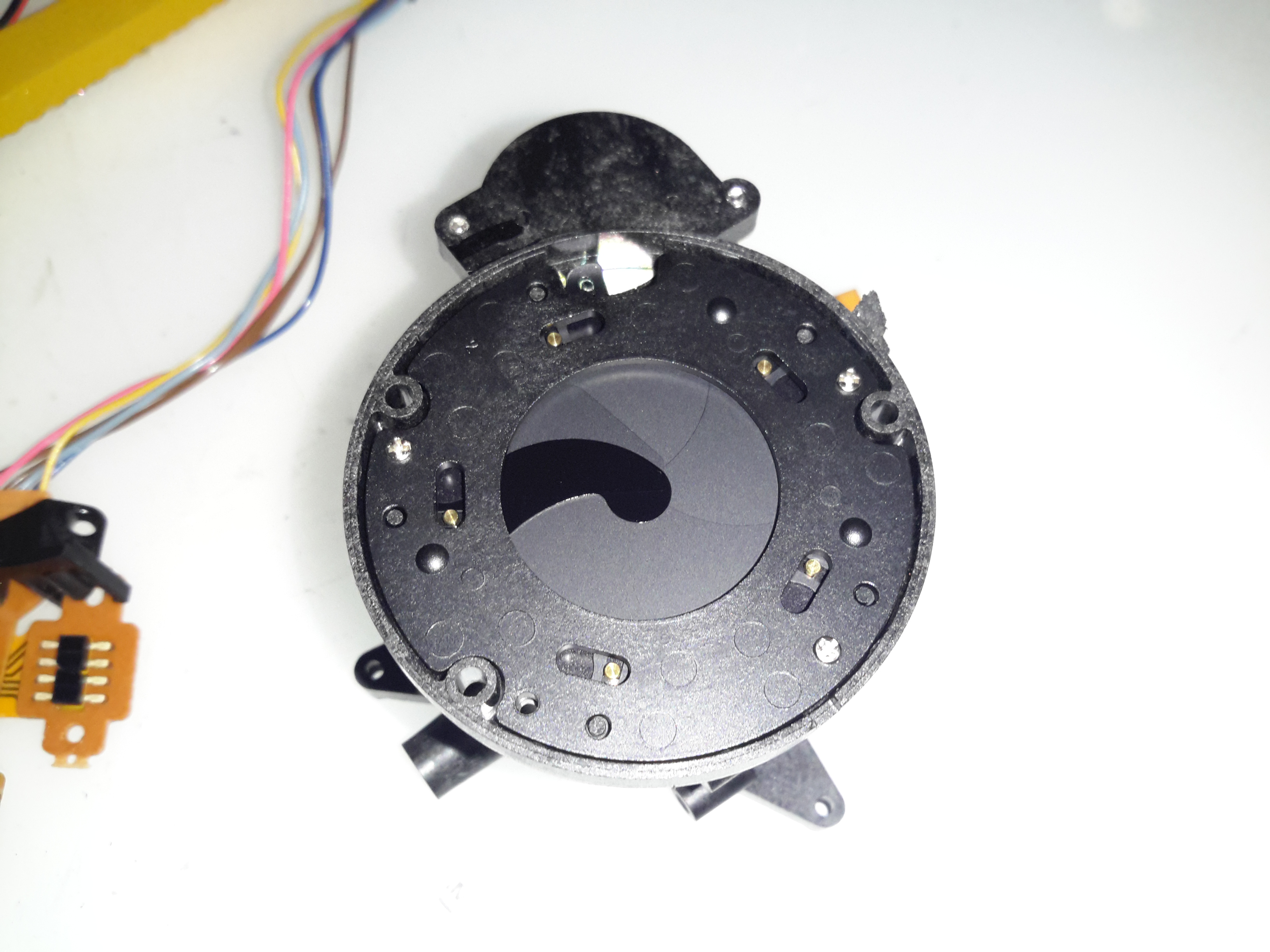
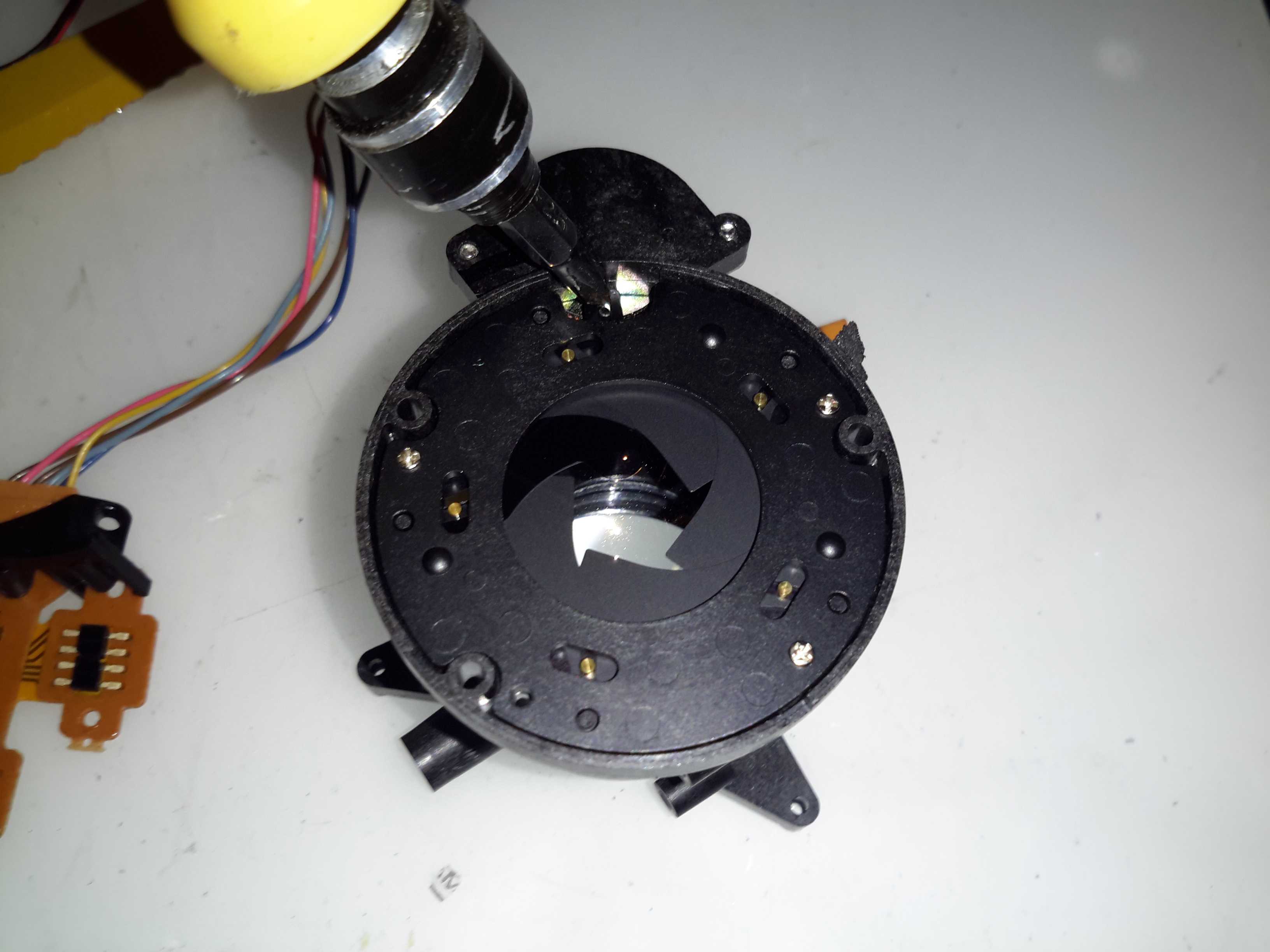
Iris Assembly
The iris is mounted just before the CCD, this is controlled with a galvanometer-type device with position sensors incorporated.
Iris Opening
Pushing on the operating lever with the end of my screwdriver opens the leaves of the iris against the return spring.
Tape Transport & Main Control
Main Control Board
Tucked into the side of the main body of the unit is the main system control board. This PCB houses all the vital functions of the camera: Power Supply, Servo Control, Colour Control,Video Amplifiers, etc.
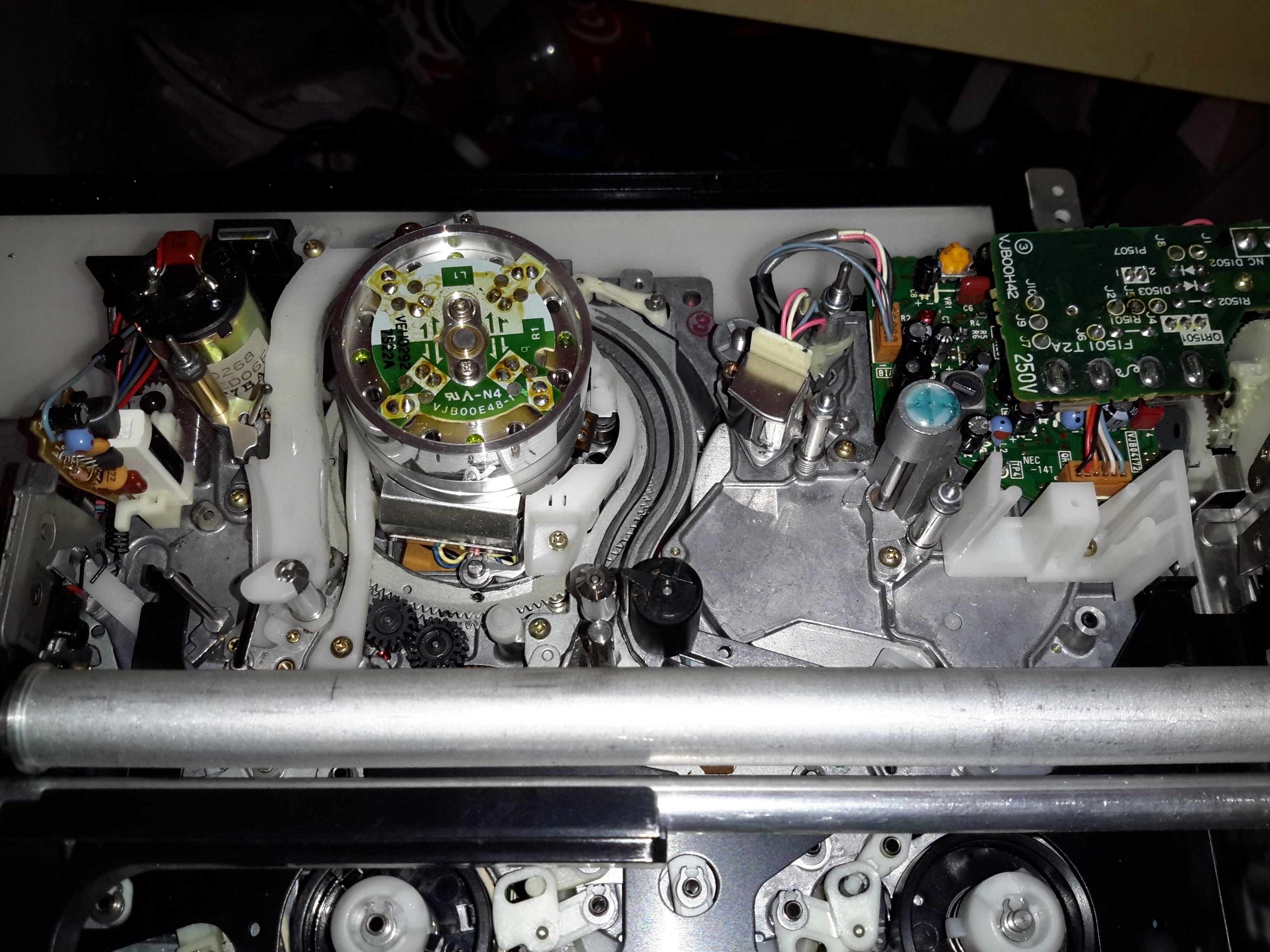
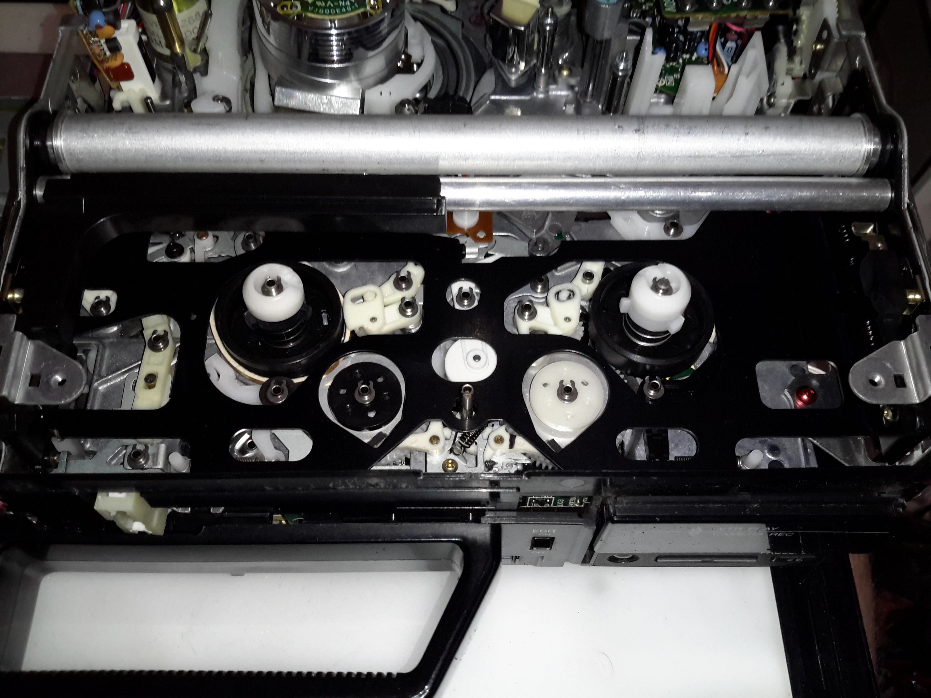
Tape Drum
Here’s the main tape transport mechanism, this is made of steel & aluminium stampings for structural support. The drum used in this transport is noticeably smaller than a standard VHS drum, the tape is wrapped around more of the drum surface to compensate.
Tape Transport
The VHS tape sits in this carriage & the spools drive the supply & take up reels in the cartridge.
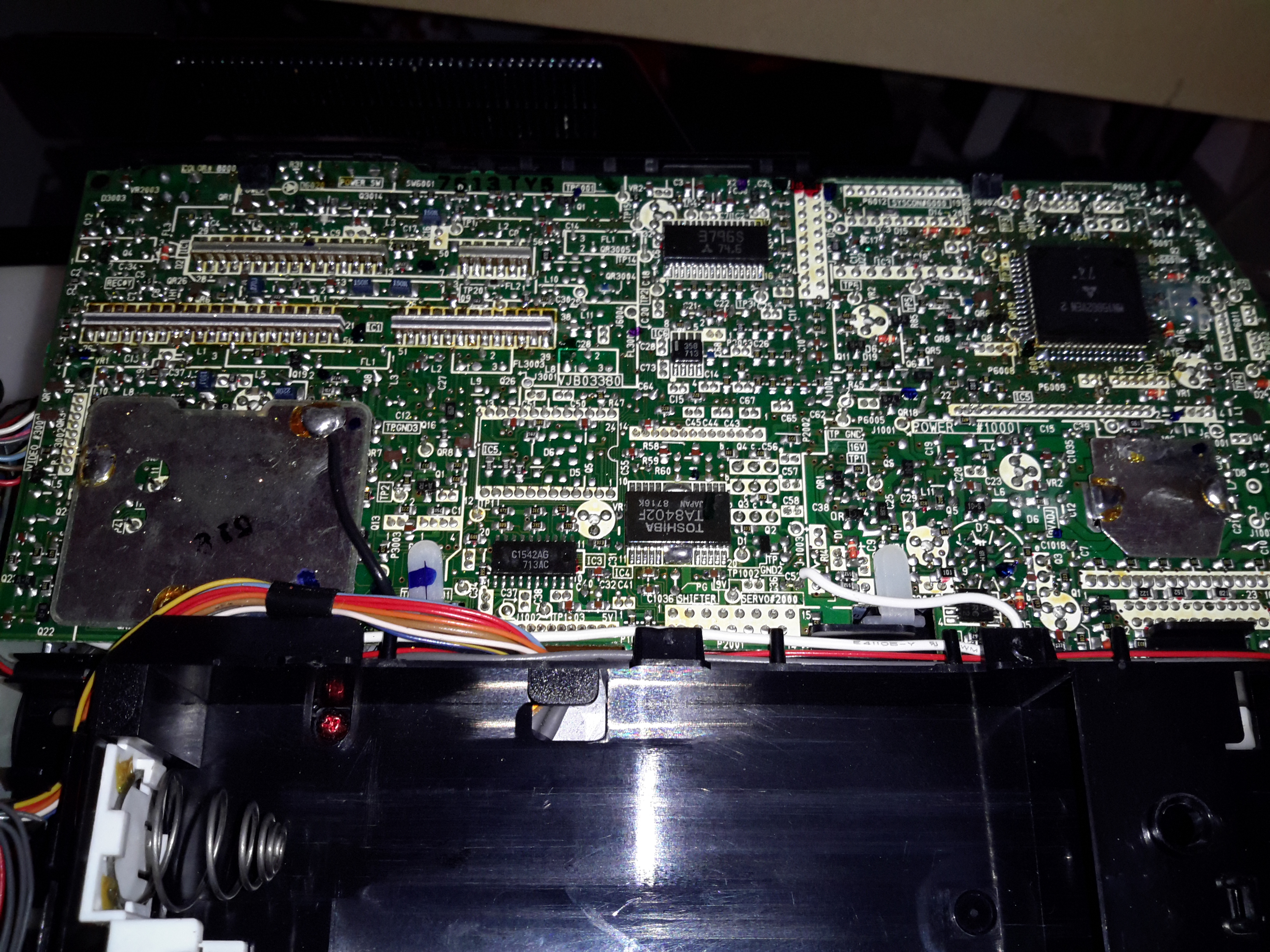
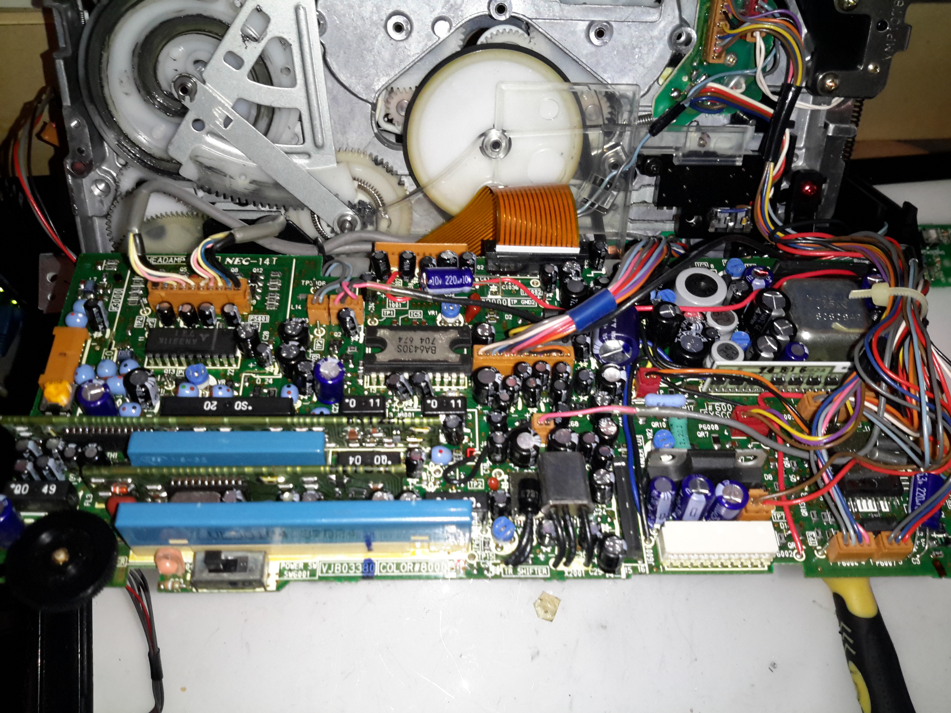
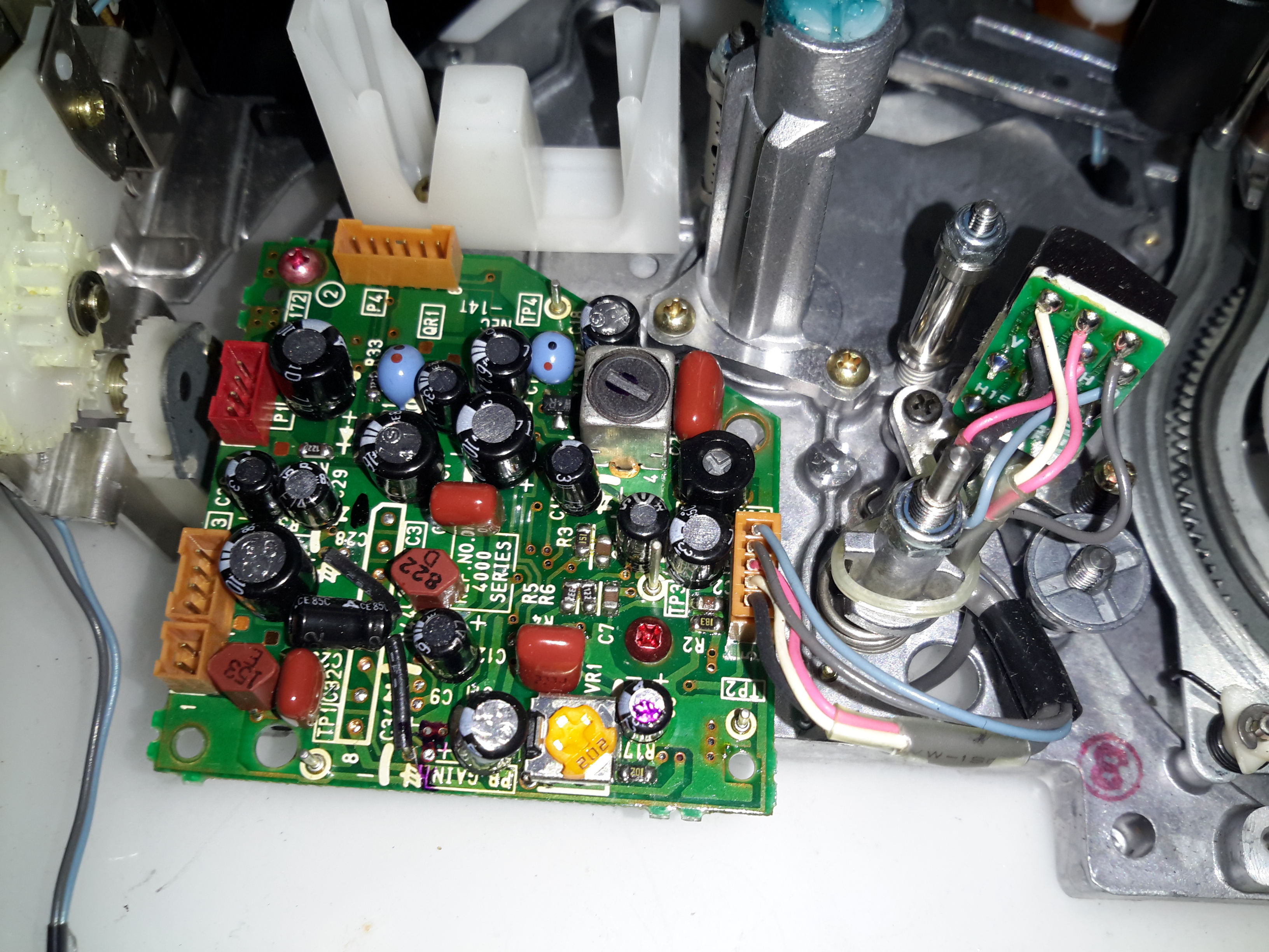
Main Control PCB
Here’s the component side of the main control PCB. This one is very densely packed with parts, I wouldn’t like to try & troubleshoot something like this!
Main PCB Left
The left side has the video head amp at the top, a Panasonic AN3311K 4-head video amp. Below that is video processing, the blue components are the analogue delay lines. There are a couple of hybrid flat-flex PCBs tucked in between with a couple of ICs & many passives. These hybrids handle the luma & chroma signals.
Top left is the capstan motor driver a Rohm BA6430S. The transport motors are all 3-phase brushless, with exception of the loading motor, which is a brushed DC type.
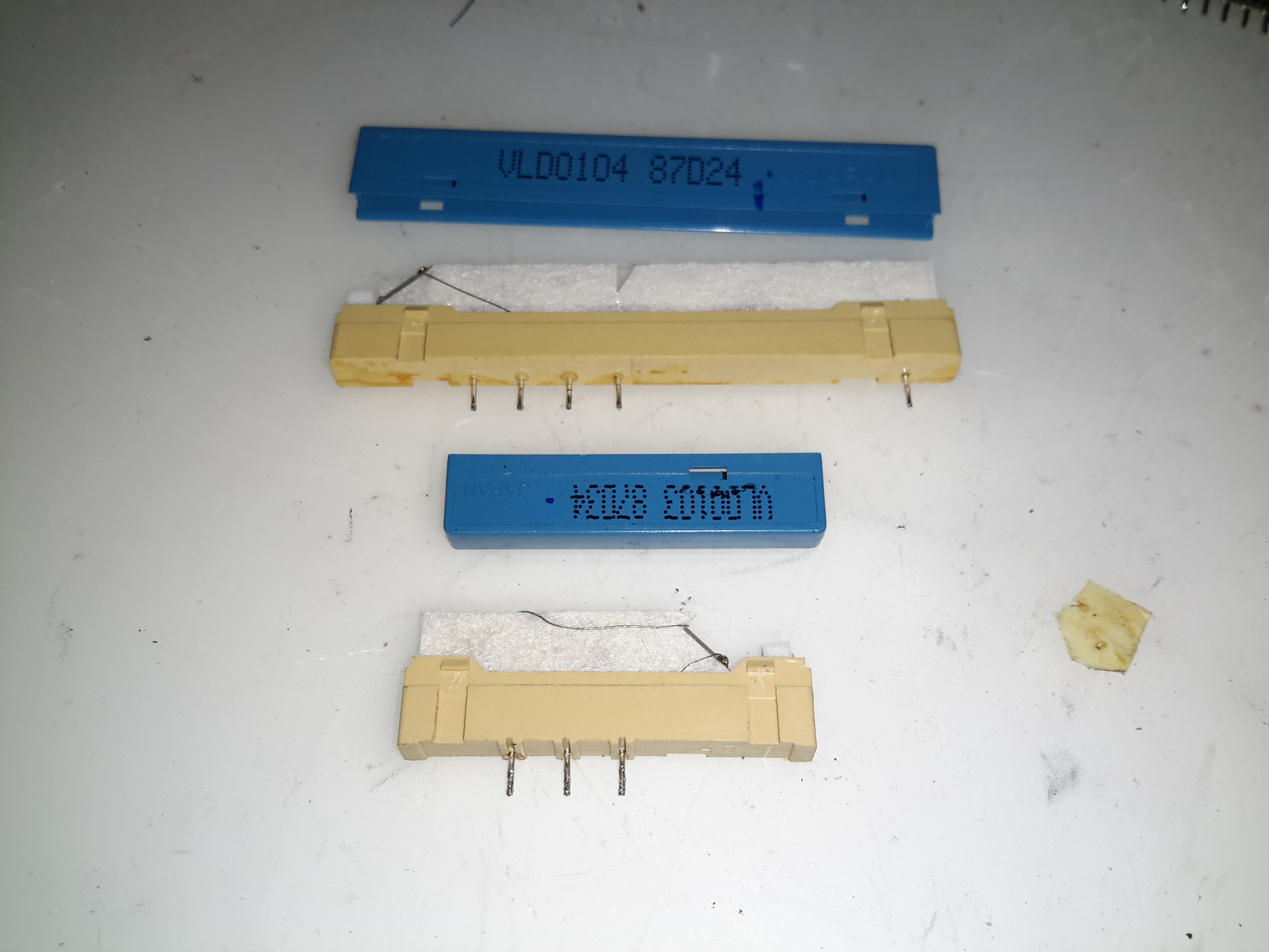
Delay Line
Here’s what is inside the delay lines for the analogue video circuits. The plastic casing holds a felt liner, inside which is the delay line itself.
Internal Glass
The delay is created by sending an acoustic signal through the quartz crystal inside the device by a piezoelectric transducer, bouncing it off the walls of the crystal before returning it to a similar transducer.
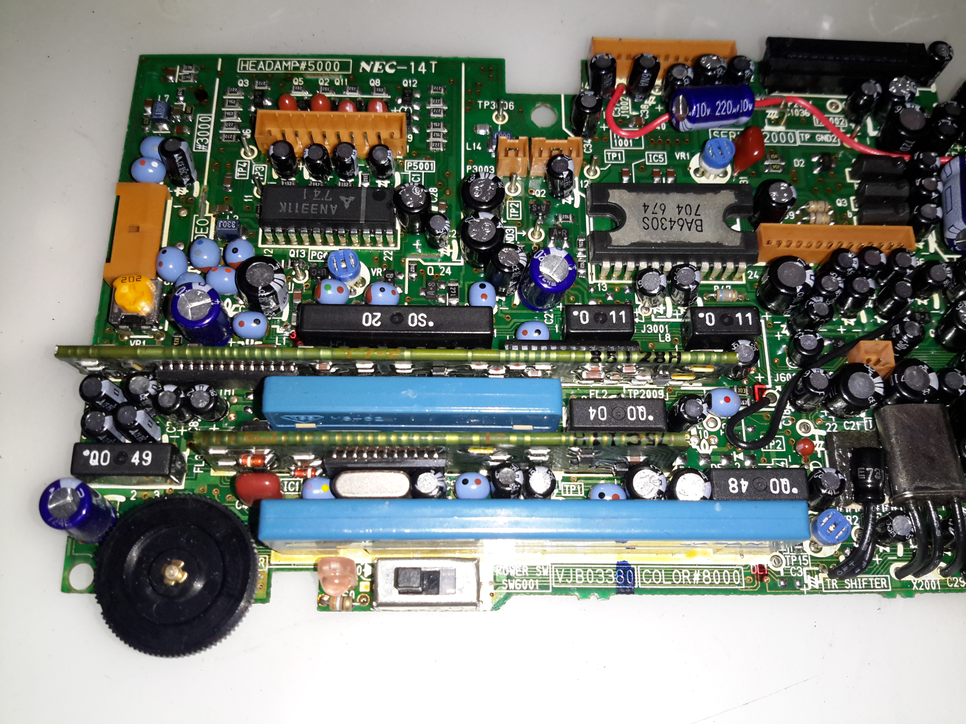
Main PCB Centre
Here’s the centre of the board, the strange crystal at bottom centre is the clock crystal for the head drum servo. Why it has 3 pins I’m not sure, only the two pins to the crystal inside are shown connected on the schematic. Maybe grounding the case?
The main servo controls for the head drum & the capstan motor are top centre, these get a control signal from the tape to lock the speed of the relative components.
Main PCB Right
Here’s the right hand side. The main power supply circuitry is at top right, with a large can containing 4 switching inductors & a ferrite pot core transformer. All these converters are controlled by a single BA6149 6-channel DC-DC converter controller IC via a ULN2003 transistor array.
The ceramic hybrid board next to the PSU has 7 switch transistors for driving various indicator LEDs.
The large tabbed IC bottom centre is the loading motor drive, an IC from Mitsubishi, the M54543. This has bidirectional DC control of the motor & built in braking functions. The large quad flat pack IC on the right is the MN1237A on-screen character generator, with the two clock crystals for the main microcontroller.
Erase Head
The full erase head has it’s power supply & oscillator on board, applying 9v to this board results in an AC signal to the head, which erases the old recording from the tape before the new recording is laid down by the flying heads on the drum.
Audio Control PCB
The Audio & Control head is connected to this PCB, which handles both reading back audio from the tape & recording new audio tracks. The audio bias oscillator is on this board, & the onboard microphone feeds it’s signal here. The control head is fed directly through to the servo section of the main board.
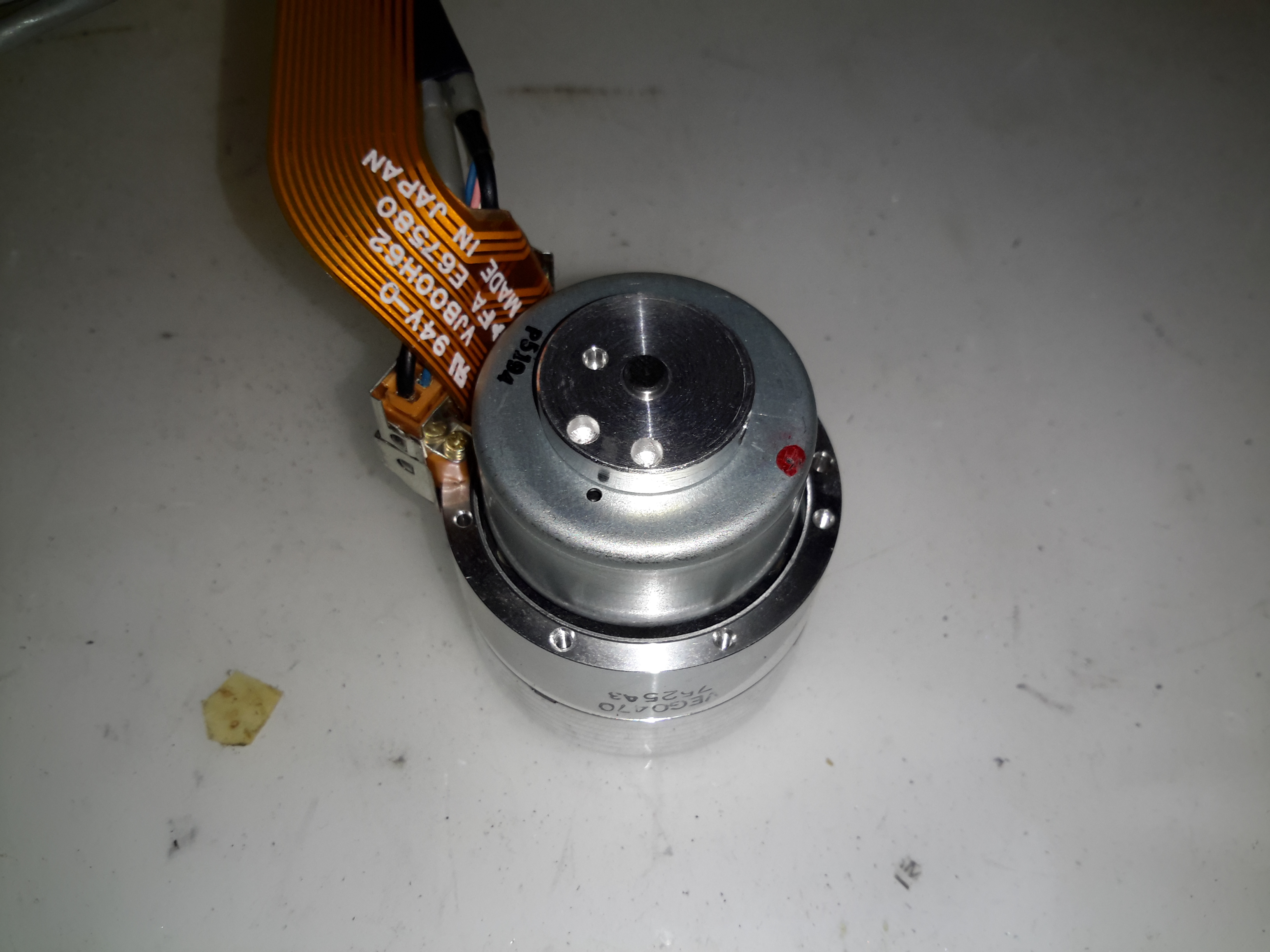
Drum Motor
The motor that drives the head drum is another DC brushless 3-phase type.
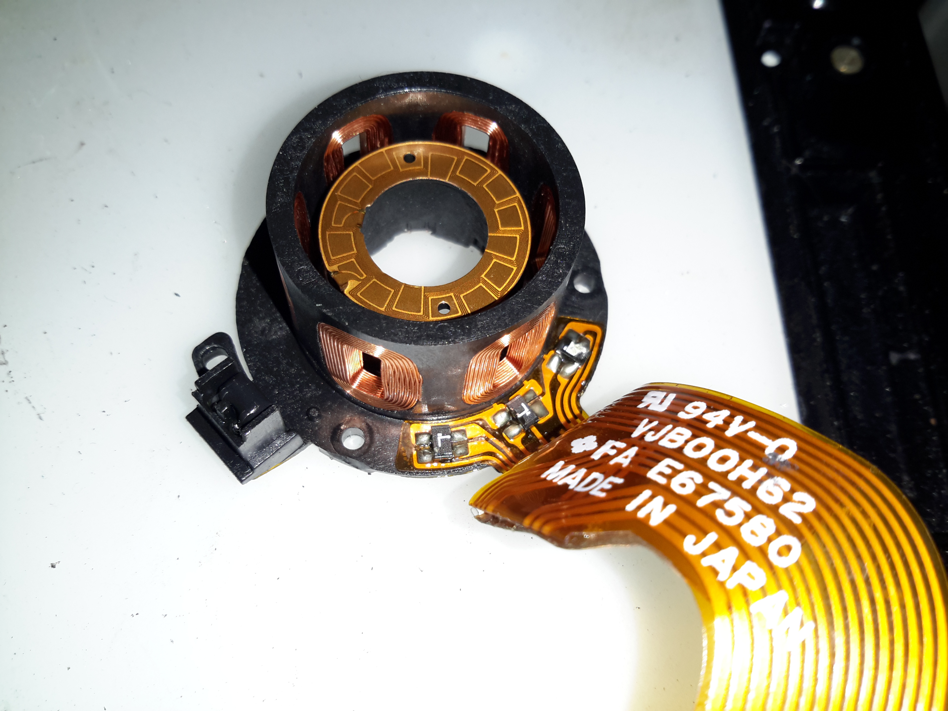
Hall Sensors
These 3 Hall sensors are used by the motor drive to determine the rotor position & time commutation accordingly.
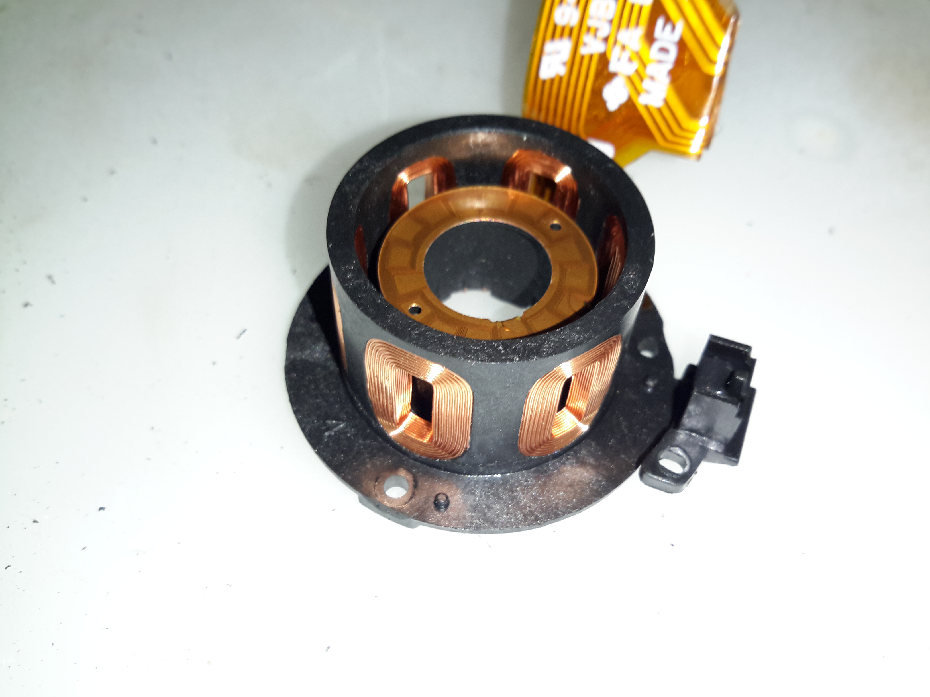
Stator
The stator on this motor is of interesting construction, with no laminated core, the coils are moulded into the plastic holder. The tach sensor is on the side of the stator core. This senses a small magnet on the outside of the rotor to determine rotational speed. For PAL recordings, the drum rotates at 1500 RPM.
Motor Removed
Not much under the stator other than the bearing housing & the feedthrough to the rotary transformer.
Head Disc
The heads are mounted onto the top disc of the drum, 4 heads in this recorder. The signals are transmitted to the rotating section through the ferrite rotary transformer on the bottom section.
Head Chip
The tiny winding of the ferrite video head can just about be seen on the end of the brass mounting.
Capstan Motor Components
The capstan motor is similar to the drum motor, only this one is flat. The rotor has a ferrite magnet, in this case it wasn’t glued in place, just held by it’s magnetic field.
Capstan Motor Stator
The PCB on this motor has a steel backing to complete the magnetic circuit, the coils for the 3 motor phases are simply glued in place. The Hall sensors on this motor are placed in the middle of the windings though.
Again there is a tach sensor on the edge of the board that communicates the speed back to the controller. This allows the servo to remain locked at constant speed.
Viewfinder
Viewfinder Assembly
As usual with these cameras, this section is the CRT based viewfinder. These units take the composite signal from the camera to display the scene. This one has many more pins than the usual viewfinder. I’ll hack a manual input into this, but I’ll leave that for another post.
Viewfinder Circuits
Being an older camera than the ones I’ve had before, this one is on a pair of PCBs, which are both single-sided.
Main Viewfinder Board
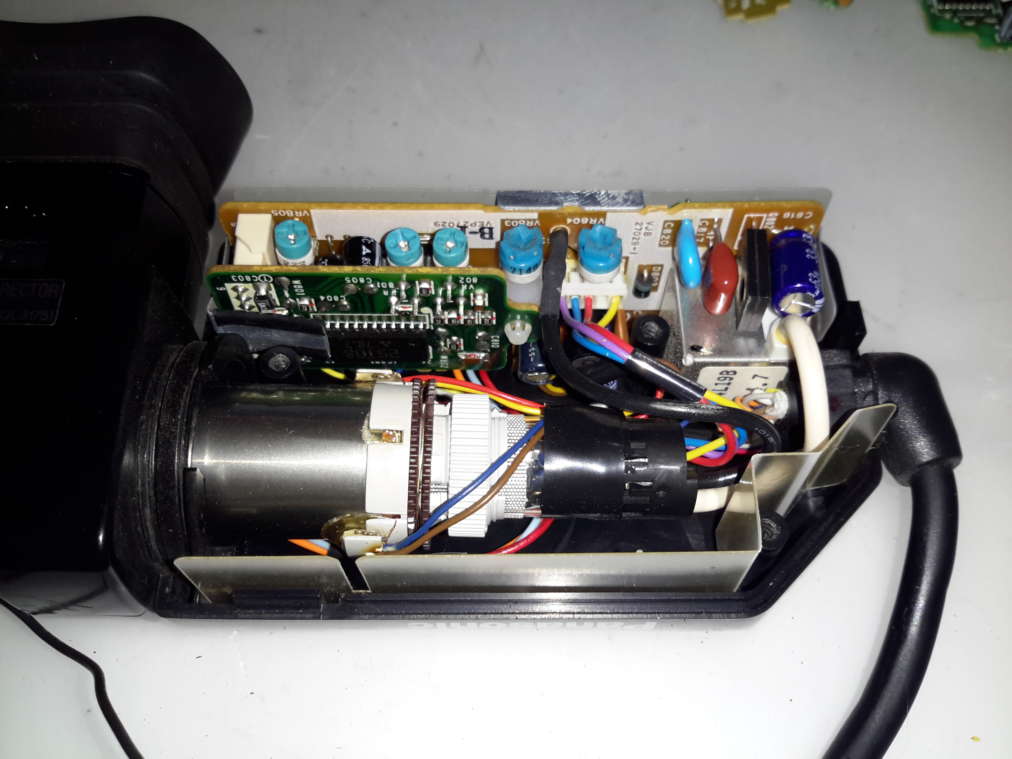
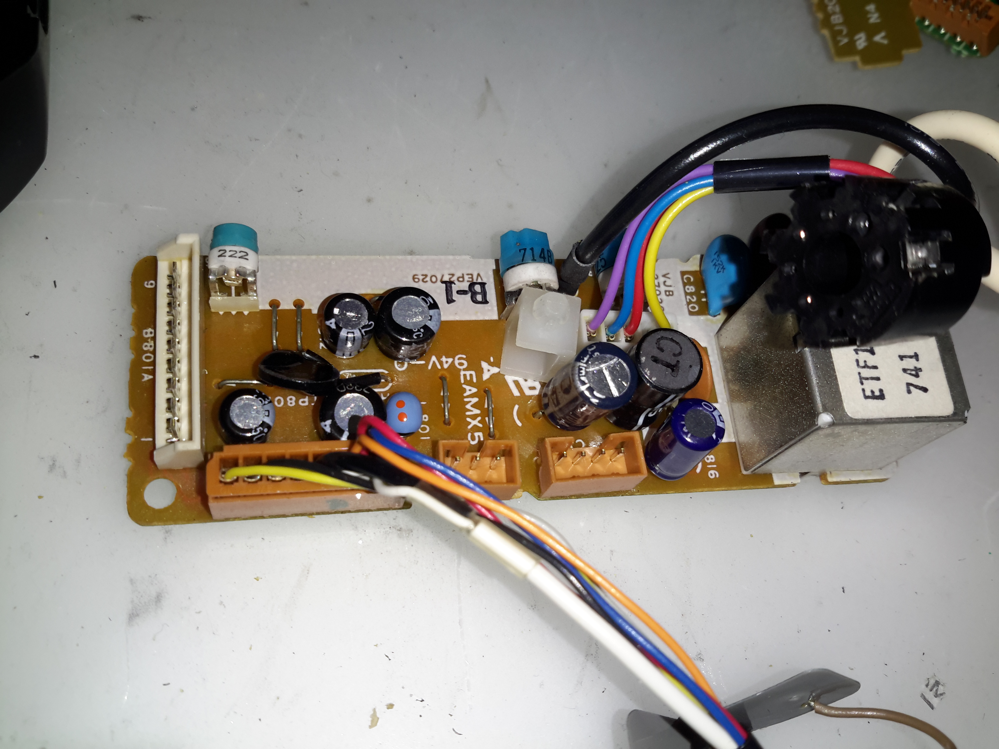
The main board has all the power components for driving the CRT & some of the adjustments. The main HV flyback transformer is on the right. This part creates both the final anode voltage for the tube & the focus/grid voltages.
Viewfinder Control PCB Top
The viewfinder control IC is on a separate daughter board in this camera, with two more controls.
Control IC
The control IC is a Matsushita AN2510S, this has all the logic required to separate the sync pulses from the composite signal & generate an image on the CRT.
Viewfinder CRT Frame
The recording indicator LEDs are mounted in the frame of the CRT & appear above the image in the viewfinder.
Viewfinder CRT With Yoke
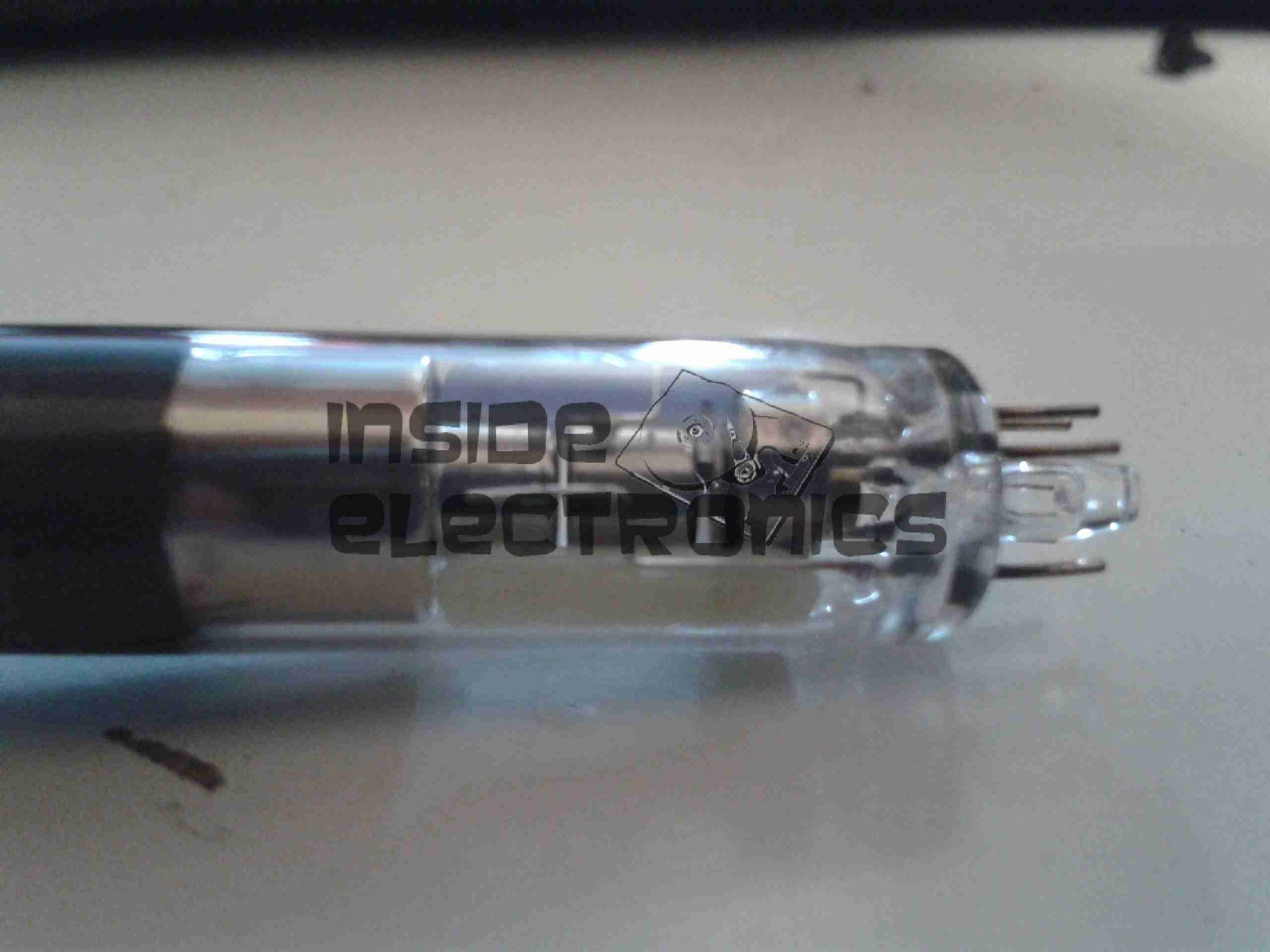
Here the CRT has been separated from the rest of the circuitry with just the deflection yoke still attached.
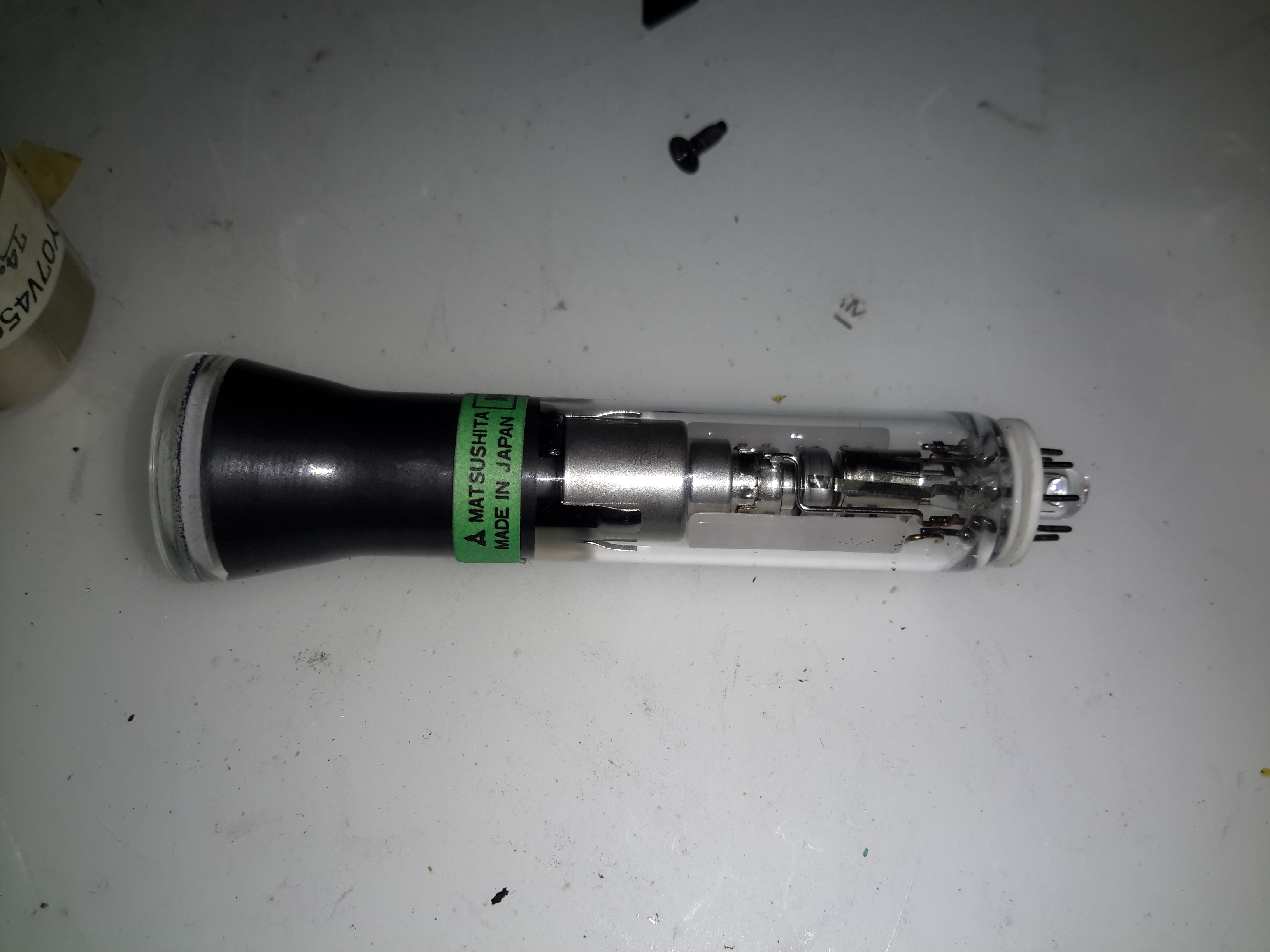
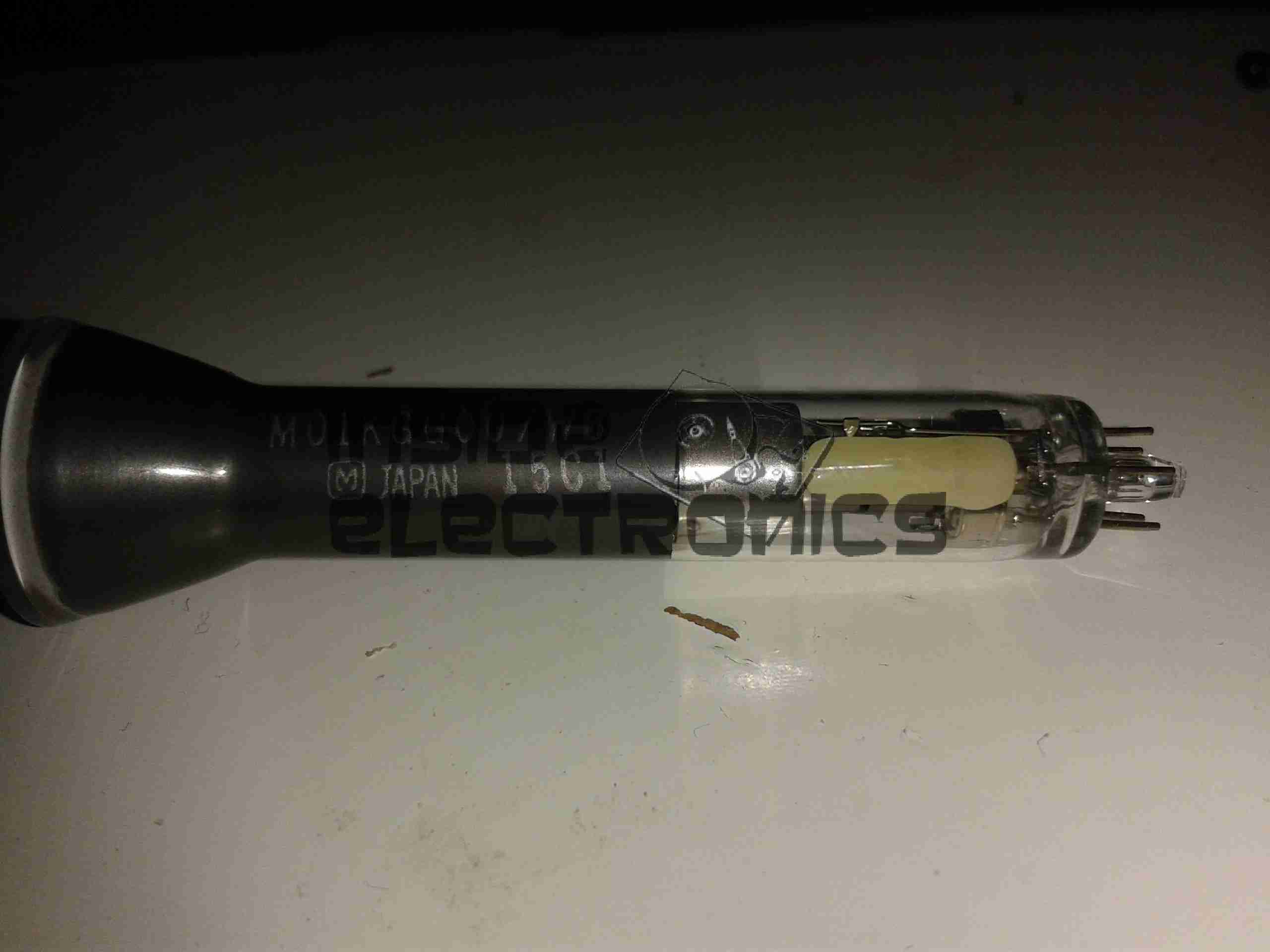
M01JPG5WB CRT
The electron gun in this viewfinder CRT is massive in comparison to the others that I have seen, and the neck of the tube is also much wider. These old tubes were very well manufactured.
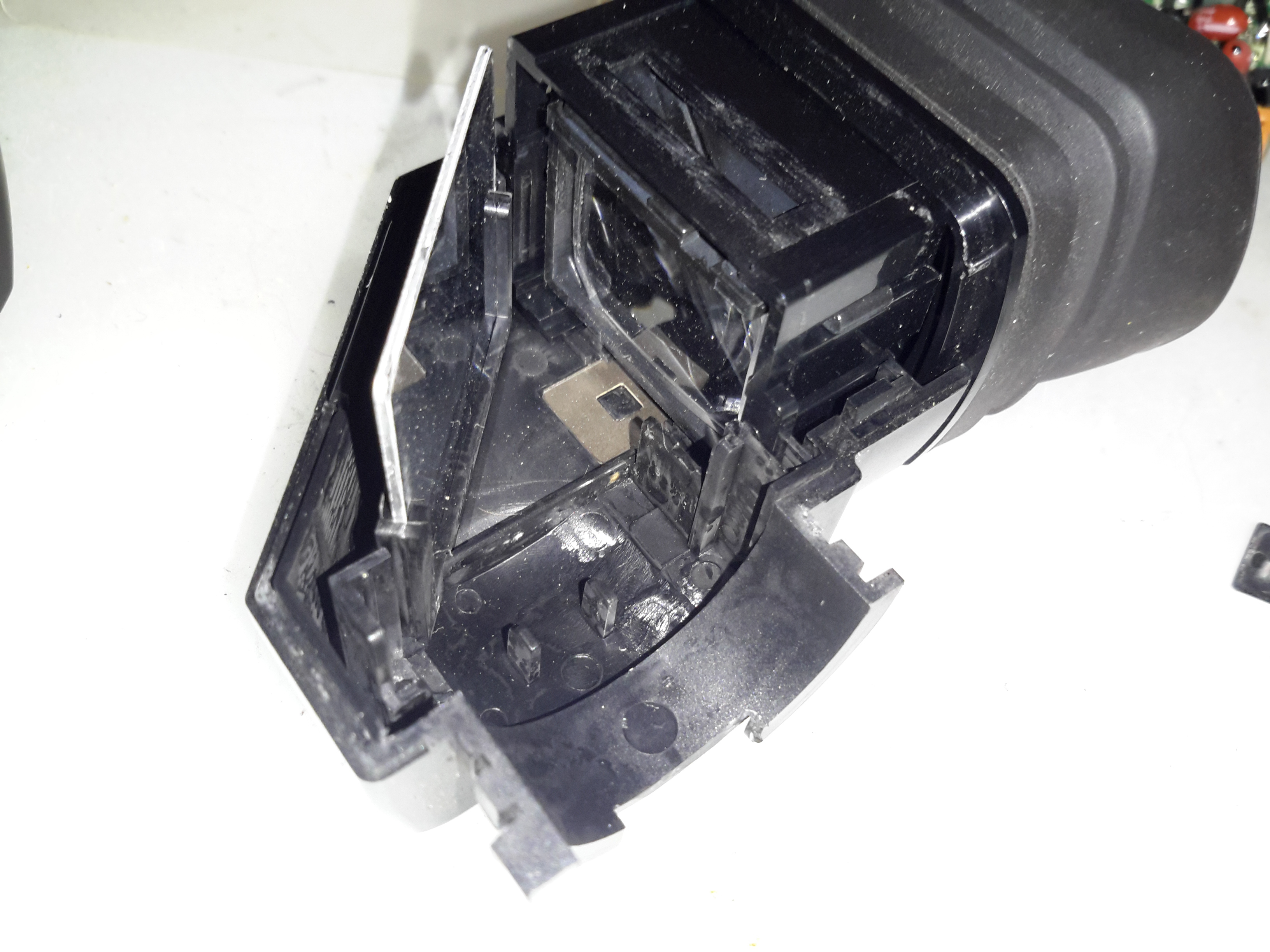
Viewfinder Optics
A simple mirror & magnifying lens completes the viewfinder unit.
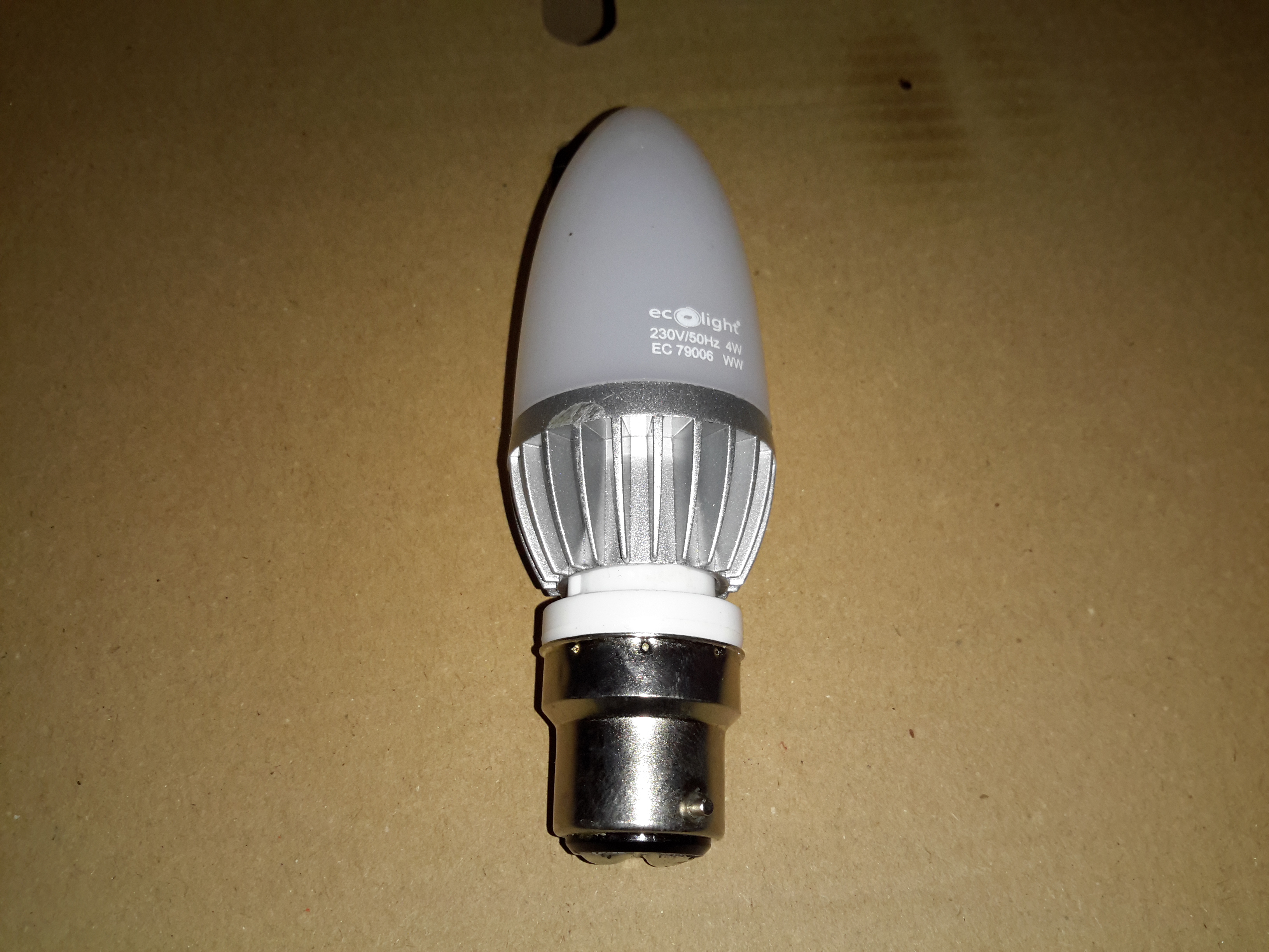
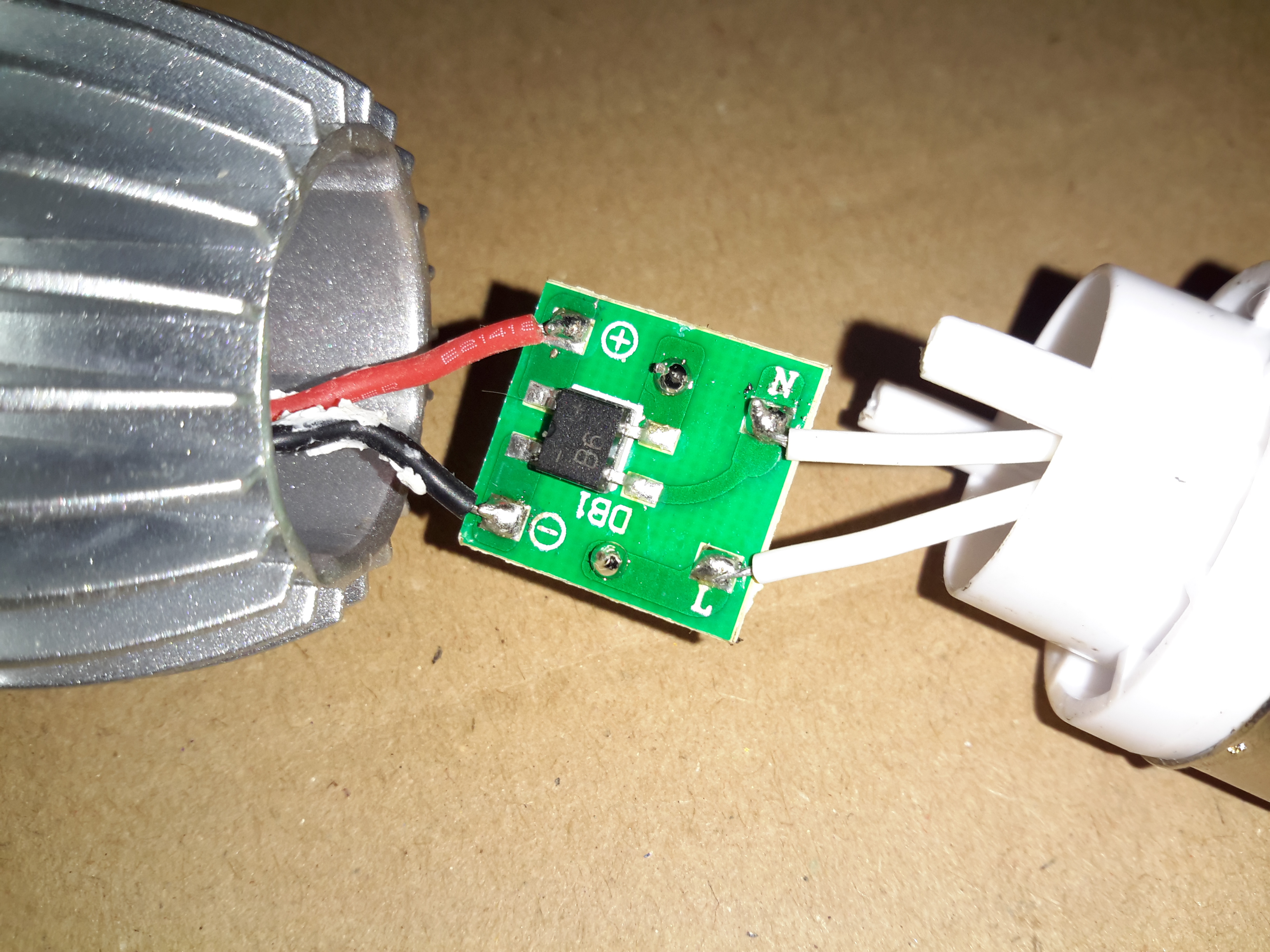
Here’s a modern LED bulb, that unfortunately decided to disassemble itself within a few minutes of being installed in a light fitting! The base plastic snapped off the main aluminium body at the screw posts!
Input Rectifier
The PCB in the base holds nothing but the input components. Above is the bridge rectifier.
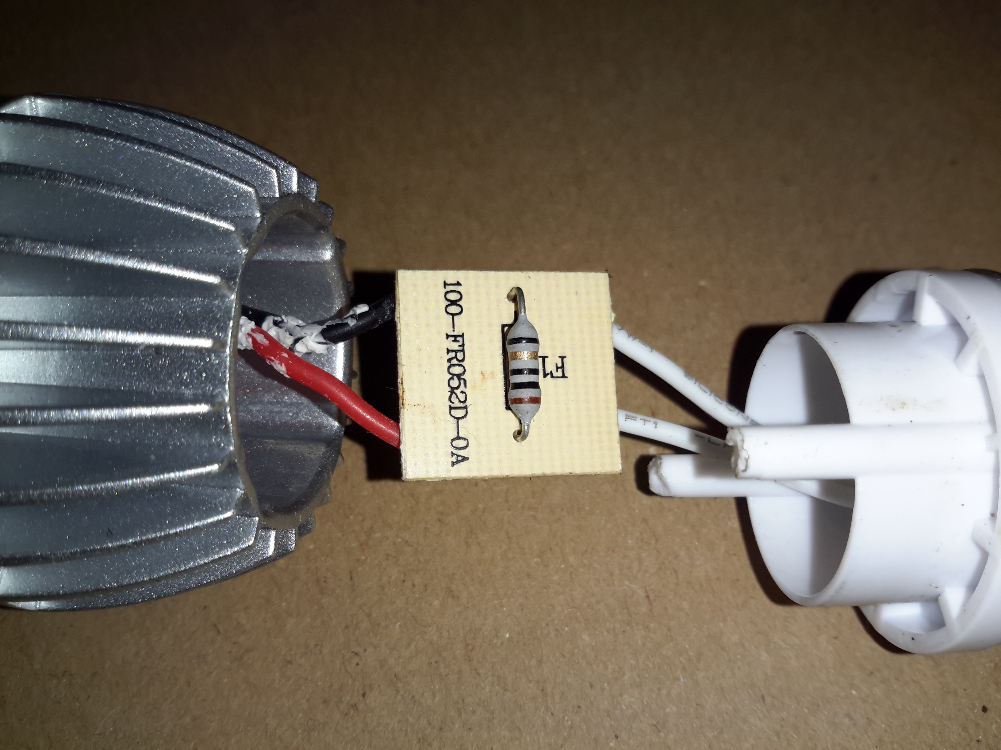
Fusible Resistor
The other side of the PCB has a 10Ω fusible resistor, for protection.
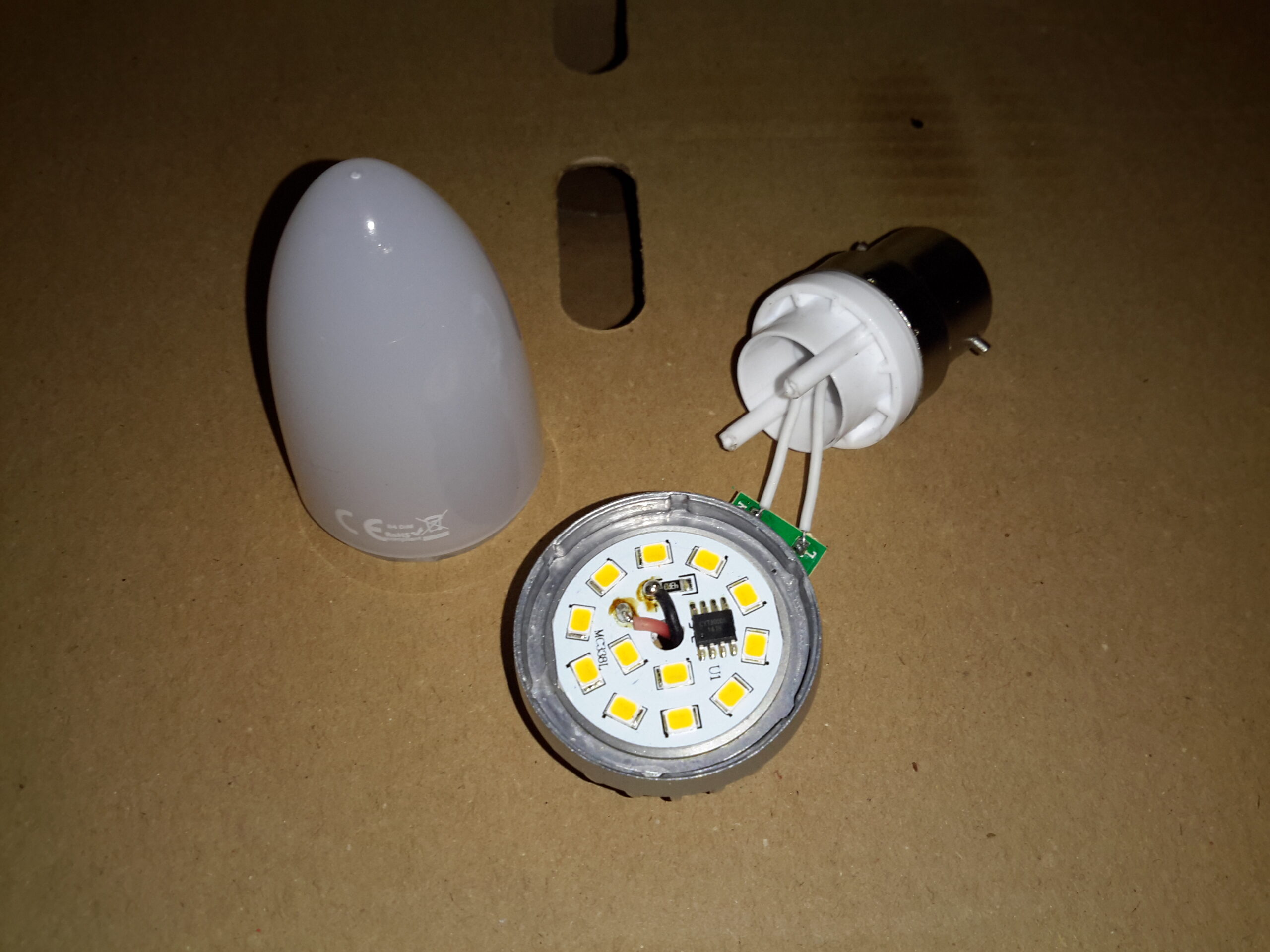
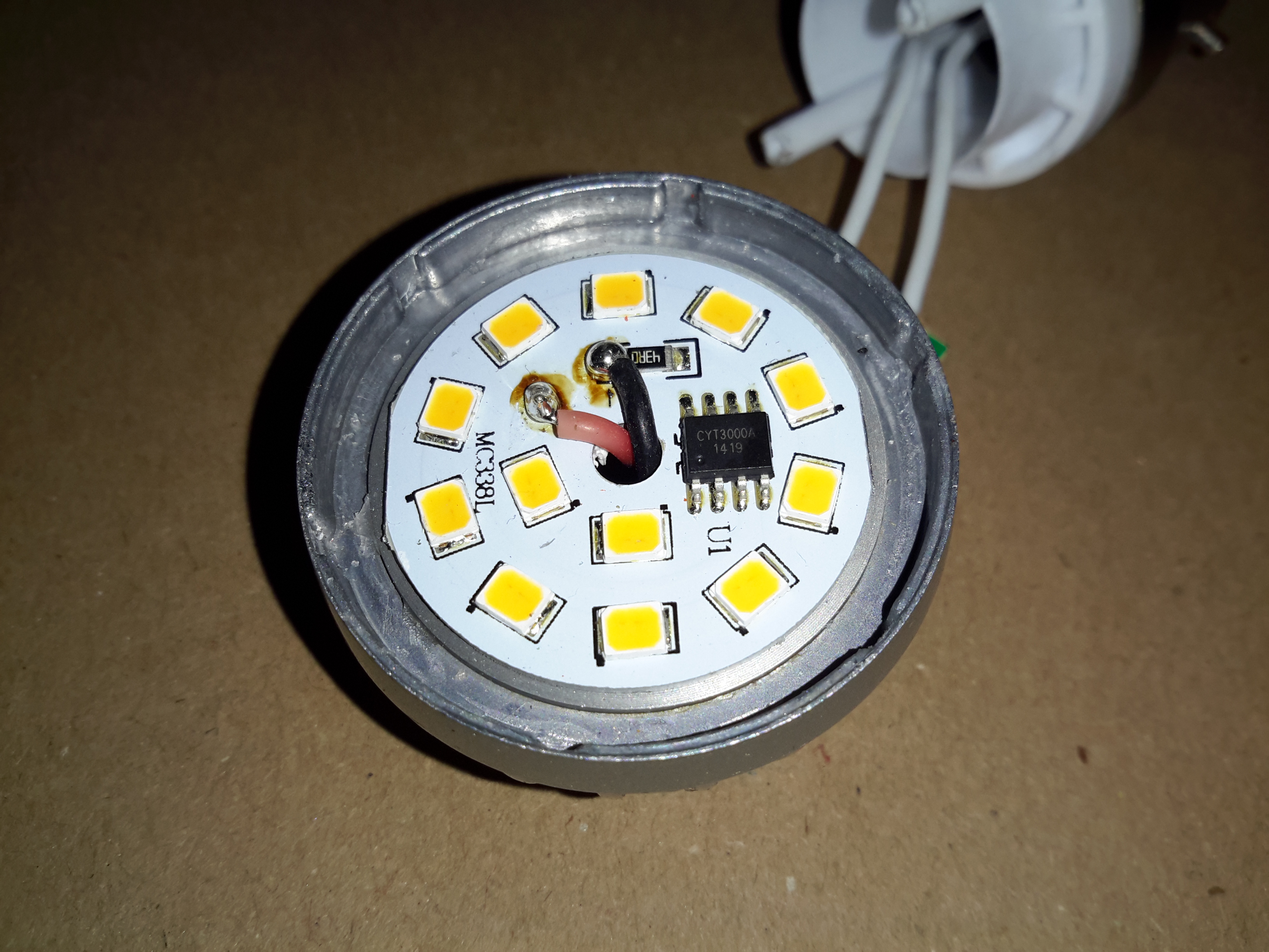
LED PCB
The LED PCB itself has the driver IC, which is a CYT3000A linear constant current IC, that runs direct from full-wave rectified mains. The single resistor sets the LED current, but there aren’t any smoothing capacitors on the DC rail, so this bulb would flicker a lot.
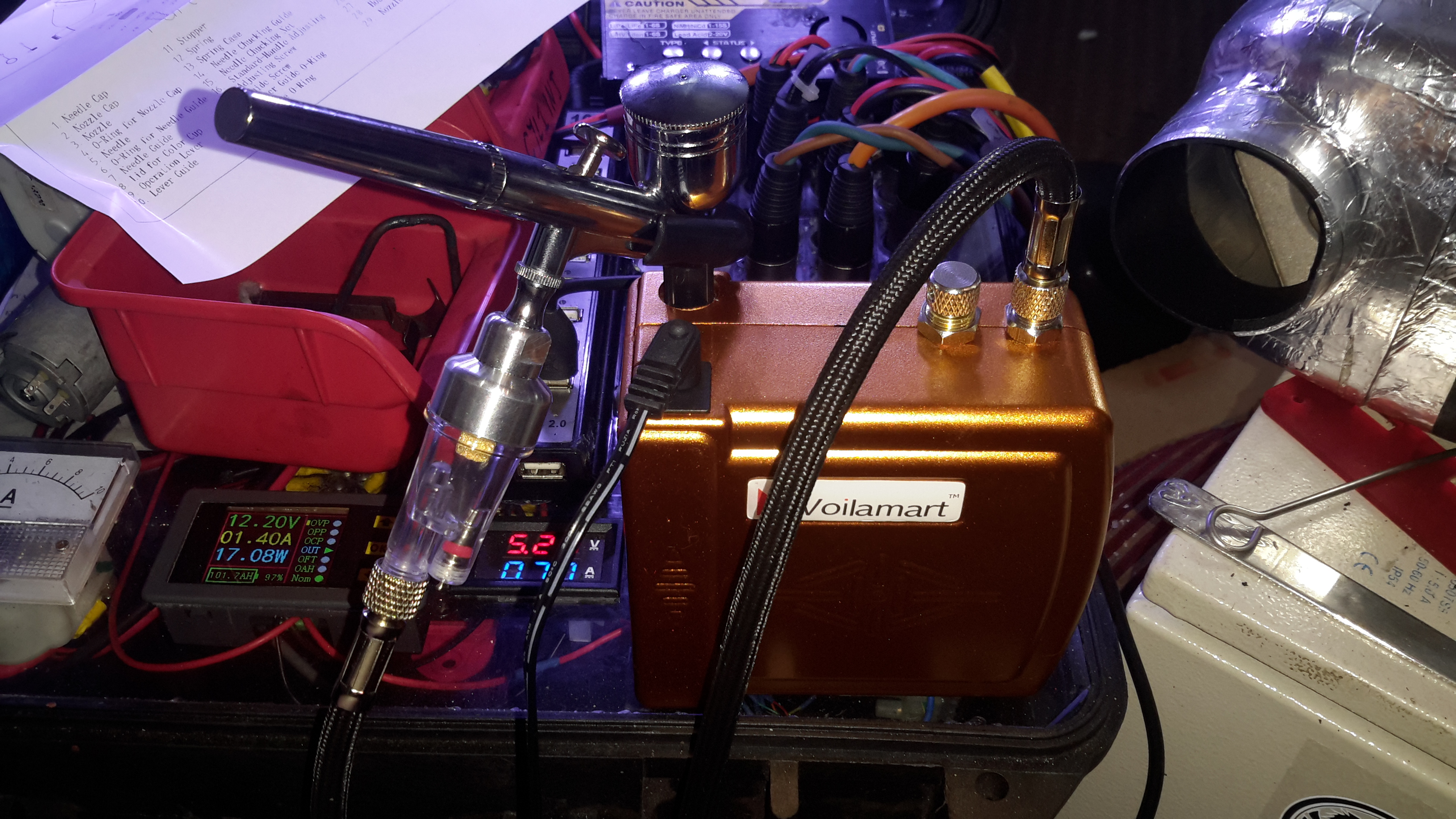
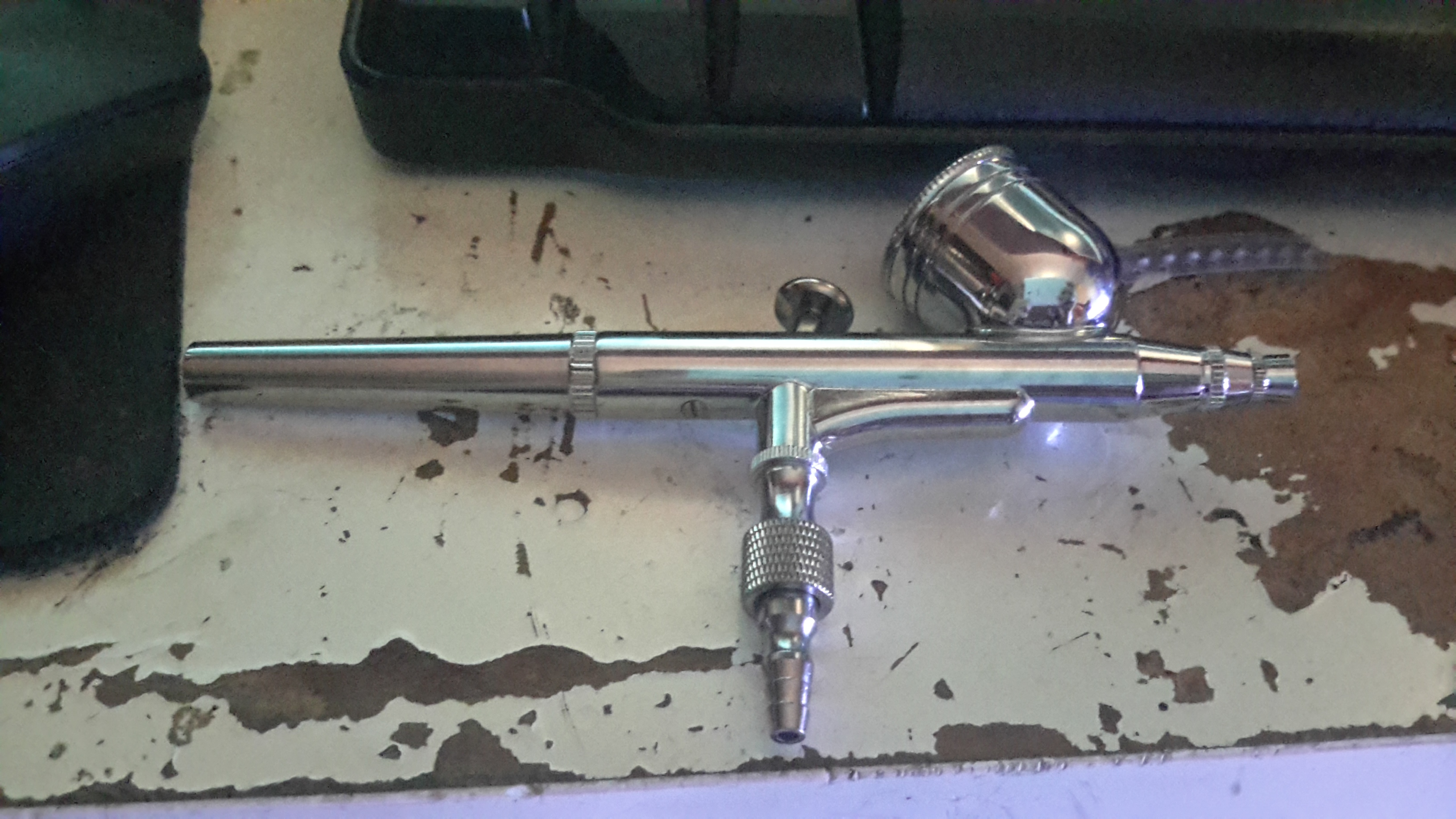
For my latest project, I needed an easier way to paint without messing about with brushes, and the associated marks they leave in a paint job. eBay provided me with a cheap airbrush & compressor.
Airbrush Kit
For less than £30, this kit doens’t look so bad. I’ve never used an airbrush before, but I’ve had no problems with this as yet spraying both water based paints & solvent based paints.
Compressor
Here’s the compressor itself, this runs on 12v & has an output pressure of 1.5 Bar, which is supposed to be adjustable.
Compressor Internals
Removing a couple of screws reveals the internal components. Nothing much unusual here, a DC diaphragm pump, pressure switch & outlet fittings. There’s also a thermal cutout fitted next to the motor for protection.
The pressure switch attached to the manifold trips at 1.5Bar, keeping the pressure to the brush pretty much constant.
Air Block
Next to the air outlet fitting is an adjustment knob, supposedly for varying the pressure. However it’s just a piss-poorly designed adjustable relief valve that vents to atmosphere. There’s not much of a control range.
Messy Wiring
The wiring gets a bit messy where the power LED is concerned, with no heatshrink over the solder joints, but it’s adequate.
Airbrush
The airbrush itself isn’t too bad. It’s solid Brass, with a very nice Chrome finish. I’m not expecting miracles from a very cheap tool, but it certainly seems to be reasonable.
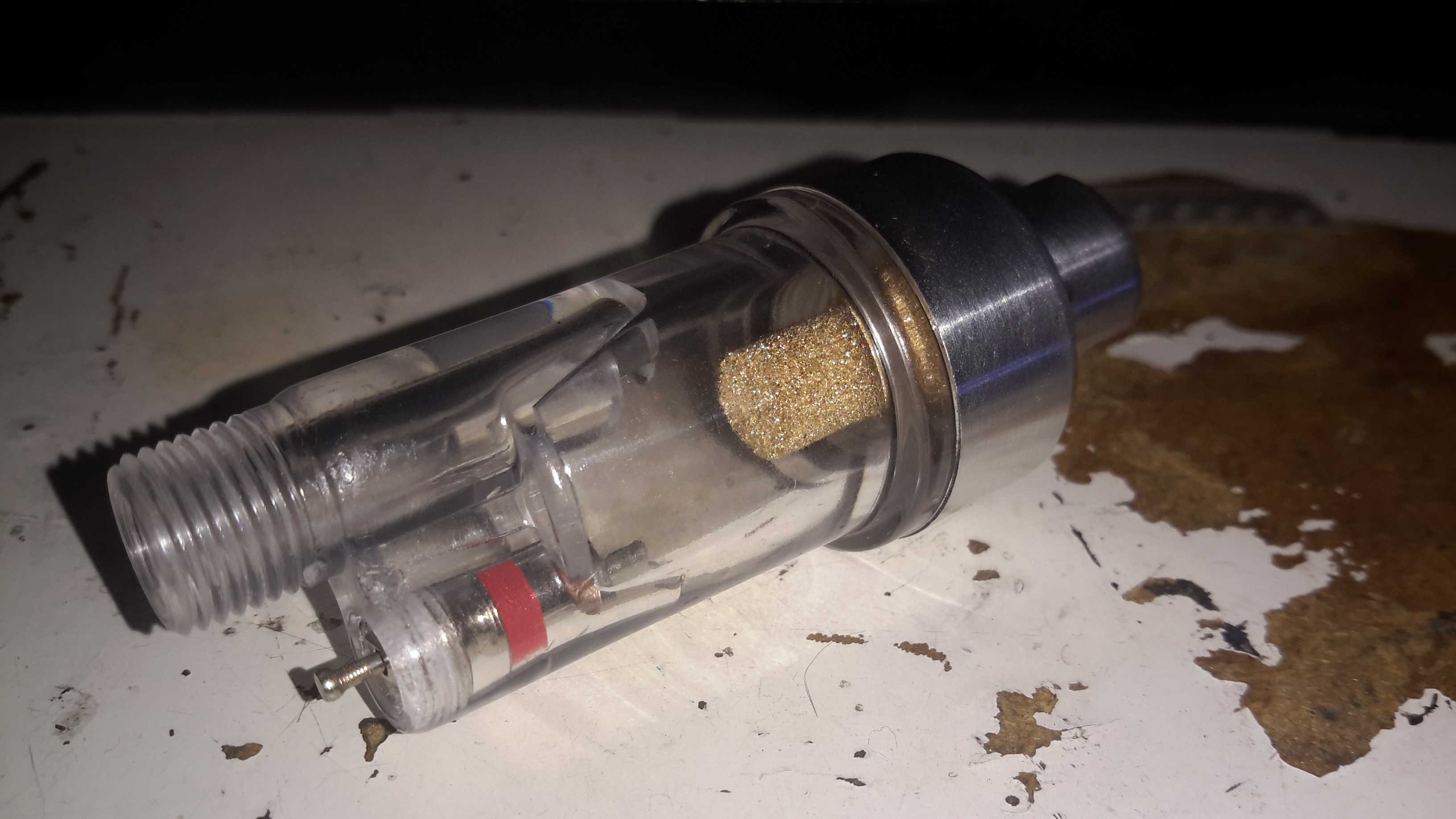
Water Trap
A moisture trap is supplied for the brush, to prevent water drops being sprayed out with the paint. Very handy.
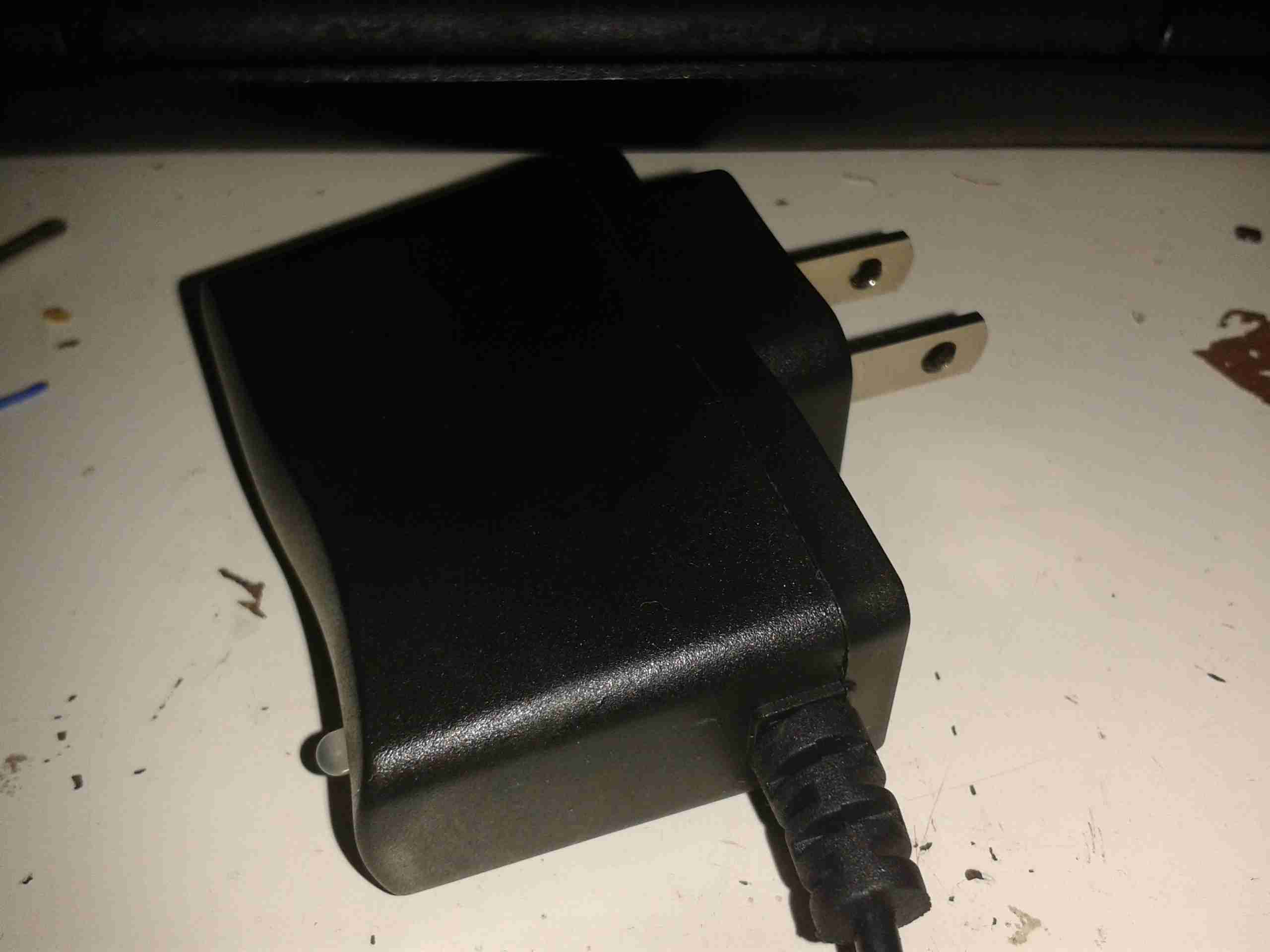
I almost forgot about this bit of kit, that came with one of my LED torches as a Lithium Ion charger. As I never plug in anything that comes from China via eBay, here’s the teardown & analysis.
Another Lethal Charger?
Here’s the unit itself. It’s very light, and is clearly intended for American NEMA power points.
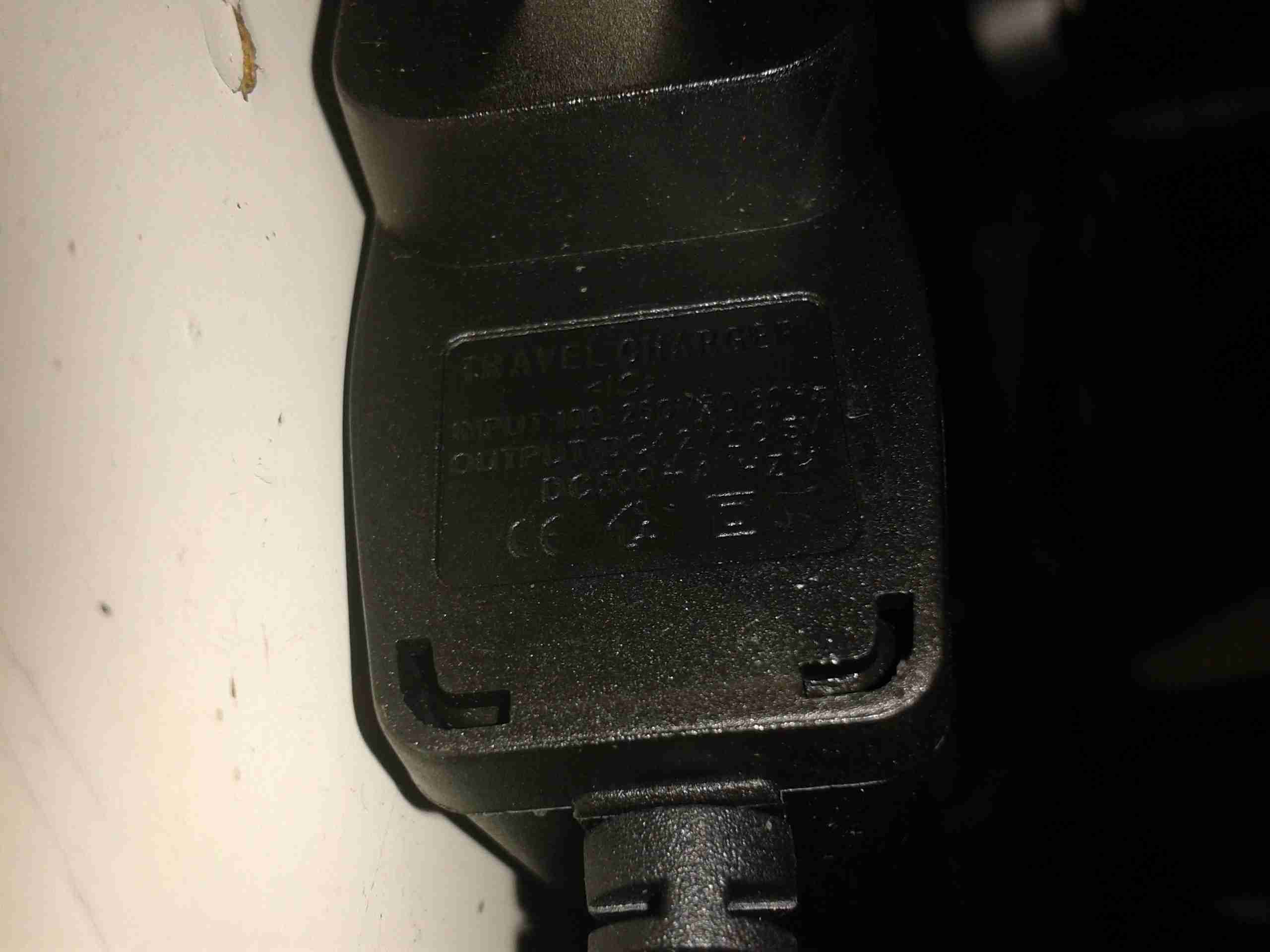
Specs
Claimed specifications are 100-240v AC input, making it universal, and 4.2v DC out ±0.5v at 500mA.
Considering the size of the output wire, if this can actually output rated voltage at rated current I’ll be surprised.
Opened
Here’s the adaptor opened up. There’s no mains wiring to speak of, the mains pins simply push into tags on the PCB.
PCB Top
Top of the SMPS PCB. As usual with Chinese gear, it’s very simple, very cheap and likely very dangerous. There’s no real fusing on the mains input, only half-wave rectification & no EMI filtering.
PCB Bottom
Here’s the bottom of the PCB. At least there’s a fairly sized gap between the mains & the output for isolation. The wiggly bit of track next to one of the mains input tags is supposed to be a fuse – I somehow doubt that it has the required breaking characteristics to actually pass any safety standards. Obviously a proper fuse or fusible resistor was far too expensive for these.
The output wiring on the left is thinner than hair, I’d say at least 28AWG, and probably can’t carry 500mA without suffering extreme volt drop.
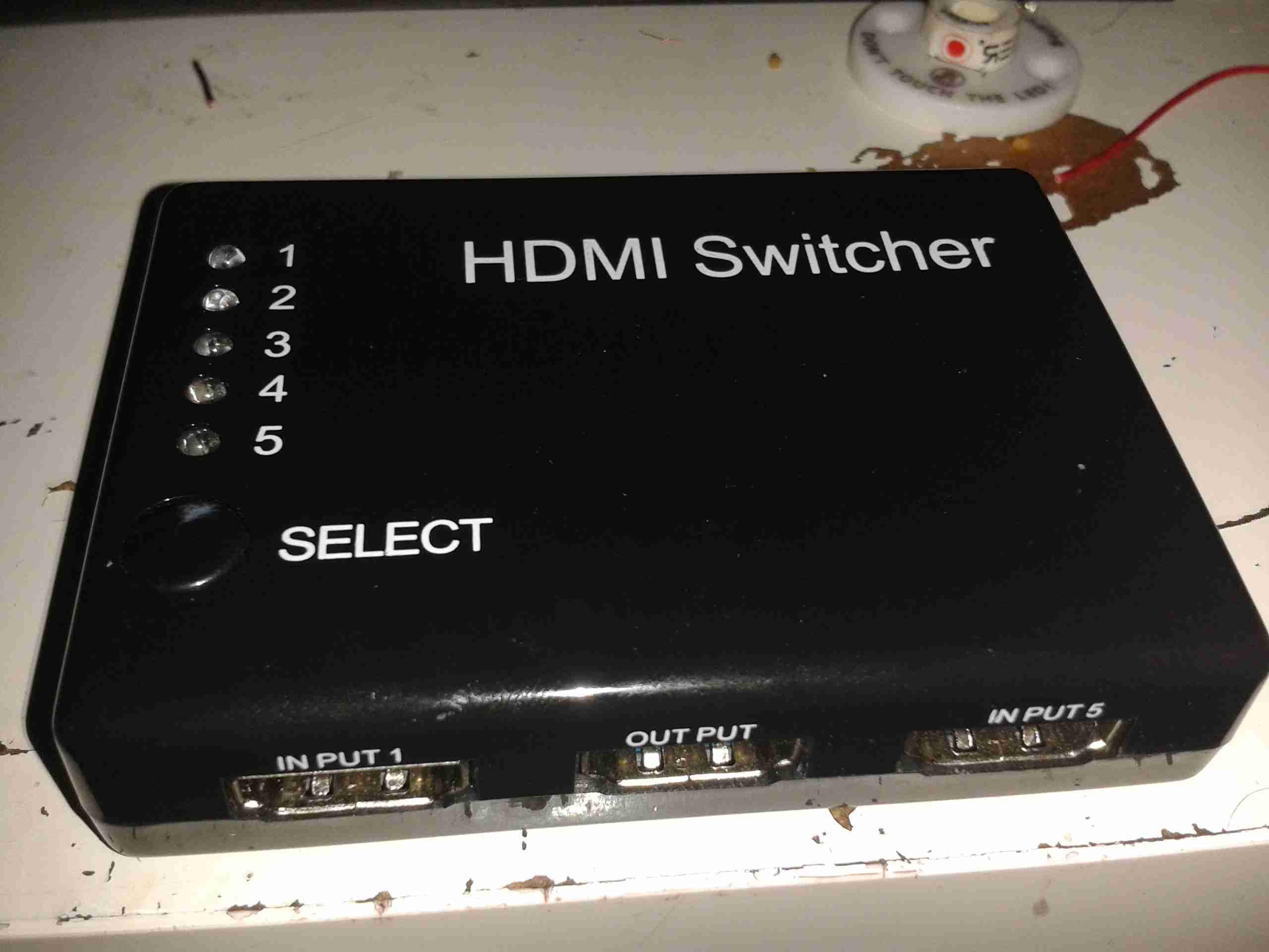
Here’s another quick teardown, a cheap 5-port HDMI switch box. This is used to allow a single input on a monitor to be used by 5 different external HDMI devices, without having to mess about plugging things in.
Power & Remote
Here’s the DC barrel jack & 3.5mm TRS jack for power & remote control. There’s a little IR decoder & remote that go with this for hands free switching.
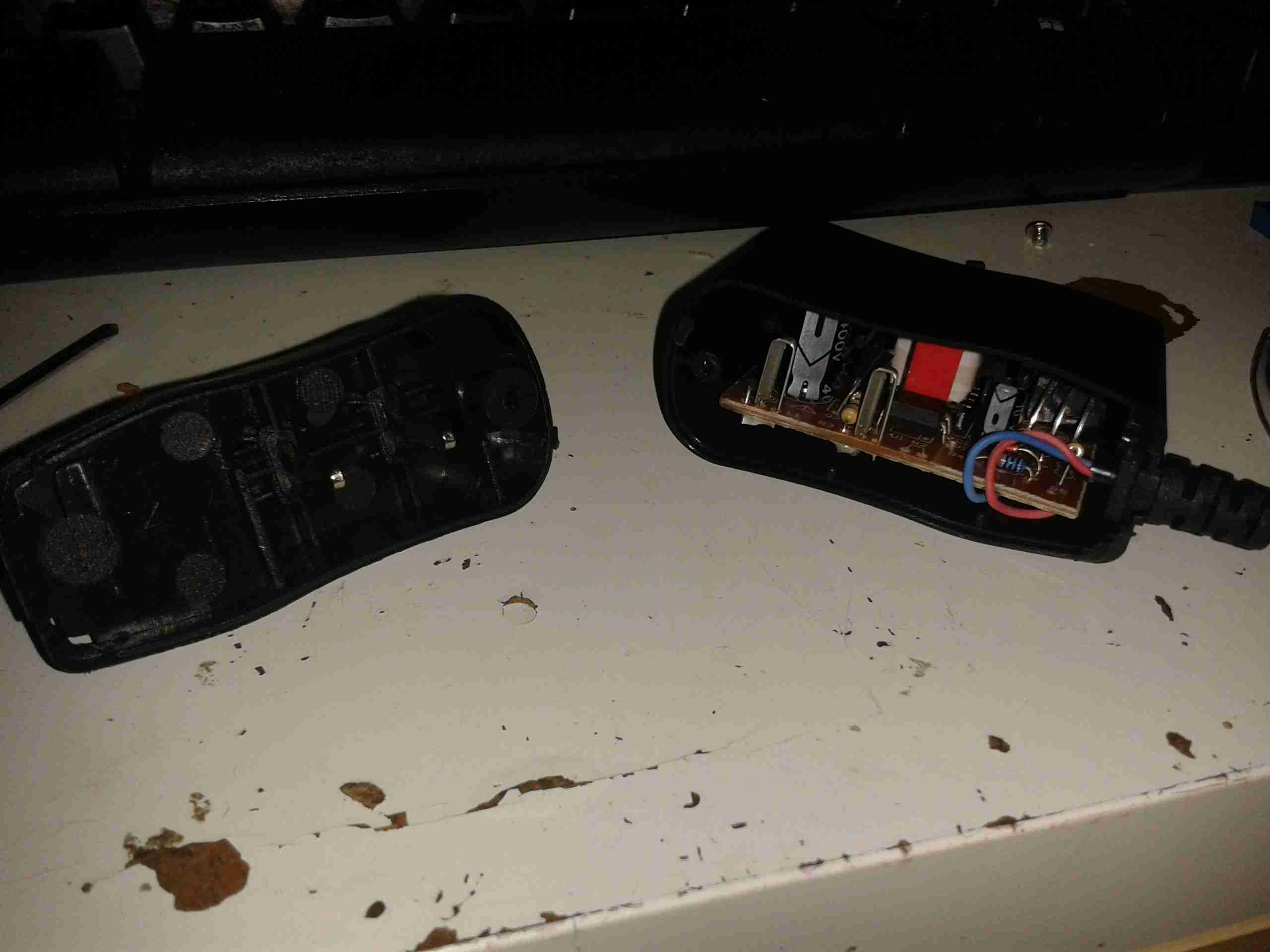
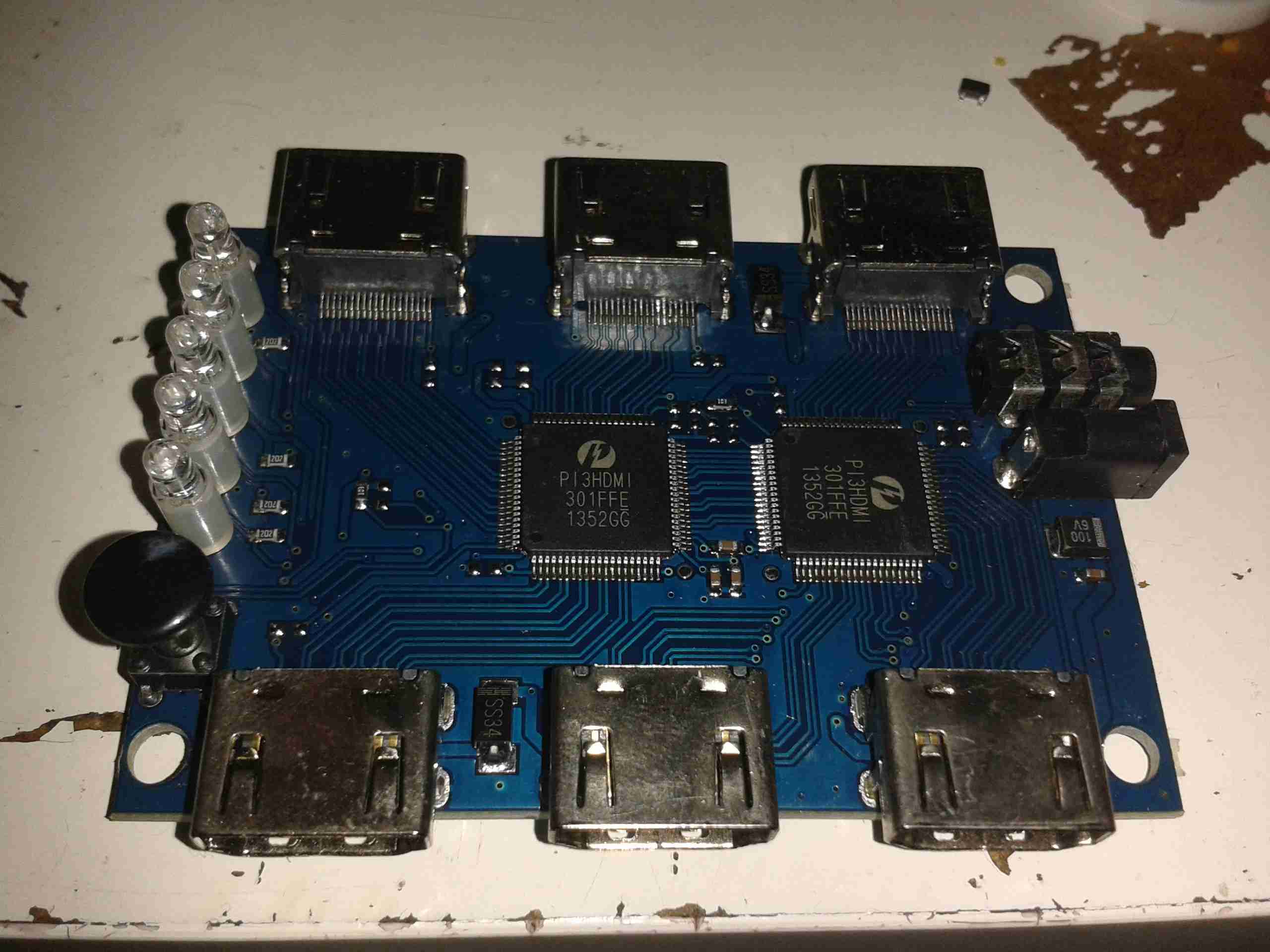
PCB Top
Here’s the PCB out of it’s plastic housing. The main logic is a pair of PI3HDMI303 3:1 HDMI switches from Pericom Semiconductor. These are cascaded for the 5-ports, the first 3 input HDMI ports are switched through both ICs to reach the output.
These HDMI switch ICs are operated with TTL input pins, the combination of these pins held either high or low determines the input port that appears on the output.
There’s a button on the left for switching between inputs, with a row of 5 LED indicators.
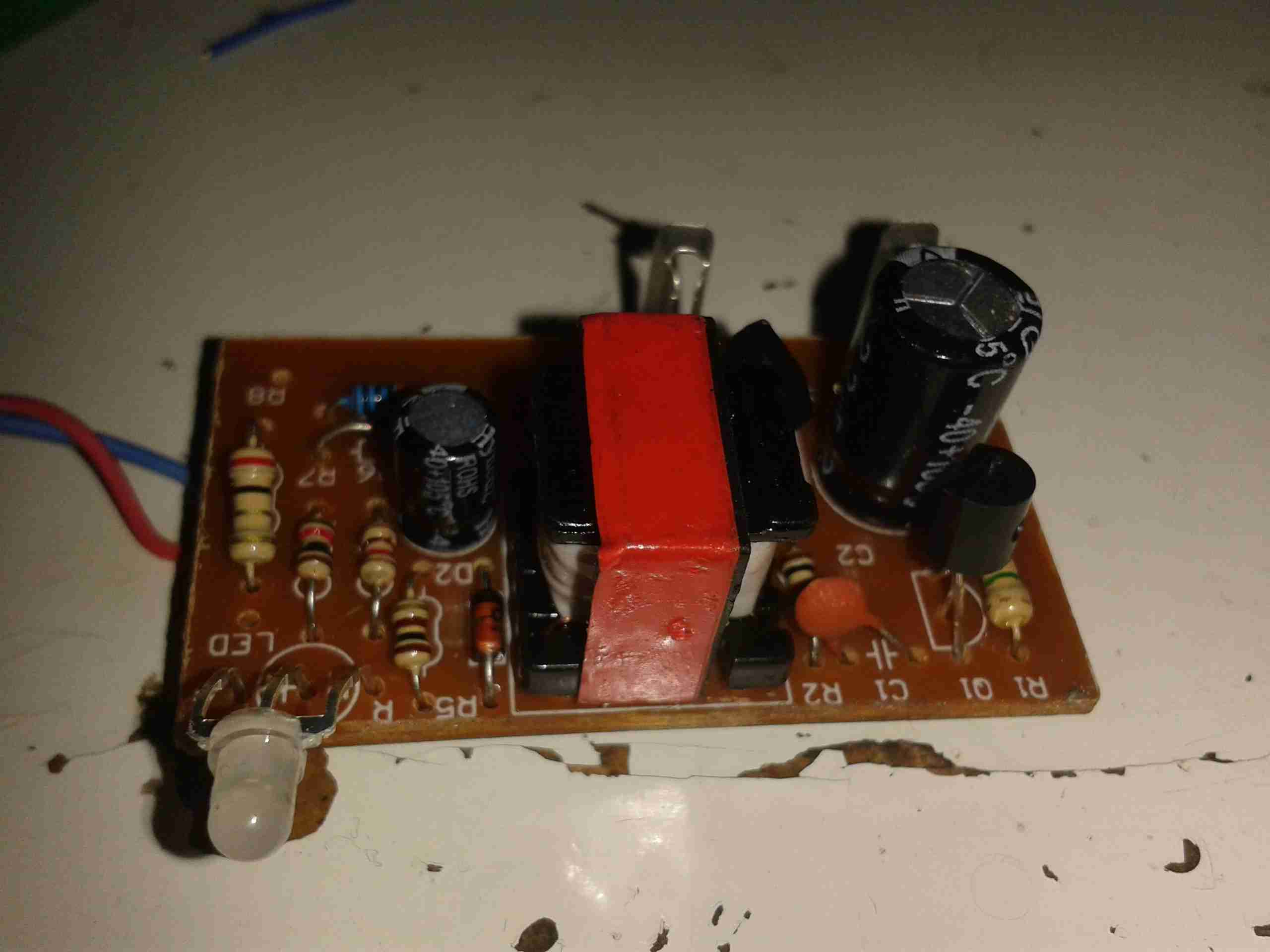
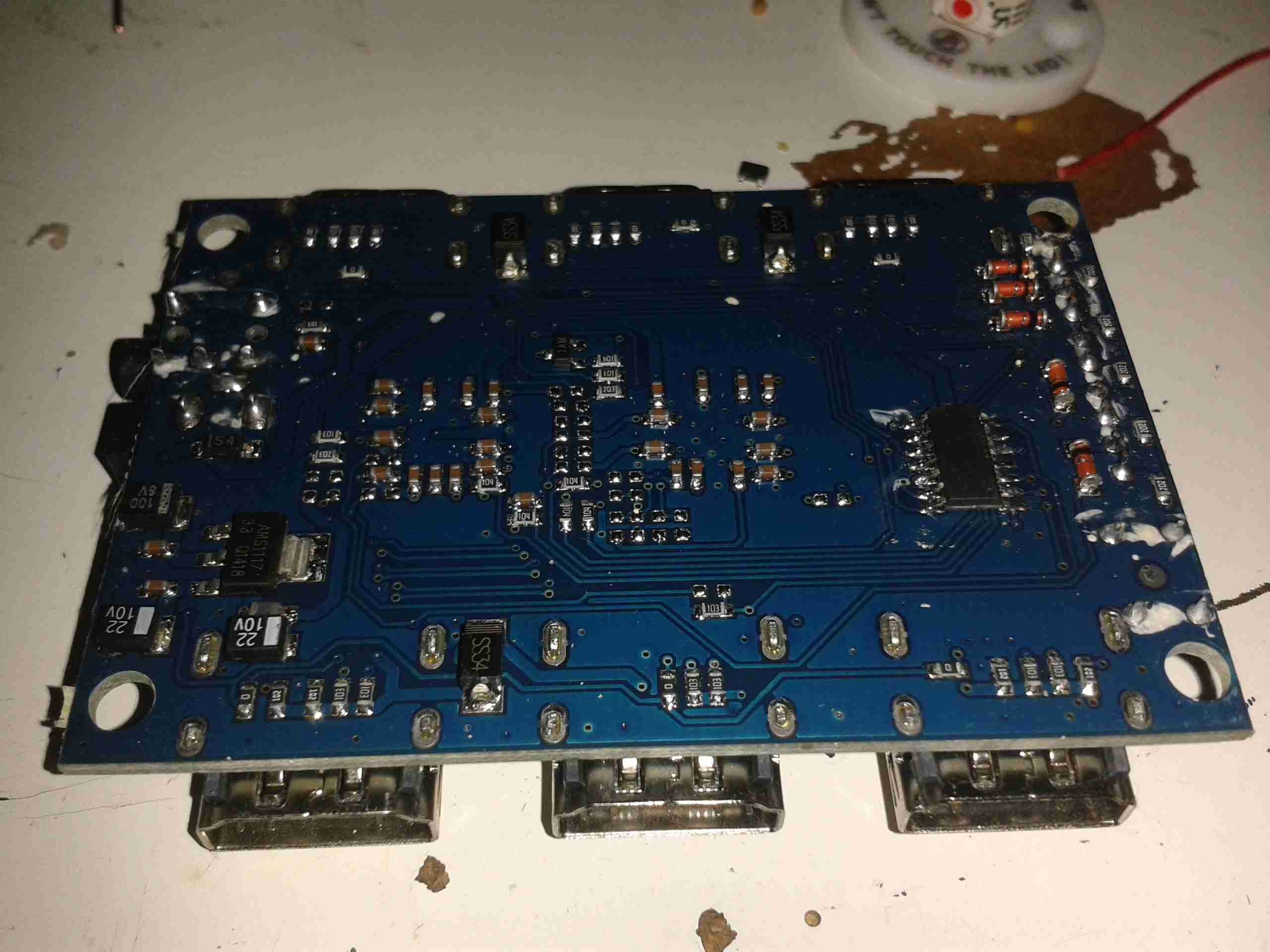
PCB Bottom
Not much on the bottom side, a lot of passives & bypass capacitors. There’s a 3.3v LDO regulator on the left for supplying the main rail to the active switch ICs. The IC on the right doesn’t have any numbering at all, but I’m presuming it’s a microcontroller, dealing with the IR remote input & pushbutton inputs to switch the inputs.
The multimode dimming/flashing modes on Chinese torches have irritated me for a while. If I buy a torch, it’s to illuminate something I’m doing, not to test if people around me have photosensitive epilepsy.
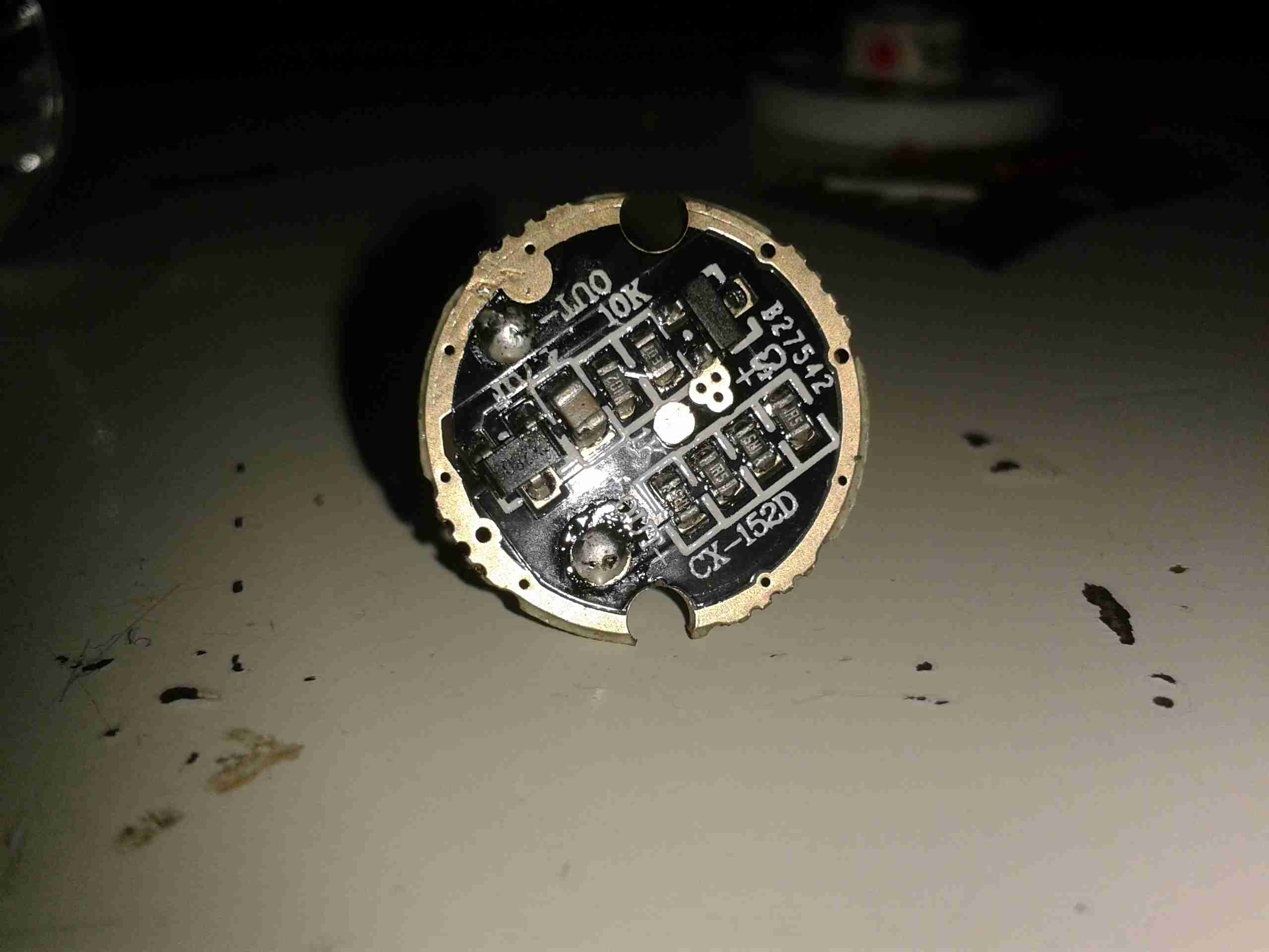
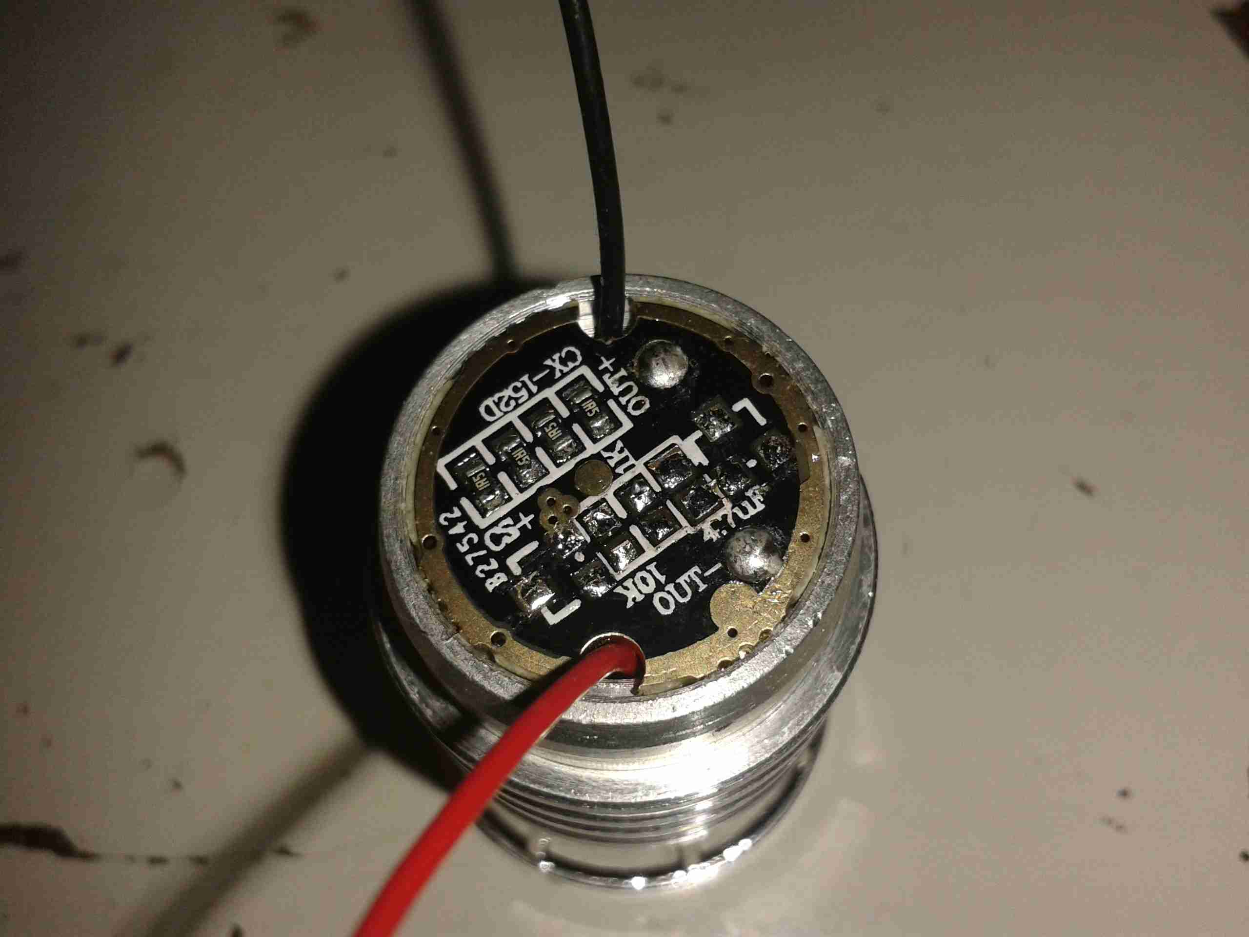
Looking at the PCB in the LED module of the torch, a couple of components are evident:
LED Driver PCB
There’s not much to this driver, it’s simply resistive for LED protection (the 4 resistors in a row at the bottom of the board).
The components at the top are the multimode circuitry. The SOT-23 IC on the left is a CX2809 LED Driver, with several modes. The SOT-23 on the right is a MOSFET, for switching the actual LED itself. I couldn’t find a datasheet for the IC itself, but I did find a schematic that seems to match up with what’s on the board.
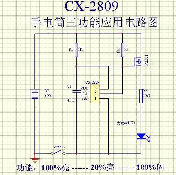
Schematic
Here’s that schematic, the only thing that needs to be done to convert the torch to single mode ON/OFF at full brightness, is to bridge out that FET.
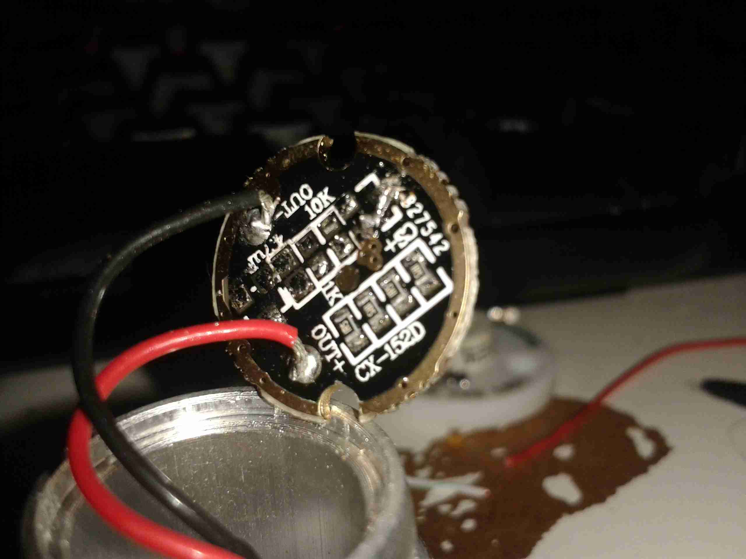
Components Desoldered
To help save the extra few mA the IC & associated circuitry will draw from the battery, I have removed all of the components involved in the multimode control. This leaves just the current limiting resistors for the LED itself.
Jumper Link
The final part above, is to install a small link across the Drain & Source pads of the FET. Now the switch controls the LED directly with no silly electronics in between. A proper torch at last.
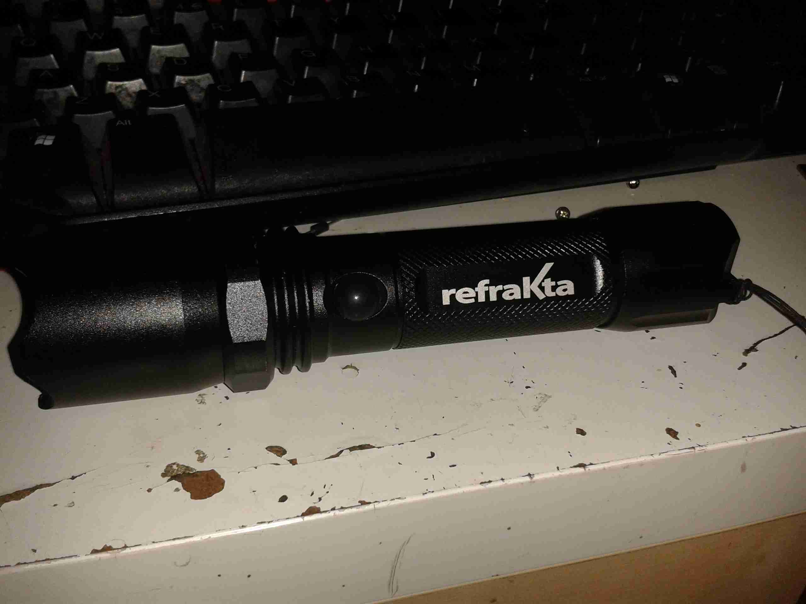
Following on from the teardown & analysis of the charger, here’s the torch itself under the spotlight.
LED Torch
Here’s the torch itself, it’s a sturdy device, made of aluminium. Power is provided by a single 18650 Li-Ion cell.
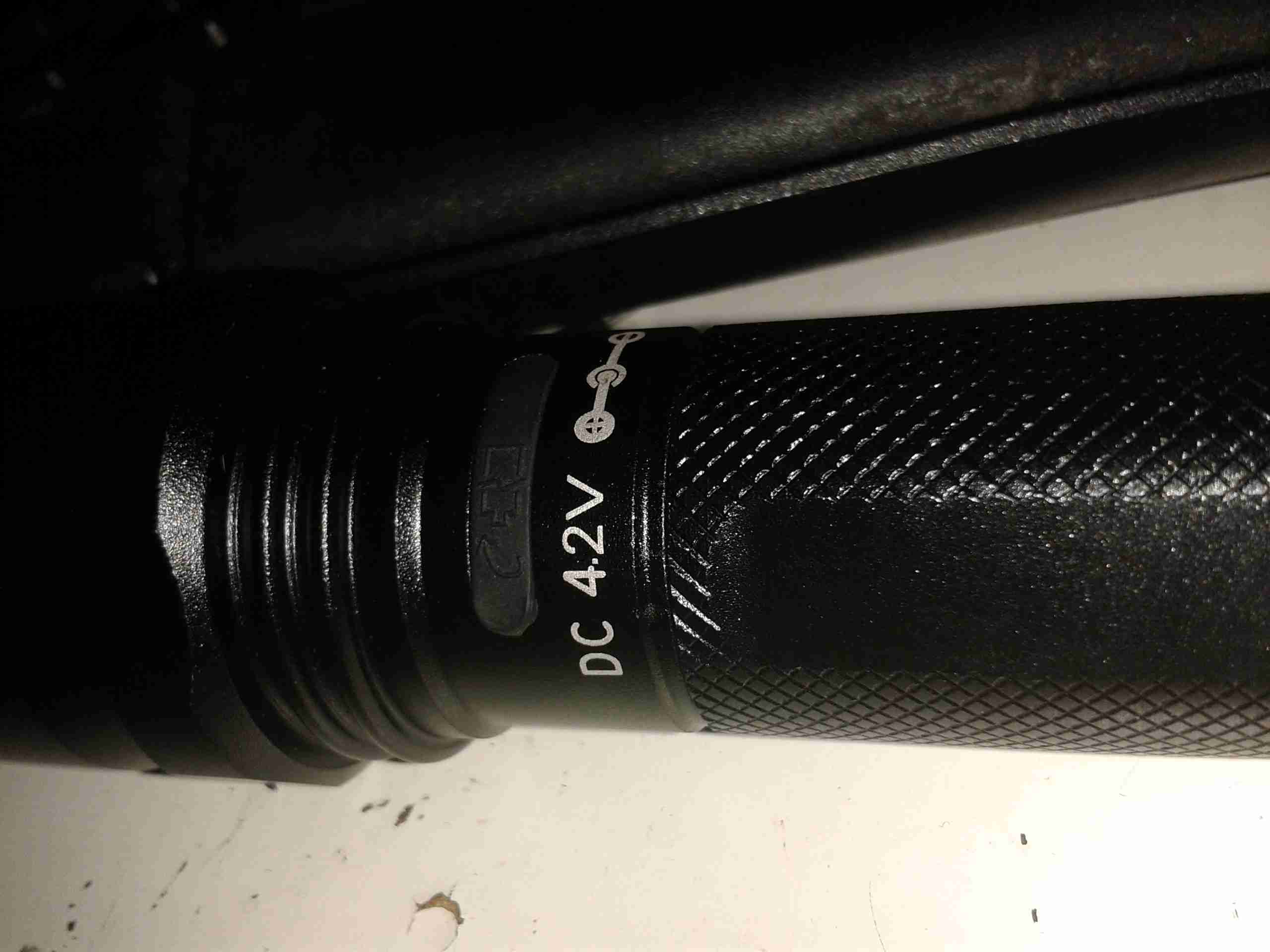
Charging Port
Here’s the charging port on the torch, there’s no electronics in here for controlling the charge, the socket is simply connected directly to the Li-Ion cell, and requires a proper external charger.
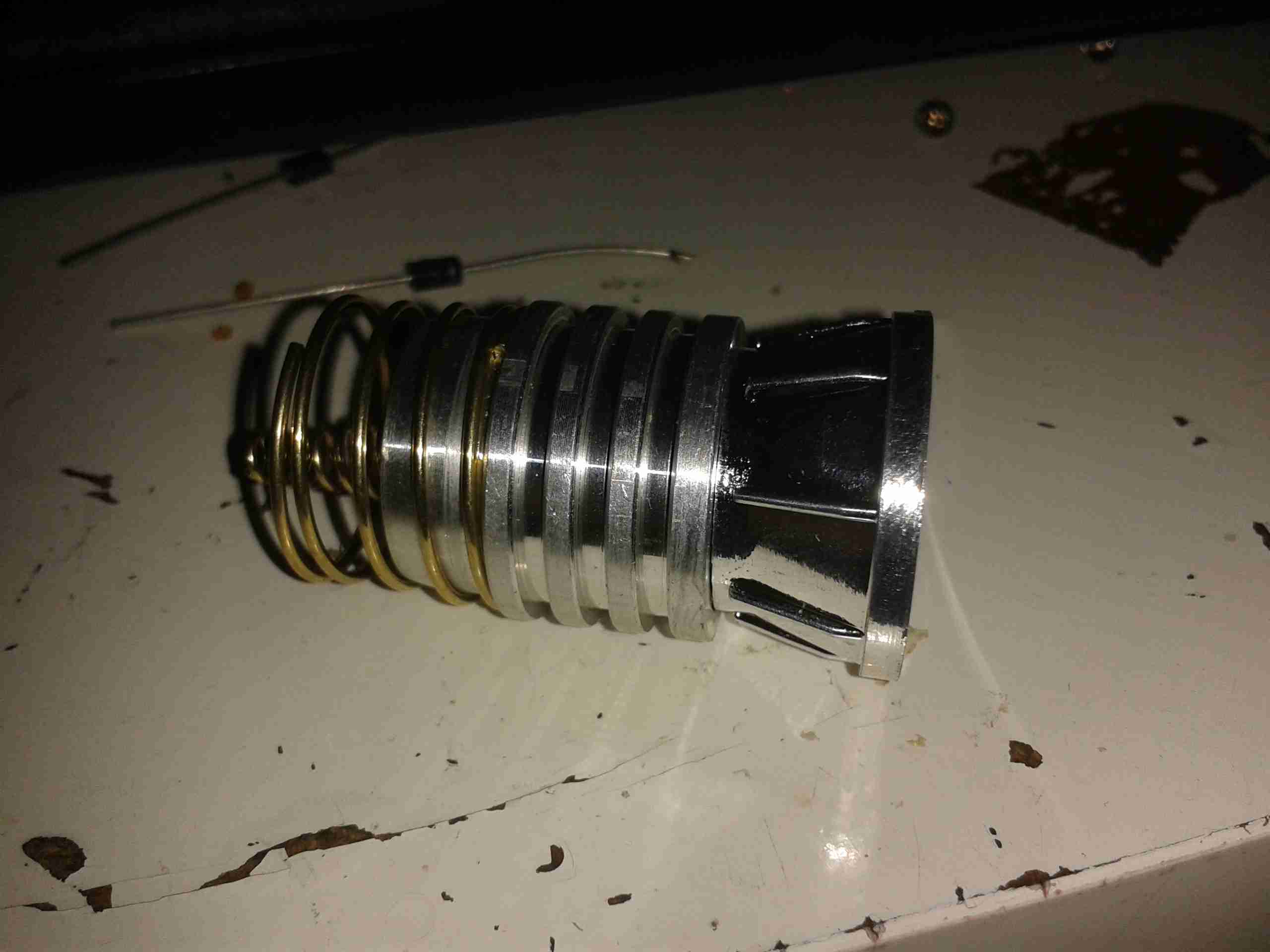
LED Pill
Unscrewing the lens gives access to the LED core, this also unscrews from the torch body itself, leaving the power switch & the battery in the body.
LED Module
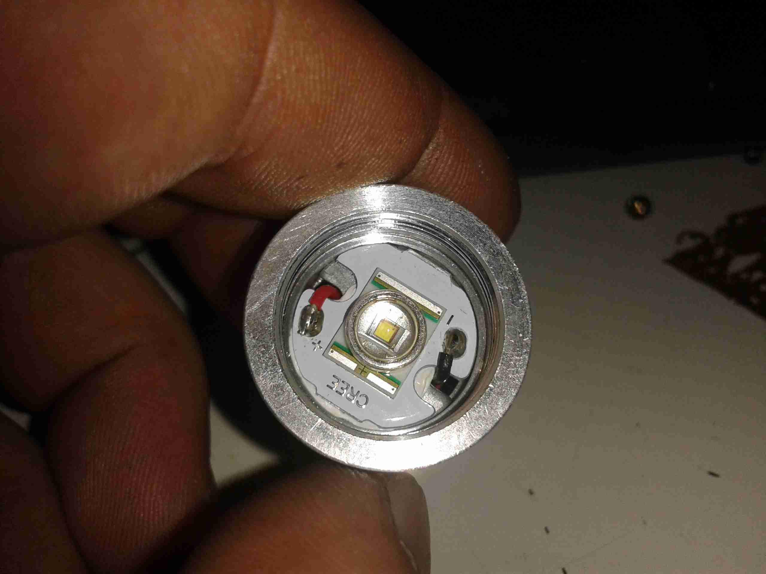
Unscrewing the aluminised plastic reflector reveals the LED itself. Being a new device, I expected an XM-L or XM-L2 Cree LED in here, but it’s actually an XR-E model, a significantly older technology, rated at max 1A of drive current.
LED Back
Popping the control PCB out from the pill reveals a lot of empty space, but the back of the LED is completely covered by a heatsinking plate, which is conducting heat to the main body of the torch.
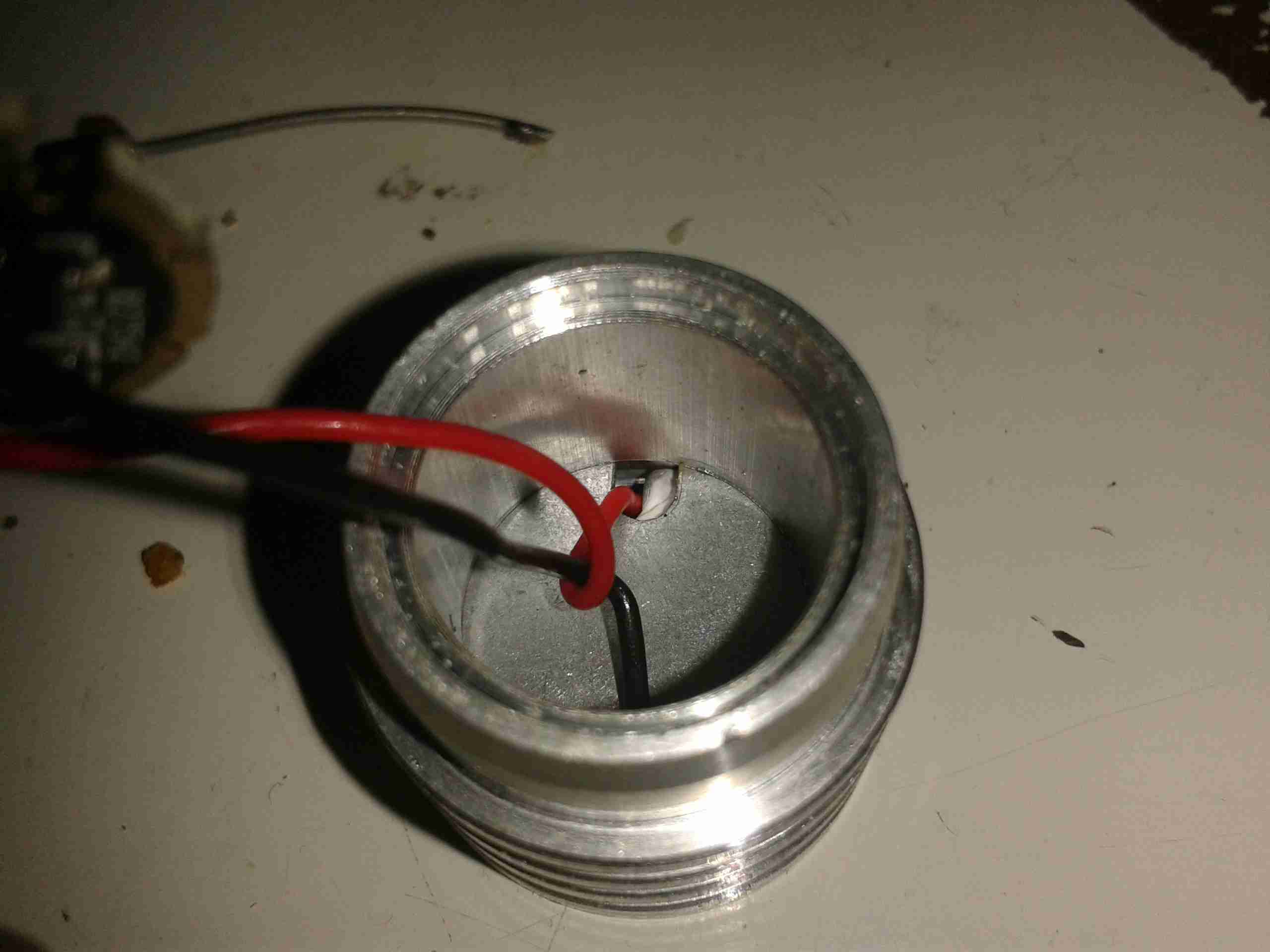
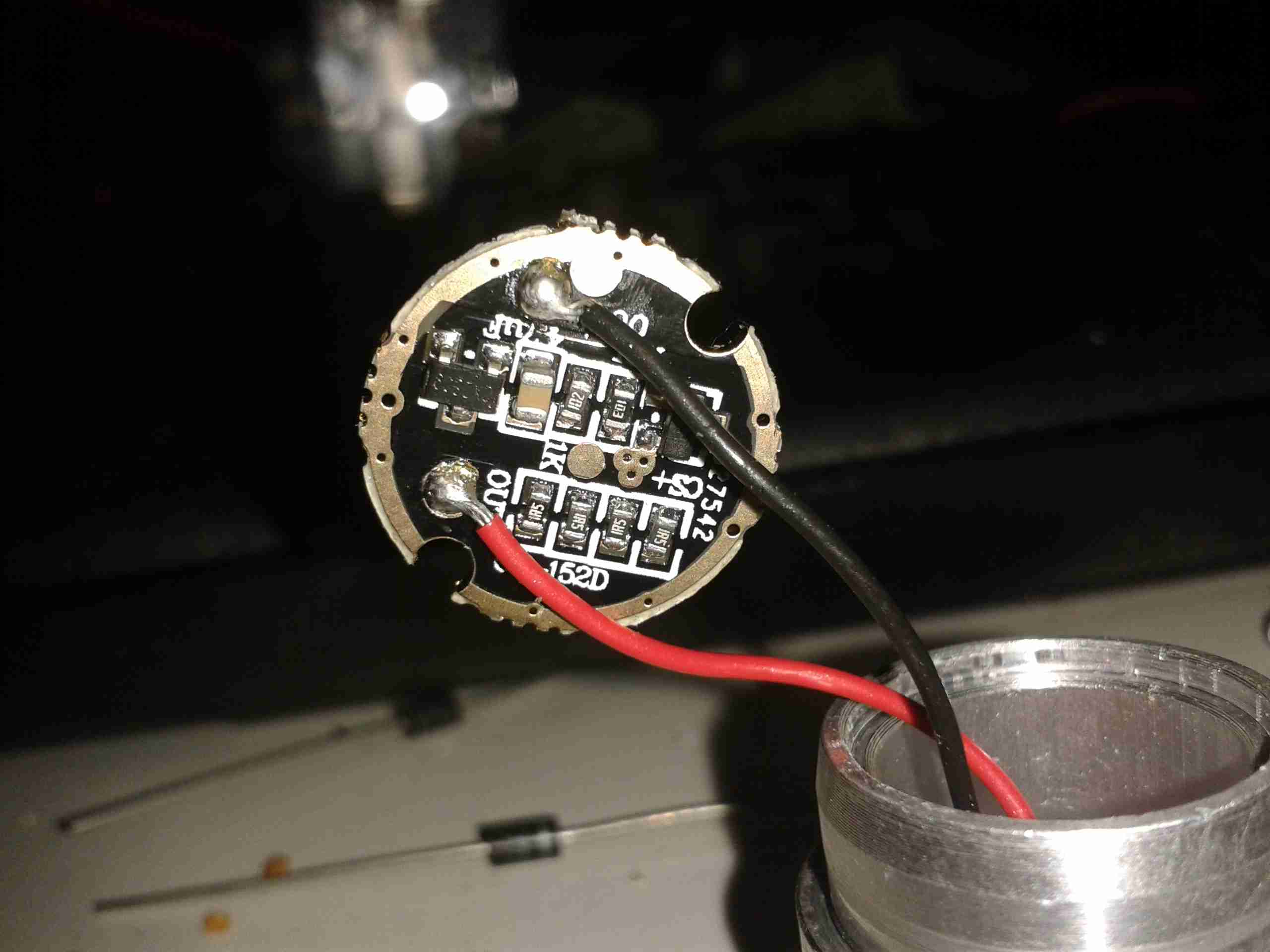
Control PCB
Not much to see on the control PCB, just a bunch of limiting resistors, and a multi-mode LED driver IC in a SOT-23 package. There’s no proper constant-current LED driver, and as the battery discharges the torch will dim, until the low voltage cutout on the cell turns things off completely.
Since I have a fair few 750GB disks sat doing nothing, I figured I’d get some USB3 caddies for them. Back when USB -> IDE caddies appeared, they were hideously expensive. Not so much these days!
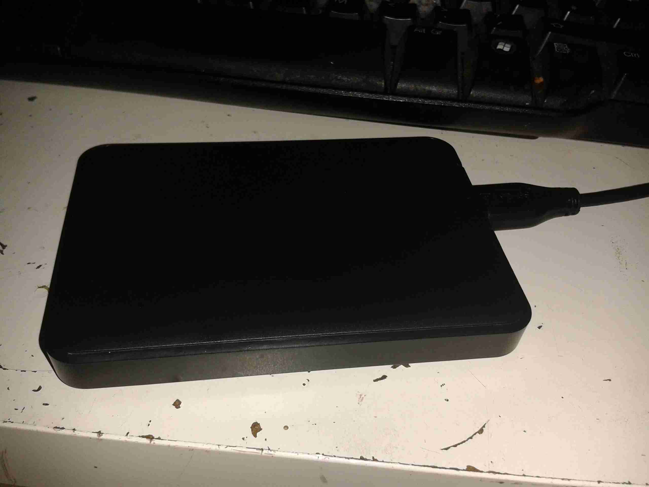
USB HDD
For £6 on eBay, you get a basic plastic box with the required bridge circuitry.
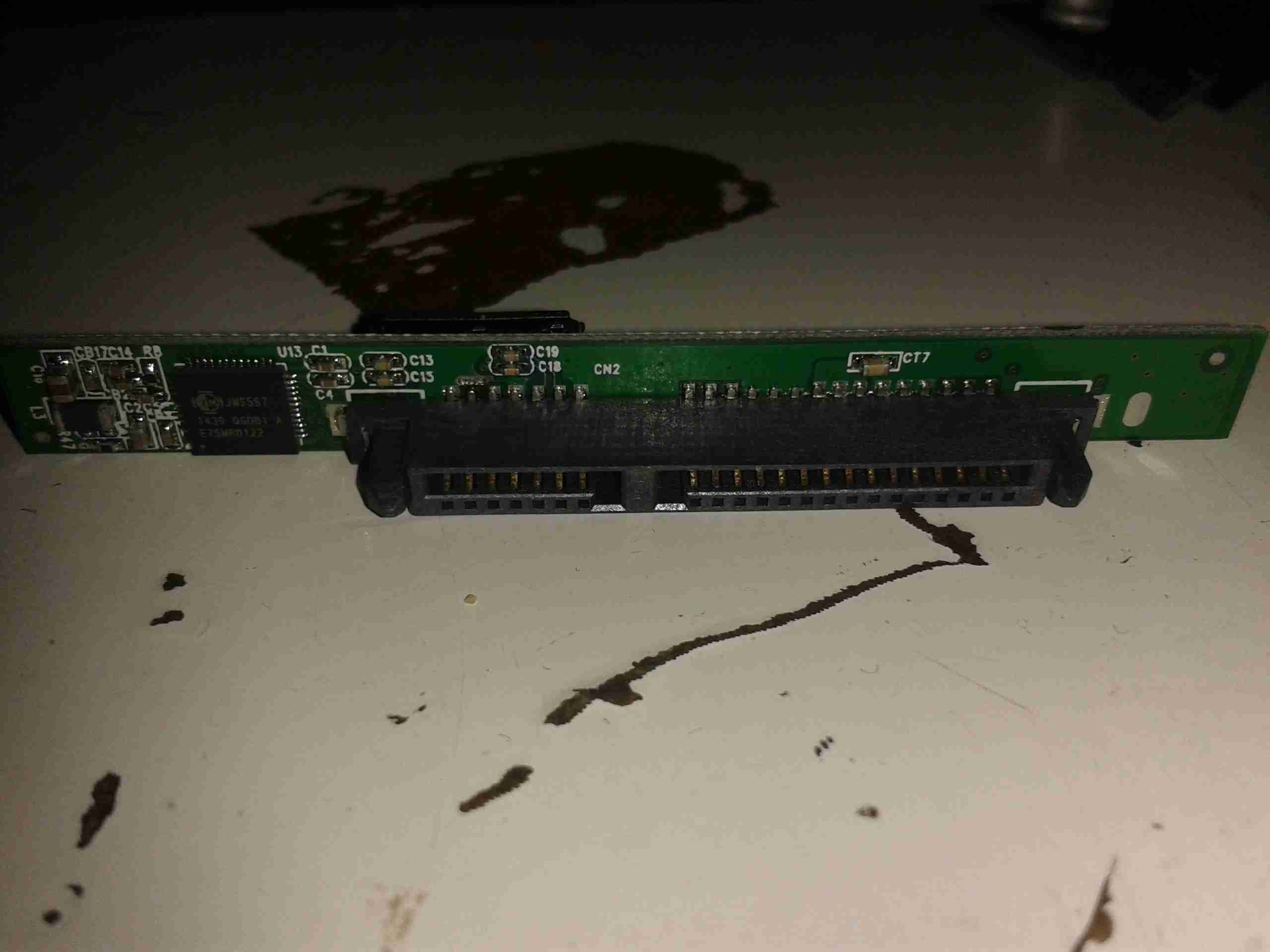
USB – SATA Bridge
Here’s the PCB – a very basic affair, with only 2 ICs. The large QFN IC on the left is the USB-SATA bridge. It’s a JMicron JMS567. Unfortunately JMicron are rather secretive about their bridge chips & I can’t find much information about it, nor a datasheet.
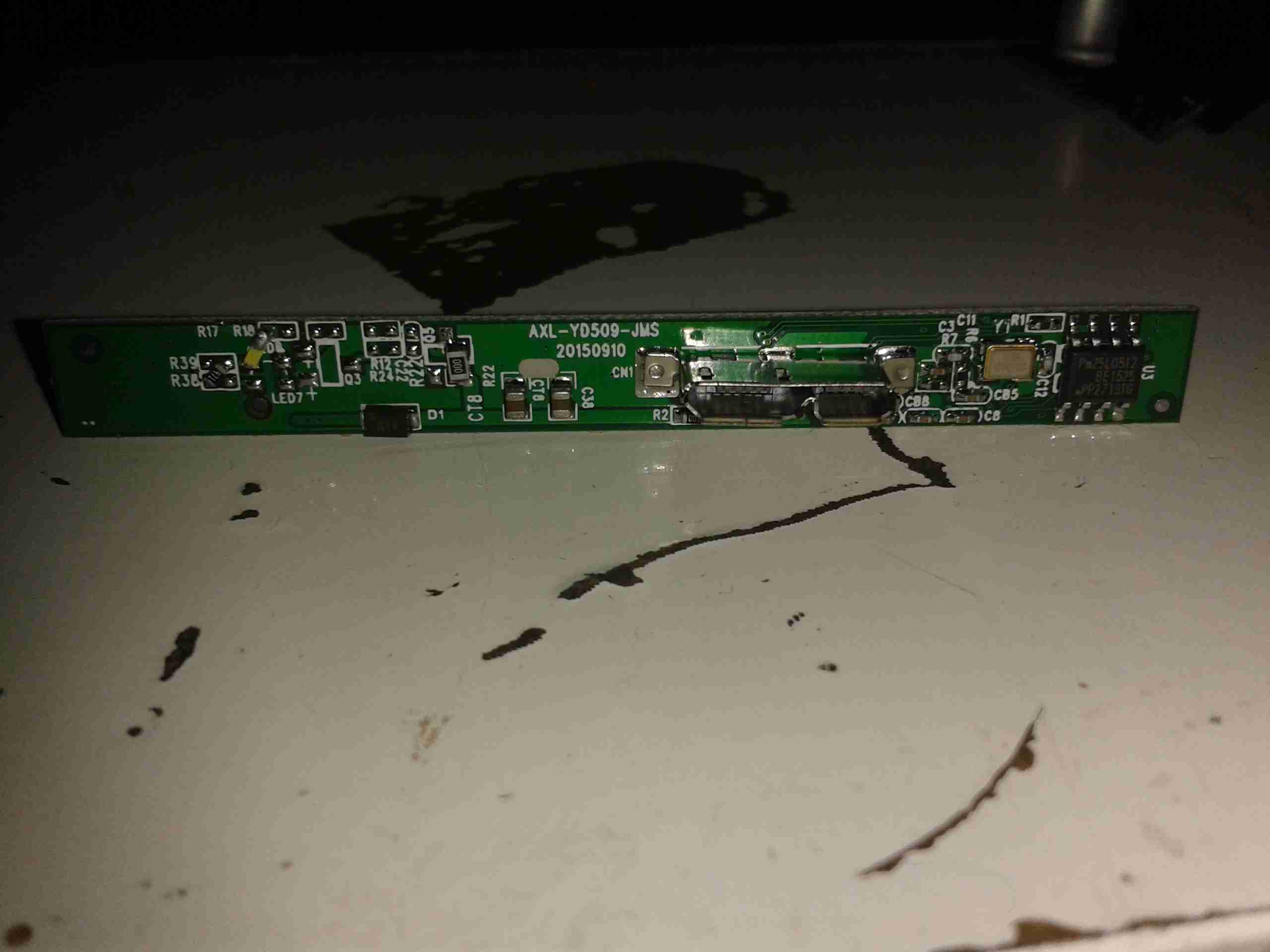
PCB Reverse
Here’s the other side of the bridge PCB – not much on here, the activity indicator LED is a bit of a bodge job, but it’s functional. The IC on the right is a Pm25LD512 512Kbit SPI EEPROM. This is used to store things like the USB device & vendor IDs, device name, type, etc. Here’s what dmesg spits out when the disk is connected on my standard Linux system:
[snippet id=”1769″]
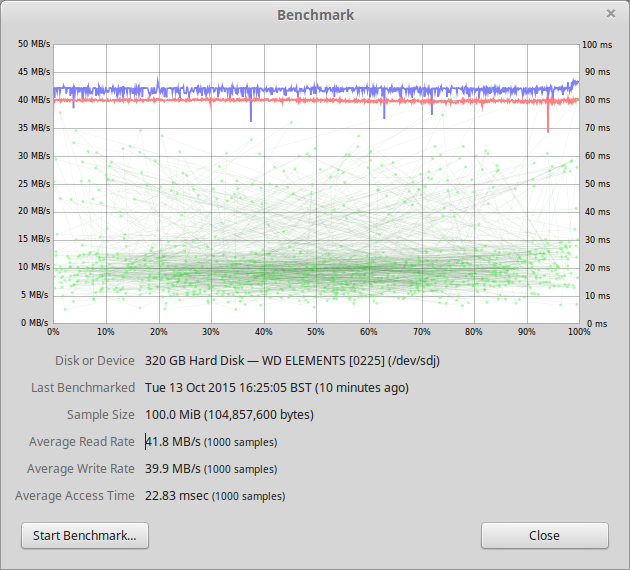
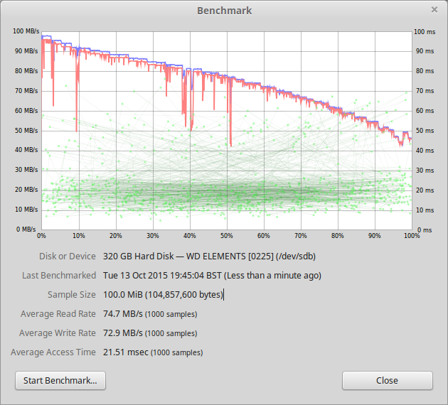
Here’s some speed benchmarks:
USB2 Benchmark
First attached to a USB2 port, above
USB3 Benchmark
And finally attached to a USB3 port, above
Tests were done with a 320GB 5400RPM Samsung HM321HI drive, direct into the root hub, for the shortest possible signal length.
In my previous post, I mentioned I’d be replacing the factory supplied charging gear with something that actually charges lithium chemistry cells correctly.
Charging Base
Here’s the base as supplied, with an indicator LED on the right hand side. This LED indicates nothing other than power being applied to the charging base. It’s just connected across the power input with a resistor. This also means that any battery left in the charger while it’s unplugged will discharge itself through this LED over time. Great design there China!
PCB Removed
Here I’ve removed the PCB – there’s no need for it to be taking up any space, as it’s just a complete waste of copper clad board in the first place. The battery tabs have been desoldered & hot snot used to secure them into the plastic casing.
USB Hole
The charger modules I use are USB powered, so a small hole has been routed out in the casing to allow access to the port.
Charging Module
Here the charging module has been installed & wired to the battery tabs. Output is now a nice 4.18v, and will automatically stop charging when the cell is full.
Safety has been restored!
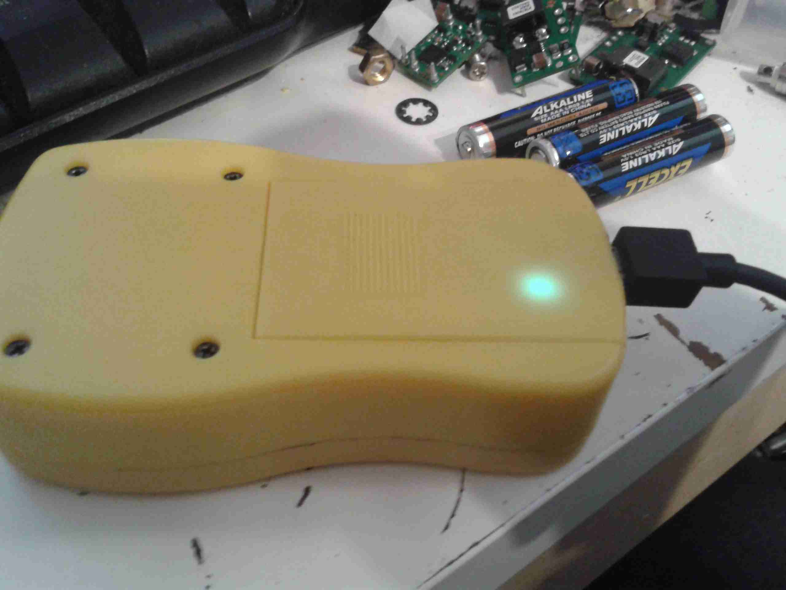
From the factory, the GY561 meter uses alkaline AAA cells for power. As these are not rechargable, and I don’t carry any other devices that take such batteries, I figured I’d replace them with a single Lithium Polymer cell that I can charge via USB.
Battery Compartment
Here’s the battery compartment, with the original spring terminals removed.
I searched eBay for a suitable sized cell, and settled on a 1000mAh type, with dimensions of 47mm x 28mm x 7mm.
This size cell required a small amount of modification to the battery compartment to make it fit properly with the associated charge & protection circuitry.
Modified Compartment
Here’s the modifications made to the compartment, I’ve ground away the plastic to make the bottom flat, and the plastic tabs that retained the original spring terminals.
Modifications
After grinding away the original battery spring holders with a dremel, the cell fits perfectly in the available space. The small PCB on the top of the cell is the USB charger & protection.
Charger
The charger is located in a slot cut in the bottom of the casing, so the USB port is accessible from outside the compartment.
Wiring
Here’s the rest of the wiring completed, with the power wires going through holes in the bottom of the battery compartment to join onto the PCB where the original terminals were located. I have insulated the solder joints on the control PCB with some Kapton tape to prevent any shorts against the lithium cell.
Battery Cover
A small cutout was also required in the battery cover to allow the USB connector to poke out. This was easy to do on the soft plastic with a Dremel tool.
Charging Port
With the battery cover installed, the USB port is nicely recessed into the edge.
Charging LED
The indicator LEDs on the charging & control board show nicely through the plastic, here’s the unit on charge. When the charge is complete, another LED lights as shown below.
There are times when I am frequently away from home base, usually either on the canal system or at a festival. During these times it’s very handy to be able to just grab a bag, without having to be concerned about sorting everything out.
This post will only detail the portable shack bag. The power supply kit that goes along with it with be detailed in another post.
The bag I use is an VHS Camcorder bag from the early 80’s. It’s very well built, & copes easily with the weight of all the radio gear.
Total weight for this system is 13.4lbs (6kg).
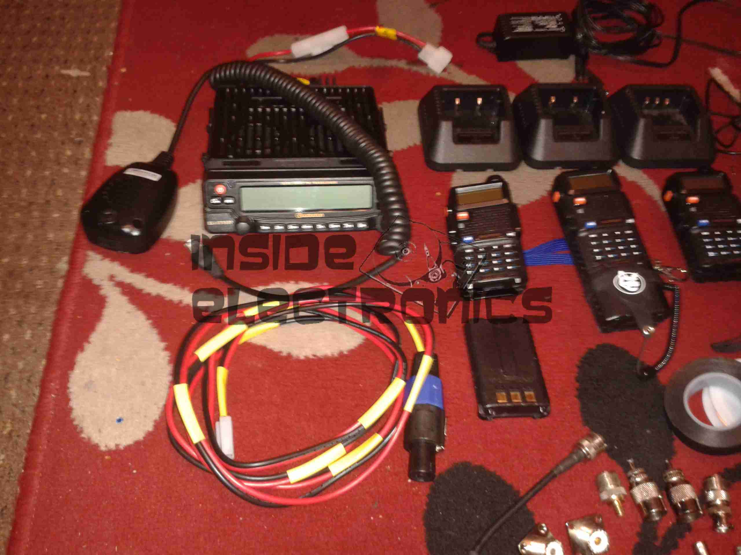
Mobile Radio Bag
Above is the bag packed. Obligatory International Ameteur Radio Symbol patch front & centre. Being an old camera bag, this easily slings over the shoulder, with it’s padded strap.
Current Equipment
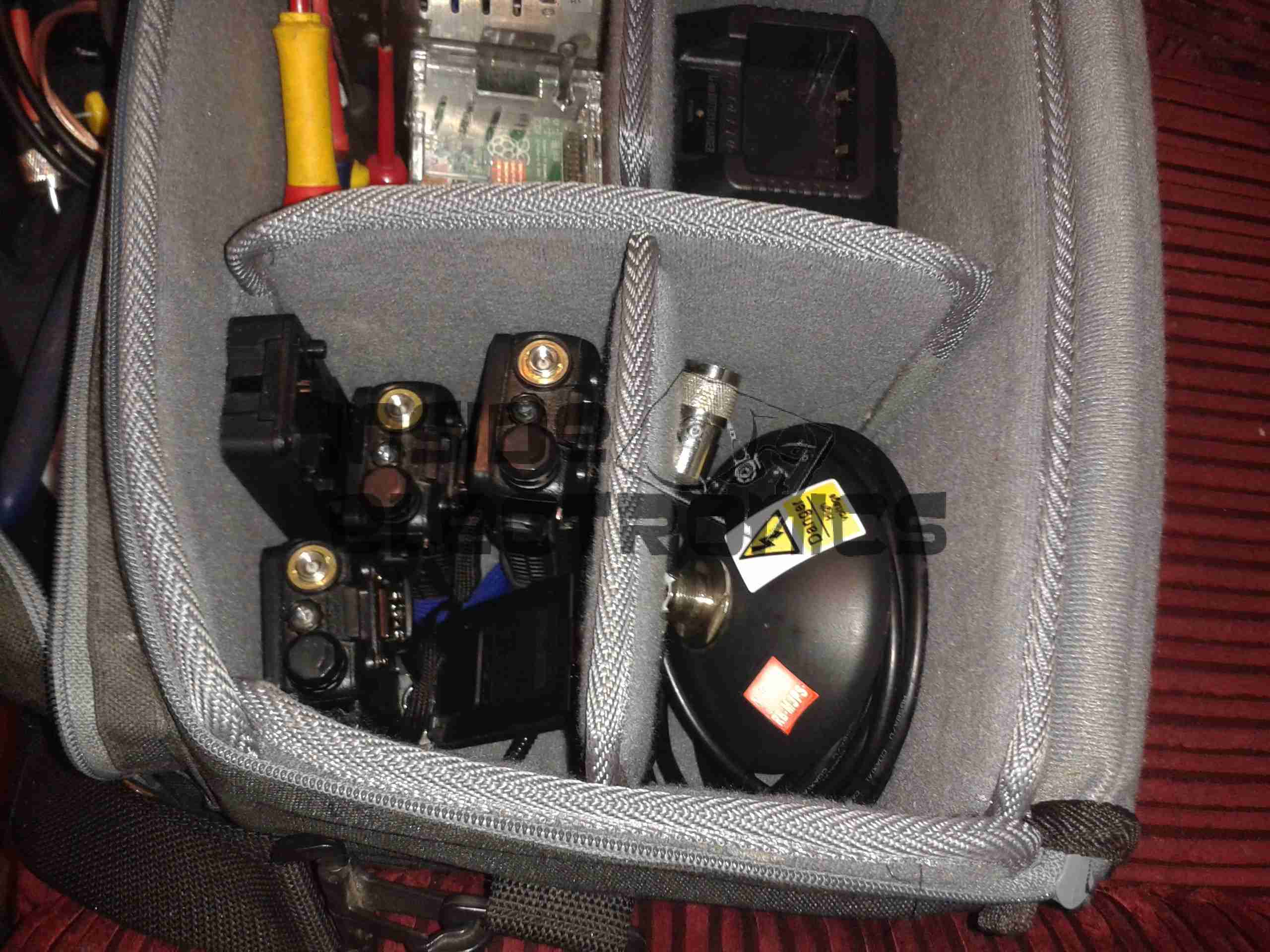
Here is all the current equipment laid out. All the equipment to enable me to set up a station anywhere.
In the following photos I will go into the details.
Main Radio
First off, my main radio. This is the same Wouxun KG-UV950P mobile rig I have posted about previously. I have heatshrunk the power cable to keep it together & attached my standard power connector to the end. More on these later on.
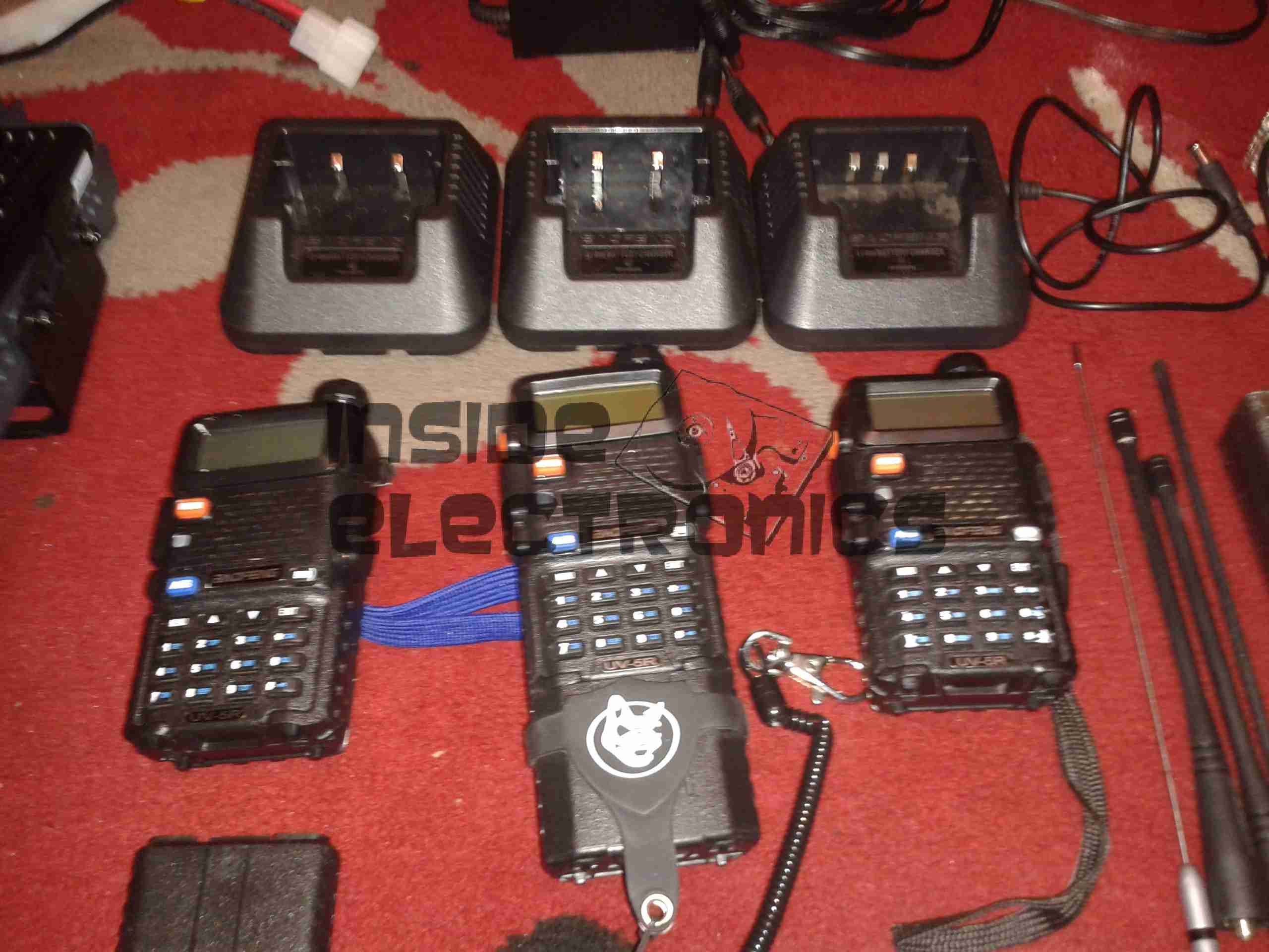
HTs
In the bag I also carry three Baofeng UV-5R handhelds. Extremely useful for short range site communications, along with their charger bases. The charging base on the right has been slightly modified to support charging of my main LED torch as well, which uses similar Li-Ion based packs as the Baofengs.
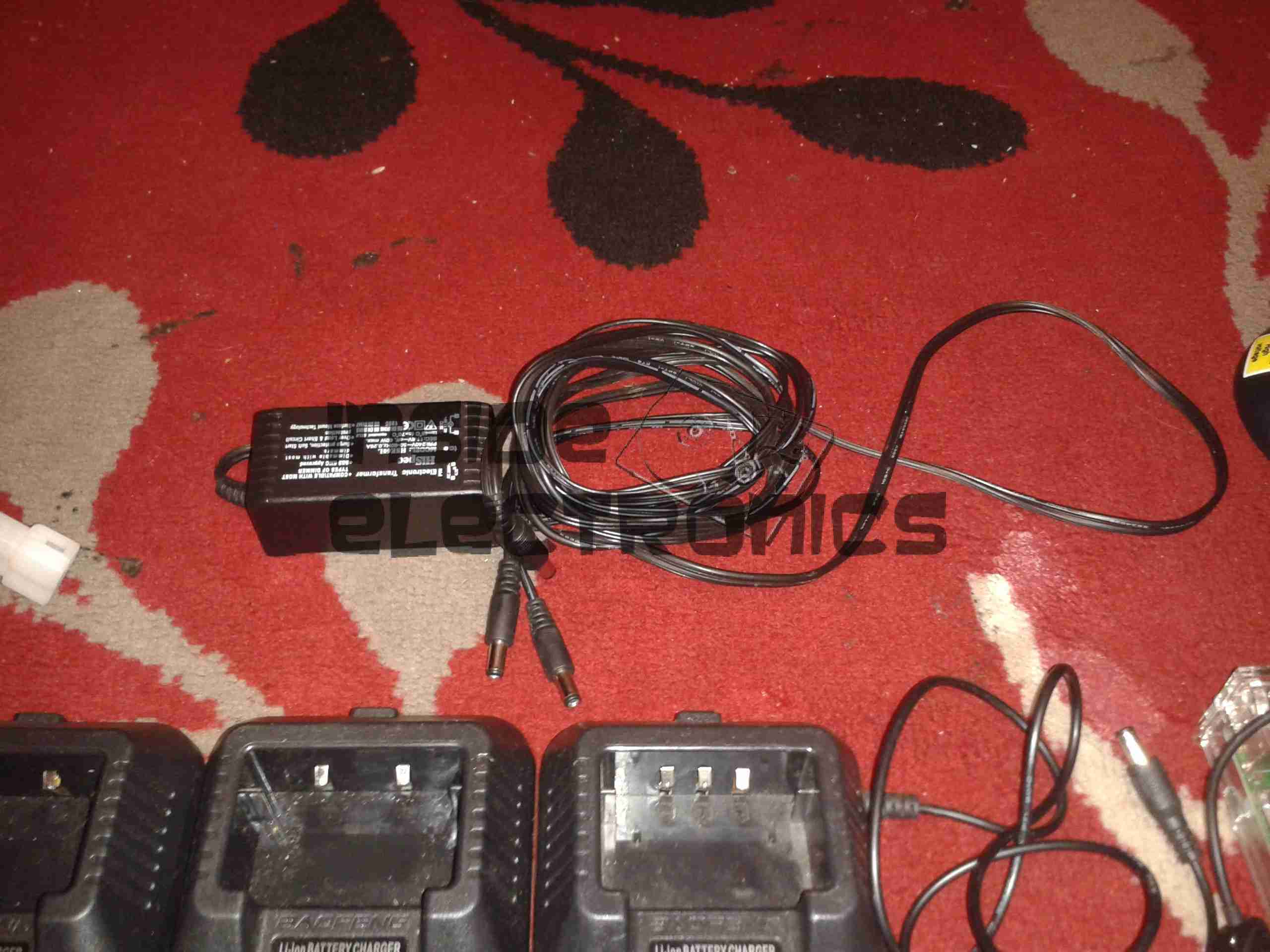
Baofeng 12v Charger
As the charger bases for the Baofeng HTs take a supply of 10v DC, I have constructed a 12v adaptor system for them. (Which utter prat of an engineer at Baofeng picked 10v?)
Linear Amplifier & SWR Meter
Also included is a small Alinco ELH-2320 35W 2m linear amplifier. This was given to me from the local HackSpace in Manchester. (They don’t have any ham members, besides myself). Also here is my small SWR & Power meter, SDR kit & a pair of syringes. These are filled respectively with Copaslip copper loaded grease, (very good for stopping fasteners exposed to the weather from seizing up), and dielectric silicone grease. (I use this stuff for filling connectors that are exposed to the weather – keeps the water out).
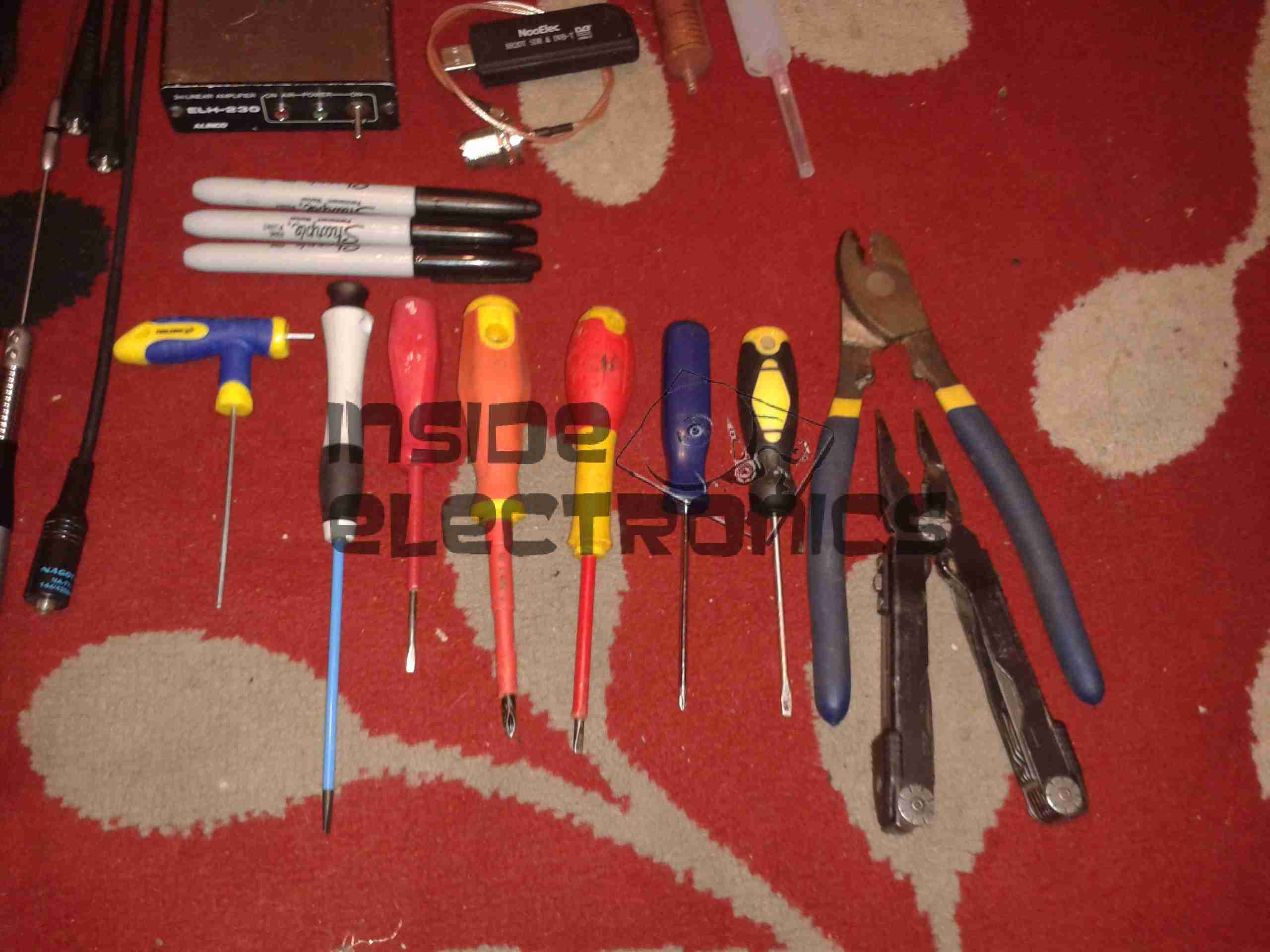
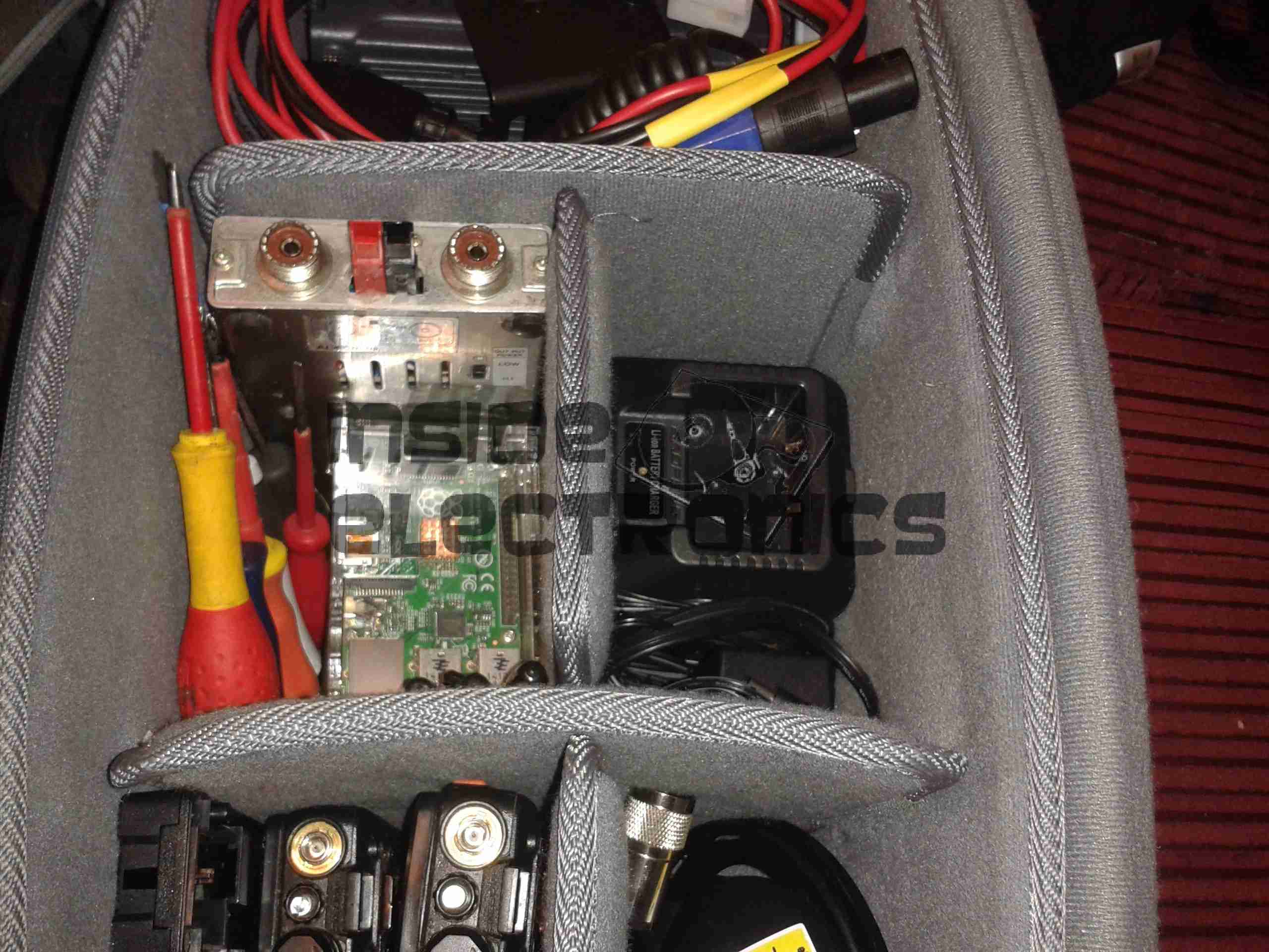
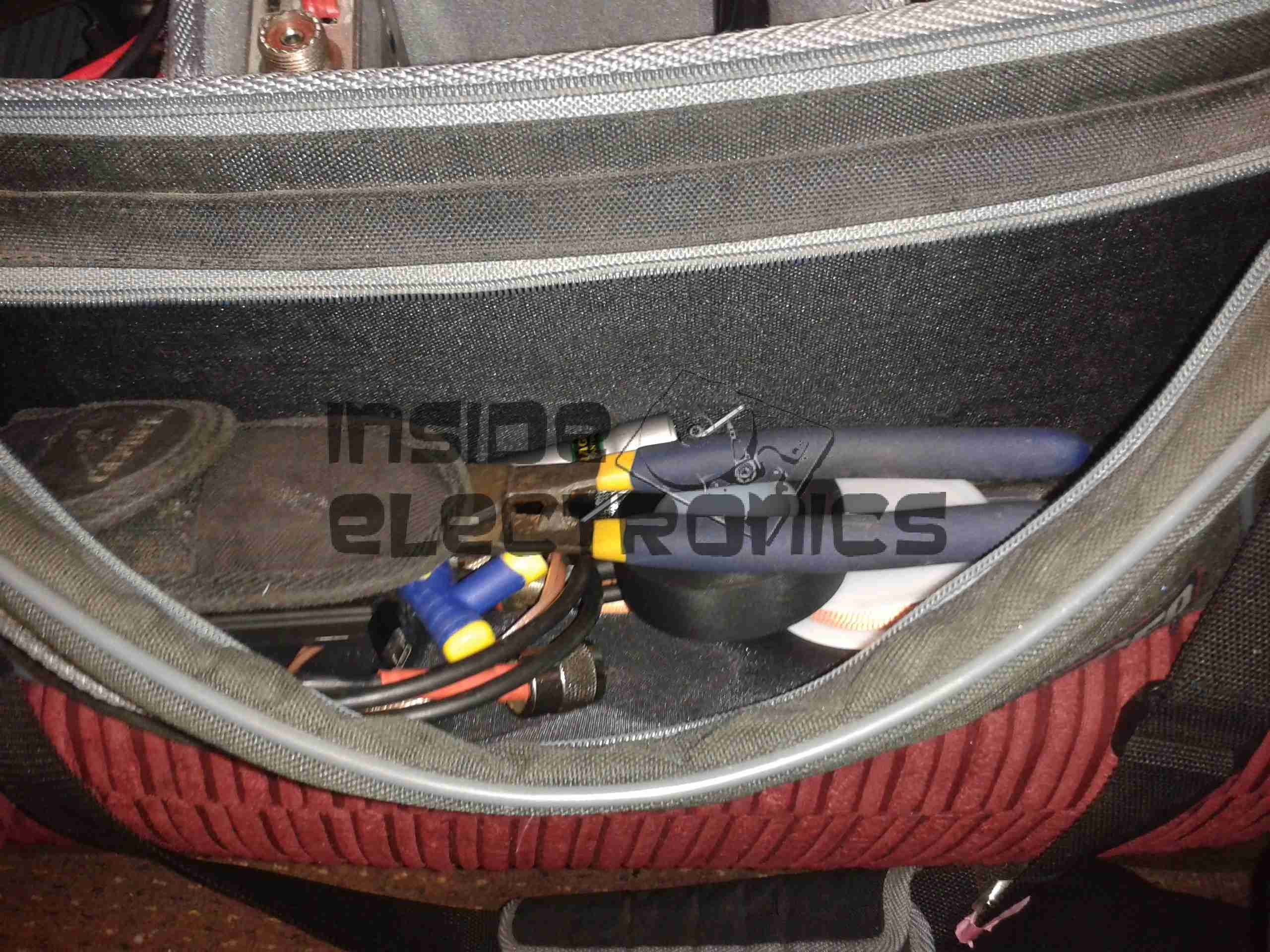
Tools
I always keep essential tools in the bag, here is the small selection of screwdrivers which fit pretty much any screw fastener around, my heavy-duty cable shears (these buggers can cut through starter cable in one go!) and my trusty Gerber Diesel multitool.
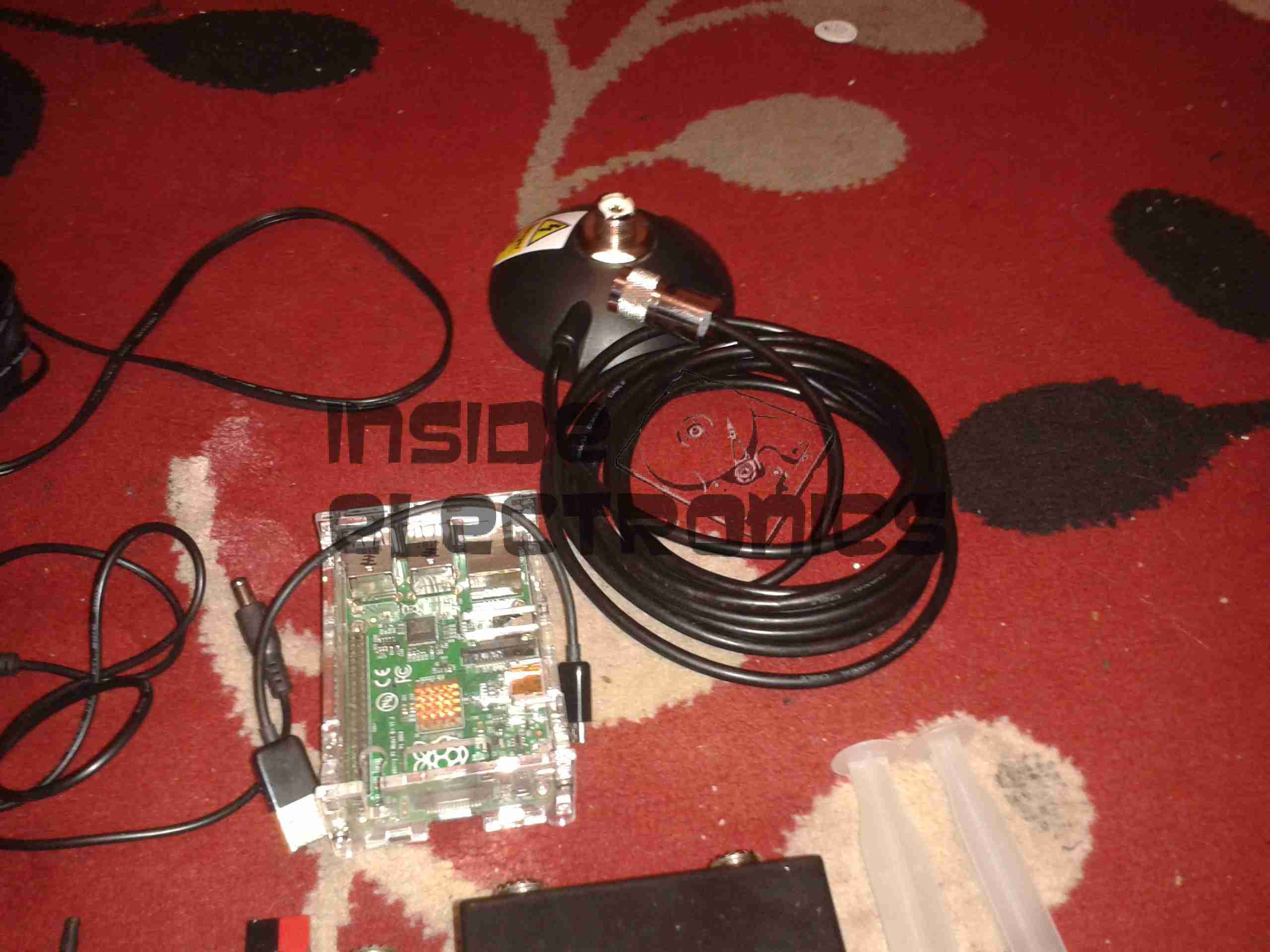
Magmount & Pi
Main antenna magmount & a spare Raspberry Pi.
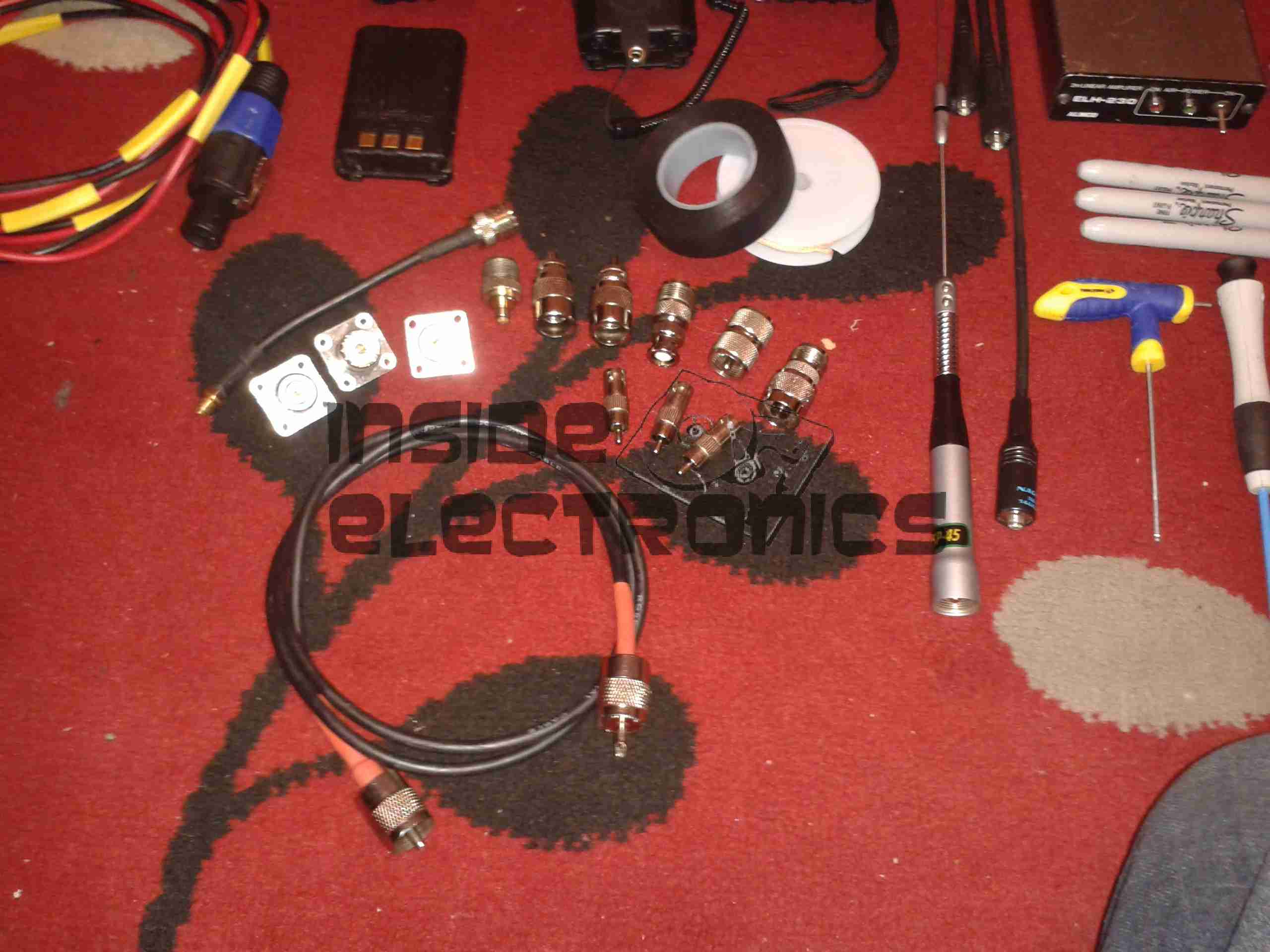
Antenna, Patch Leads, Etc.
Finally, the antennas for the HTs, main dual-band antenna (Nagoya SP-45) for the magmount, a small selection of spare plugs, sockets & adaptors. Also here is a roll of self-amalgamating tape, very handy for waterproofing wiring connections (especially when used in conjunction with the silicone grease), & a roll of solder wick.
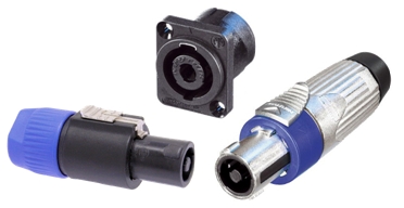
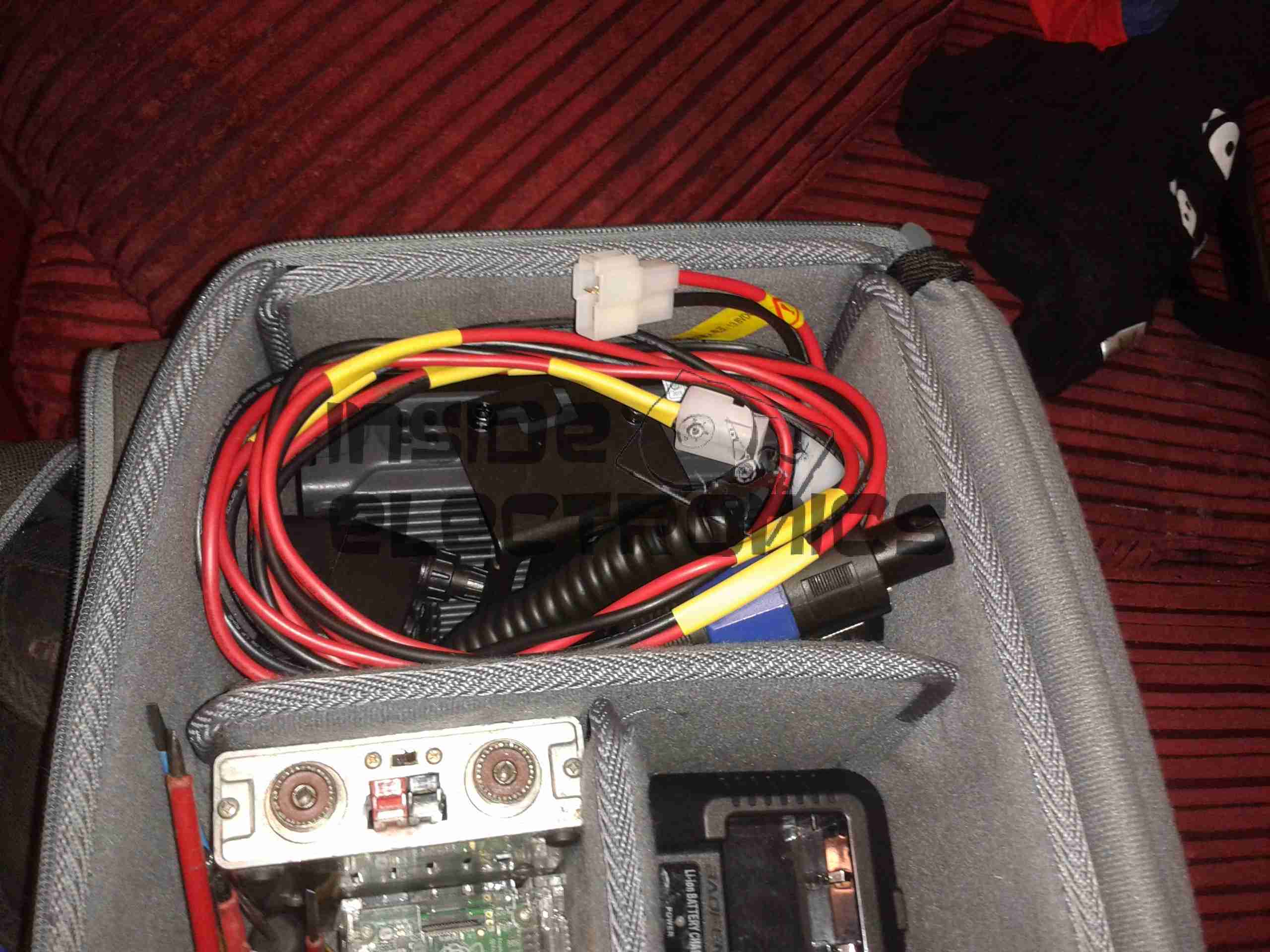
Now, the main power connectors of choice for my equipment are Neutrik SpeakOn type connectors:
Neutrik SpeakOn
These connectors have many advantages:
They are positive locking connectors. No more loose connections.
They have a high continuous current rating of 30A RMS.
Relatively weather resistant.
Also, they have two pairs of pins – and as some of my bigger non-radio related equipment is 24v, this allows me to use a single set of plugs for everything. Without having to worry about plugging a 12v device into a 24v socket, and letting out the magic blue genie.
Once everything is packed up, here’s the bag:
Packed
Everything has a neat little pocket for easy access. Some closeups below.
Here’s another viewfinder CRT, removed from a 1980’s vintage VHS camera I managed to get cheap from eBay.
This unit is very similar to the last one I posted about, although there are a few small differences in the control circuitry.
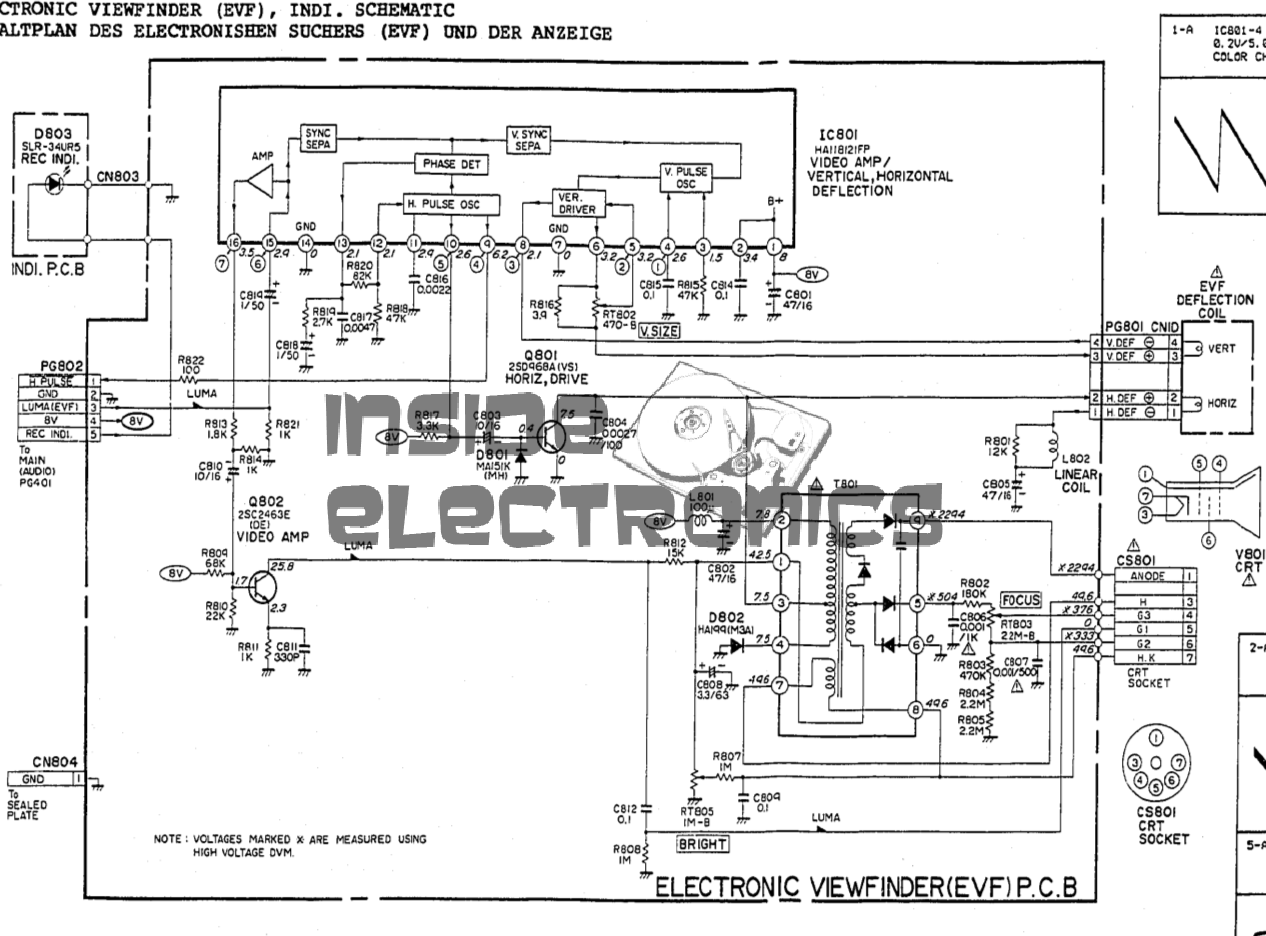
Viewfinder Schematic – Click to Embiggen
Here’s the schematic, showing all the functional blocks of the viewfinder circuitry. An integrated viewfinder IC is used, which generates all the required scan waveforms for the CRT.
On the left is the input connector, with the power & video signals. Only pins 2 (GND), 3 (Composite video), & 4 (+8v) are needed here. Pin 1 outputs a horizontal sync signal for use elsewhere in the camera, while pin 5 fed the recording indicator LED.
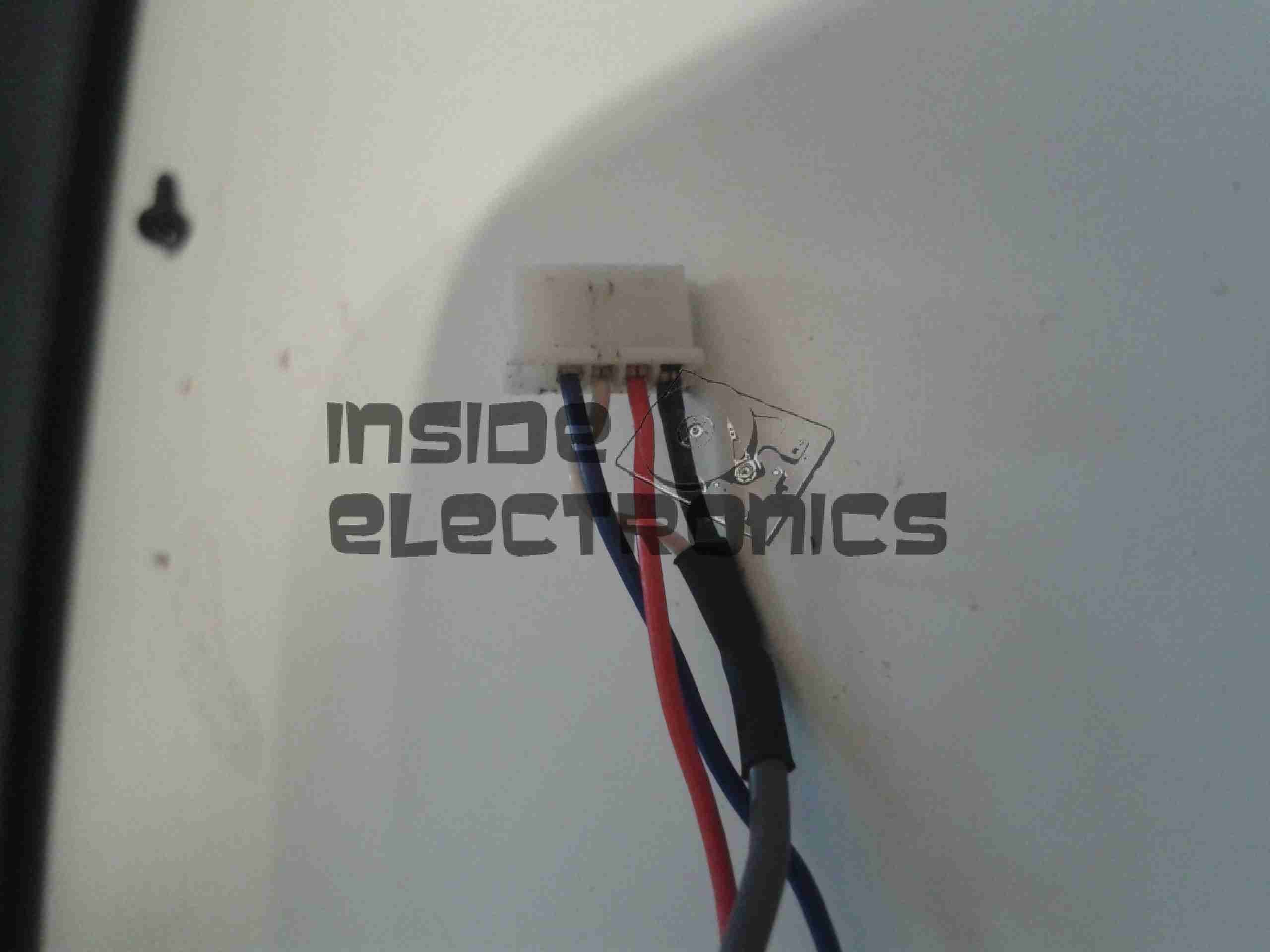
To make connection easier, I have rearranged the wires in the input connector to a more understandable colour scheme:
Input Connector
Red & Blue for power input, & a coax for the video. For the video GND connection, I have repurposed the Rec. LED input pin, putting a shorting link across where the LED would go to create a link to signal ground. Keeping this separate from the power GND connection reduces noise on the CRT.
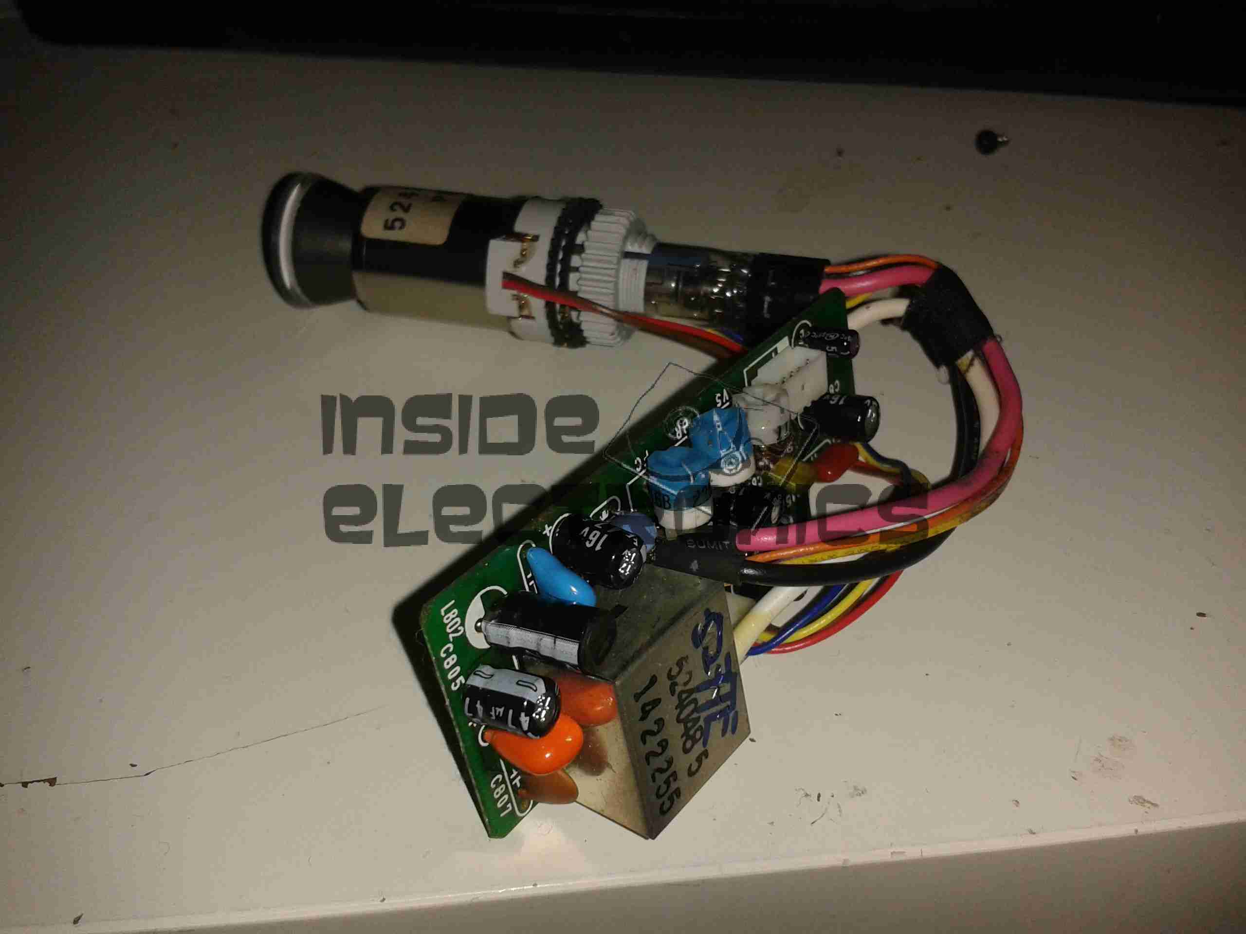
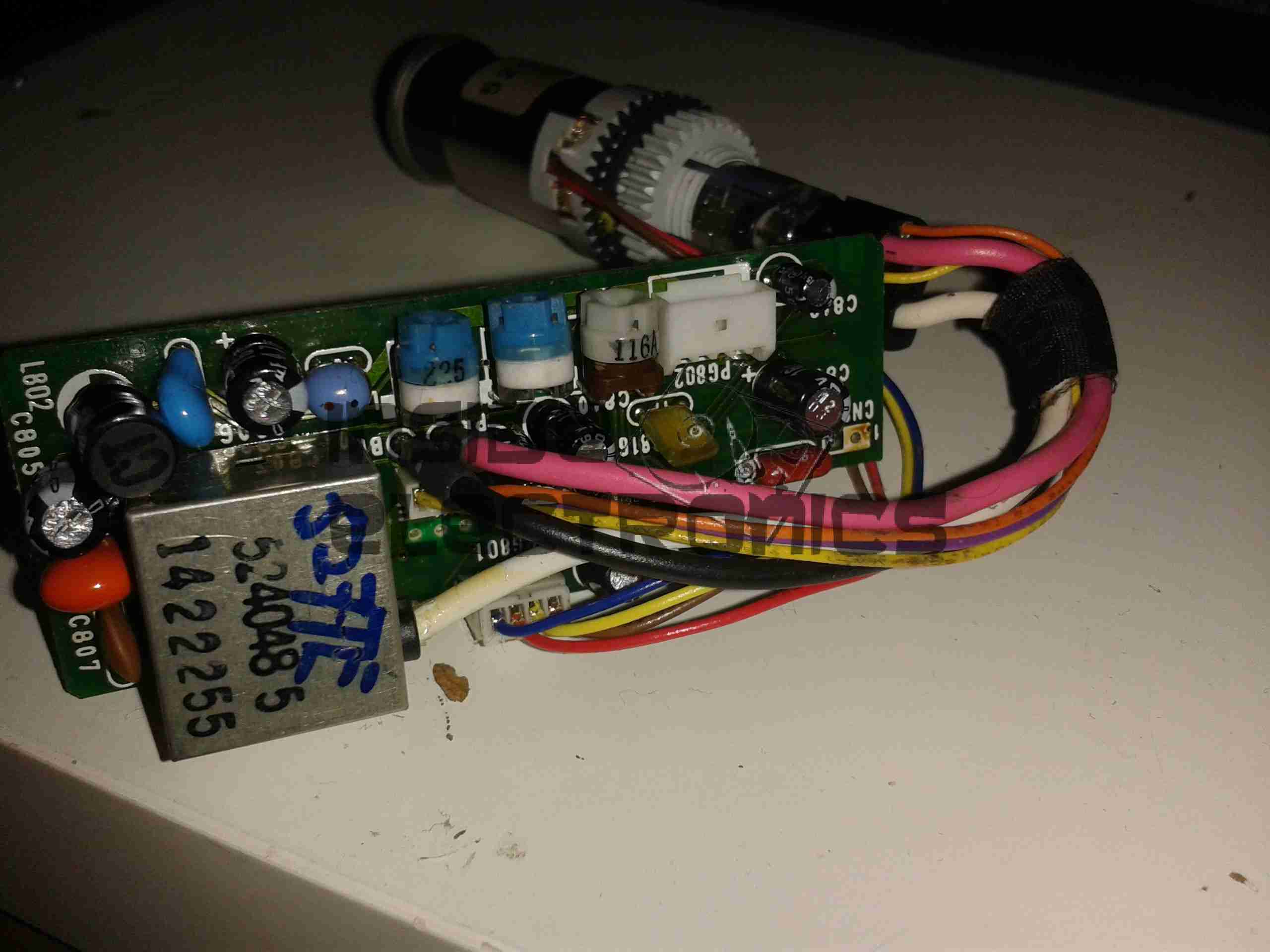
Viewfinder CRT Assembly
Here’s the complete assembly liberated from it’s plastic enclosure.
PCB Closeup
Closeup of the control PCB. The 3 potentiometers control the CRT brightness, focus & vertical size.
M01KGG007WB CRT
The tiny CRT. Only ~60mm in length, with an 18mm screen size. This tube runs on +2294v final anode voltage. Much higher than I expected.
Electron Gun Closeup
The electron gun assembly, with the cathode, focus & final anode cups.
Phosphor Screen
This screen is just a little bigger than a UK 5p piece! A marvel of precision engineering.
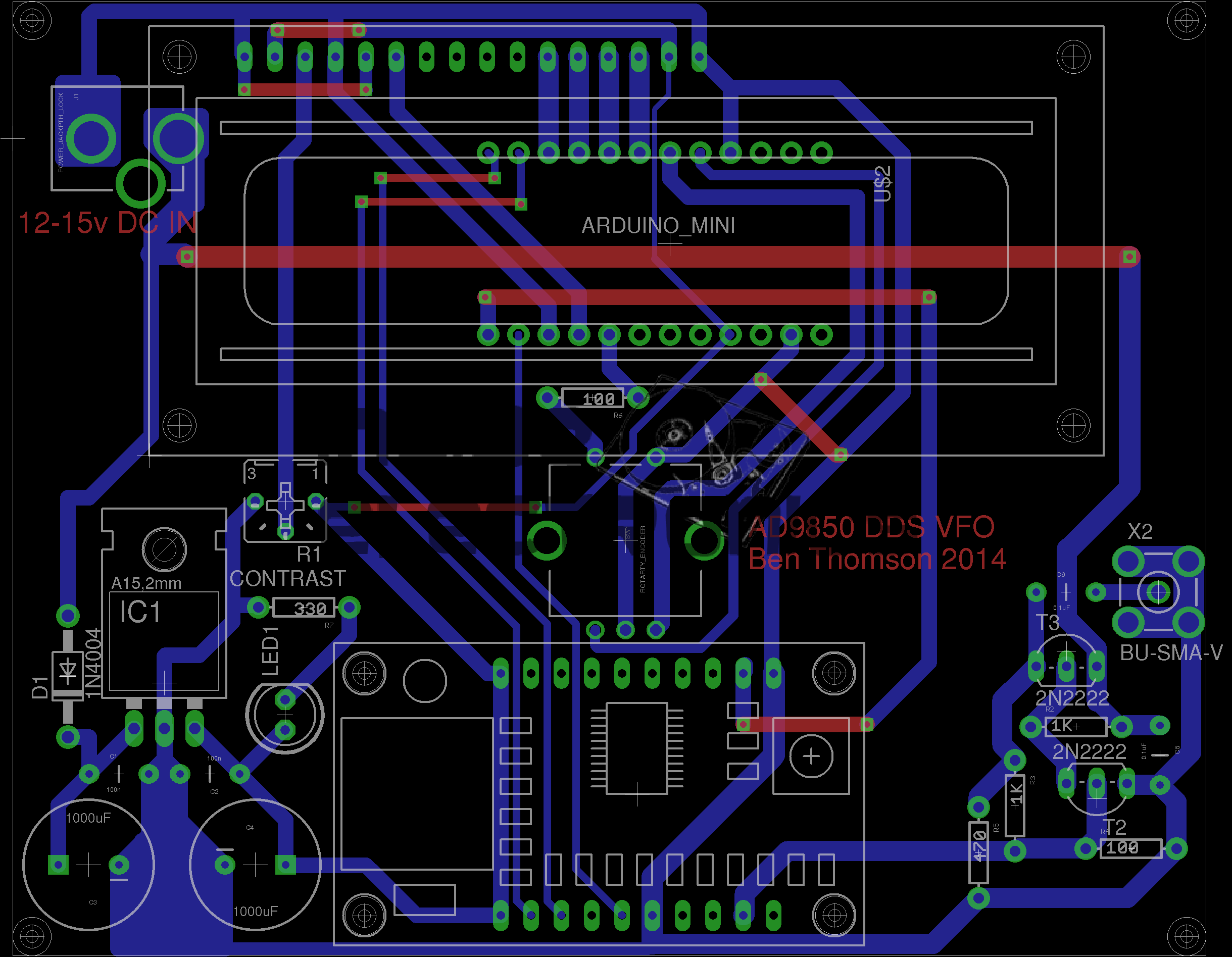
I recently came across a design for an Arduino controlled AD9850 DDS module, created by AD7C, so I figured I would release my Eagle CAD design for the PCB here.
It is a mainly single-sided layout, only a few links on the top side are needed so this is easy to etch with the toner transfer method.
My version uses an Arduino Pro Mini, as the modular format is much easier to work with than a bare ATMega 328.
RF output is via a SMA connector & has a built in amplifier to compensate for the low level generated by the DDS Module.
DDS VFO
Version 2 Update: Added reverse polarity protection, added power indicator LED, beefed up tracks around the DC Jack.
[download id=”5571″]
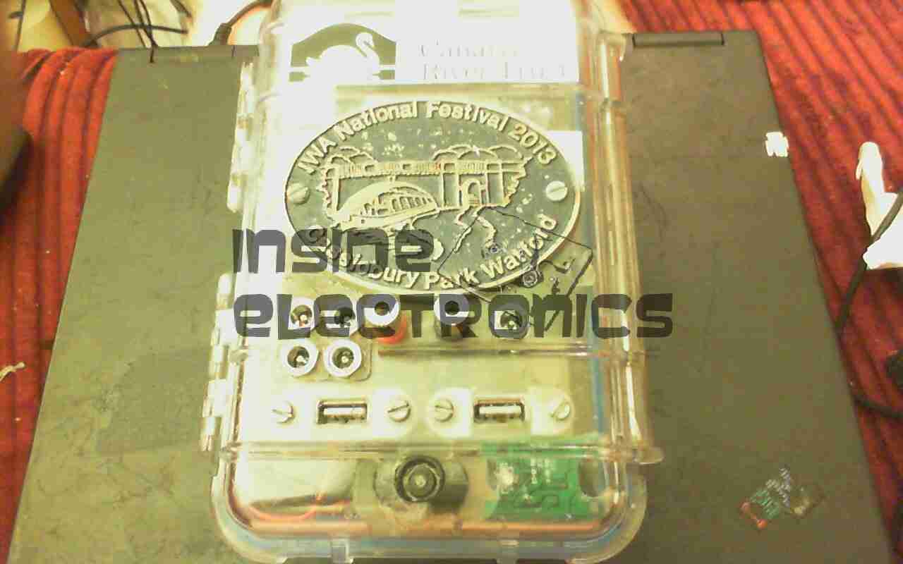
After 13 months of very heavy use at various events, festivals & boat trips, the Li-Po battery pack at the heart of my portable power supply has died.
What initially started as one cell inflating spread to the other cells in the pack over a period of about 3 months, so I have completely replaced the pack with a larger unit.
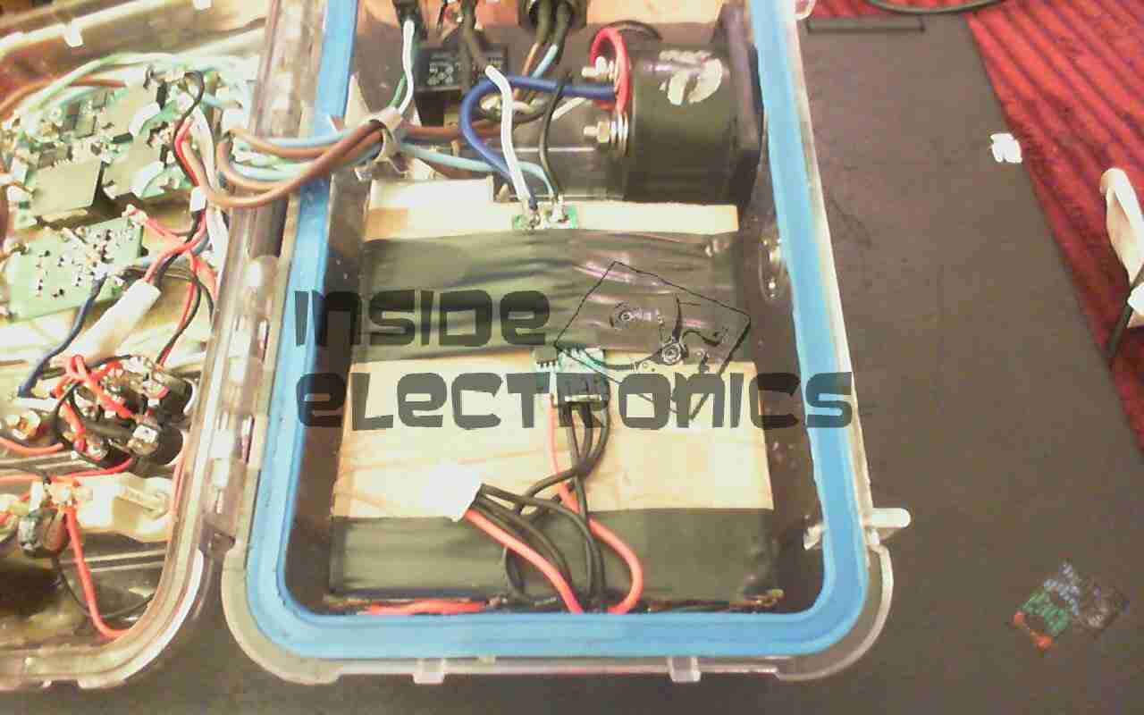
New Pack
The old pack was an 8.8Ah unit at 12.6v. By using smaller burst capacity cells, I have managed to squeeze in a total of 13.2Ah, still leaving space to spare for an extra 3 cell string along the top.
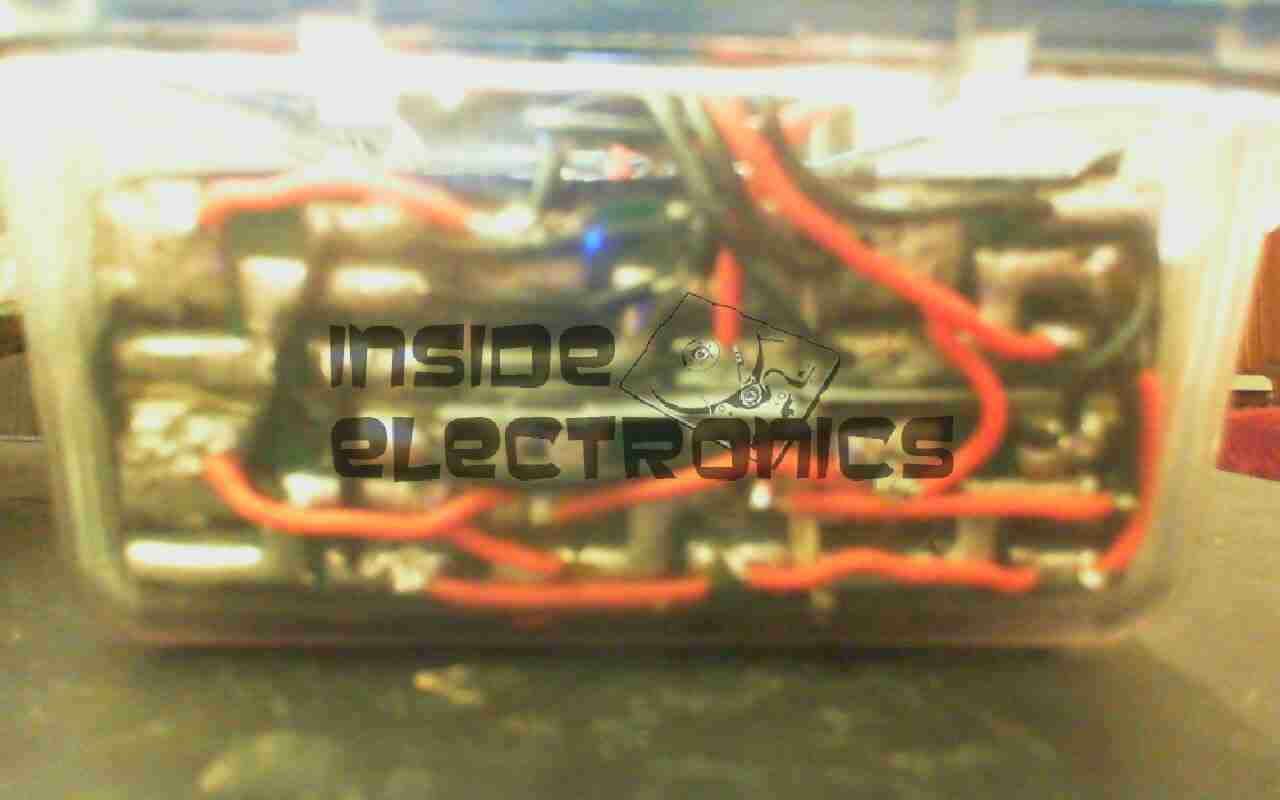
Cell Interconnects
Here is the end of the battery pack, with all the cell interconnects. There are 3 2.2Ah cells in series to give the 12.6v terminal voltage, with 6 of those strings in parallel to give the total Ah rating.
A new charging circuit will be implemented to better handle the volatile chemistry of Li-Po cells, hopefully this will result in the pack lasting longer than a year!
The new higher capacity will hopefully help with power requirements at future events, still being charged during the day by a 24W solar panel, but at night will have to cope with charging two smartphones, two eCigs & running a few watts of LED lighting.
The trial-by-fire will be this year’s Download Festival in June, when I will be operating off-grid for 6 days.
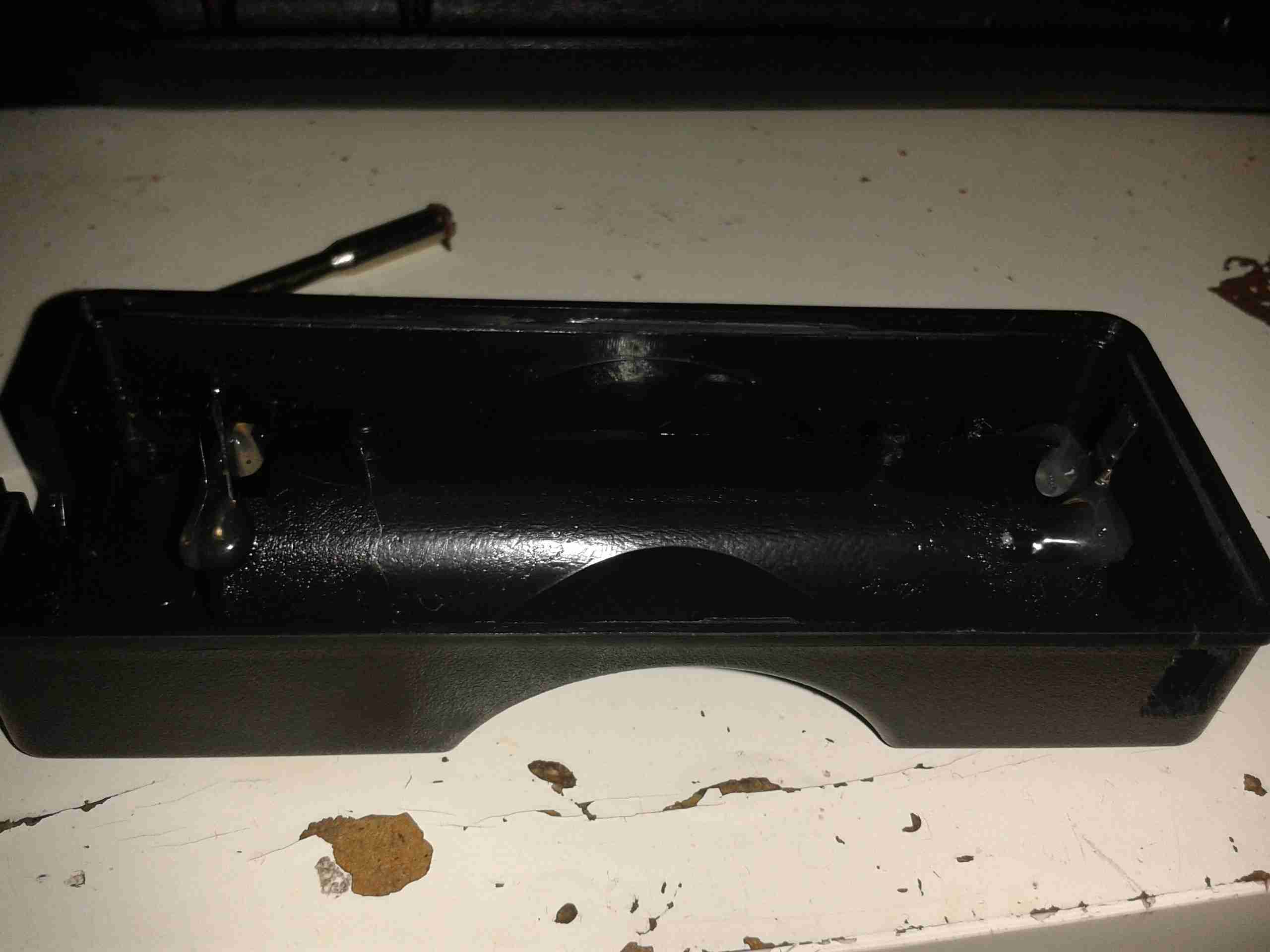
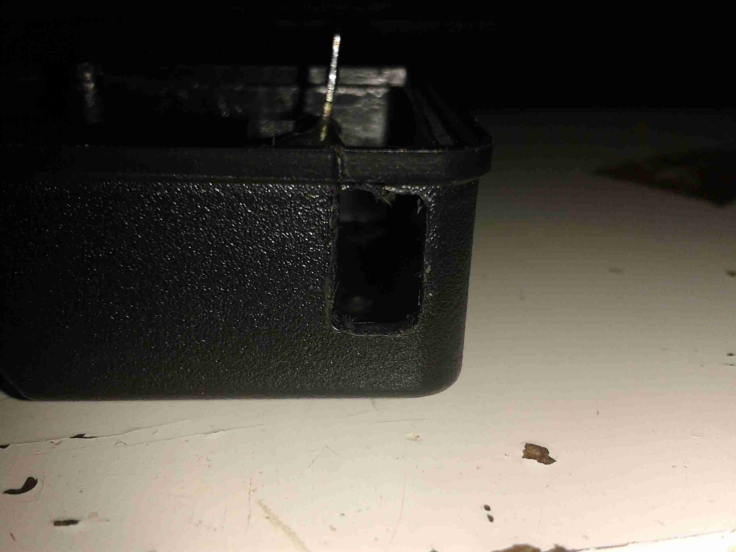
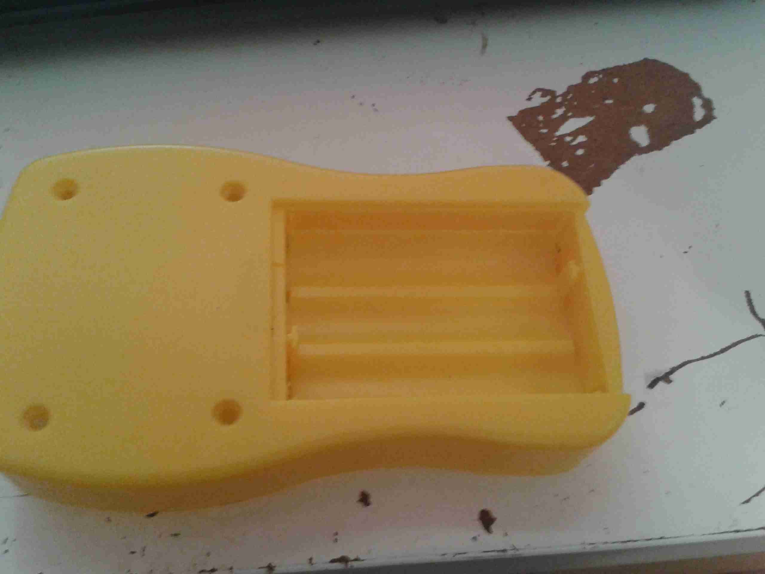
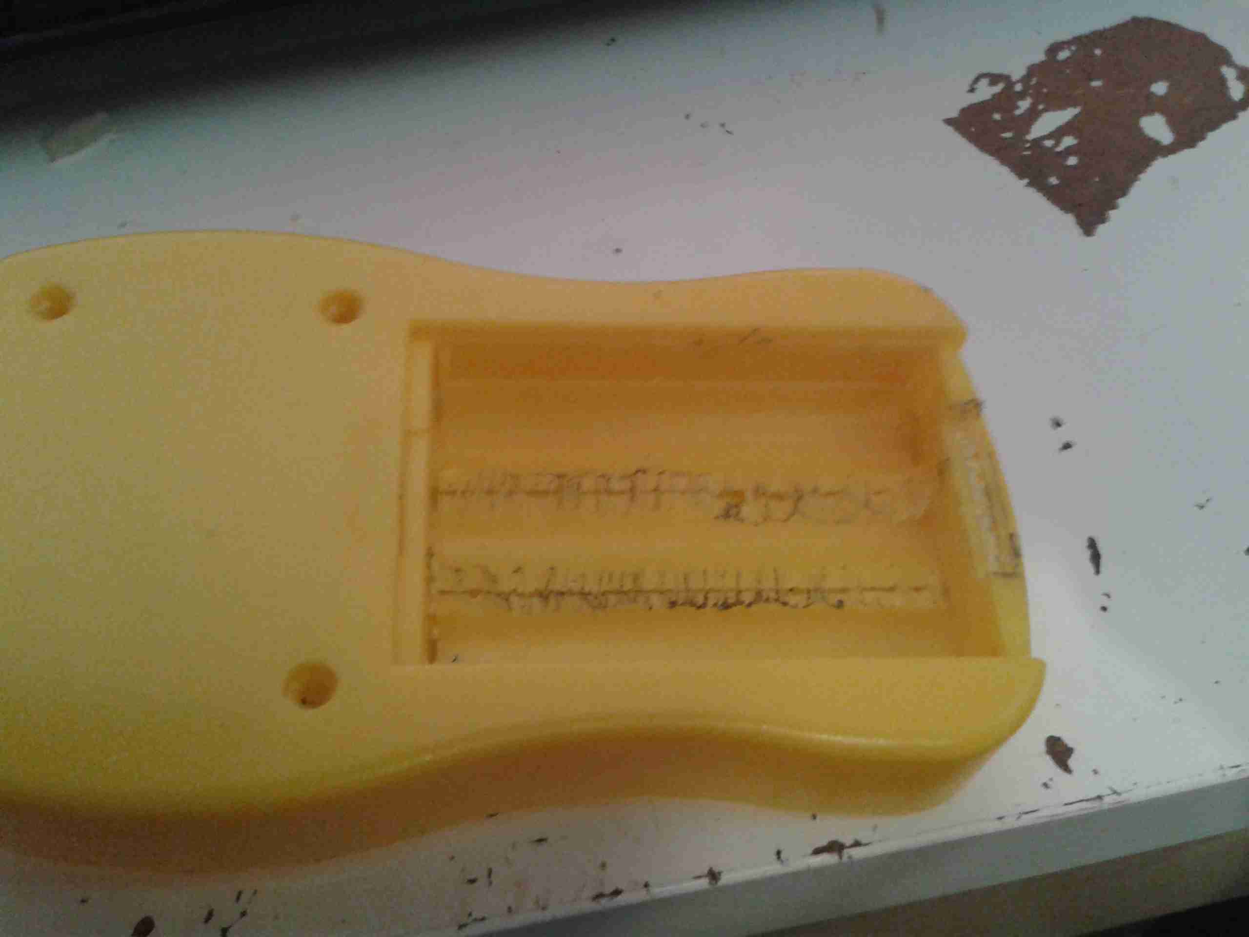
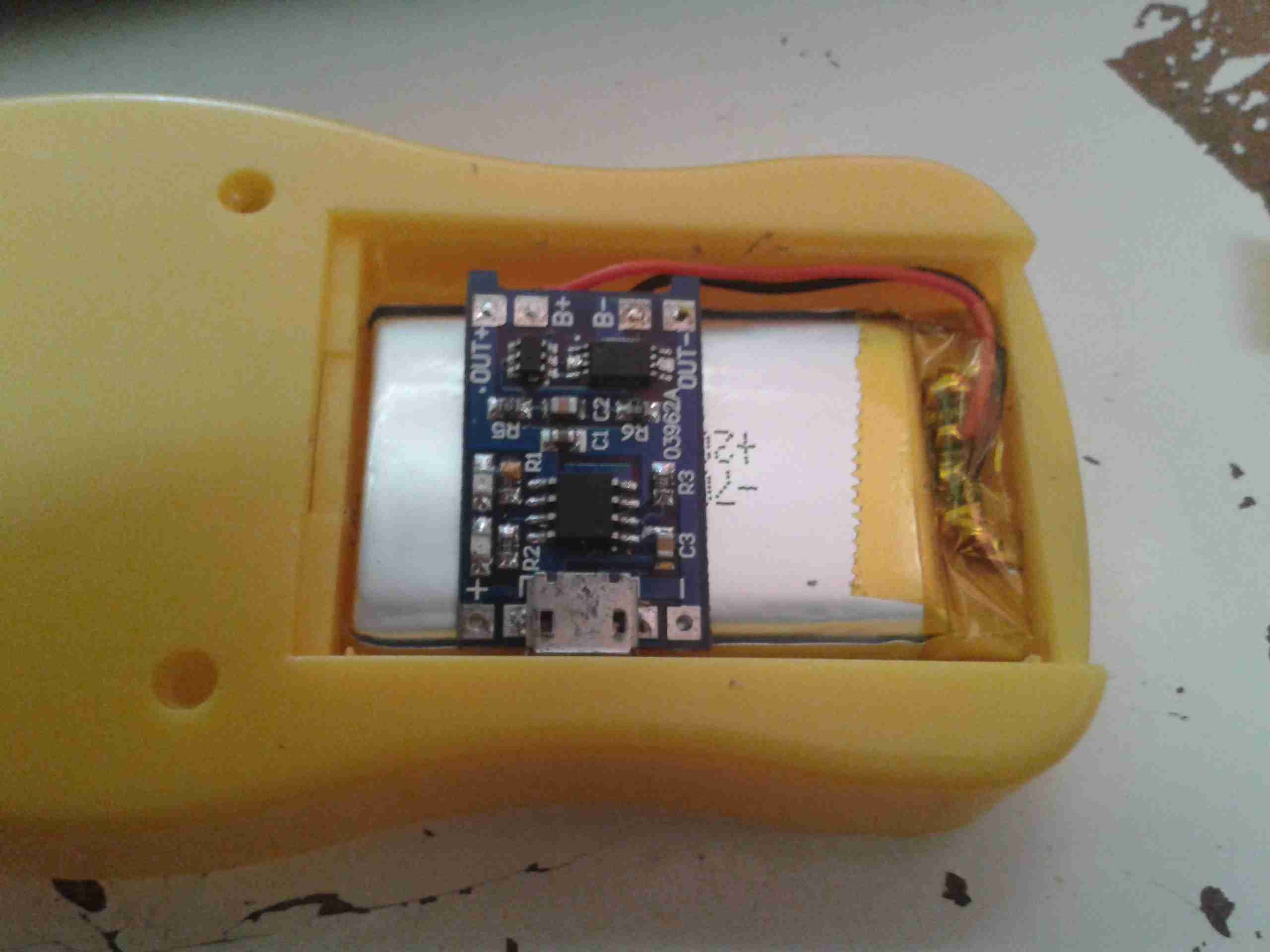
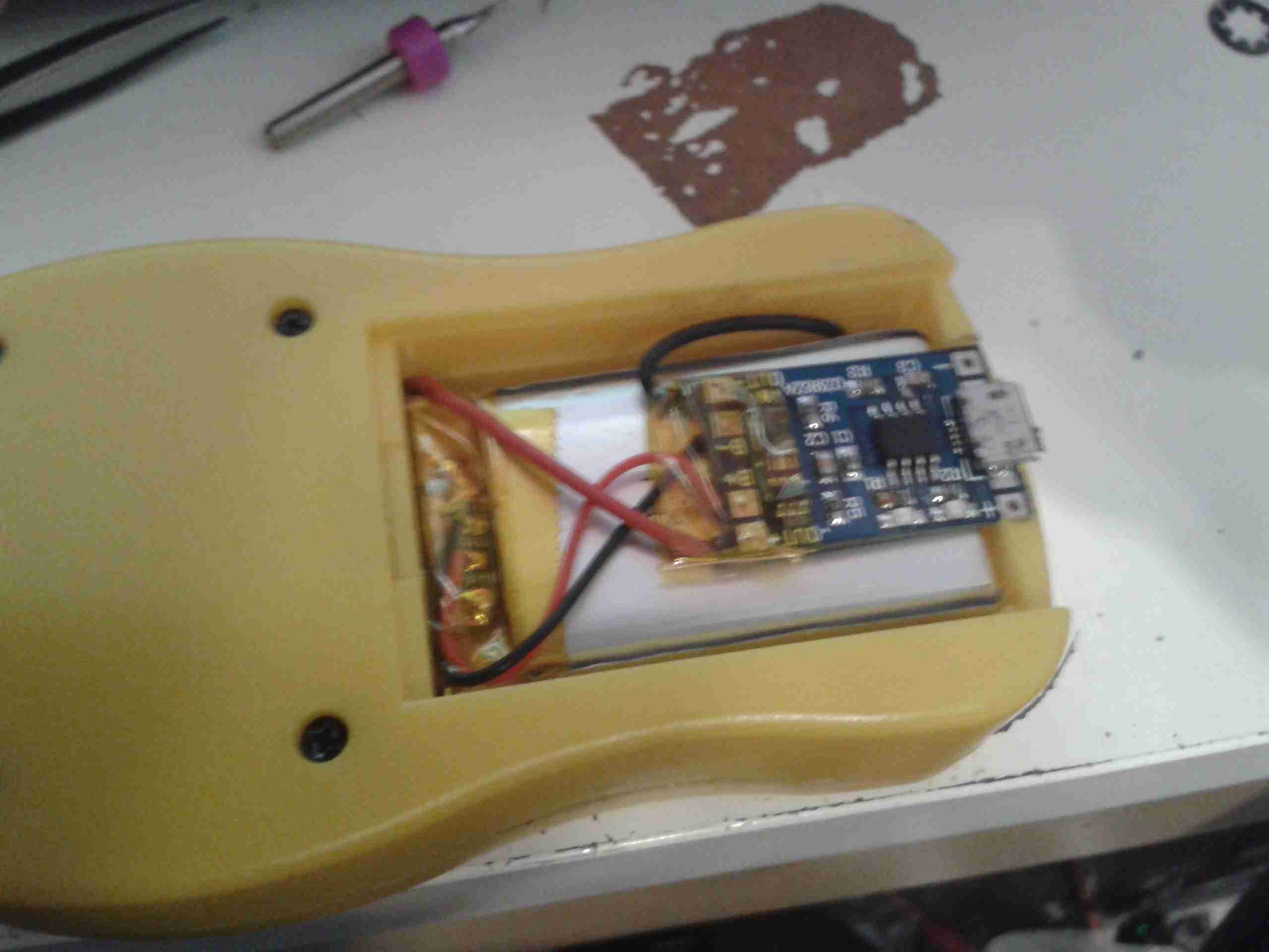
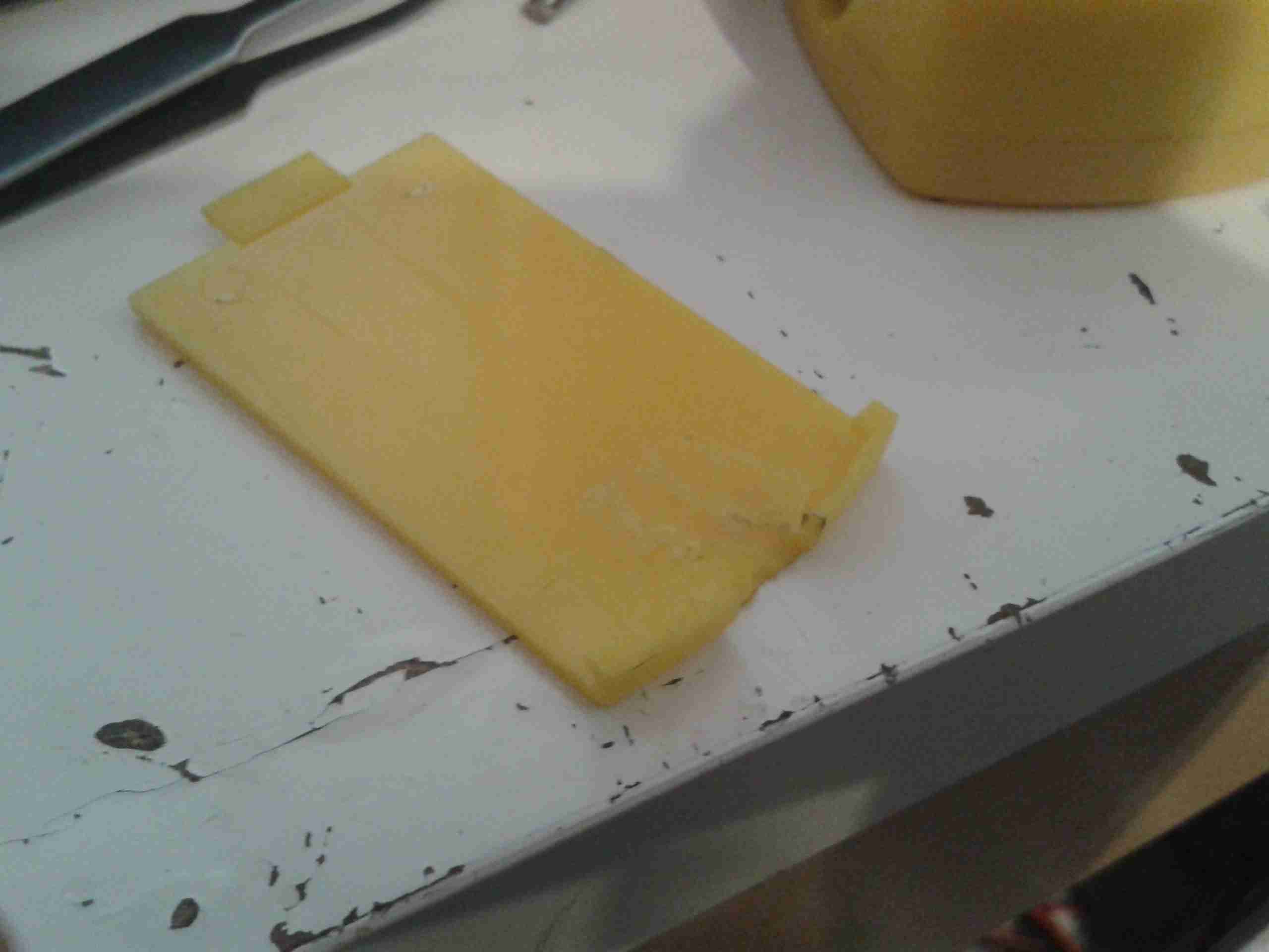
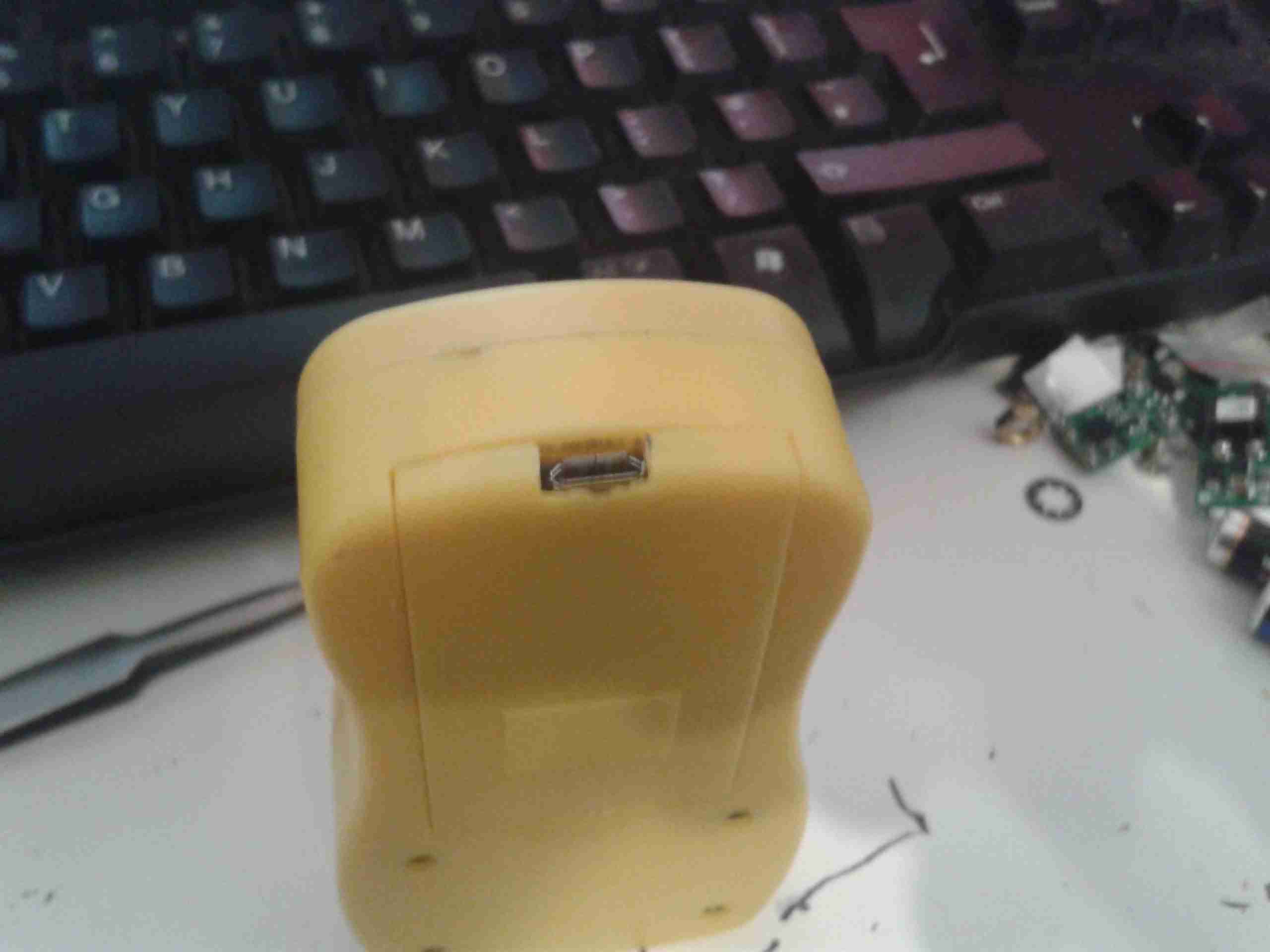
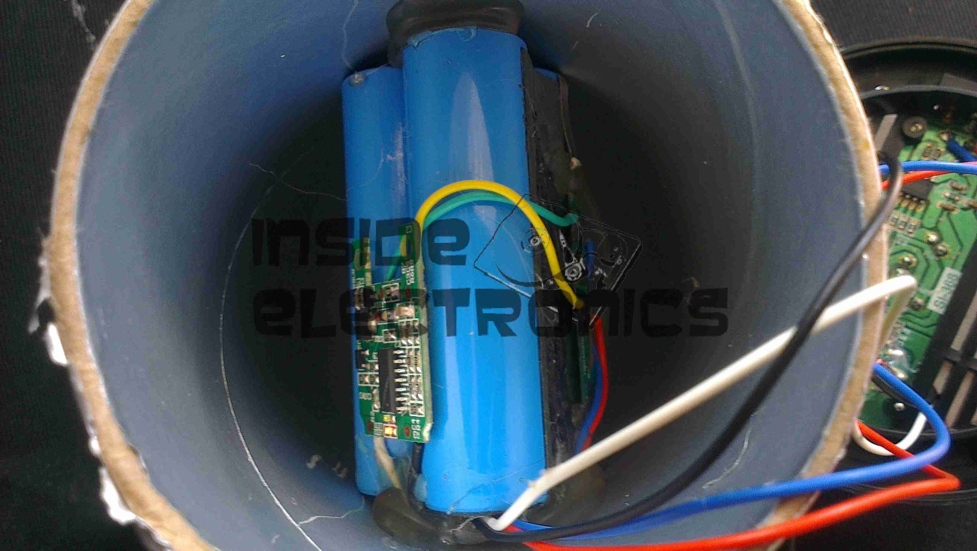
These speakers are available free from Pringles, with two packs bought. Normally running on 3x AAA cells, I have made modifications to include a high capacity Li-Ion battery & USB charging.
18650 Battery
New battery is 3x 18650 Li-Ion cells in parallel, providing ~6600mAh of capacity. These are hot glued inside the top of the tube under the speaker, with the charging & cell protection logic.
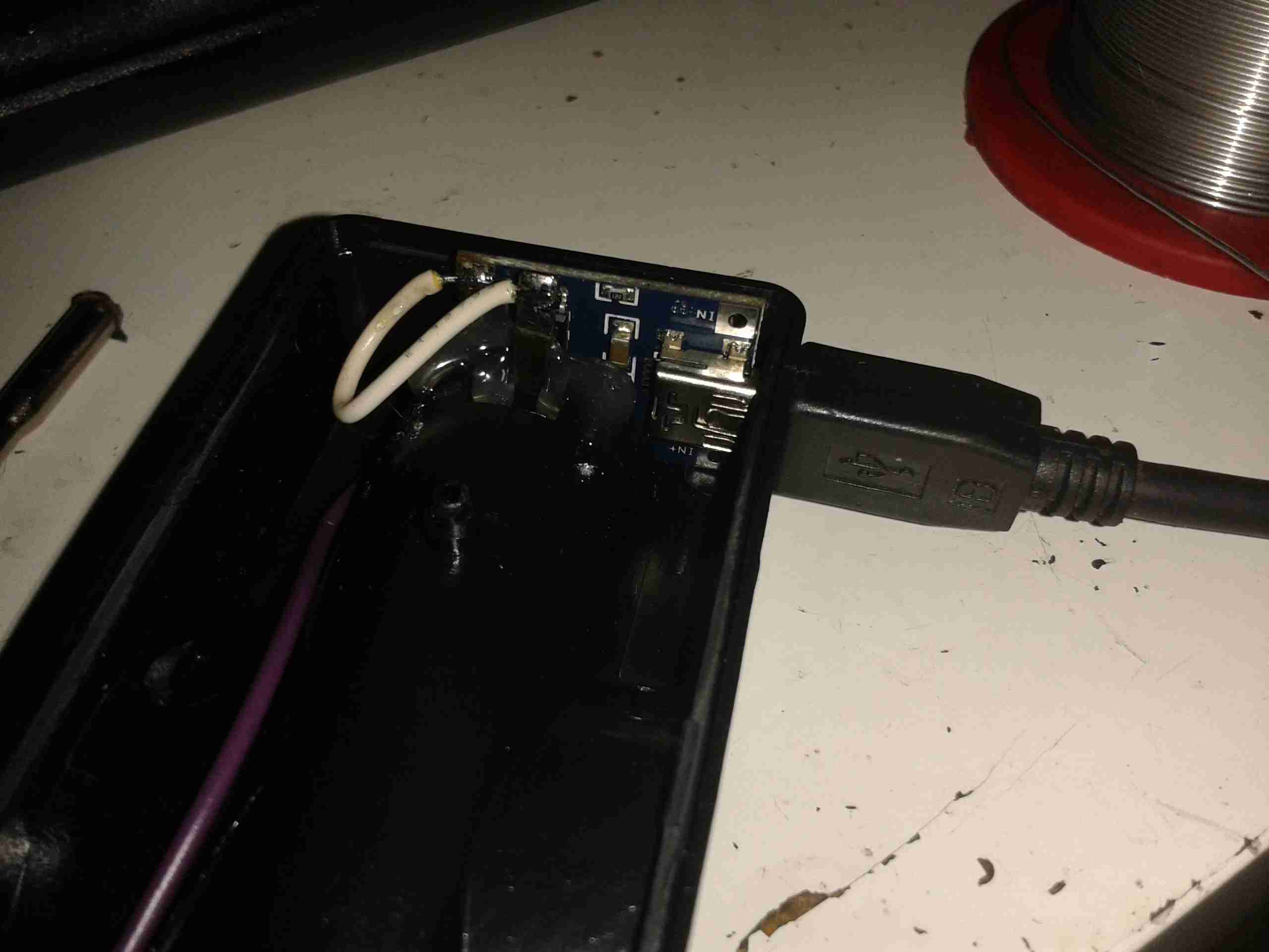
The battery charging logic is salvaged from an old USB eCig charger, these are single cell lithium chargers in a small form factor ideal for other uses. Charging current is ~450mA.
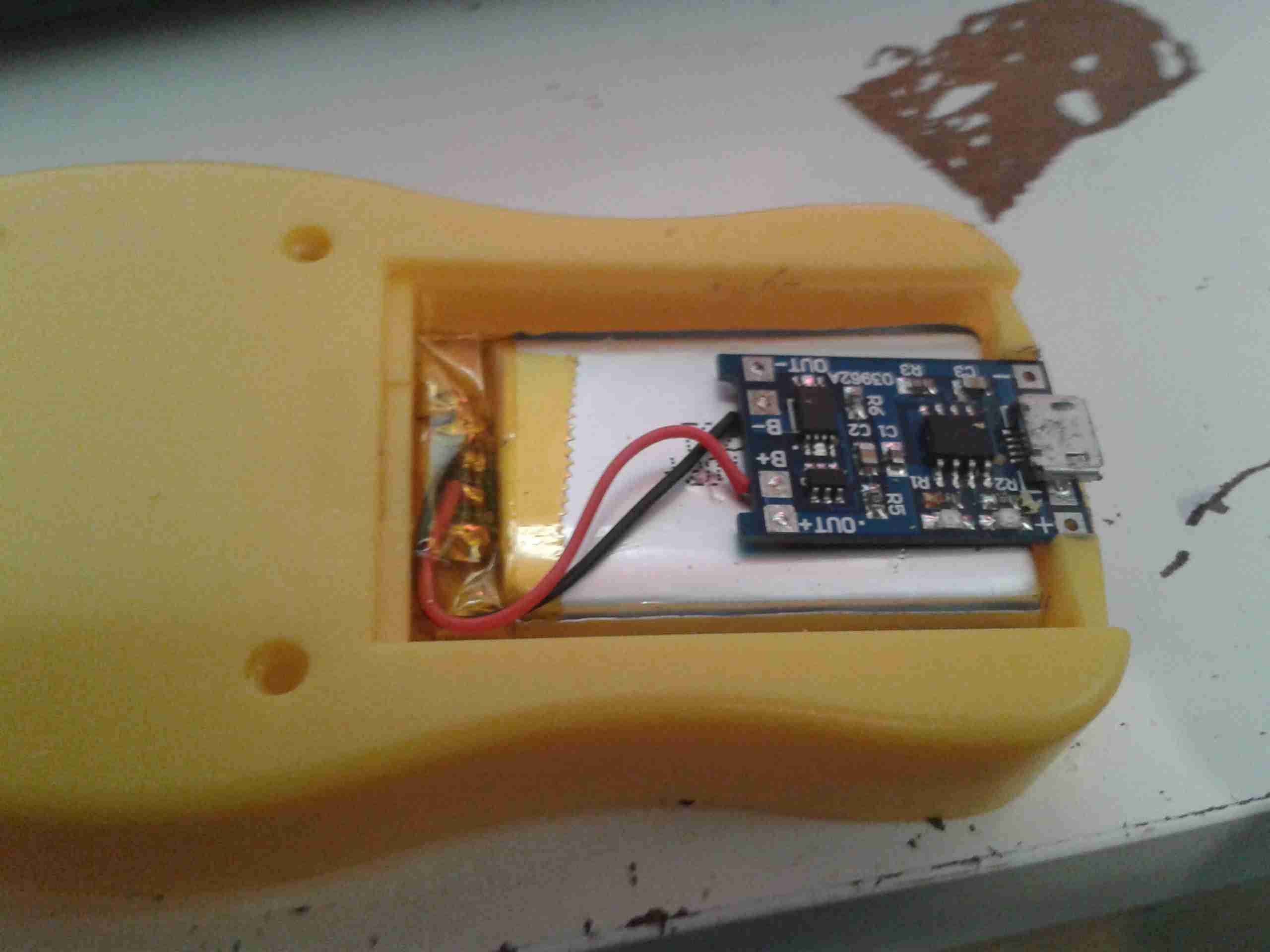
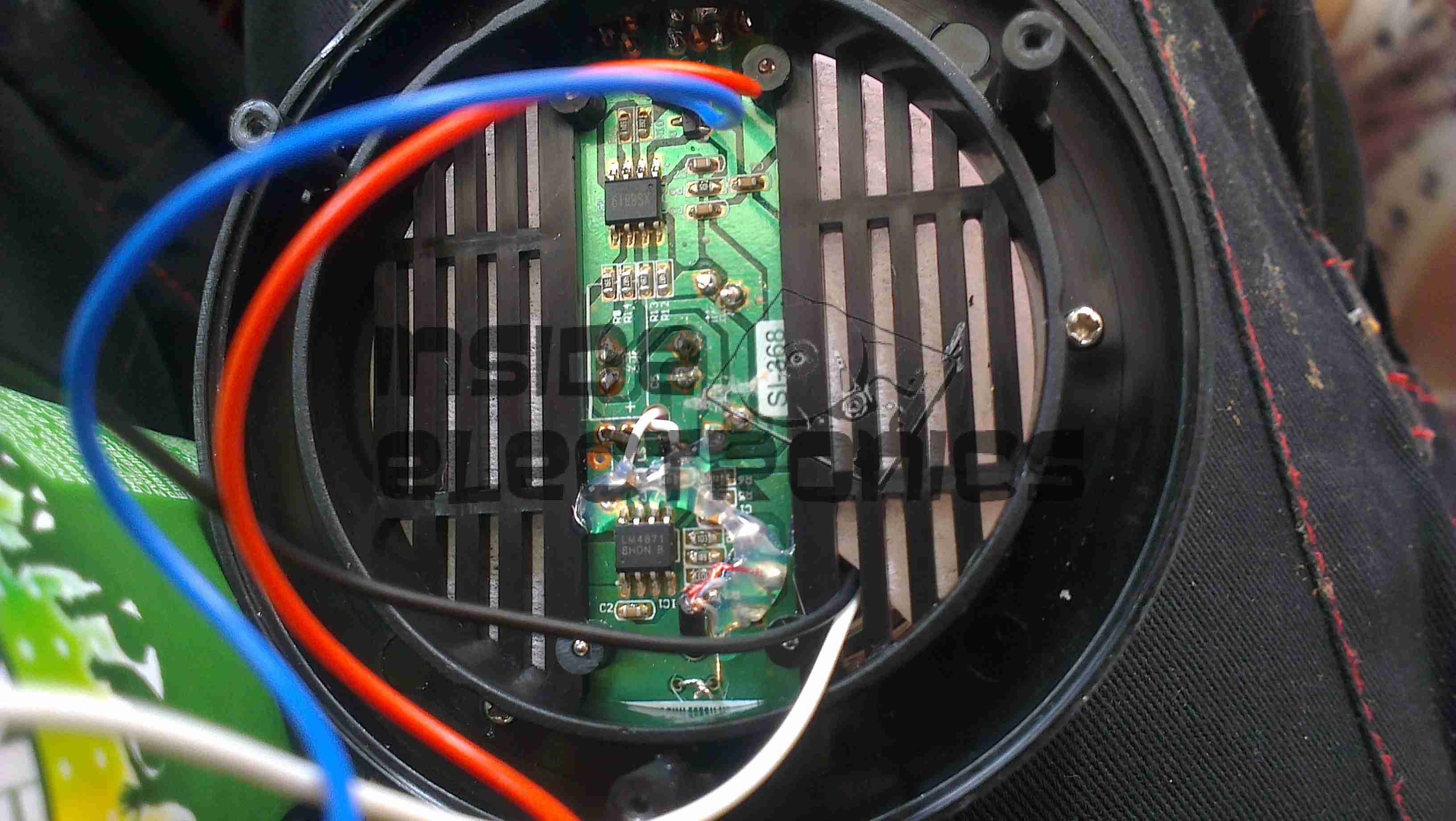
Amplifier Board
The cells are connected to the same points as the original AAA cells, with the other pair of wires going into the top of the device to connect to the MicroUSB charging port.
The amplifier in this is a LM4871 3W Mono amplifier IC, connected to a 6Ω 1W speaker.
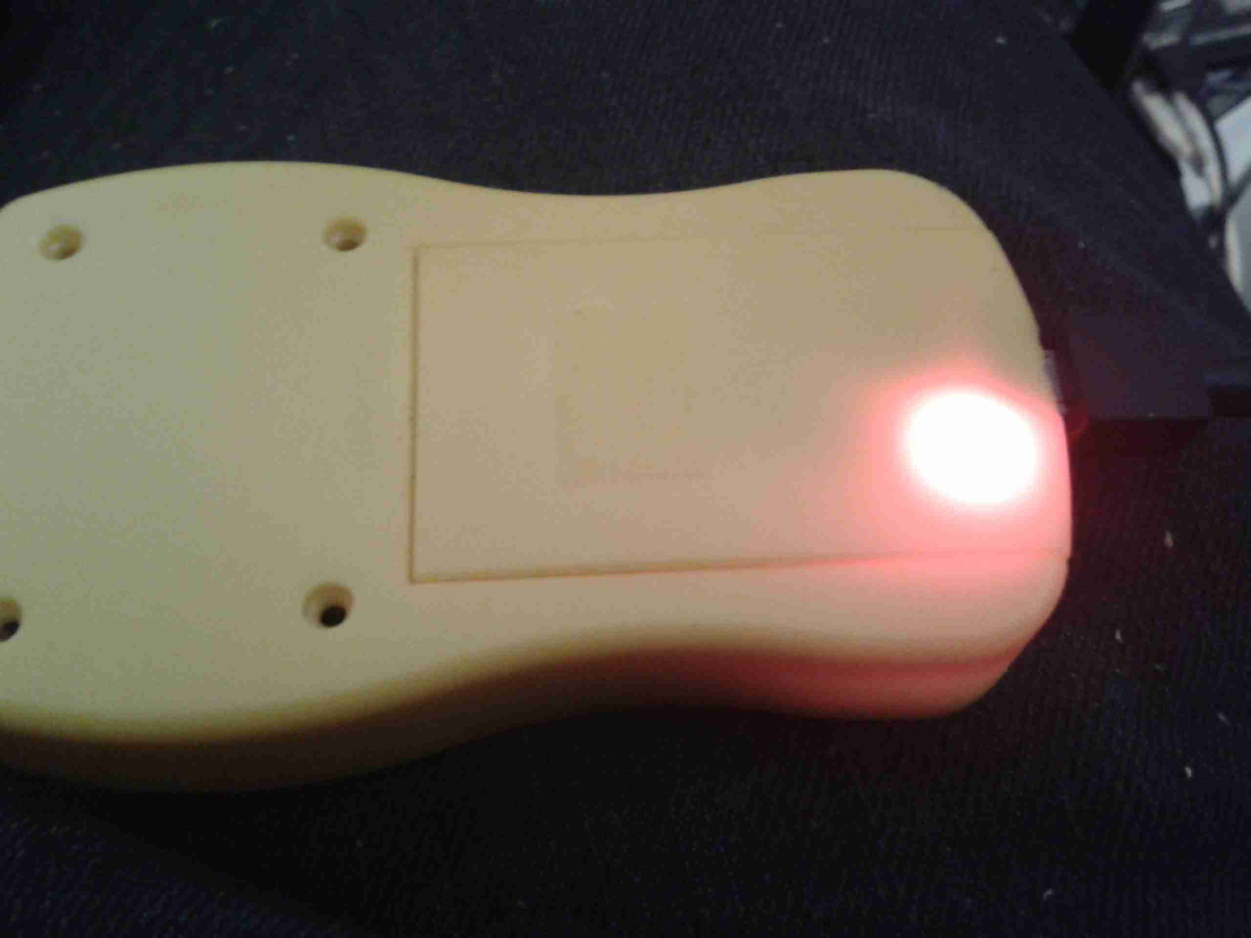
The other IC on the board is unidentifiable, but provides the flashing LED function to the beat of the music.
Tip Jar
If you’ve found my content useful, please consider leaving a donation by clicking the Tip Jar below!
All collected funds go towards new content & the costs of keeping the server online.