Posted on Leave a comment

JVC CV-F503PAL Viewfinder

EVF Bottom
EVF Bottom

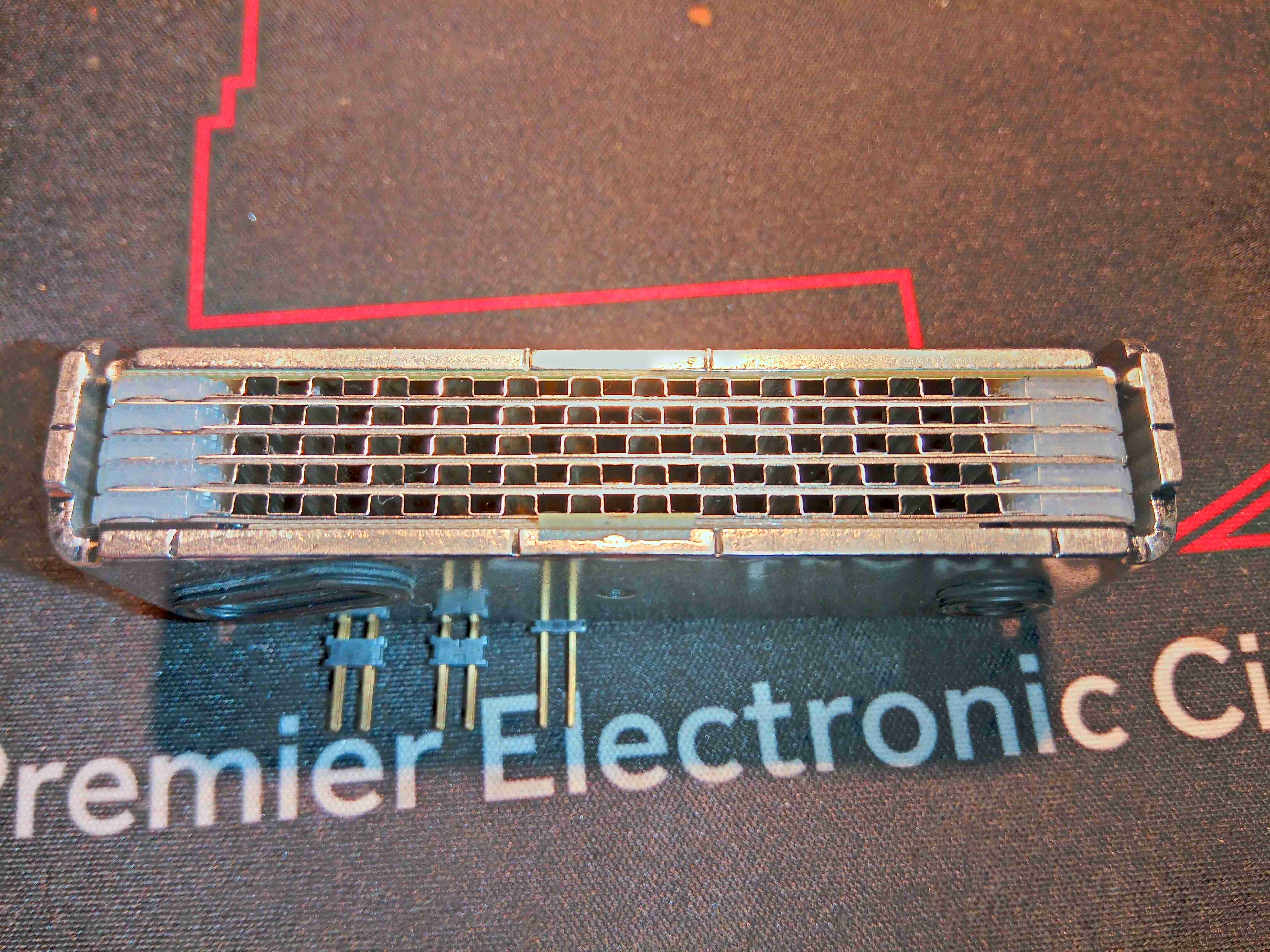
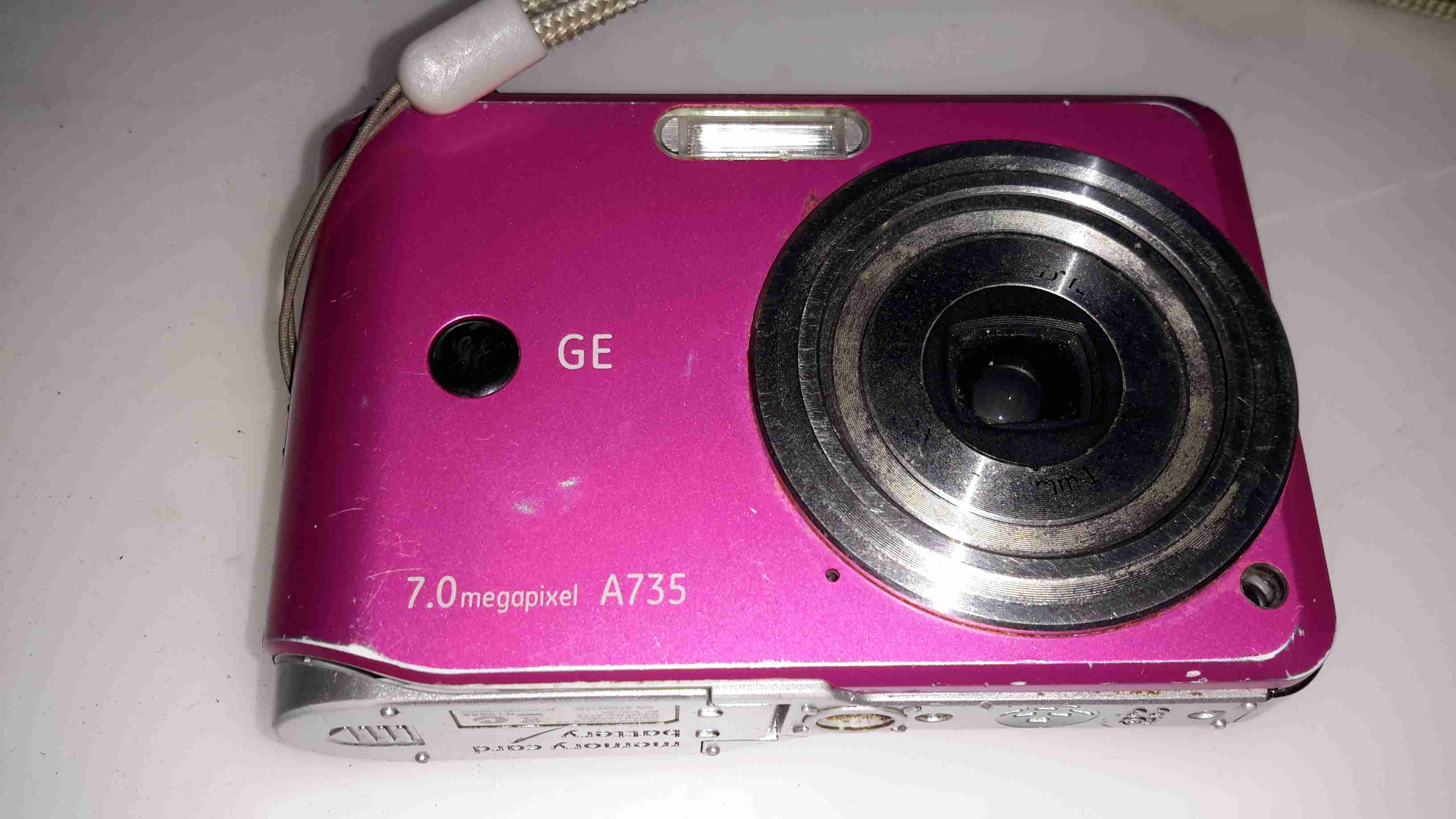
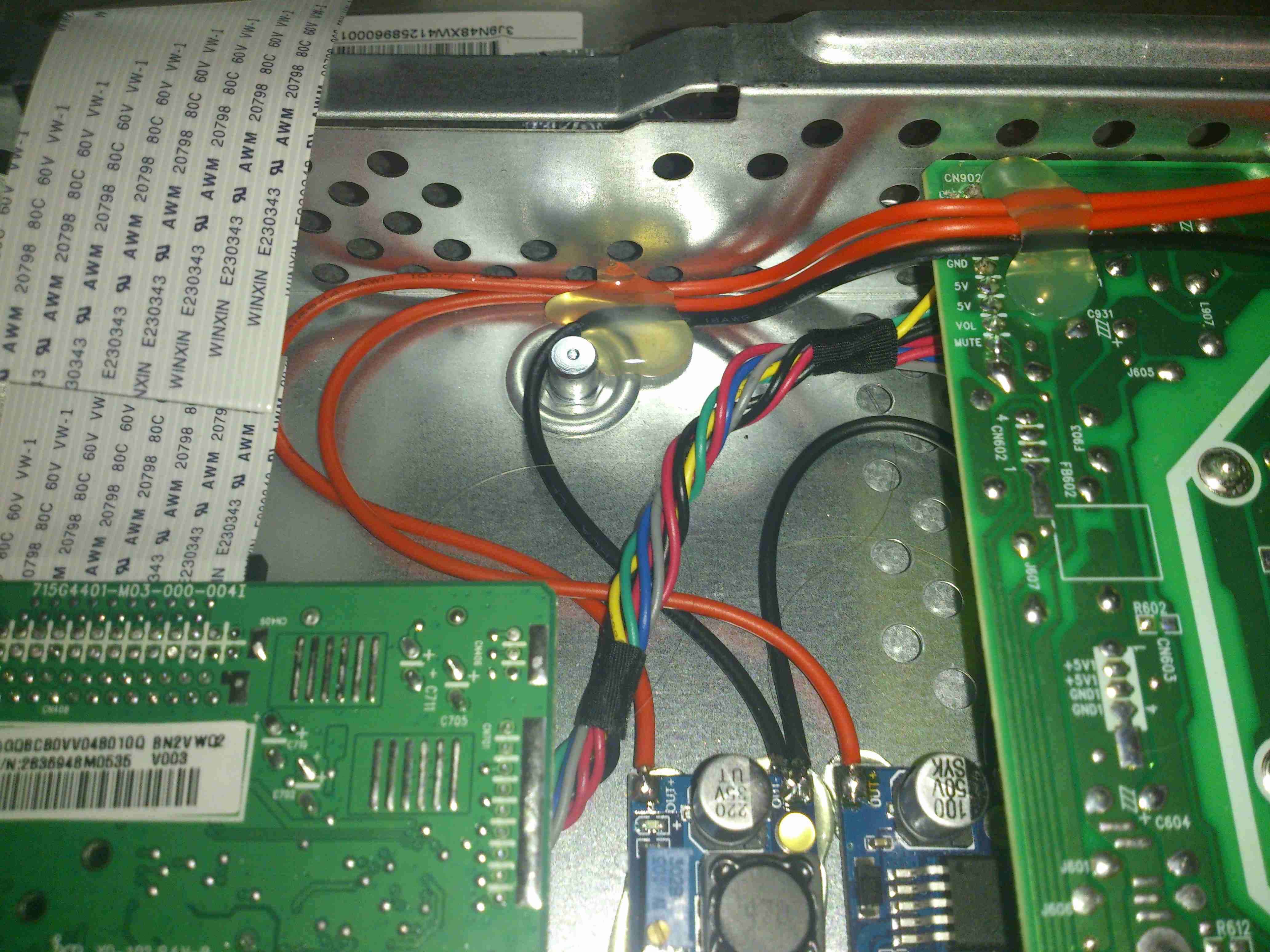
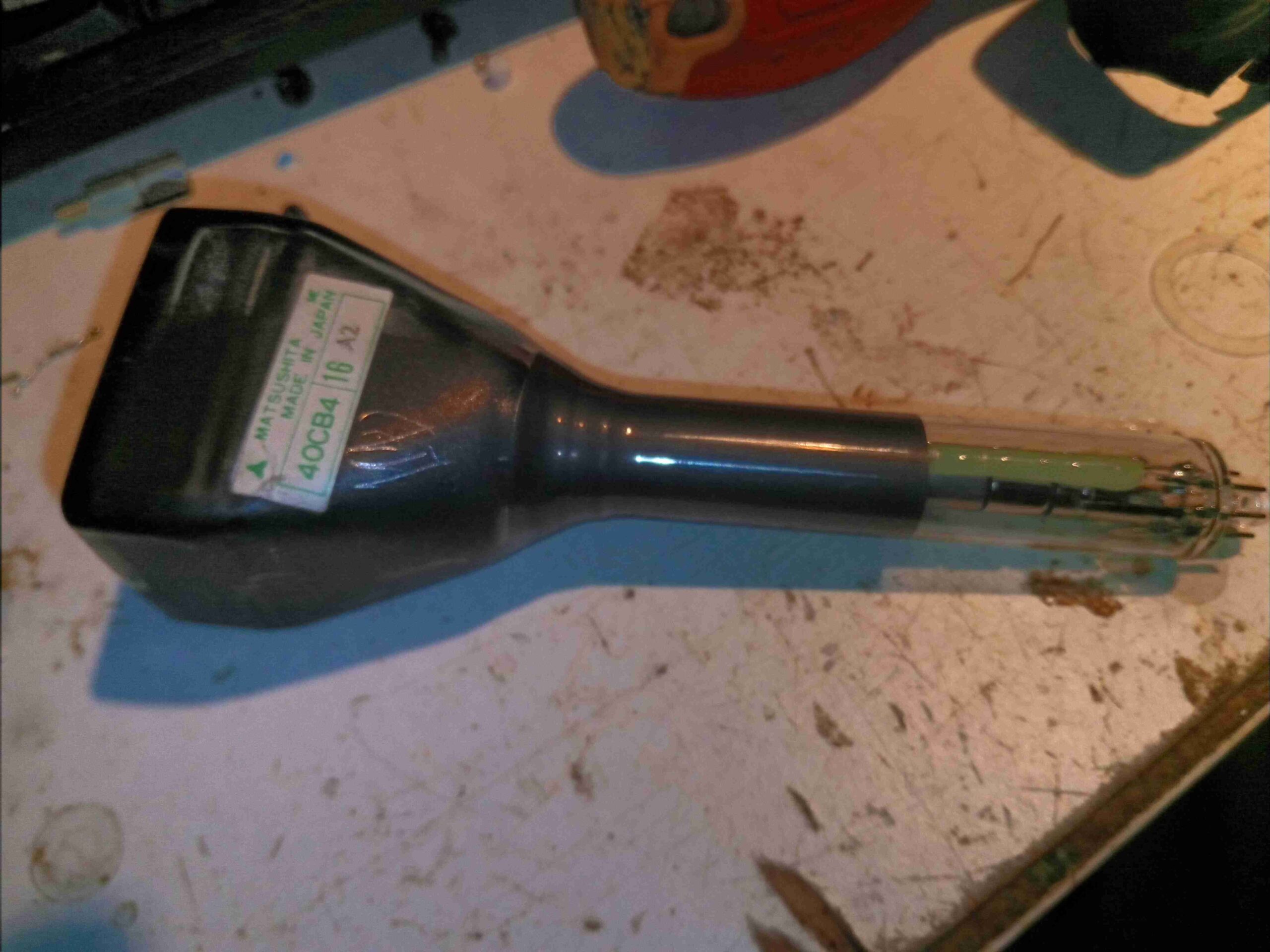
It’s time for another CRT-based post! This time it’s a Matsushita 40CB4-based viewfinder from 1980. These came from JVC colour tube cameras, and are physically massive! I’ve already worked out the pinout on the multicore cable here & attached a usable connector.

Information Label
Information Label

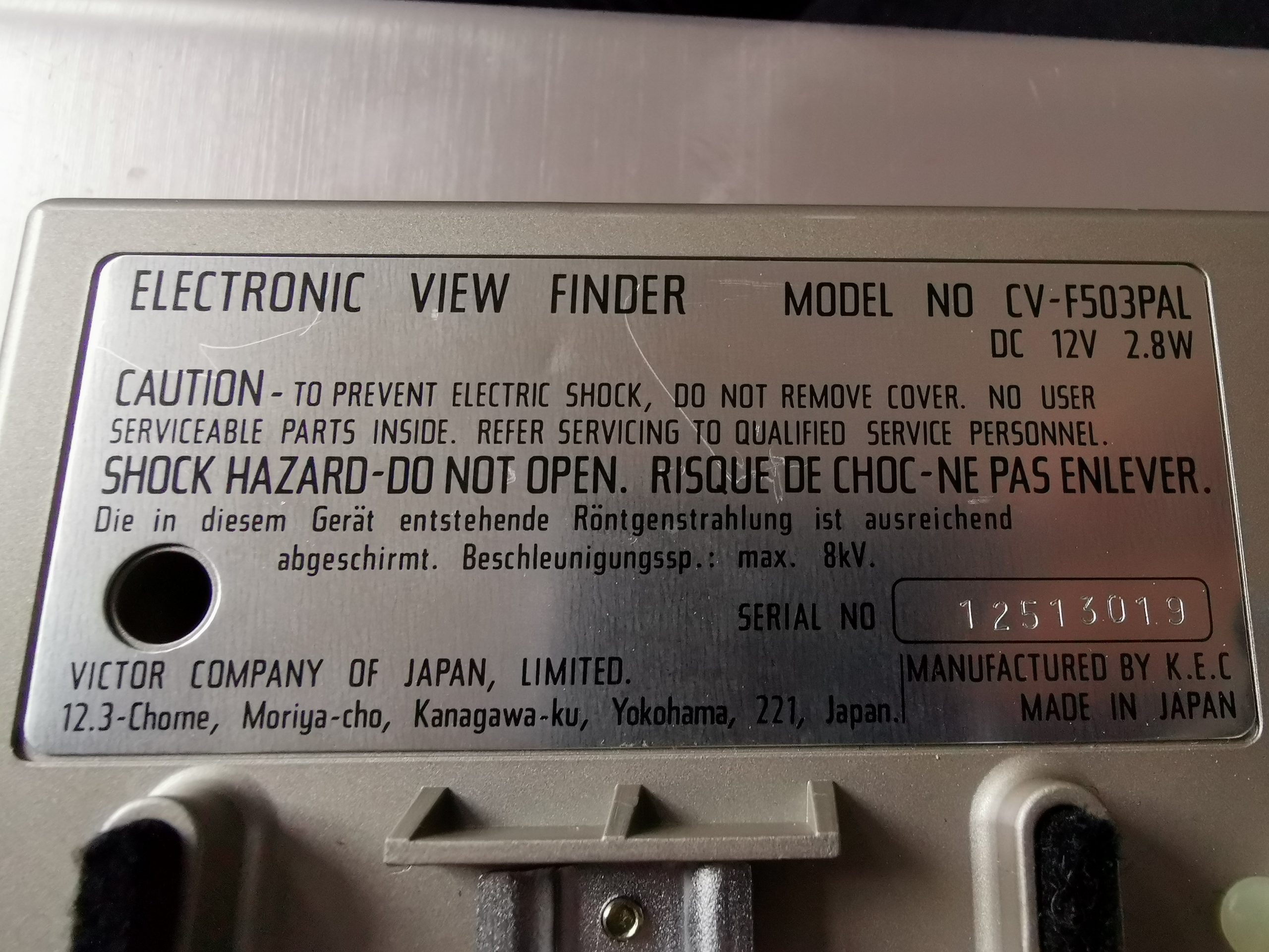
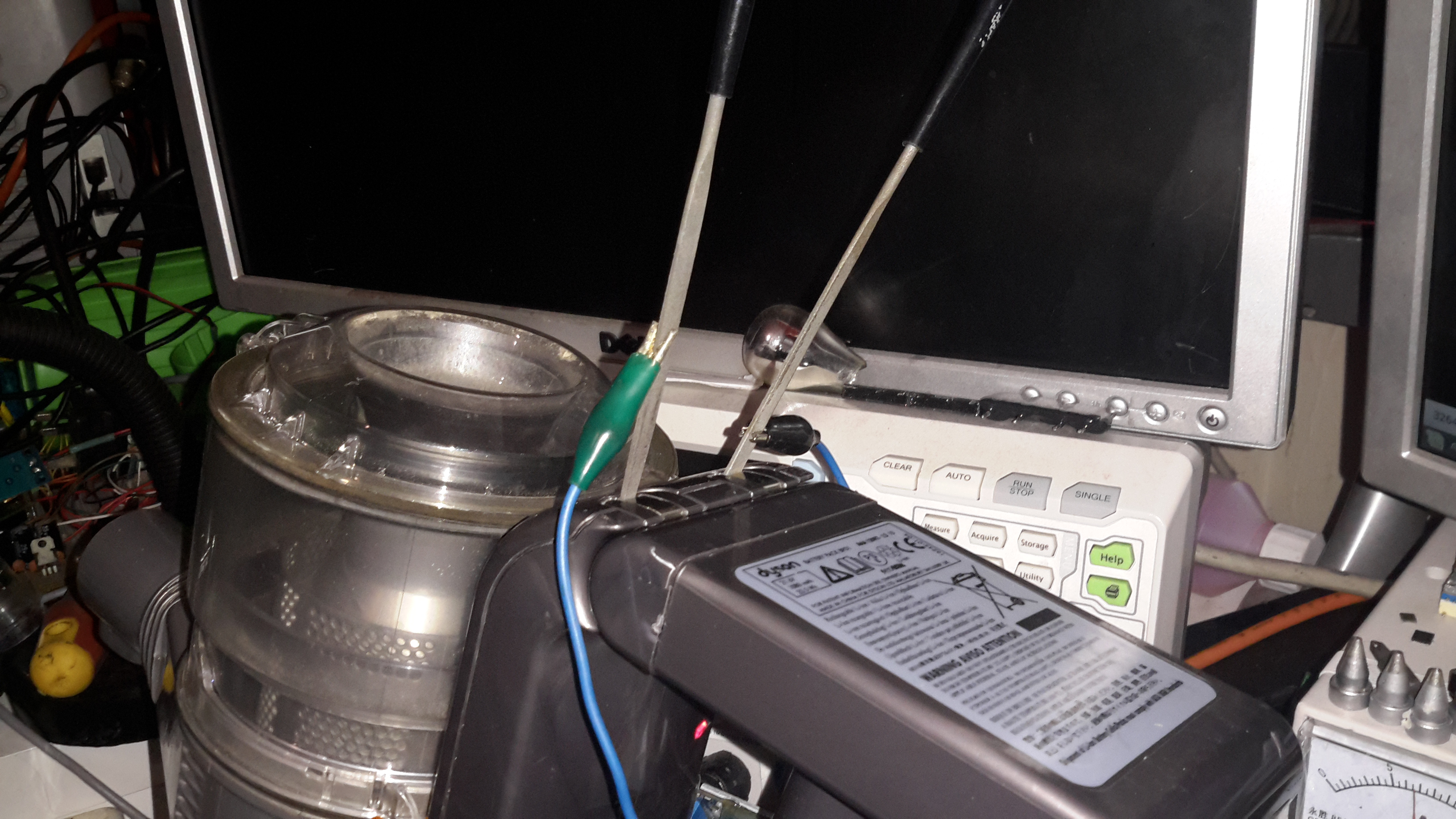
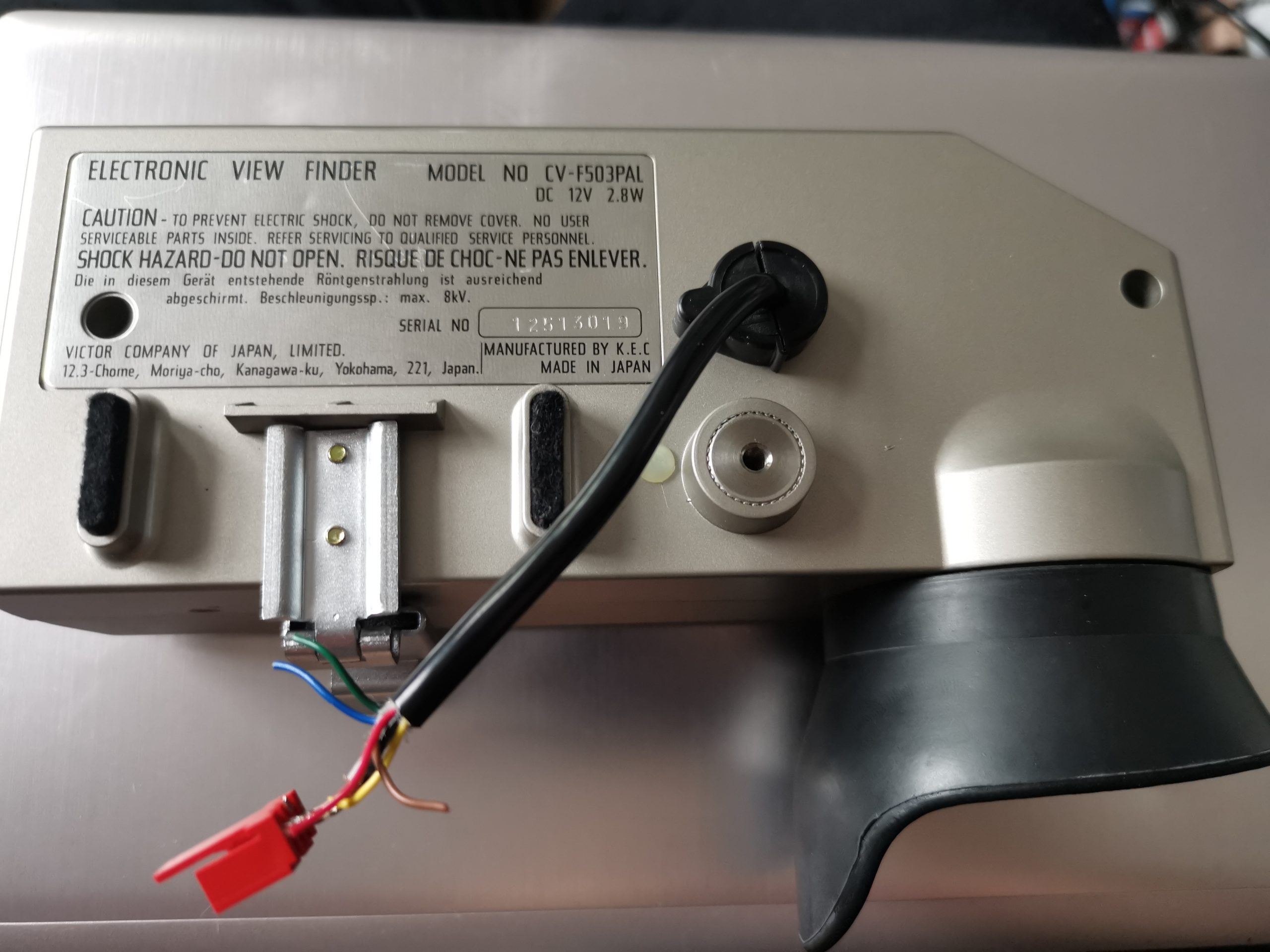
There’s lots of information on the bottom label of this unit, including a notification in German that the X-Ray emission from the device is shielded, and the maximum CRT acceleration voltage is 8kV. This last point is a bit strange, since the 40CB4 datasheet states a maximum design voltage on the final anode of 6kV. I did measure the voltage at the anode cup, and it’s stable at 7.15kV!

Internal Overview
Internal Overview

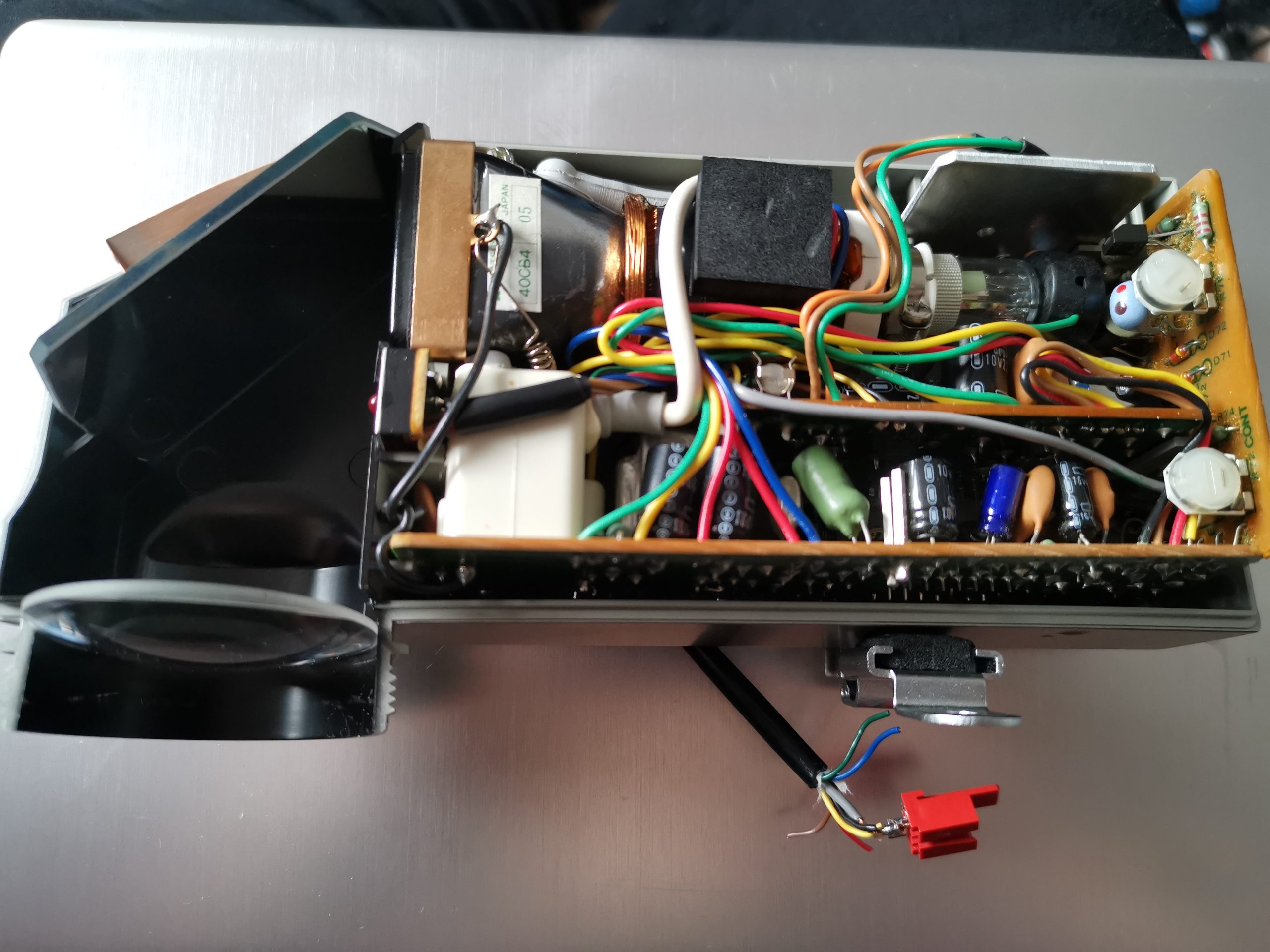
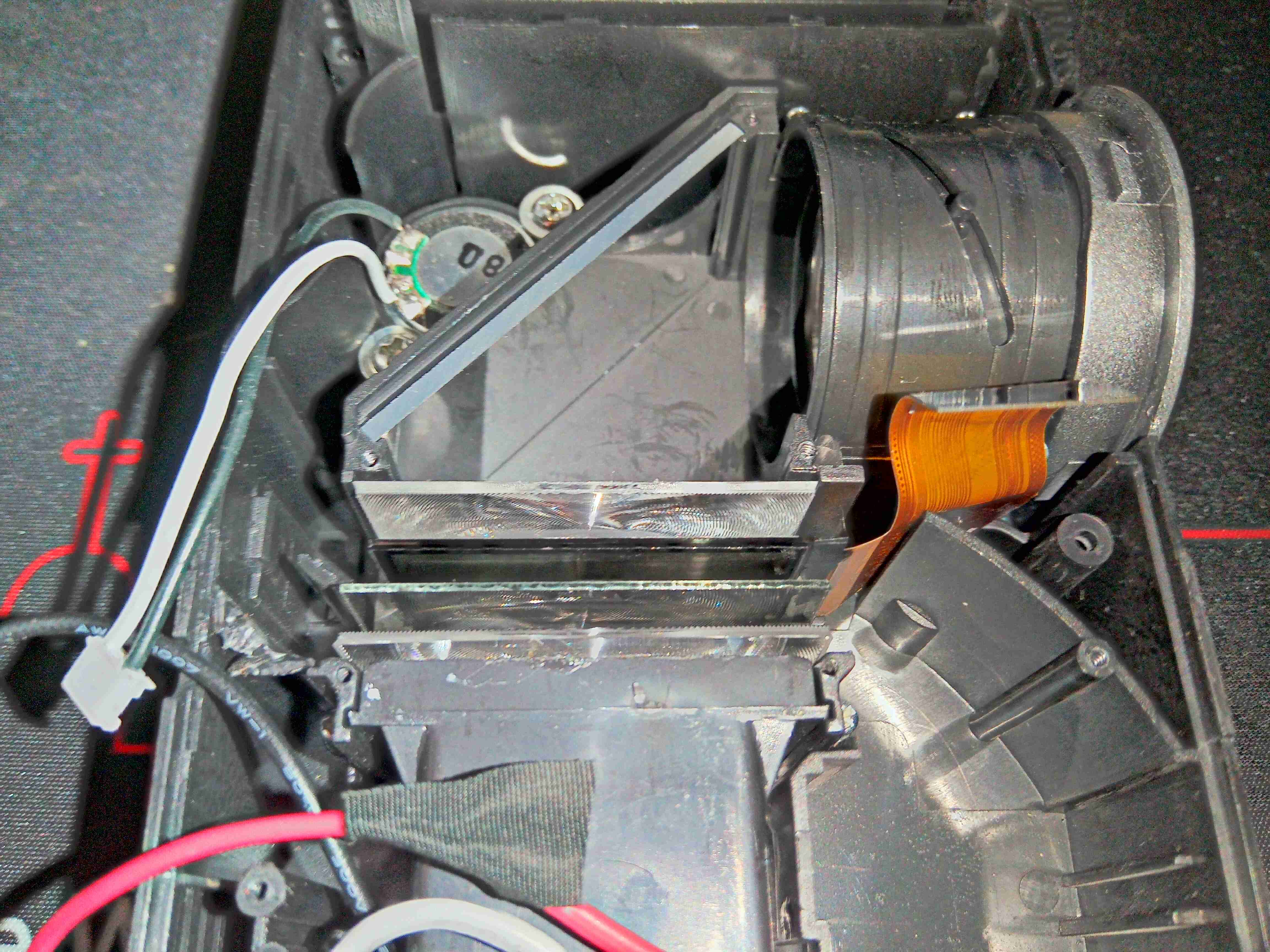
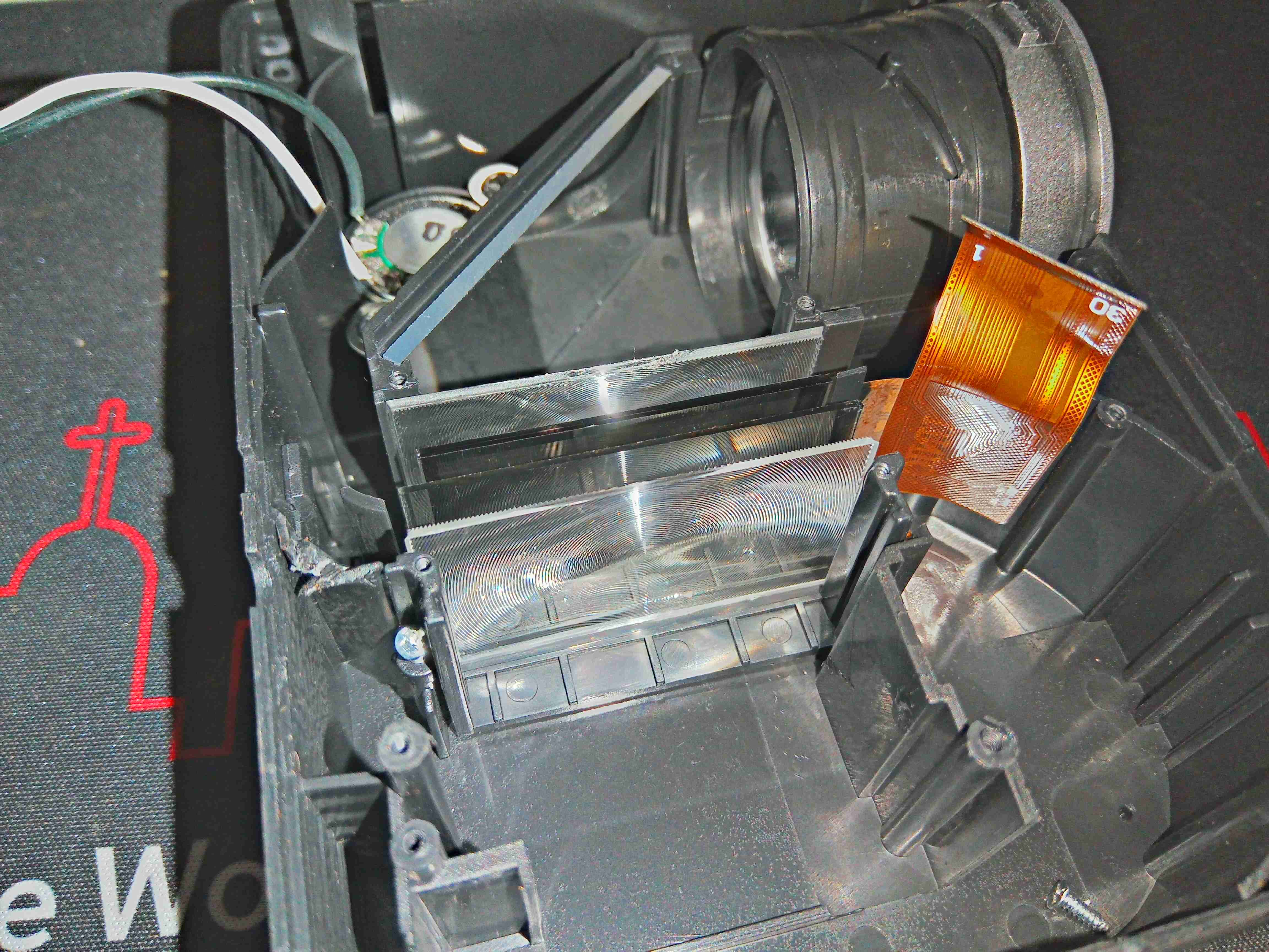
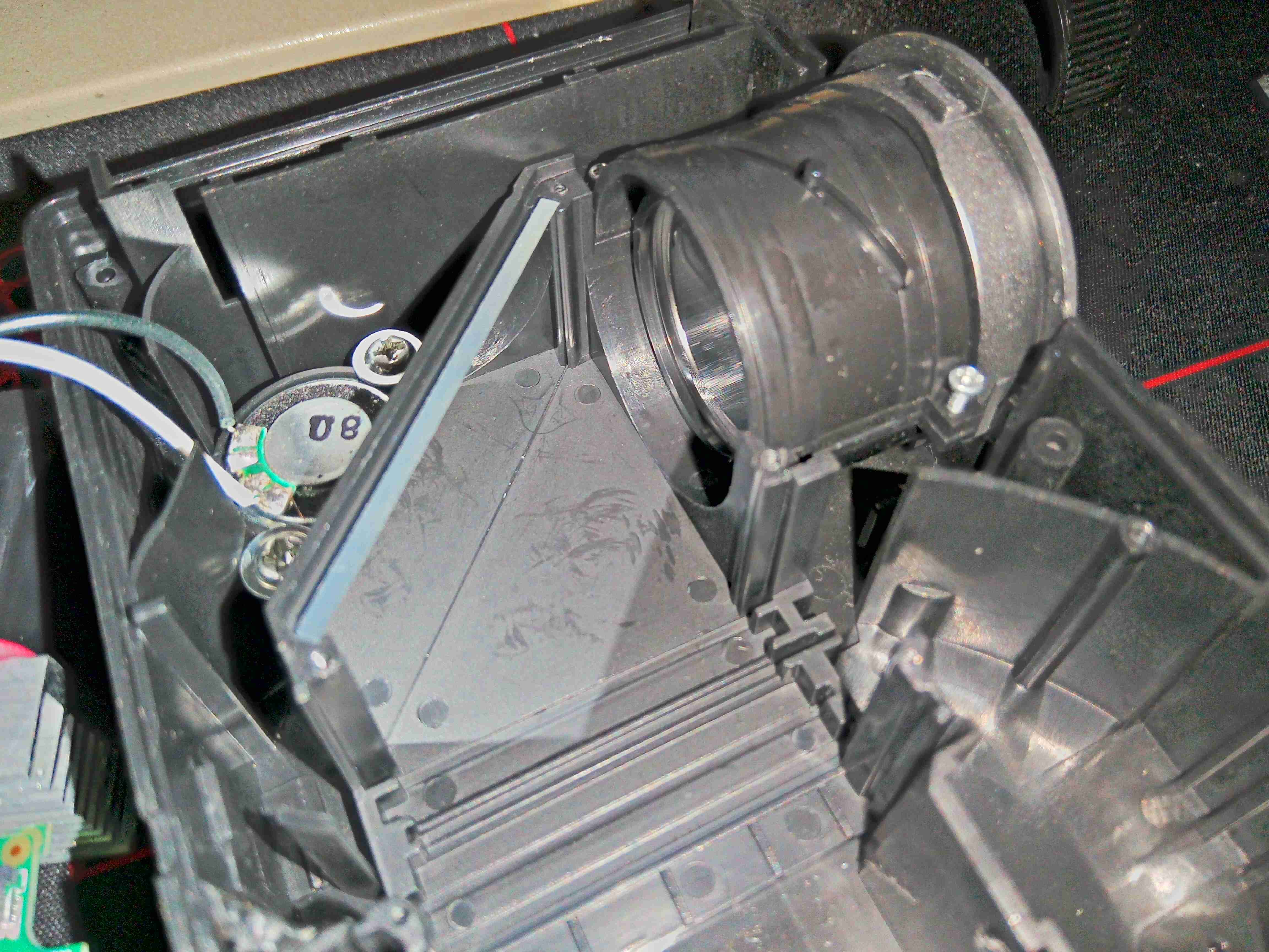
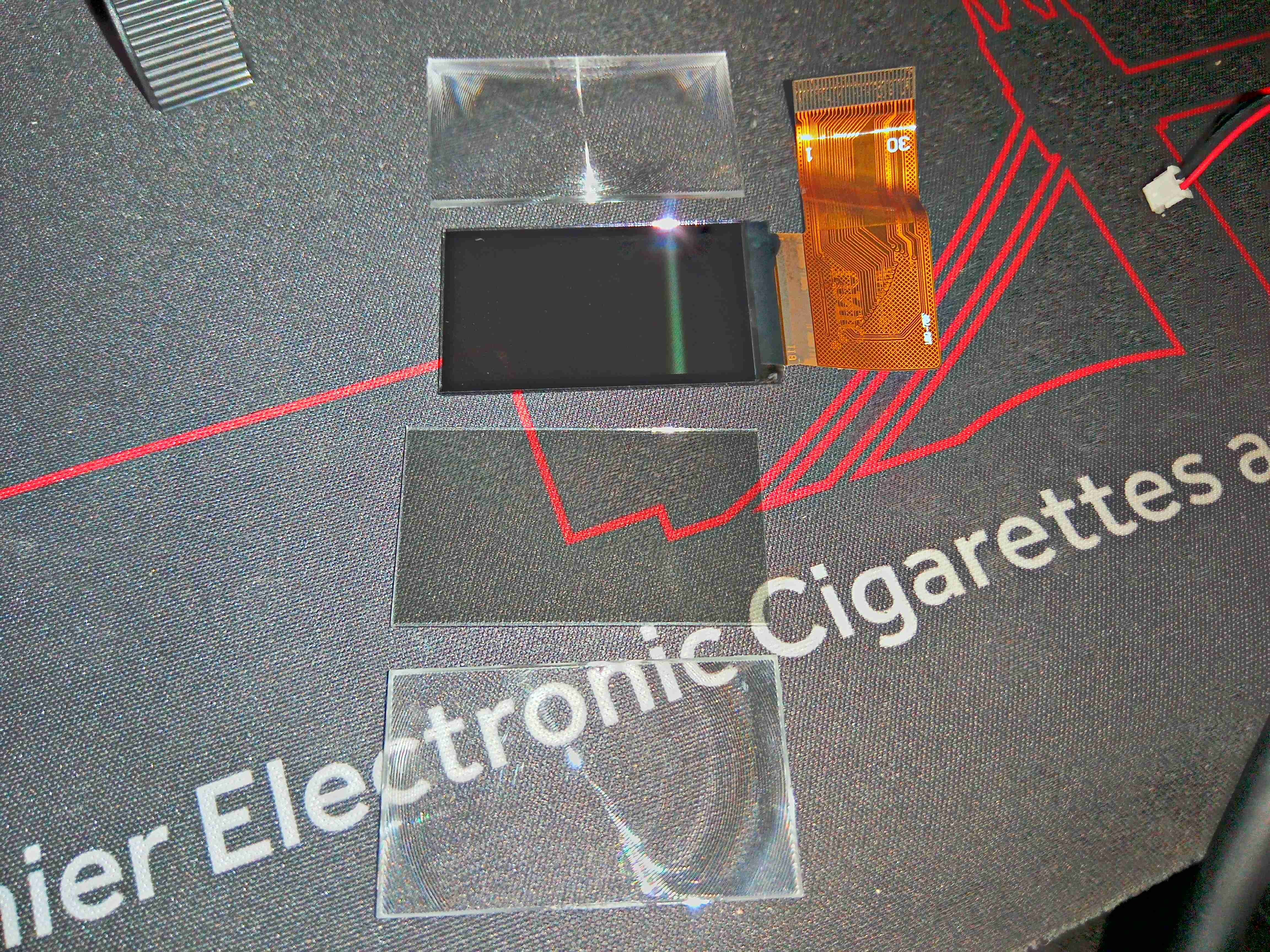
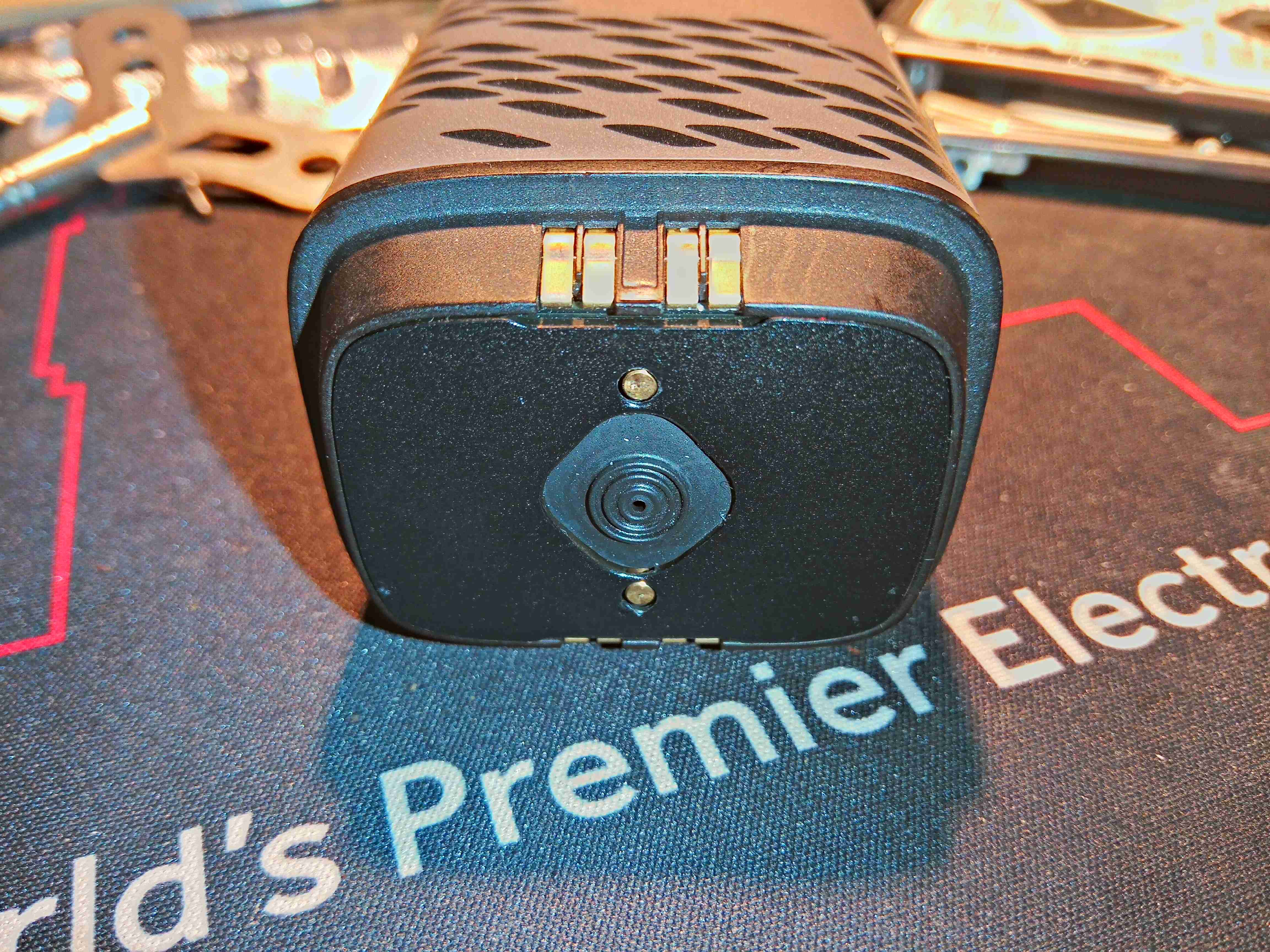
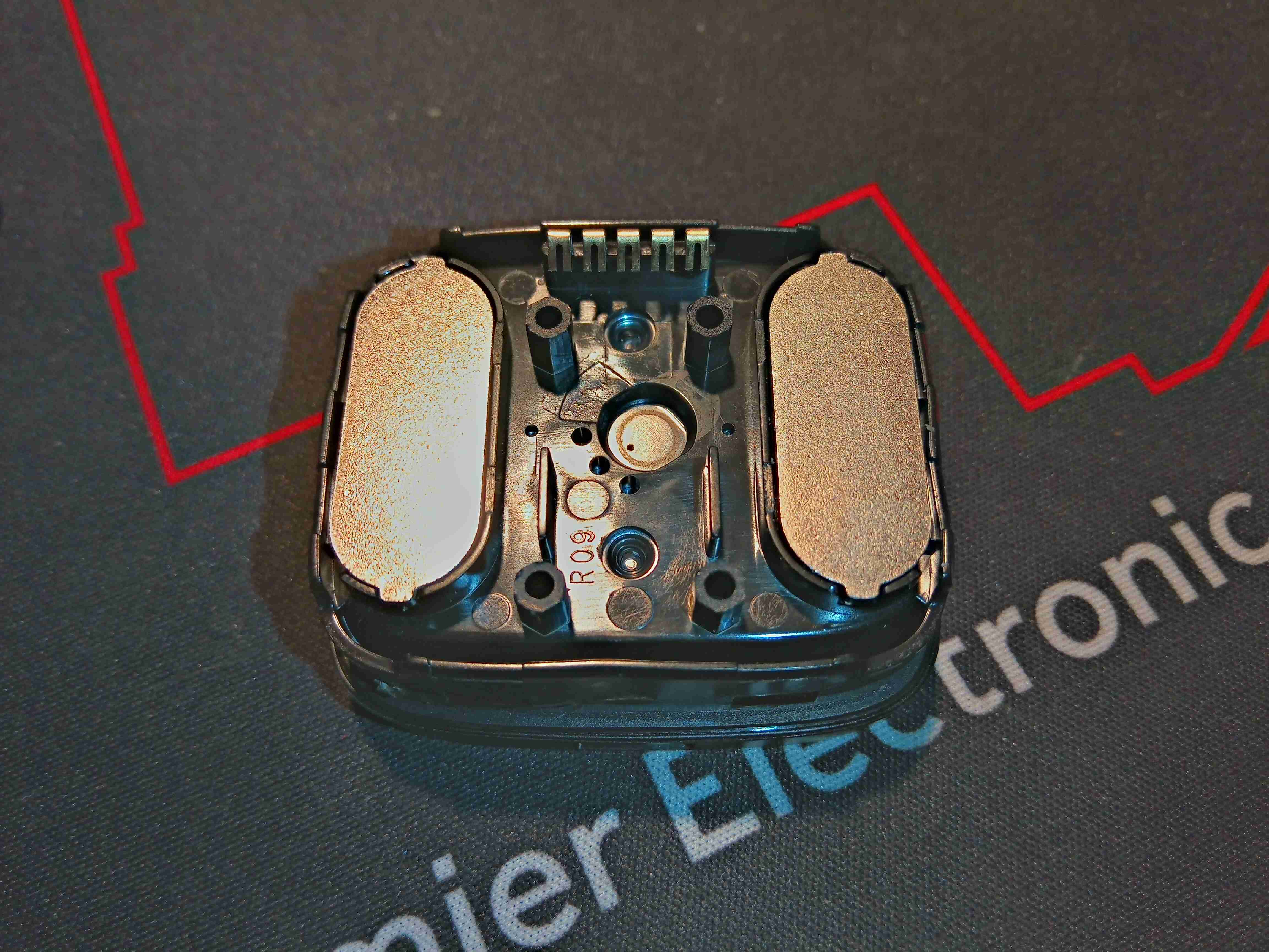
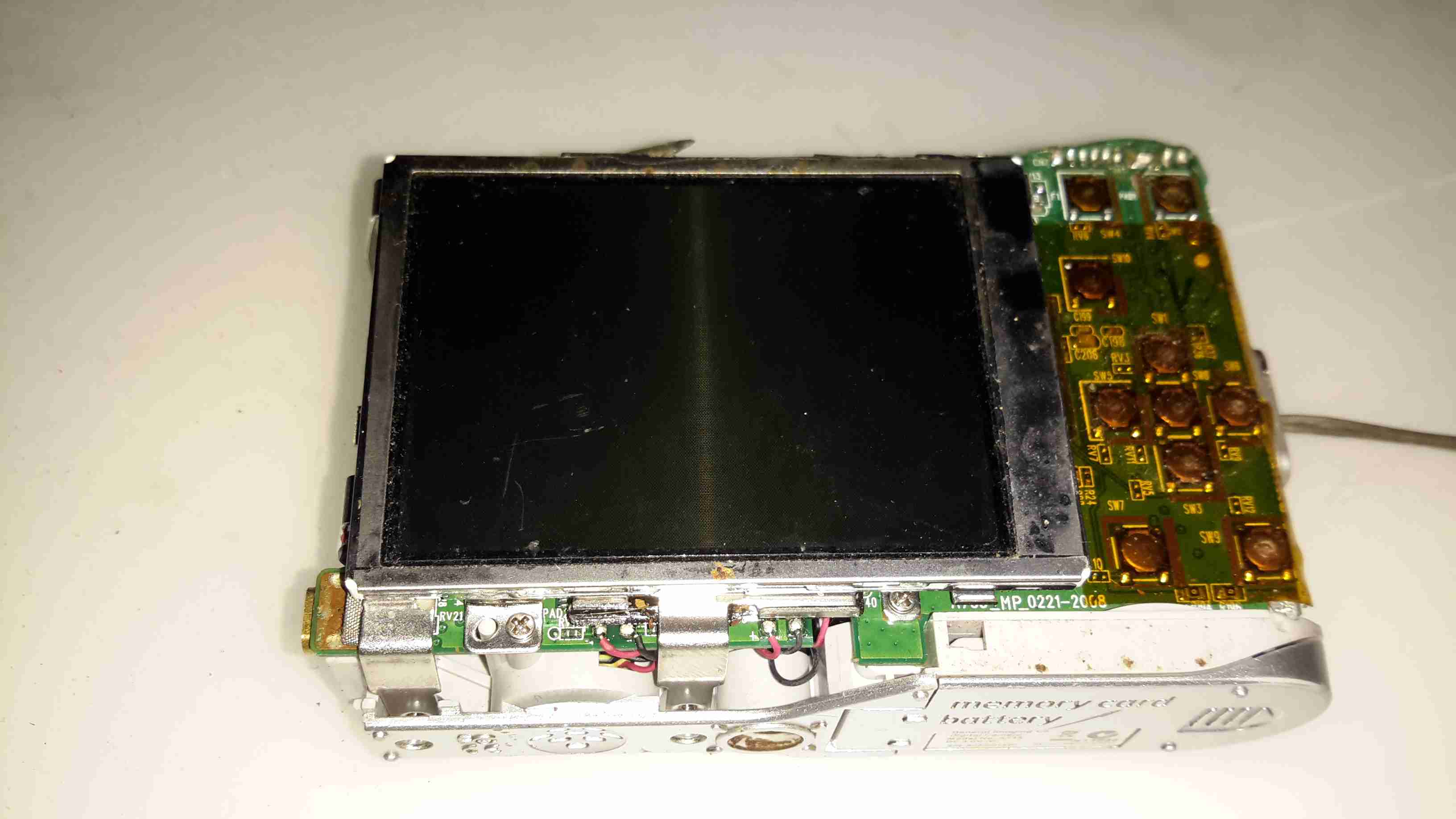
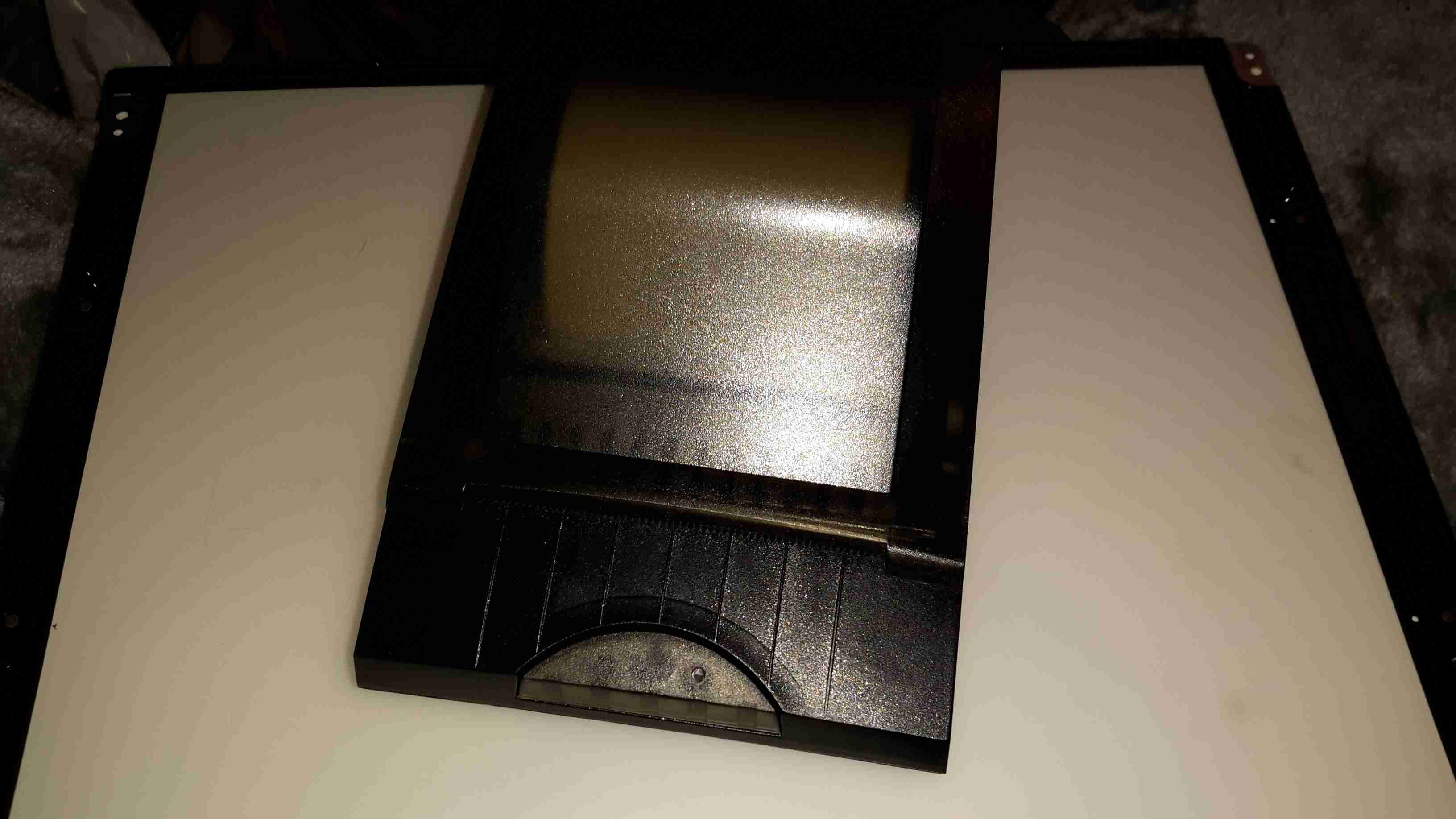
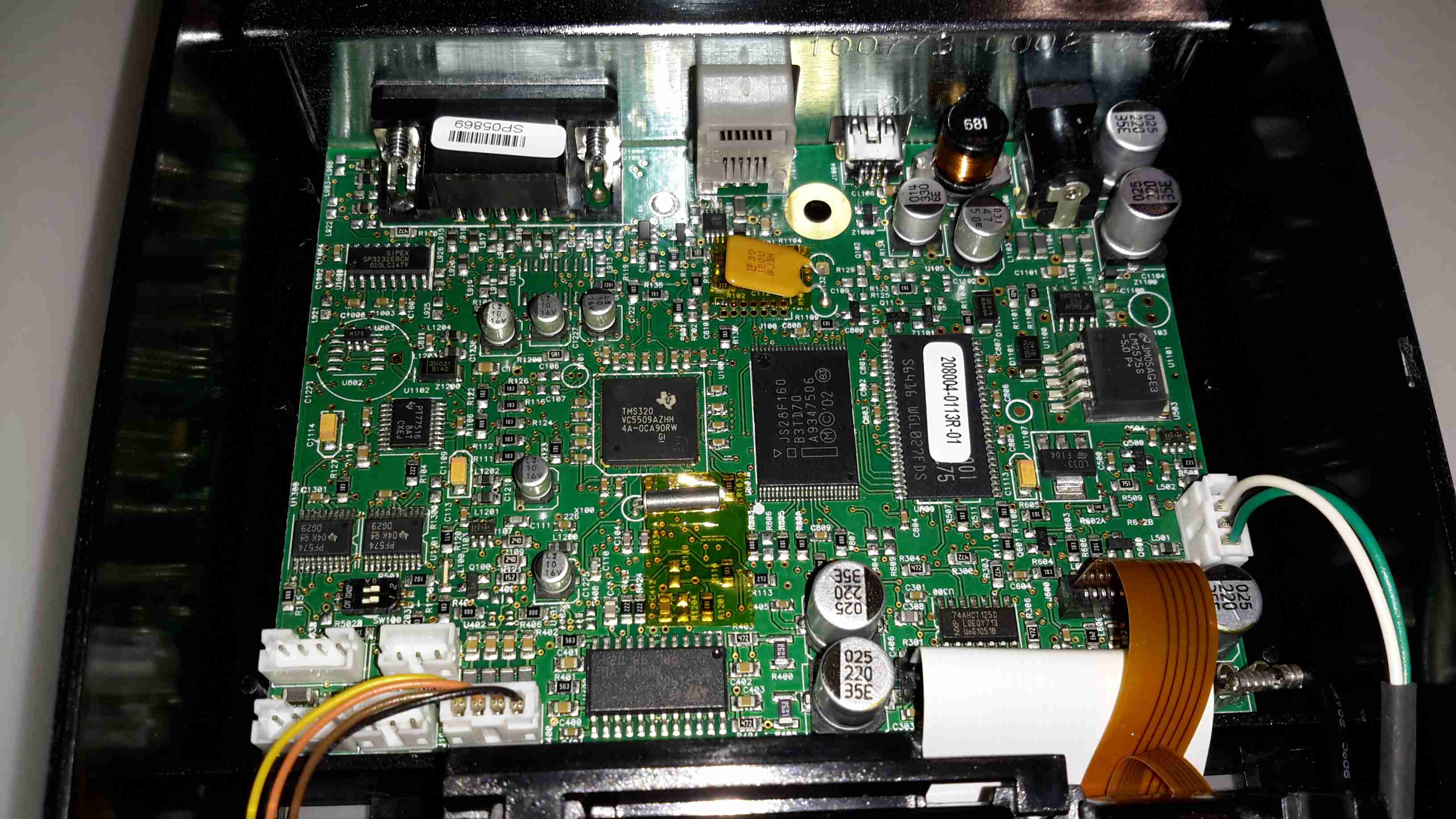
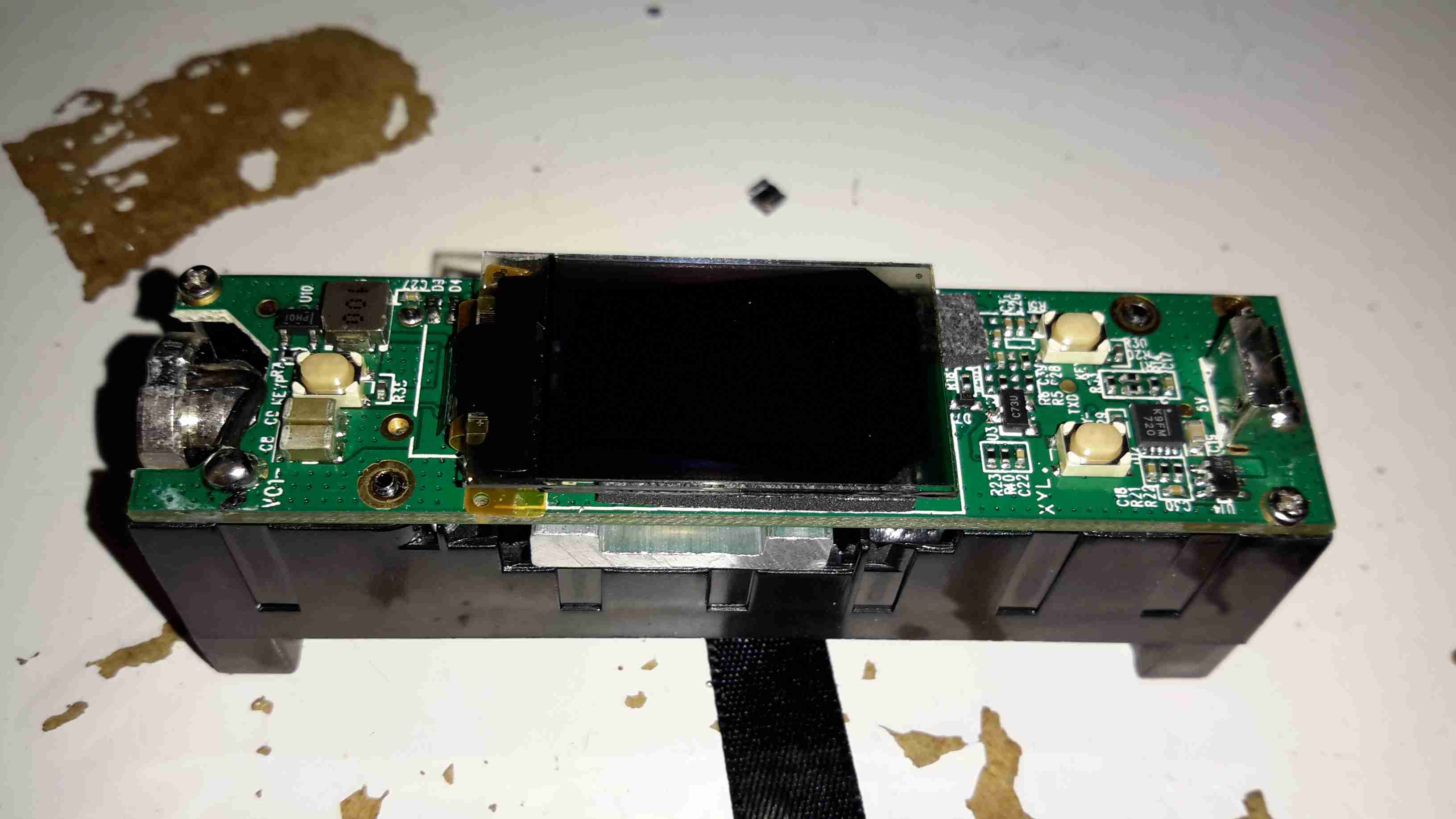
Popping a couple of screws out & removing the enormous eye cup allows the top cover to come off. This unit is very tightly packed inside, with 3 PCBs! The magnifying lens (~45mm diameter) & mirror on the left enlarge & turn the image so the camera operator can see it. The CRT’s at the top, with a copper grounding band around the face.

CRT Face
CRT Face

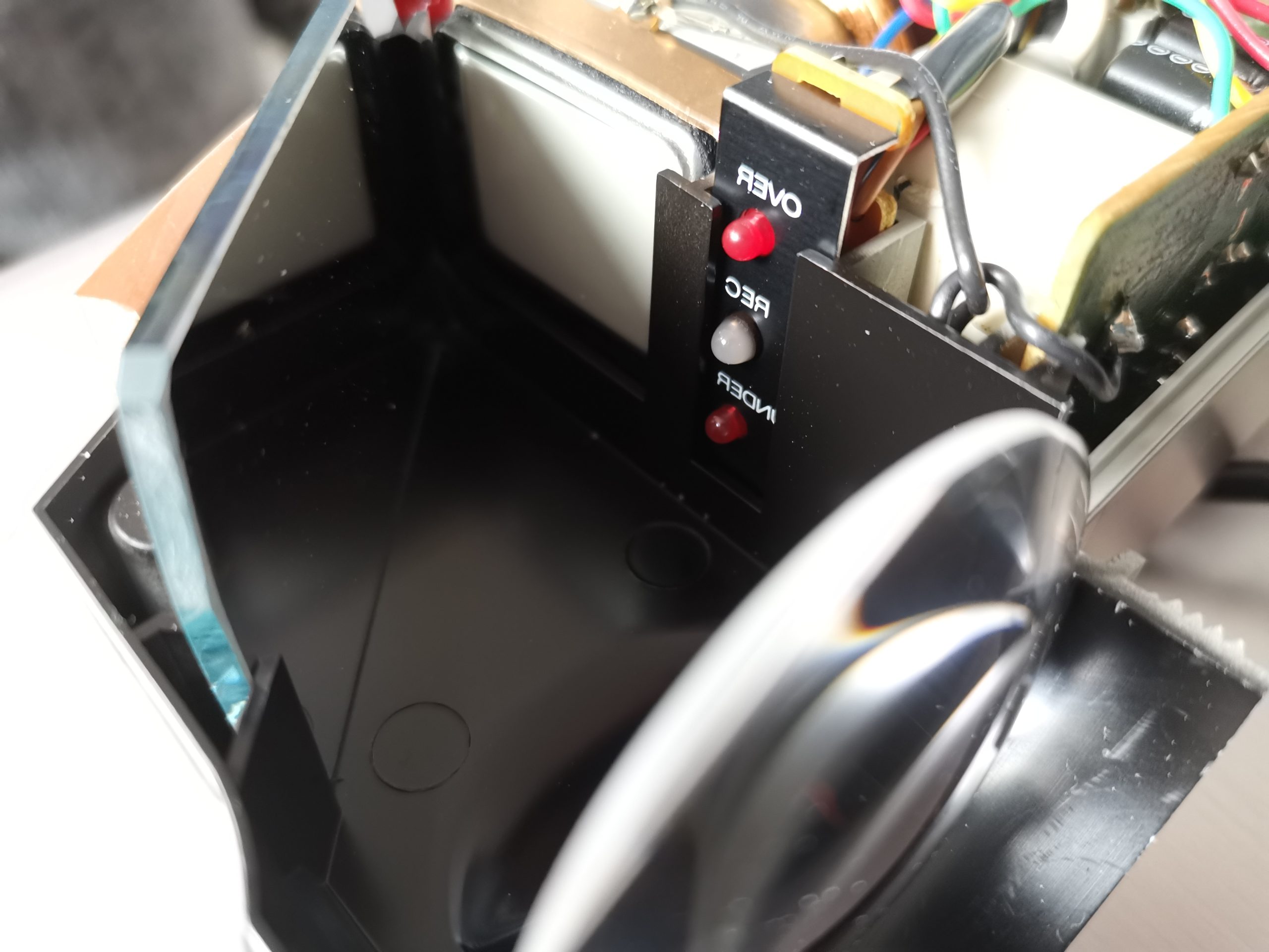
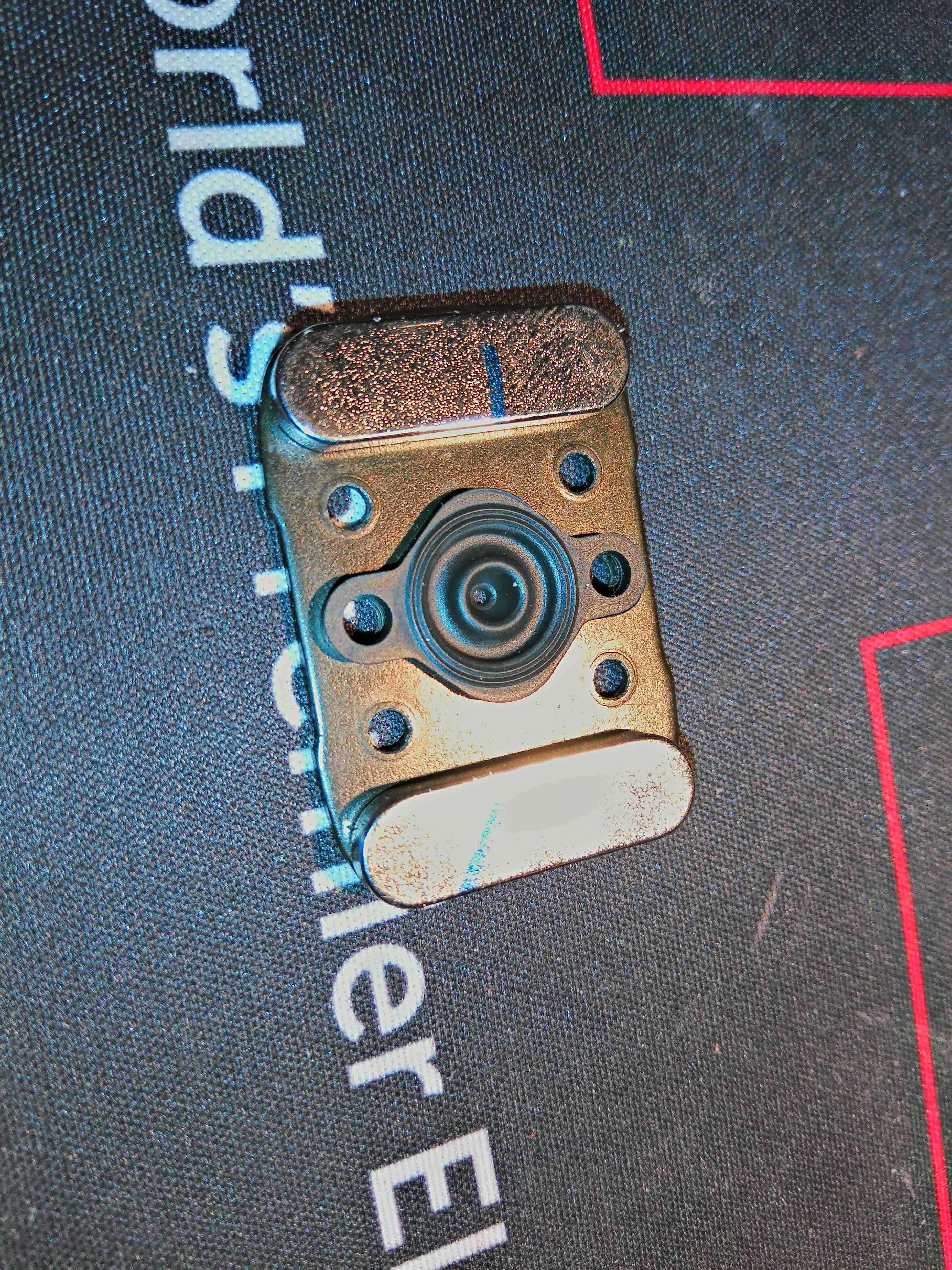
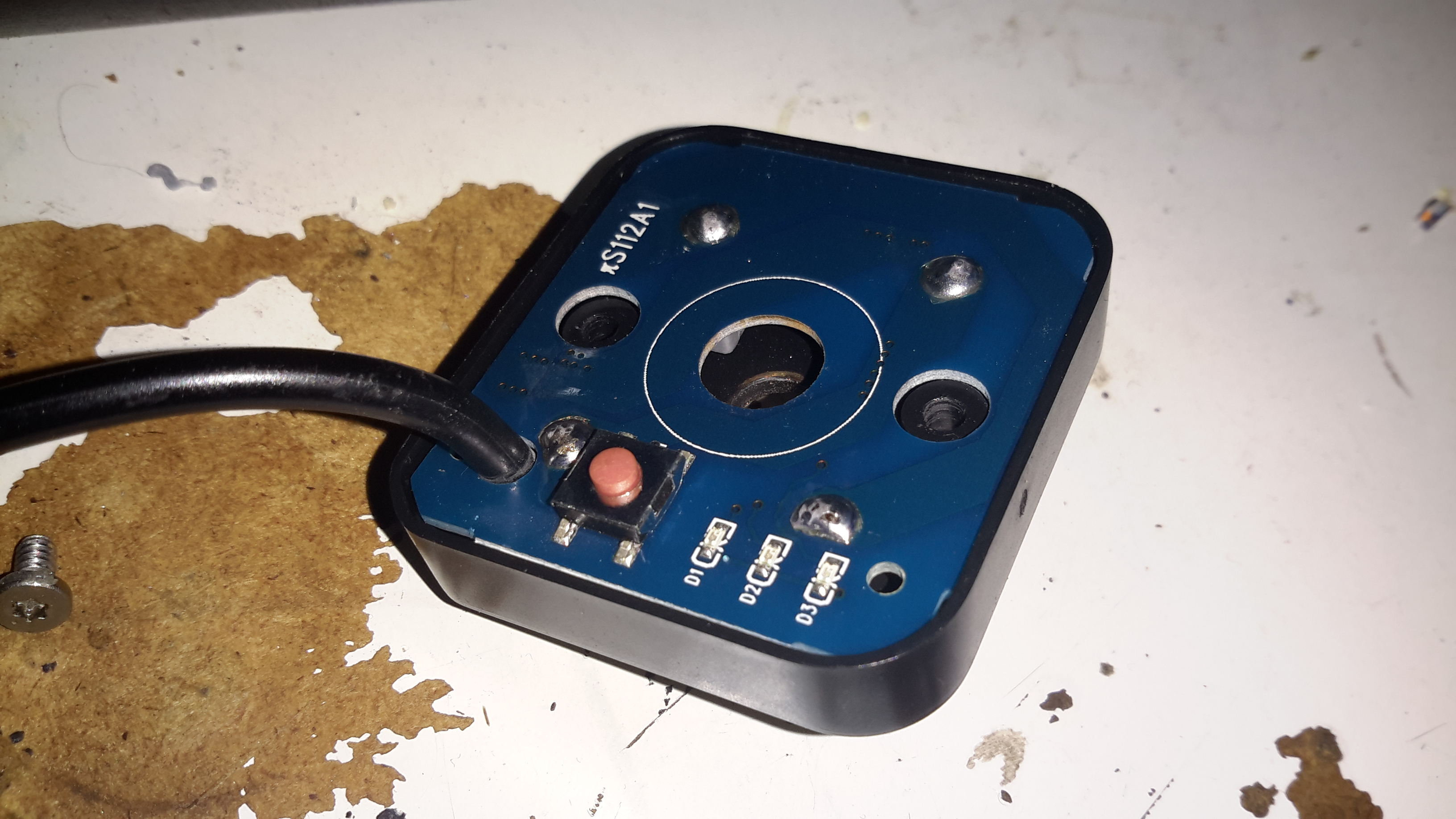
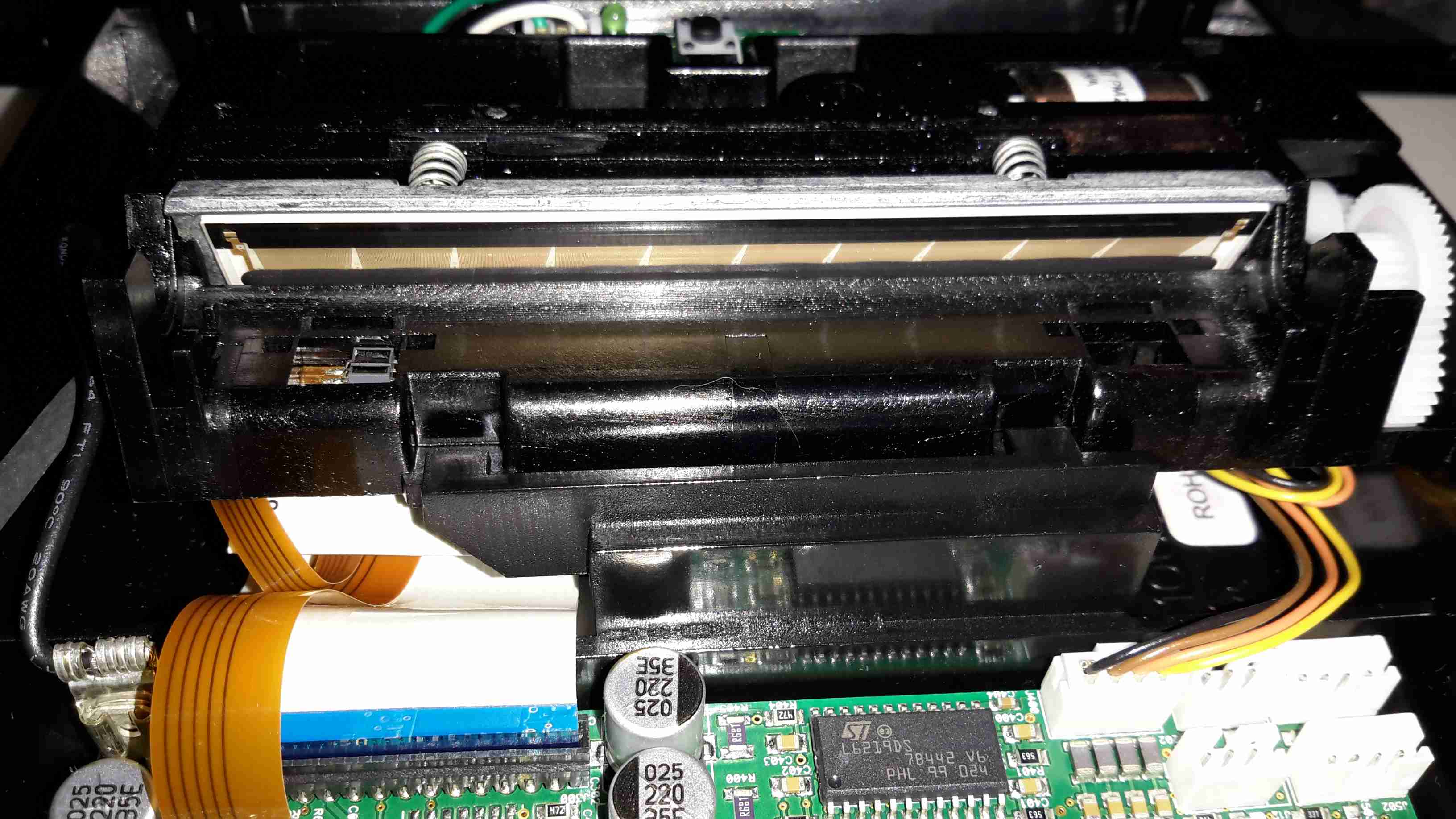
The CRT face is neatly slotted into the plastic housing, with the tally LEDs to the right of it. The legends on the LEDs are naturally printed in reverse, since they’re intended for viewing through the mirror. The optical section is entirely spray painted black for better contrast & stray light control.

Electronics Area
Electronics Area

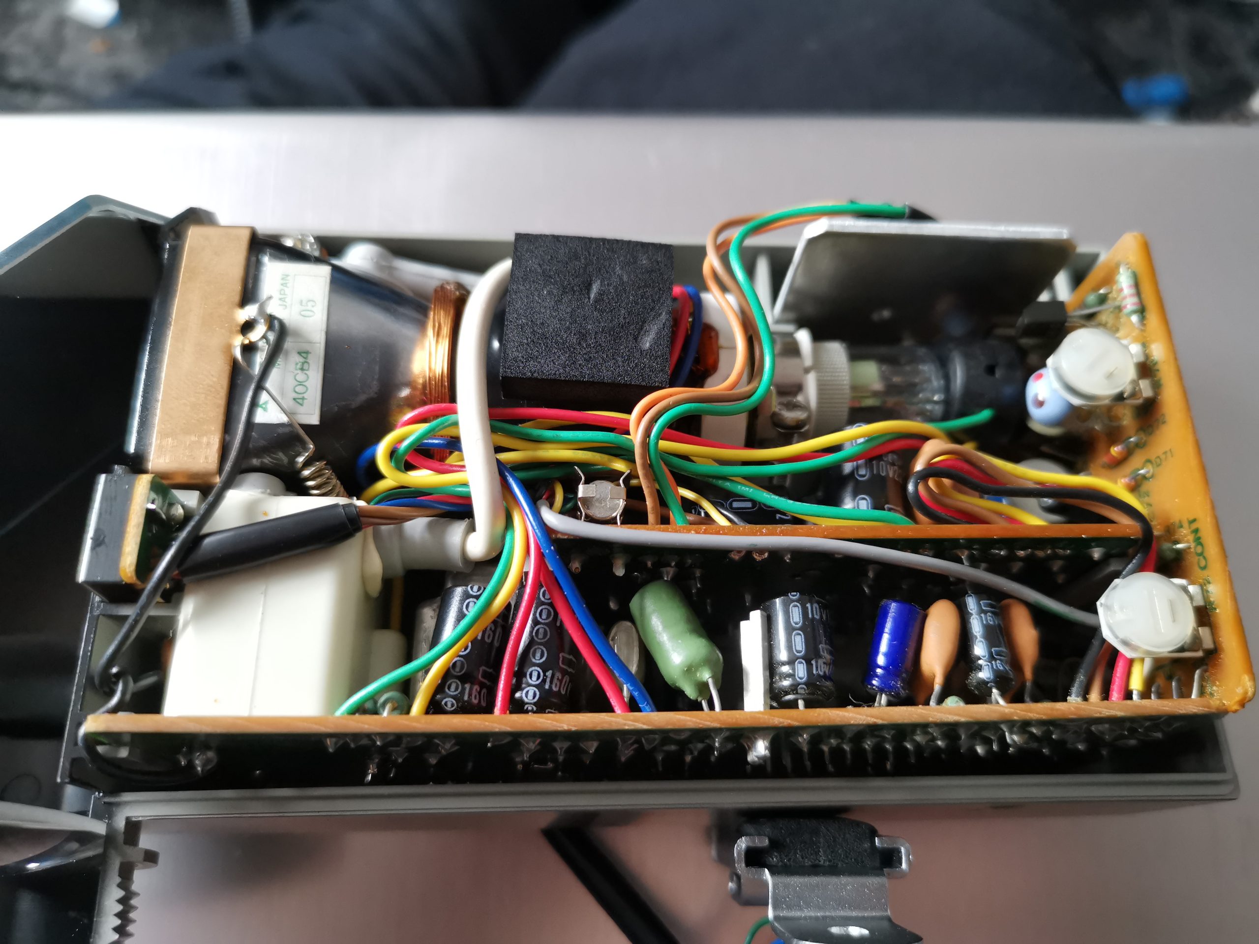
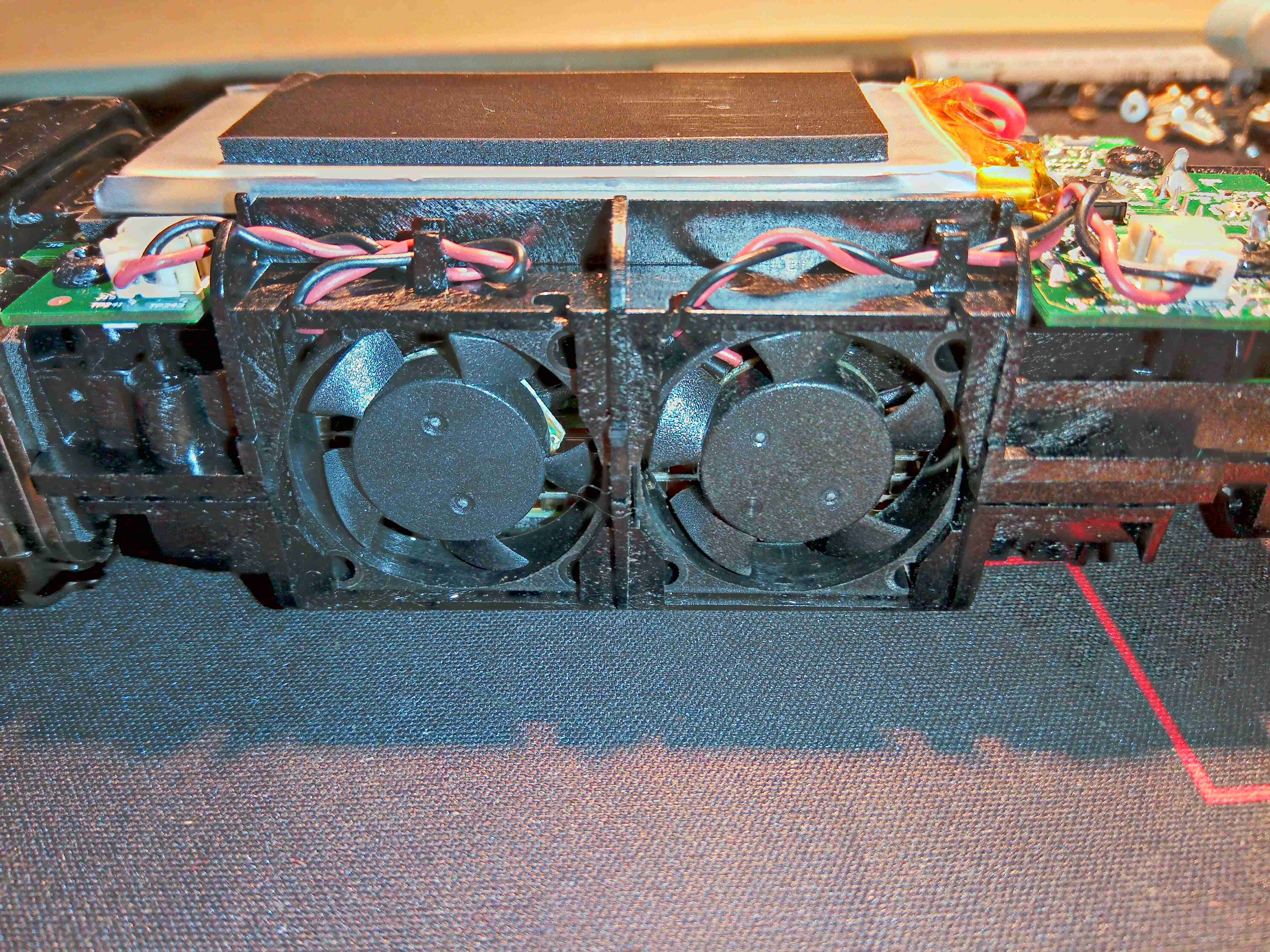
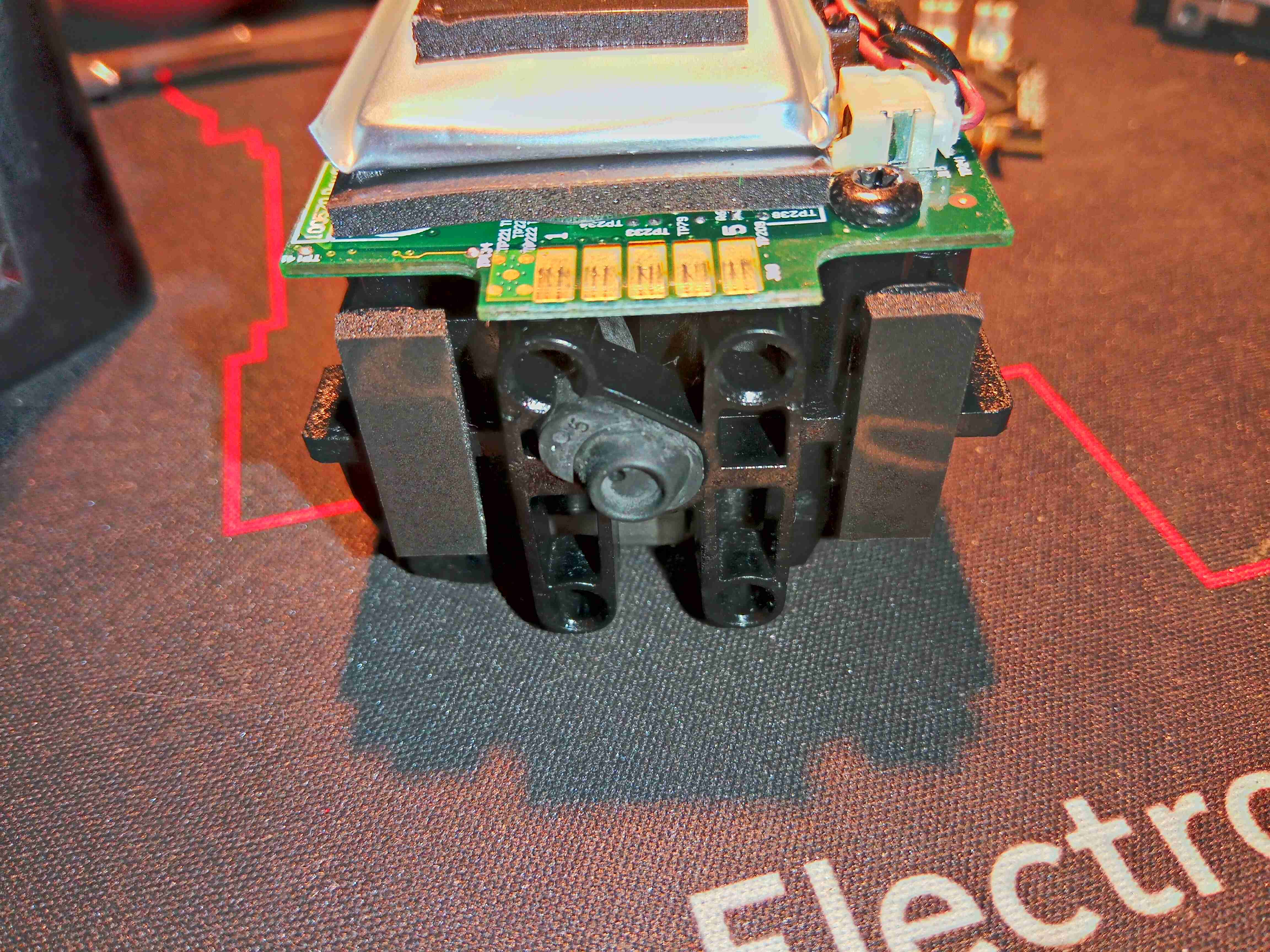
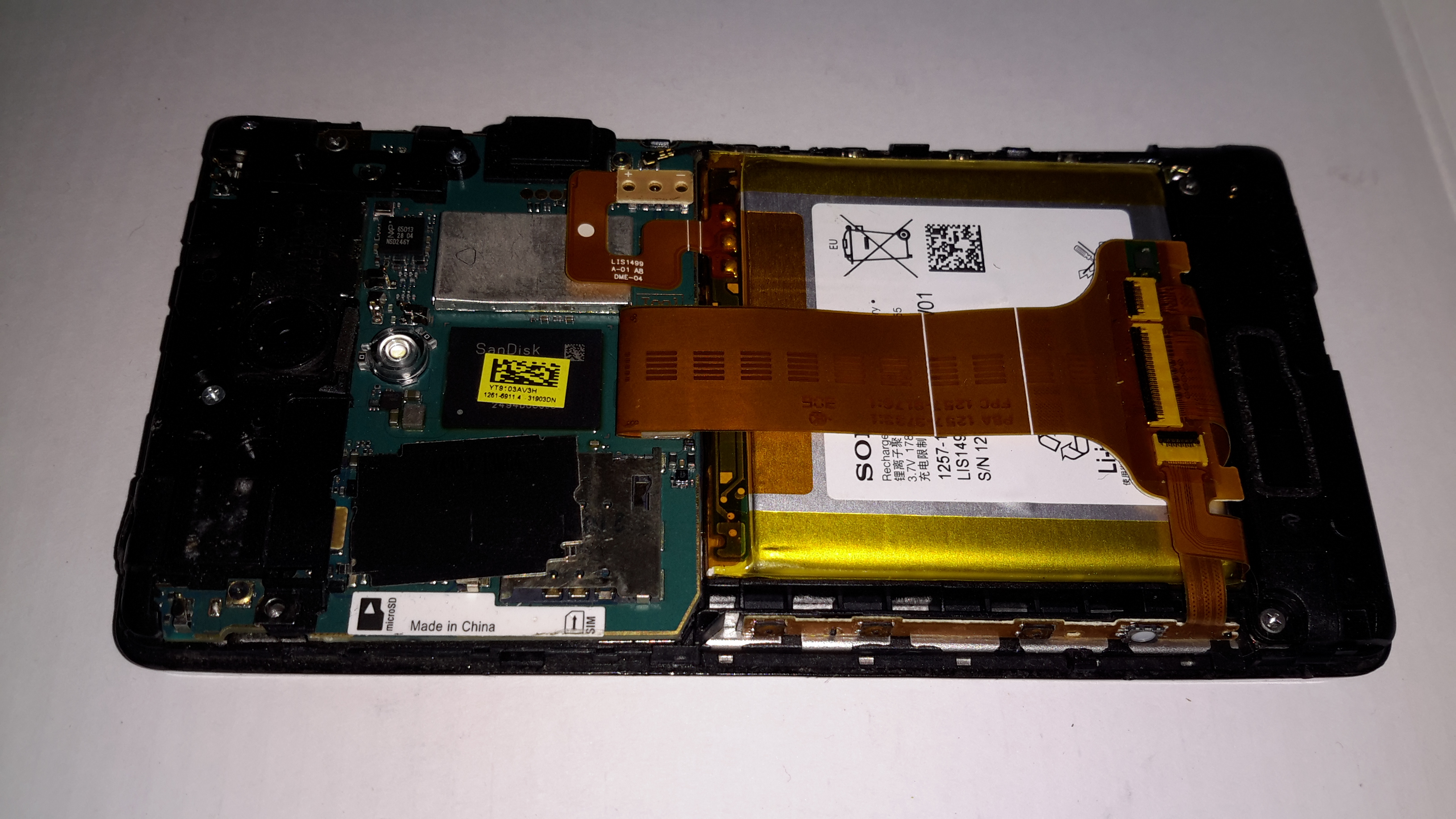
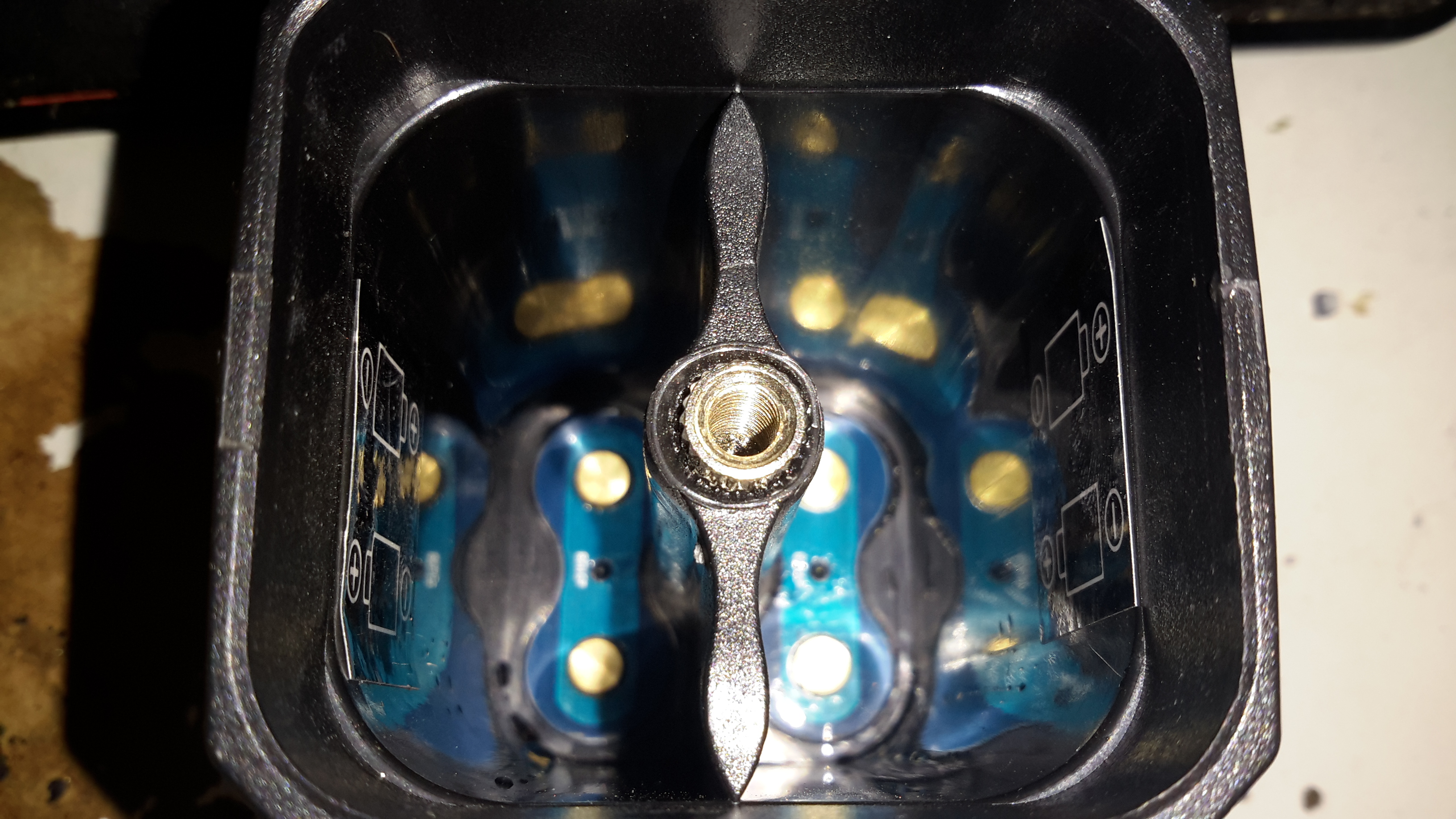
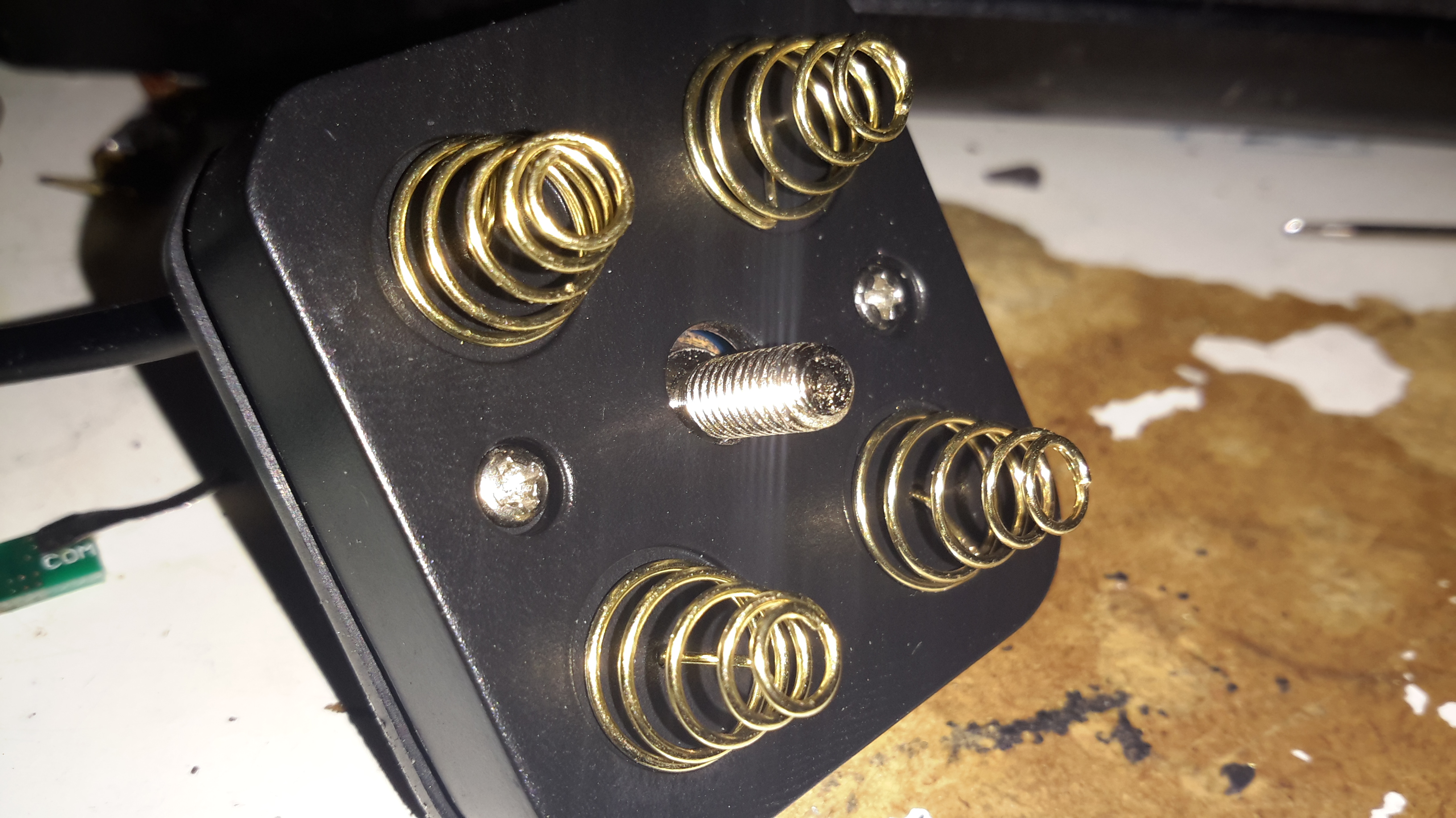
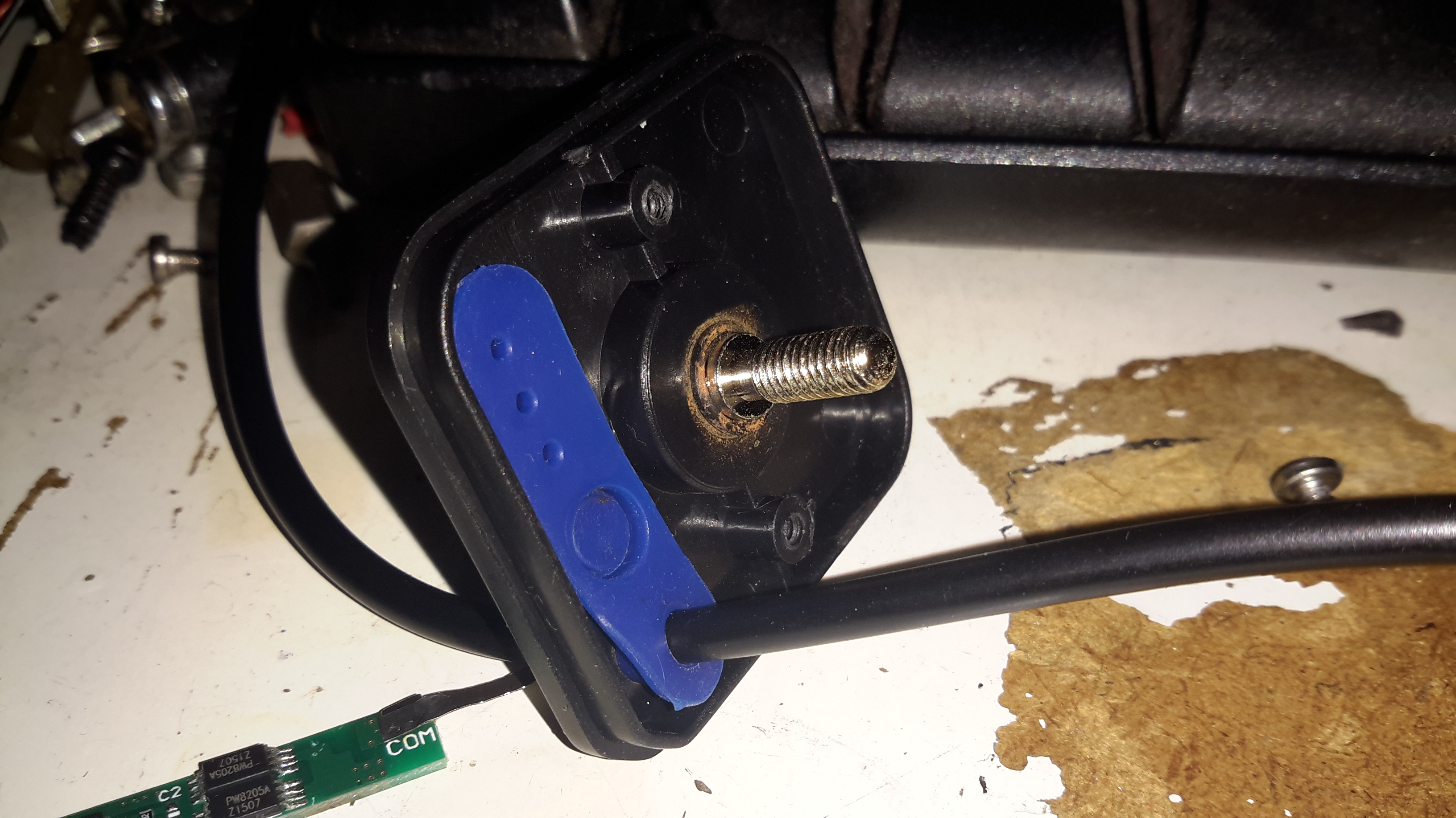
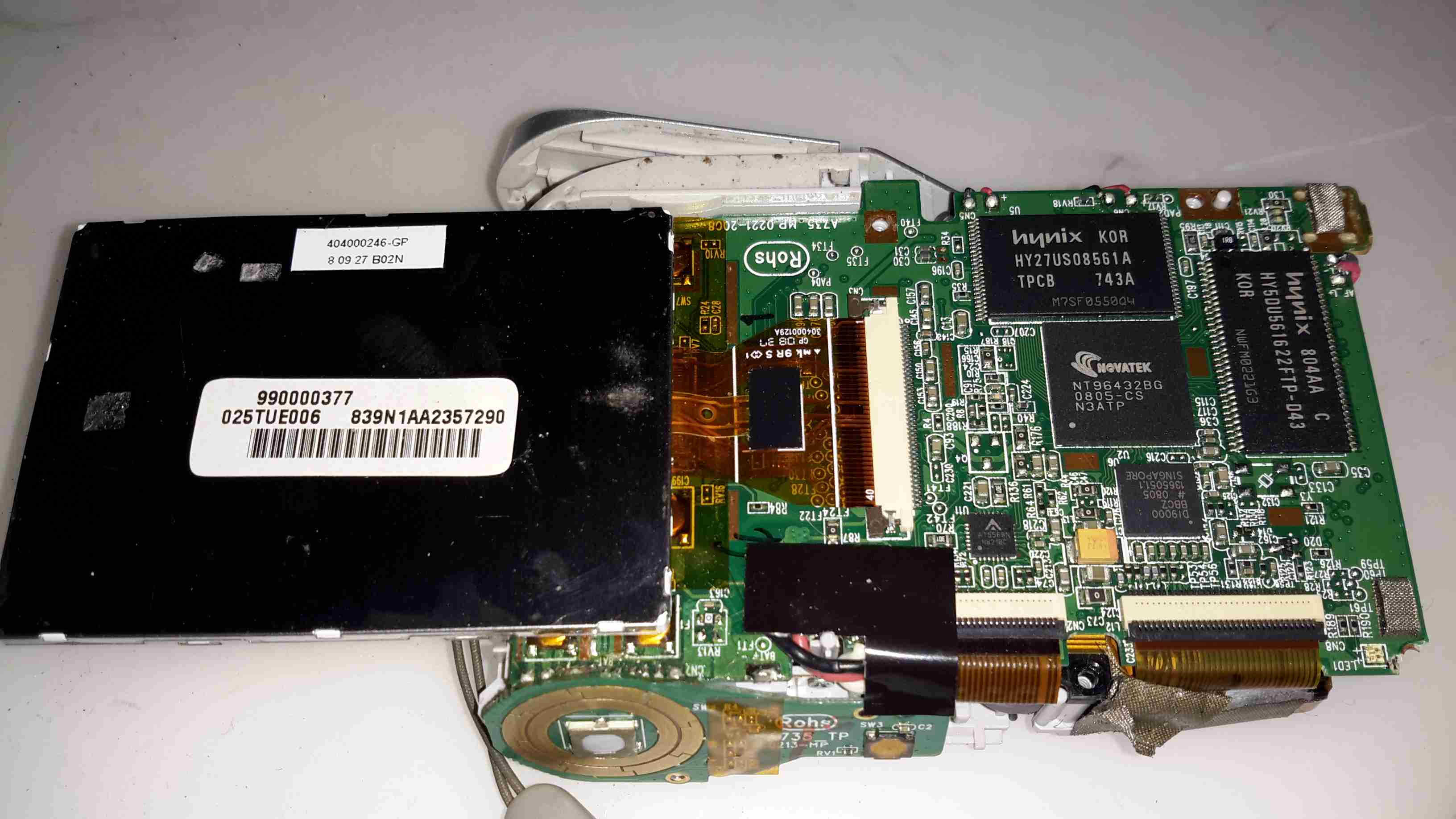
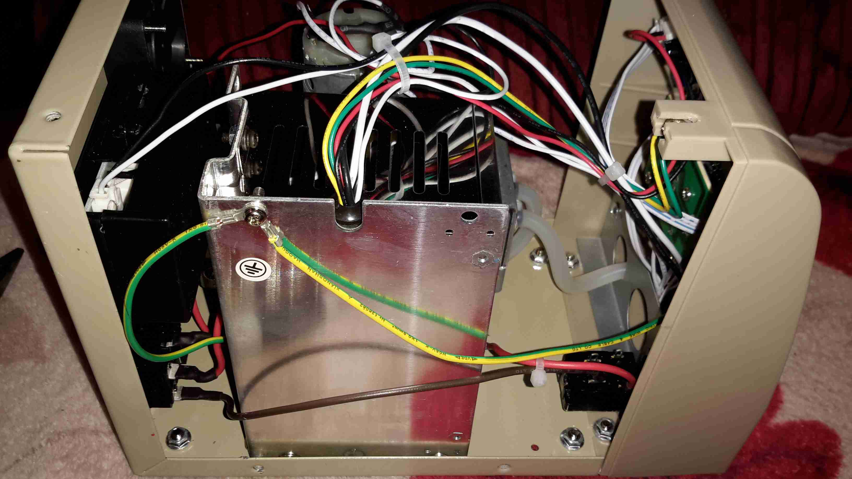
The other 5″ of the casing is packed with electronics to support the CRT. The bottom PCB even “wraps around” to the right, with copper staples connecting the boards together. The CRT tube itself is hiding inside the deflection yoke and under a foam pad at the top of the unit. It’s secured in place with a copper grounding strap wrapped around the face of the tube, and a spring. A single screw secures the strap to the case. This also provides a local earth for the outer Aquadag coating on the tube, which is the negative plate of the final anode smoothing capacitor. The other plate is formed by the coating on the inside of the CRT glass, and the dielectric is of course the glass itself.
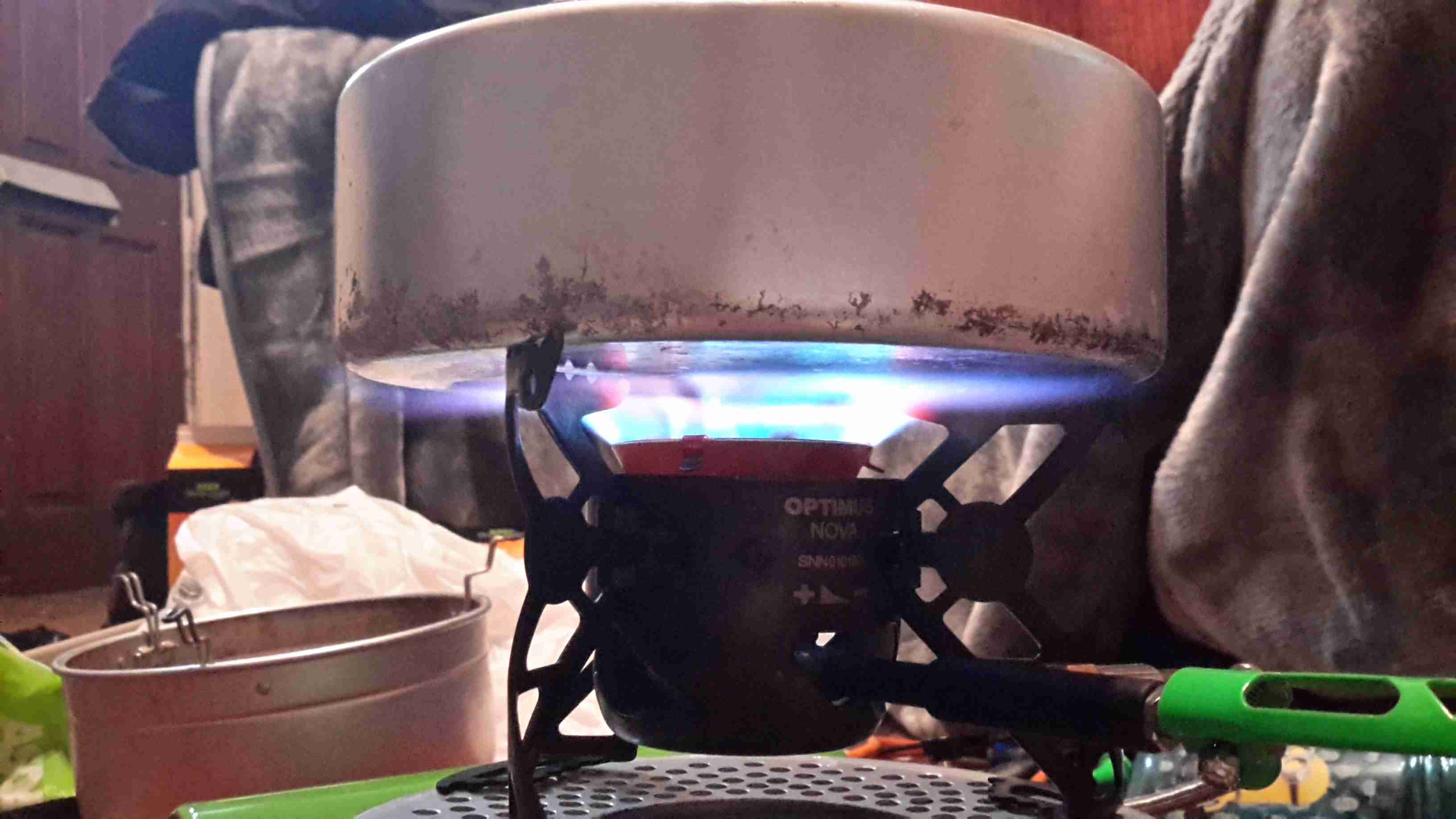
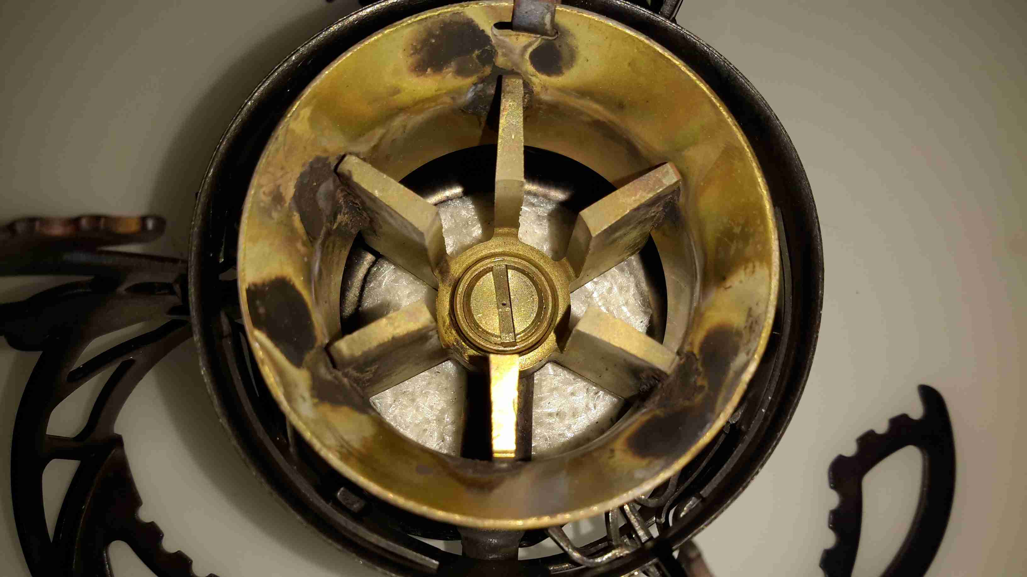
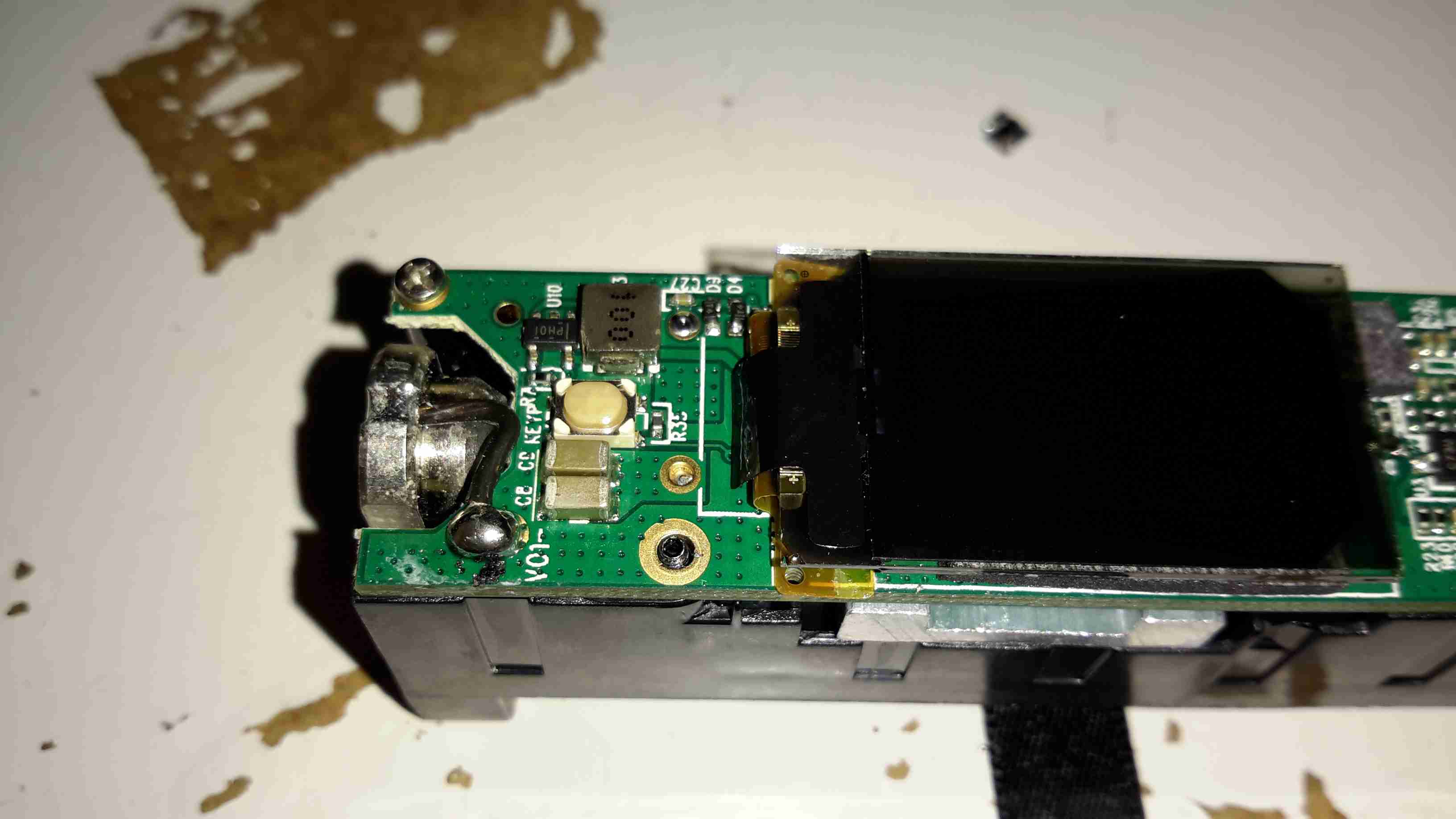
The main anode wire snakes off from the flyback at bottom left to the anode cup at the top of the CRT, insulating the 7kV from everything else.

There aren’t many reasons to jack up the final anode voltage on a CRT, past the design voltage of the tube as JVC have done here. The only plausible one I could think of is to increase brightness of the image, but the Sony 4CB4-based units I have only run at around 3kV, and those are plenty bright enough! The downside here of course, is that with higher energy electrons and a brighter image, the phosphor of the CRT will wear out faster.
Increasing voltage also increases X-Ray emission, but even at the 8kV maximum, such X-Rays would be so weak as to not make it through the CRT faceplate glass, which is loaded with lead anyway.

There’s not much sense in yanking the tube out of this unit, it’s identical to the Sony one’s I’ve done in the past:

Bare 40CB4 CRT
Bare 40CB4 CRT
Voltage Regulator Pass Transistor

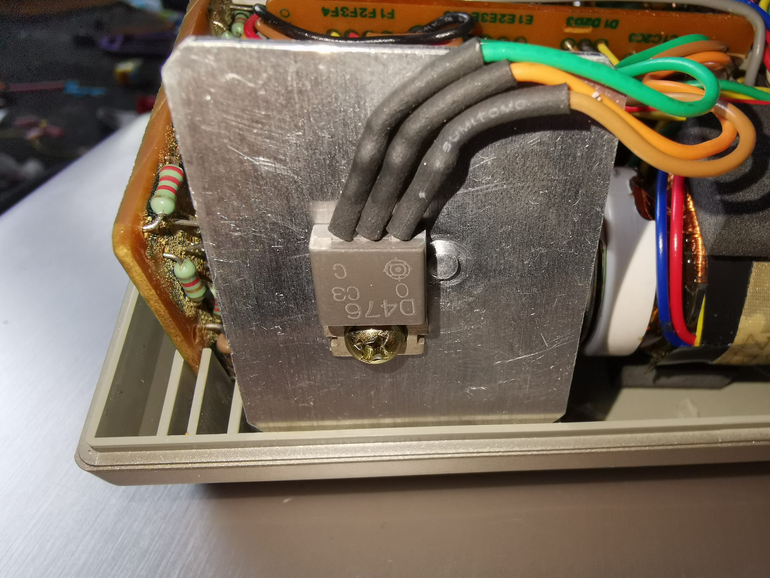
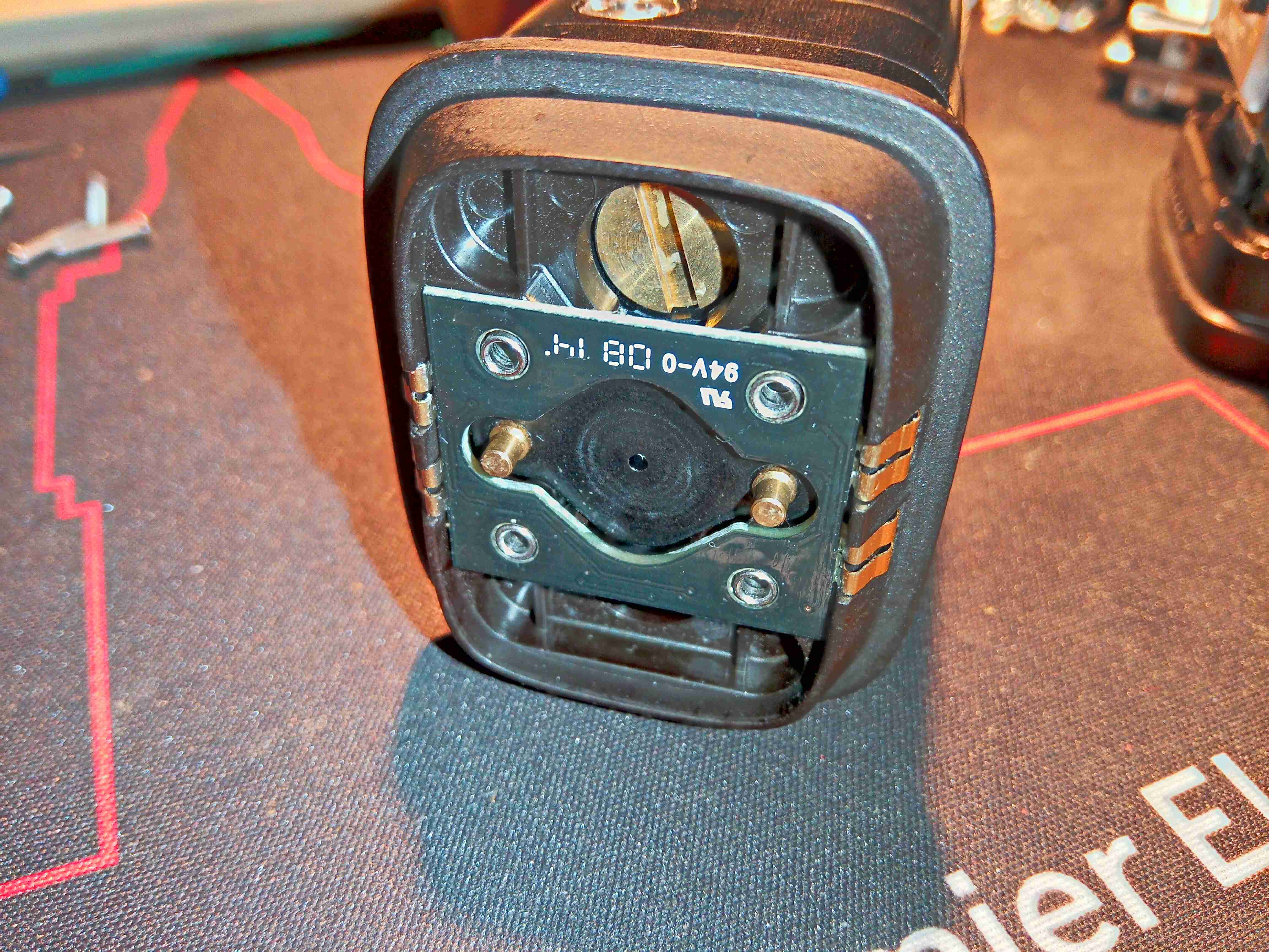
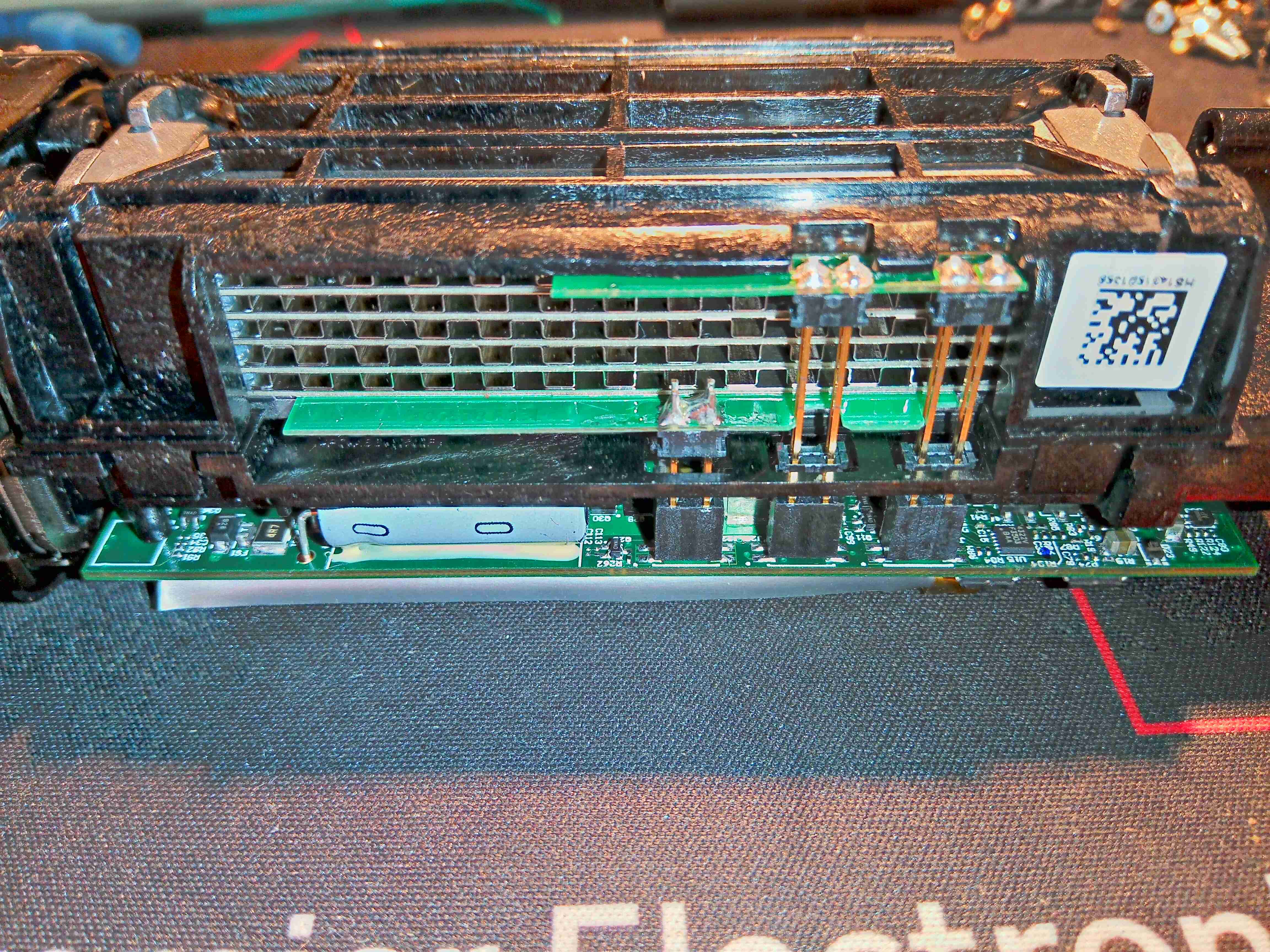
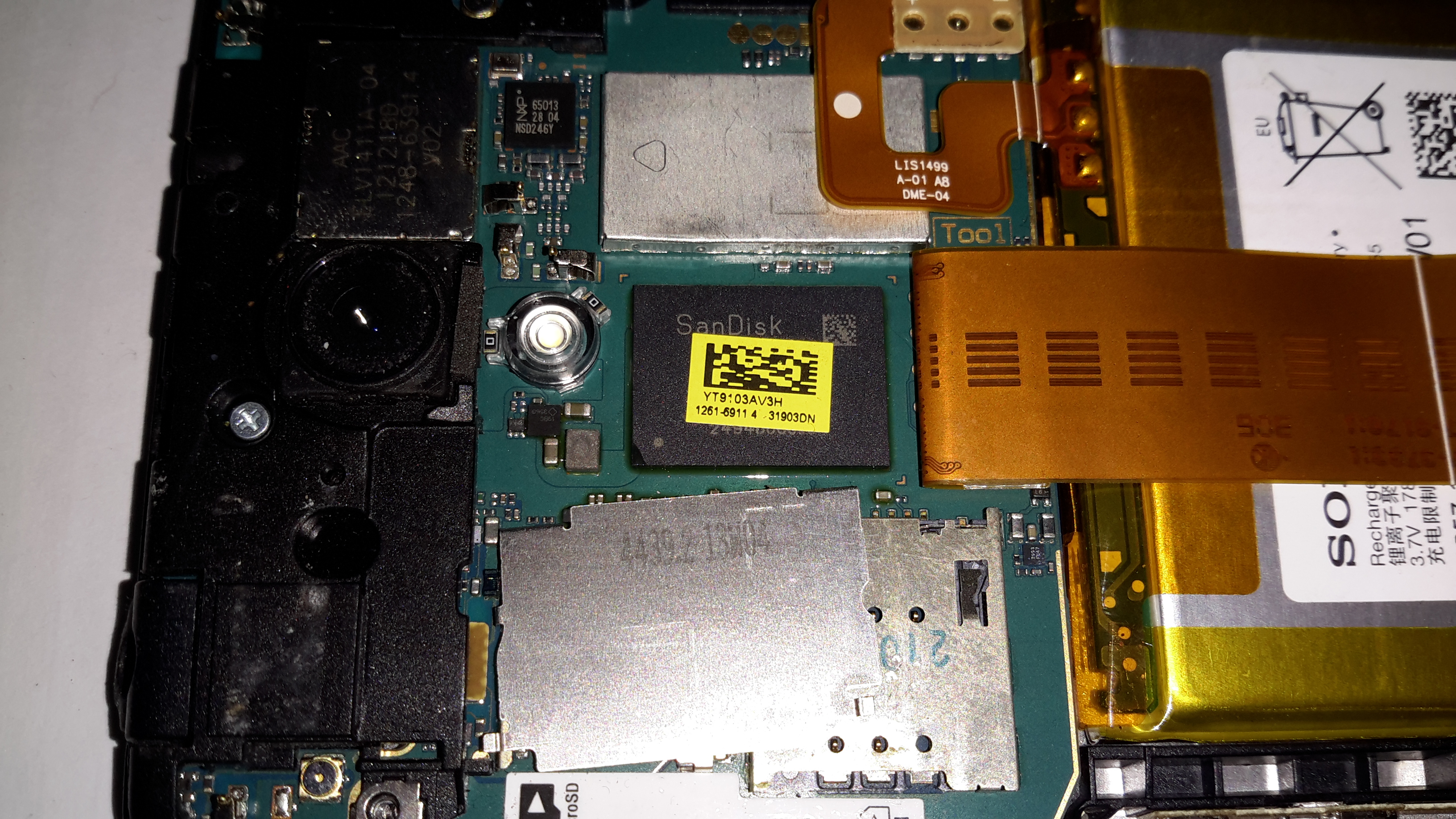
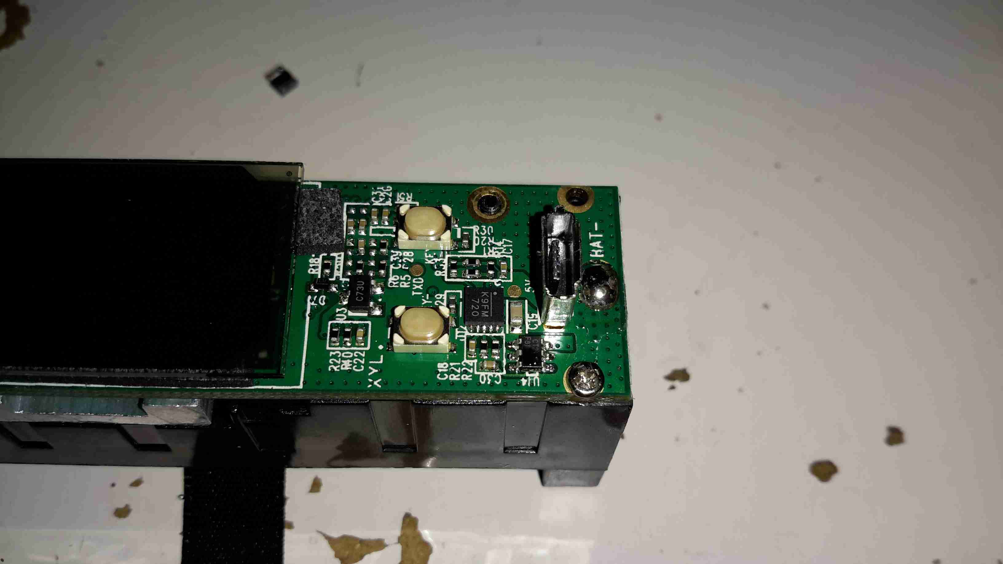
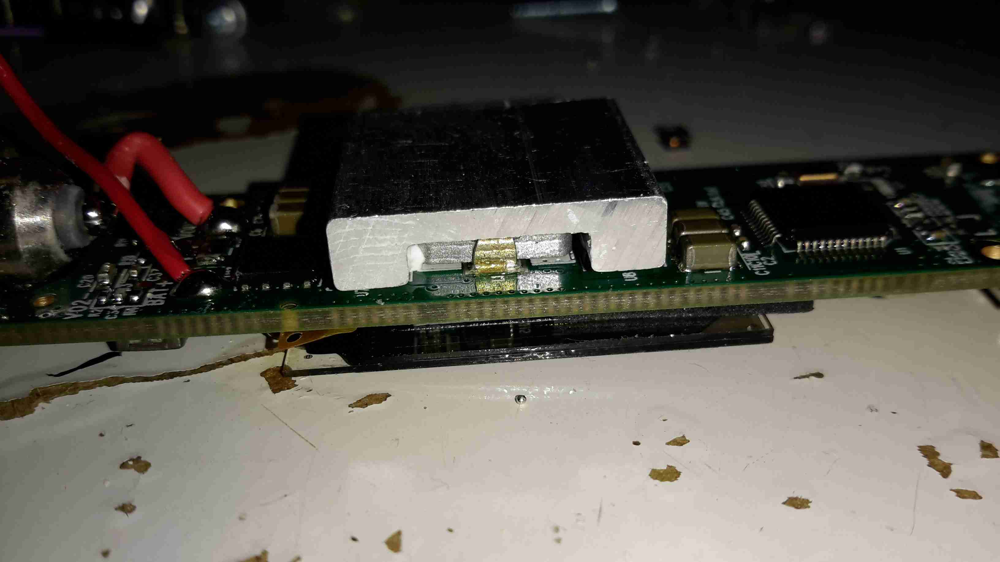
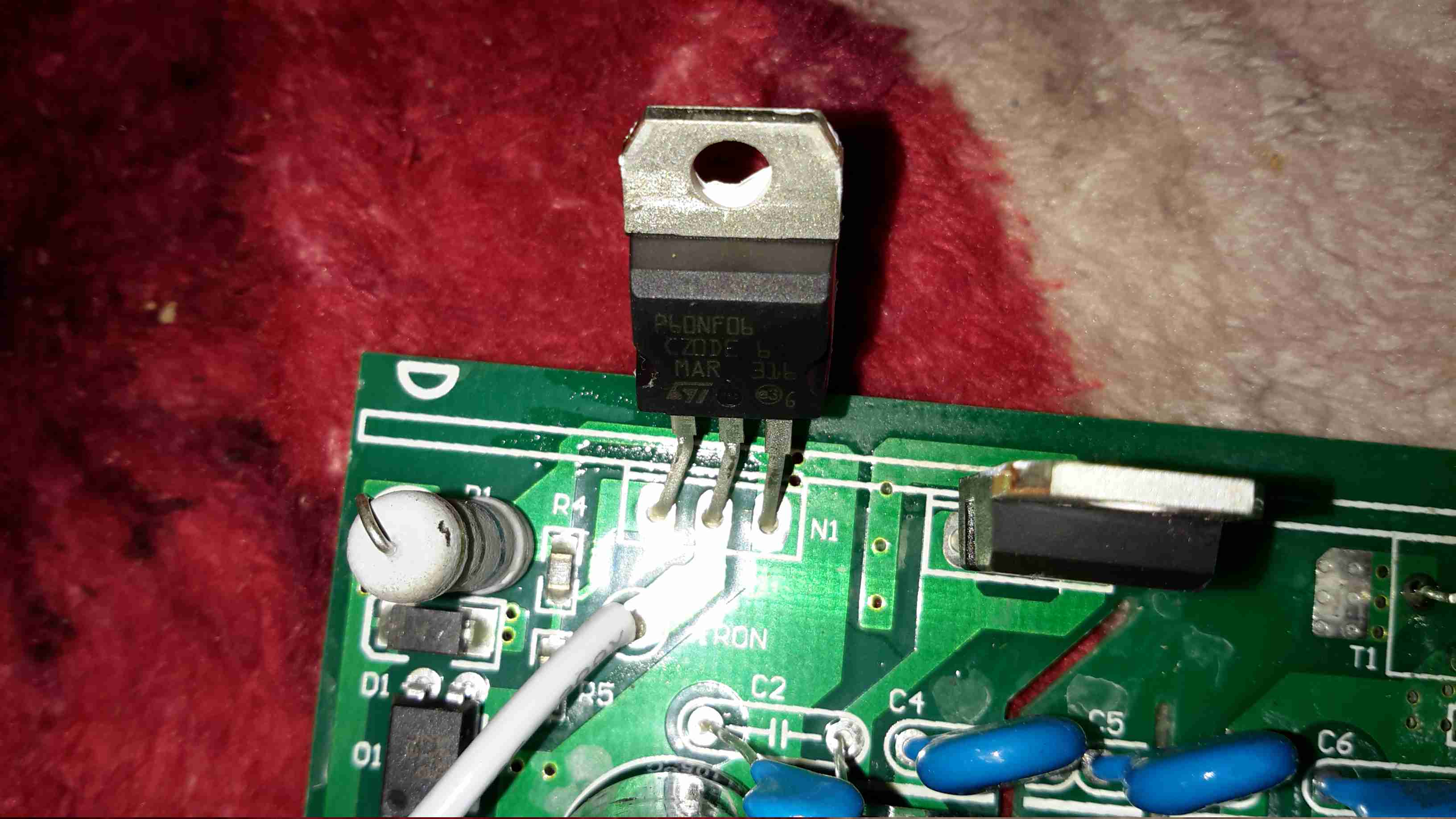
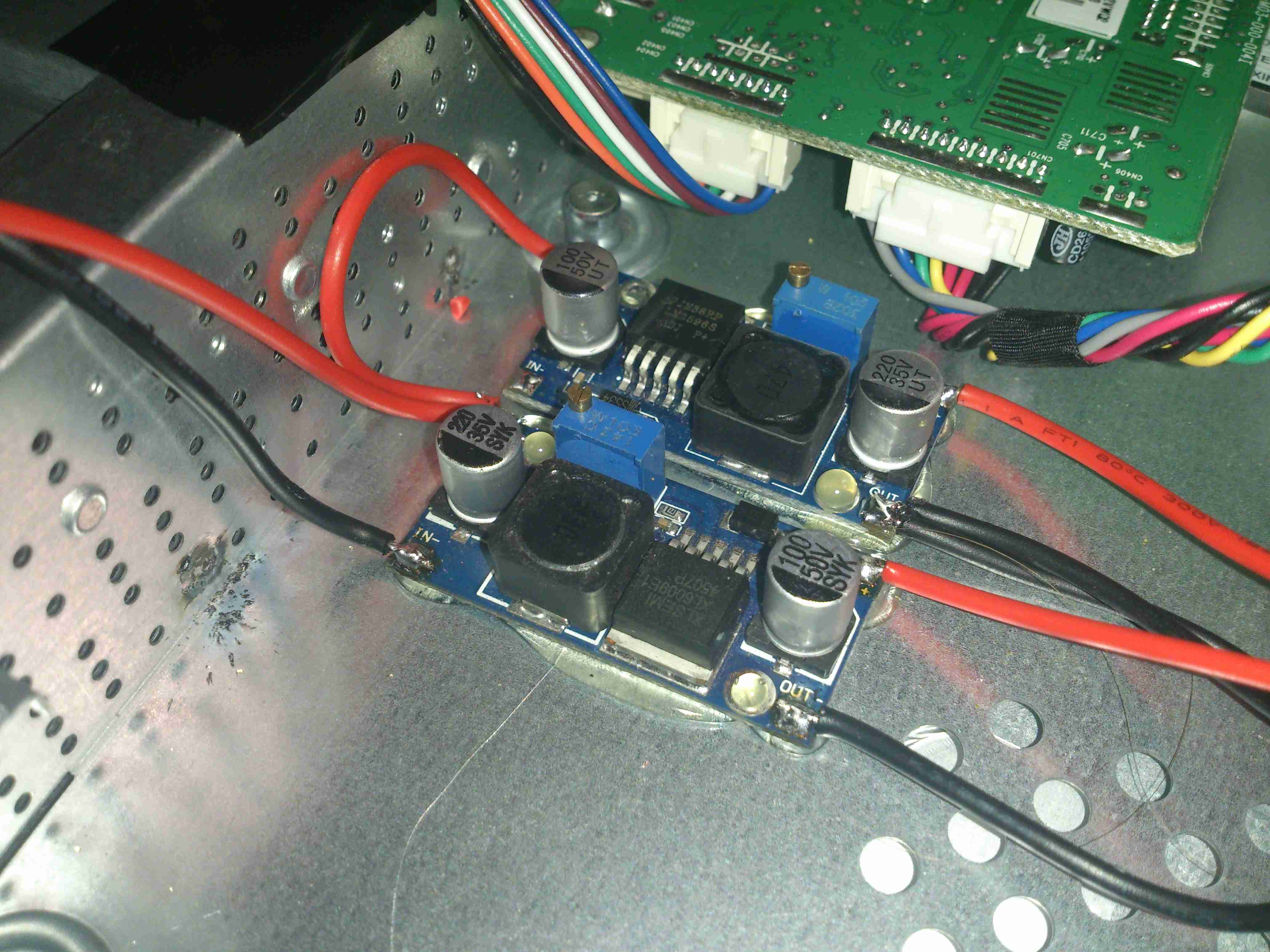
Slotted into a gap above the CRT is a large TO-220 2SD476 NPN transistor, this is part of the power circuit; it’s the series pass element regulating the input 12v down to 9v for all the remaining circuits. The aluminium sheet on the back provides some heatsinking as this part gets warm! Current draw of this unit with no video input is about 260mA.

CRT Removed & Vertical Board

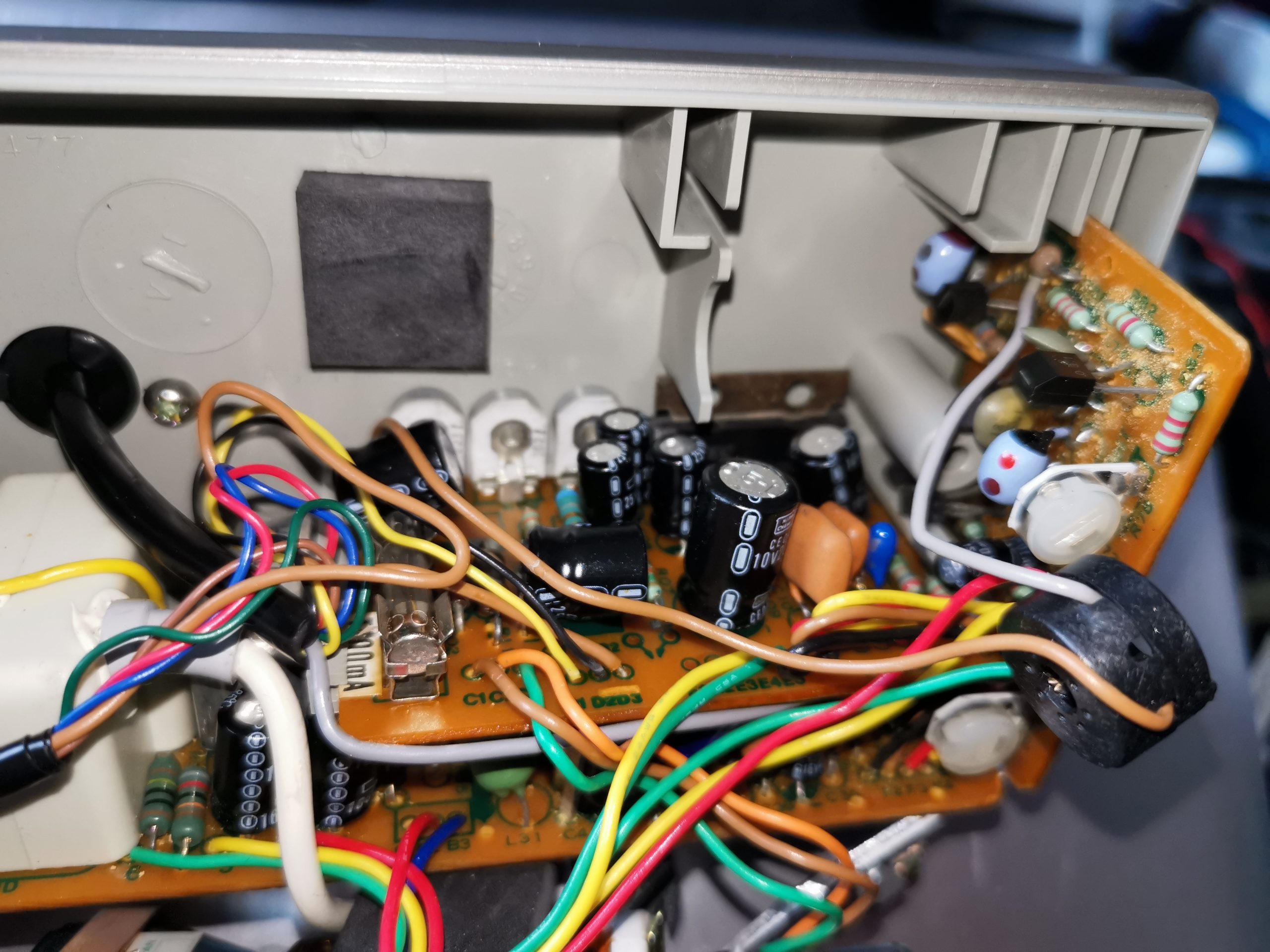
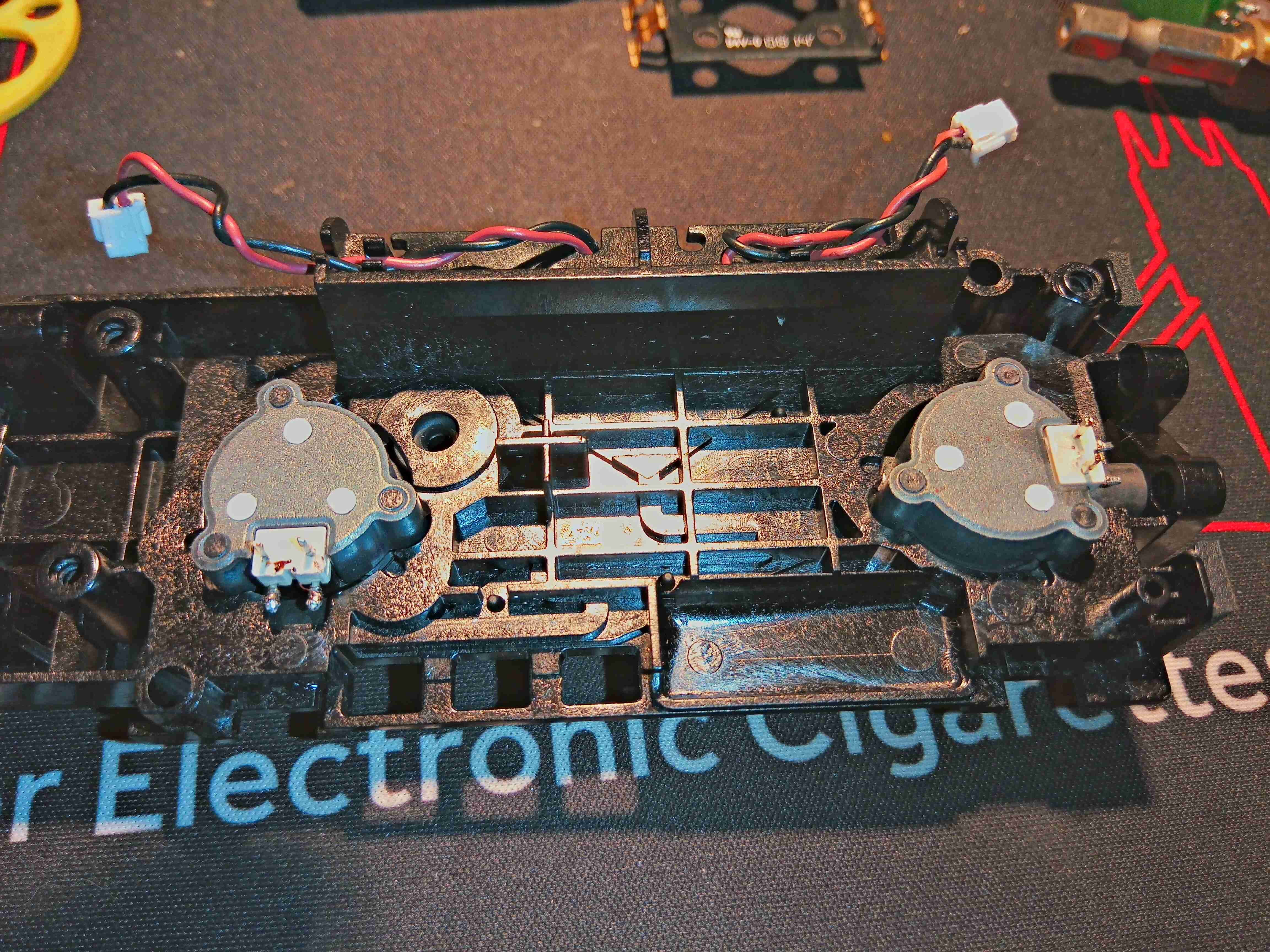
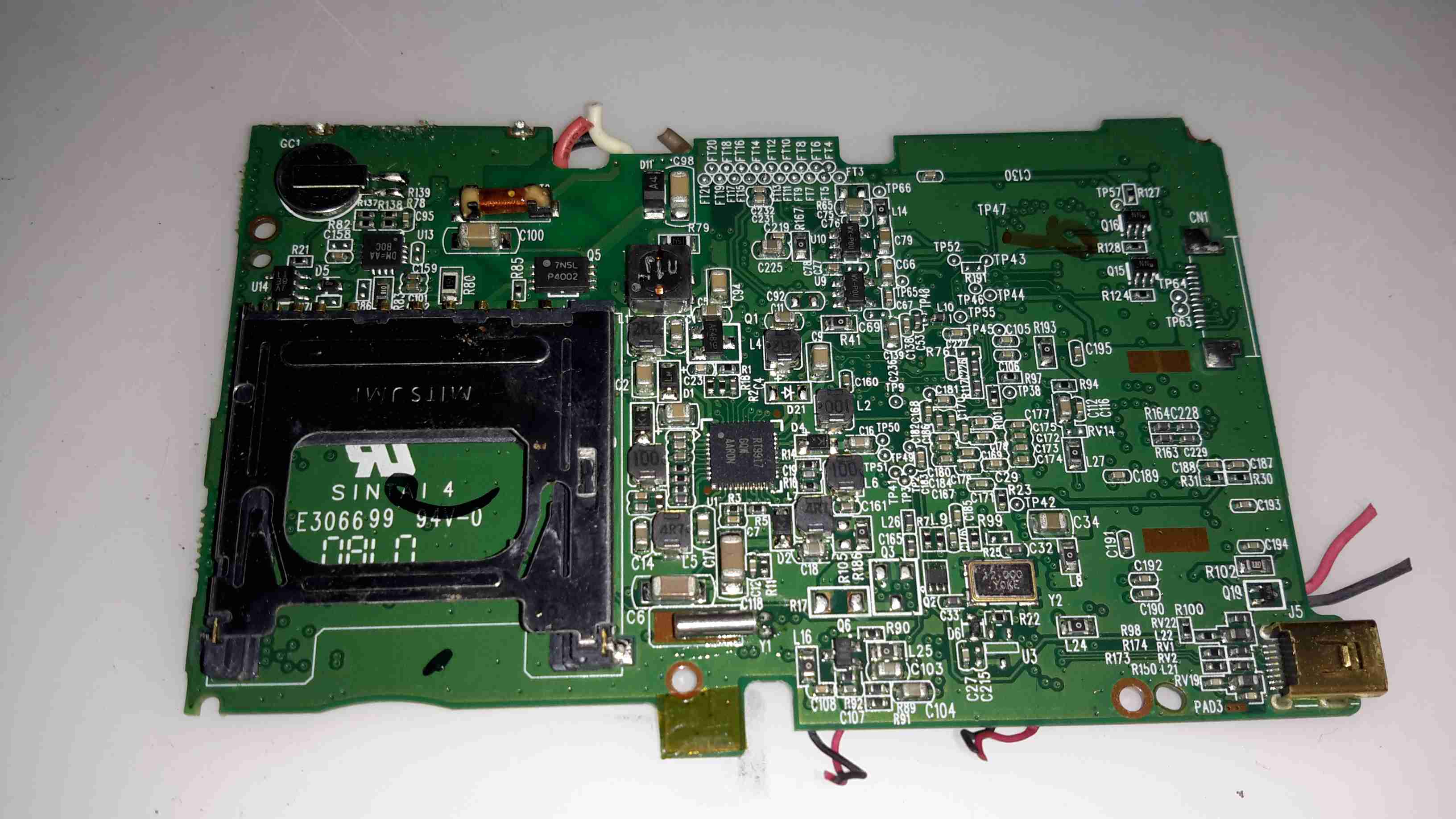
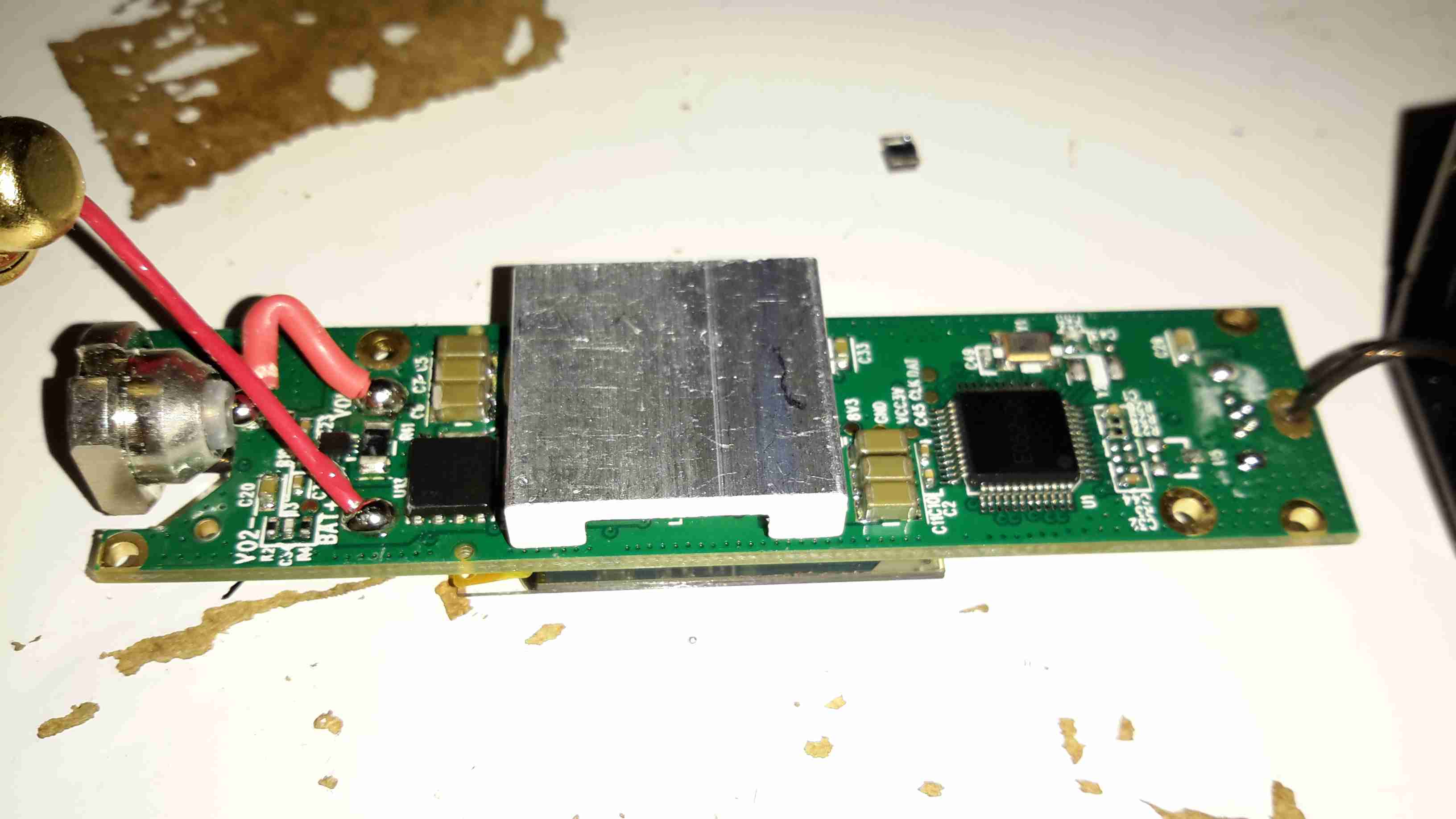
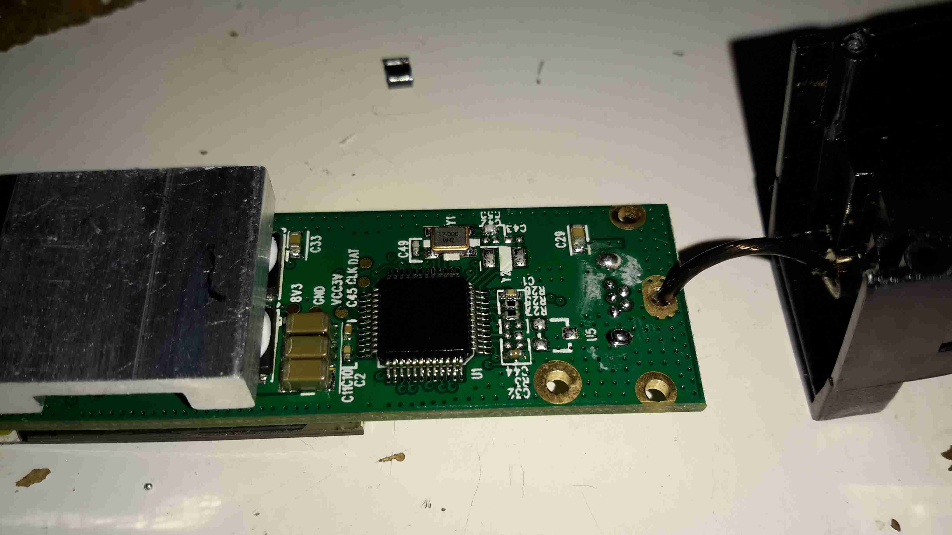
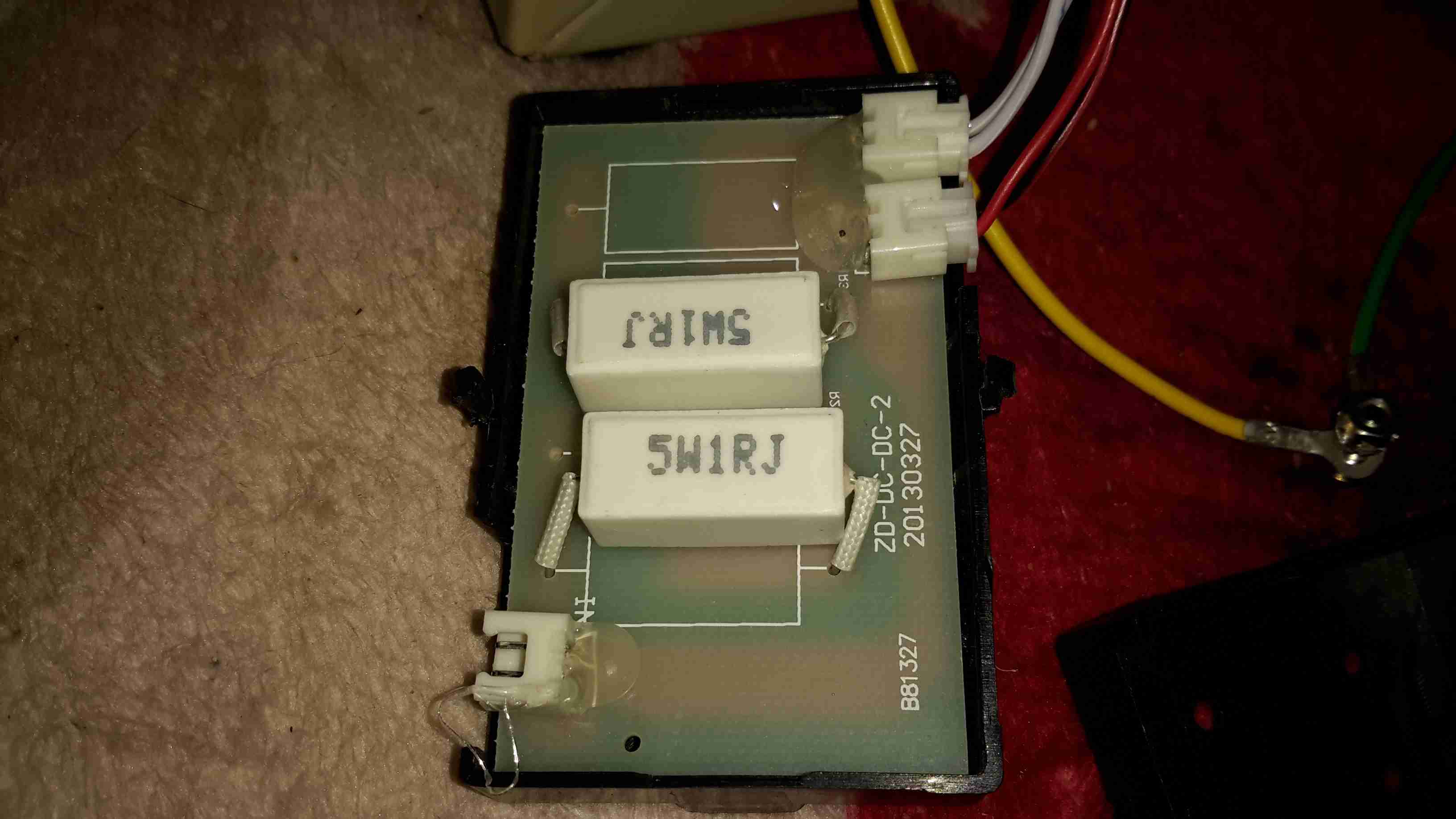
Popping the CRT out allows a view of the Vertical & Power Board. This hosts the input linear voltage regulator, and the vertical output control circuitry. Hiding at the back on the right is a NEC µPC1031H2 Vertical Deflection Controller.

Horizontal & Video Boards

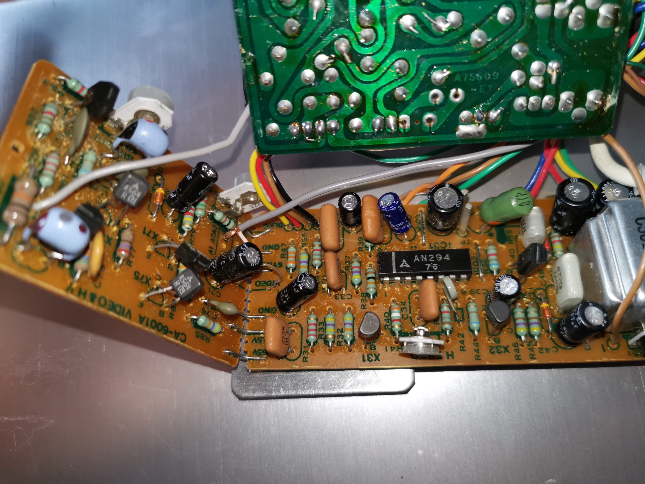
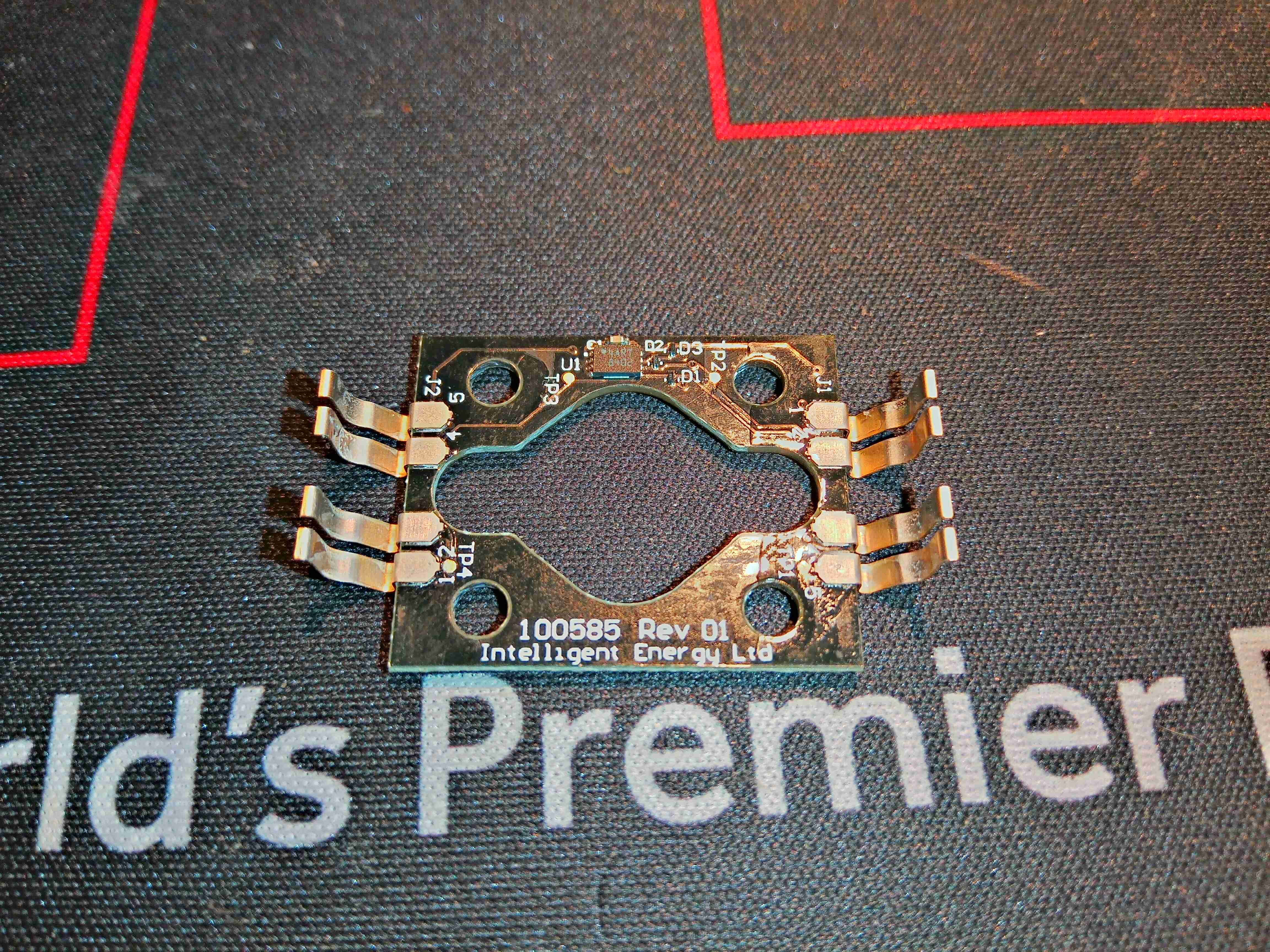
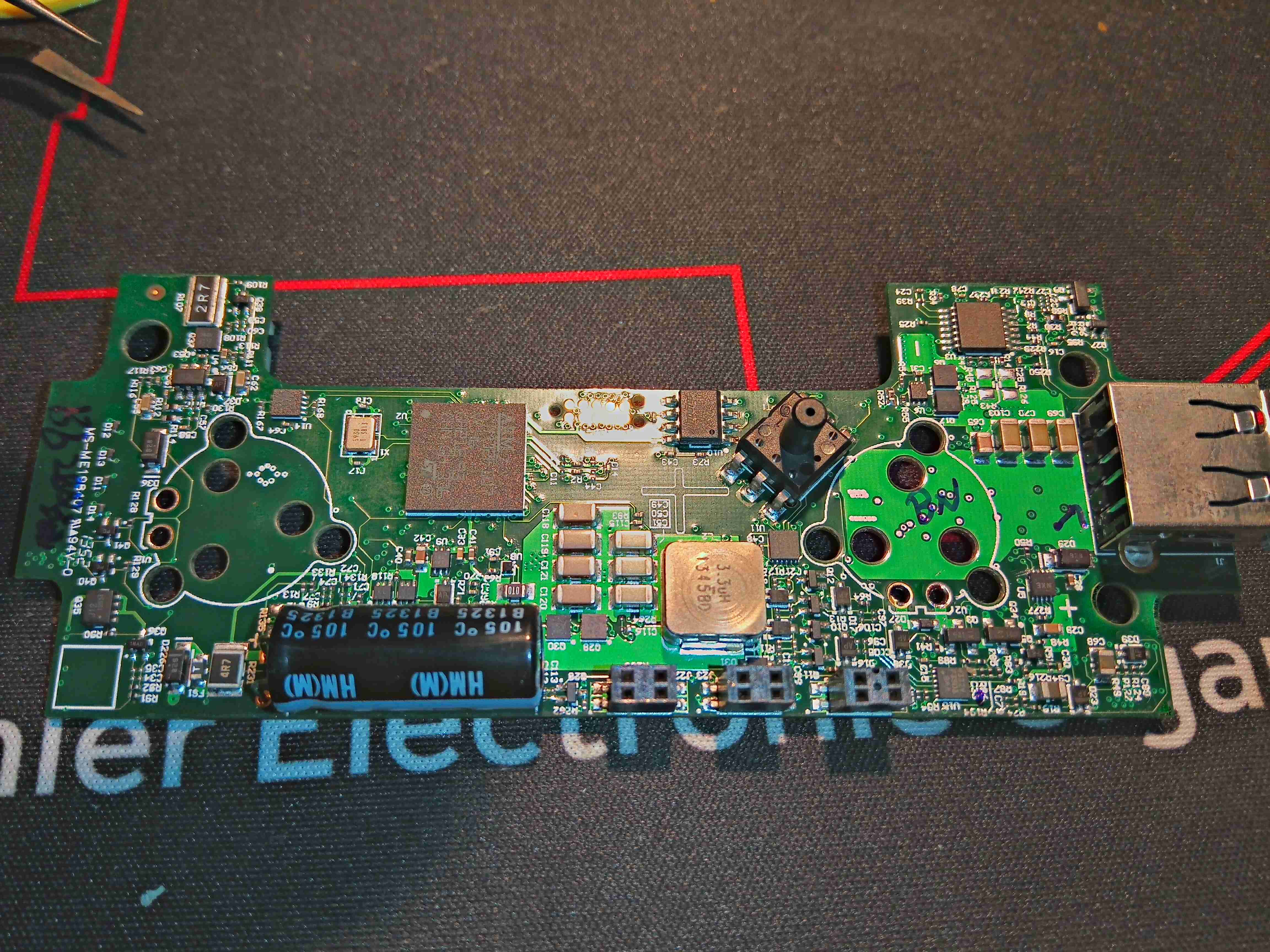
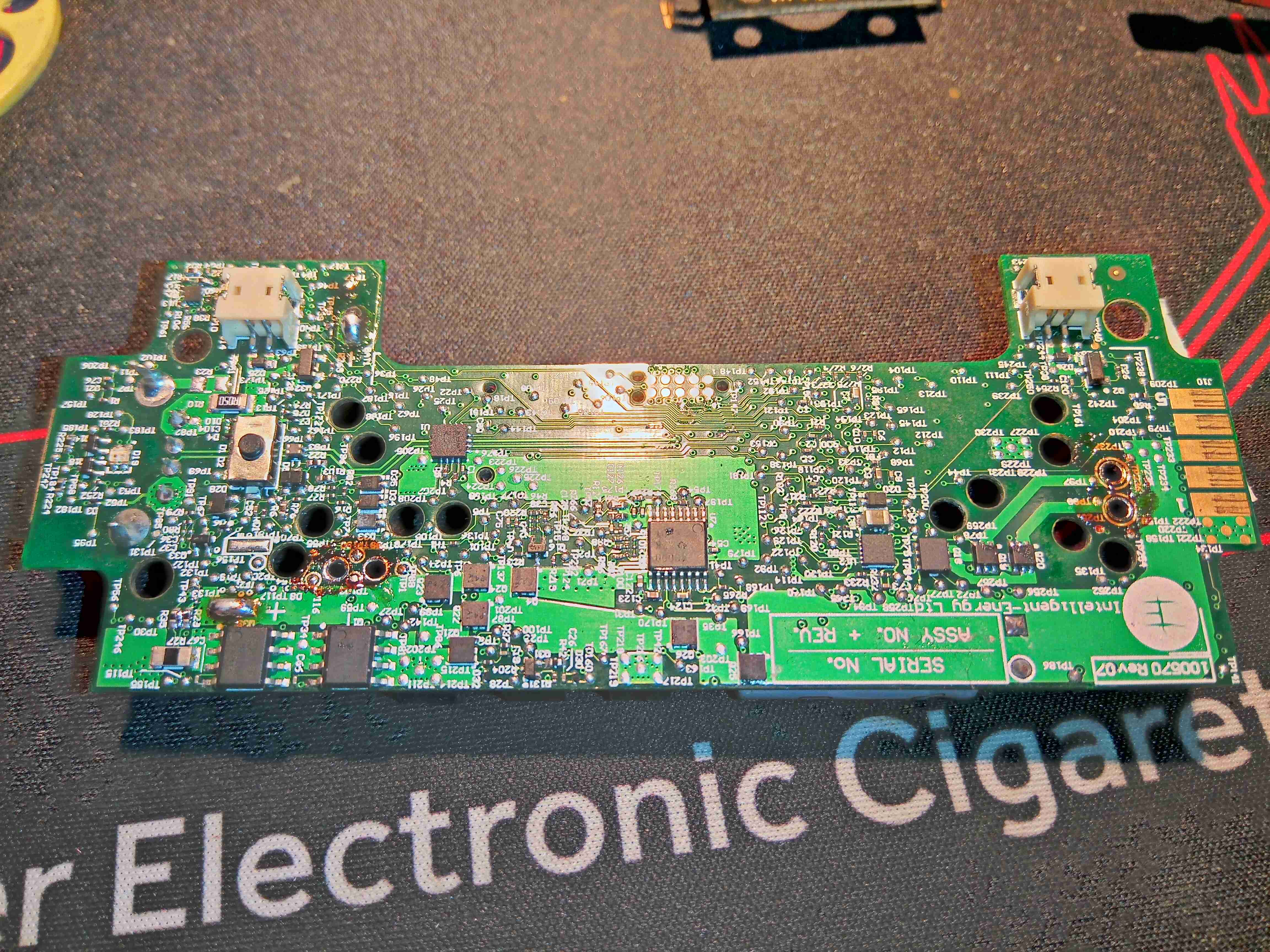
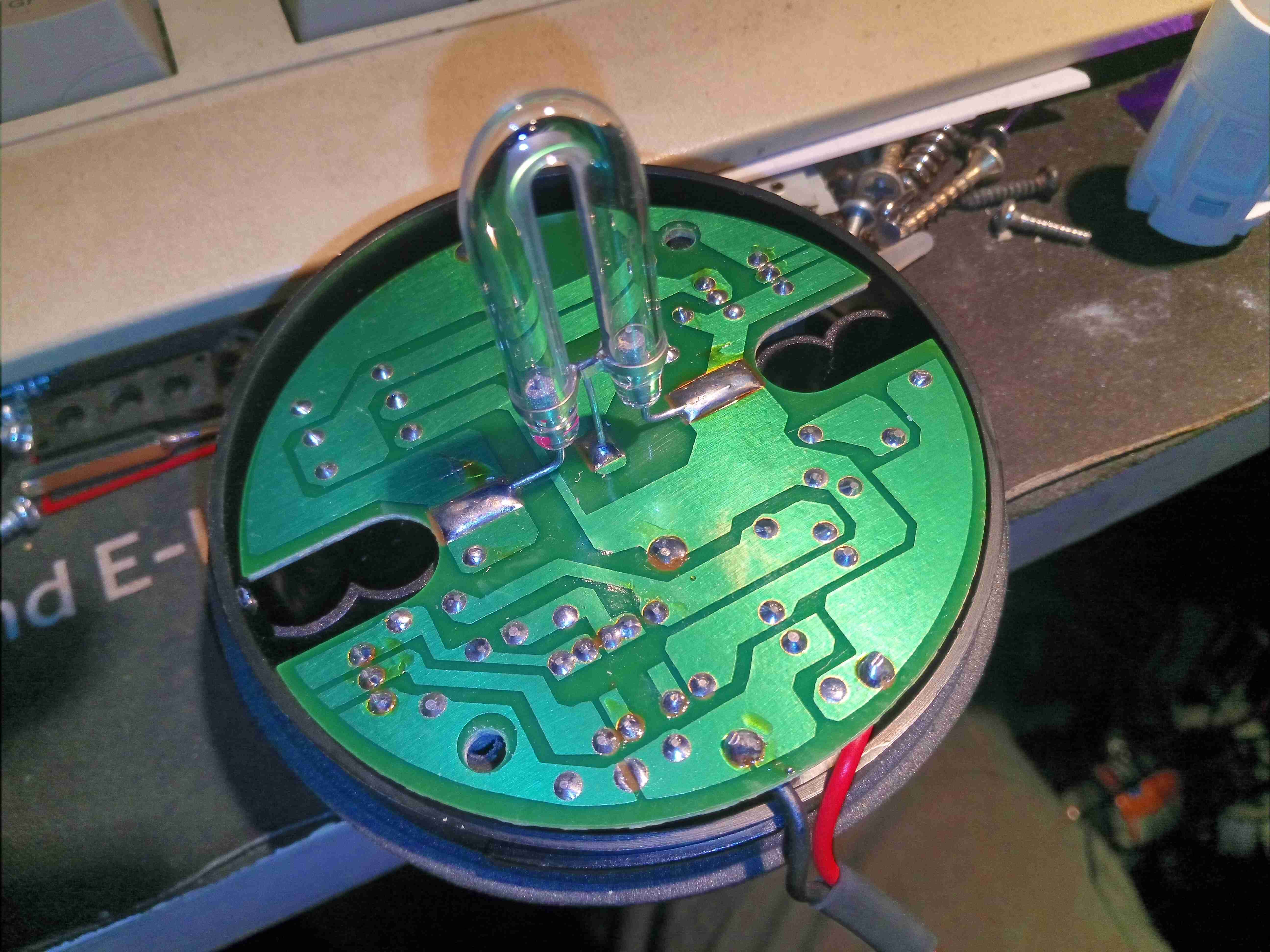
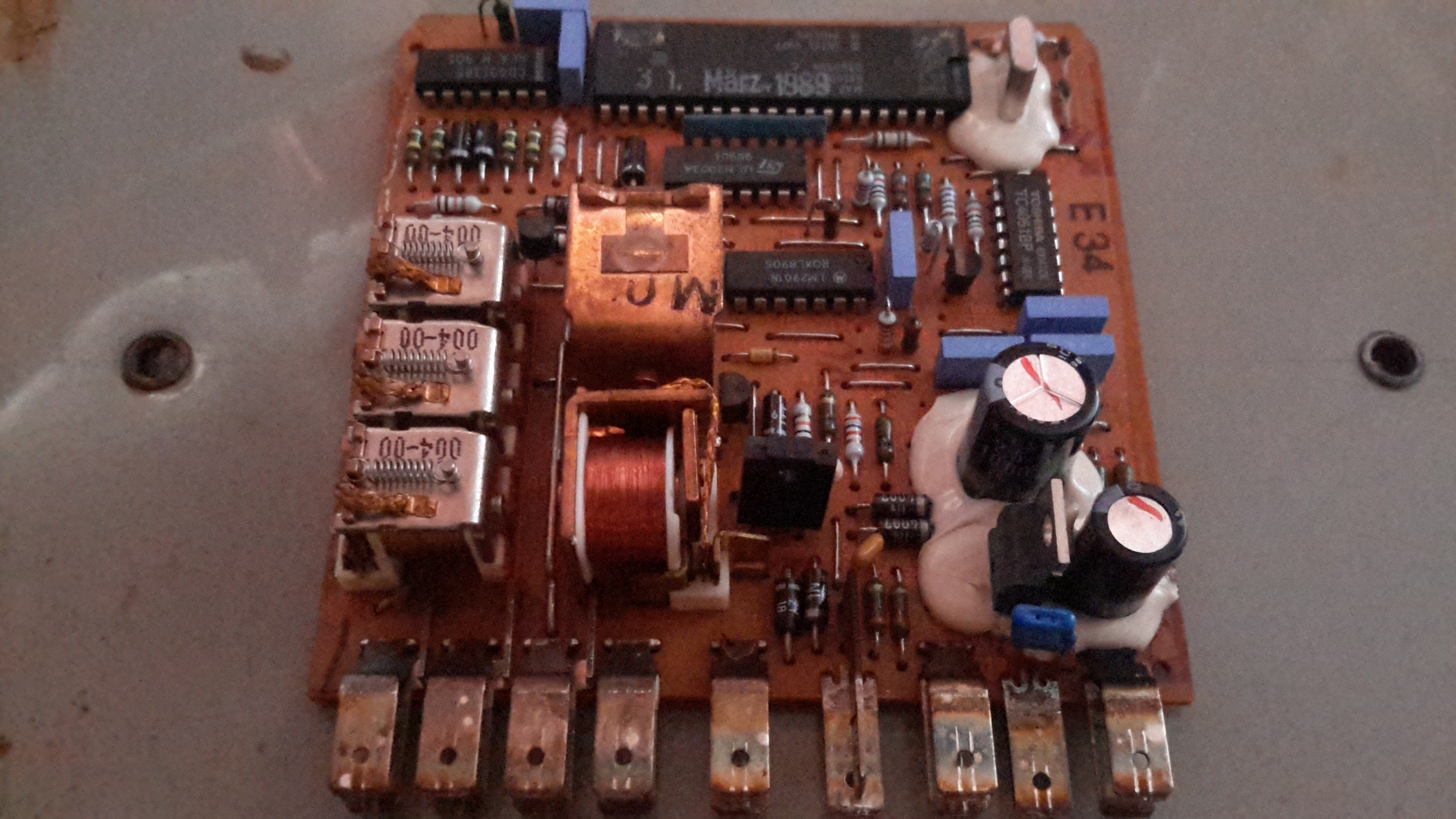
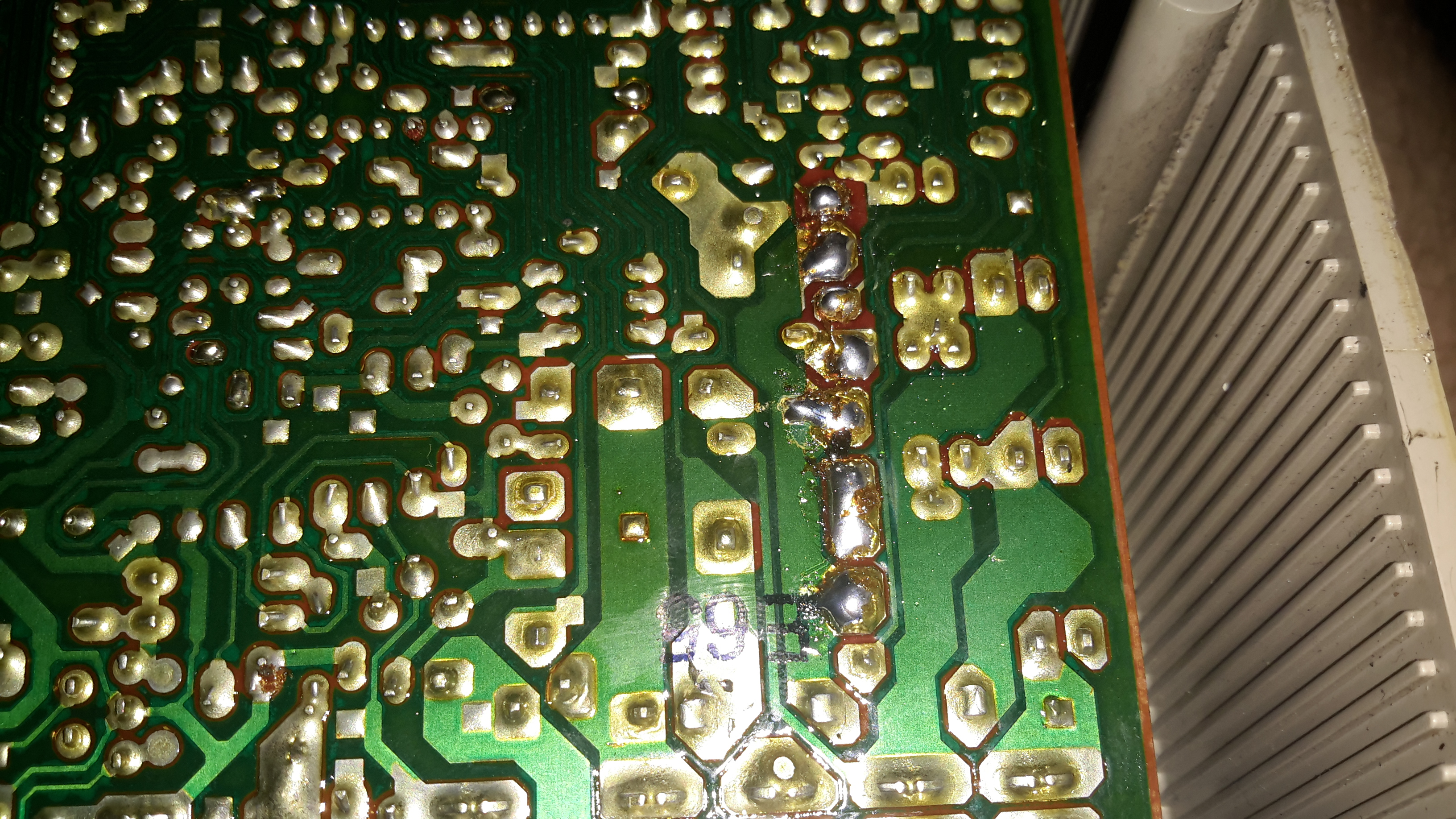
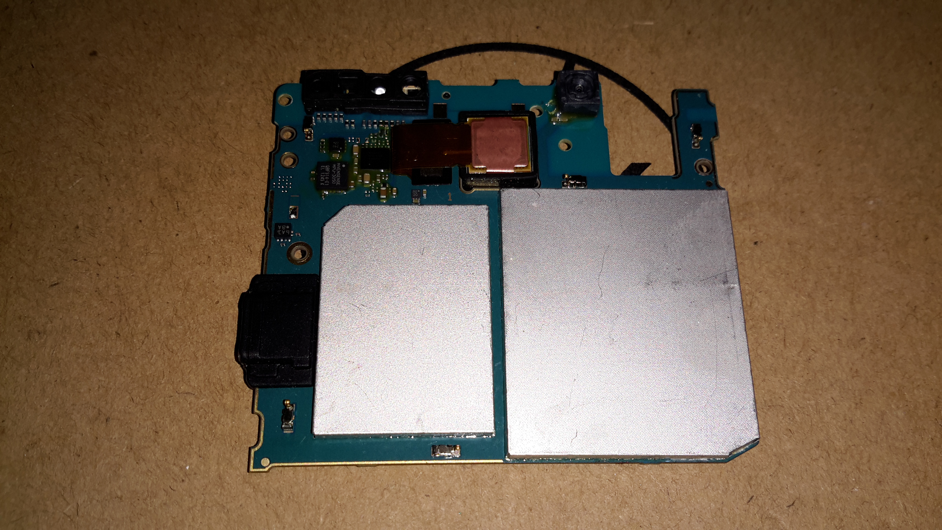
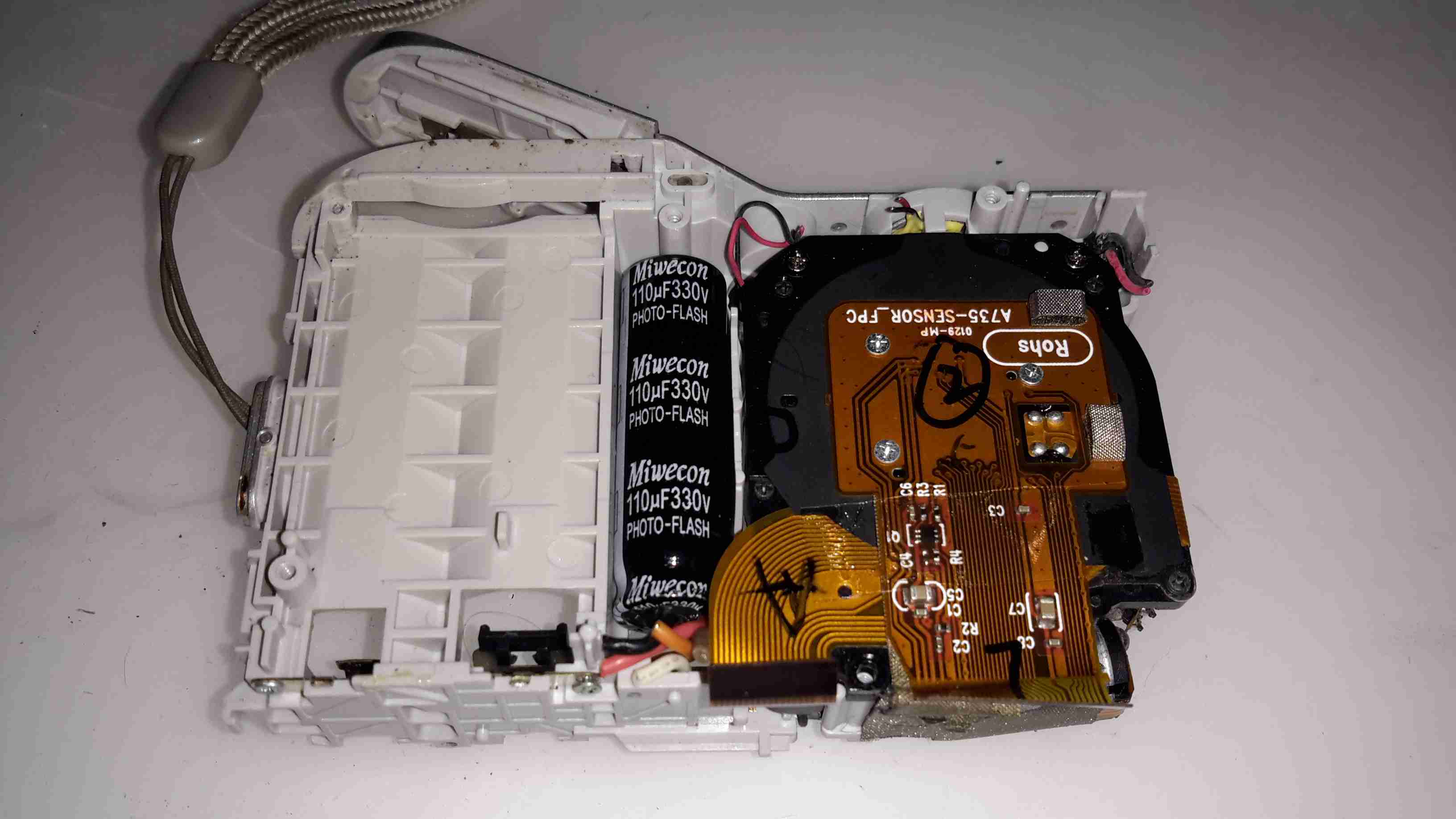
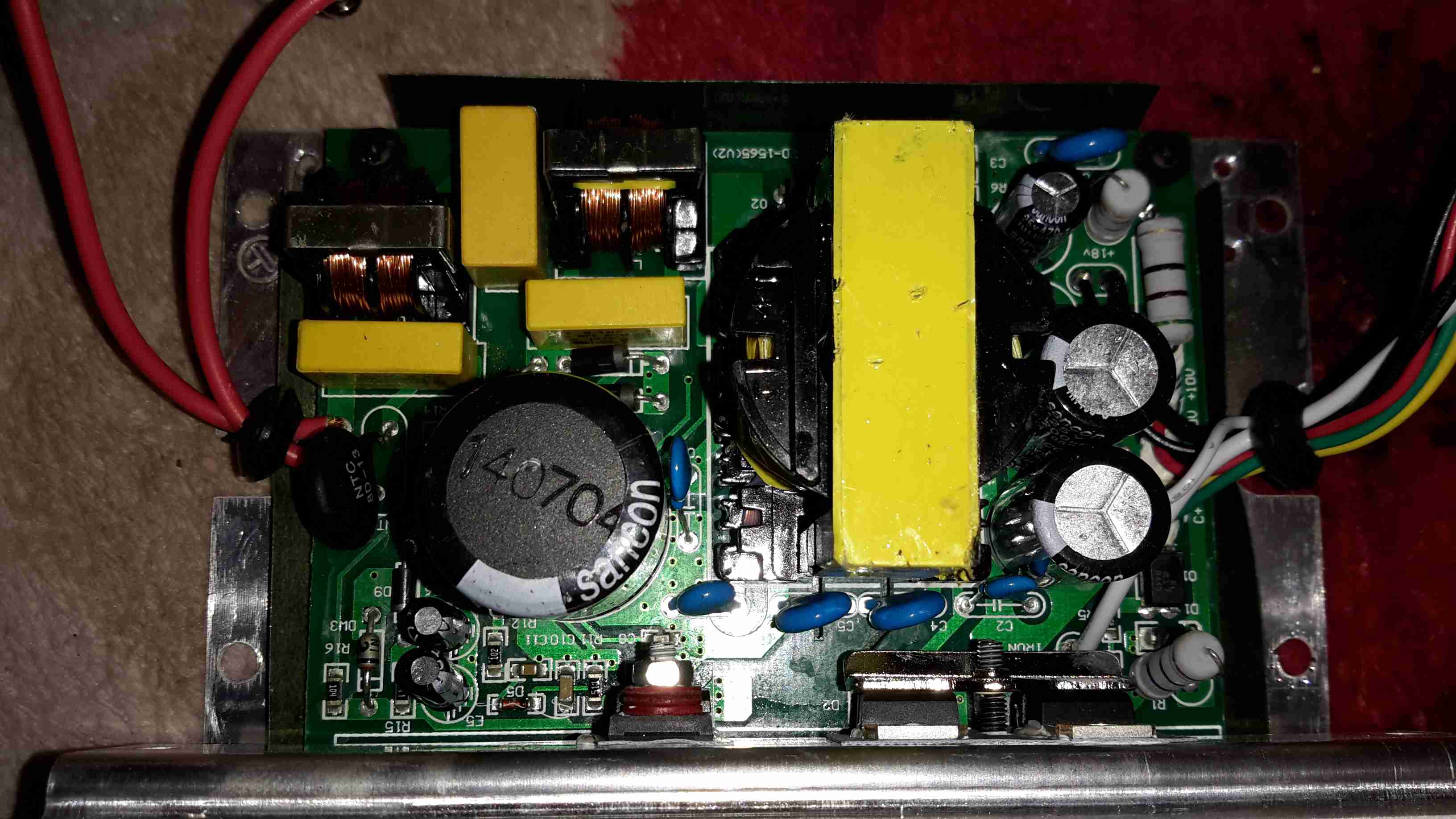
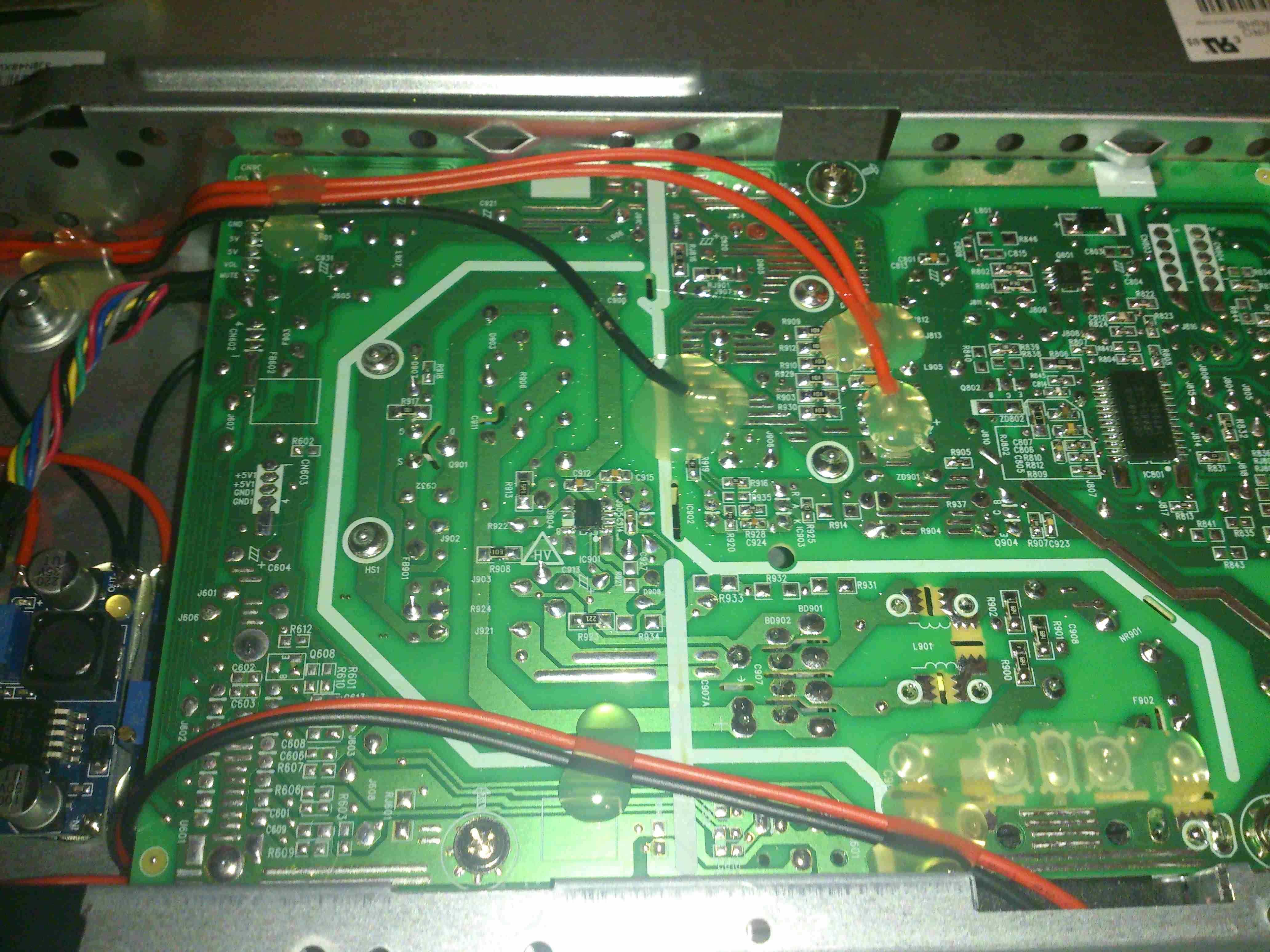
Separating the boards reveals the other two PCBs, the Video & Horizontal/HV boards. The bottom board takes care of the Horizontal output, and the lefthand board the video input, sync separation & amplification.

Horizontal Control IC

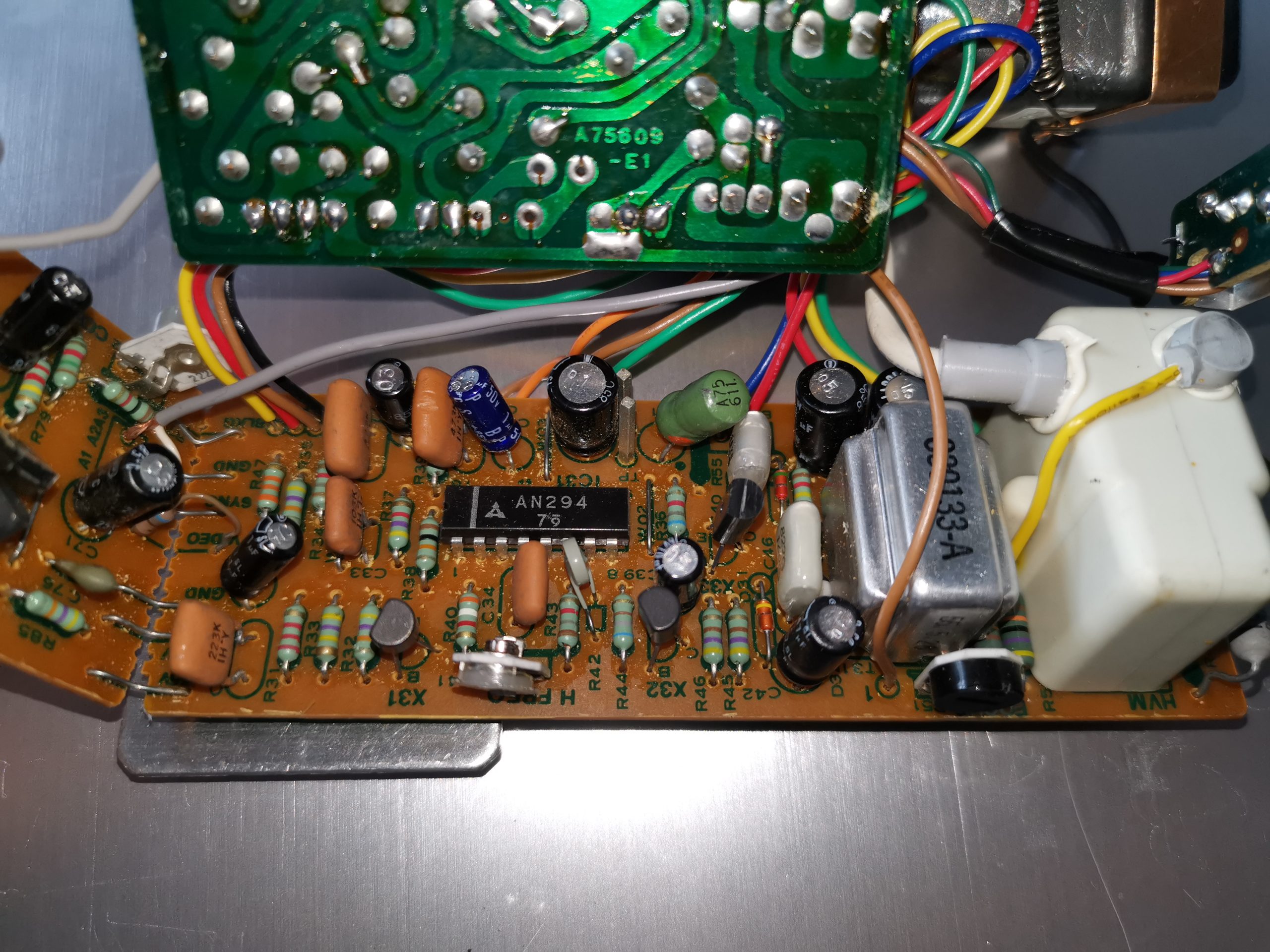
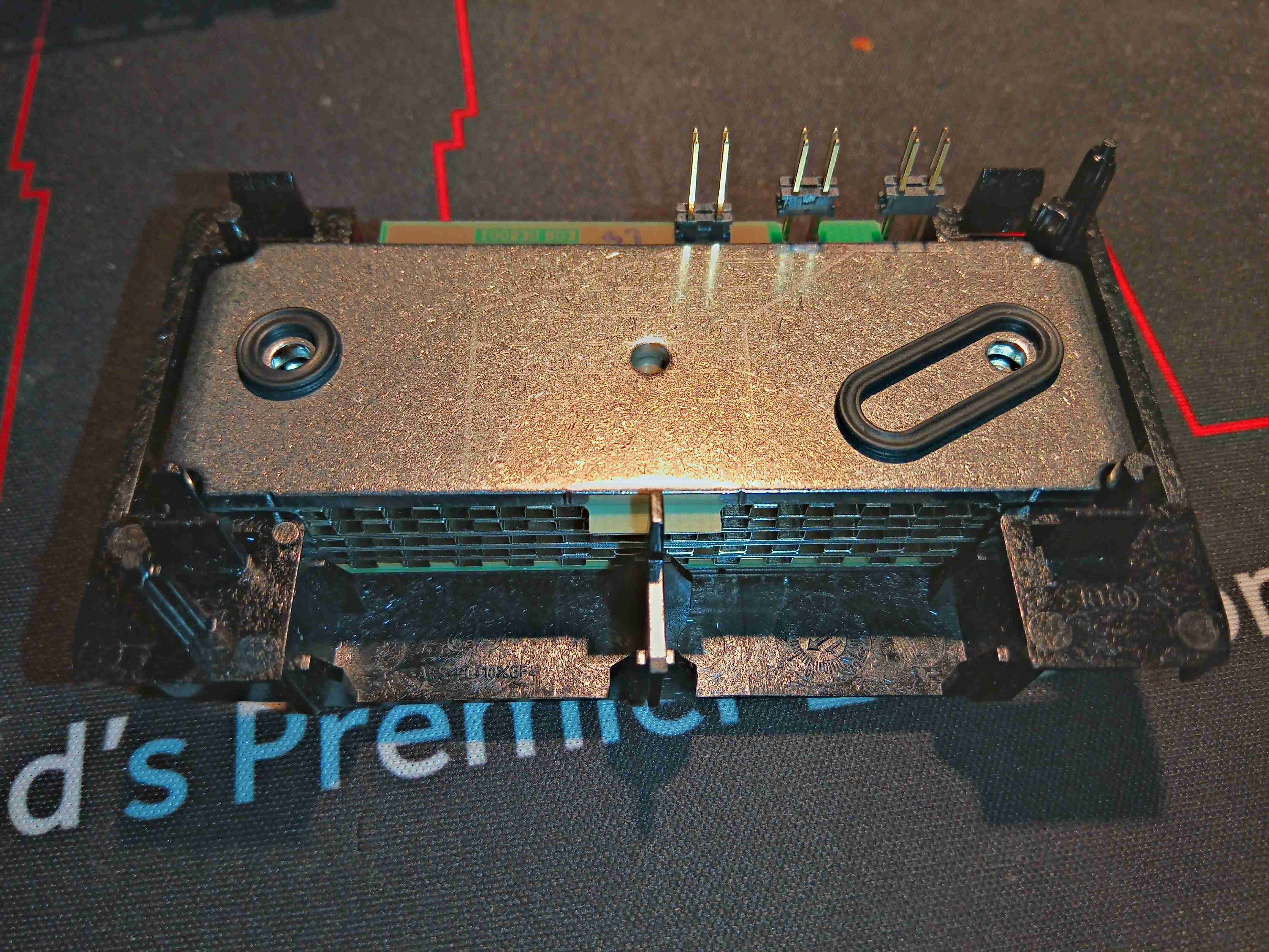
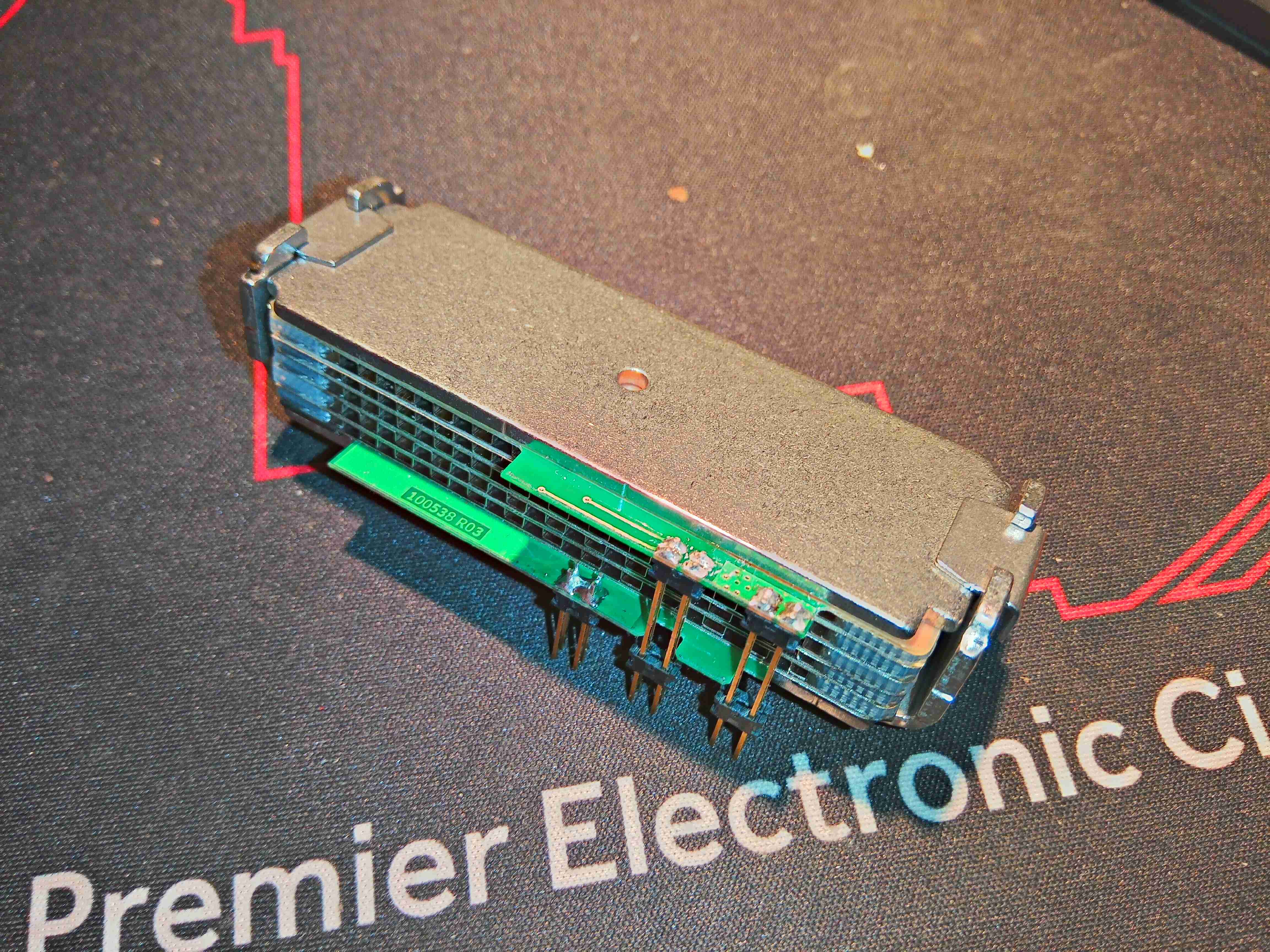
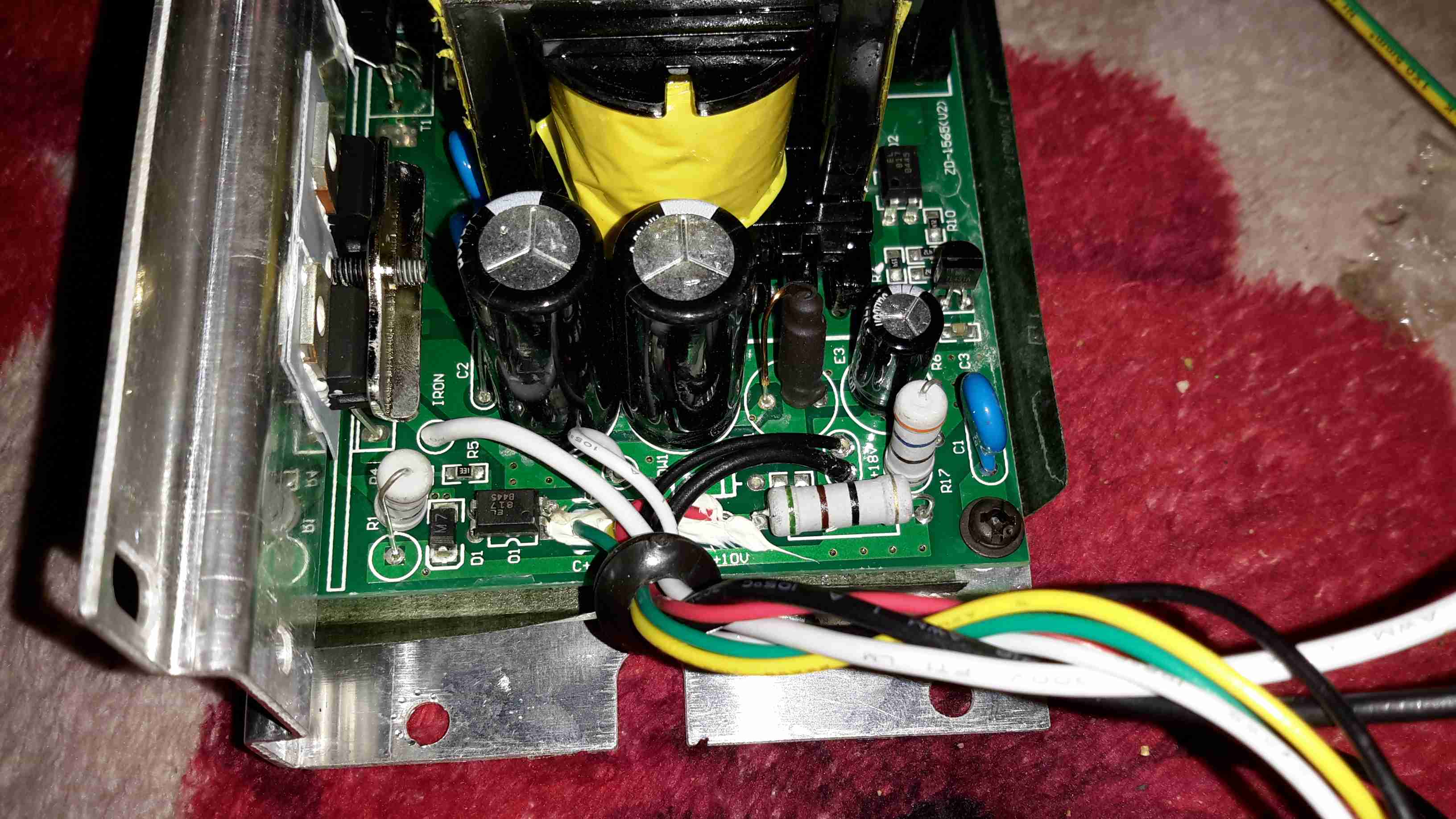
The Horizontal section is controlled by a Matsushita AN294 device. Unfortunately I haven’t been able to locate a datasheet for this one. The flyback transformer (Horizontal Output) is on the right, with another smaller transformer I don’t quite know the purpose of. Oddly, there’s no large switching transistor for the horizontal output stage – as the PCB notes the flyback as being a “HVM” this may in fact be more tightly integrated with some of the drive circuitry in the potting. There aren’t anywhere near as many pins on it as a usual CRT flyback has either.
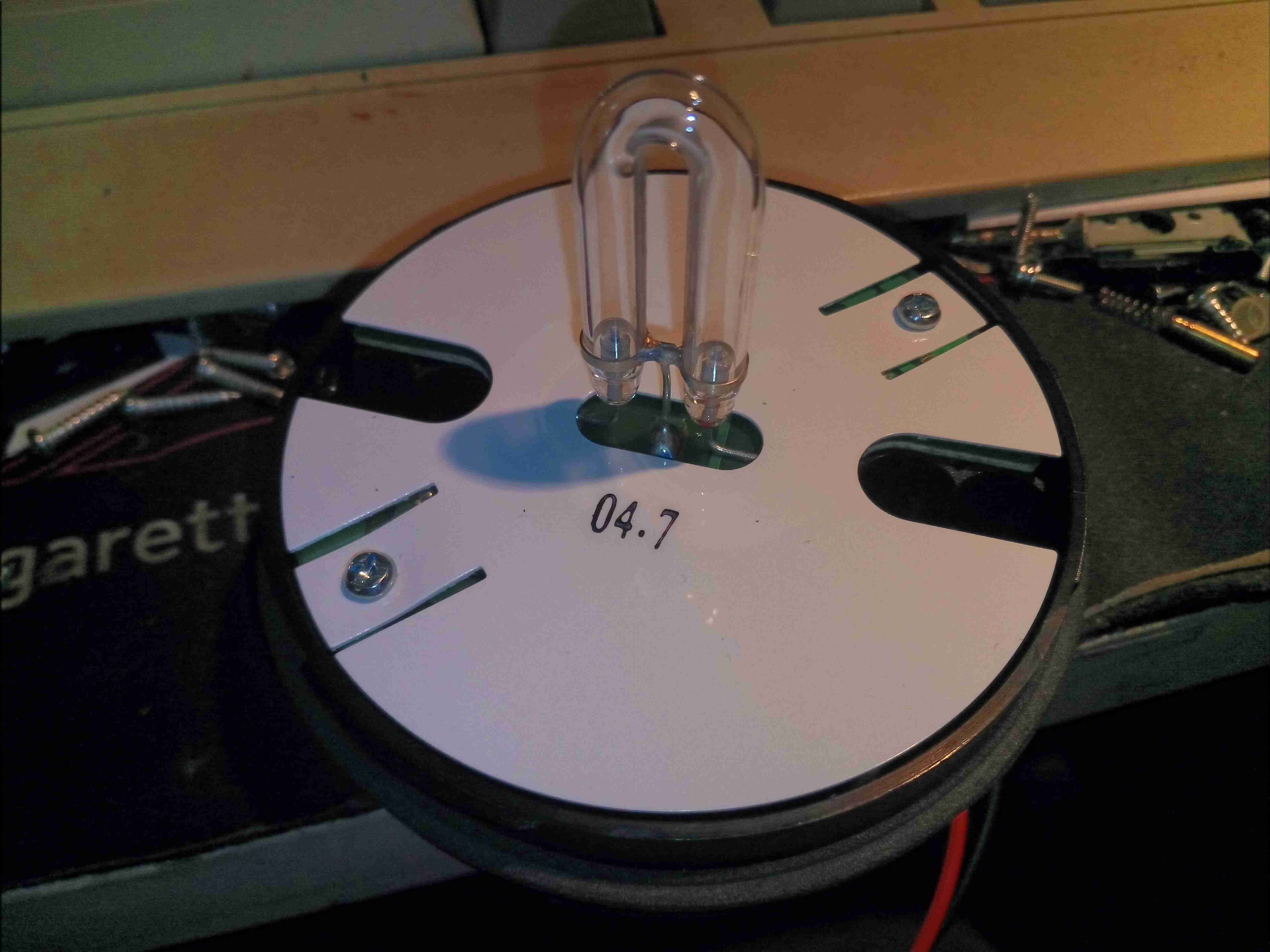
This section also generates the other voltages required by the CRT – 2.8v for the filament, and ~80v & ~400v for the grids.

Video Board
Video Board

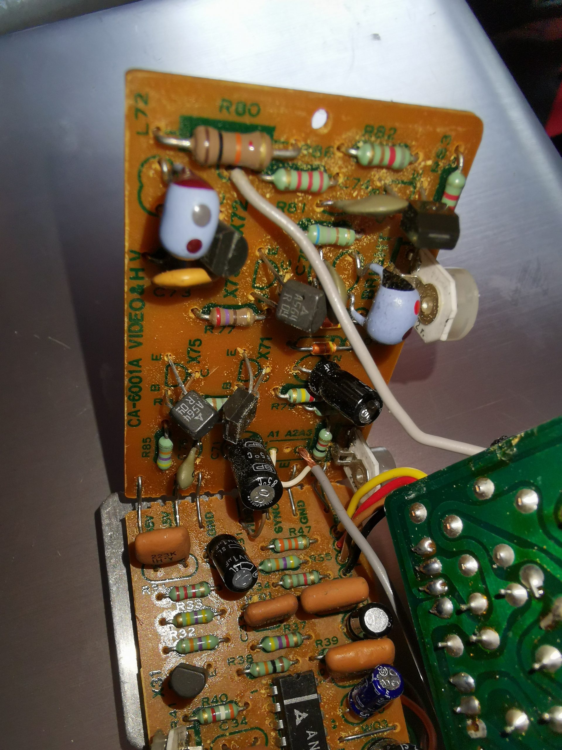
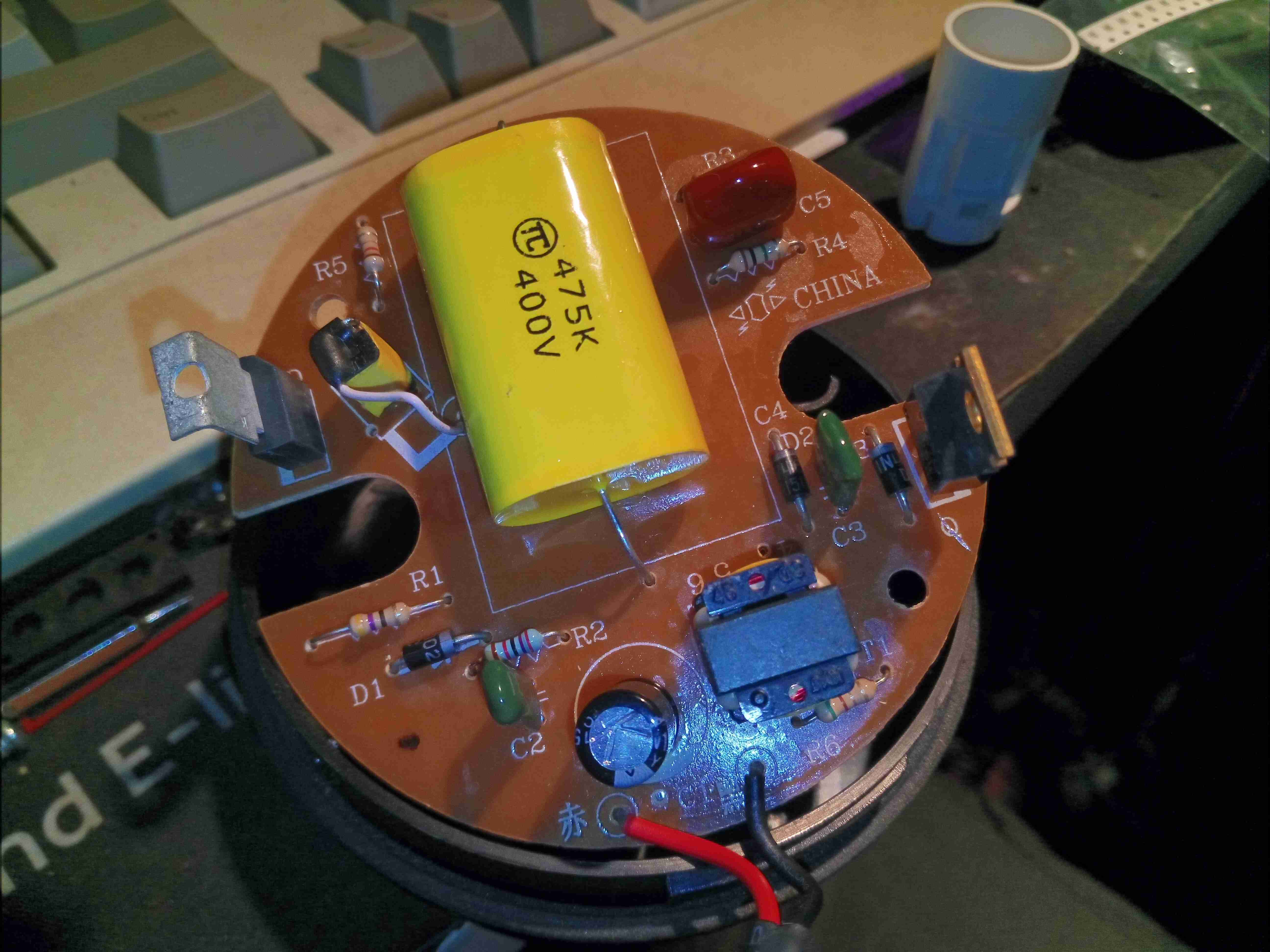
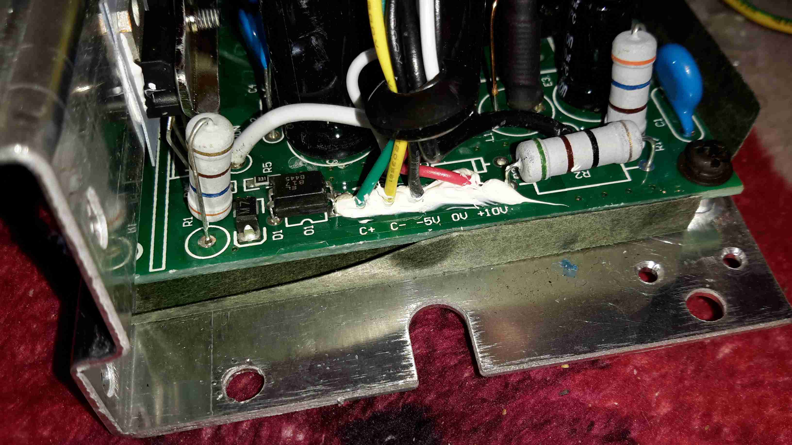
A closeup of the video board shows the relative simplicity. Only 4 transistors are doing all the video actions. There is relatively high voltage on here though – an 85v feed from the power supply which is the rail voltage for the video amplifier to the CRT cathode/G1.

Focus & Horizontal Hold Adjustments

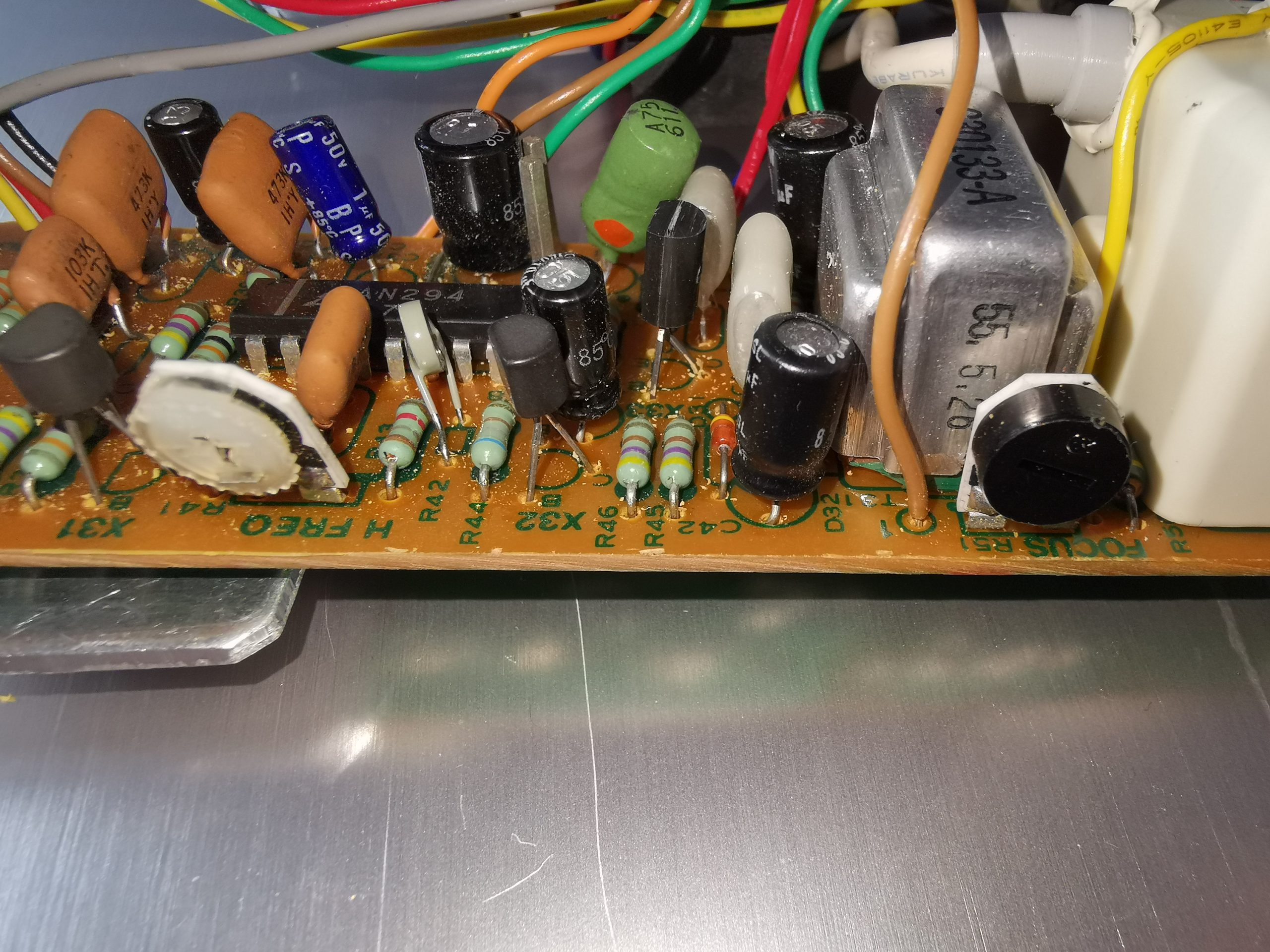
There’s a few adjustments available on this unit, here are the Focus & Horizontal Frequency (Hold) pots. Amazingly, even though this unit is about 43 years old at the time of writing, the unit fired straight up when I applied power & a composite video signal, with no adjustments required at all!

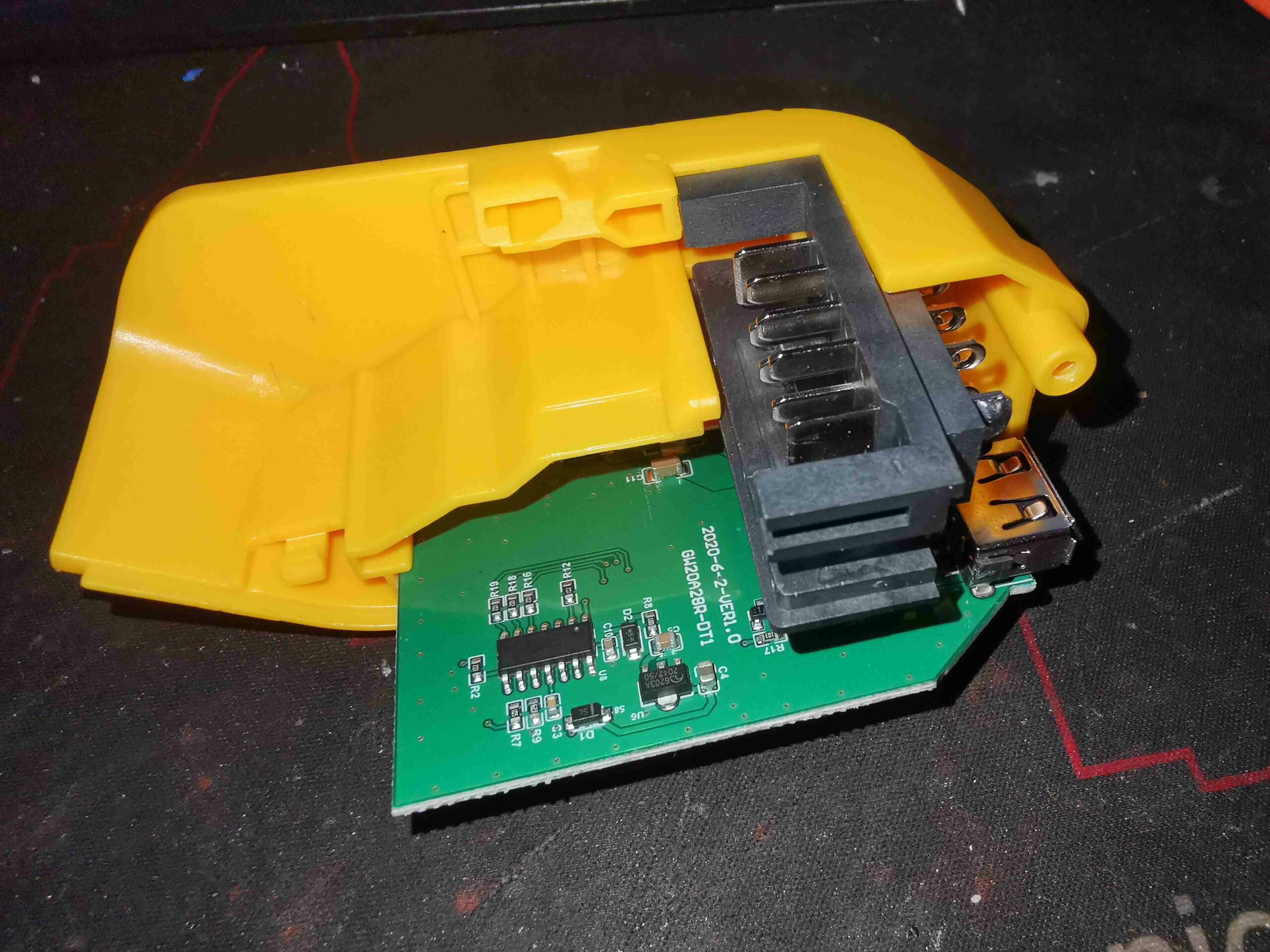
Unfortunately there’s no service manual or schematics that I could find on the web for this or the camera it came from, but connections to make this unit work are very simple:

Wire ColourSignal Name
YELLOW+12V DC
BLACKGND
Coax - CoreComposite Video 1v p-p
Coax - ShieldComposite Video GND

There’s another blogger who’s done this particular viewfinder, but they didn’t dig into the unit anywhere near as far as I usually do:

https://hex.ro/wp/blog/matsushita-40cb4-mini-crt/

This blog has a lot of CRT-based viewfinder teardowns, mainly from newer cameras. It’s an interesting read.

Datasheets for the important parts (the ones I could find!) below:


Posted on Leave a comment

DeWalt Clone 18v Battery Pack Teardown

Clone Battery Pack
Clone Battery Pack
Clone Battery Pack

I bought two of these packs for my new DeWalt combi drill, as the branded packs are very expensive and there’s unlikely to be much of a difference in cells used. I was a little mistaken on this, as you’ll see!

Battery Terminals
Battery Terminals

The top of the unit has the battery connections, with all the cell balance lines, along with an ID pin, and a TH pin. The TH pin connects a 10K NTC thermistor up to B+.

Battery Label
Battery Label

The bottom of the unit has the rating & warning label. This claims to be a 6Ah pack, but it’s nowhere even close!

Top Cover Removed
Top Cover Removed

Removing 4 Torx screws gives access to the internals. The cells are all fitted into a plastic holder. There’s a small PCB holding the connector pins, and all the cells connect up to this for the balance outputs. There’s a small PCB on the side of the pack that holds the components for the battery meter.

Connector PCB
Connector PCB

The back of the connector PCB has some passive components, but not much else. There’s the connections for the NTC at the bottom right of the board. There is an IC on this board, on the other side, but without desoldering all the pins, it’s not possible to see properly as it’s mainly hidden by the connector frame.

Battery Indicator LEDs

Not much on the front of the battery meter board, apart from the 3 bright green LEDs and the tactile switch.

Battery Indicator Components

The other side has a small ST microcontroller, a TL431 shunt reference, and some other passives.

Cell Links
Cell Links

All the cells are linked together with hefty interconnects, as expected for a high current pack. This is laid out as a 5S2P configuration, giving 21V max, 15V flat. Unfortunately I can’t see any markings on the cells – they may be off brand, or pulls from other products.

I figured as I always do with Chinese battery packs that the stated capacity of 6Ah was too good to be true, so I ran my usual cycle tests to see what the real capacity was, and was met with the following results:

Cycle NumberPack APack B
13969mAh3917mAh
23963mAh3947mAh
33961mAh3956mAh
43953mAh3959mAh

As can be seen from the table, these packs are 4Ah, not 6Ah. 2Ah cells sort of make sense for a pack like this, as the high-current capacity cells tend to be a lower capacity.

Posted on Leave a comment

Clone DCB090 DeWalt USB Battery Adaptor Teardown

DCB090 Clone USB Adaptor

Since I got my new DeWalt combi drill, I needed a way to charge the batteries without having to resort to sticking blade terminals into the pack connectors – I didn’t purchase the branded charger, mainly due to cost. I also have a very capable multi-chemistry charger that handles multi-cell lithium packs with no issues, so I saw no need to replicate things. This little gadget was ordered just for it’s main pack connector; I can then use this to make up a charger adaptor cable. What this normally does is allow the use of DeWalt XR battery packs to charge mobile devices via 5v USB outputs, so there’s going to be some kind of DC-DC converter in here. There’s also a “charge level indicator” built in, which doesn’t actually do anything sensible – even on a flat battery pack, showing a single LED on it’s charge indicator shows the full 3 LEDs on this unit.
The remaining feature is a trio of white LEDs to function as a torch, but it’s less than stellar in the brightness department. Given that there’s not much in the way of control inside the battery packs themselves, I reckon this unit could actually overdischarge a pack, causing damage.

Torch LED & Charge Indicator

The top of the unit has a large label with windows in for the various LEDs, and a pad covering the tactile switch to operate the torch function.

Label
Label

The label on the side indicates the unit will operate down to 10.8v, good for the 3S packs, as well as the 18/20V packs.

Pack Connector
Pack Connector

Here’s what I was after – the battery pack connector. This has the full compliment of pins for all the balance taps too.

Casing Opened
Casing Opened

Removing a label, and a single screw gives access to the internals. There’s not much in here apart from a large PCB, with a few components.

Main PCB
Main PCB

The PCB is pretty sparse. There’s a microcontroller in the top right corner that does the torch LED switching, and the “battery indicator LEDs”. This is completely unmarked, which is very common now for Chinese microcontrollers. The only way I’m identifying this one is via a decap operation on the IC!
The USB ports have MOSFETs in their negative pin paths, probably to switch off the ports if they’re overloaded. The data pins are bridged together on one port, and connected to the DC-DC converter on the other port.

DC-DC Converter
DC-DC Converter

The main DC-DC converter IC is in the bottom right corner of the board, next to the input pins. This is an IP6503S multi-protocol USB charging converter, with a 24W power limit. This explains why the data pins of one of the USB ports is connected back here – it’s doing some communications with the connected device for fast charging. Chinese datasheet below.

Posted on Leave a comment

ATC-1000 Serial to IP Converter Teardown

Front Cover
Front Cover

Just a quick teardown this month! This is an industrial RS-232/RS-485 to Ethernet serial converter.Not much to say about the outside of the unit, there’s the DB-9 connector for the 232 interface, and Phoenix connector blocks for the 422/485 interface. The main power input, and the Ethernet jack are on the other side.

PCB
PCB

Under the hood, there’s a pretty densely populated board. The brains of the operation is a IP210T Serial to Ethernet SoC with A/D Converter. This is an 8051 based core, wuth 10/100 MAC. No flash memory here either, only 64KB of OTP EPROM. On the left there’s a few bus transceivers to interface the serial ports, along with some glue logic. At the top we have the Ethernet magnetics, configuration EEPROM for the SoC & a trio of indicator LEDs.
Power supplies are dealt with via an LM2576-3.3 DC-DC buck converter, providing the main 3.3v rail for the logic.

Posted on Leave a comment

Chinese LED Projector Teardown

Cover Removed
Cover Removed

Another Chinese eBay teardown! This is a “720p” LED projector, available from nearly everywhere for very little cash. But they are very little cash for a reason – they’re total shit. The resolution as stated is a blantant lie – the LCD panel used in these is usually around 320×240, nowhere near the 1280×720 as stated. Being small & portable, there’s very little lighting power available, and they barely work to a level watchable without eye strain even in a completely dark room. You literally get what you pay for! Above is the projector with the top removed, showing the main board, which is fairly densely populated.

Mainboard Top
Mainboard Top

The main processor appears to be an MST3M182VGC-LF-Z1, a SoC designed specifically for LCD TV applications. This runs the internal firmware from a serial flash, a PN25F32 32Mbit (4MB). As this projector has the capability to play files from USB & SD Card, as well as from A/V inputs, there’s an Alcor Micro AU6438BS USB 2.0 Single LUN Flash controller on the right to deal with the MicroSD slot interfacing. The left top corner of the board is completely dedicated to power control, with various switching converters & transistors.

Mainboard Bottom
Mainboard Bottom

The bottom of the board is also dedicated to the remaining portion of power control – more switching regulators here generate the voltage rails required for the SoC, along with LED drive.

Optical Path
Optical Path

Removing the board allows access to the optical components of the projector.

LCD & Lenses
LCD & Lenses

Here the LED module has been removed from the casing, better showing the optical arrangement. There’s a Fresnel lens, then a polariser, the LCD panel itself, another lens, then the final turning mirror to the objective lens.

Turning Mirror & Objective

Here the rest of the optical components have been removed, showing the objective with it’s helical focusing track, which moves the lens, and the turning mirror. Behind the mirror is the pitiful speaker.

Optical Components
Optical Components

Here the main components are laid out, with lenses either side of the LCD & polariser.

LED Module
LED Module

Now onto the light source of the projector – the LED module. This is buried inside the module with a conical reflector, and a small heatsink on the back.

Reflector Removed
Reflector Removed

Removing the reflector shows the LED itself, with a thermal fuse in series for protection. The LED is screwed to the aluminium heatsink for cooling – my guess is this is roughly a 6W LED, with 3 series pairs of dies in parallel.

Posted on Leave a comment

Upp! Hydrogen Fuel Cell Teardown

Upp! Hydrogen Fuel Cell

After watching Mike’s Electric Stuff’s video on these a while back, I figured it was time to grab one from eBay & see for myself how pointless a tech these are. As far as I am aware, these units are no longer available, the domain name redirects to a company site with no mention of them, and getting cartridges refilled might not be possible without some DIY engineering. These are a small portable Hydrogen-powered PEM (Proton Exchange Membrane) Fuel Cell unit, with a USB output port for charging mobile devices. There’s quite a few vents on the sides of this device, as there has to be an airflow through the PEM Fuel Cell itself, and the only control interface is a single button on the front of the unit.

Gas Cartridge
Gas Cartridge

The Hydrogen gas is stored in a cartridge, filled with Hydralloy C5 metal hydride powder. These would be exchanged for a full one when all the gas has been used, at a cost of about £6. (Extra cartridges apparently cost about £50!).

Cartridge Valve
Cartridge Valve

The top of the cartridge holds the main valve, and some contacts. The gas is permitted to flow from the storage hydride by means of the two brass pins on either side of the seal – when these are both pushed down by pins moulded into the bottom of the main fuel cell unit, the internal valve is opened. The contacts connect to an internal PCB with a single EEPROM.

Cartridge Magnets
Cartridge Magnets

The cartridge is attached to the fuel cell with magnets – there are a pair of very powerful NdFeB magnets behind the main steel plate on the top, and a matching pair inside the bottom of the fuel cell assembly.

Cartridge EEPROM PCB

Removing a label allows access to 4 screws, which hold the top assembly onto the pressure vessel section of the gas cartridge. Here is the internal PCB with it’s EEPROM, and the large brass screw which may be for regulating the gas flow rate.

Gas Cartridge EEPROM

Removing the PCB allows us to see the EEPROM itself – a 2kBit part, which contains information like remaining gas charge, and serial number. When the cartridge reads empty according to this EEPROM, the cell will stop functioning. Luckily however, it is happy to operate without this PCB even being present – I expected the unit to spit & error & shut down if it couldn’t communicate over the I²C bus with this memory.

Pressure Relief Valve

Removing a screw in the base of the casing (hidden under a label) allows the plastic shell to come off, revealing the aluminium pressure containment to be seen. There’s a pressure relief valve on the side here, and some warnings about what not to do with the thing.

Pressure Vessel Info

Some more info on the other side, with the ISO standard this cell is rated to, and the 20 bar Rated Charging Pressure. There is also a stamp indicating how long the certification of the vessel lasts. This one is rather out of date…

Charging Valve
Charging Valve

The opposite side of the unit has another label covered in warnings, and a recessed charging valve. It’s an interesting one this – there are no threads, just a brass valve with a depressable pin in the centre to allow the gas to flow. Since this needs to be charged at 20 bar, a special jig would be required, to hold any charging adaptor in place while the gas is injected. There’s no chance of getting the official part for connecting to this, so I intend to machine a brass adaptor to connect here for charging.

USB End
USB End

The top end of the fuel cell unit has a single USB port, rated to 1A according to the rating plate:

Rating Plate
Rating Plate

Standard rating plate with some regulatory markings, and output power.

Gas Inlet
Gas Inlet

Here is the bottom of the fuel cell unit, which magnetically couples with the gas cartridge. The two pins either side of the gas port are visible, and it is these which open the valve on the cartridge. The 5 gold-plated contacts at the edge make contact with the spring terminals on the EEPROM PCB on the gas cartridge for communications. They are also used with a separate base for external charging of the LiPo cell contained inside. More on this later.

Internal Frame
Internal Frame

The main body of the cell is secured together with internal clips – and are not intended to ever be opened without damage, but here is the core of the unit. There’s a large Lithium Polymer cell on the top of the main board, which is required to actually get the unit going in the first place. I suspect this is also used to buffer the output from the PEM cell itself, and provide the maximum of 1A output current. (My unit would not charge a device even at 500mA when it arrived, until the internal cell was charged up – a red LED was lit just before the unit shut itself down).

USB Output
USB Output

The top of the board has the single user button & the USB port. This port is enabled for communications – there used to be an app for phones that would show some statistics about the unit to the user.

PEM Fuel Cell Connections

Turning the unit over shows the PEM Fuel Cell itself, a stack of 5 plates in series. There are 5 connections into the cell unit – main power output terminals, and a pair of terminals for a thermistor, which is buried right in the centre of the cell at the top, to measure operating temperature.

Cooling Fans
Cooling Fans

The other side of the frame holds two tiny fans, which waft some air through the channels in the fuel cell plates. This will both be for cooling, and to ensure that Oxygen can get into cell assembly to react with the incoming hydrogen.

Fuel Cell Frame
Fuel Cell Frame

The fuel cell unit clips off the top of the main frame, exposing the two gas control valves. The one on the left regulates the gas input from the cartridge, while the one of the right is regulating the gas outlet to atmosphere. There is also the port of a pressure sensor popping up to the left of this outlet valve.

Fuel Cell Gas Ports
Fuel Cell Gas Ports

Here’s the bottom of the fuel cell module, with a pair of rubber seals on the gas ports, which interface with the faces of the valves. The H² gas inlet port is on the left.

Bare PEM Cell
Bare PEM Cell

Some more unclipping of plastic frames allows the bare module to be removed. This is a really heavy-gauge piece of steel to clamp the module together, secured by spring clips.

PEM Cell Plates
PEM Cell Plates

Here’s the edge of the module, showing the individual plates. There are silicone seals between them to seal the gas ports, and a thin PCB material at the top & bottom as electrical contacts. The plates being stacked together means these are all in series, providing about a 4.6v output voltage.

Cartridge Adaptor Plate

Here’s the back of the cartridge adaptor, with the pair of magnets to match the ones on the gas cartridge.

Gas Inlet
Gas Inlet

This rubber grommet seals onto the metal plate in the adaptor, sealing the gas inside. The 5 contacts are visible here to communicate with the cartridge EEPROM.

PCB Bottom
PCB Bottom

A bit of de-soldering later, and the board is free from the frame. This is very densely packed board, covered in DC-DC converters of various types. The main microcontroller is a STM32F107 from ST Micro – a 72MHz part loaded with interfaces. There’s a small WinBond EEPROM here too, which from Mike’s video, seems to be used for log data. It would be nice to get access to this board through a serial interface, to see if there’s any engineering options left in the software for some tinkering. The large inductor is part of a synchronous DC-DC converter, the controller IC for such is on the other side of the PCB.
There’s a L324A Quad Op-Amp in the top right corner of the board, next to the USB port, along with a load of discreet transistors spread throughout the board. Some of these transistors will be used for switching the solenoid coils on the gas valves. The other major part on this side of the board is the gas pressure sensor, just to the right of the EEPROM.

PCB Top
PCB Top

The other side of the board has even more components, the Lithium cell protection MOSFETs are at bottom left, the Synchronous DC-DC converter controller, a TPD43000 from Texas Instruments is in the centre. There are more discreet transistors on this side, for driving the solenoids & fan power control.

Control Valve Cores
Control Valve Cores

Not much remains in the frame, other than the gas valves themselves.

This is an interesting piece of tech, but it’s definitely useless – especially in the era of high capacity power banks of up to roughly 40Ah. The gas cartridges that this unit eats through hold approx. 7Ah of capacity, and at £6 a pop, it is an expensive way to charge a mobile device. I will be coming up with a way of recharging the gas cartridge though, which will involve some sideways thinking & machining of brass. More to come on that!

Posted on Leave a comment

24v DC Industrial Strobe Light Teardown

Industrial Strobe
Industrial Strobe

Here’s something anyone in the industrial sector will recognise – it’s a strobe beacon, which continually flashes with power applied to alert operators of a hazard. These older ones are Xenon tube based, instead of LED, so contain a bit more circuitry & some high voltages.

Xenon Flash Tube
Xenon Flash Tube

Unhooking the lens reveals the Xenon lamp itself, a horseshoe format tube. A high DC potential is applied across the electrodes of the tube, below the ionisation voltage of the Xenon gas inside. When a flash is called for, a very high voltage – several kV – is applied to a 3rd trigger electrode, applied to the outside of the glass. The high electric field generated is sufficient to ionise enough gas to initiate the main discharge between the electrodes. Since the lamp is across a large capacitor, a massive current flows, generating a high-intensity flash.

Insulator Removed
Insulator Removed

Removing the pair of screws which secure the insulator & PCB reveals the board itself, which is of cheap single-sided construction. There’s no isolation on this circuit, between the internal HV side & DC input.

Main PCB Top
Main PCB Top

Flipping the board shows all the components. The largest part here is the main flash capacitor in the middle, a plastic film type, 4.7µF 400v. This will be charged to around 350v before the tube is triggered. Charging of the capacitor is done by the transformer at bottom right, switched by the transistor next to it. There are no ICs in this unit to control any timing of the DC-DC converter, so this is probably based around a blocking oscillator. A smaller capacitor to the top right of the main flash cap is part of the trigger circuit, which is charged through a resistor from the main HV supply. When the voltage on this capacitor reaches a high enough level, the large SCR on the left side of the board switches on, dumping the charge on that capacitor through the trigger transformer, the small yellow device with the white wire. This small transformer generates the high voltage pulse to trigger the flash lamp.

Posted on Leave a comment

8-Port BNC Video Distribution Amplifier

Front Panel
Front Panel

Time for another eBay special: this time it’s an 8-port video distribution amplifier, with BNC connections designed for commercial/industrial equipment. Not much on the front panel above, apart from the power switch & LED.

Rear Panel
Rear Panel

The rear panel has all the connectors, input is on the left, while the outputs are in the centre. Power is supplied through the barrel jack on the right, 9v DC in this case.

Data Label
Data Label

Not much in English on the data labels, there’s also an authenticity label on the left to make sure you don’t get a fake.

Amplifier Board
Amplifier Board

Taking the lid off reveals a very small PCB, taking up less than a third of the aluminium case! The input stage is on the right, composed of a pair of SOT-23 transistors to buffer the incoming signal. There’s an KST812M6 PNP & an S9014 NPN Epitaxial. The signal is then fed to the output stages, all individual S9014 NPN transistors to the output ports.
The power LED is just poking in the general direction of the hole in the front panel, so this isn’t likely to work very well – it’s going to illuminate the inside of the case more!

Posted on 2 Comments

Eberspacher D5W ECU Constant Overheat Error

Eberspacher ECU 25 1599 50 00 00

Here’s another Eberspacher control unit, this time from an ancient D5W 5kW water heater. The system in this case is just flaky – sometimes the heater will start without fault & run perfectly, then suddenly will stop working entirely.
The error codes are read on these very old units via an indicator lamp connected to a test terminal. In this case the code was the one for Overheat Shutdown.

Considering this fault occurs when the heater is stone cold, I figured it was either a fault with the sensor itself or the ECU.

Temperature Sensor
Temperature Sensor

The temperature sensor is located on the heat exchanger, right next to the hot water outlet fitting. I’m not sure what the spec is, but it reads exactly 1KΩ at room temperature.

ECU PCB
ECU PCB

The PCB is held into the aluminium can by means of crimps around the edge that lock into the plastic terminal cover. Inserting a screwdriver & expanding the crimps allows the PCB to be slid out.

Casing Crimps
Casing Crimps

The factory date stamp on the microcontroller dates this unit to March 1989 – considerably older than I expected!
Unlike the newer versions that use transistors, this ECU has a bunch of PCB relays to do the high current switching of the water pump motor, fan motor & glowplug.
Overall the board looks to be solidly constructed, with silicone around all the larger components.

ECU PCB Solder Side
ECU PCB Solder Side

Here’s the solder side of the PCB, which has a generous coating of sealant to keep moisture out.

Bad Joint Closeup
Bad Joint Closeup

Looking at the solder joints for the row of relays on the top side of the PCB, it looks like that there’s some dry joints here.
I suspect that years of vibration has taken it’s toll, as the relays are otherwise unsupported. It wouldn’t be possible to use silicone to secure these devices as they are completely open – any sealant would likely stop them from operating.

Resoldered Joints
Resoldered Joints

Using a very hot soldering iron I managed to get the joints to reflow properly, using lots of flux to make sure the conformal coating didn’t interfere with the reflow.

Posted on Leave a comment

Sony Xperia Z3 50% Battery Problems

Recently my phone decided it was going to die a battery-related death, and having not found much useful information on the Great Google, (all the information I could find, was hinting at many issues from firmware to a faulty motherboard, nobody seems to have actually done any investigation into similar issues), I decided to dig into the phone to try & repair the problem.

Broken Flex
Broken Flex

The phone would work correctly for a while, then with the slightest movement or knock, would spontaneously switch off, and not turn back on without being whacked on a hard surface.
This symptom pointed me at a power connection problem. After removing the back of the phone (glass & heavily glued in place, so an awkward process), This was what I was presented with on the cell flex PCB.
In the above photo, the positive connection to the flex is fractured just after the solder joint with the BMS board.

Flex Repair
Flex Repair

I managed to scrape some of the insulation off the flex PCB & solder a jumper on to restore power. Unfortunately, this repair generated another fault, where the battery level was always shown at 50%, and plugging into a USB supply wouldn’t charge the phone. The other two pins on the cell are for communication & temperature sensing, clearly one of these traces was also broken in the flex.
The above photo has a pair of very small wire tails as well, for connecting an external charger.

50% Battery
50% Battery

Here’s a screenshot of the phone with the original cell, even though it’s at about 4.15v (virtually fully charged). The battery management is having trouble talking to the phone, so for safety reasons, the charging logic refuses point-blank to charge the thing up.

Flex Cable
Flex Cable

The connector on the cell & phone motherboard is absolutely tiny, so I didn’t fancy attempting to solder on any bridge wires to try & bypass the broken flex.

Battery BMS
Battery BMS

The cell BMS has some intelligence on board, besides the usual over-current, over-charge & under-charge protection. The very small IC on the right has a Microchip logo, and the marking FT442, but I was unable to dig up any datasheets. The current sense resistor is directly connected to this IC, along with the main power FET to the left.

BMS Reverse
BMS Reverse

On the other side of the BMS board is another IC, again unidentifiable, and what looks like a bare-die, or CSP IC.

20160625_233656

At this stage I figured the only way forward was to buy a new battery, eBay turned one up for less than £5. Above is the new battery fitted to the phone, datestamped 2014, so definitely old stock.

100% Battery
100% Battery

Booting the phone with the new battery quickly lets me know the fix worked, with a 100% reading & the ability to again charge properly!

Posted on Leave a comment

Sony Xperia T Teardown

Back Cover Removed
Back Cover Removed

Since this phone has been in my drawer for some time, I figured it was time for a teardown. (It’s never going to see any more use).
The back cover on these phones is easily removed, as it’s just clipped on.

Motherboard
Motherboard

Once the back cover is removed, the Li-Polymer cell is exposed, along with the logic board. Pretty much all of the PCB is under RF shields.

Motherboard Removed
Motherboard Removed
Battery Management
Battery Management

Under the small RF can on the back of the board is the battery management circuitry & the charger. There’s an extra connection to the cell for temperature monitoring. Just under that circuitry is the eMMC flash storage.
Just to the left of the battery circuit is the NFC transceiver IC, from NXP.

Battery Flex
Battery Flex

The cell is connected to the main board with a FFC, with a very small SMT connector, although not as small as the more modern Xperia series phones.

RF Section
RF Section

The other side of the mainboard holds the large RF transceiver section, with a Qualcomm RTR8600 multiband transceiver IC. In the bottom corner is a Skyworks SKY77351-32 Quad-band power amplifier IC, along with 3 other power amplifier ICs, also from Skyworks.

Gyro & Audio Codec
Gyro & Audio Codec

The top corner of the board holds the various sensors, including an Invensense MPU-3050 3-axis gyro. To the right of that is the Audio Codec, a WCD9310 from Qualcomm.

Logic & CPU Section
Logic & CPU Section

Everything is controlled from the last section on the board, with the main CPU & RAM in a PoP (Package-On-Package) configuration. Under the main CPU is the main power management IC, also from Qualcomm. No datasheet for this one unfortunately, but it gives it’s purpose away by being surrounded by large inductors & capacitors.

Posted on Leave a comment

eBay Airbrush & Compressor

For my latest project, I needed an easier way to paint without messing about with brushes, and the associated marks they leave in a paint job. eBay provided me with a cheap airbrush & compressor.

Airbrush Kit
Airbrush Kit

For less than £30, this kit doens’t look so bad. I’ve never used an airbrush before, but I’ve had no problems with this as yet spraying both water based paints & solvent based paints.

Compressor
Compressor

Here’s the compressor itself, this runs on 12v & has an output pressure of 1.5 Bar, which is supposed to be adjustable.

Compressor Internals

Removing a couple of screws reveals the internal components. Nothing much unusual here, a DC diaphragm pump, pressure switch & outlet fittings. There’s also a thermal cutout fitted next to the motor for protection.
The pressure switch attached to the manifold trips at 1.5Bar, keeping the pressure to the brush pretty much constant.

Air Block
Air Block

Next to the air outlet fitting is an adjustment knob, supposedly for varying the pressure. However it’s just a piss-poorly designed adjustable relief valve that vents to atmosphere. There’s not much of a control range.

Messy Wiring
Messy Wiring

The wiring gets a bit messy where the power LED is concerned, with no heatshrink over the solder joints, but it’s adequate.

Airbrush
Airbrush

The airbrush itself isn’t too bad. It’s solid Brass, with a very nice Chrome finish. I’m not expecting miracles from a very cheap tool, but it certainly seems to be reasonable.

Water Trap
Water Trap

A moisture trap is supplied for the brush, to prevent water drops being sprayed out with the paint. Very handy.

Posted on Leave a comment

“SolarStorm” eBay 4x 18650 Battery Pack

Pack Top
Pack Top

Since the 4×18650 battery pack supplied with my Cree head torch is pretty shit, even by China’s standards, I figured something I could put my own cells into would be a better option. An eBay search turned up these battery boxes, not only with a direct battery output for my torch, but also a USB port for charging other devices when I’m low on charge.

LED Capacity Indicator

The output to the lamp connector is directly connected to the battery, through the usual Lithium Ion protection, but the USB output is controlled from a single power button. Battery charge condition is displayed on 3 LEDs. Not sure why they used blue silicone for the seal & then used green LEDs… But it does work, even if a little dim.

Label
Label

Essential information. Does claim to be protected, and from the already existing electronics for the USB this would be expected in all but the cheapest crap.
An IP rating of IPX4 is claimed, yet just above that rating is a notice not to be used in water. Eh?
This is sealed with an O-Ring around the edge of the top cap & silicone seals around the cable & retaining screw. I did test by immersion in about 6″ of water, and it survived this test perfectly fine, no water ingress at all.

Interconnect Straps
Interconnect Straps

The casing holds a PCB at the bottom end with the cell straps.

Screw Post
Screw Post

Someone wasn’t that careful at getting the brass screw insert properly centred in the injection mould when they did this one. It’s mushed off centre, but i’s solidly embedded & doesn’t present any problems to usability.

Cell Springs
Cell Springs

The top cover holds the cell springs & the electronics.

Button & Cable Seal
Button & Cable Seal

Removing the pair of screws allows the top cap to open up. The cable, button & LEDs are robustly sealed off with this silicone moulding.

Top Removed
Top Removed

Here’s the PCB, not much on the top, other than the power button & battery indicator LEDs.

Electronics
Electronics

Desoldering the cell springs allows the PCB to pop out of the plastic moulding. There’s more than I expected here!

Bottom left is a DC-DC converter, generating the +5v rail for the USB port, this is driven with an XL1583 3A buck converter IC.

Bottom right is the protection IC & MOSFETs for the Lithium Ion cells. I wasn’t able to find a datasheet for the tiny VA7022 IC, but I did manage to make certain it was a 7.4v Li-Ion protection IC.

Top right is a completely unmarked IC, and a 3.3v SOT-23 voltage regulator. I’m assuming that the unmarked IC is a microcontroller of some sort, as it’s handling more than just the battery level LEDs.

A pretty decent 4-core cable finishes the job off. For once there’s actually some copper in this cable, not the usual Chineseuim thin-as-hair crap.

Posted on 14 Comments

Dyson DC16 Handheld Teardown

DC16
DC16

The Dyson DC16 is one of the older handheld vacuums, before the introduction of the “Digital Motor”. (Marketing obviously didn’t think “Switched Reluctance Motor” sounded quite as good).

These vacuums have a very large DC brush motor driving the suction turbine instead, the same as would be found in a cordless power tool.

Control PCB
Control PCB

Popping the front cap off with the ID label, reveals the brains of the vacuum. The two large terminals at the right are for charging, which is only done at 550mA (0.5C). There are two PIC microcontrollers in here, along with a large choke, DC-DC converter for supplying the logic most likely. The larger of the MCUs, a PIC16HV785, is probably doing the soft-start PWM on the main motor, the smaller of the two, a PIC16F684 I’m sure is doing battery charging & power management. The motor has a PCB on it’s tail end, with a very large MOSFET, a pair of heavy leads connect directly from the battery connector to the motor.
Just out of sight on the bottom left edge of the board is a Hall Effect Sensor, this detects the presence of the filter by means of a small magnet, the vacuum will not start without a filter fitted.

Battery Pack
Battery Pack

The battery pack is a large custom job, obviously. 4 terminals mean there’s slightly more in here than just the cells.

Battery Cracked
Battery Cracked

Luckily, instead of ultrasonic or solvent welding the case, these Dyson batteries are just snapped together. Some mild attack with a pair of screwdrivers allows the end cap to be removed with minimal damage.

Cells
Cells

The cells were lightly hot-glued into the shell, but that can easily be solved with a drop of Isopropanol to dissolve the glue bond. The pack itself is made up of 6 Sony US18650VT High-Drain 18650 Li-Ion cells in series for 21.6v nominal. These are rated at a max of 20A discharge current, 10A charge current, and 1.3Ah capacity nominal.
There’s no intelligence in this battery pack, the extra pair of terminals are for a thermistor, so the PIC in the main body knows what temperature the pack is at – it certainly gets warm while in use due to the high current draw.

Motor
Motor

Hidden in the back side of the main body is the motor. Unfortunately I wasn’t able to get this out without doing some damage, as the wiring isn’t long enough to free the unit without some surgery.

Turbine
Turbine

The suction is generated by a smaller version of the centrifugal high-speed blowers used in full size vacuums. Not much to see here.

Unofficial Charger
Unofficial Charger

Since I got this without a charger, I had to improvise. The factory power supply is just a 28v power brick, all the charging logic is in the vacuum itself, so I didn’t have to worry about such nasties as over-charging. I have since fitted the battery pack with a standard Li-Po balance cable, so it can be used with my ProCell charger, which will charge the pack in 35 minutes, instead of the 3 hours of the original charger.

Posted on Leave a comment

General Electric A735 Digital Camera Teardown

Front
Front

This camera has now been retired after many years of heavy use. Exposure to a 3-year old has caused severe damage to the lens mechanism, which no longer functions correctly.

Rear Panel
Rear Panel

Pretty much standard interface for a digital camera, with a nice large LCD for it’s time.

Front Cover Removed
Front Cover Removed

With the front cover removed, the lens assembly & battery compartment is exposed.

Rear Cover Removed
Rear Cover Removed

Removing the rear cover exposes the LCD module & the main PCB, the interface tactile switches are on the right under a protective layer of Kapton tape.

Main Chipset
Main Chipset

Flipping the LCD out of it’s mounting bracket reveals the main camera chipset. The CPU is a NovaTek NT96432BG, no doubt a SoC of some kind, but I couldn’t find any information. Firmware & inbuilt storage is on a Hynix HY27US08561A 256MBit NAND Flash, with a Hynix HY5DU561622FTP-D43 256Mbit DRAM for system memory.
I couldn’t find any info on the other two chips on this side of the board, but one is probably a motor driver for the lens, while the other must be the front end for the CCD sensor input to the SoC.

Main PCB Reverse
Main PCB Reverse

The other side of the PCB handles the SD card slot & power management. All the required DC rails are provided for by a RT9917 7-Channel DC-DC converter from RichTek, an IC designed specifically for digital camera applications.
Top left above the SD card slot is the trigger circuitry for the Xenon flash tube & the RTC backup battery.

Main PCB Removed
Main PCB Removed

Once the main PCB is out of the frame, the back of the lens module with the CCD is accessible. Just to the left is the high-voltage photoflash capacitor, 110µF 330v. These can give quite the kick when charged! Luckily this camera has been off long enough for the charge to bleed off.

Sensor
Sensor

Finally, here’s the 7-Megapixel CCD sensor removed from the lens assembly, with it’s built in IR cut filter over the top. I couldn’t find any make or model numbers on this part, as the Aluminium mounting bracket behind is bonded to the back of the sensor with epoxy, blocking access to any part information.

Die images of the chipset to come once I get round to decapping them!

Posted on Leave a comment

No-Brand eBay Carbon Monoxide Detector

Chinese CO Alarm
Chinese CO Alarm

I was looking around eBay for decent deals on a branded CO alarm, and came across these for next to no money, so I thought I’d grab one just to see how bad they could be.

Alarm Opened
Alarm Opened

Popping the casing open shows the very small circuit board inside, with the CO sensor cell on the right. I can’t find any manufacturer information on this cell, nor can I find a photo of anything similar on the intertubes, so no specifications there. The other parts are pretty standard, a Piezo sounder & it’s associated step-up transformer to increase the loudness.

Sensor Closeup
Sensor Closeup

The sensor cell has the usual opening in the end to allow entry of gas.

Main PCB
Main PCB

The other side of the board doesn’t reveal much, just an LCD, a couple of LEDs, a pair of transistors, Op-Amp for the sensor & a main microcontroller.

MCU
MCU

The microcontroller isn’t marked unfortunately. It’s not had the number scrubbed off, it’s just never been laser marked with a part number. Above the micro is a SOT-23 LM321 low-power Op-Amp which does the signal conditioning for the CO sensor.


I tried to make this alarm trigger with the exhaust from the Eberspacher heater, which on a well-made branded alarm registered a reading of 154ppm after a few minutes. In the case of this alarm though, I couldn’t make it trigger at all, no matter how long I exposed it to hydrocarbon exhaust gases. I won’t be trusting this one then!

Nothing quite like a piece of safety equipment that doesn’t work correctly from new!

Posted on Leave a comment

Huawei E160E USB HSDPA Modem

E160E Modem
Huawei E160E Modem

Here’s an old HDSPA 3G USB modem stick that I got with a mobile phone contact many years ago. As it’s now very old tech, and I have a faster modem, not to mention that I’m no longer with Orange (Robbing <expletive>), here’s a teardown of the device!

Cover Removed
Cover Removed

The top shell is just clipped into place, while a pair of very small screws hold down the orange piece at left to hold the PCB stack in the casing. Not much to see here, but it’s clear that there’s a lot crammed into a very small space.

PCB Assembly
PCB Assembly

Here’s the PCB stack removed from the outer casing. The main antenna is on the right, attached with another small screw. Every IC on the boards is covered with an RF can. No problems there, pliers to the rescue!

SD Card Slot
SD Card Slot

Here’s the top PCB, all the shields have been removed. On the left is a Qualcomm PM6658 Power Management IC with integrated USB transceiver. This is surrounded by many of the power management circuits.
The integrated SD Card slot is on the right side. with what looks to be a local switching regulator for supply voltage. This might also provide the SIM card with it’s power supply.

PSU & SIM Contacts
PSU & SIM Contacts

The other side of the top board reveals more power management, with another switching regulator, and a truly massive capacitor at the top edge. I’m guessing this is a solid Tantalum.

Main Chipset PCB
Main Chipset PCB

The other PCB holds the main chipset & RF circuits. On the left here is a Samsung MCP K5D1G13ACH IC. This one is a multiple chip package, having 1Gbit of NAND Flash & 512Mbit of mobile SDRAM.
To it’s right is a Qualcomm RTR6285 RF Transceiver. This IC supports multiband GSM/EDGE/UMTS frequencies & also has a GPS receive amplifier included.
At bottom right is an Avago ACPM7371 Wide-Band 4×4 CDMA Power Amplifier. The external antenna connector is top right.

Main Chipset PCB Reverse

On the other side of the main PCB is a Qualcomm MSM6246 Baseband processor. Not sure about this one as I can’t find anything resembling a datasheet. Another micro-coax connector is in the centre, probably for factory test purposes, as it’s not accessible from the outside.
Just above the coax connector is a Qorvo RF1450 SP4T (single-pole 4-throw) High Power (34.5dBm) GSM RF Switch.
Upper right is an Avago FEM-7780 UMTS2100 4×7 Front End Module.
Under that is an RFMD RF3163 Quad-Band RF Power Amplifier Module.

Posted on Leave a comment

Portable Hearing Induction Loop

Induction Loop
Induction Loop

These units are used to broadcast local audio, such as from a public address system or local microphone. They accomplish this by producing a modulated magnetic field that a hearing aid is capable of picking up.

Back Panel
Back Panel

Not many controls on this bit of equipment. A bi-colour LED for status indications, a microphone, external audio input, charging input & a power switch.

Internals
Internals

Popping the cover off reveals a small lead-acid battery, 2.1Ah at 12v. This is used when the loop is unplugged.

Main PCB
Main PCB

Here’s the main PCB, which takes care of the audio & battery charging. The inductive loop itself is just visible as the tape-covered wire bundle around the edge of the casing.

Audio & Power Input
Audio & Power Input

Here’s the input section of the main PCB. The microphone input is handled by a SSM2166 front-end preamplifier from Analog Devices.

Power Amplifier
Power Amplifier

This audio is then fed into a TDA2003 10W Mono Power Amplifier IC, which directly drives the induction coil as if it were a speaker. Any suitable receiving coil & amplifier can then receive the signal & change it back into audio.

Posted on Leave a comment

Nanoptix “Spill-Proof” Thermal Receipt Printer

Nanoptix Spill-Proof Thermal Printer

I have yet another receipt printer, this one appears to be brand new. It’s possibly the smallest thermal 80mm printer I have at the moment, and has both USB & Serial interfaces.

Controller PCB
Controller PCB

There’s not much to these printers at all. Removing a single screw allows the case halves to separate, showing the guts. The controller is based around a Texas Instruments TMS320VC5509AFixed-Point DSP. It’s associated Flash ROM & RAM are to the right.
Power supply is dealt with in the top right of the PCB, with the interface ports further left.

Print Head
Print Head

Here’s the thermal mechanism itself, with the large print head. The stepper motor to drive the paper through the printer is just peeking out at top right. The paper present sensor is just under the left hand side of the print head.

Posted on Leave a comment

Camping Gear – Optimus Nova Multifuel Stove

Stove
Stove

For as long as I can remember I’ve been using Trangia-type alcohol fuelled stoves when I go camping, even though these have served my needs well they’re very limited & tend to waste fuel. I did some looking around for Paraffin/Kerosene fuelled stoves instead, as I already have this fuel on site.
I found very good reviews on the Optimus Nova above, so I decided to go for this one.

This stove can run on many different fuel types, “white gas” (petrol without any vehicle additives) Diesel, Kerosene & Jet A.

Burner
Burner

Here’s the “hot end” of the device, the burner itself. This is made in two cast Brass sections, that are brazed together. The fuel jet can be just seen in the centre of the casting.

Fuel Pump
Fuel Pump

The fuel bottle is pressurised with a pump very similar to the ones used on Paraffin pressure lamps, so I’m used to this kind of setup. The fuel dip tube has a filter on the end to stop any munge gumming up the valves or the burner jet.

Pre-Heating
Pre-Heating

As with all liquid-fuelled vapour burners, it has to be preheated. There’s a fibreglass pad in the bottom of the burner for this, and can be soaked with any fuel of choice. The manual states to preheat with the fuel in the bottle, but as I’m using Paraffin, this would be very smoky indeed, so here it’s being preheated with a bit of Isopropanol.
The fuel bottle can be seen in the background as well, connected to the burner with a flexible hose. The main burner control valve is attached to the green handle bottom centre.

Simmer
Simmer

Once the preheating flame has burned down, the fuel valve can be opened, here’s the stove burning Paraffin on very low simmer. (An advantage over the older alcohol burners I’m used to – adjustable heat!)

Full Power!
Full Power!

Opening the control valve a couple of turns gives flamethrower mode. At full power, the burner is a little loud, but no louder than my usual Paraffin pressure lamps.

Flame Pattern
Flame Pattern

With a pan of water on the stove, the flame covers the entire base of the pan. Good for heat transfer. This stove was able to boil 1L of water from cold in 5 minutes. A little longer than the manual states, but that’s still much quicker than I’m used to!

Fuel Jet
Fuel Jet

The top of the burner opens for cleaning, here’s a look at the jet in the centre of the burner. The preheating pad can be seen below the brass casting.

Posted on Leave a comment

Totally Wicked Forza / JoyeTech eVIC 60W Teardown

Display
Display

I’ve been a vaper now for many years, after giving up the evil weed that is tobacco. Here’s my latest acquisition in the vaping world, the JoyeTech eVIC 60W. This one is branded by Totally Wicked as the Forza VT60.

18650 Cell
18650 Cell

Powered by a single 18650 Li-Ion cell, this one is a Sony VTC4 series, 2100mAh.

Under the battery a pair of screws hold the electronics in the main cast alloy casing.

OLED Display
OLED Display

After removing the screws, the entire internal assembly comes out of the case, here’s the top of the PCB with the large OLED display in the centre.

USB Jack
USB Jack

On the right side of the board is the USB jack for charging & firmware updates. The adjustment buttons are also at this end.

Output
Output

On the left side of the board is the main output connector & the fire button. Unlike many eCigs I’ve torn down before, the wiring in this one is very beefy – it has to be to handle the high currents used with some atomizers – up to 10A.

PCB Reverse
PCB Reverse

Removing the board from the battery holder shows the main power circuitry & MCU. The aluminium heatsink is thermally bonded to the switching MOSFETs, a pair under each end. The switching inductor is under the gap in the centre of the heatsink.

DC-DC Converter
DC-DC Converter

A close up of the heatsink shows the very slim inductor under the heatsink.

Microcontroller
Microcontroller

The main MCU in this unit has a very strange part number, which I’ve been unable to find information on, but it’s probably 8081 based.

Posted on Leave a comment

Duratool ZD-915 12v Conversion

Inkeeping with everything else in my shack being low voltage operated, I had planned from the outset to convert the desoldering station to 12v operation. It turns out this has been the easiest tool to convert in my shack so far.

PSU Outputs
PSU Outputs

The factory SMPS is a fairly straightforward 18v 12A unit, with only a single small oddity: the desoldering gun’s heating element is controlled from inside the supply.

Iron MOSFET
Iron MOSFET

Next to the output rectifier on the heatsink is a large MOSFET, in this case a STP60NF06 from ST Micro. This is a fairly beefy FET at 60v & 60A capacity, RDS On of <0.016Ω.
This is driven via an opto-isolator from the main logic board. I’ve not yet looked at the waveform on the scope, but I suspect this is also being PWM’d to control temperature better when close to the set point.

Iron Element Controller

Rather than fire up the soldering iron & build a new element controller circuit (Lazy Mode™), I opted to take a saw to the original power supply. I cut the DC output section of the PCB off the rest of the supply & attached this piece back to the frame of the base unit. I also added a small heatsink to the MOSFET to make sure it stays cool.

12v Power Supply
12v Power Supply

Since the fan & vacuum pump are both already 12v rated, those are connected directly to the DC input socket, that I’ve installed in place of the original IEC mains socket. The 18v for the heating element is generated by a 10A DC-DC converter, again from eBay.

Oddly, the iron itself is rated at 24v 80W, but the factory supply is only rated to 18v. I’m not sure why they’ve derated the system, but as the station already draws up to 10A from a 13.8v supply, increasing the voltage any further would start giving my DC supplies a problem, so it can stay at 18v for now.

Posted on 3 Comments

Duratool ZD-915 Vacuum Desoldering Station Teardown

For a long time I’ve needed a decent vacuum desoldering tool, as I do much stripping of old PCBs for random parts.
Solder wick works well for most things, but it’s expensive & can be fiddly. It also doesn’t keep very long as the copper braid oxidises & after that point it never seems to work particularly well, even when soaked in fresh flux.

Desoldering Station
Desoldering Station

As usual eBay to the rescue! I managed to pick this one up for £80.

Vacuum Pump
Vacuum Pump

Removing the lid reveals the internals. Front & centre is the vacuum pump, with the mains supply behind it. There’s also a very noisy cooling fan at the back. Not sure why since the unit never gets warm enough to actually warrant a fan.

PSU
PSU

On the other side is the PSU. This is an 18v 12A rated SMPS, with a bit of custom electronics for controlling the iron element. Mounted to the back case is a small black box, more to come on this bit.

PSU Board
PSU Board

Cracking the case of the PSU reveals a pretty bog-standard SMPS, with a surprising amount of mains filtering for a Chinese supply. The DC outputs are on the right.

20160101_111613

From the rail markings, this is clearly designed to output some more voltage rails – possibly for other models of unit. In this case though, a single 18v rail is present. The iron’s element connects directly to the supply, controlled via an opto-isolated MOSFET.

Chinese Voltage Regulation

As both the fan & the vacuum pump motor are 12v devices, some provision had to be made to reduce the 18v from the power supply to a more reasonable value. Inside the black plastic box are a pair of 1Ω 5W power resistors, connected in series. The output from this connects to the fan & vacuum pump. Because cheap, obviously.

Controller
Controller

Finally, here’s the controller PCB, the main MCU is an 8081 derivative, with a Holtek HT1621B LCD controller for the front panel temperature readout. Iron temperature is achieved by a thermocouple embedded in the heater, I imagine the potentiometer on the left side of the PCB is for calibration.

Posted on 2 Comments

Roku LT Teardown


Roku LT
Roku LT

Here’s another retired piece of tech that we used to route media from the NAS to the main TV. It was retired since it’s inability to support XBMC/Kodi & having some crashing issues.

Main PCB
Main PCB

After attacking the case with the screwdriver (Torx in this case), the main board comes out. The CPU in this looks *very* familiar, being a PoP device. There are unpopulated places for an ethernet interface & USB port here.

Flash & CPU
Flash & CPU

After a little digging is turns out the CPU in this device is a BCM2835, with 256MB of RAM stacked on top. It’s a Raspberry Pi! Even the unpopulated part for Ethernet is the same SMSC LAN9512!
There’s 32MB of Flash for the software below the CPU.
On the far right of the board is a Broadcom BCM59002IML Mobile Power Management IC.

WiFi Chipset
WiFi Chipset

On the bottom of the PCB is the WiFi chipset, a Broadcom BCM4336, this most likely communicates with the CPU via SDIO. There’s also a section below for a Bluetooth chipset.


Posted on Leave a comment

ViewSonic VA2232W-LED Monitor 12v Conversion

ID Label
ID Label

On the quest to get things on board replaced that are heavy users of power, the monitor in the main cabin was next. The original CCFL-backlit monitor was very heavy on 12v power, at 5A. This meant falling asleep watching TV would result in severely flattened batteries.

Replacement with a suitable LED-backlit monitor was definitely required. The cheapest on eBay was a ViewSonic VA2232W-LED, so I took to work converting it from 240v to 12v operation.

Back Cover Removed
Back Cover Removed

There are no screws holding these monitors together, so a spudger & frequent swearing got the back off. The shield holding the circuitry is also not screwed down, only attached to the back of the LCD panel with aluminium shielding tape.

Power PCB Trackside
Power PCB Trackside

Once the tape has been cut, the main power board is accessible. The large IC on the left is the main backlight LED driver.

In this case the monitor requires a pair of rails from the supply, 18.5v for the backlight circuitry & 5v for the logic.

DC-DC Regulators
DC-DC Regulators

A pair of DC-DC converters has been fitted in the small space between the power & control boards.

PCB Connection Points

To save me some work & keep maximum compatibility, I’ve not modified the existing supply, just attached the new DC-DC converter outputs onto the corresponding outputs of the factory PSU. The 12v input leads are routed out of the same gap as the mains IEC connector, with some hot glue over the mains input solder points to provide some more insulation.

Wiring Tidied
Wiring Tidied

The wiring is tidied up with hot glue so the back cover will go back on.

Total current draw at 12v is 1.4A.