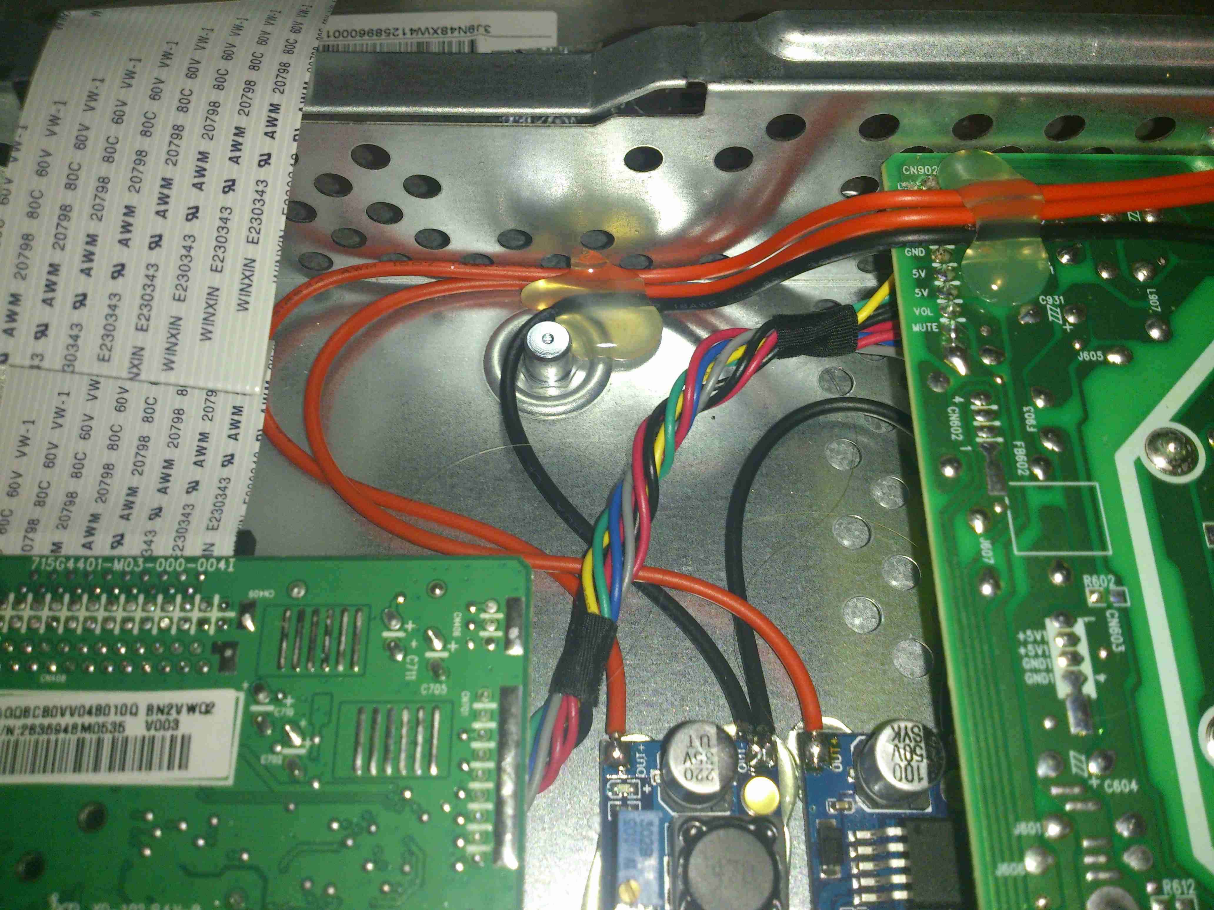
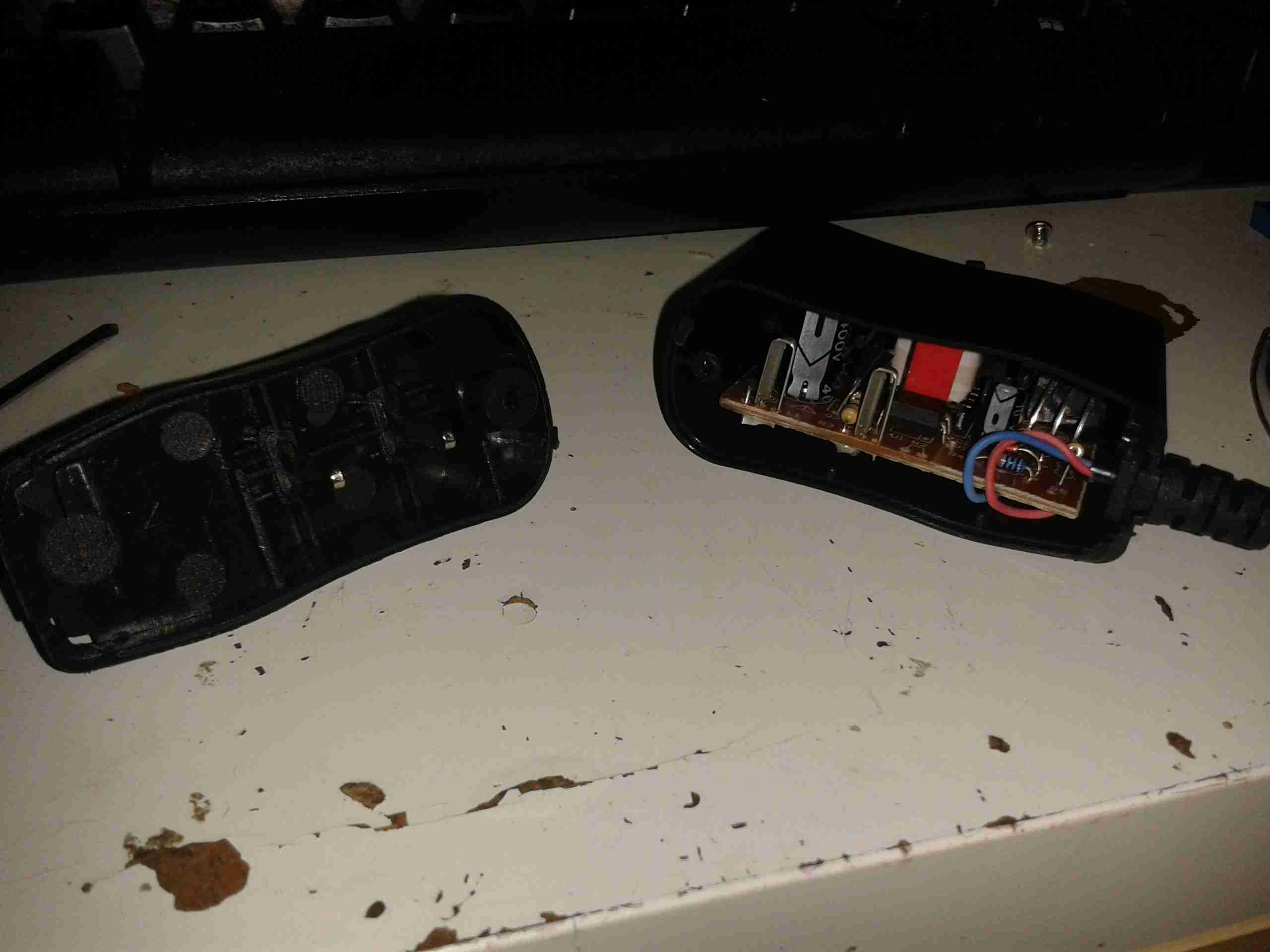
My refrigerant leak detector has one flaw – from the factory it uses C-size alkaline cells. Considering I don’t normally stock these (nothing else I have uses them!), and they’re big & heavy, I decided to do a modification to run the unit from lithium cells instead. This would allow charging via USB.
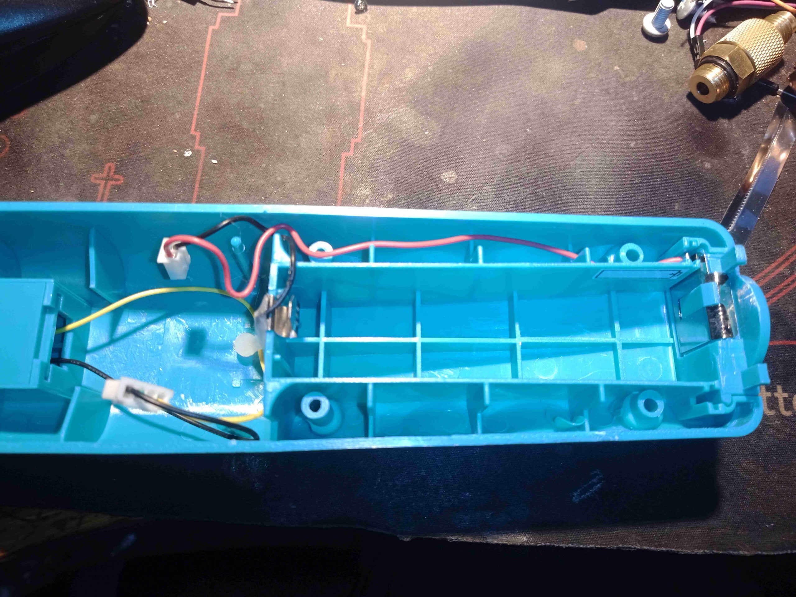
Factory Battery Compartment
Here’s the factory moulding, with extensive strengthening ribs around the battery compartment. Some of this will have to be removed to get the new cells into place. Cue the scalpel! The battery contacts will also have to be removed from the casing.
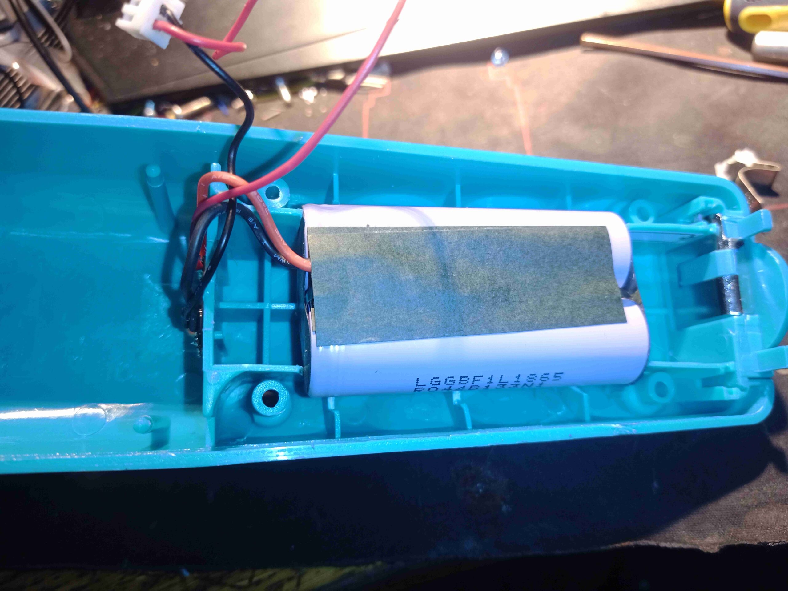
Battery Fitted
After removing some of the plastic, the new cells are a snug fit inside the battery space, with plastic ribs still in place to stop them falling out of the end of the case.
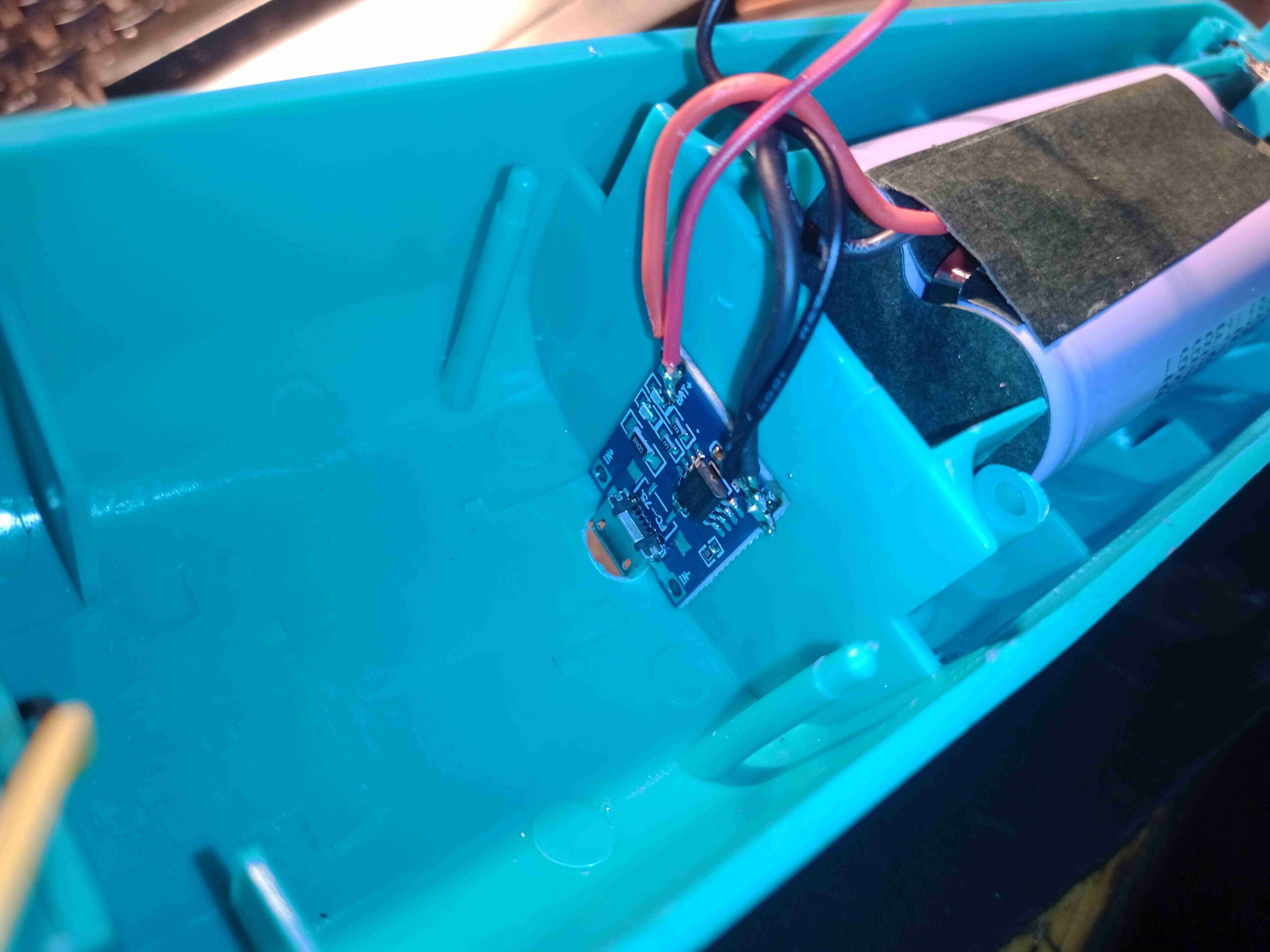
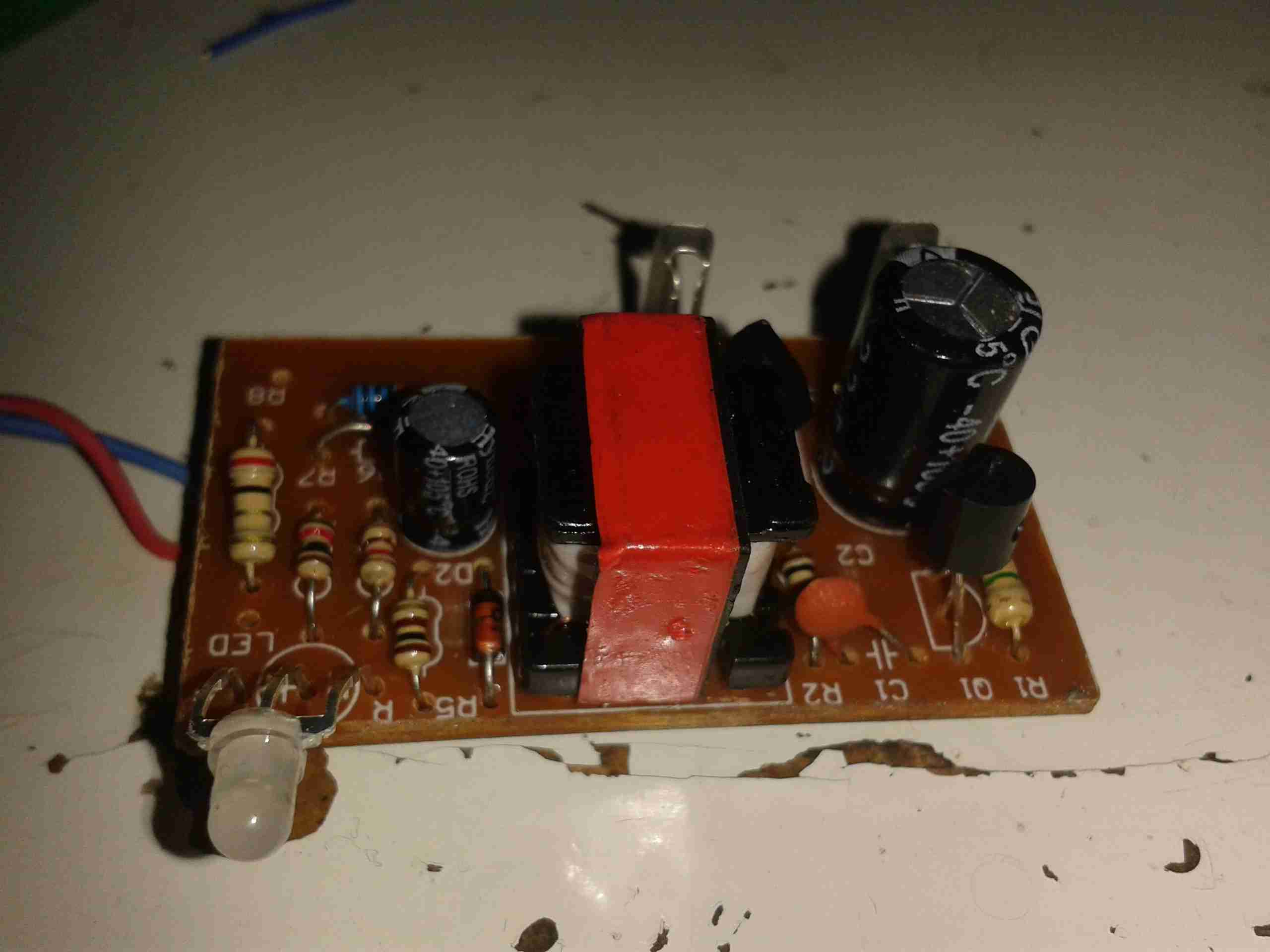
Lithium Charge IC
A small hole drilled in the back of the unit allows access to the USB port for charging, through this TP4056 3.7v charge module.
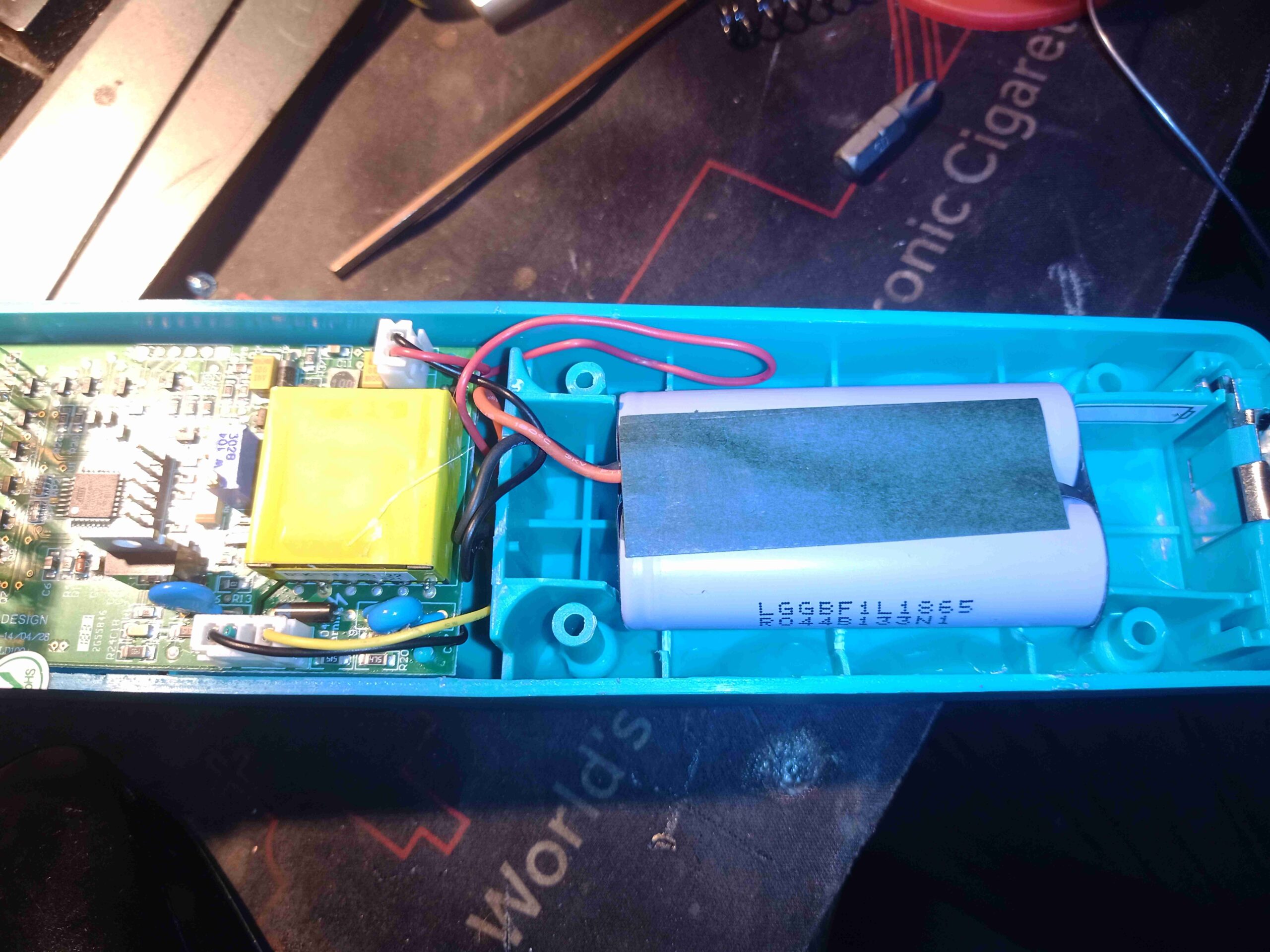
Board Refitted
A bit of rewiring, and the original battery connector is refitted to the board.
A while back I found myself in the need of an adjustable RF attenuator capable of high-GHz operation. As luck would have it I had an old Spectrum analyser on the shelf at work, which we had retired quite some time ago.
Spectrum analysers being quite capable test instruments, I knew that the input attenuation would be done with a standalone module that we could recover for reuse without too much trouble.
The attenuator module
Here’s the module itself, with the factory drive PCB removed from the bottom, showing the solenoids that operate the RF switches. There are test wires attached to them here to work out which solenoid switches which attenuation stage. In the case of this module, there are switches for the following:
Input select switch
AC/DC coupling
-5dB
-10dB
-20dB
-40dB
For me this means I have up to -75dB attenuation in 5dB steps, with optional switchable A-B input & either AC or DC coupling.
Drive is easy, requiring a pulse on the solenoid coil to switch over, the polarity depending on which way the switch is going.
Building a Control Board
Now I’ve identified that the module was reusable, it was time to spin up a board to integrate all the features we needed:
Onboard battery power
Pushbutton operation
Indication of current attenuation level
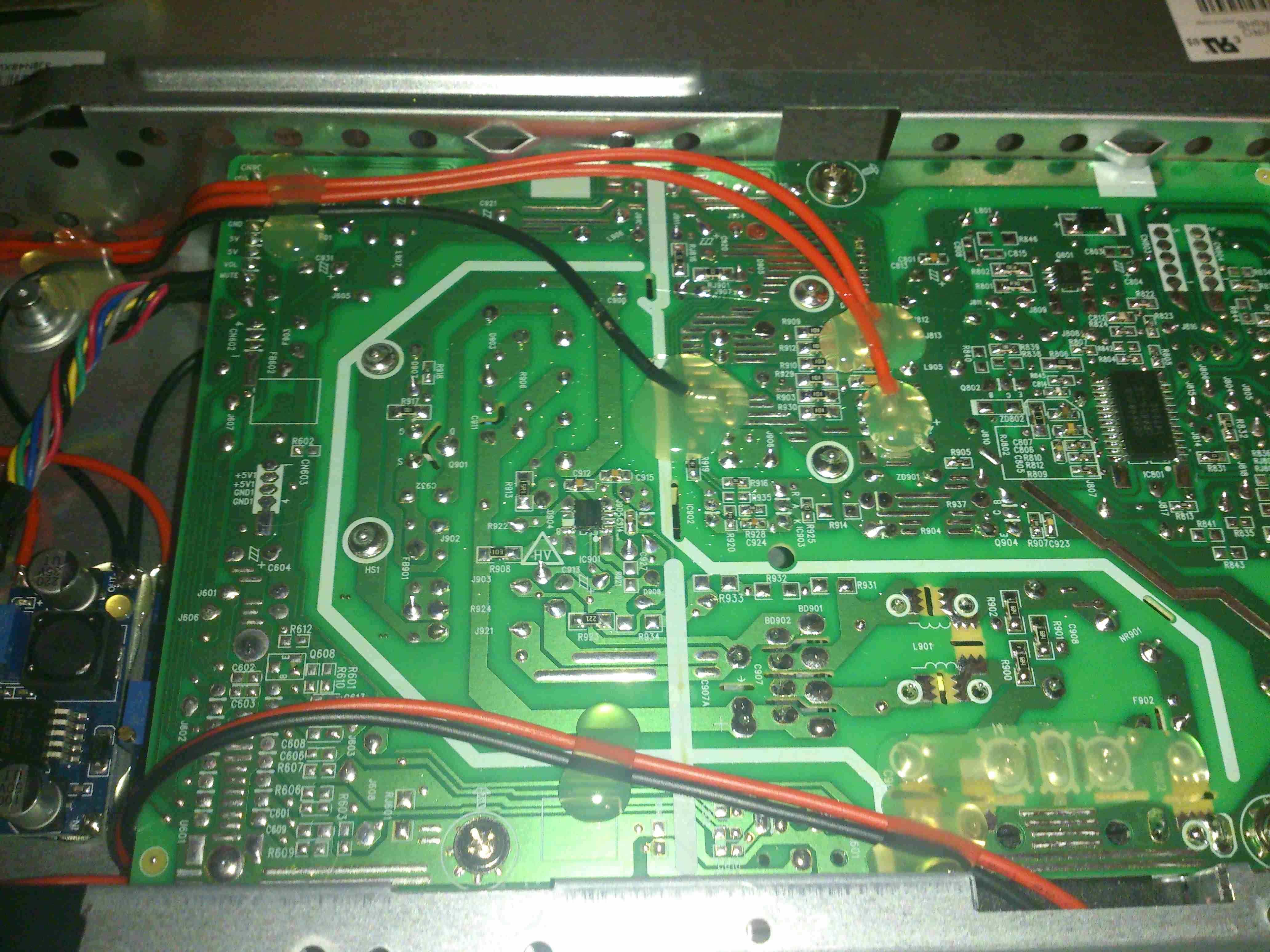
The partially populated board is shown at right, with an Arduino microcontroller for main control, 18650 battery socket on the right, and control buttons in the centre. The OLED display module for showing the current attenuation level & battery voltage level is missing at the moment, but it’s clear where this goes.
As there weren’t enough GPIO pins for everything on the Arduino, a Microchip MC23017 16-Bit I/O expander, which is controlled via an I²C bus. This is convenient since I’m already using I²C for the onboard display.
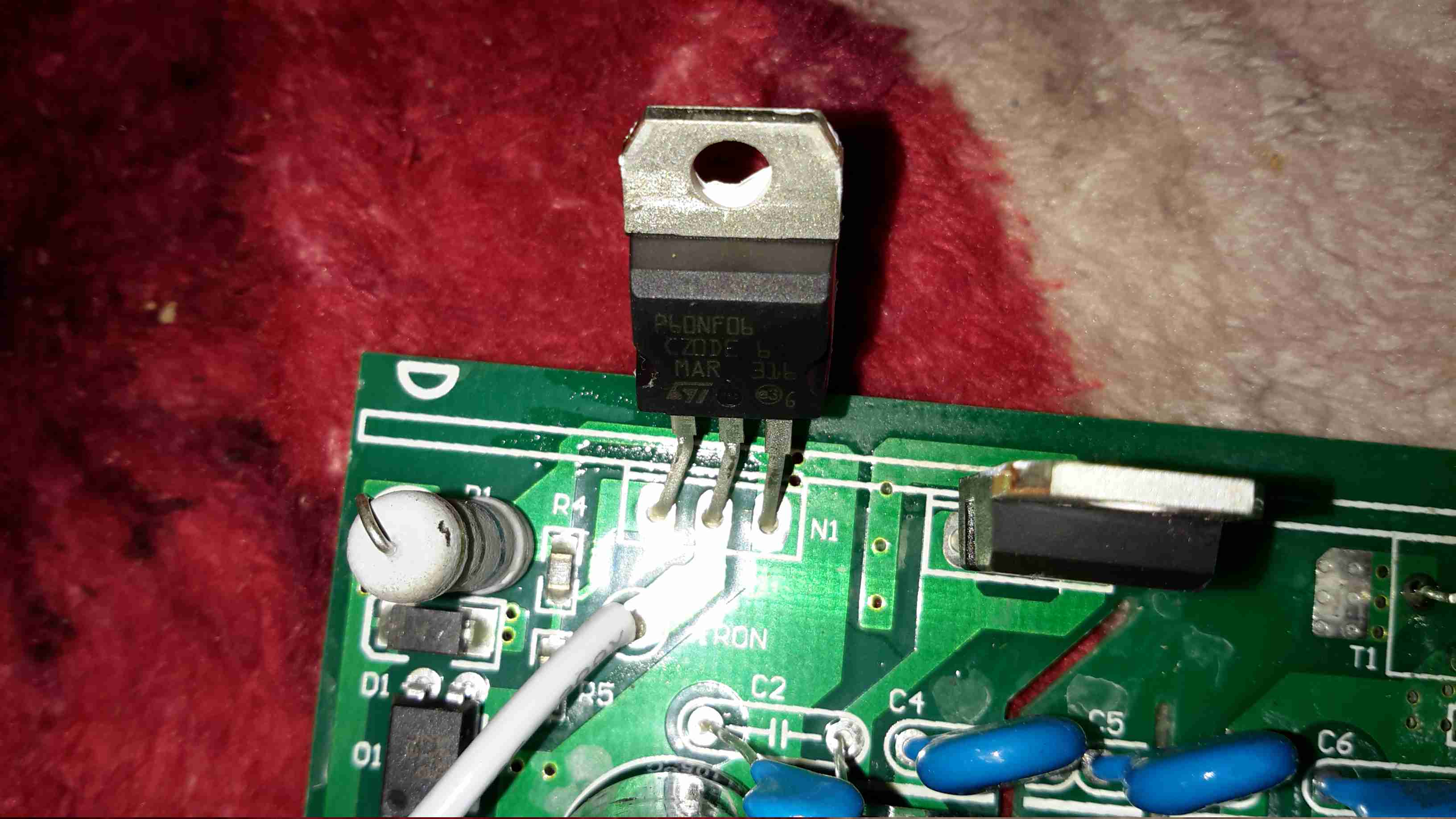
Driving the Solenoids
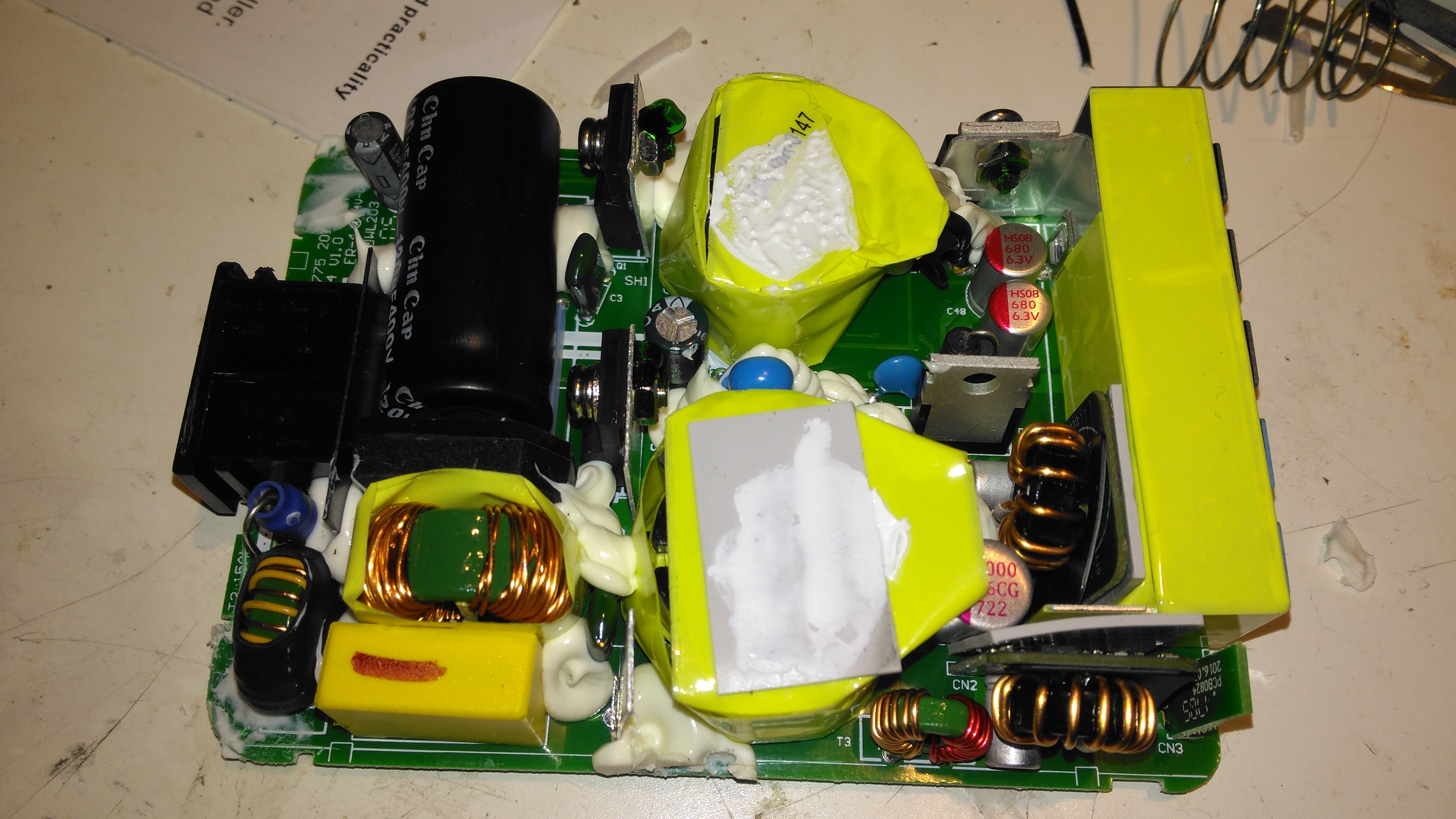
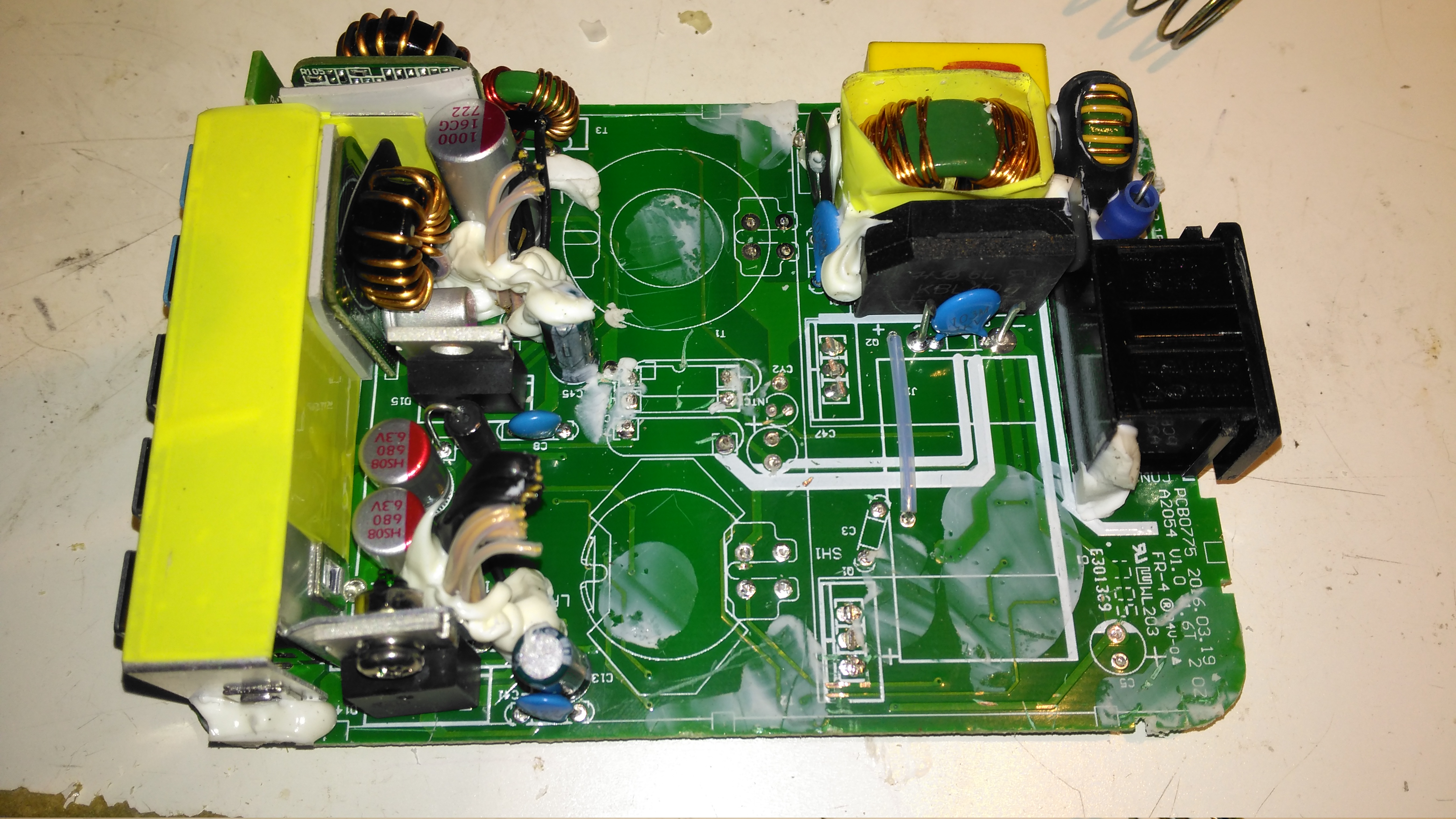
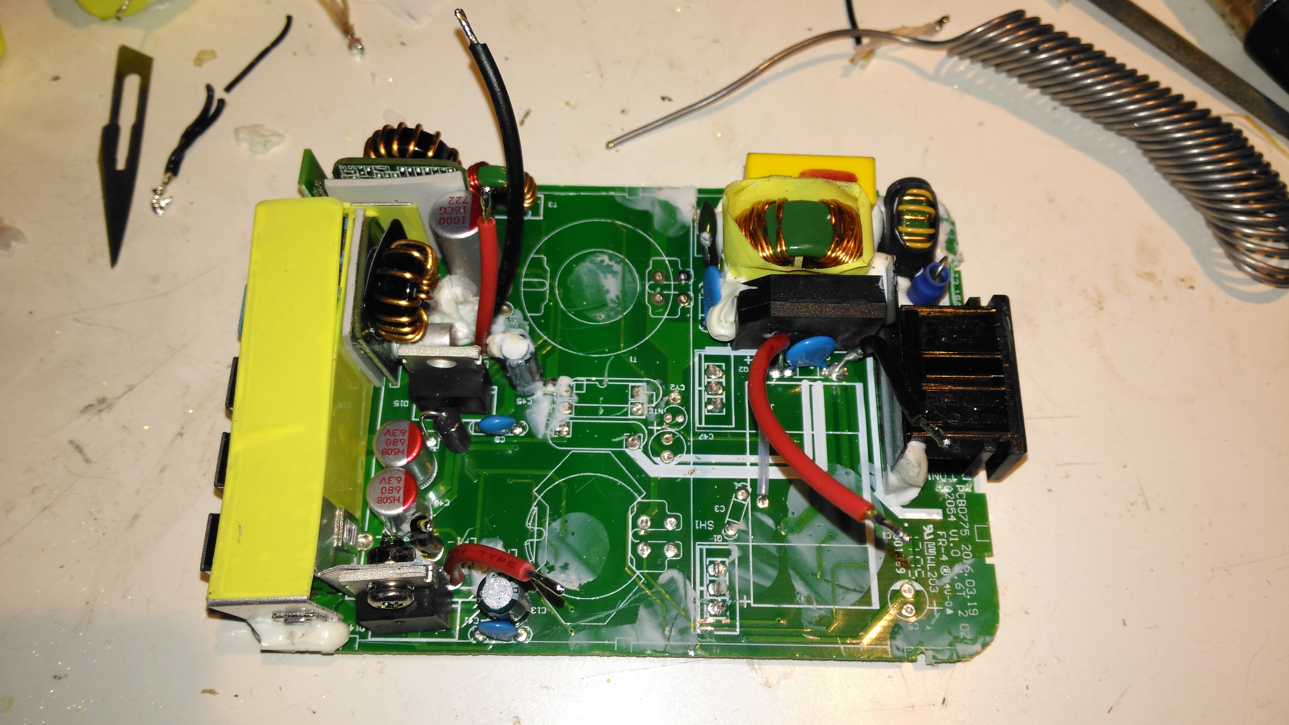
A closer view of the board shows the trip of dual H-Bridge drivers on the board, which will soon be hidden underneath the attenuator block. These are LB1836M parts from ON Semiconductor. Each chip drives a pair of solenoids.
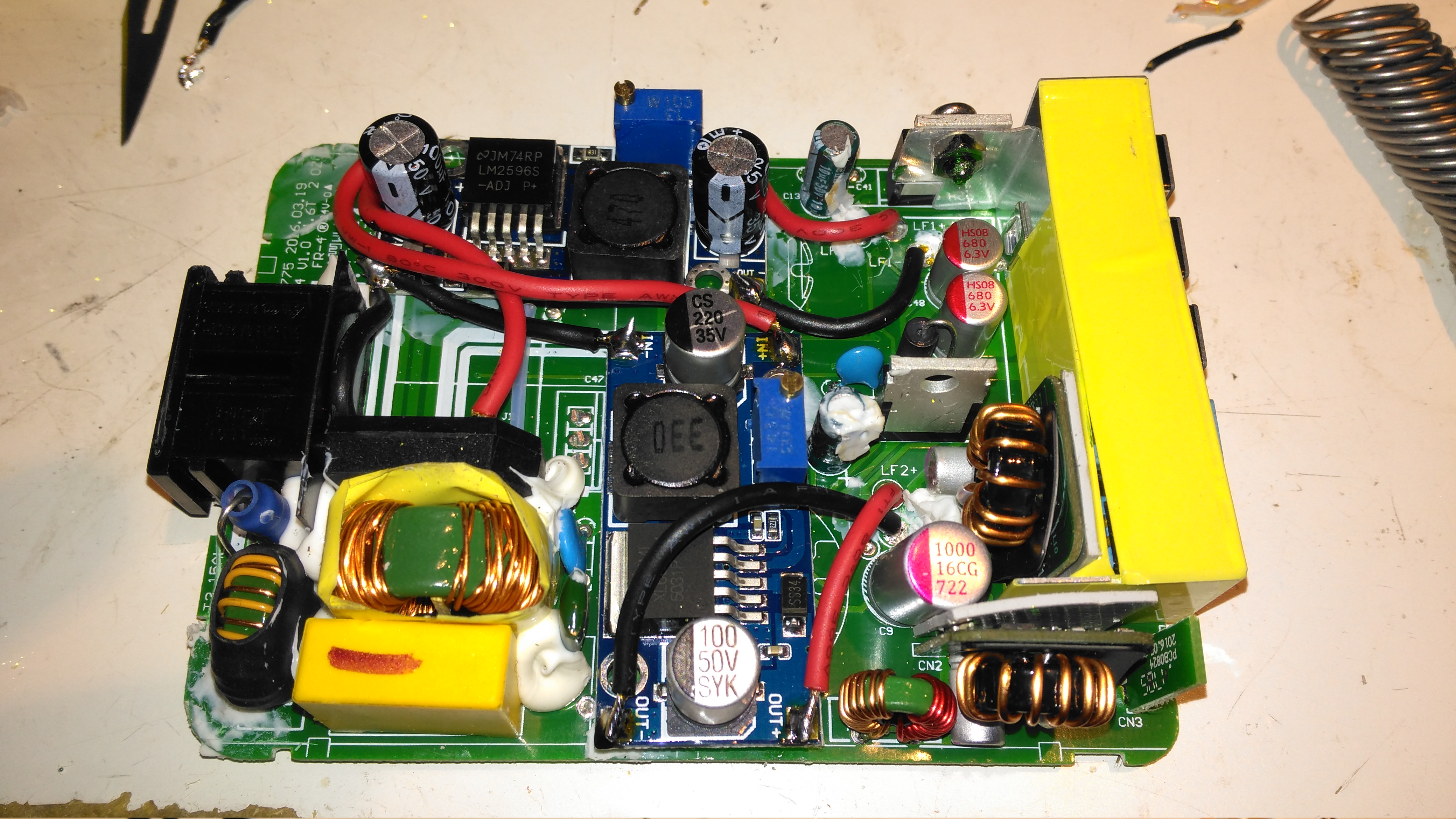
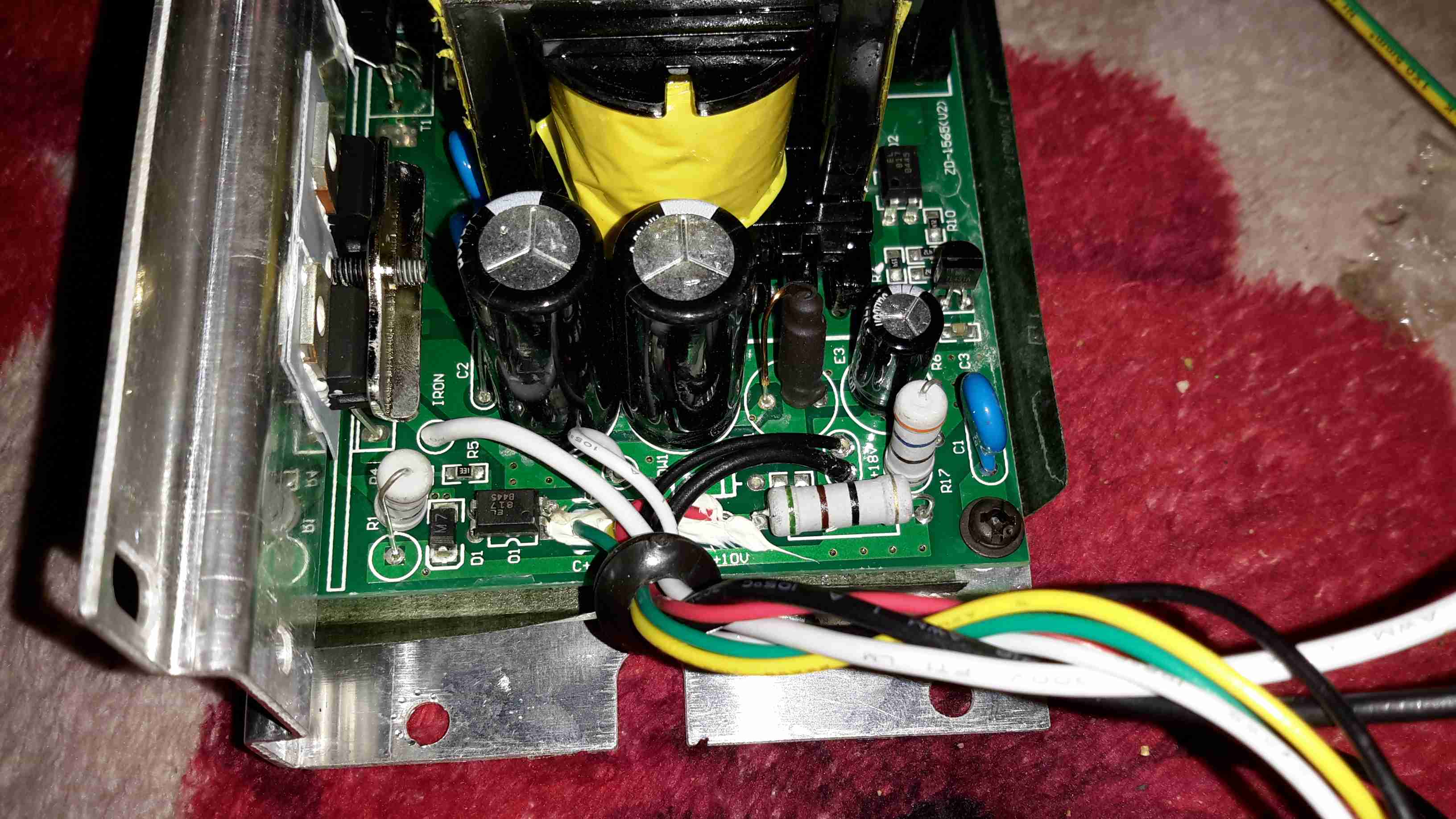
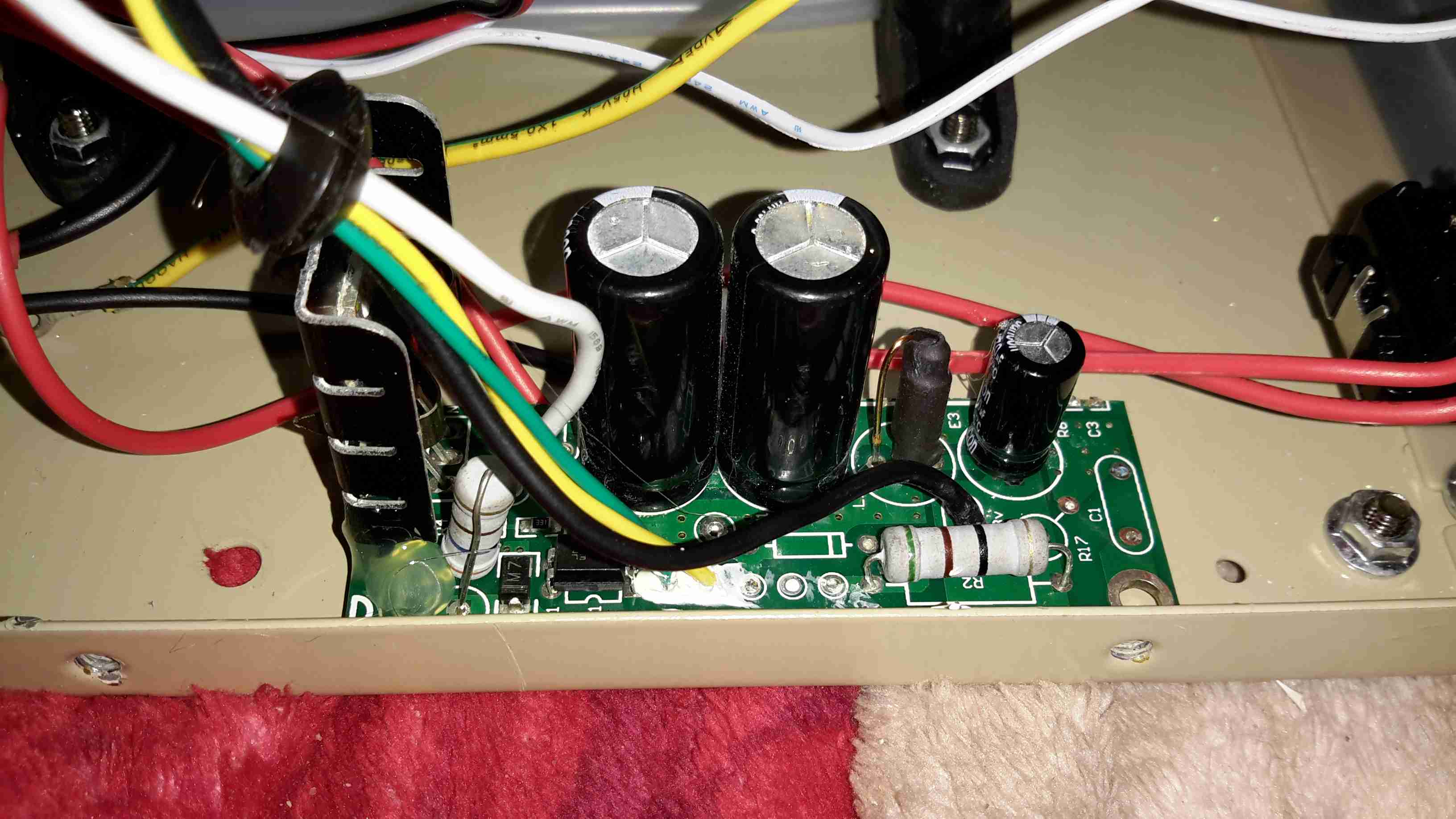
Power Supplies
The bottom of the board has all the power control circuitry, which are modularised for ease of production. There’s a Lithium charge & protection module for the 18650 onboard cell, along with a boost converter to give the ~9v rail required to operate the attenuator solenoids. While they would switch at 5v, the results were not reliable.
Finishing off
A bit more time later, some suitable firmware has been written for the Arduino, and the attenuator block is fitted onto the PCB. The onboard OLED nicely shows the current attenuation level, battery level & which input is selected.
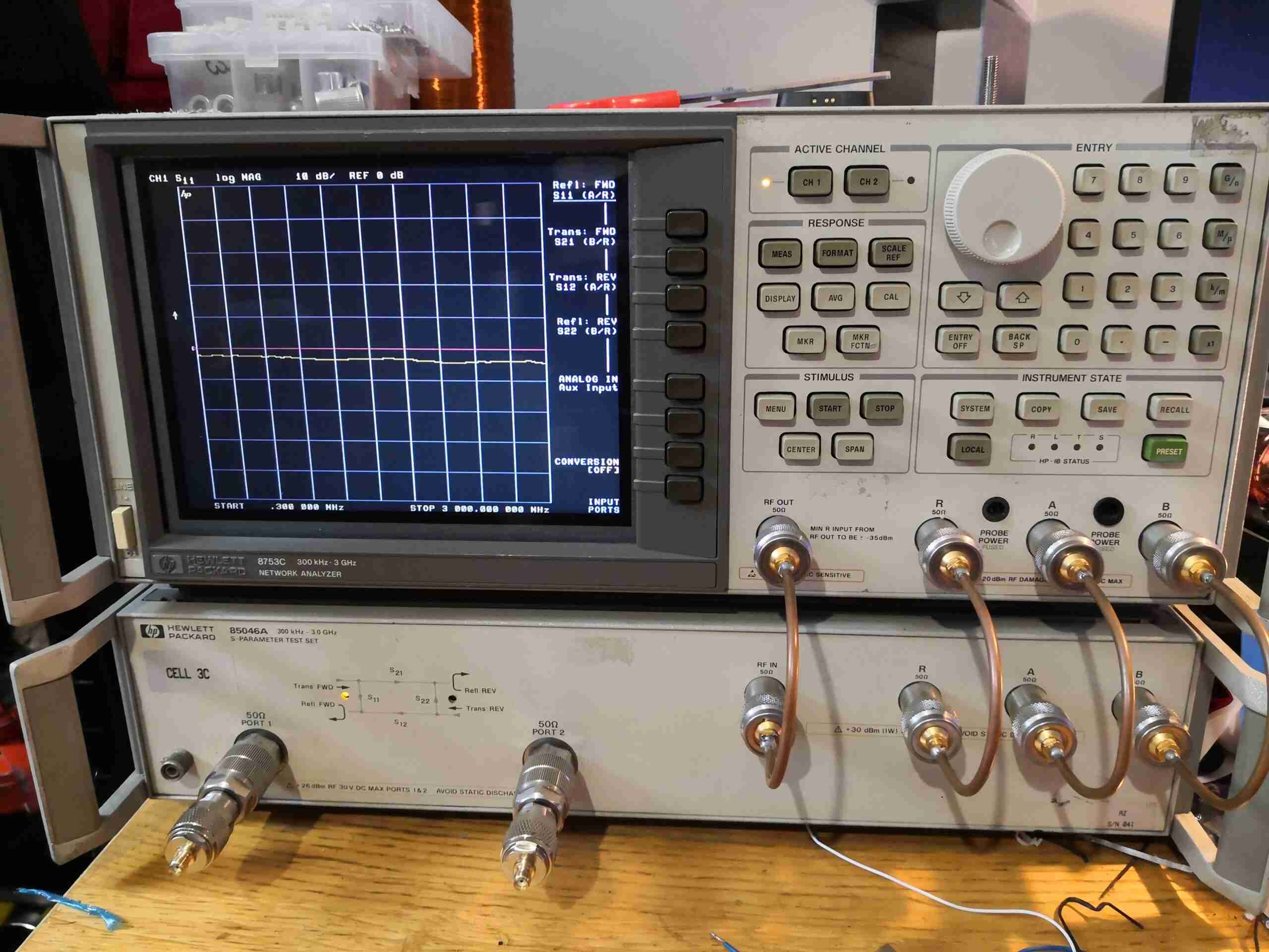
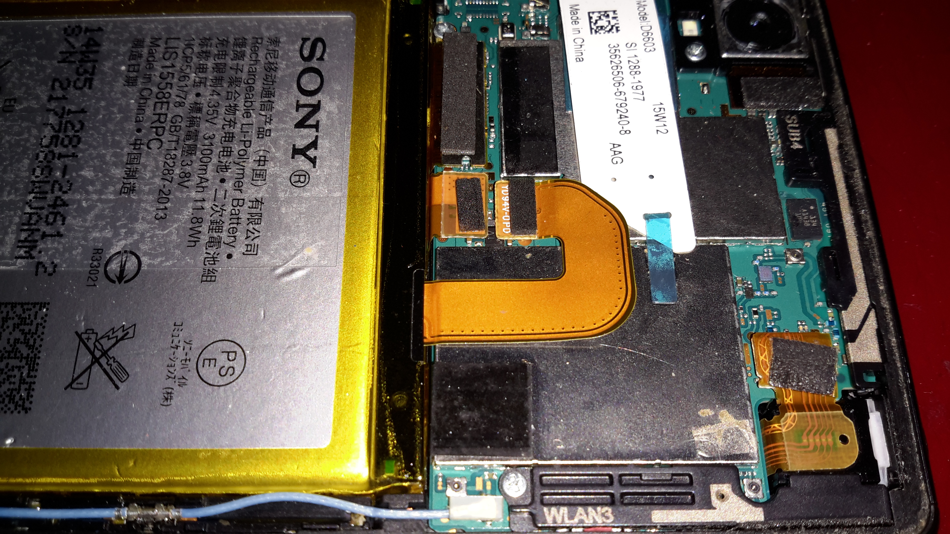
Since I inherited an old HP 8753C Network Analyser from work, I figured updating a few things to relatively modern standards would be good. The factory CRT, being 28 years old, is definitely getting a little tired, not to mention being slow to warm up. I read over on the EEVBlog forums about a DIY modification to integrate an LCD display into place instead. There was also the option of a ready-made kit for these instruments which would integrate an LCD, but the cost at over £300 was very prohibitive!
CRT Pinout
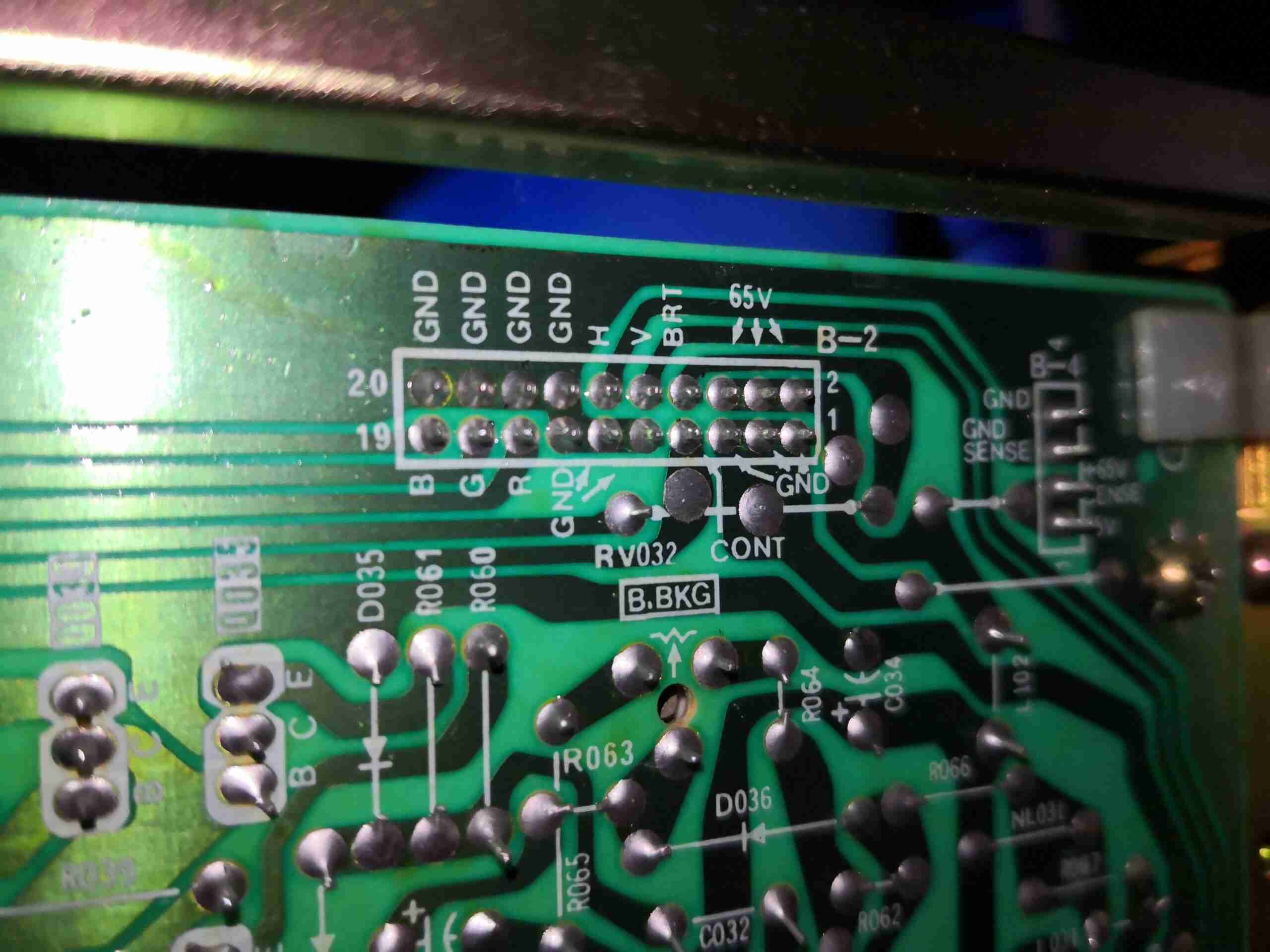
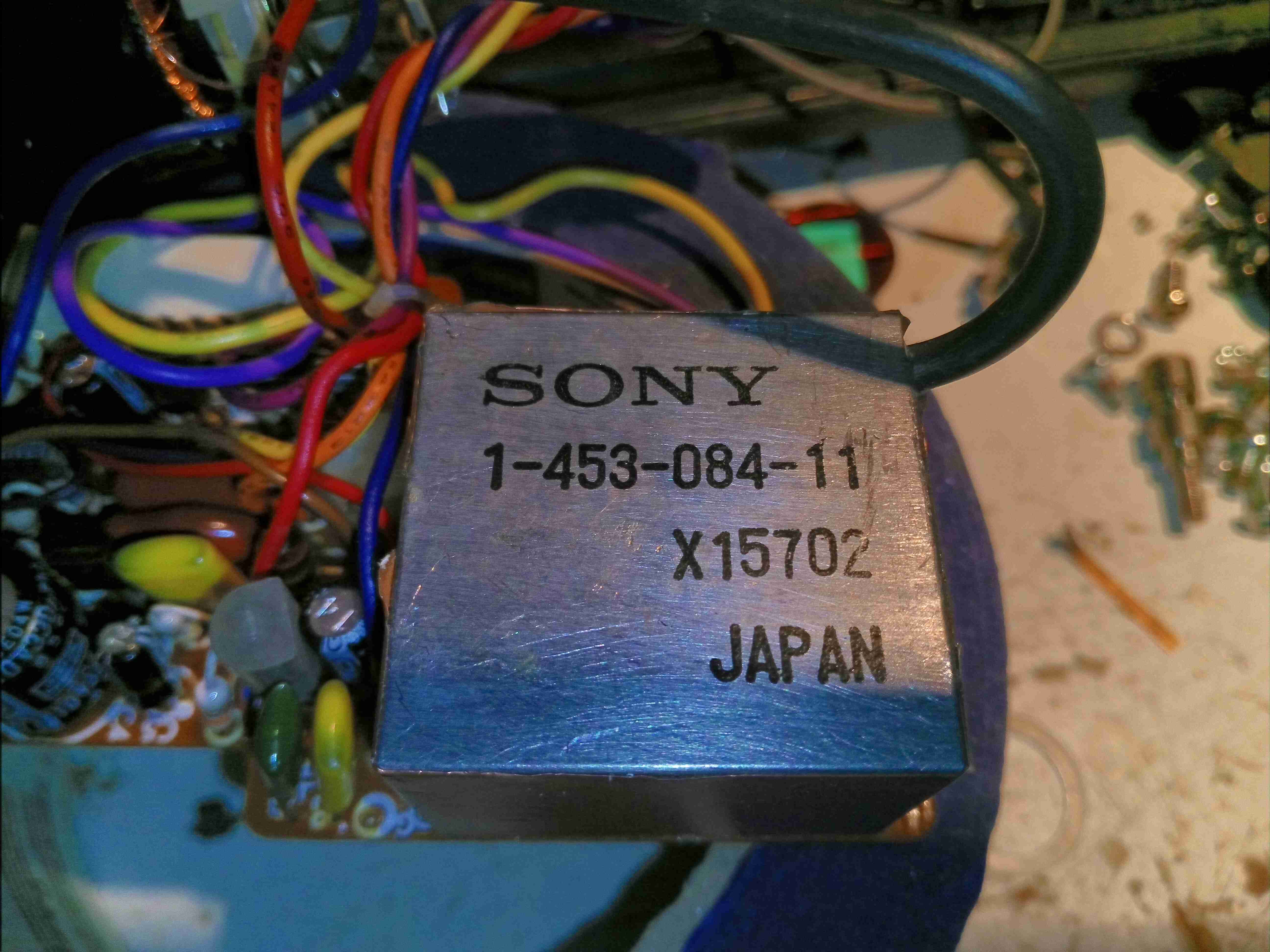
The CRT display unit is a self-contained Sony unit, taking RGBHV signalling from the graphics control card of the analyser. Power is 65v DC which will definitely come in handy for powering the new LCD & control gear, after some conversion.
Test Wiring
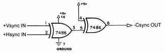
Doing a quick test with some wiring stuck into the video connector from the graphics controller, proved that I could get a decent video signal out of the unit! The only signals used here are RGB, along with the vertical & horizontal sync.
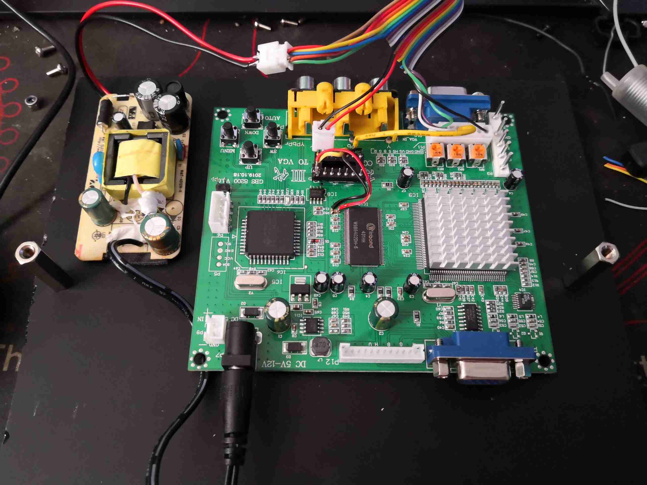
GBS-8200 Converter Board
The video is converted to VGA by way of a GBS-8200 arcade machine video conversion board, which will take many different video formats & spit out standard VGA signalling. The power supply to the left is a standard 100-240v to 12v PSU, which is happy to run at 6t5v DC input voltage, albeit with a ~5 second delay on output startup when power is applied. This is due to the massive 6.6MΩ resistance of the startup resistor chain, which I did reduce by 50% to 3.3MΩ with no effect. Since it does start OK even with the delay, I think I’ll not tinker with it any further. I doubt I could pull the full rated power from it with such a low input voltage, but all included, this mod draws less than 600mA at 12v.
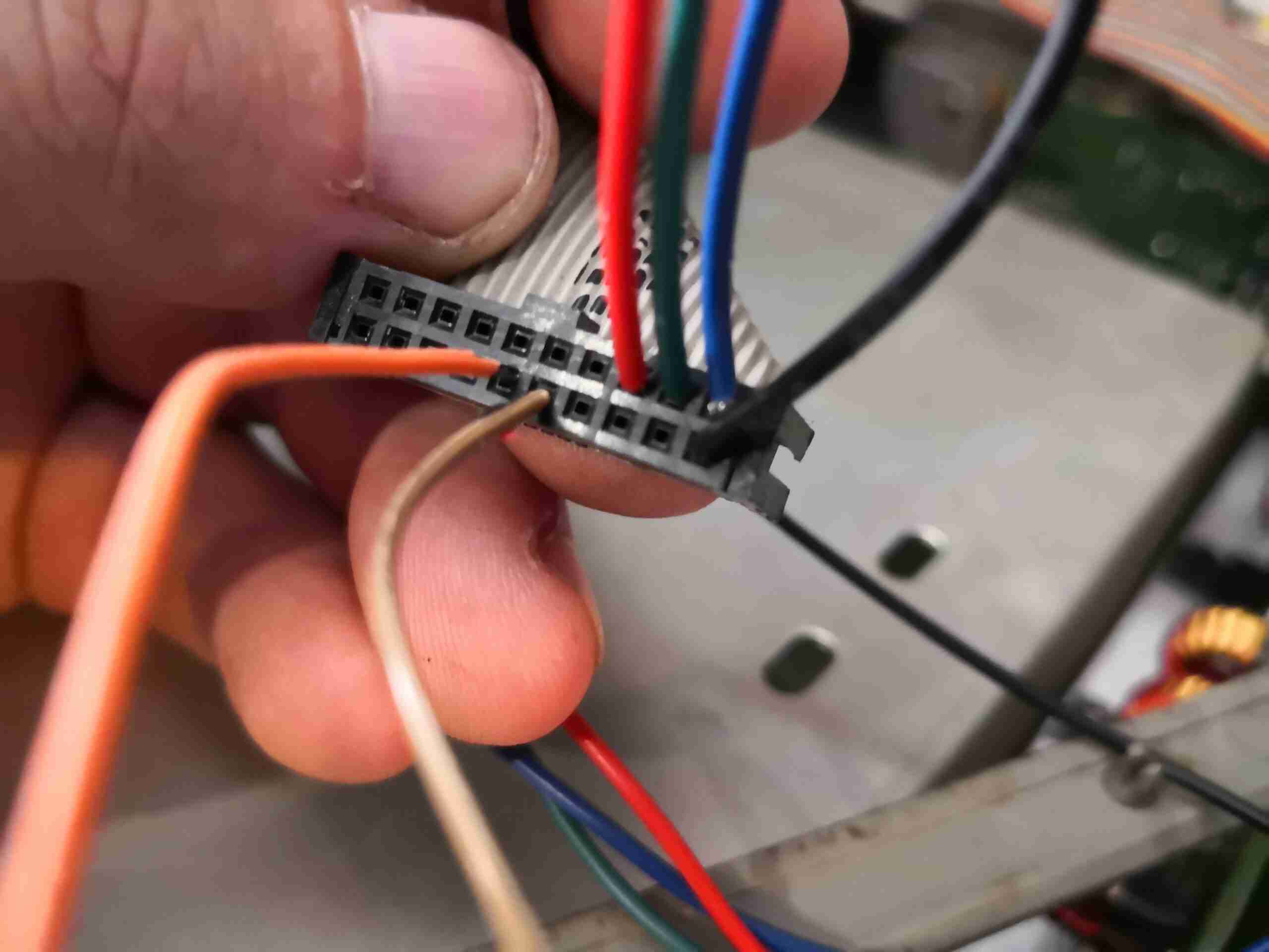
A custom 20-pin IDC cable was made up to connect to the analyser’s graphics board, and this was then broken out into the required RGB & sync signals. Quite a few of the grounds are unused, I’ve not yet noticed any issues with EMC or instability.
Sync Combiner
There is a quad-XOR gate deadbugged to the PCB, which is taking the separate sync signals & combining them into a composite sync. The conversion board does have separate sync inputs, but for some reason doesn’t sync when they’re applied separately. This gate IC is powered from the 3.3v rail of the converter board, with the power lines tacked across one of the decoupling caps for the DRAM IC.
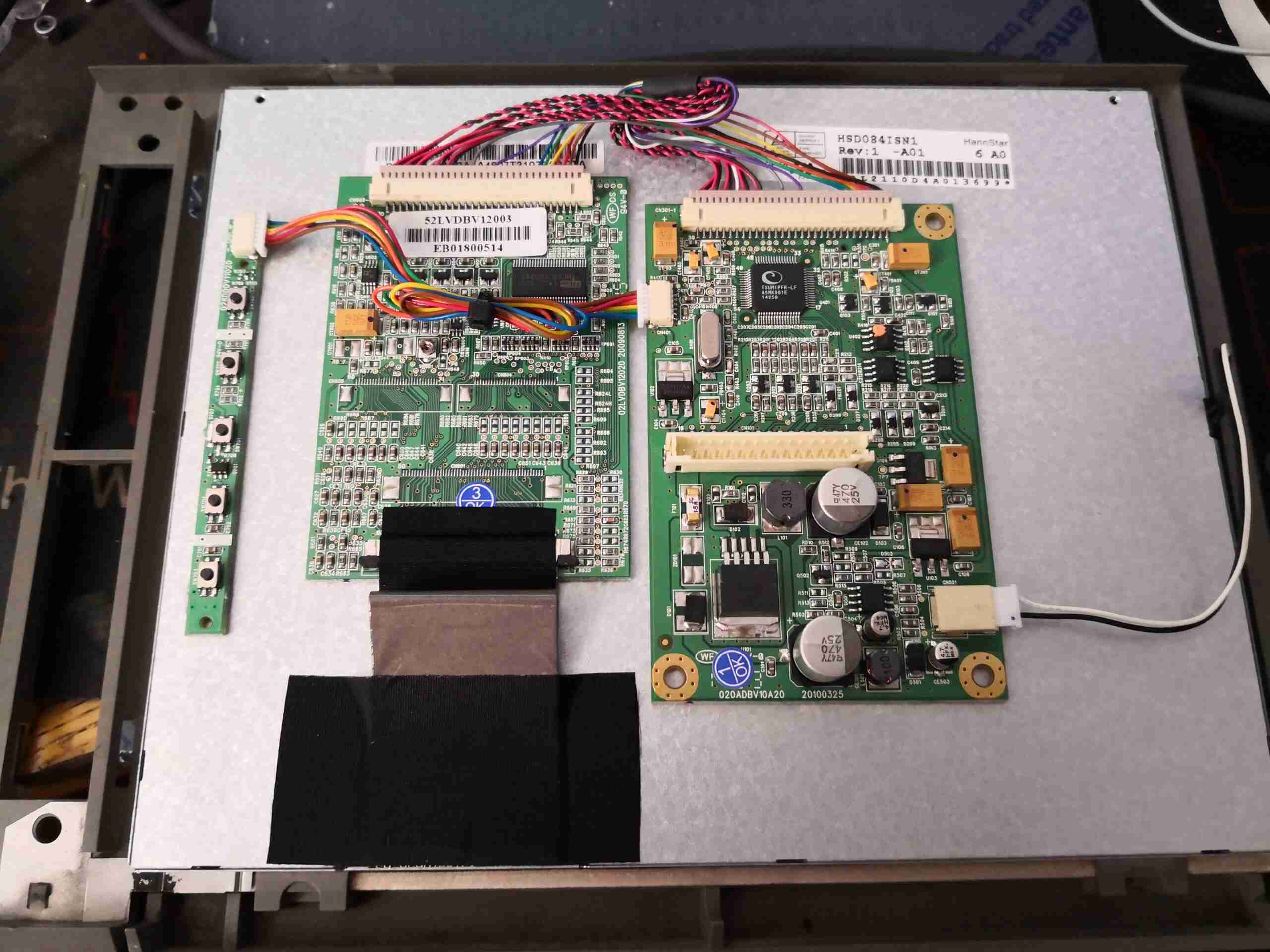
LCD Control PCBs
The donor 8.4″ LCD came from eBay in the form of a POS auxiliary display. I pulled the panel from the plastic casing, along with the control boards, and attached them all to the back. This LCD also had a sheet of toughened glass attached to the front, no doubt to protect against the Great Unwashed while in use! This was also removed.
Control Boards Mounted
A cut piece of plexiglas allows the boards to be mounted in the cavernous space the CRT once occupied, with some brass standoffs. 12v power & VGA are routed down to the LCD on the front of the analyser.
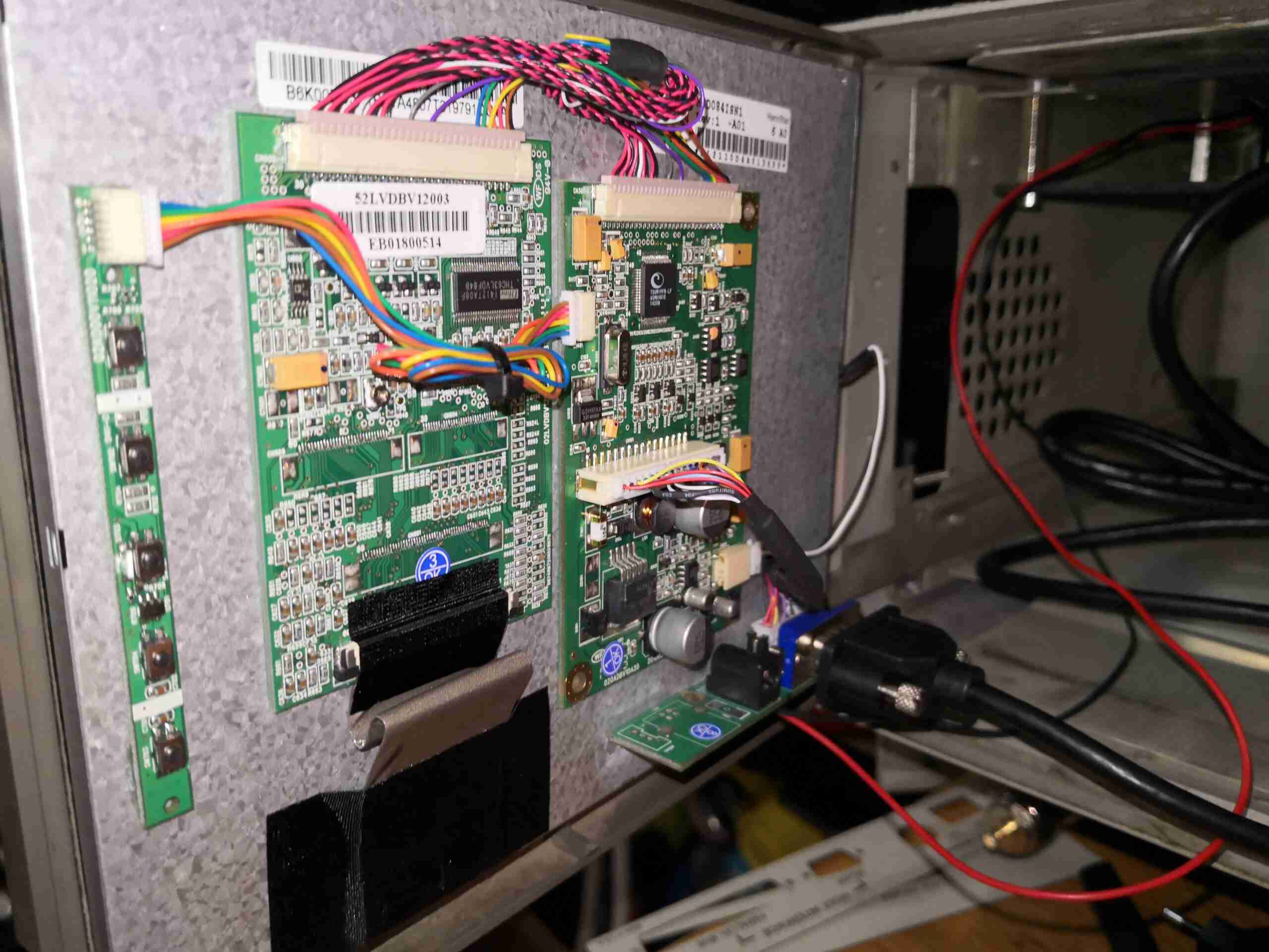
LCD Wiring
The LCD itself is tacked in place with cyanoacrylate glue to the securing clips for the glass front panel, which is more than enough to hold things in place. The input board which just has the VGA connector & power connector is glued edge-on to the metal back panel of the LCD, and is under little strain so this joint should survive OK.
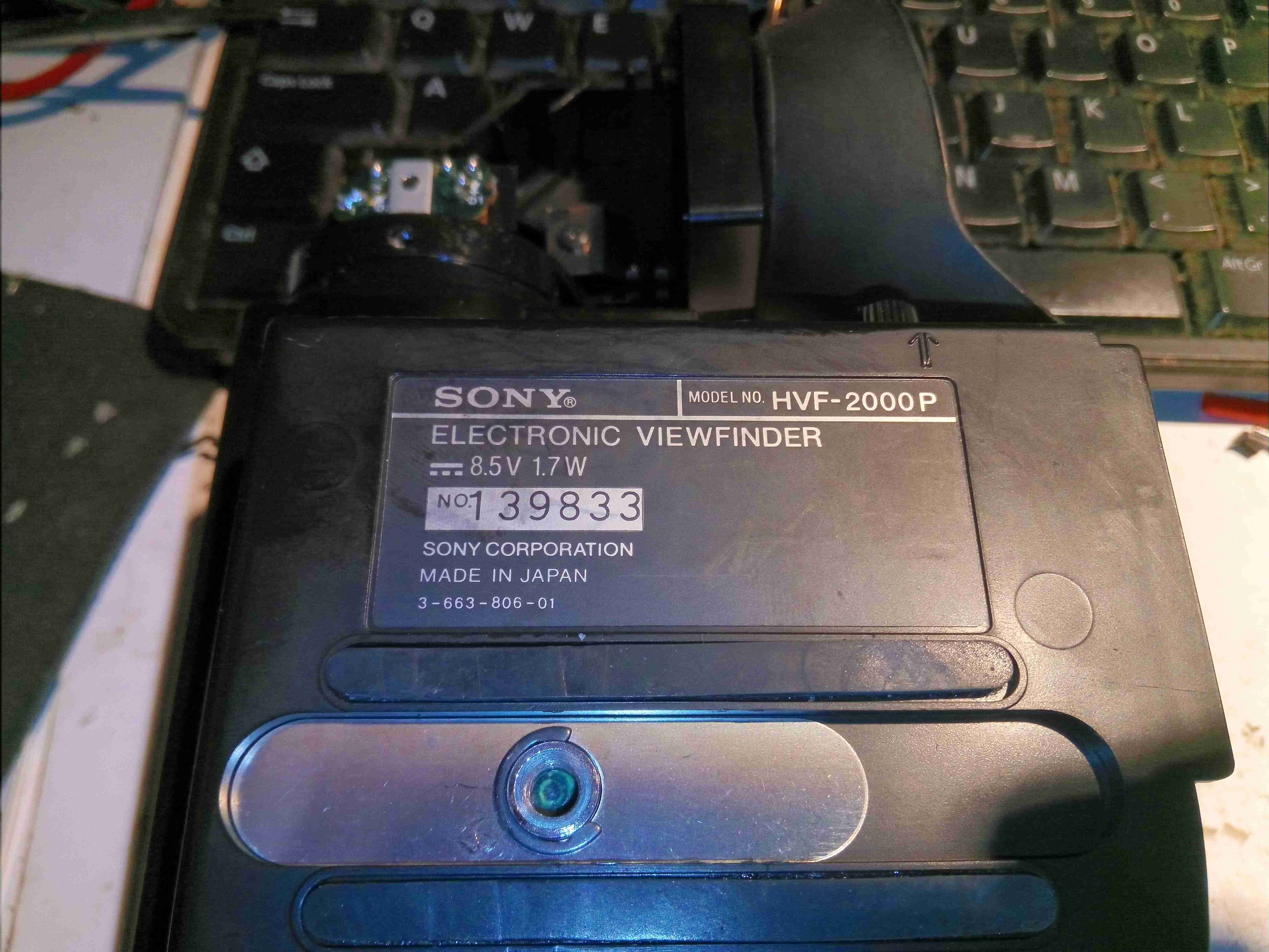
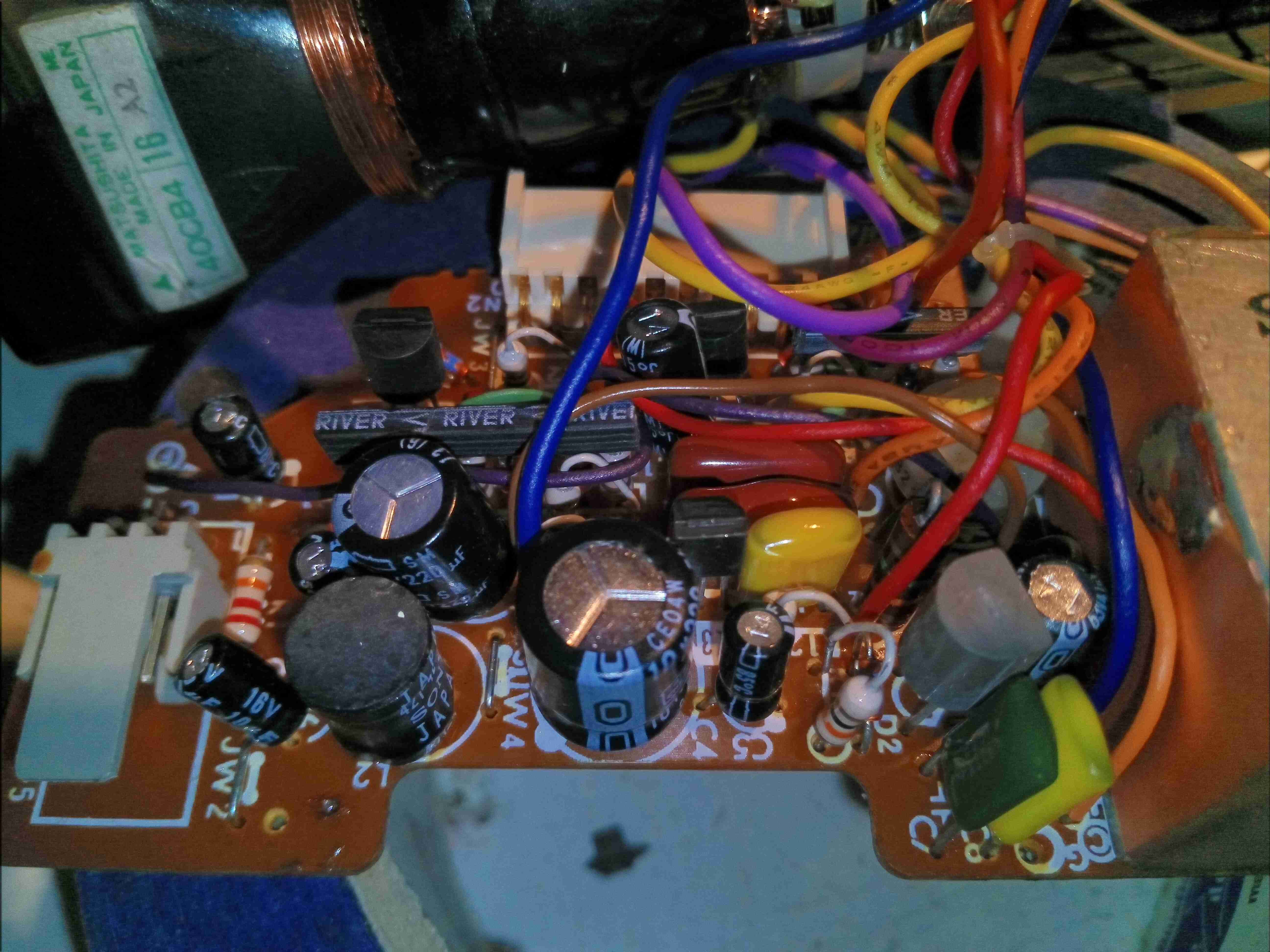
Well, it’s time for another viewfinder hack! I’ve been after one of these for a while, this is from an early 1980’s era Sony Trinicon camera, and instead of the tiny ½” round CRT display, these have a 1.5″ square CRT – a Matsushita 40CB4. Luckily I managed to score a pair of these from eBay for very little money. Update: The second camera’s viewfinder module turned out to have a dead flyback transformer, but at least I have a good spare CRT & the rest of the support components. More to come later on the teardown of the camera itself.
Mirror & Eyecup Assembly
The eyecup assembly with the magnifying lens & turning mirror is easy to remove, with clips & a single screw holding it onto the CRT holder sticking out of the side of the main casing.
Top Cover Removed
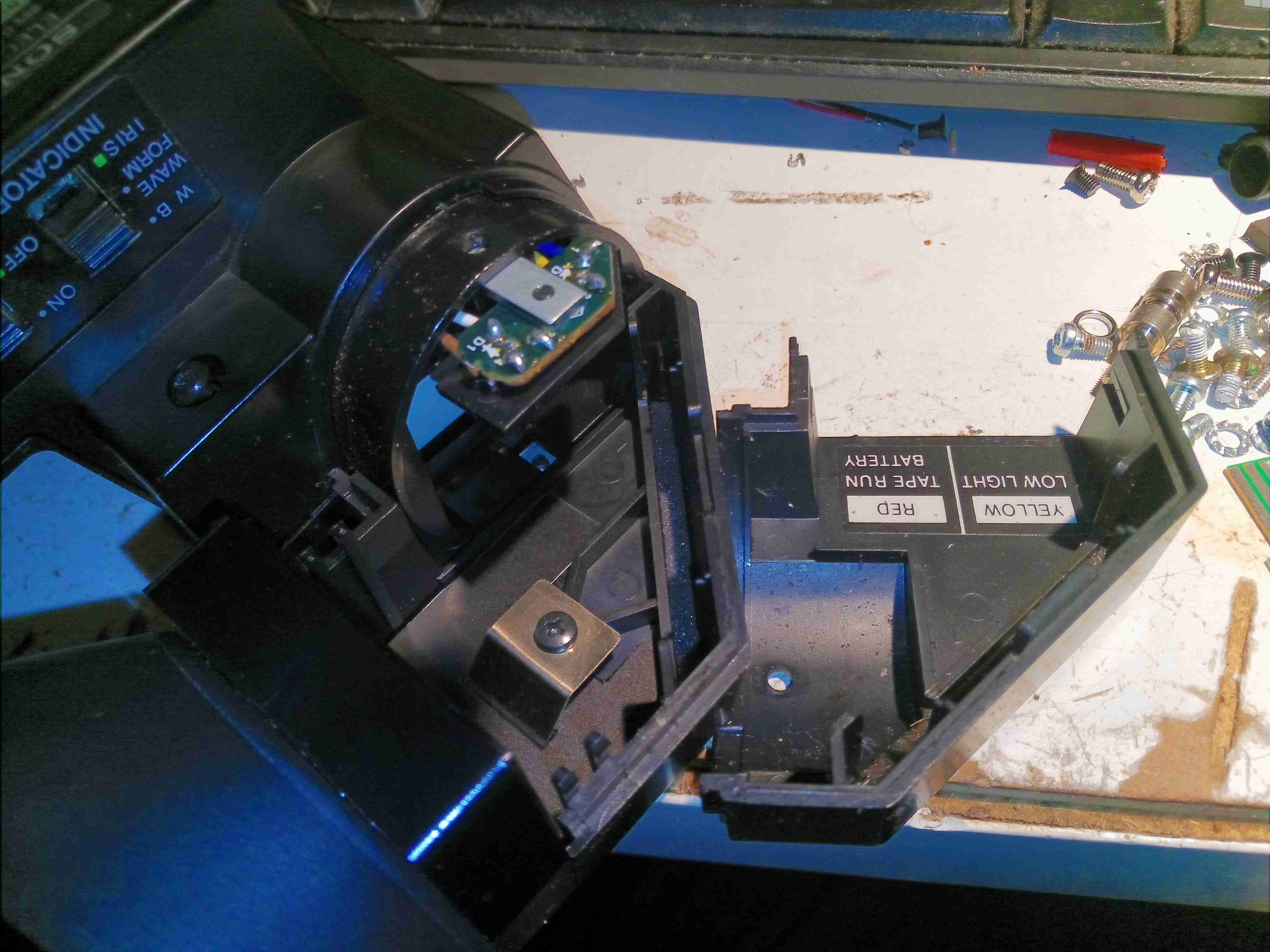
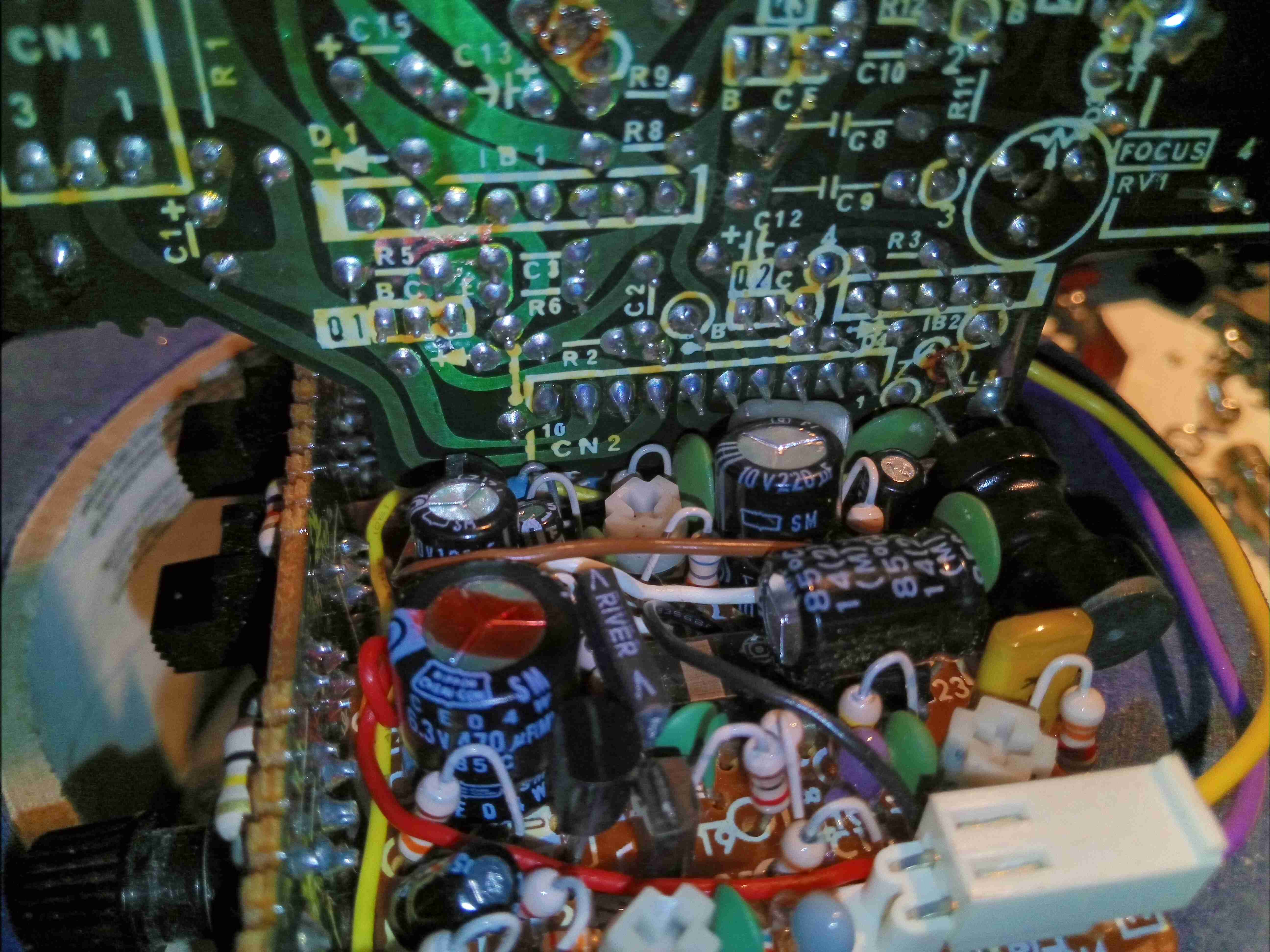
Removing some screws around the case allows the top cover to be removed, revealing the electronics. There’s certainly more in here than the later camera viewfinders, in this unit there are two boards slotted together with a board-to-board interconnect at the bottom. The CRT is at the top of the photo, hiding inside the plastic housing & deflection yoke assembly.
Bare PCBs & CRT
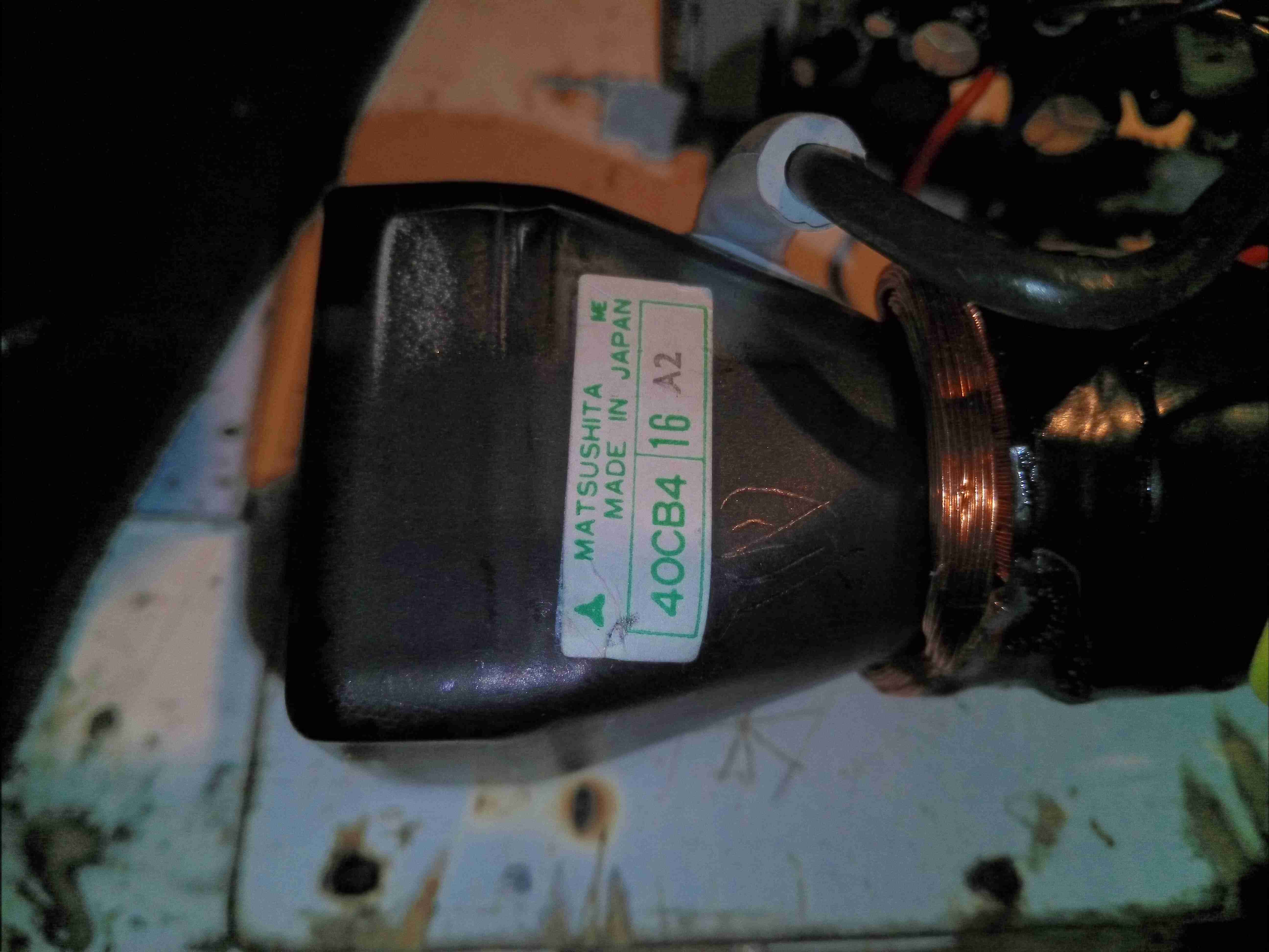
Here’s the CRT & one of the control boards removed from the case, having been stripped of the heatshrink tube that held the final anode lead in place. Just like on larger CRTs, this viewfinder has the final anode on a cavity connector fused into the bell, instead of being led out to a pin on the base. This is probably due to the much higher anode voltage of 5kV, a big jump from the 2kV on the ½” round tubes.
40CB4 CRT Label
Yup, it’s definitely the elusive 40CB4. Apparently these CRTs are still manufactured to this day for professional camera viewfinders, as the resolution of this small vacuum tube is still better than similarly sized modern tech such as LCDs or OLEDs. The phosphor used is type P4 – ZnS:Ag+(Zn,Cd)S:Ag, with an aluminized overcoat.
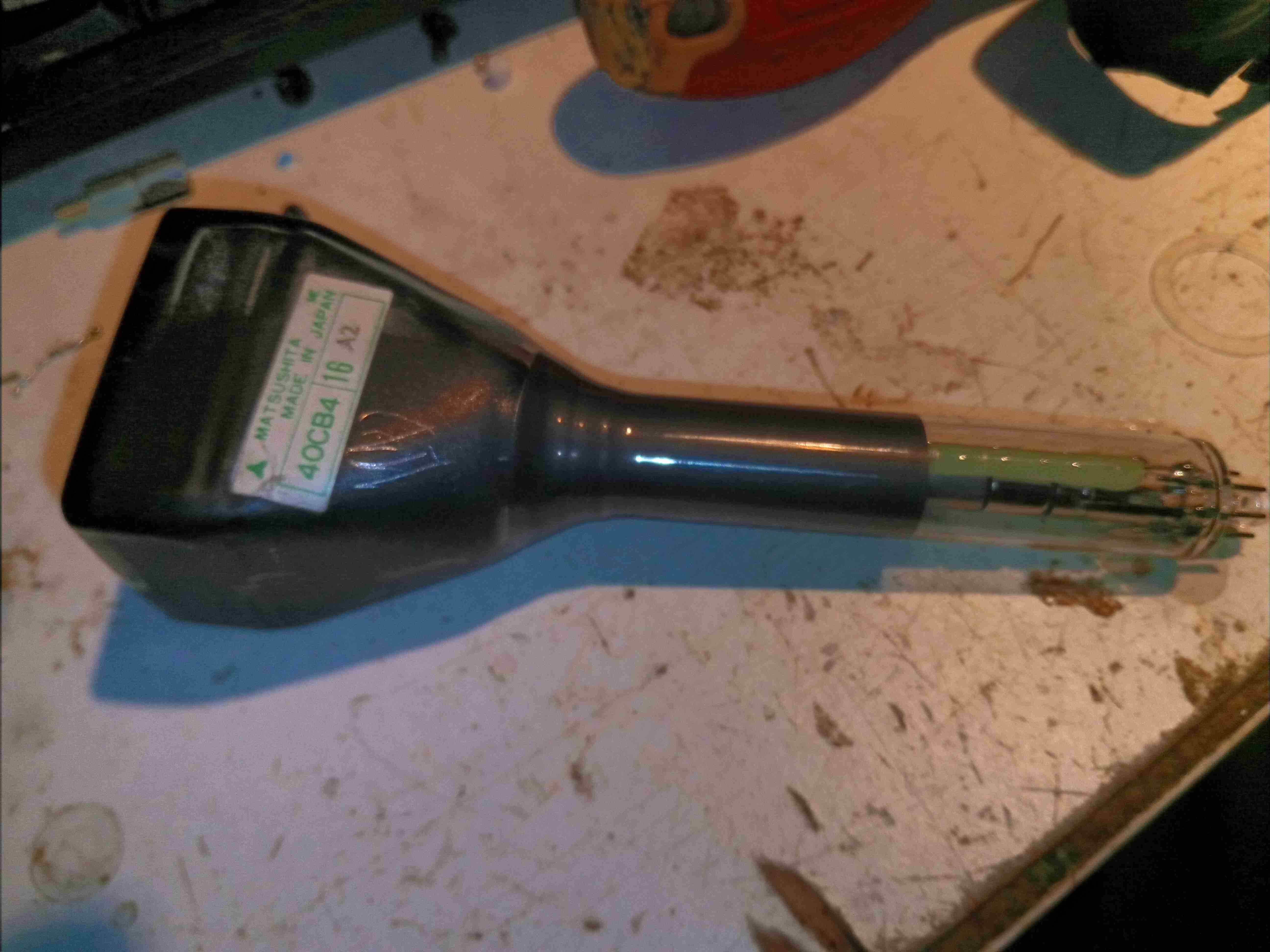
Bare 40CB4 CRT
After the base connector & deflection yoke are removed from the tube, the very long neck can be seen, this long glass neck apparently giving better focus & resolution than the stubbier tubes.
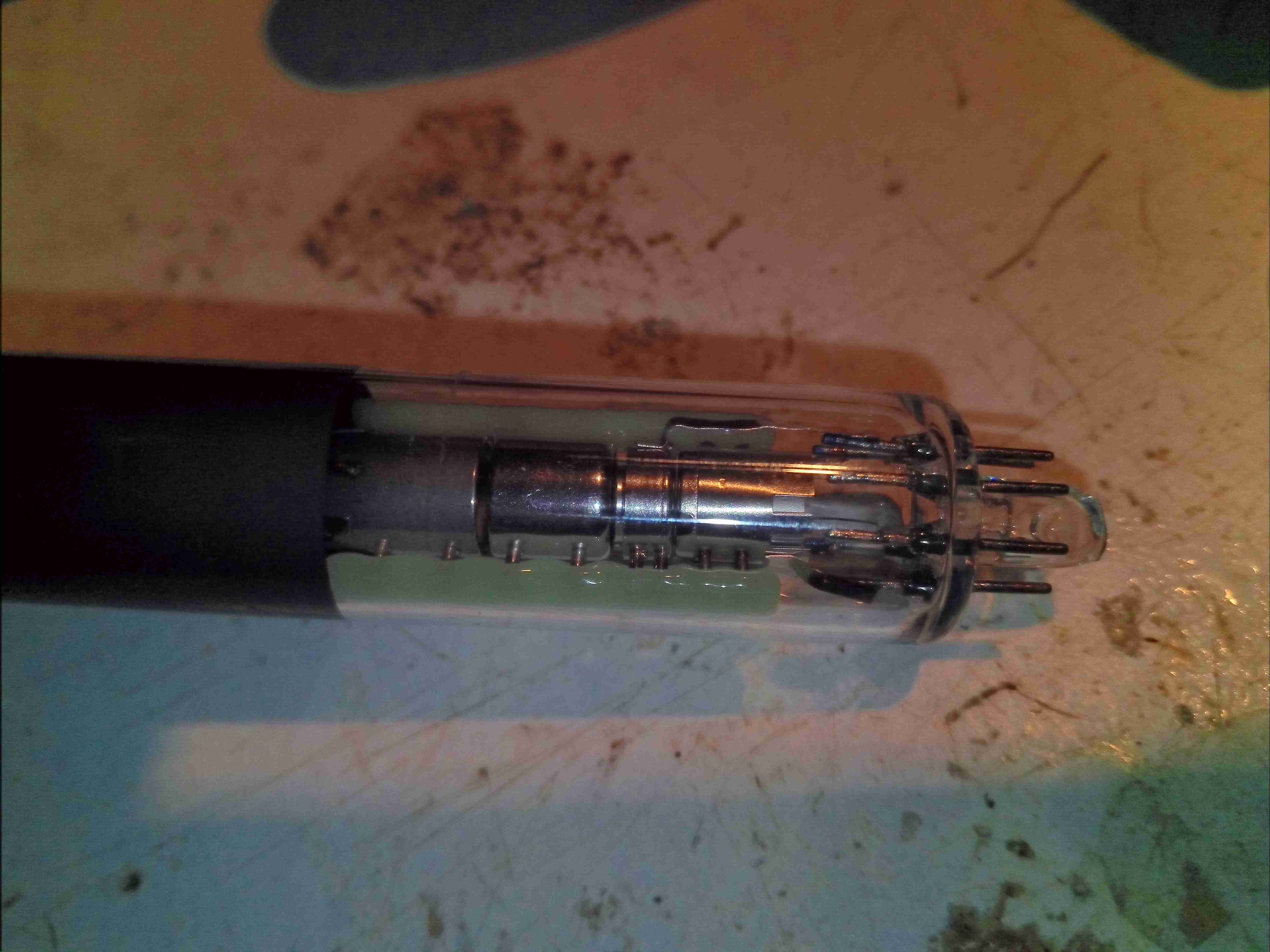
Electron Gun
The electron gun is the usual single unit as usually found in monochrome tubes.
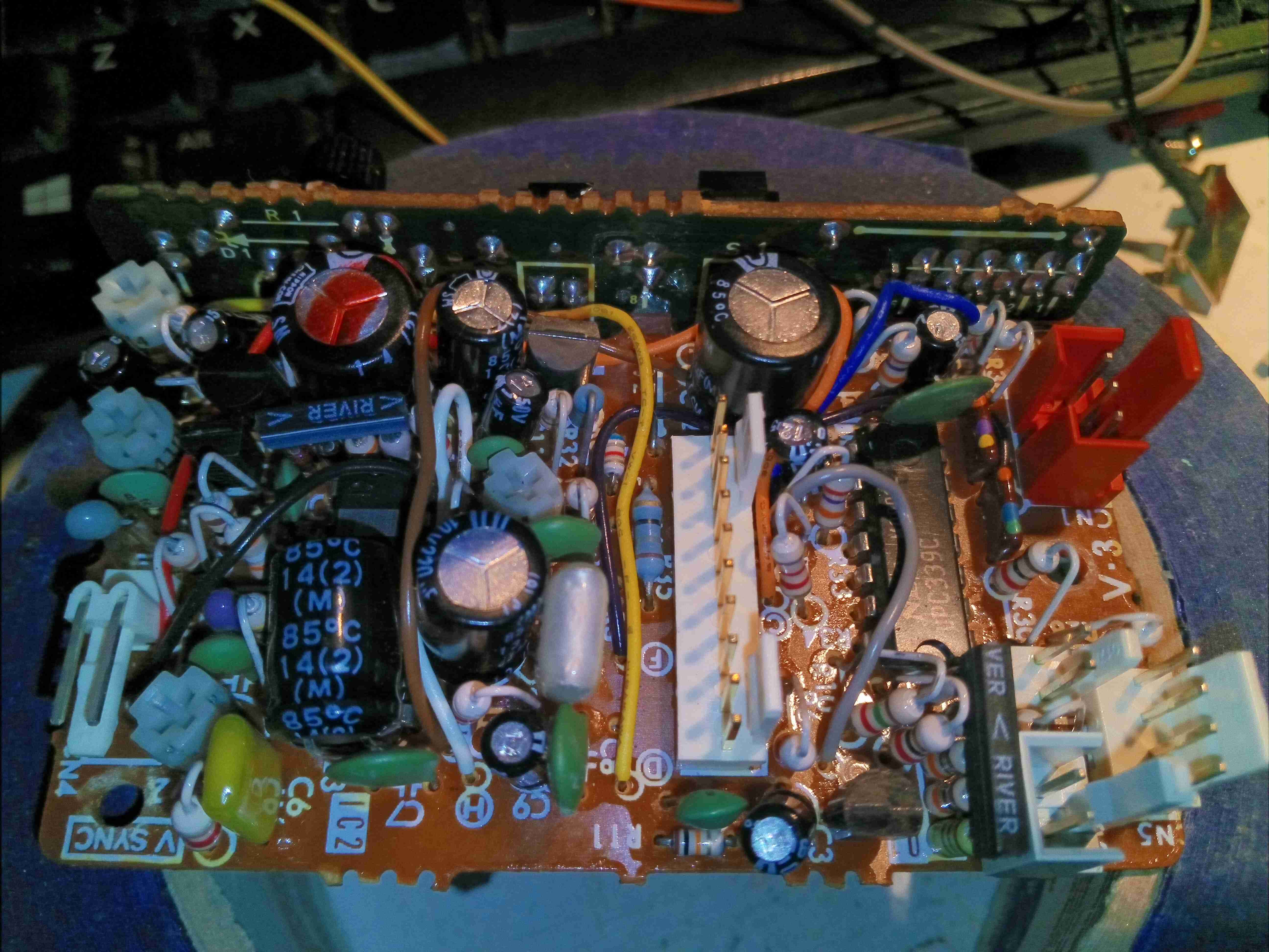
Deflection Board
The bottom board in the assembly has all the control circuitry for the CRT, including the HA11244 deflection IC, composite sync separator & vertical deflection drive circuit. There are also circuits here to display a video waveform on the CRT, along with iris & white balance markers.
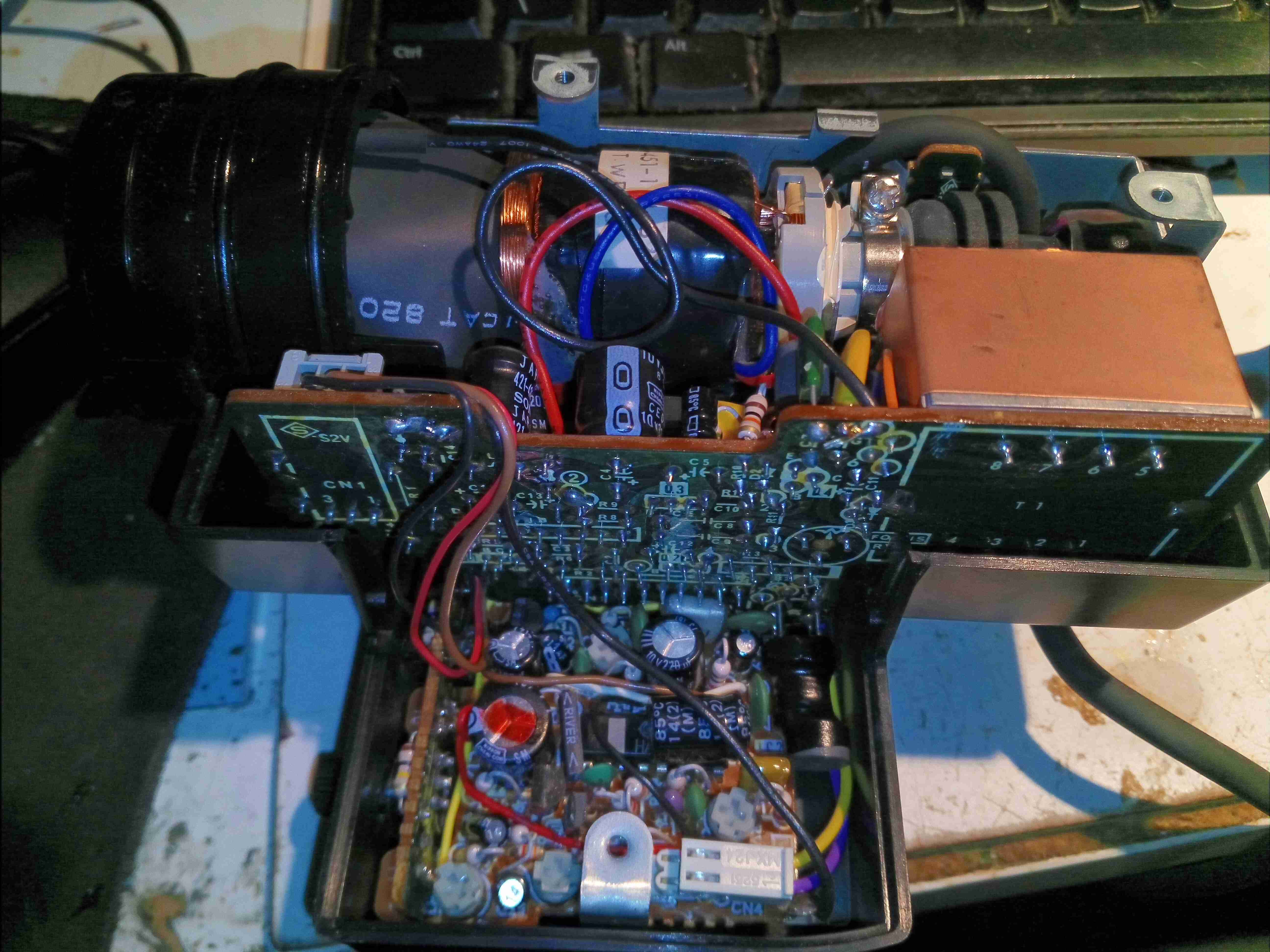
Horizontal Board
The other board has the horizontal drive circuitry, along with the video input amplifier. Despite the attempt to miniaturize the entire assembly, these are still well packed boards. Some of the resistors & diodes are bussed together in custom SIL hybrid modules to save PCB space. Like all the other CRT viewfinders, these units are meant for viewing via a mirror – the horizontal deflection coil connections need to be reversed to show a correct image without the mirror. The Red & Blue wires to the yoke need to be swapped here.
Flyback Transformer
The horizontal board on this unit also supports the flyback transformer, which is massive compared to the other viewfinder circuits. Biasing, focus & filament supplies for the CRT are also derived from this transformer, via auxiliary windings.
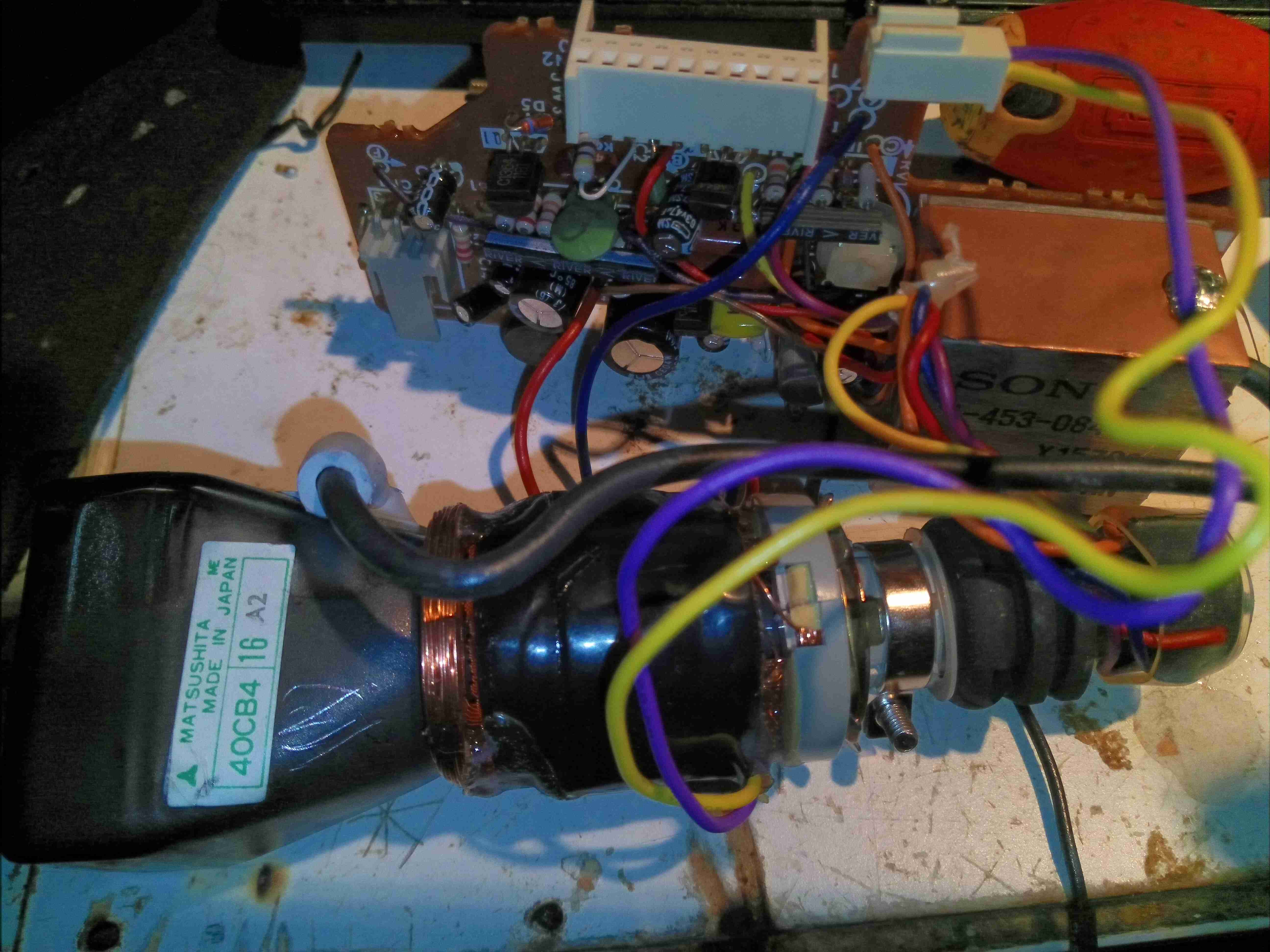
Boards Connected
The boards slot together in the centre to form the fully operational circuit.
Video Input
Out of the 3 plugs emerging from the cable feeding the viiewfinder, only this one is important, on the horizontal drive board. Black is ground, Brown +8.5v & red is composite video input. There’s also a resistor tied into the positive rail to the video input pin, which pulls it high to 8.5v – this is R1 right next to this connector. Desolder this 22K resistor to help protect anything feeding a signal into the unit, like a RPi, it’s not needed for normal operation.
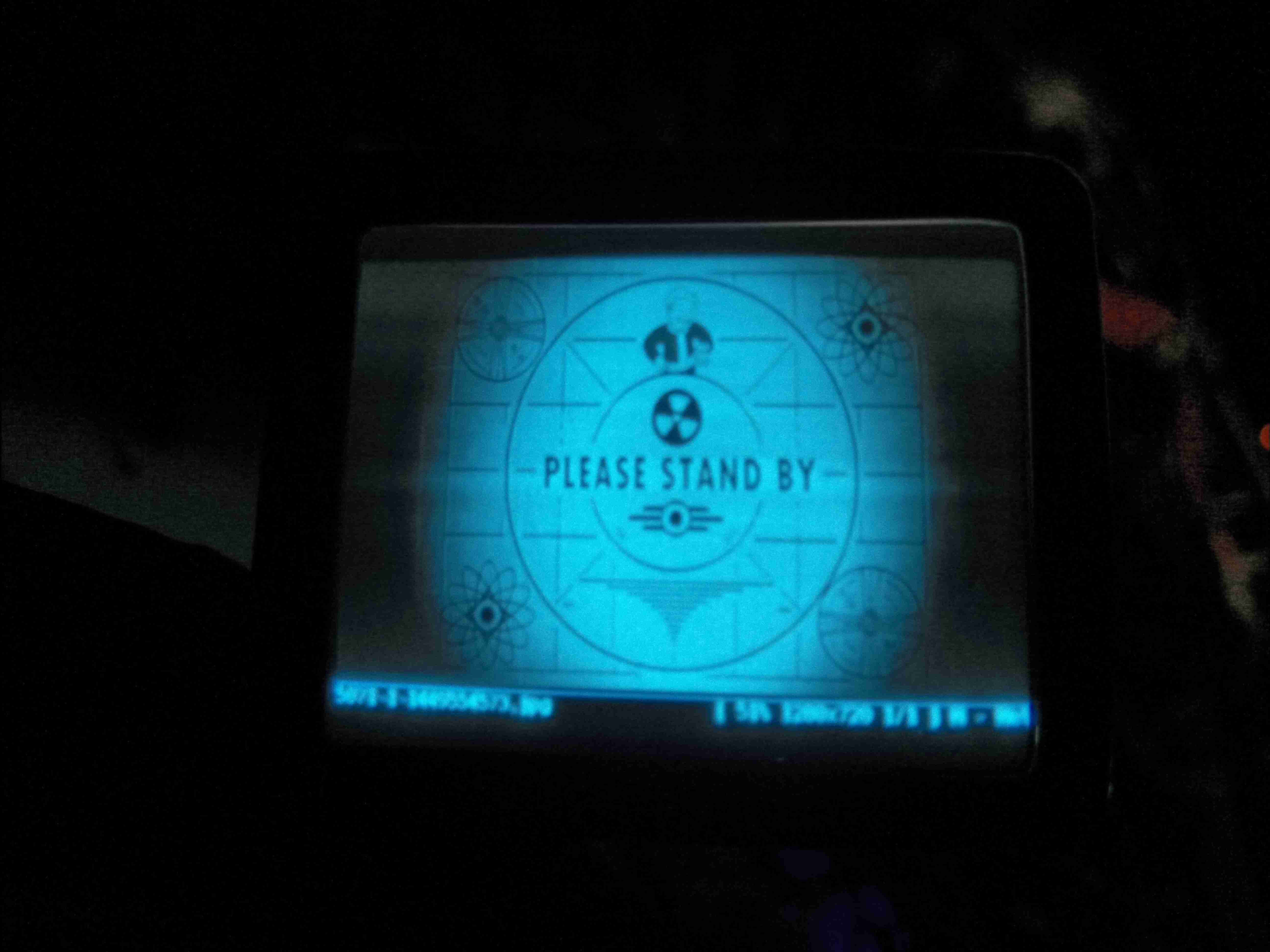
Fallout!
As usual for a CRT post, the Fallout loading screen on the display. The picture quality isn’t as good as it should be, probably due to the noisy buck-converter I have rigged up for testing. If it doesn’t get better with a linear regulator, I’ll start replacing the 39 year old electrolytic capacitors. Current draw is 130mA at 7.5v. Schematics for this unit & the CRT datasheet are available below:
Here’s the CRT & it’s drive board removed from the main chassis. Nicely modular this unit, all the individual modules (radio, tape, TV), are separate. This is effectively a TV itself, all the tuner & IF section are onboard, unlike in other vintage units I’ve modified, where the tuner & IF has been on a separate board. There’s a 3-pin header bottom centre for the tuning potentiometer, and external antenna input jack. The internal coax for the built in antenna has been desoldered from the board here. here a the usual controls on the back for adjusting brightness, contrast & V Hold, all the other adjustments are trimmers on the PCB.
Unfortunately after 30+ years of storage, this didn’t work on first power up, neither of the oscillators for vertical or horizontal deflection would lock onto the incoming signal, but a couple of hours running seemed to improve things greatly. The numerous electrolytic capacitors in this unit were probably in need of some reforming after all this time, although out of all of them, only 21 are anything to do with the CRT itself.
Anode Cap
Here’s the anode side of the unit, with the small flyback transformer. The rubber anode cap has become very hard with age, so I’ll replace this with a decent silicone one from another dead TV. The Horizontal Output Transistor (a 2SC2233 NPN type) & linearity coil are visible at the bottom right corner of the board. Unfortunately, the disgusting yellow glue has been used to secure some of the wiring & large electrolytics, this stuff tends to turn brown with age & become conductive, so it has to be removed. Doing this is a bit of a pain though. It’s still a little bit flexible in places, and rock hard in others. Soaking in acetone softens it up a little & makes it easier to detach from the components.
Neck PCB
There’s little on the neck board apart from a few resistors, forming the limiting components for the video signal, and the focus divider of 1MΩ & 470KΩ feeding G3. No adjustable focus on this unit. There’s also a spark gap between the cathode line & ground, to limit the filament to cathode voltage. The flyback transformer is nestled into the heatsink used by the horizontal output transistor & a voltage regulator transistor.
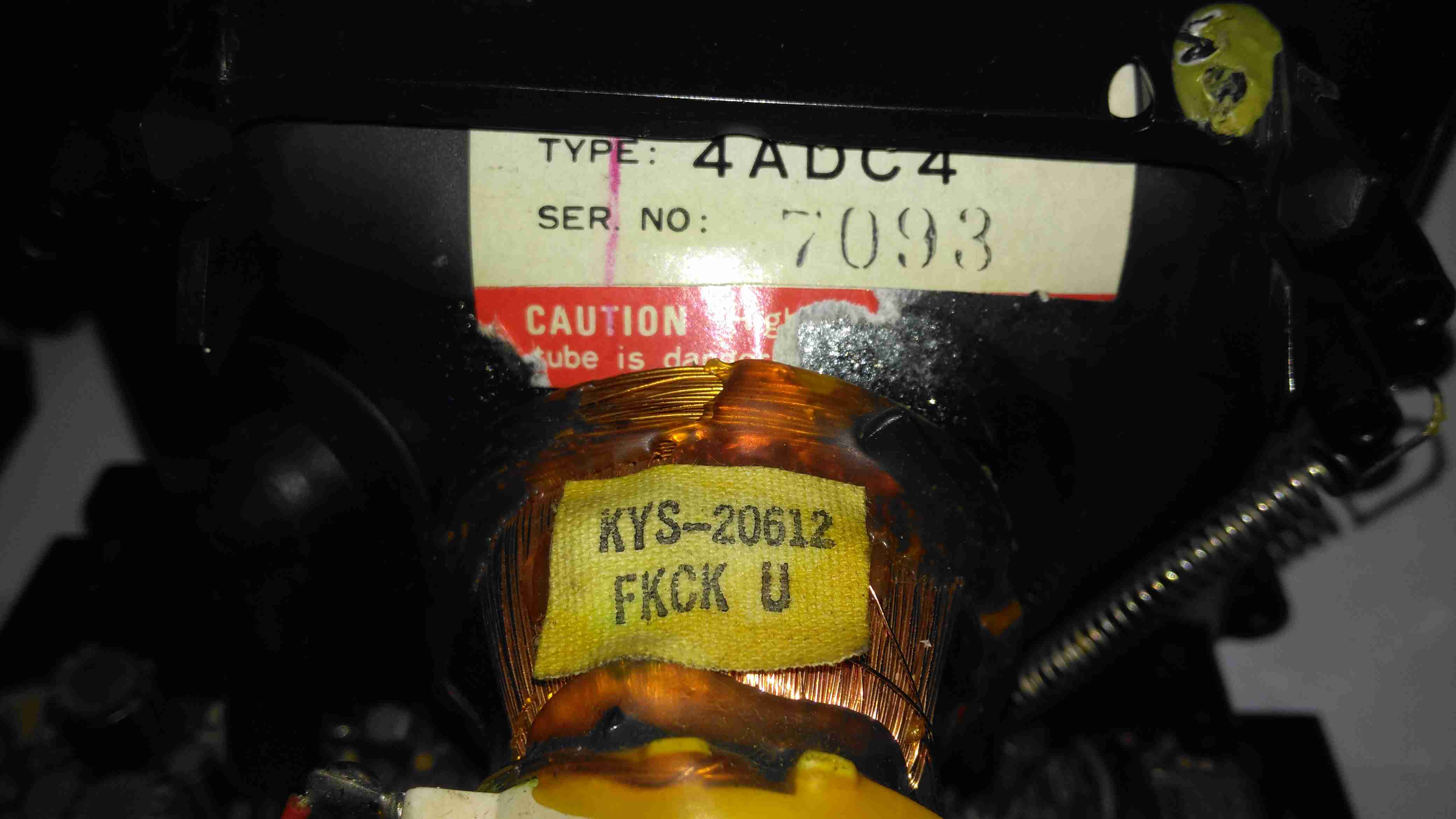
Tube Details
The CRT is a Samsung Electron Devices 4ADC4, with a really wide deflection angle. It’s a fair bit shorter than the Chinese CRT I have which is just a little larger, with a neck tube very thin indeed for the overall tube size.
Unusually, while the filament voltage is derived from the flyback transformer as usual, it’s rectified into DC in this unit, passing through a 1Ω resistor before the filament connection. I measured 5.3v here. The glow from the filament is barely visible even in the dark.
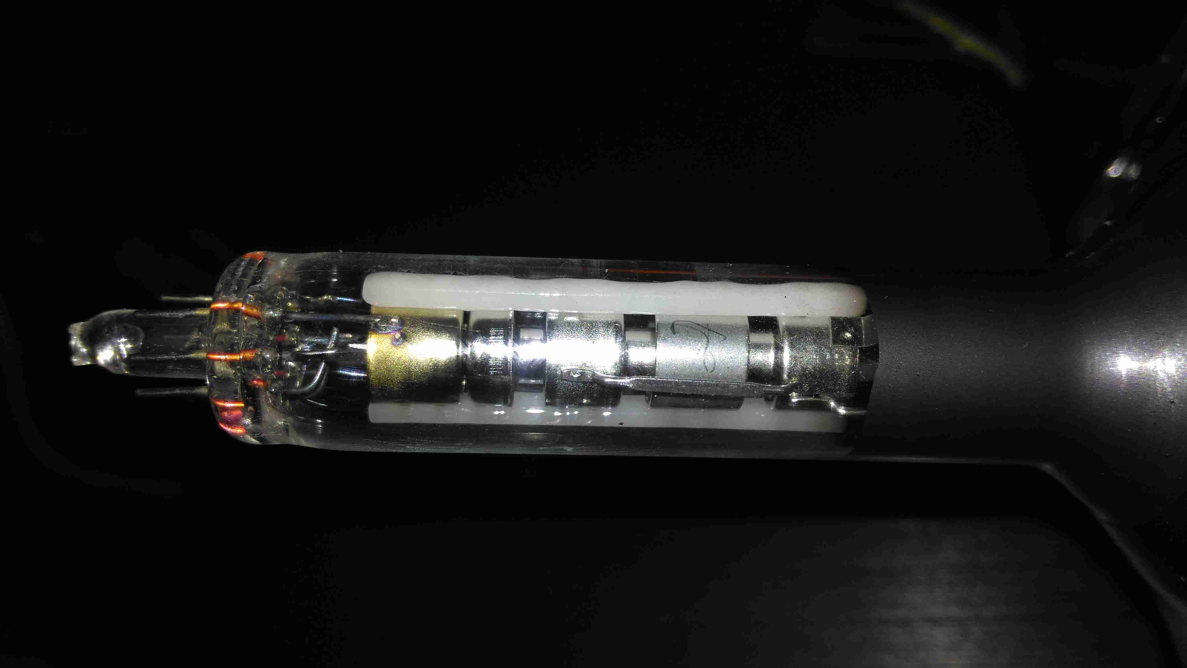
Electron Gun 1
The electron gun is the usual for a monochrome tube, with 7 pins on the seal end.
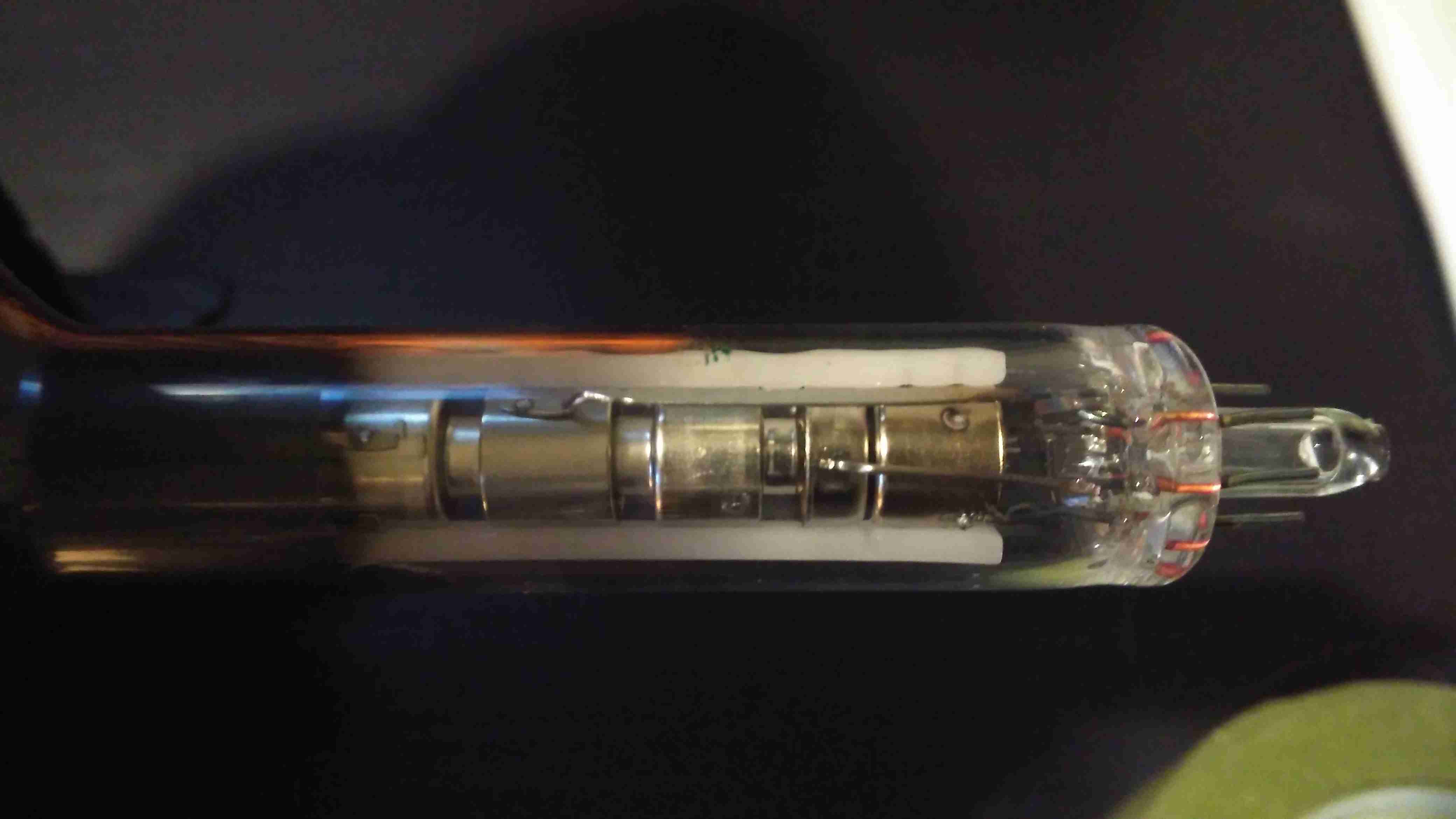
Electron Gun 2
The electrodes here from left are Final Anode, G3 (Focus Grid), Accelerating Anode, G2 (Screen Grid), G1 (Control Grid). The cathode & filament are hidden inside G1. In operation there’s about 250v on G2, and about 80v on G3.
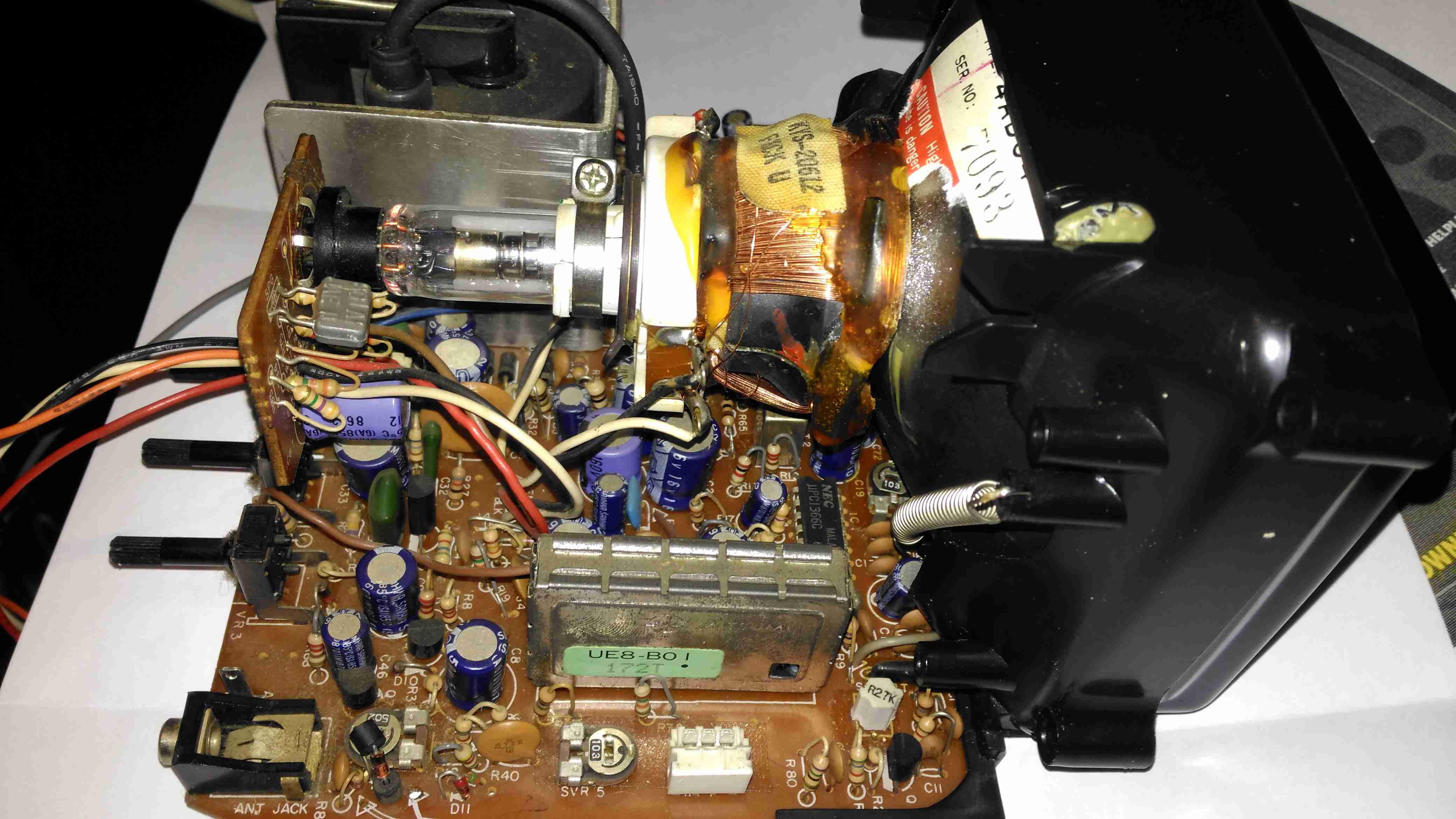
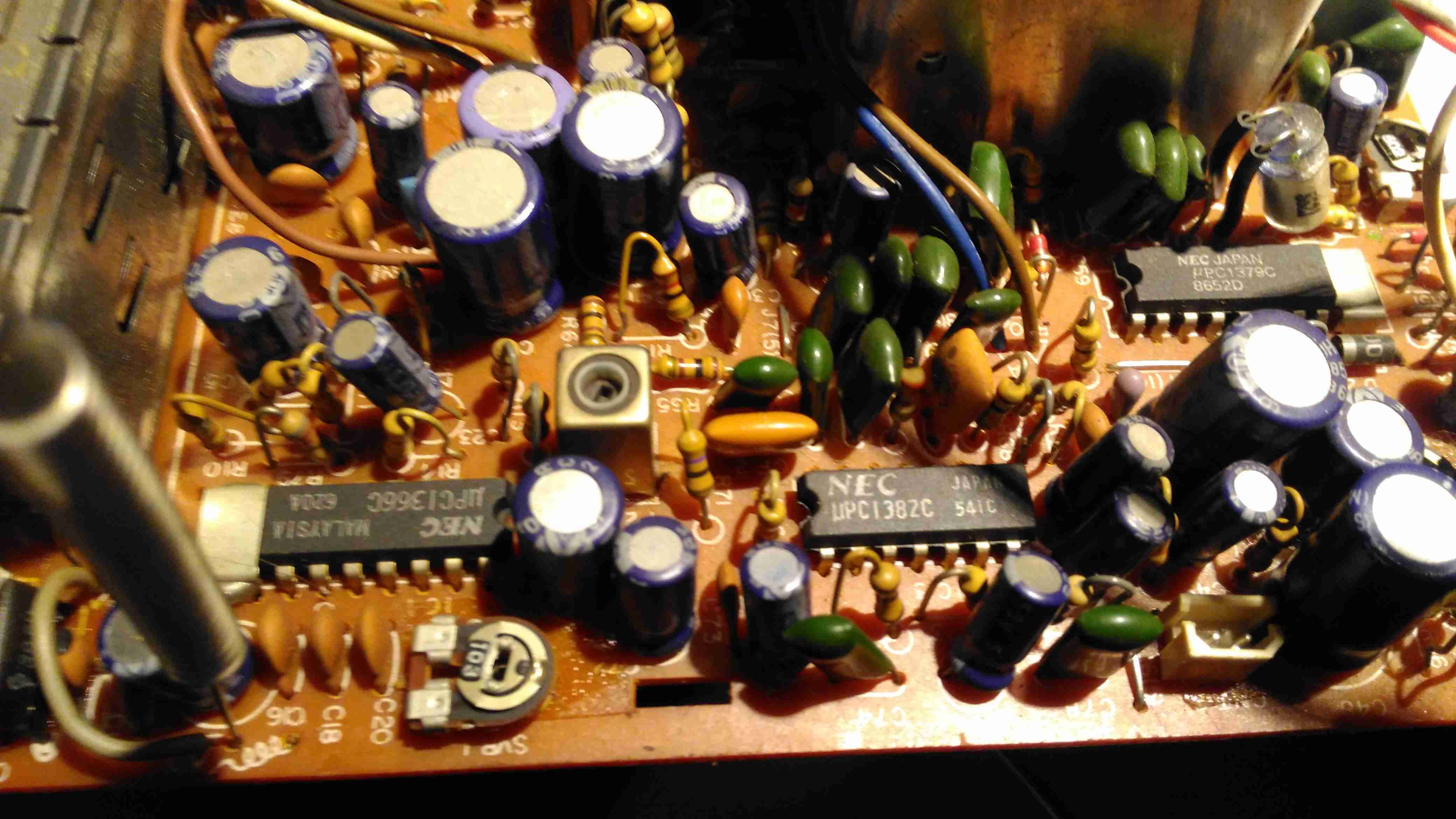
Chipset
The chipset used here is all NEC, starting with a µPC1366C Video IF Processor, which receives the IF signal from the tuner module to the left. This IC outputs the standard composite signal, and a modulated sound signal.
This then splits off to a µPC1382C Sound IF Processor & Attenuator IC, which feeds the resulting sound through the two pin header at the right bottom edge of the board to the audio amplifier in the chassis.
The composite video signal is fed through a discrete video amplifier with a single 2SC2229 transistor before going to the CRT cathode.
The remaining IC is a µPC1379C Sync Signal Processor, containing the sync separator, this is generating the required waveforms to drive the CRT deflection systems from another tap off the composite video line.
From this chip I can assume the unit was built around 1986, since this is the only date code on any of the semiconductors. Besides these 3 ICs, the rest of the circuit is all discrete components, which are well-crammed into the small board space.
There are 5 trimmer potentiometers on the board here, I’ve managed to work out the functions of nearly all of them:
SVR1: IF Gain Adjust
SVR2: H. Hold
SVR3: V. Size
SVR4: B+ Voltage Adjust
SVR5: Tuner Frequency Alignment? It’s in series with the tuning potentiometer in the chassis.
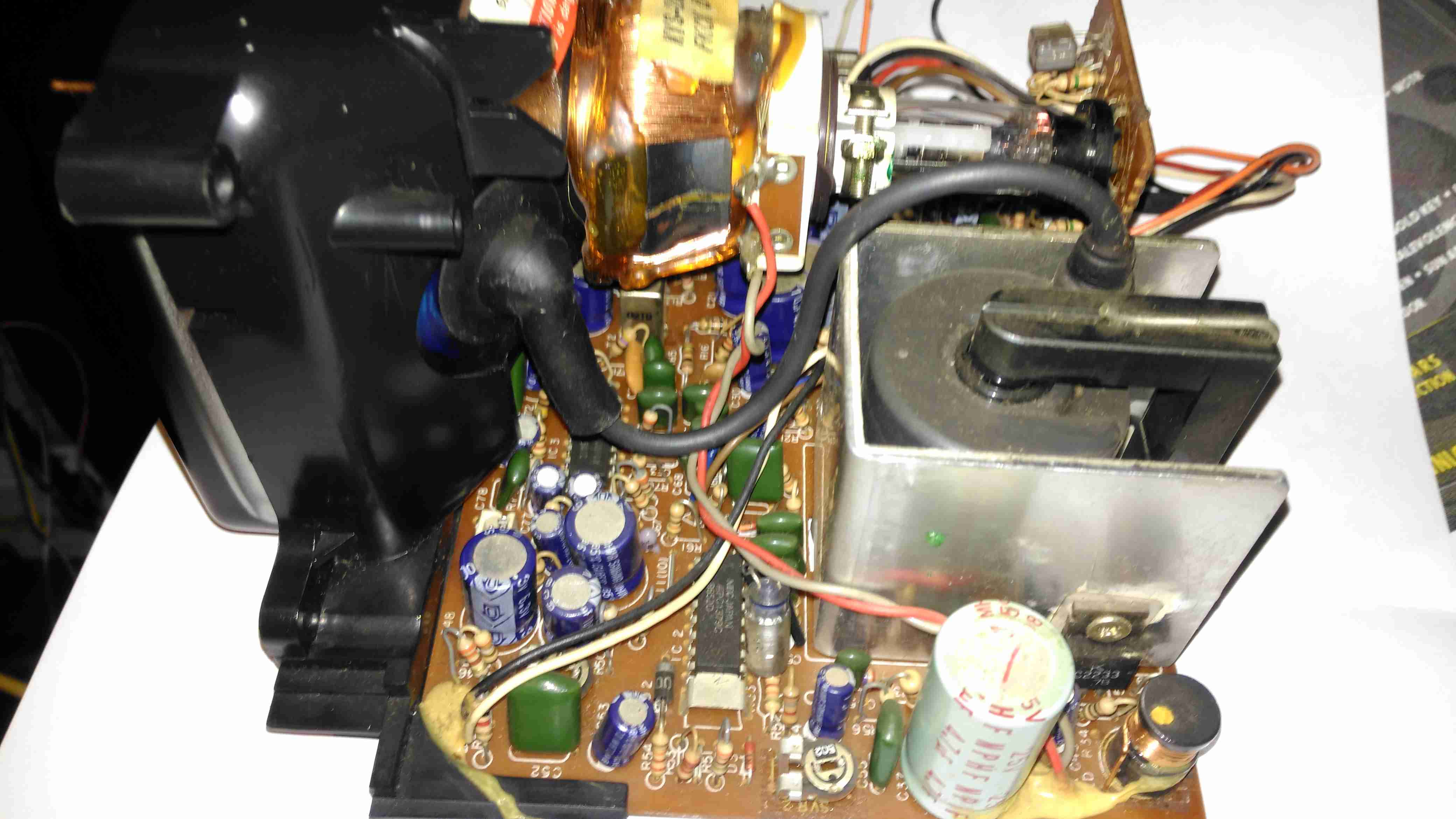
PCB Bottom
The PCB bottom shows the curved track layout typical of a hand taped out board. The soldermask is starting to flake off in places due to age, and there a couple of bodge wires completing a few ground traces. Respinning a board in those days was an expensive deal! Surprisingly, after all this time I’ve found no significant drift in the fixed resistors, but the carbon track potentiometers are drifiting significantly – 10KΩ pots are measuring as low as 8KΩ out of circuit. These will have to be replaced with modern versions, since there are a couple in timing-sensitive places, like the vertical & horizontal oscillator circuits.
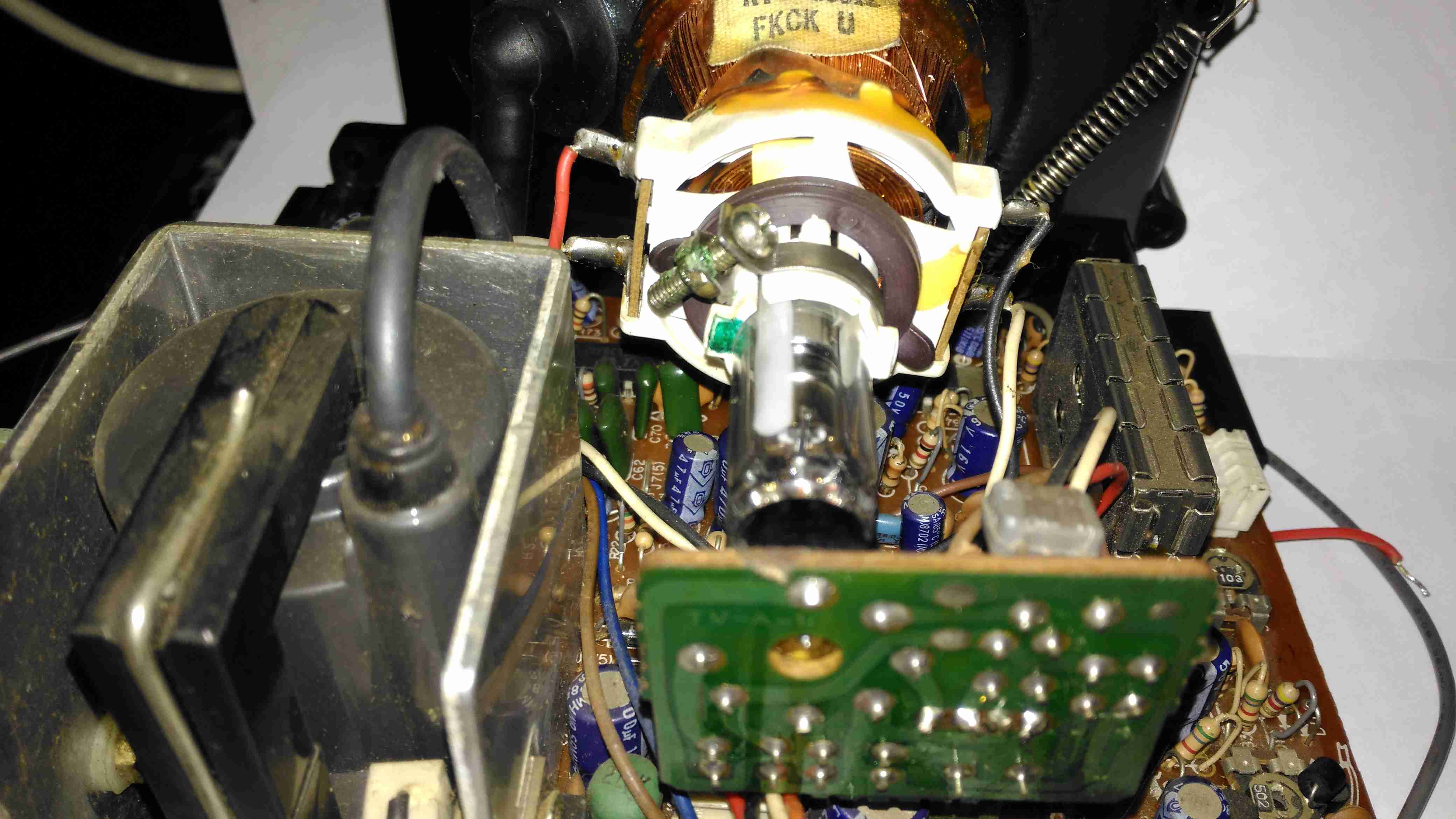
Anode Cap Replaced
Here the anode cap has been replaced with a better silicone one from another TV. This should help keep the 6kV on the CRT from making an escape. This was an easy fix – pulling the contact fork out of the cap with it’s HT lead, desoldering the fork & refitting with the new cap in place.
Here I’ve replaced the important trimmers with new ones. Should help stabilize things a little.
Composite Injection Mod
Injecting a video signal is as easy as the other units. Pin 3 of the µPC1366C Video IF Processor is it’s output, so the track to Pin 3 is cut and a coax is soldered into place to feed in an external signal.
CRT In Operation
After hooking up a Raspberry Pi, we have display! Not bad after having stood idle for 30+ years.
Datasheets for the important ICs are available below:
[download id=”5690″]
[download id=”5693″]
[download id=”5696″]
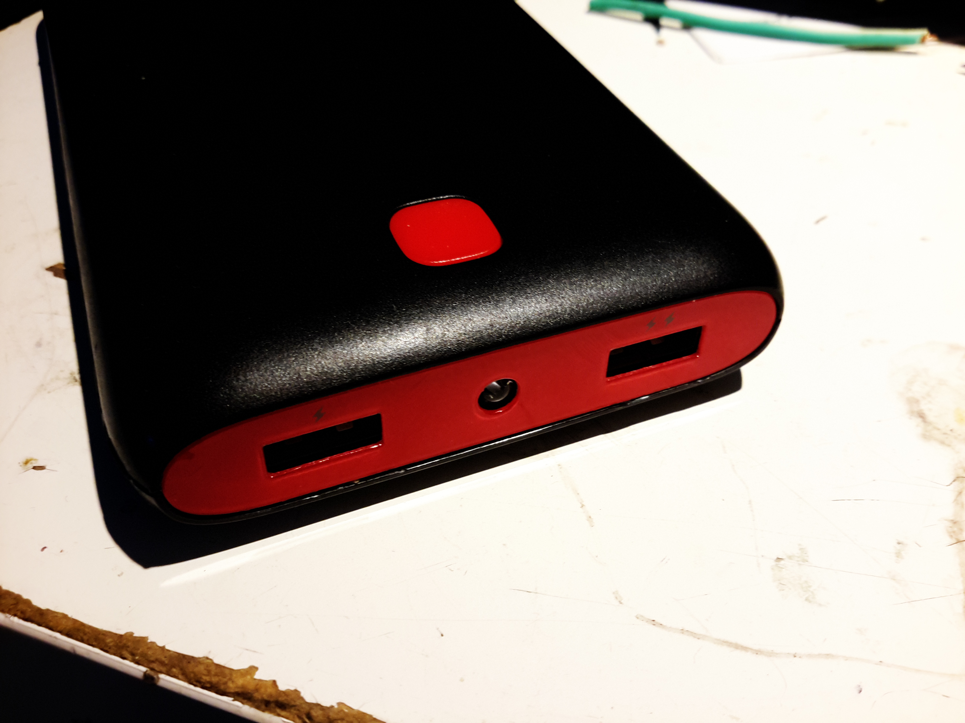
Here’s the biggest portable USB powerbank I’ve seen yet – the PowerAdd Pilot X7, this comes with a 20Ah (20,000mAh) capacity. This pack is pretty heavy, but this isn’t surprising considering the capacity.
USB Ports & LED
The front of the pack houses the usual USB ports, in this case rated at 3.4A total between the ports. There’s a white LED in the centre as a small torch, activated by double-clicking the button. A single click of the button lights up the 4 blue LEDs under the housing that indicate remaining battery capacity. Factory charging is via a standard µUSB connector in the side, at a maximum of 2A.
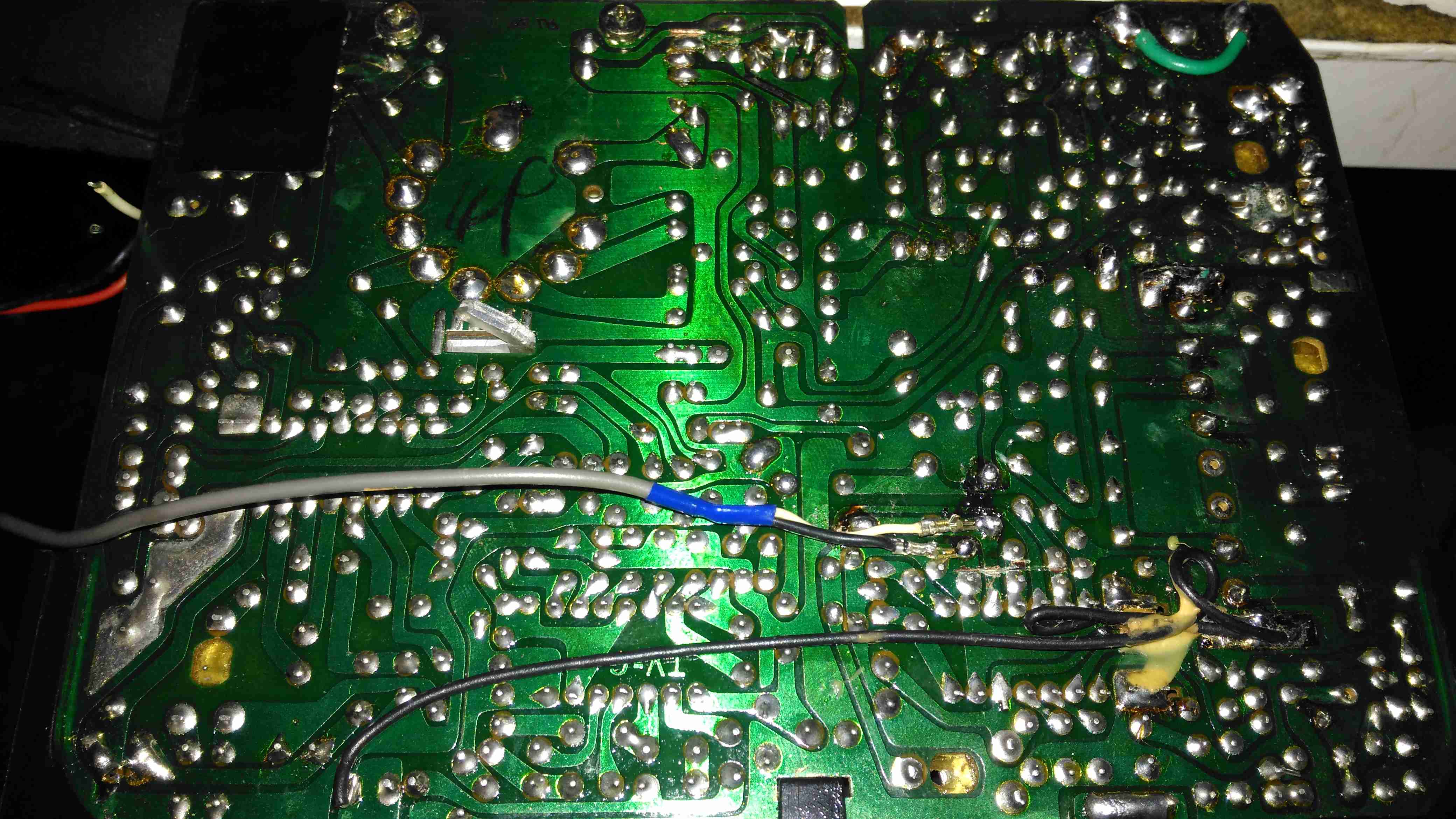
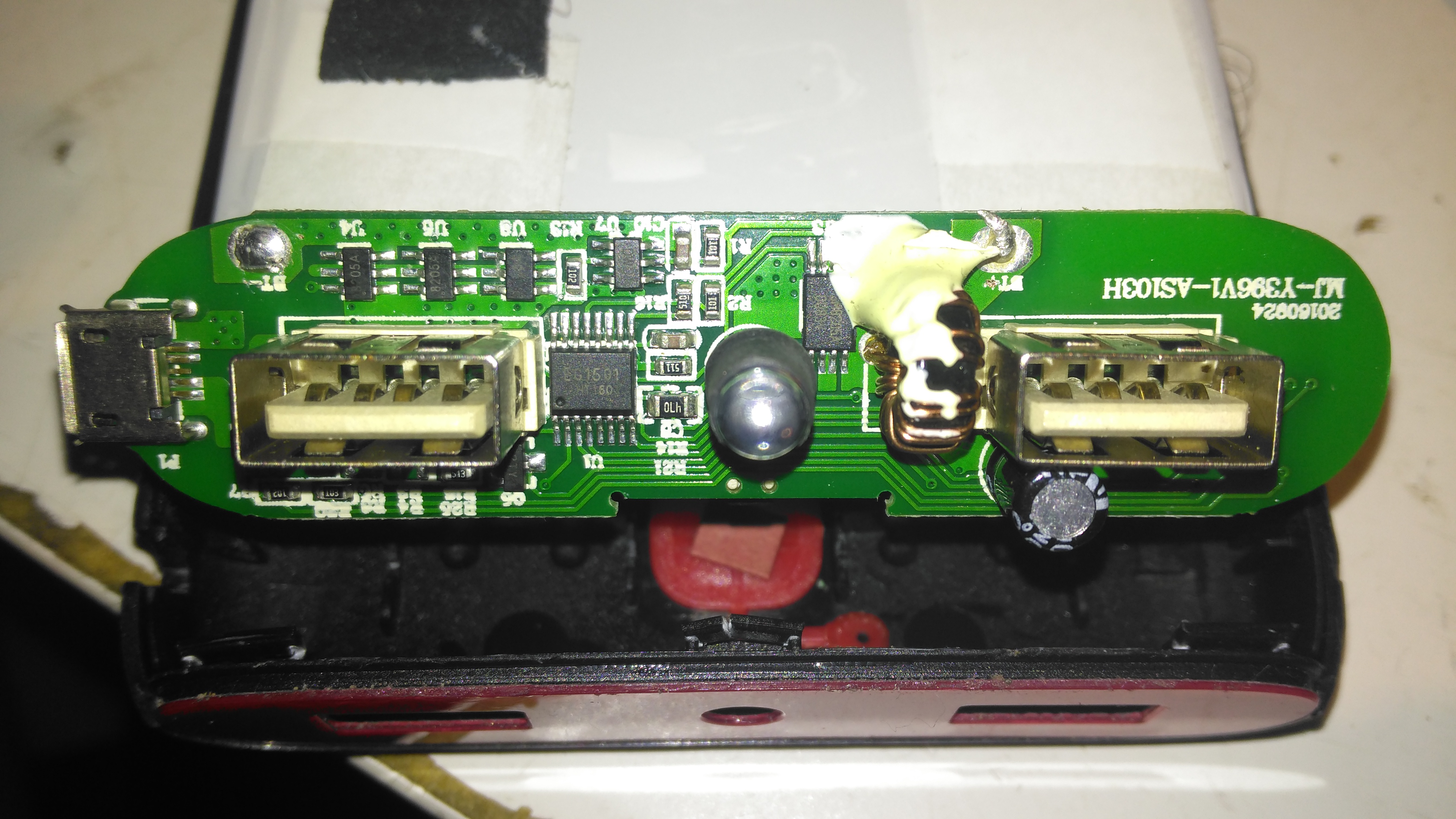
PCB Front
The front of the PCB holds the USB ports, along with most of the main control circuitry. At top left is a string of FS8025A dual-MOSFETs all in parallel for a current carrying capacity of 15A total, to the right of these is the ubiquitous DW01 Lithium-Ion protection IC. These 4 components make up the battery protection – stopping both an overcharge & overdischarge. The larger IC below is an EG1501 multi-purpose power controller.
This chip is doing all of the heavy lifting in this power pack, dealing with all the DC-DC conversion for the USB ports, charge control of the battery pack, controlling the battery level indicator LEDs & controlling the torch LED in the centre.
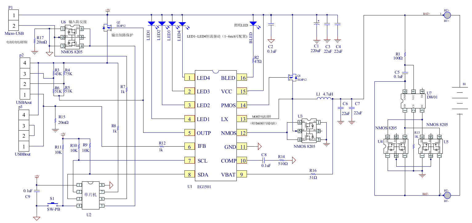
EG1501 Example
The datasheet is in Chinese, but it does have an example application circuit, which is very similar to the circuitry used in this powerbank. A toroidal inductor is nestled next to the right-hand USB port for the DC-DC converter, and the remaining IC next to it is a CW3004 Dual-Channel USB Charging Controller, which automatically sets the data pins on the USB ports to the correct levels to ensure high-current charging of the devices plugged in. This IC replaces the resistors R3-R6 in the schematic above.
The DC-DC converter section of the power chain is designed with high efficiency in mind, not using any diodes, but synchronous rectification instead.
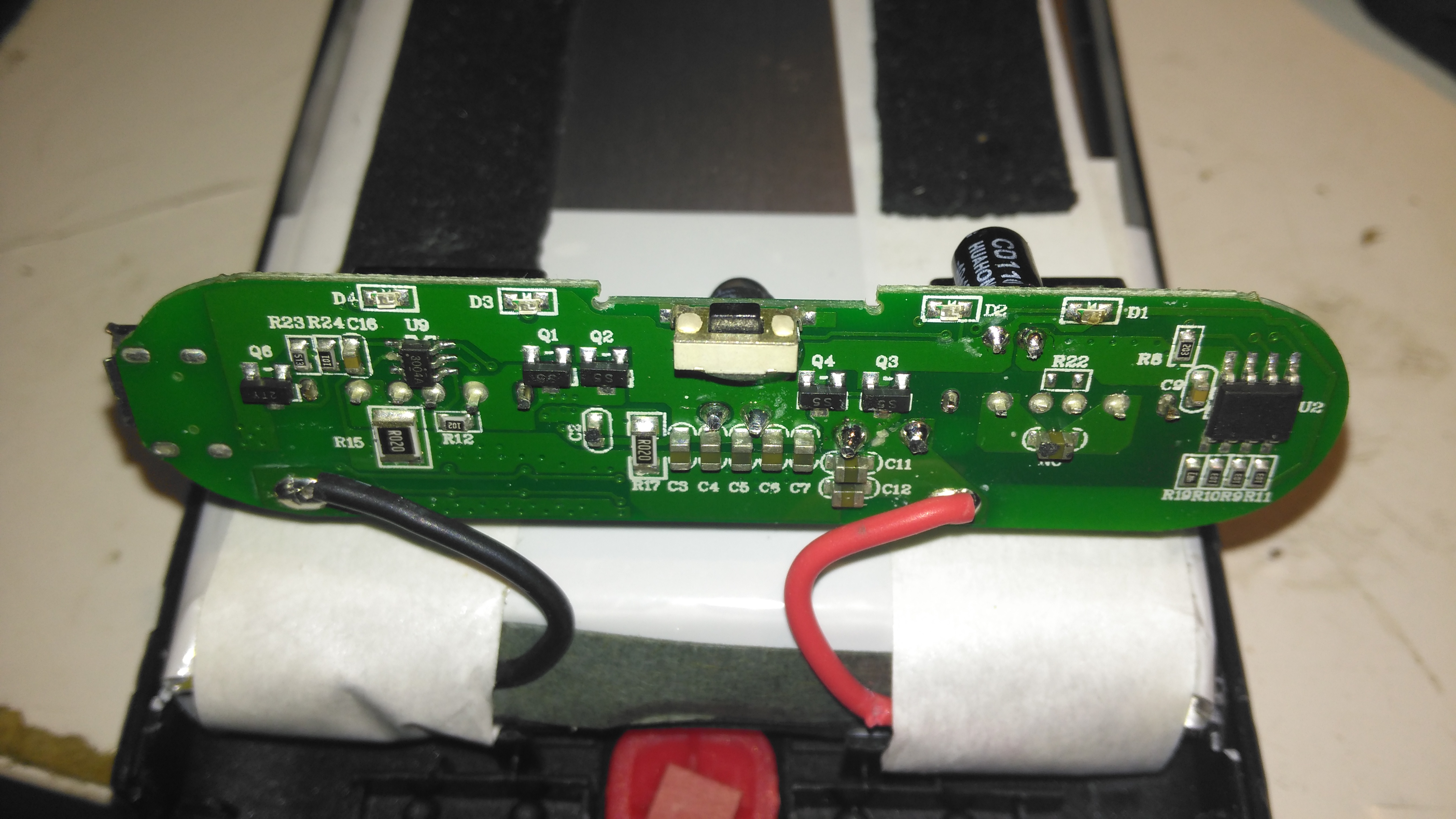
PCB Back
The back of the PCB just has a few discrete transistors, the user interface button, and a small SO8 IC with no markings at all. I’m going to assume this is a generic microcontroller, (U2 in the schematic) & is just there to interface the user button to the power controller via I²C.
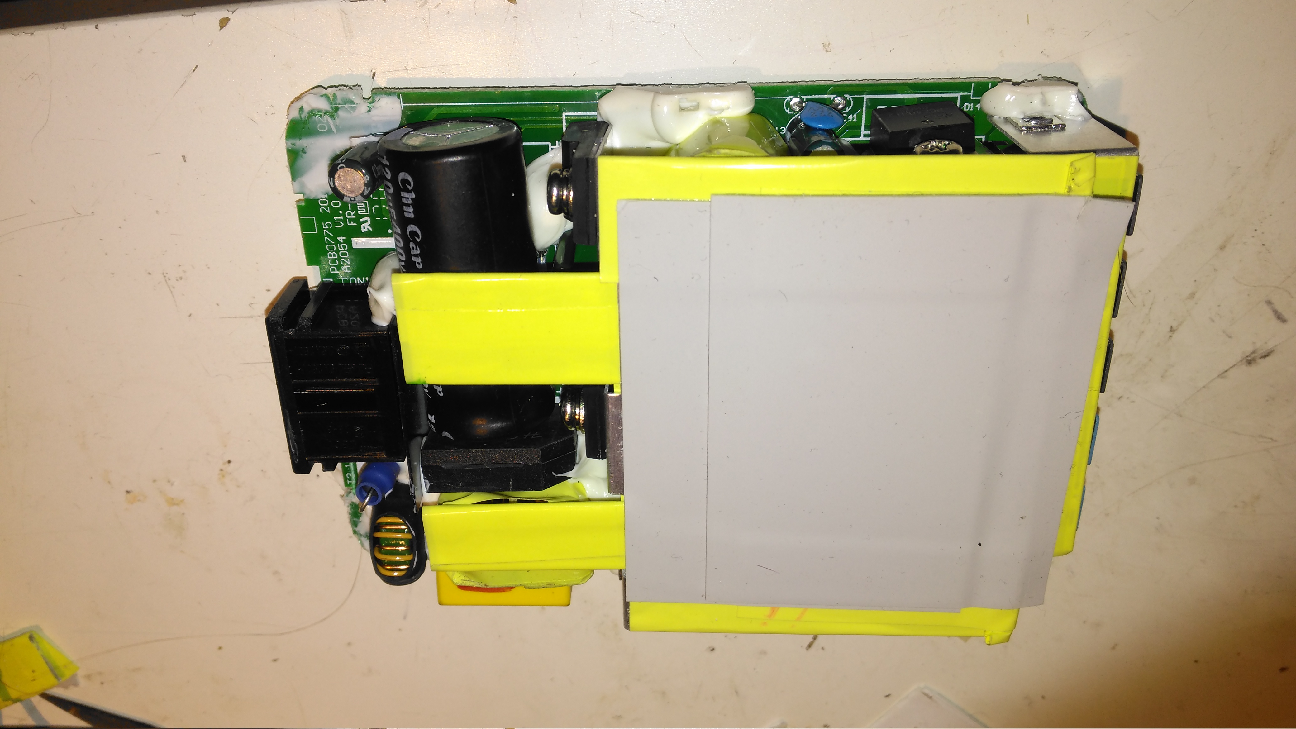
Cells
Not many markings on the cells indicating their capacity, but a full discharge test at 4A gave me a resulting capacity of 21Ah – slightly above the nameplate rating. There are two cells in here in parallel, ~10Ah capacity each.
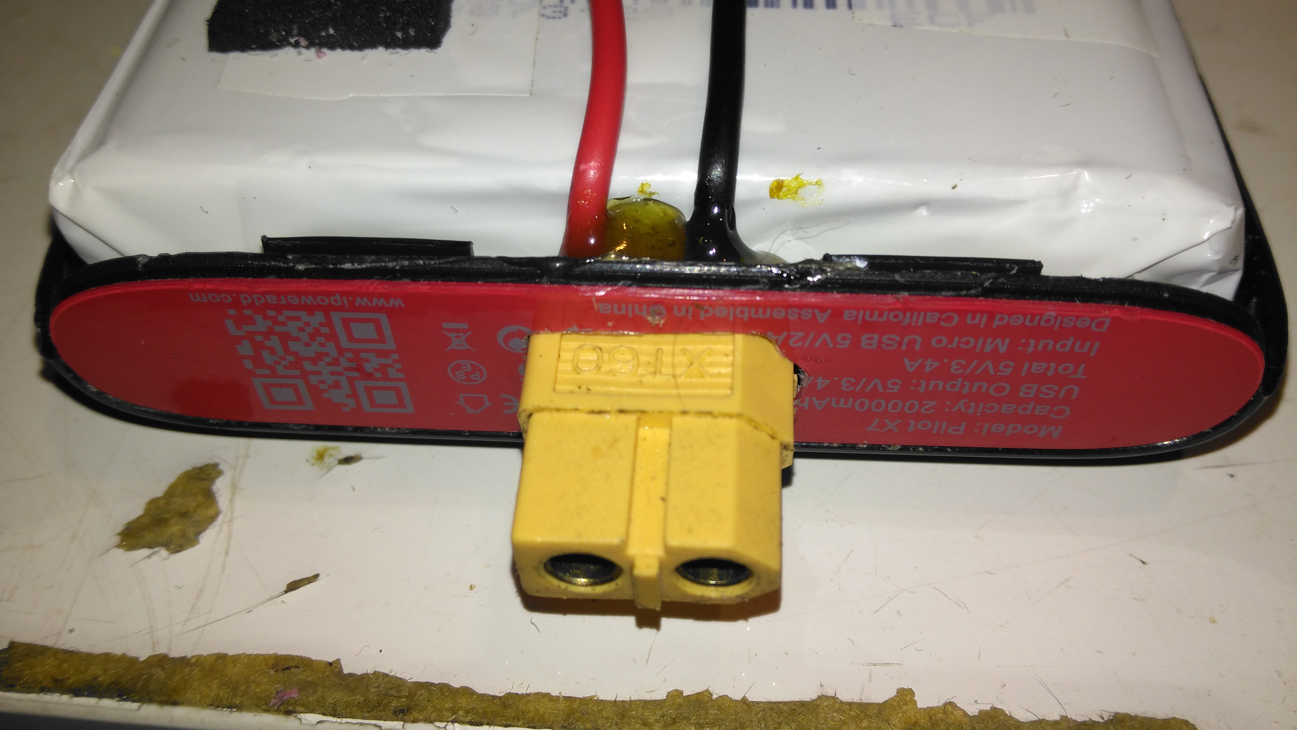
XT60 Battery Connector
The only issue with powerbanks this large is the amount of time they require to recharge themselves – at this unit’s maximum of 2A through the µUSB port, it’s about 22 hours! Here I’ve fitted an XT60 connector, to interface to my Turnigy Accucell 6 charger, increasing the charging current capacity to 6A, and reducing the full-charge time to 7 hours. This splits to 3A charge per cell, and after some testing the cells don’t seem to mind this higher charging current.
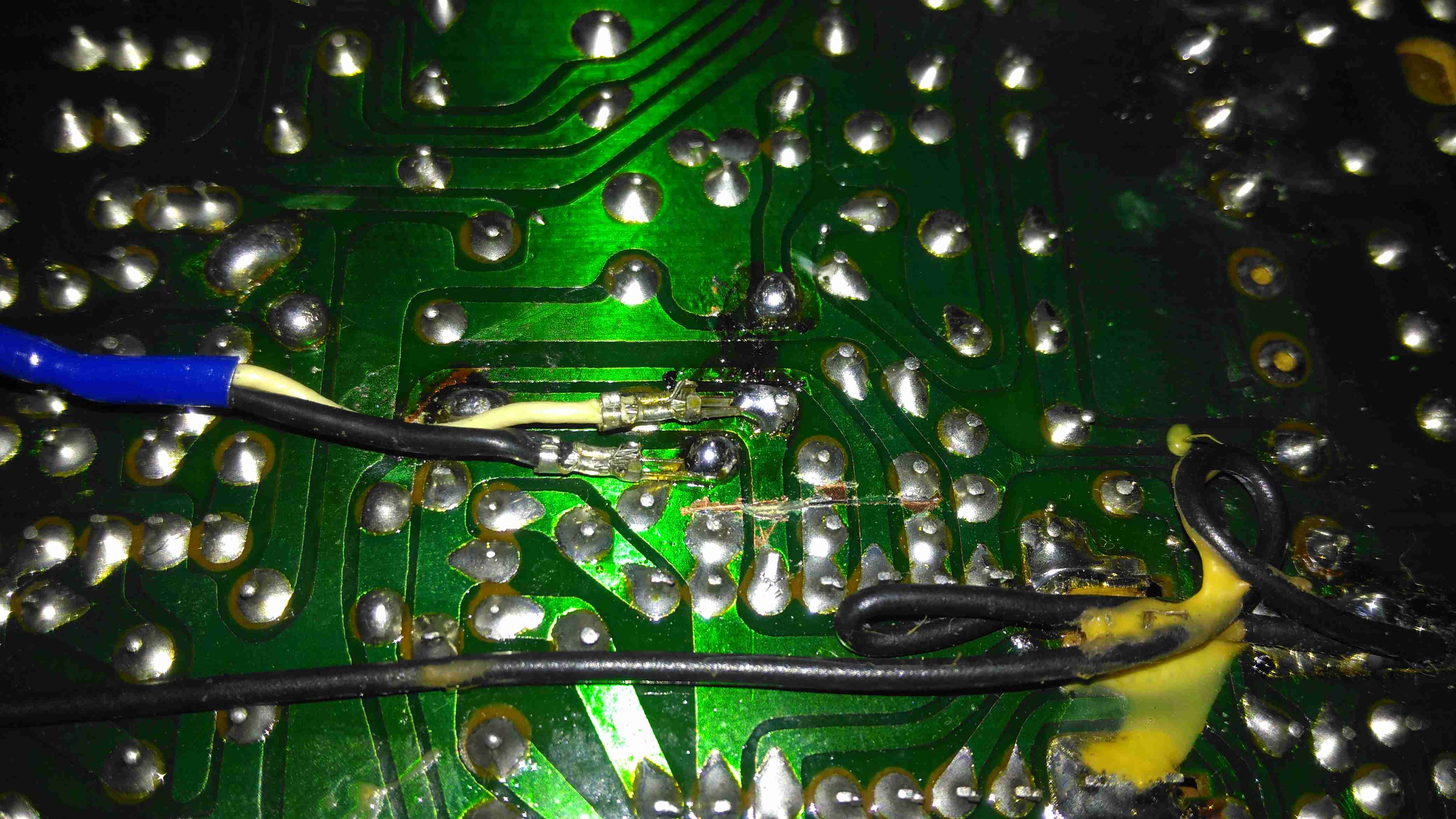
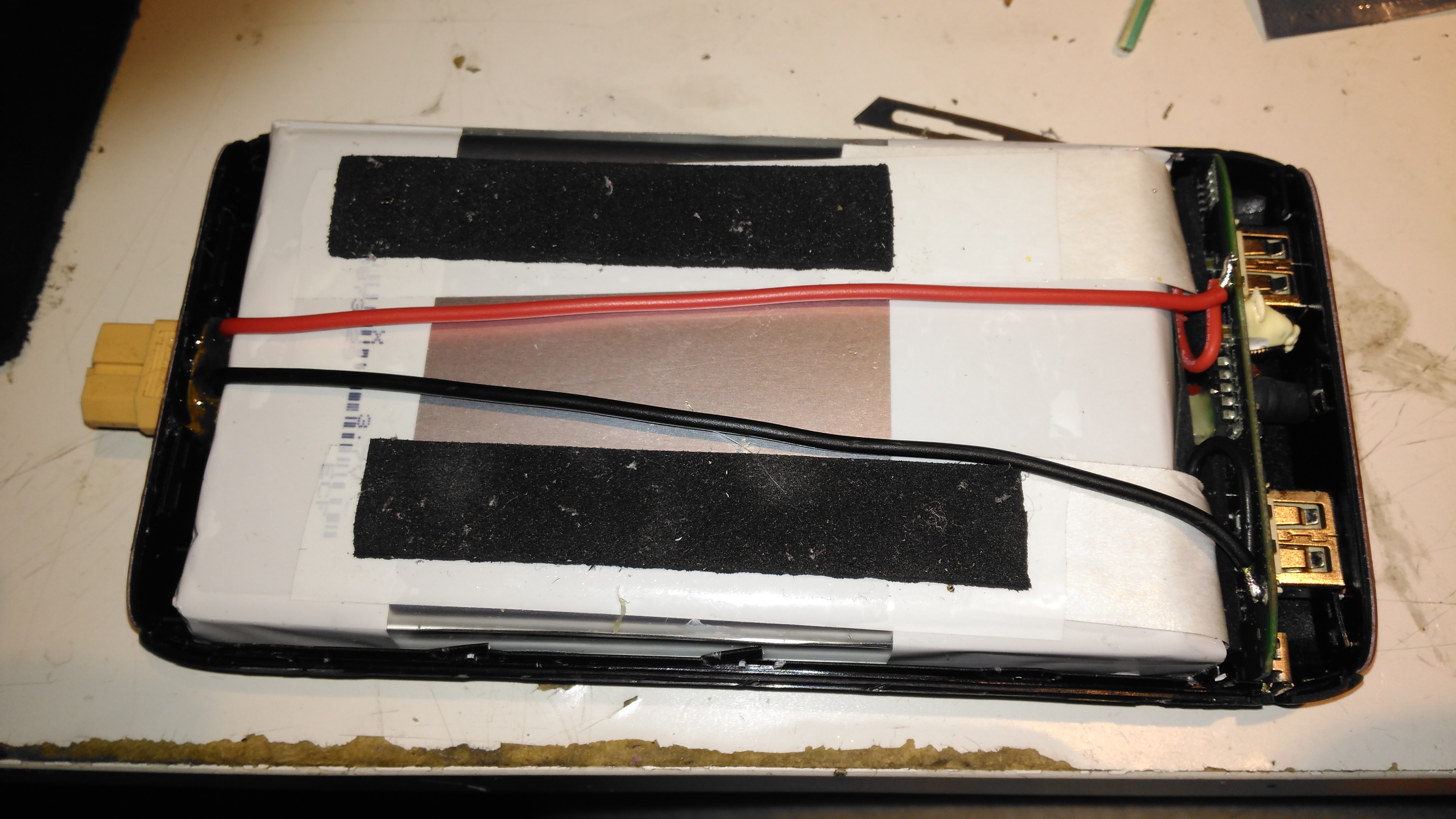
Battery Connector Wiring
The new charging connector is directly connected to the battery at the control PCB, there’s just enough room to get a pair of wires down the casing over the cells.
A few months ago I did a teardown on this Anker PowerPort Speed 5 USB charger, but I didn’t get round to detailing the conversion to 12v I had to do, so I’ll get to that now I’ve got a couple more to convert over.
Power Module
Here’s the internals of the Anker charger once I’ve removed the casing – which like many things these days, is glued together. (Joints can be cracked with a screwdriver handle without damaging the case). There’s lots of heatsinking in here to cool the primary side switching devices & the pot core transformers, so this is the first thing to get removed.
Heatsink Removed
Once the heatsink has been removed, the pot core transformers are visible, wrapped in yellow tape. There’s some more heatsink pads & thermal grease here, to conduct heat better. The transformers, primary side switching components & input filter capacitor have to go.
Primary Side Components Removed
Here’s the PCB once all the now redundant mains conversion components have been deleted. I’ve left the input filtering & bridge rectifier in place, as this solves the issue of the figure-8 cable on the input being reversible, polarity of the input doesn’t matter with the bridge. I’ve removed the main filter capacitor to make enough room for the DC-DC converters to be fitted.
Tails Installed
Installing the tails to connect everything together is the next step, this charger requires two power supplies – the QC3 circuits need 14.4v to supply the multi-voltage modules, the remaining 3 standard ports require 5v. The DC input tails are soldered into place where the main filter capacitor was, while the outputs are fitted to the spot the transformer secondary windings ended up. I’ve left the factory Schottky rectifiers in place on the secondary side to make things a little more simple, the output voltages of both the DC-DC converters does need to be increased slightly to compensate for the diode drops though. I’ve also bypassed the mains input fuse, as at 12v the input current is going to be substantially higher than when used on mains voltage.
DC-DC Converters Installed
With a squeeze both the boost converter & the buck converter fit into place on the PCB.
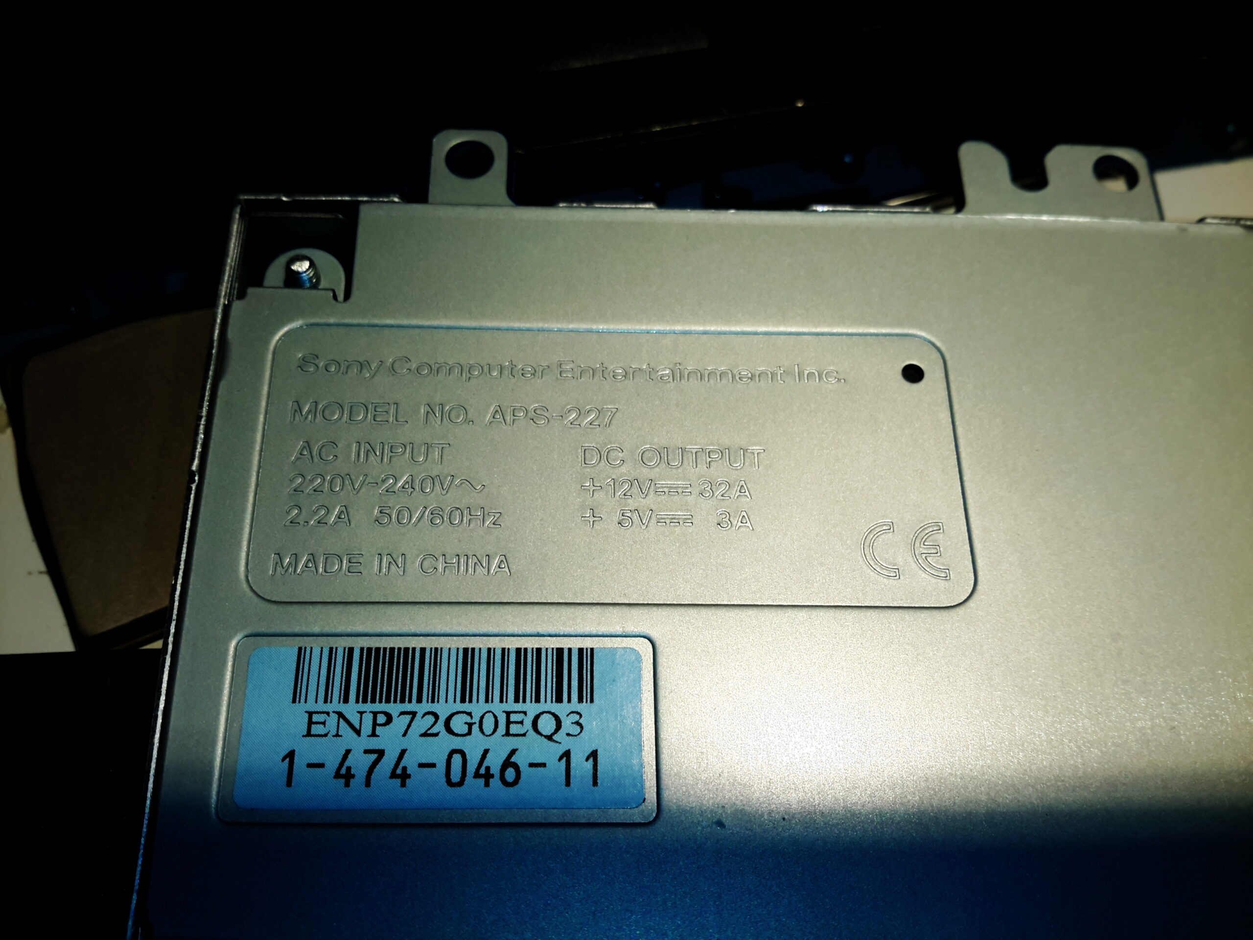
After I did the voltage mod on the APS-231 PSU power supply, I did some reading online & discovered there’s a more powerful PS3 supply – the APS-227. This beast has a 32A +12v rail, with a 3A +5v standby rail.
Specifications
As far as I can tell, these are used in another version of the PS3, obviously with a chunkier requirement for 12v DC.
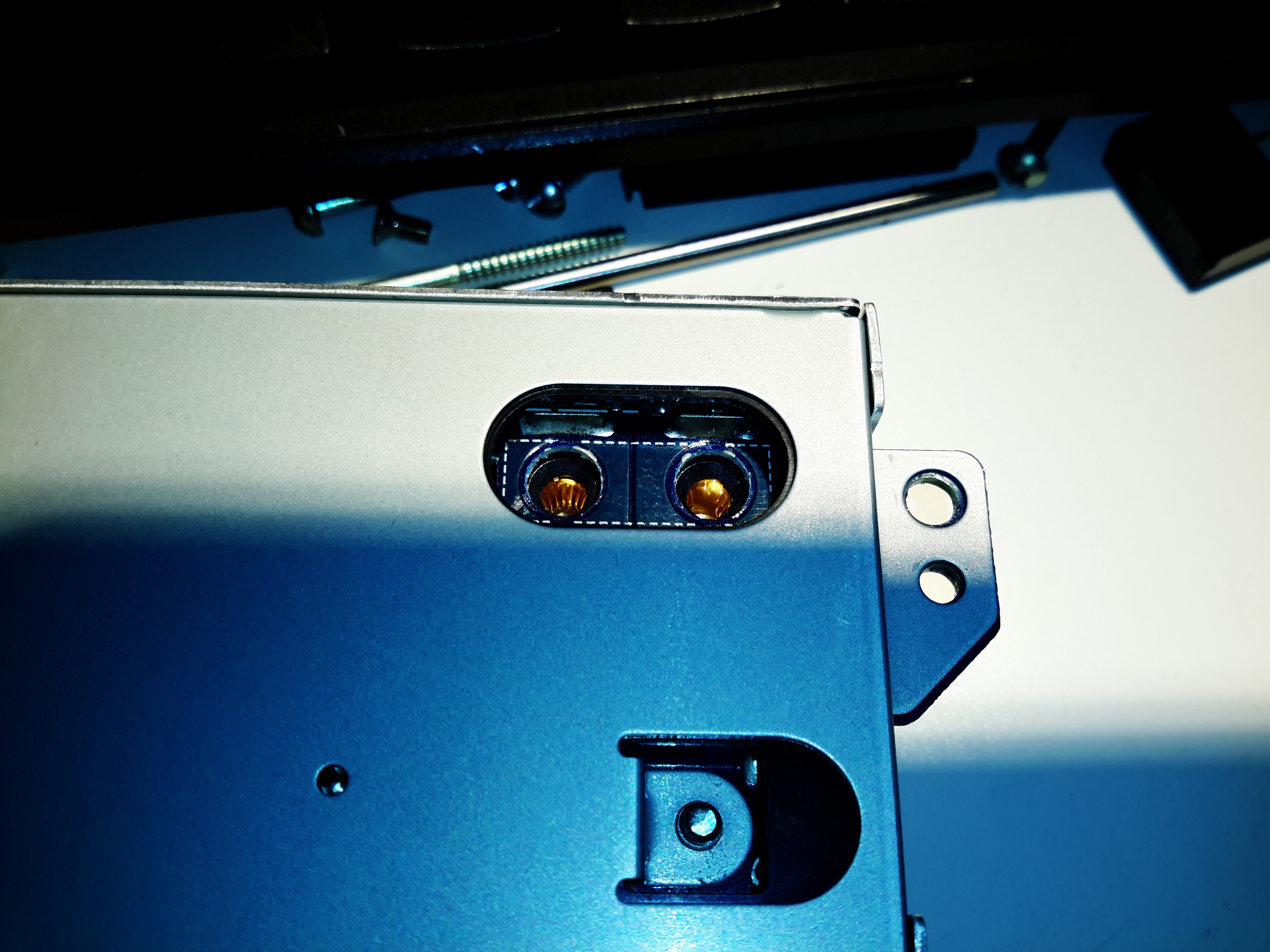
DC Output
The main DC rail appears through the same type of connector as the smaller supply, which is compatible with standard banana plugs.
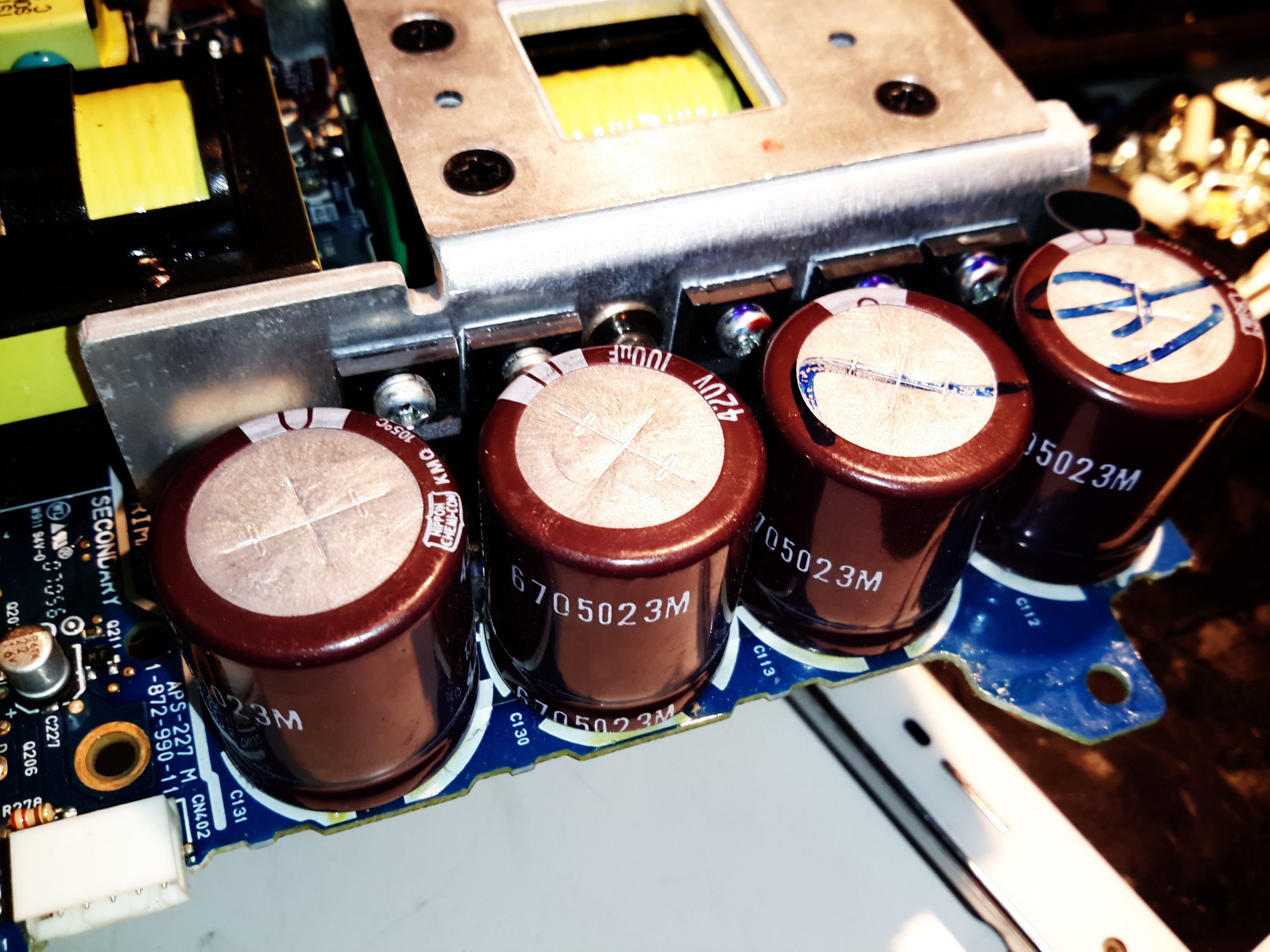
HV DC Bus Capacitors
These PSUs are very high build quality, Nichcon electrolytics are used all over the place. These are the HV DC rail filter caps, rated at 100µF 420v.
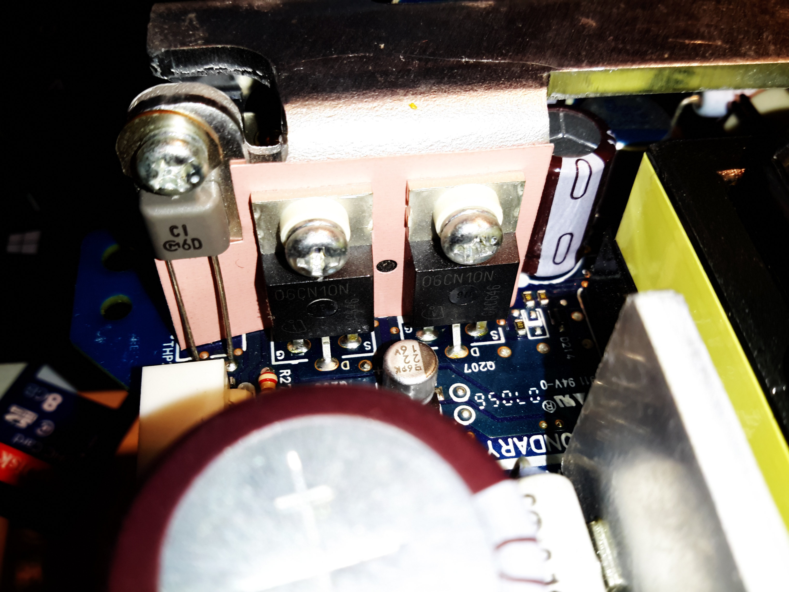
Output Synchronous FETs
Synchronous rectification is also used in these supplies, keeping the waste heat down to a minimum on the output rectification. There’s a thermistor on the heatsink to the left for the thermal protection.
+12v Rail Load Resistors
A couple of 2.2Ω resistors in series provide a minimum load to the PSU to keep things stable at low power. Adjusting the output too high will likely cause these resistors to overheat.
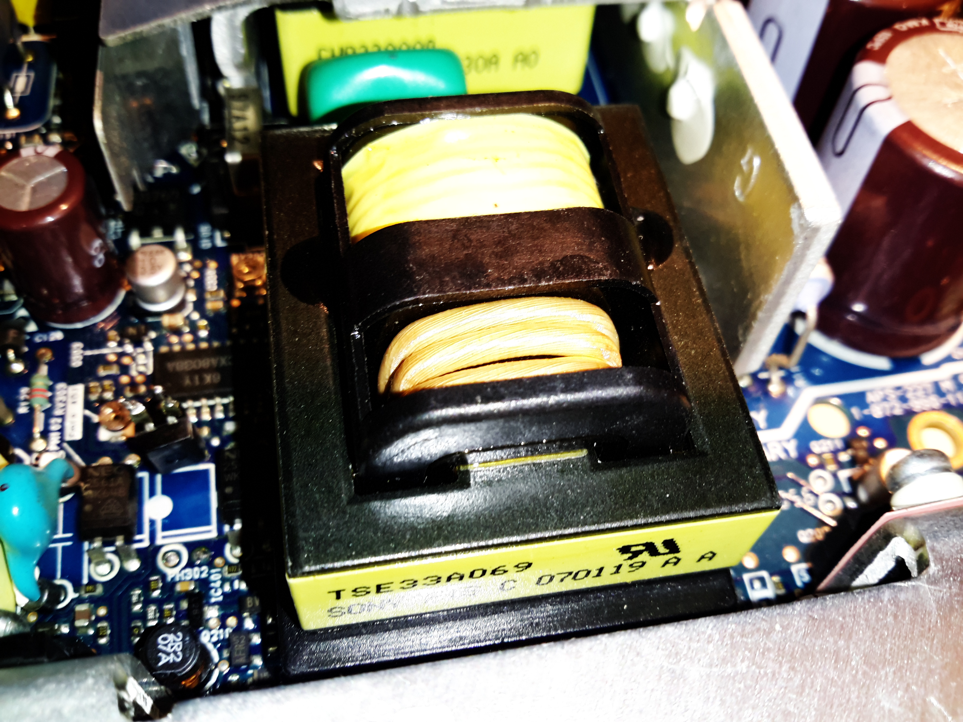
Transformer
The main transformer has a huge secondary winding, only 4 turns of Litz type wire, about 5mm².
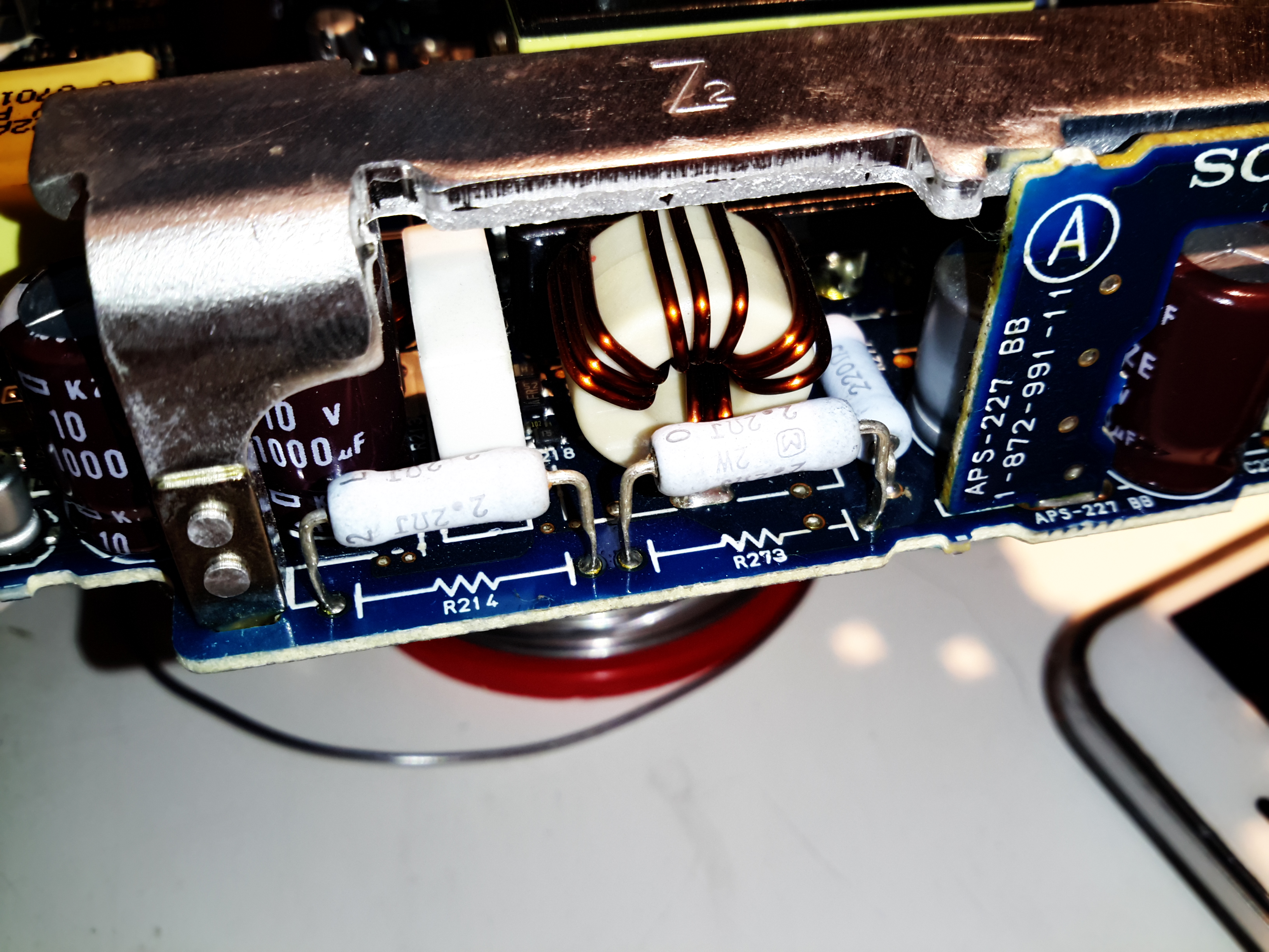
Regulator Section
Here’s the point where the mod needs to be done – the same as the other PS3 supply, a single resistor needs changing for a potentiometer, it’s the 1KΩ one in the center of the photo. (White “102” text on the top, unlike the others which are yellow). Desolder this 0402 resistor.
Mod Wires
After the resistor is removed, solder the mod wires to these test points.
Mod Pot
Just like the APS-231, a 1KΩ 18-turn potentiometer is used to tweak the voltage. I’ve secured it with a drop of CA glue to the top of the standby transformer.
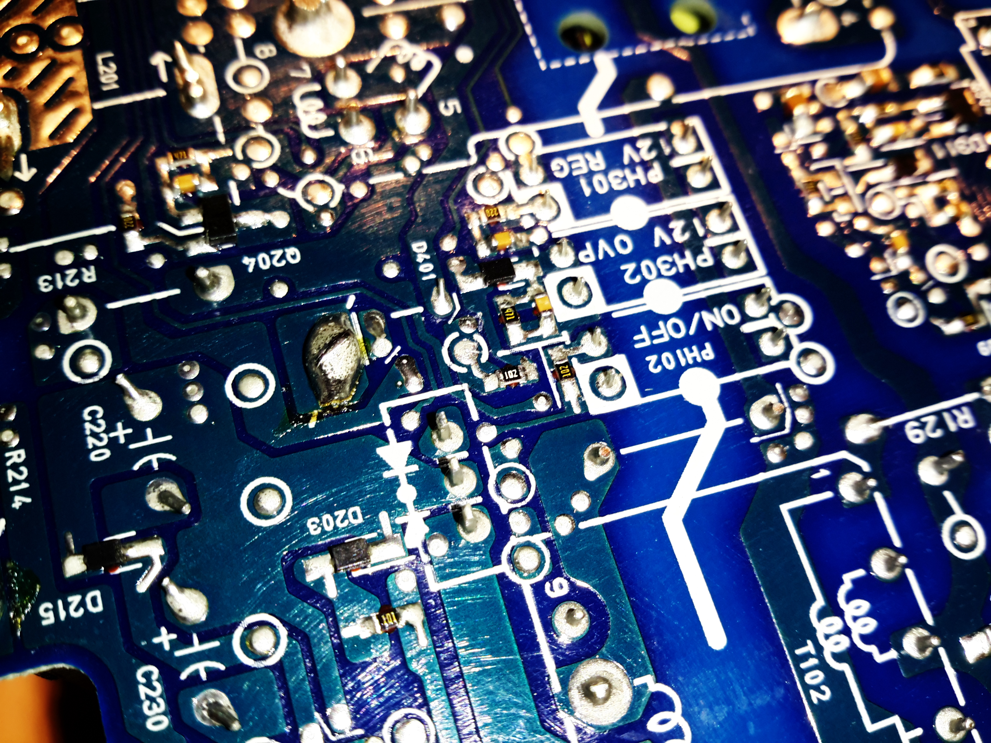
OVP Optocoupler Disconnected
The overvoltage protection on this supply is a little more aggressive – tripping things out at 13.4v. However it’s easy to defeat this on this particular supply, by disconnecting the “12V OVP” optocoupler from the secondary side. This does leave the supply with no active overvoltage protection, so be careful on how far the voltage gets tweaked up! The output electrolytics are rated at 16v, so there’s the potential for ballistic capacitors if things are tweaked too far!
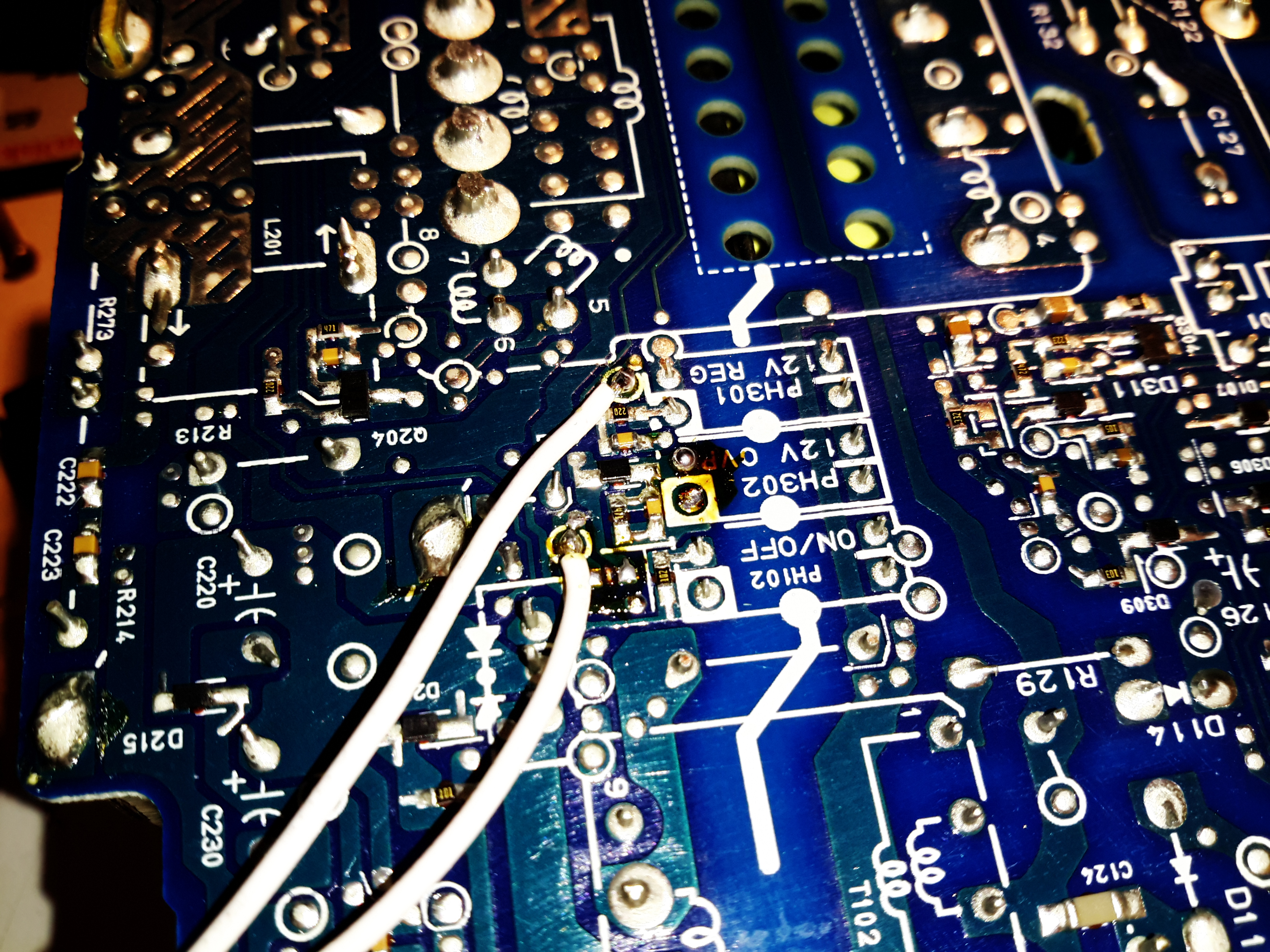
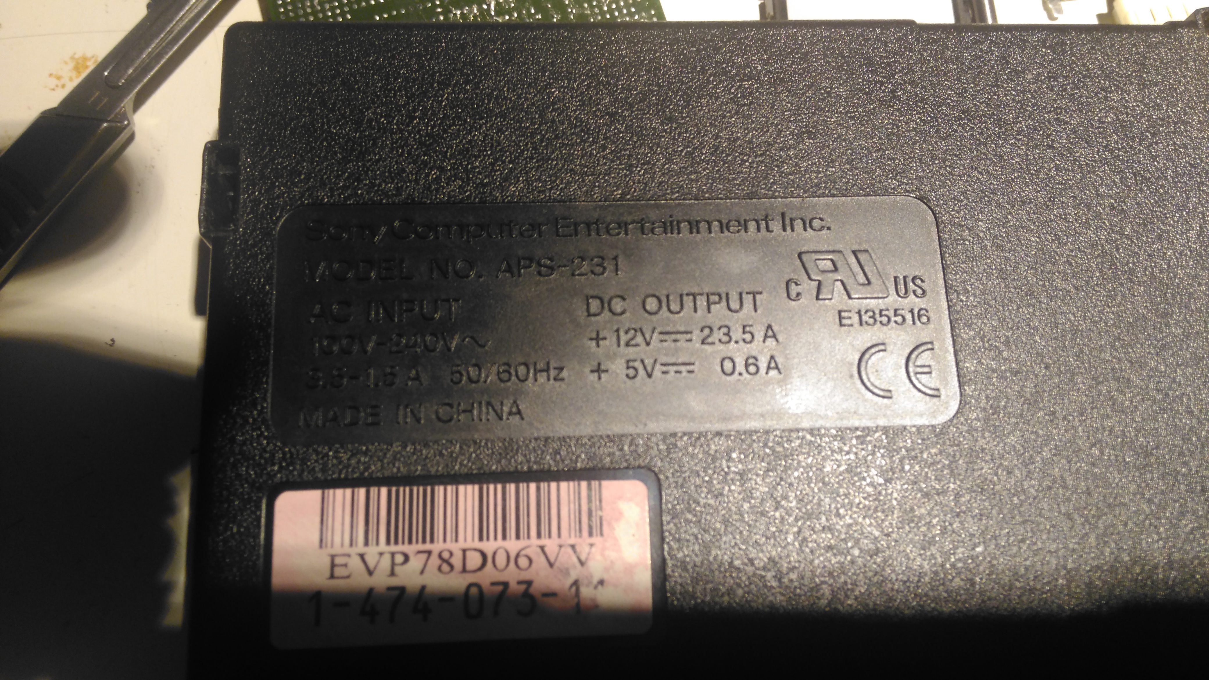
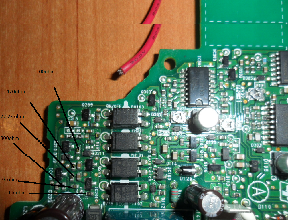
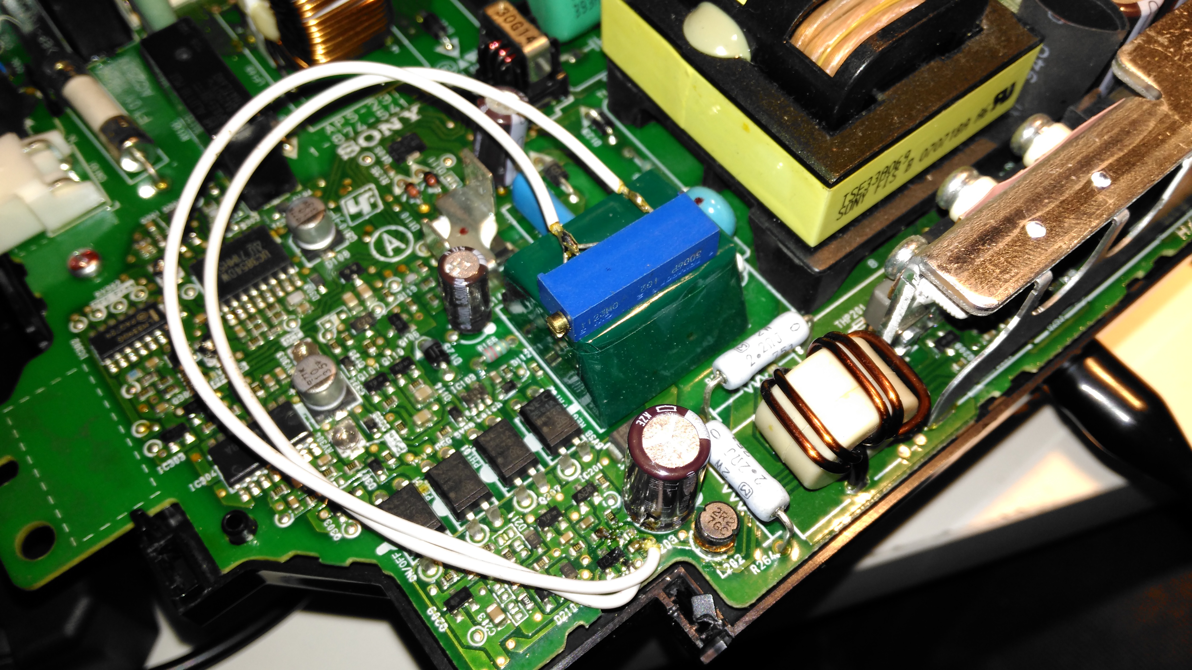
I was recently given a Sony PS3 with a dead disc drive, and since I’m not a console gamer I figured I’d see if there were any handy parts inside. Turns out these units contain a rather nice SMPS, the Sony APS-231 with a high power 12v rail, rated at 23.5A. A bit of searching around discovered a thread on the BadCaps Forums about voltage modding these supplies for a 13.8v output, suitable for my Ham radio gear.
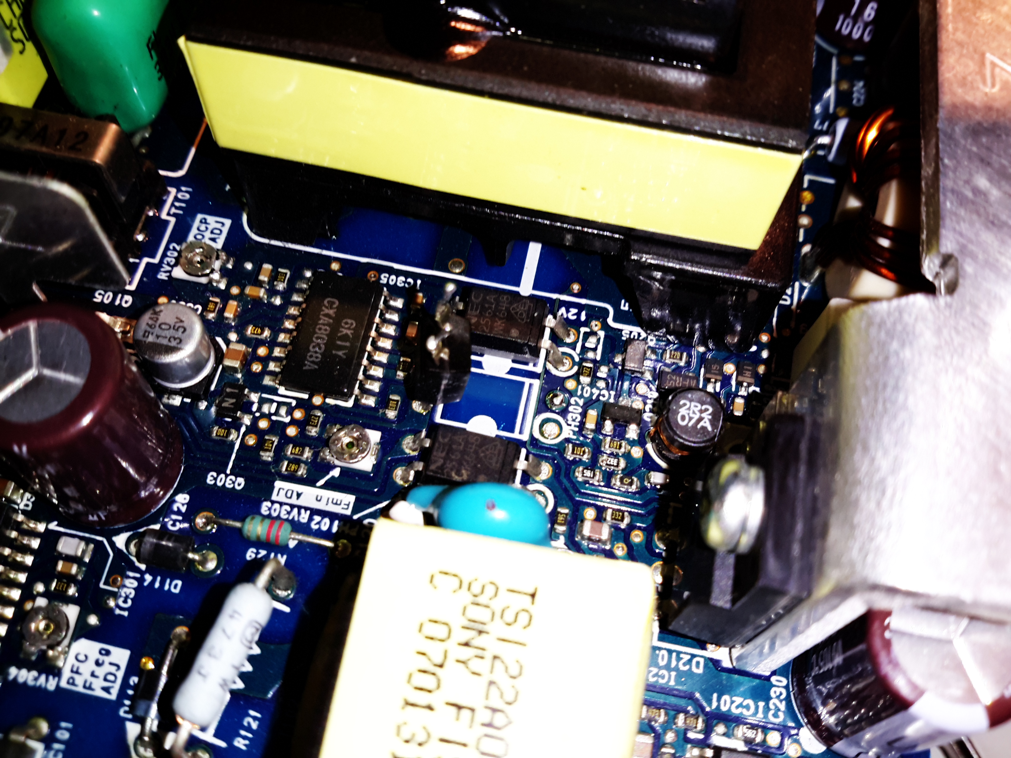
These supplies are controlled by a Sony CXA8038A, for which there is very little information. Active PFC is included, along with synchronous rectification which increases the efficiency of the supply, and in turn, reduces the waste heat output from the rectifiers.
Regulation Section
Like many of the SMPS units I’ve seen, the output voltage is controlled by referencing it to an adjustable shunt reference, and adjusting the set point of this reference will in turn adjust the output voltage of the supply, this is done in circuit by a single resistor.
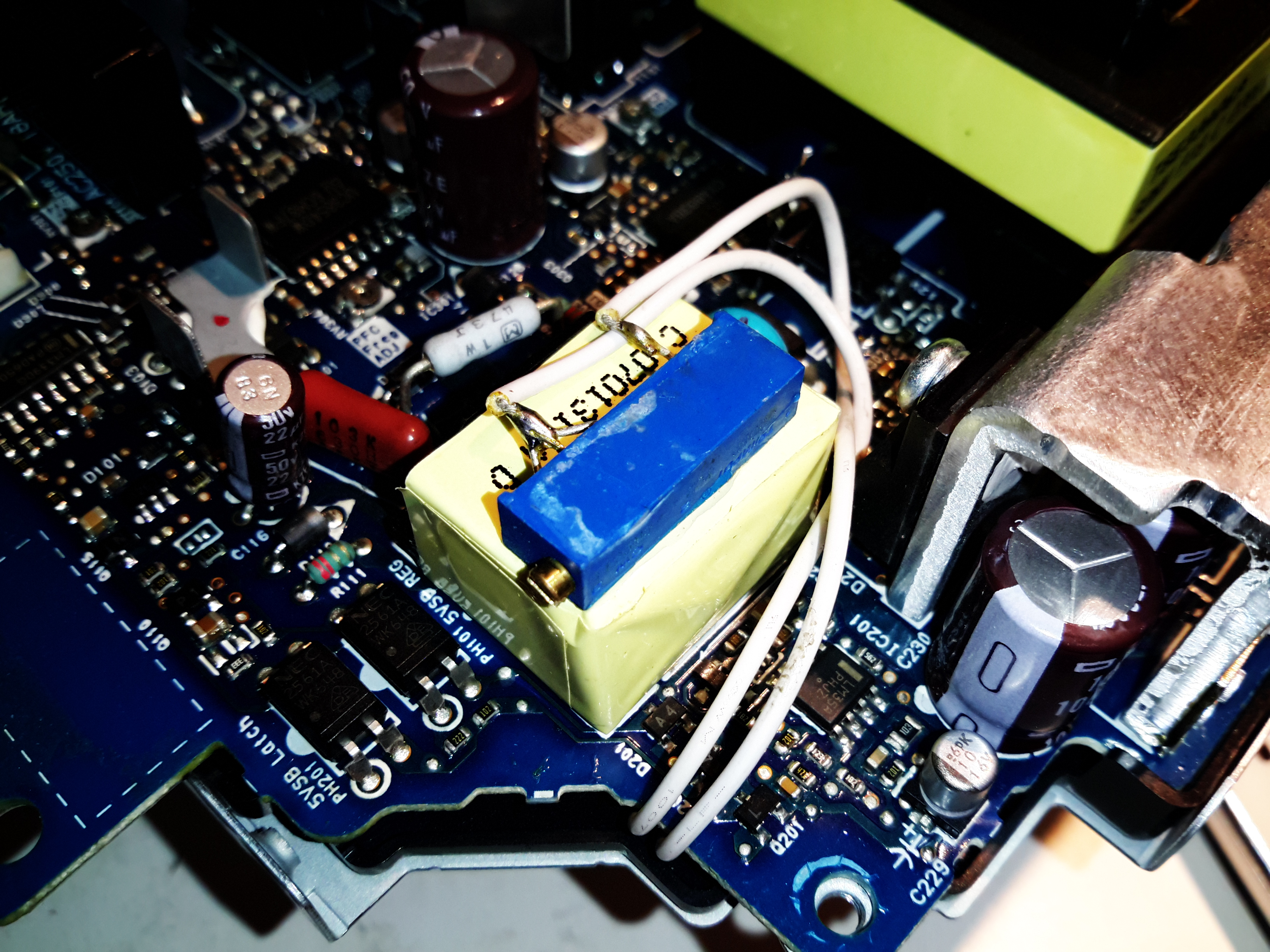
Here’s the regulator section of the PSU, with the resistors labelled. The one we’re after changing is the 800Ω one between pins 2 & 3 of the TS2431 shunt reference. It’s a very small 0402 size resistor, located right next to the filter electrolytic for the 5v standby supply circuit. A fine tip on the soldering iron is required to get this resistor removed.
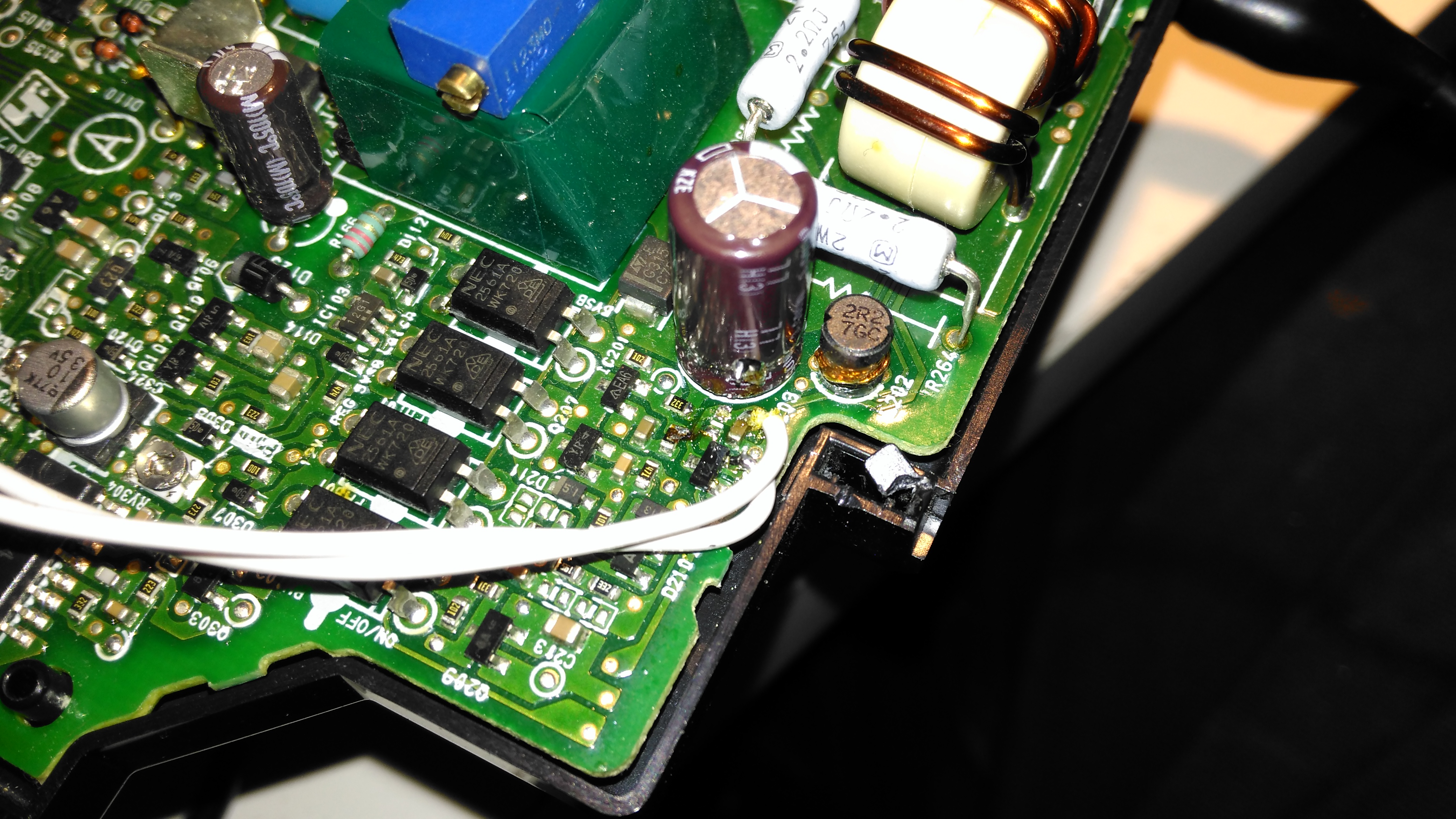
Attachment Points
Once this resistor is removed from the circuit, a 1KΩ 18-turn potentiometer is fitted in it’s place, from the Anode (Pin 3) to the Ref. (Pin 2) pins of the TS2431 shunt reference. I initally set the potentiometer to be the same 800Ω as the factory set resistor, to make sure the supply would start up at a sensible voltage before I did the adjustment.
Potentiometer
The pot is secured to the top of the standby supply transformer with a drop of CA glue to stop everything moving around. The supply can now be adjusted to a higher setpoint voltage – 13.8v is about the maxumum, as the OVP cuts the supply out at between 13.9v-14v.
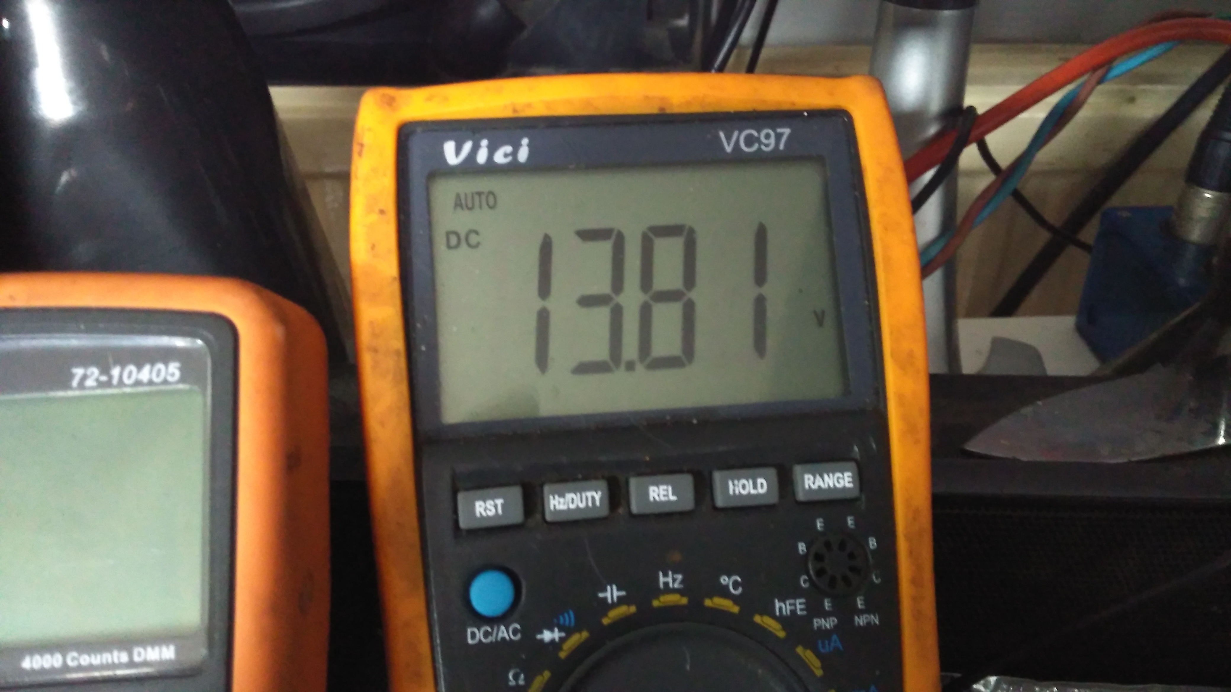
Modded Voltage
After doing some testing at roughly 50% of the supply’s rated load, everything seems to be stable, and nothing is heating up more than I’d expect.
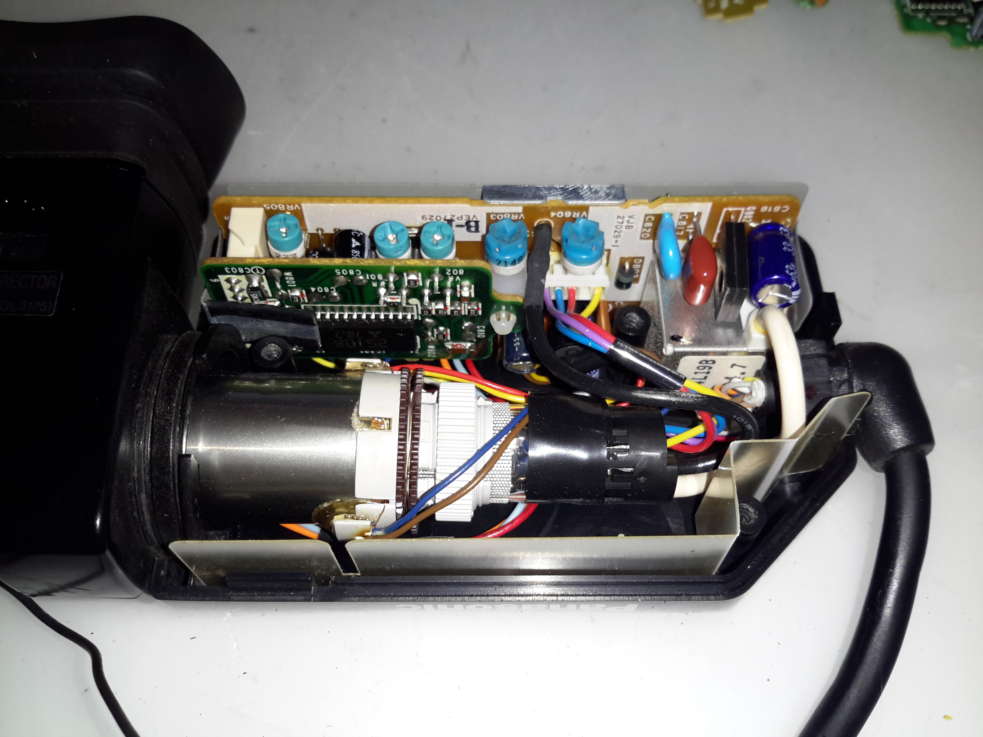
The old Panasonic NV-M5 has the standard for the time CRT based viewfinder assembly, which will happily take a composite video signal from an external source.
This viewfinder has many more connections than I would have expected, as it has an input for the iris signal, which places a movable marker on the edge of the display. This unit also has a pair of outputs for the vertical & horizontal deflection signals, I imagine for sync, but I’ve never seen these signals as an output on a viewfinder before.
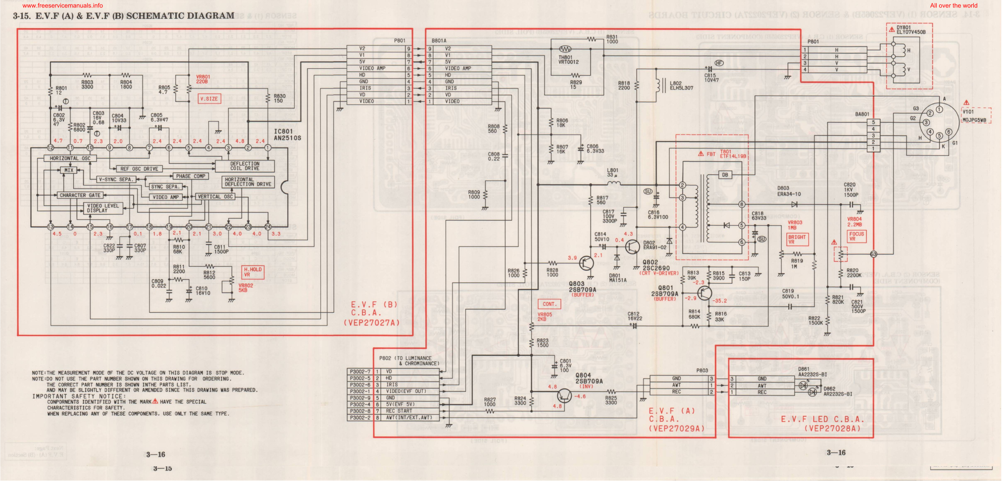
EVF Schematic
Luckily I managed to get a service manual for the camera with a full schematic.
This unit takes a 5v input, as opposed to the 8-12v inputs on previous cameras, so watch out for this! There’s also no reverse polarity protection either.
Pins
Making the iris marker vanish from the screen is easy, just put a solder bridge between pins 15 & 16 of the drive IC. The important pins on the interface connector are as follows:
Pin 3: GND
Pin 4: Video Input
Pin 5: Video GND
Pins 6: +5v Supply
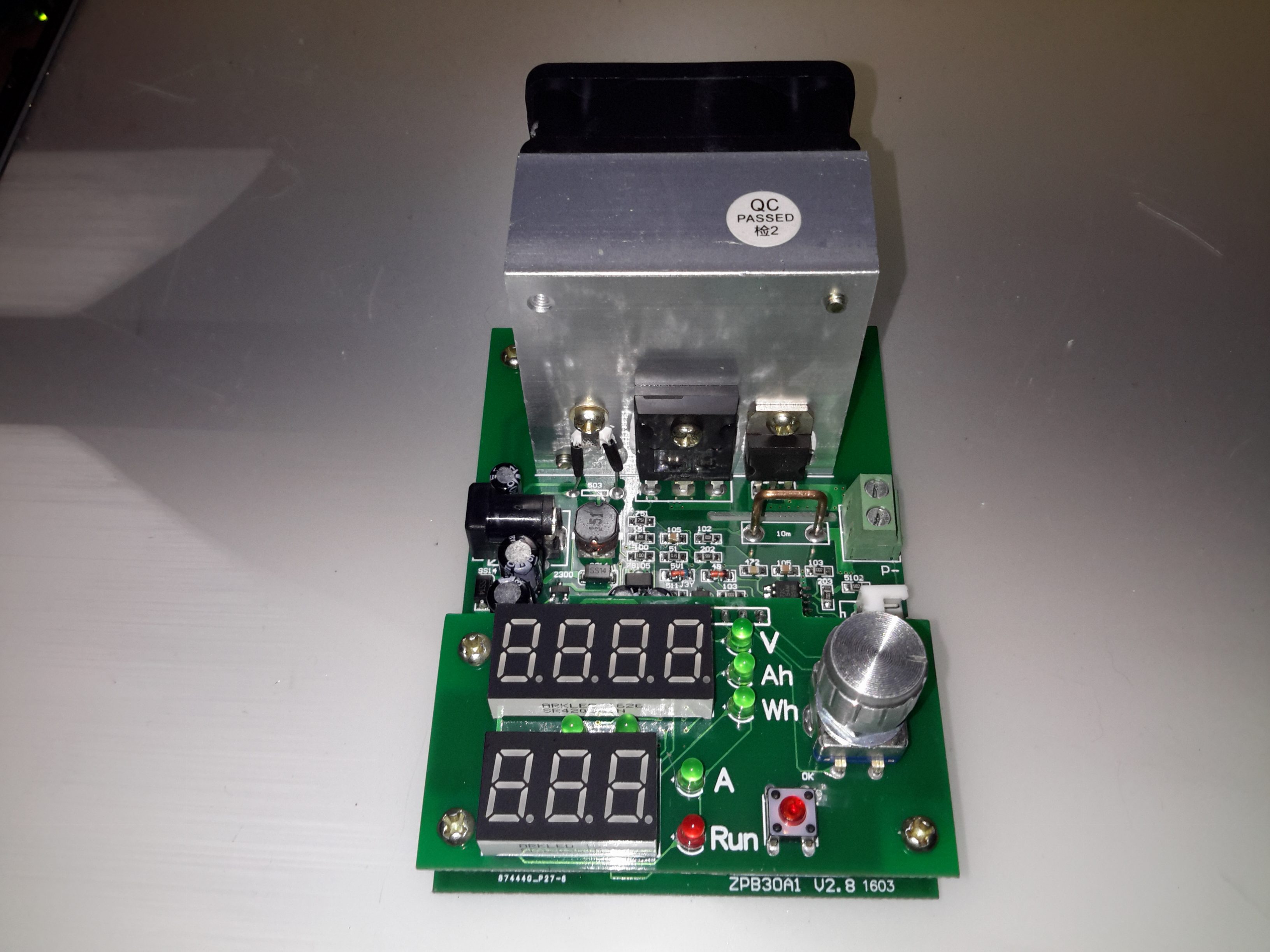
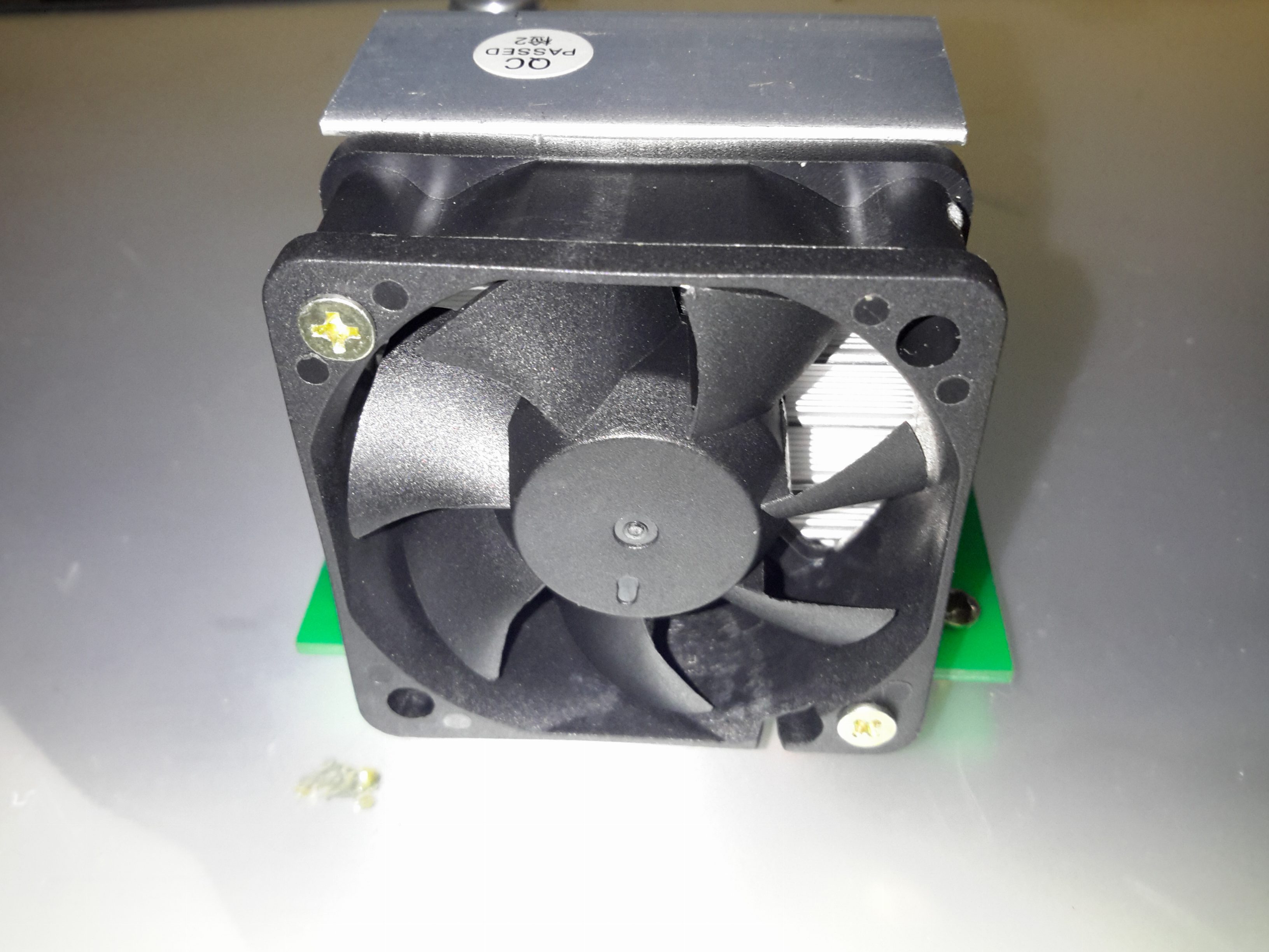
Here’s a useful tool for testing both power supplies & batteries, a dummy load. This unit is rated up to 60W, at voltages from 1v to 25v, current from 200mA to 9.99A.
This device requires a 12v DC power source separate from the load itself, to power the logic circuitry.
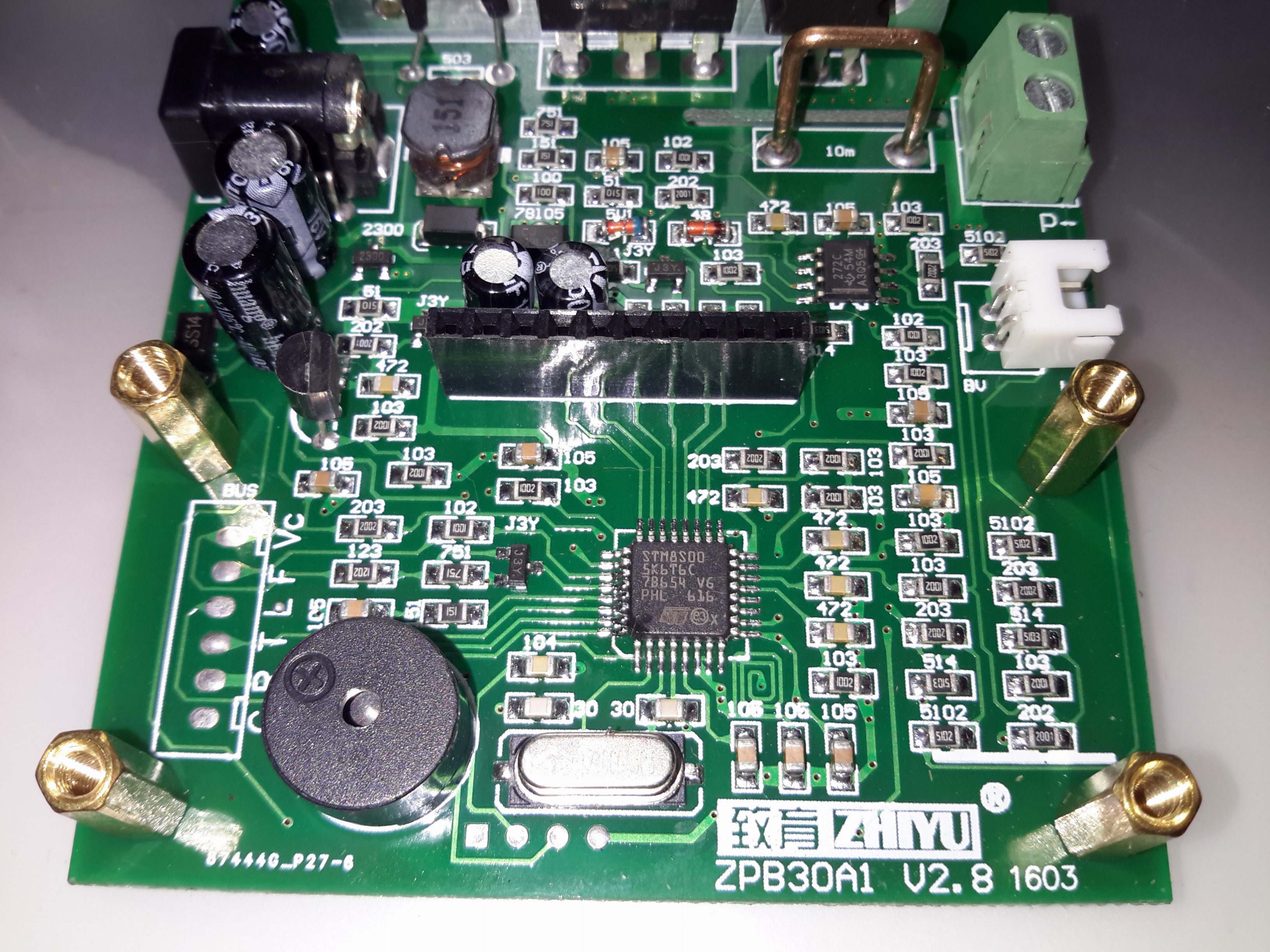
Microcontroller Section
Like many of these modules, the brains of the operation is an STM8 microcontroller. There’s a header to the left with some communication pins, the T pin transmits the voltage when the unit is operating, along with the status via RS232 115200 8N1. This serial signal is only present in DC load mode, the pin is pulled low in battery test mode. The 4 pins underneath the clock crystal are the programming pins for the STM8.
Serial CommsCooling Fan
The main heatsink is fan cooled, the speed is PWM controlled via the microcontroller depending on the temperature.
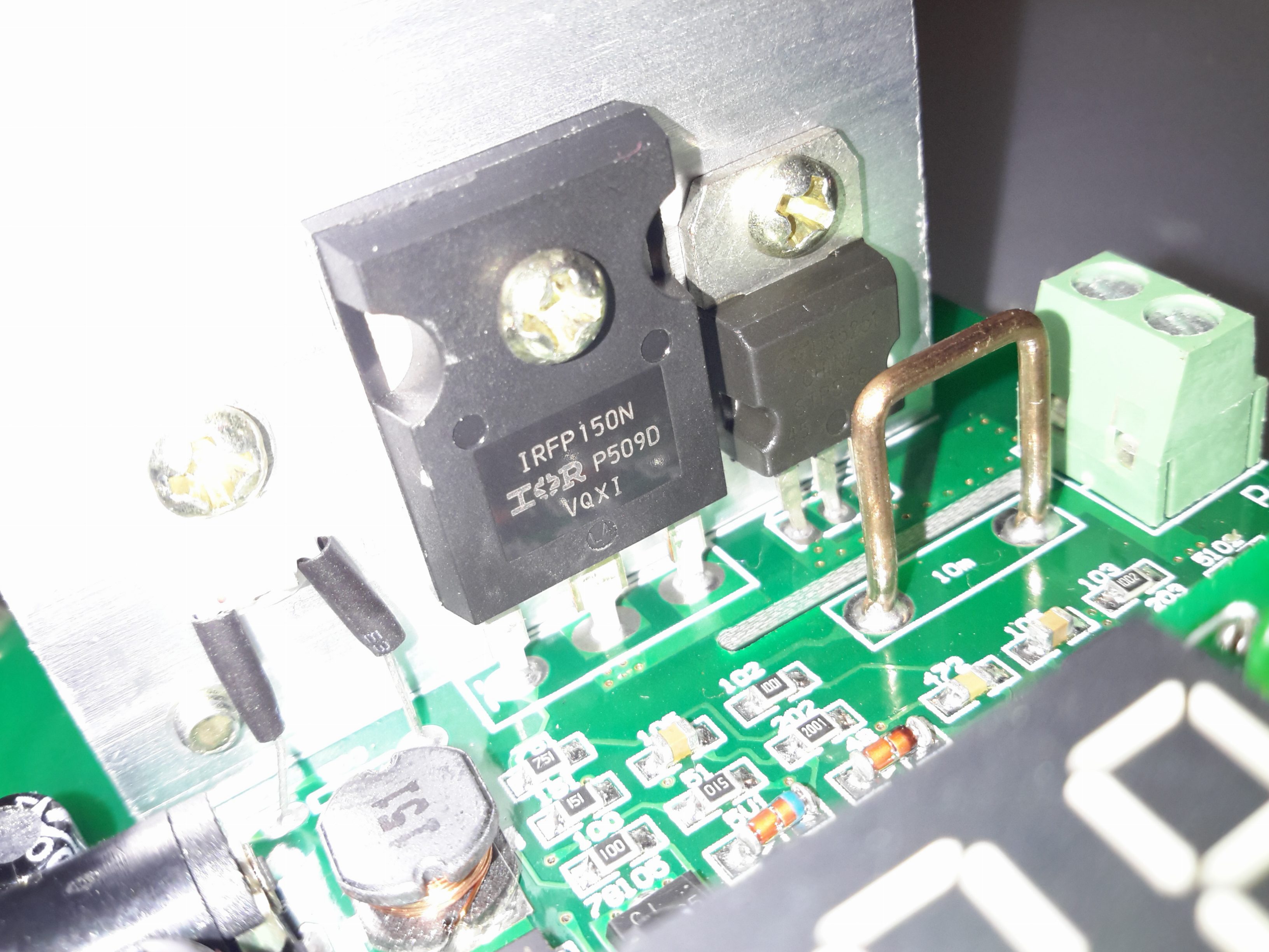
Main MOSFET
The main load MOSFET is an IRFP150N from Infineon. This device is rated at 100v 42A, with a max power dissipation of 160W. On the right is a dual diode for reverse polarity protection, this is in series with the MOSFET. On the left is the thermistor for controlling fan speed.
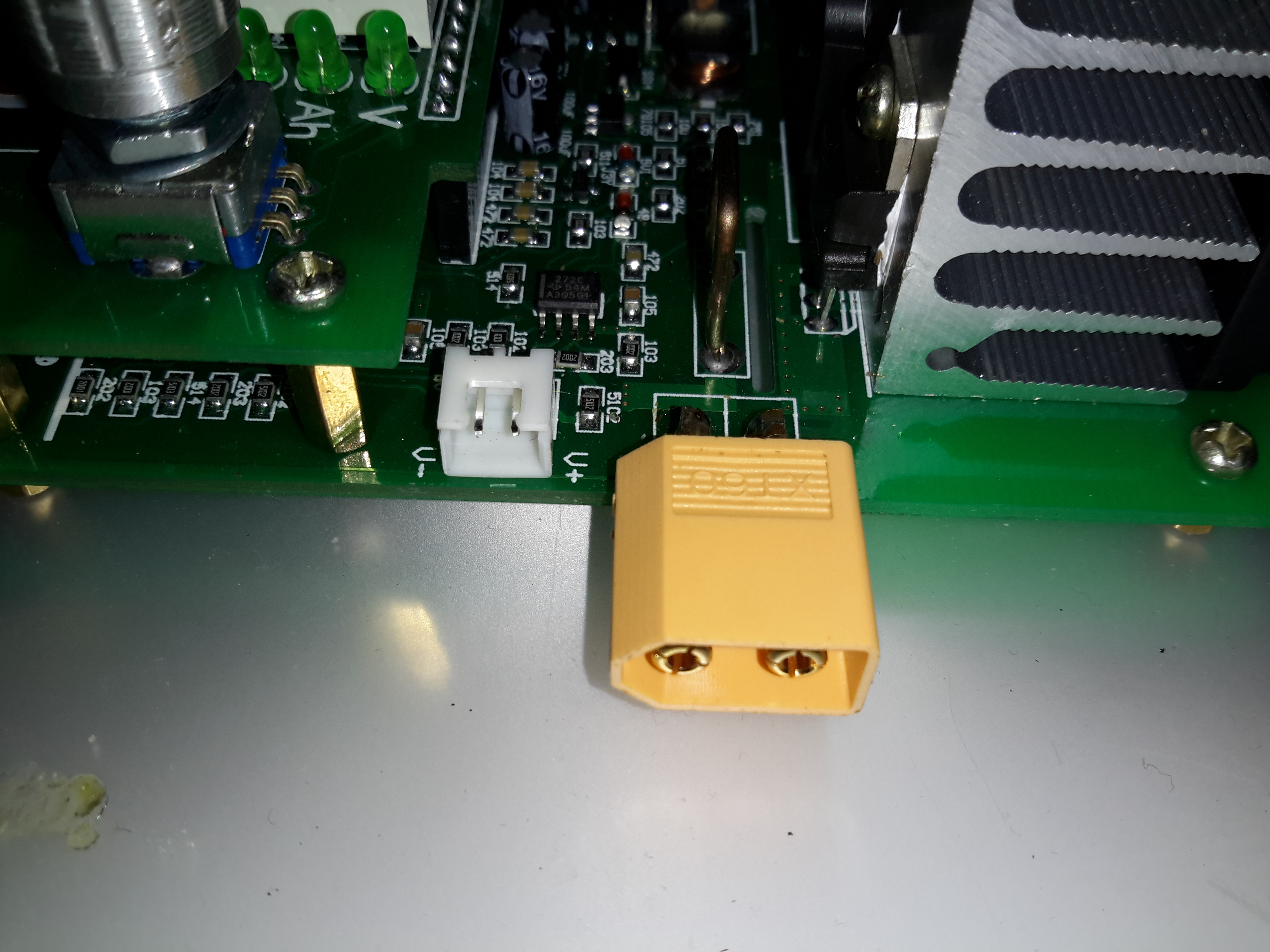
Load Terminals
The load is usually connected via a rising clamp terminal block. I’ve replaced it with a XT60 connector in this case as all my battery holders are fitted with these. This also removes the contact resistance of more connections for an adaptor cable. The small JST XH2 connector on the left is for remote voltage sensing. This is used for 4-wire measurements.
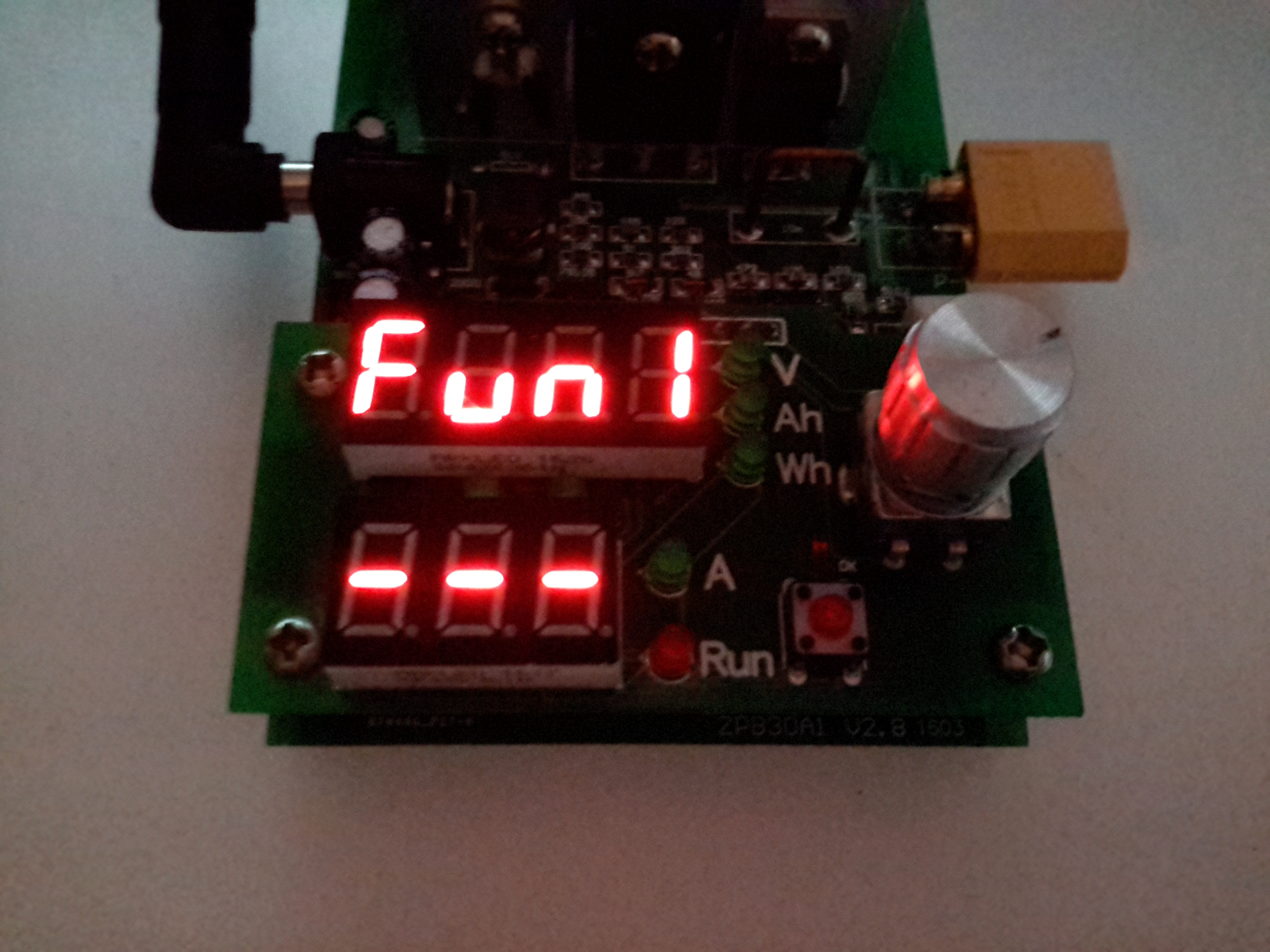
Function 1 – DC Load
Powering the device up while holding the RUN button gets you into the menu to select the operating modes. Function 1 is simple DC load.
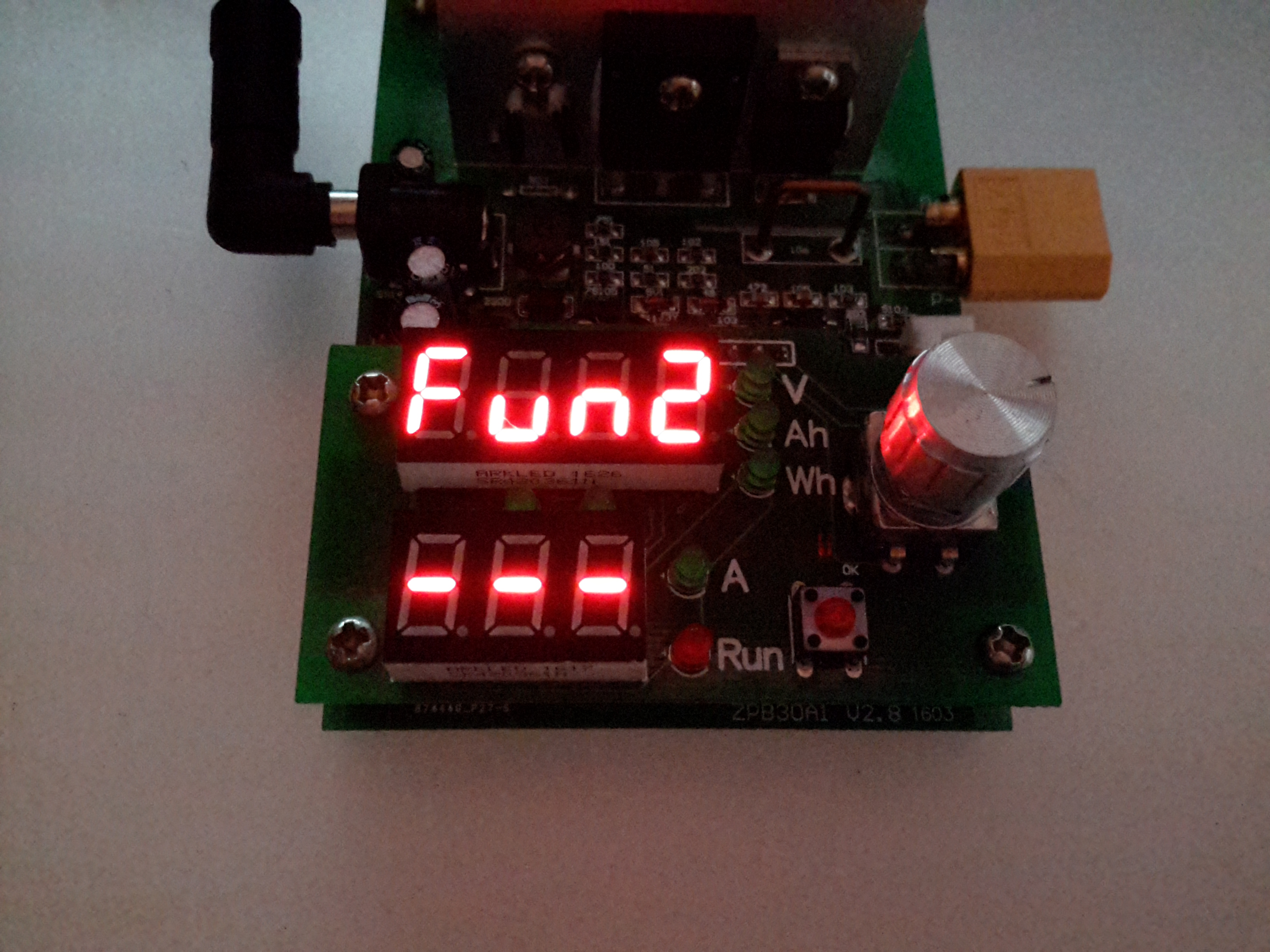
Function 2 – Battery Capacity Mode
The rotary encoder is used to select the option. Function 2 is battery capacity test mode.
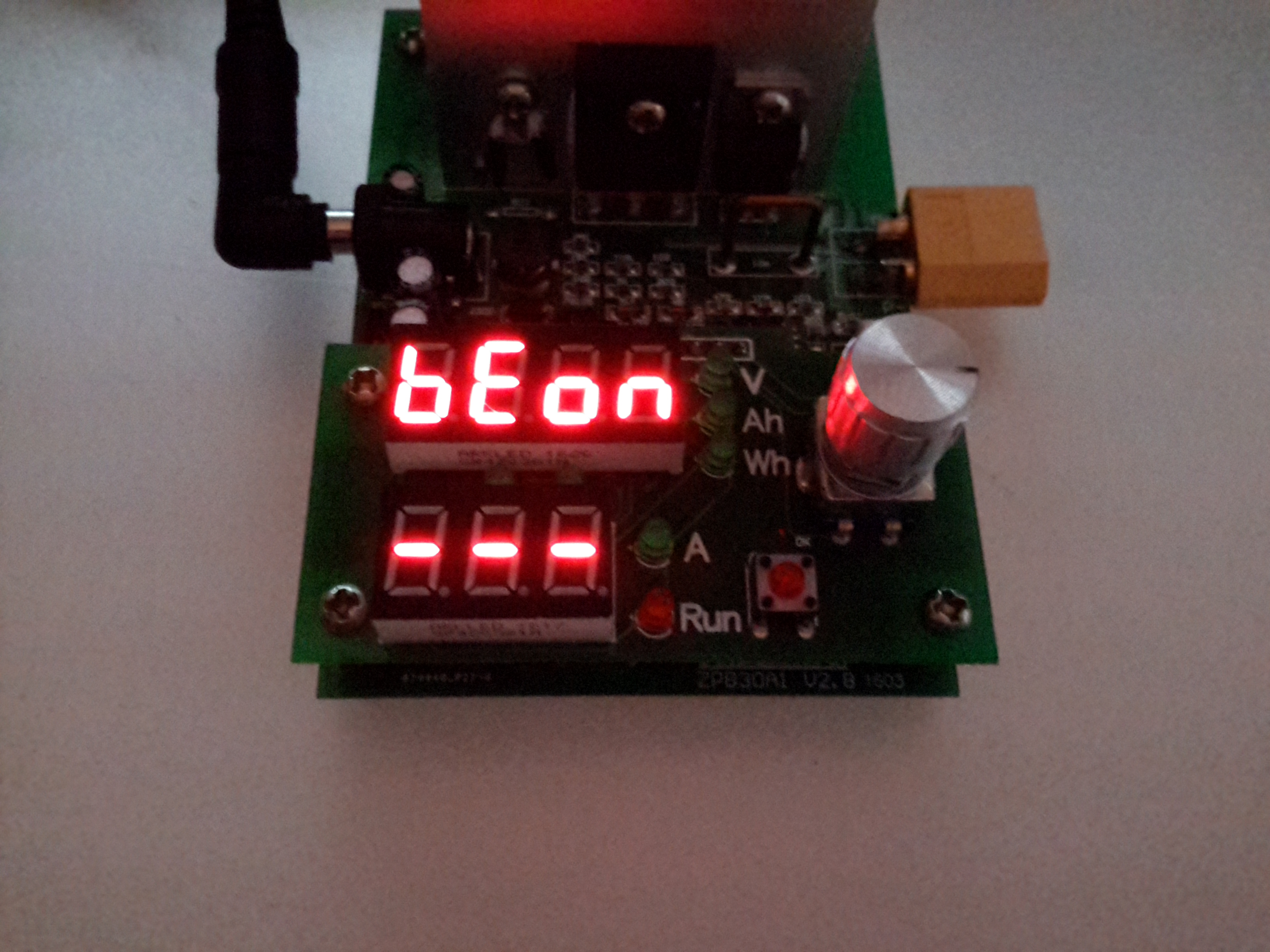
Beeper Mode
After the mode is selected, an option appears to either turn the beeper on or off.
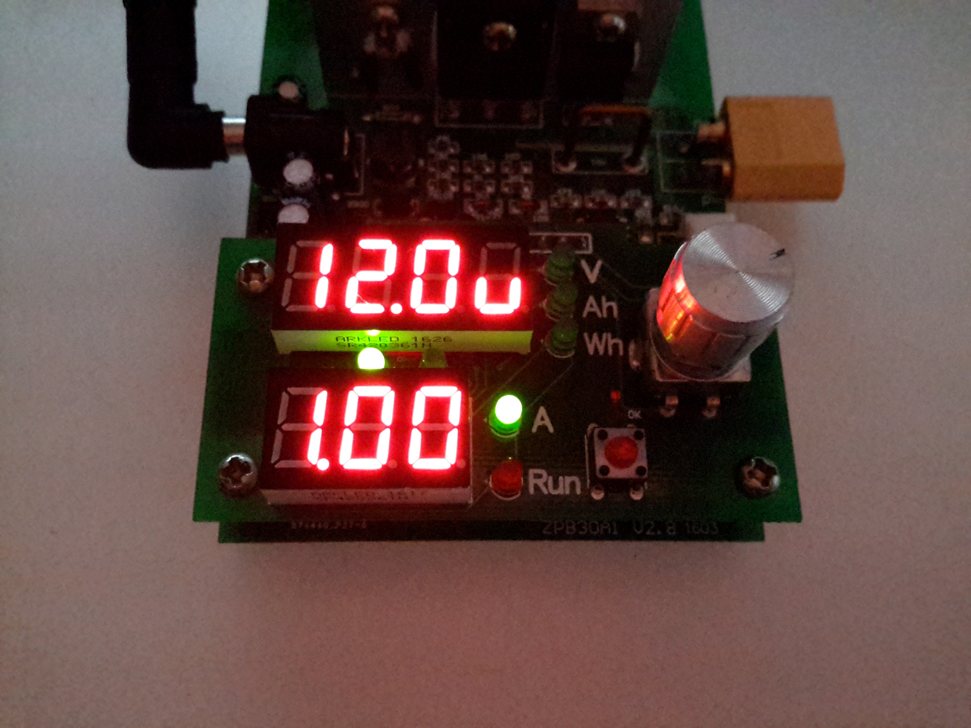
Amps Set
When in standby mode, the threshold voltage & the load current can be set. Here the Amps LED is lit, so the load current can be set. The pair of LEDs between the displays shows which digit will be changed. Pressing the encoder button cycles through the options.
Volts Set
With the Volts LED lit, the threshold voltage can be changed.
When in DC load mode (Fun1), the device will place a fixed load onto the power source until it’s manually stopped. The voltage setting in this mode is a low-voltage alarm. The current can be changed while the load is running.
When in battery discharge test mode (Fun2), the voltage set is the cutoff voltage – discharge will stop when this is reached. Like the DC load mode, the current can be changed when the load is running. After the battery has completed discharging, the capacity in Ah & Wh will be displayed on the top 7-segment. These results can be selected between with the encoder.
Below are tables with all the options for the unit, along with the error codes I’ve been able to decipher from the Chinese info available in various places online. (If anyone knows better, do let me know!).
Option
Function
Fun1
Basic DC Load
Fun 2
Battery Capacity Test
BeOn
Beeper On
BeOf
Beeper Off
Error Code
Meaning
Err1
Input Overvoltage
Err2
Low Battery Voltage / No Battery Present / Reverse Polarity
Err3
Battery ESR Too High / Cannot sustain selected discharge current
Err4
General Failure
Err6
Power Supply Voltage Too Low / Too High. Minimum 12v 0.5A.
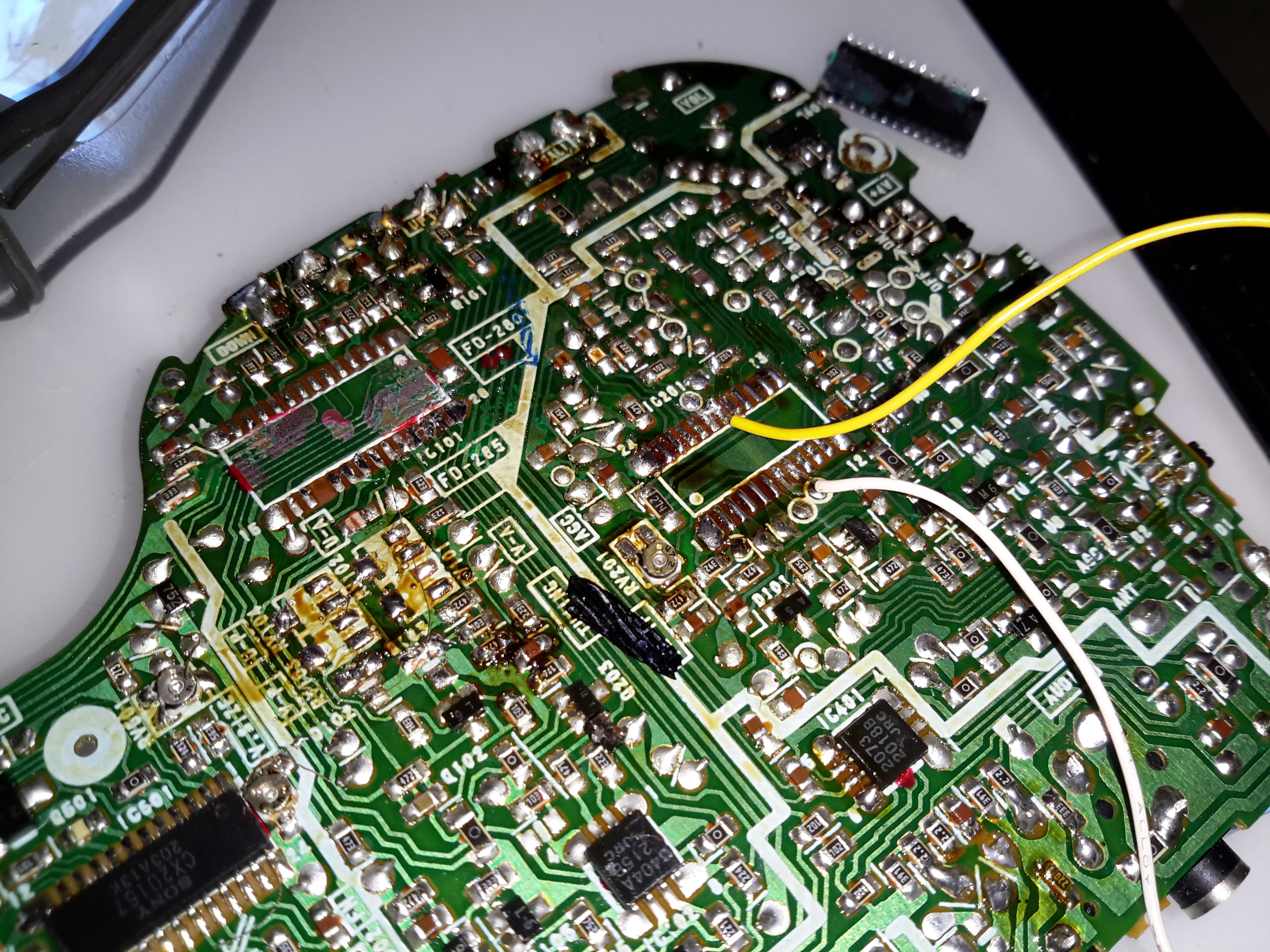
As with the previous Sony Watchman hack, injecting a composite video signal into this one is just as easy. I desoldered both the VIF/SIF IC & the digital tuner control (the tuner controller was still injecting it’s indicator into the video circuitry with the IF IC disconnected).
Composite video is on pin 18 of the Video IF IC, with the audio on Pin 13.
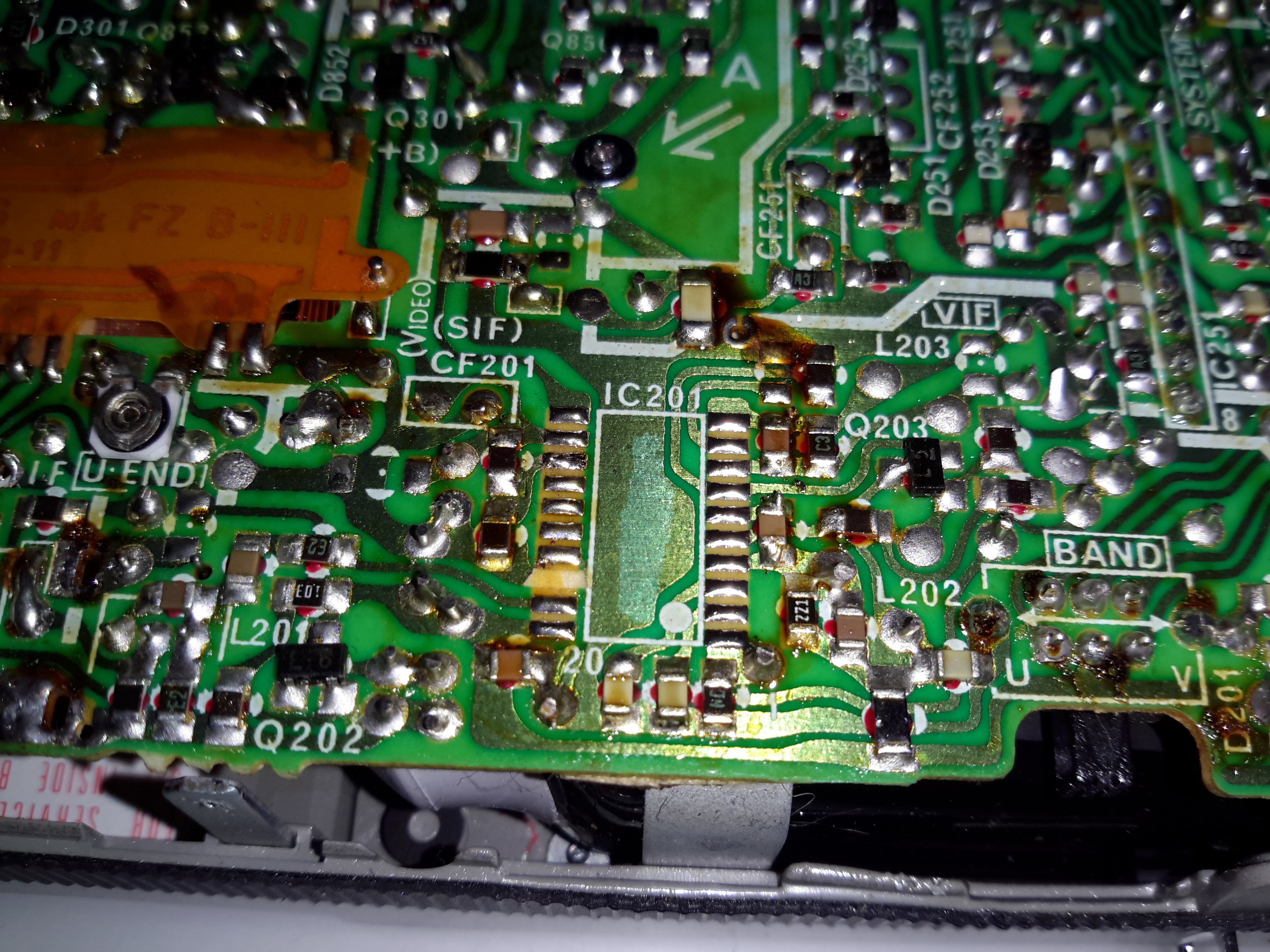
Hacking the Sony FD-20 to accept a composite input is easy – the tuner receives the RF transmission, produces an IF, this is then fed into IC201, a Mitsubishi M51364P Video IF Processor. The VIF IC then separates out the composite video signal, which is output on Pin 13 (in photo above, left side, 3rd pin from the top). The audio is separated out & sent via Pin 11 to the Audio IF processor.
In the above photo, the VIF IC has been removed from the board with hot air, as it was interfering with the signal if left in place. The RF tuner was also desoldered & removed. Unfortunately I managed to mangle a pad, which is the ground pin for the VIF IC. This isn’t much of an issue though, as an identical signal ground is available, just to the left of the IC.
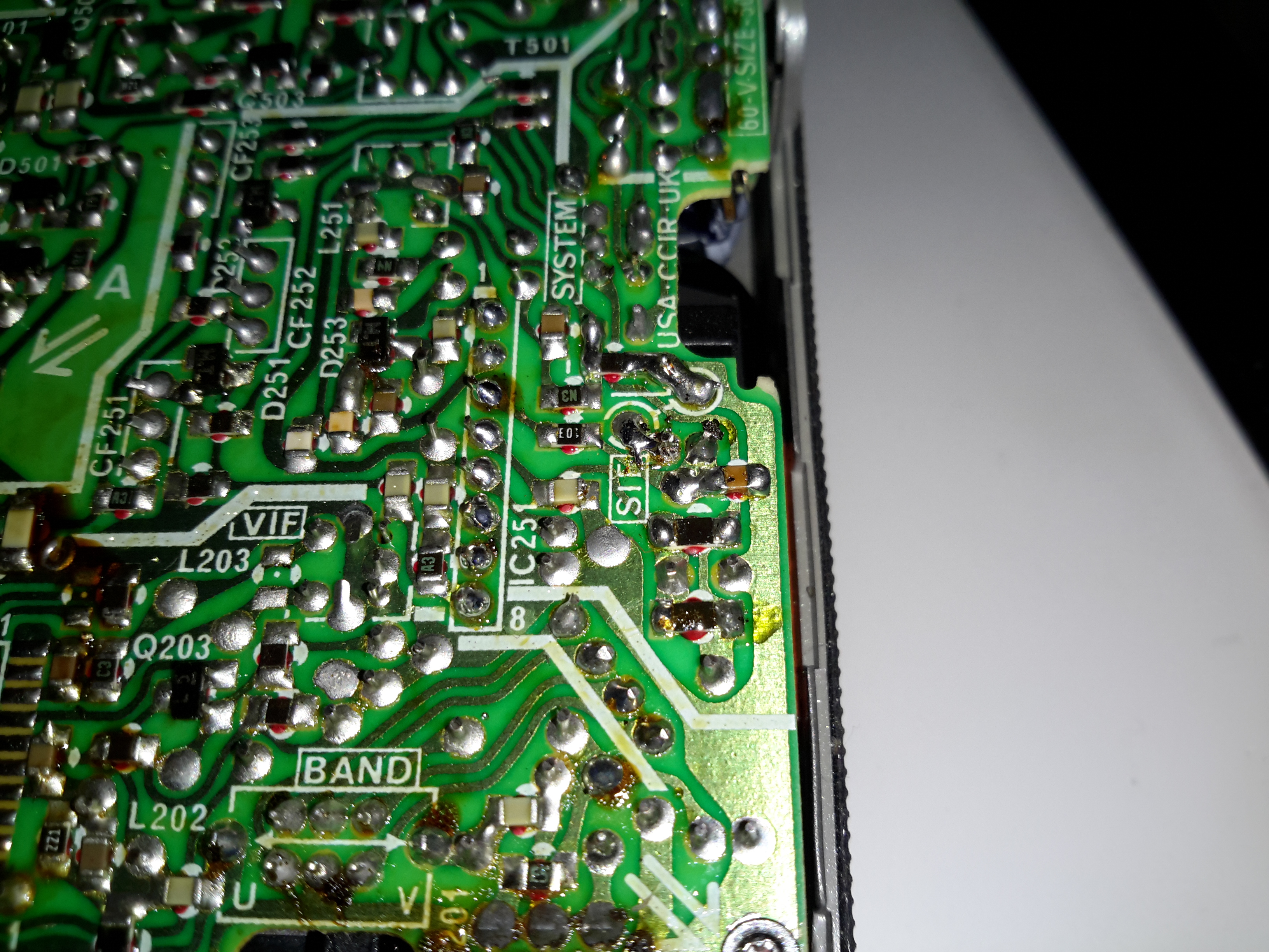
Audio Input
The audio can be tapped into in a similar way, the circled pad in the centre of the photo marked SIF is the place, this is the output of the Audio IF processor to the audio amplifier. The Audio IF processor didn’t interfere with the injected signal, so it was left in place.
Recently my phone decided it was going to die a battery-related death, and having not found much useful information on the Great Google, (all the information I could find, was hinting at many issues from firmware to a faulty motherboard, nobody seems to have actually done any investigation into similar issues), I decided to dig into the phone to try & repair the problem.
Broken Flex
The phone would work correctly for a while, then with the slightest movement or knock, would spontaneously switch off, and not turn back on without being whacked on a hard surface.
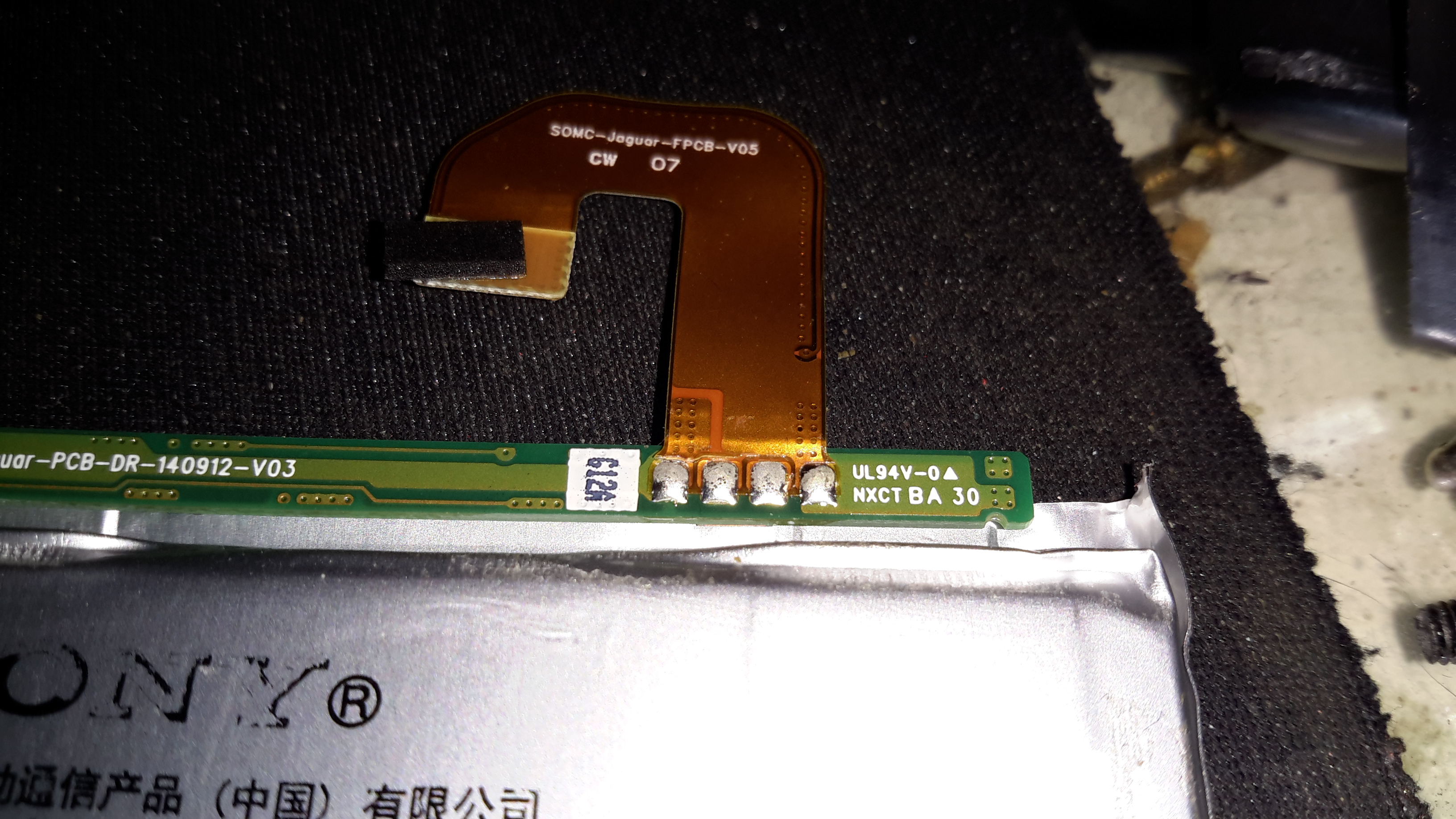
This symptom pointed me at a power connection problem. After removing the back of the phone (glass & heavily glued in place, so an awkward process), This was what I was presented with on the cell flex PCB.
In the above photo, the positive connection to the flex is fractured just after the solder joint with the BMS board.
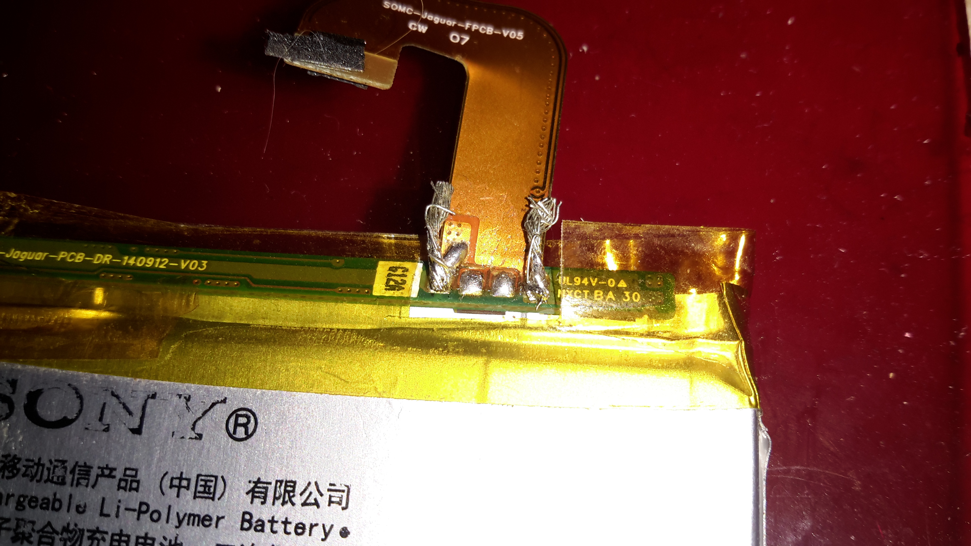
Flex Repair
I managed to scrape some of the insulation off the flex PCB & solder a jumper on to restore power. Unfortunately, this repair generated another fault, where the battery level was always shown at 50%, and plugging into a USB supply wouldn’t charge the phone. The other two pins on the cell are for communication & temperature sensing, clearly one of these traces was also broken in the flex.
The above photo has a pair of very small wire tails as well, for connecting an external charger.
50% Battery
Here’s a screenshot of the phone with the original cell, even though it’s at about 4.15v (virtually fully charged). The battery management is having trouble talking to the phone, so for safety reasons, the charging logic refuses point-blank to charge the thing up.
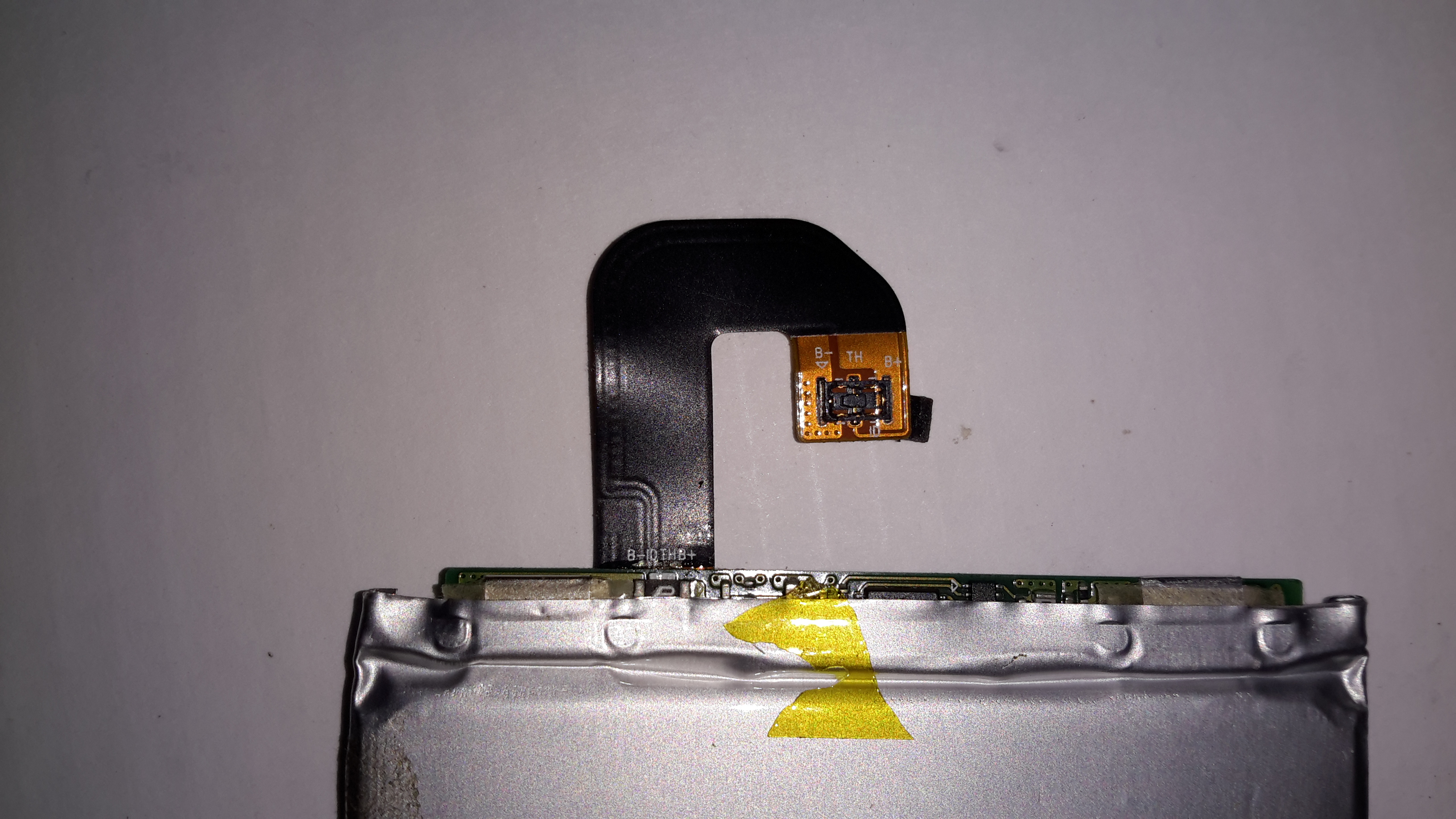
Flex Cable
The connector on the cell & phone motherboard is absolutely tiny, so I didn’t fancy attempting to solder on any bridge wires to try & bypass the broken flex.
Battery BMS
The cell BMS has some intelligence on board, besides the usual over-current, over-charge & under-charge protection. The very small IC on the right has a Microchip logo, and the marking FT442, but I was unable to dig up any datasheets. The current sense resistor is directly connected to this IC, along with the main power FET to the left.
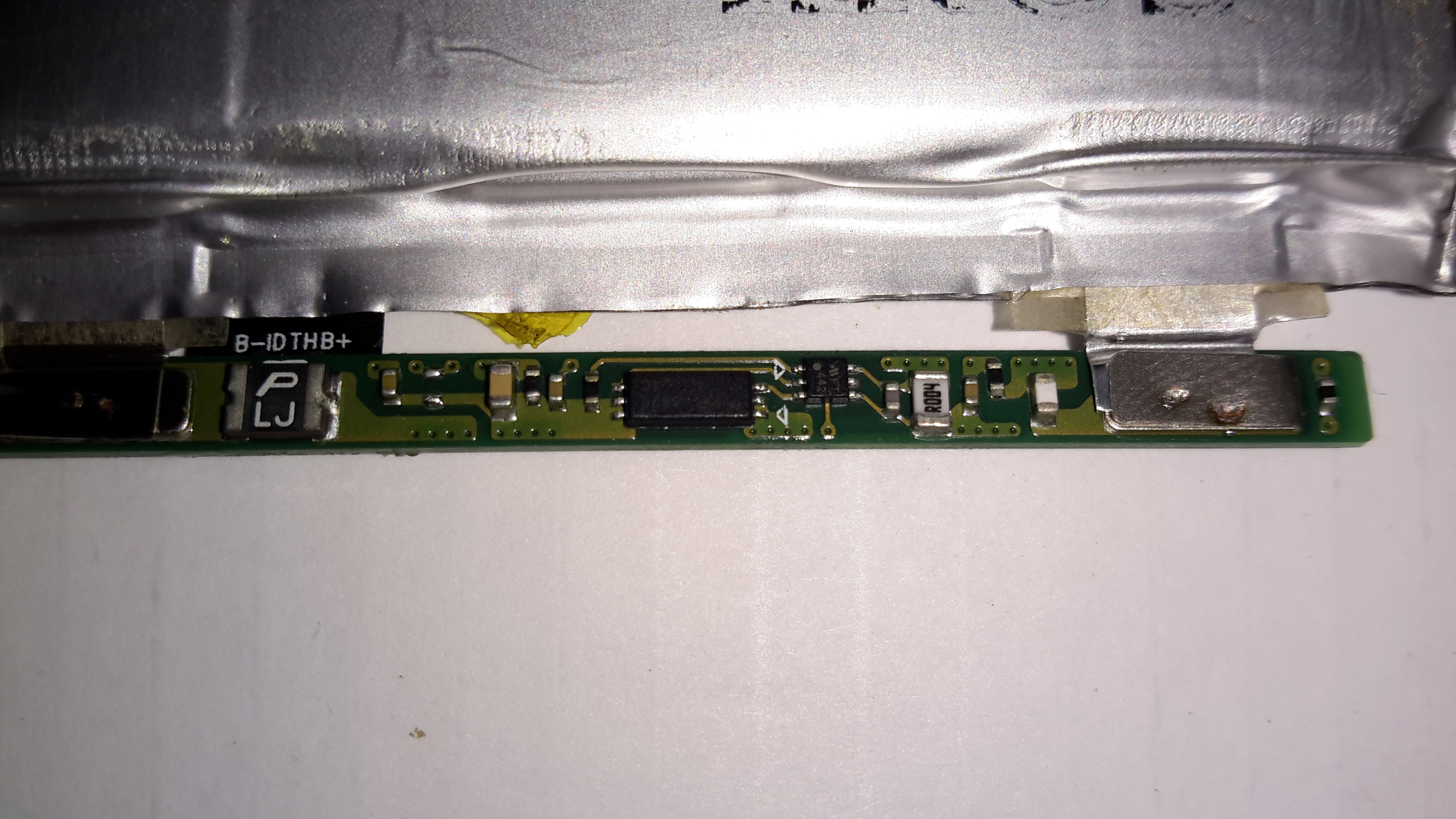
BMS Reverse
On the other side of the BMS board is another IC, again unidentifiable, and what looks like a bare-die, or CSP IC.
At this stage I figured the only way forward was to buy a new battery, eBay turned one up for less than £5. Above is the new battery fitted to the phone, datestamped 2014, so definitely old stock.
100% Battery
Booting the phone with the new battery quickly lets me know the fix worked, with a 100% reading & the ability to again charge properly!
As I’ve been posting some photos of decapped ICs lately, I thought I’d share the process I use personally for those that might want to give it a go 😉
The usual method for removing the epoxy package from the silicon is to use hot, concentrated Nitric Acid. Besides the obvious risks of having hot acids around, the decomposition products of the acid, namely NO² (Nitrogen Dioxide) & NO (Nitrogen Oxide), are toxic and corrosive. So until I can get the required fume hood together to make sure I’m not going to corrode the place away, I’ll leave this process to proper labs ;).
The method I use is heat based, using a Propane torch to destroy the epoxy package, without damaging the Silicon die too much.
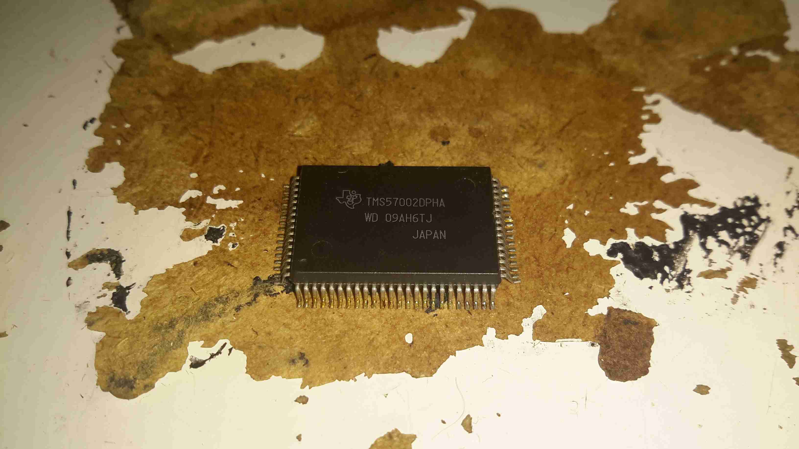
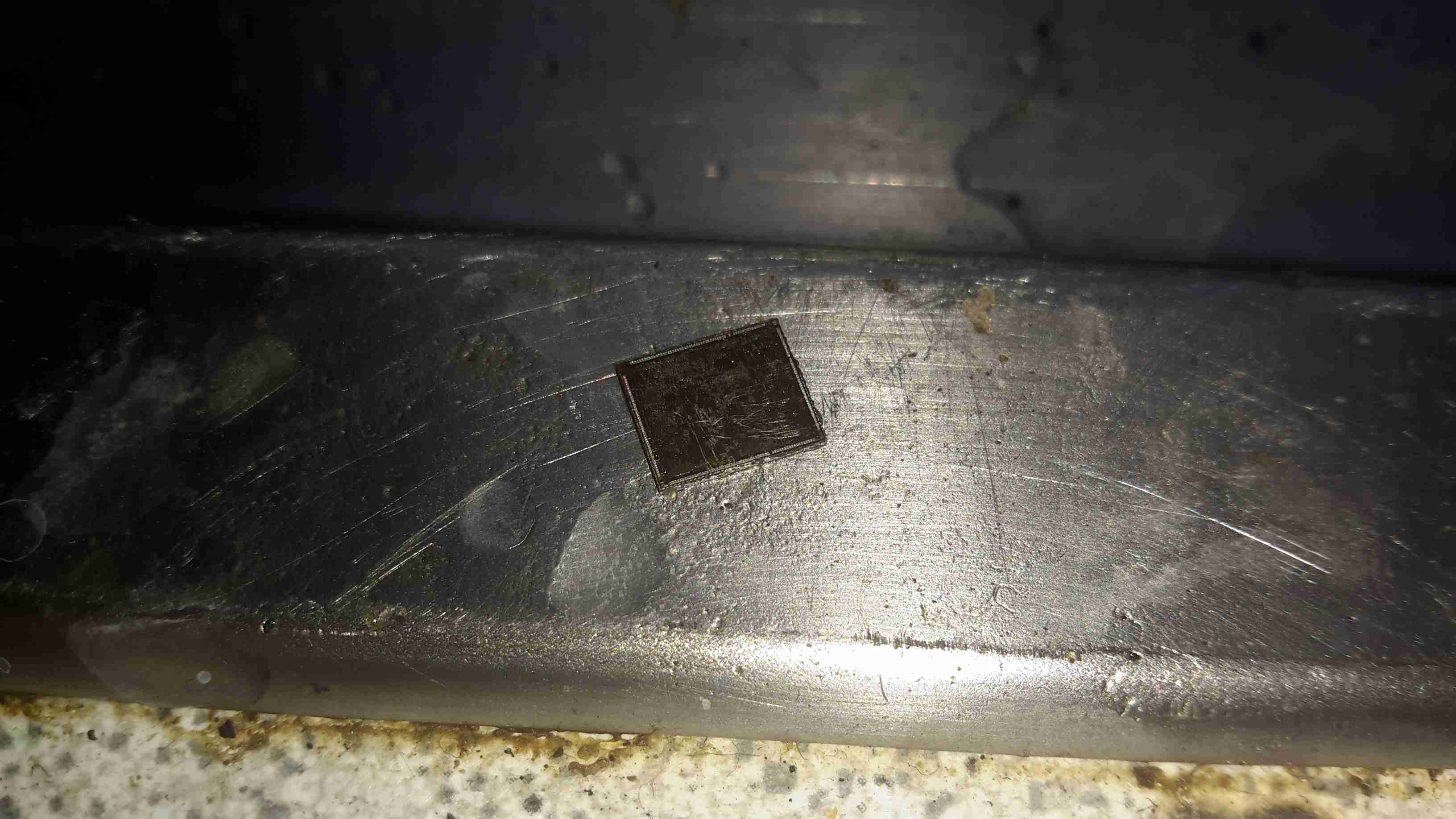
TMS57002 Audio DSP
I start off, obviously, with a desoldered IC, the one above an old audio DSP from TI. I usually desolder en-masse for this with a heat gun, stripping the entire board in one go.
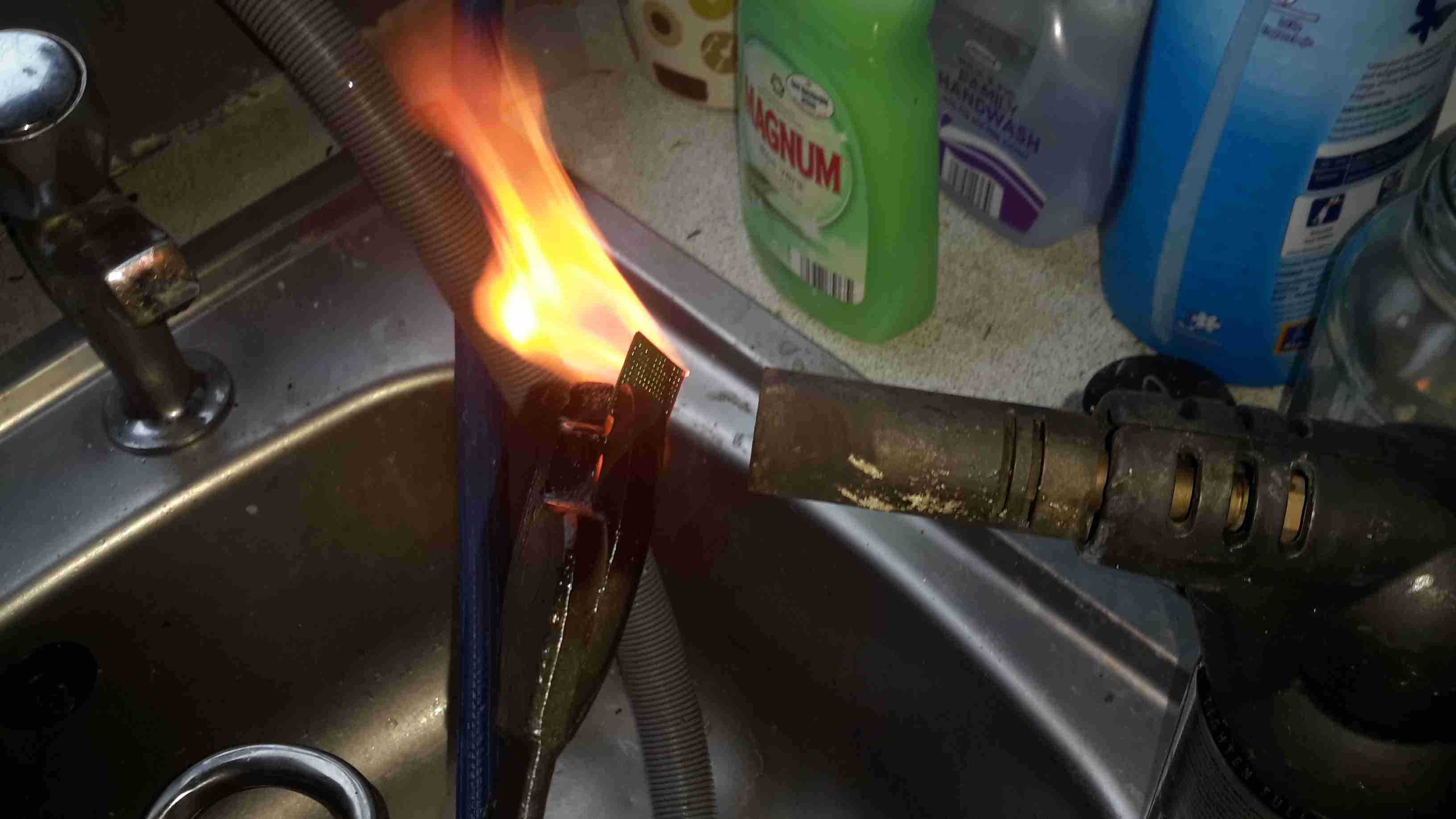
FLAMES!
Next is to apply the torch to the IC. A bit of practice is required here to get the heat level & time exactly right, overheating will cause the die to oxidize & blacken or residual epoxy to stick to the surface.
I usually apply the torch until the package just about stops emitting it’s own yellow flames, meaning the epoxy is almost completely burned away. I also keep the torch flame away from the centre of the IC, where the die is located.
Breathing the fumes from this process isn’t recommended, no doubt besides the obvious soot, the burning plastic will be emitting many compounds not brilliant for Human health!
Once the IC is roasted to taste, it’s quenched in cold water for a few seconds. Sometimes this causes such a high thermal shock that the leadframe cracks off the epoxy around the die perfectly.
All Your Die Belong To Us
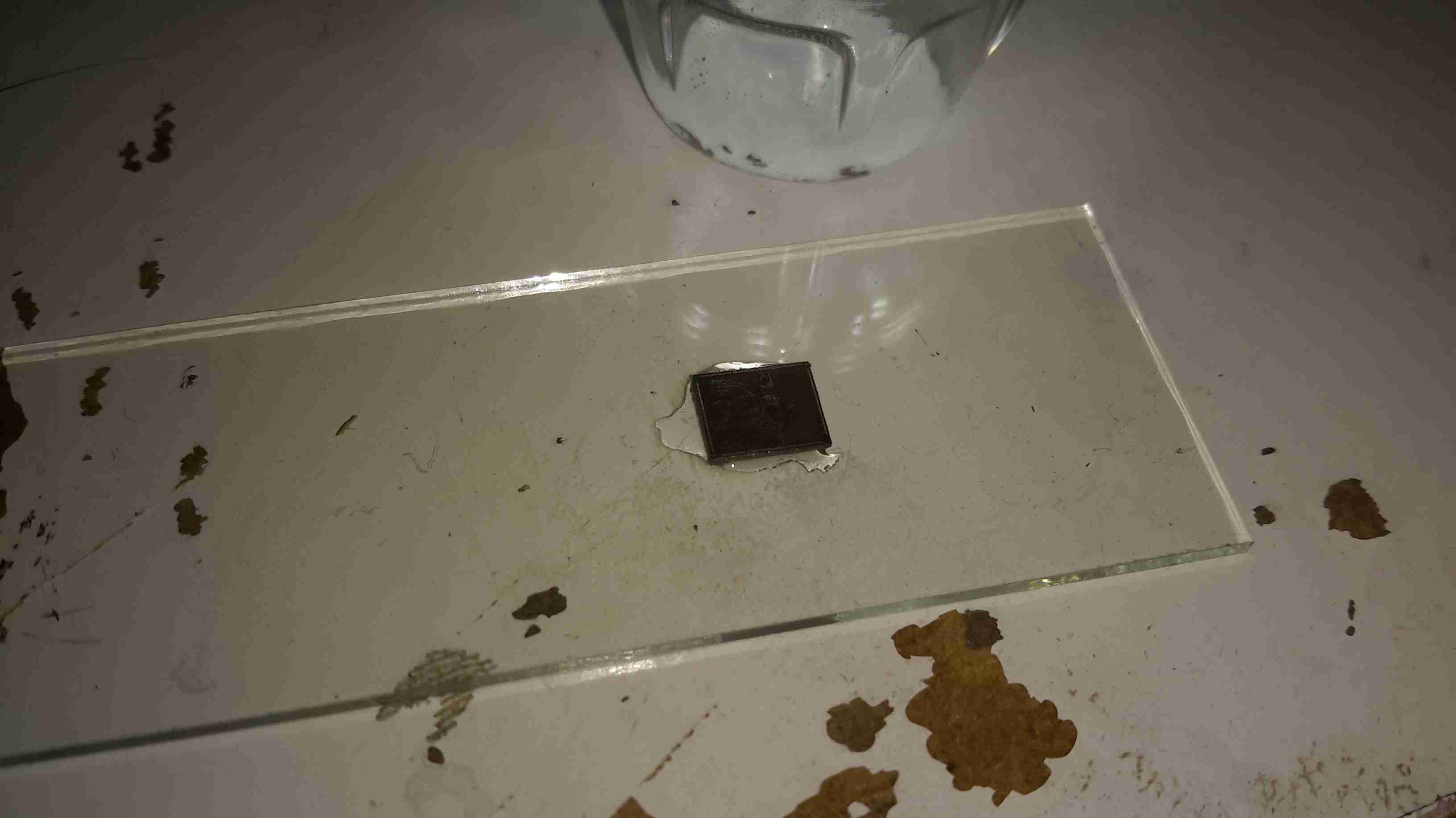
Now that the epoxy has been destroyed, it breaks apart easily, and is picked away until I uncover the die itself. (It’s the silver bit in the middle of the left half). The heat from the torch usually destroys the Silver epoxy holding the die to the leadframe, and can be removed easily from the remaining package.
Decapped
BGA packages are usually the easiest to decap, flip-chip packages are a total pain due to the solder balls being on the front side of the die, I haven’t managed to get a good result here yet, I’ll probably need to chemically remove the first layer of the die to get at the interesting bits 😉
Slide
Once the die has been rinsed in clean water & inspected, it’s mounted on a glass microscope slide with a small spot of Cyanoacrylate glue to make handling easier.
Some dies require some cleaning after decapping, for this I use 99% Isopropanol & 99% Acetone, on the end of a cotton bud. Any residual epoxy flakes or oxide stuck to the die can be relatively easily removed with a fingernail – turns out fingernails are hard enough to remove the contamination, but not hard enough to damage the die features.
Once cleaning is complete, the slide is marked with the die identification, and the photographing can begin.
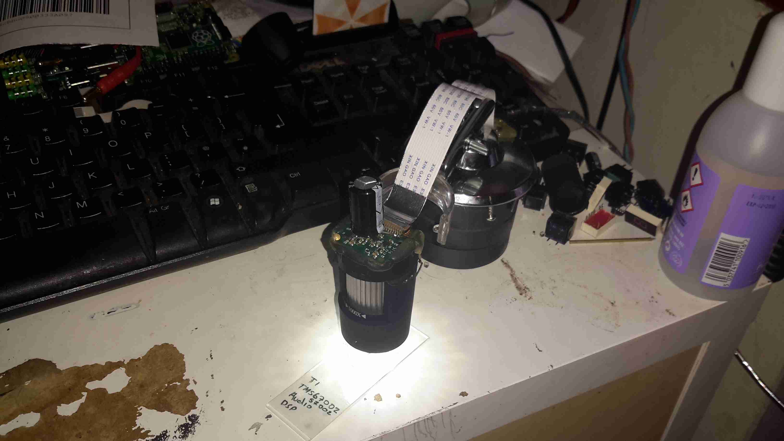
Microscope Mods
I had bought a cheap eBay USB microscope to get started, as I can’t currently afford a proper metallurgical microscope, but I found the resolution of 640×480 very poor. Some modification was required!
Modified Microscope
I’ve removed the original sensor board from the back of the optics assembly & attached a Raspberry Pi camera board. The ring that held the original sensor board has been cut down to a minimum, as the Pi camera PCB is slightly too big to fit inside.
The stock ring of LEDs is run direct from the 3.3v power rail on the camera, through a 4.7Ω resistor, for ~80mA. I also added a 1000µF capacitor across the 3.3v supply to compensate a bit for the long cable – when a frame is captured the power draw of the camera increases & causes a bit of voltage drop.
The stock lens was removed from the Pi camera module by careful use of a razor blade – being too rough here *WILL* damage the sensor die or the gold bond wires, which are very close to the edge of the lens housing, so be gentle!
Mounting Base
The existing mount for the microscope is pretty poor, so I’ve used a couple of surplus ceramic ring magnets as a better base, this also gives me the option of raising or lowering the base by adding or removing magnets.
To get more length between the Pi & the camera, I bought a 1-meter cable extension kit from Pi-Cables over at eBay, cables this long *definitely* require shielding in my space, which is a pretty aggressive RF environment, or interference appears on the display. Not surprising considering the high data rates the cable carries.
The FFC interface is hot-glued to the back of the microscope mount for stability, for handheld use the FFC is pretty flexible & doesn’t apply any force to the scope.
Die Photography
Since I modified the scope with a Raspberry Pi camera module, everything is done through the Pi itself, and the raspistill command.
Pi LCD
The command I’m currently using to capture the images is:
raspistill -ex auto -awb auto -mm matrix -br 62 -q 100 -vf -hf -f -t 0 -k -v -o CHIPNAME_%03d.jpg
This command waits between each frame for the ENTER key to be pressed, allowing me to position the scope between shots. Pi control & file transfer is done via SSH, while I use the 7″ touch LCD as a viewfinder.
The direct overhead illumination provided by the stock ring of LEDs isn’t ideal for some die shots, so I’m planning on fitting some off-centre LEDs to improve the resulting images.
Image Processing
Obviously I can’t get an ultra-high resolution image with a single shot, due to the focal length, so I have to take many shots (30-180 per die), and stitch them together into a single image.
For this I use Hugin, an open-source panorama photo stitching package.
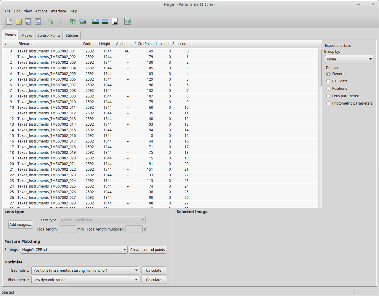
Hugin
Here’s Hugin with the photos loaded in from the Raspberry Pi. To start with I use Hugin’s built in CPFind to process the images for control points. The trick with getting good control points is making sure the images have a high level of overlap, between 50-80%, this way the software doesn’t get confused & stick the images together incorrectly.
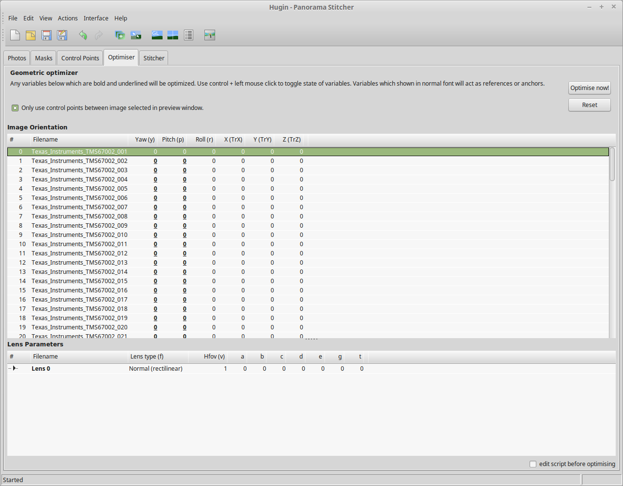
Optimiser
After the control points are generated, which for a large number of high resolution images can take some time, I run the optimiser with only Yaw & Pitch selected for all images.
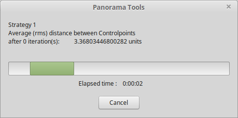
Optimising
If all goes well, the resulting optimisation will get the distance between control points to less than 0.3 pixels.
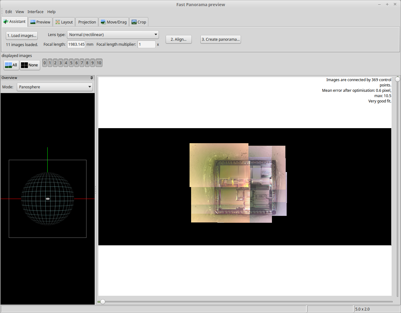
Panorama Preview
After the control points & optimisation is done, the resulting image can be previewed before generation.
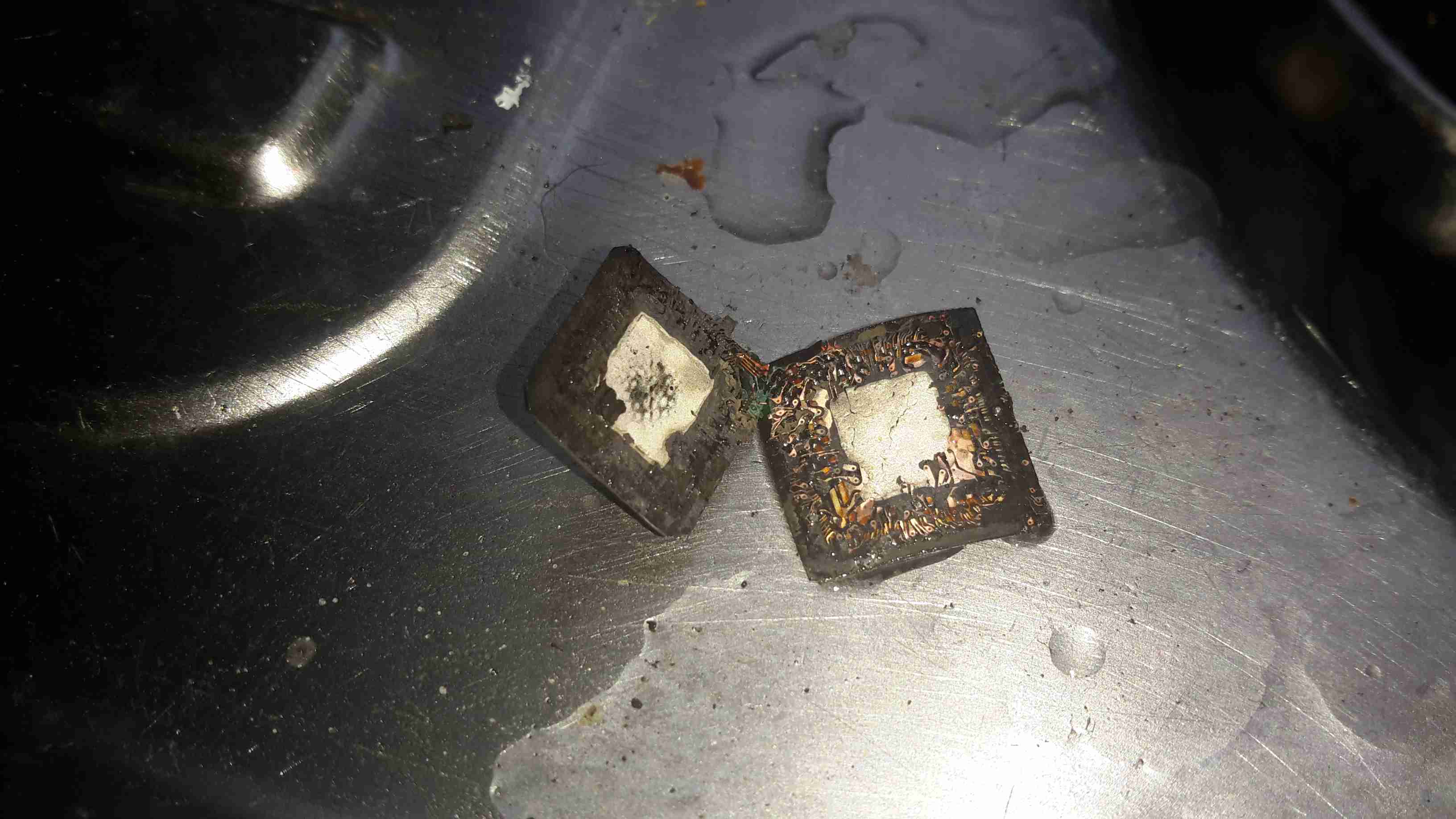
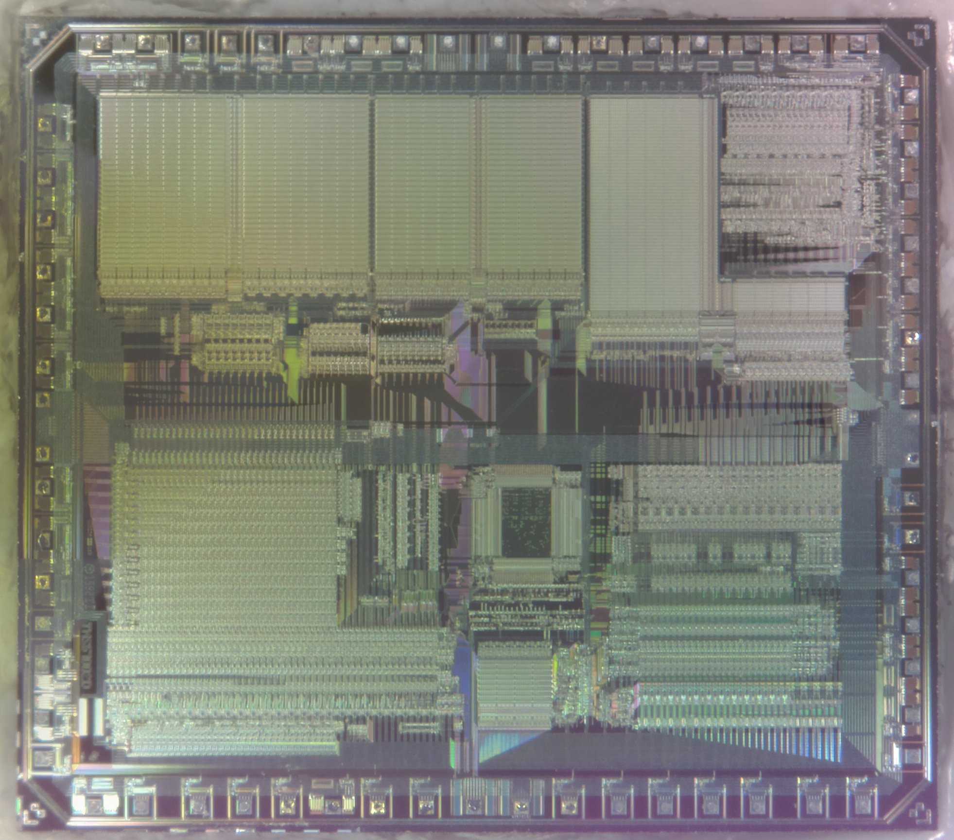
Texas Instruments TMS67002
After all the image processing, the resulting die image should look something like the above, with no noticeable gaps.
I’ve been working on something new for the blog, as I have a massive collection of scrap ICs – that is to decap the silicon & get them under a microscope!
Here’s the first image, a Texas Instruments part. This has been stitched together from 140 separate images to create the final version.
One of the central parts to the Eberspacher-type evaporative burner is the wire mesh screen that surrounds the glowplug, where the incoming fuel is heated to vapour before it’s blown into the combustion chamber & burned.
These screens, like glowplugs in the older heaters, are consumable parts and either get clogged with soot/tar or just eventually burn away.
The problem is that these parts (for what they are at least) are bloody expensive, so I’ve been looking to come up with something that can serve as a decent replacement for much lower cost.
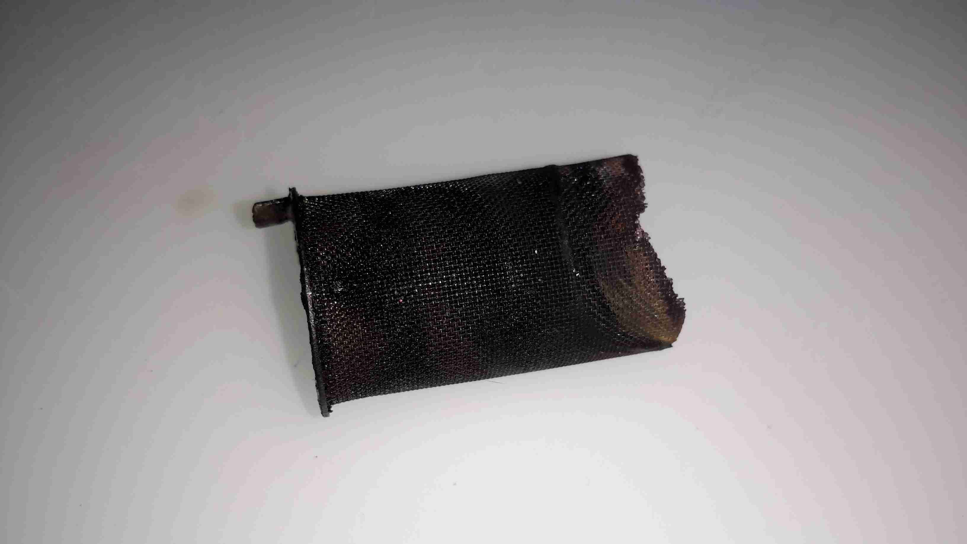
OEM Screen
Here’s a slightly used screen from my D1LCC heater, as can be seen the lower edge is already burning away even after only a few hours use. This edge tends to burn as the screen projects into the combustion chamber by about 1/4″, so it’s exposed to higher temperatures there. The rest of the screen is covered by the alloy casting that holds the burner. The mesh itself is stainless steel, and looks like something between 120-150 mesh.
The mesh is wound 2-3 turns, and spot welded to hold everything together. I would imagine to give more surface area for fuel vaporization. An unfortunate side effect of this is that the screen is much more susceptible to clogging as the mesh size is effectively reduced.
This also makes them damn near impossible to clean, as the carbon deposits get stuck between the layers in the screen. Applying a blowtorch flame to the entire screen & heating it to orange heat (~1200°C) does burn most of the crap out of them. Running Paraffin/Kerosene as the fuel also makes for a much cleaner burn, extending life.
(Assuming of course that the screen can be removed without totally destroying it – in my experience after many hours of running they seize in place & require sharp implements, violence & much swearing to remove, in several pieces.)
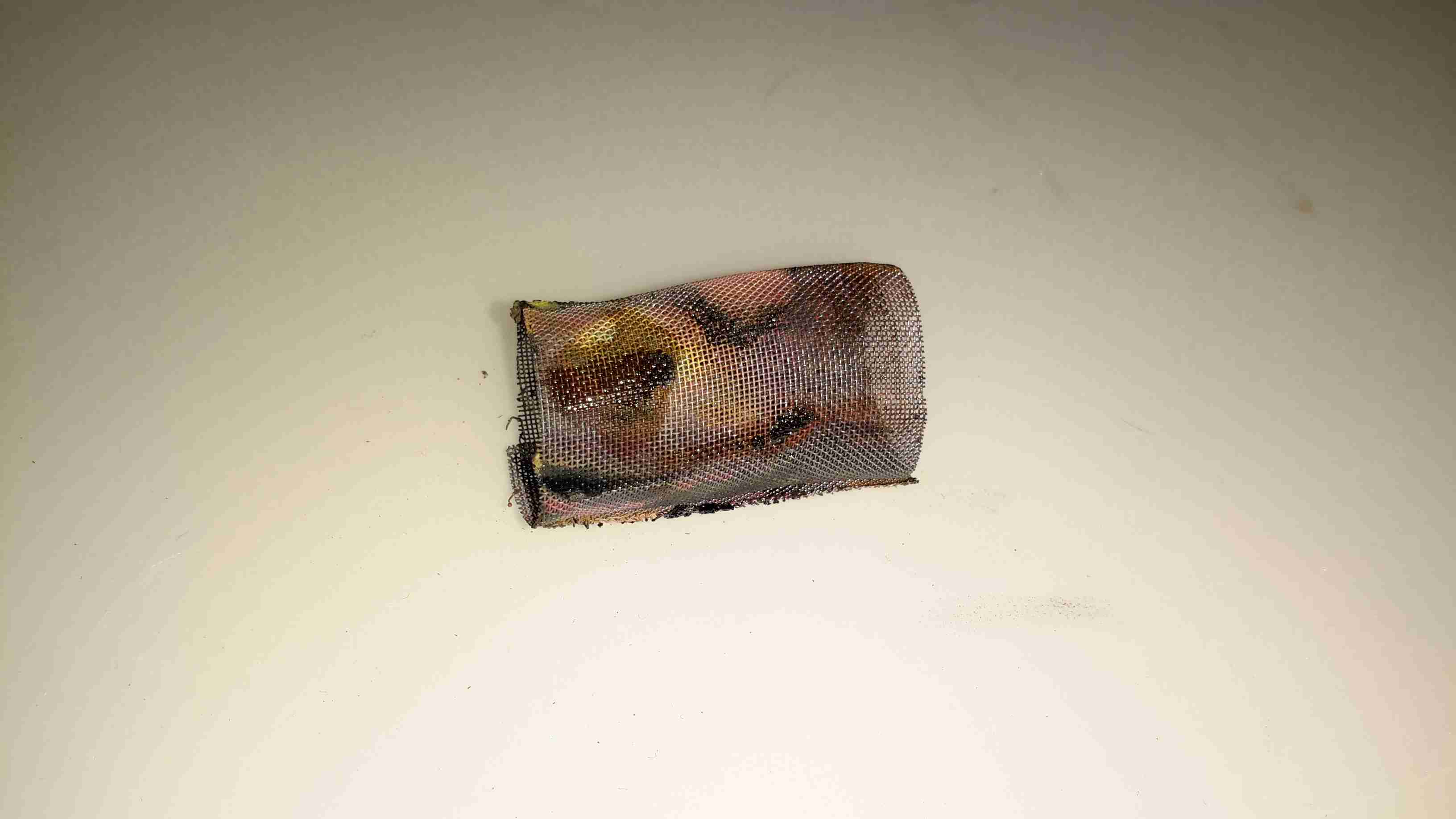
I had some copper mesh spare from a previous project, around the correct mesh size, so I figured I’d cut a piece to the same size as the official mesh & give it a go in the heater.
DIY Screen
Here’s my single-layer DIY screen after a couple of hours operation in the heater. Ignition time doesn’t seem to be impaired, there’s no smoke from the exhaust, and it appears that it’s staying cleaner than an OEM screen, since the mesh size is a little larger. I’ll have to monitor the situation & see how long these last, but if it’s anything close to the OEM screen life it’ll make maintenance much cheaper.
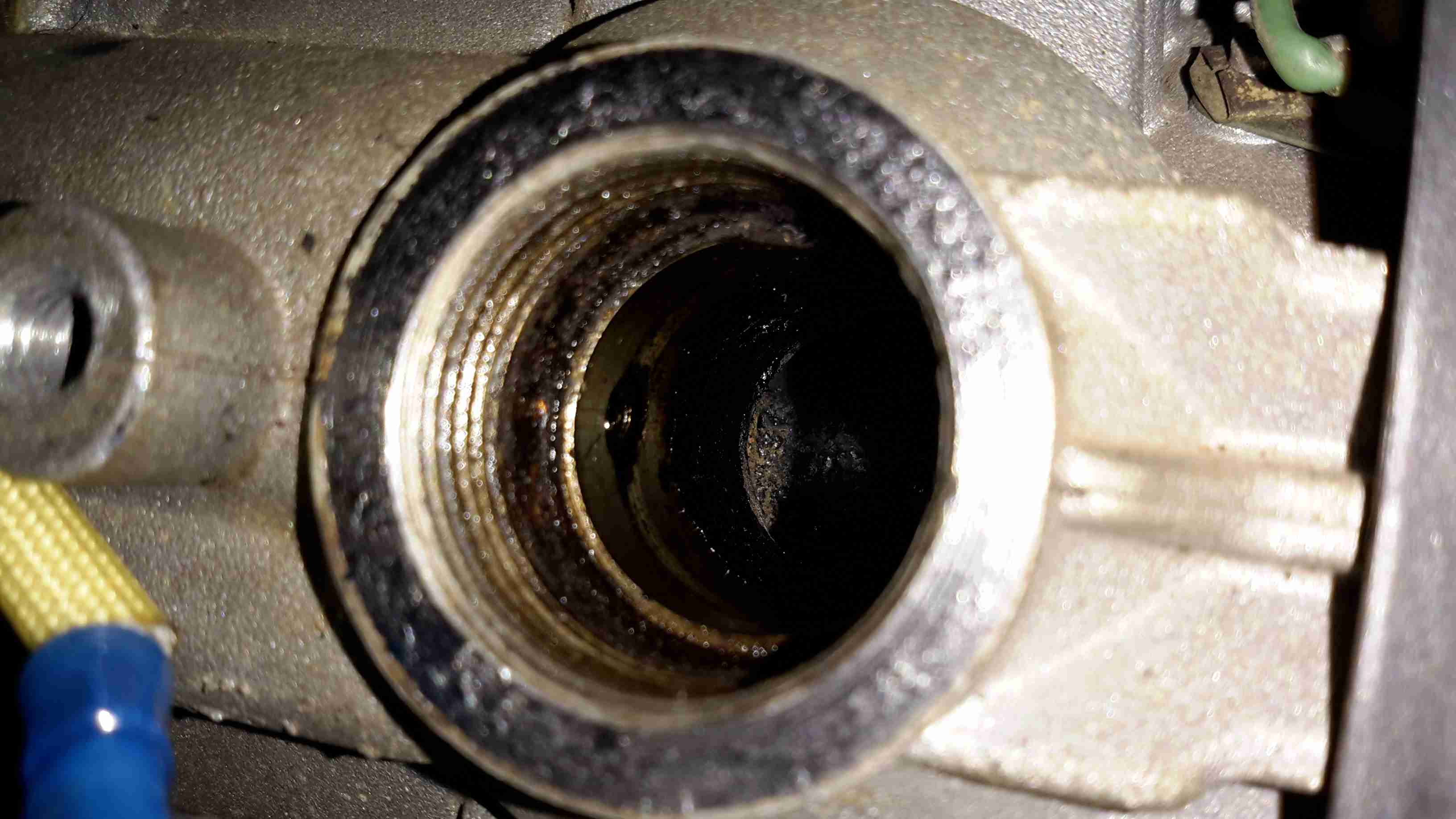
Fuel Inlet
This is the opening that holds the glowplug & it’s screen. The fuel inlet can be seen on the left wall of the chamber, with a circular groove that feeds fuel onto the screen in operation.
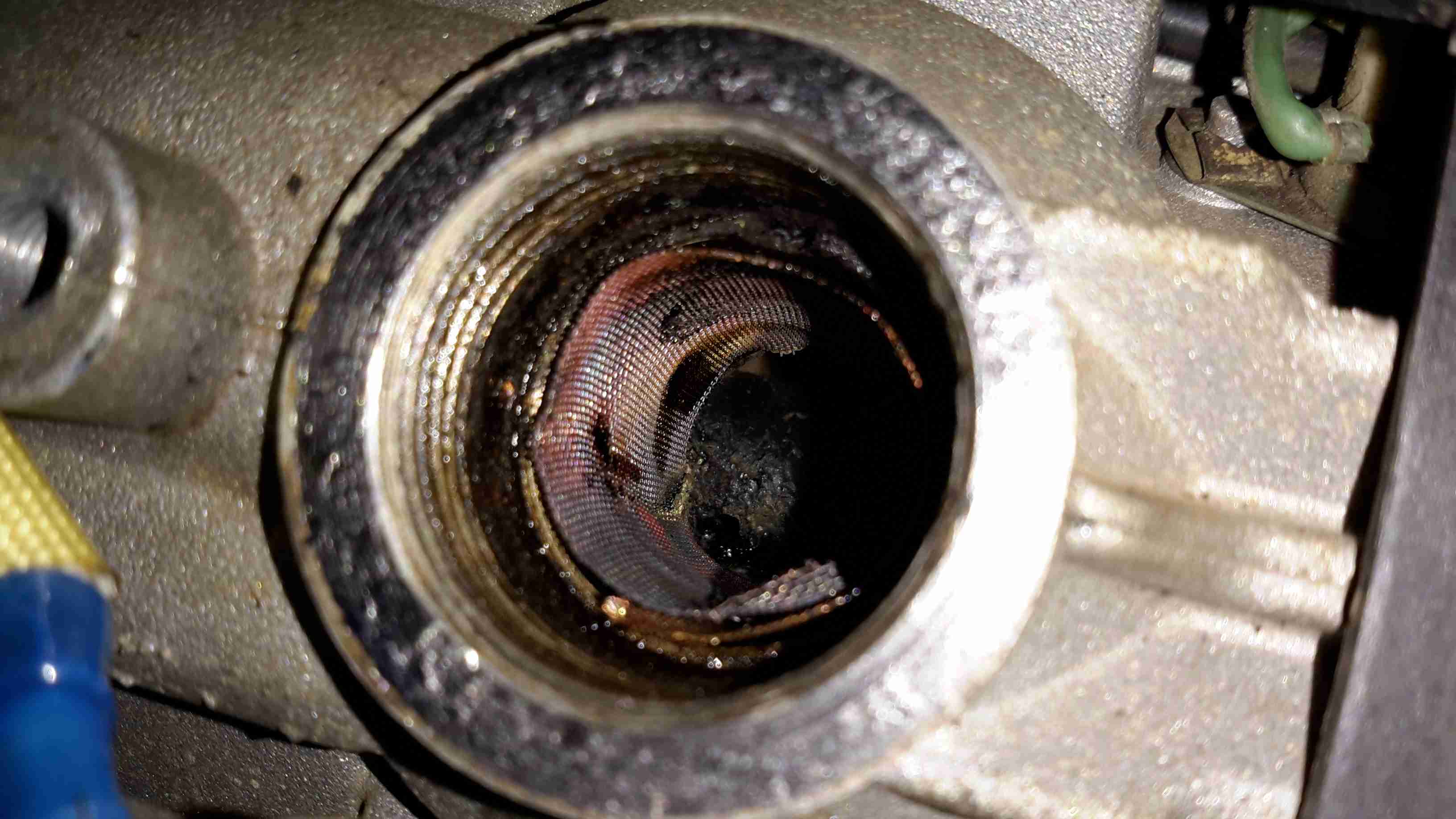
DIY Screen Fitted
And here’s the DIY screen in place, it’s obviously not as good a fit as the OEM version, but it’s sufficient to do the job!
Glowplug
Finally, here’s the glowplug itself. Possibly the beefiest plug I’ve ever seen, even in large diesel engines.
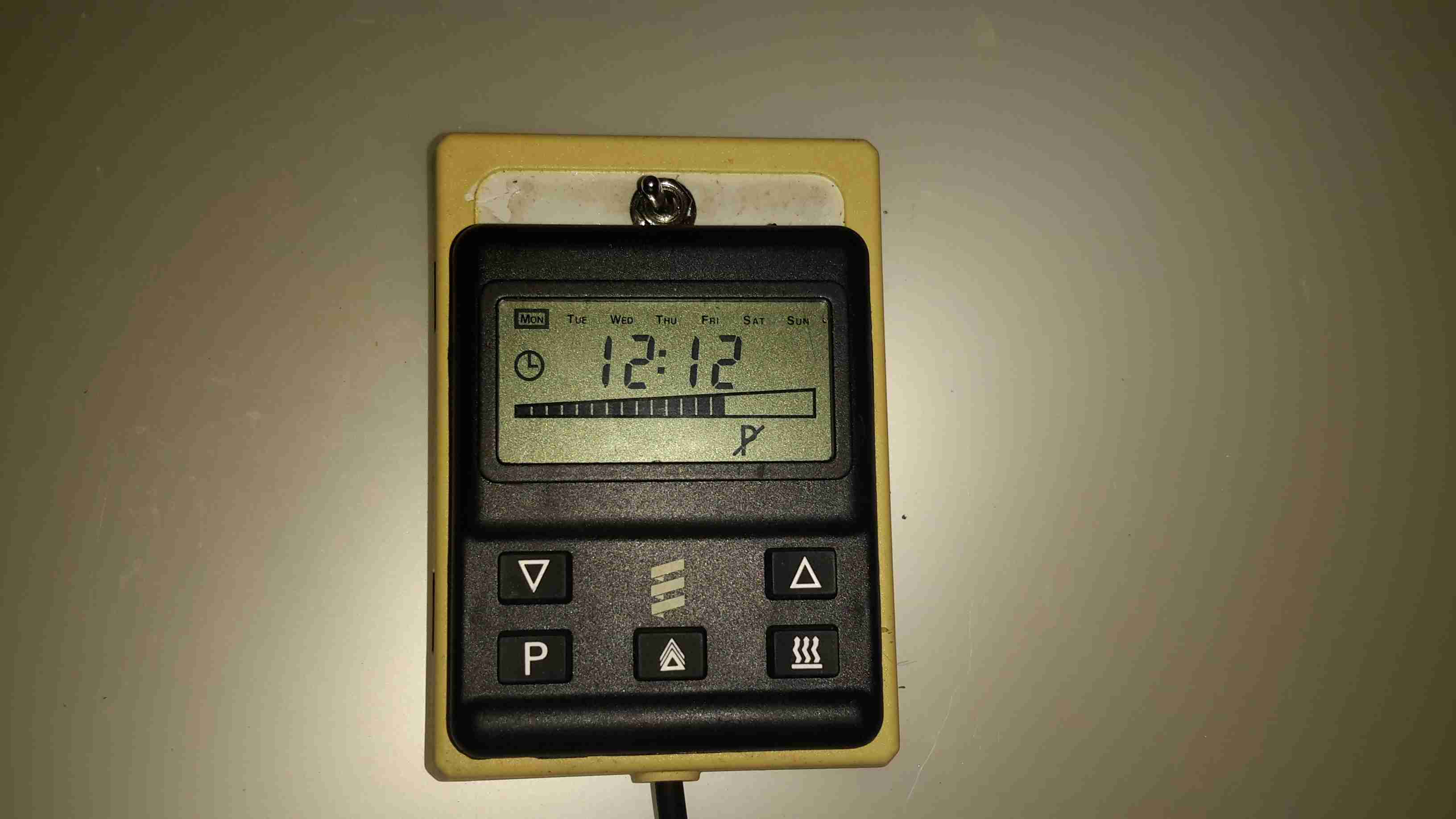
The Eberspacher heaters can be controlled with a single switch, but it’s more convenient to have some temperature control & the option of a timer. Above is an ex-BT 701 series controller, with built in 7-day programmer. Being an ex-BT van version though, it’ll only switch the heater on for 1 hour at a time.
To get around this slight niggle, I fitted a bypass toggle switch.
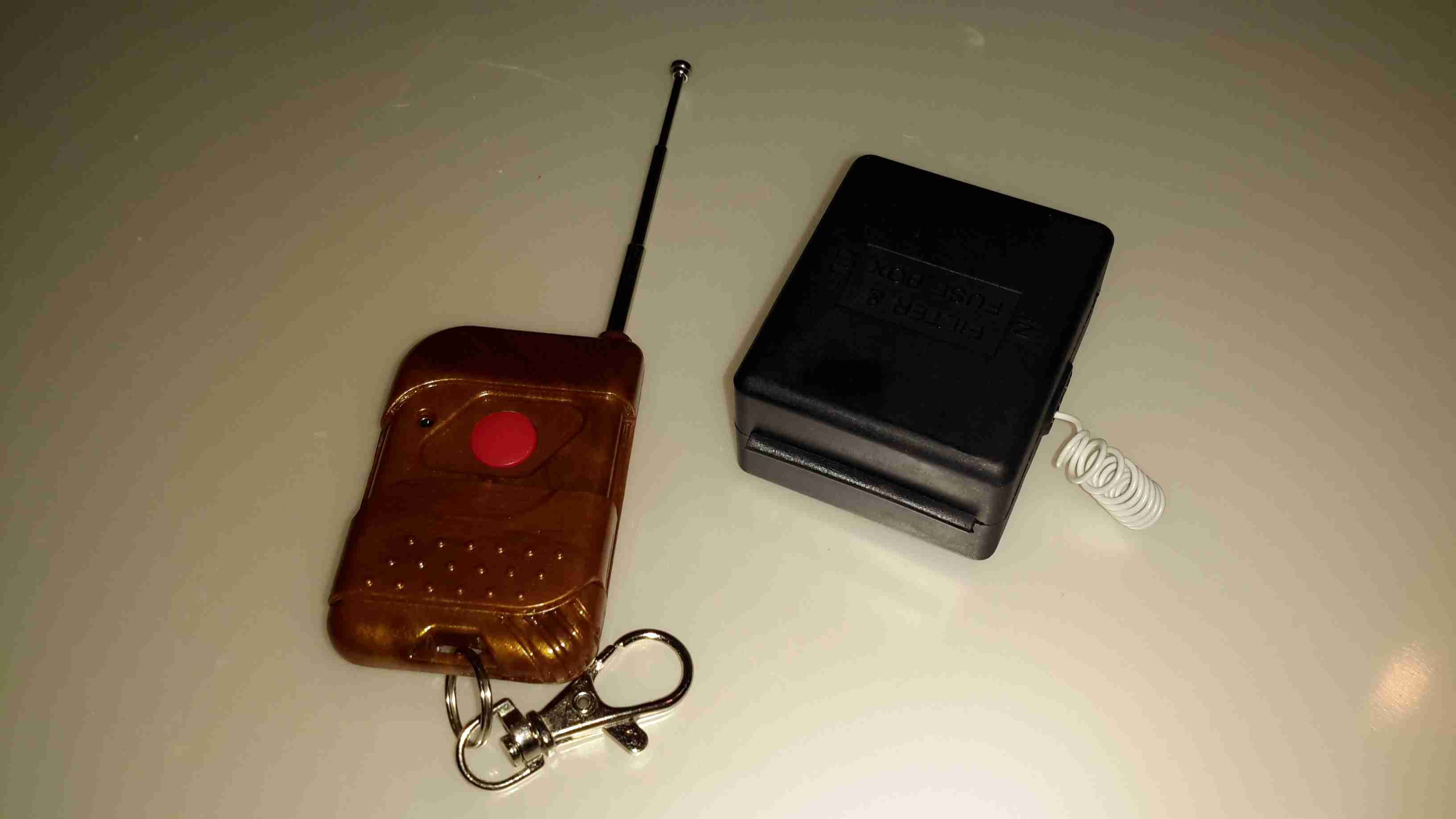
Remote Control
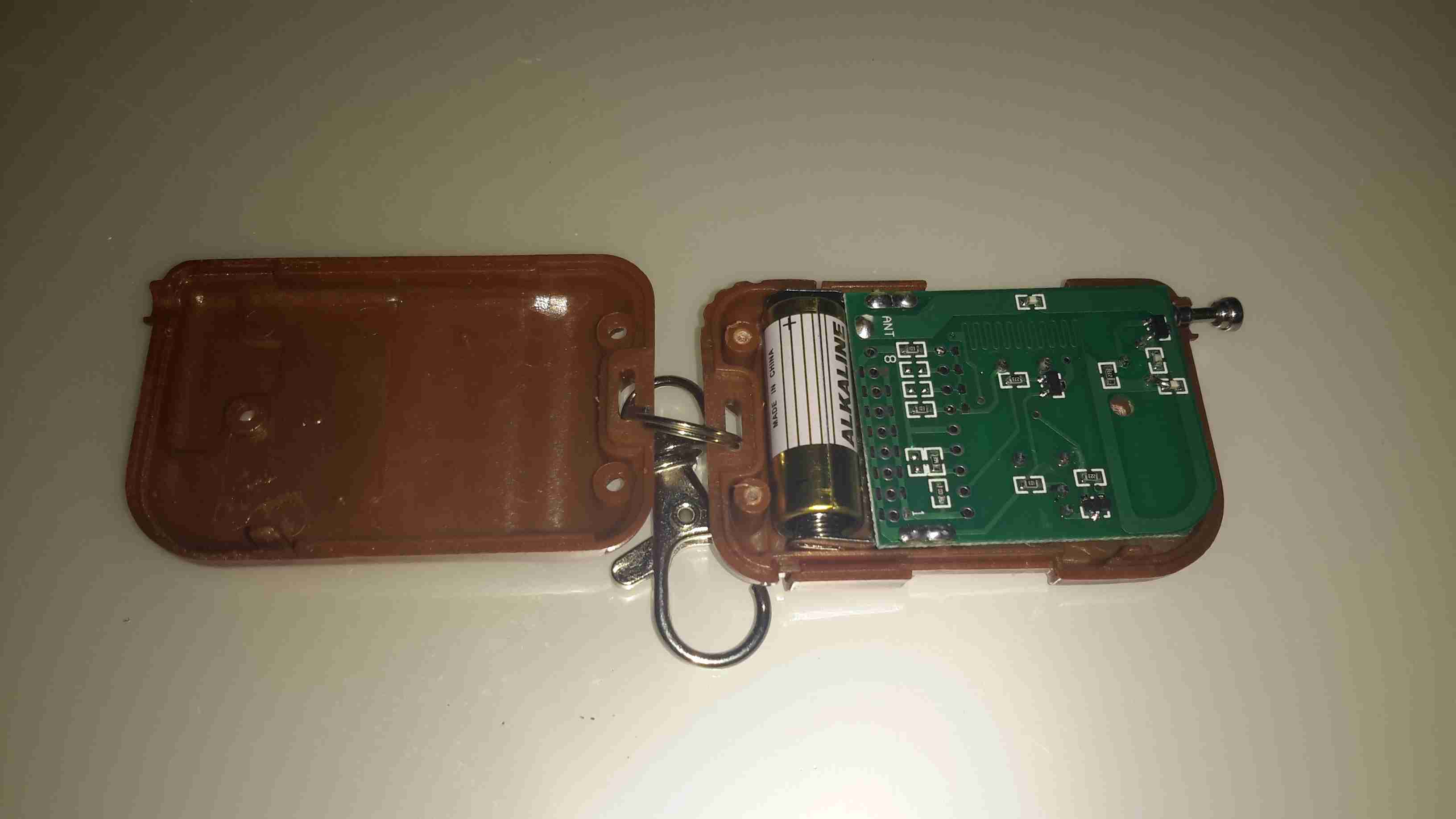
For a bit of extra convenience, I got an RF remote controlled relay module from eBay (£5).
This allows me to switch things on remotely, so I can return to a nice toasty tent while camping.
There is an official RF remote for Eberspacher heaters, but I’ve no doubt they’re hideously expensive.
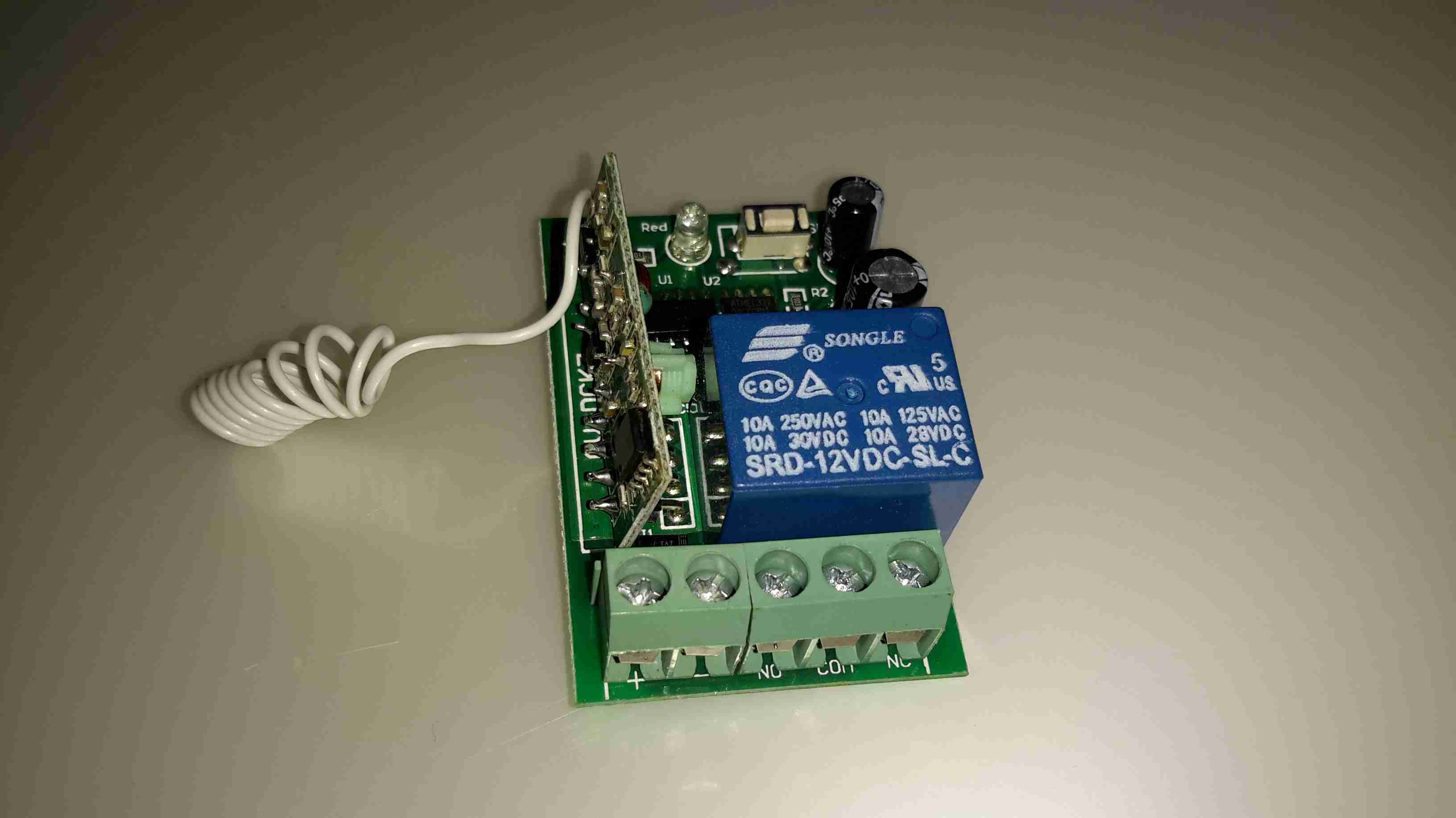
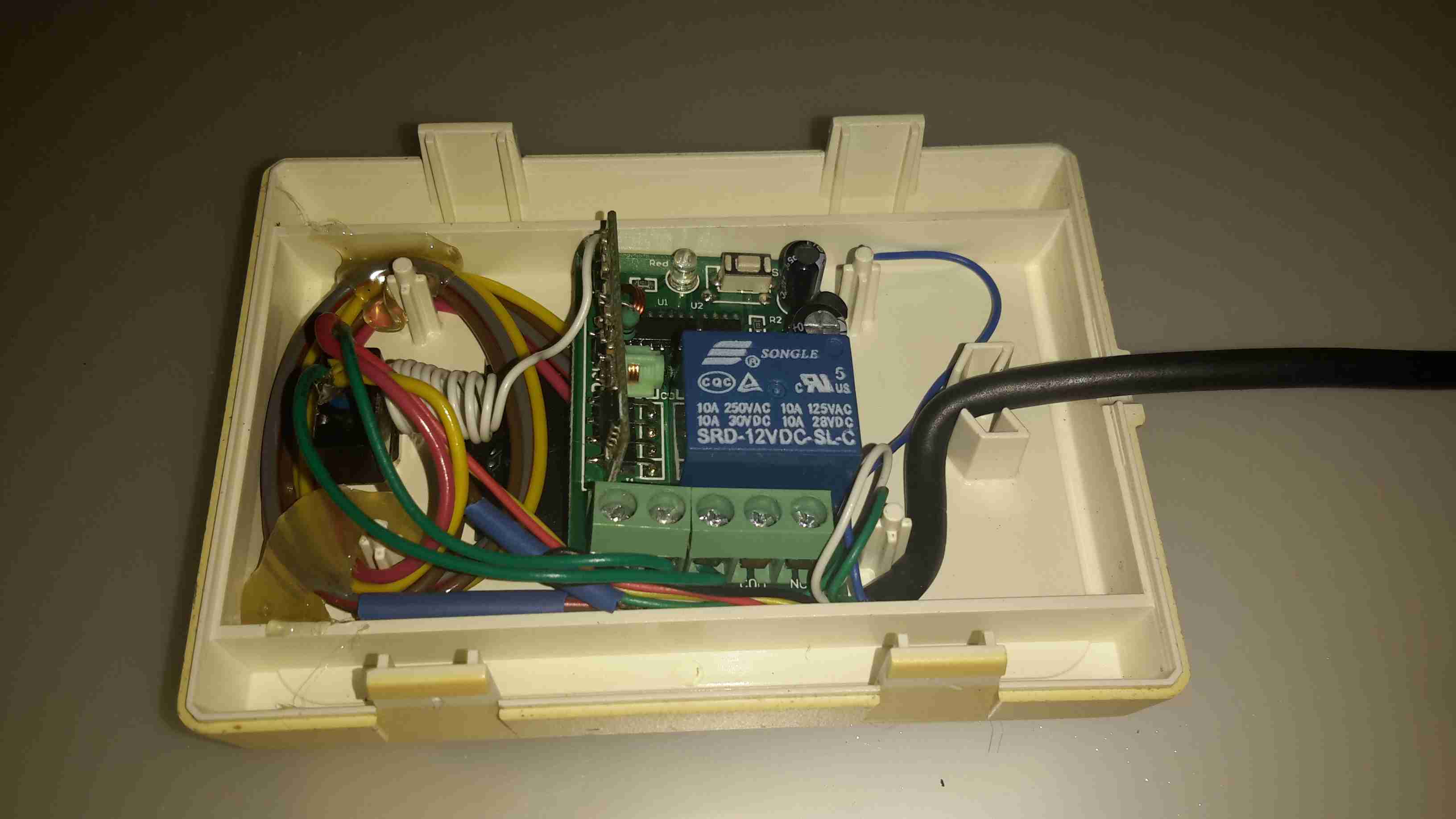
RF Receiver
Here’s the receiver PCB, there’s an EEPROM & a microcontroller onboard for handling the codes the remotes send, but as the number has been scrubbed off the micro, no data there. This uses a standard RF receiver module.
RF Remote
Here’s the remote itself, this uses a 12v battery instead of a 3v lithium cell. A little of a pain since these batteries can be a bit pricey.
As this RF system operates on 315MHz, it’s technically illegal in the UK, but I was unable to find a 433MHz version with the features required. Nevermind ;).
Controller Internals
Here’s the module installed in the controller casing. I have since run the antenna wire around the edge of the case to try & get the furthest range on receive. The relay contacts are just paralleled across the bypass switch, so when the relay energizes the heater fires up.
Luckily the thermostatic control portion of the 701 programmer is operational even when heating mode is not active.
I go camping on a regular basis here in the UK, and often even in summer it’s horribly cold at night in a field somewhere in the middle of Leicestershire. This doesn’t go too well with my severe aversion to being cold.
For the past several years I’ve used a Tilley lamp for some heat & light while at festivals & general camping, but it’s heat output is less than stellar when used in a 6-man tent.
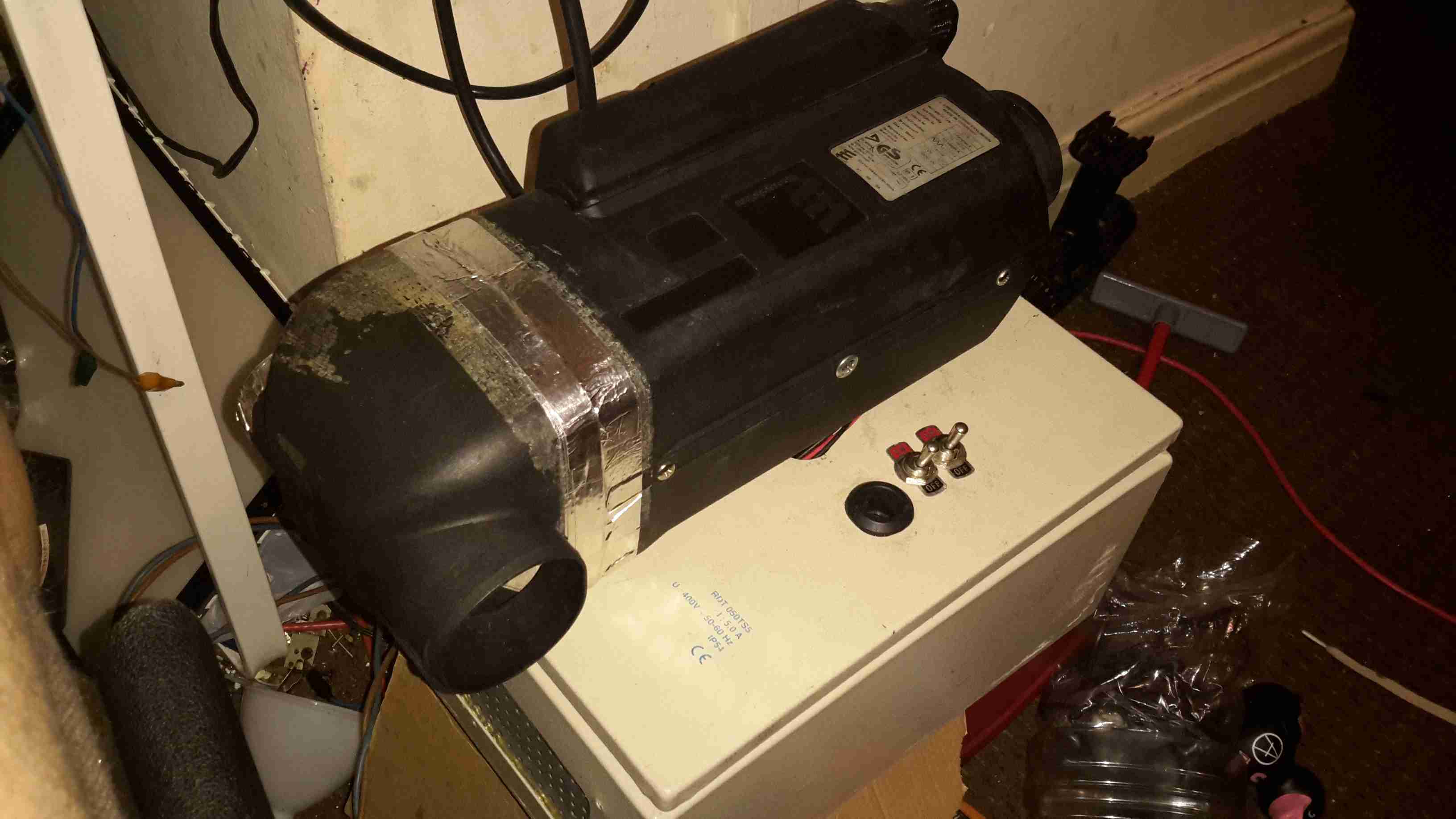
An Eberspacher diesel heater was what was required for the job. Above is the unit as it’s built at the moment – I’ve used an old D1LCC 1.8kW heater that was recently decommissioned from nb Tanya Louise, as it’s getting a bit funny about what kind of fuel it’ll run on in it’s old age. It’ll work perfectly well on kerosene though – a fuel I already take with me camping for the Tilley.
It’s mounted on a base box, which is a repurposed steel electrical junction box that saw a previous life containing a 3-phase fan motor controller.
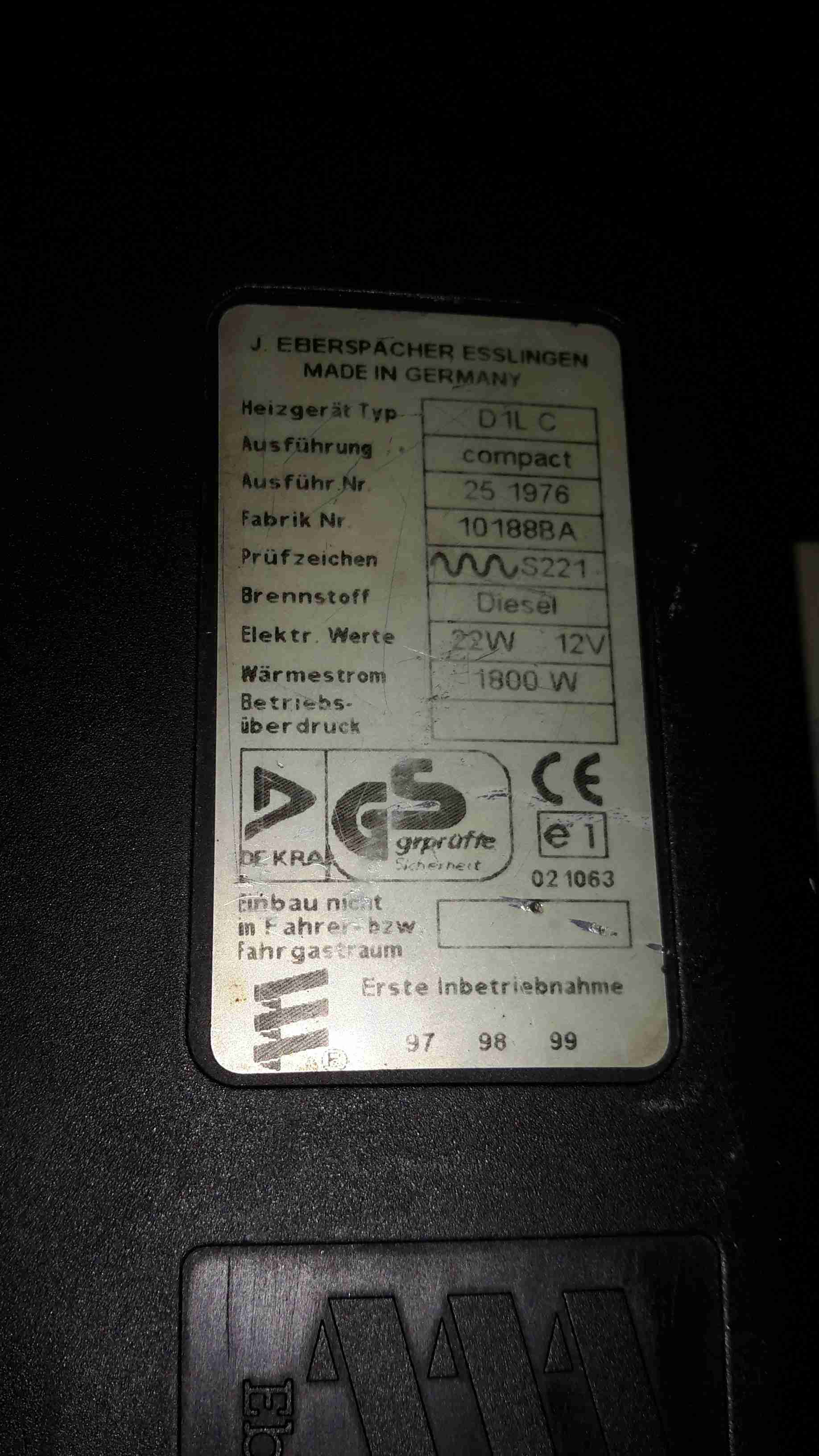
Data Plate
Here’s the info on the heater unit itself. Drawing 22W of power at 12v I’ll be getting 1.8kW of heat output – sounds good to me.
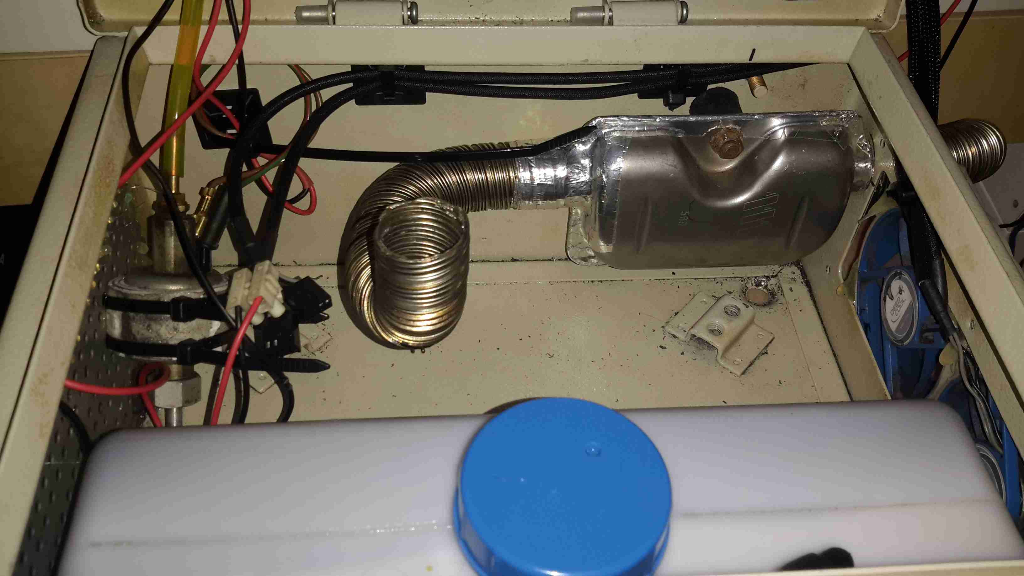
Box Internals
Here’s a view into the base box before the circulation fans were fitted, in early prototype stage. I used a small toroid as a clunk on the end of the rubber fuel line 😉
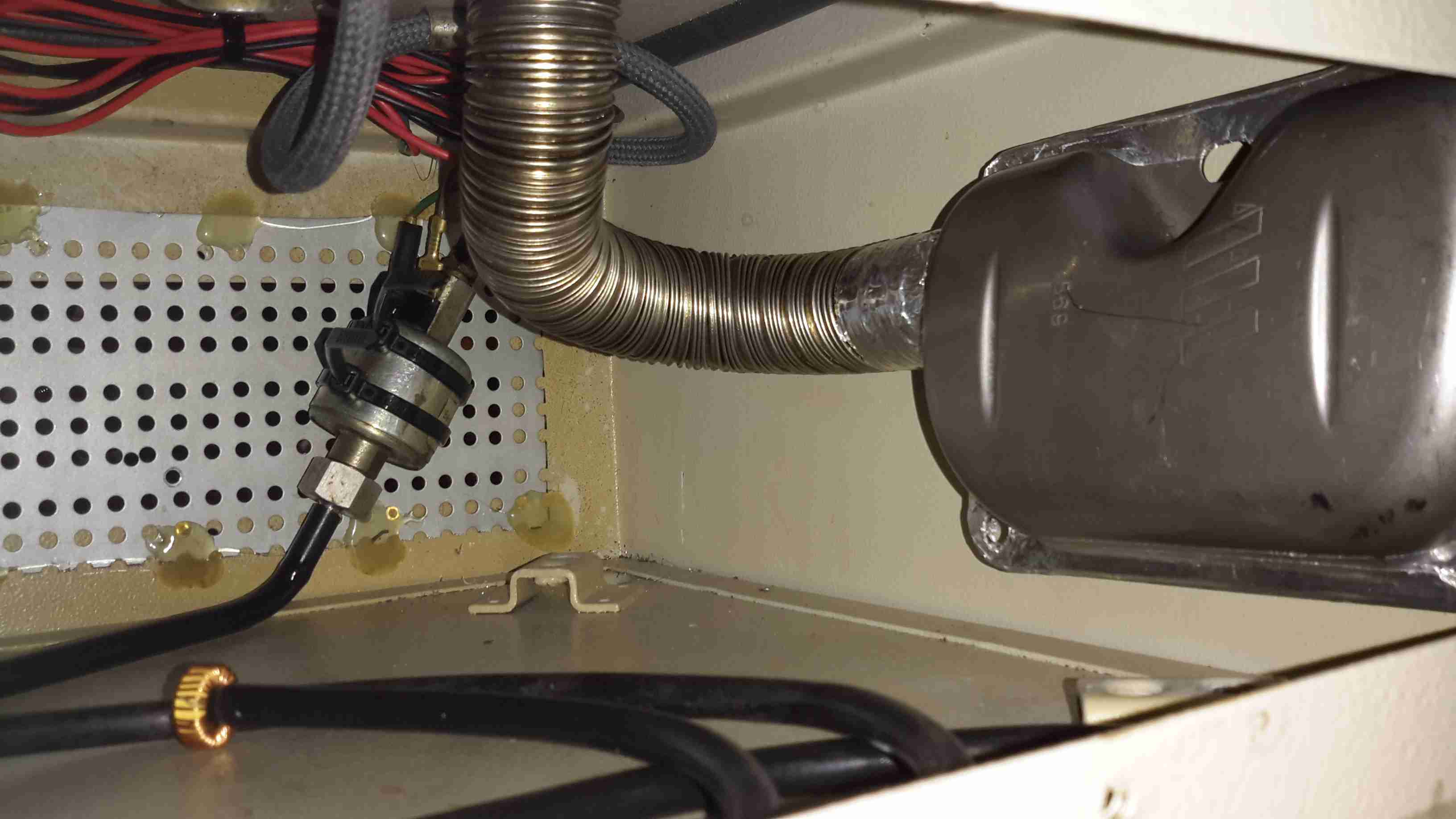
Support Components
After a few bits from the Great eBay arrived, here’s the internals of the base unit at present. The fuel tank is a repurposed 2L fridge water container – made of tough HDPE so it’s fuel resistant.
The fuel pump is mounted on the left side next to the tank – having been wrapped in some foam to deaden the continual ticking noise it creates. The exhaust & it’s silencer are mounted at the rear, the silencer being retained by a surplus rubber shock mount. Luckily the exhaust systems on these heaters don’t get particularly hot, so the rubber doesn’t melt.
The exhaust outlet is routed through the frame, to be attached to an external hose. I don’t want combustion gases in the tent with me!
Standard Eberspacher silencers also aren’t gas-tight from the factory – they’re designed to be used in the open on the underframe of a vehicle, so I’ve covered all the seams in aluminium tape to make the system airtight.
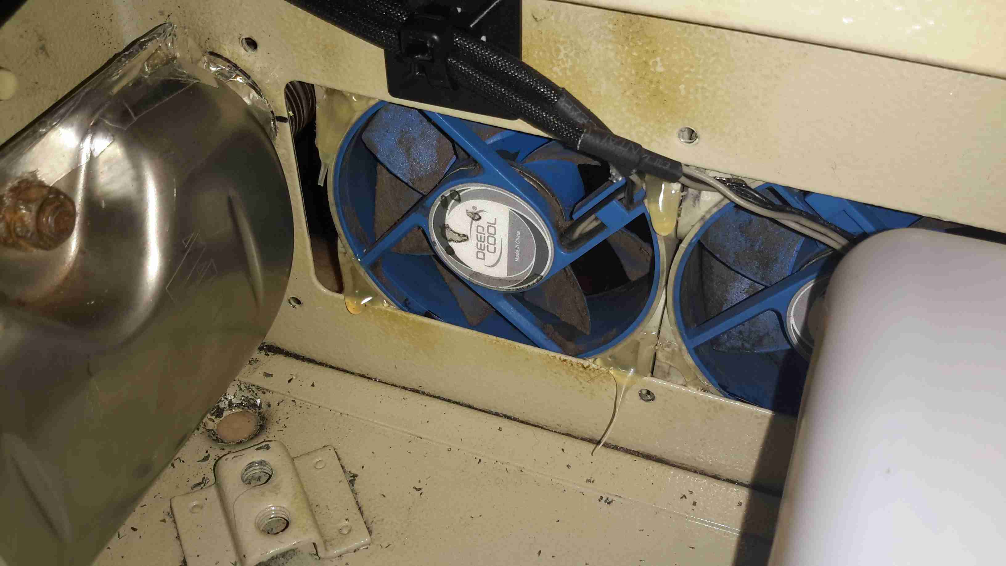
Ventilation
To make sure that the support components don’t get overheated with the exhaust being in such close proximity, and to pull a little more heat out of the system, a pair of slow-running 80mm fans has been fitted to the end of the box. These blow enough air through to give a nice warm breeze from the vents on the other end of the base.
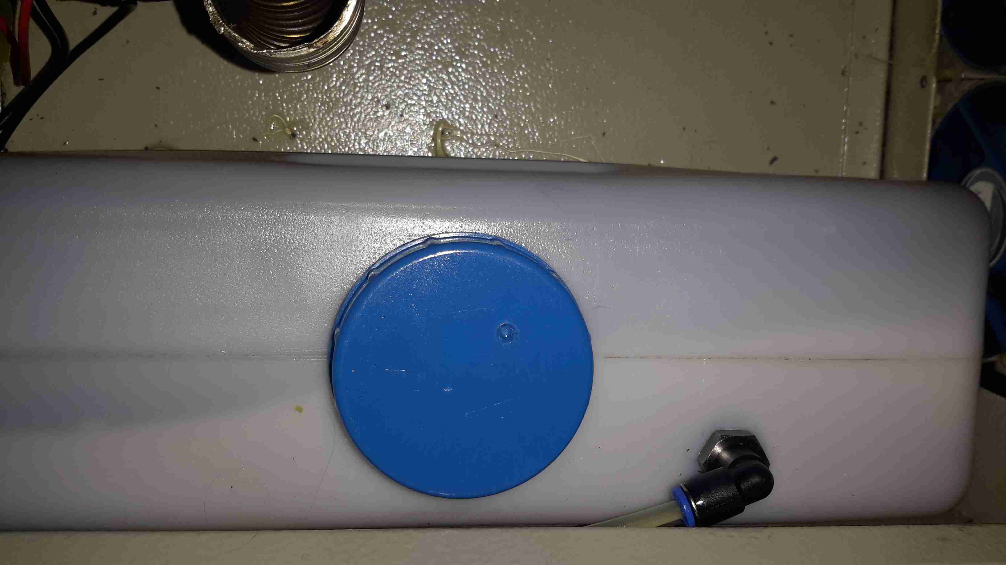
Fuel Tank
The tank I’ve used just so happened to be the perfect size to fit into the base box, and to tap the fuel off a bulkhead fitting was put into the top of the tank, with a dip tube on the other side. The fuel line itself is tiny – only 4mm.
If the specifications from Eberspacher are to be believed, 2L of fuel on board will allow the system to run for about 8 hours on full power, or 16 hours on minimum power.
Being inside the base, refuelling is a little awkward at the moment, the heater has to completely cool before the exhaust can be detached without receiving a burn, so I’ll be building in a fuel transfer system from an external jerry can later to automate the process – this will also help to avoid messy fuel spills.
More to come when the rest of the system is worked out!
Inkeeping with everything else in my shack being low voltage operated, I had planned from the outset to convert the desoldering station to 12v operation. It turns out this has been the easiest tool to convert in my shack so far.
PSU Outputs
The factory SMPS is a fairly straightforward 18v 12A unit, with only a single small oddity: the desoldering gun’s heating element is controlled from inside the supply.
Iron MOSFET
Next to the output rectifier on the heatsink is a large MOSFET, in this case a STP60NF06 from ST Micro. This is a fairly beefy FET at 60v & 60A capacity, RDS On of <0.016Ω.
This is driven via an opto-isolator from the main logic board. I’ve not yet looked at the waveform on the scope, but I suspect this is also being PWM’d to control temperature better when close to the set point.
Iron Element Controller
Rather than fire up the soldering iron & build a new element controller circuit (Lazy Mode™), I opted to take a saw to the original power supply. I cut the DC output section of the PCB off the rest of the supply & attached this piece back to the frame of the base unit. I also added a small heatsink to the MOSFET to make sure it stays cool.
12v Power Supply
Since the fan & vacuum pump are both already 12v rated, those are connected directly to the DC input socket, that I’ve installed in place of the original IEC mains socket. The 18v for the heating element is generated by a 10A DC-DC converter, again from eBay.
Oddly, the iron itself is rated at 24v 80W, but the factory supply is only rated to 18v. I’m not sure why they’ve derated the system, but as the station already draws up to 10A from a 13.8v supply, increasing the voltage any further would start giving my DC supplies a problem, so it can stay at 18v for now.
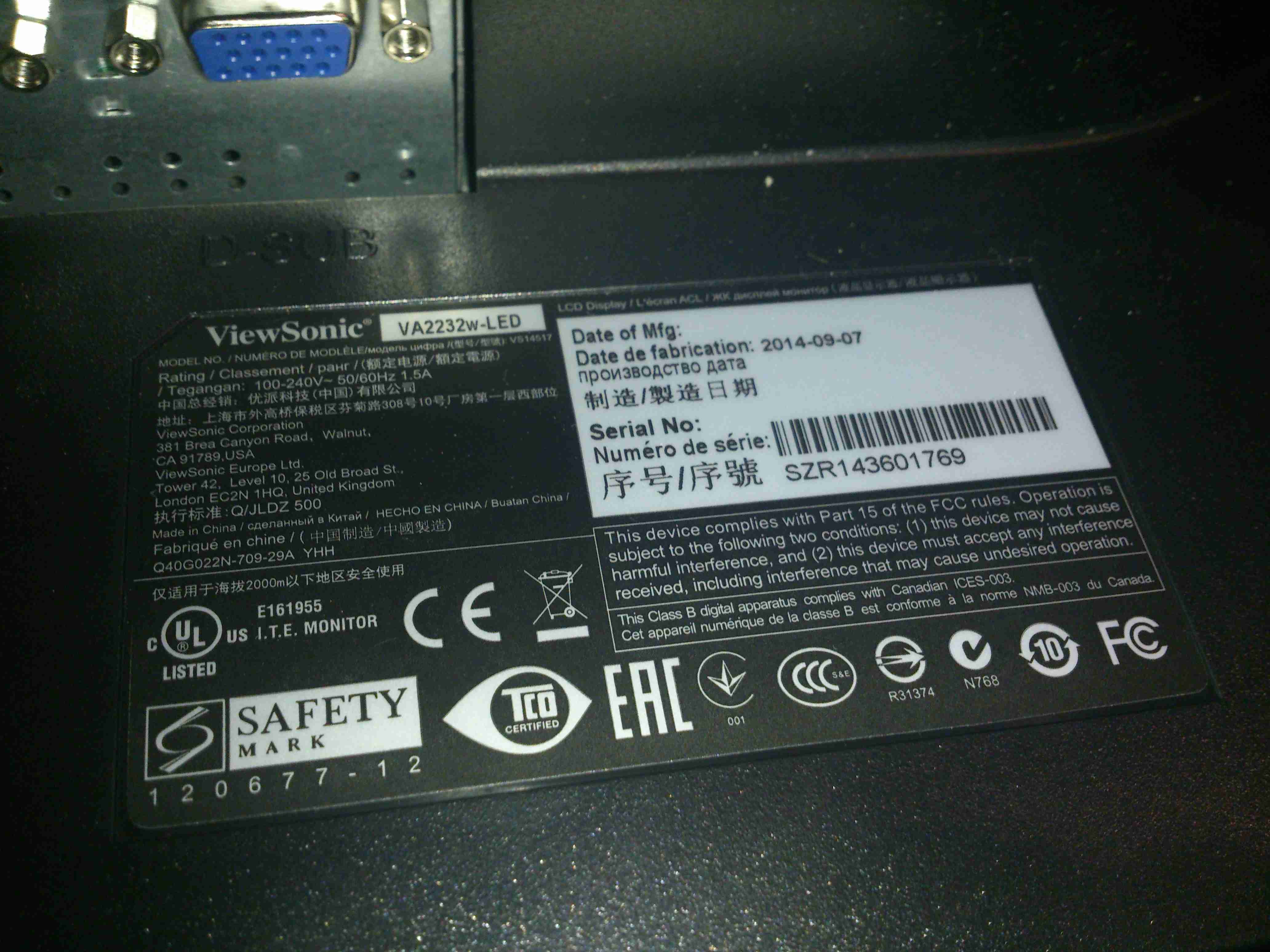
On the quest to get things on board replaced that are heavy users of power, the monitor in the main cabin was next. The original CCFL-backlit monitor was very heavy on 12v power, at 5A. This meant falling asleep watching TV would result in severely flattened batteries.
Replacement with a suitable LED-backlit monitor was definitely required. The cheapest on eBay was a ViewSonic VA2232W-LED, so I took to work converting it from 240v to 12v operation.
Back Cover Removed
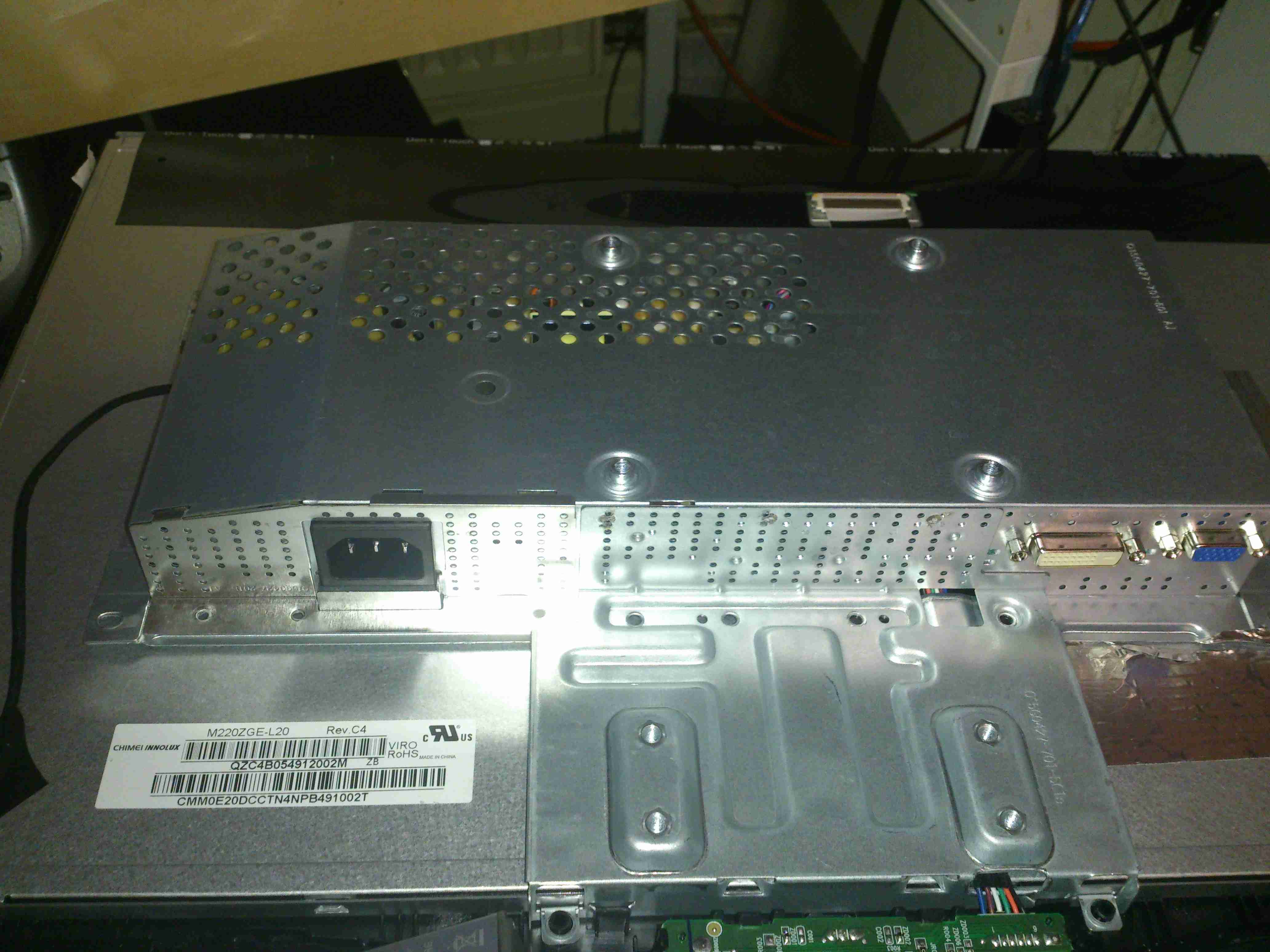
There are no screws holding these monitors together, so a spudger & frequent swearing got the back off. The shield holding the circuitry is also not screwed down, only attached to the back of the LCD panel with aluminium shielding tape.
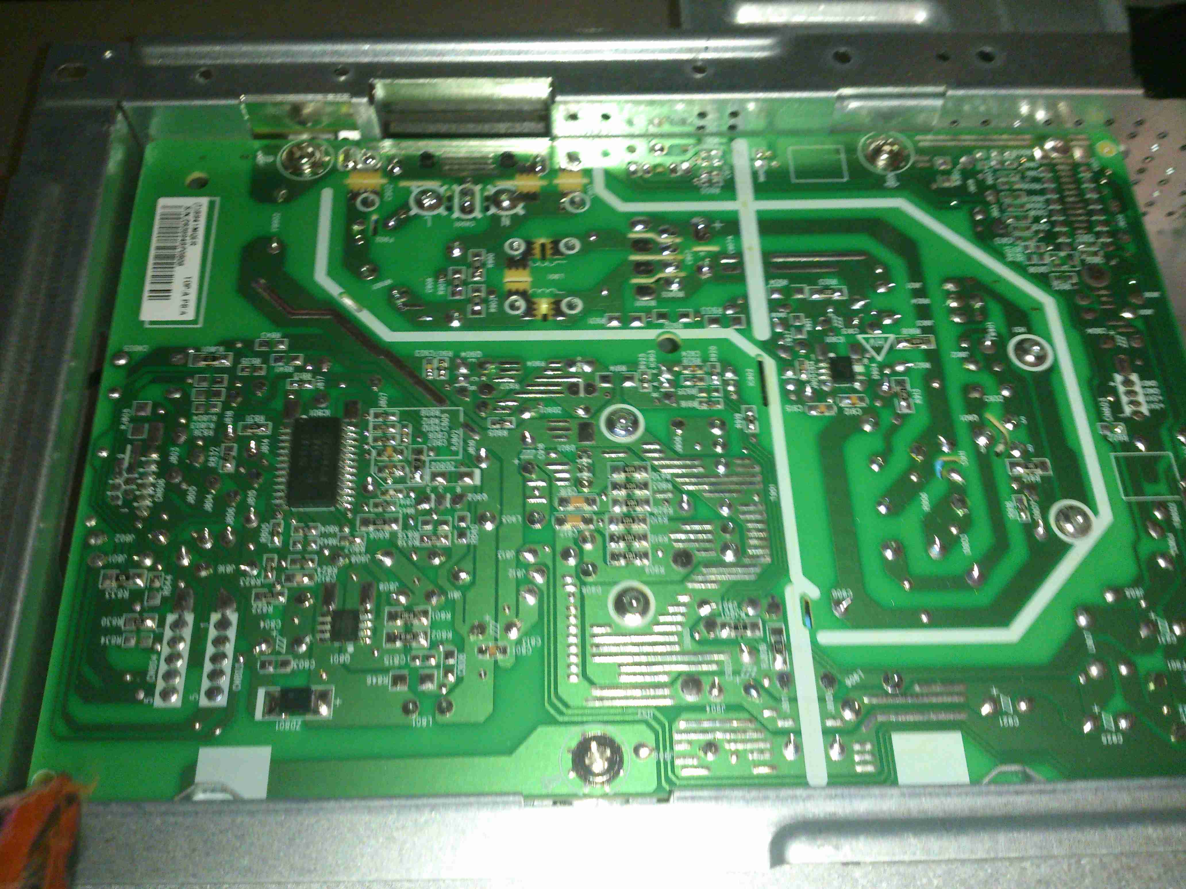
Power PCB Trackside
Once the tape has been cut, the main power board is accessible. The large IC on the left is the main backlight LED driver.
In this case the monitor requires a pair of rails from the supply, 18.5v for the backlight circuitry & 5v for the logic.
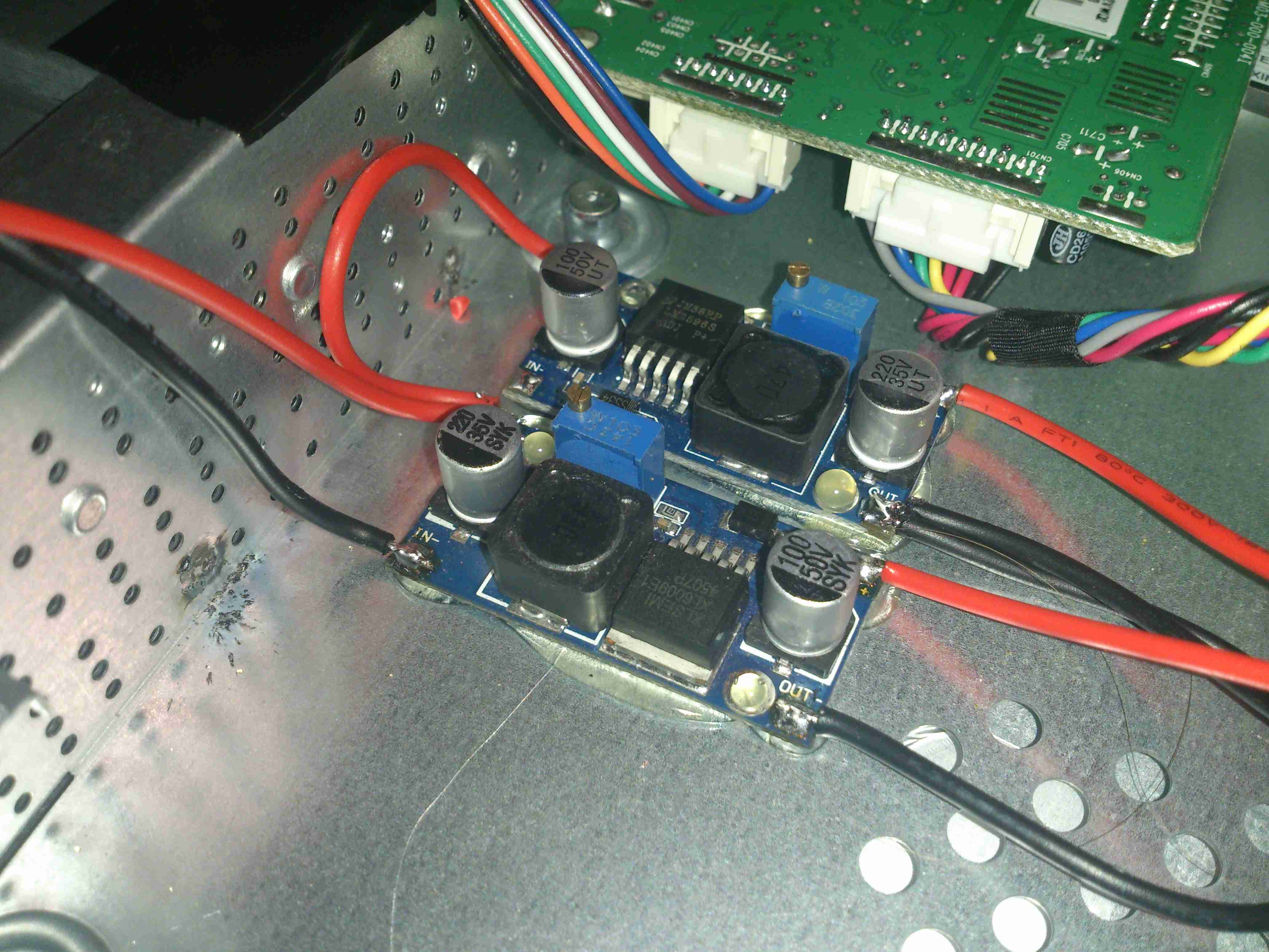
DC-DC Regulators
A pair of DC-DC converters has been fitted in the small space between the power & control boards.
PCB Connection Points
To save me some work & keep maximum compatibility, I’ve not modified the existing supply, just attached the new DC-DC converter outputs onto the corresponding outputs of the factory PSU. The 12v input leads are routed out of the same gap as the mains IEC connector, with some hot glue over the mains input solder points to provide some more insulation.
Wiring Tidied
The wiring is tidied up with hot glue so the back cover will go back on.
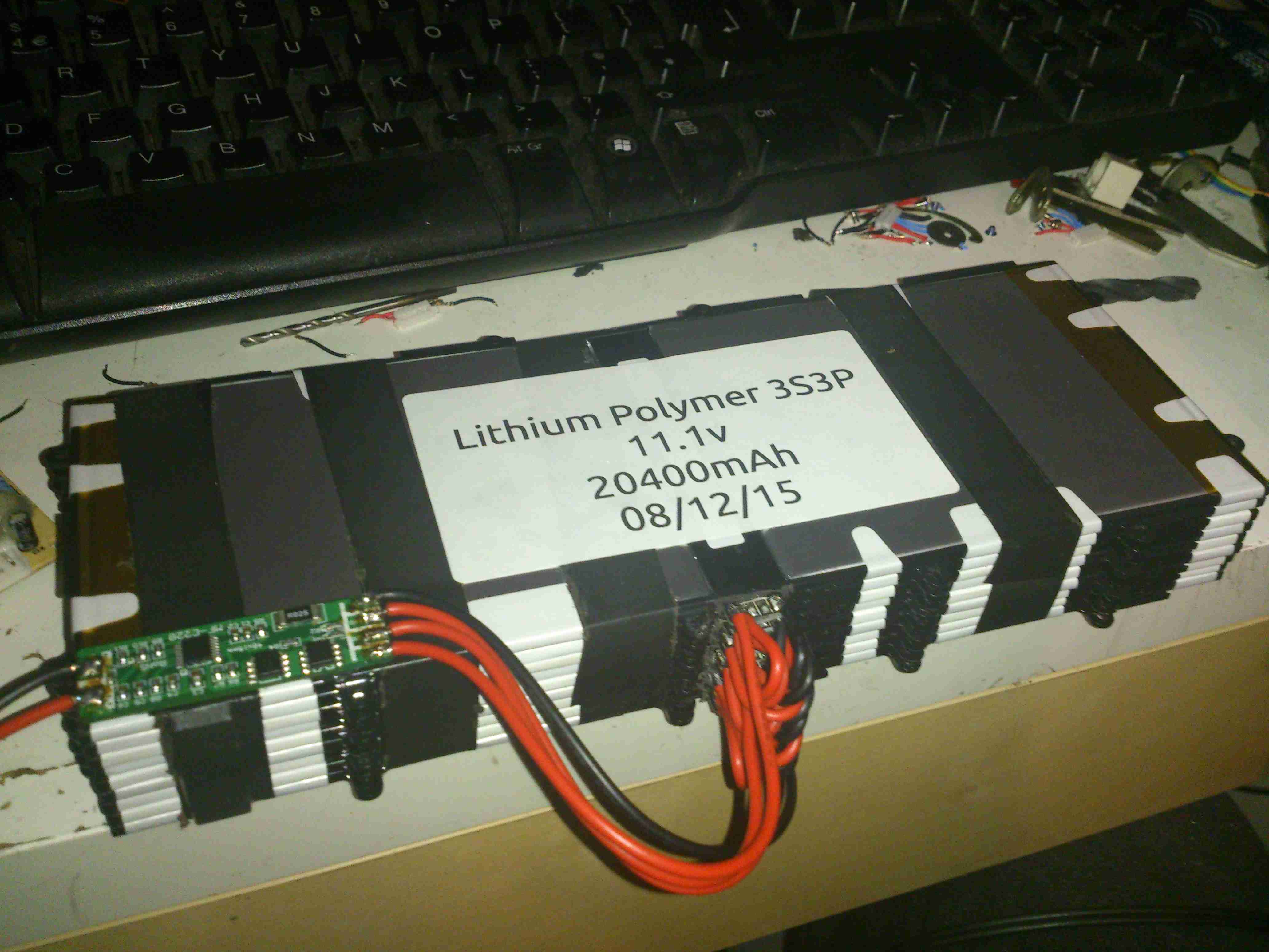
In the past, I’ve used RC type LiPo packs for my mobile power requirements, but these tend to be a bit bulky, since they’re designed for very high discharge current capability – powering large motors in models is a heavy job.
I recently came across some Samsung Galaxy Tab 10.1 battery packs on eBay very cheaply, at £2.95 a piece. For this price I get 6800mAh of capacity at 4.2v, for my 12v requirements, 3 packs must be connected in series, for a total output of 12.6v fully charged.
For an initial pack, I got 9 of these units, to be connected in 3 sets of 3 to make 20Ah total capacity.There are no control electronics built into these batteries – it’s simply a pair of 3400mAh cells connected in parallel through internal polyfuses, and an ID EEPROM for the Tab to identify the battery.
This means I can just bring the cell connections together with the original PCB, without having to mess with the welded cell tabs.
Battery Pack
Here’s the pack with it’s cell connections finished & a lithium BCM connected. This chemistry requires close control of voltages to remain stable, and with a pack this large, a thermal runaway would be catastrophic.
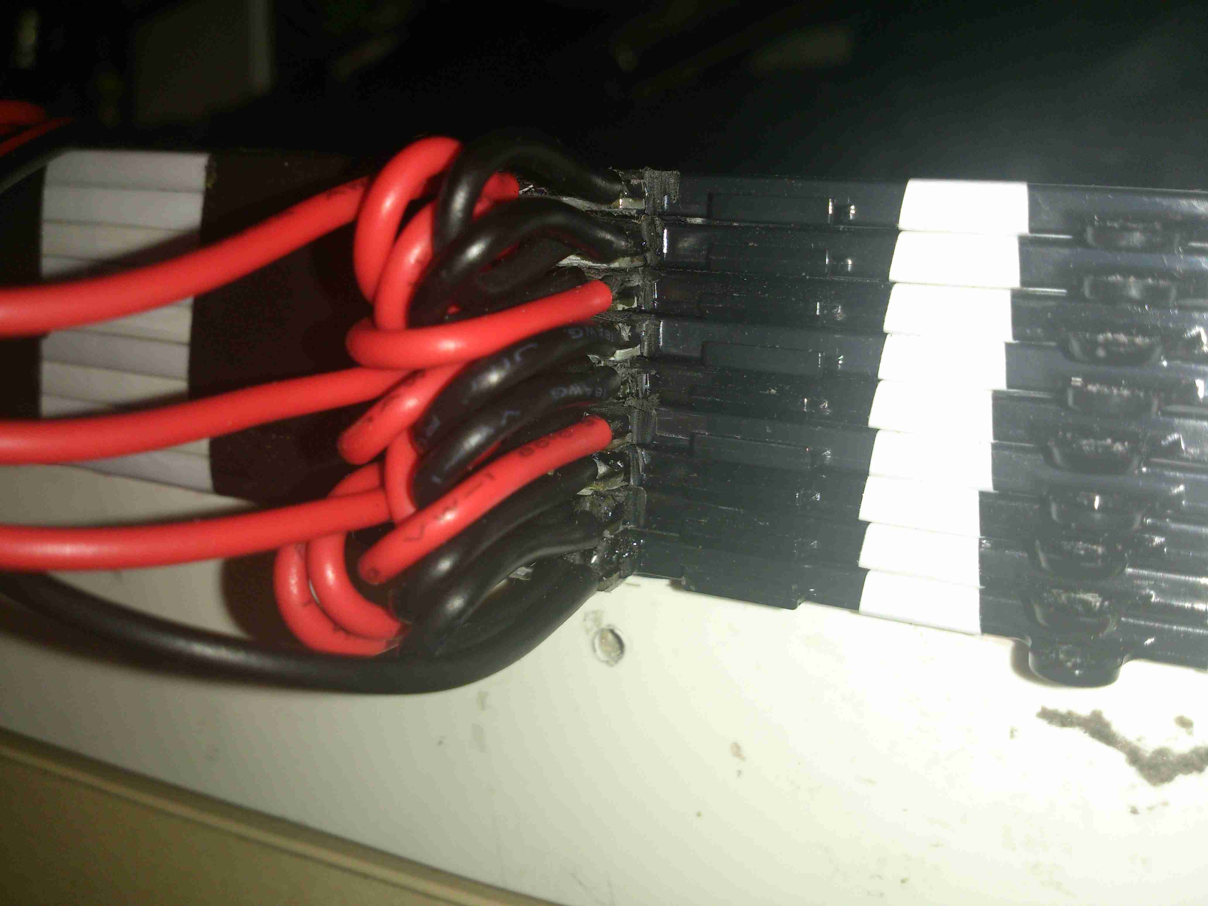
Cell Links
The OEM battery connector has been removed, and my series-parallel cell connections are soldered on, with extra lead-outs for balancing the pack. This was the most time-consuming part of the build.
If all goes well with the life of this pack for utility use, I’ll be building another 5 of these, for a total capacity of 120Ah. This will be extremely useful for portable use, as the weight is about half that of an equivalent lead-acid.
Compressed air is a rather useful power source, especially when all maintenance is done by the on board crew instead of by boatyards.
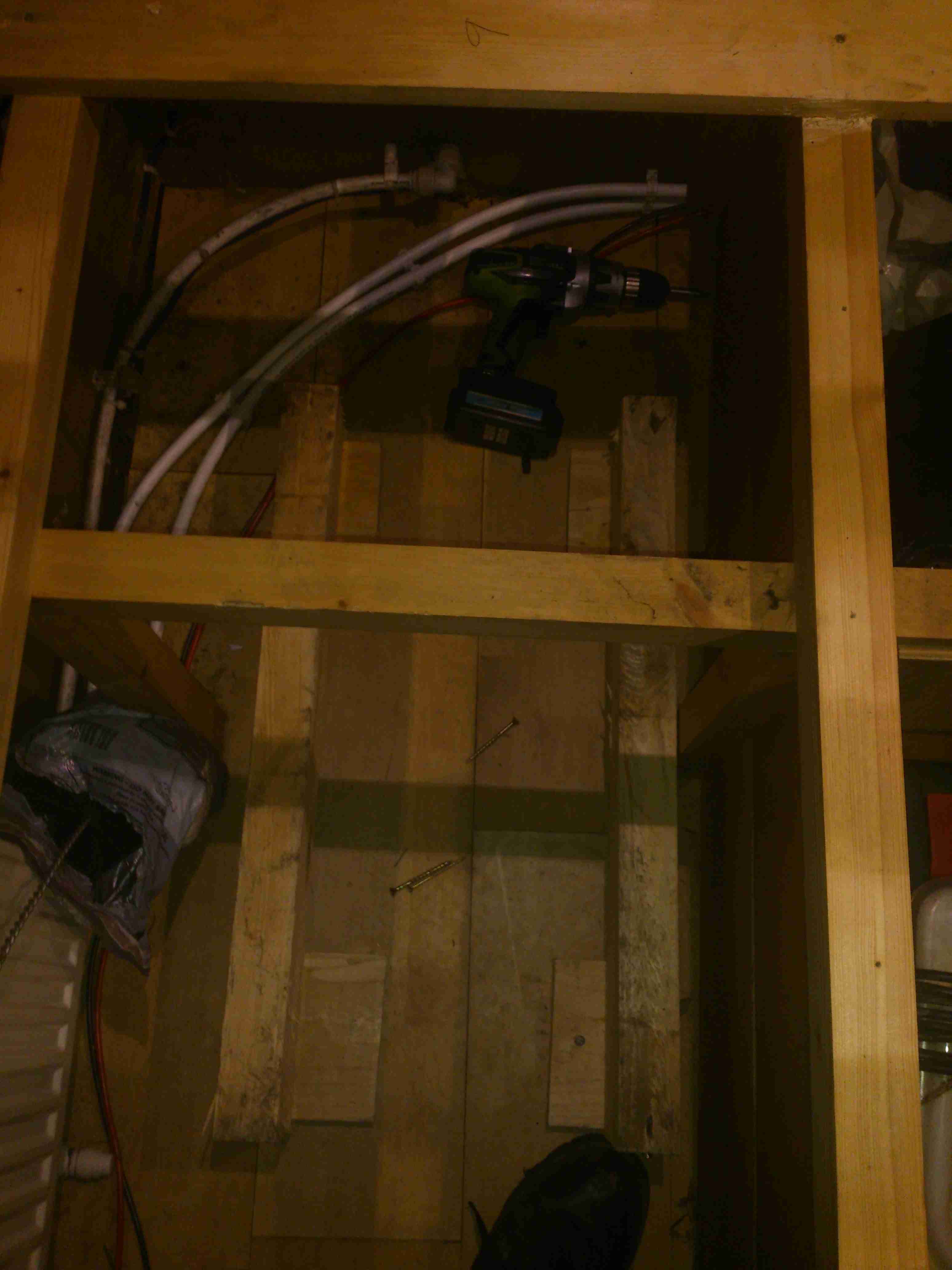
Screwfix had a good deal on a 50L 3.5CFM air compressor, to save space this has been permanently mounted in a free space & air will be piped to where it is needed from a central point.
Because of the total height of the machine, the compressor itself has been unbolted from the tank, a copper line connecting the two back together at a larger distance.
Bearers
In one of the very few free spaces available, under a bunk. A pair of timbers has been screwed to the floor to support the tank.
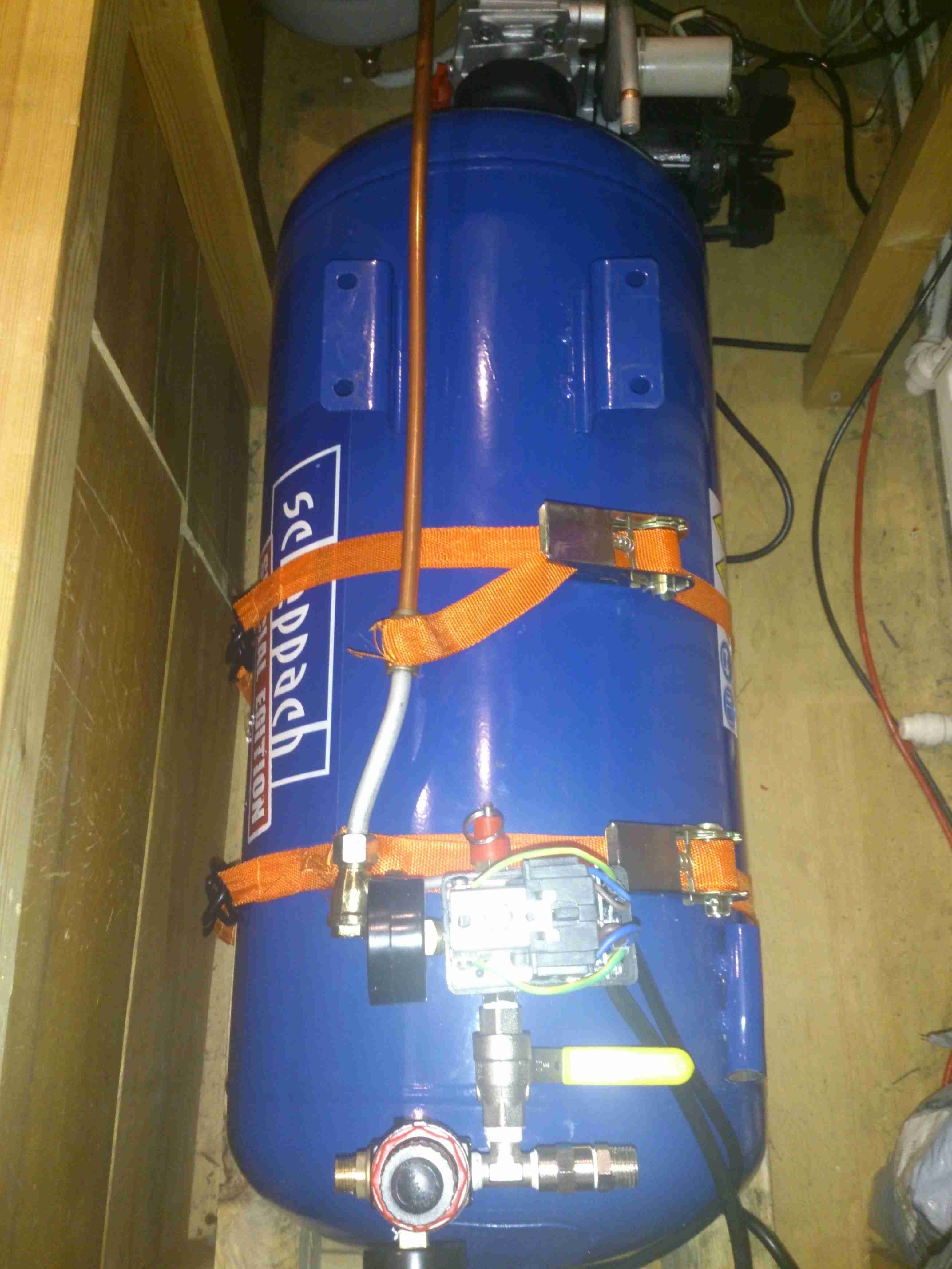
Tank Installed
The tank is strapped to the wooden supports with a pair of ratchet straps, the compressor itself can be seen just behind the tank. The copper line on the top of the tank is going back to be connected to the compressor outlet.
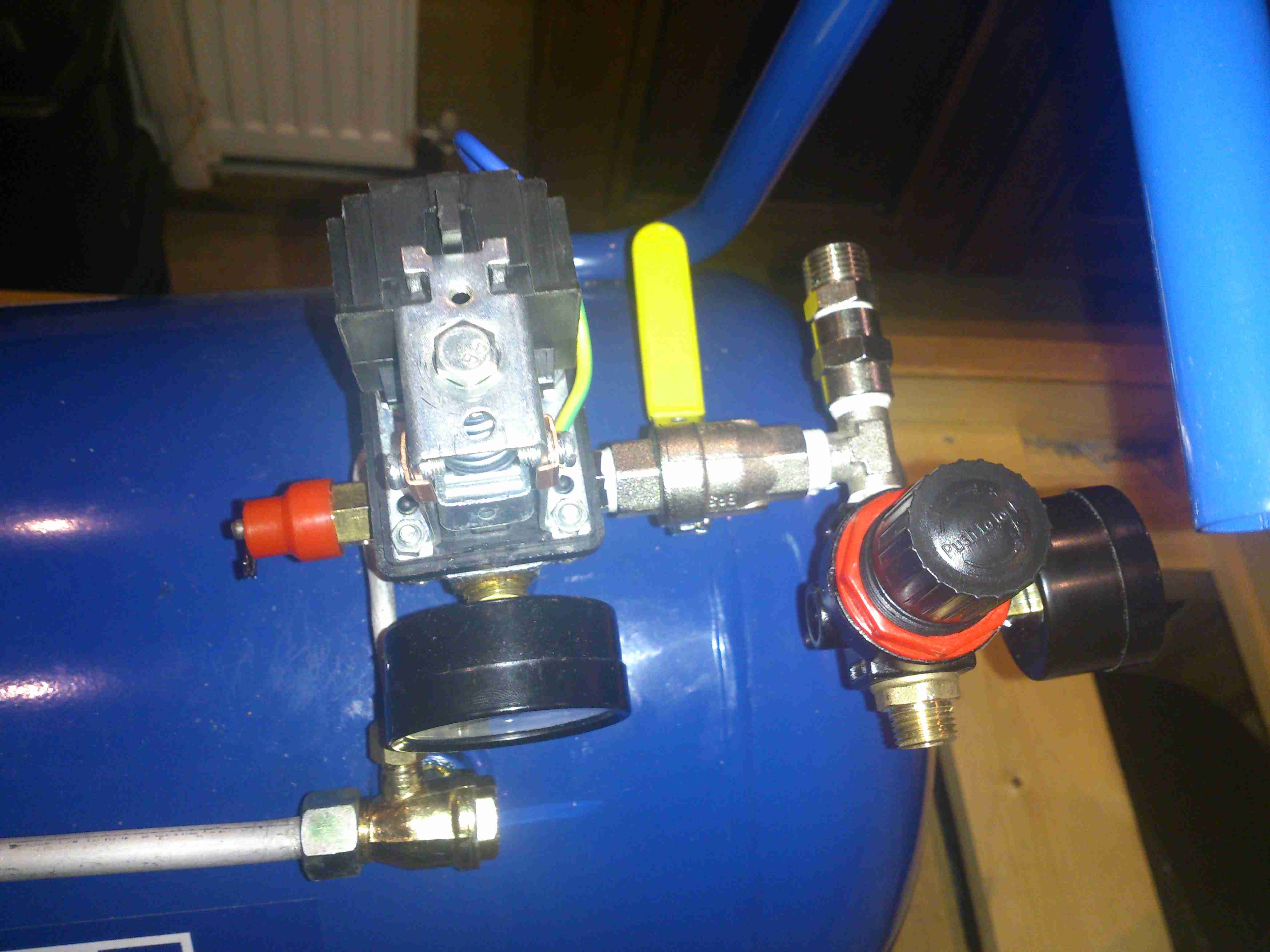
Air Fittings
Compressor control remains on top of the tank, the pressure switch & relief valve centre. After an isolation valve, the feed splits, the regulator installed will be feeding the air horn with 20PSI, replacing the existing automotive-style 12v air pump. The currently open fitting will be routed to a quick connect on the bulkhead. This will be accessible from the front deck, an air hose can be fitted to get a supply anywhere on board.
More to come when the rest of the system gets installed!
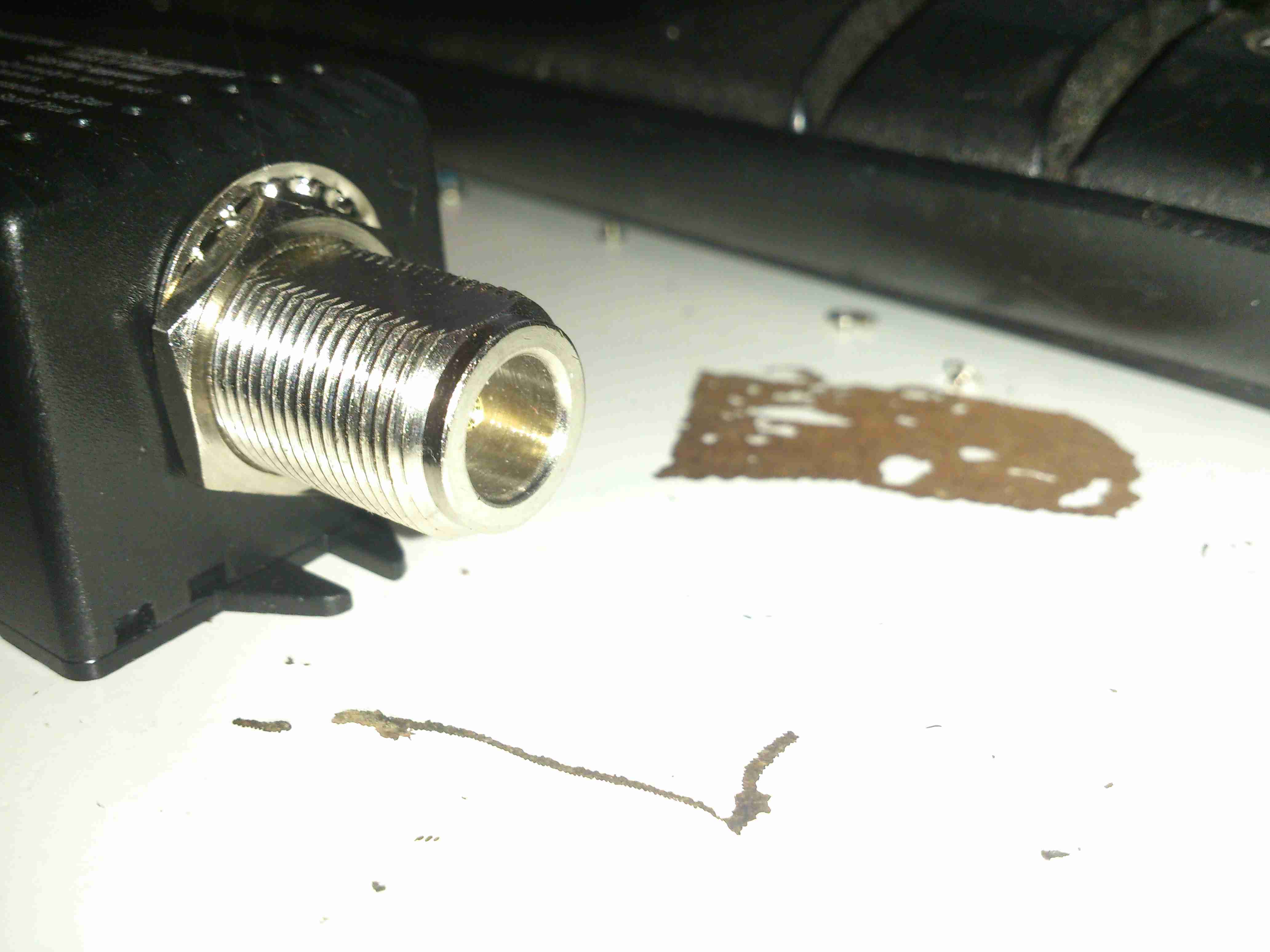
As supplied, the RTL type tuner dongles are a little fragile, especially when they’ve got a rather heavy coax feeder attached for Ham Radio use.
The MCX antenna connectors on the tuner can’t stand up to much abuse, and even the USB plug rips itself from it’s mounts after a while with a heavy weight on the end. Since this dongle sits in my radio go bag, it definitely needed some protection & support.
PCB
The PCB itself is removed from it’s flimsy plastic casing, the USB plug is desoldered from the board.
To the exposed pads, a USB cable is soldered, giving much more flexibility in where the tuner is placed.
Instead of using the MCX antenna connector on the PCB, the coax is stripped & soldered direct to the PCB itself, as this connector has become unreliable.
N-Connector
To get the RF into the device, the case is fitted with an N connector, as is everything else in my shack.
Boxed
The box used is a surplus one which previously housed an electronic lighting transformer. This would be very easy to waterproof as well, for more protection against outdoor use.
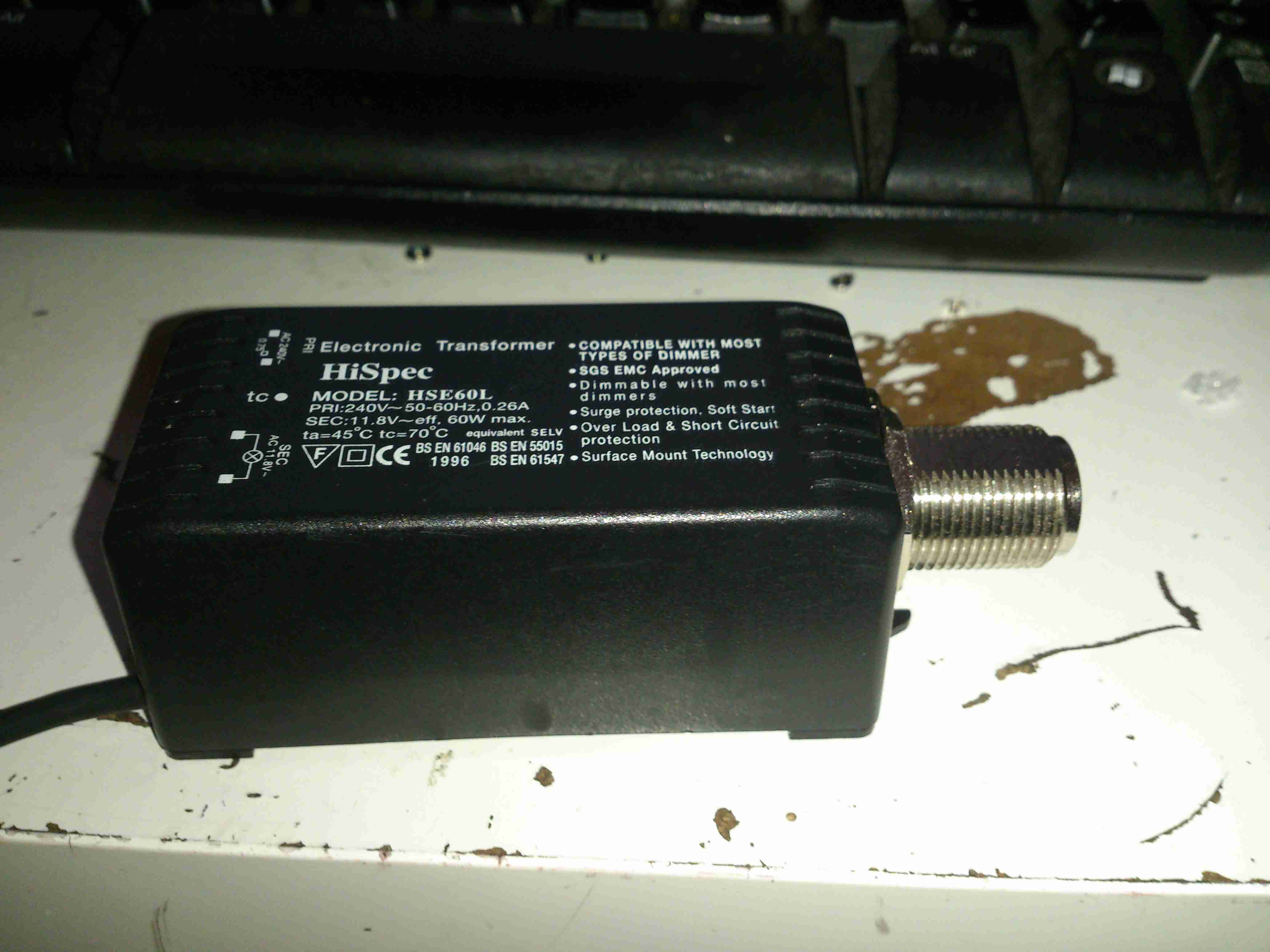
I almost forgot about this bit of kit, that came with one of my LED torches as a Lithium Ion charger. As I never plug in anything that comes from China via eBay, here’s the teardown & analysis.
Another Lethal Charger?
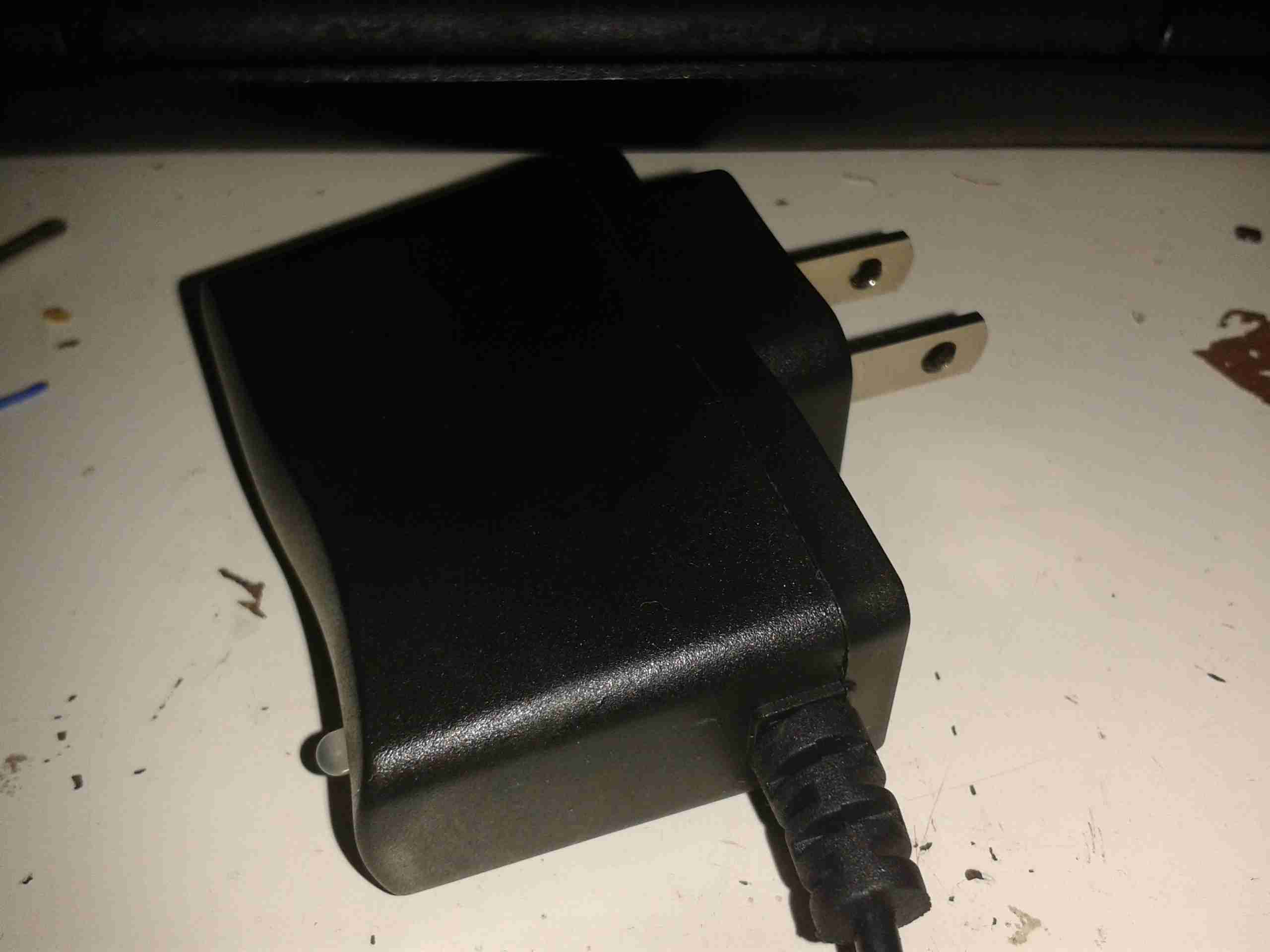
Here’s the unit itself. It’s very light, and is clearly intended for American NEMA power points.
Specs
Claimed specifications are 100-240v AC input, making it universal, and 4.2v DC out ±0.5v at 500mA.
Considering the size of the output wire, if this can actually output rated voltage at rated current I’ll be surprised.
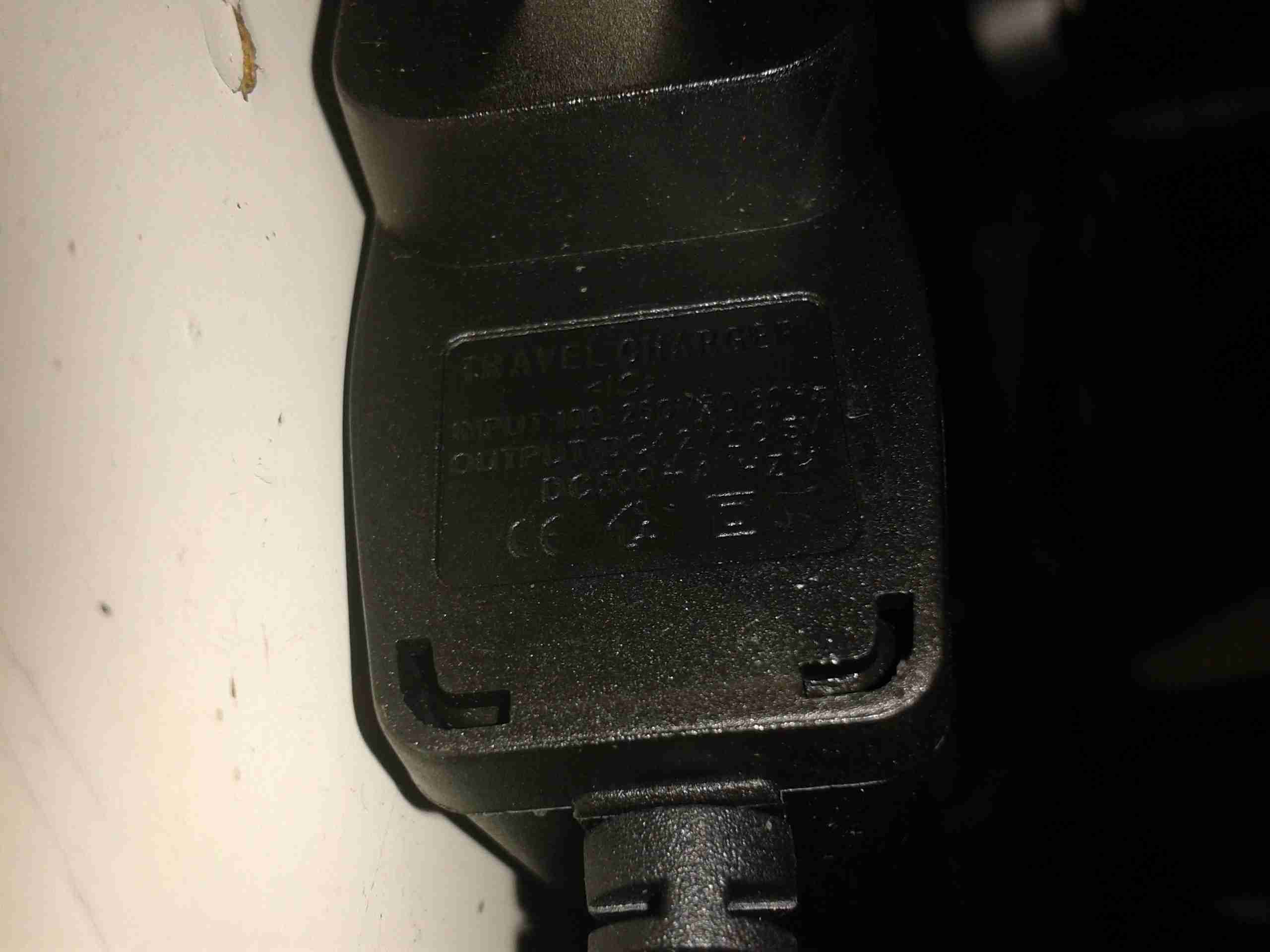
Opened
Here’s the adaptor opened up. There’s no mains wiring to speak of, the mains pins simply push into tags on the PCB.
PCB Top
Top of the SMPS PCB. As usual with Chinese gear, it’s very simple, very cheap and likely very dangerous. There’s no real fusing on the mains input, only half-wave rectification & no EMI filtering.
PCB Bottom
Here’s the bottom of the PCB. At least there’s a fairly sized gap between the mains & the output for isolation. The wiggly bit of track next to one of the mains input tags is supposed to be a fuse – I somehow doubt that it has the required breaking characteristics to actually pass any safety standards. Obviously a proper fuse or fusible resistor was far too expensive for these.
The output wiring on the left is thinner than hair, I’d say at least 28AWG, and probably can’t carry 500mA without suffering extreme volt drop.
Tip Jar
If you’ve found my content useful, please consider leaving a donation by clicking the Tip Jar below!
All collected funds go towards new content & the costs of keeping the server online.