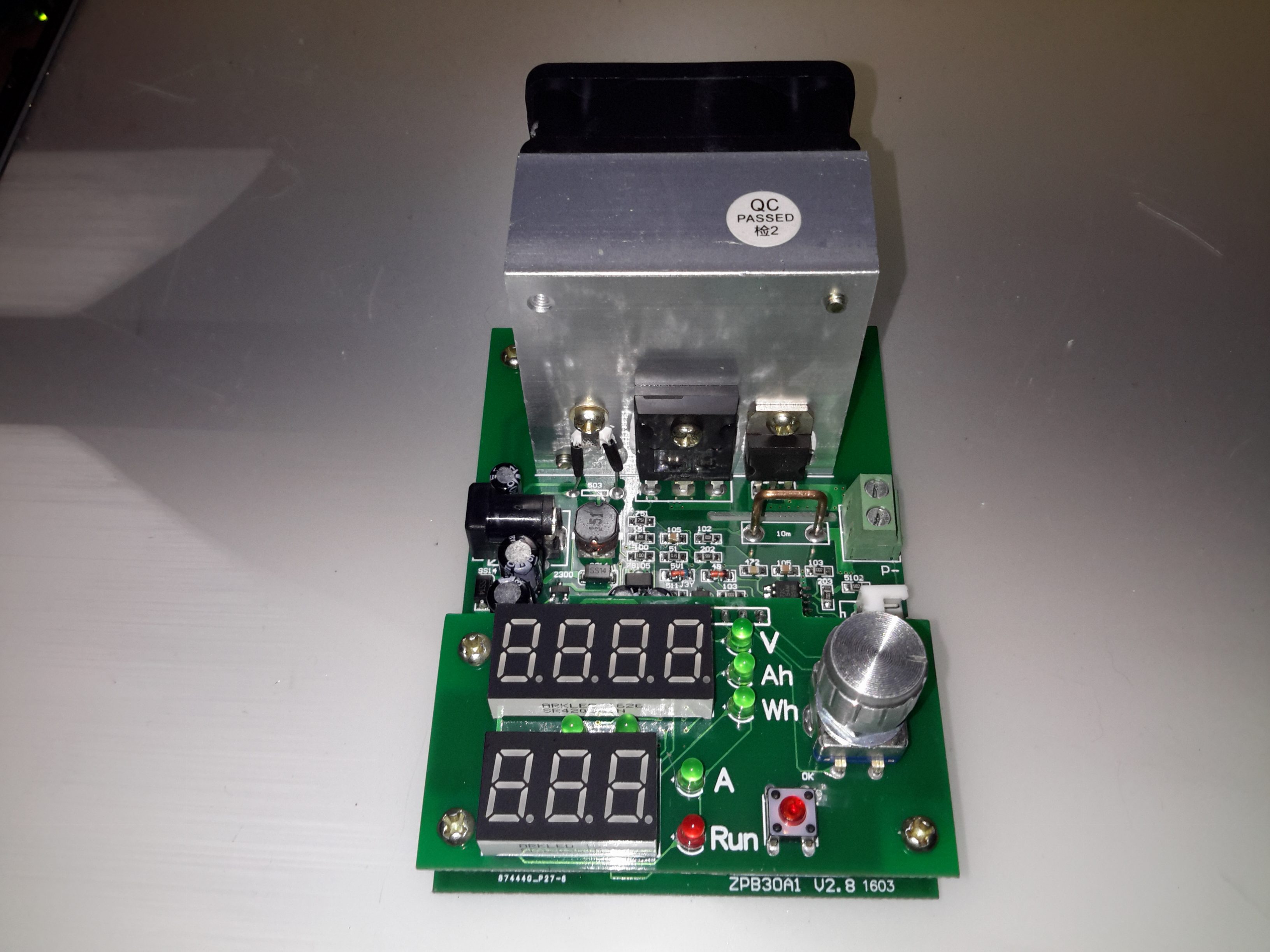
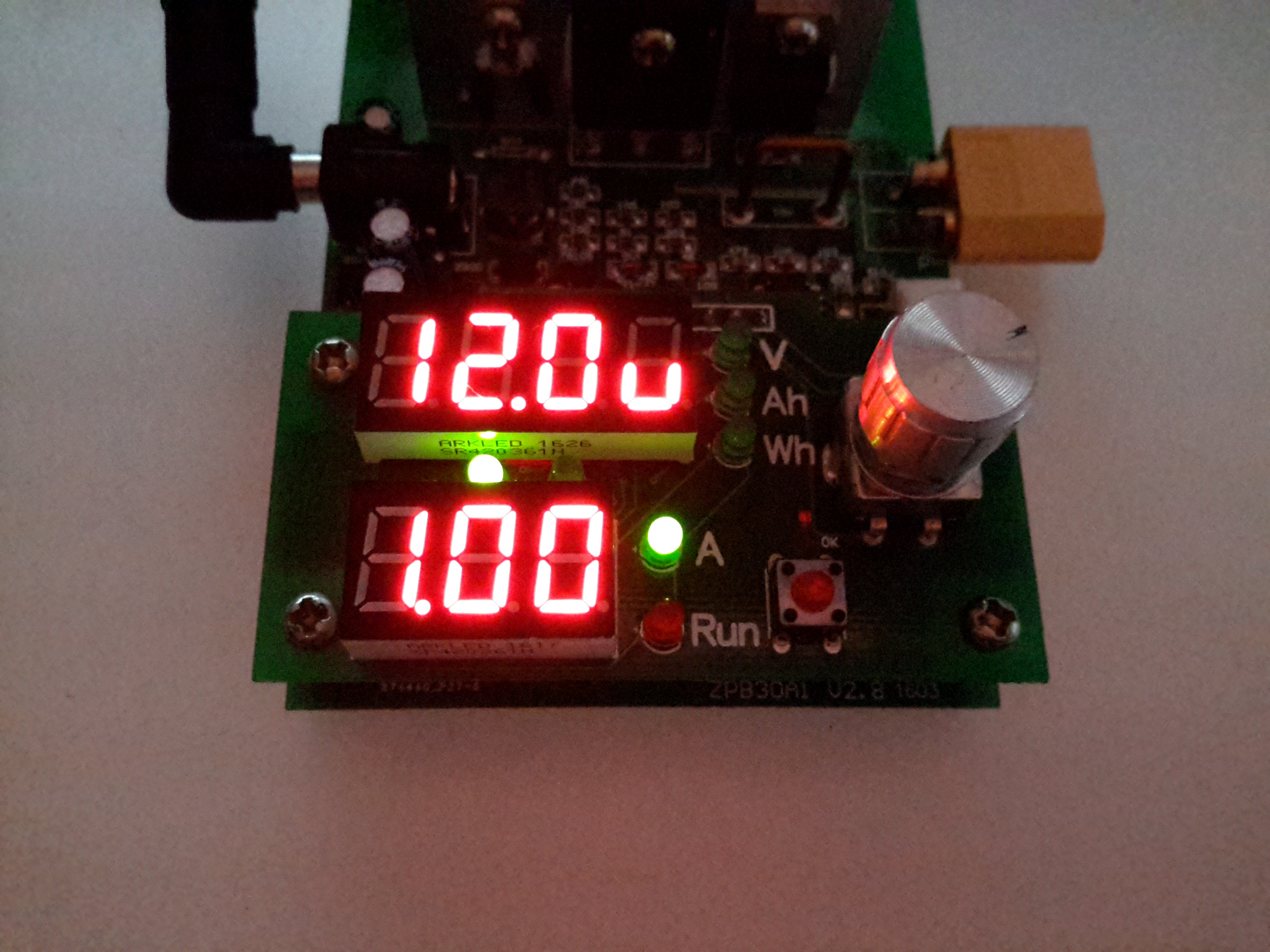
Here’s a useful tool for testing both power supplies & batteries, a dummy load. This unit is rated up to 60W, at voltages from 1v to 25v, current from 200mA to 9.99A.
This device requires a 12v DC power source separate from the load itself, to power the logic circuitry.
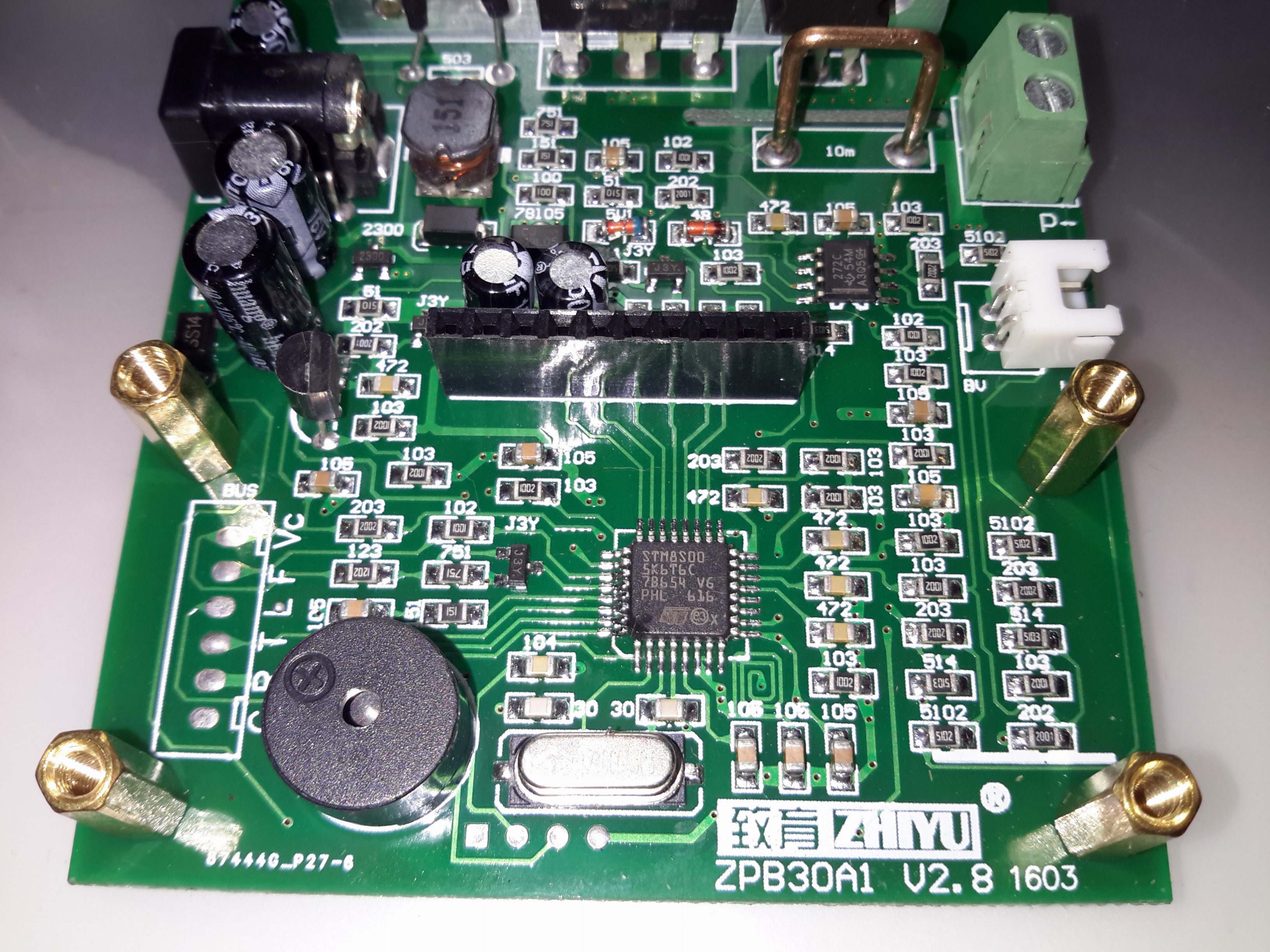
Microcontroller Section
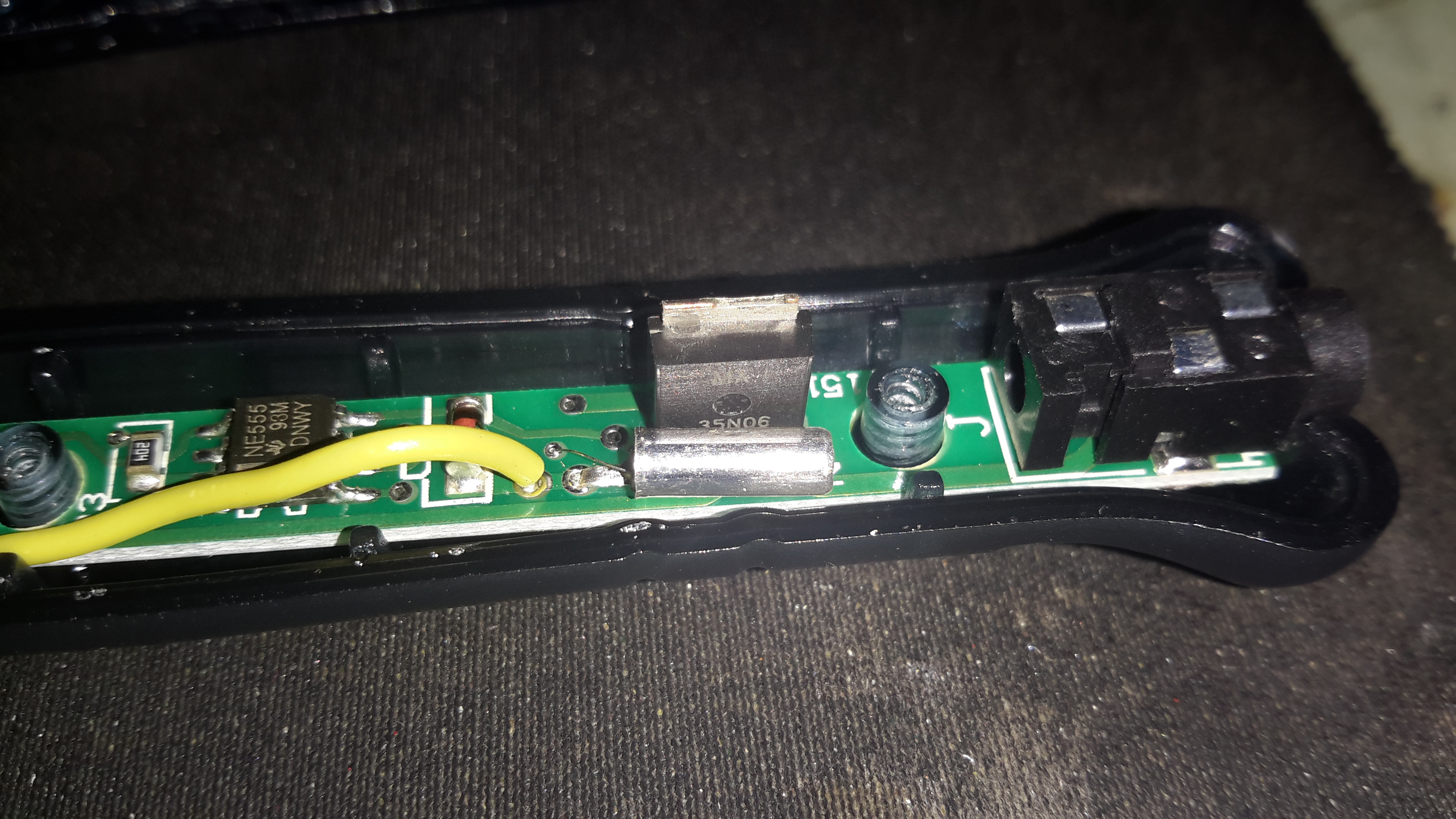
Like many of these modules, the brains of the operation is an STM8 microcontroller. There’s a header to the left with some communication pins, the T pin transmits the voltage when the unit is operating, along with the status via RS232 115200 8N1. This serial signal is only present in DC load mode, the pin is pulled low in battery test mode. The 4 pins underneath the clock crystal are the programming pins for the STM8.
Serial CommsCooling Fan
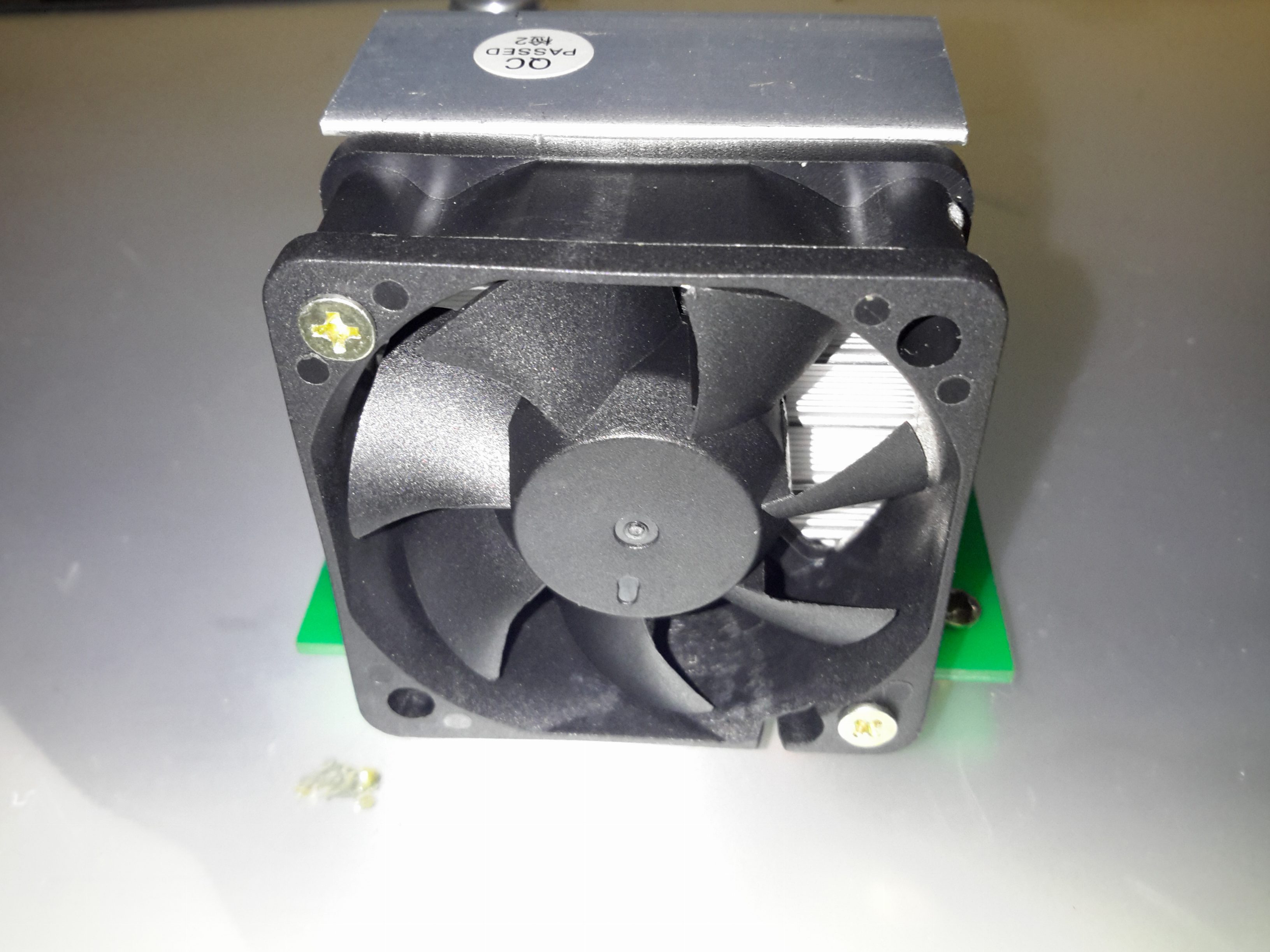
The main heatsink is fan cooled, the speed is PWM controlled via the microcontroller depending on the temperature.
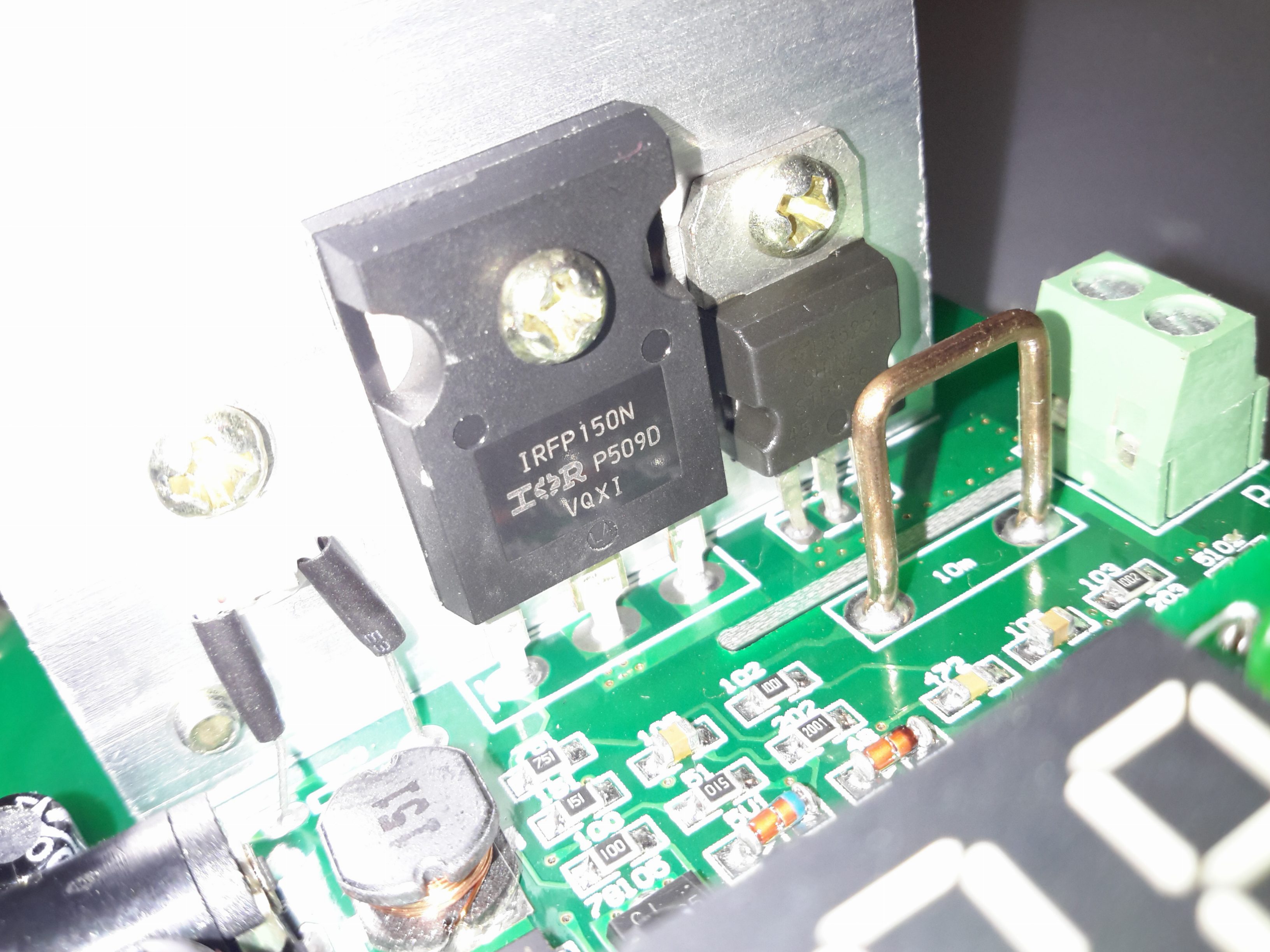
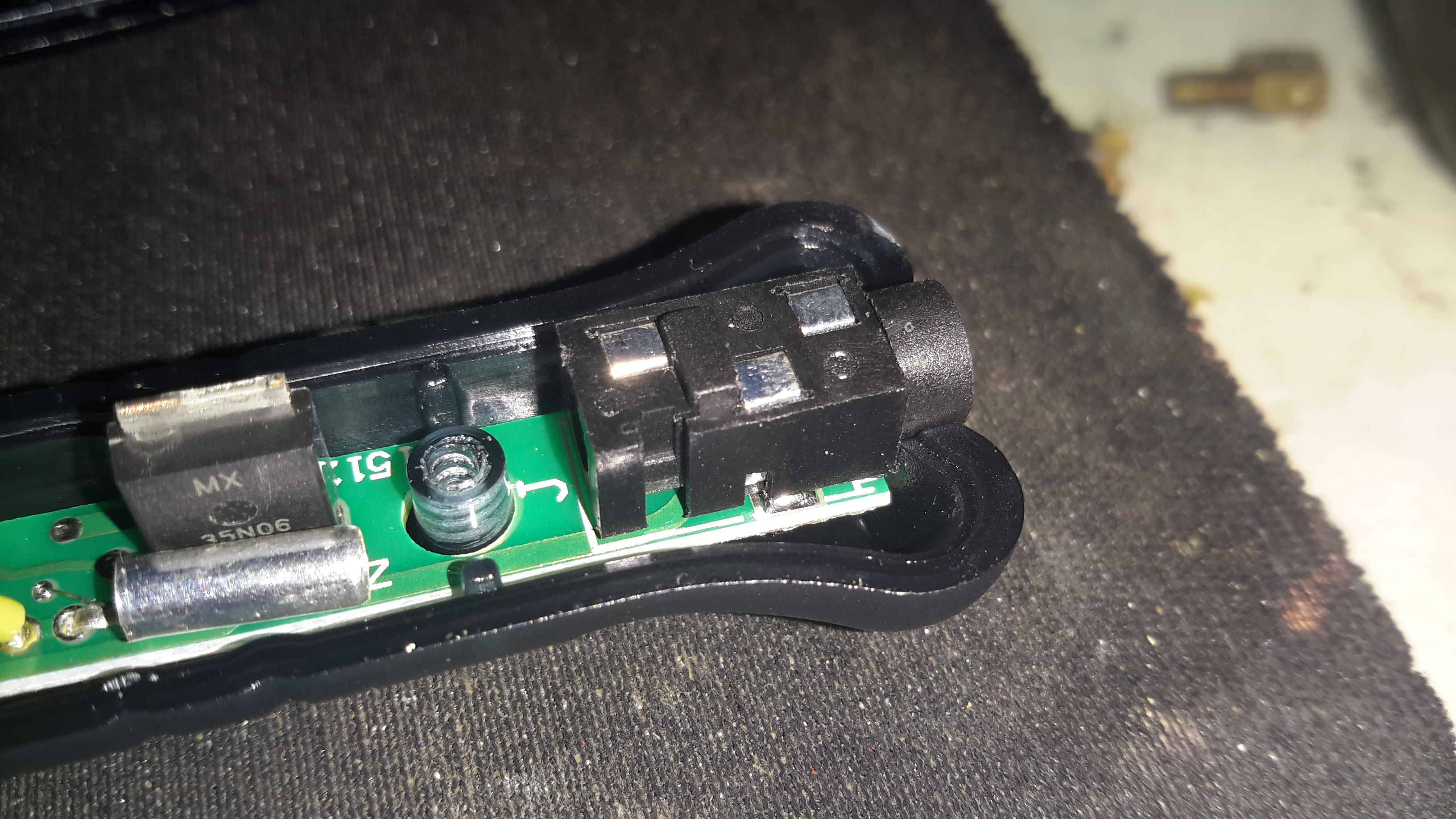
Main MOSFET
The main load MOSFET is an IRFP150N from Infineon. This device is rated at 100v 42A, with a max power dissipation of 160W. On the right is a dual diode for reverse polarity protection, this is in series with the MOSFET. On the left is the thermistor for controlling fan speed.
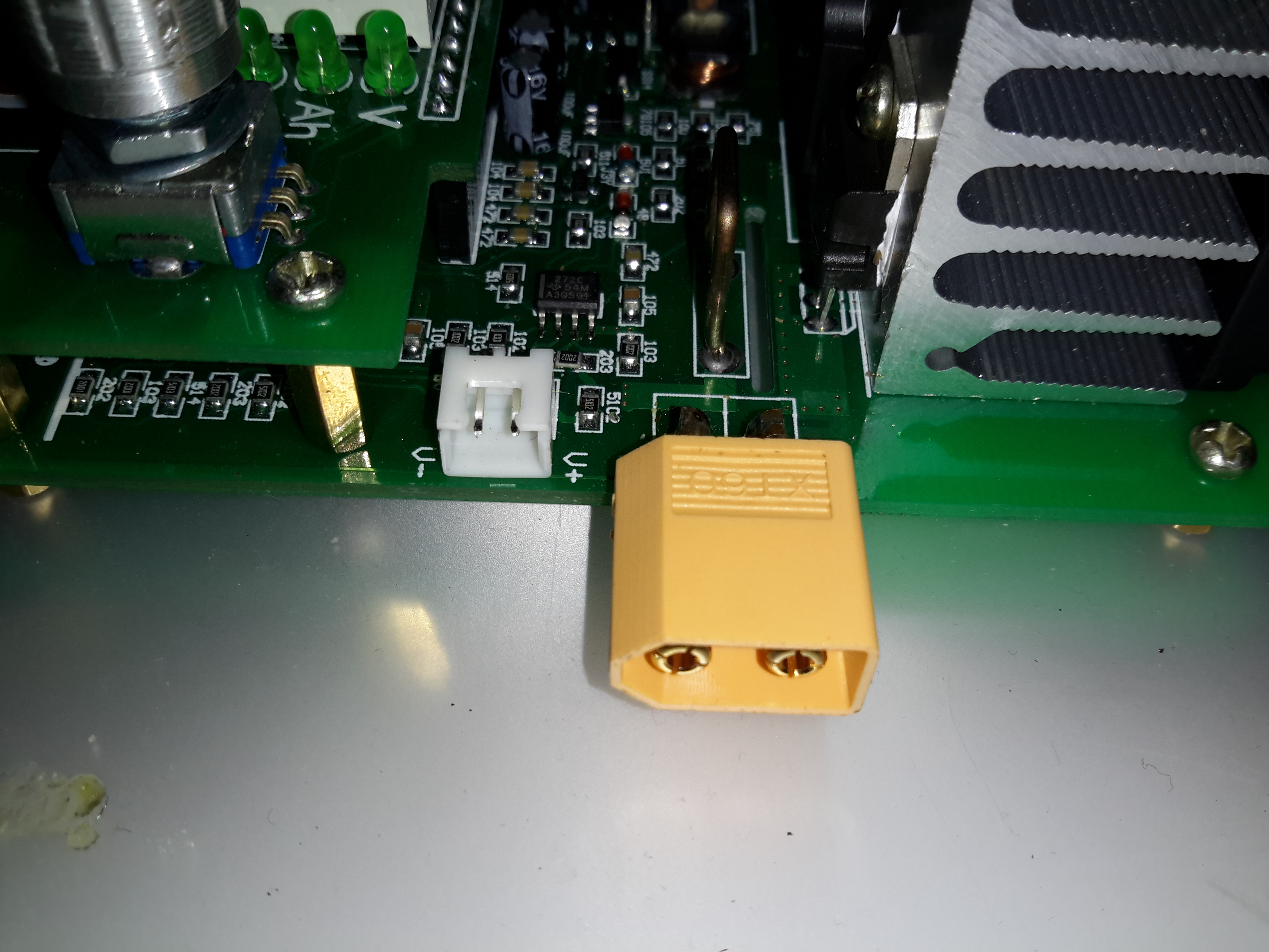
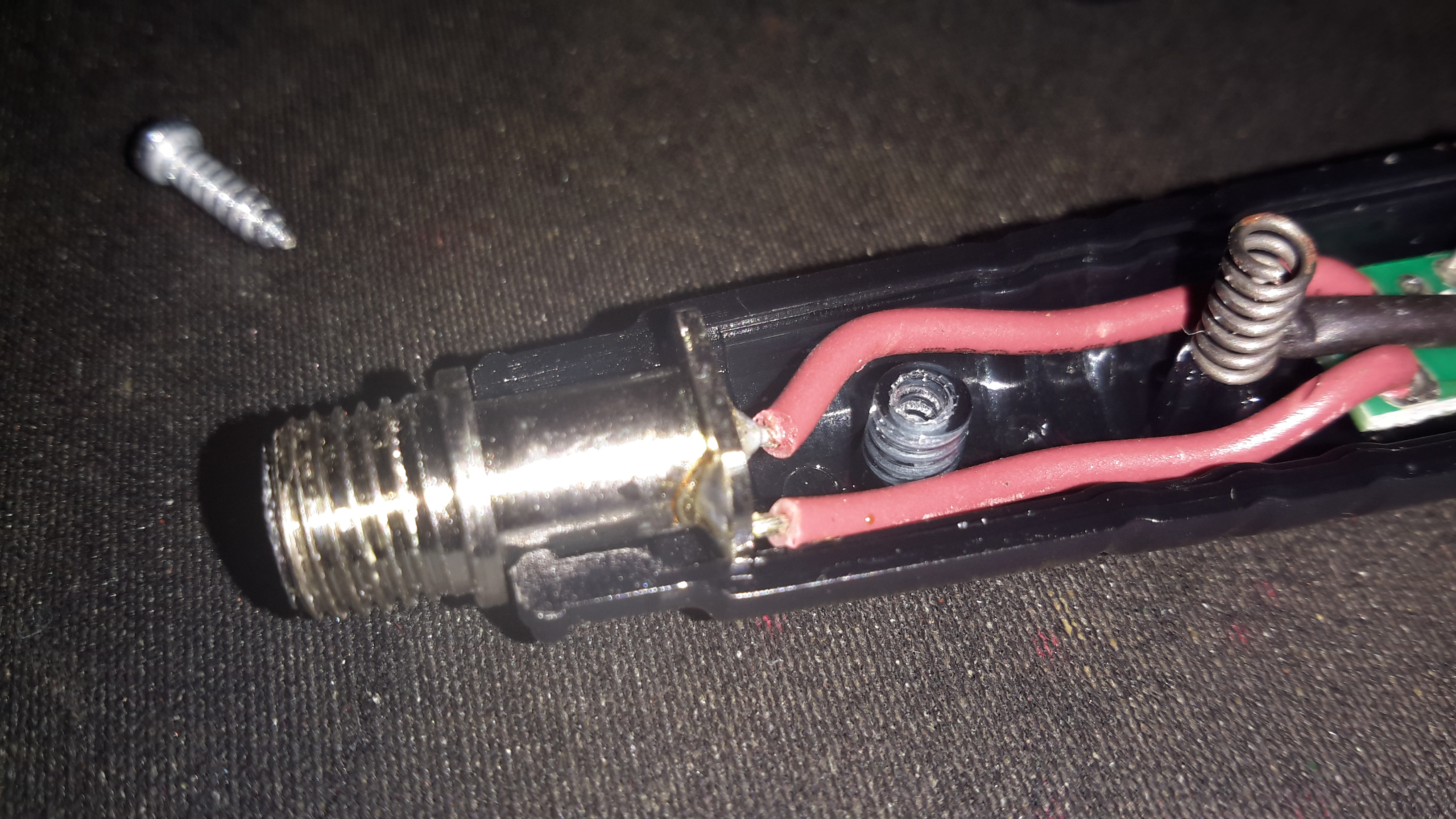
Load Terminals
The load is usually connected via a rising clamp terminal block. I’ve replaced it with a XT60 connector in this case as all my battery holders are fitted with these. This also removes the contact resistance of more connections for an adaptor cable. The small JST XH2 connector on the left is for remote voltage sensing. This is used for 4-wire measurements.
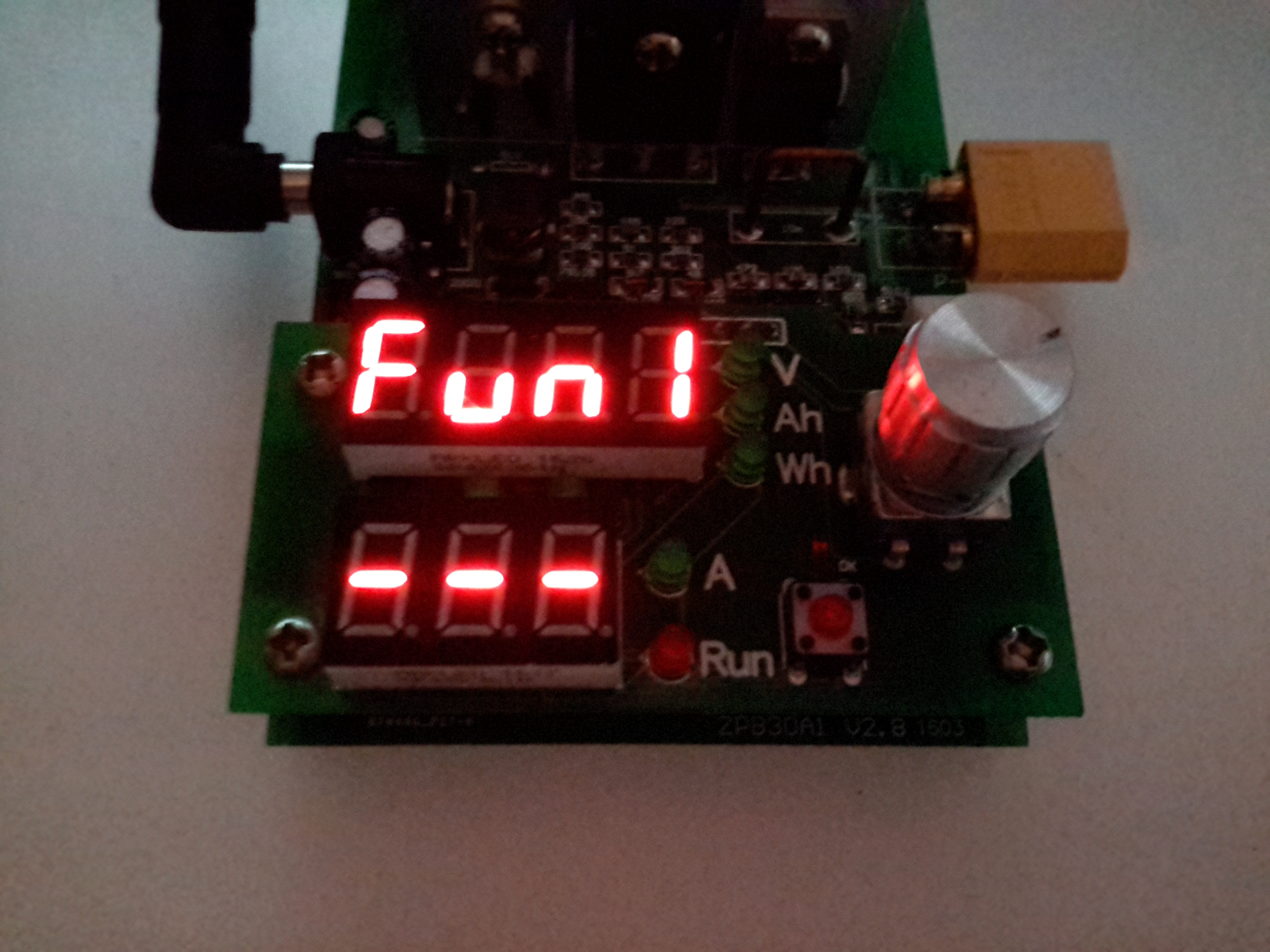
Function 1 – DC Load
Powering the device up while holding the RUN button gets you into the menu to select the operating modes. Function 1 is simple DC load.
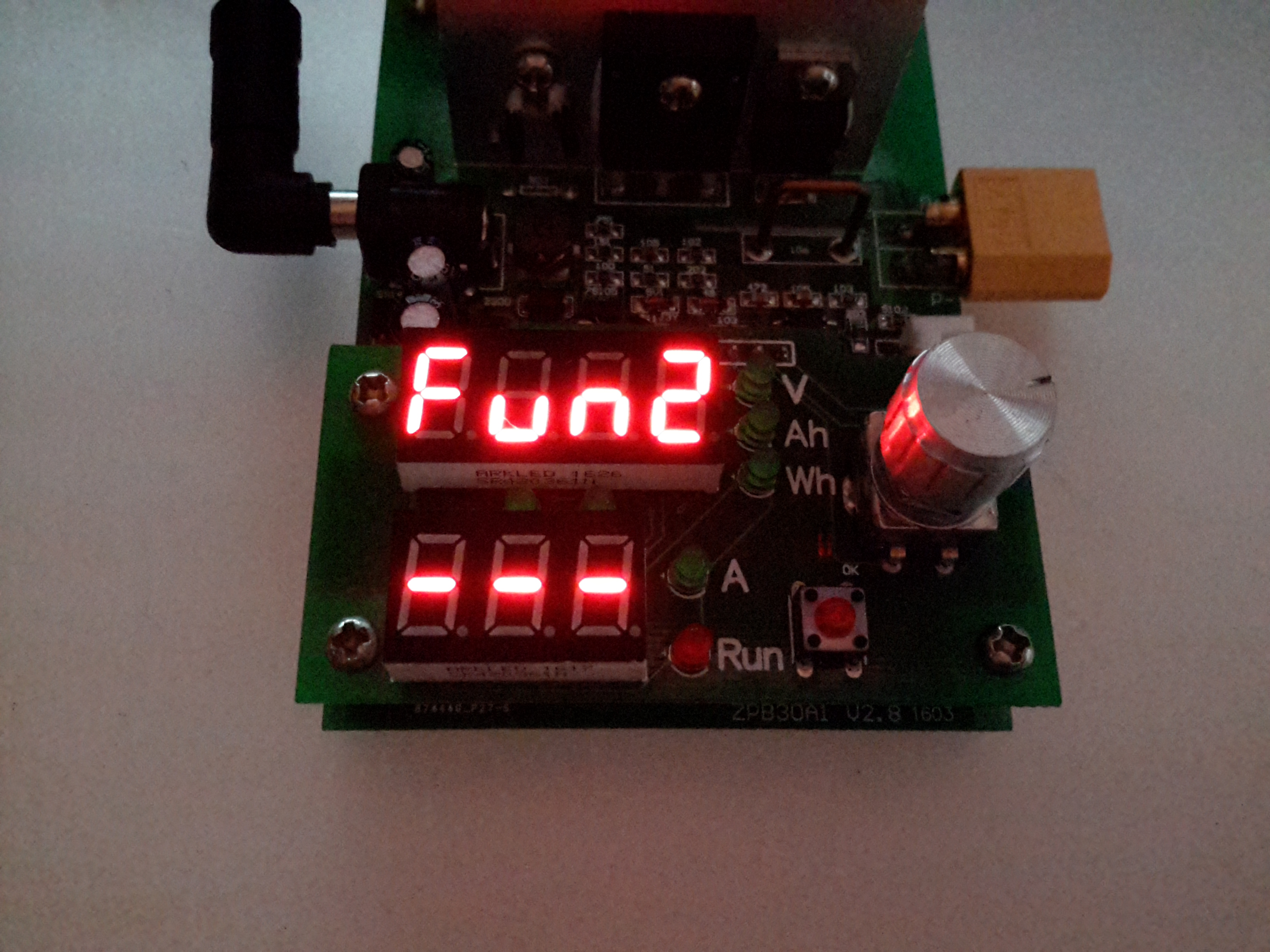
Function 2 – Battery Capacity Mode
The rotary encoder is used to select the option. Function 2 is battery capacity test mode.
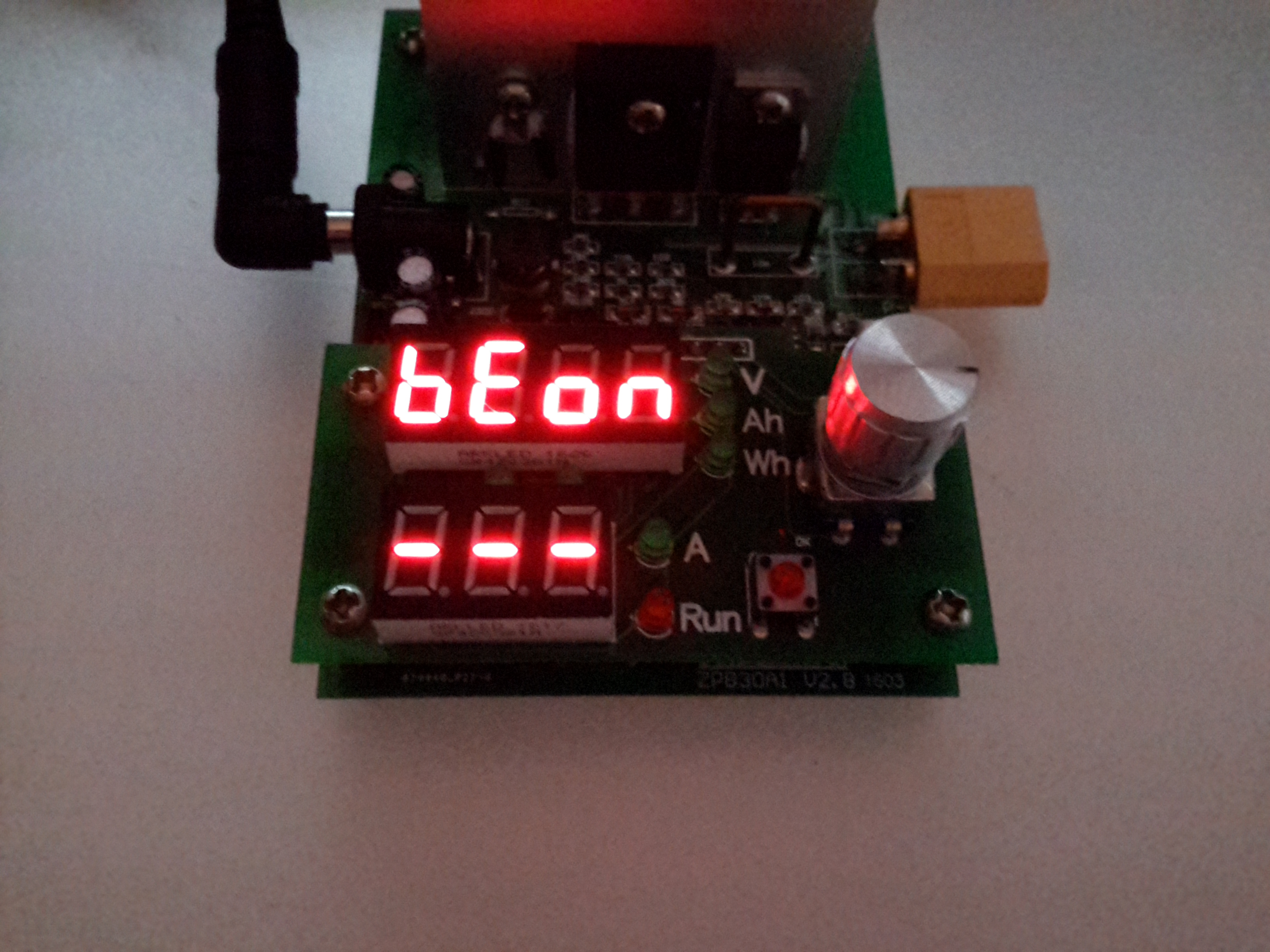
Beeper Mode
After the mode is selected, an option appears to either turn the beeper on or off.
Amps Set
When in standby mode, the threshold voltage & the load current can be set. Here the Amps LED is lit, so the load current can be set. The pair of LEDs between the displays shows which digit will be changed. Pressing the encoder button cycles through the options.
Volts Set
With the Volts LED lit, the threshold voltage can be changed.
When in DC load mode (Fun1), the device will place a fixed load onto the power source until it’s manually stopped. The voltage setting in this mode is a low-voltage alarm. The current can be changed while the load is running.
When in battery discharge test mode (Fun2), the voltage set is the cutoff voltage – discharge will stop when this is reached. Like the DC load mode, the current can be changed when the load is running. After the battery has completed discharging, the capacity in Ah & Wh will be displayed on the top 7-segment. These results can be selected between with the encoder.
Below are tables with all the options for the unit, along with the error codes I’ve been able to decipher from the Chinese info available in various places online. (If anyone knows better, do let me know!).
Option
Function
Fun1
Basic DC Load
Fun 2
Battery Capacity Test
BeOn
Beeper On
BeOf
Beeper Off
Error Code
Meaning
Err1
Input Overvoltage
Err2
Low Battery Voltage / No Battery Present / Reverse Polarity
Err3
Battery ESR Too High / Cannot sustain selected discharge current
Err4
General Failure
Err6
Power Supply Voltage Too Low / Too High. Minimum 12v 0.5A.
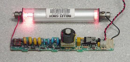
SG-HM2 is a modular He-Ne laser power supply based on IC-HI1 with some minor enhancements. The first version is for laser tubes up to approximately 1 mW (2 mW with trivial modifications) but it should be straightforward to go to 5 mW or even higher power tubes by replacing the SG-HM2 HV Module (HVM2-1) with one with a higher voltage and current rating, along with a higher power MOSFET and minor component value changes to the Control Module (suggestions below). I have added an adjustment for tube current, a current limiting resistor and Zener to protect against output short circuits, an enable input (ground to turn on), a bleeder resistor to virtually eliminate the shock hazard after the power supply is turned off, and power and status LEDs.
Get the schematic for SG-HM2 (1 mW version) in PDF format: [download id=”5610″]
Modifying SG-HM2 for Higher Power He-Ne Laser Tubes
The following are guidelines for modifying SG-HM2 to drive various power He-Ne lasers. The PCB layout below with two versions of the HV Module should accommodate He-Ne laser tubes up to 10 mW. All assume input of around 12 V though a higher power system can generally run lower power lasers at reduced input voltage. If operation at rated power on another input voltage is desired, the number of turns on the inverter transformer can be adjusted accordingly. As noted above, the 1 mW HV Module (HVM2-1) should run tubes up to about 2 mW, though increasing the µF values of some of the HV capacitors may be desirable to reduce ripple at the higher tube current. Minor changes may also be needed in the components on the SG-HM2 Control Module including using a higher power MOSFET for Q1 and reducing the values of R7 and/or R8 for the higher tube current. Or, just populate the Control Module with Q1 being an IRF644, R7 being 150 ohms, and R8 being 750 ohms for compatibility with all the HV modules. For that matter, the HVM2-5 PCB HV Module should be usable with lower power lasers.
   Laser Power       1 mW         2 mW         5 mW         10 mW
-----------------------------------------------------------------------
   Voltage           1200 V       1500 V       2300 V       3500 V
   Current           2-4mA        3-5mA        5-7mA        5-7mA

 SG-HM2 HV Module:

   PCB Version       HVM2-1       HVM2-1       HVM2-5       HVM2-5

   T101
    Core (DxH)       18x11 mm     18x11 mm     26x16 mm     26/16 mm
    Primary          9T,#28       9T,#28       9T,#26       9T,#26
    Secondary        450T,#40     450T,#40     600T,#40     900T,#40
     Res. (Est)      60 ohms      60 ohms      (90 ohms)    (120 ohms)

   D101-106          2kV          2kV          3kV          5kV

   C101-104          1nF,3kV      2nF,3kV      2nF,6kV      2nF,6kV
   C105              47pF,3kV     47pF,3kV     100pF,6kV    100pF,6kV
   C106              3nF,10kV     5nF,10kV     6nF,15kV     6nF,15kV

   R102              10K,1/2W     10K,1/2W     10K,1W       10K,1W
   R103              200M,10kV    200M,10kV    200M,15kV    200M,15kV
   R106-107 (total)  10M          10M          15M          20M

 SG-HM2 Control Module:

   Q1              IRF630       IRF630       IRF640       IRF644
   R7              300          250          150          150
   R8              500          250          100          100
SG-HM2 Inverter Transformer
The inverter transformer for HVM2-1 is wound on a ferrite pot core with a small air-gap (about 0.005″). It is 18 mm in diameter by 11 mm high. While specified to use a 9 turn primary and 450 turn secondary, these values can be adjusted somewhat to handle various input and output requirements. Don’t go much lower on the primary as this may result in core saturation. The 9/450 transformer should be fine for 1 to 2 mW He-Ne laser tubes running on 8 to 15v DC input. With 9/300, it will operate on about 12 to 20v DC. Increasing the number of secondary turns (e.g., 9/600) may result in operation on a slightly lower input voltage, but probably not by much. The 9/450 transformer may even run He-Ne laser tubes larger than 2 mW but I haven’t yet tested this since I haven’t built a prototype of HVM2-5 as yet.
It doesn’t matter very much whether the primary (P) is wound first or the secondary (S) is wound first though the former appears to work slightly better, running the tube at about 8v DC input instead of 9v DC input for the same 9/450 transformer. P over S is slightly easier to wind since the primary doesn’t get in the way and increase the lumpiness of the secondary layers. However, with S over P, insulation is somewhat less critical since the HV lead is out away from anything else. With the P over S, additional insulation is needed between them. Also, since the primary coil is larger diameter, it will have more resistance and there will be greater inter-winding capacitance (though probably not significant). The secondary should be constructed as multiple layers of about 50 or 60 turns each, with insulating tape between layers. Each should be wound in as close to a single layer as possible with alternating layers staggered to prevent arc-over. This doesn’t have to be perfect but try to go gradually from one side to the other to keep wires at high relative potential away from each other. Make sure the HV output leads (particularly the one away from the dot) are well insulated as they exit the transformer. And, as noted, if the primary is over the secondary, there must be high voltage insulation between them. The peak output voltage when the MOSFET turns off (the flyback pulse) may be more than 5 times higher than what would be expected from the DC input voltage and the turns-ratio alone – several kV and this *will* try to find a path to ground! There are more detailed transformer construction instructions in the next section.
Note that this transformer is slightly larger physically than the one from IC-HI1. This is for two reasons: (1) It is easier to wind with more space and a larger wire size for the secondary, and (2) continuous operation should be possible with 2 mW laser tubes, which might have been marginal with the original transformer used in IC-HI1. A by-product of the larger core is that its 9 turn primary should be roughly equivalent to the 12 turn primary of the smaller core in terms of inductance and core saturation limitations.
Interestingly, a similar transformer found in a different commercial power supply, had no insulating tape anywhere. It would appear that with very precise machine-wound HV secondary, done first, the voltage is distributed so uniformly that this is unnecessary.
I’ve now built and tested several transformers in IC-HI1, removing the original transformer and installing socket pins so either the original or an adapter board can be plugged in. This setup is then equivalent to SG-HM2 with the HVM2-1 HV Module. The minimum input voltage values that follow are when driving a 0.5 mW He-Ne laser tube:
           Turns        Pot Core   Vin (VDC)
   ID   P/S    Order    (DxH mm)   Min  Max           Comments
 ------------------------------------------------------------------------------
   1* 12/600  S over P    14x8     7.5  15   Original IC-HI1 transformer
   2  12/350  S over P    18x11    14   22   First prototype, described above
   3   9/350  S over P    18x11    11   18   #2 with 3 P T added out-of-phase
   4   9/425  P over S    18x11     9   16
   5   9/450  P over S    18x11     9   16
   6   9/450  S over P    18x11     8   15
   7  12/500  P over S    26x16     8   15
*The number of turns on the original (#1) is not really known exactly and may be lower or higher by up to 25 percent based on the measured secondary resistance (45 ohms) and estimated wire size (somewhere between #38 and #40. (Even with the larger wire, the amount of bobbin area taken up by the wire is less than 50 percent so it should fit even with many layers of insulating tape. The transformer is Epoxy impregnated and likely to be impossible to disassemble into any form that can be analyzed!)
All of these transformers will drive He-Ne laser tubes of up to at least 2.5mW using the equivalent of the HVM2-1 HV Module which is part of IC-HI1. Even with the 2.5mW tube, the minimum operating voltage was only about 0.5v higher than for the 0.5mW tube. There is a good chance they would drive even larger He-Ne laser tubes (though possibly at a slightly higher input voltage) but I don’t dare try using the existing HV circuitry as it might not survive for long. I suspect that transformers #4, #5, and #6 would run on an input voltage of less than 8v DC but the salvaged cores I am using have a larger air-gap than might be optimal and I don’t have anything to reduce it without heavy losses. They attempt to start the tube at around 6v DC but are unable to maintain it and flicker rapidly. (#2 and #3, which use the same style core, would also benefit somewhat.) Operation using #1 and #5 is virtually identical, with the original running at perhaps 0.5v DC less input. I expect they would be even more identical if the air-gap on #5 were smaller, and #6 with its smaller air-gap does indeed run at the lower input voltage. I haven’t actually confirmed that anything blows up above the maximum voltages listed above, which were arbitrarily chosen. But I am guessing that bad things might happen at some point. 🙂
I have also constructed a transformer which will need to be used with HVM2-5: 12/1200, P over S, on a 30×19 pot core. I will also construct a 9/900. S over P, on a 30×19 pot core (or on a 26×16 if I can find one). Testing of these will have to await an HVM2-5 prototype.
SG-HM2 Transformer Construction
Here are details on construction of the inverter transformer for SG-HM2. With all parts and tools on hand, it takes about an hour start to finish. Only a small portion of this time is in the actual winding (at least if a coil winding machine is used). Most of the time is spent in adding the insulation tape and terminating the leads. After constructing a few of these, it does go quicker. 🙂
Step-by-step instructions are provided for the HVM2-1 transformer. The changes needed for HVM2-5 are summarized at the end of this section. Some sort of coil winding machine is almost essential as #40 wire is extremely thin and easy to break. (Anything larger than #40 will not fit on the bobbin.) It doesn’t have to be fancy. Mine is probably 50 years old of the type that is (used to be?) advertised in the back of electronics magazines. However, a couple of spindles – one that is fixed or free to rotate for the wire supply and the other which can be turned for the coil being wound – are really all that are needed. Don’t use any sort of powered approach though (unless you have a *real* professional coil winder!) as it is all too easy to break the wire if there is no tactile feedback to detect snags.
Parts required for T101 of HVM2-1:
18×11 mm (1811) ferrite pot core with a small air-gap (no more than 0.005″) or no air-gap, and a single section bobbin. These are available from several manufacturers but surplus or salvaged cores may be easier to obtain. Radio Shack used to have a “ferrite kit” which included a variety of sizes of cores (only 1 each though so you’d have to buy two kits and there were no bobbins!). I doubt the kit still exists though.
Approximately 1.5 feet of #28 magnet wire for the primary (9 turns wound first) and approximately 60 feet of #40 magnet wire for the secondary (450 turns wound on top of the primary). I found both these size wire in various solenoids and relays I’ve discombobulated. 🙂 Wire sizes aren’t critical but these are known to fit and the #40 can be handled with a reasonable chance of not breaking.
Sleeving to protect the primary wires where they leave transformer. I used approximately 2″ of insulation (each lead) from the individual wires in some 25 pair phone cable.
Wirewrap wire or other thin insulated wire to terminate the secondary wires where they leave the transformer.
Insulating tape. 1 mil Mylar or similar is desirable. However, I’ve found that thin clear (non-reinforced) packing tape does an adequate job, though it probably doesn’t have as much dielectric strength as real insulating tape so additional layers are required. It will also likely not stand up to overheating too well. Electrical tape is way too thick and would prevent enough turns from fitting.
A piece of Perf. board with holes on 0.1″ centers, 0.8″x0.8″. There should be 7 rows of holes each way so that one hole lines up in the center.
A Nylon 4-40 screw and nut to fasten the transformer to the board.
Four (4) machined-type IC socket pins or something similar to use as terminals.
Wind the primary:
Slip a piece of sleeving over the start of the primary wire and position the sleeving so it extends about 1/2 turn inside the bobbin on the left side.
Wrap exactly 9 turns of this wire clockwise around the bobbin, left to right. The wires should enter and exit on the same angular position (slot) of the bobbin on opposite sides.
Slip another piece of sleeving over the wire end exiting the bobbin so that it too is about 1/2 turn inside the bobbin.
Wrap 1.5 to 2 turns of tape tightly over the primary winding to secure and insulate it.
Wind the secondary:
Strip 1/8″ or so from the end of a 2″ piece of wire-wrap wire and solder the start of the wire for the secondary winding to it. Make sure the insulation on the fine magnet wire has been removed – usually just heating it while soldering will do this. Leave an inch or so of the magnet wire extending from the connection so that continuity can be confirmed with a multimeter, then snip it off. Install this in the opposite slot of the bobbin also on the left side with about 1/4″ of insulation inside the bobbin against the side and separated from the primary. Leave a little slack in the fine secondary wire so that slight motion won’t break it. Add a small piece of tape to protect and insulate this connection.
Using your coil winding machine (you do have one, correct?), build up the secondary in layers of about 50 to 75 turns in a counter-clockwise direction (bobbin being rotated clockwise). A single layer of wire won’t fit in the 1/8″ or so available (in the 18×11 mm core bobbin) so there will have to be some overlap. But, do this several times across the layer so that any given wire won’t be next to one with a much different voltage. In other words, wind a few turns and back up so that there will in essence be multiple sub-windings of 5 or 10 turns, repeated several times across the layer. Keep the wire at least 1/32″ away from either edge of the bobbin.
After each full layer or wire, add just over 1 layer of insulating tape making sure it covers the entire width of the bobbin. There should be just enough overlap to assure there is at least 1 layer of insulation but not much more as excessive tape will end up taking up too much space.The entire 450 turn winding will then require 6 to 9 full layers. Add another layer of insulating tape over the last winding layer leaving the wire end exposed.
Terminate the end of the secondary winding with another piece of thin wire by soldering as above. Confirm continuity with a multimeter. For the 450 turn secondary, the resistance should be about 60 ohms. Add a piece of thicker sleeving over this at the HV end if space is available. Else, use some bits of tape to insulate the wirewrap wire lead from the core and exposed inner layers that it may come near as it exits out the side of the bobbin. Add another layer of tape to secure the lead in place.
Add several more layers of insulating tape to complete the bobbin assembly.
Prepare the mounting board:
Widen the center hole to 7/64″ to accommodate a 4-40 nylon screw.
Widen the holes at the 4 corners of the board to accept the 4 IC socket pins (if used) as a press-fit or glue them in place with 5 minute Epoxy or SuperGlue.
Final assembly:
Install the ferrite pot core halves to the bobbin taking care not to crunch any of the wires. Orient it so that the primary and secondary leads are conveniently located with respect to the 4 pins, e.g., primary start: bottom left; primary end: top left, secondary start: bottom right; and primary end: top right.
Use the nylon 4-40 screw and nut to *gently* secure the transformer to the mounting board. The head of the 4-40 screw should be underneath the board. Don’t over-tighten or it may crack the core, especially if it has an air-gap in the middle.
Carefully remove the insulation from the ends of the wires. The secondary wires will still be fragile even with the wirewrap wire terminations. For the magnet wire, the easiest way to remove the insulation is to burn it off with a match or hot soldering iron and then clean with fine sandpaper.
Push the wires into their respective socket pins. (The wirewrap wires are too thin to be secure but they will make adequate contact for testing.)
Use a multimeter to confirm continuity of the primary (close to 0 ohms) and secondary (about 50 to 75 ohms).
Testing:
Install the transformer in you HV Module. Attach a He-Ne laser tube and ballast resistor.
Power up on an variable DC power supply and check for reliable starting and stable operation. Adjust the core gap if needed. A smaller gap may result in more operating power available at a given input voltage. A larger gap will result in attempts to start on a lower input voltage. Somewhere around 0.005″ is probably a good compromise.
After testing the transformer (and adjusting the core gap if needed), use some adhesive to secure the pot core sections and to protect the transformer leads. Solder the leads into the socket pins.
The final result is shown on an adapter below:
Photo of SG-HM2 HVM2-1 Transformer being Tested in IC-HI1
The instructions for winding the HVM2-5 transformer are similar except for the dimensions, wire sizes and lengths, and number of turns for the primary and secondary:
Differences in parts list for T501 of HVM2-5 compared to T101 of HVM2-1:
26×16 mm (2616) ferrite pot core with a small air-gap (no more than 0.005″) or no air-gap, and a single section bobbin.
Approximately 2.0 feet of #26 magnet wire for the primary (12 turns wound first) and approximately 75 to 120 feet of #40 magnet wire for the secondary (600 or 900 turns wound on top of the primary).
A piece of Perf. board with holes on 0.1″ centers, 1.0″x1.0″. There should be 9 rows of holes each way so that one hole lines up in the center.
A Nylon 10-32 screw and nut to fasten the transformer to the board.
Since the peak voltage on the HVM2-5 secondary may be 2 to 3 times higher than for HVM2-1, extra insulation and clearances will be required on the secondary.
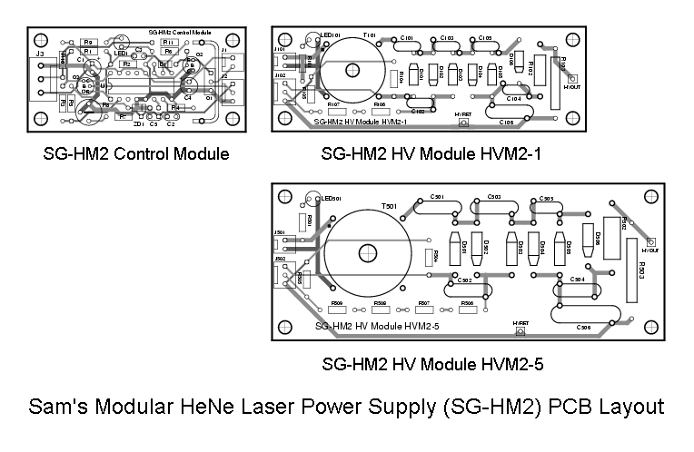
SG-HM2 Printed Circuit Board Layout
A printed circuit board layout is also available. The Control Module is 2″x1.2″. The HV Modules are 3.6″x1.2″ and 4.5″x1.8″ for the 1 mW (HVM2-1) and 5 mW (HVM2-5), respectively. The Control and HV Modules are connected by a 2 pin cable for transformer drive and a 3 pin cable for current sensing from the laser tube. The two boards can easily be merged if desired.
The layout of the 3 PCBs may be viewed as a GIF file (draft quality) as below:
Sam’s Modular He-Ne Laser Power Supply 2 PCB Layout
.
A complete PCB artwork package for SG-HM2 (all PCBs on one sheet) may be downloaded in standard (full resolution 1:1) Gerber PCB format (zipped) as [download id=”5612″]
The Gerber files include the component side copper, soldermask, and silkscreen; solder side copper and soldermask, and drill control artwork. The original printed circuit board CAD files and netlist (in Tango PCB format) are provided so that the circuit layout can be modified or imported to another system if desired. The text file ‘sghm2.doc’ (in sghm2grb.zip) describes the file contents in more detail.
Note: The netlist does NOT include wiring for the HVM2-5 HV Module. Also, part numbers on the HVM2-5 PCB actually begin with a “5” instead of a “1” since Tango PCB will not allow duplicate part numbers on the same layout.
Here’s a novel little gadget, a USB powered soldering iron. The heating tip on these is very small & might be useful for very small SMD work. Bigger joints not so much, as it’s only rated at 8W. (Still breaks the USB standard of 2.5W from a single port).
These irons aren’t actually too bad to use, as long as the limitations in power are respected. Since nearly everything has a USB power port these days, it could make for a handy emergency soldering iron.
Heater Socket
The heater & soldering bit are a single unit, not designed to be replaced separately. (I’ve not managed to find replacement elements, but at £3 for the entire iron, it would be pretty pointless).
Above is the socket where the heater plugs in, safely isolating the plastic body from any stray heat.
DC Input Jack
The DC input is a 3.5mm audio jack, a non-standard USB to 3.5mm jack cable is supplied. Such non-standard cables have the potential to damage equipment that isn’t expecting to see 5v on an audio input if it’s used incorrectly.
Touch Sensor & LED
There isn’t actually a switch on this unit for power management, but a clever arrangement of a touch button & vibration switch. The vertical spring in the photo above makes contact with a steel ball bearing pressed into the plastic housing, forming the touch contact.
MOSFET
The large MOSFET here is switching the main heater current, the silver cylinder in front is the vibration switch, connected in parallel with the touch button.
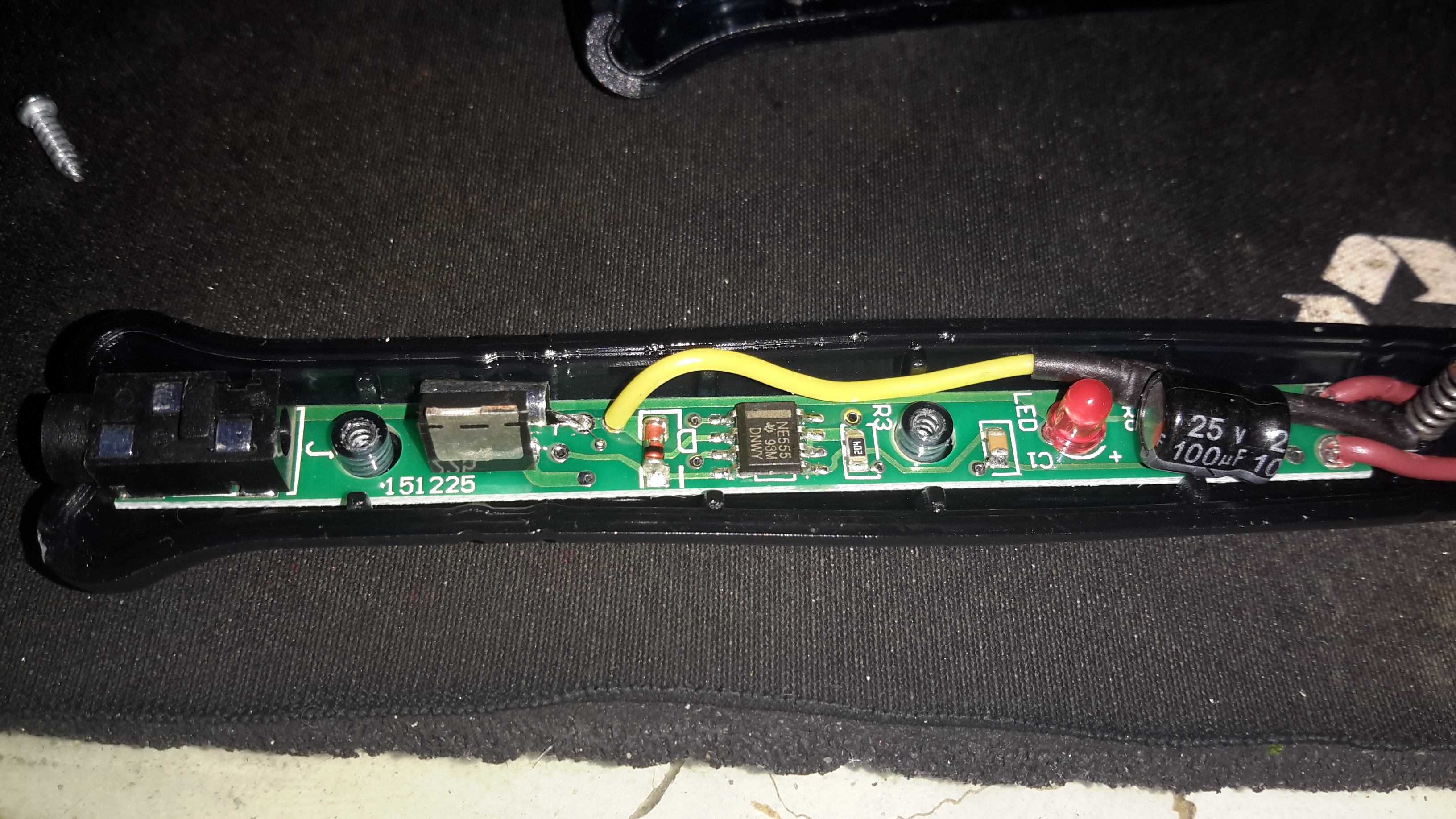
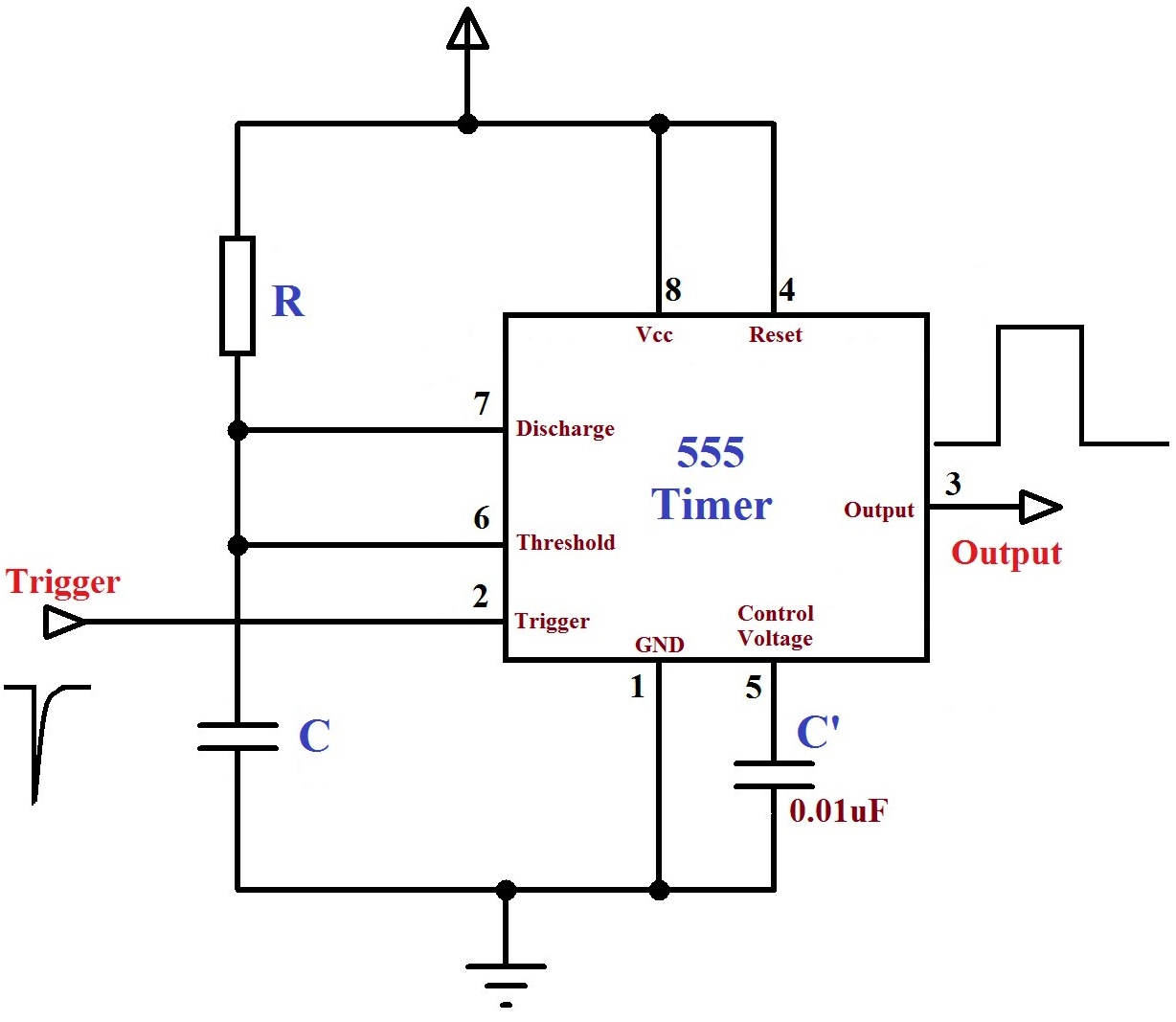
PCB
The main controller is very simple. It’s a 555 timer configured in monostable mode. Below is a schematic showing the basic circuit.
555 Monostable
Big Clive also did a teardown & review of this iron. Head over to YouTube to watch.
The Dyson DC16 is one of the older handheld vacuums, before the introduction of the “Digital Motor”. (Marketing obviously didn’t think “Switched Reluctance Motor” sounded quite as good).
These vacuums have a very large DC brush motor driving the suction turbine instead, the same as would be found in a cordless power tool.
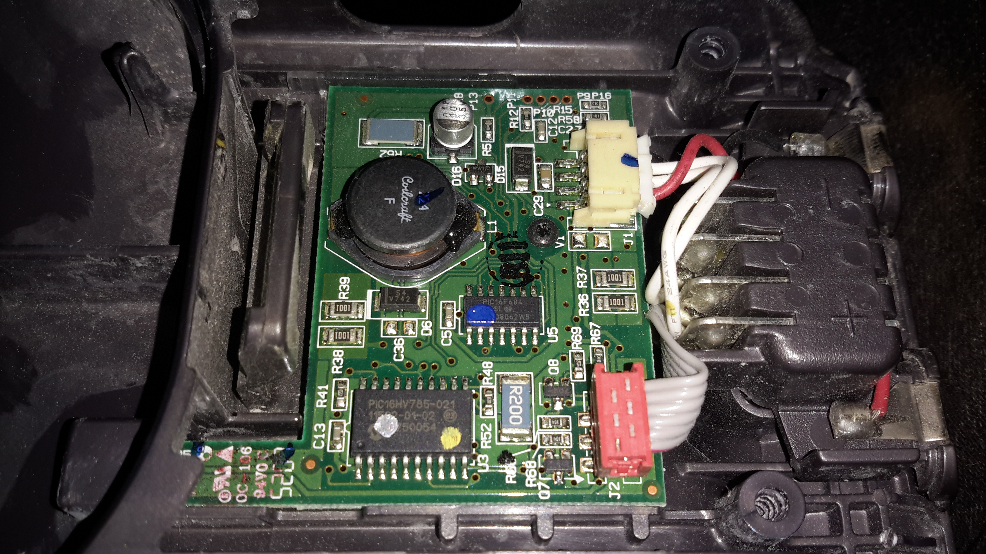
Control PCB
Popping the front cap off with the ID label, reveals the brains of the vacuum. The two large terminals at the right are for charging, which is only done at 550mA (0.5C). There are two PIC microcontrollers in here, along with a large choke, DC-DC converter for supplying the logic most likely. The larger of the MCUs, a PIC16HV785, is probably doing the soft-start PWM on the main motor, the smaller of the two, a PIC16F684 I’m sure is doing battery charging & power management. The motor has a PCB on it’s tail end, with a very large MOSFET, a pair of heavy leads connect directly from the battery connector to the motor.
Just out of sight on the bottom left edge of the board is a Hall Effect Sensor, this detects the presence of the filter by means of a small magnet, the vacuum will not start without a filter fitted.
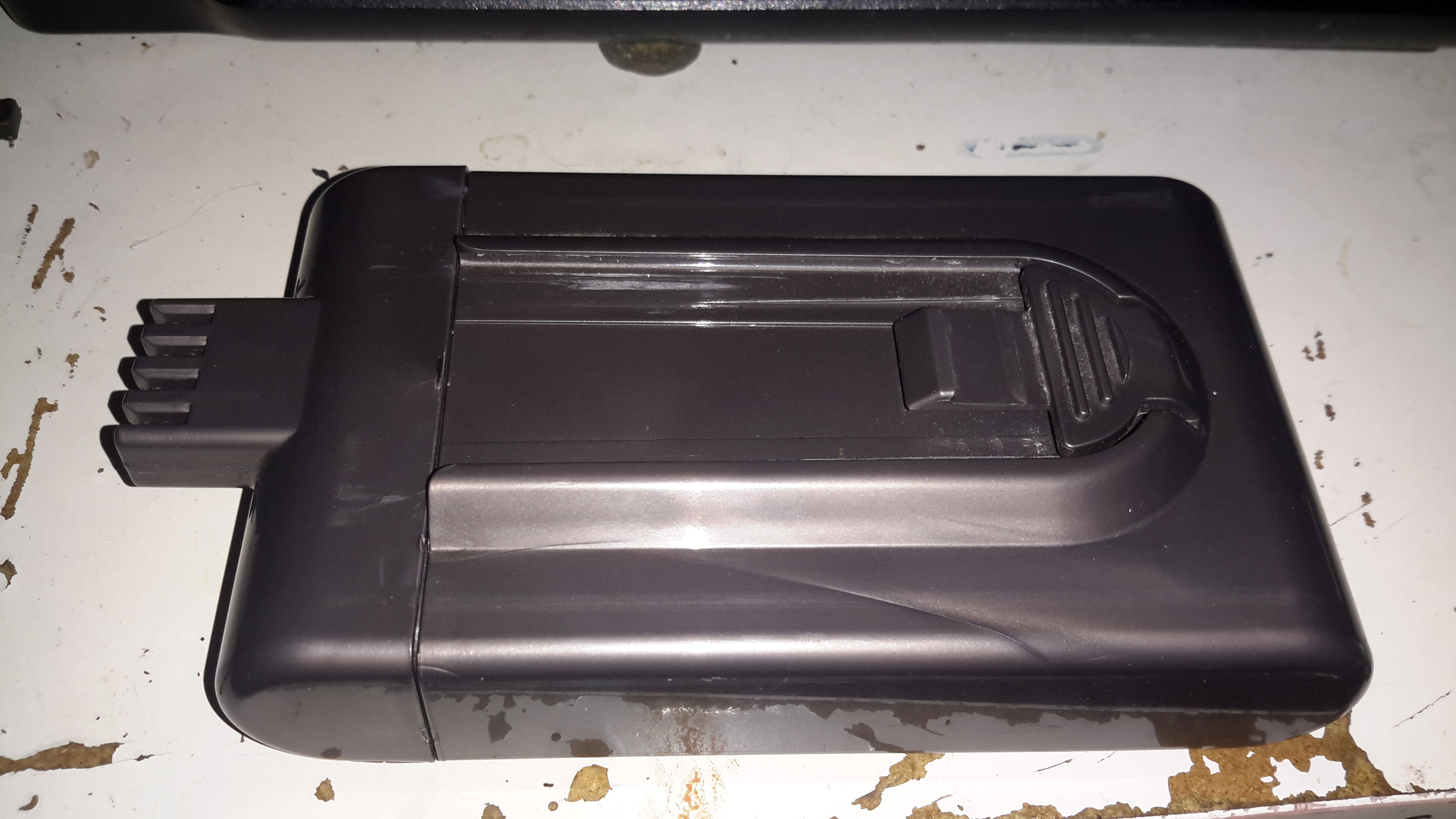
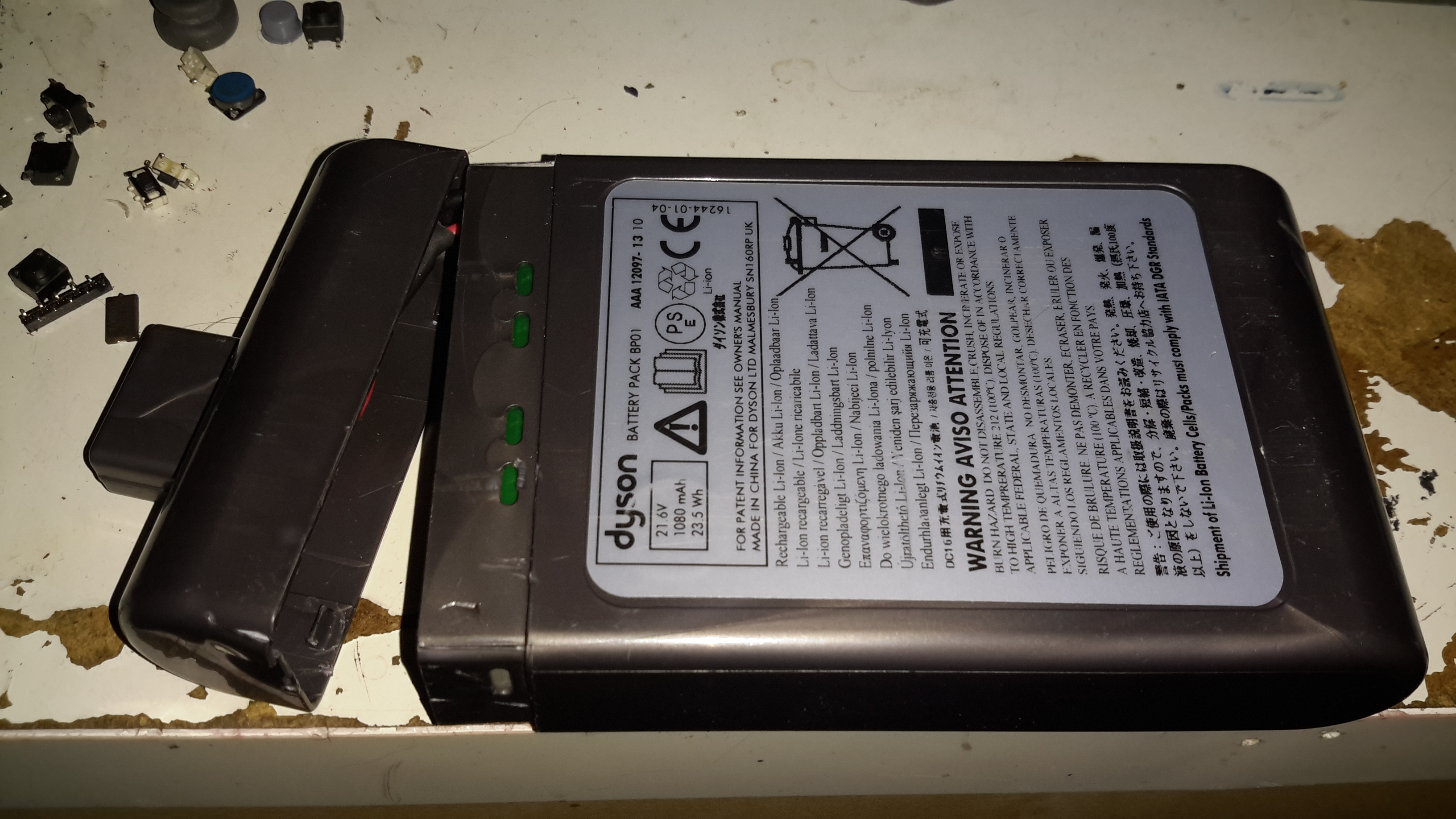
Battery Pack
The battery pack is a large custom job, obviously. 4 terminals mean there’s slightly more in here than just the cells.
Battery Cracked
Luckily, instead of ultrasonic or solvent welding the case, these Dyson batteries are just snapped together. Some mild attack with a pair of screwdrivers allows the end cap to be removed with minimal damage.
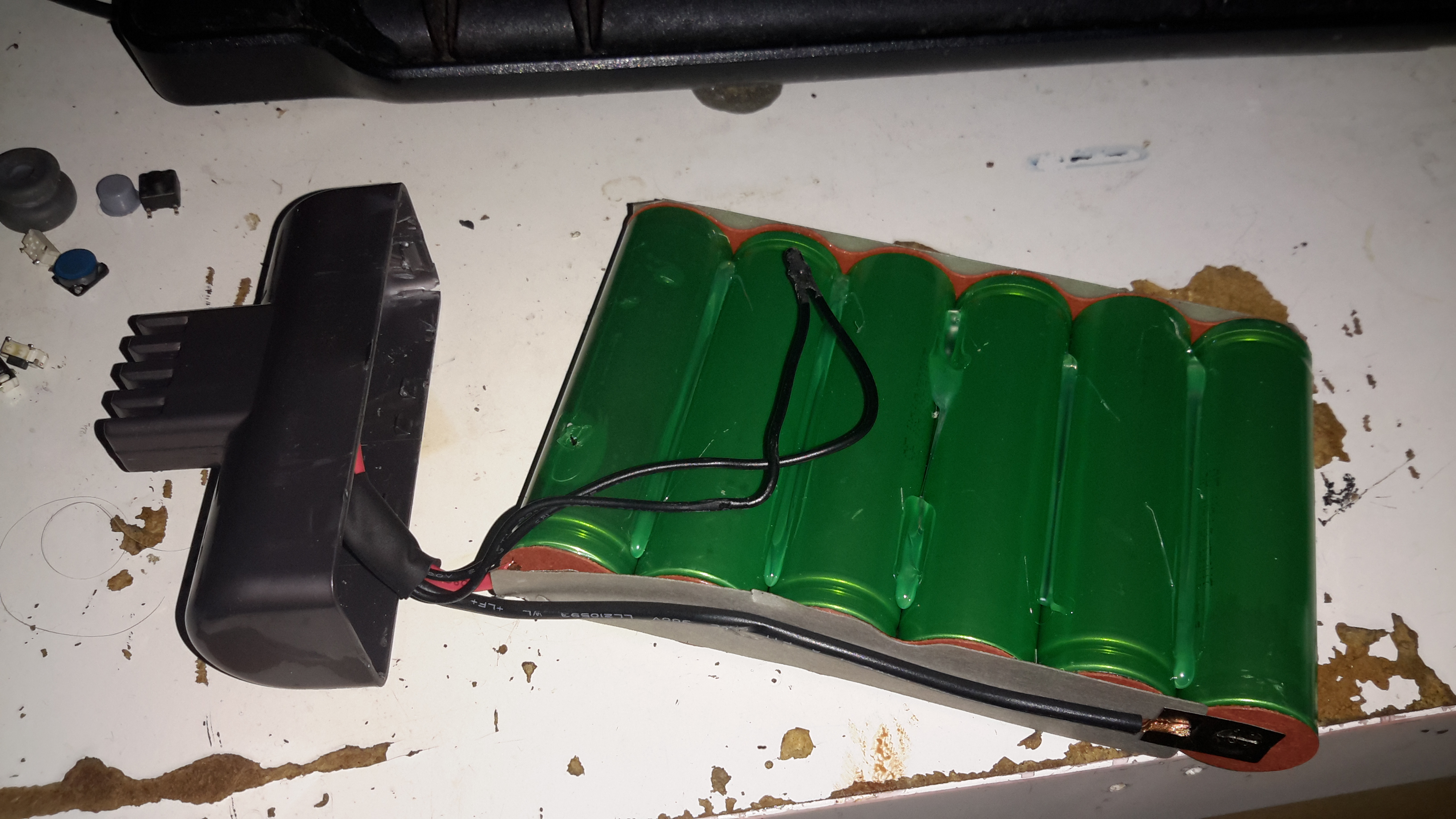
Cells
The cells were lightly hot-glued into the shell, but that can easily be solved with a drop of Isopropanol to dissolve the glue bond. The pack itself is made up of 6 Sony US18650VT High-Drain 18650 Li-Ion cells in series for 21.6v nominal. These are rated at a max of 20A discharge current, 10A charge current, and 1.3Ah capacity nominal.
There’s no intelligence in this battery pack, the extra pair of terminals are for a thermistor, so the PIC in the main body knows what temperature the pack is at – it certainly gets warm while in use due to the high current draw.
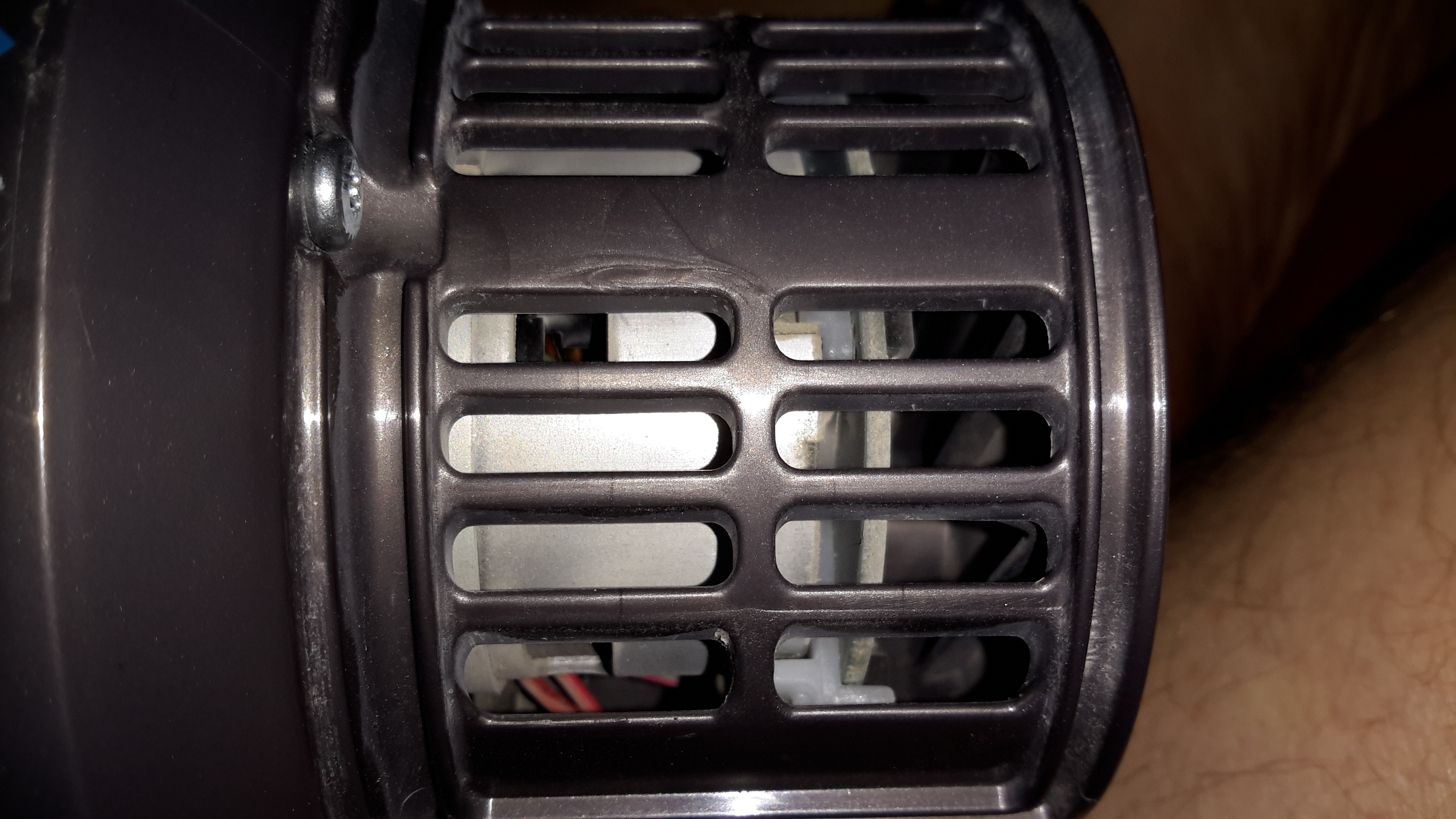
Motor
Hidden in the back side of the main body is the motor. Unfortunately I wasn’t able to get this out without doing some damage, as the wiring isn’t long enough to free the unit without some surgery.
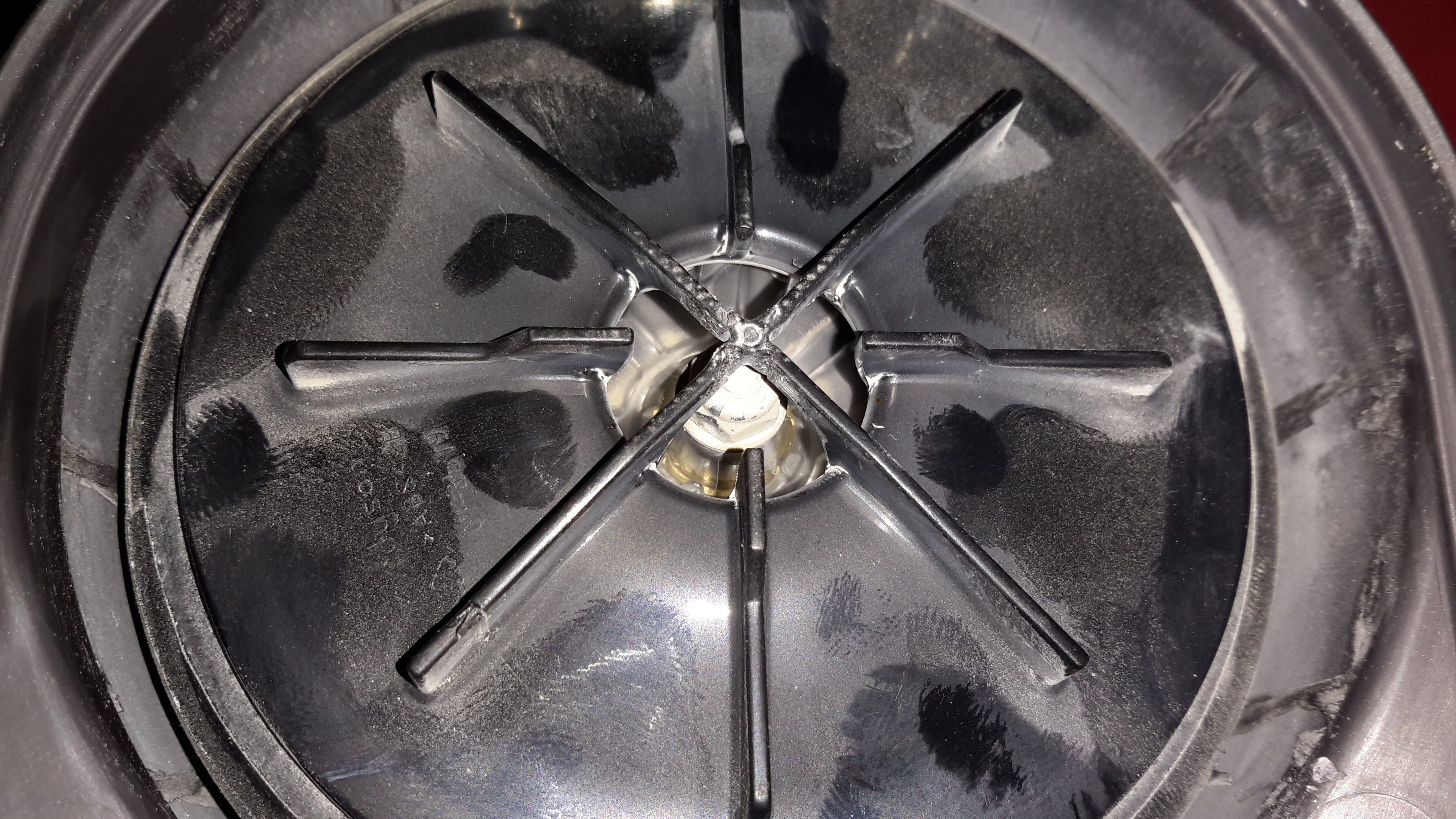
Turbine
The suction is generated by a smaller version of the centrifugal high-speed blowers used in full size vacuums. Not much to see here.
Unofficial Charger
Since I got this without a charger, I had to improvise. The factory power supply is just a 28v power brick, all the charging logic is in the vacuum itself, so I didn’t have to worry about such nasties as over-charging. I have since fitted the battery pack with a standard Li-Po balance cable, so it can be used with my ProCell charger, which will charge the pack in 35 minutes, instead of the 3 hours of the original charger.
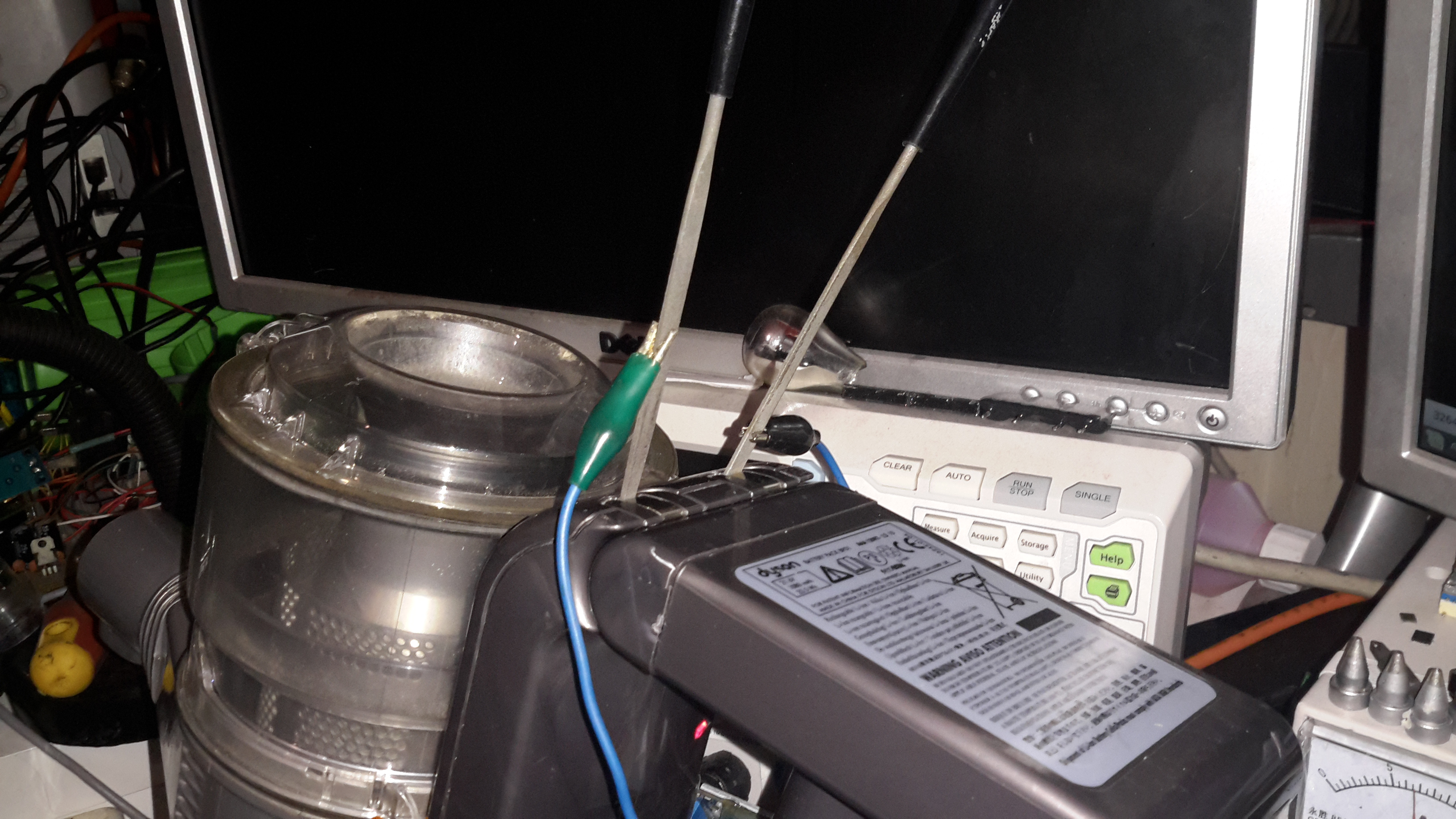
I recently came across these on eBay, so I thought I’d grab one to see how they function, with all the metrics they display, there’s potential here for them to be very useful indeed.
One of the best parts is that no wiring is required between the sensor board & the LCD head unit – everything is transmitted over a 2.4GHz data link using NRF24L01 modules.
Above is the display unit, with it’s colour LCD display. Many features are available on this, & they appear to be designed for battery powered systems.
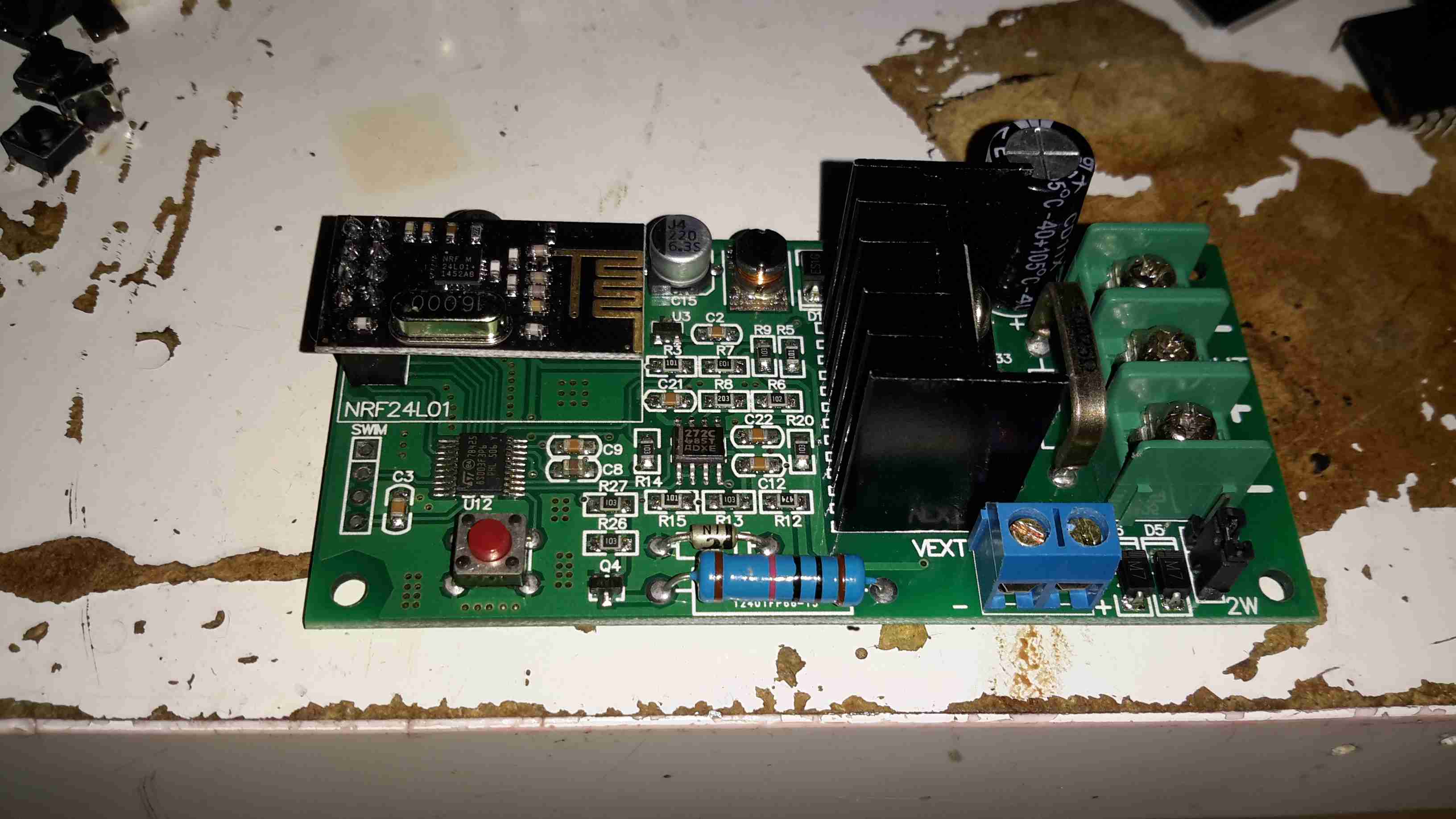
Monitor PCB
Another PCB handles the current & voltage sensing, so this one can be mounted as close to the high current wiring as possible.
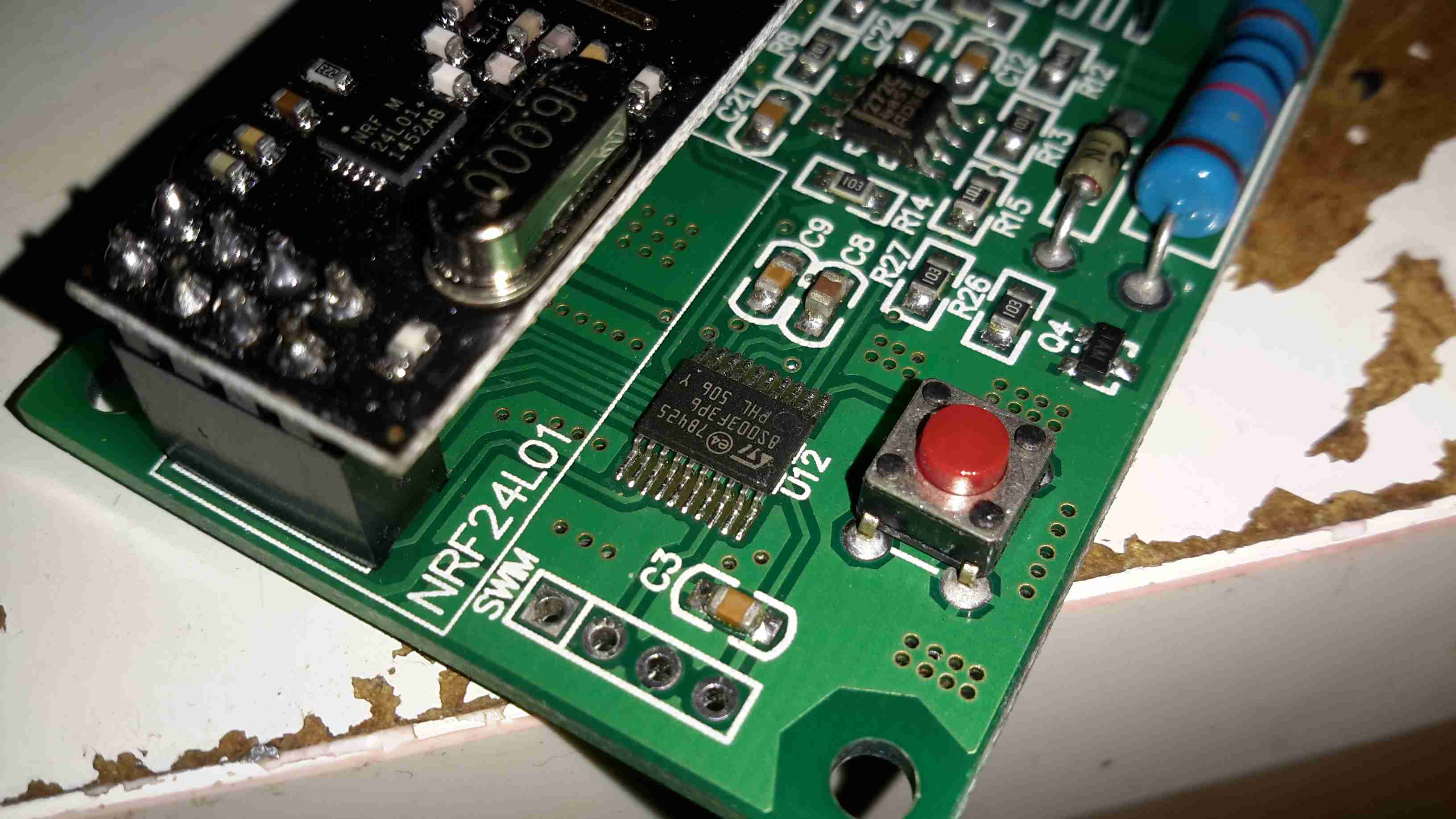
Monitor PCB Microcontroller
The transmitter PCB is controlled with an STM8S003F3 microcontroller from ST Microelectronics. This is a Flash based STM with 8KB of ROM, 1KB of RAM & 10-bit ADC. The NRF24L01 transceiver module is just to the left.
There’s only a single button on this board, for pairing both ends of the link.
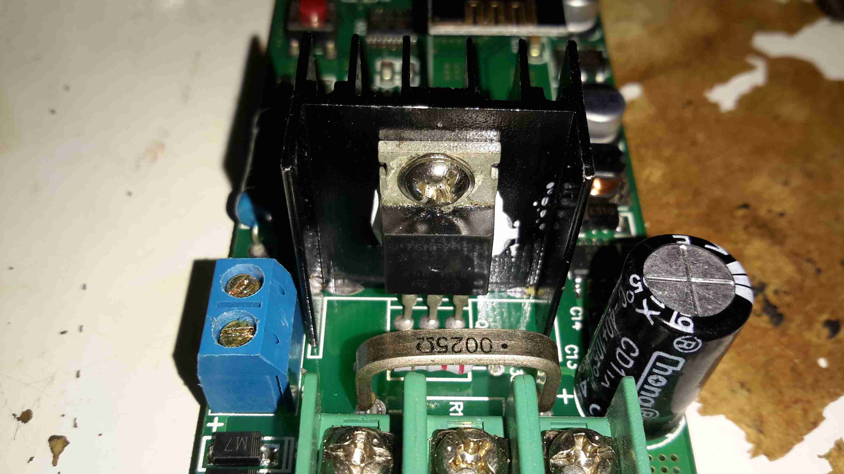
Output MOSFET
The high current end of the board has the 0.0025Ω current shunt & the output switch MOSFET, a STP75NF75 75v 75A FET, also from ST Microelectronics. A separate power source can be provided for the logic via the blue terminal block instead of powering from the source being measured.
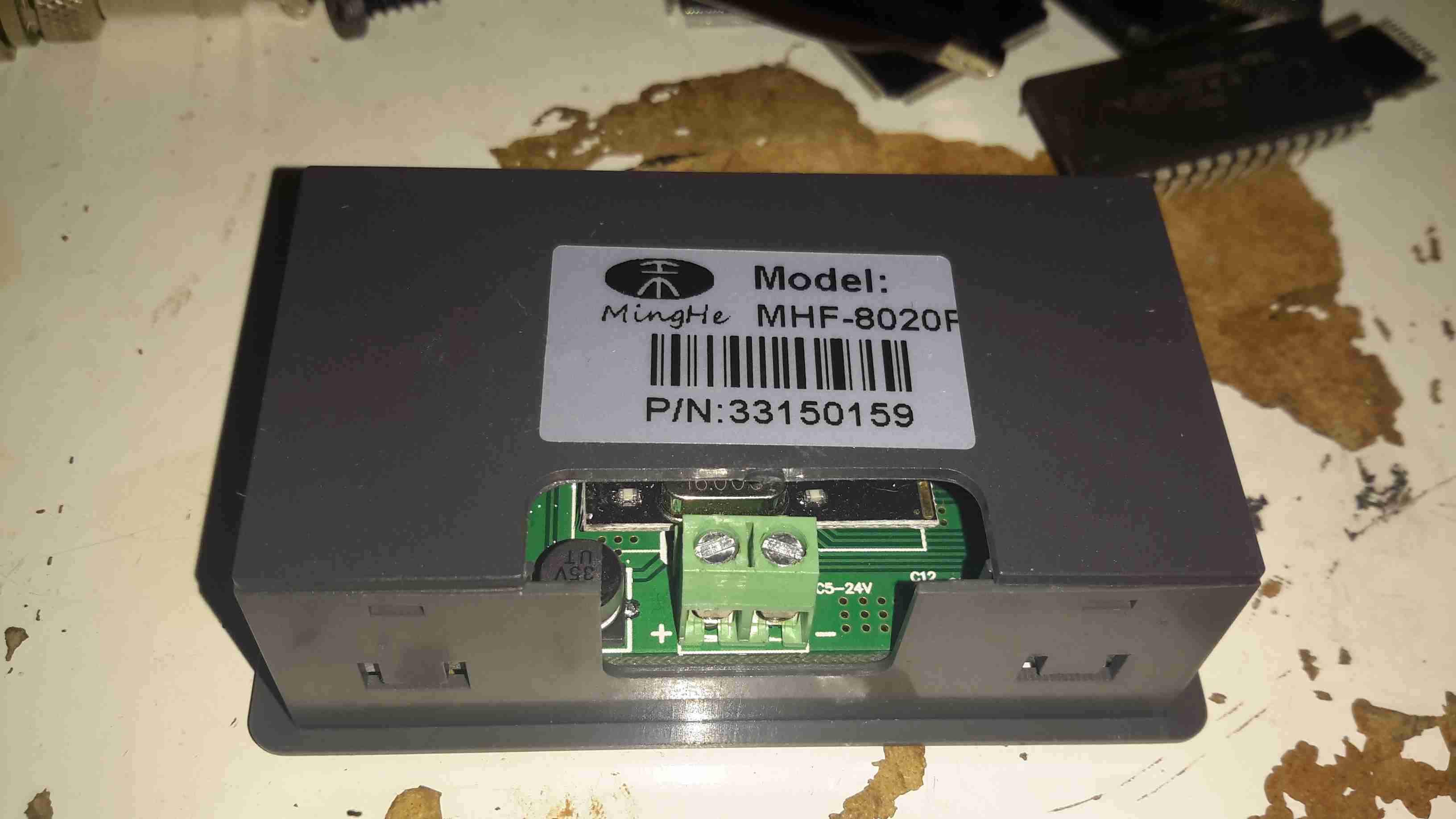
LCD Unit Rear
Here’s the display unit, only a pair of power terminals are provided, 5-24v wide-range input is catered for.
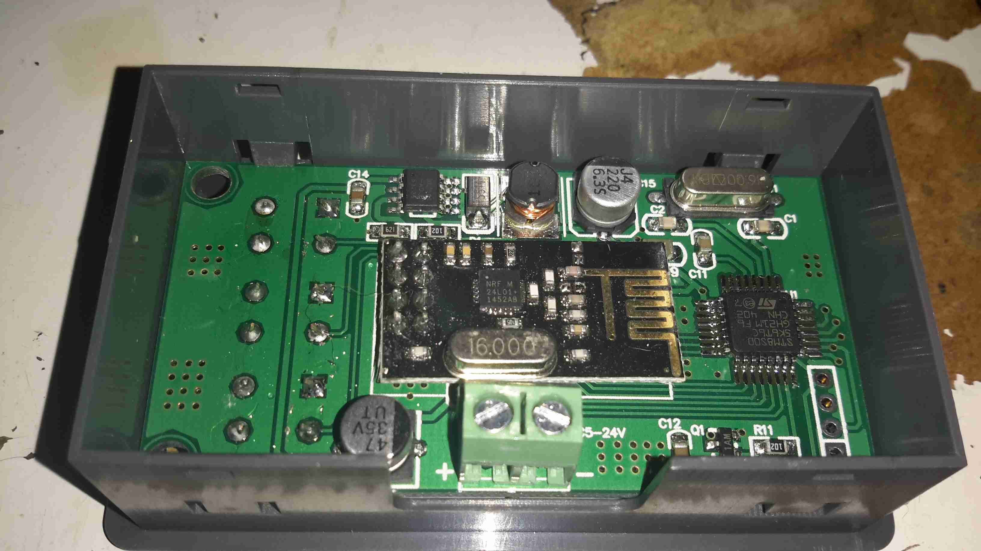
LCD Unit PCB
Unclipping the back of the board reveals the PCB, with another 2.4GHz NRF24L01 module, and a STM8S005K6 microcontroller in this case. The switching power supply that handles the wide input voltage is along the top edge of the board.
Unfortunately I didn’t get any instruction manual with this, so some guesswork & translation of the finest Chinglish was required to get my head round the way everything works. To make life a little easier for others that might have this issue, here’s a list of functions & how to make them work.
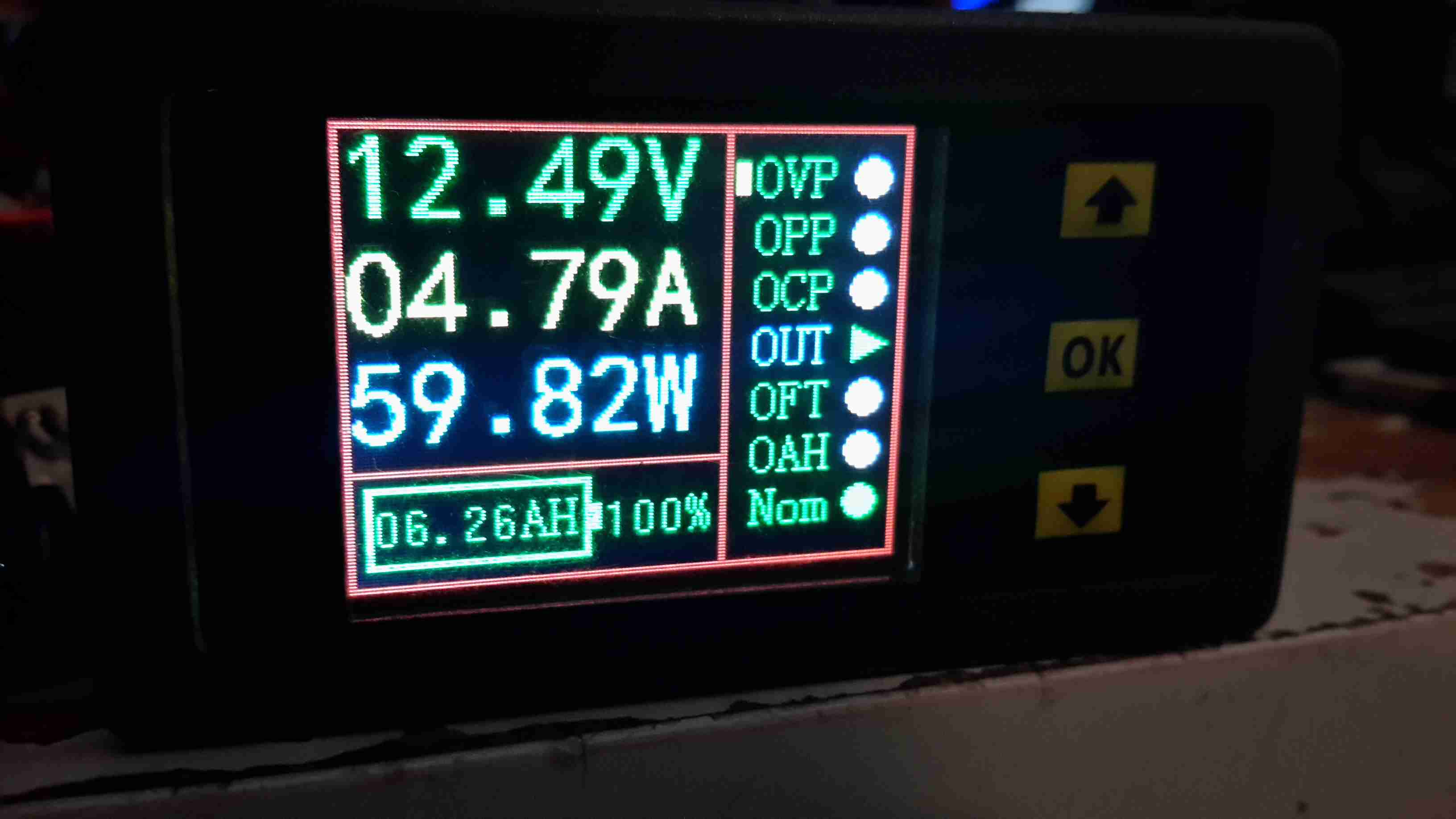
LCD Closeup
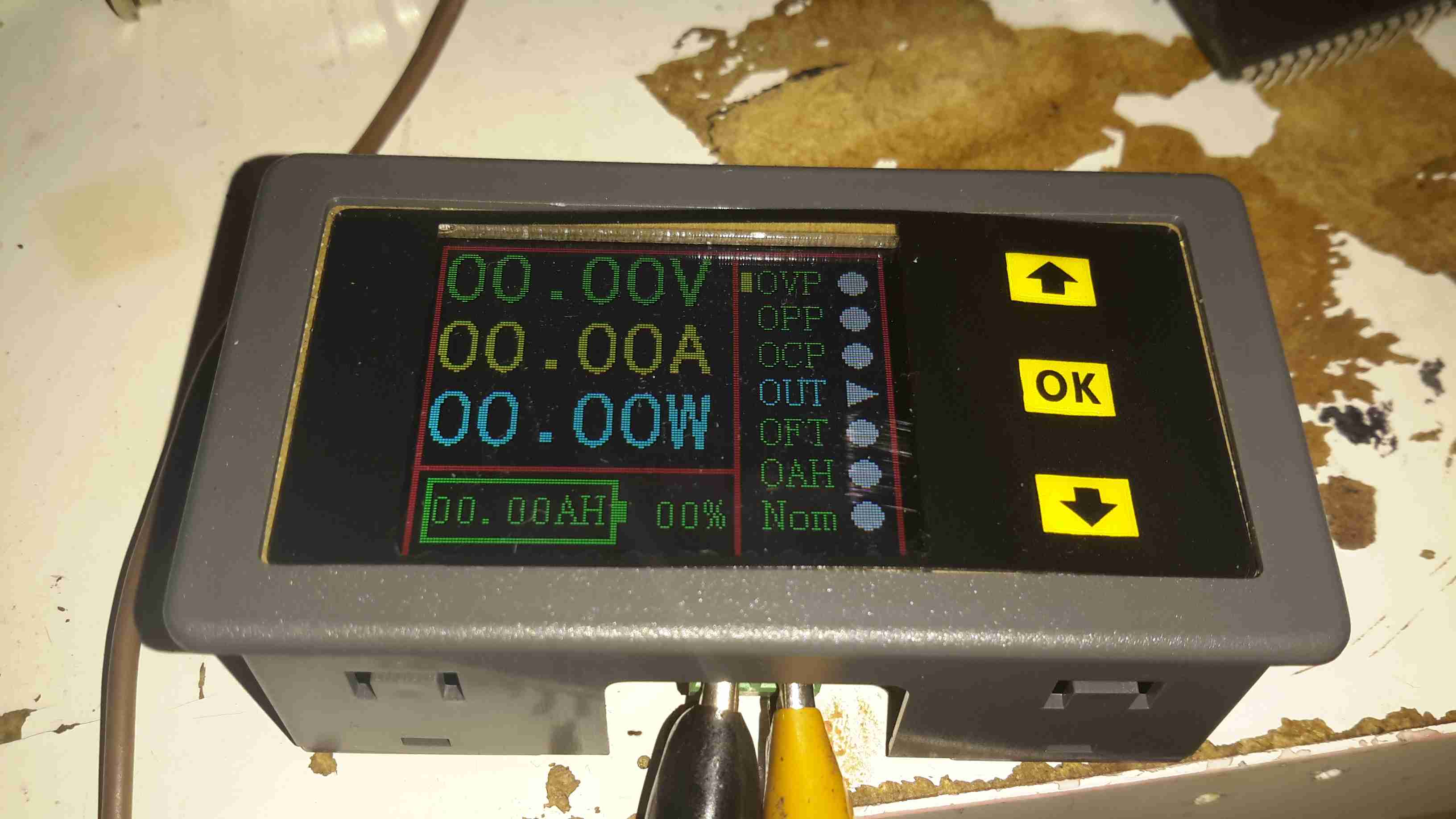
On the right edge of the board is the function list, a quick press of the OK button turns a function ON/OFF, while holding it allows the threshold to be set.
When the output is disabled by one of the protection functions, turning that function OFF will immediately enable the output again.
The UP/DOWN buttons obviously function to select the desired function with the cursor just to the left of the labels. Less obviously though, pressing the UP button while the very top function is selected will change the Amp-Hours display to a battery capacity icon, while pressing DOWN while the very bottom function is selected will change the Watts display to Hours.
The round circle to the right displays the status of a function. Green for OK/ON Grey for FAULT/OFF.
OVP: Over voltage protection. This will turn off the load when the measured voltage exceeds the set threshold.
OPP: Over power protection. This function prevents a load from pulling more than a specified number of watts from the supply.
OCP: Over current protection. This one’s a little more obvious, it’ll disable the output when the current measured exceeds the specified limit.
OUT: This one is the status of the output MOSFET. Can also be used to manually enable/disable the output.
OFT: Over time protection. This one could be useful when charging batteries, if the output is enabled for longer than the specified time, the output will toggle off.
OAH: Over Amp-Hours protection. If the counted Amp-Hours exceeds the set limit, the output will be disabled.
Nom: This one indicates the status of the RF data link between the modules, and can be used to set the channel they operate on.
Pairing is achieved by holding the OK button, selecting the channel on the LCD unit, and then pressing the button on the transmitter board. After a few seconds, (it appears to scan through all addresses until it gets a response) the display will resume updating.
This function would be required if there are more than a single meter within RF range of each other.
I’ve not yet had a proper play with all the protection functions, but a quick mess with the OVP setting proved it was very over-sensitive. Setting the protection voltage to 15v triggered the protection with the measured voltage between 12.5v-13.8v. More experimentation is required here I think, but as I plan to just use these for power monitoring, I’ll most likely leave all the advanced functions disabled.
Inkeeping with everything else in my shack being low voltage operated, I had planned from the outset to convert the desoldering station to 12v operation. It turns out this has been the easiest tool to convert in my shack so far.
PSU Outputs
The factory SMPS is a fairly straightforward 18v 12A unit, with only a single small oddity: the desoldering gun’s heating element is controlled from inside the supply.
Iron MOSFET
Next to the output rectifier on the heatsink is a large MOSFET, in this case a STP60NF06 from ST Micro. This is a fairly beefy FET at 60v & 60A capacity, RDS On of <0.016Ω.
This is driven via an opto-isolator from the main logic board. I’ve not yet looked at the waveform on the scope, but I suspect this is also being PWM’d to control temperature better when close to the set point.
Iron Element Controller
Rather than fire up the soldering iron & build a new element controller circuit (Lazy Mode™), I opted to take a saw to the original power supply. I cut the DC output section of the PCB off the rest of the supply & attached this piece back to the frame of the base unit. I also added a small heatsink to the MOSFET to make sure it stays cool.
12v Power Supply
Since the fan & vacuum pump are both already 12v rated, those are connected directly to the DC input socket, that I’ve installed in place of the original IEC mains socket. The 18v for the heating element is generated by a 10A DC-DC converter, again from eBay.
Oddly, the iron itself is rated at 24v 80W, but the factory supply is only rated to 18v. I’m not sure why they’ve derated the system, but as the station already draws up to 10A from a 13.8v supply, increasing the voltage any further would start giving my DC supplies a problem, so it can stay at 18v for now.
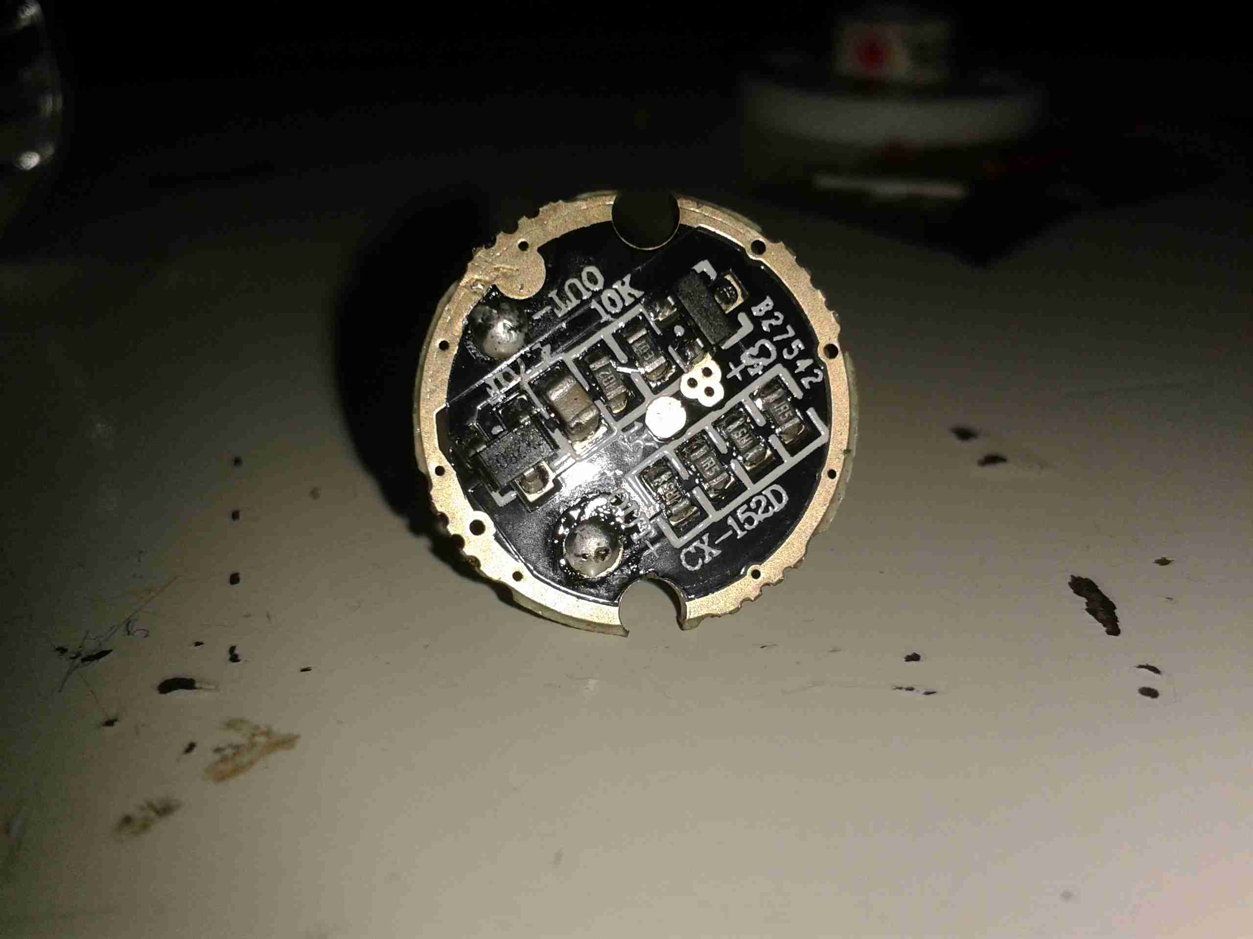
The multimode dimming/flashing modes on Chinese torches have irritated me for a while. If I buy a torch, it’s to illuminate something I’m doing, not to test if people around me have photosensitive epilepsy.
Looking at the PCB in the LED module of the torch, a couple of components are evident:
LED Driver PCB
There’s not much to this driver, it’s simply resistive for LED protection (the 4 resistors in a row at the bottom of the board).
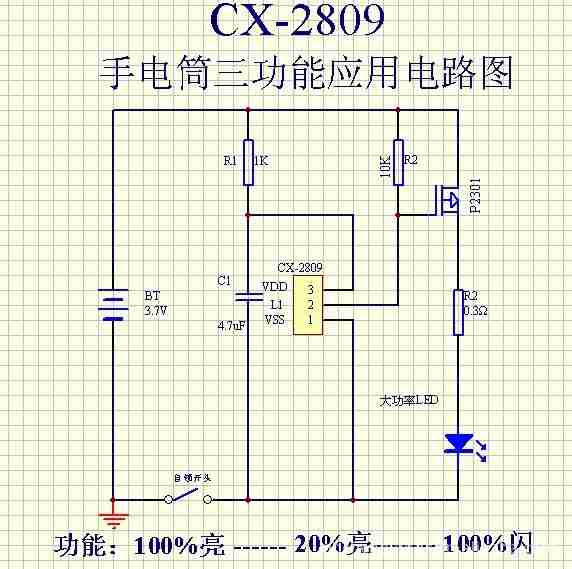
The components at the top are the multimode circuitry. The SOT-23 IC on the left is a CX2809 LED Driver, with several modes. The SOT-23 on the right is a MOSFET, for switching the actual LED itself. I couldn’t find a datasheet for the IC itself, but I did find a schematic that seems to match up with what’s on the board.
Schematic
Here’s that schematic, the only thing that needs to be done to convert the torch to single mode ON/OFF at full brightness, is to bridge out that FET.
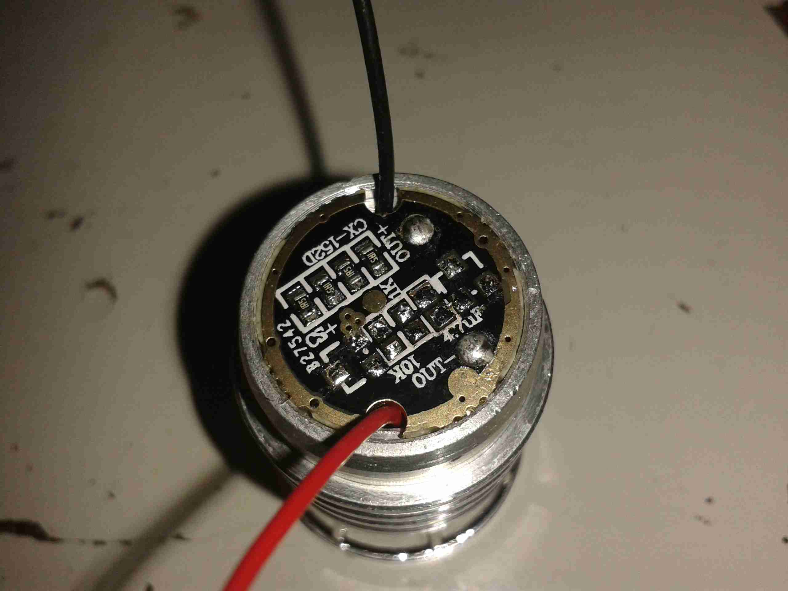
Components Desoldered
To help save the extra few mA the IC & associated circuitry will draw from the battery, I have removed all of the components involved in the multimode control. This leaves just the current limiting resistors for the LED itself.
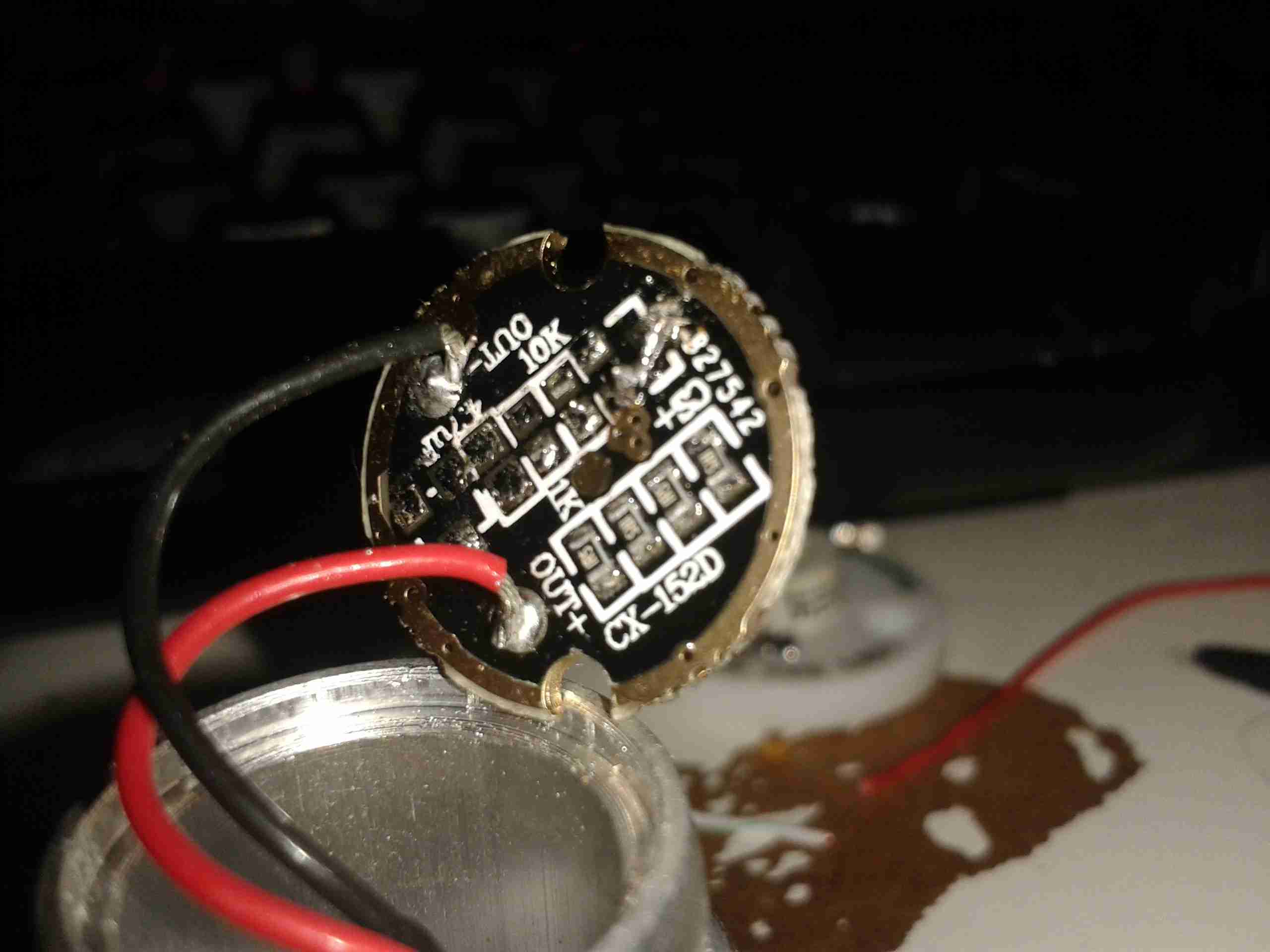
Jumper Link
The final part above, is to install a small link across the Drain & Source pads of the FET. Now the switch controls the LED directly with no silly electronics in between. A proper torch at last.
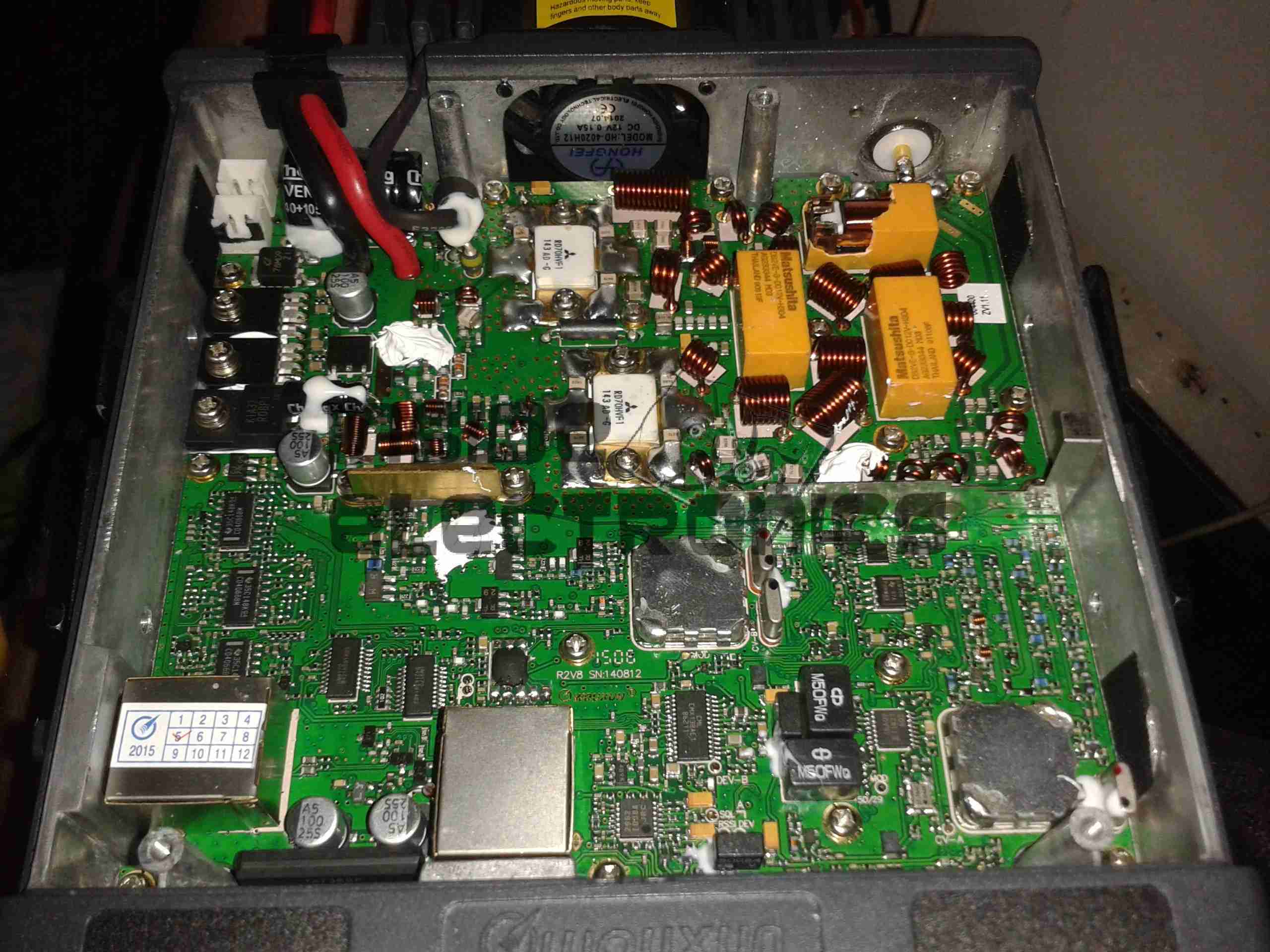
Following on from my review, here are some internal views & detail on the components used in this radio. Below is an overview of the main PCB with the top plate removed from the radio.
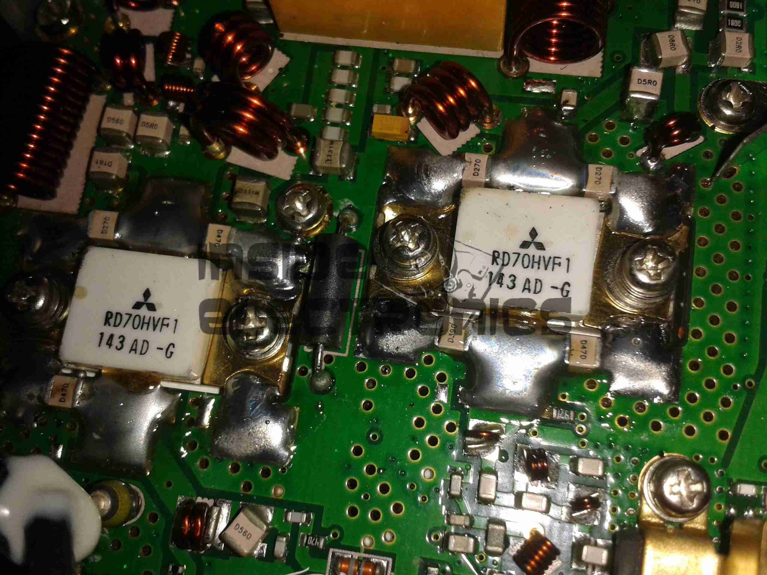
Cover RemovedRF Final Amplifier Stage
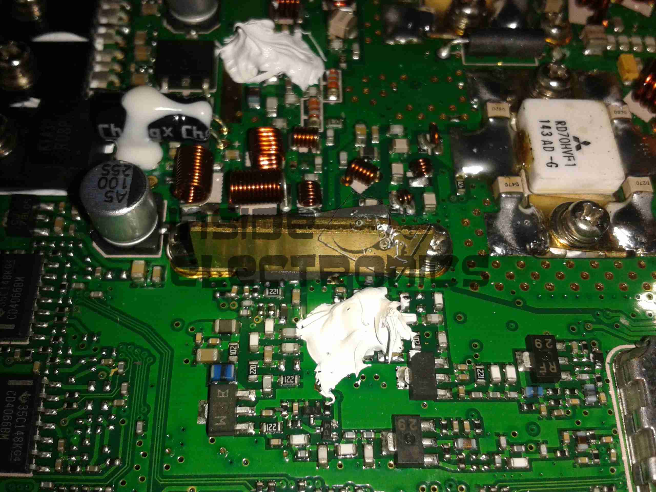
Most visible are these MOSFETs, which are Mitsubishi RD70HVF1 VHF/UHF power devices. Rated for a maximum of 75W output power at 12.5v (absolute maximum of 150W, these are used well within their power ratings. They are joined to the PCB with heavy soldering, with bypass caps tacked right on to the leads.
RF Pre Drivers
Here is the RF pre-driver stage, with intermediate transistors hidden under the small brass heatspreader.
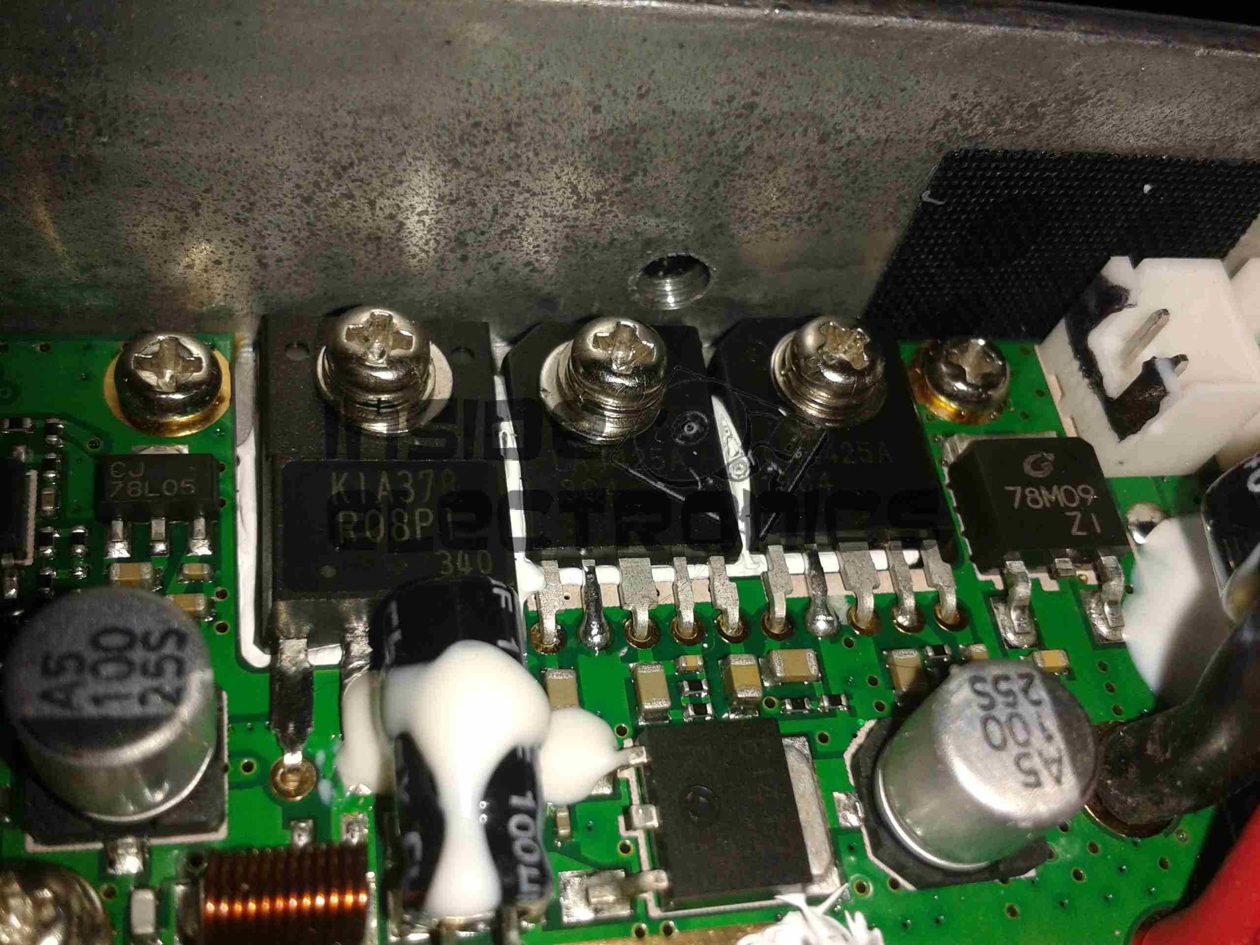
Power Section
In the top left corner of the radio, near the power input leads, is the power supply & audio amplifier section. Clearly visible are the pair of LA4425A 5W audio power amplifier ICs, these drive the speakers on the top of the radio. Either side of these parts are a 7809 & a 7805 – both linear regulators providing +9v & +5v logic supplies respectively. The large TO220 package device is a KIA378R08PI 3A LDO regulator with ON/OFF control, this one outputs +8v. Just visible in the top right corner are the sockets for the speaker connections.
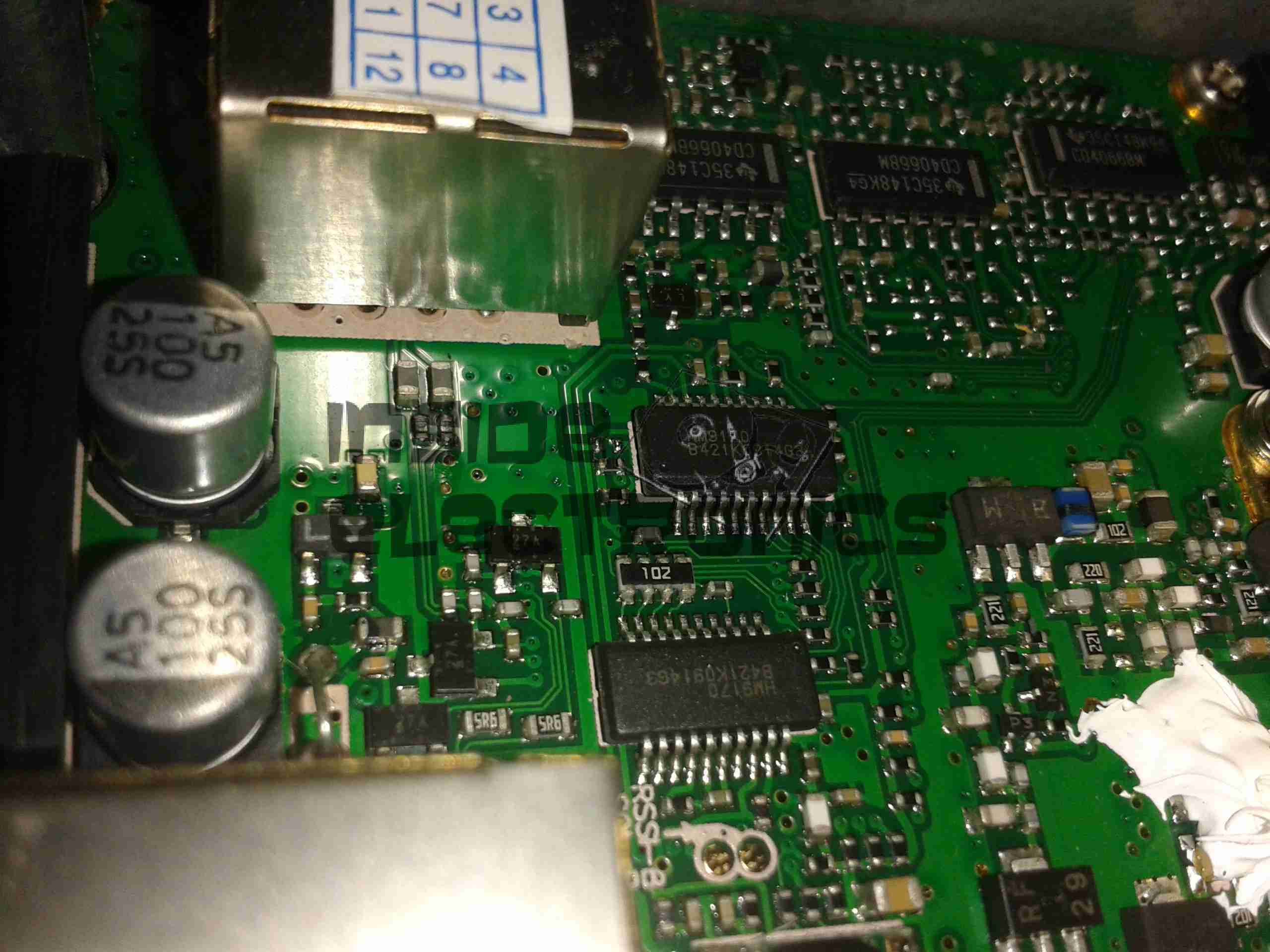
DTMF Circuits
Here are the two ICs for dealing with DTMF tones, they are HM9170 receivers.
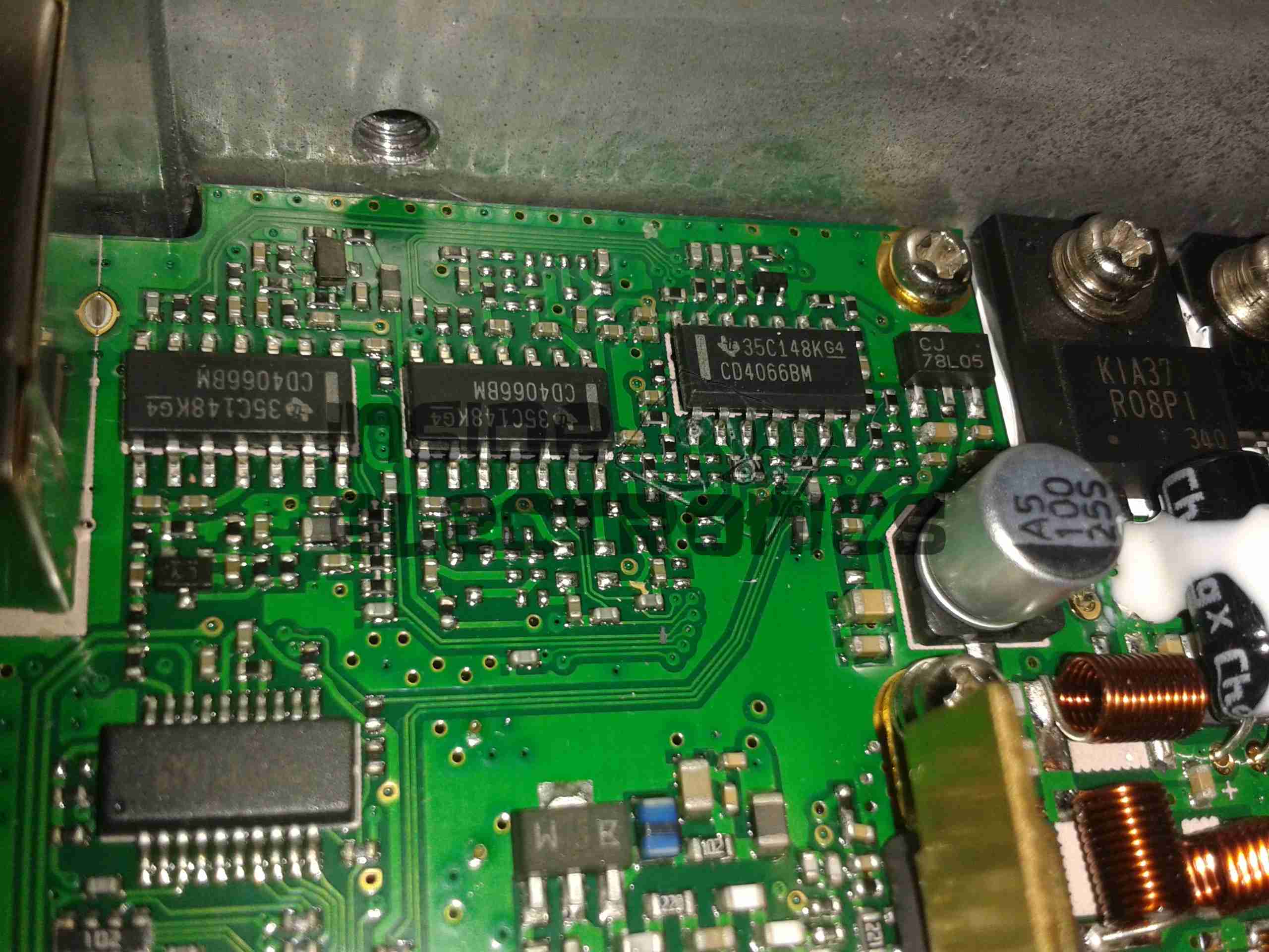
Glue Logic
In the corner next to the interface jack, there are some CD4066B Quad Bilateral switches. These make sense since the interface jack has more than a single purpose, these will switch signals depending on what is connected.
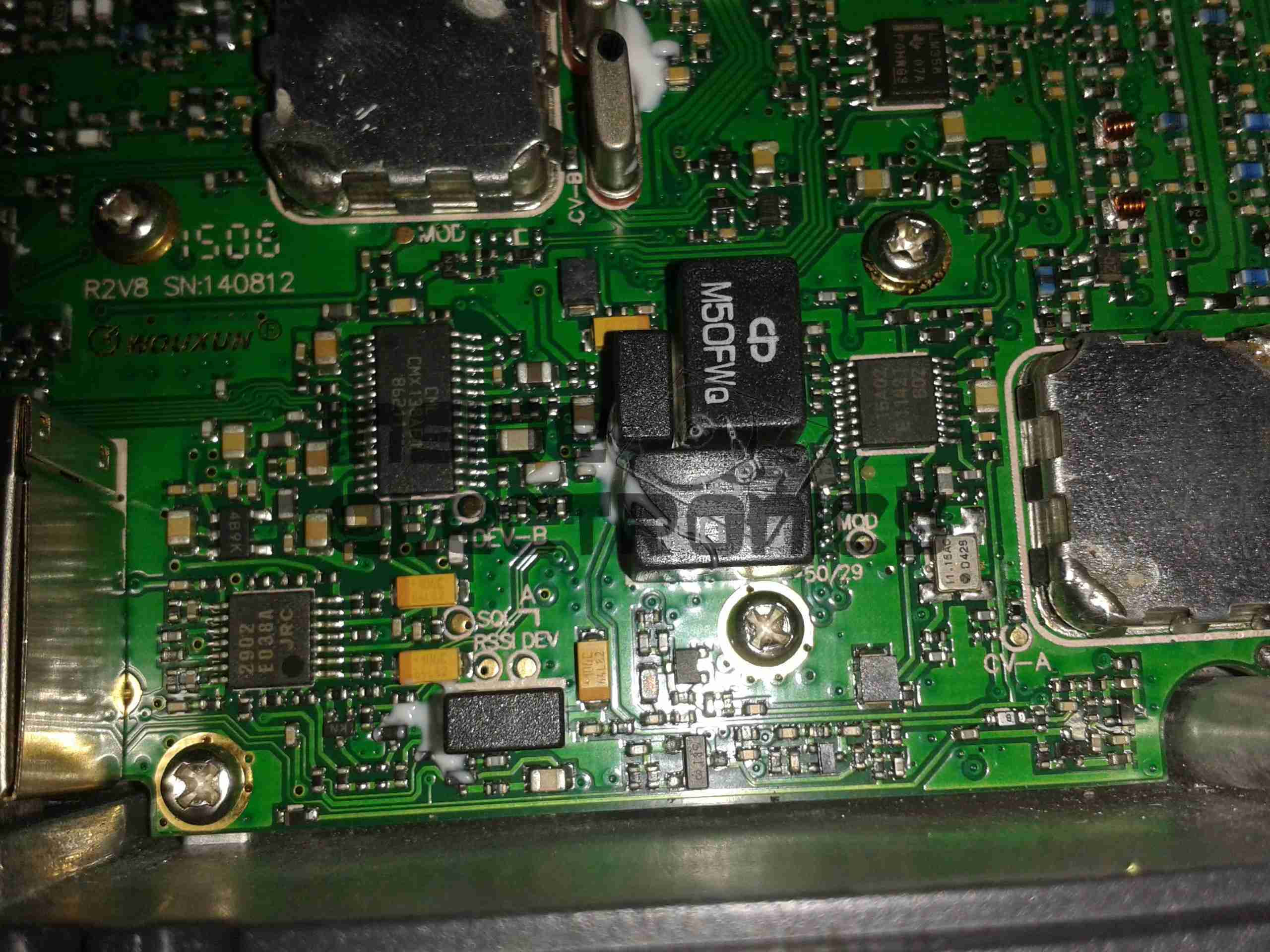
RF Section
Here are visible the RF cans for the oscillators, the crystals visible next to the can at the top. The shields are soldered on, so no opening these unfortunately.
Also visible in this image is a CMX138A Audio Scrambler & Sub-Audio Signalling processor. This IC deals with the Voice Inversion Scrambling feature of the radio, & processes the incoming audio before being sent to the modulator.
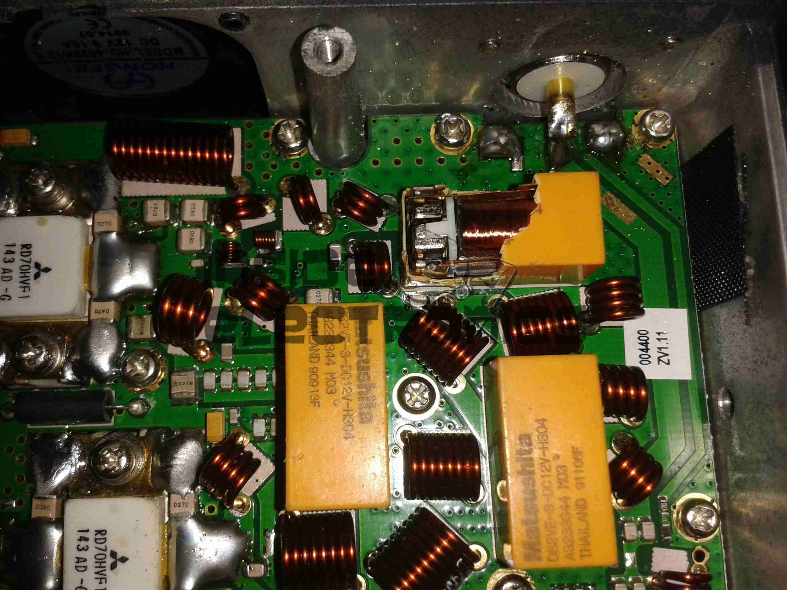
Output Filter Network
Shown here is the RF output filter network, this radio uses relays for switching instead of PIN diodes, I imagine for cost reasons. The relay closest to the RF output socket has had a slight accident 🙂 This is slated to be replaced soon.
RF Output Jack
Finally, the RF output jack.
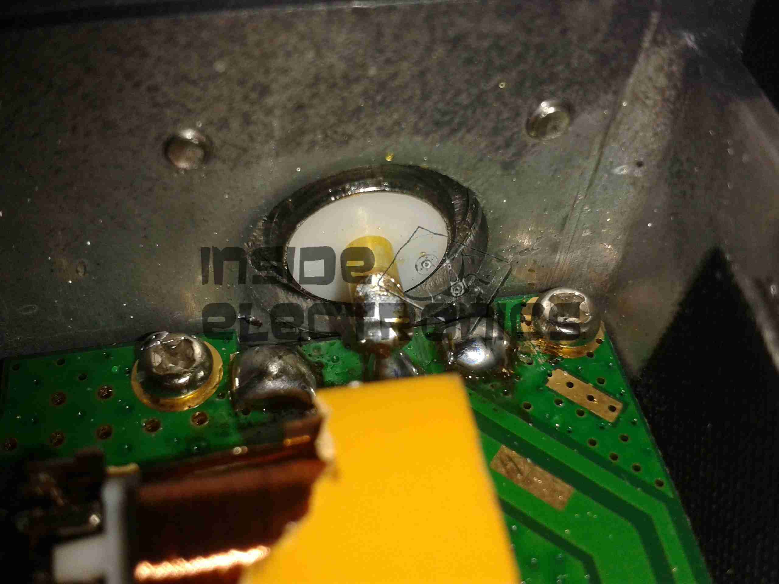
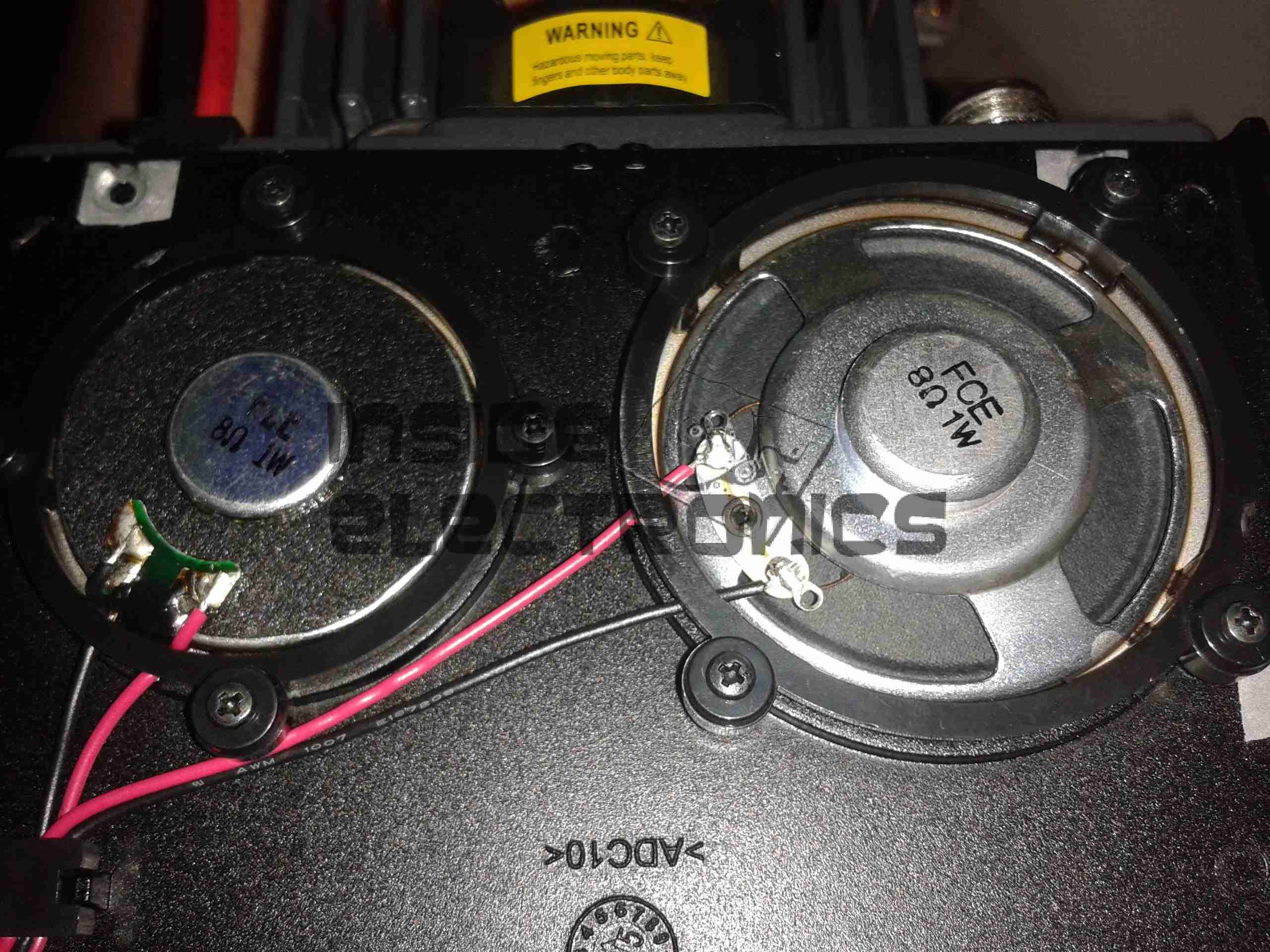
Audio Speakers
Here the speakers are shown, attached to the bottom of the top plate. They are both rated 8Ω 1W.
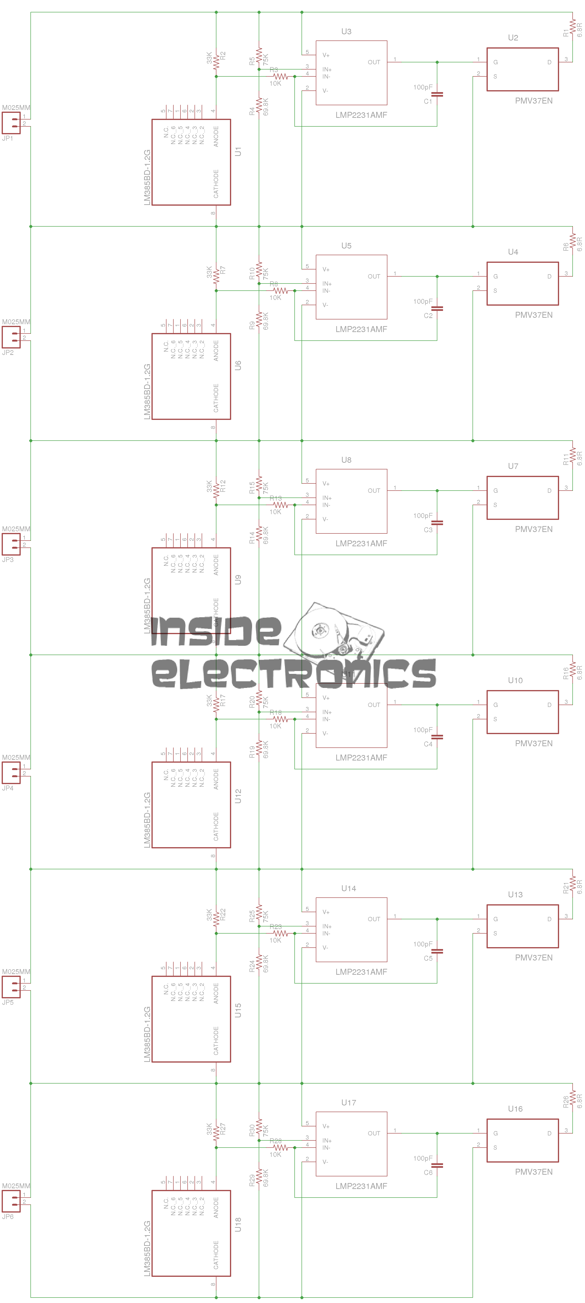
Here’s another active balancing circuit for large ultracapacitor banks, this one is designed for a series string of 6, at 2.5v per capacitor.
Based on the design here, I have transcribed the circuit into Eagle & designed a PCB layout.
Ultracap Balancer Circuit – Click to Embiggen
As can be seen from the circuit diagram above, this is just 6 copies of the circuit from the above link, with screw terminals to attach to the capacitor string.
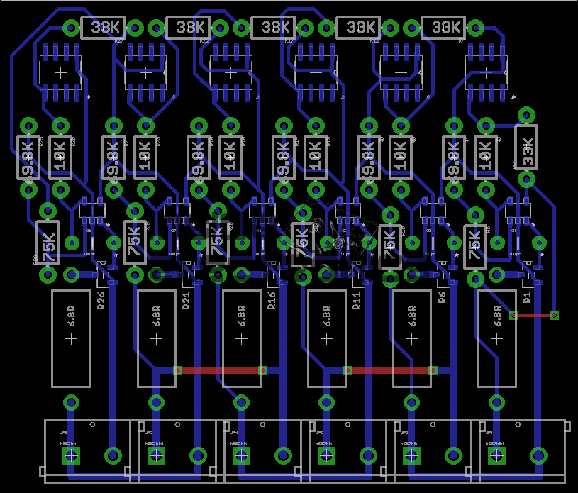
Ultracap Balancer PCB
And here’s the PCB. the MOSFETs & OpAmps are very small SMT parts, so require a steady hand in soldering. This board can easily be etched by hand as there’s only 3 links on the top side. No need for a double sided PCB.
As always, the Eagle project files & my Eagle library collection are available below:
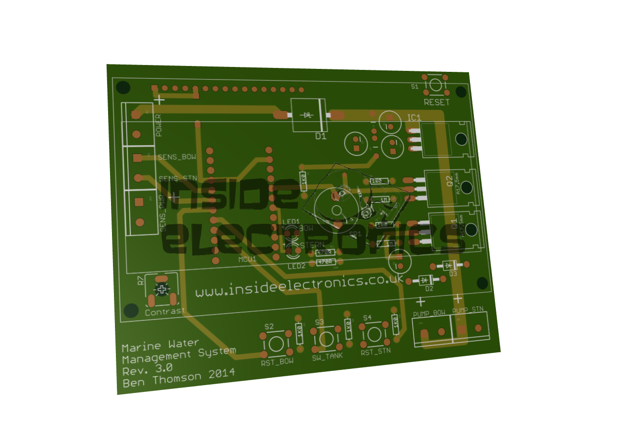
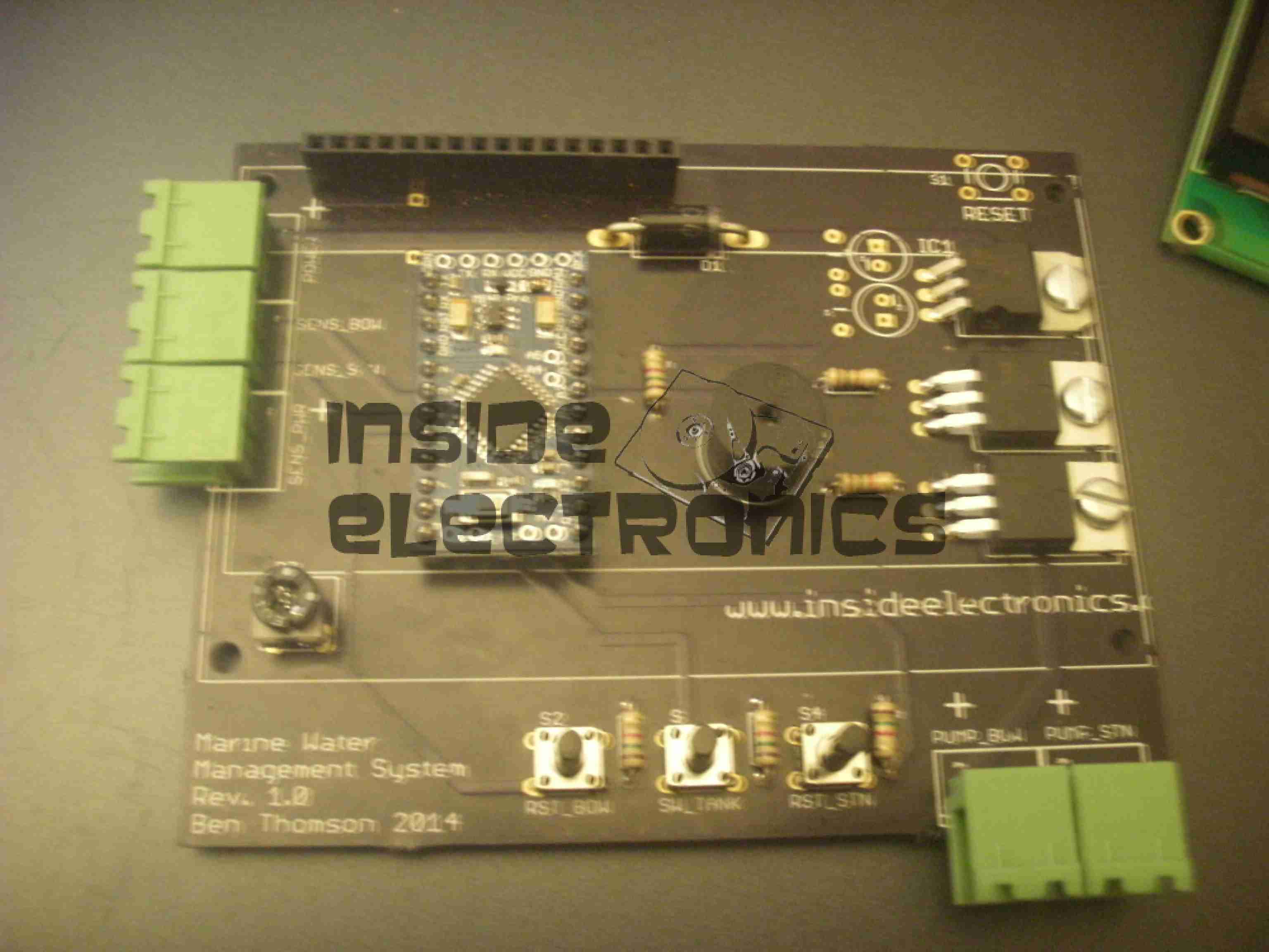
OK, a few revisions have been made to the water management PCB, mainly to reduce the possibility of the brushed DC motors in the water pumps from causing the MCU to crash, with the other changes to the I/O connector positioning & finally upgrading the reverse blocking diode to a 10A capable version rather than 5A.
Having two separate water tanks on nb Tanya Louise, with individual pumps, meant that monitoring water levels in tanks & keeping them topped up without emptying & having to reprime pumps every time was a hassle.
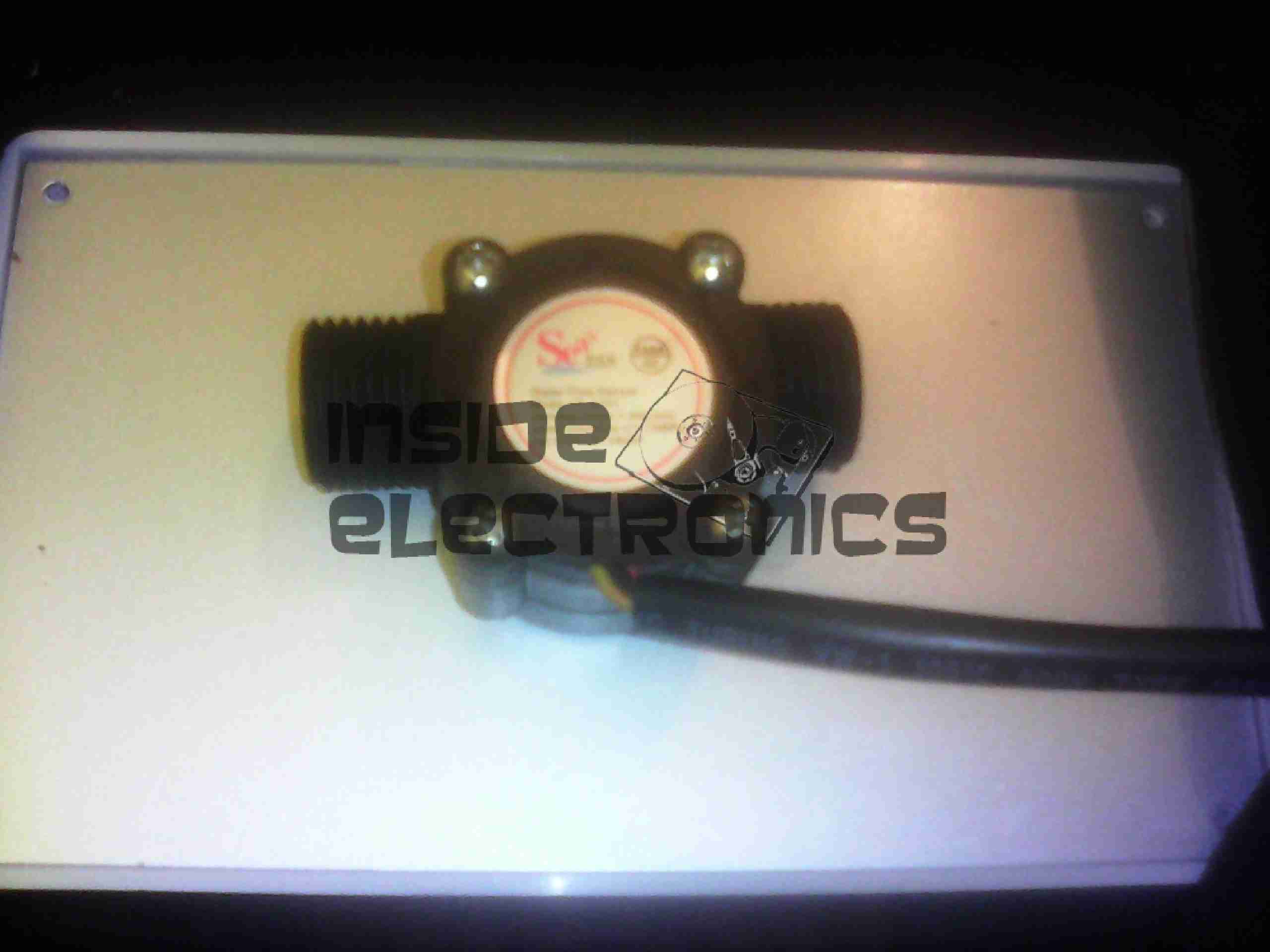
To this end I have designed & built this device, to monitor water usage from the individual tanks & automatically switch over when the tank in use nears empty, alerting the user in the process so the empty tanks can be refilled.
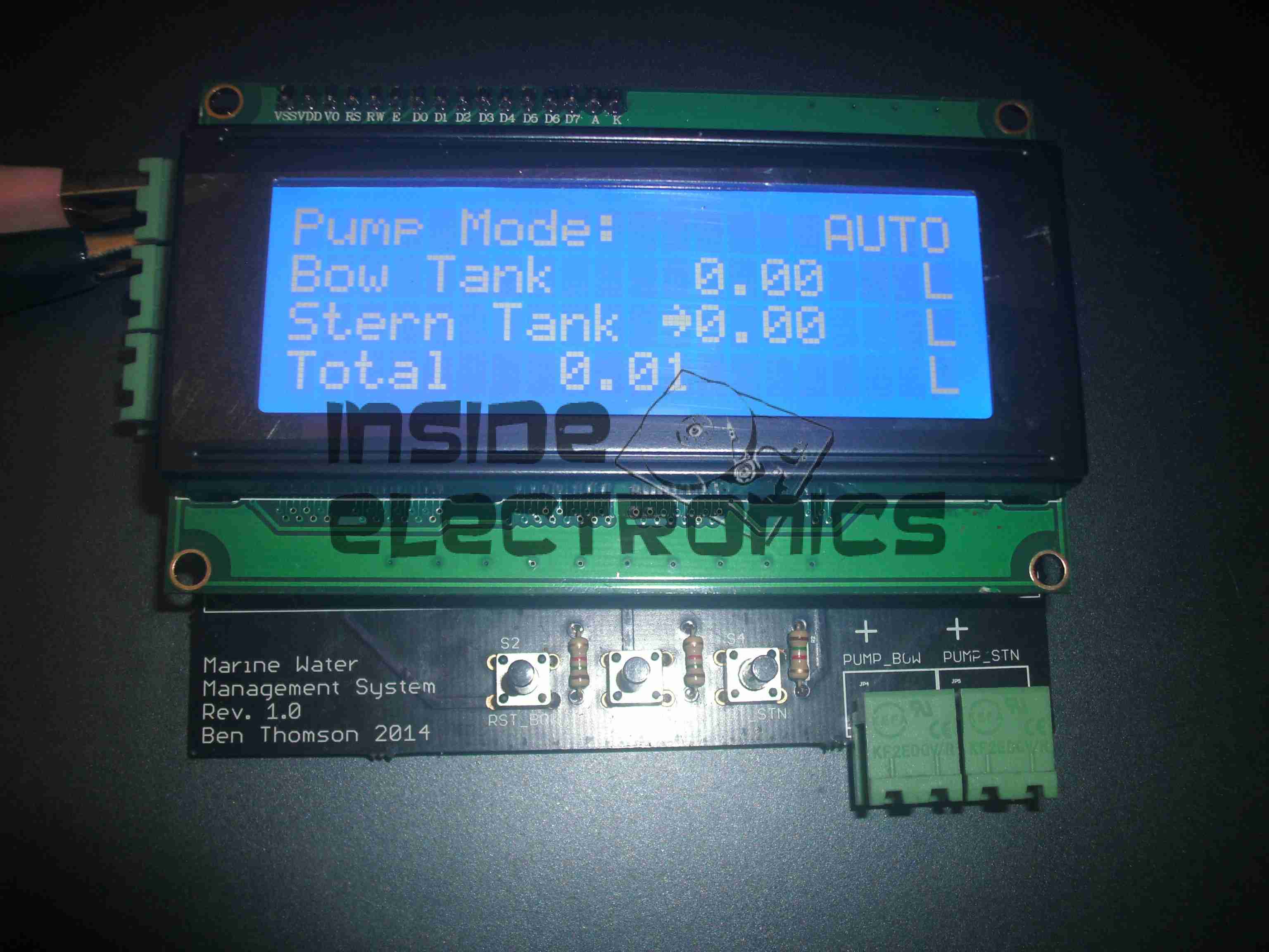
Based around an ATMega328, the unit reads a pair of sensors, fitted into the suction line of each pump from the tanks. The calculated flow is displayed on the 20×4 LCD, & logged to EEPROM, in case of power failure.
Water Flow Sensor
When the tank in use reaches a preset number of litres flowed, (currently hardcoded, but user input will be implemented soon), the pump is disabled & the other tank pump is enabled. This is also indicated on the display by the arrow to the left of the flow register. Tank switching is alerted by the built in beeper.
It is also possible to manually select a tank to use, & disable automatic operation.
Resetting the individual tank registers is done by a pair of pushbuttons, the total flow register is non-resettable, unless a hard reset is performed to clear the onboard EEPROM.
Main PCB
View of the main PCB is above, with the central Arduino Pro Mini module hosting the backend code. 12-24v power input, sensor input & 5v sensor power output is on the connectors on the left, while the pair of pump outputs is on the bottom right, switched by a pair of IRFZ44N logic-level MOSFETS. Onboard 5v power for the logic is provided by the LM7805 top right.
Code & PCB design is still under development, but I will most likely post the design files & Arduino sketch once some more polishing has been done.
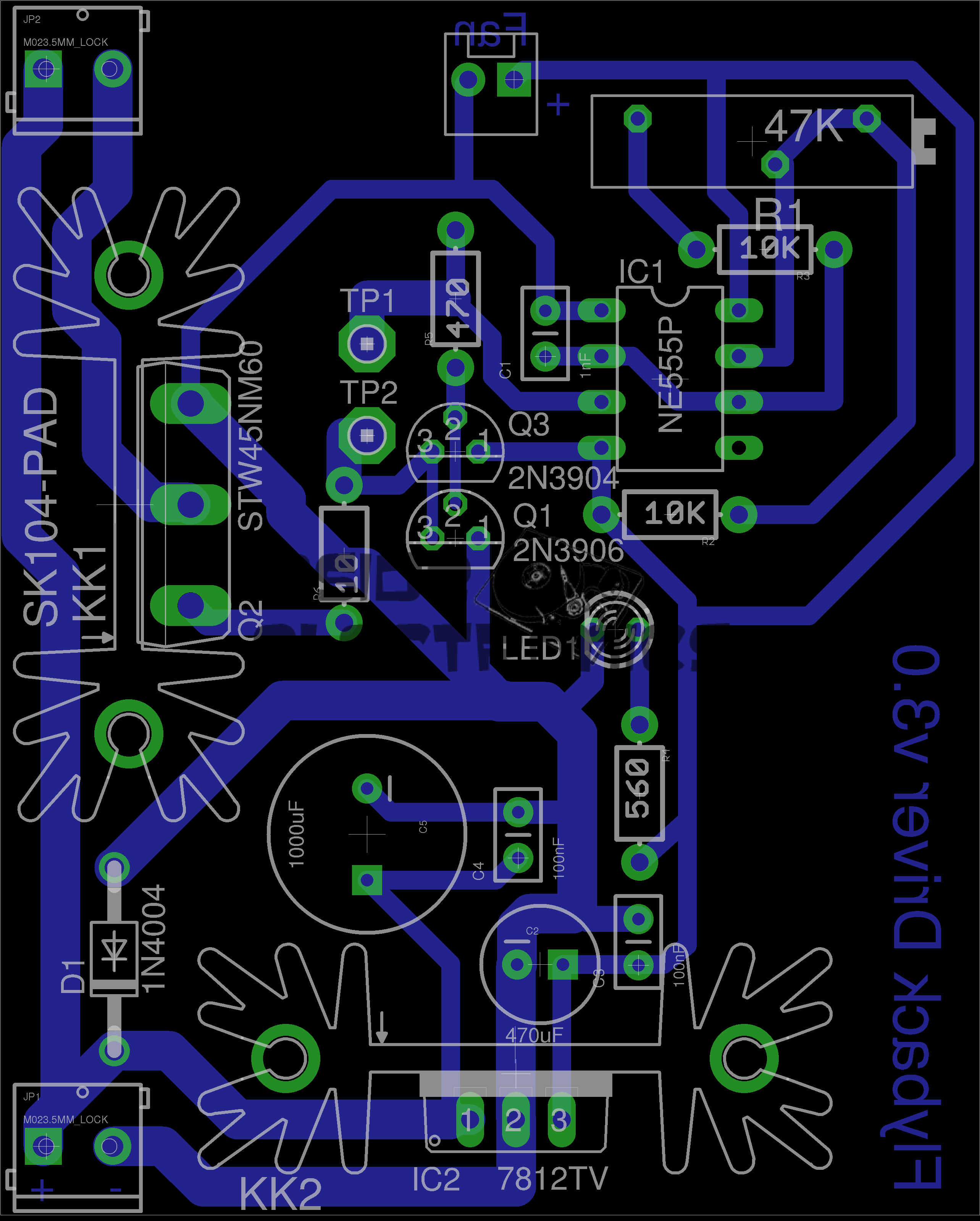
Here is a simple 555 timer based flyback transformer driver, with the PCB designed by myself for some HV experiments. Above is the Eagle CAD board layout.
The 555 timer is in astable mode, generating a frequency from about 22kHz to 55kHz, depending on the position of the potentiometer. The variable frequency is to allow the circuit to be tuned to the resonant frequency of the flyback transformer in use.
This is switched through a pair of buffer transistors into a large STW45NM60 MOSFET, rated at 650v 45A.
Input power is 15-30v DC, as the oscillator circuit is fed from an independent LM7812 linear supply.
Provision is also made on the PCB for attaching a 12v fan to cool the MOSFET & linear regulator.
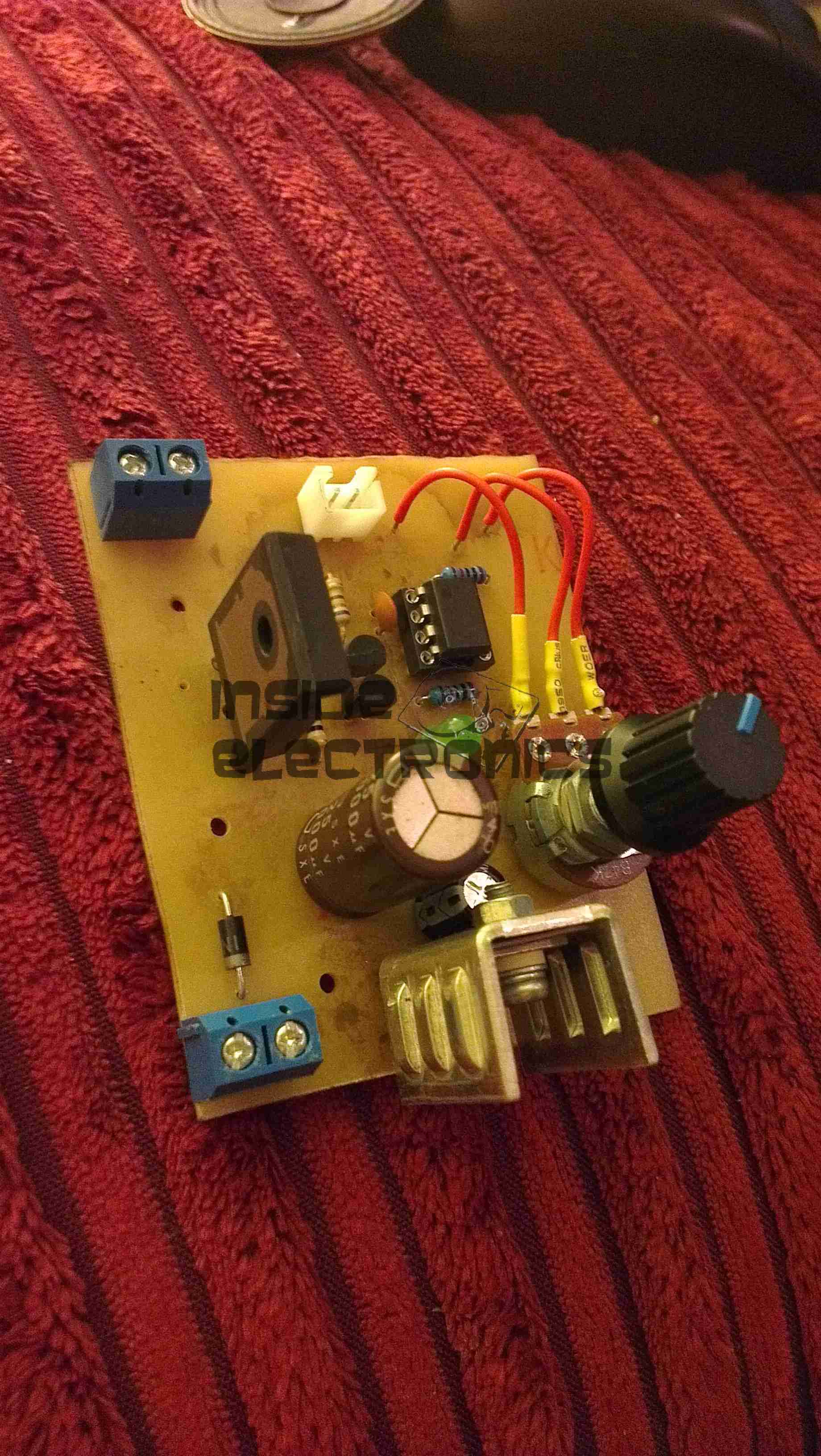
Initial Board
Board initially built, with the heatsink on the linear regulator fitted. I used a panel mount potentiometer in this case as I had no multiturn 47K pots in stock.
PCB Traces
Bottom of the PCB. The main current carrying traces have been bulked up with copper wire to help carry the potentially high currents on the MOSFET while driving a large transformer.
This board was etched using the no-peel toner transfer method, using parchement paper as the transfer medium.
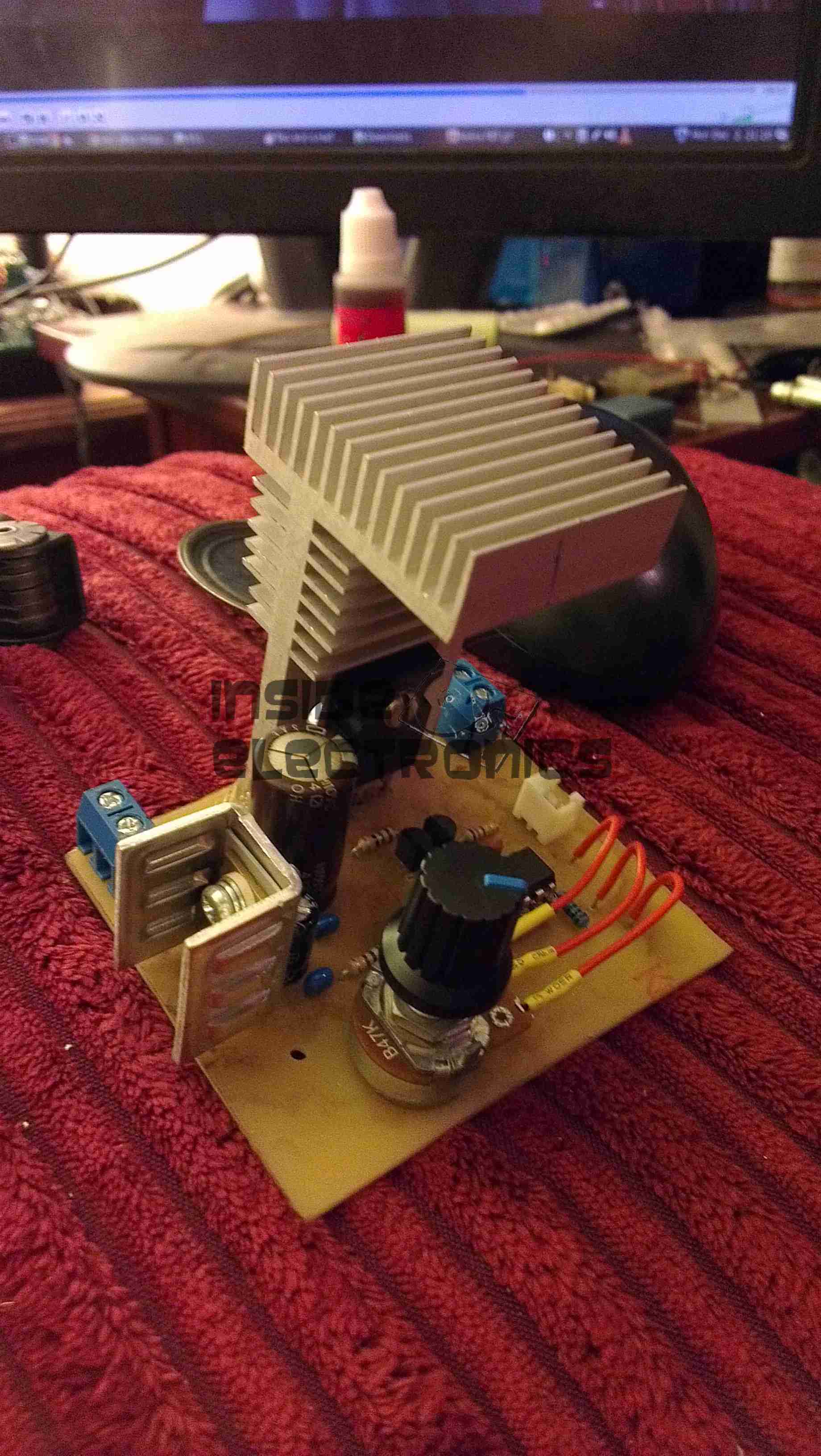
MOSFET Heatsinked
Main MOSFET now fitted with a surplus heatsink from an old switchmode power supply. A Fan could be fitted to the top of this sink to cope with higher power levels.
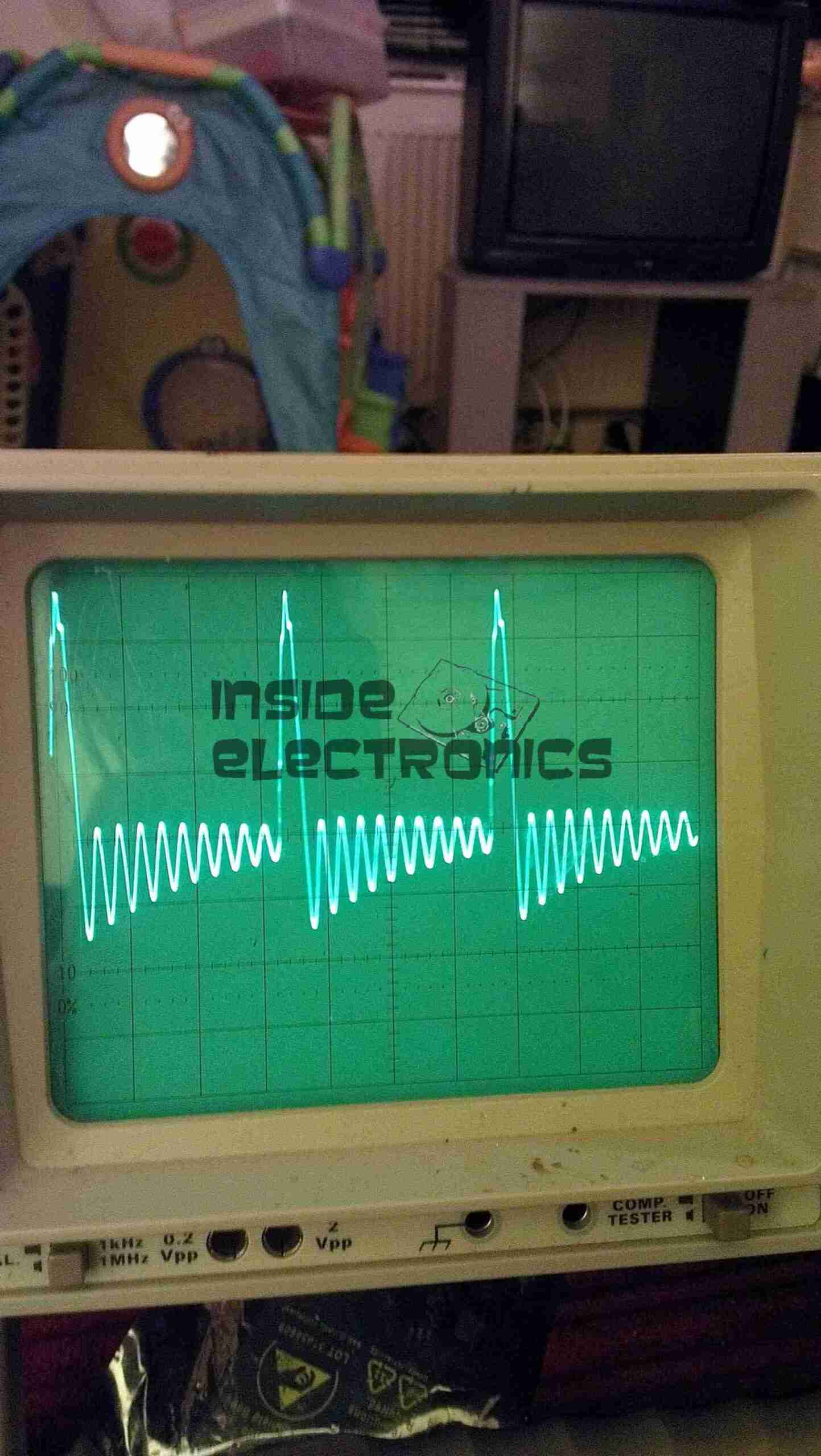
Gate Drive Waveform
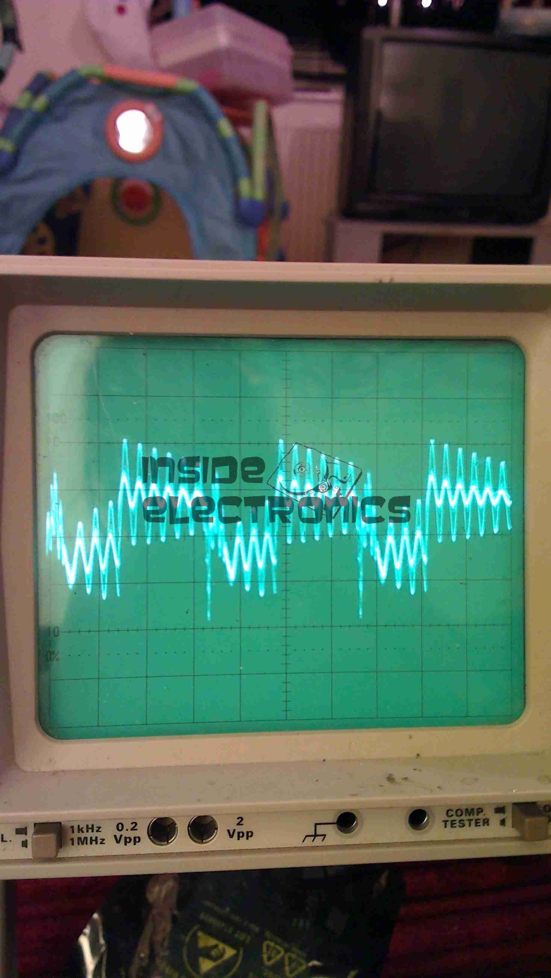
This is the gate drive waveform while a transformer is connected, the primary is causing some ringing on the oscillator. The waveform without an attached load is a much cleaner square wave.
Flyback Secondary Waveform
I obtained a waveform of the flyback secondary output by capacitively coupling the oscilloscope probe through the insulation of the HT wire. The pulses of HV can be seen with the decaying ringing of the transformer between cycles.
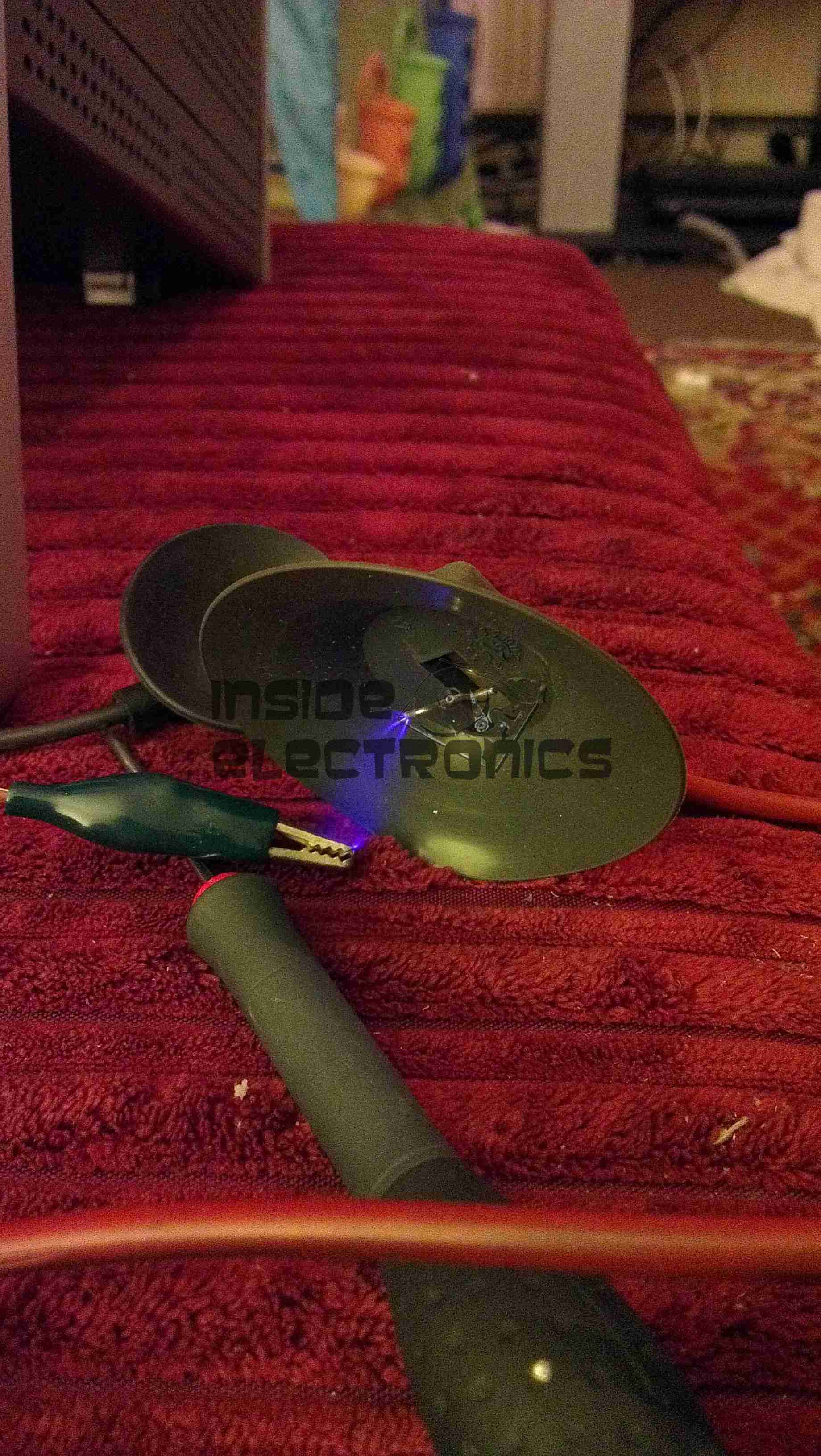
Corona DischargeArc Discharge
Corona & arc discharges at 12v input voltage.
Download the Eagle schematic files here: [download id=”5561″]
I have finally got round to designing the balancing circuitry for my ultracapacitor banks, which have a total voltage of 15v when fully charged. The 2600F capacitors have a max working voltage of 2.5v each, so to ensure reliable operation, balancing is required to make sure that each capacitor is charged fully.
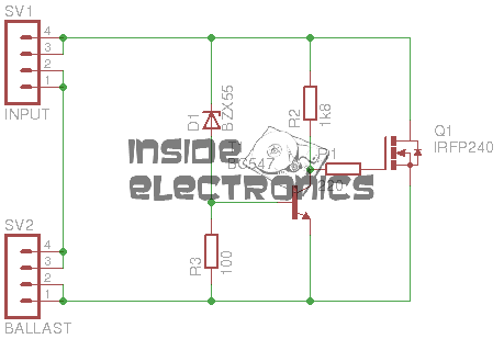
The circuit above is a simple shunt regulator, which uses a 2.2v zener diode to regulate the voltage across the capacitor.
A 10W 1Ω resistor is connected to the BALLAST header, while the capacitor is connected across the INPUT. Once the voltage on the capacitor reaches 2.6v, the MOSFET begins to conduct, the 1Ω resistor limiting current to ~2.6A.
Each capacitor in the series string requires one of these connected across it.
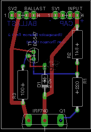
PCB
Below is a link to the Eagle project archive for this. Includes schematic, board & gerber files.
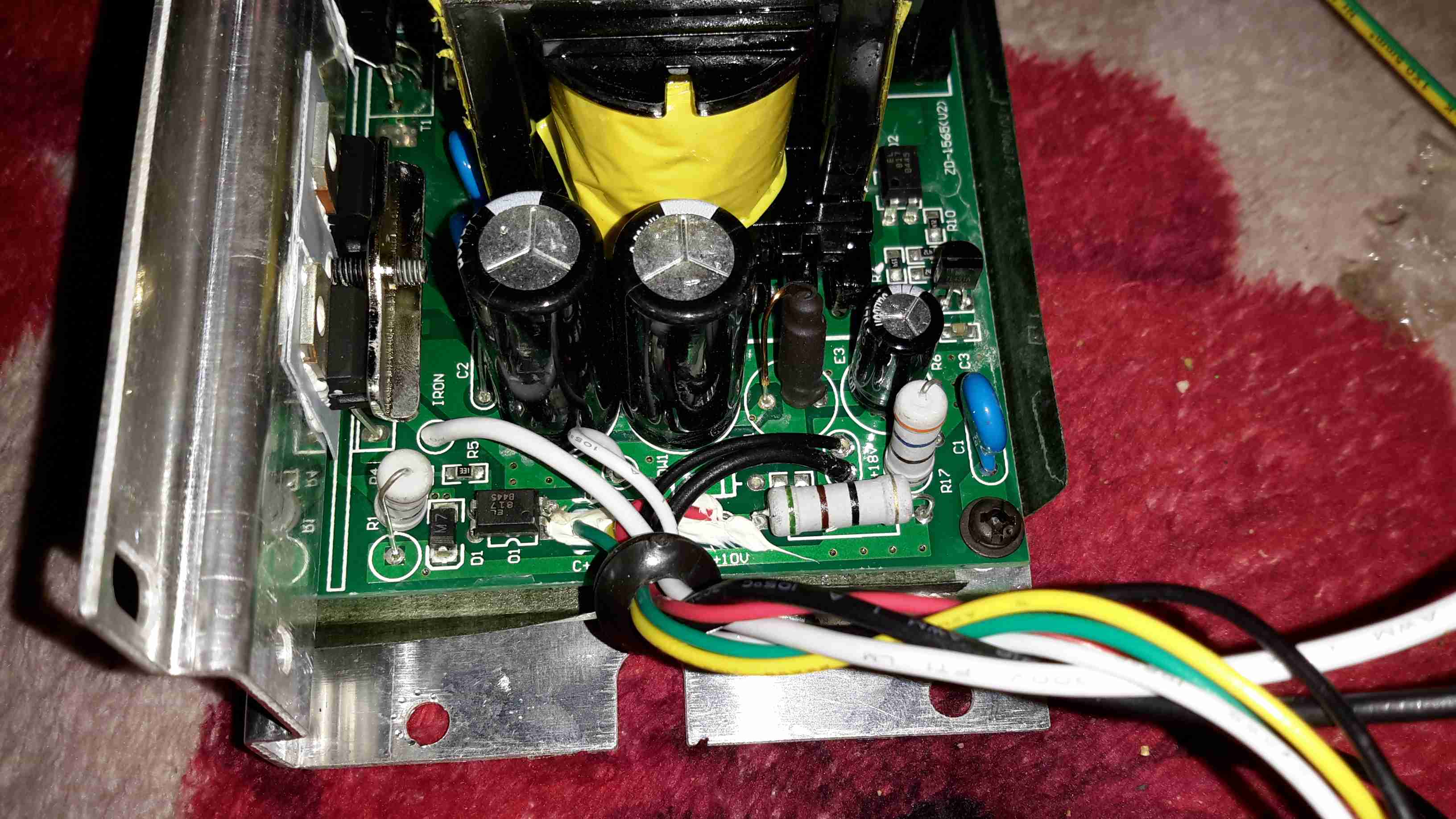
This is a small 120W power inverter, intended for small loads such as lights, fans, small TVs & laptop computers.
End Cover
End cover of the unit, 12v DC input cord at the top, power switch & indicator LEDs at the bottom.
Mains Output
Opposite end of the unit, with the standard 240v AC 50Hz Mains output socket.
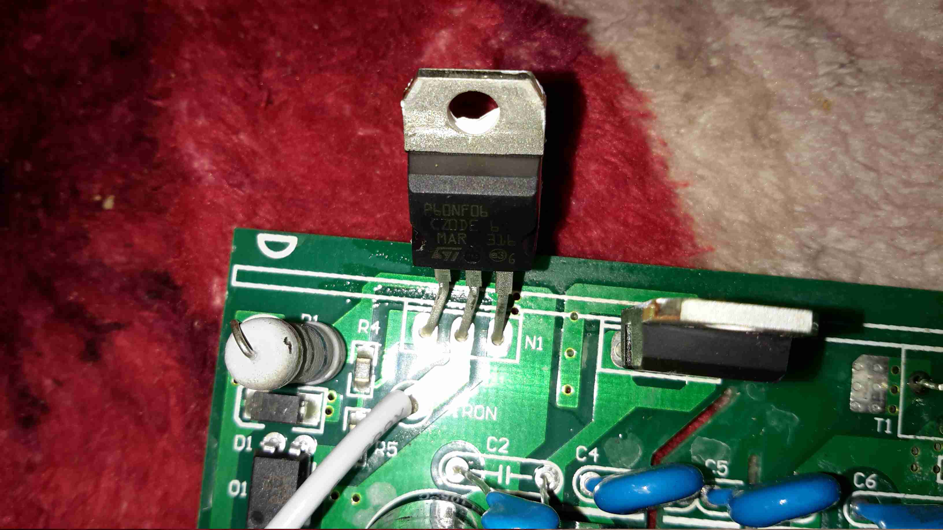
Cover Removed
Cover removed from the top of the unit. Main power transformer is visible in the centre here, MOSFET bank is under the steel clamp on the left, the aluminium case forms the heatsink.
PWM Controllers
On the right is a KA3525 switchmode PWM controller & on the left is a LM324N quad Op-Amp IC. The buzzer on the far left is for the low battery warning.
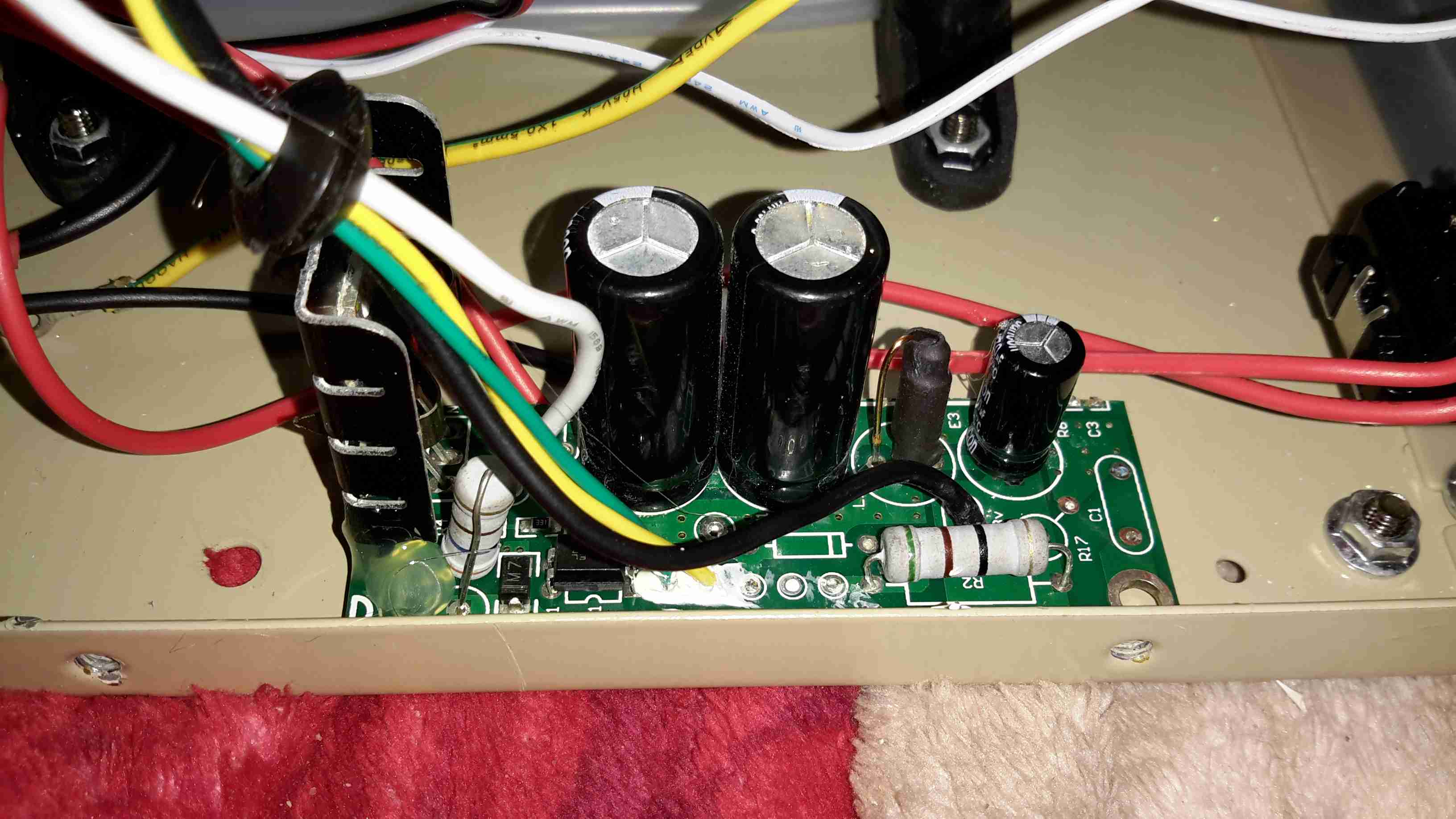
PCB Removed
PCB removed from the casing, with the MOSFET bank on the right hand side. Two potentiometers in the centre of the board tweak the frequency of the switcher & the output voltage.
Tip Jar
If you’ve found my content useful, please consider leaving a donation by clicking the Tip Jar below!
All collected funds go towards new content & the costs of keeping the server online.