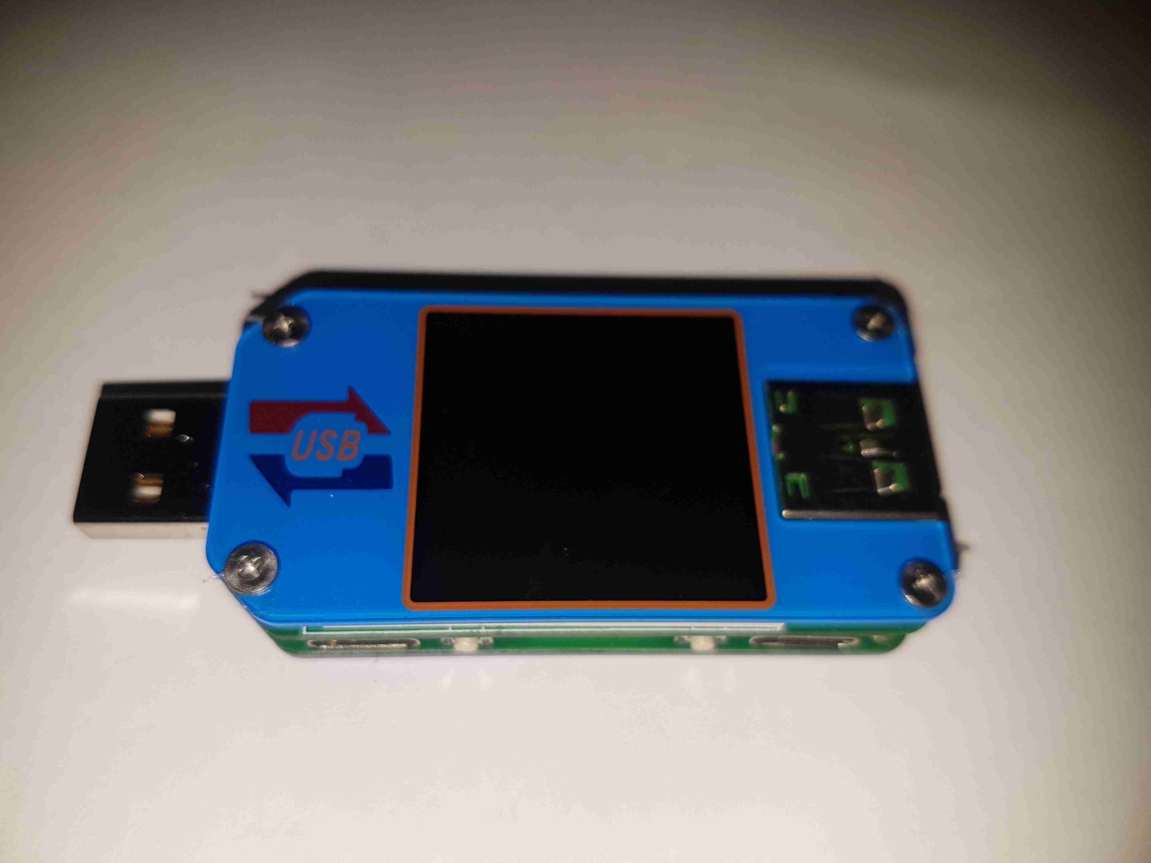
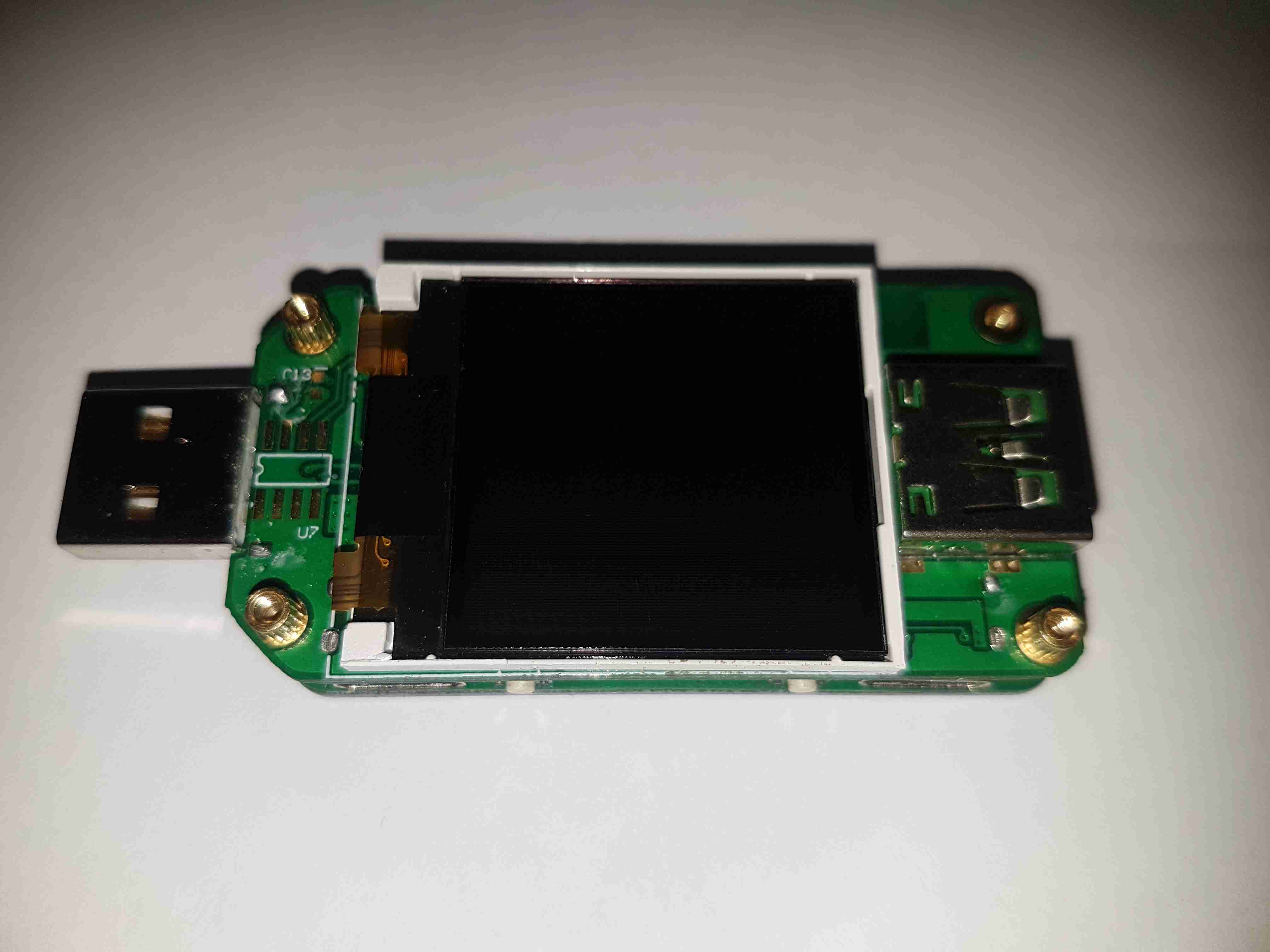
Here’s a nice little feature-packed USB power meter, the UM25C. This unit has USB-C along with the usual USB type A connectors, along with a bluetooth radio for remote monitoring of stats via a Windows or Android app. Construction is nice, it’s a stack of two PCBs, and polycarbonate cover plates, secured together with brass posts & screws.
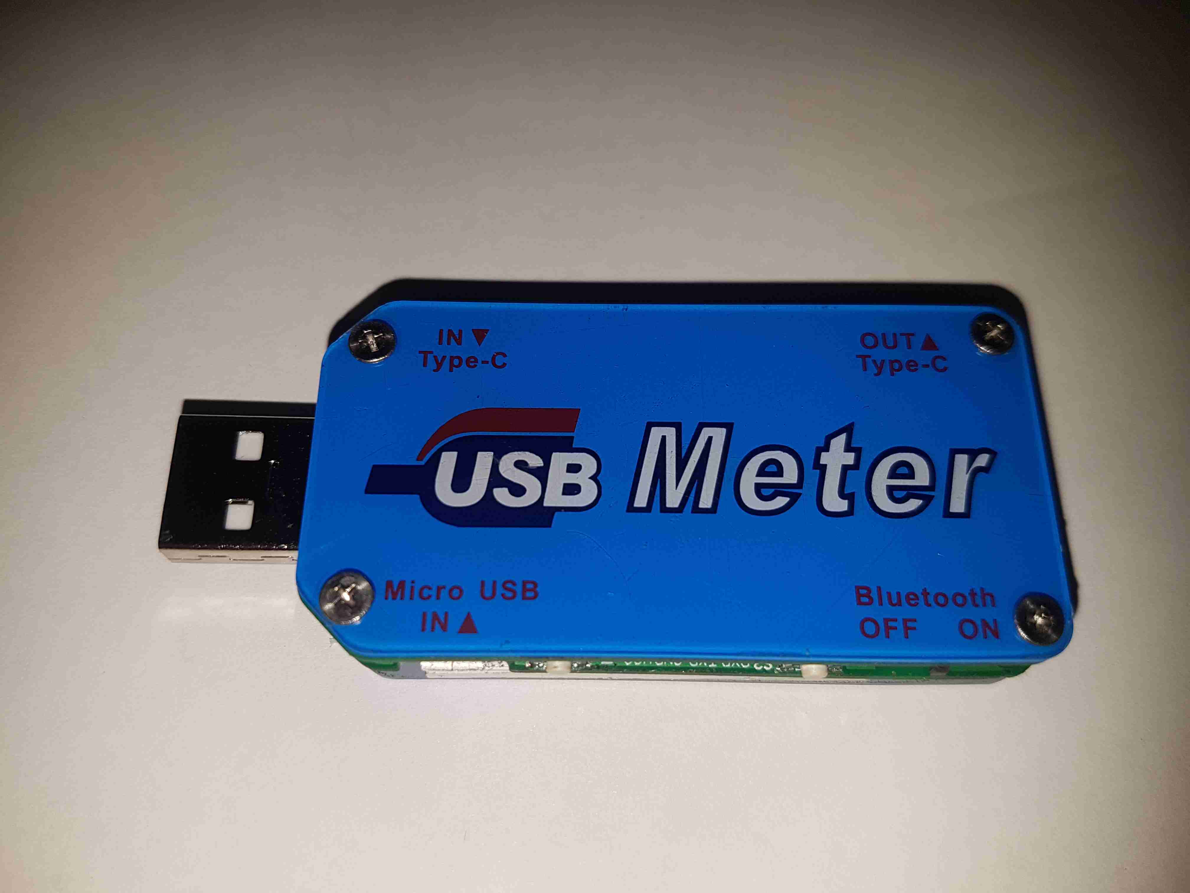
Back Cover
The back cover has the legend for all the side connectors, along with the logo.
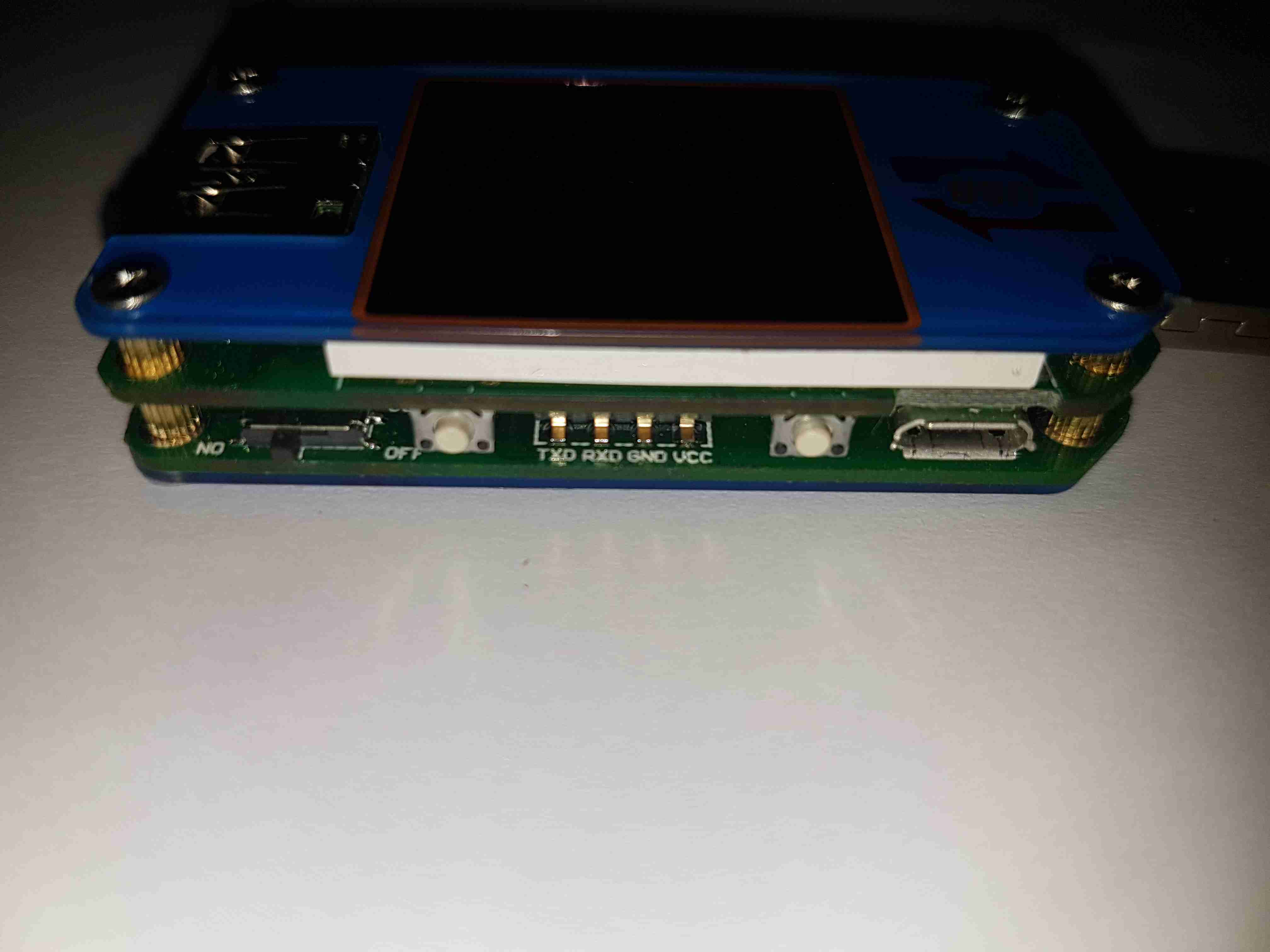
USB Micro Input
Down the sides are the user interface buttons, and here the Micro-B input connector. The 4-pin header is visible here that takes serial data down to the bluetooth section.
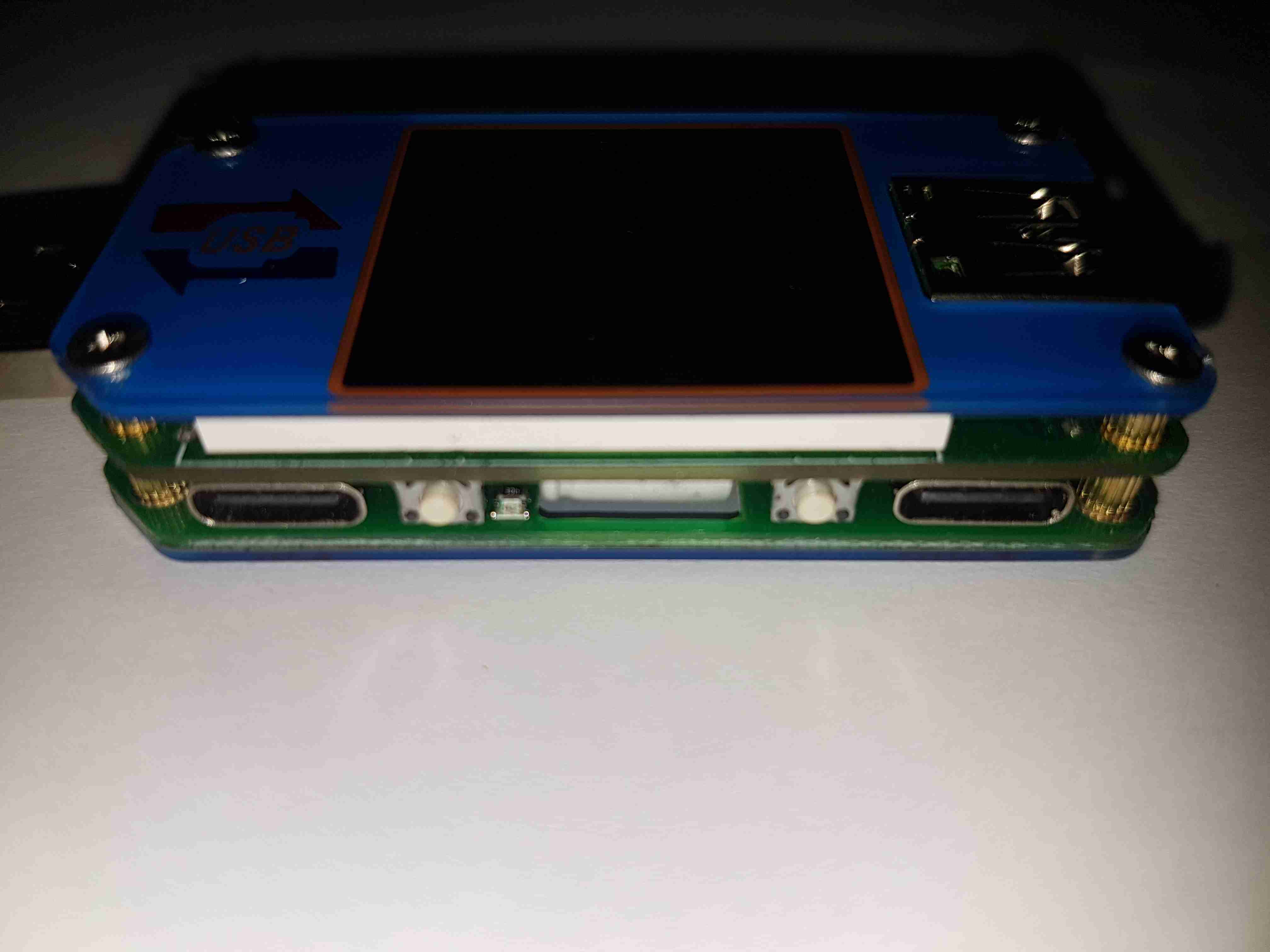
USB-C Connectors
The other side has the remaining pair of buttons, and the USB-C I/O. I don’t yet own anything USB-C based, but this is good future proofing.
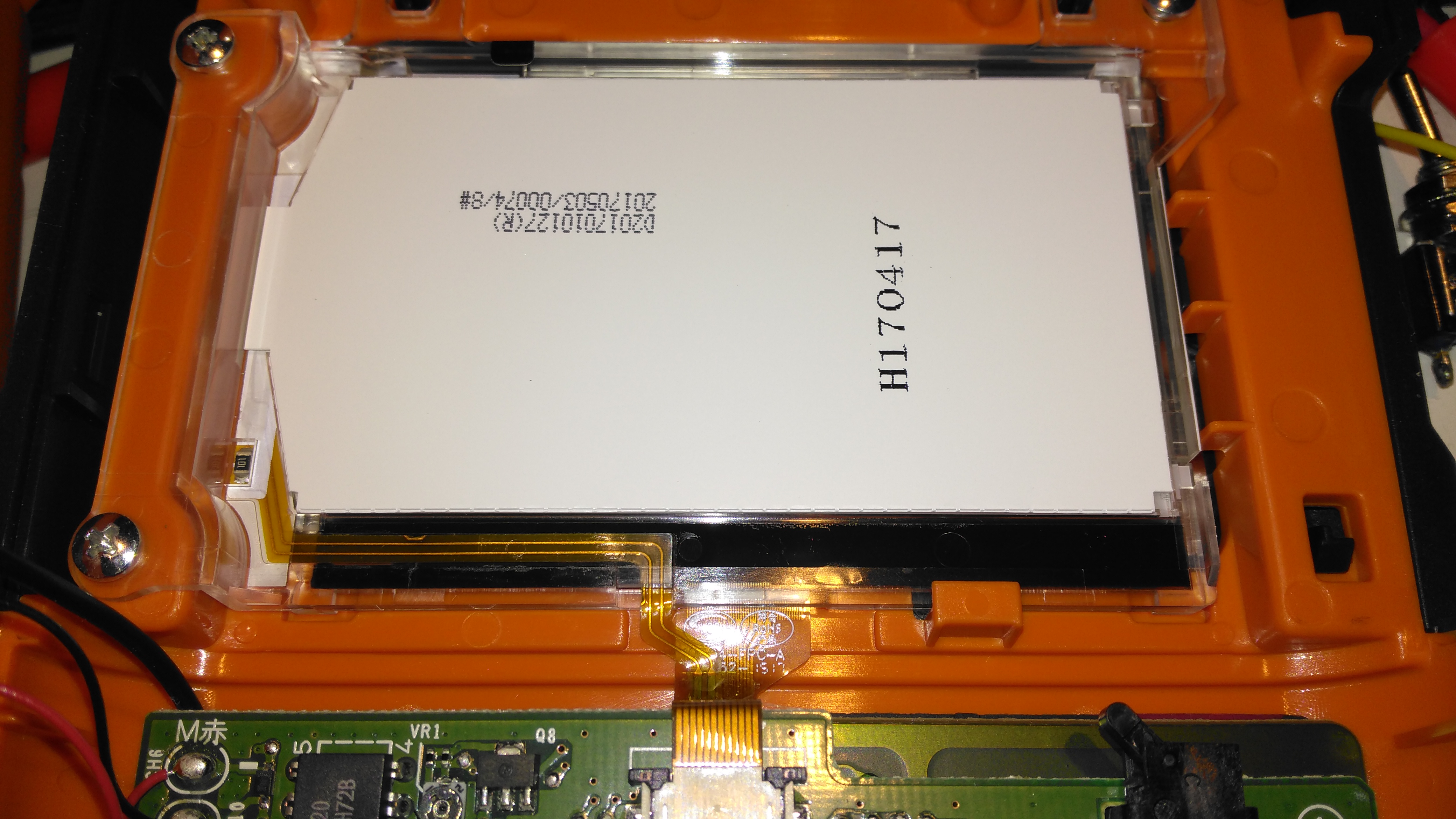
LCD Display
Removing the top plastic cover plate reveals the small 1″ TFT LCD module. This will be hot-bar soldered underneath the screen. There’s an unused footprint next to the USB input connector, judging by the pin layout it’s probably for a I²C EEPROM.
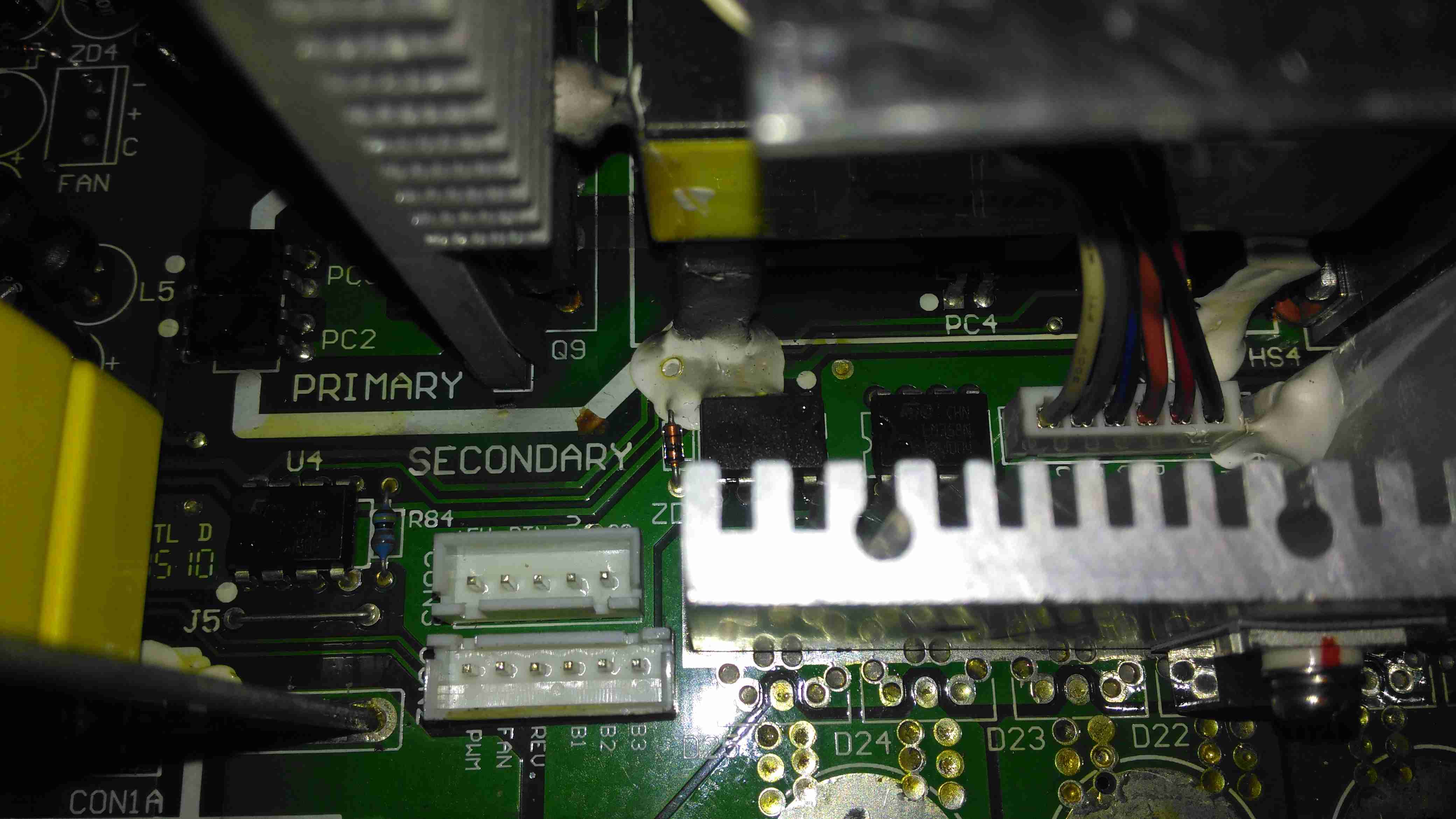
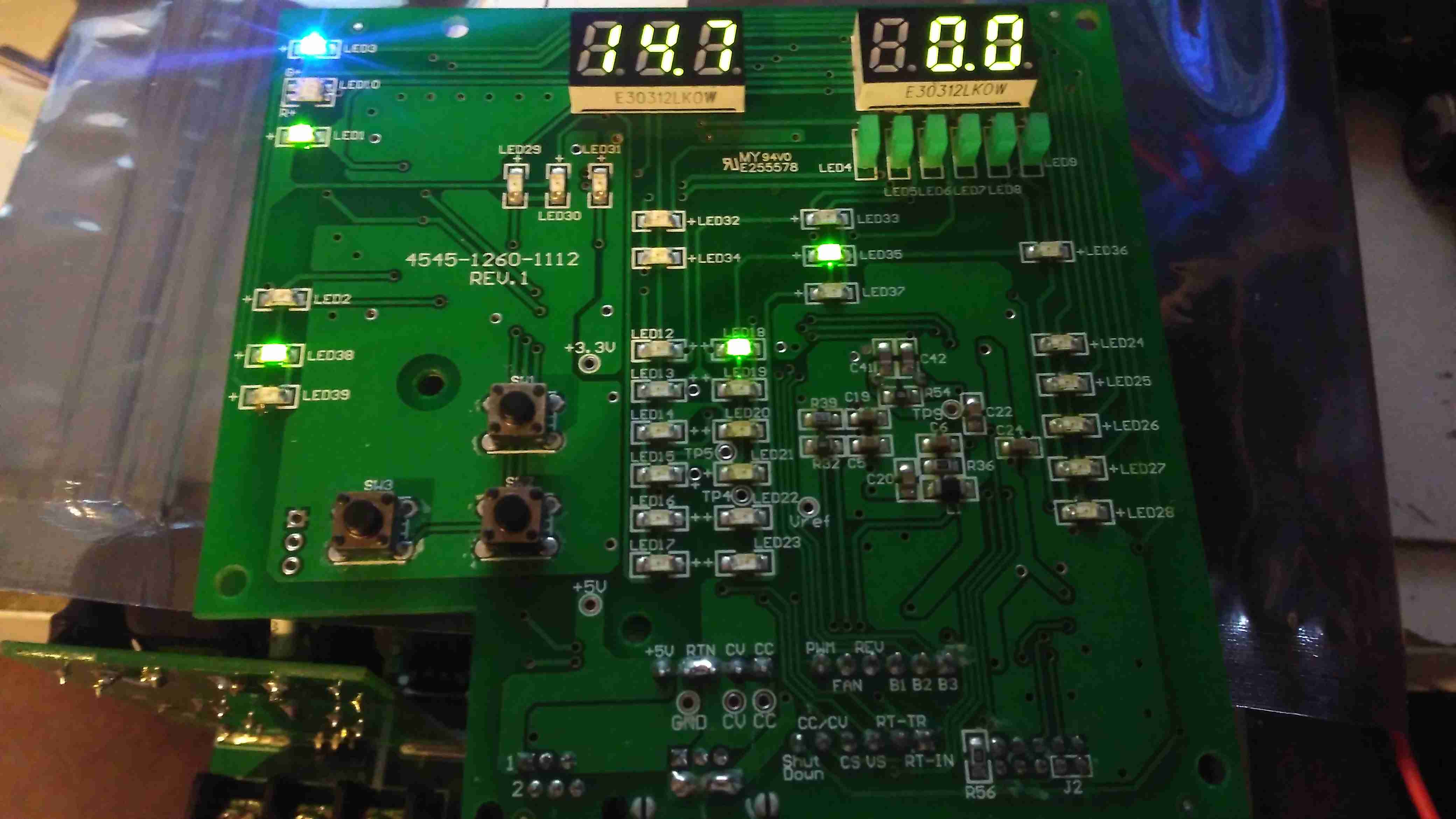
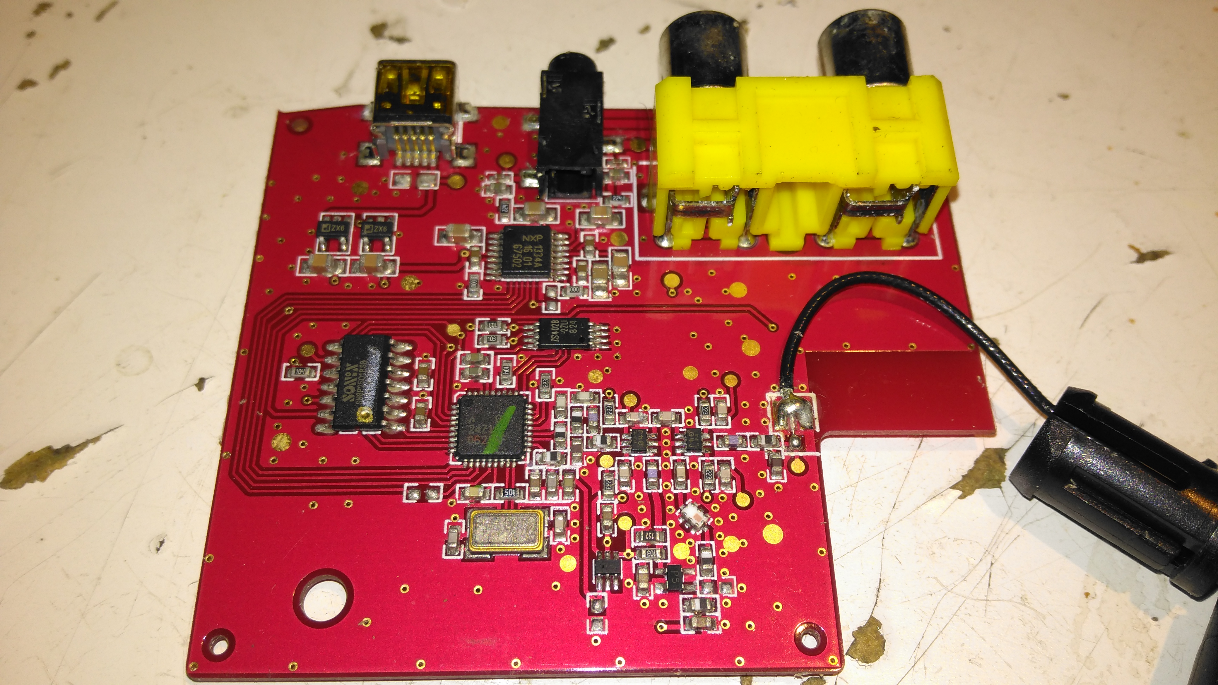
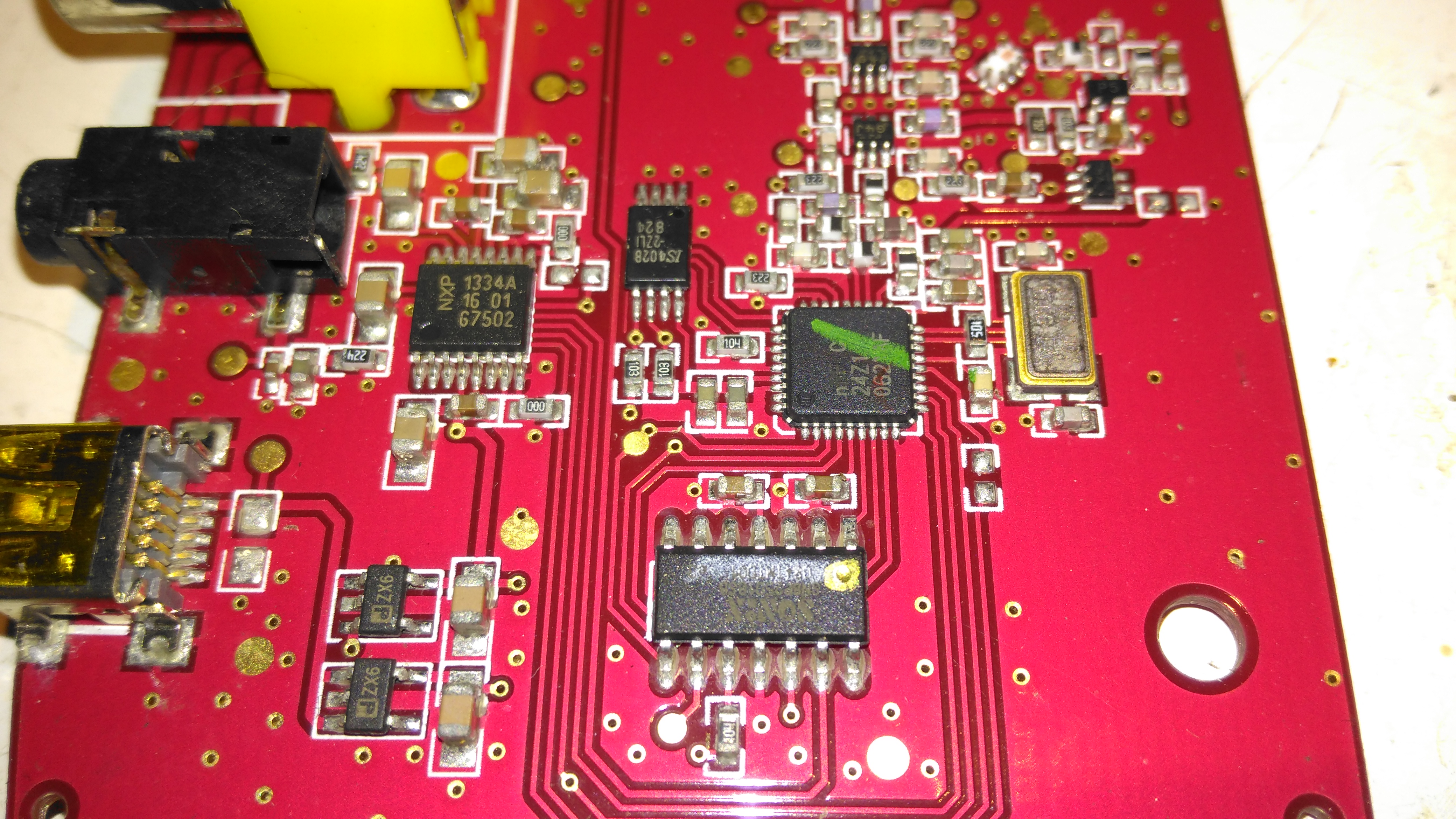
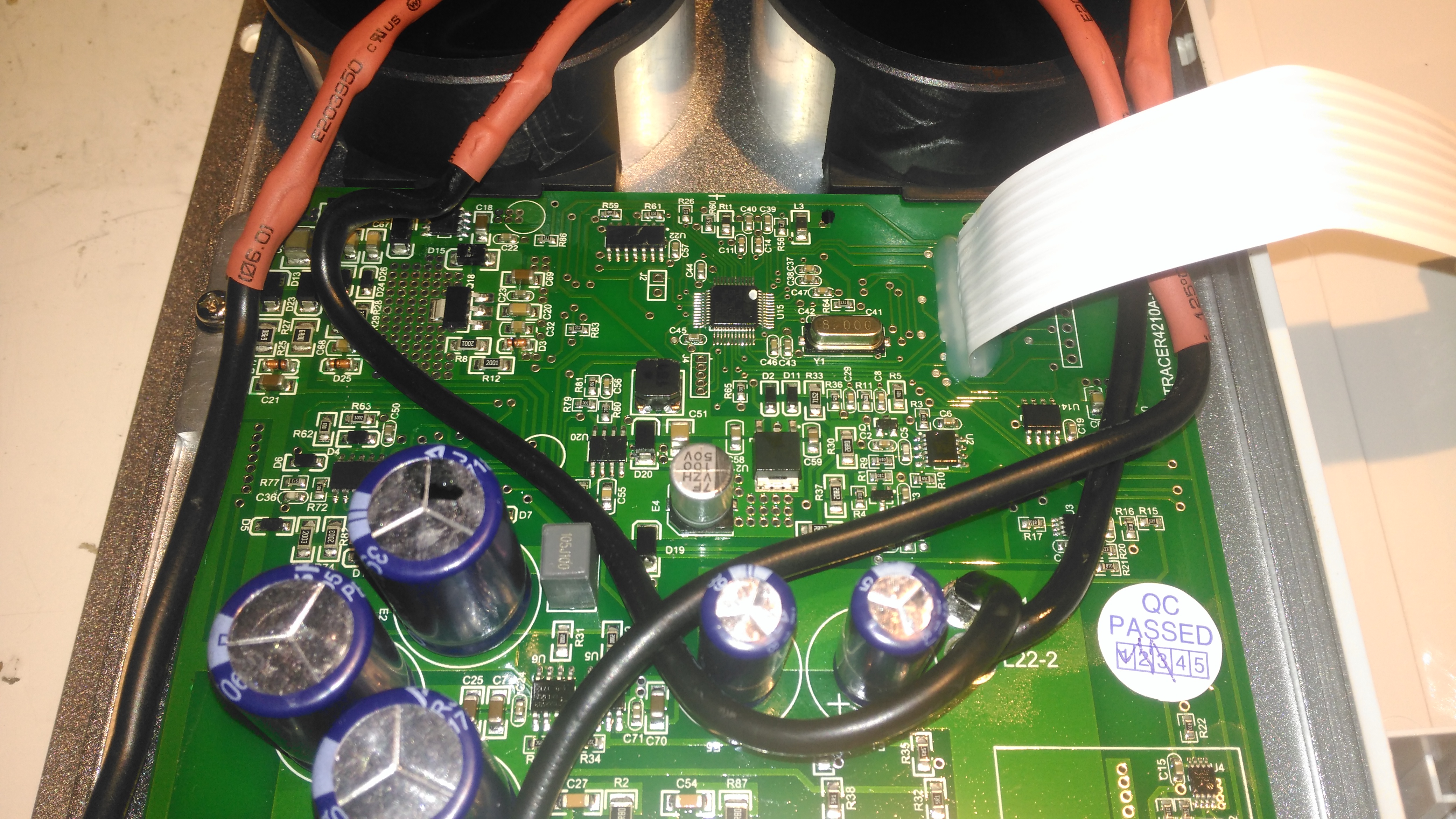
Main Board Components
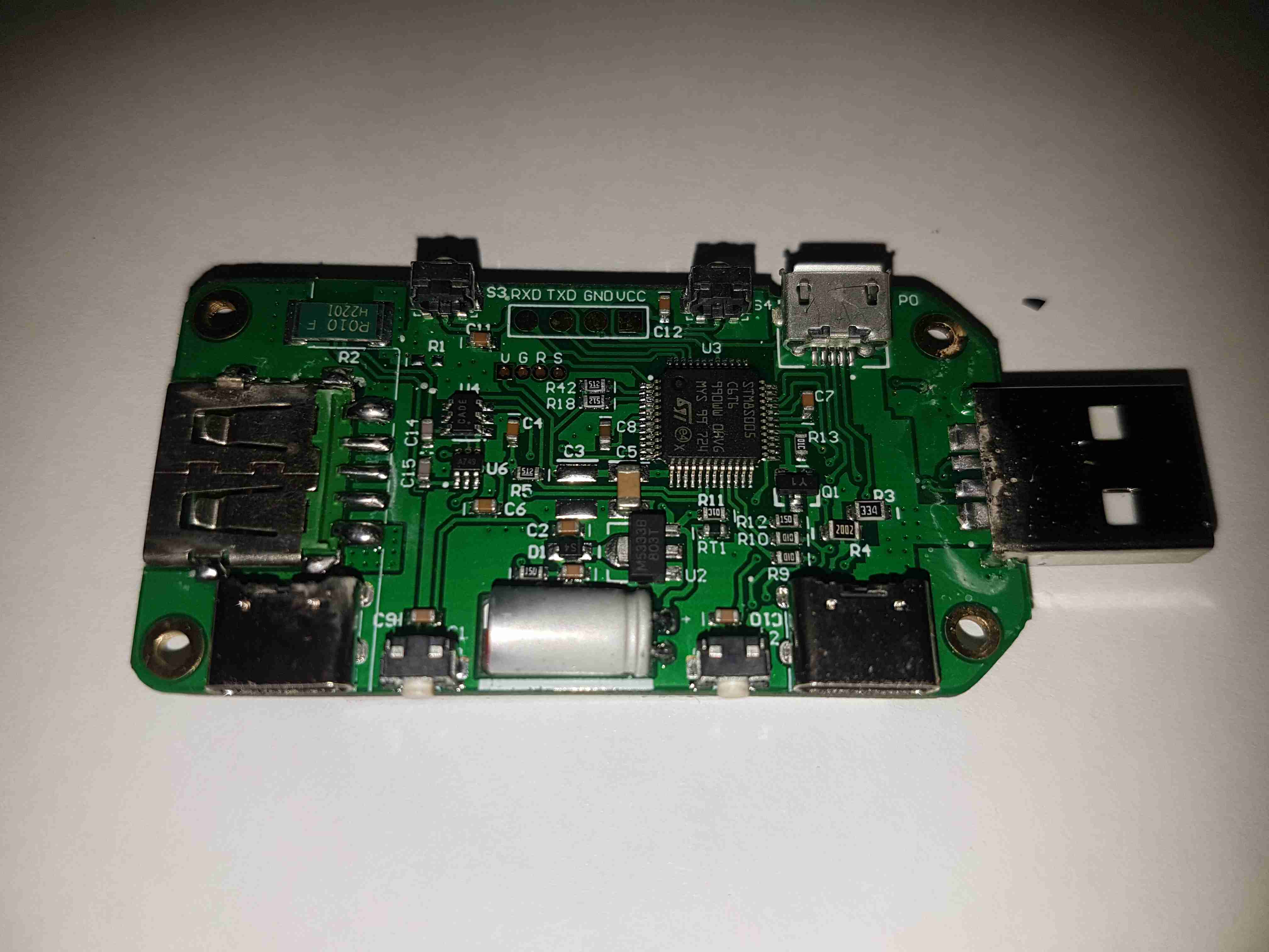
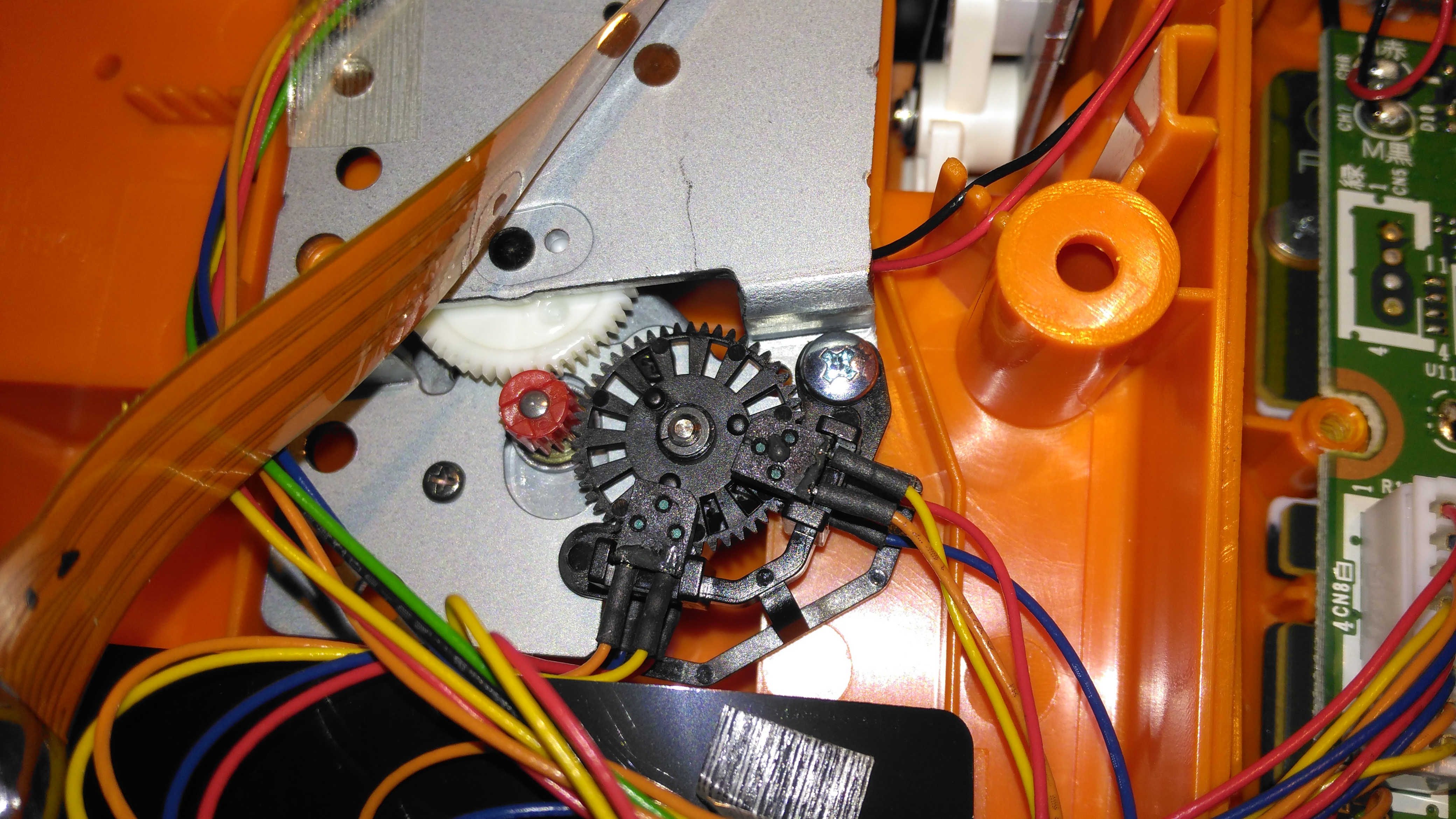
The underside of the top PCB has all the main components. The brains of the operation is a ST STM8S005C6T6 microcontroller. It’s at the basic end of the STM range, with a 16MHz clock, 32K flash, EEPROM, 10-bit ADC, SPI, UART & I²C. The main 0.010Ω current shunt is placed at the top left of the board in the negative rail. A couple of SOT-23 components in the centre of the board, I haven’t been able to identify properly, but I think they may be MOSFETs. The large electrolytic filter capacitor has a slot routed into the PCB to allow it to be laid flat. Providing the main power rail is a SOT-89 M5333B 3.3v LDO regulator.
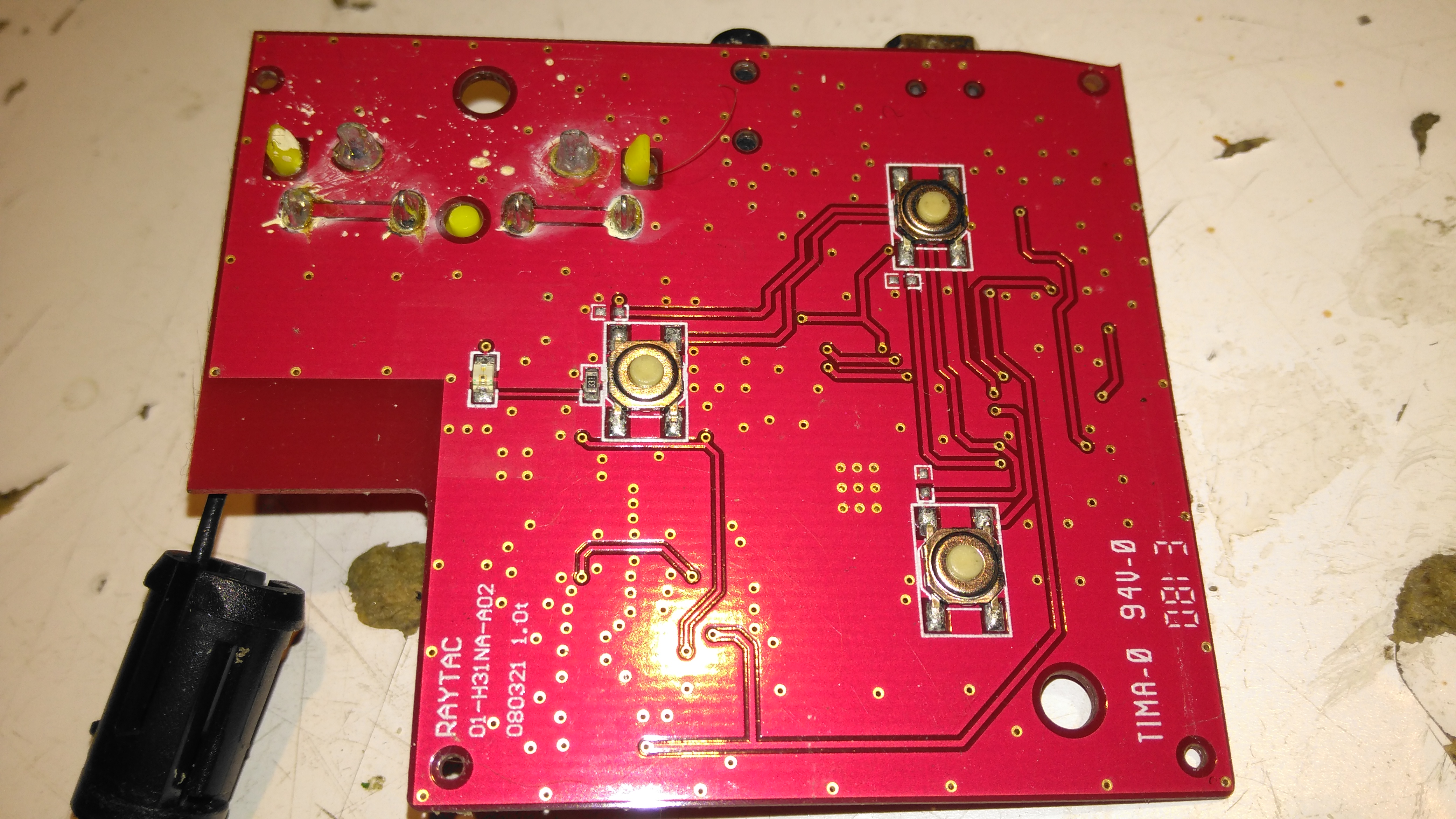
Bluetooth Radio
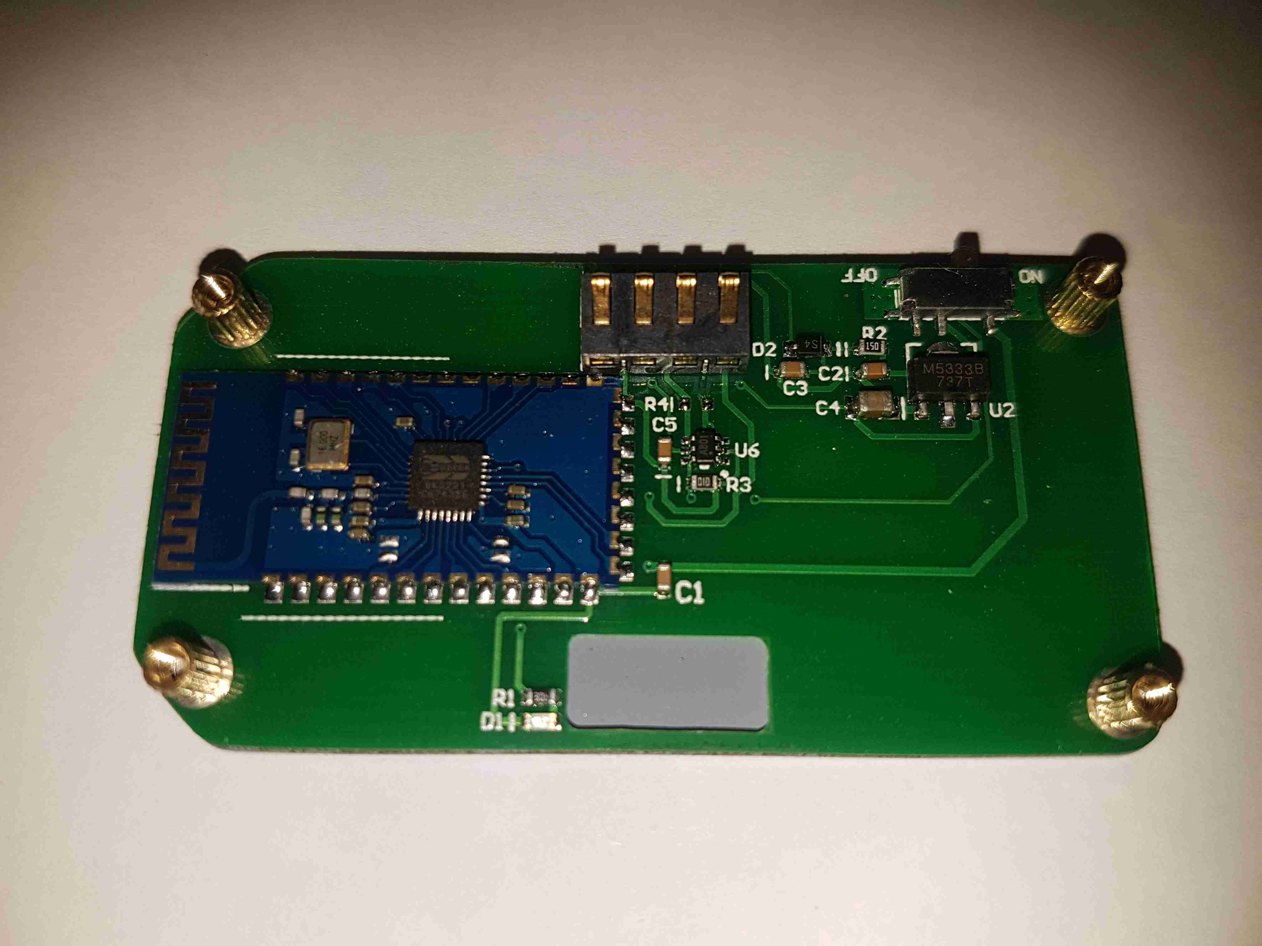
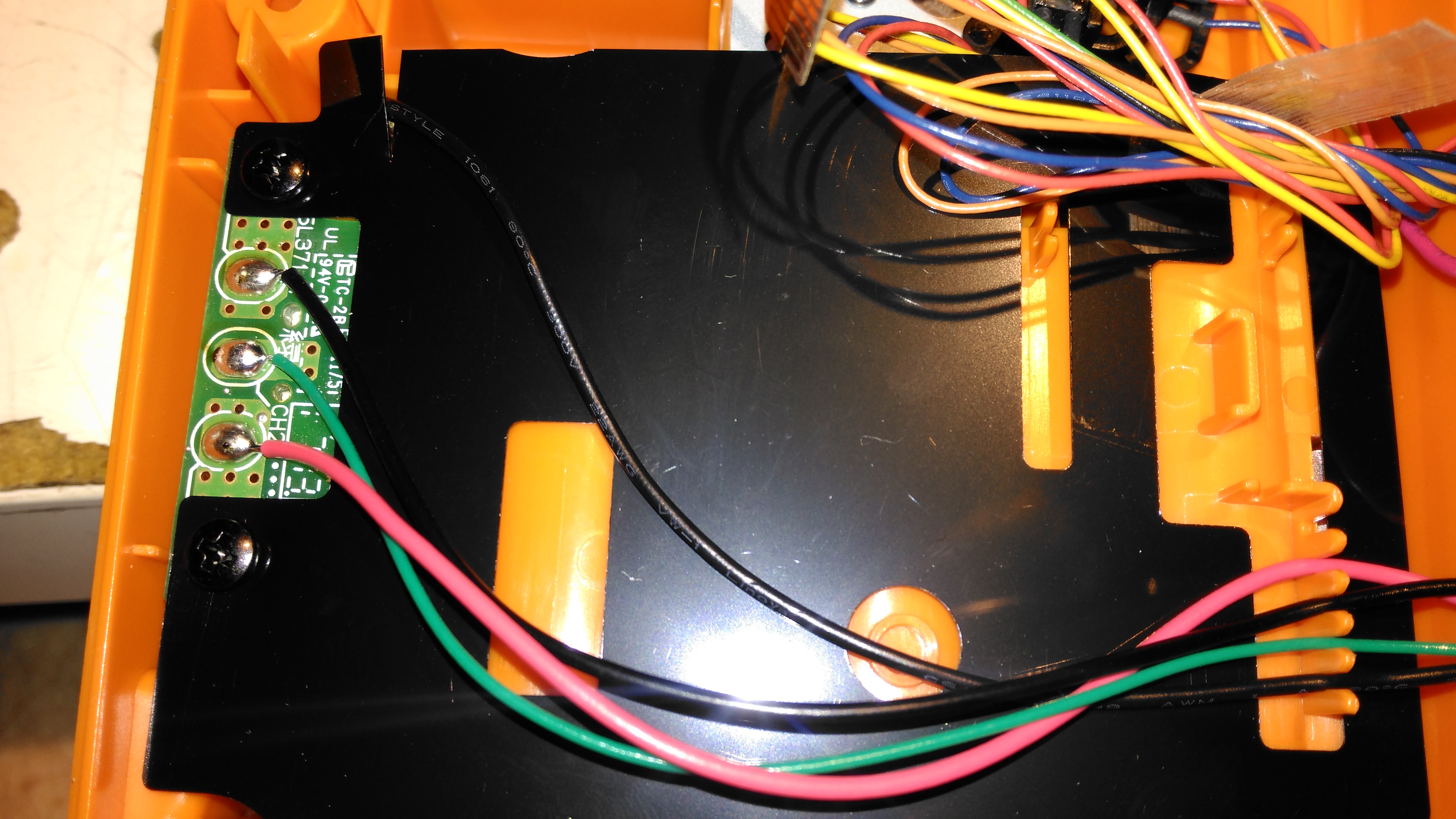
The bottom board contains the bluetooth radio module, this is a BK3231 Bluetooth HID SoC. The only profile advertised by this unit is a serial port. There’s a local 3.3v LDO regulator & support components, along with an indicator LED.
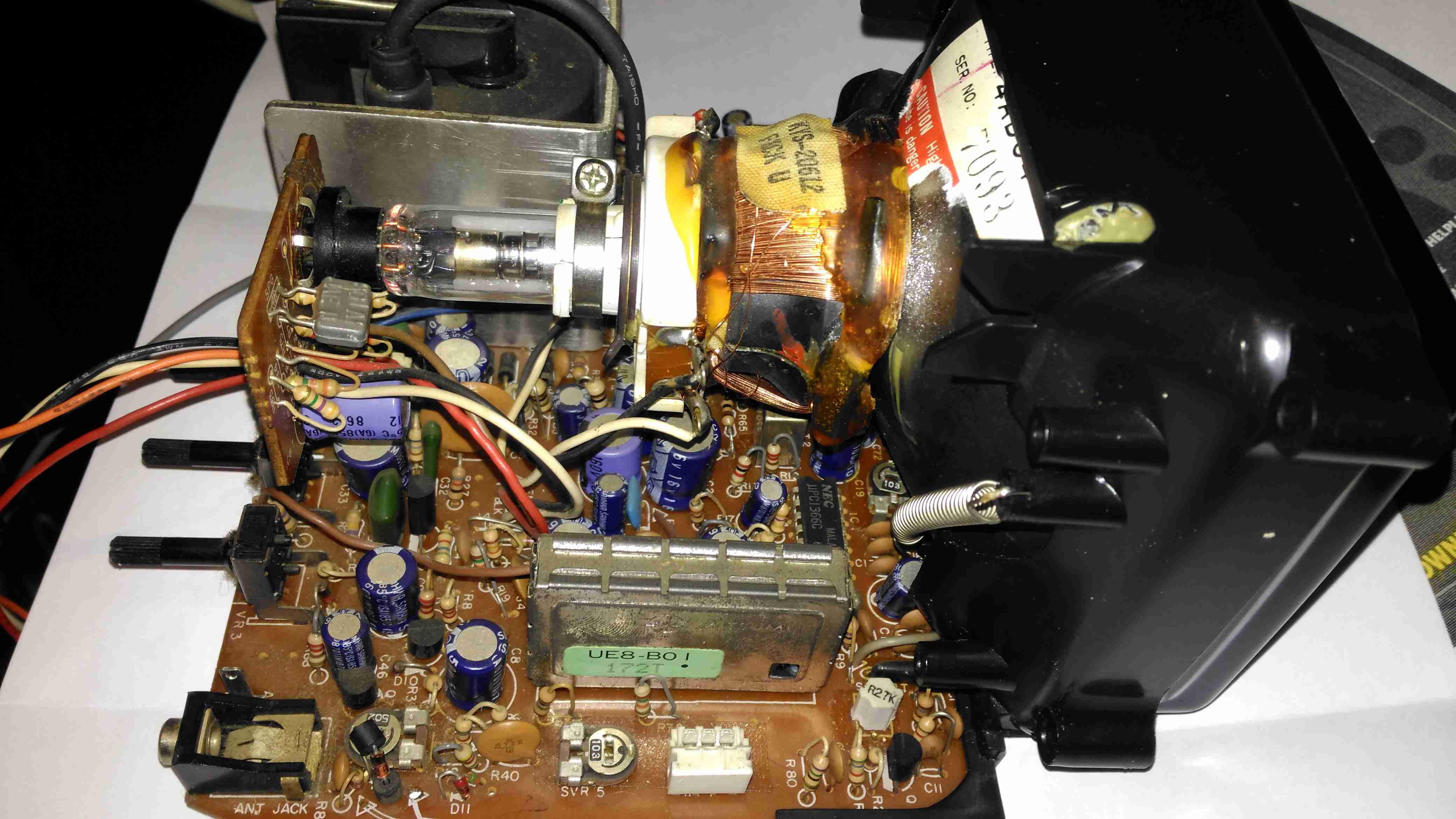
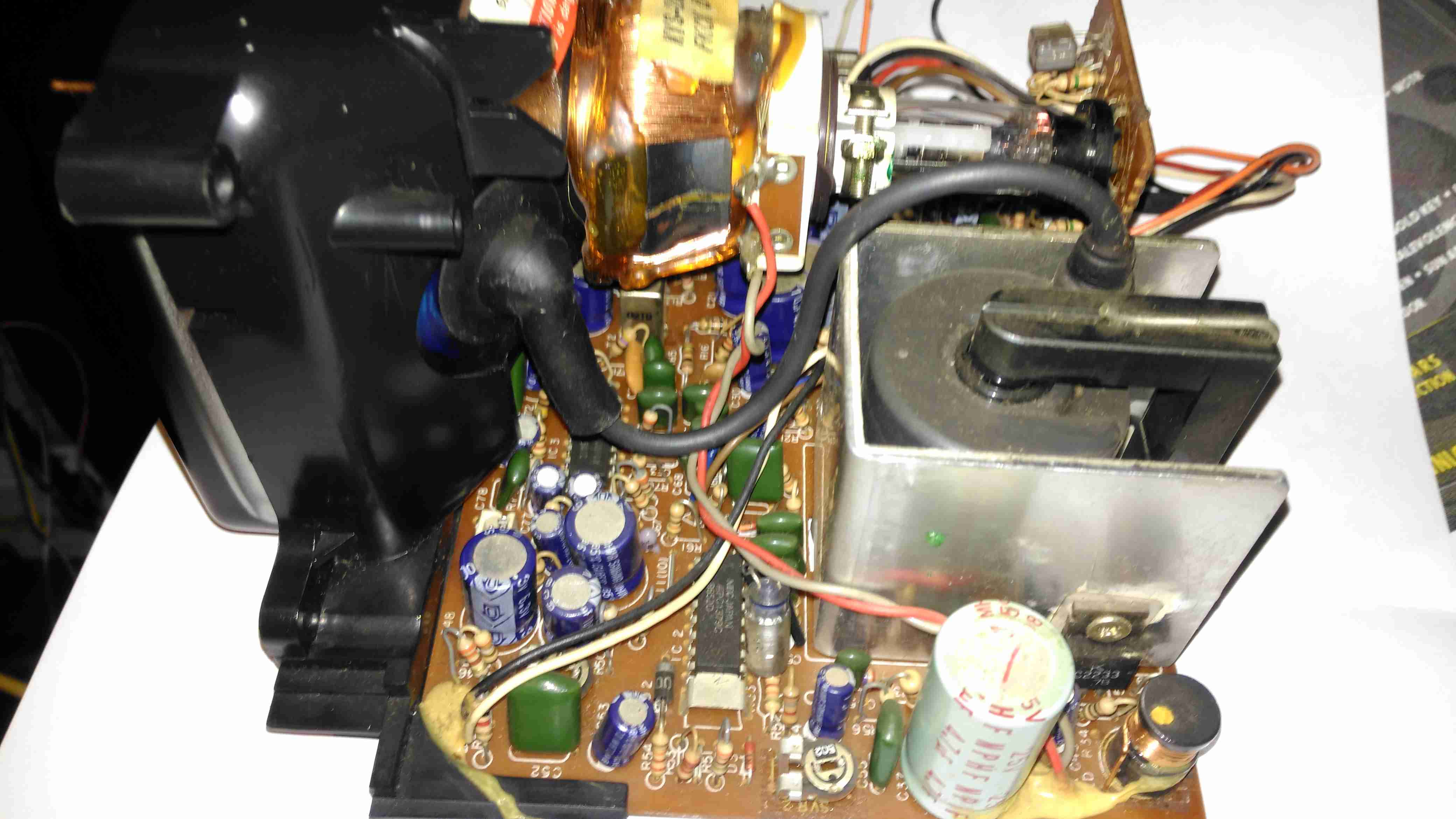
Here’s the CRT & it’s drive board removed from the main chassis. Nicely modular this unit, all the individual modules (radio, tape, TV), are separate. This is effectively a TV itself, all the tuner & IF section are onboard, unlike in other vintage units I’ve modified, where the tuner & IF has been on a separate board. There’s a 3-pin header bottom centre for the tuning potentiometer, and external antenna input jack. The internal coax for the built in antenna has been desoldered from the board here. here a the usual controls on the back for adjusting brightness, contrast & V Hold, all the other adjustments are trimmers on the PCB.
Unfortunately after 30+ years of storage, this didn’t work on first power up, neither of the oscillators for vertical or horizontal deflection would lock onto the incoming signal, but a couple of hours running seemed to improve things greatly. The numerous electrolytic capacitors in this unit were probably in need of some reforming after all this time, although out of all of them, only 21 are anything to do with the CRT itself.
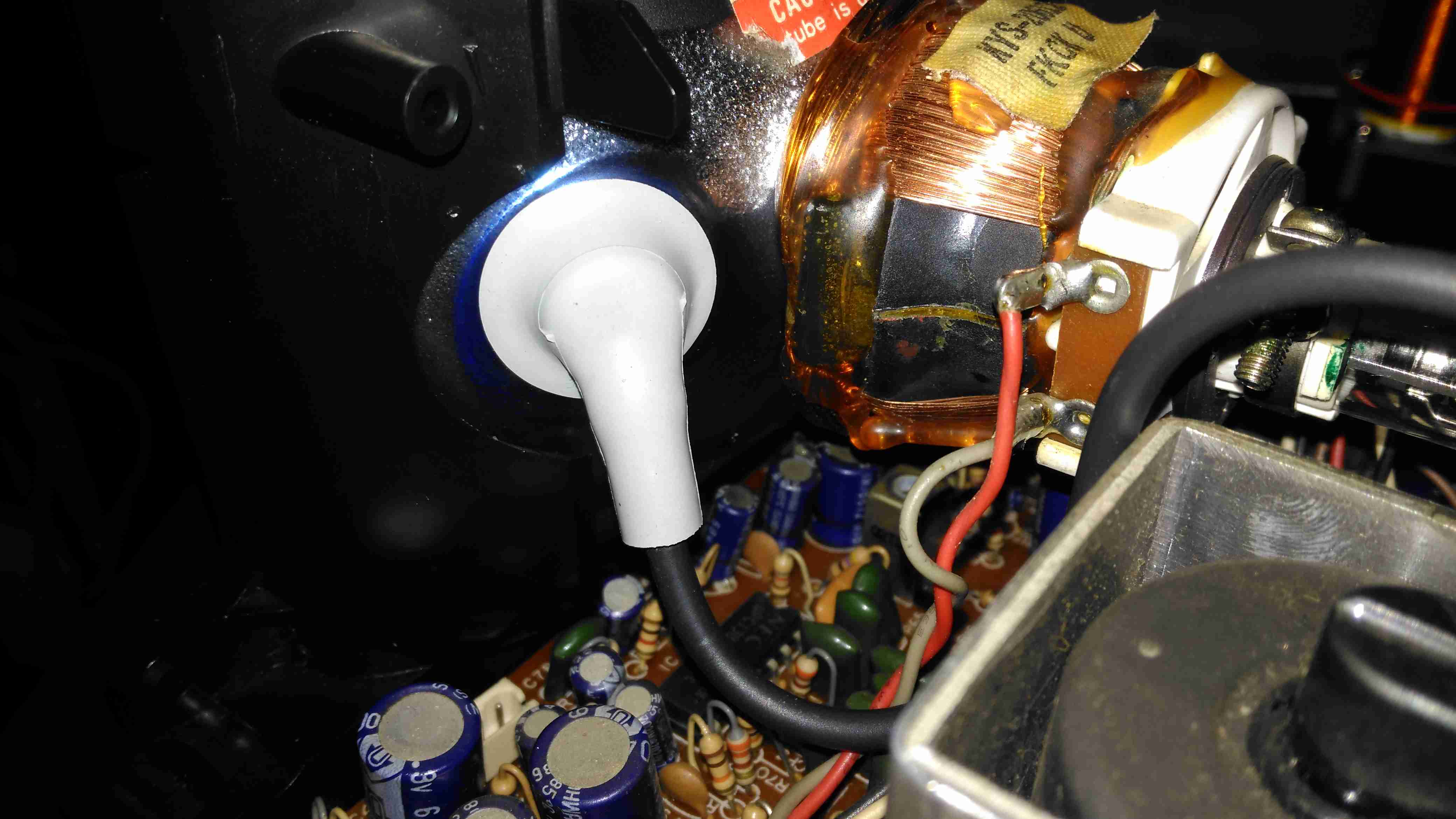
Anode Cap
Here’s the anode side of the unit, with the small flyback transformer. The rubber anode cap has become very hard with age, so I’ll replace this with a decent silicone one from another dead TV. The Horizontal Output Transistor (a 2SC2233 NPN type) & linearity coil are visible at the bottom right corner of the board. Unfortunately, the disgusting yellow glue has been used to secure some of the wiring & large electrolytics, this stuff tends to turn brown with age & become conductive, so it has to be removed. Doing this is a bit of a pain though. It’s still a little bit flexible in places, and rock hard in others. Soaking in acetone softens it up a little & makes it easier to detach from the components.
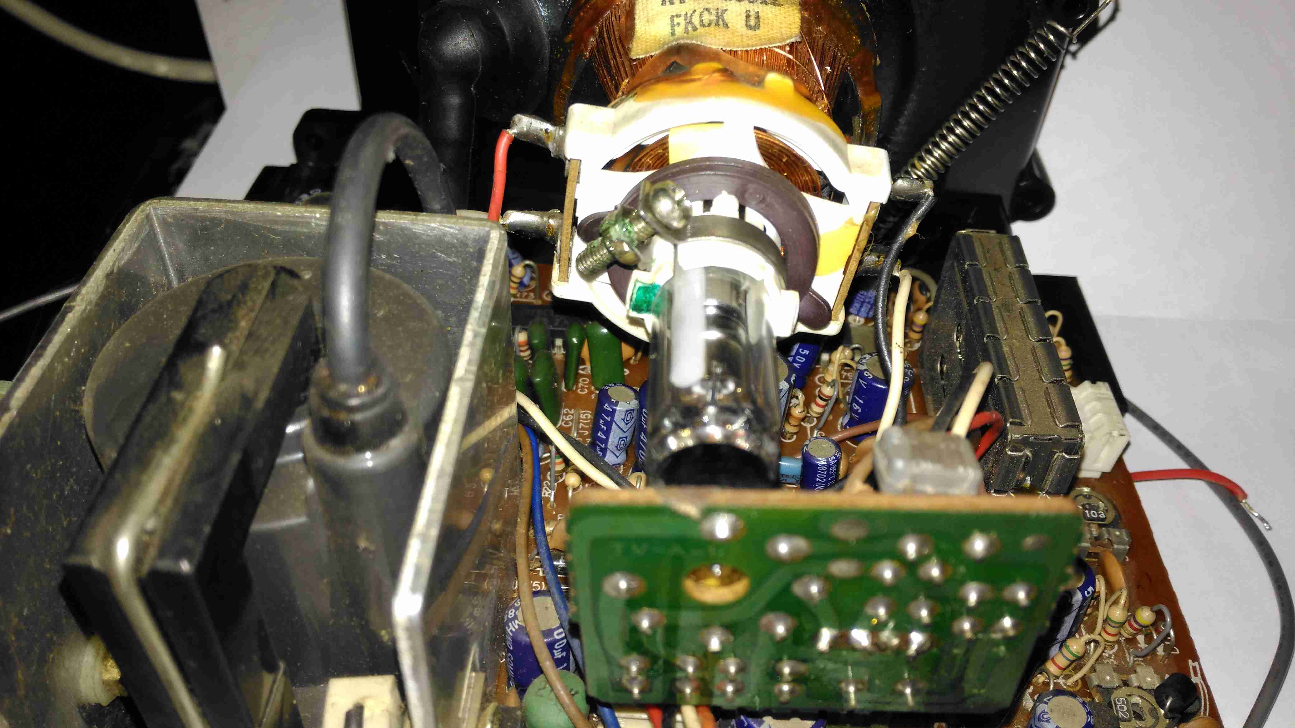
Neck PCB
There’s little on the neck board apart from a few resistors, forming the limiting components for the video signal, and the focus divider of 1MΩ & 470KΩ feeding G3. No adjustable focus on this unit. There’s also a spark gap between the cathode line & ground, to limit the filament to cathode voltage. The flyback transformer is nestled into the heatsink used by the horizontal output transistor & a voltage regulator transistor.
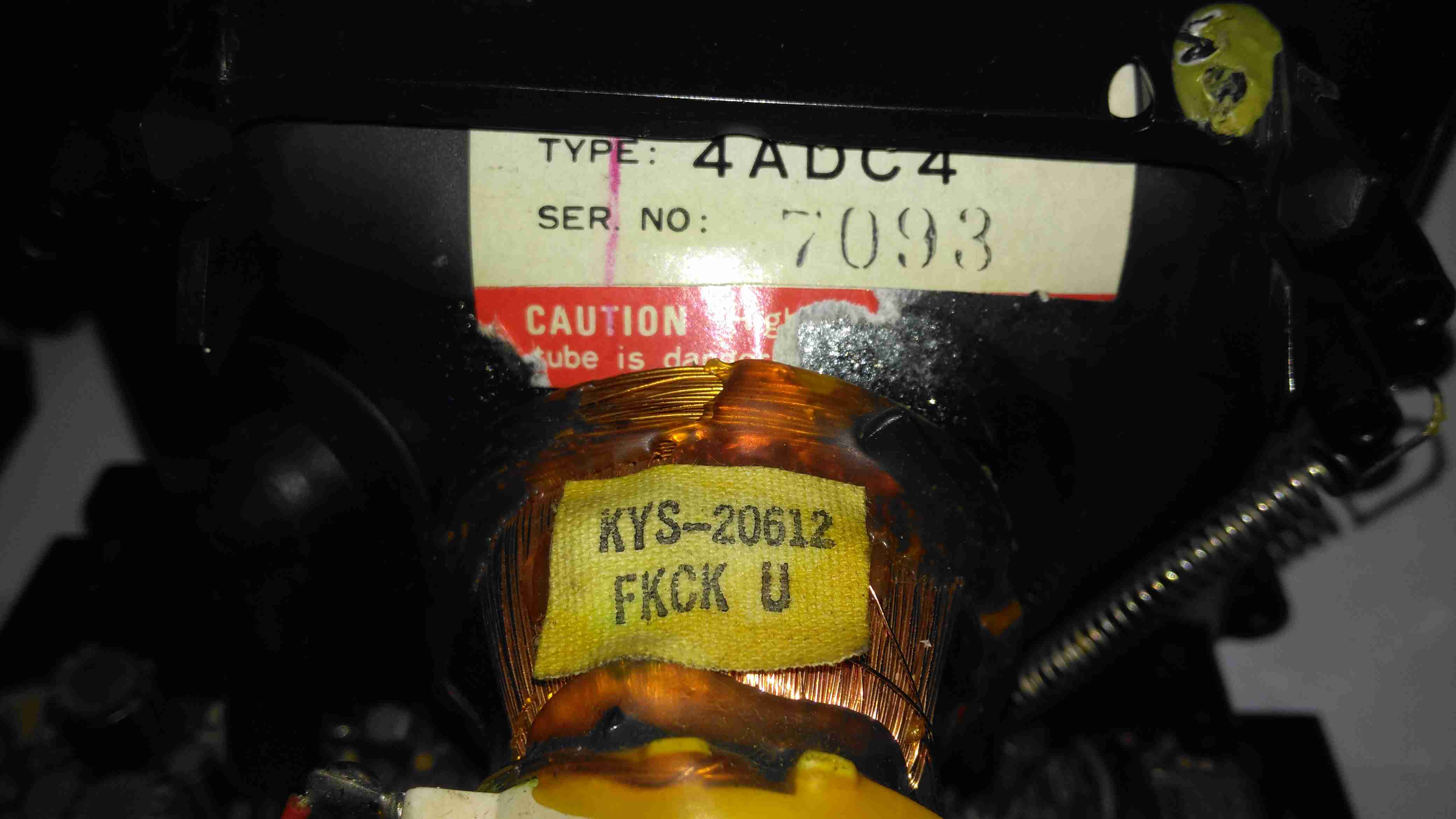
Tube Details
The CRT is a Samsung Electron Devices 4ADC4, with a really wide deflection angle. It’s a fair bit shorter than the Chinese CRT I have which is just a little larger, with a neck tube very thin indeed for the overall tube size.
Unusually, while the filament voltage is derived from the flyback transformer as usual, it’s rectified into DC in this unit, passing through a 1Ω resistor before the filament connection. I measured 5.3v here. The glow from the filament is barely visible even in the dark.
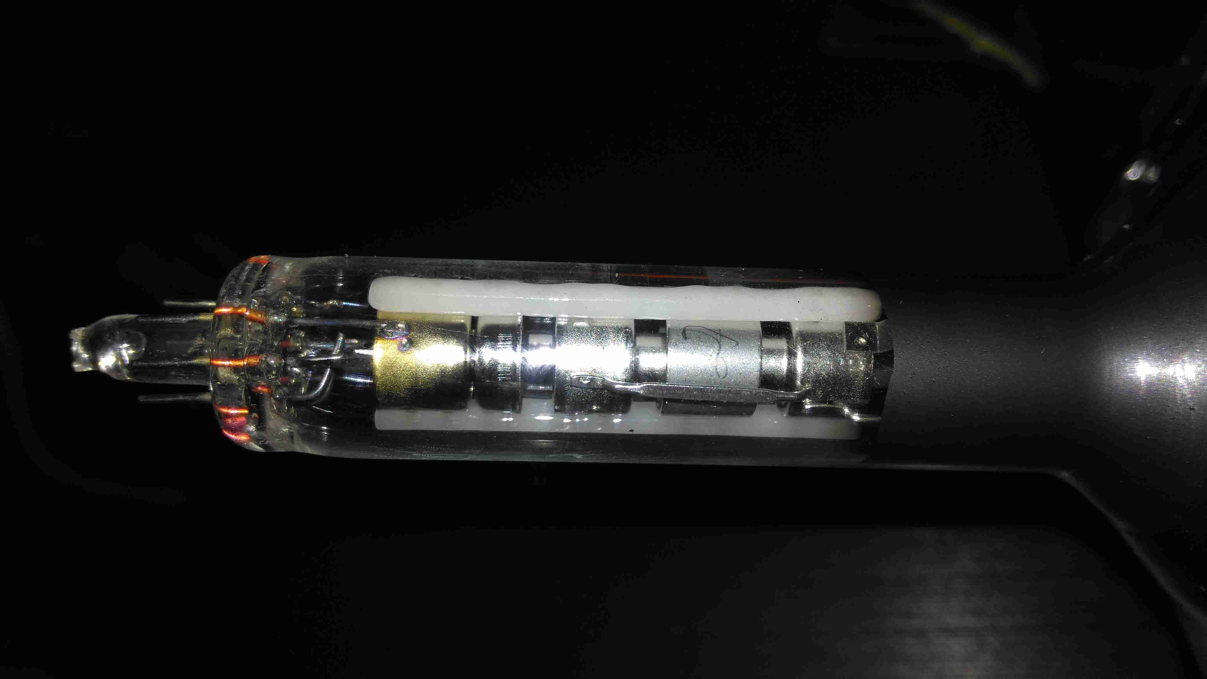
Electron Gun 1
The electron gun is the usual for a monochrome tube, with 7 pins on the seal end.
Electron Gun 2
The electrodes here from left are Final Anode, G3 (Focus Grid), Accelerating Anode, G2 (Screen Grid), G1 (Control Grid). The cathode & filament are hidden inside G1. In operation there’s about 250v on G2, and about 80v on G3.
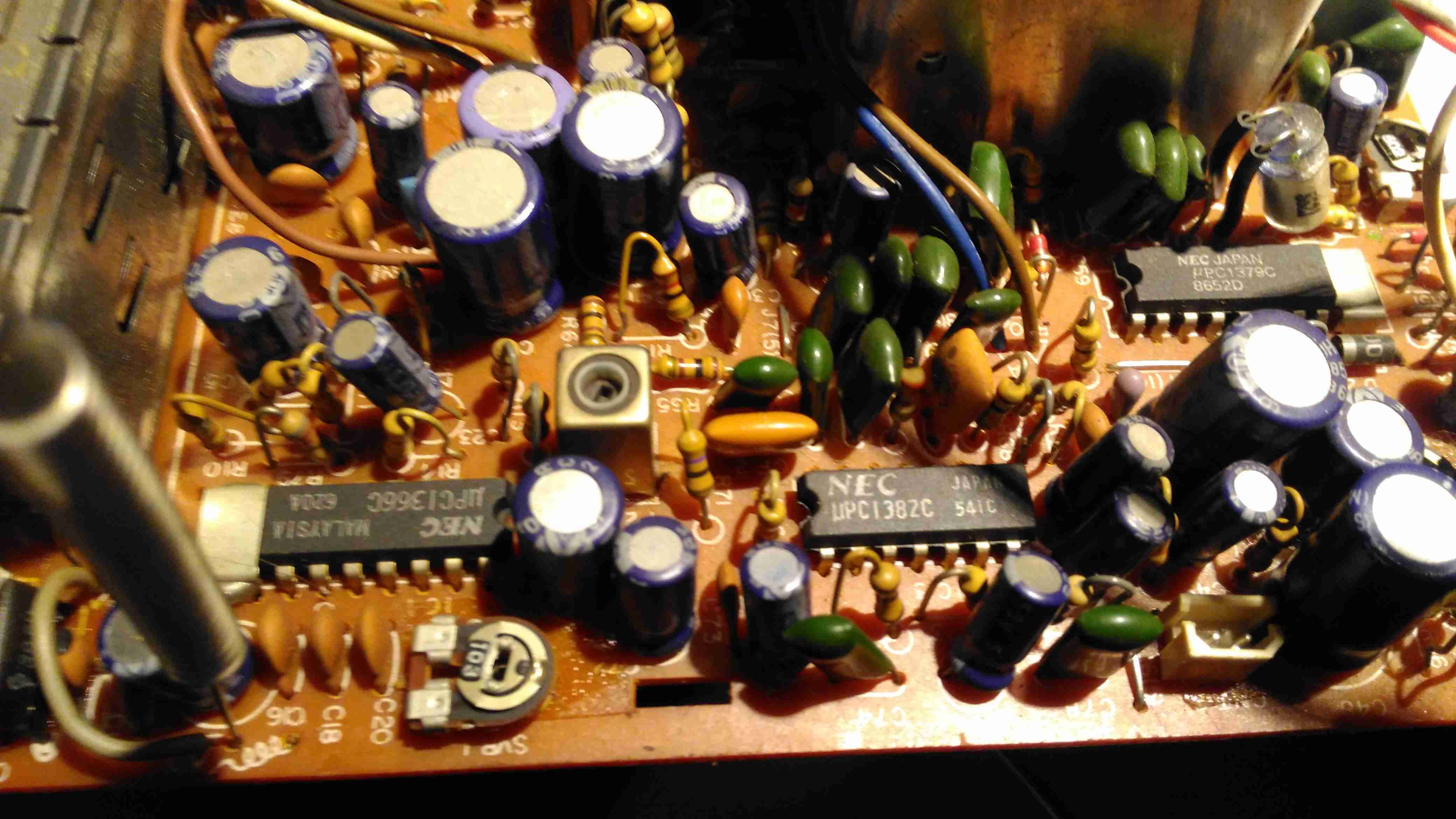
Chipset
The chipset used here is all NEC, starting with a µPC1366C Video IF Processor, which receives the IF signal from the tuner module to the left. This IC outputs the standard composite signal, and a modulated sound signal.
This then splits off to a µPC1382C Sound IF Processor & Attenuator IC, which feeds the resulting sound through the two pin header at the right bottom edge of the board to the audio amplifier in the chassis.
The composite video signal is fed through a discrete video amplifier with a single 2SC2229 transistor before going to the CRT cathode.
The remaining IC is a µPC1379C Sync Signal Processor, containing the sync separator, this is generating the required waveforms to drive the CRT deflection systems from another tap off the composite video line.
From this chip I can assume the unit was built around 1986, since this is the only date code on any of the semiconductors. Besides these 3 ICs, the rest of the circuit is all discrete components, which are well-crammed into the small board space.
There are 5 trimmer potentiometers on the board here, I’ve managed to work out the functions of nearly all of them:
SVR1: IF Gain Adjust
SVR2: H. Hold
SVR3: V. Size
SVR4: B+ Voltage Adjust
SVR5: Tuner Frequency Alignment? It’s in series with the tuning potentiometer in the chassis.
PCB Bottom
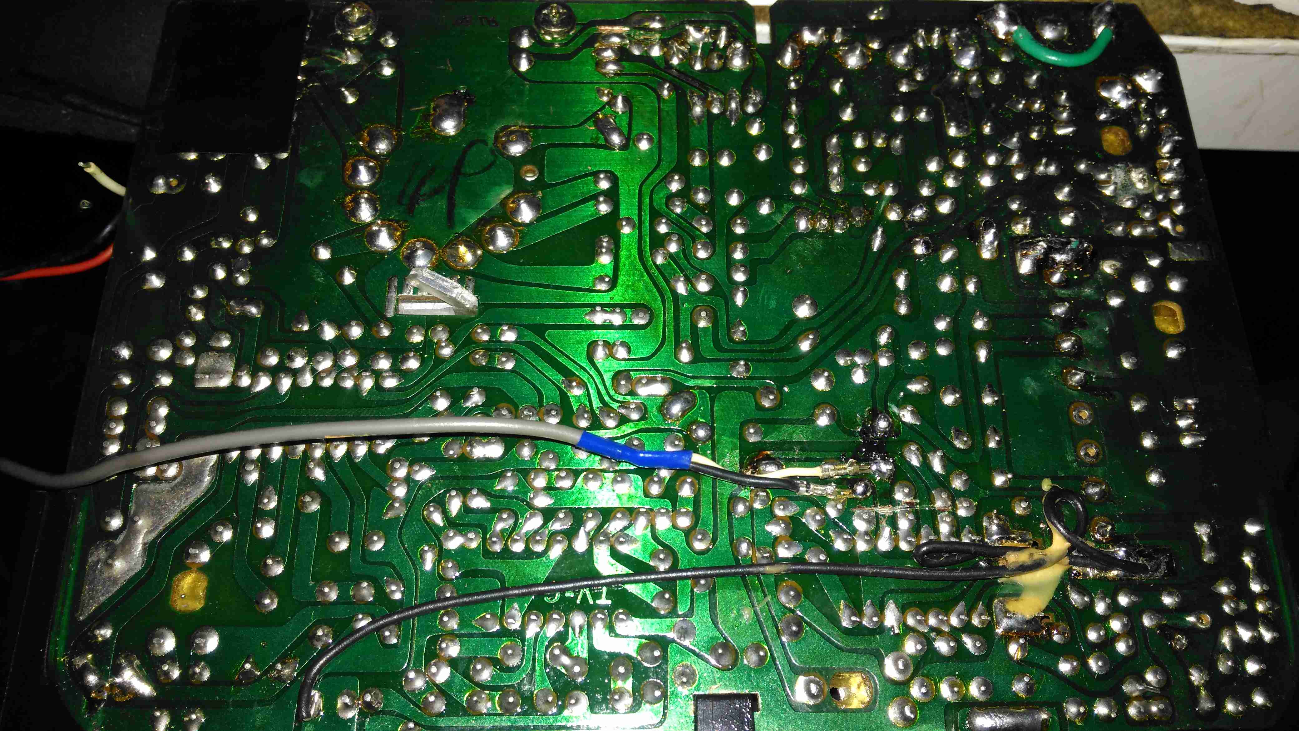
The PCB bottom shows the curved track layout typical of a hand taped out board. The soldermask is starting to flake off in places due to age, and there a couple of bodge wires completing a few ground traces. Respinning a board in those days was an expensive deal! Surprisingly, after all this time I’ve found no significant drift in the fixed resistors, but the carbon track potentiometers are drifiting significantly – 10KΩ pots are measuring as low as 8KΩ out of circuit. These will have to be replaced with modern versions, since there are a couple in timing-sensitive places, like the vertical & horizontal oscillator circuits.
Anode Cap Replaced
Here the anode cap has been replaced with a better silicone one from another TV. This should help keep the 6kV on the CRT from making an escape. This was an easy fix – pulling the contact fork out of the cap with it’s HT lead, desoldering the fork & refitting with the new cap in place.
Here I’ve replaced the important trimmers with new ones. Should help stabilize things a little.
Composite Injection Mod
Injecting a video signal is as easy as the other units. Pin 3 of the µPC1366C Video IF Processor is it’s output, so the track to Pin 3 is cut and a coax is soldered into place to feed in an external signal.
CRT In Operation
After hooking up a Raspberry Pi, we have display! Not bad after having stood idle for 30+ years.
Datasheets for the important ICs are available below:
[download id=”5690″]
[download id=”5693″]
[download id=”5696″]
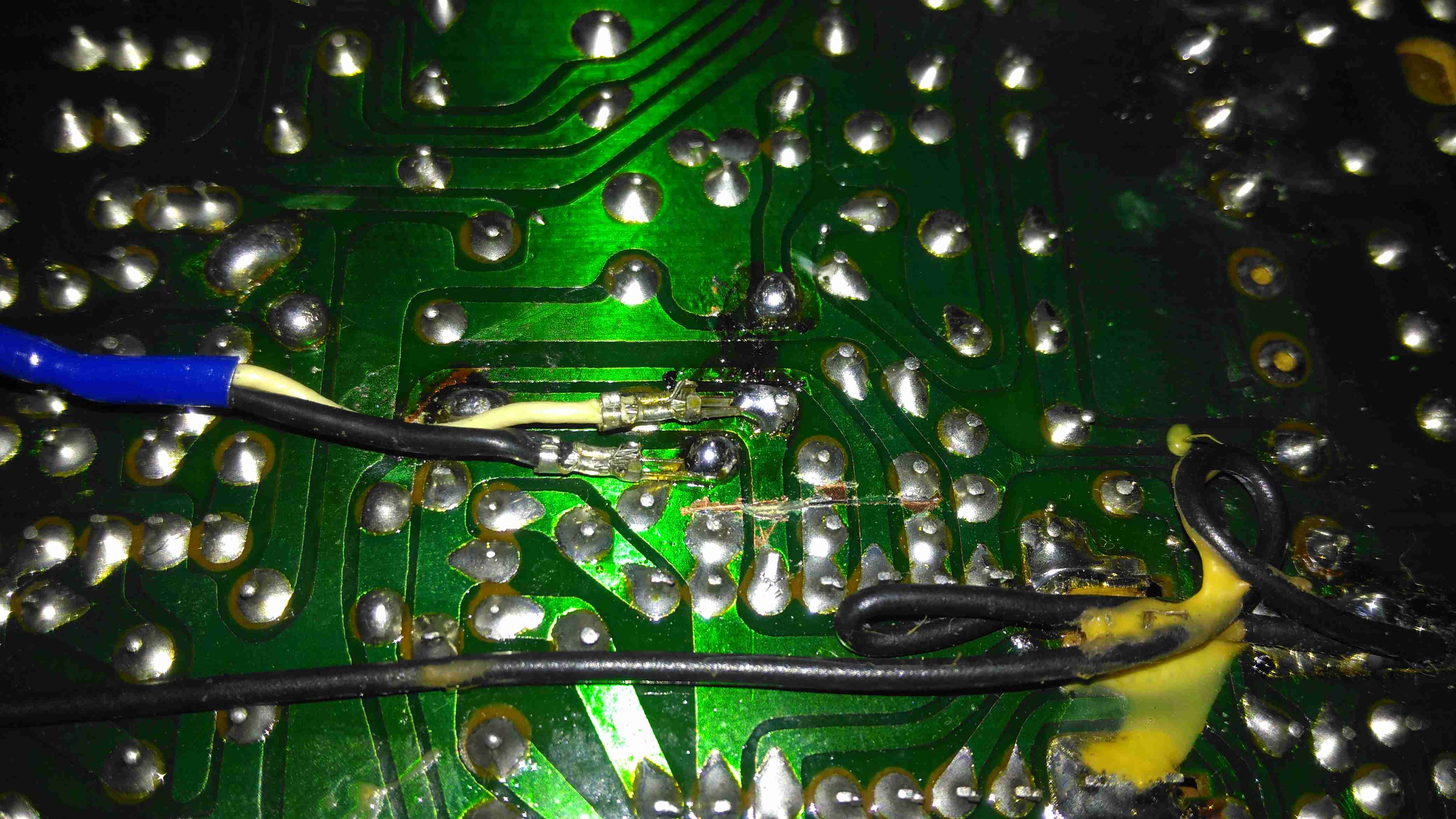
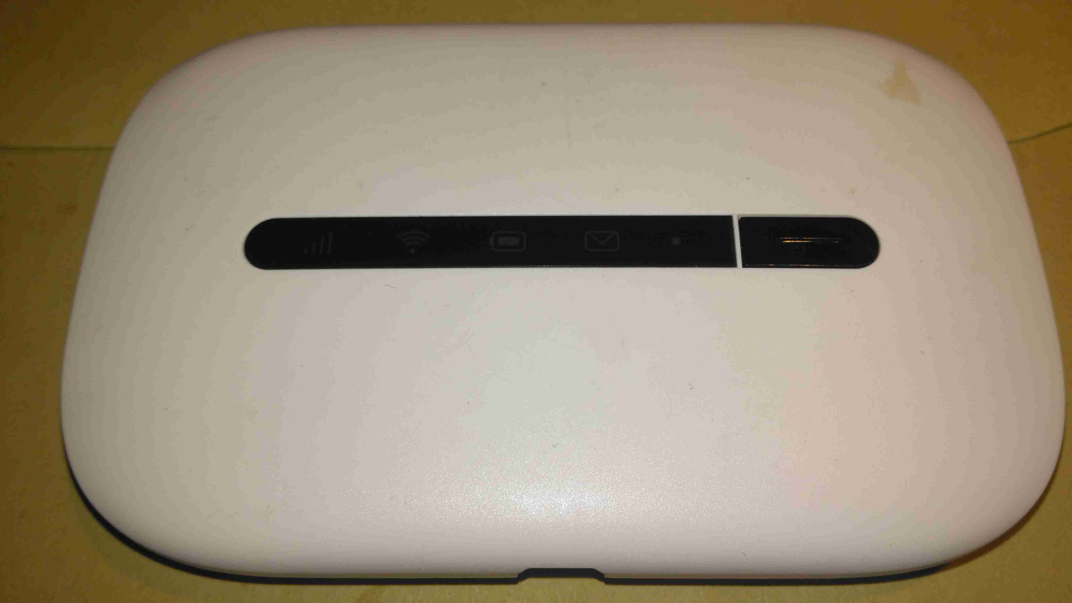
Here’s one of the old modems from my spares bin, a Vodafone Mobile WiFi R207. This is just a rebranded Huawei E5330. This unit includes a 3G modem, and a WiFi chipset, running firmware that makes this a mini-router, with NAT.
Specs
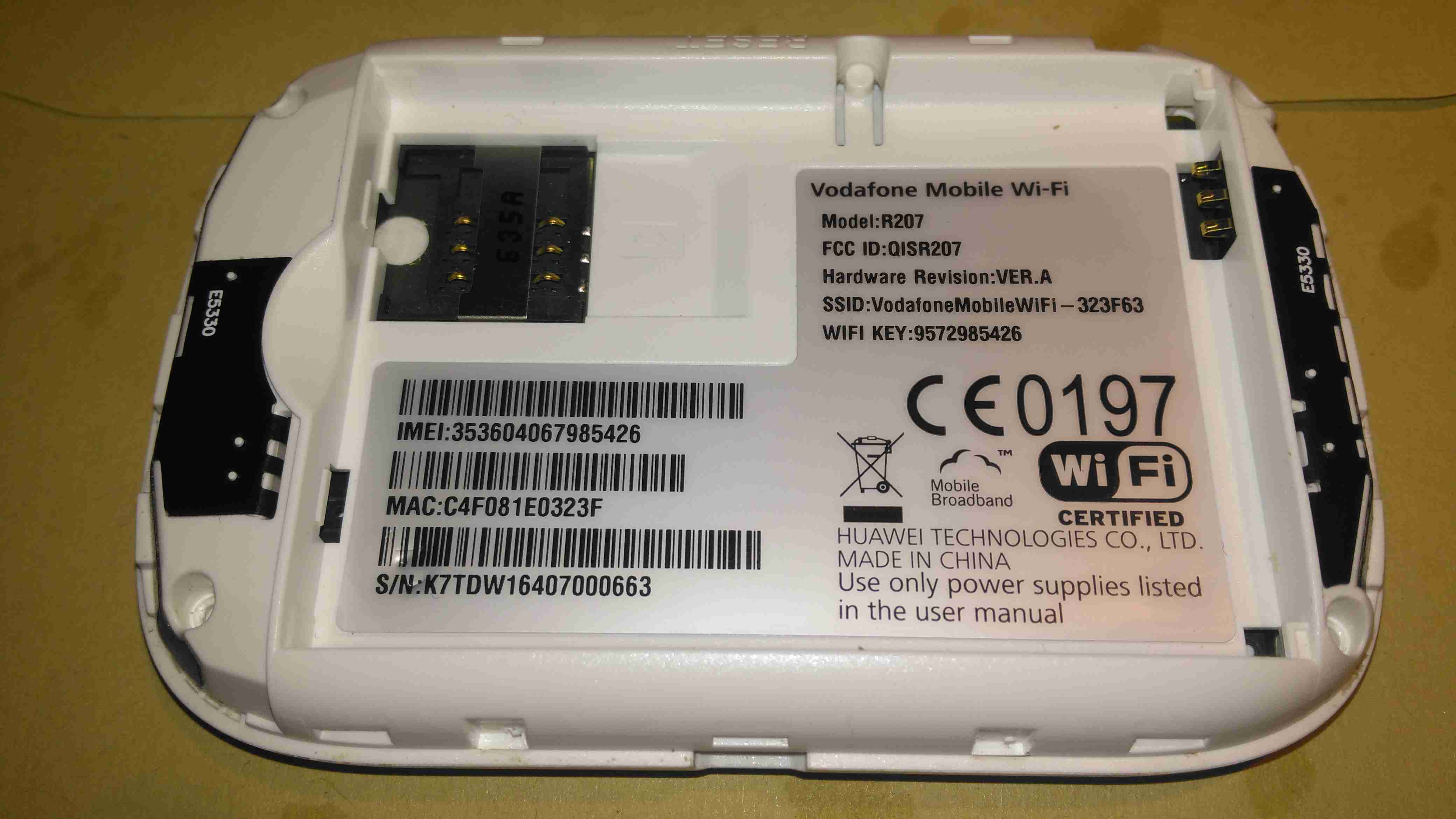
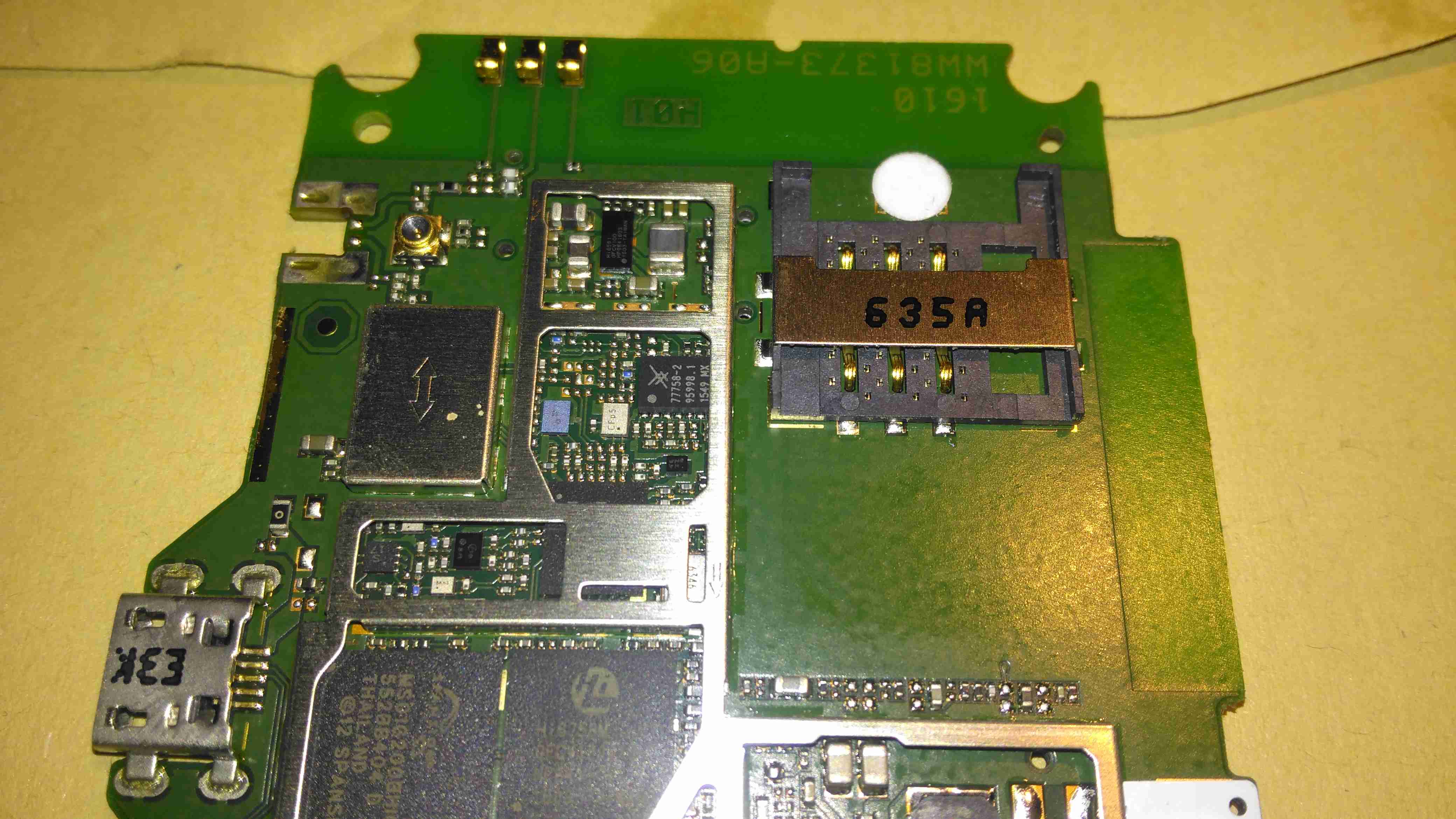
The back has the batter compartment & the SIM slot, with a large label showing all the important details.
Cover Removed
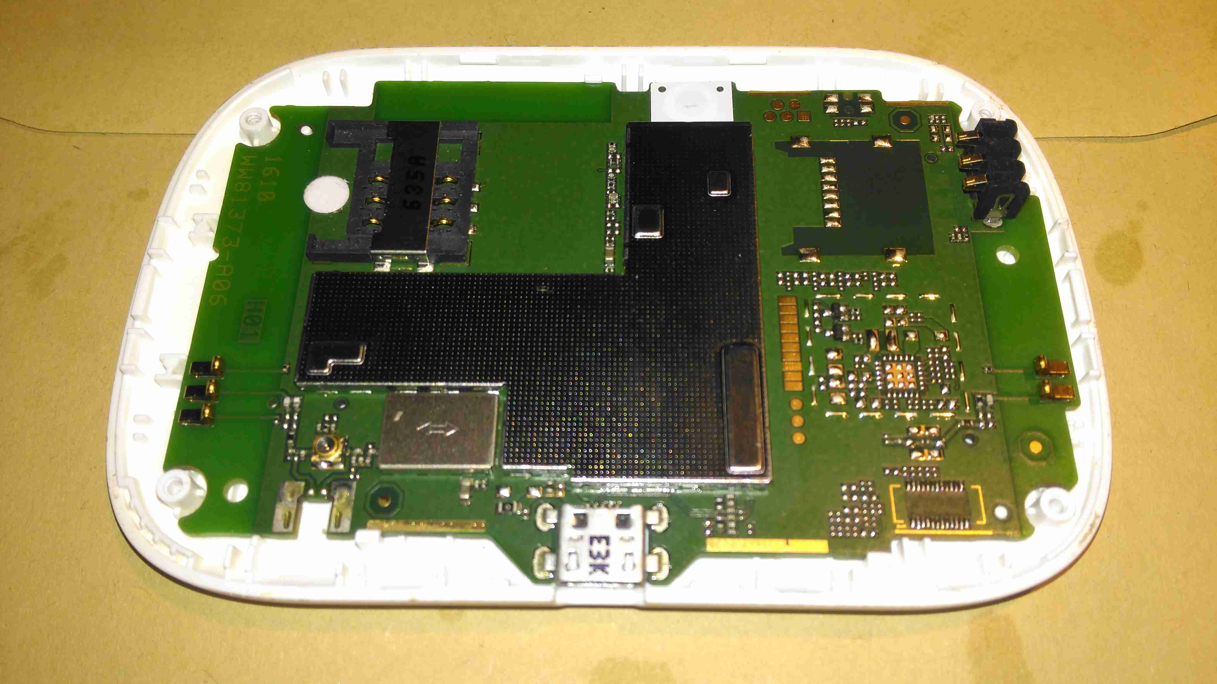
A couple of small Torx screws later & the shell splits in half. All the electronics are covered by shields here, but luckily they are the clip-on type, and aren’t soldered direct to the PCB.
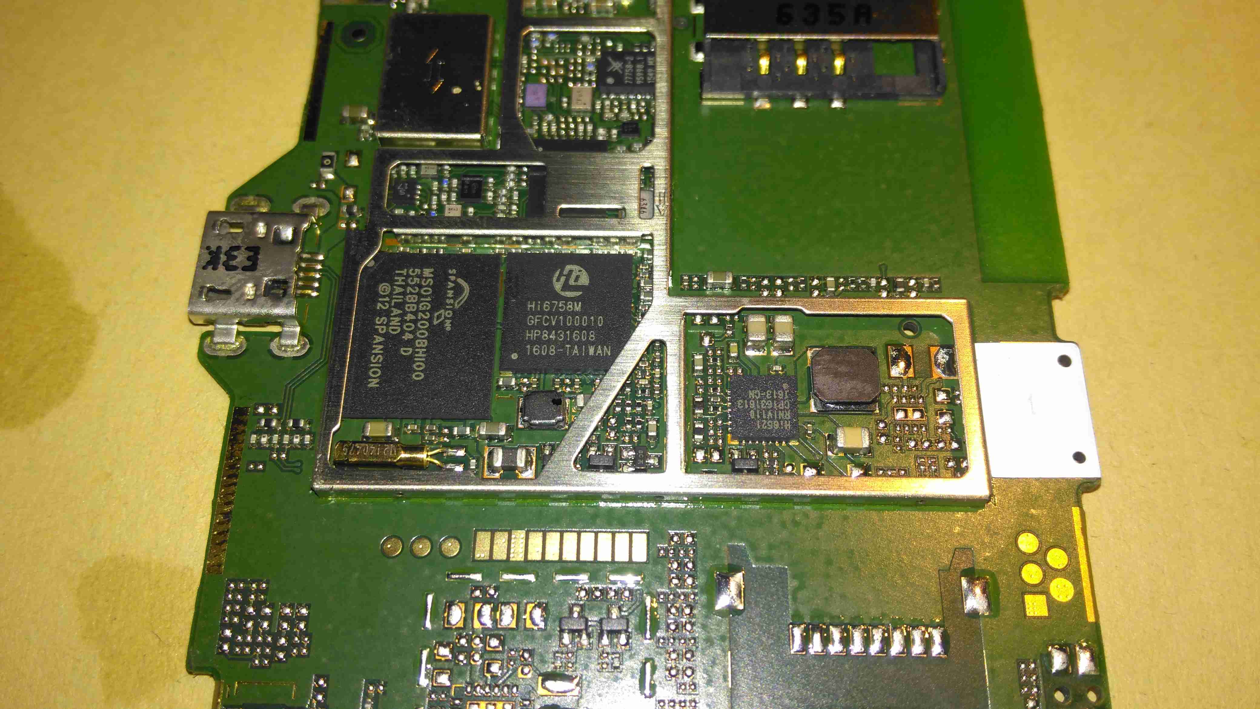
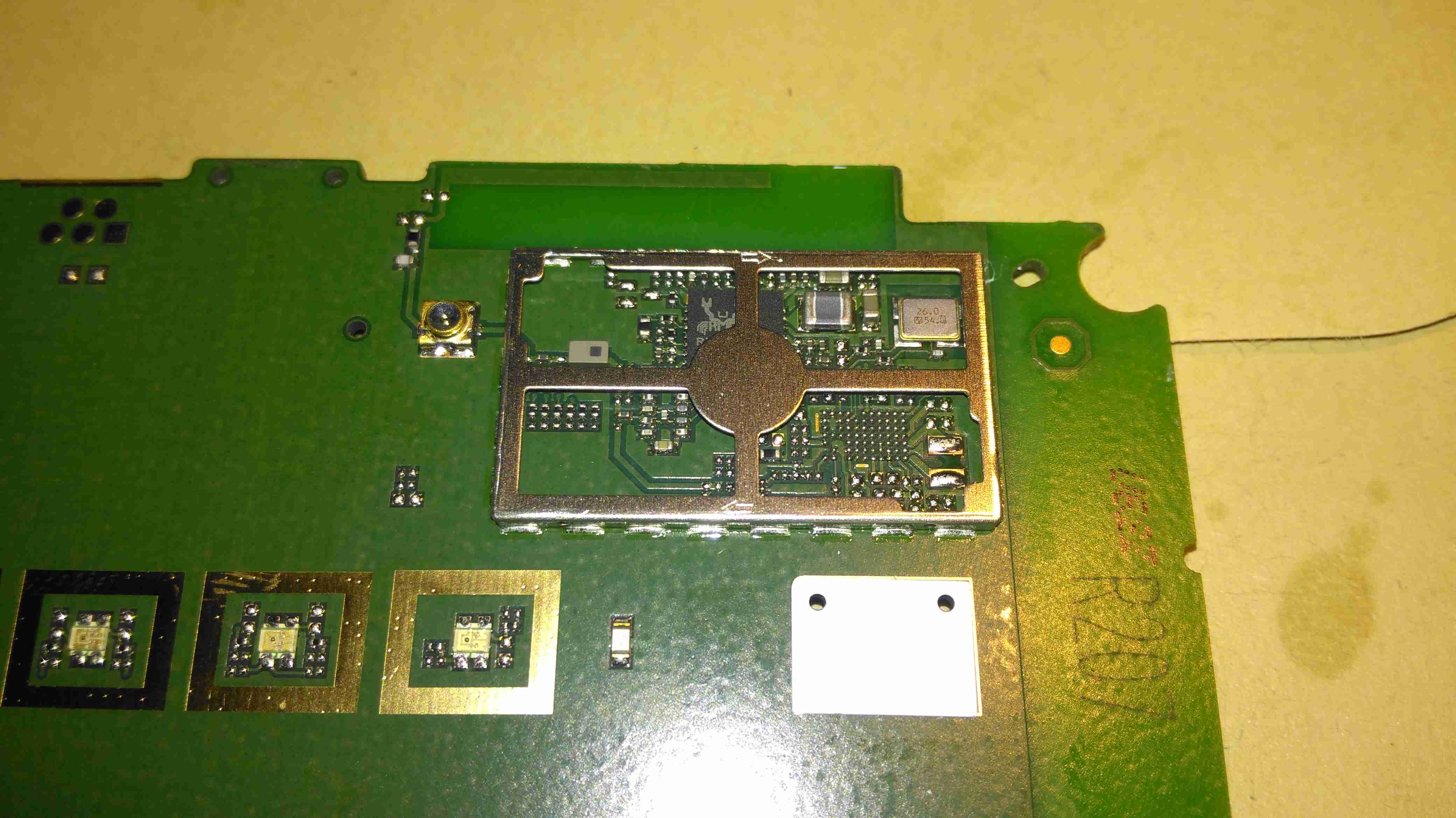
Chipset
Once the shield has been removed, the main chipset is visible underneath. There’s a large Spansion MS01G200BHI00 1GBit flash, which is holding the firmware. Next to that is the Hi6758M baseband processor. This has all the hardware required to implement a 3G modem. Just to the right is a Hi6521 power management IC, which is dealing with all the power supplies needed by the CPU.
The RF section is above the baseband processor, some of which is hiding under the bits of the shield that aren’t removable.
SIM Socket
There’s a socket onboard for a standard Mini-SIM, just to the left of that is a Hi6561 4-phase buck converter. I would imagine this is providing the power supplies for the RF section & amplifier.
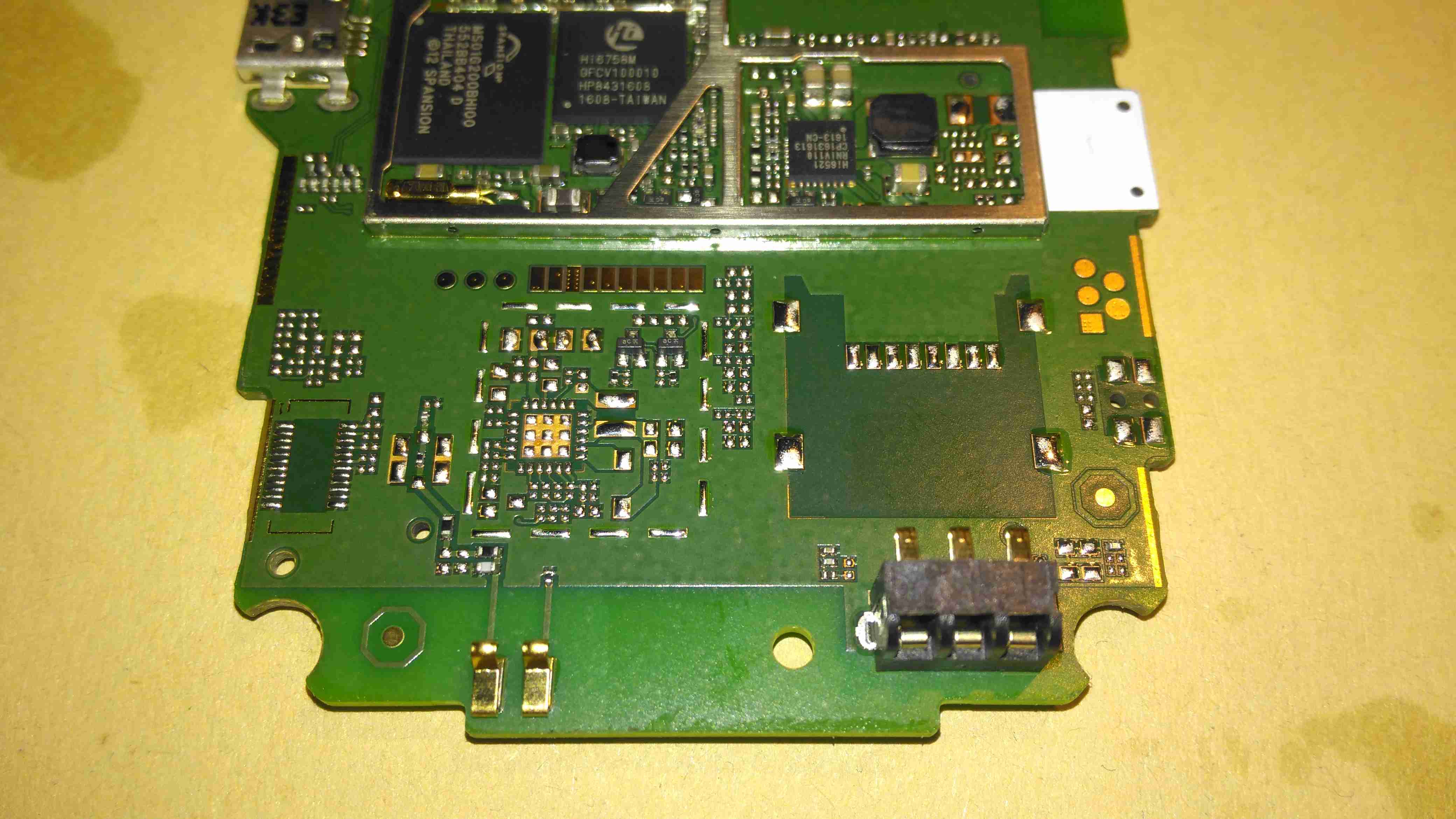
Unpopulated Parts
Not sure what this section is for, all the parts are unpopulated. Maybe a bluetooth option?
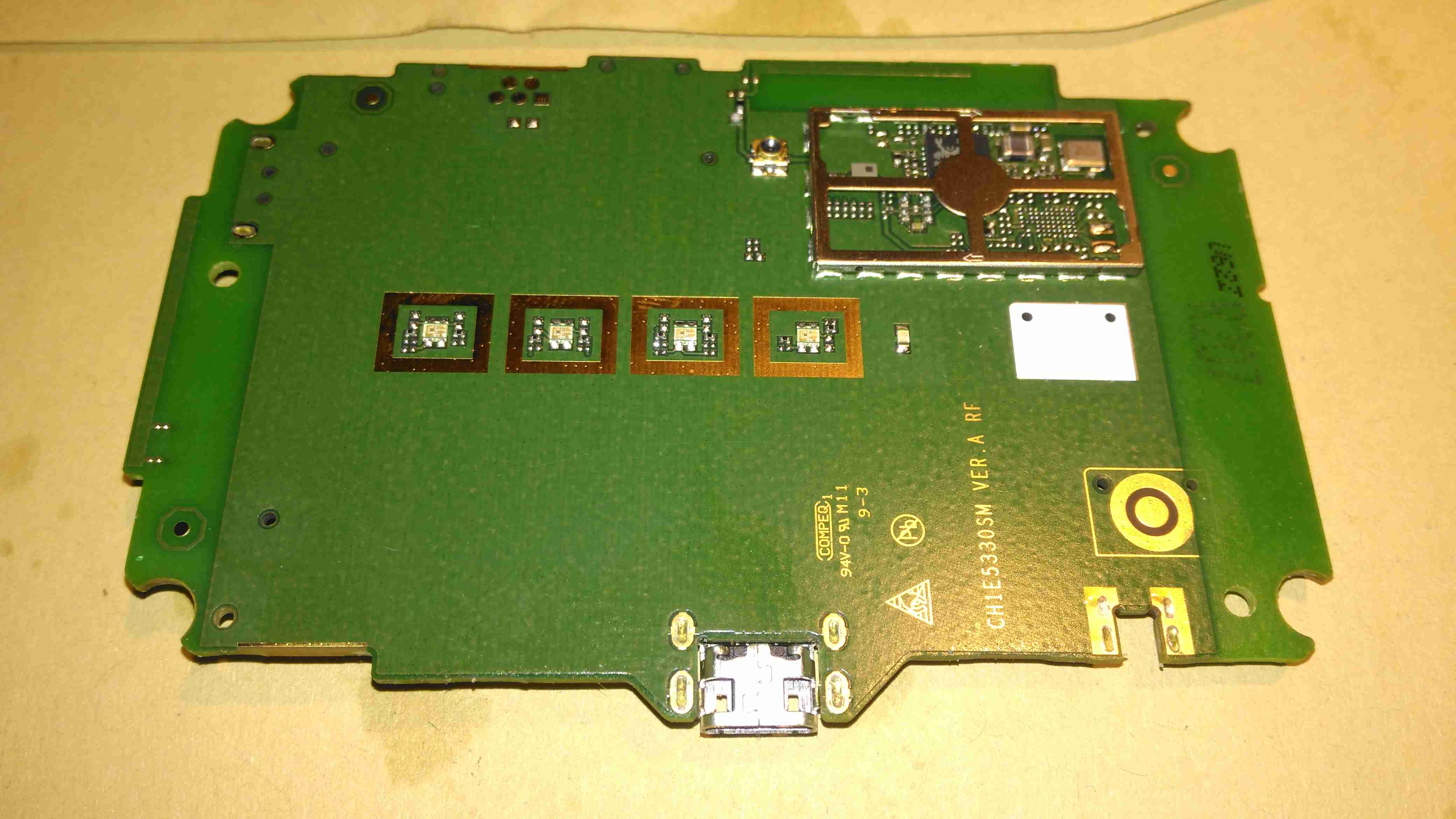
PCB Reverse
The other side of the PCB is pretty sparse, holding just the indicator LEDS, button & the WiFi Chipset.
Realtek WiFi Chipset
The chipset here is a Realtek part, but it’s number is hidden by some of the shield. The antenna connection is routed to the edge of the board, where a spring terminal on the plastic case mounted antenna makes contact.
Since I do festivals every year, along with a couple of other camping trips if the weather is good enough, I’ve been taking equipment with me for years in flight cases to make things more comfortable. Things like a large battery to power lights & device charging, an old Eberspacher diesel heater for the times when the weather isn’t great, and an inverter to run the pumps built into airbeds.
Red Diesel / Heating Oil is my fuel of choice for camping purposes, as it’s about the safest fuel around, unlike Butane/LPG it is not explosive, will not burn very readily unless it’s atomized properly & it’s very cheap. Paraffin is an alternative fuel, but it’s expensive in the UK, at about £12 per 5L.
The Hexamine-based tablet fuels the UK festivals promote is nasty stuff, and the resulting combustion products are nastier still. (Things like Hydrogen Cyanide, Formaldehyde, Ammonia, NOX). They also leave a sticky black grok on every cooking pot that’s damn near impossible to remove. Meths / Trangia stoves are perfectly usable, but the flame is totally invisible, and the flammability of alcohol has always made me nervous when you’ve got a small pot of the stuff boiling while it’s in operation in the middle of a campsite filled with sloshed festival goers. A single well-placed kick could start a massive fire.
Previous System
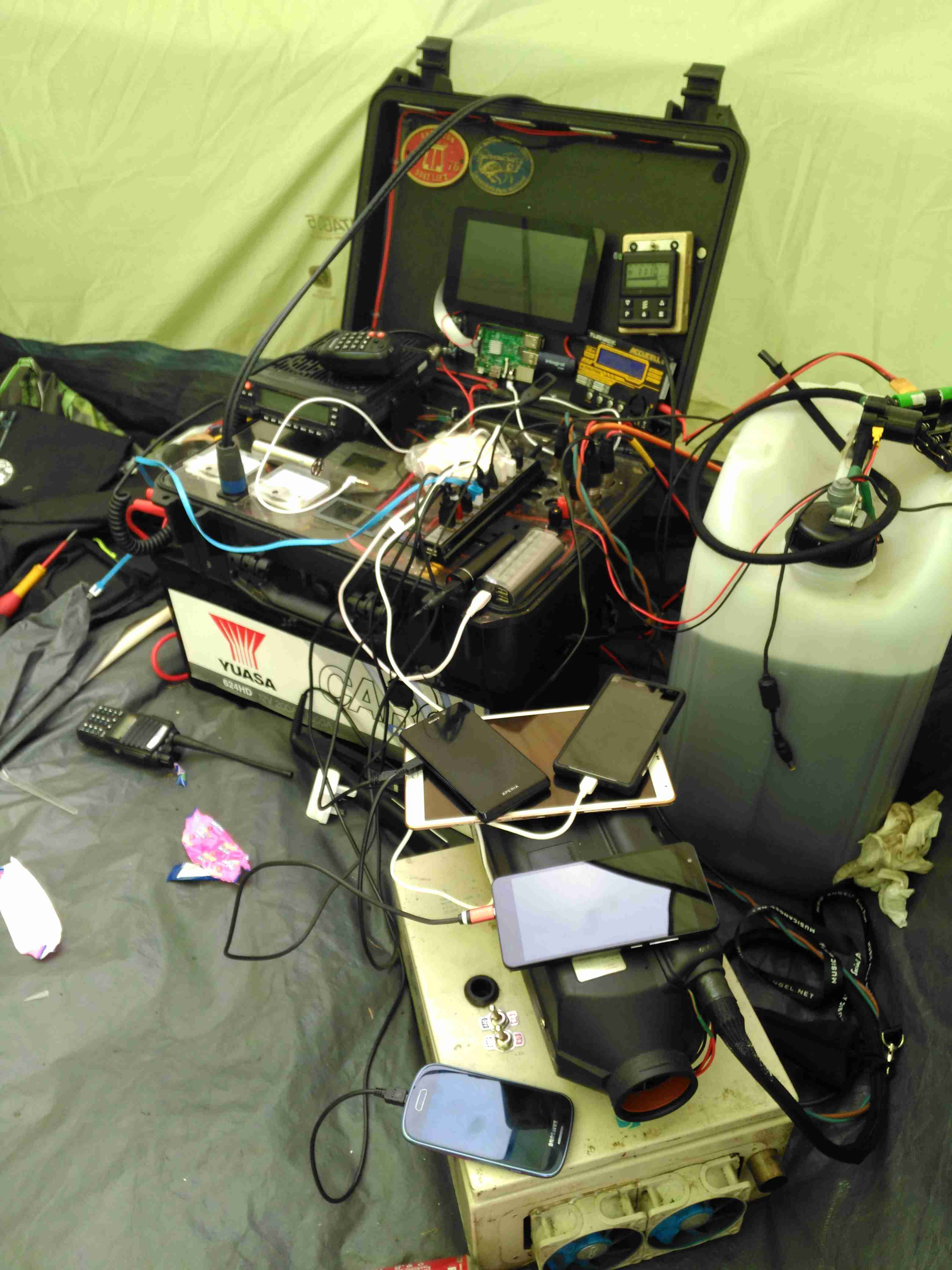
Over the years the gear has evolved and grown in size, so I decided building everything into one unit on wheels would be the best way forward. I’ve been working on this for some time, so it’s time to get some of the details on the blog! Above you can see the system used for last year’s camping, the heater is separate, with a 25L drum of heating oil, the battery is underneath the flight case containing all the power components, and it’s currently charging All The Things.
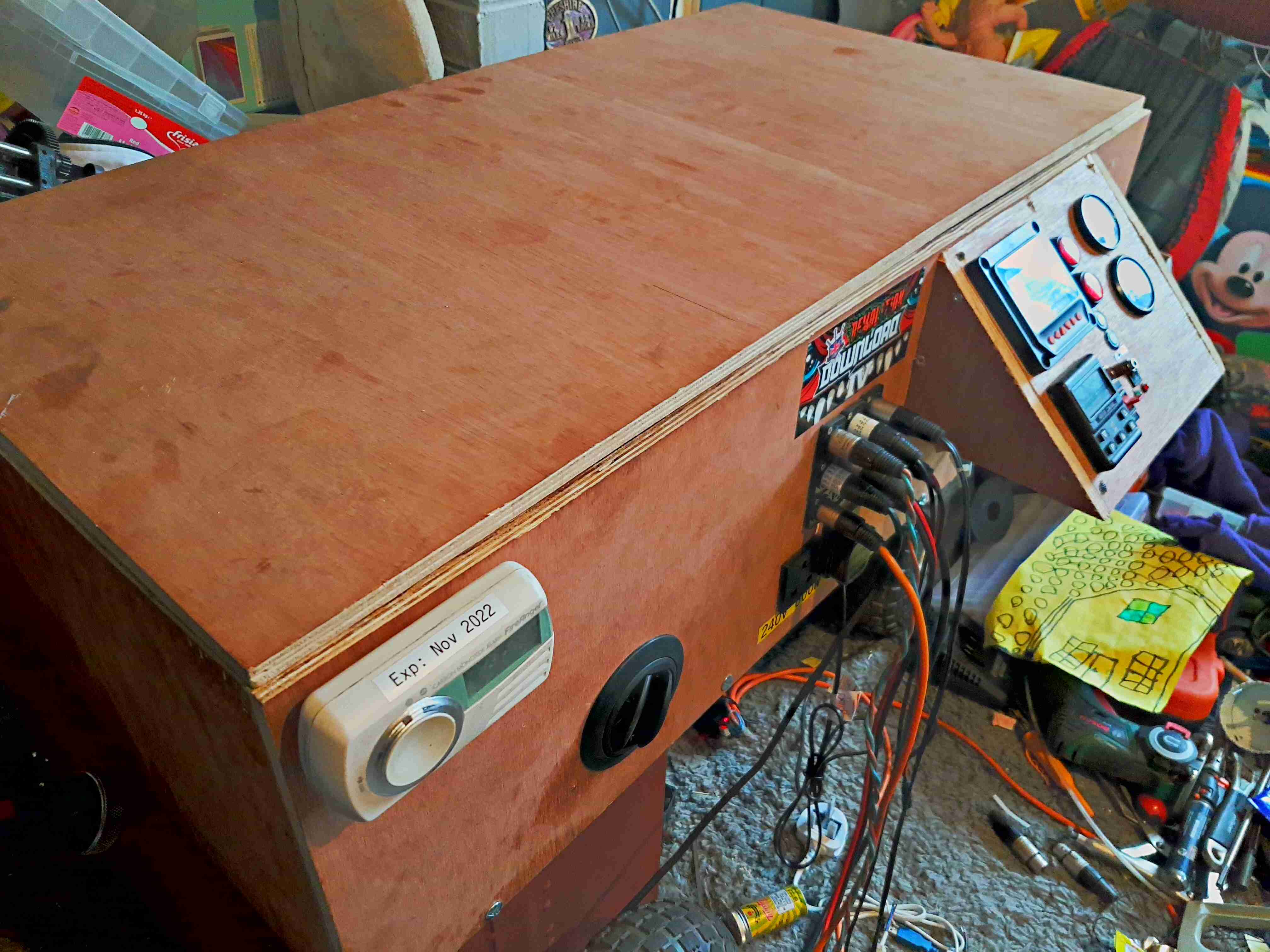
Overview
Above is the new unit almost finished, the bottom frame is a standard eBay-grade 4-wheel trolley with a few modifications of my own, with a new top box built from 12mm hardwood marine plywood. This top is secured in place with coach bolts through the 25mm angle iron of the trolley base. The essential carbon monoxide detector is fitted at the corner.
Internal View
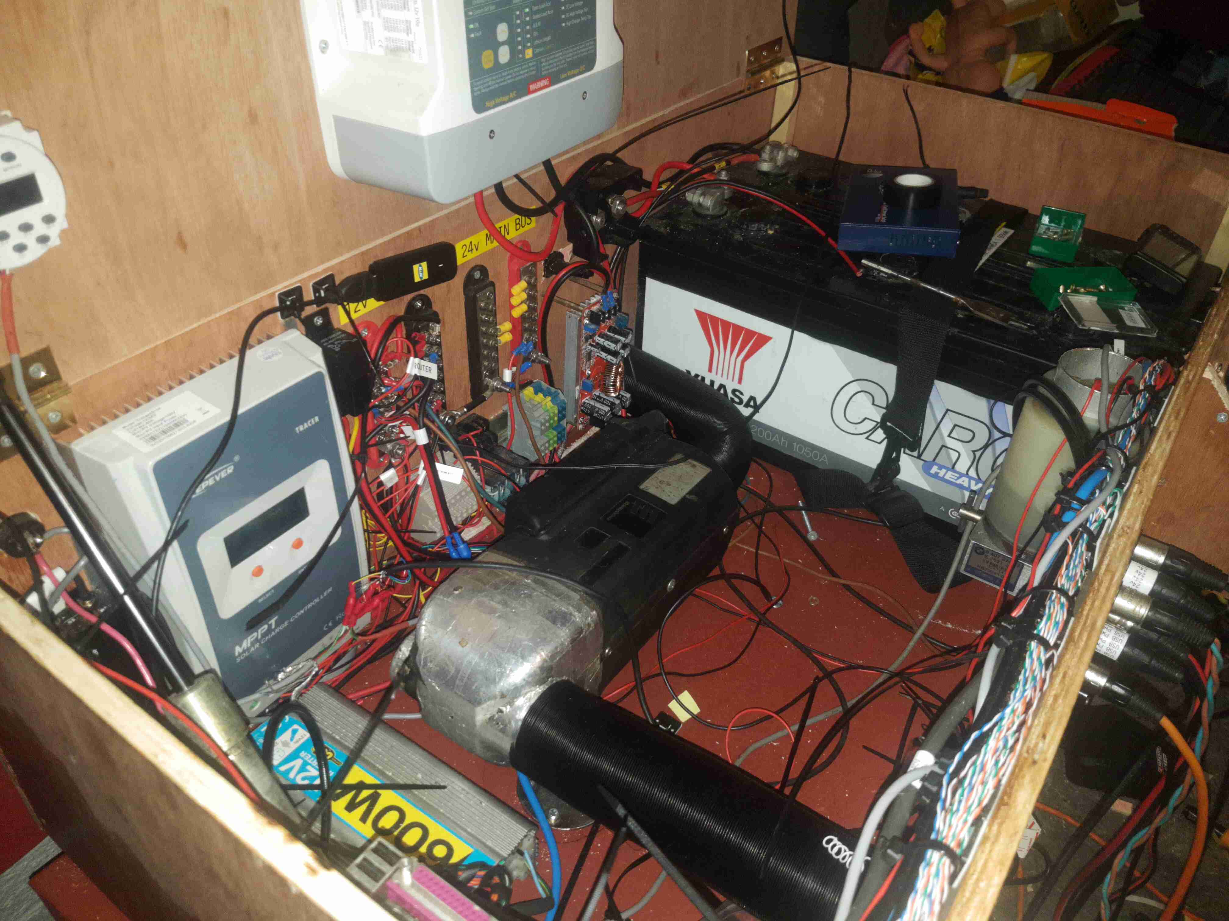
The inside gets a bit busy with everything crammed in. The large Yuasa 200Ah lead-acid battery is at the far end, with it’s isolation switch. Right in the middle is the Eberspacher heater with it’s hot air ducting. I’ve fitted my usual 12/24v dual voltage system here, with the 24v rail generated from a large 1200W DC-DC converter.
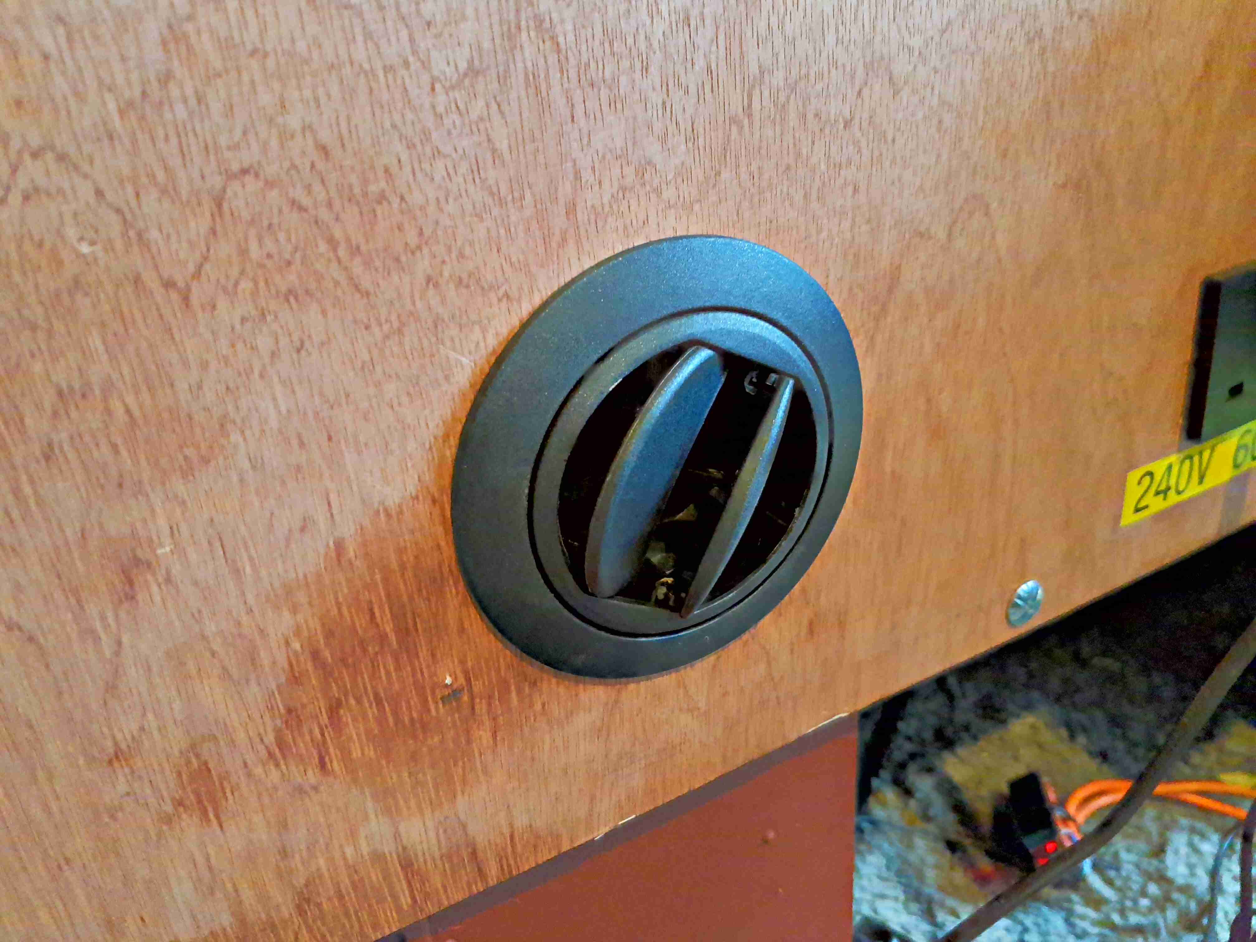
Heater Vent
The hot air duct for the heater is fed out through a standard vent in the front. Very handy for drying out after a wet day.
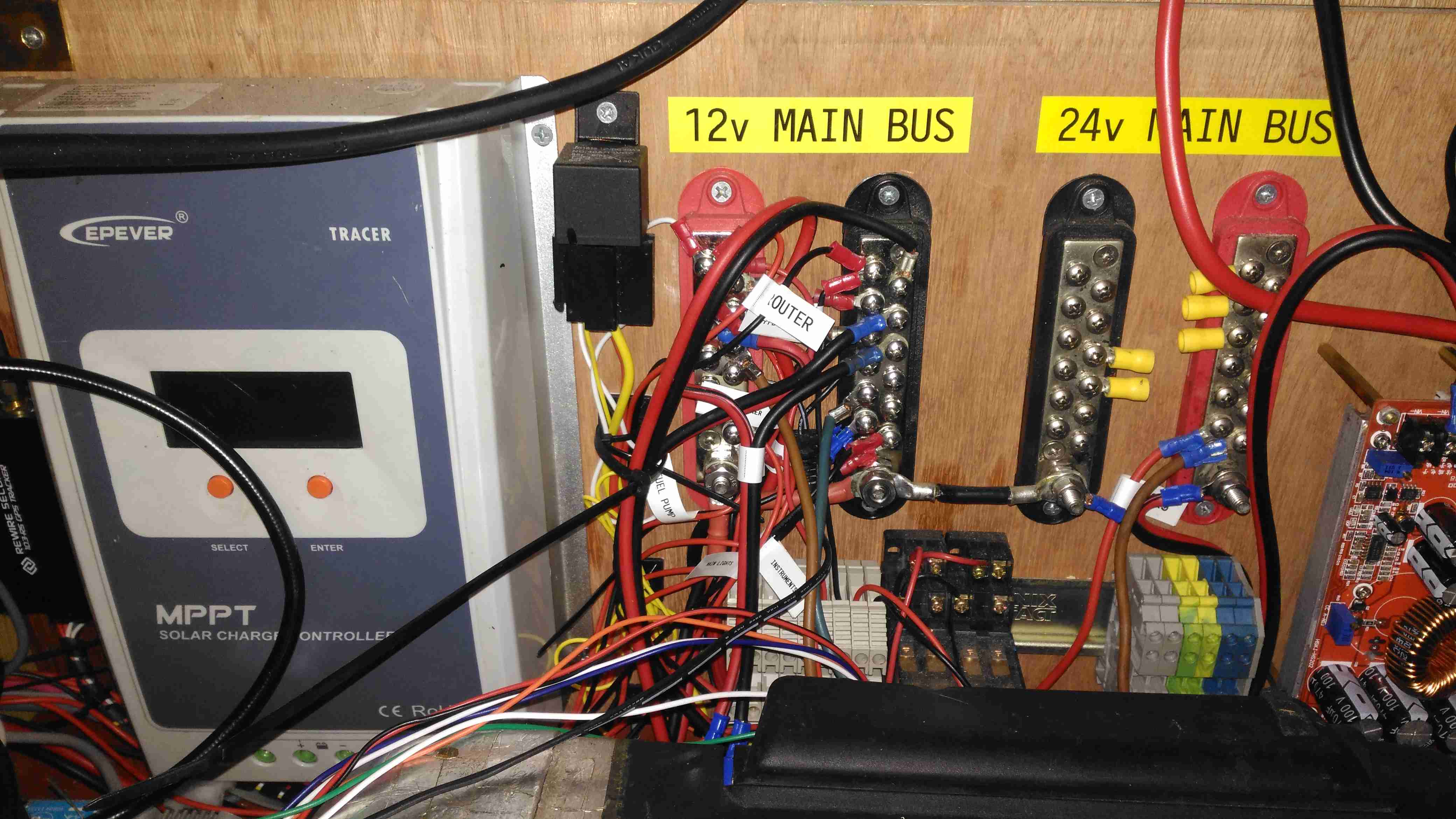
Main Bus Bars & Solar Controller
Here’s a closeup of the distribution bus bars, with both negative rails tied together in the centre to keep the positives as far away from each other as possible, to reduce the possibility of a short circuit between the two when working on the wiring. The EpEver Tracer 4210A MPPT Solar Charge Controller is on the left, tucked into the corner. This controller implements the main circuit protection for the battery, having a 40A limit. Individual circuits are separately fused where required. Solar input on this unit is going to be initially provided by a pair of 100W flexible panels in series for a 48v solar bus, the flexible panels are essential here as most of the festivals I attend do not allow glass of any kind onsite, not to mention the weight of rigid panels is a pain.
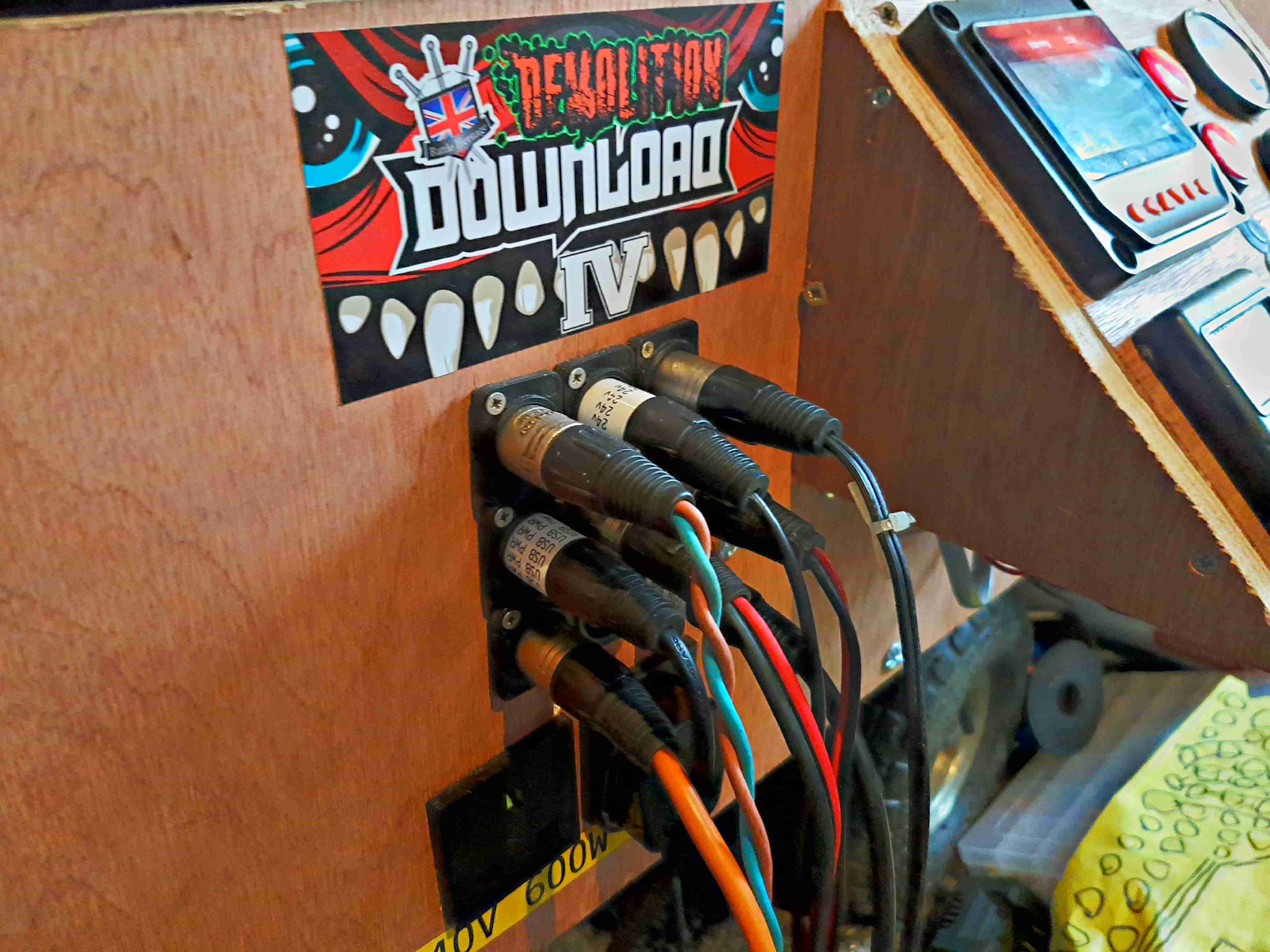
DC Output Sockets
I’ve stuck with the 3-pin XLR plugs for power in this design, giving both the 12v rail, 24v rail & ground.
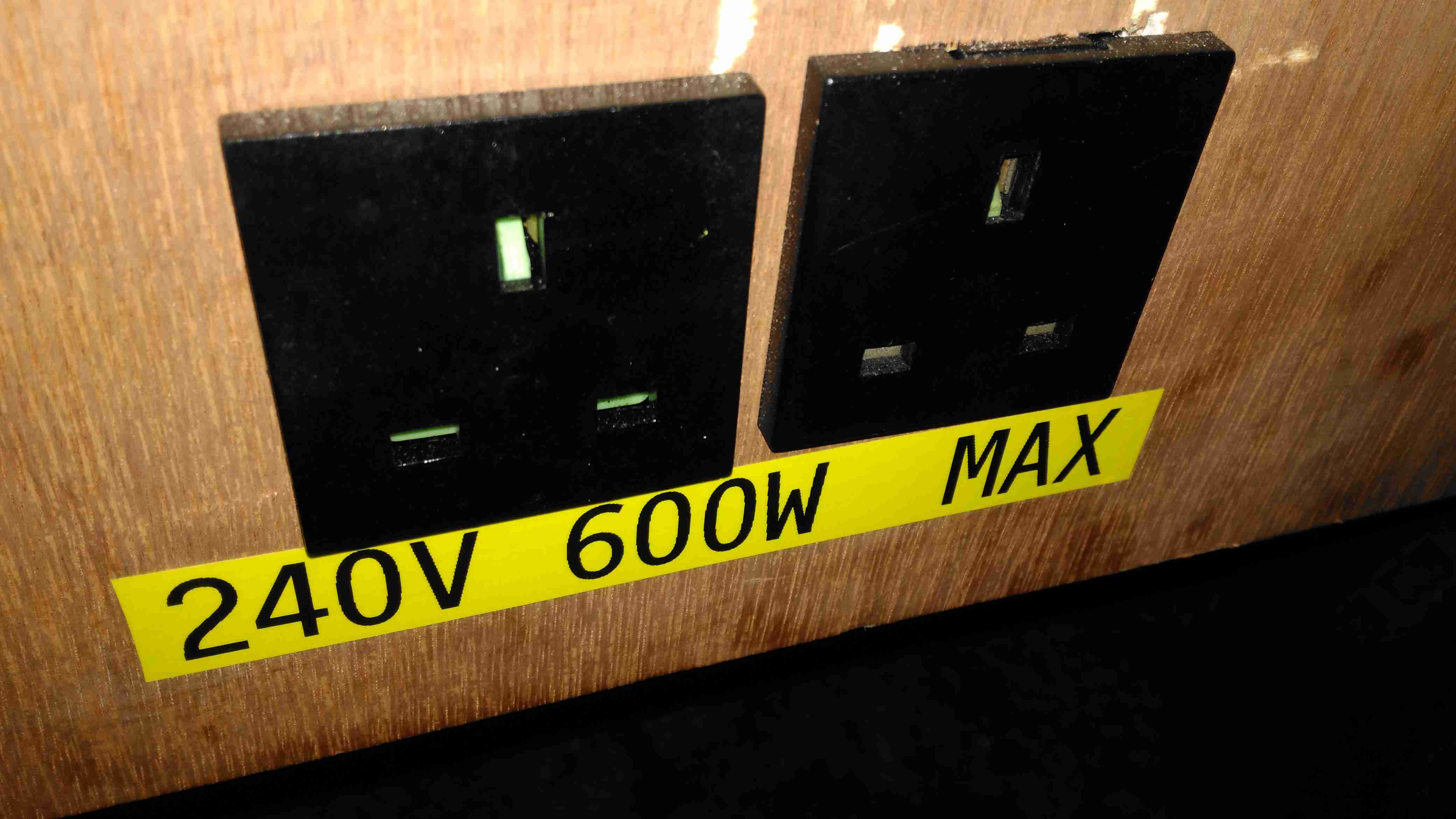
Inverter Outputs
Tucked under the DC outputs are a pair of panel sockets for the 600W inverter. This cheapo Maplin unit is only usually used to pump up air beds, so I’m not expecting anyone to pull anything near max output, but a warning label always helps.
Power Socket Wiring
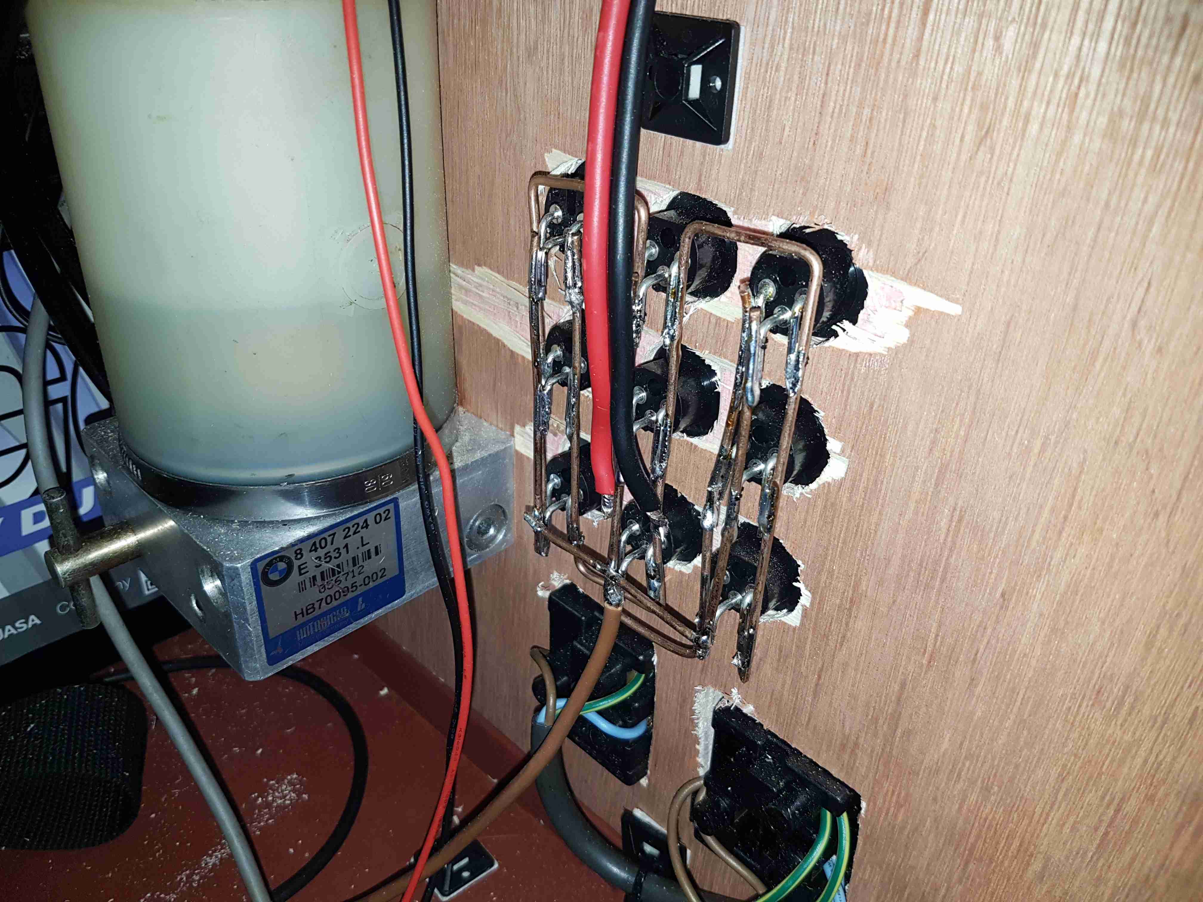
Behind the front panel is the hardwiring for the power sockets. The DC jacks are connected together using 2mm solid copper wire, bent into bus bars.The mains wiring underneath is a simple radial circuit straight from the inverter. The large cylinder on the left is a hydraulic pump from a BMW Z3, which runs a hydraulic cylinder for lifting the lid of the top box, used simply because I had one in the box of junk.
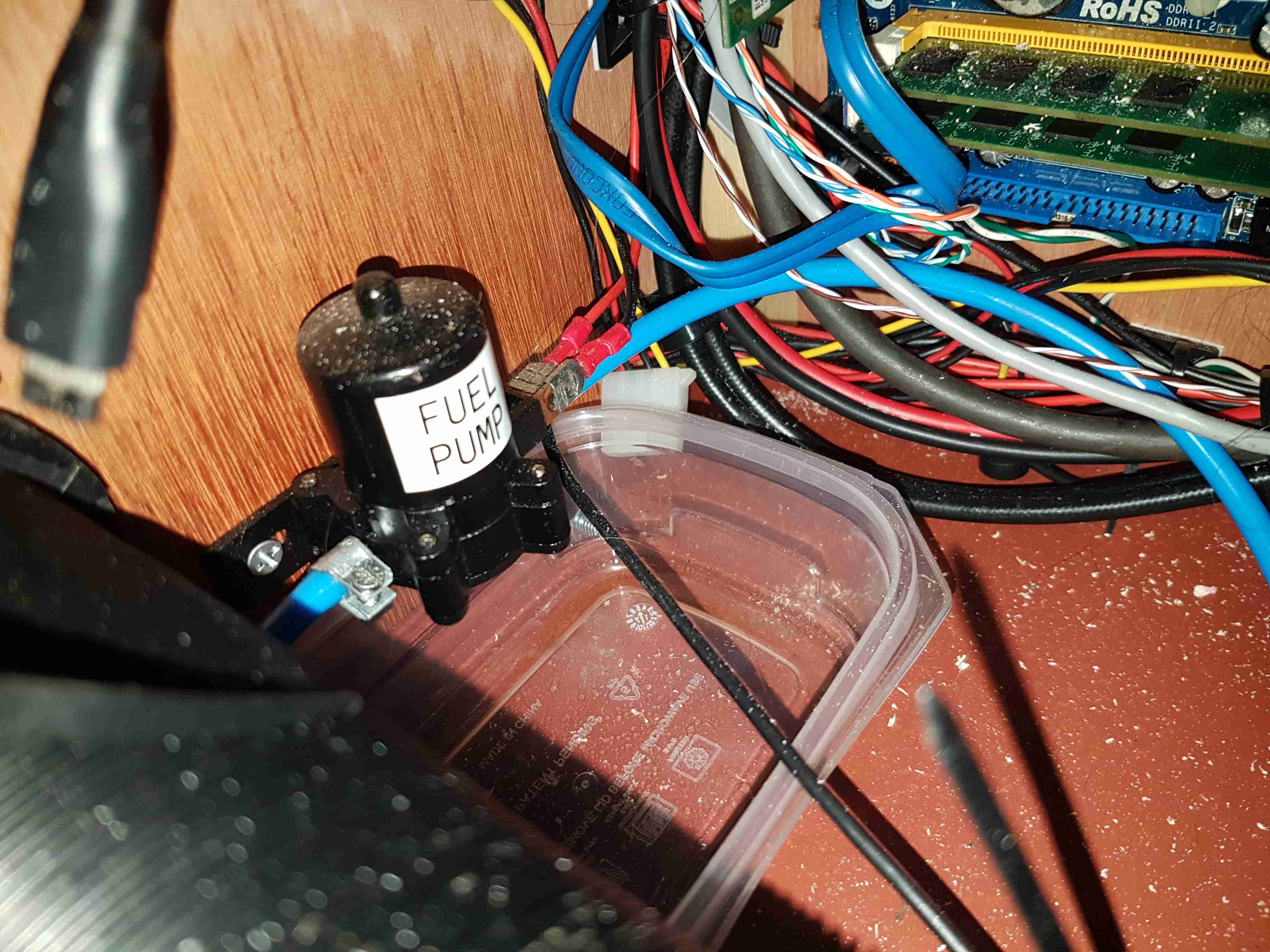
Fuel Pump
External fuelling is dealt with by a small gear pump, this is used to fuel up the Optimus Stove & Petromax Lantern. This is in fact a car windscreen wash pump, but it has coped well with pumping hydrocarbons, it currently has a small leak on the hose connections, but the seals are still entirely intact.
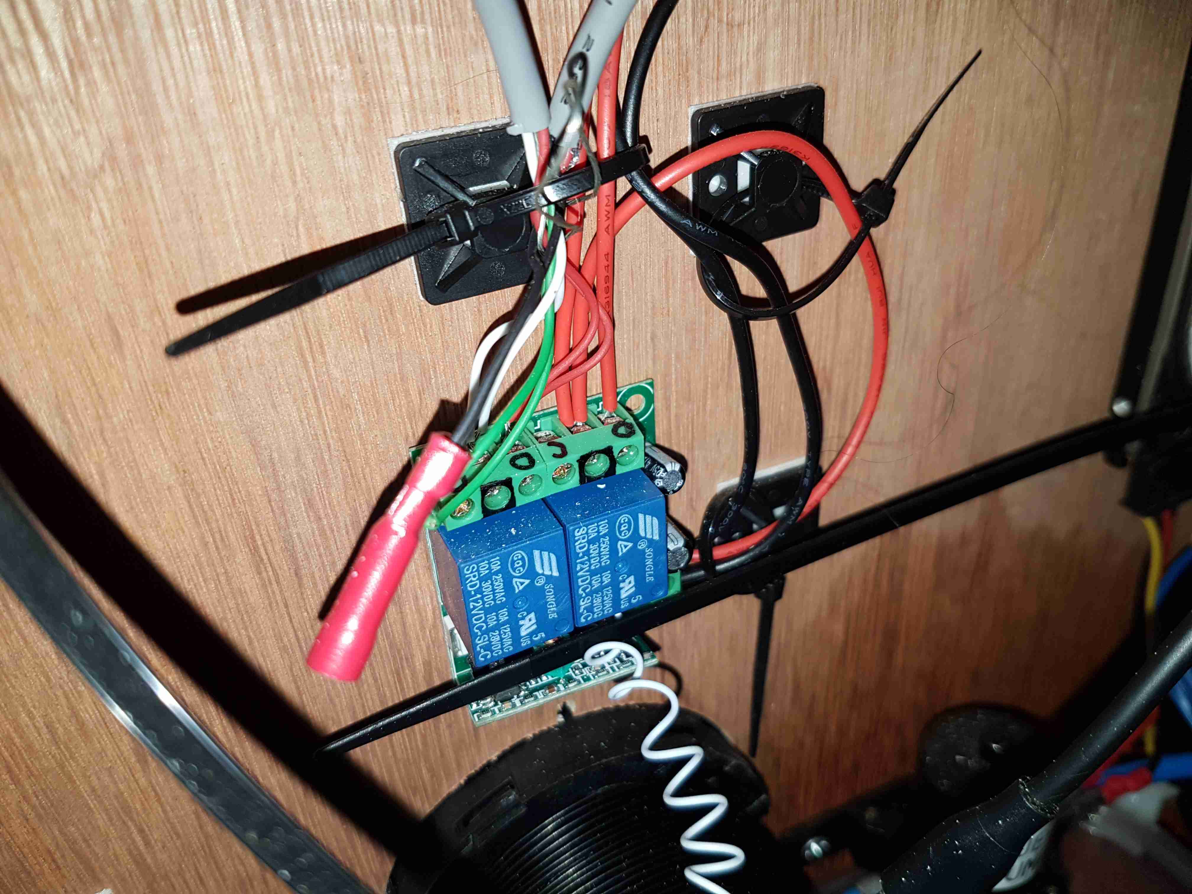
Remote Relays
There’s a small remote relay module here, for switching the DC output for lighting & the heater from afar. Very useful when it’s dark, since there’s no need to fumble around looking for a light switch. A car-style fob on my keyring instead.
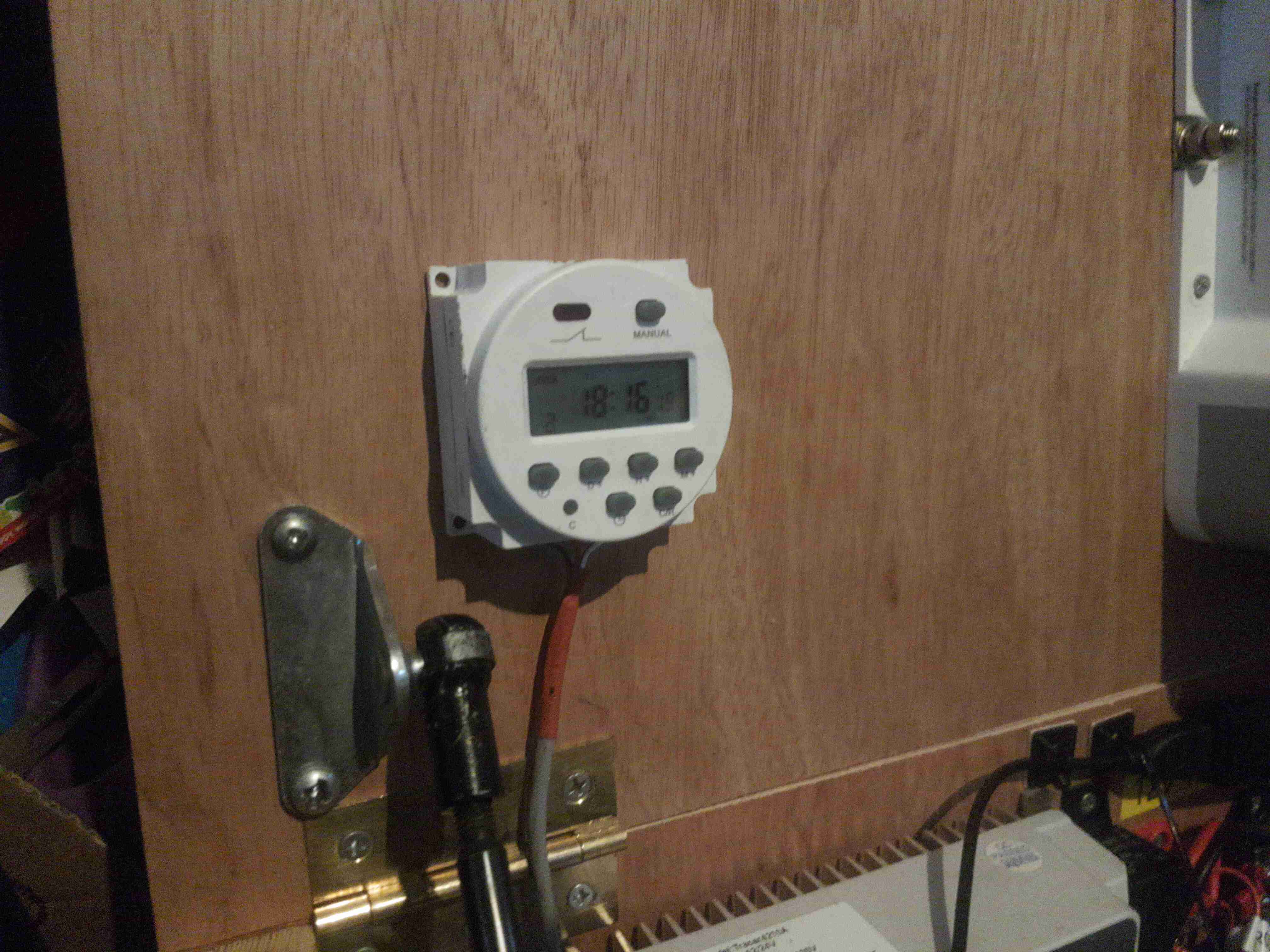
Heater Timer
Since the Eberspacher 701 controller I have is an ex-BT version, it’s very limited in it’s on time, a separate timeswitch is fitted to control the heater automatically. Being able to return to a nice warm tent is always a bonus.
Just to the left can be seen the top ball joint for the hydraulic cylinder that lifts the top of the box.
Battery Charger
The final large component is the battery charger. This unit will maintain the battery when the trolley isn’t being used.
Router Motherboard
On the left side is the old Atom motherbaord used to provide a 4G router system. This unit gets it’s internet feed from a UMTS dongle & provides a local WiFi network for high speed connectivity. The bottom of the hydraulic cylinder is visible in the bottom right corner.
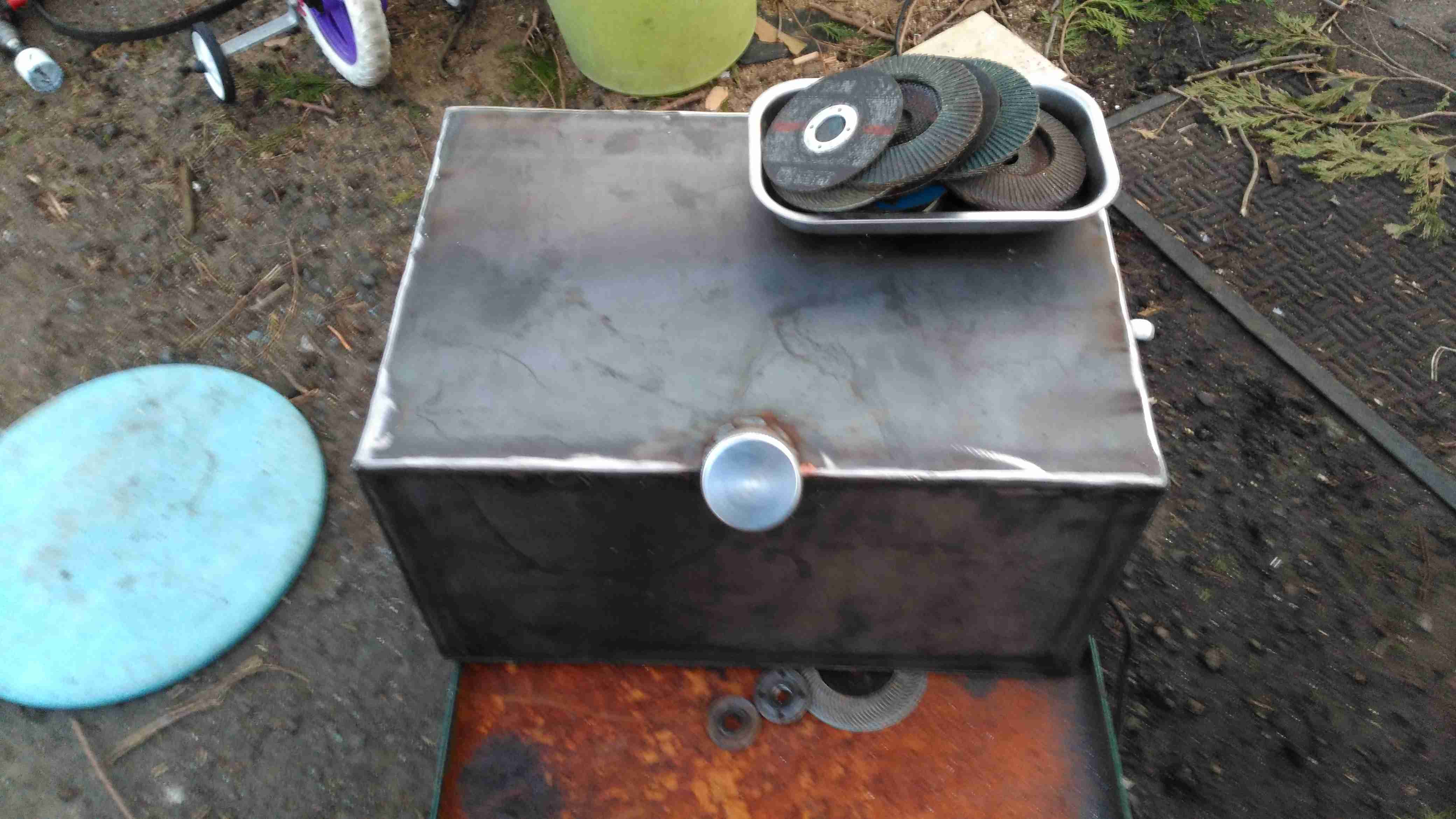
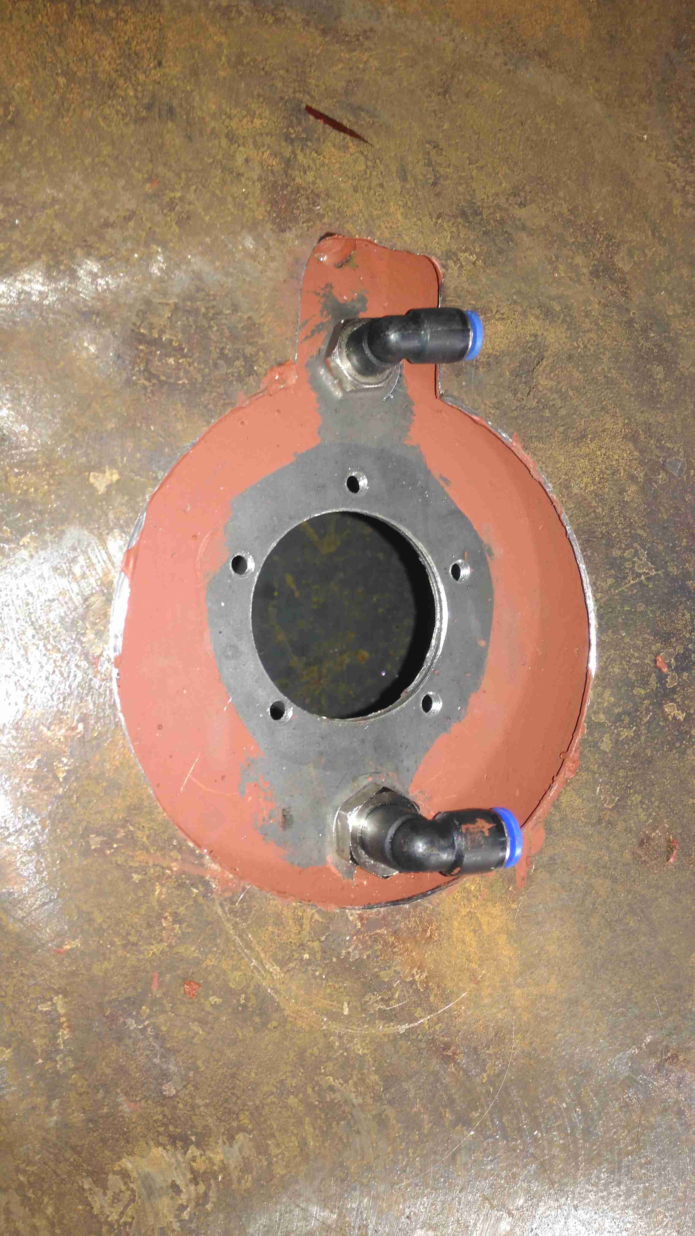
Fuel Tank Completed
Since the Eberspacher obviously needs fuel, a tank was required. In previous years I’ve used jerry cans for this purpose, but this trolley is supposed to have everything onboard, for less setup time. The tank is constructed from 3mm steel plate, MIG welded together at the seams to create a ~40L capacity. The filler neck is an eBay purchase in Stainless Steel. No photos of the tank being welded together, as I was aiming to beat sunset & it’s very difficult to operate a camera with welding gauntlets on 😉
The tank is the same width as the trolley frame, so some modification was required, having the wheels welded directly to the sides of the tank. This makes the track wider at the rear, increasing stability.
Fuel Dip Tubes
A quick view inside the tank through the level sender port shows the copper dip tubes for fuel supply to the heater, and an external fuel hose for my other fuel-powered camping gear. These tubes stop about 10mm from the bottom of the tank to stop any moisture or dirt from being drawn into the pumps.
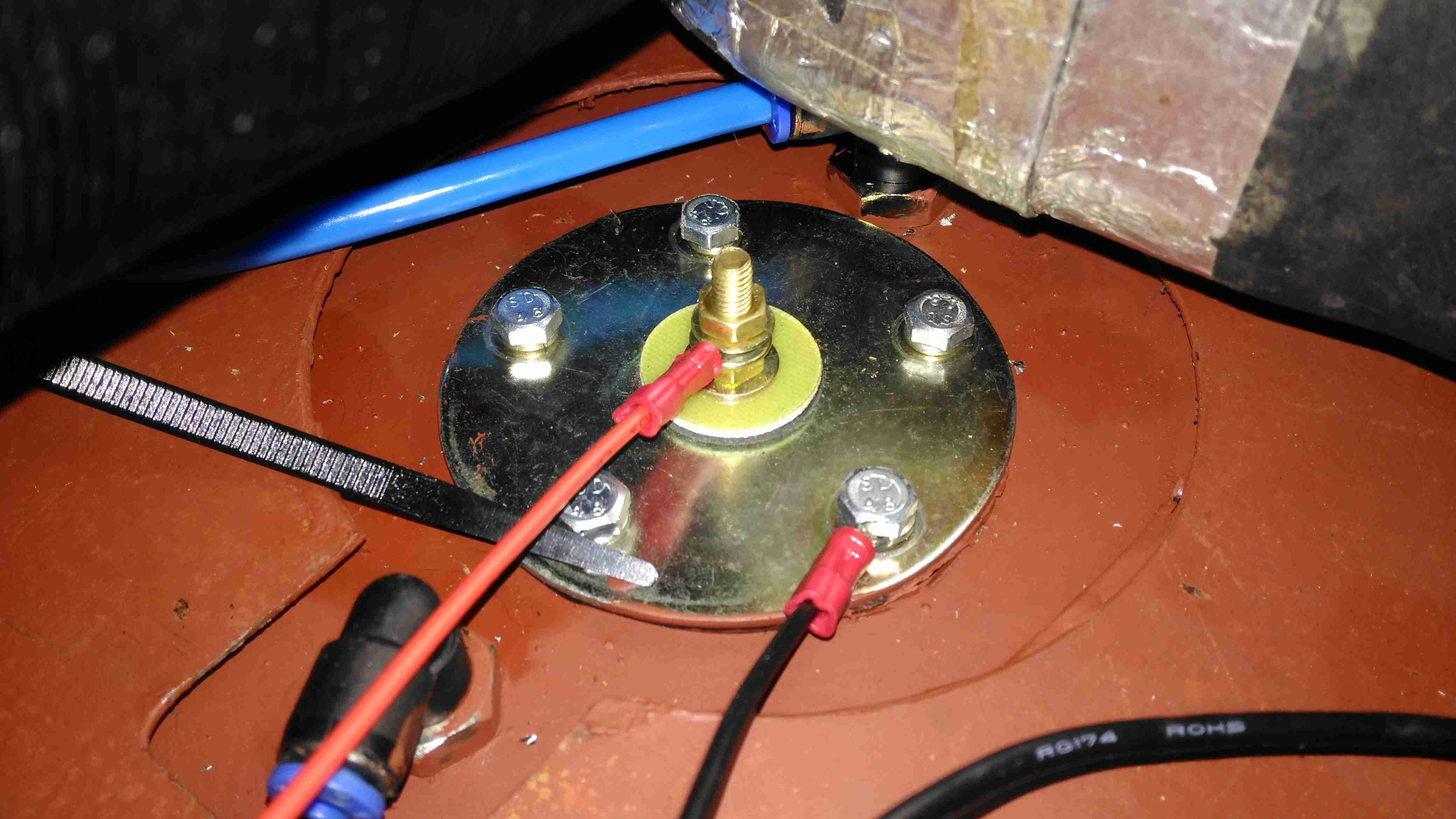
Fuel Feeds & Level Sender Port
The top of the tank is drilled for the fuel fittings & the level sender and has already been painted here. The 1mm base plate has yet to be painted.
Level Sender Installed
Touching up the paint & fitting the sender is the last job for this part. The mesh bottom of the trolley has been replaced by a 1mm steel sheet to support the other parts, mainly the heater. Fuel lines are run in polyurethane tubing to the fuel pumps.
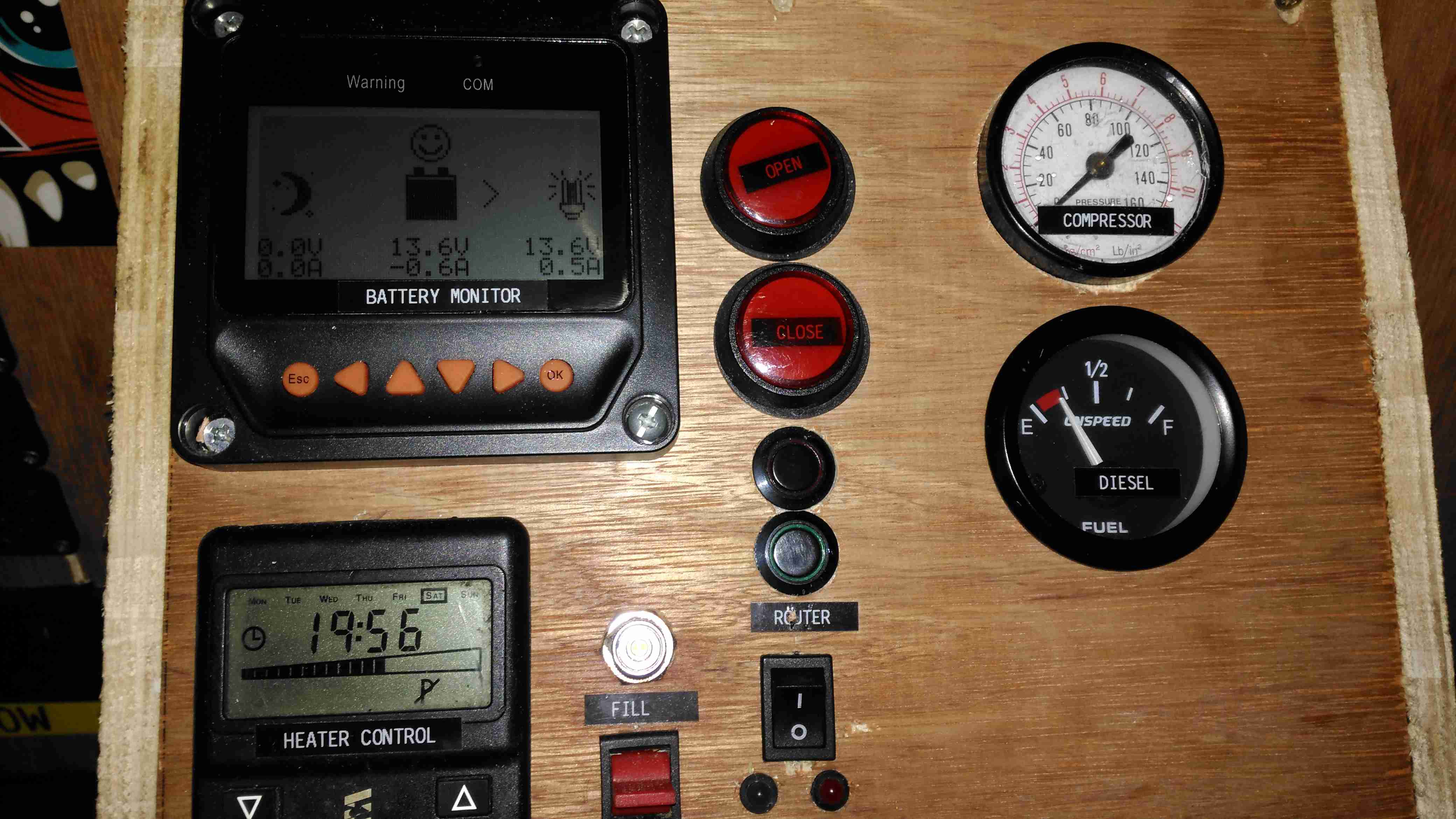
All the instruments & controls are on a single panel, with the Eberspacher thermostat, external fuelling port & pump switch, inverter control, the solar controller monitor panel, cover buttons, router controls, compressed air & fuel gauges.
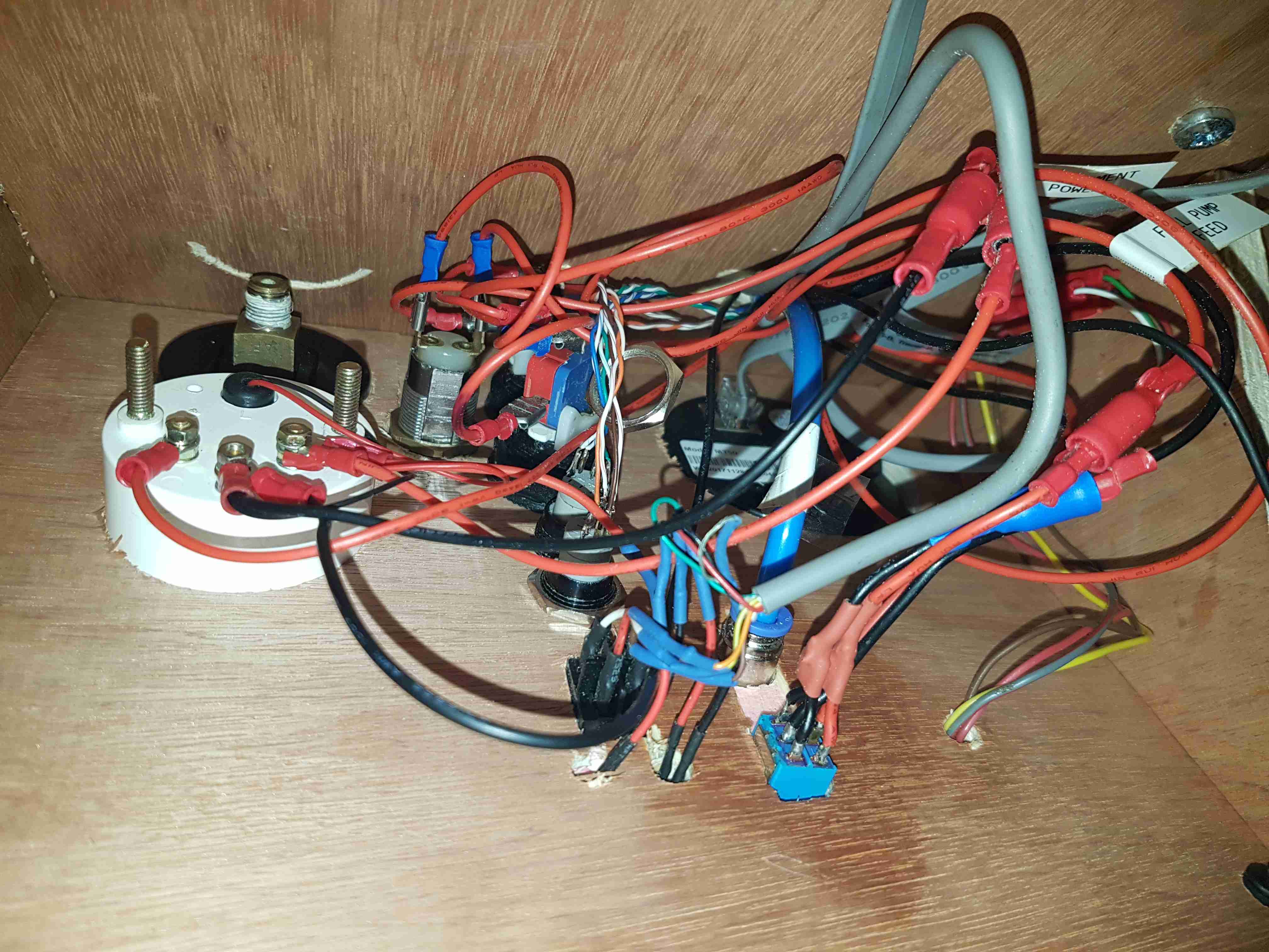
Panel Wiring
As is usual behind instrument panels, there’s a rat’s nest of wiring. There’s still the pressure gauge to connect up for the compressed air system, and the nut on one of the router buttons is such a tight fit I’ve not managed to get it into place yet.
Eberspacher Fuel Pump
The support components for the Eberspacher heater are mounted underneath the baseplate, with the fuel dosing pump secured to a rail with a pair of cable ties, and some foam tape around to isolate the constant clicking noise these pumps create in operation. The large black cylinder is the combustion air intake silencer, with the stainless steel exhaust pipe to the left of that. Silencing these heaters is essential – they sound like a jet engine without anything to deaden the noise. Most of this is generated from the side-channel blower used in the burner.
Eberspacher Exhaust
Bolted to the underside are a pair of exhaust silencers, one is an Eberspacher brand, the other is Webasto, since the latter type are better at reducing the exhaust noise. Connections are sealed with commerical exhaust assembly paste, the usual clamps supplied do not do a good enough job of stopping exhaust leaks.
Next update to come when I get the parts in for the air compressor system.
Since I seem to be the local go-to for any dead electrical equipment, this brand-new Silverline polisher has landed on my desk. Purchased cheap from an auction this was dead on arrival. Checking the fuse revealed nothing suspect, so a quick teardown to find the fault was required.
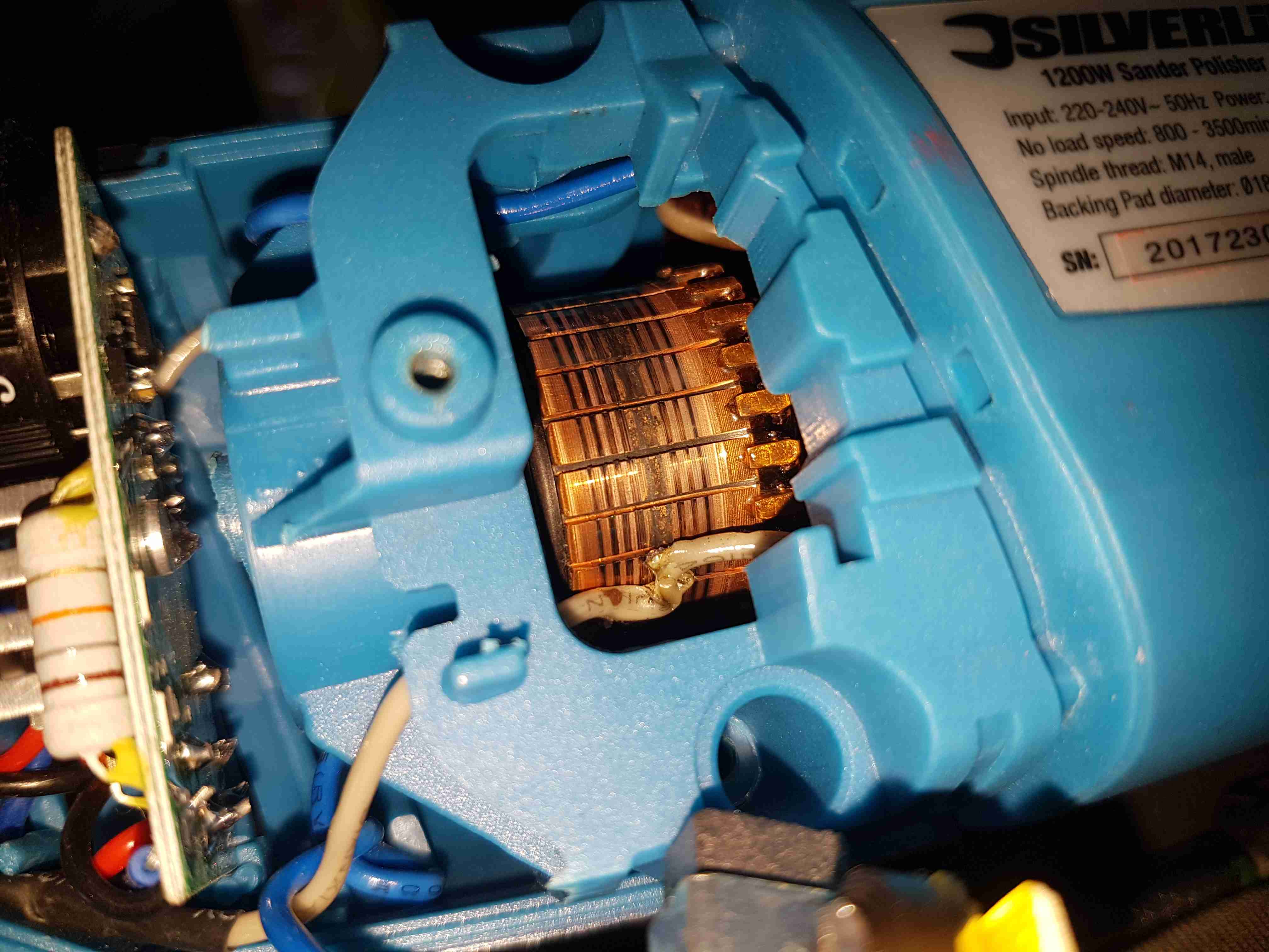
Above is a photo of the commutator with the brush holder removed, and the source of the issue. The connection onto the field winding of the universal motor has been left unsecured, as a result it’s managed to move into contact with the commutator.
This has done a pretty good job of chewing it’s way through the wire entirely. There is some minor damage to the commutator segments, but it’s still smooth, and shouldn’t damage the brushes.
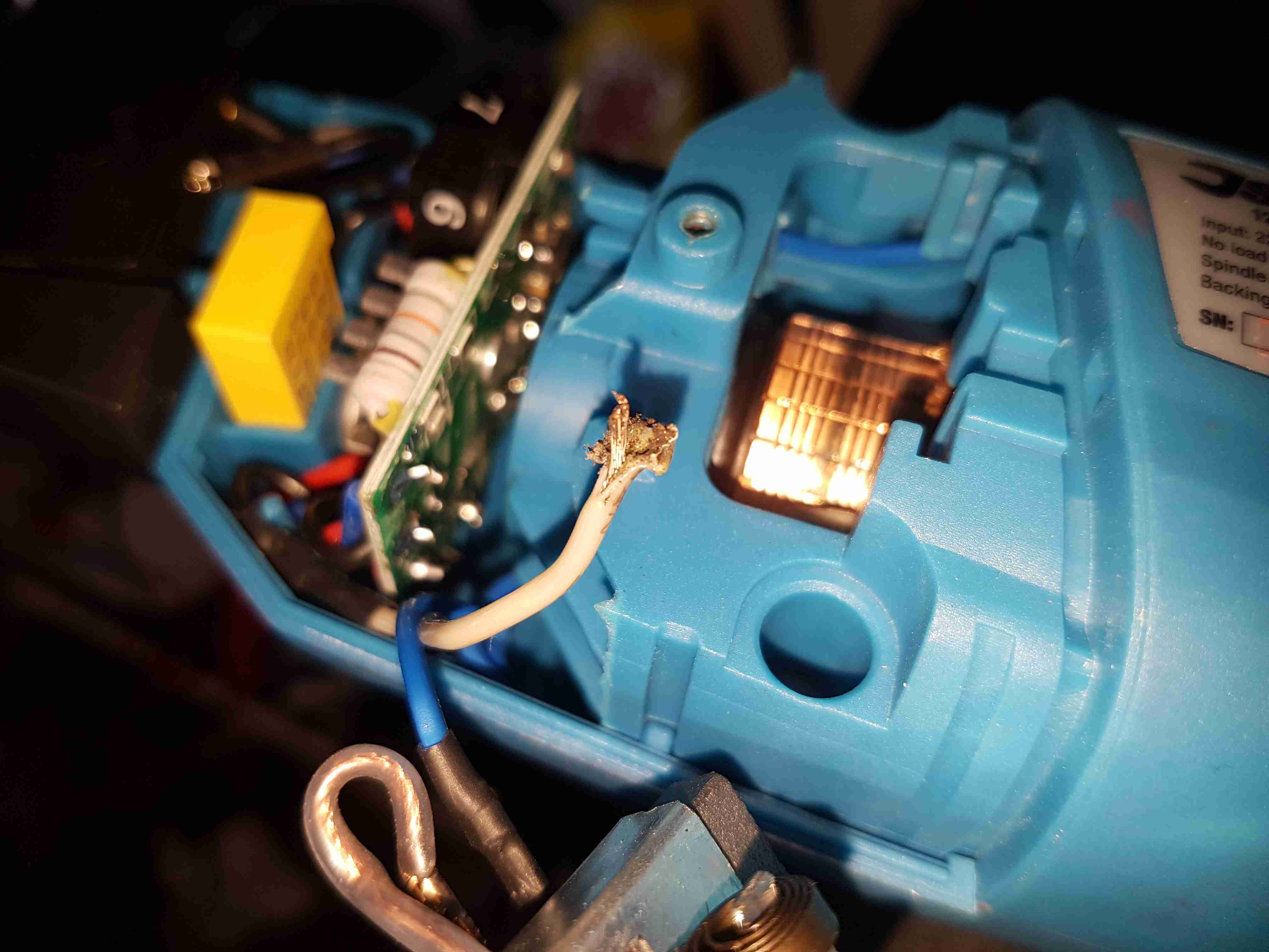
Chewed Wire
A quick pull on what’s left of the wire reveals the extent of the problem. It’s entirely burned through! Unfortunately the stator assembly with the field windings is pressed into the plastic housing, so it’s not removable. An in-place solder joint was required to the very short remains of the wire inside the housing. Once this was done the polisher sprang to life immediately, with no other damage.
This unit probably ended up at an auction as a factory reject, or a customer return to a retail outlet. If the latter, I would seriously question the quality control procedures of Silverline tools. 😉
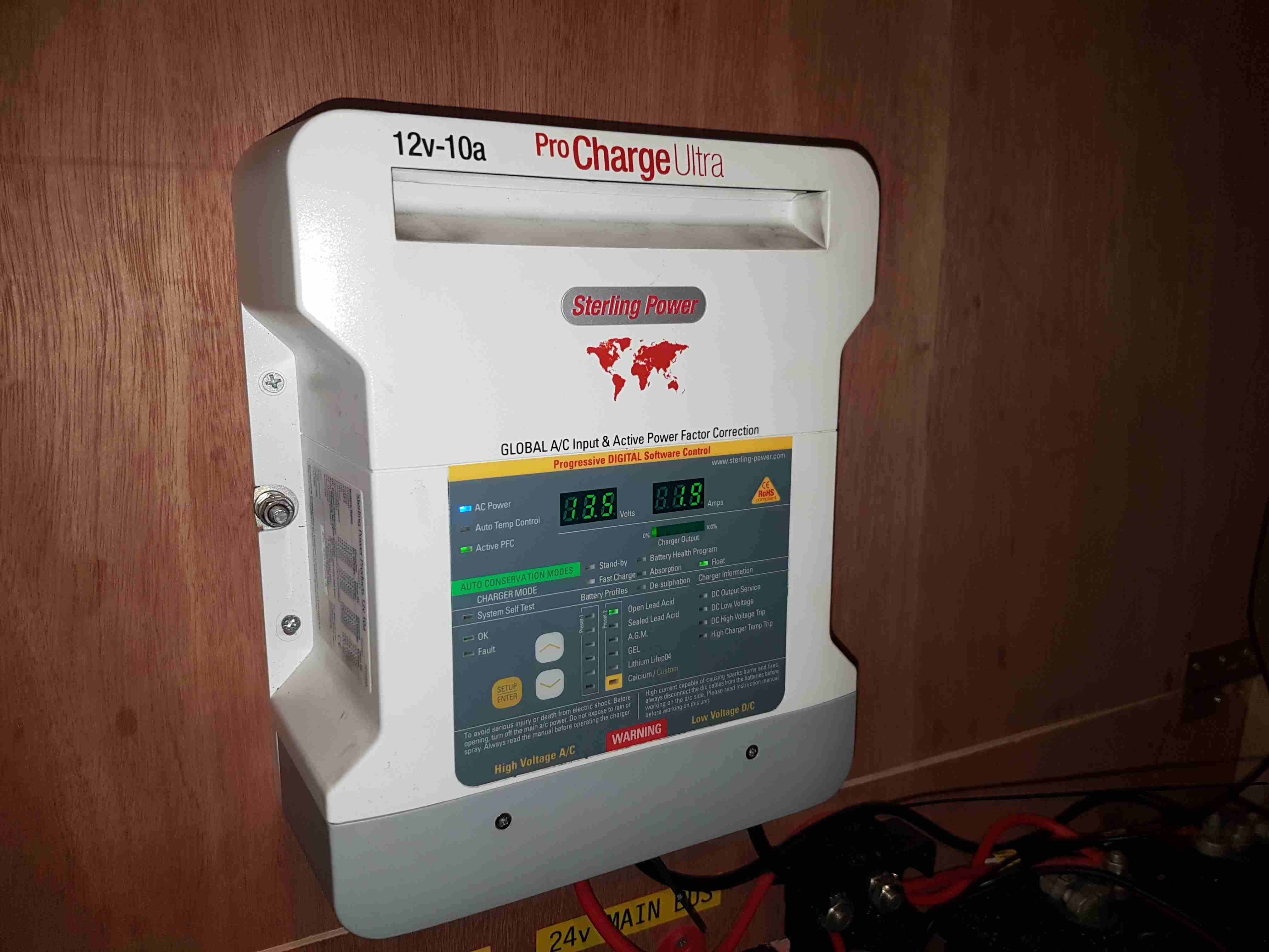
The Sterling charger we’ve had on board nb Tanya Louise since Feb 2014 has bitten the dust, with 31220 hours on it’s internal clock. Since we’re a liveaboard boat, this charger has had a lot of use while we’re on the mooring during winter, when the solar bank isn’t outputting it’s full rate. First, a bit of a teardown to explore the unit, then onto the repair:
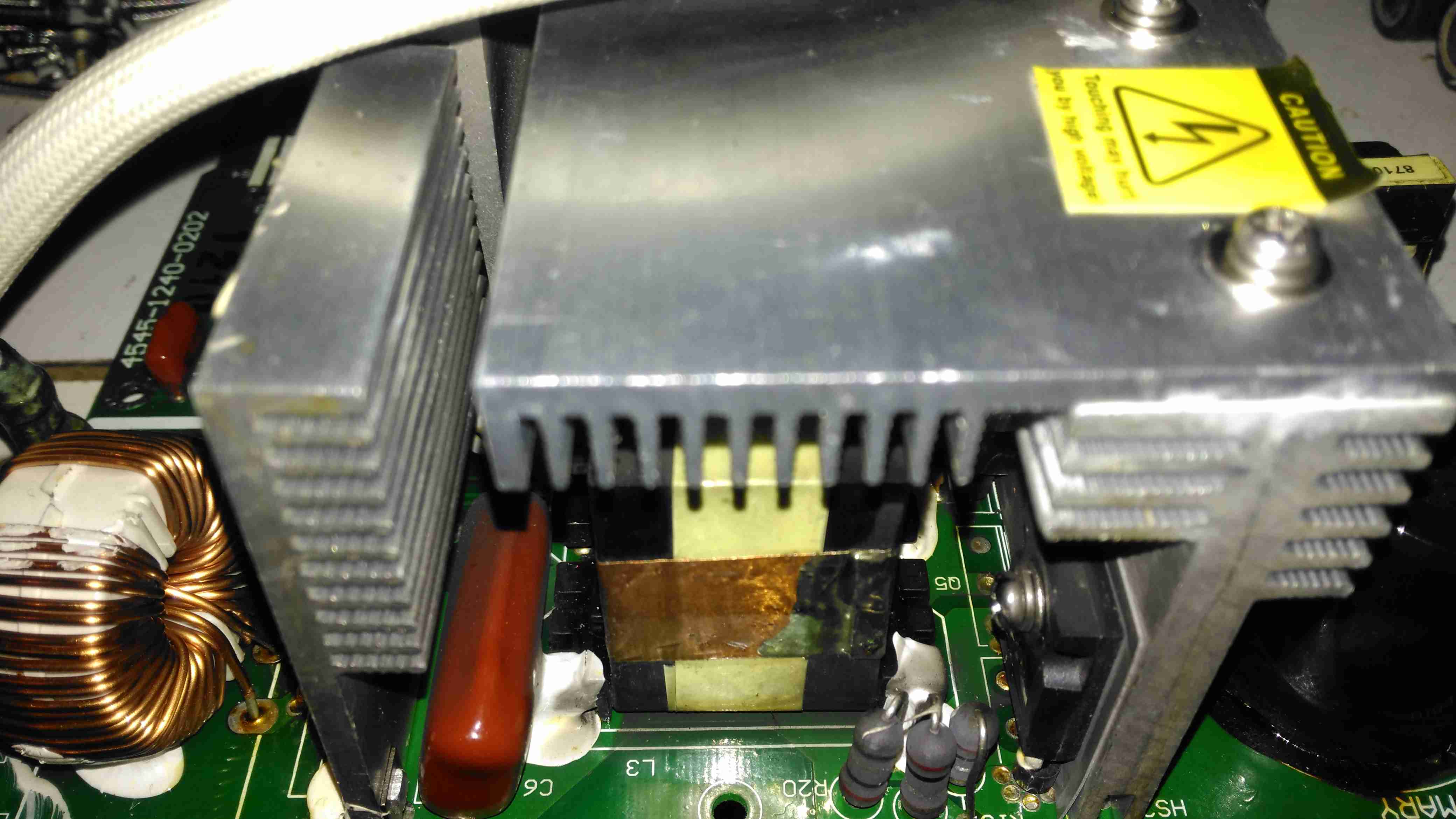
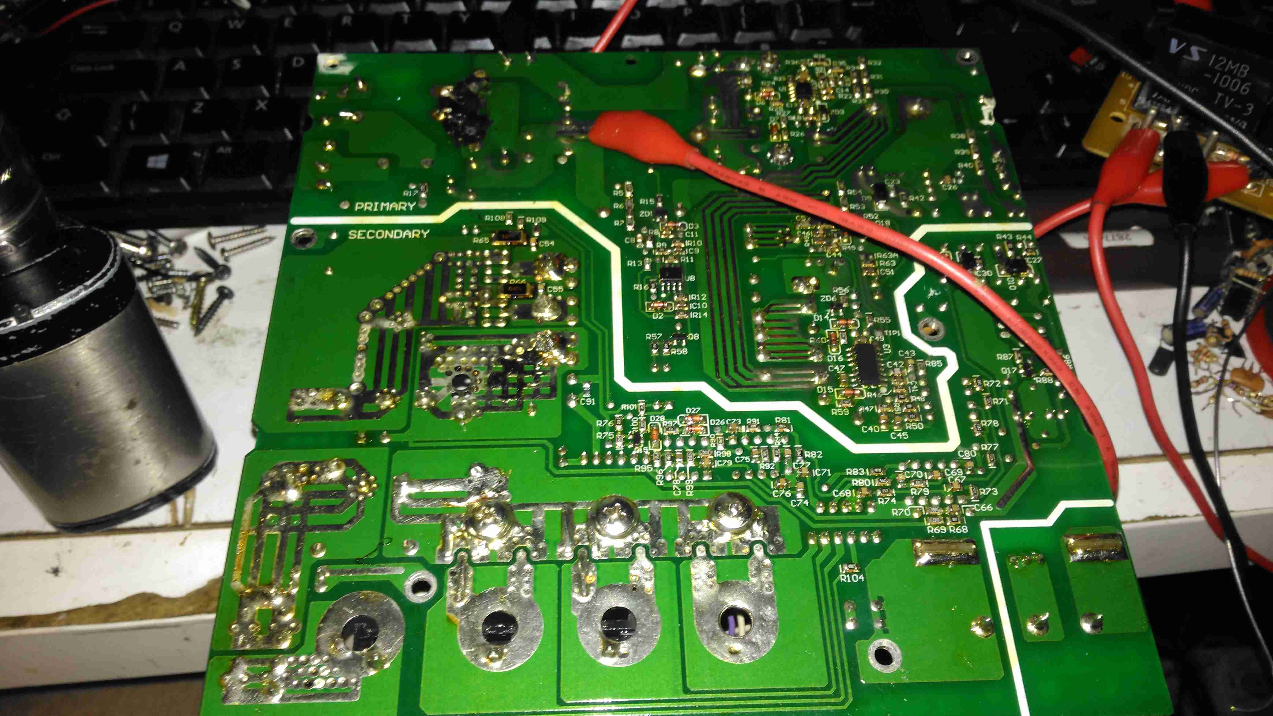
Active PFC Section
There’s the usual mains input filtering on the left, with the bridge rectifier on it’s heatsink.
Underneath the centre massive heatsinks is the main transformer (not visible here) & active PFC circuit. The device peeking out from underneath is the huge inductor needed for PFC. It’s associated switching MOSFET is to the right.
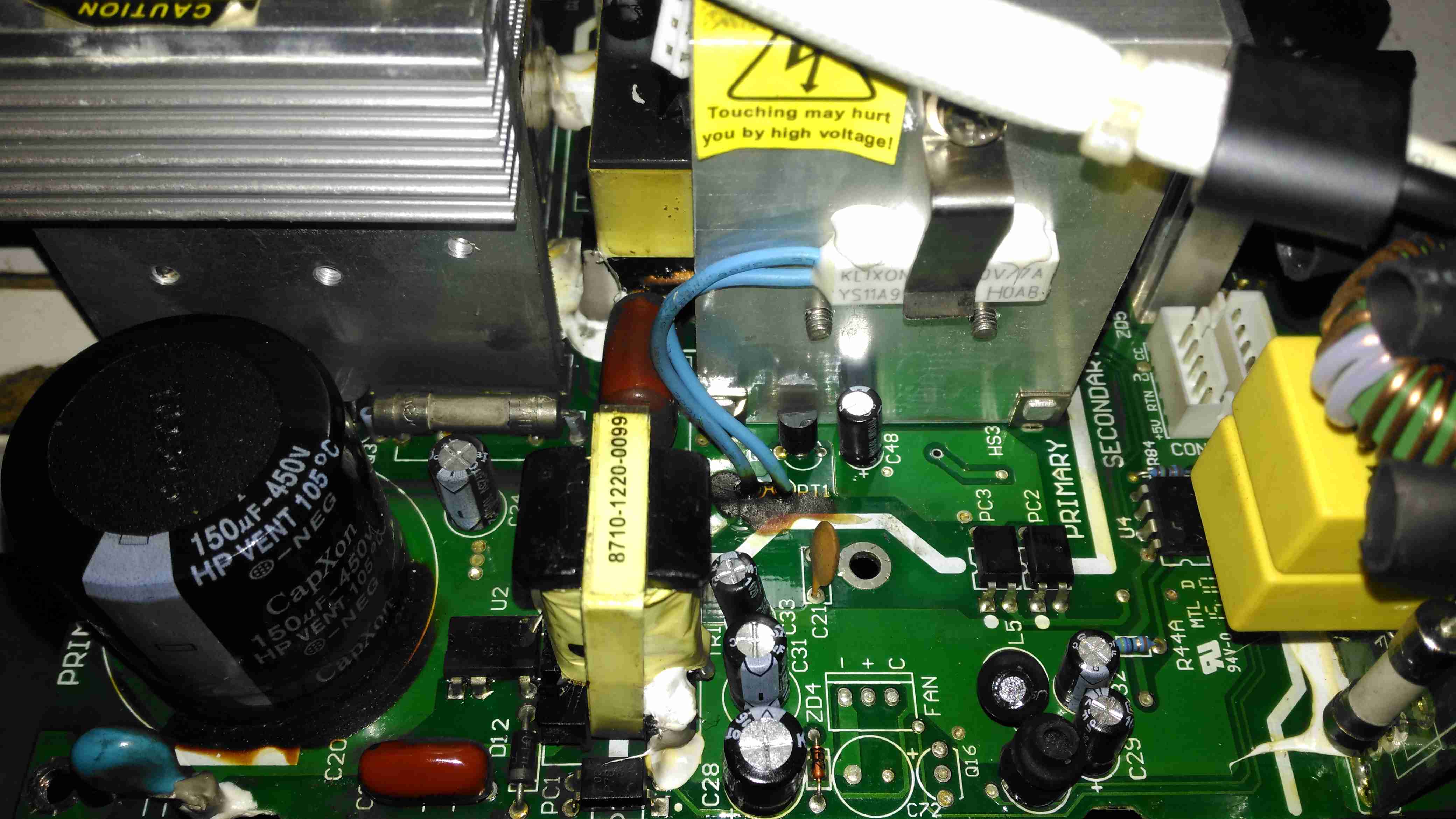
Logic PSU Section
On the other side of the PFC section is the main DC rail filter electrolytic, a 450v 150µF part. Here some evidence of long-term heating can be seen in the adhesive around the base, it’s nearly completely turned black! It’s not a decent brand either, a Chinese CapXon.
The PCB fuse just behind it is in the DC feed to the main switching supply, so the input fuse only protects the filter & Active PFC circuitry. Luckily this fuse didn’t blow during the failure, telling me the fault was earlier in the power chain.
The logic circuits are powered by an independent switching supply in the centre, providing a +5v rail to the microcontroller. The fan header & control components are not populated in this 10A model, but I may end up retrofitting a fan anyway as this unit has always run a little too warm. The entire board is heavily conformal coated on both sides, to help with water resistance associated with being in a marine environment. This has worked well, as there isn’t a single trace of moisture anywhere, only dust from years of use.
There is some thermal protection for the main SMPS switching MOSFETS with the Klixon thermal fuse clipped to the heatsink.
DC Output Section
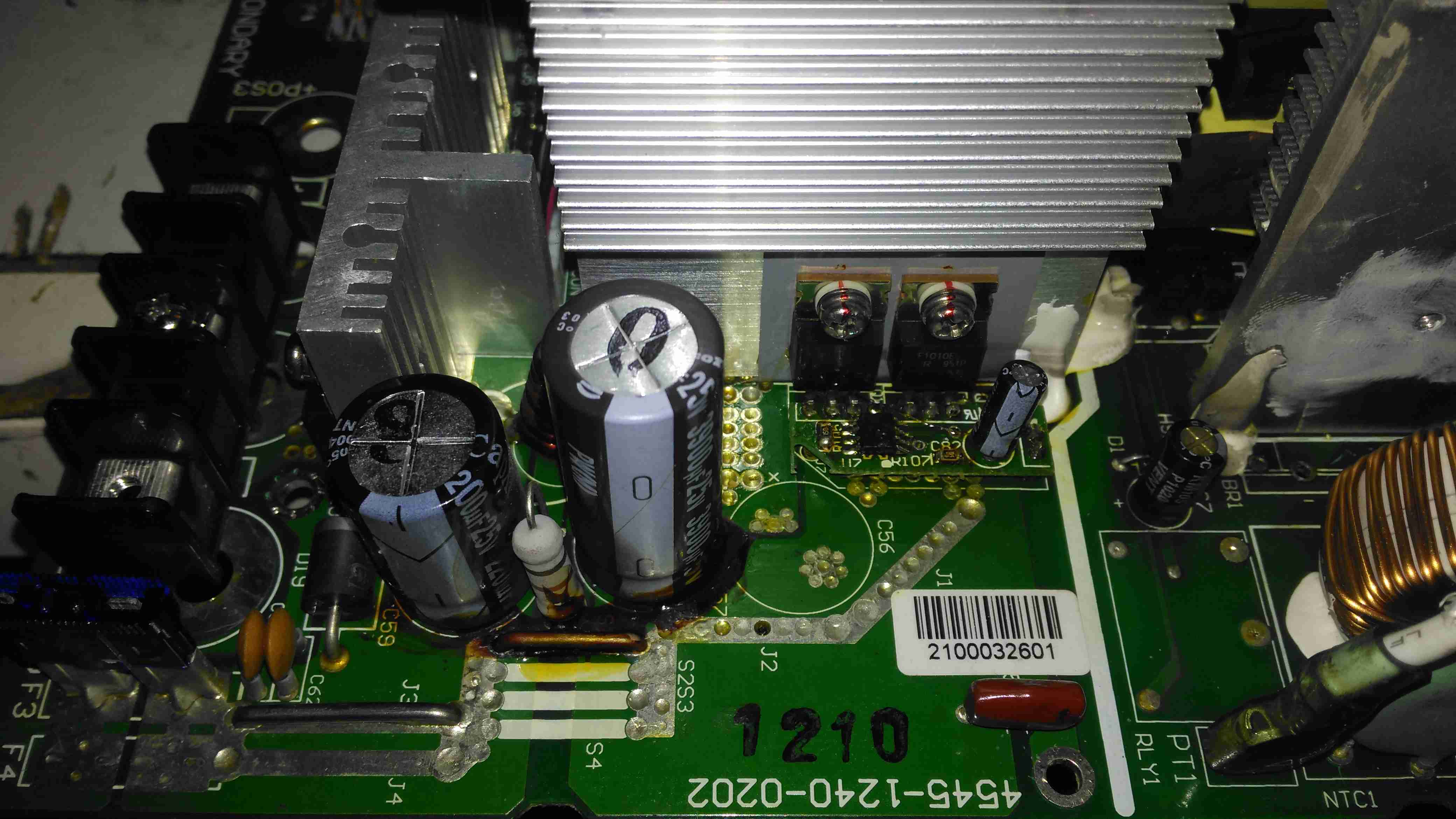
The DC output rectifiers are on the large heatsink in the centre, with a small bodge board fitted. Due to the heavy conformal coating on the board I can’t get the ID from this small 8-pin IC, but from the fact that the output rectifiers are in fact IRF1010E MOSFETS, rated at 84A a piece, this is an synchronous rectifier controller.
Oddly, the output filter electrolytics are a mix of Nichicon (nice), and CapXon (shite). A bit of penny pinching here, which if a little naff since these chargers are anything but cheap. (£244.80 at the time of writing).
Hiding just behind the electrolytics is a large choke, and a reverse-polarity protection diode, which is wired crowbar-style. Reversing the polarity here will blow the 15A DC bus fuse instantly, and may destroy this diode if it doesn’t blow quick enough.
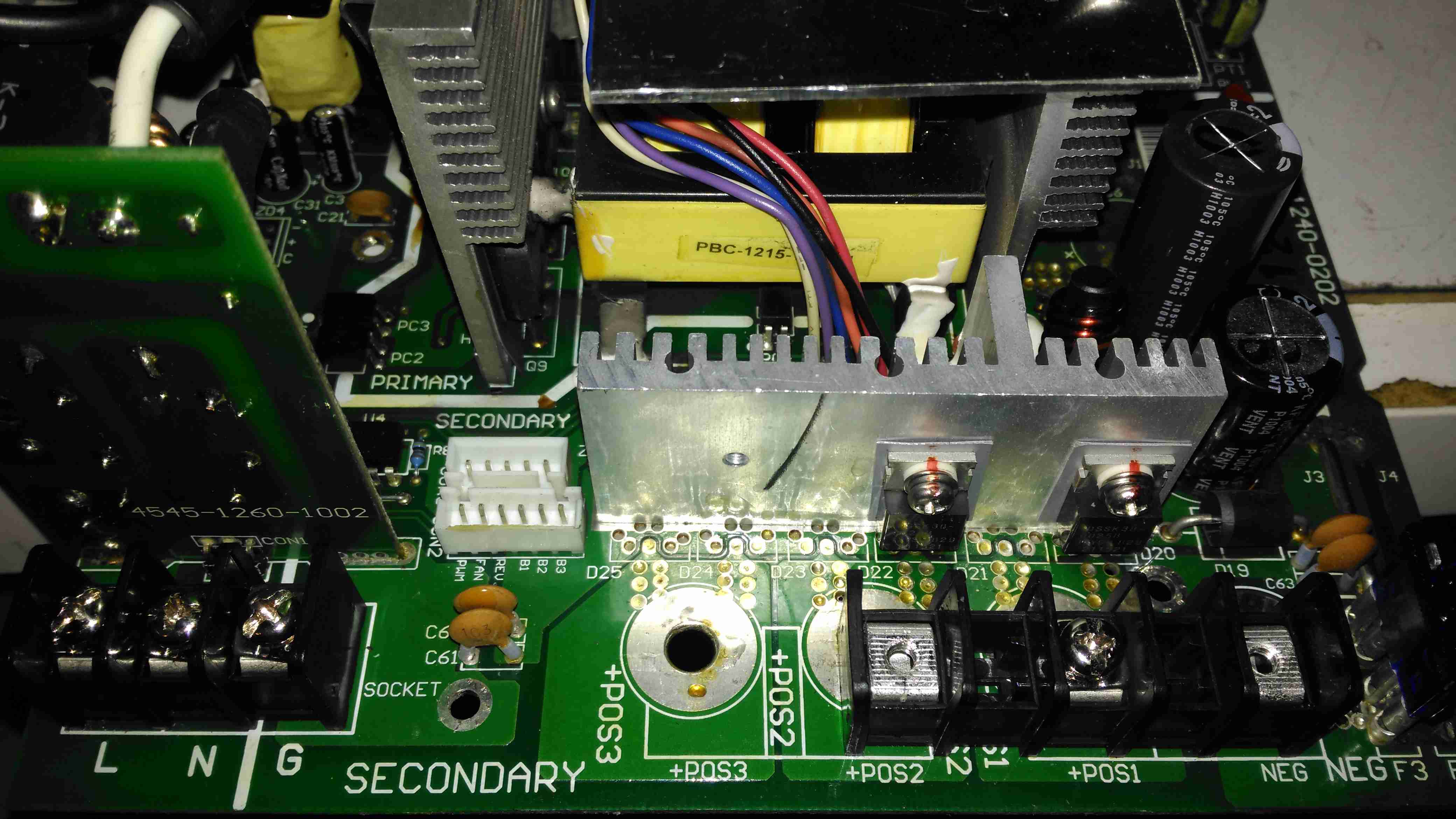
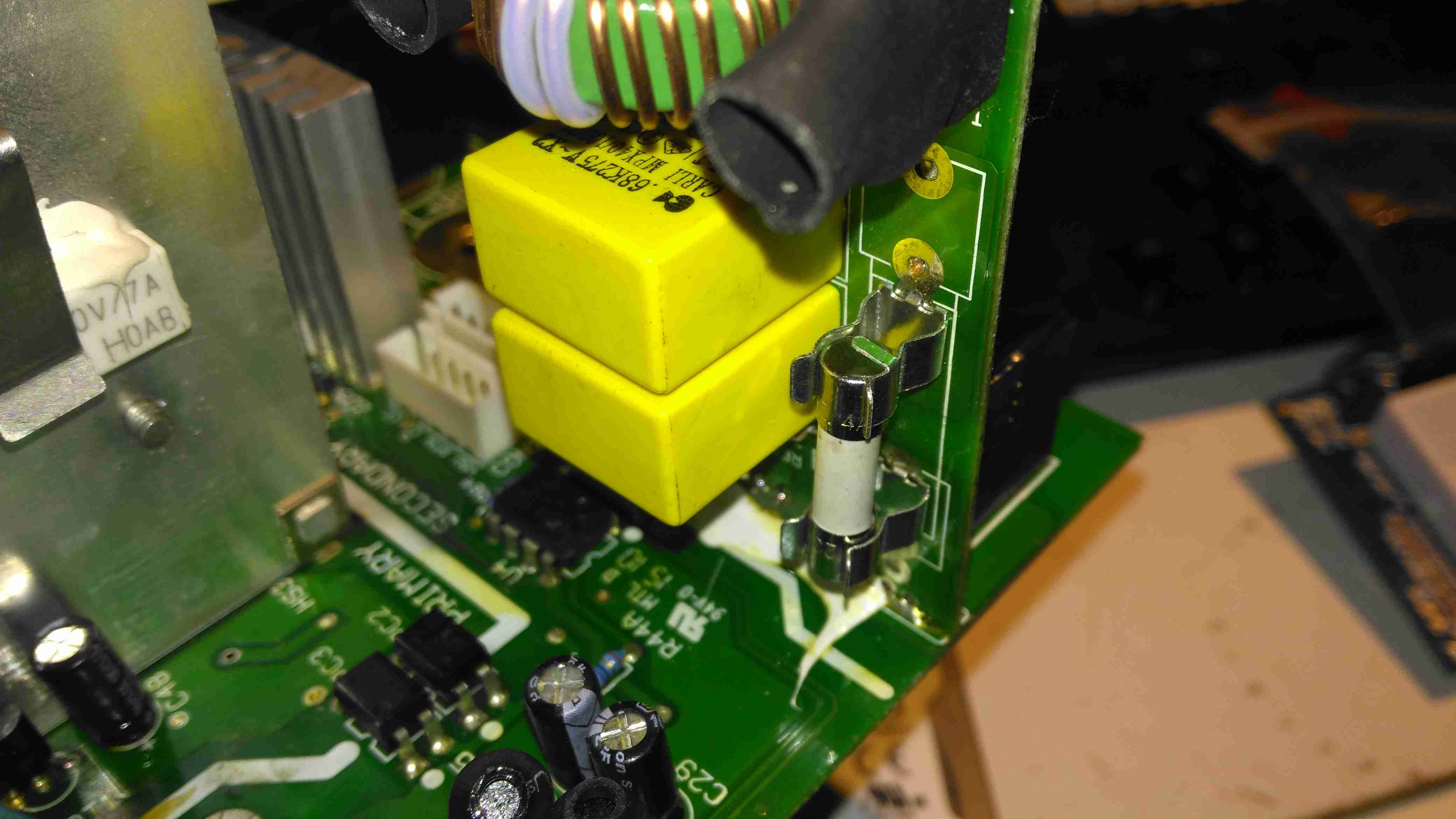
DC Outputs
Right on the output end are a pair of large Ixys DSSK38 TO220 Dual 20A dual Schottky diodes, isolating the two outputs from each other, a nice margin on these for a 10A charger, since the diodes are paralleled each channel is capable of 40A. This prevents one bank discharging into another & allows the charger logic to monitor the voltages individually. The only issue here is the 400mV drop of these diodes introduce a little bit of inefficiency. To increase current capacity of the PCB, the aluminium heatsink is being used as the main positive busbar. From the sizing of the power components here, I would think that the same PCB & component load is used for all the chargers up to 40A, since both the PFC inductor & main power transformer are massive for a 10A output. There are unpopulated output components on this low-end model, to reduce the cost since they aren’t needed.
Front Panel Control Connections
A trio of headers connect all the control & sense signals to the front panel PCB, which contains all the control logic. This unit is sensing all output voltages, output current & PSU rail voltages.
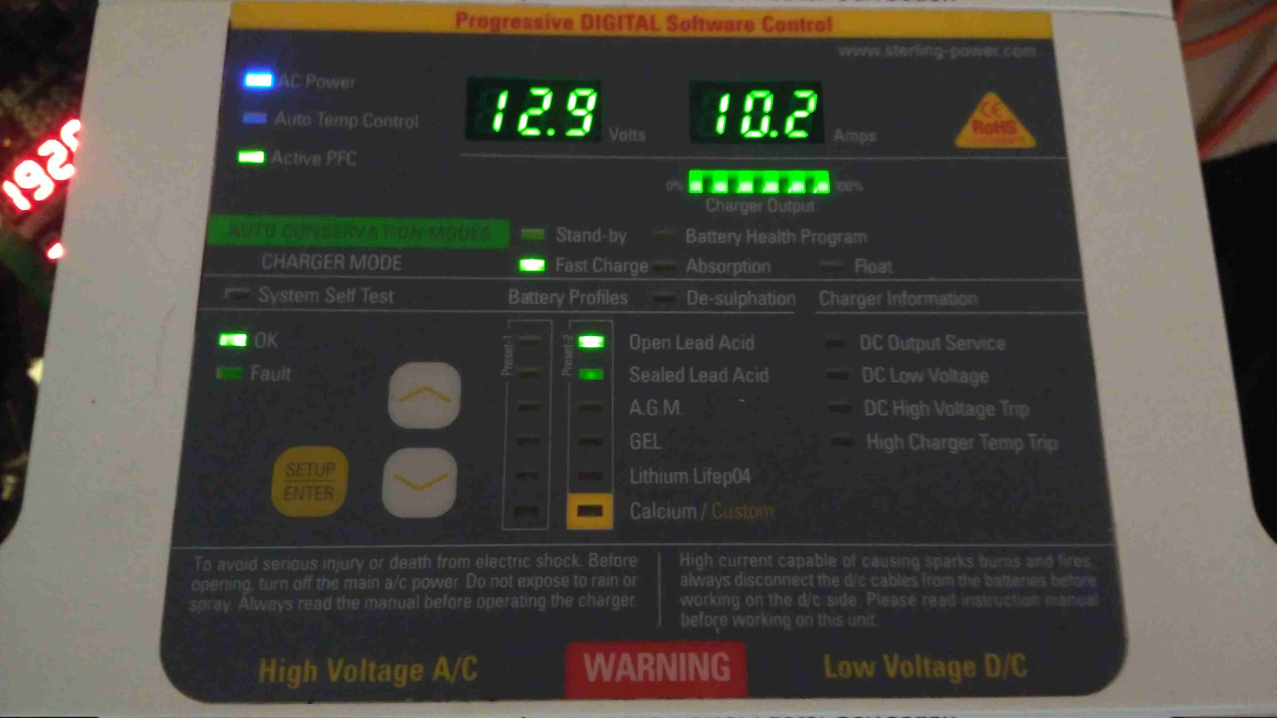
Front Panel LEDs
The front panel is stuffed with LEDs & 7-segment displays to show the current mode, charging voltage & current. There’s 2 tactile switches for adjustments.
Front Panel Reverse
The reverse of the board has the main microcontroller – again identifying this is impossible due to the heavy conformal coat. The LEDs are being driven through a 74HC245D CMOS Octal Bus Transceiver.
Now on to the repair! I’m not particularly impressed with only getting 4 years from this unit, they are very expensive as already mentioned, so I would expect a longer lifespan. The input fuse had blown in this case, leaving me with a totally dead charger. A quick multimeter test on the input stage of the unit showed a dead short – the main AC input bridge rectifier has gone short circuit.
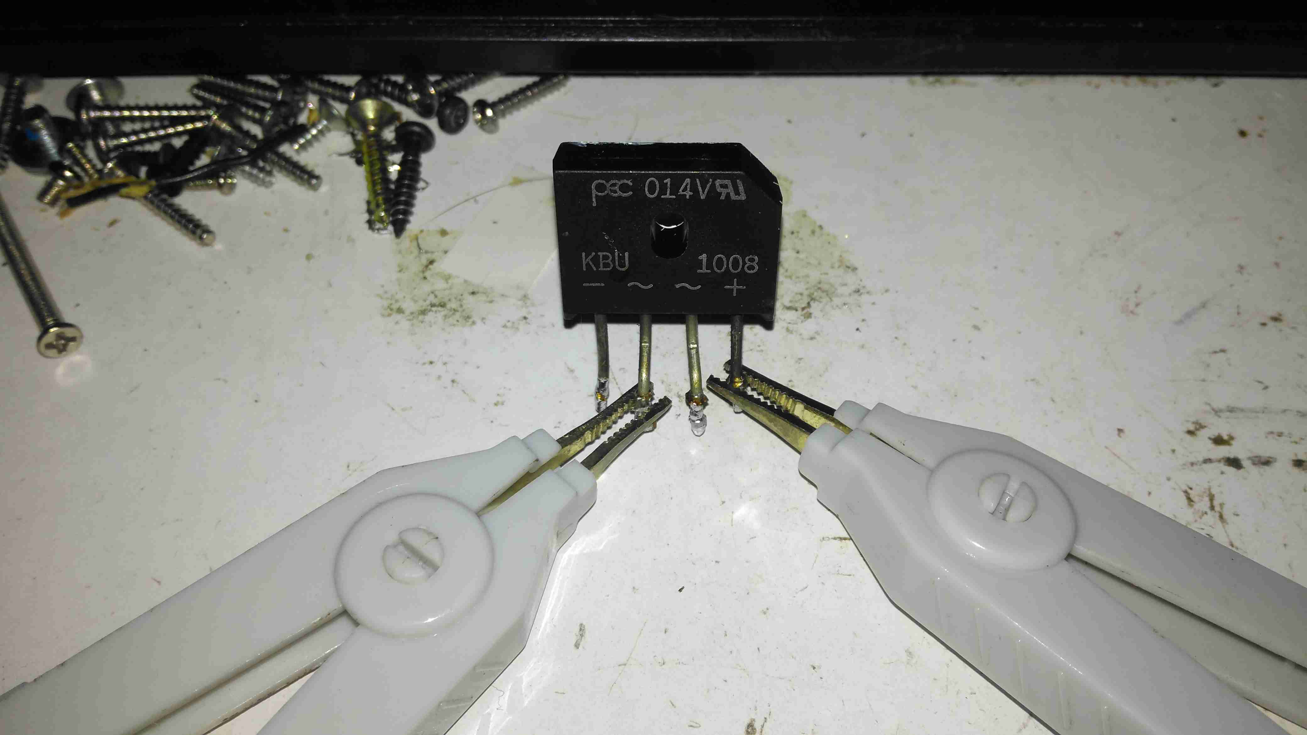
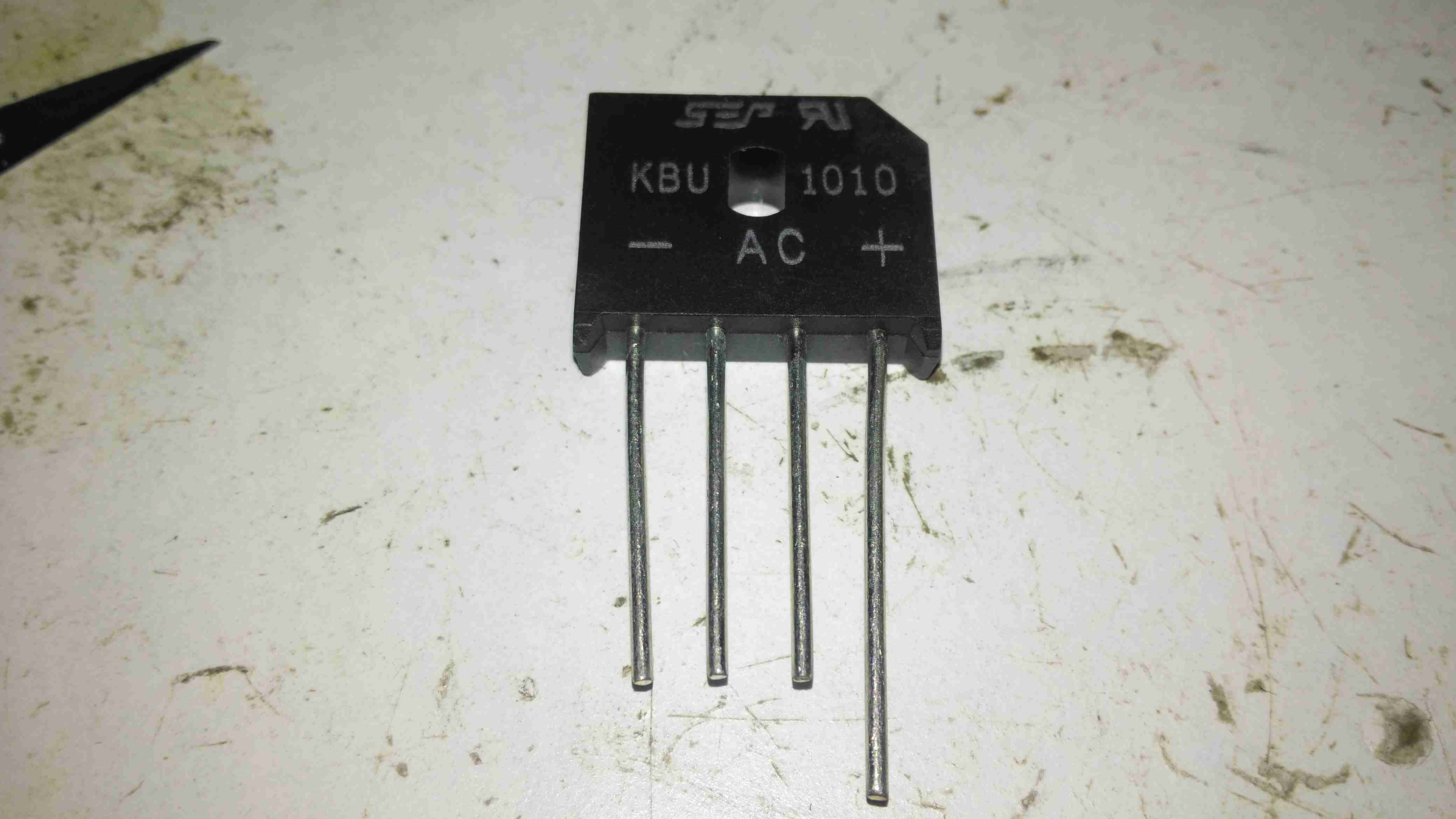
Bridge Rectifier Removed
Here the defective bridge has been desoldered from the board. It’s a KBU1008 10A 800v part. Once this was removed I confirmed there was no longer an input short, on either the AC side or the DC output side to the PFC circuit.
Testing The Rectifier
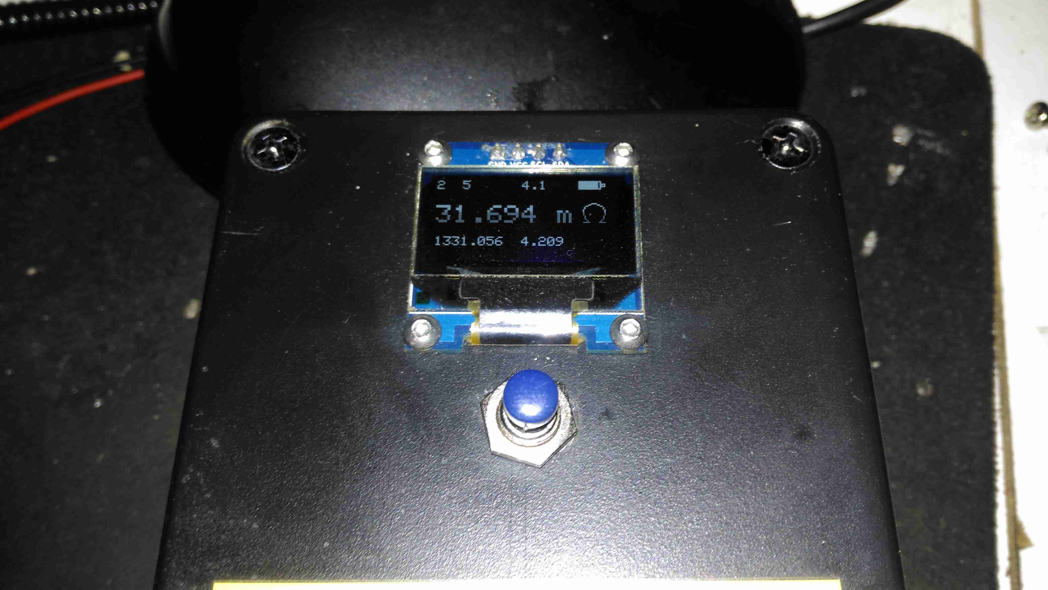
Time to stick the desoldered bridge on the milliohm meter & see how badly it has failed.
Yep, Definitely Shorted
I’d say 31mΩ would qualify as a short. It’s no wonder the 4A input fuse blew instantly. There is no sign of excessive heat around the rectifier, so I’m not sure why this would have failed, it’s certainly over-rated for the 10A charger.
Testing Without Rectifier
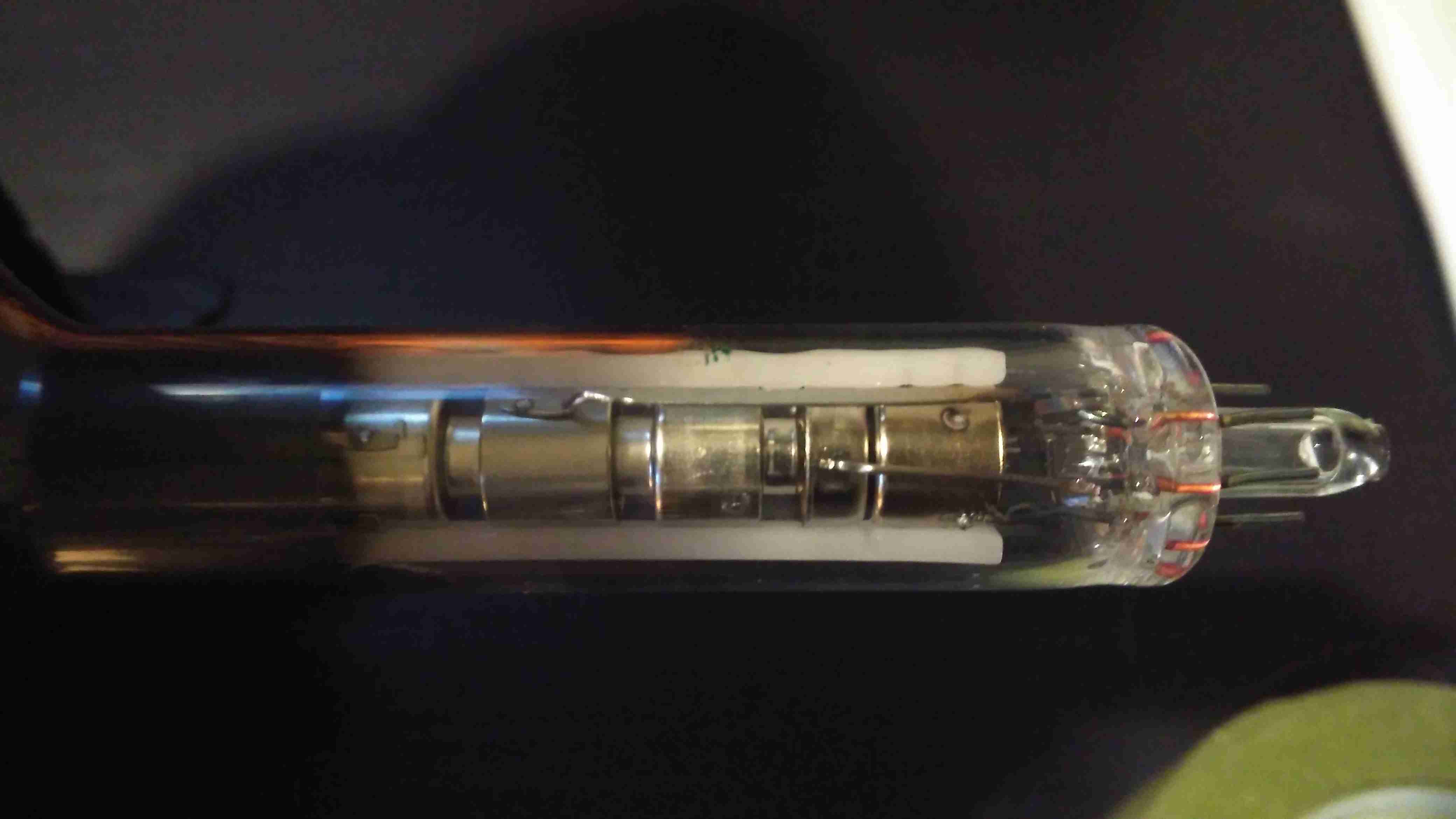
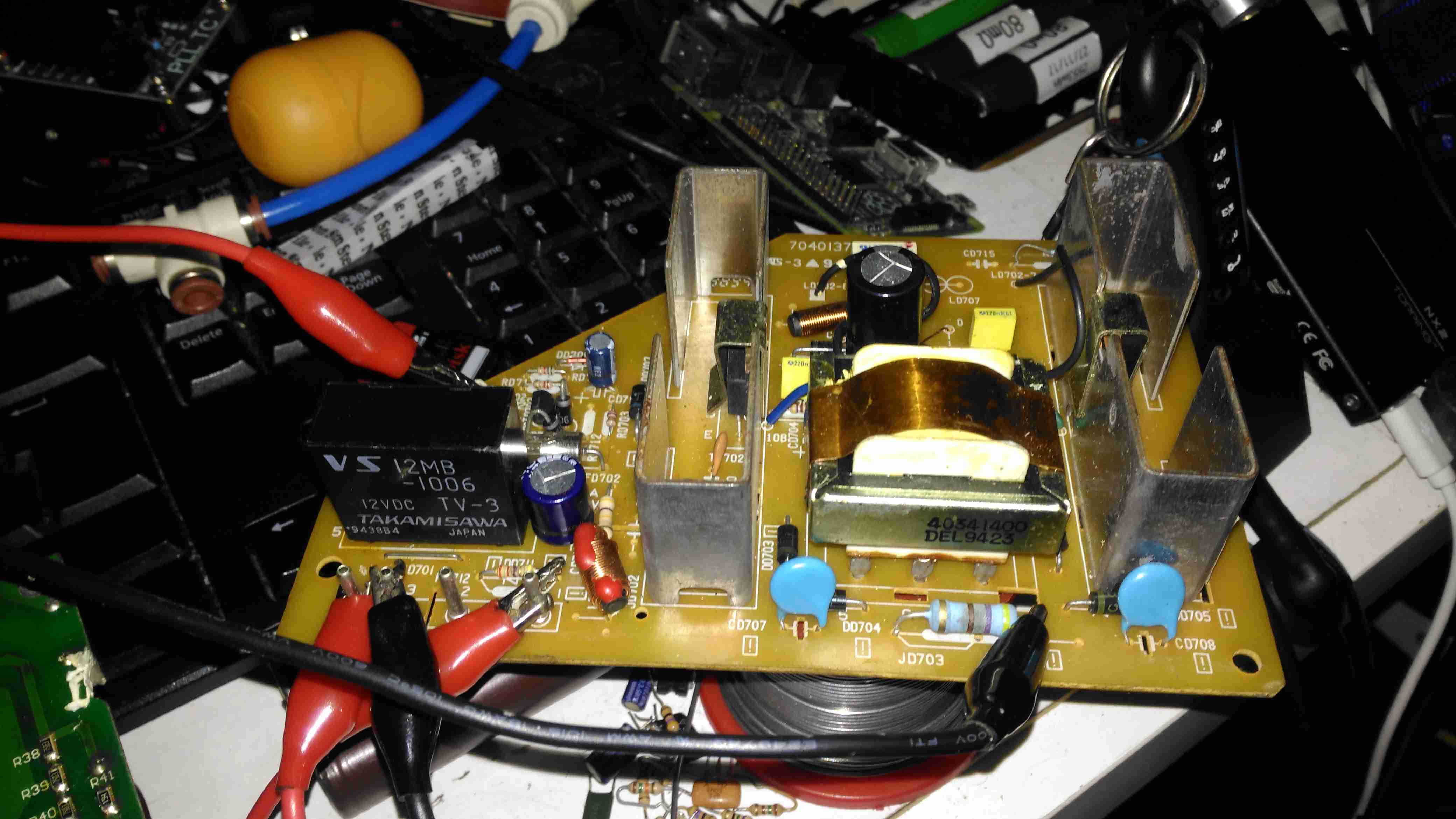
Now the defective diode bridge has been removed from the circuit, it’s time to apply some controlled power to see if anything else has failed. For this I used a module from one of my previous teardowns – the inverter from a portable TV.
Test Inverter
This neat little unit outputs 330v DC at a few dozen watts, plenty enough to power up the charger with a small load for testing purposes. The charger does pull the voltage of this converter down significantly, to about 100v, but it still provides just enough to get things going.
It’s Alive!
After applying some direct DC power to the input, it’s ALIVE! Certainly makes a change from the usual SMPS failures I come across, where a single component causes a chain reaction that writes off everything.
Replacement Rectifier
Unfortunately I couldn’t find the exact same rectifier to replace the shorted one, so I had to go for the KBU1010, which is rated for 1000v instead of 800v, but the Vf rating (Forward Voltage), is the same, so it won’t dissipate any more power.
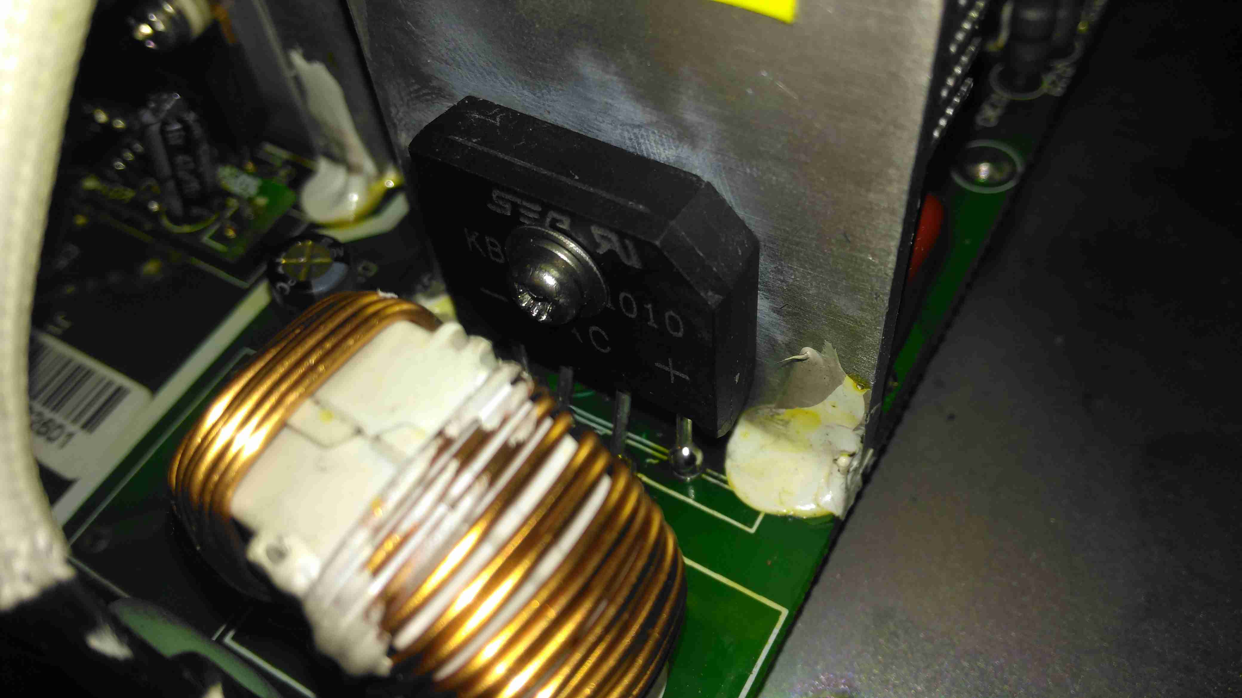
Soldered In
Here’s the new rectifier soldered into place on the PCB & bolted to it’s heatsink, with some decent thermal compound in between.
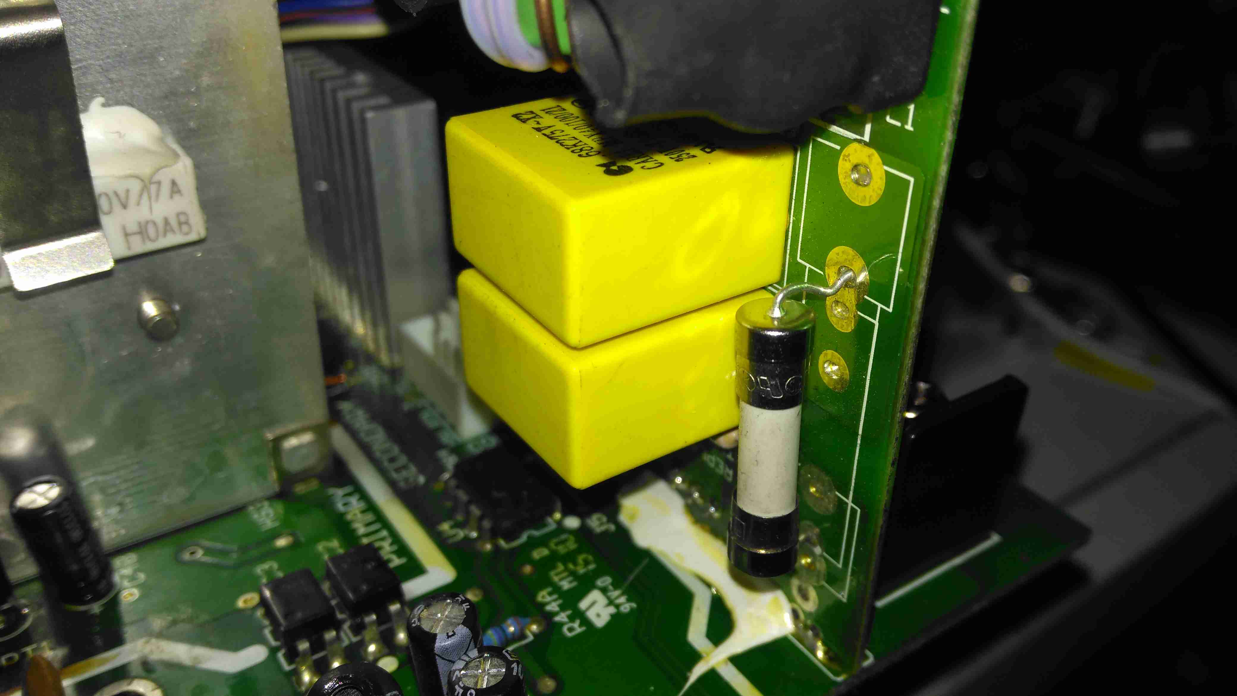
Input Board
Here is the factory fuse, a soldered in device. I’ll be replacing this with standard clips for 20x5mm fuses to make replacement in the future easier, the required hole pattern in the PCB is already present. Most of the mains input filtering is also on this little daughterboard.
Fuse Replaced
Now the fuse has been replaced with a standard one, which is much more easily replaceable. This fuse shouldn’t blow however, unless another fault develops.
Full Load Test
Now everything is back together, a full load test charging a 200Ah 12v battery for a few hours will tell me if the fix is good. This charger won’t be going back into service onboard the boat, it’s being replaced anyway with a new 50A charger, to better suit the larger loads we have now. It won’t be a Sterling though, as they are far too expensive. I’ll report back if anything fails!
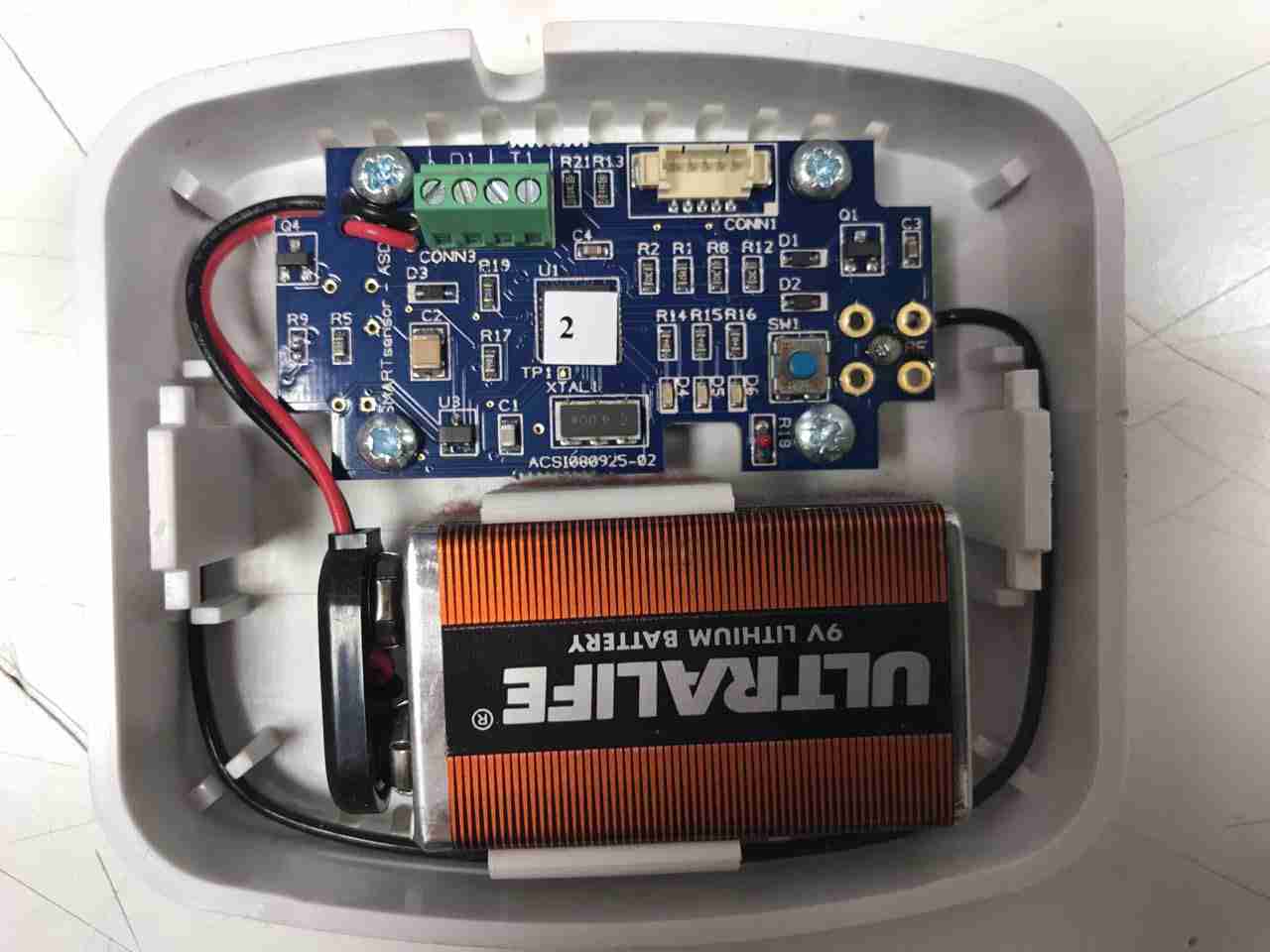
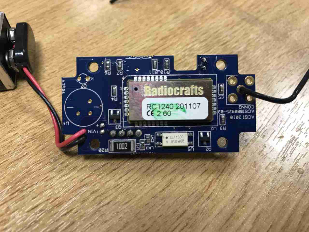
Here’s another random bit of RF tech, I’m told this is a wireless energy management sensor, however I wasn’t able to find anything similar on the interwebs. It’s powered by a standard 9v PP3 battery.
Microcontroller
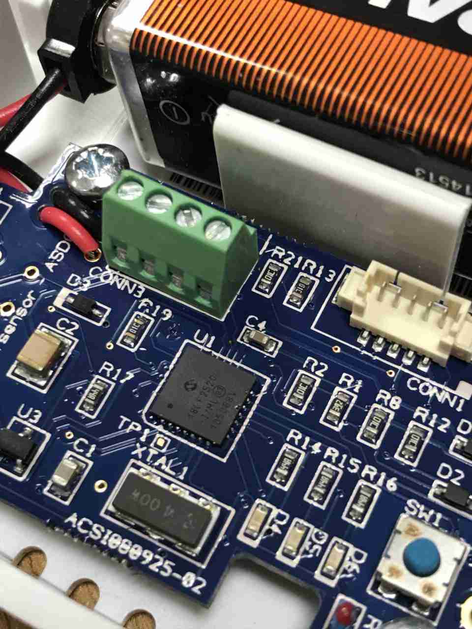
System control is handled by this Microchip PIC18F2520 Enhanced Flash microcontroller, this has an onboard 10-bit ADC & nanoWatt technology according to their datasheet. There’s a 4MHz crystal providing the clock, with a small SOT-23 voltage regulator in the bottom corner. There’s a screw terminal header & a plug header, but I’ve no idea what these would be used for. Maybe connecting an external voltage/current sensor & a programming header? The tactile button I imagine is for pairing the unit with it’s controller.
PCB Bottom
The bottom of the PCB is almost entirely taken up by a Radiocrafts RC1240 433MHz RF transceiver. Underneath there’s a large 10kΩ resistor, maybe a current transformer load resistor, and a TCLT1600 optocoupler. Just from the opto it’s clear this unit is intended to interface in some way to the mains grid. The antenna is connected at top right, in a footprint for a SMA connector, but this isn’t fitted.
Being in technology for a long time, I have seen my fair share of disk failures. However I have never seen a single instance where SMART has issued a sufficient warning to backup any data on a failing disk. The following is an example of this in action.
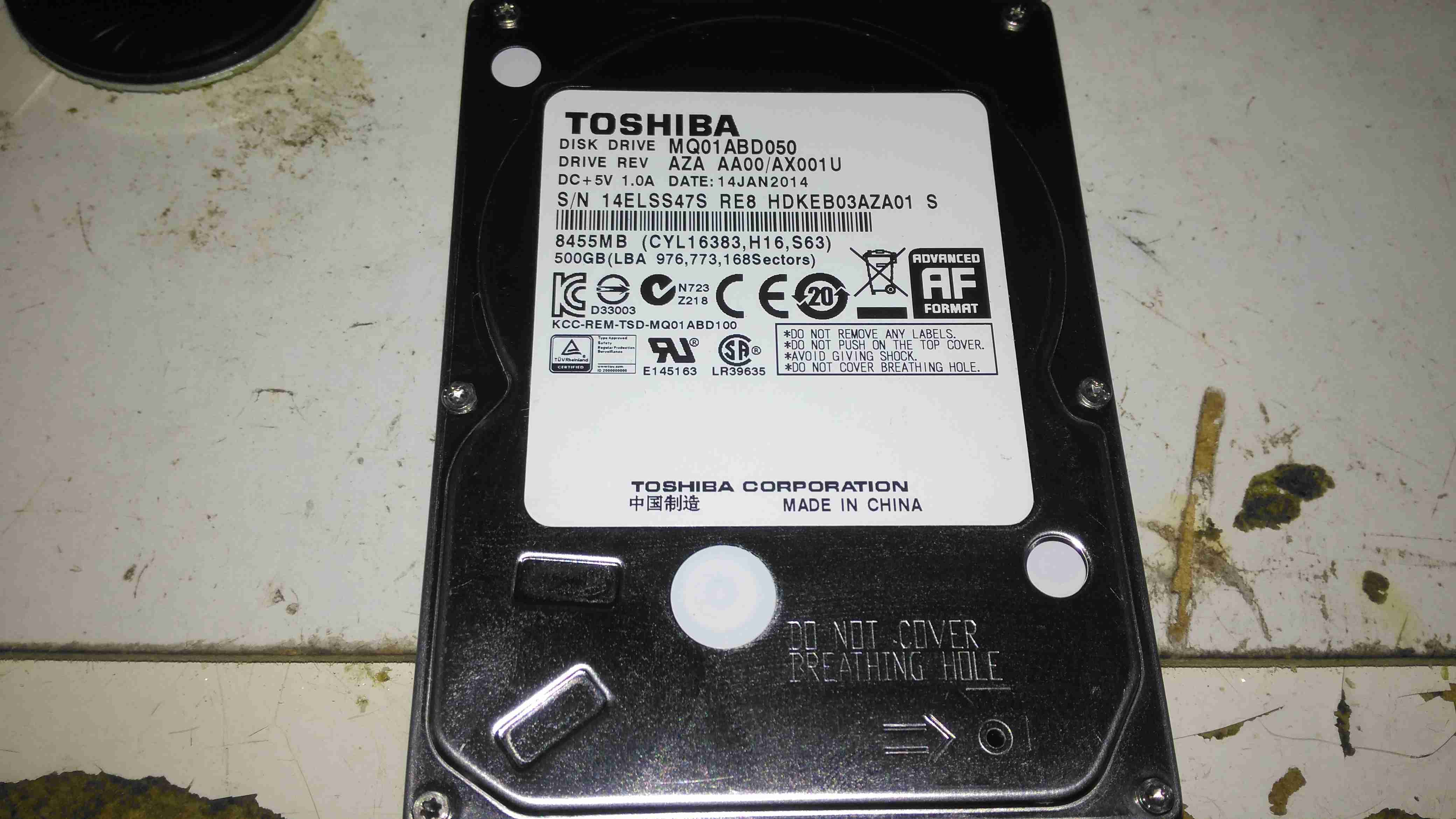
Toshiba MQ01ABD050
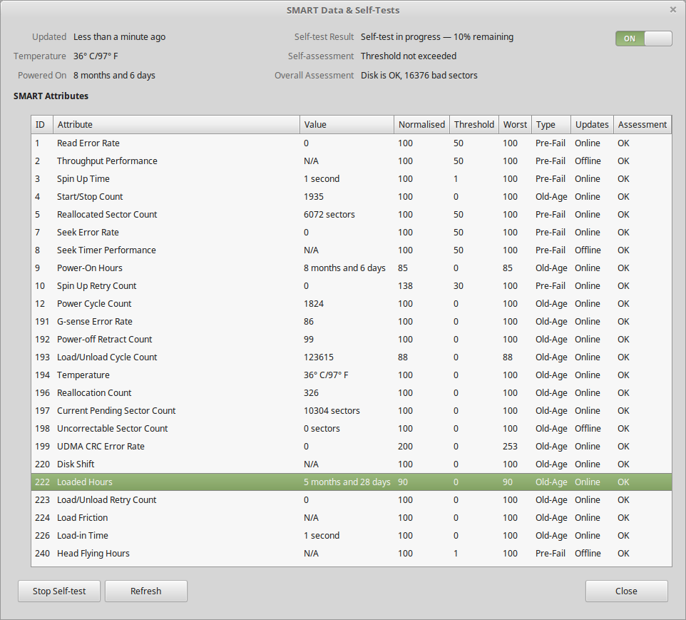
Here is a 2.5″ Toshiba MQ01ABD050 500GB disk drive. This unit was made in 2014, but has a very low hour count of ~8 months, with only ~5 months of the heads being loaded onto the platters, since it has been used to store offline files. This disk was working perfectly the last time it was plugged in a few weeks ago, but today within seconds of starting to transfer data, it began slowing down, then stopped entirely. A quick look at the SMART stats showed over 4000 reallocated sectors, so a full scan was initiated.
SMART Test Failure
After the couple of hours an extended test takes, the firmware managed to find a total of 16,376 bad sectors, of which 10K+ were still pending reallocation. Just after the test finished, the disk began making the usual clicking sound of the head actuator losing lock on the servo tracks. Yet SMART was still insisting that the disk was OK! In total about 3 hours between first power up & the disk failing entirely. This is possibly the most sudden failure of a disk I’ve seen so far, but SMART didn’t even twig from the huge number of sector reallocations that something was amiss. I don’t believe the platters are at fault here, it’s most likely to be either a head fault or preamp failure, as I don’t think platters can catastrophically fail this quickly. I expected SMART to at least flag that the drive was in a bad state once it’s self-test completed, but nope.
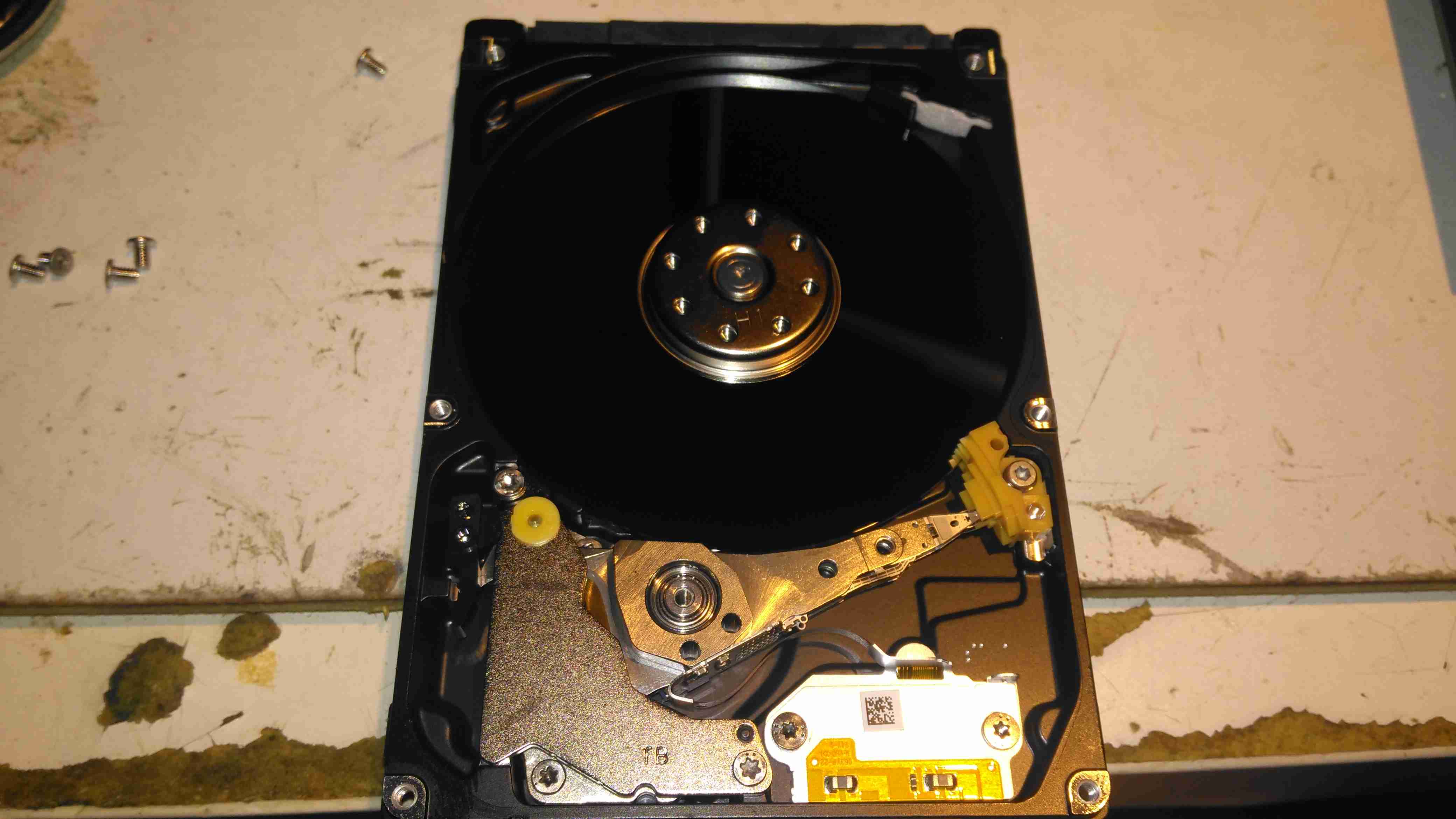
Internals
After pulling the lid on this disk, to see if there’s any evidence of a head crashing into a platter, there’s nothing – at least on a macroscopic scale, the single platter is pristine. I’ve seen disks crash to the point where the coating has been scrubbed from the platters so thoroughly that they’ve been returned to the glass discs they started off as, with the enclosure packed full of fine black powder that used to be data layer, but there’s no indication of mechanical failure here. Electronic failure is looking very likely.
Clearly, relying on SMART to alert when a disk is about to take a dive is an unwise idea, replacing drives after a set period is much better insurance if they are used for critical applications. Of course, current backups is always a good idea, no matter the age of drive.
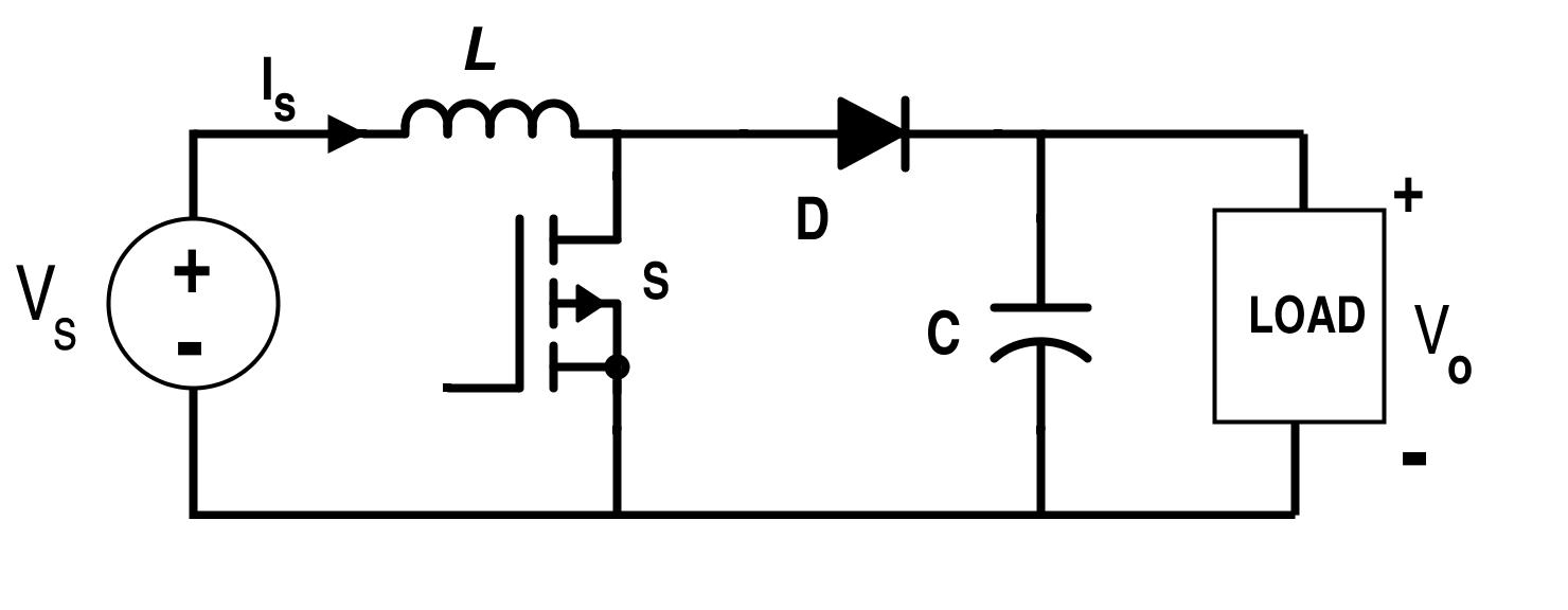
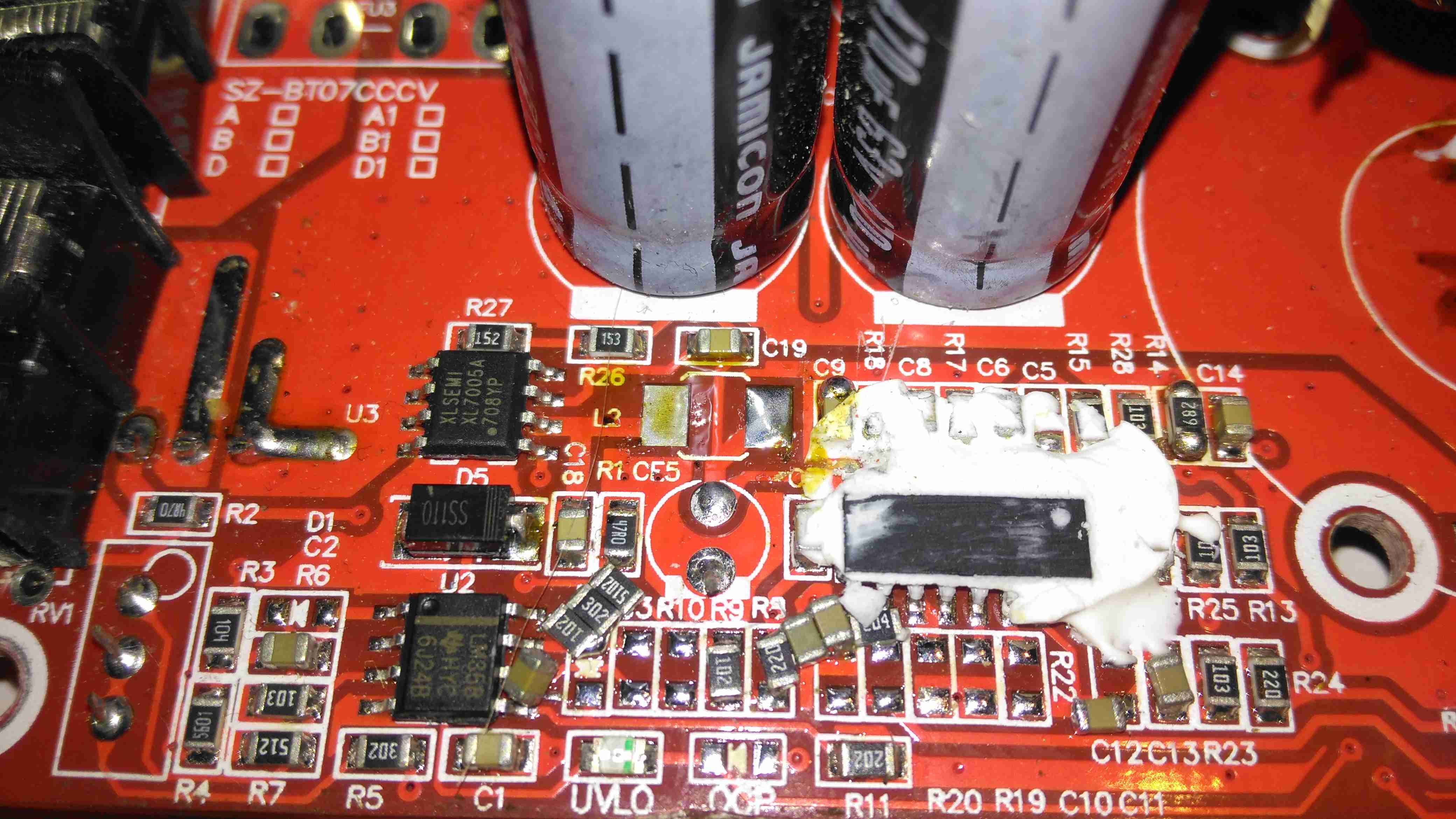
Ah the curse of the Chinese Electronics strikes again. These large DC-DC boost converters have become very common on the likes of AliExpress & eBay, and this time my order has arrived DOA… On applying power, the output LED lights up dimly, and no matter how I twiddle the adjustment pots, the output never rises above the input voltage.
Boost Converter Topology
From the usual topology above, we can assume that the switching converter isn’t working, so the input voltage is just being directly fed through to the output. The switching IC on these converters is a TL494,
Control Circuitry
The switching IC on these converters is a TL494,with it’s surrounding support components, including a LM358 dual Op-Amp. Power for this lot is supplied from the input via a small DC-DC converter controlled by an XL Semi XL7001 Buck Converter IC. Some testing revealed that power was getting to the XL7001, but the output to the switching controller was at zero volts.
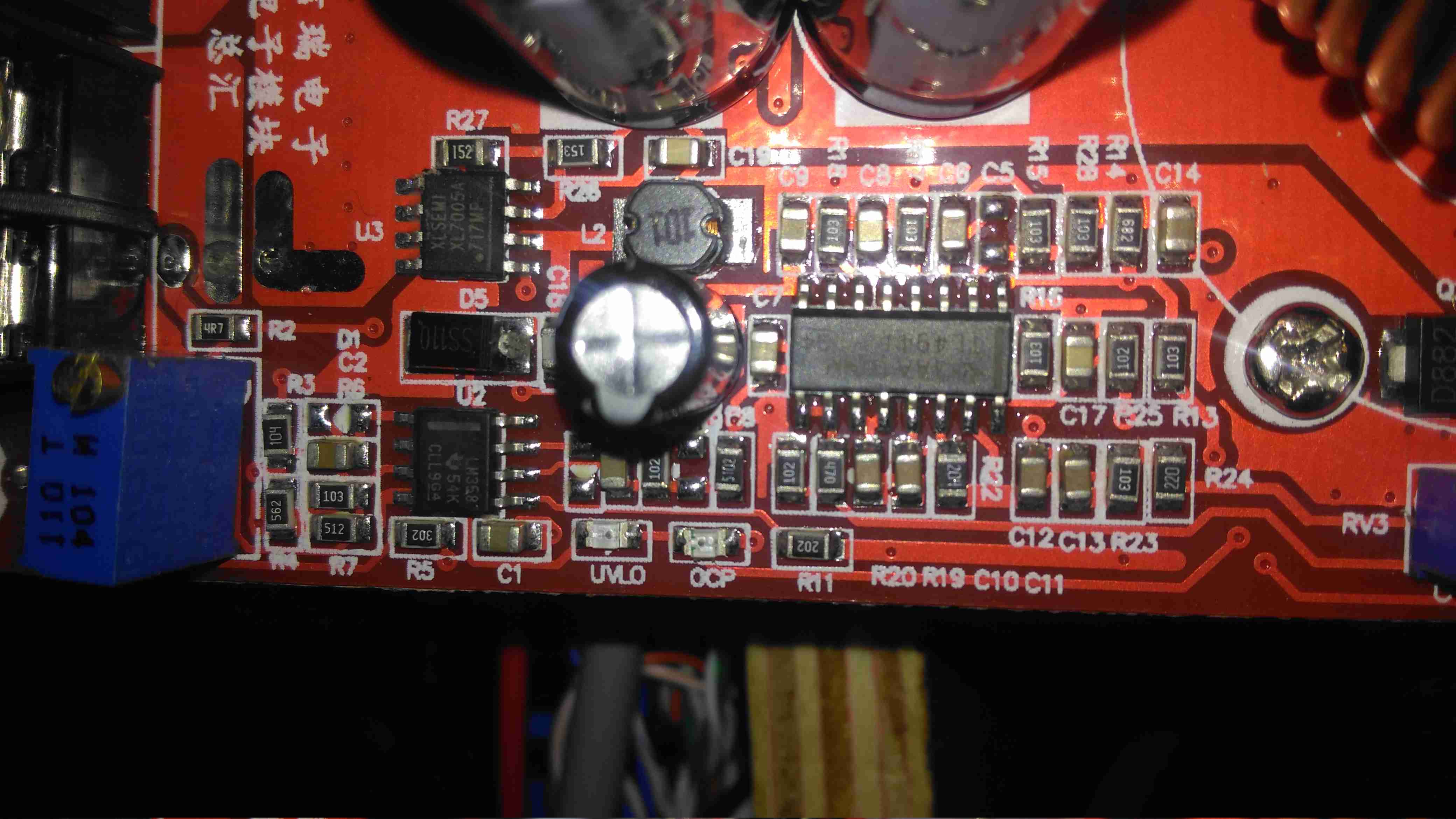
Inductor
The 100µH inductor for this buck converter is hidden behind the output electrolytic, and a quick prod with a multimeter revealed this inductor to be open circuit. That would certainly explain the no-output situation. Luckily I had an old converter that was burned out. (Don’t try to pull anything near their manufacturer “rating” from these units – it’s utter lies, more about this below).
Donor Converter
The good inductor from this donor unit has been desoldered here, it’s supposed to be L2. This one had a heatsink siliconed to the top of the TL494 PWM IC, presumably for cooling, so this was peeled off to give some access.
After this inductor was grafted into place on the dead converter, everything sprang to life as normal. I fail to see how this issue wouldn’t have been caught during manufacture, but they’re probably not even testing them before shipping to the distributor.
The sensational ratings are also utter crap – they quote 1.2kW max power, which at 12v input would be 100A. Their max input rating is given as 20A, so 240W max input power. Pulling this level of power from such a cheaply designed converter isn’t going to be reliably possible, the input terminals aren’t even rated to anywhere near 20A, so these would be the first to melt, swiftly followed by everything else. Some of these units come with a fan fitted from the factory, but these are as cheaply made as possible, with bearings made of cheese. As a result they seize solid within a couple of days of use.
Proper converters from companies like TDK-Lambda or muRata rated for these power levels are huge, with BOLTS for terminals, but they’re considerably more expensive. These Chinese units are handy though, as long as they are run at a power level that’s realistic.
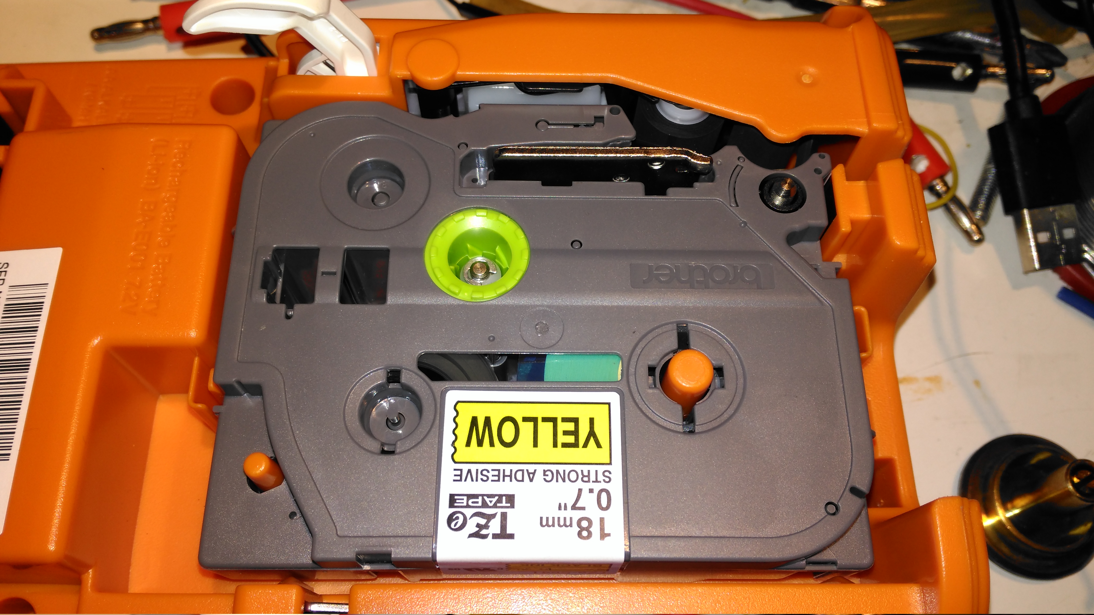
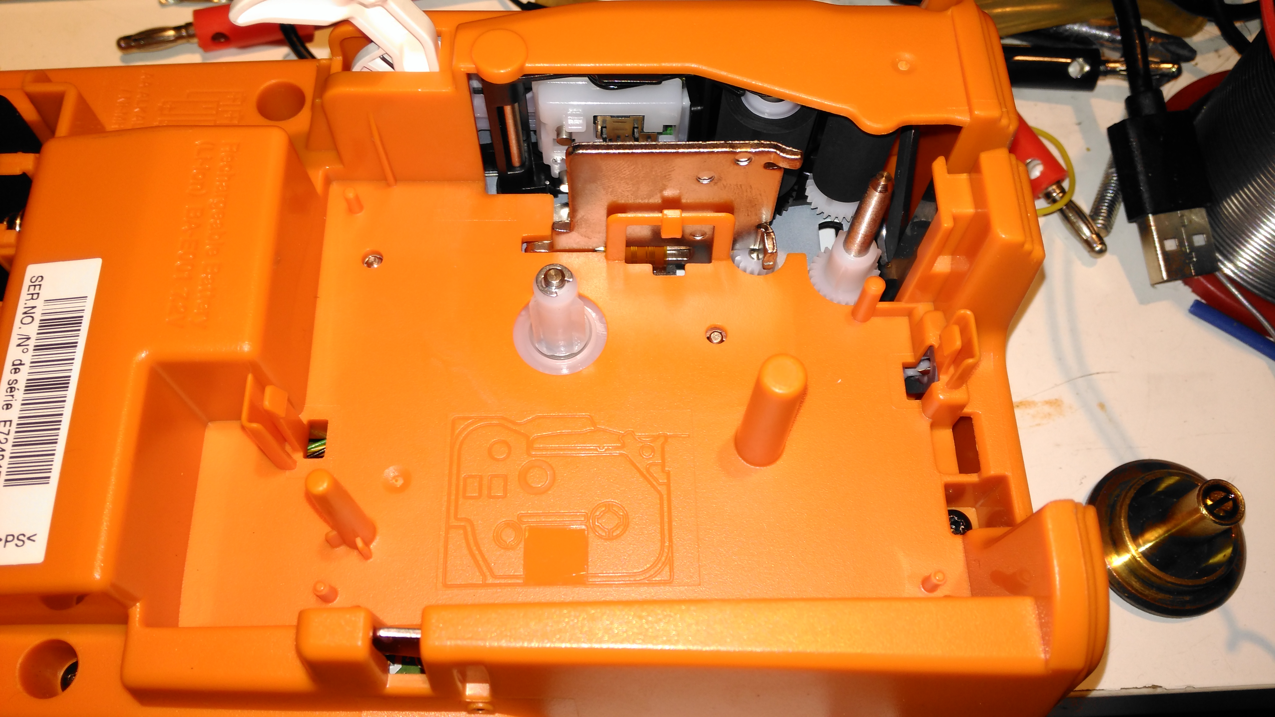
Here a tape is installed in the printer. This unit can handle tape widths up to 18mm. The pinch rollers are operated by the white lever at the top of the image, which engages with the back cover.
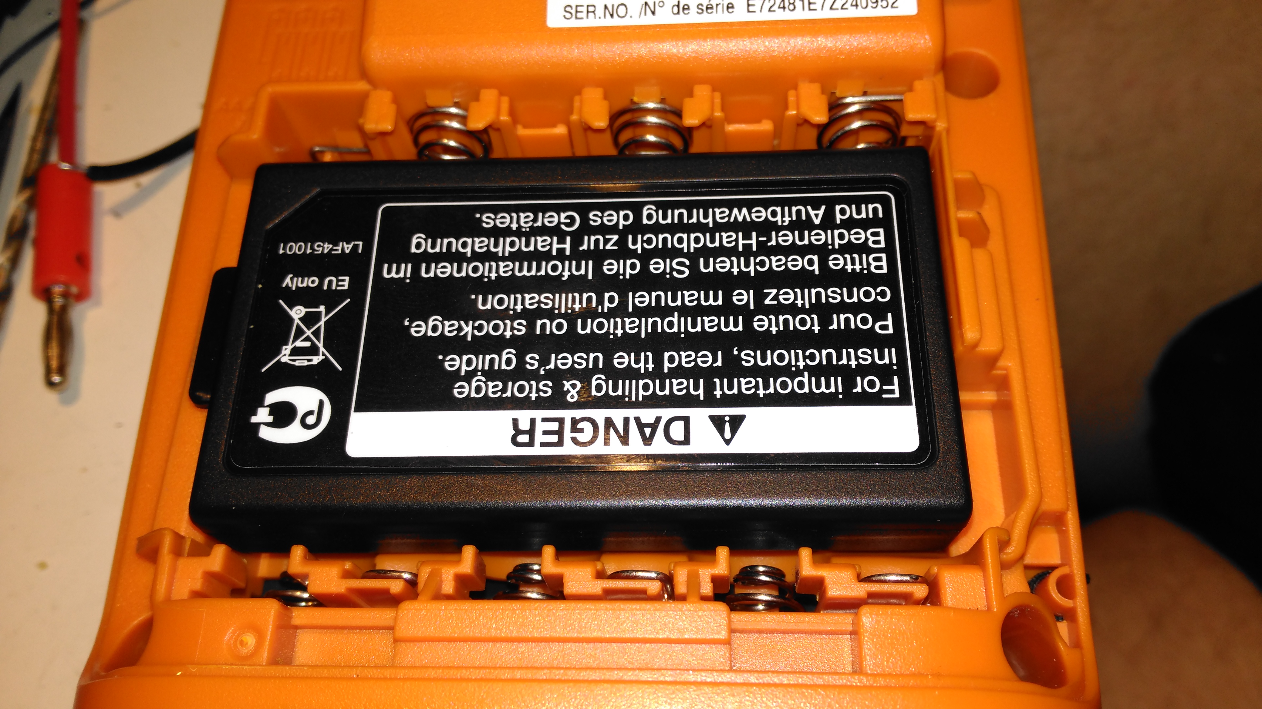
Li-Ion Battery
This printer is supplied with a rechargeable battery pack, but AA cells can be used as well. Some of the AA battery terminals can be seen above the battery.
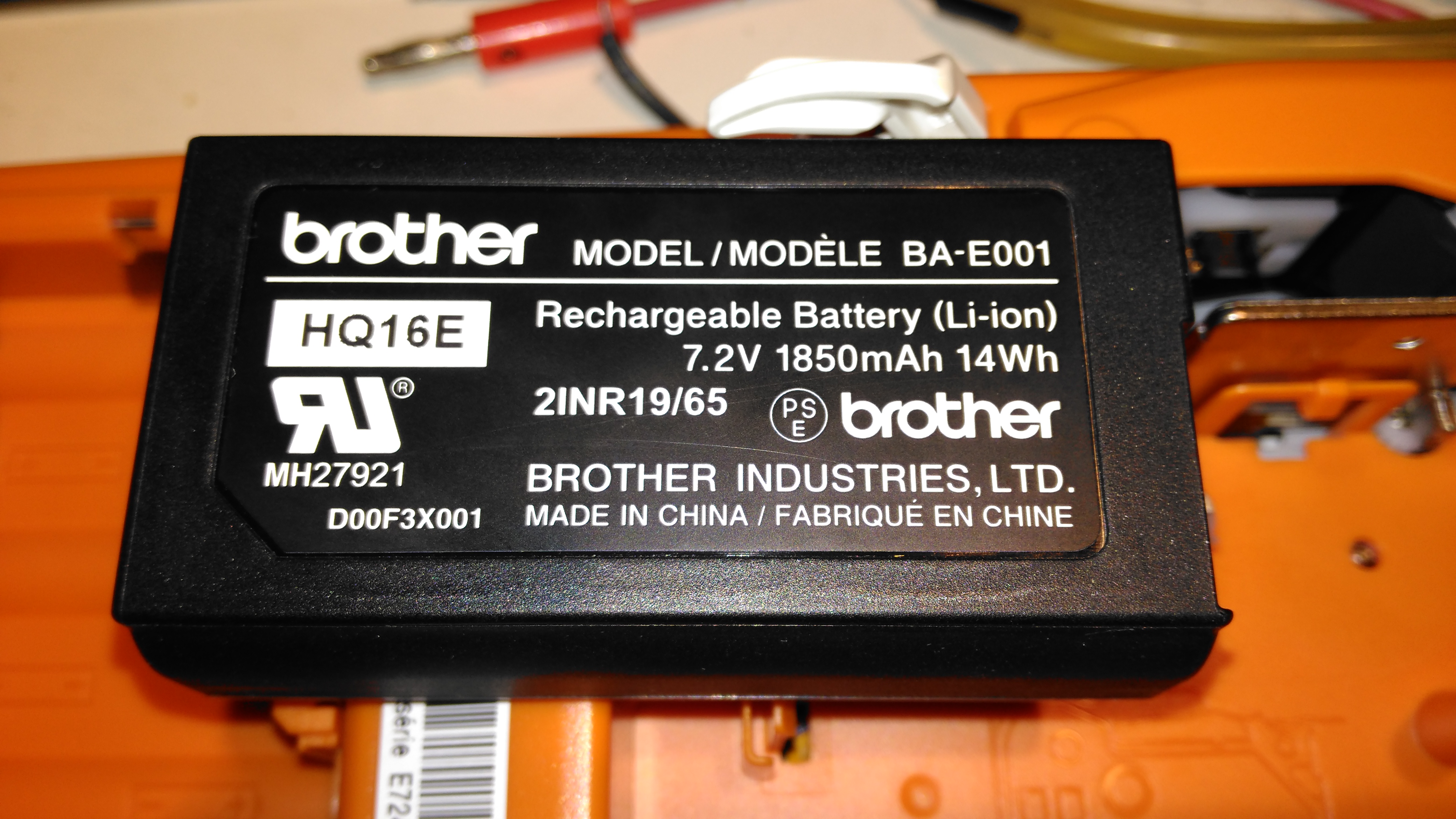
Battery Specs
Pretty standard fare for a 2-cell lithium pack. The charging circuitry doesn’t appear to charge it to full voltage though, most likely to get the most life from the pack.
Cartridge Slot
With the cartridge removed, the printer components can be seen. As these cartridges have in effect two rolls, one fro the ribbon & one for the actual label, there are two drive points.
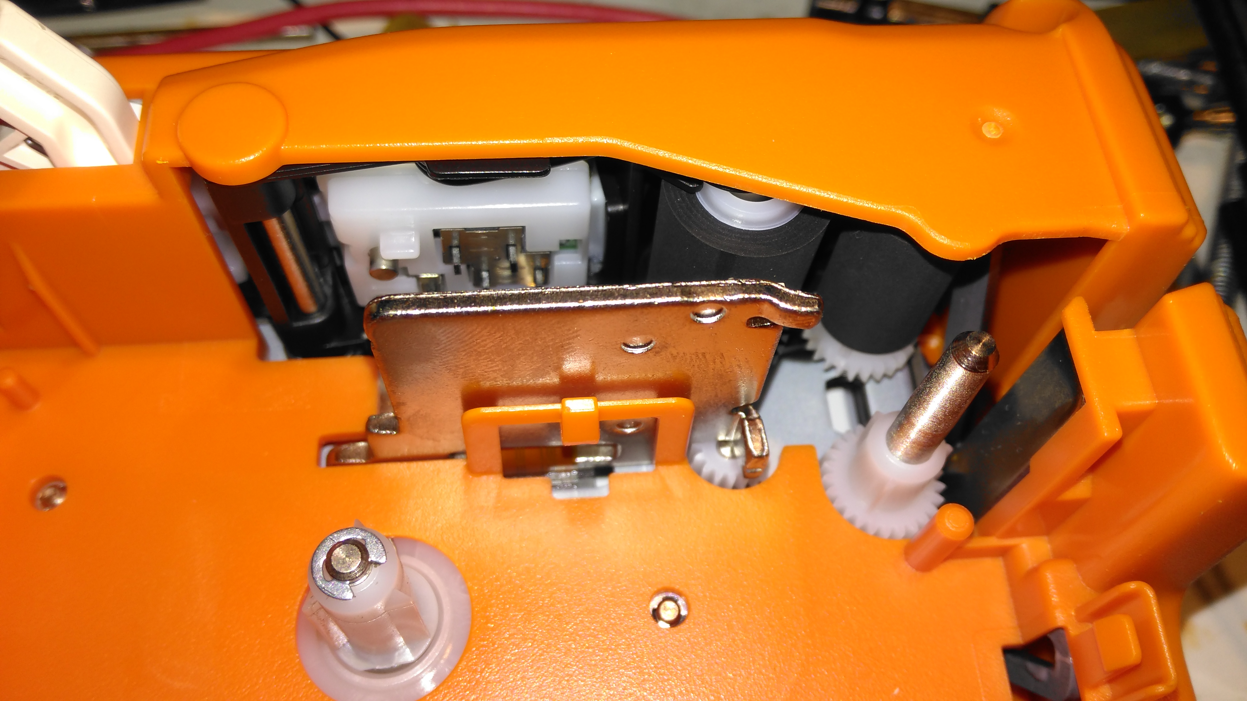
Pinch Rollers & Print Head
The thermal print head is hidden on the other side of the steel heatsink, while the pinch rollers are on the top right. The plastic piece above the print head heatsink has a matrix of switches that engage with holes in the top of the label cartridge, this is how the machine knows what size of ribbon is fitted.
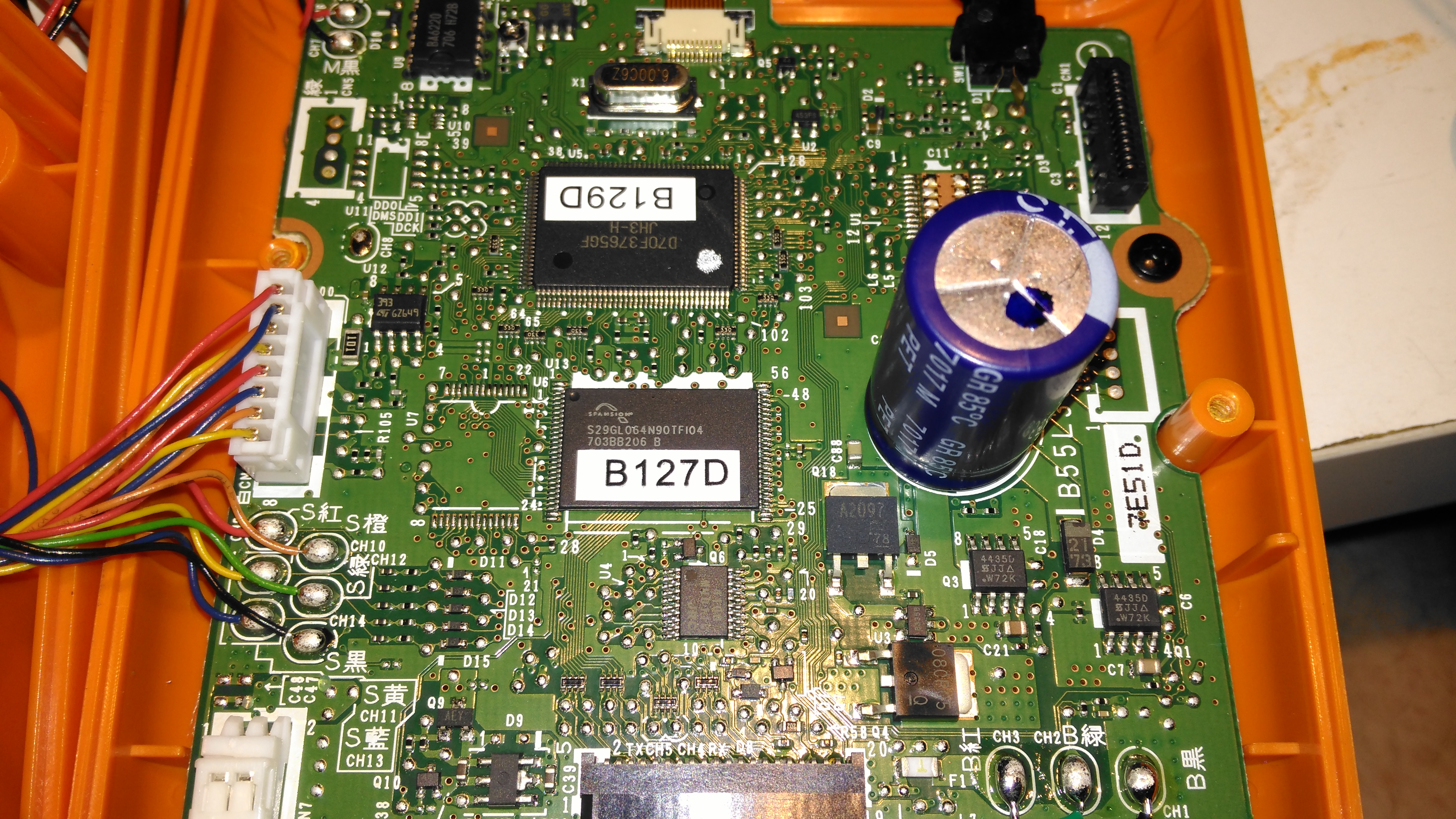
Mainboard
Most of the internal space is taken up by the main board, with the microprocessor & it’s program flash ROM top & centre.
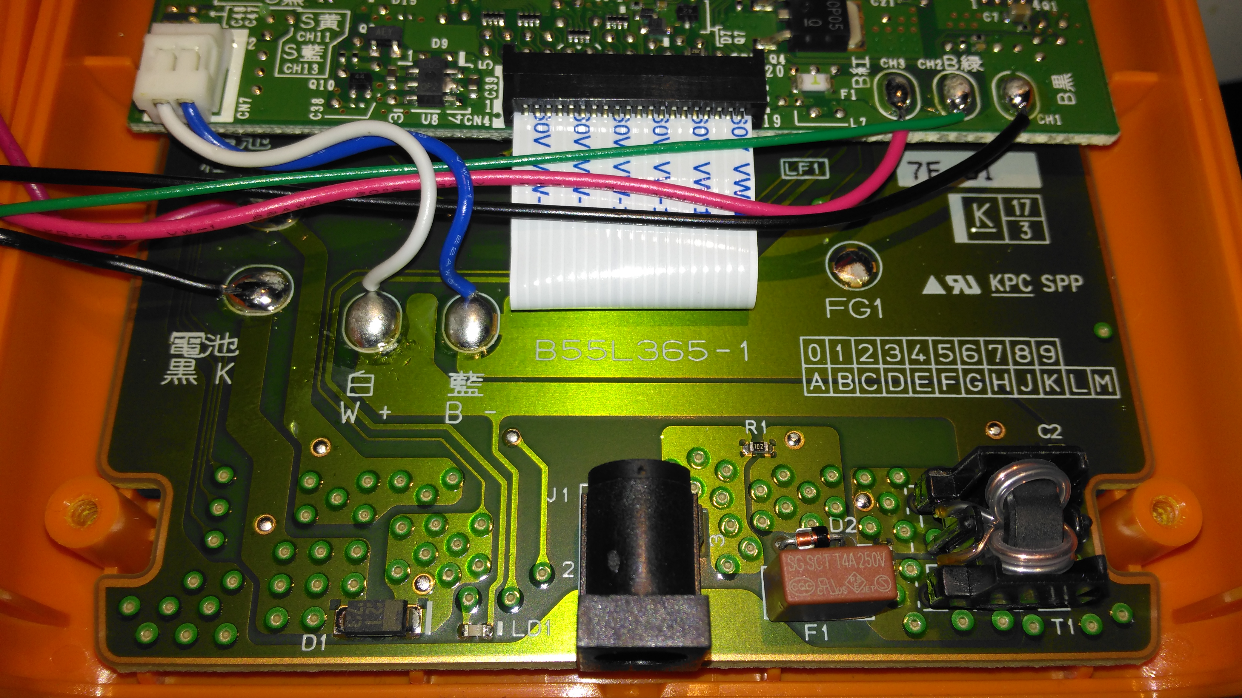
Charger Input
The charger input is located on the keyboard PCB just under the mainboard, which is centre negative, as opposed to 99% of other devices using centre positive, the bastards.
LCD Module
The dot-matrix LCD is attached to the mainboard with a short flex cable, and from the few connections, this is probably SPI or I²C.
Print Mech Drive
The printer itself is driven by a simple DC motor, speed is regulated by a pair of photo-interrupters forming an encoder on the second gear in the train.
Battery Holder Connections
The back case has the battery connections for both the lithium pack & the AA cells, the lithium pack has a 3rd connection, probably for temperature sensing.
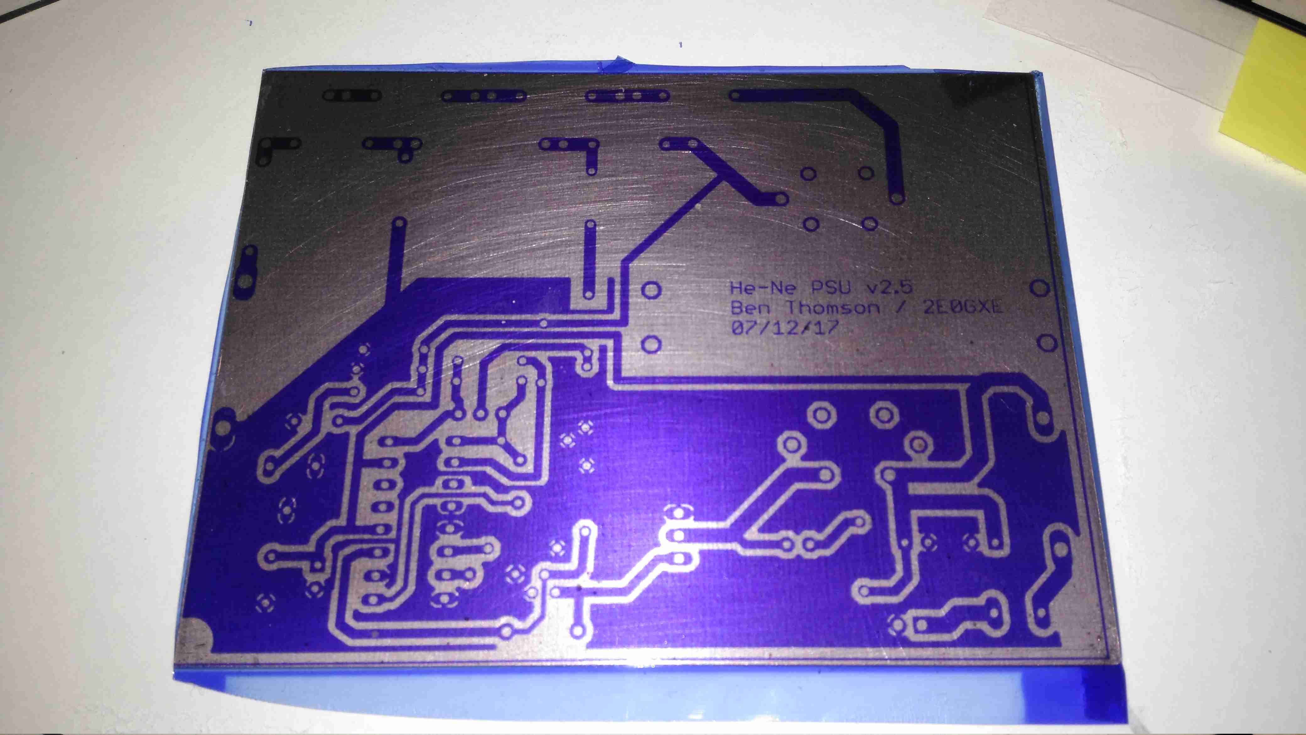
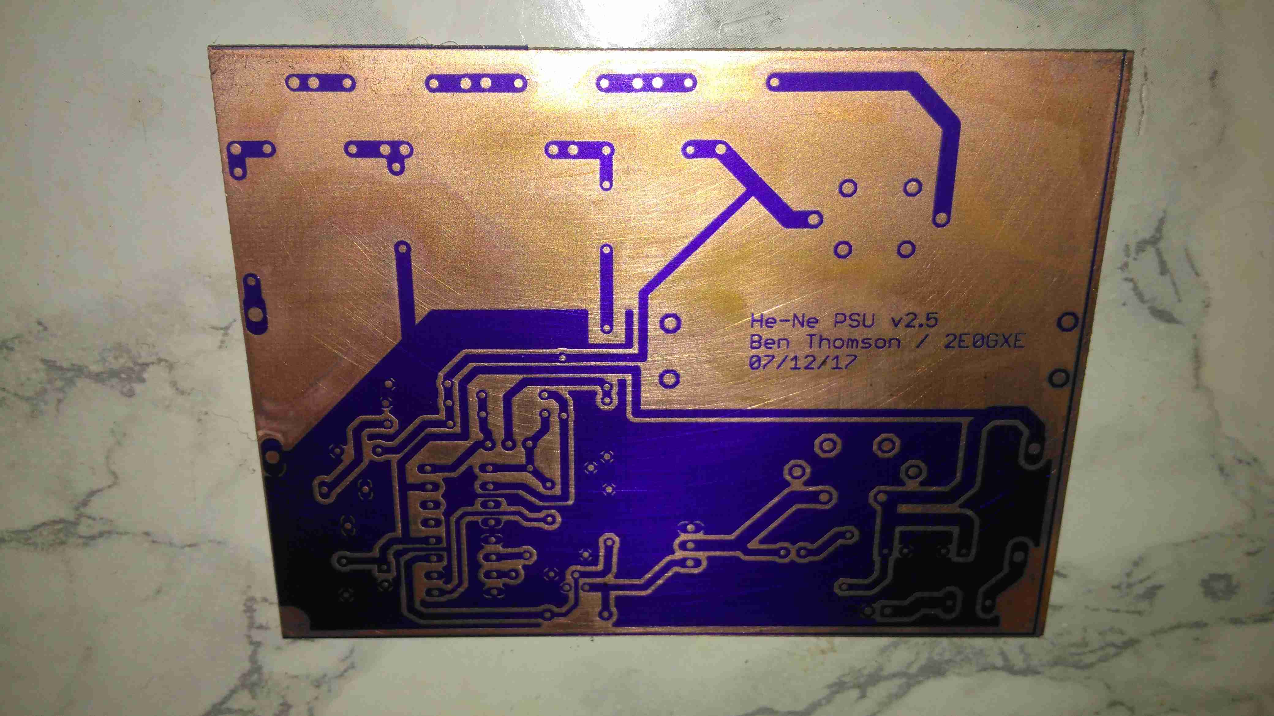
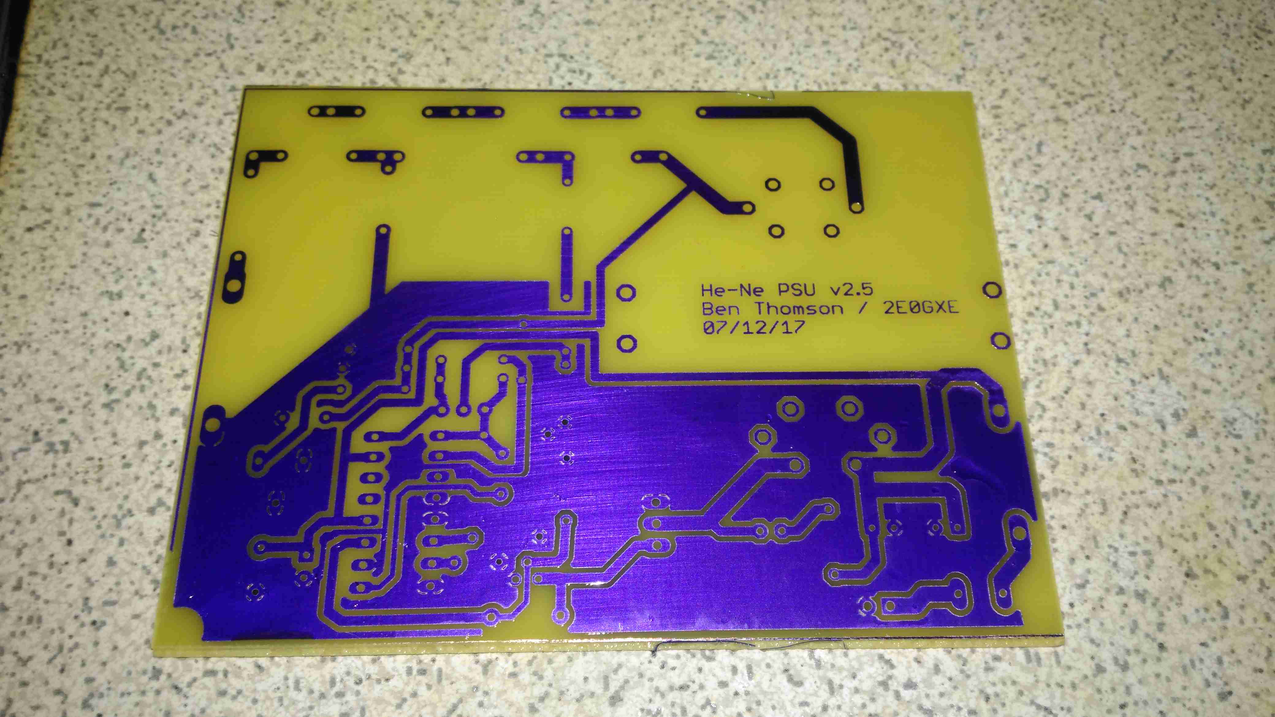
Since I do my own PCBs on a somewhat regular basis, I decided it was time to move to a more professional method to etch my boards. I have been using the cheap toner transfer method, using special yellow coated paper from China. (I think it’s coated in wax, or some plastic film).
The toner transfer paper does usually work quite well, but I’ve had many issues with pinholes in the transfer, which cause the etched tracks to look horrid, (not to mention the potential for breaks & reduced current capacity), and the toner not transferring properly at all, to issues with the paper permanently fusing to the copper instead of just transferring the toner.
BigClive has done a couple of fairly comprehensive videos on the dry film photoresist available from AliExpress & eBay. This stuff is used similarly to the toner transfer method, in that the film is fused to the board with heat, but then things diverge. It’s supplied either in cut sheets, or by the roll. I ordered a full roll to avoid the issues I’ve heard of when the stuff is folded in the post – once it’s creased, it’s totally useless. The dry film itself is a gel sandwiched between two protective plastic film sheets, and bonds to the board with the application of heat from a laminator.
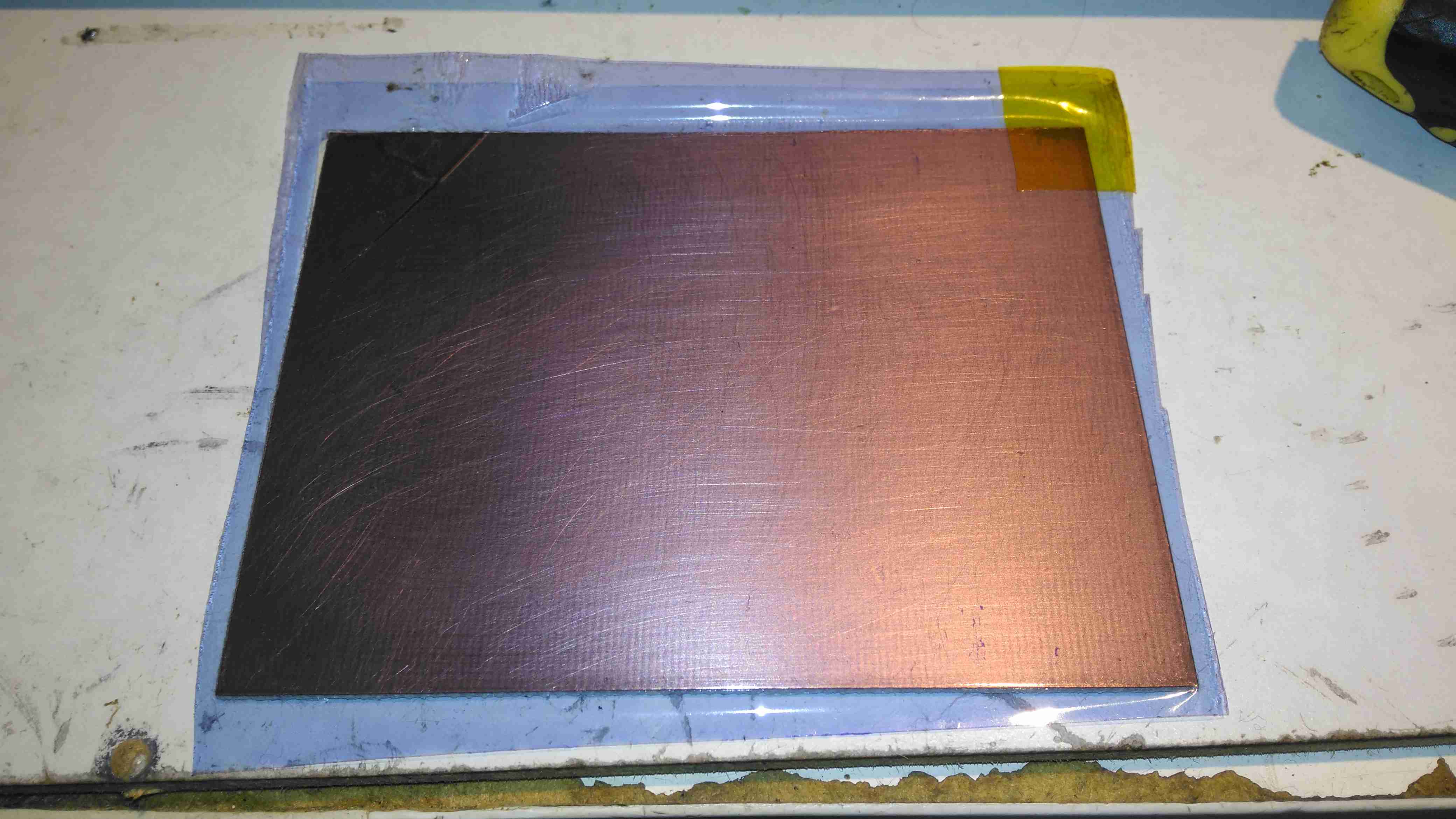
The board is first cleaned with scotchbrite pad & soap to remove any tarnish & oil from the copper.
Dry Film
Once the board has been cleaned, one side of the backing film is removed from the gel with adhesive tape, and the dry film is placed on the board while still wet. This stops the film from sticking immediately to the clean copper, one edge is pressed down, and it’s then fed through a modified laminator:
Modified Laminator
I’ve cut away most of the plastic covering the hot rollers, as constant jamming was an issue with this cheapo unit. All the mains power is safely tucked away under some remaining plastic cover at the end. The board with it’s covering of dry film is fed into the laminator – the edge that was pressed down first. This allows the laminator to squeeze out any remaining water & air bubbles from between the two so no creases or blisters form.
After Lamination
Once the board has been run through the laminator about 6 times, (enough to get it very hot to the touch), the film is totally bonded to the copper. The top film is left in place to protect the UV sensitive layer during expsure.
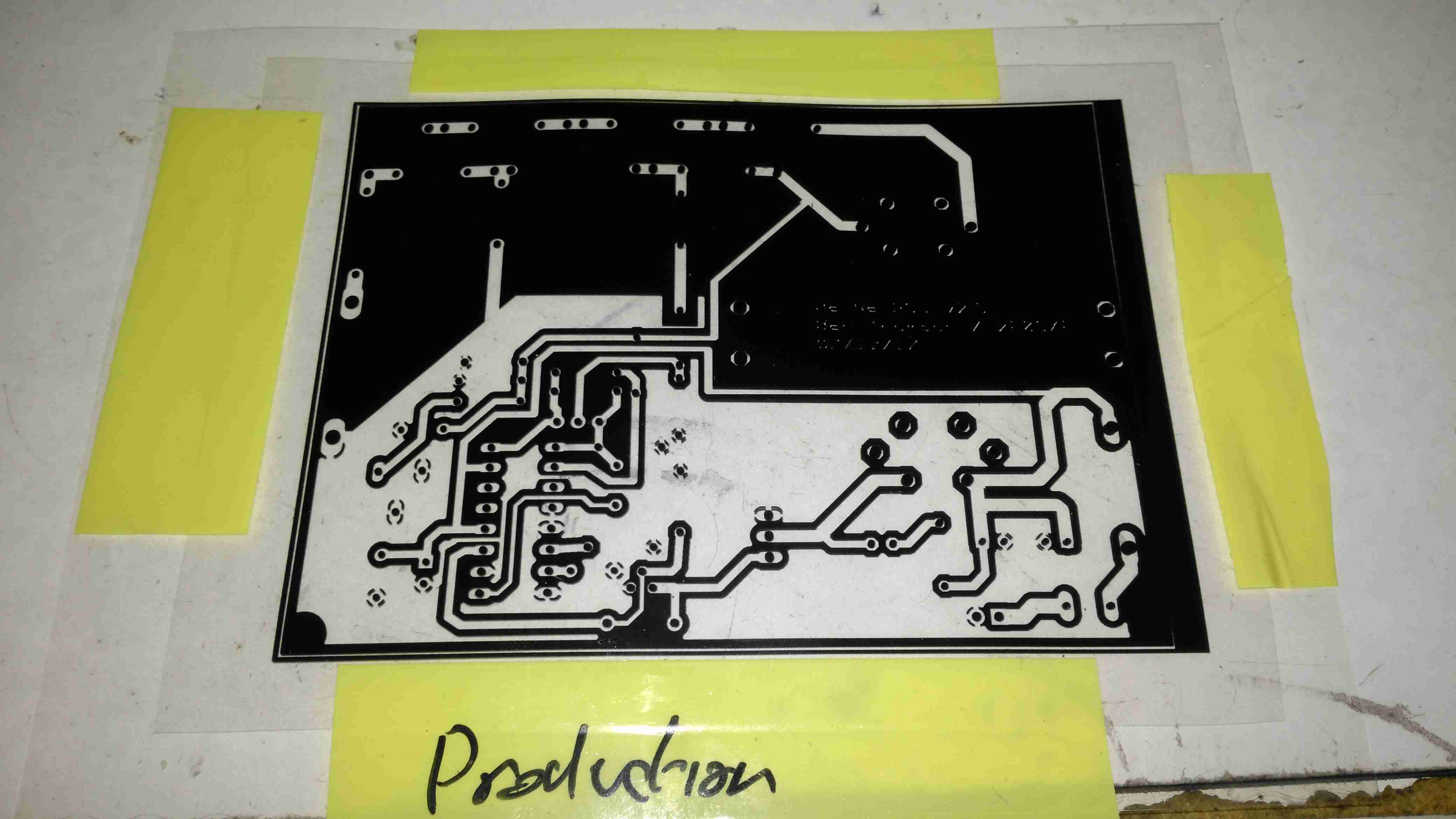
Photomask
The exposure mask is laser printed onto OHP transparencies, in this case I’ve found I need to use two copies overlaid to get enough opacity in the black toner sections to block the UV light. Some touching up with a Sharpie is also easy to do if there are any weak spots in the toner coverage. This film is negative type – All the black areas will be unexposed and washed off in the developer tank. I also found I had to be fairly generous with track spacing, using too small lines just causes issues with the UV curing bits of film it isn’t supposed to.
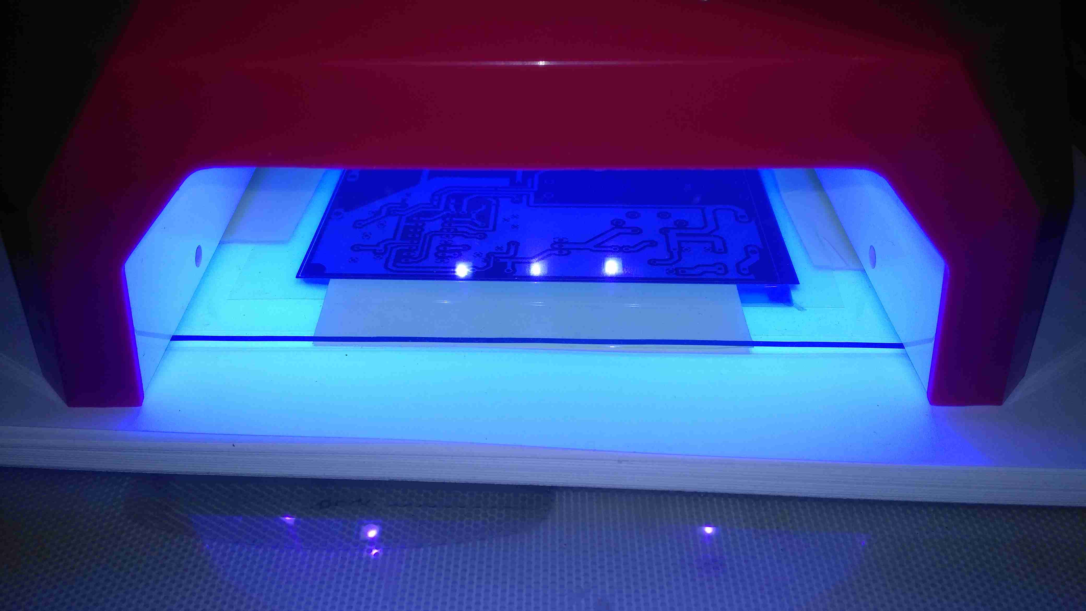
Exposing The PCB
The PCB is placed on a firm surface, the exposure mask lined up on top, and the whole thing covered with a sheet of standard glass to apply even pressure. The UV exposure lamp in this case is a cheap eBay UV nail curing unit, with 15 high power LEDs. (I’ll do a teardown on this when I get some time, it’s got some very odd LEDs in it). Exposing the board for 60 seconds is all the time needed.
After Exposure
After the board is exposed, the areas that got hit with the UV light have turned purple – the resist has hardened in these areas. It’s bloody tough as well, I’ve scrubbed at it with some vigour and it doesn’t come off. Toner transfer was a bit naff in this respect, most of the time the toner came off so easily that the etchant lifted it off. After this step is done, the remaining protective film on the top can be removed.
After Developing
The film is developed in a solution of Sodium Carbonate (washing Soda). This is mildly alkaline and it dissolves off the unexposed resist.
After Etching
Now it’s into the etching tank for a couple of minutes, I’m still using Ferric Chloride to etch my boards, at about 60°C. Etching at room temperature is much too slow. Once this is done, the board is washed, and then dipped in the strip tank for a couple of minutes. This is a Sodium Hydroxide solution, and is very caustic, so gloves are required for this bit. Getting Ferric Chloride on skin is also a fairly bad idea, it stains everything orange, and it attacks pretty much every metal it comes into contact with, including Stainless Steel.
This method does require some more effort than the toner transfer method, but it’s much more reliable. If something goes wrong with the exposure, it’s very easy to strip the board completely & start again before etching. This saves PCB material and etchant. This is definitely more suited to small-scale production as well, since the photomask can be reused, there’s much less waste at the end. The etched lines are sharper, much better defined & even with some more chemicals involved, it’s a pretty clean process. All apart from the Ferric Chloride can be disposed of down the sink after use, since the developer & stripper are just alkaline solutions.
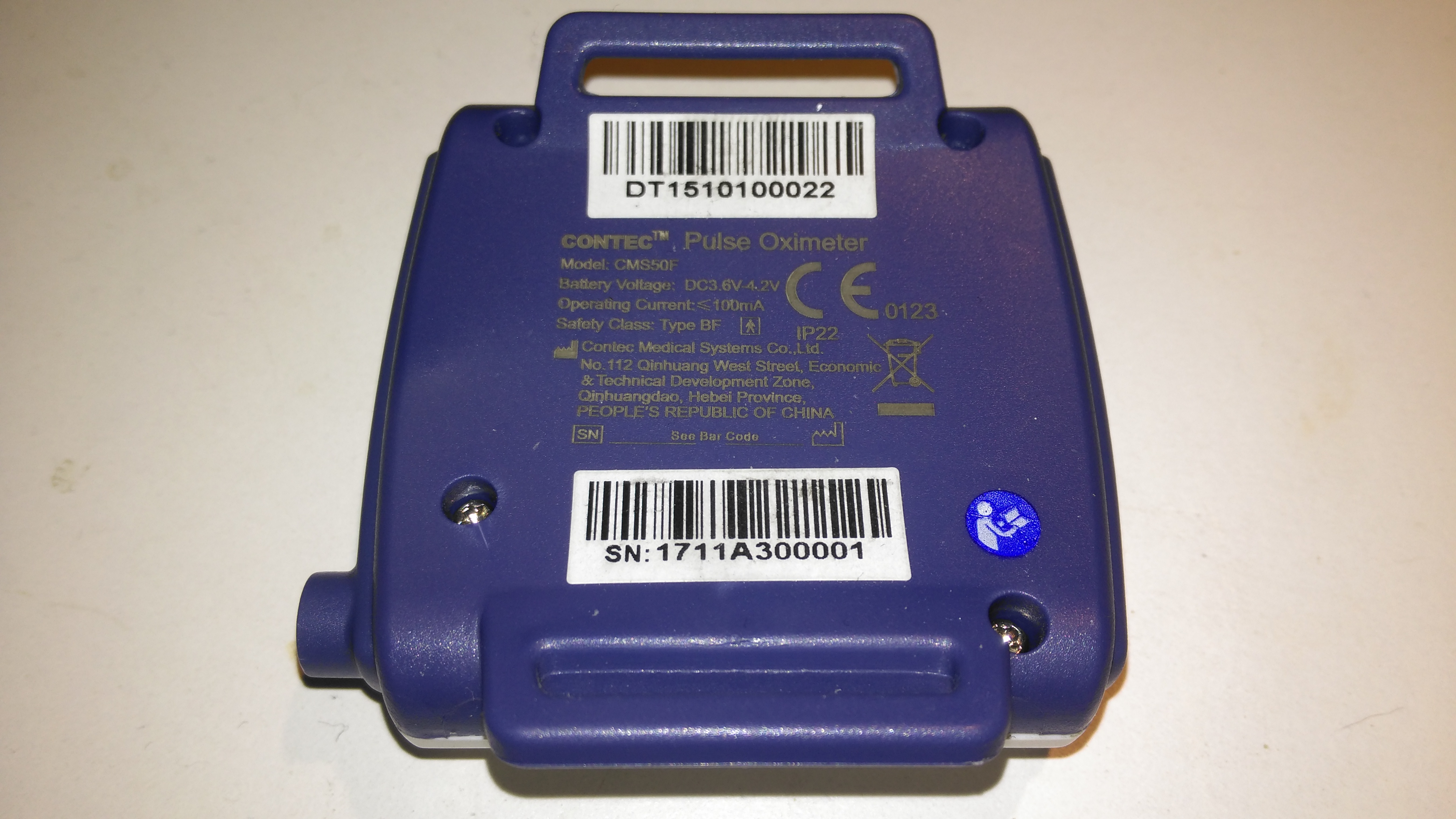
The rear has the specifications, laser-marked into the plastic. The serial numbers are just sticky labels though, and will come off easily with use.
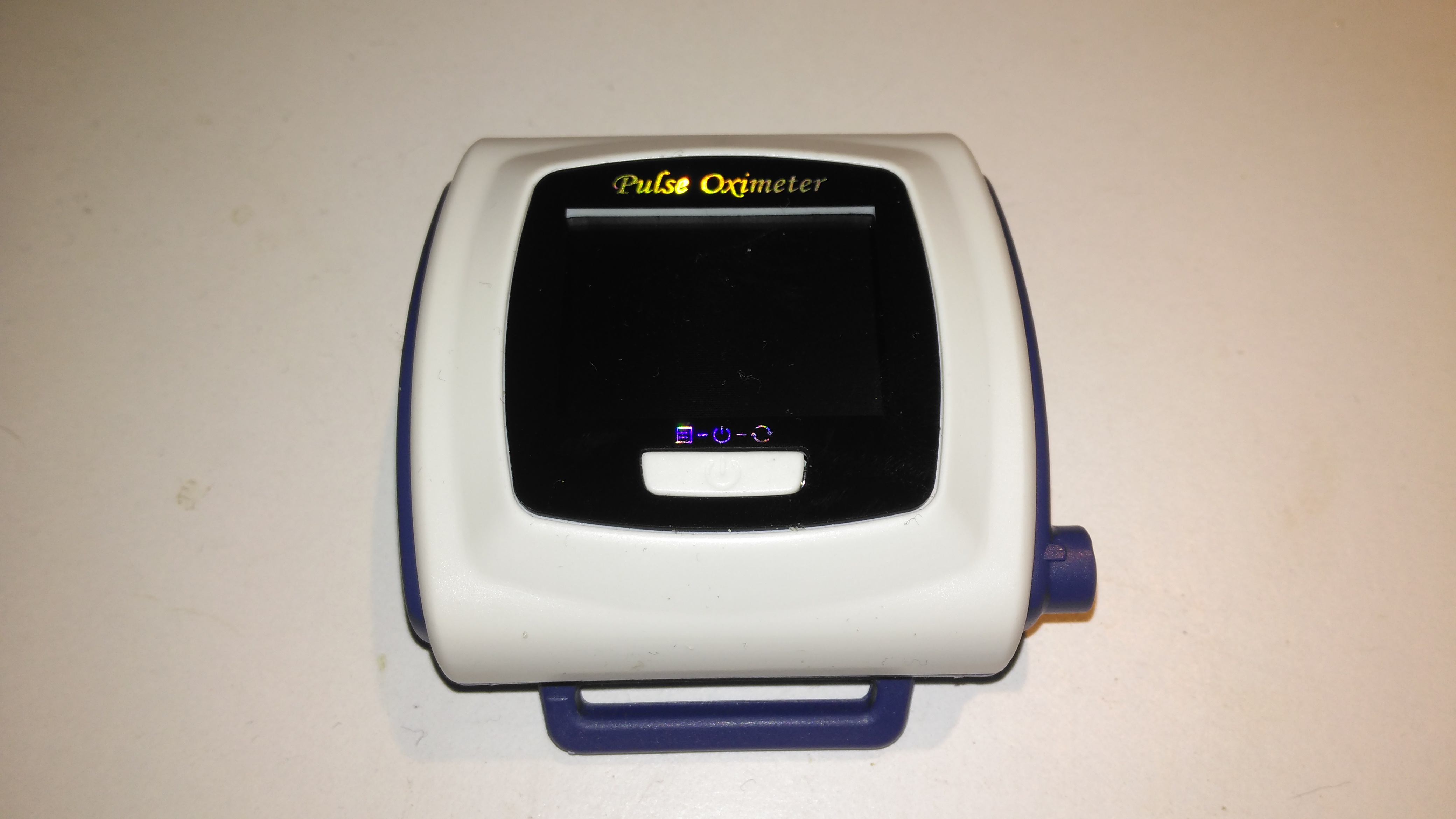
Contec CMS-50F
This is the Contec CMS-50F wrist-mounted pulse oximeter unit, which has the capability to record data continuously to onboard memory, to be read out at a later time via a USB-Serial link. There is software supplied with the unit for this purpose, although it suffers from the usual Chinese quality problems. The hardware of this unit is rather well made, the firmware has some niggles but is otherwise fully functional, however the PC software looks completely rushed, is of low quality & just has enough functionality to kind-of pass as usable.
Top Cover Removed
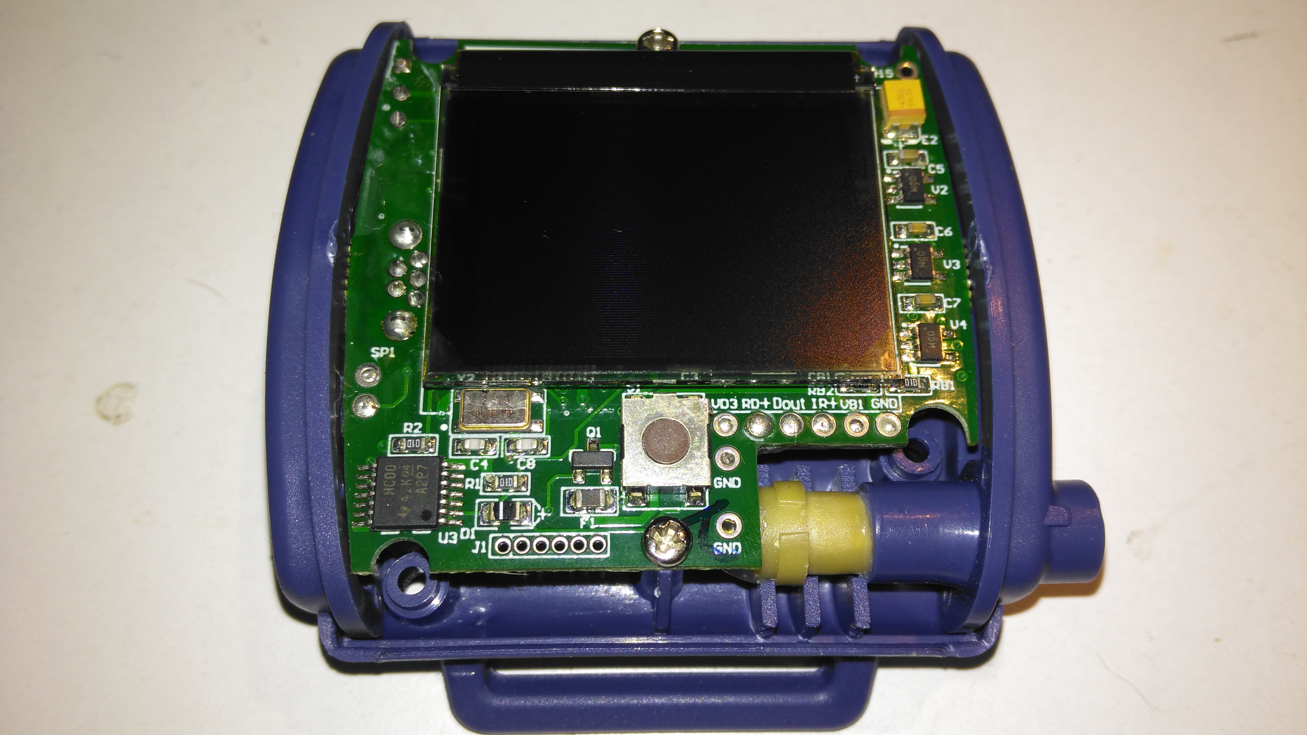
A total of 4 screws hold the casing together, once these are removed the top comes off. The large colour OLED display covers nearly all of the board here. The single button below is the user interface. The connection to the probe is made via the Lemo-style connector on the lower right.
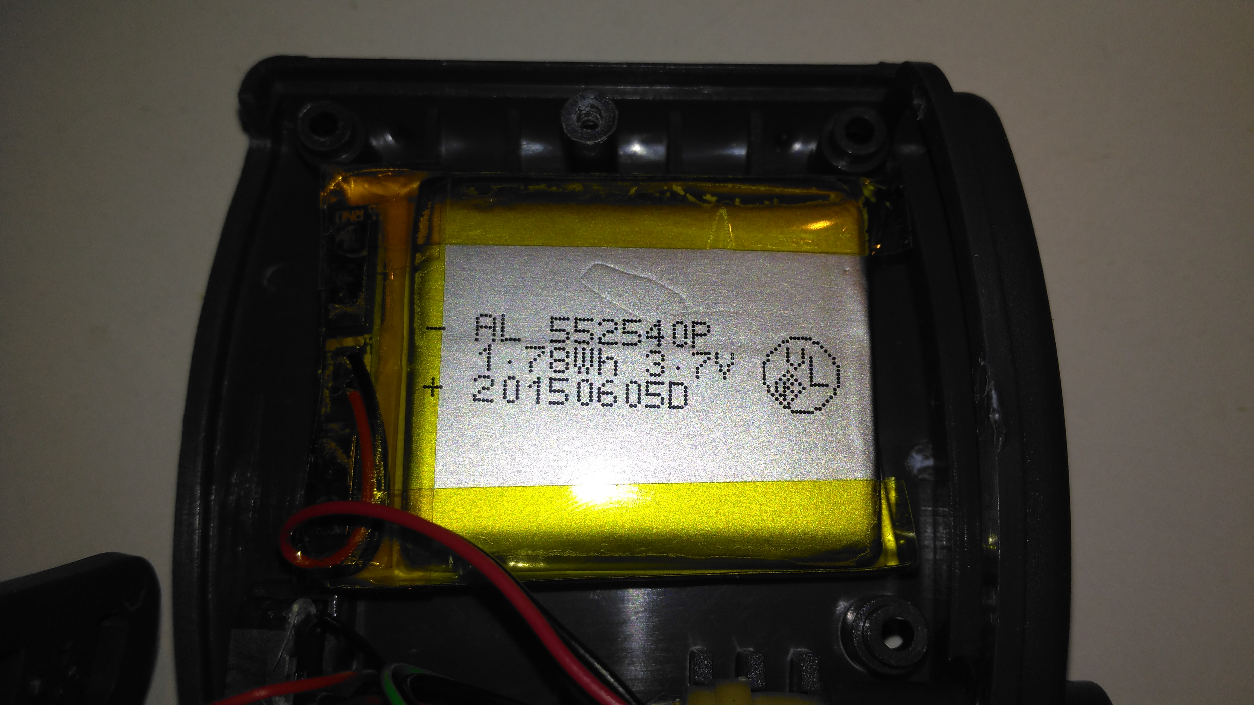
Lithium Cell
Power is provided by a relatively large lithium-ion cell, rated at 1.78Wh.
Main Processor
All the heavy lifting work of the LCD, serial comms, etc are handled by this large Texas Instruments microcontroller, a MSP430F247. The clock crystal is just to the left, with the programming pins. I’m not sure of the purpose of the small IC in the top left corner, I couldn’t find any reference to the markings.
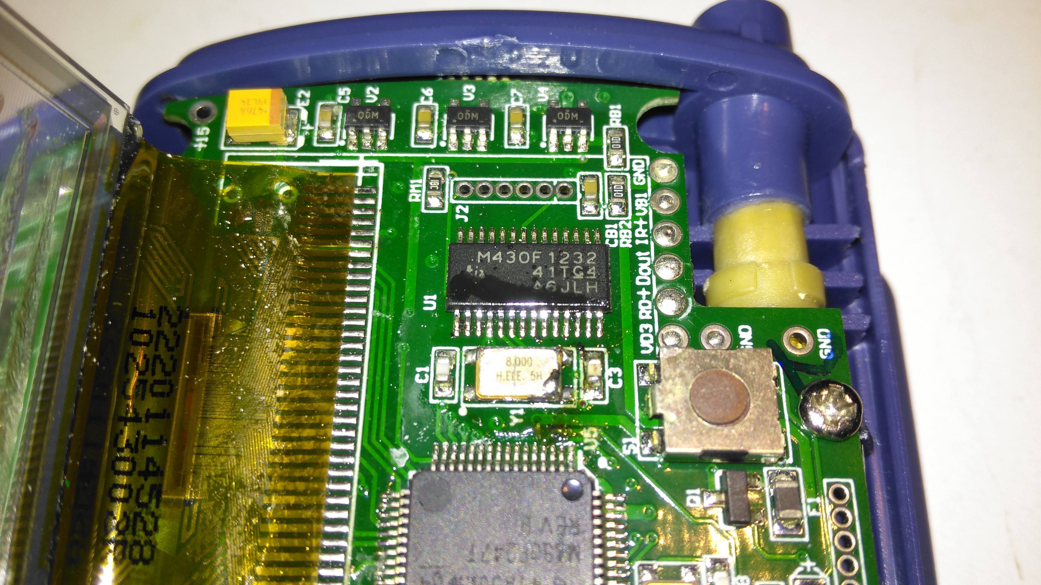
Aux Processor
The actual pulse oximetry sensor readings seem to be dealth with by a secondary microcontroller, a Texas Instruments M430F1232 Mixed-Signal micro. This has it’s own clock crystal just underneath. The connections to the probe socket are to the right of this µC, while the programming bus is broken out to vias just above. The final devices on this side of the board are 3 linear regulators, supplying the rails to run all the logic in this device.
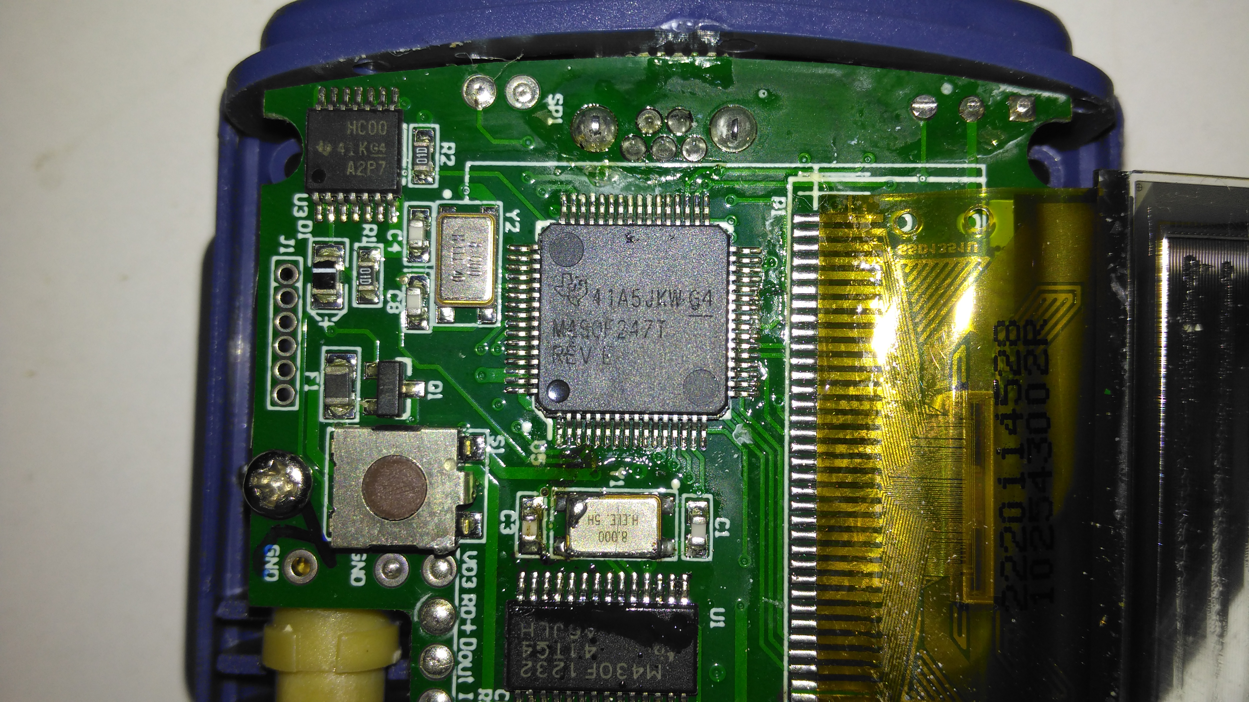
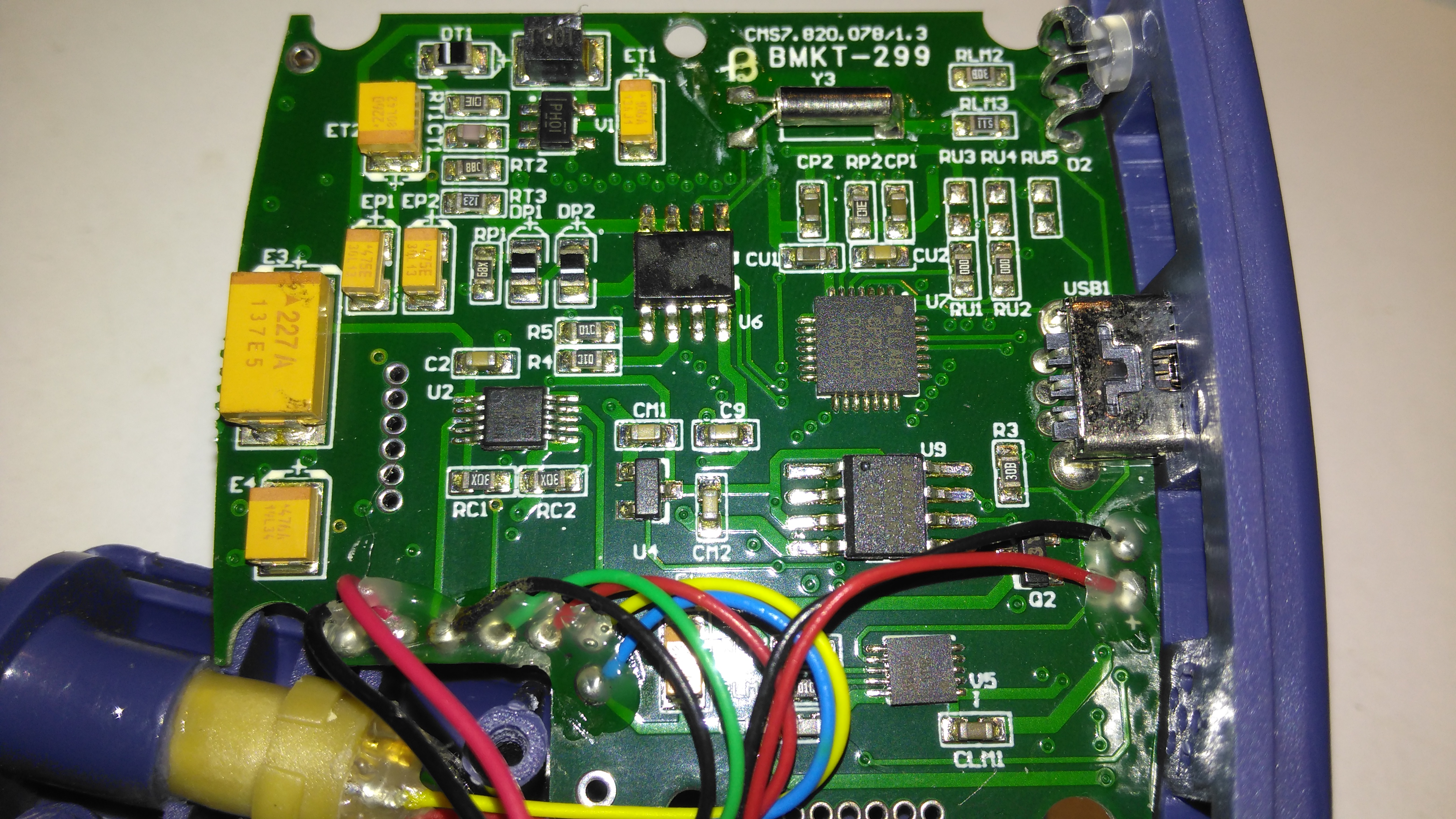
Main PCB Rear
The rear of the PCB has the SiLabs CL2102 USB-Serial interface IC, the large Winbond 25X40CLNIG 512KByte SPI flash for recording oximetry data, and some of the power support components. The RTC crystal is also located here at the top of the board. Up in the top left corner is a Texas Instruments TPS61041 Boost converter, with it’s associated components. This is probably supplying the main voltage for the OLED display module.
This is a pair of modules that Maplin was selling some time back, to send stereo audio over a 2.4GHz radio link. The transmitter identifies as a USB sound card, I’ve personally used these units to transmit audio about 60ft. The transmitter, above, has a single button for pairing with the receiver below.
Receiver
The receiver unit has a large external antenna, a link status LED & volume buttons, these directly control the volume level on the host PC via the sound card drivers.
Receiver PCB Top
Popping the case open on the receiver reveals a large PCB, holding the chipset, along with the audio output jacks & Mini-USB power input. The antenna Coax is soldered to the PCB.
Receiver PCB Bottom
The top of the board has the control buttons, and the status LED.
Receiver Chipset
The chipset used here is a Nordic Semiconductor nRF20Z01 2.4GHz Stereo Audio Streamer, there’s a small microcontroller which does all the register magic on the RF transceiver. The RF chain is at the top of the photo, audio outputs on the top left, and the micro USB power input & voltage regulators at bottom left.
Transmitter PCB Top
The transmitter PCB has a Sonix USB Audio Codec, to interface with the host PC. This is then fed into another Nordic Semi part on the opposite side of the board:
Transmitter PCB Bottom
The bottom of the transmitter has the RF section, and another small control microcontroller.
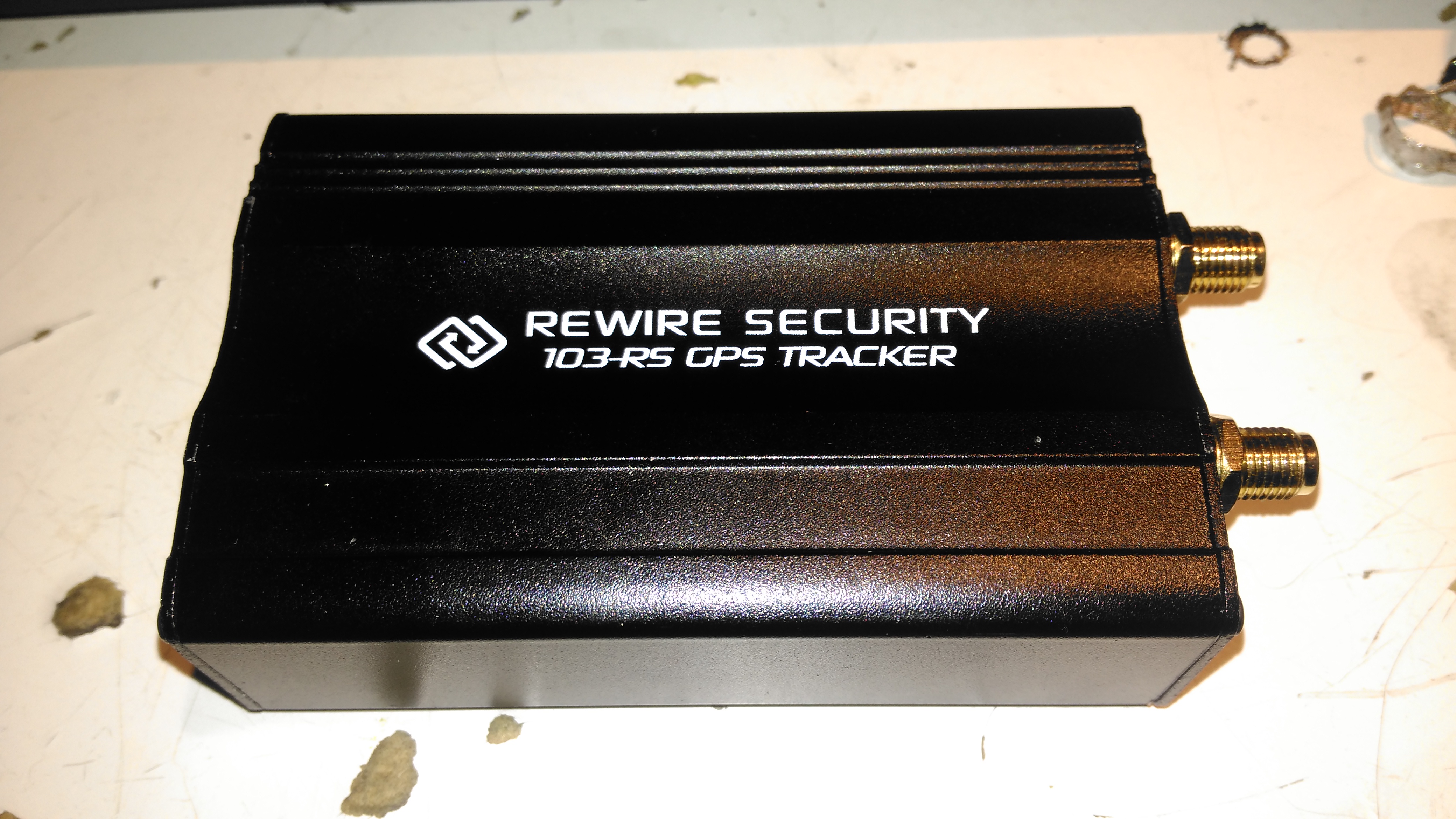
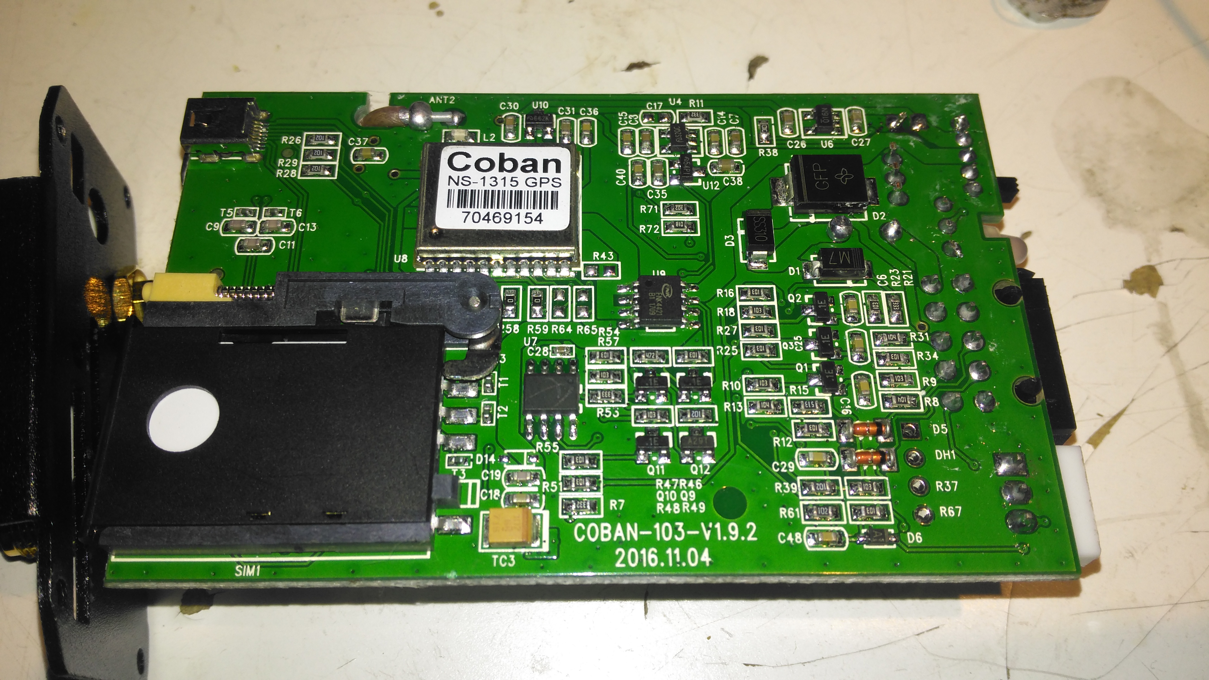
I thought it was time to add a bit of security to the gear I take camping, so this GPS tracker unit was sourced from eBay. This is a Rewire Security 103RS, a slightly customised version of the common Chinese TK103 GPS tracker.
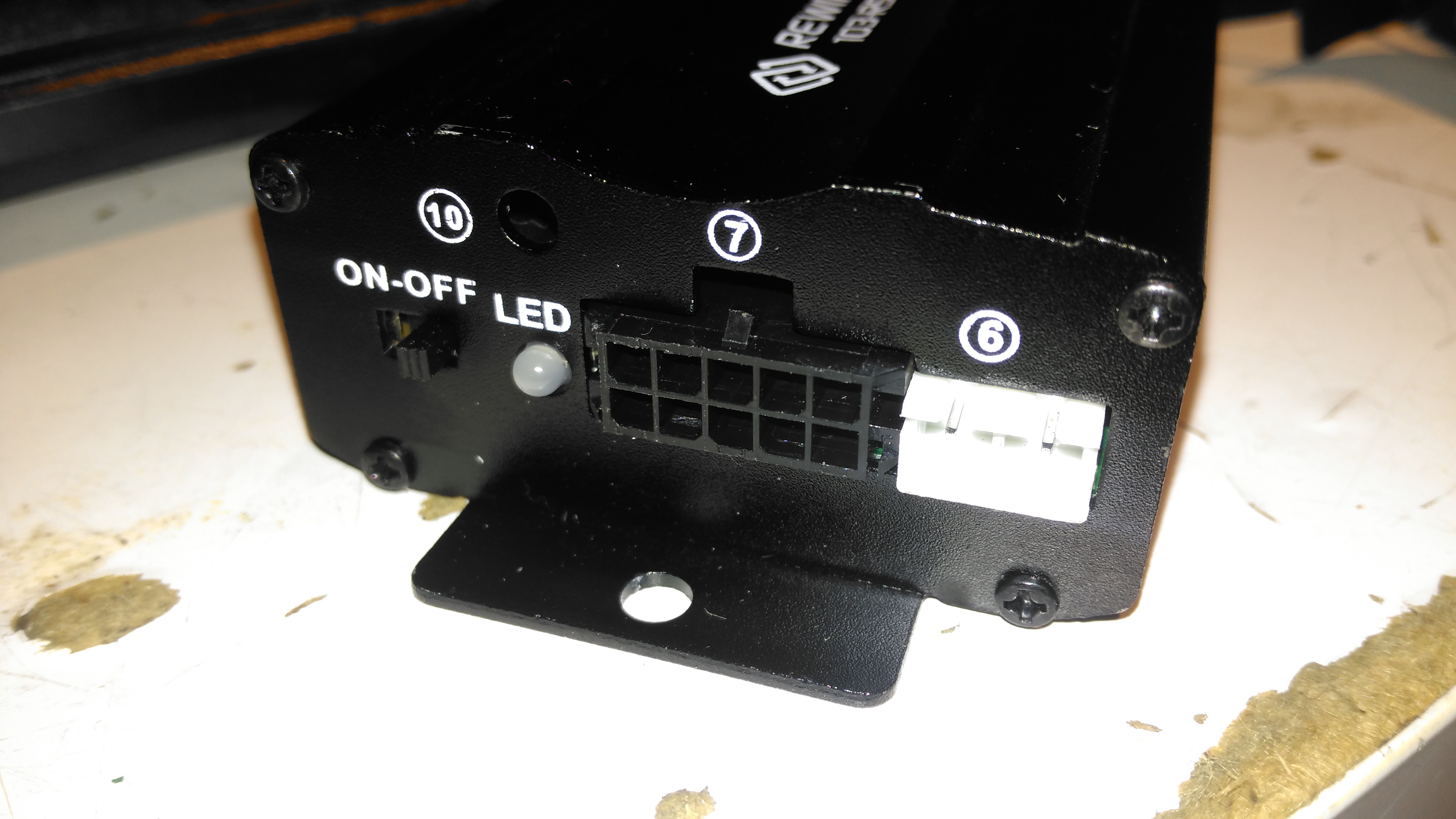
Input Connections
The small module has all it’s power connections on one end of the unit, on a Molex multi-way block. The white connector is for a piezo-shock sensor – this interfaces with the alarm functionality of the unit. There’s an indicator LED for both the GPS & GSM status, and a switch for the backup battery.
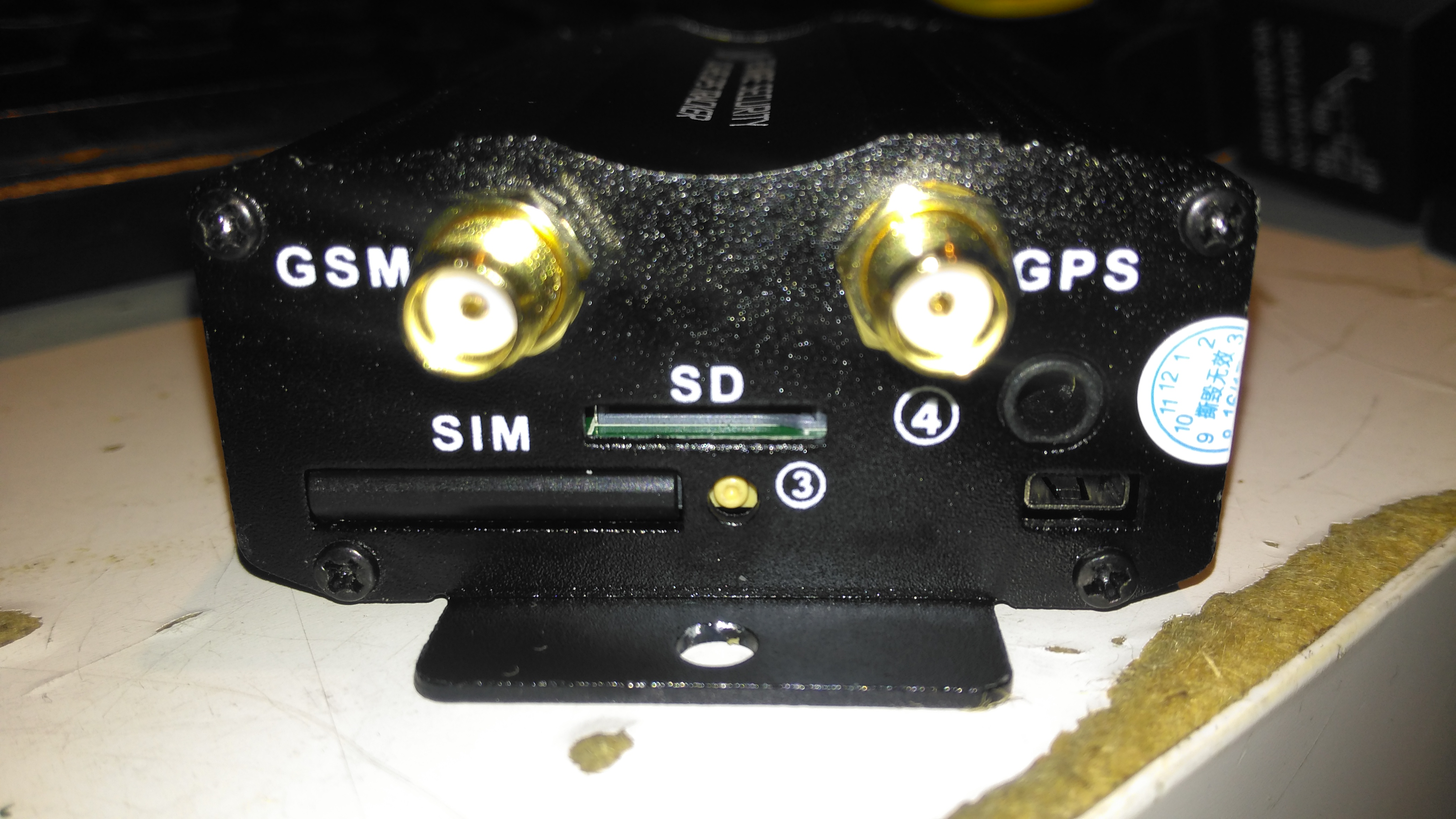
Antenna Connections
The other end has the antenna connections, microphone connection for the monitor function, along with the SIM & SD card slots.
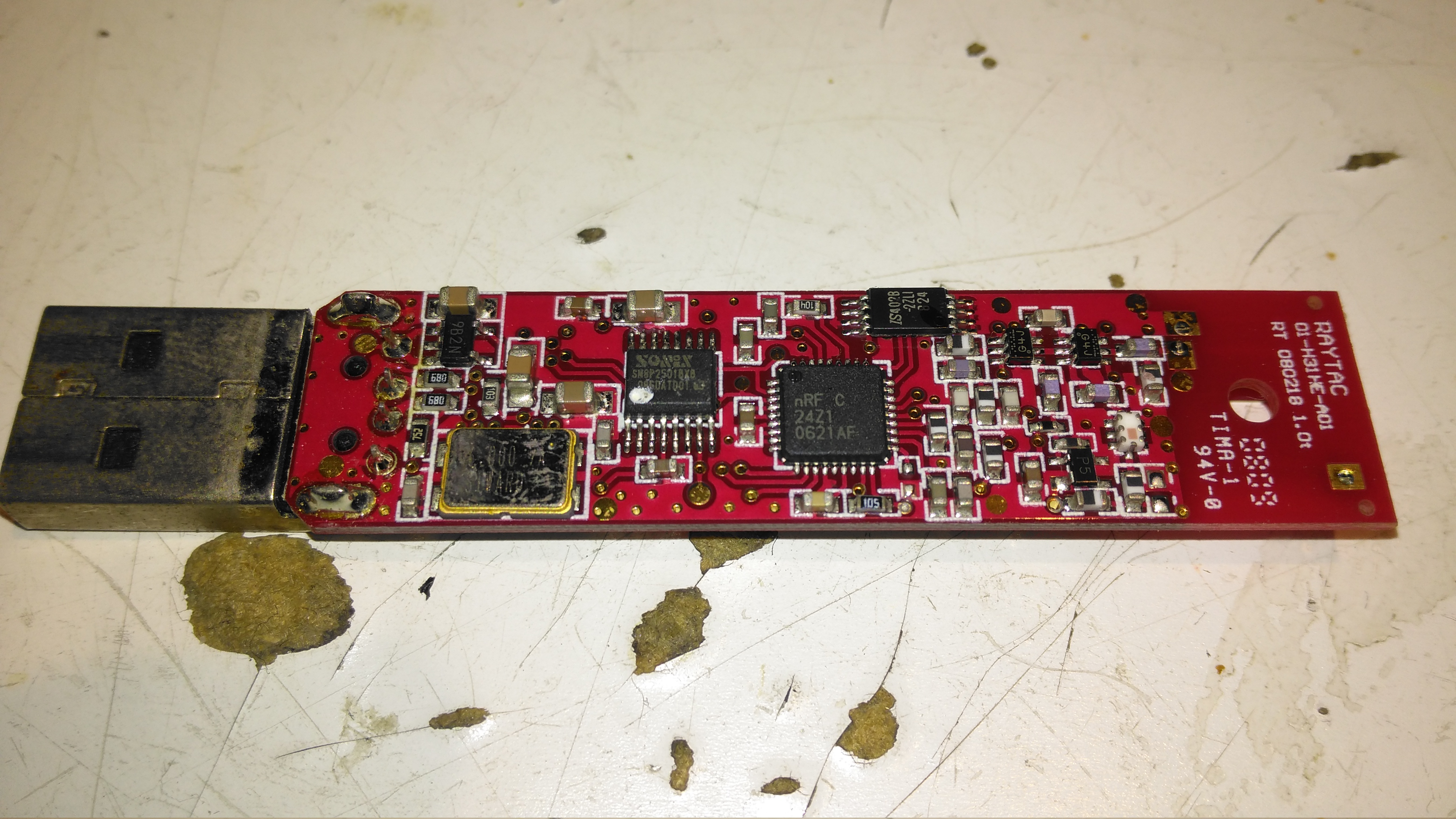
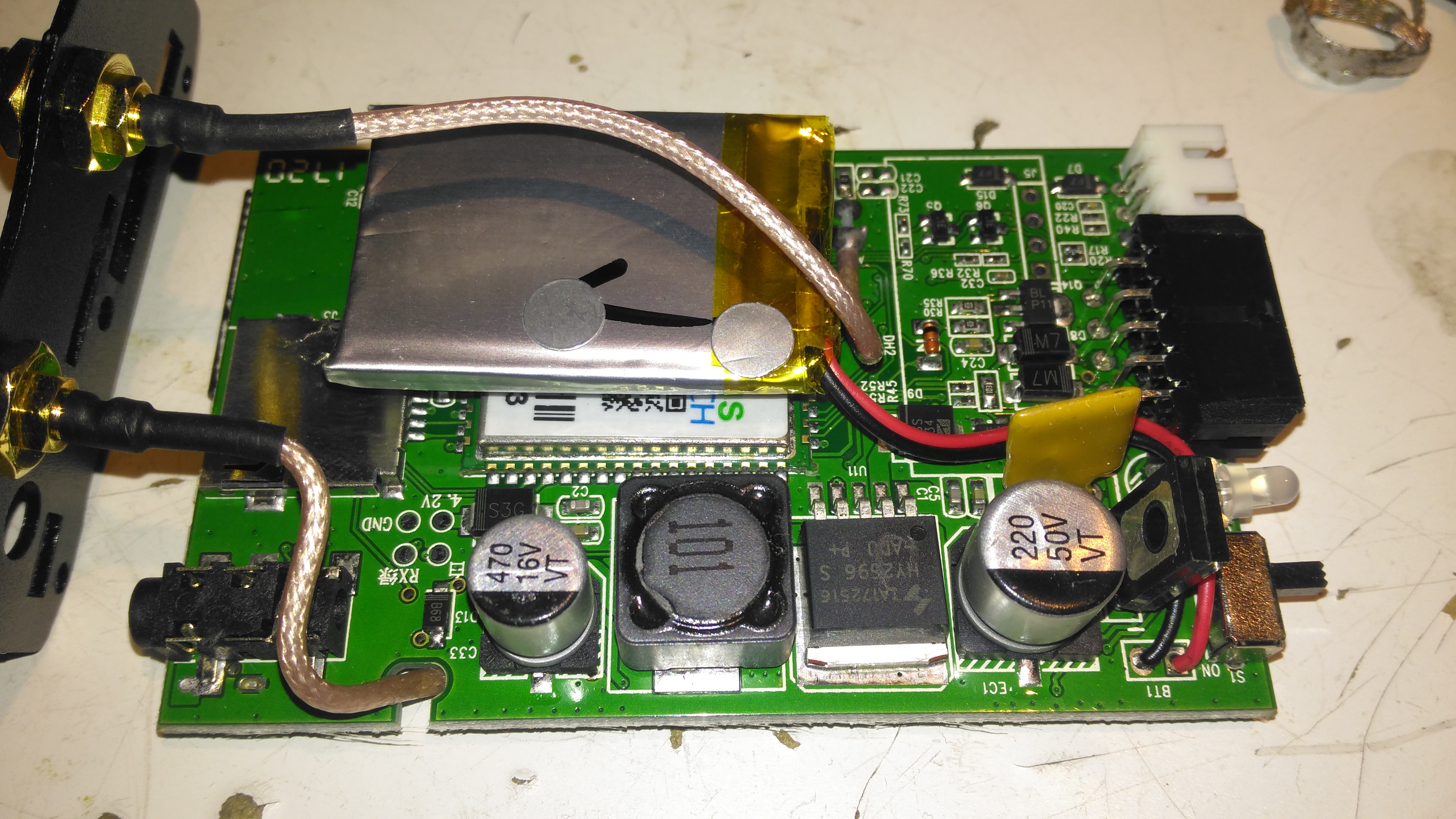
PCB Top
Once the end panel is removed, the PCB just slides out of the aluminium extruded casing. It’s pretty heavily packed with components in here. A switching regulator deals with the 12v input from the vehicle battery, and is protected by a polyfuse on the right. The GSM module is hiding under the Li-Po backup cell, unfortunately the sticky pad used to secure this wouldn’t come off without damaging something. The pigtails for both the GPS & GSM antennas are permanently soldered to the board here.
PCB Bottom
The bottom of the PCB has the GPS module, and mainly input protection & bypassing components. There is a FNK4421 Dual P-Channel MOSFET here as well, probably used for switching the external relay or alarm siren. The SIM socket for the GSM modem is located here in the corner.
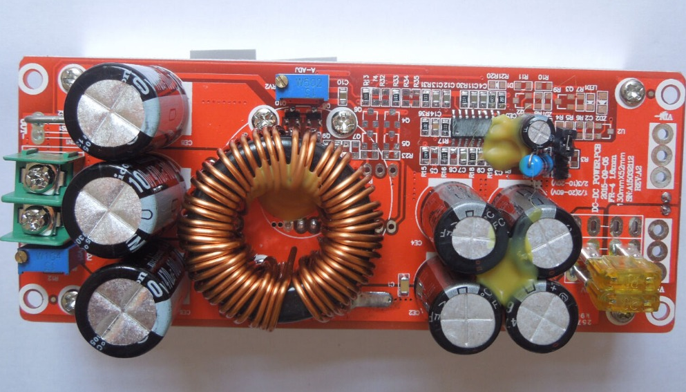
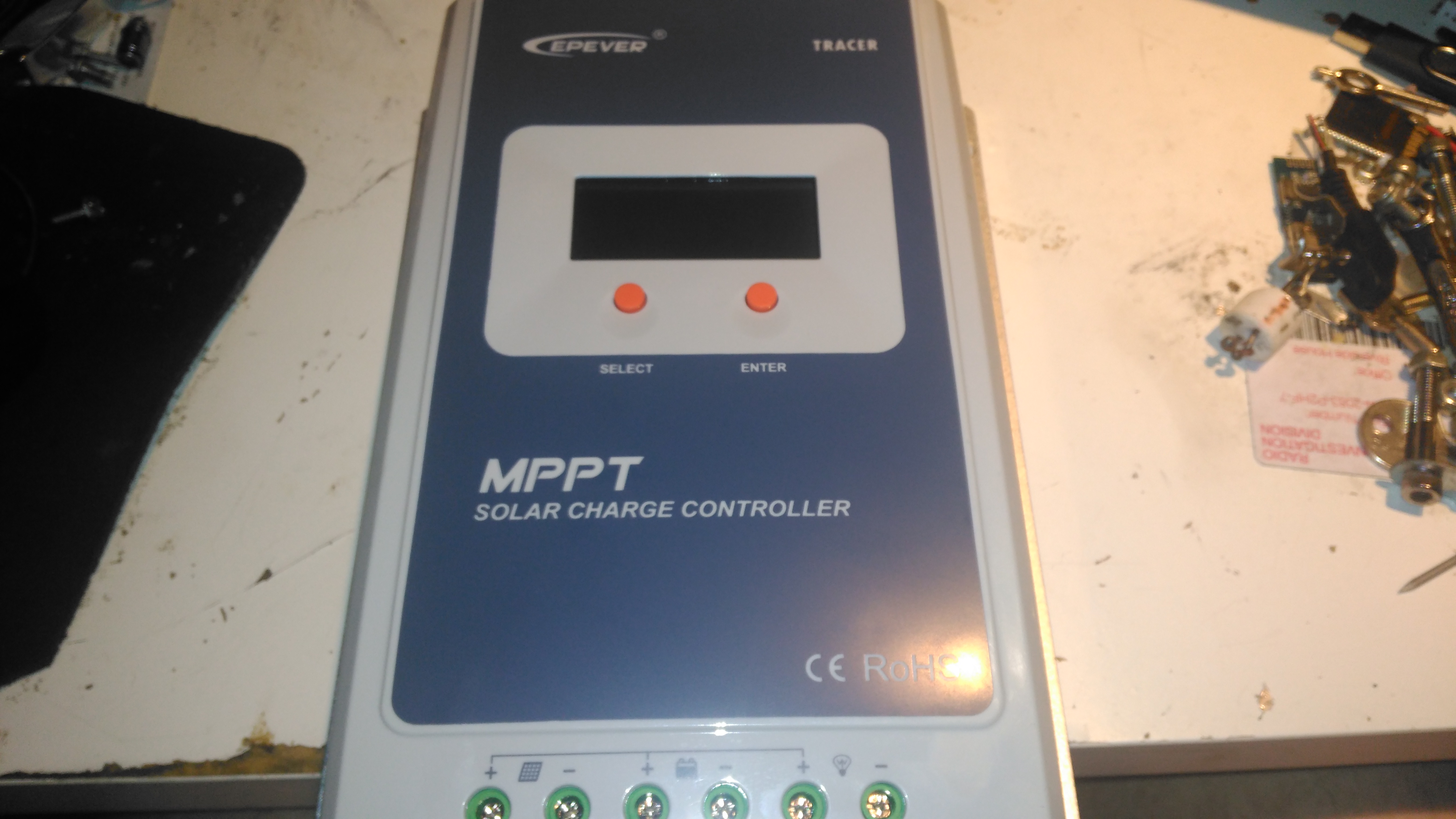
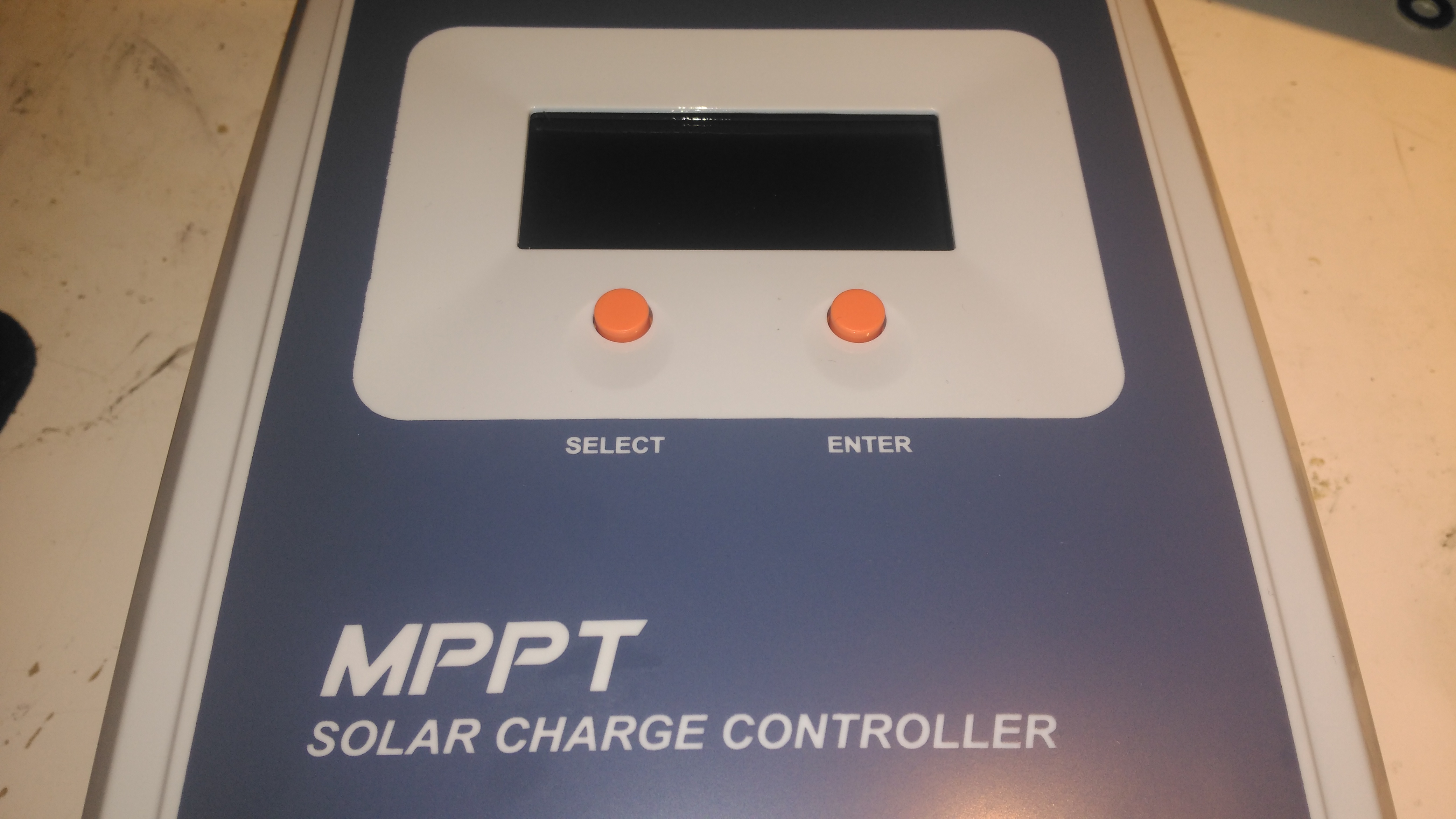
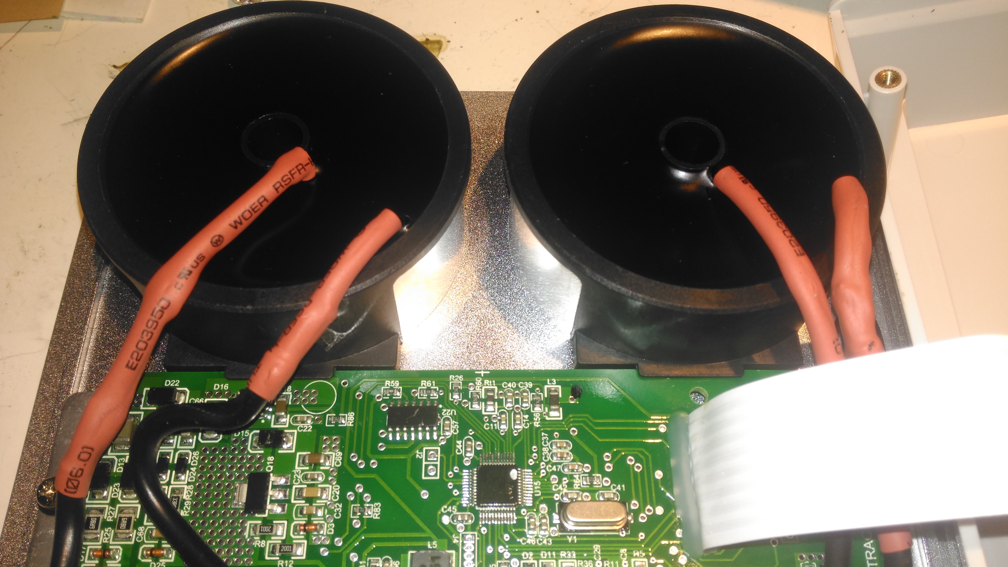
Here’s the solar charge controller to go with the MT50 from the last post. This is the 40A version of the EpEver Tracer A series, the 4210A. This unit is large, and very heavy. Most of this weight comes from the enormous heatsink which doubles as the mounting plate for all the other components, and the large inductors that are going to be required for the DC-DC conversion that MPPT requires.
Front Panel
The front panel has a basic LCD, which shows various stats, such as PV Volts & Amps, and battery bank Volts & Amps. The pair of buttons are used to navigate the basic menu to configure some options, along with switching the load terminals ON/OFF.
Specifications
There’s a specs label on the top, with a slight difference here vs the manual, which states the max. PV volts as 92v.
Main PCB Overview
Removing 4 machine screws from the bottom of the unit allows the top to come off. Like the MT50 remote panel, this unit also has moulded-in brass thread inserts in the plastic parts. The PCB in here is heavily comformal coated, which stops me from reading the laser-etched numbers on the semiconductor devices, so there will be few details there.
Main PCB Lower
Here’s the bottom section of the main PCB, with the enormous screw terminals, which will easily take cables up to about 16mm². The RJ-45 jack which hosts the unit’s RS-485 bus is to the right, and a smaller 2-pin connector on the left sorts out the battery temperature sensor.
The DC output MOSFET switches are hiding just behind the right-hand terminals, there’s a pair of them in this unit to handle the output current. Some beefy diodes polarity-protect both the battery & PV inputs.
Board Centre
Moving up the board shows two 35A automotive blade fuses soldered into the board – these would be a real pain to replace if they ever blew, however with the electronic load current protection built into this unit, it’s an unlikely situation, unless something went hideously wrong. The main switching devices for the DC-DC converter are hidden – they’re clamped to the heatsink with the bars at right angles in the photo, I’m not going to dig any deeper into this just for those though – they’re just TO220 devices.
Under a load of thermal gunk on the right are 4 current shunt resistors, and the amplifiers for reading their values. These 1206-size SMD resistors looked a bit small for the power rating to me, but they’re heatsinked in operation to a small heatsink mounted in the top cover.
Board Upper
The upper section of the PCB hosts the main microcontroller, and the connections over to the front panel LCD & buttons. Couldn’t really get much info from these chips, due to the conformal coating.
Toroidal Inductors
Right at the top of the unit are these toroidal inductors, potted into aluminium housings. The copper windings of these is very heavy – at least 2.5mm². They’re electrically in parallel, the 20A version would only have a single inductor.
Current Shunt Heatsink
This small heatsink sits inside the top cover, and provides some cooling to the current shunts.
Display Board
Not much to say for the display board, there’s going to be nothing here apart from an I²C LCD driver & the pair of front panel buttons, so I won’t bother removing this from the case.
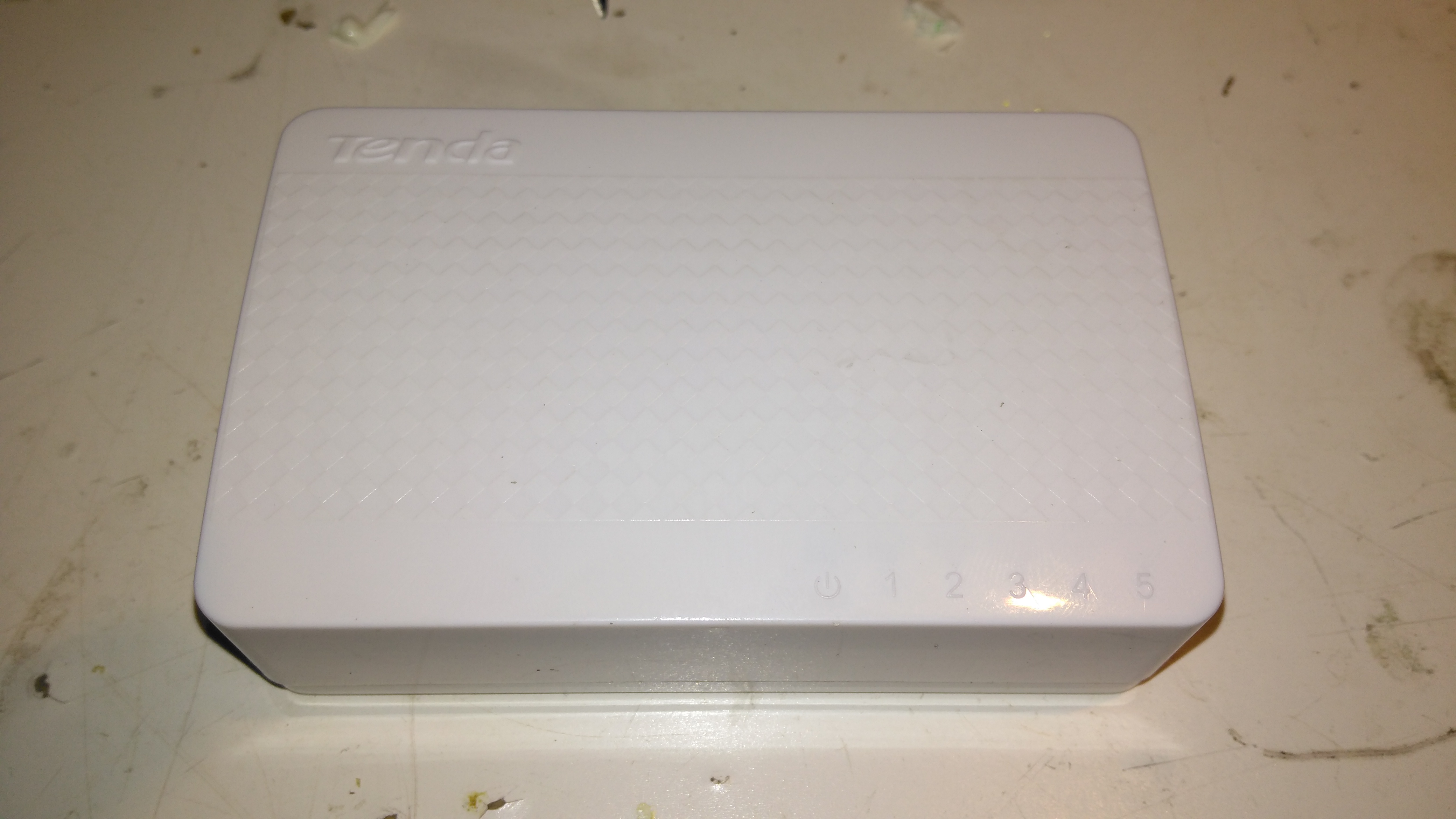
Here’s a tiny ethernet switch from the great fle market that is eBay – the Tenda S105. This unit has 5 ports, but only supports 10/100M. Still, for something so small it’s not bad.
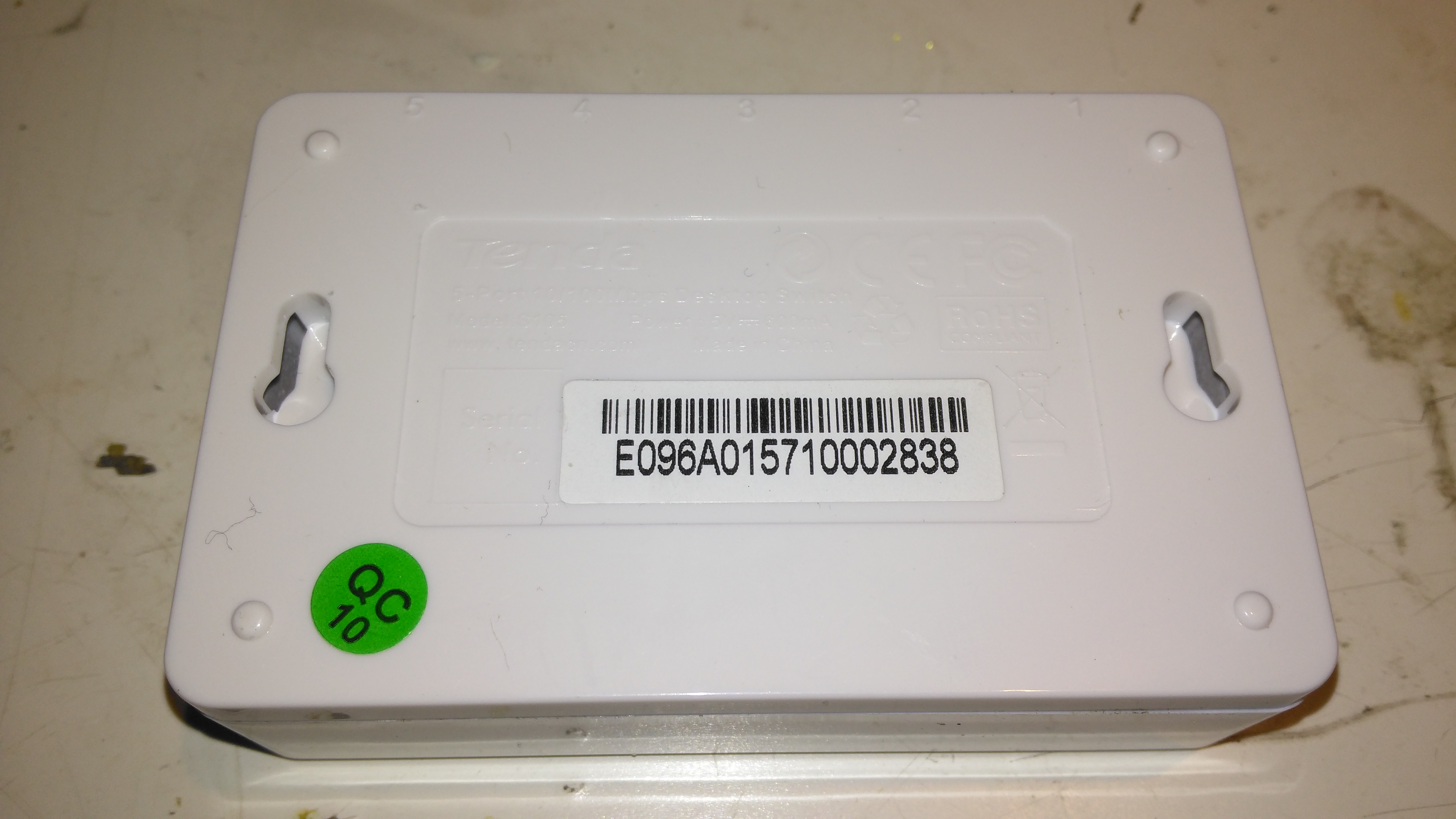
Bottom
Not much on the bottom, there’s a pair of screw hooks for mounting this to a surface.
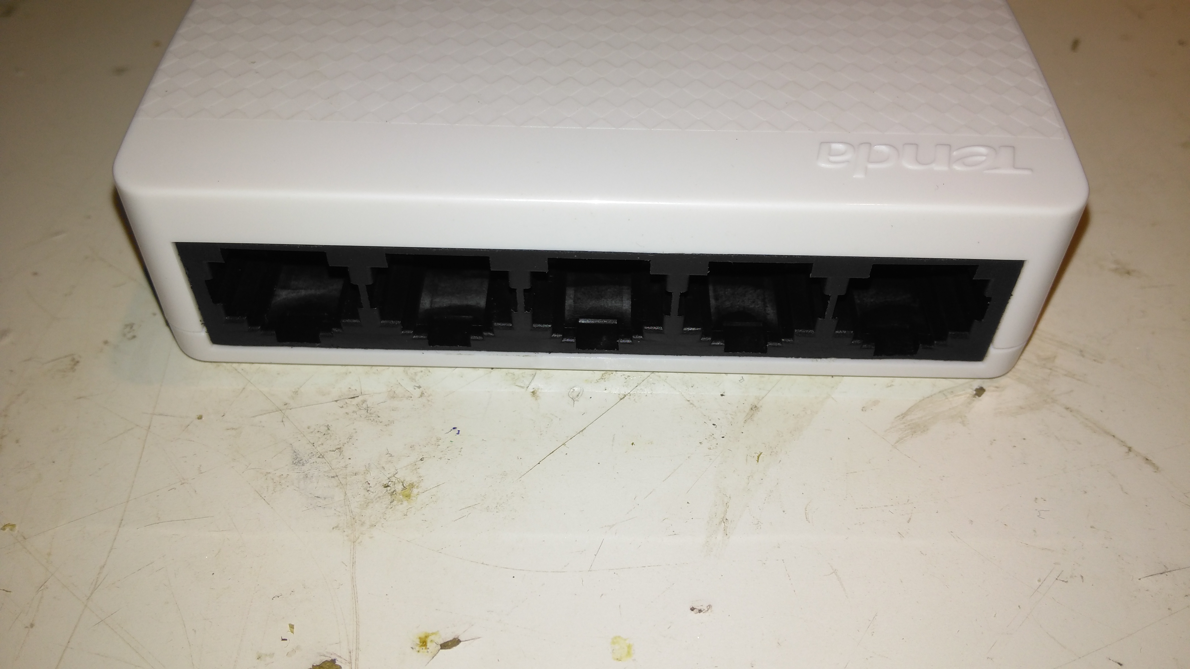
Ports
The 5 ports on the front actually have the pins for the unused pairs of the ethernet cables removed – saving every penny here.
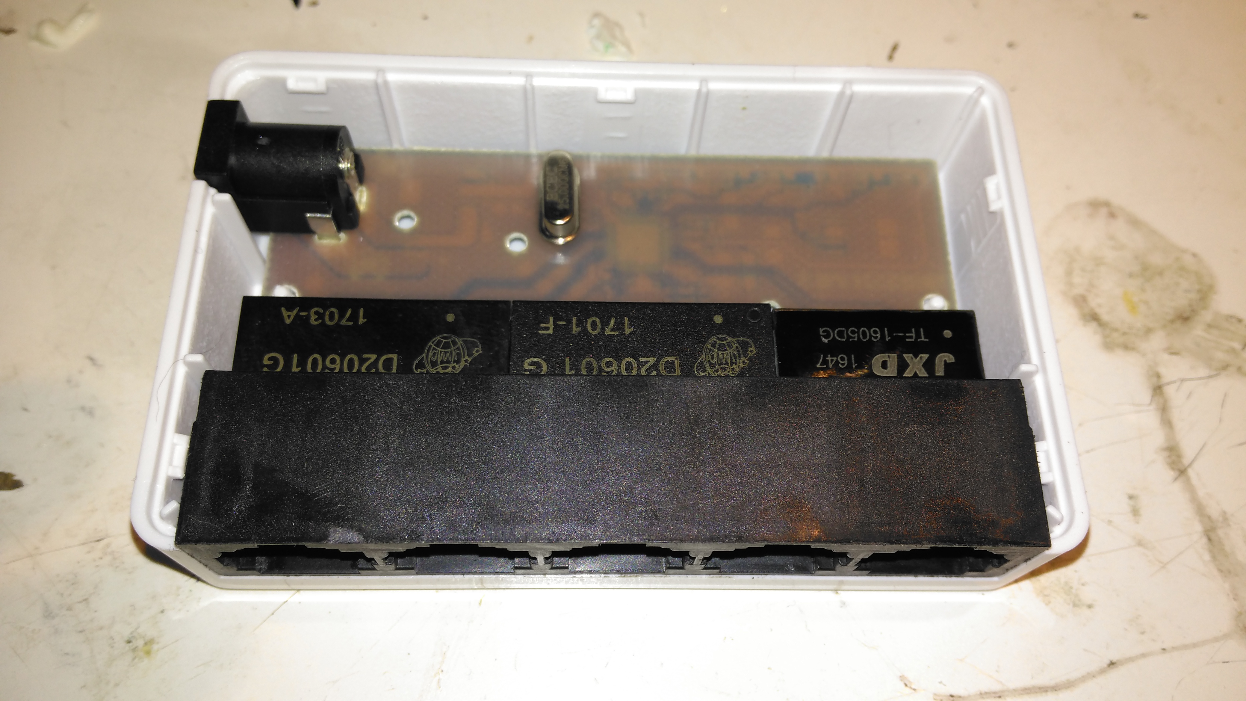
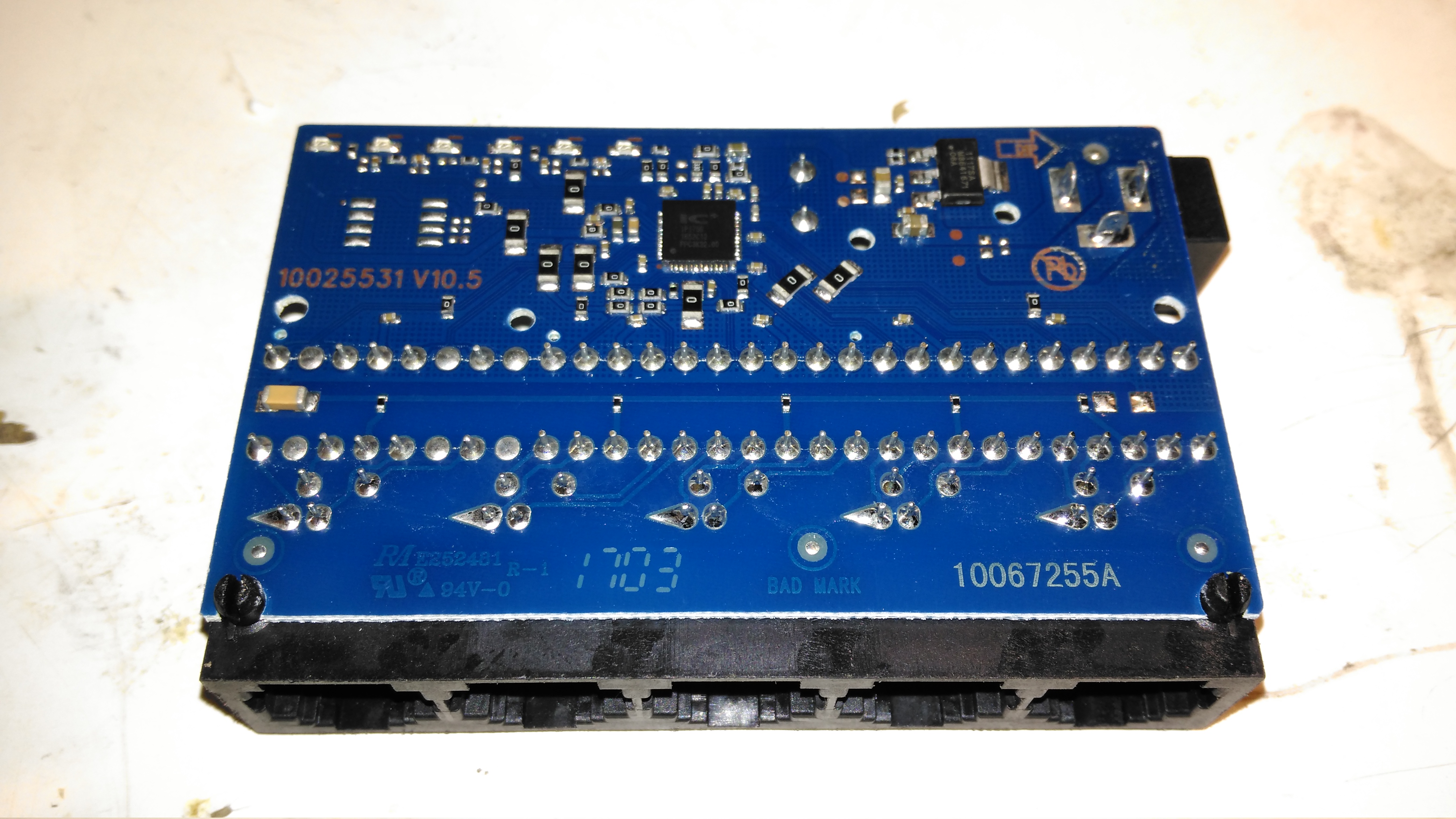
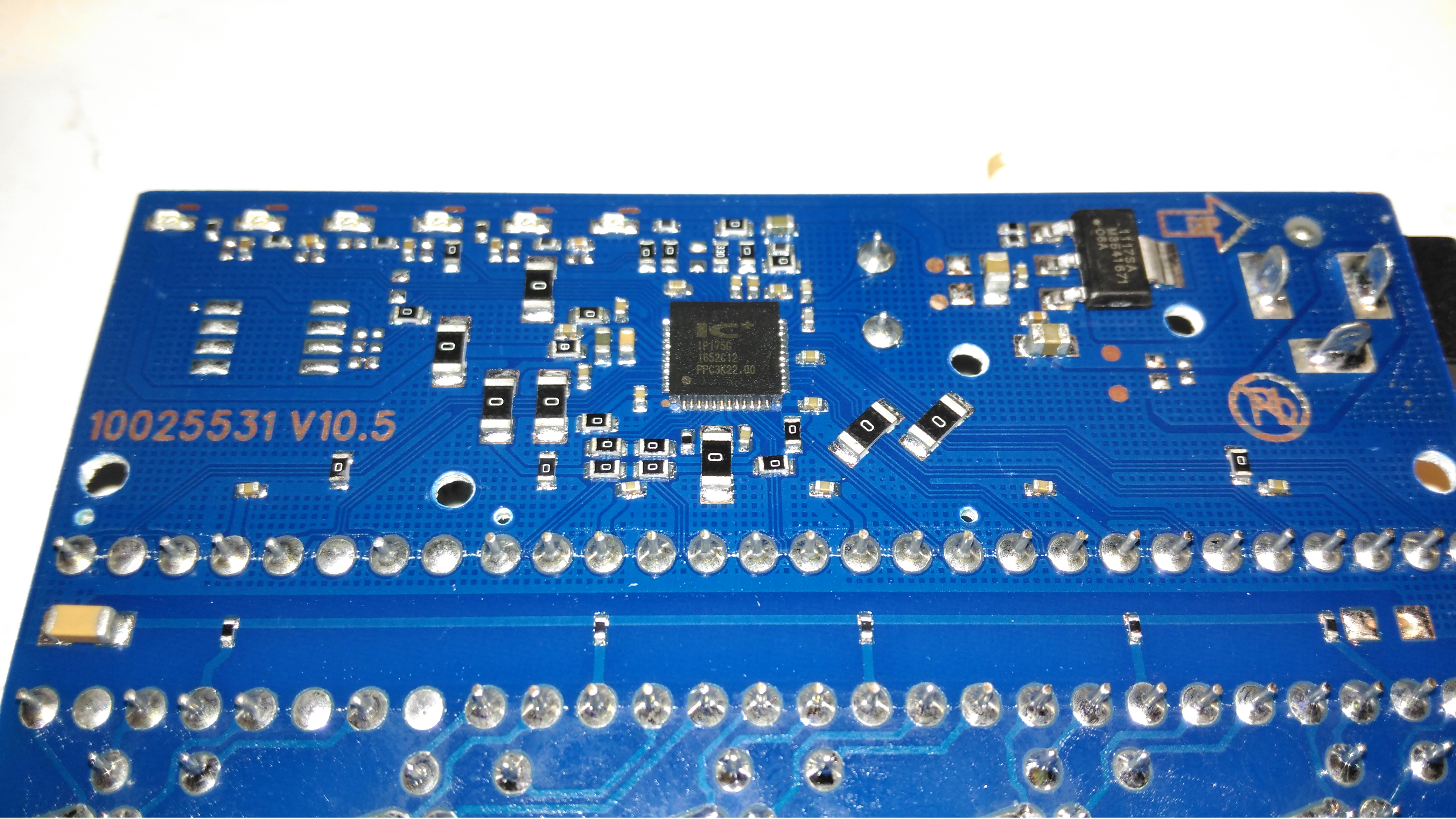
PCB Top
The casing just unclips, revealing the small PCB. Nothing much on the top, just the connectors, isolating transformers & the crystal for the switch IC.
PCB Bottom
The bottom of the PCB is a little more busy, mainly with decoupling components. There’s a 3.3v linear regulator to step down the 5v input for the switch IC.
Switch IC
The IC doing all the data switching is an IP175G 5-Port 10/100 Switch from IC+ Corp. No datasheet available for this, but it’s going to be a bog-standard switch.
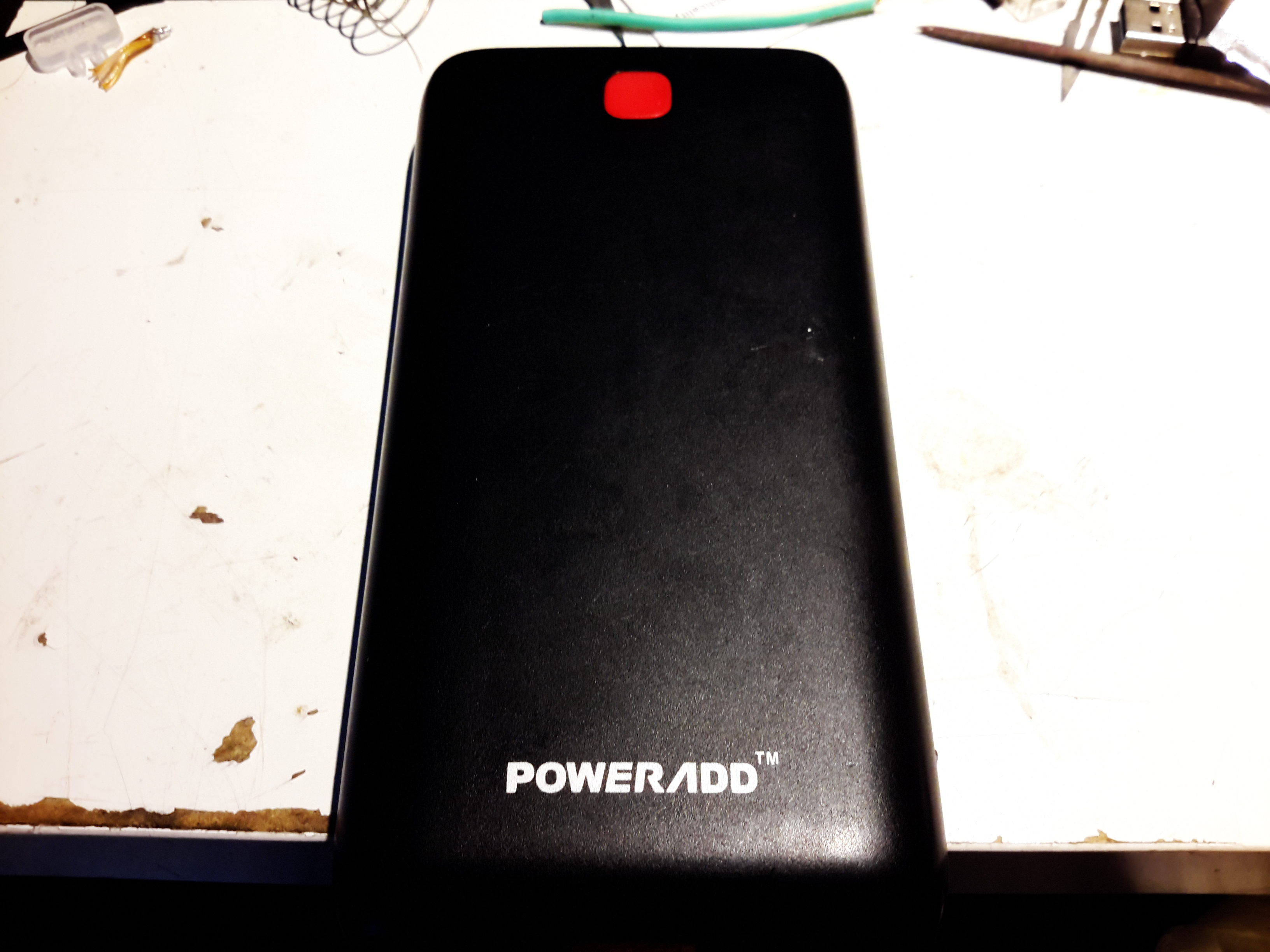
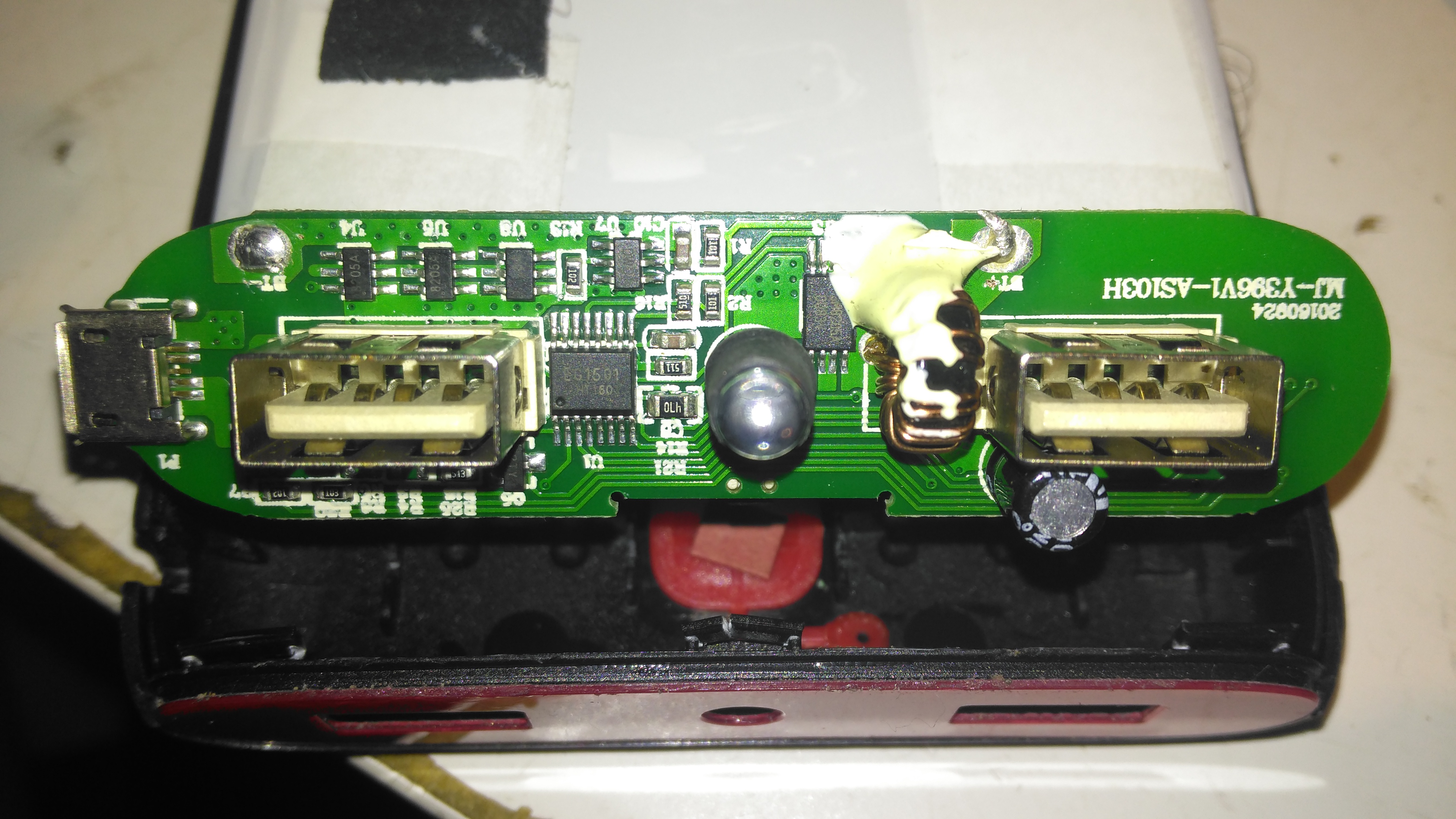
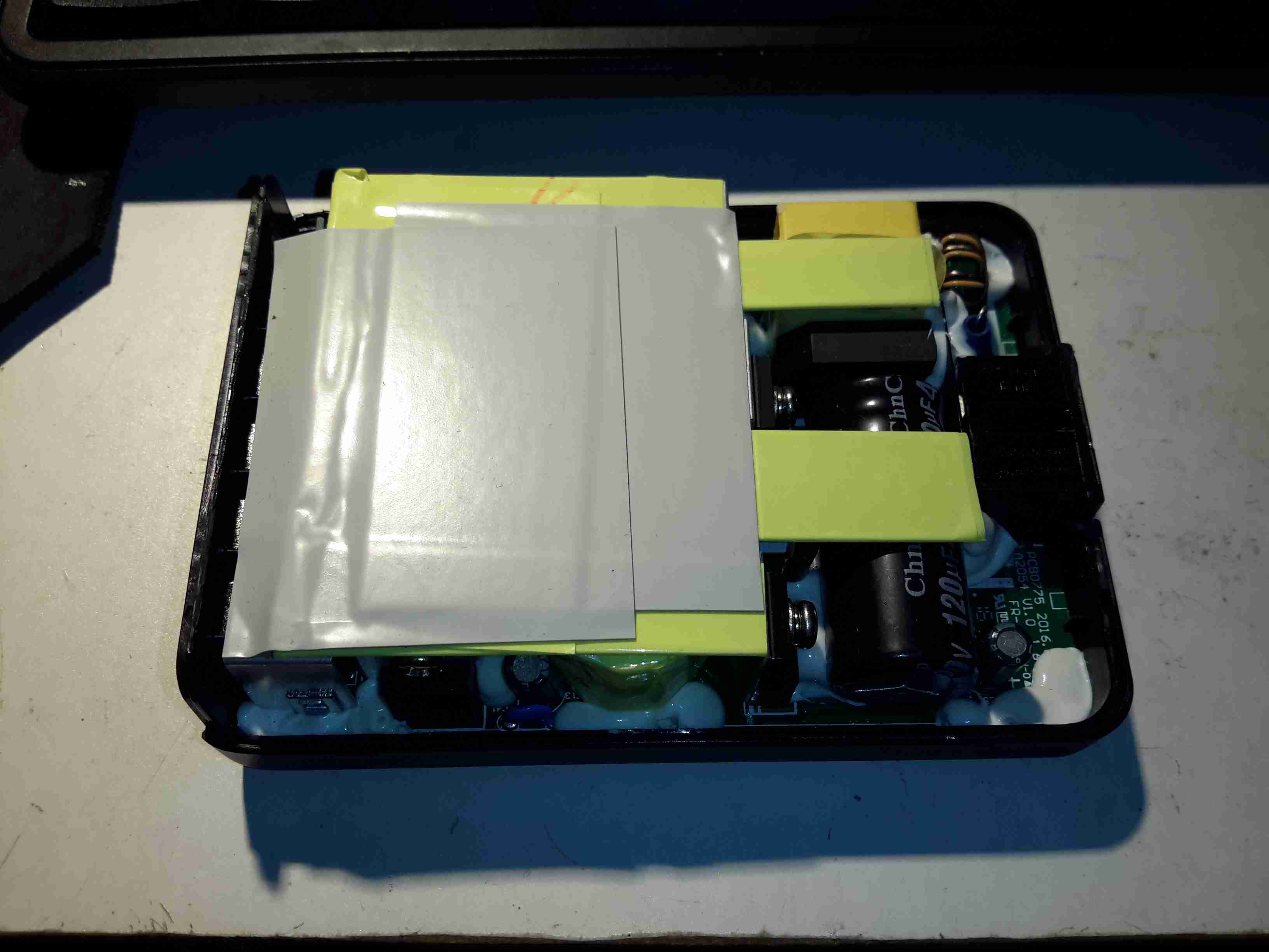
Here’s the biggest portable USB powerbank I’ve seen yet – the PowerAdd Pilot X7, this comes with a 20Ah (20,000mAh) capacity. This pack is pretty heavy, but this isn’t surprising considering the capacity.
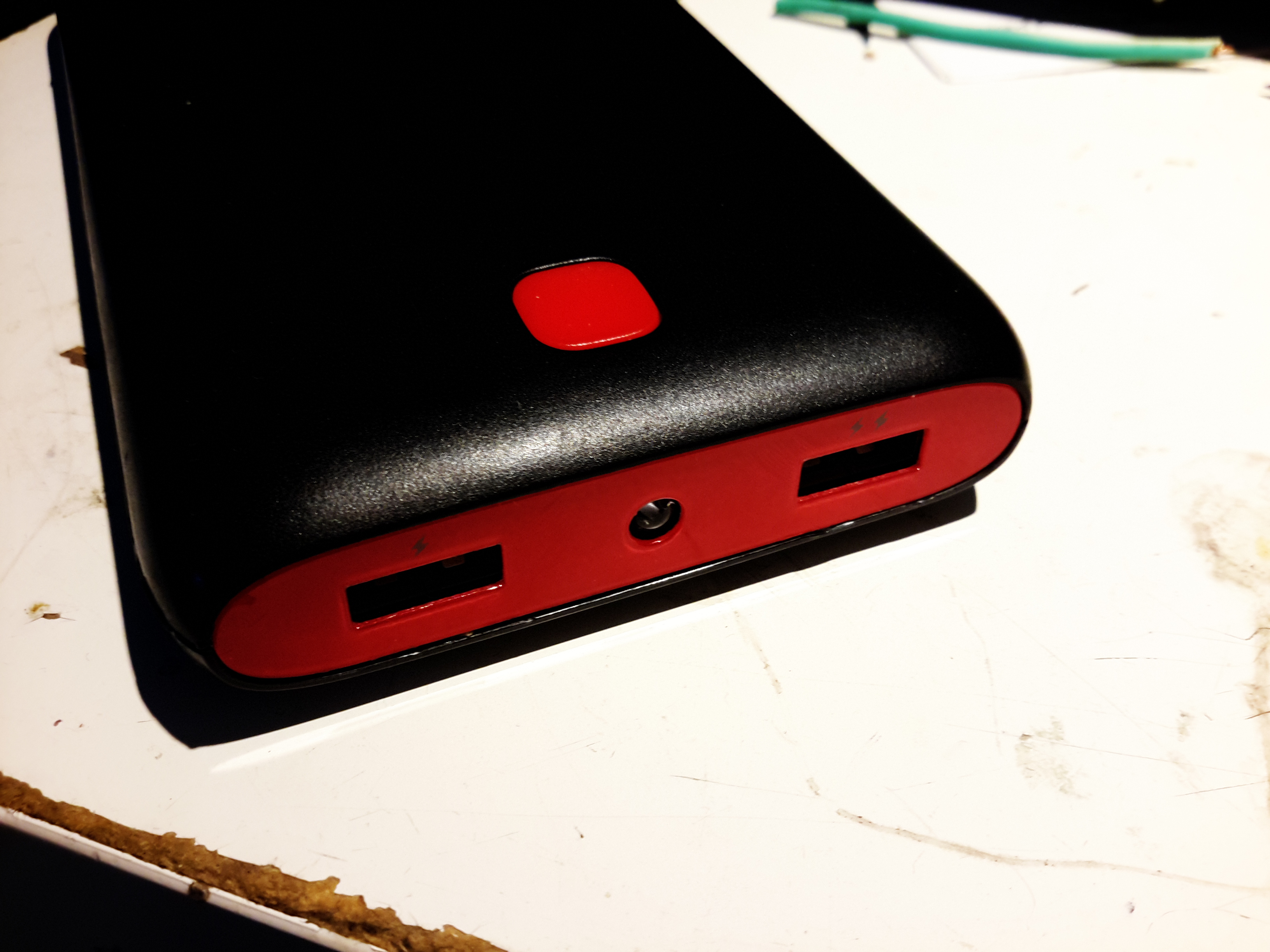
USB Ports & LED
The front of the pack houses the usual USB ports, in this case rated at 3.4A total between the ports. There’s a white LED in the centre as a small torch, activated by double-clicking the button. A single click of the button lights up the 4 blue LEDs under the housing that indicate remaining battery capacity. Factory charging is via a standard µUSB connector in the side, at a maximum of 2A.
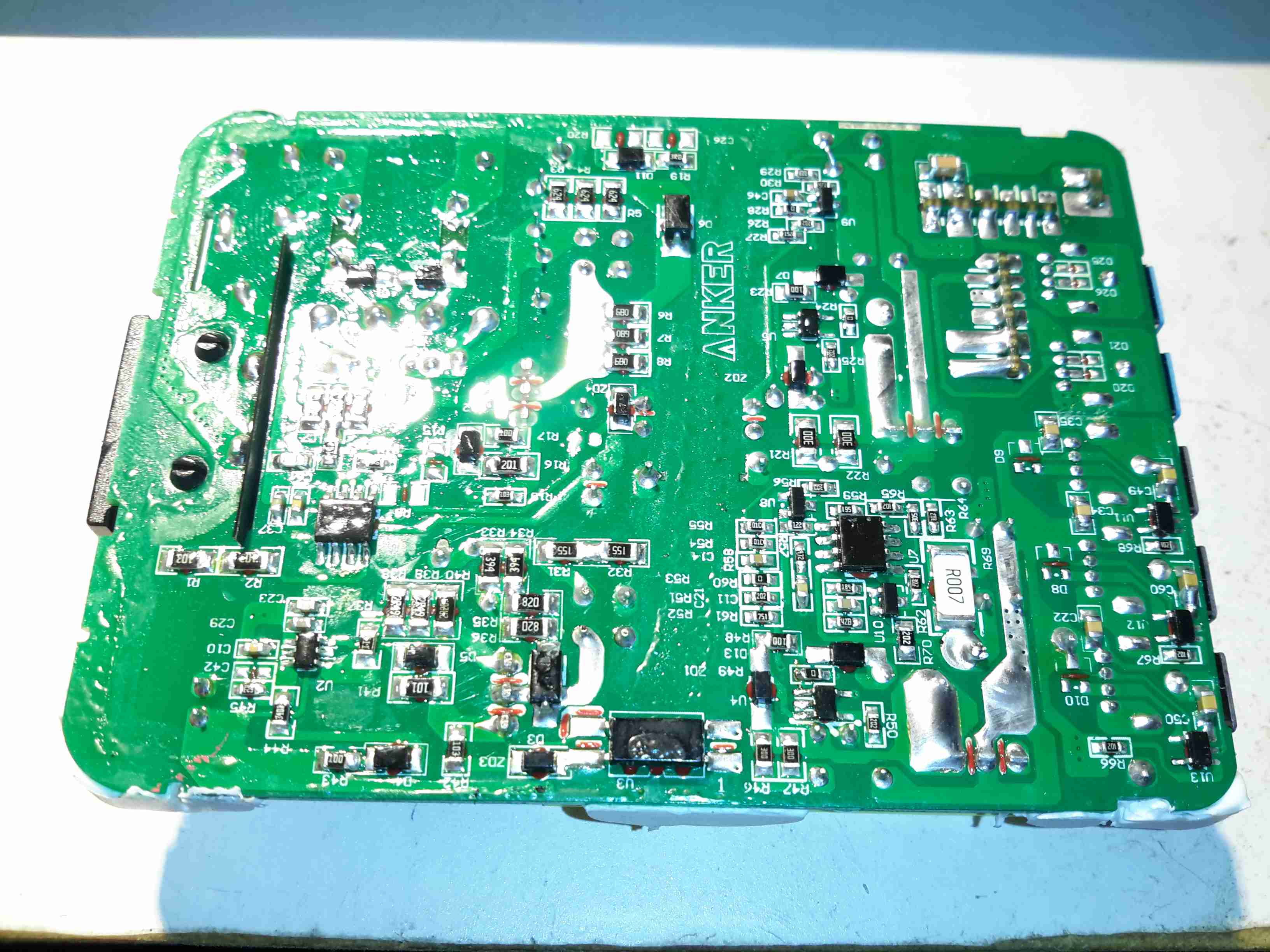
PCB Front
The front of the PCB holds the USB ports, along with most of the main control circuitry. At top left is a string of FS8025A dual-MOSFETs all in parallel for a current carrying capacity of 15A total, to the right of these is the ubiquitous DW01 Lithium-Ion protection IC. These 4 components make up the battery protection – stopping both an overcharge & overdischarge. The larger IC below is an EG1501 multi-purpose power controller.
This chip is doing all of the heavy lifting in this power pack, dealing with all the DC-DC conversion for the USB ports, charge control of the battery pack, controlling the battery level indicator LEDs & controlling the torch LED in the centre.
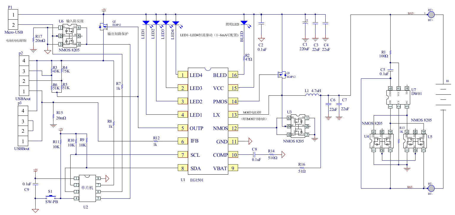
EG1501 Example
The datasheet is in Chinese, but it does have an example application circuit, which is very similar to the circuitry used in this powerbank. A toroidal inductor is nestled next to the right-hand USB port for the DC-DC converter, and the remaining IC next to it is a CW3004 Dual-Channel USB Charging Controller, which automatically sets the data pins on the USB ports to the correct levels to ensure high-current charging of the devices plugged in. This IC replaces the resistors R3-R6 in the schematic above.
The DC-DC converter section of the power chain is designed with high efficiency in mind, not using any diodes, but synchronous rectification instead.
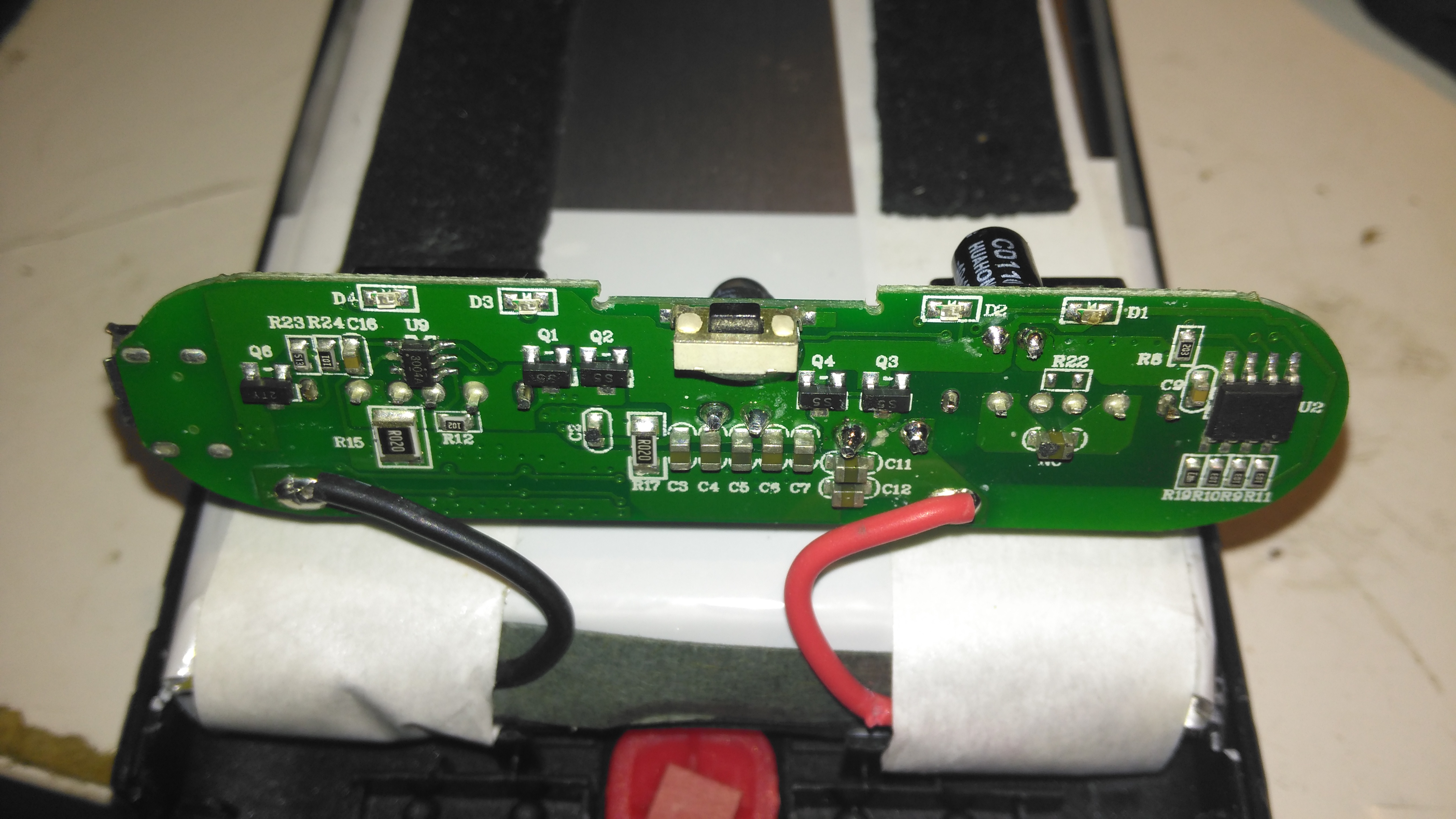
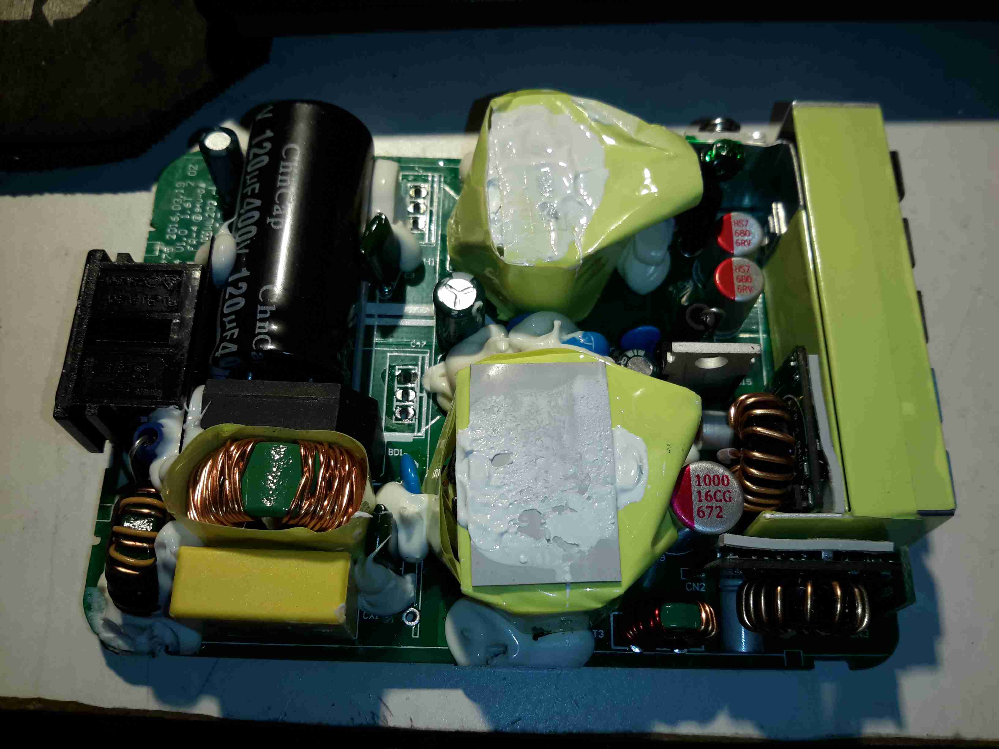
PCB Back
The back of the PCB just has a few discrete transistors, the user interface button, and a small SO8 IC with no markings at all. I’m going to assume this is a generic microcontroller, (U2 in the schematic) & is just there to interface the user button to the power controller via I²C.
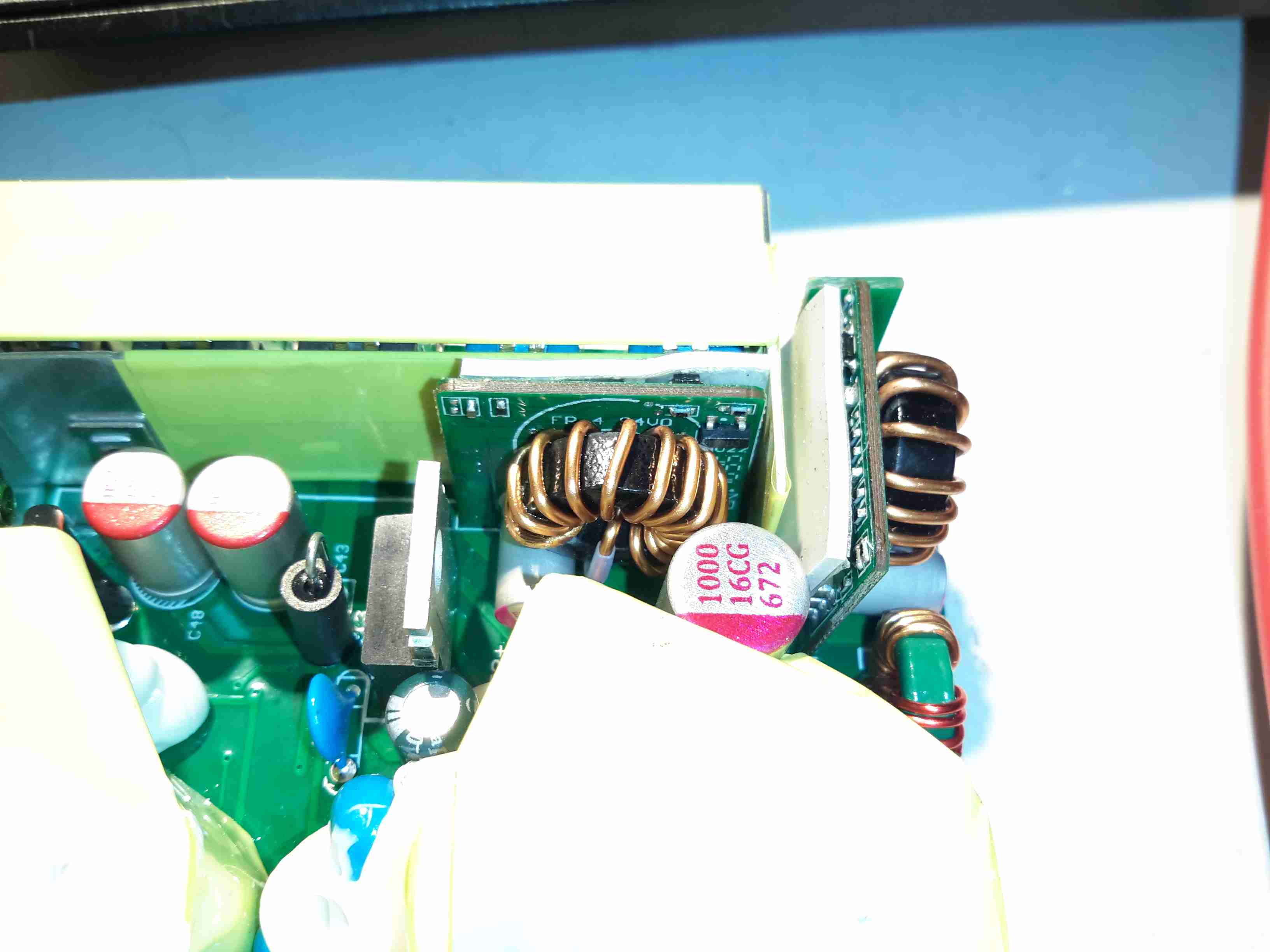
Cells
Not many markings on the cells indicating their capacity, but a full discharge test at 4A gave me a resulting capacity of 21Ah – slightly above the nameplate rating. There are two cells in here in parallel, ~10Ah capacity each.
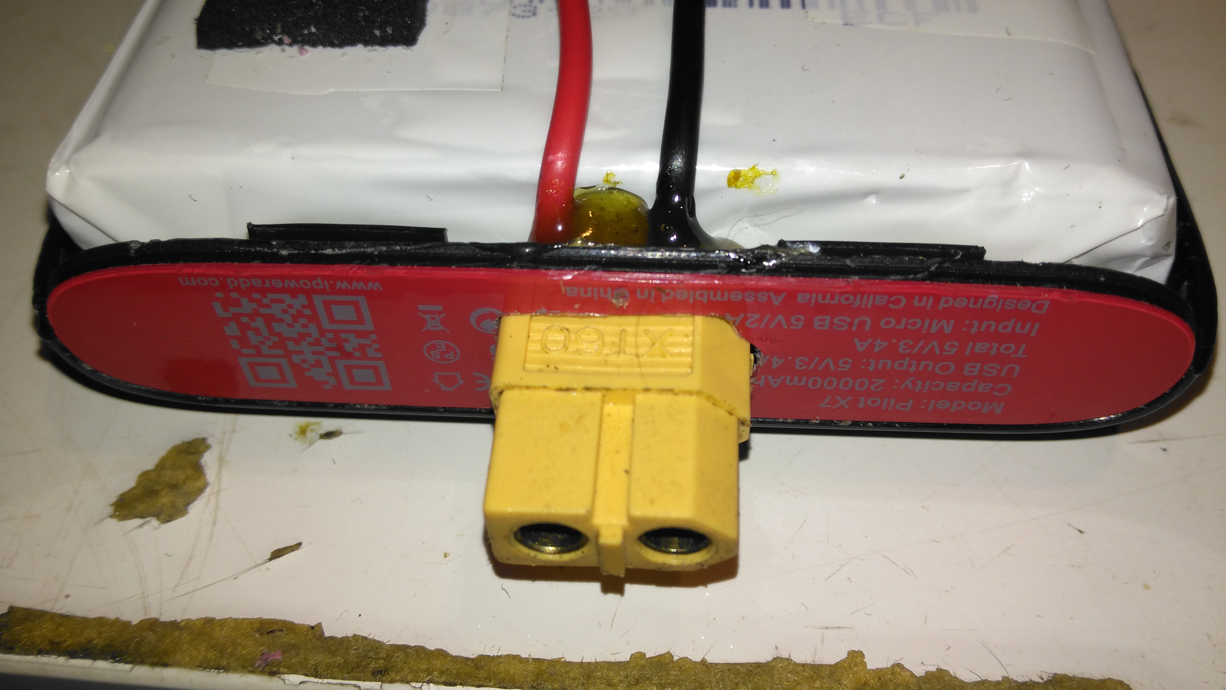
XT60 Battery Connector
The only issue with powerbanks this large is the amount of time they require to recharge themselves – at this unit’s maximum of 2A through the µUSB port, it’s about 22 hours! Here I’ve fitted an XT60 connector, to interface to my Turnigy Accucell 6 charger, increasing the charging current capacity to 6A, and reducing the full-charge time to 7 hours. This splits to 3A charge per cell, and after some testing the cells don’t seem to mind this higher charging current.
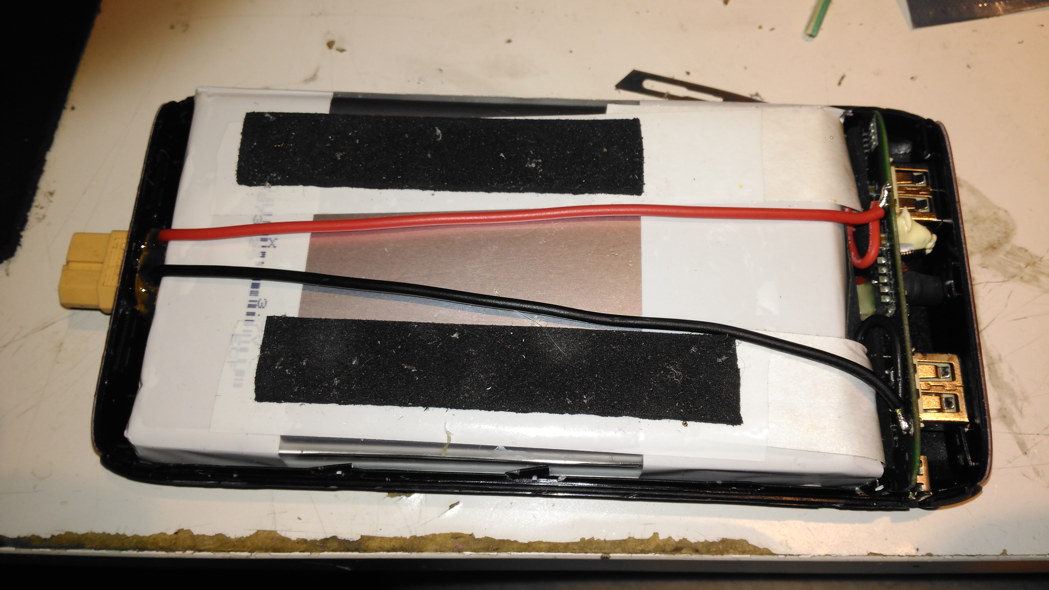
Battery Connector Wiring
The new charging connector is directly connected to the battery at the control PCB, there’s just enough room to get a pair of wires down the casing over the cells.
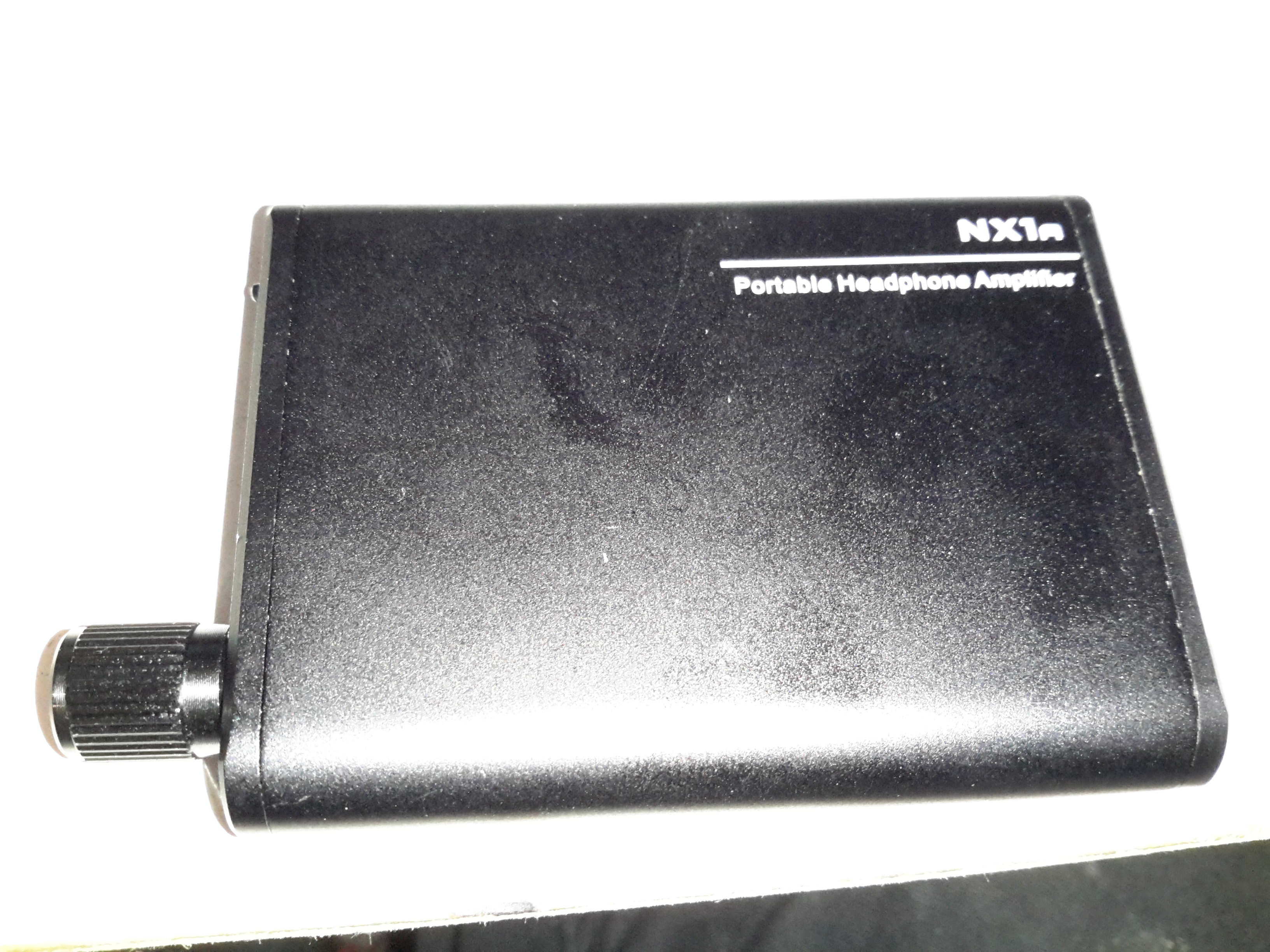
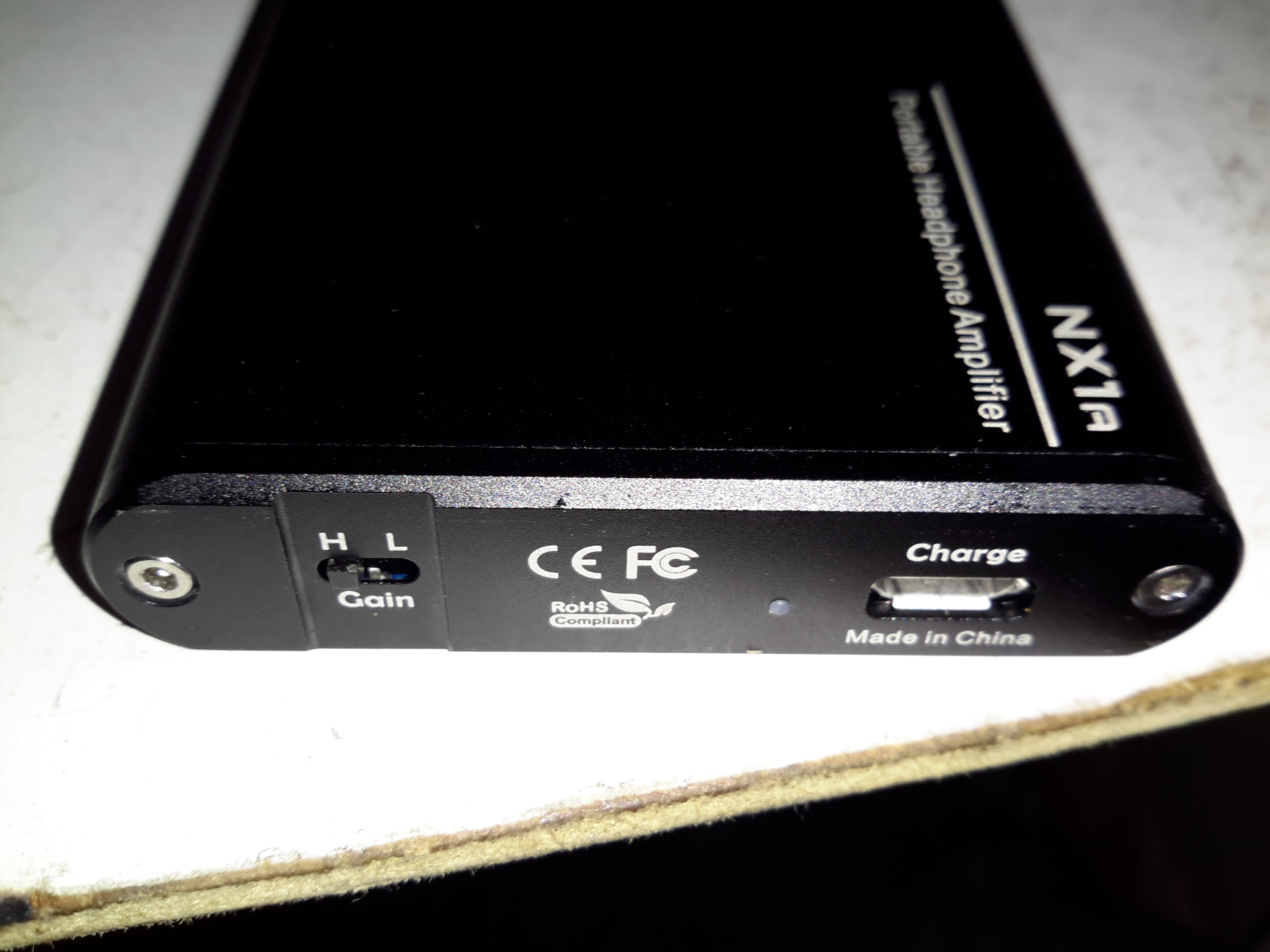
Time for another teardown! Here’s a pocket-sized headphone amplifier for use with mobile devices. This unit is powered by a built-in lithium cell, and can give some pretty impressive volume levels given it’s small size.
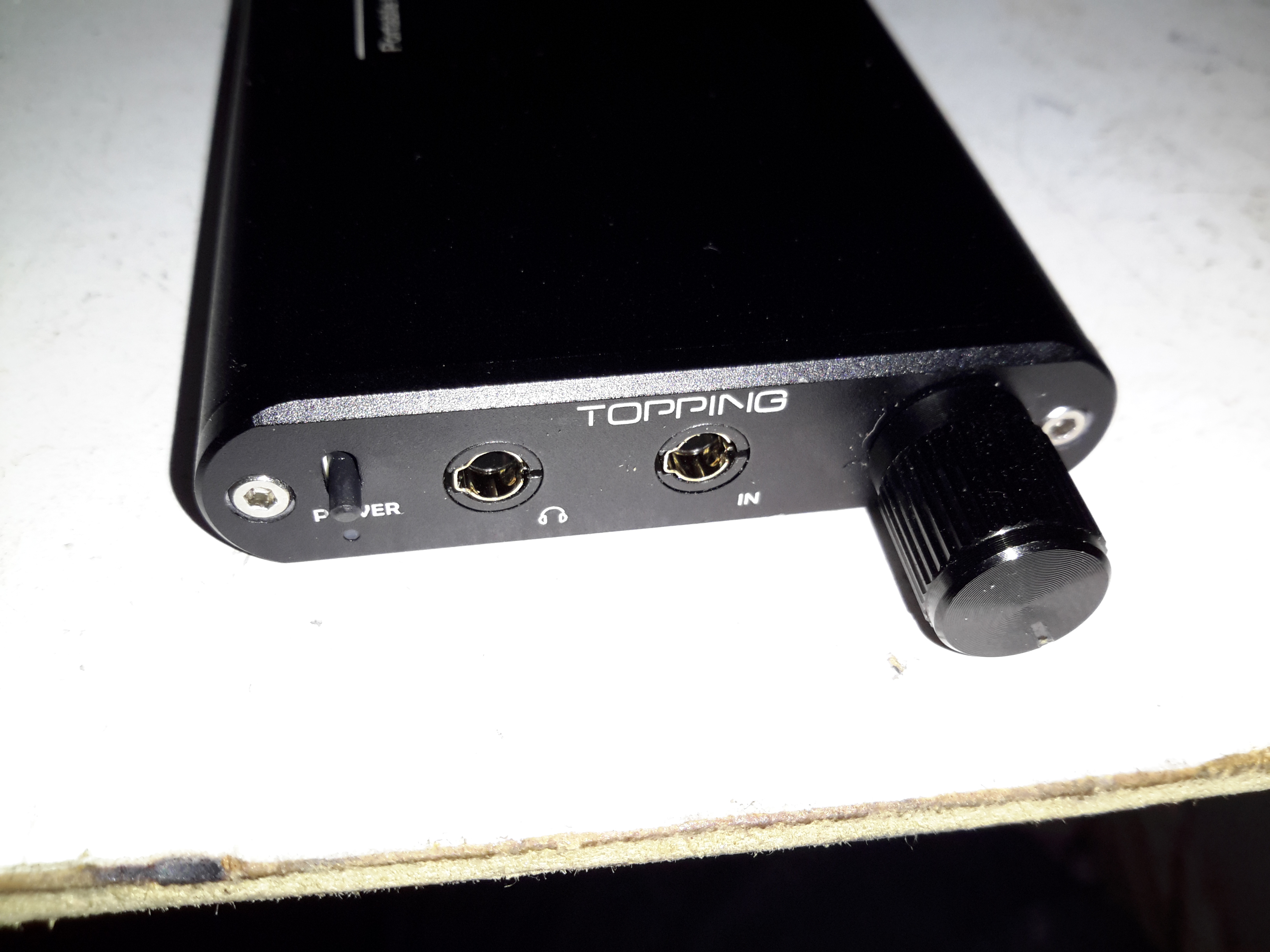
Audio Connections
The 3.5mm audio input & output jacks are on the front of the unit, along with the relatively enormous volume knob & power switch. There’s a little blue LED under the switch that lets the user know when the power is on, but this is a very sedate LED, using very little power.
Gain & Charging
On the back is the High-Low gain switch, and the µUSB charging port. There’s another indicator LED to show that the internal cell is charging, in this case a red one.
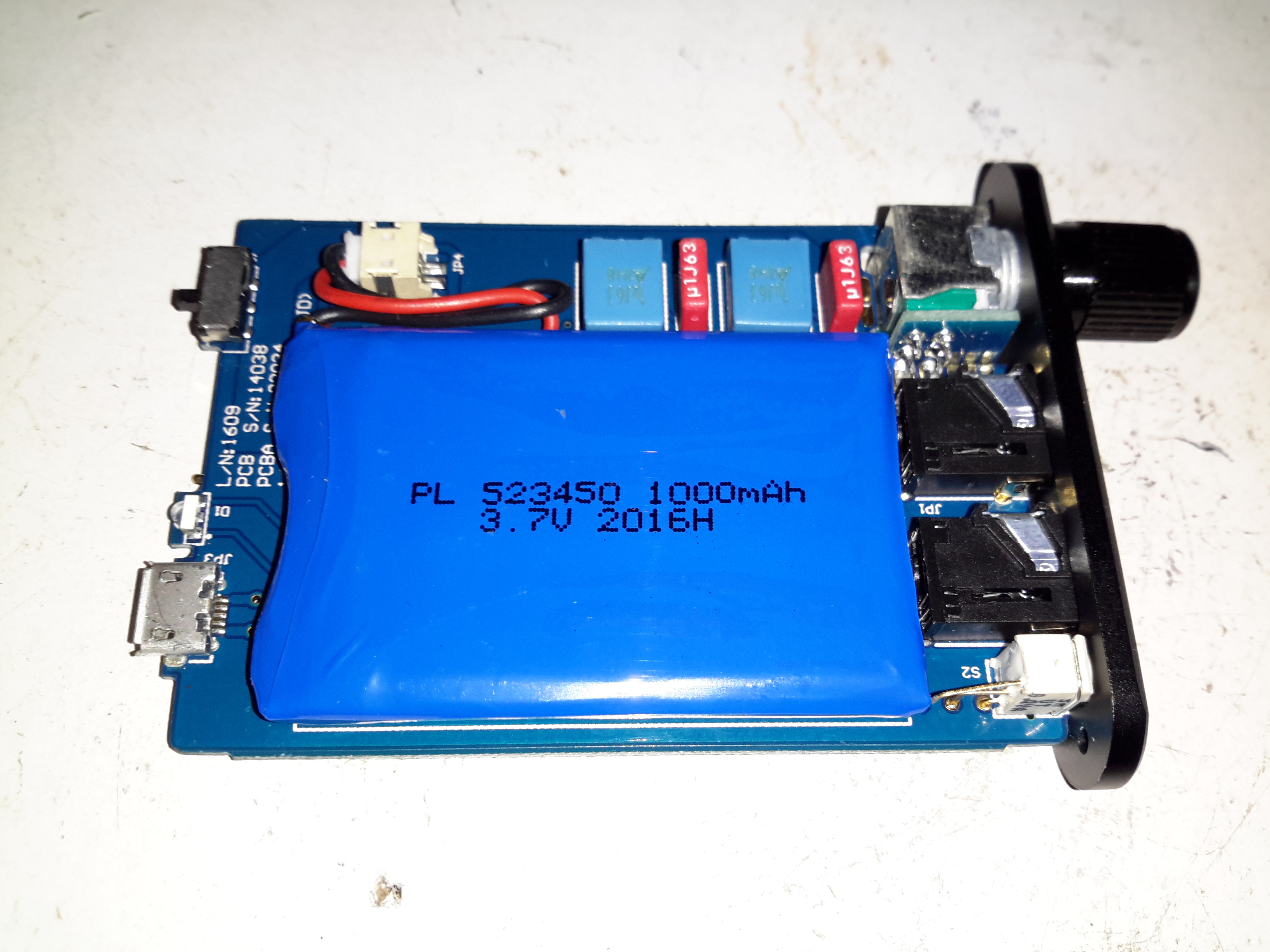
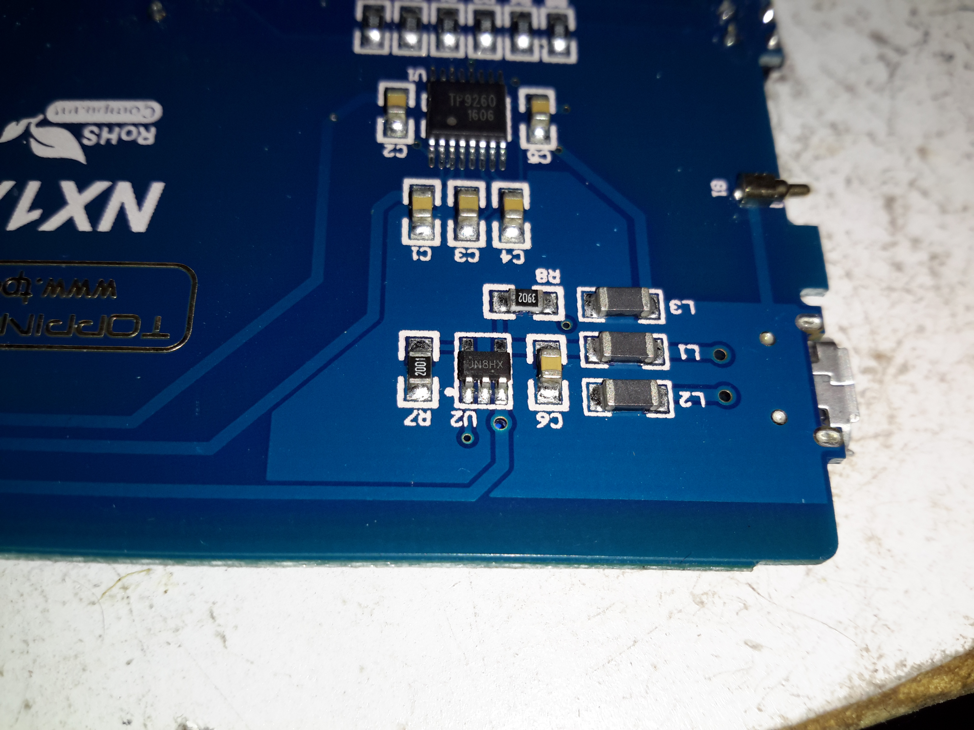
PCB Top
Removing a couple of cap screws allows the internals to slide out of the extruded aluminium casing. Most of the internal space is taken up by the 1Ah lithium cell, here on the top of the PCB secured by some double-sided tape. The volume potentiometer is mounted on a small daughterboard at right angles to get it to fit into the small vertical space in the case.
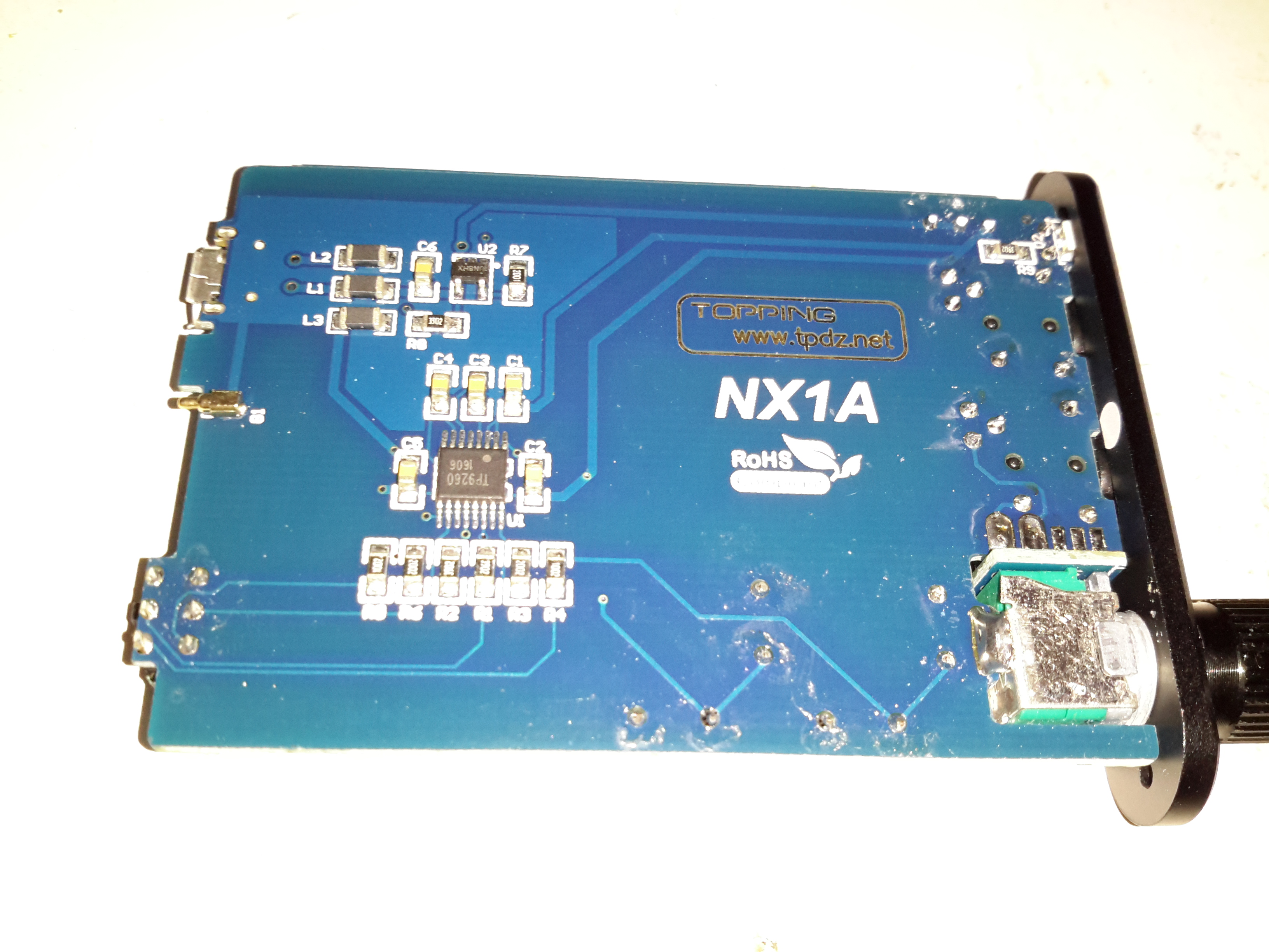
PCB Rear
The bottom of the PCB is equally as sparse – the only ICs being the main audio amp in the centre & the battery charger IC at the top.
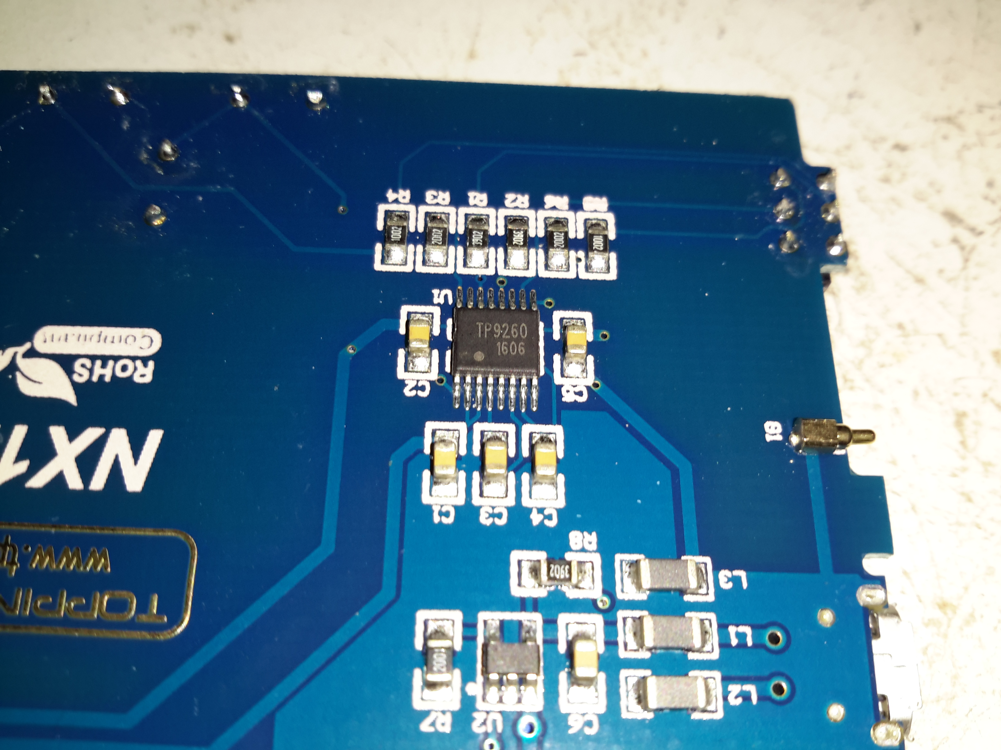
Amplifier IC
The main audio amplifier is a TP9260, I couldn’t find a datasheet on this, so I’m unsure of what the specs are. The row of resistors above the IC are for the gain divider circuit. There’s also a pogo pin on the right that makes contact with the back panel of the case for grounding.
Battery Charger
Battery charging is taken care of by a UN8HX 500mA linear charging IC, not much special here.
This little amplifier seems to be pretty well made, considering the price point. The only issue I’ve had so far is the audio cables act like antennas, and when in close proximity to a phone some signal gets picked up & blasted into the headphones as interference.
I recently got the latest upgrade from Virgin Media, 200Mbit DL / 20Mbit UL, and to get this I was informed I’d have to buy their latest hardware, since my existing CPE wouldn’t be able to handle the extra 5Mbit/s upload speed. (My bullshit detector went off pretty hard at that point, as the SuperHub 2 hardware is definitely capable of working fine with 20Mbit/s upload rates). Instead of having to return the old router, I was asked to simply recycle it, so of course the recycling gets done in my pretty unique way!
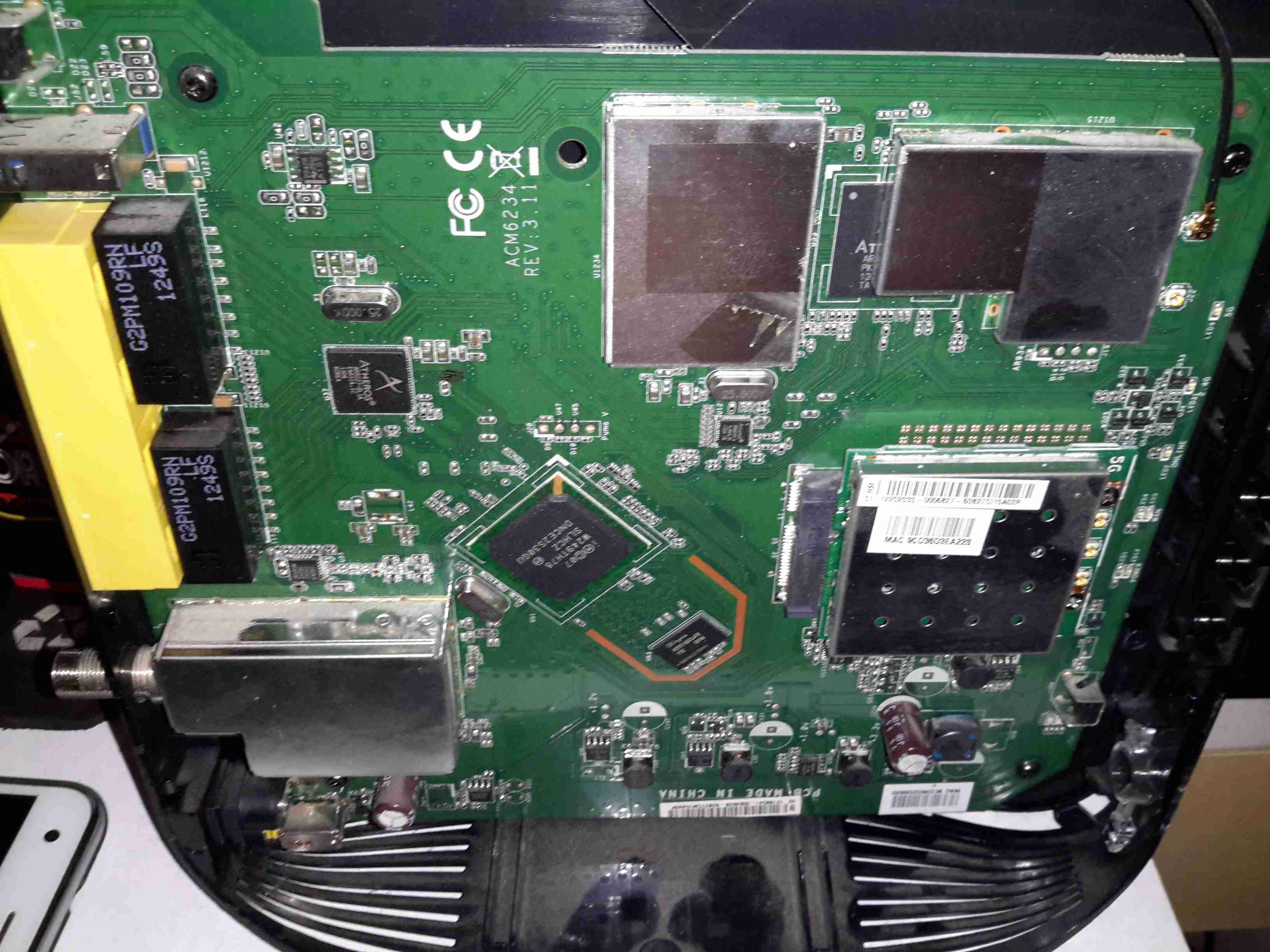
Mainboard
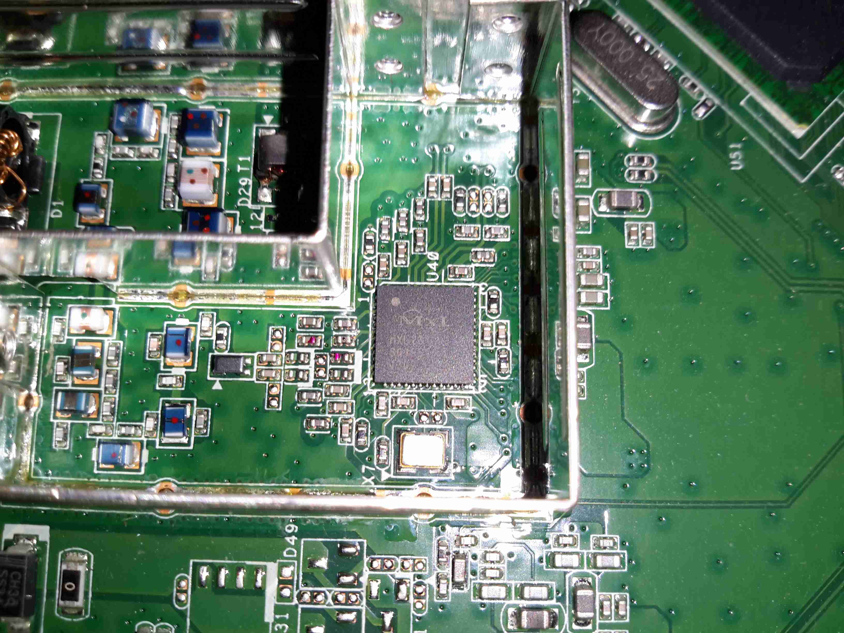
The casing of these units is held together by a single screw & a metric fuckton of plastic clips, disassembly is somewhat hindered by the radio antennas being positioned all over both sides of the casing. Once the side is off, the mainboard is visible. The DOCSIS frontend is lower left, centre is the Intel PUMA 5 Cable Modem SoC with it’s RAM just to the lower right. The right side of the board is taken up by both of the WiFi radio frontends, the 5GHz band being covered by a Mini PCIe card.
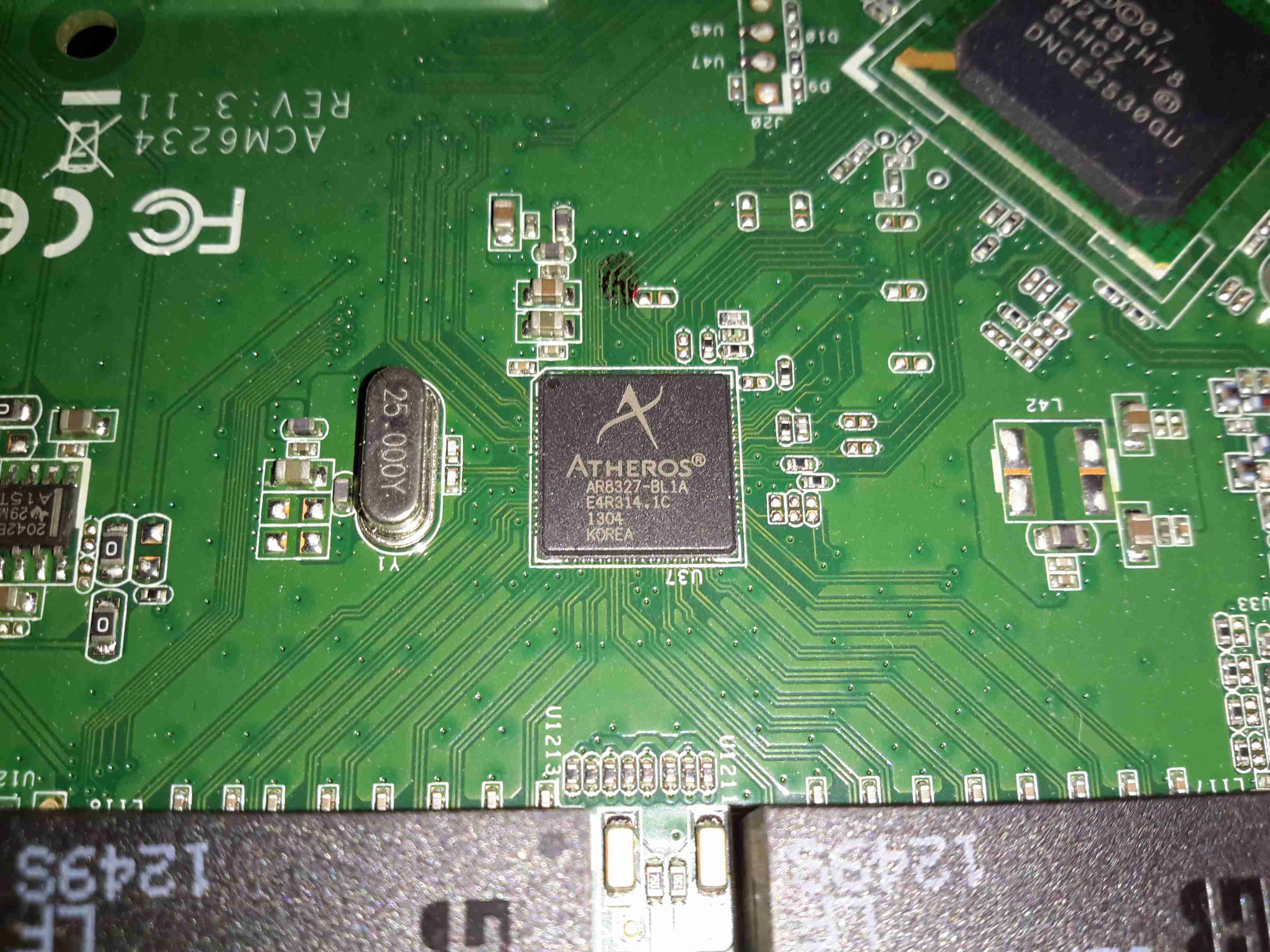
Atheros Gigabit Switch
The 4 gigabit Ethernet ports on the back are serviced by an Atheros AR8327 Managed Layer 3 switch IC, which seems to be a pretty powerful device:
The AR8327 is the latest in high performance small network switching. It is ultra low power, has extensive routing and data management functions and includes hardware NAT functionality (AR8327N). The AR8327/AR8327N is a highly integrated seven-port Gigabit Ethernet switch with a fully non-blocking switch fabric, a high-performance lookup unit supporting 2048 MAC addresses, and a four-traffic class Quality of Service (QoS) engine. The AR8327 has the flexibility to support various networking applications. The AR8327/AR8327N is designed for cost-sensitive switch applications in wireless AP routers, home gateways, and xDSL/cable modem platforms.
Unfortunately most of the features of this router are locked out by VM’s extremely restrictive firmware. With any of their devices, sticking the VM supplied unit into modem mode & using a proper router after is definitely advised!
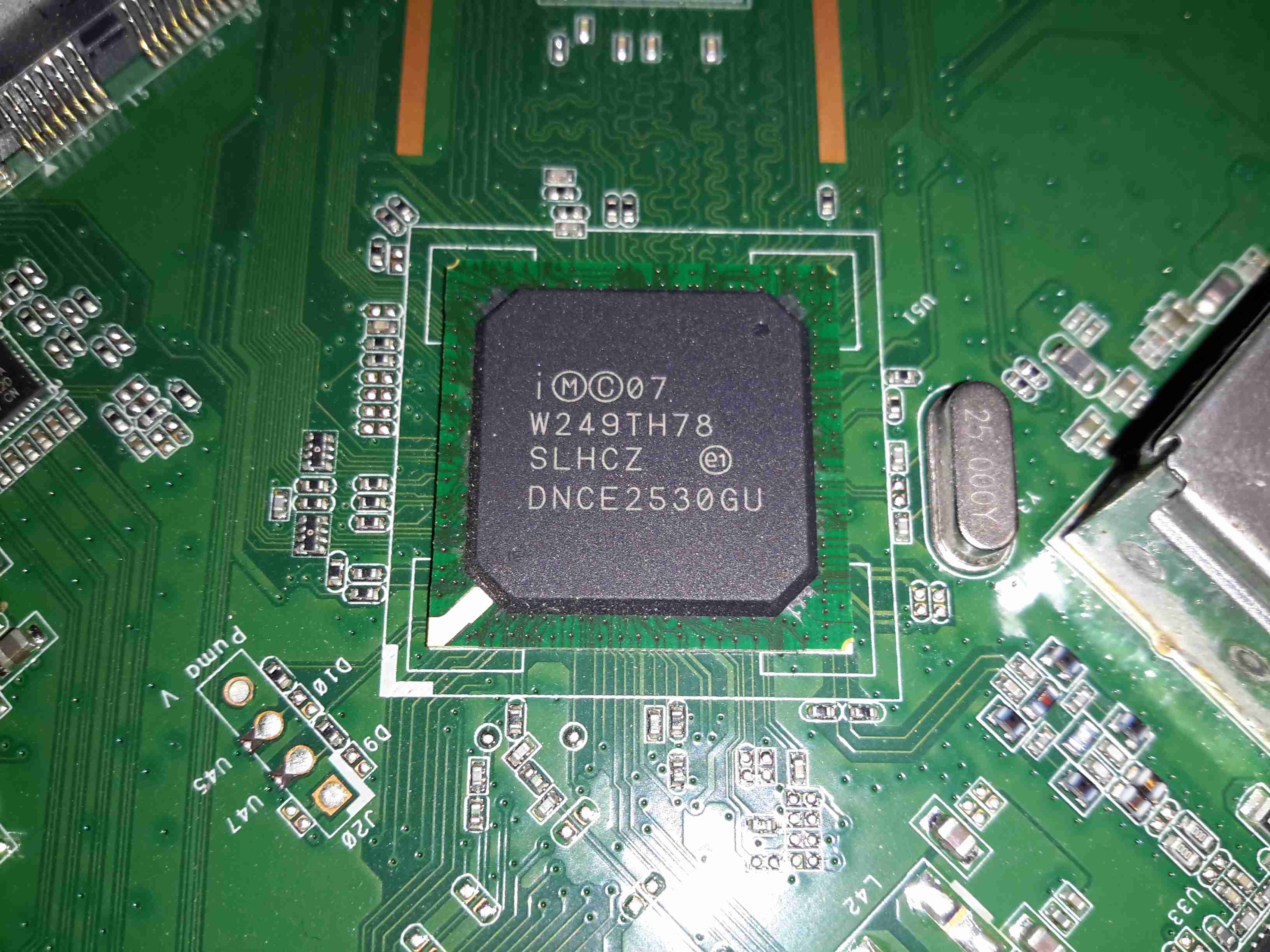
Intel Puma 5 CM CPU
The cable modem side of things is taken care of by the Intel PUMA 5 DNCE2530GU SoC. This appears to communicate with the rest of the system via the Ethernet switch & PCI Express for the 5GHz radio.
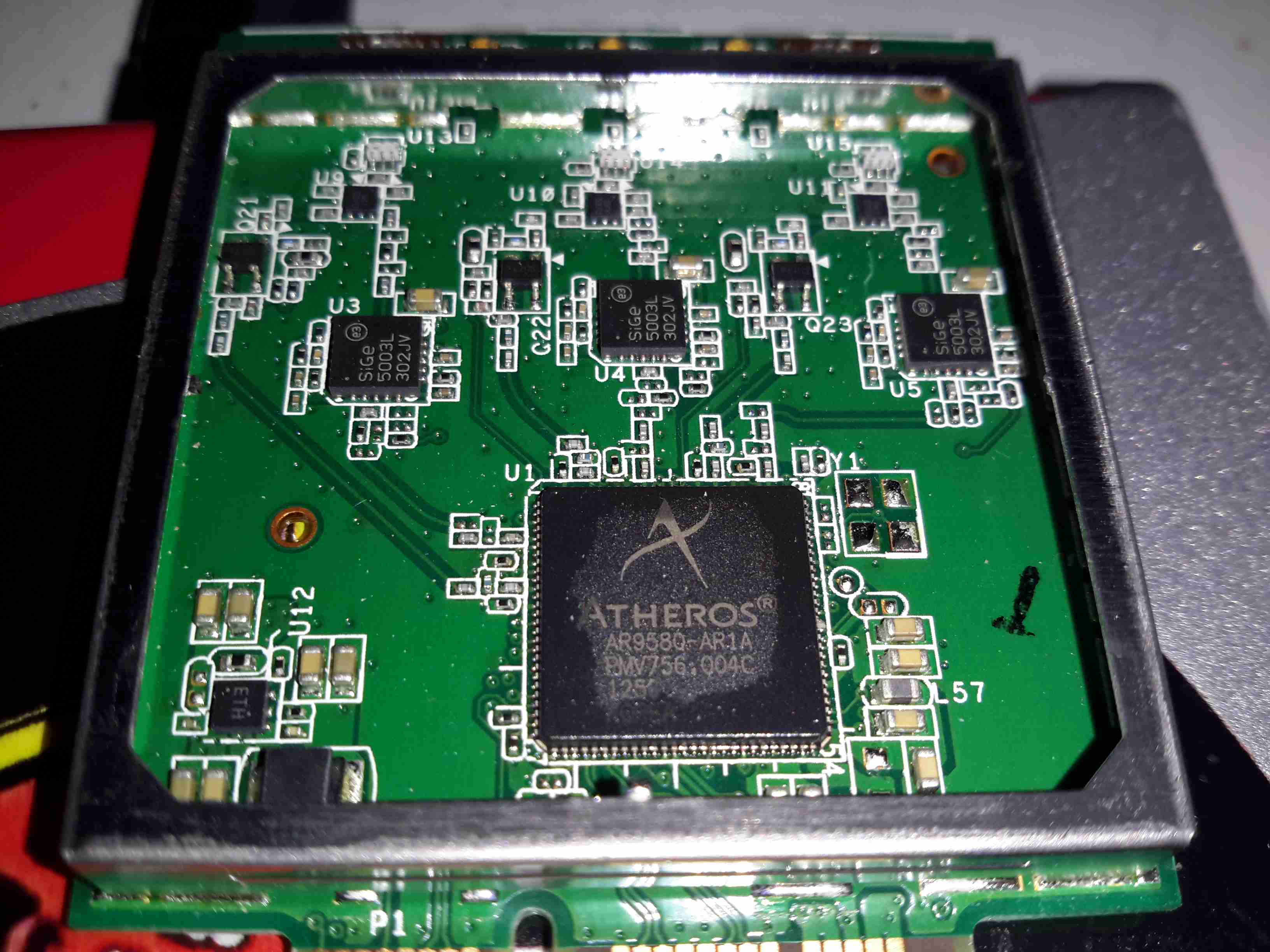
Atheros WiFi SoC
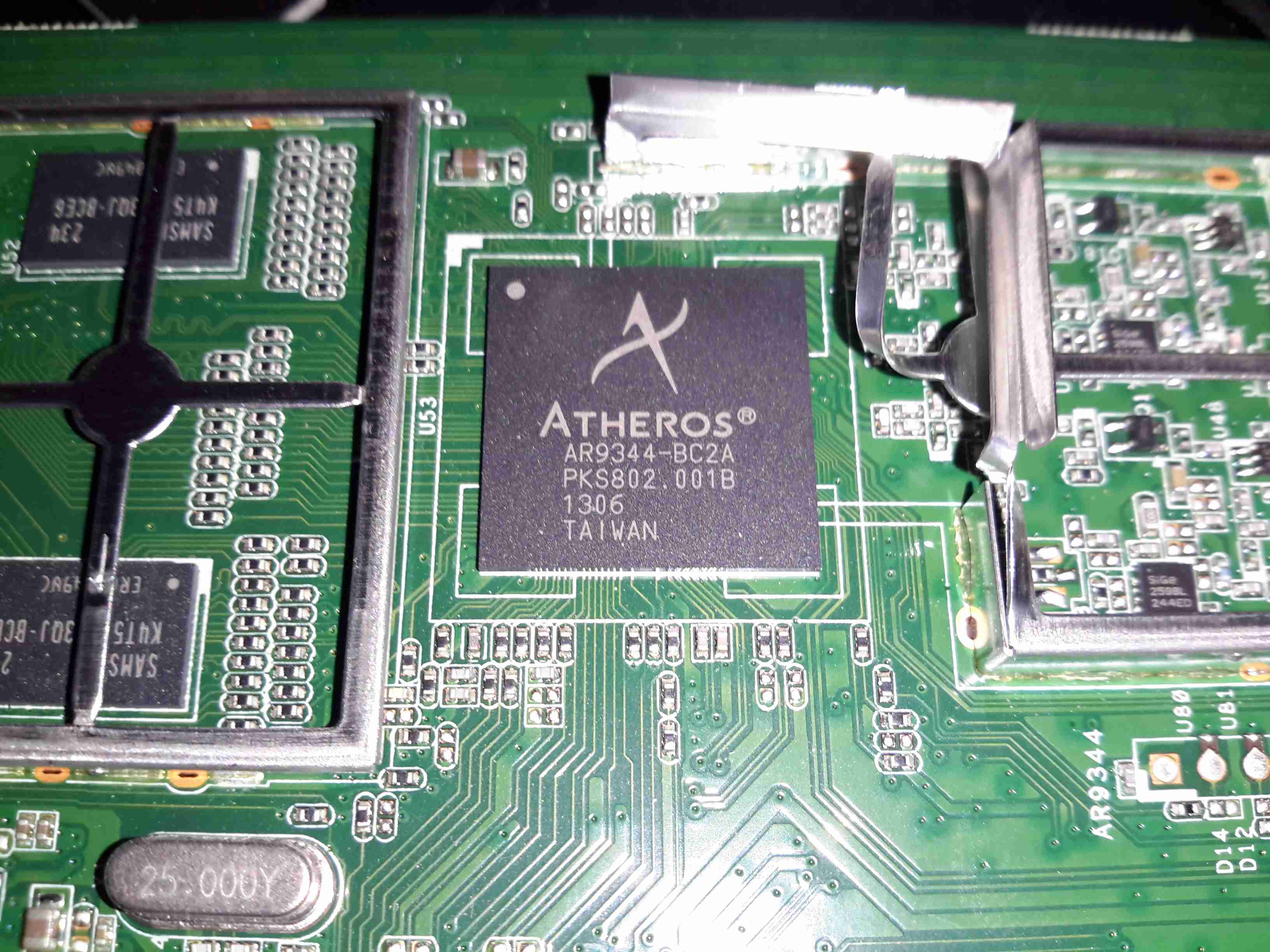
The 2.4GHz radio functionality is supplied by an Atheros AR9344 SoC, it’s RAM is to the left. This is probably handling all the router functions of this unit, but I can’t be certain.
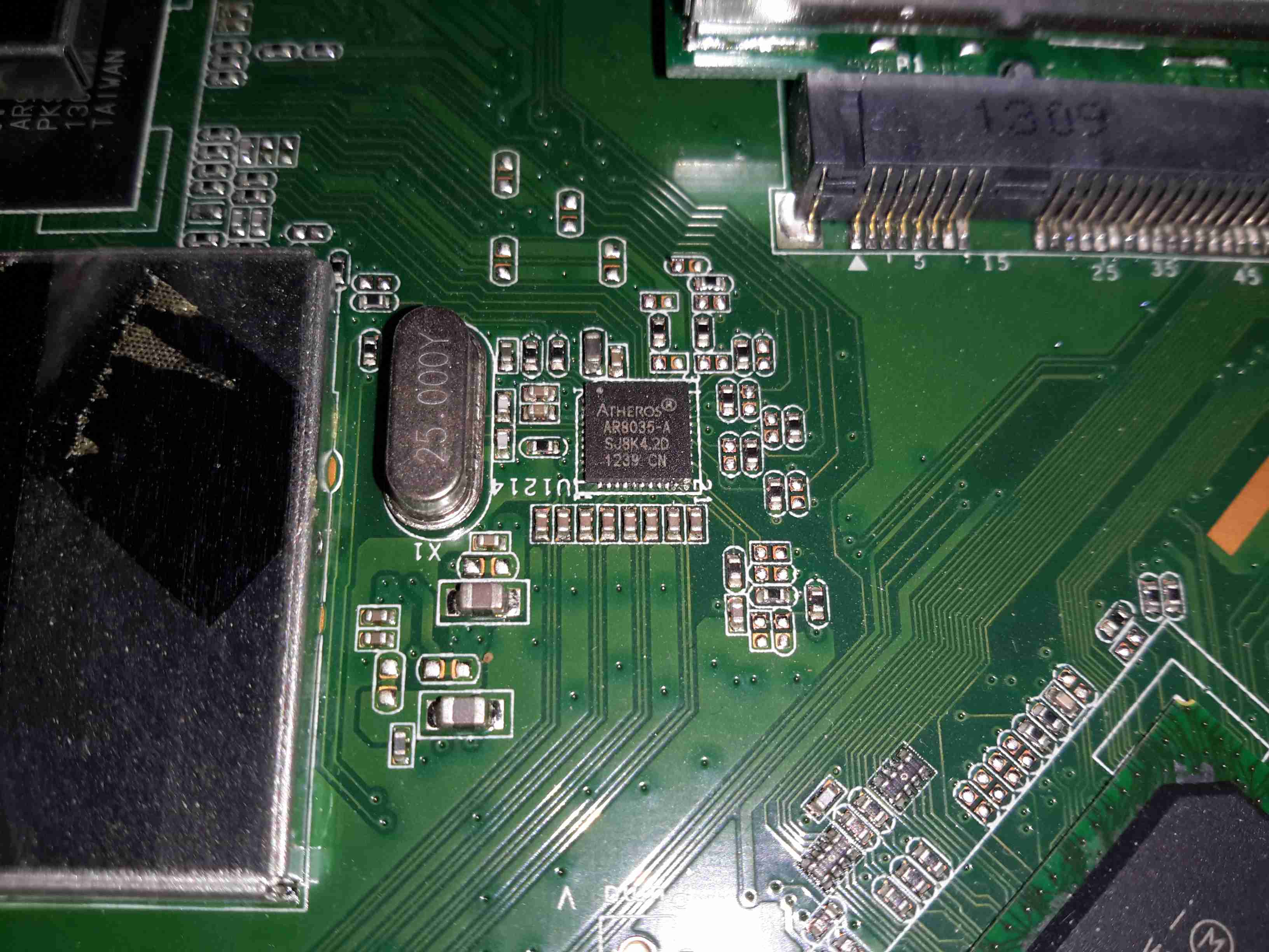
Atheros LAN PHY
A separate Ethernet PHY is located between the SoC & the switch IC.
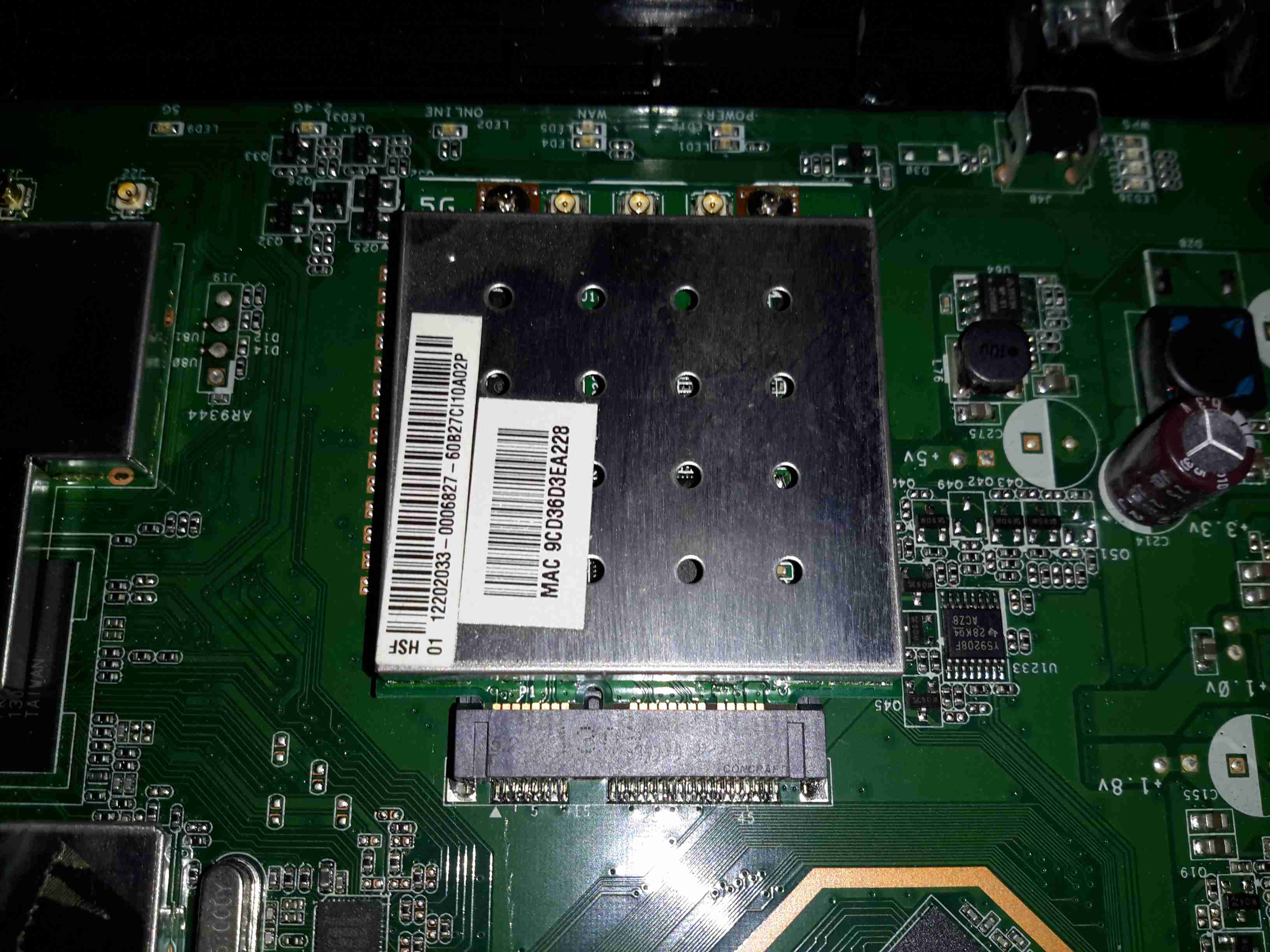
5GHz Radio Card
The 5GHz band is served by a totally separate radio module, in Mini PCIe format, although it’s a bit wider than standard. This module will probably be kept for reuse in another application.
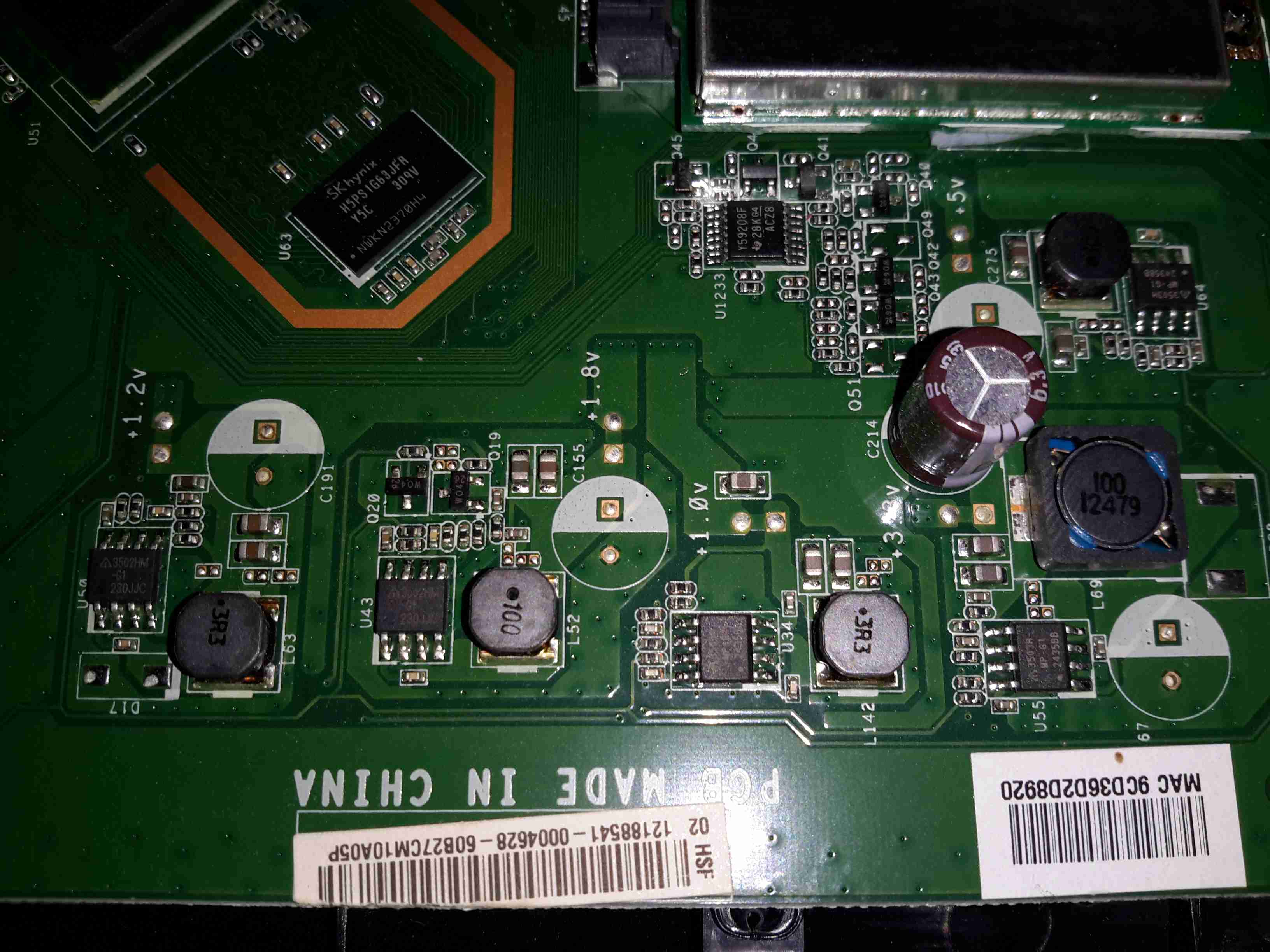
Power Supplies
All down the edge of the board are the multiple DC-DC converters to generate the required voltage rails.
MaxLinear MXL261 Frontend
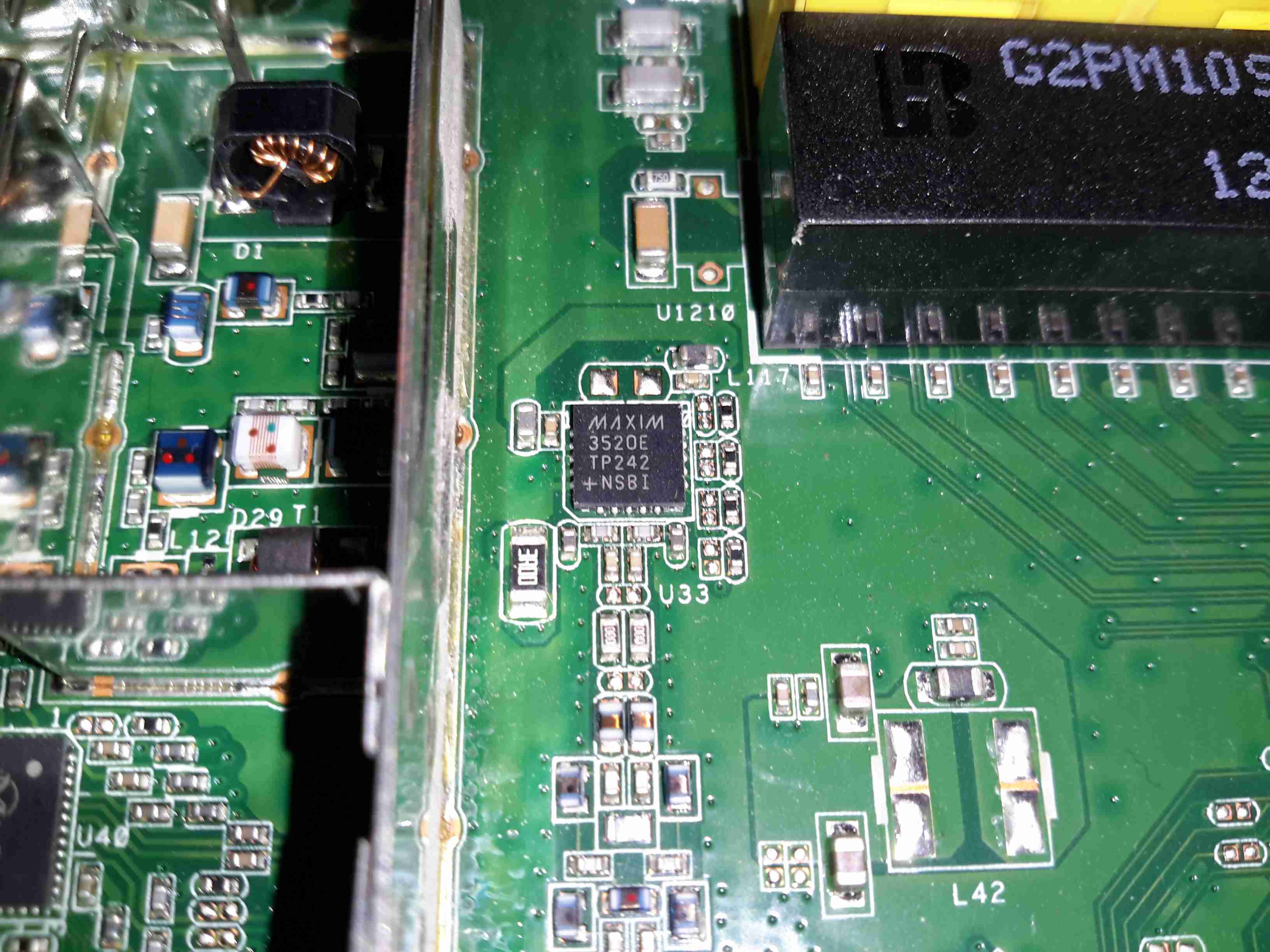
The DOCSIS frontend is handled by a MaxLinar MXL261 Tuner/Demodulator. More on this IC in my decapping post 🙂
The Unknown One
I’ve honestly no idea what on earth this Maxim component is doing. It’s clearly connected via an impedance matched pair, and that track above the IC looks like an antenna, but nothing I search for brings up a workable part number.
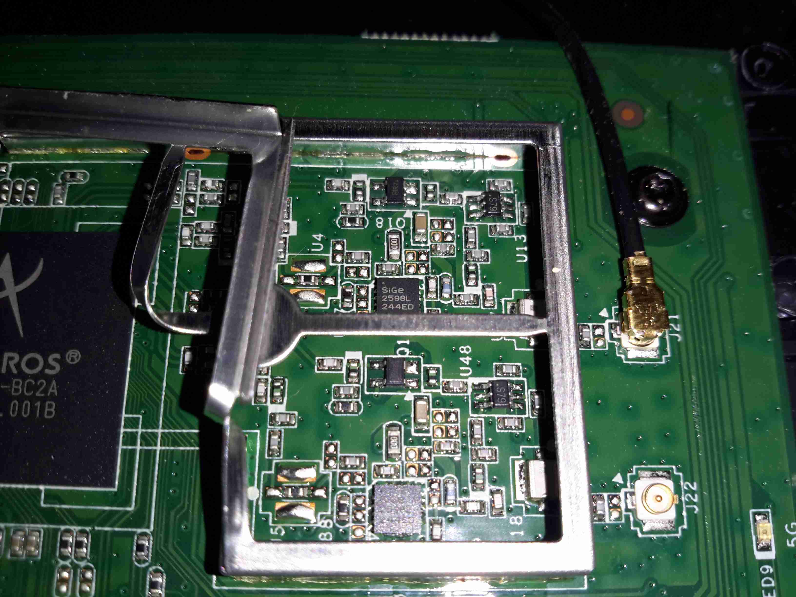
2.4GHz Frontend
The RF switching & TX amplifiers are under a shield, these PA chips are SiGe parts.
Atheros 5GHz Radio
Pretty much the same for the 5GHz radio, but with 3 radio channels.
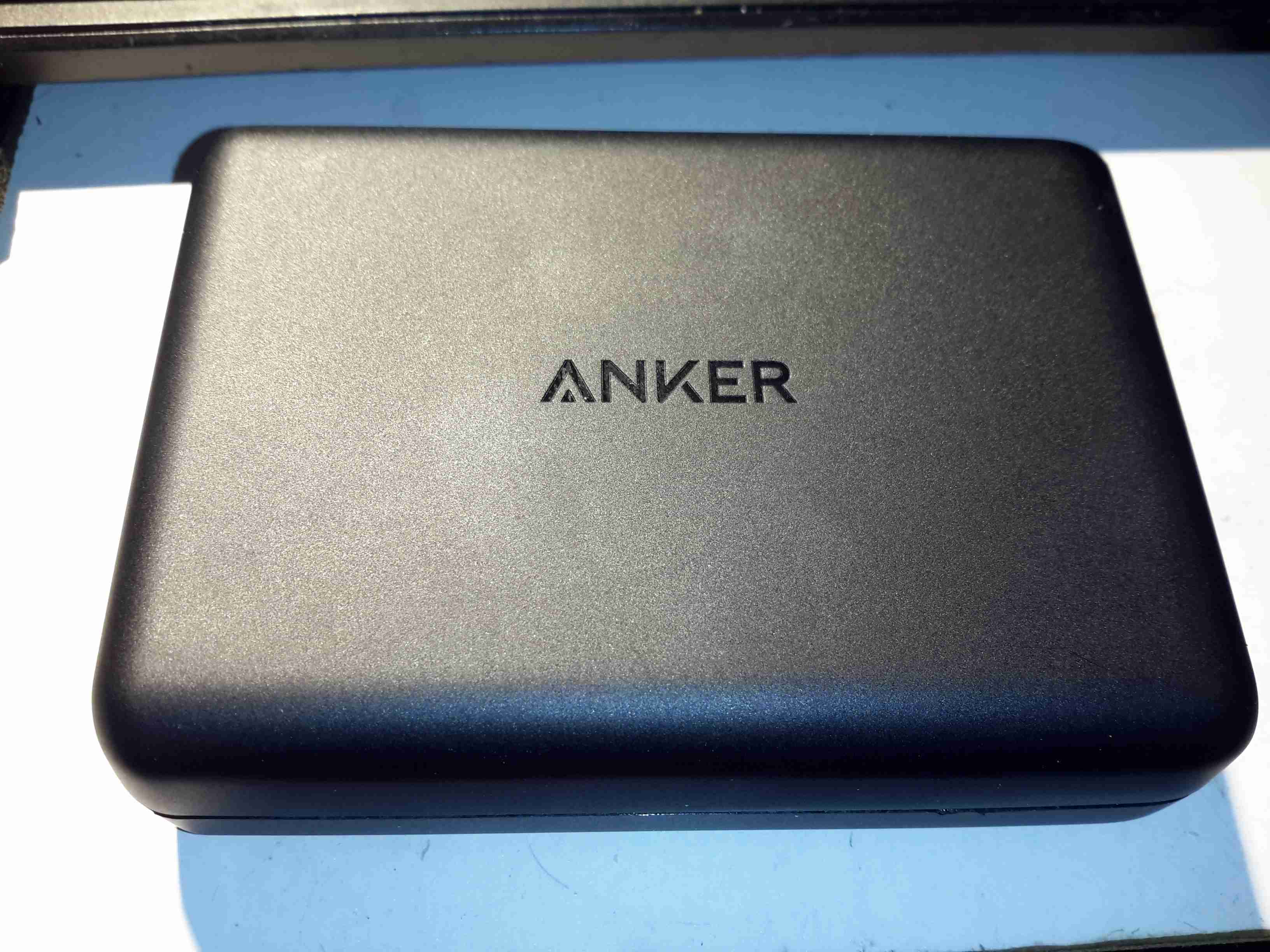
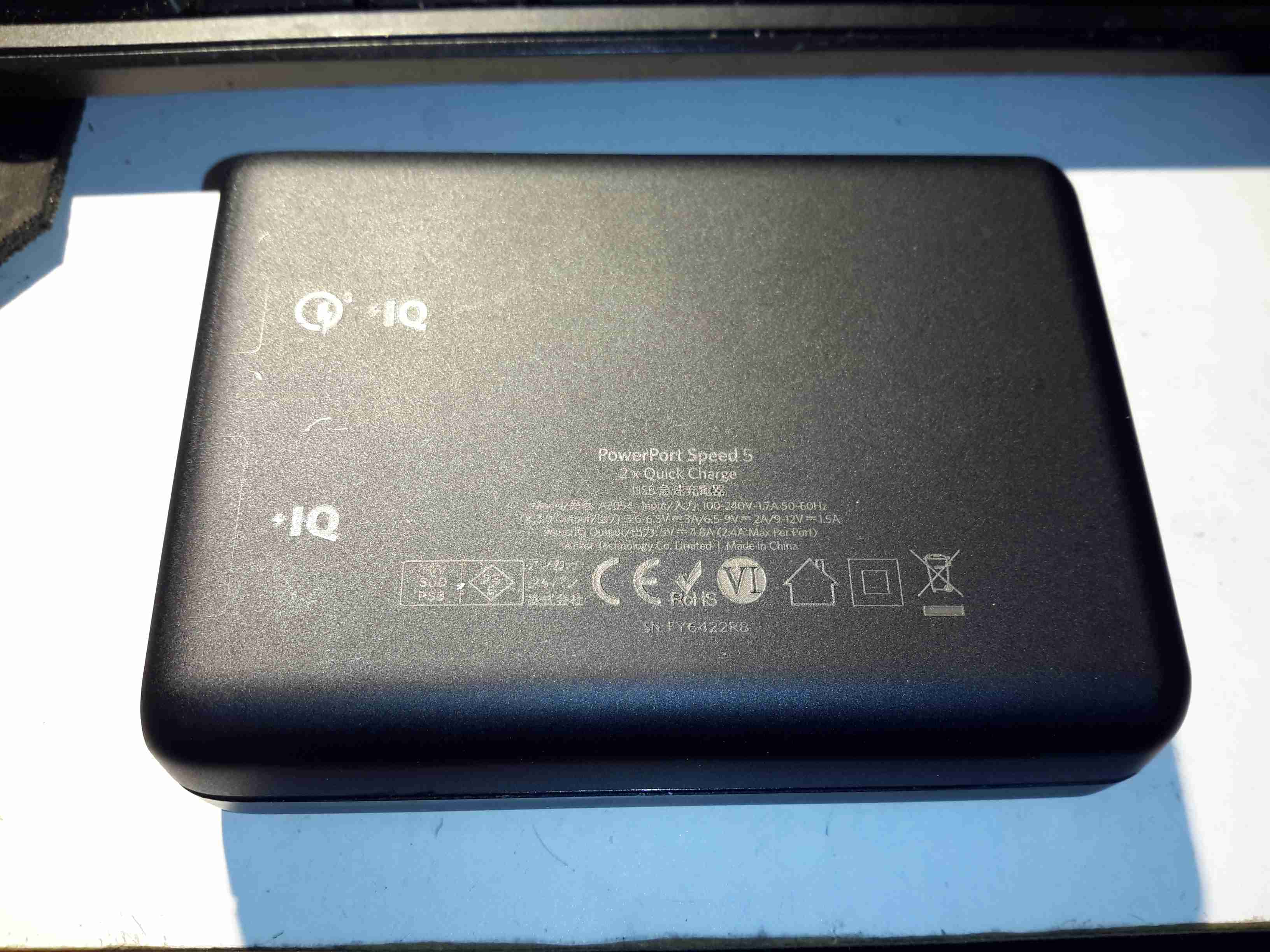
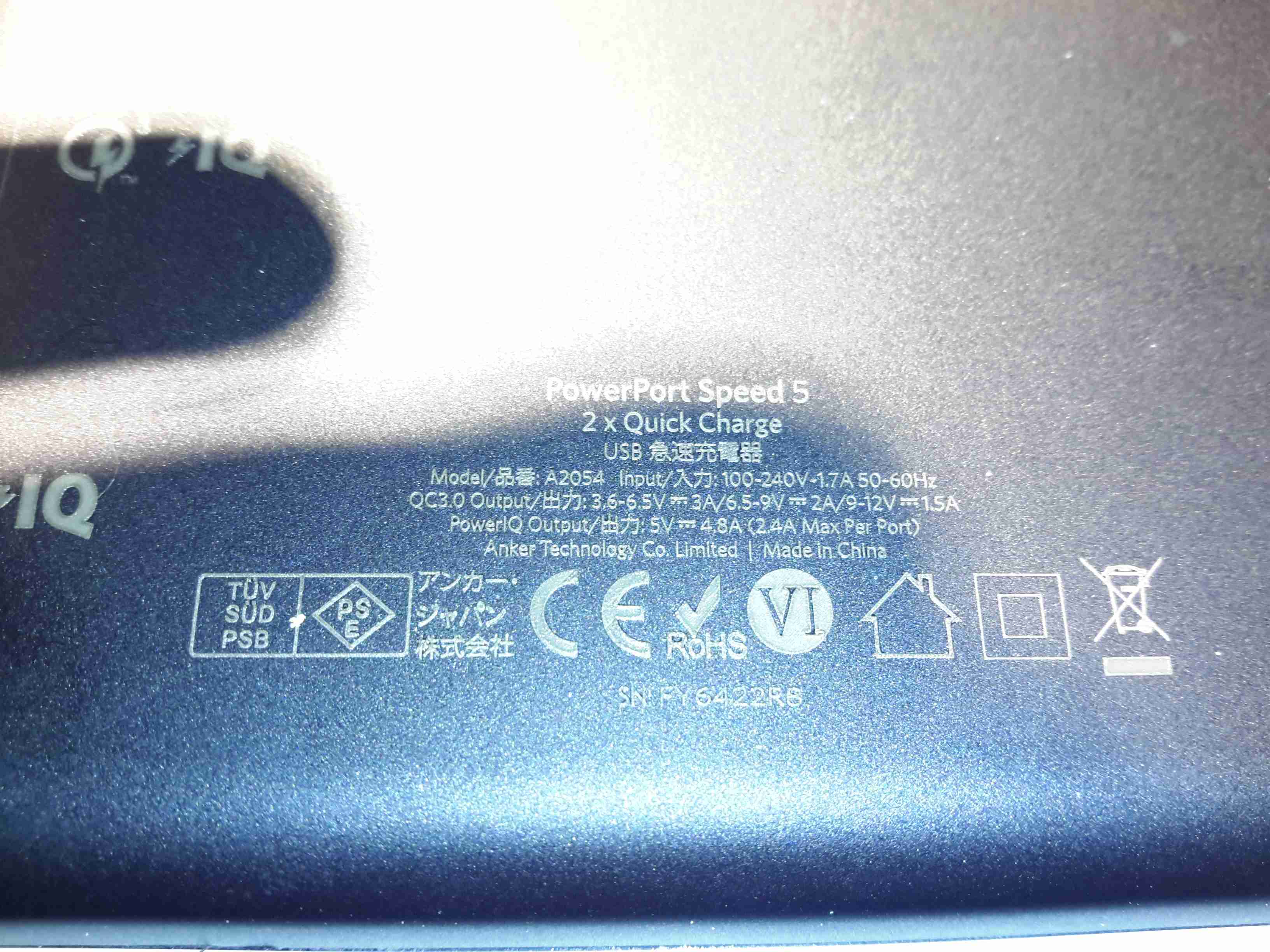
Here’s a piece of tech that is growing all the more important in recent times, with devices with huge battery capacities, a quick charger. This unit supports Qualcomm’s Quick Charge 3 standard, where the device being charged can negotiate with the charger for a higher-power link, by increasing the bus voltage past the usual 5v.
Rear
The casing feels rather nice on this unit, sturdy & well designed. All the legends on the case are laser marked, apart from the front side logo which is part of the injection moulding.
Specifications
The power capacity of this charger is pretty impressive, with outputs for QC3 from 3.6-6.5v at 3A, up to 12v 1.5A. Standard USB charging is limited at 4.8A for the other 3 ports.
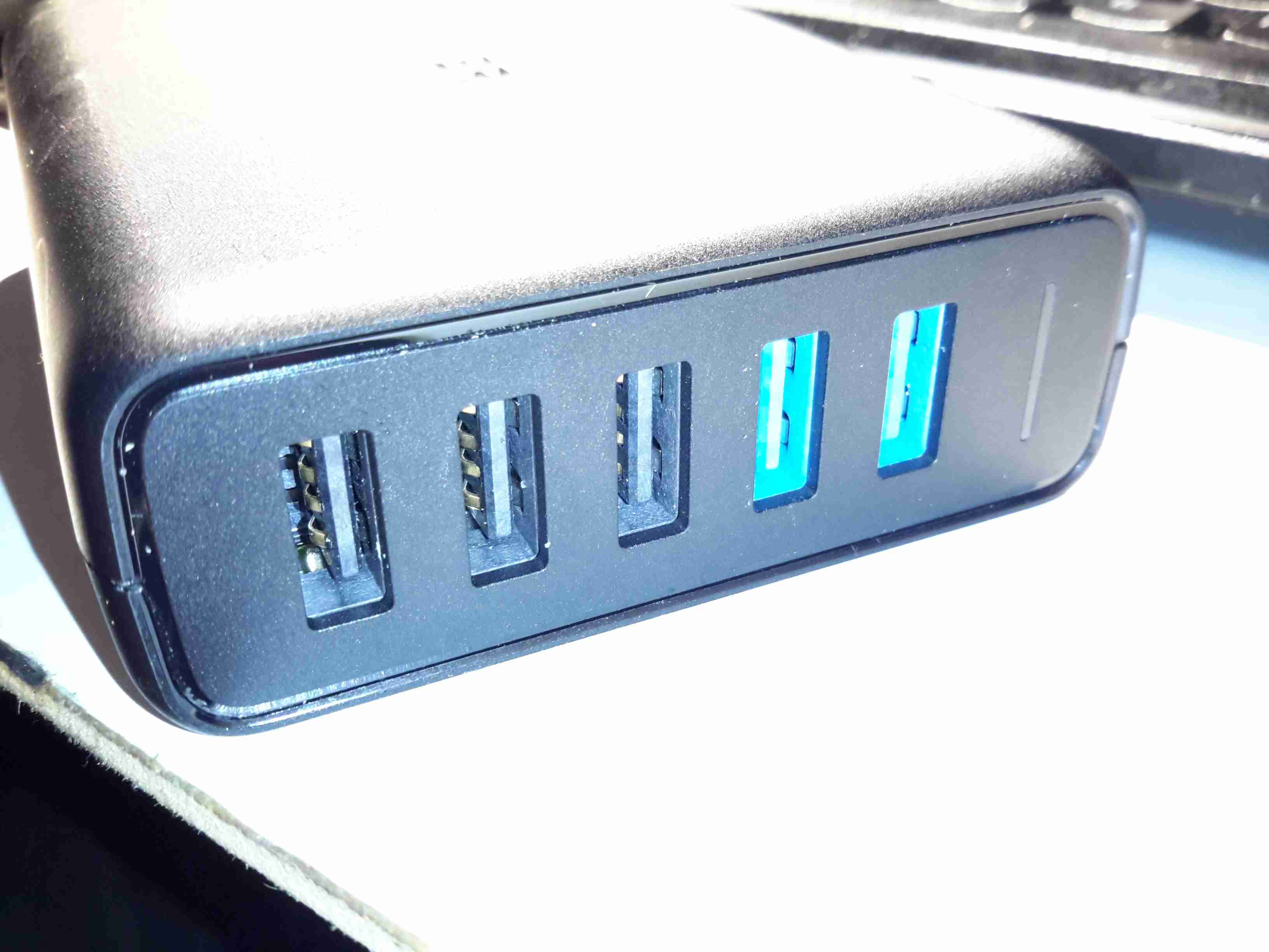
Ports
The two of the 5 USB ports are colour coded blue on the QC3 ports. The other 3 are standard 5v ports, the only thing that doesn’t make sense in the ratings is the overall current rating of the 5v supply (4.8A), and the rated current of each of the ports (2.4A) – this is 7.2A total rather than 4.8A.
Top Removed
The casing is glued together at the seam, but it gave in to some percussive attack with a screwdriver handle. The inside of this supply is mostly hidden by the large heatspreader on the top.
Main PCB Bottom
This is a nicely designed board, the creepage distances are at least 8mm between the primary & secondary sides, the bottom also has a conformal coating, with extra silicone around the primary-side switching transistor pins, presumably to decrease the chances of the board flashing over between the close pins.
On the lower 3 USB ports can be seen the 3 SOT-23 USB charge control ICs. These are probably similar to the Texas Instruments TPS2514 controllers, which I’ve experimented with before, however I can’t read the numbers due to the conformal coating. The other semiconductors on this side of the board are part of the voltage feedback circuits for the SMPS. The 5v supply optocoupler is in the centre bottom of the board.
Heatsink Removed
Desoldering the pair of primary side transistors allowed me to easily remove the heatspreader from the supply. There’s thermal pads & grease over everything to get rid of the heat. Here can be seen there are two transformers, forming completely separate supplies for the standard USB side of things & the QC3 side. Measuring the voltages on the main filter capacitors showed me the difference – the QC3 supply is held at 14.2v, and is managed through other circuits further on in the power chain. There’s plenty of mains filtering on the input, as well as common-mode chokes on the DC outputs before they reach the USB ports.
Quick Charge 3 DC-DC Converters
Here’s where the QC3 magic happens, a small DC-DC buck converter for each of the two ports. The data lines are also connected to these modules, so all the control logic is located on these too. The TO-220 device to the left is the main rectifier.
Some time ago I did a couple of posts on cheapening up the maintenance of Eberspacher hot air heaters by making the glow plug screens myself. Now one of my pieces of stainless mesh has been in the heater for nearly a year, and the heater is starting to get a bit smoky on a cold start. This is usually a sign that the screen isn’t allowing the fuel to vaporise quick enough for the glow plug to ignite the flame, because it’s becoming blocked. So far the heater has had about 150L of diesel through it with my DIY screen.
Old Screen
After removing the plug, here’s what’s left of the screen. The bottom end has completely disintegrated, but this is to be expected – OEM screens do the same thing as this end is exposed to the most heat in the burner. There’s quite a bit of coke buildup on the top end of the screen around the fuel nozzle, again this isn’t surprising, as this is the coolest part of the heater not all the heavier fractions of the diesel fuel have the chance to vaporise.
Innards
Looking further down into the mixing tube of the main burner, everything looks good. There’s a coating of soot in there, but no tar-like build up that would tell me the unit isn’t burning properly. Another advantage of making my own screens is that they’re much easier to extract from the hole once they’ve been in there for months. The OEM screens have a stainless ring spot welded to the mesh itself to hold it’s shape, and once there’s enough fuel residue built up the entire mess seizes in place, requiring some sharp pokey tools & some colourful language to remove. The single loop of mesh held in place by it’s own spring pressure is much easier to remove as it collapses easily.
New 80 Mesh Screen
I’ve decided to change the mesh size of the screen while I’m in here, in this case to 80 mesh, which is much closer to the OEM screen size. There doesn’t seem to be much of a difference so far in either the starting or running capability of the heater, although the thicker wire of this screen might last longer before disintegrating at the burner end.
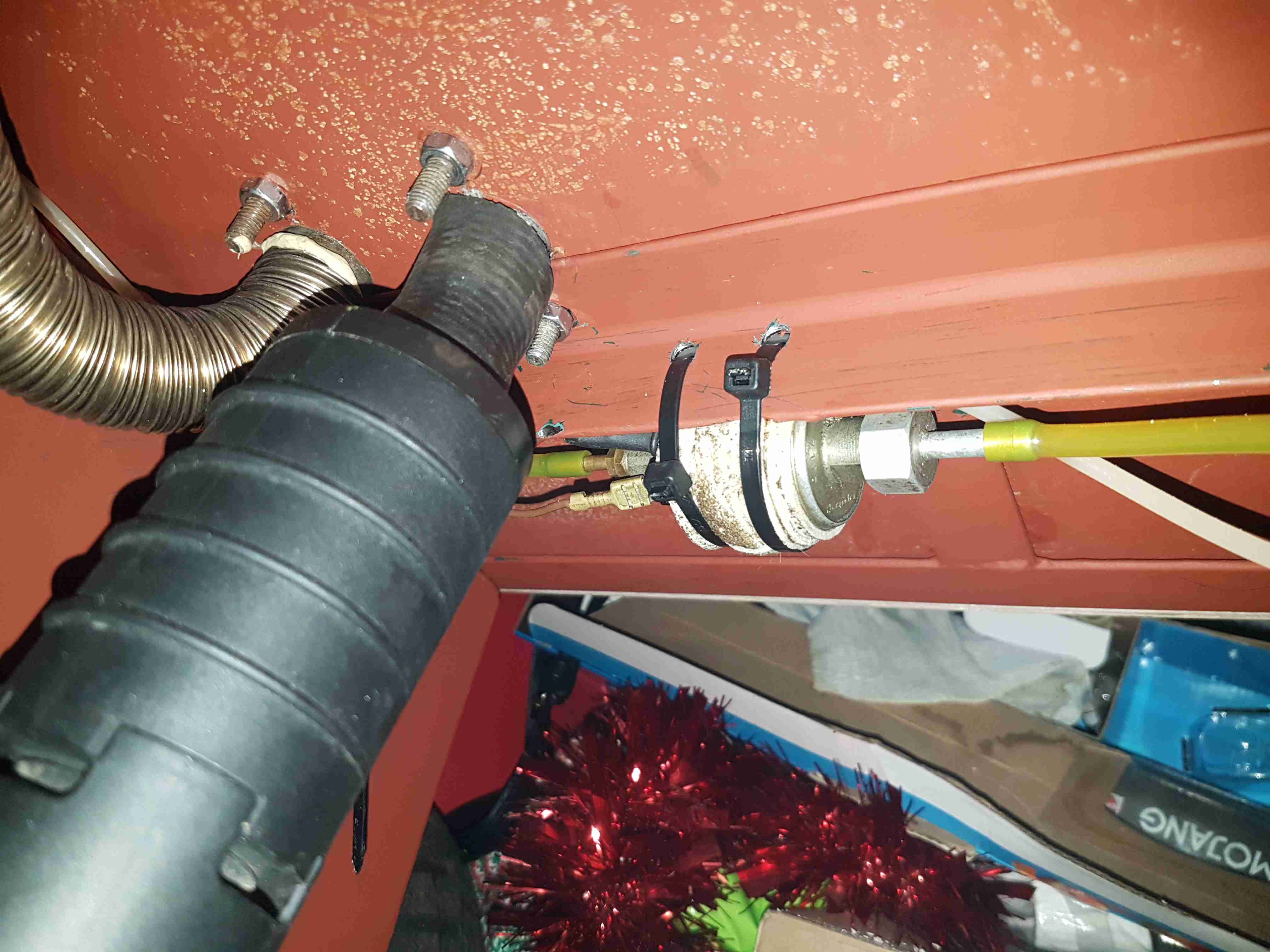
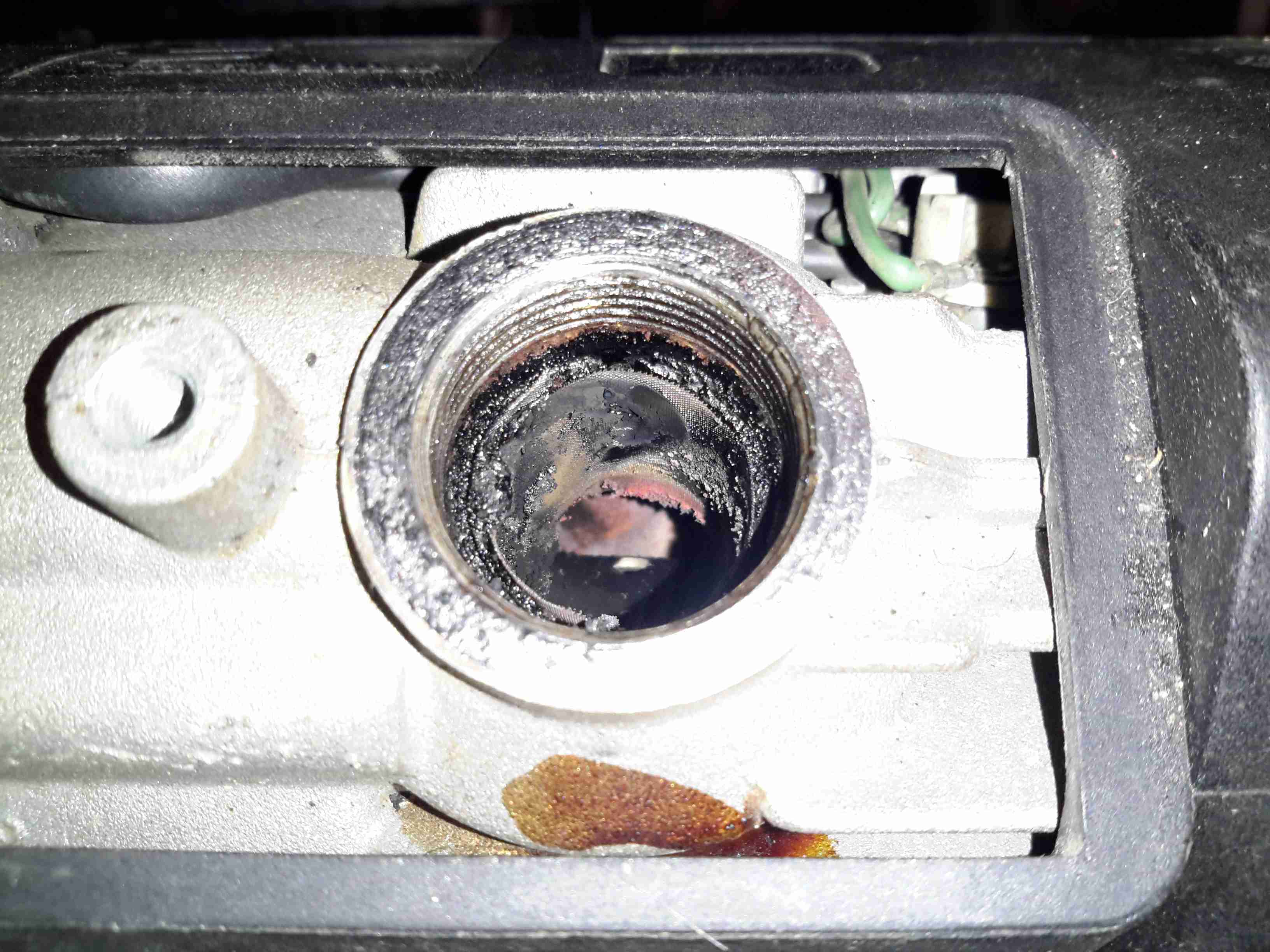
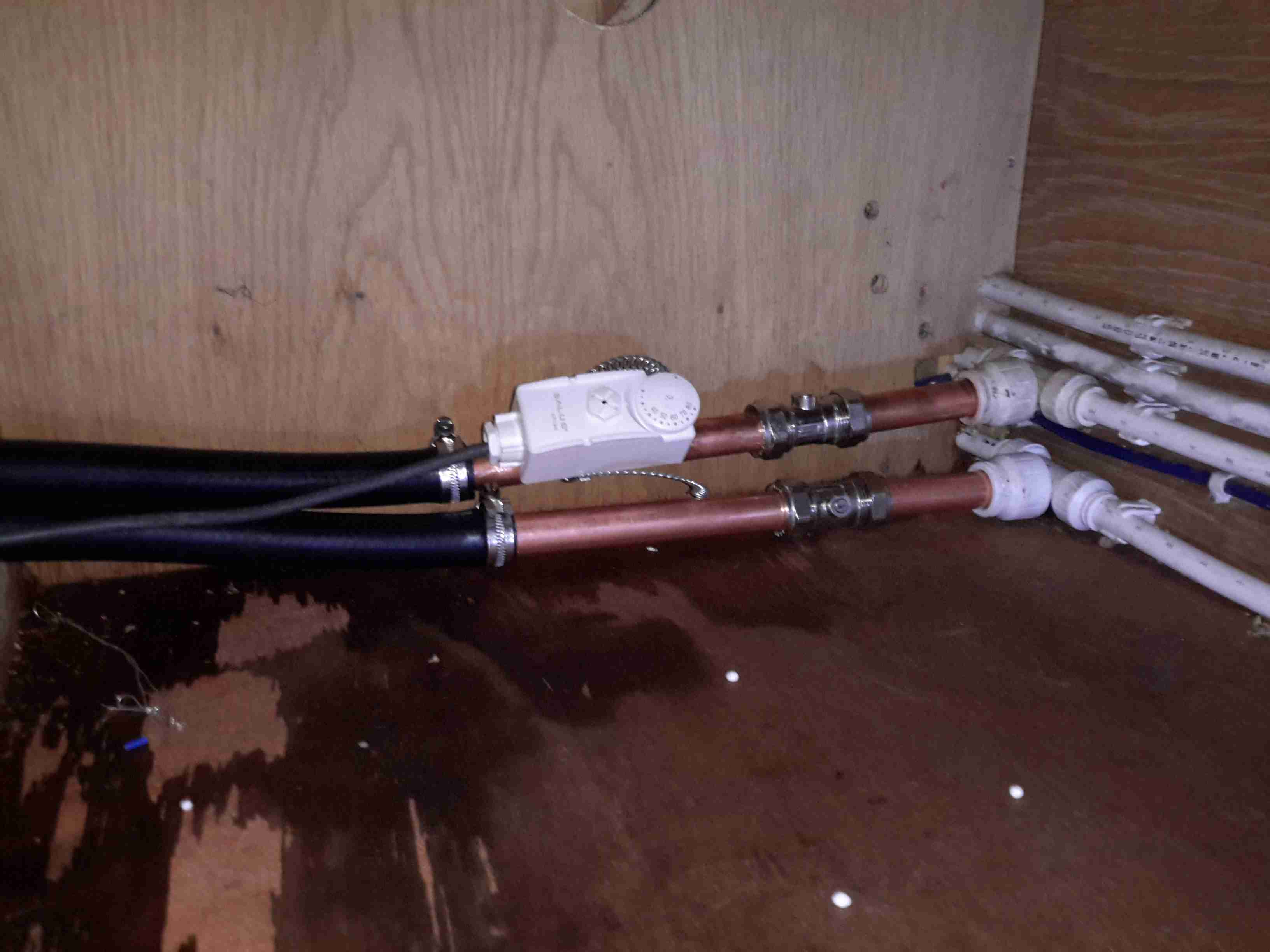
Here the pipework feeding the matrix of the blower unit has been tapped into the heating circuit, the first radiator on the loop is just out of shot to the right, this is all tucked away under the bed in one of the cabins. The pipestat is attached to the flow from the boiler, this will switch on the blower once hot water starts flowing through the system. Isolation valves have been fitted to make the inevitable maintenance of the matrix unit easier, as the system is pressurised to 14PSI, dropping the pressure out of the system without making quite a mess is difficult.
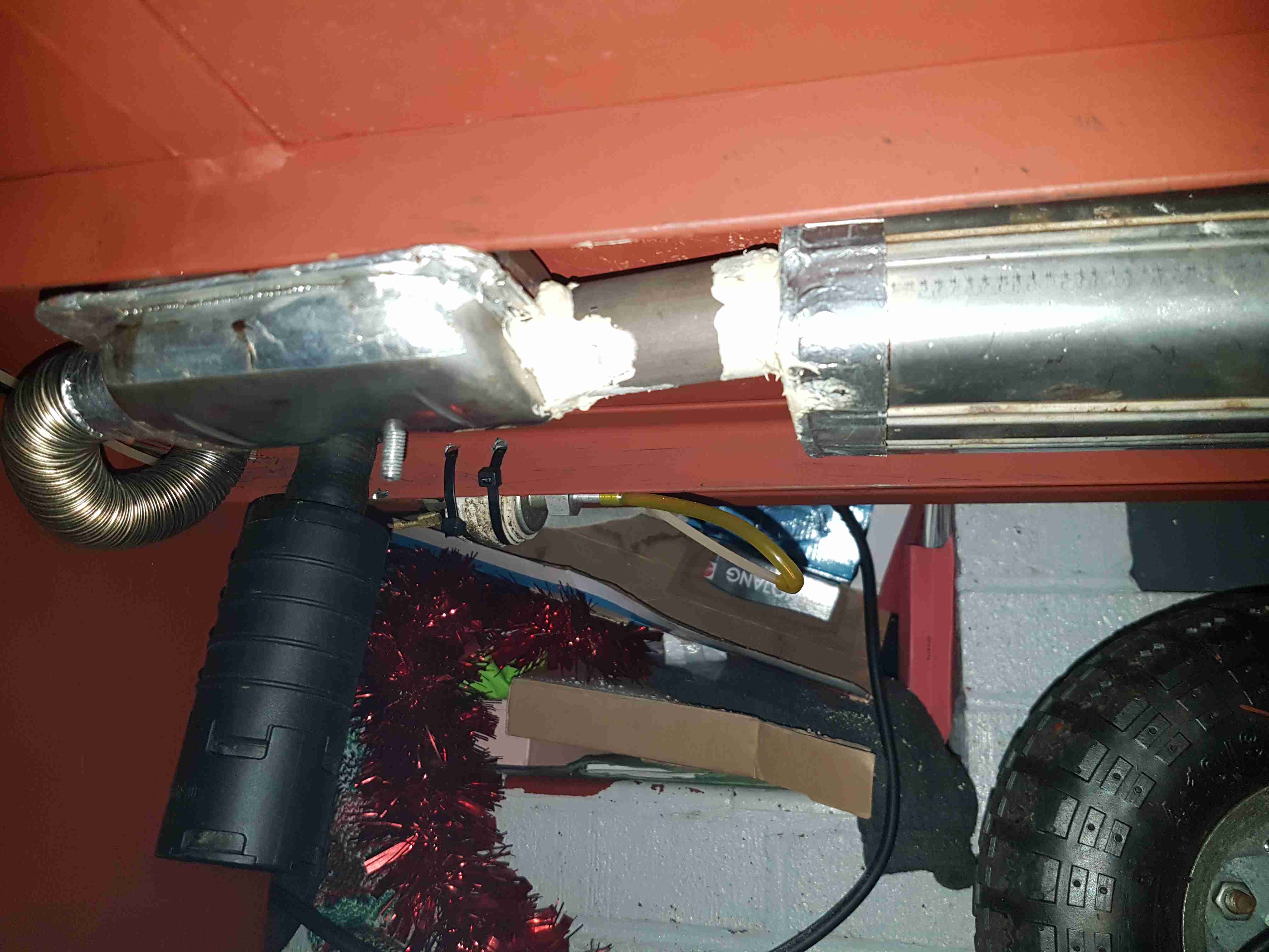
Heater Matrix & Ducting
The heater itself is mounted on the other side of a wooden partition in the small space left under a shelf. This made installing the unit like trying to plumb in a radiator through a letterbox ;). 4 60mm ducts snake off to the vents mounted in the wall.
Water Connections
The hot water hoses appear through a hole in the timber to connect to the matrix unit, with some 15mm pipe in between as reducers from the 3/4″ hose to the 1/2″ attached to the matrix itself. The blower is wired in low speed mode only, as running it any faster makes far too much noise from the vents.
As a heating solution, this unit works well onboard. Within a 10 minutes of the diesel heater firing up, the blower automatically comes on thanks to the thermostat, and blows plenty of hot air into the saloon to keep the cold at bay.
Here’s an eBay oddity – it’s got the same light & lens mechanism as the cheap “disco light” style bulbs on eBay, but this one is battery powered & has a built in MP3 player.
MP3 Disco Light
This device simply oozes cheapness. The large 4″ plastic dome lens sits on the top above the cheap plastic moulding as a base, which also contains the MP3 player speaker.
Controls
There are few controls on this player, the volume buttons are combined with the skip track buttons, a long press operates the volume control, while a short press skips the tracks. Several options for getting this thing to play music are provided:
Bluetooth – Allows connection from any device for bluetooth audio
USB – Plugging in a USB flash drive with MP3 files
SD Card – Very similar to the USB flash drive option, just a FAT32 formatted card with MP3 files
Aux – There’s no 3.5mm jack on this unit for an audio input, instead a “special” USB cable is supplied that is both used to charge the built in battery & feed an audio signal. This is possible since the data lines on the port aren’t used. But it’s certainly out of the ordinary.
Top Removed
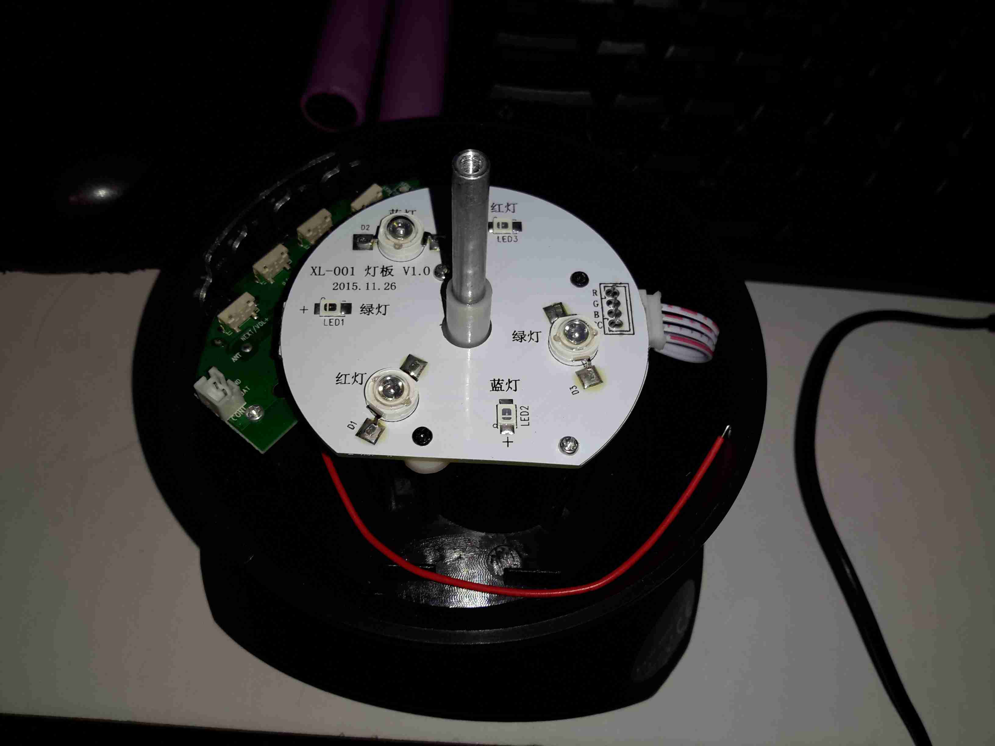
The top comes off with the removal of a single screw in the centre of the lens. The shaft in the centre that holds the lens is attached to a small gear motor under the LED PCB. There’s 6 LEDs on the board, to form an RGB array. Surprisingly for a very small battery powered unit these are bright to the point of being utterly offensive.
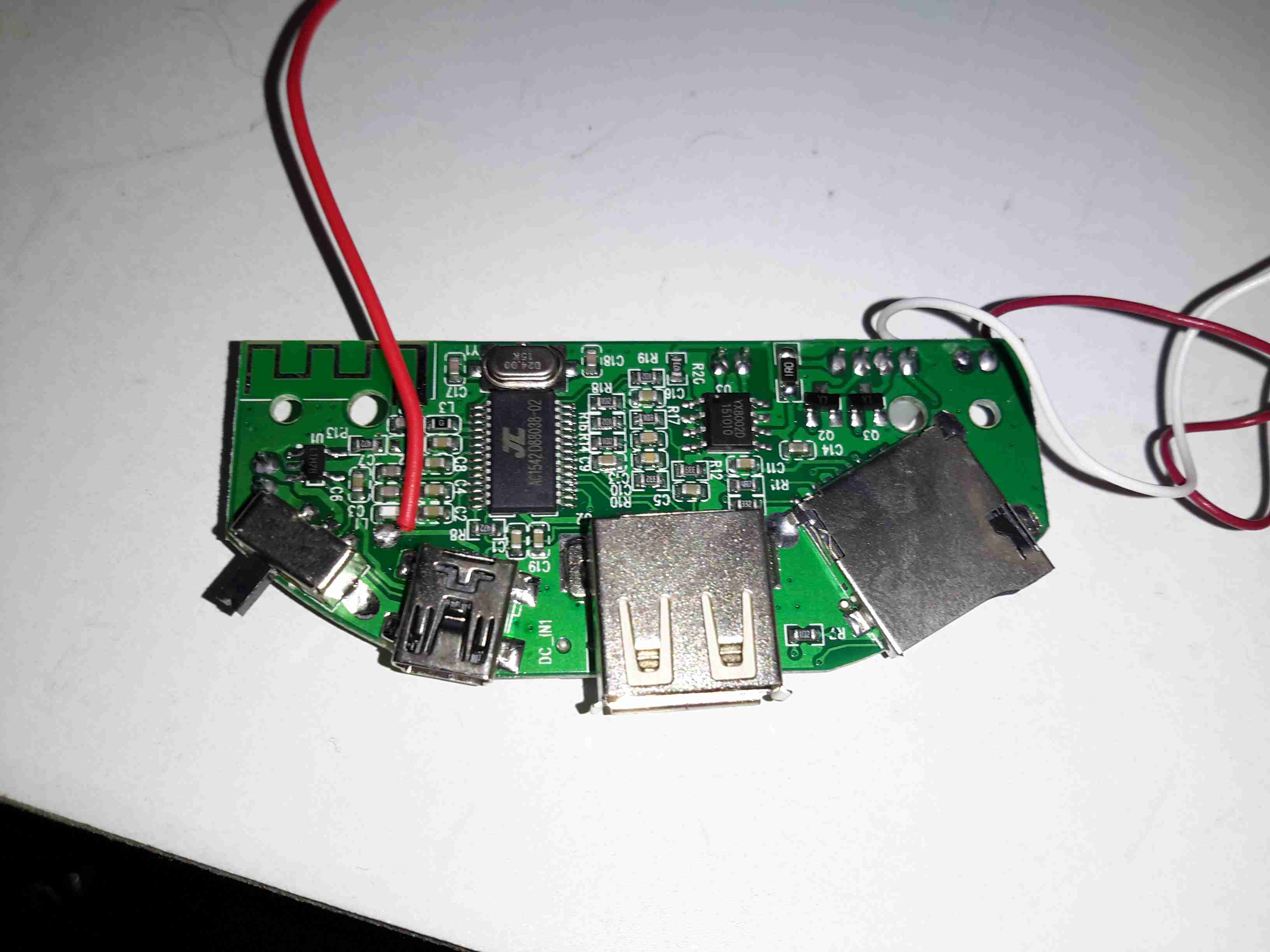
Mainboard
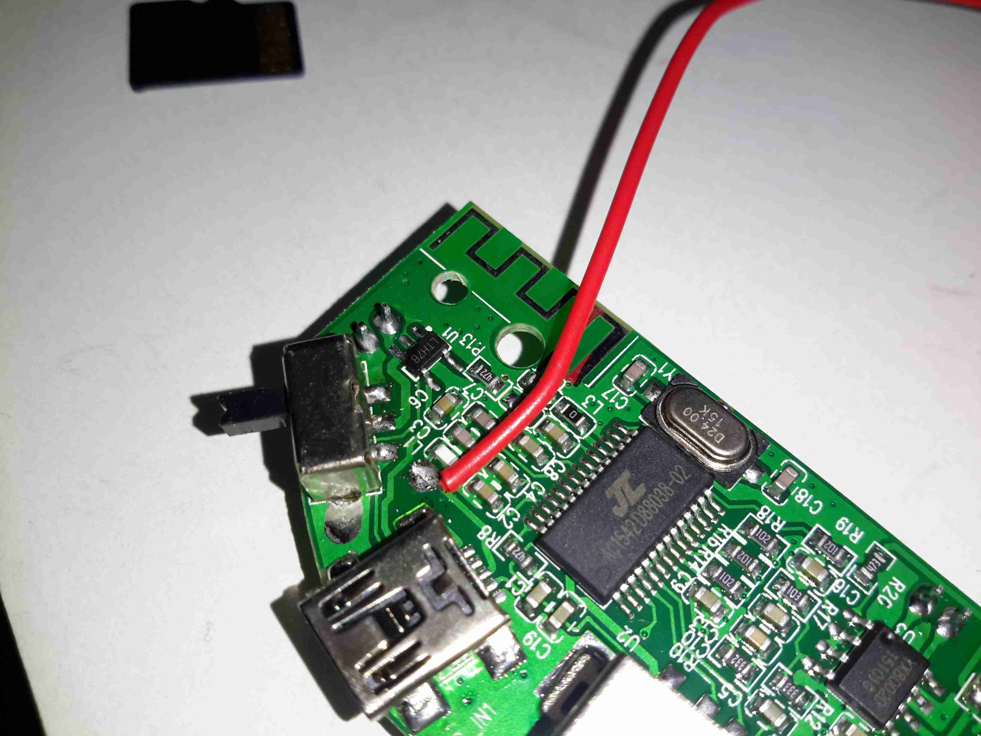
Here’s the mainboard removed from the plastic base. There’s not much to this device, even with all the options it has. The power switch is on the left, followed by the Mini-B USB charging port & aux audio input. The USB A port for a flash drive is next, finishing with the µSD slot. I’m not sure what the red wire is for on the left, it connects to one of the pins on the USB port & then goes nowhere.
Audio Amplifier
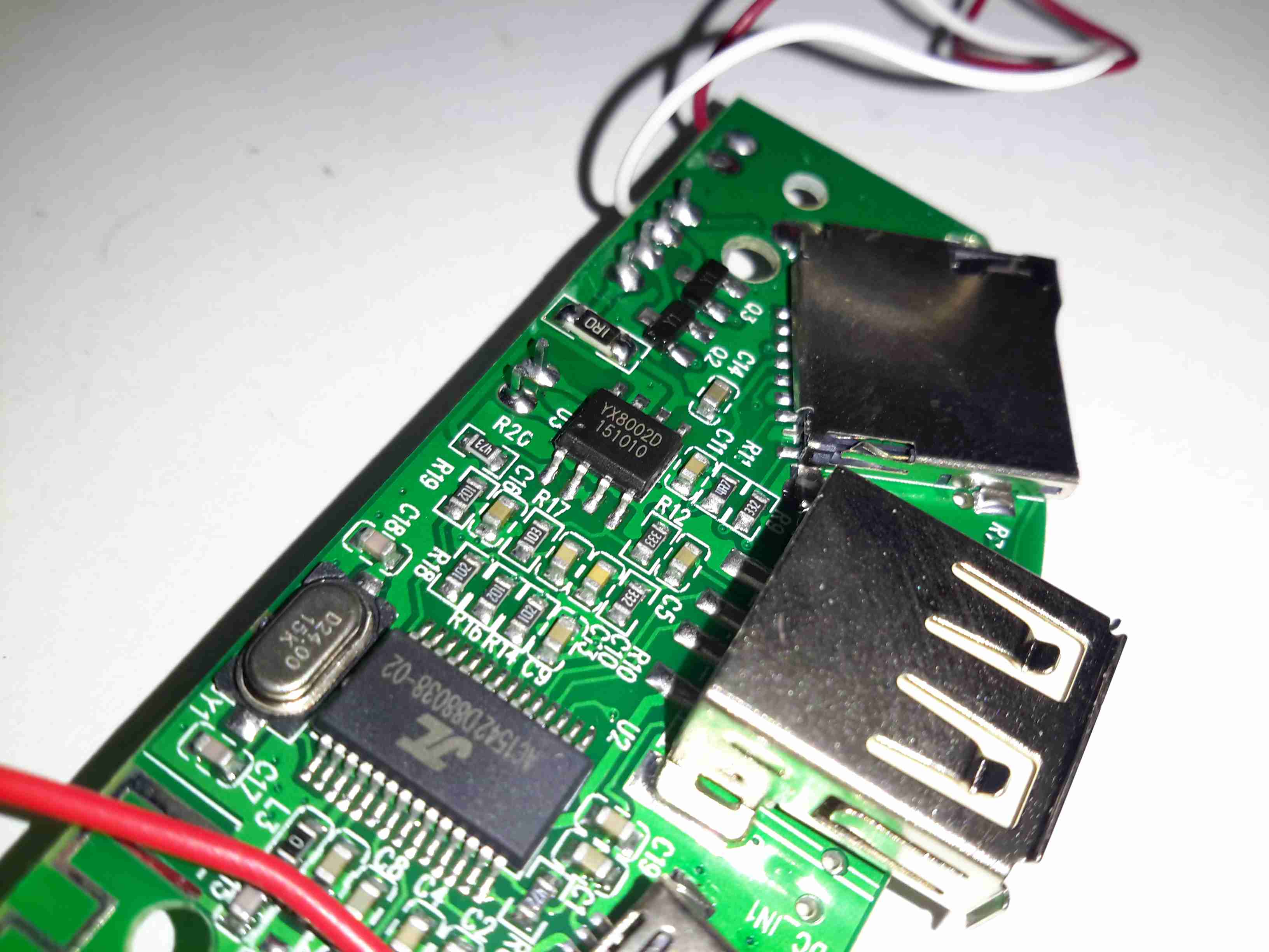
The audio amplifier is a YX8002D, I couldn’t find a datasheet for this, but it’s probably Class D.
Main Chipset
Finally there’s the main IC, which is an AC1542D88038. I’ve not been able to find any data on this part either, it’s either a dedicated MP3 player with Bluetooth radio built in, or an MCU of some kind.The RF antenna for the Bluetooth mode is at the top of the board.
Just behind the power switch is a SOT23-6 component, which should be the charger for the built in Lithium Ion cell.
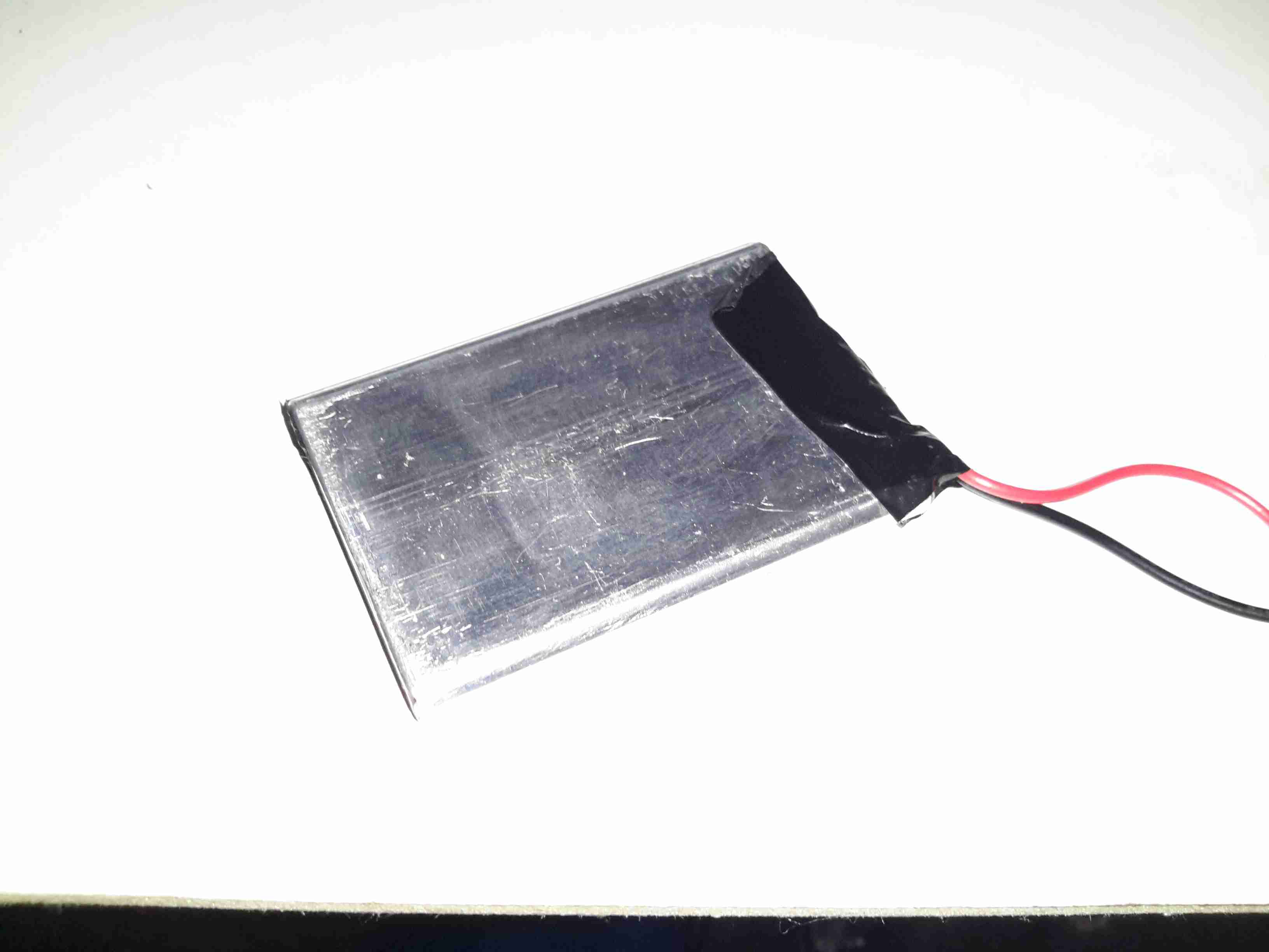
Lithium Ion Cell
The cell itself is a prismatic type rated in the instructions at 600mAh, however my 1C discharge test gave a reading of 820mAh, which is unusual for anything Li-Ion based that comes from eBay 😉
There is cell protection provided, it’s under the black tape on the end, nothing special here.
The main issue so far with this little player is the utterly abysmal battery life – at full volume playing MP3s from a SD card, the unit’s current draw is 600mA, with the seizure & blindness-inducing LEDs added on top, the draw goes up to about 1200mA. The built in charger is also not able to keep up with running the player while charging. This in all only gives a battery life of about 20 minutes, which really limits the usability of the player.
With some recent upgrades to the boat’s heating system, the hot water circulation pumps we’ve been using are becoming far too small for the job. After the original Johnson Marine circulation pump died of old age (the brushes wore down so far the springs ate the commutator) some time ago, it was replaced with a Pierburg WUP1 circulation pump from a BMW. (As we’re moored next to a BMW garage, these are easily obtainable & much cheaper than the marine pumps).
WUP1 Cutaway
These are also brushless, where as the standard Johnson ones are brushed PM motors – the result here is a much longer working life, due to fewer moving parts.
The rated flow & pressure on these pumps is pretty pathetic, at 13L/min at 0.1bar head pressure. As the boat’s heating system is plumbed in 15mm pipe instead of 22mm this low pressure doesn’t translate to a decent flow rate. Turns out it’s pretty difficult to shove lots of water through ~110ft of 15mm pipe ;). Oddly enough, the very low flow rate of the system was never a problem for the “high output” back boiler on the stove – I suspect the “high output” specification is a bit optimistic.
This issue was recently made worse with the addition of a Webasto Thermo Top C 5kW diesel-fired water heater, which does have it’s own circulation pump but the system flow rate was still far too low to allow the heater to operate properly. The result was a rapidly cycling heater as it couldn’t dump the generated hot water into the rest of the system fast enough.
The easiest solution to the problem here is a larger pump with a higher head pressure capability. (The more difficult route would be completely re-piping the system in 22mm to lower the flow resistance). Luckily Pierburg produce a few pumps in the range that would fit the job.
Pierburg CWA-50
Here’s the next size up from the original WUP1 pump, the CWA50. These are rated at a much more sensible 25L/min at 0.6bar head pressure. It’s physically a bit larger, but the connector sizes are the same, which makes the install onto the existing hoses easier. (For those that are interested, the hose connectors used on BMW vehicles for the cooling system components are NormaQuick PS3 type. These snap into place with an O-Ring & are retained by a spring clip).
The CWA50 draws considerably more power than the WUP1 (4.5A vs 1.5A), and are controllable with a PWM signal on the connector, but I haven’t used this feature. The PWM pin is simply tied to the positive supply to keep the pump running at maximum speed.
Once this pump was installed the head pressure immediately increased on the gauge from the 1 bar static pressure to 1.5 bar, indicating the pump is running at about it’s highest efficiency point. The higher water flow has so far kept the Webasto happy, there will be more to come with further improvements!
CWA-50 Pump Teardown
CWA50 Cutaway
Above is a cutaway drawing of the new pump. These have a drilling through the shaft allows water to pass from the high pressure outlet fitting, through the internals of the pump & returns through the shaft to the inlet. This keeps the bearings cool & lubricated. The control & power drive circuitry for the 3-phase brushless motor is attached to the back & uses the water flowing through the rotor chamber as a heatsink. Overall these are very well made pumps.
Impeller
Here’s the impeller of the pump, which is very small considering the amount of power this unit has. The return port for the lubricating water can be seen in the centre of the impeller face.
3-Phase Driver
Inside the back of the pump is the control module. The main microcontroller is hiding under the plastic frame which holds the large power chokes & the main filter electrolytic.
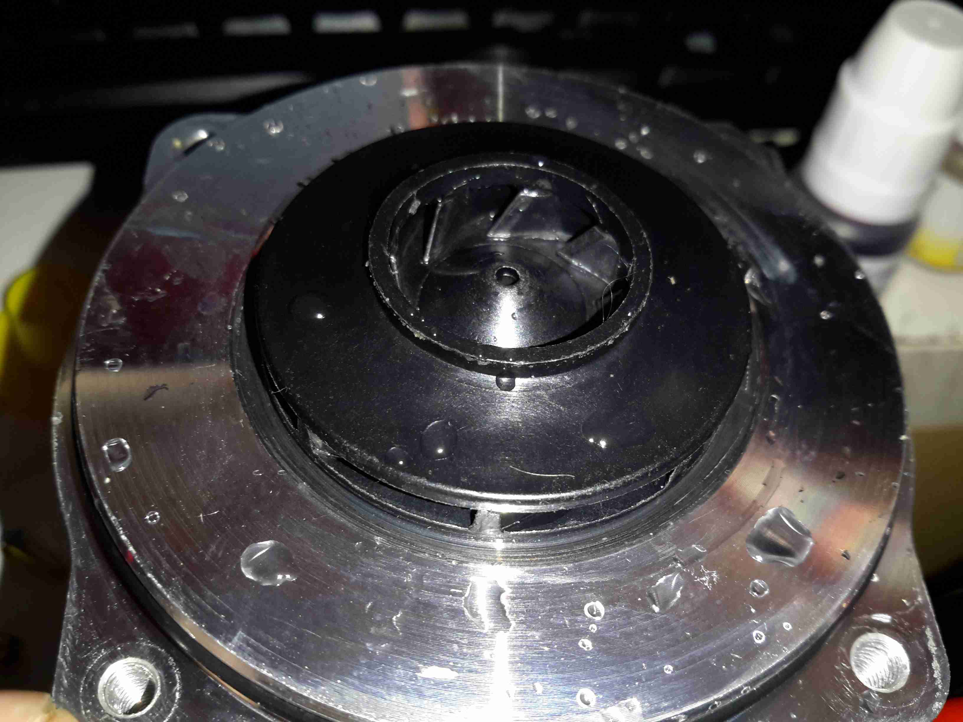
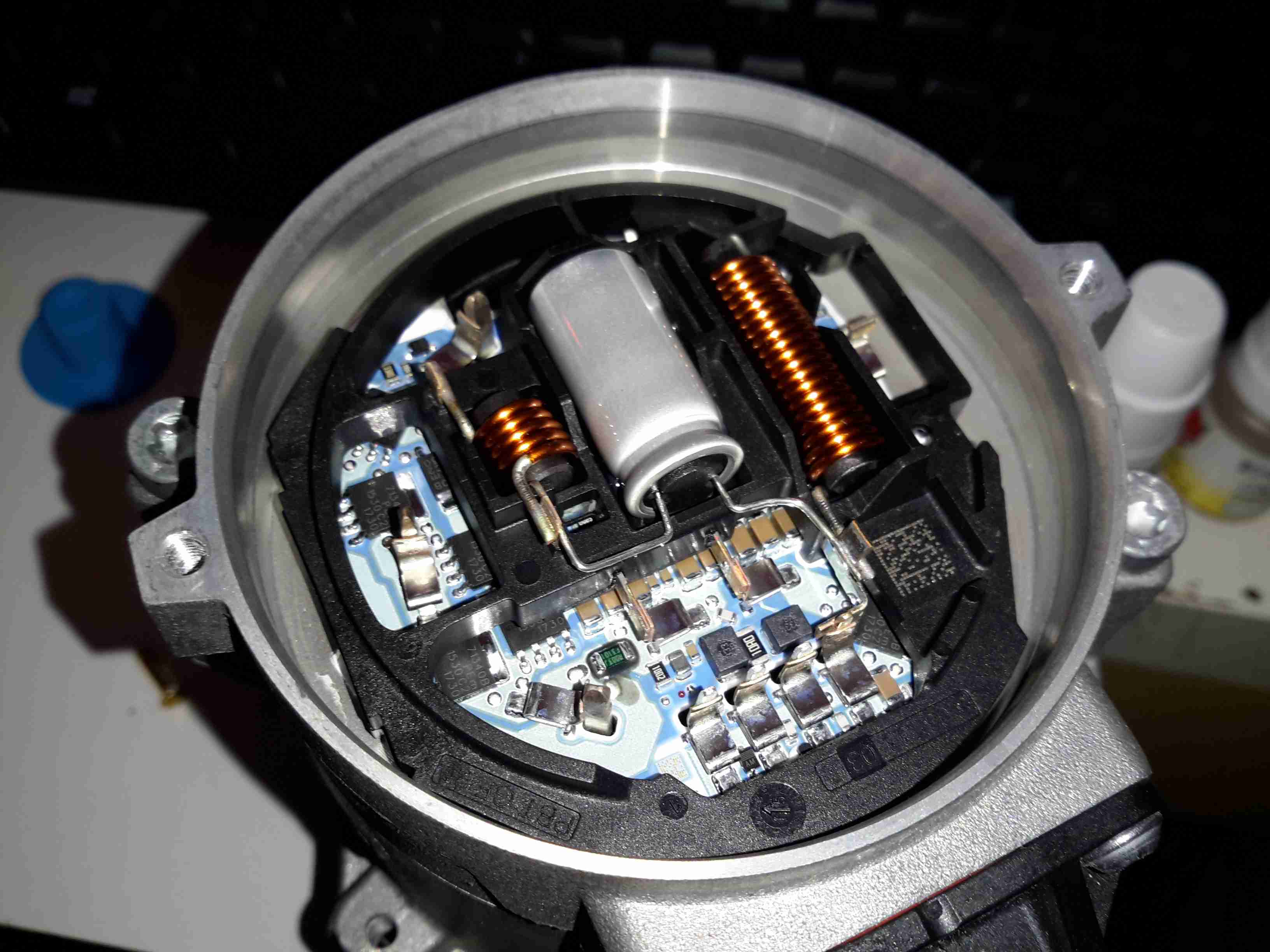
The old Panasonic NV-M5 has the standard for the time CRT based viewfinder assembly, which will happily take a composite video signal from an external source.
This viewfinder has many more connections than I would have expected, as it has an input for the iris signal, which places a movable marker on the edge of the display. This unit also has a pair of outputs for the vertical & horizontal deflection signals, I imagine for sync, but I’ve never seen these signals as an output on a viewfinder before.
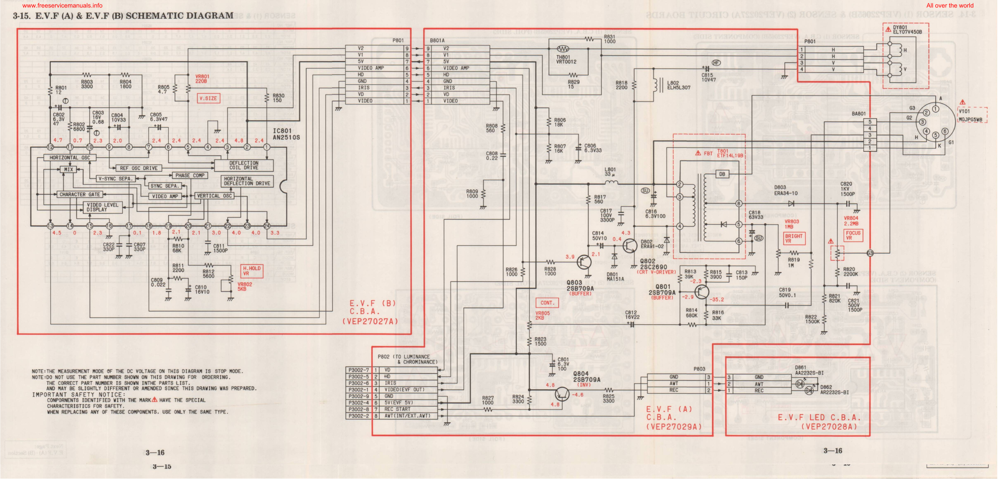
EVF Schematic
Luckily I managed to get a service manual for the camera with a full schematic.
This unit takes a 5v input, as opposed to the 8-12v inputs on previous cameras, so watch out for this! There’s also no reverse polarity protection either.
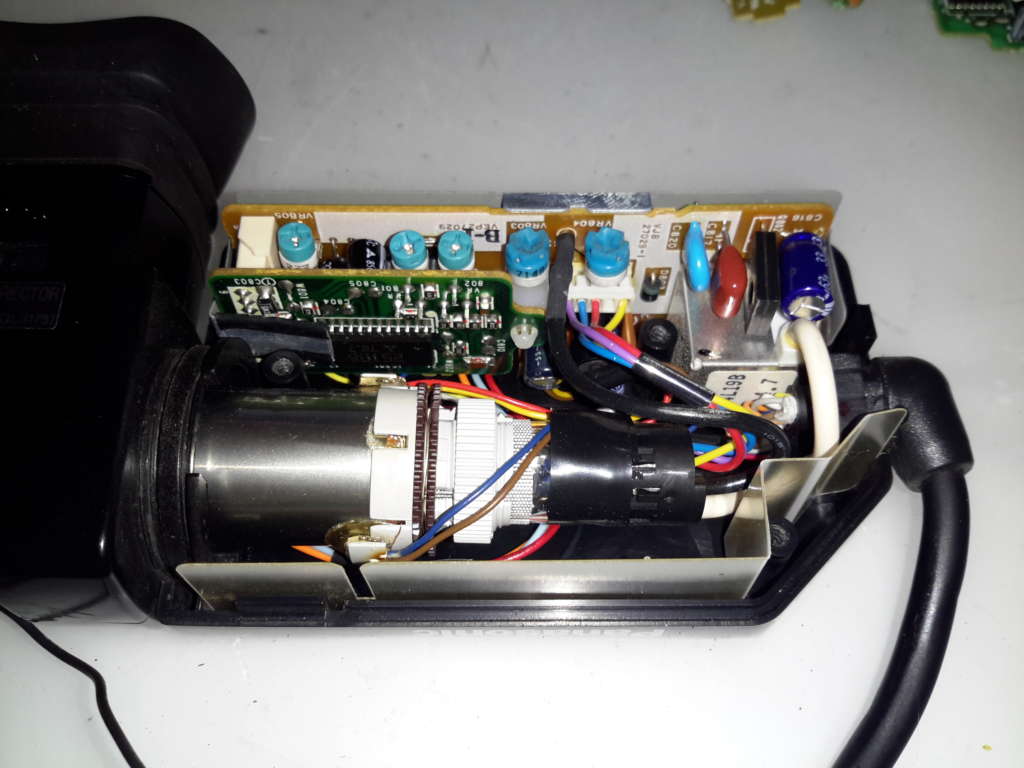
Pins
Making the iris marker vanish from the screen is easy, just put a solder bridge between pins 15 & 16 of the drive IC. The important pins on the interface connector are as follows:
Pin 3: GND
Pin 4: Video Input
Pin 5: Video GND
Pins 6: +5v Supply
Tip Jar
If you’ve found my content useful, please consider leaving a donation by clicking the Tip Jar below!
All collected funds go towards new content & the costs of keeping the server online.