Posted on 5 Comments

Vodafone Mobile WiFi R207 Teardown

Vodafone Mobile WiFi R207

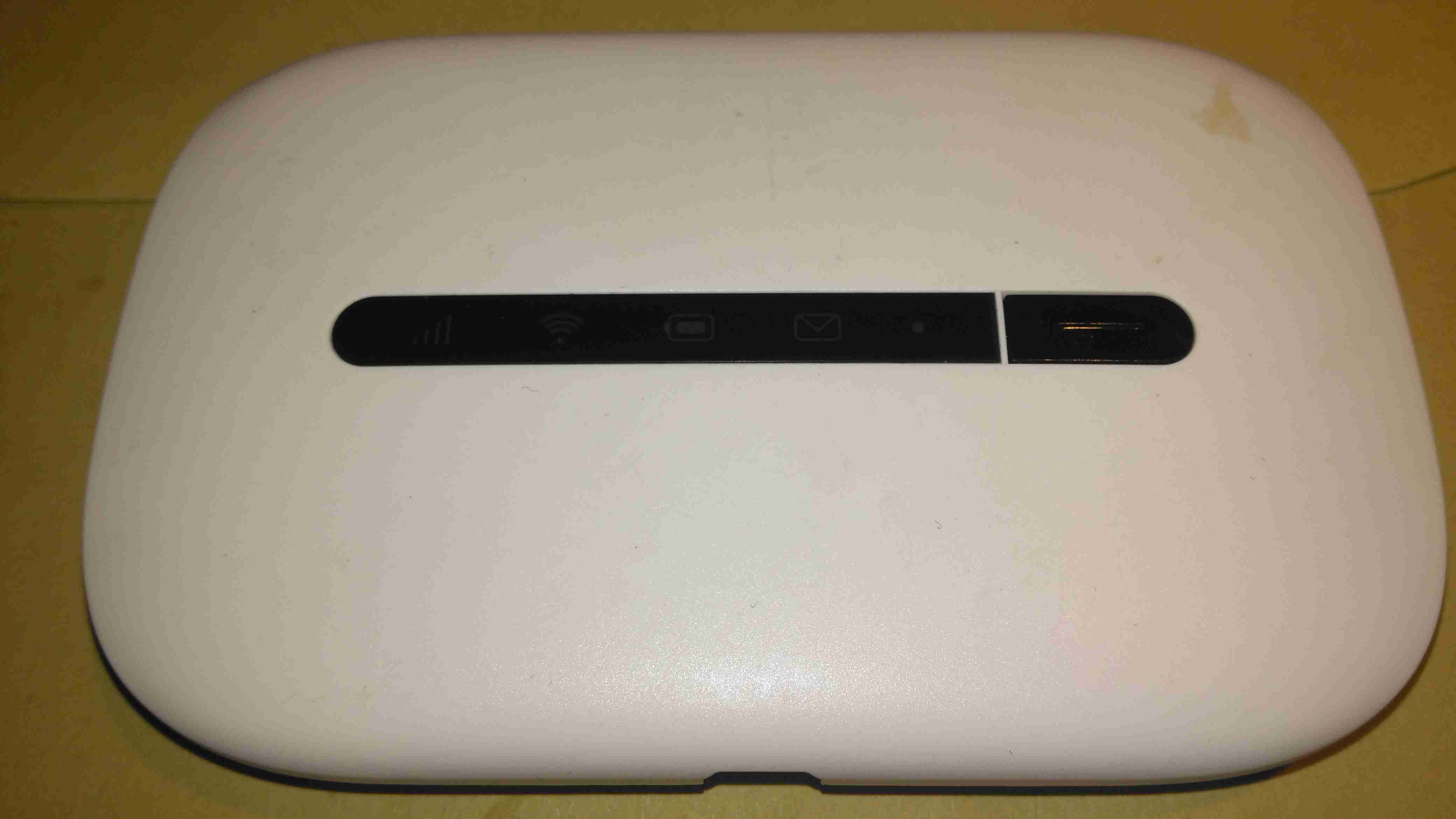
Here’s one of the old modems from my spares bin, a Vodafone Mobile WiFi R207. This is just a rebranded Huawei E5330. This unit includes a 3G modem, and a WiFi chipset, running firmware that makes this a mini-router, with NAT.

Specs
Specs

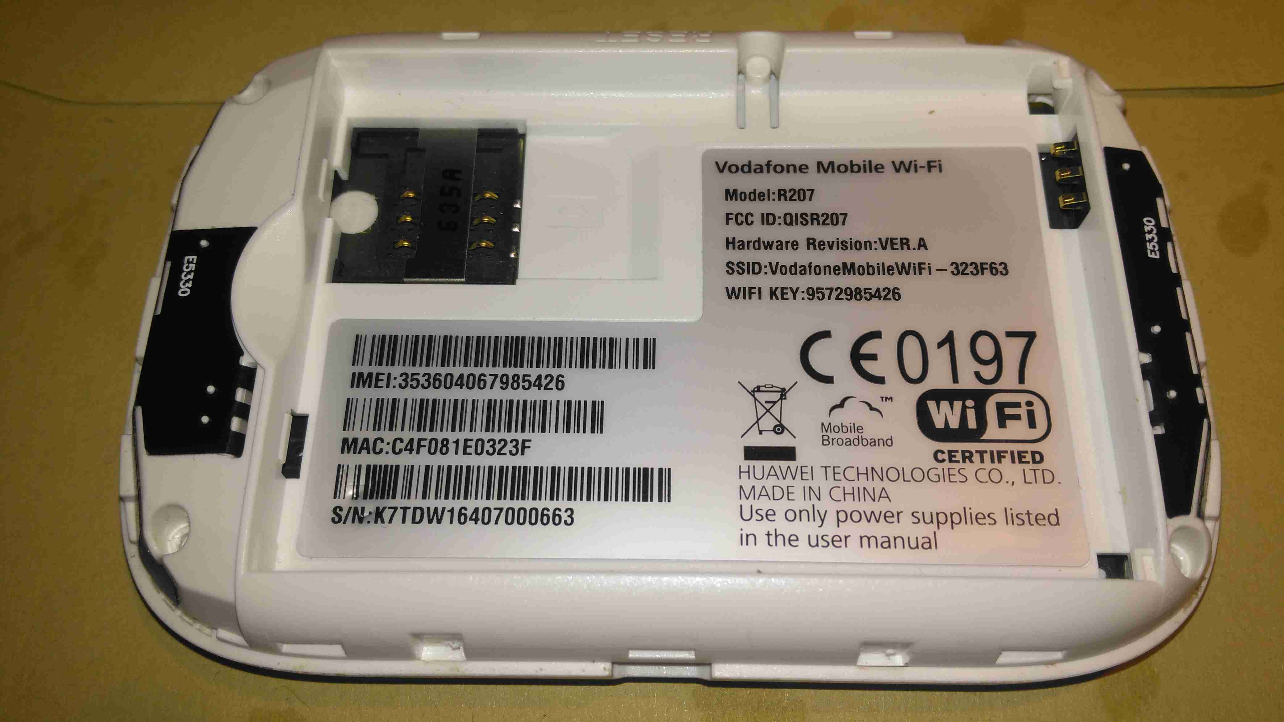
The back has the batter compartment & the SIM slot, with a large label showing all the important details.

Cover Removed
Cover Removed

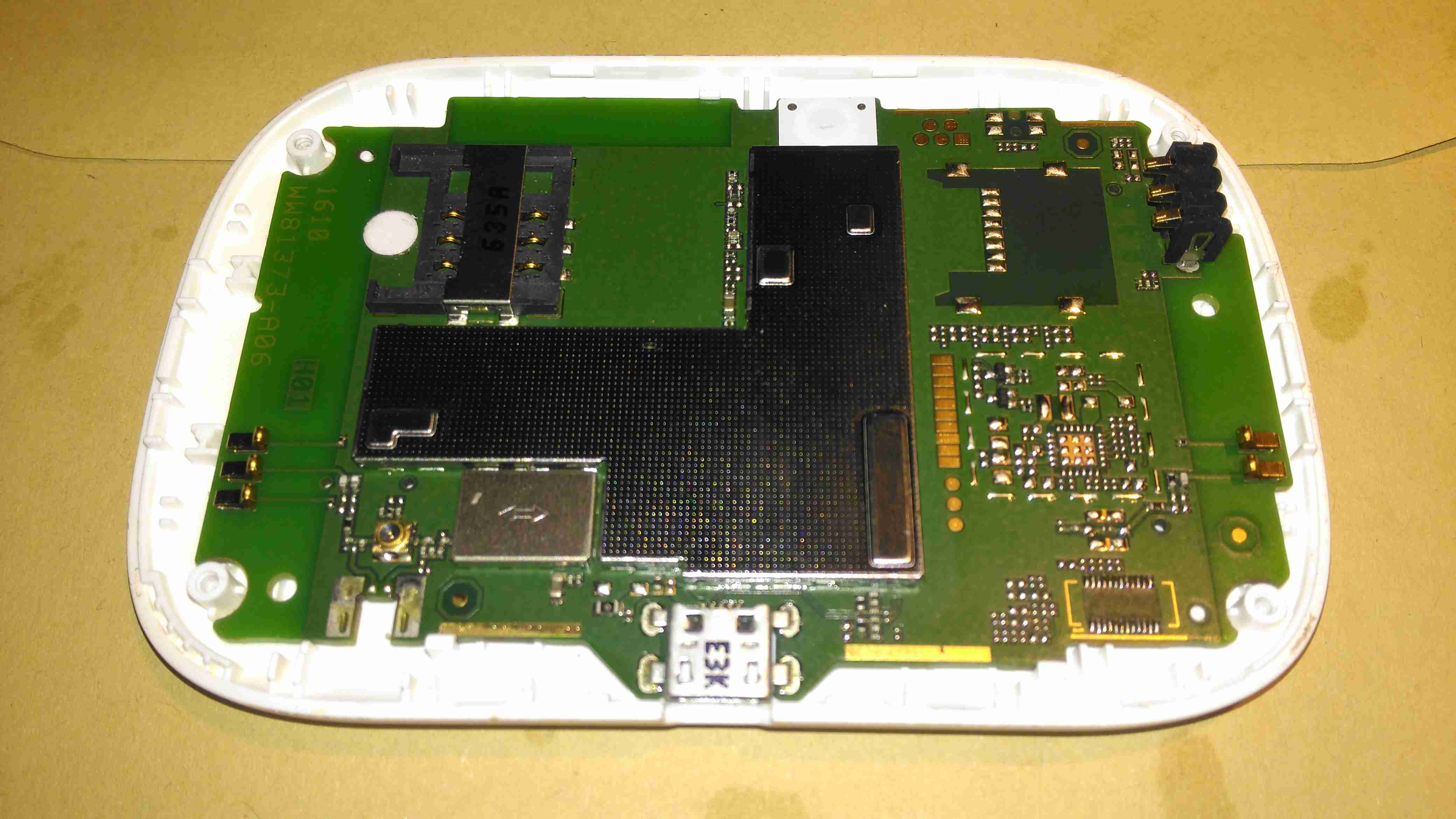
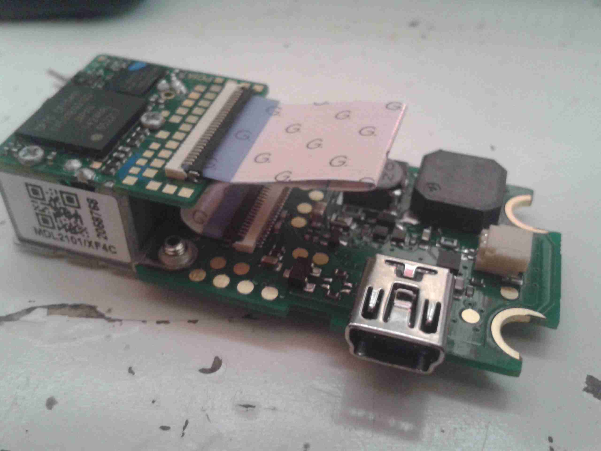
A couple of small Torx screws later & the shell splits in half. All the electronics are covered by shields here, but luckily they are the clip-on type, and aren’t soldered direct to the PCB.

Chipset
Chipset

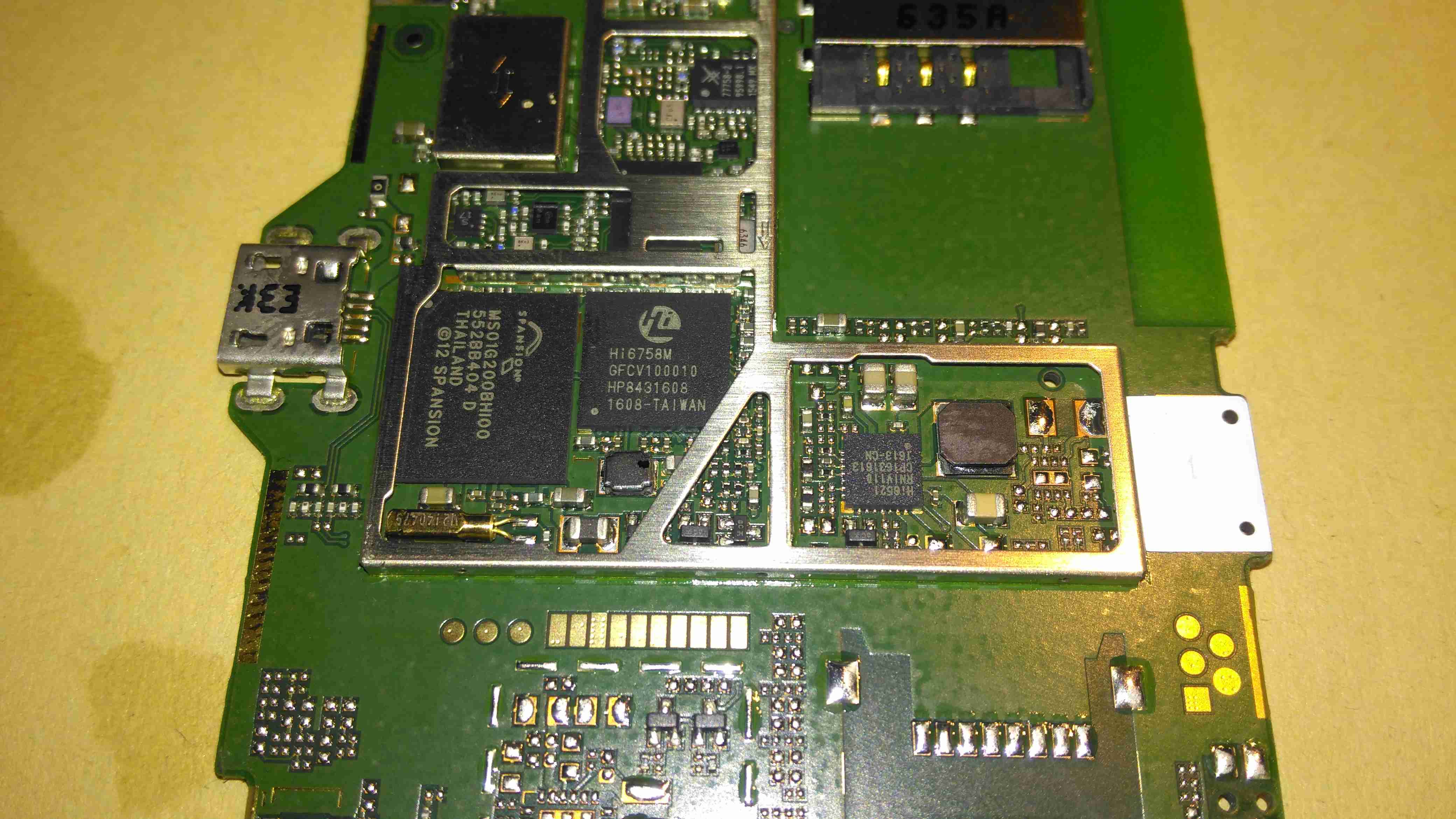
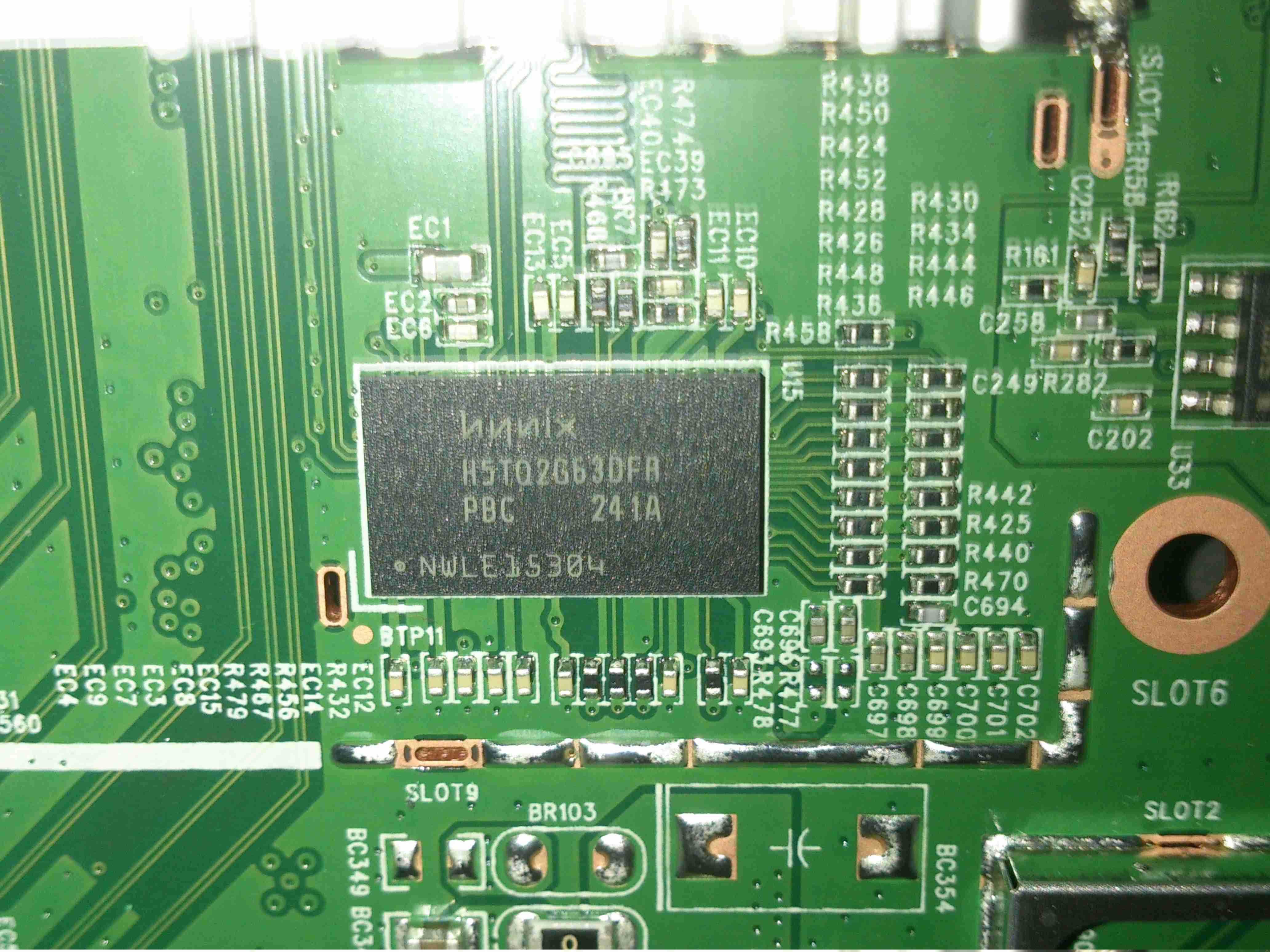
Once the shield has been removed, the main chipset is visible underneath. There’s a large Spansion MS01G200BHI00 1GBit flash, which is holding the firmware. Next to that is the Hi6758M baseband processor. This has all the hardware required to implement a 3G modem. Just to the right is a Hi6521 power management IC, which is dealing with all the power supplies needed by the CPU.
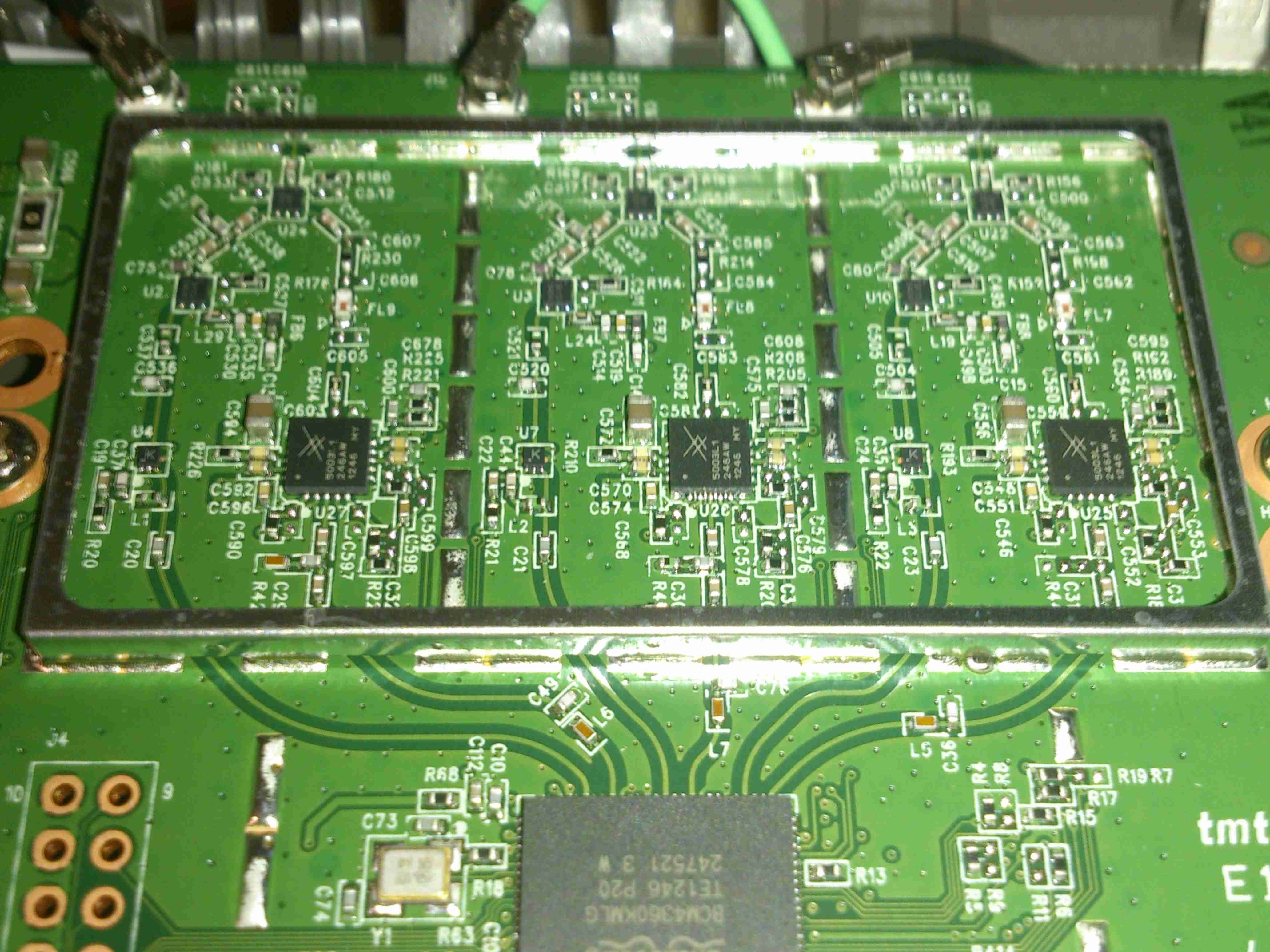
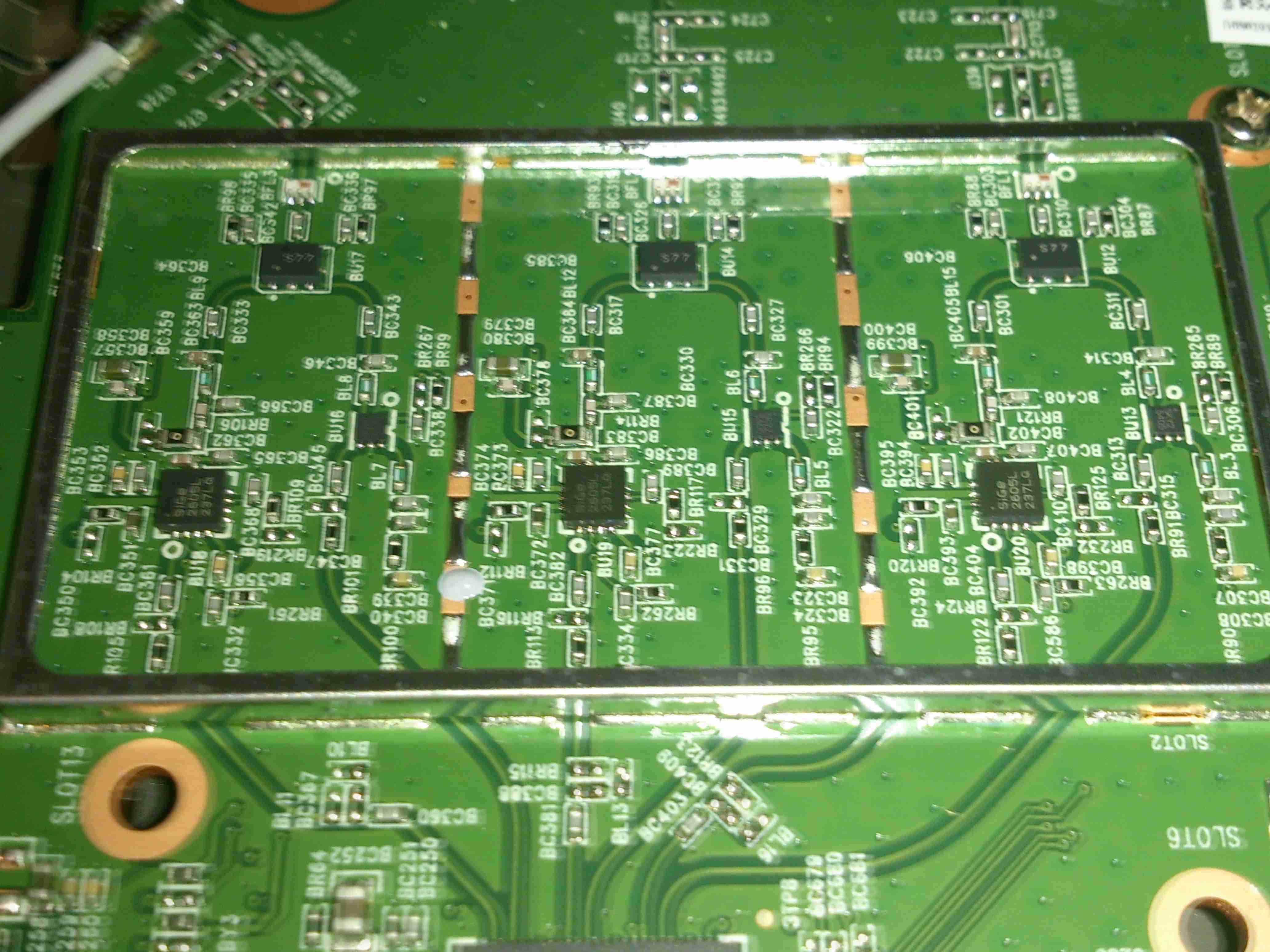
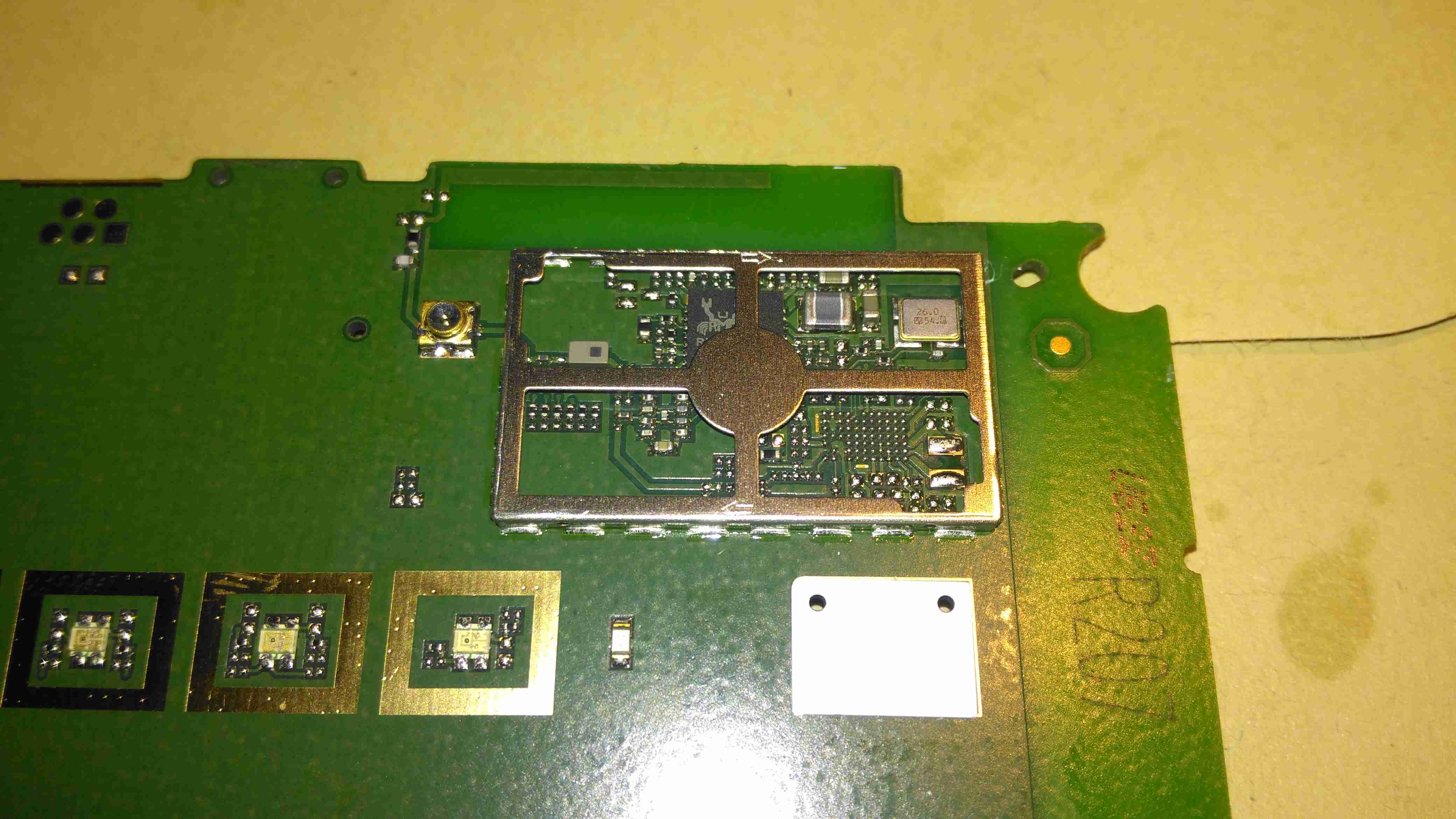
The RF section is above the baseband processor, some of which is hiding under the bits of the shield that aren’t removable.

SIM Socket
SIM Socket

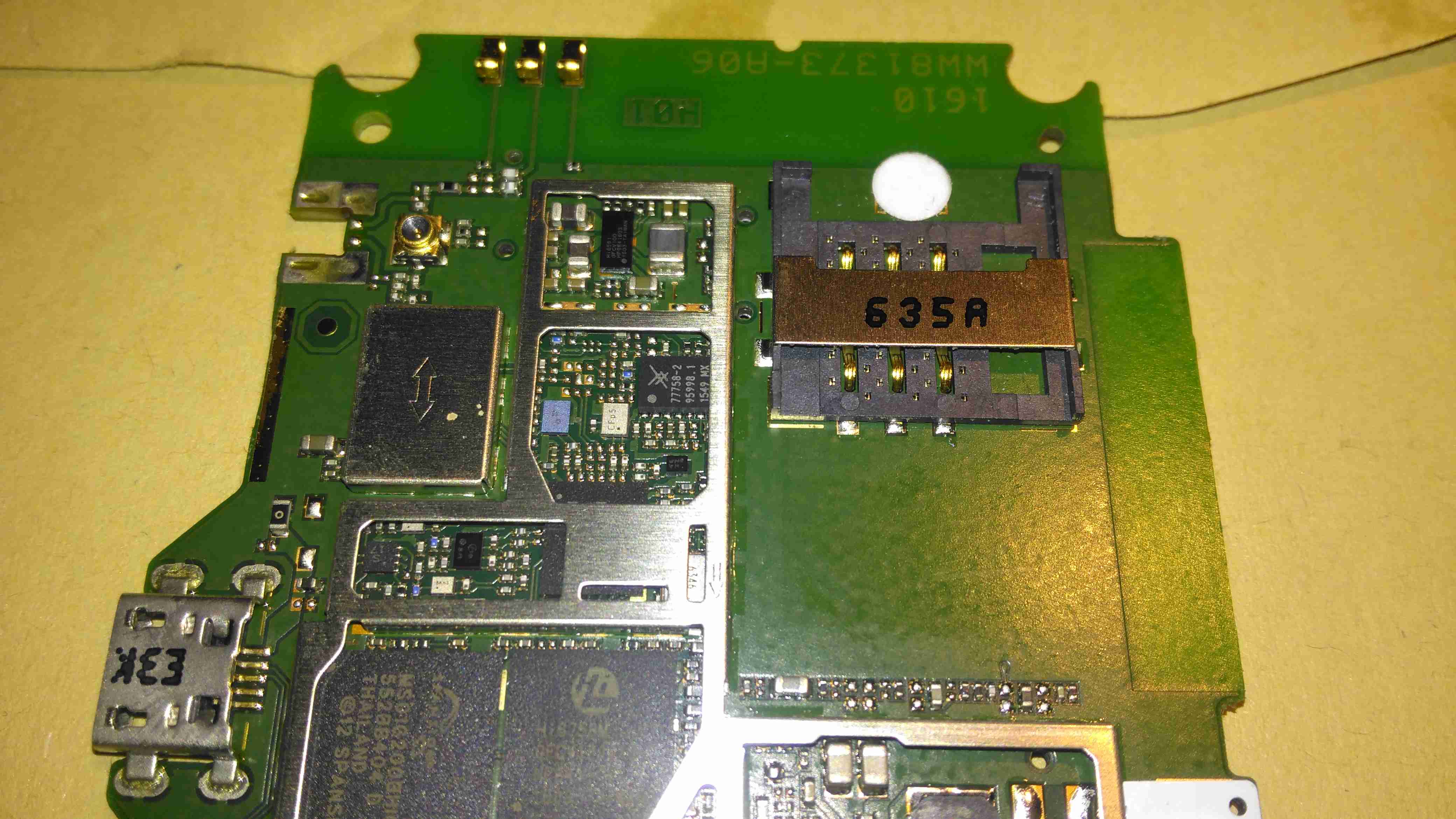
There’s a socket onboard for a standard Mini-SIM, just to the left of that is a Hi6561 4-phase buck converter. I would imagine this is providing the power supplies for the RF section & amplifier.

Unpopulated Parts
Unpopulated Parts

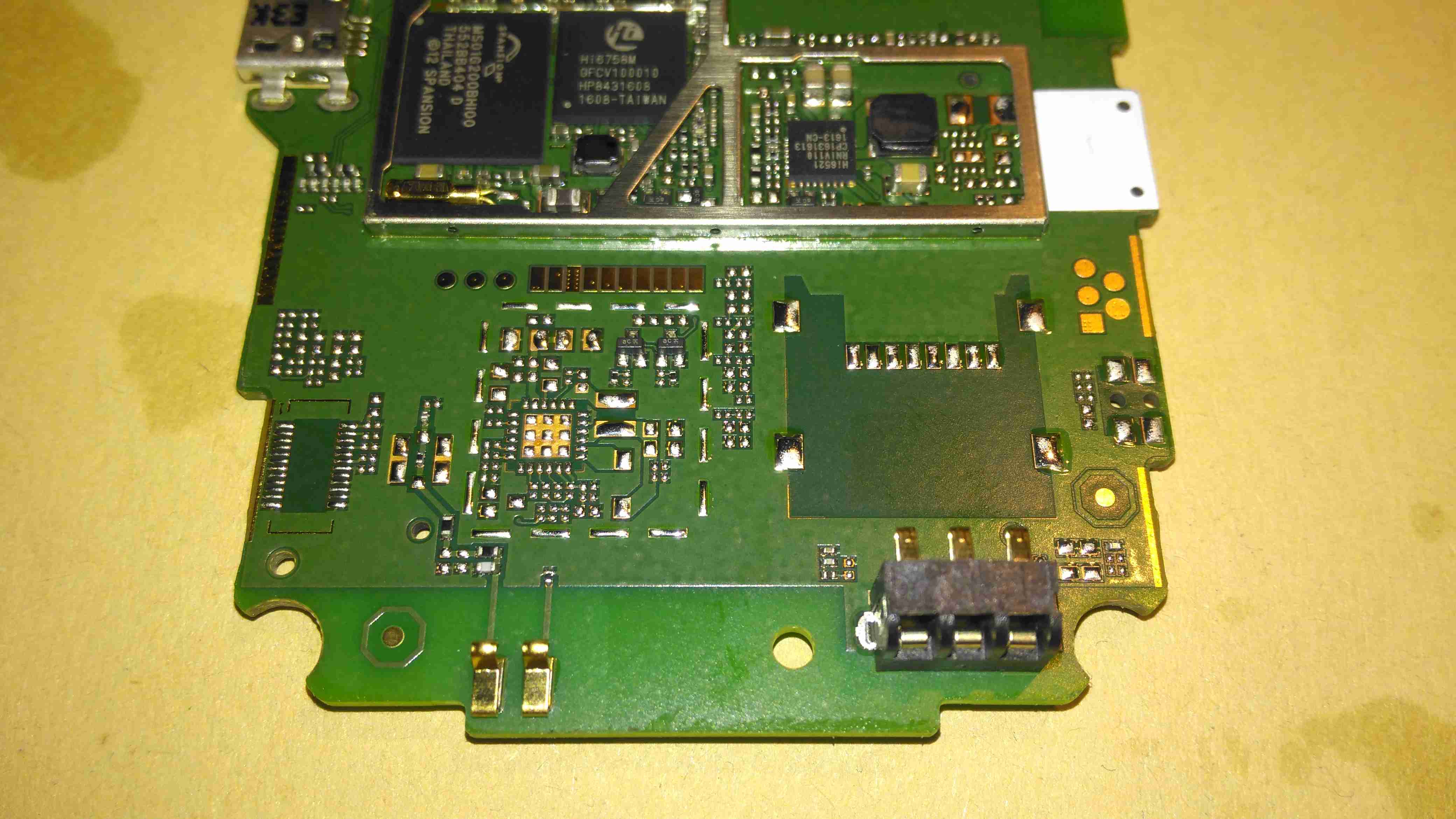
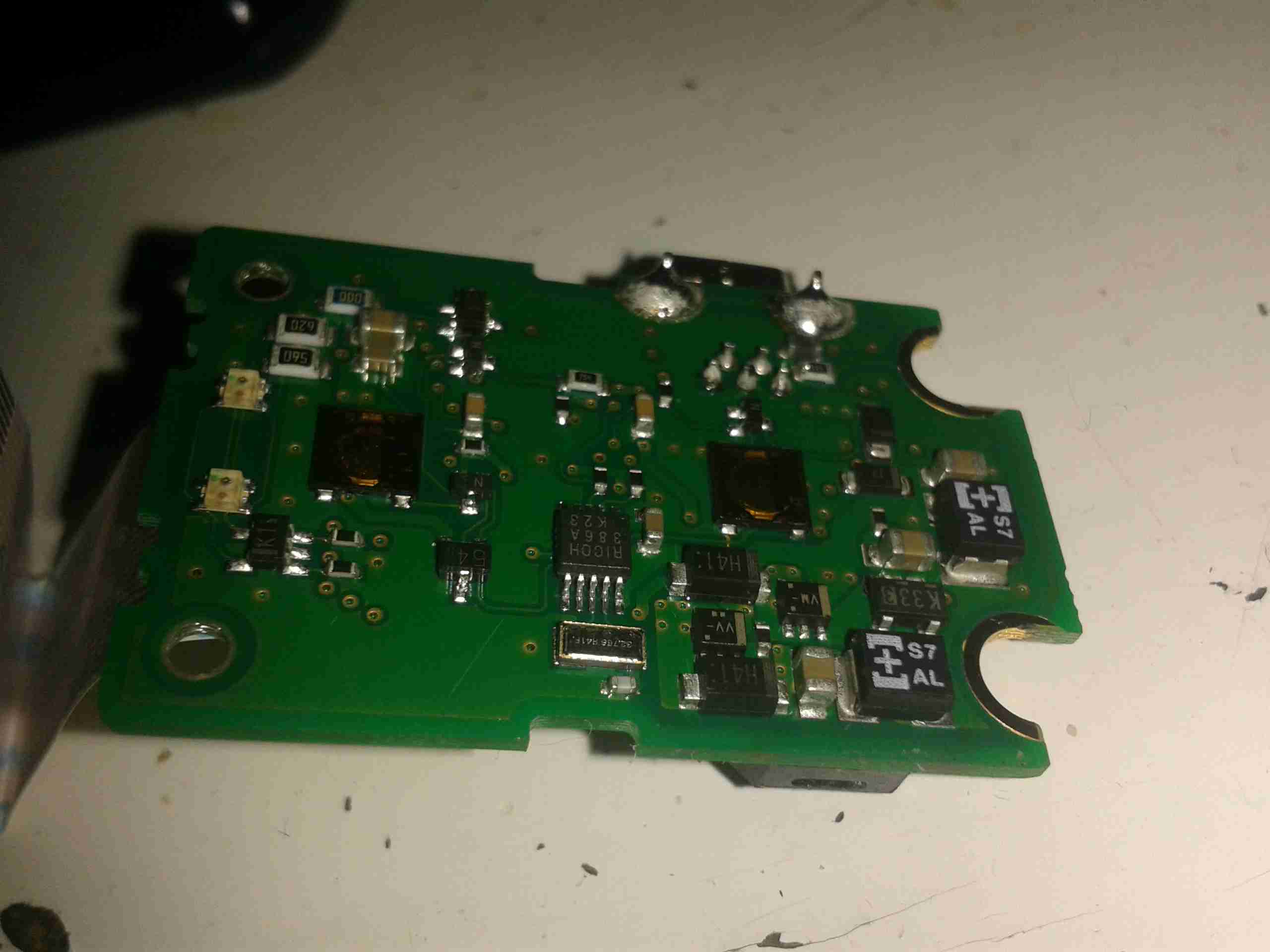
Not sure what this section is for, all the parts are unpopulated. Maybe a bluetooth option?

PCB Reverse
PCB Reverse

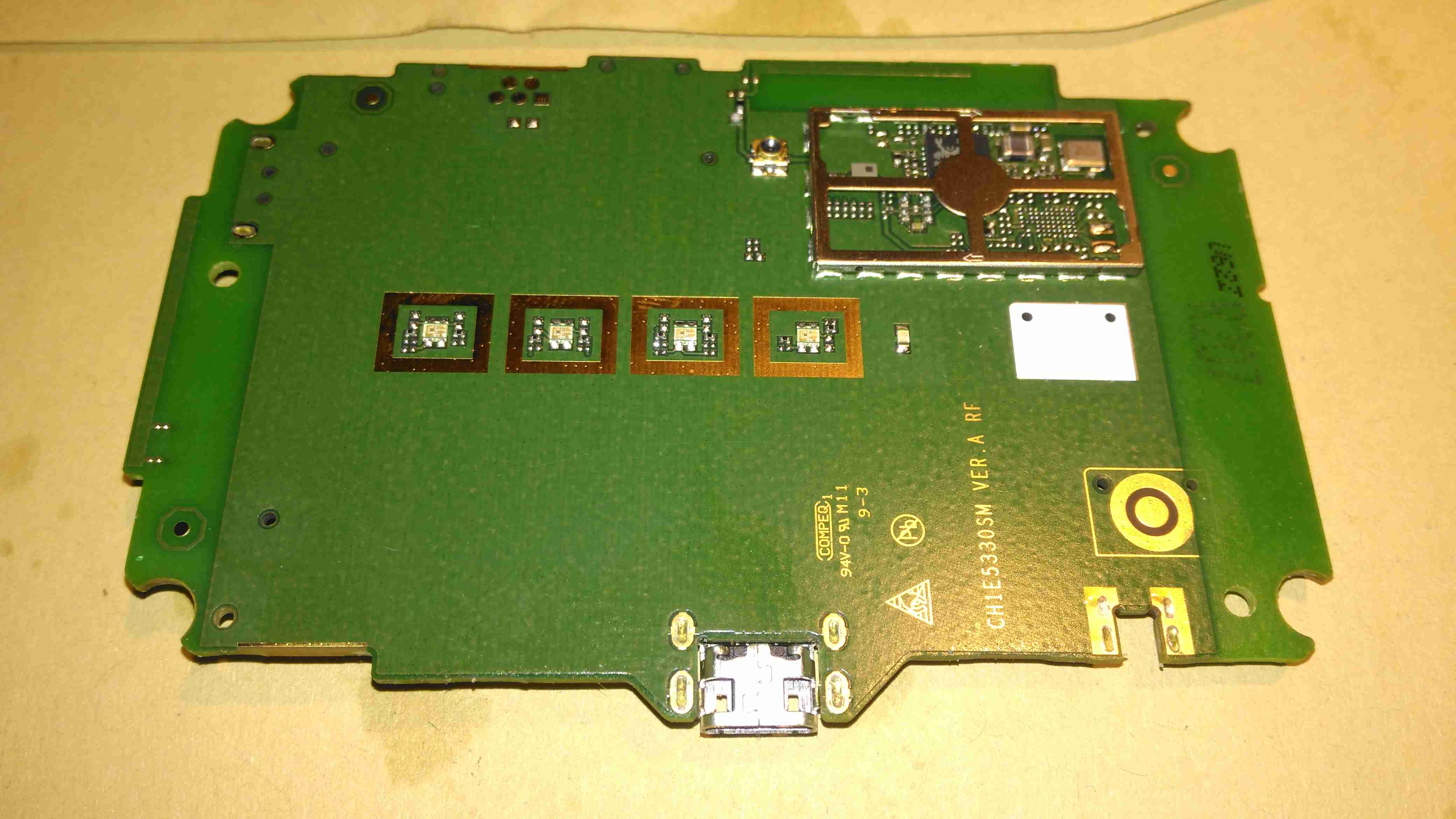
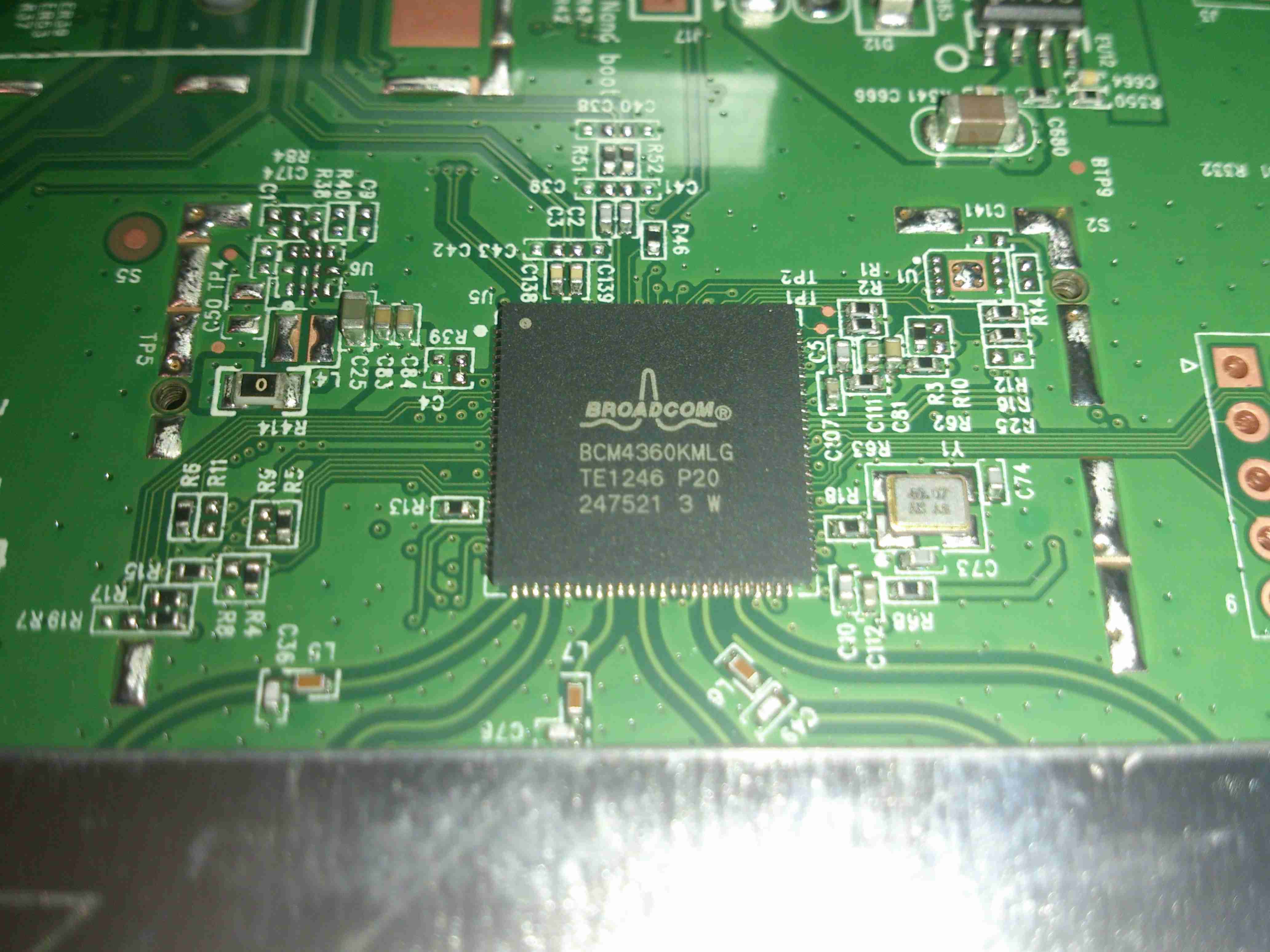
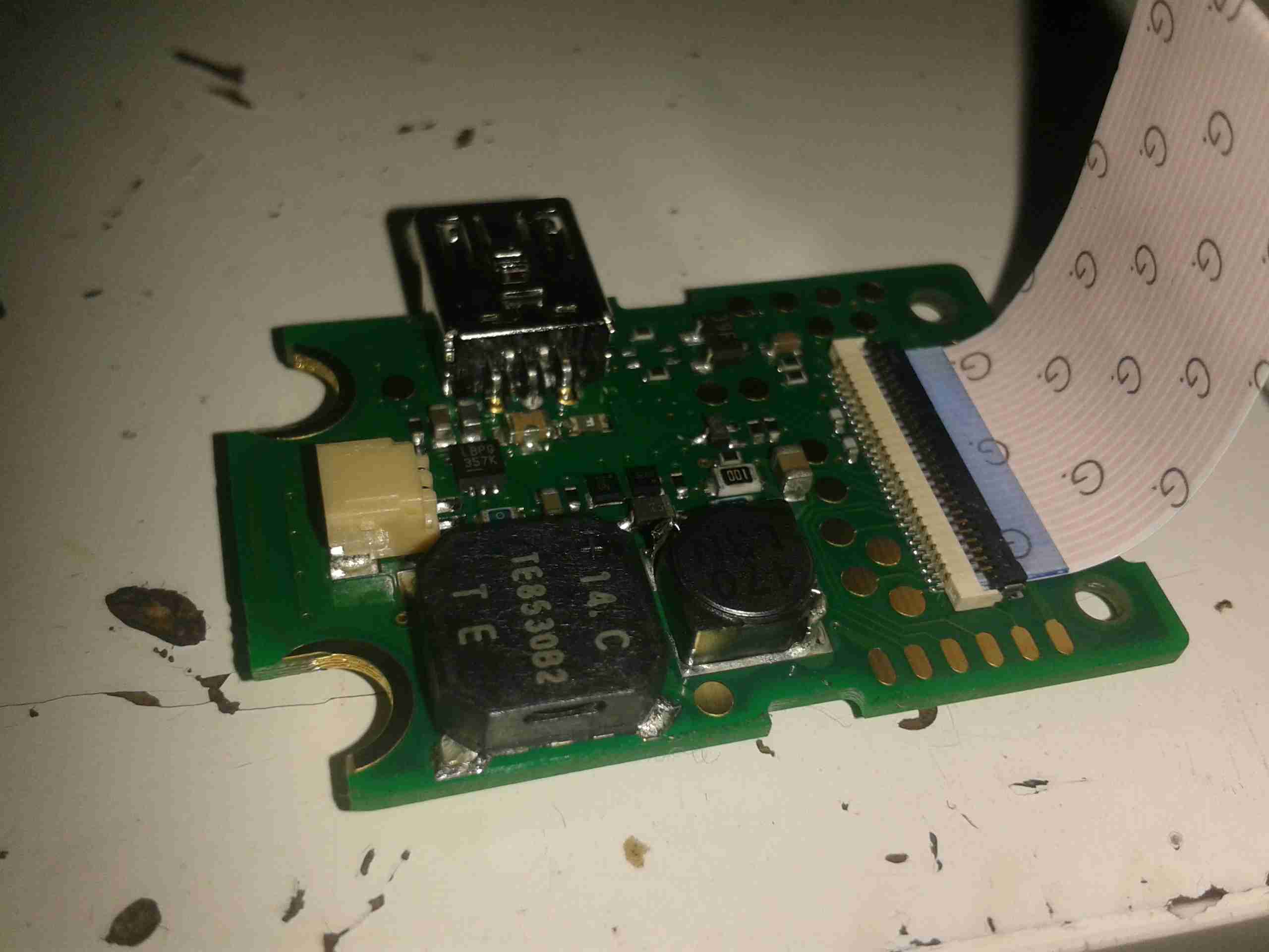
The other side of the PCB is pretty sparse, holding just the indicator LEDS, button & the WiFi Chipset.

Realtek WiFi Chipset

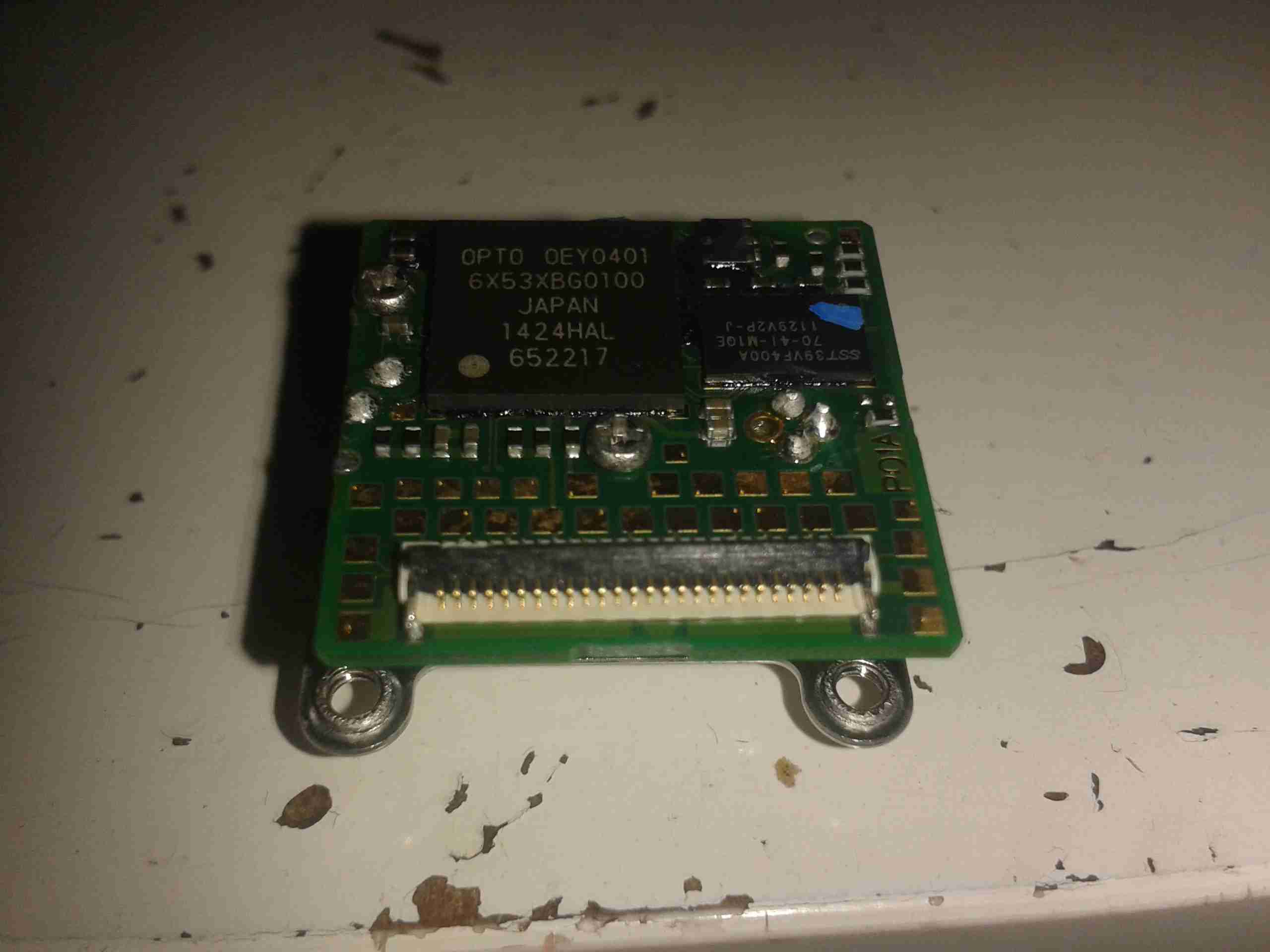
The chipset here is a Realtek part, but it’s number is hidden by some of the shield. The antenna connection is routed to the edge of the board, where a spring terminal on the plastic case mounted antenna makes contact.

Posted on Leave a comment

Raspberry Pi 3 Model B+ Initial Tests & Benchmarks

Raspberry Pi 3 Model B+

Yesterday, the Raspberry Pi community got a nice surprise – a new Pi! This one has some improved features over the previous RPi 3 Model B:

  • Improved CPU – 64-Bit 1.4GHz Quad-Core BCM2837B0
  • Improved WiFi – Dual Band 802.11b/g/n/ac. This is now under a shield on the top of the board.
  • Improved Ethernet – The USB/Ethernet IC has been replaced with a LAN7515, supporting gigabit ethernet. The backhaul is still over USB2 though, so this would max out at about 300Mbit/s
  • PoE Support – There’s a new 4-pin header, and a matching HAT for power over ethernet support.
Chipset
Chipset

The USB/LAN Controller is now a BGA package, supporting gigabit ethernet. The USB connections are still USB2 though, limiting total bandwidth. This shouldn’t be much of an issue though, since anything over the 100Mbit connection we’ve had previously is an improvement.

CPU & Radio
CPU & Radio

The CPU now has a metal heatspreader on top of the die, no doubt to help with cooling under heavy loads. As far as I know, it’s still the same silicon under the hood though. The WiFi radio is under the shielding can to the top left, with the PCB trace antenna down the left edge of the board.

Power Controller
Power Controller

The power supplies are handled on this new Pi by the MaxLinear MxL7704, from what I can tell from MaxLinear’s page, it seems to be somewhat of a collaborative effort to find something that would do the best job, since they apparently worked with the Foundation to get this one right. This IC apparently includes four synchronous step-down buck regulators that provide system, memory, I/O and core power from 1.5A to 4A. An on-board 100mA LDO provides clean 1.5V to 3.6V power for analog sub-systems. This PMIC utilizes a conditional sequencing state machine that is flexible enough to meet the requirements of virtually any processor.

PCB Bottom
PCB Bottom

The bottom of the PCB has the Elpida 1GB RAM package, which is LPDDR2, along with the MicroSD slot.

A quick benchmark running Raspbian Lite & a SanDisk Ultra 32GB Class 10 SD card gives some nice results:

Posted on 2 Comments

Cisco EA6700 / Linksys AC1750 Router

Cisco EA6700
Cisco EA6700

Since the boat was still running it’s internal network on 10/100M speeds, an upgrade was decided on, the internal WiFi signal strength was also pretty poor further than a few feet from the NOC.

The new router is a Cisco/Linksys AC1750 model, with gigabit networking, and full 802.11ac 2.4/5GHz Wireless. This router also has a built in media server, print server, USB3 & USB2.

PCB Overview
PCB Overview

Teardown time! Here’s the router with the cover removed. Most of the fun stuff is hidden under the shields, but these aren’t fully soldered down & the covers are removable. The 6 antennas can be seen spaced around the edge of the housing, the main CPU is under the large heatsink upper centre. The radio power amplifier stages are underneath the shields, while the main RF transceivers are just outside the shields.

2.4GHz Transceiver
2.4GHz Transceiver

Wireless N is provided by a Broadcom BCM4331, this provides full dual-band 3×3 802.11n support. Being 3×3 it is actually 3 separate transceivers in a single package, to get much higher throughput rates of 600Mbit/s.

5GHz Transceiver
5GHz Transceiver

Wireless AC is provided by it’s sister IC, the BCM4360, with throughput speeds of 1.3Gbit/s. Both of these transceiver ICs connect back to the main CPU via PCI Express.

5GHz Power Amplifiers

To get increased range, there are a trio of Skyworks SE5003L +23dBm 5GHz power amplifier ICs under the shield, along with the TX/RX switching & antenna matching networks. Heatsinking for these is provided by a sink screwed to the bottom side of the PCB. The outputs to the antennas can be seen at the top of the image.

2.4GHz Power Amplifiers

The 2.4GHz section is fitted with a trio of Skyworks SE2605L +23dBm 2.4GHz power amplifiers, with a similar heatsink arrangement under the board. Unlike the 5GHz section, the 2.4GHz antenna feeds are soldered to the PCB here instead of using connectors.

Main CPU
Main CPU

The main CPU is a BCM4708 Communications Processor from Broadcom, as for the other Broadcom chips in this router, very little information is available unless under NDA, but I do know it’s a dual core ARM Cortex A9 running at 1GHz, with built in 5-port gigabit ethernet switch.

CPU RAM
CPU RAM

Working RAM for the processor is a Hynix H5TQ2G63DFA 256MB part.

More to come on the installation of the new networking, with it’s associated 4G mobile gateway connection system.

73s for now!

Posted on Leave a comment

Opticon OPN-2001 Barcode Scanner

OPN-2001
OPN-2001

Random teardown time!

The OPN-2001 is a very small handheld barcode data collection device, used for stock keeping, inventory, etc.

It’s powered by an internal Li-Poly cell, at 150mAh, and has storage for 1000 barcodes in it’s internal memory.

USB
USB

The unit is charged via it’s USB port, the data can also be downloaded using this interface.

ID Label
ID Label

Here’s the bottom of the unit with it’s label. Serial number removed to protect the guilty. 😉

Cover Removed
Cover Removed

Here the bottom cover has been removed from the scanner, showing the internals. The barcode engine is on the left, this contains all the hardware & logic for scanning & storing the barcode data. The Li-Poly cell is under the FFC cable wrapped in foam tape for protection.

PCB Removed
PCB Removed

Here’s the PCB & engine assembly removed from the casing. The lower PCB appears to just handle the user interface buttons, beeper & USB power & charging circuitry. All the processing logic is on the barcode engine itself.

PCB Reverse
PCB Reverse

Here’s the back of the support PCB, with the pair of buttons for scanning & deleting barcodes. Also on this board is a 32kHz clock crystal & a Ricoh RV5C386A RTC IC. This communicates with the main processor via I²C for storing the date & time with the barcodes. At the bottom right corner are some of the power supply passives.

Support PCB
Support PCB

Here’s the other side of the support PCB, with the beeper, battery connector & the switching regulator to provide the barcode engine with 3.3v power.

Barcode Engine
Barcode Engine

Here’s the barcode engine itself, which is absolutely tiny, at roughly 20mm square. The main processor & it’s associated Flash ROM are on this PCB. The main processor has an ARM7 32bit core, with 64kB of RAM, and onboard 512kB of ROM for program & barcode storage.

Mirror
Mirror

Here’s the business end of the barcode engine, the mirror vibrates at 100Hz to produce the scan line. The laser diode is rated at 1mW, 650nm. This is in the deep red range.


Posted on Leave a comment

USB1100 Digital Message Unit

This is basically an industrial, rugged MP3 player, in an extruded aluminium case.
They are used in commercial settings for generating telephone hold music or continual playback of background music in shops.

USB1100
USB1100

It’s quite a compact unit, in a nice aluminium case, designed for mounting into a comms setup. This unit will play any MP3 file, up to a maximum size of 11MB.

Connections
Connections

Here’s the user connections on the end of the unit. The device takes a standard 12v DC input, and has a single button for setup, user feedback is given through the multi-colour LED next to the power jack.
Both 8Ω & 600Ω audio outputs are provided for maximum compatibility. Volume & tone controls are also here.
On the other end of the unit is a single USB port for loading the audio files from a USB drive, and a reset button.

Main PCB
Main PCB

Here’s the single PCB removed from the casing. Unfortunately the main CPU has had it’s part number sanded off, and I can’t be bothered to try & find out what kind of processor it is at this point. To the right of the CPU are some flash ROM & SDRAM, along with the single USB port at bottom right.
The left side of the board is dedicated to audio output & voltage regulation, there are a fair few linear regulators in this unit.

Audio End
Audio End

Here’s the audio output side of the board, the transformer on the left is to provide the 600Ω output, the audio amplifier IC (BA5416) is just behind it. To the right are some of the main voltage regulators, a 5v one on the heatsink & a LM317.

Audio Codec
Audio Codec

The audio codec is a CS4271 from Cirrus Logic, a really high quality part, 24-bit resolution, 192kHz Stereo codec. Considering this is for telephone & PA systems that aren’t that high fidelity, it’s well built!

Posted on Leave a comment

Rio LAHS4 Salon Laser Hair Remover

Unit Overview
Unit Overview

Here is a home laser hair removal unit, a Rio LAHS4. Shown above is the system overview, with the laser wand & the user controls.

Main PCB Top
Main PCB Top

Main base unit popped open reveals the main PCB, with the central processor, a PIC16F628A.

Main PCB Bottom
Main PCB Bottom

Other side of the PCB is mainly populated with power supply & filtering for the logic sections.

Wand PCB
Wand PCB

Cracking open the laser wand reveals a stacked pair of PCBs, a main laser controller & the capacitive sensor PCB. This capacitive sensor connects to a pair of pins on the laser head & prevents operation if the unit is not held firmly against the skin.

Diode Module
Diode Module

Front of the laser diode module with the movable lens, on a pair of voice coil actuators. Very similar to the lens positioner used in any CD/DVD player pickup assembly.
The diode in this unit is an 808nm chip, with power in the 300-600mW range most likely.

Diode Module Rear
Diode Module Rear

Rear of the diode module, with the connections to the diode itself & the voice coil positioner for the lens.

Wand PCB Top
Wand PCB Top

Other side of the wand PCB, showing the capacitive sensor board on top of the main controller board. There is another CPU on the board here, which most likely communicates with the main processor in the base through a serial connection.


Posted on Leave a comment

Motorola V360v

Front
Front

Here is a more modern phone, the Motorola V360v. Features include Dual screens, 640×480 VGA camera, full col

our TFT Main LCD, SD-Micro slot.
Here on the back the grey scale LCD can be seen, with the camera lens to the right of the Motorola logo

Keypad
Keypad

Here the phone is opened showing the keypad & the full colour TFT LCD display.

Battery Compartment
Battery Compartment

Here the battery is removed from the unit, showing the SIM connector. The antenna cover is still on at the bottom.

Antenna
Antenna

The antenna cover has been removed in this shot, the antenna is the white section at the bottom, With the loudspeaker & the external antenna connector hidden at the right.

PCB
PCB

Here is the main PCB. Parts from left are the Bluetooth module at the top, supplied by Broadcom, the SD Card socket at the bottom. Main CPU next to that is the Freescale SC29343VKP. Above right of the CPU is the Freescale SC13890P23A Charger, Power & Audio IC. Below is the SIM card socket. Under the main CPU is the Intel Flash memory IC. ICs inside the shields are the RF sections for transmit & receive.

Cover Removed
Cover Removed

Rear of the display unit showing the monochrome LCD. The camera module on the bottom left. Ear speaker on the far right of the unit.

Main LCD
Main LCD

Main colour TFT LCD.

Camera
Camera

Camera module removed from the LCD unit.

Vibra-Motor
Vibra-Motor

The vibration motor attached to one of the LCD looms.

Posted on Leave a comment

Ericsson GA628

Front
Front

Here is a phone from the mid 90s, the Ericsson GA628. Here visible is the front of the unit with keypad, & single line monochrome LCD for number display.

Battery & Rear
Battery & Rear

Here the battery is removed from the phone, showing the SIM card socket. At the top under the antenna stub is the socket for an external antenna.

Front Removed
Front Removed

Here the front is removed from the phone, PCB on left, rear of keypad on right. Microphone is at bottom of keypad, with speaker at the top. Top right of the PCB is the ringer buzzer, left is shield for RF amplifier.

Main PCB
Main PCB

Here is the back of the main PCB, RF sections on left & centre. Processing & memory on right.

Battery
Battery

This phone had a Ni-Mh battery, before Li-Ion batteries were introduced.

LCD
LCD

The LCD from the front of the phone is shown here. A simple dot matrix single line unit.