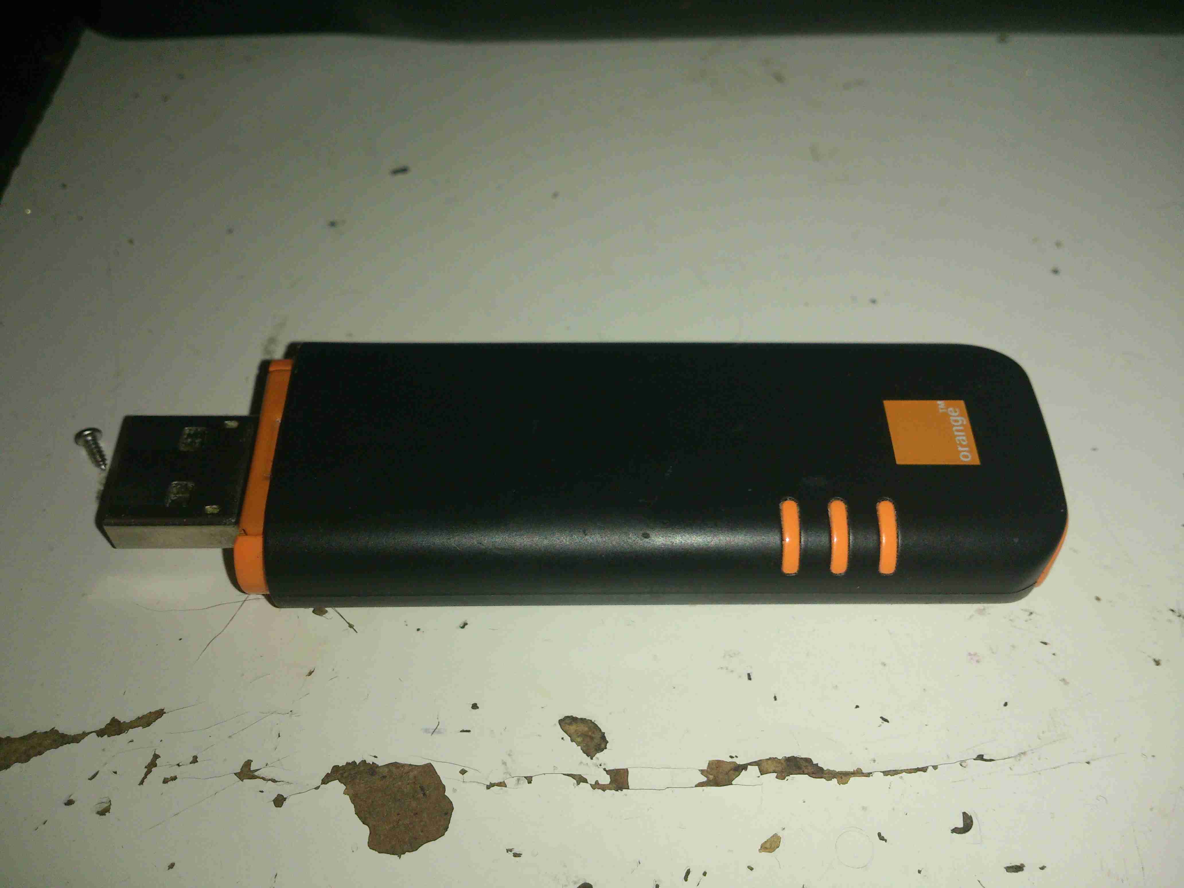
Here’s an old HDSPA 3G USB modem stick that I got with a mobile phone contact many years ago. As it’s now very old tech, and I have a faster modem, not to mention that I’m no longer with Orange (Robbing <expletive>), here’s a teardown of the device!
Cover Removed
The top shell is just clipped into place, while a pair of very small screws hold down the orange piece at left to hold the PCB stack in the casing. Not much to see here, but it’s clear that there’s a lot crammed into a very small space.
PCB Assembly
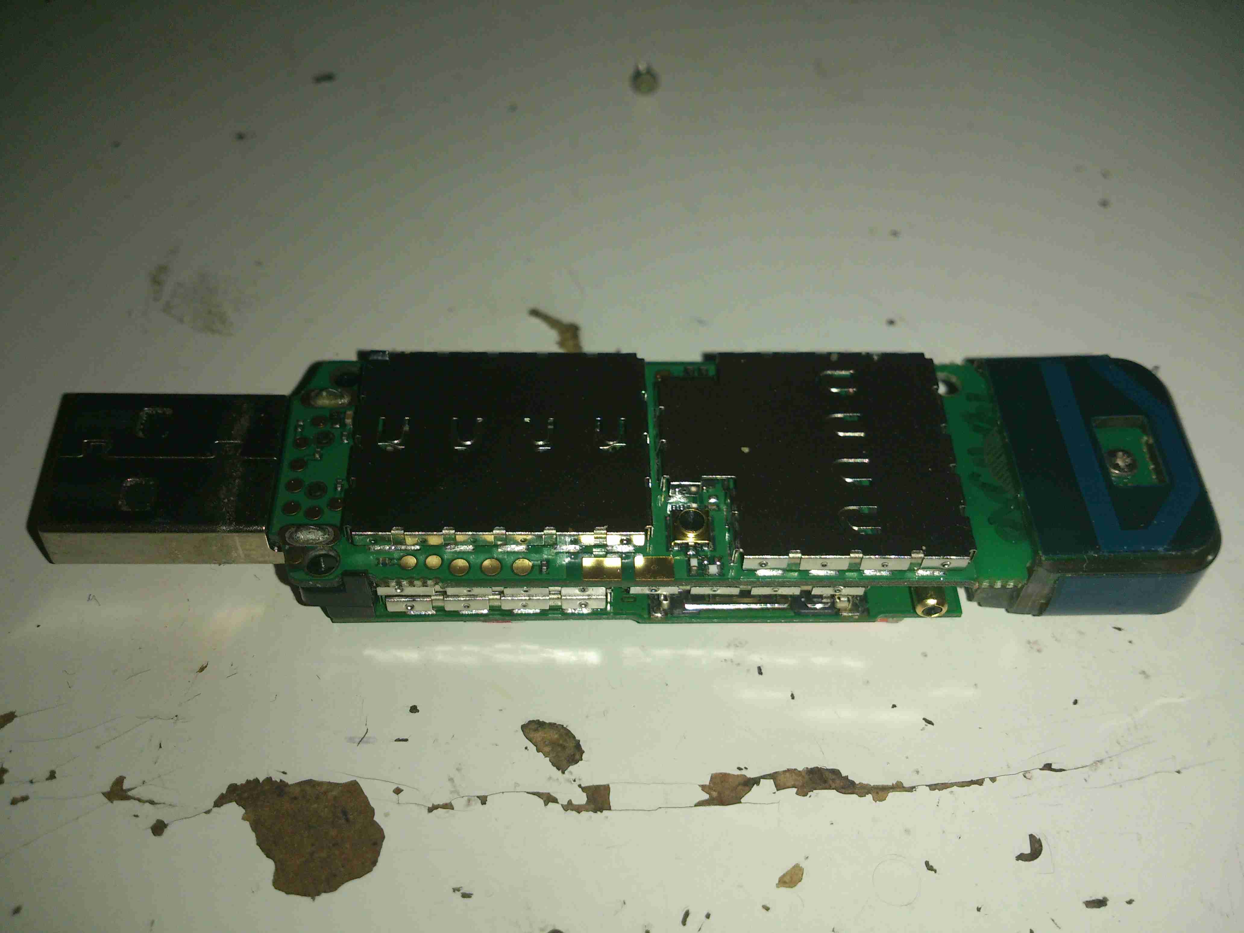
Here’s the PCB stack removed from the outer casing. The main antenna is on the right, attached with another small screw. Every IC on the boards is covered with an RF can. No problems there, pliers to the rescue!
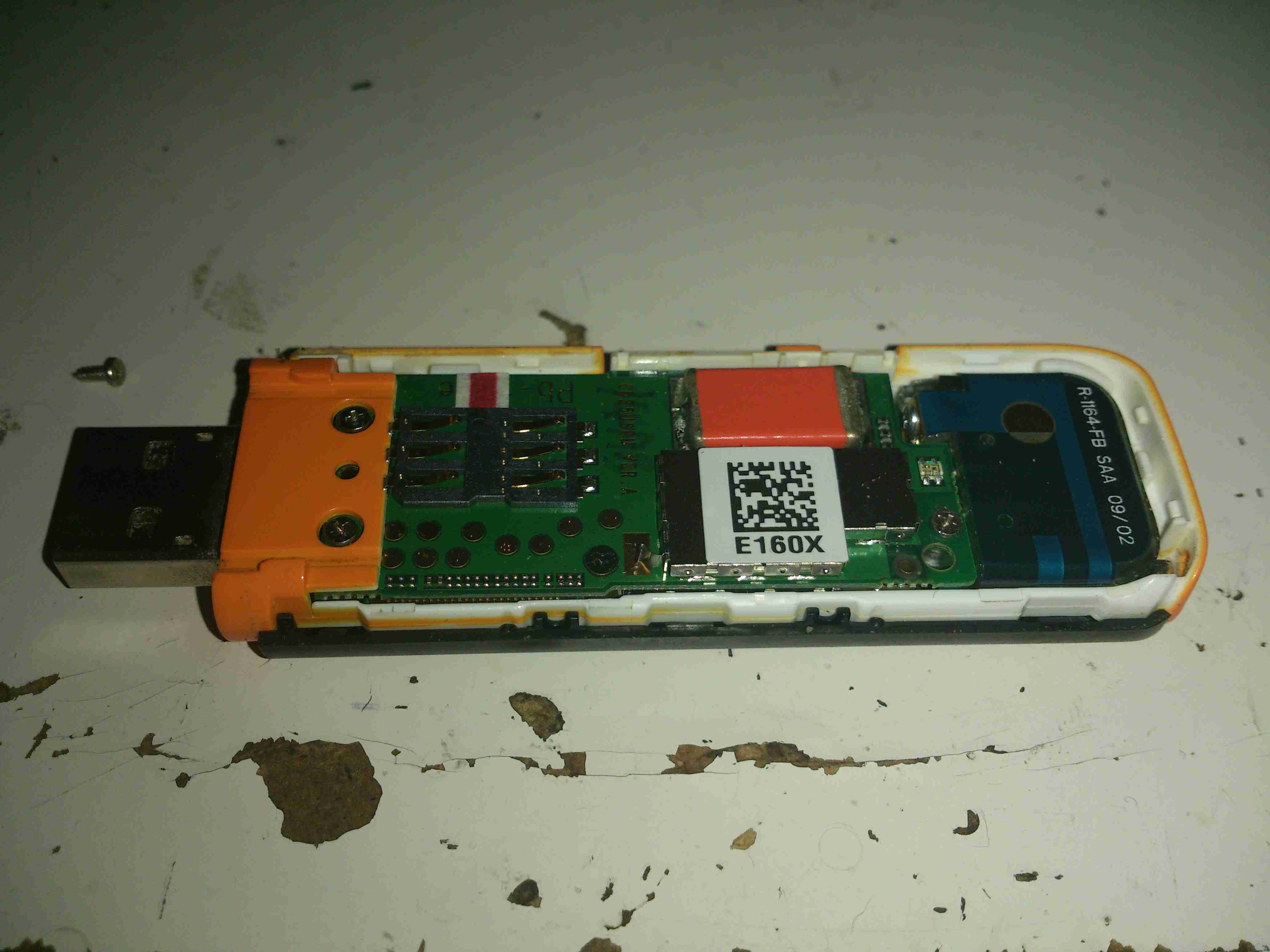
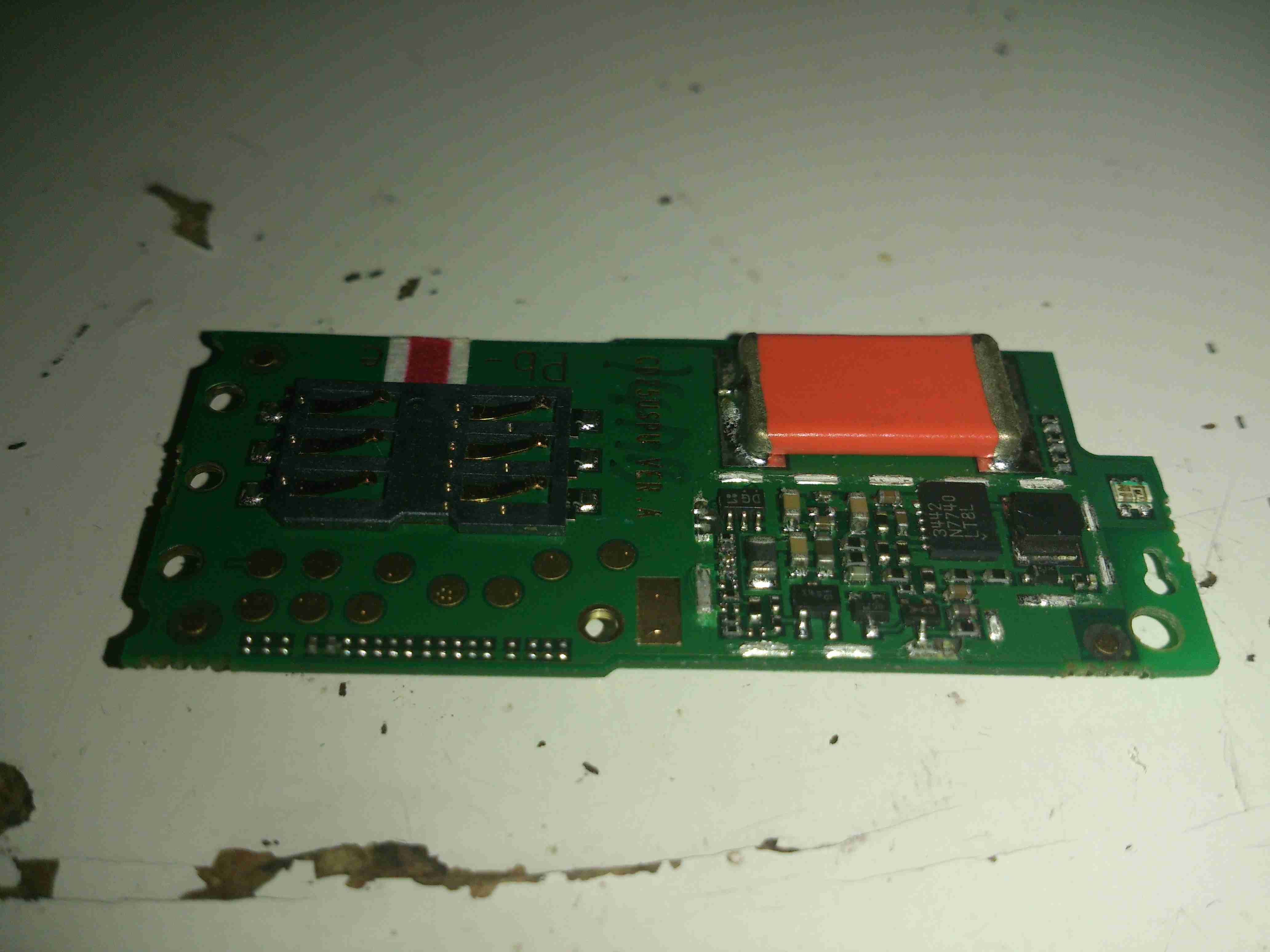
SD Card Slot
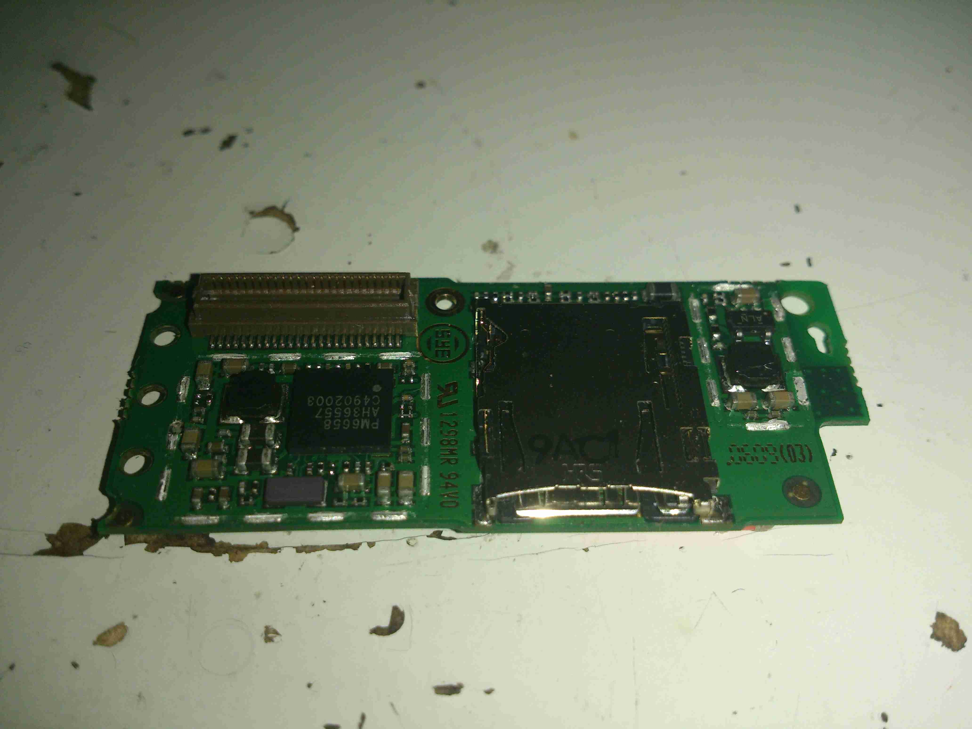
Here’s the top PCB, all the shields have been removed. On the left is a Qualcomm PM6658 Power Management IC with integrated USB transceiver. This is surrounded by many of the power management circuits.
The integrated SD Card slot is on the right side. with what looks to be a local switching regulator for supply voltage. This might also provide the SIM card with it’s power supply.
PSU & SIM Contacts
The other side of the top board reveals more power management, with another switching regulator, and a truly massive capacitor at the top edge. I’m guessing this is a solid Tantalum.
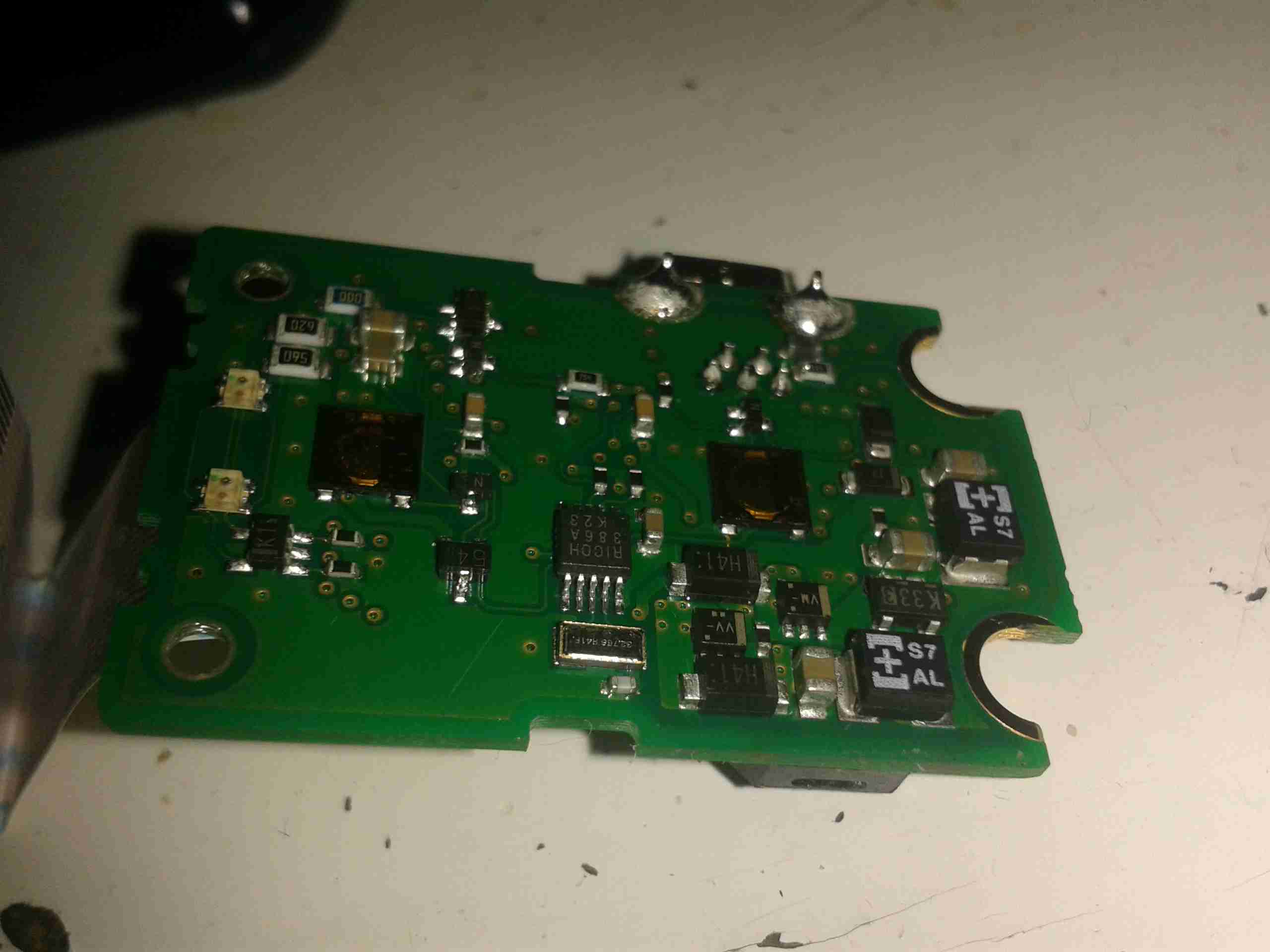
Main Chipset PCB
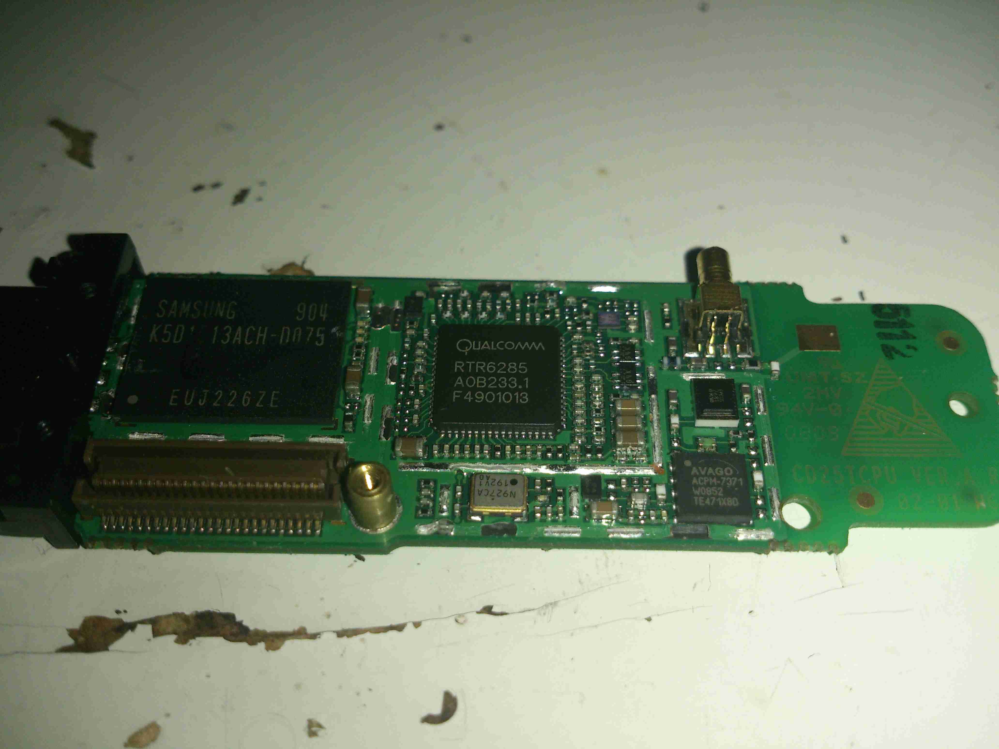
The other PCB holds the main chipset & RF circuits. On the left here is a Samsung MCP K5D1G13ACH IC. This one is a multiple chip package, having 1Gbit of NAND Flash & 512Mbit of mobile SDRAM.
To it’s right is a Qualcomm RTR6285 RF Transceiver. This IC supports multiband GSM/EDGE/UMTS frequencies & also has a GPS receive amplifier included.
At bottom right is an Avago ACPM7371 Wide-Band 4×4 CDMA Power Amplifier. The external antenna connector is top right.
Main Chipset PCB Reverse
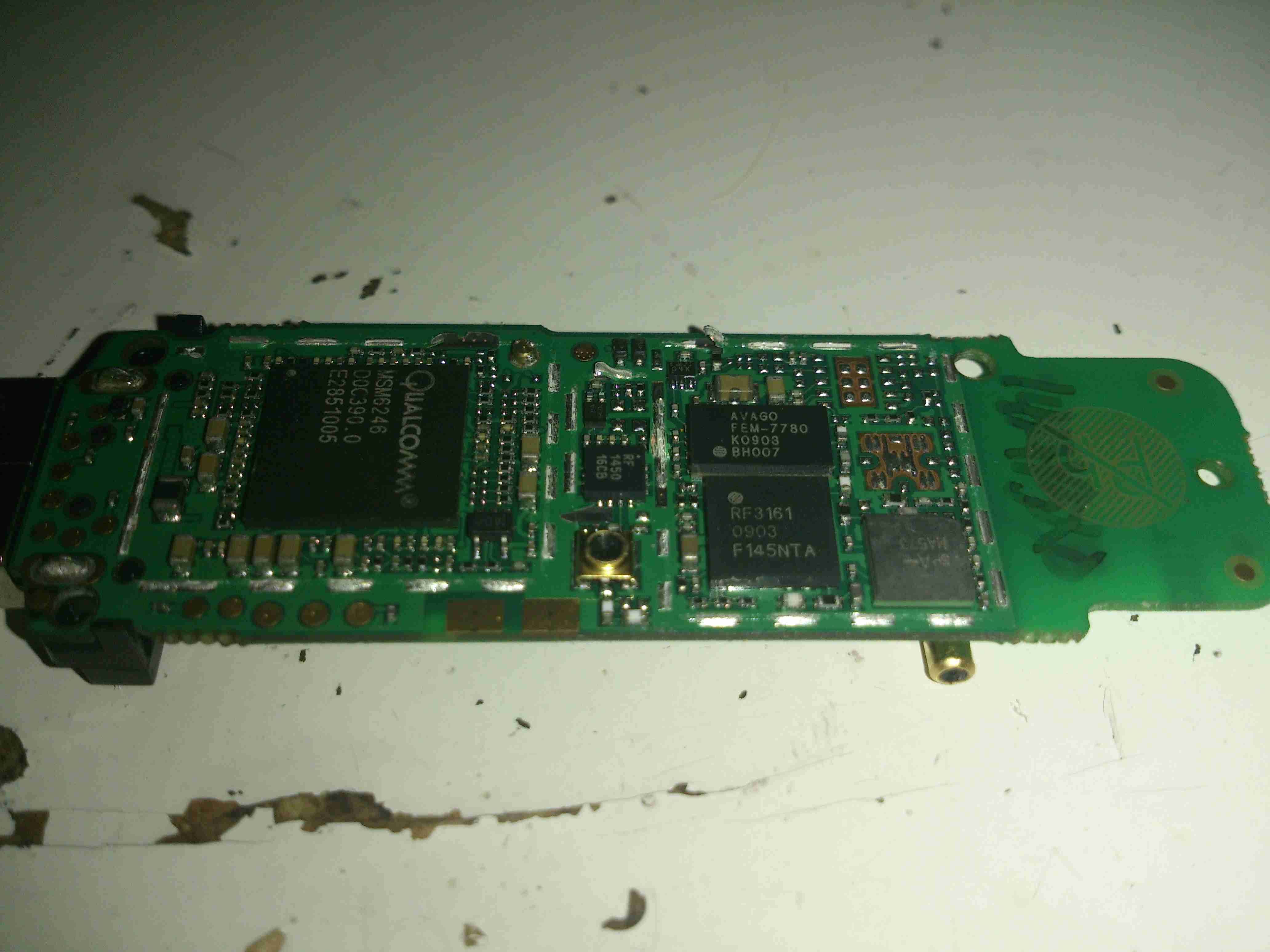
On the other side of the main PCB is a Qualcomm MSM6246 Baseband processor. Not sure about this one as I can’t find anything resembling a datasheet. Another micro-coax connector is in the centre, probably for factory test purposes, as it’s not accessible from the outside.
Just above the coax connector is a Qorvo RF1450 SP4T (single-pole 4-throw) High Power (34.5dBm) GSM RF Switch.
Upper right is an Avago FEM-7780 UMTS2100 4×7 Front End Module.
Under that is an RFMD RF3163 Quad-Band RF Power Amplifier Module.
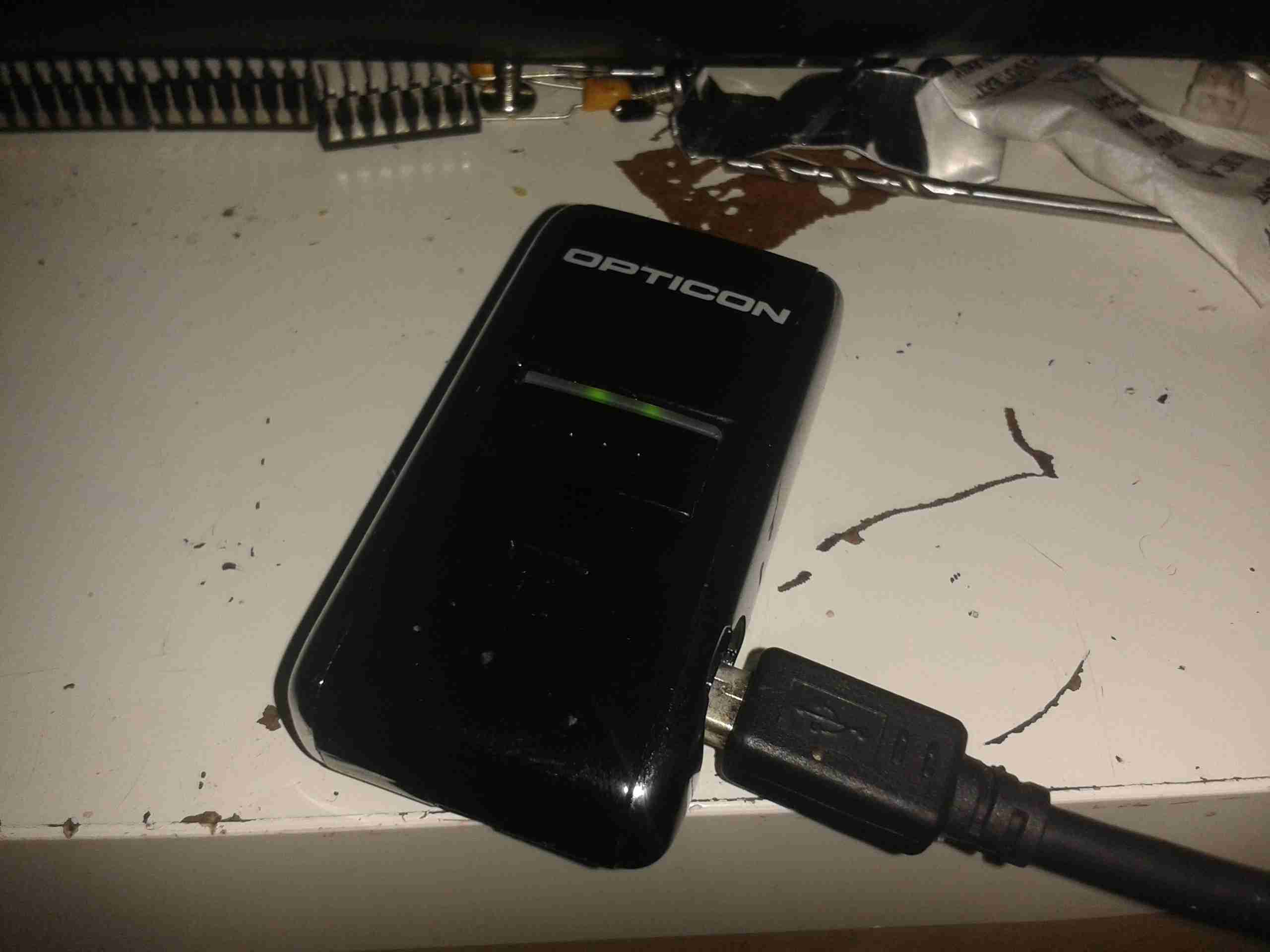
The OPN-2001 is a very small handheld barcode data collection device, used for stock keeping, inventory, etc.
It’s powered by an internal Li-Poly cell, at 150mAh, and has storage for 1000 barcodes in it’s internal memory.
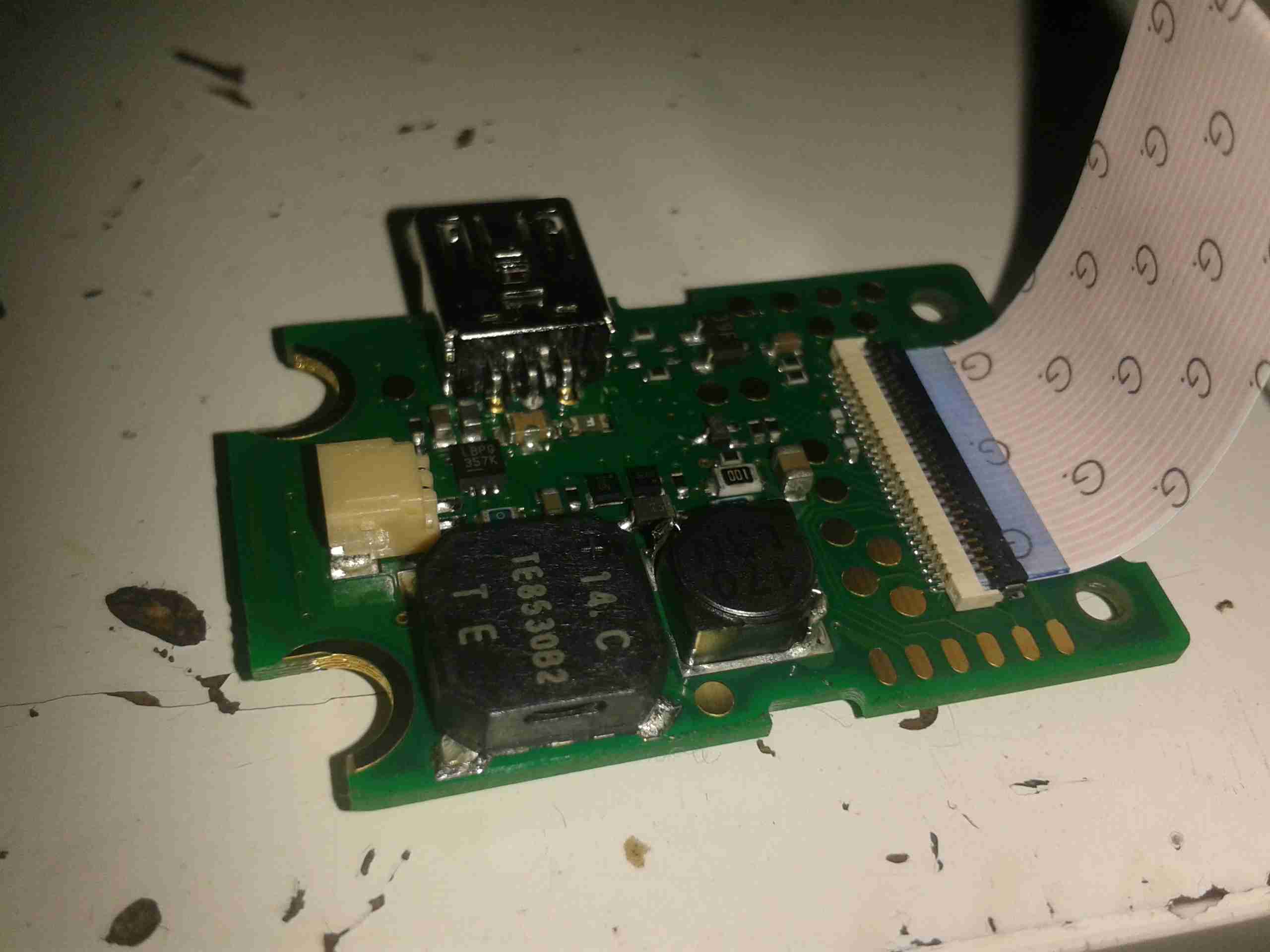
USB
The unit is charged via it’s USB port, the data can also be downloaded using this interface.
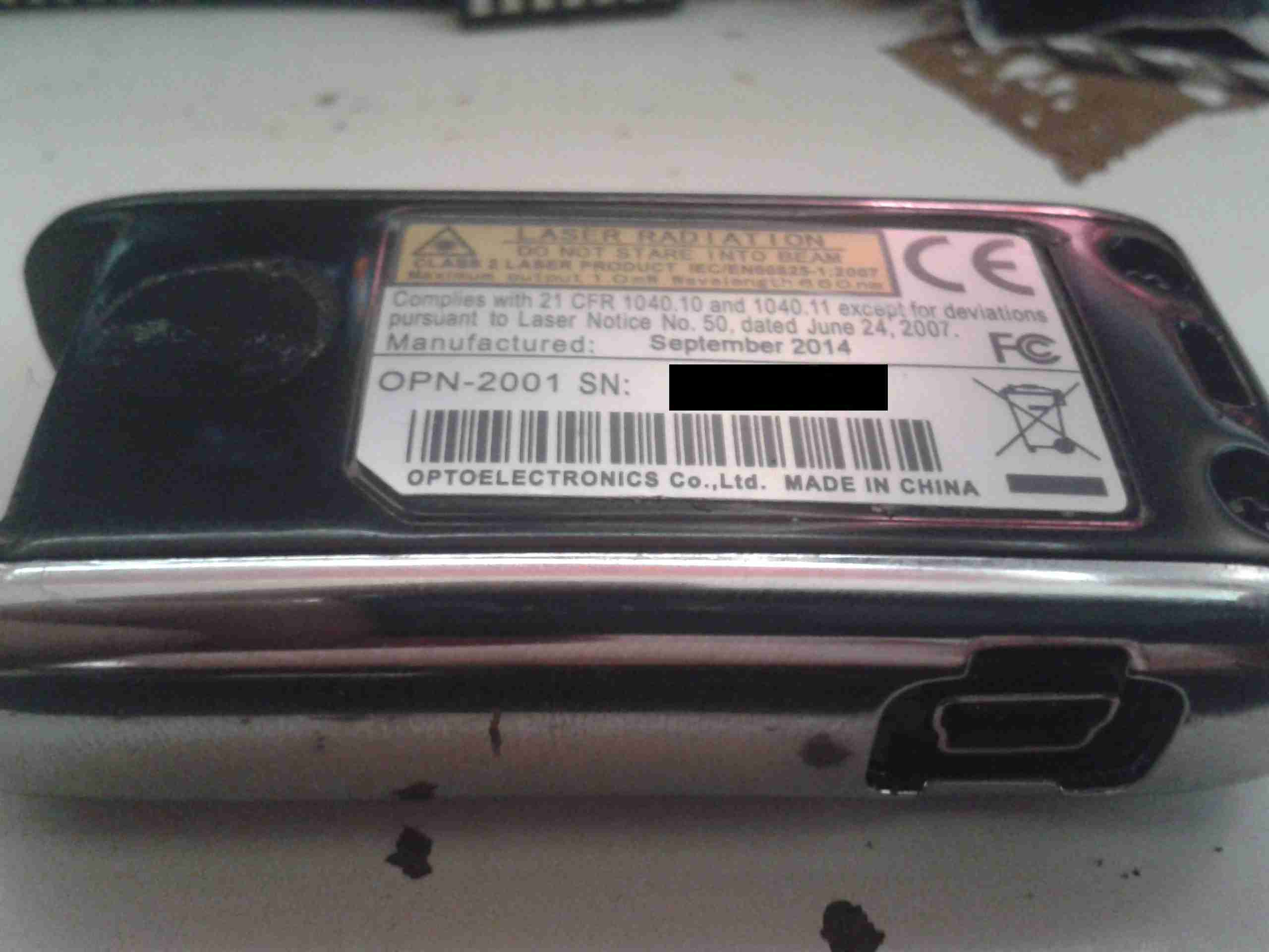
ID Label
Here’s the bottom of the unit with it’s label. Serial number removed to protect the guilty. 😉
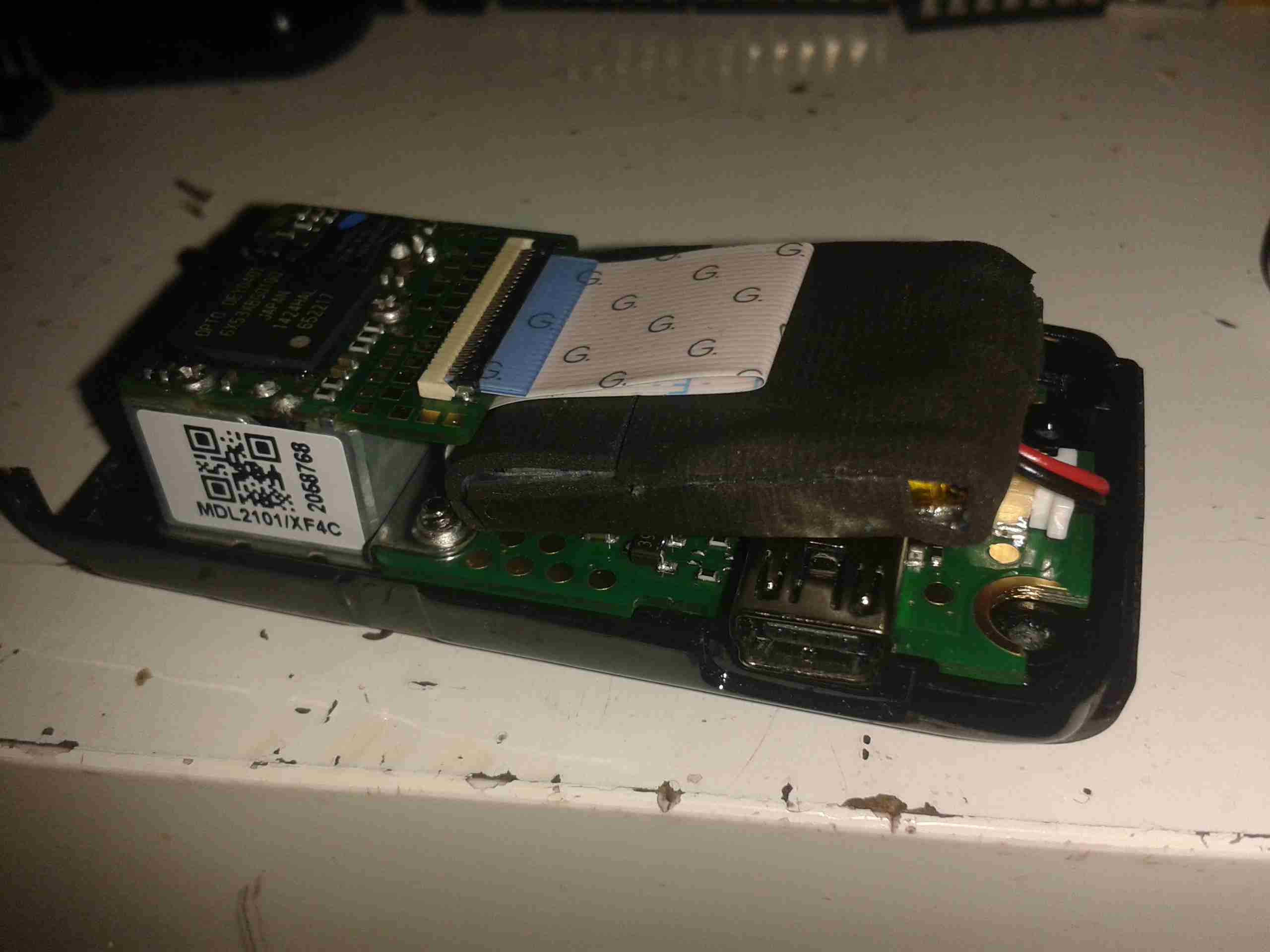
Cover Removed
Here the bottom cover has been removed from the scanner, showing the internals. The barcode engine is on the left, this contains all the hardware & logic for scanning & storing the barcode data. The Li-Poly cell is under the FFC cable wrapped in foam tape for protection.
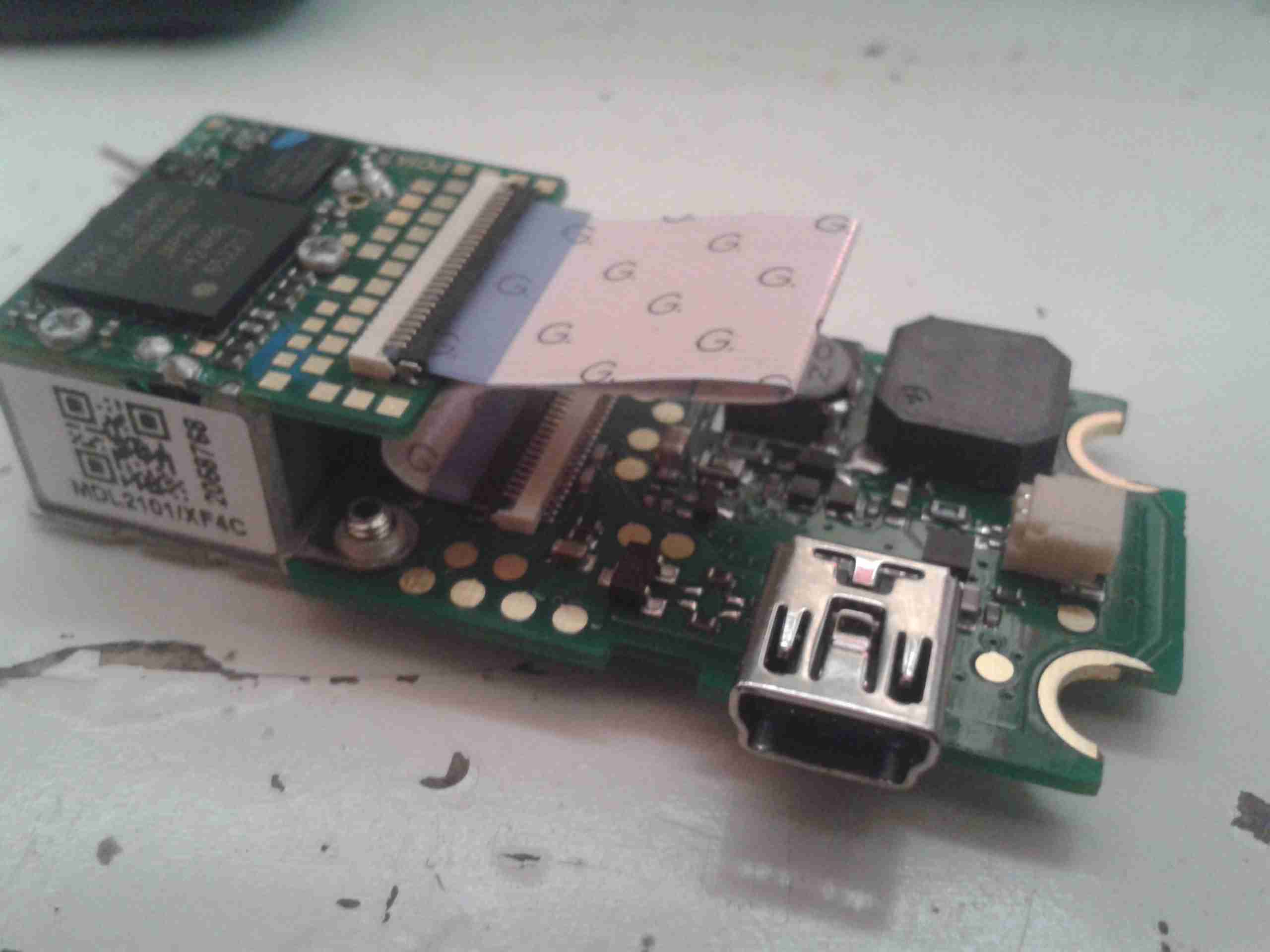
PCB Removed
Here’s the PCB & engine assembly removed from the casing. The lower PCB appears to just handle the user interface buttons, beeper & USB power & charging circuitry. All the processing logic is on the barcode engine itself.
PCB Reverse
Here’s the back of the support PCB, with the pair of buttons for scanning & deleting barcodes. Also on this board is a 32kHz clock crystal & a Ricoh RV5C386A RTC IC. This communicates with the main processor via I²C for storing the date & time with the barcodes. At the bottom right corner are some of the power supply passives.
Support PCB
Here’s the other side of the support PCB, with the beeper, battery connector & the switching regulator to provide the barcode engine with 3.3v power.
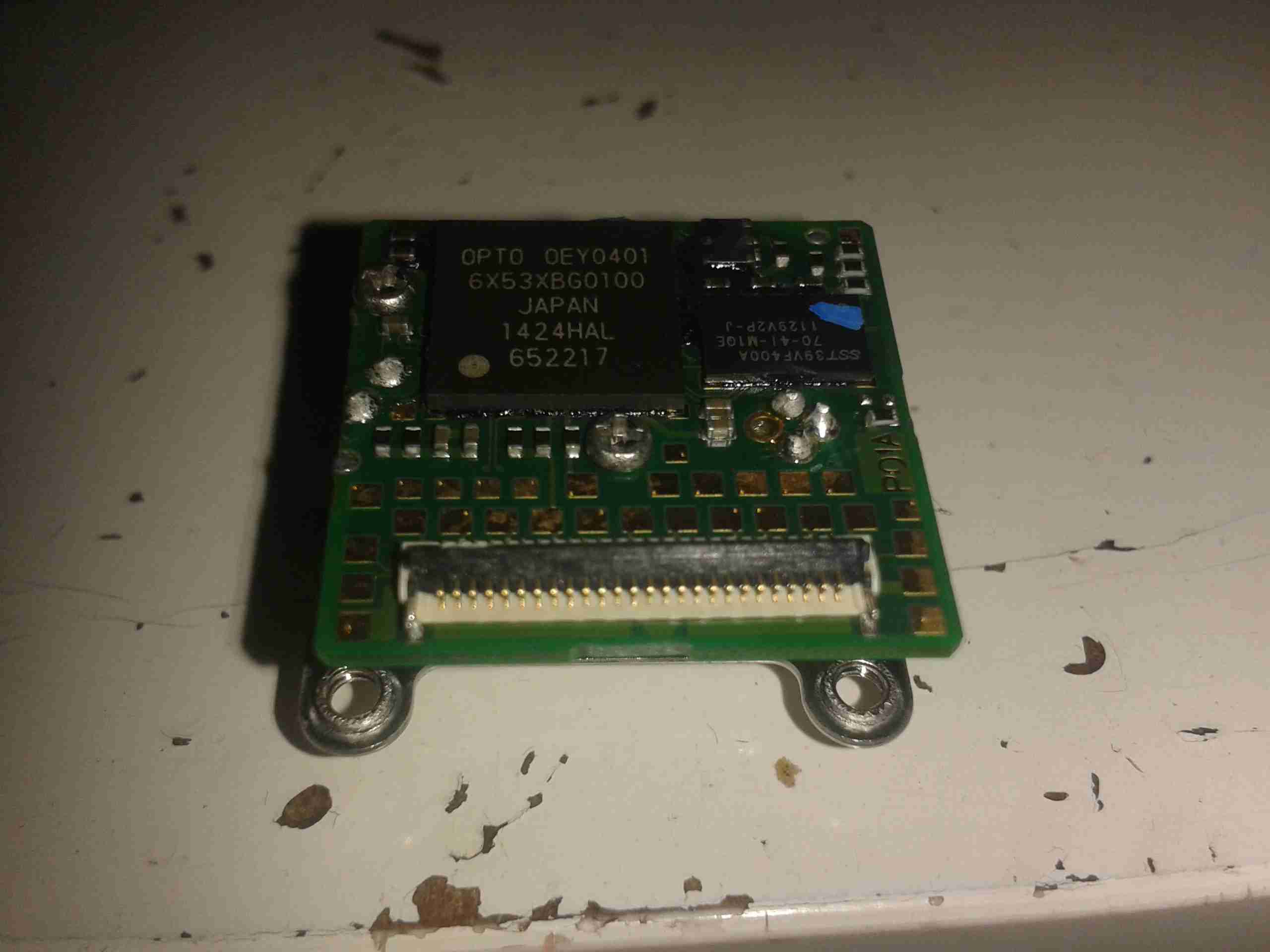
Barcode Engine
Here’s the barcode engine itself, which is absolutely tiny, at roughly 20mm square. The main processor & it’s associated Flash ROM are on this PCB. The main processor has an ARM7 32bit core, with 64kB of RAM, and onboard 512kB of ROM for program & barcode storage.
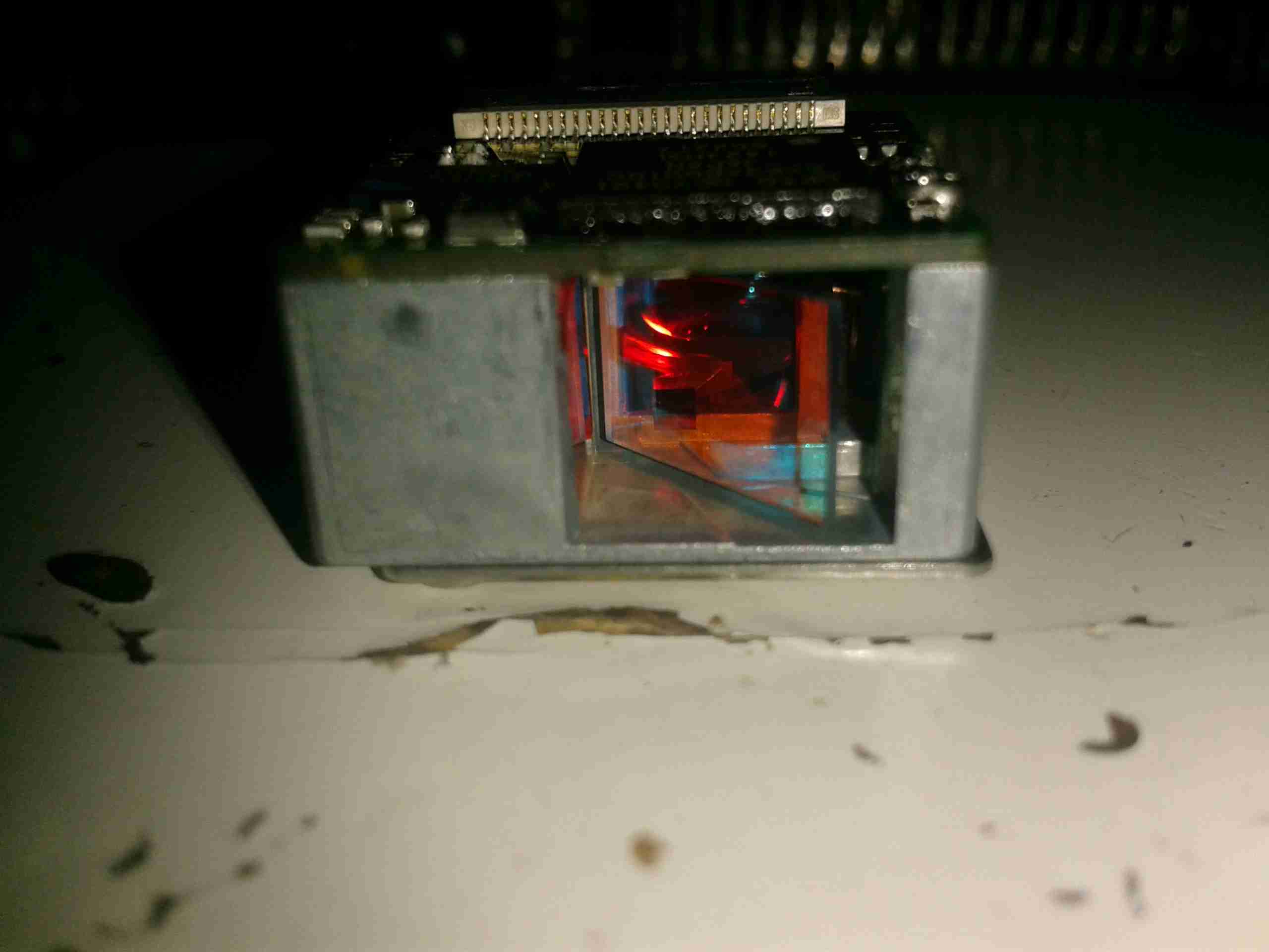
Mirror
Here’s the business end of the barcode engine, the mirror vibrates at 100Hz to produce the scan line. The laser diode is rated at 1mW, 650nm. This is in the deep red range.
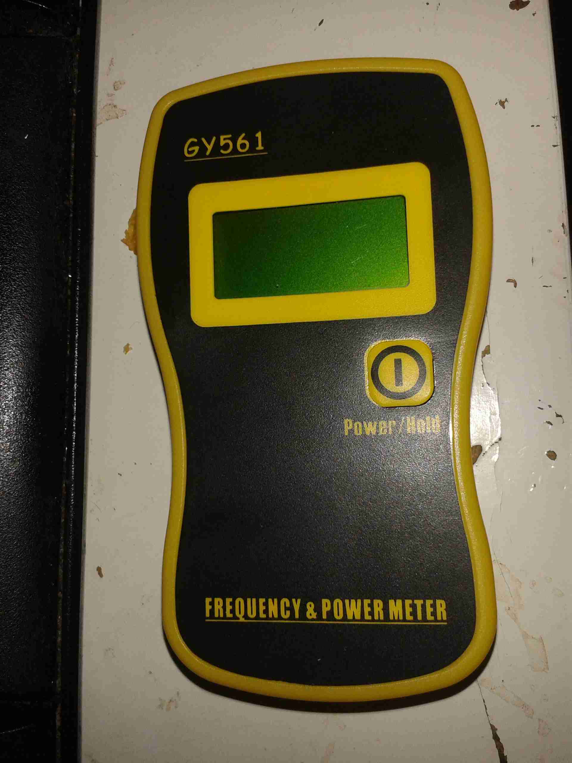
The latest addition to my radio shack is the GY561 frequency & power meter, which has already come in useful for measuring the output power of all my radios.
GY561
It’s a small device, roughly the same size & weight as a stock UV-5R. Power is provided by 3 AAA cells.
Display
The display is a standard HD44780 8×2 module. The display on this unit isn’t backlit, so no operating in the dark.
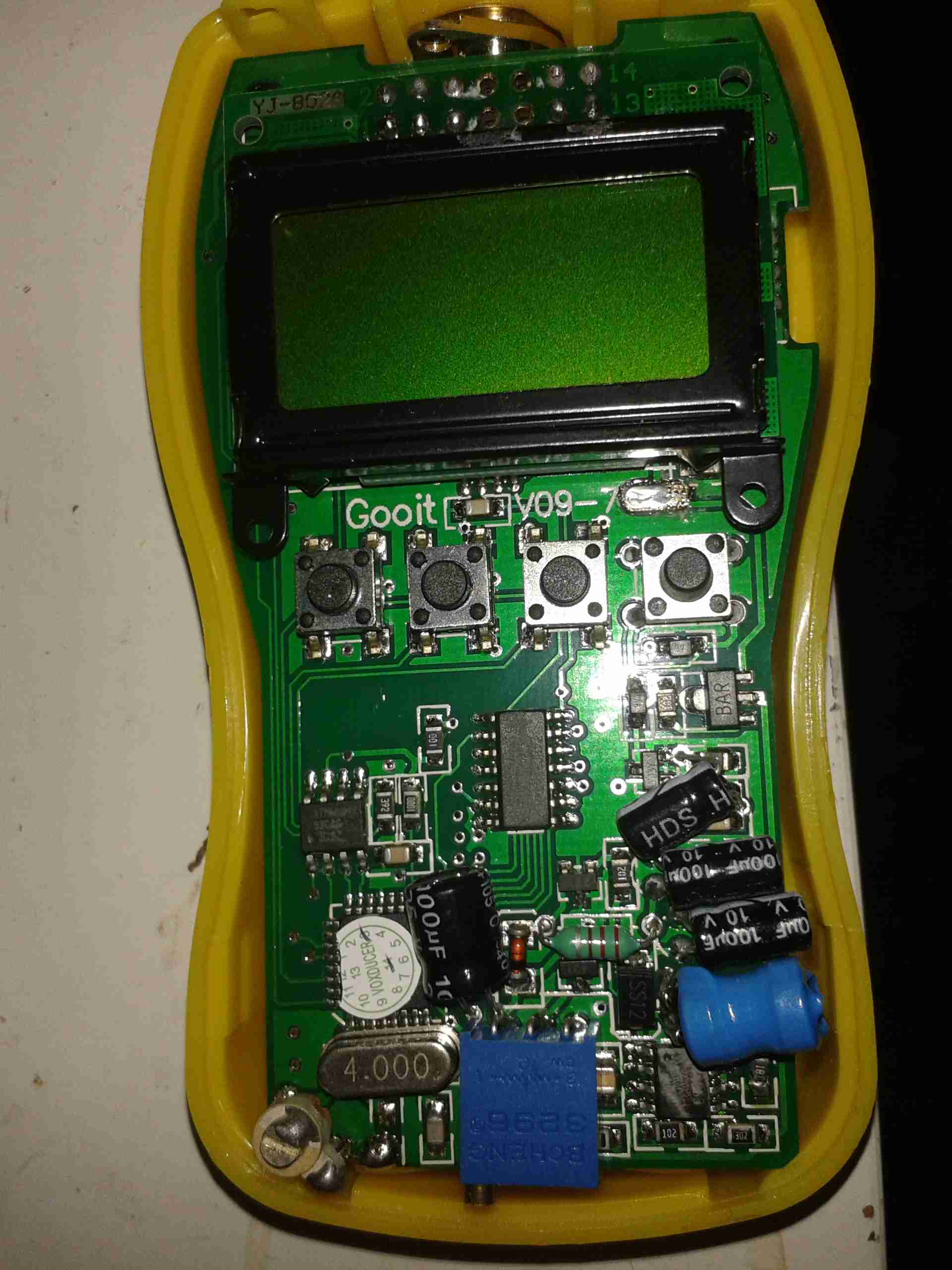
Cover Removed
The cover pops off easily to allow access to the internals, without having to remove any screws!
The 4 screws on the back of the unit hold the heatsink plate for the 50W 50Ω dummy load resistor.
Removing the cover reveals a couple of adjustments, for frequency & RF power calibration.
There are also 3 tactile switches that aren’t on the front panel. According to the manual (which in itself is a masterpiece of Chinglish), they are used to software calibrate the unit if an accurate RF power source is available. I will attempt to do a reasonable translation when time allows.
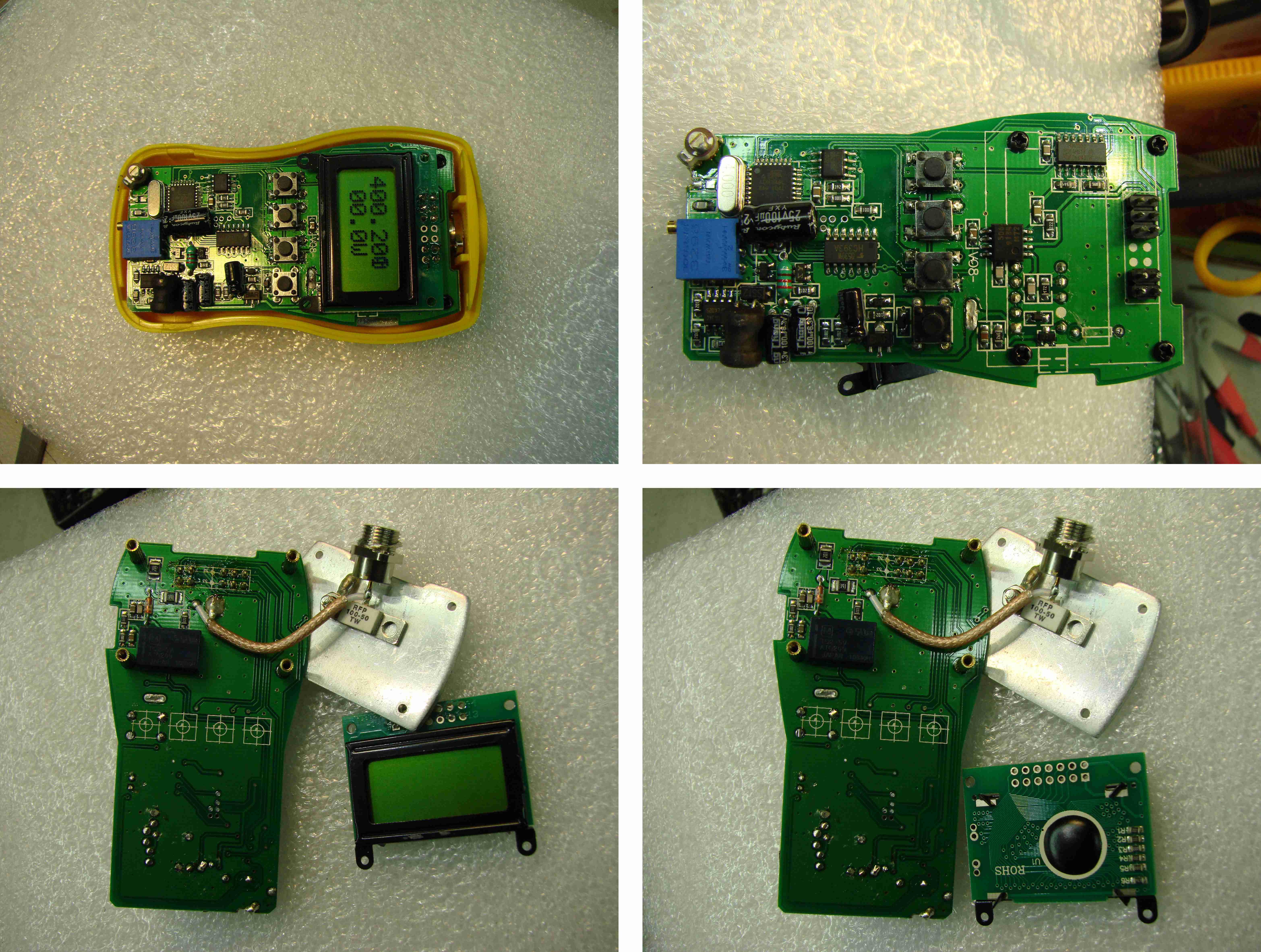
Disassembly further than this involves some desoldering in awkward places, so a search of the internet revealed an image of the rest of the internal components. In the case of my meter, all the part numbers have been scrubbed off the ICs in an attempt to hide their purpose. While it’s possible to cross-reference IC databooks & find the part numbers manually, this process is a time consuming one. Luckily the image I managed to locate doesn’t have the numbers scrubbed.
Total Disassembly
Under the LCD is some 74HC series logic, and a prescaler IC as seen in the previous frequency counter post. However in this unit the prescaler is a MB506 microwave band version to handle the higher frequencies specified.
In this case however the main microcontroller is an ATMEGA8L.
This is complemented by a SN54HC393 4-bit binary counter for the frequency side of things. This seems to make it much more usable down to lower frequencies, although the manual is very generous in this regard, stating that it’s capable of reading down to 1kHz. In practice I’ve found the lowest it reliably reads the frequency input is 10MHz, using my AD9850 DDS VFO Module as a signal source.
It did however read slightly high on all readings with the DDS, but this could have been due to the low power output of the frequency source.
Just like the other frequency counter module, this also uses a trimmer capacitor to adjust the microcontroller’s clock frequency to adjust the calibration.
The power supply circuitry is in the bottom left corner of the board, in this case a small switching supply. The switching regulator is needed to boost the +4.5v of the batteries to +5v for the logic.
Also, as the batteries discharge & their terminal voltage drops, the switching regulator will allow the circuit to carry on functioning. At present I am unsure of the lower battery voltage limit on the meter, but AAA cells are usually considered dead at 0.8v terminal voltage. (2.4v total for the 3 cells).
When turned on this meter draws 52mA from the battery, and assuming 1200mAh capacity for a decent brand-name AAA cell, this should give a battery life of 23 hours continuous use.
On the back of the main PCB is a 5v relay, which seems to be switching an input attenuator for higher power levels, although I only managed to trigger it on the 2m band.
Finally, right at the back attached to an aluminium plate, is the 50Ω dummy load resistor. This component will make up most of the cost of building these, at roughly £15.
On my DVM, this termination reads at about 46Ω, because of the other components on the board are skewing the reading. There are a pair of SMT resistors, at 200Ω & 390Ω in series, and these are connected across the 50Ω RF resistor, giving a total resistance of 46.094Ω.
This isn’t ideal, and the impedance mismatch will probably affect the calibration of the unit somewhat.
The heatsinking provided by the aluminium plate is minimal, and the unit gets noticeably warm within a couple of minutes measuring higher power levels.
High power readings should definitely be limited to very short periods, to prevent overheating.
The RF is sampled from the dummy load with a short piece of Teflon coax.
There’s a rubber duck antenna included, but this is pretty useless unless it’s almost in contact with the transmitting antenna, as there’s no input amplification. It might be handy for detecting RF emissions from power supplies, etc.
For the total cost involved I’m not expecting miracles as far as accuracy is concerned, (the manual states +/-10% on power readings).
The frequency readout does seem to be pretty much spot on though, and the ability to calibrate against a known source is handy if I need some more accuracy in the future.
I’ve also done an SWR test on the dummy load, and the results aren’t good.
At 145.500 MHz, the SWR is 3:1, while at 433.500 it’s closer to 4:1. This is probably due to the lower than 50Ω I measured at the meter’s connector.
These SWR readings also wander around somewhat as the load resistor warms up under power.
I’ll probably also replace the AAA cells with a LiPo cell & associated charge/protection circuitry, to make the unit chargeable via USB. Avoiding disposable batteries is the goal.
After watching a video over at Scullcom Hobby Electronics on YouTube, I figured I’d build one of these precision references to calibrate my multimeters.
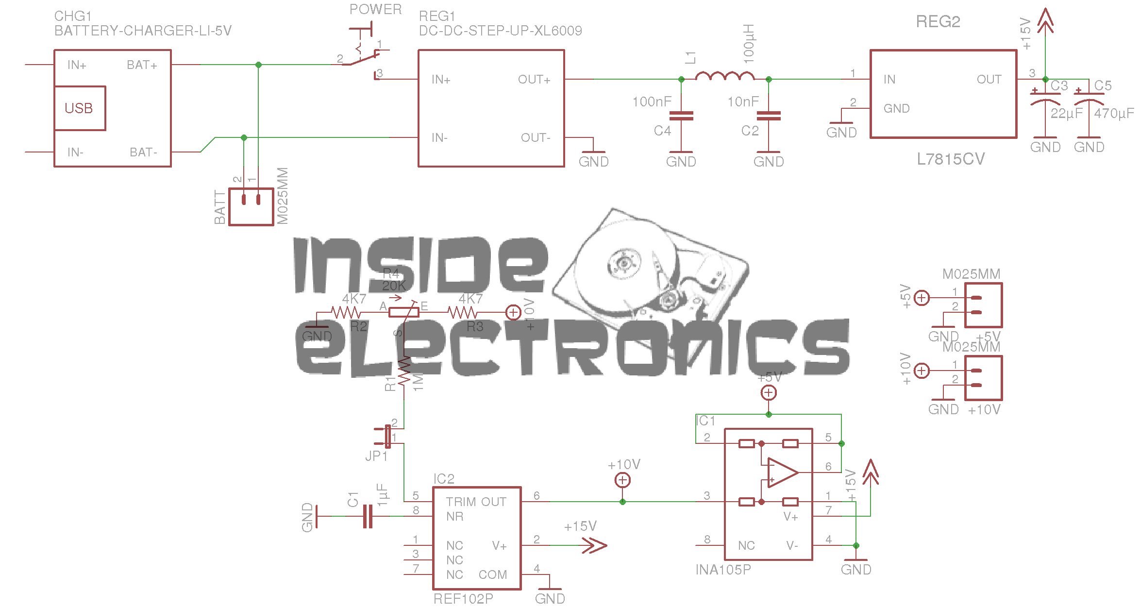
It’s based around a REF102P 10v precision reference & an INA105P precision unity gain differential amplifier.
For full information, check out the video, I won’t go into the details here, just my particular circuit & PCB layout.
In the video, Veroboard is used. I’m not too fond of the stuff personally. I find it far too easy to make mistakes & it never quite looks good enough. To this end I have spun a board in Eagle, as usual.
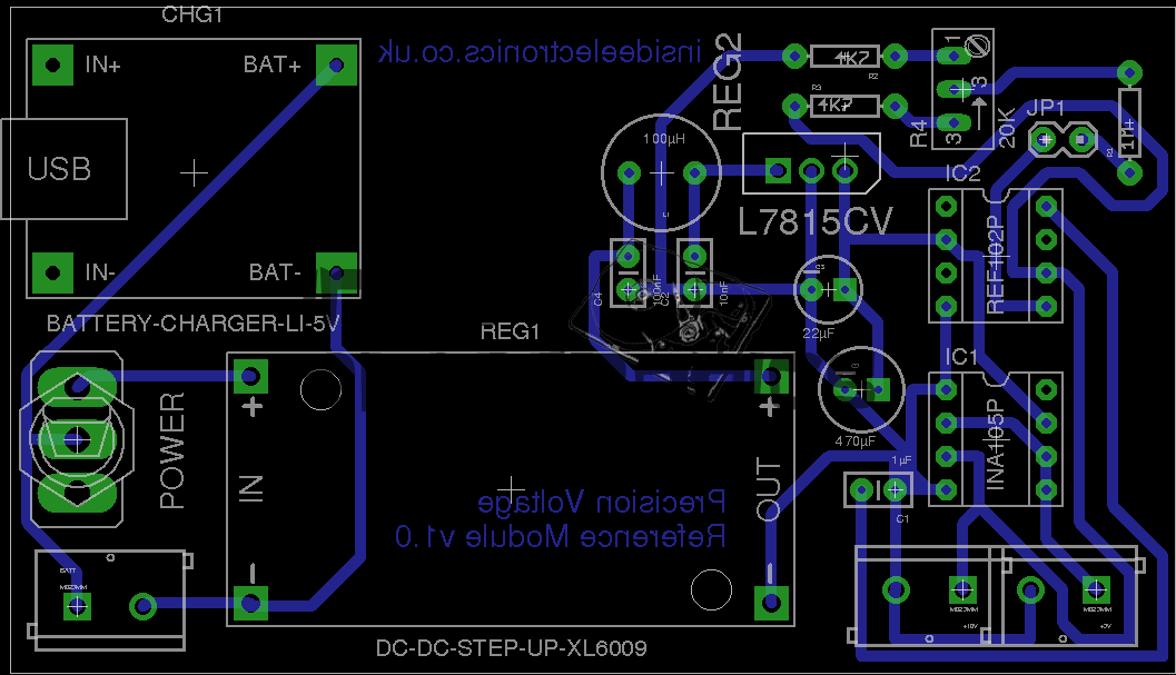
Precision Ref SCH – Click to Embiggen
Here’s the schematic layout, the same as is in the video.
Precision Ref BRD
As usual, the Eagle CAD layout files can be found at the bottom of the post.
And the associated PCB layout. I have added the option to be able to tweak the output, to get a more accurate calibration, which can be added by connecting JP1 on the PCB.
As in the original build, this unit uses pre-built DC-DC converter & Li-Ion charger modules. A handy Eagle library can be found online for these parts.
I have however left off the battery monitor section of the circuit, since I plan to use a protected lithium cell for power. This also allowed me to keep the board size down, & use a single sided layout.
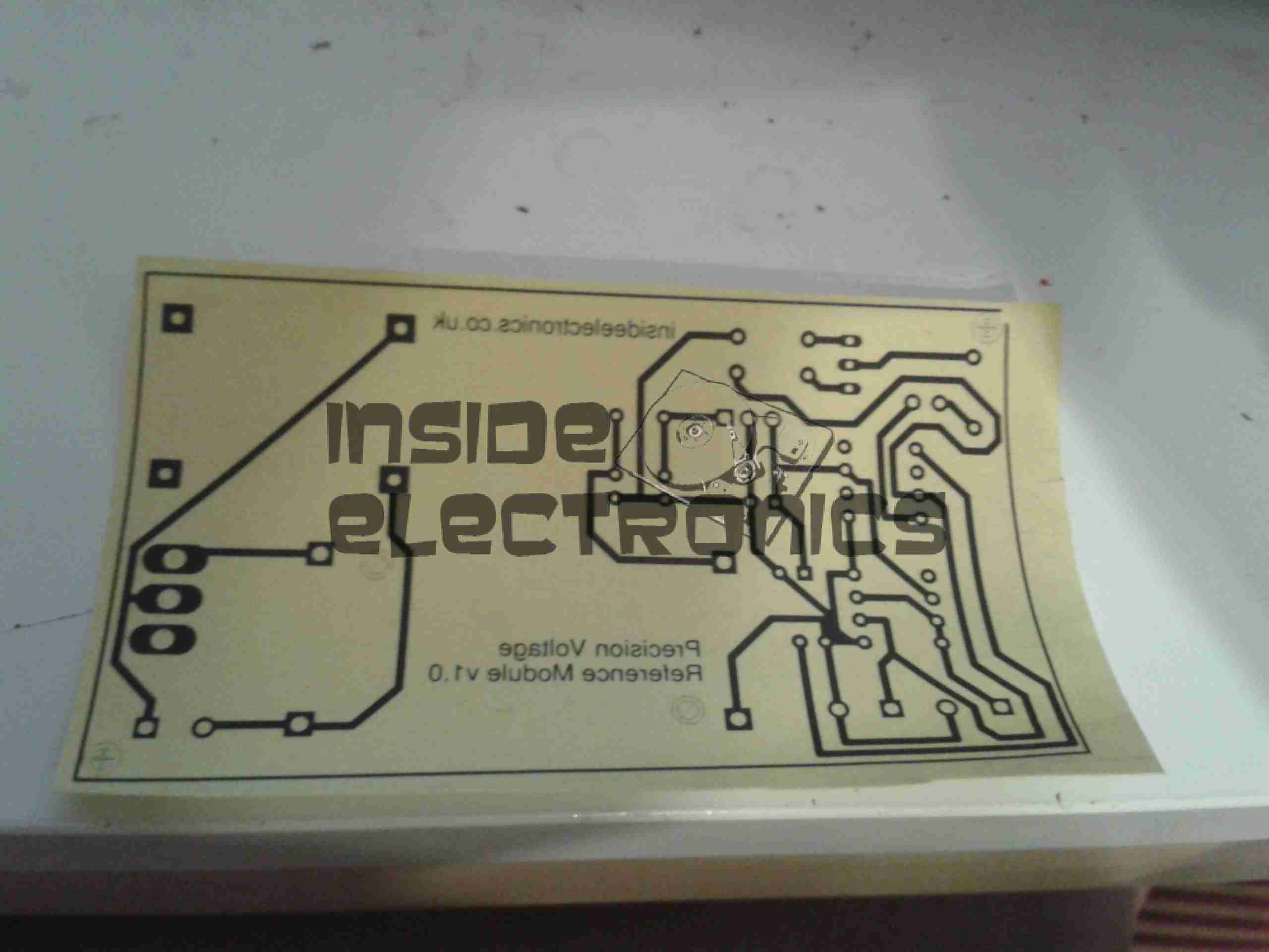
Toner Transfer Paper
Here’s the track layout ready to iron onto the copper clad board. I use the popular toner transfer system with special paper from eBay, this stuff has a coating that allows the toner to easily be transferred to the PCB without having to mess about with soaking in water & scraping paper off.
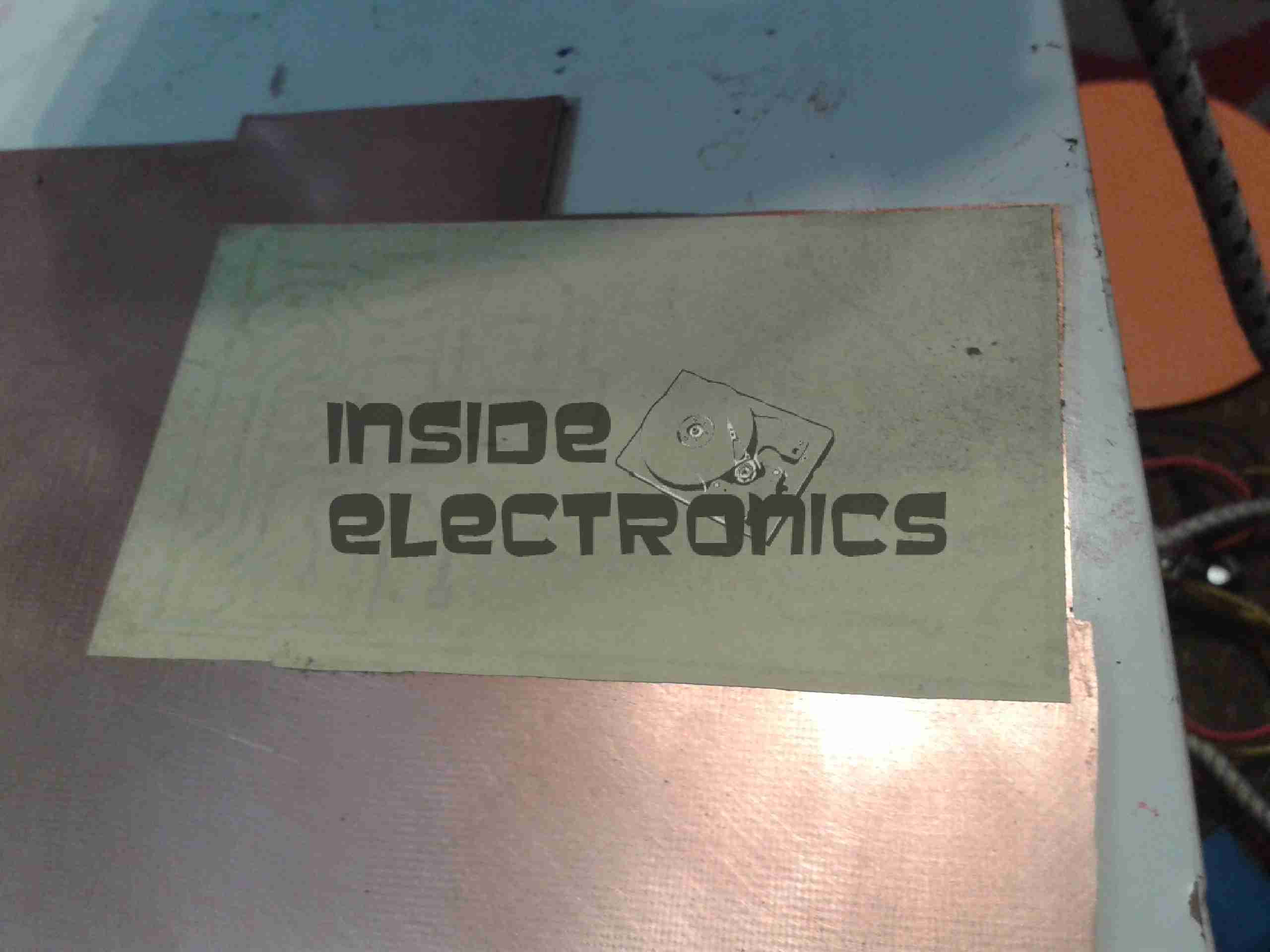
Ironed On
Here’s the paper having just been ironed onto the copper. After waiting for the board to cool off the paper is peeled off, leaving just the toner on the PCB.
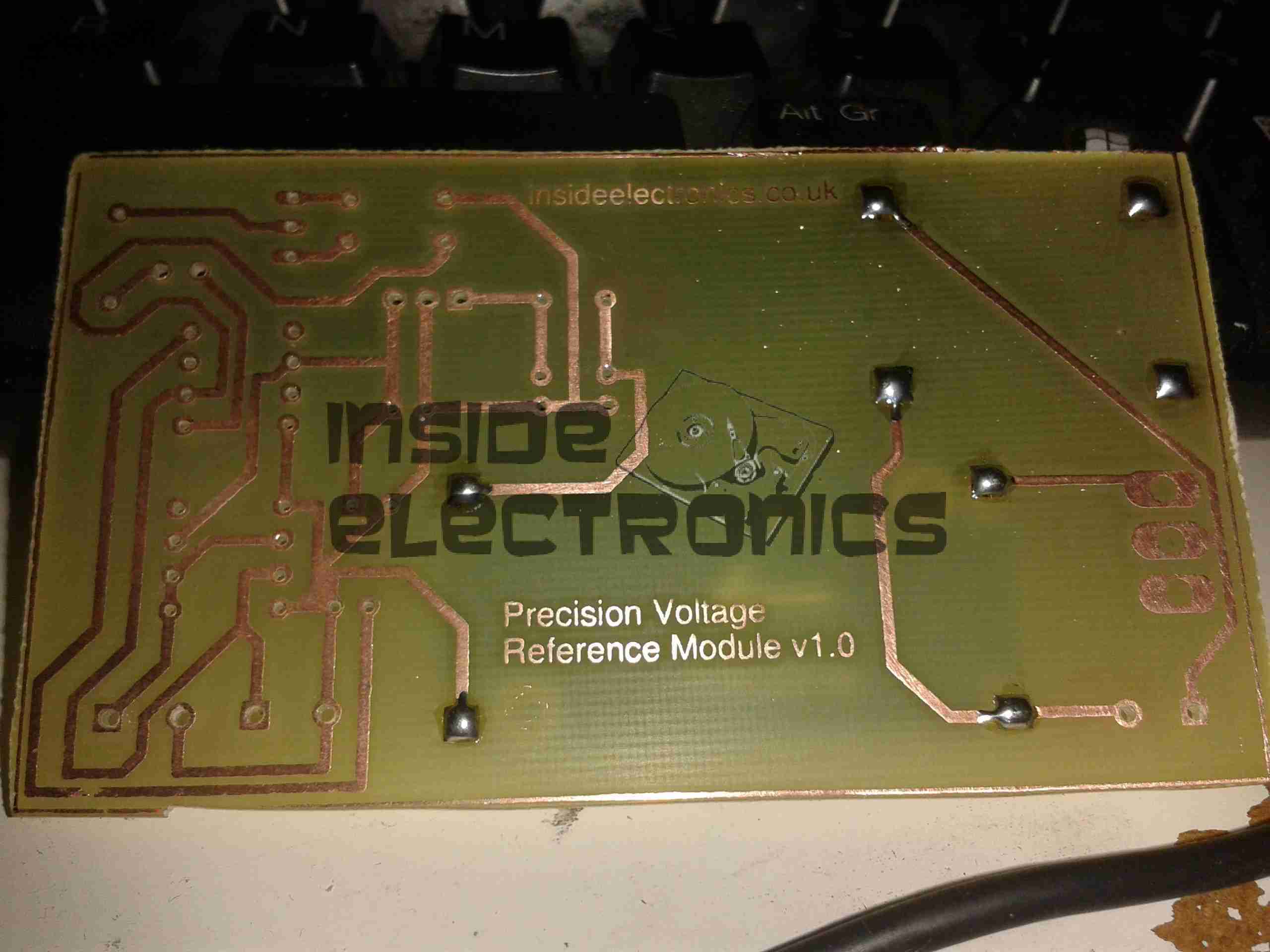
Etched PCB
PCB just out of the etch tank, drilled & with the solder pins for the modules installed. Only one issue with the transfer, in the bottom left corner of the board is visible, a very small section of copper was over etched.
This is easily fixed with a small piece of wire.
Components Populated
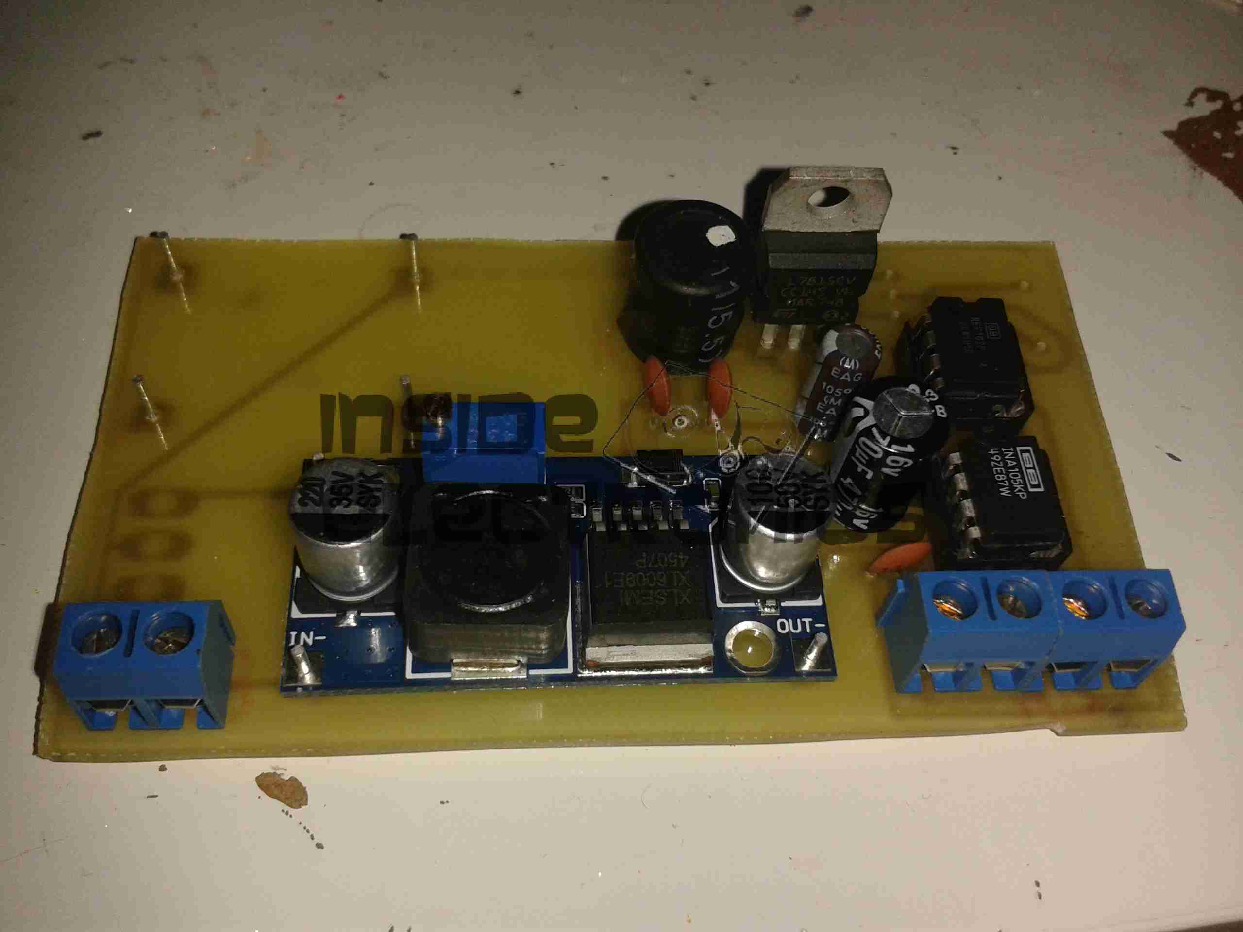
Main components populated. The DC-DC converter is set at 24v output, which the linear regulator then drops down to the +15v rail for the reference IC. The linear section of the regulator, along with the LC filter on the output of the switching regulator produce a low-ripple supply.
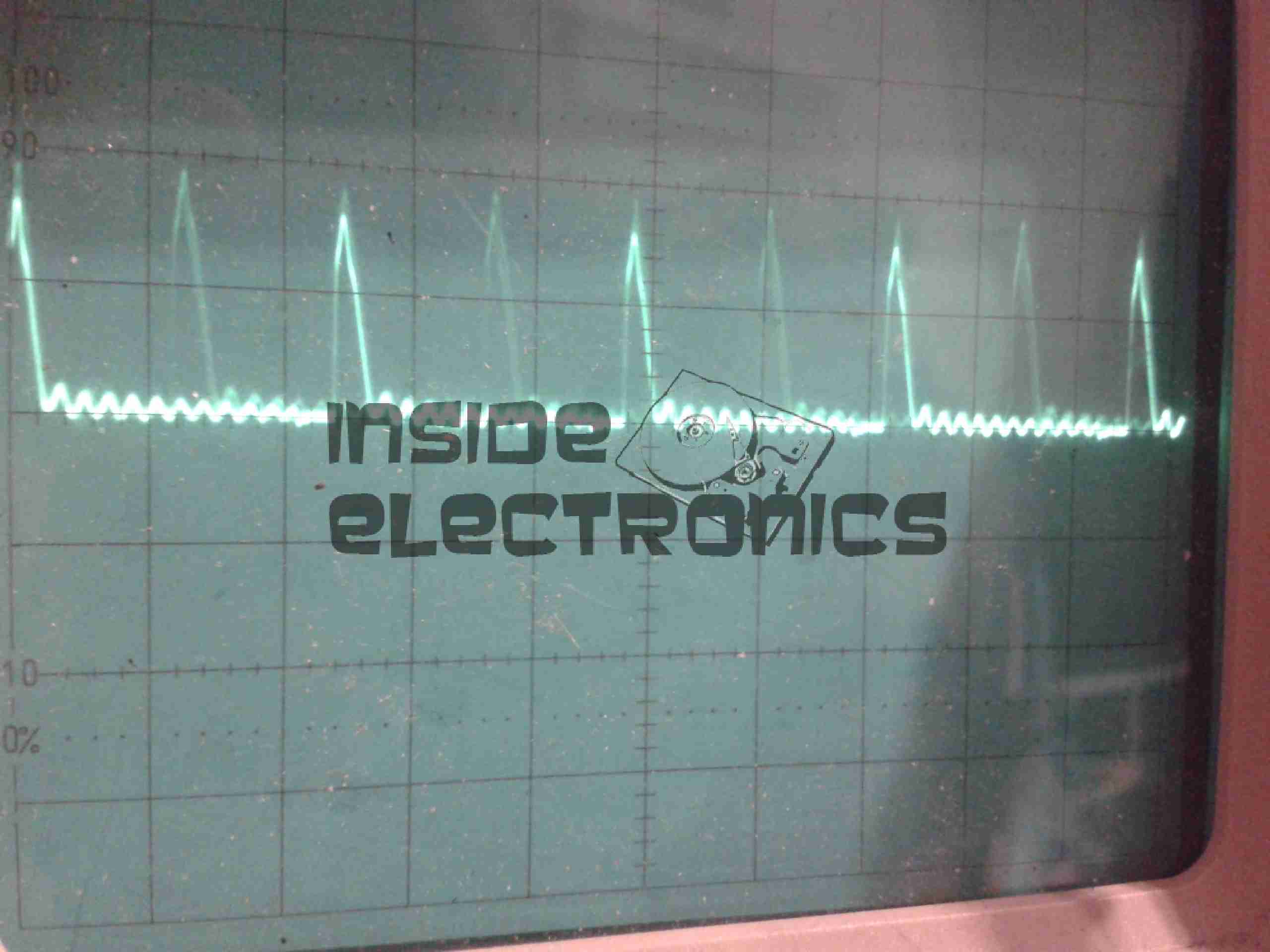
SMPS Ripple
Here’s the scope reading the AC ripple on the output of the DC-DC converter. Scale is 100mV/Div. Roughly 150mV of ripple is riding on top of the DC rail.
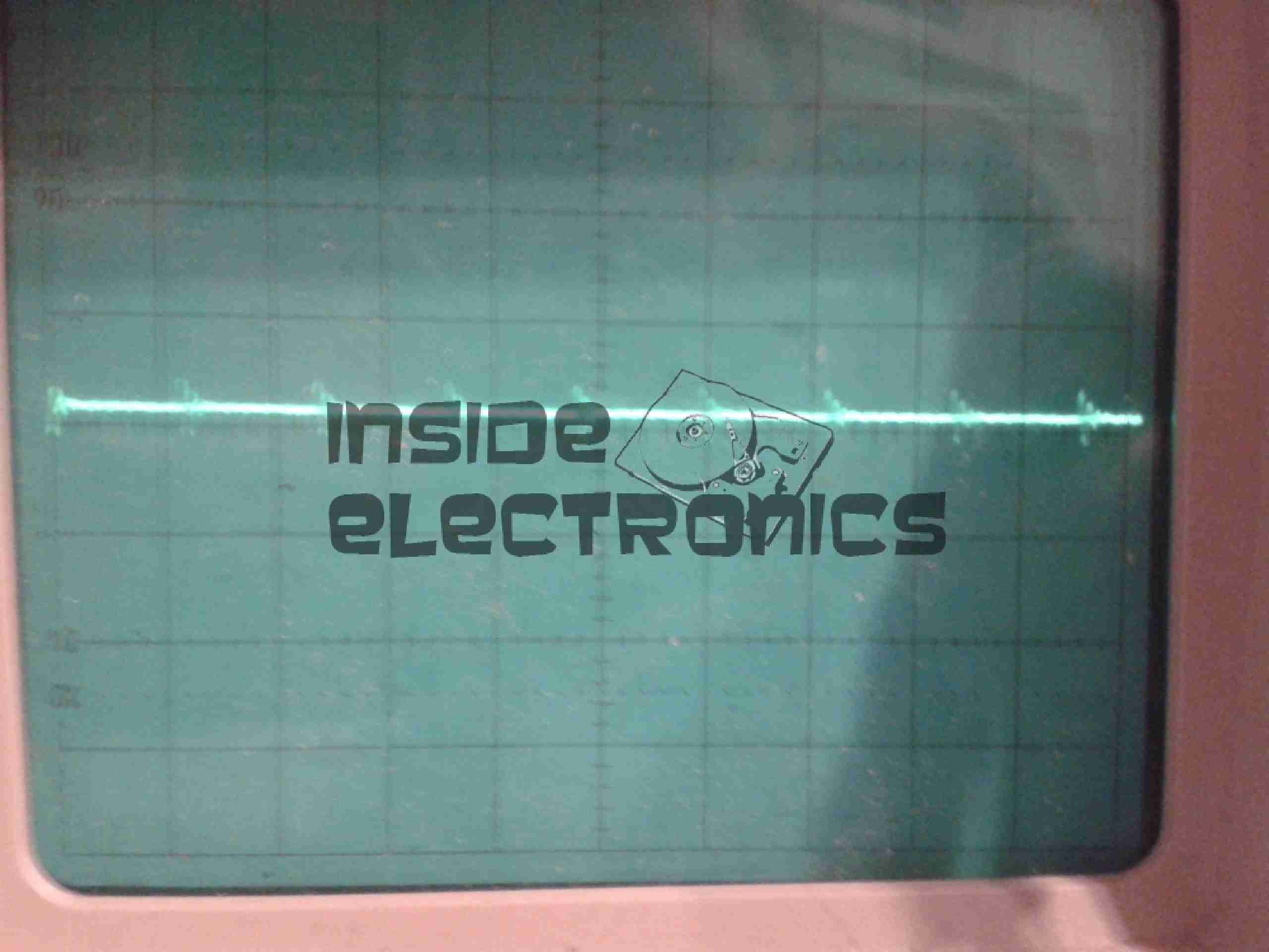
Linear PSU Ripple
And here’s the output from the linear regulator, scale of 50mV/Div. Ripple has been reduced to ~15mV for the reference IC.
In total the circuit as built has a power consumption of ~0.5W, most of which is being dissipated as heat in the linear part of the PSU.
Here is a ZyXel WAP3205 WiFi Access Point that has suffered a reverse polarity event, due to an incorrect power supply being used with the unit.
ZyXEL WAP3205
While most electronic gadgets are protected against reverse polarity with a blocking diode, this unit certainly wasn’t. Applying +12v DC the wrong way round resulted in this:
Blown Switchmode IC (Fuzzy Focus)
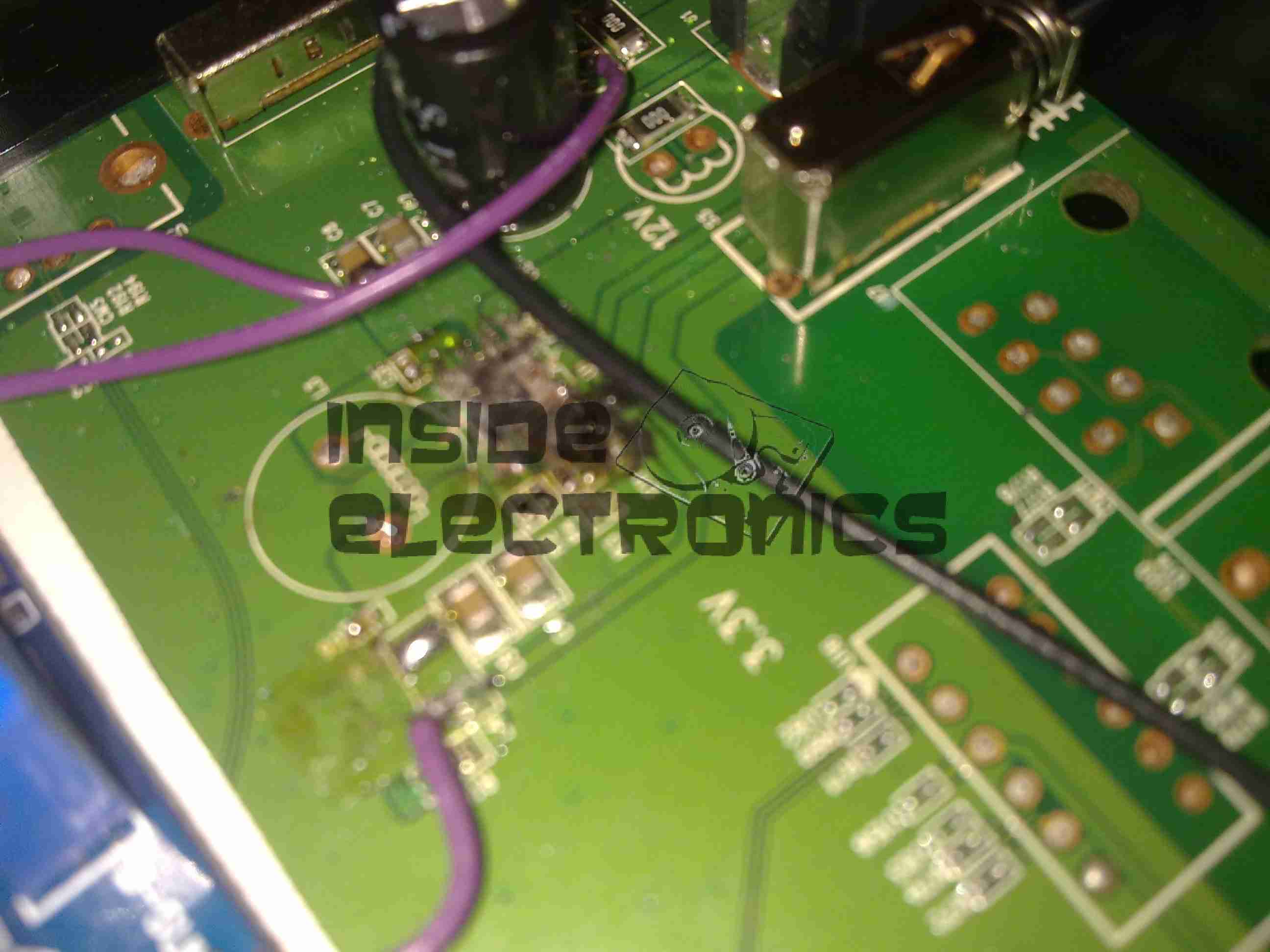
That is the remains of the 3.3v regulator IC, blown to smithereens & it even attempted an arson attack. Luckily this was the only damaged component, & I was able to repair the unit by replacing the switching IC with a standalone regulator. (Replacing the IC would have been preferable, if there was anything left of it to obtain a part number from).
I scraped away the pins of the IC to clear the short on the input supply, removed the switching inductor, & tacked on an adjustable regulator module set to 3.3v. Luckily the voltage of the supply is handily marked on the PCB next to the circuit.
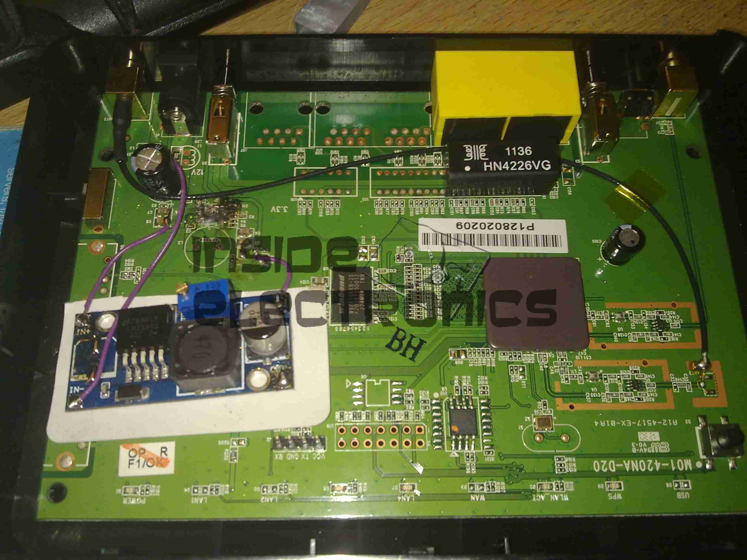
Replacement PSU
Replacement SMPS in place on top of the PCB. The output of the supply is connected to one of the pads of L4 (on my unit just an 0 ohm link), the +12v input is connected to the + rail side of C8 & C7 & the final ground connection is hooked in to the back of the barrel jack.
After this replacement, the unit booted straight up as if nothing had happened. All the logic is undamaged!
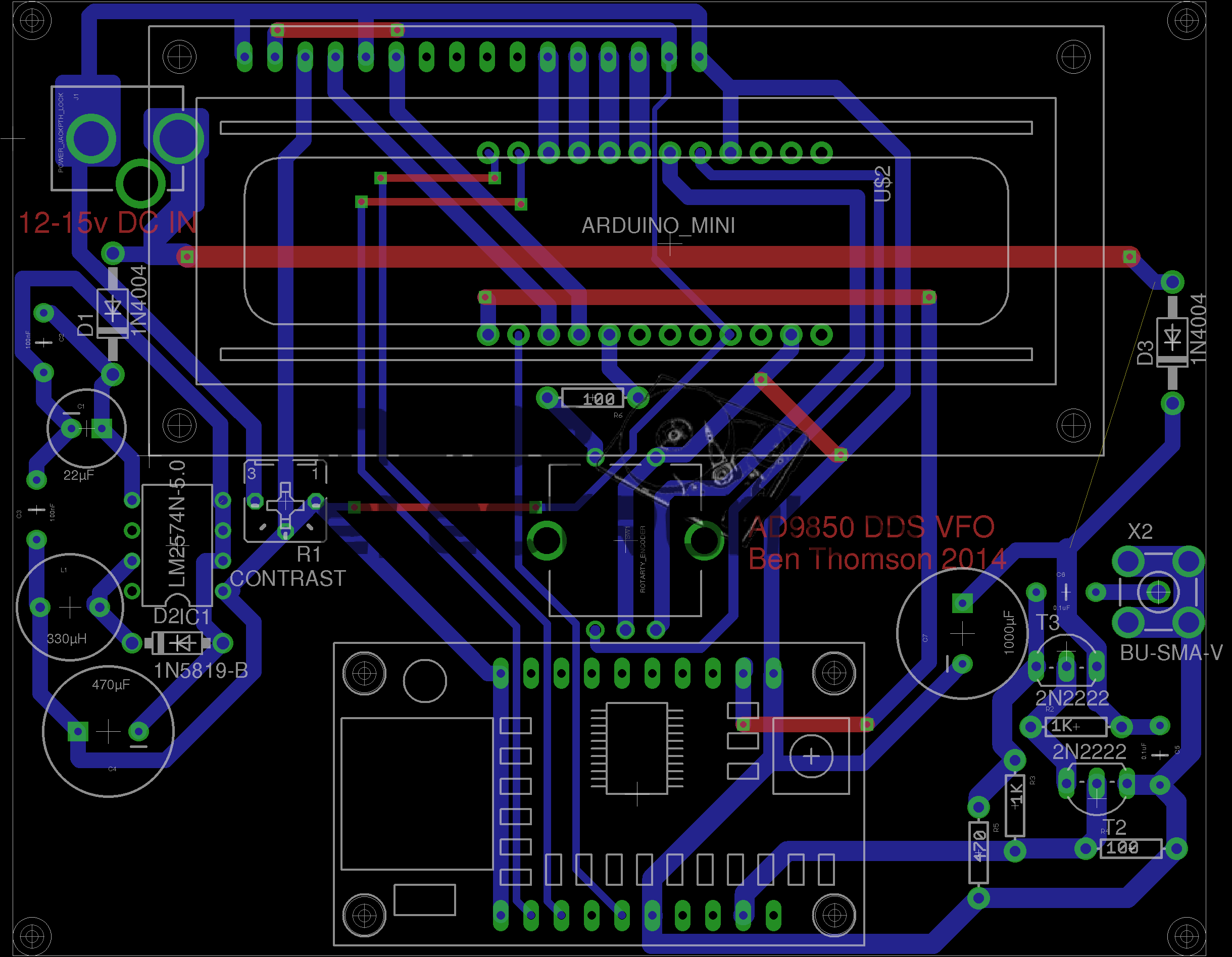
Continuing from my previous post where I published an Eagle design layout for AD7C‘s Arduino powered VFO, here is a completed board.
I have made some alterations to the design since posting, which are reflected in the artwork download in that post, mainly due to Eagle having a slight psychotic episode making me ground one of the display control signals!
AD9850 VFO
The amplifier section is unpopulated & bypassed as I was getting some bad distortion effects from that section, some more work is needed there.
The Arduino Pro Mini is situated under the display, and the 5v rail is provided by the LM7805 on the lower left corner.
Current draw at 12v input is 150mA, for a power of 1.8W total. About 1W of this is dissipated in the LM7805 regulator, so I have also done a layout with an LM2574 Switching Regulator.
The SMPS version should draw a lot let power, as less is being dissipated in the power supply, but this version is more complex.
DDS VFO-SMPS
Here the SMPS circuit can be seen on the left hand side of the board, completely replacing the linear regulator.
I have not yet built this design, so I don’t know what kind of effect this will have on the output signal, versus the linear regulator. I have a feeling that the switching frequency of the LM2574 (52kHz) might produce some interference on the output of the DDS module. However I have designed this section to the standards in the datasheet, so this should be minimal.
Nevertheless this version is included in the Downloads section at the bottom of this post.
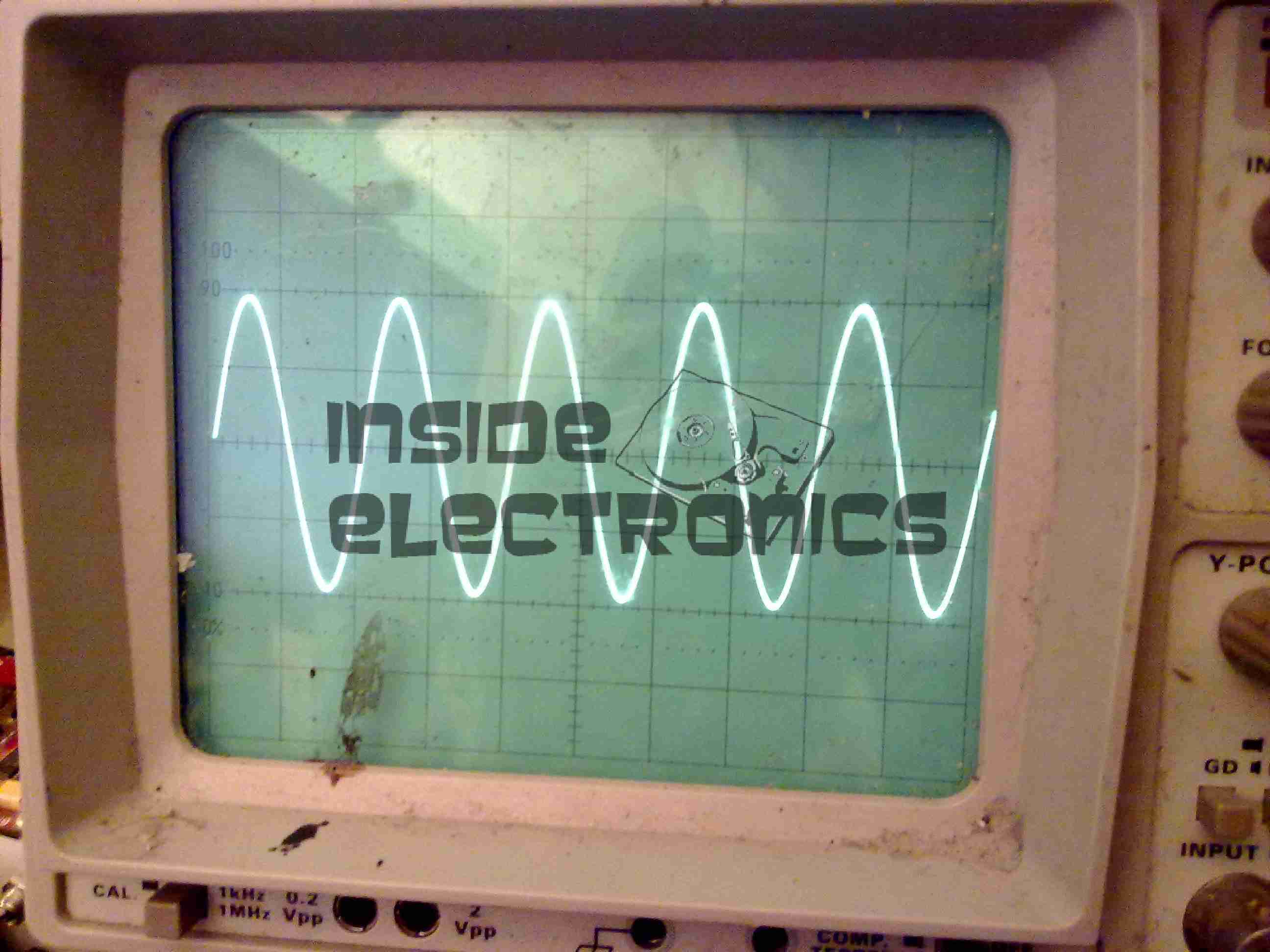
The output coupled through a 100nF capacitor is very clean, as can be seen below, outputting a 1kHz signal. Oscilloscope scale is 0.5ms/div & 1V/div.
VFO Output (Mucky ‘Scope)Scope Connected
Thanks again to Rich over at AD7C for the very useful tool design!
Linked below is the Eagle design files for this project, along with my libraries used to create it.
To provide more run time with the conversion to petrol & spark ignition, I have also upgraded the on-board electronics supply to compensate for the extra ~650mA draw of the ignition module.
This modification is centred around a 3S Lithium-Polymer battery pack, providing a nominal 11.1v to a voltage regulator, which steps down this higher voltage to the ~6v required by the receiver & servo electronics.
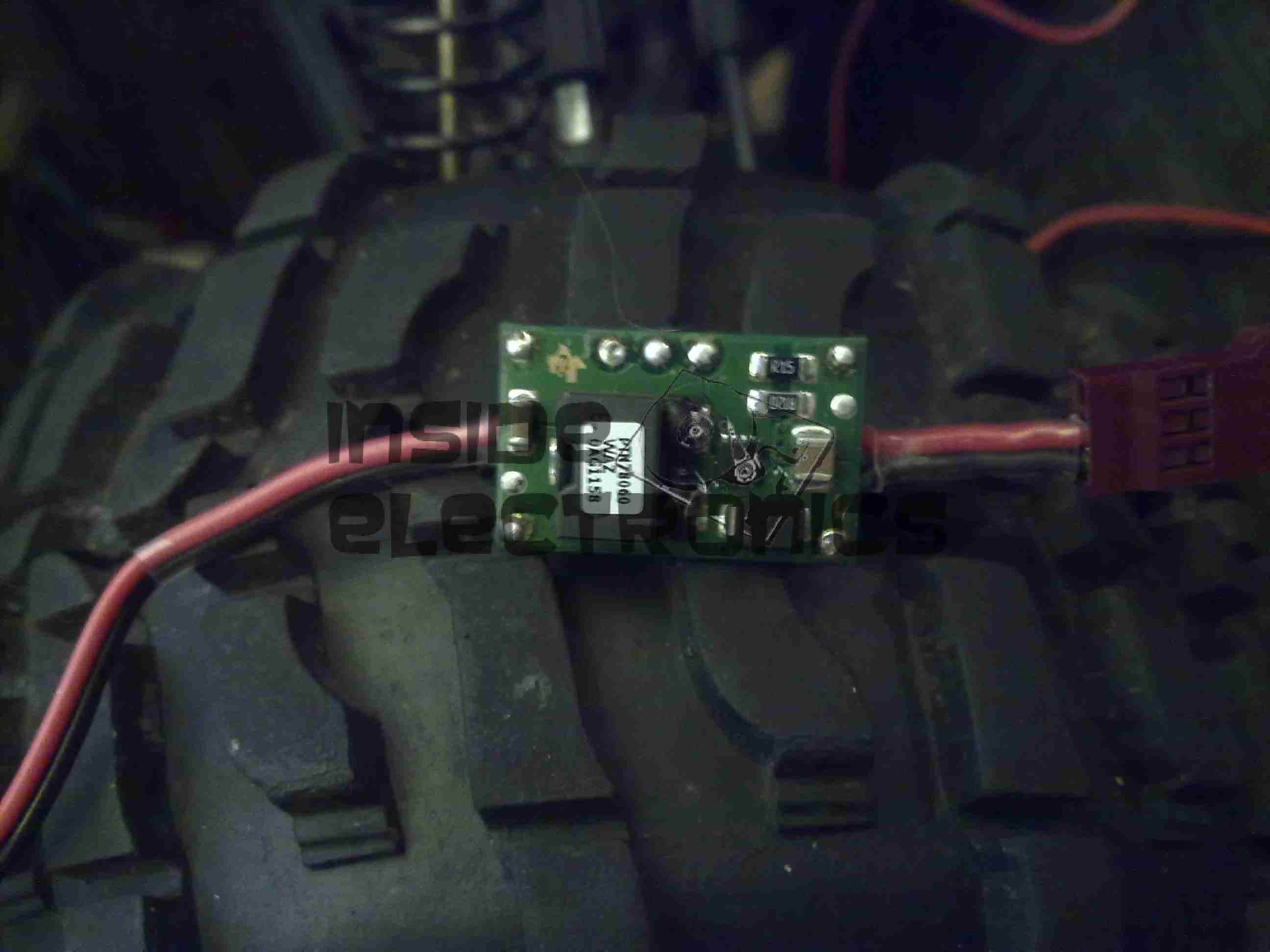
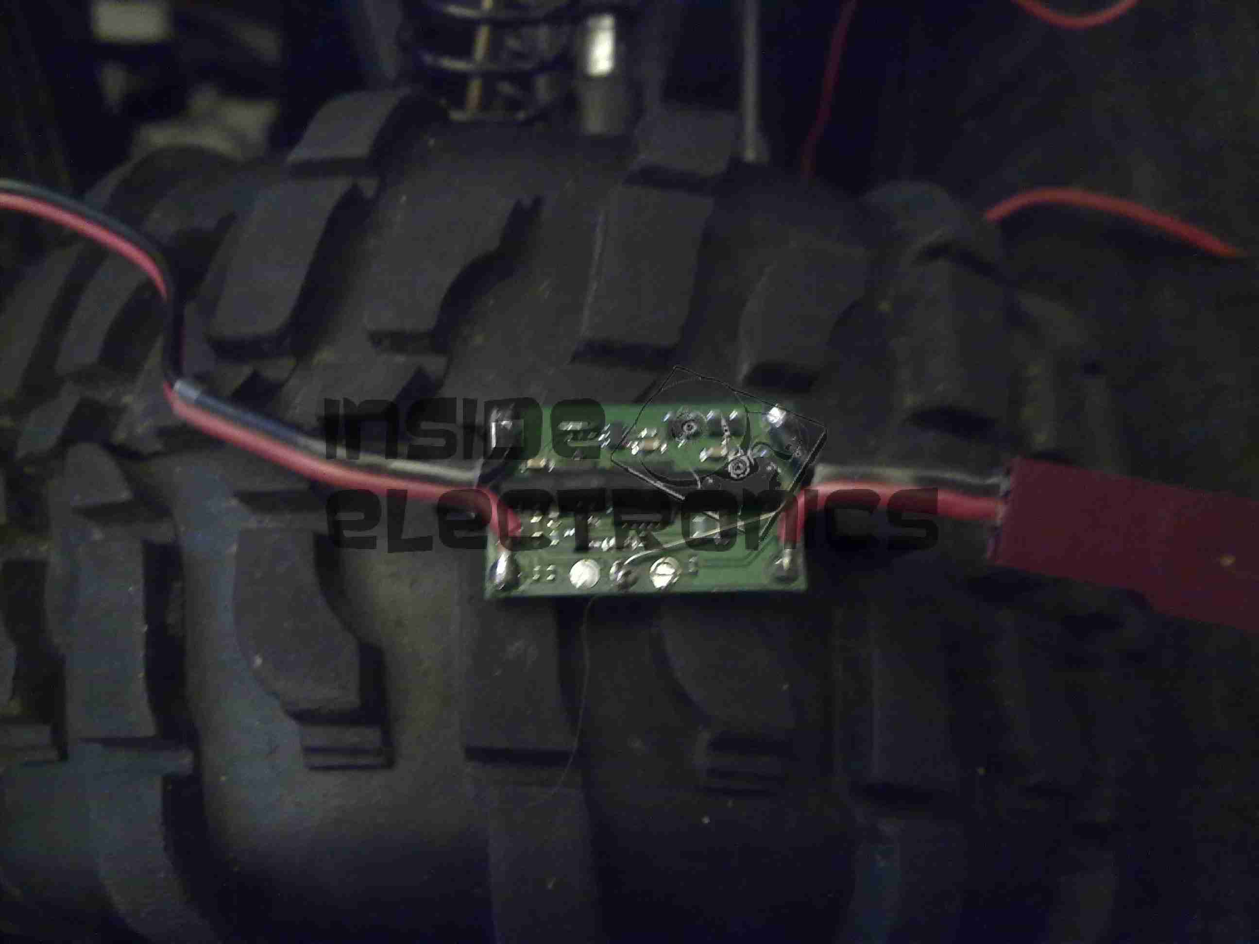
Power RegulatorPower Regulator
The regulator, shown above, is a Texas Instruments PTN78060WAZ wide-input voltage adjustable regulator. This module has an exceptionally high efficiency of ~96% at it’s full output current of 3A. The output voltage is set by a precision resistor, soldered to the back of the module, in this case 6.5v. Standard RC connectors are used on the regulator to allow connection between the power switch & the radio receiver.
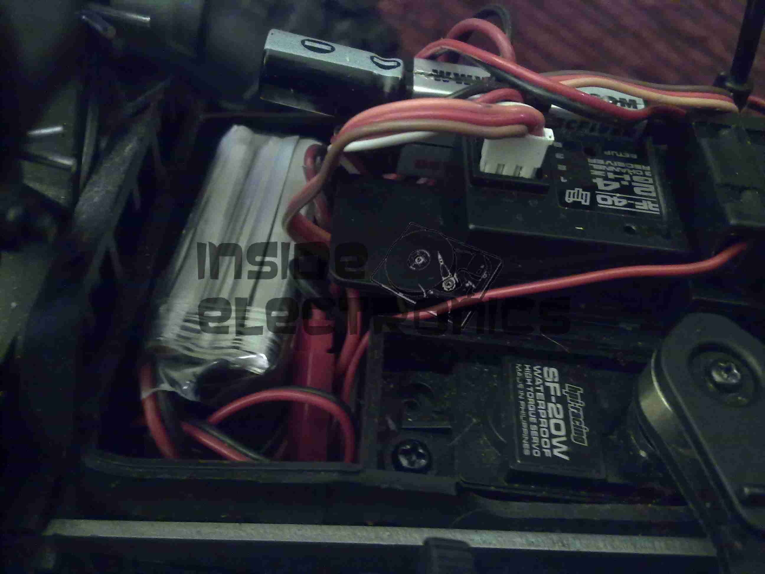
Receiver Box
Everything tucked away into place inside the receiver box. The 3S 1000mAh LiPo fits perfectly in the space where the original Ni-Mh hump pack was located.
The completely stable output voltage of the regulator over the discharge curve of the new battery gives a much more stable supply to the radio & ignition, so I should experience fewer dropouts. Plus the fact that the engine now relies on power from the receiver pack to run, it’s a built in fail safe – if the power dies to the receiver, the engine also cuts out.
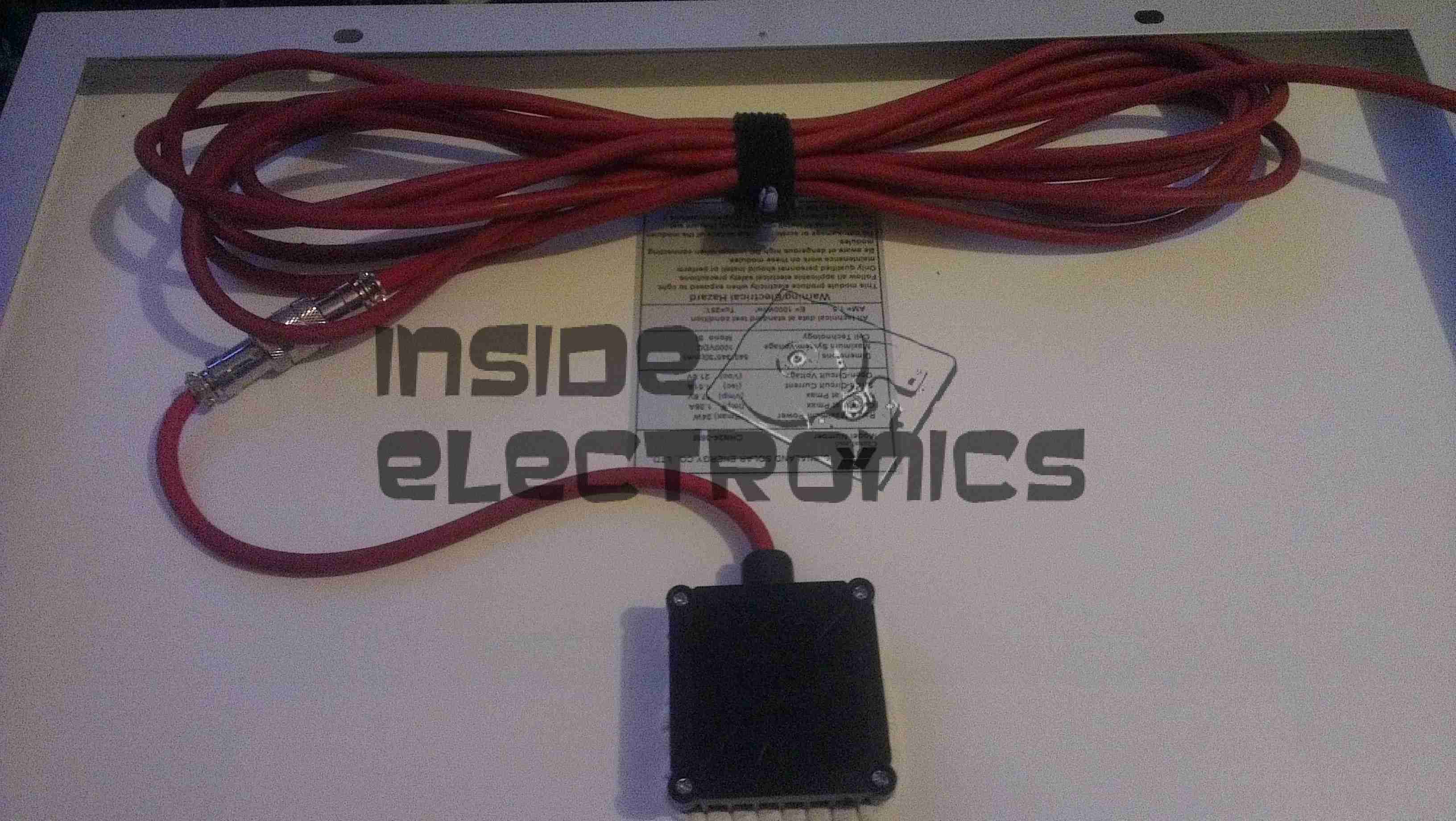
As the cable supplied with the panel is far too short, inflexible & does not even allow the cable gland on the terminal box to form a seal, I have replaced it with some high quality twin core guitar cable, with silicone insulation.
The cable is removable from the panel tail by means of a screwlock two pin connector.
On another note, I have noticed a side effect of fitting a switchmode regulator to the panel: it seems to have formed an MPPT-type regulator setup, as even in low light conditions, when the bare panel is outputting 18.5v at 50mA short circuit, with the switching regulator I can get a useable 13.25v at ~170mA.
This effect is increased in full light, where I can obtain 4.5A short circuit current & ~1.8A at 13.25v output.
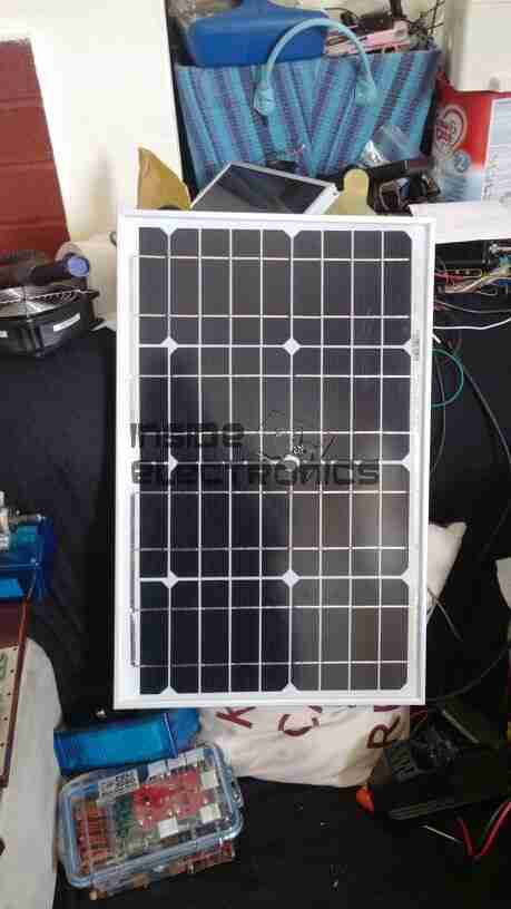
I have acquired a 24W monocrystalline solar panel to charge my portable battery pack while on the move. This panel will be able to charge all devices I carry on a regular basis with nothing but some sunlight!
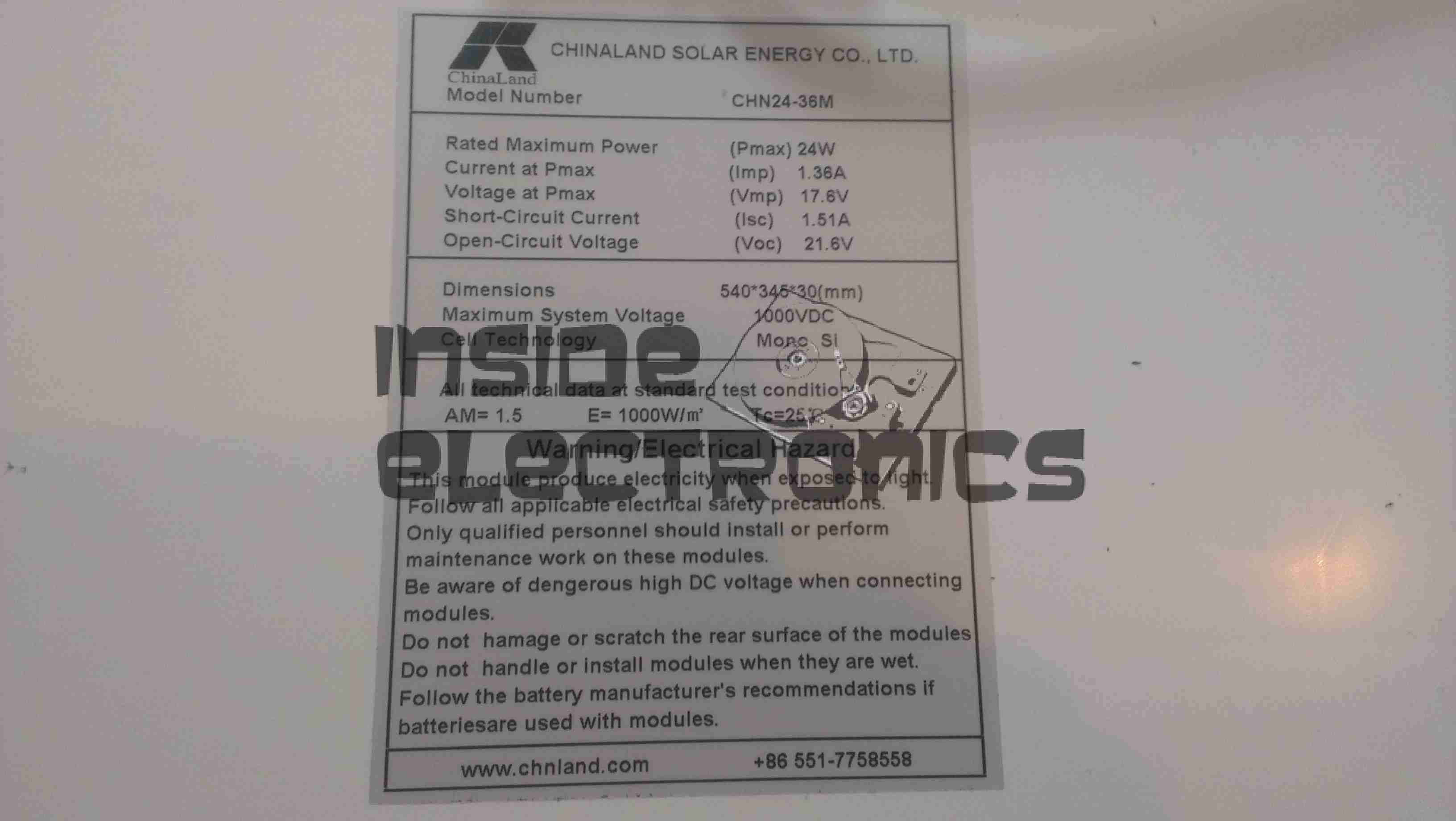
Info Panel
Info on the panel itself. Rated at 24W with nominal 17.6v DC, 1.36A output.
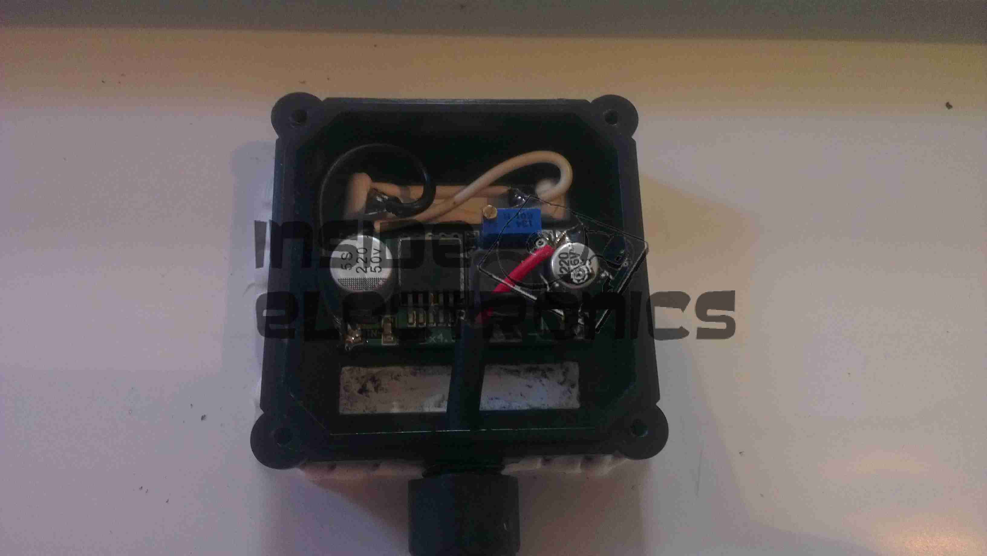
Regulator
I have installed a switching regulator in the back of the panel, where the connections would normally be wired straight to the array of cells. This regulates the voltage down to a constant 13.8v to provide more compatibility with 12v charging equipment. I have tested the output of the panel in late day sun, at 1.27A.
As the first USB hub I was using was certainly not stable – it would not enumerate between boots & to get it working again would require waiting around 12 hours before applying power, it has been replaced. This is a cheapie eBay USB hub, of the type shown below.
These hubs are fantastic for hobbyists, as the connections for power & data are broken out on the internal PCB into a very convenient row of pads, perfect for integration into many projects.
Breakout Hub
I now have two internal spare USB ports, for the inbuilt keyboard/mouse receiver & the GPS receiver I plan to integrate into the build.
These hubs are also made in 7-port versions, however I am not sure if these have the same kind of breakout board internally. As they have the same cable layout, I would assume so.
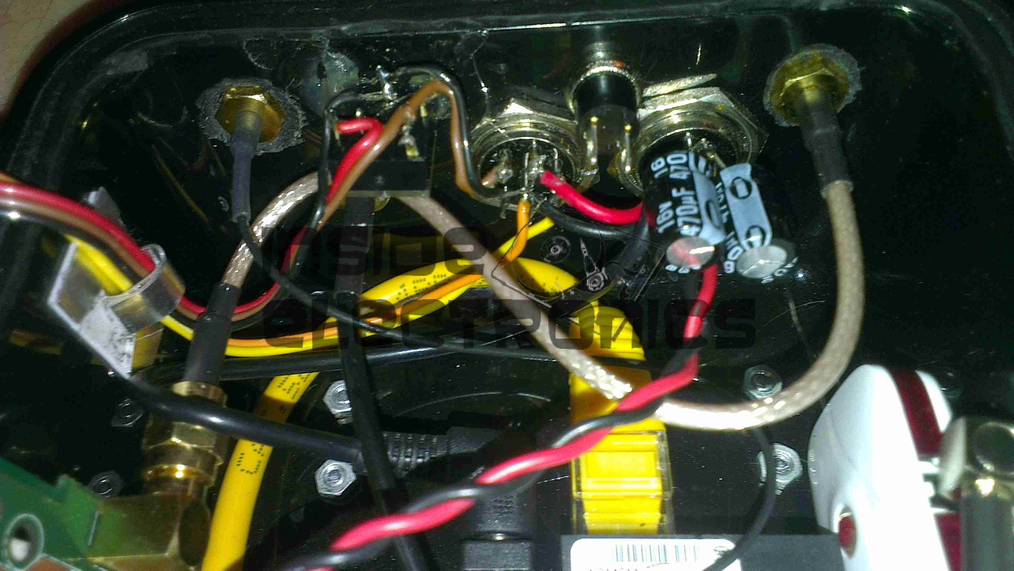
Connector Panel
Here is a closeup of the back of the connectors, showing a couple of additions.
I have added a pair of 470µF capacitors across the power rails, to further smooth out the ripple in the switching power supply, as I was having noise issues on the display.
Also, there is a new reset button added between the main interface connectors, which will be wired into the pair of pads that the Raspberry Pi has to reset the CPU.
This can be used as a power switch in the event the Pi is powered down when not in use & also to reset the unit if it becomes unresponsive.
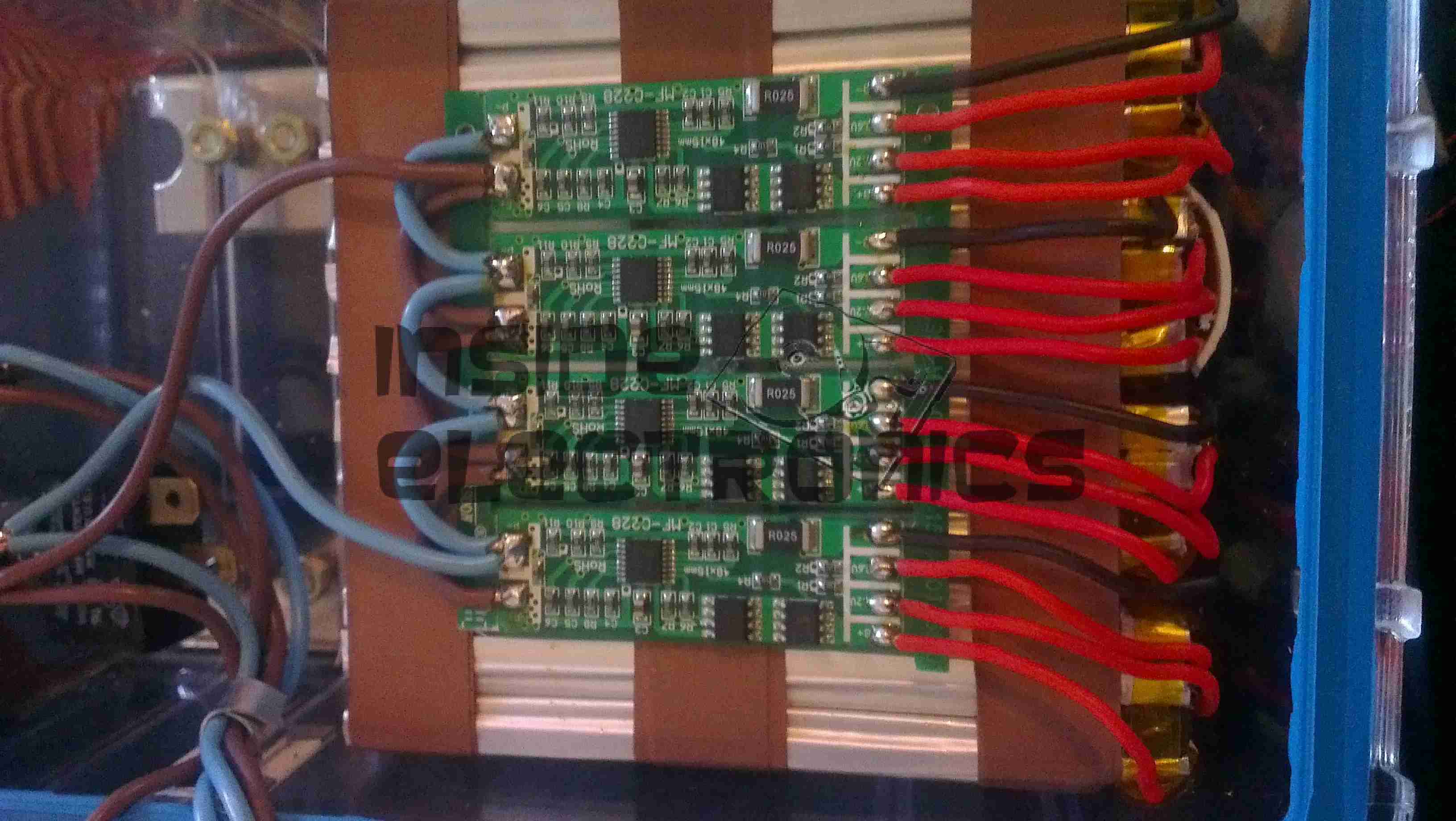
The final part for the battery pack has finally arrived, the PCM boards. These modules protect the cells by cutting off the power at overcharge, undercharge & overcurrent. Each cell is connected individually on the right, 12v power appears on the left connections. These modules also ensure that all the cells in the pack are balanced.
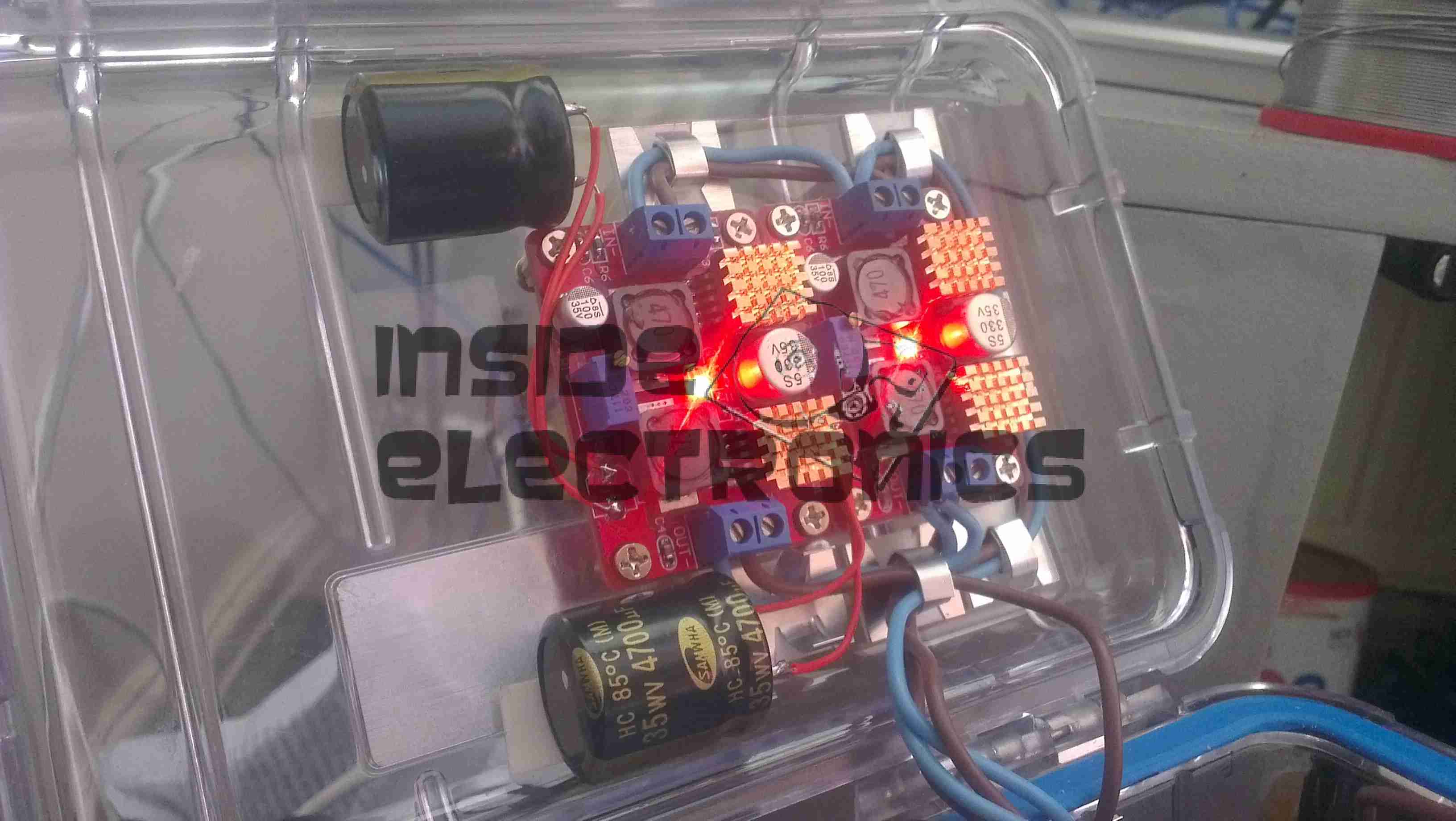
A few modifications were required to the SMPS modules to make the power rails stable enough to run the Pi & it’s monitor. Without these the rails were so noisy that instability was being caused.
I have replaced the 100µF output capacitors & replaced them with 35v 4700µF caps. This provides a much lower output ripple.
There are also heatsinks attached to the converter ICs to help spread the heat.
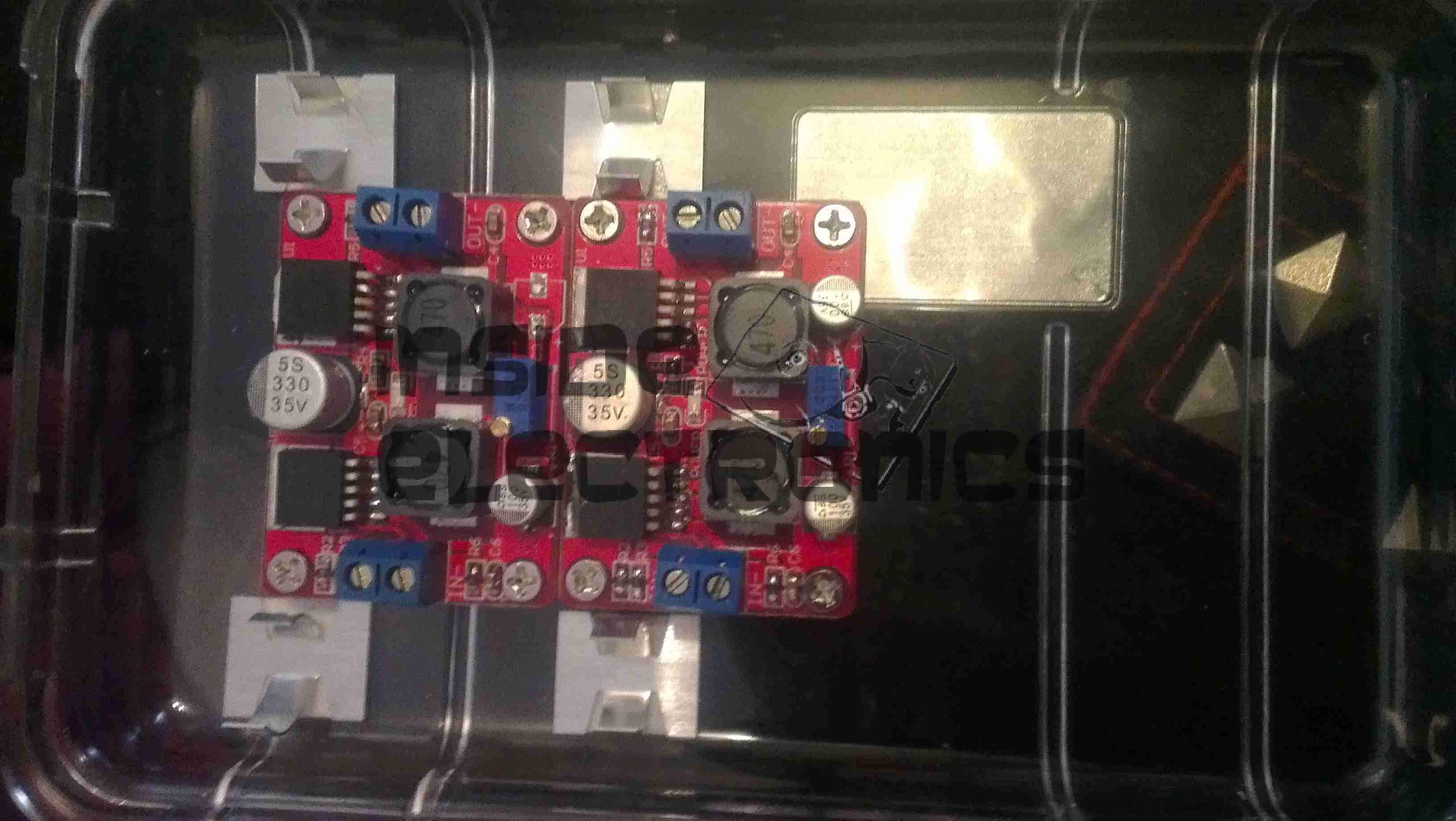
Progress is finally starting on the power supply unit for the Pi, fitted into the same case style as the Pi itself, this is an 8Ah Li-Poly battery pack with built in voltage regulation.
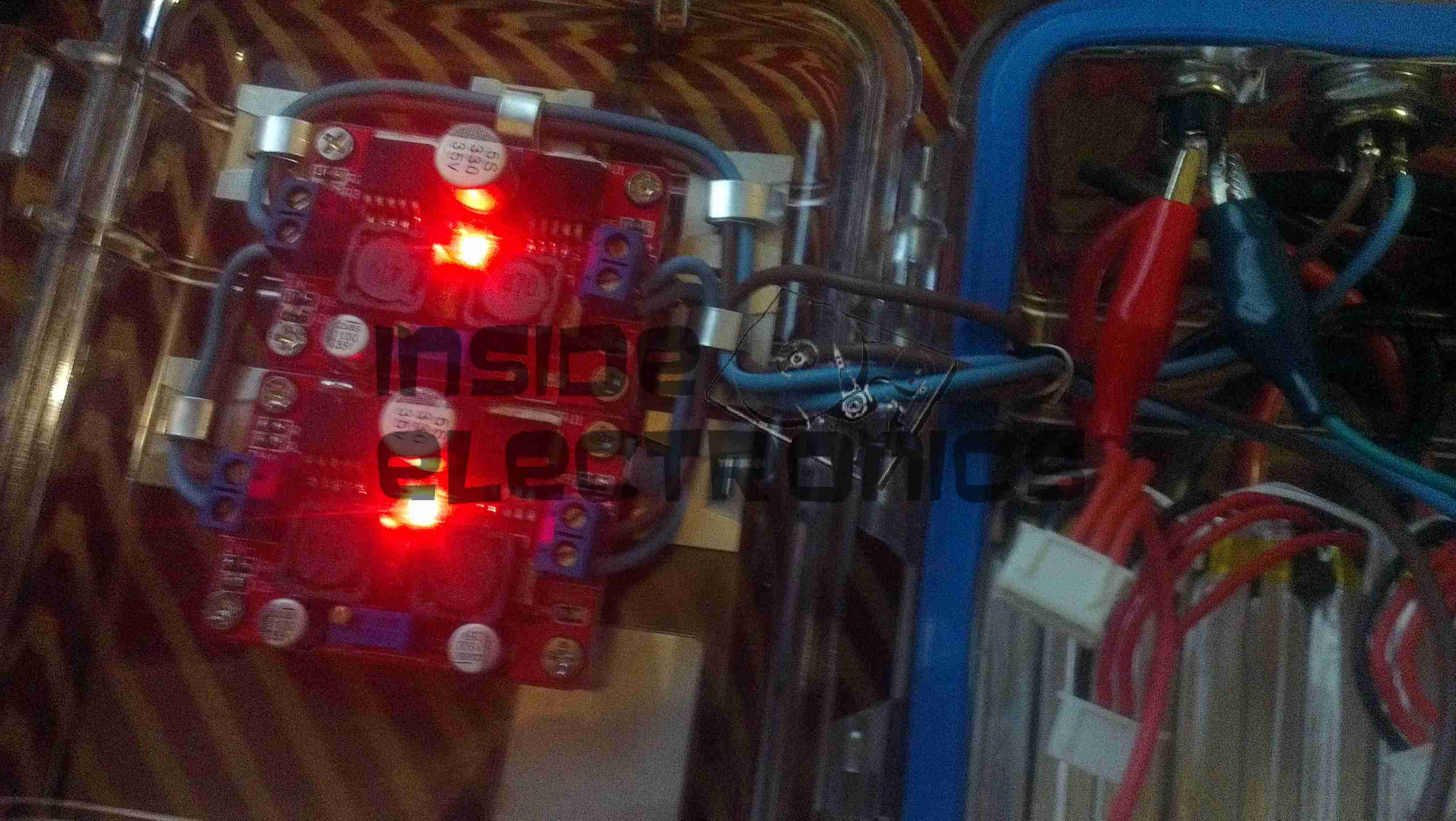
Regulator Boards
Here are the regulators, fixed to the top of the enclosure. These provide the 12v & 5v power rails for the Pi unit, at a max 3A per rail.
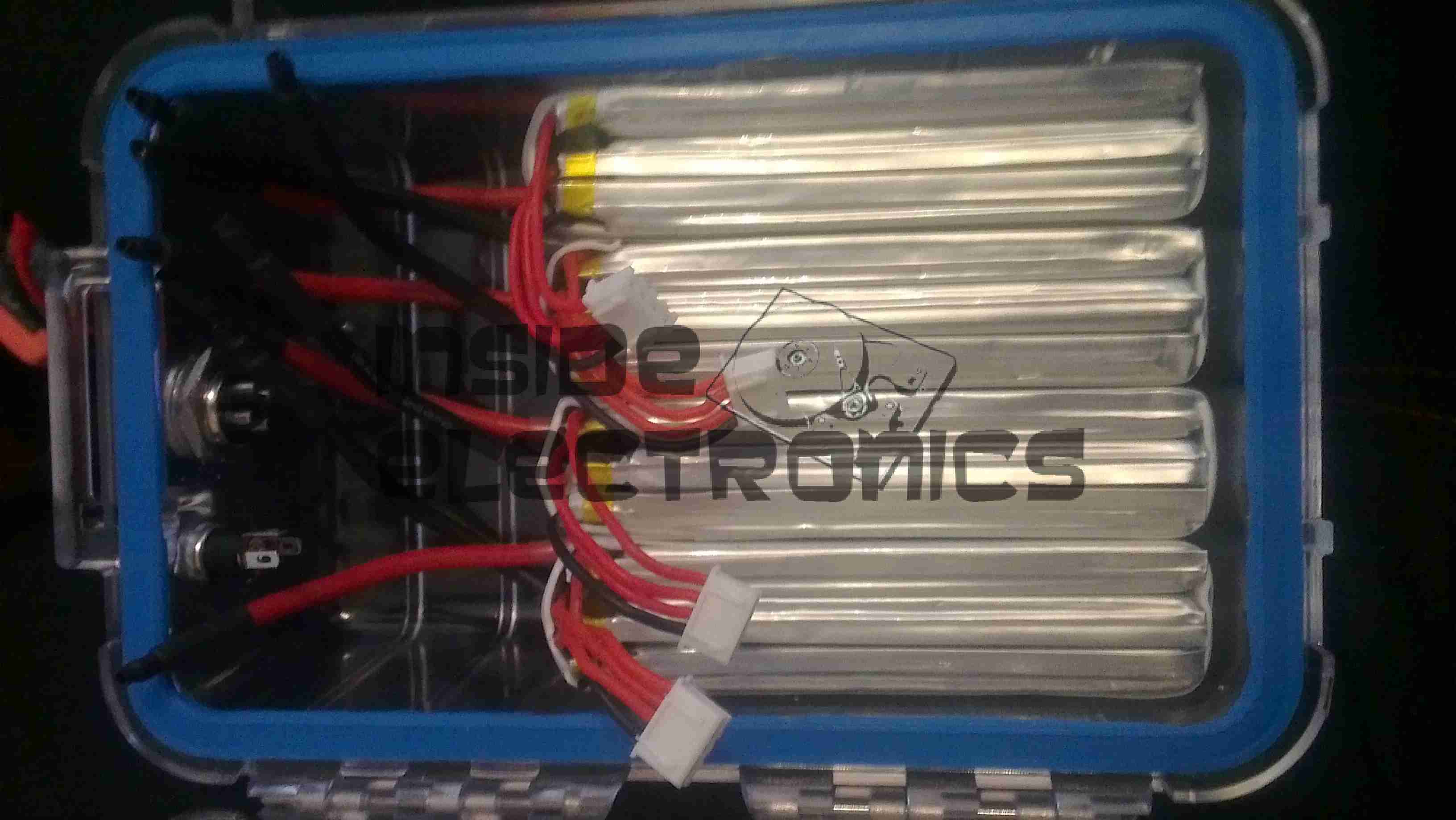
Battery Pack
In the main body of the case the battery pack is fitted. This is made up of 4 3-cell Li-Poly RC battery packs, rated at 2Ah each. All wired in parallel this will provide a total of 8Ah at 12.6v when fully charged.
Powered Up
Here the regulators are powered up from a 13v supply for testing. I have discovered at full load these modules have very bad ripple, so I will be adding extra smoothing capacitors to the power rails to compensate for this.
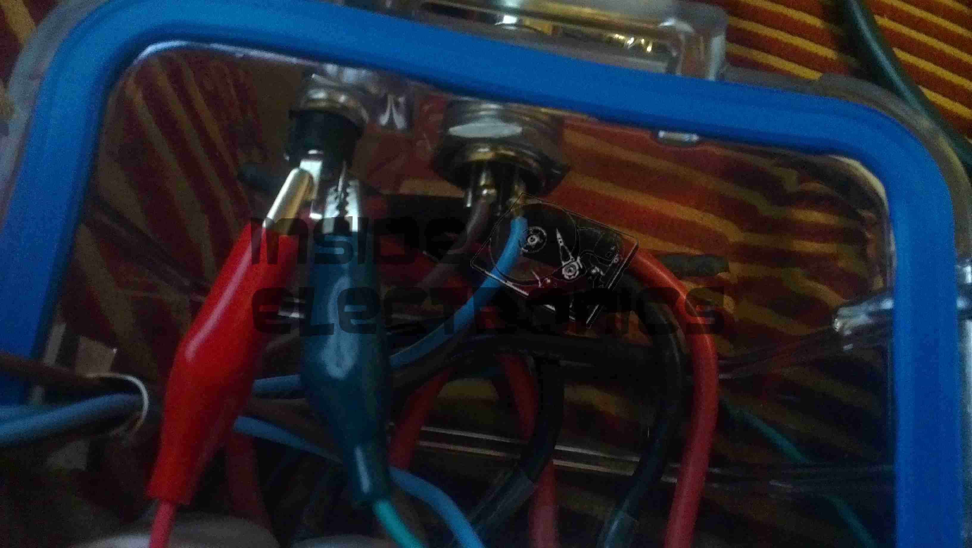
I/O
Here are the connectors on the top of the unit, outputting the two power rails to the Pi & the DC barrel jack that will be used to charge the pack.
As an ultracapacitor has a pretty linear discharge curve, some electronics are required to make them behave more like batteries, such as as SEPIC converter.
On the right is a MuRata Power Solutions UQQ-12/8-Q12P-C switching regulator, which will accept a 9-36v input source & output a constant 12v at 8A (96W).
Tip Jar
If you’ve found my content useful, please consider leaving a donation by clicking the Tip Jar below!
All collected funds go towards new content & the costs of keeping the server online.