Posted on 3 Comments

Chinese “1200W” DC-DC Boost Converter DOA Fix

1200W DC-DC Converter

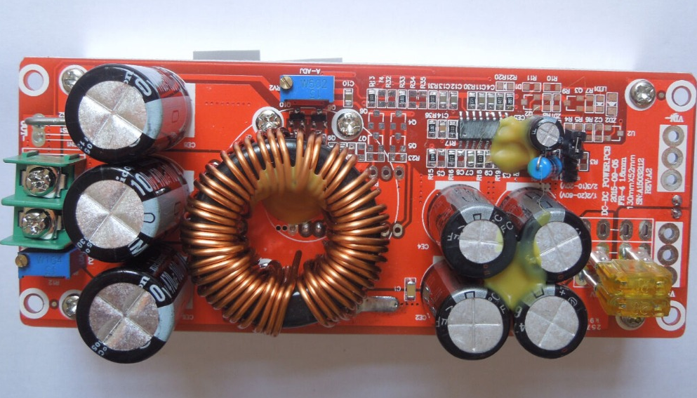
Ah the curse of the Chinese Electronics strikes again. These large DC-DC boost converters have become very common on the likes of AliExpress & eBay, and this time my order has arrived DOA… On applying power, the output LED lights up dimly, and no matter how I twiddle the adjustment pots, the output never rises above the input voltage.

Boost Converter Topology

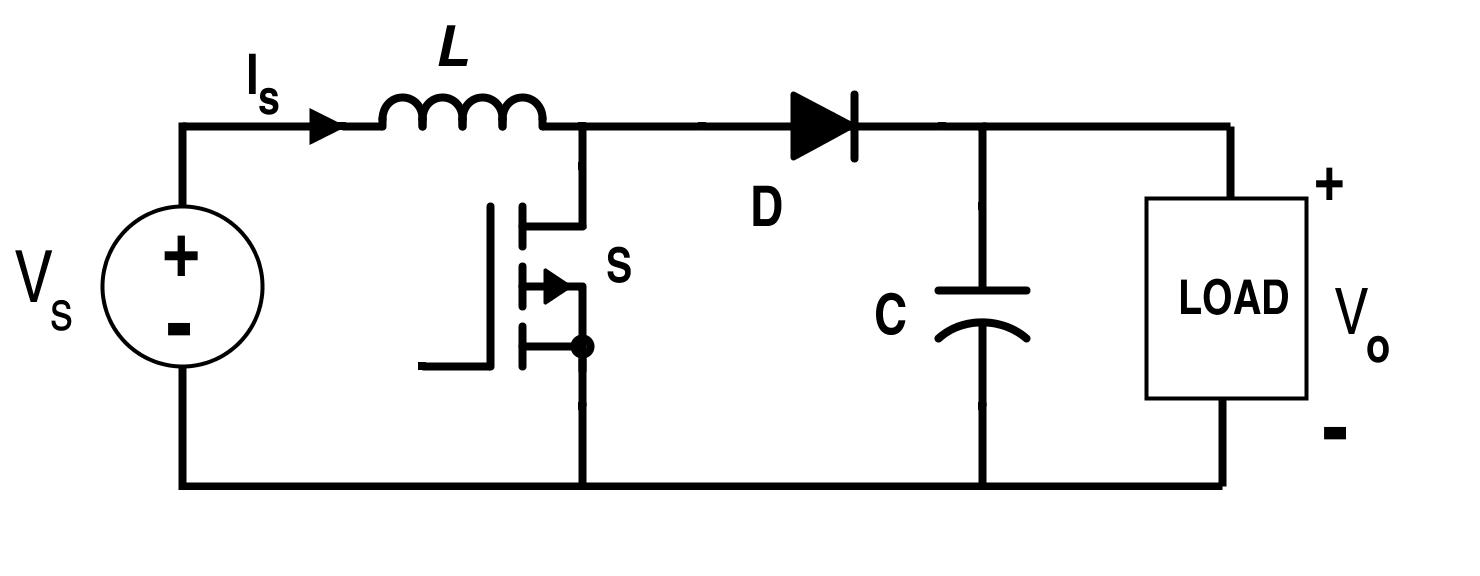
From the usual topology above, we can assume that the switching converter isn’t working, so the input voltage is just being directly fed through to the output. The switching IC on these converters is a TL494,

Control Circuitry
Control Circuitry

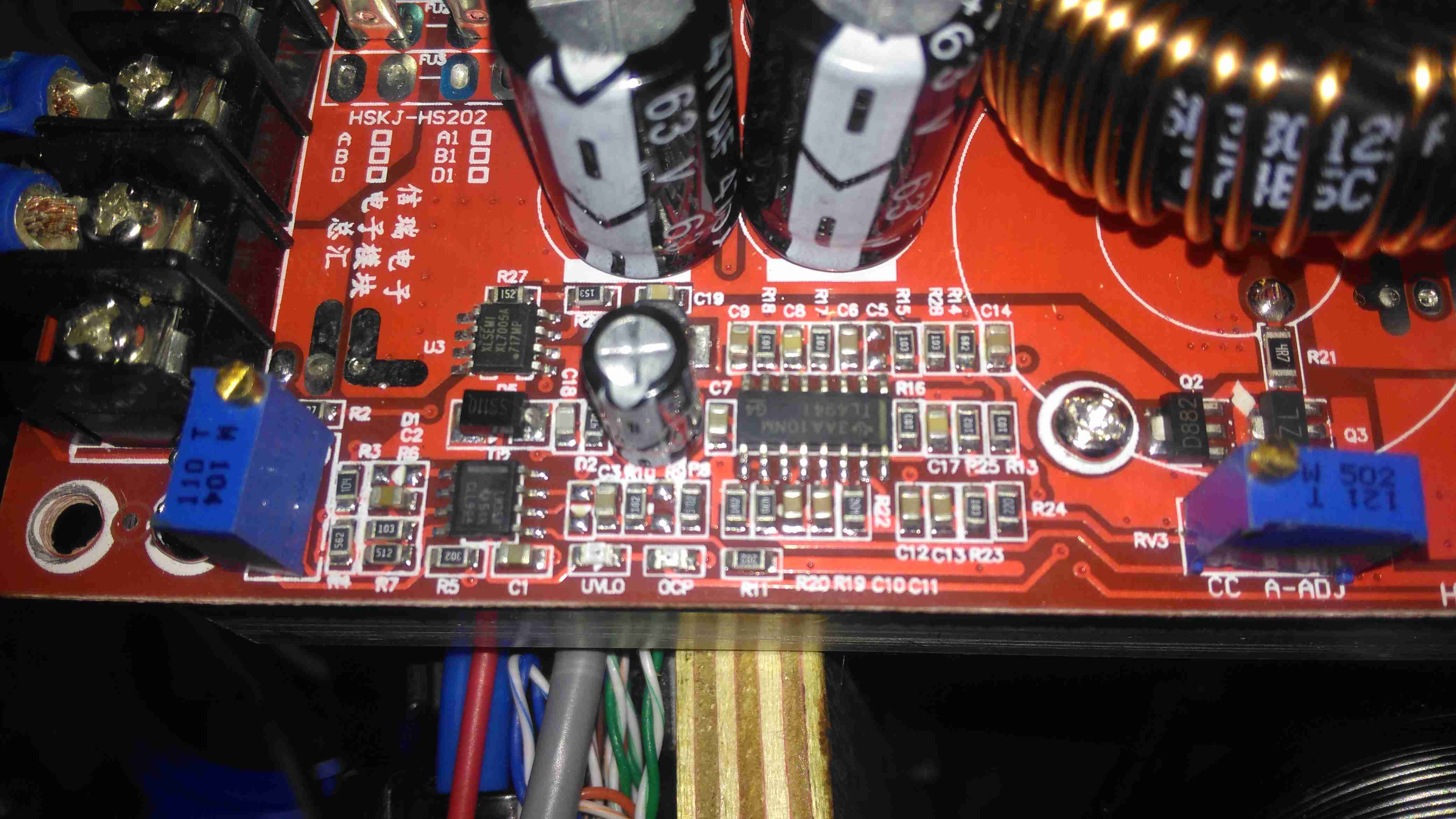
The switching IC on these converters is a TL494,with it’s surrounding support components, including a LM358 dual Op-Amp. Power for this lot is supplied from the input via a small DC-DC converter controlled by an XL Semi XL7001 Buck Converter IC. Some testing revealed that power was getting to the XL7001, but the output to the switching controller was at zero volts.

Inductor
Inductor

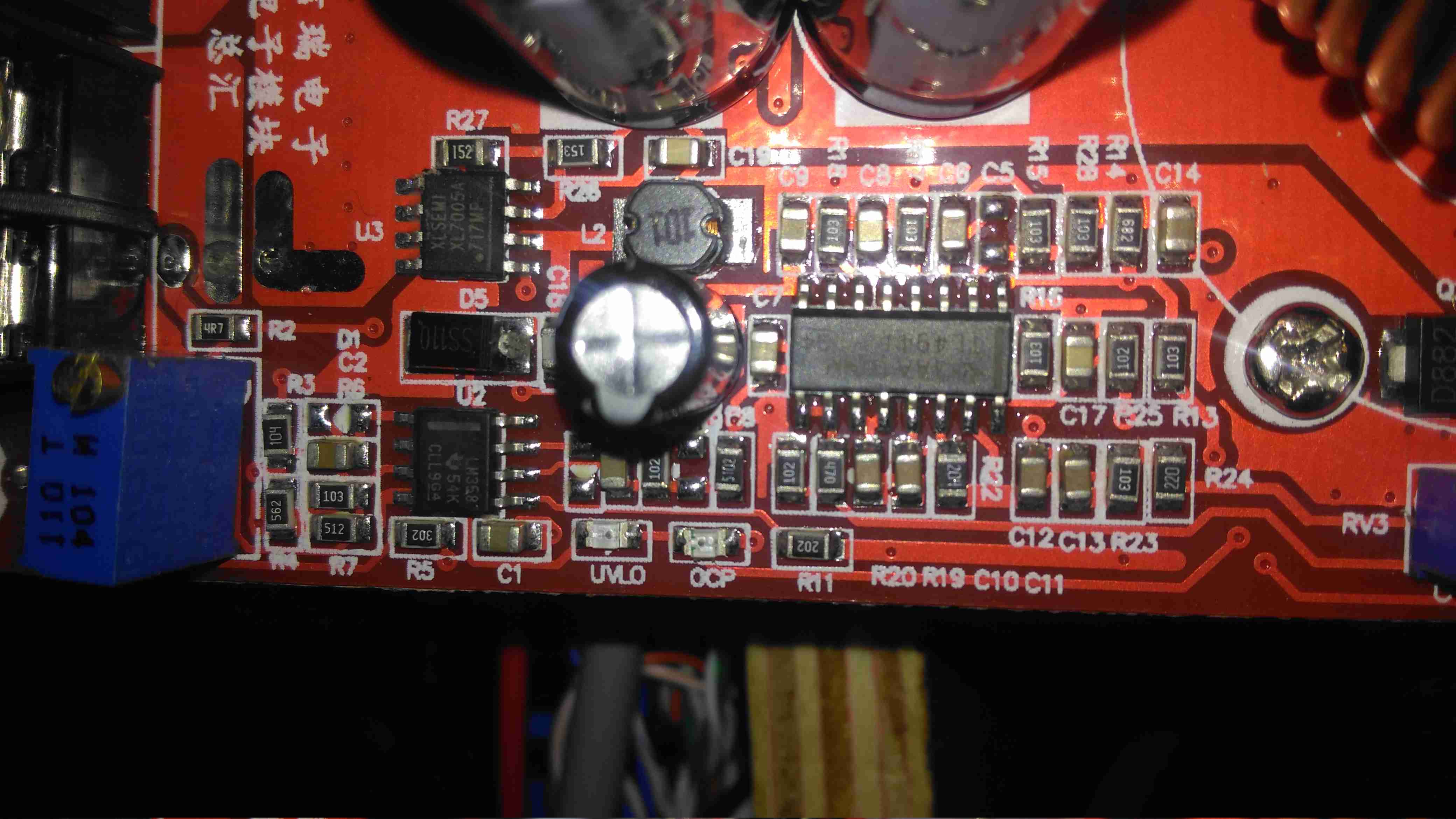
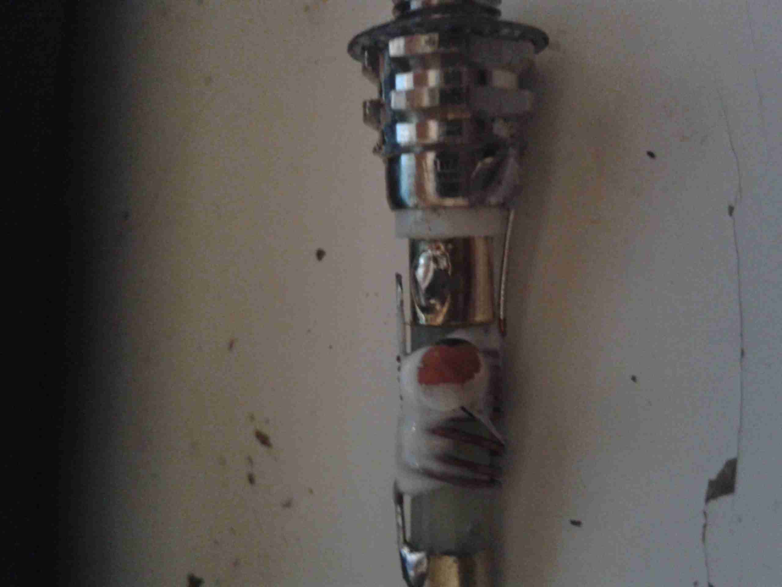
The 100µH inductor for this buck converter is hidden behind the output electrolytic, and a quick prod with a multimeter revealed this inductor to be open circuit. That would certainly explain the no-output situation. Luckily I had an old converter that was burned out. (Don’t try to pull anything near their manufacturer “rating” from these units – it’s utter lies, more about this below).

Donor Converter
Donor Converter

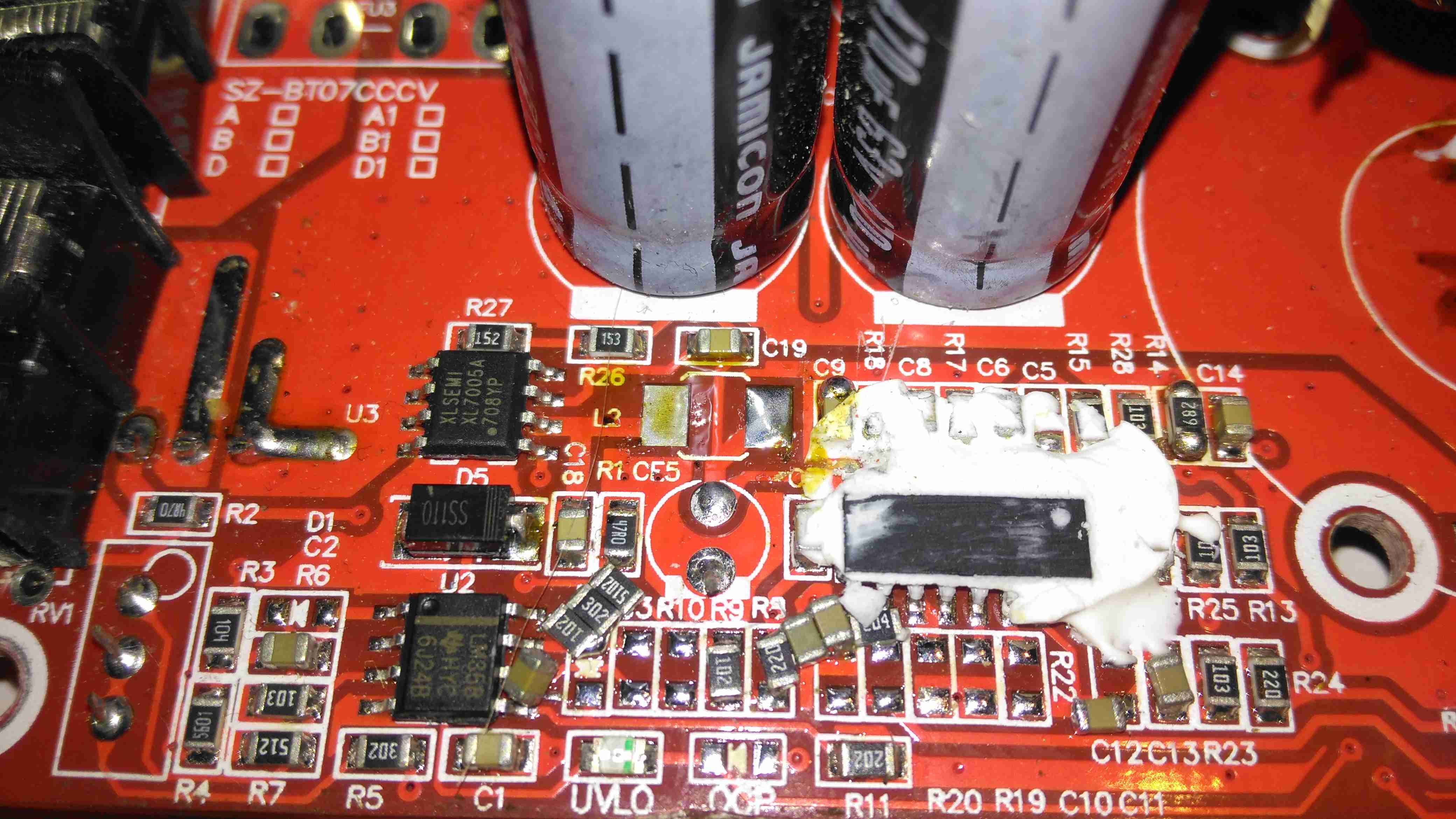
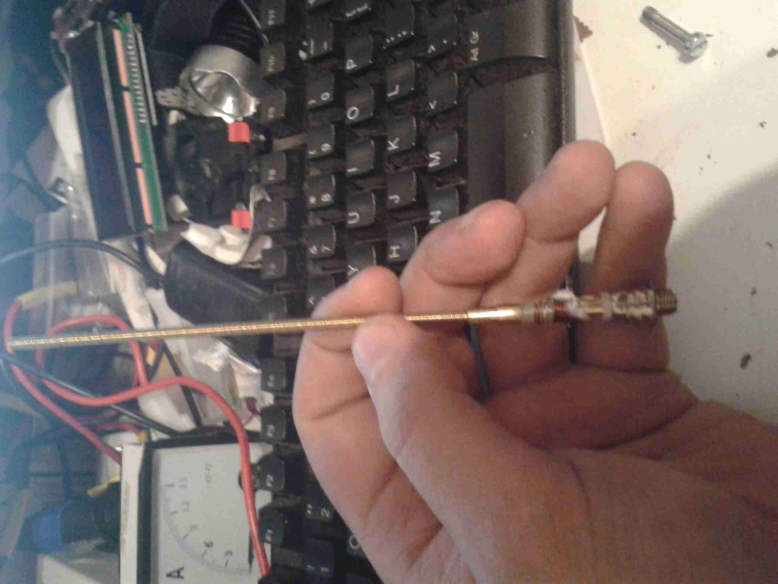
The good inductor from this donor unit has been desoldered here, it’s supposed to be L2. This one had a heatsink siliconed to the top of the TL494 PWM IC, presumably for cooling, so this was peeled off to give some access.
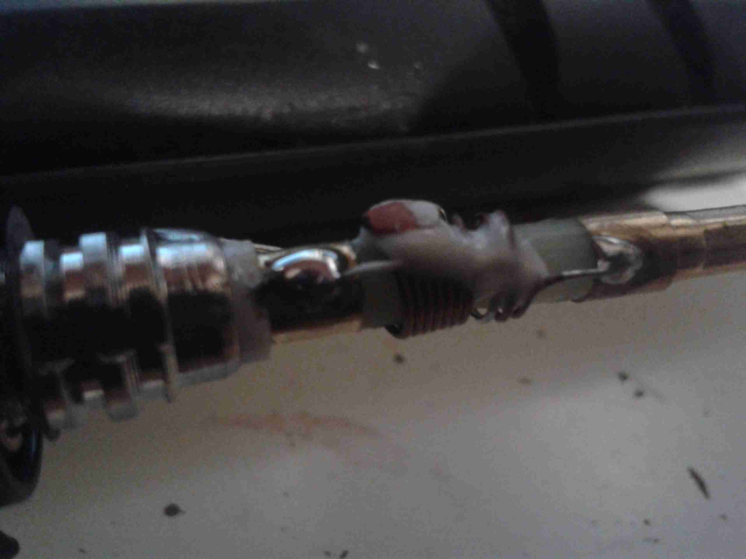
After this inductor was grafted into place on the dead converter, everything sprang to life as normal. I fail to see how this issue wouldn’t have been caught during manufacture, but they’re probably not even testing them before shipping to the distributor.
The sensational ratings are also utter crap – they quote 1.2kW max power, which at 12v input would be 100A. Their max input rating is given as 20A, so 240W max input power. Pulling this level of power from such a cheaply designed converter isn’t going to be reliably possible, the input terminals aren’t even rated to anywhere near 20A, so these would be the first to melt, swiftly followed by everything else. Some of these units come with a fan fitted from the factory, but these are as cheaply made as possible, with bearings made of cheese. As a result they seize solid within a couple of days of use.
Proper converters from companies like TDK-Lambda or muRata rated for these power levels are huge, with BOLTS for terminals, but they’re considerably more expensive. These Chinese units are handy though, as long as they are run at a power level that’s realistic.

Posted on Leave a comment

De La Rue Coin Counting Machine Followup – PSU Oddness

I did a little more digging into the PSU circuitry of the small coin counting machine, and it’s even more strange than I thought!
The part I originally thought was a transformer on the PSU board is in fact a DC-DC converter module!

DC-DC Converter
DC-DC Converter

Here’s the device after desoldering it from the PCB. It turns out that instead of a transformer, it’s an inductor.

Hiding Control Electronics

Underneath is the controller electronics, with an COB controller & the switching transistors are under a protective covering of silicone.

Mains Transformer
Mains Transformer

Driving this whole lot of PSU randomness is the mains transformer, with a secondary voltage of 35v.

The only reason I can think of that the manufacturer went to this much expense with the power supply is stability – a coin counting machine that miscounts due to power supply surges, sags & spikes wouldn’t be very much use. It’s not likely I’ll see anything similar again, unless I manage to get hold of something like medical grade equipment.

Posted on Leave a comment

Totally Wicked Forza / JoyeTech eVIC 60W Teardown

Display
Display

I’ve been a vaper now for many years, after giving up the evil weed that is tobacco. Here’s my latest acquisition in the vaping world, the JoyeTech eVIC 60W. This one is branded by Totally Wicked as the Forza VT60.

18650 Cell
18650 Cell

Powered by a single 18650 Li-Ion cell, this one is a Sony VTC4 series, 2100mAh.

Under the battery a pair of screws hold the electronics in the main cast alloy casing.

OLED Display
OLED Display

After removing the screws, the entire internal assembly comes out of the case, here’s the top of the PCB with the large OLED display in the centre.

USB Jack
USB Jack

On the right side of the board is the USB jack for charging & firmware updates. The adjustment buttons are also at this end.

Output
Output

On the left side of the board is the main output connector & the fire button. Unlike many eCigs I’ve torn down before, the wiring in this one is very beefy – it has to be to handle the high currents used with some atomizers – up to 10A.

PCB Reverse
PCB Reverse

Removing the board from the battery holder shows the main power circuitry & MCU. The aluminium heatsink is thermally bonded to the switching MOSFETs, a pair under each end. The switching inductor is under the gap in the centre of the heatsink.

DC-DC Converter
DC-DC Converter

A close up of the heatsink shows the very slim inductor under the heatsink.

Microcontroller
Microcontroller

The main MCU in this unit has a very strange part number, which I’ve been unable to find information on, but it’s probably 8081 based.

Posted on Leave a comment

Stock Baofeng Antenna Problems

Recently I’ve noticed my usual mobile rig, the Baofeng UV-5R, has had very poor receive, and non-existent transmit.

I did a power test on the radio, and confirmed it was still outputting it’s rated RF power. Trying another antenna proved that the radio was fine.

Time to tear down the antenna & see if it can be fixed!

Stock Antenna
Stock Antenna

Here’s the antenna, just the factory rubber duckie. As with all these antennas, they’re a compromise between size & their efficiency.

Naked Antenna!
Naked Antenna!

Giving a gentle pull to the antenna sheath while it’s attached to the radio allows it to come apart. The quality actually doesn’t look to bad. It’s very similar in construction to my Diamond X-30, just on a much smaller scale.

At the bottom of the antenna is the matching network, an inductor & ceramic disc capacitor. Here lies the problem with this antenna.

Dry Joint
Dry Joint

Here where the capacitor joins onto the feedpoint from the SMA connector, the solder joint has come away. This was a very poor joint to start with, and the solder hadn’t wetted the capacitor lead at all

After cleaning the joint, and applying some flux, a new joint was easily made with some Real Solder.

Repaired Joint
Repaired Joint

Here’s the joint freshly repaired, the antenna is now back to full working order. It even seems to work better than the others I have 🙂

Posted on Leave a comment

ZyXel WAP3205 Repair

Here is a ZyXel WAP3205 WiFi Access Point that has suffered a reverse polarity event, due to an incorrect power supply being used with the unit.

ZyXEL WAP3205
ZyXEL WAP3205

While most electronic gadgets are protected against reverse polarity with a blocking diode, this unit certainly wasn’t. Applying +12v DC the wrong way round resulted in this:

Blown Switchmode IC
Blown Switchmode IC (Fuzzy Focus)

That is the remains of the 3.3v regulator IC, blown to smithereens & it even attempted an arson attack. Luckily this was the only damaged component, & I was able to repair the unit by replacing the switching IC with a standalone regulator. (Replacing the IC would have been preferable, if there was anything left of it to obtain a part number from).

I scraped away the pins of the IC to clear the short on the input supply, removed the switching inductor, & tacked on an adjustable regulator module set to 3.3v. Luckily the voltage of the supply is handily marked on the PCB next to the circuit.

Replacement PSU
Replacement PSU

Replacement SMPS in place on top of the PCB. The output of the supply is connected to one of the pads of L4 (on my unit just an 0 ohm link), the +12v input is connected to the + rail side of C8 & C7 & the final ground connection is hooked in to the back of the barrel jack.

After this replacement, the unit booted straight up as if nothing had happened. All the logic is undamaged!

Makerplate
Makerplate
Posted on Leave a comment

Chicom “500W” ATX PSU

Cover Removed
Cover Removed

Here is a cheapo 500W rated ATX PSU that has totally borked itself, probably due to the unit NOT actually being capable of 500W. All 3 of the switching transistors were shorted, causing the ensuing carnage:

AC Input
AC Input

Here is the AC input to the PCB. Note the vapourised element inside the input fuse on the left. There is no PFC/filtering built into this supply, being as cheap as it is links have been installed in place of the RFI chokes.

Input Side
Input Side

Main filter capacitors & bridge rectifier diodes. PCB shows signs of excessive heating.

Filter Caps Removed
Filter Caps Removed

Filter capacitors have been removed from the PCB here, showing some cooked components. Resistor & diode next to the heatsink are the in the biasing network for the main switching transistors.

Heatsinks Removed
Heatsinks Removed

Heatsink has been removed, note the remaining pin from one of the switching transistors still attached to the PCB & not the transistor 🙂

Transformers
Transformers

Output side of the PSU, with heatsink removed. Main transformer on  the right, transformers centre & left are the 5vSB  transformer & feedback transformer.

Output Side
Output Side

Output side of the unit, filter capacitors, choke & rectifier diodes are visible here attached to their heatsink.

Comparator
Comparator

Comparator IC that deals with regulation of the outputs & overvoltage protection.

Posted on Leave a comment

Southwestern Bell Freedom Phone

Phone
Phone

This is an old cordless landline phone, with dead handset batteries.

Handset Radio Board
Handset Radio Board

Here’s the handset with the back removed. Shown is the radio TX/RX board, underneath is the keyboard PCB with the speaker & mic. All the FM radio tuning coils are visible & a LT450GW electromechanical filter.

Handset Radio Board Bottom

Radio PCB removed from the housing showing the main CPU controlling the unit, a Motorola MC13109FB.

Keypad Board
Keypad Board

The keypad PCB, with also holds the microphone & speaker.

Handset Keypad Board Bottom

Bottom of the keypad board, which holds a LSC526534DW 8-Bit µC & a AT93C46R serial EEPROM for phone number storage.

Base Main Board
Base Main Board

Here’s the base unit with it’s top cover removed. Black square object on far right of image is the microphone for intercom use, power supply section is top left, phone interface bottom left, FM radio is centre. Battery snap for power backup is bottom right.

Power Supply Section

PSU section of the board on the left here, 9v AC input socket at the bottom, with bridge rectifier diodes & main filter capacitor above. Two green transformers on the right are for audio impedance matching. Another LT450GW filter is visible at the top, part of the base unit FM transceiver.

ICs
ICs

Another 8-bit µC, this time a LSC526535P, paired with another AT93C46 EEPROM. Blue blob is 3.58MHz crystal resonator for the MCU clock. The SEC IC is a KS58015 4-bit binary to DTMF dialer IC. This is controlled by the µC.

Base Main Board Bottom

Underside of the base unit Main PCB, showing the matching MC13109FB IC for the radio functions.