Posted on Leave a comment

Official Raspberry Pi 7″ Touch LCD

Raspberry Pi LCD
Raspberry Pi LCD

Finally the Raspberry Pi Foundation have released an official LCD for the DSI connector on the Pi. When these were announced, I placed an order straight away, but due to demand it’s taken quite a while for it to arrive in the post.

Interface PCB
Interface PCB

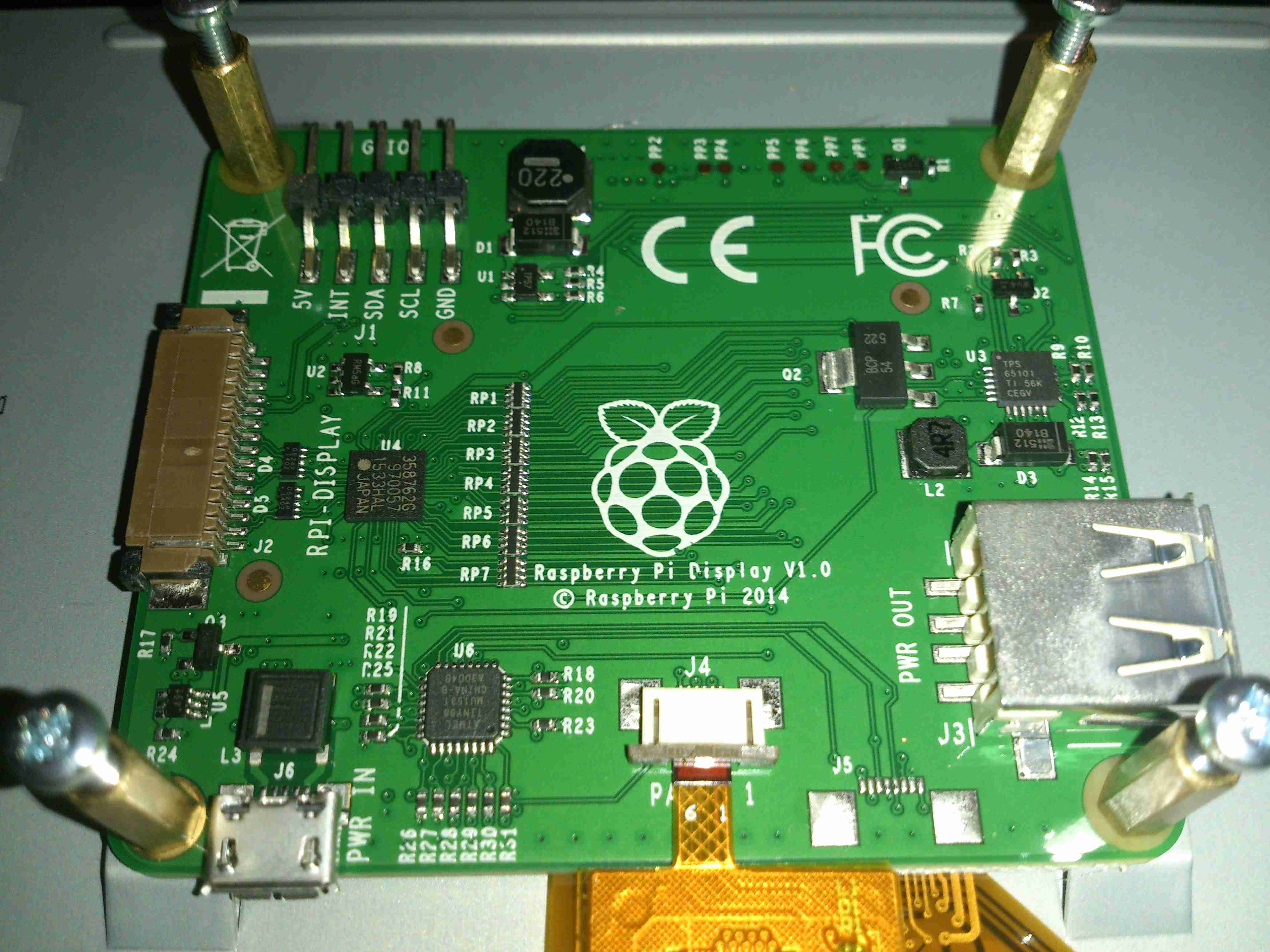
The LCD itself is an RGB panel, to interface the Pi via the MIPI DSI port, some signal conversion is required. A small PCB is mounted on the back of the LCD to do this conversion. It also handles the power supply rails required by the LCD itself & interfacing the touch screen.

LCD Power Supply
LCD Power Supply

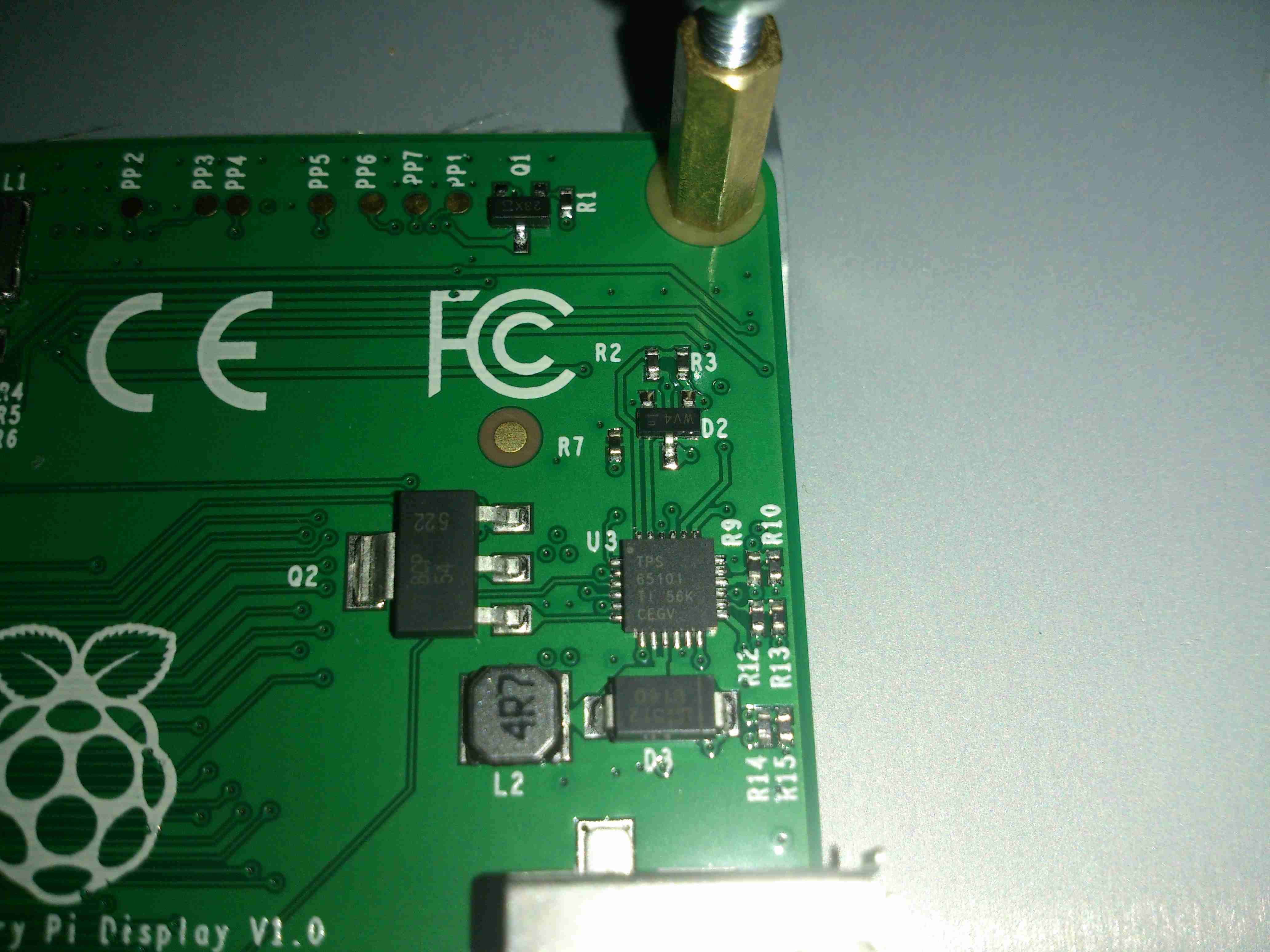
Taking care of the power supply is a Texas Instruments TPS65101 triple output LCD power supply IC. This also has a built in linear regulator to supply 3.3v for the rest of the circuitry on board. The large transistor to the left of the IC is the pass transistor for this regulator.

Main Controller
Main Controller

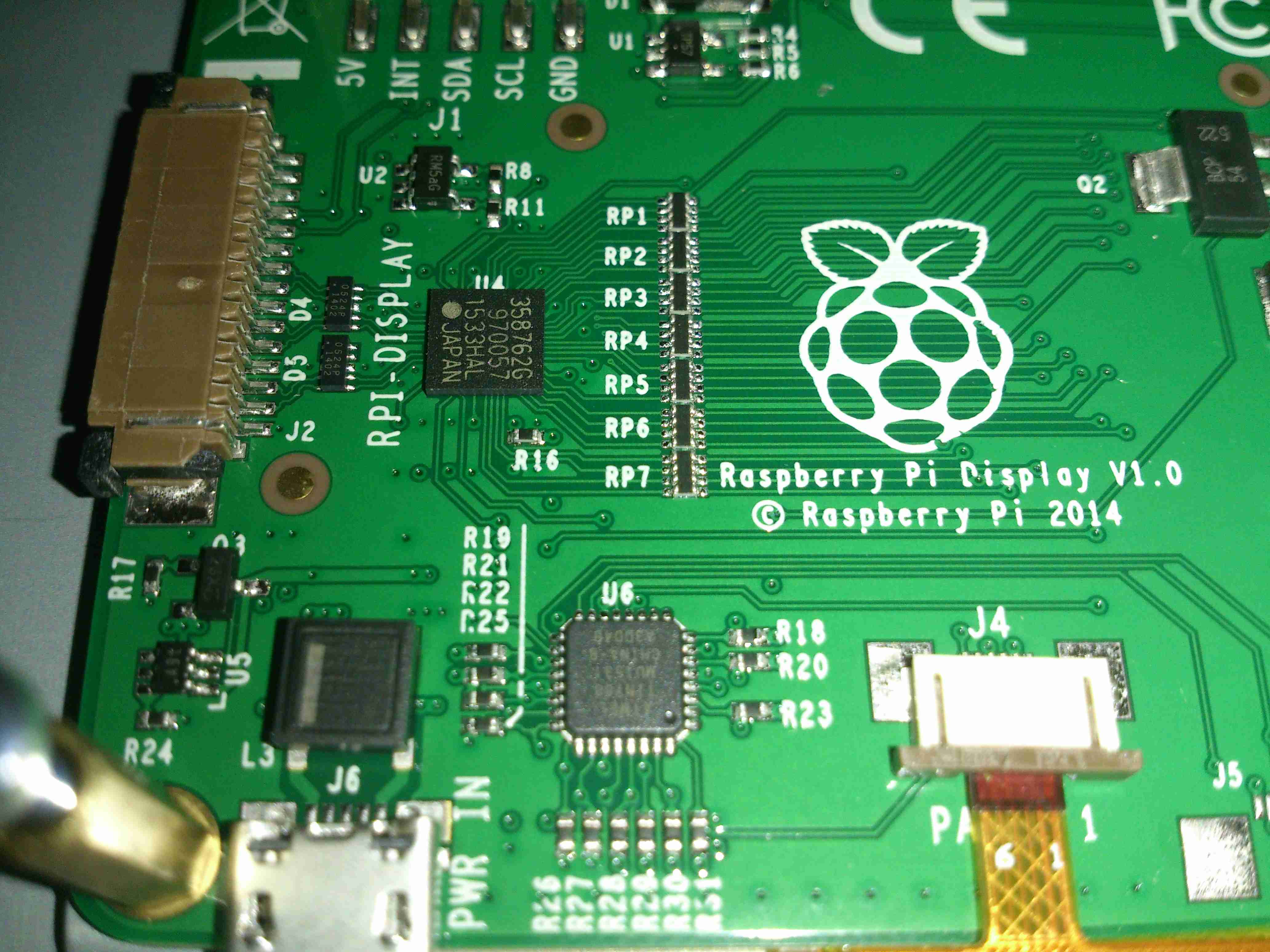
The video signal comes in on the FFC connector on the left, into the BGA IC. I’ve not managed to identify this component, but it’s doing the conversion from serial video from the Pi to parallel RGB for the LCD.
There’s also an Atmel ATtiny88 on the board below the main video conversion IC, not sure what this is doing.
The touch controller itself is mounted on the flex of the LCD, in this case it’s a FT5406.

Raspberry Pi LCD
Raspberry Pi LCD

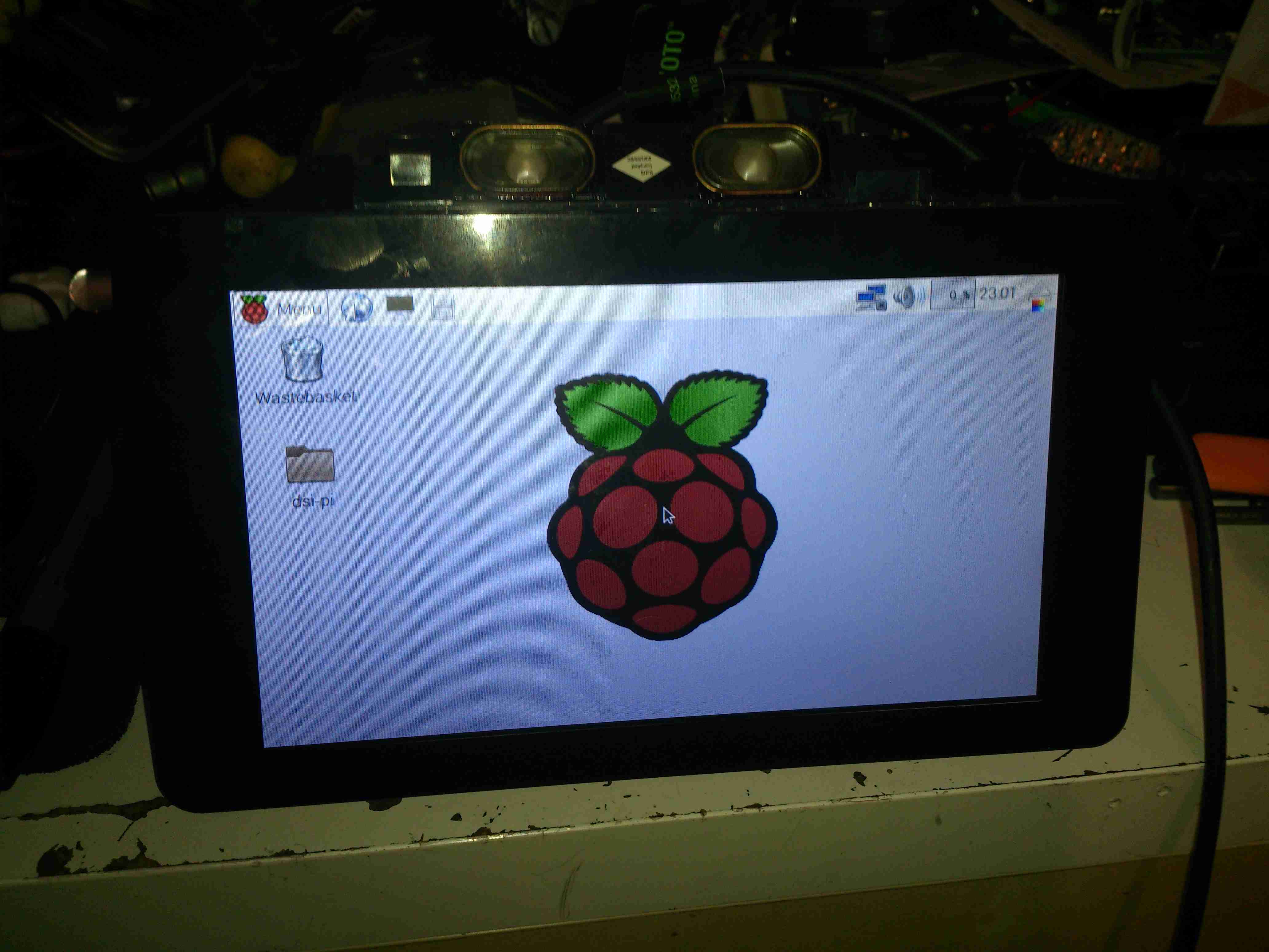
Here’s the LCD in operation. It’s not the highest resolution out there, but it leaves the GPIO & HDMI ports free for other uses.

Pi Mounted
Pi Mounted

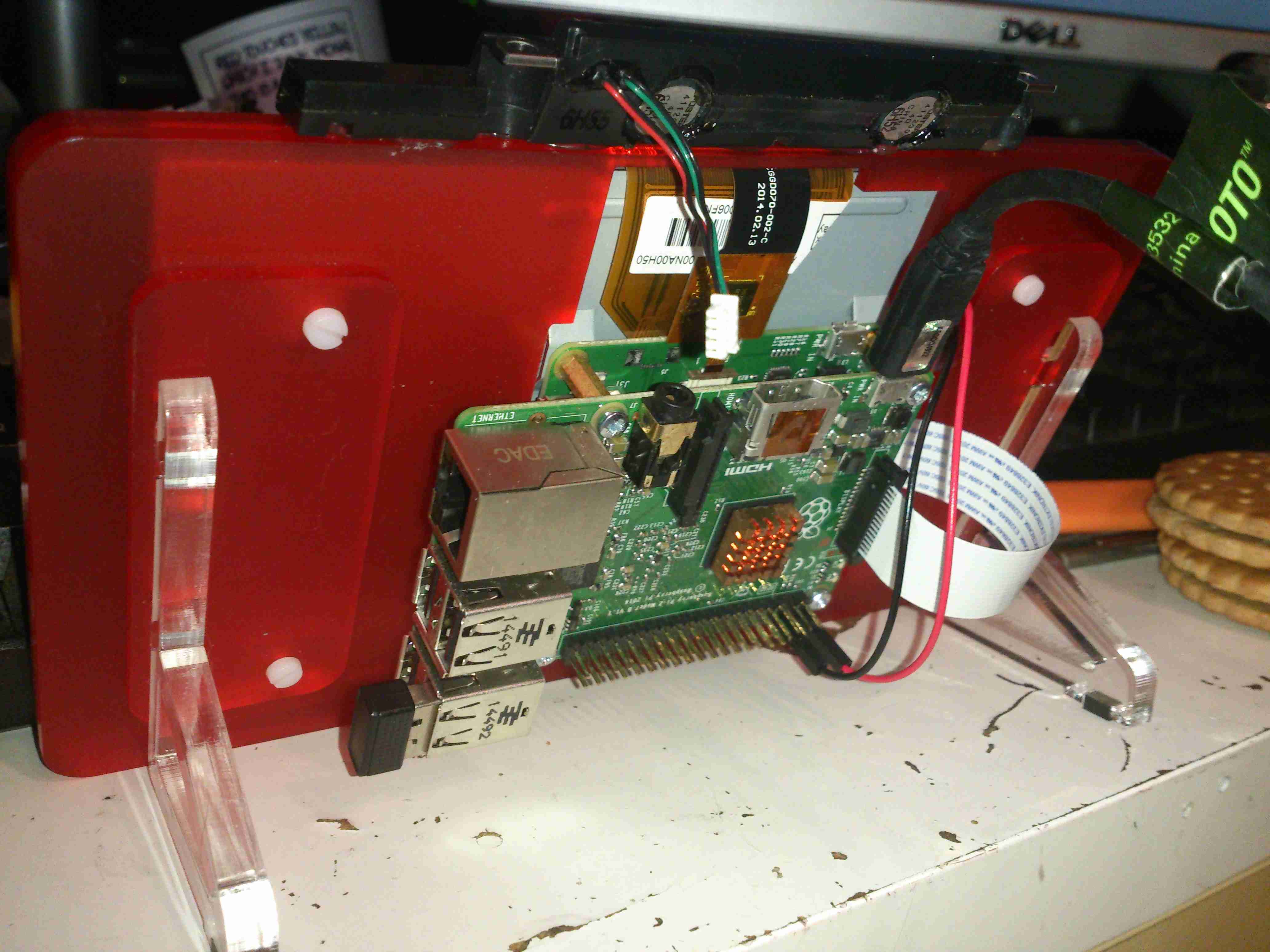
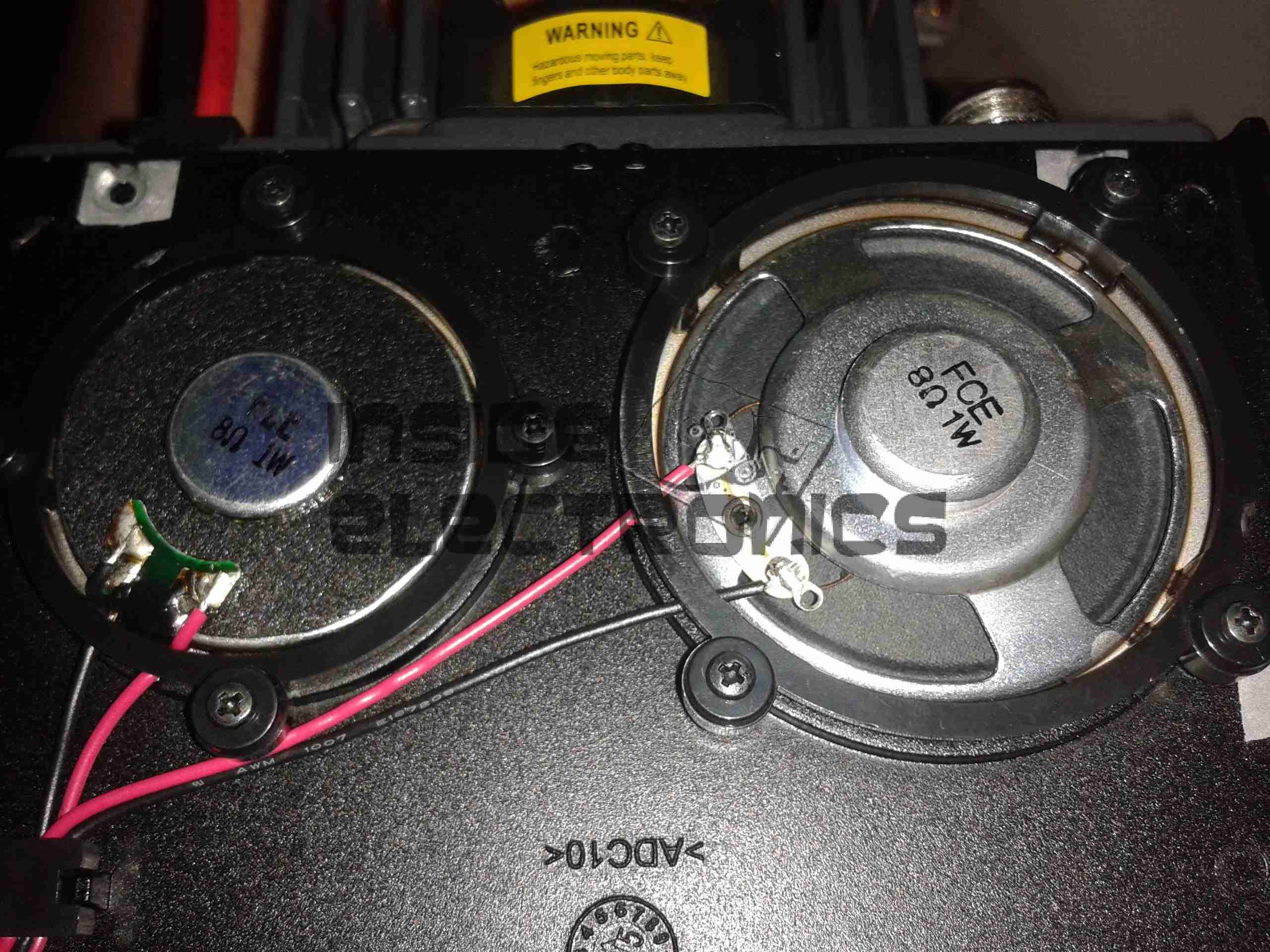
The Pi screws to the back of the LCD & is connected with a flat flex cable & a pair of power jumpers. I’ve added a couple of small speakers to the top edge of the LCD to provide sound. (More to come on this bit).


Posted on Leave a comment

nbTanya Louise – New TV Antenna

Here’s the final instalment of the new high gain TV antenna & it’s masthead amplifier.

High Gain Antenna
High Gain Antenna

Here’s the new antenna on it’s removable mast. This apparently will give 13db of gain over the old antenna. The masthead amplifier box is mounted just below.

Amplifier
Amplifier

Here’s the amplifier just below the antenna. I do hope the seals on this hold against the weather! The amplifier inside isn’t protected at all.

Amplifier Module
Amplifier Module

Here’s the module itself. This is powered by +12v injected into the coax with the power supply I previously modified. F-type connectors are used. (I don’t like these connector types, their lack of a true centre pin is poor design in my opinion).

Here’s the power supply, mounted behind the TV where the cable comes through the hull.

PSU
PSU
Amplifier PCB
Amplifier PCB

Here’s the inside of the amplifier module. It’s very simple, with some input filtering to block out 4G mobile signals, and a single amplifier transistor.


Posted on Leave a comment

Wouxun KG-UV950P Teardown & Analysis

Following on from my review, here are some internal views & detail on the components used in this radio. Below is an overview of the main PCB with the top plate removed from the radio.

Cover Removed
Cover Removed
RF Final Amplifier Stage

Most visible are these MOSFETs, which are Mitsubishi RD70HVF1 VHF/UHF power devices.  Rated for a maximum of 75W output power at 12.5v (absolute maximum of 150W, these are used well within their power ratings. They are joined to the PCB with heavy soldering, with bypass caps tacked right on to the leads.

RF Pre Drivers
RF Pre Drivers

Here is the RF pre-driver stage, with intermediate transistors hidden under the small brass heatspreader.

Power Section
Power Section

In the top left corner of the radio, near the power input leads, is the power supply & audio amplifier section. Clearly visible are the pair of LA4425A 5W audio power amplifier ICs, these drive the speakers on the top of the radio. Either side of these parts are a 7809 & a 7805 – both linear regulators providing +9v & +5v logic supplies respectively. The large TO220 package device is a KIA378R08PI 3A LDO regulator with ON/OFF control, this one outputs +8v. Just visible in the top right corner are the sockets for the speaker connections.

DTMF Circuits
DTMF Circuits

Here are the two ICs for dealing with DTMF tones, they are HM9170 receivers.

Glue Logic
Glue Logic

In the corner next to the interface jack, there are some CD4066B Quad Bilateral switches. These make sense since the interface jack has more than a single purpose, these will switch signals depending on what is connected.

RF Section
RF Section

Here are visible the RF cans for the oscillators, the crystals visible next to the can at the top. The shields are soldered on, so no opening these unfortunately.
Also visible in this image is a CMX138A Audio Scrambler & Sub-Audio Signalling processor. This IC deals with the Voice Inversion Scrambling feature of the radio, & processes the incoming audio before being sent to the modulator.

Output Filter Network

Shown here is the RF output filter network, this radio uses relays for switching instead of PIN diodes, I imagine for cost reasons. The relay closest to the RF output socket has had a slight accident 🙂 This is slated to be replaced soon.

RF Output Jack
RF Output Jack

Finally, the RF output jack.

Audio Speakers
Audio Speakers

Here the speakers are shown, attached to the bottom of the top plate. They are both rated 8Ω 1W.

Posted on Leave a comment

555 Flyback Driver

Flyback Secondary Waveform
Board Layout
Board Layout

Here is a simple 555 timer based flyback transformer driver, with the PCB designed by myself for some HV experiments. Above is the Eagle CAD board layout.

The 555 timer is in astable mode, generating a frequency from about 22kHz to 55kHz, depending on the position of the potentiometer. The variable frequency is to allow the circuit to be tuned to the resonant frequency of the flyback transformer in use.

This is switched through a pair of buffer transistors into a large STW45NM60 MOSFET, rated at 650v 45A.

Input power is 15-30v DC, as the oscillator circuit is fed from an independent LM7812 linear supply.

Provision is also made on the PCB for attaching a 12v fan to cool the MOSFET & linear regulator.

Initial Board
Initial Board

Board initially built, with the heatsink on the linear regulator fitted. I used a panel mount potentiometer in this case as I had no multiturn 47K pots in stock.

PCB Traces
PCB Traces

Bottom of the PCB. The main current carrying traces have been bulked up with copper wire to help carry the potentially high currents on the MOSFET while driving a large transformer.
This board was etched using the no-peel toner transfer method, using parchement paper as the transfer medium.

MOSFET Heatsinked
MOSFET Heatsinked

Main MOSFET now fitted with a surplus heatsink from an old switchmode power supply. A Fan could be fitted to the top of this sink to cope with higher power levels.

Gate Drive Waveform
Gate Drive Waveform

This is the gate drive waveform while a transformer is connected, the primary is causing some ringing on the oscillator. The waveform without an attached load is a much cleaner square wave.

Flyback Secondary Waveform

I obtained a waveform of the flyback secondary output by capacitively coupling the oscilloscope probe through the insulation of the HT wire. The pulses of HV can be seen with the decaying ringing of the transformer between cycles.

Corona Discharge
Corona Discharge
Arc Discharge
Arc Discharge

Corona & arc discharges at 12v input voltage.

Download the Eagle schematic files here: [download id=”5561″]

Posted on Leave a comment

Amano PIX 3000x Timeclock

Front
Front

This is a late 90’s business timeclock, used for maintaining records of staff working times, by printing the time when used on a sheet of card.

Front Internal
Front Internal

Here is the top cover removed, which is normally locked in place to stop tampering. The unit is programmed with the 3 buttons & the row of DIP switches along the top edge.

Instructions
Instructions

Closeup of the settings panel, with all the various DIP switch options.

CPU & Display
CPU & Display

Cover plate removed from the top, showing the LCD & CPU board, the backup battery normally fits behind this. The CPU is a 4-bit microcontroller from NEC, with built in LCD driver.

PSU & Drivers
PSU & Drivers

Power Supply & prinhead drivers. This board is fitted with several NPN Darlington transistor arrays for driving the dox matrix printhead.

Printhead
Printhead

Printhead assembly itself. The print ribbon fits over the top of the head & over the pins at the bottom. The drive hammers & solenoids are housed in the circular top of the unit.

Printhead Bottom
Printhead Bottom

Bottom of the print head showing the row of impact pins used to create the printout.

2013-02-13 18.00.09Bottom of the solenoid assembly with the ribbon cable for power. There are 9 solenoids, to operate the 9 pins in the head.

Return Spring
Return Spring

Top layer of the printhead assembly, showing the leaf spring used to hold the hammers in the correct positions.

Hammers
Hammers

Hammer assembly. The fingers on the ends of the arms push on the pins to strike through the ribbon onto the card.

Solenoids
Solenoids

The ring of solenoids at the centre of the assembly. These are driven with 3A darlington power arrays on the PSU board.

Gearbox Internals
Gearbox Internals

There is only a single drive motor in the entire unit, that both clamps the card for printing & moves the printhead laterally across the card. Through a rack & pinion this also advances the ribbon with each print.


Posted on Leave a comment

Raspberry Pi GPIO Experiment Board Improvements

First Mods
First Mods

Here are the first set of mods & improvements to the RasPi Experiment board. Instead of the solder-point experiment space, I have added a standard mini-breadboard, even though it’s a little too long to fit on the board properly.

In the DIP breakout, is a MAX232 TTL-RS232 interface IC, useful for interfacing directly to the Pi’s UART, made available on the GPIO breakout. I will be hardwiring the MAX232 IC into the GPIO port, & fitting headers to the relevant pins on the IC breakout to make interfacing to the Pi easier.

All the MAX232 requires to operate are a 5v supply & 4 1µF capacitors.

The new TO220 device next to the breadboard is a TIP121 darlington power transistor.This is rated at 80v 5A continuous. Useful for driving large loads from a GPIO output.


More to come soon!

Posted on Leave a comment

PSi 150 Power Inverter

Front
Front

This is a small 120W power inverter, intended for small loads such as lights, fans, small TVs & laptop computers.

End Cover
End Cover

End cover of the unit, 12v DC input cord at the top, power switch & indicator LEDs at the bottom.

Mains Output
Mains Output

Opposite end of the unit, with the standard 240v AC 50Hz Mains output socket.

Cover Removed
Cover Removed

Cover removed from the top of the unit. Main power transformer is visible in the centre here, MOSFET bank is under the steel clamp on the left, the aluminium case forms the heatsink.

PWM Controllers
PWM Controllers

On the right is a KA3525 switchmode PWM controller & on the left is a LM324N quad Op-Amp IC. The buzzer on the far left is for the low battery warning.

PCB Removed
PCB Removed

PCB removed from the casing, with the MOSFET bank on the right hand side. Two potentiometers in the centre of the board tweak the frequency of the switcher & the output voltage.


Posted on Leave a comment

Chicom “500W” ATX PSU

Cover Removed
Cover Removed

Here is a cheapo 500W rated ATX PSU that has totally borked itself, probably due to the unit NOT actually being capable of 500W. All 3 of the switching transistors were shorted, causing the ensuing carnage:

AC Input
AC Input

Here is the AC input to the PCB. Note the vapourised element inside the input fuse on the left. There is no PFC/filtering built into this supply, being as cheap as it is links have been installed in place of the RFI chokes.

Input Side
Input Side

Main filter capacitors & bridge rectifier diodes. PCB shows signs of excessive heating.

Filter Caps Removed
Filter Caps Removed

Filter capacitors have been removed from the PCB here, showing some cooked components. Resistor & diode next to the heatsink are the in the biasing network for the main switching transistors.

Heatsinks Removed
Heatsinks Removed

Heatsink has been removed, note the remaining pin from one of the switching transistors still attached to the PCB & not the transistor 🙂

Transformers
Transformers

Output side of the PSU, with heatsink removed. Main transformer on  the right, transformers centre & left are the 5vSB  transformer & feedback transformer.

Output Side
Output Side

Output side of the unit, filter capacitors, choke & rectifier diodes are visible here attached to their heatsink.

Comparator
Comparator

Comparator IC that deals with regulation of the outputs & overvoltage protection.