Posted on Leave a comment

Anker PowerPort Speed 5 12v DC Conversion

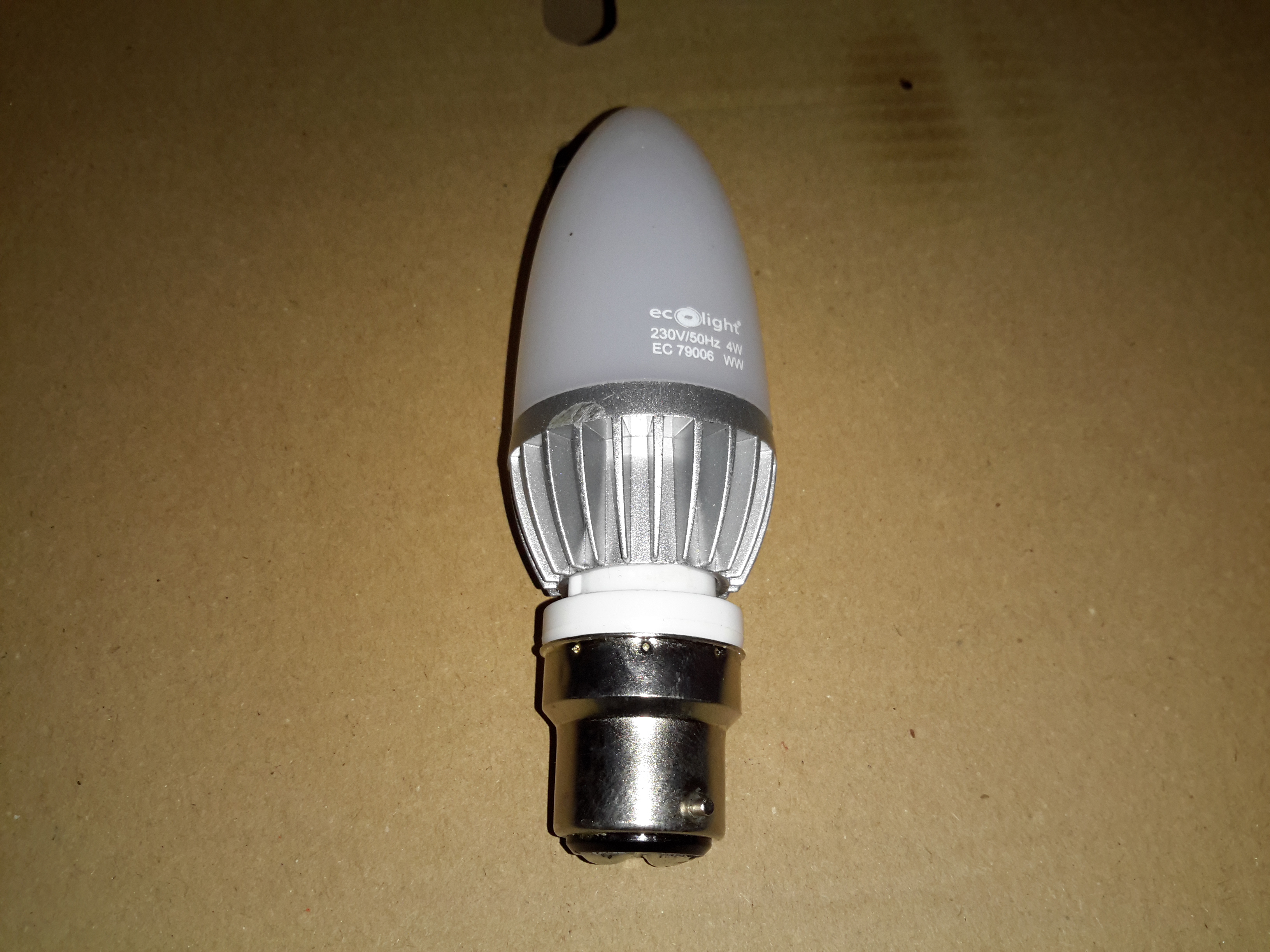
A few months ago I did a teardown on this Anker PowerPort Speed 5 USB charger, but I didn’t get round to detailing the conversion to 12v I had to do, so I’ll get to that now I’ve got a couple more to convert over.

Power Module
Power Module

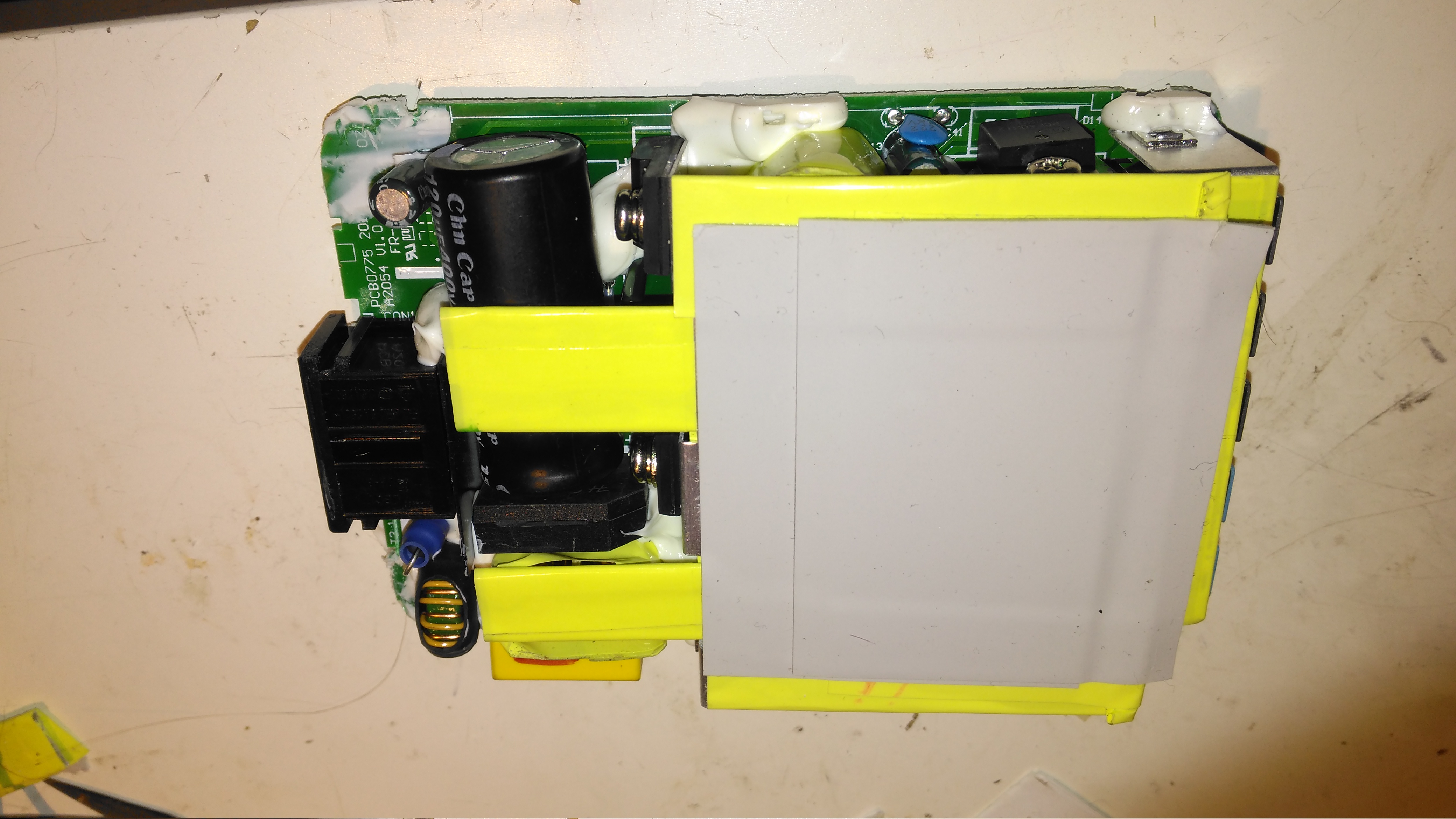
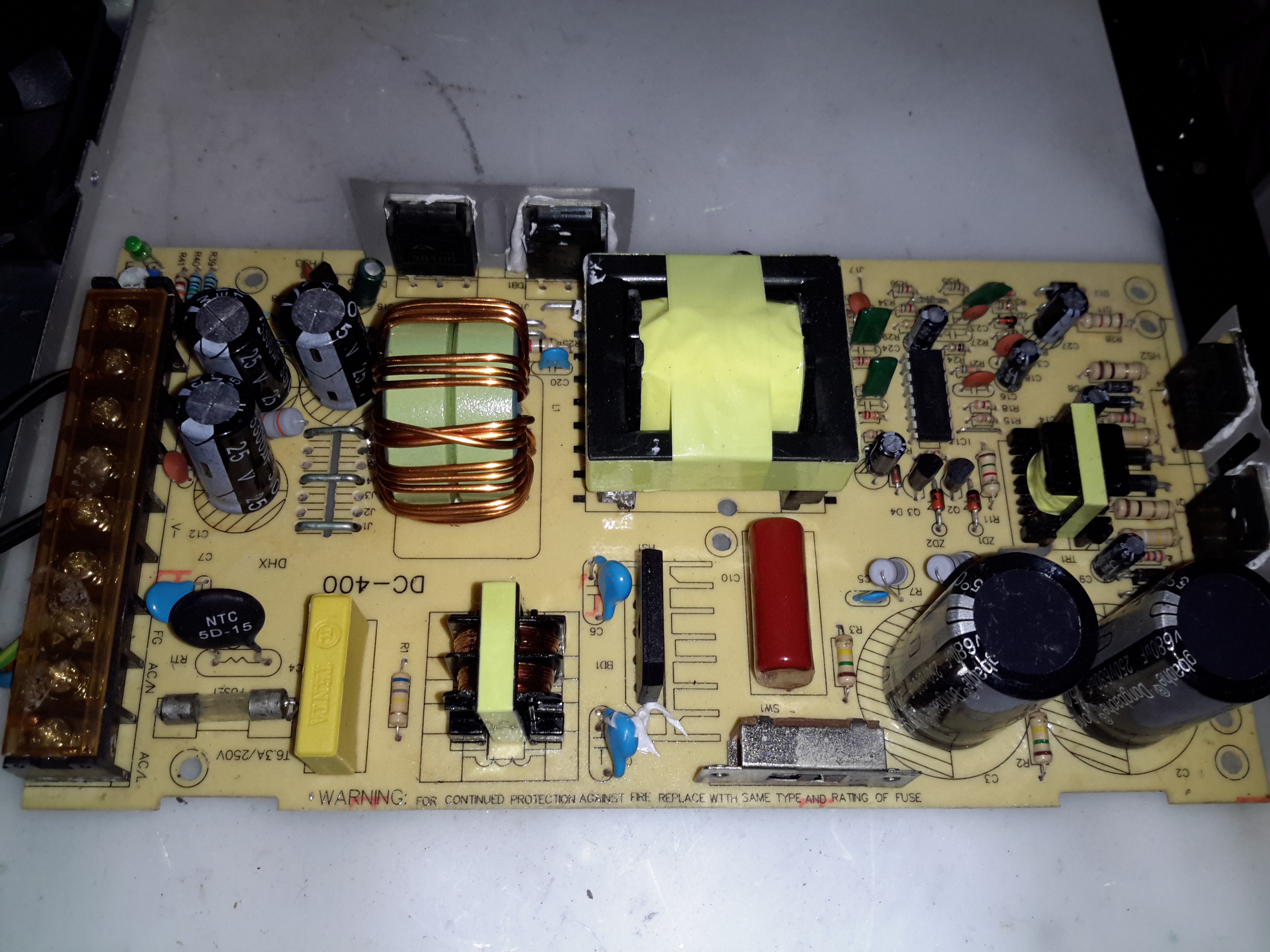
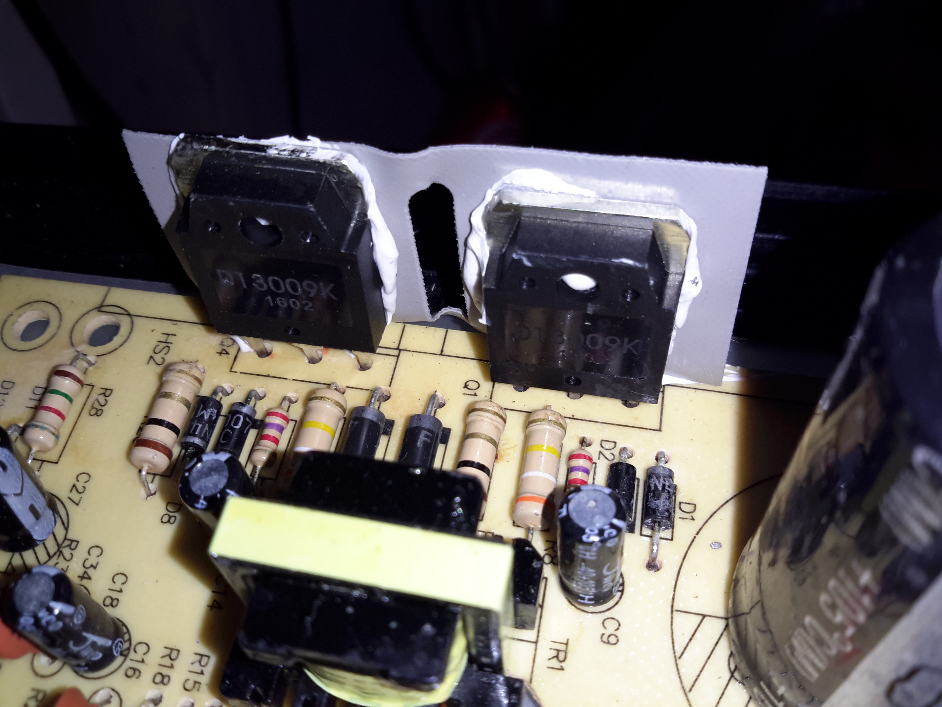
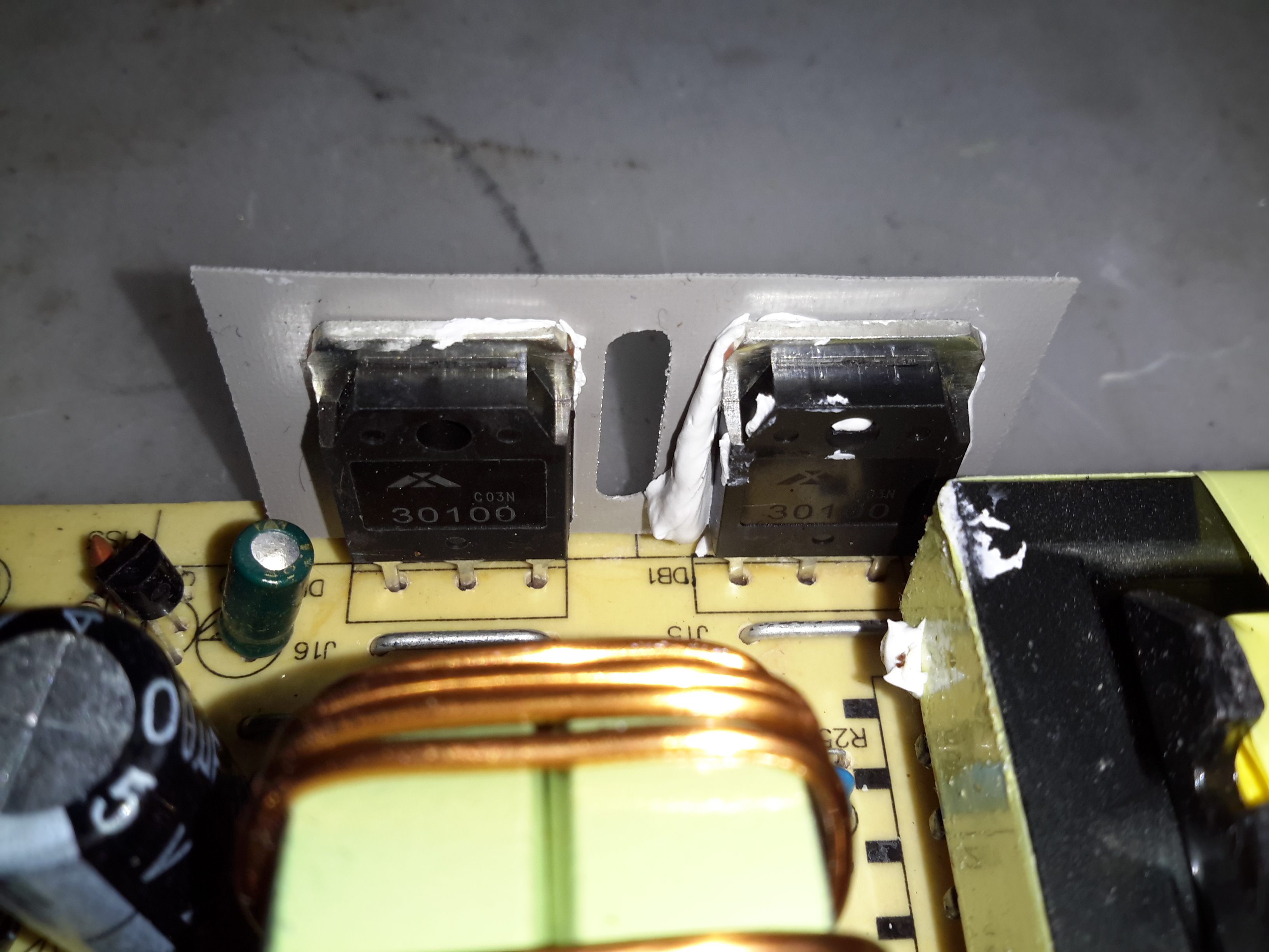
Here’s the internals of the Anker charger once I’ve removed the casing – which like many things these days, is glued together. (Joints can be cracked with a screwdriver handle without damaging the case). There’s lots of heatsinking in here to cool the primary side switching devices & the pot core transformers, so this is the first thing to get removed.

Heatsink Removed
Heatsink Removed

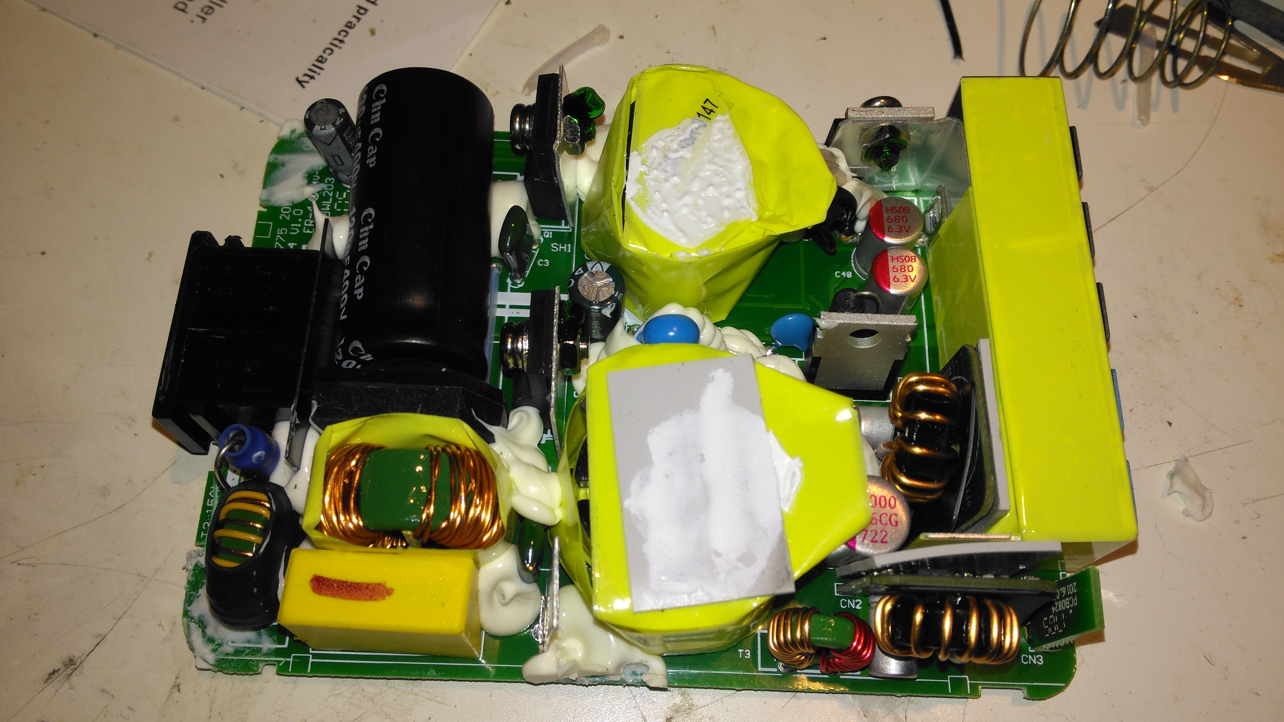
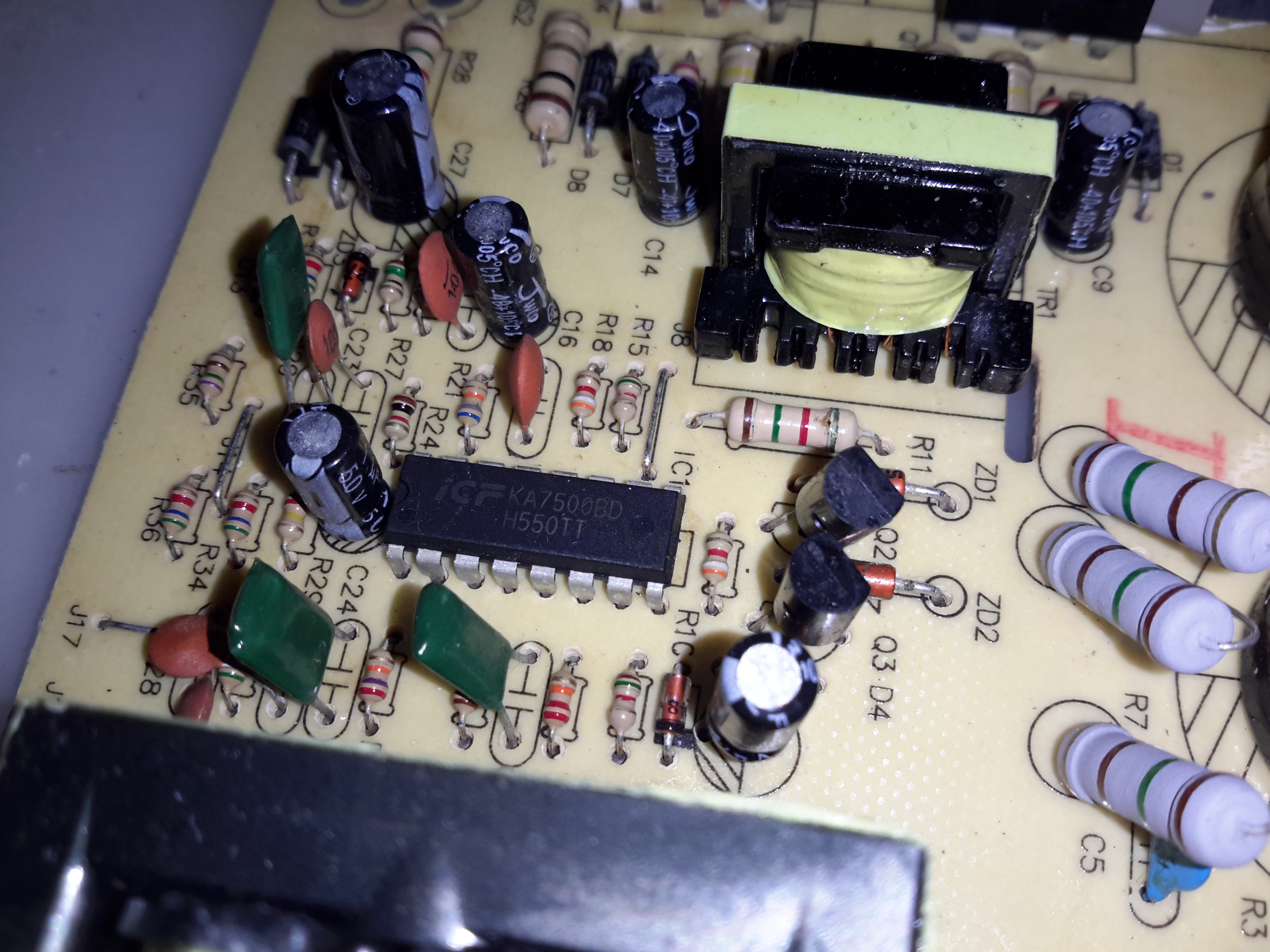
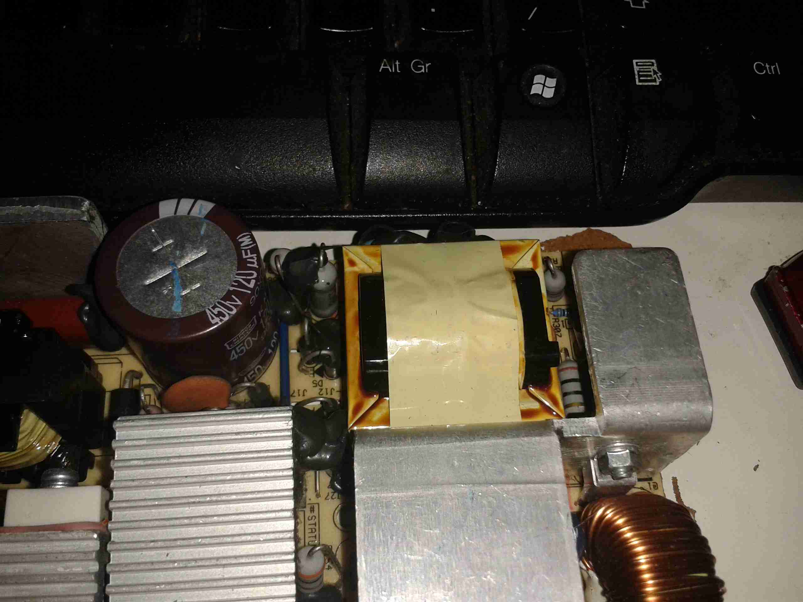
Once the heatsink has been removed, the pot core transformers are visible, wrapped in yellow tape. There’s some more heatsink pads & thermal grease here, to conduct heat better. The transformers, primary side switching components & input filter capacitor have to go.

Primary Side Components Removed

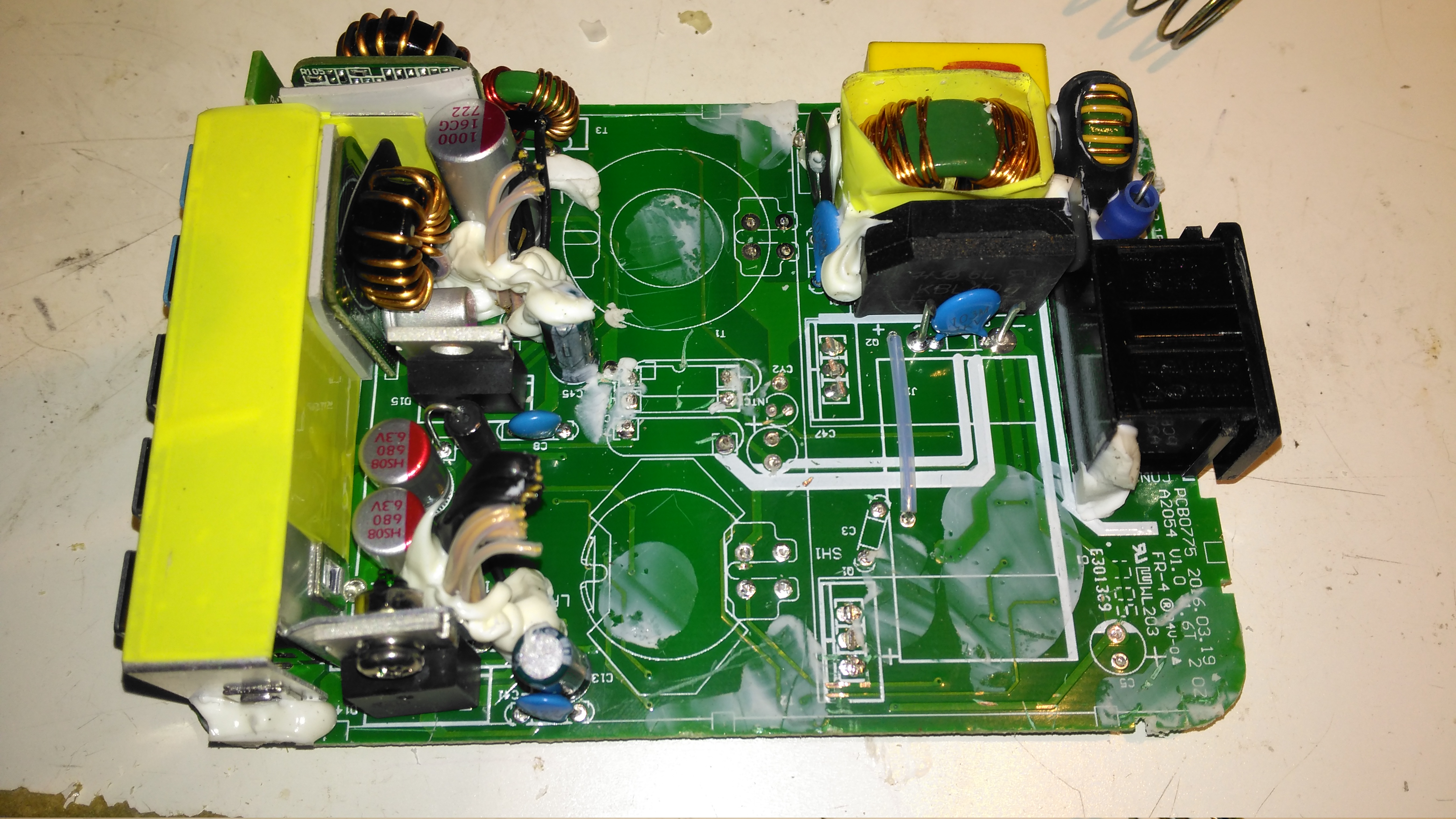
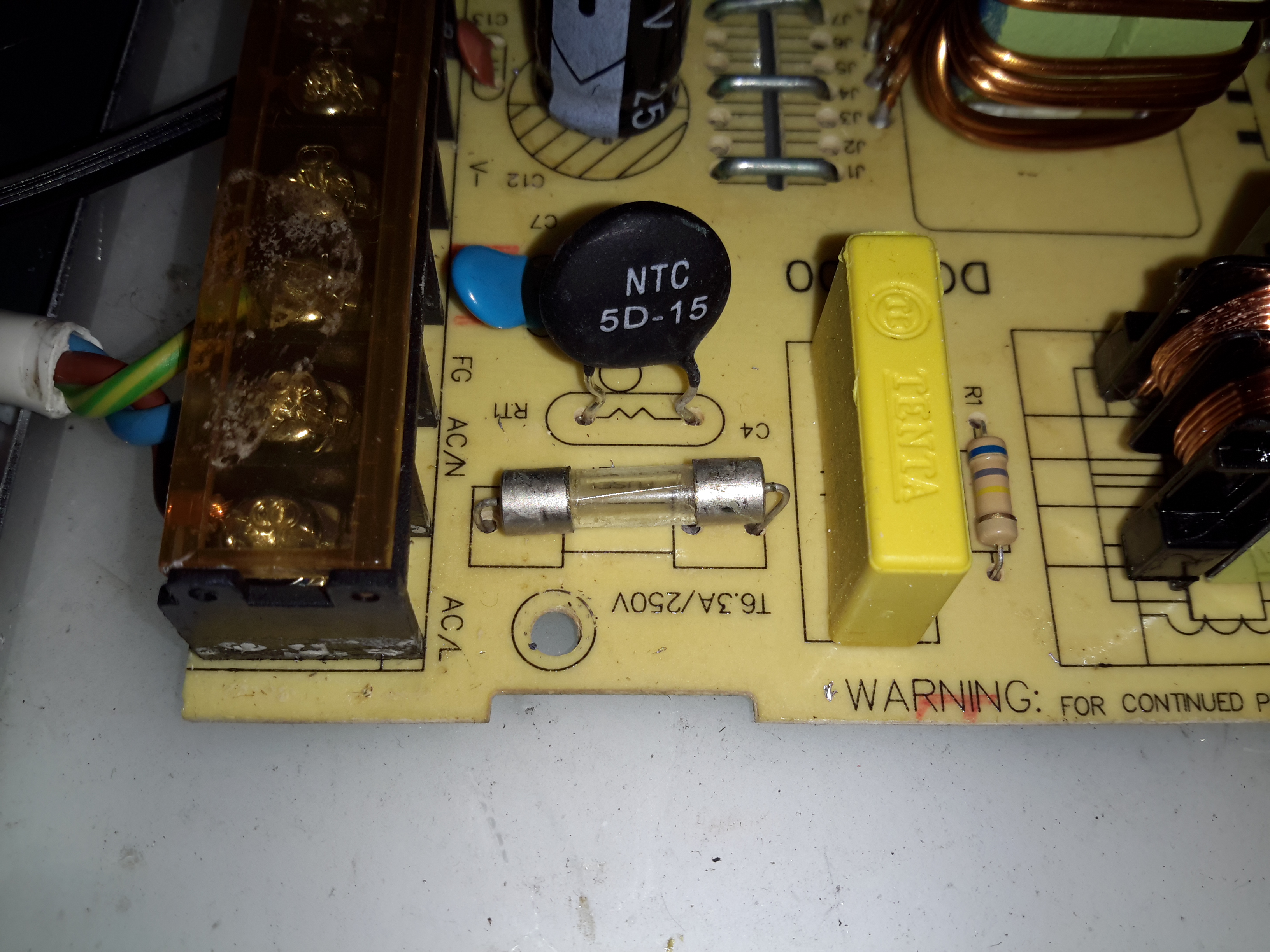
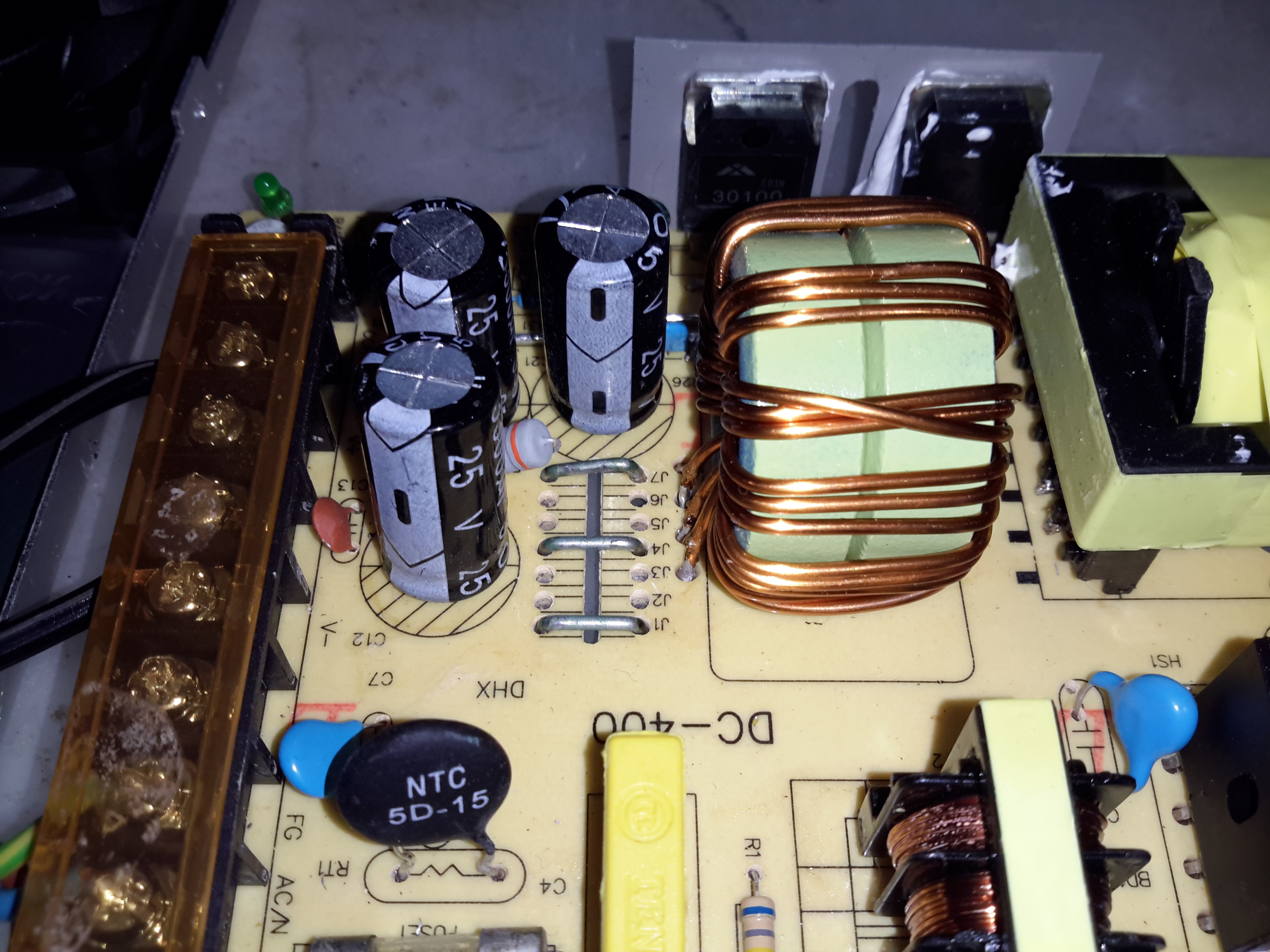
Here’s the PCB once all the now redundant mains conversion components have been deleted. I’ve left the input filtering & bridge rectifier in place, as this solves the issue of the figure-8 cable on the input being reversible, polarity of the input doesn’t matter with the bridge. I’ve removed the main filter capacitor to make enough room for the DC-DC converters to be fitted.

Tails Installed
Tails Installed

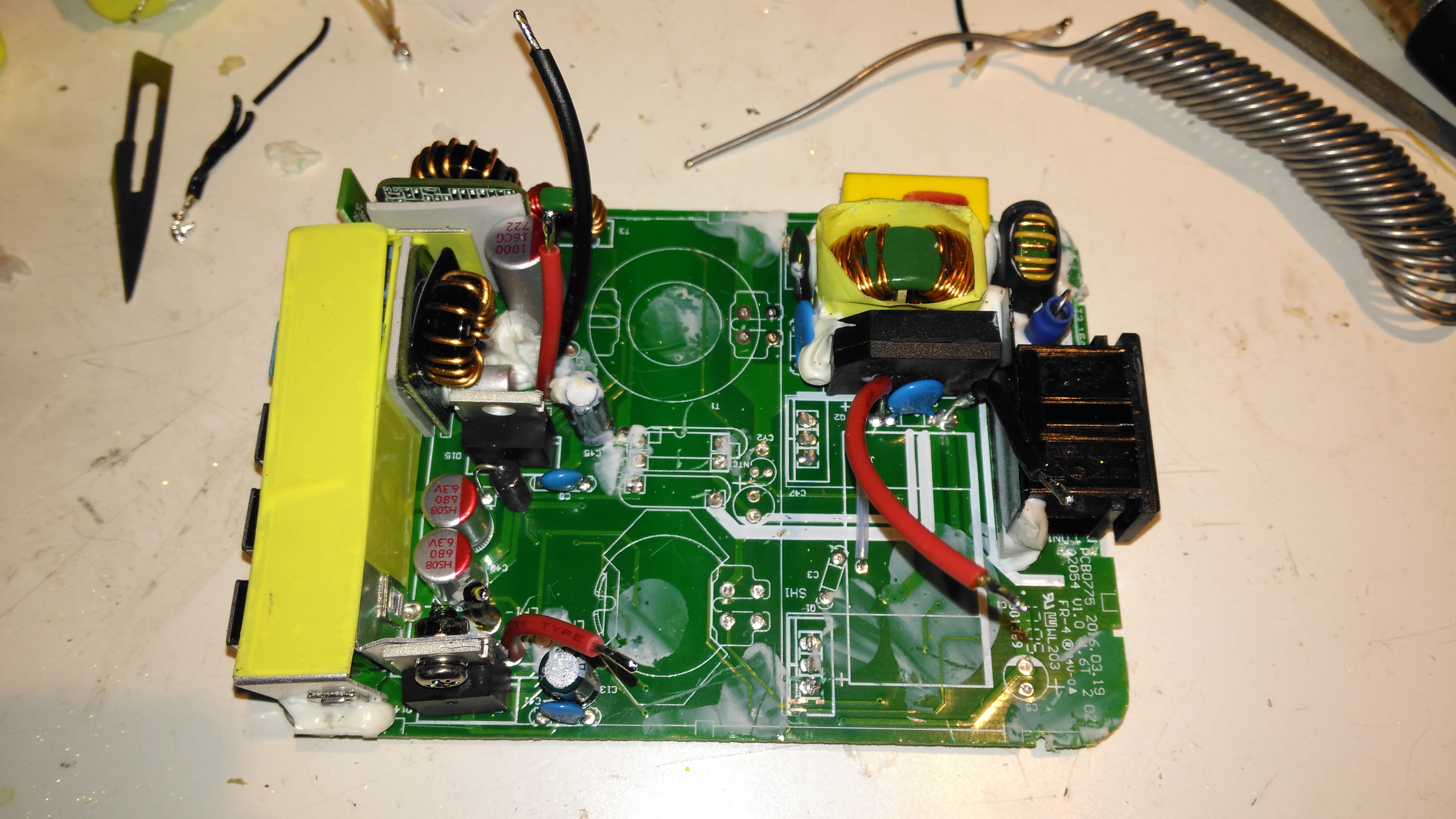
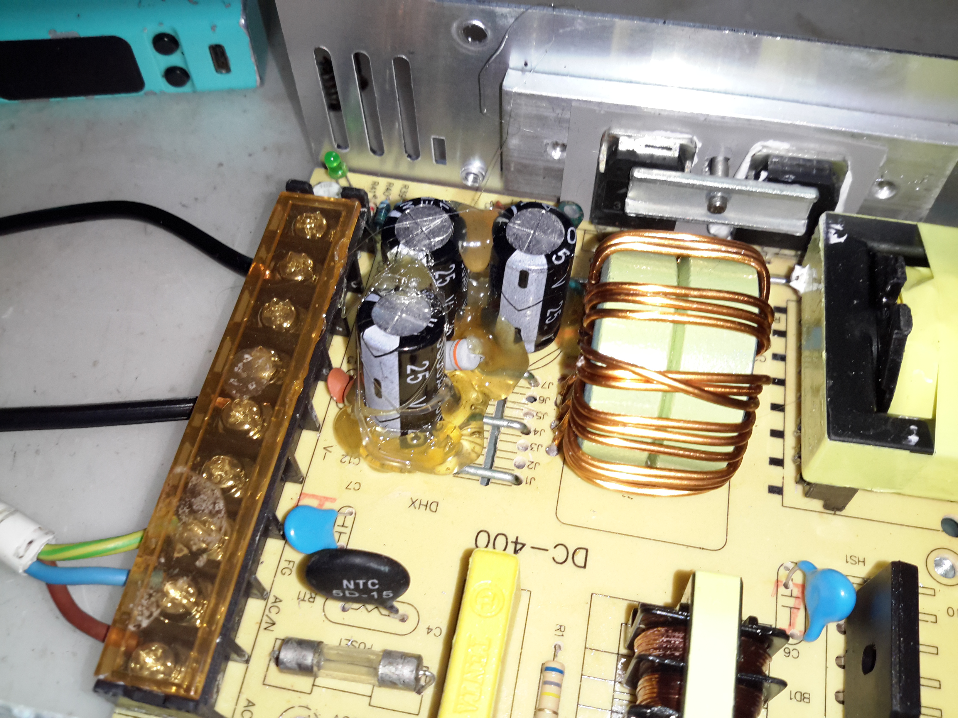
Installing the tails to connect everything together is the next step, this charger requires two power supplies – the QC3 circuits need 14.4v to supply the multi-voltage modules, the remaining 3 standard ports require 5v. The DC input tails are soldered into place where the main filter capacitor was, while the outputs are fitted to the spot the transformer secondary windings ended up. I’ve left the factory Schottky rectifiers in place on the secondary side to make things a little more simple, the output voltages of both the DC-DC converters does need to be increased slightly to compensate for the diode drops though. I’ve also bypassed the mains input fuse, as at 12v the input current is going to be substantially higher than when used on mains voltage.

DC-DC Converters Installed

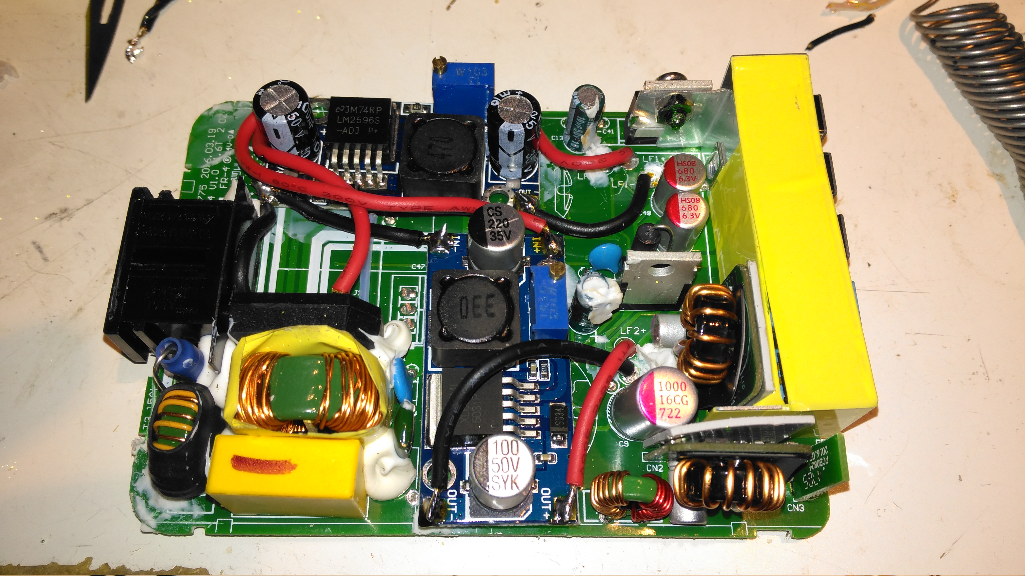
With a squeeze both the boost converter & the buck converter fit into place on the PCB.

Posted on 1 Comment

Panasonic NV-M5 CRT Viewfinder Hack

Viewfinder Circuits
Viewfinder Circuits


The old Panasonic NV-M5 has the standard for the time CRT based viewfinder assembly, which will happily take a composite video signal from an external source.

This viewfinder has many more connections than I would have expected, as it has an input for the iris signal, which places a movable marker on the edge of the display. This unit also has a pair of outputs for the vertical & horizontal deflection signals, I imagine for sync, but I’ve never seen these signals as an output on a viewfinder before.

EVF Schematic
EVF Schematic

Luckily I managed to get a service manual for the camera with a full schematic.
This unit takes a 5v input, as opposed to the 8-12v inputs on previous cameras, so watch out for this! There’s also no reverse polarity protection either.

Pins
Pins

Making the iris marker vanish from the screen is easy, just put a solder bridge between pins 15 & 16 of the drive IC. The important pins on the interface connector are as follows:

Pin 3: GND
Pin 4: Video Input
Pin 5: Video GND
Pins 6: +5v Supply

Posted on Leave a comment

eBay Chinese Chassis Power Supply S-400-12 400W 12v 33A

S-400-12 PSU
S-400-12 PSU

Here’s a cheap PSU from the treasure trove of junk that is eBay, rated at a rather beefy 400W of output at 12v – 33A! These industrial-type PSUs from name brands like TDK-Lambda or Puls are usually rather expensive, so I was interested to find out how much of a punishment these cheap Chinese versions will take before grenading. In my case this PSU is to be pushed into float charging a large lead acid battery bank, which when in a discharged state will try to pull as many amps from the charger as can be provided.

Rating Label
Rating Label

These PSUs are universal input, voltage adjustable by a switch on the other side of the PSU, below. The output voltage is also trimmable from the factory, an important thing for battery charging, as the output voltage needs to be sustained at 13.8v rather than the flat 12v from the factory.

Input Voltage Selector
Main Terminal Block
Main Terminal Block

Mains connections & the low voltage outputs are on beefy screw terminals. The output voltage adjustment potentiometer & output indicator LED are on the left side.

Cooling Fan
Cooling Fan

The cooling fan for the unit, which pulls air through the casing instead of blowing into the casing is a cheap sleeve bearing 60mm fan. No surprises here. I’ll probably replace this with a high-quality ball-bearing fan, to save the PSU from inevitable fan failure & overheating.

PCB Bottom
PCB Bottom

The PCB tracks are generously laid out on the high current output side, but there are some primary/secondary clearance issues in a couple of places. Lindsay Wilson over at Imajeenyus.com did a pretty thorough work-up on the fineries of these PSUs, so I’ll leave most of the in-depth stuff via a linky. There’s also a modification of this PSU for a wider voltage range, which I haven’t done in this case as the existing adjustment is plenty wide enough for battery charging duty.

Bare PCB
Bare PCB

The PCB is laid out in the usual fashion for these PSUs, with the power path taking a U-route across the board. Mains input is lower left, with some filtering. Main diode bridge in the centre, with the voltage selection switch & then the main filter caps. Power is then switched into the transformer by the pair of large transistors on the right before being rectified & smoothed on the top left.

Main Switching Transistors

The pair of main switching devices are mounted to the casing with thermal compound & an insulating pad. To bridge the gap there’s a chunk of aluminium which also provides some extra heatsinking.

SMPS Drive IC & Base Drive Transformer

The PSU is controlled by a jelly-bean TL494 PWM controller IC. No active PFC in this cheap supply so the power factor is going to be very poor indeed.

Input Protection
Input Protection

Input protection & filtering is rather simple with the usual fuse, MOV filter capacitor & common mode choke.

Main Output Rectifiers

Beefy 30A dual diodes on the DC output side, mounted in the same fashion as the main switching transistors.

Output Current Shunt

Current measurement is done by these large wire links in the current path, selectable for different models with different output ratings.

Hot Glue Support
Hot Glue Support

The output capacitors were just floating around in the breeze, with one of them already having broken the solder joints in shipping! After reflowing the pads on all the capacitors some hot glue as flowed around them to stop any further movement.

This supply has now been in service for a couple of weeks at a constant 50% load, with the occasional hammering to recharge the battery bank after a power failure. at 13A the supply barely even gets warm, while at a load high enough to make 40A rated cable get uncomfortably warm (I didn’t manage to get a current reading, as my instruments don’t currently go high enough), the PSU was hot in the power semiconductor areas, but seemed to cope at full load perfectly well.

Posted on Leave a comment

Eco-Light 4W LED Bulb Teardown

Components
Damaged Bulb
Damaged Bulb

Here’s a modern LED bulb, that unfortunately decided to disassemble itself within a few minutes of being installed in a light fitting! The base plastic snapped off the main aluminium body at the screw posts!

Input Rectifier
Input Rectifier

The PCB in the base holds nothing but the input components. Above is the bridge rectifier.

Fusible Resistor
Fusible Resistor

The other side of the PCB has a 10Ω fusible resistor, for protection.

LED PCB
LED PCB

The LED PCB itself has the driver IC, which is a CYT3000A linear constant current IC, that runs direct from full-wave rectified mains. The single resistor sets the LED current, but there aren’t any smoothing capacitors on the DC rail, so this bulb would flicker a lot.

Posted on Leave a comment

Maplin/Refrakta Torch Modification & Mode Removal

The multimode dimming/flashing modes on Chinese torches have irritated me for a while. If I buy a torch, it’s to illuminate something I’m doing, not to test if people around me have photosensitive epilepsy.

Looking at the PCB in the LED module of the torch, a couple of components are evident:

LED Driver PCB
LED Driver PCB

There’s not much to this driver, it’s simply resistive for LED protection (the 4 resistors in a row at the bottom of the board).
The components at the top are the multimode circuitry. The SOT-23 IC on the left is a CX2809 LED Driver, with several modes. The SOT-23 on the right is a MOSFET, for switching the actual LED itself. I couldn’t find a datasheet for the IC itself, but I did find a schematic that seems to match up with what’s on the board.

Schematic
Schematic

Here’s that schematic, the only thing that needs to be done to convert the torch to single mode ON/OFF at full brightness, is to bridge out that FET.

Components Desoldered

To help save the extra few mA the IC & associated circuitry will draw from the battery, I have removed all of the components involved in the multimode control. This leaves just the current limiting resistors for the LED itself.

Jumper Link
Jumper Link

The final part above, is to install a small link across the Drain & Source pads of the FET. Now the switch controls the LED directly with no silly electronics in between. A proper torch at last.

Posted on Leave a comment

eBay Special 2.5″ HDD USB Case

Since I have a fair few 750GB disks sat doing nothing, I figured I’d get some USB3 caddies for them. Back when USB -> IDE caddies appeared, they were hideously expensive. Not so much these days!

USB HDD
USB HDD

For £6 on eBay, you get a basic plastic box with the required bridge circuitry.

USB - SATA Bridge
USB – SATA Bridge

Here’s the PCB – a very basic affair, with only 2 ICs. The large QFN IC on the left is the USB-SATA bridge. It’s a JMicron JMS567. Unfortunately JMicron are rather secretive about their bridge chips & I can’t find much information about it, nor a datasheet.

PCB Reverse
PCB Reverse

Here’s the other side of the bridge PCB – not much on here, the activity indicator LED is a bit of a bodge job, but it’s functional. The IC on the right is a Pm25LD512 512Kbit SPI EEPROM. This is used to store things like the USB device & vendor IDs, device name, type, etc. Here’s what dmesg spits out when the disk is connected on my standard Linux system:

[10397.893298] usb 2-3.1.1: new SuperSpeed USB device number 8 using xhci_hcd
[10397.909019] usb 2-3.1.1: New USB device found, idVendor=152d, idProduct=1562
[10397.909025] usb 2-3.1.1: New USB device strings: Mfr=1, Product=2, SerialNumber=3
[10397.909027] usb 2-3.1.1: Product: ELEMENTS
[10397.909028] usb 2-3.1.1: Manufacturer: ELEMENTS
[10397.909029] usb 2-3.1.1: SerialNumber: 0F00000000157DC
[10397.912679] scsi host13: uas
[10397.913198] scsi 13:0:0:0: Direct-Access     WD       ELEMENTS         0225 PQ: 0 ANSI: 6
[10397.914043] sd 13:0:0:0: Attached scsi generic sg11 type 0
[10397.914179] sd 13:0:0:0: [sdk] Spinning up disk...
[10398.917575] .....ready
[10402.939800] sd 13:0:0:0: [sdk] 1465149168 512-byte logical blocks: (750 GB/698 GiB)
[10402.939803] sd 13:0:0:0: [sdk] 4096-byte physical blocks
[10402.940358] sd 13:0:0:0: [sdk] Write Protect is off
[10402.940363] sd 13:0:0:0: [sdk] Mode Sense: 53 00 00 08
[10402.940662] sd 13:0:0:0: [sdk] Write cache: enabled, read cache: enabled, doesn't support DPO or FUA
[10403.038847]  sdk: sdk1
[10403.040572] sd 13:0:0:0: [sdk] Attached SCSI disk
[10404.347605] device-mapper: table: 252:0: adding target device sdk1 caused an alignment inconsistency: physical_block_size=4096, logical_block_size=512, alignment_offset=0, start=4096
[10404.347611] device-mapper: table: 252:0: adding target device sdk1 caused an alignment inconsistency: physical_block_size=4096, logical_block_size=512, alignment_offset=0, start=4096
[10404.626320] device-mapper: table: 252:0: adding target device sdk1 caused an alignment inconsistency: physical_block_size=4096, logical_block_size=512, alignment_offset=0, start=2100224
[10404.626325] device-mapper: table: 252:0: adding target device sdk1 caused an alignment inconsistency: physical_block_size=4096, logical_block_size=512, alignment_offset=0, start=2100224

Here’s some speed benchmarks:


USB2 Benchmark
USB2 Benchmark

First attached to a USB2 port, above

USB3 Benchmark
USB3 Benchmark

And finally attached to a USB3 port, above

Tests were done with a 320GB 5400RPM Samsung HM321HI drive, direct into the root hub, for the shortest possible signal length.


Posted on 1 Comment

Cisco PSU Hack & Switched Mode PSU Background

Recently I decommissioned some networking equipment, and discovered the power supplies in some switches were single rail 12v types, with a rather high power rating. I figured these would be very good for powering my Ham radio gear.

They’re high quality Delta Electronics DPSN-150BP units, rated at a maximum power output of 156W.

Label
Label

These supplies have an adjustment pot for the output voltage regulation, but unfortunately it just didn’t have quite enough range to get from 12.0v to 13.8v. The highest they would go was ~13.04v.

After taking a look at the regulator circuit, I discovered  I could further adjust the output voltage by changing a single resistor to a slightly lower value.

Firstly though, a little background on how switched mode power supplies operate & regulate their output voltage.

SMPS
SMPS

Here’s the supply. It’s mostly heatsink, to cool the large power switching transistors.

The first thing a SMPS does, is to rectify the incoming mains AC with a bridge rectifier. This is then smoothed by a large electrolytic capacitor, to provide a main DC rail of +340v DC (when on a 240v AC supply).

Mains Input
Mains Input

Above is the mains input section of the PSU, with a large common-mode choke on the left, bridge rectifier in the centre, and the large filter capacitor on the right. These can store a lot of energy when disconnected from the mains, and while they should have a discharge resistor fitted to safely drain the stored energy, they aren’t to be relied on for safety!

Once the supply has it’s main high voltage DC rail, this is switched into the main transformer by a pair of very large transistors – these are hidden from view on the large silver heatsinks at the bottom of the image. These transistors are themselves driven with a control IC, in the case of this supply, it’s a UC3844B. This IC is hidden under the large heatsink, but is just visible in the below photo. (IC5).

Control IC
Control IC
Main Switching Transformer

Here’s the main switching transformer, these can be much smaller than a conventional transformer due to the high frequencies used. This supply operates at 500kHz.
After the main transformer, the output is rectified by a pair of Schottky diodes, which are attached to the smaller heatsink visible below the transformer, before being fed through a large toroidal inductor & the output filter capacitors.
All this filtering on both the input & the output is required to stop these supplies from radiating their operating frequency as RF – a lot of cheap Chinese switching supplies forego this filtering & as a result are extremely noisy.

After all this filtering the DC appears at the output as usable power.

Getting back to regulation, these supplies read the voltage with a resistor divider & feed it back to the mains side control IC, through an opto-isolator. (Below).

Feedback Loop
Feedback Loop

The opto isolators are the black devices at the front with 4 pins.

Regulator Adjustment

For a more in-depth look at the inner workings of SMPS units, there’s a good article over on Hardware Secrets.

My modification is simple. Replacing R306 (just below the white potentiometer in the photo), with a slightly smaller resistor value, of 2.2KΩ down from 2.37KΩ, allows the voltage to be pulled lower on the regulator. This fools the unit into applying more drive to the main transformer, and the output voltage rises.

It’s important to note that making too drastic a change to these supplies is likely to result in the output filter capacitors turning into grenades due to overvoltage. The very small change in value only allows the voltage to rise to 13.95v max on the adjuster. This is well within the rating of 16v on the output caps.

Now the voltage has been sucessfully modified, a new case is on the way to shield fingers from the mains. With the addition of a couple of panel meters & output terminals, these supplies will make great additions to my shack.

More to come on the final build soon!

Posted on 1 Comment

AVR Optical Tachometer

Here is an AVR powered optical tachometer design, that I adapted from the schematic found here.

I made a couple of changes to the circuit & designed a PCB & power supply module to be built in. The original design specified a surface mount IR LED/Photodiode pair, however my adjustment includes a larger IR reflectance sensor built onto the edge of the board, along with a Molex connector & a switch to select an externally mounted sensor instead of the onboard one.

There is also an onboard LM7805 based power supply, designed with a PCB mount PP3 battery box.
The power supply can also be protected by a 350mA polyfuse if desired. If this part isn’t fitted, then a pair of solder bridge pads are provided within the footprint for the fuse to short out the pads.

For more information on the basic design, please see the original post with the link at the top of the page.

Schematic
Schematic

Here is an archive of the firmware & the Eagle CAD files for the PCB & schematic design.


Posted on Leave a comment

USB-IDE/SATA Adaptor

Front
Front

This is a device to use an IDE or SATA interface drive via a USB connection. Here is the front of the device, IDE interface at the bottom, 2.5″ form factor.

PCB Top
PCB Top

PCB removed from the casing. USB cable exits the top, 12v DC power jack to the left.
SATA interface below the DC Jack.
Molex connector below SATA is the power output for the drive in use. This unit has a built in 5v regulator.

PCB Bottom
PCB Bottom

Bottom of the PCB showing the interface IC.

Drive Adaptor
Drive Adaptor

Adaptor to plug into the 44-pin 2.5″ form factor IDE interface on the adaptor, converts to standard 40-pin 3.5″ IDE.

Power Cable
Power Cable

Power pigtail with standard Molex & SATA power plugs.

Posted on Leave a comment

Chicom “500W” ATX PSU

Cover Removed
Cover Removed

Here is a cheapo 500W rated ATX PSU that has totally borked itself, probably due to the unit NOT actually being capable of 500W. All 3 of the switching transistors were shorted, causing the ensuing carnage:

AC Input
AC Input

Here is the AC input to the PCB. Note the vapourised element inside the input fuse on the left. There is no PFC/filtering built into this supply, being as cheap as it is links have been installed in place of the RFI chokes.

Input Side
Input Side

Main filter capacitors & bridge rectifier diodes. PCB shows signs of excessive heating.

Filter Caps Removed
Filter Caps Removed

Filter capacitors have been removed from the PCB here, showing some cooked components. Resistor & diode next to the heatsink are the in the biasing network for the main switching transistors.

Heatsinks Removed
Heatsinks Removed

Heatsink has been removed, note the remaining pin from one of the switching transistors still attached to the PCB & not the transistor 🙂

Transformers
Transformers

Output side of the PSU, with heatsink removed. Main transformer on  the right, transformers centre & left are the 5vSB  transformer & feedback transformer.

Output Side
Output Side

Output side of the unit, filter capacitors, choke & rectifier diodes are visible here attached to their heatsink.

Comparator
Comparator

Comparator IC that deals with regulation of the outputs & overvoltage protection.

Posted on Leave a comment

Southwestern Bell Freedom Phone

Phone
Phone

This is an old cordless landline phone, with dead handset batteries.

Handset Radio Board
Handset Radio Board

Here’s the handset with the back removed. Shown is the radio TX/RX board, underneath is the keyboard PCB with the speaker & mic. All the FM radio tuning coils are visible & a LT450GW electromechanical filter.

Handset Radio Board Bottom

Radio PCB removed from the housing showing the main CPU controlling the unit, a Motorola MC13109FB.

Keypad Board
Keypad Board

The keypad PCB, with also holds the microphone & speaker.

Handset Keypad Board Bottom

Bottom of the keypad board, which holds a LSC526534DW 8-Bit µC & a AT93C46R serial EEPROM for phone number storage.

Base Main Board
Base Main Board

Here’s the base unit with it’s top cover removed. Black square object on far right of image is the microphone for intercom use, power supply section is top left, phone interface bottom left, FM radio is centre. Battery snap for power backup is bottom right.

Power Supply Section

PSU section of the board on the left here, 9v AC input socket at the bottom, with bridge rectifier diodes & main filter capacitor above. Two green transformers on the right are for audio impedance matching. Another LT450GW filter is visible at the top, part of the base unit FM transceiver.

ICs
ICs

Another 8-bit µC, this time a LSC526535P, paired with another AT93C46 EEPROM. Blue blob is 3.58MHz crystal resonator for the MCU clock. The SEC IC is a KS58015 4-bit binary to DTMF dialer IC. This is controlled by the µC.

Base Main Board Bottom

Underside of the base unit Main PCB, showing the matching MC13109FB IC for the radio functions.