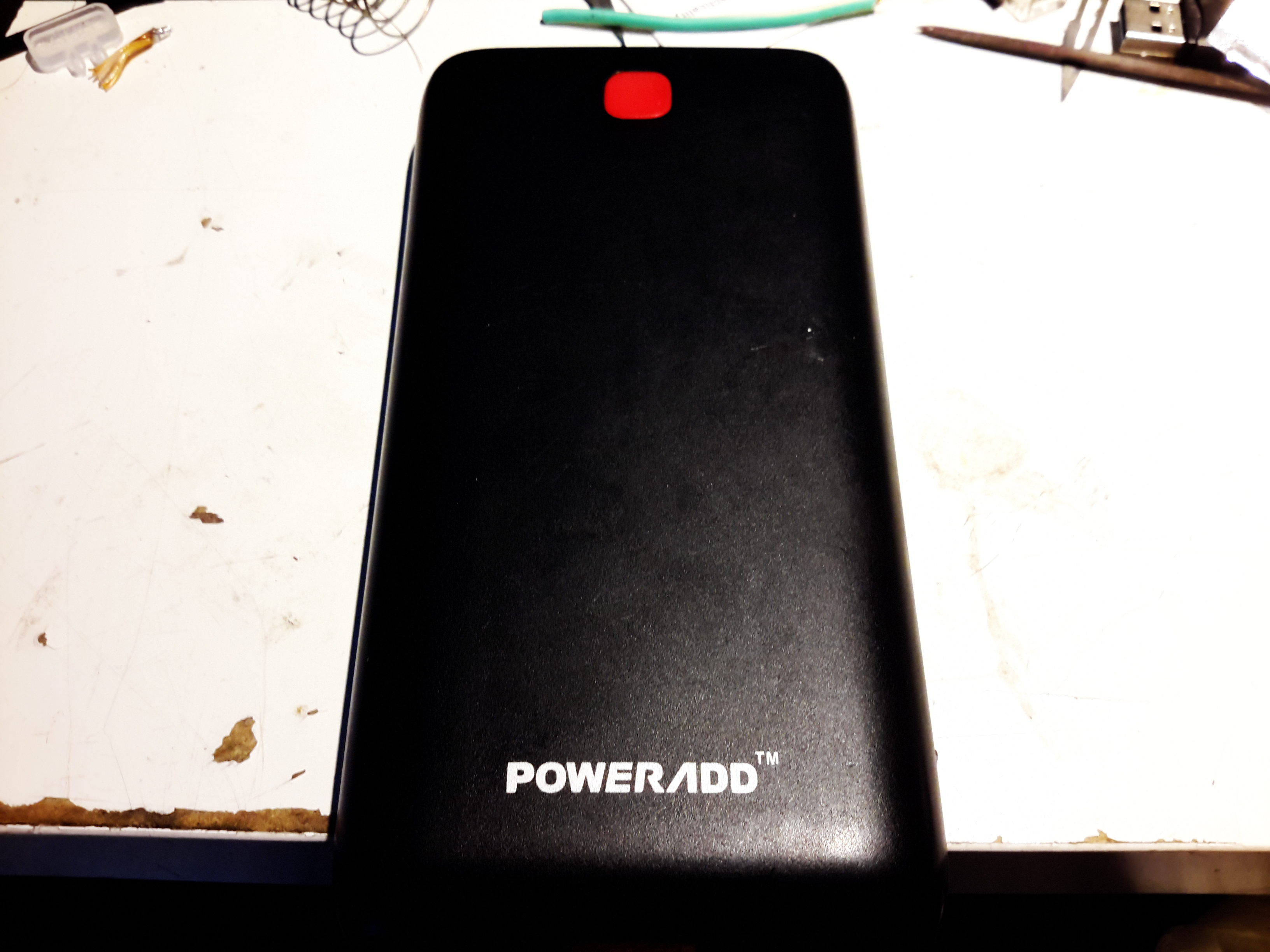
Here’s the biggest portable USB powerbank I’ve seen yet – the PowerAdd Pilot X7, this comes with a 20Ah (20,000mAh) capacity. This pack is pretty heavy, but this isn’t surprising considering the capacity.
USB Ports & LED
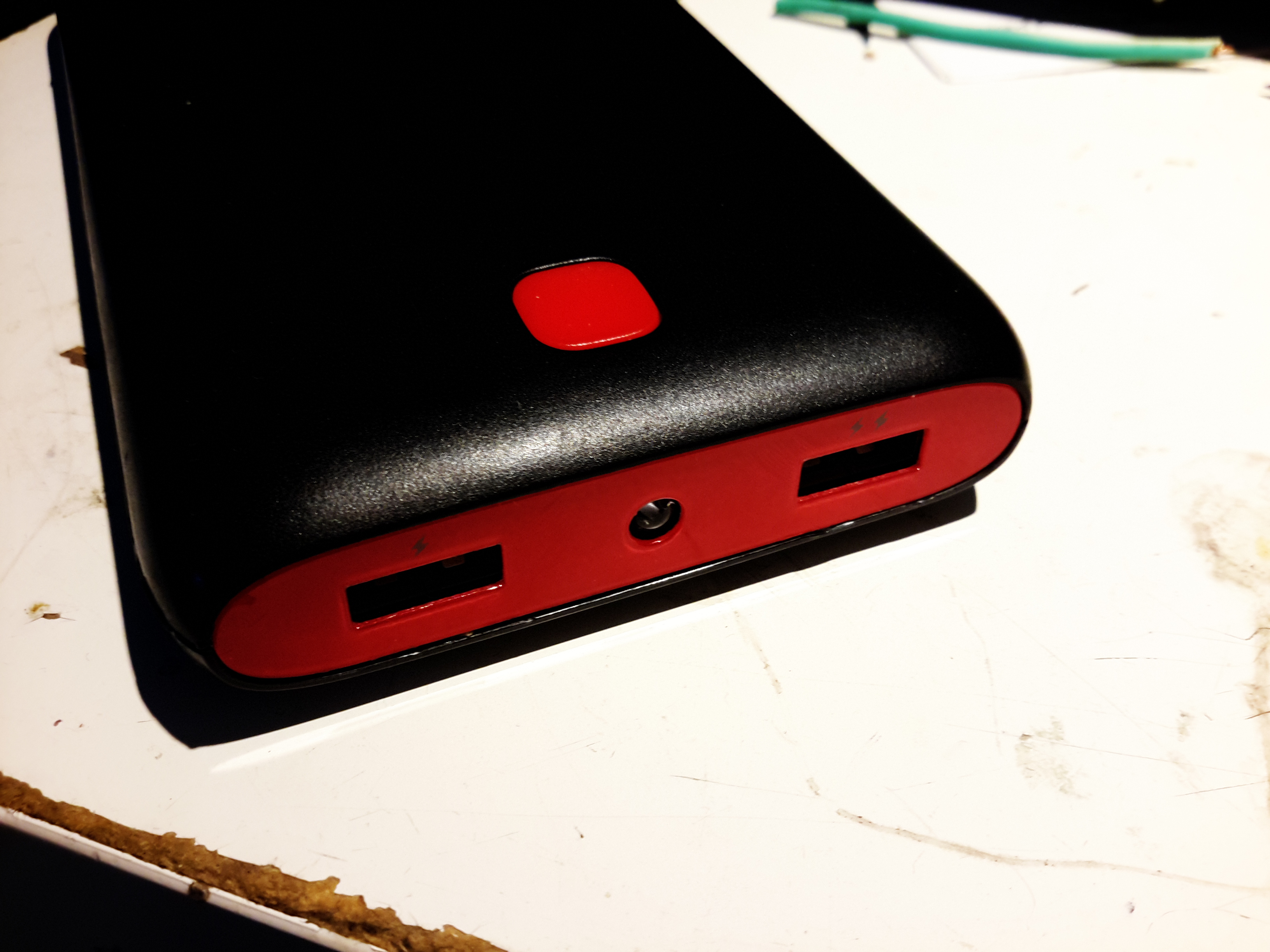
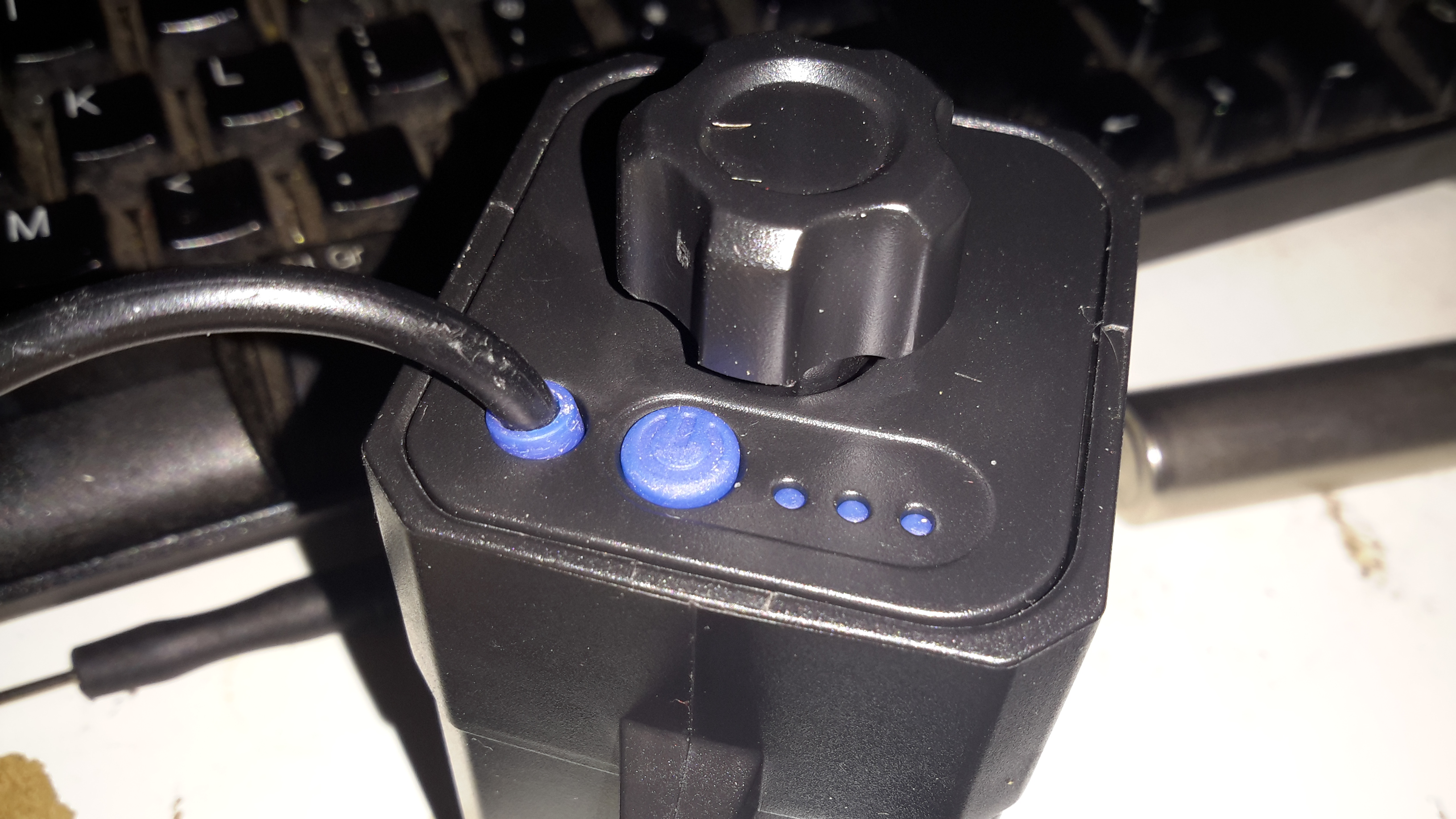
The front of the pack houses the usual USB ports, in this case rated at 3.4A total between the ports. There’s a white LED in the centre as a small torch, activated by double-clicking the button. A single click of the button lights up the 4 blue LEDs under the housing that indicate remaining battery capacity. Factory charging is via a standard µUSB connector in the side, at a maximum of 2A.
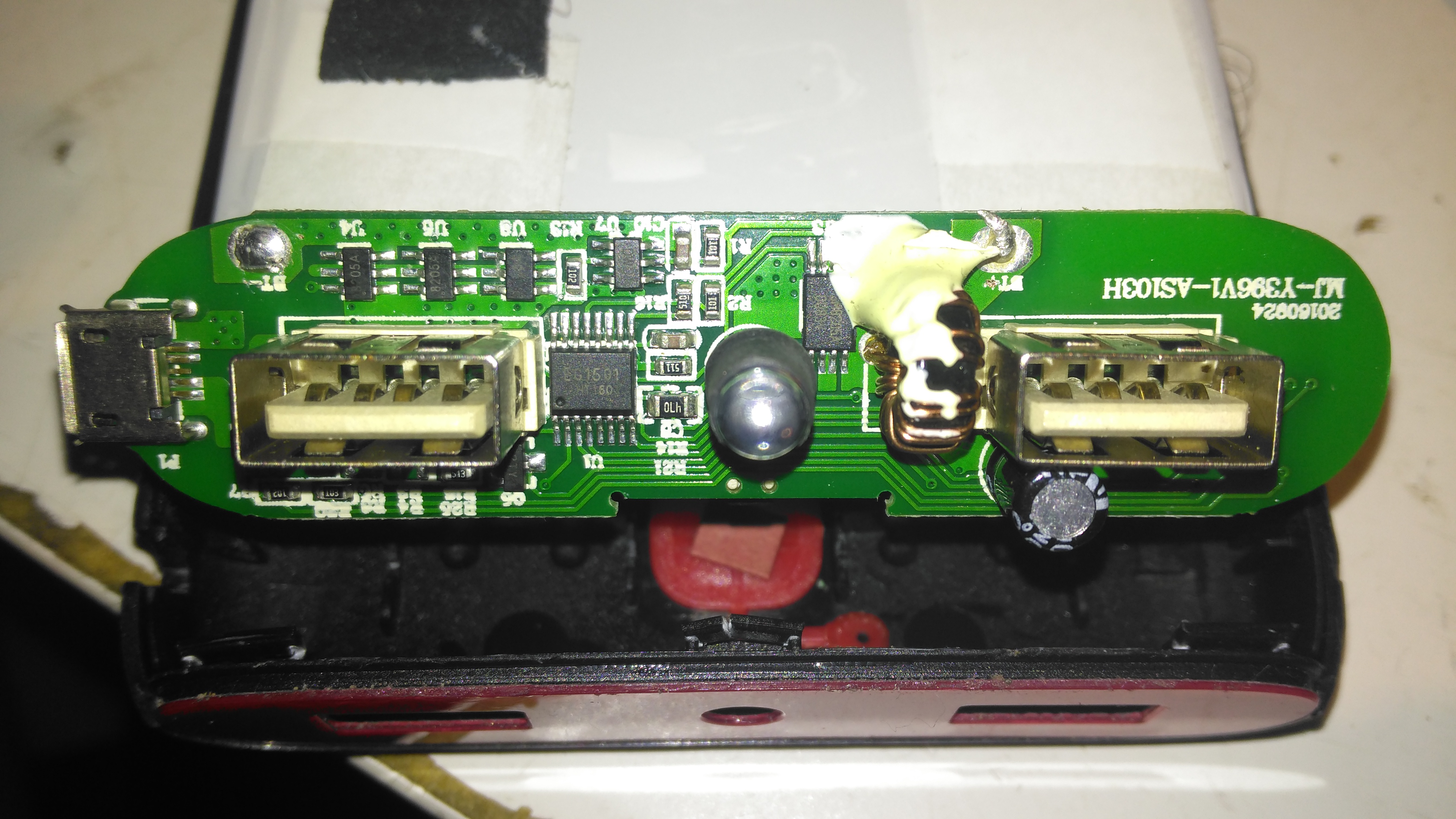
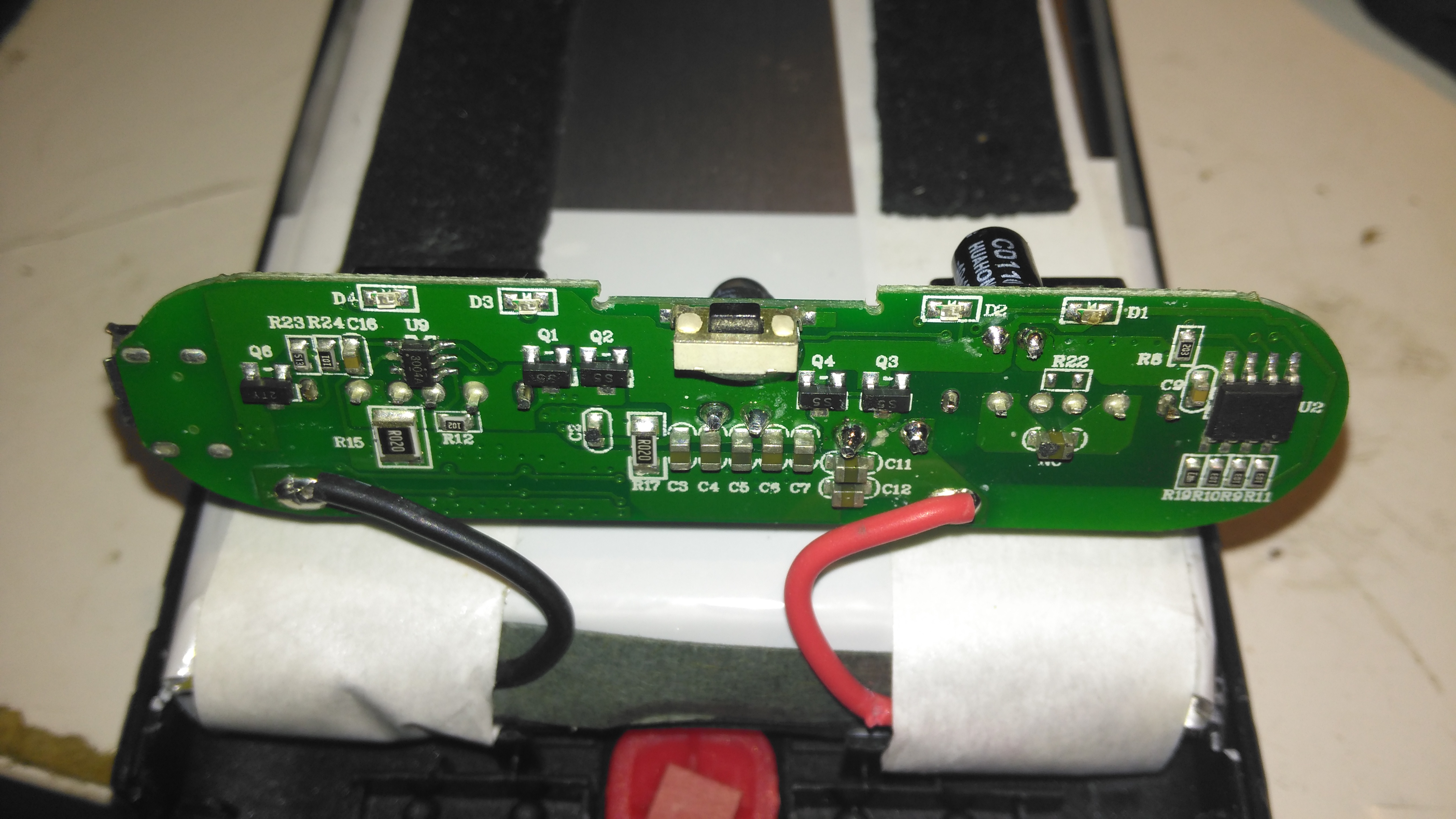
PCB Front
The front of the PCB holds the USB ports, along with most of the main control circuitry. At top left is a string of FS8025A dual-MOSFETs all in parallel for a current carrying capacity of 15A total, to the right of these is the ubiquitous DW01 Lithium-Ion protection IC. These 4 components make up the battery protection – stopping both an overcharge & overdischarge. The larger IC below is an EG1501 multi-purpose power controller.
This chip is doing all of the heavy lifting in this power pack, dealing with all the DC-DC conversion for the USB ports, charge control of the battery pack, controlling the battery level indicator LEDs & controlling the torch LED in the centre.
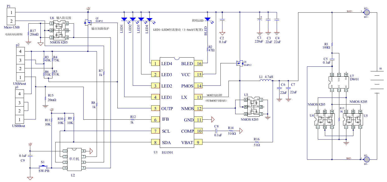
EG1501 Example
The datasheet is in Chinese, but it does have an example application circuit, which is very similar to the circuitry used in this powerbank. A toroidal inductor is nestled next to the right-hand USB port for the DC-DC converter, and the remaining IC next to it is a CW3004 Dual-Channel USB Charging Controller, which automatically sets the data pins on the USB ports to the correct levels to ensure high-current charging of the devices plugged in. This IC replaces the resistors R3-R6 in the schematic above.
The DC-DC converter section of the power chain is designed with high efficiency in mind, not using any diodes, but synchronous rectification instead.
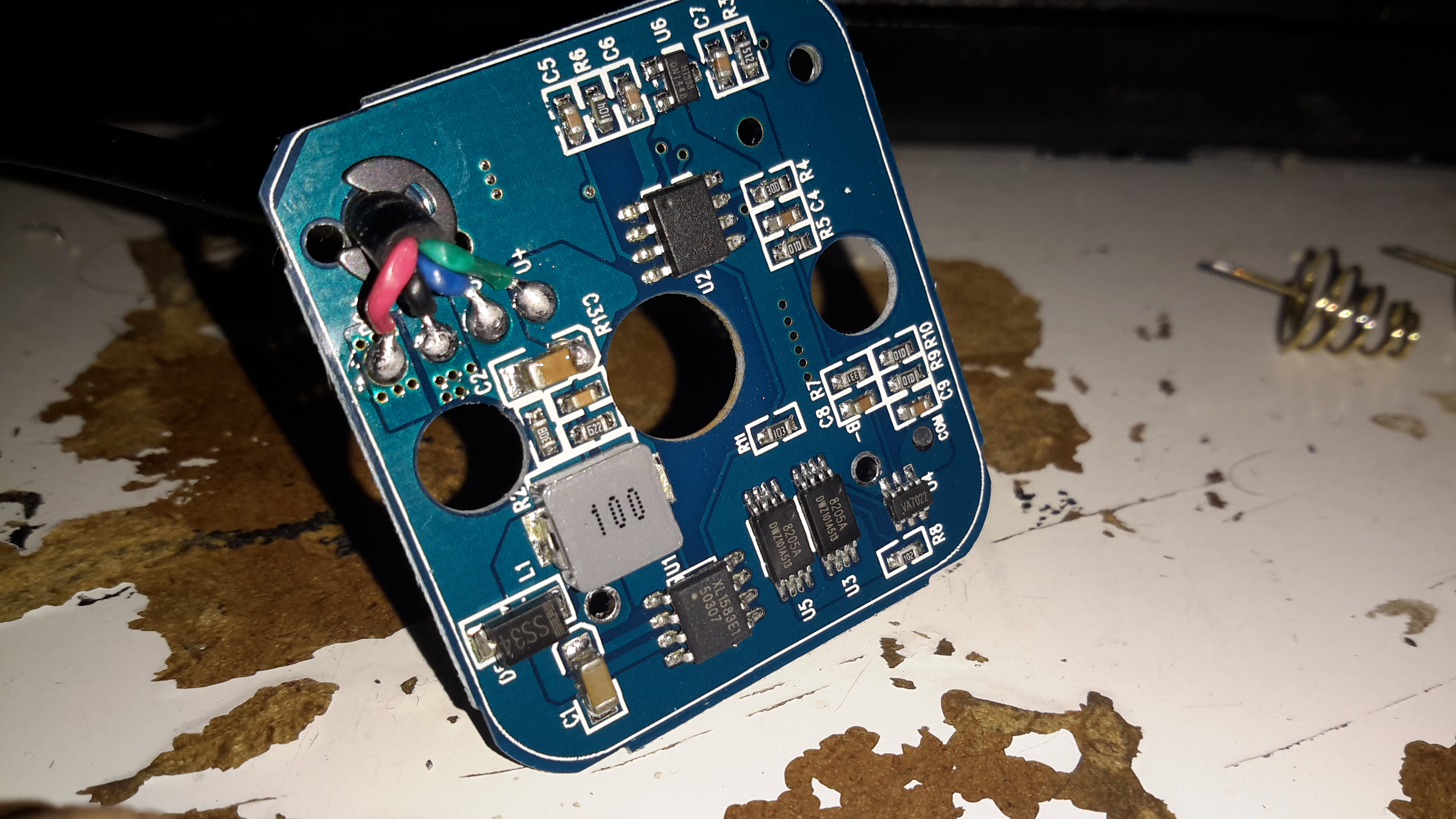
PCB Back
The back of the PCB just has a few discrete transistors, the user interface button, and a small SO8 IC with no markings at all. I’m going to assume this is a generic microcontroller, (U2 in the schematic) & is just there to interface the user button to the power controller via I²C.
Cells
Not many markings on the cells indicating their capacity, but a full discharge test at 4A gave me a resulting capacity of 21Ah – slightly above the nameplate rating. There are two cells in here in parallel, ~10Ah capacity each.
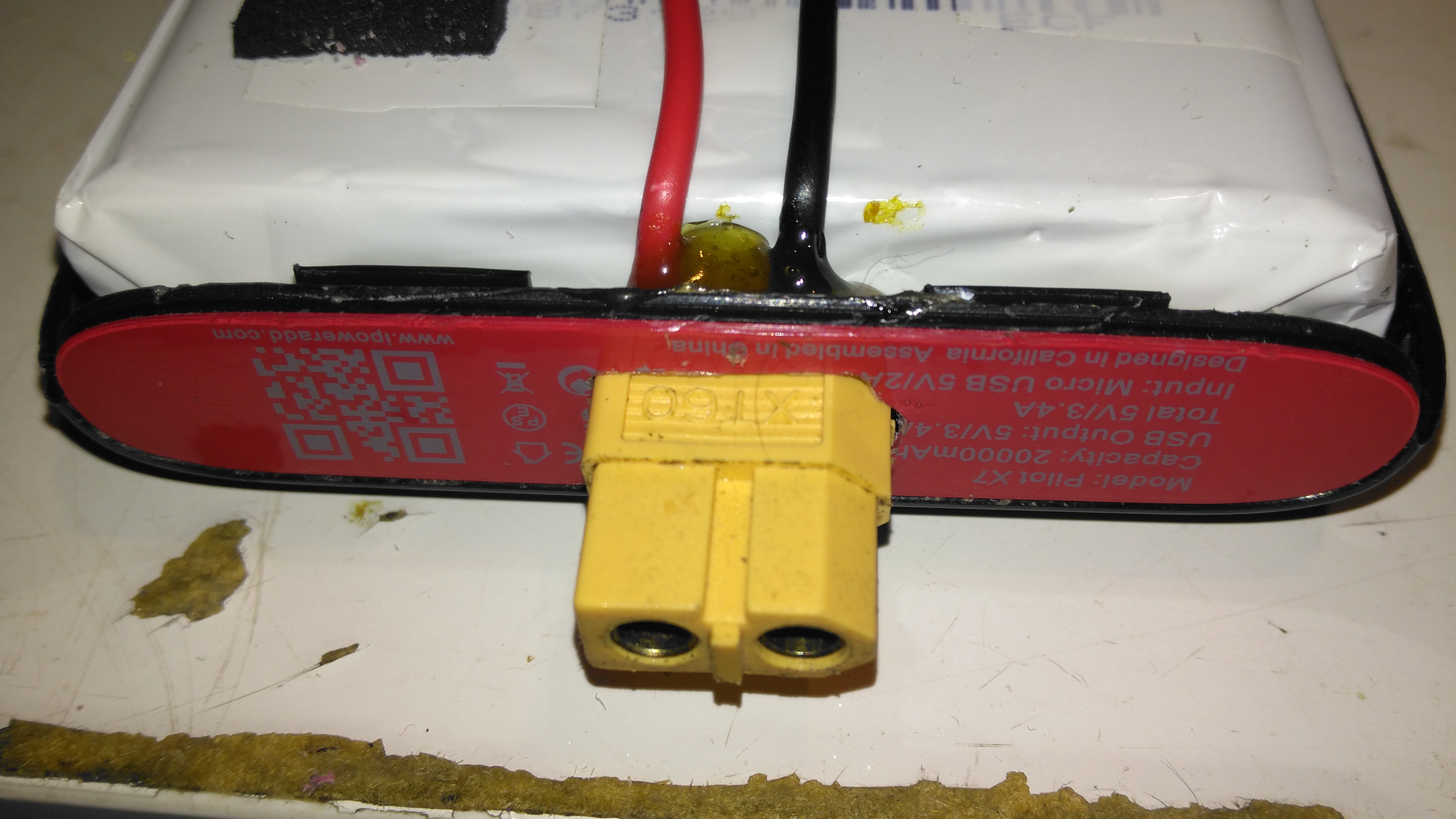
XT60 Battery Connector
The only issue with powerbanks this large is the amount of time they require to recharge themselves – at this unit’s maximum of 2A through the µUSB port, it’s about 22 hours! Here I’ve fitted an XT60 connector, to interface to my Turnigy Accucell 6 charger, increasing the charging current capacity to 6A, and reducing the full-charge time to 7 hours. This splits to 3A charge per cell, and after some testing the cells don’t seem to mind this higher charging current.
Battery Connector Wiring
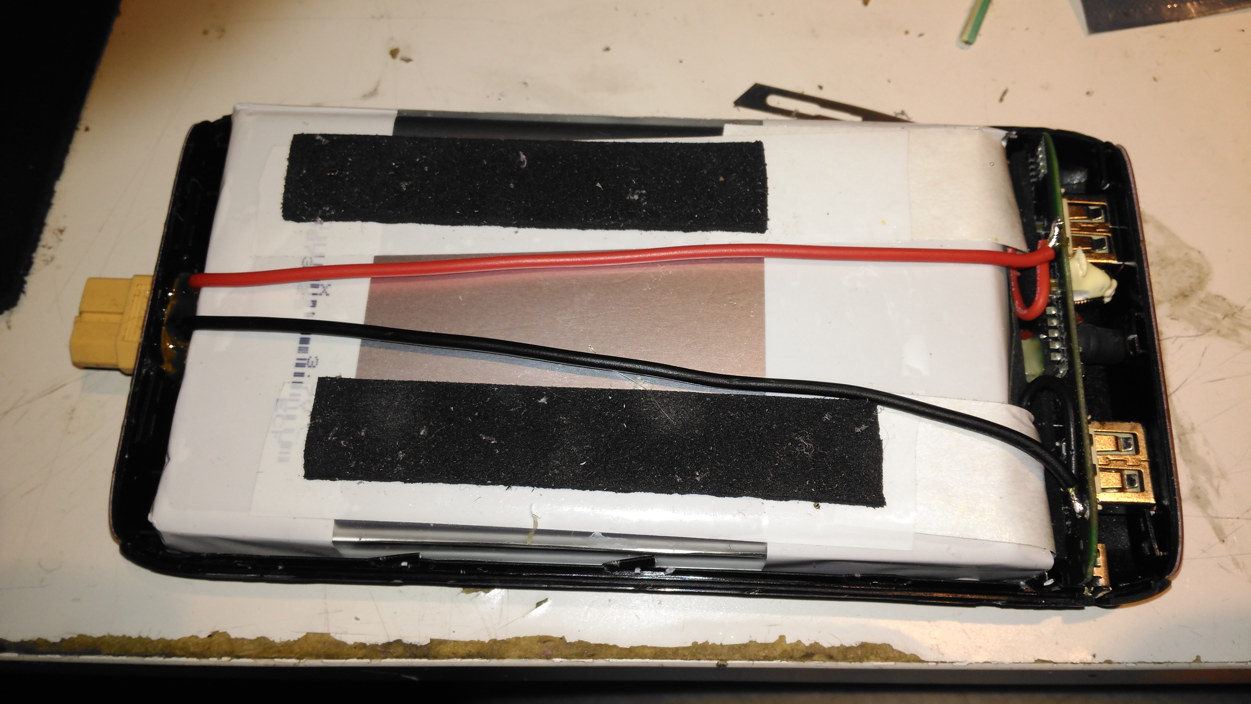
The new charging connector is directly connected to the battery at the control PCB, there’s just enough room to get a pair of wires down the casing over the cells.
Since the 4×18650 battery pack supplied with my Cree head torch is pretty shit, even by China’s standards, I figured something I could put my own cells into would be a better option. An eBay search turned up these battery boxes, not only with a direct battery output for my torch, but also a USB port for charging other devices when I’m low on charge.
LED Capacity Indicator
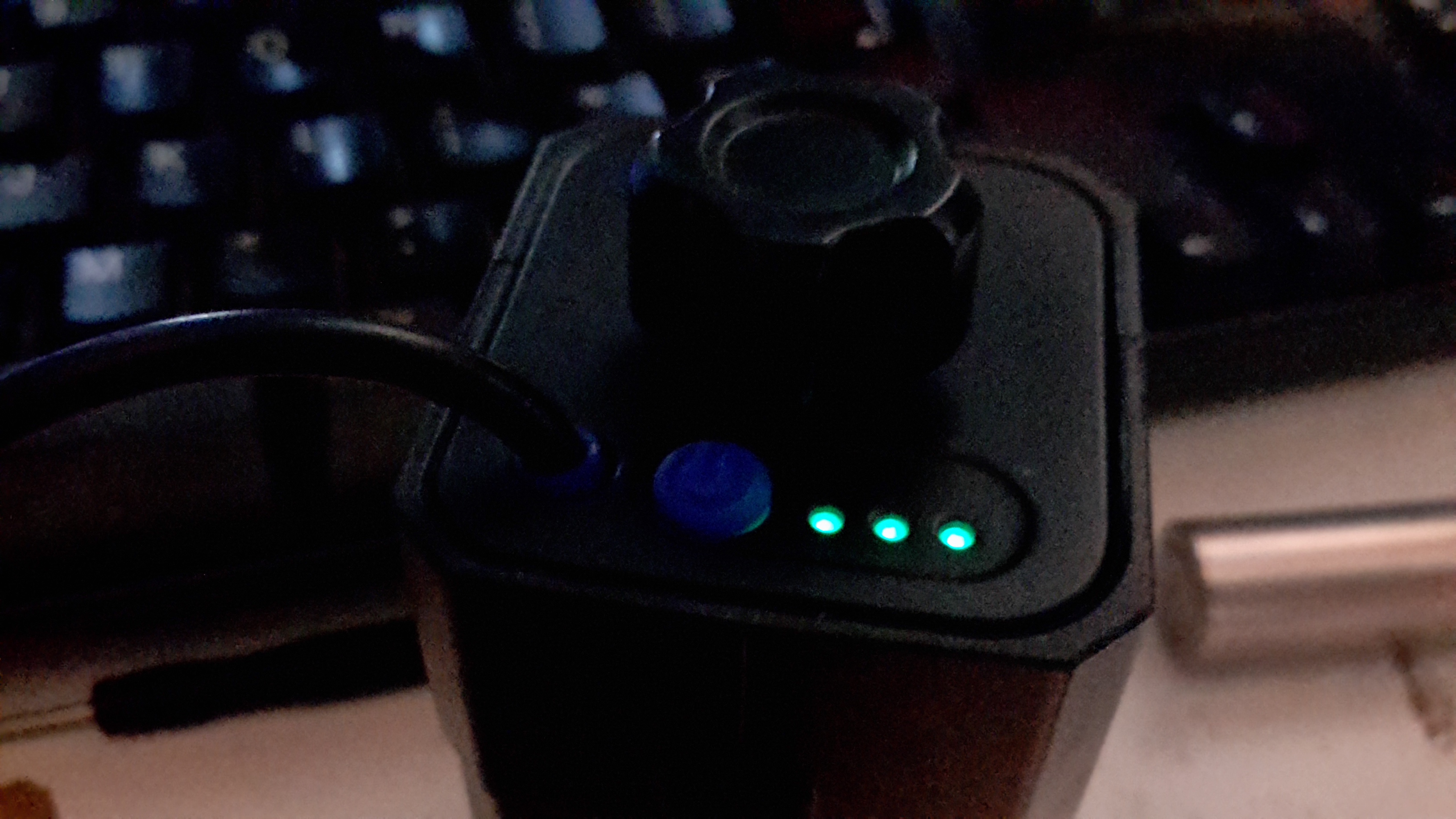
The output to the lamp connector is directly connected to the battery, through the usual Lithium Ion protection, but the USB output is controlled from a single power button. Battery charge condition is displayed on 3 LEDs. Not sure why they used blue silicone for the seal & then used green LEDs… But it does work, even if a little dim.
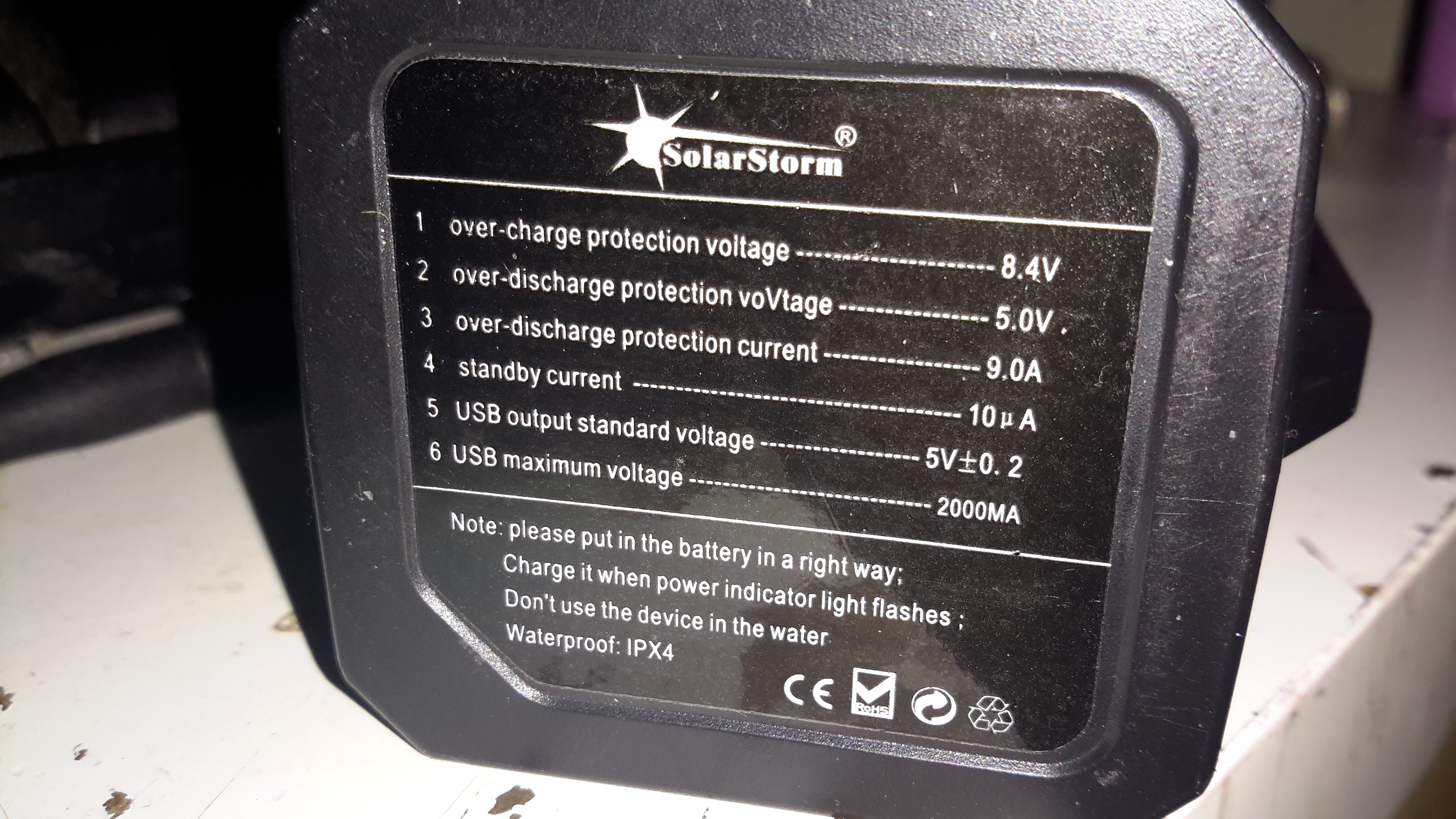
Label
Essential information. Does claim to be protected, and from the already existing electronics for the USB this would be expected in all but the cheapest crap.
An IP rating of IPX4 is claimed, yet just above that rating is a notice not to be used in water. Eh?
This is sealed with an O-Ring around the edge of the top cap & silicone seals around the cable & retaining screw. I did test by immersion in about 6″ of water, and it survived this test perfectly fine, no water ingress at all.
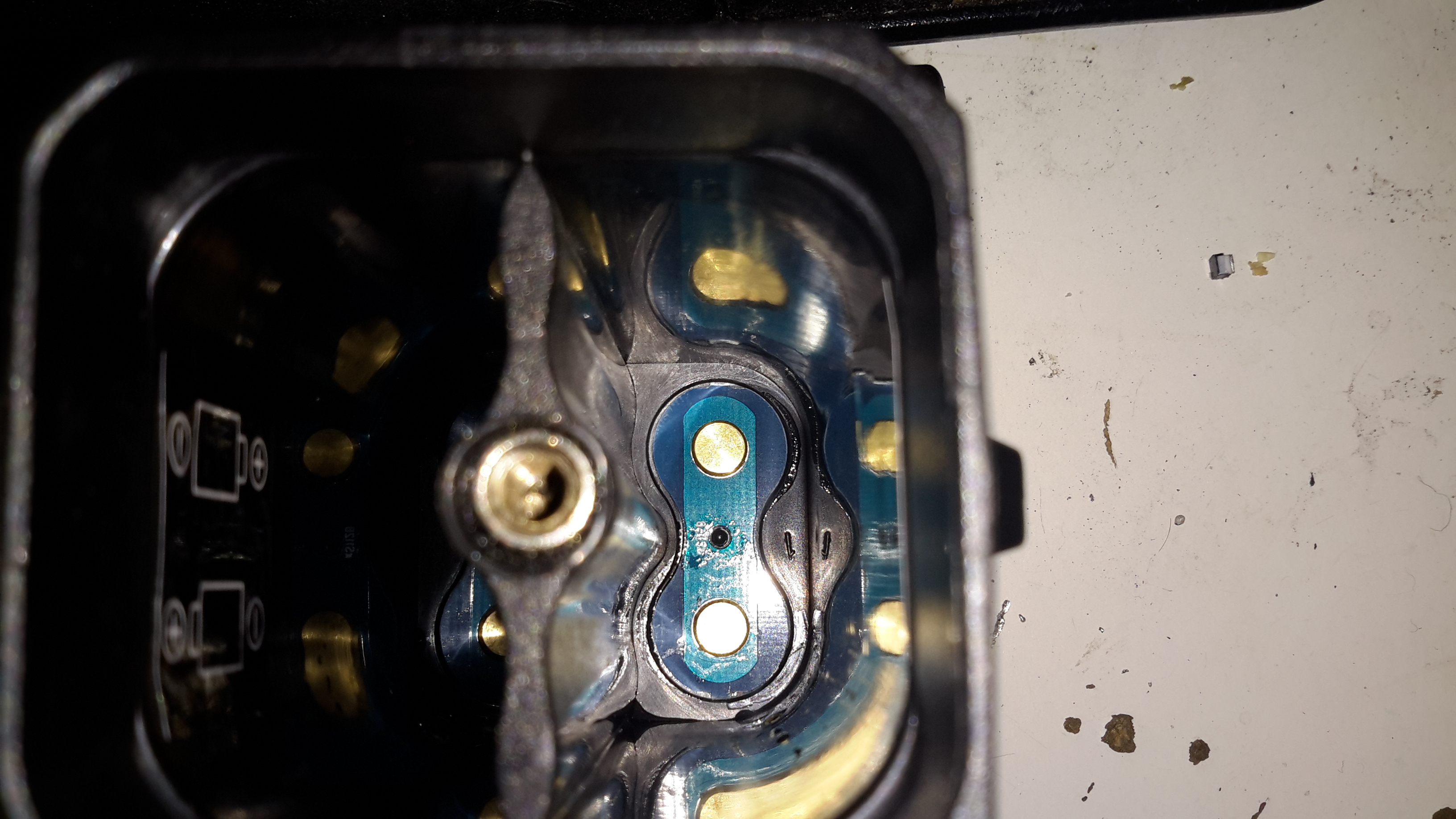
Interconnect Straps
The casing holds a PCB at the bottom end with the cell straps.
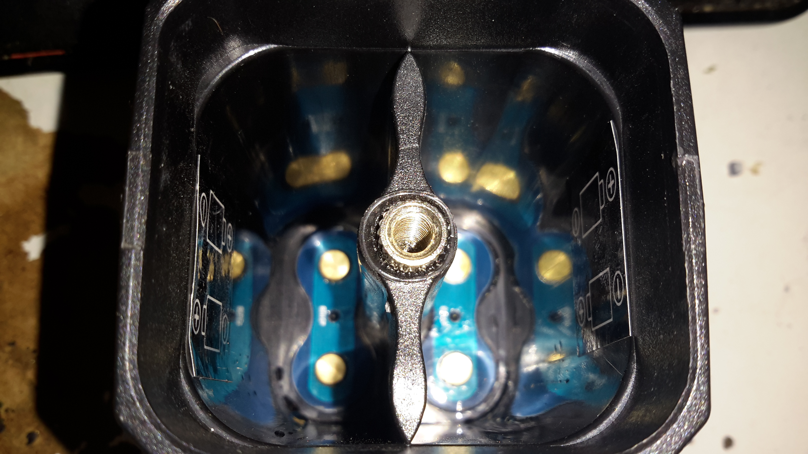
Screw Post
Someone wasn’t that careful at getting the brass screw insert properly centred in the injection mould when they did this one. It’s mushed off centre, but i’s solidly embedded & doesn’t present any problems to usability.
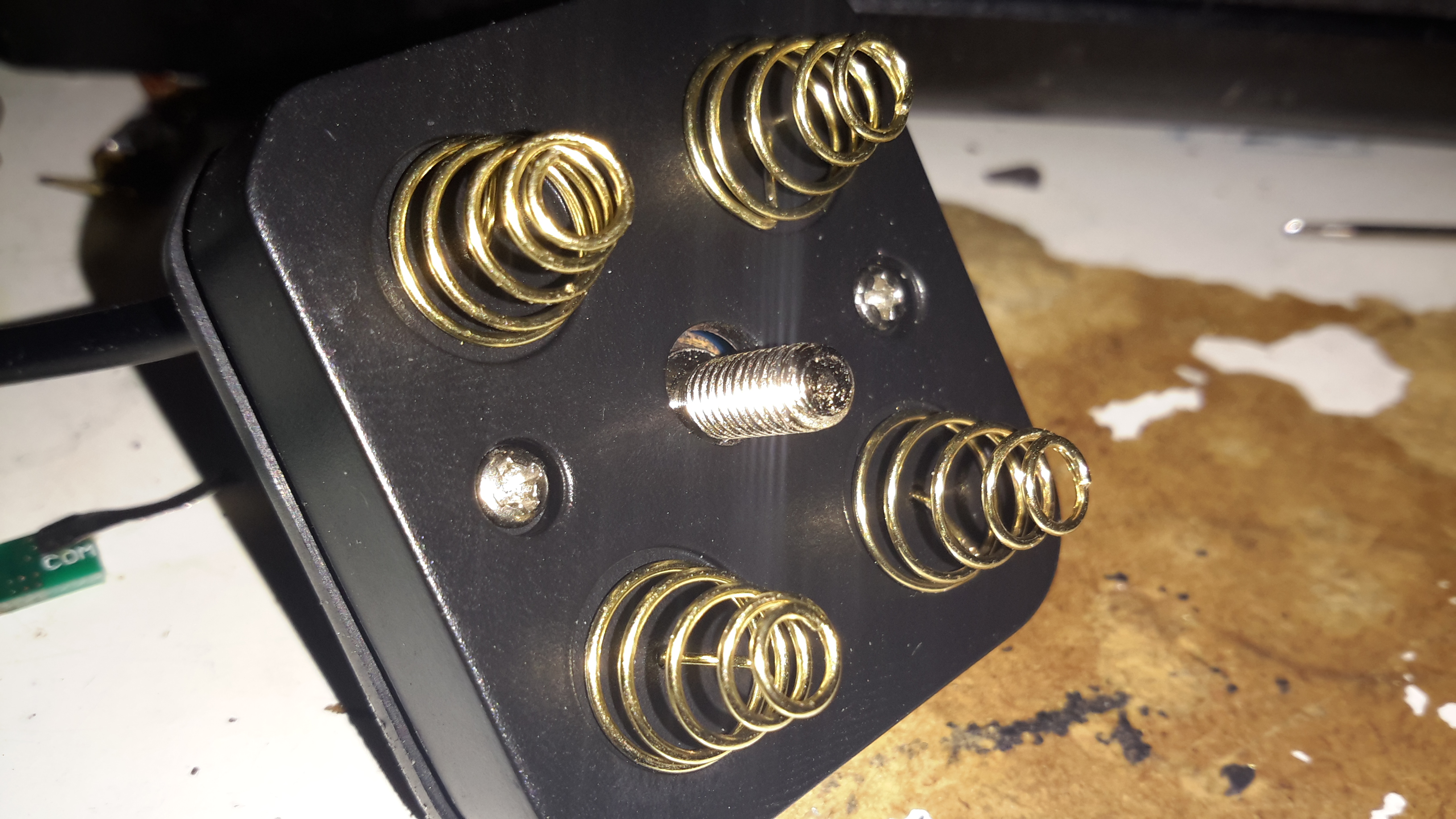
Cell Springs
The top cover holds the cell springs & the electronics.
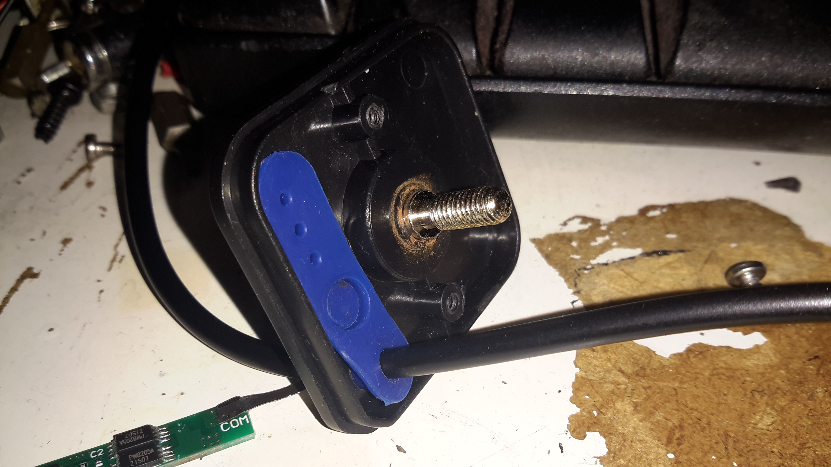
Button & Cable Seal
Removing the pair of screws allows the top cap to open up. The cable, button & LEDs are robustly sealed off with this silicone moulding.
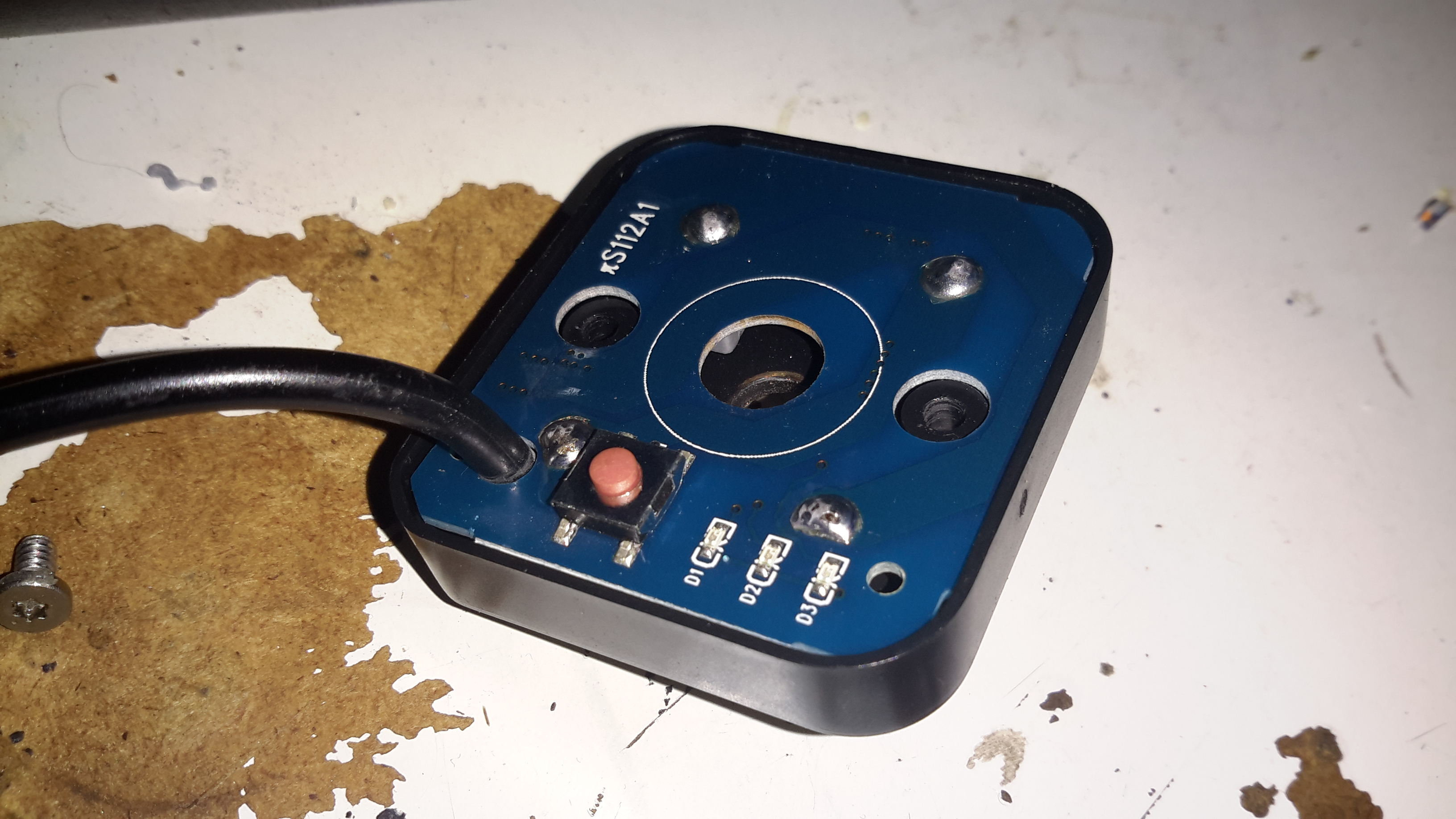
Top Removed
Here’s the PCB, not much on the top, other than the power button & battery indicator LEDs.
Electronics
Desoldering the cell springs allows the PCB to pop out of the plastic moulding. There’s more than I expected here!
Bottom left is a DC-DC converter, generating the +5v rail for the USB port, this is driven with an XL1583 3A buck converter IC.
Bottom right is the protection IC & MOSFETs for the Lithium Ion cells. I wasn’t able to find a datasheet for the tiny VA7022 IC, but I did manage to make certain it was a 7.4v Li-Ion protection IC.
Top right is a completely unmarked IC, and a 3.3v SOT-23 voltage regulator. I’m assuming that the unmarked IC is a microcontroller of some sort, as it’s handling more than just the battery level LEDs.
A pretty decent 4-core cable finishes the job off. For once there’s actually some copper in this cable, not the usual Chineseuim thin-as-hair crap.
As I’ve been posting some photos of decapped ICs lately, I thought I’d share the process I use personally for those that might want to give it a go 😉
The usual method for removing the epoxy package from the silicon is to use hot, concentrated Nitric Acid. Besides the obvious risks of having hot acids around, the decomposition products of the acid, namely NO² (Nitrogen Dioxide) & NO (Nitrogen Oxide), are toxic and corrosive. So until I can get the required fume hood together to make sure I’m not going to corrode the place away, I’ll leave this process to proper labs ;).
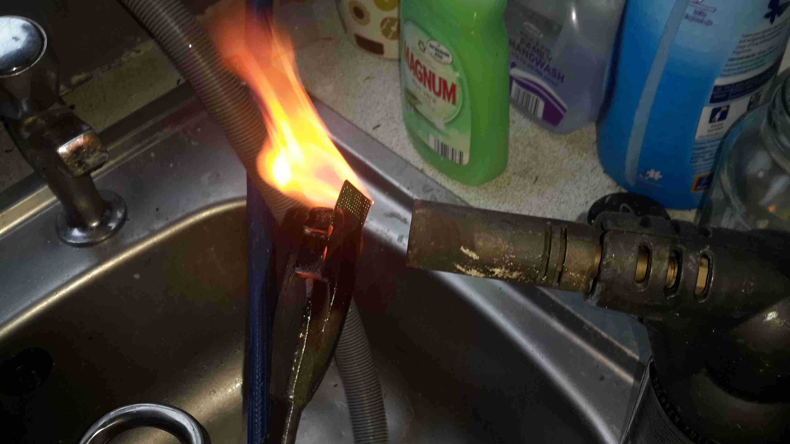
The method I use is heat based, using a Propane torch to destroy the epoxy package, without damaging the Silicon die too much.
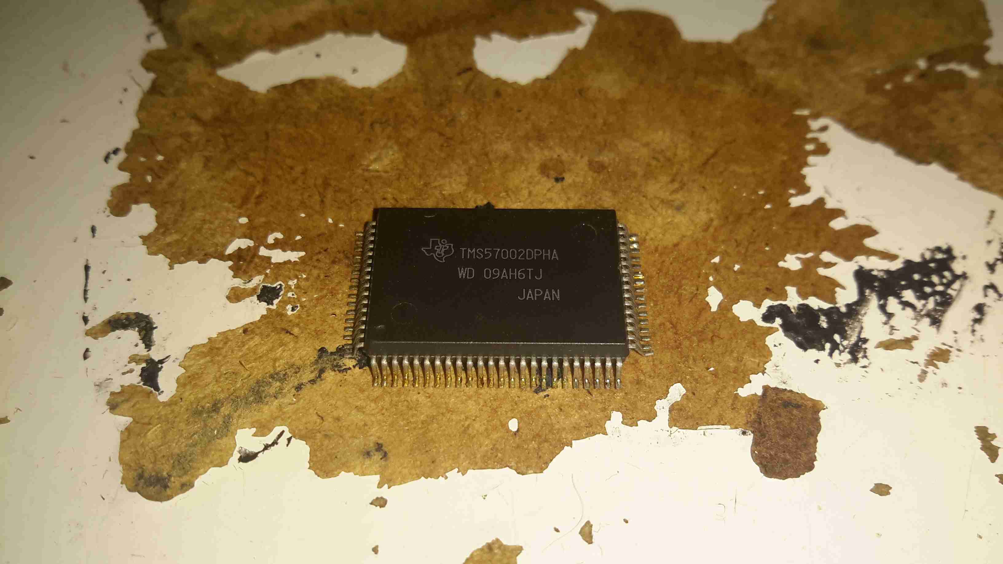
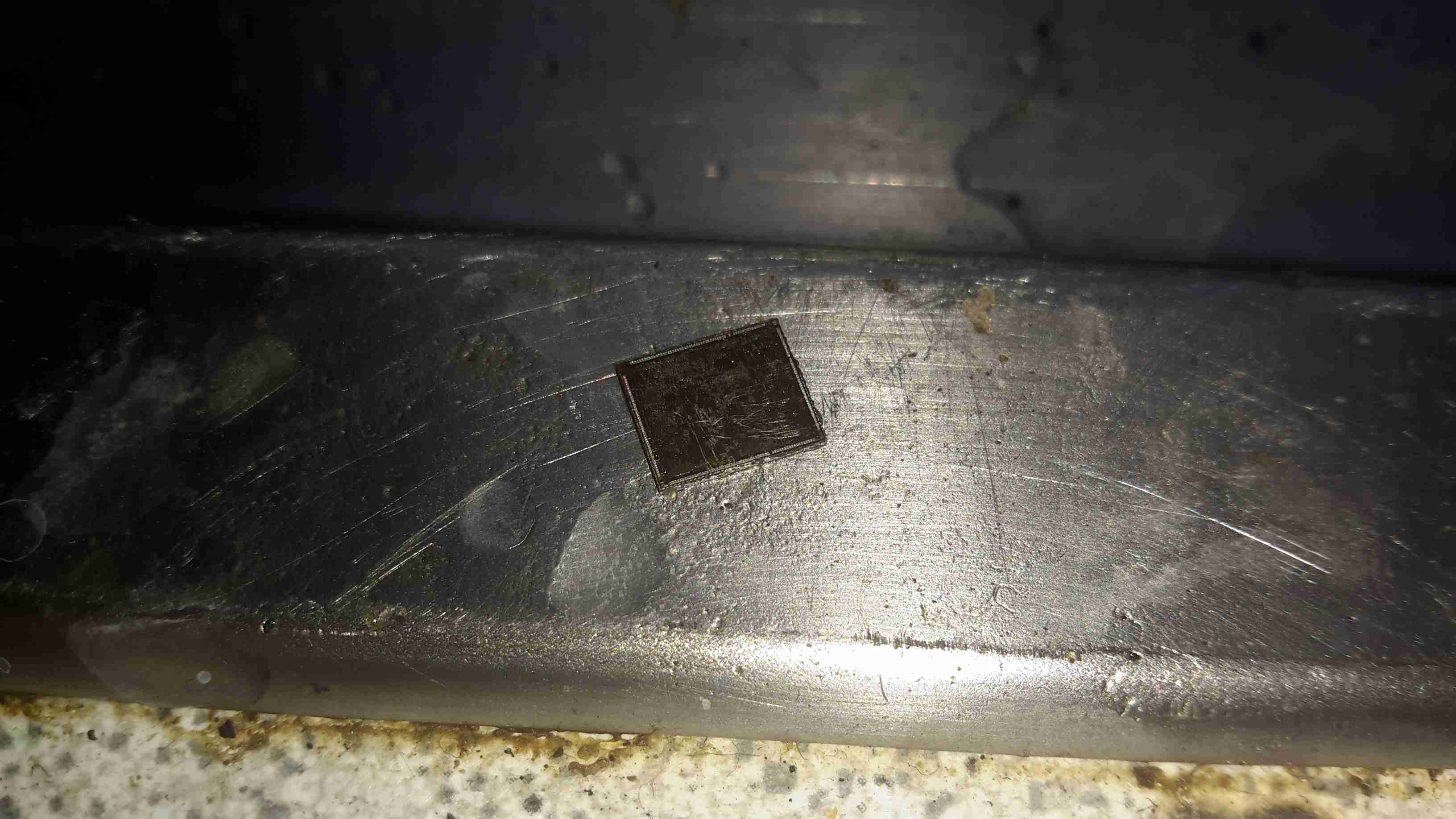
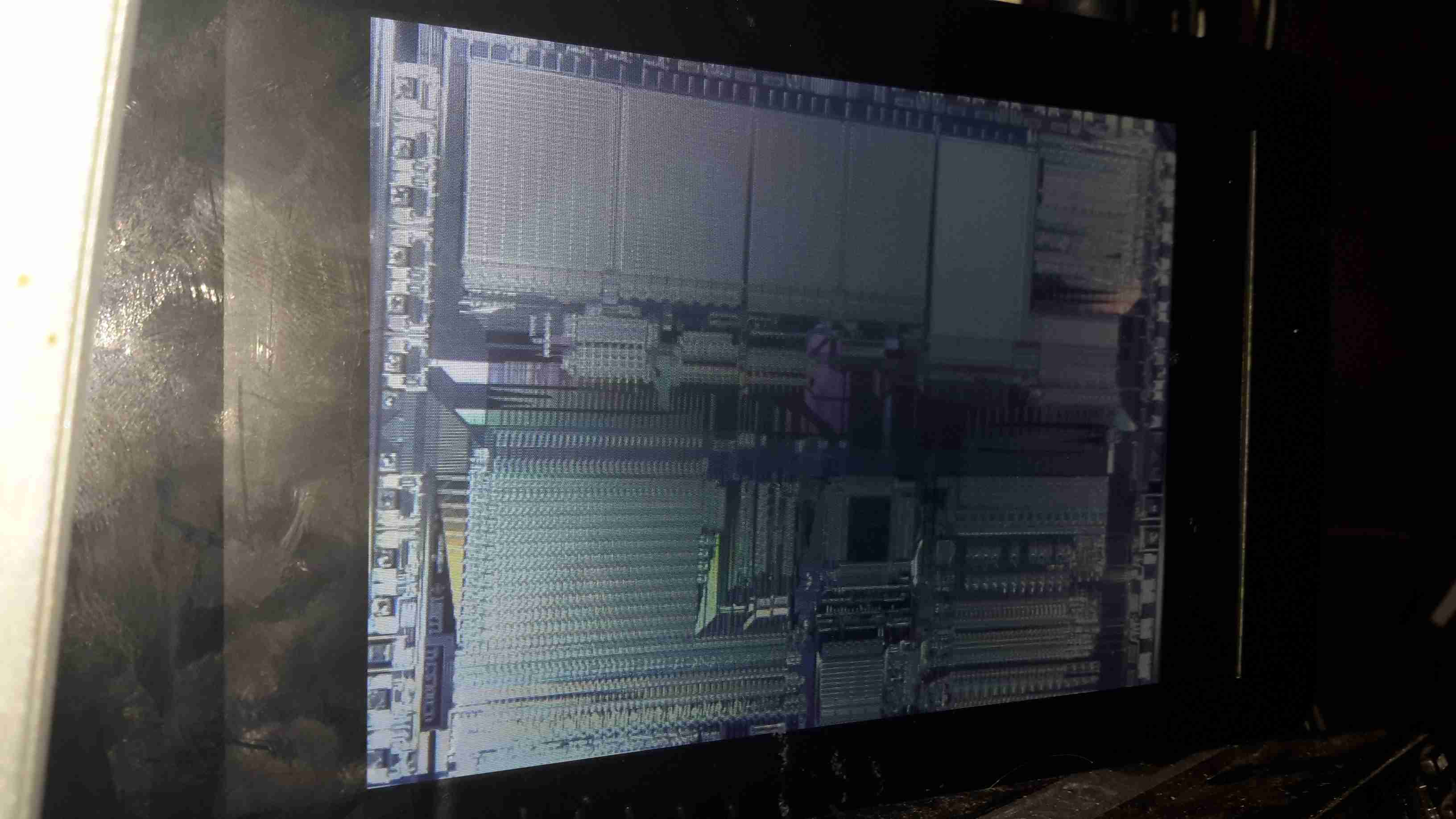
TMS57002 Audio DSP
I start off, obviously, with a desoldered IC, the one above an old audio DSP from TI. I usually desolder en-masse for this with a heat gun, stripping the entire board in one go.
FLAMES!
Next is to apply the torch to the IC. A bit of practice is required here to get the heat level & time exactly right, overheating will cause the die to oxidize & blacken or residual epoxy to stick to the surface.
I usually apply the torch until the package just about stops emitting it’s own yellow flames, meaning the epoxy is almost completely burned away. I also keep the torch flame away from the centre of the IC, where the die is located.
Breathing the fumes from this process isn’t recommended, no doubt besides the obvious soot, the burning plastic will be emitting many compounds not brilliant for Human health!
Once the IC is roasted to taste, it’s quenched in cold water for a few seconds. Sometimes this causes such a high thermal shock that the leadframe cracks off the epoxy around the die perfectly.
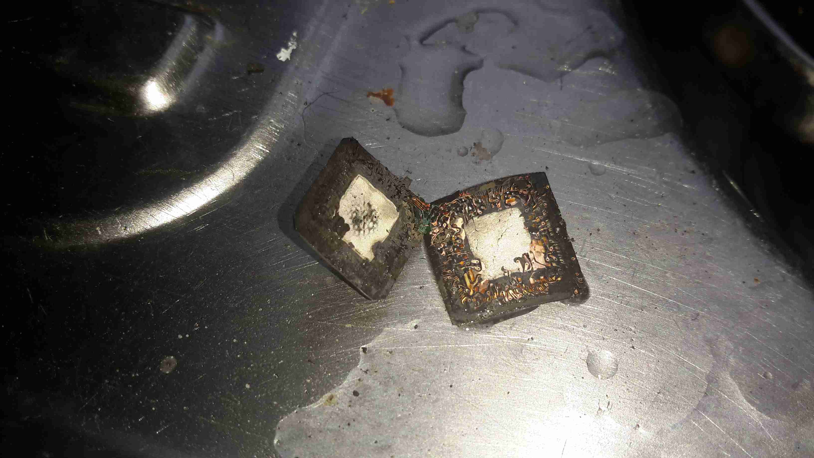
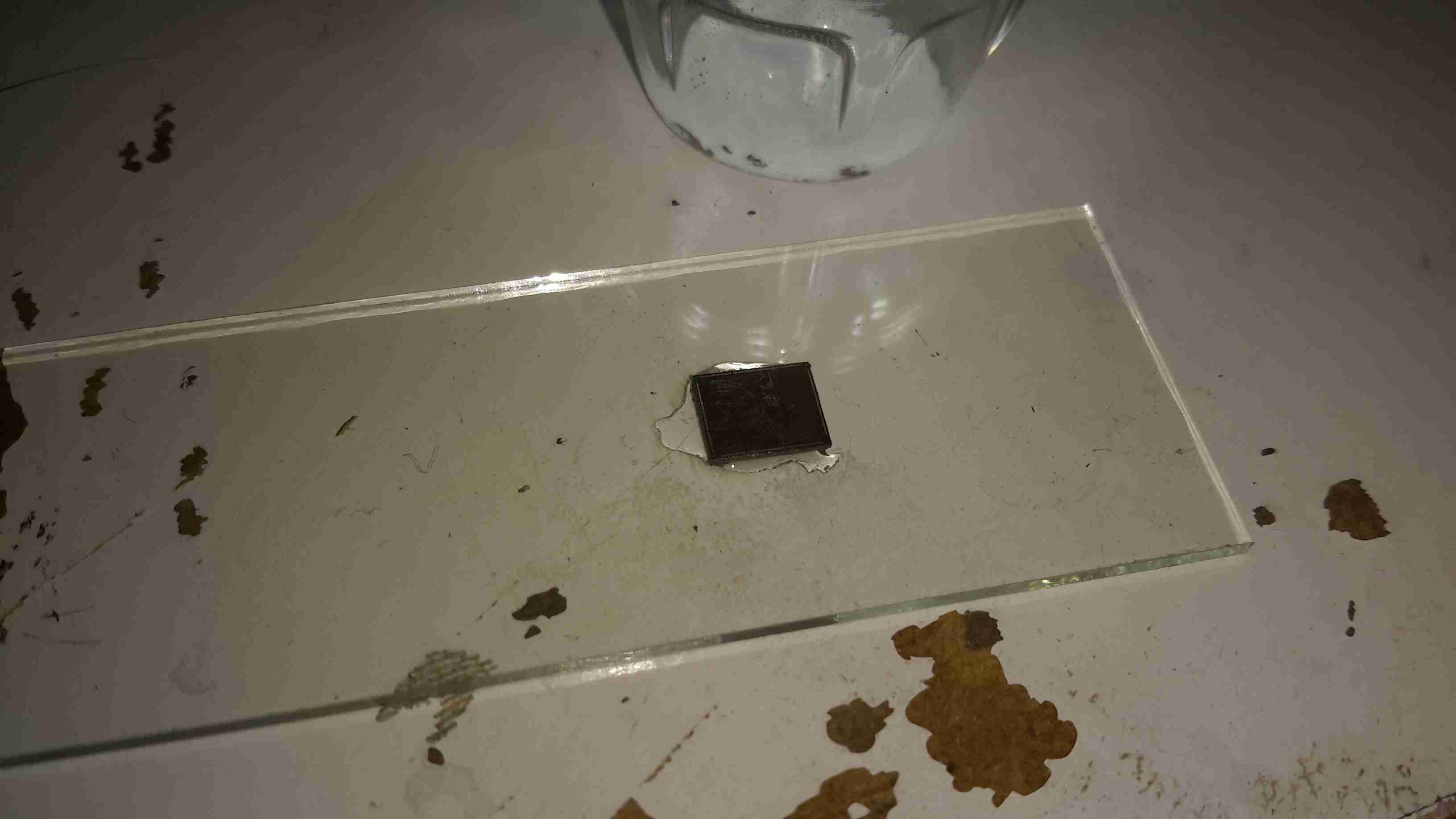
All Your Die Belong To Us
Now that the epoxy has been destroyed, it breaks apart easily, and is picked away until I uncover the die itself. (It’s the silver bit in the middle of the left half). The heat from the torch usually destroys the Silver epoxy holding the die to the leadframe, and can be removed easily from the remaining package.
Decapped
BGA packages are usually the easiest to decap, flip-chip packages are a total pain due to the solder balls being on the front side of the die, I haven’t managed to get a good result here yet, I’ll probably need to chemically remove the first layer of the die to get at the interesting bits 😉
Slide
Once the die has been rinsed in clean water & inspected, it’s mounted on a glass microscope slide with a small spot of Cyanoacrylate glue to make handling easier.
Some dies require some cleaning after decapping, for this I use 99% Isopropanol & 99% Acetone, on the end of a cotton bud. Any residual epoxy flakes or oxide stuck to the die can be relatively easily removed with a fingernail – turns out fingernails are hard enough to remove the contamination, but not hard enough to damage the die features.
Once cleaning is complete, the slide is marked with the die identification, and the photographing can begin.
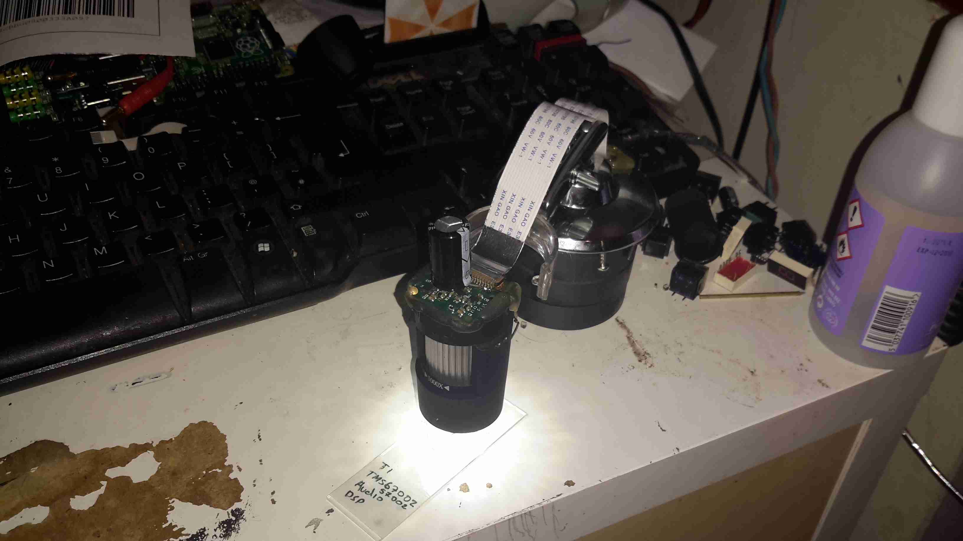
Microscope Mods
I had bought a cheap eBay USB microscope to get started, as I can’t currently afford a proper metallurgical microscope, but I found the resolution of 640×480 very poor. Some modification was required!
Modified Microscope
I’ve removed the original sensor board from the back of the optics assembly & attached a Raspberry Pi camera board. The ring that held the original sensor board has been cut down to a minimum, as the Pi camera PCB is slightly too big to fit inside.
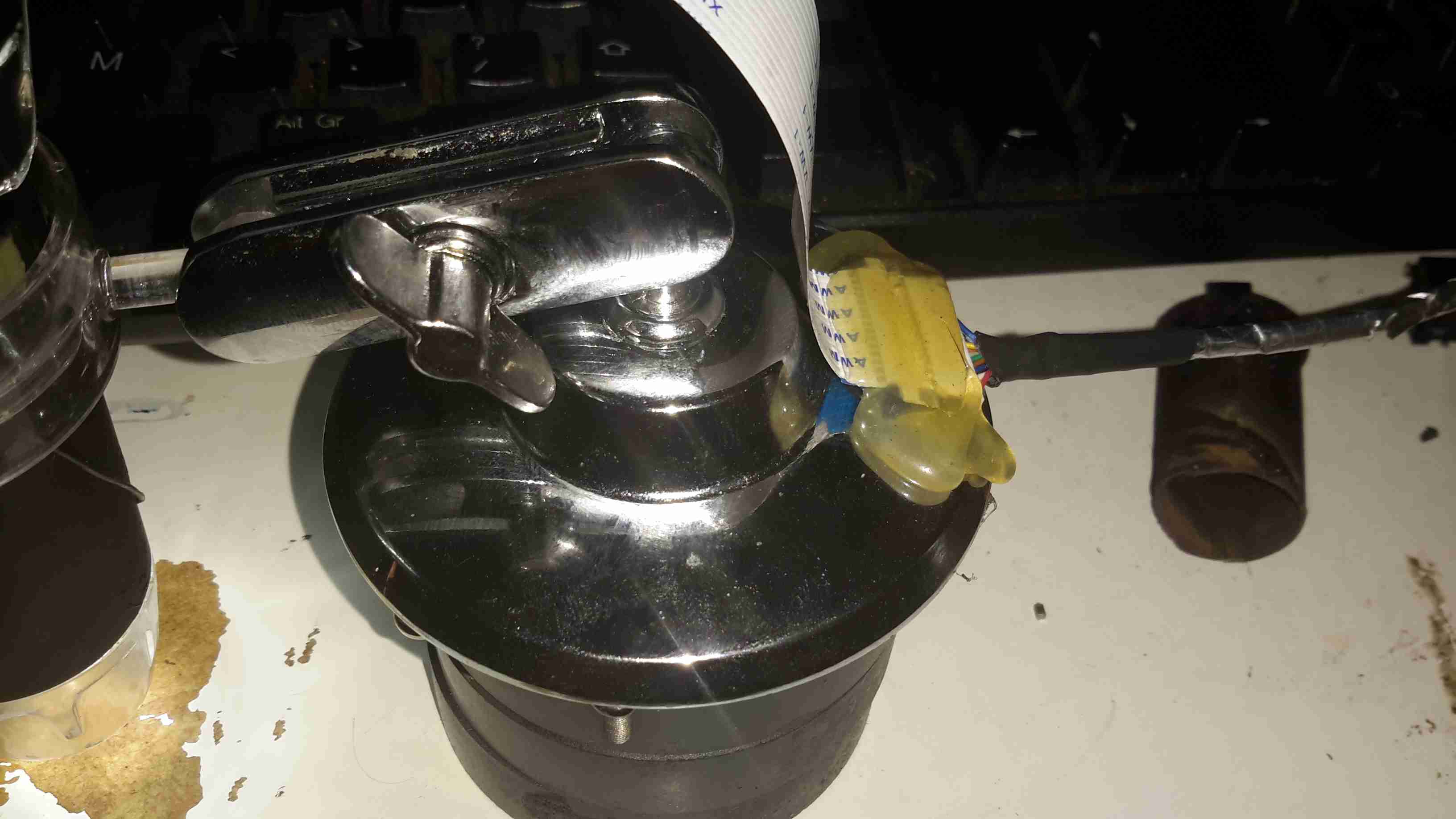
The stock ring of LEDs is run direct from the 3.3v power rail on the camera, through a 4.7Ω resistor, for ~80mA. I also added a 1000µF capacitor across the 3.3v supply to compensate a bit for the long cable – when a frame is captured the power draw of the camera increases & causes a bit of voltage drop.
The stock lens was removed from the Pi camera module by careful use of a razor blade – being too rough here *WILL* damage the sensor die or the gold bond wires, which are very close to the edge of the lens housing, so be gentle!
Mounting Base
The existing mount for the microscope is pretty poor, so I’ve used a couple of surplus ceramic ring magnets as a better base, this also gives me the option of raising or lowering the base by adding or removing magnets.
To get more length between the Pi & the camera, I bought a 1-meter cable extension kit from Pi-Cables over at eBay, cables this long *definitely* require shielding in my space, which is a pretty aggressive RF environment, or interference appears on the display. Not surprising considering the high data rates the cable carries.
The FFC interface is hot-glued to the back of the microscope mount for stability, for handheld use the FFC is pretty flexible & doesn’t apply any force to the scope.
Die Photography
Since I modified the scope with a Raspberry Pi camera module, everything is done through the Pi itself, and the raspistill command.
Pi LCD
The command I’m currently using to capture the images is:
raspistill -ex auto -awb auto -mm matrix -br 62 -q 100 -vf -hf -f -t 0 -k -v -o CHIPNAME_%03d.jpg
This command waits between each frame for the ENTER key to be pressed, allowing me to position the scope between shots. Pi control & file transfer is done via SSH, while I use the 7″ touch LCD as a viewfinder.
The direct overhead illumination provided by the stock ring of LEDs isn’t ideal for some die shots, so I’m planning on fitting some off-centre LEDs to improve the resulting images.
Image Processing
Obviously I can’t get an ultra-high resolution image with a single shot, due to the focal length, so I have to take many shots (30-180 per die), and stitch them together into a single image.
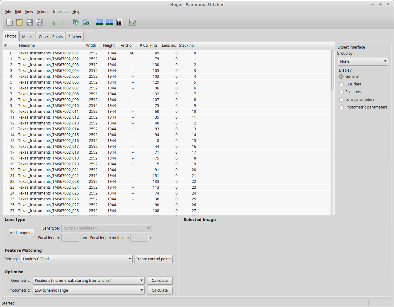
For this I use Hugin, an open-source panorama photo stitching package.
Hugin
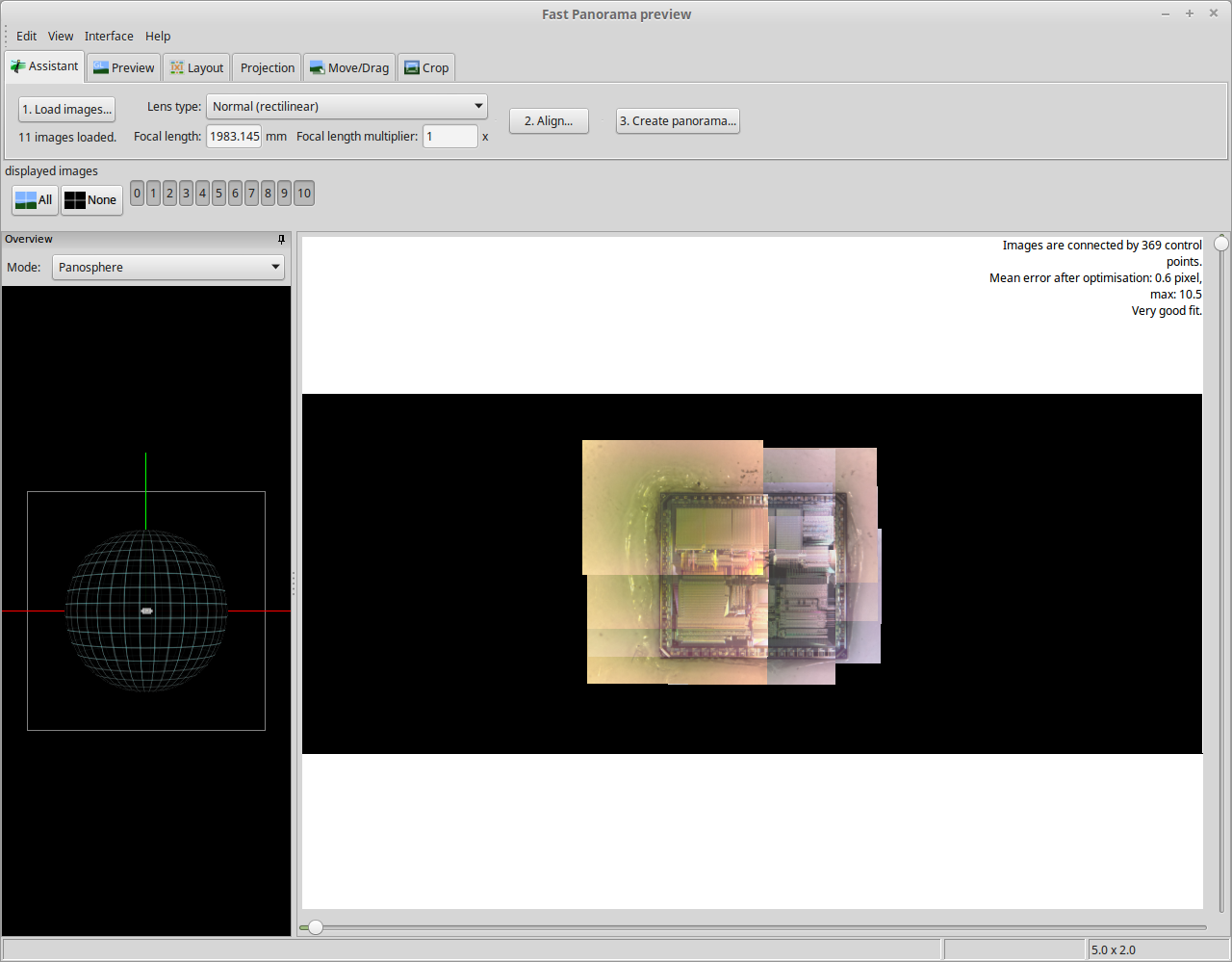
Here’s Hugin with the photos loaded in from the Raspberry Pi. To start with I use Hugin’s built in CPFind to process the images for control points. The trick with getting good control points is making sure the images have a high level of overlap, between 50-80%, this way the software doesn’t get confused & stick the images together incorrectly.
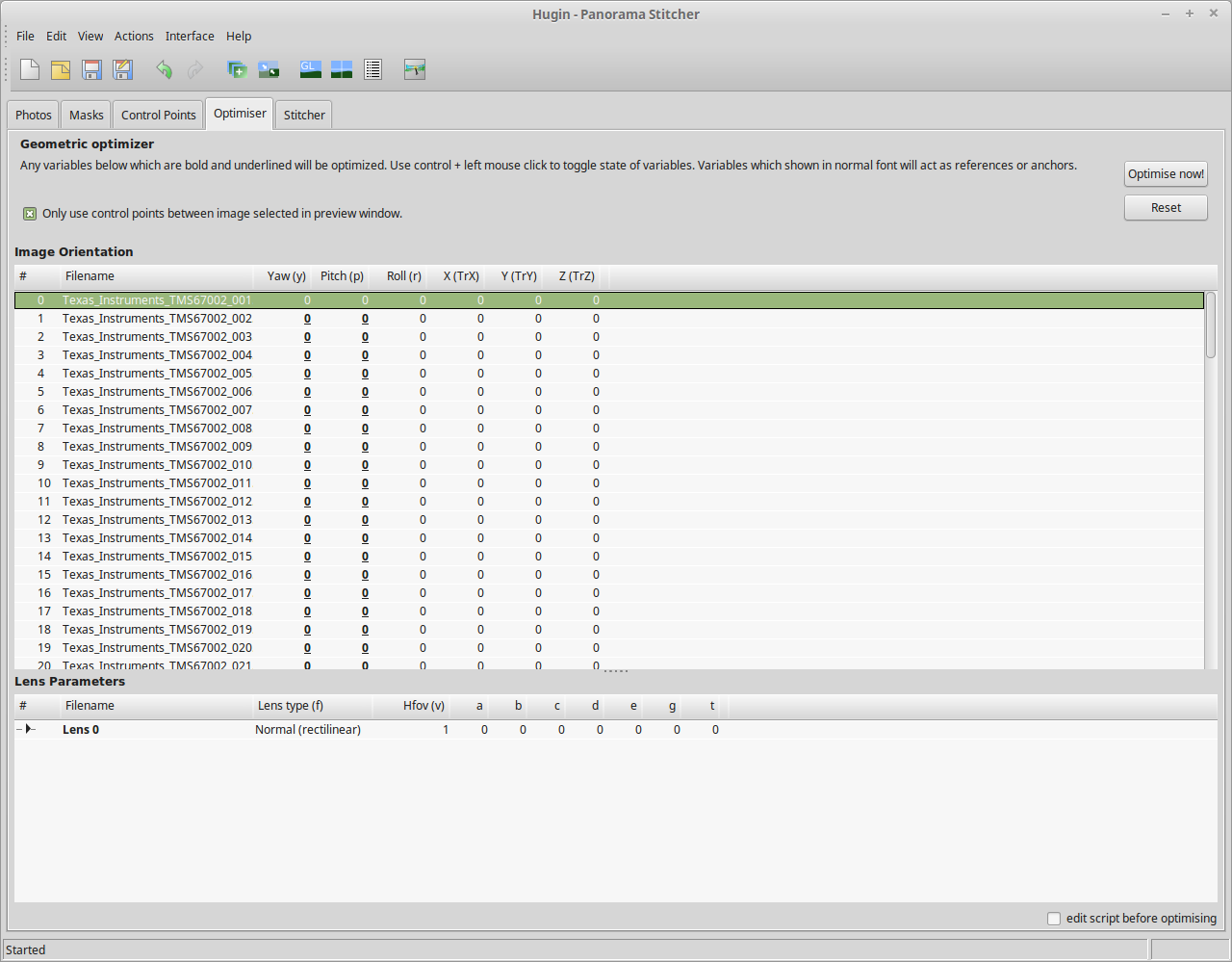
Optimiser
After the control points are generated, which for a large number of high resolution images can take some time, I run the optimiser with only Yaw & Pitch selected for all images.
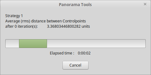
Optimising
If all goes well, the resulting optimisation will get the distance between control points to less than 0.3 pixels.
Panorama Preview
After the control points & optimisation is done, the resulting image can be previewed before generation.
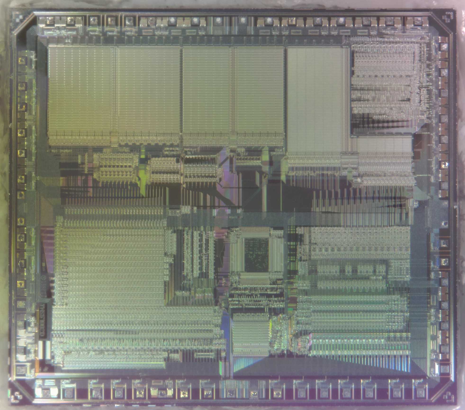
Texas Instruments TMS67002
After all the image processing, the resulting die image should look something like the above, with no noticeable gaps.
The multimode dimming/flashing modes on Chinese torches have irritated me for a while. If I buy a torch, it’s to illuminate something I’m doing, not to test if people around me have photosensitive epilepsy.
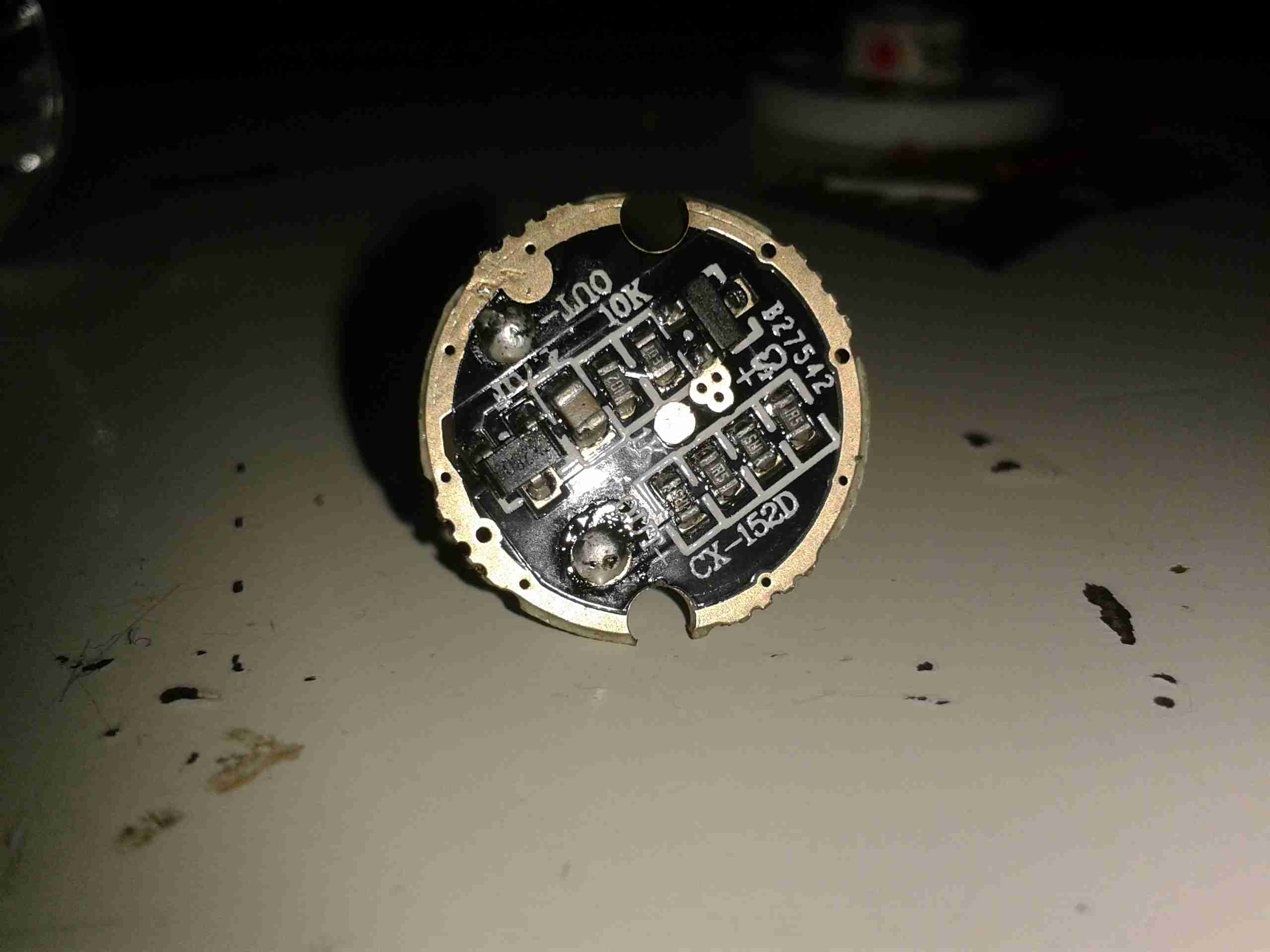
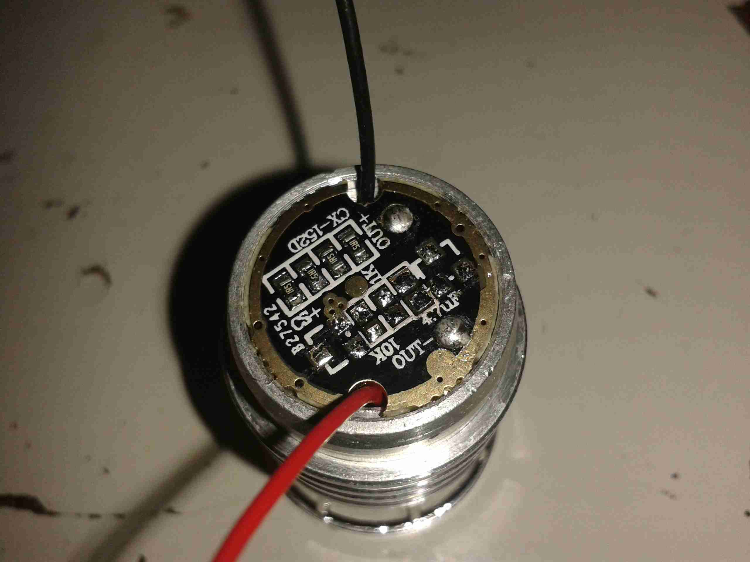
Looking at the PCB in the LED module of the torch, a couple of components are evident:
LED Driver PCB
There’s not much to this driver, it’s simply resistive for LED protection (the 4 resistors in a row at the bottom of the board).
The components at the top are the multimode circuitry. The SOT-23 IC on the left is a CX2809 LED Driver, with several modes. The SOT-23 on the right is a MOSFET, for switching the actual LED itself. I couldn’t find a datasheet for the IC itself, but I did find a schematic that seems to match up with what’s on the board.
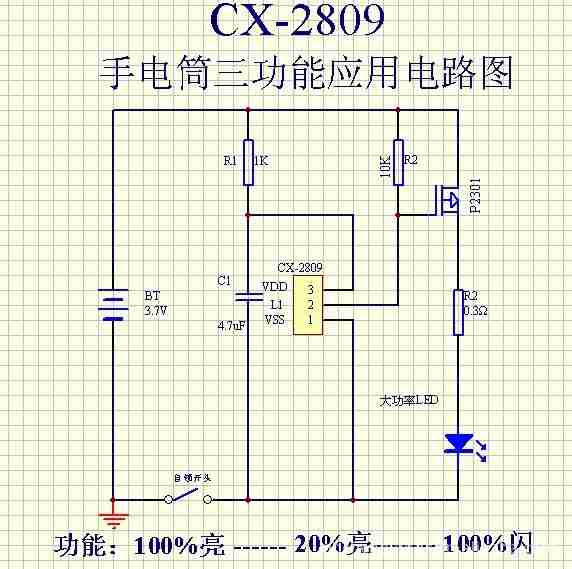
Schematic
Here’s that schematic, the only thing that needs to be done to convert the torch to single mode ON/OFF at full brightness, is to bridge out that FET.
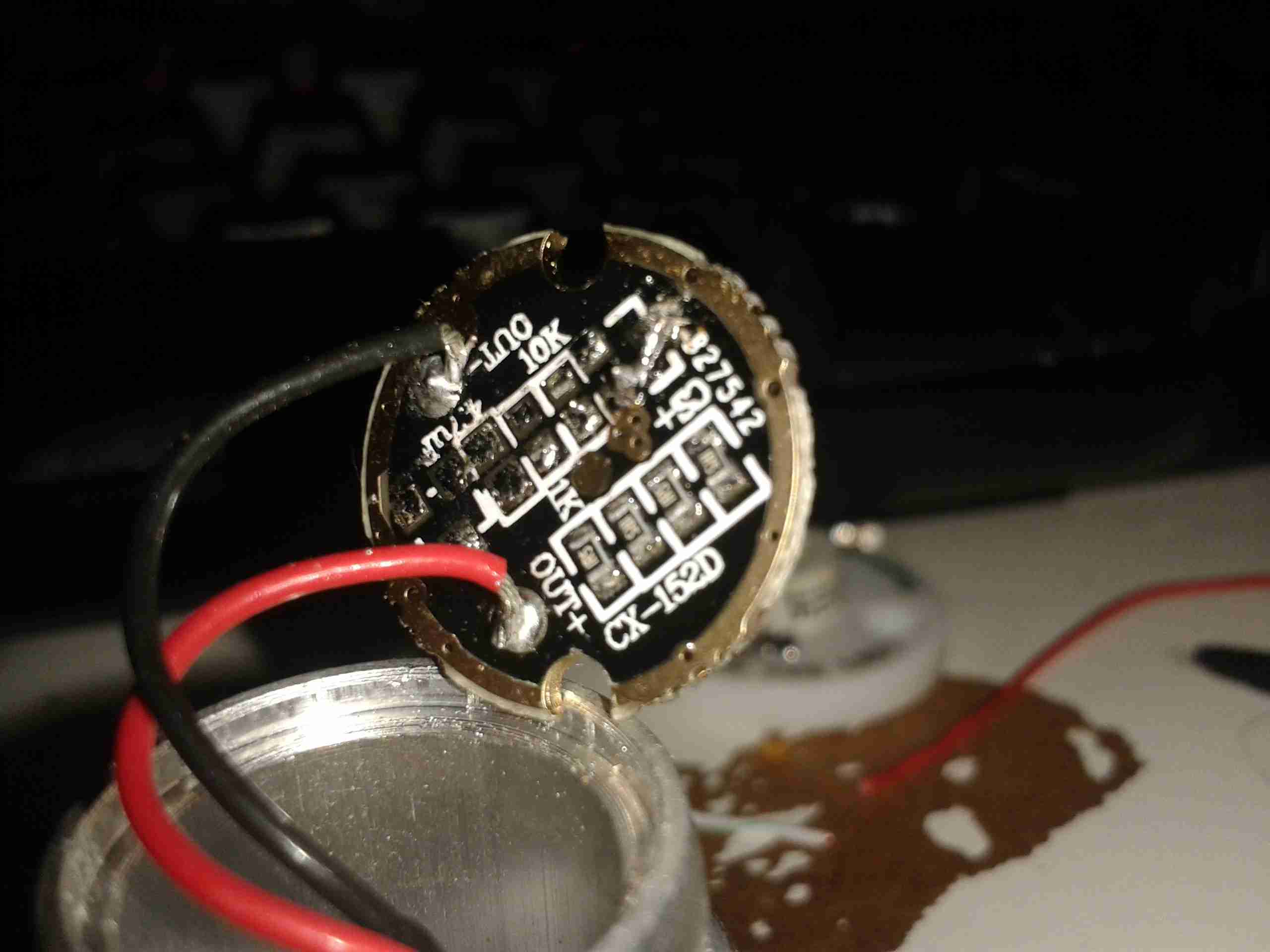
Components Desoldered
To help save the extra few mA the IC & associated circuitry will draw from the battery, I have removed all of the components involved in the multimode control. This leaves just the current limiting resistors for the LED itself.
Jumper Link
The final part above, is to install a small link across the Drain & Source pads of the FET. Now the switch controls the LED directly with no silly electronics in between. A proper torch at last.
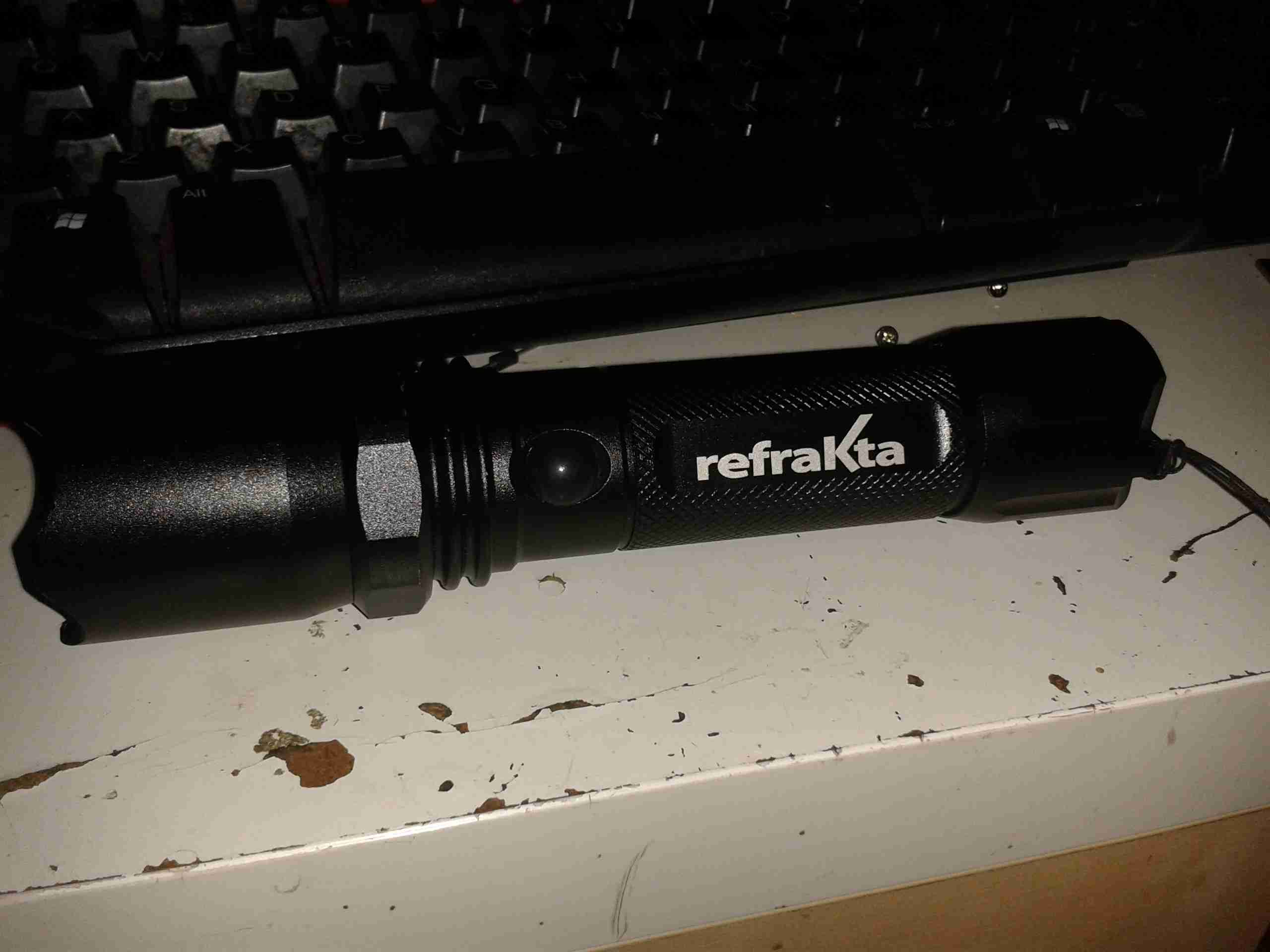
Following on from the teardown & analysis of the charger, here’s the torch itself under the spotlight.
LED Torch
Here’s the torch itself, it’s a sturdy device, made of aluminium. Power is provided by a single 18650 Li-Ion cell.
Charging Port
Here’s the charging port on the torch, there’s no electronics in here for controlling the charge, the socket is simply connected directly to the Li-Ion cell, and requires a proper external charger.
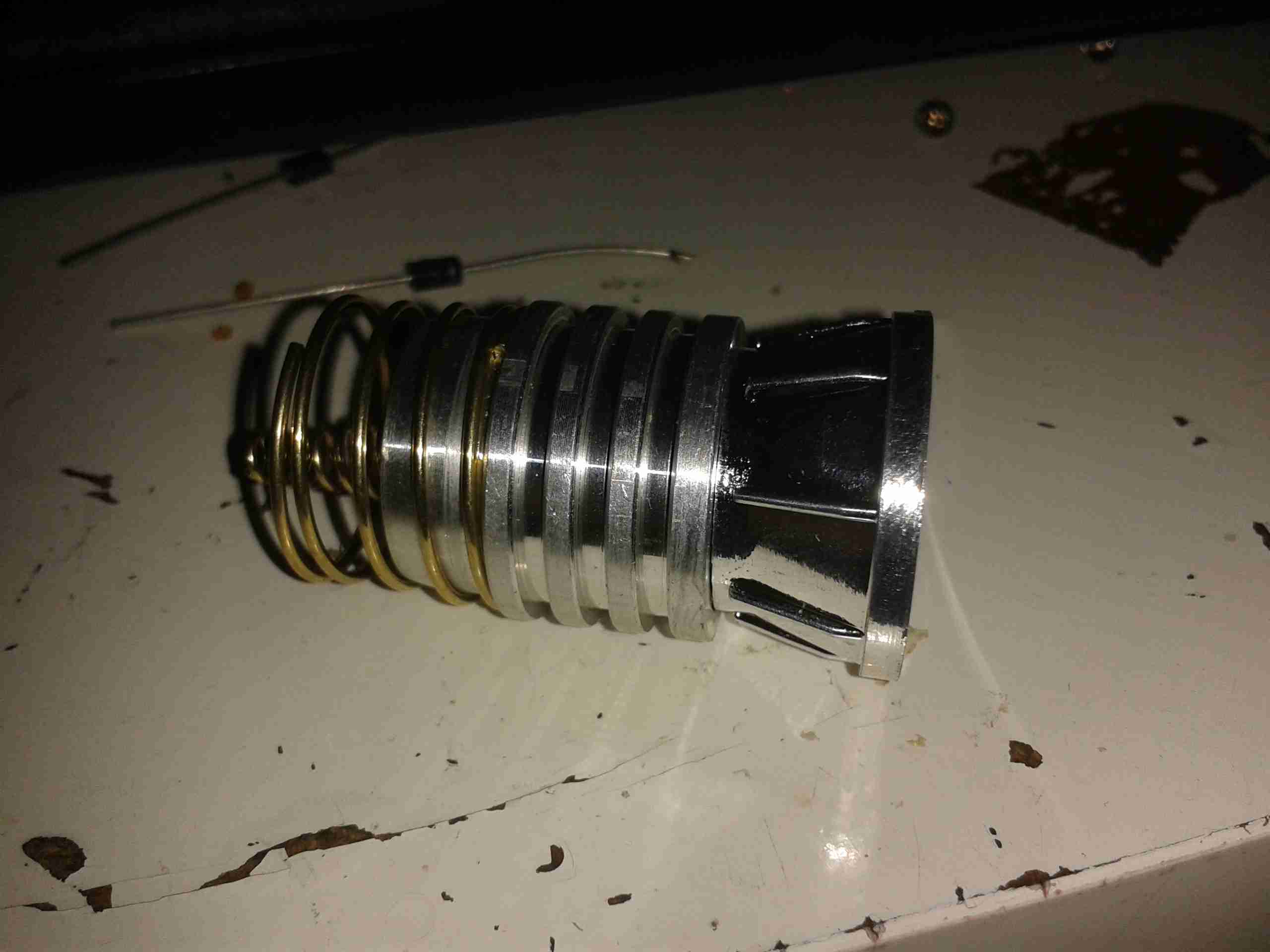
LED Pill
Unscrewing the lens gives access to the LED core, this also unscrews from the torch body itself, leaving the power switch & the battery in the body.
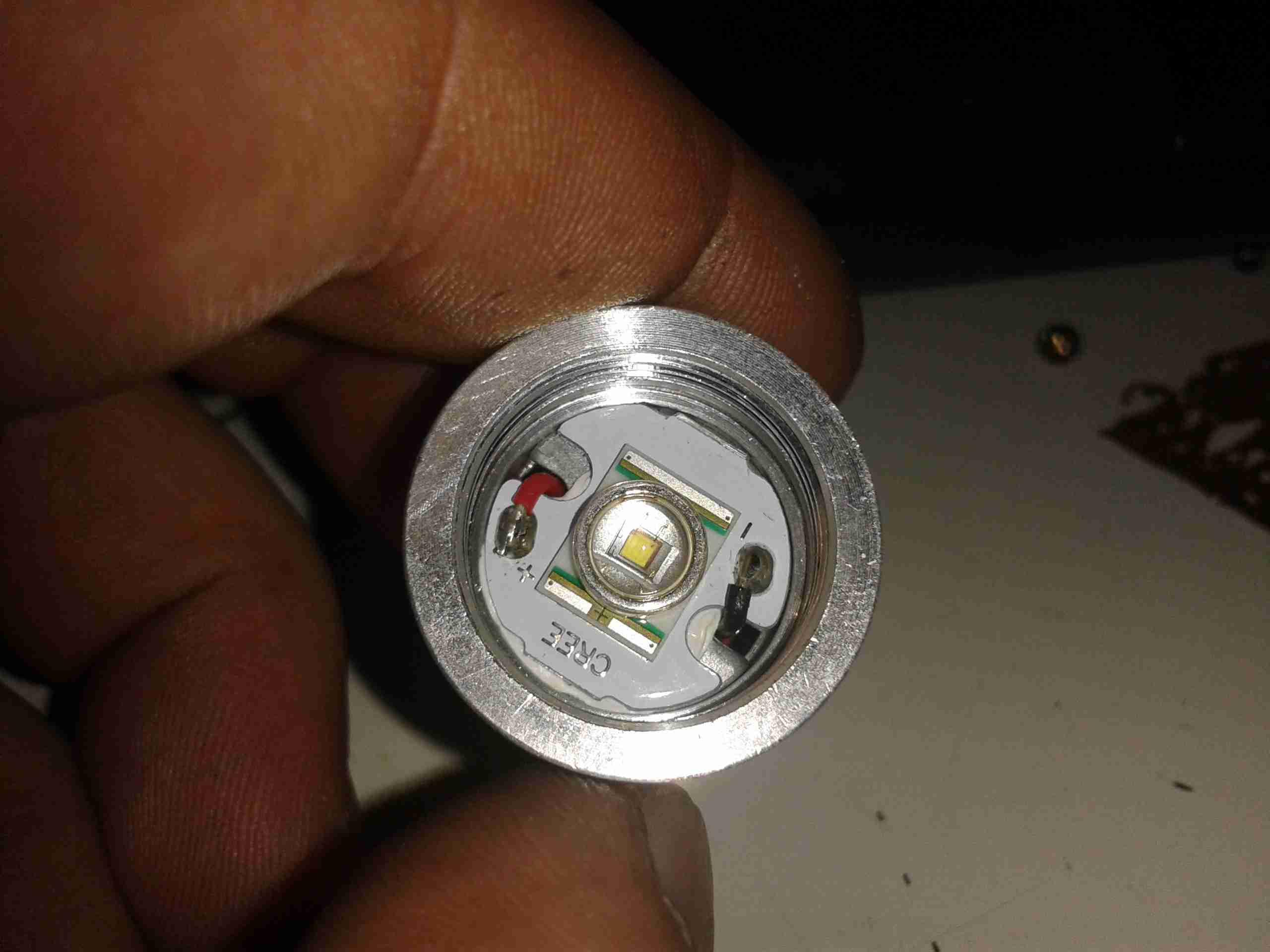
LED Module
Unscrewing the aluminised plastic reflector reveals the LED itself. Being a new device, I expected an XM-L or XM-L2 Cree LED in here, but it’s actually an XR-E model, a significantly older technology, rated at max 1A of drive current.
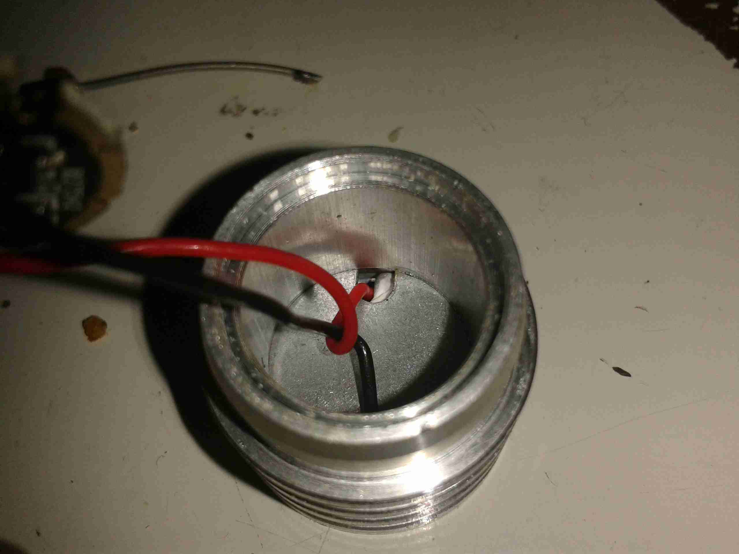
LED Back
Popping the control PCB out from the pill reveals a lot of empty space, but the back of the LED is completely covered by a heatsinking plate, which is conducting heat to the main body of the torch.
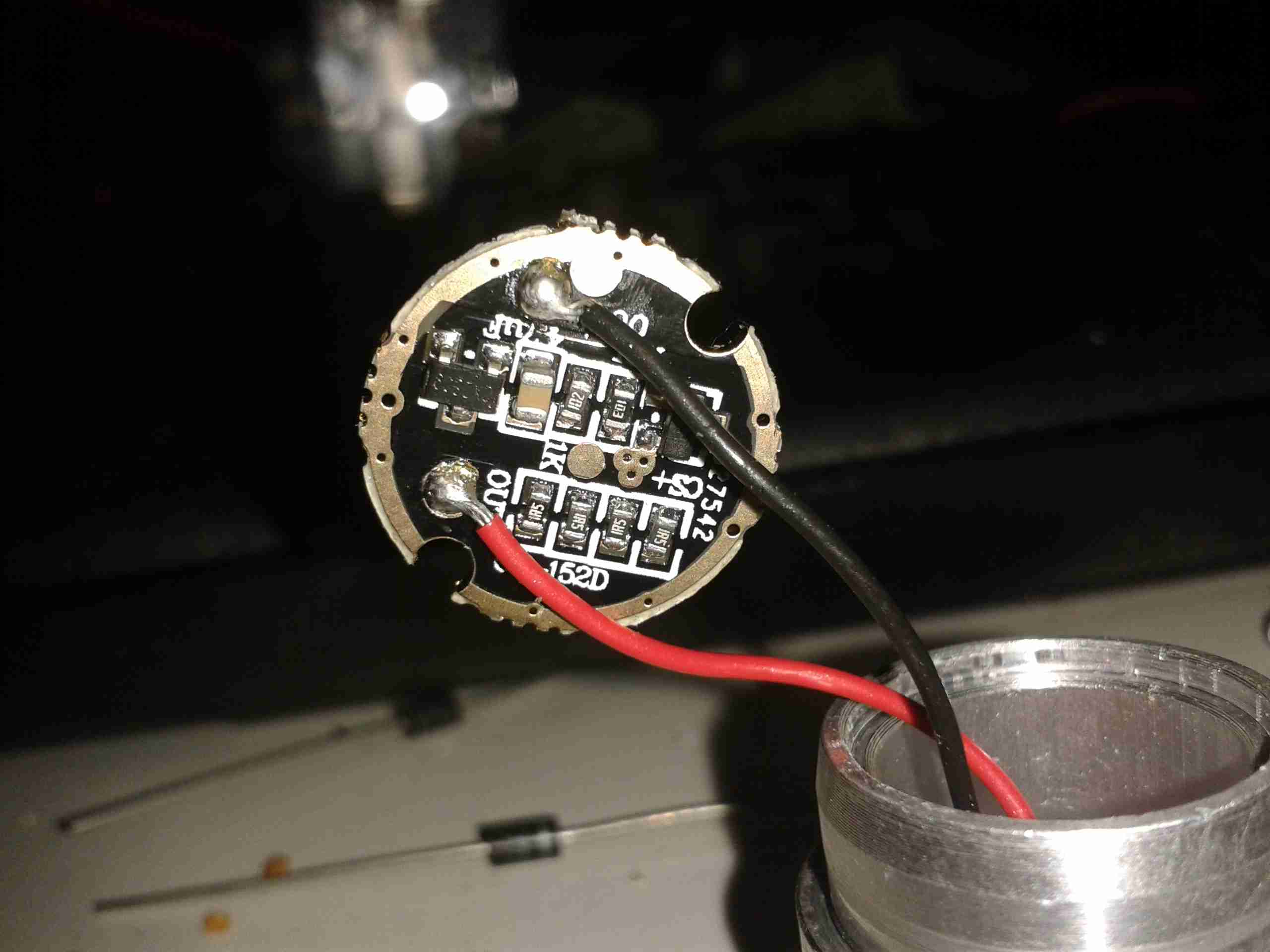
Control PCB
Not much to see on the control PCB, just a bunch of limiting resistors, and a multi-mode LED driver IC in a SOT-23 package. There’s no proper constant-current LED driver, and as the battery discharges the torch will dim, until the low voltage cutout on the cell turns things off completely.
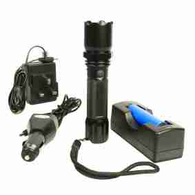
A member of the family recently bought one of these torches from Maplin electronics, and the included chargers for the 18650 lithium-ion cells leave a lot to be desired.
Torch
Here’s what’s supplied. The torch itself is OK – very bright, and a good size. Me being cynical of overpriced Chinese equipment with lithium batteries, I decided to look in the charging base & the cigar-lighter adaptor to see if there was any actual charging logic.
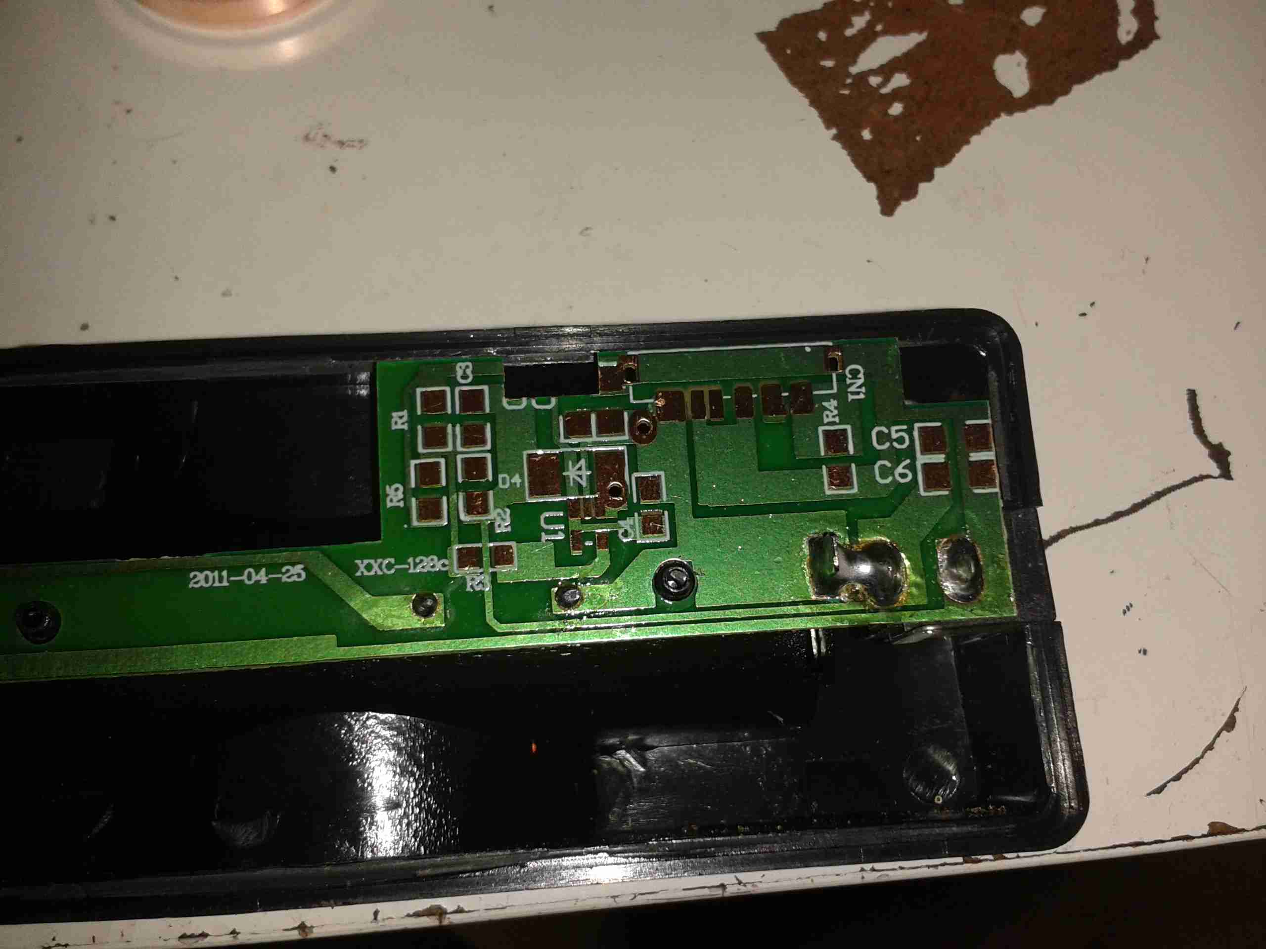
Charger
Answer – nope. Not a single active component in here. It’s just a jack connected to the battery terminals. There’s all the space there to fit a proper charging circuit, but it’s been left out to save money.
OK then, is it inside the cigarette lighter adaptor?
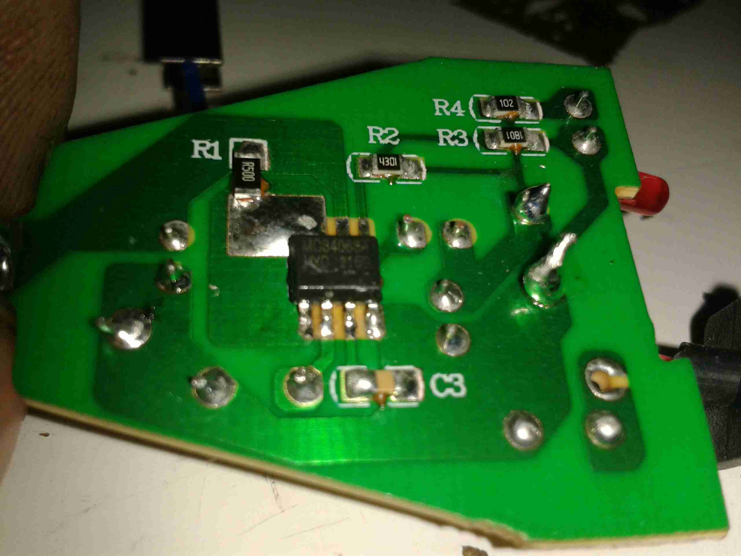
Lighter Adaptor
Nope. Not a single sign of anything resembling a Lithium-Ion charger IC. There’s a standard MC34063A 1.5A Buck converter IC on the bottom of the PCB, this is what’s giving the low voltage output for the torch.
Charger Bottom
Here’s the IC – just a buck converter. The output voltage here is 4.3v. This is higher than the safe charging voltage of a lithium ion cell, of 4.2v.
The cells supplied are “protected” versions, having charge/discharge protection circuitry built onto the end of the cell on a small PCB, this makes the cell slightly longer than a bare 18650, so it’s easy to tell them apart.
The manufacturers in this case are relying on that protection circuit on the cell to prevent an overcharge condition – this isn’t the purpose they’re designed for, and charging this way is very stressful for the cells. I wouldn’t like to leave one of these units charging unattended, as a battery explosion might result.
More to come shortly when I build a proper charger for this torch, so it can be recharged without fearing an alkali metal fire!
This is a cheap Sigma branded keychain photoframe. User buttons for power & selecting photos are on the left.
There are two white LEDs on the bottom edge that function as a torch as well.
Display
Front of the unit removed, showing the LCD module. The USB jack is bottom left, next to the pair of white LEDs & above that is the 32kHz watch crystal that the CPU uses for timekeeping.
Back Removed
Here the back has been removed showing the 3.7v Li-Ion cell used to provide power.
Display Folded Back
Here the display has been removed from the PCB exposing the chipset.
Chipset
Here the CPU blob-top chip & a flash memory IC are visible. The CPU is a Sitronix ST2205U.
Tip Jar
If you’ve found my content useful, please consider leaving a donation by clicking the Tip Jar below!
All collected funds go towards new content & the costs of keeping the server online.