Since this phone has been in my drawer for some time, I figured it was time for a teardown. (It’s never going to see any more use).
The back cover on these phones is easily removed, as it’s just clipped on.
Motherboard
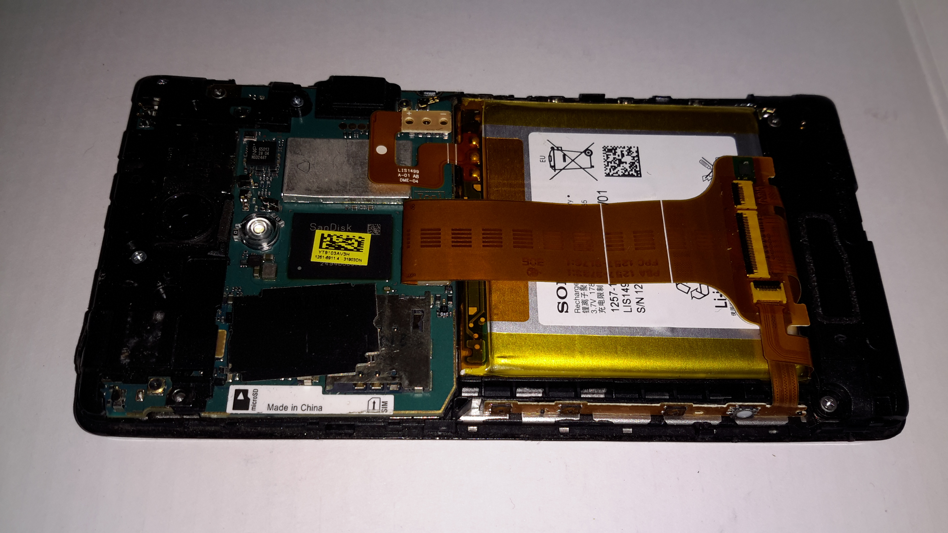
Once the back cover is removed, the Li-Polymer cell is exposed, along with the logic board. Pretty much all of the PCB is under RF shields.
Motherboard RemovedBattery Management
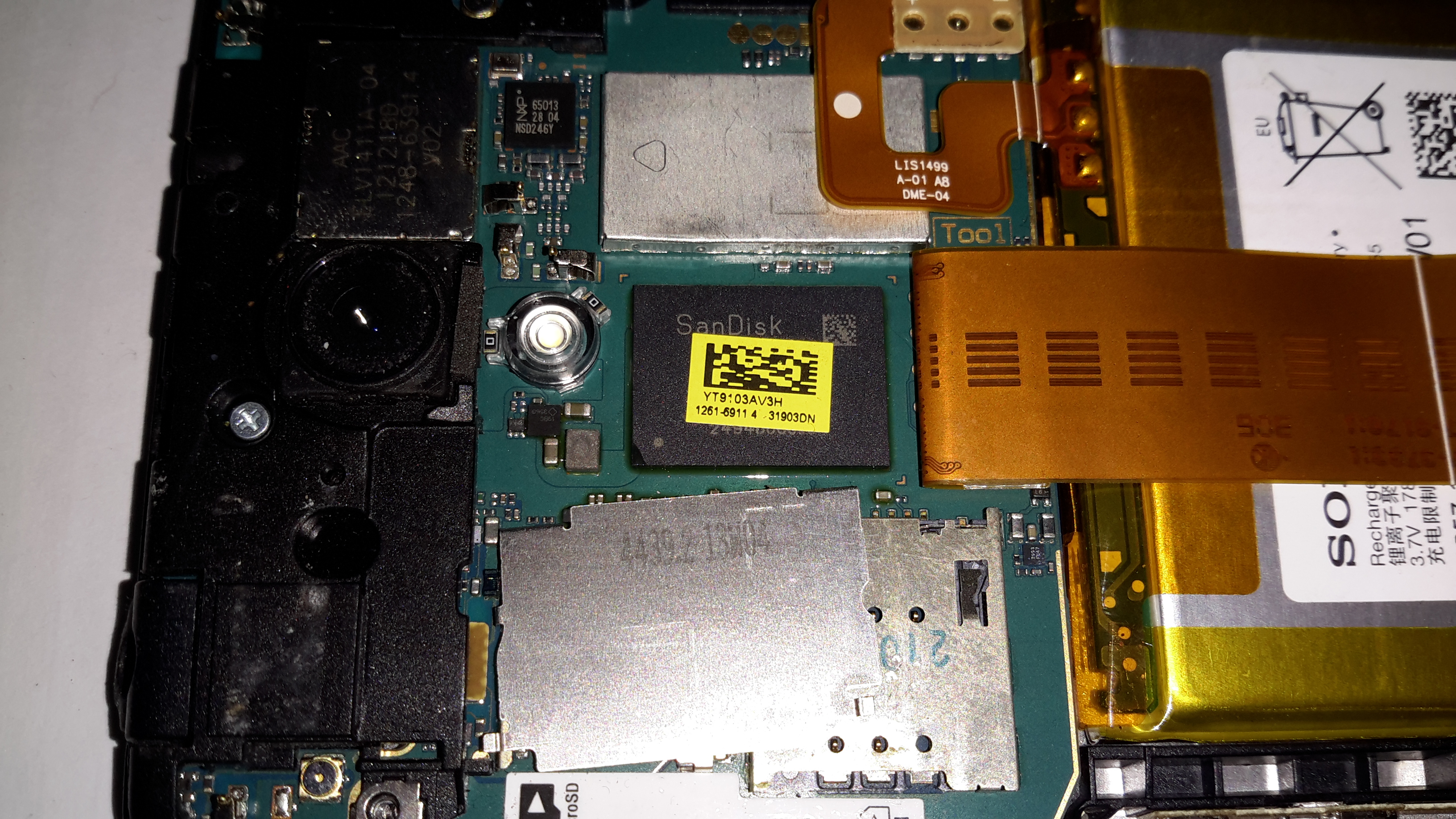
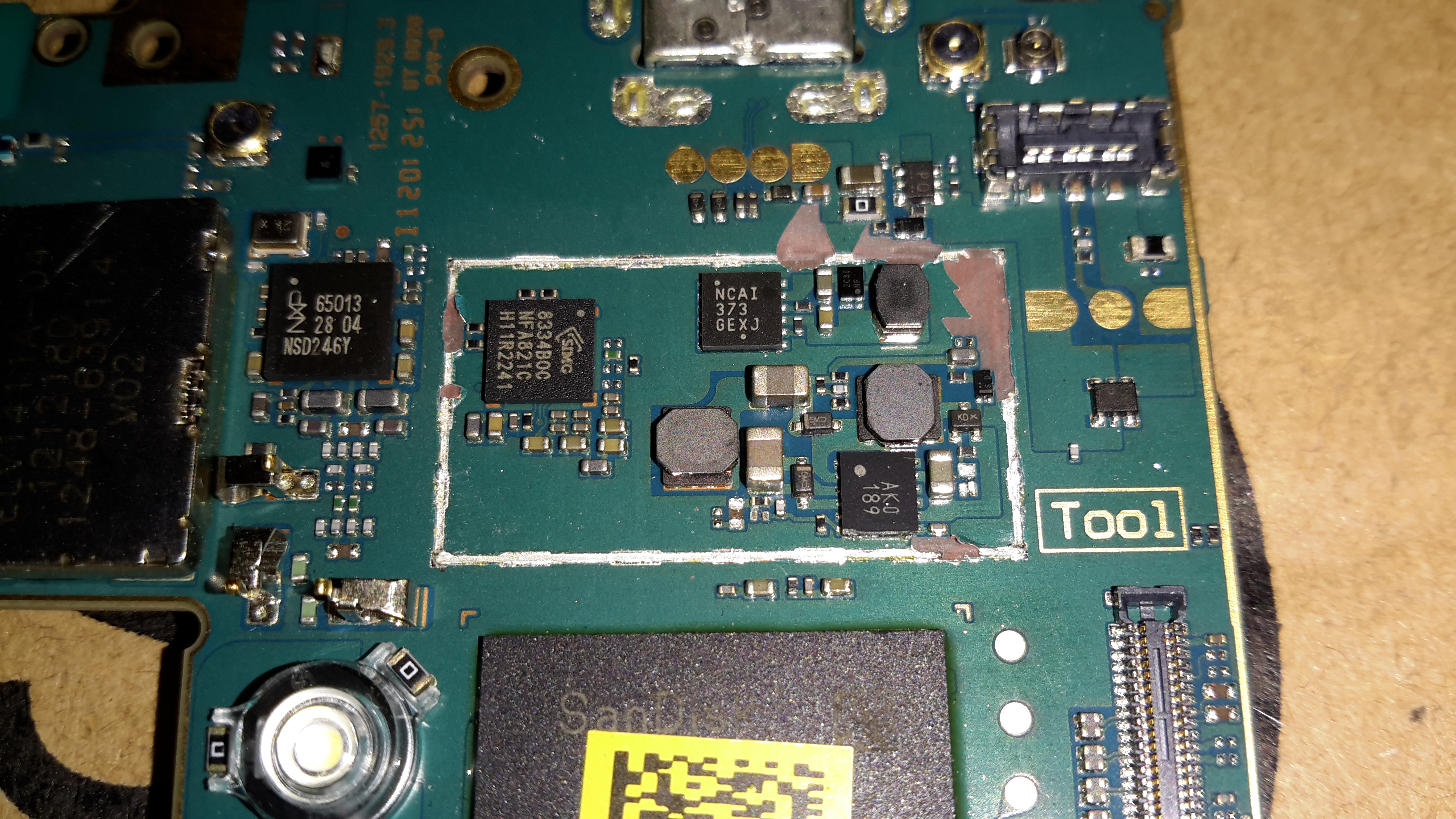
Under the small RF can on the back of the board is the battery management circuitry & the charger. There’s an extra connection to the cell for temperature monitoring. Just under that circuitry is the eMMC flash storage.
Just to the left of the battery circuit is the NFC transceiver IC, from NXP.
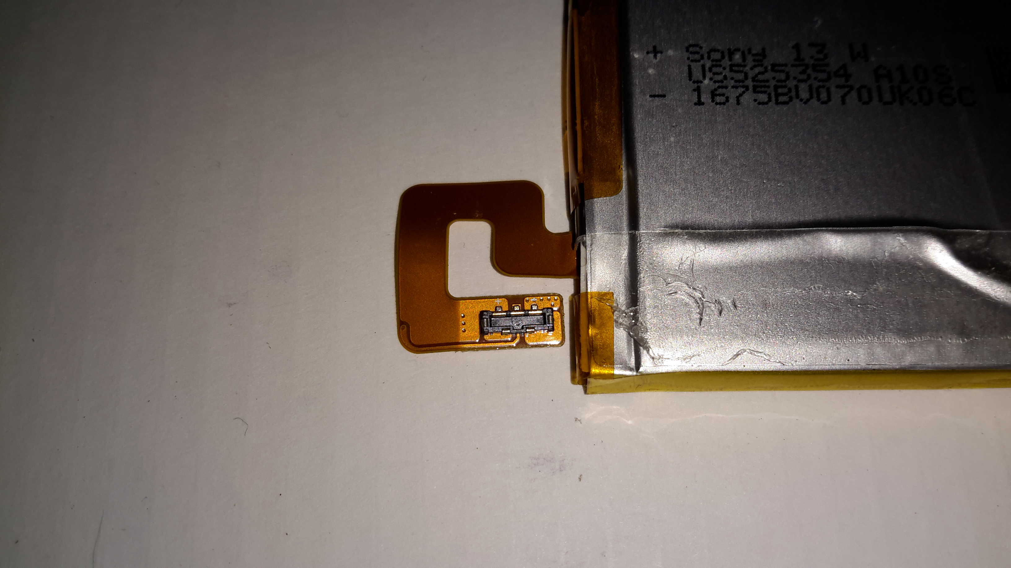
Battery Flex
The cell is connected to the main board with a FFC, with a very small SMT connector, although not as small as the more modern Xperia series phones.
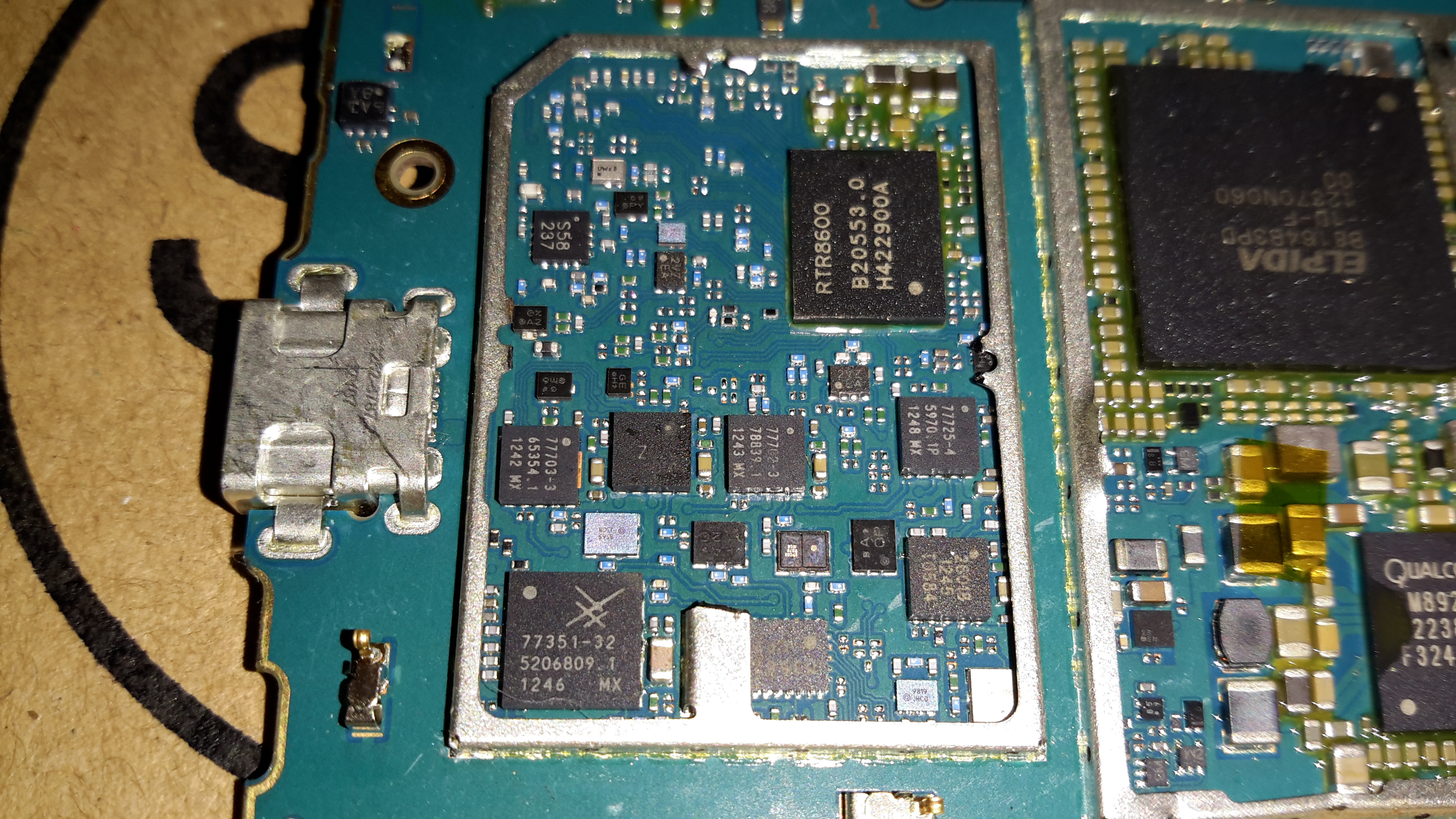
RF Section
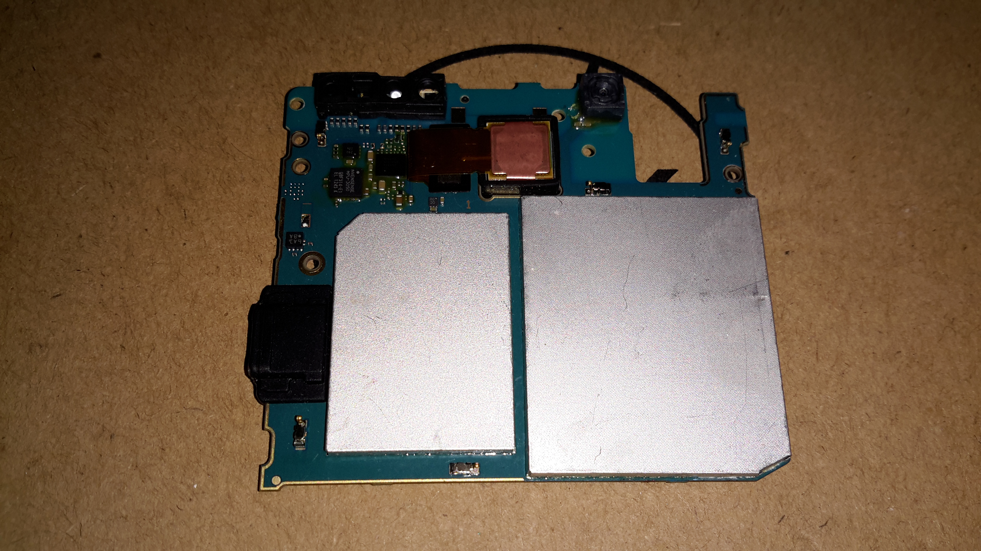
The other side of the mainboard holds the large RF transceiver section, with a Qualcomm RTR8600 multiband transceiver IC. In the bottom corner is a Skyworks SKY77351-32 Quad-band power amplifier IC, along with 3 other power amplifier ICs, also from Skyworks.
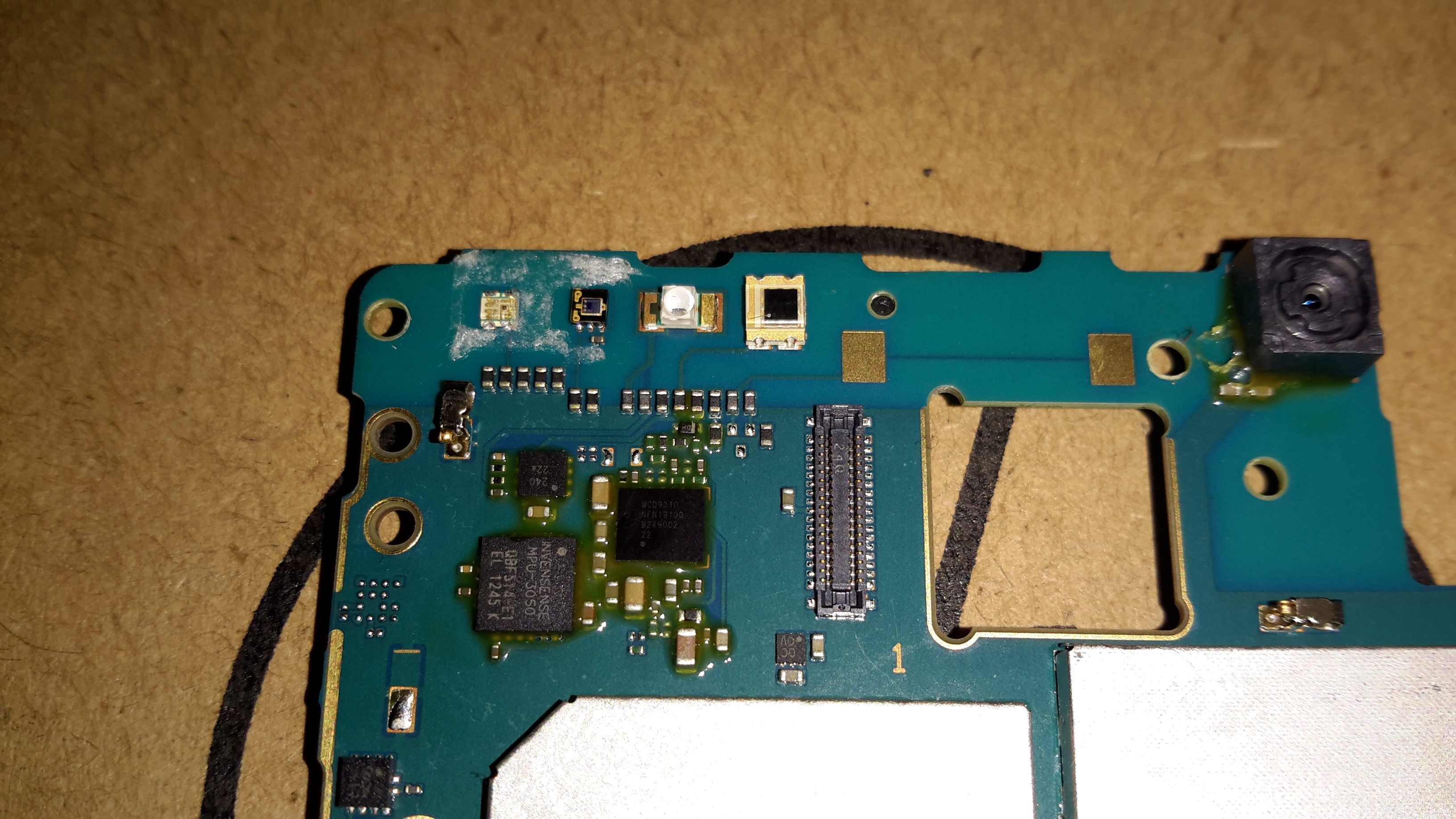
Gyro & Audio Codec
The top corner of the board holds the various sensors, including an Invensense MPU-3050 3-axis gyro. To the right of that is the Audio Codec, a WCD9310 from Qualcomm.
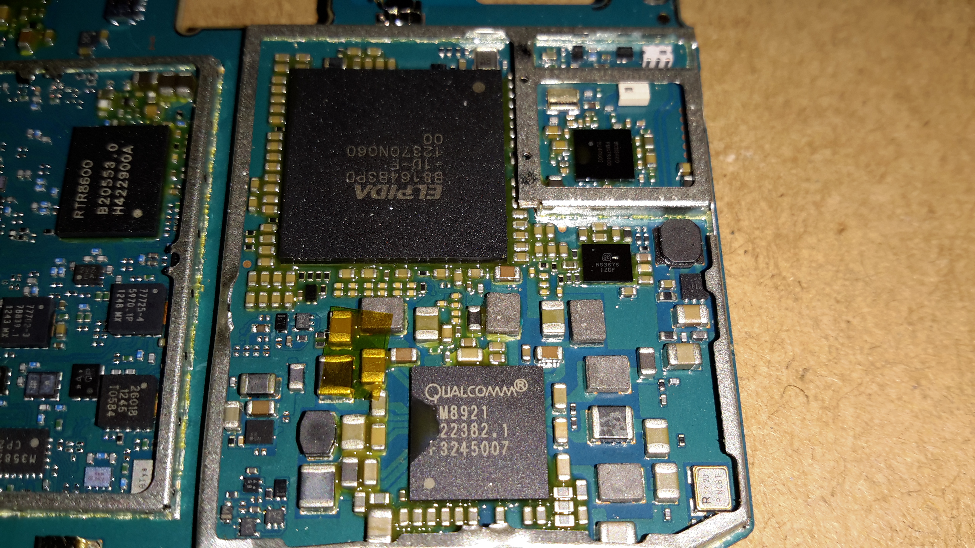
Logic & CPU Section
Everything is controlled from the last section on the board, with the main CPU & RAM in a PoP (Package-On-Package) configuration. Under the main CPU is the main power management IC, also from Qualcomm. No datasheet for this one unfortunately, but it gives it’s purpose away by being surrounded by large inductors & capacitors.
As I’ve been posting some photos of decapped ICs lately, I thought I’d share the process I use personally for those that might want to give it a go 😉
The usual method for removing the epoxy package from the silicon is to use hot, concentrated Nitric Acid. Besides the obvious risks of having hot acids around, the decomposition products of the acid, namely NO² (Nitrogen Dioxide) & NO (Nitrogen Oxide), are toxic and corrosive. So until I can get the required fume hood together to make sure I’m not going to corrode the place away, I’ll leave this process to proper labs ;).
The method I use is heat based, using a Propane torch to destroy the epoxy package, without damaging the Silicon die too much.
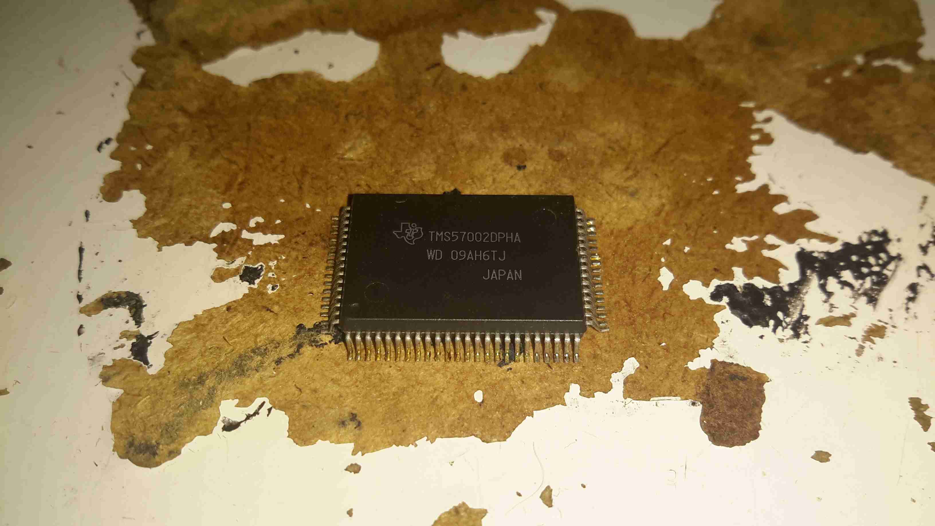
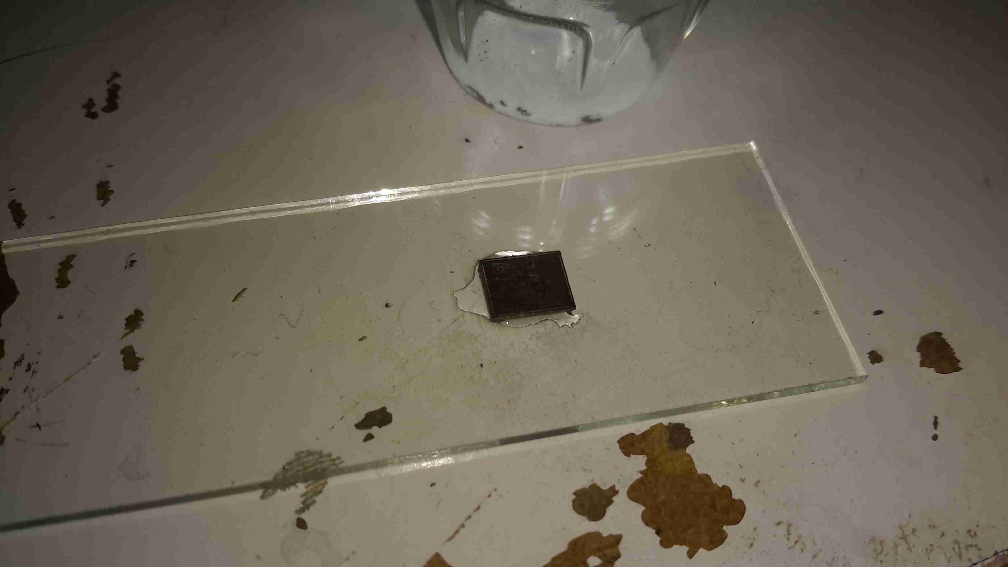
TMS57002 Audio DSP
I start off, obviously, with a desoldered IC, the one above an old audio DSP from TI. I usually desolder en-masse for this with a heat gun, stripping the entire board in one go.
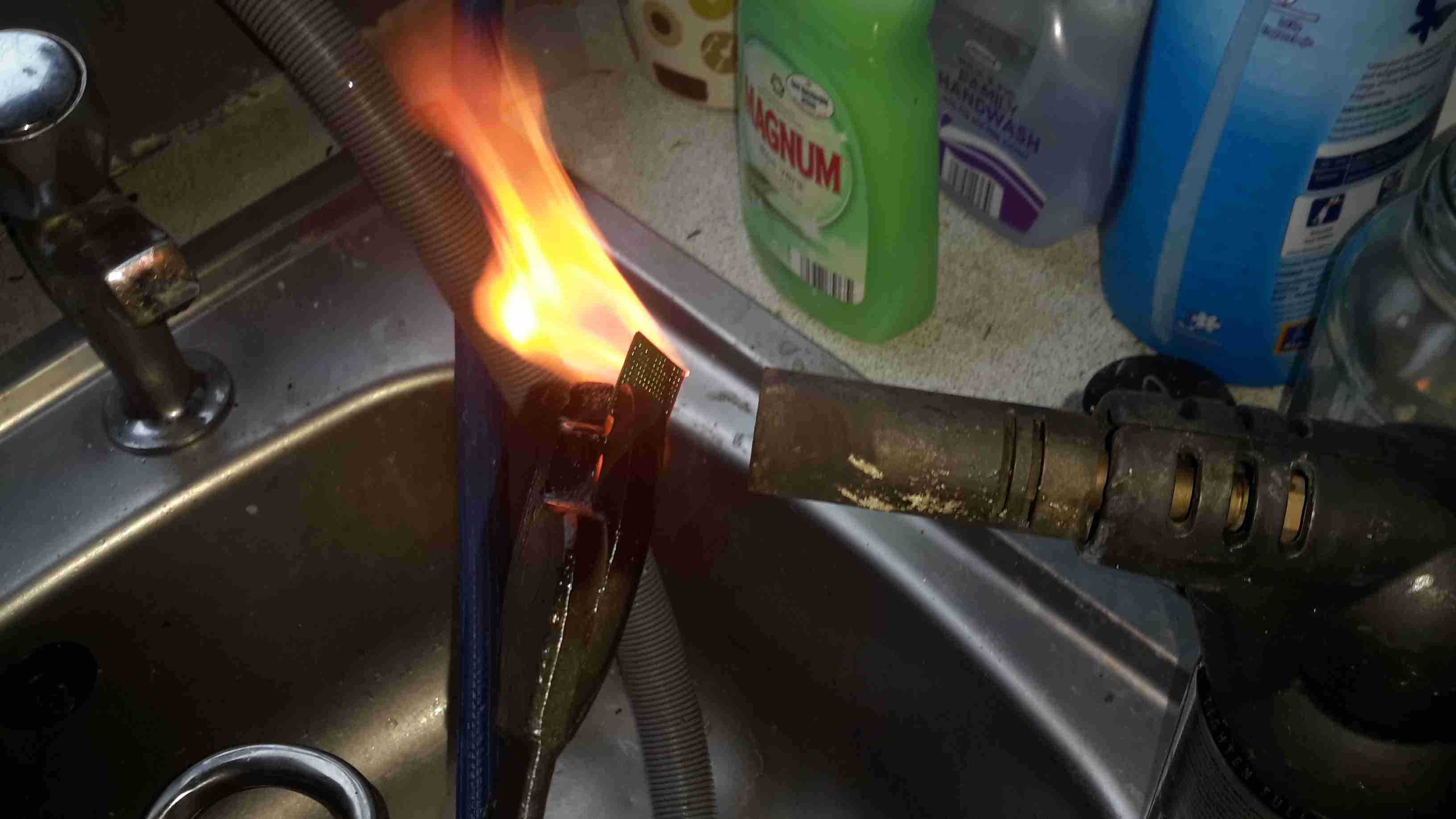
FLAMES!
Next is to apply the torch to the IC. A bit of practice is required here to get the heat level & time exactly right, overheating will cause the die to oxidize & blacken or residual epoxy to stick to the surface.
I usually apply the torch until the package just about stops emitting it’s own yellow flames, meaning the epoxy is almost completely burned away. I also keep the torch flame away from the centre of the IC, where the die is located.
Breathing the fumes from this process isn’t recommended, no doubt besides the obvious soot, the burning plastic will be emitting many compounds not brilliant for Human health!
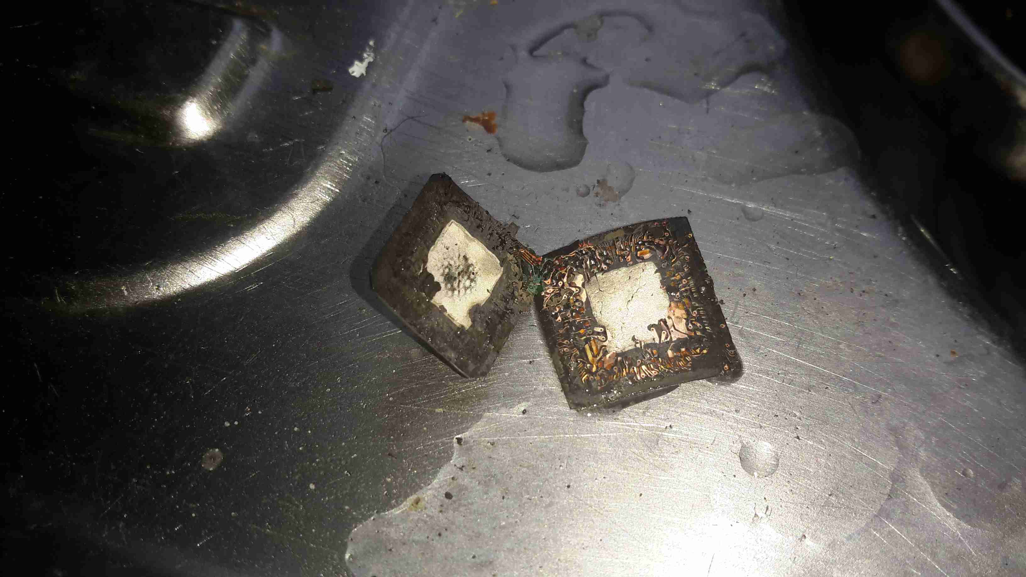
Once the IC is roasted to taste, it’s quenched in cold water for a few seconds. Sometimes this causes such a high thermal shock that the leadframe cracks off the epoxy around the die perfectly.
All Your Die Belong To Us
Now that the epoxy has been destroyed, it breaks apart easily, and is picked away until I uncover the die itself. (It’s the silver bit in the middle of the left half). The heat from the torch usually destroys the Silver epoxy holding the die to the leadframe, and can be removed easily from the remaining package.
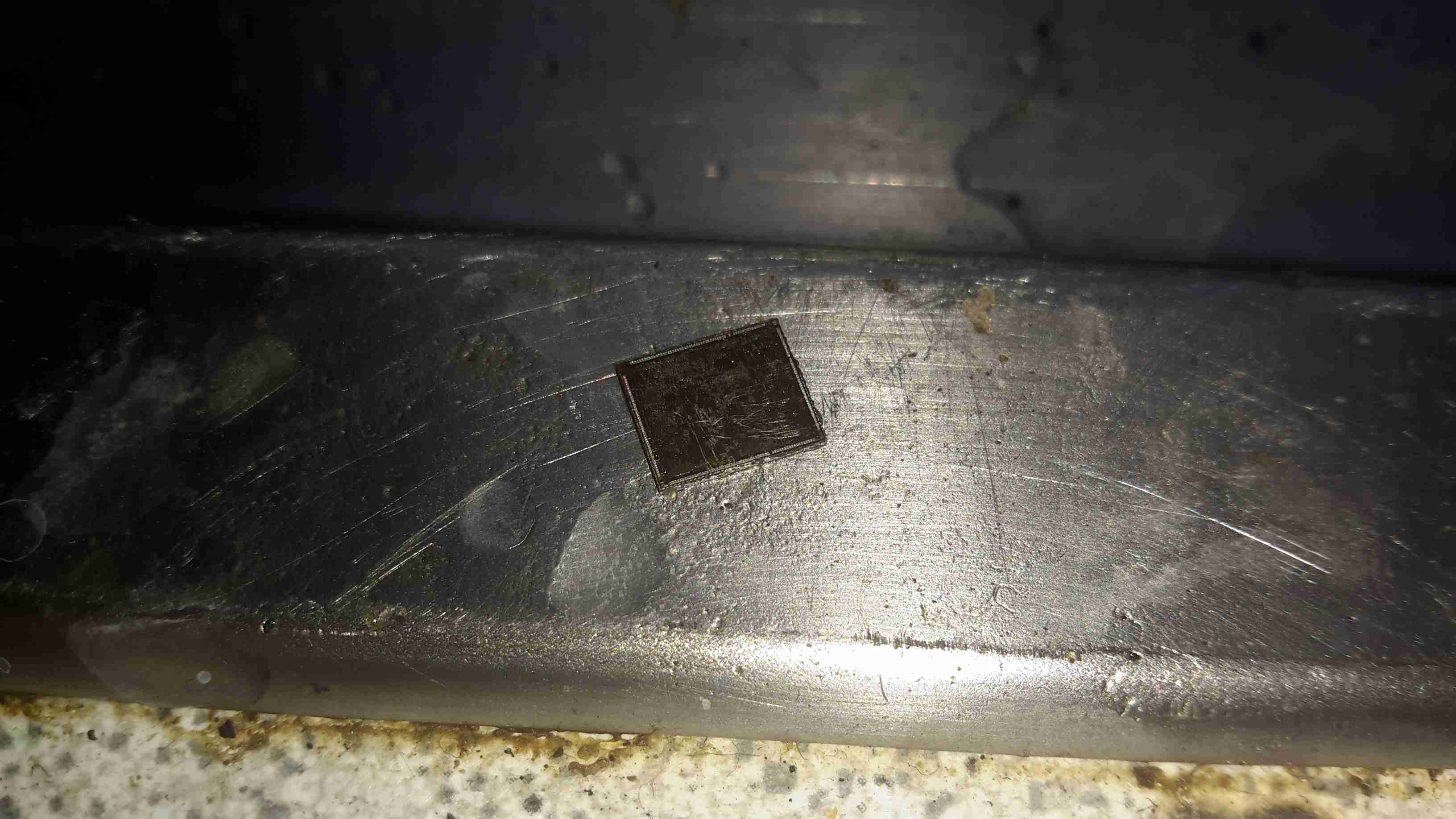
Decapped
BGA packages are usually the easiest to decap, flip-chip packages are a total pain due to the solder balls being on the front side of the die, I haven’t managed to get a good result here yet, I’ll probably need to chemically remove the first layer of the die to get at the interesting bits 😉
Slide
Once the die has been rinsed in clean water & inspected, it’s mounted on a glass microscope slide with a small spot of Cyanoacrylate glue to make handling easier.
Some dies require some cleaning after decapping, for this I use 99% Isopropanol & 99% Acetone, on the end of a cotton bud. Any residual epoxy flakes or oxide stuck to the die can be relatively easily removed with a fingernail – turns out fingernails are hard enough to remove the contamination, but not hard enough to damage the die features.
Once cleaning is complete, the slide is marked with the die identification, and the photographing can begin.
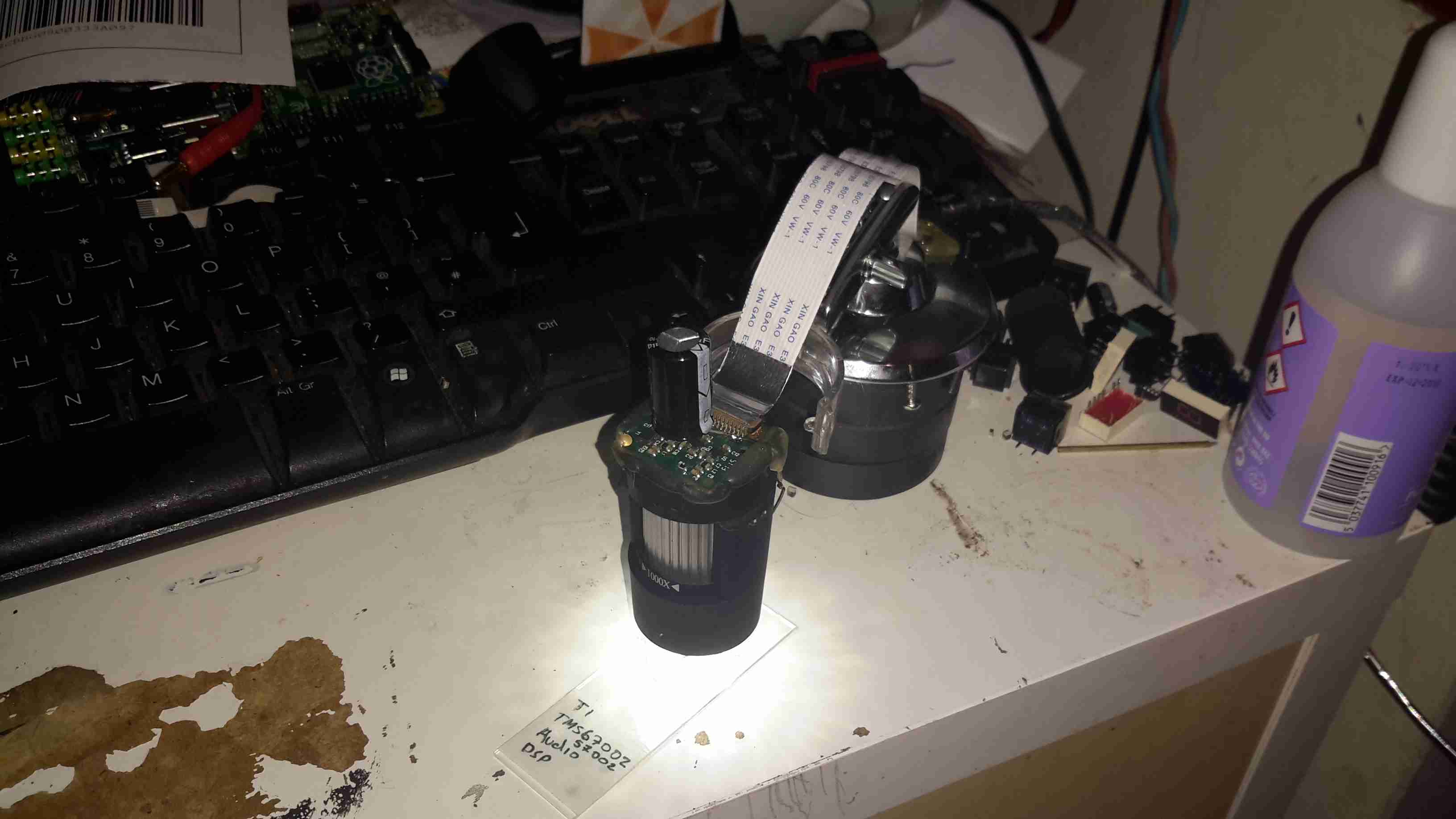
Microscope Mods
I had bought a cheap eBay USB microscope to get started, as I can’t currently afford a proper metallurgical microscope, but I found the resolution of 640×480 very poor. Some modification was required!
Modified Microscope
I’ve removed the original sensor board from the back of the optics assembly & attached a Raspberry Pi camera board. The ring that held the original sensor board has been cut down to a minimum, as the Pi camera PCB is slightly too big to fit inside.
The stock ring of LEDs is run direct from the 3.3v power rail on the camera, through a 4.7Ω resistor, for ~80mA. I also added a 1000µF capacitor across the 3.3v supply to compensate a bit for the long cable – when a frame is captured the power draw of the camera increases & causes a bit of voltage drop.
The stock lens was removed from the Pi camera module by careful use of a razor blade – being too rough here *WILL* damage the sensor die or the gold bond wires, which are very close to the edge of the lens housing, so be gentle!
Mounting Base
The existing mount for the microscope is pretty poor, so I’ve used a couple of surplus ceramic ring magnets as a better base, this also gives me the option of raising or lowering the base by adding or removing magnets.
To get more length between the Pi & the camera, I bought a 1-meter cable extension kit from Pi-Cables over at eBay, cables this long *definitely* require shielding in my space, which is a pretty aggressive RF environment, or interference appears on the display. Not surprising considering the high data rates the cable carries.
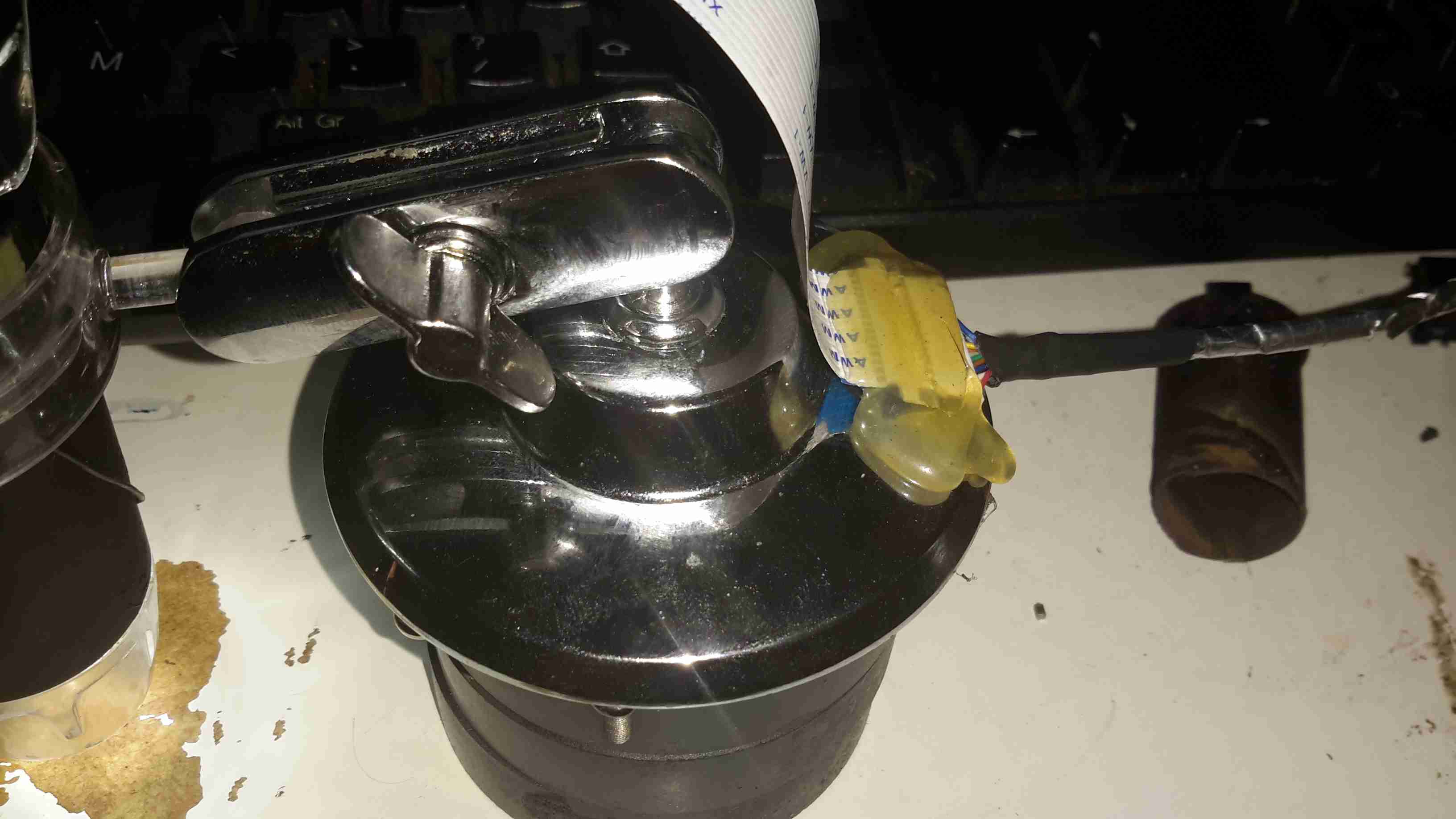
The FFC interface is hot-glued to the back of the microscope mount for stability, for handheld use the FFC is pretty flexible & doesn’t apply any force to the scope.
Die Photography
Since I modified the scope with a Raspberry Pi camera module, everything is done through the Pi itself, and the raspistill command.
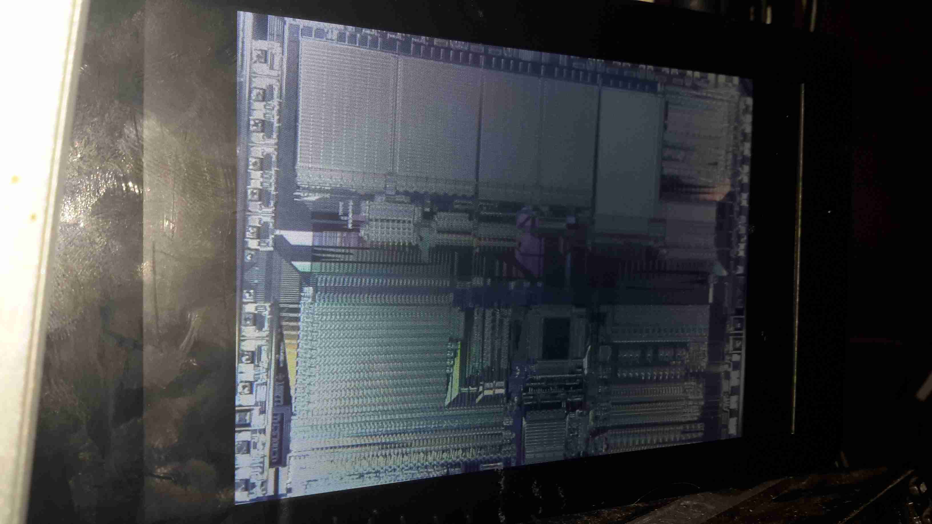
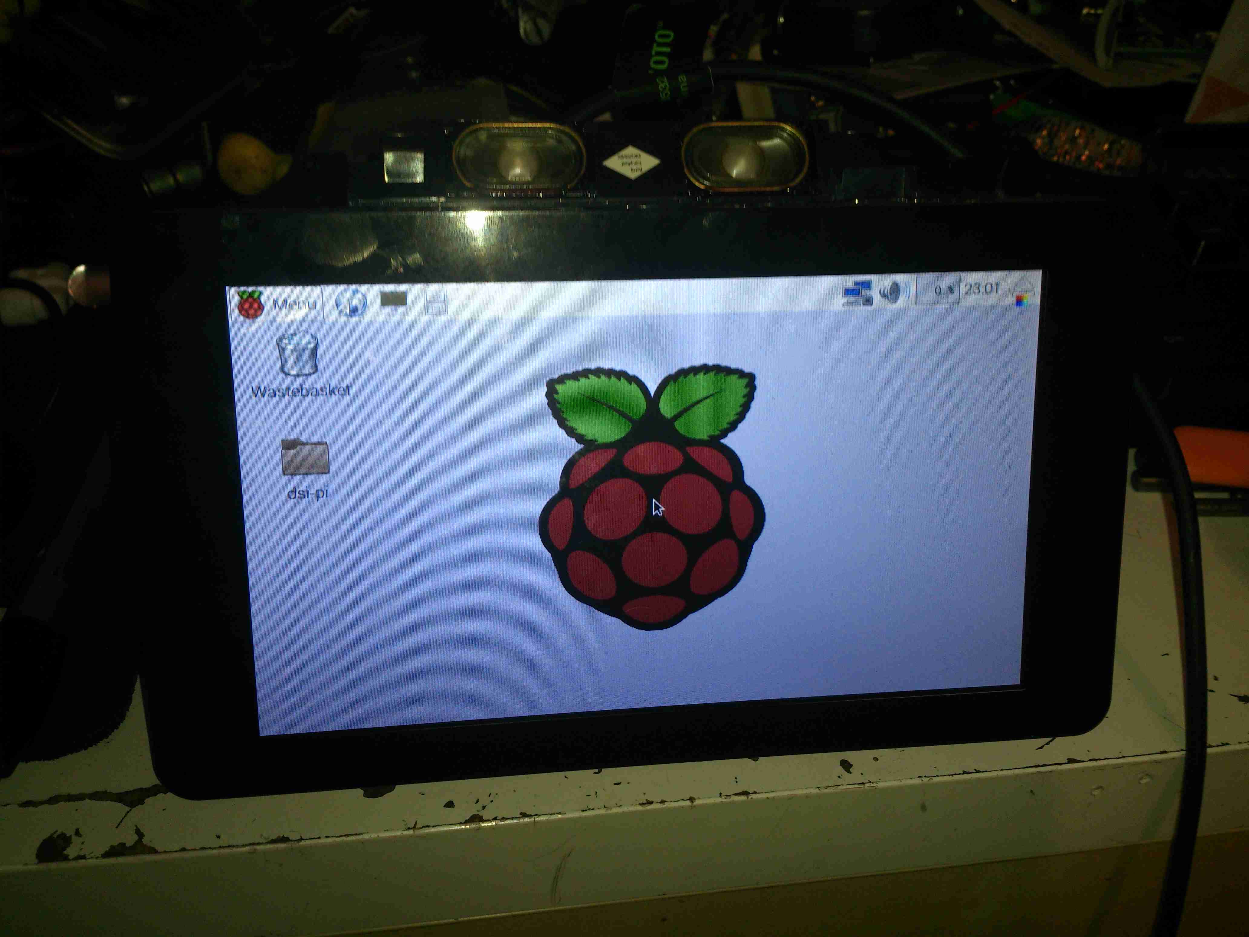
Pi LCD
The command I’m currently using to capture the images is:
raspistill -ex auto -awb auto -mm matrix -br 62 -q 100 -vf -hf -f -t 0 -k -v -o CHIPNAME_%03d.jpg
This command waits between each frame for the ENTER key to be pressed, allowing me to position the scope between shots. Pi control & file transfer is done via SSH, while I use the 7″ touch LCD as a viewfinder.
The direct overhead illumination provided by the stock ring of LEDs isn’t ideal for some die shots, so I’m planning on fitting some off-centre LEDs to improve the resulting images.
Image Processing
Obviously I can’t get an ultra-high resolution image with a single shot, due to the focal length, so I have to take many shots (30-180 per die), and stitch them together into a single image.
For this I use Hugin, an open-source panorama photo stitching package.
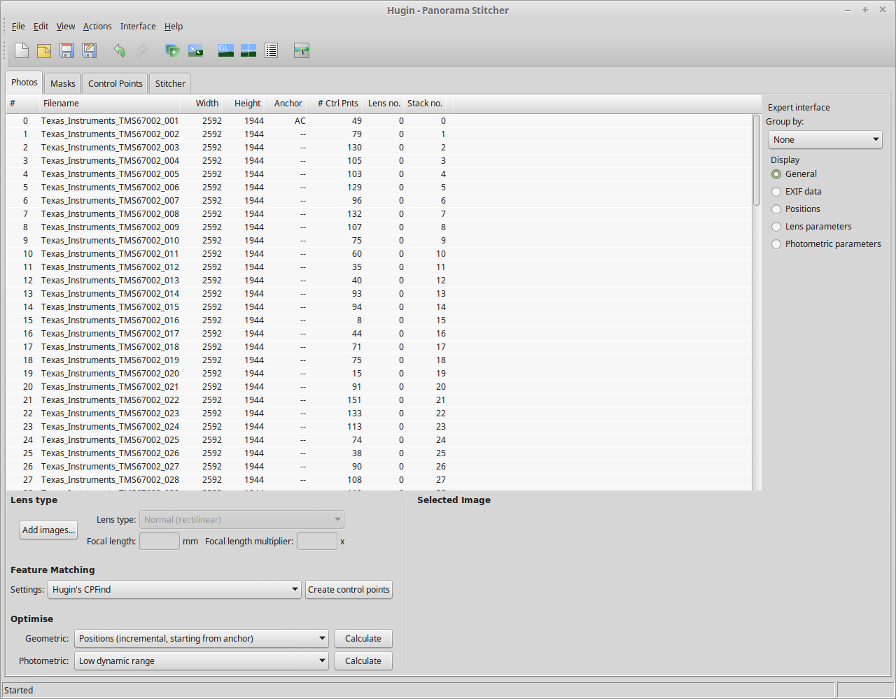
Hugin
Here’s Hugin with the photos loaded in from the Raspberry Pi. To start with I use Hugin’s built in CPFind to process the images for control points. The trick with getting good control points is making sure the images have a high level of overlap, between 50-80%, this way the software doesn’t get confused & stick the images together incorrectly.
Optimiser
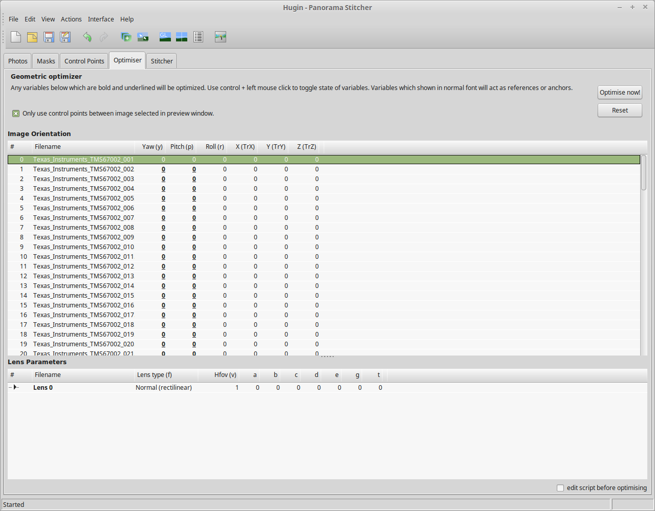
After the control points are generated, which for a large number of high resolution images can take some time, I run the optimiser with only Yaw & Pitch selected for all images.
Optimising
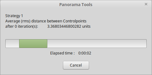
If all goes well, the resulting optimisation will get the distance between control points to less than 0.3 pixels.
Panorama Preview
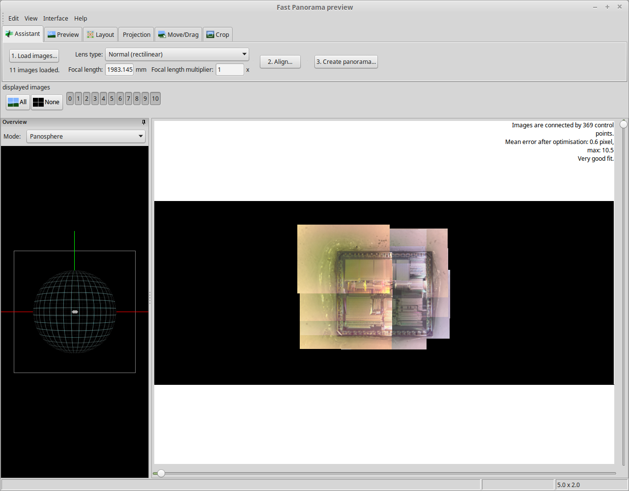
After the control points & optimisation is done, the resulting image can be previewed before generation.
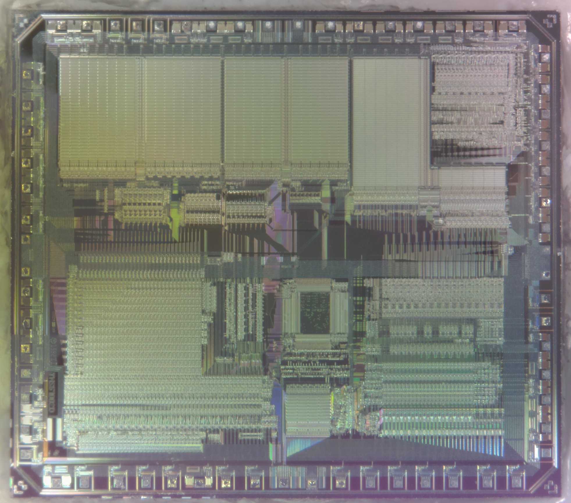
Texas Instruments TMS67002
After all the image processing, the resulting die image should look something like the above, with no noticeable gaps.
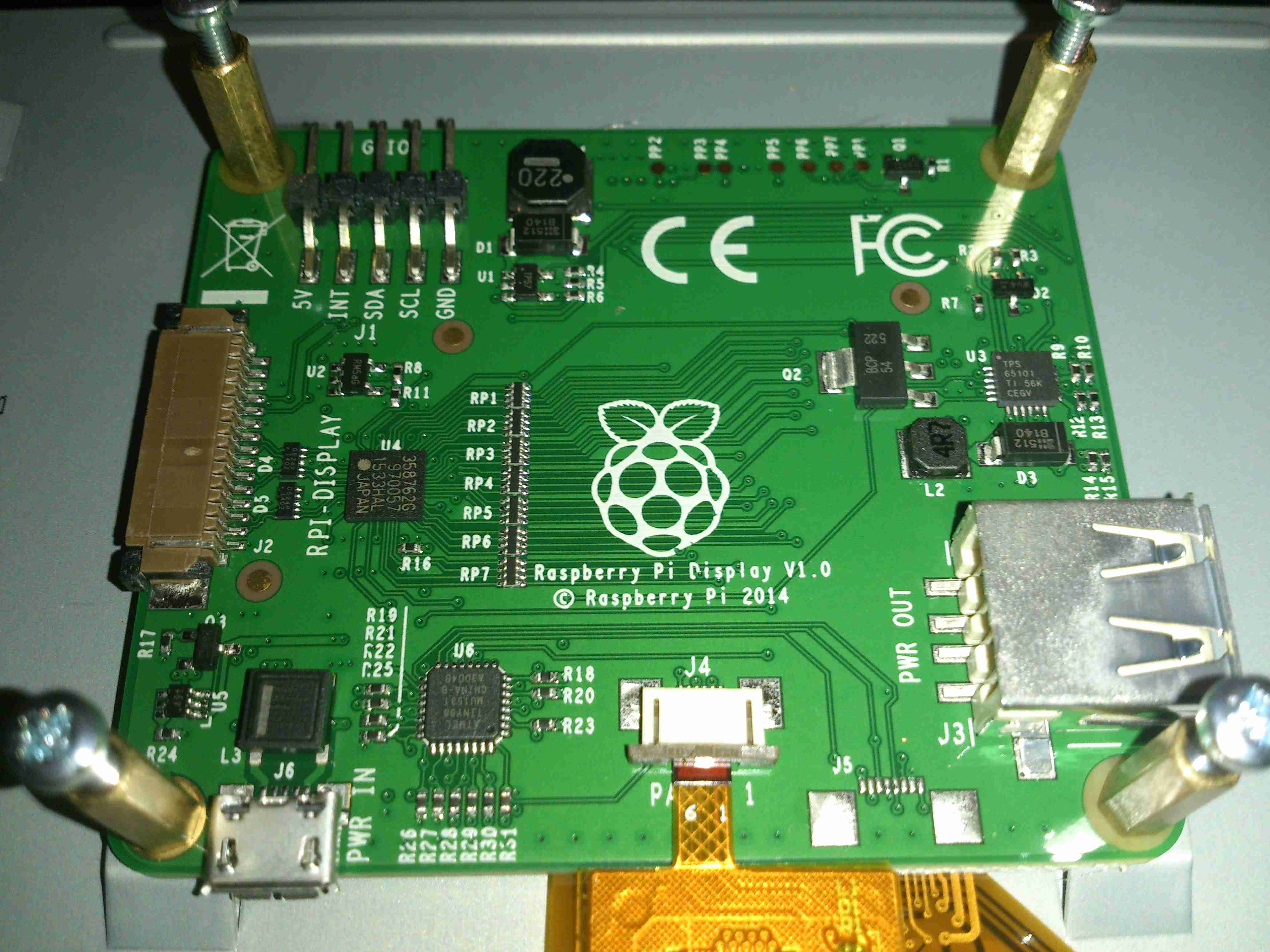
Finally the Raspberry Pi Foundation have released an official LCD for the DSI connector on the Pi. When these were announced, I placed an order straight away, but due to demand it’s taken quite a while for it to arrive in the post.
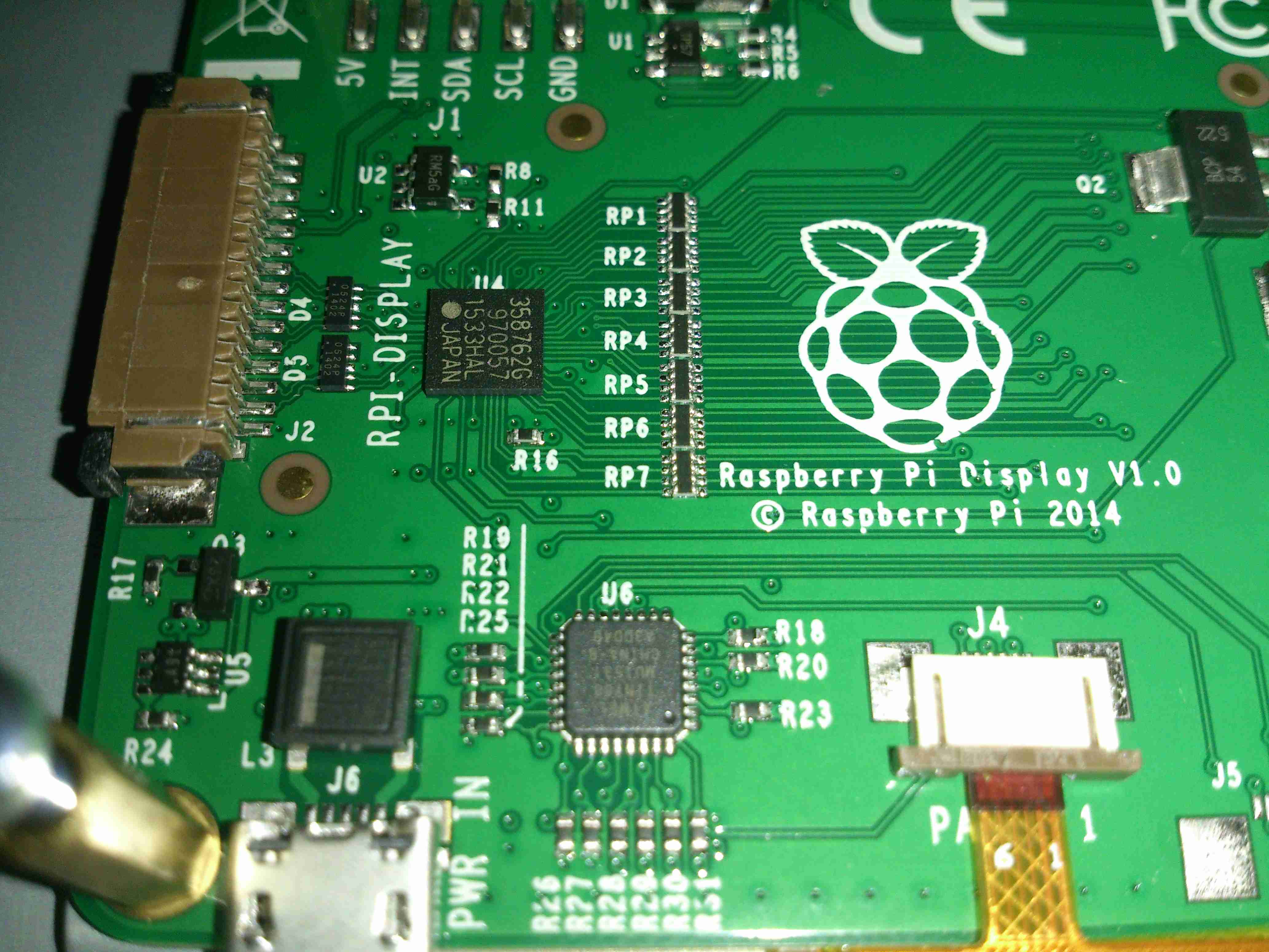
Interface PCB
The LCD itself is an RGB panel, to interface the Pi via the MIPI DSI port, some signal conversion is required. A small PCB is mounted on the back of the LCD to do this conversion. It also handles the power supply rails required by the LCD itself & interfacing the touch screen.
LCD Power Supply
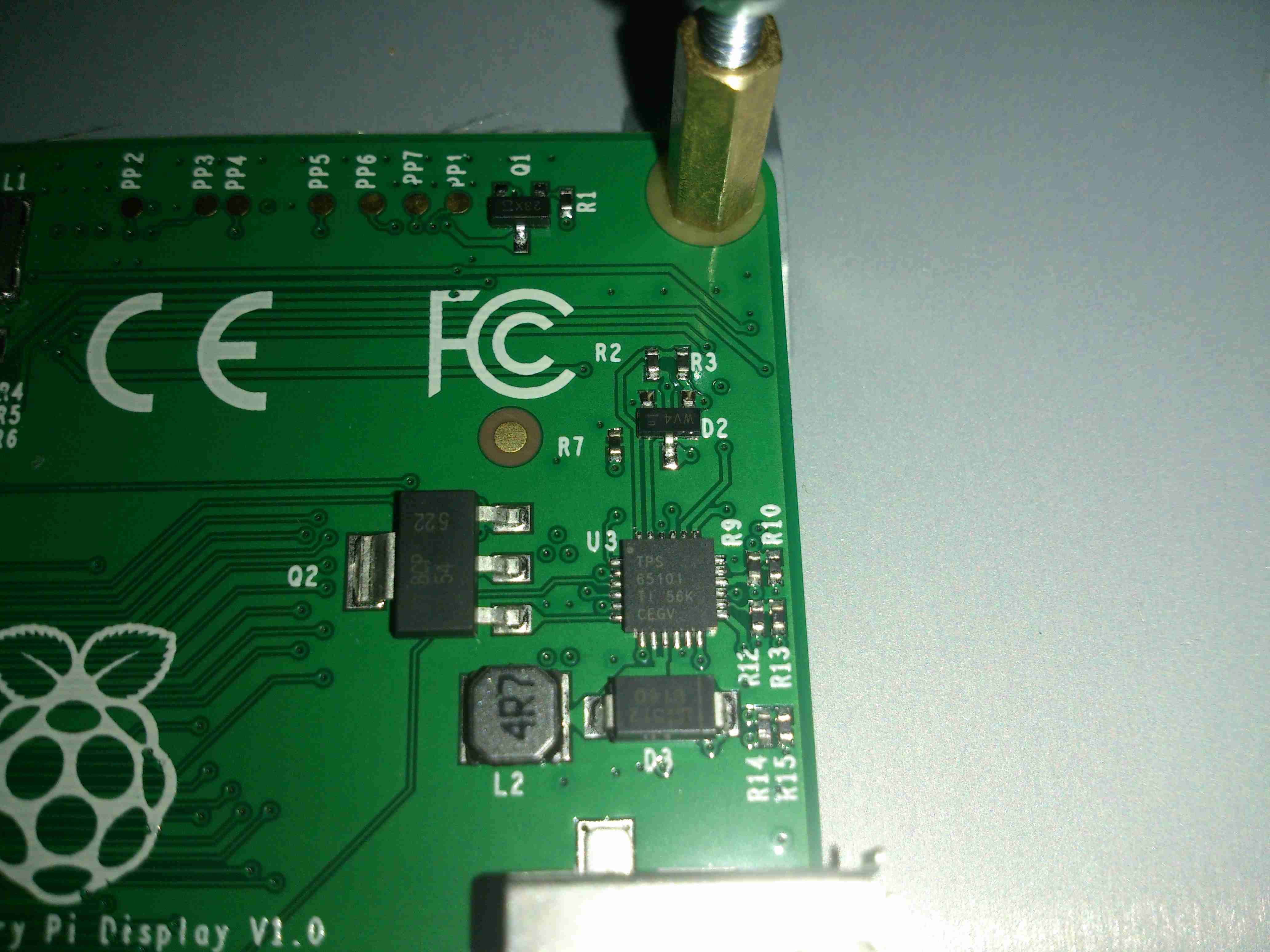
Taking care of the power supply is a Texas Instruments TPS65101 triple output LCD power supply IC. This also has a built in linear regulator to supply 3.3v for the rest of the circuitry on board. The large transistor to the left of the IC is the pass transistor for this regulator.
Main Controller
The video signal comes in on the FFC connector on the left, into the BGA IC. I’ve not managed to identify this component, but it’s doing the conversion from serial video from the Pi to parallel RGB for the LCD.
There’s also an Atmel ATtiny88 on the board below the main video conversion IC, not sure what this is doing.
The touch controller itself is mounted on the flex of the LCD, in this case it’s a FT5406.
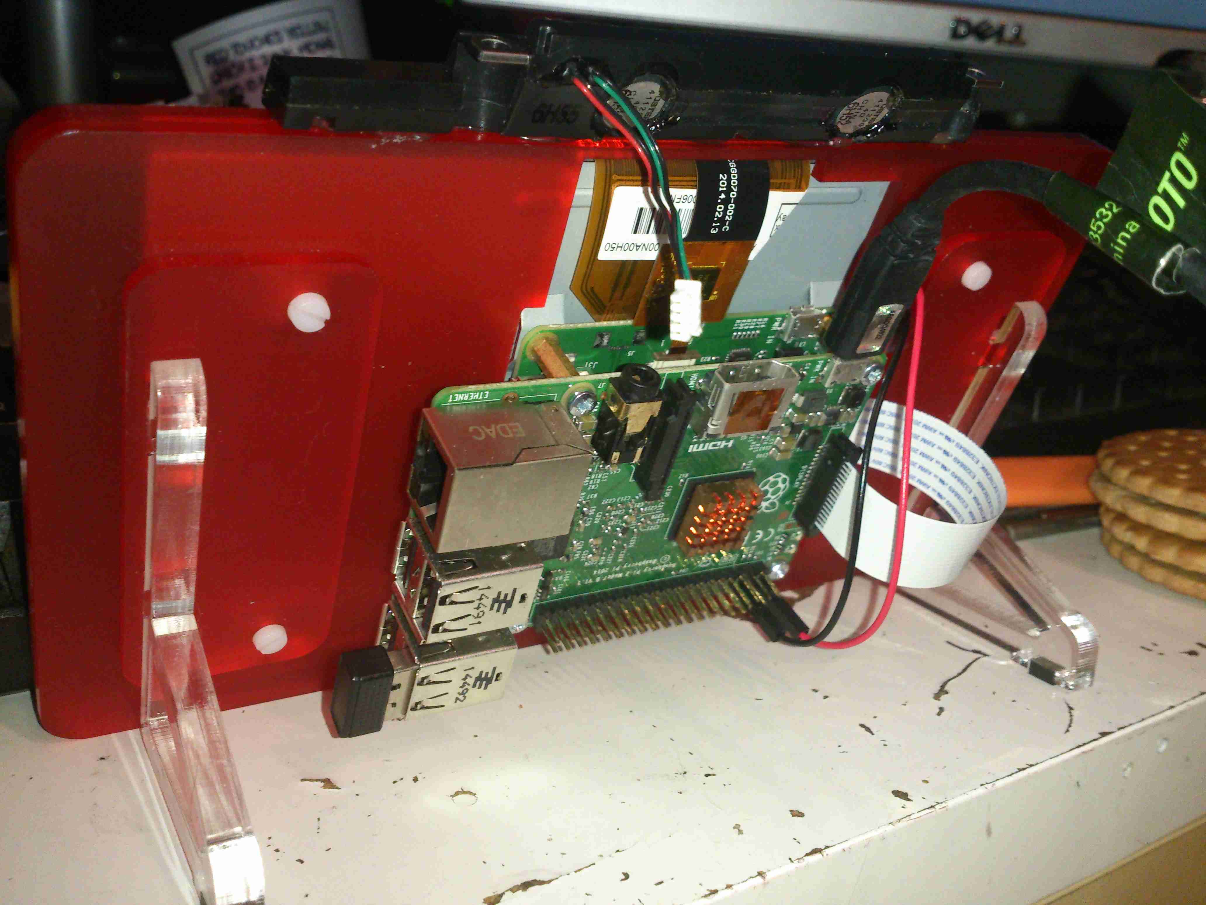
Raspberry Pi LCD
Here’s the LCD in operation. It’s not the highest resolution out there, but it leaves the GPIO & HDMI ports free for other uses.
Pi Mounted
The Pi screws to the back of the LCD & is connected with a flat flex cable & a pair of power jumpers. I’ve added a couple of small speakers to the top edge of the LCD to provide sound. (More to come on this bit).
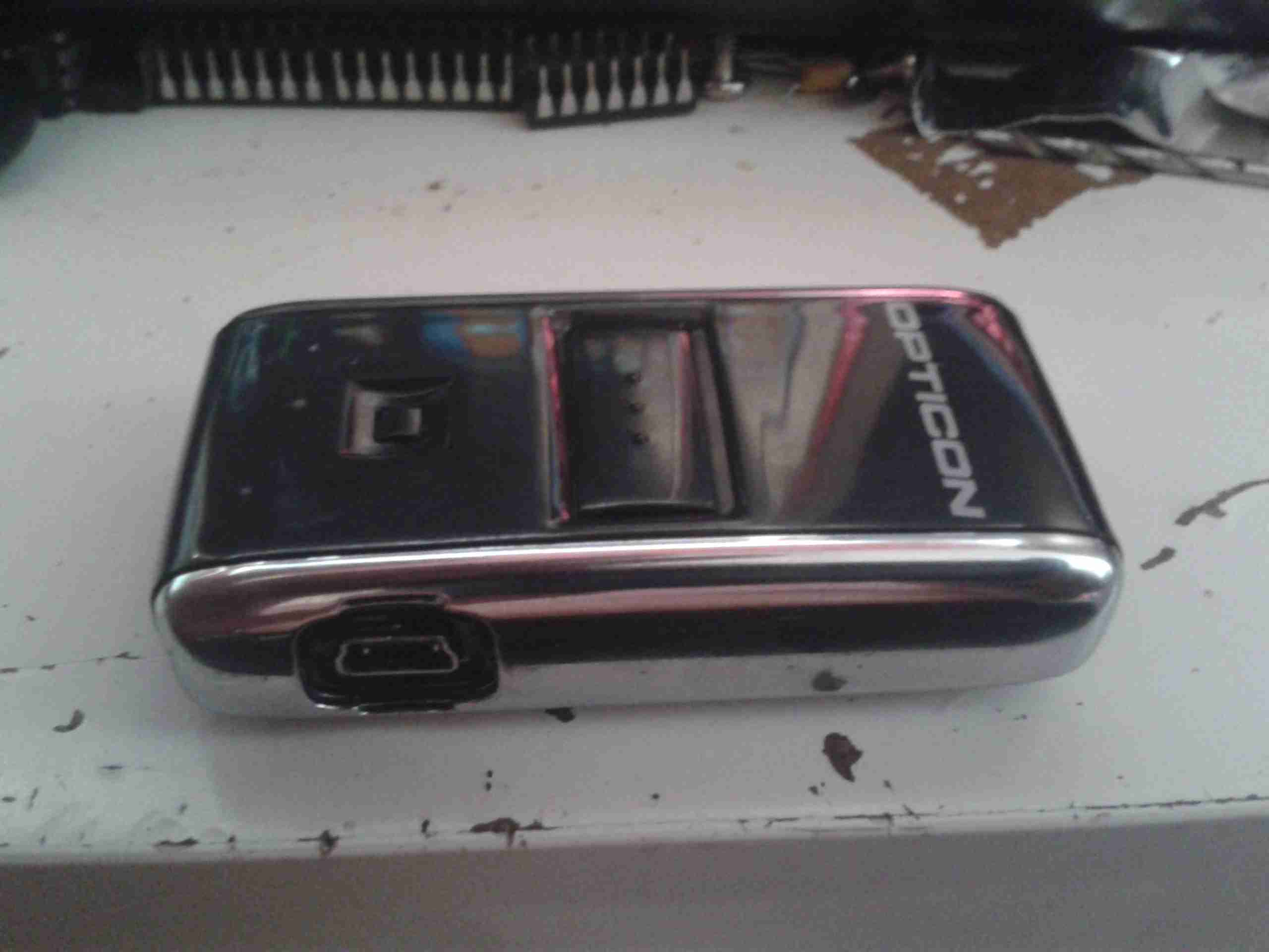
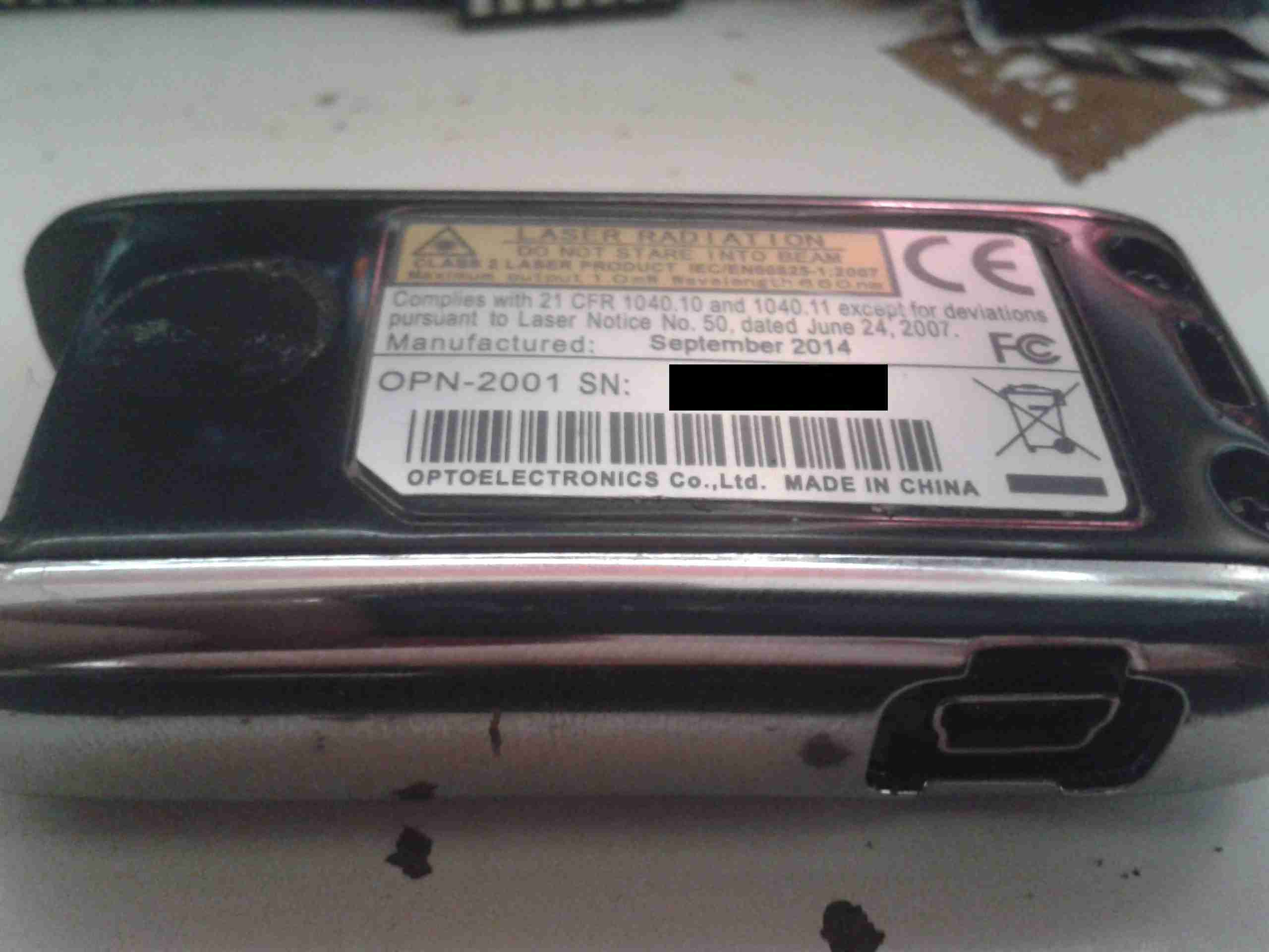
The OPN-2001 is a very small handheld barcode data collection device, used for stock keeping, inventory, etc.
It’s powered by an internal Li-Poly cell, at 150mAh, and has storage for 1000 barcodes in it’s internal memory.
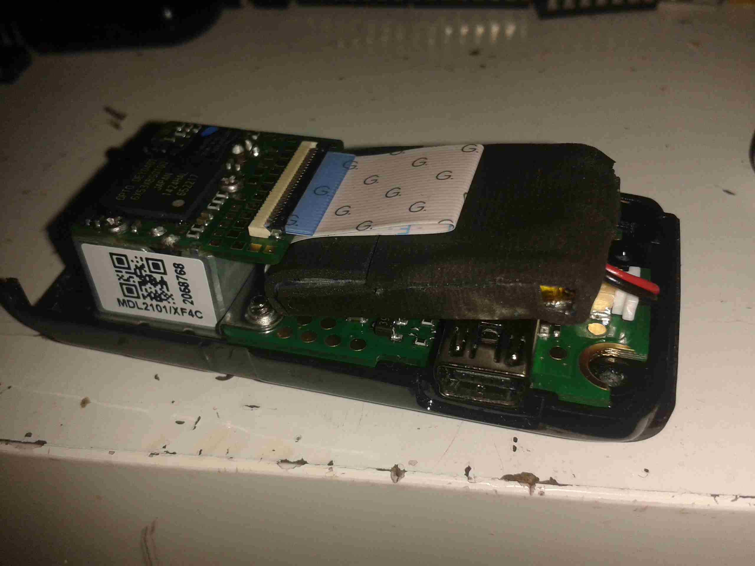
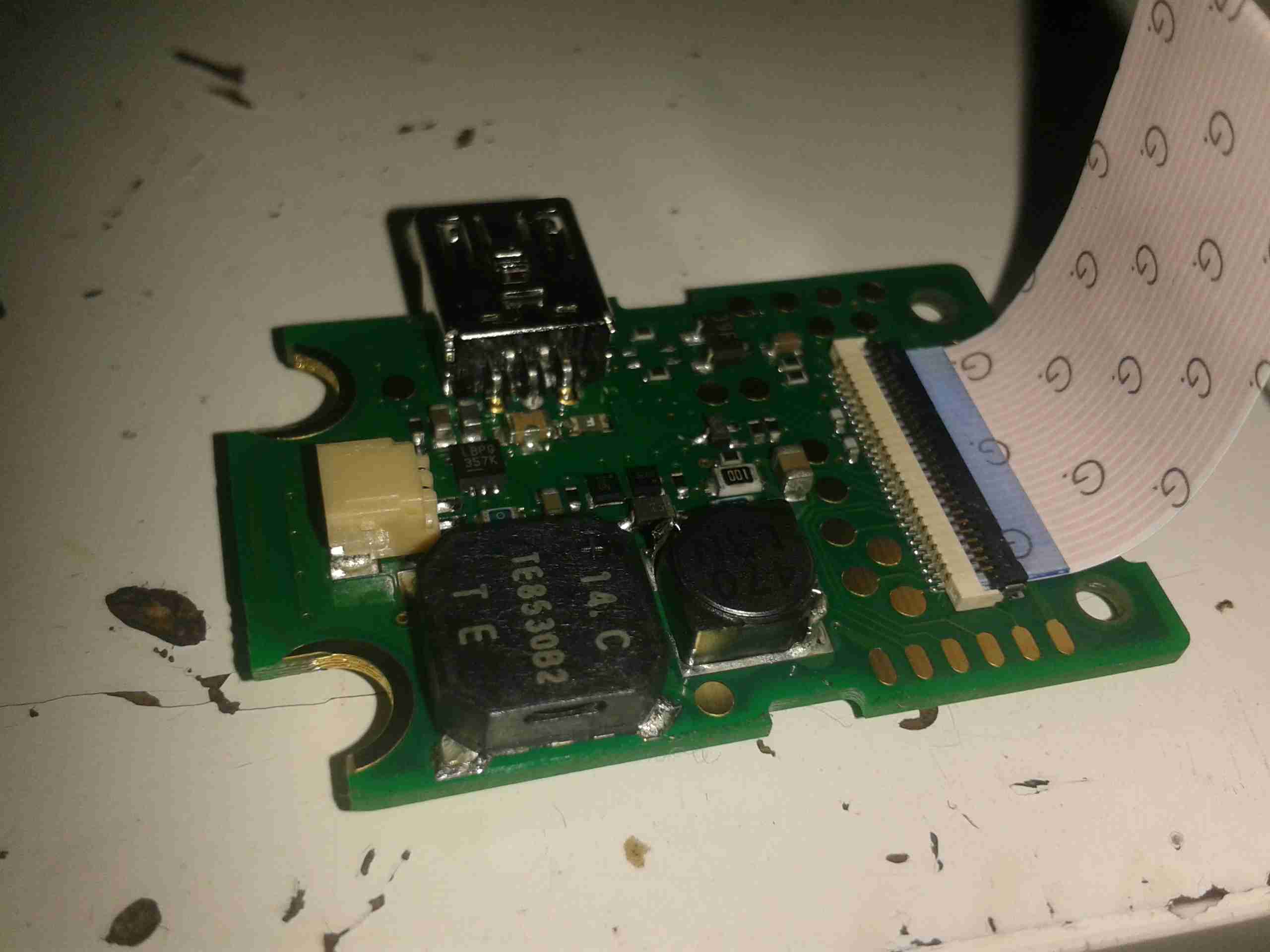
USB
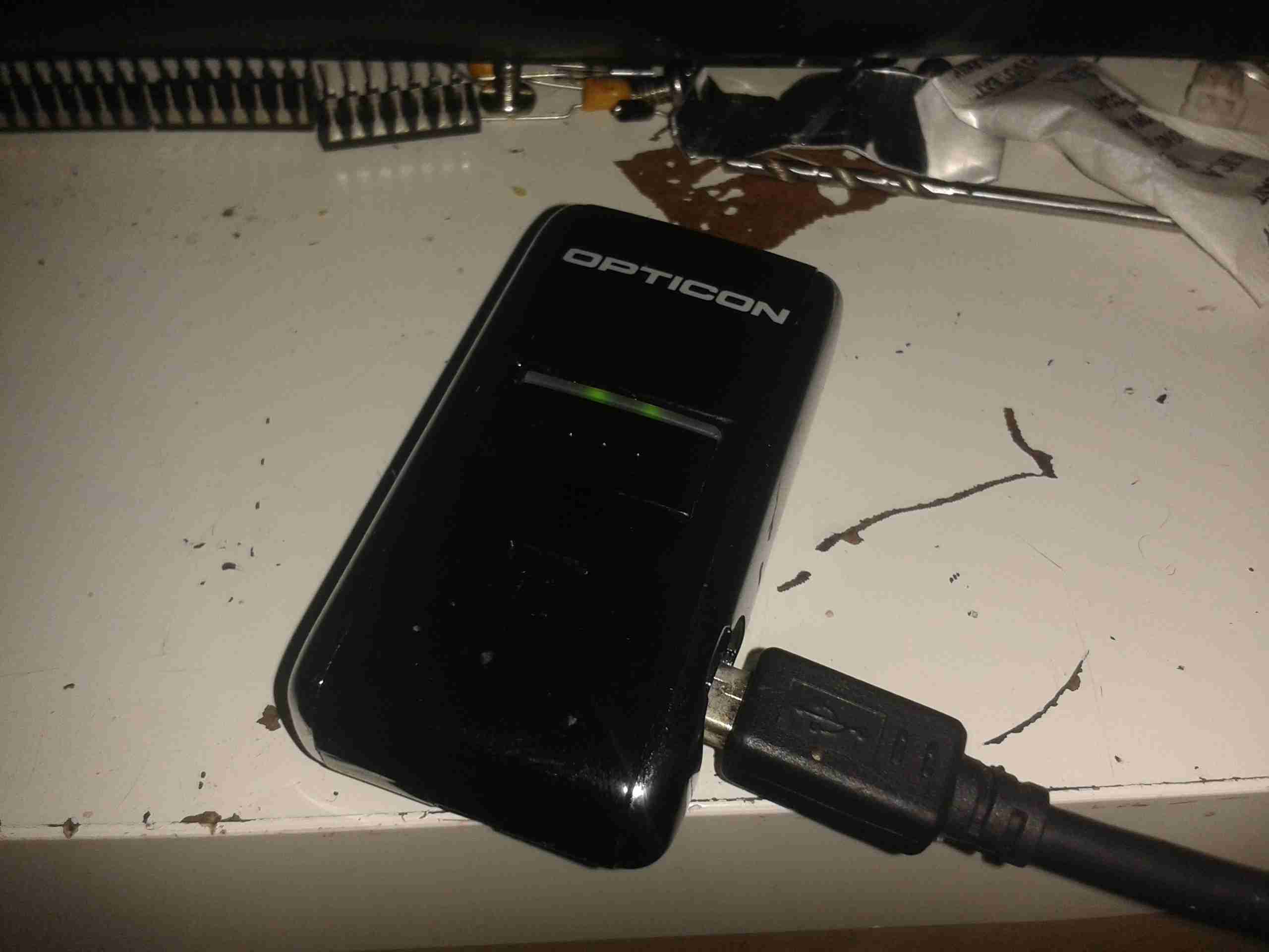
The unit is charged via it’s USB port, the data can also be downloaded using this interface.
ID Label
Here’s the bottom of the unit with it’s label. Serial number removed to protect the guilty. 😉
Cover Removed
Here the bottom cover has been removed from the scanner, showing the internals. The barcode engine is on the left, this contains all the hardware & logic for scanning & storing the barcode data. The Li-Poly cell is under the FFC cable wrapped in foam tape for protection.
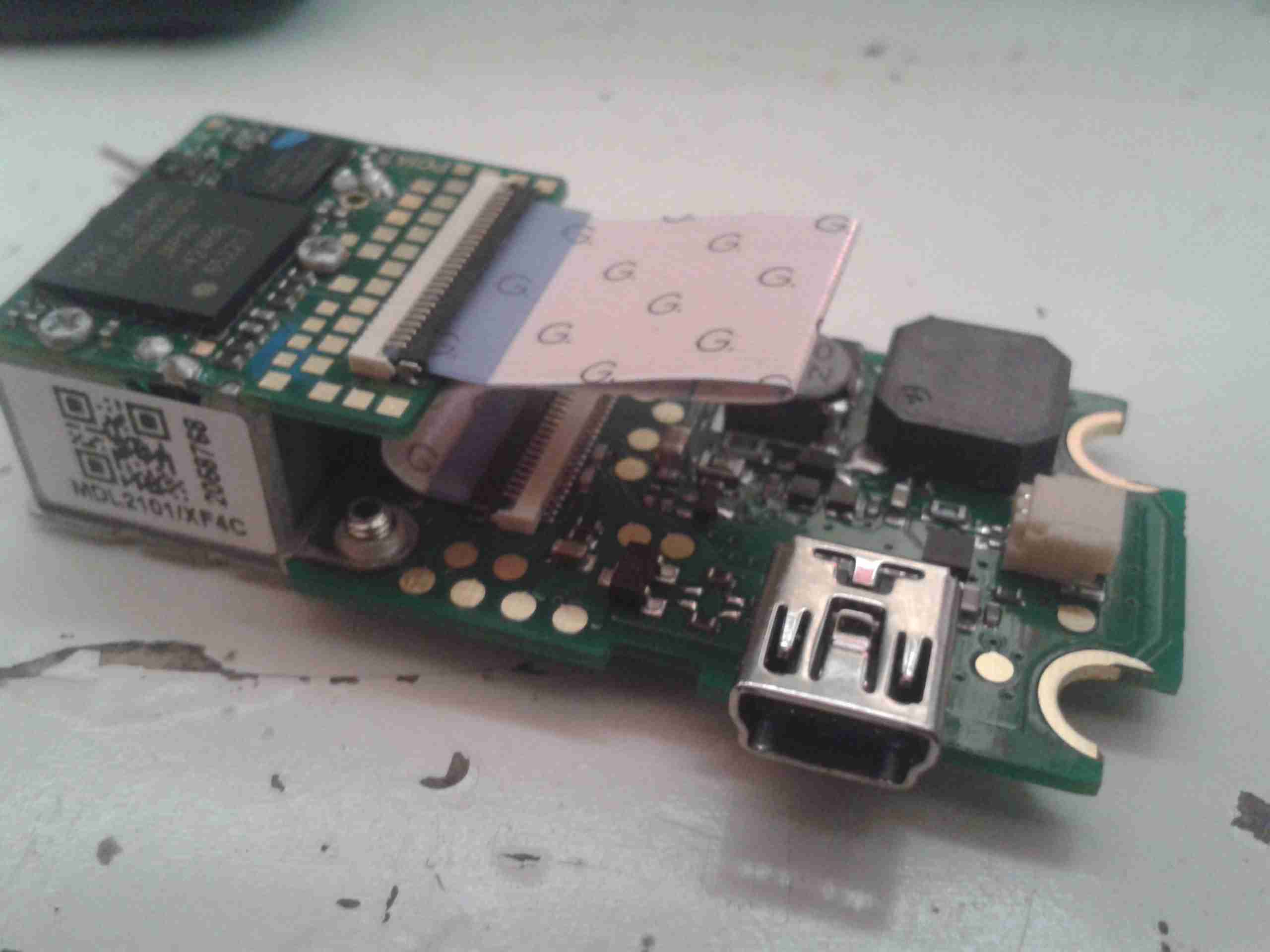
PCB Removed
Here’s the PCB & engine assembly removed from the casing. The lower PCB appears to just handle the user interface buttons, beeper & USB power & charging circuitry. All the processing logic is on the barcode engine itself.
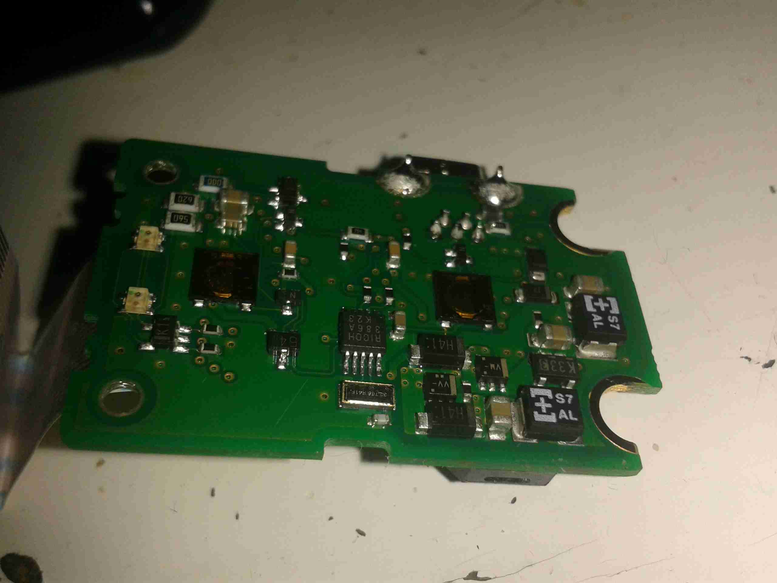
PCB Reverse
Here’s the back of the support PCB, with the pair of buttons for scanning & deleting barcodes. Also on this board is a 32kHz clock crystal & a Ricoh RV5C386A RTC IC. This communicates with the main processor via I²C for storing the date & time with the barcodes. At the bottom right corner are some of the power supply passives.
Support PCB
Here’s the other side of the support PCB, with the beeper, battery connector & the switching regulator to provide the barcode engine with 3.3v power.
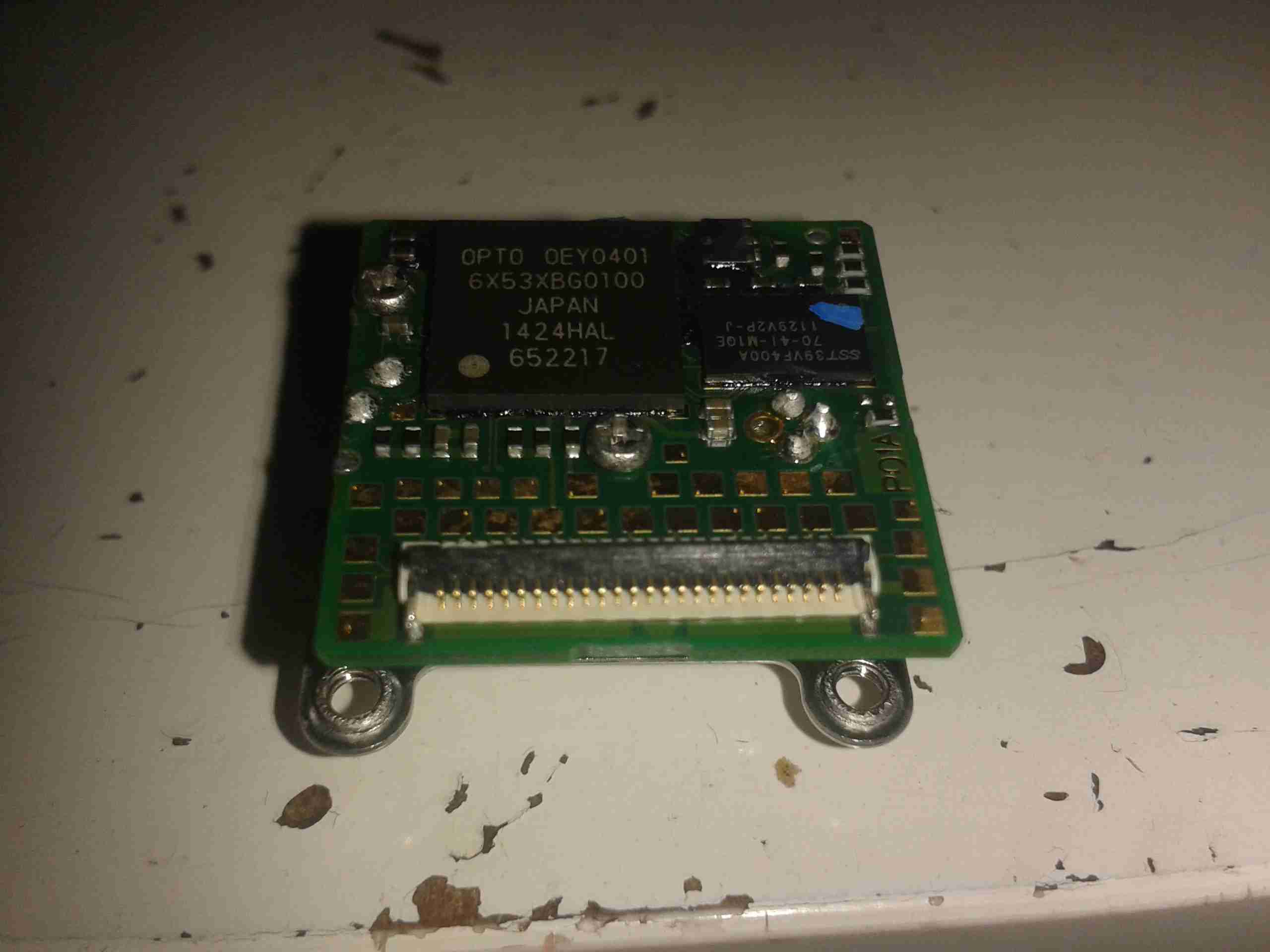
Barcode Engine
Here’s the barcode engine itself, which is absolutely tiny, at roughly 20mm square. The main processor & it’s associated Flash ROM are on this PCB. The main processor has an ARM7 32bit core, with 64kB of RAM, and onboard 512kB of ROM for program & barcode storage.
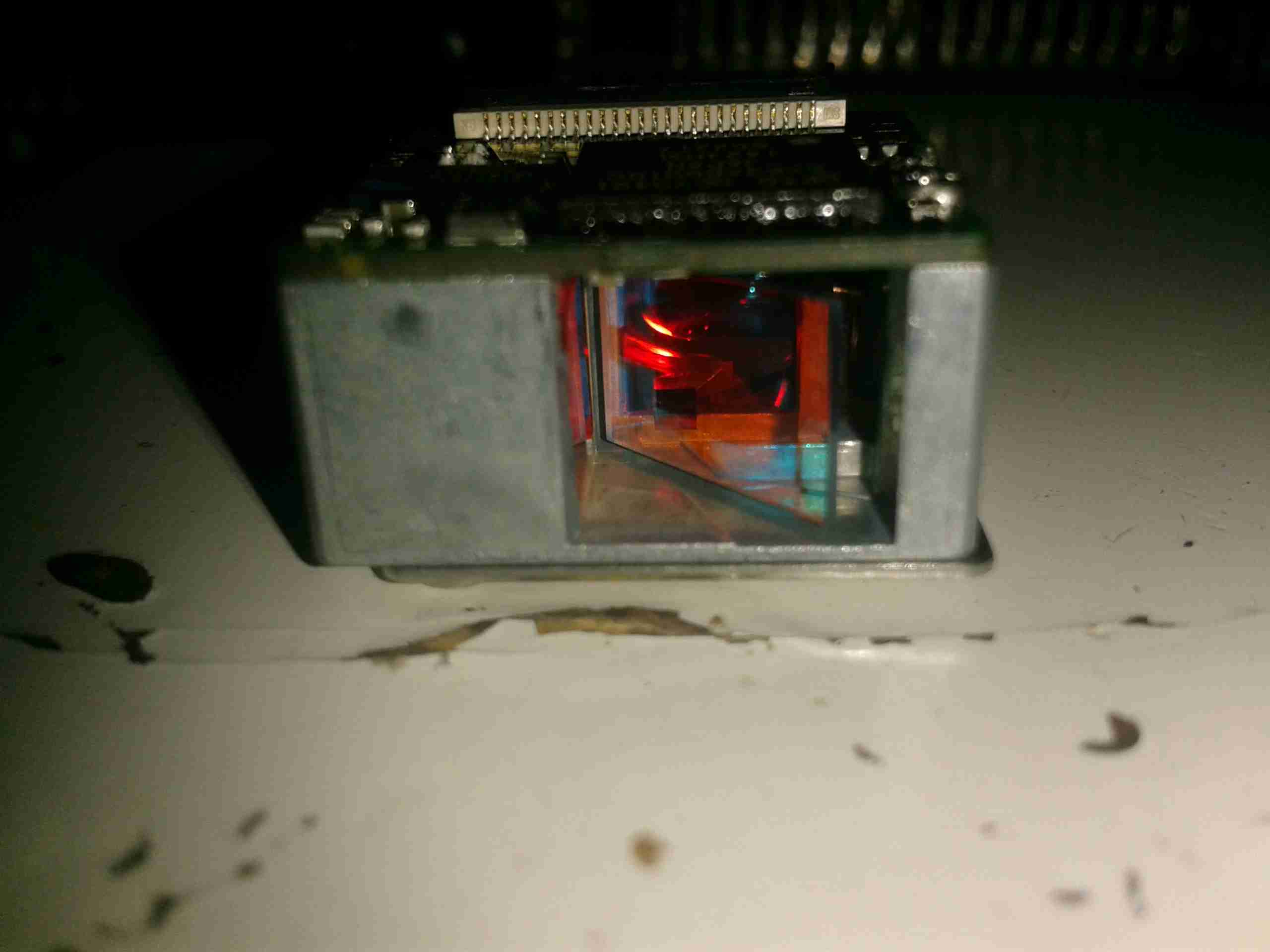
Mirror
Here’s the business end of the barcode engine, the mirror vibrates at 100Hz to produce the scan line. The laser diode is rated at 1mW, 650nm. This is in the deep red range.
Tip Jar
If you’ve found my content useful, please consider leaving a donation by clicking the Tip Jar below!
All collected funds go towards new content & the costs of keeping the server online.