A while back I found myself in the need of an adjustable RF attenuator capable of high-GHz operation. As luck would have it I had an old Spectrum analyser on the shelf at work, which we had retired quite some time ago.
Spectrum analysers being quite capable test instruments, I knew that the input attenuation would be done with a standalone module that we could recover for reuse without too much trouble.
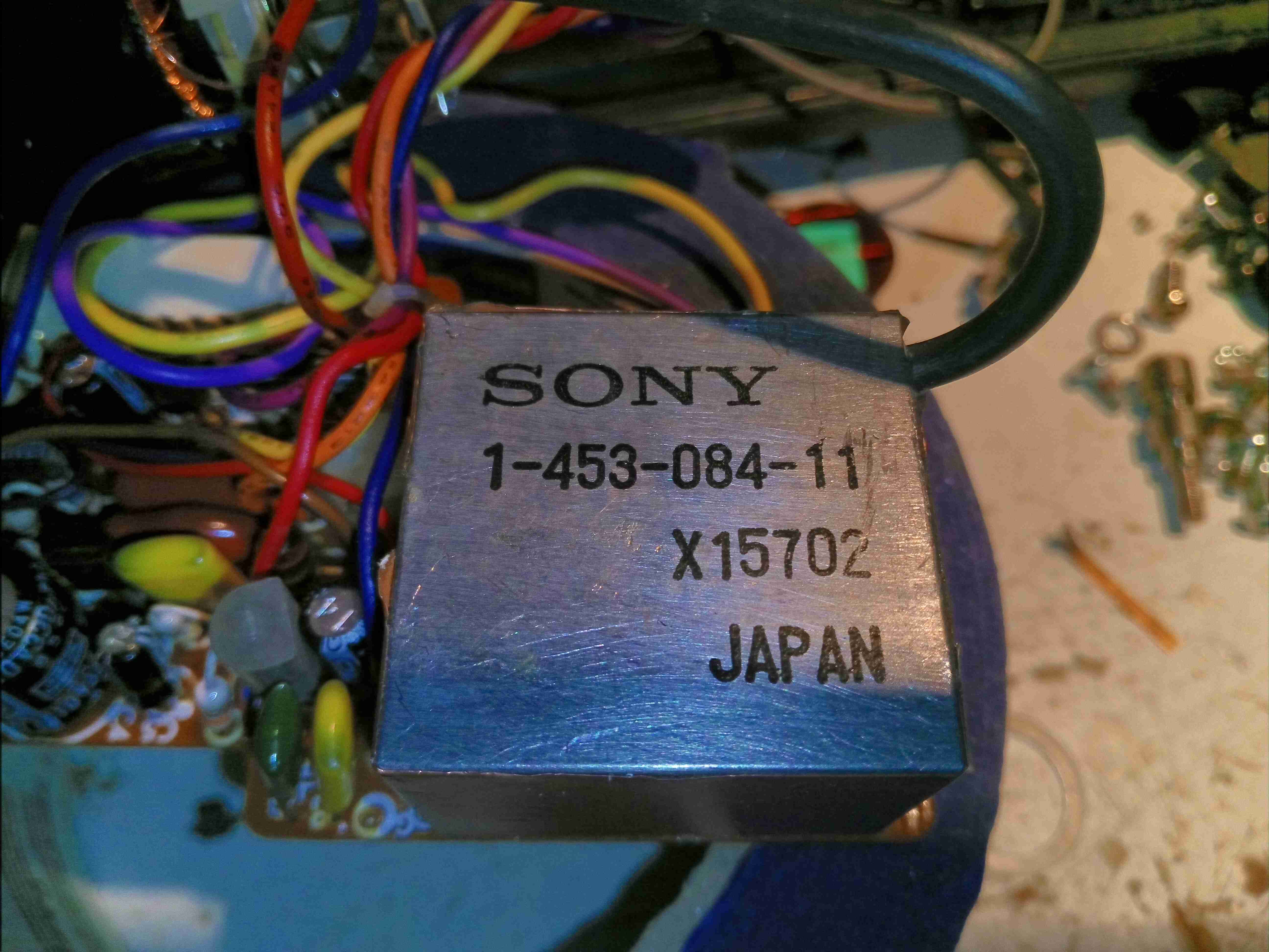
The attenuator module
Here’s the module itself, with the factory drive PCB removed from the bottom, showing the solenoids that operate the RF switches. There are test wires attached to them here to work out which solenoid switches which attenuation stage. In the case of this module, there are switches for the following:
Input select switch
AC/DC coupling
-5dB
-10dB
-20dB
-40dB
For me this means I have up to -75dB attenuation in 5dB steps, with optional switchable A-B input & either AC or DC coupling.
Drive is easy, requiring a pulse on the solenoid coil to switch over, the polarity depending on which way the switch is going.
Building a Control Board
Now I’ve identified that the module was reusable, it was time to spin up a board to integrate all the features we needed:
Onboard battery power
Pushbutton operation
Indication of current attenuation level
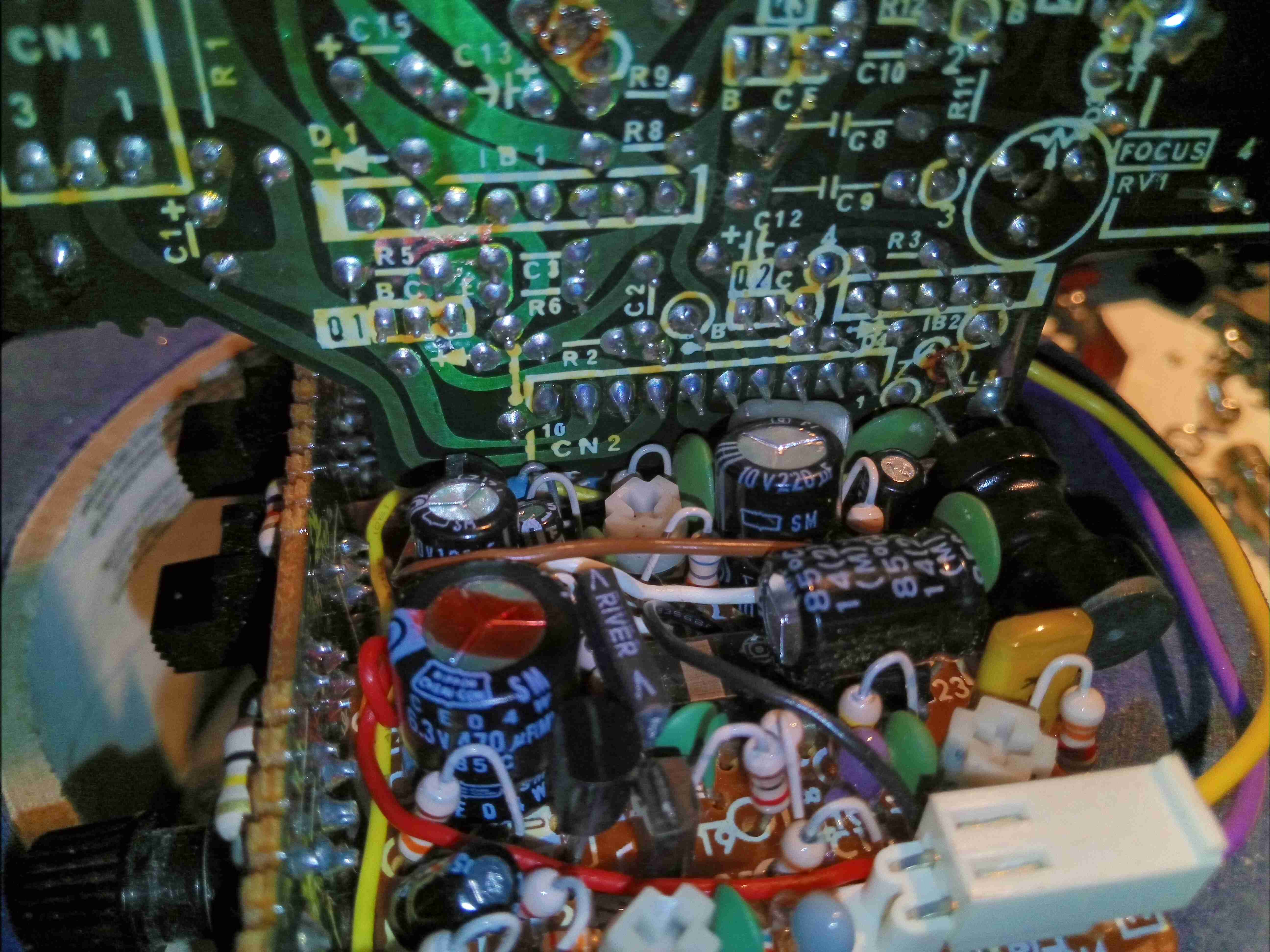
The partially populated board is shown at right, with an Arduino microcontroller for main control, 18650 battery socket on the right, and control buttons in the centre. The OLED display module for showing the current attenuation level & battery voltage level is missing at the moment, but it’s clear where this goes.
As there weren’t enough GPIO pins for everything on the Arduino, a Microchip MC23017 16-Bit I/O expander, which is controlled via an I²C bus. This is convenient since I’m already using I²C for the onboard display.
Driving the Solenoids
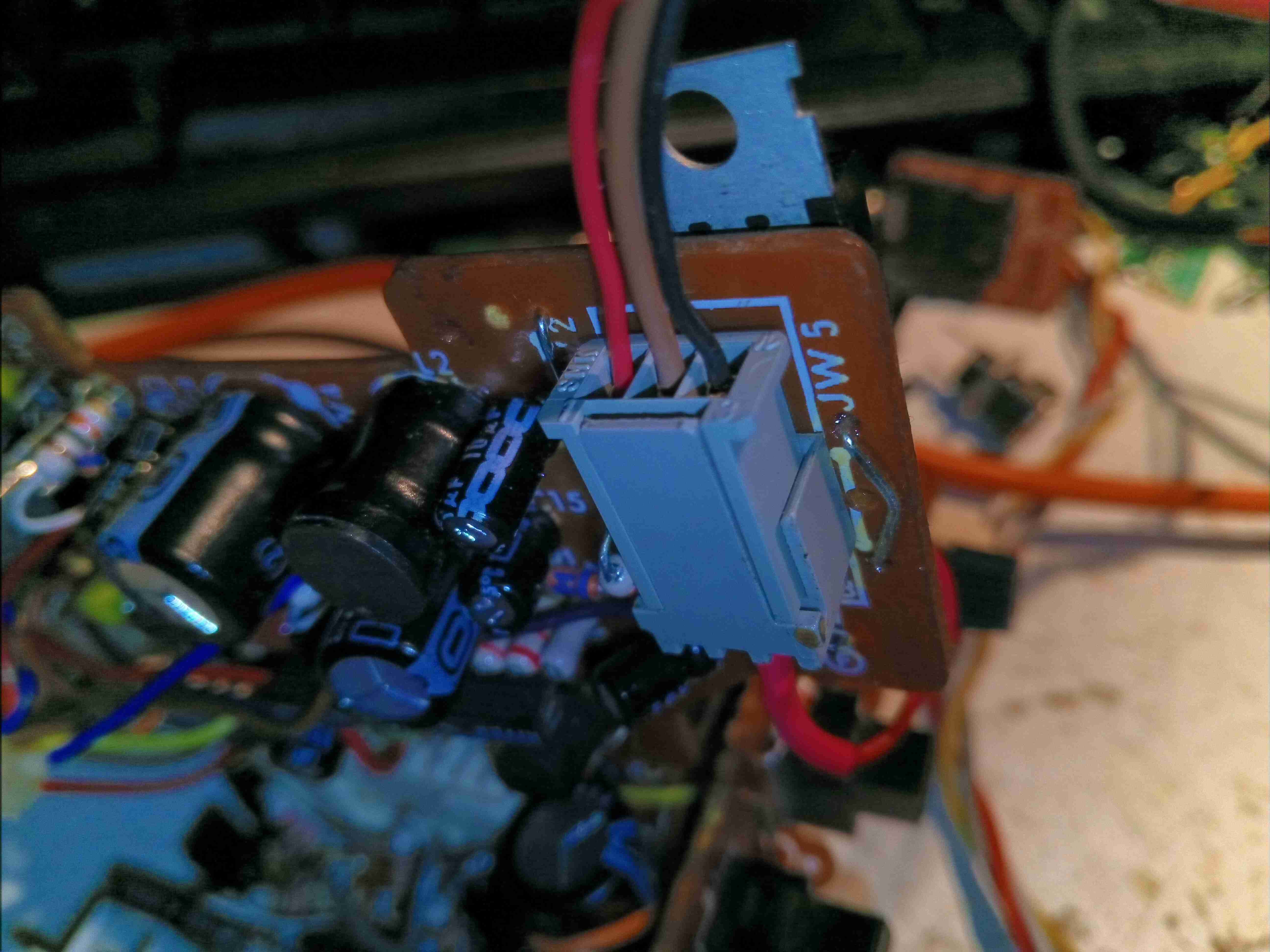
A closer view of the board shows the trip of dual H-Bridge drivers on the board, which will soon be hidden underneath the attenuator block. These are LB1836M parts from ON Semiconductor. Each chip drives a pair of solenoids.
Power Supplies
The bottom of the board has all the power control circuitry, which are modularised for ease of production. There’s a Lithium charge & protection module for the 18650 onboard cell, along with a boost converter to give the ~9v rail required to operate the attenuator solenoids. While they would switch at 5v, the results were not reliable.
Finishing off
A bit more time later, some suitable firmware has been written for the Arduino, and the attenuator block is fitted onto the PCB. The onboard OLED nicely shows the current attenuation level, battery level & which input is selected.
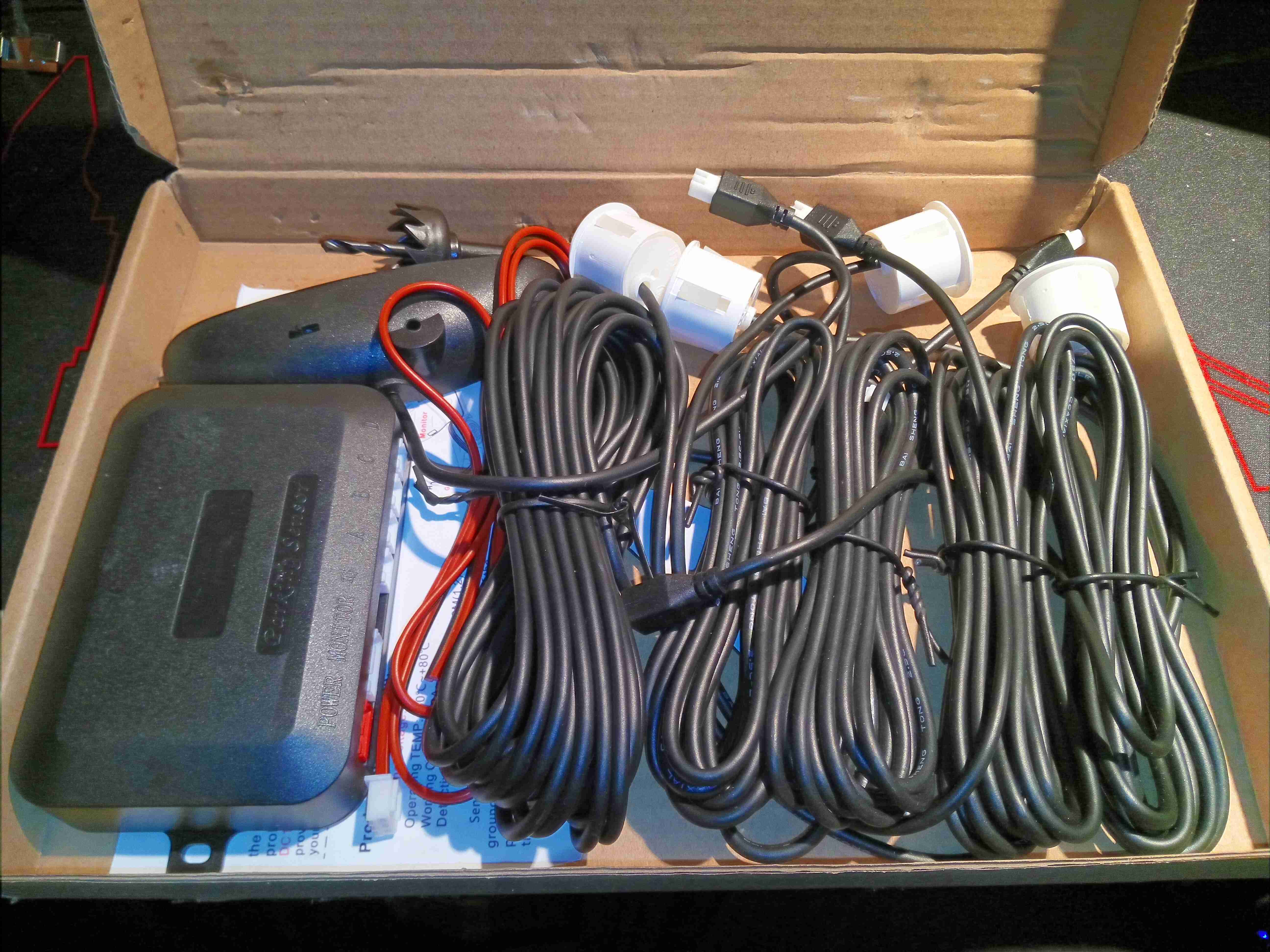
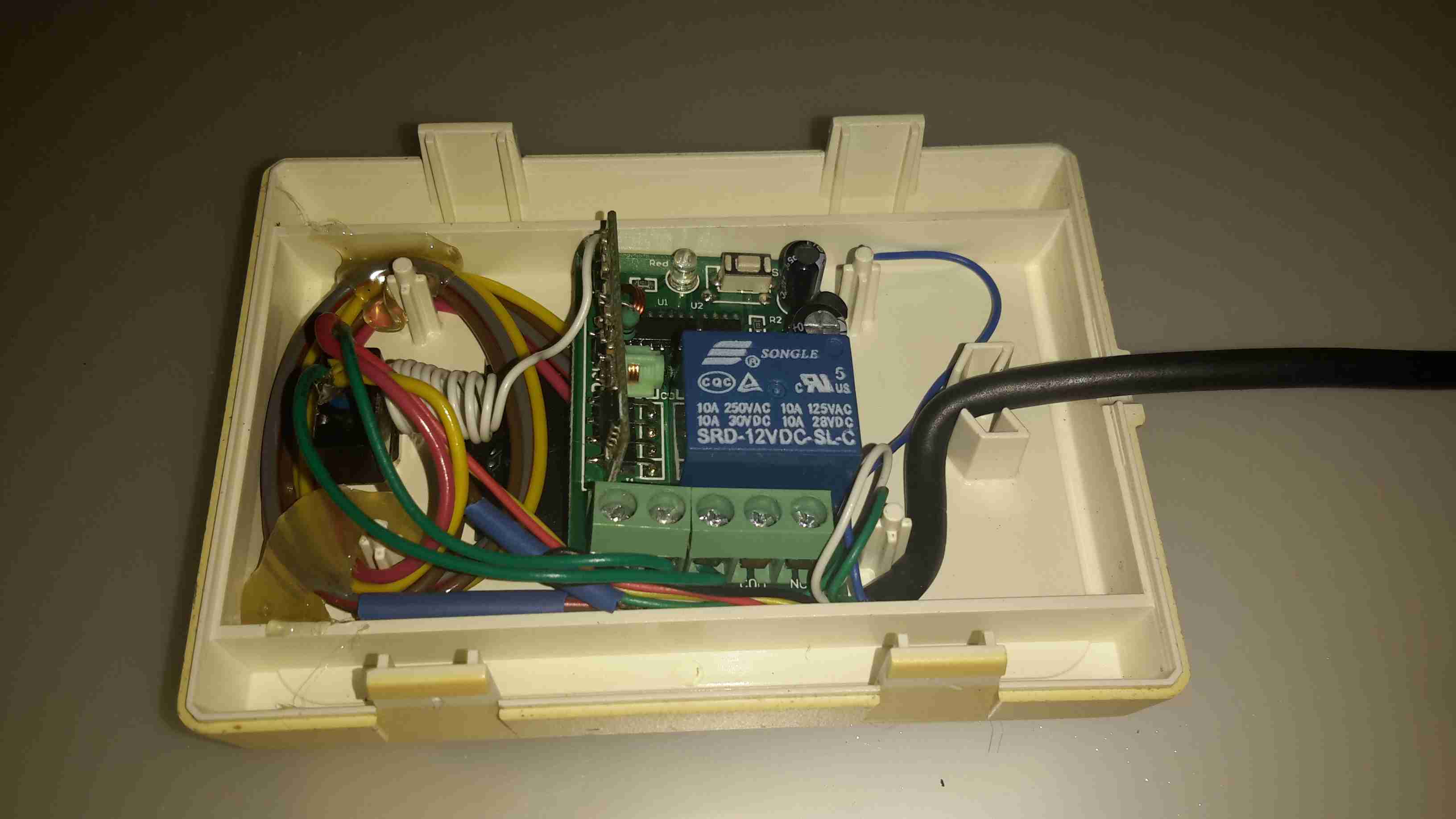
This is a cheap kit from eBay, to retrofit an older car with ultrasonic parking sensors. 4 sensors are included in the kit, along with a hole saw to fit them to the bumper. There’s a small controller module, and a display module that fits onto the dash of the car.
Controller Module
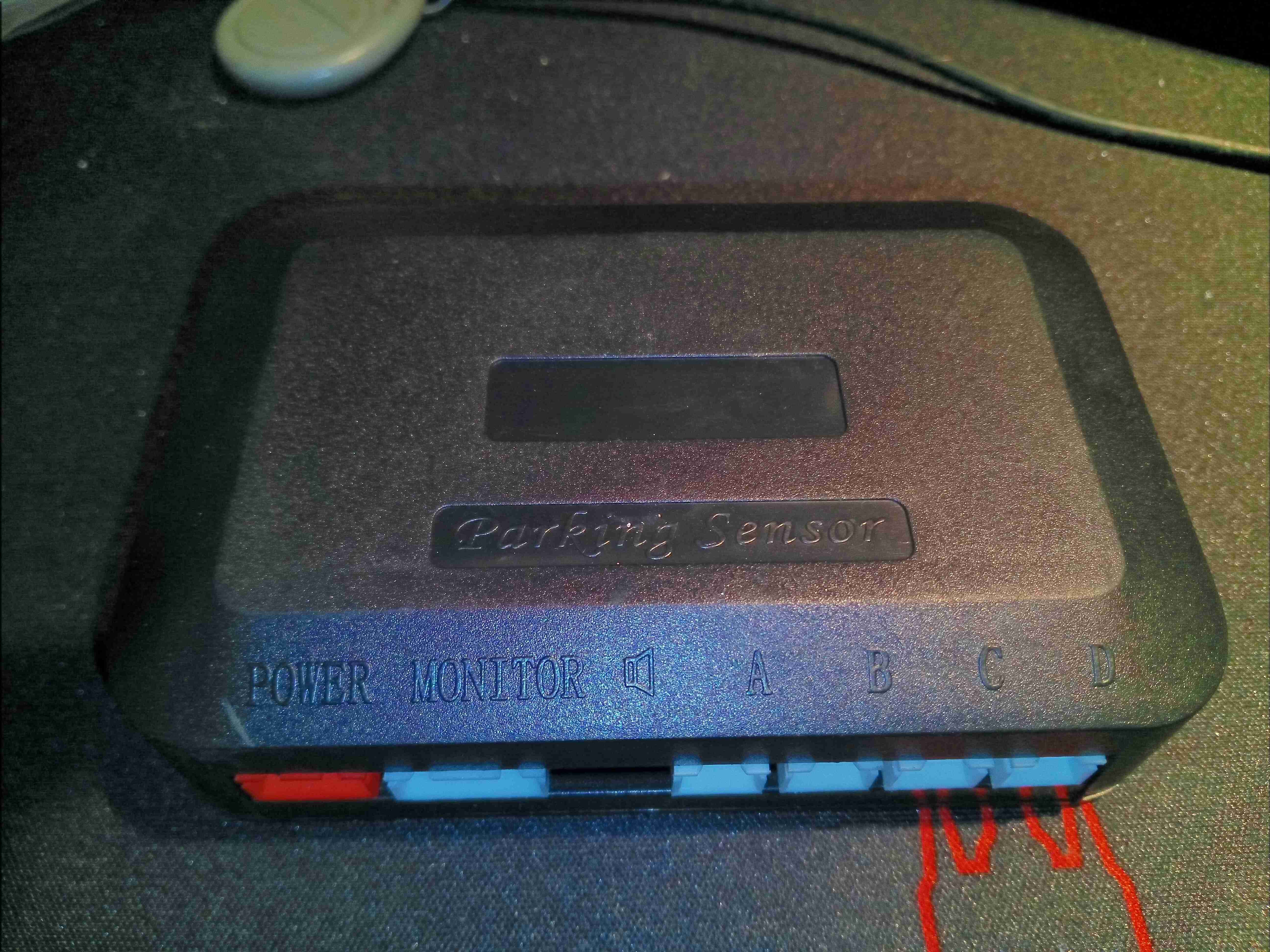
Here’s the controller module, with it’s row of connectors along the front. The unit gets it’s power from the reversing light circuit, via the red connector.
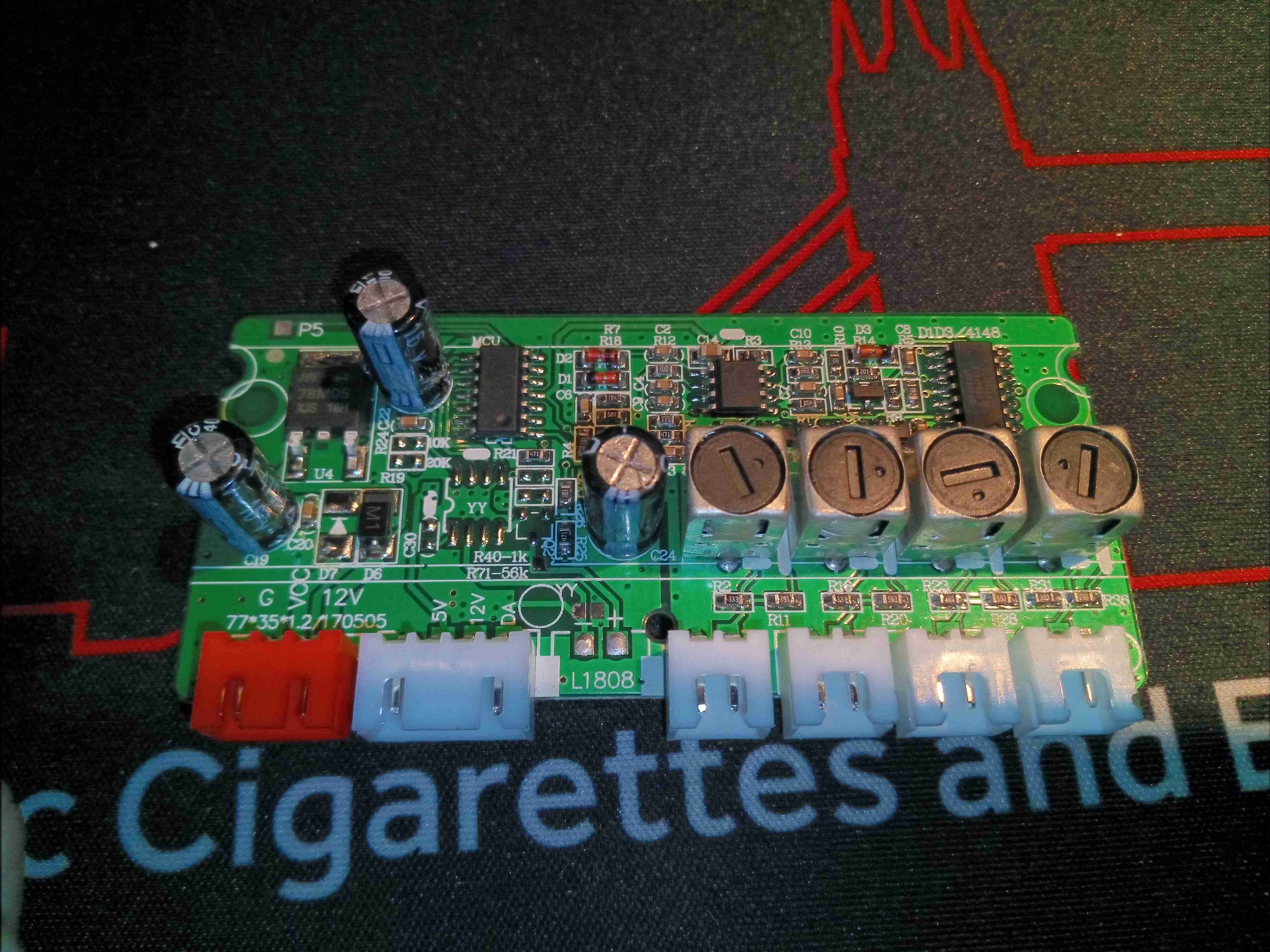
Main Controller PCB
Removing a couple of screws allows the PCB to be removed. There’s quite a bit on this board, including 4 tunable inductors for the ultrasonic transducers. There’s a linear voltage regulator on the left which supplies power to the electronics, and a completely unmarked microcontroller.
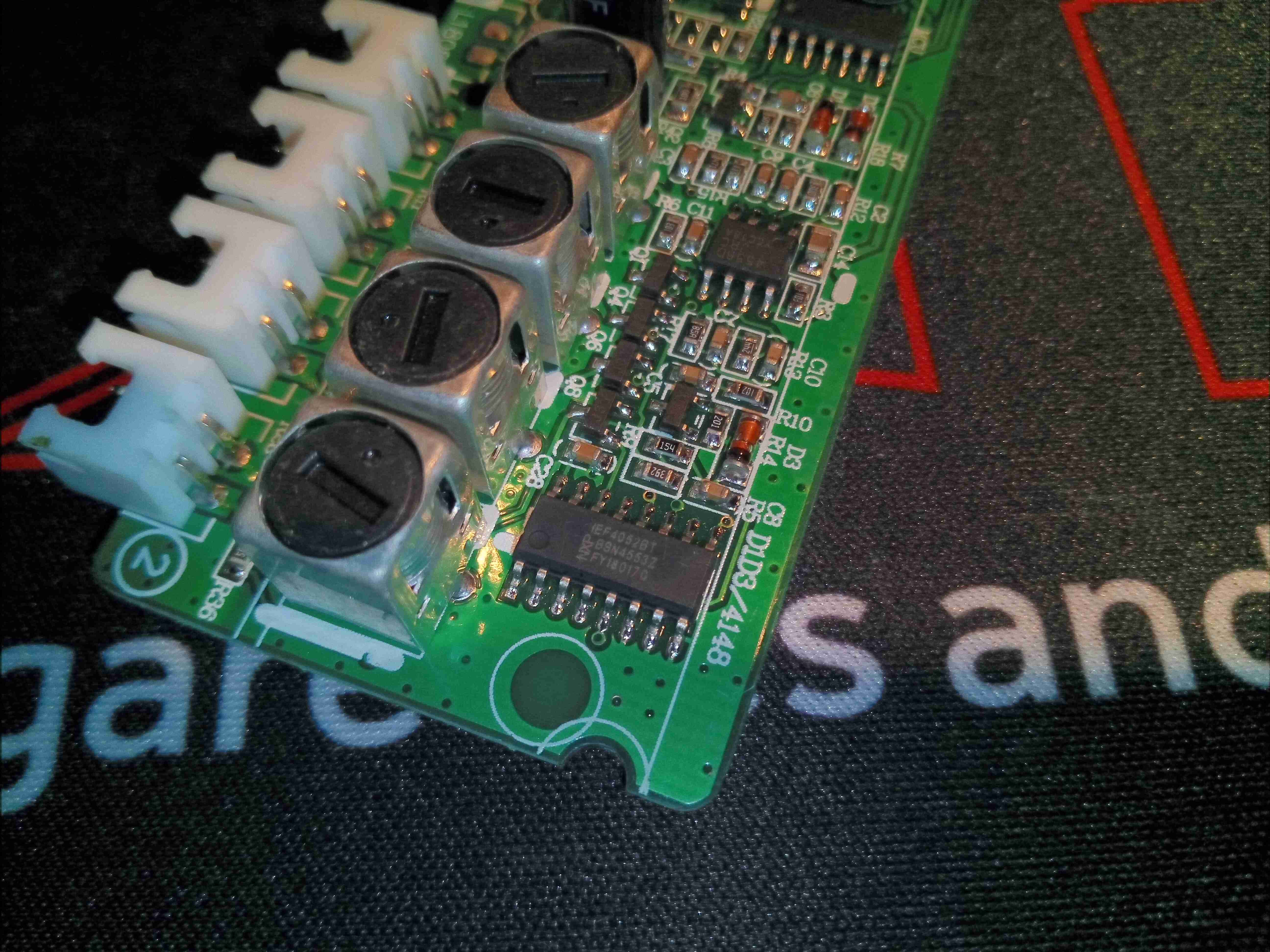
Electronics Closeup
A closer look at the analogue end of the board shows a JRC4558D dual Op-Amp, and an NXP HEF4052B analogue multiplexer. As the microcontroller is unmarked I have no data for that one.
Dash Display
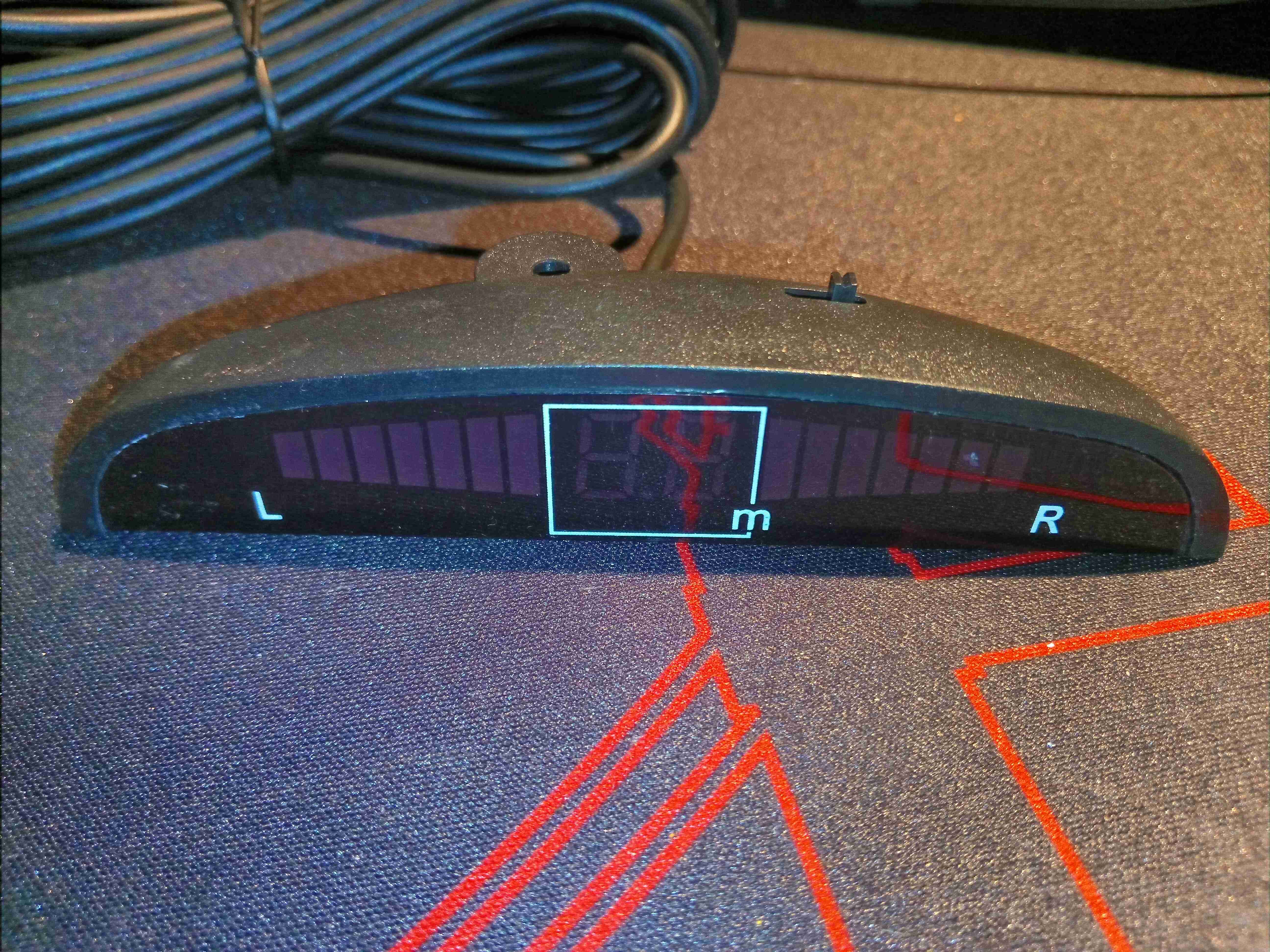
The dash display is housed in another small plastic box, with bargraphs for each side of the car & an overall distance meter.
Display Module
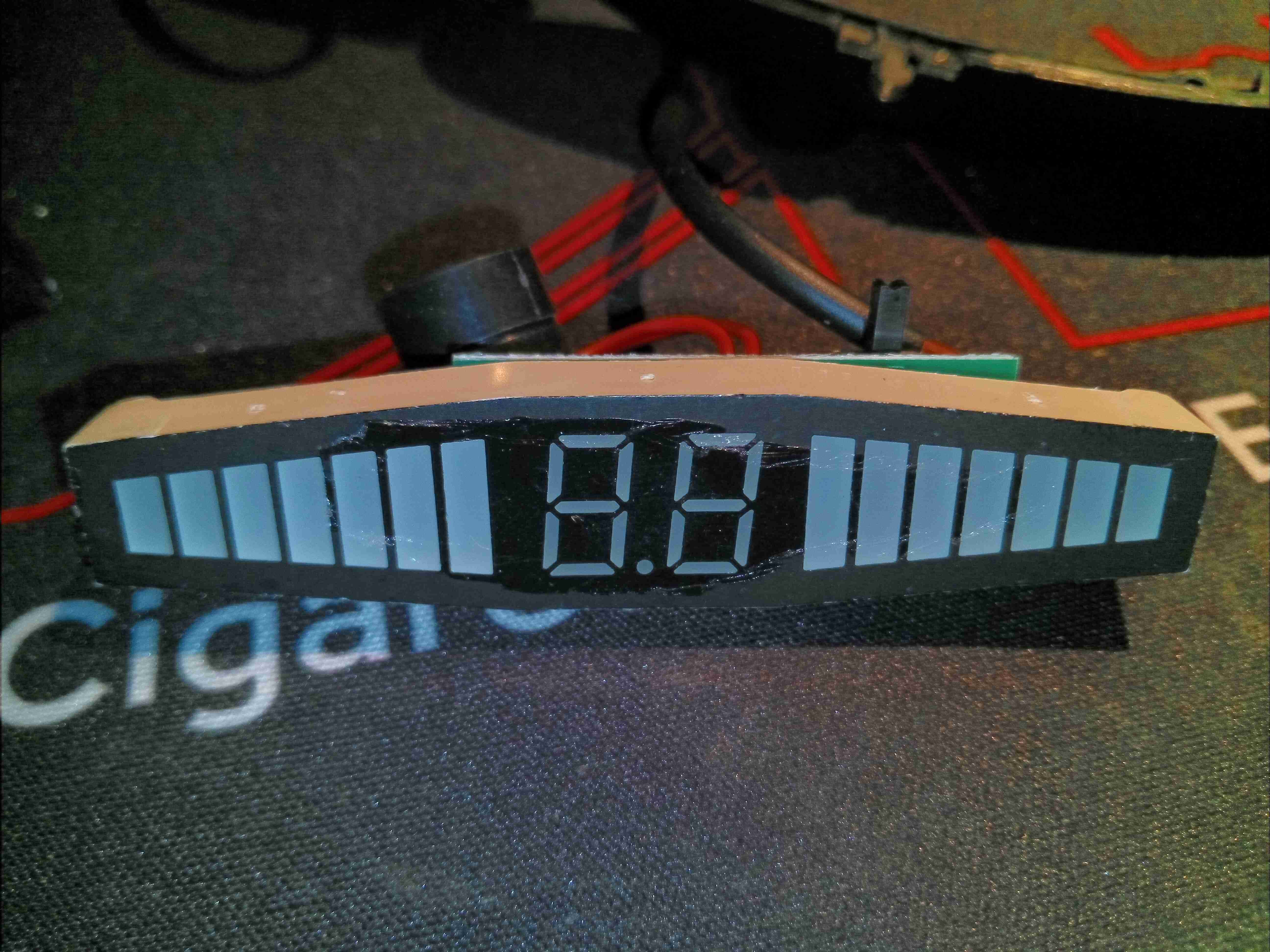
Clearly this is a custom module, with the tapered bargraph LEDs on each side & the 7-segment display in the centre. There’s a beeper which works like every factory-fitted unit does, increasing in rate as the distance closes.
Display PCB
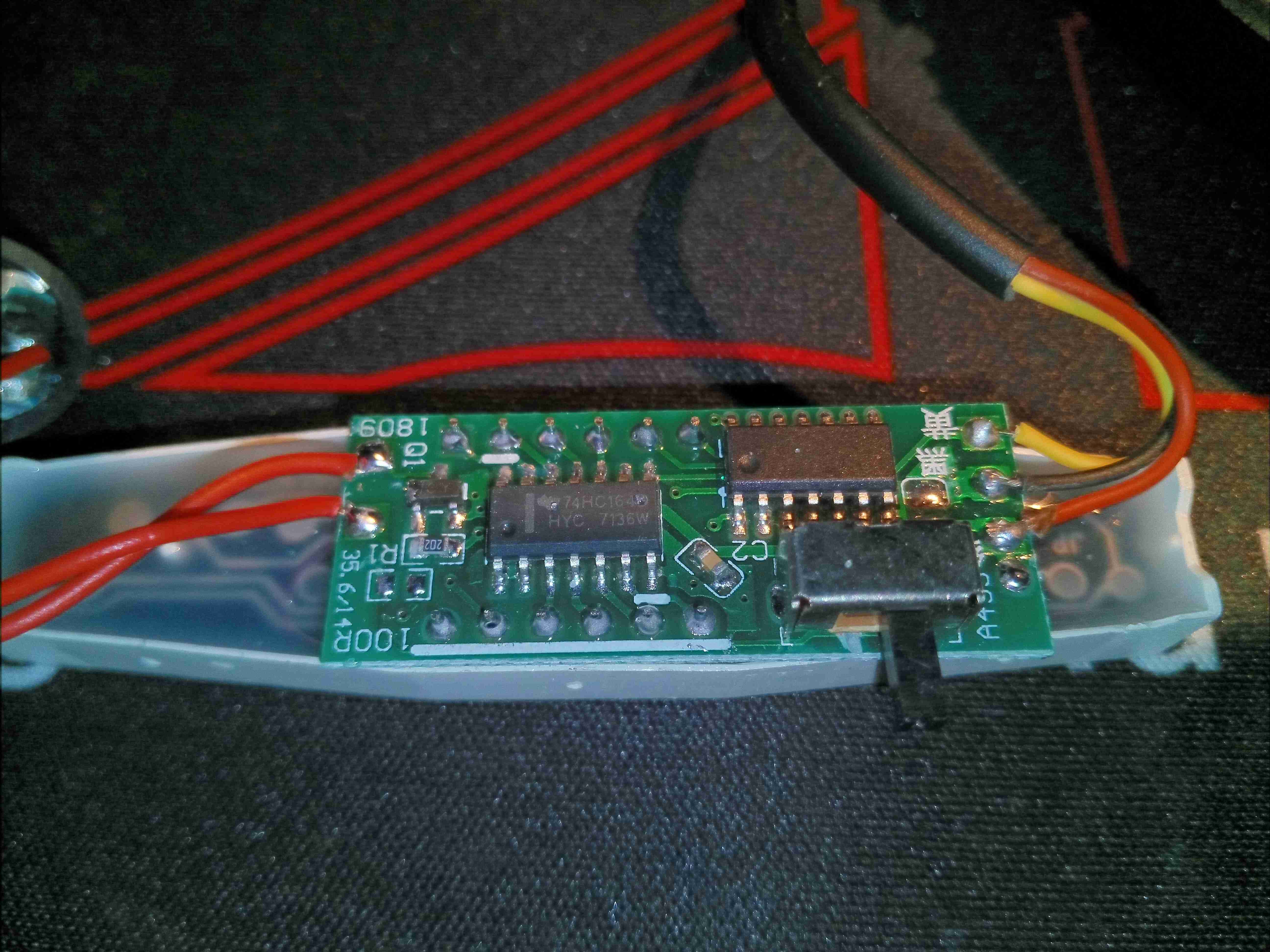
The back of the display module has the driver PCB, with yet another unmarked microcontroller, and a TI 74HC164 serial shift register as a display driver. There’s only 3 wires in the loom from the controller, so some sort of 1-wire protocol must be being used, while I²C is the most likely protocol to be talking to the display driver circuit. There’s also a small switch for muting the beeper.
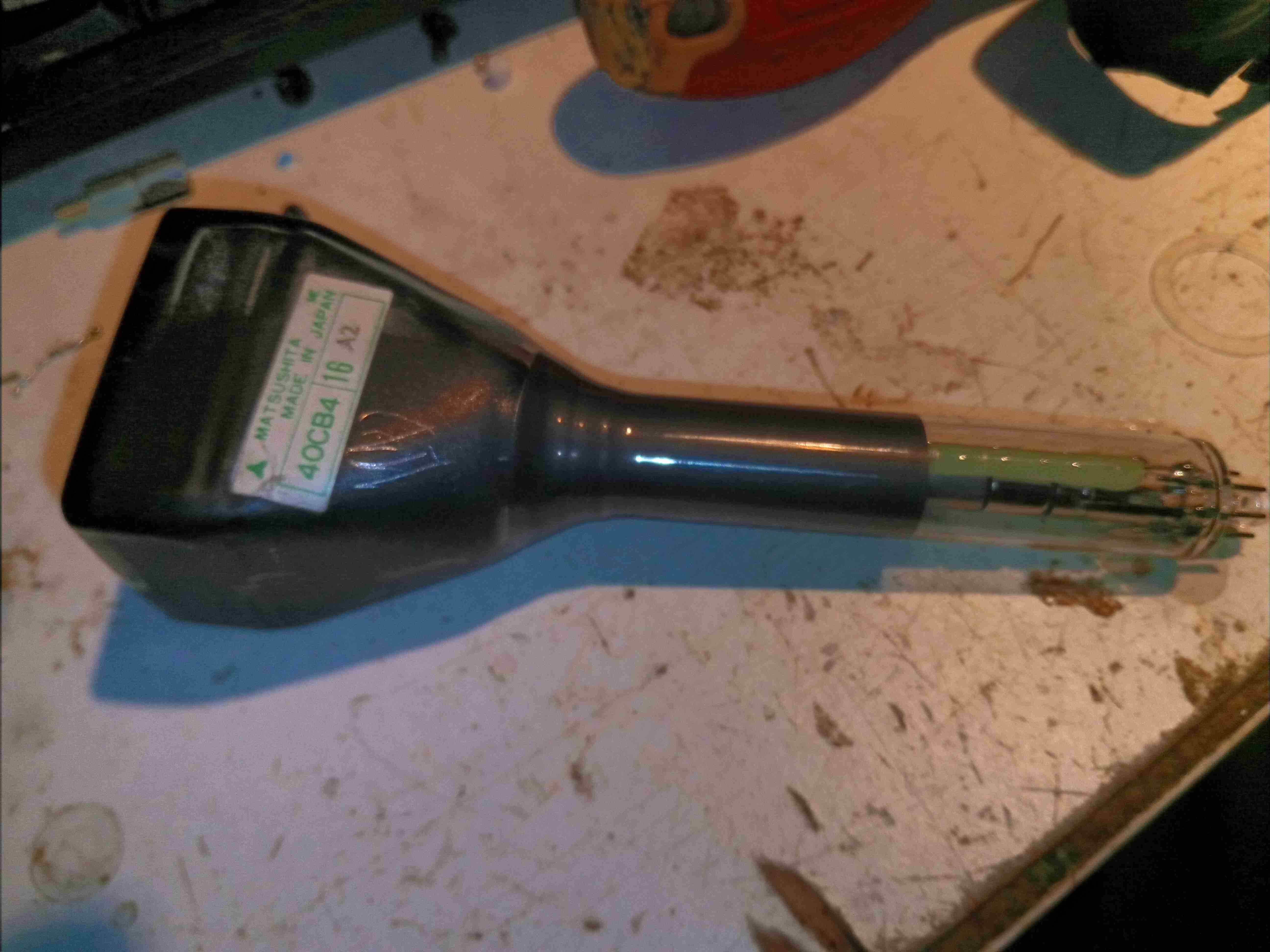
Well, it’s time for another viewfinder hack! I’ve been after one of these for a while, this is from an early 1980’s era Sony Trinicon camera, and instead of the tiny ½” round CRT display, these have a 1.5″ square CRT – a Matsushita 40CB4. Luckily I managed to score a pair of these from eBay for very little money. Update: The second camera’s viewfinder module turned out to have a dead flyback transformer, but at least I have a good spare CRT & the rest of the support components. More to come later on the teardown of the camera itself.
Mirror & Eyecup Assembly
The eyecup assembly with the magnifying lens & turning mirror is easy to remove, with clips & a single screw holding it onto the CRT holder sticking out of the side of the main casing.
Top Cover Removed
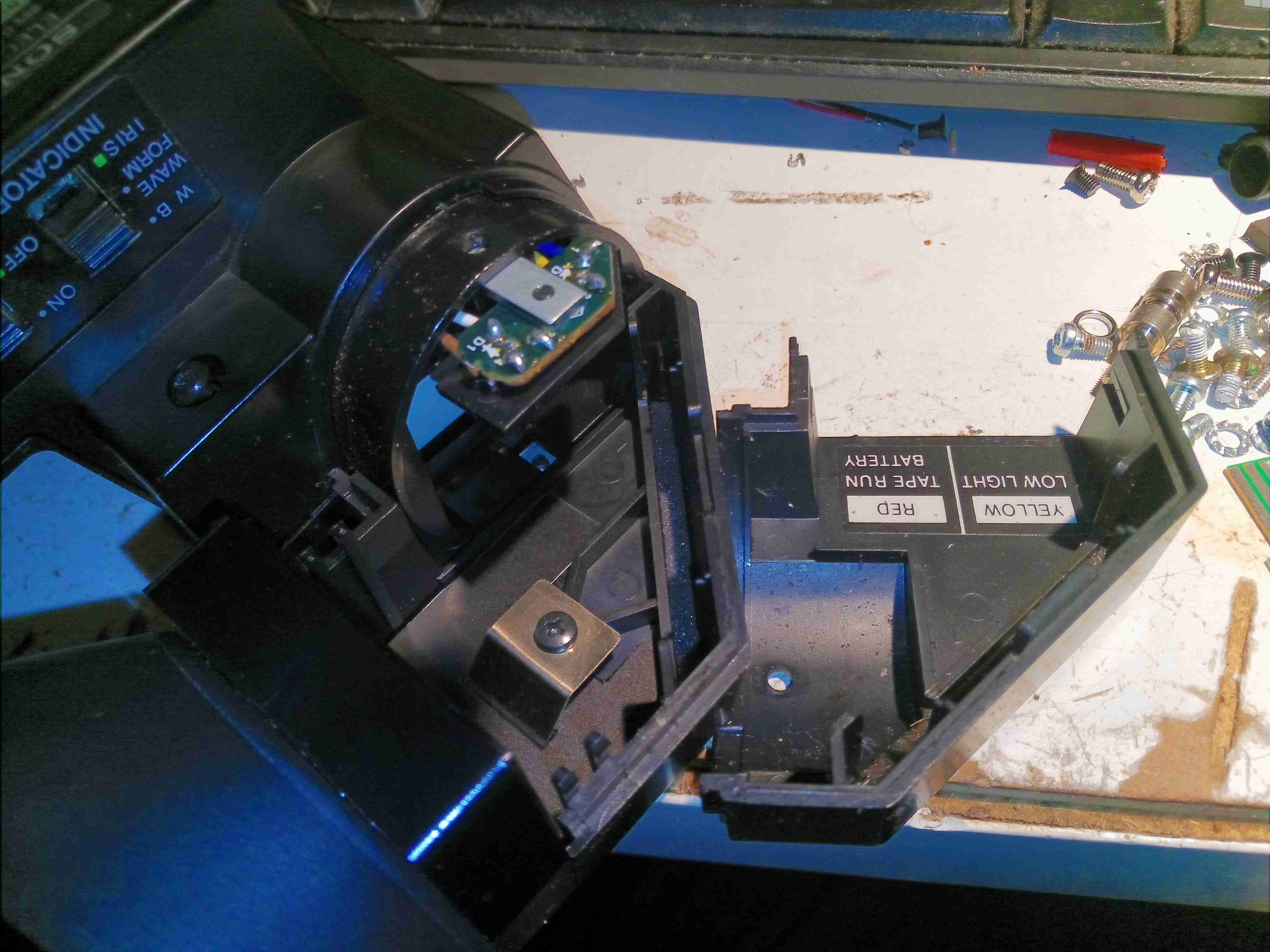
Removing some screws around the case allows the top cover to be removed, revealing the electronics. There’s certainly more in here than the later camera viewfinders, in this unit there are two boards slotted together with a board-to-board interconnect at the bottom. The CRT is at the top of the photo, hiding inside the plastic housing & deflection yoke assembly.
Bare PCBs & CRT
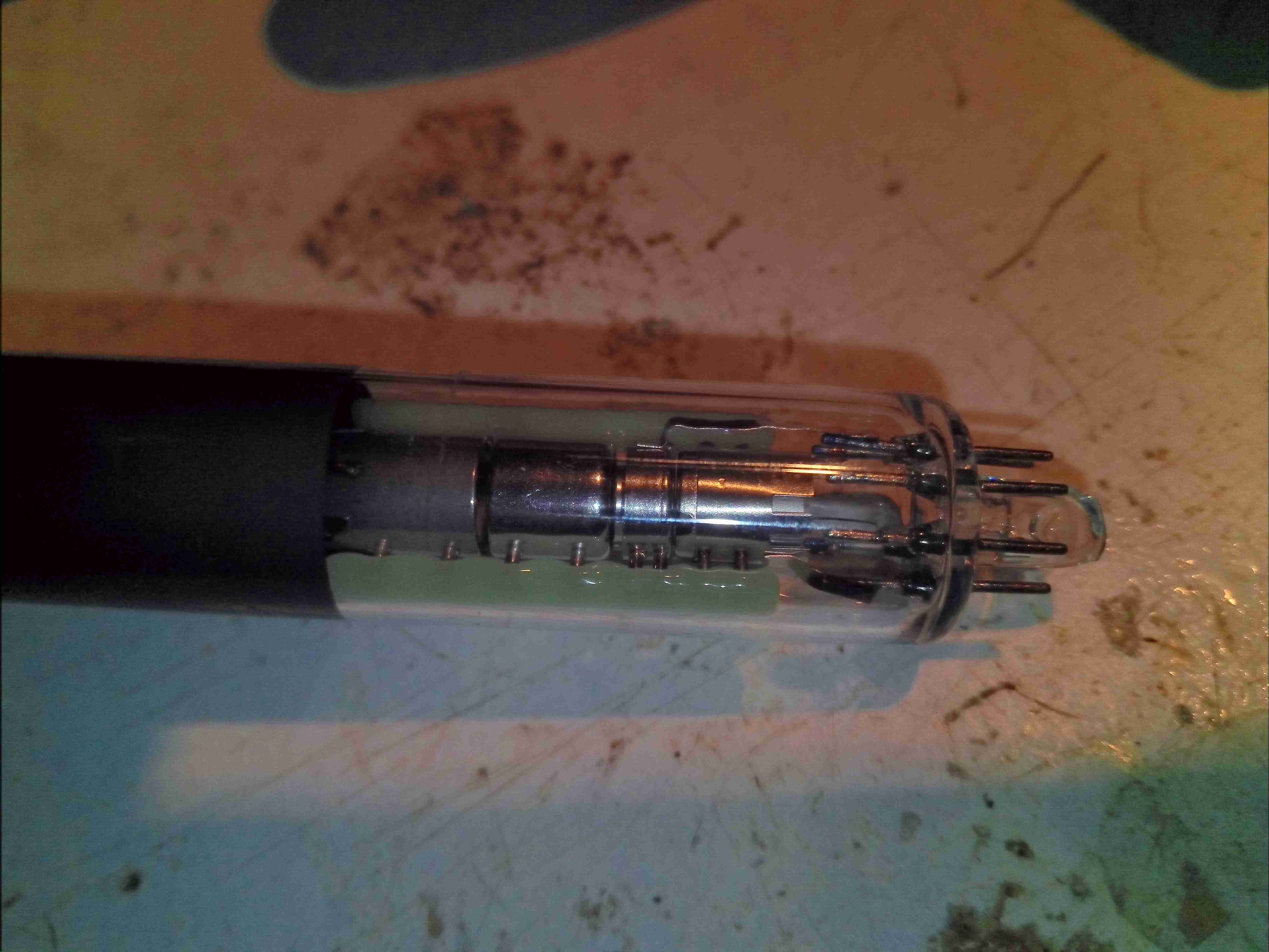
Here’s the CRT & one of the control boards removed from the case, having been stripped of the heatshrink tube that held the final anode lead in place. Just like on larger CRTs, this viewfinder has the final anode on a cavity connector fused into the bell, instead of being led out to a pin on the base. This is probably due to the much higher anode voltage of 5kV, a big jump from the 2kV on the ½” round tubes.
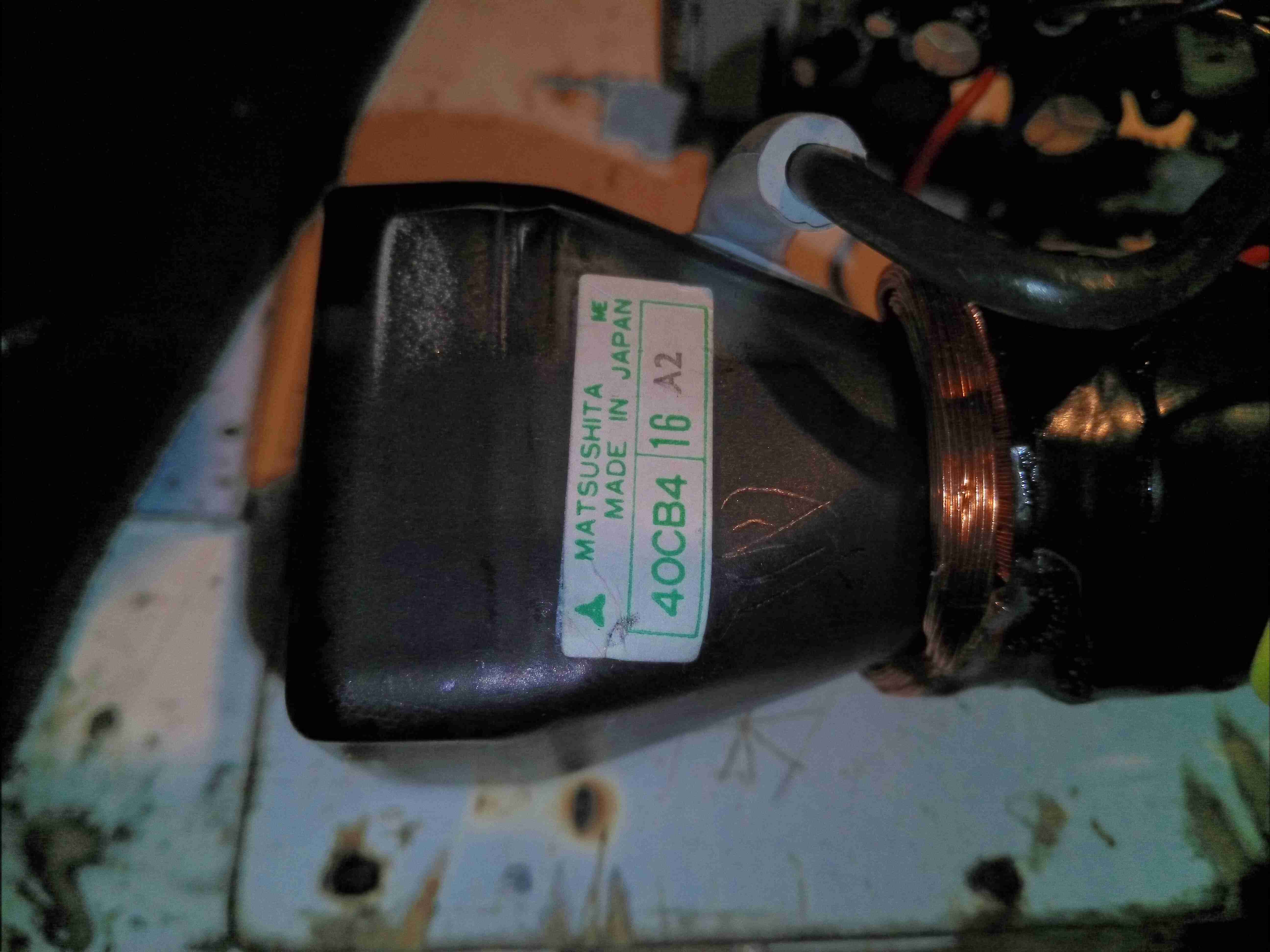
40CB4 CRT Label
Yup, it’s definitely the elusive 40CB4. Apparently these CRTs are still manufactured to this day for professional camera viewfinders, as the resolution of this small vacuum tube is still better than similarly sized modern tech such as LCDs or OLEDs. The phosphor used is type P4 – ZnS:Ag+(Zn,Cd)S:Ag, with an aluminized overcoat.
Bare 40CB4 CRT
After the base connector & deflection yoke are removed from the tube, the very long neck can be seen, this long glass neck apparently giving better focus & resolution than the stubbier tubes.
Electron Gun
The electron gun is the usual single unit as usually found in monochrome tubes.
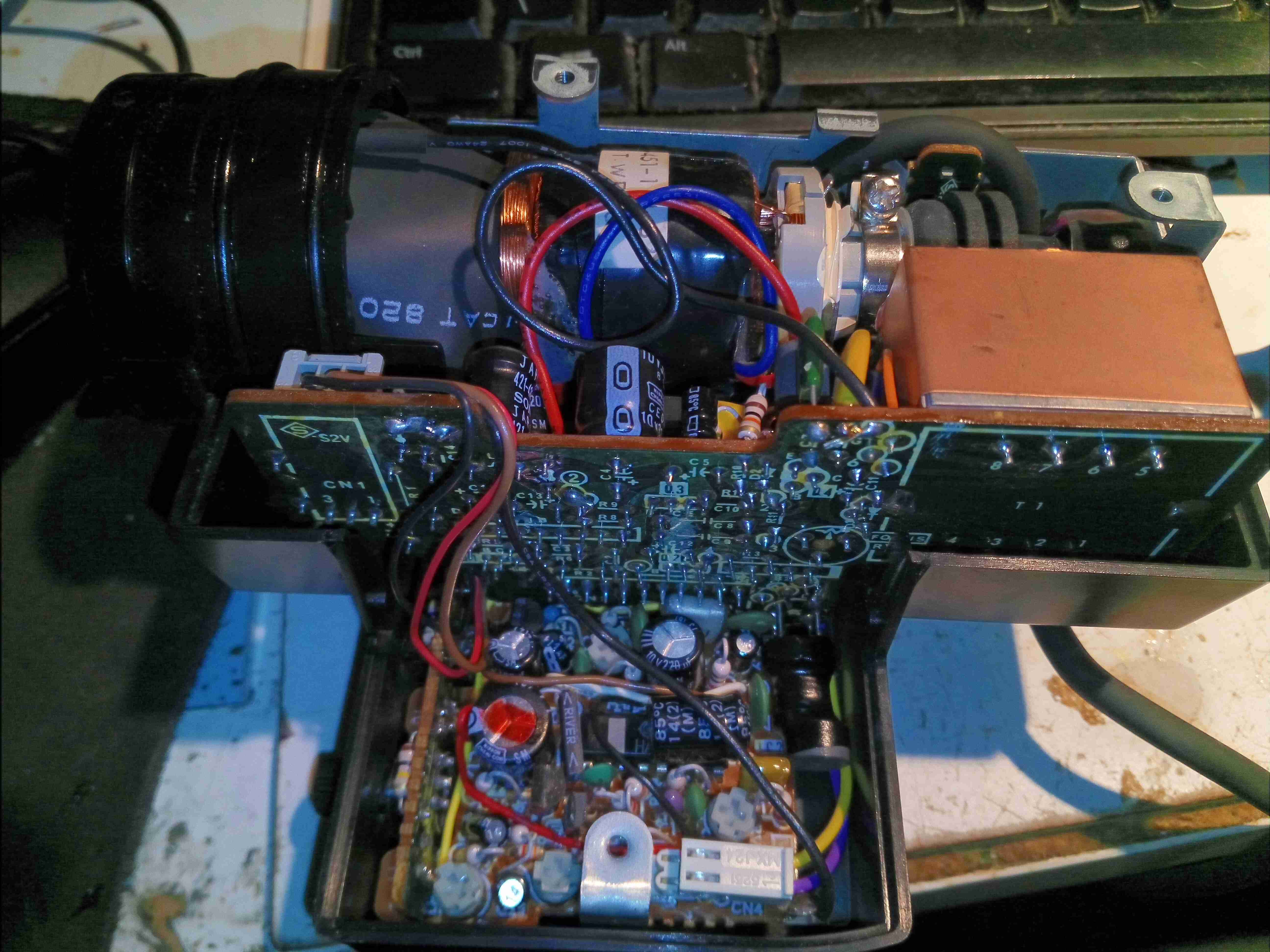
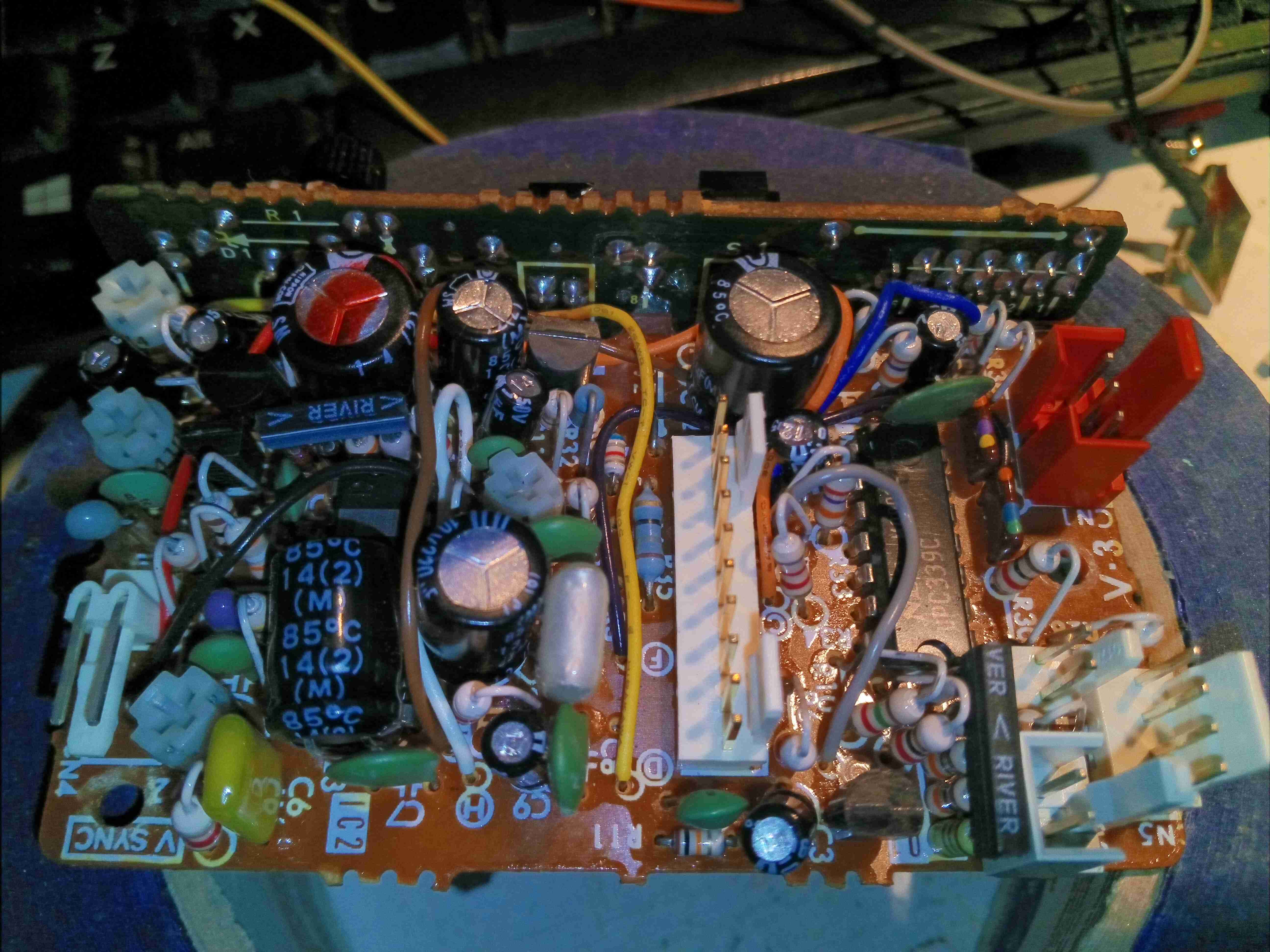
Deflection Board
The bottom board in the assembly has all the control circuitry for the CRT, including the HA11244 deflection IC, composite sync separator & vertical deflection drive circuit. There are also circuits here to display a video waveform on the CRT, along with iris & white balance markers.
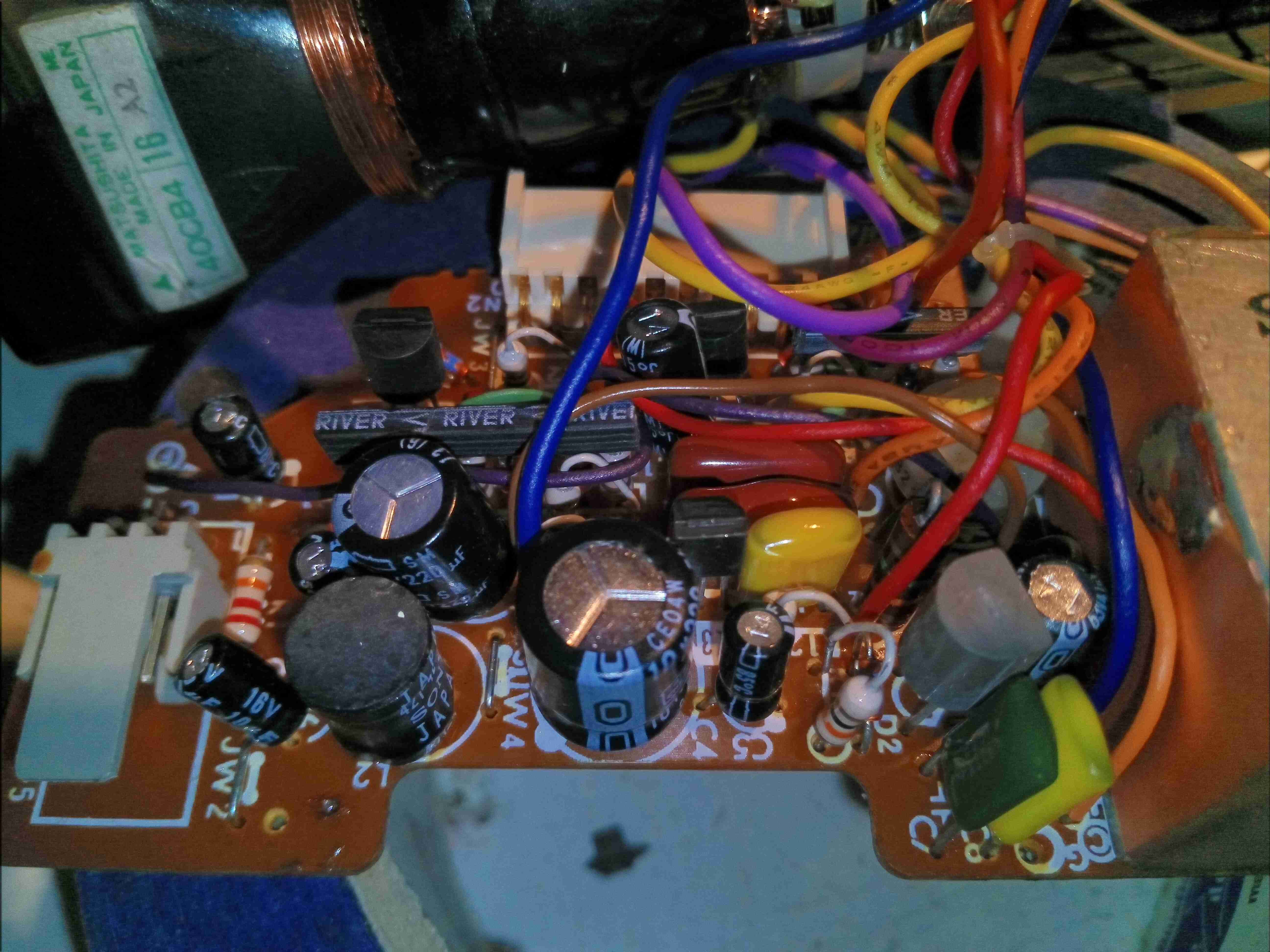
Horizontal Board
The other board has the horizontal drive circuitry, along with the video input amplifier. Despite the attempt to miniaturize the entire assembly, these are still well packed boards. Some of the resistors & diodes are bussed together in custom SIL hybrid modules to save PCB space. Like all the other CRT viewfinders, these units are meant for viewing via a mirror – the horizontal deflection coil connections need to be reversed to show a correct image without the mirror. The Red & Blue wires to the yoke need to be swapped here.
Flyback Transformer
The horizontal board on this unit also supports the flyback transformer, which is massive compared to the other viewfinder circuits. Biasing, focus & filament supplies for the CRT are also derived from this transformer, via auxiliary windings.
Boards Connected
The boards slot together in the centre to form the fully operational circuit.
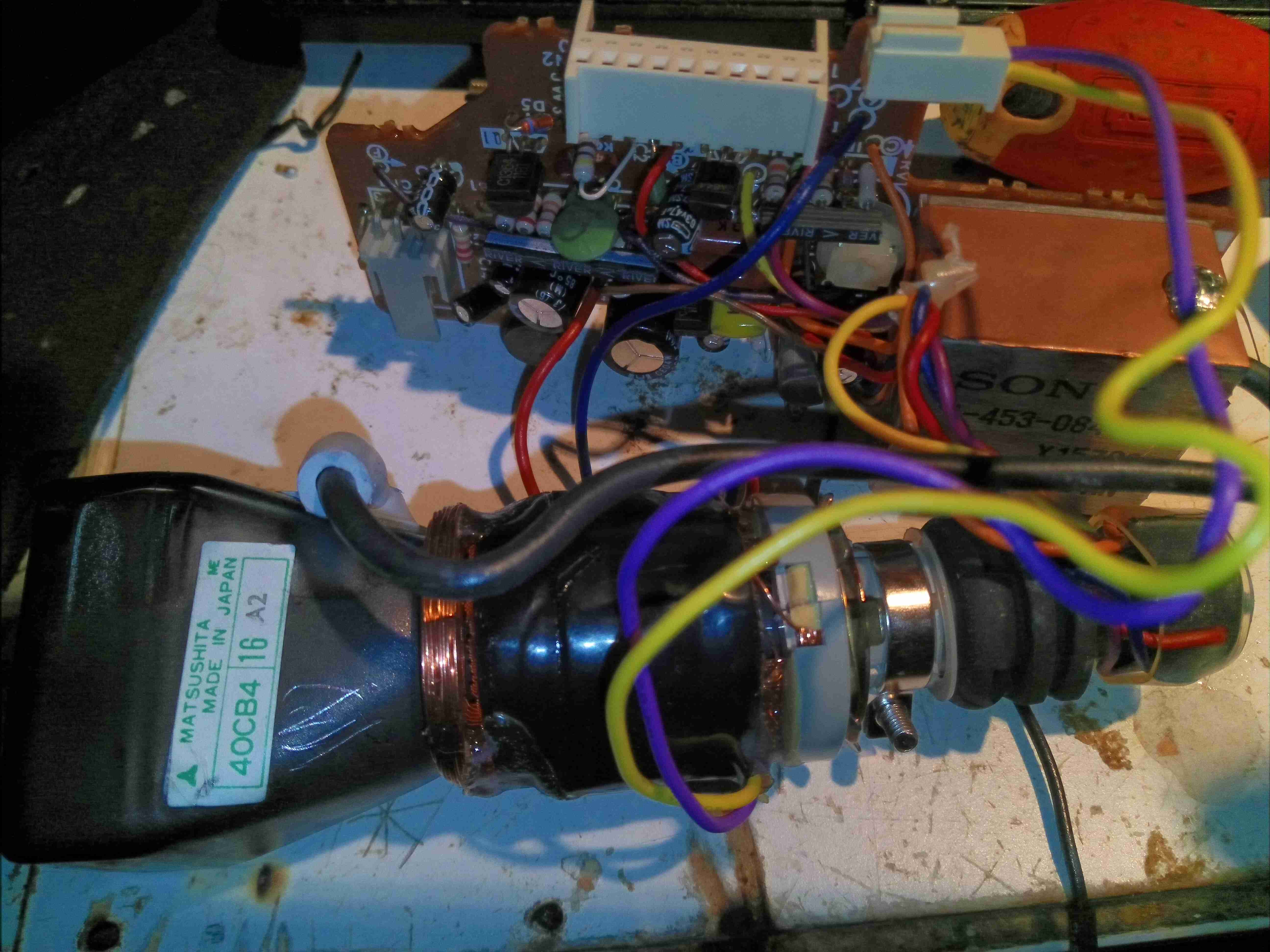
Video Input
Out of the 3 plugs emerging from the cable feeding the viiewfinder, only this one is important, on the horizontal drive board. Black is ground, Brown +8.5v & red is composite video input. There’s also a resistor tied into the positive rail to the video input pin, which pulls it high to 8.5v – this is R1 right next to this connector. Desolder this 22K resistor to help protect anything feeding a signal into the unit, like a RPi, it’s not needed for normal operation.
Fallout!
As usual for a CRT post, the Fallout loading screen on the display. The picture quality isn’t as good as it should be, probably due to the noisy buck-converter I have rigged up for testing. If it doesn’t get better with a linear regulator, I’ll start replacing the 39 year old electrolytic capacitors. Current draw is 130mA at 7.5v. Schematics for this unit & the CRT datasheet are available below:
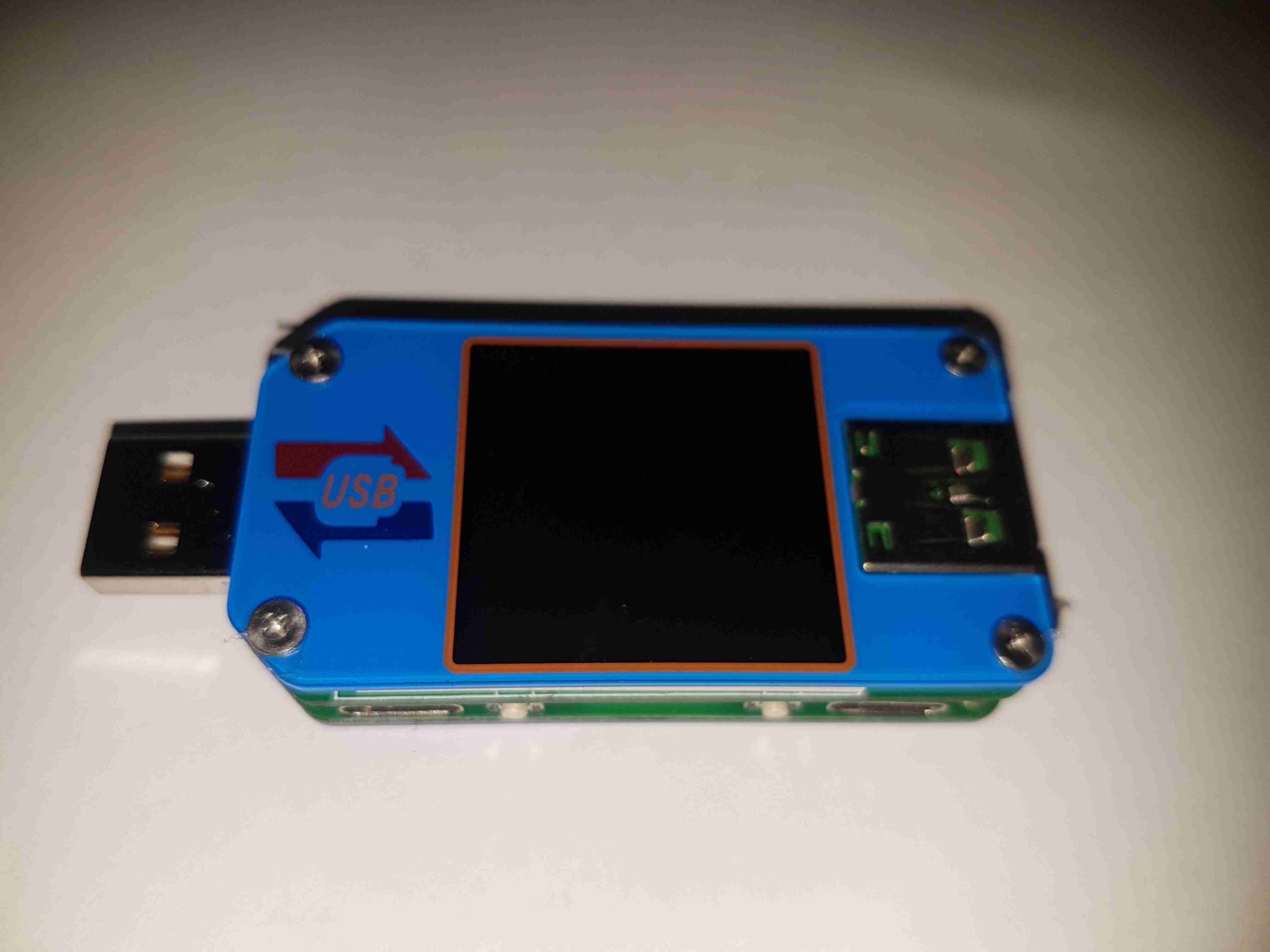
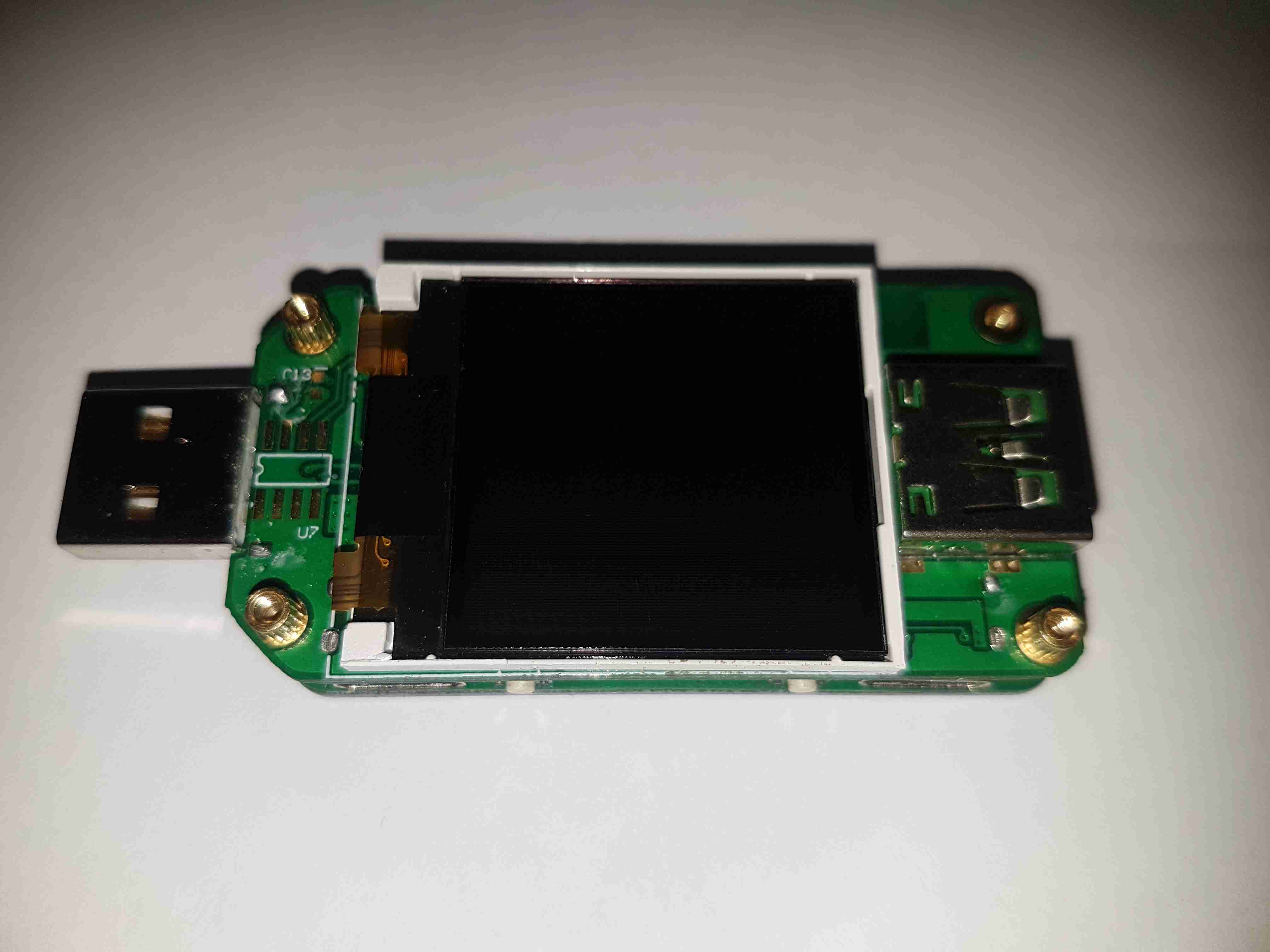
Here’s a nice little feature-packed USB power meter, the UM25C. This unit has USB-C along with the usual USB type A connectors, along with a bluetooth radio for remote monitoring of stats via a Windows or Android app. Construction is nice, it’s a stack of two PCBs, and polycarbonate cover plates, secured together with brass posts & screws.
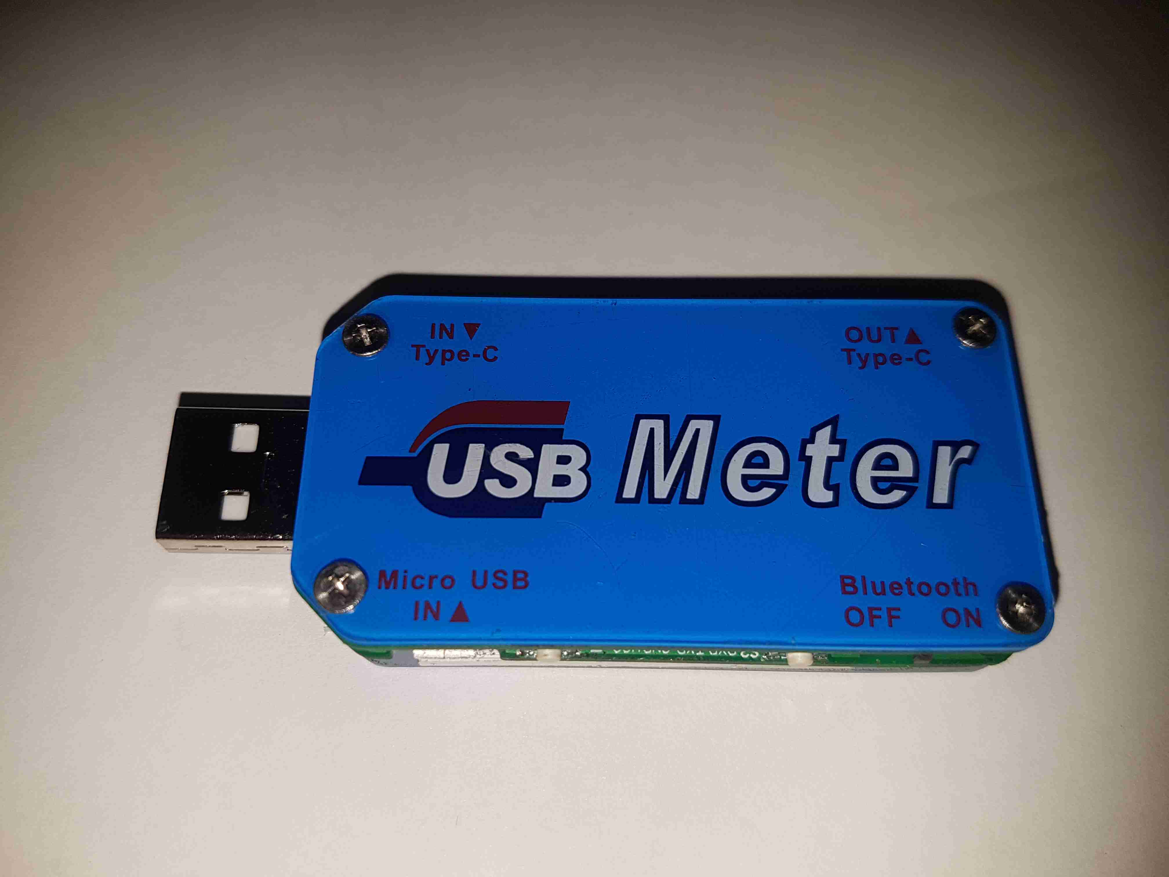
Back Cover
The back cover has the legend for all the side connectors, along with the logo.
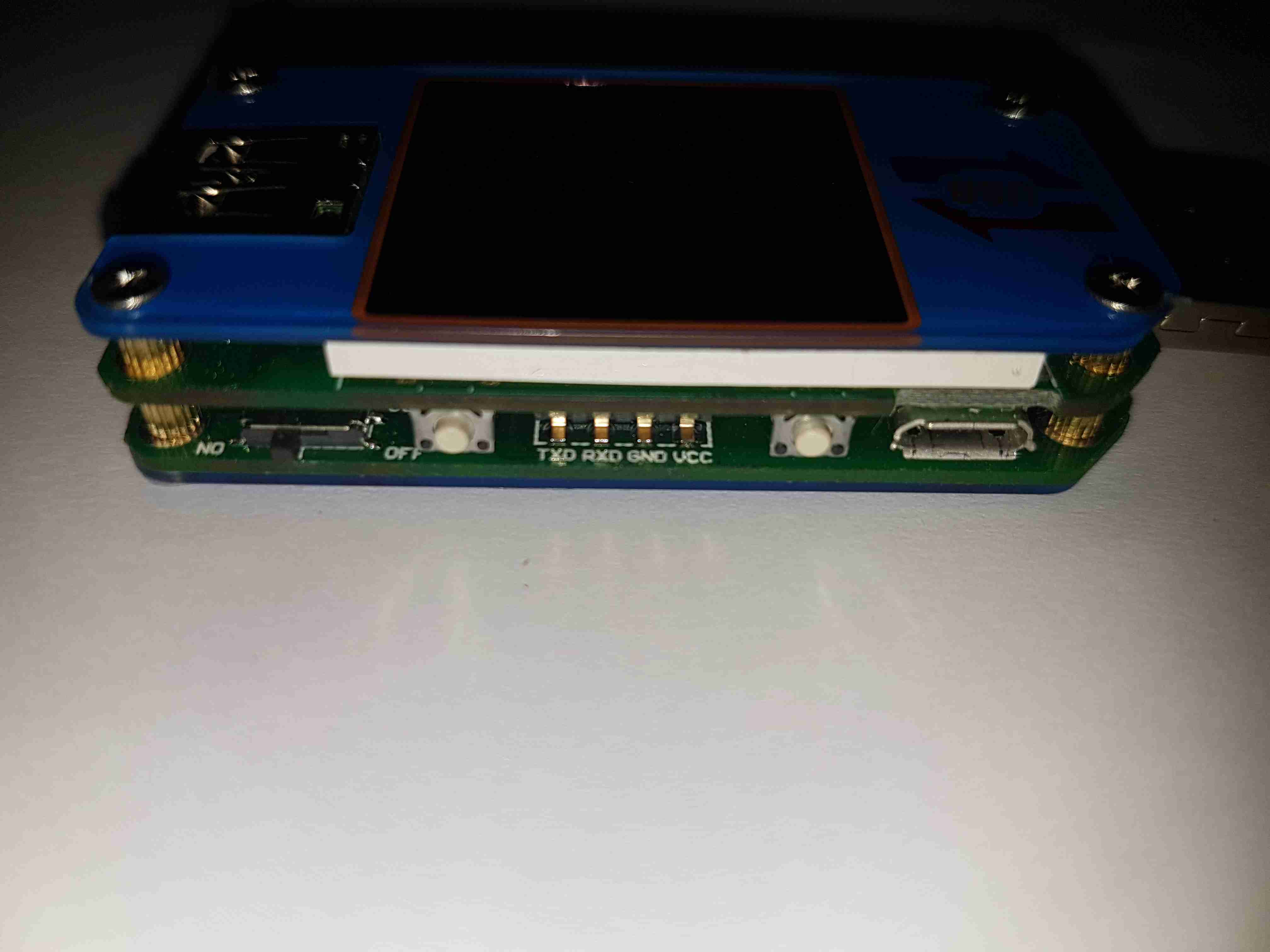
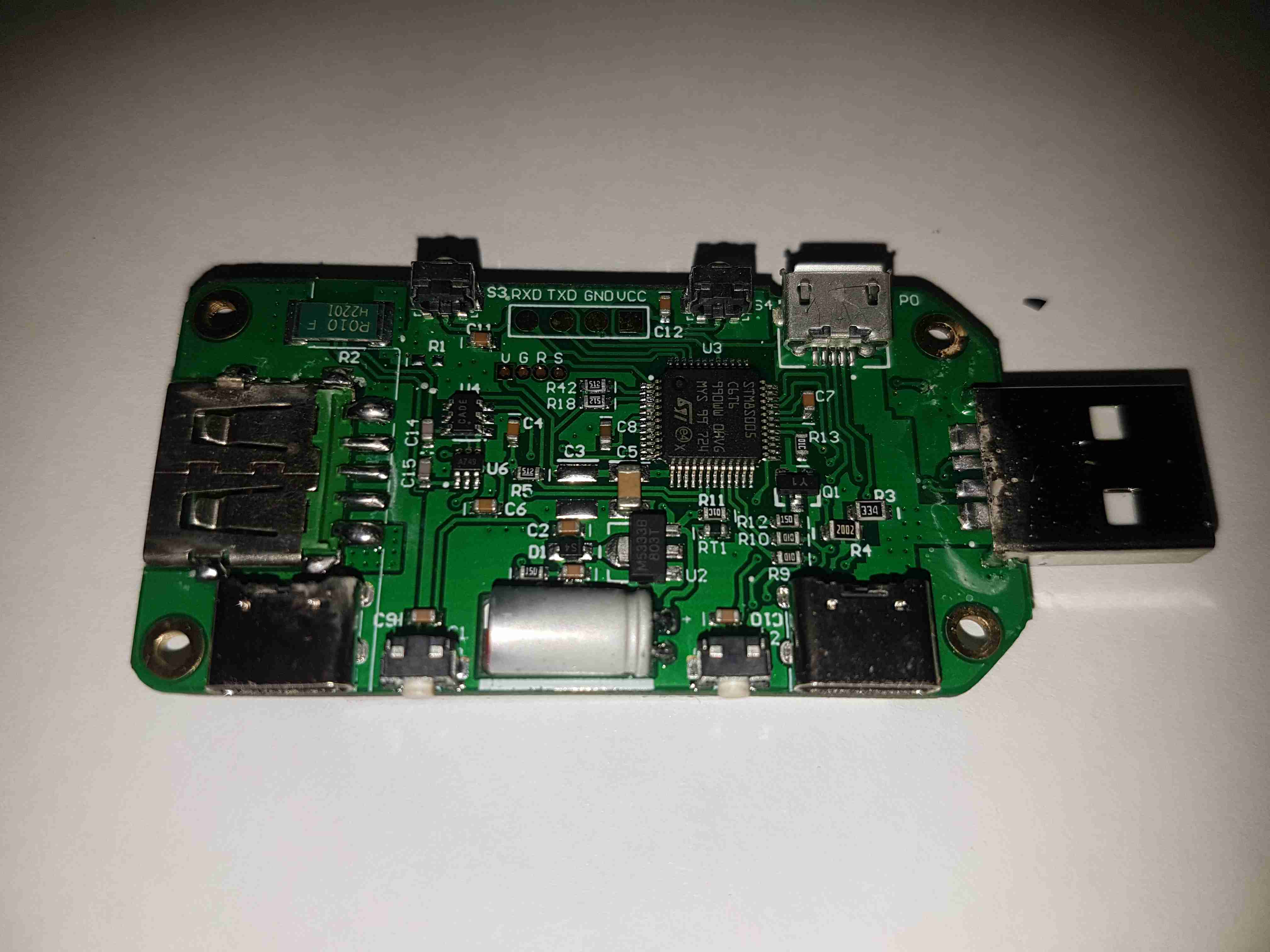
USB Micro Input
Down the sides are the user interface buttons, and here the Micro-B input connector. The 4-pin header is visible here that takes serial data down to the bluetooth section.
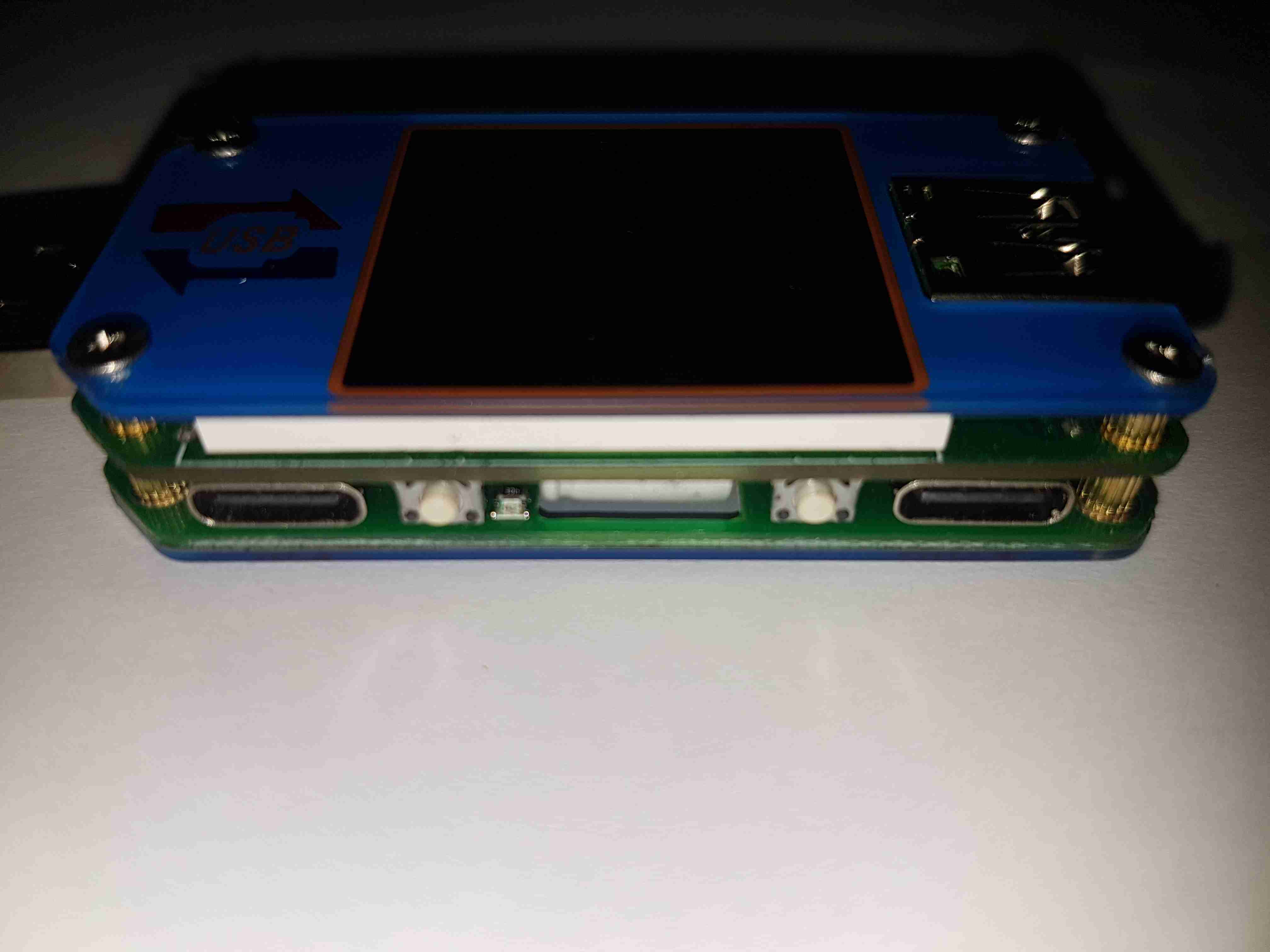
USB-C Connectors
The other side has the remaining pair of buttons, and the USB-C I/O. I don’t yet own anything USB-C based, but this is good future proofing.
LCD Display
Removing the top plastic cover plate reveals the small 1″ TFT LCD module. This will be hot-bar soldered underneath the screen. There’s an unused footprint next to the USB input connector, judging by the pin layout it’s probably for a I²C EEPROM.
Main Board Components
The underside of the top PCB has all the main components. The brains of the operation is a ST STM8S005C6T6 microcontroller. It’s at the basic end of the STM range, with a 16MHz clock, 32K flash, EEPROM, 10-bit ADC, SPI, UART & I²C. The main 0.010Ω current shunt is placed at the top left of the board in the negative rail. A couple of SOT-23 components in the centre of the board, I haven’t been able to identify properly, but I think they may be MOSFETs. The large electrolytic filter capacitor has a slot routed into the PCB to allow it to be laid flat. Providing the main power rail is a SOT-89 M5333B 3.3v LDO regulator.
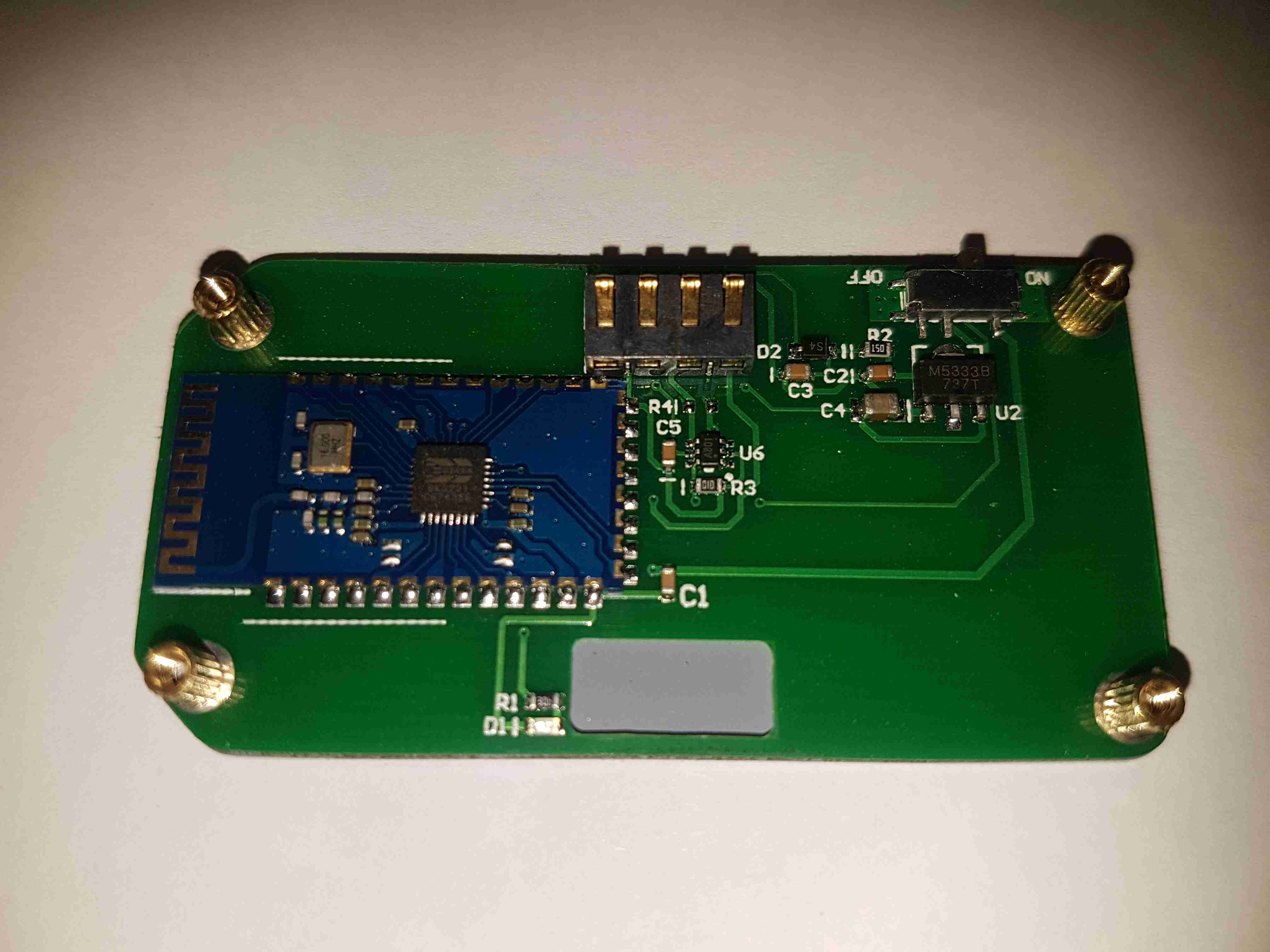
Bluetooth Radio
The bottom board contains the bluetooth radio module, this is a BK3231 Bluetooth HID SoC. The only profile advertised by this unit is a serial port. There’s a local 3.3v LDO regulator & support components, along with an indicator LED.
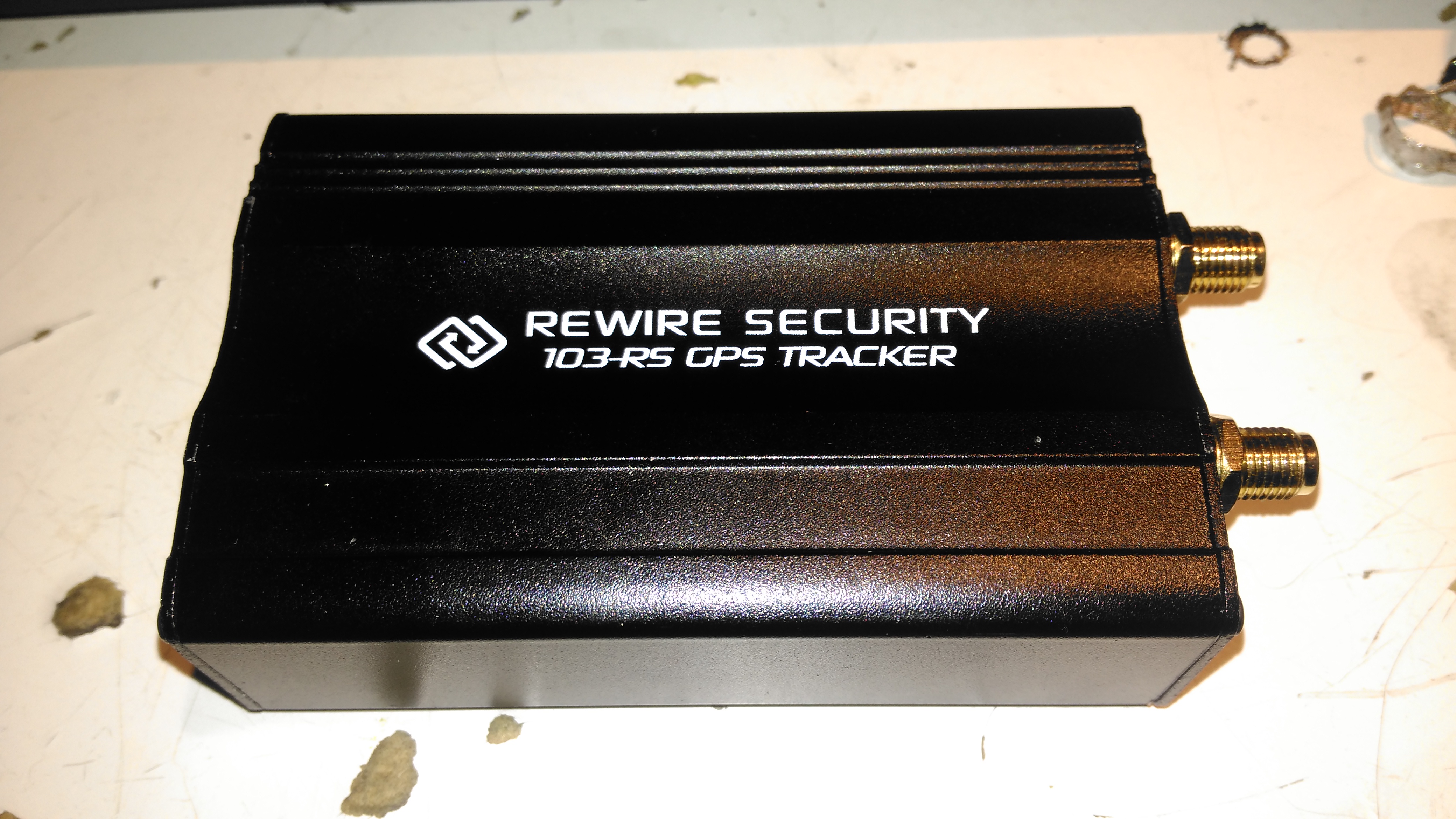
I thought it was time to add a bit of security to the gear I take camping, so this GPS tracker unit was sourced from eBay. This is a Rewire Security 103RS, a slightly customised version of the common Chinese TK103 GPS tracker.
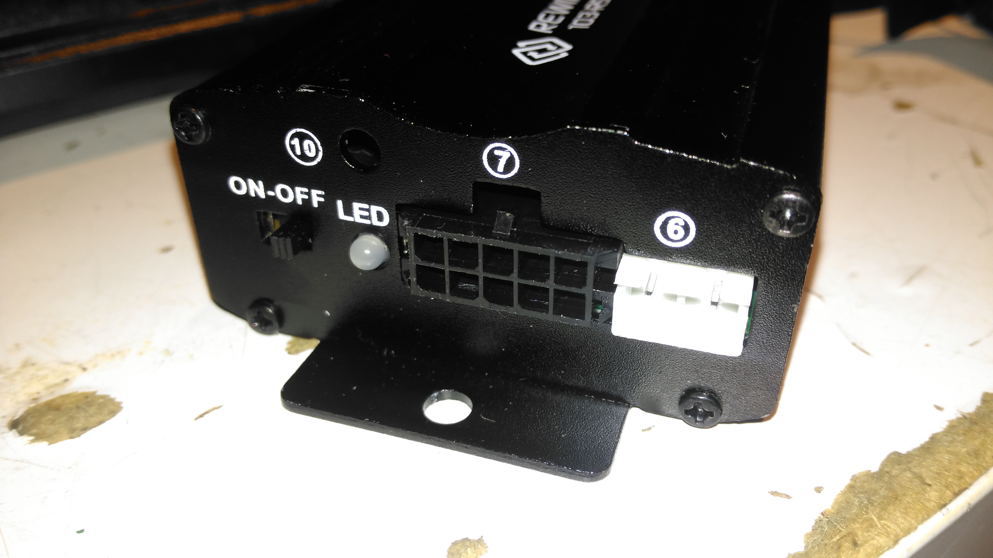
Input Connections
The small module has all it’s power connections on one end of the unit, on a Molex multi-way block. The white connector is for a piezo-shock sensor – this interfaces with the alarm functionality of the unit. There’s an indicator LED for both the GPS & GSM status, and a switch for the backup battery.
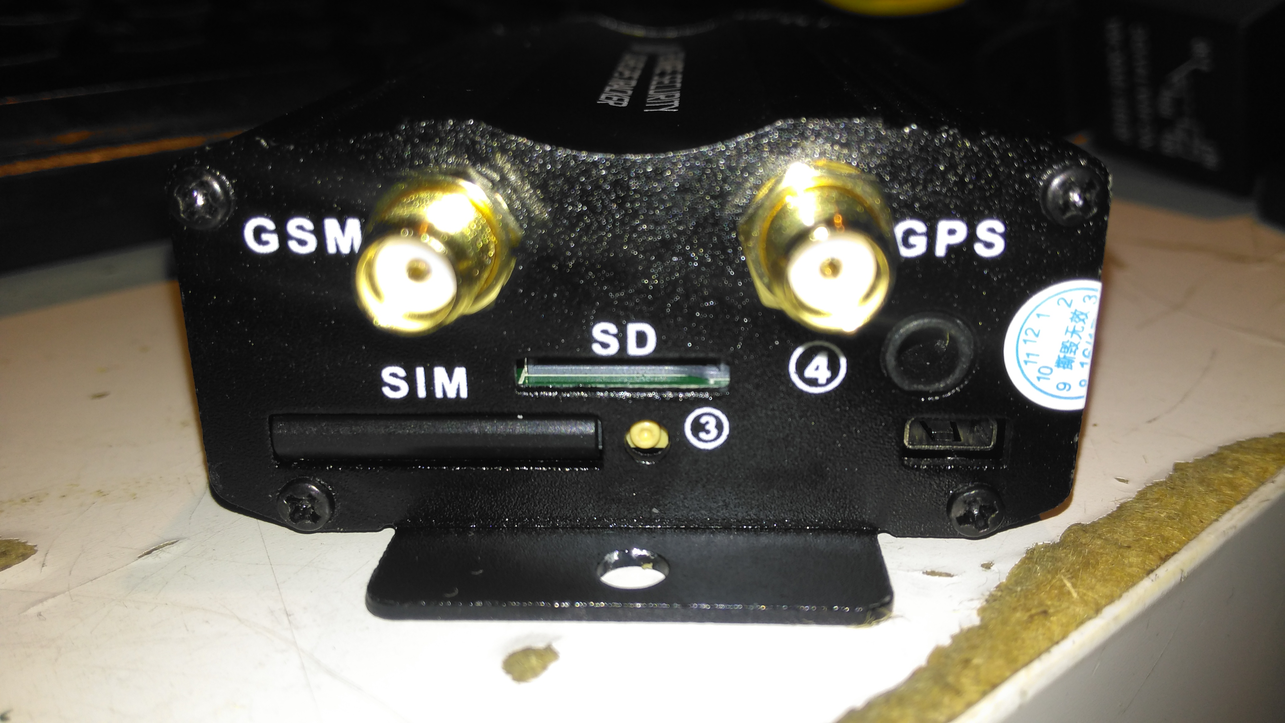
Antenna Connections
The other end has the antenna connections, microphone connection for the monitor function, along with the SIM & SD card slots.
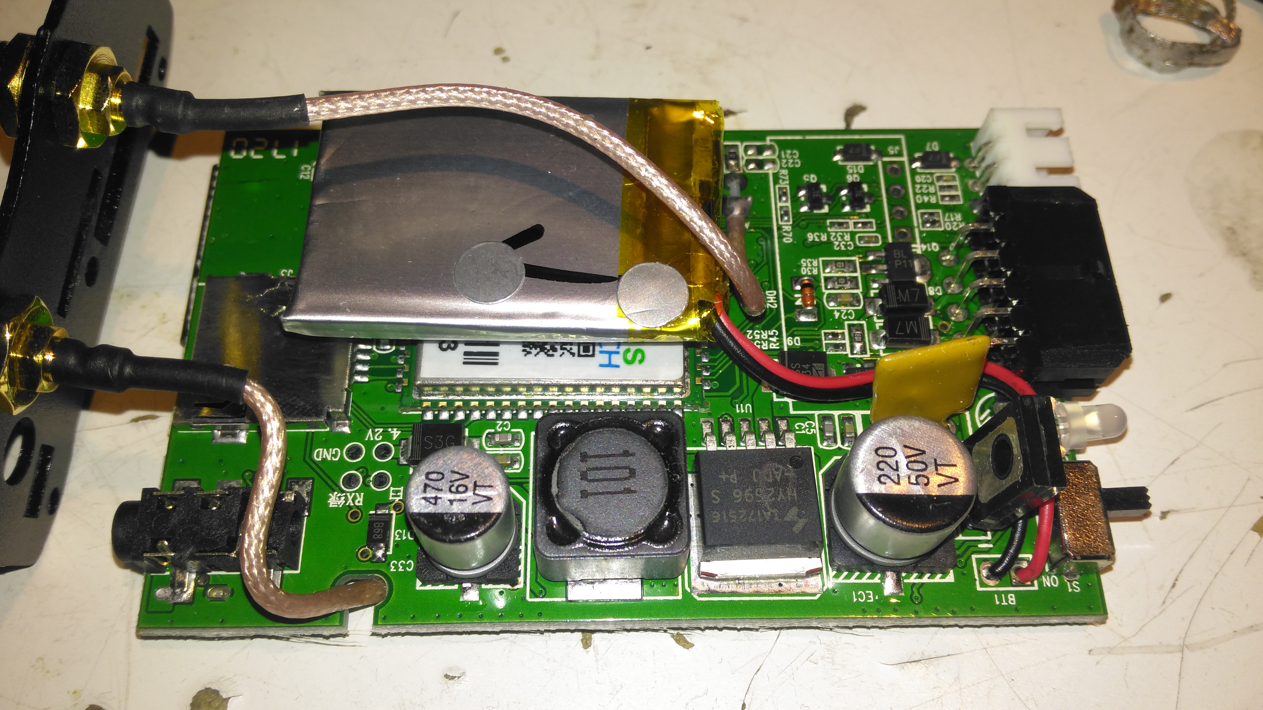
PCB Top
Once the end panel is removed, the PCB just slides out of the aluminium extruded casing. It’s pretty heavily packed with components in here. A switching regulator deals with the 12v input from the vehicle battery, and is protected by a polyfuse on the right. The GSM module is hiding under the Li-Po backup cell, unfortunately the sticky pad used to secure this wouldn’t come off without damaging something. The pigtails for both the GPS & GSM antennas are permanently soldered to the board here.
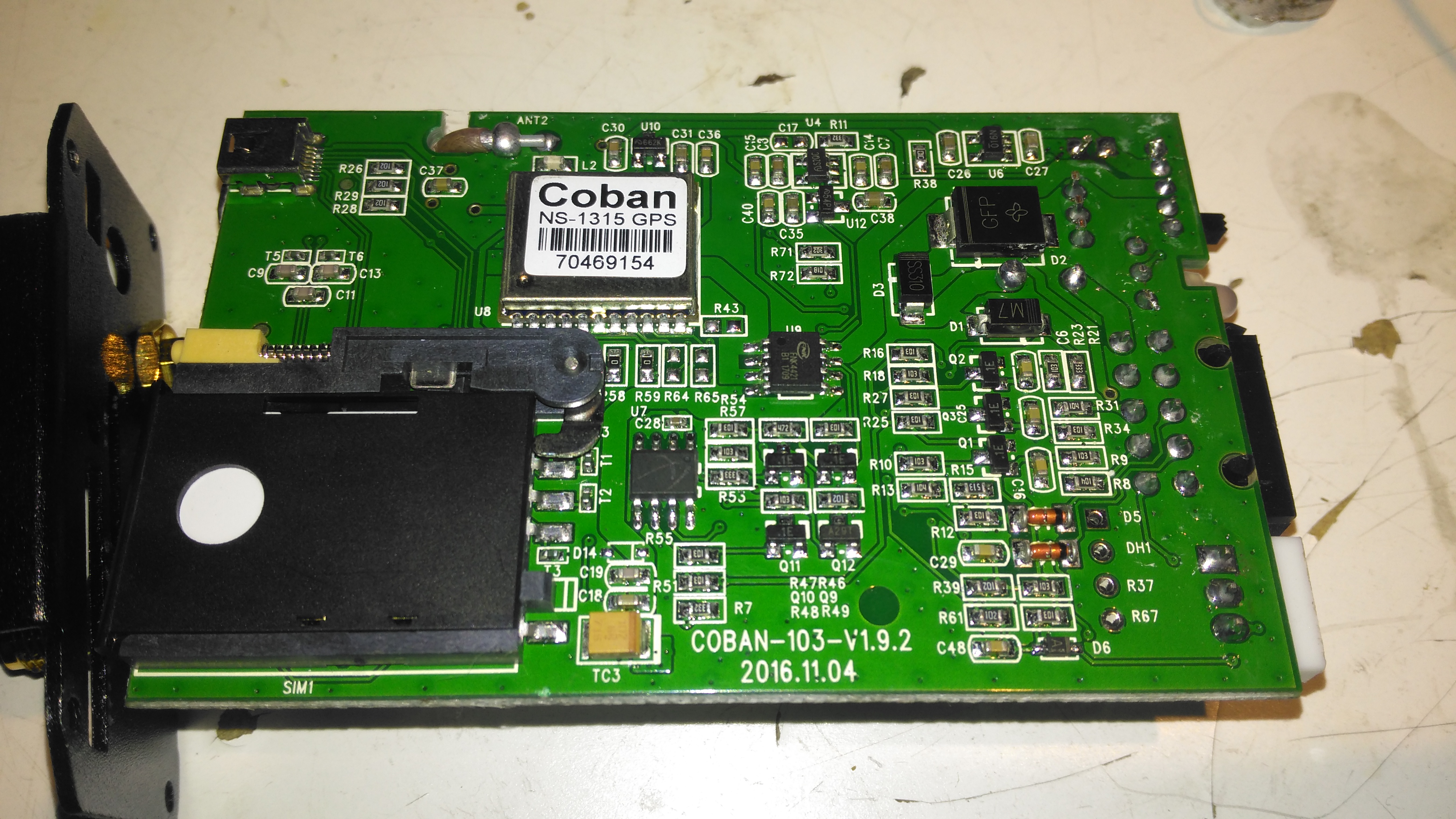
PCB Bottom
The bottom of the PCB has the GPS module, and mainly input protection & bypassing components. There is a FNK4421 Dual P-Channel MOSFET here as well, probably used for switching the external relay or alarm siren. The SIM socket for the GSM modem is located here in the corner.
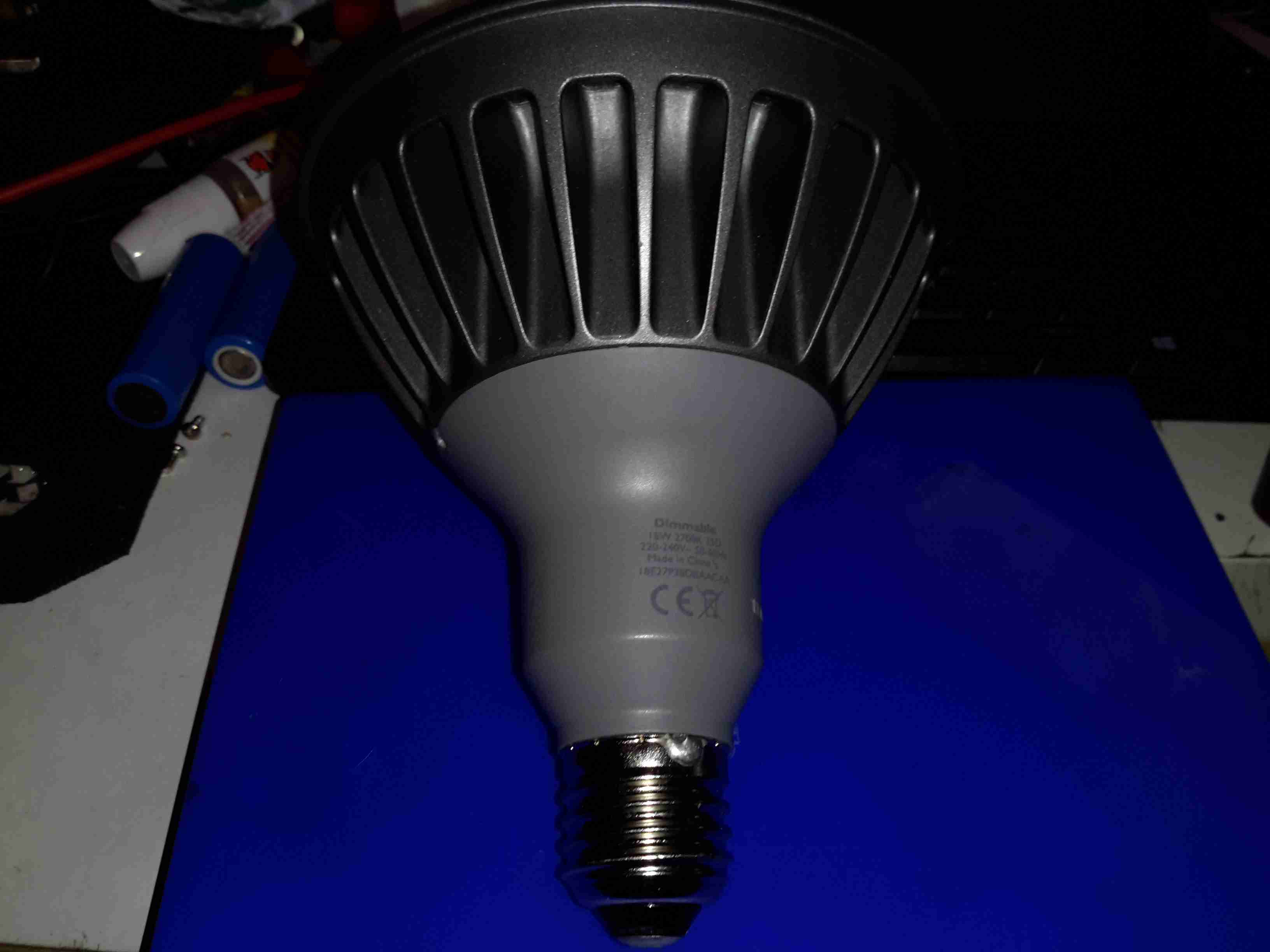
These large LED Philips PAR38 lamps were recently on clearance sale in my local T.N. Robinsons electrical contractors for about £3, so I decided to grab one in the hopes I might be able to hack it into a low-voltage LED lamp. These are full-size PAR38 format, with most of the bulk being the large aluminium heatsink on the front. The back section with the power supply module is secured with silicone, so some unreasonable force was required to liberate the two pieces.
Specification
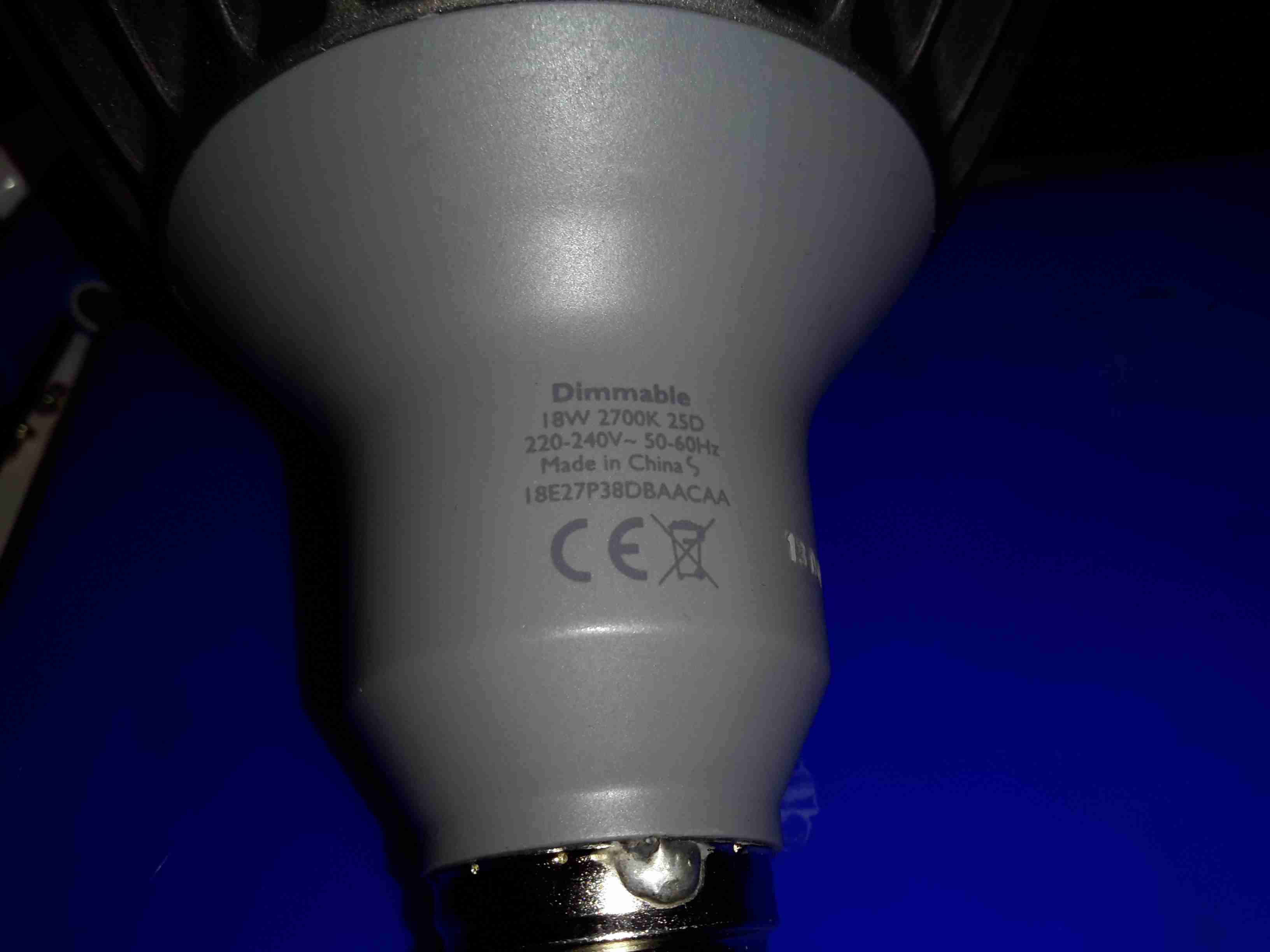
These lamps are rated at 18W in operation, and are surprisingly bright for this power level.
Lens
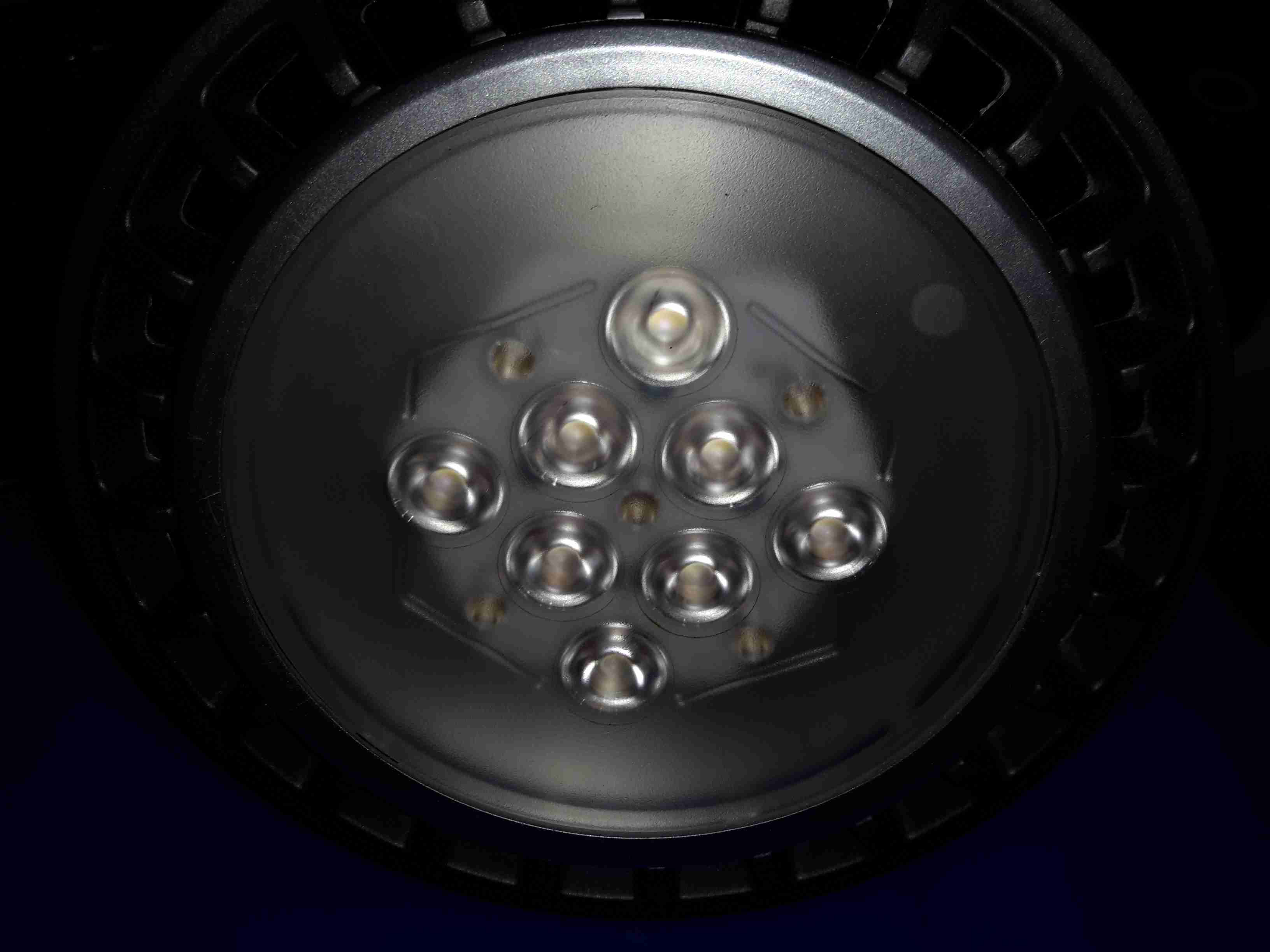
The front has the moulded multi-lens over the LEDs, to spread the light a bit further than the bare dies.
LED Array
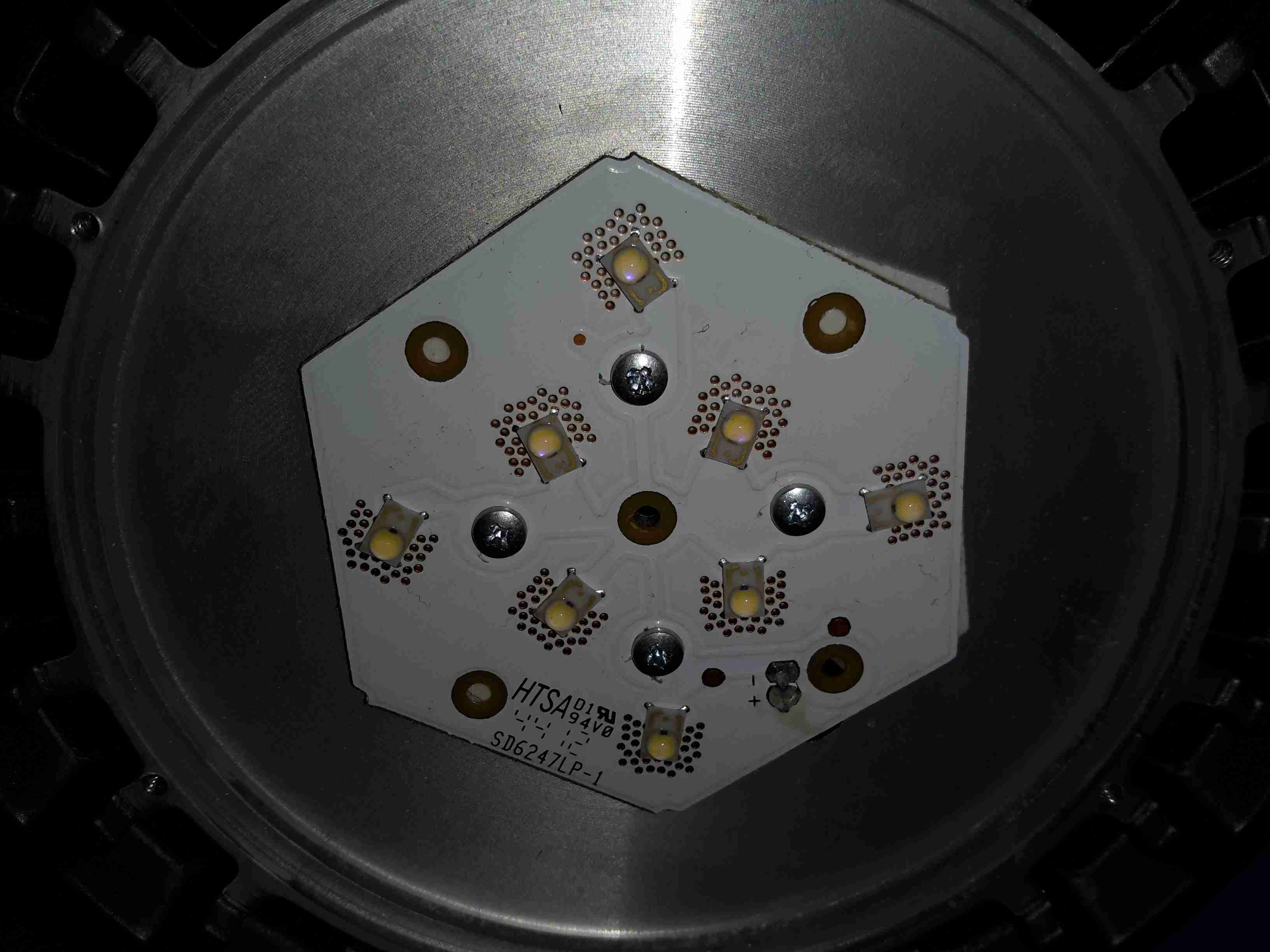
The LED array is two series strings of 4 LEDs, for ~24v forward voltage. Unusual for a high power LED array, this PCB isn’t aluminium cored, but 0.8mm FR4. Heat is transferred to the copper plane on the backside by the dozens of vias around the Luxeon Rebel LEDs. There is a thermal pad under the PCB for improved heat transfer to the machined surface of the heatsink.
Control PCB Top
The power supply & control PCB is pretty well made, it’s an isolated converter, so no nasty mains on the LED connections.
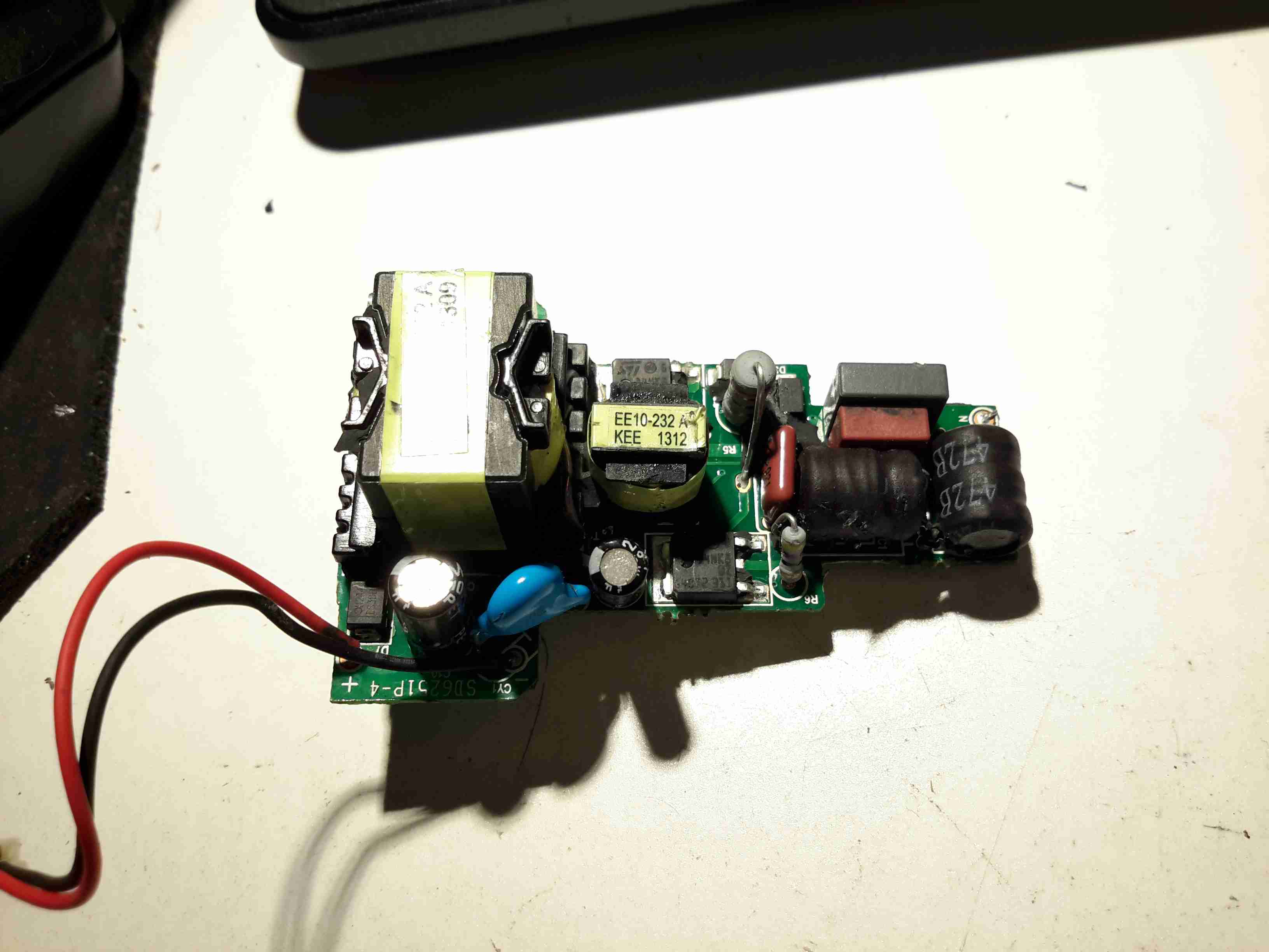
I recently got the latest upgrade from Virgin Media, 200Mbit DL / 20Mbit UL, and to get this I was informed I’d have to buy their latest hardware, since my existing CPE wouldn’t be able to handle the extra 5Mbit/s upload speed. (My bullshit detector went off pretty hard at that point, as the SuperHub 2 hardware is definitely capable of working fine with 20Mbit/s upload rates). Instead of having to return the old router, I was asked to simply recycle it, so of course the recycling gets done in my pretty unique way!
Mainboard
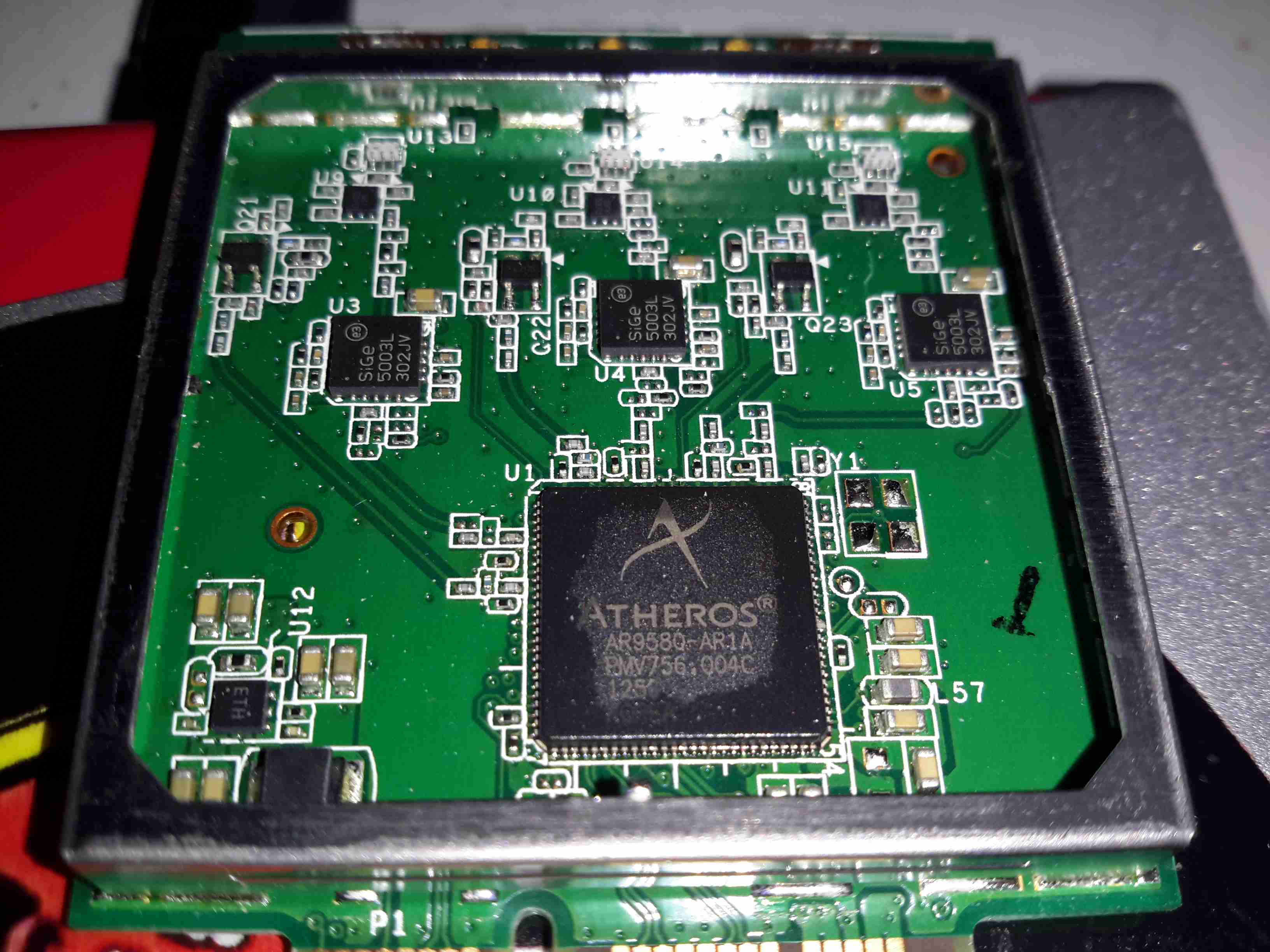
The casing of these units is held together by a single screw & a metric fuckton of plastic clips, disassembly is somewhat hindered by the radio antennas being positioned all over both sides of the casing. Once the side is off, the mainboard is visible. The DOCSIS frontend is lower left, centre is the Intel PUMA 5 Cable Modem SoC with it’s RAM just to the lower right. The right side of the board is taken up by both of the WiFi radio frontends, the 5GHz band being covered by a Mini PCIe card.
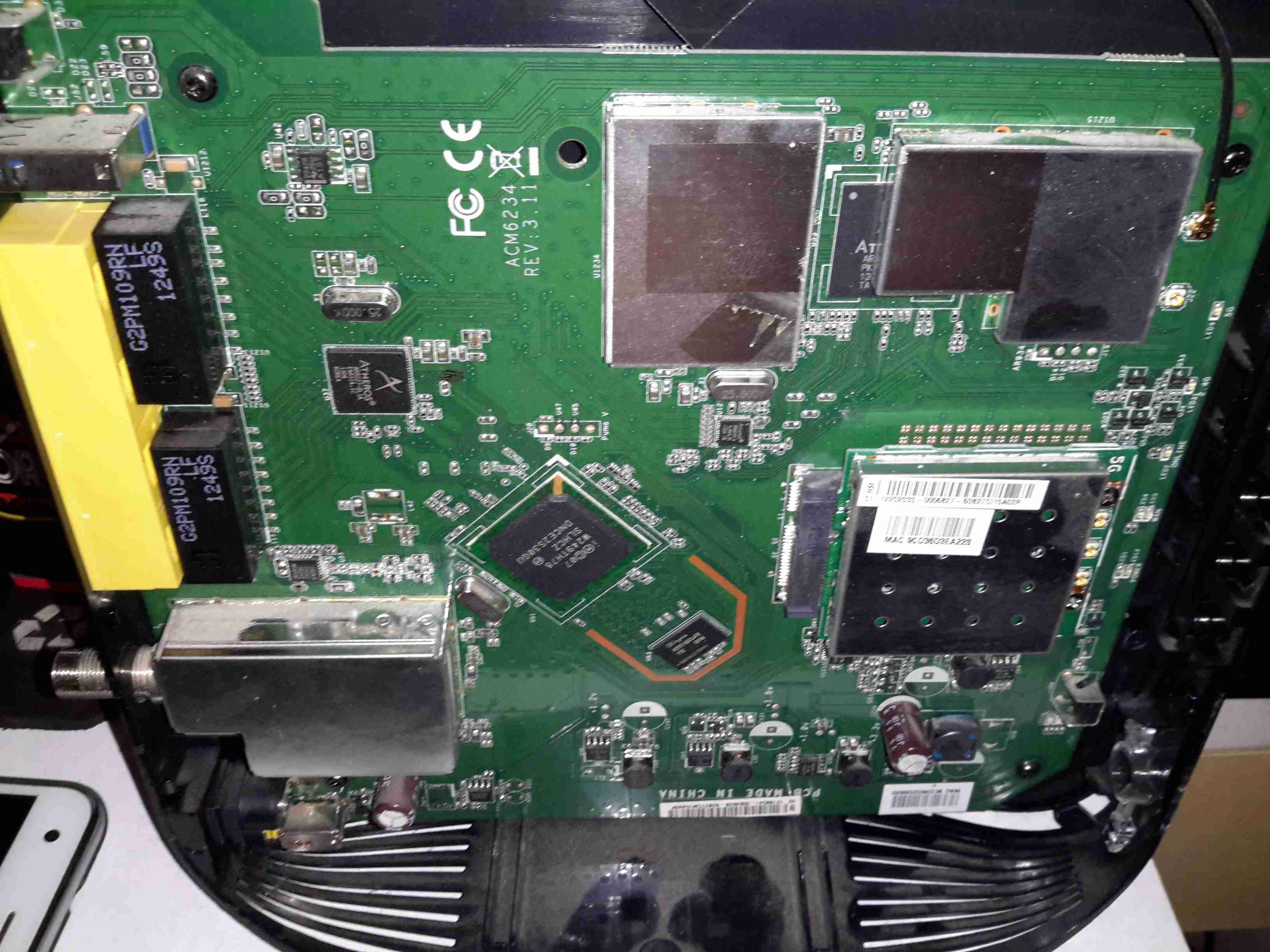
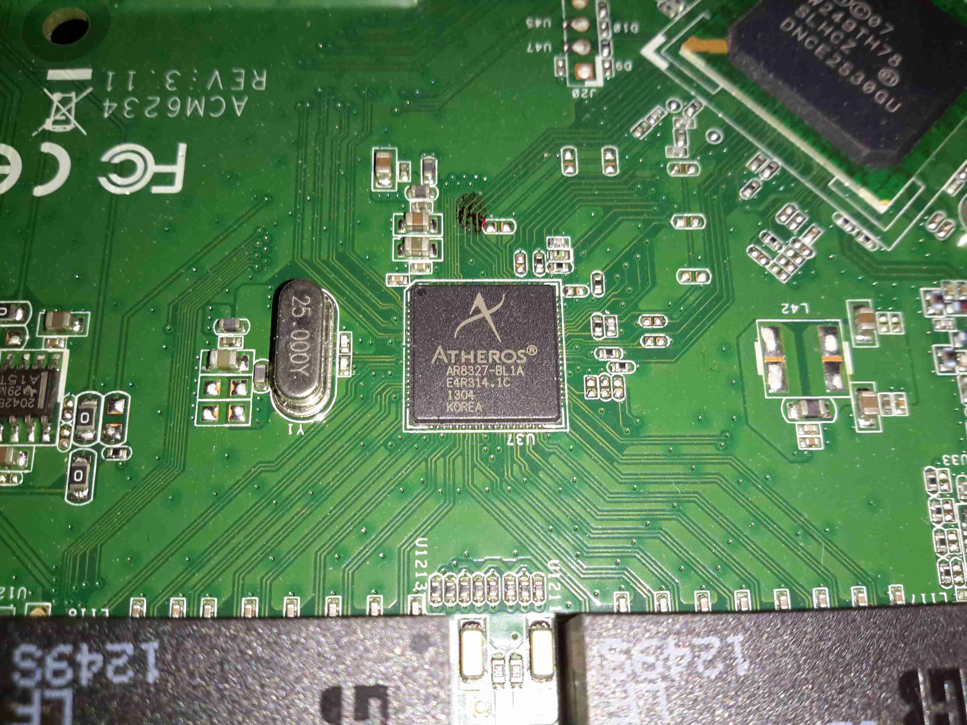
Atheros Gigabit Switch
The 4 gigabit Ethernet ports on the back are serviced by an Atheros AR8327 Managed Layer 3 switch IC, which seems to be a pretty powerful device:
The AR8327 is the latest in high performance small network switching. It is ultra low power, has extensive routing and data management functions and includes hardware NAT functionality (AR8327N). The AR8327/AR8327N is a highly integrated seven-port Gigabit Ethernet switch with a fully non-blocking switch fabric, a high-performance lookup unit supporting 2048 MAC addresses, and a four-traffic class Quality of Service (QoS) engine. The AR8327 has the flexibility to support various networking applications. The AR8327/AR8327N is designed for cost-sensitive switch applications in wireless AP routers, home gateways, and xDSL/cable modem platforms.
Unfortunately most of the features of this router are locked out by VM’s extremely restrictive firmware. With any of their devices, sticking the VM supplied unit into modem mode & using a proper router after is definitely advised!
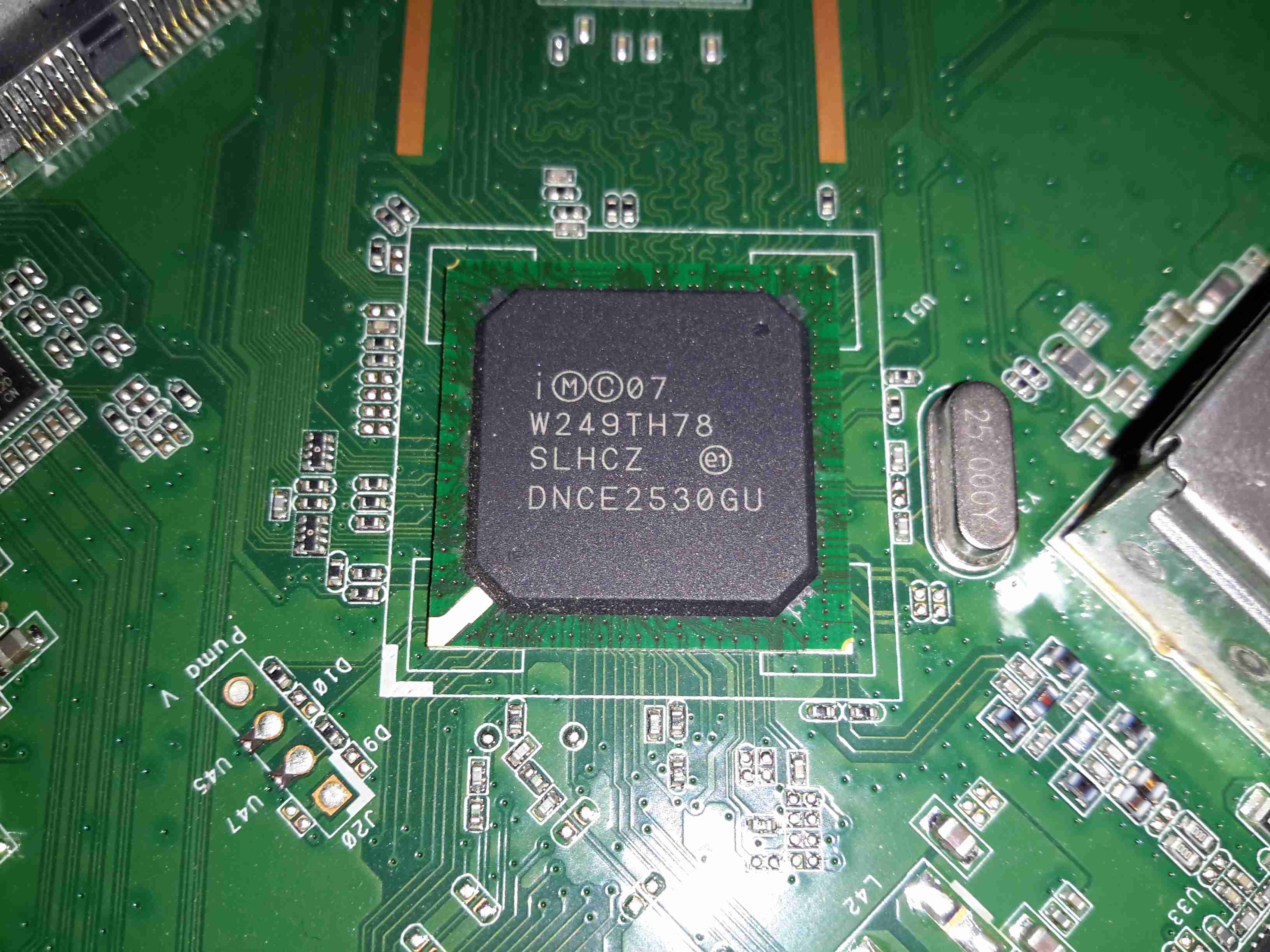
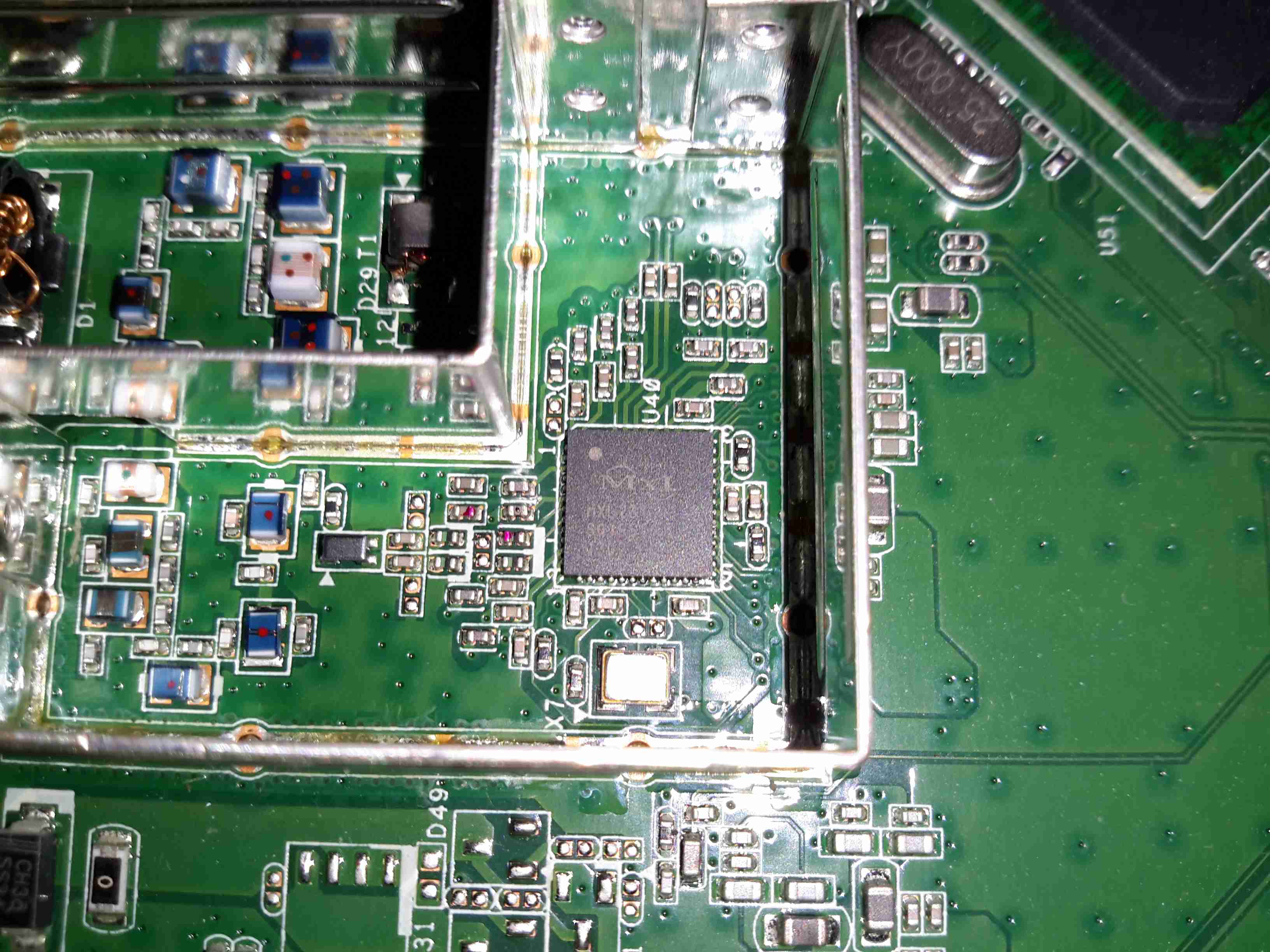
Intel Puma 5 CM CPU
The cable modem side of things is taken care of by the Intel PUMA 5 DNCE2530GU SoC. This appears to communicate with the rest of the system via the Ethernet switch & PCI Express for the 5GHz radio.
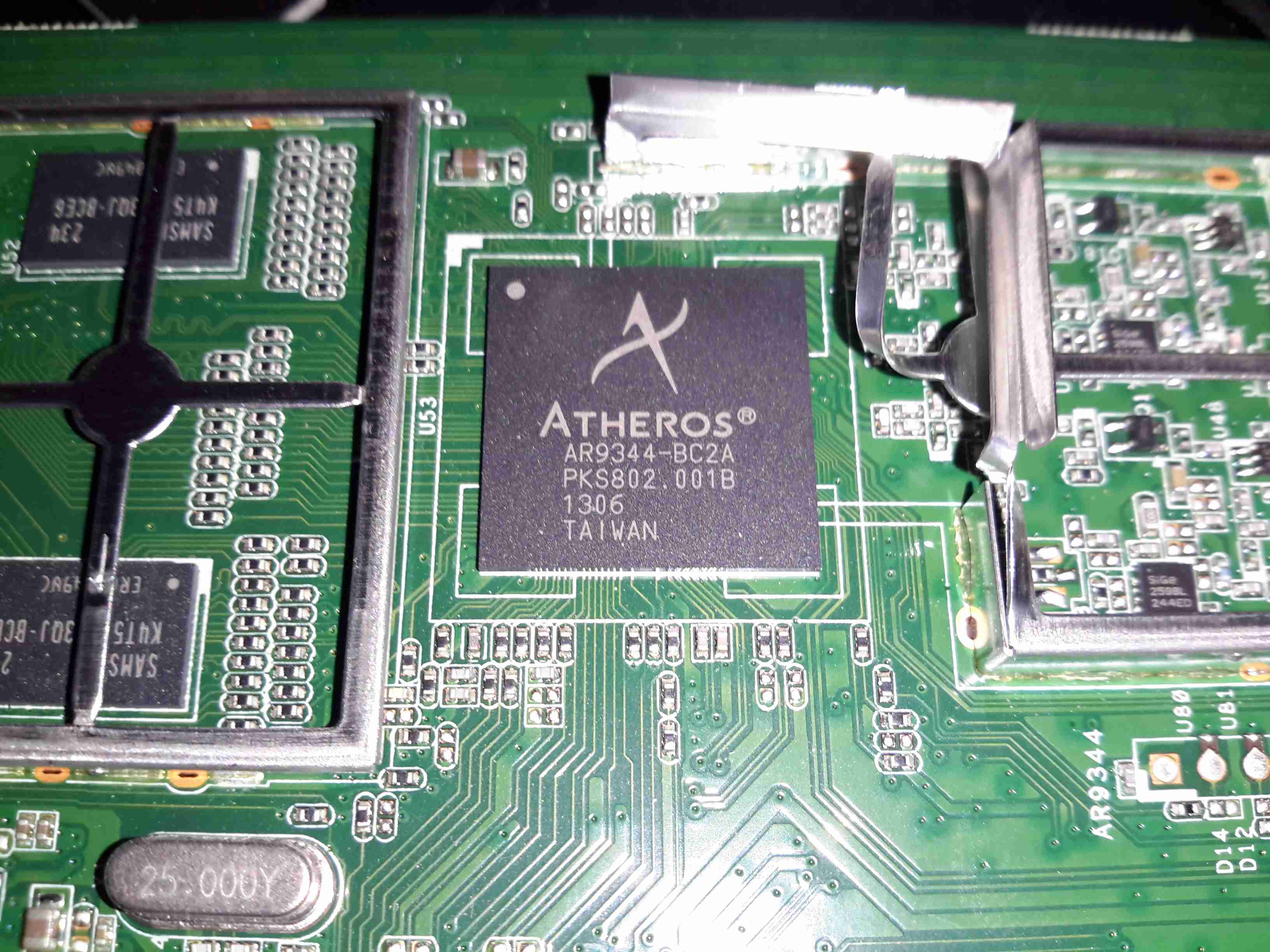
Atheros WiFi SoC
The 2.4GHz radio functionality is supplied by an Atheros AR9344 SoC, it’s RAM is to the left. This is probably handling all the router functions of this unit, but I can’t be certain.
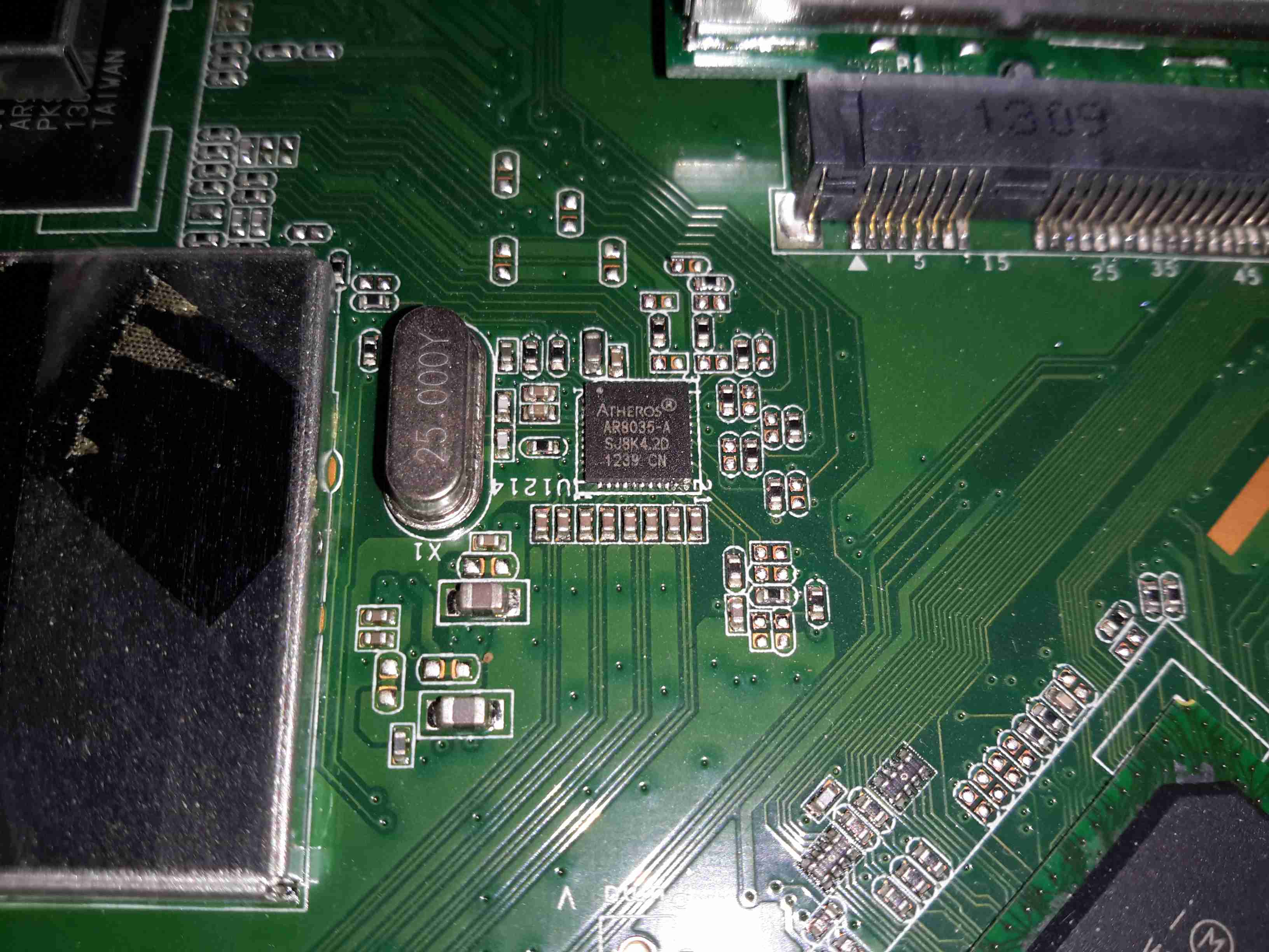
Atheros LAN PHY
A separate Ethernet PHY is located between the SoC & the switch IC.
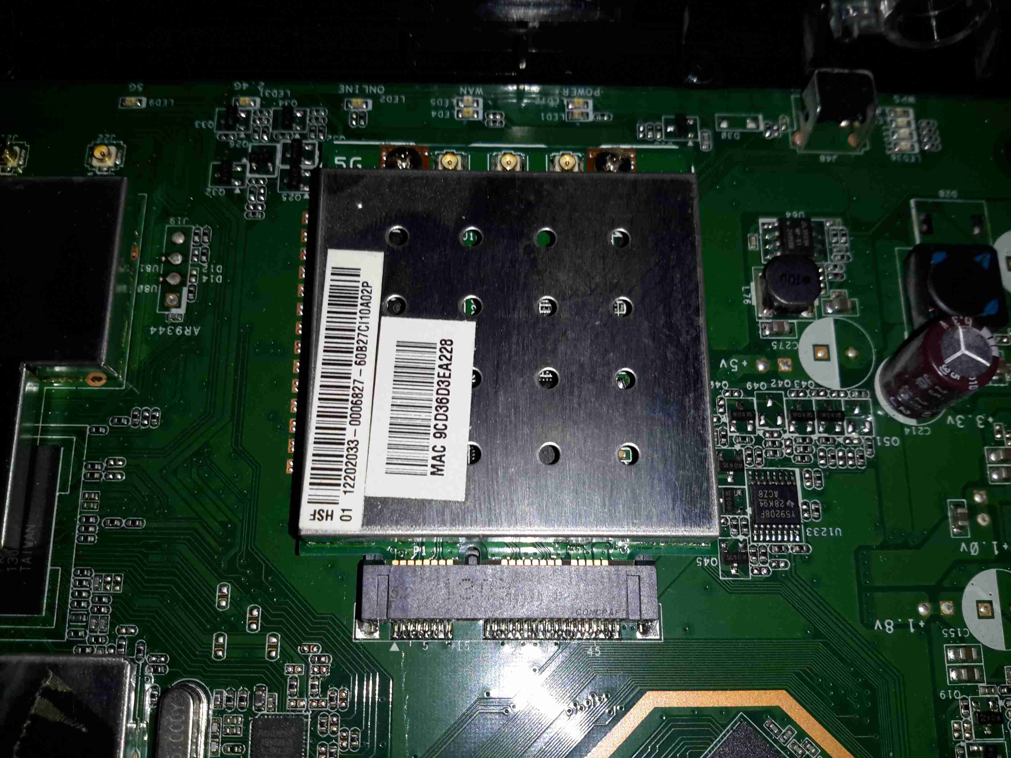
5GHz Radio Card
The 5GHz band is served by a totally separate radio module, in Mini PCIe format, although it’s a bit wider than standard. This module will probably be kept for reuse in another application.
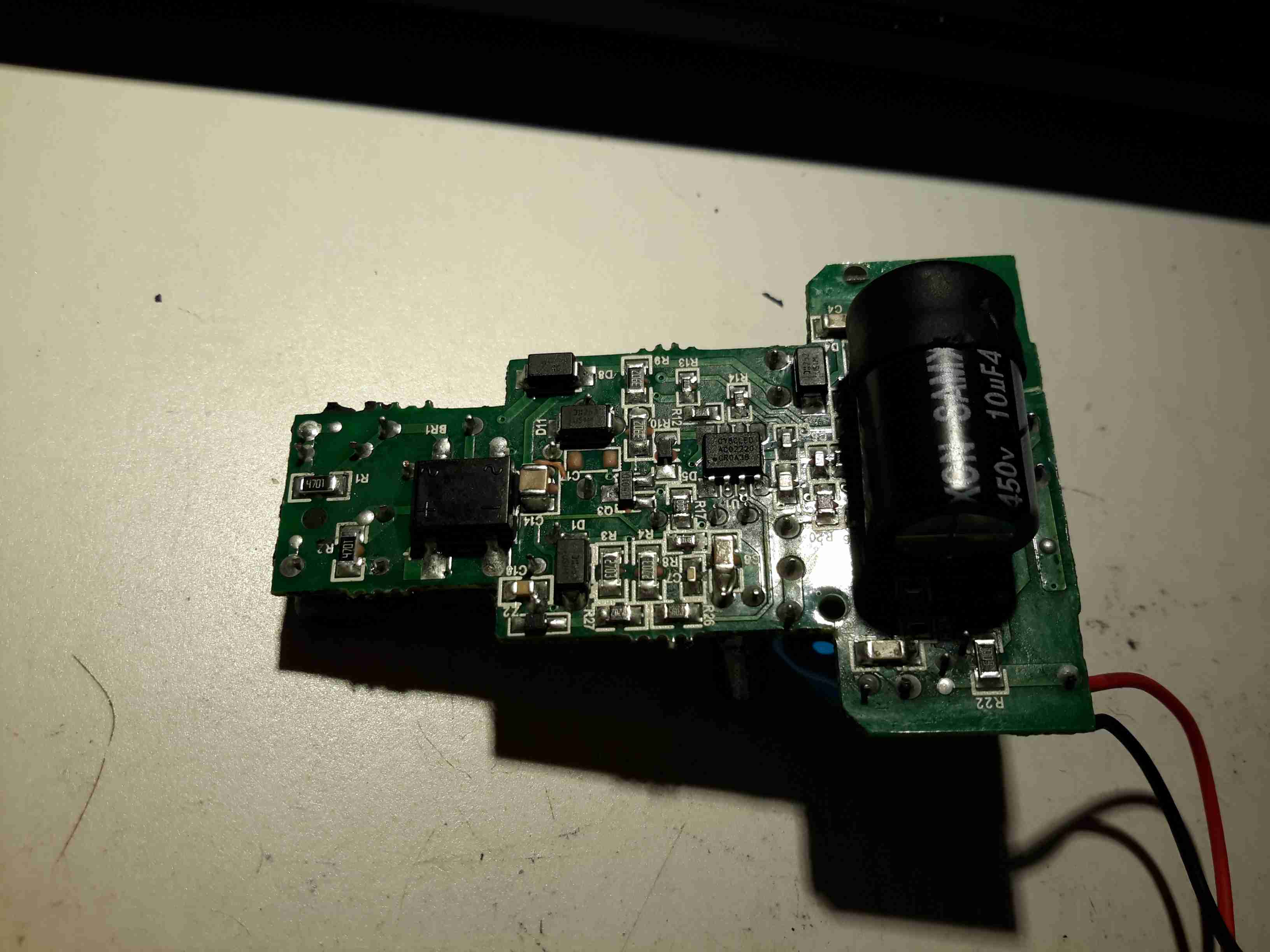
Power Supplies
All down the edge of the board are the multiple DC-DC converters to generate the required voltage rails.
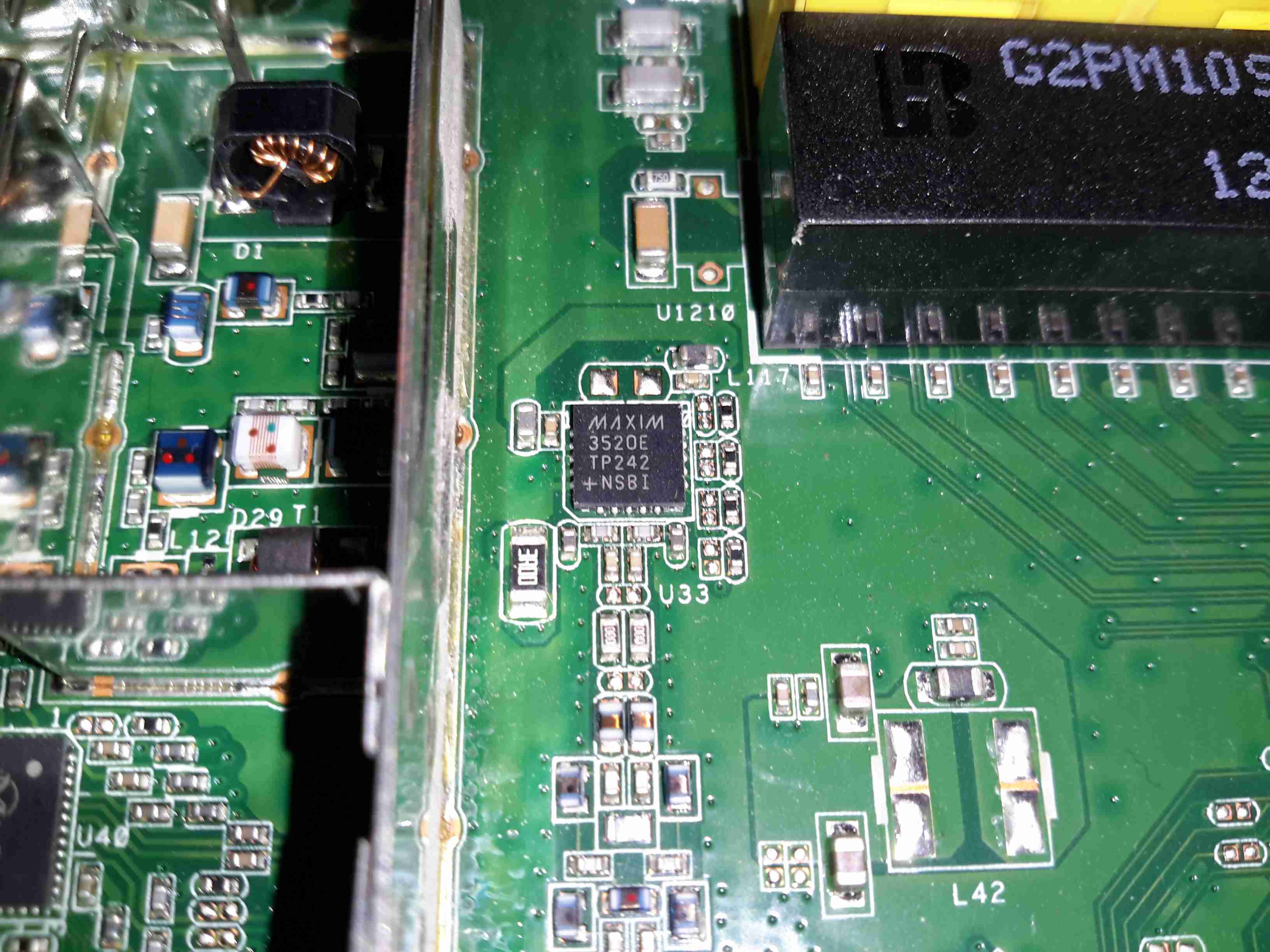
MaxLinear MXL261 Frontend
The DOCSIS frontend is handled by a MaxLinar MXL261 Tuner/Demodulator. More on this IC in my decapping post 🙂
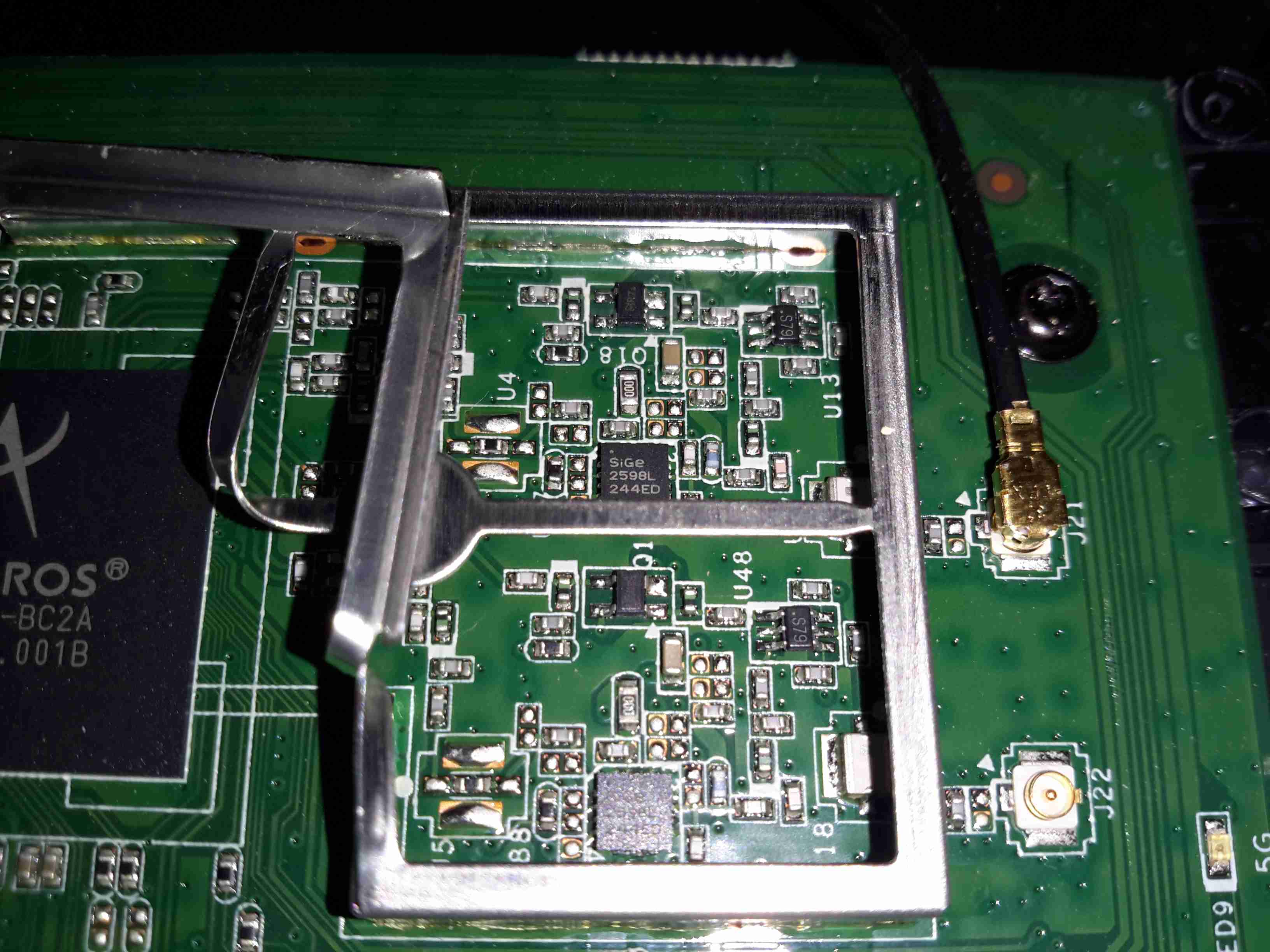
The Unknown One
I’ve honestly no idea what on earth this Maxim component is doing. It’s clearly connected via an impedance matched pair, and that track above the IC looks like an antenna, but nothing I search for brings up a workable part number.
2.4GHz Frontend
The RF switching & TX amplifiers are under a shield, these PA chips are SiGe parts.
Atheros 5GHz Radio
Pretty much the same for the 5GHz radio, but with 3 radio channels.
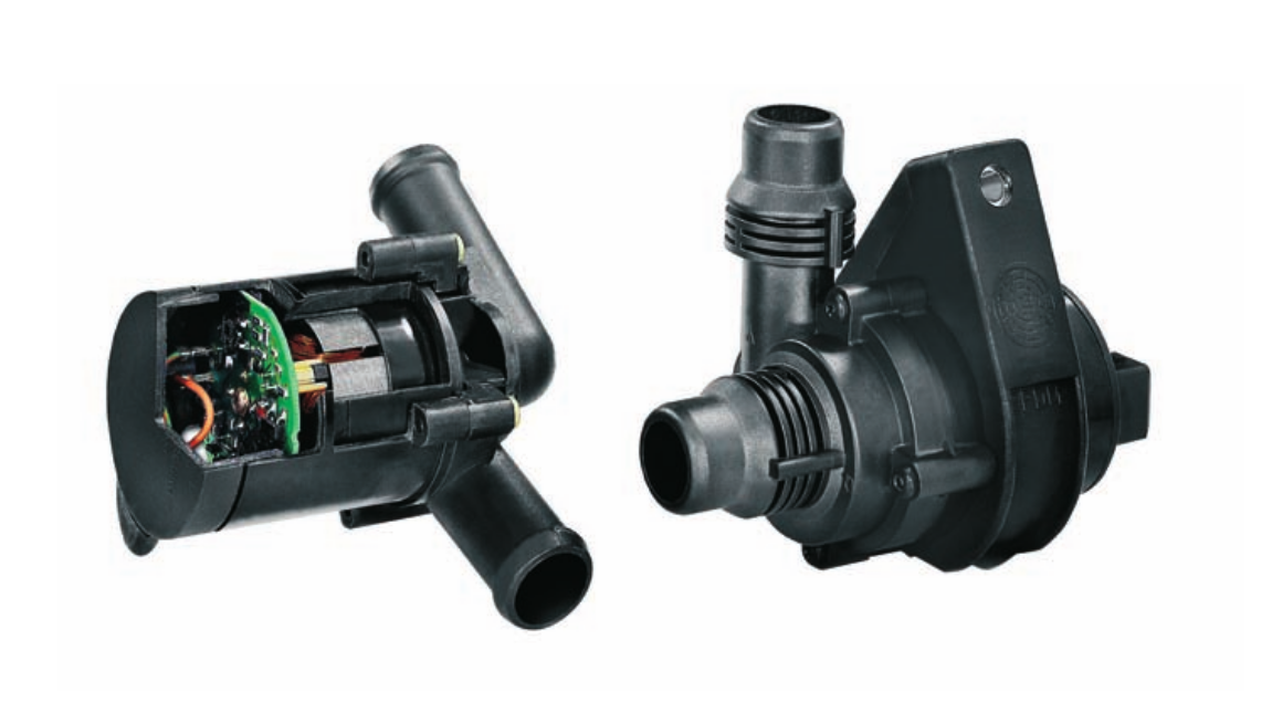
With some recent upgrades to the boat’s heating system, the hot water circulation pumps we’ve been using are becoming far too small for the job. After the original Johnson Marine circulation pump died of old age (the brushes wore down so far the springs ate the commutator) some time ago, it was replaced with a Pierburg WUP1 circulation pump from a BMW. (As we’re moored next to a BMW garage, these are easily obtainable & much cheaper than the marine pumps).
WUP1 Cutaway
These are also brushless, where as the standard Johnson ones are brushed PM motors – the result here is a much longer working life, due to fewer moving parts.
The rated flow & pressure on these pumps is pretty pathetic, at 13L/min at 0.1bar head pressure. As the boat’s heating system is plumbed in 15mm pipe instead of 22mm this low pressure doesn’t translate to a decent flow rate. Turns out it’s pretty difficult to shove lots of water through ~110ft of 15mm pipe ;). Oddly enough, the very low flow rate of the system was never a problem for the “high output” back boiler on the stove – I suspect the “high output” specification is a bit optimistic.
This issue was recently made worse with the addition of a Webasto Thermo Top C 5kW diesel-fired water heater, which does have it’s own circulation pump but the system flow rate was still far too low to allow the heater to operate properly. The result was a rapidly cycling heater as it couldn’t dump the generated hot water into the rest of the system fast enough.
The easiest solution to the problem here is a larger pump with a higher head pressure capability. (The more difficult route would be completely re-piping the system in 22mm to lower the flow resistance). Luckily Pierburg produce a few pumps in the range that would fit the job.
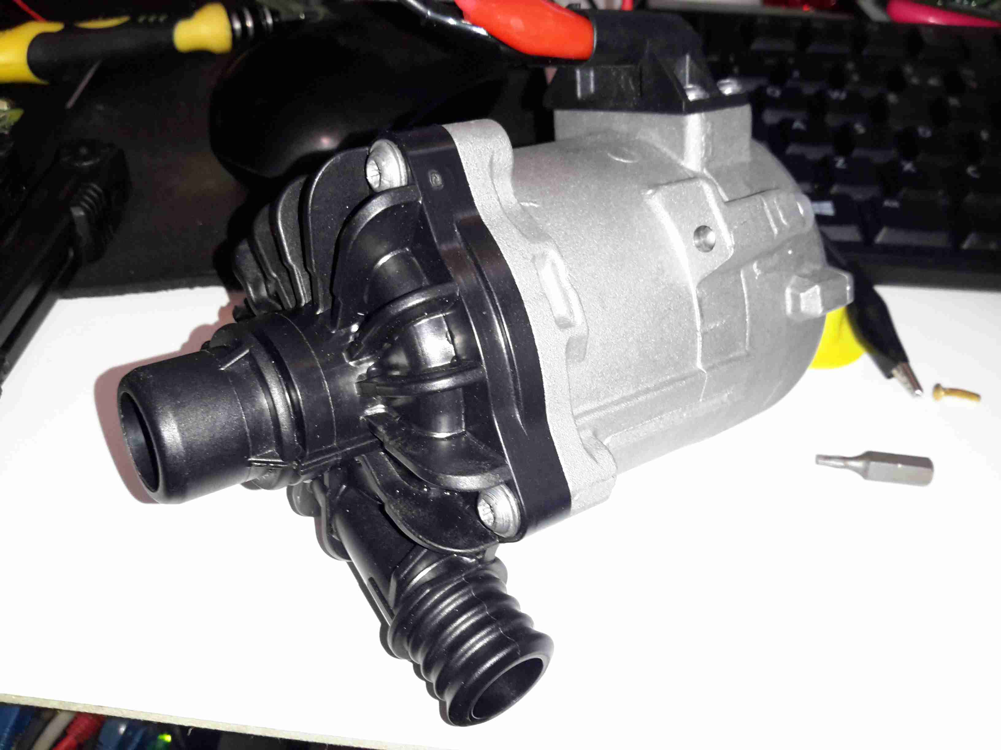
Pierburg CWA-50
Here’s the next size up from the original WUP1 pump, the CWA50. These are rated at a much more sensible 25L/min at 0.6bar head pressure. It’s physically a bit larger, but the connector sizes are the same, which makes the install onto the existing hoses easier. (For those that are interested, the hose connectors used on BMW vehicles for the cooling system components are NormaQuick PS3 type. These snap into place with an O-Ring & are retained by a spring clip).
The CWA50 draws considerably more power than the WUP1 (4.5A vs 1.5A), and are controllable with a PWM signal on the connector, but I haven’t used this feature. The PWM pin is simply tied to the positive supply to keep the pump running at maximum speed.
Once this pump was installed the head pressure immediately increased on the gauge from the 1 bar static pressure to 1.5 bar, indicating the pump is running at about it’s highest efficiency point. The higher water flow has so far kept the Webasto happy, there will be more to come with further improvements!
CWA-50 Pump Teardown
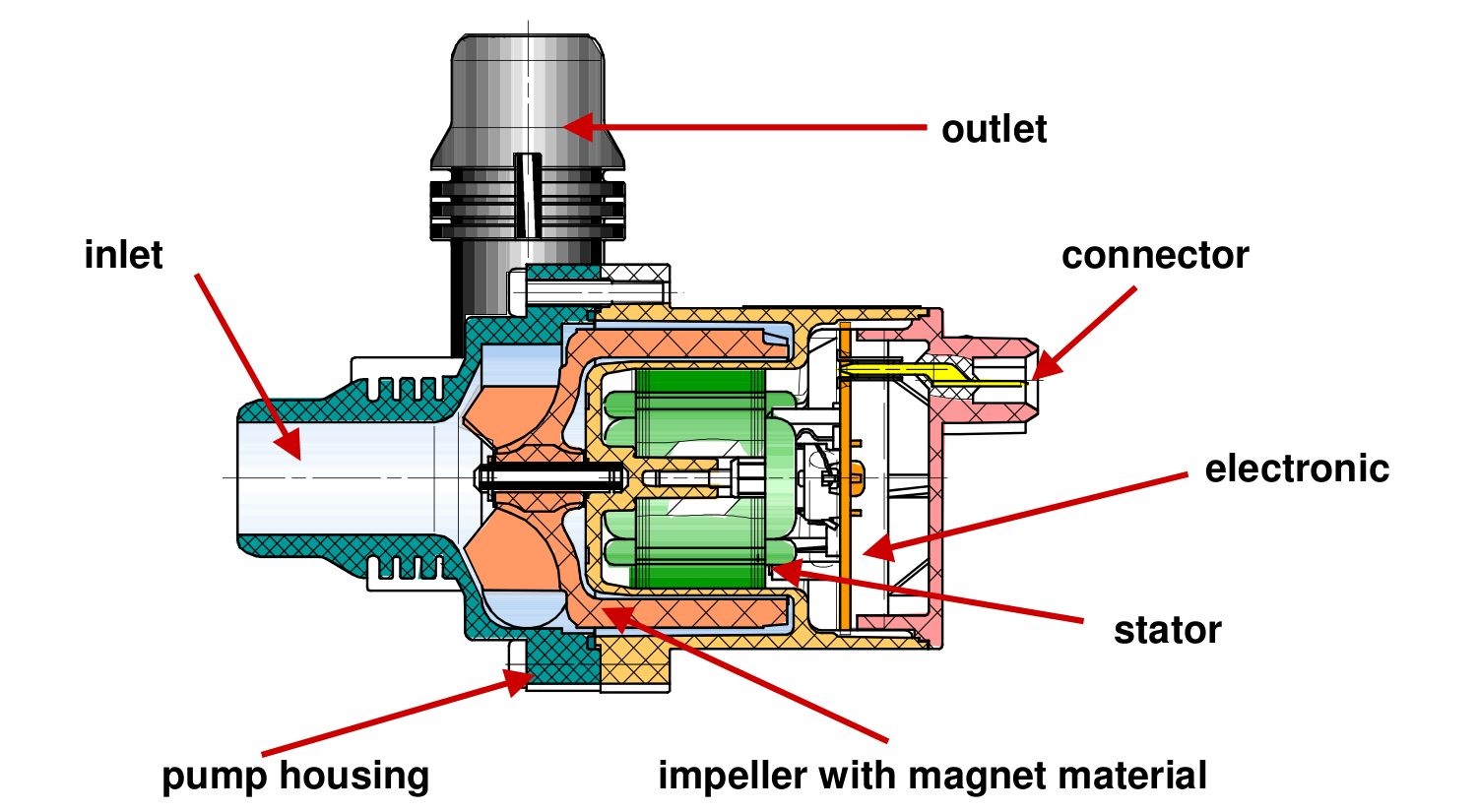
CWA50 Cutaway
Above is a cutaway drawing of the new pump. These have a drilling through the shaft allows water to pass from the high pressure outlet fitting, through the internals of the pump & returns through the shaft to the inlet. This keeps the bearings cool & lubricated. The control & power drive circuitry for the 3-phase brushless motor is attached to the back & uses the water flowing through the rotor chamber as a heatsink. Overall these are very well made pumps.
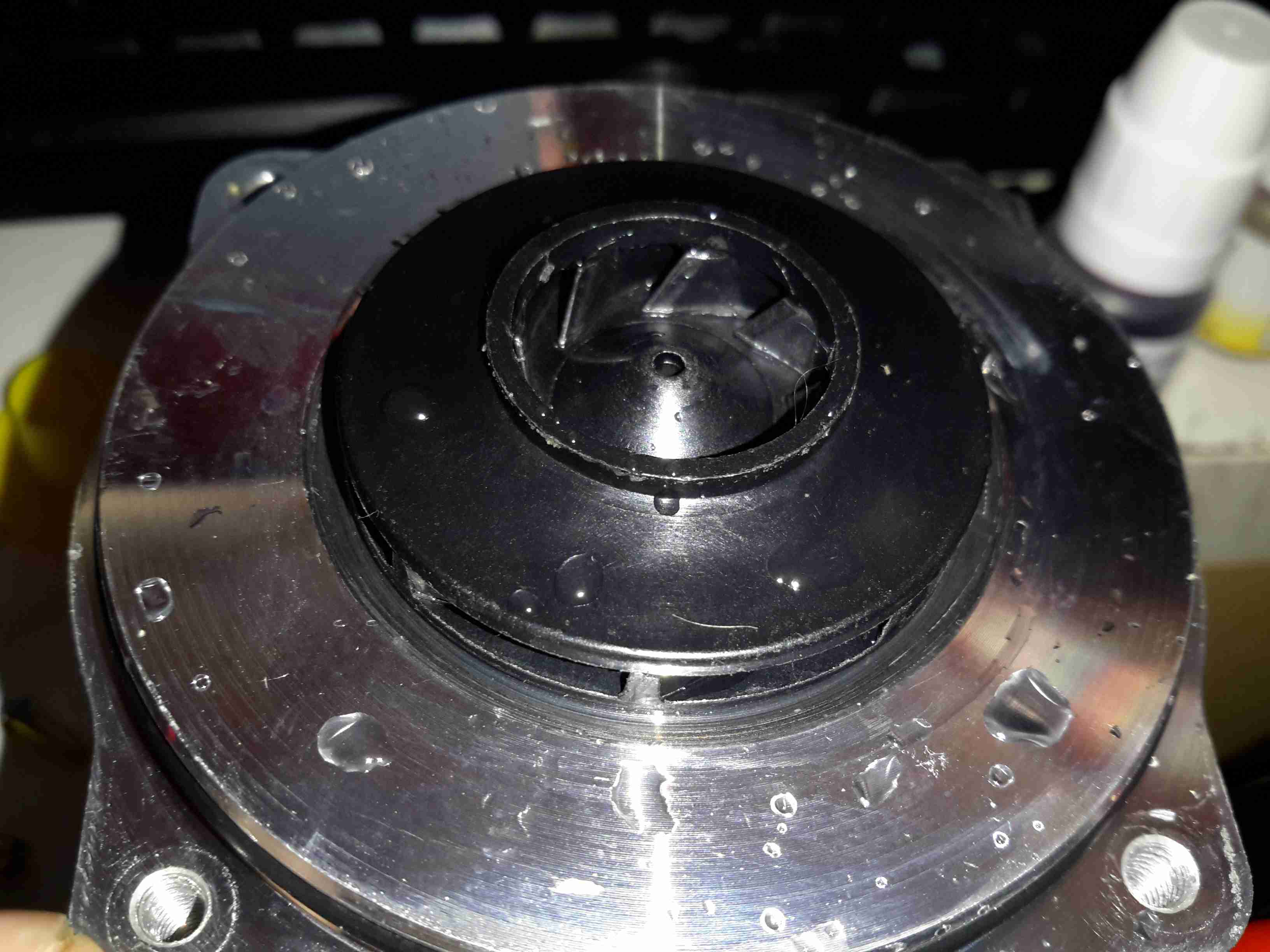
Impeller
Here’s the impeller of the pump, which is very small considering the amount of power this unit has. The return port for the lubricating water can be seen in the centre of the impeller face.
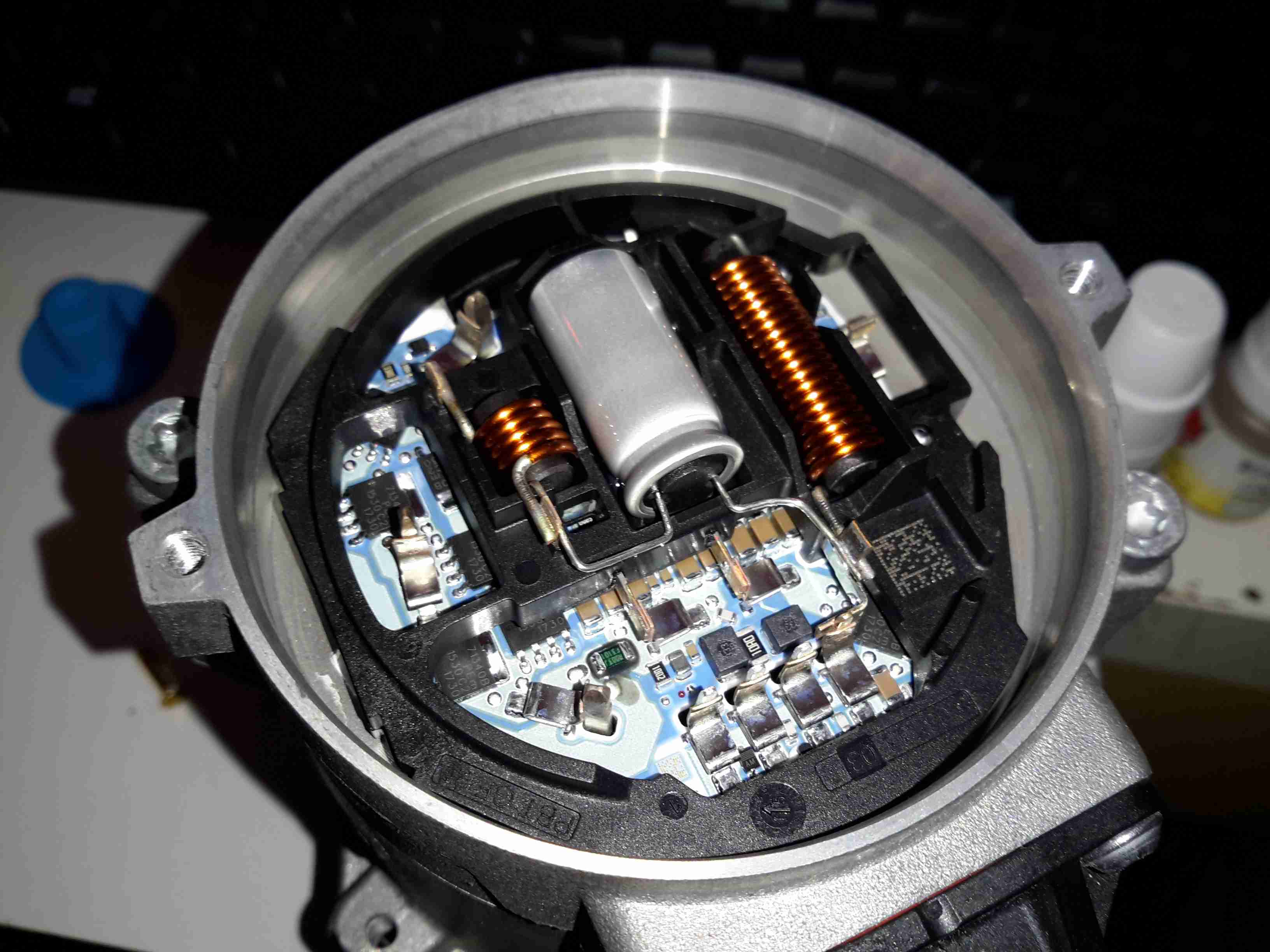
3-Phase Driver
Inside the back of the pump is the control module. The main microcontroller is hiding under the plastic frame which holds the large power chokes & the main filter electrolytic.
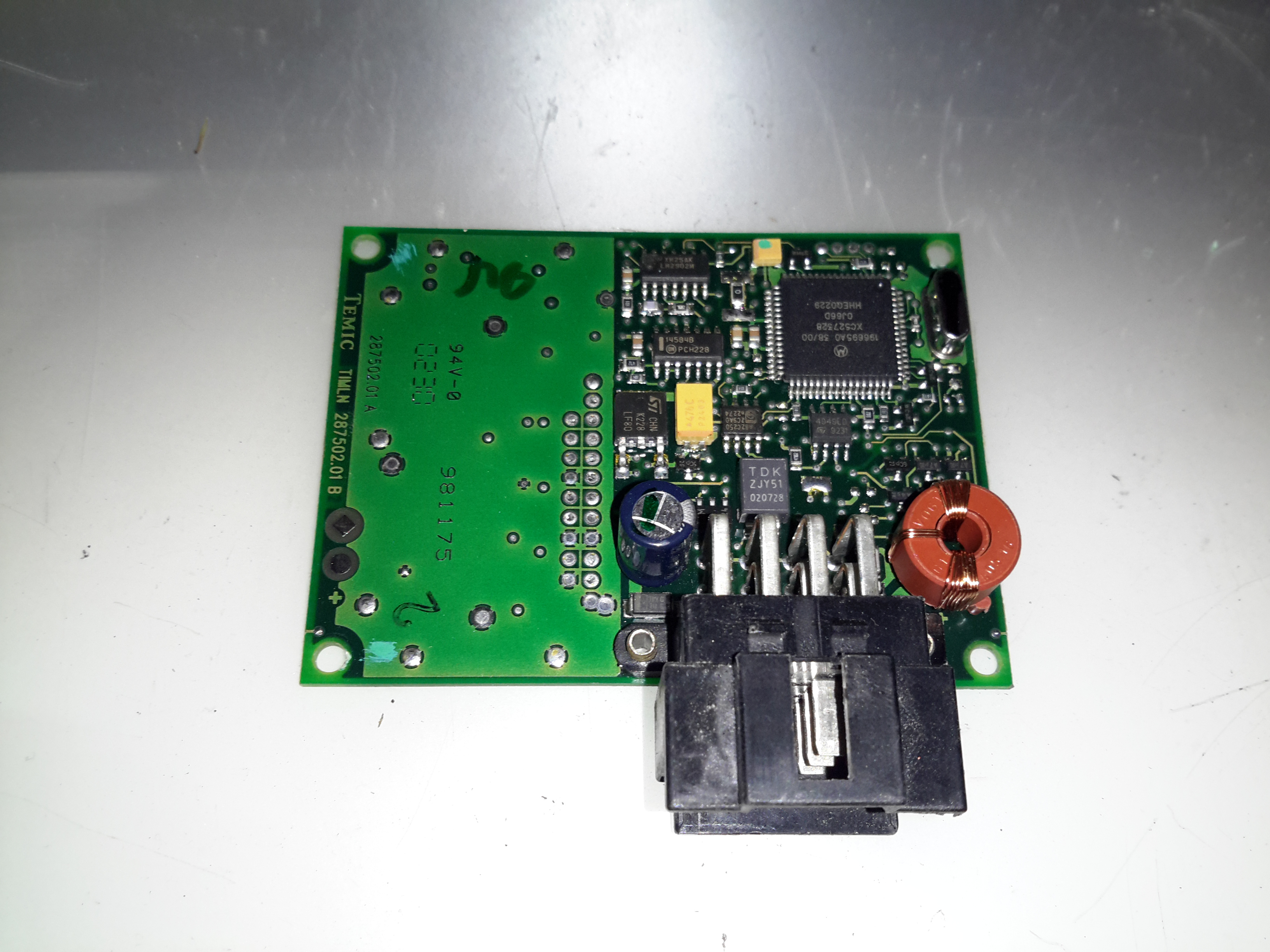
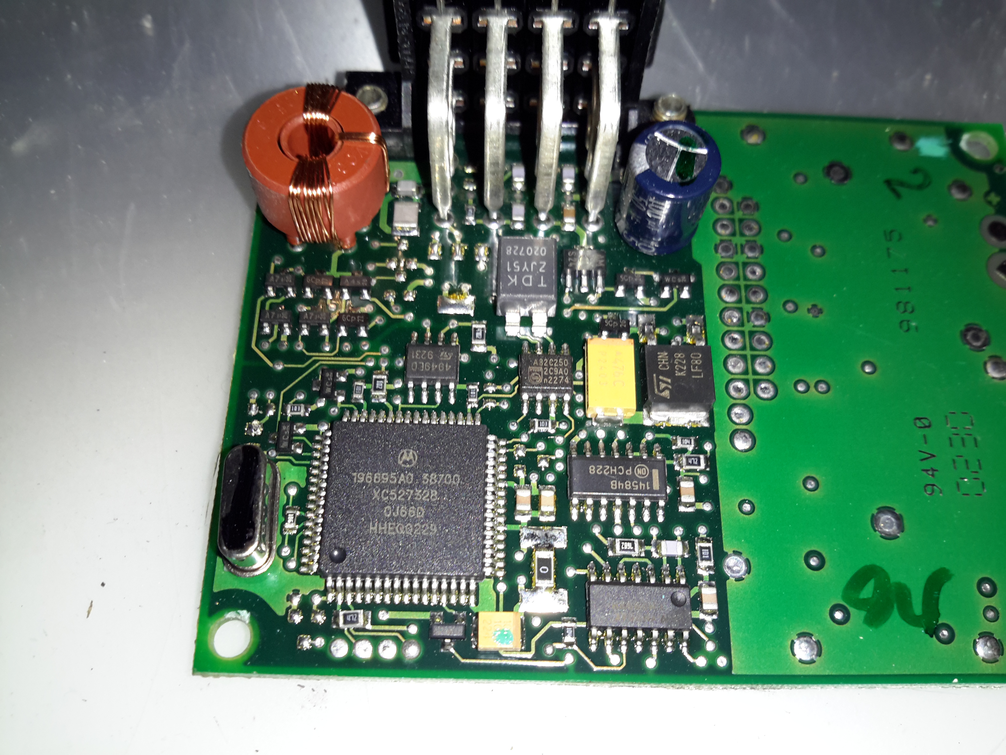
The other day I was given a random pile of car electronic parts from the scrap bin at the local garage, so I decided to do a few teardowns. This first one is a Temic Central Locking / Immobiliser module from a Mercedes van. Judging by the 125kHz stamped on the label, this also has RFID capability.
PCB
The casing just unclips, revealing the PCB. Surprisingly for an automotive module, there is no conformal coating on this (they’re usually heavily coated in protective lacquer to prevent moisture ingress).
Microcontroller
The large IC from Motorola I’m assuming to be a microcontroller, but I didn’t manage to find anything from the markings. There’s not much else in here apart from some glue logic, and what I think is the 125Khz toroidal antenna in the top left corner.
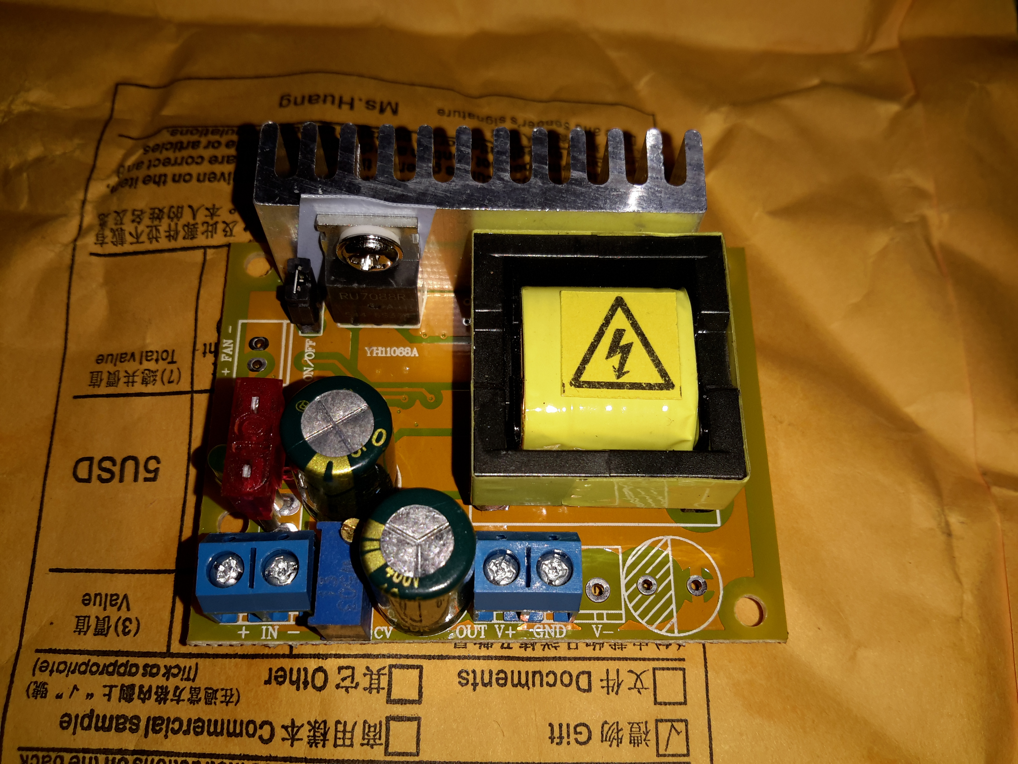
Going through eBay recently looking for parts for a couple of CRT-based projects, I came across these DC-DC converters.
Apparently rated from 45-390v DC output at 200mA, these should be ideal for driving some of the electrodes (focus, screen, grid) in a CRT.
Above is the top of the board, input voltage header on the left, output voltage adjust in the centre & output voltage header on the right.
This module has a mini-automotive fuse, at 10A for input protection.
On the heatsink is mounted the main switching MOSFET, a RU7088R from Ruichips. This FET is fairly heavily rated at 70v 80A, with 6.5mΩ on-resistance.
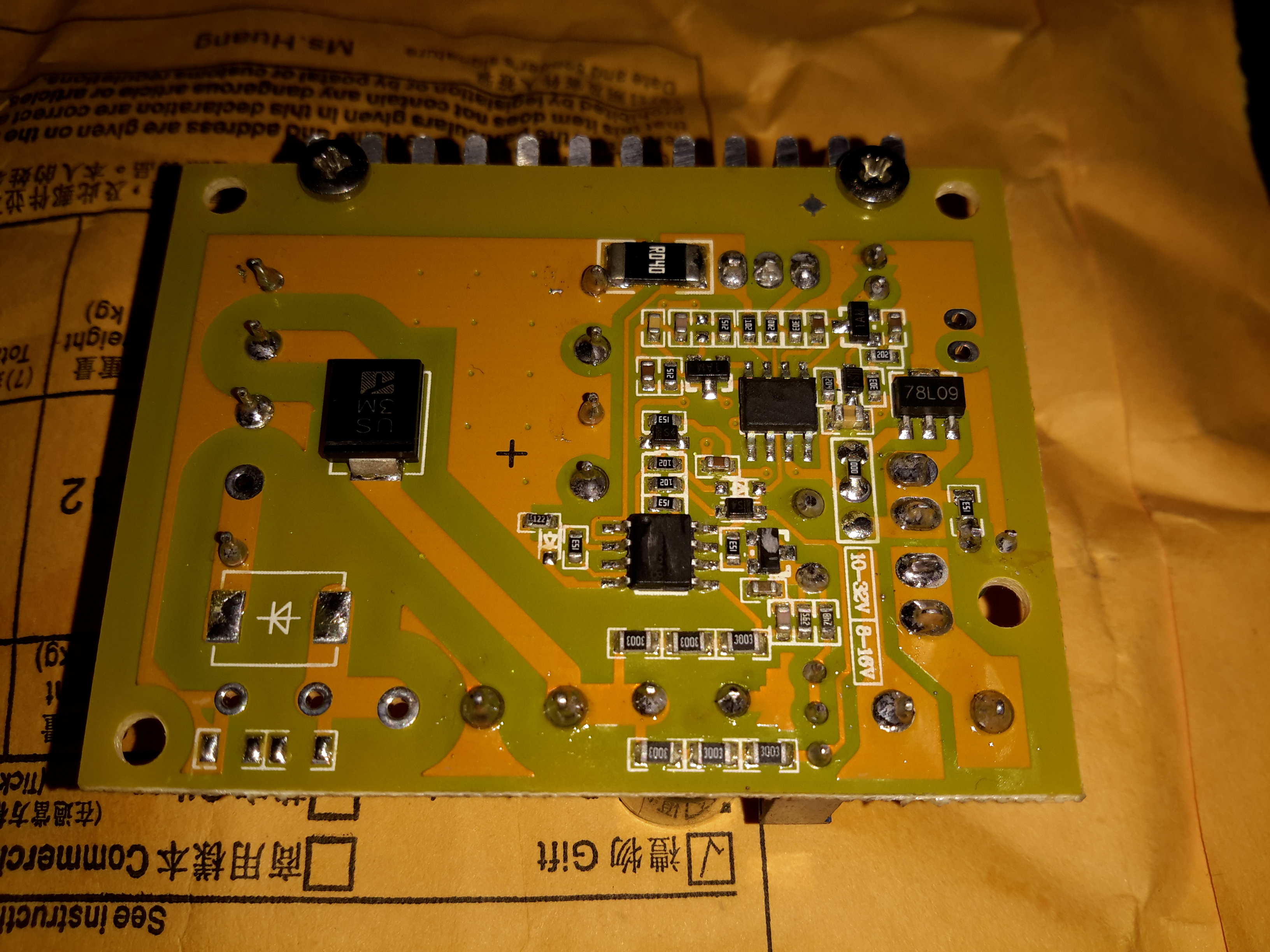
PCB Bottom
The bottom of the board has the control components, with a pair of ICs. Unfortunately the numbers have been scrubbed off, so no identification here. The output from the transformer is rectified with a single large SMD diode on the left side of the board.
There’s also plenty of isolation gap between the HV output trace & the low voltage logic side of the circuit, the two being bridged only by a resistive divider for output voltage measurement.
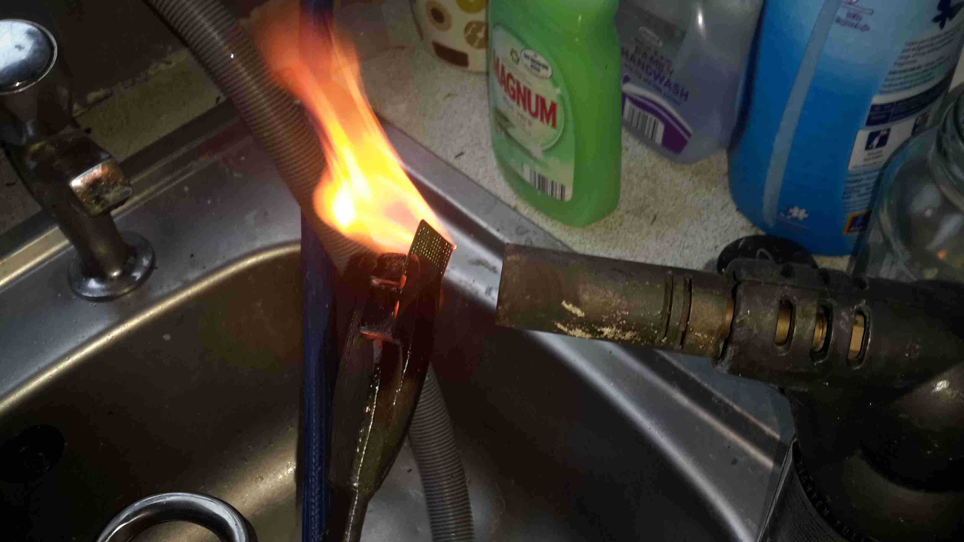
As I’ve been posting some photos of decapped ICs lately, I thought I’d share the process I use personally for those that might want to give it a go 😉
The usual method for removing the epoxy package from the silicon is to use hot, concentrated Nitric Acid. Besides the obvious risks of having hot acids around, the decomposition products of the acid, namely NO² (Nitrogen Dioxide) & NO (Nitrogen Oxide), are toxic and corrosive. So until I can get the required fume hood together to make sure I’m not going to corrode the place away, I’ll leave this process to proper labs ;).
The method I use is heat based, using a Propane torch to destroy the epoxy package, without damaging the Silicon die too much.
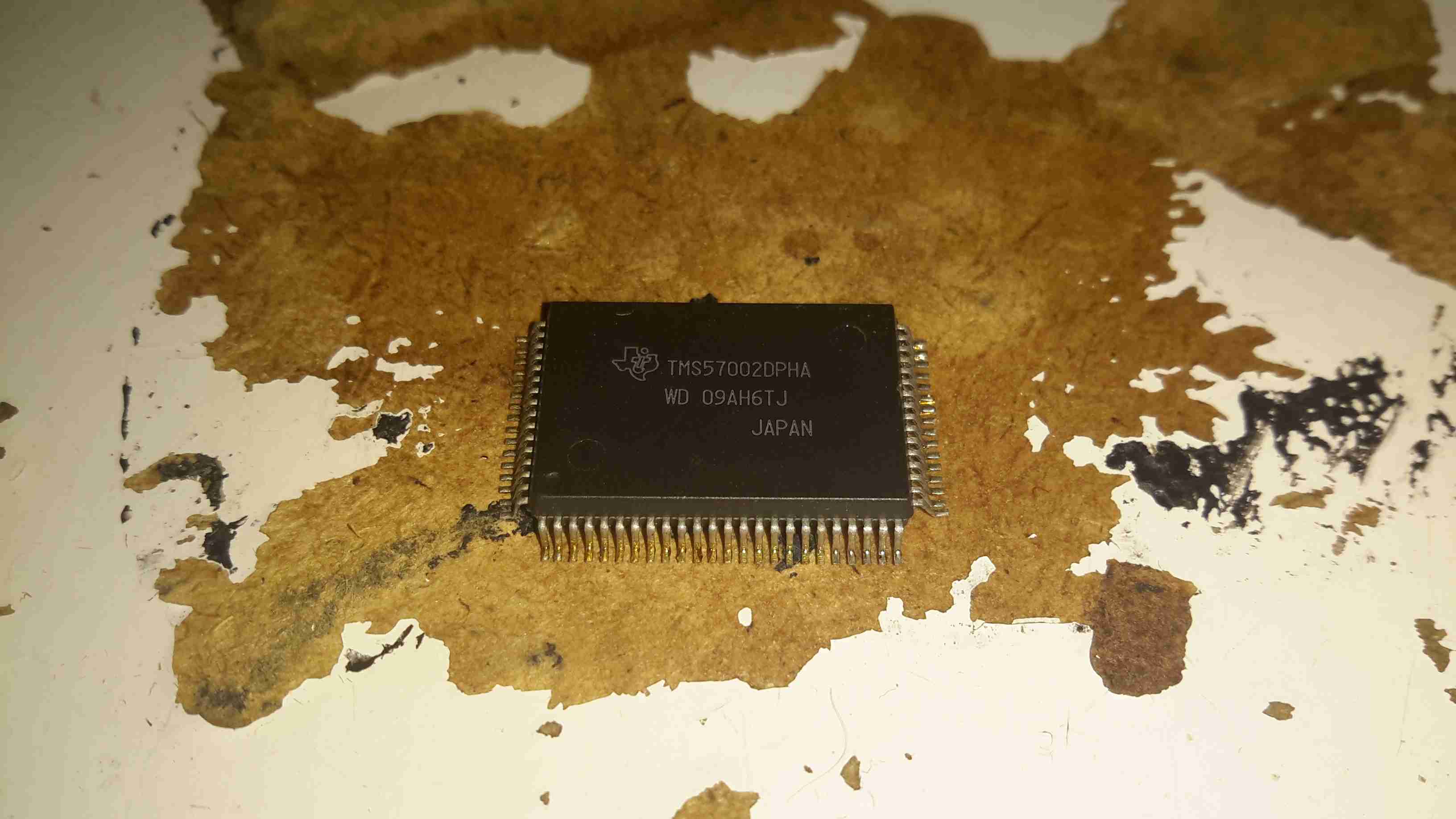
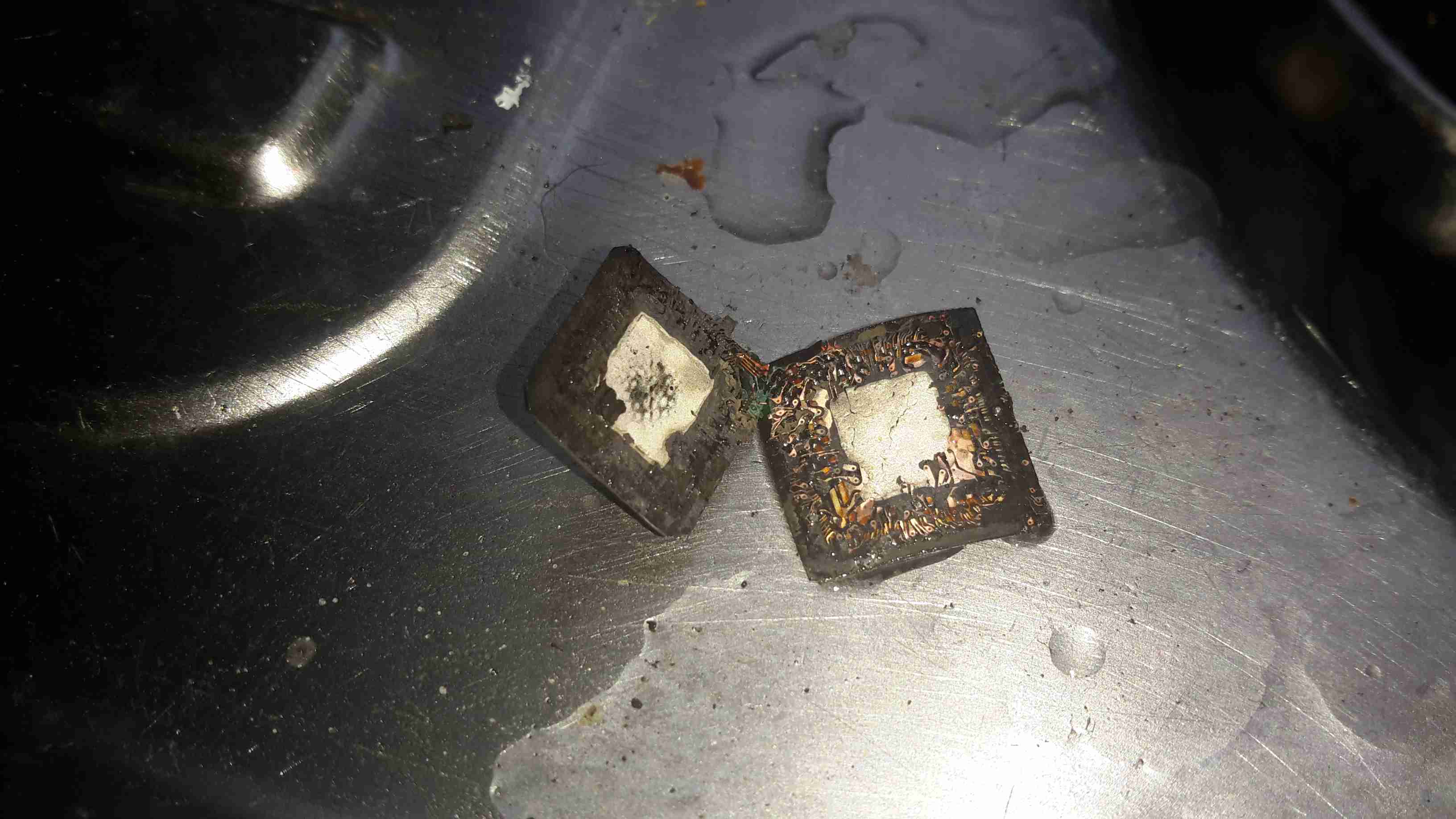
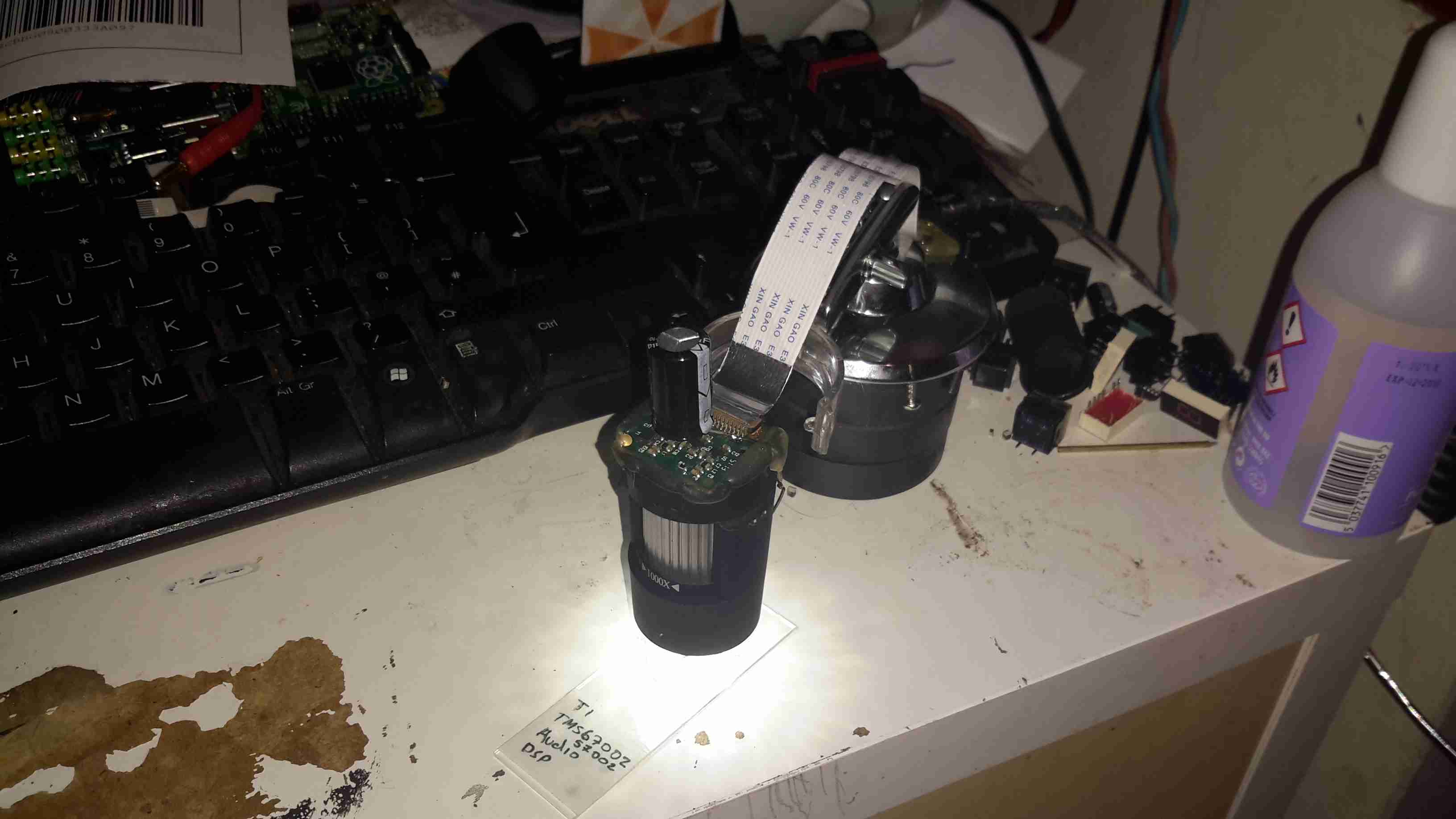
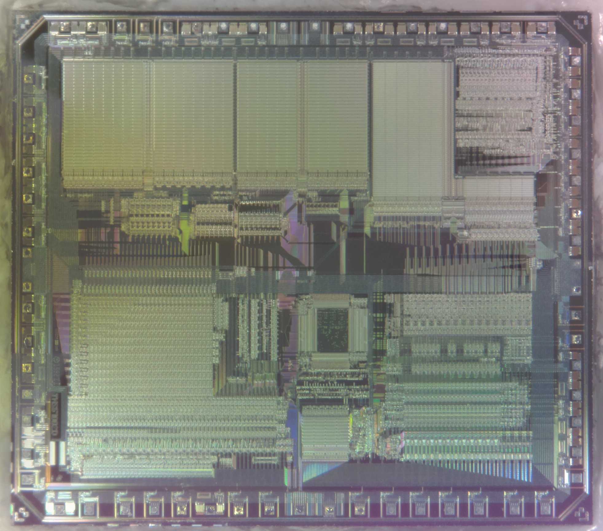
TMS57002 Audio DSP
I start off, obviously, with a desoldered IC, the one above an old audio DSP from TI. I usually desolder en-masse for this with a heat gun, stripping the entire board in one go.
FLAMES!
Next is to apply the torch to the IC. A bit of practice is required here to get the heat level & time exactly right, overheating will cause the die to oxidize & blacken or residual epoxy to stick to the surface.
I usually apply the torch until the package just about stops emitting it’s own yellow flames, meaning the epoxy is almost completely burned away. I also keep the torch flame away from the centre of the IC, where the die is located.
Breathing the fumes from this process isn’t recommended, no doubt besides the obvious soot, the burning plastic will be emitting many compounds not brilliant for Human health!
Once the IC is roasted to taste, it’s quenched in cold water for a few seconds. Sometimes this causes such a high thermal shock that the leadframe cracks off the epoxy around the die perfectly.
All Your Die Belong To Us
Now that the epoxy has been destroyed, it breaks apart easily, and is picked away until I uncover the die itself. (It’s the silver bit in the middle of the left half). The heat from the torch usually destroys the Silver epoxy holding the die to the leadframe, and can be removed easily from the remaining package.
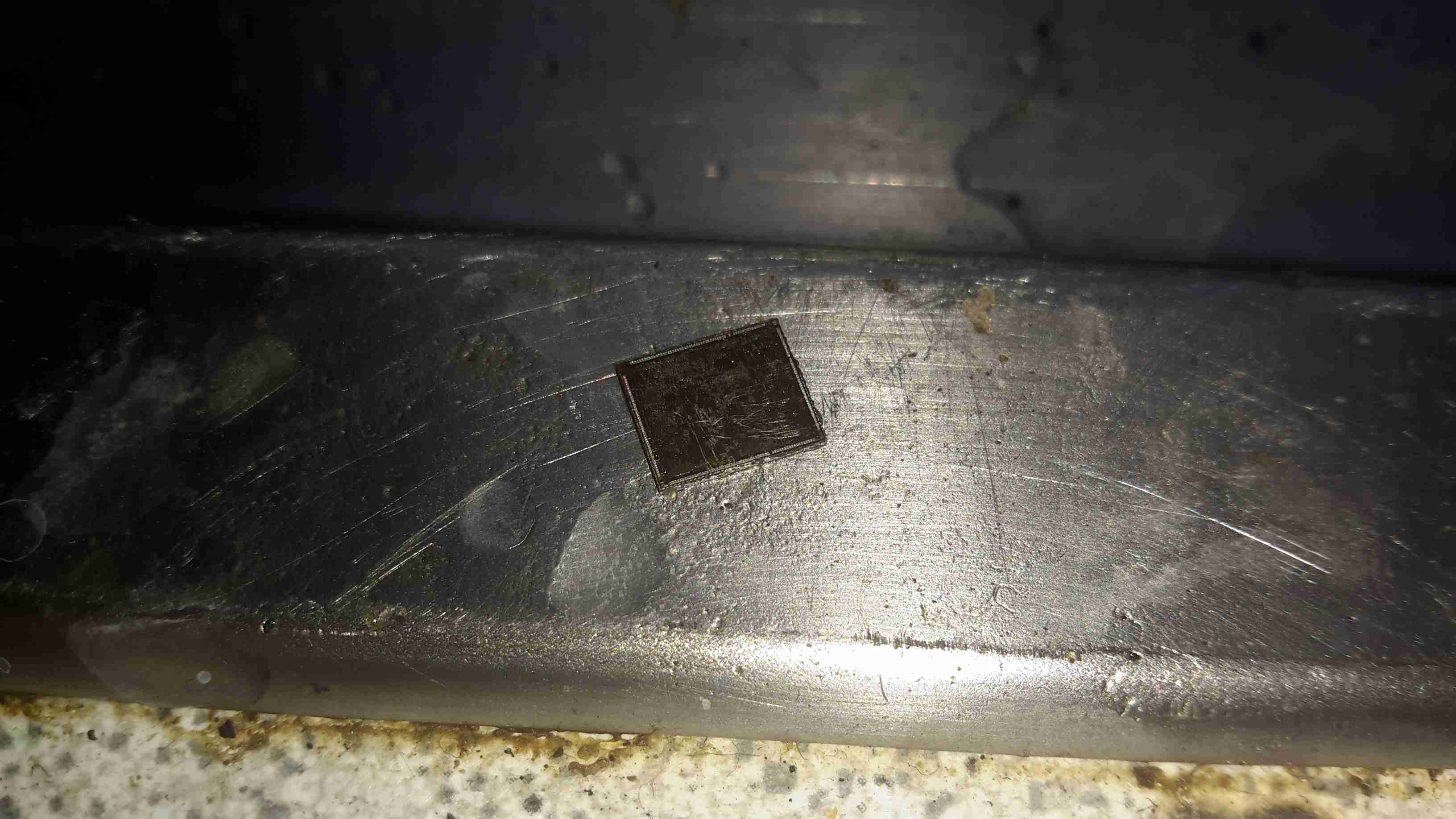
Decapped
BGA packages are usually the easiest to decap, flip-chip packages are a total pain due to the solder balls being on the front side of the die, I haven’t managed to get a good result here yet, I’ll probably need to chemically remove the first layer of the die to get at the interesting bits 😉
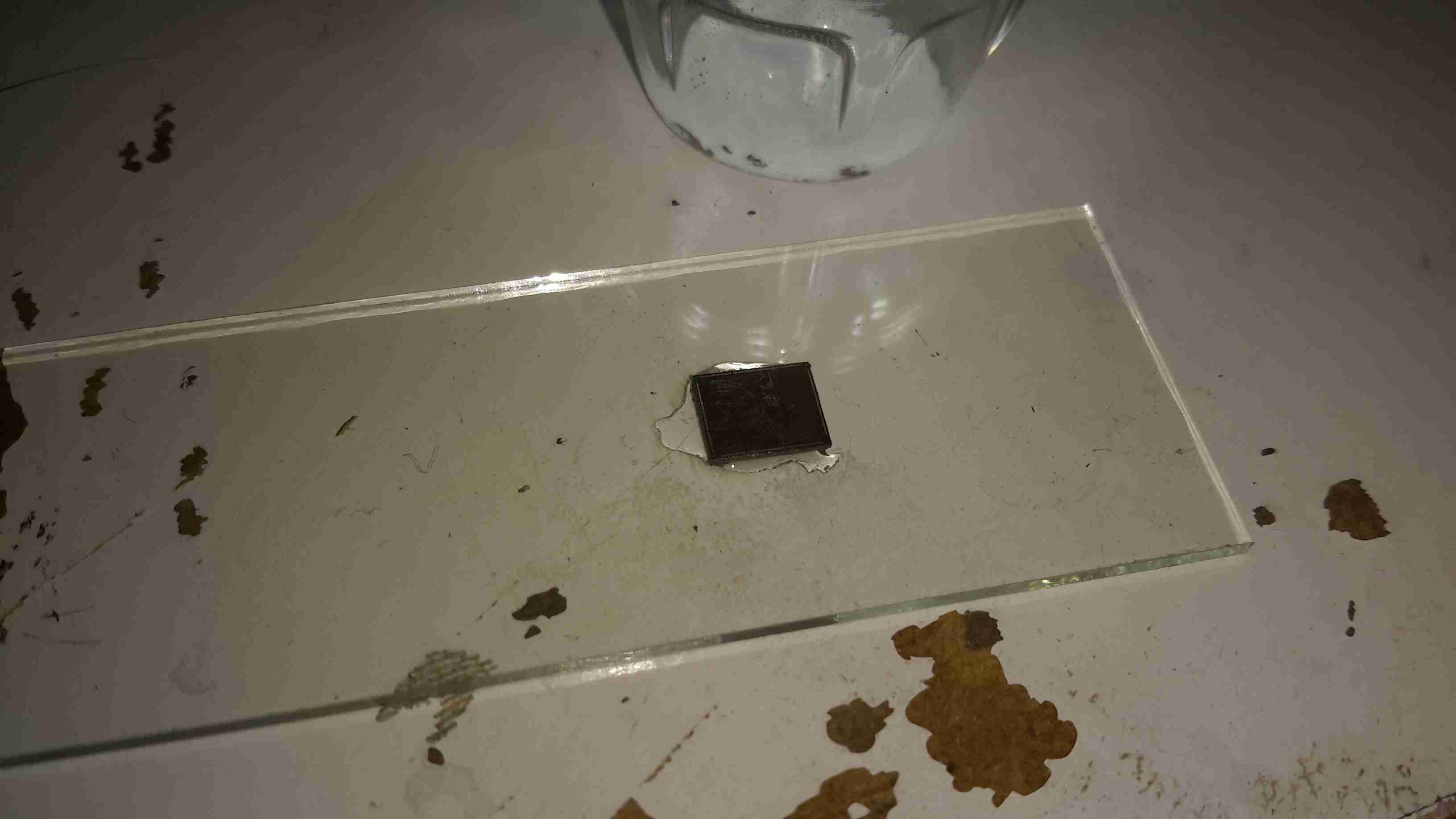
Slide
Once the die has been rinsed in clean water & inspected, it’s mounted on a glass microscope slide with a small spot of Cyanoacrylate glue to make handling easier.
Some dies require some cleaning after decapping, for this I use 99% Isopropanol & 99% Acetone, on the end of a cotton bud. Any residual epoxy flakes or oxide stuck to the die can be relatively easily removed with a fingernail – turns out fingernails are hard enough to remove the contamination, but not hard enough to damage the die features.
Once cleaning is complete, the slide is marked with the die identification, and the photographing can begin.
Microscope Mods
I had bought a cheap eBay USB microscope to get started, as I can’t currently afford a proper metallurgical microscope, but I found the resolution of 640×480 very poor. Some modification was required!
Modified Microscope
I’ve removed the original sensor board from the back of the optics assembly & attached a Raspberry Pi camera board. The ring that held the original sensor board has been cut down to a minimum, as the Pi camera PCB is slightly too big to fit inside.
The stock ring of LEDs is run direct from the 3.3v power rail on the camera, through a 4.7Ω resistor, for ~80mA. I also added a 1000µF capacitor across the 3.3v supply to compensate a bit for the long cable – when a frame is captured the power draw of the camera increases & causes a bit of voltage drop.
The stock lens was removed from the Pi camera module by careful use of a razor blade – being too rough here *WILL* damage the sensor die or the gold bond wires, which are very close to the edge of the lens housing, so be gentle!
Mounting Base
The existing mount for the microscope is pretty poor, so I’ve used a couple of surplus ceramic ring magnets as a better base, this also gives me the option of raising or lowering the base by adding or removing magnets.
To get more length between the Pi & the camera, I bought a 1-meter cable extension kit from Pi-Cables over at eBay, cables this long *definitely* require shielding in my space, which is a pretty aggressive RF environment, or interference appears on the display. Not surprising considering the high data rates the cable carries.
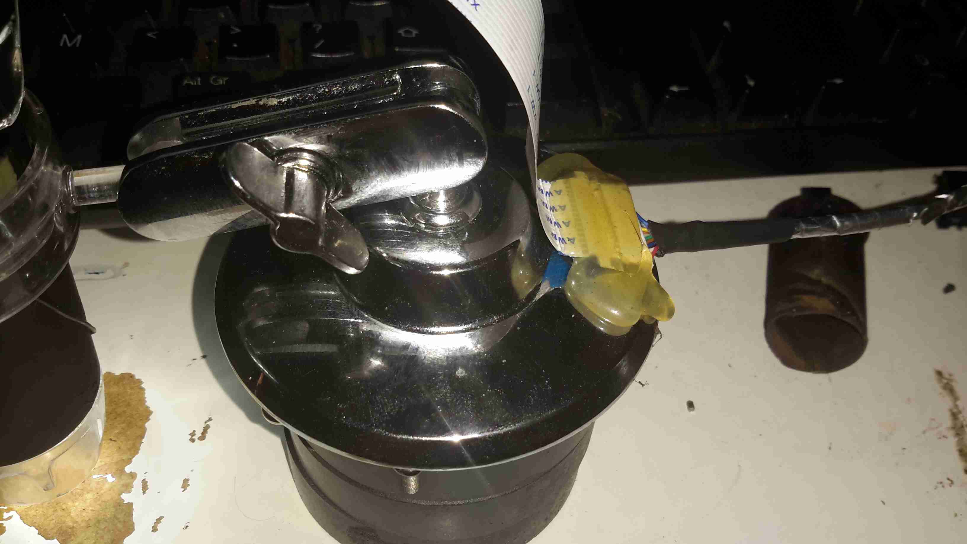
The FFC interface is hot-glued to the back of the microscope mount for stability, for handheld use the FFC is pretty flexible & doesn’t apply any force to the scope.
Die Photography
Since I modified the scope with a Raspberry Pi camera module, everything is done through the Pi itself, and the raspistill command.
Pi LCD
The command I’m currently using to capture the images is:
raspistill -ex auto -awb auto -mm matrix -br 62 -q 100 -vf -hf -f -t 0 -k -v -o CHIPNAME_%03d.jpg
This command waits between each frame for the ENTER key to be pressed, allowing me to position the scope between shots. Pi control & file transfer is done via SSH, while I use the 7″ touch LCD as a viewfinder.
The direct overhead illumination provided by the stock ring of LEDs isn’t ideal for some die shots, so I’m planning on fitting some off-centre LEDs to improve the resulting images.
Image Processing
Obviously I can’t get an ultra-high resolution image with a single shot, due to the focal length, so I have to take many shots (30-180 per die), and stitch them together into a single image.
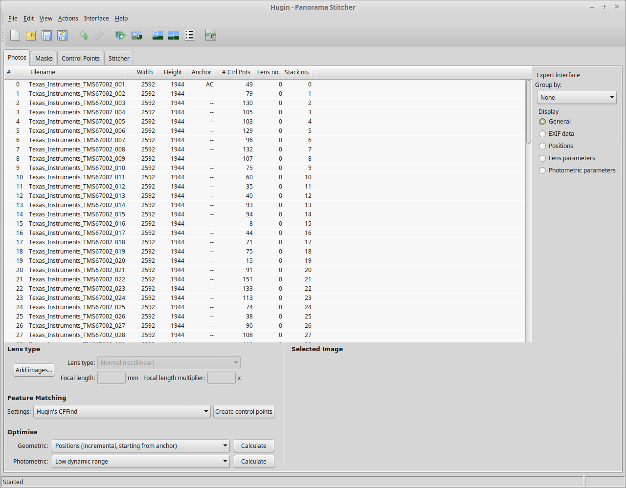
For this I use Hugin, an open-source panorama photo stitching package.
Hugin
Here’s Hugin with the photos loaded in from the Raspberry Pi. To start with I use Hugin’s built in CPFind to process the images for control points. The trick with getting good control points is making sure the images have a high level of overlap, between 50-80%, this way the software doesn’t get confused & stick the images together incorrectly.
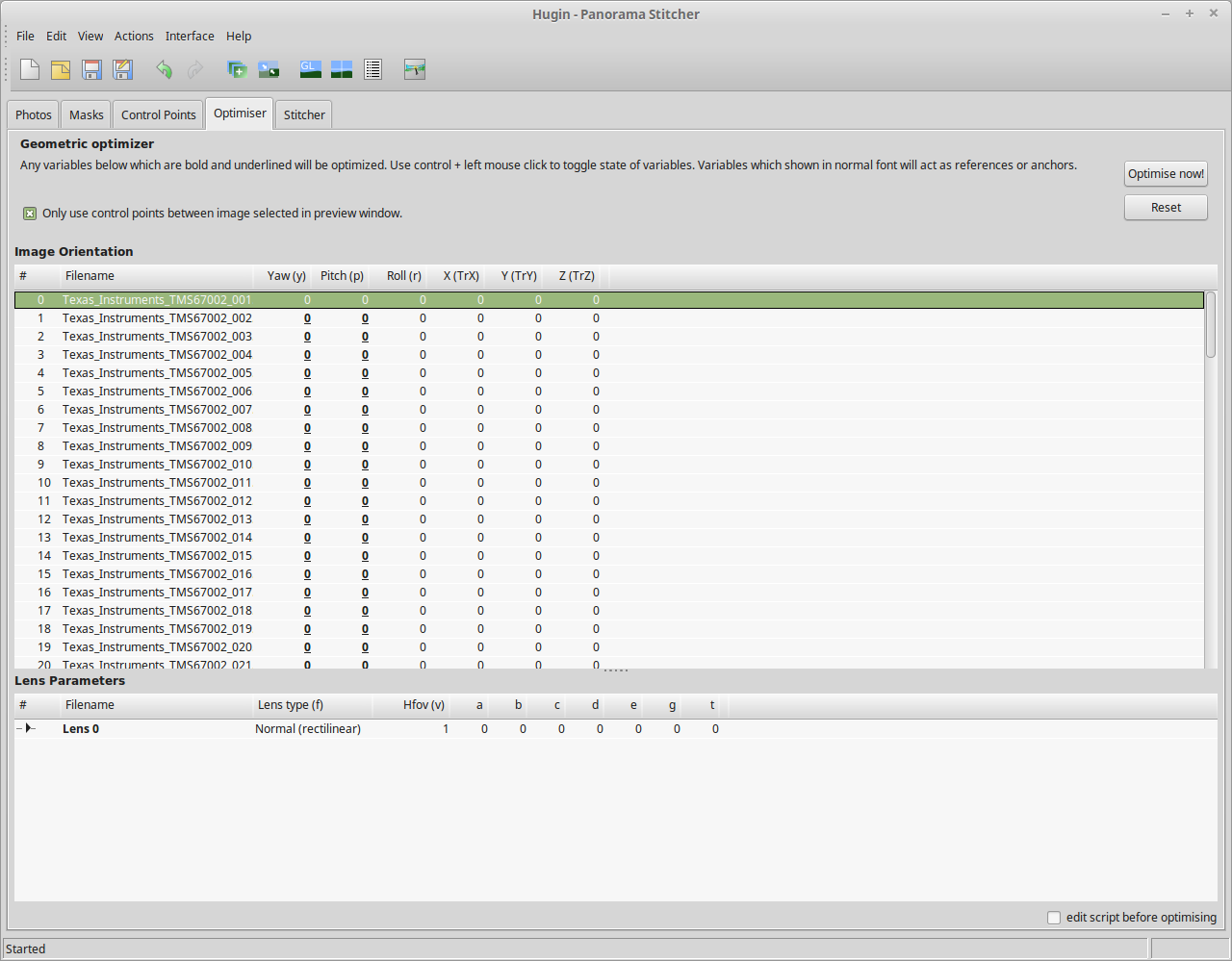
Optimiser
After the control points are generated, which for a large number of high resolution images can take some time, I run the optimiser with only Yaw & Pitch selected for all images.
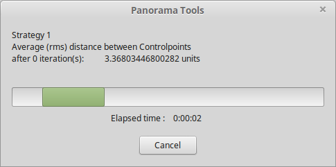
Optimising
If all goes well, the resulting optimisation will get the distance between control points to less than 0.3 pixels.
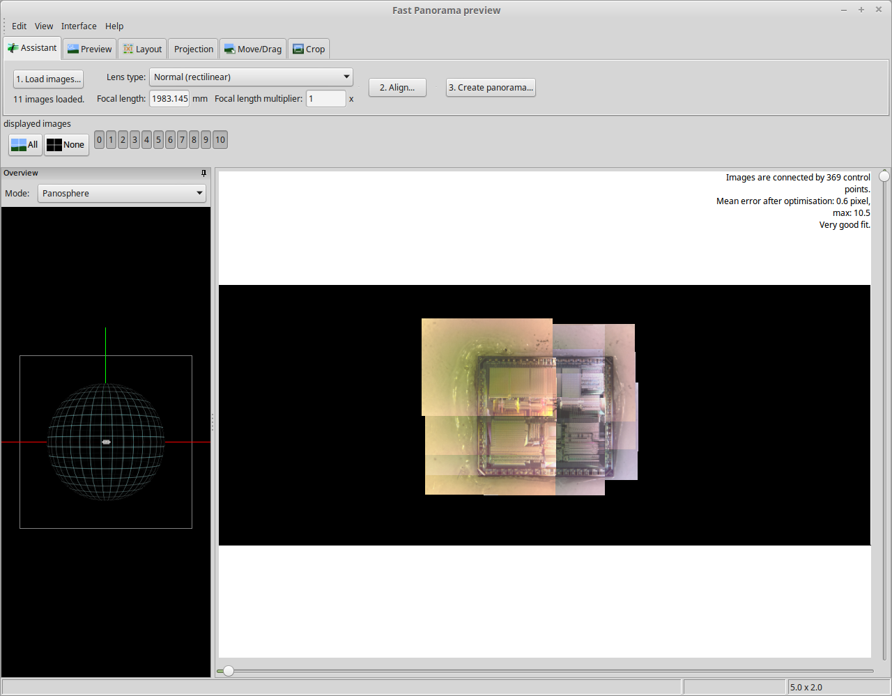
Panorama Preview
After the control points & optimisation is done, the resulting image can be previewed before generation.
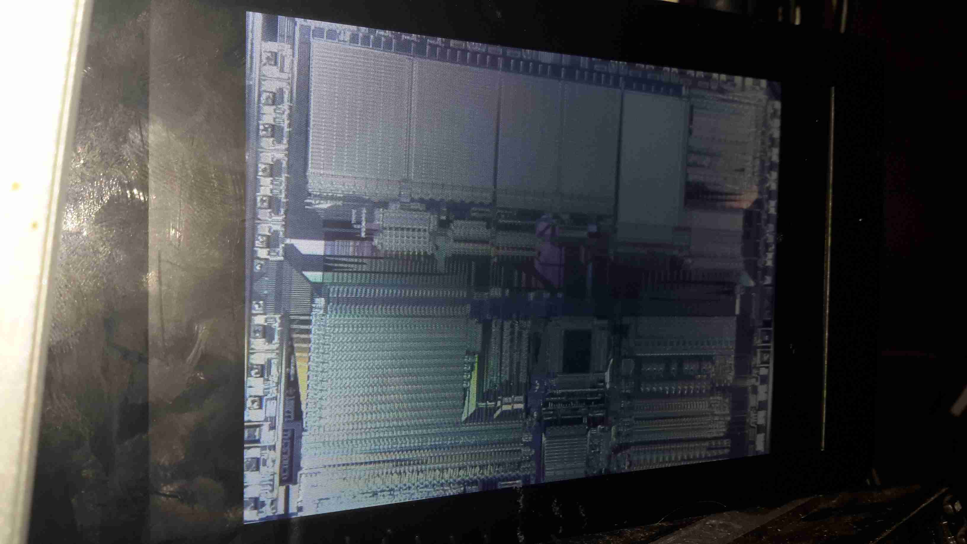
Texas Instruments TMS67002
After all the image processing, the resulting die image should look something like the above, with no noticeable gaps.
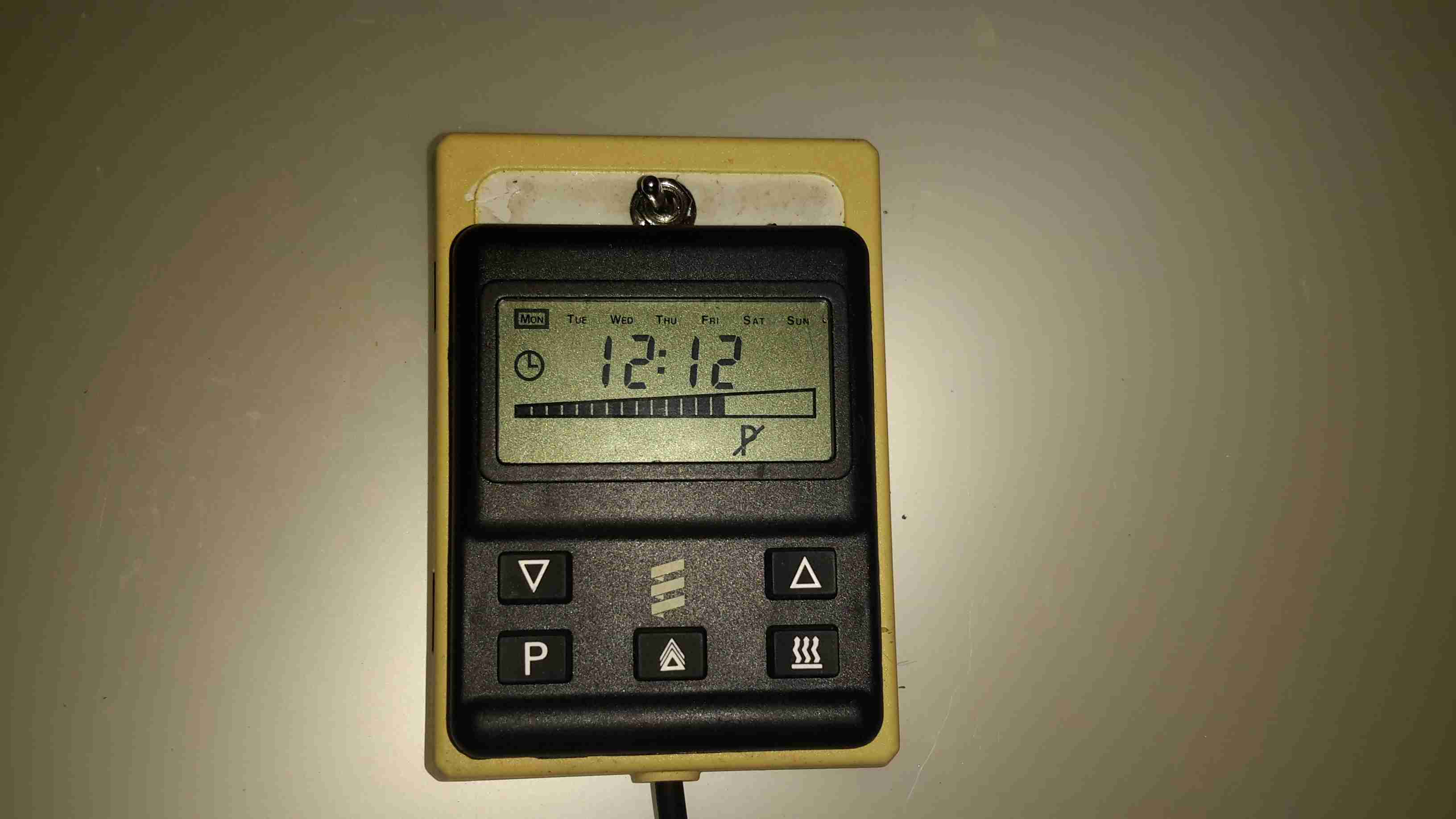
The Eberspacher heaters can be controlled with a single switch, but it’s more convenient to have some temperature control & the option of a timer. Above is an ex-BT 701 series controller, with built in 7-day programmer. Being an ex-BT van version though, it’ll only switch the heater on for 1 hour at a time.
To get around this slight niggle, I fitted a bypass toggle switch.
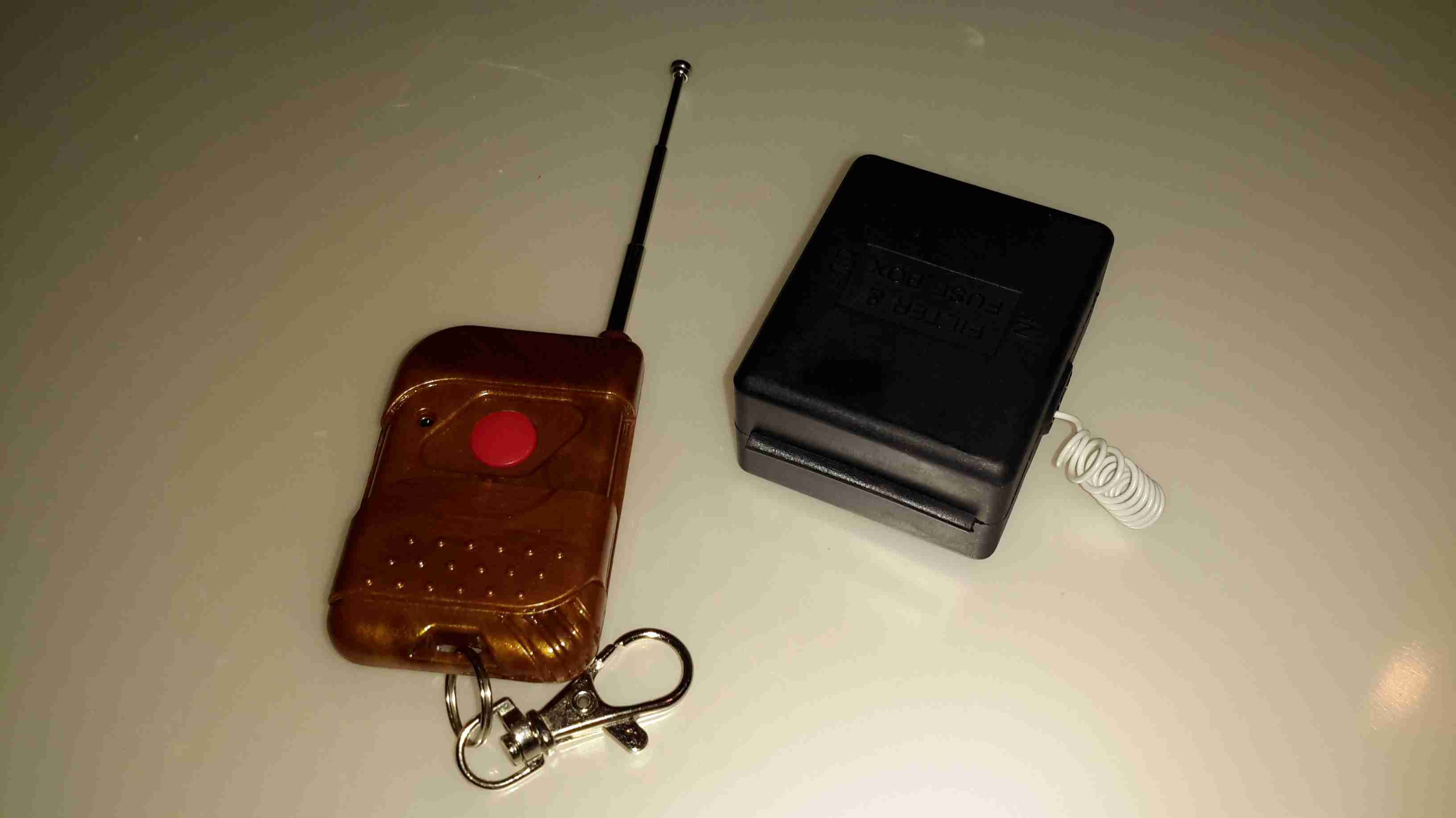
Remote Control
For a bit of extra convenience, I got an RF remote controlled relay module from eBay (£5).
This allows me to switch things on remotely, so I can return to a nice toasty tent while camping.
There is an official RF remote for Eberspacher heaters, but I’ve no doubt they’re hideously expensive.
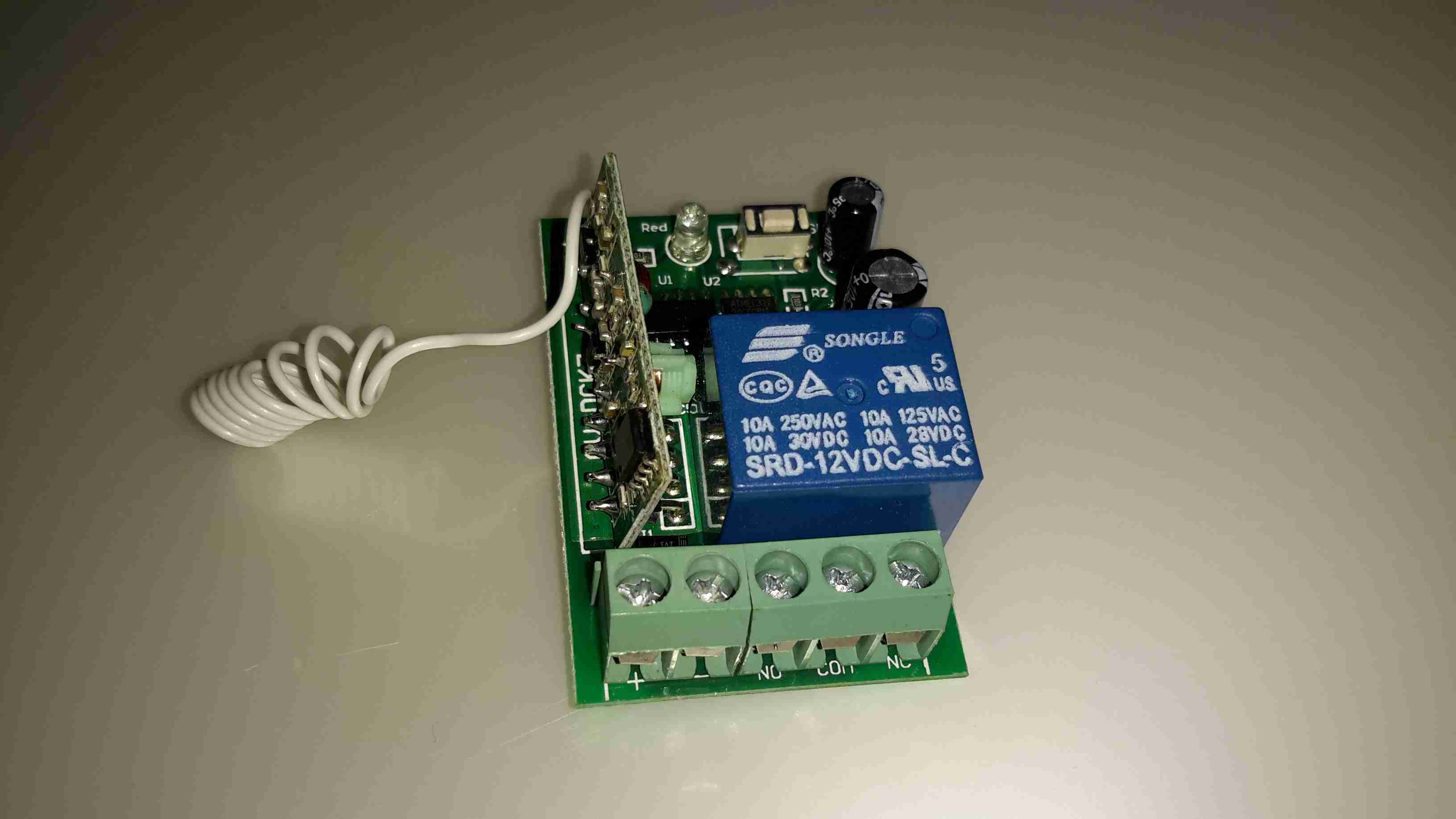
RF Receiver
Here’s the receiver PCB, there’s an EEPROM & a microcontroller onboard for handling the codes the remotes send, but as the number has been scrubbed off the micro, no data there. This uses a standard RF receiver module.
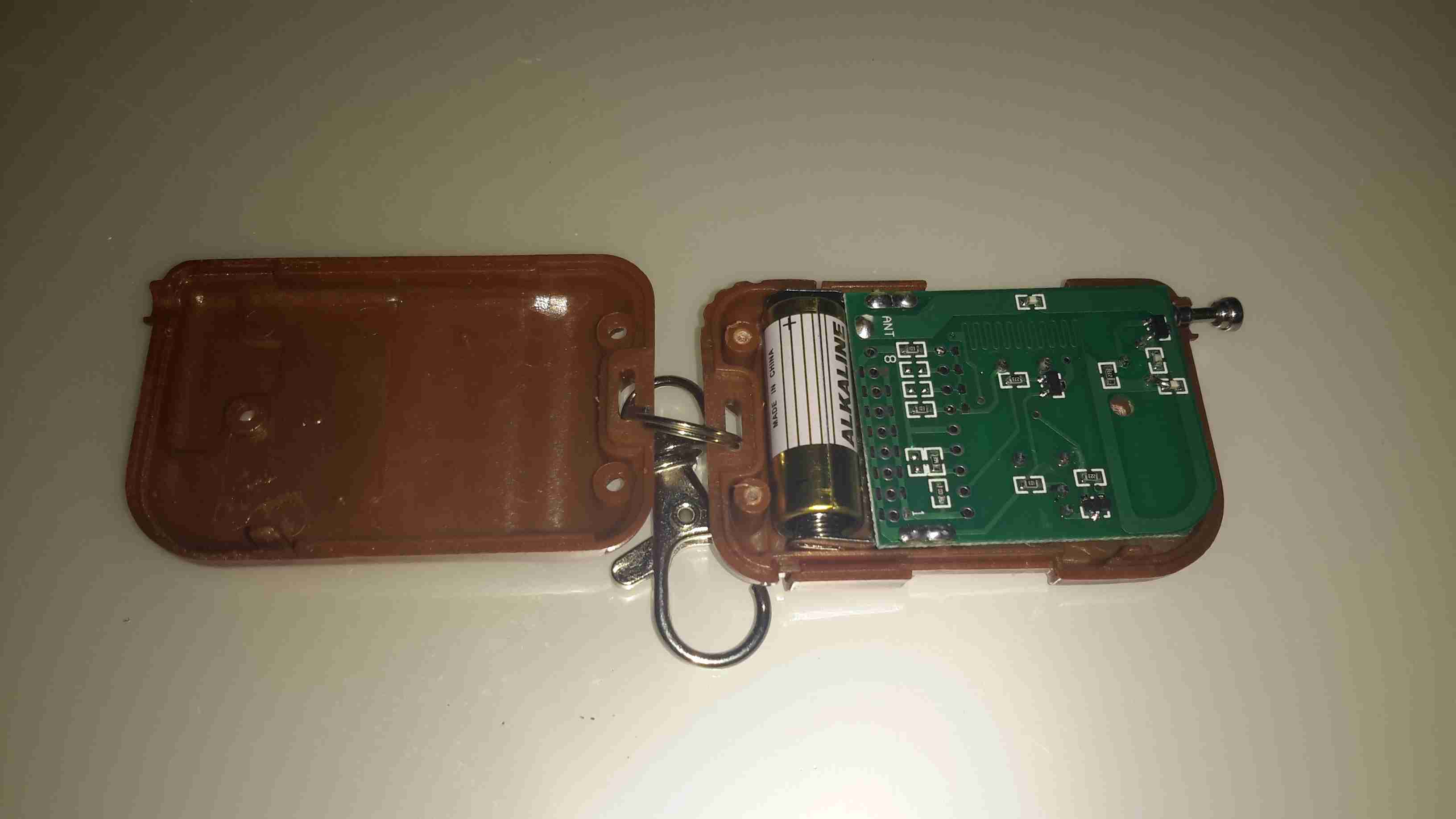
RF Remote
Here’s the remote itself, this uses a 12v battery instead of a 3v lithium cell. A little of a pain since these batteries can be a bit pricey.
As this RF system operates on 315MHz, it’s technically illegal in the UK, but I was unable to find a 433MHz version with the features required. Nevermind ;).
Controller Internals
Here’s the module installed in the controller casing. I have since run the antenna wire around the edge of the case to try & get the furthest range on receive. The relay contacts are just paralleled across the bypass switch, so when the relay energizes the heater fires up.
Luckily the thermostatic control portion of the 701 programmer is operational even when heating mode is not active.
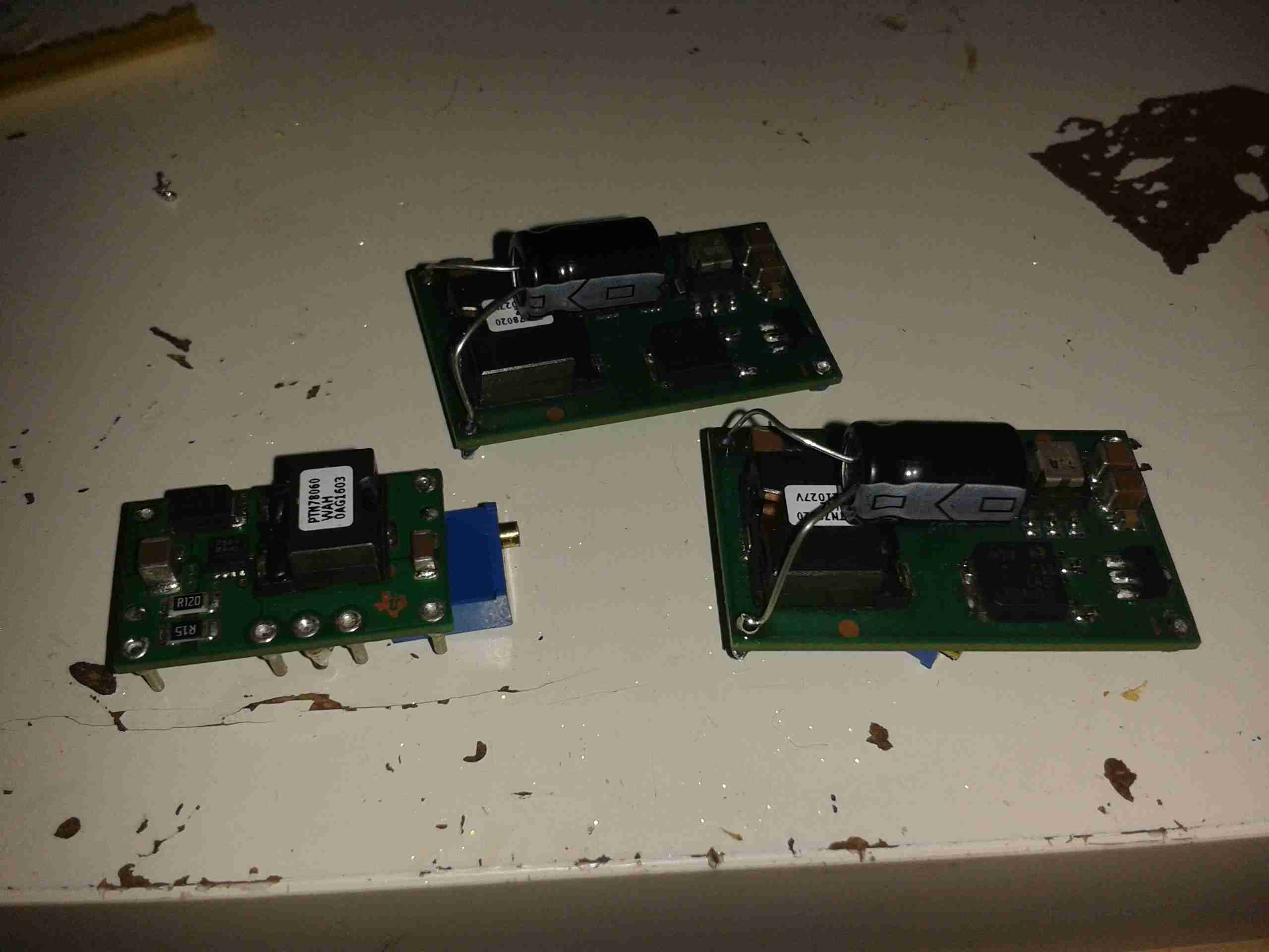
While searching around for regulators to convert my new scope to 12v power, I remembered I had some DC-DC modules from Texas Instruments that I’d got a while ago. Luckily a couple of these are inverting controllers, that will go down to -15v DC at 15W/3A capacity.
I’ve had to order a new module from TI to do the -17v rail, but in the meantime I’ve been getting the other regulators set up & ready to go.
The DC-DC module I’ve got for the -7.5v rail is the PTN78060A type, and the +7.5v & +5v rails will be provided by the PTN78020W 6A buck regulators.
These regulators are rated well above what the scope actually draws, so I shouldn’t have any issues with power.
DC-DC Modules
Here’s the regulators for the 5v, 7.5v & -7.5v rails, with multiturn potentiometers attached for setting the voltage output accurately. I’ve also attached a couple of electrolytics on the output for some more filtering. I’ll add on some more LC filters on the output to keep the noise down to an absolute minimum. These are set up ready with the exact same output voltage as the existing mains AC switching supply, when the final regulator arrives from TI I will put everything together & get some proper rail readings.
There won’t be a proper PCB for this, as I don’t have the parts in Eagle CAD, and I simply don’t have the energy to draw them out from the datasheets.
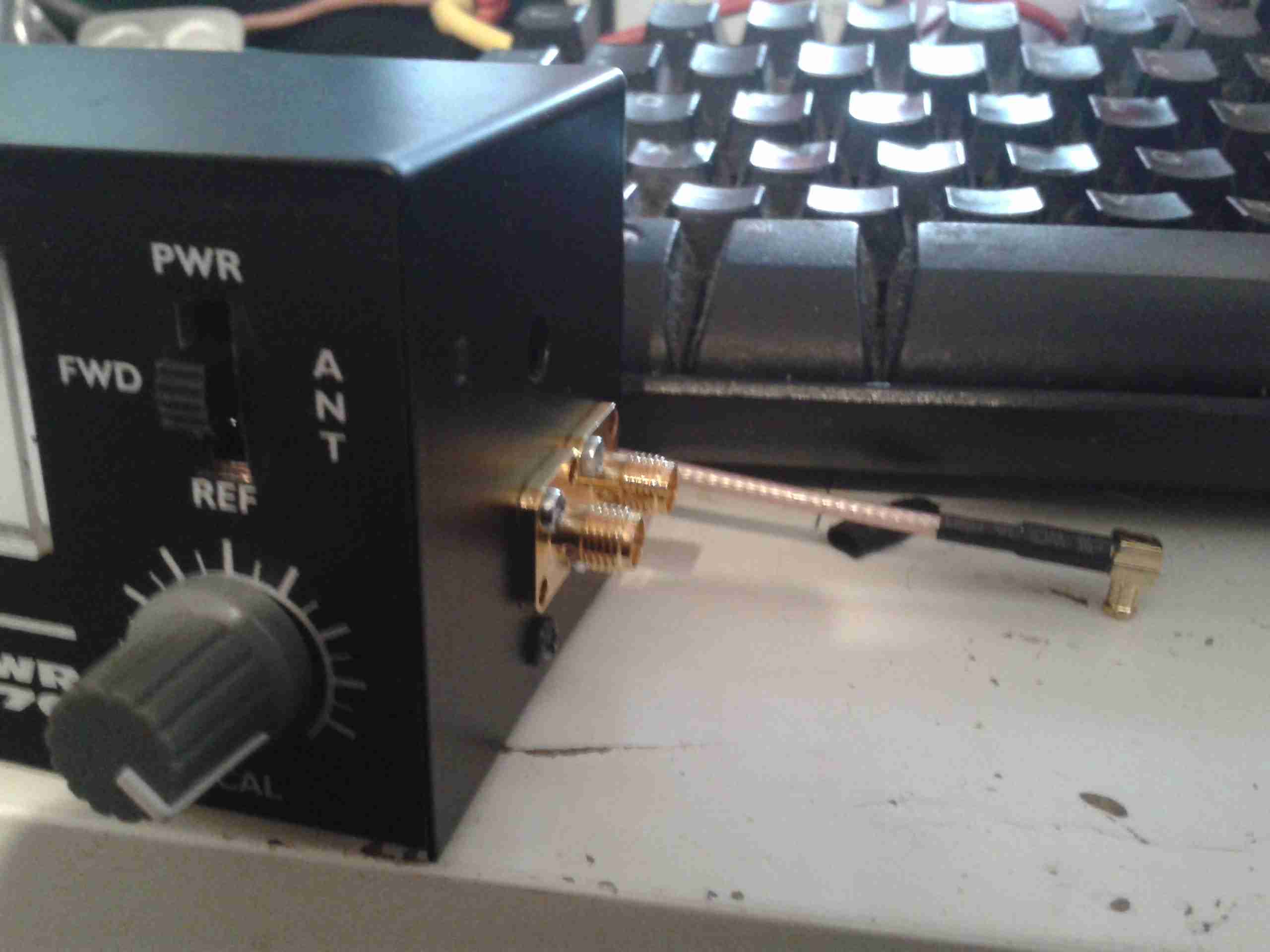
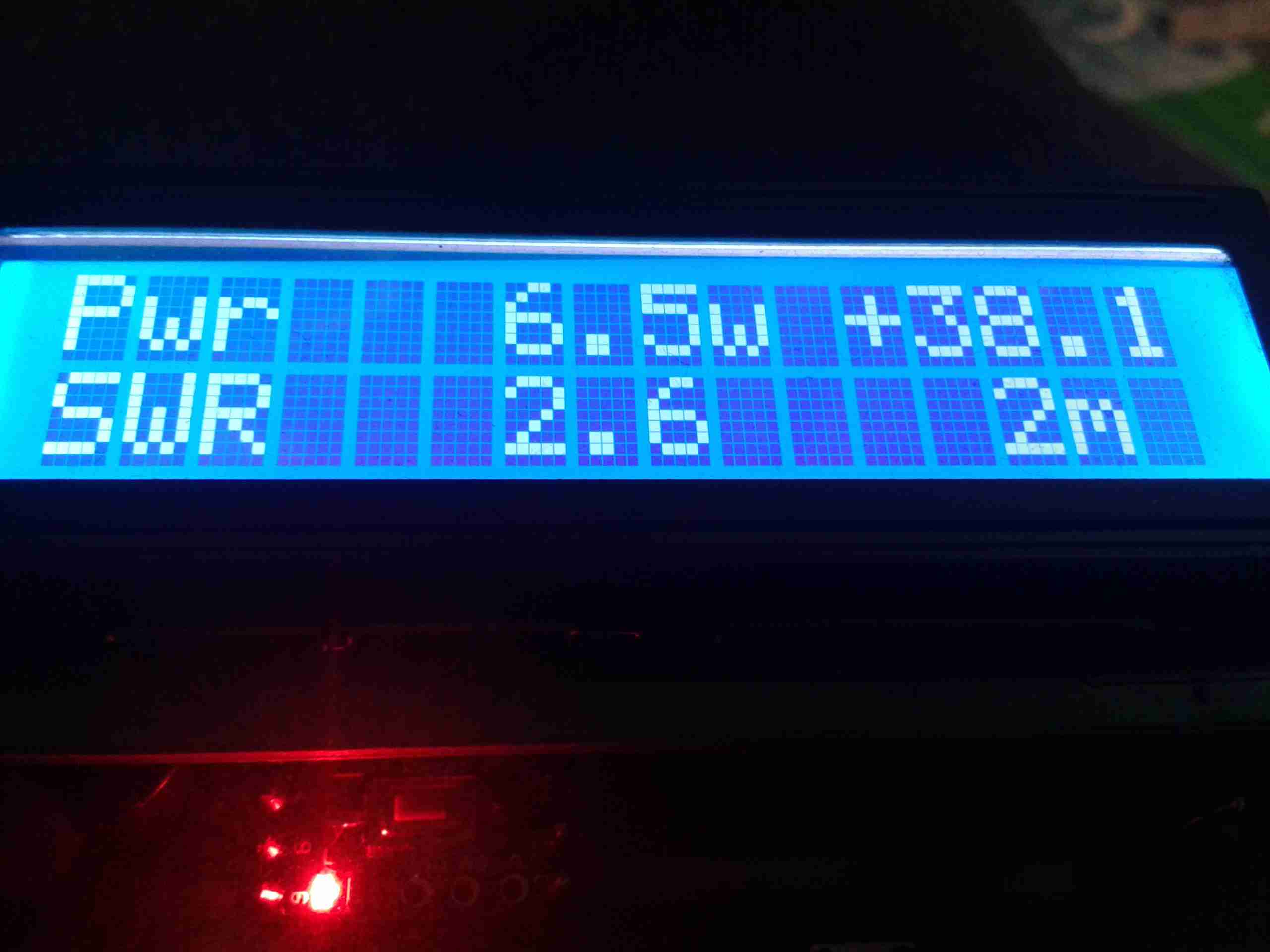
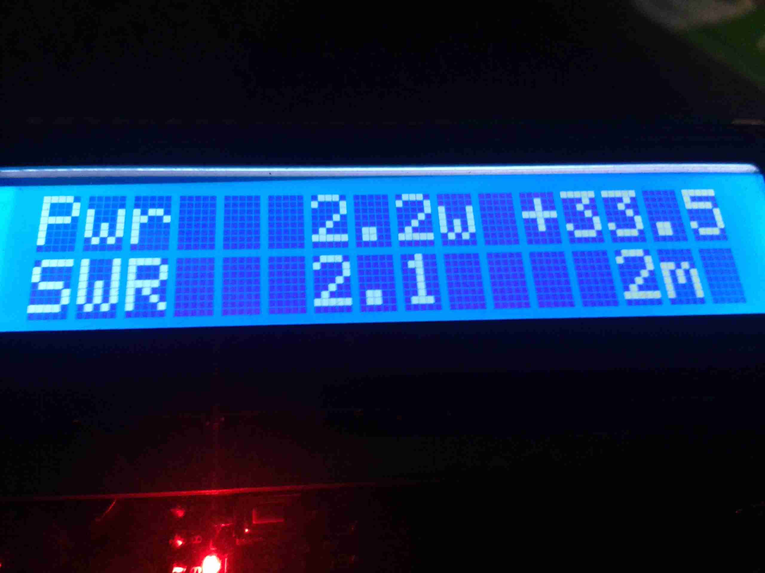
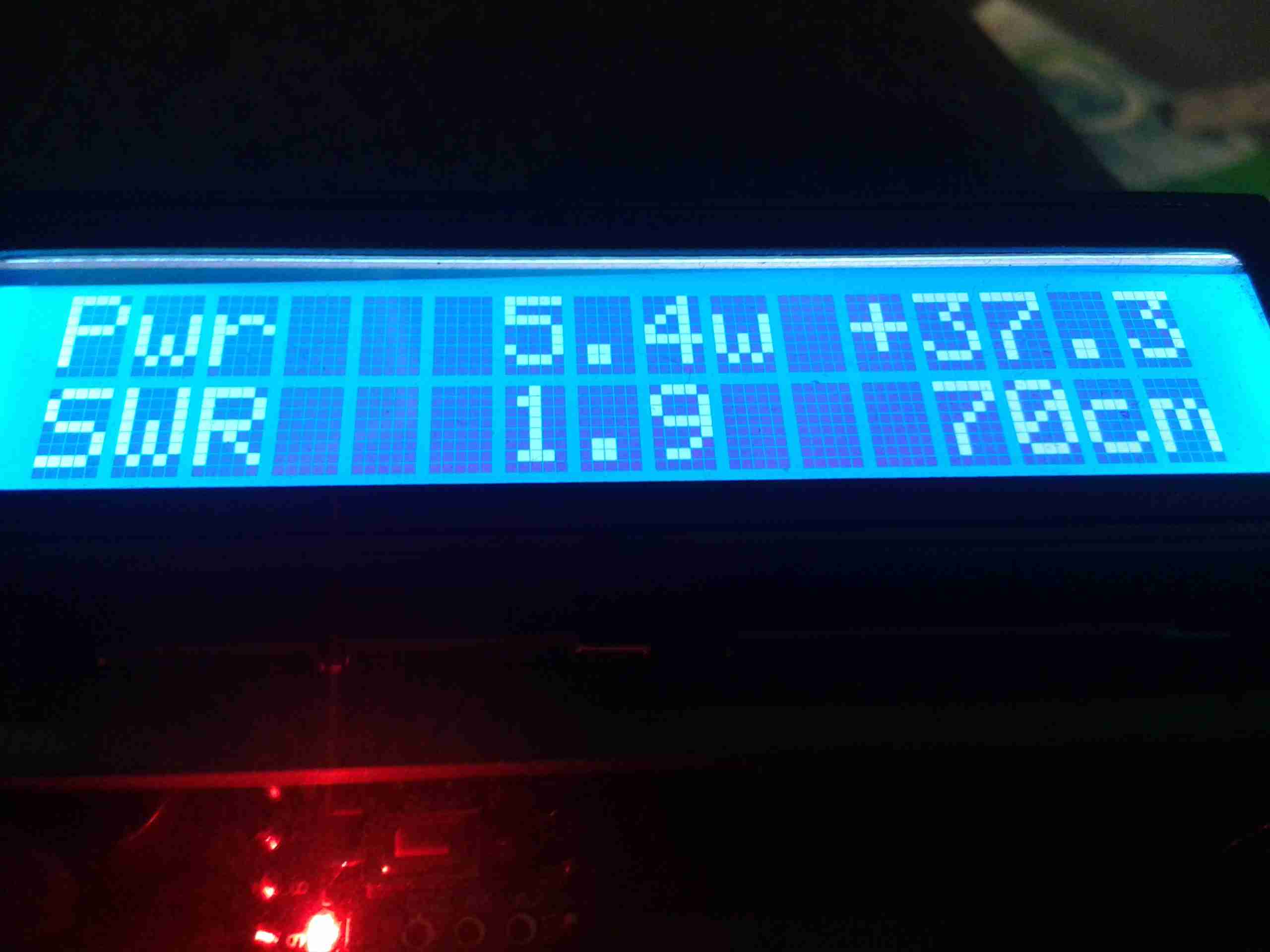
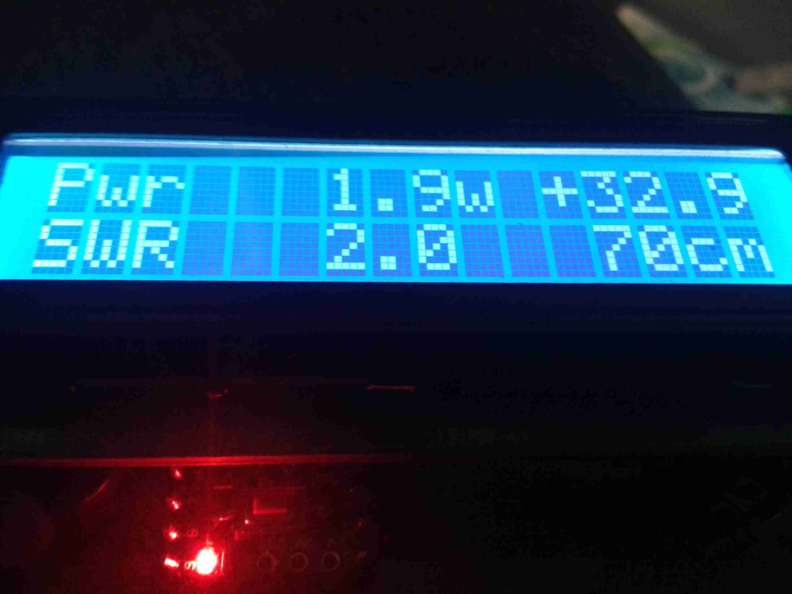
Now the final bits have arrived for the SWR Meter module, I can do the final assembly.
SMA Connectors
Here the SMA connectors are installed on the side of the eBay meter, for forward & reverse power tap.
These are simply tee’d off the wiring inside the meter where it connects to the switch.
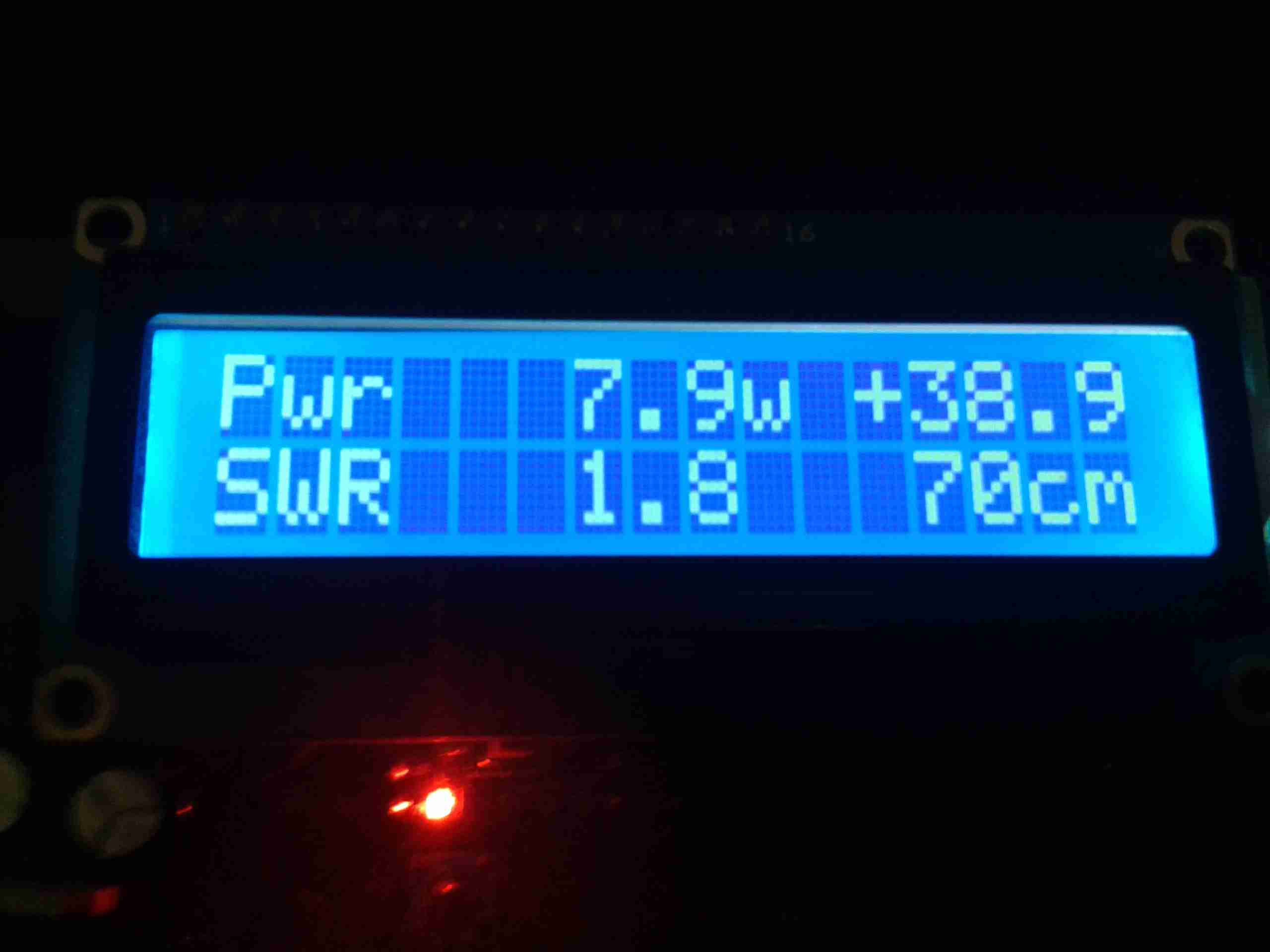
Uncalibrated
The meter is connected to the module via a pair of RG58 SMA leads, above is a readout before calibration, using one of my Baofeng UV-5Rs.
I’m using my GY561 eBay Power Meter as a calibration source, and as this isn’t perfect, the readings will be slightly off. If I can get my hands on an accurate power meter & dummy load I can always recalibrate.
Tools are only as accurate as the standard they were calibrated from!
After calibration, here’s the readings on 2m & 70cm. These readings coincide nicely with the readings the GY561 produce, to within a couple tenths of a watt. SWR is more than 1:1 as the dummy load in the GY561 isn’t exactly 50Ω.
High Power VHFLow Power VHFHigh Power UHFLow Power UHF
Shortly I’ll calibrate against 6m & 10m so I can use it on every band I have access to 🙂
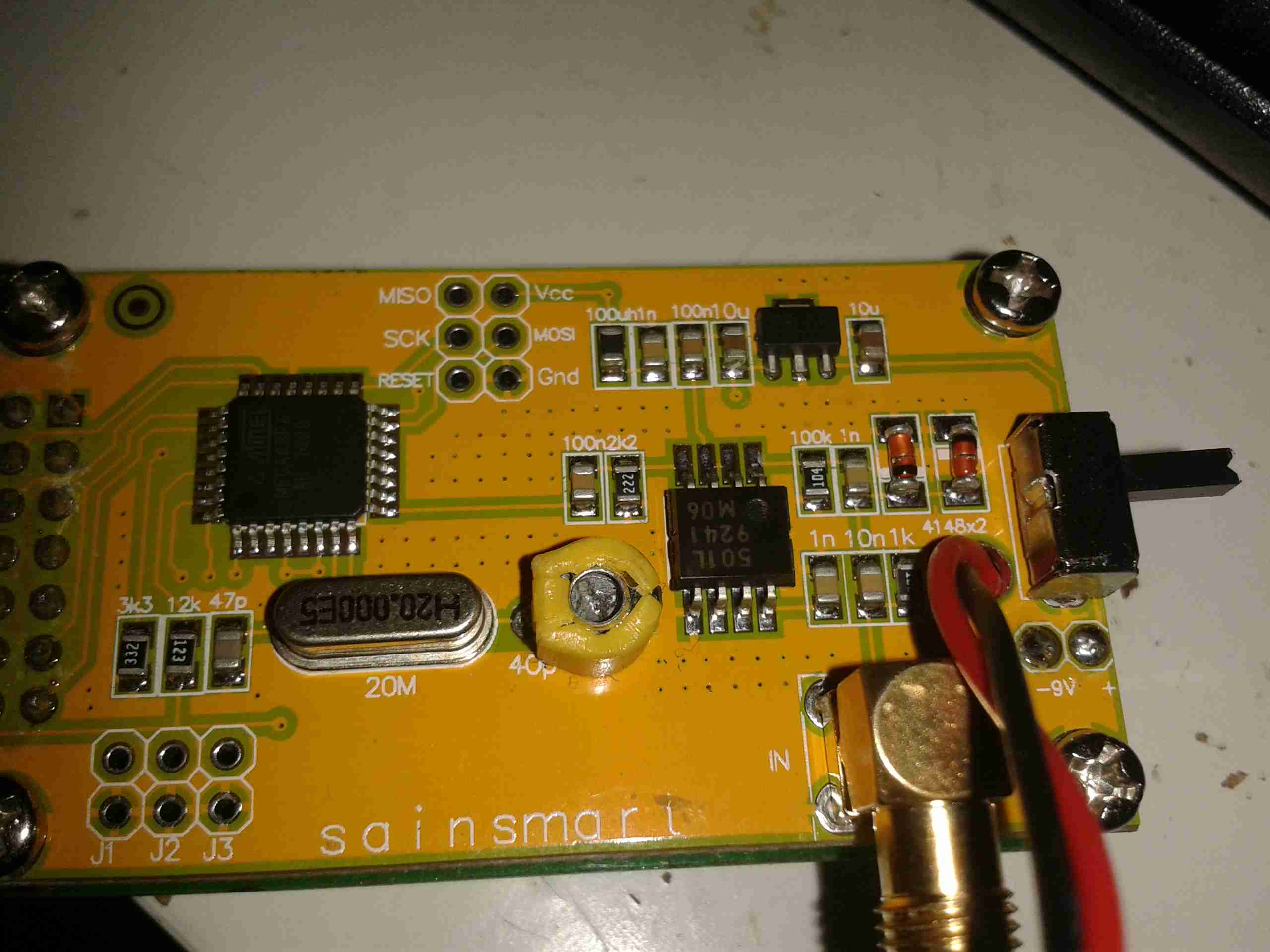
Here’s a quick look at a Sainsmart frequency counter module. These are useful little gadgets, showing the locked frequency on a small LCD display.
It’s built around an ATMega328 microcontroller (µC), and an MB501L Prescaler IC. The circuit for this is very simple, and is easily traced out from the board.
Frequency Counter
Here’s the back of the board, with the µC on the left & the prescaler IC on the right. This uses a rather novel method for calibration, which is the trimmer capacitor next to the crystal. This trimmer varies the frequency of the µC’s oscillator, affecting the calibration.
Input protection is provided by a pair of 1N4148 diodes in inverse parallel. These will clamp the input to +/-1v.
The prescaler IC is set to 1/64 divide ratio. This means that for an input frequency of 433MHz, it will output a frequency of 6.765625MHz to the µC.
The software in the µC will then calculate the input frequency from this intermediate frequency. This is done because the ATMega controllers aren’t very cabable of measuring such high frequencies.
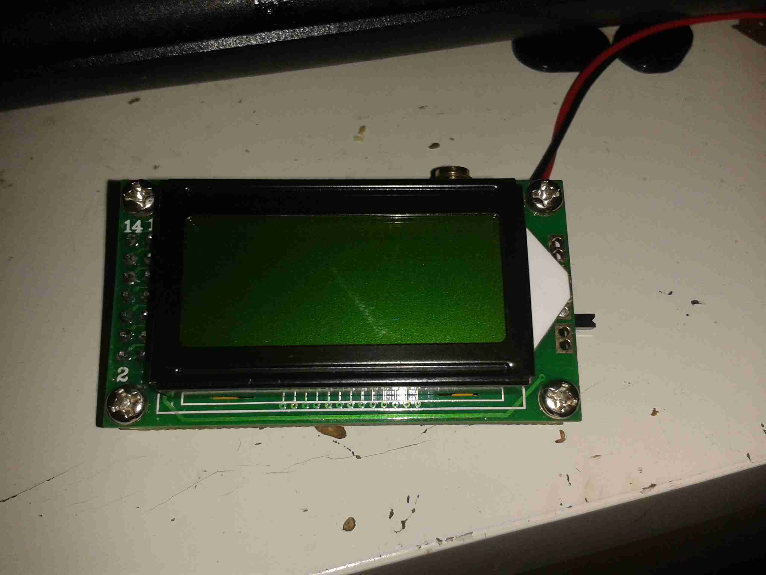
The calculated frequency is then displayed on the LCD. This is a standard HD44780 display module.
LCD
Power is provided by a 9v PP3 battery, which is then regulated down by a standard LM7805 linear regulator.
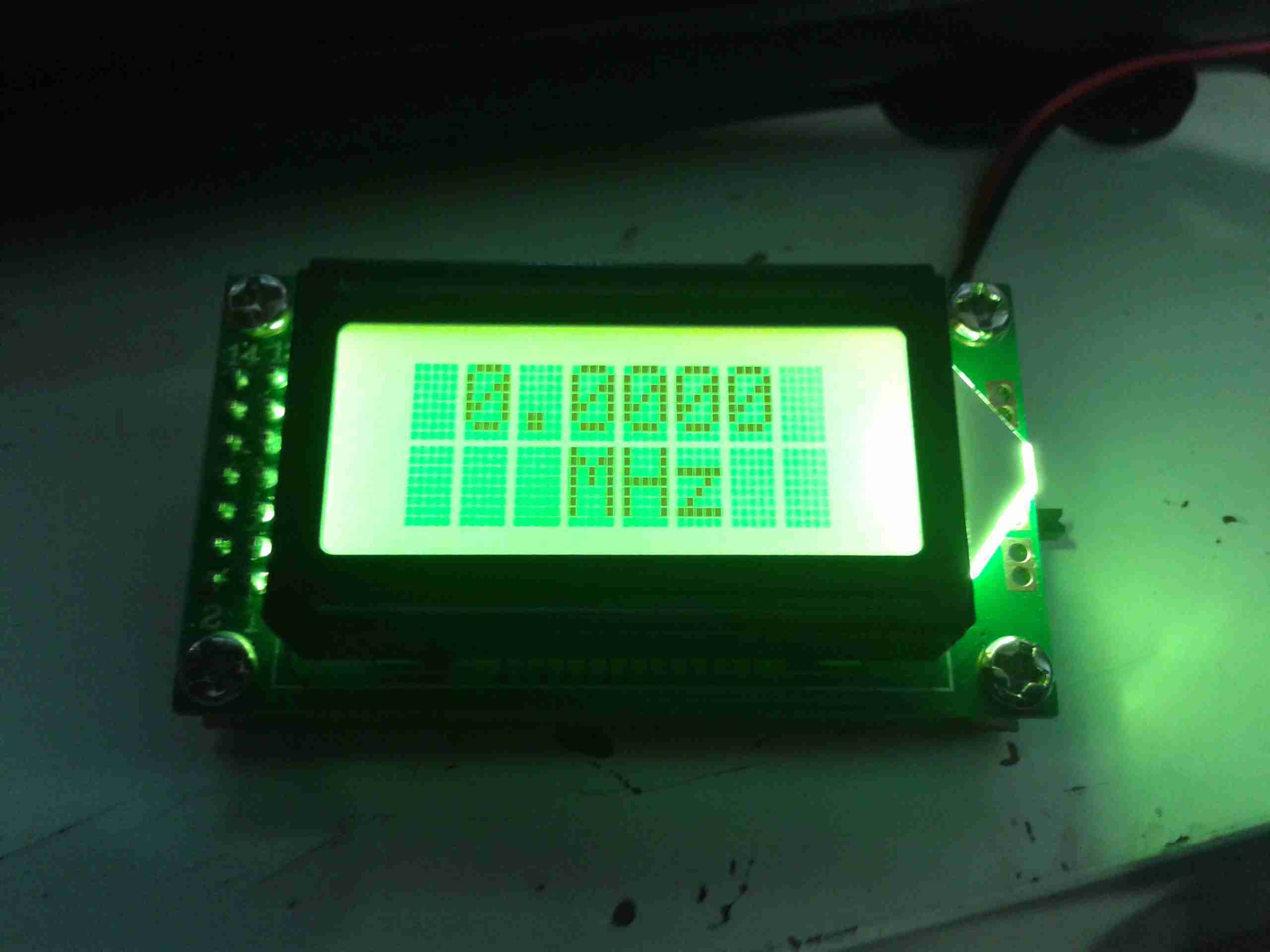
Readout
I’ve found it’s not very accurate at all at the lower frequencies, when I fed it 40MHz from a signal generator it displayed a frequency of around 74MHz. This is probably due to the prescaler & the software not being configured for such a low input. In the case for 40MHz input the scaled frequency would have been 625kHz.
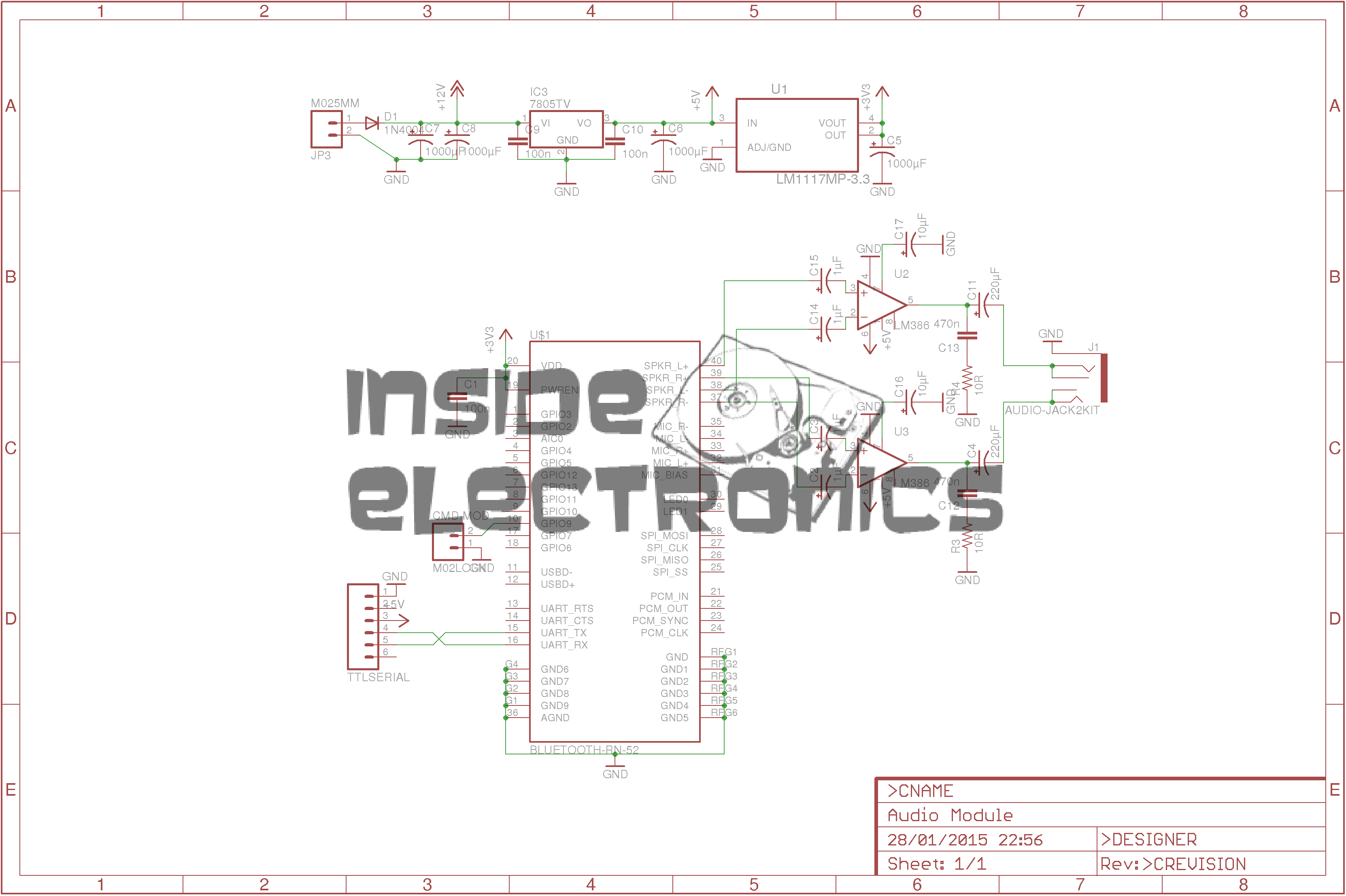
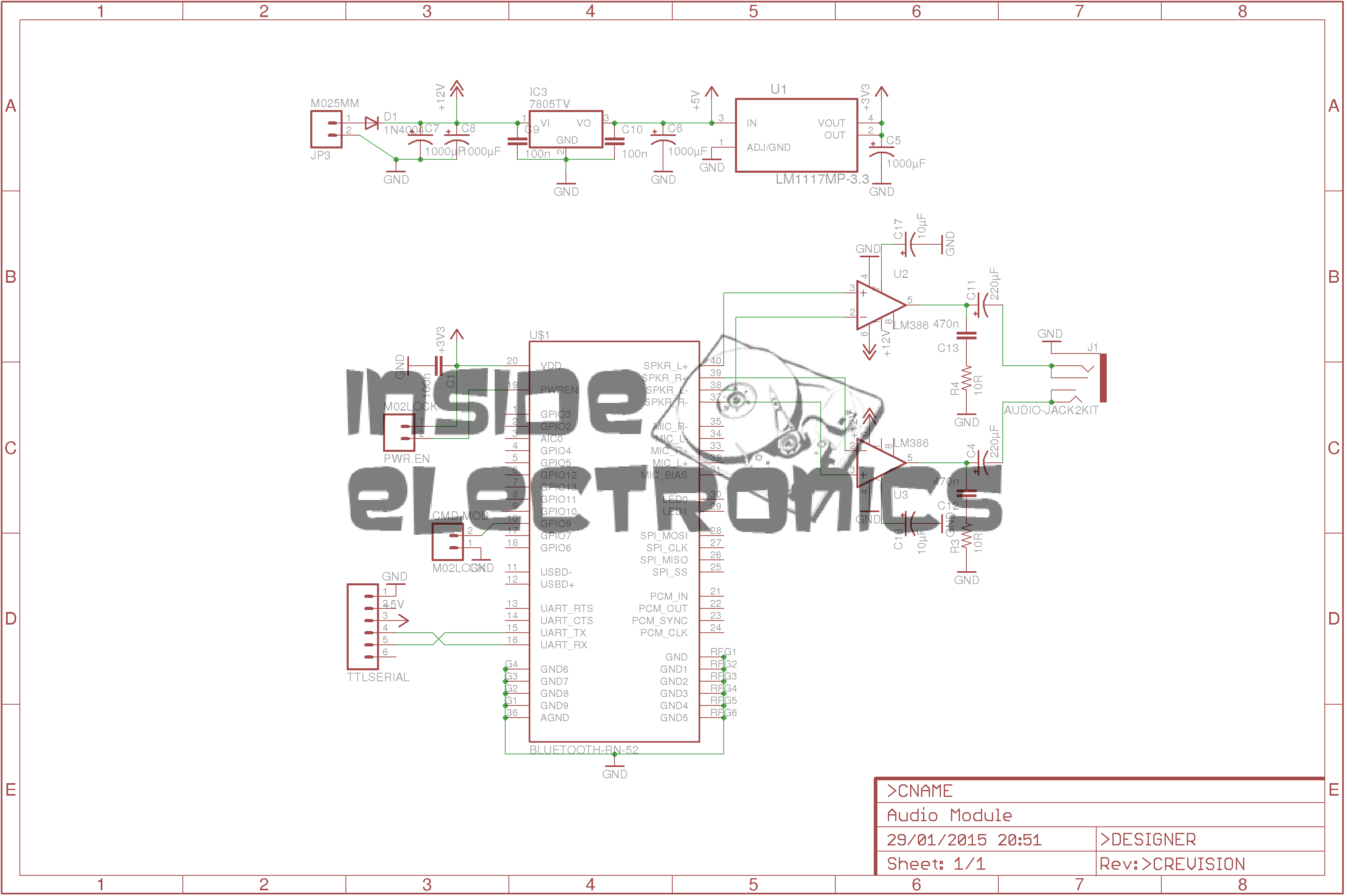
I’ve been doing some tinkering with the RN-52 Bluetooth Audio module from Roving Networks, in prep for building a portable wireless speaker system, & thought I’d share my designs.
Initially I was having some issues with RF noise on the audio output from the RN-52, as I was only using the outputs single-ended. The module didn’t like this treatment, with all the RF whine coming straight out of the speakers.
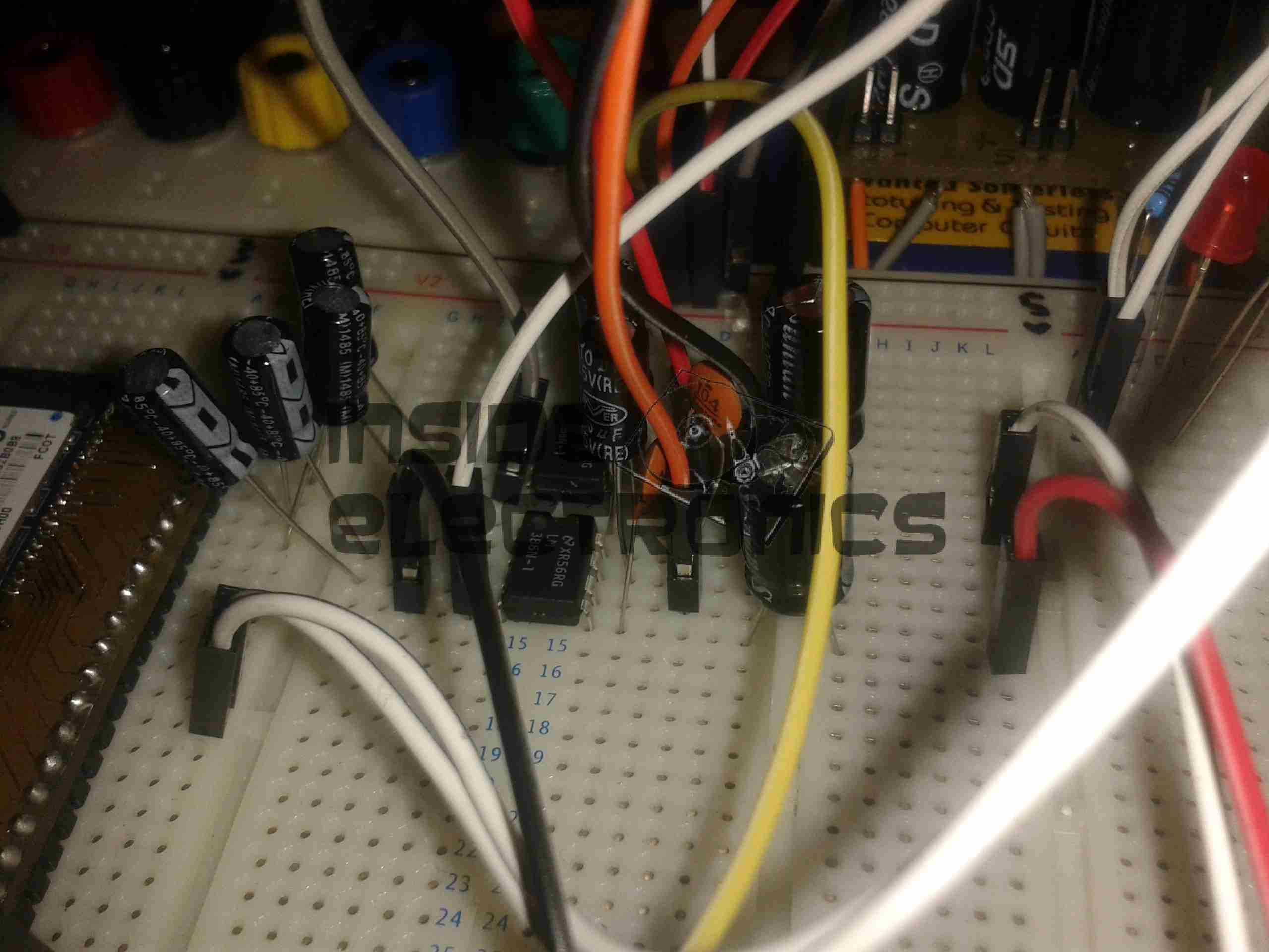
To fix this issue I have used a pair of jellybean LM386 audio power amplifiers, running in differential input mode. This solves the high-pitched whine when the audio is enabled, & also allows the module to directly drive a set of 32Ω headphones at a reasonable level.
In Eagle I have designed a simple board, routing only the audio output, serial TTL & command mode pins out, along with the supporting power supply circuitry to operate from 12v DC.
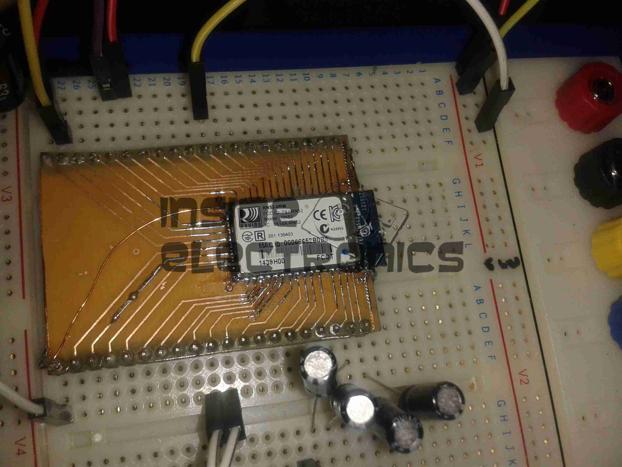
RN-52 Breadboard
Above is the current incarnation of the circuit on the breadboard. The RN-52 is on the left, audio power stage in the centre & headphone output on the right.
RN-52 Breakout
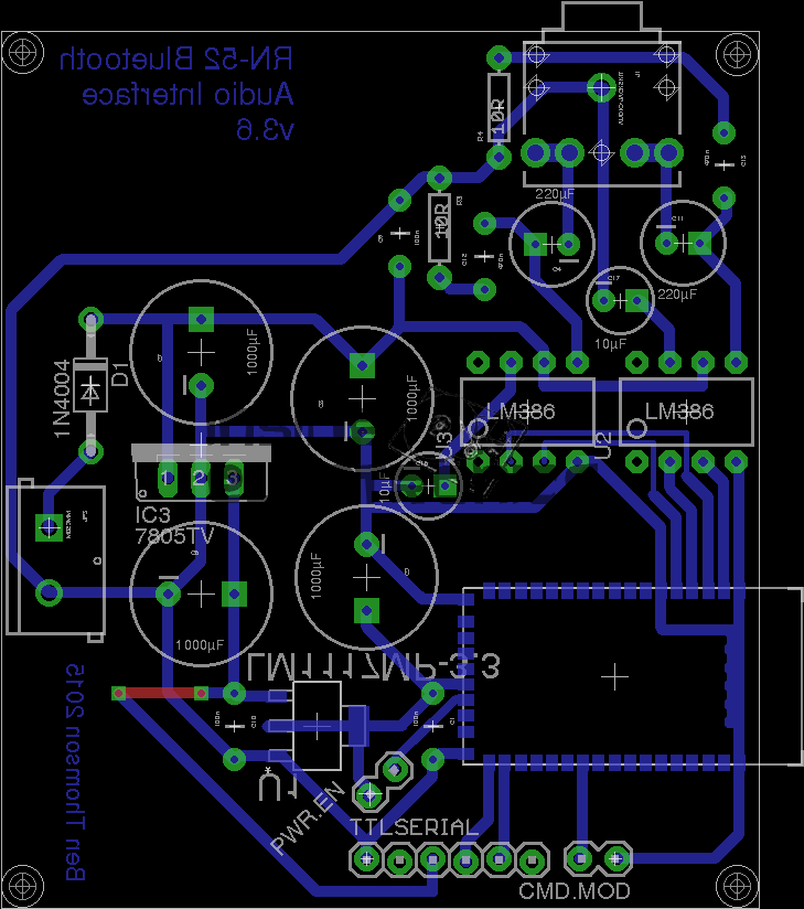
The bluetooth module on a breakout board. I was cheap in this case & etched my own board. I’m not paying Sparkfun, (as much as I like them), an extra ~£10 for a small PCB with the pins broken out. Much cheaper to spend 15 minutes with the laser printer & the iron, & do a toner transfer PCB.
As this board is single sided, I added a ground plane on the underside with copper foil, to help with the RF issues. Breadboards really aren’t all that good at rejecting noise induced when there’s a 2.4GHz transceiver mounted on them.
LM386 Amplifier
The LM386 audio power stage. The differential inputs from the module are capacitively coupled with 1µF electrolytics. This setup remarkably reduced the noise on the output. I left these at their default gain of 20, as I’ll be connecting another high power amplifier stage to drive large speakers.
RN-52 Eagle Layout
Here’s the circuit laid out in Eagle, ready for PCB.
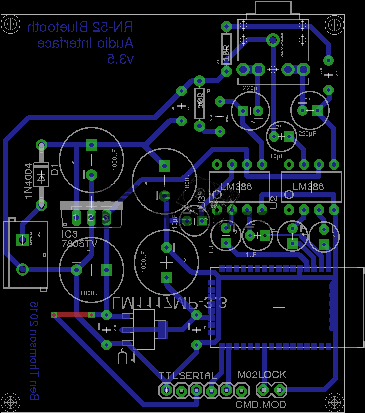
RN-52 Eagle PCB
And here’s the PCB layout. Only one link required for the +5v line from the TTL serial port.
As always, the Eagle PCB & Schematic layout files are available at the bottom of the article.
*Update 29-01-15*
Rerouted a few things:
Moved the audio power stage to the +12v rail to improve sound response. – As the LM386 has a max input voltage of 12v (absolute maximum 15v), a regulated supply is recommended. The LM386-N4 variant has a higher voltage range, up to 18v. This should be suitable for an unregulated supply.
Removed 1µF coupling capacitors to reduce distortion & amplifier hiss. The capacitors appeared to cause some instability on the amplifier, causing random distortion. Removing them has cured this. No signal hiss has also been reduced to a very low level.
Reversed input polarity on input of one of the amplifiers – this appears to produce better audio.
Added PWR.EN header to allow connection of power button. Saves hassle of cycling power to the board when the RN-52 goes into sleep mode.
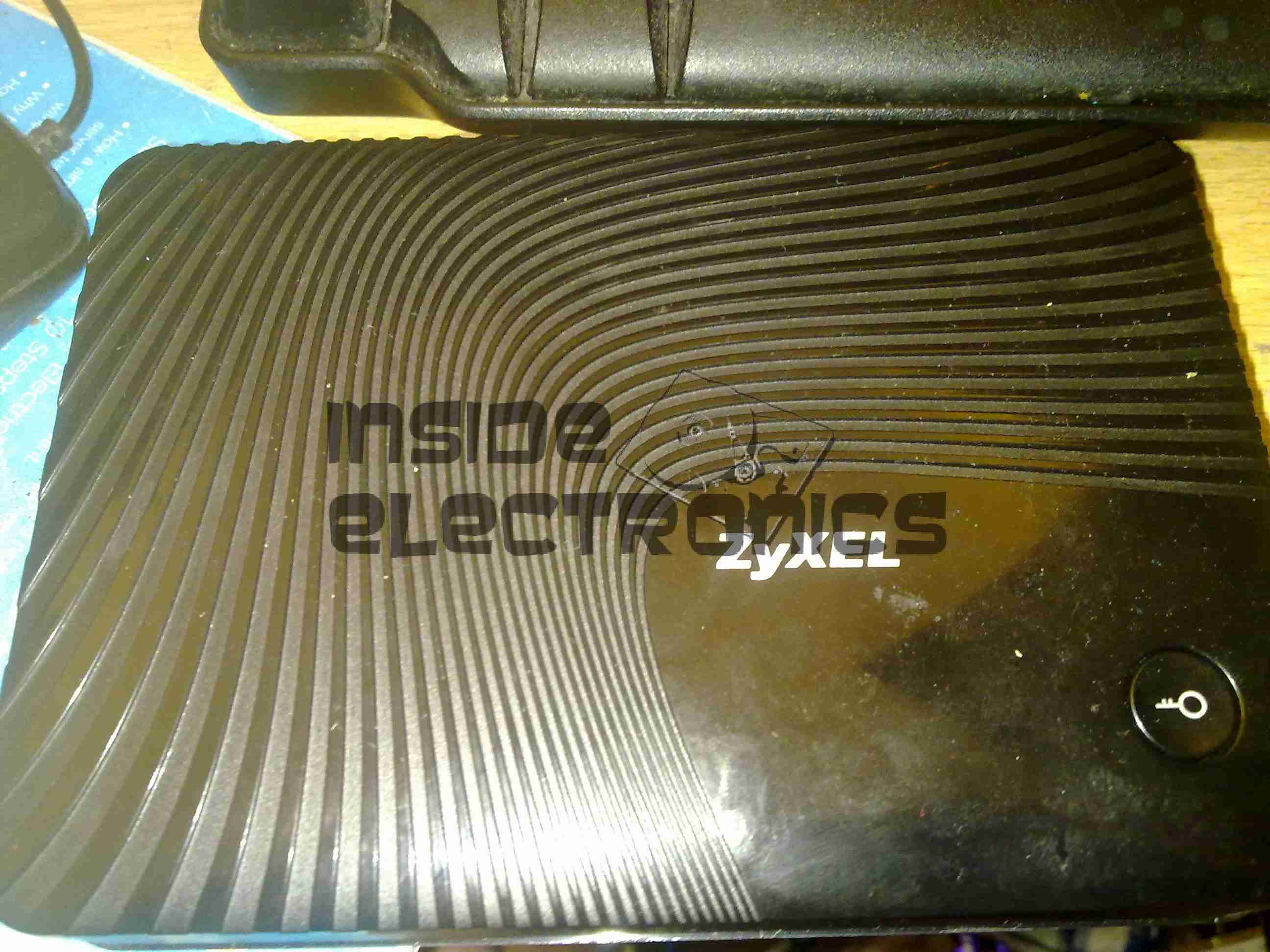
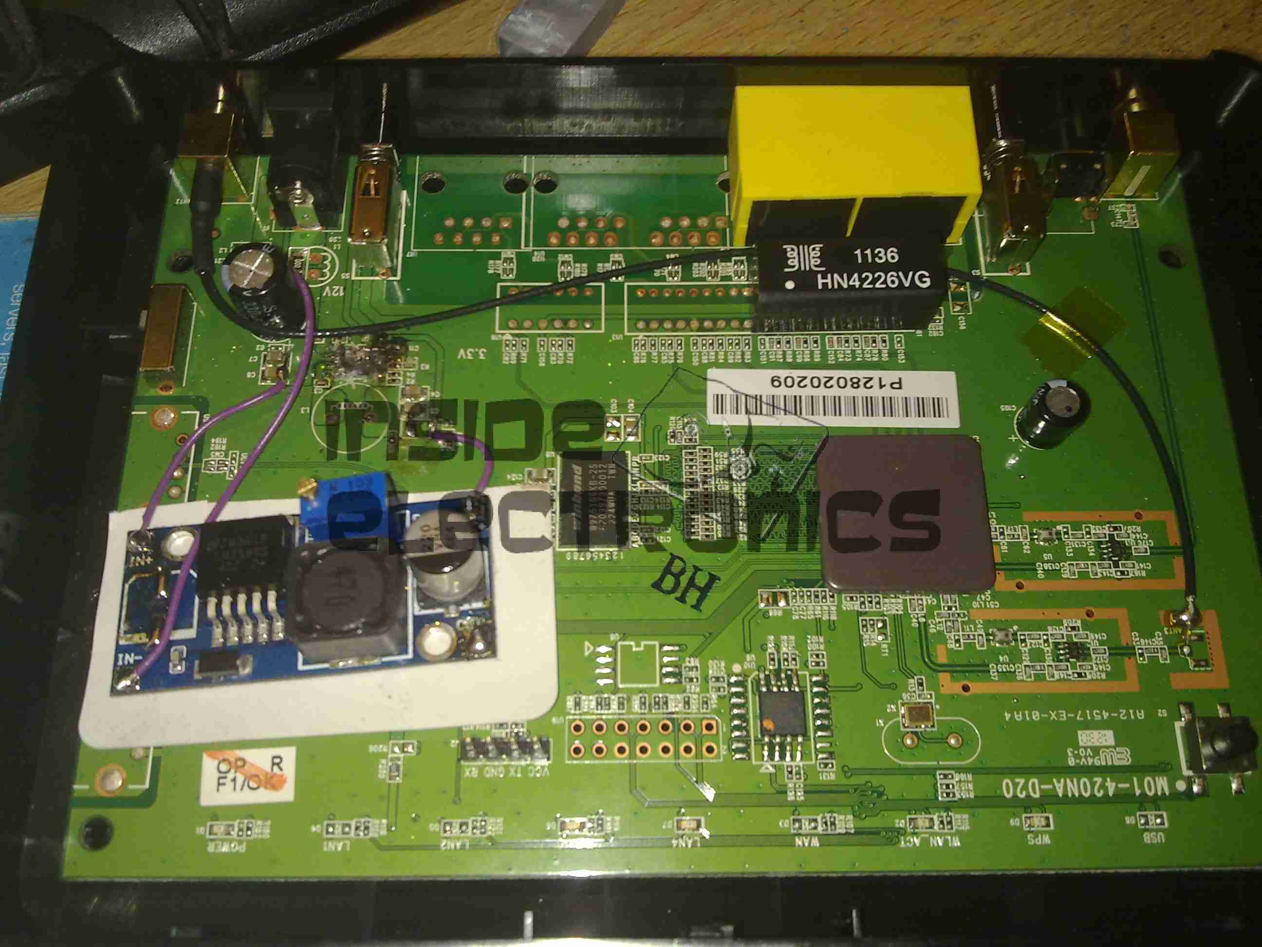
Here is a ZyXel WAP3205 WiFi Access Point that has suffered a reverse polarity event, due to an incorrect power supply being used with the unit.
ZyXEL WAP3205
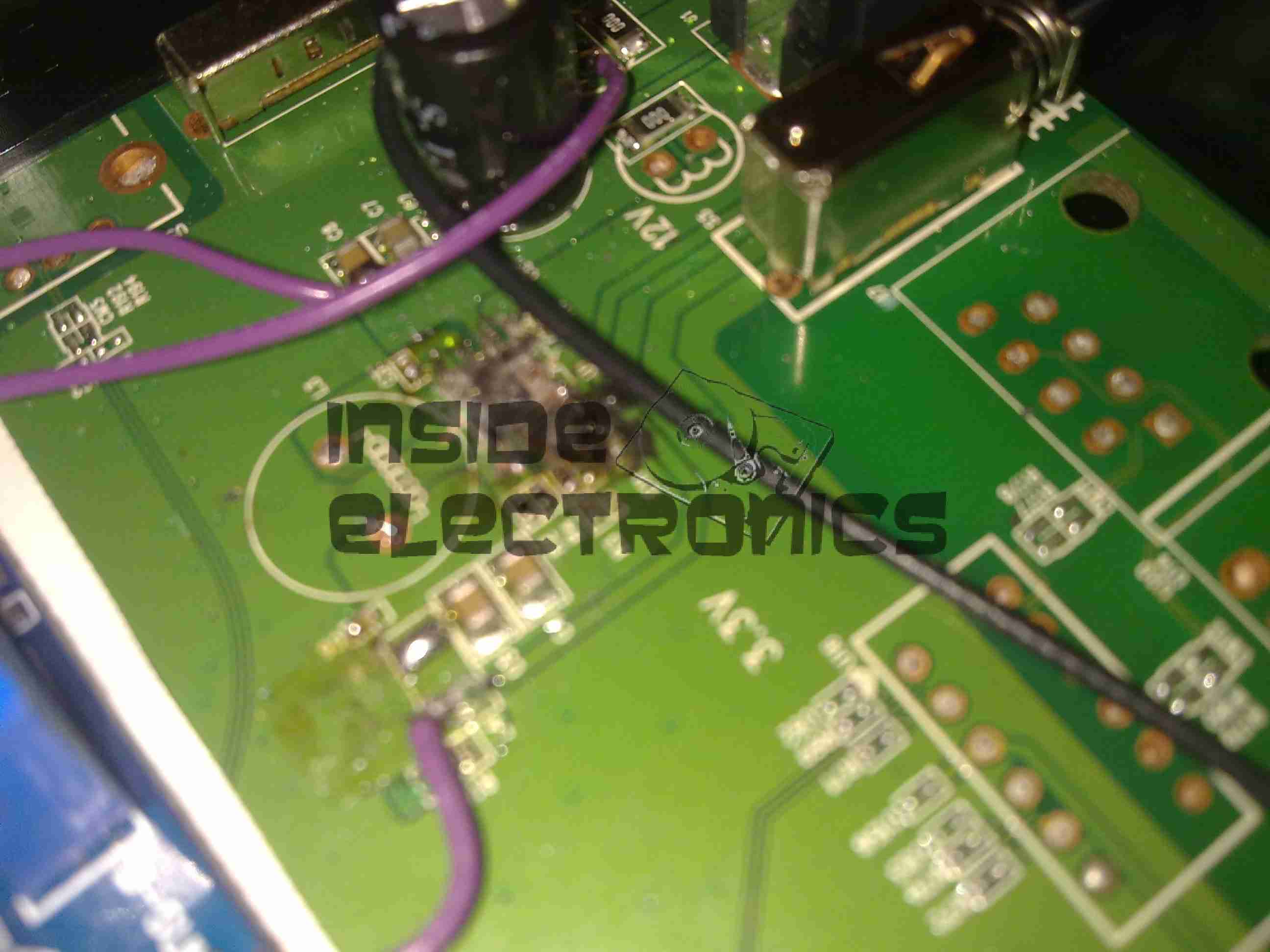
While most electronic gadgets are protected against reverse polarity with a blocking diode, this unit certainly wasn’t. Applying +12v DC the wrong way round resulted in this:
Blown Switchmode IC (Fuzzy Focus)
That is the remains of the 3.3v regulator IC, blown to smithereens & it even attempted an arson attack. Luckily this was the only damaged component, & I was able to repair the unit by replacing the switching IC with a standalone regulator. (Replacing the IC would have been preferable, if there was anything left of it to obtain a part number from).
I scraped away the pins of the IC to clear the short on the input supply, removed the switching inductor, & tacked on an adjustable regulator module set to 3.3v. Luckily the voltage of the supply is handily marked on the PCB next to the circuit.
Replacement PSU
Replacement SMPS in place on top of the PCB. The output of the supply is connected to one of the pads of L4 (on my unit just an 0 ohm link), the +12v input is connected to the + rail side of C8 & C7 & the final ground connection is hooked in to the back of the barrel jack.
After this replacement, the unit booted straight up as if nothing had happened. All the logic is undamaged!
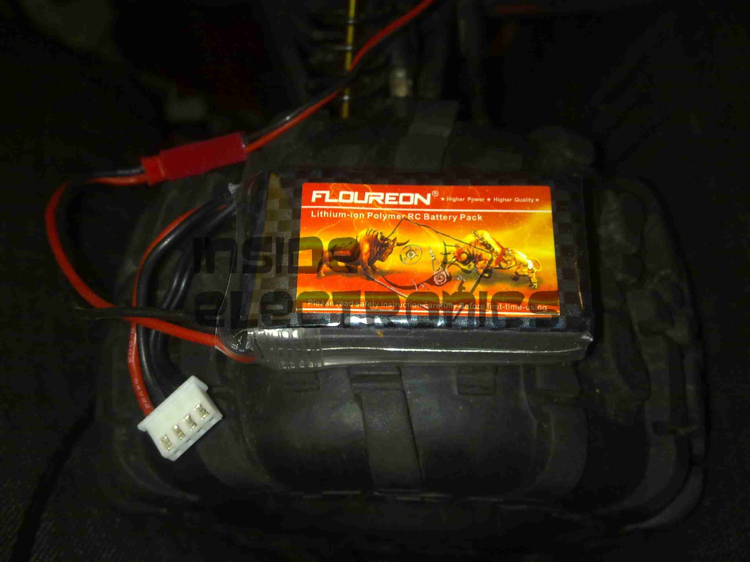
To provide more run time with the conversion to petrol & spark ignition, I have also upgraded the on-board electronics supply to compensate for the extra ~650mA draw of the ignition module.
This modification is centred around a 3S Lithium-Polymer battery pack, providing a nominal 11.1v to a voltage regulator, which steps down this higher voltage to the ~6v required by the receiver & servo electronics.
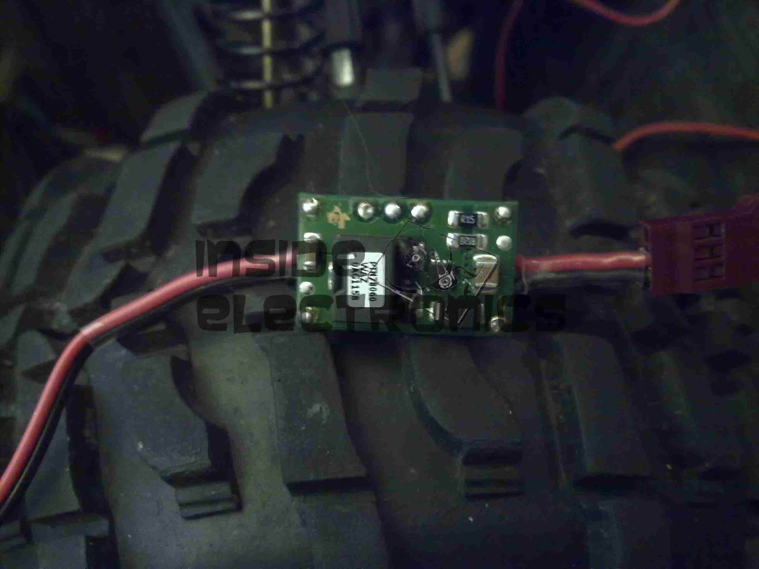
Power RegulatorPower Regulator
The regulator, shown above, is a Texas Instruments PTN78060WAZ wide-input voltage adjustable regulator. This module has an exceptionally high efficiency of ~96% at it’s full output current of 3A. The output voltage is set by a precision resistor, soldered to the back of the module, in this case 6.5v. Standard RC connectors are used on the regulator to allow connection between the power switch & the radio receiver.
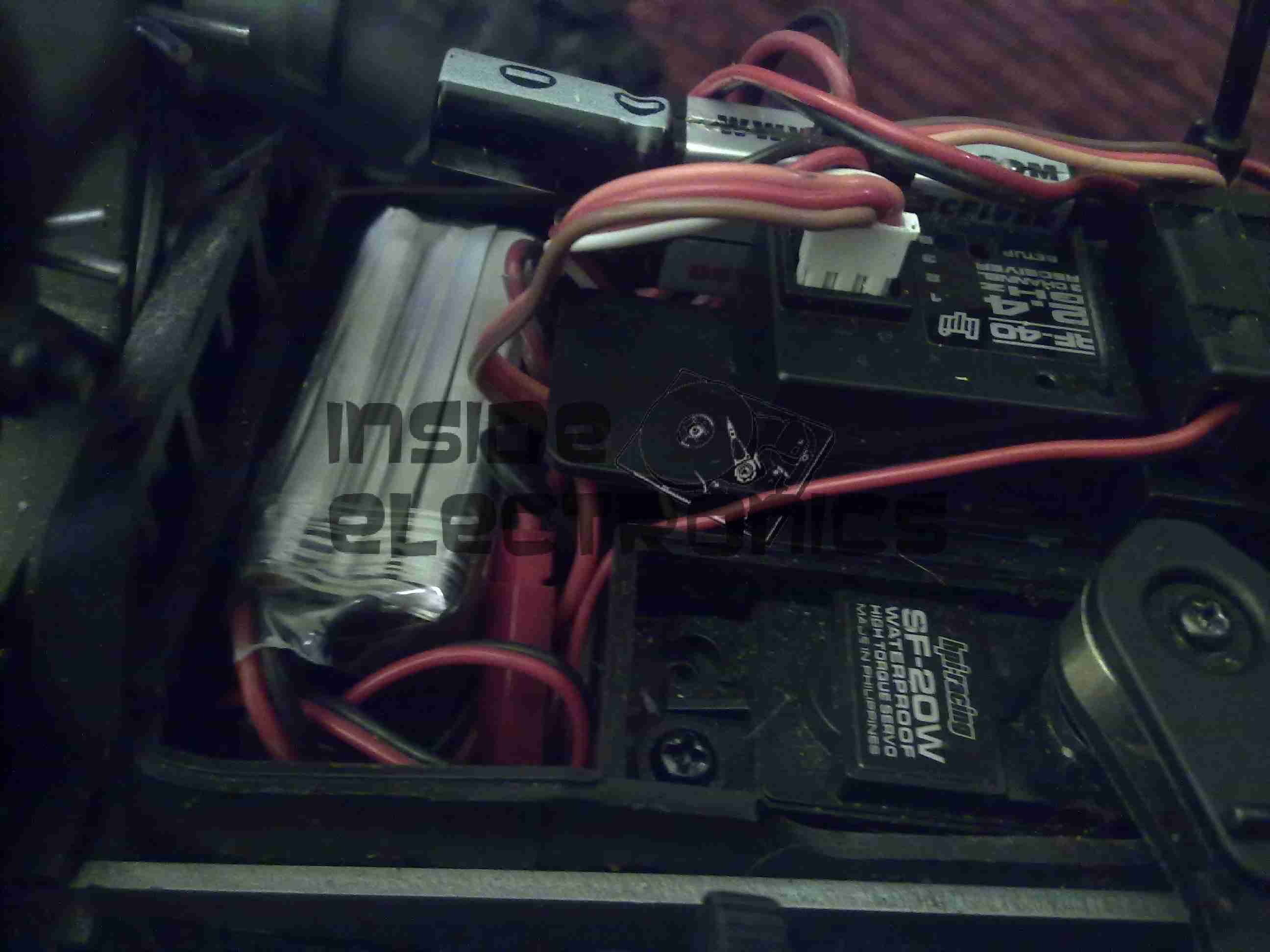
Receiver Box
Everything tucked away into place inside the receiver box. The 3S 1000mAh LiPo fits perfectly in the space where the original Ni-Mh hump pack was located.
The completely stable output voltage of the regulator over the discharge curve of the new battery gives a much more stable supply to the radio & ignition, so I should experience fewer dropouts. Plus the fact that the engine now relies on power from the receiver pack to run, it’s a built in fail safe – if the power dies to the receiver, the engine also cuts out.
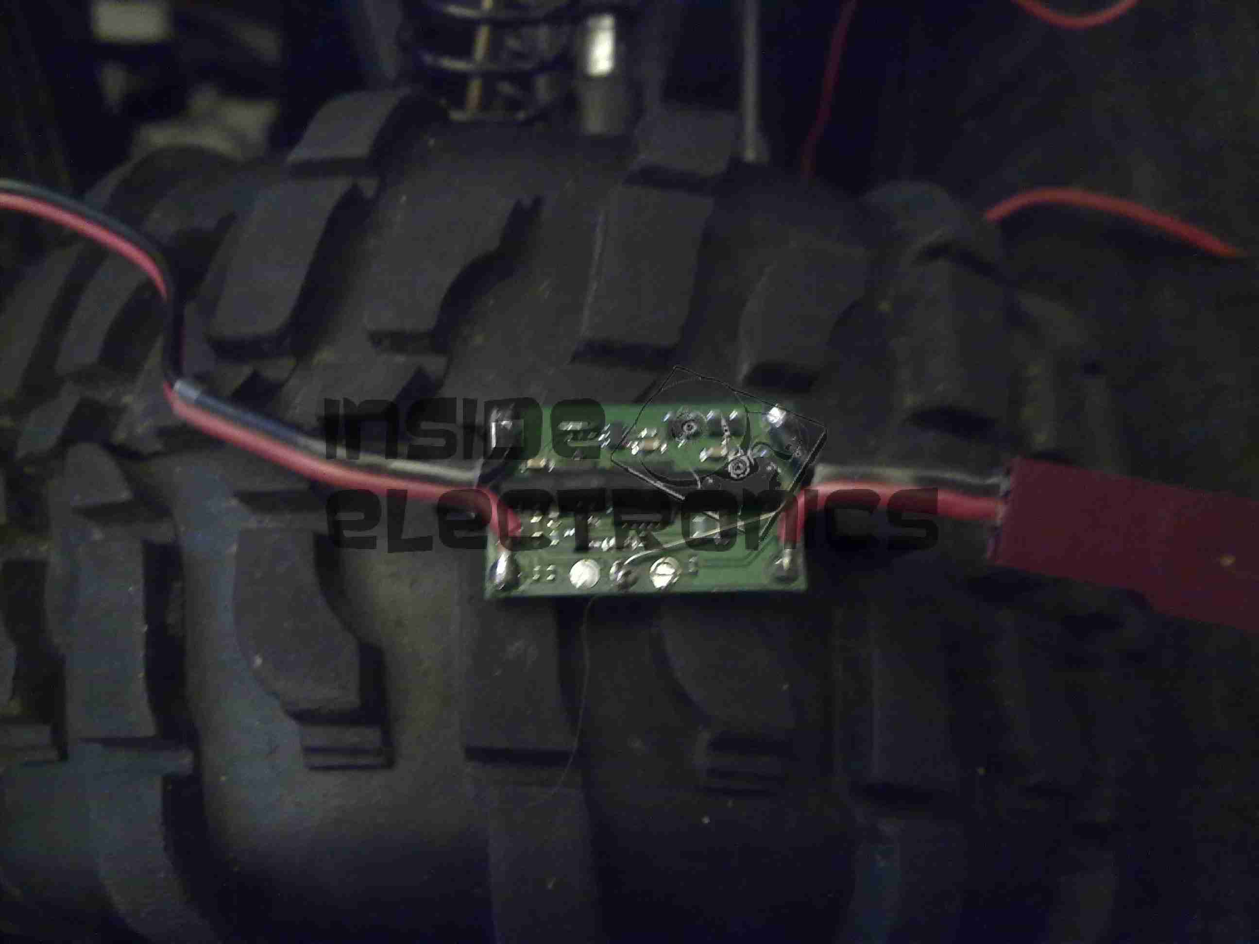
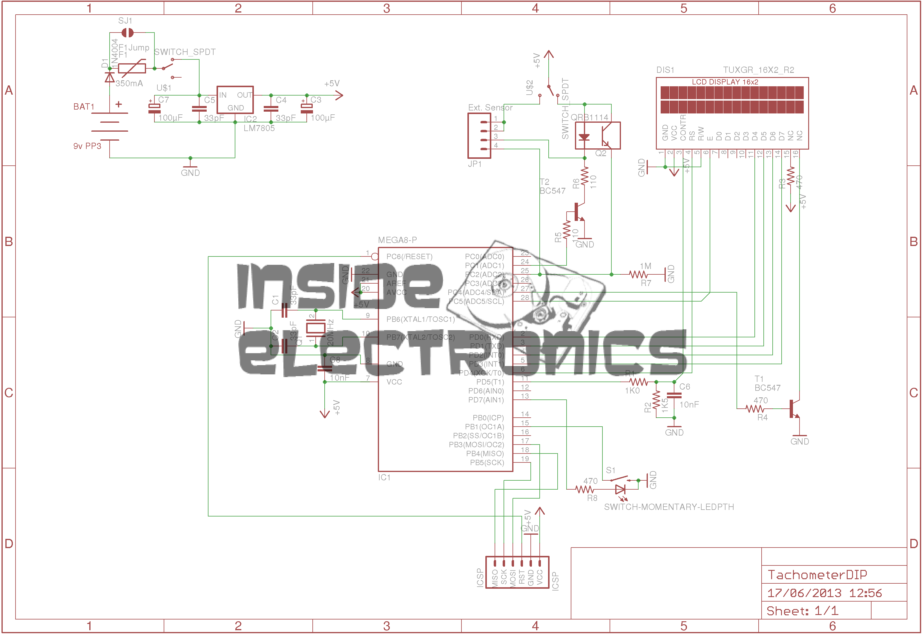
Here is an AVR powered optical tachometer design, that I adapted from the schematic found here.
I made a couple of changes to the circuit & designed a PCB & power supply module to be built in. The original design specified a surface mount IR LED/Photodiode pair, however my adjustment includes a larger IR reflectance sensor built onto the edge of the board, along with a Molex connector & a switch to select an externally mounted sensor instead of the onboard one.
There is also an onboard LM7805 based power supply, designed with a PCB mount PP3 battery box.
The power supply can also be protected by a 350mA polyfuse if desired. If this part isn’t fitted, then a pair of solder bridge pads are provided within the footprint for the fuse to short out the pads.
For more information on the basic design, please see the original post with the link at the top of the page.
Schematic
Here is an archive of the firmware & the Eagle CAD files for the PCB & schematic design.
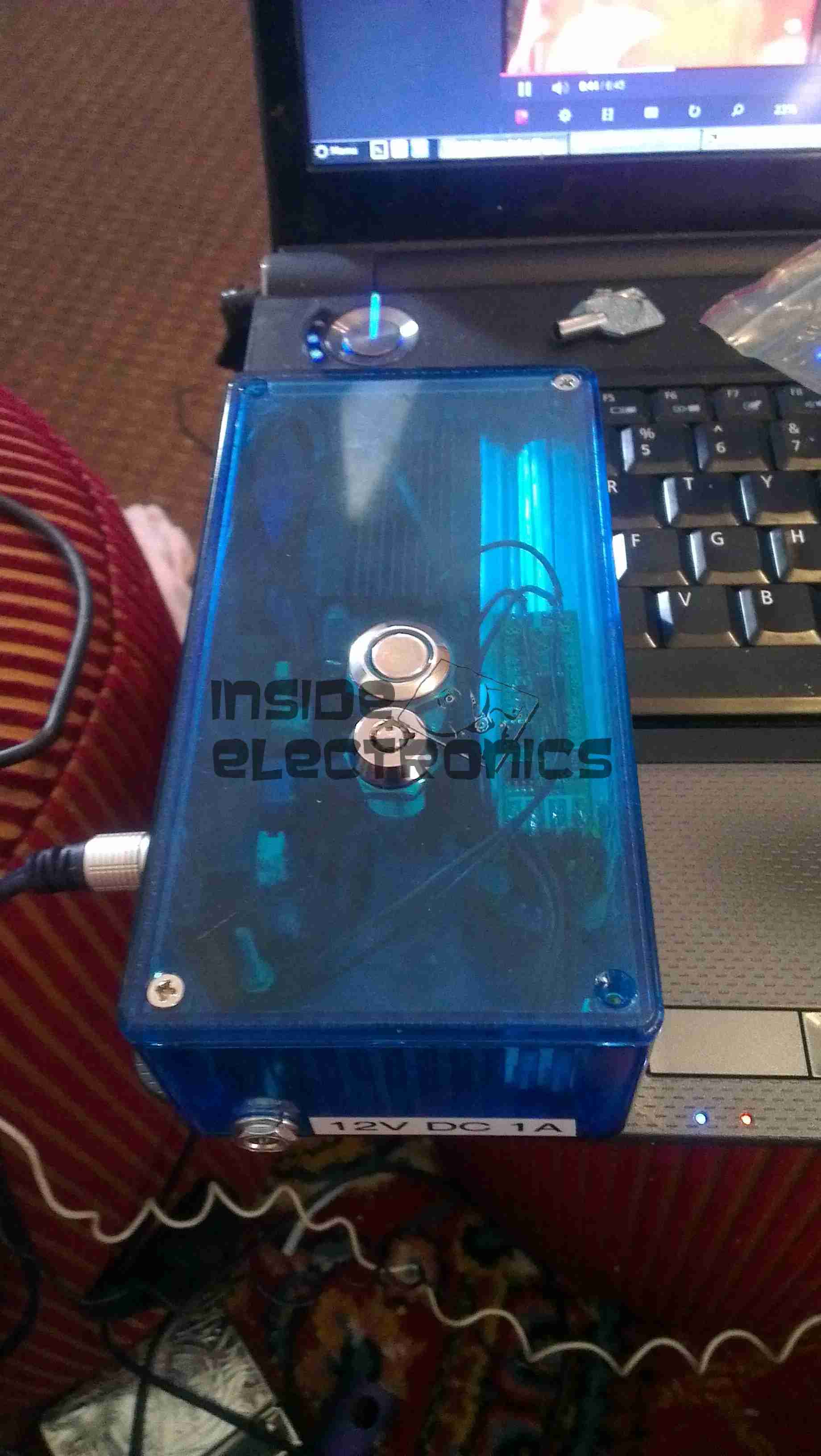
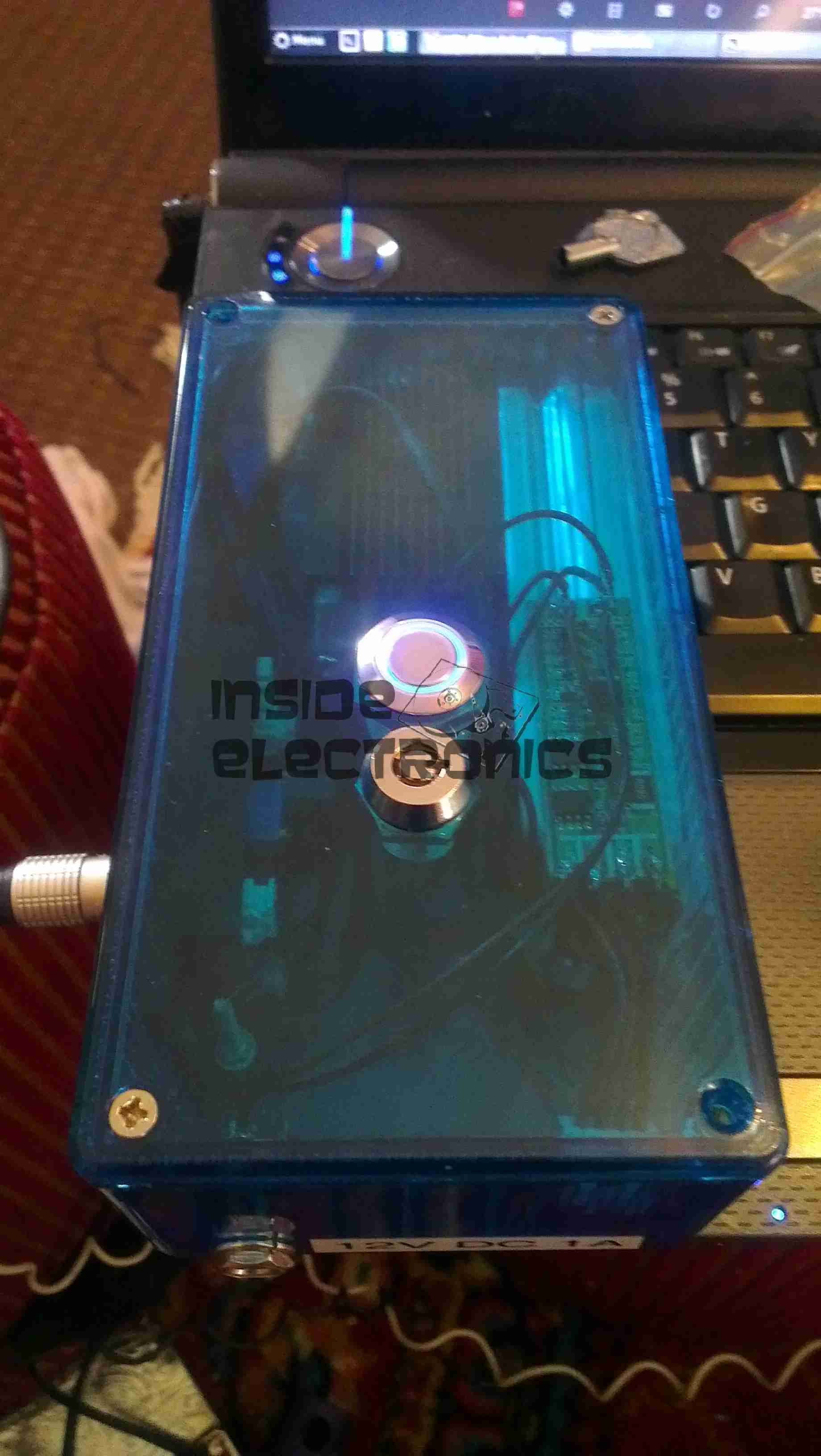
Here is a followup from the 1.5W laser module post.
The module has been fitted into a housing, with a 2.2Ah Li-Poly battery pack. Charging is accomplished with an external 12.6v DC power supply.
Above can be seen the pair of switches on the top, the keyswitch must be enabled for the laser to fire.
Armed
When armed, the ring around the push button illuminates blue, as a warning that the unit is armed.
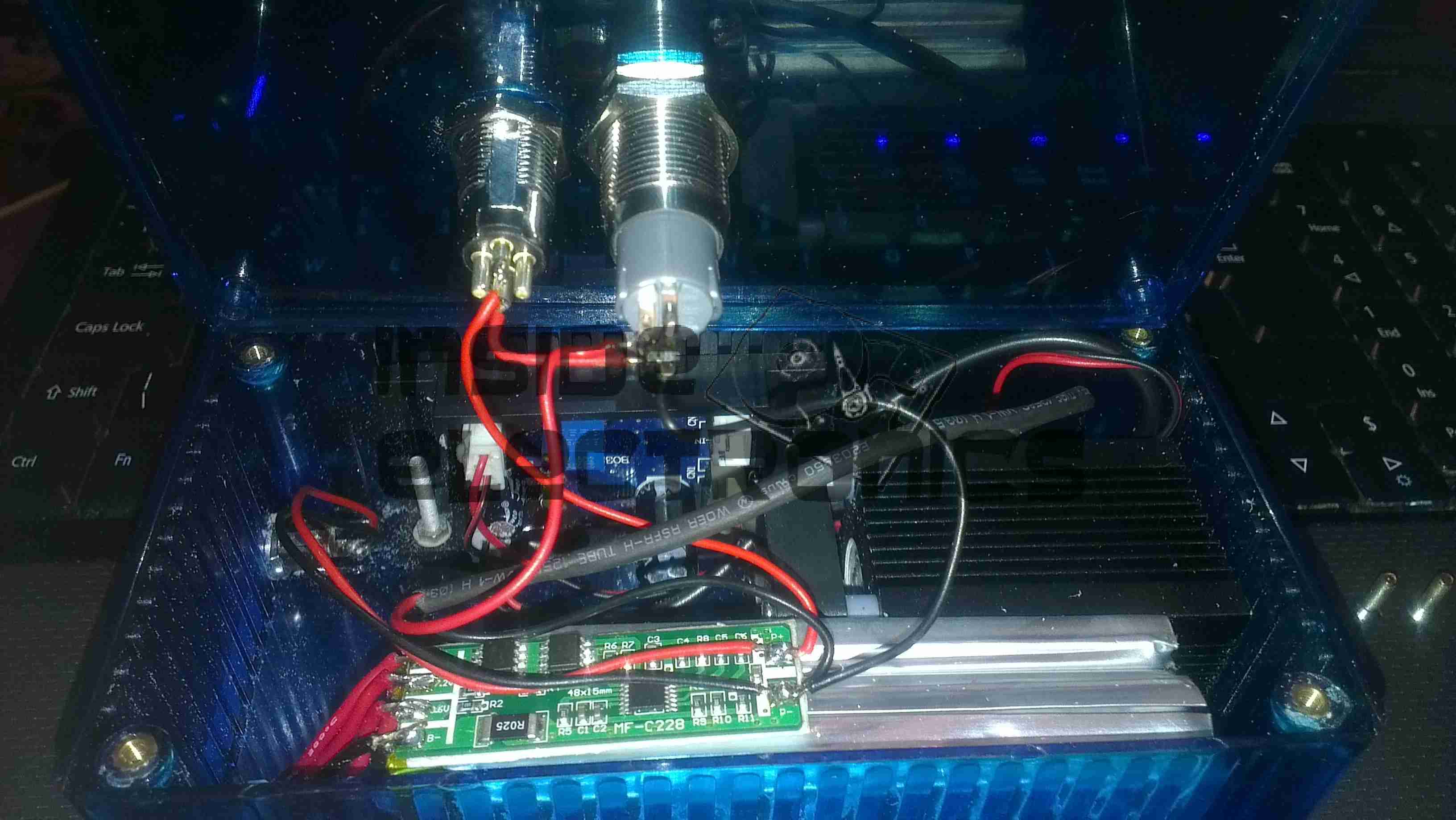
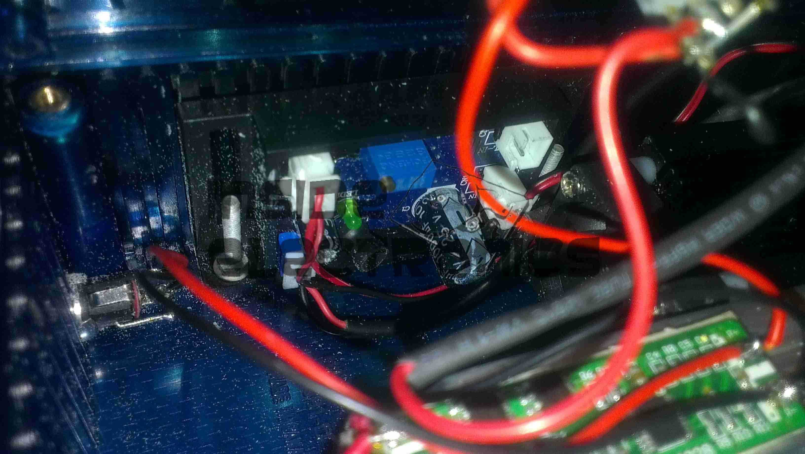
Switch Wiring
Inside the unit. The Li-Poly battery pack is at the bottom, with it’s protection & charging circuitry on the top. The switches are wired in series, with the LED connected to illuminate when the keyswitch is turned to the ON position.
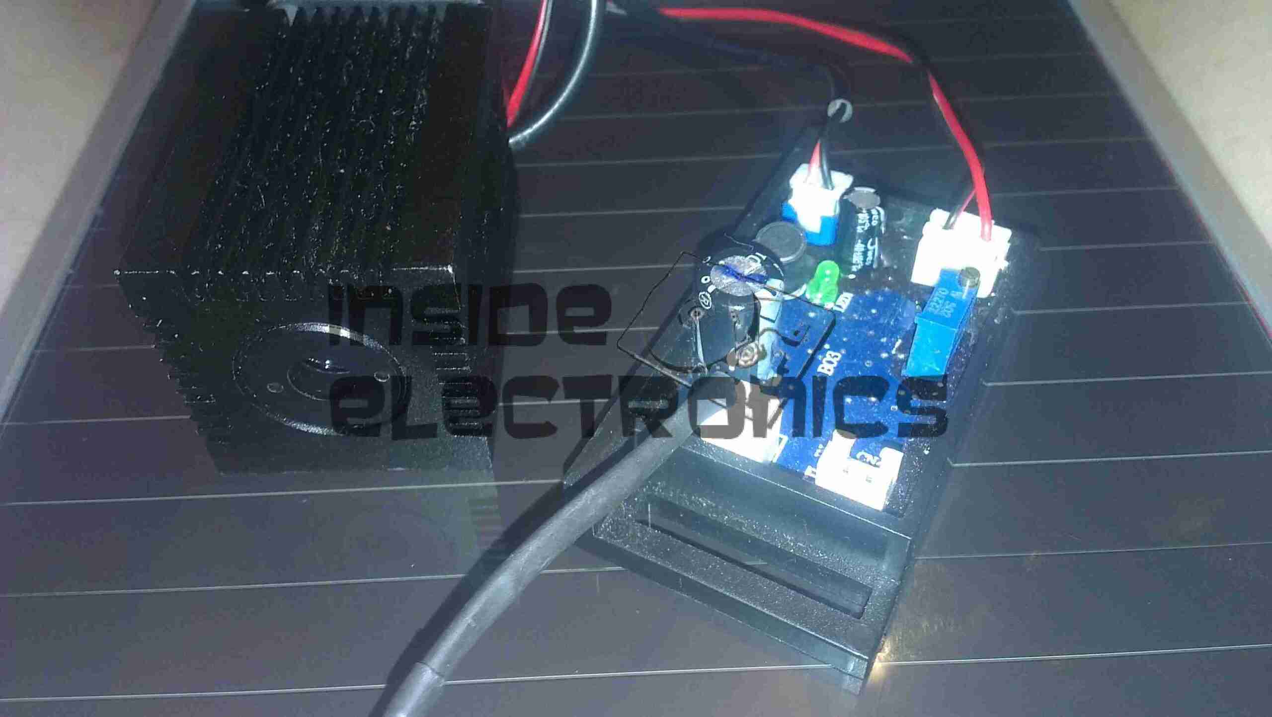
Laser Driver
The push button applies power to the laser driver module, which regulates the input power to safely drive the semiconductor laser in the aluminium heatsink housing.
This is a fan cooled 445nm laser module, which emits in the blue part of the spectrum.
Fan cooled & with TTL control built in, this is the beginning of a new laser projector.
I thought this would be of interest, as it’s from a drive circa 2001, (DVD-CD-RW).
It’s the biggest & most complex optical block I’ve ever seen, with totally separate beam paths for the IR CD beam & the visible DVD beam. It also combines the use of bare laser diodes & combined diode/photodiode array modules for the pickup.
Cover Removed
Here’s a look at the optics inside the sled, on the left is a bare laser diode & photodiode array, for the CD reading, and the bottom right has the DVD combined LD/PD array module. The beam from the CD diode has to pass though some very complex beam forming optics & a prism to fold it round to the final turning mirror to the objective lens at top center.
There are also two separate photodiodes which are picking up the waste beam from the prisms, most likely for power control.
I bought one of these cheap HID kits from eBay to build a high-brightness work light that I could run from my central 12v supply.
At £14.99 I certainly wasn’t expecting anything more than the usual cheap Chinese construction. And that’s definitely what I got 😀
Potted PCB
The casing is screwed together with the cheapest of screws, with heads that are deformed enough to present a problem with removal.
As can be seen here, the inside of the unit is potted in rubber compound, mostly to provide moisture resistance, as these are for automotive use.
The ballast generates a 23kV pulse to strike the arc in the bulb, then supplies a steady 85v AC at 3A, 400Hz to maintain the discharge.
This module could quite easily be depotted as the silicone material used is fairly soft & can be removed with a pointed tool.
Hi-Lo Bulb Assembly
Here is the bulb removed from it’s mount. Under the bulb itself is a solenoid, which tilts the bulb by a few degrees, presumably to provide dim/dip operation for a headlight. This functionality is superfluous to my requirements.
Here’s the teardown of the projector itself! On the right is the info label from the projector, which covers the flex ribbon to the VGA/composite input board below.
This unit is held together with Allen screws, but is easy to get apart.
PicoP Display Engine
Here’s the insides of the projector, with just the top cover removed. The main board can be seen under the shielding can, the Micro HDMI connector is on the left & the MicroUSB connection is on the right. The USB connection is solely for charging the battery & provides no data interface to the unit.
On top of the main board is the shield can covering the PicoP Display Engine driver board, this shield was soldered on so no peek inside unfortunately!
Laser Module
The laser module itself is in the front of the unit, the laser assemblies are closest to the camera, on the left is the Direct Doubled Green module, in the centre is the blue diode, and the red diode on the right. Inside the module itself is an arrangement of mirrors & beamsplitters, used to combine the RGB beams from the lasers into a single beam to create any colour in the spectrum.
Module Innards
Here is the module innards revealed, the laser mounts are at the top of the screen, the green module is still mounted on the base casting.
The three dichroic mirrors in the frame do the beam combining, which is then bounced onto the mirror on the far left of the frame, down below the MEMs. From there a final mirror directs the light onto the MEMs scanning mirror before it leaves through the output window.
A trio of photodiodes caters for beam brightness control & colour control, these are located behind the last dichroic turning mirror in the centre of the picture.
Green Module Cavity
This is inside the green laser module, showing the complexity of the device. This laser module is about the size of a UK 5p coin!
Green Module Labeled
And here on the left is the module components labelled.
Main PCB Top
Here is the main PCB, with the unit’s main ARM CPU on the right, manufactured by ST.
User buttons are along the sides.
Main PCB Bottom
Other side of the main board, with ICs that handle video input from the HDMI connector, battery charging via the USB port & various other management.
Here is a 2Gbit Fibre Channel transceiver from Cisco Systems in SFP module format.
Shield Removed
Here the shield has been removed from the bottom of the module (it just clips off). The bottom of the PCB can be seen, with the copper interface on the left & the rubber boots over the photodiode & 850 nm laser on the right.
PCB Bottom
Here the PCB has been completely removed from the frame, the fibre ends slide into the rubber tubes on the right.
PCB Top
Top of the PCB, showing the chipset. There are a pair of adjustment pots under some glue, next to the chipset, presumably for adjusting laser power & receive sensitivity. The laser diode & photodiode are inside the soldered cans on the right hand side of the board, with the optics required to couple the 850nm near-IR light into the fibre.
Tip Jar
If you’ve found my content useful, please consider leaving a donation by clicking the Tip Jar below!
All collected funds go towards new content & the costs of keeping the server online.